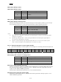
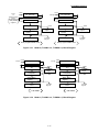
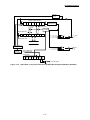
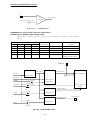
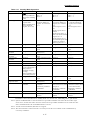
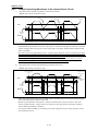
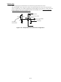
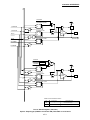
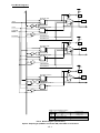
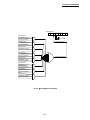
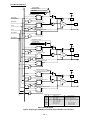
1
CMOS 8-BIT MICROCONTROLLER
LC870G00 SERIES
USER’S MANUAL
www.onsemi.com
REV : 1.00
ON Semiconductor
Digital Solution Division
Microcontroller & Flash Business Unit
ON Semiconductor and the ON logo are registered trademarks of Semiconductor Components Industries, LLC (SCILLC) or its subsidiaries in the United States
and/or other countries. SCILLC owns the rights to a number of patents, trademarks, copyrights, trade secrets, and other intellectual property. A listing of
SCILLC’s product/patent coverage may be accessed at www.onsemi.com/site/pdf/Patent-Marking.pdf . SCILLC reserves the right to make changes without
further notice to any products herein. SCILLC makes no warranty, representation or guarantee regarding the suitability of its products for any particular purpose,
nor does SCILLC assume any liability arising out of the application or use of any product or circuit, and specifically disclaims any and all liability, including
without limitation special, consequential or incidental damages. “Typical” parameters which may be provided in SCILLC data sheets and/or specifications can
and do vary in different applications and actual performance may vary over time. All operating parameters, including “Typicals” must be validated for each
customer application by customer’s technical experts. SCILLC does not convey any license under its patent rights nor the rights of others. SCILLC products are
not designed, intended, or authorized for use as components in systems intended for surgical implant into the body, or other applications intended to support or
sustain life, or for any other application in which the failure of the SCILLC product could create a situation where personal injury or death may occur. Should
Buyer purchase or use SCILLC products for any such unintended or unauthorized application, Buyer shall indemnify and hold SCILLC and its officers,
employees, subsidiaries, affiliates, and distributors harmless against all claims, costs, damages, and expenses, and reasonable attorney fees arising out of,
directly or indirectly, any claim of personal injury or death associated with such unintended or unauthorized use, even if such claim alleges that SCILLC was
negligent regarding the design or manufacture of the part. SCILLC is an Equal Opportunity/Affirmative Action Employer. This literature is subject to all
applicable copyright laws and is not for resale in any manner.
Contents
Chapter 1 Overview········································································ 1-1
1.1
1.2
1.3
1.4
1.5
1.6
1.7
1.8
1.9
1.10
Overview ······················································································ 1-1
Features ······················································································ 1-1
Pin Assignment·············································································· 1-6
System Block Diagram ···································································· 1-7
Pin Description ·············································································· 1-8
On-chip Debugger Pin Connection Requirements ································ 1-10
Recommended Unused Pin Connections ··········································· 1-10
Port Output Types ········································································ 1-10
User Option Table ········································································ 1-11
Power Pin Treatment Recommendations (VDD1, VSS1) ······················· 1-11
Chapter 2 Internal Configuration ····················································· 2-1
2.1
2.2
2.3
2.4
2.5
2.6
2.7
2.8
2.9
2.10
2.11
Memory Space ·············································································· 2-1
Program Counter (PC) ···································································· 2-1
Program Memory (ROM) ································································· 2-2
Internal Data Memory (RAM) ···························································· 2-2
Accumulator/A Register (ACC/A) ······················································· 2-3
B Register (B)················································································ 2-3
C Register (C) ··············································································· 2-4
Program Status Word (PSW) ···························································· 2-4
Stack Pointer (SP) ·········································································· 2-5
Indirect Addressing Registers ··························································· 2-5
Addressing Modes·········································································· 2-6
2.11.1
2.11.2
2.11.3
2.11.4
2.11.5
2.11.6
2.11.7
Immediate Addressing (#) ······························································· 2-6
Indirect Register Indirect Addressing ([Rn]) ········································· 2-7
Indirect Register + C Register Indirect Addressing ([Rn,C]) ···················· 2-7
Indirect Register (R0) + Offset Value indirect Addressing ([off]) ··············· 2-8
Direct Addressing (dst) ··································································· 2-8
ROM Table Look-up Addressing ······················································· 2-9
External Data Memory Addressing ···················································· 2-9
2.12 Wait Sequence ············································································· 2-10
2.12.1
2.12.2
Wait Sequence Occurrence ····························································2-10
What is a Wait Sequence? ·····························································2-10
Chapter 3 Peripheral System Configuration ······································ 3-1
3.1
Port 0 ·························································································· 3-1
3.1.1
3.1.2
3.1.3
Overview ····················································································· 3-1
Functions····················································································· 3-1
Related Registers ·········································································· 3-2
i
Contents
3.1.4
3.1.5
3.2
Port 1 ·························································································· 3-6
3.2.1
3.2.2
3.2.3
3.2.4
3.2.5
3.3
Overview ····················································································3-45
Functions····················································································3-45
Circuit Configuration ·····································································3-46
Related Registers ·········································································3-48
Serial Interface 1 (SIO1) ································································· 3-51
3.7.1
3.7.2
3.7.3
3.7.4
3.7.5
3.8
Overview ····················································································3-32
Functions····················································································3-32
Circuit Configuration ·····································································3-34
Related Registers ·········································································3-39
Base Timer (BT) ··········································································· 3-45
3.6.1
3.6.2
3.6.3
3.6.4
3.7
Overview ····················································································3-21
Functions····················································································3-21
Circuit Configuration ·····································································3-23
Related Registers ·········································································3-27
Timer/Counter 1 (T1) ····································································· 3-32
3.5.1
3.5.2
3.5.3
3.5.4
3.6
Overview ····················································································3-17
Functions····················································································3-17
Related Registers ·········································································3-18
Options ······················································································3-19
HALT and HOLD Mode Operation····················································3-19
Timer/Counter 0 (T0) ····································································· 3-21
3.4.1
3.4.2
3.4.3
3.4.4
3.5
Overview ····················································································· 3-6
Functions····················································································· 3-6
Related Registers ·········································································· 3-7
Options ······················································································3-16
HALT and HOLD Mode Operation····················································3-16
Port 7 ························································································· 3-17
3.3.1
3.3.2
3.3.3
3.3.4
3.3.5
3.4
Options ······················································································· 3-4
HALT and HOLD Mode Operation····················································· 3-4
Overview ····················································································3-51
Functions····················································································3-51
Circuit Coufiguration ·····································································3-52
SIO1 Transmission Examples ·························································3-56
Related Registers ·········································································3-60
AD Converter (ADC12) ··································································· 3-62
3.8.1
3.8.2
3.8.3
3.8.4
3.8.5
3.8.6
Overview ····················································································3-62
Functions····················································································3-62
Circuit Configuration ·····································································3-64
Related Registers ·········································································3-64
ADC Conversion Example ······························································3-68
Hints on the Use of the ADC ···························································3-69
ii
Contents
3.9
Reference Voltage Generator Circuit ················································· 3-71
3.9.1
3.9.2
3.9.3
3.9.4
Overview ····················································································3-71
Functions····················································································3-71
Related Registers ·········································································3-71
HALT and HOLD Time Operation ····················································3-74
3.10 VCPWM ······················································································ 3-75
3.10.1
3.10.2
3.10.3
3.10.4
Overview ····················································································3-75
Functions····················································································3-75
Circuit Configuration ·····································································3-76
Related Registers ·········································································3-78
3.11 HPWM2 ······················································································ 3-84
3.11.1
3.11.2
3.11.3
3.11.4
Overview ····················································································3-84
Functions····················································································3-84
Circuit Configuration ·····································································3-85
Related Registers ·········································································3-87
3.12 Temperature sensor ······································································ 3-90
3.12.1
3.12.2
3.12.3
3.12.4
3.12.5
Overview ····················································································3-90
Functions····················································································3-90
Circuit Configuration ·····································································3-90
Related Registers ·········································································3-92
Example of Using Temperature sensor ·············································3-93
Chapter 4 Control Functions ··························································· 4-1
4.1
Interrupt Function ··········································································· 4-1
4.1.1
4.1.2
4.1.3
4.1.4
4.2
System Clock Generator Function ····················································· 4-5
4.2.1
4.2.2
4.2.3
4.2.4
4.3
Overview ····················································································· 4-5
Functions····················································································· 4-5
Circuit Configuration ······································································ 4-6
Related Registers ·········································································· 4-9
Standby Function ·········································································· 4-15
4.3.1
4.3.2
4.3.3
4.4
Overview ····················································································· 4-1
Functions····················································································· 4-1
Circuit Configuration ······································································ 4-2
Related Registers ·········································································· 4-3
Overview ····················································································4-15
Functions····················································································4-15
Related Registers ·········································································4-16
Reset Function ············································································· 4-21
4.4.1
4.4.2
4.4.3
Overview ····················································································4-21
Functions····················································································4-21
Reset State ·················································································4-22
iii
Contents
4.5
Watchdog Timer (WDT) ·································································· 4-23
4.5.1
4.5.2
4.5.3
4.5.4
4.5.5
4.5.6
4.6
Overview ····················································································4-23
Functions····················································································4-23
Circuit Configuration ·····································································4-24
Related Registers ·········································································4-26
Using the Watchdog Timer ·····························································4-28
Notes on the Use of the Watchdog Timer ··········································4-29
Internal Reset Function ·································································· 4-31
4.6.1
4.6.2
4.6.3
4.6.4
4.6.5
4.6.6
4.6.7
Overview ····················································································4-31
Functions····················································································4-31
Circuit Configuration ·····································································4-31
Options ······················································································4-32
Sample Operating Waveforms of the Internal Reset Circuit ···················4-34
Notes on the Use of the Internal Reset Circuit ····································4-35
Notes to be Taken When Not Using the Internal Reset Circuit ···············4-37
iv
Contents
Appendix I Special Functions Register (SFR) Map ························ AI (1-8)
Appendix II Port Block Diagrams ···············································AII (1-7)
v
LC870G00 Chapter 1
1.
Overview
1.1
Overview
The LC870G00 series is an 8-bit microcontroller that, centered around a CPU running at a minimum bus cycle
time of 83.3 ns, integrate on a single chip a number of hardware features such as 8K bytes of flash ROM
(onboard programmable), 256 bytes of RAM, a sophisticated 16-bit timer/counter (may be divided into 8-bit
timers), a 16-bit timer/counter (may be divided into 8-bit timers or 8-bit PWM modules), a 16-bit timer with a
prescaler, a base timer serving as a time-of-day clock, an asynchronous/synchronous SIO interface, an 7-channel
A/D converter with a 12-/8-bit resolution selector, a 10x/20× amplifier, a reference voltage generator
circuit(2V/4V) for an AD converter, a comparator, a 8/10-bit High-speed PWM(150kHz), a 12-bit PWM x 2ch, a
temperature sensor, a system clock frequency divider, an internal reset circuit, and 15-source 10-vector interrupt
feature.
1.2
Features
■Flash ROM
・Capable of on-board programming with a wide range of supply voltages: 2.2 to 5.5V
・Block-erasable in 128 byte units
・Writes data in 2-byte units
・8192 × 8 bits
■RAM
・256×9 bits
■Bus Cycle Time
・83.3ns ( 12MHz, VDD=2.7V to 5.5V, Ta=-40℃ to 85℃)
・125ns ( 8MHz, VDD=2.0V to 5.5V, Ta=-40℃ to 85℃)
・250ns ( 4MHz, VDD=1.8V to 5.5V, Ta=-40℃ to 85℃)
Note : The bus cycle time here refers to the ROM read speed.
■Minimum Instruction Cycle Time (tCYC)
・250ns (12MHz, VDD=2.7V to 5.5V, Ta=-40℃ to 85℃)
・375ns ( 8MHz, VDD=2.0V to 5.5V, Ta=-40℃ to 85℃)
・750ns ( 4MHz, VDD=1,8V to 5.5V, Ta=-40℃ to 85℃)
■Potrs
・Normal withstand voltage I/O ports whose I/O direction can be designated in 1-bit units
18(P0n,P1n,P70,CF1,CF2)
・Reset pins
1(RES)
・Power supply pins
3(VSS1, VSS2,VDD1)
・Reference voltage outputs
1(VREF)
・Dedicated debugger port
1(OWP0)
1-1
■Timers
• Timer 0 : 16-bit timer/counter with 2 capture registers.
Mode 0 : 8-bit timer with an 8-bit programmable prescaler (with two 8-bit capture registers) × 2
channels
Mode 1 : 8-bit timer with an 8-bit programmable prescaler (with two 8-bit capture registers)
+ 8-bit counter (with two 8-bit capture registers)
Mode 2 : 16-bit timer with an 8-bit programmable prescaler (with two 16-bit capture registers)
Mode 3 : 16-bit counter (with two 16-bit capture registers)
• Timer 1 : 16-bit timer/counter that supports PWM/toggle outputs
Mode 0 : 8-bit timer with an 8-bit prescaler (with toggle outputs) + 8-bit timer/
counter with an 8-bit prescaler (with toggle outputs)
Mode 1 : 8-bit PWM with an 8-bit prescaler × 2 channels
Mode 2 : 16-bit timer/counter with an 8-bit prescaler (with toggle outputs)
(toggle outputs also possible from lower-order 8 bits)
Mode 3 : 16-bit timer with an 8-bit prescaler (with toggle outputs)
(lower-order 8 bits may be used as a PWM output)
• Base timer
(1) The clock is selectable from the subclock (32.768kHz crystal oscillation), the low speed RC, system
clock, and timer 0 prescaler output.
(2) with an 8-bit programmable prescaler
(3) Interrupts programmable in 5 different time schemes
■SIO
• SIO1 : 8-bit asynchronous/synchronous serial interface
Mode 0 : Synchronous 8-bit serial I/O (2- or 3-wire configuration, 2 to 512 tCYC transfer clocks)
Mode 1 : Asynchronous serial I/O (half-duplex, 8 data bits, 1 stop bit, 8 to 2048 tCYC baudrates)
Mode 2 : Bus mode 1 (start bit, 8 data bits, 2 to 512 tCYC transfer clocks)
Mode 3 : Bus mode 2 (start detect, 8 data bits, stop detect)
■AD Converter
• AD converter input port with 10×/20× amplifier (1channel)
• AD converter input port (7channel)
12-/8-bit resolution selectable AD converter
•Selectable reference voltage source for an AD converter
( Selectable from VDD , Internal Reference Voltage Generator Circuit(VREF) .)
■Internal Reference Voltage Generator Circuit(VREF)
・ G e n e r a t e s 2 . 0 V / 4 . 0 V f o r A D c o n v e r t e r.
■Comparator
Comparator input pin (1 channel)
Comparator output pin (1 channel)
Comparator output set high when (comparator input level) < 1.22V
Comparator output set low when (comparator input level) > 1.22V
■Clock Output Function
• Generates clocks with a clock rate of 1/1, 1/2, 1/4, 1/8, 1/16, 1/32, or 1/64 of the source oscillation clock that
is selected as the system clock.
■Watchdog Timer
• Generates an internal reset on an overflow occurring in the timer running on the low-speed RC oscillator
clock (approx. 30kHz) or subclock.
• Operating mode at standby is selectable from 3 modes
(continue counting/suspend operation/suspend counting with the count value retained)
1-2
LC870G00 Chapter 1
■Interrupts
• 15 sources, 10 vectors
1) Provides three levels (low (L), high (H), and highest (X)) of multiplex interrupt control. Any interrupt
requests of
the level equal to or lower than the current interrupt are not accepted.
2) When interrupt requests to two or more vector addresses occur at the same time, the interrupt of the
highest level
takes precedence over the other interrupts. For interrupts of the same level, the interrupt into the smallest
vector address is given priority.
No.
Vector Address
Level
Interrupt Source
1
00003H
X or L
INT0
2
0000BH
X or L
INT1
3
00013H
H or L
INT2/T0L/INT4
4
0001BH
H or L
INT3/BT
5
00023H
H or L
T0H
6
0002BH
H or L
T1L/T1H
7
00033H
H or L
HPWM2
8
0003BH
H or L
SIO1
9
00043H
H or L
ADC
10
0004BH
H or L
P0/VCPWM
• Priority levels X > H > L
• Of interrupts of the same level, the one with the smallest vector address takes precedence.
■Subroutine Stack Levels: Up to 128levels (the stack is allocated in RAM.)
■High-speed Multiplication/Division Instructions
• 16 bits × 8 bits
(5 tCYC execution time)
• 24 bits × 16 bits
(12 tCYC execution time)
• 16 bits ÷ 8 bits
(8 tCYC execution time)
• 24 bits ÷ 16 bits
(12 tCYC execution time)
■Oscillation Circuits
• Internal oscillation circuits
1) Low-speed RC oscillation circuit:
2) Medium-speed RC oscillation circuit:
3) Hi-speed RC oscillation circuit1:
4) Hi-speed RC oscillation circuit2:
For system clock (approx.30kHz)
For system clock (1MHz)
For system clock (8MHz)
For High speed PWM (40MHz)
■System Clock Divider Function
• Can run on low consumption current.
• Minimum instruction cycle selectable from 375ns, 750ns, 1.5μs, 3.0μs, 6.0μs, 12.0μs, 24.0μs, 48.0μs, and
96.0μs (at 8MHz main clock)
■Internal Reset Circuit
•Power-on reset (POR) function
1) POR reset is generated only at power-on time.
2) The POR release level is 1.67V.
• Low-voltage detection reset (LVD) function
1) LVD and POR functions are combined to generate resets when power is turned on and when power
voltage falls below a certain level.
2) The use/disuse of the LVD function and the low voltage threshold level can be selected from 7 levels
(1.91V, 2.01V, 2.31V, 2.51V, 2.81V, 3.79V and 4.28V). through option configuration.
1-3
■Standby Function
• HALT mode: Halts instruction execution while allowing the peripheral circuits to continue operation.
1) Oscillation is not halted automatically.
2) There are three ways of resetting the HALT mode.
(1) Setting the reset pin to the low level
(2) Having the watchdog timer or LVD function generate a reset
(3) Having an interrupt generated
• HOLD mode: Suspends instruction execution and the operation of the peripheral circuits.
1) The CF, RC and crystal oscillators automatically stop operation.
Note: The low-speed RC oscillator is controlled directly by the watchdog timer; its oscillation in the
standby mode is also controlled by the watchdog timer.
2) There are four ways of resetting the HOLD mode:
(1) Setting the reset pin to the lower level
(2) Having the watchdog timer or LVD function generate a reset
(3) Having an interrupt source established at one of the INT0, INT1, INT2 and INT4 pins
* INT0 and INT1 can be used in the level sense mode only.
(4) Having an interrupt source established at port 0.
• X'tal HOLD mode: Suspends instruction execution and the operation of the peripheral circuits except the
base timer.
(when X’tal oscillation or low-speed RC oscillation is selected).
1) The CF, low-speed, and medium-speed RC oscillators automatically stop operation.
Note: The low-speed RC oscillator is controlled directly by the watchdog timer; its oscillation in the
standby mode is also controlled by the watchdog timer.
Note: If the base timer is run with low-speed RC oscillation selected as the base timer input clock source
and the X’tal HOLD mode is entered, the low-speed RC oscillator retains the state that is established when
the X’tal HOLD mode is entered.
2) The state of crystal oscillation established when the X'tal HOLD mode is entered is retained.
3) There are five ways of resetting the X'tal HOLD mode.
(1) Setting the reset pin to the low level
(2) Having the watchdog timer or LVD function generate a reset
(3) Having an interrupt source established at one of the INT0, INT1, INT2, and INT4 pins
* INT0 and INT1 can be used in the level sense mode only.
(4) Having an interrupt source established at port 0
(5) Having an interrupt source established in the base timer circuit
■VCPWM: Frequency tunable 12-bit PWM ×2ch
■High speed PWM (HPWM2)
8-/10- bits PWM ×1ch
1) The PWM clock is selectable from system clock and Hi-speed RC2 (40MHz)
2) The PWM type is selectable from 8 bits(Normal mode) and 10 bits( additive puls mode).
■Temperature sensor
・Senseor voltage can be comapred by the AD converter.
■On-chip Debugger Function
• Supports software debugging with the IC mounted on the target board.
• Provides 1 channel of on-chip debugger pin.
OWP0
■Data Security Function
• Protects the program data stored in flash memory from unauthorized read or copy.
Note: This data security function does not necessarily provide absolute data security.
1-4
LC870G00 Chapter 1
■Package Form
• SSOP24 (225mil): Lead-free and halogen-free type
■Development Tools
• On-chip debugger: TCB87 Type C (1-wire interface cable) + LC87F0G08A
■Programming Board
Package
Programming board
SSOP24(225mil)
W87F0GQ
1-5
1.3 Pin Assignment
P70/INT0/T0LCP/AN09
RES
VSS1
CF1/XT1
CF2/XT2
VDD1
P10/SO1
P11/SI1/SB1
P12/SCK1
P13/INT4/T1IN/AN7
P14/INT4/T1IN/AN6
P15/INT3/T0IN/AN5
1
2
3
4
5
6
7
8
9
10
11
12
24
23
22
21
20
19
18
17
16
15
14
13
LC87F0G08A
OWP0
P06/T1PWMH
P05/T1PWML /CKO
P04/AN4/VCPWM1
P03/AN3/VCPWM0
P02/AN2/CPIM
P01/APIP
P00/APIM
VREF
VSS2
P17/BUZ/INT1/T0HCP/HPWM2
P16/INT2/T0IN/CPOUT/HPWM2
SSOP24(225mil)
"Lead-/Halogen-free Type"
SSOP24
NAME
SSOP24
NAME
1
P70/INT0/T0LCP/AN09
13
P16/INT2/T0IN/CPOUT/HPWM2
2
RES
14
P17/BUZ/INT1/T0HCP/HPWM2
3
VSS1
15
VSS2
4
CF1/XT1
16
VREF
5
CF2/XT2
17
P00/APIM
6
VDD1
18
P01/APIP
7
P10/SO1
19
P02/AN2/CPIM
8
P11/SI1/SB1
20
P03/AN3/VCPWM0
9
P12/SCK1
21
P04/AN4/VCPWM1
10
P13/INT4/T1IN/AN7
22
P05/T1PWML/CKO
11
P14/INT4/T1IN/AN6
23
P06/T1PWMH
12
P15/INT3/T0IN/AN5
24
OWP0
1-6
LC870G00 Chapter 1
System Block Diagram
Interrupt control
IR
CF/XT
low speed RC
medium speed RC
High speed RC
PLA
Flash ROM
Clock Generator
Standby control
PC
RES
WDT
(low speed RC)
Reset circuit
(LVD/POR)
ACC
Reset control
1.4
B register
C register
SIO1
Bus interface
ALU
Timer0
Port0
Timer1
Port1
PSW
Base timer
HPWM2
High speed RC2
Te
RAR
VCPWM
RAM
Port7
Stack pointer
INT0-4
(INT3 with Noise filter)
On-chip debugger
ADC
10x/20x amplifier
(1 channel)
Vref
Comparator
1-7
+
−
1.5
Pin Description
Pin Name
I/O
Description
Option
VSS1
-
- power supply pin
No
VDD1
-
+ power supply pin
No
VSS2
-
- power supply pin
No
VREF
I/O
Reference voltage output(2.0V/4.0V) or External input
No
OWP0
I/O
On-chip debugger pin
No
Port 0
I/O
・7-bit I/O port
Yes
・I/O specifiable in 1-bit units.
・Pull-up resistors can be turned on and off in 1-bit units.
P00 to P06
• Pin functions
P00 (AN0), P01 (AN1): AD converter input port with 10x/20x operational amplifier
P02: AD converter input port (AN2) / Comparator input (CPIM)
P03: AD converter input port (AN3) / VCPWM0 output
P04: AD converter input port (AN4) / VCPWM1 output
P05: Timer 1 PWML output / System clock output
P06: Timer 1 PWMH output
P07: On-chip debugger pin (OWP0)
Port 1
P10 to P15
I/O
・8-bit I/O port
・I/O specifiable in 1-bit units.
・Pull-up resistors can be turned on and off in 1-bit units.
Yes
• Pin functions
P10: SIO1 data output
P11: SIO1 data input/bus input/output
P12: SIO1 clock input/output
P13: INT4 input/HOLD release input/timer 1 event input/timer 0L capture input/
timer 0H capture input/ AD converter input port (AN7)
P14: INT4 input/HOLD release input/timer 1 event input/timer 0L capture input/
timer 0H capture input/ AD converter input port (AN6)
P15: INT3 input(with noise filter)/timer 0 event input/timer 0H capture input/
AD converter input port (AN5)
P16: INT2 input/HOLD release input/timer 0 event input/
timer 0L capture input/HPWM2 output
P17: beeper output/INT1 input/HOLD release input/timer 0H capture
input/HPWM2 output
Interrupt acknowledge type
Rising &
H level
L level
disable
enable
enable
enable
enable
disable
disable
enable
enable
enable
disable
disable
enable
enable
enable
disable
disable
Rising
Falling
INT1
enable
enable
INT2
enable
INT3
INT4
Falling
Continued on next page
1-8
LC870G00 Chapter 1
Continued from preceding page
Port 7
I/O
・1-bit I/O port
No
・I/O specifiable
・Pull-up resistors can be turned on and off.
P70
• Pin functions
P70 : INT0 input/HOLD release input/timer 0L capture input/AD converter input
port (AN9)
Interrupt acknowledge type
INT0
RES
I
Rising
Falling
enable
enable
Rising &
Falling
disable
H level
L level
enable
enable
External reset input/internal reset output pin
Yes
Internal
pullup
ON/OFF
CF1/XT1
I/O
• Ceramic oscillator/32.768kHz crystal oscillator input pin
No
• Pin functions
・1-bit I/O port
・I/O specifiable
(only Nch-open drain)
CF2/XT2
I/O
• Ceramic oscillator/32.768kHz crystal oscillator output pin
No
• Pin functions
・1-bit I/O port
・I/O specifiable
OWP0
I/O
On-chip debugger pin
No
1-9
1.6
On-chip Debugger Pin Connection Requirements
For the treatment of the on-chip debugger pins, refer to the separately available documents
entitled “Rd87 On-chip Debugger Installation Manual”
1.7
Recommended Unused Pin Connections
Recommended Unused Pin Connections
Port Name
Board
Software
P00 to P07
Open
Output low
P10 to P17
Open
Output low
P70
Open
Output low
CF1/XT1
Open
General I/O port output low
CF2/XT2
Open
General I/O port output low
OWP0
Pulled low with a 100kΩ resistor
-
1.8
Port Output Types
The table below lists the types of port outputs and the presence/absence of a pull-up resistor.
Data can be read into any input port even if it is in the output mode.
Port Name
P00 to P06
Option selected in
units of
Output type
Pull-up resistor
1
CMOS
Programmable
2
Nch-open drain
Programmable
1 bit
1
CMOS
Programmable
Nch-open drain
Programmable
CF1/XT1
-
No
Nch-open drain
when general I/O port is selected.
No
CF2/XT2
-
No
CMOS / Nch-open drain
when
general
I/O
selected.(programmable)
Nch-open drain
P10 to P17
1 bit
Option type
2
P70
-
No
1-10
No
port
is
Programmable
LC870G00 Chapter 1
1.9
User Option Table
Option Name
Option Type
Flash Version
Option Selected in Units of
P00 to P06
enable
1 bit
P10 to P17
enable
1 bit
Port output form
Option Selection
CMOS
Nch-open drain
CMOS
Program start
address
-
enable
-
-
enable
-
Protected area
(Note1)
Nch-open drain
00000h or 01E00h
When protected area 1) is
selected
00000h
When either of protected area
2), 3) or 4) is selected
1) 1800h-1FFFh
2) 0000h-1DFFh,1F00h-1FFFh
3) 0000h-1CFFh,1F00h-1FFFh
4) 0000h-1AFFh,1F00h-1FFFh
Reset pin
ON
OFF
Enable: Use
Internal pullup
ON/OFF
enable
-
Low-voltage
detection reset
function
Detect function
enable
-
Detect level
enable
-
7-level
Power-on reset
function
Power-On reset level
enable
-
1-level
Disable: Not Used
Note1: onboard programming inhbited address
1.10 Power Pin Treatment Recommendations (VDD1, VSS1)
Connect bypass capacitors that meet the following conditions between the VDD1 and VSS1
pins:
• Connect among the VDD1 and VSS1 pins and bypass capacitors C1 and C2 with the shortest possible heavy
lead wires, making sure that the impedances between the both pins and the bypass capacitors are as equal as
possible (L1=L1’, L2=L2’).
• Connect a large-capacity capacitor C1 and a small-capacity capacitor C2 in parallel.
The capacitance of C2 should be approximately 0.1μF.
L2
L1
VSS1
C1
C2
VDD1
L1’
L2’
1-11
LC870G00 Chapter 2
2.
Internal Configuration
2.1
Memory Space
This series of microcontrollers has the following three types of memory space:
1)
2)
Program memory space:
Internal data memory space:
3)
External data memory space:
Address
3FFFFH
256K bytes (128K bytes × 2 banks)
64K bytes (0000H to FDFFH out of 0000H to FFFFH is shared
with the stack area.)
16M bytes
External data memory
Address
FFFFFFH
Program memory
ROM bank 1
128KB
Intermal data
memory space
Address
FFFFH
RAM
16MB
Reserved for
system
FF00H
FEFFH
SFR(8-bit)
1FFFFH
ROM bank 0
128KB
00000H
(some 9-bit)
FE00H
FDFFH
RAM/Stack
64 KB
(9-bit config.)
0000H
000000H
Note: SFR is the area in which special registers such as the accumulator are allocated (see
Appendix-I).
Fig. 2.1.1 Types of Memory Space
2.2
Program Counter (PC)
The program counter (PC) is made up of 17 bits and a bank flag BNK. The value of BNK determines the
bank. The lower-order 17 bits of the PC allows linear access to the 128K ROM space in the current bank.
Normally, the PC advances automatically in the current bank on each execution of an instruction. Bank
switching is accomplished by executing a Return instruction after pushing necessary addresses onto the
stack. When executing a branch or subroutine instruction, when accepting an interrupt, or when a reset is
generated, the value corresponding to each operation is loaded into the PC.
Table 2.2.1 lists the values that are loaded into the PC when the respective operations are performed.
2-1
Table 2.2.1
Values Loaded in the PC
Operation
PC value
Inter- Reset
00000H
BNK value
0
rupt
INT0
00003H
0
INT1
0000BH
0
INT2/T0L/INT4
00013H
0
INT3/BT
0001BH
0
T0H
00023H
0
T1L/T1H
0002BH
0
HPWM2
00033H
0
SIO1
0003BH
0
ADC
00043H
0
P0/VCPWM
0004BH
0
Unconditional branch
instructions
JUMP
a17
PC = a17
Unchanged
BR
r12
PC = PC + 2 + r12[-2048 to + 2047]
Unchanged
Conditional branch
instructions
BE, BNE, DBNZ, DBZ, BZ, BNZ, PC = PC + nb + r8[-128 to + 127]
BZW, BNZW, BP, BN, BPC
nb: Number of instruction bytes
Unchanged
Call instructions
CALL
PC = a17
Unchanged
RCALL r12
PC = PC + 2 + r12[-2048 to + 2047]
Unchanged
RCALLA
PC = PC + 1 + Areg[0 to + 255]
Unchanged
Return instructions
RET, RETI
PC16 to 08 = (SP)
PC07 to 00 = (SP-1)
(SP) denotes the contents of RAM
address designated by the value of
the stack pointer SP.
BNK is set
to bit 8 of
(SP-1).
Standard instructions
NOP, MOV, ADD, …
PC = PC + nb
nb: Number of instruction bytes
Unchanged
2.3
a17
Program Memory (ROM)
This series of microcontrollers has a program memory space of 256K bytes but the size of the ROM that is
actually incorporated in the microcontroller varies with the series of the microcontroller. The ROM table
lookup instruction (LDC) can be used to refer all ROM data within the bank. Of the ROM space, the 256
bytes in ROM bank 0 (LC870A00 series: (1F00H to 1FFFH) are reserved as the option area. Consequently,
this area is not available as a program area.
2.4
Internal Data Memory (RAM)
The LC870000 series microcontrollers has an internal data memory space of 64K bytes but the size of the
RAM that is actually incorporated in the microcontroller varies with the series of the microcontroller. 9
bits are used to access addresses 0000H to FDFFH of the 128K ROM space and 8 or 9 bits are used to
access addresses FE00H to FFFFH. The 9th bit of RAM is implemented by bit 1 of the PSW and can be
read and written.
The 128 bytes of RAM from 0000H to 007FH are paired to form 64 2-byte and can also be used as 64
indirect address registers. The bit length of these indirect registers is normally 16 bits (8 bits × 2). When
they are used by the ROM table lookup instruction (LDCW), however, their bit length is set to 17 bits (9
higher-order bits + 8 lower-order bits).
As shown in Figure 2.4.1, the usable instructions vary depending on the address of RAM.
The efficiency improvement of use ROM and execution speed can be attempted by using these instructions
properly.
2-2
LC870G00 Chapter 2
FFFFH
Reserved for
system
FF00H
FEFFH
FE00H
FDFFH
2000H
1FFFH
*Note: Some registers are 9-bit.
SFR space
* 8-bit
RAM/
Stack space
9-bit
0200H
01FFH
0100H
00FFH
0000H
Bit instruction direct (long)
Bit instruction direct (short)
Non-bit instruction direct (long)/indirect,16-bit operation instruction direct/indirect
Non-bit instruction direct (short)
Fig. 2.4.1 RAM Addressing Map
When the value of the PC is stored in RAM during the execution of a subroutine call instruction or
interrupt, assuming that SP represents the current value of the stack pointer, the value of BNK and the
lower-order 8 bits of the (17-bit) PC are stored in RAM address SP+1 and the higher-order 9 bits in SP + 2,
after which SP is set to SP + 2.
2.5
Accumulator/A Register (ACC/A)
The accumulator (ACC), also called the A register, is an 8-bit register that is used for data computation,
transfer, and I/O processing. It is allocated to address FE00H in the internal data memory space and
initialized to 00H on a reset.
Address
Initial value
R/W
Name
BIT7
BIT6
BIT5
BIT4
BIT3
BIT2
BIT1
BIT0
FE00
0000 0000
R/W
AREG
AREG7
AREG6
AREG5
AREG4
AREG3
AREG2
AREG1
AREG0
2.6
B Register (B)
The B register is combined with the ACC to form a 16-bit arithmetic register during the execution of a 16bit arithmetic instruction. During a multiplication or division instruction, the B register is used with the
ACC and C register to store the results of computation. In addition, during an external memory access
instruction (LDX or STX), the B register designates the higher-order 8 bits of the 24-bit address.
The B register is allocated to address FE01H of the internal data memory space and initialized to 00H on a
reset.
Address
Initial value
R/W
Name
BIT7
BIT6
BIT5
BIT4
BIT3
BIT2
BIT1
BIT0
FE01
0000 0000
R/W
BREG
BREG7
BREG6
BREG5
BREG4
BREG3
BREG2
BREG1
BREG0
2-3
2.7
C Register (C)
The C register is used with the ACC and B register to store the results of computation during the execution
of a multiplication or division instruction. In addition, during a C register offset indirect instruction, the C
register stores the offset data (-128 to + 127) to the contents of an indirect register.
The C register is allocated to address FE02H of the internal data memory space and initialized to 00H on a
reset.
Address
Initial value
R/W
Name
BIT7
BIT6
BIT5
BIT4
BIT3
BIT2
BIT1
BIT0
FE02
0000 0000
R/W
CREG
CREG7
CREG6
CREG5
CREG4
CREG3
CREG2
CREG1
CREG0
2.8
Program Status Word (PSW)
The program status word (PSW) is made up of flags that indicate the status of computation results, a flag
to access the 9th bit of RAM, and a flag to designate the bank during the LDCW instruction. The PSW is
allocated to address FE06H of the internal data memory space and initialized to 00H on a reset.
Address
Initial value
R/W
Name
BIT7
BIT6
BIT5
BIT4
BIT3
BIT2
BIT1
BIT0
FE06
0000 0000
R/W
PSW
CY
AC
PSWB5
PSWB4
LDCBNK
OV
P1
PARITY
CY (bit 7): Carry flag
CY is set (to 1) when a carry occurs as the result of a computation and cleared (to 0) when no carry occurs.
There are the following types of carries:
<1>
<2>
<3>
<4>
Carry resulting from an addition
Borrow resulting from a subtraction
Borrow resulting from a comparison
Carry resulting from a rotation
There are some instructions that do not affect this flag at all.
AC (bit 6): Auxiliary carry flag
AC is set (to 1) when a carry or borrow occurs in bit 3 (bit 3 of the higher-order byte during a 16-bit
computation) as the result of an addition or subtraction and cleared (to 0) otherwise.
There are some instructions that do not affect this flag at all.
PSWB5, PSWB4 (bits 5 and 4): User bits
These bits can be read and written through instructions. They can be used by the user freely.
LDCBNK (bit 3): Bank flag for the table lookup instruction (LDCW)
This bit designates the ROM bank to be specified when reading the program ROM with a table lookup
instruction.
(0: ROM-ADR = 0 to 1FFFF, 1: ROM-ADR = 20000 to 3FFFF)
OV (bit 2): Overflow flag
OV is set (to 1) when an overflow occurs as the result of an arithmetic operation and cleared (to 0)
otherwise. An overflow occurs in the following cases:
<1> When MSB is used as the sign bit and when the result of negative number + negative number
or negative number – positive number is a positive
<2> When MSB is used as the sign bit and when the result of positive number + positive number or
positive number – negative number is a negative number
2-4
LC870G00 Chapter 2
<3> When the higher-order 8 bits of a 16 bits × 8 bits multiplication is nonzero
<4> When the higher-order 16 bits of a 24 bits × 16 bits multiplication is nonzero
<5> When the divisor of a division is 0
There are some instructions that do not affect this flag at all.
P1 (bit 1): RAM bit 8 data flag
P1 is used to manipulate bit 8 of 9-bit internal data RAM (0000H to FDFFH). Its behavior varies
depending on the instruction executed. See Table 2.4.2 for details.
PARITY (bit 0): Parity flag
This bit shows the parity of the accumulator (A register). The parity flag is set (to 1) when there are an odd
number of 1s in the A register. It is cleared (to 0) when there are an even number of 1s in the A register.
2.9
Stack Pointer (SP)
The LC870000 series microcontrollers can use RAM addresses 0000H to FDFFH as a stack area. The size
of RAM, however, varies depending on the model of the microcontroller. The SP is 16 bits long and made
up of two registers: SPL (at address FE0AH) and SPH (at address FE0BH). It is initialized to 0000H on a
reset.
The SP is incremented by 1 before data is saved in stack memory and decremented by 1 after the data is
restored from stack memory.
Address
Initial value
R/W
Name
BIT7
BIT6
BIT5
BIT4
FE0A
0000 0000
R/W
SPL
SP7
SP6
SP5
SP4
FE0B
0000 0000
R/W
SPH
SP15
SP14
SP13
SP12
BIT3
BIT2
BIT1
BIT0
SP3
SP2
SP1
SP0
SP11
SP10
SP9
SP8
The value of the SP changes as follows:
<1> When the PUSH instruction is executed:
<2> When the CALL instruction is executed:
<3> When the POP instruction is executed:
<4> When the RET instruction is executed:
2.10
SP = SP + 1, RAM (SP) = DATA
SP = SP + 1, RAM (SP) = ROMBANK + ADL
SP = SP + 1, RAM (SP) = ADH
DATA = RAM (SP), SP = SP - 1
ADH = RAM (SP), SP = SP - 1
ROM BANK + ADL = RAM(SP), SP = SP - 1
Indirect Addressing Registers
The LC870000 series microcontrollers are provided with three addressing schemes ([Rn], [Rn + C], [off])
that use the contents of indirect registers (indirect addressing modes). (See Section 2.11 for the addressing
modes.) Used for these addressing modes are 64 2-byte indirect registers (R0 to R63) allocated to RAM
addresses 0 to 7EH. The indirect registers can also be used as general-purpose registers (e.g., for saving 2byte data). Naturally, these addresses can be used as ordinary RAM (on a 1 byte (9 bits) basis) if they are
not used as indirect registers. R0 to R63 are "system reserved words" to the assembler and need not be
defined by the user.
2-5
RAM
Reserved for system
Address
・
7FH
R63(upper)
7EH
R63(lower)
R63 = 7EH
・
・
・
・
・
・
03H
R1(upper)
02H
R1(lower)
01H
R0(upper)
00H
R0(lower)
R1 = 02H
R0 = 00H
Fig. 2.10.1 Allocation of Indirect Registers
2.11
Addressing Modes
The LC870000 series microcontrollers support the following seven addressing modes:
<1> Immediate (immediate data refers to data whose value has been established at program
preparation (assembly) time.)
<2> Indirect register (Rn) indirect (0 ≦ n ≦ 63)
<3> Indirect register (Rn) + C register indirect (0 ≦ n ≦ 63)
<4> Indirect register (R0) + Offset value indirect
<5> Direct
<6> ROM table look-up
<7> External data memory access
The rest of this section describes these addressing modes.
2.11.1
Immediate Addressing (#)
The immediate addressing mode allows 8-bite (1-byte) or 16-bit (1-word) immediate data to be handled.
Examples are given below.
Examples:
LD
L1: LDW
PUSH
ADD
BE
#12H;
#1234H;
#34H;
#56H;
#78H, L1;
Loads the accumulator with byte data (12H).
Loads the BA register pair with word data (1234H).
Loads the stack with byte data (34H).
Adds byte data (56H) to the accumulator.
Compares byte data (78H) with the accumulator for a branch.
2-6
LC870G00 Chapter 2
2.11.2
Indirect Register Indirect Addressing ([Rn])
In the indirect register indirect addressing mode, it is possible to select one of the indirect registers (R0 to
R63) and use its contents to designate an address in RAM or SFR. When the selected register contains, for
example, "FE02H," it designates the C register.
Examples: When R3 contains "123H" (RAM address 6: 23H, RAM address 7: 01H)
LD
[R3];
Transfers the contents of RAM address 123H to the accumulator.
L1: STW
[R3];
Transfers the contents of BA register pair to RAM address 123H.
PUSH [R3];
Saves the contents of RAM address123H in the stack.
SUB
[R3];
Subtracts the contents of RAM address 123H from the accumulator.
DBZ
[R3], L1;
Decrements the contents of RAM address 123H by 1 and causes a branch if
zero.
2.11.3
Indirect Register + C Register Indirect Addressing ([Rn, C])
In the indirect register + C register indirect addressing mode, the result of adding the contents of one of the
indirect registers (R0 to R63) to the contents of the C register (-128 to + 127 with MSB being the sign bit)
designates an address in RAM or SFR. For example, if the selected indirect register contains "FE02H" and
the C register contains "FFH (-1)," the address "B register (FE02H + (-1) = FE01H" is designated.
Examples: When R3 contains "123H" and the C register contains "02H"
LD
[R3, C];
Transfers the contents of RAM address 125H to the accumulator.
L1: STW
[R3, C];
Transfers the contents of the BA register pair to RAM address 125H.
PUSH [R3, C];
Saves the contents of 125H in the stack.
SUB
[R3, C];
Subtracts the contents of RAM address 125H from the accumulator.
DBZ
[R3, C], L1; Decrements the contents of RAM address 125H by 1 and causes a branch if
zero.
<Notes on this addressing mode >
The internal data memory space is divided into three closed functional areas as explained in Section 2.1,
namely, 1) system reserved area (FF00H to FFFFH), 2) SFR area (FE00H to FEFFH), and 3) RAM/stack
area (0000H to FDFFH). Consequently, it is disallowed to point to a different area using the value of the C
register from the basic area designated by the contents of Rn. For example, if the instruction "LD [R5,C]"
is executed when R5 contains "0FDFFH" and the C register contains "1," since the basic area is 3)
RAM/stack area (0000H to FDFFH), the intended address "0FDFFH + 1 = 0FE00H" lies outside the basic
area and "0FFH" is consequently placed in the ACC. If the instruction "LD [R5,C]" is executed when R5
contains "0FEFFH" and the C register contains "2," since the basic area is 2) SFR area (FE00H to FEFFH),
the intended address "0FEFFH + 2 = 0FF01H" lies outside the basic area. In this case, since SFR is
confined in an 8-bit address space, the part of the address data addressing outside the 8-bit address space is
ignored and the contents of 0FE01H (B register) are placed in the ACC as the result of the computation
"0FF01H&0FFH + 0FE00H = 0FE01."
2-7
2.11.4
Indirect Register (R0) + Offset Value indirect Addressing ([off])
In this addressing mode, the results of adding the 7-bit signed offset data off (-64 to + 63) to the contents
of the indirect register R0 designate an address in RAM or SFR. If R0 contains "FE02H" and off has a
value of "7EH(-2)," for example, the A register (FE02H + (-2) = FE00H) is designated.
Examples: When R0 contains "123H" (RAM address 0: 23H, RAM address 1: 01H)
LD
[10H];
Transfers the contents of RAM address 133H to the accumulator.
L1: STW
[10H];
Transfers the contents of the BA register pair to RAM address 133H.
PUSH [10H];
Saves the contents of RAM address 133H in the stack.
SUB
[10H];
Subtracts the contents of RAM address 133H from the accumulator.
DBZ
[10H], L1;
Decrements the contents of RAM address 133H by 1 and causes a branch if
zero.
<Notes on this addressing mode>
The internal data memory space is divided into three closed functional areas as explained in Section 2.1,
namely, 1) system reserved area (FF00H to FFFFH), 2) SFR area (FE00H to FEFFH), and 3) RAM/stack
area (0000H to FDFFH). Consequently, it is disallowed to point to a different area using an offset value
from the basic area designated by the contents of R0. For example, if the instruction "LD [1]" is executed
when R0 contains "0FDFFH," since the basic area is 3) RAM/stack area (0000H to FDFFH), the intended
address "0FDFFH+1 = 0FE00H" lies outside the basic area and "0FFH" is placed in the ACC as the results
of LD. If the instruction "LD [2]" is executed when R0 contains "0FEFFH," since the basic area is 2) SFR
(FE00H to FEFFH), the intended address "0FEFFH + 2 = 0FF01H" lies outside the basic area. In this case,
since SFR is confined in an 8-bit address space, the part of the address data addressing outside the 8-bit
address space is ignored and the contents of "0FE01H (B register) are placed in the ACC as the result of
computation "0FF01H&0FFH + 0FE00H = 0FE01."
2.11.5
Direct Addressing (dst)
The direct addressing mode allows a RAM or SFR address to be specified directly in an operand. In this
addressing mode, the assembler automatically generates optimum instruction code from the address
specified in the operand (the number of instruction bytes varies according to the address specified in the
operand). Long (middle) range instructions (identified by an "L (M)" at the end of the mnemonic) are
available to make the byte count of instructions constant (align instructions with the longest one).
Examples:
LD
123H;
LDL
123H;
STW
PUSH
SUB
DBZ
123H;
123H;
123H;
123H, L1;
L1:
Transfers the contents of RAM address 123H to the accumulator
(2-byte instruction).
Transfers the contents of RAM address 123H to the accumulator
(3-byte instruction).
Transfers the contents of the BA register pair to RAM address 123H.
Saves the contents of RAM address 123H in the stack.
Subtracts the contents of RAM address 123H from the accumulator.
Decrements the contents of RAM address 123H by 1 and causes a branch if
zero.
2-8
LC870G00 Chapter 2
2.11.6
ROM Table Look-up Addressing
The LC870000 series microcontrollers can read 2-byte data into the BA register pair at once using the
LDCW instruction. Three addressing modes [Rn], [Rn, C], and [off] are available for this purpose. (In this
case only, Rn are configured as 17-bit registers (128K-byte space)).
For models with banked ROM, it is possible to reference the ROM data in the ROM bank (128K bytes)
identified by the LDCBNK flag (bit 3) in the PSW. Consequently, when looking into the ROM table on a
series model with banked ROM, execute the LDCW instruction after switching the bank using the SET1 or
CLR1 instruction so that the LDCBNK flag designates the ROM bank where the ROM table resides.
Examples:
TBL: DB
DB
DW
•
•
LDW
CHGP3
CHGP1
STW
LDCW
MOV
LDCW
INC
LDCW
34H
12H
5678H
•
•
#TBL;
(TBL >> 17) & 1;
(TBL >> 16) & 1;
R0;
[1];
#1, C;
[R0, C];
C;
[R0, C];
Loads the BA register pair with the TBL address.
Loads LDCBNK in PSW with bit 17 of the TBL address. (Note 1)
Loads P1 in PSW with bit 16 of the TBL address.
Load indirect register R0 with the TBL address (bits 16 to 0).
Reads the ROM table (B = 78H, ACC = 12H).
Loads the C register with "01H."
Reads the ROM table (B = 78H, ACC = 12H).
Increments the C register by 1.
Reads the ROM table (B = 56H, ACC = 78H).
Note 1: LDCBNK (bit 3) of PSW need to be set up only for models with banked ROM.
2.11.7
External Data Memory Addressing
The LC870000 series microcontrollers can access external data memory spaces of up to 16M bytes (24
bits) using the LDX and STX instructions. To designate a 24-bit space, specify the contents of the B
register (8 bits) as the highest-order byte of the address and the contents (16 bits) of (Rn), (Rn) + (C), or
(R0) + off (either one) as the lower-order bytes of the address.
Examples:
LDW
STW
MOV
LDX
#3456H;
R5;
#12H, B;
[1];
Sets up the lower-order 16 bits.
Loads the indirect register R5 with the lower-order 16 bits of the address.
Sets up the higher-order 8 bits of the address.
Transfers the contents of external data memory (address 123456H) to the
accumulator.
2-9
2.12
2.12.1
Wait Sequence
Wait Sequence Occurrence
The LC870A00 series of microcontrollers does not have wait sequences that automatically suspends
execution of instructions.
2.12.2
1)
2)
3)
4)
5)
What Is a Wait Sequence?
When a wait request occurs out of a factor explained in Subsection 2.12.1, the CPU suspends the
execution of the instruction for one cycle, during which transfers the required data. This is called a
wait sequence.
The peripheral circuits such as timers and PWM continue processing during the wait sequence.
A wait sequence extends over no more than two cycles.
The microprocessor performs no wait sequence when it is in the HALT or HOLD mode.
Note that one cycle of discrepancy is introduced between the progresses of the program counter and
time once a wait sequence occurs.
2-10
LC870G00 Chapter 2
Table 2.4.2
Chart of State Transitions of Bit 8 (RAM / SFR) and P1
Instruction
BIT8 (RAM/SFR)
P1 (PSW BIT 1)
LD#/LDW# −
−
LD
−
P1←REG8
Remarks
LDW
−
P1←REGH8
ST
REG8←P1
−
STW
REGL8, REGH8←P1
−
MOV
REG8←P1
−
PUSH#
RAM8←P1
−
PUSH
RAM8←REG8
P1←REG8
PUSHW
RAMH8←REGH8, RAML8←REGL8
P1←REGH8
PUSH_P
RAM8←Pl
−
PUSH_BA
RAMH8←P1, RAML8←P1
−
POP
REG8←RAM8
P1←RAM8
P1←bit1 when PSW is
popped
POPW
REGH8←RAMH8, REGL8←RAML8
Pl←RAMH8
P1←bit1 when higherorder address of PSW is
popped
POP_P
−
P1←RAMl (bit l)
BIT8 ignored
POP_BA
−
P1←RAMH8
XCH
REG8C↔P1
Same as left.
XCHW
REGH8←P1, REGL8←Pl, P1←REGH8
Same as left.
INC
INC 9 bits
P1←REG8 after
computation
INC 9 bits
INCW
INC 17 bits, REGL8←lower byte of CY
P1←REGH8 after
computation
INC 17 bits
DEC
DEC 9 bits
P1←REG8 after
computation
DEC 9 bits
DECW
DEC 17 bits, REGL8← lower byte of CY
inverted
P1←REGH8 after
computation
DEC 17 bits
DBNZ
DEC 9 bits
P1←REG8
DEC 9 bits, check
lower-order 8 bits
DBZ
DEC 9 bits
P1←REG8
DEC 9 bits, check
lower-order 8 bits
SET1
−
−
NOT1
−
−
CLR1
−
−
BPC
−
−
BP
−
−
BN
−
−
MUL24
/DIV24
RAM8←"1"
−
FUNC
−
−
Bit 8 of RAM address
for storing results is set
to 1.
Note: A "1" is read if the processing target is an 8-bit register (no bit 8).
Legends:
REG8:
REGH8/REGL8:
RAM8:
RAMH8/RAML8:
Bit 8 of a RAM or SFR location
Bit 8 of the higher-order byte of a RAM location or SFR/bit 8 of the lower-order byte
Bit 8 of a RAM location
Bit 8 of the higher-order byte of a RAM location/bit 8 of the lower-order byte
2-11
2-12
LC870G00 Chapter 3
3. Peripheral System Configuration
This chapter describes the built-in functional blocks (peripheral system) of this series of microcontrollers
except the CPU core, RAM, and ROM.
Port block diagrams are provided in Appendix-II for reference.
3.1
Port 0
3.1.1
Overview
Port 0 is an 7-bit I/O port equipped with programmable pull-up resistors. It is made up of a data latch, a
data direction register, and a control circuit. Control of the input/output signal direction is accomplished
through the data direction register in 1-bit units.
This port can also serve as a pin for external interrupts and can release the HOLD mode. As a user option,
either CMOS output with a programmable pull-up resistor or N-channel open drain output with a
programmable pull-up resistor can be selected as the output type on a bit basis.
<Notes on the flash ROM version>
Do not apply a clock or low vololtage level or any medium voltage level signal to the port OWP0.
For the treatment of the on-chip debugger pins, refer to the separately available documents entitled "RD87
On-chip Debugger Installation Manual" and "LC870000 Series On-chip Debugger Pin Processing."
3.1.2
1)
2)
3)
Functions
Input/output port (7 bits: P00- P06)
• The port output data is controlled by port 0 data latch (P0: FE40), and the I/O direction is
controlled by the port 0 direction register (P0DDR: FE41).
• Each port bit is provided with a programmable pull-up resistor.
Interrupt pin function
P0FLG (P0FCR: FE42, bit 5) is set when an input port is specified and 0 level data is input to one of
port bits whose corresponding bit in the port 0 data latch (P0: FE40) is set to 1.
In this case, if P0IE (P0FCR: FE42, bit 4) is 1, the HOLD mode is released and an interrupt request
to vector address 004BH is generated.
Multiplexed pin
Pin P06 also serves as the Timer1 PWMH output pin, pin P05 also serves as the system clock output
pin /Timer1 PWML output pin, pin P04 also serves as the VCPWM1 output pin, pin P03 also serves
as the VCPWM0 output pin, pins P02 to P04 as the AD input channel pins AN2 to AN4, pin P02
also serves as the comparator output pin, and pins P00 and P01 as AD input pin with a 10×/20×
operational amplifier.
Address
Initial value
R/W
Name
BIT7
BIT6
BIT5
BIT4
BIT3
BIT2
BIT1
BIT0
FE40
0000 0000
R/W
P0
FIX0
P06
P05
P04
P03
P02
P01
P00
FE41
0000 0000
R/W
P0DDR
FIX0
FE42
0000 0000
R/W
P0FCR
T1HPWMEN
P06DDR P05DDR P04DDR P03DDR P02DDR P01DDR P00DDR
T1LPWMEN
3-1
P0FLG
P0IE
CLKOEN CKODV2 CKODV1 CKODV0
PORTS
3.1.3
Related Registers
3.1.3.1
Port 0 data latch (P0)
1)
The port 0 data latch is an 8-bit register for controlling port 0 output data and port 0 interrupts.
( Bit7 must always set to 0. )
When this register is read with an instruction, data at pins P00 to P06 is read in. If P0 (FE40) is
manipulated with an instruction NOT1, CLR1, SET1, DBZ, DBNZ, INC, or DEC, the contents of
the register are referenced instead of the data at port pins.
( The value of bit7 should be ignored. )
Port 0 data can always be read regardless of the I/O state of the port.
2)
3)
Address
Initial value
R/W
Name
BIT7
BIT6
BIT5
BIT4
BIT3
BIT2
BIT1
BIT0
FE40
0000 0000
R/W
P0
FIX0
P06
P05
P04
P03
P02
P01
P00
3.1.3.2
Port 0 data direction register (P0DDR)
1)
The port 0 data direction register is an 8-bit register that controls the I/O direction of port 0 data in
1-bit units. A 1 in bit P0nDDR places port P0n into the output mode, and a 0 places into the input
mode. ( Bit7 must always set to 0. )
When bit P0nDDR is set to 0 and bit P0n of port 0 data latch is set to 1, the port P0n is an input with
a pull-up resistor.
P04DDR must be set to 0 for VCPWM1 output.
In this case, pin P04 can output a VCPWM1 output even if P04DDR is 0.
P03DDR must be set to 0 for VCPWM0 output.
In this case, pin P03 can output a VCPWM0 output even if P03DDR is 0.
2)
3)
4)
Address
Initial value
R/W
Name
BIT7
FE41
0000 0000
R/W
P0DDR
FIX0
Register Data
BIT6
BIT5
BIT4
BIT3
BIT2
BIT1
BIT0
P06DDR P05DDR P04DDR P03DDR P02DDR P01DDR P00DDR
Port P0n State
Internal Pull-up
Resistor
P0n
P0nDDR
Input
0
0
Enabled
Open
OFF
1
0
Enabled
Internal pull-up resistor
ON
0
1
Enabled
Low
OFF
1
1
Enabled
High/open (CMOS/N-channel open drain)
OFF
3.1.3.3
1)
Output
Port 0 Function Control Register (P0FCR)
The port 0 function control register is a 6-bit register that controls the shared output of port 0.
Address
Initial value
R/W
Name
BIT7
BIT6
BIT5
BIT4
FE42
0000 0000
R/W
P0FCR
T1HPWMEN
T1LPWMEN
P0FLG
P0IE
BIT3
BIT2
BIT1
BIT0
CLKOEN CKODV2 CKODV1 CKODV0
T1HPWMEN (bit 7): timer 1 PWMH output control
When P06 is placed in the output mode (P06DDR = 1), the EOR of (AND of this bit and timer 1 PWMH
output) and the port data latch is placed at pin P06.
T1HPWMEN
P06
0
1
1
–
0
1
P06 Pin Data in Output Mode (P06DDR = 1)
Value of port data latch (P06)
Timer 1 PWMH data
Inversion of the above
3-2
LC870G00 Chapter 3
T1LPWMEN (bit 6): timer 1 PWML output control
When P05 is placed in the output mode (P05DDR = 1), the EOR of ( OR of (AND of this bit and timer 1
PWML output) and the system clock) and port data latch is placed at pin P05.
T1LPWMEN
CLKOEN
P05
0
0
0
1
1
1
1
0
1
1
0
0
1
1
–
0
1
0
1
0
1
P05 Pin Data in Output Mode (P05DDR = 1)
Value of port data latch (P05)
The system clock
Inversion of the above
Timer 1 PWML data
Inversion of the above
The OR of timer 1 PWML data and the system clock
Inversion of the above
P0FLG (bit 5): P0 interrupt source flag
This flag is set when a low level is applied to a port 0 pin specified as input and the corresponding P0
(FE40) bit is set.
A HOLD mode release signal and an interrupt request to vector address 004BH are generated when both
this bit and the interrupt request enable bit (P0IE) are set to 1.
This bit must be cleared with an instruction as it is not cleared automatically.
P0IE (bit 4): P0 interrupt request enable
Setting this bit and P0FLG to 1 generates a HOLD mode release signal and an interrupt request to vector
address 004BH.
CLKOEN (bit 3):
This bit controls the output data of pin P05.
This bit is disabled when P05 is in the input mode.
When P05 is in the output mode, P05 outputs data as summarized in the above table.
CKODV2 (bit 2):
CKODV1 (bit 1):
CKODV0 (bit 0):
These bits define the frequency of the system clock to be placed at P05.
000: Frequency of source oscillator selected as system clock
001: 1/2 of frequency of source oscillator selected as system clock
010: 1/4 of frequency of source oscillator selected as system clock
011: 1/8 of frequency of source oscillator selected as system clock
100: 1/16 of frequency of source oscillator selected as system clock
101: 1/32 of frequency of source oscillator selected as system clock
110: 1/64 of frequency of source oscillator selected as system clock
111: Frequency of source oscillator selected as subclock
<Notes on the use of the clock output feature>
Take notes <1> to <3> given below when using the clock output feature. Anomalies may be observed in
the waveform of the port clock output if these notes are violated.
<1> Do not change the frequency of the clock output when CLKOEN (bit 3) is set to 1.
Æ Do not change the settings of CKODV2 to CKODV0 (bits 2-0).
<2> Do not change the system clock selection when CLKOEN (bit 3) is set to 1.
Æ Do not change the settings of CLKCB5 and CLKCB4 (bits 5 and 4) of the OCR register.
3-3
PORTS
<3> CLKOEN will not go to 0 immediately even when the user executes an instruction that loads the
P0FCR register with such data that sets the state of CLKOEN from 1 to 0. CLKOEN is set to 0 at
the end of the clock that is being output (on detection of a falling edge of the clock). Accordingly,
when changing the clock divider setting or changing the system clock selection after setting
CLKOEN to 0 with an instruction, be sure to read the CLKOEN value in advance and make sure
that it is 0.
3.1.4
Options
Two user options are available.
1) CMOS output
2) N-channel open drain output
3.1.5
(with a programmable pull-up resistor)
(with a programmable pull-up resistor)
HALT and HOLD Mode Operation
When in the HALT or HOLD mode, port 0 retains the state that is established when the HALT or HOLD
mode is entered.
3-4
LC870G00 Chapter 3
3-5
PORTS
3.2
Port 1
3.2.1
Overview
Port 1 is an 8-bit I/O port equipped with programmable pull-up resistors. It is made up of a data latch, a
data direction register, a function control register and a control circuit. Control of the input/output signal
direction is accomplished by the data direction register on a bit basis. Port 1 can also be used as a serial
interface I/O port , a HPWM2 output port , or a comparator output port by manipulating its function
control register.
As a user option, either CMOS output with a programmable pull-up resistor or N-channel open drain
output with a programmable pull-up resistor can be selected as the output type on a bit basis.
3.2.2
1)
2)
4)
5)
6)
7)
Functions
I/O port (8 bits: P10 to P17)
• The port output data is controlled by the port 1 data latch (P1: FE44) and the I/O direction is
controlled by the port 1 data direction register (P1DDR: FE45).
• Each port bit is provided with a programmable pull-up resistor.
Interrupt input pin function
• P17 is assigned to INT1 and used to detect the low level, high level, low edge, or high edge of
the interrupt signal and sets the corresponding interrupt flag.
• P16 and P15 are assigned to INT2 and INT3, respectively, and used to detect the low edge,
high edge, or both edges of the interrupt signal and set the corresponding interrupt flag.
• A port (INT4) selected out of P13 and P14 are used to detect the low edge, high edge, or both
edges of the interrupt signal and sets the corresponding interrupt flag.
Timer 0 count input function
A count signal is sent to timer 0 each time a signal change such that the interrupt flag is set is
supplied to the port selected from P16 and P15.
Timer 0L capture input function
A timer 0L capture signal is generated each time a signal change such that the interrupt flag is set is
supplied to the port selected from P70, P16, P14, and P13.
When a selected level of signal is input to P70 that is specified for level-triggered interrupts, a timer
0L capture signal is generated at 1 cycle interval.
Timer 0H capture input function
A timer 0H capture signal is generated each time a signal change such that the interrupt flag is set is
supplied to the port selected from P17, P15, P14, and P13.
When a selected level of signal is input to P17 that is specified for level-triggered interrupts, a timer
0H capture signal is generated at 1 cycle interval. This continues while the input is present.
Timer 1 count input function
A count signal is sent to timer 1 each time a signal change such that the interrupt flag is set is
supplied to the port selected from P14 and P13.
3-6
LC870G00 Chapter 3
8)
9)
HOLD mode release function
• When the interrupt flag and interrupt enable flag are set by INT0 (P70), INT1 (P17), INT2
(P16), or INT4 (P14 or P13), a HOLD mode release signal is generated, releasing the HOLD
mode. The CPU then enters the HALT mode (main oscillation by CR). When the interrupt is
accepted, the CPU switches from the HALT mode to normal operating mode.
• The interrupt flag cannot be set, however, by a rising edge occurring when INT2 (P16) data
which is established when the HOLD mode is entered, is in the high state or by a falling edge
occurring when P16 data which is established when the HOLD mode is entered, is in the low
state. Consequently, to release the HOLD mode with P16, it is recommended that P16 be used
in the double edge interrupt mode.
Multiplexed pin function
P17 is also used as the HPWM2 or base timer buzzer output, P16 as the timer HPWM2 output or
comparator output, pins P13 to P15 as AD input channel AN7 to AN5, and P12 to P10 for SIO1 I/O.
Input
P17
P16
P15
Interrupt Input Signal
Detection
Output
With
CMOS/N-channel
programmable open drain
pull-up
resistor
Timer Count
Input
Capture Input
L level, H level,
L edge, H edge
−
Timer 0H
Enabled
(Note)
L edge, H edge,
both edges
Timer 0
Timer 0
Timer 0L
Enabled
Timer 0H
Timer 0L,H
Enabled
Timer 0L,H
Enabled
Timer 1
P14
Timer 1
P13
Note: HOLD mode of P17 can be released only when it is set for level detection.
Hold Mode
Release
Address
Initial value
R/W
Name
BIT7
BIT6
BIT5
BIT4
BIT3
BIT2
BIT1
BIT0
FE44
0000 0000
R/W
P1
P17
P16
P15
P14
P13
P12
P11
P10
FE45
0000 0000
R/W
P1DDR
P17DDR P16DDR P15DDR P14DDR P13DDR P12DDR P11DDR P10DDR
FE46
0000 0000
R/W
P1FCR
P17FCR P16FCR P15FCR P14FCR
FE47
0H0H HHH0
R/W
P1TST
FE4A
0000 0000
R/W
I45CR
FE4B
0000 0000
R/W
I45SL
FIX0
-
FIX0
INT5HEG INT5LEG INT5IF
I5SL3
I5SL2
I5SL1
FE5D
0000 0000
R/W
I01CR
INT1LH INT1LV
FE5E
0000 0000
R/W
I23CR
INT3 HEG INT3LEG INT3IF
INT1IF
FE5F
0000 0000
R/W
ISL
-
P13FCR P12FCR P11FCR P10FCR
-
-
-
INT5IE INT4 HEG INT4LEG INT4IF
I5SL0
INT1IE
I4SL3
I4SL2
INT0LH INT0LV
I4SL1
FIX0
INT4IE
I4SL0
INT0IF
INT0IE
INT3IE INT2 HEG INT2LEG INT2IF
INT2IE
ST0HCP ST0LCP BTIMC1 BTIMC0 BUZON
NFSEL
NFON
ST0IN
Bit 7, bit 5, and bit 0 of P1TST (FE47) must always be set to 0.
3.2.3
Related Registers
3.2.3.1
Port 1 data latch (P1)
1)
2)
3)
The port 1 data latch is an 8-bit register for controlling port 1 output data and pull-up resistors.
When this register is read with an instruction, data at pins P10 to P17 is read in. If P1 (FE44) is
manipulated with an instruction NOT1, CLR1, SET1, DBZ, DBNZ, INC, or DEC, the contents of
the register are referenced instead of the data at port pins.
Port 1 data can always be read regardless of the I/O state of the port.
Address
Initial value
R/W
Name
BIT7
BIT6
BIT5
BIT4
BIT3
BIT2
BIT1
BIT0
FE44
0000 0000
R/W
P1
P17
P16
P15
P14
P13
P12
P11
P10
3.2.3.2
1)
Port 1 data direction register (P1DDR)
The port 1 data direction register is an 8-bit register that controls the I/O direction of port 1 data on a
bit basis. Port P1n are placed in the output mode when bit P1nDDR is set to 1 and in the input mode
when bit P1nDDR is set to 0.
3-7
PORTS
2)
When bit P1nDDR is set to 0 and the bit P1n of the port 1 data latch is set to 1, port P1n becomes an
input with a pull-up resistor.
Address
Initial value
R/W
Name
FE45
0000 0000
R/W
P1DDR
BIT7
Register Data
Input
OFF
1
0
Enabled Built-in pull-up resister
ON
0
1
Enabled Low
OFF
1
1
Enabled High/open (CMOS/N-channel open drain)
OFF
Port 1 function control register (P1FCR)
The port 1 function control register is an 8-bit register that controls the shared output of port 1.
R/W
Name
P1FCR
1
0
Built-in Pull-up
Resistor
Output
R/W
2
BIT0
Enabled Open
0000 0000
3
BIT1
0
Initial value
4
BIT2
P1nDDR
FE46
5
BIT3
Port P1n State
Address
6
BIT4
0
1)
7
BIT5
P1n
3.2.3.3
n
BIT6
P17DDR P16DDR P15DDR P14DDR P13DDR P12DDR P11DDR P10DDR
P1nFCR
P1n
BIT7
BIT6
BIT5
BIT4
P17FCR P16FCR P15FCR P14FCR
BIT3
BIT2
BIT1
BIT0
P13FCR P12FCR P11FCR P10FCR
P1n Pin Data in Output Mode (P1nDDR = 1)
0
–
Value of port data latch (P17)
1
0
HPWM2 data or base timer buzzer data
1
1
HPWM2 data or base timer buzzer inverted data
0
–
Value of port data latch (P16)
1
0
AND of timer HPWM2 and comparator output
1
1
Inversion of (AND of the above
0
–
Value of port data latch (P15)
1
0
Low output
1
1
High output
0
–
Value of port data latch (P14)
1
0
Low output
1
1
High output
0
–
Value of port data latch (P13)
1
0
Low output
1
1
High output
0
–
Value of port data latch (P12)
1
0
SIO1 clock output data
1
1
High output
0
–
Value of port data latch (P11)
1
0
SIO1 output data
1
1
High output
0
–
Value of port data latch (P10)
1
0
SIO1 output data
1
1
High output
The high data output pins P10 to P17 that are selected as N-channel open drain outputs (by user option) is
represented by an open circuit.
3-8
LC870G00 Chapter 3
P17FCR (bit 7): P17 function control (HPWM2 or base timer buzzer output control)
This bit controls the output data at pin P17.
When P17 is placed in the output mode (P17DDR = 1) and P17FCR is set to 1, the EOR of HPWM2
output or buzzer output from the base timer and the port data latch is placed at pin 17.
* The selection between HPWM2 and base timer buzzer output is accomplished by the P17H2ASL
(HPWM2AL: FE8E, bit1) and the BUZSEL (ISL: FE5F, bit 3).
P17H2ASL
BUZON
(HPWM2AL bit1))
(ISL bit3)
0
0
0
1
1
0
1
1
–
–
P17
–
0
1
0
1
P17 Pin Data in Output Mode (P17DDR = 1)
Value of port data latch (P17)
base timer buzzer output
Inversion of the above
HPWM2 data
Inversion of the above
P16FCR (bit 6): P16 function control (HPWM2 output control)
This bit controls the output data at pin P16.
When P16 is placed in the output mode (P16DDR = 1) and P16FCR is set to 1, the EOR of (AND of
HPWM2 output data and comparator output) and the port data latch data is placed at pin 16.
* The comparator output is set to 0 when CPON (VRCNT bit 5) is set to 1. Consequently, when P16 is
placed in the output mode (P16DDR = 1) and P16FCR is set to 1, the EOR of the HPWM2 output and
port data latch is placed at pin P16.
P16H2ASL
CPON
(HPWM2AL bit0))
(VRCNT bit5)
0
1
1
1
1
X
0
0
1
1
P16
–
0
1
0
1
P16 Pin Data in Output Mode (P16DDR = 1)
Value of port data latch (P16)
HPWM2 data
Inversion of the above
AND of HPWM2 data and comparatpor output
Inversion of the above
P15FCR (bit 5): P15 function control
This bit controls the output data at pin P15.
When P15 is placed in the output mode (P15DDR = 1) and P15FCR is set to 1, the value of port data latch
is placed at pin 15.
P14FCR (bit 4): P14 function control
This bit controls the output data at pin P14.
When P14 is placed in the output mode (P14DDR = 1) and P14FCR is set to 1, the value of port data latch
is placed at pin P14.
P13FCR (bit 3): P13 function control
This bit controls the output data at pin P13.
When P13 is placed in the output mode (P13DDR = 1) and P13FCR is set to 1, the value of port data latch
is placed at pin P13.
P12FCR (bit 2): P12 function control (SIO1 clock output control)
This bit controls the output data at pin P12.
When P12 is placed in the output mode (P12DDR = 1) and P12FCR is set to 1, the OR of the SIO1 clock
output data and the port data latch is placed at pin P12.
P11FCR (bit 1): P11 function control (SIO1 data output control)
This bit controls the output data at pin P11.
3-9
PORTS
When P11 is placed in the output mode (P11DDR = 1) and P11FCR is set to 1, the OR of the SIO1 output
data and the port data latch is placed at pin P11.
When the SIO1 is active, SIO1 input data is read from P11 regardless of the I/O state of P11.
P10FCR (bit 0): P10 function control (SIO0 data output control)
This bit controls the output data at pin P10.
When P10 is placed in the output mode (P10DDR = 1) and P10FCR is set to 1, the OR of the SIO1 output
data and the port data latch is placed at pin P10.
3-10
LC870G00 Chapter 3
3.2.3.4
1)
External interrupt 4/5 control register (I45CR)
The external interrupt 4/5 control register is an 8-bit register for controlling external interrupts 4 and
5.
Address Initial value R/W
FE4A
0000 0000
R/W
Name
I45CR
BIT7
BIT6
INT5HEG INT5LEG
BIT5
BIT4
INT5IF
INT5IE
BIT3
BIT2
INT4 HEG INT4LEG
BIT1
BIT0
INT4IF
INT4IE
INT5HEG (bit 7) to INT5IE (bit 4): Must always be set to 0.
INT4HEG (bit 3): INT4 rising edge detection control
INT4LEG (bit 2): INT4 falling edge detection control
INT4HEG
INT4LEG
INT4 Interrupt Conditions (Pin Data)
0
0
No edge detected
0
1
Falling edge detected
1
0
Rising edge detected
1
1
Both edges detected
INT4IF (bit 1): INT4 interrupt source flag
This bit is set when the conditions specified by INT4HEG and INT4LEG are satisfied.
When this bit and the INT4 interrupt request enable bit (INT4IE) are set to 1, a HOLD mode reset signal
and an interrupt request to vector address 0013H are generated.
The interrupt flag, however, cannot be set by a rising edge occurring when INT4 data which is established
when the HOLD mode is entered is in the high state or by a falling edge occurring when INT4 data which
is established when the HOLD mode is entered is in the low state. Consequently, to release the HOLD
mode with INT4, it is recommended that INT4 be used in the double edge interrupt mode.
This bit must be cleared with an instruction as it is not cleared automatically.
INT4IE (bit 0): INT4 interrupt request enable
When this bit and INT4IF are set to 1, a HOLD mode release signal and an interrupt request to vector
address 0013H are generated.
3.2.3.5
1)
External interrupt 4/5 pin select register (I45SL)
The external interrupt 4/5 pin select register is an 8-bit register used to select pins for the external
interrupts 4 and 5.
Address
Initial value
R/W
Name
BIT7
BIT6
BIT5
BIT4
BIT3
BIT2
BIT1
BIT0
FE4B
0000 0000
R/W
I45SL
I5SL3
I5SL2
I5SL1
I5SL0
I4SL3
I4SL2
I4SL1
I4SL0
I5SL3 (bit 7) to I5SL0 (bit4): Must always be set to 0.
3-11
PORTS
I4SL3 (bit 3): INT4 pin select
I4SL2 (bit 2): INT4 pin select
I4SL3
I4SL2
Pin Assigned to INT4
0
0
Port P13
0
1
Port P14
1
0
Inhibited
1
1
Inhibited
I4SL1 (bit 1): INT4 pin function select
I4SL0 (bit 0): INT4 pin function select
When the data change specified by the external interrupt 4/5 control register (I45CR) is given to the pin
that is assigned to INT4, timer 1 count clock input and timer 0 capture signal are generated.
Notes:
1)
2)
3)
I4SL1
I4SL0
Function other than INT4 Interrupt
0
0
None
0
1
Timer 1 count clock input
1
0
Timer 0L capture signal input
1
1
Timer 0H capture signal input
If the timer 0L or 0H capture signal input is specified together with port 7 for INT4, any signal
from port 7 is ignored.
If INT4 is specified for timer 1 count clock input and timer 0L or 0H capture signal input at
the same time, both inputs are accepted.
If timer 1 count clock input is specified for INT4, timer 1L serves as an event counter. If the
timer 1 count clock input is not specified, timer 1L counts every 2Tcyc.
3.2.3.6 External interrupt 0/1 control register (I01CR)
1) The external interrupt 0/1 control register is an 8-bit register for controlling external interrupts 0 and
1.
Address
Initial value
R/W
Name
BIT7
BIT6
BIT5
BIT4
BIT3
BIT2
BIT1
BIT0
FE5D
0000 0000
R/W
I01CR
INT1LH
INT1LV
INT1IF
INT1IE
INT0LH
INT0LV
INT0IF
INT0IE
INT1LH (bit 7): INT1 detection polarity select
INT1LV (bit 6): INT1 detection level/edge select
INT1LH
INT1LV
INT1 Interrupt Conditions (P17 Pin Data)
0
0
Falling edge detected
0
1
Low level detected
1
0
Rising edge detected
1
1
High level detected
INT1IF (bit 5): INT1 interrupt source flag
This bit is set when the conditions specified by INT1LH and INT1LV are satisfied. When this bit and the
INT1 interrupt request enable bit (INT1IE) are set to 1, a HOLD mode release signal and an interrupt
request to vector address 000BH are generated.
This bit must be cleared with an instruction as it is not cleared automatically.
INT1IE (bit 4): INT1 interrupt request enable
When this bit and INT1IF are set to 1, a HOLD mode release signal and an interrupt request to vector
address 000BH are generated.
3-12
LC870G00 Chapter 3
INT0LH (bit 3): INT0 detection polarity select
INT0LV (bit 2): INT0 detection level/edge select
INT0LH
INT0LV
INT0 Interrupt Conditions (P70 Pin Data)
0
0
Falling edge detected
0
1
Low level detected
1
0
Rising edge detected
1
1
High level detected
INT0IF (bit 1): INT0 interrupt source flag
This bit is set when the conditions specified by INT0LH and INT0LV are satisfied. When this bit and the
INT0 interrupt request enable bit (INT0IE) are set to 1, a HOLD mode release signal and an interrupt
request to vector address 0003H are generated.
This bit must be cleared with an instruction as it is not cleared automatically.
INT0IE (bit 0): INT0 interrupt request enable
When this bit and INT0IF are set to 1, a HOLD mode release signal and an interrupt request to vector
address 0003H are generated.
3.2.3.7 External interrupt 2/3 control register (I23CR)
1)
The external interrupt 2/3 control register is an 8 bit register for controlling external interrupts 2 and 3.
Address
Initial value
R/W Name
BIT7
BIT6
FE5E
0000 0000
R/W I23CR INT3HEG INT3LEG
BIT5
BIT4
INT3IF
INT3IE
BIT3
BIT2
INT2HEG INT2LEG
BIT1
BIT0
INT2IF
INT2IE
INT3HEG (bit 7): INT3 rising edge detection control
INT3LEG (bit 6): INT3 falling edge detection control
INT3HEG
INT3LEG
0
0
No edge detected
INT3 Interrupt Conditions (P15 Pin Data)
0
1
Falling edge detected
1
0
Rising edge detected
1
1
Both edges detected
INT3IF (bit 5): INT3 interrupt source flag
This bit is set when the conditions specified by INT3HEG and INT3LEG are satisfied. When this bit and
the INT3 interrupt request enable bit (INT3IE) are set to 1, an interrupt request to vector address 001BH
are generated.
This bit must be cleared with an instruction as it is not cleared automatically.
INT3IE (bit 4): INT3 interrupt request enable
When this bit and INT3IF are set to 1, an interrupt request to vector address 001BH is generated.
INT2HEG (bit 3): INT2 rising edge detection control
INT2LEG (bit 2): INT2 falling edge detection control
INT2HEG
INT2LEG
INT2 Interrupt Conditions (P16 Pin Data)
0
0
No edge detected
0
1
Falling edge detected
1
0
Rising edge detected
1
1
Both edges detected
3-13
PORTS
INT2IF (bit 1): INT2 interrupt source flag
This bit is set when the conditions specified by INT2HEG and INT2LEG are satisfied.
When this bit and the INT2 interrupt request enable bit (INT2IE) are set to 1, a HOLD mode release signal
and an interrupt request to vector address 0013H are generated.
The interrupt flag cannot be set, however, by a rising edge occurring when P16 data which is established
when the HOLD mode is entered is in the high state or by a falling edge occurring when P16 data which is
established when the HOLD mode is entered is in the low state. Consequently, to release the HOLD mode
with P16, it is recommended that P16 be used in the double edge interrupt mode.
This bit must be cleared with an instruction as it is not cleared automatically.
INT2IE (bit 0): INT2 interrupt request enable
When this bit and INT2IF are set to 1, a HOLD mode release signal and an interrupt request to vector
address 0013H are generated.
3.2.3.8 Input signal select register (ISL)
1)
The input signal select register is an 8-bit register that controls the timer 0 input, noise filter time
constant, buzzer output, and base timer clock .
Address
Initial value
R/W
Name
BIT7
BIT6
FE5F
0000 0000
R/W
ISL
ST0HCP
ST0LCP
BIT5
BIT4
BTIMC1 BTIMC0
BIT3
BIT2
BIT1
BIT0
BUZON
NFSEL
NFON
ST0IN
ST0HCP (bit 7): Timer 0H capture signal input port select
This bit selects the timer 0H capture signal input port.
When set to 1, a timer 0H capture signal is generated when an input that satisfies the INT1 interrupt
detection conditions is supplied to P17. If the INT1 interrupt detection mode is set to level detection,
capture signals are generated at an interval of 1 Tcyc as long as the detection level is present at P17.
When this bit is set to 0, a timer 0H capture signal is generated when an input that satisfies the INT3
interrupt detection conditions is supplied to P15.
ST0LCP (bit 6): Timer 0L capture signal input port select
This bit selects the timer 0L capture signal input port.
When this bit is set to 1, a timer 0L capture signal is generated when an input that satisfies the INT0
interrupt detection conditions is supplied to P70. If the INT0 interrupt detection mode is set to level
detection, capture signals are generated at an interval of 1 Tcyc as long as the detection level is present at
P70.
When this bit is set to 0, a timer 0L capture signal is generated when an input that satisfies the INT2
interrupt detection conditions is supplied to P16.
BTIMC1 (bit 5): Base timer clock select
BTIMC0 (bit 4): Base timer clock select
BTIMC1
BTIMC0
0
0
Subclock
Base Timer Input Clock
0
1
Cycle clock
1
0
Internal low-speed RC
1
1
Timer/counter 0 prescaler output
BUZON (bit 3): Buzzer output/timer 1 PWMH output select
When P17FCR (P1FCR, bit7) is set to 1, this bit selects the data (buzzer output or timer 1 PWMH) to be
sent to port P17.
When this bit is set to 1, the timer 1 PWMH output is always set high and port P17 is provided, as buzzer
output, with the signal that is generated by dividing the base timer clock.
3-14
LC870G00 Chapter 3
When this bit is set to 0, the buzzer output is always set high, in which case port 7 is provided with the
timer 1 PWMH output data.
NFSEL (bit 2): Noise filter time constant select
NFON (bit 1): Noise filter time constant select
A noise filter is connected to INT3.
INT0, INT1, and INT4 do not have a noise filter.
NFSEL
NFON
Noise Filter Time Constant
0
0
1 Tcyc
0
1
128 Tcyc
1
0
1 Tcyc
1
1
32Tcyc
ST0IN (bit 0): Timer 0 counter clock input port select
This bit selects the timer 0 counter clock signal input port.
When set to 1, a timer 0 count clock is generated when an input that satisfies the INT3 interrupt detection
conditions is supplied to P15.
When this bit is set to 0, a timer 0 count clock is generated when an input that satisfies the INT2 interrupt
detection conditions is supplied to P16.
Note: If timer 0L capture signal input or timer 0H capture signal input is specified to both P70 and
P14 at the same time as an INT4, any signals from port 7and port 1 are ignored.
3-15
PORTS
3.2.4
Options
The following two user options are available for P10 to P17.
1)
CMOS output
(with a programmable pull-up resistor)
2)
N-channel open drain output
(with a programmable pull-up resistor)
3.2.5
HALT and HOLD Mode Operation
When in the HALT or HOLD mode, port 1 retains the state that is established when the HALT or HOLD
mode is entered.
3-16
LC870G00 Chapter 3
3.3
Port 7
3.3.1
Overview
Port 7 is a 1-bit I/O port equipped with a programmable pull-up resistor. It is made up of a data control
latch and a control circuit. The input/output direction of port data can be controlled on a bit basis.
Port 7 can also serve as an input port for external interrupts. It can also be used as an input port for the
capture signal input and HOLD mode release signal input.
There is no user option for this port.
3.3.2
1)
2)
3)
4)
5)
Functions
Input/output port (1 bit: P70)
• The bit 0 of the port 7 control register (P7: FE5C) is used to control the port output data and
the bit 4 to control the I/O direction of port data.
• P70 is of the N-channel open drain output type.
• Each port bit is provided with a programmable pull-up resistor.
Interrupt input pin function
• P70 is assigned to INT0, and used to detect a low or high level, or a low or high edge and set
the interrupt flag.
Timer 0L capture input function
A timer 0L capture signal is generated each time a signal change such that the interrupt flag is set is
supplied to the port selected from P70 and P16.
When a selected level of signal is input to P70 that is specified for level-triggered interrupts, a timer
0L capture signal is generated at 1 cycle interval. This continues while the input is present.
HOLD mode release function
• When the interrupt flag and interrupt enable flag are set by INT0, a HOLD mode release signal
is generated, releasing the HOLD mode. The CPU then enters the HALT mode (main
oscillation by CR). When the interrupt is accepted, the CPU switches from the HALT mode to
normal operating mode.
• When a signal change such that the interrupt flag is set is input to P70 that is specified for
level-triggered interrupt in the HOLD mode, the interrupt flag is set. In this case, the HOLD
mode is released if the corresponding interrupt enable flag is set.
Multiplexed pins
Pin P70 also serves as the AD input channel pin AN9.
3-17
PORTS
Input
P70
With
programmable
pull-up
resistor
Address
FE5C
Initial value
Interrupt Input Signal
Detection
Output
N-channel open
drain
R/W Name
HHH0 HHH0 R/W
P7
Timer 0L
Enabled
BIT6
BIT5
BIT4
BIT3
BIT2
BIT1
BIT0
-
-
P70DDR
-
-
-
P70DT
INT0LH
INT0LV
R/W I01CR INT1LH
0000 0000
R/W I23CR INT3HEG INT3LEG
FE5F
0000 0000
R/W
ST0HCP
3.3.3
Related Registers
3.3.3.1
Port 7 control register (P7)
3)
–
-
0000 0000
2)
Hold Mode
Release
BIT7
FE5E
1)
Capture Input
L level, H level,
L edge, H edge
FE5D
ISL
Timer 0 Count
Input
INT1LV
ST0LCP
INT1IF
INT1IE
INT3IF
INT3IE
BTIMC1
BTIMC0
INT2HEG INT2LEG
BUZON
NFSEL
INT0IF
INT0IE
INT2IF
INT2IE
NFON
ST0IN
The port 7 control register is a 2-bit register for controlling the I/O of port 7 data and pull-up
resistors.
When this register is read with an instruction, data at pin P70 is read into bit 0. Bit 4 is loaded with
bit 4 of register P7. If P7 (FE5C) is manipulated with an instruction NOT1, CLR1, SET1, DBZ,
DBNZ, INC, or DEC, the contents of the register are referenced as bit 0 instead of the data at port
pin.
Port 7 data can always be read regardless of the I/O state of the port.
Address
Initial value
R/W
Name
BIT7
BIT6
BIT5
BIT4
BIT3
BIT2
BIT1
BIT0
FE5C
HHH0 HHH0
R/W
P7
-
-
-
P70DDR
-
-
-
P70DT
Register Data
Port P70 State
Built-in Pull-up Resistor
P70
P70DDR
Input
Output
0
0
Enabled
Open
OFF
1
0
Enabled
Built-in pull-up resistor
ON
0
1
Enabled
Low
OFF
1
1
Enabled
Open
ON
(Bits 7 to 5): These bits do not exist. They are always read as "1."
P70DDR (bit 4): P70 I/O control
A 1 or 0 in this bit controls the output (N-channel open drain) or input of pin P70.
(Bit s3 to 1): These bits do not exist. They are always read as "1."
P70 (bit 0): P70 data
The value of this bit is output from pin P70 when P70DDR is set to 1. Since this bit is of N-channel open
drain output type, then is placed in the high-impedance state when P70 is set to 1.
A value of 1 or 0 in this bit turns on and off the internal pull-up resistor for pin P70.
3-18
LC870G00 Chapter 3
3.3.3.2
External interrupt 0/1 control register (I01CR)
See “3.2.3.6 External interrupt 0/1 control register (I01CR).”
3.3.3.3
External interrupt 2/3 control register (I23CR)
See “3.2.3.7 External interrupt 2/3 control register (I23CR).”
3.3.3.4
Input signal select register (ISL)
See “3.2.3.8 Input signal select register (ISL).”
*
The input transistor for the port 7 pin is always on.
Consequently, current will flow into the input transistor when the voltage level at the input pin reaches an
intermediate level.
3.3.4
Options
There is no user option for this port.
3.3.5
HALT and HOLD Mode Operation
The pull-up resistor to P70 is turned off.
3-19
PORTS
3-20
LC870G00 Chapter 3
3.4
Timer/Counter 0 (T0)
3.4.1
Overview
The timer/counter 0 (T0) incorporated in this series of microcontrollers is a 16-bit timer/counter that
provides the following four functions:
1)
Mode 0:
2)
Mode 1:
3)
Mode 2:
4)
Mode 3:
3.4.2
1)
Two channels of 8-bit programmable timers with a programmable prescaler (equipped
with an 8-bit capture register)
8-bit programmable timer with a programmable prescaler (equipped with an 8-bit
capture register) + 8-bit programmable counter (equipped with an 8-bit capture register)
16-bit programmable timer with a programmable prescaler (equipped with a 16-bit
capture register)
16-bit programmable counter (equipped with a 16-bit capture register)
Functions
Mode 0:
Two-channels of 8-bit programmable timers with a programmable prescaler (equipped
with an 8-bit capture register)
• Two independent 8-bit programmable timers (T0L and T0H) run on the clock (with a period
of 1 to 256 Tcyc) from an 8-bit programmable prescaler.
• The contents of T0L are captured into the capture register T0CAL on an external input
detection signal from P70/INT0/T0LCP, P16/INT2/T0IN, P13 and P14 timer 0L capture
input pins.
• The contents of T0H are captured into the capture register T0CAH on an external input
detection signal from P17/INT1/T0HCP, P15/INT3/T0IN, P13 and P14 timer 0H capture
input pins.
T0L period = (T0LR + 1) × (T0PRR + 1) × Tcyc
T0H period = (T0HR + 1) × (T0PRR + 1) × Tcyc
Tcyc = Period of cycle clock
2)
Mode 1:
•
•
•
•
8-bit programmable timer with a programmable prescaler (equipped with an 8-bit
capture register) + 8-bit programmable counter (equipped with an 8-bit capture register)
T0L serves as an 8-bit programmable counter that counts the number of external input
detection signal from pins P16/INT2/T0IN and P15/INT3/T0IN.
T0H serves as an 8-bit programmable timer that runs on the clock (with a period of 1 to 256
Tcyc) from an 8-bit programmable prescaler.
The contents of T0L are captured into the capture register T0CAL on an external input
detection signal from P70/INT0/T0LCP, P16/INT2/T0IN, P13 and P14 timer 0L capture
input pins.
The contents of T0H are captured into the capture register T0CAH on an external input
detection signal from P17/INT1/T0HCP, P15/INT3/T0IN, and P13 and P14 timer 0H capture
input pins.
T0L period = (T0LR + 1)
T0H period = (T0HR + 1) × (T0PRR + 1) × Tcyc
3-21
T0
3)
Mode 2:
16-bit programmable timer with a programmable prescaler (equipped with a 16-bit
capture register)
• In this mode, timer/counter 0 serves as a 16-bit programmable timer that runs on the clock
(with a period of 1 to 256 Tcyc) from an 8-bit programmable prescaler.
• The contents of T0L and T0H are captured into the capture registers T0CAL and T0CAH at
the same time on an external input detection signal from P17/INT1/T0HCP, P15/INT3/T0IN,
and P13 and P14 timer 0H capture input pins.
T0 period = ([T0HR, T0LR] + 1) × (T0PRR + 1) × Tcyc
16 bits
4)
Mode 3:
16-bit programmable counter (equipped with a 16-bit capture register)
• In this mode, timer/counter 0 serves as a 16-bit programmable counter that counts the number
of external input detection signal from pins P16/INT2/T0IN and P15/INT3/T0IN.
• The contents of T0L and T0H are captured into the capture registers T0CAL and T0CAH at
the same time on an external input detection signal from P17/INT1/T0HCP, P15/INT3/T0IN,
P13 and P14 timer 0H capture input pins.
T0 period = [T0HR, T0LR] + 1
16 bits
5)
Interrupt generation
T0L or T0H interrupt requests are generated at the counter interval for timer/counter T0L or T0H if
the interrupt request enable bit is set.
6)
To control timer/counter 0 (T0), it is necessary to manipulate the following special function registers.
• T0CNT, T0PRR, T0L, T0H, T0LR, T0HR
• P1, P1DDR, P1FCR
• P7, TSL, ISL, I01CR, I23CR
• I45CR, I45SL
Address
Initial value
R/W
Name
BIT7
BIT6
BIT5
BIT4
BIT3
FE10
0000 0000
R/W
T0CNT T0HRUN T0LRUN T0LONG T0LEXT T0HCMP
FE11
0000 0000
R/W
T0PRR
T0PRR7
T0PRR6
T0PRR5
T0PRR4
T0PRR3
BIT2
BIT1
BIT0
T0HIE
T0LCMP
T0LIE
T0PRR2
T0PRR1
T0PRR0
FE12
0000 0000
R
T0L
T0L7
T0L6
T0L5
T0L4
T0L3
T0L2
T0L1
T0L0
FE13
0000 0000
R
T0H
T0H7
T0H6
T0H5
T0H4
T0H3
T0H2
T0H1
T0H0
FE14
0000 0000
R/W
T0LR
T0LR7
T0LR6
T0LR5
T0LR4
T0LR3
T0LR2
T0LR1
T0LR0
FE15
0000 0000
R/W
T0HR
T0HR7
T0HR6
T0HR5
T0HR4
T0HR3
T0HR2
T0HR1
T0HR0
FE16
XXXX XXXX
R
T0CAL
FE17
XXXX XXXX
R
T0CAH T0CAH7 T0CAH6 T0CAH5 T0CAH4 T0CAH3 T0CAH2 T0CAH1 T0CAH0
T0CAL7 T0CAL6 T0CAL5 T0CAL4 T0CAL3 T0CAL2 T0CAL1 T0CAL0
3-22
LC870G00 Chapter 3
3.4.3
Circuit Configuration
3.4.3.1
Timer/counter 0 control register (T0CNT) (8-bit register)
1)
This register controls the operation and interrupts of T0L and T0H.
3.4.3.2
1)
3.4.3.3
1)
2)
3)
4)
3.4.3.4
1)
2)
3)
4)
3.4.3.5
1)
2)
3)
4)
Programmable prescaler match register (T0PRR) (8-bit register)
This register stores the match data for the programmable prescaler.
Programmable prescaler (8-bit counter)
Start/stop:
This register runs in modes other than the HOLD mode.
Count clock: Cycle clock (period = 1 Tcyc).
Match signal: A match signal is generated when the count value matches the value of register
T0PRR (period: 1 to 256 Tcyc)
Reset:
The counter starts counting from 0 when a match signal occurs or when data is
written into T0PRR.
Timer/counter 0 low byte (T0L) (8-bit counter)
Start/stop:
This counter is started and stopped by the 0/1 value of T0LRUN (timer 0 control
register, bit 6).
Count clock: Either prescaler's match signal or external signal must be selected through the 0/1
value of T0LEXT (timer 0 control register, bit 4).
Match signal: A match signal is generated when the count value matches the value of the match
buffer register (16 bits of data need to match in the 16-bit mode).
Reset:
This counter is reset when it stops operation or a match signal is generated.
Timer/counter 0 high byte (T0H) (8-bit counter)
Start/stop:
This counter is started and stopped by the 0/1 value of T0HRUN (timer 0 control
register, bit 7).
Count clock: Either prescaler's match signal or T0L match signal must be selected through the 0/1
value of T0LONG (timer 0 control register, bit 5).
Match signal: A match signal is generated when the count value matches the value of the match
buffer register (16 bits of data need to match in the 16-bit mode).
Reset:
This counter is reset when it stops operation or a match signal is generated.
3.4.3.6 Timer/counter 0 match data register low byte (T0LR) (8-bit register with a match
buffer register)
1)
2)
This register is used to store the match data for T0L. It has an 8-bit match buffer register. A match
signal is generated when the value of this match buffer register coincides with the lower-order byte
of timer/counter 0 (16 bits of data need to match in the 16-bit mode).
The match buffer register is updated as follows:
• The match register matches T0LR when it is inactive (T0LRUN = 0).
• When the match register is running (T0LRUN = 1), it is loaded with the contents of T0LR
when a match signal is generated.
3-23
T0
3.4.3.7
1)
2)
3.4.3.8
1)
2)
3.4.3.9
1)
2)
Timer/counter 0 match data register high byte (T0HR) (8-bit register with a match
buffer register)
This register is used to store the match data for T0H. It has an 8-bit match buffer register. A match
signal is generated when the value of this match buffer register coincides with the higher-order byte
of timer/counter 0 (16 bits of data need to match in the 16-bit mode).
The match buffer register is updated as follows:
• The match register matches T0HR when it is inactive (T0HRUN = 0).
• When the match register is running (T0HRUN = 1), it is loaded with the contents of T0HR
when a match signal is generated.
Timer/counter 0 capture register low byte (T0CAL) (8-bit register)
Capture clock:
External input detection signal from the P70/INT0/T0LCP, P16/INT2/T0IN, P13 and P14 timer 0L
capture input pins when T0LONG (timer 0 control register, bit 5) is set to 0.
External input detection signal from the P17/INT1/T0HCP, P15/INT3/T0IN, P13 and P14 timer 0H
capture input pins when T0LONG (timer 0 control register, bit 5) is set to 1.
Capture data: Contents of timer/counter 0 low byte (T0L).
Timer/counter 0 capture register high byte (T0CAH) (8-bit register)
Capture clock:
External input detection signals from the P17/INT1/T0HCP, P15/INT3/T0IN, P13 and P14 timer
0H capture input pins
Capture data: Contents of timer/counter 0 high byte (T0H)
Table 3.4.1 Timer 0 (T0H, T0L) Count Clocks
Mode T0LONG
T0LEXT
0
0
0
T0H Count Clock
T0PRR match signal
1
0
1
T0PRR match signal
External signal
–
2
1
0
–
–
T0PRR match signal
3
1
1
–
–
External signal
3-24
T0L Count Clock
T0PRR match signal
[T0H, T0L] Count Clock
–
LC870G00 Chapter 3
Clock
Tcyc
Clear
Prescaler
Capture trigger
Match
Comparator
Registers I01CR(FE5Dh),
I23CR(FE5Eh),and
ISL(FE5Fh)
need setting up.
T0PRR
T0CAL
T0CAH
Capture
Capture
Clock
Clock
Clear
T0L
Match
Comparator
Comparator
T0LCMP
flag set
Match buffer register
Match
T0HCMP
flag set
Match buffer register
Reload
Reload
T0LR
T0HR
8-bit programmable timer with
programmable prescaler
Figure 3.4.1
Clear
T0H
8-bit programmable timer with
programmable prescaler
Mode 0 (T0LONG = 0, T0LEXT = 0) Block Diagram
Capture trigger
Tcyc
Clock
Clear
Prescaler
Registers I01CR(FE5Dh),
I23CR(FE5Eh),and
ISL(FE5Fh)
need setting up.
Comparator
Match
T0PRR
T0CAL
External
input
T0CAH
Capture
Capture
Clock
Clock
Clear
T0L
Set in
ISL(FE5Fh)
Comparator
Match
Match buffer register
Reload
Comparator
T0LCMP
flag set
T0LR
Match
Match buffer register
Reload
T0HR
8-bit programmable timer with
programmable prescaler
8-bit programmable counter
Figure 3.4.2
Clear
T0H
Mode 1 (T0LONG = 0, T0LEXT = 1) Block Diagram
3-25
T0HCMP
flag set
T0
Clock
Clear
Tcyc
Prescaler
Match
Comparator
T0PRR
Capture trigger
T0CAH
T0CAL
Capture
Clock
T0H
T0L
Clear
Registers I01CR(FE5Dh),
I23CR(FE5Eh),and
ISL(FE5Fh)
need setting up.
Match
Comparator
Match buffer register
Reload
T0HR
T0LCMP
T0HCMP
flags set
T0LR
16-bit programmable timer with
programmable prescaler
Figure 3.4.3
Mode 2 (T0LONG = 1, T0LEXT = 0) Block Diagram
Capture trigger
T0CAH
External
input
T0CAL
Capture
Clock
T0H
T0L
Set in
ISL(FE5Fh)
Clear
Match
Comparator
Match buffer register
Reload
T0HR
Registers I01CR(FE5Dh),
I23CR(FE5Eh),and
ISL(FE5Fh)
need setting up.
T0LCMP
T0HCMP
flags set
T0LR
16-bit programmable counter
Figure 3.4.4
Mode 3 (T0LONG = 1, T0LEXT = 1) Block Diagram
3-26
LC870G00 Chapter 3
3.4.4
Related Registers
3.4.4.1
Timer/counter 0 control register (T0CNT)
1)
This register is an 8-bit register that controls the operation and interrupts of T0L and T0H.
Address
Initial value
R/W
Name
FE10
0000 0000
R/W
T0CNT T0HRUN T0LRUN T0LONG T0LEXT T0HCMP
BIT7
BIT6
BIT5
BIT4
BIT3
BIT2
BIT1
BIT0
T0HIE
T0LCMP
T0LIE
T0HRUN (bit 7): T0H count control
When this bit is set to 0, timer/counter 0 high byte (T0H) stops on a count value of 0. The match
buffer register of T0H has the same value as T0HR.
When this bit is set to 1, timer/counter 0 high byte (T0H) performs the required counting operation.
The match buffer register of T0H is loaded with the contents of T0HR when a match signal is
generated.
T0LRUN (bit 6): T0L count control
When this bit is set to 0, timer/counter 0 low byte (T0L) stops on a count value of 0. The match
buffer register of T0L has the same value as T0LR.
When this bit is set to 1, timer/counter 0 low byte (T0L) performs the required counting operation.
The match buffer register of T0L is loaded with the contents of T0LR when a match signal is
generated.
T0LONG (bit 5): Timer/counter 0 bit length select
When this bit is set to 0, timer/counter 0's higher- and lower-order bytes serve as independent 8-bit
timers/counters.
When this bit is set to 1, timer/counter 0 functions as a 16-bit timer/counter. A match signal is
generated when the count value of the 16-bit counter comprising T0H and T0L matches the
contents of the match buffer register of T0H and T0L.
T0LEXT (bit 4): T0L input clock select
When this bit is set to 0, the count clock for T0L is the match signal for the prescaler.
When this bit is set to 1, the count clock for T0L is an external input signal.
T0HCMP (bit 3): T0H match flag
This bit is set when the value of T0H matches the value of the match buffer register for T0H while
T0H is running (T0HRUN = 1) and a match signal is generated. Its state does not change if no
match signal is generated. Consequently, this flag must be cleared with an instruction.
In the 16-bit mode (T0LONG = 1), a match needs to occur in all 16 bits of data for a match signal to
generate.
T0HIE (bit 2): T0H interrupt request enable control
When this bit and T0HCMP are set to 1, an interrupt request to vector address 0023H is generated.
3-27
T0
T0LCMP (bit 1): T0L match flag
This bit is set when the value of T0L matches the value of the match buffer register for T0L while
T0L is running (T0LRUN = 1) and a match signal is generated. Its state does not change if no match
signal is generated. Consequently, this flag must be cleared with an instruction.
In the 16-bit mode (T0LONG = 1), a match needs to occur in all 16 bits of data for a match signal to
generate.
T0LIE (bit 0): T0L interrupt request enable control
When this bit and T0LCMP are set to 1, an interrupt request to vector address 0013H is generated.
Notes:
• T0HCMP and T0LCMP must be cleared to 0 with an instruction.
• When the 16-bit mode is to be used, T0LRUN and T0HRUN must be set to the same value to control
operation.
• T0LCMP and T0HCMP are set at the same time in the 16-bit mode.
3.4.4.2
1)
2)
3)
Timer 0 programmable prescaler match register (T0PRR)
Timer 0 programmable prescaler match register is an 8-bit register that is used to define the clock
period (Tpr) of timer/counter 0.
The count value of the prescaler starts at 0 when T0PRR is loaded with data.
Tpr = (T0PRR + 1) × Tcyc
Tcyc = Period of cycle clock
Address
Initial value
R/W
Name
FE11
0000 0000
R/W
T0PRR
3.4.4.3
1)
BIT7
BIT6
BIT5
BIT4
BIT3
BIT2
BIT1
BIT0
T0PRR7 T0PRR6 T0PRR5 T0PRR4 T0PRR3 T0PRR2 T0PRR1 T0PRR0
Timer/counter 0 low byte (T0L)
This is a read-only 8-bit timer/counter. It counts the number of match signals from the prescaler or
external signals.
Address
Initial value
R/W
Name
BIT7
BIT6
BIT5
BIT4
BIT3
BIT2
BIT1
BIT0
FE12
0000 0000
R
T0L
T0L7
T0L6
T0L5
T0L4
T0L3
T0L2
T0L1
T0L0
3.4.4.4
1)
Timer/counter 0 high byte (T0H)
This is a read-only 8-bit timer/counter. It counts the number of match signals from the prescaler or
overflows occurring T0L.
Address
Initial value
R/W
Name
BIT7
BIT6
BIT5
BIT4
BIT3
BIT2
BIT1
BIT0
FE13
0000 0000
R
T0H
T0H7
T0H6
T0H5
T0H4
T0H3
T0H2
T0H1
T0H0
3.4.4.5
1)
2)
Timer/counter 0 match data register low byte (T0LR)
This register is used to store the match data for T0L. It has an 8-bit match buffer register. A match
signal is generated when the value of this match buffer register coincides with the lower-order byte
of timer/counter 0 (16 bits of data need match in the 16-bit mode).
The match buffer register is updated as follows:
The match register matches T0LR when it is inactive (T0LRUN = 0).
When the match register is running (T0LRUN = 1), it is loaded with the contents of T0LR when a
match signal is generated.
Address
Initial value
R/W
Name
BIT7
BIT6
BIT5
BIT4
BIT3
BIT2
BIT1
BIT0
FE14
0000 0000
R/W
T0LR
T0LR7
T0LR6
T0LR5
T0LR4
T0LR3
T0LR2
T0LR1
T0LR0
3-28
LC870G00 Chapter 3
3.4.4.6
1)
2)
Timer/counter 0 match data register high byte (T0HR)
This register is used to store the match data for T0H. It has an 8-bit match buffer register. A match
signal is generated when the value of this match buffer register coincides with the higher-order byte
of timer/counter 0 (16 bits of data need match in the 16-bit mode)
The match buffer register is updated as follows:
The match register matches T0HR when it is inactive (T0HRUN = 0).
When the match register is running (T0HRUN = 1), it is loaded with the contents of T0HR when a
match signal is generated.
Address
Initial value
R/W
Name
BIT7
BIT6
BIT5
BIT4
BIT3
BIT2
BIT1
BIT0
FE15
0000 0000
R/W
T0HR
T0HR7
T0HR6
T0HR5
T0HR4
T0HR3
T0HR2
T0HR1
T0HR0
3.4.4.7
1)
Timer/counter 0 capture register low byte (T0CAL)
This register is a read-only 8-bit register used to capture the contents of timer/counter 0 low byte
(T0L) on an external input detection signal.
Address
Initial value
R/W
Name
FE16
XXXX XXXX
R
T0CAL
3.4.4.8
1)
BIT7
BIT6
BIT5
BIT4
BIT3
BIT2
BIT1
BIT0
T0CAL7 T0CAL6 T0CAL5 T0CAL4 T0CAL3 T0CAL2 T0CAL1 T0CAL0
Timer/counter 0 capture register high byte (T0CAH)
This register is a read-only 8-bit register used to capture the contents of timer/counter 0 high byte
(T0H) on an external input detection signal.
Address
Initial value
R/W
FE17
XXXX XXXX
R
Name
BIT7
BIT6
BIT5
BIT4
BIT3
BIT2
BIT1
BIT0
T0CAH T0CAH7 T0CAH6 T0CAH5 T0CAH4 T0CAH3 T0CAH2 T0CAH1 T0CAH0
3-29
T0
3-30
3-31
T1
3.5
Timer/Counter 1 (T1)
3.5.1
Overview
The timer/counter 1 (T1) incorporated in this series of microcontrollers is a 16-bit timer/counter with a
prescaler that provides the following four functions:
1)
Mode 0:
2)
3)
Mode 1:
Mode 2:
4)
Mode 3:
3.5.2
1)
8-bit programmable timer with an 8-bit prescaler (with toggle output) + 8-bit
programmable timer/counter (with toggle output)
Two channels of 8-bit PWM with an 8-bit prescaler
16-bit programmable timer/counter with an 8-bit prescaler (with toggle output) (the
lower-order 8 bits may be used as a timer/counter with toggle output.)
16-bit programmable timer with an 8-bit prescaler (with toggle output) (the lower-order
8 bits may be used as a PWM.)
Functions
Mode 0:
8-bit programmable timer with an 8-bit prescaler (with toggle output) + 8-bit
programmable timer/counter (with toggle output)
• T1L functions as an 8-bit programmable timer/counter that counts the number of signals
obtained by dividing the cycle clock by 2 or external events while T1H functions as an 8-bit
programmable timer that counts the number of signals obtained by dividing the cycle clock
by 2.
• Two independent 8-bit programmable timers (T1L and T1H) run on a clock that is obtained
by dividing the cycle clock by 2.
• T1PWML and T1PWMH generate a signal that toggles at the interval of T1L and T1H period,
respectively. (Note 1)
T1L period = (T1LR+1) × (T1LPRC count) × 2Tcyc or
(T1LR+1) × (T1LPRC count) events detected
T1PWML period = T1L period × 2
T1H period = (T1HR+1) × (T1HPRC count) × 2Tcyc
T1PWMH period = T1H period × 2
2)
Mode 1:
Two channels of 8-bit PWM with an 8-bit prescaler
• Two independent 8-bit PWMs (T1PWML and T1PWMH) run on the cycle clock.
T1PWML period = 256 × (T1LPRC count) × Tcyc
T1PWML low period = (T1LR+1) × (T1LPRC count) × Tcyc
T1PWMH period = 256 × (T1HPRC count) × Tcyc
T1PWMH low period = (T1HR+1) × (T1HPRC count) × Tcyc
3)
Mode 2:
16-bit programmable timer/counter with an 8-bit prescaler (with toggle output) (the
lower-order 8 bits may be used as a timer/counter with toggle output.)
• A 16-bit programmable timer/counter runs that counts the number of signals whose frequency
is equal to that of the cycle clock divided by 2 or the number of external events. Since
interrupts can occur from the lower-order 8-bit timer (T1L) at the interval of T1L period, the
lower-order 8 bits of this 16-bit programmable timer/counter can be used as the reference
timer.
• T1PWML and T1PWMH generate a signal that toggles at the interval of T1L and T1 periods,
respectively. (Note 1)
3-32
LC870G00 Chapter 3
T1L period = (T1LR+1) × (T1LPRC count) × 2Tcyc or
(T1LR+1) × (T1LPRC count) events detected
T1PWML period = T1L period × 2
T1 period = (T1HR+1) × (T1HPRC count) × T1L period or
(T1HR +1) × (T1HPRC count) × (T1LR +1) × (T1LPRC count) events detected
T1PWMH period = T1 period × 2
4)
Mode 3:
16-bit programmable timer with an 8-bit prescaler (with toggle output) (the lower-order
8 bits may be used as a PWM.)
• A 16-bit programmable timer runs on the cycle clock.
• The lower-order 8 bits run as a PWM (T1PWML) having a period of 256 Tcyc.
• T1PWMH generates a signal that toggles at the interval of T1 period. (Note 1)
T1PWML period = 256 × (T1LPRC count) × Tcyc
T1PWML low period = (T1LR+1) × (T1LPRC count) × Tcyc
T1 period = (T1HR+1) × (T1HPRC count) × T1PWML period
T1PWMH period = T1 period × 2
5)
Interrupt generation
T1L or T1H interrupt request is generated at the counter period of the T1L or T1H timer if the
interrupt request enable bit is set.
6)
To control timer 1 (T1), it is necessary to manipulate the following special function registers:
• T1CNT, T1L, T1H, T1LR, T1HR, T1PRR,
• P1, P1DDR, P1FCR
• I45CR, I45SL
Address
Initial Value
R/W
Name
FE18
0000 0000
R/W
T1CNT
BIT7
BIT6
BIT5
FE1A
0000 0000
R
T1L
FE1B
0000 0000
R
T1H
T1H7
T1H6
T1H5
T1H4
T1H3
T1H2
T1H1
T1H0
FE1C
0000 0000
R/W
T1LR
T1LR7
T1LR6
T1LR5
T1LR4
T1LR3
T1LR2
T1LR1
T1LR0
FE1D
0000 0000
R/W
T1HR
T1HR7
T1HR6
T1HR5
T1HR4
T1HR3
T1HR2
T1HR1
T1HR0
FE19
0000 0000
R/W
T1PRR
T1HRUN T1LRUN T1LONG
T1L7
T1L6
T1L5
BIT4
BIT3
BIT2
BIT1
BIT0
T1PWM
T1HCMP
T1HIE
T1LCMP
T1LIE
T1L4
T1L3
T1L2
T1L1
T1L0
T1HPRE T1HPRC2 T1HPRC1 T1HPRC0 T1LPRE
T1LPRC2 T1LPRC1 T1LPRC0
Note 1: The output of the T1PWML is fixed at the high level if the T1L is stopped. If the T1L is running,
the output of the T1PWML is fixed at the low level when T1LR=FFH. The output of T1PWMH is
fixed at the high level if the T1H is stopped. If the T1H is running, the output of the T1PWMH is
fixed at the low level when T1HR=FFH.
3-33
T1
3.5.3
Circuit Configuration
3.5.3.1
Timer 1 control register (T1CNT) (8-bit register)
1)
3.5.3.2
1)
3.5.3.3
1)
2)
The timer 1 control register controls the operation and interrupts of the T1L and T1H.
Timer 1 prescaler control register (T1PRR) (8-bit counter)
This register sets the clocks for T1L and T1H.
Timer 1 prescaler low byte (8-bit counter)
Start/stop: The start/stop of timer 1 prescaler low byte is controlled by the 0/1 value of T1LRUN
(timer 1 control register, bit 6).
Count clock: Varies with the operating mode.
Mode
T1LONG
T1PWM
T1L Prescaler Count Clock
0
0
0
2 Tcyc/events (Note 1)
1
0
1
1 Tcyc (Note 2)
2
1
0
2 Tcyc/events (Note 1)
3
1
1
1 Tcyc (Note 2)
Note 1: T1L serves as an event counter when INT4 is specified as the timer 1 count clock input in the
external interrupt 4/5 pin select register (I45SL). It serves as a timer that runs using 2Tcyc as its
count clock if INT4 is not specified as the timer 1 count clock input.
Note 2: T1L will not run normally if INT4 is specified as the timer 1 count clock input when T1PWM=1.
When T1PWM=1, do not specify INT4 as the timer 1 count clock input.
3)
4)
Prescaler count: Determined by the T1PRR value.
The count clock for T1L is generated at the intervals determined by the prescaler count.
T1LPRE
T1LPRC2
T1LPRC1
T1LPRC0
T1L Prescaler Count
0
−
−
−
1
1
0
0
0
2
1
0
0
1
4
1
0
1
0
8
1
0
1
1
16
1
1
0
0
32
1
1
0
1
64
1
1
1
0
128
1
1
1
1
256
Reset: When the timer 1 stops operation or a T1L reset signal is generated.
3-34
LC870G00 Chapter 3
3.5.3.4
1)
2)
3)
4)
3.5.3.5
Timer 1 prescaler high byte
Start/stop: The start/stop of timer 1 prescaler high byte is controlled by the 0/1 value of T1HRUN
(timer 1 control register, bit 7).
Count clock: Varies with the operating mode.
Mode
T1LONG
T1PWM
T1H Prescaler Count Clock
0
0
0
2 Tcyc
1
0
1
1 Tcyc
2
1
0
T1L match signal
3
1
1
256 × (T1LPRC count) × Tcyc
Prescaler count: Determined by the T1PRR value.
The count clock for T1H is generated at the intervals determined by the prescaler count.
T1HPRE
T1HPRC2
T1HPRC1
T1HPRC0
T1H Prescaler Count
0
−
−
−
1
1
0
0
0
2
1
0
0
1
4
1
0
1
0
8
1
0
1
1
16
1
1
0
0
32
1
1
0
1
64
1
1
1
0
128
1
1
1
1
256
Reset: When the timer 1 stops operation or a T1H reset signal is generated.
Timer 1 low byte (T1L) (8-bit counter)
1)
Start/stop:
2)
3)
Count clock:
Match signal:
4)
Reset:
3.5.3.6
(8-bit counter)
The start/stop of the timer 1 low byte is controlled by the 0/1 value of T1LRUN
(timer 1 control register, bit 6).
T1L prescaler output clock
A match signal is generated when the count value matches the value of the match
buffer register.
The timer 1 low byte is reset when it stops operation or a match signal occurs on the
mode 0, or 2 condition.
Timer 1 high byte (T1H) (8-bit counter)
1)
Start/stop:
2)
3)
Count clock:
Match signal:
4)
Reset:
The start/stop of the timer 1 high byte is controlled by the 0/1 value of T1HRUN
(timer 1 control register, bit 7).
T1H prescaler output clock
A match signal is generated when the count value matches the value of the match
buffer register.
The timer 1 high byte is reset when it stops operation or a match signal occurs on the
mode 0, 2, or 3 condition.
3-35
T1
3.5.3.7
1)
2)
Timer 1 match data register low byte (T1LR) (8-bit register with a match buffer register)
This register is used to store the match data for T1L. It has an 8-bit match buffer register. A match
signal is generated when the value of this match buffer register coincides with that of timer 1 low
byte (T1L).
The match buffer register is updated as follows:
T1LR and the match register has the same value when in inactive state (T1LRUN=0).
If active (T1LRUN=1), the match buffer register is loaded with the contents of T1LR when the value
of T1L reaches 0.
3.5.3.8
1)
2)
Timer 1 match data register high byte (T1HR) (8-bit register with a match buffer register)
This register is used to store the match data for T1H. It has an 8-bit match buffer register. A match
signal is generated when the value of this match buffer register coincides with that of timer 1 high
byte (T1H).
The match buffer register is updated as follows:
T1HR and the match register have the same value when in inactive state (T1HRUN=0).
If active (T1HRUN=1), the match buffer register is loaded with the contents of T1HR when the
value of T1H reaches 0.
3.5.3.9
1)
2)
3)
Timer 1 low byte output (T1PWML)
The T1PWML output is fixed at the high level when T1L is inactive. If T1L is active, the T1PWML
output is fixed at the low level when T1LR=FFH.
Timer 1 low byte output is a toggle output whose state changes on a T1L match signal when
T1PWM (timer 1 control register, bit 4) is set to 0.
When T1PWM (timer 1 control register, bit 4) is set to 1, this PWM output is cleared on an T1L
overflow and set on a T1L match signal.
3.5.3.10 Timer 1 high byte output (T1PWMH)
1)
2)
3)
The T1PWMH output is fixed at the high level when T1H is inactive. If T1H is active, the
T1PWMH output is fixed at the low level when T1HR=FFH.
The timer 1 high byte output is a toggle output whose state changes on a T1H match signal when
T1PWM=0 or T1LONG=1.
When T1PWM=1 and T1LONG=0, this PWM output is cleared on a T1H overflow and set on a T1H
match signal.
3-36
LC870G00 Chapter 3
Clock
Clock
2Tcyc
or
external events
Set in
I45CR(FE4Ah) Clock
I45SL(FE4Bh)
registers
2Tcyc
T1L prescaler
Clock
Clear
T1L
Match
Comparator
T1H prescaler
Invert
Clear
T1H
Match
Comparator
T1PWML
output
T1PWMH
output
Match buffer
register
Match buffer
register
Reload
Reload
T1LCMP
flag set
T1LR
8-bit programmable timer
Mode 0 (T1LONG = 0, T1PWM = 0) Block Diagram
Clock
1Tcyc
T1HCMP
flag set
T1HR
8-bit programmable timer
Figure 3.5.1
Invert
Clock
1Tcyc
T1L prescaler
Clock
Overflow
T1L
Match
Comparator
Reset
T1H prescaler
Clock
T1PWML
output
Set
Match buffer
register
Match
Comparator
Reset
T1PWMH
output
Set
Match buffer
register
Reload
Reload
T1LCMP
flag set
T1LR
8-bit PWM
Figure 3.5.2
Overflow
T1H
T1HR
8-bit PWM
Mode 1 (T1LONG = 0, T1PWM = 1) Block Diagram
3-37
T1HCMP
flag set
T1
Clock
2Tcyc
or
external events
Set in
Clock
I45CR(FE4Ah)
I45SL(FE4Bh)
registers
Clock
T1L prescaler
Clock
Clear
T1L
Comparator
T1H prescaler
Clear
T1H
Match
Invert
Comparator
Match
T1PWML
output
Invert
T1PWMH
output
Match buffer
register
Match buffer
register
Reload
Reload
T1LCMP
flag set
T1LR
T1HCMP
flag set
T1HR
16-bit programmable timer
Figure 3.5.3
Mode 2 (T1LONG = 1, T1PWM = 0) Block Diagram
Clock
1Tcyc
Clock
T1L prescaler
Clock
T1L
Comparator
T1H prescaler
Overflow
Match
Reset
Clock
Clear
T1H
T1PWML
output
Set
Match buffer
register
Comparator
Reload
T1LCMP
flag set
T1HR
16-bit programmable timer
Figure 3.5.4
Invert
T1PWMH
output
Match buffer
register
Reload
T1LR
Match
Mode 3 (T1LONG = 1, T1PWM = 1) Block Diagram
3-38
T1HCMP
flag set
LC870G00 Chapter 3
3.5.4
Related Registers
3.5.4.1
Timer 1 control register (T1CNT)
1)
Timer 1 control register is an 8-bit register that controls the operation and interrupts of T1L and
T1H.
Address
Initial Value
R/W
Name
FE18
0000 0000
R/W
T1CNT
BIT7
BIT6
BIT5
T1HRUN T1LRUN T1LONG
BIT4
BIT3
BIT2
BIT1
BIT0
T1PWM
T1HCMP
T1HIE
T1LCMP
T1LIE
T1HRUN (bit 7): T1H count control
When this bit is set to 0, timer 1 high byte (T1H) stops on a count value of 0. The match buffer register of
T1H has the same value as T1HR.
When this bit is set to 1, timer 1 high byte (T1H) performs the required counting operation.
T1LRUN (bit 6): T1L count control
When this bit is set to 0, timer 1 low byte (T1L) stops on a count value of 0. The match buffer register of
T1L has the same value as T1LR.
When this bit is set to 1, timer 1 low byte (T1L) performs the required counting operation.
T1LONG (bit 5): Timer 1 bit length select
When this bit is set to 0, timer 1's higher- and lower-order bytes serve as independent 8-bit timers.
When this bit is set to 1, timer 1 serves as a 16-bit timer since the timer 1 high byte (T1H) counts up at the
interval of the timer 1 low byte (T1L).
Independent match signals are generated from T1H and T1L when their count value matches the contents
of the corresponding match buffer register, regardless of the value of this bit.
T1PWM (bit 4): T1 output mode select
This bit and T1LONG (bit 5) determine the output mode of T1 (T1PWMH and T1PWML) as summarized
in Table 3.7.1.
Table 3.7.1 Timer 1 Output (T1PWMH, T1PWML)
Mode
T1LONG
T1PWM
T1PWMH
Toggle output
0
0
0
Period: (T1HR+1) × (T1HPRC count) ×
4 × Tcyc
T1PWML
Toggle output
or
1
2
0
1
1
PWM output
Period: 256 × (T1HPRC count) × Tcyc
PWM output
Toggle output
Period: (T1HR+1) × (T1HPRC count) ×
(T1PWML period)
Period: 2(T1HR+1) × (T1HPRC count) ×
(T1LR+1) × (T1LPRC count) × events
Period: (T1HR+1) × (T1HPRC count) ×
(T1PWML period) × 2
Toggle output
0
or
3
1
1
Toggle output
T1HCMP (bit 3): T1H match flag
This flag is set if T1H reaches 0 when T1H is active (T1HRUN=1).
This flag must be cleared with an instruction.
3-39
or
PWM output
Period: (T1LR+1) × (T1LPRC
count) × 4 × Tcyc
Period: 2(T1LR+1) × (T1LPRC
count) × events
Period: 256 × (T1LPRC count)
× Tcyc
Period: (T1LR+1) × (T1LPRC
count) × 4 × Tcyc
Period: 2(T1LR+1) × (T1LPRC
count) × events
Period: 256 × (T1LPRC count)
× Tcyc
T1
T1HIE (bit 2): T1H interrupt request enable control
An interrupt request is generated to vector address 002BH when this bit and T1HCMP are set to 1.
T1LCMP (bit 1): T1L match flag
This flag is set if T1L reaches 0 when T1L is active (T1LRUN=1).
This flag must be cleared with an instruction.
T1LIE (bit 0): T1L interrupt request enable control
An interrupt request is generated to vector address 002BH when this bit and T1LCMP are set to 1.
Note: T1HCMP and T1LCMP must be cleared to 0 with an instruction.
3.5.4.2
1)
2)
Timer 1 prescaler control register (T1PRR)
This register sets up the count values for the timer 1 prescaler.
When the register value is changed while the timer is running, the change is reflected in the prescaler
operation at the same timing when the match buffer register for the timer (T1L, T1H) is updated.
Address
Initial Value
R/W
Name
FE19
0000 0000
R/W
T1PRR
T1HPRE (bit 7):
T1HPRC2 (bit 6):
T1HPRC1 (bit 5):
T1HPRC0 (bit 4):
BIT7
BIT6
BIT5
BIT4
BIT3
T1HPRE T1HPRC2 T1HPRC1 T1HPRC0 T1LPRE
BIT2
BIT1
Controls the timer 1 prescaler high byte.
Controls the timer 1 prescaler high byte.
Controls the timer 1 prescaler high byte.
Controls the timer 1 prescaler high byte.
T1HPRE
T1HPRC2
T1HPRC1
T1HPRC0
T1H Prescaler Count
0
−
−
−
1
1
0
0
0
2
1
0
0
1
4
1
0
1
0
8
1
0
1
1
16
1
1
0
0
32
1
1
0
1
64
1
1
1
0
128
1
1
1
1
256
3-40
BIT0
T1LPRC2 T1LPRC1 T1LPRC0
LC870G00 Chapter 3
T1LPRE (bit 3):
T1LPRC2 (bit 2):
T1LPRC1 (bit 1):
T1LPRC0 (bit 0):
3.5.4.3
1)
Controls the timer 1 prescaler low byte.
Controls the timer 1 prescaler low byte.
Controls the timer 1 prescaler low byte.
Controls the timer 1 prescaler low byte.
T1LPRE
T1LPRC2
T1LPRC1
T1LPRC0
T1L Prescaler Count
0
−
−
−
1
1
0
0
0
2
1
0
0
1
4
1
0
1
0
8
1
0
1
1
16
1
1
0
0
32
1
1
0
1
64
1
1
1
0
128
1
1
1
1
256
Timer 1 low byte (T1L)
This is a read-only 8-bit timer. It counts up on every T1L prescaler output clock.
Address
Initial Value
R/W
Name
BIT7
BIT6
BIT5
BIT4
BIT3
BIT2
BIT1
BIT0
FE1A
0000 0000
R
T1L
T1L7
T1L6
T1L5
T1L4
T1L3
T1L2
T1L1
T1L0
3.5.4.4
1)
Timer 1 high byte (T1H)
This is a read-only 8-bit timer. It counts up on every T1H prescaler output clock.
Address
Initial Value
R/W
Name
BIT7
BIT6
BIT5
BIT4
BIT3
BIT2
BIT1
BIT0
FE1B
0000 0000
R
T1H
T1H7
T1H6
T1H5
T1H4
T1H3
T1H2
T1H1
T1H0
3.5.4.5
1)
2)
Timer 1 match data register low byte (T1LR)
This register is used to store the match data for T1L. It has an 8-bit match buffer register. A match
signal is generated when the value of this match buffer register coincides with the value of timer 1
low byte.
Match buffer register is updated as follows:
T1LR and the match register has the same value when in inactive (T1LRUN=0).
If active (T1LRUN=1), the match buffer register is loaded with the contents of T1LR when the value
of T1L reaches 0.
Address
Initial Value
R/W
Name
BIT7
BIT6
BIT5
BIT4
BIT3
BIT2
BIT1
BIT0
FE1C
0000 0000
R/W
T1LR
T1LR7
T1LR6
T1LR5
T1LR4
T1LR3
T1LR2
T1LR1
T1LR0
3.5.4.6
1)
2)
Timer 1 match data register high byte (T1HR)
This register is used to store the match data for T1H. It has an 8-bit match buffer register. A match
signal is generated when the value of this match buffer register coincides with the value of timer 1
high byte.
The match buffer register is updated as follows:
T1HR and the match register has the same value when in inactive (T1HRUN=0).
If active (T1HRUN=1), the match buffer register is loaded with the contents of T1HR when the
value of T1H reaches 0.
Address
Initial Value
R/W
Name
BIT7
BIT6
BIT5
BIT4
BIT3
BIT2
BIT1
BIT0
FE1D
0000 0000
R/W
T1HR
T1HR7
T1HR6
T1HR5
T1HR4
T1HR3
T1HR2
T1HR1
T1HR0
3-41
T1
Match buffer register value
Mode 0, 2
T1L,T1H
Match signal
Interrupt flag set
T1PWML,T1PWMH
Counter value=FFH
Mode 1
Match
T1L,T1H
Match signal
Counter value=FFH
Interrupt flag set
T1PWML,T1PWMH
3-42
LC870G00 Chapter 3
Match buffer register value
Mode 3
T1H
Match signal
Interrupt flag set
T1PWMH
Counter value=FFH
Match
T1L
Match signal
Counter value=FFH
Interrupt flag set
T1PWML
3-43
3-44
LC870G00 Chapter 3
3.6
Base Timer (BT)
3.6.1
Overview
The base timer (BT) incorporated in this series of microcontrollers is a 14-bit binary up-counter that
provides the following five functions:
1)
2)
3)
4)
5)
3.6.2
Clock timer
14-bit binary up-counter (with a programmable prescaler)
High-speed mode (when used as a 6-bit base timer)
Buzzer output
X'tal Hold mode release
Functions
1)
Clock timer
The base timer can count clocks at 0.5 second intervals when a 32.768 kHz subclock is used as the
count clock for the base timer.
One of the four clocks, namely, cycle clock, timer/counter 0 prescaler output, subclock, and
low-speed RC oscillator clock must be loaded in the input signal select register (ISL) as the base
timer count clock.
2)
14-bit binary up-counter (with a programmable prescaler)
A 14-bit binary up-counter can be constructed using an 8-bit binary up-counter which runs on the
clock output from an 8-bit programmable prescaler and a 6-bit binary up-counter. These counters
can be cleared under program control.
3)
High speed mode (when used as a 6-bit base timer)
When the base timer is used as a 6-bit timer, it can clock at intervals of approximately 2 ms if the
32.768 kHz subclock is used as the count clock. The bit length of the base timer can be specified
using the base timer control register (BTCR).
4)
Buzzer output function
The signal generated by frequency-dividing the output of a programmable prescaler by 8 can be
used as the buzzer signal. The control mode of the buzzer output can be specified using the input
signal select register (ISL). The buzzer output/HPWM2 shares an output pin and can be transmitted
via pin 17.
5)
Interrupt generation
An interrupt request to vector address 001BH is generated if an interrupt request is generated by the
base timer when the interrupt request enable bit is set. The base timer can generate two types of
interrupt requests: "base timer interrupt 0" and "base timer interrupt 1."
6)
X'tal HOLD mode operation and X'tal HOLD mode releasing
The base timer is enabled for operation in the X'tal HOLD mode by selecting the subclock or
low-speed RC oscillator clock as the base timer count clock source and setting bit 2 of the power
control register (PCON). The X'tal HOLD mode can be released by an interrupt from the base timer.
This function allows the microcontroller to perform low-current intermittent operations.
7)
To control the base timer, it is necessary to manipulate the following special function registers:
• BTCR, BTPRR, ISL, P1, P1DDR, P1FCR, HPWM2AL
Address
Initial Value
R/W
Name
FE7F
0000 0000
R/W
BTCR
FE3D
0000 0000
R/W
BTPRR
FE5F
0000 0000
R/W
ISL
BIT7
BIT6
BIT5
BIT4
BIT3
BIT2
BIT1
BIT0
BTFST
BTON
BTC11
BTC10
BTIF1
BTIE1
BTIF0
BTIE0
BTPRR7 BTPRR6 BTPRR5 BTPRR4 BTPRR3 BTPRR2 BTPRR1 BTPRR0
ST0HCP
ST0LCP
BTIMC1 BTIMC0
3-45
BUZON
NFSEL
NFON
ST0IN
BT
3.6.3
Circuit Configuration
3.6.3.1
8-bit programmable prescaler
1)
This prescaler is an 8-bit programmable prescaler that uses the signal selected by the input signal
select register (ISL) as its clock source. A match signal is generated when a match occurs between
its output value and the value of the programmable prescaler match register (BTPRR). This match
signal serves as the clock input to the binary up-counter in the following stage.
2)
This counter is reset under the conditions: BTON (BTCR, bit 6) is set to 0 (stop base timer
operation), a match signal is generated, data is loaded into the BTPRR, and the microcontroller is in
HOLD mode.
3.6.3.2
8-bit binary up-counter
1)
This counter is an 8-bit binary up-counter that uses, as its clock source, the match signal from the
programmable prescaler. Its output is used as the buzzer output signal or used to set the base timer
interrupt 1 flag. The overflow output of this counter serves as the clock input to the 6-bit binary
up-counter.
2)
This counter is reset under the conditions: BTON (BTCR, bit 6) is set to 0 (stop base timer
operation), data is loaded into the BTPRR, and the microcontroller is in HOLD mode.
3.6.3.3
6-bit binary up-counter
1)
This counter is a 6-bit binary up-counter that uses, as its clock source, the match signal from the
programmable prescaler or overflow output from the 8-bit binary up-counter and generates set
signals for base timer interrupts 0 and 1. The switching of the input clock is accomplished by the
base timer control register (BTCR).
2)
This counter is reset under the conditions: BTON (BTCR, bit 6) is set to 0 (stop base timer
operation), data is loaded into the BTPRR, and the microcontroller is in HOLD mode.
3.6.3.4
1)
Base timer input clock source
The clock input to the base timer can be selected via the input signal select register (ISL) from 4
clock sources, i.e., "cycle clock," "timer/counter 0 prescaler output," "subclock," and "low-speed
RC oscillator clock."
3-46
LC870G00 Chapter 3
BTON
HOLD mode
Load BTPRR
BTFST
BTIMC1-0
(ISL bits 5-4)
Programmable
prescaler
16384/64tBST
6-bit
counter
BTIF0 set
256tBST
Timer 0 prescaler
Reset
Comparator
1tBST
BTC11-0
8-bit
counter
Match
512/2tBST
2048/8tBST
32tBST
128tBST
BTPRR
Selector
Selector
BTIF1 set
8tBST
Timer 1PWMH
Selector
Low-speed RC OSC clock
Selector
Reset
Subclock
Tcyc
Reset
To P17/BUZ
BUZON
(ISL bit 3)
* tBST: Base timer input clock period selected by (BTPRR set value + 1) × BTIMC1-0 (ISL bits 5-4)
Figure 3.6.1 Base Timer Block Diagram
3-47
BT
3.6.4
Related Registers
3.6.4.1
Base timer control register (BTCR)
1)
The base timer control register is an 8-bit register that controls the operation of the base timer.
Address
Initial Value
R/W
Name
BIT7
BIT6
BIT5
BIT4
BIT3
BIT2
BIT1
BIT0
FE7F
0000 0000
R/W
BTCR
BTFST
BTON
BTC11
BTC10
BTIF1
BTIE1
BTIF0
BTIE0
BTFST (bit 7): Base timer interrupt 0 period control
This bit is used to select the interval at which base timer interrupt 0 is to occur. If this bit is set to 1,
the base timer interrupt 0 flag is set when an overflow occurs in the 6-bit counter. The interval at
which overflows occur is 64tBST.
If this bit is set to 0, the base timer interrupt 0 flag is set when an overflow occurs in the 14-bit
counter. The interval at which overflows occur is 16384tBST.
This bit must be set to 1 when the high speed mode is to be used.
tBST: Is the period of the input clock to the base timer that is selected by
(BTPRR set value + 1) × BTIMC1-0 (ISL, bits 5-4)
BTON (bit 6): Base timer operation control
When this bit is set to 0, the base timer stops operation when a count value of 0 is reached.
When this bit is set to 1, the base timer continues operation.
BTC11 (bit 5): Base timer interrupt 1 period control
BTC10 (bit 4): Base timer interrupt 1 period control
BTFST
BTC11
BTC10
0
0
0
0
1
1
1
1
0
0
1
1
0
0
1
1
0
1
0
1
0
1
0
1
Base Timer Interrupt 0
Period
16384tBST
16384tBST
16384tBST
16384tBST
64tBST
64tBST
64tBST
64tBST
Base Timer Interrupt 1
Period
32tBST
128tBST
512tBST
2048tBST
32tBST
128tBST
2tBST
8tBST
BTIF1 (bit 3): Base timer interrupt 1 flag
This flag is set at the interval equal to the base timer interrupt 1 period that is defined by BTFST,
BTC11, and BTC10.
This flag must be cleared with an instruction.
BTIE1 (bit 2): Base timer interrupt 1 request enable control
Setting this bit and BTIF1 to 1 generates "X'tal HOLD release reset signal" and "interrupt request
to vector address 001BH" conditions.
BTIF0 (bit 1): Base timer interrupt 0 flag
This flag is set at the interval equal to the base timer interrupt 0 period that is defined by BTFST.
This flag must be cleared with an instruction.
3-48
LC870G00 Chapter 3
BTIE0 (bit 0): Base timer interrupt 0 request enable control
Setting this bit and BTIF0 to 1 generates the "X'tal HOLD mode release signal" and "interrupt
request to vector address 001BH.
Notes:
• The base timer interrupt period must be set up as the conditions for setting the flags (BTIF1 and
BTIF0) at every base timer interrupt interval so that the cycle clock period (Tcyc) and the base timer
interrupt period satisfy the following relationship.
Cycle clock period (Tcyc) < Base timer interrupt period ÷ 2
Since program processing (e.g., interrupt processing routine) is involved in practice, the time
that is required to execute such processing should be taken into consideration when setting up
the optimum interrupt period.
• There are cases in which BTIF1 is set to 1 if an attempt is made to rewrite BTC11 or BTC10 while the
base timer is running.
• Base timer oscillation may be suspended if the CPU is placed in the standby mode while the base
timer is running when the main clock or subclock is selected as the base timer clock source. Although
the oscillation is resumed when the standby mode is exited, erroneous counting will occur in the base
timer because no oscillation stabilization time can be reserved in this case. It is therefore
recommended that measures be taken to stop the base timer before placing the CPU in the standby
mode.
(See Section 4.2, "System Clock Generator Function," for the state of the oscillation circuits in
the standby mode.)
• Counting errors can occur in the base timer if the base timer clock source is changed (resetting ISL,
bits 5 and 4) while the base timer is running. Be sure to stop the base timer in advance when
changing the base timer clock source.
3.6.4.2
Base timer programmable prescaler match register (BTPRR)
1)
This register is an 8-bit register that sets the clock period (tBST) of 8-bit/6-bit binary up-counter.
2)
When BTPRR is loaded with data, the prescaler and the binary up-counter are reset to the count
value “0”.
3)
tBST = (BTPRR set value + 1) × Base timer input clock period
Address
Initial Value
R/W
Name
FE3D
0000 0000
R/W
BTPRR
3.6.4.3
1)
BIT7
BIT6
BIT5
BIT4
BIT3
BIT2
BIT1
BIT0
BTPRR7 BTPRR6 BTPRR5 BTPRR4 BTPRR3 BTPRR2 BTPRR1 BTPRR0
Input signal select register (ISL)
This register is an 8-bit register that controls the timer 0 input, noise filter sampling clock selection,
buzzer output/timer 1 PWMH output selection, and base timer clock selection.
Address
Initial Value
R/W
Name
BIT7
BIT6
FE5F
0000 0000
R/W
ISL
ST0HCP
ST0LCP
BIT5
BIT4
BTIMC1 BTIMC0
BIT3
BIT2
BIT1
BIT0
BUZON
NFSEL
NFON
ST0IN
ST0HCP (bit 7): Timer 0H capture signal input port select
ST0LCP (bit 6): Timer 0L capture signal input port select
These 2 bits have nothing to do with the control function on the base timer.
BTIMC1 (bit 5): Base timer clock select
BTIMC0 (bit 4): Base timer clock select
BTIMC1
BTIMC0
0
0
0
1
1
0
1
1
Base Timer Input Clock
Subclock
Cycle clock
Low-speed RC oscillation clock
Timer/counter 0 prescaler output
3-49
BT
BUZON (bit 3): Buzzer output enable
This bit enables data (buzzer output) to be transferred to port P17 when P17FCR (P1FCR, bit7) is
set to 1 and P17H2ASL (HPWM2AL bit 1) is set to 0..
When this bit is set to 1, a signal that is obtained by dividing the base timer clock is sent to port
P17 as buzzer output.
When this bit is set to "0," the buzzer output is held low, and it is sent to port P17.
NFSEL (bit 2): Noise filter time constant select
NFON (bit 1): Noise filter time constant select
ST0IN (bit 0): Timer 0 counter clock input port select
These 3 bits have nothing to do with the control function on the base timer.
3-50
LC870G00 Chapter 3
3.7
Serial Interface 1 (SIO1)
3.7.1
Overview
The serial interface SIO1 incorporated in this series of microcontrollers provides the following four
functions:
1)
2)
3)
4)
3.7.2
1)
2)
3)
4)
5)
Mode 0: Synchronous 8-bit serial I/O (2- or 3-wire system, clock rates of 2 to 512 Tcyc)
Mode 1: Asynchronous serial I/O (Half-duplex, 8 data bits, 1 stop bit, baud rates of 8 to 2048 Tcyc)
Mode 2: Bus-master (start bit, 8 data bits, transfer clock of 2 to 512 Tcyc)
Mode 3: Bus-slave (start detection, 8 data bits, stop detection)
Functions
Mode 0: Synchronous 8-bit serial I/O
• Performs 2- or 3-wire synchronous serial communication. The clock may be an internal
or external clock.
• The clock rate of the internal clock is programmable within the range of 2 to 512 Tcyc.
Mode 1: Asynchronous serial (UART)
• Performs half-duplex, 8 data bits/1 stop bit asynchronous serial communication.
• The baudrate is programmable within the range of 8 to 2048 Tcyc.
Mode 2: Bus-master
• SIO1 is used as a bus master controller.
• The start conditions are automatically generated but the stop conditions must be
generated by manipulating ports.
• Clock synchronization is used. Since it is possible to verify the transfer-time bus data at
the end of transfer, this mode can be combined with mode 3 to provide support for
multi-master configurations.
• The period of the output clock is programmable within the range of 2 to 512 Tcyc.
Mode 3: Bus-slave
• SIO1 is used as a slave device of the bus.
• Start/stop condition detection processing is performed but the detection of an address
match condition and the generation of an acknowledge require program intervention.
• SIO1 can generate an interrupt after automatically placing the clock line at the low level
on the falling edge of the eighth clock for recognition by a program.
Interrupt generation
An interrupt request is generated at the end of communication if the interrupt request enable flag is
set.
6)
To control serial interface 1 (SIO1), it is necessary to control the following special function registers.
• SCON1, SBUF1, SBR1
• P1, P1DDR, P1FCR
Address
Initial Value
R/W
Name
BIT8
BIT7
BIT6
FE34
0000 0000
R/W
SCON1
-
SI1M1
SI1M0
FE35
00000 0000
R/W
SBUF1 SBUF18 SBUF17 SBUF16 SBUF15 SBUF14 SBUF13 SBUF12 SBUF11 SBUF10
FE36
0000 0000
R/W
SBR1
-
BIT5
BIT4
BIT3
BIT2
BIT1
SI1RUN SI1REC SI1DIR SI1OVR SI1END
BIT0
SI1IE
SBRG17 SBRG16 SBRG15 SBRG14 SBRG13 SBRG12 SBRG11 SBRG10
3-51
SIO1
3.7.3
Circuit Configuration
3.7.3.1
1)
SIO1 control register (SCON1) (8-bit register)
The SIO1 control register controls the operation and interrupts of SIO1.
3.7.3.2
1)
2)
SIO1 shift register (SIOSF1) (8-bit shift register)
This register is a shift register used to transfer and receive SIO1 data.
This register cannot be accessed with an instruction. It is accessed via SBUF1.
3.7.3.3
1)
2)
SIO1 data register (SBUF1) (9-bit register)
The lower-order 8 bits of SBUF1 are transferred to SIOSF1 at the beginning of data transfer.
At the end of data transfer, the contents of SIOSF1 are placed in the lower-order 8 bits of SBUF1. In
modes 1, 2, and 3, since the 9th input data is placed in bit 8 of SBUF1, it is possible to check for a
stop bit.
3.7.3.4
1)
2)
SIO1 baudrate generator register (SBR1) (8-bit reload counter)
This is a reload counter to generate an internal clock.
The generator can generate clocks of 2 to 512 Tcyc in modes 0 and 2 and clocks of 8 to 2048 Tcyc in
mode 1.
3-52
LC870G00 Chapter 3
Table 3.7.1
SIO1 Operations and Operating Modes
Synchronous (Mode 0) UART (Mode 1)
Bus Master (Mode 2)
Transmit
Receive
Transmit
Receive
Transmit
SI1REC = 0 SI1REC = 1 SI1REC = 0 SI1REC = 1 SI1REC = 0
Input
(Low)
Receive
SI1REC = 1
None
Data output
8
8
(Shift data) (All 1s)
8
8
(Shift data) (All 1s)
8
(Shift data)
8
(All 1s)
8
(Shift data)
8
(All 1s)
Data input
8
←
(Input pin)
8
←
(Input pin)
8
(Input pin)
←
8
(Input pin)
←
Stop bit
None
←
Output
(High)
Input
(H/L)
Input
(H/L)
Output
(SBUF1
bit8)
Input
(H/L)
Output
(L)
Clock
8
←
9
(Internal)
←
9
←
Low output
on falling
edge of 8th
clock
←
1) No start 1) On left
bit on falling side
edge of
SI1END
when
SI1RUN = 1
2) With start
bit on rising
edge of
SI1RUN
when
SI1END = 0
1) On right
side
1) Clock
released on
falling edge
of SI1END
when
SI1RUN = 1
2) Start bit
detected
when
SI1RUN = 0
and
2 to 512Tcyc ←
2 to 512Tcyc ←
Start bit
1)
Instruction detected
2) Start bit
detected
Instruction
Already set
Already set
Start bit
detected
End of stop ←
bit
1) Stop
condition
detected
←
1) Stop
condition
detected
2) Ack = 1
detected
←
1) Falling
←
←
Output
(Low)
Bus Slave (Mode 3)
Transmit
SI1REC = 0
Start bit
Operation start SI1RUN↑
None
Receive
SI1REC = 1
1) SI1RUN Start bit
detected
2) Start bit
detected
↑
Period
SI1RUN
(bit 5)
2 to 512
Tcyc
←
Set Instruction ←
Clear End of
←
processing
8 to 2048
Tcyc
←
See 1) and 2) Not required Not required See 2) below
below
2) When
arbitration
lost (Note 1)
SI1END
(bit 1)
Set End of
←
processing
Clear Instruction ←
End of stop ←
bit
1) Rising
Instruction ←
edge of 9th
edge of 8th
clock
clock
2) Stop
condition
detected
2) Stop
condition
detected
Instruction
(Continued on next page)
3-53
←
SI1END = 0
←
Instruction
←
SIO1
Table 3.7.1
SIO1 Operations and Operating Modes (cont.)
Synchronous (Mode 0) UART (Mode 1)
Bus Master (Mode 2)
Transmit
Receive
Transmit
Receive
Transmit
SI1REC = 0 SI1REC = 1 SI1REC = 0 SI1REC = 1 SI1REC = 0
SI1OVR Set
(bit 2)
1) Falling ←
edge of
clock
detected
when
SI1RUN=0
2) SI1END
set
conditions
met when
SI1END=1
Clear Instruction ←
SBUF1→ ←
Shifter at
beginning
of
operation
Shift→SBUF1 Rising edge ←
(bits 0 to 7)
of 8th clock
Shift data
update
Automatic
update of
SBUF1 bit 8
←
None
Receive
SI1REC = 1
1) Falling ←
edge of
clock
detected
when
SI1RUN=0
2) SI1END
set
conditions
met when
SI1END=1
1) SI1END ←
set
conditions
met when
SI1END = 1
←
←
Instruction ←
SBUF1→
←
Shifter at
beginning of
operation
Instruction
SBUF1→
Shifter at
beginning
of
operation
When 8 bit
data
transferred
Input data
read in on
stop bit
When 8-bit Rising edge ←
data
of 8th clock
received
←
Input data
←
read in on
rising edge
of 9th clock
Bus Slave (Mode 3)
Transmit
SI1REC = 0
Receive
SI1REC = 1
1) Falling
←
edge of
clock
detected
when
SI1RUN = 0
2) SI1END
set
conditions
met when
SI1END = 1
3) Start bit
detected
Instruction ←
SBUF1→
←
Shifter at
beginning of
operation
Rising edge ←
of 8th clock
Input data
←
read in on
rising edge
of 9th clock
Note 1: If internal data output state = "H" and data port state = "L" conditions are detected at the rising
edges of the first to 8th clocks, the microcontroller recognizes a bus arbitration lost and clears
SI1RUN (and also stops the generation of the clock immediately).
Data input
8-bit shift register (SIOSF1)
Data
output
Clock
At time
tr ansfer
ends
At time
operation
starts
bit7 bit6 bit5 bit4 bit3 bit2 bit1 bit0
SBUF1 (FE35h)
Clock
Clock generation
circuit
MSB, LSB first control
Baud rate
generator Serial transfer end flag
SBR1 (FE36h)
Overrun flag
SIO1 output co ntr ol
P10
P10 por t latch
P10 output co ntr ol
SIO1 output co ntr ol
P11 por t latch
P11 output co ntr ol
P11
SIO1 output co ntr ol
P12
P12 por t latch
P12 output co ntr ol
bit7 bit6 bit5 bit4 bit3 bit2 bit1 bit0
SCON1 (FE34h)
Interrupt request
Figure 3.7.1 SIO1 Mode 0: Synchronous 8-bit Serial I/O Block Diagram (SI1M1=0, SI1M0=0)
3-54
LC870G00 Chapter 3
Start bit
additional
circuit
Shift input
Shift input
8-bit shift register (SIOSF1)
Start, stop bit
additional circuit
Shift clock
At time 8-bit
transfer
ends
At time
operation starts
LSB, MSB
first control
Stop bit data input
bit8
bit7 bit6 bit5 bit4 bit3 bit2 bit1 bit0
SIO1 outpu t control
SBUF1 (FE35h)
Stop bit input clock
P10
P10 port latch
P10 outpu t control
BUS
Clock generation
circuit
Baud rate
generator
SBR1 (FE36h)
SIO1 outpu t control
P11 port latch
P11
P11 outpu t control
SET SI1END when
stop bit data ends
Overrun flag
bit7 bit6 bit5 bit4 bit3 bit2 bit1 bit0
SCON1 (FE34h)
Interrupt request
Figure 3.7.2 SIO1 Mode 1: Asynchronous Serial [UART] Block Diagram (SI1M1=0, SI1M0=1)
3-55
SIO1
3.7.4
SIO1 Transmission Examples
3.7.4.1
1)
Synchronous serial transmission (mode 0)
Setting the clock
• Set up SBR1 when using an internal clock.
Setting the transmission mode
• Set as follows:
SI1M0=0, SI1M1=0, SI1DIR, SI1IE=1
Setting up the ports and SI1REC (BIT4)
2)
3)
4)
5)
6)
3.7.4.2
1)
2)
3)
Internal clock
Clock Port P12
Output
External clock
Input
Data I/O Port
P11
–
SI1REC
Data transmission only
Data Output Port
P10
Output
Data reception only
–
Input
1
Data transmission/reception
(3-wire)
Output
Input
0
Data transmission/reception
(2-wire)
–
N-channel open drain
output
0
0
Setting up output data
• Write output data into SBUF1 in the data transmission mode (SI1REC=0).
Starting operation
• Set SI1RUN.
Reading data (after an interrupt)
• Read SBUF1 (SBUF1 has been loaded with serial data from the data I/O port even in the
transmission mode).
• Clear SI1END and exit interrupt processing.
• Return to step 4) when repeating processing.
Asynchronous serial transmission (Mode 1)
Setting the baudrate
• Set up SBR1.
Setting the transmission mode
• Set as follows:
SI1M0 = 1, SI1M1 = 0, SI1DIR, SI1IE = 1
Setting up the ports.
Data transmission/reception (2-wire)
Data Output Port
P10
Output
Data I/O Port
P11
Input
Data transmission/reception (1-wire)
–
N-channel open drain
output
3-56
LC870G00 Chapter 3
4)
5)
6)
Starting transmission
• Set SI1REC to 0 and write output data into SBUF1.
• Set SI1RUN.
Note: Use the SIO1 data I/O port (P11) when using the SIO1 transmission only in mode
1.
In mode 1, transmission is automatically started when a falling edge of receive
data is detected. While mode 1 is on, the falling edge of data is always detected at
the data I/O port (P11). Consequently, if the transmit port is assigned to the data
output port (P10), it is likely that data transmissions are started unexpectedly
according to the changes in the state of P11.
Starting receive operation
• Set SI1REC to 1. (Once SI1REC is set to 1, do not attempt to write data to the SCON1
register until the SI1END flag is set.)
• Detect the falling edge of receive data.
Reading data (after an interrupt)
• Read SBUF1. (SBUF1 has been loaded with serial data read from the data I/O port even
in the transmission mode. When SBUF1 is read in, the data about the position of the stop
bit is read into bit 1 of the PSW.)
• Clear SI1END and exit interrupt processing.
• Return to step 4) when repeating processing.
Note: Make sure that the following conditions are met when performing continuous mode
reception processing with SIO1 in mode 1 (UART):
• The number of stop bits is set to 2 or greater.
• Clearing of SI1END during interrupt processing terminates before the next start bit
arrives.
3.7.4.3
1)
2)
3)
4)
5)
6)
Bus-master mode (mode 2)
Setting the clock
• Set up SBR1.
Setting the mode.
• Set as follows:
SI1M0 = 0, SI1M1 = 1, SI1DIR, SI1IE = 1, SI1REC = 0
Setting up the ports
• Designate the clock and data ports as N-channel open drain output ports.
Starting communication (sending an address)
• Load SBUF1 with address data.
• Set SI1RUN (transfer a start bit + SBUF1 (8 bits) + stop bit (H)).
Checking for address data (after an interrupt)
• Read SBUF1. (SBUF1 has been loaded with serial data from the data I/O port even in
the transmission mode. When SBUF1 is read in, the data about the position of the stop
bit is read into bit 1 of the PSW.)
• Check for an acknowledge by reading bit 1 of the PSW.
• An interrupt does not occur when arbitration lost because SI1RUN is cleared. (Refer to
the note of the table 3-10-1).When possibility of the arbitration lost exists, for example
other device of the master mode is in the system, do the timeout processing using the
timer module and detect the case of the arbitration lost.
Sending data
• Load SBUF1 with output data.
• Clear SI1END and exit interrupt processing (transfer SBUF1 (8 bits) + stop bit (H)).
3-57
SIO1
7)
8)
9)
10)
3.7.4.4
1)
2)
3)
Checking sent data (after an interrupt)
• Read SBUF1. (SBUF1 has been loaded with serial data from the data I/O port even in
the transmission mode. When SBUF1 is read in, the data about the position of the stop
bit is read into bit 1 of the PSW.)
• Check for an acknowledge by reading bit 1 of the PSW.
• An interrupt does not occur when arbitration lost because SI1RUN is cleared. (Refer to
the note of the table 3-10-1).When possibility of the arbitration lost exists, for example
other device of the master mode is in the system, do the timeout processing using the
timer module and detect the case of the arbitration lost.
• Return to step 6) when continuing data transmission.
• Go to step 10) to terminate communication.
Receiving data
• Set SI1REC to 1.
• Clear SI1END and exit interrupt processing (receive (8bits) + SBUF1 bit 8
(acknowledge) output).
Reading received data (after an interrupt)
• Read SBUF1.
• Return to step 8) to continue reception of data.
• Go to * in step 10) to terminate processing. At this moment, SBUF1 bit 8 data has
already been presented as acknowledge data and the clock for the master side has been
released.
Terminating communication
• Manipulate the clock output port (P12FCR = 0, P12DDR = 1, P12 = 0) and set the clock
output to 0.
• Manipulate the data output port (P11FCR = 0, P11DDR = 1, P11 = 0) and set the data
output to 0.
• Restore the clock output port into the original state (P12FCR = 1, P12DDR = 1, P12 = 0)
and release the clock output.
* • Wait for all slaves to release the clock and the clock to be set to 1.
• Allow for a data setup time, then manipulate the data output port (P11FCR= 0, P11DDR
= 1, P11 = 1) and set the data output to 1. In this case, the SIO1 overrun flag
(SI1OVR:FE34, bit 2) is set but this will exert no influence on the operation of SIO1.
• Restore the data output port into the original state (set P11FCR to 1, then P11DDR to 1
and P11 to 0).
• Clear SI1END and SI1OVR, then exit interrupt processing.
• Return to step 4) to repeat processing.
Bus-slave mode (mode 3)
Setting the clock
• Set up SBR1 (to set the acknowledge data setup time).
Setting the transmission mode
• Set as follows:
SI1M0 = 1, SI1M1 = 1, SI1DIR, SI1IE = 1, SI1REC = 0
Setting up ports
• Designate the clock and data ports as N-channel open drain output ports.
3-58
LC870G00 Chapter 3
4)
5)
6)
7)
Starting communication (waiting for an address)
*1 • Set SI1REC.
*2 • SI1RUN is automatically set on detection of a start bit.
• Perform receive processing (8 bits) and set the clock output to 0 on the falling edge of
the 8th clock, which generates an interrupt.
Checking address data (after an interrupt)
• Detecting a start condition sets SI1OVR. Check SI1RUN = 1 and SI1OVR = 1 to
determine if the address has been received.
(SI1OVR is not automatically cleared. Clear it by instruction.)
• Read SBUF1 and check the address.
• If no address match occurs, clear SI1RUN and SI1END and exit interrupt processing,
then wait for a stop condition detection at * of step 8).
Receiving data
* • Clear SI1END and exit interrupt processing. (If a receive sequence has been performed,
send an acknowledge and release the clock port after the lapse of (SBR1 value + 1) ×
Tcyc.)
• When a stop condition is detected, SI1RUN is automatically cleared and an interrupt is
generated. Then, clear SI1END to exit interrupt processing and return to *2 in step 4).
• Perform a receive operation (8 bits), then set the clock output to 0 on the falling edge of
the 8th clock, after which an interrupt occurs. The clock counter will be cleared if a start
condition is detected in the middle of receive processing. In such a case, another 8 clocks
are required to generate an interrupt.
• Read SBUF1 and store the read data.
Note: Bit 8 of SBUF1 is not yet updated because the rising edge of 9th clock has not
yet occurred.
• Return to * in step 6) to continue receive processing.
Sending data
• Clear SI1REC.
• Load SBUF1 with output data.
• Clear SI1END and exit interrupt processing. (Send an acknowledge for the preceding
reception operation and release the clock port after the lapse of (SBR1 value + 1) ×
Tcyc.)
*1 • Perform a send operation (8 bits) and set the clock output to 0 on the falling edge of the
8th clock, after which an interrupt occurs.
*2 • Go to *3 in step 7) if SI1RUN is set to 1.
• If SI1RUN is set to 0, implying an interrupt from *4 in step 7), clear SI1END and
SI1OVR and return to *1 in step 4).
*3 • Read SBUF1 and check send data as required.
Note: Bit 8 of SBUF1 is not yet updated because the rising edge of 9th clock has not
yet occurred.
• Load SBUF1 with the next output data.
• Clear SI1END and exit interrupt processing. (Release the clock port after the lapse of
(SBR1 value + 1) × Tcyc).
• Return to *1 in step7) if an acknowledge from the master is present (L).
• If there is no acknowledge presented from the master (H), SIO1, recognizing the end of
data transmission, automatically clears SI1RUN and release the data port.
* However, in a case that restart condition comes just after the event, SI1REC must be
set to “1” before exiting the interrupt (SI1REC is for detecting a start condition and is
not set automatically). It may disturb the transmission of address from the master if
there is an unexpected restart just after slave’s transmission (when SI1REC is not set 1
by instruction).
*4 • When a stop condition is detected, an interrupt is generated and processing returns to *2
in step 7).
3-59
SIO1
8)
Terminating communication
• Set SI1REC.
• Return to * in step 6) to cause communication to automatically terminate.
• To force communication to termination, clear SI1RUN and SI1END (release the clock
port).
* • An interrupt occurs when a stop condition is detected. Then, clear SI1END and SI1OVR
and return to *2 in step 4).
3.7.5
Related Registers
3.7.5.1
1)
SIO1 control register (SCON1)
The SIO1 control register is an 8-bit register that controls the operation and interrupts of SIO1.
Address Initial Value
FE34
0000 0000
R/W
Name
BIT8
BIT7
BIT6
R/W
SCON1
-
SI1M1
SI1M0
BIT5
BIT4
SI1RUN SI1REC
BIT3
BIT2
BIT1
SI1DIR SI1OVR SI1END
BIT0
SI1IE
SI1M1 (bit 7): SIO1 mode control
SI1M0 (bit 6): SIO1 mode control
Table 3-7.2
SIO1 Operation Modes
Mode
SI1M1
SI1M0
Operating Mode
0
0
0
Synchronous 8-bit SIO
1
0
1
UART (1 stop bit, no parity)
2
1
0
Bus master mode
3
1
1
Bus slave mode
SI1RUN (bit 5): SIO1 operation flag
1)
A 1 in this bit indicates that SIO1 is running.
2)
See Table 3-10.1 for the conditions for setting and clearing this bit.
SI1REC (bit 4): SIO1 receive/send control
1)
Setting this bit to 1 places SIO1 into the receive mode.
2)
Setting this bit to 0 places SIO1 into the send mode.
SI1DIR (bit 3): MSB/LSB first select
1)
Setting this bit to 1 places SIO1 into the MSB first mode.
2)
Setting this bit to 0 places SIO1 into the LSB first mode.
SI1OVR (bit 2): SIO1 overrun flag
1)
In mode 0, 1, 3, this bit is set when a falling edge of the input clock is detected with SI1RUN = 0.
2)
This bit is set if the conditions for setting SI1END are established when SI1END = 1.
3)
In modes 3 this bit is set when the start condition is detected.
4)
This bit must be cleared with an instruction.
SI1END (bit 1): End of serial transmission flag
1)
This bit is set when serial transmission terminates (see Table 3-10.1).
2)
This bit must be cleared with an instruction.
SI1IE (bit 0): SIO1 interrupt request enable control
When this bit and SI1END are set to 1, an interrupt request to vector address 003BH is generated.
3-60
LC870G00 Chapter 3
3.7.5.2
1)
2)
3)
Serial buffer 1 (SBUF1)
Serial buffer 1 is a 9-bit register used to store data to be handled during SIO1 serial transmission.
The lower-order 8 bits of SBUF1 are transferred to the data shift register for data
transmission/reception at the beginning of transmission processing and the contents of the shift
register are placed in the lower-order 8 bits of SBUF1 when 8-bit data is transferred.
In modes 1, 2, and 3, bit 8 of SBUF1 is loaded with the 9th data bit that is received (data about the
position of the stop bit).
Address Initial Value
FE35
3.7.5.3
1)
2)
3)
00000 0000
Name
R/W
SBUF1
BIT8
BIT7
BIT6
BIT5
BIT4
BIT3
BIT2
BIT1
BIT0
SBUF18 SBUF17 SBUF16 SBUF15 SBUF14 SBUF13 SBUF12 SBUF11 SBUF10
Baudrate generator register (SBR1)
The baudrate generator register is an 8-bit register that defines the baudrate of SIO1.
Loading this register with data causes the baudrate generating counter to be initialized immediately.
The baudrate varies from mode to mode (the baudrate generator is disabled in mode 3).
Modes 0 and 2: TSBR1 = (SBR1 value + 1) × 2 Tcyc
(Value range = 2 to 512 Tcyc)
Mode 1:
TSBR1 = (SBR1 value + 1) × 8Tcyc
(Value range = 8 to 2048Tcyc)
Address Initial Value
FE36
R/W
0000 0000
R/W
Name
BIT8
R/W
SBR1
-
BIT7
BIT6
BIT5
BIT4
BIT3
BIT2
BIT1
BIT0
SBRG17 SBRG16 SBRG15 SBRG14 SBRG13 SBRG12 SBRG11 SBRG10
3-61
ADC12
3.8
AD Converter (ADC12)
3.8.1
Overview
This series of microcontrollers incorporates a 12-bit resolution AD converter that has the features listed
below. It allows the microcontroller to take in analog signals easily.
1)
2)
3)
4)
5)
6)
7)
3.8.2
12-bit resolution
Successive approximation
AD conversion mode select (resolution switching)
Analog input (7-channel)/analog input (1-channel) with 10×/20× operational amplifier
analog input(1-channel) for VREF1.2V, analog input(1-channel) for temperature sensor
Conversion time select
Reference-voltage automatic generation
AD conversion reference-voltage source select
Functions
1)
2)
3)
Successive approximation
• The ADC has a resolution of 12 bits.
• It requires some conversion time after starting conversion processing.
• The conversion results are placed in the AD conversion results register (ADRLC, ADRHC).
AD conversion select (resolution switching)
The AD converter supports two AD conversion modes: 12- and 8-bit conversion modes so that the
appropriate conversion resolution can be selected according to the operating conditions of the
application. Mode switching is accomplished through the AD mode register (ADMRC).
Analog input
The signal to be converted is selected using the AD control register (ADCRC) out of 10 types of
analog signals that are supplied from ports P02 toP04,P13 to P15 and P70, the 10×/20× amplifier,
VREF1.2V, temperature sensor.
See “3.9 Reference Voltage Generator Circuit(VREF)” for the control of the 10×/20× amplifier.
4)
Conversion time select
The AD conversion time can be set to 1/1 to 1/128 (frequency division ratio). The AD mode register
(ADMRC) and AD conversion result low byte register (ADRLC) are used to select the conversion
time for appropriate AD conversion.
5)
Automatic reference voltage generation control
The ADC incorporates a reference voltage generator that automatically generates the reference
voltage when an AD conversion starts and stops the generation when the conversion ends.
Accordingly, set/reset control of reference voltage generation is not necessary. Also, there is no need
to supply reference voltage externally.
6)
AD conversion reference-voltage source select
AD conversion reference-voltage source can be selected from VDD, internal-VREF, external
voltage source.
See “3.9 Reference Voltage Generator Circuit(VREF)” for the internal-VREF.
7)
Address
It is necessary to manipulate the following special control registers to control the AD converter:
• ADCRC, ADMRC, ADRLC, ADRHC
Initial value
R/W
Name
FE58
0000 0000
R/W
ADCRC
FE59
0000 0000
R/W
ADMRC
BIT7
BIT6
BIT5
BIT4
AD
AD
AD
AD
CHSEL3
CHSEL2
CHSEL1
CHSEL0
ADMD4
ADMD3
ADMD2
ADMD1
3-62
BIT3
ADCR3
ADMD0
BIT2
BIT1
AD
AD
START
ENDF
ADMR2
ADTM1
BIT0
ADIE
ADTM0
LC870G00 Chapter 3
FE5A
0000 0000
R/W
ADRLC
DATAL3
DATAL2
DATAL1
DATAL0
ADRL3
ADRL2
ADRL1
ADTM2
FE5B
0000 0000
R/W
ADRHC
DATA7
DATA6
DATA5
DATA4
DATA3
DATA2
DATA1
DATA0
3-63
ADC12
3.8.3
Circuit Configuration
3.8.3.1
1)
AD conversion control circuit
The AD conversion control circuit runs in two modes: 12- and 8-bit AD conversion modes.
3.8.3.2
1)
Comparator circuit
The comparator circuit consists of a comparator that compares the analog input with the reference
voltage and a control circuit that controls the reference voltage generator circuit and the conversion
result. The end of conversion flag (ADENDF) of the AD control register (ADCRC) is set when an
analog input channel is selected and the AD conversion terminates in the conversion time designated
by the conversion time control register. The conversion results are placed in the AD conversion
results register (ADRHC, ADRLC).
3.8.3.3
1)
Multiplexer 1 (MPX1)
Multiplexer 1 is used to select the analog signal to be subject to AD conversion from 8 channels of
analog signals.
3.8.3.4
Automatic reference voltage generator circuit
1)The reference voltage generator circuit consists of a network of ladder resistors and a multiplexer
(MPX2) and generates the reference voltage that is supplied to the comparator circuit. Generation of
the reference voltage is automatically started when an AD conversion starts and stopped when the
conversion ends. The reference voltage output ranges from reference-voltage to VSS. AD
conversion reference-voltage source can be selected from VDD, internal-VREF, external voltage
source.
See “3.9 Reference Voltage Generator Circuit(VREF)” for the internal-VREF.
3.8.4
Related Registers
3.8.4.1
1)
AD converter control register (ADCRC)
The AD converter control register is an 8-bit register that controls the operation of the AD converter.
Address
FE58
Initial value
0000 0000
ADCHSEL3 (bit 7):
ADCHSEL2 (bit 6):
ADCHSEL1 (bit 5):
ADCHSEL0 (bit 4):
R/W
Name
R/W
ADCRC
BIT7
BIT6
BIT5
BIT4
AD
AD
AD
AD
BIT3
CHSEL3
CHSEL2
CHSEL1
CHSEL0
ADCR3
BIT2
BIT1
AD
AD
START
ENDF
AD conversion input signal select
These 4 bits are used to select the signal to be subject to AD conversion.
AD
CHSEL3
AD
CHSEL2
AD
CHSEL1
AD
CHSEL0
Signal Input Pin
0
0
0
0
10×/20× amplifier
0
0
0
1
VREF1.2V
0
0
1
0
P02/AN2
0
0
1
1
P03/AN3
0
1
0
0
P04/AN4
0
1
0
1
0
1
1
0
P15/AN5
P14/AN6
0
1
1
1
P13/AN7
1
0
0
1
P70/AN9
1
Temperature sensor
1
1
1
3-64
BIT0
ADIE
LC870G00 Chapter 3
ADCR3 (bit 3): Fixed bit
Must always be set to 0.
ADSTART (bit 2): AD conversion control
Starts (1) or stops (0) AD conversion processing. Setting this bit to 1 starts AD conversion. The bit
is reset automatically when the AD conversion ends. The time specified by the conversion time
control register is required to complete the conversion. The conversion time is defined using three
bits, i.e., the ADTM2 bit (bit 0) of the AD conversion result register low byte (ADRLC) and the
ADTM1 (bit 1) and ADTM0 (bit 0) of the AD mode register (ADMRC).
Setting this bit to 0 stops the AD conversion. No correct conversion results can be obtained if this bit
is cleared when AD conversion is in progress.
Never clear this bit while the AD conversion processing is in progress.
ADENDF (bit 1): End of AD conversion flag
This bit identifies the end of an AD conversion operation. It is set when the AD conversion is
finished. Then, an interrupt request to vector address 0043H is generated if ADIE is set to 1. If
ADENDF is set to 0, it indicates that no AD conversion operation is in progress.
This flag must be cleared with an instruction.
ADIE (bit 0): AD conversion interrupt request enable control
An interrupt request to vector address 0043H is generated when this bit and ADENDF are set to 1.
Notes:
• It is inhibited to set ADCHSEL3 to ADCHSEL0 to a value 1000 and from 1010 to 1110.
• Do not place the microprocessor in the HALT or HOLD mode with ADSTART set to 1. Make sure
that ADSTART is set to 0 before putting the microprocessor in the HALT or HOLD mode.
3.8.4.2
1)
AD mode register (ADMRC)
The AD mode (selector) register is an 8-bit register that controls AD converter operation mode.
Address
Initial value
R/W
Name
BIT7
BIT6
BIT5
BIT4
BIT3
BIT2
BIT1
BIT0
FE59
0000 0000
R/W
ADMRC
ADMD4
ADMD3
ADMD2
ADMD1
ADMD0
ADMR2
ADTM1
ADTM0
ADMD4 (bit 7): Fixed bit
Must always be set to 0.
ADMD3 (bit 6): AD conversion mode control (resolution switching)
This bit selects the AD converter's conversion mode between 12-bit AD conversion mode (0) and
8-bit AD conversion mode (1).
If this bit is set to 1, the AD converter serves as an 8-bit AD converter. The conversion results are
placed only in the AD conversion results high byte register (ADRHC); the contents of the AD
conversion results low byte register (ADRLC) remain unchanged.
If this bit is set to 0, the AD converter serves as a 12-bit AD converter. The conversion results are
placed in the AD conversion results high byte register (ADRHC) and the higher-order 4 bits of AD
conversion results low byte register (ADRLC).
ADMD2 (bit 5): Fixed bit
Must always be set to 0.
ADMD1 (bit 4): Fixed bit
Must always be set to 0.
ADMD0 (bit 3): Fixed bit
Must always be set to 0.
3-65
ADC12
ADMR2 (bit 2): Fixed bit
Must always be set to 0.
ADTM1 (bit 1):
AD conversion time control
ADTM0 (bit 0):
These bits and ADTM2 bit (bit 0) of the AD conversion results low byte register (ADRLC) define
the conversion time.
ADRLC
Register
ADMRC Register
ADTM2
ADTM1
ADTM0
0
0
0
0
1
1
1
1
0
0
1
1
0
0
1
1
0
1
0
1
0
1
0
1
AD Frequency Division Ratio
1/1
1/2
1/4
1/8
1/16
1/32
1/64
1/128
Conversion time calculation formulas
• 12-bit AD conversion mode: Conversion time = ((52/(AD division ratio)) + 2) × (1/3) × Tcyc
• 8-bit AD conversion mode: Conversion time = ((32/(AD division ratio)) + 2) × (1/3) × Tcyc
Notes:
• The conversion time is doubled in the following cases:
1) The AD conversion is carried out in the 12-bit AD conversion mode for the first time after a system
reset.
2) The AD conversion is carried out for the first time after the AD conversion mode is switched from
8-bit to 12-bit AD conversion mode.
• The conversion time determined by the above formula is taken in the second and subsequent conversions
or in the AD conversions that are carried out in the 8-bit AD conversion mode.
3-66
LC870G00 Chapter 3
3.8.4.3
1)
2)
AD conversion results low byte register (ADRLC)
The AD conversion results low byte register is used to hold the lower-order 4 bits of the results of an
AD conversion carried out in the 12-bit AD conversion mode and to control the conversion time.
Since the data in this register is not established during an AD conversion, the conversion results
must be read out only after the AD conversion is completed.
Address
Initial value
R/W
Name
BIT7
BIT6
BIT5
BIT4
BIT3
BIT2
BIT1
BIT0
FE5A
0000 0000
R/W
ADRLC
DATAL3
DATAL2
DATAL1
DATAL0
ADRL3
ADRL2
ADRL1
ADTM2
DATAL3 (bit 7):
DATAL2 (bit 6):
AD conversion results lower-order 4 bits
DATAL1 (bit 5):
DATAL0 (bit 4):
ADRL3 (bit 3): Fixed bit
Must always be set to 0.
ADRL2 (bit 2): Fixed bit
Must always be set to 0.
ADRL1 (bit 1): Fixed bit
Must always be set to 0.
ADTM2 (bit 0): AD conversion time control
This bit and AD mode register (ADMRC) bits ADTM1 (bit 1) and ADTM0 (bit 0) are used to
control the conversion time. See the subsection on the AD mode register for the procedure to set the
conversion time.
Note:
•
3.8.4.4
1)
2)
The conversion results data contains some errors (quantization error + combination error). Be
sure to use only valid conversion results while referring to the latest “SANYO Semiconductors
Data Sheet”.
AD conversion results high byte register (ADRHC)
The AD conversion results high byte register is used to hold the higher-order 8 bits of the results of
an AD conversion that is carried out in the 12-bit AD conversion mode. The register stores the
whole 8 bits of an AD conversion that is carried out in the 8-bit AD conversion mode.
Since the data in this register is not established during an AD conversion, the conversion results
must be read out only after the AD conversion is completed.
Address
Initial value
R/W
Name
BIT7
BIT6
BIT5
BIT4
BIT3
BIT2
BIT1
BIT0
FE5B
0000 0000
R/W
ADRHC
DATA7
DATA6
DATA5
DATA4
DATA3
DATA2
DATA1
DATA0
3-67
ADC12
3.8.5
ADC Conversion Example
3.8.5.1
1)
12-bit AD conversion mode
Setting up the 12-bit AD conversion mode
• Set the ADMD3 bit (bit 6) of the AD mode register (ADMRC) to 0.
Setting up the conversion time
• To set the conversion time to 1/32, set the AD conversion results low byte register (ADRLC), bit 0
(ADTM2) to 1 and the AD mode register (ADMRC), bit 1 (ADTM1) to 0 and bit 0 (ADTM0) to 1.
Setting up the input channel
• When using AD channel input AN5, set AD control register (ADCRC), bit 7 (ADCHSEL3) to 0,
bit 6 (ADCHSEL2) to 1, bit 5 (ADCHSEL1) to 0, and bit 4 (ADCHSEL0) to 1.
Starting AD conversion
• Set bit 2 (ADSTART) of the AD control register (ADCRC) to 1.
• The conversion time is doubled after a system reset and when the AD conversion is carried out for
the first time after the AD conversion mode is switched from 8-bit to 12-bit AD conversion mode.
The conversion time determined by the formula is taken in the second and subsequent conversions.
Testing the end of AD conversion flag
• Monitor bit 1 (ADENDF) of the AD control register (ADCRC) until it is set to 1.
• Clear the end of conversion flag ADENDF to 0 after confirming that the ADENDF flag (bit 1) is
set to 1.
Reading in the AD conversion results
• Read the AD conversion results high byte register (ADRHC) and AD conversion results low byte
register (ADRLC). Since the conversion results data contains some errors (quantization error +
combination error), use only the valid part of the conversion data selected according to the
specifications given in the latest “SANYO Semiconductors Data Sheet.”
• Pass the above read data to the application software processing.
• Return to step 4) to repeat the conversion processing.
2)
3)
4)
5)
6)
3-68
LC870G00 Chapter 3
3.8.6
Hints on the Use of the ADC
1)
The conversion time that the user can select varies depending on the frequency of the cycle clock.
When preparing a program, refer to the latest “SANYO Semiconductors Data Sheet” to select an
appropriate conversion time.
2)
Setting ADSTART to 0 while conversion is in progress will stop the conversion function.
3)
Do not place the microcontroller in the HALT or HOLD mode while AD conversion processing is in
progress. Make sure that ADSTART is set to 0 before putting the microcontroller in the HALT or
HOLD mode.
4)
ADSTART is automatically reset and the AD converter stops operation if a reset is triggered while
AD conversion processing is in progress.
5)
When conversion is finished, the end of AD conversion flag (ADENDF) is set and, at the same time,
the AD conversion operation control bit (ADSTART) is reset. The end of conversion condition can
be identified by monitoring ADENDF. Setting ADIE causes an interrupt request to vector address
0043H to be generated at the end of conversion.
6)
The conversion time is doubled in the following cases:
• The AD conversion is carried out in the 12-bit AD conversion mode for the first time after a
system reset.
• The AD conversion is carried out for the first time after the AD conversion mode is switched from
8-bit to 12-bit AD conversion mode.
• The conversion time determined using the "conversion time calculation formula" is adopted in the
second and subsequent conversions or in the AD conversions that are carried out in the 8-bit AD
conversion mode.
7)
The conversion results data contains some errors (quantization error + combination error). Be sure to
use only valid conversion results while referring to the latest “SANYO Semiconductors Data Sheet.”
8)
Make sure that only input voltages that fall within the specified range are supplied to pins
P00/APIM, P01/APIP, P02/AN2 to P04/AN4, P15/AN5 to P13/AN7 and P70/AN9. Application of a
voltage greater than VDD or lower than VSS to an input pin may exert adverse influences on the
converted value of the channel in question or other channels.
9)
Take the following preventive actions as countermeasures to keep the reduction in conversion
accuracy due to noise interferences as low as possible:
• Be sure to add external bypass capacitors several μF and thousands pF near the VDD1 and VSS1
pins (as close as possible, desirably 5 mm or less).
• Add external low-pass (RC) filters or capacitors, most suitable for noise reduction, immediately
close to the analog input pins. To avert the adverse coupling influences, use a ground that is free of
noise interferences as the ground for the capacitors (rough standard values are: R = less than 5 kΩ,
C=1000 pF to 0.1μF).
• Do not lay analog signal lines close to, in parallel with, or in a crossed arrangement with digital
pulse signal lines or signal lines in which large current changes can occur. Shield both ends of
analog signal lines with noise-free ground shields.
• Make sure that no digital pulses are applied to or generated out of pins adjacent to the analog input
pin that is being subject to conversion.
• Correct conversion results may not be obtained because of noise interferences if the state of port
outputs is changing. To minimize the adverse influences of noise interferences, it is necessary to
keep the line resistance across the power supply and the VDD pins of the microcontroller at
minimum. This should be kept in mind when designing an application circuit.
3-69
ADC12
•Adjust the amplitudes of the voltage at the oscillator pin and the I/O voltages at the other pins so
that they fall within the voltage range between VDD and VSS.
10)
To obtain valid conversion data, perform conversion operations on the input several times, discard
the maximum and minimum values of the conversion results, and take an average of the remaining
data.
3-70
LC870G00 Chapter 3
3.9
Reference Voltage Generator Circuit
3.9.1 Overview
The reference voltage generator circuit controls the operation (on/off) of the reference voltage
(VREF2.0V/4.0V) generator, adjusts the voltage level, and controls the operation of the operational
amplifier with a gain of 10×/20×, operation the comparator, and disable the digital input function of AD
converter input ports
3.9.2 Functions
1)
2)
The VRCNT register is used to control the operation of the reference voltage (VREF2.0V/4.0V)
generator and the comparator.
The VR2AJ register is used to adjust the VREF2.0V level.
3)
The ANIEZ register is used to disable the digital input function of AD converter input ports
4)
The APCNT register is used to control the operation of the operational amplifier with a gain of
10×/20×.
The VR4AJ register is used to adjust the VREF4.0V level.
5)
Address
Initial value
R/W
Name
FEC0
000H HH00
R/W
VRCNT
VR12ON VR24ON
FEC1
XXXX XXXX
R/W
VR2AJ
VR2AJ7
FEC2
0000 0000
R/W
FEC3
00H0_H000
R/W
APCNT
APON
GAIN20
-
FIX0
FEC6
XXXX XXXX
R/W
VR4AJ
VR4AJ7
VR4AJ6
VR4AJ5
VR4AJ4
3.9.3
3.9.3.1
1)
BIT7
BIT6
BIT5
BIT4
BIT3
BIT2
CPON
-
-
-
VR2AJ5
VR2AJ4
VR2AJ3
VR2AJ2
VR2AJ1
VR2AJ0
ANIEZ AN13IEZ AN12IEZ AN11IEZ AN10IEZ AN9IEZ
AN7IEZ
AN6IEZ
AN5IEZ
-
APDIR
APMD1
APMD0
VR4AJ3
VR4AJ2
VR4AJ1
VR4AJ0
VR2AJ6
BIT1
BIT0
VRADSEL VR2SELZ
Related Registers
Reference voltage control register (VRCNT)
The reference voltage control register is an 8-bit register that controls the generation of the reference
voltage (VREF) and the operation of the 10×/20× operational amplifier.
Address
Initial value
R/W
Name
FEC0
000H HH00
R/W
VRCNT
BIT7
BIT6
VR12ON VR24ON
BIT5
BIT4
BIT3
BIT2
CPON
-
-
-
VR12ON (bit 7): VREF12 operation control
Setting VR12ON to 0 stops operation of “VREF12V” circuit block.
Setting VR12ON to 1 starts operation of “VREF12V” circuit block.
( See Fig 3.9.2 for “VREF12V” circuit block. )
VR24ON (bit 6): 10x/20x operational amplifier operation control
Setting VR24ON to 0 stops operation of “VREF24V” circuit block.
Setting VR24ON to 1 starts operation of “VREF24V” circuit block.
( See Fig 3.9.2 for “VREF24V” circuit block. )
CPON (bit 5): Comparator operation control
Setting CPON to 1 and VR12ON to 1 starts the operation of the comparator.
When (voltage level at P02) < 1.22V, comparator output = High level
When (voltage level at P02) > 1.22V, comparator output = Low level
3-71
BIT1
BIT0
VRADSEL VR2SELZ
Reference Voltage Generator Circuit
P02
To P16 pin function
Comparator
VREF12V output ( TYP1.22V)
+
Fig 3.9.1
Comparator
VRADSEL (bit 1): AD converter reference voltage select
VR2SELZ (bit 0): VREF24 output voltage select
These bits control the AD converter reference voltage as the bellow
table.
Register data
VR12ON
VR24ON
VRADSEL
VR2SELZ
1
1
1
0
1
1
1
1
X
X
0
X
0
X
X
X
1
0
1
X
VREF24
Circuit block
VREF pin output
ON
ON
OFF
OFF
OFF
2.0V
4.0V
Open
Open
Opem
AD converter reference
voltage
2.0V
4.0V
VDD
VDD
VREF pin
(external voltage source)
VREF pin
VREF12
1.22V output
VREF24
2.0V/4.0V output
AD converter
reference voltage input
VR12ON
ON/OFF control
VDD
VR2SELZ
2.0V/4.0V select
VR24ON
ON/OFF control
reference voltage select
VRADSEL
AN0
10x/20x amplifier
amplifier output
ON/OFF control
APON
Comparator
ON/OFF control
CPON
Fig 3.9.2
VREF related circuit
3-72
comparator output
to P16 function
LC870G00 Chapter 3
3.9.3.2
Reference Voltage 2.0V Adjustment Register (VR2AJ)
The reference voltage 2.0V adjustment register is used to adjust the VREF2.0V level..
Address
Initial value
R/W
Name
BIT7
BIT6
BIT5
BIT4
BIT3
BIT2
BIT1
BIT0
FEC1
XXXX XXXX
R/W
VR2AJ
VR2AJ7
VR2AJ6
VR2AJ5
VR2AJ4
VR2AJ3
VR2AJ2
VR2AJ1
VR2AJ0
No access must be made to this register.
3.9.3.3
Analog Input Port Control Register (ANIEZ)
The ANIEZ register is used to disable the digital input function of AD converter input ports.
The leak current through the transistor of the digital input circuit of ports can be surpressed, and AD
conversion can be done on less noise condition.
Address
Initial value
R/W
Name
BIT7
BIT6
BIT5
BIT4
BIT3
BIT2
BIT1
BIT0
FEC2
0000 0000
R/W
ANIEZ AN13IEZ AN12IEZ AN11IEZ AN10IEZ AN9IEZ AN7IEZ AN6IEZ AN5IEZ
AN13IEZ (bit 7): Test bit. Must always be set to 0.
AN12IEZ (bit 6): Test bit. Must always be set to 0.
AN11IEZ (bit 5): Test bit. Must always be set to 0.
AN10IEZ (bit 4): Test bit. Must always be set to 0.
AN9IEZ (bit 3): Analog input (P70/AN9) port digital input function disable control
When P70/AN9 is used as an analog input, this bit should be set to 1.
When P70/AN9 is not used as an analog input, this bit must be set to 0.
AN7IEZ (bit 2): Analog input (P13/AN7) port digital input function disable control
When P13/AN7 is used as an analog input, this bit should be set to 1.
When P13/AN7 is not used as an analog input, this bit must be set to 0.
AN6IEZ (bit 1): Analog input (P14/AN6) port digital input function disable control
When P14/AN6 is used as an analog input, this bit should be set to 1.
When P14/AN6 is not used as an analog input, this bit must be set to 0.
AN5IEZ (bit 0): Analog input (P15/AN5) port digital input function disable control
When P15/AN5 is used as an analog input, this bit should be set to 1.
When P15/AN5 is not used as an analog input, this bit must be set to 0.
3.9.3.4
10x/20x Amplifier Control Register (APCNT)
The APCNT register is used to control the operation of the operational amplifier with a gain of 10×/20×.
Address
Initial value
R/W
Name
BIT7
BIT6
BIT5
BIT4
BIT3
BIT2
BIT1
BIT0
FEC3
00H0_H000
R/W
APCNT
APON
GAIN20
-
FIX0
-
APDIR
APMD1
APMD0
APON (bit 7): 10x/20x operational amplifier operation control
Setting APON to 1 and VR12ON to 1 starts the operation of the 10x/20× operational amplifier.
The output voltage of the amplifier can be measured by performing AD conversion on AD
converter's analog channel 0 (AN0) when the amplifier is running. Provided that
When (APDIR bit2) is set to 0, (Voltage level at P00)≦(Voltage level at P01)
When (APDIR bit2) is set to 1, (Voltage level at P00)≧(Voltage level at P01)
3-73
Reference Voltage Generator Circuit
GAIN20 (bit 6): 10x/20x operational amplifier gain control
Setting this bit to 0 set the gain of operational amplifier 10x.
Setting this bit to 1 set the gain of operational amplifier 20x.
(bit 4): Test bit. Must always be set to 0.
APDIR, APMD1, APMD0 (bit 2,1,0): 10x/20x operational amplifier input switch control
These bits are used to control the switches for the amplifier inputs, so that the AD converter can be
used to measure the 10x/20× amplified voltage between pins P00 and P01 and the offset voltage of
the amplifier itself.
Register Data
APDIR
Amplifier Input Switch
APMD1 APMD0 SW1
Amplifier Output
SW2 SW3 SW4
X
0
0
OFF
OFF
OFF
OFF
OFF
0
0
1
ON
OFF
ON
OFF
10x/20× voltage between P00 and P01 including offset
(Voltage level at P00)≦(Voltage level at P01)
1
0
1
OFF
ON
OFF
ON
10x/20× voltage between P00 and P01 including offset
(Voltage level at P00)≧(Voltage level at P01)
X
1
0
ON
OFF
OFF
ON
Amplifier's offset voltage (when P00 is set to GND)
X
1
1
OFF
ON
ON
OFF
Amplifier's offset voltage (when P01 is set to GND)
P00 (- side input)
SW1
SW5
SW2
To AD converter
10x/20× amplifier
P01 (+ side input)
SW3
+
SW4
3.9.3.5
Reference Voltage 4.0V Adjustment Register (VR4AJ)
The reference voltage 4.0V adjustment register is used to adjust the VREF4.0V level..
Address
Initial value
R/W
Name
BIT7
BIT6
BIT5
BIT4
BIT3
BIT2
BIT1
BIT0
FEC6
XXXX XXXX
R/W
VR4AJ
VR4AJ7
VR4AJ6
VR4AJ5
VR4AJ4
VR4AJ3
VR4AJ2
VR4AJ1
VR4AJ0
No access must be made to this register.
3.9.4
HALT and HOLD Time Operation
In the HALT or HOLD mode, the VREF and AMP circuits retain their state that is established when the
microcontroller enters the HALT or HOLD mode.
3-74
LC870G00 Chapter 3
3.10 Voltage control PWM (VCPWM0/VCPWM1)
3.10.1
Overview
This series of microcontrollers incorporates two 12-bit PWMs, named VCPWM0 and VCPWM1. Each
PWM is made up of a PWM generator circuit that generates multifrequency 8-bit fundamental PWM
waves and a 4-bit additional pulse generator.
3.10.2
Functions
1)
VCPWM0: Fundamental PWM mode (register VCPWM0L = 0)
2)
Tcyc (programmable in 16
Tcyc increments, common to
• Fundamental wave period =
3
3
VCPWM1)
• High-level pulse width = 0 to Fundamental wave period – 13 Tcyc (programmable in 13 Tcyc
increments)
VCPWM0: Fundamental wave + Additional pulse PWM mode
3)
• Fundamental wave period =
Tcyc (programmable in 16
Tcyc increments, common to
3
3
VCPWM1)
• Overall period = Fundamental wave period × 16
• High-level pulse width = 0 to Overall period – 13 Tcyc (programmable in 13 Tcyc increments)
VCPWM1: Fundamental wave PWM mode (register VCPWM1L=0)
4)
• Fundamental wave period =
Tcyc (programmable in 16
Tcyc increments, common to
3
3
VCPWM0)
• High-level pulse width = 0 to Fundamental wave period – 13 Tcyc (programmable in 13 Tcyc
increments)
VCPWM1: Fundamental + Additional pulse PWM mode
5)
• Fundamental wave period =
Tcyc (programmable in 16
Tcyc increments, common to
3
3
VCPWM0)
• Overall period = Fundamental wave period × 16
• High-level pulse width = 0 to Overall period – 13 Tcyc (programmable in 13 Tcyc increments)
Interrupt generation
6)
• Interrupt requests are generated at the intervals equal to the overall PWM period if the interrupt
request enable bit is set.
Waveform selection
(16 to 256)
(16 to 256)
(16 to 256)
(16 to 256)
7)
• VCPWM0/VCPWM1 can also generate waveform of (the PWM waves and the system clock).
To control VCPWM0 and VCPWM1, it is necessary to manipulate the following special function
registers:
• VCPWM0L, VCPWM0H, VCPWM1L, VCPWM1H, VCPWM0C, VCPWM01P
Address Initial Value R/W
FE80
FE81
FE82
FE83
0000 HHHH R/W
0000 0000
R/W
0000 HHHH R/W
Name
BIT7
BIT6
BIT5
BIT4
VCPWM0L CPWM0L3 CPWM0L2 CPWM0L1 CPWM0L0
BIT3
BIT2
BIT1
BIT0
-
-
-
-
VCPWM0H CPWM0H7 CPWM0H6 CPWM0H5 CPWM0H4 CPWM0H3 CPWM0H2 CPWM0H1 CPWM0H0
VCPWM1L CPWM1L3 CPWM1L2 CPWM1L1 CPWM1L0
-
-
-
-
0000 0000
R/W
FE84
0000 0000
R/W
VCPWM0C CPWM0C7 CPWM0C6 CPWM0C5 CPWM0C4 ENCPWM1 ENCPWM0 CPWM00V CPWM01E
FE85
HHH0 0000
R/W
VCPWM01P
VCPWM1H CPWM1H7 CPWM1H6 CPWM1H5 CPWM1H4 CPWM1H3 CPWM1H2 CPWM1H1 CPWM1H0
-
-
-
3-75
CPWM01P2 CPWM1ECK CPWM0ECK
FIX0
FIX0
VCPWM
3.10.3
Circuit Configuration
3.10.3.1
1)
VCPWM0/VCPWM1 control register (VCPWM0C) (8-bit register)
The VCPWM0/VCPWM1 control register controls the operation and interrupts of VCPWM0 and
VCPWM1.
3.10.3.2
1)
2)
VCPWM0 compare register L (VCPWM0L) (4-bit register)
The VCPWM0 compare register L controls the additional pulses of VCPWM0.
VCPWM0L is assigned bits 7 to 4 and all of its lower-order 4 bits are apparently set to "1" when it is
read.
When the VCPWM0 control bit (VCPWM0C: FE84, bit 2) is set to "0," the output of VCPWM0
(ternary) can be controlled using bits 7 to 4 of VCPWM0L.
3)
3.10.3.3
1)
2)
VCPWM0 compare register H (VCPWM0H) (8-bit register)
The VCPWM0 compare register H controls the fundamental pulse width of VCPWM0.
When bits 7 to 4 of VCPWM0L are all fixed at "0," VCPWM0 can serve as period-programmable
8-bit PWM that is controlled by VCPWM0H.
3.10.3.4
1)
2)
VCPWM1 compare register L (VCPWM1L) (4-bit register)
The VCPWM1 compare register L controls the additional pulses of VCPWM1.
VCPWM1L is assigned bits 7 to 4 and all of its lower-order 4 bits are apparently set to "1" when it is
read.
When the VCPWM1 control bit (VCPWM0C: FE84, bit 3) is set to "0," the output of VCPWM1
(ternary) can be controlled using bits 7 to 4 of VCPWM1L.
3)
3.10.3.5
1)
2)
VCPWM1 compare register H (VCPWM1H) (8-bit register)
The VCPWM1 compare register H controls the fundamental pulse width of VCPWM1.
When bits 7 to 4 of VCPWM1L are all fixed at "0," VCPWM1 can serve as period-programmable
8-bit PWM that is controlled by VCPWM1H.
3.10.3.6 VCPWM01 port input register (VCPWM01P) (2-bit register)
1) This register controls the waveform and the output buffer of VCPWM0.
2) This register controls the waveform and the output buffer of VCPWM1.
3-76
LC870G00 Chapter 3
System clock
Match
Clock
VCPWM0/1
fundamental wave
period generation
counter
Clear
Match
Comparator
Comparator
Match buffer
register
Fundamental period
match data
(VCPWM0C7-4)
Comparator
Match
Match buffer
register
Reload
Reload
VCPWM0 compare
VCPWM0 compare
VCPWM1 compare
register H
(VCPWM0H)
register L
(VCPWM0L)
register H
(VCPWM1H)
VCPWM0 output
Match
control circuit
VCPWM1 output
control circuit
Comparator
VCPWM1
output
VCPWM0
output
CPWM0OV set signal
(Occurs in every overall period)
Overflow
VCPWM0/1
additional pulses
generation counter
Comparator
Clock
Match
VCPWM1 compare
register L
(VCPWM1L)
Figure 3.10.1 VCPWM0 and VCPWM1 Block Diagram
3-77
VCPWM
3.10.4
Related Registers
3.10.4.1
1)
VCPWM0/VCPWM1 control register (VCPWM0C)
The VCPWM0/VCPWM1 control register controls the operation and interrupts of VCPWM0 and
VCPWM1.
Address Initial Value R/W
FE84
0000 0000
R/W
Name
BIT7
BIT6
BIT5
BIT4
BIT3
BIT2
BIT1
BIT0
VCPWM0C CPWM0C7 CPWM0C6 CPWM0C5 CPWM0C4 ENCPWM1 ENCPWM0 CPWM0OV CPWM0IE
CPWM0C7 to CPWM0C4 (bits 7 to 4): VCPWM0/VCPWM1 period control
• Fundamental wave period = (Value represented by (CPWM0C7 to CPWM0C4) + 1) ×
• Overall period
= Fundamental wave period × 16
16
3
Tcyc
ENCPWM1 (bit 3): VCPWM1 operation control
• When this bit is set to "1," VCPWM1 is active.
• When this bit is set to "0," the VCPWM1 output (ternary) can be controlled using bits 7 to 4 of
VCPWM1L.
ENCPWM0 (bit 2): VCPWM0 operation control
• When this bit is set to "1," VCPWM0 is active.
• When this bit is set to "0," the VCPWM0 output (ternary) can be controlled using bits 7 to 4 of
VCPWM0L.
CPWM0OV (bit 1): VCPWM0/VCPWM1 overflow flag
• This bit is set at the interval equal to the overall period of PWM.
• This flag must be cleared with an instruction.
CPWM0IE (bit 0): VCPWM0/VCPWM1 interrupt request enable control
An interrupt to vector addresses 004BH is generated when this bit and CPWM0OV are both
set to "1."
3.10.4.2
1)
2)
VCPWM0 compare register L (VCPWM0L)
The VCPWM0 compare register L controls the additional pulses of VCPWM0.
VCPWM0L is assigned bits 7 to 4 and all of its lower-order 4 bits are apparently set to "1" when it is
read.
When the VCPWM0 control bit (VCPWM0C: FE84, bit 2) is set to "0," the output of VCPWM0
(ternary) can be controlled using bits 7 to 4 of VCPWM0L.
3)
Address
Initial Value
R/W
FE80
0000 HHHH
R/W
VCPWM0 Output
HI-Z
LOW
HIGH
Name
BIT7
BIT6
BIT5
BIT4
BIT3
BIT2
BIT1
BIT0
-
-
-
-
VCPWM0L CPWM0L3 CPWM0L2 CPWM0L1 CPWM0L0
ENCPWM0
CPWM0L3
CPWM0L2
CPWM0L1,0
FE84-bit2
FE80-bit7
FE80-bit6
FE80-bit5,4
0
0
0
−
0
1
1
−
0
1
3-78
0, 0
0, 0
LC870G00 Chapter 3
3.10.4.3
1)
VCPWM0 compare register H (VCPWM0H)
The VCPWM0 compare register H controls the fundamental pulse width of VCPWM0.
Fundamental pulse width = (Value represented by CPWM0H7 to CPWM0H 0) × 13 Tcyc
When bits 7 to 4 of VCPWM0L are all fixed at "0," VCPWM0 can serve as period-programmable
8-bit PWM that is controlled by VCPWM0H.
2)
Address
Initial Value
R/W
FE81
0000 0000
R/W
3.10.4.4
1)
2)
Address
Initial Value
R/W
FE82
0000 HHHH
R/W
VCPWM1 Output
BIT5
BIT4
BIT3
Name
BIT7
BIT6
BIT5
BIT4
BIT2
BIT1
BIT0
BIT3
BIT2
BIT1
BIT0
-
-
-
-
VCPWM1L CPWM1L3 CPWM1L2 CPWM1L1 CPWM1L0
CPWM1L3
CPWM1L2
CPWM1L1,0
FE84-bit3
FE82-bit7
FE82-bit6
FE82-bit5,4
0
0
0
−
0
1
1
0, 0
0, 0
0
1
−
VCPWM1 compare register H (VCPWM1H)
The VCPWM1 compare register H controls the fundamental pulse width of VCPWM1.
Fundamental pulse width = (Value represented by CPWM1H7 to CPWM1H0) × 13 Tcyc
When bits 7 to 4 of VCPWM1L are all fixed at "0," VCPWM1 can serve as period-programmable
8-bit PWM that is controlled by VCPWM1H.
Address Initial Value R/W
FE53
BIT6
ENCPWM1
HI-Z
LOW
HIGH
2)
BIT7
VCPWM1 compare register L (VCPWM1L)
The VCPWM1 compare register L controls the additional pulses of VCPWM1.
VCPWM1L is assigned bits 7 to 4 and all of its lower-order 4 bits are apparently set to "1" when it is
read.
When the VCPWM1 control bit (VCPWM0C: FE84, bit 3) is set to "0," the output of VCPWM1
(ternary) can be controlled using bits 7 to 4 of VCPWM1L.
3)
3.10.4.5
1)
Name
VCPWM0H CPWM0H7 CPWM0H6 CPWM0H5 CPWM0H4 CPWM0H3 CPWM0H2 CPWM0H1 CPWM0H0
0000 0000
Additional
pulse
付加パルスカウンタ
counter
Additional pulses
E
R/W
Name
BIT7
BIT6
BIT5
BIT4
BIT3
BIT2
BIT1
BIT0
VCPWM1H CPWM1H7 CPWM1H6 CPWM1H5 CPWM1H4 CPWM1H3 CPWM1H2 CPWM1H1 CPWM1H0
F
0
1
2
3
4
付加パルス
PWPWM0H,PWM1H
M2H, PWM3H setting value
での設定値
Fundamental
pulse
基本波カウンタ
counter
基本PWM波形
Fundamental
PWM
waveform
PWM
output
出力PWM波形
waveform
3-79
VCPWM
●
The 12-bit PWM has the following waveform structure:
• The overall period consists of 16 fundamental wave periods.
• A fundamental wave period is represented by an 8-bit PWM. (PWM compare register H) (PWMH)
• 4 bits are used to designate the fundamental wave period to which additional pulses are to be
added. (PWM compare register L) (PWML)
→
12-bit register structure
●
(PWMH), (PWML) = XXXX XXXX, XXXX (12BIT)
How pulses are added to the fundamental wave periods (Example 1)
• PWM compare register H (PWMH)
=
00
[H]
• PWM compare register L (PWML)
=
0 to F
[H]
Overall period
Fundamental
wave period 0
Fundamental period
signal
Fundamental
wave period 1
0
1
2
Fundamental
wave period 2
3
4
Fundamental
Fundamental
Fundamental
wave period 13 wave period 14 wave period 15
5
6
7
PWMH,
PWML=000
PWMH,
PWML=001
PWMH,
PWML=002
PWMH,
PWML=003
PWMH,
PWML=004
PWMH,
PWML=005
PWMH,
PWML=006
PWMH,
PWML=007
PWMH,
PWML=008
PWMH,
PWML=009
PWMH,
PWML=00A
〃
PWMH,
PWML=00B
〃
PWMH,
PWML=00C
〃
PWMH,
PWML=00D
〃
PWMH,
PWML=00E
PWMH,
PWML=00F
3-80
8
9
10
11
12
13
14
15
LC870G00 Chapter 3
●
How pulses are added to fundamental wave periods
• PWM compare register H (PWMH) =
01
[H]
• PWM compare register L (PWML) =
0 to F [H]
Overall period
Fundamental
wave period 0
Fundamental
wave period 1
Fundamental period
0
signal
1
2
Fundamental
wave period 2
3
4
Fundamental
Fundamental
Fundamental
wave period 13 wave period 14 wave period 15
5
6
7
8
9
10
11
12
13
14
PWMH,
PWML=010
PWMH,
PWML=011
PWMH,
PWML=012
PWMH,
PWML=013
PWMH,
PWML=014
PWMH,
PWML=015
PWMH,
PWML=016
PWMH,
PWML=017
PWMH,
PWML=018
PWMH,
PWML=019
PWMH,
PWML=01A
〃
PWMH,
PWML=01B
〃
PWMH,
PWML=01C
〃
PWMH,
PWML=01D
〃
PWMH,
PWML=01E
PWMH,
PWML=01F
●
The fundamental wave period is variable within the range of
(16 to 256)
3
Tcyc.
Fundamental wave period = (Value represented by CPWM0C7 to CPWM0C4 + 1) ×
• The overall period can be changed by changing the fundamental wave period.
• The overall period is made up of 16 fundamental wave periods.
3-81
16
3
Tcyc
15
VCPWM
Examples:
●
Wave comparison when the 12-bit PWM contains 237[H].
12-bit register configuration → (PWMH), (PWML) = 237[H]
1.Pulse added system (this series)
Fundamental
period signal
PWMH,
PWML=237
Overall period
0
1
2
3
4
5
6
7
8
9
10
11
12
13
14
15
2.Ordinary system
Since the ripple component of the integral output in this system is greater than that of the pulse
added system as seen from the figure below, the pulse added system is considered better for
motor-controlling uses.
Overall period
PWMH,
PWML=237
Ripple
3.10.4.6 VCPWM01 port input register (VCPWM01P)
1) This register controls the waveform and the output buffer of VCPWM0.
2) This register controls the waveform and the output buffer of VCPWM1.
Address Initial Value R/W
FE85
HHH0 0000
R/W
Name
BIT7
BIT6
BIT5
VCPWM01P
-
-
-
3-82
BIT4
BIT3
BIT2
CPWM01P2 CPWM1ECK CPWM0ECK
BIT1
BIT0
FIX0
FIX0
LC870G00 Chapter 3
(bits 7 to 5): Does not exist; always read as 1.
CPWM01P2 (bit 4): Test bit. Must always be set to 0.
CPWM1ECK (bit 3):
When this bit is set to 1, VCPWM1 generates waveform of (the PWM waves and the system clock).
CPWM0ECK (bit 2):
When this bit is set to 1, VCPWM0 generates waveform of (the PWM waves and the system clock).
(bits 1 to 0): Test bit. Must always be set to 0.
3-83
HPWM2
3.11 High-speed PWM2 (HPWM2)
3.11.1
Overview
This series of microcontrollers incorporates high-speed 8-/12-bit PWM, named HPWM2. HPWM2 is made
up of a PWM generator circuit that generates multifrequency 8-bit fundamental PWM waves and a 2-bit
additional pulse generator.
3.11.2
Functions
High-speed 8-bit fundamental PWM mode
HPWM2 operates as an 8-bit PWM by a PWM generator circuit that generates multifrequency 8-bit
fundamental PWM waves
• Fundamental wave period = 256 x (period set by HPWM2AC, bits 6 to 5)
• High-level pulse width = (data of HPWM2AH + 1) x (period set by HPWM2AC, bit6 to 5)
High-speed 10-bit fundamental + Additional pulse PWM mode
HPWM2 operates as a 10-bit PWM by a PWM generator circuit that generates multifrequency 8-bit
fundamental PWM waves and a 2-bit additional pulse generator.(Note1)
• Fundamental wave period = 256 x (period set by HPWM2AC, bits 6 to 5)
• Overall period = Fundamental wave period × 4
• High-level pulse width = [HPWM2AH, HPWM2AL bits 7 to 6] x (period set by HPWM2AC,
bit6 to 5)
Interrupt generation
• Interrupt request to vector address 0033H is generated at the intervals equal to the fundamental
PWM period(8-bit mode) or the overall PWM period(10-bit mode) if the interrupt request enable
bit is set.
To control high-speed PWM2(HPWM2), it is necessary to manipulate the following special function
registers:
• HPWM2AC, HPWM2AL, HPWM2AH, P1, P1DDR, P1FCR
Address Initial Value R/W
FE8D
0000 0000
R/W
FE8E
00HH HH00
FE8F
0000 0000
Name
BIT7
BIT6
BIT5
BIT4
H2ACKSL H2ABWSL
BIT3
BIT2
BIT1
BIT0
H2ARUN
H2ARLBSY
H2AOVF
H2AIE
-
-
HPWM2AC
H2A40MON H2ACKDV
R/W
HPWM2AL
HPWM2AL1 HPWM2AL0
R/W
HPWM2AH HPWM2AH7 HPWM2AH6 HPWM2AH5 HPWM2AH4 HPWM2AH3 HPWM2AH2 HPWM2AH1 HPWM2AH0
-
-
P17H2ASL P16H2ASL
Note1: When HPWM2 is not operating, HPWM2 output is fixed to high level.
When HPWM2 is operating as the 8-bit PWM mode and the data of HPWM2AH is FFH, HPWM2 output is
fixed to high level.
When HPWM2 is operating as the 10-bit PWM mode and the data of [HPWM2AH, HPWM2AL bits 7 to 6]
is 000H, HPWM2 output is fixed to low level.
3-84
LC870G00 Chapter 3
3.11.3
Circuit Configuration
3.11.3.1
1)
HPWM2 control register (HPWM2AC) (8-bit register)
The HPWM2 control register controls the operation of the internal high-speed RC and the operation
and interrupts of HPWM2.
H2ARLBSY(HPWM2AC, bit2) is read only bit.
2)
3.11.3.2 HPWM2 compare register L (HPWM2AL) (4-bit register)
The HPWM2 compare register L controls the additional pulses of HPWM2 and the function outputs of P17
and P16.
3.11.3.3 HPWM2 compare register H (HPWM2AH) (8-bit register)
The HPWM2 compare register H controls the fundamental pulse width of HPWM2.
3.11.3.4 HPWM2 compare data buffer register (HPWM2BR) (10-bit buffer register)
The HPWM2 compare data buffer register is used to store the setting data of the puls width of HPWM2.
The data of [HPWM2AH, HPWM2AL bits 7 to 6] is stored to this register.
The update of the buffer register is carried out as follows.
• When HPWM2 is not operating(H2ARUN = 0), the data of HPWM2BR will be equal to the data of
[HPWM2AH, HPWM2AL bits 7 to 6].
•When HPWM2 is operating(H2ARUN=1), when HPWM2AH is written, reload-wait-flag (H2ARLBSY)
is set and writing to HPWM2AL bits 7 to 6 and HPWM2AH is inhibited. In this state, when an
overflow signal of the next PWM period(fundamenta period at 8-bit PWM mode, overall period at
10-bit mode) is generated, the data of [HPWM2AH, HPWM2AL bits 7 to 6] is reloaded to
HPWM2BR, and H2ARLBSY is cleared.(Note 2)
Note2: HPWM2AH must be written finally in the data update process of the program because writing to
HPWM2AH is the trigger of reload operation.
H2ACKSL
H2ACKDV
H2ABWSL
count clock
OVF
additional
OVF
puls
counter
P17H2ASL
set
comparetor
agreement
set signal for
H2AOVF
H2ABWSL
T1PWMH
or BUZ output
add
decorder
PWM wave
reset
HPWM2 output
selector
fundamental
counter
(8bit)
selector
P17 function output
generate circuit
P16H2ASL
HPWM2BR
HPWM2BR
reload
reload
T1PWML output
HPWM2AL
bits 7 to 6
HPWM2AH
write signal
selector
oscillation
control
H2A40MO
divider
selector
Internal
high-speed
RC(40MHz)
selector
the system clock
comparator output
reload signal
generate circuit
BUS
H2ARLBSY
(inhibit writing to
HPWM2AH/HPWM2AL
bits 7 to 6.)
Figure 3.11.1 HPWM2 Block Diagram
3-85
P16 function output
HPWM2
fundamental period
fundamental period
HPWM2AH
value=00h
HPWM2AH
value=01h
HPWM2AH
value=02h
HPWM2AH
value=FFh
※fundamental period = 256 x ( period set by HPWM2AC bits 6 to 5 )
※high puls width =
( value of HPWM2AH + 1 ) x ( period set by HPWM2AC bits 6 to 5 )
Figure 3.11.2 Examples of waveform of the 8-bit PWM mode(H2ABWSL=0)
overall period
[HPWM2AH,
HPWM2AL bits 7 to 6]
value=000h
fundamental
period
fundamental
period
fundamental
period
overall period
fundamental
period
fundamental
period
fundamental
period
fundamental
period
fundamental
period
[HPWM2AH,
HPWM2AL bits 7 to 6]
value=001h
[HPWM2AH,
HPWM2AL bits 7 to 6]
value=002h
[HPWM2AH,
HPWM2AL bits 7 to 6]
value=003h
[HPWM2AH,
HPWM2AL bits 7 to 6]
value=004h
[HPWM2AH,
HPWM2AL bits 7 to 6]
value=005h
[HPWM2AH,
HPWM2AL bits 7 to 6]
value=006h
[HPWM2AH,
HPWM2AL bits7 to 6]
value=007h
[HPWM2AH,
HPWM2AL bits 7 to 6]
value=3FFh
※fundamental period = 256 x ( period set by HPWM2AC bits 6 to 5 )
※overall period = fundamental period x 4
※high puls width = [ HPWM2AH, HPWM2AL bits 7 to 6] x ( period set by HPWM2AC bits 6 to 5 )
Figure 3.11.3 Examples of waveform of the 10-bit PWM mode(H2ABWSL=1)
3-86
LC870G00 Chapter 3
3.11.4
Related Registers
3.11.4.1
1)
HPWM2 control register (HPWM2AC)
The HPWM2 control register controls the operation of the internal high-speed RC and the operation
and interrupts of HPWM2.
H2ARLBSY(HPWM2AC, bit2) is read only bit.
2)
Address Initial Value R/W
FE8D
0000 0000
R/W
Name
HPWM2AC
BIT7
BIT6
BIT5
H2A40MON H2ACKDV
BIT4
H2ACKSL H2ABWSL
BIT3
BIT2
BIT1
BIT0
H2ARUN
H2ARLBSY
H2AOVF
H2AIE
H2A40MON (bit 7): Internal high-sped RC(40MHz) oscillation control
• Setting this bit to 0 stops the oscillation of the internal high-speed RC(40MHz) oscillator circuit.
• Setting this bit to 1 starts the oscillation of the internal high-speed RC(40MHz) oscillator circuit.
H2ACKDV (bit 6): HPWM2 clock divider control
• When this bit is set to 1, the 1/1 division of the clock selected by H2ACKSL is used.
• When this bit is set to 0, the 1/2 division of the clock selected by H2ACKSL is used.
H2ACKSL (bit 5): HPWM2 clock select
H2ACKSL
HPWM2 clock
0
Internal high-speed RC(40MHz)
1
System-clock (fSCLK)
H2ABWSL (bit 4): HPWM2 resolution select
H2ABWSL
HPWM2 resolution
0
8-bit ( fundamental )
1
10-bit ( fundamental + additional pulse )
H2ARUN (bit 3): HPWM2 operation control
• Setting this bit to 0 stops the operation of HPWM2.
• Setting this bit to 1 starts the operation of HPWM2.
H2ARLBSY (bit 2): HPWM2 reload wait flag
When HPWM2 is operating(H2ARUN=1), when HPWM2AH is written, reload-wait-flag
(H2ARLBSY) is set and writing to HPWM2AL bits 7 to 6 and HPWM2AH is inhibited.
The conditions required to clear H2ARLBSY are:
1) When HPWM2 is not operationg(H2ARUN=0).
2) When an overflow signal of the next PWM period(fundamenta period at 8-bit PWM mode, overall
period at 10-bit mode) is generated.
H2AOVF (bit 1): HPWM2 period overflow flag
When HPWM2 is operating(H2ARUN=1), this bit is set whenever an overflow signal of the PWM
period(fundamenta period at 8-bit PWM mode, overall period at 10-bit mode) is generated.
This bit must be cleared with an instruction .
H2AIE (bit 0): HPWM2 interrupt request enable
When this bit and H2AOVF are set to 1, an interrupt request to vector address 0033H are generated.
3-87
HPWM2
Note:
•When the internal high-speed RC(40MHz) is used for HPWM2 operation, an oscillation stabilization time of
about 10 uS after an oscillation start ( H2A40MON=0(oscillation stop) ---> 1(oscillation start)) is required before
HPWM2 starts operation.
•When the internal high-speed RC(40MHz) is operating, about
an operating current of several mA is
always flowing in the IC.
If it is required to reduce a current at the stanby mode, the oscillation must be stopped (H2A40MON=0) before
standby mode is entered
3.11.4.2
1)
HPWM2 compare register L (HPWM2AL)
The HPWM2 compare register L controls the additional pulses of HPWM2 and the function outputs
of P17 and P16.
Address Initial Value R/W
FE8E
00HH HH00
R/W
Name
HPWM2AL
BIT7
BIT6
BIT5
BIT4
BIT3
BIT2
-
-
-
-
HPWM2AL1 HPWM2AL0
BIT1
BIT0
P17H2ASL P16H2ASL
P17H2ASL (bit 1): P17 function output control
• This bit and BUZON(ISL bit3) select the data transferred to P17 from the buzzer, timer 1 PWMH
and HPWM2 output.
Note: It is also required for the function output from P17 to setup P17(P1 bit7),
P17DDR(P1DDR bit7) and P17FCR(P1FCR bit7).
P17H2ASL
BUZON
(HPWM2AL bit1)
(ISL bit3)
0
0
Timer1 PWMH output
0
1
Basetimer BUZ output
1
-
HPWM2 output
P17 function output
P16H2ASL (bit 0): P16 function output control
• When this bit is set to 0, (AND of timer 1 PWML and the comparator output) is transferred to P16.
• When this bit is set to 1, (AND of HPWM2 and the comparator output) is transferred to P16.
Note:• The comparator output is fixed to high level when CPON(VRCNT, bit5) is set to 0.
• It is also required for the function output from P16 to setup P16(P1 bit6), P16DDR(P1DDR bit6)
and P16FCR(P1FCR bit6).
3.11.4.3
1)
HPWM2 compare register H (HPWM2AH)
The HPWM2 compare register H controls the fundamental pulse width of HPWM2.
Address Initial Value R/W
FE8F
0000 0000
R/W
Name
BIT7
BIT6
BIT5
BIT4
BIT3
BIT2
BIT1
BIT0
HPWM2AH HPWM2AH7 HPWM2AH6 HPWM2AH5 HPWM2AH4 HPWM2AH3 HPWM2AH2 HPWM2AH1 HPWM2AH0
The PWM period and high-level pulse witdth are set by HPWM2AH and HPWM2AL bits 7 to 6.as
following.
< 8-bit PWM mode (H2ABWSL=0) >
• Fundamental wave period = 256 x (period set by HPWM2AC, bits 6 to 5)
• High-level pulse width = (data of HPWM2AH + 1) x (period set by HPWM2AC, bit6 to 5)
< 10-bit PWM mode (H2ABWSL=1) >
• Fundamental wave period = 256 x (period set by HPWM2AC, bits 6 to 5)
• Overall period = Fundamental wave period × 4
• High-level pulse width = [HPWM2AH, HPWM2AL bits 7 to 6] x (period set by HPWM2AC,
bit6 to 5)
3-88
LC870G00 Chapter 3
Note: When HPWM2 is operating in 8-bit PWM mode, setting of HPWM2AL bits 7 to 6 doesn't
affect HPWM2 operation.
See "3.11.3.4 HPWM2 compare data buffer register" for the detail reload operation of the compare
data (HPWM2AH, HPWM2AL bits 7 to 6).
3-89
HPWM2
3.12 Temperature sensor (TEMPS)
3.12.1
Overview
This series of microcontrollers incorporates a simplified temperature sensor and microcontrollers can
detect temperature changes using this sensor.
1) The output voltage level of the sensor varies according to temperature
2) The output voltage level of the senser can be monitored by the AD converter.
3) The result of AD conversion of a reference output voltage level of the sensor has been stored in SFR
before shipment/sorting of ICs.
3.12.2
Functions
1) Temperature sensor function
• The output voltage level of the sensor varies linearly according to temperature.
• The lower tenperature is, the higher the output voltage level of the sensor is.
( low-temperature≧room-temperature≧low-temperature )
• The output of the sensor is connected to the AD converter input, so a temperature can be monitored by
the AD conversion of the output voltage level of the sensor.
2) Reference to reference voltage level of the temperature sensor
The result of AD conversion of the reference output voltage level of the sensor at about 60℃ has been
stored in SFR before shipment/sorting of this series of microcontrollers, and it can be referred by program.
3) To control temperature sensor, it is necessary to manipulate the following special function registers:
• TEMPS2CNT, ADCRC, ADMRC, ADRLC, ADRHC
• D2TL, D2TH, D4TL, D4TH
Address Initial Value R/W
Name
BIT7
BIT6
BIT5
BIT4
BIT3
BIT2
BIT1
BIT0
FEDA
00HH HH00
R/W
TEMPS2CNT
TEMPS2ON
FIX0
-
-
-
-
DIO2X
FIX0
FEE0
XXXX XXXX
R/W
D2TL
D2TL7
D2TL6
D2TL5
D2TL4
D2TL3
D2TL2
D2TL1
D2TL0
FEE1
0000 XXXX
R/W
D2TH
D2TH7
D2TH6
D2TH5
D2TH4
D2TH3
D2TH2
D2TH1
D2TH0
FEE2
XXXX XXXX
R/W
D4TL
D4TL7
D4TL6
D4TL5
D4TL4
D4TL3
D4TL2
D4TL1
D4TL0
FEE3
0000 XXXX
R/W
D4TH
D4TH7
D4TH6
D4TH5
D4TH4
D4TH3
D4TH2
D4TH1
D4TH0
3.12.3
Circuit Configuration
3.12.3.1 Temperature sensor control register (TEMPS2CNT) (8-bit register)
The temperature sensor control register controls the operation of the temperature sensor.
3.12.3.2
Temperature sensor 60℃ 2-diodes reference register L (D2TL) (8-bit register)
The lower 8-bit of the result of 12-bit AD conversion(VREF2.0V) of the reference output voltage level of
the sensor(2-diodes) at about 60℃ is stored in this register.
3.12.3.3
Temperature sensor 60℃ 2-diodes reference register H (D2TH) (8-bit register)
The upper 4-bit of the result of 12-bit AD conversion(VREF2.0V) of the reference output voltage level of
the sensor(2-diodes) at about 60℃ is stored in this register.
3-90
LC870G00 Chapter 3
3.12.3.4
Temperature sensor 60℃ 4-diodes reference register L (D4TL) (8-bit register)
The lower 8-bit of the result of 12-bit AD conversion(VREF4.0V) of the reference output voltage level of
the sensor(4-diodes) at about 60℃ is stored in this register.
3.12.3.5
Temperature sensor 60℃ 4-diodes reference register H (D4TH) (8-bit register)
The upper 4-bit of the result of 12-bit AD conversion(VREF4.0V) of the reference output voltage level of
the sensor(4-diodes) at about 60℃ is stored in this register.
3.12.3.6
Temperature sensor
This is a temperature sensor whose output voltage level varies according to temperature.
ADC start
AN15 selected
TEMPS2ON
TEMPS2CNT
Sensor
BUS
ON/OFF
Temperature
D2TL
60℃ 2-diodes reference lower
D2TH
60℃ 2-diodes reference upper
D4TL
60℃ 4-diodes reference lower
D4TH
60℃4-diodes reference upper
Figure 3.12.1 Temperature Sensor Block Diagram
3-91
AD Converter
HPWM2
3.12.4
Related Registers
3.12.4.1 Temperature sensor control register (TEMPS2CNT)
The temperature sensor control register controls the operation of the temperature sensor.
Address Initial Value R/W
FEDA
00HH HH00
R/W
Name
BIT7
BIT6
BIT5
BIT4
BIT3
BIT2
BIT1
BIT0
TEMPS2CNT
TEMPS2ON
FIX0
-
-
-
-
DIO2X
FIX0
TEMPS2ON (bit 7): Temperature sensor operation control (manual)
• Setting this bit to 0 stops the operation of the temperature sensor.
• Setting this bit to 1 starts the operation of the temperature sensor.
Note: When AN15 is selected as AD converter input and AD conversion starts, the operation of the temperature
sensor is turned on automatically.
And when AD conversion ends, the operation of the temperature sensor is turned off automatically.
(bit 6): Test bit. Must always be set to 0.
DIO2X (bit 1): Temperature sensor diode number of row select
• When this bit is set to 0, the temperature sensor is configured to 4-diodes mode.
• When this bit is set to 1, the temperature sensor is configured to 2-diodes mode.
(bit 0): Test bit. Must always be set to 0.
Note: When the temperature sensor is operating(TEMPS2ON=1), about an operating current of several hundreds
uA is always flowing in the IC.
In this state, when standby mode is entered, the temperature sensor keeps its operation.
If it is required to reduce a current at the stanby mode, the operation of the temperature sensor must be stopped
(TEMPS2ON=0) before standby mode is entered
3.12.4.2
Temperature sensor 60℃ 2-diodes reference register L (D2TL) (8-bit register)
The lower 8-bit of the result of 12-bit AD conversion(VREF2.0V) of the reference output voltage level of
the sensor(2-diodes) at about 60℃ is stored in this register.
Address Initial Value R/W
FEE0
3.12.4.3
XXXX XXXX
R/W
Name
BIT7
BIT6
BIT5
BIT4
BIT3
BIT2
BIT1
BIT0
D2TL
D2TL7
D2TL6
D2TL5
D2TL4
D2TL3
D2TL2
D2TL1
D2TL0
Temperature sensor 60℃ 2-diodes reference register H (D2TH) (8-bit register)
The upper 4-bit of the result of 12-bit AD conversion(VREF2.0V) of the reference output voltage level of
the sensor(2-diodes) at about 60℃ is stored in this register.
Address Initial Value R/W
FEE1
3.12.4.4
0000 XXXX
R/W
Name
BIT7
BIT6
BIT5
BIT4
BIT3
BIT2
BIT1
BIT0
D2TH
D2TH7
D2TH6
D2TH5
D2TH4
D2TH3
D2TH2
D2TH1
D2TH0
Temperature sensor 60℃ 4-diodes reference register L (D4TL) (8-bit register)
The lower 8-bit of the result of 12-bit AD conversion(VREF4.0V) of the reference output voltage level of
the sensor(4-diodes) at about 60℃ is stored in this register.
Address Initial Value R/W
FEE2
XXXX XXXX
R/W
Name
BIT7
BIT6
BIT5
BIT4
BIT3
BIT2
BIT1
BIT0
D4TL
D4TL7
D4TL6
D4TL5
D4TL4
D4TL3
D4TL2
D4TL1
D4TL0
3-92
LC870G00 Chapter 3
3.12.4.5
Temperature sensor 60℃ 4-diodes reference register H (D4TH) (8-bit register)
The upper 4-bit of the result of 12-bit AD conversion(VREF4.0V) of the reference output voltage level of
the sensor(4-diodes) at about 60℃ is stored in this register.
Address Initial Value R/W
FEE3
3.12.5
0000 XXXX
R/W
Name
BIT7
BIT6
BIT5
BIT4
BIT3
BIT2
BIT1
BIT0
D4TH
D4TH7
D4TH6
D4TH5
D4TH4
D4TH3
D4TH2
D4TH1
D4TH0
Example of Using Temperature sensor
1) Setting of the temperature sensor
• Write 80h to TEMPS2CNT, and the operation of temperature sensor starts.
If the automatic turning on/off function of the temperature sensor is used, this writing is not necessary.
2) Setting of the AD converter
•Write to ADMRC and ADRLC, setup the appropriate AD conversion time.
•Write F4h/F5h(Interrupt request enable/disable) to ADCRC, connect the output of the temperature sensor
to the input of AD conveter, start AD conversion.
3) Detection of the temperaturer
•After the end of AD conversion, calculate the temperature value using the AD conversion data in ADRLC,
ADRHC and the reference temperature sensor data at 60℃ stored in (D2TL, D2TH, D4TL, D4TH).
3-93
LC870G00 Chapter 4
4. Control Functions
4.1
Interrupt Function
4.1.1
Overview
This series of microcontrollers has the capabilities to control three levels of multiple interrupts, i.e., low
level (L), high level (H), and highest level (X). The master interrupt enable resister and interrupt priority
control register are used and enable or disable interrupts and determine the priority of interrupts.
4.1.2
Functions
1)
Interrupt processing
• Peripheral modules generate an interrupt request to the predetermined vector address when the
interrupt request and interrupt request enable flags are set to 1.
• When the microcontroller receives an interrupt request from a peripheral module, it determines
the level, priority and interrupt enable status of the interrupt. If the interrupt request is
legitimate for processing, the microcontroller saves the value of PC in the stack and causes a
branch to the predetermined vector address.
• The return from the interrupt routine is accomplished by the RETI instruction, which restores
the old state of the PC and interrupt level.
2)
Multilevel interrupt control
• The interrupt function supports three levels of interrupts, that is, the low level (L), high level
(H), and highest level (X). The interrupt function will not accept any interrupt requests of the
same level or lower than that of the interrupt that is currently being processed.
3)
Interrupt priority
• When interrupt requests to two or more vector addresses occur at the same time, the interrupt
request of the highest level takes precedence over the other interrupt requests. Among the
interrupt requests of the same level, the one whose vector address is the smallest is prioritary.
4)
Interrupt request enable control
• The master interrupt enable register can be used to control the enabling/disabling of H- and
L-level interrupt requests.
• Interrupt requests of the X level cannot be disabled.
5)
Interrupt disable period
• Interrupts are held disabled for a period of 2Tcyc after a write operation is performed to the IE
(FE08H) or IP (FE09H) register, or the HOLD mode is released.
• No interrupt can occur during the interval between the execution of an instruction that loads the
PCON (FE07H) register and the execution of the next instruction.
• No interrupt can occur during the interval between the execution of a RETI instruction and the
execution of the next instruction.
4-1
Interrupt
6)
Interrupt level control
• Interrupt levels can be selected on a vector address basis.
Table of Interrupts
Vector Address
No.
1
00003H
Interrupt Sources
INT0
2
0000BH
X or L
INT1
3
00013H
H or L
INT2/ T0L /INT4
4
0001BH
H or L
INT3/Base timer
5
00023H
H or L
T0H
6
0002BH
H or L
T1L/T1H
7
00033H
H or L
HPWM2A
8
0003BH
H or L
SIO1
9
00043H
H or L
ADC
10
•
•
7)
Selectable Level
X or L
0004BH
H or L
Port0/VCPWM
Priority levels: X > H > L
Of interrupts of the same level, the one with the smallest vector address takes precedence.
To enable interrupts and to specify their priority, it is necessary to manipulate the following special
function registers:
• IE, IP
Address
Initial value
R/W
Name
BIT7
BIT6
BIT5
BIT4
BIT3
BIT2
BIT1
BIT0
FE08
0000 HH00
R/W
IE
IE7
XFLG
HFLG
LFLG
-
-
XCNT1
XCNT0
FE09
0000 0000
R/W
IP
IP4B
IP43
IP3B
IP33
IP2B
IP23
IP1B
IP13
4.1.3
Circuit Configuration
4.1.3.1
1)
2)
3)
Master interrupt enable control register (IE) (6-bit register)
The master interrupt enable control registers enables and disables H- and L-level interrupts.
The interrupt level flag of the register can be read.
The register selects the level (L or X) of interrupts to vector addresses 00003H and 0000BH.
4.1.3.2 Interrupt priority control register (IP) (8-bit register)
1) The interrupt priority control register selects the level (H or L) of interrupts to vector addresses
00013H to 0004BH.
4-2
LC870G00 Chapter 4
4.1.4
Related Registers
4.1.4.1 Master interrupt enable control register (IE)
1) The master interrupt enable control register is a 6-bit register for controlling the interrupts. Bits 6 to 4
of this register are read only.
Address
Initial value
R/W
Name
BIT7
BIT6
BIT5
BIT4
BIT3
BIT2
BIT1
BIT0
FE08
0000 HH00
R/W
IE
IE7
XFLG
HFLG
LFLG
-
-
XCNT1
XCNT0
IE7 (bit 7): H-/L-level interrupt enables/disables control
• A 1 in this bit enables H- and L-level interrupt requests to be accepted.
• A 0 in this bit disables H- and L-level interrupt requests to be accepted.
• X-level interrupt requests are always enabled regardless of the state of this bit.
XFLG (bit 6): X-level interrupt flag (R/O)
• This bit is set when an X-level interrupt is accepted and reset when execution returns from the
processing of the X-level interrupt.
• This bit is read only. No instruction can rewrite the value of this bit directly.
HFLG (bit 5): H-level interrupt flag (R/O)
• This bit is set when an H-level interrupt is accepted and reset when execution returns from the
processing of the H-level interrupt.
• This bit is read only. No instruction can rewrite the value of this bit directly.
LFLG (bit 4): L-level interrupt flag (R/O)
• This bit is set when an L-level interrupt is accepted and reset when execution returns from the
processing of the L-level interrupt.
• This bit is read only. No instruction can rewrite the value of this bit directly.
(Bits 3, 2): These bits do not exist. They are always read as "1."
XCNT1 (bit 1): 0000BH Interrupt level control flag
• A 1 in this bit sets all interrupts to vector address 0000BH to the L-level.
• A 0 in this bit sets all interrupts to vector address 0000BH to the X-level.
XCNT0 (bit 0): 00003H Interrupt level control flag
• A 1 in this bit sets all interrupts to vector address 00003H to the L-level.
• A 0 in this bit sets all interrupts to vector address 00003H to the X-level.
4-3
Interrupt
4.1.4.2
1)
Interrupt priority control register (IP)
The interrupt priority control register is an 8-bit register that selects the interrupt level (H/L) of
interrupts to vector addresses 00013H to 0004BH.
Address
Initial value
R/W
Name
BIT7
BIT6
BIT5
BIT4
BIT3
BIT2
BIT1
BIT0
FE09
0000 0000
R/W
IP
IP4B
IP43
IP3B
IP33
IP2B
IP23
IP1B
IP13
7
Interrupt
Vector Address
0004BH
6
00043H
IP43
5
0003BH
IP3B
4
00033H
IP33
3
0002BH
IP2B
2
00023H
IP23
1
0001BH
IP1B
0
00013H
IP13
IP Bit
Value
0
1
0
1
0
1
0
1
0
1
0
1
0
1
0
1
IP4B
4-4
Interrupt Level
L
H
L
H
L
H
L
H
L
H
L
H
L
H
L
H
LC870G00 Chapter 4
4.2
System Clock Generator Function
4.2.1
Overview
This series of microcontrollers incorporates five systems of oscillator circuits, i.e., the main clock
oscillator, subclock oscillator, low-, medium-, and high-speed RC oscillators as system clock generator
circuits. The low-, medium-, and high-speed RC oscillator circuits have built-in resistors and capacitors, so
that no external circuits are required.
The system clock can be selected from these five types of clock sources under program control.
4.2.2
Functions
1)
System clock select
• Allows the system clock to be selected under program control from five types of clocks
generated by the main clock oscillator, subclock oscillator, low-, medium, and high-speed RC
oscillators.
2)
System clock frequency division
• Divides frequency of the oscillator clock selected as the system clock and supplies the resultant
clock to the system as the system clock.
• The frequency divider circuit is made up of two stages:
1
1
and .
The first stage allows the selection of division ratios of
1
The second stage allows the selection of division ratios of
1
.
and
2
1
1
,
1
2
,
1
4
,
1
, 1
8
16
,
1
32
,
1
64
,
128
3)
Oscillator circuit control
• Allows the start/stop control of the five systems of oscillators to be executed independently
through microcontroller instructions. The main clock and subclock oscillator circuits share
pins (CF1/XT1 and CF2/XT2) and cannot be used at the same time.
4)
Multiplexed input/output pin function
• The CF oscillation/crystal oscillation pins (CF1/XT1 and CF2/XT2) can also be used as
general-purpose input/output ports.
5)
Oscillator circuit states and operating modes
Mode/Clock
Reset
Main Clock
Sub clock
Low-speed
RC Oscillator
(Note 1)
Medium-speed High-speed RC
System Clock
RC Oscillator
Oscillator
Stopped
Stopped
Running
Normal mode
Programmable
Programmable
Programmable
Programmable
Programmable
Programmable
HALT
State established State established State established
at entry time
at entry time
at entry time
State established
at entry time
State established
at entry time
State established
at entry time
HOLD
Stopped
Stopped
Stopped
Stopped
Stopped
Stopped
Medium-speed
RC oscillator
Stopped
Immediately
after exit from
HOLD mode
State established State established
Running (Note 2) Running (Note 2) Stopped
at entry time
at entry time
X'tal HOLD
Stopped
Immediately
after exit from
X'tal HOLD
mode
State established State established State established
at entry time
at entry time
at entry time
State established Stopped (Note 3)
at entry time
Stopped
Low- or
medium-speed
RC oscillator
Stopped
Stopped
Stopped
State established
at entry time
State established
at entry time
State established
at entry time
Note: See Section 4.3," Standby Function," for the procedures to enter and exit the microcontroller
operating modes
4-5
System Clock
● Reset
・Main clock stopped.
・Subclock stopped
・Low--speed RC oscillator
stopped
・Medium-speed RC oscillator
started
・High-speed RC oscillator
stopped
● HOLD mode (Note 1)
・All oscillators stopped.
・If OCR3 register, bit 1 is set to 1,
since OCR3 register, bit 0 is set,
and OCR register, bits 4 and 5
are cleared, the low-speed RC
oscillator is activated and
designated as system clock when
the HOLD mode is released.
・If OCR3 register, bit 1 is set to 0,
since OCR register, bits 1, 4, and
5 are cleared, the medium-speed
RC oscillator is activated and
designated as system clock when
the HOLD mode is released.
・Since OCR3 register bit 6 is
cleared, the high-speed RC
oscillator is stopped when the
HOLD mode is released.
● X'tal HOLD (Note 1)
・Main clock, low-, medium-, and
high-speed RC oscillators are
stopped. Subclock retains the
state established when X'tal
HOLD mode is entered. (Note 3)
・Contents of OCR, and OCR3
registers remain unchanged.
・CPU enters this mode after
selecting subclock, low-,
medium-, or high-speed RC
oscillator as system clock source.
・When X'tal HOLD mode is
released, the oscillators return to
the state established when the
X'tal HOLD mode is entered.
● Normal operating mode (Note 1)
・Start/stop of oscillators
programmable
● HALT mode (Note 1)
・All oscillators retain the state
established when HALT mode is
entered.
Note 1:The oscillation of the low-speed RC oscillator circuit is controlled directly by the watchdog timer.
Its oscillation is also controlled in the standby mode. See Section 4.6, "Watchdog Timer," for
details.
Note 2:When the Hold mode is released, low-sped RC oscillator or medium-speed RC oscillator
automatically resumes oscillation and is set to be the system clock according to the value of
oscillation control register 3 (OCR3), bit 1 when the HOLD mode is entered.
Note 3: If the X’tal HOLD mode is entered with the low-speed RC oscillator selected as the base timer
input clock source, and the base timer has been started, the low-speed RC oscillator circuit retains
the state that is established when the X’tal HOLD mode is entered.
6)
To control the system clock, it is necessary to manipulate the following special function registers:
• PCON, CLKDIV, OCR, XT2PC, OCR3
Address
Initial value
R/W
Name
BIT7
BIT6
BIT5
BIT4
BIT3
BIT2
BIT1
BIT0
FE07
HHHH H000
R/W
PCON
-
-
-
-
-
XTIDLE
PDN
IDLE
FE0C
HHHH H000
R/W CLKDIV
-
-
-
-
-
CLKDV2 CLKDV1 CLKDV0
FE0E
0000 XX00
R/W
OCR
FE43
HH00 0000
R/W
XT2PC
FE7C
0000 0000
R/W
OCR3
CLKSGL EXTOSC CLKCB5 CLKCB4
-
Circuit Configuration
4.2.3.1
Main clock oscillator circuit
2)
3)
XT1DR
XT1DT
FRCSEL FRCSTART OCR3B5 OCR3B4
4.2.3
1)
-
XT2IN
XT1IN
RCSTOP
XTCFSEL XT2CMOS XT2DR
OCR3B3
FIX0
CFSTOP
XT2DT
SRCSEL SRCSTART
The main clock oscillator circuit gets ready for oscillation by connecting a ceramic oscillator and a
capacitor to the CF1/XT1 and CF2/XT2 pins and controlling the OCR and XT2PC registers.
The data at the CF1/XT1 and CF2/XT2 pins can be read as bits 2 and 3 of the OCR register.
The general-purpose input configuration must be selected and the CF1/XT1 and CF2/XT2 pins
must be held high or low level when neither main nor subclock is to be used or they are not to be
used as general-purpose input ports.
4-6
LC870G00 Chapter 4
4.2.3.2
1)
2)
3)
4.2.3.3
1)
2)
4.2.3.4
1)
2)
4.2.3.5
1)
2)
4.2.3.6
1)
4.2.3.7
1)
2)
3)
4)
4.2.3.8
1)
2)
4.2.3.9
1)
2)
Subclock oscillator circuit
The subclock oscillator circuit gets ready for oscillation by connecting a crystal oscillator (32.768
kHz standard), a capacitor, and a damping resistor to the CF1/XT1 and CF2/XT2 pins and controlling
the OCR and XT2PC registers.
The data at the CF2/XT2 pin can be read as bit 3 of the oscillation control register (OCR). The data at
the CF1/XT1 pin is not read as bit 2 of the OCR register.
The general-purpose input configuration must be selected and the CF1/XT1 and CF2/XT2 pins must
be kept high or low level when neither main nor subclock is to be used or they are not to be used as
general-purpose input ports.
Internal low-speed RC oscillator
The low-speed RC oscillator oscillates according to the internal resistor and capacitor (at 30 kHz
standard).
The internal low-speed RC oscillator serves as the system clock that is to be used for low-power,
low-speed operation.
Internal medium-speed RC oscillator
The medium-speed RC oscillator oscillates according to the internal resistor and capacitor (at 1 MHz
standard).
The clock from the medium-speed RC oscillator is designated as the system clock after the reset state
is released. After the HOLD mode is exited, the clock from the medium- or low-speed RC oscillator
is designated as the system clock according to the value of oscillation control register 3 (OCR3), bit 1
when HOLD mode is entered.
Internal high-speed RC oscillator circuit
The high-speed RC oscillator circuit oscillates according to the internal resistor and capacitor.
The internal high-speed RC oscillator serves as the system clock that is used for high-speed
operation.
Power control register (PCON) (3-bit register)
The power control register specifies the operating mode (normal/HALT/HOLD/X'tal HOLD).
Oscillation control register (OCR) (8-bit register)
The oscillation control register controls the start/stop operations of the main clock, subclock, and
medium-speed RC oscillator circuits.
This register selects the system clock.
1
or
The register sets the division ratio of the oscillation clock to be used as the system clock to
1
The data at the CF1/XT1 and CF2/XT2 pins can be read as bits 2 and 3 of this register.
1
2
Oscillation control register 2 (XT2PC) (6-bit register)
The oscillation control register 2 controls the main clock oscillator circuit.
This register controls the general-purpose inputs/outputs at the CF1/XT1 and CF2/XT2 pins.
Oscillation control register 3 (OCR3) (8-bit register)
The oscillation control register 3 controls the start/stop operations of the low-speed/high-speed RC
oscillator circuits.
This register controls the RC clock selector and the high-speed clock selector.
4.2.3.10 System clock division control register (CLKDIV) (3-bit register)
1)
The system clock division control register controls the operation of the system clock divider circuit.
1
1
1
1
1
1
1
1
,
,
, and
are allowed.
The division ratios of , , , ,
1
2
4
8
16
32
4-7
64
128
.
System Clock
FRCSEL
Main clock
High-speed
RC oscillator
circuit
FRCSTART
Medium-speed
RC oscillator
circuit
RCSTOP
Low-speed
RC oscillator
circuit
SRCSTART
Oscillation control
from watchdog timer
High-speed clock
SRCSEL
CLKCB5-4
Selector
Selector
ECFOSC
Main clock (CF)
oscillator circuit
Selector
CFSTOP
RC clock
CLKSGL
CLKDV2-0
Divider
(1)
Divider
(2)
To watchdog timer
and base timer
fSCLK: System clock frequency
EXTOSC
Subclock
(X tal) oscillator
circuit
fCYC: Cycle clock frequency
Subclock
(minimum instruction cycle)
fCYC = fSCLK÷3
To base timer
Figure 4.2.1 System Clock Generator Block Diagram
4-8
System clock
(SCLK)
LC870G00 Chapter 4
4.2.4
Related Registers
4.2.4.1
Power Control Register (PCON) (3-bit register)
1)
The power control register is a 3-bit register used to specify the operating mode (normal/HALT/
HOLD/X'tal HOLD).
See “4.3 Standby Function” for the procedures to enter and exit the microcontroller operating modes.
Address
Initial value
R/W
Name
BIT7
BIT6
BIT5
BIT4
BIT3
BIT2
BIT1
BIT0
FE07
HHHH H000
R/W
PCON
-
-
-
-
-
XTIDLE
PDN
IDLE
(bits 7to3): These bits do not exist. They are always read as 1.
XTIDLE (bit 2): X'tal HOLD mode setting flag
PDN (bit 1): HOLD mode setting flag
XTIDLE
PDN
–
0
Operating mode
Normal or HALT mode
0
1
HOLD mode
1
1
X'tal HOLD mode
1)
These bits must be set with an instruction.
• When the microcontroller enters the HOLD mode, all oscillations (main clock, subclock,
low-/medium-/high-speed RC) are suspended and the related registers are placed in the states
described below.
If OCR3 register, bit 1 is set to 1, OCR3 register, bit 0 is set and OCR register, bits 4 and 5
and OCR3 register, bit 6 are cleared.
If OCR3 register, bit 1 is set to 0, OCR register, bits 1, 4, and 5 and OCR3 register, bit 6 are
cleared.
• When the microcontroller returns from the HOLD mode, according to the values of OCR
and OCR3 registers, the low- or medium-speed RC oscillator starts operation and is
designated as the system clock source. The main clock and subclock return to the states that
were established before the microcontroller entered the HOLD mode. The high-speed RC
oscillator is suspended.
• When the microcontroller enters the X'tal HOLD mode, all oscillations except subclock (i.e.,
main clock and low-/medium-/high-speed RC) are suspended, but the states of the OCR and
OCR3 registers remain unchanged. If, however, the X’tal HOLD mode is entered with the
low-speed RC oscillator selected as the base timer input clock source, and the base timer has
been started, the low-speed RC oscillator circuit retains the state that is established when the
X’tal HOLD mode is entered.
• When the microcontroller returns from the X'tal HOLD mode, the system clock to be used
when the X'tal HOLD mode is entered needs to be set to either subclock or
low-/medium-/high-speed RC because required oscillation stabilization time cannot be
secured for the main clock.
• Since the X'tal HOLD mode is used usually for low-current clock counting , less current will
be consumed if the system clock is switched to the subclock or low-speed RC and the main
clock, and medium-/high-speed RC oscillators are suspended before the X'tal HOLD mode is
entered.
2)
3)
XTIDLE must be cleared with an instruction.
PDN is cleared when a HOLD mode releasing signal (INT0, INT1, INT2, INT4, Port 0 interrupt,
base timer interrupt, or CVD interrupt) or a reset occurs.
Bit 0 is automatically set when PDN is set.
4)
4-9
System Clock
IDLE (bit 0): HALT mode setting flag
1)
2)
3)
Setting this bit places the microcontroller into the HALT mode.
This bit is automatically set whenever bit 1 is set.
This bit is cleared on acceptance of an interrupt request or on receipt of a reset signal.
Note: The oscillation of the low-speed RC oscillator circuit is controlled directly by the watchdog
timer. Its oscillation is also controlled in the standby mode. See Section 4.6, "Watchdog Timer,"
for details.
4.2.4.2
1)
Oscillation Control Register (OCR) (8-bit register)
The oscillation control register is an 8-bit register that selects the system clock division ratio, controls
the operation of the oscillator circuits, selects the system clock, and reads data from the CF1/XT1 and
CF2/XT2 pins. Except for read-only bits 3 and 2, all bits of this register can be read or written.
Address
Initial value
R/W
Name
FE0E
0000 XX00
R/W
OCR
BIT7
BIT6
BIT5
BIT4
CLKSGL EXTOSC CLKCB5 CLKCB4
BIT3
BIT2
XT2IN
XT1IN
BIT1
BIT0
RCSTOP CFSTOP
CLKSGL (bit 7): System clock division ratio select
1)
2)
When this bit is set to 1, the clock selected by bits 4 and 5 is used as the system clock as is.
1
When this bit is set to 0, the clock having a clock rate of 2 of the clock selected by bits 4 and 5 is
used as the system clock.
EXTOSC (bit 6): CF1/XT1 and CF2/XT2 function control
1)
2)
When this bit and CFSTOP (bit 0) are set to 1, the CF1/XT1 and CF2/XT2 pins serve as the pins for
subclock oscillation and get ready for oscillation when a crystal oscillator (32.768 kHz standard),
capacitors, and damping resistors are connected. When the OCR register is read in this case, bit 3
reads the data at the CF2/XT2 pin and bit 2 reads 0.
When this bit is set to 0 and XTCFSEL (XT2PC register, bit 3) is set to 1, the CF1/XT1 and
CF2/XT2 pins serve as the pins for main clock oscillation and get ready for oscillation when a
ceramic oscillator, capacitors, feedback resistors, and damping resistors are connected. When the
OCR register is read in this case, bit 3 reads the data at the CF2/ XT2 pin and bit 2 reads the data at
the CF1/XT1 pin.
CLKCB5 (bit 5): System clock select
CLKCB4 (bit 4): System clock select
1)
2)
CLKCB5 and CLKCB4 are used to select the system clock.
CLKCB5 and CLKCB4 are cleared at reset time or when the HOLD mode is entered.
CLKCB5
0
CLKCB4
0
System clock
RC clock
0
1
High-speed clock
1
0
Subclock
1
1
High-speed clock
* See Figure 4.2.1 for details.
4-10
LC870G00 Chapter 4
XT2IN (bit 3): CF2/XT2 data (read-only)
XT1IN (bit 2): CF1/XT1 data (read-only)
1)
Data that can be read via XT2IN and XT1IN varies as shown in the table below according to the
value of EXTOSC (bit 6).
EXTOSC
0
XT2IN
CF2/XT2 pin data
XT1IN
CF1/XT1 pin data
1
CF2/XT2 pin data
Read 0
RCSTOP (bit 1): Medium-speed RC oscillator circuit control
1)
2)
3)
4)
Setting this bit to 1 stops the oscillation of the medium-speed RC oscillator circuit.
Setting this bit to 0 starts the oscillation of the medium-speed RC oscillator circuit.
When a reset occurs, this bit is cleared and the RC oscillator circuit is enabled for oscillation.
When the microcontroller enters the HOLD mode, this bit is set as described below according to the
value of bit 1 of the OCR3 register.
• If OCR3 register, bit 1 is set to 0, this bit is cleared and the oscillator starts oscillation and the
medium-speed RC oscillator is designated as the system clock source when the microcontroller
exits the HOLD mode.
• If OCR3 register, bit 1 is set to 1, the state of this bit remains unchanged.
CFSTOP (bit 0): CF oscillator circuit control
1)
2)
3)
Setting this bit to 1 stops the CF oscillator circuit.
Setting this bit to 0 starts the CF oscillator circuit.
When a reset occurs, this bit and XT2PC register bit 6 are cleared and the CF1 and CF2 pins serve as
the input pins.
EXTOSC
CFSTOP
XT2PC
register
XTCFSEL
0
0
1
0
1
1
1
1
X
1
0
X
Inhibited
0
0
0
General-purpose input
0
1
0
General-purpose
input/output
OCR register
4.2.4.3
1)
OCR register
CF1/XT1,
CF2/XT2 state
Main clock oscillator
active
Main clock oscillator
stopped
Subclock oscillator
active
XT2IN
CF2/XT2
pin data
CF2/XT2
pin data
CF2/XT2
pin data
CF2/XT2
pin data
CF2/XT2
pin data
CF2/XT2
pin data
XT1IN
CF1/XT1
pin data
CF1/XT1
pin data
Read 0
Read 0
CF1/XT1
pin data
CF1/XT1
pin data
Oscillation Control Register 2 (XT2PC) (6-bit register)
The oscillation control register 2 is an 6-bit register that controls the operation of the oscillator
circuits, controls the general-purpose outputs of CF1/XT1(N-channel open drain), CF2/XT2 pins, and
reads data from the CF1 and CF2 pins.
Address
Initial value
R/W
Name
BIT7
BIT6
BIT5
FE43
HH00 0000
R/W
XT2PC
-
-
XT1DR
4-11
BIT4
BIT3
BIT2
BIT1
XT1DT XTCFSEL XT2CMOS XT2DR
BIT0
XT2DT
System Clock
XT1DR (bit 5): CF1/XT1 data direction
This bit controls the CF1/XT1 input/output direction when OCR register sets CF1/XT1 and
CF2/XT2 to the general-purpose input/output mode
1)
When this bit is set to 0, CF1/XT1 is set to the input mode.
2)
When this bit is set to 1, CF1/XT1 is set to the output mode(N-channel open drain)
XT1DT (bit 4): CF1/XT1 data latch
This bit controls the CF1/XT1 output data when OCR register sets CF1/XT1 and CF2/XT2 to the
general-purpose input/output mode
CF1/XT1 State
Register Data
XT1DT
XT1DR
Input
Output
0
0
Enabled
Open
1
0
Enabled
Open
0
1
Enabled
Low
1
1
Enabled
Open
*When general-purpose input/output mode is selected. See Figure 4.2.4.2 Oscillation Control Register for
details.
XTCFSEL (bit 3): CF1/XT1 and CF2/XT2 input control
This bit and EXTOSC (OCR register, bit 6) and CFSTOP (OCR register, bit 0) are used to select the
function of the CF1/XT1 and CF2/XT2 pins between main clock, subclock, and general-purpose
input/output port pins. (See 4.2.4.2, "Oscillation control register," for details.)
XT2CMOS (bit 2): CF2/XT2 output mode
This bit controls the CF2/XT2 output mode when OCR register sets CF1/XT1 and CF2/XT2 to the
general-purpose input/output mode and CF2/XT2 is set to the output mode(XT2DR=1).
1)
When this bit is set to 0, CF2/XT2 output mode is set to N-channel open drain.
2)
When this bit is set to 1, CF2/XT2 output mode is set to CMOS
XT2DR (bit 1): CF2/XT2 data direction
This bit controls the CF2/XT2 input/output direction when OCR register sets CF1/XT1 and CF2/XT2 to the
general-purpose input/output mode
1)
When this bit is set to 0, CF2/XT2 is set to the input mode.
2)
When this bit is set to 1, CF2/XT2 is set to the output mode
XT2DT (bit 0): CF2/XT2 data latch
This bit controls the CF2/XT2 output data when OCR register sets CF1/XT1 and CF2/XT2 to the
general-purpose input/output mode
4-12
LC870G00 Chapter 4
Register Data
CF2/XT2 State
XT2DT
XT2DR
XT2CMOS
Input
Output
0
0
Open
0
Enabled
Open
0
1
–
–
–
Enabled
1
Enabled
Low
0
Enabled
Open
1
Enabled
High
1
1
*When general-purpose input/output mode is selected. See Figure 4.2.4.2 Oscillation Control Register for
details.
4.2.4.4
1)
Oscillation Control Register 3 (OCR3) (8-bit register)
The oscillation control register 3 is an 8-bit register that controls the operation of the low-speed
RCoscillator circuit and the high-speed RC oscillator circuit and selects the high-speed clock source
and the RC clock source.
Address
Initial value
R/W
Name
FE7C
0000 0000
R/W
OCR3
BIT7
BIT6
BIT5
BIT4
BIT3
FRCSEL FRCSTART OCR3B5 OCR3B4 OCR3B3
BIT2
FIX0
BIT1
BIT0
SRCSEL SRCSTART
FRCSEL (bit 7): High-speed clock select
1)
2)
When this bit is set to 0, the main clock is selected as the high-speed clock source.
When this bit is set to 1, the high-speed RC oscillator clock is selected as the high-speed clock
source.
* See Figure 4.2.1 for details.
FRCSTART (bit 6): High-speed RC oscillator circuit control
1)
2)
3)
4)
Setting this bit to 0 stops the oscillation of the high-speed RC oscillator circuit.
Setting this bit to 1 starts the oscillation of the high-speed RC oscillator circuit.
When a reset occurs, this bit is cleared and the oscillator circuit is disabled for oscillation.
When the microcontroller enters the HOLD mode, this bit is cleared and the oscillator circuit is
disabled for oscillation.
OCR3B5 to 3 (bits 5 to 3): General-purpose flags
These bits can be used as general-purpose flag bits.
Any manipulations of these bits exert no influence on the operation of this function block.
SRCSEL (bit 1): RC clock select
1)
2)
When this bit is set to 0, the medium-speed RC oscillator clock is selected as the RC clock source.
When this bit is set to 1, the low-speed RC oscillator clock is selected as the RC clock source.
* See Figure 4.2.1 for details.
SRCSTART (bit 0): Low-speed RC oscillator circuit control
1)
2)
3)
4)
A 0 in this bit stops the low-speed RC oscillator circuit.
A 1 in this bit starts the low-speed RC oscillator circuit.
When a reset occurs, this bit is cleared and the oscillator circuit is disabled for oscillation.
When the microcontroller enters the HOLD mode, this bit is set as described below according to the
value of SRCSEL.
• If SRCSEL is set to 0, the state of this bit remains unchanged.
• If SRCSEL is set to 1, this bit is set and the oscillator starts oscillation and the low-speed RC
oscillator is designated as the system clock source when the microcontroller returns from the
HOLD mode.
4-13
System Clock
4.2.4.5
1)
System clock divider control register (CLKDIV) (3-bit register)
The system clock divider control register controls the frequency division processing of the system
clock.
Address
Initial value
R/W
Name
BIT7
BIT6
BIT5
BIT4
BIT3
FE0C
HHHH H000
R/W
CLKDIV
-
-
-
-
-
BIT2
(Bits 7 to 3): These bits do not exist. They are always read as 1.
CLKDV2 (bit 2):
CLKDV1 (bit 1):
CLKDV0 (bit 0):
Define the division ratio of the system clock.
CLKDV2
CLKDV1
CLKDV0
Division Ratio
0
0
0
1
1
0
0
1
1
2
0
1
0
1
4
0
1
1
1
8
1
0
0
1
16
1
0
1
1
32
1
1
0
1
64
1
1
1
1
128
4-14
BIT1
BIT0
CLKDV2 CLKDV1 CLKDV0
LC870G00 Chapter 4
4.3
Standby Function
4.3.1
Overview
This series of microcontrollers supports three standby modes, called the HALT, HOLD, and X'tal HOLD
modes, that are used to reduce current consumption at power-failure time or in program standby mode. In a
standby mode, the execution of all instructions is suspended.
4.3.2
Functions
1)
HALT mode
• The microcontroller suspends the execution of instructions but its peripheral circuits continue
processing (certain serial transfer functions are stopped.) (Note 1)
• The HALT mode is entered by setting bit 0 of the PCON register to 1.
• Bit 0 of the PCON register is cleared and the microcontroller returns to the normal operating
mode when a reset occurs or an interrupt request is accepted.
2)
HOLD mode
• All oscillations are suspended. The microcontroller suspends the execution of instructions and
its peripheral circuits stop processing. (Notes 1, 2)
• The HOLD mode is entered by setting bit 1 of the PCON register to 1 when bit 2 is set to 0. In
this case, bit 0 of the PCON register (HALT mode flag) is automatically set.
• When a reset occurs or a HOLD mode release signal (INT0, INT1, INT2, INT4 and port 0
interrupt) occurs, bit 1 of the PCON register is cleared and the microcontroller switches into
the HALT mode.
3)
X'tal HOLD mode
• All clock oscillations except that of the subclock are stopped. (If, however, the base timer has
been started with low-speed RC oscillation selected as the base timer input clock source, the
low-speed RC oscillation circuit retains the state that is established when the X'tal HOLD
mode is entered.) The execution of instructions and the operation of the peripheral circuits
except the base timer are suspended (Notes 1 and 2).
• The X'tal HOLD mode is entered by setting bit 1 of the PCON register to 1 when bit 2 is set
to 1. In this case, bit 0 of the PCON register (HALT mode flag) is automatically set.
• When a reset occurs or a HOLD mode release signal (INT0, INT1, INT2, INT4 and port 0
interrupt) occurs, bit 1 of the PCON register is cleared and the microcontroller switches into
the HALT mode.
Note 1: The oscillation of the low-speed RC oscillation circuit is controlled directly by the watchdog timer.
Its oscillation is also controlled in the standby mode. See Section 4.6, "Watchdog Timer," for
details.
Note 2: Do not allow the microcontroller to enter into the HOLD, or X’tal HOLD mode while AD
conversion is in progress. Make sure that ADSTART (ADCRC register bit 2) is set to 0 before
placing the microcontroller into one of the above-mentioned standby modes.
4-15
Standby
4.3.3
Related Registers
4.3.3.1
Power Control Register (PCON) (3-bit register)
1)
The power control register is a 3-bit register that specifies the operating mode (normal/HALT/
HOLD/X'tal HOLD).
Address
Initial value
R/W
Name
BIT7
BIT6
BIT5
BIT4
BIT3
BIT2
BIT1
BIT0
FE07
HHHH H000
R/W
PCON
-
-
-
-
-
XTIDLE
PDN
IDLE
See 4.2.4.1 “Power control register (PCON).”
4-16
LC870G00 Chapter 4
Table 4.3.1 Standby Mode Operations
Item/mode
Entry conditions
Reset State
• RES applied
• Reset by POR/LVD
• Reset from watchdog
HALT Mode
• PCON register
Bit 1 = 0
Bit 0 = 1
HOLD Mode
• PCON register
Bit 2 = 0
Bit 1 = 1
X'tal HOLD Mode
• PCON register
Bit 2 = 1
Bit 1 = 1
timer
Data changed on entry
• Initialized as shown in • WDTCNT, bit 5 is
separate table.
(When watchdog timer
reset: WDTCNT
register, bit 7 is set)
Main clock oscillation
• Stopped
cleared if WDTCNT
register, bit 4=0 and bit
3=1.
• State established at entry
• WDTCNT register, bit 5
• WDTCNT register, bit 5
is cleared if WDTCNT
is cleared if WDTCNT
register, bit 4=0 and bit
register, bit 4=0 and bit
3=1.
3=1.
• PCON register, bit 0 is
• PCON register, bit 0 is
set.
set.
• OCR 3 register, bit 6 is
cleared.
• OCR register, bits 5, 4,
and 1 are cleared if OCR3
register, bit 1=0.
• OCR3 register, bit 0 is
set and OCR register, bits
5 and 4 are cleared if
OCR3 register, bit 1=1.
• Stopped
• Stopped
• Stopped
• State established at entry
• Stopped (Note 1)
• Stopped (Notes 1, 2)
• Stopped
• Stopped
• Stopped
• Stopped
• Stopped
• Stopped
time
Subclock oscillation
• Stopped
• State established at entry
time
time
Low-speed RC
oscillation
• Stopped
• State established at entry
Medium-speed RC
oscillation
• Running
• State established at entry
High-speed RC
oscillation
• Stopped
CPU
• Initialized
I/O pin state
• See Table 4.4.2.
←
←
←
RAM
• RES : Unpredictable
• Data preserved
• Data preserved
• Data preserved
• State established at entry
• Stopped
• State established at entry
time (Note 1)
time
• State established at entry
time
• Stopped
• LVD: Unpredictable or
data preserved
(depends on supply
voltage)
• When watchdog timer
reset: Data preserved
Base timer
• Stopped
time
Peripheral modules
except base timer
• Stopped
Exit conditions
• Entry conditions
time
• State established at entry
• Stopped
• Stopped
time (Note 3)
canceled.
• Interrupt request
accepted.
• Reset/entry conditions
established
• Interrupt request from
• Interrupt request from
INT0, INT1, INT2, INT4 INT0, INT1, INT2, INT4,
and port 0.
port 0 and base timer.
• Reset/entry conditions
• Reset/entry conditions
established
established
Returned mode
• Normal mode
• Normal mode (Note 4)
• HALT (Note 4)
• HALT (Note 4)
Data changed on exit
• None
• PCON register, bit 0 is
• PCON register, bit 1 is
• PCON register, bit 1 is
cleared
cleared
cleared
Note 1: The oscillation of the low-speed RC oscillation circuit is controlled directly by the watchdog timer. Its
oscillation is also controlled in the standby mode. See Section 4.6, "Watchdog Timer," for details.
Note 2: If the X’tal HOLD mode is entered with the low-speed RC oscillation selected as the base timer input
clock source, and the base timer has been started, the low-speed RC oscillation circuit retains the state
that is established when the X’tal HOLD mode is entered.
Note 3: Certain serial transmission functions are stopped.
Note4: The microcontroller switches into the reset state if it exits the current mode on the establishment of
reset/entry conditions.
4-17
Standby
Table 4.3.2 Pin States and Operating Modes (This Series)
Pin
Name
Reset Time
Normal Mode
HALT Mode
HOLD Mode
On Exit from
HOLD
RES
• I/O pin
←
←
←
←
CF1/
• Input pin
• Oscillation not
started
• CF oscillation inverter
input/general-purpose
input/output selected by
bit 3 of register XT2PC
(FE43H).
←
XT1
• CF oscillation inverter
• State established
input/general-purpose input on entry into
is in the state established on HOLD mode
entry into HOLD mode.
• Oscillation enabled or
disabled by register OCR
(FE0EH).
• Feedback resistors
for CF and XT are
turned off.
• Feedback resistor
between CF1 and CF2
controlled by a program.
CF2/
• Input pin
XT2
• Oscillation not
started
• CF oscillation inverter
output/general-purpose
input/output selected by
bit 3 of register XT2PC
(FE43H).
• Feedback resistor between
CF1 and CF2 is in the state
established on entry into
HOLD mode.
• CF oscillation inverter
output/general-purpose
input is in the state
established on entry into
HOLD mode.
←
• State established
on entry into
HOLD mode
• Oscillation enabled or
disabled by register OCR
(FE0EH).
• Feedback resistors
for CF and XT are
turned off.
• Feedback resistor
between CF1 and CF2
controlled by a program.
• Feedback resistor between
CF1 and CF2 is in the state
established on entry into
HOLD mode.
P00-P06
• Input mode
• Input/output/pull-up
resistor controlled by a
• Pull-up resistor off
program.
←
←
←
P10-P17
• Input mode
←
←
←
• Pull-up resistor off
P20-P27
• Input mode
• Pull-up resistor off
P70
• Input mode
• Input/output/pull-up
resistor/constant current
mode controlled by a
program.
• Input/output/pull-up
resistor/constant current
mode controlled by a
program.
• Input/output/pull-up
resistor controlled by a
• Pull-up resistor off
program.
• Input mode
• Pull-up resistor off
4-18
• Normal operating
mode
LC870G00 Chapter 4
● All modes
■ Reset state entry conditions
■ Reset state release conditions
• Low level applied to RES pin.
• Lapse of predetermined time after
resetting conditions are terminated
• Reset signal generated by internal
reset function (POR/LVD)
• Reset signal generated by watchdog
timer
■ HOLD mode entry conditions
• PCON register (FE07H), bit 2 set to
0 and bit 1 to 1
● Reset
• Main clock stopped
• Subclock stopped
• Low-speed RC oscillator stopped
• Medium-speed RC oscillator started
• High-speed RC oscillator stopped
• All registers initialized
■ X’tal HOLD mode entry conditions
• PCON register (FE07H), bit 2 set to 1
and bit 1 to 1
● HOLD mode (Note 1)
• All oscillators stopped
• If OCR3 register, bit 1 is set to 1,
since OCR3 register, bit 0 is set and
OCR register, bits 4 and 5 are
cleared, the low-speed RC oscillator
is activated and designated as
system clock when the HOLD mode
is released.
• If OCR3 register, bit 1 is set to 0,
since OCR register, bits 1, 4, and 5
are cleared, the medium-speed RC
oscillator is activated and designated
as system clock when the HOLD
mode is released.
• Since OCR3 register, bit 6 is cleared,
the high-speed RC oscillator is
stopped when the HOLD mode is
released.
• CPU and peripheral modules are
stopped.
● Normal operating mode (Note 1)
• Start/stop of oscillators
programmable
• CPU and peripheral modules run
in normal mode.
● HALT mode (Note 1)
• All oscillators retain the state
established when the HALT mode
is entered
• CPU stopped. Peripheral modules
keep running.
● X’tal HOLD (Note 1)
• Main clock, low-/medium-/high-speed
RC oscillators stopped. Subclock
retains the state established when
X'tal HOLD mode is entered. (Note 2)
• Contents of OCR and OCR3 registers
remain unchanged
・CPU enters this mode after selecting
subclock, low-speed RC oscillator,
medium-speed RC oscillator, or
high-speed RC oscillator as system
clock source.
• CPU and all peripheral modules
except base timer stop operation.
Base timer retains the state
established when X'tal HOLD mode is
entered.
• When X'tal HOLD mode is exited, the
oscillators return to the state
established when the mode is entered
■ HOLD mode release conditions
• INT0 or INT1 level interrupt request
generated
• Request for INT2, INT4, or port 0
interrupt generated
• Resetting condition established
(Note 3)
■ HALT mode entry conditions
• PCON register (FE07H), bit 1 set to
0 and bit 0 to 1
■ X'tal HOLD mode release conditions
■ HALT mode release conditions
• Interrupt request accepted (Note 4)
• Resetting condition established (Note 3)
• Interrupt request by base timer
generated.
• INT0 or INT1 level interrupt request
generated
• Request for INT2, INT4, or port 0
interrupt generated
• Resetting condition established (Note 3)
Note 1: The oscillation of the low-speed RC oscillation circuit is controlled directly by the watchdog timer. Its
oscillation is also controlled in the standby mode. See Section 4.6, "Watchdog Timer," for details.
Note 2: If the X’tal HOLD mode is entered with the low-speed RC oscillation selected as the base timer input clock
source and the base timer has been started, the low-speed RC oscillation circuit retains the state that is
established when the X’tal HOLD mode is entered.
Note 3: The CPU enters the reset state when the resetting conditions are established.
Note 4: The CPU cannot return from the HALT mode since no interrupt request can be accepted unless its
interrupt level is higher than the interrupt level that placed the CPU into the HALT, HOLD, or X'tal HOLD
mode.
Interrupt level at which the CPU entered
HALT, HOLD, or X'tal HOLD mode
Interrupt request level that can release
HALT mode
No interrupt request present
X, H, and L levels
L level
X level, H level
H level
X level
X level
None (unable to release with interrupt)
Figure 4.3.1 Standby Mode State Transition Diagram
4-19
Watchdog timer
4-20
LC870G00 Chapter 4
4.4
Reset Function
4.4.1
Overview
The reset function initializes the microcontroller when it is powered on or while it is running.
4.4.2
Functions
This series of microcontrollers provides the following three types of resetting function:
1)
2)
3)
4)
External reset via the RES pin
• The microcontroller is reset without fail by applying and holding a low level to the RES pin
for 200μs or longer. Note, however, that a low level of a small duration (less than 200μs) is
likely to trigger a reset.
• The RES pin pin can serve as a power-on reset pin when it is provided with an external time
constant element.
Internal reset
• The internal reset function is available in two types: the power-on reset (POR) that triggers a
reset when power is turned on and the low-voltage detection reset (LVD) that triggers a reset
when the power voltage falls below a certain level.
• Options are available to set the power-on reset release level, to Enable (use) and Disable
(disuse) the low-voltage detection reset function, and its threshold level.
Internal pull-up resistor
• Options are available to Enable(use) and Disable(disuse) the internal pull-up resistor for the
RES pin.
Reset function using a watchdog timer
• The watchdog timer of this series of microcontroller can be used to generate reset, by the
internal low-speed RC oscillator or the subclock, at a predetermined time intervals.
An example of a resetting circuit is shown in Figure 4.4.1. The external circuit connected to the reset
pin shows an example that the internal reset function is disabled and an external power-on reset circuit
is configured.
Exterior of
microcontroller
Interior of
microcontroller
Watchdog
timer (WDT)
RES
Sync. circuit
Internal pull-up resistor
(option)
Internal reset
circuit
(POR/LVD)
Figure 4.5.1 Sample Reset Circuit Block Diagram
4-21
Internal
reset signal
Reset
4.4.3
Reset State
When a reset is generated by the RES pin, internal reset circuit, or watchdog timer, the hardware functional
blocks of the microcontroller are initialized by a reset signal that is in synchronization with the system
clock.
Since the system clock is switched to the internal medium-speed RC oscillator when a reset occurs,
hardware initialization is also carried out immediately even at power-on time. After the hardware reset if
the main clock is to be used, enable the oscillation of the main clock and switch the system clock to the
main clock after the oscillation gets stabilized. The program counter is initialized to 0000H on a reset. See
Appendix (AI), 87 Register Map, for the initial values of the special function registers (SFR).
<Notes and precautions>
• The stack pointer is initialized to 0000H.
• Data RAM is never initialized by a reset. Consequently, the contents of RAM are unpredictable at
power-on time.
• When using the internal reset function, it is necessary to implement and connect an external
circuit to the reset pin according to the user's operating environment. Be sure to review and
observe the operating specifications, circuit configuration, precautions, and considerations
discussed in section 4.7, "Internal Reset Function."
4-22
LC870G00 Chapter 4
4.5
Watchdog Timer (WDT)
4.5.1
Overview
This series of microcontrollers is provided with a watchdog timer (WDT) that has the following features:
1)
Can generate an internal reset signal on an overflow occurring on a timer which runs on either an
internal low-speed RC oscillator clock or subclock.
2)
Three standby-mode-time operating modes (continue count operation, suspend operation, suspend
count operation while retaining the count value).
* The primary function of the watchdog timer is to detect program runaway conditions. The use of the
watchdog timer is highly recommended to enhance system reliability.
4.5.2
Functions
1)
Watchdog timer
• A 17-bit up-counter (WDTCT) runs on the WDT clock (the clock source is selected from either
internal low-speed RC oscillation clock or subclock). A WDT reset (internal reset) signal is
generated when the overflow time (selected out of 8 time values) that is selected by the watchdog
timer control register (WDTCNT) expires. At this moment, the WDT reset detection flag
(WDTRSTF) is set. Since the WDTCT can be cleared by a program, it is necessary to code the
program so that the WDTCT be cleared at regular intervals.
• If the WDT operation is started with the internal low-speed RC oscillator clock selected as the
WDT clock source, the internal low-speed RC oscillation circuit is controlled by both of the
oscillation control register 3 (OCR3) and WDT. Since they control the oscillation independently of
each other, even if the system clock happens to be suspended by a program runaway condition, the
WDT continues operation, so that it is possible to detect the runaway condition.
• If the WDT operation is started when the subclock is selected as the WDT clock, a WDT reset is
generated on detection of subclock oscillation suspended by the XT function control bit
(EXTOSC) of oscillation control register (OCR) or entry into the HOLD mode. In this case,
WDTRSTF is set.
2)
Standby mode time operations
• The action that the WDT takes in the standby mode can be selected from three operating modes,
i.e., "continue count operation," "suspend operation," and "suspend count operation while
retaining the count value." If the internal low-speed RC oscillator clock is selected as the WDT
clock source when the "continue count operation" is selected, an operating current of several μA is
always flowing in the IC because the internal low-speed RC oscillation circuit is continuing
oscillation. (For details, refer to the latest "SANYO Semiconductor Data Sheet.")
3)
To control the watchdog timer (WDT), it is necessary to manipulate the following special function
register:
• WDTCNT
Address
Initial value
R/W
FE79
0000 0000
R/W
Name
BIT7
BIT6
BIT5
WDTCNT WDTRSTF WDTCKSL WDTRUN
4-23
BIT4
BIT3
BIT2
BIT1
BIT0
IDLOP1
IDLOP0
WDTSL2
WDTSL1
WDTSL0
WDT
4.5.3
Circuit Configuration
4.5.3.1
WDT control register (WDTCNT) (8-bit register)
1)
The WDT control register is used to manipulate the WDT reset detection flag, to select operations in
the standby-time mode, to select the overflow time, and to control the operation of WDT.
Note: The WDTCNT is initialized with "00H" when a low-level signal is applied to the external RES pin or
a reset is triggered by the internal reset (POR/LVD) function. Bit 6 and bits 4 to 0 of the WDTCNT
are not initialized, however, when a WDT-triggered reset occurs.
Note: The WDTCNT is disabled for writes once the WDT is started (WDTRUN set to 1). If the instruction
"MOV #55H, WDTCNT" is executed in this case, the WDTCT is cleared and count operation is
restarted at a count value of 0 (the WDTCT is not cleared when it is loaded with 55H by any other
instruction).
Note: The internal low-speed RC oscillator circuit is started by setting WDTCKSL (WDTCNT, bit 6) to 0
and WDTRUN (WDTCNT, bit 5) to 1. Once the oscillator starts oscillation, operating current of
several μA flows. (For details, refer to the latest "SANYO Semiconductor Data Sheet.")
It is noted that the oscillation is also started by setting SRCSTART (OCR3, bit 0) to 1.
4.5.3.2
WDT counter (WDTCT) (17-bit counter)
1)
Operation start/stop:
2)
Count clock:
3)
Overflow:
4)
Resetting:
Places the CPU into the standby mode when WDTRUN is set to 1 and
WDTRUN is set to 0, or when WDTRUN is set to 1 and IDLOP1 and IDLOP0
(WDTCNT, bits 4 and 3) are set to 2.
WDT clock (selected from the internal low-speed RC oscillation clock or
subclock).
Generated when the WDTCT count value matches the count value designated
by WDTSL2 through WDTSL0 (WDTCNT, bits 2 to 0).
* Generates the WDT reset signal, the WDTRUN clear signal, and WDTRSTF
(WDTCNT, bit 7) set signal.
Setting WDTRUN to 0 or WDTRUN to 1 and executing "MOV #55H,
WDTCNT" instruction.
* See Figure 4.6.2 for details on the WDT operation.
4-24
LC870G00 Chapter 4
SRCSTART
(OCR3 bit0)
PDN
(PCON bit1)
XTIDLE
(PCON bit2)
BTON
(BTCR bit6)
BTIMC1- 0=2
(ISL bit5-4)
Enable
oscillation
WDTRUN
To system clock and base timer
WDTCKSL
Oscillation
control
WDT
internal RC
oscillation
control circuit
Stop oscillation
Internal
low-speed RC
oscillator circuit
BUS
Write WDTCNT
MOV #55H,WDTCNT
write instruction
detector circuit
XTCLK
Selector
Low-speed RC oscillation clock
Clock
WDT counter
(WDTCT)
Reset
WDTRUN
Stop clock
Selector
WDTCKSL
Set
WDT reset
generator
circuit
WDTRST=1
WDTRUN clear signal
WDT reset
WDTRSTF set signal
3
WDTSL2-0
IDLOP1-0=2
Standby mode
WDTRST=0
IDLOP1-0=1
Enter standby mode
WDTRUN clear signal
WDTRUN
WDTCKSL
WDTRUN clear signal
WDT reset
WDTRSTF set signal
EXTOSC
(OCR bit6)
Enter HOLD mode
Figure 4.5.1
Watchdog Timer Block Diagram
4-25
WDT
Overflow
*Operation performed when IDLOP1-0 are set to 0 or 3 (continue count operation)
WDTSL2-0 set count value
WDTCT
Count value 0
Time set in WDTSL2-0
"MOV #55H,WDTCNT"
instruction executed
(WDTCT cleared to 0)
WDT operation start
(WDTRUN=1)
Low-speed RC
oscillator start (Note)
WDT reset signal generated
WDTRUN cleared to 0
WDTRSTF set to 1
Low-speed RC oscillator stopped
(Note)
*Operation performed when IDLOP1-0 are set to 1 (suspend operation)
Standby mode entered
WDTSL2-0 set count value
WDTCT
Count value 0
WDT operation start
(WDTRUN=1)
Low-speed RC
oscillator start (Note)
WDTRUN cleared to 0
Low-speed RC
oscillator stopped
(Note)
*Operation performed when IDLOP1-0 are set to 2 (suspend count operation while retaining the count
Standby mode entered
Low-speed RC oscillator
stopped (Note)
Standby mode exited
Low-speed RC oscillator
started (Note)
Overflow
WDTSL2-0 set count value
WDTCT
Count value 0
Time set in WDTSL2-0 + Standby mode time
WDT operation start
(WDTRUN=1)
Low-speed RC
oscillator start (Note)
Note: Oscillation start/stop control for low-speed RC oscillator circuit is performed when WDTCKSL is set to 0.
Figure 4.5.2
Sample Watchdog Timer Operation Waveforms
4.5.4
Related Registers
4.5.4.1
WDT control register (WDTCNT)
1)
WDT reset signal generated
WDTRUN cleared to 0
WDTRSTF set to 1
Low-speed RC oscillator stopped
(Note)
The WDT control register is used to manipulate the reset detection flag, to select the standby mode
operation, to select the overflow time, and to control the operation of the WDT.
Address
Initial value
R/W
Name
BIT7
BIT6
BIT5
FE79
0000 0000
R/W WDTCNT WDTRSTF WDTCKSL WDTRUN
BIT4
BIT3
BIT2
BIT1
BIT0
IDLOP1
IDLOP0
WDTSL2
WDTSL1
WDTSL0
WDTRSTF (bit 7): WDT reset detection flag
This bit is cleared when a reset is effected by applying a low level to the external RES pin or using the
internal reset (POR/LVD) function.
This bit is set when a WDT-triggered reset occurs.
This flag can be rewritten with an instruction.
WDTCKSL (bit 6): WDTCT input clock select
WDTCKSL
WDTCT input clock
0
Internal low-speed RC oscillation clock
1
Subclock
4-26
LC870G00 Chapter 4
WDTRUN (bit 5): WDT operation control
Setting this bit to 0 stops the WDT operation.
Setting this bit to 1 starts the WDT operation.
IDLOP1 (bit 4):
IDLOP0 (bit 3):
WDT standby mode operation selection
IDLOP1
IDLOP0
WDT Standby Mode Operation
0
0
Continue count operation
0
1
Suspend operation
1
0
Suspend count operation while retaining the count value
1
1
Continue count operation
* See Figure 4.6.2 for details of the WDT operating modes.
WDTSL2 (bit 2):
WDTSL1 (bit 1):
Overflow time select
WDTSL0 (bit 0):
WDTSL2
WDTSL1
WDTSL0
WDTCT set count number and overflow
generation time example
Count
number
Low-speed RC
clock
Subclock
0
0
0
1024
34.13ms
31.25ms
0
0
1
2048
68.26ms
62.50ms
0
1
0
4096
136.5ms
125.0ms
0
1
1
8192
273.0ms
250.0ms
1
0
0
16384
546.1ms
500.0ms
1
0
1
32768
1.092ms
1.000s
1
1
0
65536
2.184ms
2.000s
1
1
1
131072
4.368s
4.000s
* Time values in the Low-speed RC clock column of the table refer to the time for a WDTCT
overflow to occur when the low-speed RC oscillation frequency is 30 kHz (typical). The low-speed
RC oscillation frequency varies from IC to IC. For details, refer to the latest "SANYO
Semiconductor Data Sheet."
* Time values in the Subclock column of the table refer to the time a WDTCT overflow to occur
when the 32.768 kHz X’tal oscillator is used.
Note: The WDTCNT is initialized with "00H" when a low-level signal is applied to the external RES pin or
a reset is triggered by the internal reset (POR/LVD) function. Bit 6 and bits 4 to 0 of the WDTCNT
are not initialized, however, when a WDT-triggered reset occurs.
Note: The WDTCNT is disabled for write once the WDT starts operation (WDTRUN set to 1). If the
instruction "MOV #55H, WDTCNT" is executed in this case, the WDTCT is cleared and count
operation is restarted at a count value of 0 (the WDTCT is not cleared when it is loaded with 55H
with any other instruction).
Note: The internal low-speed RC oscillator circuit is started by setting WDTCKSL to 0 and WDTRUN to 1.
Once the oscillator starts oscillation, operating current of several μA flows. (For details, refer to the
latest "SANYO Semiconductor Data Sheet.") It is noted that the oscillation is also started by setting
SRCSTART (OCR3, bit 0) to 1.
4-27
WDT
4.5.5
Using the Watchdog Timer
Code a program so that instructions for clearing the watchdog timer periodically are executed.
1) Starting the watchdog timer
(1) Set the time for a WDT reset to occur to WDTCKSL (WDTCNT, bit 6) and WDTSL 2 to 0
(WDTCNT, bits 2 to 0).
(2) Set the WDT standby mode operation (HALT/HOLD/X’tal HOLD) to IDLOP 1 to 0
(WDTCNT, bits 4 to 3).
(3) After (1) and (2), set WDTRUN (WDTCNT, bit 5) to 1.
The watchdog timer starts functioning when WDTRUN is set to 1. Once the watchdog timer
starts operation, WDTCNT is disabled for write; it is allowed only to clear WDTCT and read
WDTCNT. Consequently, the watchdog timer can never be stopped with an instruction. The
function of the watchdog timer is stopped only when a low level is applied to the external reset
pin, a reset by the internal reset function (POD/LVD) occurs, or the standby mode is entered
when IDLOP 1 to 0 are set to 1. In this case, WDTRUN is cleared.
2) Clearing the watchdog timer
When the watchdog timer starts operation, WDTCT counts up. When this WDTCT overflows, a
WDT reset occurs. To run the program in the normal mode, it is necessary to periodically clear
WDTCT before WDTCT overflows. Execute the following instruction to clear WDTCT while it is
running:
MOV #55H, WDTCNT
3) Detecting a runaway condition
Unless the above-mentioned instruction is executed, WDTCT overflows because the watchdog
timer is not cleared. If an overflow occurs, the watchdog timer considers that a program hangup
has occurred and triggers a WDT reset. In this case, WDTRSTF (WDTCNT, bit 7) is set. After a
WDT reset occurs, the program execution restarts at address 0000H. ( In the case of flash ROM
version, the program execution restarts at address selected as an option.)
4-28
LC870G00 Chapter 4
4.5.6
Notes on the Use of the Watchdog Timer
1)
When the internal low-speed RC oscillation clock is selected as the WDT clock (WDTCKSL = 0)
・If the internal low-speed RC oscillation clock is not to be used as the system clock, set SRCSTART
(OCR3, bit 0) to 0 (the start/stop of the internal low-speed RC oscillator circuit is also controlled
from the watchdog timer side). If SRCSTART (OCR3, bit 0) is set to1, the internal low-speed RC
oscillator circuit continues oscillation in the HALT mode even though the watchdog timer is
running with IDLOP 1 and 0 set to 1 or 2.
・To realize ultra-low-power operation using the HOLD mode, it is necessary to disable the watchdog
timer from running in the HOLD mode by setting IDLOP 1 and 0 to 1 or 2. When setting IDLOP 1
and 0 to 1 or 3, several μA of operating current flows at all times because the low-speed RC
oscillator circuit continues oscillating even in the HOLD mode.
・If the standby mode is entered when the watchdog timer is running with IDLOP 1 and 0 set to 2, the
internal low-speed RC oscillator circuit stops oscillation and the watchdog timer stops count
operation and retains the count value. When the CPU subsequently exits the standby mode, the
low-speed RC oscillator circuit resumes oscillation and the watchdog timer starts count operation.
If the period between the release of the standby mode to the next entry into a standby mode is less
than “low-speed RC oscillation clock × 4,” however, the low-speed RC oscillator circuit may not
stop oscillation when the CPU enters the standby mode. In such a case (the standby mode is on),
several μA of operating current flows because the low-speed RC oscillator circuit is active though
the watchdog timer is inactive.
To minimize the standby power requirement of the set, code the program so that an interval of
“low-speed RC oscillator clock × 4” or longer be provided between release from a standby mode
and entry into the next standby mode (Note that the oscillation frequency of the low-speed RC
oscillator may fluctuate. For details, refer to the latest "SANYO Semiconductor Data Sheet.").
2)
When the subclock is selected as WDT clock (WDTCKSL = 1)
・When the watchdog timer is used with WDTCKSL set to 1, set EXTOSC (OCR, bit 6) to 1 and start
the watchdog timer operation with a program control allowing the subclock oscillator to get
stabilized.
・On the detection of subclock oscillation suspended by EXTOSC (OCR, bit 6) being set to 0 or the
HOLD mode being entered when the watchdog timer is running, the watchdog timer considers that
a program hangup has occurred and triggers a WDT reset. In this case, WDTRSTF is set.
* This mode is primarily used for real time clock applications to realize low-power operation.
4-29
WDT
4-30
LC870A00 Chapter 4
4.6
Internal Reset Function
4.6.1
Overview
This series of microcontroller incorporates internal reset functions called the power-on reset (POR) and
low voltage detection reset (LVD). The use of these functions will contribute to the reduction in the
number of externally required reset circuit components (reset IC, etc.).
4.6.2
1)
2)
4.6.3
Functions
Power-on reset (POR) function
POR is a hardware feature that generates a reset to the microcontroller at power-on time. This
function allows the user to select the POR release level by option only when the disuse of the low
voltage detection reset function is selected. It is necessary to use the undermentioned low voltage
detection reset function together with this function, or configure an external reset circuit if there are
possibilities that chatter can occur or a momentary power loss occur at power-on time.
Low voltage detection reset (LVD) function
This function, when used together with the POR function, can generate a reset when power is turned
on and when the power level lowers. As a user option the use or disuse and the detection level of this
function can be specified.
Circuit Configuration
The internal reset circuit consists of POR, LVD, pulse stretcher circuit, capacitor CRES discharging
transistor, external capacitor CRES + pull-up resistor RRES or pull-up resistor RRES alone. The circuit
diagram of the internal reset circuit is given in Figure 4.6.1.
• Pulse stretcher circuit
The pulse stretcher circuit stretches the POR and LVD reset signals. It is used to stretch the
internal reset period and discharge the external capacitor CRES connected to the RESET pin.
The stretching time is from 30 μs to 100 μs.
• Capacitor CRES discharging transistor
This is an N-channel transistor used to discharge the external capacitor CRES connected to
the RESET pin. If the capacitor CRES is not to be connected to the RESET pin, it is possible
to monitor the internal reset signal by connecting only the external pull-up resistor RRES.
• Option selector circuit
The option selector circuit is used to configure the LVD options. This circuit selects the
enable or disable of LVD and its detection level. See Subsection 4.6.4.
• External capacitor CRES + Pull-up resistor RRES
After the reset signal from the internal reset circuit is released, the reset period is further
stretched according to the external CR time constant. This enables the microcontroller to
avoid the repetitive entries and releases of the reset state from occurring when the power-on
chatter occurs. The circuit configuration shown in Figure 4.6.1 in which the capacitor CRES
and pull-up resistor RRES are externally connected, is recommended when both POR and
LVD functions are to be used. The recommended constant values are: CRES = 0.022 μF and
RRES = 510 kΩ. When the disuse of the internal pull-up resistor function is selected by
option, the external pull-up resistor RRES must always be installed even when the set's
specifications inhibit the installation of the external capacitor CRES.
4-31
Internal reset
Interior of microcontroller
Internal pull-up resistor
(option)
RRES=510kΩ
RES
Reset
CRES=0.022μF
Power-on reset
(POR)
Pulse stretcher
Options
Low voltage
detection reset
(LVD)
Figure 4.6.1
4.6.4
Internal Reset Circuit Configuration
Options
The POR and LVD options are available for the reset circuit.
1) LVD Reset Function Options
"Enable": Use
"Disable": Disuse
2) LVD Reset Level Option
3) POR Release Level Option
Typical Value of
Min. Operating
Typical Value of
Min. Operating
Selected Option
VDD Value (*)
Selected Option
VDD Value (*)
"1.67V"
1.8V to
"1.91V"
2.1V to
"1.97V"
"2.01V"
2.2V to
"2.07V"
"2.31V"
2.5V to
"2.37V"
"2.51V"
2.7V to
"2.57V"
"2.81V"
3.0V to
"2.87V"
"3.79V"
4.0V to
"3.86V"
"4.28V"
4.5V to
"4.35V"
* The minimum operating VDD value specifies the approximate lower limit value of the VDD value
beyond which the selected POR release level or LVD reset level can be effected without
generating a reset.
1) LVD reset function option
When "Enable" is selected , a reset is generated at the voltage that is selected by the LVD reset level
option.
Note 1: In this configuration, operating current of several μA always flows in all modes.
No LVD reset is generated when "Disable" is selected.
Note 2: In this configuration, no operating current will flow in all modes.
* See the sample operating waveforms of the reset circuit shown in Subsection 4.6.5 for details.
2) LVD reset level option
The LVD reset level can be selected from 7 level values only when the LVD reset function is
enabled. Select the optimal detection level based on the actual operating conditions.
3) POR release level option
The POR release level can be selected only when the LVD reset function is disabled. When not
using the internal reset circuit, set the POR release level to the lowest level (1.67V) that will not
affect the minimum guaranteed operating voltage.
Note 3: No operating current flows when the POR reset state is released.
Note 4: See the notes in paragraph 2) of Subsection 4.6.6 when selecting a POR release
level that is lower than the minimum guaranteed operating voltage (1.67V).
4-32
LC870A00 Chapter 4
Selection example 1
Selecting the optimum LVD reset level to keep the microcontroller running without resetting it until VDD
falls below 2.7V according to the set's requirements
Set the LVD reset function option to "Enable" and select "2.51V" as the LVD reset
level.
Set operating range
VDD=2.7V
LVD release voltage (LVDET+LVHYS)
LVD reset voltage (LVDET=Typ. 2.51V)
Selection example 2
Selecting the optimum LVD reset level that meets the guaranteed operating conditions of
VDD=2.7V/tCYC=250 ns
Set the LVD reset function option to "Enable" and select "2.81V" as the LVD reset
level option.
Microcontroller guaranteed operating range
LVD release voltage (LVDET+LVHYS)
LVD reset voltage (LVDET=Typ. 2.81V)
Operation guarantee voltage
Selection example 3
Disabling the internal reset circuit and using an external reset IC that can detect and react at 3.0V (see also
paragraph 1) of Subsection 4.6.7)
Set the LVD reset function option to "Disable" and select "1.67V" as the POR release
level option.
Set operating range
VDD=3.1V
External 3.0V detection circuit
POR release voltage
(PORRL=Typ. 1.67V)
Note 5: The operation guarantee values (voltage/operating frequency) shown in the examples vary
with the microcontroller type. Be sure to see the latest “SANYO Semiconductor Data Sheet
for details.”
4-33
Internal reset
4.6.5
1)
Sample Operating Waveforms of the Internal Reset Circuit
Waveform observed when only POR is used (LVD not used)
(RESET pin: Pull-up resistor RRES only)
POR release voltage
(a)
(b)
(PORRL)
VDD
Reset period
100μs or longer
Reset period
Unknown state
(POUKS)
RES#
• There exists an unknown-state (POUKS), before the POR transistor starts functioning normally.
• The POR function generates a reset only when power is turned on starting at the VSS level. The reset
release voltage in this case may have some range. Refer to the latest “SANYO Semiconductor Data
Sheet” for details.
• No stable reset will be generated if power is turned on again when the power level does not go down
to the VSS level as shown in (a). If such a case is anticipated, use the LVD function together with the
POR function as explained in 2) or implement an external reset circuit.
• A reset is generated only when the power level goes down to the VSS level as shown in (b) and
power is turned on again after this condition continues for 100 μs or longer.
2)
Waveform observed when both POR and LVD functions are used
(RESET pin: Pull-up resistor RRES only)
LVD hysteresis width
LVD release voltage
(LVHYS)
(LVDET+LVHYS)
VDD
LVD reset voltage
(LVDET)
Reset period
Reset period
Reset period
Unknown-state
(LVUKS)
RES#
• There also exists an unknown-state (LVUKS), before the POR transistor starts functioning normally
when both POR and LVD functions are used.
• Resets are generated both when power is turned on and when the power level lowers. The reset
release voltage and entry voltage in this case may have some range. Refer to the latest “SANYO
Semiconductor Data Sheet” for details.
• A hysteresis width (LVHYS) is provided to prevent the repetitions of reset release and entry cycles
near the detection level.
4-34
LC870A00 Chapter 4
4.6.6
Notes on the Use of the Internal Reset Circuit
1)
When generating resets only with the POR function
When generating resets using only the POR function, do not short the RESET pin directly to VDD as
when using it with the LVD function. Be sure to use an external capacitor CRES of an appropriate
capacitance. When the disuse of the internal pull-up resistor function is selected by option, be sure to
use a pull-up resistor RRES. Test the circuit intensively under the anticipated power supply conditions
to verify that resets are reliably generated.
Microcontroller
Internal pull-up resistor
(option)
RRES
RES
RESET
CRES
From POR
Figure 4.6.2 Reset Circuit Configuration Using Only the Internal POR Function
2)
When selecting a release voltage level of 1.67V only with the internal POR function
When selecting an internal POR release level of 1.67V, connect the external capacitor CRES;
furthermore when the disuse of the internal pull-up resistor function is selected by option, connect the
pull-up resistor RRES of the values that match the power supply's rise time to the RESET pin
and make necessary adjustments so that the reset state is released after the release voltage exceeds the
minimum guaranteed operating voltage. Or, set and hold the voltage level of the RESET pin at the
low level until the release voltage exceeds the minimum guaranteed operating voltage.
When POR release
level is 1.67V
Min. guaranteed operating
voltage.
VDD
Reset VIH level
Unknown-state
Reset period
(LVUKS)
RES
Figure 4.6.3 Sample Release Level Waveform in Internal POR Only Configuration
4-35
Internal reset
3)
When temporary power interruption or voltage fluctuations shorter than several hundreds μs are
anticipated
The response time measured from the time the LVD senses a power voltage drop at the optionselected level till it generates a reset signal is defined as the minimum low-voltage detection width
TLVDW shown in Figure 4.6.4 (see “SANYO Semiconductor Data Sheet”). If temporary power
interruption or power voltage fluctuations shorter than this minimum low-voltage detection width
are anticipated, be sure to take preventive measures shown in Figure 4.6.5 or other necessary
measures.
VDD
LVD release voltage
LVD reset voltage
(LVDET)
LVDET-0.5V
TLVDW
VSS
Figure 4.6.4 Example of Power Interruption or Voltage Fluctuation Waveform
Microcontroller
VDD1
Power
supply
VSS1
RES
Figure 4.6.5 Example of Power Interruption/Voltage Fluctuation Countermeasures
4-36
LC870A00 Chapter 4
4.6.7
1)
Notes to be Taken When Not Using the Internal Reset Circuit
When configuring an external reset IC without using the internal reset circuit
The POR function is activated and the capacitor CRES discharging N-channel transistor connected to
the RESET pin turns on when power is turned on even if the internal reset circuit is not used. For
this reason, when connecting an external reset IC, adopt the reset IC of a type whose detection level
is not lower than the minimum guaranteed operating voltage level and select the lowest POR release
level (1.67V) that does not affect the minimum guaranteed operating voltage. The figures given
below show sample reset circuit configurations that use reset ICs of N-channel open drain and
CMOS types, respectively.
Reset IC
N-channel open
drain type
Microcontroller
Several
hundreds
kΩ
Internal pull-up resistor
(option)
RES
RESET
From POR
Figure 4.6.6 Sample Reset Circuit Configuration Using an N-channel Open Drain Type Reset IC
Reset IC
Insert a protective resistor of
several to scores of kΩ to
prevent through current.
Microcontroller
CMOS type
Internal pull-up resistor
(option)
RESET
RES
From POR
Figure 4.6.7 Sample Reset Circuit Configuration Using a CMOS Type Reset IC
4-37
Internal reset
2)
When configuring the external POR circuit without using the internal reset circuit
The internal POR is active at power-on time even if the internal reset circuit is not used as in the
case 1) in Subsection 4.6.7. When configuring an external POR circuit with a CRES value of 0.1μF or
larger to obtain a longer reset period than with the internal POR, however, be sure to connect an
external diode DRES as shown in Figure 4.6.8.
Microcontroller
DRES
Internal pull-up resistor
(option)
RRES
RES
RESET
CRES
From POR
Connect an
external diode.
Figure 4.6.8 Sample External POR Circuit Configuration
4-38
LC870A00 Chapter 4
4-39
Appendixes
Table of Contents
Appendix-I
• Special Functions Register (SFR) Map
Appendix-II
• Port 0 Block Diagram
• Port 1 Block Diagram
• Port 7 Block Diagram
LC870G00 APPENDIX-Ⅰ
Address
Initial Value
0∼00FF
FE00
FE01
FE02
FE03
FE04
FE05
FE06
FE07
FE08
FE09
FE0A
FE0B
FE0C
FE0D
FE0E
XXXX
0000
0000
0000
XXXX
0000
0000
0000
R/W
R/W
R/W
R/W
R/W
0000
HHHH
0000
0000
0000
0000
HHHH
0000
H000
HH00
0000
0000
0000
H000
R/W
R/W
R/W
R/W
R/W
R/W
R/W
PSW
PCON
IE
IP
SPL
SPH
CLKDV
0000 XX00
R/W
OCR
FE10
FE11
FE12
FE13
FE14
FE15
FE16
FE17
FE18
FE19
FE1A
FE1B
FE1C
FE1D
0000
0000
0000
0000
0000
0000
XXXX
XXXX
0000
0000
0000
0000
0000
0000
R/W
R/W
R
R
R/W
R/W
R
R
R/W
R/W
R
T0CNT
T0PRR
T0L
T0H
T0LR
T0HR
T0CAL
T0CAH
T1CNT
T1PRR
0000
0000
0000
0000
0000
0000
XXXX
XXXX
0000
0000
0000
0000
0000
0000
LC870G00
Remarks
RAM256B 9 bits long
AREG
BREG
CREG
T1L
R
T1H
R/W
T1LR
R/W
T1HR
XT1 and XT2 read at bits 2 and 3
Prescaler is 8 bits long. (max.256Tcyc)
Timer 0 capture register L
Timer 0 capture register H
BIT8
BIT7
BIT6
BIT5
BIT4
BIT3
BIT2
BIT1
BIT0
-
AREG7
BREG7
CREG7
AREG6
BREG6
CREG6
AREG5
BREG5
CREG5
AREG4
BREG4
CREG4
AREG3
BREG3
CREG3
AREG2
BREG2
CREG2
AREG1
BREG1
CREG1
AREG0
BREG0
CREG0
-
CY
IE7
IP4B
SP7
SP15
-
AC
XFLG
IP43
SP6
SP14
-
PSWB5
HFLG
IP3B
SP5
SP13
-
PSWB4
LFLG
IP33
SP4
SP12
-
LDCBNK
IP2B
SP3
SP11
-
OV
XTIDLE
IP23
SP2
SP10
CLKDV2
P1
PDN
XCNT1
IP1B
SP1
SP9
CLKDV1
PARITY
IDLE
XCNT0
IP13
SP0
SP
CLKDV0
-
CLKSGL
EXTOSC
CLKCB5
CLKCB4
XT2IN
XT1IN
RCSTOP
CFSTOP
-
T0HRUN
T0PRR7
T0L7
T0H7
T0LR7
T0HR7
T0CAL7
T0CAH7
T1HRUN
T1HPRE
T1L7
T1H7
T1LR7
T1HR7
T0LRUN
T0PRR6
T0L6
T0H6
T0LR6
T0HR6
T0CAL6
T0CAH6
T1LRUN
T1HPRC2
T1L6
T1H6
T1LR6
T1HR6
T0LONG
T0PRR5
T0L5
T0H5
T0LR5
T0HR5
T0CAL5
T0CAH5
T1LONG
T1HPRC1
T1L5
T1H5
T1LR5
T1HR5
T0LEXT
T0PRR4
T0L4
T0H4
T0LR4
T0HR4
T0CAL4
T0CAH4
T1PWM
T1HPRC0
T1L4
T1H4
T1LR4
T1HR4
T0HCMP
T0PRR3
T0L3
T0H3
T0LR3
T0HR3
T0CAL3
T0CAH3
T1HCMP
T1HCMP
T1L3
T1H3
T1LR3
T1HR3
T0HIE
T0PRR2
T0L2
T0H2
T0LR2
T0HR2
T0CAL2
T0CAH2
T1HIE
T1HIE
T1L2
T1H2
T1LR2
T1HR2
T0LCMP
T0PRR1
T0L1
T0H1
T0LR1
T0HR1
T0CAL1
T0CAH1
T1LCMP
T1LCMP
T1L1
T1H1
T1LR1
T1HR1
T0LIE
T0PRR0
T0L0
T0H0
T0LR0
T0HR0
T0CAL0
T0CAH0
T1LIE
T1LIE
T1L0
T1H0
T1LR0
T1HR0
AI-1
Address
FE1E
FE1F
FE20
FE21
FE22
FE23
FE24
FE25
FE26
FE27
FE28
FE29
FE2A
FE2B
FE2C
FE2D
FE2E
FE2F
FE30
FE31
FE32
FE33
FE34
FE35
FE36
FE37
FE38
FE39
FE3A
FE3B
FE3C
FE3D
Initial Value
R/W
LC870G00
0000 0000
00000 0000
0000 0000
R/W
R/W
R/W
SCON1
SBUF1
SBR1
0000 0000
R/W
BTPRR
Remarks
9bit REG
BIT8
BIT7
BIT6
BIT5
BIT4
BIT3
BIT2
BIT1
BIT0
SBUF18
-
SI1M1
SBUF17
SBRG17
SI1M0
SBUF16
SBRG16
SI1RUN
SBUF15
SBRG15
SI1REC
SBUF14
SBRG14
SI1DIR
SBUF13
SBRG13
SI1OVR
SBUF12
SBRG12
SI1END
SBUF11
SBRG11
SI1IE
SBUF10
SBRG10
-
BTPRR7
BTPRR6
BTPRR5
BTPRR4
BTPRR3
BTPRR2
BTPRR1
BTPRR0
AI-2
LC870G00 APPENDIX-Ⅰ
Address
FE3E
FE3F
FE40
FE41
FE42
FE43
FE44
FE45
FE46
FE47
FE48
FE49
FE4A
FE4B
FE4C
FE4D
FE4E
FE4F
FE50
FE51
FE52
FE53
FE54
FE55
FE56
FE57
FE58
FE59
FE5A
FE5B
FE5C
FE5D
Initial Value
R/W
LC870G00
0000
0000
0000
HH00
0000
0100
0100
0H0H
HH00
HH00
0000
0000
0000
0000
0000
0000
0001
0011
0000
HHH0
0000
0000
0000
0000
R/W
R/W
R/W
R/W
R/W
R/W
R/W
R/W
R/W
R/W
R/W
R/W
P0
P0DDR
P0FCR
XT2PC
P1
P1DDR
P1FCR
P1TST
0000
0000
0000
0000
HHH0
0000
0000
0000
0000
0000
HHH0
0000
R/W
R/W
R/W
R/W
R/W
R/W
ADCRC
ADMRC
ADRLC
ADRHC
P7
I01CR
Remarks
Oscillator pin/general-purpose port input control
( Access inhibited )
( Access inhibited )
I45CR
I45SL
BIT8
BIT7
BIT6
BIT5
BIT4
BIT3
BIT2
BIT1
BIT0
-
FIX0
FIX0
P06
P06DDR
T1HPWMEN
T1LPWMEN
P17
P17DDR
P17FCR
FIXO
INT5HEG
I5SL3
-
P16
P16DDR
P16FCR
INT5LEG
I5SL2
-
P05
P05DDR
P0FLG
XT1DR
P15
P15DDR
P15FCR
FIX0
FIX0
FIX0
INT5IF
I5SL1
-
P04
P04DDR
P0IE
XT1DT
P14
P14DDR
P14FCR
FIX0
FIX0
INT5IE
I5SL0
-
P03
P03DDR
CLKOEN
XTCFSEL
P13
P13DDR
P13FCR
FIX0
FIX0
INT4HEG
I4SL3
-
P02
P02DDR
CLKODV2
XT2CMOS
P12
P12DDR
P12FCR
FIX0
FIX0
INT4LEG
I4SL2
-
P01
P01DDR
CLKODV1
FIX0
P11
P11DDR
P11FCR
FIX0
FIX0
INT4IF
I4SL1
-
P00
P00DDR
CLKODV0
FIX0
P10
P10DDR
P10FCR
FIXO
FIX0
FIX0
INT4IE
I4SL0
-
12-bit AD control
-
ADCHSEL3
ADCHSEL2
ADCHSEL1
ADCHSEL0
ADCR3
ADSTART
ADENDF
ADIE
12-bit AD mode
-
ADMD4
DATAL3
DATA7
INT1LH
ADMD3
DATAL2
DATA6
INT1LV
ADMD2
DATAL1
DATA5
INT1IF
ADMD1
DATAL0
DATA4
P70DDR
INT1IE
ADMD0
ADRL3
DATA3
INT0LH
ADMR2
ADRL2
DATA2
INT0LV
ADTM1
ADRL1
DATA1
INT0IF
ADTM0
ADTM2
DATA0
P70DT
INT0IE
12-bit AD conversion result L
12-bit AD conversion result H
1bit-IO (4:DDR
0:DATA)
AI-3
Address
Initial Value
FE5E
FE5F
FE60
FE61
FE62
FE63
FE64
FE65
FE66
FE67
FE68
FE69
FE6A
FE6B
FE6C
FE6D
FE6E
FE6F
FE70
FE71
FE72
FE73
FE74
FE75
FE76
FE77
FE78
FE79
FE7A
FE7B
FE7C
0000 0000
0000 0000
R/W
R/W
R/W
LC870G00
I23CR
ISL
0000 0000
R/W
WDTCNT
0000 0000
R/W
OCR3
Remarks
Timer type watchdog timer
BIT8
-
BIT7
INT3HEG
ST0HCP
BIT6
INT3LEG
ST0LCP
BIT5
INT3IF
BTIMC1
BIT4
INT3IE
BTIMC0
BIT3
INT2HEG
BUZON
BIT2
INT2LEG
NFSEL
BIT1
INT2IF
NFON
BIT0
INT2IE
ST0IN
-
RSTFLG
WDTCKSL
WDTRUN
IDLOP1
IDLOP0
WDTSL2
WDTSL1
WDTSL0
-
FRCSEL
FRCSTART
OCR3B5
OCR3B4
OCR3B3
OCR3B2
SRCSEL
SRCSTART
AI-4
LC870G00 APPENDIX-Ⅰ
Address
Initial Value
R/W
LC870G00
FE7D
FE7E
0000 0000
R/W
FSR0
0000
0000
0000
0000
0000
0000
HHH0
0000
HHHH
0000
HHHH
0000
0000
0000
R/W
R/W
R/W
R/W
R/W
R/W
R/W
0000 0000
00HH HH00
0000 0000
R/W
R/W
R/W
FE7F
FE80
FE81
FE82
FE83
FE84
FE85
FE86
FE87
FE88
FE89
FE8A
FE8B
FE8C
FE8D
FE8E
FE8F
FE90
FE91
FE92
FE93
FE94
FE95
FE96
FE97
FE98
FE99
FE9A
FE9B
BIT8
BIT7
BIT6
BIT5
BIT4
BIT3
BIT2
BIT1
BIT0
FLASH control (bit 4 is R/0)
-
FSR0B7
Fix to 0
FSR0B6
Fix to 0
FSAERR
FSWOK
INTHIGH
FSLDAT
FSPGL
FSWREQ
BTCR
VCPWM0L
VCPWM0H
VCPWM1L
VCPWM1H
VCPWM0C
Base timer control
BTON
CPWM0L2
CPWM0H6
CPWML2
CPWM1H6
CPWM0C6
-
BTC11
CPWM0L1
CPWM0H5
CPWML1
CPWM1H5
CPWM0C5
-
BTIF1
CPWM0H3
CPWM1H3
ENCPWM1
BTIE1
CPWM0H2
CPWM1H2
ENCPWM0
BTIF0
CPWM0H1
CPWM1H1
CPWM00V
BTIE0
CPWM0H0
CPWM1H0
CPWM01E
Voltage control PWM
BTFST
CPWM0L3
CPWM0H7
CPWML3
CPWM1H7
CPWM0C7
-
BTC10
CPWM0L0
CPWM0H4
CPWML0
CPWM1H4
CPWM0C4
VCPWM01P
-
CPWM01P2
CPWM1ECK
CPWM0ECK
FIX0
FIX0
HPWM2AC
HPWM2AL
HPWM2AH
High speed PWM
-
H2A40MON
H2ACKDV
H2ABWSL
-
H2ARUN
-
H2AOVF
H2AIE
HPWM2AL0
H2ACKSL
-
H2ARLBSY
HPWM2AL1
-
P17H2ASL
P16H2ASL
HPWM2AH7
HPWM2AH6
HPWM2AH5
HPWM2AH4
HPWM2AH3
HPWM2AH2
HPWM2AH1
HPWM2AH0
Remarks
Voltage control PWM
Voltage control PWM
Voltage control PWM
Voltage control PWM
Voltage control PWM
High speed PWM
High speed PWM
AI-5
Address
FE9C
FE9D
FE9E
FE9F
FEA0
FEA1
FEA2
FEA3
FEA4
FEA5
FEA6
FEA7
FEA8
FEA9
FEAA
FEAB
FEAC
FEAD
FEAE
FEAF
FEB0
FEB1
FEB2
FEB3
FEB4
FEB5
FEB6
FEB7
FEB8
FEB9
FEBA
FEBB
Initial Value
R/W
LC870G00
0000 0000
R/W
RCTRMTST
XXXX XXXX
XXXX XXXX
R/W
R/W
R/W
X XXXX XXXX
BIT8
BIT7
BIT6
BIT5
BIT4
BIT3
BIT2
BIT1
BIT0
Frequency counter control
-
REFCKS1
REFCKS0
SELFRQ1
SELFRQ0
FRQTST1
FRQCTST
FRQCTEND
RCTRMTST0
(FRCTRM0)
High speed RC triming register 0
FRCADJ3
FRCTEMP1
FRCTEMP0
Slow speed RC triming register
FRCADJ6
FRCFRQ0
SRCRCB2
FRCTEMP2
(SRCTRM)
FRCADJ7
FRCFRQ1
SRCRCB3
FRCADJ4
High speed RC triming register 1
-
FRCADJ5
(FRCTRM1)
SRCRCB1
SRCRCB0
SRCFCB2
FRCADJ2
BIT2
SRCFCB1
FRCADJ1
FRCADJ9
SRCFCB0
FRCADJ0
FRCADJ8
SRCDCB
Remarks
SRCSL30KZ
AI-6
LC870G00 APPENDIX-Ⅰ
Address
FEBC
FEBD
FEBE
FEBF
FEC0
FEC1
FEC2
FEC3
FEC4
FEC5
FEC6
FEC7
FEC8
FEC9
FECA
FECB
FECC
FECD
FECE
FECF
FED0
FED1
FED2
FED3
FED4
FED5
FED6
FED7
FED8
FED9
FEDA
FEDB
Initial Value
R/W
LC870G00
000H
XXXX
0000
00H0
XXXX
XHHH
XXXX
HH00
XXXX
0000
H000
XXXX
HHXX
XXXX
R/W
R/W
R/W
R/W
R/W
R/W
R/W
VRCNT
VR2AJ
ANIEZ
APCNT
00HH HH00
R/W
BIT8
BIT7
BIT6
BIT5
BIT4
BIT3
BIT2
BIT1
BIT0
VREF4V ajust
-
VR12ON
VR2AJ7
AN13IEZ
APON
VMRCAD7
VMSL40M
VR4AJ7
VR24ON
VR2AJ6
AN12IEZ
GAIN20
VMRCAD6
VR4AJ6
CPON
VR2AJ5
AN11IEZ
VMRCAD5
VR4AJ5
VR2AJ4
AN10IEZ
APTOE
VMRCAD4
VR4AJ4
VR2AJ3
AN9IEZ
VMRCAD3
VR4AJ3
VR2AJ2
AN7IEZ
APDIR
VMRCAD2
VR4AJ2
VRADSEL
VR2AJ1
AN6IEZ
APMD1
VMRCAD1
VMRCAD9
VR4AJ1
VR2SELZ
VR2AJ0
AN5IEZ
APMD0
VMRCAD0
VMRCAD8
VR4AJ0
Temperature sensor control
-
TEMPS2ON
FIX0
-
-
-
-
DIO2X
FIX0
Remarks
VREF control
VREF2V ajust
AD input port control
10x/20x amplifier control
PWRCTRM0
PWM RC triming register 0
PWRCTRM1
PWM RC triming 1
VR4AJ
TEMPS2CNT
AI-7
Address
FEDC
FEDD
FEDE
FEDF
FEE0
FEE1
FEE2
FEE3
FEE4
FEE5
FEE6
FEE7
FEE8
FEE9
FEEA
FEEB
FEEC
FEED
FEEE
FEEF
FEF0
FEF1
FEF2
FEF3
FEF4
FEF5
FEF6
FEF7
FEF8
FEF9
FEFA
FEFB
Initial Value
R/W
LC870G00
XXXX
XXXX
XXXX
XXXX
R/W
R/W
R/W
R/W
D2TL
D2TH
D4TL
D4TH
XXXX
XXXX
XXXX
XXXX
Remarks
2-Diode 60C data L
2-Diode 60C data H
4-Diode 60C data L
4-Diode 60C data H
BIT8
BIT7
BIT6
BIT5
BIT4
BIT3
BIT2
BIT1
BIT0
-
D2TL7
D2TH7
D4TL7
D4TH7
D2TL6
D2TH6
D4TL6
D4TH6
D2TL5
D2TH5
D4TL5
D4TH5
D2TL4
D2TH4
D4TL4
D4TH4
D2TL3
D2TH3
D4TL3
D4TH3
D2TL2
D2TH2
D4TL2
D4TH2
D2TL1
D2TH1
D4TL1
D4TH1
D2TL0
D2TH0
D4TL0
D4TH0
AI-8
LC870G00 APPENDIX-Ⅰ
AI-9
Bus
LC870G00 APPENDIX-II
T1HPWM
P0FCR(FE42) bit6
D Q
W-P0FCR
R-P0FCR
W-P0
R-P0
W-P0DDR
PU
C
SW
P0 (FE40) bit6
D Q
CMOS
or
Nch-OD
Pin
P06
EOR
C
P0DDR(FE41) bit6
D Q
Special input
C
R-P0DDR
CLKOUT
CLKOEN
Control circuit
T1LPWM
P0FCR(FE42) bit5
D Q
PU
C
SW
P0 (FE40) bit5
D Q
CMOS
or
Nch-OD
Pin
EOR
C
P05
P0DDR (FE41) bit5
D Q
C
Table of Port 0 Shared Function
Port
P06
P05
Special input
-
FUNCTION Output
timer1H PWM output
Clock output (system/subclock selectable)
timer1L PWM output
Port 0 Block Diagram ( P06,P05 )
Option: Output type (CMOS or N-channel OD) selectable on a bit basis.
AII-1
Port Block Diagrams
Bus
PU
SW
P0 (FE40) bit4
D Q
W-P0
R-P0
W-P0DDR
R-P0DDR
CMOS
or
Nch-OD
C
Pin
P04
Special input
P0DDR(FE41) bit4
D Q
C
CDPWM1DP0
CDPWM1CP0
PU
SW
P0 (FE40) bit3
D Q
CMOS
or
Nch-OD
C
Pin
P03
Special input
P0DDR(FE41) bit3
D Q
C
CDPWM0DP0
CDPWM0CP0
PU
SW
P0 (FE40) bit2∼0
D Q
CMOS
or
Nch-OD
Pin
P02 to P00
C
Special input
P0DDR(FE41) bit2∼0
D Q
C
Table of Port 0 Shared Function
Port
P04
P03
P02
P01
P00
Special input
AN4
AN3
AN2/comparator input
APIP (10x/20x amplifier +side input)
APIM (10x/20x amplifier -side input)
FUNCTION output
VCPWM1 Output
VCPWM0 Output
-
Port 0 Block Diagram ( P04 to P00 )
Option: Output type (CMOS or N-channel OD) selectable on a bit basis.
AII -2
LC870G00 APPENDIX-II
P0FCR(FE42)
-
-
5
4
3
2
1
P0(FE40) bit 7
P0DDR(FE41) bit 7
P07 pin input data
P0 interrupt detect
P0(FE40) bit 6
P0DDR(FE41) bit 6
P06 pin input data
P0(FE40) bit 5
P0DDR(FE41) bit 5
P05 pin input data
P0(FE40) bit 4
P0DDR(FE41) bit 4
P04 pin input data
P0 interrupt detect
P0(FE40) bit 3
P0DDR(FE41) bit 3
P03 pin input data
P0(FE40) bit 2
P0DDR(FE41) bit 2
P02 pin input data
P0(FE40) bit 1
P0DDR(FE41) bit 1
P01 pin input data
P0(FE40) bit 0
P0DDR(FE41) bit 0
P00 pin input data
Port 0(Interrupt) Block Diagram
AII-3
0
Bus
Port Block Diagrams
P17HPWSEL
HPWM2 output
BUZON
BUZ output
P1FCR(FE46) bit7
D Q
W-P1FCR
R-P1FCR
W-P1
R-P1
W-P1DDR
PU
C
SW
P1 (FE44) bit7
D Q
CMOS
or
Nch-OD
Pin
EOR
C
P17
Special input
P1DDR(FE45) bit7
D Q
C
R-P1DDR
comparator output
P16HPWSEL
HPWM2 output
P1FCR(FE46) bit6
D Q
PU
C
SW
P1 (FE44) bit6
D Q
CMOS
or
Nch-OD
Pin
EOR
C
P16
Special input
P1DDR(FE45) bit6
D Q
C
FUNCTION bits 5 to 0
P1FCR(FE46) bits 5 to 0
D Q
PU
C
SW
P1(FE44) bits 5 to 0
D Q
CMOS
or
Nch-OD
Pin
P15 to P10
C
Special input
P1DDR (FE45) bits 5 to 0
D Q
C
Table of Port 1 Shared Function
Special input
Port
P17
P16
P15
P14
P13
P12
P11
P10
INT1/T0HCP
INT2/T0IN
INT3/T0IN/AN5
INT4/T1IN/AN6
INT4/T1IN/AN7
SIO1 clock input
SIO1 data input
-
FUNCTION output
HPWM2 output/BUZ
HPWM2 & comparator output
-
SIO1 clock output
SIO1 data output
SIO1 data output
Port 1 Block Diagram
Option: Output type (CMOS or N-channel OD) selectable on a bit basis.
AII -4
LC870G00 APPENDIX-II
Int. request to
address 00013
7
6
5
4
3
2
1
0
7
6
5
4
3
2
1
0
I45CR (FE4A)
I45SL (FE4B)
P13
Timer 1 count clock
INT4
Timer 0L capture signal
P14
Timer 0H capture signal
Ports 1 (Interrupt) Block Diagram
AII-5
Bus
Port Block Diagrams
PU
HALT/HOLD
SW
Pin
P7 (FE5C) bit 0
D Q
W-P7
R-P7
P70
C
Special input
P7(FE5C) bit 4
D Q
C
Table of Port 7 Shared Function
Port
Special Input
FUNCTION Output
P70
INT0/T0LCP/AN9
-
Port 7 Block Diagram
Option: None
AII -6
LC870G00 APPENDIX-II
ISL(FE5F)
7
INT3
6
5
4
3
2
1
Noise filter
0
Timer 0 clock input
Timer 0H capture signal
Int. request to
address 00013
7
6
5
4
3
2
1
0
I23CR(FE5E)
Int. request to
address 0001B
INT2
Timer 0L capture signal
INT1
H level
L level
Int. request to
address 00003
7
6
5
4
3
2
1
0
I01CR(FE5D)
Int. request to
address 0000B
INT0
H level
L level
Ports 1 and Port 7 (Interrupt) Block Diagram
AII-7
Important Note
This document is designed to provide the reader with accurate information in easily
understandable form regarding the device features and the correct device implementation
procedures.
The sample configurations included in the various descriptions are intended for reference
only and should not be directly incorporated in user product configurations.
ON Semiconductor shall bear no responsibility for obligations concerning patent
infringements, safety or other legal disputes arising from prototypes or actual products
created using the information contained herein.
LC870G00 SERIES USER’S MANUAL
Rev : 1.00
June 14, 2013
ON Semiconductor
Digital Solution Division
Microcontroller & Flash Business Unit