1
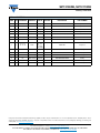
SiP12109DB, SiP12110DB www.vishay.com Vishay Siliconix Demo Board User Manual for SiP12109 (4 A) and SiP12110 (6 A), 4.5 V to 15 V Input Synchronous Buck Regulators THE CHIP PRODUCT SUMMARY SiP12109DMP-T1-GE4 Input Voltage Range 4.5 V to 15 V Output Voltage Range 0.6 V to 5.5 V Operating Frequency 400 kHz to 1.5 MHz Continuous Output Current Package 4A QFN16 3 mm x 3 mm FEATURES • 4.5 V to 15 V input voltage • Adjustable output voltage down to 0.6 V • 4 A (SiP12109)/6 A (SiP12110) continuous output current • Selectable switching frequency from 400 kHz to 1.5 MHz with an external resistor • 95 % peak efficiency PRODUCT SUMMARY SiP12110DMP-T1-GE4 • Stable with any capacitor. No external ESR network required Input Voltage Range 4.5 V to 15 V • Ultrafast transient response Output Voltage Range 0.6 V to 5.5 V • Power saving scheme for increased light load efficiency Operating Frequency 400 kHz to 1.5 MHz Continuous Output Current Package 6A QFN16 3 mm x 3 mm • ± 1 % accuracy of VOUT setting • Cycle-by-cycle current limit • Fully protected with OTP, SCP, UVP, OVP • PGOOD Indicator DESCRIPTION The SiP12109 and SiP12110 are high frequency current-mode constant-on-time (CM-COT) synchronous buck regulator with integrated high-side and low-side power MOSFETs. The SiP12109 is capable of 4 A continuous current and the SiP12110 is capable of 6 A. These regulators produce an adjustable output voltage down to 0.6 V from 4.5 V to 15 V input rail to accommodate a variety of applications, including computing, consumer electronics, telecom, and industrial. The CM-COT architecture delivers ultra-fast transient response with minimum output capacitance and tight ripple regulation at very light load. The parts are stable with any capacitor type and no ESR network is required for loop stability. The devices also incorporate a power saving scheme that significantly increases light load efficiency. The regulator integrates a full protection feature set, including output overvoltage protection (OVP), output under voltage protection (UVP) and thermal shutdown (OTP). It also has UVLO for the input rail and an internal soft-start. The SiP12109 is available in lead (Pb)-free power enhanced 3 mm x 3 mm QFN-16 package. • -40 °C to +125 °C operating junction temperature • Output voltage tracking APPLICATIONS • Point of load regulation for low-power processors, network processors, DSPs, FPGAs, and ASICs • Low voltage, distributed power architectures with 5 V or 12 V rails • Computing, broadband, networking, LAN / WAN, optical, test, and measurement • A/V, high density cards, storage, DSL, STB, DVR, DTV, industrial PC ORDERING INFORMATION DEMO BOARD PART NUMBER MAX. OUTPUT CURRENT SiP12109DB 4A SiP12110DB 6A SPECIFICATION This reference board allows the end user to evaluate the SiP12109 or the SiP12110 chip for its features and all functionalities. It can also be a reference design for a user’s application. Input voltage (V): 4.5 to 15 Output voltage (V): 0.6 to 5 Output current (A): 0 to 4 for SiP12109, 0 to 6 for SiP12110 Revision: 30-Jan-14 Document Number: 64324 1 For technical questions, contact: [email protected] THIS DOCUMENT IS SUBJECT TO CHANGE WITHOUT NOTICE. THE PRODUCTS DESCRIBED HEREIN AND THIS DOCUMENT ARE SUBJECT TO SPECIFIC DISCLAIMERS, SET FORTH AT www.vishay.com/doc?91000 SiP12109DB, SiP12110DB www.vishay.com Vishay Siliconix CONNECTION AND SIGNAL / TEST POINTS CHANGING SWITCHING FREQUENCY Power Sockets The following equation illustrates the relationship between ON-time, VIN, VOUT, and RON value: VIN (J1), GND (J4): Input voltage source with VIN to be positive. Connect to a 4.5 V to 16 V source that powers SiP12109. VOUT (J2), GND (J3): Output voltage with VOUT to be positive. Connect to a load that draws less than 4 A current. SIGNAL AND TEST LEADS EN (J5): When the pin is grounded the SiP12109 is disabled. A voltage above ~ 1.5 V will be seen as HI and enable the part allowing switching to occur. PGD(J6): Is an open drain output and is pulled up with a 100 k resistor to VIN. When FB or VOUT are within 25 percent of the set voltage this pin will go HI to indicate the output is okay. POWER UP PROCEDURE To turn-on the reference board, apply 12 V to VIN and another supply > 1.5 V to the EN pin J10. The board will come up in ECO power save mode with an output voltage preset to 1.2 V. This will allow much higher efficiency due to lower switching frequency at zero to very light loads. As the load increases the frequency will increase until the nominal set frequency (preset to ~ 1 MHz) is reached. When applying higher than 12 V to the input it is recommended to install a RC snubber from LX to GND. There are place holders on the reference board R4 and C23 for the snubber. Values of 5.6 and 0.39 nF are a reasonable starting point. COMMON ADJUSTMENTS MADE TO THE REFERENCE BOARD OUTPUT VOLTAGE ADJUSTMENT The evaluation board is configured for a 1.2 V output. If a different output voltage is needed, simply change the value of VOUT and solve for R11 based on the following formula: R11 = R7 x Vref VOUT - Vref = 5.11 kΩ x 0.6 V 1.2 V - 0.6 V = 5.11 kΩ TON = RON x K x VOUT VIN , where K is a constant set internally. ( K = 17 x 10-12) Once ON time is set, pseudo constant frequency is then determined by the following equation: VOUT VIN VOUT D Fsw = = = 1 xR xK TON RON x K ON VIN OUTPUT RIPPLE VOLTAGE Output ripple voltage is measured at the a tip and barrel measurement across COUT or use the probe jack located at VOUT. Typically output ripple voltage is set to 3 % to 5% of the output voltage, but an all ceramic output solution can bring output ripple voltage to a much lower level since the ESR of ceramics is very small. This can cause stability issues with other COT controllers, which require a minimum ripple voltage, but not with the SIP12109 which uses current mode control. The SiP12109 can work with any type of output capacitors that suits your needs. INDUCTOR SELECTION Knowing VIN, VOUT, Fsw, full load current and choosing a ripple current (•I) that's between 20 % to 50 % of full load current we can calculate an inductor value. VOUT L = (VIN - VOUT) x Fsw x VIN x ΔI x IOUT max. 1.2 = (12 V - 1.2 V) x 1x 106 = 1 μH x 12 V x 0.25 x 4 A INPUT CAPACITORS The input capacitors are chosen as a combination of bulk and ceramic capacitors, to satisfy cost, RMS current, ESR, input voltage ripple requirements and a source for instantaneous energy and filtering that the converter may require. INDUCTORS Other than the inductance the DCR and saturation current parameters are key values. The DCR causes an I2R loss which will decrease the system efficiency and generate heat. The saturation current has to be higher than the maximum output current plus 1/2 the ripple current. In over current condition the inductor current may be very high. All this needs to be considered when selecting the inductor. On this board Vishay IHLP-2525EZ series inductors are used to meet cost requirement and get better efficiency and utilizes a material that has incredible saturation levels compared to competing products. Revision: 30-Jan-14 Document Number: 64324 2 For technical questions, contact: [email protected] THIS DOCUMENT IS SUBJECT TO CHANGE WITHOUT NOTICE. THE PRODUCTS DESCRIBED HEREIN AND THIS DOCUMENT ARE SUBJECT TO SPECIFIC DISCLAIMERS, SET FORTH AT www.vishay.com/doc?91000 SiP12109DB, SiP12110DB www.vishay.com OUTPUT CAPACITORS Vishay Siliconix REFERENCE BOARD PHOTOS Voltage rating, ESR, transient response, overall PCB area, and cost are requirements for selecting output capacitors. The types of capacitors and there general advantages and disadvantages are covered next. Electrolytic have high ESR, dry out over time so ripple current rating must be examined and have slower transient response, but are fairly inexpensive for the amount of overall capacitance. Tantalums can come in low ESR varieties and high capacitance value for its overall size, but they fail short when damaged and also have slower transient response. Ceramics have very low ESR, fast transient response, and overall small size, but are expensive and come in low capacitance values compared to the others above. The SiP12109 is an advanced current mode constant on time controller which eliminates the minimum output ripple voltage required by voltage mode based controllers and can operate stably with an all ceramic output capacitance. SOFT START The external soft start cap is charged via a 5 μA current source. Using this formula we can calculate the soft start time Fig. 1 - Top of the PCB SS = (Cext x 0.8 V)/5 μA Using a 10 nF cap we get ~ 1 ms typical soft start time which is dependent on VOUT level also. Fig. 2 - Bottom of the PCB Revision: 30-Jan-14 Document Number: 64324 3 For technical questions, contact: [email protected] THIS DOCUMENT IS SUBJECT TO CHANGE WITHOUT NOTICE. THE PRODUCTS DESCRIBED HEREIN AND THIS DOCUMENT ARE SUBJECT TO SPECIFIC DISCLAIMERS, SET FORTH AT www.vishay.com/doc?91000 SiP12109DB, SiP12110DB www.vishay.com Vishay Siliconix PCB LAYOUT Revision: 30-Jan-14 Fig. 3 - Top Layer Fig. 5 - Inner Layer 1 Fig. 4 - Inner Layer 2 Fig. 6 - Bottom Layer Document Number: 64324 4 For technical questions, contact: [email protected] THIS DOCUMENT IS SUBJECT TO CHANGE WITHOUT NOTICE. THE PRODUCTS DESCRIBED HEREIN AND THIS DOCUMENT ARE SUBJECT TO SPECIFIC DISCLAIMERS, SET FORTH AT www.vishay.com/doc?91000 SiP12109DB, SiP12110DB www.vishay.com Vishay Siliconix J3 22uF Vcc R4 100k R6 5k11 0.1uF R7 5k11 22uF C3 C2 C1 1uH L1 100k R5 22n C8 0.47nF PGD 1 J6 J5 PGD EN R1 1 EN J4 C9 6.04k R3 Ron 4 3 1u C7 1 VIN_GND 17 15 16 1 2 Vcc AGND Vin2 14 Vin1 GMO 13 Vcc 75k PGND2 0.1uF EN 9 PGD SiP12109 PGOOD 10 LX1 LX2 11 12 LX3 PGND0 22uF 5 PGND1 C5 6 Vfb C6 0.1uF SS C4 7 R2 0 BOOT IC1 EN J1 8 1 VIN VOGND J2 1 Revision: 30-Jan-14 VO_GND 1 VOUT SCHEMATIC OF DEMO BOARD Document Number: 64324 5 For technical questions, contact: [email protected] THIS DOCUMENT IS SUBJECT TO CHANGE WITHOUT NOTICE. THE PRODUCTS DESCRIBED HEREIN AND THIS DOCUMENT ARE SUBJECT TO SPECIFIC DISCLAIMERS, SET FORTH AT www.vishay.com/doc?91000 SiP12109DB, SiP12110DB www.vishay.com Vishay Siliconix BILL of MATERIAL ITEM QTY REFERENCE PCB FOOTPRINT VALUE VOLTAGE DESCRIPTION PART NUMBER 1 3 C1, C5, C6 C0402-TDK 0.1 μF 35 V GMK105BJ104KV-F Taiyo Yuden 2 2 C2, C3 C0805-TDK 22 μF 10 V LMK212BJ226MG-T Taiyo Yuden 1 C4 C0805-TDK 22 μF 35 V C2012X5R1V226M125AC TDK 3 1 C7 C0603-TDK 1 μF 25 V TMK107BJ105KA-T Taiyo Yuden 4 1 C8 C0402-TDK 22 nF 50 V CGA2B3X5R1H223K050BB TDK 5 1 C9 C0402-TDK 0.47 nF 50 V C1005C0G1H471J050BA TDK 6 1 IC1 MLP44-16 SiP12109 - SiP12109 Vishay 7 6 J1, J2, J3, J4, J5, J6 TP30 VIN, VOUT, VO_GND, VIN_GND, EN, PGD - 5002K-ND Keystone 8 1 L1 IHLP-1616 1 μH - IHLP1616BZER1R0M11 Vishay 9 1 R1 R0402-Vishay 75 k - CRCW040275K0FKEDHP Vishay 10 1 R2 R0402-Vishay 0 - RCG04020000Z0ED Vishay 11 1 R3 R0402-Vishay 6.04 k - CRCW04026K04FKED Vishay 12 2 R4, R5 R0402-Vishay 100 k - CRCW0402100KFKED Vishay 13 2 R6, R7 R0402-Vishay 5.11 k - CRCW04025K11FKED Vishay Vishay Siliconix maintains worldwide manufacturing capability. Products may be manufactured at one of several qualified locations. Reliability data for Silicon Technology and Package Reliability represent a composite of all qualified locations. For related documents such as package/tape drawings, part marking, and reliability data, see www.vishay.com/ppg?64324. Revision: 30-Jan-14 Document Number: 64324 6 For technical questions, contact: [email protected] THIS DOCUMENT IS SUBJECT TO CHANGE WITHOUT NOTICE. THE PRODUCTS DESCRIBED HEREIN AND THIS DOCUMENT ARE SUBJECT TO SPECIFIC DISCLAIMERS, SET FORTH AT www.vishay.com/doc?91000 Mouser Electronics Authorized Distributor Click to View Pricing, Inventory, Delivery & Lifecycle Information: Vishay: SIP12109DB SiP12110DB