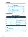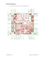
1
CMA34CR cpuModules™ User’s Manual BDM-610000083 Revision H ® www.rtd.com ISO9001 and AS9100 Certified “Accessing the Analog World”® CMA34CR cpuModules™ User’s Manual RTD Document Number: BDM-610000083 Revision H Copyright © 2009-2014 RTD Embedded Technologies, Inc. All rights reserved. Trademarks Advanced Analog I/O, Advanced Digital I/O, aAIO, aDIO, a2DIO, Autonomous SmartCal, “Catch the Express”, cpuModule, dspFramework, dspModule, expressMate, ExpressPlatform, HiDANplus, “MIL Value for COTS prices”, multiPort, PlatformBus, and PC/104EZ are trademarks, and “Accessing the Analog World”, dataModule, IDAN, HiDAN, RTD, and the RTD logo are registered trademarks of RTD Embedded Technologies, Inc (formerly Real Time Devices, Inc.). PS/2 is a trademark of International Business Machines Inc. PCI, PCI Express, and PCIe are trademarks of PCI-SIG. PC/104, PC/104-Plus, PCI-104, PCIe/104, PCI/104-Express and 104 are trademarks of the PC/104 Embedded Consortium. All other trademarks appearing in this document are the property of their respective owners. Failure to follow the instructions found in this manual may result in damage to the product described in this manual, or other components of the system. The procedure set forth in this manual shall only be performed by persons qualified to service electronic equipment. Contents and specifications within this manual are given without warranty, and are subject to change without notice. RTD Embedded Technologies, Inc. shall not be liable for errors or omissions in this manual, or for any loss, damage, or injury in connection with the use of this manual. Revision History ii Revision Date Reason for Change PRELIM 8/1/2014 Preliminary release A 10/8/2014 Intial release. Added test results and made corrections throughout B 10/23/2014 Updated Operating Temperature table with Quad Core temperature ranges. C 11/19/2014 Removed unused sections, updated IDAN pinouts and back panel picture D 12/17/2014 Updated temperature ratings, increased Serial UART from 64 to 512 E 1/14/2015 Updated Dual RS-422 Mode Table 24. F 2/5/2015 Corrected “Disable Bus-Stack Error” Jumper setting G 2/13/2015 Changed the ref designator for Fan Power connector, updated Sandra version, udpated table 23., Added dimensioned IDAN drawing. H 3/16/2015 Updated Dual RS232 mode pinout table, added a note to the PCIe connector CMA34CR cpuModule BDM-610000083 Rev H CMA34CR cpuModules™ ® www.rtd.com ISO9001 and AS9100 Certified “Accessing the Analog World”® iv CMA34CR cpuModule BDM-610000083 Rev H Table of Contents Chapter 1 Introduction CMA34CR cpuModules . . . . . . . . . . . . . . . . . . . . . . . . . . . . . . . . . . . . . . . . . . . . . . . . . . . . . . . . . . . . . . . . . . . . . . . . . . . . . . . . 2 aDIO . . . . . . . . . . . . . . . . . . . . . . . . . . . . . . . . . . . . . . . . . . . . . . . . . . . . . . . . . . . . . . . . . . . . . . . . . . . . . . . . . . . . . . . . . . . . . . . . . . . . . . . . 3 Ordering Information . . . . . . . . . . . . . . . . . . . . . . . . . . . . . . . . . . . . . . . . . . . . . . . . . . . . . . . . . . . . . . . . . . . . . . . . . . . . . . . . . 4 CMA34CR Model Options . . . . . . . . . . . . . . . . . . . . . . . . . . . . . . . . . . . . . . . . . . . . . . . . . . . . . . . . . . . . . . . . . . . . . . . . . . . . . . . . . . . Cable Kits and Accessories . . . . . . . . . . . . . . . . . . . . . . . . . . . . . . . . . . . . . . . . . . . . . . . . . . . . . . . . . . . . . . . . . . . . . . . . . . . . . . . . . . . 4 5 Board Features . . . . . . . . . . . . . . . . . . . . . . . . . . . . . . . . . . . . . . . . . . . . . . . . . . . . . . . . . . . . . . . . . . . . . . . . . . . . . . . . . . . . . . . . 6 I/O . . . . . . . . . . . . . . . . . . . . . . . . . . . . . . . . . . . . . . . . . . . . . . . . . . . . . . . . . . . . . . . . . . . . . . . . . . . . . . . . . . . . . . . . . . . . . . . . . . . . . . . . . . RTD Enhanced BIOS . . . . . . . . . . . . . . . . . . . . . . . . . . . . . . . . . . . . . . . . . . . . . . . . . . . . . . . . . . . . . . . . . . . . . . . . . . . . . . . . . . . . . . . . . 7 8 Block Diagram. . . . . . . . . . . . . . . . . . . . . . . . . . . . . . . . . . . . . . . . . . . . . . . . . . . . . . . . . . . . . . . . . . . . . . . . . . . . . . . . . . . . . . . . . 9 Specifications. . . . . . . . . . . . . . . . . . . . . . . . . . . . . . . . . . . . . . . . . . . . . . . . . . . . . . . . . . . . . . . . . . . . . . . . . . . . . . . . . . . . . . . . . . 10 Physical Characteristics . . . . . . . . . . . . . . . . . . . . . . . . . . . . . . . . . . . . . . . . . . . . . . . . . . . . . . . . . . . . . . . . . . . . . . . . . . . . . . . . . . . . . . Power Consumption . . . . . . . . . . . . . . . . . . . . . . . . . . . . . . . . . . . . . . . . . . . . . . . . . . . . . . . . . . . . . . . . . . . . . . . . . . . . . . . . . . . . . . . . . .............................................................................................................. Operating Conditions . . . . . . . . . . . . . . . . . . . . . . . . . . . . . . . . . . . . . . . . . . . . . . . . . . . . . . . . . . . . . . . . . . . . . . . . . . . . . . . . . . . . . . . . Electrical Characteristics . . . . . . . . . . . . . . . . . . . . . . . . . . . . . . . . . . . . . . . . . . . . . . . . . . . . . . . . . . . . . . . . . . . . . . . . . . . . . . . . . . . . . 10 10 11 12 13 Migrating to RTD’s Intel Core i7 cpuModules . . . . . . . . . . . . . . . . . . . . . . . . . . . . . . . . . . . . . . . . . . . . . . . . . . . . . . . . . 15 Connector Pinout & Function Differences . . . . . . . . . . . . . . . . . . . . . . . . . . . . . . . . . . . . . . . . . . . . . . . . . . . . . . . . . . . . . . . . . . . . New I/O Connectors . . . . . . . . . . . . . . . . . . . . . . . . . . . . . . . . . . . . . . . . . . . . . . . . . . . . . . . . . . . . . . . . . . . . . . . . . . . . . . . . . . . . Connector Differences . . . . . . . . . . . . . . . . . . . . . . . . . . . . . . . . . . . . . . . . . . . . . . . . . . . . . . . . . . . . . . . . . . . . . . . . . . . . . . . . . . Software Differences . . . . . . . . . . . . . . . . . . . . . . . . . . . . . . . . . . . . . . . . . . . . . . . . . . . . . . . . . . . . . . . . . . . . . . . . . . . . . . . . . . . . . . . . . aDIO. . . . . . . . . . . . . . . . . . . . . . . . . . . . . . . . . . . . . . . . . . . . . . . . . . . . . . . . . . . . . . . . . . . . . . . . . . . . . . . . . . . . . . . . . . . . . . . . . . . . UEFI Shell . . . . . . . . . . . . . . . . . . . . . . . . . . . . . . . . . . . . . . . . . . . . . . . . . . . . . . . . . . . . . . . . . . . . . . . . . . . . . . . . . . . . . . . . . . . . . . . 15 15 15 16 16 16 Contact Information . . . . . . . . . . . . . . . . . . . . . . . . . . . . . . . . . . . . . . . . . . . . . . . . . . . . . . . . . . . . . . . . . . . . . . . . . . . . . . . . . . 17 Chapter 2 Getting Started Connector Locations . . . . . . . . . . . . . . . . . . . . . . . . . . . . . . . . . . . . . . . . . . . . . . . . . . . . . . . . . . . . . . . . . . . . . . . . . . . . . . . . . . 20 Selecting the Stack Order for the CMA34CR . . . . . . . . . . . . . . . . . . . . . . . . . . . . . . . . . . . . . . . . . . . . . . . . . . . . . . . . . . 22 Stack Example . . . . . . . . . . . . . . . . . . . . . . . . . . . . . . . . . . . . . . . . . . . . . . . . . . . . . . . . . . . . . . . . . . . . . . . . . . . . . . . . . . . . . . . . . 23 Connecting to the Stack . . . . . . . . . . . . . . . . . . . . . . . . . . . . . . . . . . . . . . . . . . . . . . . . . . . . . . . . . . . . . . . . . . . . . . . . . . . . . . . 24 Power Input Connections . . . . . . . . . . . . . . . . . . . . . . . . . . . . . . . . . . . . . . . . . . . . . . . . . . . . . . . . . . . . . . . . . . . . . . . . . . . . . 24 Connecting to the Utility Port 2.0 . . . . . . . . . . . . . . . . . . . . . . . . . . . . . . . . . . . . . . . . . . . . . . . . . . . . . . . . . . . . . . . . . . . . . 25 Booting the CMA34CR cpuModule for the First Time . . . . . . . . . . . . . . . . . . . . . . . . . . . . . . . . . . . . . . . . . . . . . . . . . 25 Chapter 3 Connecting the cpuModule Proper Grounding Techniques. . . . . . . . . . . . . . . . . . . . . . . . . . . . . . . . . . . . . . . . . . . . . . . . . . . . . . . . . . . . . . . . . . . . . . . . . 28 Connector Locations . . . . . . . . . . . . . . . . . . . . . . . . . . . . . . . . . . . . . . . . . . . . . . . . . . . . . . . . . . . . . . . . . . . . . . . . . . . . . . . . . . 28 Auxiliary Power (CN3). . . . . . . . . . . . . . . . . . . . . . . . . . . . . . . . . . . . . . . . . . . . . . . . . . . . . . . . . . . . . . . . . . . . . . . . . . . . . . . . . 30 Utility Port 2.0 Connector (CN5) . . . . . . . . . . . . . . . . . . . . . . . . . . . . . . . . . . . . . . . . . . . . . . . . . . . . . . . . . . . . . . . . . . . . . . 31 BDM-610000083 Rev H Table of Contents v USB 2.0 Connector. . . . . . . . . . . . . . . . . . . . . . . . . . . . . . . . . . . . . . . . . . . . . . . . . . . . . . . . . . . . . . . . . . . . . . . . . . . . . . . . . . . . . . . . . . . Speaker. . . . . . . . . . . . . . . . . . . . . . . . . . . . . . . . . . . . . . . . . . . . . . . . . . . . . . . . . . . . . . . . . . . . . . . . . . . . . . . . . . . . . . . . . . . . . . . . . . . . . . System Reset. . . . . . . . . . . . . . . . . . . . . . . . . . . . . . . . . . . . . . . . . . . . . . . . . . . . . . . . . . . . . . . . . . . . . . . . . . . . . . . . . . . . . . . . . . . . . . . . . 32 32 32 SVGA Video Connector (CN18) . . . . . . . . . . . . . . . . . . . . . . . . . . . . . . . . . . . . . . . . . . . . . . . . . . . . . . . . . . . . . . . . . . . . . . . 33 DisplayPort Connector (CN4) . . . . . . . . . . . . . . . . . . . . . . . . . . . . . . . . . . . . . . . . . . . . . . . . . . . . . . . . . . . . . . . . . . . . . . . . . 34 SATA Data Connector (CN15) . . . . . . . . . . . . . . . . . . . . . . . . . . . . . . . . . . . . . . . . . . . . . . . . . . . . . . . . . . . . . . . . . . . . . . . . . 36 Serial Port 1 (CN7) and Serial Port 2 (CN8) . . . . . . . . . . . . . . . . . . . . . . . . . . . . . . . . . . . . . . . . . . . . . . . . . . . . . . . . . . . 37 Serial Port UART . . . . . . . . . . . . . . . . . . . . . . . . . . . . . . . . . . . . . . . . . . . . . . . . . . . . . . . . . . . . . . . . . . . . . . . . . . . . . . . . . . . . . . . . . . . . . RS-232 Serial Port (Default) . . . . . . . . . . . . . . . . . . . . . . . . . . . . . . . . . . . . . . . . . . . . . . . . . . . . . . . . . . . . . . . . . . . . . . . . . . . . . . . . . . RS-422 or RS-485 Serial Port. . . . . . . . . . . . . . . . . . . . . . . . . . . . . . . . . . . . . . . . . . . . . . . . . . . . . . . . . . . . . . . . . . . . . . . . . . . . . . . . . . RS-422 Mode Pinout . . . . . . . . . . . . . . . . . . . . . . . . . . . . . . . . . . . . . . . . . . . . . . . . . . . . . . . . . . . . . . . . . . . . . . . . . . . . . . . . . . . . RS-485 Mode Pinout . . . . . . . . . . . . . . . . . . . . . . . . . . . . . . . . . . . . . . . . . . . . . . . . . . . . . . . . . . . . . . . . . . . . . . . . . . . . . . . . . . . . Dual Serial Port Modes. . . . . . . . . . . . . . . . . . . . . . . . . . . . . . . . . . . . . . . . . . . . . . . . . . . . . . . . . . . . . . . . . . . . . . . . . . . . . . . . . . . . . . . 37 37 38 39 40 41 Advanced Digital I/O (aDIO™) Port (CN6). . . . . . . . . . . . . . . . . . . . . . . . . . . . . . . . . . . . . . . . . . . . . . . . . . . . . . . . . . . . . 43 USB 2.0 Connector (CN17) . . . . . . . . . . . . . . . . . . . . . . . . . . . . . . . . . . . . . . . . . . . . . . . . . . . . . . . . . . . . . . . . . . . . . . . . . . . . 44 Ethernet (10/100/1000Base-T and -TX) Connectors (CN20 and CN30) . . . . . . . . . . . . . . . . . . . . . . . . . . . . . . . 45 PCIe/104 Type 2 Bus (CN1 - Top and CN2 - Bottom) . . . . . . . . . . . . . . . . . . . . . . . . . . . . . . . . . . . . . . . . . . . . . . . . . . 46 PCIe/104 Type 2 Compatibility . . . . . . . . . . . . . . . . . . . . . . . . . . . . . . . . . . . . . . . . . . . . . . . . . . . . . . . . . . . . . . . . . . . . . . . . . . . . . . . USB 3.0 . . . . . . . . . . . . . . . . . . . . . . . . . . . . . . . . . . . . . . . . . . . . . . . . . . . . . . . . . . . . . . . . . . . . . . . . . . . . . . . . . . . . . . . . . . . . . . . . . . . . . . 48 49 Optional RTC Battery Input (CN13) . . . . . . . . . . . . . . . . . . . . . . . . . . . . . . . . . . . . . . . . . . . . . . . . . . . . . . . . . . . . . . . . . . . 50 Fan Power (CN12) . . . . . . . . . . . . . . . . . . . . . . . . . . . . . . . . . . . . . . . . . . . . . . . . . . . . . . . . . . . . . . . . . . . . . . . . . . . . . . . . . . . . . 50 Chapter 4 Using the cpuModule The RTD Enhanced BIOS . . . . . . . . . . . . . . . . . . . . . . . . . . . . . . . . . . . . . . . . . . . . . . . . . . . . . . . . . . . . . . . . . . . . . . . . . . . . . . 52 Configuring the RTD Enhanced BIOS . . . . . . . . . . . . . . . . . . . . . . . . . . . . . . . . . . . . . . . . . . . . . . . . . . . . . . . . . . . . . . . . . . . . . . . . . Entering the BIOS Setup through the Graphical BIOS Menu . . . . . . . . . . . . . . . . . . . . . . . . . . . . . . . . . . . . . . . . . . . . . . . . . . . Field Selection . . . . . . . . . . . . . . . . . . . . . . . . . . . . . . . . . . . . . . . . . . . . . . . . . . . . . . . . . . . . . . . . . . . . . . . . . . . . . . . . . . . . . . . . . . . . . . . 52 52 53 Onboard PCI/PCIe Devices . . . . . . . . . . . . . . . . . . . . . . . . . . . . . . . . . . . . . . . . . . . . . . . . . . . . . . . . . . . . . . . . . . . . . . . . . . . . 54 Advanced Digital I/O Ports (aDIO™). . . . . . . . . . . . . . . . . . . . . . . . . . . . . . . . . . . . . . . . . . . . . . . . . . . . . . . . . . . . . . . . . . . 55 Digital I/O Register Set . . . . . . . . . . . . . . . . . . . . . . . . . . . . . . . . . . . . . . . . . . . . . . . . . . . . . . . . . . . . . . . . . . . . . . . . . . . . . . . . . . . . . . . Port 1 Data register is a read/write byte direction . . . . . . . . . . . . . . . . . . . . . . . . . . . . . . . . . . . . . . . . . . . . . . . . . . . . . . . . Interrupts . . . . . . . . . . . . . . . . . . . . . . . . . . . . . . . . . . . . . . . . . . . . . . . . . . . . . . . . . . . . . . . . . . . . . . . . . . . . . . . . . . . . . . . . . . . . . . . . . . . Advanced Digital Interrupts . . . . . . . . . . . . . . . . . . . . . . . . . . . . . . . . . . . . . . . . . . . . . . . . . . . . . . . . . . . . . . . . . . . . . . . . . . . . . Event Mode . . . . . . . . . . . . . . . . . . . . . . . . . . . . . . . . . . . . . . . . . . . . . . . . . . . . . . . . . . . . . . . . . . . . . . . . . . . . . . . . . . . . . . . . . . . . . Match Mode . . . . . . . . . . . . . . . . . . . . . . . . . . . . . . . . . . . . . . . . . . . . . . . . . . . . . . . . . . . . . . . . . . . . . . . . . . . . . . . . . . . . . . . . . . . . Strobe Mode . . . . . . . . . . . . . . . . . . . . . . . . . . . . . . . . . . . . . . . . . . . . . . . . . . . . . . . . . . . . . . . . . . . . . . . . . . . . . . . . . . . . . . . . . . . . 56 58 58 58 58 58 59 SATA Controller Configuration . . . . . . . . . . . . . . . . . . . . . . . . . . . . . . . . . . . . . . . . . . . . . . . . . . . . . . . . . . . . . . . . . . . . . . . . 60 Onboard SATA Storage . . . . . . . . . . . . . . . . . . . . . . . . . . . . . . . . . . . . . . . . . . . . . . . . . . . . . . . . . . . . . . . . . . . . . . . . . . . . . . . . . . . . . . SATA Links on the PCIe/104 Type Connectors . . . . . . . . . . . . . . . . . . . . . . . . . . . . . . . . . . . . . . . . . . . . . . . . . . . . . . . . . . . . . . . . 60 60 Real Time Clock Control. . . . . . . . . . . . . . . . . . . . . . . . . . . . . . . . . . . . . . . . . . . . . . . . . . . . . . . . . . . . . . . . . . . . . . . . . . . . . . . 61 Watchdog Timer Control . . . . . . . . . . . . . . . . . . . . . . . . . . . . . . . . . . . . . . . . . . . . . . . . . . . . . . . . . . . . . . . . . . . . . . . . . . . . . . 62 Thermal Management . . . . . . . . . . . . . . . . . . . . . . . . . . . . . . . . . . . . . . . . . . . . . . . . . . . . . . . . . . . . . . . . . . . . . . . . . . . . . . . . . 63 Thermal Monitor . . . . . . . . . . . . . . . . . . . . . . . . . . . . . . . . . . . . . . . . . . . . . . . . . . . . . . . . . . . . . . . . . . . . . . . . . . . . . . . . . . . . . . . . . . . . Hardware-Enforced Thermal Protection . . . . . . . . . . . . . . . . . . . . . . . . . . . . . . . . . . . . . . . . . . . . . . . . . . . . . . . . . . . . . . . . . . . . . . 63 63 vi CMA34CR cpuModule BDM-610000083 Rev H Further Temperature Reduction . . . . . . . . . . . . . . . . . . . . . . . . . . . . . . . . . . . . . . . . . . . . . . . . . . . . . . . . . . . . . . . . . . . . . . . . . . . . . . 63 Power Management . . . . . . . . . . . . . . . . . . . . . . . . . . . . . . . . . . . . . . . . . . . . . . . . . . . . . . . . . . . . . . . . . . . . . . . . . . . . . . . . . . . 64 Advanced Configuration and Power Interface (ACPI) . . . . . . . . . . . . . . . . . . . . . . . . . . . . . . . . . . . . . . . . . . . . . . . . . . . . . . . . . Power Button Modes . . . . . . . . . . . . . . . . . . . . . . . . . . . . . . . . . . . . . . . . . . . . . . . . . . . . . . . . . . . . . . . . . . . . . . . . . . . . . . . . . . . . . . . . Low-Power Wake Options. . . . . . . . . . . . . . . . . . . . . . . . . . . . . . . . . . . . . . . . . . . . . . . . . . . . . . . . . . . . . . . . . . . . . . . . . . . . . . . . . . . . AT vs. ATX Power Supplies . . . . . . . . . . . . . . . . . . . . . . . . . . . . . . . . . . . . . . . . . . . . . . . . . . . . . . . . . . . . . . . . . . . . . . . . . . . . . . . . . . . ATX Power Supply Signals . . . . . . . . . . . . . . . . . . . . . . . . . . . . . . . . . . . . . . . . . . . . . . . . . . . . . . . . . . . . . . . . . . . . . . . . . . . . . . . . . . . . Reducing Power Consumption . . . . . . . . . . . . . . . . . . . . . . . . . . . . . . . . . . . . . . . . . . . . . . . . . . . . . . . . . . . . . . . . . . . . . . . . . . . . . . . 64 64 64 65 65 65 Multi-Color LED . . . . . . . . . . . . . . . . . . . . . . . . . . . . . . . . . . . . . . . . . . . . . . . . . . . . . . . . . . . . . . . . . . . . . . . . . . . . . . . . . . . . . . . 66 Reset Status Register . . . . . . . . . . . . . . . . . . . . . . . . . . . . . . . . . . . . . . . . . . . . . . . . . . . . . . . . . . . . . . . . . . . . . . . . . . . . . . . . . . 67 Features and Settings That Can Affect Boot Time . . . . . . . . . . . . . . . . . . . . . . . . . . . . . . . . . . . . . . . . . . . . . . . . . . . . . 69 Boot Device Order . . . . . . . . . . . . . . . . . . . . . . . . . . . . . . . . . . . . . . . . . . . . . . . . . . . . . . . . . . . . . . . . . . . . . . . . . . . . . . . . . . . . . . . . . . . Add-On Cards With BIOS Extensions . . . . . . . . . . . . . . . . . . . . . . . . . . . . . . . . . . . . . . . . . . . . . . . . . . . . . . . . . . . . . . . . . . . . . . . . . VGA Controller . . . . . . . . . . . . . . . . . . . . . . . . . . . . . . . . . . . . . . . . . . . . . . . . . . . . . . . . . . . . . . . . . . . . . . . . . . . . . . . . . . . . . . . . . . . . . . Hard Drive Type . . . . . . . . . . . . . . . . . . . . . . . . . . . . . . . . . . . . . . . . . . . . . . . . . . . . . . . . . . . . . . . . . . . . . . . . . . . . . . . . . . . . . . . . . . . . . Monitor Type . . . . . . . . . . . . . . . . . . . . . . . . . . . . . . . . . . . . . . . . . . . . . . . . . . . . . . . . . . . . . . . . . . . . . . . . . . . . . . . . . . . . . . . . . . . . . . . . Network (PXE) Boot . . . . . . . . . . . . . . . . . . . . . . . . . . . . . . . . . . . . . . . . . . . . . . . . . . . . . . . . . . . . . . . . . . . . . . . . . . . . . . . . . . . . . . . . . 69 69 69 69 69 69 System Recovery. . . . . . . . . . . . . . . . . . . . . . . . . . . . . . . . . . . . . . . . . . . . . . . . . . . . . . . . . . . . . . . . . . . . . . . . . . . . . . . . . . . . . . . 70 Reset Button Recovery . . . . . . . . . . . . . . . . . . . . . . . . . . . . . . . . . . . . . . . . . . . . . . . . . . . . . . . . . . . . . . . . . . . . . . . . . . . . . . . . . . . . . . . Load Default BIOS Settings. . . . . . . . . . . . . . . . . . . . . . . . . . . . . . . . . . . . . . . . . . . . . . . . . . . . . . . . . . . . . . . . . . . . . . . . . . . . . . . . . . . Serial Power-On-Self-Test (POST) Code Output . . . . . . . . . . . . . . . . . . . . . . . . . . . . . . . . . . . . . . . . . . . . . . . . . . . . . . . . . . . . . . . 70 70 70 Appendix A Hardware Reference Jumper Settings and Locations . . . . . . . . . . . . . . . . . . . . . . . . . . . . . . . . . . . . . . . . . . . . . . . . . . . . . . . . . . . . . . . . . . . . . . . . 72 Physical Dimensions . . . . . . . . . . . . . . . . . . . . . . . . . . . . . . . . . . . . . . . . . . . . . . . . . . . . . . . . . . . . . . . . . . . . . . . . . . . . . . . . . . . 73 Appendix B Troubleshooting Common Problems and Solutions . . . . . . . . . . . . . . . . . . . . . . . . . . . . . . . . . . . . . . . . . . . . . . . . . . . . . . . . . . . . . . . . . . . . . 76 Troubleshooting a PC/104 System. . . . . . . . . . . . . . . . . . . . . . . . . . . . . . . . . . . . . . . . . . . . . . . . . . . . . . . . . . . . . . . . . . . . . 77 How to Obtain Technical Support . . . . . . . . . . . . . . . . . . . . . . . . . . . . . . . . . . . . . . . . . . . . . . . . . . . . . . . . . . . . . . . . . . . . . 78 Appendix C IDAN™ Dimensions and Pinout IDAN Dimensions and Connectors . . . . . . . . . . . . . . . . . . . . . . . . . . . . . . . . . . . . . . . . . . . . . . . . . . . . . . . . . . . . . . . . . . . . 80 IDAN Contents . . . . . . . . . . . . . . . . . . . . . . . . . . . . . . . . . . . . . . . . . . . . . . . . . . . . . . . . . . . . . . . . . . . . . . . . . . . . . . . . . . . . . . . . 81 External I/O Connections . . . . . . . . . . . . . . . . . . . . . . . . . . . . . . . . . . . . . . . . . . . . . . . . . . . . . . . . . . . . . . . . . . . . . . . . . . . . . 82 Appendix D Additional Information Application Notes . . . . . . . . . . . . . . . . . . . . . . . . . . . . . . . . . . . . . . . . . . . . . . . . . . . . . . . . . . . . . . . . . . . . . . . . . . . . . . . . . . . . . 87 Drivers and Example Programs . . . . . . . . . . . . . . . . . . . . . . . . . . . . . . . . . . . . . . . . . . . . . . . . . . . . . . . . . . . . . . . . . . . . . . . . 87 Interrupt Programming . . . . . . . . . . . . . . . . . . . . . . . . . . . . . . . . . . . . . . . . . . . . . . . . . . . . . . . . . . . . . . . . . . . . . . . . . . . . . . . 87 Serial Port Programming . . . . . . . . . . . . . . . . . . . . . . . . . . . . . . . . . . . . . . . . . . . . . . . . . . . . . . . . . . . . . . . . . . . . . . . . . . . . . . 87 PC/104 Specifications . . . . . . . . . . . . . . . . . . . . . . . . . . . . . . . . . . . . . . . . . . . . . . . . . . . . . . . . . . . . . . . . . . . . . . . . . . . . . . . . . 87 BDM-610000083 vii Rev H Table of Contents Appendix E viii Limited Warranty CMA34CR cpuModule BDM-610000083 Rev H Chapter 1 Introduction This manual provides comprehensive hardware and software information for users developing with the CMA34CR PCIe/104 cpuModule. Note Read the specifications beginning on page 10 prior to designing with the cpuModule. This manual is organized as follows: Chapter 1 Introduction Introduces main features and specifications Chapter 2 Getting Started Provides abbreviated instructions to get started quickly Chapter 3 Connecting the cpuModule Provides information on connecting the cpuModule to peripherals Chapter 4 Using the cpuModule Provides information to develop applications for the cpuModule, including general cpuModule information, detailed information on storing both applications and system functions, and using utility programs Appendix A Hardware Reference Lists jumper locations and settings, physical dimensions, and processor thermal management Appendix B Troubleshooting Offers advice on debugging problems with your system Appendix C IDAN™ Dimensions and Pinout Provides connector pinouts for the cpuModule installed in an RTD Intelligent Data Acquisition Node (IDAN) frame Appendix D Additional Information Lists sources and websites to support the cpuModule installation and configuration Appendix E Limited Warranty BDM-610000083 Rev H Chapter 1: Introduction 1 CMA34CR cpuModules RTD's CMA34CR cpuModule represents the latest in low power and high performance PCI Express embedded controllers. Based on a 3rd Generation Intel(r) Core i7 (tm) processor and chipset, the CMA34CR is offered with a high performance 1.5 GHz Single core processor, a1.7 GHz Dual-Core processor or a 2.1 GHz Quad-Core processor. Each comes with a complete DDR3 memory interface supporting up to 8 GB and operating at up to 1600 MT/s. All memory chips are soldered directly onto the board. A Serial-ATA (SATA) controller provides a fast connection to the hard drives. Network connectivity is provided by two integrated 10/100/1000 Mbps Ethernet controllers. High-speed peripheral connections include USB 2.0, with up to 480 Mb/sec data throughput. Four additional SATA links and USB 3.0 connections permit further expandability on the top and bottom-side PCIe/104 Type 2 connectors. Also provided are 8 x1 PCI Express Gen 2.0 links, four to the top connector and four to the bottom connector. Other features include two RS-232/422/485 COM ports and Advanced Digital I/O (aDIO). RTD has gone the extra mile to include additional advanced features for maximum flexibility. These include an onboard SATA surface-mount flash drive with a standard SATA interface. An Advanced Watchdog Timer is provided that can generate an interrupt or reset when the timer expires. The CMA34CR is also available in a rugged, fanless IDAN enclosure. Factory Use (CN9) Factory Use (CN10) SVGA Video (CN18) COM2&4 (CN8) DisplayPort (CN4) COM1&3 (CN7) USB 2.0 (CN17) aDIO (CN6) Ethernet (CN30) Utility Port 2.0 (CN5) Ethernet (CN20) SATA (CN15) Battery (CN13) PCIe/104 Bus (CN1 Top & CN2 Bottom) Figure 1 Auxiliary Power (CN3) Fan (CN12) CMA34CR cpuModule (top view) You can easily customize the cpuModule by stacking PCI/104-Express or PCIe/104 modules such as video controllers, Digital Signal Processors, drive carriers, LAN controllers, or analog and digital data acquisition modules. Stacking modules onto the cpuModule avoids expensive installations of backplanes and card cages, and preserves the module's compactness. 2 CMA34CR cpuModule BDM-610000083 Rev H The cpuModule uses the RTD Enhanced BIOS. Drivers in the BIOS allow booting from hard disk, UEFI shell, or PXE Ethernet, thus enabling the system to be used with traditional disk drives or nonmechanical drives. Boot from USB devices and network are also supported. The cpuModule and BIOS are also compatible with any real-time operating systems for PC compatible computers, although these may require creation of custom drivers to use the aDIO and watchdog timer. Intel Turbo Boost The Intel Turbo Boost Technology is a feature integrated into the dual and quad core i7 processors. This allows the processor to run faster than its rated operating core and/or graphics rendering clock frequency in the right circumstances. There must be sufficient power headroom and the cpuModule must be within all thermal and current limits. This feature is designed to increase the performace of both multi-threaded and single-threaded work loads. The support for Turbo mode occurs when the processor can use the thermal capacity associated with the package and run at higher power levels for short durations. Increasing system responsiveness for short, burst useage conditions. Note Intel Turbo Boost is not available on the Single Core Celeron processor. aDIO RTD’s exclusive aDIO™ is 12 digital bits configured as 8 bit-direction programmable and 4-bit port-direction programmable I/O, plus 2 strobe inputs giving you any combination of inputs and outputs. Match, event, and strobe interrupt modes mean no more wasting valuable processor time polling digital inputs. Interrupts are generated when the 8 bit-direction programmable digital inputs match a pattern or on any value change event. Bit masking allows selecting any subgroup of eight bits. The strobe input latches data into the bit-programmable port and generates an interrupt. BDM-610000083 Rev H Chapter 1: Introduction 3 Ordering Information The CMA34CR cpuModule is available with a selection of processors and memory sizes. The cpuModule can also be purchased as part of an Intelligent Data Acquisition Node (IDAN™) building block, which consists of the cpuModule and a milled aluminum IDAN frame. The IDAN building block can be used in just about any combination with other IDAN building blocks to create a simple but rugged PC/104 stack. Refer to Appendix C, IDAN™ Dimensions and Pinout, for more information. The CMA34CR cpuModule can also be purchased as part of a custom-built RTD HiDAN™ or HiDANplus High Reliability Intelligent Data Acquisition Node. Contact RTD for more information on its high reliability PC/104 systems. CMA34CR Model Options The basic cpuModule model options are shown below. Refer to the RTD website (www.rtd.com) for more detailed ordering information and any new variations that may be available. Each CPU has the option to go up to 8 GB DDR3-SDRAM, and up to a 32 GByte onboard SATA flash drive. Table 1 CMA34CR cpuModule Model Options Part Number Description CMA34CRS1500HR-4096 Intel Celeron, Single Core 1.5 GHz, 4GB DDR3-SDRAM CMA34CRD1700HR-4096 Intel Core i7, Dual Core 1.7 GHz, 4GB DDR3-SDRAM CMA34CRQ2100HR-4096 Intel Core i7, Quad Core 2.1 GHz, 4GB DDR3-SDRAM Table 2 4 CMA34CR cpuModule Part Number Breakdown RTD Part Number Example Description CMx CMA CPU fucntionality ## 34 Bus Structure used on the cpuModule XXX CRD Processor code and number of cores S=single, D=dual, Q=quad #### 1700 Processor Speed (MHz) XX HR Environmental Testing HR= High Reliability(-40 to +85 C) ER= Extened Reliability (0 to +70C) #### 4096 Memory Size X _ Standard Heatsink or Flat Spreader Heatsink blank = Standard F = Flat Spreader BDM-610000083 Rev H Cable Kits and Accessories For maximum flexibility, RTD does not provide cables with the cpuModule. You may wish to purchase the CMA34CR cpuModule cable kit (P/N XK-CM113), which contains: • • • • • • • Utility Port 2.0 multi-function cable (2x USB 2.0 ports, battery, reset button, power button, speaker) Two serial port cables (DIL-10 to DSUB-9) VGA monitor cable (DIL-10 to high density 15-pin DSUB) aDIO cable (DIL-16 to DSUB-25) Two USB cables (5-pin SIL to USB A) PCIe/104 Type 2 break-out board (provides standard PC interfaces for SATA and USB devices) Two Ethernet cables (DIL-10 to RJ-45) For additional accessories, refer to the RTD website. BDM-610000083 Rev H Chapter 1: Introduction 5 Board Features • Intel Core i7 Processor: Part Number • • • • • • • 6 Cores Core Frequency Intel Smart Cache Intel Part Number CMA34CRS1500 One 1.5 GHz 1 MByte 927UE CMA34CRD1700 Two 1.7 GHz 4 MByte 3517UE CMA34CRQ2100 Four 2.1 GHz 6 MBytes 3612UE – Enhanced Intel SpeedStep Technology – ACPI-compliant supporting system sleep states S0, S3, S4, and S5 and ACPI processor C-States – Thermal Throttling reduces clock speed to prevent thermal runaway – 22 nm process Intel QM77 Processor Controller Hub 4 GBytes BGA DDR3 SDRAM Standard – Dual-channel memory interface – 1600 MT/s Data Rate – Surface Mounted for maximum reliability – Option to upgrade to 8 GBytes of SDRAM Stackable 156-pin PCIe/104 Type 2 bus on top – Four PCI Express x1 Links – Two PCI Express x4 Links – Two SATA 2.0 (revision 3.0, 6 GB/s) – Two USB 2.0 – Two USB 3.0 (Super-Speed shared with USB 2.0 links) Stackable 156-pin PCIe/104 Type 2 bus on bottom – Four PCI Express x1 Links – Two PCI Express x4 Links – Two SATA 2.0 (revision 2.0, 3 GB/s) – Two USB 2.0 – Two USB 3.0 (High-Speed shared with USB 2.0 links) Advanced Thermal Management – Thermal Throttling reduces clock speed to prevent thermal runaway – Auto Fan Control only runs fan when needed – Hardware monitor for temperature and voltage – Mini Fan Heatsink with Auto Fan control – Passive Structural Heatsink & Heatpipes in IDAN and HiDAN System Configurations Advanced Programmable Interrupt Controller (APIC) – 24 interrupt channels with APIC enabled (15 in legacy PIC mode) – High Precision Event Timer Advanced Configuration and Power Interface (ACPI) CMA34CR cpuModule BDM-610000083 Rev H – ACPI 3.0 Compliant – Supported power down modes: S3 (Suspend to RAM), S4 (Hibernate), and S5 (Soft-Off) – ACPI processor C-States – Wake events include: • • • • • • • • USB event (device insertion, keyboard keystroke, etc.) Real Time Clock alarm or timeout Power Switch LAN Real-Time Clock (external battery required to maintain time only) Nonvolatile storage of CMOS settings without battery Advanced Watchdog timer Complete PC-compatible Single Board Computer I/O • • • • • BDM-610000083 Processor Graphics Controller – Intel Rapid Memory Power Management (Intel RMPM) – Intel Graphics Performance Modulation Technology (Intel GPMT) – Intel Smart 2D Display Technology (Intel S2DDT) – Graphics Render C-State (RC76) – Intel Seemless Display Refresh Rate Switching with eDP port Analog VGA Interface – RGB CRT output – Maximum Resolution 2048 x 1536 DisplayPort Interface – Supports all mandatory features of the VESA DisplayPort Standard (Version 1.1a) – Maximum Resolution 2048 x 1536 – Audio over DisplayPort support Dual Gigabit Ethernet – Two Intel 82574IT Controllers (PRO1000 Series) – 10/100/1000 Auto-negotiation – Jumbo Frame Support (9kB) – PXE network Boot – Automatic MDI/MDI-X crossover capable Software-configurable RS-232/422/485 serial ports – 16550 compatible UARTs for high-speed – 120 Ohm Termination resistors for RS-422/485 through BIOS Configuration – Each serial port connector can be configured as two limited serial ports, for a total of four serial ports – Fully jumperless configuration – Included Auto-RTS, Auto-CTS – Support for Non-Standard baud rates in BIOS Rev H Chapter 1: Introduction 7 • • • • • Advanced Digital I/O (aDIO) – One 8-bit bit-programmable I/O with Advanced Digital Interrupt Modes – One 4-bit port programmable as input or output – Event Mode Interrupt generates an interrupt when any input bit changes – Match Mode Interrupt generates an interrupt when input bits match a preset value – External Strobe Mode latches 8 data inputs and generates and interrupt – Two Strobes can be configured as readable inputs Two USB 2.0 (Universal Serial Bus) Ports – Supports 480 Mb/s (high-speed), 12Mb/s (full-speed), and 1.5Mbs (low speed) peripherals – Automatic resettable over-current protection (500 mA @ 5 Vdc per port) – USB Boot capability Serial ATA (SATA) – Up to 32GB Surface-Mounted SATA Flash (8GB Standard) – Two SATA ports at SATA revision 3.0, up to 6.0 Gbit/sec (Stackable 156-pin PCIe/104 Type 2 bus on top) – Two SATA ports at SATA revision 2.0 , up to 3.0 Gbit/sec (Stackable 156-pin PCIe/104 Type 2 bus on bottom) – Onboard SATA data connector at SATA revision 2.0, up to 3.0 Gbit/sec – Compatability mode supports legacy operating systems. – RAID 0 and 1 support. Utility Port 2.0 Connector – 1x USB 2.0 Port – Speaker port (0.1 W output) – Hardware Reset input – Soft Power Button input – Battery input for Real Time Clock Auxilliary Power Connector – Supplies both 5V and 12V to the system. – If you plan to power the board through the Auxilliary connector you must connect all pins to ensure enough power is supplied to the board. The power cable should be twisted together and not be more than 2 ft in length to ensure proper power delivery. RTD Enhanced BIOS • • • • • 8 User-configurable using built-in Setup program Flash-based CMOS Setup - No battery required to store CMOS settings Supports boot from SATA, USB, or Ethernet (PXE) UEFI (Unified Extensible Firmware Interface) Shell Special RTD Reliability Enhancements CMA34CR cpuModule BDM-610000083 Rev H Block Diagram The next figure shows a simplified block diagram of the CMA34CR cpuModule. Figure 2 BDM-610000083 Rev H CMA34CR cpuModule Simplified Block Diagram Chapter 1: Introduction 9 Specifications Physical Characteristics Basic dimensions and the weight of the CMA34CR are listed below. For a more detailed dimensional drawing, refer to the Physical Dimensions section on page 73. • Dimensions – Board Size • • – Length (EL): 79.380mm (3.125”) Width (EW): 12.700mm (0.500”) Stand-off Height • • • Width (W): 115.0mm W (4.500") I/O Extension • • – Length (L): 95.885mm L (3.775") Above the CPU: 22.000mm (0.866”) Below the CPU: 15.240mm (0.600”) Weight: Approximately 0.24 Kg (0.52 lbs.) with Heatsink Power Consumption Exact power consumption depends on the actual application. Typical power consumption of the CMA34CR is listed in Table 3. Tables 4 lists the Max power consumption. Tables 5-7 list power consumption for common applications. It is expected that power consumption of a typical application will be a combination of these scenarios. Table 3 Typical Power Consumption Part Number CMA34CRS1500HR-4096 12 W CMA34CRD1700HR-4096 17 W CMA34CRQ2100HR-4096 28 W Table 4 Max Power Consumption Part Number 10 CMA34CR cpuModule Power Consumption Power Consumption CMA34CRS1500HR-4096 15.9 W CMA34CRD1700HR-4096 25.9 W CMA34CRQ2100HR-4096 40.5 W BDM-610000083 Rev H Table 5 Power Consumption (1.5 MGHz, Single Core, 4 GBytes) Idle Single-Threaded Application Multi-Threaded Application CPU & Graphics Intensive Application ACPI S3 ACPI S4/S5 +5V Current Draw 1.8 A 2.2 A N/A 2.2 A 0.3 A 0.6 A +12V Current Draw 0.2 A 0.4 A N/A 0.4 A 0A 0A Power Consumption 10.8W 15.9 W N/A 16.0 W 2.3 W 2.9 W Table 6 Power Consumption (1.7 MGHz, Dual Core, 4 GBytes) Idle Single-Threaded Application Multi-Threaded Application CPU & Graphics Intensive Application ACPI S3 ACPI S4/S5 +5V Current Draw 1.5 A 1.8 A 2.3 A 2.5 A 0.5 A 0.5 A +12V Current Draw 0.2 A 0.9 A 1.2 A 1.3 A 0.0 A 0A Power Consumption 11.3W 19.1 W 25.9 W 25.6 W 2.7 W 2.5 W Table 7 Power Consumption (2.1 MGHz, QuadCore, 4 GBytes) Idle Single-Threaded Application Multi-Threaded Application CPU & Graphics Intensive Application ACPI S3 ACPI S4/S5 +5V Current Draw 1.9 A 1.9 A 3.3 A 3.1 A 0.7 A 0.6 A +12V Current Draw 0.3 A 1.2 A 2.0 A 1.8 A 0A 0A Power Consumption 13.1 W 23.9 W 40.5 W 37.1 W 3.2 W 3.0 W Note The measurements listed above are intended to represent common usage scenarios. The cpuModule’s power consumption is heavily influenced by the running software and system activity. BDM-610000083 Rev H Chapter 1: Introduction 11 Operating Conditions Table 8 Symbol Parameter VCC5 Operating Conditions Min. Max. 5V Supply Voltage 4.75V 5.25V VCC12 12V Supply Voltage 11.4V 12.6V VCCSTBY 5V Standby Voltage1 4.75V 5.25V - 500mA ICCSTBY Test Condition 1 5V Standby Current 2 Ta Ambient Operating Temperature ( Single and Dual Core CPUs) -40C +85C TFULL Full Performance Operating Temperature3 (Single and Dual Core CPUs) -40C +70C Ta Ambient Operating Temperature4 ( Quad Core CPU) -40C +70C TFULL Full Performance Operating Temperature5 (Quad Core CPU) -40C +55C Ts Storage Temperature -40C +85C Rh Humidity 0 90% Non-Condensing 1. 5V Standby is used to power the board when the main supply is turned off (power down modes S3-S5). It is not required for board operation. 2. With supplied heat sink solution. Depending on the CPU usage, performance may degrade as the ambient temperature approaches the maximum. Contact RTD Tech Support for more information. 3. Less than 10% reduction in Aggregate Processor Performance at temperatures from +70 to +85 as measured by Sandra 2013 SP4. 4. With supplied heat sink solution. Depending on the CPU usage, performance may degrade as the ambient temperature approaches the maximum. Contact RTD Tech Support for more information. 5. Less than 10% reduction in Aggregate Processor Performance at temperatures from +60 to +70 as measured by Sandra 2013 SP4. 12 CMA34CR cpuModule BDM-610000083 Rev H Electrical Characteristics The table below lists the Electrical Characteristics of the CMA34CR. Operating outside of these parameters may cause permanent damage to the cpuModule. Table 9 Symbol Electrical Characteristics Parameter Test Condition Min. Max. 0.5 A 5.0 A USB Ports Ioc Overcurrent Limit Each port SVGA Port VOH Output Voltage High HSYNC, VSYNC IOH = –8.0 mA 2.4 V 3.3 V VOL Output Voltage Low HSYNC, VSYNC IOL = 8.0 mA 0.0 V 0.5 V VOH Output Voltage High DDC_* IOH = –4.0 mA 2.4 V 3.3 V VOL Output Voltage Low DDC_* IOL = 8.0 mA 0.0 V 0.4 V VIH Input Voltage High DDC_* — 2.0 V 5.5 V VIL Input Voltage Low DDC_* — -0.3 V 0.8 V IDDCvcc Supply Current for DDC Electronics — 500 mA DisplayPort IVCC Supply Current — 500 mA VOH Output Voltage High RL = 3 k 5.0 V 7.0 V VOL Output Voltage Low RL = 3 k -7.0 V -5.0 V VIH Input Voltage High — 2.0 V 15 V VIL Input Voltage Low — -15 V 0.6 V Serial Ports - RS-232 Serial Ports - RS-422/485 VOD1 Differential Output RL = 100 Ohm 2.0 V VOD2 Differential Output RL = 54 Ohm 1.5 V VOC Common Mode Output RL = 54 or 100 Ohm VTH Differential Input Threshold VI Absolute Max Input Voltage 3.0 V -200 mV -50 mV -18 V 18 V aDIO BDM-610000083 Rev H VOH Output Voltage High IOH = –29 mA 2.4 V 3.3 V VOL Output Voltage Low IOL = 17 mA 0.0 V 0.5 V VIH Input Voltage High — 1.8 V 5.5 V VIL Input Voltage Low — -0.3 V IADIOvcc Supply current — 0.8 V 500 mA Chapter 1: Introduction 13 Table 9 Symbol Parameter TMIN Update Interval Electrical Characteristics Test Condition Min. — 1ms Max. Utility Port 2.0 Connector (CN5) VRTC Input RTC Voltage1 — IRTC RTC Battery Current — < 4 uA IUTILvcc Utility Supply Current — 500 mA 2.5V 3.6 V 1. Only required to maintain date and time when power is completely removed from the system. Not required for board operation. 14 CMA34CR cpuModule BDM-610000083 Rev H Migrating to RTD’s Intel Core i7 cpuModules When migrating to RTD’s Intel Core i7 cpuModules, there are several differences from preceding cpuModule product families of which the user should be aware. Connector Pinout & Function Differences The newer Intel Core i7 cpuModules have several connector-related differences, which are summarized below. Complete information about the connectors on the CMA34CR can be found in Chapter 3, Connecting the cpuModule. New I/O Connectors The CMA34CR cpuModule introduces a new I/O connector that was not present on previous RTD cpuModules: • • DisplayPort (CN4) – Provides video and audio output – Unlike legacy LVDS and flat panel connectors which needed to have their BIOS pre-configured to a specific manufacturer’s flat panel parameters, the DisplayPort connector is compatible with any display that has a DisplayPort interface. SATA Connector (CN15) – Provides access to the data segment of one standard SATA port Connector Differences While some connectors on the CMA34CR have identical pinouts as on previous cpuModule generations, the features of the connector are sometimes different. Other connectors have entirely different pinouts than those on previous cpuModule generations. Connectors with pinout and feature differences include: • • • BDM-610000083 Auxiliary Power Connector (CN3) – 12 pins (unlike the 10-pin connector on RTD Core 2 Duo cpuModules) – +5V and +12V inputs (unlike +5V only auxilliary power connectors found on all previous RTD cpuModule generations) – The Auxilliary Power Connector excludes ATX power signaling. The ATX power signals are provided on the PCIe/104 Type 2 bus connectors. Utility Port 2.0 (CN5) – Replaces the legacy Utility Port multi-function connector – Replaces the PS/2 Mouse and Keyboard connections with one USB 2.0 port – The pinout of the Utility Port 2.0 is not compatible with previous generations of RTD cpuModules. COM Ports (CN7 and CN8) – Connector CN7 can be configured to output Serial POST codes out of the TXD pin when in single RS-232 mode (unlike RTD Core 2 Duo cpuModules, where the DTR pin was configured for serial POST code output on the second port of CN7 in dual-port mode). For more information, refer to Serial Power-On-Self-Test (POST) Code Output on page 70. – Of all single and dual-port modes, only the single RS-232 pinout is compatible with previous generations of RTD cpuModules. – Dual-mode COM port pinouts permit dual RS-232, dual RS-422, and dual RS-485 modes. Unlike some previous generations of RTD cpuModules, a dual “combined” mode with RS-232 and RS-422/458 is not supported. Rev H Chapter 1: Introduction 15 – Unlike some previous cpuModule generations, the single-mode RS-422/485 pinouts of the CMA34CR do not include the DCD, DSR, DTR, and RI signals. – When a COM port connector is configured for dual-port mode, enabling/disabling COM port termination enables/disables the termination for both ports on that connector. (Some previous generations of cpuModules have the ability to independently enable/disable termination on both ports when configured for dual-mode.) Software Differences The newer Intel Core i7 cpuModules have several software-related differences, which are summarized below. Complete information about these CMA34CR features can be found in Chapter 4, Using the cpuModule. aDIO While the 16-pin aDIO connector is pin-for-pin compatible with previous generations of RTD cpuModules (such as the Core 2 Duo series), the hardware is slightly different, and requires that writes ands reads to/from the aDIO ports happen no more than once per millisecond. Migrating legacy software to the CMA34CR that utilizes RTD’s Advanced Digital I/O may require that you add this delay prior to all reads and writes. UEFI Shell Previous generations of RTD cpuModules contained a Failsafe Boot ROM image, which permitted the cpuModule to boot to a DOS prompt even when no disk drives were connected to the system. The RTD Intel Core i7 cpuModules provide a similar prompt, called the Unified Extensible Firmware Interface (UEFI) Shell, which provides an enviroment to execute simple commands. To boot this environment, the UEFI shell must be configured as the first boot device in the BIOS setup. • 16 64 Bit OS Installation using UEFI – To use the UEFI boot option you first need to enter the BIOS Setup and set the Boot Type to UEFI Boot Type or set Boot EFI Device First to enable. – Windows: The BIOS can detect some boot loaders such as the loader for Windows 7. The BIOS will create a boot option just for Windows, this will replace the Drive Boot Option. – Linux: openSuse will install itself into the Boot Order list. Linux systems usually require the GRUB-EFI boot loader to be re-installed when moving from system to system. CMA34CR cpuModule BDM-610000083 Rev H Contact Information RTD Embedded Technologies, Inc. 103 Innovation Blvd. State College, PA 16803-0906 USA Phone: Fax: +1-814-234-8087 +1-814-234-5218 E-mail: [email protected] [email protected] Internet: http://www.rtd.com BDM-610000083 Rev H Chapter 1: Introduction 17 18 CMA34CR cpuModule BDM-610000083 Rev H Chapter 2 Getting Started For many users, the factory configuration of the CMA34CR cpuModule can be used to get a PC/104 system operational. You can get your system up and running quickly by following the simple steps described in this chapter, which are: 1. Before connecting the cpuModule, the user must be properly grounded to prevent electrostatic discharge (ESD). For more information, refer to Proper Grounding Techniques on page 28. 2. Connect power. 3. Connect the Utility Port 2.0 cable. 4. Connect a USB keyboard. 5. Default BIOS configuration. 6. UEFI (Unified Extensible Firmware Interface) shell. 7. Connect a monitor to the SVGA connector or DisplayPort interface. Refer to the remainder of this chapter for details on each of these steps. BDM-610000083 Rev H Chapter 2: Getting Started 19 Connector Locations Figure 3 shows the connectors of the CMA34CR cpuModule. Factory Use (CN9) Factory Use (CN10) SVGA Video (CN18) COM2&4 (CN8) DisplayPort (CN4) COM1&3 (CN7) USB 2.0 (CN17) aDIO (CN6) Ethernet (CN30) Utility Port 2.0 (CN5) Ethernet (CN20) SATA (CN15) Battery (CN13) PCIe/104 Bus (CN1 Top & CN2 Bottom) Figure 3 Auxiliary Power (CN3) Fan (CN12) CMA34CR Connector Locations Note Pin 1 of each connector is indicated by a white silk-screened square on the top side of the board and a square solder pad on the bottom side of the board. 20 CMA34CR cpuModule BDM-610000083 Rev H Table 10 CMA34CR Basic Connectors Connector Function Size and Pitch Mating Connector CN1 PCIe/104 Type 2 Bus (Top) 156-pin, 0.635mm Samtec ASP-129646-03 CN2 PCIe/104 Type 2 Bus (Bottom) 156-pin, 0.635mm Samtec ASP-129637-03 CN3 Auxiliary Power 1x12, 0.1” FCI 65039-025LF CN4 DisplayPort Molex P/N Series 47272-xxxx Molex P/N Series 68783-xxxx CN5 Utility Port 2.0 2x5, 0.1” 3M 89110-0001 CN6 aDIO 2x8, 0.1” 3M 89116-0001 CN7 Serial Port 1 (COM 1&3) 2x5, 0.1” 3M 89110-0001 CN8 Serial Port 2 (COM 2&4) 2x5, 0.1” 3M 89110-0001 CN12 Fan Power (switched) 1x3, 2mm FCI 69305-003LF CN13 RTC Battery Input (optional) 1x2, 2mm FCI 69305-002LF CN15 SATA Data Connector (host receptacle) Molex P/N Series 67800-xxxx (SATA device plug connector; various) CN17 USB 2.0 2x5, 0.1” 3M 89110-0001 CN18 Video (SVGA) 2x5, 2mm FCI 89947-710LF CN20 Ethernet 2x5, 0.1” 3M 89110-0001 CN30 Ethernet 2x5, 0.1” 3M 89110-0001 WARNING If you connect power incorrectly, the module will almost certainly be damaged or destroyed. Such damage is not covered by the RTD warranty! Please verify connections to the module before applying power. Power is normally supplied to the cpuModule through the top or bottom PCIe connectors (CN1 or CN2). If you are placing the cpuModule onto a stack that has a PCIe/104 power supply, you do not need to make additional connections to supply power. Alternatively, if you are using the cpuModule without a PC/104 stack or with a stack that does not include a power supply, refer to Auxiliary Power (CN3) on page 30 for an alternative method on how to power the cpuModule. BDM-610000083 Rev H Chapter 2: Getting Started 21 Selecting the Stack Order for the CMA34CR There are several things to consider when selecting the order of boards in the stack. Before selecting the order, be sure to determine which bus connector on each board is the “Active” bus. Typically, if a peripheral module has both PCIe and PCI bus connectors, only the PCIe is active and the PCI is pass-through. The following is a list of rules to use to determine the stack order: 22 1. The PCIe connectors above and below the CPU have completely separate signals. Therefore it is possible to attach boards to the PCIe connector above and below the CPU. 2. Any board that uses a PCIe or SATA link must be within six boards of the CPU. Devices using PCIe Gen 3 should be the next card directly below/above the CPU for best performance. Devices using PCIe Gen 2 should not be more than 3 boards away from the CPU for best performance. 3. Any board that uses a USB 3.0 link must be within four boards of the CPU. 4. Any board that uses a USB 3.0 link must be closer to the CPU than any board that uses a USB 2.0 link. 5. To preserve power integrity, it is recommended that there be no more than six boards between the CPU and the power supply. 6. In order to maintain maximum performance over the full temperature range, it is recommended that a PCIe spacer be used between the CPU and any board immediately above it. 7. A maximum of four PCI boards may be attached to any PCI bus. 8. The PCIe to PCI bridge (if one exists in the stack) must be at one end of the PCI bus segment, and all of the peripheral cards at the other end. There may be up to eight PCI pass-through connectors between the PCIe to PCI bridge and the peripheral cards. 9. There must be no more than two boards between the first PCI peripheral and the last PCI peripheral. If there are four PCI peripheral cards in a PCI bus segment, there may not be any PCI pass-through connections between them. CMA34CR cpuModule BDM-610000083 Rev H Stack Example The figure below shows an example of a complete system stack. Most systems will be a subset of this example. This example stack may be further expanded with PCIe to PCIe bridges, or a PCIe to PCI bridge. PCIe x1 Peripheral PCIe PCIe x1 Peripheral PCIe Unconnected & Unused PCI Bus Segment PCIe x1 Peripheral PCIe PCIe x1 Peripheral USB 3.0 within four boards of CPU No more than eight PCI Pass-Through Connectors All four PCI Peripherals together PCIe USB 3.0 Peripheral with pass-through PCI PCI PCIe USB 3.0 Peripheral with pass-through PCI PCI PCIe SATA Hard Drive Carrier PCIe Spacer PCIe CMA34CR CPU PCIe PCIe x4Peripheral PCIe PCIe x1 Peripheral PCIe PCIe x1 Peripheral PCIe PCIe x1 Peripheral PCIe PCIe x1 to PCI Bridge PCI PCIe Power Supply PCI PCIe USB 2.0 Peripheral with pass-through PCI PCI PCIe USB 2.0 Peripheral with pass-through PCI PCI PCIe PCI Peripheral PCI PCI Peripheral with pass-through ISA PCI ISA PCI Peripheral with pass-through ISA PCI ISA PCI Peripheral with pass-through ISA PCI ISA PCIe and SATA within six boards of CPU Spacer to improve cooling. PCIe and SATA within six boards of CPU, no more than six boards between CPU and power supply. Unconnected & Unused ISA Bus Segment Figure 4 BDM-610000083 Rev H System Stacking Example Chapter 2: Getting Started 23 Connecting to the Stack The bus connectors of the cpuModule are simply plugged onto a PC/104 stack to connect to other devices. Follow the procedure below to ensure that stacking of the modules does not damage connectors or electronics. WARNING Do not force the module onto the stack! Wiggling the module or applying too much pressure may damage it. If the module does not readily press into place, remove it, check for bent pins or out-of-place keying pins, and try again. For mechanical dimensions, including board-to-board spacing, see Physical Dimensions on page 73. 1. Turn off power to the PC/104 system or stack. 2. Always work at an ESD protected workstation, and wear a grounded wrist-strap. 3. Select and install stand-offs to properly position the cpuModule on the stack. 4. Remove the cpuModule from its anti-static bag. 5. Check that pins of the bus connector are properly positioned. 6. Check the stacking order; make sure all of the busses used by the peripheral cards are connected to the cpuModule. 7. Hold the cpuModule by its edges and orient it so the bus connector pins line up with the matching connector on the stack. 8. Gently and evenly press the cpuModule onto the PC/104 stack. Power Input Connections Power to the board must come from either the top or bottom PCIe/104 Type 2 bus connectors (CN1 or CN2), or the auxiliary power connector (CN3). These connectors provide the required +5V and +12V DC voltage rail inputs to the cpuModule. 24 CMA34CR cpuModule BDM-610000083 Rev H Connecting to the Utility Port 2.0 The Utility Port 2.0 connector (CN5) implements the following interfaces: • • • • • One USB 2.0 port Speaker port (0.1W output) Hardware Reset input Battery input for Real Time Clock Soft Power Button input To use these interfaces, you must connect to the Utility Port 2.0 connector (CN5). The Utility Port 2.0 cable from the RTD cable kit provides a small speaker, two USB 2.0 ports for a keyboard and mouse, a push-button for resetting the system, a soft-power button, and a lithium battery to provide backup power for the real time clock. Refer to Utility Port 2.0 Connector (CN5) on page 31 to connect devices to the Utility Port 2.0 connector. Booting the CMA34CR cpuModule for the First Time You can now apply power to the cpuModule.If you press Escape on a keyboard while booting, the cpuModule will enter Setup. Once you have configured the cpuModule using Setup, save your changes and reboot. If you don’t press Escape, the cpuModule will try to boot from the current settings. Note You may miss the initial sign-on messages if your monitor takes a while to power on. Note By default, cpuModules are shipped with a UEFI (Unified Extensible Firmware Interface) shell. When no other bootable device is installed in the system, the system will boot to it exclusively. This internal bootable shell may be disabled in the BIOS screen’s boot menu. Note For more information on the BIOS please refer to page 52 of this manual. WARNING Incorrect modifications to the BIOS can cause your system to break. If you are unsure of any changes made to the BIOS there is a Load RTD Defaults option under the Exit tab in the SCU. This option restores the BIOS to the defualt factory settings. BDM-610000083 Rev H Chapter 2: Getting Started 25 26 CMA34CR cpuModule BDM-610000083 Rev H Chapter 3 Connecting the cpuModule This chapter provides information on all CMA34CR cpuModule connectors. Proper Grounding Techniques—page 28 Connector Locations—page 28 Auxiliary Power (CN3)—page 30 Utility Port 2.0 Connector (CN5)—page 31 SVGA Video Connector (CN18)—page 33 DisplayPort Connector (CN4)—page 34 SATA Data Connector (CN15)—page 36 Serial Port 1 (CN7) and Serial Port 2 (CN8)—page 37 Advanced Digital I/O (aDIO™) Port (CN6)—page 43 USB 2.0 Connector (CN17)—page 44 Ethernet (10/100/1000Base-T and -TX) Connectors (CN20 and CN30)—page 45 PCIe/104 Type 2 Bus (CN1 - Top and CN2 - Bottom)—page 46 Optional RTC Battery Input (CN13)—page 50 Fan Power (CN12)—page 50 BDM-610000083 Rev H Chapter 3: Connecting the cpuModule 27 Proper Grounding Techniques Before removing the CMA34CR from its static bag, proper grounding techniques must be used to prevent electrostatic discharge (ESD) damage to the cpuModule. Common grounding procedures include an anti-static mat on a workbench, which may connect to an anti-static wrist strap (also known as an ESD wrist strap) on the wrist of the technician or engineer. Connector Locations Figure 5 shows the connectors of the CMA34CR cpuModule. Factory Use (CN9) Factory Use (CN10) SVGA Video (CN18) COM2&4 (CN8) DisplayPort (CN4) COM1&3 (CN7) USB 2.0 (CN17) aDIO (CN6) Ethernet (CN30) Utility Port 2.0 (CN5) Ethernet (CN20) SATA (CN15) Battery (CN13) PCIe/104 Bus (CN1 Top & CN2 Bottom) Figure 5 Auxiliary Power (CN3) Fan (CN12) CMA34CR Connector Locations Note Pin 1 of each connector is indicated by a white silk-screened square on the top side of the board and a square solder pad on the bottom side of the board. Pin 1 of the bus connectors match when stacking PC/104 modules. 28 CMA34CR cpuModule BDM-610000083 Rev H Table 11 CMA34CR Basic Connectors Connector Function Size and Pitch Mating Connector CN1 PCIe/104 Type 2 Bus (Top) 156-pin, 0.635mm Samtec ASP-129646-03 CN2 PCIe/104 Type 2 Bus (Bottom) 156-pin, 0.635mm Samtec ASP-129637-03 CN3 Auxiliary Power 1x12, 0.1” FCI 65039-025LF CN4 DisplayPort Molex P/N Series 47272-xxxx Molex P/N Series 68783-xxxx CN5 Utility Port 2.0 2x5, 0.1” 3M 89110-0001 CN6 aDIO 2x8, 0.1” 3M 89116-0001 CN7 Serial Port 1 (COM1&3) 2x5, 0.1” 3M 89110-0001 CN8 Serial Port 2 (COM2&4) 2x5, 0.1” 3M 89110-0001 CN12 Fan Power (switched) 1x3, 2mm FCI 69305-003LF CN13 RTC Battery Input (optional) 1x2, 2mm FCI 69305-002LF CN15 SATA Data Connector (host receptacle) Molex P/N Series 67800-xxxx (SATA device plug connector; various) CN17 USB 2.0 2x5, 0.1” 3M 89110-0001 CN18 Video (SVGA) 2x5, 2mm FCI 89947-710LF CN20 Ethernet 2x5, 0.1” 3M 89110-0001 CN30 Ethernet 2x5, 0.1” 3M 89110-0001 BDM-610000083 Rev H Chapter 3: Connecting the cpuModule 29 Auxiliary Power (CN3) The Auxiliary Power connector (CN3) can be used to supply power to devices that are attached to the cpuModule. These devices include hard drive, front-end boards for data acquisition systems, and other devices. Power can also be conveyed to the module through the Auxiliary Power connector (CN3). The cpuModule only requires +5 VDC, +12 VDC, and ground for operation. Note Although it is possible to power the cpuModule through the Auxiliary Power connector, the preferred method is to power it through the bus connector from a power supply in the stack. The cpuModule can have large current transients during operation, which make powering it through wires difficult. Powering through the bus eliminates such problems as voltage drop and lead inductance. Note If you do choose to power the board through the Auxiliary Power connector you must connect all wires to ensure enough power is being supplies to the cpuModule. If using the Auxiliary Power connector to power the system, care must be taken to ensure good power connections. The power and ground leads must be twisted together, or as close together as possible to reduce lead inductance. A separate lead must be used for each of the power pins. All 5V pins, 12V pins, and all ground pins must be connected. Do not use wire smaller than 20 gauge, and take care to ensure the length of the wire does not exceed 2 ft. The power supply solution must be verified by measuring voltage at the Auxiliary Power Connector and verifying that it meets the input voltage specifications. The voltage at the connector should be checked with an oscilloscope while the system is operational. WARNING This 12-pin power connector is not compatible with previous generations of RTD cpuModules. WARNING If you connect power incorrectly, the module will almost certainly be destroyed. Please verify power connections to the module before applying power. G Table 12 30 CMA34CR cpuModule Auxiliary Power Connector (CN3) Pin Signal Function 1 GND Ground 2 +5 V +5 Volts DC 3 +5 V +5 Volts DC 4 GND Ground 5 GND Ground 6 +12V +12 Volts DC 7 +12V +12 Volts DC 8 GND Ground 9 GND Ground 10 +5 V +5 Volts DC 11 +5 V +5 Volts DC 12 GND Ground BDM-610000083 Rev H Utility Port 2.0 Connector (CN5) The Utility Port 2.0 connector implements the following functions: • • • • • 1x USB 2.0 Port Speaker port (0.1W output) Hardware Reset input Soft Power Button input Battery input for Real Time Clock Table 13 provides the pinout of the Utility Por 2.0 connector. Table 13 Utility Port 2.0 Connector (CN5) Pin Signal Function In/Out 1 SPKR Speaker Output (open collector) out 2 PWR +5 V out 3 RESET# Manual Push-Button Reset 4 DATA– Bidirectional data line for USB1 5 PWRSW# 6 DATA+ 7 GND Ground out 8 GND Ground out 9 BAT RTC Battery Input 10 GND Ground in in/out Soft Power Button in Bidirectional data line for USB1 in/out in out WARNING The pinout of the Utility Port 2.0 connector is not compatible with previous generations of RTD cpuModules. Attaching a legacy Utility Port harness to the Utility Port 2.0 connector may damage or destroy the cpuModule. Facing the connector pins, the pinout is: BDM-610000083 Rev H 9 7 5 3 1 BAT GND PWRSW# RESET# SPKR GND GND DATA+ DATA- PWR 10 8 6 4 2 Chapter 3: Connecting the cpuModule 31 USB 2.0 Connector One USB 2.0 compliant connector is available on connector CN5. Table 13 provides the pinout of the USB connector. Note For proper operation at USB 2.0 speeds, be sure to use a cable that is rated for USB 2.0, such as the cable kit supplied by RTD. Speaker A speaker output is available on pins 1 and 2 of the Utility Port 2.0 connector. These outputs are controlled by a transistor to supply 0.1 W of power to an external speaker. The external speaker should have 8 Ohm impedance and be connected between pins 1 and 2. System Reset Pin 3 of the Utility Port 2.0 connector allows connection of an external push-button to manually reset the system. The push-button should be normally open, and connect to ground when pushed. The type of reset generated by this button can be set in the BIOS configuration utility. Soft Power Button Pin 5 of the Utility Port 2.0 connector allows connection of an external push-button to send a soft power signal to the system. The push-button should be normally open, and connect to ground when pushed. For more information on the modes of the Soft Power Button, refer to the Power Management section in Chapter 4, Using the cpuModule. Battery Pin 9 of the Utility Port 2.0 connector is the connection for an external backup battery. This battery is used by the cpuModule when system power is removed in order to preserve the date and time of the real time clock. Connecting a battery is only required to maintain time when power is completely removed from the cpuModule. A battery is not required for board operation. WARNING The optional RTC battery input connector (CN13) should be left unconnected if the multi-function connector (CN5) has a battery connected to pin 9. 32 CMA34CR cpuModule BDM-610000083 Rev H SVGA Video Connector (CN18) Table 14 provides the pinout of the video connector. Table 14 SVGA Video Connector (CN18) Pin Signal Function In/Out 1 VSYNC Vertical Sync out 2 HSYNC Horizontal Sync out 3 DDCSCL Monitor Communications Clock out 4 RED Red Analog Output out 5 DDCSDA 6 GREEN 7 Monitor Communications Data bidirectional Green Analog Output out PWR +5 V out 8 BLUE Blue Analog Output out 9 GND Ground out 10 GND Ground out Facing the connector pins of the SVGA Video connector (CN18), the pinout is: BDM-610000083 Rev H 9 7 5 3 1 GND PWR DDCSDA DDCSCL VSYNC GND BLUE GREEN RED HSYNC 10 8 6 4 2 Chapter 3: Connecting the cpuModule 33 DisplayPort Connector (CN4) The DisplayPort connector on the CMA34CR cpuModule is a standard PC DisplayPort connector complete with latch holes to provide a rugged connecting solution for latching DisplayPort cables. The DisplayPort supports all mandatory features of the VESA DisplayPort Standard (Version 1.1a), permits a resolution of 2560 x 1600, and supports audio out the connector. Full bandwidth transmission is supported over a two meter cable, with reduced bandwidth transmission supported up to a length of 15 meters. Table 15 provides the pinout of the DisplayPort connector. Table 15 DisplayPort Connector (CN4) Pin Signal Standard Function Dual-mode (DP++) Function (DVI / HDMI mode)1 In/Out 1 LN0+ Main Link, Lane 0 (positive) TMDS Channel 2 (positive) out 2 GND Ground Ground out 3 LN0- Main Link, Lane 0 (negative) TMDS Channel 2 (negative) out 4 LN1+ Main Link, Lane 1 (positive) TMDS Channel 1 (positive) out 5 GND Ground Ground out 6 LN1- Main Link, Lane 1 (negative) TMDS Channel 1 (negative) out 7 LN2+ Main Link, Lane 2 (positive) TMDS Channel 0 (positive) out 8 GND Ground Ground out 9 LN2- Main Link, Lane 2 (negative) TMDS Channel 0 (negative) out 10 LN3+ Main Link, Lane 3 (positive) TMDS Clock (positive) out 11 GND Ground Ground out 12 LN3- Main Link, Lane 3 (negative) TMDS Clock (negative) out 13 CFG1 Configuration Pin 1 Cable Adapter Detect out 14 CFG2 Configuration Pin 2 Consumer Electronics Control2 out 15 AUX+ Auxiliary Channel (positive) DDC Clock 16 GND Ground Ground 17 AUX- Auxiliary Channel (negative) DDC Data 18 HPD Hot Plug Detect Hot Plug Detect in 19 DPG Return for DPV Return for DPV out 20 DPV +3.3V DC Power +3.3V DC Power out in/out out in/out 1. Requires special passive adapter 2. HDMI mode only 34 CMA34CR cpuModule BDM-610000083 Rev H Facing the connector pins of the DisplayPort connector (CN4), the pinout is: 19 17 15 13 11 9 7 5 3 1 DPG AUX- AUX+ CFG1 GND LN2- LN2+ GND LN0- LN0+ DPV HPD GND CFG2 LN3- LN3+ GND LN1- LN1+ GND 20 18 16 14 12 10 8 6 4 2 BDM-610000083 Rev H Chapter 3: Connecting the cpuModule 35 SATA Data Connector (CN15) SATA Data Connector (CN15) provides a SATA host interface connection on a vertical surface mount SATA data connector. For more information on configuring the SATA ports on the CMA34CR, refer to on page 59. 36 CMA34CR cpuModule BDM-610000083 Rev H Serial Port 1 (CN7) and Serial Port 2 (CN8) Serial Port 1 (COM1) is implemented on connector CN7, and Serial Port 2 (COM2) is implemented on connector CN8. The serial ports are normally configured as PC compatible full-duplex RS-232 ports, but you may use the BIOS Setup program to reconfigure these ports as half-duplex RS-422 or full-duplex RS-422 or RS-485. If you reconfigure the ports, you must also select the I/O address and corresponding interrupt using Setup. Table 16 provides the standard I/O addresses and corresponding interrupts. The serial ports support Auto-RTS, Auto-CTS and can be set for non-standard baud rates using the multiplier in the BIOS setup. Table 16 Serial Port Settings I/O Address (hex) IRQ 03F8 IRQ4 02F8 IRQ3 03E8 IRQ4 02E8 IRQ3 Serial Port UART The serial ports are implemented with a 16550/16750-compatible UART (Universal Asynchronous Receiver/ Transmitter). This UART is capable of baud rates up to 115.2 kbaud, and includes a 512-byte FIFO. Refer to any standard PC-AT hardware reference for the register map of the UART. RS-232 Serial Port (Default) The default serial port mode is full-duplex RS-232. With this mode enabled, the serial port connectors must be connected to RS-232 compatible devices. Table 17 provides the serial port connector pinout and shows how to connect to an external DB-25 or DB-9 compatible serial connector. Table 17 BDM-610000083 Rev H Serial Port in RS-232 Mode Pin Signal Function In/Out DB-25 DB-9 1 DCD Data Carrier Detect in 8 1 2 DSR Data Set Ready in 6 6 3 RXD Receive Data in 3 2 4 RTS Request To Send out 4 7 5 TXD Transmit Data out 2 3 6 CTS Clear To Send in 5 8 7 DTR Data Terminal Ready out 20 4 8 RI Ring Indicate in 22 9 9,10 GND Signal Ground — 7 5 Chapter 3: Connecting the cpuModule 37 Facing the serial port’s connector pins, the pinout is: 9 7 5 3 1 GND DTR TXD RXD DCD GND RI CTS RTS DSR 10 8 6 4 2 RS-422 or RS-485 Serial Port You may use the BIOS setup utility to configure the serial ports as RS-422 or RS-485. In this case, you must connect the serial port to an RS-422 or RS-485 compatible device. When using RS-422 mode, you can use the serial ports in either half-duplex (two-wire) or full-duplex (four-wire) configurations. Note The cpuModule has a 120 Ohm termination resistor. Termination is usually necessary on all RS-422 receivers and at the ends of the RS-485 bus. Termination resistors can be enabled in the BIOS setup utility. When using full-duplex in RS-422 mode, connect the ports as shown in Table 18. Table 18 Full-Duplex Connections Port 1 Port 2 RXD+ TXD+ TXD+ RXD+ RXD– TXD– TXD– RXD– In RS-485 mode, the connection of the ports is always half-duplex, as the transceivers’ transmitters are connected to the receivers internally. 38 CMA34CR cpuModule BDM-610000083 Rev H RS-422 Mode Pinout Table 19 provides the serial port connector pinout when RS-422 mode is enabled. Table 19 Serial Port in RS-422 Mode Pin Signal Function In/Out DB-9 1 TXD– Transmit Data (–) out 1 2 — Reserved — 6 3 TXD+ Transmit Data (+) out 2 4 — Reserved — 7 5 RXD+ Receive Data (+) in 3 6 — Reserved — 8 7 RXD– Receive Data (–) in 4 8 — Reseved — 9 9,10 GND Signal Ground out 5 Facing the serial port connector, the pinout is: 9 7 5 3 1 GND RXD- RXD+ TXD+ TXD- GND Rsvd Rsvd Rsvd Rsvd 10 8 6 4 2 WARNING The pinout of the COM ports in RS-422 mode is not compatible with previous generations of RTD cpuModules. BDM-610000083 Rev H Chapter 3: Connecting the cpuModule 39 RS-485 Mode Pinout Table 20 provides the serial port connector pinout when RS-482 mode is enabled Table 20 Serial Port in RS-485 Mode Pin Signal Function In/Out DB-9 1 D– Data (–) in/out 1 2 — Reserved — 6 3 D+ Data (+) in/out 2 4 — Reserved — 7 5 — Reserved — 3 6 — Reserved — 8 7 — Reserved — 4 8 — Reseved — 9 9,10 GND Signal Ground out 5 Facing the serial port connector, the pinout is: 9 7 5 3 1 GND Rsvd Rsvd D+ D- GND Rsvd Rsvd Rsvd Rsvd 10 8 6 4 2 WARNING The pinout of the COM ports in RS-485 mode is not compatible with previous generations of RTD cpuModules. Note When using the serial port in RS-485 mode, the serial transmitters are enabled and disabled under software control. The transmitters are enabled by manipulating the Request To Send (RTS*) signal of the serial port controller. This signal is controlled by writing bit 1 of the Modem Control Register (MCR) as follows: • If MCR bit 1 = 1, then RTS* = 0, and serial transmitters are disabled • If MCR bit 1 = 0, then RTS* = 1, and serial transmitters are enabled Note For more information on the serial port registers, including the MCR, refer to the Serial Port Programming reference in Appendix D. 40 CMA34CR cpuModule BDM-610000083 Rev H Dual Serial Port Modes The serial port connectors can be configured as dual serial ports in the BIOS. The mapping between the connectors and COM port numbers is shown in Table 21. The supported combinations of serial port modes are listed in Table 22, which also includes a reference to the corresponding connector pinout. Table 21 Dual Serial Port Connections Connector COM A COM B CN7 COM 1 COM 3 CN8 COM 2 COM 4 Table 22 Dual Serial Port Modes COM A COM B Pinout Reference Echo Mode RS-232 RS-232 Table 23 — RS-422 RS-422 Table 24 — RS-485 RS-485 Table 25 echo cancelled RS-485 RS-485 Table 24 with echo1 1. Dual RS-485 mode with echo uses dual RS-422 mode pinout WARNING The dual serial port mode pinouts of the COM ports are not compatible with previous generations of RTD cpuModules. Note The cpuModule has 120 Ohm termination resistors. Termination is usually necessary on all RS-422 receivers and at the ends of the RS-485 bus. Termination resistors can be enabled in the BIOS setup utility. When termination is enabled in dual port mode, it is enabled for both ports. Table 23 BDM-610000083 Rev H COM A (RS-232) and COM B (RS-232) Pin Signal Function In/Out DB-9 1 DCD1 COM A - Data Carrier Detect in 1 2 CTS1 COM A - Clear to Send in 6 3 RXD1 COM A - Receive Data in 2 4 TXD2 COM B - Transmit Data out 7 5 TXD1 COM A - Transmit Data out 3 6 RXD2 COM B - Receive Data in 8 7 RTS1 COM A - Ready to Send out 4 8 RI1 COM A - Ring Indicate in 9 9,10 GND Signal Ground — 5 Chapter 3: Connecting the cpuModule 41 Table 24 COM A (RS-422) and COM B (RS-422)1 Pin Signal Function In/Out DB-9 1 TXD1- COM A- Transmit Data(-) out 1 2 TXD2- COM B- Transmit Data (-) out 6 3 TXD1+ COM A - Transmit Data (+) out 2 4 TXD2+ COM B - Transmit Data (+) out 7 5 RXD1+ COM A - Receive Data (+) in 3 6 RXD2+ COM B - Receive Data (+) in 8 7 RXD1- COM A - Receive Data (-) in 4 8 RXD2- COM B - Reveive Data (-) in 9 9,10 GND Signal Ground — 5 1. Dual RS-485 mode with echo uses dual RS-422 mode pinout Table 25 42 CMA34CR cpuModule Pin Signal 1 COM A (RS-485) and COM B (RS-485) Function In/Out DB-9 D1- COM A- Data (–) in/out 1 2 D2- COM B - Data (–) in/out 6 3 D1+ COM A - Data (+) in/out 2 4 D2+ COM B - Data (+) in/out 7 5 — Reserved — 3 6 — Reserved — 8 7 — Reserved — 4 8 — Reserved — 9 9,10 GND Signal Ground — 5 BDM-610000083 Rev H Advanced Digital I/O (aDIO™) Port (CN6) Connector CN6 is configured as an aDIO port. aDIO is 12 digital bits configured as 8-bit programmable and 4-bit port programmable I/O, providing any combination of inputs and outputs. Match, event, and strobe interrupt modes mean no more wasting valuable processor time polling digital inputs. Interrupts are generated when the 8-bit programmable digital inputs match a pattern, or on any value change event. Bit masking allows selecting any subgroup of 8 bits. The strobe input latches data into the bit programmable port and generates an interrupt. Refer to Advanced Digital I/O Ports (aDIO™)—page 55 for information on programming the aDIO. Table 26 aDIO Pinout CN6 Pin Function CN6 Pin Function 1 P0-0 2 P0-1 3 P0-2 4 P0-3 5 P0-4 6 P0-5 7 P0-6 8 P0-7 9 strobe 0 10 strobe 1 11 P1-0 12 P1-1 13 P1-2 14 P1-3 15 GND 16 +5 V1 1. Available during standby. BDM-610000083 Rev H Chapter 3: Connecting the cpuModule 43 USB 2.0 Connector (CN17) Two USB 2.0 compliant connectors are available on connector CN17. Table 27 provides the pinout of the USB connector. Table 27 USB Connector (CN17) Pin Signal Function In/Out 1 VCC1 Supply +5 V to USB1 out 2 VCC2 Supply +5 V to USB2 out 3 DATA1– Bidirectional data line for USB1 in/out 4 DATA2– Bidirectional data line for USB2 in/out 5 DATA1+ Bidirectional data line for USB1 in/out 6 DATA2+ Bidirectional data line for USB2 in/out 7 GND Ground out 8 GND Ground out 9 GND Ground out 10 GND Ground out Facing the connector pins, the pinout of CN17 is: 9 7 5 3 1 GND GND DATA1+ DATA1– VCC1 GND GND DATA2+ DATA2– VCC2 10 8 6 4 2 Note For proper operation at USB 2.0 speeds, be sure to use a cable that is rated for USB 2.0, such as the cable kit supplied by RTD. 44 CMA34CR cpuModule BDM-610000083 Rev H Ethernet (10/100/1000Base-T and -TX) Connectors (CN20 and CN30) This connector provides a 10/100/1000Base-T Ethernet connection. Table 28 provides the pinout of the Ethernet connector. For 1000Base-T, all four pairs are used for transmit and receive. To use the onboard 10/100/1000 Ethernet controller, Ethernet must be enabled in the BIOS. When enabled, the multi-color LED will blink to indicate an Ethernet connection. For more information, refer to the Multi-Color LED section on page 66. Table 28 BDM-610000083 Rev H Ethernet Connector (CN20 and CN30) RJ-45 Pin 10-Pin DIL Pin Signal Function 3 1 B+ (RX+) Receive+ (10/100) 6 2 B- (RX–) Receive– (10/100) 4 3 C+ 5 4 C- 1 5 A+ (TX+) Transmit+ (10/100) 2 6 A- (TX–) Transmit– (10/100) 7 7 D+ 8 8 D- — 9 AGND Ethernet Ground — 10 AGND Ethernet Ground 9 7 5 3 1 AGND D+ A+ C+ B+ AGND D+ A– C+ B– 10 8 6 4 2 Chapter 3: Connecting the cpuModule 45 PCIe/104 Type 2 Bus (CN1 - Top and CN2 - Bottom) Connectors CN1 and CN2 carry the signals of the PCIe/104 PCIe bus. These signals match definitions found in the PCI/104-Express & PCIe/104 Specification Version 2.10 from the PC/104 Embedded Consortium. Table 29 lists the pinouts of the PC/104-Express bus connector. WARNING Not all PCIe cards are compatible with the PCIe/104 Type 2 connector. Be sure that all of the boards attached to this bus are compatible before powering the system. Note 3.3V is not required for CPU operation. All power for the CPU is supplied either through the Auxilary power connector (CN3) or through a power supply in the stack. Table 29 46 CMA34CR cpuModule PCIe/104 Type 2 Bus Signal Assignments (Top View)1 Signal Signal Pin 1 USB_OC# PE_RST# 2 3 +3.3V +3.3V 4 5 USB_1p USB_0p 6 7 USB_1n USB_0n 8 9 GND GND 10 11 PEx1_1Tp PEx1_0Tp 12 13 PEx1_1Tn PEx1_0Tn 14 15 GND GND 16 17 PEx1_2Tp PEx1_3Tp 18 19 PEx1_2Tn PEx1_3Tn 20 21 GND GND 22 23 PEx1_1Rp PEx1_0Rp 24 25 PEx1_1Rn PEx1_0Rn 26 27 GND GND 28 29 PEx1_2Rp PEx1_3Rp 30 31 PEx1_2Rn PEx1_3Rn 32 33 GND GND 34 35 PEx1_1Clkp PEx1_0Clkp 36 37 PEx1_1Clkn PEx1_0Clkn 38 39 +5V_STBY +5V_STBY 40 41 PEx1_2Clkp PEx1_3Clkp 42 43 PEx1_2Clkn PEx1_3Clkn 44 45 CPU_DIR PWRGOOD 46 47 SMB_Data PEx4_Clkp 48 49 SMB_Clock PEx4_Clkn 50 51 SMB_Alert# PSON# 52 +5 Volts Pin BDM-610000083 Rev H Table 29 BDM-610000083 Rev H PCIe/104 Type 2 Bus Signal Assignments (Top View)1 Signal Signal Pin 53 STK0 / WAKE# STK1 54 55 GND GND 56 57 PEx4_1T(0)p PEx4_0T(0)p 58 59 PEx4_1T(0)n PEx4_0T(0)n 60 61 GND GND 62 63 PEx4_1T(1)p PEx4_0T(1)p 64 65 PEx4_1T(1)n PEx4_0T(1)n 66 67 GND GND 68 69 PEx4_1T(2)p PEx4_0T(2)p 70 71 PEx4_1T(2)n PEx4_0T(2)n 72 73 GND GND 74 75 PEx4_1T(3)p PEx4_0T(3)p 76 77 PEx4_1T(3)n PEx4_0T(3)n 78 79 GND GND 80 81 SATA_1Tp SATA_0Tp 82 83 SATA_1Tn SATA_0Tn 84 85 GND GND 86 87 SSTX1p SSTX0p 88 89 SSTX1n SSTX0n 90 91 GND GND 92 93 Reserved Reserved 94 95 Reserved Reserved 96 97 GND GND 98 99 Reserved Reserved 100 101 Reserved Reserved 102 103 GND GND 104 +5 Volts Pin Chapter 3: Connecting the cpuModule 47 Table 29 PCIe/104 Type 2 Bus Signal Assignments (Top View)1 Signal Signal Pin 105 STK2 Reserved 106 107 GND GND 108 109 PEx4_1R(0)p PEx4_0R(0)p 110 111 PEx4_1R(0)n PEx4_0R(0)n 112 113 GND GND 114 115 PEx4_1R(1)p PEx4_0R(1)p 116 117 PEx4_1R(1)n PEx4_0R(1)n 118 119 GND GND 120 121 PEx4_1R(2)p PEx4_0R(2)p 122 123 PEx4_1R(2)n PEx4_0R(2)n 124 125 GND GND 126 127 PEx4_1R(3)p PEx4_0R(3)p 128 129 PEx4_1R(3)n PEx4_0R(3)n 130 131 GND GND 132 133 SATA_1Rp SATA_0Rp 134 135 SATA_1Rn SATA_0Rn 136 137 GND GND 138 139 SSRX1p SSRX0p 140 141 SSRX1n SSRX0n 142 143 GND GND 144 145 Reserved Reserved 146 147 Reserved Reserved 148 149 GND GND 150 151 Reserved Reserved 152 153 Reserved Reserved 154 155 GND GND 156 +12 Volts Pin 1. Signals marked with (#) are active low. PCIe/104 Type 2 Compatibility The PCIe/104 Type 2 connector is compatible with any PCI/104-Express or PCIe/104 peripheral module that does not use the x16 Link. This includes any card that uses the PCIe x1 links, USB, or a power supply. In addition, this connector can be used to add SATA devices to the system. If a card is installed that is not compatible with the Type 2 connector, the CPU will keep the system in soft-off, and the LED will be Cyan to indicate that there is a Bus Stacking Error. If this feature is not desired JP6 can be installed to disable the Bus Stacking Error feature. 48 CMA34CR cpuModule BDM-610000083 Rev H USB 3.0 This module supports USB 3.0, or SuperSpeed USB, on the CN1 and CN2 bus connectors. There are two USB 3.0 links available on the top bus connector (CN1) and two links available on the bottom bus connector (CN2). The links are provided by the Intel Chipset. Drivers are available for Windows 7 and Windows 8. Linux support is available in Kernel version 2.6.37 or later. Early Linux support for USB 3.0 has been shown to have issues with USB 3.0 Hubs, therefore we recommend using Kernel version 3.1.0 or later. Each USB 3.0 link consists of a high-speed TX and RX differential pair for SuperSpeed, and a bi-directional differential pair for HighSpeed, FullSpeed, and LowSpeed. Typically, a USB 3.0 Hub will use both sets of signals, and USB Devices will use one set or the other. In order for USB 3.0 to function correctly, the SuperSpeed and HighSpeed signals for a specific link must go to the same endpoint. Therefore, if both USB 3.0 and USB 2.0 boards are used in the same system, the USB 3.0 boards must be closer to the CPU than the USB 2.0 boards. Otherwise the USB 2.0 boards will shift the HighSpeed signals without shifting the SuperSpeed signals, and the link association will be broken. BDM-610000083 Rev H Chapter 3: Connecting the cpuModule 49 Optional RTC Battery Input (CN13) The optional RTC battery input is the connection for an external backup battery. This battery is used by the cpuModule when system power is removed in order to preserve the date and time of the real time clock. Connecting a battery is only required to maintain time when power is completely removed from the cpuModule. A battery is not required for board operation. Table 30 Optional RTC Battery Input (CN13) Pin Signal Function 1 BAT RTC Battery Input 2 GND Ground WARNING This optional RTC battery connector (CN13) should be left unconnected if the Utility Port 2.0 connector (CN5) has a battery connected. Fan Power (CN12) The fan power connector (CN12) is an optional fan connector which allows the system to power a fan for use under high temperatures. To utilize this connector, refer to the Thermal Management section on page 63. Table 31 50 CMA34CR cpuModule Fan Power, Switched (CN12) Pin Signal 1 CPU_FAN_PWM 2 GND 3 FAN_TACH Function +5 Volts DC, Switched Ground Fan Tachometer Input BDM-610000083 Rev H Chapter 4 Using the cpuModule This chapter provides information for users who wish to develop their own applications programs for the CMA34CR cpuModule. This chapter includes information on the following topics: The RTD Enhanced BIOS —page 52 Onboard PCI/PCIe Devices—page 54 Advanced Digital I/O Ports (aDIO™)—page 55 SATA Controller Configuration—page 60 Real Time Clock Control—page 61 Watchdog Timer Control—page 62 Thermal Management—page 63 Power Management—page 64 Multi-Color LED—page 66 Reset Status Register—page 67 Features and Settings That Can Affect Boot Time—page 69 System Recovery—page 70 BDM-610000083 Rev H Chapter 4: Using the cpuModule 51 The RTD Enhanced BIOS The RTD Enhanced BIOS is software that interfaces hardware-specific features of the cpuModule to an operating system (OS). Physically, the BIOS software is stored in a Flash EPROM on the cpuModule. Functions of the BIOS are divided into two parts. The first part of the BIOS is known as POST (power-on self-test) software, and it is active from the time power is applied until an OS boots (begins execution). POST software performs a series of hardware tests, sets up the machine as defined in Setup, and begins the boot of the OS. The second part of the BIOS is known as the CORE BIOS. It is the normal interface between cpuModule hardware and the OS which is in control. It is active from the time the OS boots until the cpuModule is turned off. The CORE BIOS provides the system with a series of software interrupts to control various hardware devices. Configuring the RTD Enhanced BIOS The cpuModule Setup program allows you to customize the cpuModule's configuration. Selections made in Setup are stored on the board and are read by the BIOS at power-on. Entering the BIOS Setup through the Graphical BIOS Menu To launch Setup, apply power or rebooting the cpuModule and repeatedly press the Escape key. This will bring you to a graphical BIOS menu with several options described in Table 32, below. To enter Setup, navigate to select the “SCU” option with the arrow keys, and press Enter. Table 32 Option Continue Function Exit the graphical menu, and proceed with booting Boot Manager Select a device to boot to during the current power cycle, which will override the selected boot device order in Setup Device Management Set the primary video BIOS during the current power cycle, and view a list of the system’s detected device (disk, video, network, input, etc.) Boot From File SCU 52 Graphical Menu Options CMA34CR cpuModule Displays a list of bootable files in the system Traditional BIOS Setup BDM-610000083 Rev H Field Selection To move between fields in Setup, use the keys listed below. When you are finished with Setup, save your changes and exit. The system will automatically reboot. Table 33 Key Function F1 Help , , , Setup Keys Move between fields F5, F6 Selects next/previous values in fields Enter Go to the submenu for the field Esc To previous menu then to exit menu F9 Load Setup defaults F10 Save settings and exit Setup Main Menu Setup Fields The following is a list of Main Menu Setup fields. Table 34 Main Menu Setup Fields Field Active Keys Selections Main Press Enter to select Access system information such as the cpuModule’s serial number, CPU speed and type, BIOS version, FPGA version, and CMOS time and date settings. Advanced Press Enter to select Setup advanced RTD cpuModule features such as boot options, SATA links, USB ports, aDIO and serial port configuration, and miscellaneous feature control. Security Press Enter to select Setup the supervisor access password Power Press Enter to select Setup adavnced power modes, power-state control, and enable system wake options Boot Press Enter to select Set the system boot sequence Exit Press Enter to select Save or discard changes and exit the BIOS, or load the default BIOS settings Note Future BIOS versions may have slightly different setup menus and options. Note The Main page shows the BIOS Version number. This number can be useful if you need tech support for your cpuModule. WARNING Incorrect modifications to the BIOS can cause your system to break. If you are unsure of any changes made to the BIOS there is a Load RTD Defaults option under the Exit tab in the SCU. This option restores the BIOS to the defualt factory settings. BDM-610000083 Rev H Chapter 4: Using the cpuModule 53 Onboard PCI/PCIe Devices The CMA34CR cpuModule has several onboard PCI/PCIe devices, all of which are listed in the table below. This table shows a typical configuration, and the actual devices may change based on BIOS settings. Table 35 54 CMA34CR cpuModule Onboard PCI Devices Device ID Vendor ID Description 0154 8086 Host bridge 0166 8086 VGA-compatible Controller 1E31 8086 Universal Serial Bus (USB) 1E3A 8086 Other Communications Device 1E2D 8086 Universal Serial Bus (USB) 1E10 8086 PCI-to-PCI Bridge 1E1E 8086 PCI-to-PCI Bridge 1E26 8086 Universal Serial Bus (USB) 1E55 8086 ISA Bridge 1E03 8086 SATA Controller 1E22 8086 SMBus (System Management Bus) 8605 10B5 PCI-to-PCI Bridge 8605 10B5 PCI-to-PCI Bridge 8605 10B5 PCI-to-PCI Bridge 8605 10B5 PCI-to-PCI Bridge 10D3 8086 Ethernet Controller (CN20) 10D3 8086 Ethernet Controller (CN30) BDM-610000083 Rev H Advanced Digital I/O Ports (aDIO™) This board supports 12 bits of TTL/CMOS compatible digital I/O (TTL signaling). These I/O lines are grouped into two ports, Port 0 and Port 1. Port 0 is bit programmable; Port 1 is byte programmable. Port 0 supports RTD’s Advanced Digital Interrupt modes. The three modes are strobe, match and event. Strobe mode generates an interrupt and latches Port 0 when the strobe input transitions from low to high. Match mode generates an interrupt when an 8-bit pattern is received in parallel that matches the match mask register. Event mode generates an interrupt when a change occurs on any bit. In any mode, masking can be used to monitor selected lines. When the CPU boots, all digital I/O lines are programmed as inputs, meaning that the digital I/O line’s initial state is undetermined. If the digital I/O lines must power up to a known state, an external 10 k-Ohm resistor must be added to pull the line high or low. The 8-bit control read/write registers for the digital I/O lines are located from I/O address EC0h to EC3h. These registers are written to zero upon power up. From EC0h to EC3h, the name of these registers are Port 0 data, Port 1 data, Multi-Function, and DIO-Control register. Note While the 16-pin aDIO connector is pin-for-pin compatible with previous generations of RTD cpuModules (such as the Core 2 Duo series), the hardware is slightly different, and requires that writes ands reads to/from the aDIO ports happen no more than once per millisecond. Migrating legacy software to the CMA34CR that utilizes RTD’s Advanced Digital I/O may require that you add this delay prior to all reads and writes. Note RTD provides drivers that support the aDIO interface on popular operating systems. RTD recommends using these drivers instead of accessing the registers directly. BDM-610000083 Rev H Chapter 4: Using the cpuModule 55 Digital I/O Register Set Table 36 Port 0 Data I/O Address EC0h D7 D6 D5 D4 D3 D2 D1 D0 P0.7 P0.6 P0.5 P0.4 P0.3 P0.2 P0.1 P0.0 Port 0 Data register is a read/write bit direction programmable register. A particular bit can be set to input or output. A read of an input bit returns the value of port 0. A read of an output bit returns the last value written to Port 0. A write to an output bit sends that value to port 0. Table 37 Port 1 Data I/O Address EC1h D7 D6 D5 D4 D3 D2 D1 D0 Reserved Reserved Reserved Reserved P1.3 P1.2 P1.1 P1.0 Port 1 Data register is a read/write byte direction programmable register. A read on this register when it is programmed to input will read the value at the aDIO connector. A write on this register when it is programmed as output will write the value to the aDIO connector. A read on this register when it is set to output will read the last value sent to the aDIO connector. Table 38 D7 D6 D5 Multi-Function I/O Address EC2h D4 D3 D2 D1 D0 The multi-function register is a read/write register whose contents are set by the DIO-Control register. See the DIO-Control register description for a description of this register. 56 CMA34CR cpuModule BDM-610000083 Rev H Table 39 D7 D6 DIO-Control I/O Address EC3h—Read Access D5 D4 Strobe 1 Status 0 = no strobe 1 = strobe Strobe 0 Status 0 = no strobe 1 = strobe Digital IRQ Status 0 = no digital interrupt 1 = digital interrupt Table 40 D7 D6 D3 Digital IRQ Mode 00 = Disabled 01 = strobe Mode 10 = event mode 11 = match mode D2 D1 D0 Multi-Function Register Select 00 = clear mode 01 = port 0 direction 10 = mask register 11 = compare register Port 1 Direction 0 = input 1 = output DIO-Control I/O Address EC3h—Write Access D5 D4 Reserved D3 Digital IRQ Mode 00 = Disabled 01 = strobe Mode 10 = event mode 11 = match mode D2 D1 Port 1 Direction 0 = input 1 = output D0 Multi-Function Register Select 00 = clear mode 01 = port 0 direction 10 = mask register 11 = compare register Multi-Function at Address EC2h1 Table 41 X X X X X X X X 01 Port 0 direction I/O I/O I/O I/O I/O I/O I/O I/O 0 no mask, 1 mask 10 DIO mask M7 M6 M5 M4 M3 M2 M1 M0 read/write 11 compare C7 C6 C5 C4 C3 C2 C1 C0 read/write 00 clear 0 in, 1 out 1. Contents based on bits D0 and D1 of DIO-Control. Clear Register: A read to this register Clears the IRQs and a write to this register sets the DIO-Compare, DIO- Mask, DIO-Control, Port 1, and Port 0 to zeros. A write to this register is used to clear the board. Port 0 Direction Register: Writing a zero to a bit in this register makes the corresponding pin of the aDIO connector an input. Writing a one to a bit in this register makes the corresponding pin of the aDIO connector an output. Mask Register: Writing a zero to a bit in this register will not mask off the corresponding bit in the DIO-Compare register. Writing a one to a bit in this register masks off the corresponding bit in the DIO-Compare register. When all bits are masked off the aDIOs comparator is disabled. This condition means Event and Match mode will not generate an interrupt. This register is used by Event and Match modes. Compare Register: A Read/Write register used for Match Mode. Bit values in this register that are not masked off are compared against the value on Port 0. A Match or Event causes bit 6 of DIO-Control to be set and if the aDIO is in Advanced interrupt mode, the Match or Event causes an interrupt. BDM-610000083 Rev H Chapter 4: Using the cpuModule 57 Port 1 Data register is a read/write byte direction Interrupts In order to use an interrupt with aDIO, the interrupt must first be selected in the BIOS setup utility under Advanced, I/O Devices, aDIO Configuration, aDIO Interrupt. The Digital I/O can use interrupts 3, 5, 6, 10, and 11. To configure the aDIO interrupt, navigage to the BIOS Setup option, the “Advanced”, “RTD aDIO”, and “aDIO Interrupt” menu options. The BIOS will automatically reserve the selected interrupt so that is it not assigned to PCI devices. Then, select the appropriate interrupt mode in the DIO Control register. Advanced Digital Interrupts There are three Advanced Digital Interrupt modes available. These three modes are Event, Match, and Strobe. The use of these three modes is to monitor state changes at the aDIO connector. Interrupts are enabled by writing to the Digital IRQ Mode field in the DIO-Control register. Event Mode When this mode is enabled, Port 0 is latched into the DIO-Compare register at 8.33 MHz. The aDIO circuitry includes deglitching logic. The deglitching requires pulses on Port 0 to be at least 120 ns in width. As long as changes are present longer than that, the event is guaranteed to register. Pulses as small as 60 ns can register as an event, but they must occur between the rising and falling edge of the 8.33 MHz clock. To enter Event mode, set bits [4:3] of the DIO-Control register to “10”. Match Mode When this mode is enabled, Port 0 is latched into the DIO-Compare register at 8.33 MHz. The aDIO circuitry includes deglitching logic. The deglitching requires pulses on Port 0 to be at least 120 ns in width. As long as changes are present longer than that, the match is guaranteed to register. Pulses as small as 60 ns can register as a match, but they must occur between the rising and falling edge of the 8.33 MHz clock. To enter Match mode, set bits [4:3] of the DIO-Control register to “11”. Note Make sure bits [4:3] are set BEFORE writing the DIO-Compare register. If you do not set them first, the contents of the DIO-Compare register could be lost because the Event mode latches in Port 0 into the DIO-Compare register. 58 CMA34CR cpuModule BDM-610000083 Rev H Figure 6 aDIO Match Mode Strobe Mode Another interrupt mode supported by aDIO is Strobe mode. This allows the strobe pin of the DIO connector to trigger an interrupt. A low to high transition on the strobe pin will cause an interrupt request. The request will remain high until the Clear Register is read from. Additionally, the Compare Register latched in the value at Port 0 when the Strobe pin made a low to high transition. No further strobes will be available until a read of the Compare Register is made. You must read the Compare Register, and then clear interrupts so that the latched value in the compare register is not lost. To enter Strobe mode, set bits [4:3] of the DIO-Control register to “01”. BDM-610000083 Rev H Chapter 4: Using the cpuModule 59 SATA Controller Configuration The CMA34CR has a combined total of six SATA links. Four SATA links reside on the top and bottom PCIe/104 Type 2 connectors (CN1 and CN2). A fifth is available on a standard SATA data connector (CN15), on the South side of the board. The sixth SATA link connects to the onboard SATA storage. The SATA links on CN1 operate at SATA revision 3, with transfers up to 6 GB/s. All other SATA links including connectors CN2, CN15, and the onboard storage operate at SATA revision 2, with transfers up to 3 GB/s. Table 42 Chipset Port Designator 0 CN1, 0 1 CN1, 1 2 — 3 SATA Host Controller Modes of Operation Function Native IDEMode AHCI Mode PCIe Type 2 bus (top) Device 31: Function 2 Device 31: Function 2 PCIe Type 2 bus (top) Device 31: Function 2 Device 31: Function 2 Onboard SATA Storage Device 31: Function 2 Device 31: Function 2 CN2, 0 PCIe Type 2 bus (bottom) Device 31: Function 2 Device 31: Function 2 4 CN2, 1 PCIe Type 2 bus (bottom) Device 31: Function 5 Device 31: Function 5 5 CN15 SATA Data Connector Device 31: Function 5 Device 31: Function 5 Onboard SATA Storage The cpuModule was designed to be used in embedded computing applications. In such environments, rotating media like hard disks are not very desirable. It is possible to eliminate rotating storage devices by placing your operating system and application software into the cpuModule's onboard SATA storage. The onboard SATA storage will always be connected through the SATA controller, meaning it it will always be shown as a SATA IDE device, and will always be configured for AHCI. SATA Links on the PCIe/104 Type Connectors The SATA links on the top and bottom-side PCIe/104 Type connectors (CN1 & CN2) are connected to a SATA controller which can be configured for either AHCI or Native IDE in the BIOS Setup. However, the operating system must support the selected mode for the device to operate correctly. The default configuration for the controller is Native IDE Mode. 60 CMA34CR cpuModule BDM-610000083 Rev H Real Time Clock Control The cpuModule is equipped with a Real Time Clock (RTC) which provides system date and time functions. When the cpuModule is turned off, a battery must be attached to the Utility Port 2.0 connector (CN5) to provide power to the RTC. Without power, the RTC will lose the date/time information when the system is turned off. The RTC also provides an “alarm” function. This may be used to generate an interrupt at a particular time and day. This feature is commonly used to wake up the system from Sleep/Standby to run a scheduled task (defragment the hard drive, back up files, etc.). In addition to the date/time/alarm functions, the RTC contains several bytes of battery-backed RAM, commonly called CMOS memory. In a typical desktop PC, the CMOS memory is used by the BIOS to store user settings. This RTD cpuModule uses onboard flash to store user BIOS settings. Except for a few well-known CMOS locations which are automatically populated for legacy compatibility, the CMOS memory is largely unused and should be considered “Reserved”. Note Alternative battery inputs reside on the Optional RTC Battery Input (CN13) as well as the PCIe/104 Type 2 Bus connectors (CN1 & CN2). WARNING Only one RTC battery input connection should be used at a time. The other should remain unconnected. BDM-610000083 Rev H Chapter 4: Using the cpuModule 61 Watchdog Timer Control The cpuModule includes a Watchdog Timer, which provides protection against programs “hanging”, or getting stuck in an execution loop where they cannot respond correctly. The watchdog timer consists of a counter, a reset generator, and an interrupt generator. When the counter reaches the interrupt time-out, it can generate an interrupt. When the counter reaches the reset time-out, the system is reset. The counter is “refreshed,” or set back to zero by reading from a specific register. The watchdog can also be put into an “inactive” state, in which no resets or interrupts are generated. The ability to generate an interrupt allows the application to gracefully recover from a bad state. For example, consider a system that has a reset time-out of 2 seconds, interrupt time-out of 1 second, and the watchdog timer is refreshed every 0.5 seconds. If something goes wrong, an interrupt is generated. The Interrupt service routine then attempts to restart the application software. If it is successful, the application is restarted in much less time than a full reboot would require. If it is not successful, the system is rebooted. Due to system latency, it is recommended that the Watchdog be refreshed at about half of the reset time-out period, or half of the interrupt time-out period, whichever is applicable. Register Description The Advanced Watchdog Timer has a Setup Register and a Runtime Register. The Setup Register is set by the BIOS, and can be adjusted by entering the BIOS Setup Utility, and going to “Advanced”, “RTD Advanced Options”, “RTD Miscellaneous Feature Control”. The Setup Register may also be read by the driver to determine if the Watchdog is enabled, and the interrupt and base address that it is using. Note Enabling the watchdog timer in the BIOS does not actually arm it. The watchdog timer can be armed by accessing I/O address E85h, as explained below. Table 43 D7 D6 D5 D4 Advanced Watchdog Setup Register E8Bh D3 D2 D1 WDT_IRQ Select Interrupt for WDT 000 = Disabled 001 = IRQ5 010 = Reserved 011 = IRQ10 100 = IRQ11 101 = Reserved 110 = IRQ3 111 = IRQ6 Reserved Table 44 D0 Reg_Enable 0 = Watchdog timer is disabled and Runtime Register will not appear in I/O map 1 = Watchdog Timer is enabled. Runtime Register will appear in I/O map Advanced Watchdog Runtime Register E85h D7 D6 WDT_Active 0 = Watchdog timer is disabled. 1 = Watchdog is armed and can generate resets and interrupts. WDT_IRQ_Ena 0 = Watchdog interrupt is disabled. 1 = Watchdog interrupt is enabled. D5 D4 Reserved D3 D2 WDT_IRQ_Time Select Interrupt time for WDT 00 = 0.25s 01 = 0.50s 10 = 0.75s 11 = 1.00s D1 D0 WDT_RST_Time Select Reset time for WDT 00 = 2.00s 01 = 0.50s 10 = 0.75s 11 = 1.00s Reading the Runtime Register also refreshes the watchdog timer. 62 CMA34CR cpuModule BDM-610000083 Rev H Thermal Management The cpuModule has several thermal features which can be used to monitor and control the board’s temperature when extreme operating conditions are prevalent. Thermal Monitor The Thermal Monitor is a feature on the CMA34CR that automatically throttles the CPU when the CPU exceeds its thermal limit. The maximum temperature of the processor is defined as the temperature that the Thermal Monitor is activated. The thermal limit and duty cycle of the Thermal Monitor cannot be modified. Note The CPU and PCB temperatures displayed in the BIOS are approximate and should not be used to validate a cooling solution. Hardware-Enforced Thermal Protection The processor includes a hardware-enforced thermal protection mechanism which will cause the processor to enter a Thermal Trip state when the processor’s temperature has approached the point at which may be damaged. Upon entering the Thermal Trip state, the CMA34CR will immediately transition to the S5 (Soft-Off) ACPI power state. To exit theThermal Trip state (and S5), a power cycle or RSM reset (deepest reset) is required. The reset may be configured as an RSM reset (default BIOS setting) in the BIOS setup utility. For more information on the S5 power state, refer to Advanced Configuration and Power Interface (ACPI)—page 64. The reset status register contains a bit which indicates if the cpuModule has entered S5 as a result of the processor entering the Thermal Trip state. For more information on the reset status register, refer to Reset Status Register—page 67. Further Temperature Reduction The cpuModule’s temperature is directly related to power consumption. Reducing the power consumption of the cpuModule will have an effect on the cpuModule’s temperature. Suggested methods for reducing the cpuModule’s power consumption can be found in the Power Management section on page 64. BDM-610000083 Rev H Chapter 4: Using the cpuModule 63 Power Management The CMA34CR cpuModule supports various powering mechanisms which allow the cpuModule to monitor power consumption and temperature, and achieve minimal power consumption states. These unique features include thermal monitoring and thermal throttling, as well as low power modes including ACPI configurations. Various wake options are also available to resume normal system power. Advanced Configuration and Power Interface (ACPI) The cpuModule supports several different ACPI low power modes, including the S3, S4, and S5 sleeping states. These suspend modes are described below: • S3 (Suspend to RAM): Everything in the system is powered off except for the system memory. When the system wakes from this mode, operating systems allow applications to resume where they left off, as the state of the application is preserved in memory. • S4 (Hibernate): When the system enters this state, the operating system will save the current state of applications and relevant data to disk, thus allowing the system RAM to be powered down. • S5 (Soft-Off): The system is in a soft off state, and must be rebooted when it wakes. Power Button Modes The soft power button input of the Utility Port 2.0 connector (CN5) can be configured by the operating system as a suspend button (transition to S3) or as soft power button (transition to S5). Consult your operating system documentation for information on how to configure it. The power button will always cause a transition to S5 if pressed for 4 seconds or longer, without interaction from the operating system. The soft power button of the Utility Port 2.0 connector (CN5) is the only mechanism to wake the system from S4 and S5. Note When the reset button of the Utility Port 2.0 connector is configured as a power button (via the BIOS setup utility), it inherits the ACPI suspend and resume features of the power button. Low-Power Wake Options The cpuModule supports several methods of waking from a low power state. 64 • Resume from USB: Operating systems that support S3 permit waking the system from the USB interfaces. Common USB wake methods include insertion of a USB device, a USB keyboard stroke, or movement from another USB device, such as mouse. • Resume on RTC Alarm / Timeout: The RTC Alarm allows the system to turn on at a certain time every day. • Resume on WAKE#: The system can wake when a signal is applied to the WAKE#. This signal can be sent from the the PCIe/104 Type 2 connectors (CN1 & CN2) or either LAN connections (CN20 & CN30). CMA34CR cpuModule BDM-610000083 Rev H Table 45 Supported ACPI Resume/Wake Mechanisms Resume/Wake Mechanism S3 S4 S5 Wake from USB Y — — Wake from RTC Alarm / Timeout Y — — Wake from WAKE# (CN1 & CN2, CN20 &CN30) Y — — Power Button Input (CN5) Y Y Y AT vs. ATX Power Supplies Both AT and ATX power supplies may be used with the CMA34CR cpuModule, however AT power supplies do not provide any standby power to the cpuModule. When an AT power supply is used to power the system, low power modes that require a standby power to wake the system will not be fully supported. ATX power supplies do provide a standby power, thus allowing the system to utilize all low power modes supported by the hardware. When an ATX supply is used to power the cpuModule, lower power modes can be achieved. During these low power modes, the standby power from the ATX power supply provides power to a small circuit on the CPU, which is used to watch for a system wake event. ATX Power Supply Signals The PCIe/104 Type 2 Bus connectors (CN1 & CN2) provide two ATX style signals., +5V Standby and PSON#. The +5V Standby rail is used to power certain parts of the cpuModule when the main power supply is turned off, i.e. during Suspend-to-RAM (S3), Hibernate (S4), or Soft-Off (S5) power modes. The PSON# signal is an active low open-drain output that signals the power supply to turn on. Use of these signals allows the power consumption to drop to below 1W during standby modes, and still enable any of the wake events. Reducing Power Consumption In addition to the CPU’s low power modes, power consumption can further be reduced by making some modifications to the BIOS setup. When the following features are disabled in the BIOS, the CPU’s power consumption will decrease: • • • • • BDM-610000083 Ethernet USB Ports SATA Controller Serial Ports Multi-Color LED Rev H Chapter 4: Using the cpuModule 65 Multi-Color LED The CMA34CR has a Multi-Color LED which can be enabled or disabled in the BIOS setup screen. The color of the LED indicates the status of the board, as shown in Table 46. Table 46 LED Colors Color Description Green Normal Operation Blue SATA Activity Red1 cpuModule is in reset2 Yellow (Red + Green) cpuModule is in Standby White (R+G+B) cpuModule is approaching thermal limit3 Cyan (Blue + Green) Ethernet Link at 100 Mbps or Bus Stacking Error Magenta (Blue + Red) Ethernet Link at 1000 Mbps Blink Ethernet Activity 1. If power is applied to the cpuModule while jumper JP5 is installed, the LED will be red. This does not indicate that the board is in reset 2. Unlike previous generations of RTD cpuModules, the CMA34CR requires both +5V and +12V to be present to come out of reset. For more information, refer to: Auxiliary Power (CN3)— page 30 3. The LED will remain White until the system is shut down. The LED can also be controlled manually by writing to I/O Port EA5h, as shown in Table 47 and Table 48. Table 47 Multi-Color LED I/O Address EA7h D7 D6 D5 D4 D3 D2 Reserved Reserved Reserved Reserved Reserved D1 D0 Multi-Color LED The following table lists the color displayed and the value written. Table 48 Manual LED Colors I/O Port 984h Value 66 CMA34CR cpuModule Color 0x00 Automatic (see Table 46) 0x08 Off (will reduce system power consumption) 0x09 Blue 0x0A Green 0x0B Cyan (Green + Blue) 0x0C Red 0x0D Magenta (Red + Blue) 0x0E Yellow (Red + Green) 0x0F White (Red + Green + Blue) BDM-610000083 Rev H Reset Status Register The cpuModule has several different signals on board which can cause a system reset. If a reset occurs, the reset status register can be used to see which reset or resets have been asserted on the cpuModule. The user has the ability to see which resets have been asserted. Resets can also be cleared. • Examine Resets: Reading from I/O port 0xED0 will indicate if a reset has been asserted. If a 1 is read, the corresponding reset has been asserted. If a 0 is read from the bit, the reset has not been asserted • Clear Reset: Each reset can be cleared by writing a 1 to the selected bit of I/O port 0xED0. Table 49 D7 D6 Pwr Good 3.3V 1 = reset asserted 0 = no reset D5 Rev H D4 Memory Pwr Good 1 = reset asserted 0 = no reset EPLD Pwr Good 1 = reset asserted 0 = no reset BDM-610000083 Reset Status I/O Address ED0h - Read Access D3 D2 Pwr Good 1.05V Alwys 1 = reset asserted 0 = no reset RSM Reset 1 = reset asserted 0 = no reset D1 D0 Main 12V Pwr 1 = reset asserted 0 = no reset Pwr Good 3.3V Alwys 1 = reset asserted 0 = no reset Main 5V Pwr 1 = reset asserted 0 = no reset Chapter 4: Using the cpuModule 67 Table 50 E0 DF Utility Reset 1 = reset asserted 0 = no reset Reset Status I/O Address ED0h - Read Access DE Table 51 E7 Reserved 68 CMA34CR cpuModule DA D9 D8 CPU Pwr Good 1 = reset asserted 0 = no reset Pwr Good 1.8V 1 = reset asserted 0 = no reset Pwr Good 1.05V 1 = reset asserted 0 = no reset Term Mem Voltage 1 = reset asserted 0 = no reset Reset Status I/O Address ED0h - Read Access E6 E5 WDT Trip 1 = reset asserted 0 = no reset Reserved DB Pwr Good 0.85V 1 = reset asserted 0 = no reset PCH Pwr OK 1 = reset asserted 0 = no reset PLX Switch reset 1 = reset asserted 0 = no reset E8 DC E4 E3 Sleep S4 1 = reset asserted 0 = no reset Thermal Trip 1 = reset asserted 0 = no reset E2 E1 Soft Power Off 1 = reset asserted 0 = no reset Sleep S3 1 = reset asserted 0 = no reset Utiliy Reset 1 = reset asserted 0 = no reset BDM-610000083 Rev H Features and Settings That Can Affect Boot Time The boot time of a system is dependent upon numerous system settings as well as devices attached to a system. This section addresses some devices and settings that can increase or decrease a system’s boot time. Boot Device Order The BIOS contains a list of devices to try booting from. If you wish to boot to a particular device (for example, a hard drive), make sure that it is first in the boot order. This will speed up boot times. Add-On Cards With BIOS Extensions Some add-on cards have an integrated BIOS extension. The most common examples are SCSI controllers and network cards with boot ROMs. During POST, the BIOS executes the card's extension code. This extension code is third-party code, which is beyond RTD's control. The BIOS extension will most likely increase the boot time. Exactly how much it increases boot time will depend on the particular card and firmware version. VGA Controller VGA controllers have a VGA BIOS that must be initialized during POST. It can take some time to initialize the VGA BIOS. Exactly how long will depend on the particular VGA controller and BIOS version. Hard Drive Type During Hard Drive initialization, each device must be probed. Some devices take longer to probe. 2.5-inch hard drives tend to take longer than 3.5-inch ones, because they spin at a lower RPM. Monitor Type Some monitors take a while to power on. Desktop flat panels are especially slow. This does not affect the actual boot time of the CPU. However, the CPU may boot before the monitor powers on. Network (PXE) Boot The Ethernet controllers on the CMA34CR support Preboot Execution Environment (PXE) which permits the cpuModule to boot using a network interface. The PXE Boot ROM, which allows booting over the network, may be disabled in the BIOS to speed up boot time. BDM-610000083 Rev H Chapter 4: Using the cpuModule 69 System Recovery Reset Button Recovery The CMA34CR provides several methods for recovering from an incorrectly configured system. In order to enter the recovery mode, follow the steps below: 1. Remove power from the system, including standby power. 2. Press and hold the reset button attached to the Utility Port 2.0 connector. 3. Apply power to the system while continuing to hold the reset button. 4. Wait the amount of time shown in Table 52 for the desired recovery mode. 5. Release the reset button, allowing the system to boot. Table 52 Reset Button Recovery Modes Hold Time1 Mode 0-4 seconds No recovery mode. System will stay in reset while button is pressed. 4-8 seconds Load Default BIOS Settings 8-12 seconds Serial POST Code Output 1. To assist with timing while the reset button is pushed, the LED will blink OFF at 4 second intervals. Load Default BIOS Settings Loading BIOS defaults allows recovery from an incorrectly configured display device, incorrect boot options, and many other incorrect settings. It is also a good starting point when making BIOS changes. After restoring defaults, the BIOS settings should be reviewed and modified as needed. The default BIOS can be restored either by using Reset Button Recovery, or the “Load RTD Defaults” option in the BIOS. Serial Power-On-Self-Test (POST) Code Output The POST Codes represent a series of events that take place in a system during the Power On Self Test. If the POST fails, the system will not boot as expected. Knowing which POST code the failure occurred may help system debug. This recovery mode configures serial port connector CN7 as single RS-232, and sends the POST codes on the transmit pin. The port settings are 115kbps, 8 bits, no parity, one stop bit. When using this recovery mode, the POST codes can be logged on another computer running terminal software. Contact RTD technical support for more details. Note POST Codes over the serial port (CN7) may also be enabled by installing JP5 and JP6 prior to power cycling the cpuModule. For more information, see Jumper Settings and Locations on page 72. 70 CMA34CR cpuModule BDM-610000083 Rev H Appendix A Hardware Reference This appendix provides information on CMA34CR cpuModule hardware, including: Jumper Settings and Locations—page 72 Physical Dimensions—page 73 BDM-610000083 Rev H Appendix A: Hardware Reference 71 Jumper Settings and Locations Many cpuModule options are configured by positioning jumpers. Jumpers are labeled on the board as JP followed by a number. Figure 7 shows the jumper locations that are used to configure the cpuModule. Table 53 lists the jumpers and their settings. JP5 JP6 Figure 7 CMA34CR Jumper Locations (top side) Table 53 Jumper 72 CMA34CR Jumpers Pins Function Default JP5 2 Reserved open JP6 2 Used to disable the Bus Stacking Error detection. See PCIe/104 Type 2 Compatibility on page 48. pins 1–2: Disable Bus Stacking Error detection open: Enable Bus Stacking Error detection (normal operation) open JP5 + JP6 2 Used to configure serial port connector CN7 as single RS-232, and sends the POST codes on the transmit pin. See Serial Power-On-Self-Test (POST) Code Output on page 70 pins 1–2 ( JP5 and JP6): Enable POST Codes over Serial Port CN7 open: Normal operation open CMA34CR cpuModule BDM-610000083 Rev H Physical Dimensions Figure 8 shows the mechanical dimensions of the CMA34CR cpuModule. Figure 8 BDM-610000083 Rev H CMA34CR Physical Dimensions (±0.005 inches) Appendix A: Hardware Reference 73 74 CMA34CR cpuModule BDM-610000083 Rev H Appendix B Troubleshooting Many problems you may encounter with operation of your CMA34CR cpuModule are due to common errors. This appendix includes the following sections to help you get your system operating properly. Common Problems and Solutions —page 76 Troubleshooting a PC/104 System—page 77 How to Obtain Technical Support—page 78 BDM-610000083 Rev H Appendix B: Troubleshooting 75 Common Problems and Solutions Table 54 lists some of the common problems you may encounter while using your CMA34CR cpuModule, and suggests possible solutions. If you are having problems with your cpuModule, review this table before contacting RTD Technical Support. Table 54 Troubleshooting Problem Additional Symptoms Possible Cause(s) cpuModule does not boot (no video output) LED is red (in reset) Input power is inadequate. Refer to Chapter 1, Electrical Characteristics. Verify input voltages are correct. If power is supplied via CN3, check for cabling issues. Malfunctioning peripheral card. Remove all peripheral cards from the system. LED is yellow (in standby) cpuModule is in “Soft Off” due to operating system shutdown. Press power button to wake. ATX power supply is not turning on. Check jumpers on power supply. Verify PSON# signal. LED is cyan (bus stacking error) See Chapter 3, PCIe/104 Type 2 Compatibility LED is green (normal operation) cpuModule may be booted, but video is not connected properly. Attach a keyboard and verify the operation of the Num Lock and Caps Lock LEDs. If they respond as expected, the cpuModule is booted. Check the video cable connections. Video output may have been disabled in the BIOS. Try loading BIOS defaults per Chapter 4, System Recovery. If a PCI device is installed, the slot selection switch/jumpers may not be set correctly. Peripheral card may be interfering with boot sequence. Remove all peripheral cards from the system. cpuModule reboots unexpectedly cpuModule is running Windows By default, Windows will automatically reboot when a Bugcheck (Blue Screen) is triggered. Disable this feature in the Control Panel. This will allow you to see the error and identify the root cause. cpuModule is powered via Auxiliary Power Connector (CN3) Power cabling issues. Verify all pins on CN3 are reliably connected with proper gauge wires. Power supply noise or current limiting. Check power pins with an oscilloscope and verify they remain in range. Power supply may not respond quickly enough to changes in power consumption. Switch to a different power supply (a PCI Express power supply is recommended) Peripheral card(s) installed Peripheral card(s) may be overloading the power supply. Reduce the system to just the cpuModule and power supply and see if the problem re-appears. (Note that CN3 is intended for powering the cpuModule only.) cpuModule does not boot to USB device USB device has a high power draw (e.g. DVD or hard drive) Some USB devices are not fully compliant and draw too much current. Consider switching to a self-powered USB device with its own AC/DC power supply. Date/time not saved when system is off No RTC battery A battery must be attached to the Utility Port 2.0 connector (CN5) to maintain date/time when main power is removed. For a list of alternate battery inputs, refer to Real Time Clock Control—page 61. System performance lower than expected LED is white cpuModule is overheating and the processor is throttling. Increase the cooling (more airflow, larger heatsink, etc). 76 CMA34CR cpuModule BDM-610000083 Rev H Troubleshooting a PC/104 System If you have reviewed the preceding table and still cannot isolate the problem with your CMA34CR cpuModule, please try the following troubleshooting steps. Even if the resulting information does not help you find the problem, it will be very helpful if you need to contact technical support. BDM-610000083 1. Simplify the system. Remove items one at a time and see if one particular item seems to cause the problem. 2. Swap components. Try replacing items in the system one-at-a-time with similar items. Rev H Appendix B: Troubleshooting 77 How to Obtain Technical Support If after following the above steps, you still cannot resolve a problem with your CMA34CR cpuModule, please gather the following information: • • • • • • cpuModule model, BIOS version, and serial number List of all boards in system List of settings from cpuModule Setup program Printout of autoexec.bat and config.sys files (if applicable) Description of problem Circumstances under which problem occurs Then contact RTD Technical Support: Phone: 814-234-8087 78 Fax: 814-234-5218 E-mail: [email protected] CMA34CR cpuModule BDM-610000083 Rev H Appendix C IDAN™ Dimensions and Pinout Like all other RTD PC/PCI-104 and PCIe/104 modules, cpuModules can be packaged in Intelligent Data Acquisition Node (IDAN) frames, which are milled aluminum frames with integrated heat sinks and heat pipes for fanless operation. RTD modules installed in IDAN frames are called building blocks. IDAN building blocks maintain the simple but rugged stacking concept of PC/PCI-104 and PCIe/104. Each RTD module is mounted in its own IDAN frame and all I/O connections are brought to the walls of each frame using standard PC connectors. On the CMA34CR, no connections are made from module to module internal to the system other than through the PCIe/104 Type 2 bus, enabling quick interchangeability and system expansion without hours of rewiring and board redesign. The CMA34CR cpuModule can also be purchased as part of a custom-built RTD HiDAN™ or HiDANplus™ High Reliability Intelligent Data Acquisition Node. This appendix provides the dimensions and pinouts of the CMA34CR installed in an IDAN frame. Contact RTD for more information on high reliability IDAN, HiDAN, and HiDANplus PC/PCI-104 systems. IDAN—Adhering to the PC/PCI-104 and PCIe/104 stacking concept, IDAN allows you to build a customized system with any combination of RTD modules. IDAN Heat Pipes—Advanced heat pipe technology maximizes heat transfer to heat sink fins. HiDANplus—Integrating the modularity of IDAN with the ruggedization of HiDAN, HiDANplus enables connectors on all system frames, with signals running between frames through a dedicated stack-through raceway. BDM-610000083 Rev H Appendix C: IDAN™ Dimensions and Pinout 79 IDAN Dimensions and Connectors 15-pin high-density D (female) module P/N: Adam Tech HDT15SD mating P/N: Adam Tech HDT15PD CN18 CN5 9-pin D (male) module P/N: Adam Tech DE09PD mating P/N: Adam Tech DE09SD CN7 CN6 CN8 25-pin D (female) module P/N: Adam Tech DB25SD mating P/N: Adam Tech DB25PD USB Connector module P/N: Series “A” Receptacle mating P/N: Series “A” Plug 9-pin D (male) module P/N: Adam Tech DE09PD mating P/N: Adam Tech DE09SD CN17 CN30 CN20 DisplayPort Connector module P/N: Molex 47272 series mating P/N: Molex 68783 series Figure 9 1. 80 IDAN-CMA34CR Connectors1 Use 40mm for this frame when calculating bolt lengths. CMA34CR cpuModule BDM-610000083 Rev H Figure 10 BDM-610000083 Rev H IDAN-CMA34CR Frame Dimensions Appendix C: IDAN™ Dimensions and Pinout 81 IDAN Contents The IDAN-CMA34CR contains both a CMA34CR cpuModule and a SATA34106 carrier for a 2.5” SATA drive. Also inside the IDAN-CMA34CR unit is a CMOS battery which is connected to the battery input connection of the cpuModule’s Utility Port 2.0 connector. The frame of the IDAN-CMA34CR brings out the cpuModule’s multi-color LED as well as the cpuModule’s reset button. (The cpuModule’s power button is not accessible from the exterior of the frame, but the reset button is configurable as as a power button through the BIOS.) Most IDAN frames bring out a D-Sub connector to connect to the outside. There is the option to bring out the USB connections through a Standard USB connector inplace of the D-Sub connectors. For more information on cpuModule’s battery input and reset button input on the Utility Port 2.0 connector, refer to the Utility Port 2.0 Connector (CN5) on page 31. 82 CMA34CR cpuModule BDM-610000083 Rev H External I/O Connections Table 55 Table 56 BDM-610000083 Rev H COM1/COM2 (Single Port Mode)— 9-Pin D Connector (male) CPU Pin IDAN Pin (DB-9) Single RS-232 Single RS-422 Single RS-485 1 1 DCD TXD– D– 2 6 DSR — — 3 2 RXD TXD+ D+ 4 7 RTS — — 5 3 TXD RXD+ — 6 8 CTS — — 7 4 DTR RXD– — 8 9 RI — — 9,10 5 GND GND GND COM1/COM2 (Dual Port Mode)— 9-Pin D Connector (male) CPU Pin IDAN Pin (DB-9) Dual RS-232 Dual RS-422 Dual RS-485 1 1 reserved TXD1- D1- 3 2 RXD1 TXD1+ D1+ 5 3 TXD1 RXD1+ — 7 4 reserved RXD1- — 9,10 5 GND GND GND 2 6 reserved TXD2- D2- 4 7 TXD2 TXD2+ D2+ 6 8 RXD2 RXD2+ — 8 9 reserved RXD2- — Appendix C: IDAN™ Dimensions and Pinout 83 Table 57 84 CMA34CR cpuModule aDIO — 25-Pin D Connector (female) IDAN Pin # aDIO Port CPU Pin # 1 P0-0 1 2 P0-2 3 3 P0-4 5 4 P0-6 7 5 Strobe 0 9 6 P1-0 11 7 P1-2 13 8 GND 15 9 reserved - 10 reserved - 11 reserved - 12 Power Button - 13 GND - 14 P0-1 2 15 P0-3 4 16 P0-5 6 17 P0-7 8 18 Strobe 1 10 19 P1-1 12 20 P1-3 14 21 +5 V 16 22 reserved - 23 reserved - 24 Reset Button - 25 RTC Battery Input - BDM-610000083 Rev H Table 58 IDAN Pin # BDM-610000083 Rev H SVGA — 15-Pin High Density D Connector (female) Signal Function CPU Pin # 1 Red Red Analog Output 4 2 Green Green Analog Output 6 3 Blue Blue Analog Output 8 4 Reserved Reserved — 5 GND Ground 9 6 GND Ground 9 7 GND Ground 9 8 GND Ground 10 9 +5 V + 5 Volts 7 10 GND Ground 10 11 Reserved Reserved — 12 DDC Data Monitor data 5 13 HSYNC Horizontal Sync 2 14 VSYNC Vertical Sync 1 15 DDC CLK Monitor Clock 3 Appendix C: IDAN™ Dimensions and Pinout 85 Table 59 DisplayPort Connector Pin Signal Standard Function Dual-mode (DP++) Function (DVI / HDMI mode)1 In/Out 1 LN0+ Main Link, Lane 0 (positive) TMDS Channel 2 (positive) out 2 GND Ground Ground out 3 LN0- Main Link, Lane 0 (negative) TMDS Channel 2 (negative) out 4 LN1+ Main Link, Lane 1 (positive) TMDS Channel 1 (positive) out 5 GND Ground Ground out 6 LN1- Main Link, Lane 1 (negative) TMDS Channel 1 (negative) out 7 LN2+ Main Link, Lane 2 (positive) TMDS Channel 0 (positive) out 8 GND Ground Ground out 9 LN2- Main Link, Lane 2 (negative) TMDS Channel 0 (negative) out 10 LN3+ Main Link, Lane 3 (positive) TMDS Clock (positive) out 11 GND Ground Ground out 12 LN3- Main Link, Lane 3 (negative) TMDS Clock (negative) out 13 CFG1 Configuration Pin 1 Cable Adapter Detect out 14 CFG2 Configuration Pin 2 Consumer Electronics Control2 out 15 AUX+ Auxiliary Channel (positive) DDC Clock 16 GND Ground Ground 17 AUX- Auxiliary Channel (negative) DDC Data 18 HPD Hot Plug Detect Hot Plug Detect in 19 DPG Return for DPV Return for DPV out 20 DPV +3.3V DC Power +3.3V DC Power out in/out out in/out 1.Requires special passive adapter 2.HDMI mode only Facing DisplayPort connector, the pinout is: 86 19 17 15 13 11 9 7 5 3 1 DPG AUX- AUX+ CFG1 GND LN2- LN2+ GND LN0- LN0+ DPV HPD GND CFG2 LN3- LN3+ GND LN1- LN1+ GND 20 18 16 14 12 10 8 6 4 2 CMA34CR cpuModule BDM-610000083 Rev H Table 60 IDAN Pin # Signal Function Mode 1 VCC1 +5 V to USB1 output 2 Data USB1– USB1 Data– input/output 3 Data USB1+ USB1 Data+ input/output 4 GND Ground — 5 GND Ground — 6 VCC2 +5 V to USB2 output 7 Data USB2– USB2 Data– input/output 8 Data USB2+ USB2 Data+ input/output 9 GND Ground — Table 61 BDM-610000083 Rev H USB — 9-Pin D Connector (male) Ethernet — 9-Pin D Connector (female) IDAN Pin # RJ-45 Pin Signal CPU Pin # 1 3 B+ (RX+) 1 2 4 C+ 3 3 1 A+ (TX+) 5 4 7 D+ 7 5 — Ground 9 6 6 B- (RX–) 2 7 5 C- 4 8 2 A- (TX–) 6 9 8 D- 8 Appendix C: IDAN™ Dimensions and Pinout 87 88 CMA34CR cpuModule BDM-610000083 Rev H Appendix D Additional Information Application Notes RTD offers many application notes that provide assistance with the unique feature set of the CMA34CR cpuModule. For the latest application notes, refer to the RTD website. Drivers and Example Programs To obtain the latest versions of drivers and example programs for this cpuModule, refer to the RTD website. Interrupt Programming For more information about interrupts and writing interrupt service routines, refer to the following book: Interrupt-Driven PC System Design by Joseph McGivern ISBN: 0929392507 Serial Port Programming For more information about programming serial port UARTs, consult the following book: Serial Communications Developer's Guide by Mark Nielson ISBN: 0764545701 PC/104 Specifications A copy of the latest PC/104specifications can be found on the webpage for the PC/104 Embedded Consortium: http://www.pc104.org BDM-610000083 Rev H Appendix D: Additional Information 87 88 CMA34CR cpuModule BDM-610000083 Rev H Appendix E Limited Warranty RTD Embedded Technologies, Inc. warrants the hardware and software products it manufactures and produces to be free from defects in materials and workmanship for one year following the date of shipment from RTD Embedded Technologies, Inc. This warranty is limited to the original purchaser of product and is not transferable. During the one year warranty period, RTD Embedded Technologies will repair or replace, at its option, any defective products or parts at no additional charge, provided that the product is returned, shipping prepaid, to RTD Embedded Technologies. All replaced parts and products become the property of RTD Embedded Technologies. Before returning any product for repair, customers are required to contact the factory for a Return Material Authorization number. This limited warranty does not extend to any products which have been damaged as a result of accident, misuse, abuse (such as: use of incorrect input voltages, improper or insufficient ventilation, failure to follow the operating instructions that are provided by RTD Embedded Technologies, “acts of god” or other contingencies beyond the control of RTD Embedded Technologies), or as a result of service or modification by anyone other than RTD Embedded Technologies. Except as expressly set forth above, no other warranties are expressed or implied, including, but not limited to, any implied warranties of merchantability and fitness for a particular purpose, and RTD Embedded Technologies expressly disclaims all warranties not stated herein. All implied warranties, including implied warranties for merchantability and fitness for a particular purpose, are limited to the duration of this warranty. In the event the product is not free from defects as warranted above, the purchaser's sole remedy shall be repair or replacement as provided above. Under no circumstances will RTD Embedded Technologies be liable to the purchaser or any user for any damages, including any incidental or consequential damages, expenses, lost profits, lost savings, or other damages arising out of the use or inability to use the product. Some states do not allow the exclusion or limitation of incidental or consequential damages for consumer products, and some states do not allow limitations on how long an implied warranty lasts, so the above limitations or exclusions may not apply to you. This warranty gives you specific legal rights, and you may also have other rights which vary from state to state. RTD Embedded Technologies, Inc. 103 Innovation Blvd. State College PA 16803-0906 USA Website: www.rtd.com BDM-610000083 Rev H Appendix E: Limited Warranty 89 90 CMA34CR cpuModule BDM-610000083 Rev H