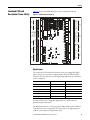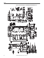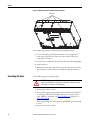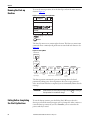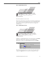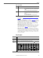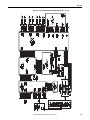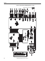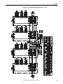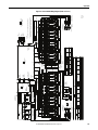
1
User Manual
LiquiFlo 2.0 AC Drive
Important User Information
Solid-state equipment has operational characteristics differing from those of electromechanical equipment. Safety
Guidelines for the Application, Installation and Maintenance of Solid State Controls (publication SGI-1.1 available from
your local Rockwell Automation sales office or online at http://www.rockwellautomation.com/literature/) describes some
important differences between solid-state equipment and hard-wired electromechanical devices. Because of this difference,
and also because of the wide variety of uses for solid-state equipment, all persons responsible for applying this equipment
must satisfy themselves that each intended application of this equipment is acceptable.
In no event will Rockwell Automation, Inc. be responsible or liable for indirect or consequential damages resulting from the
use or application of this equipment.
The examples and diagrams in this manual are included solely for illustrative purposes. Because of the many variables and
requirements associated with any particular installation, Rockwell Automation, Inc. cannot assume responsibility or
liability for actual use based on the examples and diagrams.
No patent liability is assumed by Rockwell Automation, Inc. with respect to use of information, circuits, equipment, or
software described in this manual.
Reproduction of the contents of this manual, in whole or in part, without written permission of Rockwell Automation,
Inc., is prohibited.
Throughout this manual, when necessary, we use notes to make you aware of safety considerations.
WARNING: Identifies information about practices or circumstances that can cause an explosion in a hazardous environment,
which may lead to personal injury or death, property damage, or economic loss.
ATTENTION: Identifies information about practices or circumstances that can lead to personal injury or death, property
damage, or economic loss. Attentions help you identify a hazard, avoid a hazard, and recognize the consequence.
SHOCK HAZARD: Labels may be on or inside the equipment, for example, a drive or motor, to alert people that dangerous
voltage may be present.
BURN HAZARD: Labels may be on or inside the equipment, for example, a drive or motor, to alert people that surfaces may
reach dangerous temperatures.
ARC FLASH HAZARD: Labels may be on or inside the equipment, for example, a motor control center, to alert people to
potential Arc Flash. Arc Flash will cause severe injury or death. Wear proper Personal Protective Equipment (PPE). Follow ALL
Regulatory requirements for safe work practices and for Personal Protective Equipment (PPE).
IMPORTANT
Identifies information that is critical for successful application and understanding of the product.
Allen-Bradley, Rockwell Software, Rockwell Automation, and TechConnect are trademarks of Rockwell Automation, Inc.
Trademarks not belonging to Rockwell Automation are property of their respective companies.
Summary of Changes
This manual contains new and updated information.
New and Updated
Information
This table contains the major changes made to this revision.
Topic
Page
Added Motor Overload Protection specification
234
Rockwell Automation Publication D2-3518-3 - May 2013
3
Summary of Changes
Notes:
4
Rockwell Automation Publication D2-3518-3 - May 2013
Table of Contents
Summary of Changes
New and Updated Information . . . . . . . . . . . . . . . . . . . . . . . . . . . . . . . . . . . . . 3
Chapter 1
Introduction
Firmware Versions . . . . . . . . . . . . . . . . . . . . . . . . . . . . . . . . . . . . . . . . . . . . . . . . . 6
Manual Conventions . . . . . . . . . . . . . . . . . . . . . . . . . . . . . . . . . . . . . . . . . . . . . . . 7
Getting Assistance from Rockwell Automation . . . . . . . . . . . . . . . . . . . . . . . 7
Additional Resources . . . . . . . . . . . . . . . . . . . . . . . . . . . . . . . . . . . . . . . . . . . . . . . 7
Chapter 2
About the Drive
Identifying the Drive by Cabinet Assembly ID Number . . . . . . . . . . . . . . . 9
LiquiFlo 2.0 Drive Component Locations. . . . . . . . . . . . . . . . . . . . . . . . . . 10
Drive Components Locations (Frame 3) . . . . . . . . . . . . . . . . . . . . . . . 10
Power Module Components Locations (Frame 3) . . . . . . . . . . . . . . . 12
Drive Components Locations (Frame 4) . . . . . . . . . . . . . . . . . . . . . . . 15
Power Module Components Locations (Frame 4) . . . . . . . . . . . . . . . 17
Identifying the Power Module by Model Number. . . . . . . . . . . . . . . . . . . 20
AC Line I/O Board Description (Frame 3 Only) . . . . . . . . . . . . . . . . . . . 21
Digital Inputs . . . . . . . . . . . . . . . . . . . . . . . . . . . . . . . . . . . . . . . . . . . . . . . . 21
Digital Outputs . . . . . . . . . . . . . . . . . . . . . . . . . . . . . . . . . . . . . . . . . . . . . . 21
Analog Inputs. . . . . . . . . . . . . . . . . . . . . . . . . . . . . . . . . . . . . . . . . . . . . . . . 21
Analog Outputs . . . . . . . . . . . . . . . . . . . . . . . . . . . . . . . . . . . . . . . . . . . . . . 21
Standard I/O Board Description (Frame 3 Only) . . . . . . . . . . . . . . . . . . . 23
Digital Inputs . . . . . . . . . . . . . . . . . . . . . . . . . . . . . . . . . . . . . . . . . . . . . . . . 23
Digital Outputs . . . . . . . . . . . . . . . . . . . . . . . . . . . . . . . . . . . . . . . . . . . . . . 23
Analog Inputs. . . . . . . . . . . . . . . . . . . . . . . . . . . . . . . . . . . . . . . . . . . . . . . . 23
Analog Outputs . . . . . . . . . . . . . . . . . . . . . . . . . . . . . . . . . . . . . . . . . . . . . . 24
Combined I/O Board Description (Frame 4 Only) . . . . . . . . . . . . . . . . . 25
Digital Inputs . . . . . . . . . . . . . . . . . . . . . . . . . . . . . . . . . . . . . . . . . . . . . . . . 25
Digital Outputs . . . . . . . . . . . . . . . . . . . . . . . . . . . . . . . . . . . . . . . . . . . . . . 26
Analog Inputs. . . . . . . . . . . . . . . . . . . . . . . . . . . . . . . . . . . . . . . . . . . . . . . . 26
Analog Outputs . . . . . . . . . . . . . . . . . . . . . . . . . . . . . . . . . . . . . . . . . . . . . . 27
DPI Communication Ports . . . . . . . . . . . . . . . . . . . . . . . . . . . . . . . . . . . . . . . 28
Optional Equipment . . . . . . . . . . . . . . . . . . . . . . . . . . . . . . . . . . . . . . . . . . . . . 29
Rockwell Automation Publication D2-3518-3 - May 2013
5
Table of Contents
Chapter 3
Planning the Installation
General Requirements for the Installation Site . . . . . . . . . . . . . . . . . . . . . .
Making Sure Environmental Conditions are Met. . . . . . . . . . . . . . . .
Determining Total Area Required Based on Drive Dimensions . . .
Verifying Recommended Air Flow Clearances. . . . . . . . . . . . . . . . . . .
Verifying Power Module Input Ratings Match Supplied Power . . .
Wiring Requirements for the Drive . . . . . . . . . . . . . . . . . . . . . . . . . . . . . . . .
Determining Wire Size Requirements . . . . . . . . . . . . . . . . . . . . . . . . . .
Verifying Power Module Output Current Rating Is Greater Than
Chiller Running Load Amps. . . . . . . . . . . . . . . . . . . . . . . . . . . . . . . . . . .
Stopping the Drive . . . . . . . . . . . . . . . . . . . . . . . . . . . . . . . . . . . . . . . . . . . . . . .
31
31
32
37
37
37
37
38
38
Chapter 4
Mounting The Power Module and
Grounding the Drive
Lifting and Mounting the Drive . . . . . . . . . . . . . . . . . . . . . . . . . . . . . . . . . . . 41
Grounding the Drive . . . . . . . . . . . . . . . . . . . . . . . . . . . . . . . . . . . . . . . . . . . . . 42
Lifting and Mounting the Power Module. . . . . . . . . . . . . . . . . . . . . . . . . . . 43
Chapter 5
Installing Input and Output Power
Wiring
Installing Power Wiring from the AC Input Line to the Main Input
Circuit Breaker. . . . . . . . . . . . . . . . . . . . . . . . . . . . . . . . . . . . . . . . . . . . . . . . . . . 45
Installing Wiring from the Power Module Output to the Motor . . . . . 46
Chapter 6
Completing the Installation
Checking the Installation . . . . . . . . . . . . . . . . . . . . . . . . . . . . . . . . . . . . . . . . . 47
Powering Up After Installation Is Complete . . . . . . . . . . . . . . . . . . . . . . . . 48
Chapter 7
Using the Start-up Routines
Preparing for Startup . . . . . . . . . . . . . . . . . . . . . . . . . . . . . . . . . . . . . . . . . . . . . 49
Running the Start-up Routines . . . . . . . . . . . . . . . . . . . . . . . . . . . . . . . . . . . . 50
Exiting Before Completing the Start-Up Routines . . . . . . . . . . . . . . . . . . 50
Chapter 8
Programming Basics
6
About Parameters . . . . . . . . . . . . . . . . . . . . . . . . . . . . . . . . . . . . . . . . . . . . . . . .
How Parameters are Organized . . . . . . . . . . . . . . . . . . . . . . . . . . . . . . . . . . . .
Inverter Parameters View . . . . . . . . . . . . . . . . . . . . . . . . . . . . . . . . . . . . . . . . .
Rectifier Parameters View . . . . . . . . . . . . . . . . . . . . . . . . . . . . . . . . . . . . . . . . .
Accessing the Parameters. . . . . . . . . . . . . . . . . . . . . . . . . . . . . . . . . . . . . . . . . .
Viewing Rectifier or Inverter Parameters. . . . . . . . . . . . . . . . . . . . . . . .
Selecting the Parameter Access Level . . . . . . . . . . . . . . . . . . . . . . . . . . . . . . .
Inverter Parameters Basic Access Level. . . . . . . . . . . . . . . . . . . . . . . . . .
Rectifier Parameters Basic Access Level . . . . . . . . . . . . . . . . . . . . . . . . .
Security and Passwords . . . . . . . . . . . . . . . . . . . . . . . . . . . . . . . . . . . . . . . . . . .
If There is More Than One OIM Connected to the Drive . . . . . . .
Rockwell Automation Publication D2-3518-3 - May 2013
51
52
53
56
58
58
59
60
60
62
63
Table of Contents
Chapter 9
Parameter Descriptions
What the Symbols Mean. . . . . . . . . . . . . . . . . . . . . . . . . . . . . . . . . . . . . . . . . . 65
Parameter Organization . . . . . . . . . . . . . . . . . . . . . . . . . . . . . . . . . . . . . . . . . . 65
Inverter Parameters . . . . . . . . . . . . . . . . . . . . . . . . . . . . . . . . . . . . . . . . . . . . . . 66
Rectifier Parameters . . . . . . . . . . . . . . . . . . . . . . . . . . . . . . . . . . . . . . . . . . . . . 158
Chapter 10
Troubleshooting the Drive
Verify that the DC Bus Capacitors are Discharged Before Servicing .
Determining Drive Status Using the Status LEDs. . . . . . . . . . . . . . . . . .
About Alarms. . . . . . . . . . . . . . . . . . . . . . . . . . . . . . . . . . . . . . . . . . . . . . . . . . .
Alarm Descriptions. . . . . . . . . . . . . . . . . . . . . . . . . . . . . . . . . . . . . . . . . .
About Faults. . . . . . . . . . . . . . . . . . . . . . . . . . . . . . . . . . . . . . . . . . . . . . . . . . . .
About the Fault Queue . . . . . . . . . . . . . . . . . . . . . . . . . . . . . . . . . . . . . .
Clearing Faults . . . . . . . . . . . . . . . . . . . . . . . . . . . . . . . . . . . . . . . . . . . . . .
Fault Descriptions and Corrective Actions . . . . . . . . . . . . . . . . . . . .
Diagnostic Parameters . . . . . . . . . . . . . . . . . . . . . . . . . . . . . . . . . . . . . . . . . . .
Common Symptoms and Corrective Actions . . . . . . . . . . . . . . . . . . . . . .
Replacement Parts . . . . . . . . . . . . . . . . . . . . . . . . . . . . . . . . . . . . . . . . . . . . . .
Replacement Parts (Frame 3 Drive) . . . . . . . . . . . . . . . . . . . . . . . . . . .
Replacement Parts (Frame 4 Drive) . . . . . . . . . . . . . . . . . . . . . . . . . . .
Ordering Replacement Parts . . . . . . . . . . . . . . . . . . . . . . . . . . . . . . . . .
Board Replacement, Firmware Setup Procedures. . . . . . . . . . . . . . . . . . .
Clearing Drive Faults . . . . . . . . . . . . . . . . . . . . . . . . . . . . . . . . . . . . . . . .
LiquiFlo 2.0 Frame 3 Firmware Setup Procedures . . . . . . . . . . . . . .
LiquiFlo 2.0 Frame 4 Firmware Setup Procedures . . . . . . . . . . . . . .
Troubleshooting the Drive Using the OIM. . . . . . . . . . . . . . . . . . . . . . . .
Accessing the Fault Queue . . . . . . . . . . . . . . . . . . . . . . . . . . . . . . . . . . .
Accessing the Fault Parameters . . . . . . . . . . . . . . . . . . . . . . . . . . . . . . .
Accessing the Drive Status Parameters. . . . . . . . . . . . . . . . . . . . . . . . .
Determining the Product Version. . . . . . . . . . . . . . . . . . . . . . . . . . . . .
Checking the Power Modules with Input Power Off . . . . . . . . . . . . . . .
Contacting Technical Support for Assistance . . . . . . . . . . . . . . . . . .
191
192
194
195
197
198
199
199
211
212
214
214
216
217
218
218
218
220
222
222
223
223
223
225
227
Appendix A
Technical Specifications
Service Conditions . . . . . . . . . . . . . . . . . . . . . . . . . . . . . . . . . . . . . . . . . . . . . .
Environmental Conditions . . . . . . . . . . . . . . . . . . . . . . . . . . . . . . . . . . . . . .
Cooling System Specifications (Refrigerant) . . . . . . . . . . . . . . . . . . . . . . .
Motor Overload Protection . . . . . . . . . . . . . . . . . . . . . . . . . . . . . . . . . . . . . .
Rockwell Automation Publication D2-3518-3 - May 2013
229
229
230
230
7
Table of Contents
Appendix B
Using the OIM
Installing and Removing the OIM . . . . . . . . . . . . . . . . . . . . . . . . . . . . . . . .
Removing the OIM While the Drive is Powered. . . . . . . . . . . . . . . .
Display Description . . . . . . . . . . . . . . . . . . . . . . . . . . . . . . . . . . . . . . . . . . . . .
Key Descriptions . . . . . . . . . . . . . . . . . . . . . . . . . . . . . . . . . . . . . . . . . . . .
OIM Menu Structure. . . . . . . . . . . . . . . . . . . . . . . . . . . . . . . . . . . . . . . . . . . .
Powering Up and Adjusting the OIM . . . . . . . . . . . . . . . . . . . . . . . . . . . . .
Selecting the Fast Power Up Feature. . . . . . . . . . . . . . . . . . . . . . . . . . .
Adjusting the Screen Contrast . . . . . . . . . . . . . . . . . . . . . . . . . . . . . . . .
Resetting the Display. . . . . . . . . . . . . . . . . . . . . . . . . . . . . . . . . . . . . . . . .
Selecting a Device in the System . . . . . . . . . . . . . . . . . . . . . . . . . . . . . . . . . .
Using the OIM to Program the Drive . . . . . . . . . . . . . . . . . . . . . . . . . . . . .
Viewing and Adjusting Parameters . . . . . . . . . . . . . . . . . . . . . . . . . . . .
Loading and Saving User Sets . . . . . . . . . . . . . . . . . . . . . . . . . . . . . . . . .
Monitoring the Drive Using the Process Display Screen on the OIM
Displaying and Changing the OIM Reference. . . . . . . . . . . . . . . . . . . . . .
Customizing the Process Display Screen. . . . . . . . . . . . . . . . . . . . . . . . . . .
Customizing the Function Keys . . . . . . . . . . . . . . . . . . . . . . . . . . . . . . . . . .
Customizing the Function Key Label Text . . . . . . . . . . . . . . . . . . . . .
Setting the Display Timeout Period . . . . . . . . . . . . . . . . . . . . . . . . . . .
Using Reverse Video for the Process Display Screen. . . . . . . . . . . . .
Controlling the Drive From the OIM . . . . . . . . . . . . . . . . . . . . . . . . . . . . .
Starting the Drive. . . . . . . . . . . . . . . . . . . . . . . . . . . . . . . . . . . . . . . . . . . .
Stopping the Drive. . . . . . . . . . . . . . . . . . . . . . . . . . . . . . . . . . . . . . . . . . .
231
233
233
234
235
236
236
236
236
236
236
237
238
238
239
239
239
241
242
242
242
242
242
Appendix C
LiquiFlo 2.0 Drive Frame 3 Wiring
Diagrams
Frame 3 Wiring Diagrams. . . . . . . . . . . . . . . . . . . . . . . . . . . . . . . . . . . . . . . . 243
Appendix D
LiquiFlo 2.0 Drive Frame 4 Wiring
Diagrams
8
Frame 4 Wiring Diagrams. . . . . . . . . . . . . . . . . . . . . . . . . . . . . . . . . . . . . . . . 251
Rockwell Automation Publication D2-3518-3 - May 2013
Chapter
1
Introduction
This manual is intended for qualified electrical and plumbing personnel familiar
with installing, programming, and maintaining AC drives.
This manual contains information on:
• Installing and wiring the LiquiFlo 2.0 AC drive
• Programming the drive
• Troubleshooting the drive
ATTENTION: Only qualified electrical personnel familiar with the construction
and operation of this equipment and the hazards involved should install, adjust,
operate, or service this equipment. Read and understand this manual and other
applicable manuals in their entirety before proceeding. Failure to observe this
precaution could result in severe bodily injury or loss of life.
ATTENTION: DC bus capacitors retain hazardous voltages after input power has
been disconnected. After disconnecting input power, wait 5 minutes for the DC
bus capacitors to discharge and then check the voltage with a voltmeter to
ensure the DC bus capacitors are discharged before touching any internal
components. Failure to observe this precaution could result in severe bodily
injury or loss of life.
ATTENTION: The drive can operate at and maintain zero speed. You are
responsible for assuring safe conditions for operating personnel by providing
suitable guards, audible or visual alarms, or other devices to indicate that the
drive is operating or may operate at or near zero speed. Failure to observe this
precaution could result in severe bodily injury or loss of life.
ATTENTION: Do not install modification kits with power applied to the drive.
Disconnect and lock out incoming power before attempting such installation or
removal. Failure to observe this precaution could result in severe bodily injury or
loss of life.
ATTENTION: You must provide an external, hardwired emergency stop circuit
outside of the drive circuitry. This circuit must disable the system in case of
improper operation. Uncontrolled machine operation may result if this
procedure is not followed. Failure to observe this precaution could result in
bodily injury.
Rockwell Automation Publication D2-3518-3 - May 2013
9
Chapter 1
ATTENTION: The drive contains ESD- (Electrostatic Discharge) sensitive parts
and assemblies. Static control precautions are required when installing, testing,
servicing, or repairing the drive. Erratic machine operation and damage to, or
destruction of, equipment can result if this procedure is not followed. Failure to
observe this precaution can result in bodily injury.
ATTENTION: You are responsible for conforming with all applicable local,
national, and international codes. Failure to observe this precaution could result
in damage to, or destruction of, the equipment.
Firmware Versions
There are two frame types for LiquiFlo 2.0 drives: Frame 3 and Frame 4. See
Chapter 2 for a description of the physical layout, components, and ratings for
each frame type.
Each drive contains two sections: the inverter section and the rectifier section.
Each section contains its own firmware.
• Firmware for Frame 3 drives are version 1.xx series
• Firmware for Frame 4 drives are version 2.xx series
The current drive firmware versions are listed in Table 1.
Table 1 - Firmware Versions
Release Date
Firmware Type
Current Version
May 2011
Frame 3 inverter application firmware
1.12
May 2011
Frame 3 rectifier application firmware
1.14
June 2011
Frame 4 inverter application firmware
2.12
June 2011
Frame 4 rectifier application firmware
2.12
See Determining the Product Version on page 227 for instructions on
determining the firmware version currently installed in a drive.
10
Rockwell Automation Publication D2-3518-3 - May 2013
Chapter 1
Manual Conventions
Parameter names: In most instances, parameter names are shown as the
parameter name followed by the parameter number. The parameter name is
preceded by inverter or rectifier for reference.
For example: inverter PI Control (125).
Getting Assistance from
Rockwell Automation
If you have any questions or problems with the products described in this
instruction manual, contact your local Rockwell Automation sales office. For
technical assistance, call 1-888-926-6786, Option 1.
Also, see Rockwell Automation Support on the back cover of this user manual for
technical support contact information.
Additional Resources
These documents contain additional information concerning related products
from Rockwell Automation.
Resource
Description
VS Utilities Getting Results Manual, publication D2-3488
Provides information explaining the uses and interface of
VS Utilities, and information to help you complete basic
tasks such as installing the software and starting the
application, and finding instructions to complete more
sophisticated tasks using the online help.
Industrial Automation Wiring and Grounding Guidelines,
publication 1770-4.1
Provides general guidelines for installing a Rockwell
Automation industrial system.
Product Certifications website, http://www.ab.com
Provides declarations of conformity, certificates, and other
certification details.
You can view or download publications at
http:/www.rockwellautomation.com/literature/. To order paper copies of
technical documentation, contact your local Rockwell Automation sales
representative.
Rockwell Automation Publication D2-3518-3 - May 2013
11
Chapter 1
Notes:
12
Rockwell Automation Publication D2-3518-3 - May 2013
Chapter
2
About the Drive
This chapter describes how to identify the drive assembly, the power module, and
shows the major drive components.
The LiquiFlo 2.0 AC drive is a pulse-width-modulated (PWM) liquid-cooled
drive that provides vector and general purpose regulation for a wide range of
applications.
Identifying the Drive by
Cabinet Assembly ID Number
Each LiquiFlo 2.0 AC drive is identified by its assembly number or order number
(see Figure 1). These numbers appear on the shipping label and on the nameplate
of the drive.
Figure 1 - Identifying the Drive by Cabinet Assembly ID Number
180264-A 03 - 3 00
180580-A 09 - 6 AA
Input: 440-480VAC 60HZ 3PH
Output: 480VAC 405A 0-250 Hz
Type Enclosure: TYPE 1
Short Circuit Rating: 65kAIC
Max. Ambient: 40˚C
Coolant Type: R134a OR Treated Water
Design Pressure: 185 psig
ID NO. Cab. Assy: 180264-A03-600
Cabinet Assy S/N: XXXXXXXXXX
Mfg On: XX-XX-XX
Frame Code
Frame 3 180264
3 = 2AA
6 = 2CC
Frame 4 180580
7 = 4AA
9 = 4CC
Voltage (3-PH input)
3 = 380 - 415V, 50 Hz
6 = 440 - 480V, 60 Hz
8 = 346V, 50 Hz
PWR Mod. M/N: LF200460AAR
PWR Mod. S/N: XXXXXXXXXXX
Made in USA by Rockwell Automation
Options
Cabinet Assembly ID Number
AA = 3PH Meter Kit
BA = 100 kAIC Circuit Breaker
CA = CE Touch Kit
KA = Meter Kit + 100 kAIC Circuit Breaker
LA = Meter Kit + CE Kit
TA = 100 kAIC Circuit Breaker + CE Kit
ZB = Meter Kit + 100 kAIC Circuit Breaker + CE Kit
00 = No Options
Cabinet Assembly Serial Number
Rockwell Automation Publication D2-3518-3 - May 2013
13
Chapter 2
LiquiFlo 2.0 Drive Component
Locations
LiquiFlo 2.0 AC drives include a drive section and a power module section. The
components are listed and illustrated below.
Drive Components Locations (Frame 3)
Frame 3 Units 180264-A0x
The drive section contains the following main components. The numbered items
listed below correspond to the numbers used in Figure 2. Replacement parts are
listed in Chapter 10.
1. AC Contactor (3) with Surge Suppressor
2. Terminal Block, 6-position
3. Precharge Resistors (3)
4. Power Module Assembly
5. Power Module Nameplate
6. Fuse Block, 30 A, 600V, Class CC, 3-Line
7. Fuse, Class CC, 600V, 1 A
8. Fuse, Class CC, 600V, 20 A
9. Line Sync. PC Board Assembly
10. Line Sync. Board Cover
11. 115V Fan, 6 in. diameter (2)
12. Capacitor Guard Panel (not shown)
13. Capacitor Bank Assembly
14. Fuse Block, 30 A, 600V, Class CC
15. Fuse, Class CC, 600V, 5 A
16. Fuse, Class CC, 600V, 25 A
17. Fuse Holder, 600V, 30 A
18. Fuse, Class RK5, 600V, 15 A
19. Transformer, 5 kVA
20. Resistor, 100 kOhm, 50 W
21. Operating Mechanism, Complete Kit
22. Main Input Circuit Breaker
23. Ground Lug, 2-600 MCM
24. 115V Fan, 5 in., sq.
25. Air Filter
26. Floor Mounting Kit (3)
27. Surge Suppressor
14
Rockwell Automation Publication D2-3518-3 - May 2013
Chapter 2
Figure 2 - Drive Components (Frame 3)
8
3
2
6
1
24
23
22
4
W
L1 L2 L3
V
21
U
20
L3
27
L2
L1
19
17
14
5
18
15 16
26
13
12
11
25
10
9
Rockwell Automation Publication D2-3518-3 - May 2013
6
7
15
Chapter 2
Power Module Components Locations (Frame 3)
Frame 3 Units LF200460AAR and LF200608CCR
The power module section contains the following main components. The
numbered items listed below correspond to the numbers used in Figure 3 and
Figure 4. Replacement parts are listed in Chapter 10.
1. Wire Harness Assembly, Power Supply, Logic (2)
2. Current Feedback Device, 1000 A (6)
3. Terminal Block, 2-Position
4. 80 W Power Supply Assembly (2)
5. Cable Assembly, 40-pin, 0.050 in Pitch, Flex Film (2)
6. Cable Assembly, 30-pin, 0.050 in Pitch, Flex Film (2)
7. Wire Harness Assembly, Power Supply, Upper Gate (2)
8. Inverter Power Interface Assembly
9. Wire Harness Assembly, Power Supply, Lower Gate (2)
10. Insulation Sheet (2)
11. Communications Interface Assembly
12. Rectifier Power Interface Assembly
13. Wire Harness Assembly, Gate Driver
14. Wire Harness Assembly, Current Feedback Device
15. Wire Harness Assembly, Line Sync.
16. Wire Harness Assembly, DC Bus Bleeder Resistors
17. Cable Assembly, 20-pin, 0.050 in Pitch, Flex Film (optional)
18. Communications Assembly (optional)
19. Internal Fan
20. Connector, Terminal Block, 32-pin
21. AC Line I/O Assembly
22. Rectifier Control Assembly
23. Inverter Control Assembly
24. Standard I/O Assembly
25. Wire Harness Assembly, Control Sync.
16
Rockwell Automation Publication D2-3518-3 - May 2013
Chapter 2
Figure 3 - Power Module Component Locations - Door Open (Frame 3)
1
2
3
4
5
6
7
25
8
9
10
11
5
6
7
1
12
9
4
10
7
13
14
16
15
Rockwell Automation Publication D2-3518-3 - May 2013
17
Chapter 2
Figure 4 - Power Module Component Locations - Door Closed (Frame 3)
23
24
11
20
Optional
17
22
Optional
18
21
20
19
18
Rockwell Automation Publication D2-3518-3 - May 2013
Chapter 2
Drive Components Locations (Frame 4)
Frame 4 Units 180580-A07 and 180580-A09
The drive section contains the following main components. The numbered items
listed below correspond to the numbers used in Figure 5. Replacement parts are
listed in Chapter 10.
1. Circuit Breaker, 600V
2. Inductor
3. AC Contactor
4. Power Module Assembly
5. Input Filter Capacitor Assembly
6. OIM
7. Fans, 115V AC, Inductor (4)
8. Transformer, 5 kVA
9. Fan, 115V AC, Contactor
10. Resistors, 100 kOhms, 50 W
11. Precharge Resistors
12. Relay, Oil Pump & Control Power Terminals
13. Fuse, Class RK-5, 600V, 10 A (2)
14. Fuse, Class CC, 600V, 25 A (1)
15. Fuse, Class CC, 600V, 10 A (1)
16. Fuse, Class T, 600V, 300 A (3)
17. Fuse, Class CC, 600V, 20 A (3)
18. Fuse, Class CC, 600V, 1 A (3)
19. Ground Lug, 2-600 MCM
20. Nameplate, Power Module
21. Door Inter-lock (2)
22. Surge Suppressor
23. Circuit Breaker Operating Mechanism
Rockwell Automation Publication D2-3518-3 - May 2013
19
Chapter 2
Figure 5 - Drive Components (Frame 4)
2
9
11
17
3
19
16
L1
L2
L3
L1
U
L2
V
L3
W
4
1
10
12
22
23
20
8
13
20
14
15
5
21
7
18
21
Rockwell Automation Publication D2-3518-3 - May 2013
6
Chapter 2
Power Module Components Locations (Frame 4)
Frame 4 Units LF200900CCR and LF201215CCR
The power module section contains the following main components. The
numbered items listed below correspond to the numbers used in Figure 6 and
Figure 7. Replacement parts are listed in Chapter 10.
1. Combined Power PCB Assembly, 900 A, or
Combined Power PCB Assembly, 1215 A
2. Wire Harness Assembly, Gate Driver
3. Internal Fan, 24V DC
4. Internal Fan, 24V DC
5. Wire Harness Assembly, Internal Fan
6. Wire Harness Assembly, DC Power
7. Wire Harness Assembly, DC Bus Resistors
8. Current Feedback Device, 2000 A
9. Wire Harness Assembly, Current Feedback Device, Rectifier Side
10. Wire Harness Assembly, Current Feedback Device, Inverter Side
11. Wire Harness Assembly, RTD, Recitifier Side
12. Wire Harness Assembly, RTD, Inverter Side
13. Cable Assembly, 40-Pin
14. Combined Control PCB Assembly
15. Combined I/O PCB Assembly
16. RS-485 Communications Assembly (optional)
17. Cable Assembly, 20-Pin (optional)
18. Cable, Mini DIN, 8 Pos., Male/Male, 1 m (3.2 ft)
Rockwell Automation Publication D2-3518-3 - May 2013
21
Chapter 2
Figure 6 - Power Module Component Locations - I/O and Control Panel Removed (Frame 4)
6
9
10
7
UNDER
TOP
COVER
5
3
1
2
2X
9
11
8
6X
12
4
Figure 7 - Power Module Component Locations - Front Panel Removed (Frame 4)
22
Rockwell Automation Publication D2-3518-3 - May 2013
Chapter 2
15
14
Optional
17
Optional
16
13
2X
18
Rockwell Automation Publication D2-3518-3 - May 2013
23
Chapter 2
Identifying the Power
Module by Model Number
Each LiquiFlo 2.0 AC power module is identified by its model number. See
Figure 8. This number appears on the shipping label and on the nameplate of the
power module. Power ratings are provided in Table 2.
Figure 8 - Identifying the Power Module Model Number
LF20 0608CC R
LF20 = LiquiFlo 2.0
Continuous Ampere Rating
and Frame Size
0460AA = 405 amps*, frame 2AA
0608CC = 608 amps, frame 2CC
0900CC = 900 amps, frame 4AA
1215CC = 1215 amps, frame 4CC
Cooling Method
R = refrigerant/water
* 460 A with refrigerant, 405 A with water as coolant
Table 2 - Drive Assembly and Power Module Ratings
Drive Assembly ID
Number
Power Module
Model Number
Enclosure
Rating
Input
Power
(KVA)
180264-A03
LF200460AAR
NEMA 1
337
180264-A06
LF200608CCR
180580-A07
180580-A09(1)
Input Voltage
(V)
Input
Current(2)
(Amps)
Output
Current
at 2 kHz(3)
(Amps)
405
405
505
608
608
LF200900CCR
673
900
900
LF201215CCR
1010
1215
1215
480 ±10%
(1) No overload rating for 180580-A09. 100% output current capability.
(2) 460 A with refrigerant, 405 A with water as coolant.
(3) 110% output current capability for one minute, 150% output current capability for 5 sec.
24
Rockwell Automation Publication D2-3518-3 - May 2013
Chapter 2
AC Line I/O Board Description
(Frame 3 Only)
The following signals are available at the AC Line I/O board terminal block. The
AC Line I/O board is labeled as item 21 in Figure 4. See Figure 9 for terminal
identification.
Digital Inputs
The AC Line I/O board terminal block provides terminals for four digital inputs
(terminals 22...26). These digital inputs cannot be configured.
Digital Outputs
The AC Line I/O board terminal provides terminals for six digital outputs that
are non user-configurable terminals 5...16 and 27...32. The state of these six
outputs can be changed by writing to inverter parameter Appl Digital Out (30).
Digital output 1 is always connected to the shunt trip circuit; do not use digital
output 1 for anything else.
The digital output devices are form C relays capable of switching 250V AC at 8 A
or 30V DC at 8 A.
Analog Inputs
The AC Line I/O board contains no component hardware for user-configurable
analog inputs.
Analog Outputs
The AC Line I/O board terminal block provdes terminals for two special
purpose analog outputs, using terminals 1-2 and 17-18. These outputs are not
user-configurable.
Rockwell Automation Publication D2-3518-3 - May 2013
25
Chapter 2
Figure 9 - AC Line I/O Board (Frame 3)
AC Line I/O Terminal Block (detail)
AC Line I/O
Terminal Block
AC Line I/O Board
26
Rockwell Automation Publication D2-3518-3 - May 2013
Chapter 2
Standard I/O Board
Description (Frame 3 Only)
The Standard I/O board is offered as an option for Frame 3 LiquiFlo 2.0 drives.
The following signals are available at the Standard I/O board. The Standard I/O
board is labeled as item 24 in Figure 4. See Figure 10 for terminal identification.
Digital Inputs
The Standard I/O board terminal block provides terminals (27...32) for six
user-configurable digital inputs. These inputs can be configured using the
inverter digital input selection parameters (361...366).
Digital Outputs
The Standard I/O board terminal block provides terminals for two
user-configurable digital outputs (terminals 11...16). These logic outputs can be
configured for any of the 30 functions controlled by Digital Out1 Sel (380) and
Digital Out2 Sel (384).
The digital output devices are form C relays capable of switching 250V AC at 8 A
or 30V DC at 8 A.
Analog Inputs
The standard I/O board terminal block provides two user-configurable terminals
for analog inputs (terminals 1...4 and 17...20). Configure the inputs using inverter
parameters Anlg In Config through Analog In 2 Loss (320...327). Each analog
input has two modes: voltage-sensing (input senses -10 V...10 V) and currentsensing (input senses 0 mA...20 mA). Separate terminals on the standard I/O
board are used for each mode.
The mode for both inputs are selected via inverter parameter Anlg In Config
(320). If the bit corresponding to a particular analog input is set to 1, then the
analog input is in current-sensing mode; if set to 0 it is in voltage-sensing mode.
The following table describes the correspondence between the mode of each
user-configurable analog input and the standardI/O board terminals that should
be used.
Input and Mode
Paramter 320 Setting
Terminal Designators
Terminal Numbers
Analog input 1,
voltage-sensing
Bit 0 = 0
V1+, V1-
1, 2
Analog input 1,
current-sensing
Bit 0 = 1
I1+, I2-
17, 18
Analog input 2,
voltage-sensing
Bit 1 = 0
V2+, V2-
3, 4
Analog input 2,
current-sensing
Bit 1 = 1
I1+, l2-
19, 20
Rockwell Automation Publication D2-3518-3 - May 2013
27
Chapter 2
Analog Outputs
The single analog output channel can be configured using Analog Out Config
(340) and Analog Out1 Sel (342) to select any one of 31 analog outputs.
Terminals 8 and 9 output 4...20 mA. Terminals 6 and 7 output 0...10 V.
Figure 10 - Standard I/O Board (Frame 3)
+
+
+
A4
A1
Standard I/O Terminal Block (Detail)
U8
+
+
+
Standard I/O
Terminal Block
2
+
C71
1
R74
+
+
J3
Q2
Q3
+
24 VOLT AC/DC
+
A2
24 VOLT AC/DC
U24
U27
C78
C79
C80
R75
R76 R77
R81
R82
U29
C81 C82 C83
+
C77
C75
R78
R79
R80
R83 R84
1
R85
R86
A3
Standard I/O Board
28
U28
Rockwell Automation Publication D2-3518-3 - May 2013
1
Chapter 2
Figure 11 shows terminal block locations on the Combined I/O Board.
Combined I/O Board
Description (Frame 4 Only)
Figure 11 - Combined I/O Board (Frame 4)
LINE
VOLTAGE
L1
TB5
1
L2
3
L3
5
TB6
1
G1
GRID
VOLTAGE
G2
3
G3
5
CNTRL PWR
PRECHARGE OUT
SHUNT TRIP
SW 24V
TEMPSW INV
TEMPSW RCT
PRECHARGE FB
+12V
COMMON
A+
ENCODER
INPUT
AB+
B-
ANALOG
INPUT
AI 1+
AI 1AI 2+
AI 2AI 3+
AI 3AI 4+
AI 4-
ANALOG
OUTPUT
AO 1+
AO 1AO 2+
AO 2AO 3+
AO 3AO 4+
AO 4-
TB1
12
11
10
9
8
7
6
5
4
3
2
1
TB2
12
11
10
9
8
7
6
5
4
3
2
1
TB7
1
2
3
4
5
6
7
TB10
1
2
3
4
5
6
TB8
1
2
3
4
5
6
7
8
TB9
1
2
3
4
5
6
7
8
TB3
9
8
7
6
5
4
3
2
1
TB4
7
6
5
4
3
2
1
DO 1 NC
DO 1 COM
DO 1 NO
DO 2 NC
DO 2 COM
DO 2 NO
DO 3 NC
DO 3 COM
DO 3 NO
DO 4 NC
DO 4 COM
DO 4 NO
DIGITAL
OUTPUT
1
DO 5 NC
DO 5 COM
DO 5 NO
DO 6 NC
DO 6 COM
DO 6 NO
DO 7 NC
DO 7 COM
DO 7 NO
DO 8 NC
DO 8 COM
DO 8 NO
DIGITAL
OUTPUT
2
GATEKILL +
GATEKILL DI 24V+
DI 1
DIGITAL
DI 2
INPUT
1
DI 3
DI 4
DI COM 1
DI 24VDI 24V+
DI 5
DI 6
DI 7
DI 8
DI COM 2
DI 24V-
DIGITAL
INPUT
2
Digital Inputs
The combined I/O board provides hardware for six user-configurable digital
inputs, using connector positions designated DI3...DI8. The following table
shows the correspondence between the digital input and the inverter parameter
used to configure it.
Inverter Parameter Number
Inverter Parameter Name
Connector Position Designator
361
Digital In1 Sel
DI3
362
Digital In2 Sel
DI4
363
Digital In3 Sel
D15
364
Digital In4 Sel
DI6
365
Digital In5 Sel
DI7
366
Digital In6 Sel
DI8
The states of all six user-configurable digital inputs are visible in inverter
parameter Dig In Status (216).
The digital inputs that use connector positions DI1 and DI2 on the combined
I/O board are not user-configurable. The status of these two digital inputs are
visible in rectifier parameter Dig In Status (216).
Rockwell Automation Publication D2-3518-3 - May 2013
29
Chapter 2
Digital Outputs
The combined I/O board provides two user-configurable digital outputs, using
connector positions designated DO1 and DO2. These two digital outputs are
configured using inverter parameters Digital Out1 Sel through Digital Out2
Off Time (380...387).
The combined I/O board contains six special purpose digital outputs, using
connector positions designated DO3...DO8. The state of these six outputs can be
changed by writing to inverter parameter Appl Digital Out (30).
All eight digital output devices are form C relays capable of switching 250V AC
at 8 A, or 30V DC at 8 A.
The combined I/O board also contains dedicated terminals for driving the shunt
trip circuit.
Analog Inputs
The combined I/O board provides two user-configurable analog inputs.
Configure the inputs using inverter parameters Anlg In Config through Analog
In 2 Loss (320...327). Each analog input has two modes: voltage-sensing (input
senses -10 V...10 V) and current-sensing (input senses 0 mA...20 mA). Separate
terminals on the standard I/O board are used for each mode.
The mode for both inputs are selected via inverter parameter Anlg In Config
(320). If the bit corresponding to a particular analog input is set to 1, then the
analog input is in current-sensing mode; if set to 0 it is in voltage-sensing mode.
The following table describes the correspondence between the mode of each
user-configurable analog input and the combined I/O board terminals that
should be used.
30
Input and Mode
Paramter 320 Setting
Combined I/O Board Designator
Analog input 1,
voltage-sensing
Bit 0 = 0
AI1
Analog input 1,
current-sensing
Bit 0 = 1
AI2
Analog input 2,
voltage-sensing
Bit 1 = 0
AI3
Analog input 2,
current-sensing
Bit 1 = 1
AI4
Rockwell Automation Publication D2-3518-3 - May 2013
Chapter 2
Analog Outputs
The combined I/O board contains one user-configurable analog output. The
output is configurable using inverter parameters Anlg Out Config through
Analog Out1 Lo (340...344). The analog output has two modes: voltage (output
at -10 V...10 V) and current (output at 0 mA...20 mA). Separate terminals on the
combined I/O board are used for each mode.
The mode is selected via inverter parameter Anlg Out Config (340). In this
parameter, if the lowest bit is set to 1, then the analog output is in voltage mode;
if set to 0 it is in current mode.
The following table describes the correspondence between the mode of the
user-configurable analog output and the combined I/O board terminals that
should be used.
Mode
Parameter 340 Setting
Combined I/O BoardDesignator
Analog Output, voltage
Bit 0 = 0
AO3
Analog Output, current
Bit 0 = 1
AO4
The combined I/O board contains two special purpose analog outputs: AO1 and
AO2. These outputs are not user-configurable.
Rockwell Automation Publication D2-3518-3 - May 2013
31
Chapter 2
DPI Communication Ports
For Frame 3 drives, the Communication Interface board contains three DIN
connectors that are used as DPI communication ports (Figure 12). These ports
provide communication between the LiquiFlo 2.0 drive and other DPI devices
(for example, an OIM or a personal computer running the VS Utilities software).
The three connectors (DPI ports 3, 4, and 5) are equivalent. This manual
assumes that peripherals are always plugged into DPI port 3.
Figure 12 - DPI Communication Interface Board (Frame 3)
DPI Port 5
DPI Port 4
DPI Port 3
For Frame 4 drives, there is only one DPI port, accessible via the OIM connector
on the front panel of the power module (see Figure 13). An internal cable
connects this connector to the DIN connector on the control board. A device
plugged directly into this connector uses DPI port 3. If there is a requirement
that multiple DPI peripheral devices be connected, a DPI port expander box can
be used, but no device should be plugged into the DPI Port 2 connector because
the rectifier connects to the inverter using that port.
Figure 13 - Power Module Bottom Left Front View (Frame 4)
Connect OIM Here
32
Rockwell Automation Publication D2-3518-3 - May 2013
Chapter 2
Optional Equipment
Table 3 lists standard LiquiFlo 2.0 kits and options.
Table 3 - Available LiquiFlo 2.0 Kits and Options
Description
Model Number
Instruction Manual
Operator Interface Module (OIM)
RE1LCD
LiquiFlo 2.0 AC Drive User Manual,
publication D2-3518. See Using the OIM on
page 235.
OIM LCD Hand-held Cable
RECBL-LCD
N/A
OIM Door-mount Bezel Kit
REBZL-N1
MD60/MD65 Door-Mount NEMA 1 OIM
Bezel Kit (MDI) Instruction Manual,
publication D2-3517
Serial Converter with VS Utilities Software
RECOMM-232
VS Utilities Getting Results Manual,
publication D2-3488
Rockwell Automation Publication D2-3518-3 - May 2013
33
Chapter 2
Notes:
34
Rockwell Automation Publication D2-3518-3 - May 2013
Chapter
3
Planning the Installation
This chapter provides information for planning a LiquiFlo 2.0 drive installation.
ATTENTION: Only qualified electrical personnel familiar with the construction
and operation of this equipment and the hazards involved should install, adjust,
operate, or service this equipment. Read and understand this manual and other
applicable manuals in their entirety before proceeding. Failure to observe this
precaution could result in severe bodily injury or loss of life.
ATTENTION: Use of power factor correction capacitors on the output of the
drive can result in erratic operation of the motor, nuisance tripping, and/or
permanent damage to the drive. Remove power factor correction capacitors
before proceeding. Failure to observe this precaution could result in damage to,
or destruction of, the equipment.
ATTENTION: You are responsible for conforming with all applicable local,
national, and international codes. Failure to observe this precaution could result
in damage to, or destruction of, the equipment.
General Requirements for
the Installation Site
Always properly plan the installation before installing a LiquiFlo 2.0 drive to be
sure that the environment and operating conditions are satisfactory. Read the
following recommendations before continuing with drive installation.
Making Sure Environmental Conditions are Met
Before deciding on an installation site, consider the following guidelines:
• Verify that NEMA/UL Type 1 enclosure drives can be kept clean and dry.
• Verify that the area chosen allows for proper airflow. See Verifying the Site
Provides for Recommended Air Flow Clearances on page 41.
• Be sure that the NEMA/UL Type 1 enclosure is installed away from oil,
coolants, and other airborne contaminants.
• Do not install the drive above 1000 m (3300 ft) without derating output
power. For every 91.4 m (300 ft) above 1000 m (3300 ft), derate the
output current 1%.
• Verify that the drive location meets the environmental conditions specified
in Table 4.
• Floor-mounted units should be attached to the floor with the C-channel
rails provided. See Figure 14 and Figure 16.
Rockwell Automation Publication D2-3518-3 - May 2013
35
Chapter 3
Table 4 - Environmental Conditions
Condition
Specification
Operating Temperature
(inside NEMA/UL Type 1 enclosure)
0...+55 ° C(1) (32...131 ° F)
Ambient Temperature
(outside NEMA/UL Type 1 enclosure)
0...+40 ° C (32...104 ° F)
Storage Temperature (Ambient)
- 40...65 ° C (- 40...149 ° F)
Humidity
5%...95% (non-condensing)
(1) With typical heat rise inside a cabinet, 40 ° C (104 °F) ambient outside usually results in 55 ° C (131 °F) inside.
Determining Total Area Required Based on Drive Dimensions
Overall drive dimensions are identified in these figures:
• Frame 3 drives 180264-A03 and 180264-A06 in Figure 14
• Frame 4 drives 180580-A07 and 180580-A09 in Figure 16
Overall power module dimensions are identified in these figures:
• Frame 3 power modules LF200460AAR and LF200608CCR in Figure 15
• Frame 4 power modules LF200900CCRand LF201215CCR in Figure 17
36
Rockwell Automation Publication D2-3518-3 - May 2013
Chapter 3
Figure 14 - Exterior Enclosure Dimensions - 180264-A03 and 180264-A06 (Frame 3), in. (mm)
Rockwell Automation Publication D2-3518-3 - May 2013
37
Chapter 3
Figure 15 - Power Module Dimensions - LF200460AAR and LF200608CCR (Frame 3), in.
38
Rockwell Automation Publication D2-3518-3 - May 2013
Chapter 3
FILTER INSTALLED
5.25 REF
16.50
1.000
Rockwell Automation Publication D2-3518-3 - May 2013
0.63
TYP
0.50
TYP
1.000
21.47
26.43
BOTTOM VIEW
26.43
21.47
4.40
DRIVE
PIPING
ACCESS
Figure 16 - Exterior Enclosure Dimensions - 180580-A07 and 180580-A09 (Frame 4), in.
39
40
18.42
IN
2.25
13.67
4.76
OUT
COOLANT
CONNECTIONS
SEE NOTES
2, 3 AND 4
2.12
FROM BACK OF
CHASSIS TO
ORFSSEALING
SURFACE
43.17
Rockwell Automation Publication D2-3518-3 - May 2013
Ø.56
1.12
2.99
9.09
9.09
Ø.453
(4)-PLACES
SEENOTE1
3.15
.38
L1
L2
L3
3.90
2.62
.50
TYP.
14.75
SEE
DETAIL
A
FRONT PANEL
SEENOTE5.
37.00
3.18
LIFTING
Ø1.00
(4)-PLACES
LEFT SIDEVIEW
DETAIL A
INPUT AND OUTPUT
WIRING CONNECTION
SCALE 1:4
.88
1.13
2.00
4.50
4.50
2.49
8.01
5.60
6.94
1.74
10.92
4.81
37.94
OIM
CONNECTION
DC
POS.
(+)
RECTIFIERSIDE
2A32
AIRFLOW
BOTTOM VIEW
21.93
17.12
FRONT VIEW
7.31
2A11
2.88
36.44
10.55
11.96
2A12
43.19
4.81
DC
NEG.
(-)
INVERTERSIDE
16.78
DC BUS MEASUREMENT POINTS ON LAMINATED BUS ASSY.
.25" X .032" MALE FASTON. ACCESSABLEBY REMOVING TOP COVER.
8.00
.75
1.74
18.96
W/ T3
V/ T2
U/ T1
2.62
1.50
.33
9.81
8.63
FIELD
CONTROL
WIRING
ACCESS
(BOTH
SIDES)
5.50
2.27
2.49
4-5
4-5
2A32
[IN-LBF]
.5 - .6
[N-M]
TORQUE
.5 - .6
SCREW SIZE
REFERENCE
LF201215CCR
MODEL NUMBER
FIELD CONTROL WIRING
M3 MOUNTING
11.30
2.17
9.50
DETAIL COG
SCALE 1:4
CENTEROF GRAVITY:
X = 21.38
Y = 4.50
Z = 18.25 (INTO
PLANEOF DRAWING)
WEIGHT: 450 LBF.
M3 TERMINAL
IN
OUT
2.89
SEE
DETAIL
COG
2A12
NAME
RIGHT SIDEVIEW
5.84
DC BUS
MEASUREMENT
POINTS
-
24 TO 12
[AWG]
WIRESIZE
180015-A04
4CC
FRAME
-
.28
[INCH]
STRIP LENGTH
PART NUMBER
Chapter 3
Figure 17 - Power Module Dimensions - LF200900CCRand LF201215CCR (Frame 4), in.
Chapter 3
Verifying the Site Provides for Recommended Air Flow Clearances
Be sure there is adequate clearance for air circulation around the enclosure. A
6-inch minimum clearance is required wherever vents are located in the cabinet.
Verifying Power Module Input Ratings Match Supplied Power
Verify that plant power meets the input power requirements of the power module
circuitry for the LiquiFlo 2.0 drive. See Table 2 on page 24 for input power rating
specifications. Be sure input power to the power module corresponds to the
nameplate voltage, current, and frequency of the power module.
Wiring Requirements for the
Drive
Evaluate the input power wire sizes, branch circuit protection, and control wiring
before continuing with the drive installation (Chapter 6).
Determining Wire Size Requirements
Determine wire size based on current requirements, size of conduit openings, and
applicable local, national, and international codes (for example, NEC/CEC
regulations).
ATTENTION: You are responsible for conforming with all applicable local,
national, and international codes. Failure to observe this precaution could result
in damage to, or destruction of, the equipment.
Conduit Entry Opening Sizes
Determine the size of the conduit openings in the cabinet that the drive is
mounted in so that the wire planned for a specific entry point will fit through the
opening.
Recommended Power Wire Sizes
Use copper input power wiring that is sized according to applicable codes to
handle the continuous-rated input current of the drive. Use copper output wiring
that is sized according to applicable codes to handle the continuous-rated output
current of the drive.
Recommended Control and Signal Wire Sizes
The recommended wire size to connect I/O signals to the control terminal block
is 4 mm2 (12 AWG). Recommended terminal tightening torque is 0.8...1 N•m
(7...9 lb•in).
Rockwell Automation Publication D2-3518-3 - May 2013
41
Chapter 3
Recommended Motor Lead Lengths
Motor lead lengths can total up to 76 m (250 ft).
Verifying Power Module Output Current Rating Is Greater Than
Chiller Running Load Amps
Verify that the LiquiFlo 2.0 power module output current rating is equal to or
greater than the running load amps (RLA) of the chiller. Table 2 on page 24 lists
the output current values.
Stopping the Drive
ATTENTION: You must provide an external, hardwired emergency stop circuit
outside of the drive circuitry. This circuit must disable the system in case of
improper operation. Uncontrolled machine operation may result if this
emergency stop circuit is not implemented. Failure to observe this precaution
could result in bodily injury.
Depending on the requirements of the application, the LiquiFlo 2.0 drive can be
programmed to provide either a coast-to-rest or a ramp-to-rest operational stop
without physical separation of the power source from the motor.
• A coast-to-rest stop turns off the gate drive to the IGBT power devices.
• A ramp-to-rest stop continues to fire the IGBT power devices in a
controlled manner until the motor comes to a stop, and then turns off the
power devices.
You can also program zero speed with power maintained to the motor, but in this
condition, the drive is not actually stopped.
In addition to the operational stop, the LiquiFlo 2.0 power module provides a
hardwired gate kill. This function provides a two-wire emergency stop circuit
that does not depend on software or on the transmission of commands over a
communications network. When the two-wire circuit is opened, the gate drive to
the IGBTs is removed.
In Frame 3, the gate kill function is provided by a two-position terminal block
(A33) located on the power module. See Figure 18 for gate kill connections in
Frame 4.
42
Rockwell Automation Publication D2-3518-3 - May 2013
Chapter 3
Figure 18 - Frame 4 Combined I/O (partial view) with Gate Kill Connections
LINE
VOLTAGE
L1
TB5
1
L2
3
L3
5
TB6
1
G1
GRID
VOLTAGE
G2
3
G3
5
CNTRL PWR
PRECHARGE OUT
SHUNT TRIP
SW 24V
TEMPSW INV
TEMPSW RCT
PRECHARGE FB
+12V
COMMON
A+
ENCODER
INPUT
AB+
B-
ANALOG
INPUT
AI 1+
AI 1AI 2+
AI 2AI 3+
AI 3AI 4+
AI 4-
ANALOG
OUTPUT
AO 1+
AO 1AO 2+
AO 2AO 3+
AO 3AO 4+
AO 4-
TB1
12
11
10
9
8
7
6
5
4
3
2
1
TB2
12
11
10
9
8
7
6
5
4
3
2
1
TB7
1
2
3
4
5
6
7
TB10
1
2
3
4
5
6
TB8
1
2
3
4
5
6
7
8
TB9
1
2
3
4
5
6
7
8
TB3
9
8
7
6
5
4
3
2
1
TB4
7
6
5
4
3
2
1
Rockwell Automation Publication D2-3518-3 - May 2013
DO 1 NC
DO 1 COM
DO 1 NO
DO 2 NC
DO 2 COM
DO 2 NO
DO 3 NC
DO 3 COM
DO 3 NO
DO 4 NC
DO 4 COM
DO 4 NO
DIGITAL
OUTPUT
1
DO 5 NC
DO 5 COM
DO 5 NO
DO 6 NC
DO 6 COM
DO 6 NO
DO 7 NC
DO 7 COM
DO 7 NO
DO 8 NC
DO 8 COM
DO 8 NO
DIGITAL
OUTPUT
2
GATEKILL +
GATEKILL DI 24V+
DI 1
DIGITAL
DI 2
INPUT
1
DI 3
DI 4
DI COM 1
DI 24VDI 24V+
DI 5
DI 6
DI 7
DI 8
DI COM 2
DI 24V-
Gate Kill Connections
TB3-8
TB3-9
DIGITAL
INPUT
2
43
Chapter 3
Notes:
44
Rockwell Automation Publication D2-3518-3 - May 2013
Chapter
4
Mounting The Power Module and Grounding the
Drive
This chapter shows how to mount and properly ground the drive.
Lifting and Mounting the
Drive
Be careful to prevent damage due to dropping or jolting when moving the drive.
A forklift truck or similar means of lifting and transporting may be used. Sling in
a manner that equalizes the load at the lifting points. Use a spreader bar if the
angle of the sling is less than 45 degrees relative to horizontal. Do not jolt while
lifting.
Figure 19 - Lift Point Locations for LiquiFlo 2.0 Drives (Frame 3)
Lifting Points
Rockwell Automation Publication D2-3518-3 - May 2013
45
Chapter 4
Figure 20 - Lift Point Locations for LiquiFlo 2.0 Drives (Frame 4)
Lifting Points
Use the following procedure to lift and mount the LiquiFlo 2.0 drive:
1. Use an overhead or portable hoist (minimum 2 ton rated capacity) to
attach a free-fall chain to the chain secured to the drive. Take up any
vertical slack in the chain.
2. Use the hoist to carefully lift the drive from the horizontal shipping pallet.
3. Position the drive.
4. Machine fasten the drive enclosure using 1/2-inch bolts, grade 5 or better,
with compression washers. Verify mounting bolt torque specifications.
Grounding the Drive
Use the following steps to ground the drive:
ATTENTION: You are responsible for conforming with all applicable local,
national, and international codes. Failure to observe this precaution could result
in damage to, or destruction of, the equipment.
1. Open the door of the enclosure.
2. Run a suitable equipment grounding conductor unbroken from the drive
to earth ground. Recommended tightening torque is 11.3...13.5 N•m
(100...120 lb•in). For Frame 3 see Figure 2 on page 15, for Frame 4 see
Figure 5 on page 20.
Note: For grounding the motor, the motor ground cable provided should
be used.
3. Close the door of the enclosure.
46
Rockwell Automation Publication D2-3518-3 - May 2013
Chapter 4
Lifting and Mounting the
Power Module
Be careful to prevent damage due to dropping or jolting when moving the drive.
A forklift truck or similar means of lifting and transporting may be used. Sling in
a manner that equalizes the load at the lifting points. Use a spreader bar if the
angle of the sling is less than 45 degrees relative to horizontal. Do not jolt while
lifting.
Figure 21 - Lift Point Locations for LiquiFlo 2.0 Power Module (Frame 3)
Lifting Hole
(both sides)
Input and Output
Busbar
Lifting Hole
(both sides)
Figure 22 - Lift Point Locations for LiquiFlo 2.0 Power Module (Frame 4)
Lifting Hole
(both sides)
Input and Output
Busbar (both sides)
Lifting Hole
(both sides)
Rockwell Automation Publication D2-3518-3 - May 2013
47
Chapter 4
Use the following procedure to lift and mount the LiquiFlo 2.0 power module:
ATTENTION: Do not use input and output busbars for lifting or handling.
Otherwise, damage to equipment may result.
ATTENTION: Mechanically support conductors to minimize mechanical load on
input and output busbars. Otherwise, damage to equipment may result.
1. Use an overhead or portable hoist (minimum 2 ton rated capacity) to
attach a free-fall chain to the chain secured to the power module. Take up
any vertical slack in the chain.
2. Use the hoist to carefully lift the power module from the horizontal
shipping pallet.
3. Position the power module in the prepared mounting location.
4. Machine fasten the power module enclosure using 1/2-inch bolts, grade 5
or better, with compression washers. Recommended tightening torque is
11.3...13.5 N•m (100...120 lb•in).
48
Rockwell Automation Publication D2-3518-3 - May 2013
Chapter
5
Installing Input and Output Power Wiring
Install all wiring in conformance with the applicable local, national, and
international codes (for example, NEC/CEC). Signal wiring, control wiring, and
power wiring must be routed in separate conduits to prevent interference with
drive operation. Use grommets, when hubs are not provided, to guard against
wire chafing.
Installing Power Wiring from
the AC Input Line to the Main
Input Circuit Breaker
Use the following steps to connect AC input power to the main input circuit
breaker:
1. Turn off, lock out, and tag the input power to the drive.
2. Remove the input wiring panel and drill the required number of openings
in the top of the drive enclosure. Take care that metal chips do not enter
the enclosure. See Figure 14 on page 37 through Figure 17 on page 40.
3. Wire the AC input power leads by routing them though the openings to
the main input circuit breaker.
ATTENTION: Do not route signal and control wiring with power wiring in the
same conduit. This can cause interference with drive operation. Failure to
observe this precaution could result in damage to, or destruction of, the
equipment.
4. Connect the three-phase AC input power leads (three-wire 480V AC) to
the appropriate input terminals of the circuit breaker. See Figure 2 on
page 15 and Figure 5 on page 20.
5. Tighten the AC input power terminals to the proper torque as specified on
the input circuit breaker.
Rockwell Automation Publication D2-3518-3 - May 2013
49
Chapter 5
Installing Wiring from the
Power Module Output
Terminals to the Motor
Use the following steps to connect the AC output power wiring from the power
module to the motor.
IMPORTANT
The total motor lead length must not exceed 76 m (250 ft). See Table 5 for
recommended minimum motor lead wire sizes.
1. Turn off, lock out, and tag the input power to the drive. Wait 5 minutes.
2. Remove the input wiring panel and drill the required number of openings
for the wiring. See Figure 14 on page 37 and Figure 16 on page 39.
3. Connect the three-phase AC output power motor leads to the power
module busbars labeled U, V, and W. See Figure 15 on page 38 and
Figure 17 on page 40.
4. Tighten the three-phase AC output power terminals:
• Frame 3 – M10 Class 8.8 or 3/8 in. Grade 5 fastener. Tighten to
40N•m (30 lb•ft).
• Frame 4 – M12 Class 8.8 or 1/2 in. Grade 5 fastener. Tighten to
100N•m (75 lb•ft).
Table 5 - Recommended Minimum Motor Lead Wire Size
Power Module Model Number
Minimum Motor Lead Wire Size(1)
LF200460AAR
2 x 2/0 AWG
LF200608CCR
2 x 250 MCM
LF200900CCR
4 x 250 MCM
LF201215CCR
4 x 250 MCM
(1) Motor lead wiring must comply with all local and national codes.
50
Rockwell Automation Publication D2-3518-3 - May 2013
Chapter
6
Completing the Installation
This chapter provides instructions on how to perform a final check of the
installation before power is applied to the drive.
ATTENTION: Only qualified electrical personnel familiar with the construction
and operation of this equipment and the hazards involved should start and
adjust it. Read and understand this manual in its entirety before proceeding.
Failure to observe this precaution could result in severe bodily injury or loss of
life.
Checking the Installation
Use the following procedure to verify the condition of the installation:
ATTENTION: DC bus capacitors retain hazardous voltages after input power has
been disconnected. After disconnecting input power, wait 5 minutes for the DC
bus capacitors to discharge and then check the voltage with a voltmeter to
ensure the DC bus capacitors are discharged before touching any internal
components. Failure to observe this precaution could result in severe bodily
injury or loss of life.
1. Turn off, lock out, and tag the input power to the drive. Wait 5 minutes.
2. Verify that the DC bus voltage is zero. See Verify that the DC Bus
Capacitors are Discharged Before Servicing the Drive on page 195.
ATTENTION: You must provide an external, hardwired emergency stop circuit
outside of the drive circuitry. This circuit must disable the system in case of
improper operation. Uncontrolled machine operation may result if this
procedure is not followed. Failure to observe this precaution could result in
bodily injury.
3. Remove any debris, such as metal shavings, from around the drive.
4. Check that there is adequate clearance around the drive.
5. Verify that the wiring to the terminal strip and the power terminals is
correct.
6. Check that the wire size is within terminal specifications and that the wires
are tightened properly.
7. Check that user-supplied branch circuit protection is installed and
correctly rated.
Rockwell Automation Publication D2-3518-3 - May 2013
51
Chapter 6
8. Check that the incoming power is rated correctly.
9. Check the motor installation and length of motor leads.
10. Check that the rating of the transformer (if used) matches the drive
requirements and is connected properly.
11. Verify that a properly sized ground wire is installed and a suitable earth
ground is used. Check for and eliminate any grounds between the motor
frame and the motor power leads. Verify that all ground leads are
unbroken.
12. Visually inspect the liquid-cooling connections for leaks.
Powering Up After
Installation Is Complete
Use the following procedure to verify that the drive is installed correctly and is
receiving the proper line voltage:
1. Turn the input circuit breaker of the drive to the On position.
2. Verify that coolant is flowing through the power module.
3. Follow the start-up procedure in Using the Start-up Routines on page 53.
52
Rockwell Automation Publication D2-3518-3 - May 2013
Chapter
7
Using the Start-up Routines
ATTENTION: Only qualified electrical personnel familiar with the construction
and operation of this equipment and the hazards involved should install, adjust,
operate, or service this equipment. Read and understand this chapter in its
entirety before proceeding. Failure to observe this precaution could result in
severe bodily injury or loss of life.
ATTENTION: Incorrect values for some of the parameters in the start-up
routines can cause the drive to operate improperly. Verify that the values of
these parameters are appropriate for your application. Failure to observe this
precaution could result in bodily injury.
For standard applications, the start-up routines on the OIM enable you to
configure the most commonly used parameters through a series of steps. This
helps you set up the drive as quickly as possible.
For advanced applications, you may need to adjust additional parameters in the
parameter list using either the OIM or VS Utilities software.
Preparing for Startup
Before performing the start-up routine, you must:
• Be qualified to configure the drive and be familiar with the operation of
AC drives.
• Be familiar with the operation of the OIM.
• Have completed all hardware installation.
• Properly connect the drive to the motor.
Rockwell Automation Publication D2-3518-3 - May 2013
53
Chapter 7
Running the Start-up
Routines
To access the start-up routines, select the Start-Up icon from the main menu as
shown in Figure 23
Figure 23 - Accessing the Start-Up Routines
>>
Auto
Stopped
P0: LiquiFlo 2.0
Main Menu
Start-Up
Monitor
Lang
Highlight Start-Up icon
Select
The Start-Up menu screen contains eight selections. The first seven menu items
contain the most commonly used parameters associated with each function. See
Figure 24.
Figure 24 - Start-Up Menu
Main Menu
Start-Up
Intro
Press
Input
Voltage
Motor
Data
Motor
Tests
Speed
Limits
Ref Setup
Configure for
Alternate
Input Voltage
Enter Motor
Nameplate
Data
Optimize
Torque and
Verify Direction
Set Min/Max
Speed, Stop
Mode, and
Direction Conrol
Set
Reference
Control
Source
Configure
I/O
Done
Set TB I/O
Functions
The Start-up routine automates the process of entering values of selected
parameters by taking you to the next parameter after you accept a parameter
value. As each item in the list is completed, you are automatically advanced to the
next step.
IMPORTANT
Exiting Before Completing
the Start-Up Routines
54
Parameter values are saved as they are changed. Pressing
Start-up routine does not undo the changes.
ESC/
PROG
or aborting the
To exit the Start-up routines, press the F4 key (Exit). When you select the
Start-up icon from the main menu again, you are prompted to either continue or
restart the Start-up routines. If you select Continue, you are returned to the
point at which you exited.
Rockwell Automation Publication D2-3518-3 - May 2013
Chapter
8
Programming Basics
To program the drive for a specific application, you adjust the appropriate
parameters. The parameters are used to define characteristics of the drive.
This chapter provides an overview of parameter types and how they are
organized. Parameter descriptions are provided in Chapter 9.
About Parameters
There are three types of parameters:
Numbered List
Parameters
Numbered list parameters allow a selection from
two or more options. The OIM displays a text
message for each item.
Example: inverter Speed Ref A Sel (90)
Bit Parameters
Bit parameters have individual bits associated with
features or conditions:
• If the bit is 0, the feature is off or the
condition is false.
• If the bit is 1, the feature is on or the
condition is true.
Example: inverter Drive Status 1 (209)
Numeric Parameters
These parameters have a single numerical value
(for example, 0.1 V).
Example: inverter Maximum Freq (55)
Parameters are also either configurable, tunable, or read-only:
Configurable Parameters Can be adjusted or changed only while the drive is
stopped.
Tunable Parameters
Can be adjusted or changed while the drive is
running or stopped.
Read-only Parameters
Cannot be adjusted.
Rockwell Automation Publication D2-3518-3 - May 2013
55
Chapter 8
How Parameters are
Organized
Inverter parameters are organized into seven files:
• Monitor
• Motor Control
• Speed Command
• Dynamic Control
• Utility
• Communication
• Inputs and Outputs
Rectifier parameters are organized into seven files:
• Monitor
• Configuration
• Dynamic Control
• Internal Data
• Utility
• Communication
• Inputs and Outputs
Each file contains parameters that are grouped by their function. A file can
contain several groups of parameters. See Figure 25.
Figure 25 - Example of Parameter Organization
File
Group
Parameter
Motor Control
Motor Data
Motor Type
Motor NP Volts
Torq
Attributes
Torque Perf Mode
Maximum Voltage
Volts per
Hertz
Start/Acc Boost
Run Boost
Speed
Command
Control Src
Sel
Logic Source Sel
Speed Ref A Sel
Spd Mode &
Lmts
Speed Mode
Minimum Speed
56
Rockwell Automation Publication D2-3518-3 - May 2013
Chapter 8
Inverter Parameters View
The table below shows the inverter parameters organized by their respective files
and groups.
File
Group
Monitor
Metering
Output Freq
1
Output Powr Fctr
8
Analog In2 Value
17
Commanded Freq
2
Elapsed MWh
9
Analog In3 Value
18
Output Current
3
Elapsed Run Time 10
Ground Current
21
Torque Current
4
MOP Frequency
11
Phase U Current
22
Flux Current
5
DC Bus Voltage
12
Phase V Current
23
Output Voltage
6
DC Bus Memory
13
Phase W Current
24
Output Power
7
Analog In1 Value
16
Est Input Power
25
Rated kW
26
Rated Amps
28
–
Rated Volts
27
Control SW Ver
29
–
Appl Digital Out
30
Rctfr Config
32
Rctfr Status
34
Appl Analog Out
31
Rctfr Control
33
Rctfr Fault
35
Motor Type
40
Motor NP RPM
44
Motor OL Amps
48
Motor NP Volts
41
Motor NP Power
45
Imbalance Limit
49
Motor NP FLA
42
Mtr NP Pwr Units
46
Imbalance Time
50
Motor NP Hertz
43
Motor OL Hertz
47
Torque Perf Mode
53
Flux Up Mode
57
IR Voltage Drop
62
Maximum Voltage
54
Flux Up Time
58
Flux Current Ref
63
Maximum Freq
55
SV Boost Filter
59
Ixo Voltage Drop
64
Compensation
56
Autotune
61
–
Start/Acc Boost
69
Break Voltage
71
–
Run Boost
70
Break Frequency
72
–
Speed Mode
80
Overspeed Limit
83
Skip Frequency 3
86
Minimum Speed
81
Skip Frequency 1
84
Skip Freq Band
87
Maximum Speed
82
Skip Frequency 2
85
Speed Ref A Sel
90
Speed Ref B Sel
93
TB Man Ref Sel
96
Speed Ref A Hi
91
Speed Ref B Hi
94
TB Man Ref Hi
97
Speed Ref A Lo
92
Speed Ref B Lo
95
TB Man Ref Lo
98
Discrete Speeds
Jog Speed
100
Preset Speed 1...7 101...
107
–
Speed Trim
Trim In Select
117
Trim Hi
119
–
Trim Out Select
118
Trim Lo
120
–
Slip Comp
Slip RPM @ FLA
121
Slip Comp Gain
122
Slip RPM Meter
123
Process PI
PI Configuration
124
PI Integral Time
129
PI Status
134
PI Control
125
PI Prop Gain
130
PI Ref Meter
135
PI Reference Sel
126
PI Lower Limit
131
PI Fdback Meter
136
PI Setpoint
127
PI Upper Limit
132
PI Error Meter
137
PI Feedback Sel
128
PI Preload
133
PI Output Meter
138
Drive Data
Application
Motor Control
Motor Data
Torq Attributes
Volts per Hertz
Speed Command
Parameters
Spd Mode & Limits
Speed References
Rockwell Automation Publication D2-3518-3 - May 2013
–
–
57
Chapter 8
File
Group
Dynamic Control
Ramp Rates
Accel Time 1
140
Decel Time 1
142
S Curve %
Accel Time 2
141
Decel Time 2
143
–
Current Lmt Sel
147
Current Lmt Gain
149
Current Lmt Val
148
Drive OL Mode
150
Stop Mode A
155
DC Brake Time
159
DB Resistor Type
163
Stop Mode B
156
Bus Reg Ki
160
Bus Reg Kp
164
DC Brake Lvl Sel
157
Bus Reg Mode A
161
Bus Reg Kd
165
DC Brake Level
158
Bus Reg Mode B
162
–
Stop/Restart Modes
Start At PowerUp
168
Flying Start En
169
–
Restart Modes
Flying Start Gain
170
Sleep-Wake
Mode
178
Wake Time
181
Auto Rstrt Tries
174
Sleep-Wake Ref
179
Sleep Level
182
Auto Rstrt Delay
175
Wake Level
180
Sleep Time
183
Power Loss
Power Loss Mode
184
Power Loss Time
185
Power Loss Level
186
Direction Config
Direction Mode
190
–
–
–
HIM Ref Config
Save HIM Ref
192
Man Ref Preload
193
–
MOP Config
Save MOP Ref
194
MOP Rate
195
–
Drive Memory
Param Access Lvl
196
Save To User Set
199
Voltage Class
202
Reset To Defalts
197
Reset Meters
200
Drive Checksum
203
Load Frm Usr Set
198
Language
201
Drive Status 1
209
Dig Out Status
217
Status 1 @ Fault
227
Drive Status 2
210
Invtr Base Temp
218
Status 2 @ Fault
228
Drive Alarm 1
211
Drive OL Count
219
Alarm 1 @ Fault
229
Drive Alarm 2
212
Motor OL Count
220
Alarm 2 @ Fault
230
Speed Ref Source
213
Imbalance Count
221
Testpoint 1 Sel
234
Start Inhibits
214
Fault Frequency
224
Testpoint 1 Data
235
Last Stop Source
215
Fault Amps
225
Testpoint 2 Sel
236
Dig In Status
216
Fault Bus Volts
226
Testpoint 2 Data
237
Fault Config 1
238
Fault Clear Mode
241
–
Fault Clear
240
Power Up Marker
242
–
Fault 1 Code...
Fault 8 Code
243
245
247
249
251
253
255
257
Fault 1 Time...
Fault 8 Time
244
246
248
250
252
254
256
258
–
Alarm Config 1
259
Alarm Clear
261
Drive Alarm 1
211
Drive Alarm 2
212
Load Limits
Stop/Brake Modes
Utility
Diagnostics
Faults
Alarms
58
Parameters
Rockwell Automation Publication D2-3518-3 - May 2013
PWM Frequency
146
151
–
–
Alarm 1 Code...
Alarm 8 Code
–
262...
269
Chapter 8
File
Group
Communication
Comm Control
Masks & Owners
Datalinks
Inputs & Outputs
Analog Inputs
Analog Outputs
Temperature etc
Parameters
DPI Data Rate
270
Drive Ref Rslt
272
–
Drive Logic Rslt
271
Drive Ramp Rslt
273
–
Logic Mask
276
Fault Clr Mask
283
Reference Owner
292
Start Mask
277
MOP Mask
284
Accel Owner
293
Jog Mask
278
Local Mask
285
Decel Owner
294
Direction Mask
279
Stop Owner
288
Fault Clr Owner
295
Reference Mask
280
Start Owner
289
MOP Owner
296
Accel Mask
281
Jog Owner
290
Local Owner
297
Decel Mask
282
Direction Owner
291
Data In A1 Link A Word 1
300
Data In D 1 Link D Word 1
306
Data Out C 1 Link C Word 1
314
Data In A2 Link A Word 2
301
Data In D 2 Link D Word 2
307
Data Out C 2 Link C Word 2
315
Data In B 1 Link B Word 1
302
Data Out A1 Link A Word 1
310
Data Out D 1 Link D Word 1
316
Data In B 2 Link B Word 2
303
Data Out A2 Link A Word 2
311
Data Out D 2 Link D Word 2
317
Data In C 1 Link C Word 1
304
Data Out B 1 Link B Word 1
312
–
Data In C 2 Link C Word 2
305
Data Out B 2 Link B Word 2
313
–
Anlg In Config
320
Analog In 1 Lo
323
Analog In 2 Lo
326
Anlg In Sqr Root
321
Analog In 1 Loss
324
Analog In 2 Loss
327
–
Analog In 1 Hi
322
Analog In 2 Hi
325
Anlg Out Config
340
Analog Out1 Sel
342
–
Anlg Out Absolut
341
Analog Out1 Hi
343
–
Analog Out1 Lo
344
Inv IGBT Tmp Top
345
Inv Coldplt Tmp
349
Inv PS -12
353
Inv IGBT Tmp Up
346
Inv Ambient Tmp
350
Inv I/O ID V
354
Inv IGBT TMP Low
347
Inv PS Tmp
351
–
Inv PS +12
352
–
Inv IGBT Tmp Bot
348
Digital Inputs
Digital In1 Sel...
Digital In6 Sel
361...
366
–
Digital Outputs
Digital Out1 Sel
380
Dig Out1 OffTime
383
Dig Out2 OnTime
386
Dig Out1 Level
381
Digital Out2 Sel
384
Dig Out2 OffTime
387
Dig Out1 OnTime
382
Dig Out2 Level
385
Rockwell Automation Publication D2-3518-3 - May 2013
–
–
59
Chapter 8
Rectifier Parameters View
The table below shows the rectifier parameters organized by their respective files
and groups.
File
Group
Monitor
Metering
Line Frequency
1
Input Voltage TR
9
Elapsed Run Time
17
Input Current R
2
DC Bus Voltage
10
Rctfr Base Temp
18
Input Current S
3
Active Voltage
11
Rctfr IGBT Temp
19
Input Current T
4
Reactive Voltage
12
Rctfr IT Overld
20
Active Current
5
Input kW
13
Rctfr I2T Overld
21
Reactive Current
6
Input Pwr Factor
14
Line I Imbalance
22
Input Voltage RS
7
Motoring kWh
15
Line V Imbalance
23
Input Voltage ST
8
Regen kWh
16
–
Rated kW
26
Rated Amps
28
–
Rated Volts
27
Control SW Ver
29
–
V Imbalance Lmt
60
I Imbalance Lmt
62
Ride Through Ena
64
V Imbalance Time
61
I Imbalance Time
63
Ride Through Sec
65
Control and Status
Rectifier Contrl
100
Rectifier Status
101
–
Bus Voltage
Vdc Optimize
102
Vdc Reference
103 Vdc Command
104
Load Limits
Current Limit
105
Max Motor Volts
107 Base Motor Freq
109
Input Load Amps
106
Max Motor Freq
108
VML Ki
110
CML Ki
112 VML Reset Level
VML Kp
111
CML Kp
113
Cold Plate Temp
120
CPC K2
124 Delay After Move
128
Invtr Base Temp
121
High Temp Limit
125 Ambient Temp
129
Rctfr Base Temp
122
Low Temp Limit
126
–
CPC K1
123
Start Move Time
127
–
Normalized Amps
Input Load Amps
150
Current Limit
151
–
Total Elapsed
Life KW H
152
Life Power Time
154
–
Life Run Time
153
Life Power Cycle
155
–
DPI Error
156
CS Timeout Cnt
159 PC MSG Tx Cnt
162
CS Msg Rx Cnt
157
CS MSG Bad Cnt
160 PC Timeout Cnt
163
CS Msg Tx Cnt
158
PC MSG Rx Cnt
161 CAN Bus Off Cnt
164
D/A Select (N)
171...
174
Drive Data
Configuration
Dynamic Control
AC Line
Regulator Tuning
Cold Plate
Internal Data
DPI Counters
D/A Output Sel
60
Parameters
Rockwell Automation Publication D2-3518-3 - May 2013
–
–
114
–
–
Chapter 8
File
Group
Utility
Drive Memory
Status
Diagnostics
Fault Queue
Communications
Inputs & Outputs
In Data Links
Temperatures etc
Parameters
Param Access Lvl
196
Save to User Set
199 Drive Checksum
Reset to Defaults
197
Reset Meters
200
–
Load Frm Usr Set
198
Language
201
–
Drive Alarm
211
Dig In Status
216
–
Start Inhibits
214
Dig Out Status
217
–
Fault Frequency
220
Fault Amps D
225 Testpoint 1 Data
235
Fault Amps R
221
Fault Volts Vdc
226 Testpoint 2 Sel
236
Fault Amps S
222
Fault Volts Q
227 Testpoint 2 Data
237
Fault Amps T
223
Fault Volts D
228
–
Fault Amps Q
224
Testpoint 1 Sel
234
–
Fault Config
238
Fault To Invertr
241 Fault 1 Code...
Fault 4 Code
243
245
247
249
Fault Clear
240
Power Up Marker
242 Fault 1 Time...
Fault 4 Time
244
246
248
250
IOC Redir Time
300
Service 302
302
–
IOC Redir Max
301
Service 303
303
–
Rct IGBT Tmp Top
345
Rct Coldplt Tmp
349 Rct PS -12V
353
Rct IGBT Tmp Up
346
Rct Ambient Tmp
350 Rct I/O ID V
354
Rct IGBT Tmp Low
347
Rct PS Tmp
351
–
Rct IGBT Tmp Bot
348
Rct PS +12V
352
–
Rockwell Automation Publication D2-3518-3 - May 2013
203
61
Chapter 8
Accessing the Parameters
Parameters are programmed and viewed using the OIM or VS Utilities software.
The OIM displays parameters by group, by individual parameter number, and
parameters that have changed from their default value.
To access parameters using the OIM, select the Parameters icon from the main
screen. See Figure 26.
See Appendix B for information on modifying parameters using the OIM.
Refer to the VS Utilities Getting Results Manual, publication D2-3488, for
information on accessing and modifying parameters using VS Utilities software.
Figure 26 - Accessing the Parameters Using the OIM
>>
Stopped
Auto
P0: LiquiFlo 2.0
Main Menu
Parameters
Monitor
Lang
ESC/
PROG
>>
Stopped
Auto
P0: LiquiFlo 2.0
File:
File 1 Name
File 2 Name
File 3 Name
Parameters:
By Group
P Numbers
Changed Params
ESC/
PROG
Group:
Group 1 Name
Group 2 Name
Group 3 Name
ESC/
PROG
ESC/
PROG
>>
Stopped
Auto
P0: LiquiFlo 2.0
Parameter # 1234
Parameter Text
+456.78
Unit
Parameters:
By Group
P Numbers
Changed Params
Dflt
ESC/
PROG
ESC/
PROG
>>
Stopped
Auto
P0: LiquiFlo 2.0
Parameter # 1234
Parameter Text
+456.78
Unit
Parameters:
By Group
P Numbers
Changed Params
Changed: Par
Searching. . .
Dflt
ESC/
PROG
ESC/
PROG
Viewing Rectifier or Inverter Parameters
The OIM initially displays information about the inverter, including inverter
parameters.
To display rectifier parameters and other information about the rectifier, switch
the OIM to the Active Rectifier device. See Figure 27.
62
Rockwell Automation Publication D2-3518-3 - May 2013
Chapter 8
Figure 27 - Selecting the Active Rectifier
Auto
Stopped
P0: LiquiFlo 2.0
Stopped
Main Menu
LiquiFlo 2.0
LCD OIM
Active Rectifier
Device Select
Monitor
Main Menu
1
2
Auto
P2: Active Rectifier
0
ESC
PROG
Lang
Device Select
Highlight
Password
Highlight
Deviceicon
Select
Monitor
Icon
Lang
To switch back to viewing inverter information, use the process described by
Figure 27, but select the LiquiFlo 2.0 device.
Selecting the Parameter
Access Level
The LiquiFlo 2.0 AC drive provides two levels of access to the parameters:
• Basic (0)
• Advanced (1)
The Advanced level allows access to all of the parameters.
The Basic level allows access to a subset of the Standard level and contains only
the most commonly used parameters. See Inverter Parameters Basic Access Level
on page 64 and Rectifier Parameters Basic Access Level on page 64 for
parameters available at the Basic level.
The active access level is displayed in Parameter Access Level (196).
To select the parameter access level using the OIM, select the Password icon from
the main menu. See Figure 28.
IMPORTANT
This option is not supported in the VS Utilities software.
Figure 28 - Selecting the Parameter Access Level
>>
Stopped
Auto
P0: LiquiFlo 2.0
Main Menu
Password:
Set Access Lvl
Password:
Set Wrt Prot PW
Advanced
Basic
Password
Monitor
Lang
Highlight Password icon
Highlight option
Select
Rockwell Automation Publication D2-3518-3 - May 2013
63
Chapter 8
Inverter Parameters Basic Access Level
The inverter parameters available at the Basic level (0) are listed in the table
below.
1
Output Freq
97
TB Man Ref Hi
190
Direction Mode
2
Commanded Freq
98
TB Man Ref Lo
196
Param Access Lvl
3
Output Current
100
Jog Speed
197
Reset To Defalts
12
DC Bus Voltage
101...
107
Preset Speed 1...7
198
Load Frm Usr Set
41
Motor NP Volts
140
Accel Time 1
199
Save To User Set
42
Motor NP FLA
141
Accel Time 2
201
Language
43
Motor NP Hertz
142
Decel Time 1
214
Start Inhibits
44
Motor NP RPM
143
Decel Time 2
216
Dig In Status
45
Motor NP Power
146
S Curve %
217
Dig Out Status
46
Mtr NP Pwr Units
147
Current Lmt Sel
238
Fault Config 1
47
Motor OL Hertz
148
Current Lmt Val
320
Anlg In Config
53
Torque Perf Mode
155
Stop Mode A
322
Analog In 1 Hi
54
Maximum Voltage
156
Stop Mode B
323
Analog In 1 Lo
55
Maximum Freq
157
DC Brake Lvl Sel
325
Analog In 2 Hi
61
Autotune
158
DC Brake Level
326
Analog In 2 Lo
81
Minimum Speed
159
DC Brake Time
342
Analog Out1 Sel
82
Maximum Speed
161
Bus Reg Mode A
343
Analog Out1 Hi
90
Speed Ref A Sel
162
Bus Reg Mode B
344
Analog Out1 Lo
91
Speed Ref A Hi
163
DB Resistor Type
361...
366
Digital In1 Sel...
Digital In6 Sel
92
Speed Ref A Lo
168
Start At PowerUp
380
Digital Out1 Sel
93
Speed Ref B Sel
174
Auto Rstrt Tries
381
Dig Out1 Level
94
Speed Ref B Hi
175
Auto Rstrt Delay
384
Digital Out2 Sel
95
Speed Ref B Lo
184
Power Loss Mode
385
Dig Out2 Level
96
TB Man Ref Sel
185
Power Loss Time
–
Rectifier Parameters Basic Access Level
The rectifier parameters available at the Basic level (0) are listed in the table
below.
64
1
Line Frequency
103
Vdc Reference
164
CAN Bus Off Cnt
2
Input Current R
104
Vdc Command
171...
174
D/A Select (N)
3
Input Current S
105
Current Limit
196
Param Access Lvl
4
Input Current T
106
Input Load Amps
197
Reset to Defalts
5
Active Current
107
Max Motor Volts
198
Load Frm Usr Set
6
Reactive Current
108
Max Motor Freq
199
Save to User Set
Rockwell Automation Publication D2-3518-3 - May 2013
Chapter 8
7
Input Voltage RS
109
Base Motor Freq
200
Reset Meters
8
Input Voltage ST
110
VML Ki
201
Language
9
Input Voltage TR
111
VML Kp
203
Drive Checksum
10
DC Bus Voltage
112
CML Ki
211
Drive Alarm
11
Active Voltage
113
CML Kp
214
Start Inhibits
12
Reactive Voltage
114
VML Reset Level
216
Dig In Status
13
Input kW
120
Cold Plate Temp
217
Dig Out Status
14
Input Pwr Factor
121
Invtr Base Temp
220
Fault Frequency
15
Motoring kWh
122
Rctfr Base Temp
221
Fault Amps R
16
Regen kWh
123
CPC K1
222
Fault Amps S
17
Elapsed Run Time
124
CPC K2
223
Fault Amps T
18
Rctfr Base Temp
125
High Temp Limit
224
Fault Amps Q
19
Rctfr IGBT Temp
126
Low Temp Limit
225
Fault Amps D
20
Rctfr IT Overld
127
Start Move Time
226
Fault Volts Vdc
21
Rctfr I2T Overld
128
Delay After Move
227
Fault Volts Q
22
Line I Imbalance
129
Ambient Temp
228
Fault Volts D
23
Line V Imbalance
150
Input Load Amps
234
Testpoint 1 Sel
26
Rated kW
151
Current Limit
235
Testpoint 1 Data
27
Rated Volts
152
Life KW H
236
Testpoint 2 Sel
28
Rated Amps
153
Life Run Time
237
Testpoint 2 Data
29
Control SW Ver
154
Life Power Time
238
Fault Config
60
V Imbalance Lmt
155
Life Power Cycle
240
Fault Clear
61
V Imbalance Time
156
DPI Error
241
Fault To Invertr
62
I Imbalance Lmt
157
CS Msg Rx Cnt
242
Power Up Marker
63
I Imbalance Time
158
CS Msg Tx Cnt
243
245
247
249
Fault 1 Code...
Fault 4 Code
64
Ride Through Ena
159
CS Timeout Cnt
244
246
248
250
Fault 1 Time...
Fault 4 Time
65
Ride Through Sec
160
CS MSG Bad Cnt
300
IOC Redir Time
100
Rectifier Contrl
161
PC MSG Rx Cnt
301
IOC Redir Max
101
Rectifier Status
162
PC MSG Tx Cnt
302
Service 302
102
Vdc Optimize
163
PC Timeout Cnt
303
Service 303
Rockwell Automation Publication D2-3518-3 - May 2013
65
Chapter 8
Security and Passwords
ATTENTION: It is your responsibility to determine how to distribute the writeprotect password. Rockwell Automation is not responsible for unauthorized
access violations within your organization. Failure to observe this precaution
could result in bodily injury.
Parameter values can be password-protected using the OIM. When the password
is enabled, parameter values can be displayed. However, if there is an attempt to
change a parameter value, a password pop-up box appears on the OIM screen to
prompt for the user-defined write-protect password.
To set the write-protect password, select the Password icon from the main menu.
See Figure 29. The password value can range from 1...9999. A value of 0 disables
the password (factory default). To disable the password, you must first enter the
correct value and then set the password to zero.
When the password is enabled, the lock symbol on the screen changes from
to .
Figure 29 - Setting the Write-protect Password
>>
Stopped
Auto
P0: LiquiFlo 2.0
Main Menu
Password:
Set Wrt Prot PW:
Set Access Lvl
Set Wrt Prot PW
New Code:
0
Password
Monitor
Lang
Highlight Password
icon
Highlight option
Increase/decrease value
Move placeholder
Accept value
When you enter the password, you can adjust parameters until you select Logout
or return to the process display screen, which re-activates the password. See
Monitoring the Drive Using the Process Display Screen on the OIM on page 242
for information about the process display screen.
IMPORTANT
66
This option is not supported in the VS Utilities software.
Rockwell Automation Publication D2-3518-3 - May 2013
Chapter 8
If There is More Than One OIM Connected to the Drive
IMPORTANT
Setting the write-protect password value to zero on one OIM disables the
write-protect password on all connected OIMs.
Setting the write-protect password in one OIM does not affect any other OIM
connected to the drive unless a write-protect password has also been set in the
other OIMs. In this case, the last password value entered becomes the password
value for all password-protected OIMs. (Each OIM cannot have a different
password value.)
For example, if the write-protect password has been set to 5555 for the local
OIM, someone using a remote OIM with no write-protect password set can still
program all of the parameters. If the write-protect password is then set to 6666
on the remote OIM, you are required to enter 6666 on the local OIM to program
the parameters.
Rockwell Automation Publication D2-3518-3 - May 2013
67
Chapter 8
Notes:
68
Rockwell Automation Publication D2-3518-3 - May 2013
Chapter
9
Parameter Descriptions
The following information is provided for each parameter along with its
description:
Parameter Number:
Unique number assigned to each parameter.
Parameter Name:
Unique name assigned to each parameter.
Range:
Predefined parameter limits or selections. Note that
a negative Hz value indicates reverse rotation.
Default:
Factory default setting.
Access:
Parameter access level.
• 0 = Basic (reduced parameter set, most
commonly used)
• 1 = Advanced (full parameter set)
Path:
Menu selections to reach specified parameter. The
path is indicated in this manner: File > Group
See also:
Associated parameters that may provide additional
or related information.
What the Symbols Mean
Symbol
Meaning
32
32-bit parameter
Drive must be stopped before changing parameter value.
Parameter Organization
The parameters in this chapter are presented in numerical order. To view the
parameters organized by their file and group structure, see:
• Inverter Parameters View on page 57
• Rectifier Parameters View on page 60
Rockwell Automation Publication D2-3518-3 - May 2013
69
Chapter 9
Inverter Parameters
1
Output Freq
Range:
+/-400.0 Hz [0.1 Hz]
Default:
Read Only
Access:
0
Path: Monitor > Metering
See also:
The output frequency present at T1, T2, and T3 (U, V, and W).
2
Commanded Freq
Range:
+/- 400.0 Hz [0.1 Hz]
Default:
Read Only
Access:
0
Path: Monitor > Metering
See also:
The value of the active frequency command.
3
Output Current
Range:
0.0...3276.7 A [0.1 A]
Default:
Read Only
Access:
0
Path: Monitor > Metering
See also:
The total RMS output current present at T1, T2, and T3 (U, V, and W).
4
Torque Current
Range:
+/- 1800.0 A [0.1 A]
Default:
Read Only
Access:
1
Path: Monitor > Metering
See also:
The amount of output current that is in phase with the fundamental voltage
component.
5
Flux Current
Range:
+/- 1800.0 A [0.1 A]
Default:
Read Only
Access:
1
Path: Monitor > Metering
See also:
The amount of output current that is out of phase with the fundamental voltage
component.
70
Rockwell Automation Publication D2-3518-3 - May 2013
Chapter 9
6
Output Voltage
Range:
0.0...600.0V AC [0.1V AC]
Default:
Read Only
Access:
1
Path: Monitor > Metering
See also:
The RMS output voltage present at terminals T1, T2, and T3 (U, V, and W).
7
Output Power
Range:
0...2400.0 kW [0.1 kW]
Default:
Read Only
Access:
1
Path: Monitor > Metering
See also:
The output power present at T1, T2, and T3 (U, V, and W).
8
Output Powr Fctr
Range:
0.00...1.00 [0.01]
Default:
Read Only
Access:
1
Path: Monitor > Metering
See also:
The output power factor.
9
32
Elapsed MWh
Range:
0.0...429,496,729.5 MWh [0.1 MWh]
Default:
Read Only
Access:
1
Path: Monitor > Metering
See also:
The accumulated output energy of the drive.
10
32
Elapsed Run Time
Range:
0.0...429,496,729.5 Hr [0.1 Hr]
Default:
Read Only
Access:
1
Path: Monitor > Metering
See also:
The accumulated time the drive has been outputting power.
Rockwell Automation Publication D2-3518-3 - May 2013
71
Chapter 9
11
MOP Frequency
Range:
+/- 400.0 [0.1 Hz]
Default:
Read Only
Access:
1
Path: Monitor > Metering
See also:
The current value of the Motor Operated Potentiometer (MOP) output
frequency value maintained internal to the drive firmware.
12
DC Bus Voltage
Range:
0...3276.7V DC [0.1V DC]
Default:
Read Only
Access:
0
Path: Monitor > Metering
See also:
The present DC bus voltage level.
13
DC Bus Memory
Range:
0...819.2V DC [0.1V DC]
Default:
Read Only
Access:
1
Path: Monitor > Metering
See also:
When AC line voltage is present and the drive is synchronized to the AC line
voltage waveform, this parameter contains the present DC bus voltage level.
When the drive is not synchronized to the AC line voltage waveform (for
example, when the AC line voltage is not present), this parameter contains a
6-minute average of the DC bus voltage level.
16
17
18
Analog In1 Value
Analog In2 Value
Analog In3 Value
Range:
0.000...20.000 mA [0.001 mA]
-/+10.000V [0.001V]
Default:
Read Only
Access:
1
Path: Monitor > Metering
See also:
The value of the signal of a user-configurable analog input. See AC Line I/O
Board Description (Frame 3 Only) on page 25 through Combined I/O Board
Description (Frame 4 Only) on page 29 for a description of I/O hardware that is
present on this drive and is controlled by the inverter.
Analog In3 Value (18) is not usable on LiquiFlo 2.0 drives, and is only provided
for compatibility with other drive models. Analog In3 Value (18) is present on
Frame 3 drives only.
72
Rockwell Automation Publication D2-3518-3 - May 2013
Chapter 9
21
Ground Current
Range:
0.0...3276.7 [0.1 A]
Default:
Read Only
Access:
1
Path: Monitor > Metering
See also:
The analog value of motor ground current. Ground current trip is at about 50%
of drive rated current.
22
23
24
Phase U Current
Phase V Current
Phase W Current
Range:
0.0...3276.7 [0.1 A]
Default:
Read Only
Access:
1
Path: Monitor > Metering
See also:
The RMS motor output current value, as follows:
• Parameter 22 displays the phase U RMS current value.
• Parameter 23 displays the phase V RMS current value.
• Parameter 24 displays the phase W RMS current value.
25
Est Input Power
Range:
0.0...3000.0 [0.1 kW]
Default:
Read Only
Access:
1
See also:
7
Path: Monitor > Metering
The estimated input power of the drive. This value is calculated as a function of
the output power.
26
32
Rated kW
Range:
0.00...3000.00 kW [0.01 kW]
Default:
Read Only
Access:
1
Path: Monitor > Drive Data
See also:
The drive power rating.
Rockwell Automation Publication D2-3518-3 - May 2013
73
Chapter 9
27
Rated Volts
Range:
480V [0.1V AC]
Default:
Read Only
Access:
1
Path: Monitor > Drive Data
See also:
The drive output voltage class.
28
Rated Amps
Range:
0.0...6553.5 Amps [0.1 A]
Default:
Read Only
Access:
1
Path: Monitor > Drive Data
See also:
The drive rated RMS output current.
29
Control SW Ver
Range:
0.000...65.256 [0.001]
Default:
Read Only
Access:
1
See also:
196
Path: Monitor > Drive Data
The Main Control board software version.
30
Appl Digital Out
Range:
See Figure 30 and Figure 31
Default:
See Figure 30 and Figure 31
Access:
1
Path: Monitor > Application
See also:
Frame 3 drives (firmware version 1.x) only:
The lower byte of this parameter controls the state of the application digital
outputs on the AC Line I/O card. The upper byte controls the operation of the
rectifier when configured for manual operation.
See AC Line I/O Board Description (Frame 3 Only) on page 25 through
Combined I/O Board Description (Frame 4 Only) on page 29 for a description
of I/O hardware that is present on this drive and is controlled by the inverter.
74
Rockwell Automation Publication D2-3518-3 - May 2013
Chapter 9
En
a
Clo ble R
se ect
Pre ifie
-ch r
arg
e
AC
L
i
AC ne
I/
AC Line O Dig
I/
.
AC Line O Dig Out
Lin I/O . O put
AC e I Dig utp 6
/O .
u
AC Line Dig Outp t 5
Lin I/O . O ut 4
e I Dig utp
/O . O ut
Dig utp 3
. O ut
utp 2
ut
1
Figure 30 - Appl Digital Output (30) Frame 3
x x x x x x 0 0 x x 0 0 0 0 0 0
15 14 13 12 11 10 9 8 7 6 5 4 3 2 1 0
Nibble 4
Nibble 3
Nibble 2
Nibble 1
Bit #
Factory Default Bit Values
1 =Active
0 =Inactive
x =Reserved
Frame 4 drives (firmware version 2.x) only:
The lower byte of this parameter controls the state of the shunt trip digital output
and the six application controlled digital outputs on the Combined I/O board.
The upper byte controls the operation of the rectifier when configured for
manual operation.
En
a
Clo ble R
se ect
Pre ifie
-ch r
Co
arg
mb
e
Co . I/
O
mb D
Co . I/ ig.
m O
O
Co b. I/ Dig. utpu
mb O D Ou t 8
Co . I/ ig. tpu
m O
O t
Co b. I/O Dig. utpu 7
mb D Ou t 6
Sh . I/ ig. tpu
un O D Ou t 5
t tr ig tp
ip . O ut
utp 4
ut
3
Figure 31 - Appl Digital Output (30) Frame 4
x x x x x x 0 0 x 0 0 0 0 0 0 0
15 14 13 12 11 10 9 8 7 6 5 4 3 2 1 0
Nibble 4
Nibble 3
Nibble 2
Nibble 1
Bit #
Powerup Default Bit Values
1 =Active
0 =Inactive
x =Reserved
In addition to controlling digital output 3, bit 1 is also used to force the Aux Run
digital output condition to true. This only occurs if the Digital Out Sel
parameter for one of the user-configurable digital outputs is set to Aux Run.
31
Appl Analog Out
Range:
-32.767...32.767 [0.001 mA, or 0.001V (frame 4 only)]
Default:
See Table 6 below.
Access:
1
See also:
342, 343, 344
Path: Monitor > Application
The value entered into this parameter is output on the analog output when it is
configured for Application control. See parameter Analog Out1 Sel (342).
Rockwell Automation Publication D2-3518-3 - May 2013
75
Chapter 9
The usable range and default for this parameter depends on the operational mode
of the analog output, which in turn depends both on the capabilities of the analog
output hardware and the current value of parameter Analog Out Config (340).
Table 6 describes the details for usable range and default.
Table 6 - Appl Analog Output (31) usable range and default
Mode
Usable Range
Default
0...10V (unipolar)
0.000...10.000V
0.000V
-10...10V (bipolar)
-10.000...10.000V
0.000V
4...20 mA
0.000...20.000 mA
0.000 mA
The value in the Default column of Table 6 is in effect when the drive powers up.
This parameter value is not stored in non-volatile memory.
For frame 3 drives (firmware version 1.x), the user-configurable analog output
hardware is located on the optional Standard I/O Board. This parameter is not
usable if the optional Standard I/O Board is not present. See Standard I/O Board
Description (Frame 3 Only) on page 27 for terminal block assignments.
For frame 4 drives (firmware version 2.x), the user-configurable analog output
hardware is located on the Combined I/O Board. See Combined I/O Board
Description (Frame 4 Only) on page 29 for terminal block assignments.
32
Rctfr Config
Range:
0 = Run at Start
1 = Run at Power Up
2 = Manual Control
3 = Diode Rectifier
Default:
0
Access:
1
See also:
30
Path: Monitor > Application
Selects how rectifier sequencing operates.
0 = The precharge is closed and voltage regulation is enabled when the
inverter is requested to start.
1 = The precharge is closed and voltage regulation is enabled when power is
turned on.
2 = The closing of the precharge and enabling of voltage regulation is
controlled by some other device writing into inverter Appl Digital Out
(30).
3 = Rectifier consists of a diode bridge. This mode is for engineering use only.
76
Rockwell Automation Publication D2-3518-3 - May 2013
Chapter 9
33
Rctfr Control
Range:
See Figure 32 and Figure 33
Default:
N/A
Access:
1
See also:
30, 32, rectifier 100
Path: Monitor > Application
The commanded state of the rectifier.
IMPORTANT
This parameter is used for communication between the inverter and the
rectifier. Do not write to this parameter using VS Utilities, DriveExplorer, or an
OIM. Its value changes according to the operational state of the drive.
Frame 3 drives (firmware version 1.x) only:
Ex
te
DC nd
Ne Bus L
tw i
Inv ork mit
e L
Re rter F oss
set au
En Re lt
a
c
Clo ble R ifier
e
se ct Fau
Pre ifie lt
-ch r
arg
e
AC
Lin
AC e
L I/
AC ine O: Di
I/ g
AC Line O: Di . Out
Lin I/O: g. O put
AC e I Di ut 6
L /O g pu
AC ine : Dig. Out t 5
Lin I/O: . O put
e I Dig utp 4
/O: . O ut
Dig utp 3
. O ut
utp 2
ut
1
Figure 32 - Rectifier Control (33) Frame 3
x
x x
15 14 13 12 11 10 9 8 7 6 5 4 3 2 1 0
Nibble 4
Nibble 3
Nibble 2
Nibble 1
Bit #
x =Reserved
Frame 4 drives (firmware version 2.x) only:
rip
tT
un
Sh
Ex
te
DC nd
B
Ne us L
t
Inv work imit
er L
Re ter F oss
s
a
En et Re ult
ab cti
Clo le R fier
se ect Fau
Pre ifie lt
-ch r
arg
e
Figure 33 - Rectifier Control (33) Frame 4
x x x x x x x
x
15 14 13 12 11 10 9 8 7 6 5 4 3 2 1 0
Nibble 4
Nibble 3
Nibble 2
Nibble 1
Bit #
Rockwell Automation Publication D2-3518-3 - May 2013
x =Reserved
77
Chapter 9
34
Rctfr Status
Range:
See Figure 34 and Figure 35
Default:
N/A
Access:
1
See also:
rectifier 101
Path: Monitor > Application
The actual state of the rectifier.
This parameter is used for communication between the inverter and the
rectifier. Do not write to this parameter using VS Utilities, DriveExplorer, or an
OIM. Its value changes according to the operational state of the drive.
IMPORTANT
Frame 3 drives (firmware version 1.x) only:
Bit
0I
nd
ica
tes
OK
to
Ru
n
Re
ctif
i
Sta er
n C
Fa dby arrie
ult
rS
ync
Re Re
ctif set
Re ier Ec
c R h
Re tifier egen o
c a
e
Re tifier t Volt ratin
ctif Ph ag g
Re ier ase e
c S d
Re tifier ynch ACB
ctif in ron
Re ier Lim ize
d
c F it
OK tifier aulte
to Run d
Ru nin
nI g
nve
rte
r
Figure 34 - Rectifier Status (34) Frame 3
x
x x x
15 14 13 12 11 10 9 8 7 6 5 4 3 2 1 0
Nibble 4
Nibble 3
Nibble 2
Nibble 1
Bit #
x =Reserved
Frame 4 drives (firmware version 2.x) only:
Bit
0
Ap indi
pl. cat
Ap Dig es O
p
i
Lo l. Di tal O K to
op git ut run
Re Con al O 4
c
tr u
Sta tifier ol En t 3
nd Car ab
Fa by rie le
u
rS
ync
Re lt Re
ctif set
Re ier Ec
c R h
Re tifier egen o
c a
e
Re tifier t Volt ratin
ctif Ph ag g
Re ier ase e
c S d
Re tifier ynch ACB
ctif in ron
Re ier Lim ize
d
c F it
OK tifier aulte
to Run d
Ru nin
nI g
nve
rte
r
Figure 35 - Rectifier Status (34) Frame 4
x
15 14 13 12 11 10 9 8 7 6 5 4 3 2 1 0
Nibble 4
Nibble 3
Nibble 2
Nibble 1
Bit #
78
Rockwell Automation Publication D2-3518-3 - May 2013
x =Reserved
Chapter 9
35
Rctfr Fault
Range:
0...299
Default:
Read Only
Access:
1
Path: Monitor > Application
See also:
Displays a fault from the rectifier. The rectifier writes a fault code into this
parameter through a data link.
40
Motor Type
Range:
0 = Induction
1 = Synchr Reluc
2 = Synchr PM
Default:
0 = Induction
Access:
1
Path: Motor Control > Motor Data
See also:
Set to match the type of motor connected: Induction, Synchronous Reluctance,
or Synchronous Permanent Magnet.
41
Motor NP Volts
Range:
0.0 to Drive Rated Volts [0.1V AC]
Default:
Based on Drive Type
Access:
0
Path: Motor Control > Motor Data
See also:
Set to the motor nameplate rated volts. The motor nameplate base voltage
defines the output voltage when operating at rated current, rated speed, and rated
temperature.
42
Motor NP FLA
Range:
0.0 to Rated Amps x 2 [0.1 A]
Default:
Based on Drive Type
Access:
0
See also:
47, 48
Path: Motor Control > Motor Data
Set to the motor nameplate rated full load amps. The motor nameplate FLA
defines the output amps when operating at rated voltage, rated speed, and rated
temperature. It is used in the motor thermal overload and in the calculation of
slip.
Rockwell Automation Publication D2-3518-3 - May 2013
79
Chapter 9
43
Motor NP Hertz
Range:
5.0...250.0 Hz [0.1 Hz]
Default:
Based on Drive Type
Access:
0
Path: Motor Control > Motor Data
See also:
Set to the motor nameplate rated frequency. The motor nameplate base
frequency defines the output frequency when operating at rated voltage, rated
current, rated speed, and rated temperature.
44
Motor NP RPM
Range:
60...24000 RPM [1 RPM]
Default:
1780 RPM
Access:
0
Path: Motor Control > Motor Data
See also:
Set to the motor nameplate rated RPM. The motor nameplate RPM defines the
rated speed when operating at motor nameplate base frequency, rated current,
base voltage, and rated temperature. This is used to calculate slip.
45
32
Motor NP Power
Range:
0.00...3000.00 [0.01 kW or 0.01 HP]
Default:
Based on Drive Type
Access:
0
See also:
46
Path: Motor Control > Motor Data
Set to the motor nameplate rated power. The motor nameplate power is used
with the other nameplate values to calculate default values for motor parameters
to assist the commissioning process. This is entered in horsepower or in kilowatts
as selected in parameter 46.
46
Mtr NP Pwr Units
Range:
0 = Horsepower
1 = kilowatts
Default:
Based on Drive Type
Access:
0
Path: Motor Control > Motor Data
See also:
Set to the power units shown on the motor nameplate. This parameter
determines the units for parameter 45.
80
Rockwell Automation Publication D2-3518-3 - May 2013
Chapter 9
47
Motor OL Hertz
Range:
0.0...400.0 Hz [0.1 Hz]
Default:
0
Access:
0
See also:
42, 48, 220
Path: Motor Control > Motor Data
Selects the output frequency below which the motor operating current is derated.
The motor thermal overload then generates a fault at lower levels of current. For
all settings of overload Hz other than zero, the overload capacity is reduced to
70% when output frequency is zero.
48
Motor OL Amps
Range:
1.0...2000.0 [0.1 A]
Default:
Based on Drive Type
Access:
1
See also:
42, 47, 220
Path: Motor Control > Motor Data
Sets the RMS amps threshold for motor overload fault. In order for the motor
overload fault (48) to occur, it must be enabled using inverter parameter Fault
Config 1 (238).
The drive output current is visible in inverter parameter Output Current (3).
The motor overload fault occurs under these conditions:
• If the drive output (motor) current is 138% of Motor OL Amps, the fault
occurs at 1.5 seconds.
• If the drive output (motor) current is greater than 138% of Motor OL
Amps, the fault occurs in less than 1.5 seconds.
• If the drive output (motor) current is between 102% and 138% of Motor
OL Amps, the fault occurs in greater than 1.5 seconds.
• If the drive output (motor) current is less than 102% of Motor OL Amps,
the fault does not occur.
Motor overload fault percent trip is visible in inverter parameter Motor OL
Count (220). The fault occurs when this parameter reaches 100%. This
parameter does not increase unless the drive output current is greater than 102%
of Motor OL Amps.
Rockwell Automation Publication D2-3518-3 - May 2013
81
Chapter 9
49
Imbalance Limit
Range:
0.0...40.0 [0.1%]
Default:
10.0
Access:
1
See also:
50, 221
Path: Motor Control > Motor Data
Sets the fault threshold for motor current imbalance.
If inverter Imbalance Count (221) exceeds inverter Imbalance Limit (49) for
longer than the time in inverter Imbalance Time (50), the drive faults with the
Motor I Imbalance fault (fault 37).
50
Imbalance Time
Range:
1.0...10.0 [0.1 sec]
Default:
5.0
Access:
1
See also:
49, 221
Path: Motor Control > Motor Data
Sets the time delay in generating a motor current imbalance fault.
If inverter Imbalance Count (221) exceeds inverter Imbalance Limit (49) for
longer than the time in inverter Imbalance Time (50), the drive faults with the
Motor I Imbalance fault (fault 37).
Also sets the time delay in generating a Current Feedback Lost Fault (fault 35). If
this parameter is set to exactly 10.0 seconds, then the Current Feedback Lost
Fault does not occur.
53
Torque Perf Mode
Range:
0 = Sensrls Vect
1 = SV Economize
2 = Custom V/Hz
3 = Fan/Pmp-V/Hz
Default:
0 = Sensrls Vect
Access:
0
See also:
62, 63, 69, 70
Path: Motor Control > Torq Attributes
Sets the method of motor torque production.
54
Maximum Voltage
Range:
(Rated Volts x 0.25) to Rated Volts [0.1V AC]
Default:
Drive Rated Volts
Access:
0
See also:
rectifier 107
Path: Motor Control > Torq Attributes
Sets the highest RMS voltage the drive will output. See description of rectifier
Max Motor Volts parameter (107 in rectifiers parameters).
82
Rockwell Automation Publication D2-3518-3 - May 2013
Chapter 9
55
Maximum Freq
Range:
5.0...250.0 Hz [0.1 Hz]
Default:
130.0 Hz
Access:
0
See also:
82, 83, rectifier 108
Path: Motor Control > Torq Attributes
Sets the maximum allowable frequency the drive will output. Note that this is not
maximum speed, which is set in parameter 82. See Figure 36.
See description of rectifier Max Motor Freq parameter (108 in rectifiers
parameters).
Figure 36 - Speed Limits
Allowable Output Frequency Range
Bus Regulation or Current Limit
Allowable Output Frequency Range
Normal Operation
Allowable Reference Frequency Range
V
o Max Volts
l
t Motor Volts
a
g
e
Frequency Trim due to
Speed Control Mode
Overspeed
Limit
Break Volts
Start Boost
Run
0
Min
Speed
Break
Frequency
Motor
Hz
Max
Speed
Output
Freq Limit
Max
Freq
Frequency
56
Compensation
Range:
See Figure 37
Default:
See Figure 37
Access:
1
Path: Motor Control > Torq Attributes
See also:
Enables/disables the compensation correction options.
Ex
te
Ixo nded
A
En utoC Rang
ab al e
Re le J c
flec erk
tW
ave
Figure 37 - Compensation (56)
x x x x x x x x x x x x 0 0 1 0
15 14 13 12 11 10 9 8 7 6 5 4 3 2 1 0
Nibble 4
Nibble 3
Nibble 2
Nibble 1
Bit #
Factory Default Bit Values
Rockwell Automation Publication D2-3518-3 - May 2013
1 =Enabled
0 =Disabled
x =Reserved
83
Chapter 9
Bit 0 – Reflect Wave
• Enables/disables reflected wave correction software, which reduces
overvoltage transients from the drive to the motor. For lead lengths
beyond 91 m (300 ft), enable this feature.
Bit 1 – Enable Jerk
• Enables/disables the jerk limit in the current limiter that helps to eliminate
overcurrent trips on fast accelerations. Disable this feature if your
application requires the actual acceleration of the motor to be faster than
.25 seconds.
Bit 2 – IXo Auto Calc
• This bit has no function in Liquiflo 2.0 drives.
Bit 3 – Extend Range
• This bit is for engineering use only.
57
Flux Up Mode
Range:
0 = Manual
1 = Automatic
Default:
0 = Manual
Access:
1
See also:
53, 58
Path: Motor Control > Torq Attributes
Manual (0) = Flux is established for Flux Up Time (58) before acceleration.
Auto (1) = Flux is established for a calculated time period based on motor
nameplate data. Flux Up Time (58) is not used.
58
Flux Up Time
Range:
0.00...5.00 sec [0.01 sec]
Default:
0.0 sec
Access:
1
See also:
53, 58
Path: Motor Control > Torq Attributes
Sets the amount of time the drive uses to try to achieve full motor stator flux.
When a start command is issued, DC current at current limit level is used to
build stator flux before accelerating.
59
SV Boost Filter
Range:
0...32767
Default:
500
Access:
1
Path: Motor Control > Torq Attributes
See also:
Sets the amount of filtering used to boost voltage during Sensorless Vector
operation.
84
Rockwell Automation Publication D2-3518-3 - May 2013
Chapter 9
61
Autotune
Range:
0 = Ready
1 = Static Tune
2 = Rotate Tune
3 = Calculate
Default:
3 = Calculate
Access:
0
See also:
53, 62, 63
Path: Motor Control > Torq Attributes
Provides a manual or automatic method for setting IR Voltage Drop (62) and
Flux Current Ref (63), which affect sensorless vector performance. Valid only
when Torque Perf Mode (53) is set to Sensrls Vect or SV Economize.
Ready (0) = Parameter returns to this setting following a Static Tune or Rotate
Tune. It also permits manually setting IR Voltage Drop (62) and Flux Current
Ref (63).
Static Tune (1) = A temporary command that initiates a non-rotational motor
stator resistance test for the best possible automatic setting of IR Voltage Drop. A
start command is required following the initiation of this setting. The parameter
returns to Ready (0) following the test, at which time another start transition is
required to operate the drive in normal mode. Used when the motor cannot be
uncoupled from the load.
Rotate Tune (2) = A temporary command that initiates a Static Tune followed
by a rotational test for the best possible automatic setting of Flux Current Ref. A
start command is required following initiation of this setting.
The parameter returns to Ready (0) following the test, at which time another
start transition is required to operate the drive in normal mode.
ATTENTION: Rotation of the motor in an undesired direction can occur during
this procedure (Autotune [61] = Rotate Tune [2]). To guard against possible
injury and/or equipment damage, it is recommended that the motor be
disconnected from the load before proceeding.
IMPORTANT
Rotate Tune (2) is used when motor is uncoupled from the load. Results may
not be valid if a load is coupled to the motor during this procedure.
Calculate (3) = This setting uses motor nameplate data to automatically set IR
Voltage Drop and Flux Current Ref.
Rockwell Automation Publication D2-3518-3 - May 2013
85
Chapter 9
62
IR Voltage Drop
Range:
0.0 to Motor NP Volts x 0.25 [0.1V AC]
Default:
Based on Drive Rating
Access:
1
See also:
53
Path: Motor Control > Torq Attributes
Value of volts dropped across the resistance of the motor stator. Used only when
Torque Perf Mode (53) is set to Sensrls Vect or SV Economize.
When inverter Autotune (61) is set to Calculate, the value of this parameter is
set according to the motor nameplate parameters, and you cannot write to this
parameter.
63
32
Flux Current Ref
Range:
0.00 to Drive Rated Amps [0.01 A]
Default:
Based on Drive Rating
Access:
1
See also:
53
Path: Motor Control > Torq Attributes
Value of RMS motor amps for full motor flux. Used only when Torque Perf
Mode (53) is set to Sensrls Vect or SV Economize.
When inverter Autotune (61) is set to Calculate, the value of this parameter is
set according to the motor nameplate parameters, and you cannot write to this
parameter.
64
Ixo Voltage Drop
Range:
0.00...20.0V [0.1V AC]
Default:
0.0V AC
Access:
1
Path: Motor Control > Torq Attributes
See also:
This parameter should be left at its default value of 0.0V AC.
69
Start/Acc Boost
Range:
0.0 to Motor NP Volts x 0.25 [0.1V AC]
Default:
Based on drive rating
Access:
1
See also:
53, 70, 83
Path: Motor Control > Volts per Hertz
Sets the voltage boost level for starting and acceleration when Custom V/Hz
mode is selected in Torque Perf Mode (53).
86
Rockwell Automation Publication D2-3518-3 - May 2013
Chapter 9
70
Run Boost
Range:
0.0 to Motor NP Volts x 0.25 [0.1V AC]
Default:
Based on drive rating
Access:
1
See also:
53, 69, 83
Path: Motor Control > Volts per Hertz
Sets the boost level for steady state or deceleration when Fan/Pmp V/Hz or
Custom V/Hz modes are selected in Torque Perf Mode (53).
71
Break Voltage
Range:
0.0 to Motor NP Volts [0.1V AC]
Default:
Motor NP Volts x 0.25
Access:
1
See also:
53, 72, 83
Path: Motor Control > Volts per Hertz
Sets the voltage the drive will output at Break Frequency (72).
72
Break Frequency
Range:
0.0...250.0 [0.1 Hz]
Default:
Motor NP Freq x 0.25
Access:
1
See also:
53, 71, 83
Path: Motor Control > Volts per Hertz
Sets the frequency the drive will output at Break Voltage (71).
80
Speed Mode
Range:
0 = Open Loop
1 = Slip Comp
2 = Process PI
Default:
0 = Open Loop
Access:
1
See also:
124...138
Path: Speed Command > Spd Mode & Limits
Sets the method of speed regulation.
Rockwell Automation Publication D2-3518-3 - May 2013
87
Chapter 9
81
Minimum Speed
Range:
0.0 to Maximum Speed [0.1 Hz]
Default:
0.0 Hz
Access:
0
See also:
83, 92, 95
Path: Speed Command > Spd Mode & Limits
Sets the low limit for the speed reference after scaling is applied.
ATTENTION: The drive can operate at and maintain zero speed. You are
responsible for assuring safe conditions for operating personnel by providing
suitable guards, audible or visual alarms, or other devices to indicate that the
drive is operating or may operate at or near zero speed. Failure to observe this
precaution could result in severe bodily injury or loss of life.
82
Maximum Speed
Range:
5.0...250.0 [0.1 Hz]
Default:
60.0 Hz
Access:
0
See also:
55, 83, 91, 94, 202
Path: Speed Command > Spd Mode & Limits
Sets the high limit for the speed reference after scaling is applied.
ATTENTION: You are responsible for ensuring that driven machinery, all drivetrain mechanisms, and application material are capable of safe operation at the
maximum operating speed of the drive. Overspeed detection in the drive
determines when the drive shuts down. See Figure 38. Failure to observe this
precaution could result in bodily injury.
88
Rockwell Automation Publication D2-3518-3 - May 2013
Chapter 9
83
Overspeed Limit
Range:
0.0...20.0 Hz [0.1 Hz]
Default:
10.0 Hz
Access:
1
See also:
55, 82
Path: Speed Command > Spd Mode & Limits
Sets the incremental amount of the output frequency (above Maximum Speed)
allowable for functions such as slip compensation. See Figure 38.
Maximum Speed + Overspeed Limit must be ≤to Maximum Frequency.
Figure 38 - Speed Limits
Allowable Output Frequency Range
Bus Regulation or Current Limit
Allowable Output Frequency Range
Normal Operation
Allowable Reference Frequency Range
V
o Max Volts
l
t Motor Volts
a
g
e
Frequency Trim due to
Speed Control Mode
Overspeed
Limit
Break Volts
Start Boost
Run
0
Min
Speed
Break
Frequency
Motor
Hz
Max
Speed
Output
Freq Limit
Max
Freq
Frequency
84
85
86
Skip Frequency 1
Skip Frequency 2
Skip Frequency 3
Range:
-/+250.0 [0.1 Hz]
Default:
0.0 Hz
Access:
1
See also:
87
Path: Speed Command > Spd Mode & Limits
Sets a frequency at which the drive will not operate (also called an avoidance
frequency). Requires that both Skip Frequency 1...3 and Skip Frequency Band
(87) be set to a value other than 0.
Rockwell Automation Publication D2-3518-3 - May 2013
89
Chapter 9
87
Skip Freq Band
Range:
0.0...30.0 Hz [0.1 Hz]
Default:
0.0 Hz
Access:
1
See also:
84, 85, 86
Path: Speed Command > Spd Mode & Limits
Determines the bandwidth around a skip frequency (half the band above and half
the band below the skip frequency).
90
Speed Ref A Sel
Range:
1 = Analog In 1
2 = Analog In 2
3...8 = Reserved
9 = MOP Level
10 = Reserved
11 = Preset Spd 1
12 = Preset Spd 2
13 = Preset Spd 3
14 = Preset Spd 4
15 = Preset Spd 5
16 = Preset Spd 6
17 = Preset Spd 7
18 = DPI Port 1
19 = DPI Port 2
20 = DPI Port 3
21 = DPI Port 4
22 = DPI Port 5
Default:
17 = Preset Spd 7
Access:
0
See also:
2, 91...93, 101...107, 117...120, 192...194, 213, 272, 273, 361...366
Path: Speed Command > Speed References
Selects the source of the speed reference to the drive unless Preset Speed 1...7
(101...107) is selected.
Note that the manual reference command can override the reference control
source.
ATTENTION: Removing and replacing the OIM while the drive is running may
cause an abrupt speed change if the OIM is the selected reference source. The
drive will ramp to the reference level provided by the OIM at the rate specified in
Accel Time 1 (140), Accel Time 2 (141), Decel Time 1 (142), and Decel Time 2
(143). Be aware that an abrupt speed change may occur depending upon the
new reference level and the rate specified in these parameters. Failure to
observe this precaution could result in bodily injury.
90
Rockwell Automation Publication D2-3518-3 - May 2013
Chapter 9
91
Speed Ref A Hi
Range:
-/+Maximum Speed [0.1 Hz]
Default:
Maximum Speed
Access:
0
See also:
82
Path: Speed Command > Speed References
Scales the upper value of the Speed Ref A Sel (90) selection when the source is an
analog input.
92
Speed Ref A Lo
Range:
-/+Maximum Speed [0.1 Hz]
Default:
0.0 Hz
Access:
0
See also:
81
Path: Speed Command > Speed References
Scales the lower value of the Speed Ref A Sel (90) selection when the source is an
analog input.
93
Speed Ref B Sel
Range:
1 = Analog In 1
2 = Analog In 2
3...8 = Reserved
9 = MOP Level
10 = Reserved
11 = Preset Spd 1
12 = Preset Spd 2
13 = Preset Spd 3
14 = Preset Spd 4
15 = Preset Spd 5
16 = Preset Spd 6
17 = Preset Spd 7
18 = DPI Port 1
19 = DPI Port 2
20 = DPI Port 3
21 = DPI Port 4
22 = DPI Port 5
Default:
17 = Preset Spd 7
Access:
0
See also:
2, 91...93, 101...107, 117...120, 192...194, 213, 272, 273, 361...366
Path: Speed Command > Speed References
Selects the source of the speed reference to the drive unless Preset Speed 1...7
(101...107) is selected.
Rockwell Automation Publication D2-3518-3 - May 2013
91
Chapter 9
Note that the manual reference command can override the reference control
source.
ATTENTION: Removing and replacing the OIM while the drive is running may
cause an abrupt speed change if the OIM is the selected reference source. The
drive will ramp to the reference level provided by the OIM at the rate specified in
Accel Time 1 (140), Accel Time 2 (141), Decel Time 1 (142), and Decel Time 2
(143). Be aware that an abrupt speed change may occur depending upon the
new reference level and the rate specified in these parameters. Failure to
observe this precaution could result in bodily injury.
94
Speed Ref B Hi
Range:
-/+Maximum Speed [0.1 Hz]
Default:
Maximum Speed
Access:
0
See also:
82
Path: Speed Command > Speed References
Scales the upper value of the Speed Ref B Sel (93) selection when the source is an
analog input.
95
Speed Ref B Lo
Range:
-/+Maximum Speed [0.1 Hz]
Default:
0.0 Hz
Access:
0
See also:
81
Path: Speed Command > Speed References
Scales the lower value of the Speed Ref B Sel (93) selection when the source is an
analog input.
96
TB Man Ref Sel
Range:
1 = Analog In 1
2 = Analog In 2
3...8 = Reserved
9 = MOP Level
Default:
2 = Analog In 1
Access:
0
See also:
97, 98
Path: Speed Command > Speed References
Specifies the manual speed reference source when a digital input is configured for
auto/manual and manual reference mode is active.
92
Rockwell Automation Publication D2-3518-3 - May 2013
Chapter 9
97
TB Man Ref Hi
Range:
-/+Maximum Speed [0.1 Hz]
Default:
Maximum Speed
Access:
0
See also:
96
Path: Speed Command > Speed References
Scales the upper value of the TB Man Ref Sel selection when the source is an
analog input.
98
TB Man Ref Lo
Range:
-/+Maximum Speed [0.1 Hz]
Default:
0.0 Hz
Access:
0
See also:
96
Path: Speed Command > Speed References
Scales the lower value of the TB Man Ref Sel selection when the source is an
analog input.
100
Jog Speed
Range:
0 to Maximum Speed [0.1 Hz]
Default:
10.0 Hz
Access:
0
Path: Speed Command > Discrete Speeds
See also:
Sets the output frequency when a jog command is issued.
101
102
103
104
105
106
107
Preset Speed 1
Preset Speed 2
Preset Speed 3
Preset Speed 4
Preset Speed 5
Preset Speed 6
Preset Speed 7
Range:
-/+Maximum Speed [0.1 Hz]
Default:
See Table 7 on page 94
Access:
101...107 = 0
See also:
90, 93
Path: Speed Command > Discrete Speeds
Provides an internal fixed speed command value when Speed Ref A = Preset Spd
1...7.
Rockwell Automation Publication D2-3518-3 - May 2013
93
Chapter 9
Table 7 - Default Values for Preset Speeds 1...7
Parameter No.
Parameter Name
Default
101
Preset Speed 1
5.0 Hz
102
Preset Speed 2
10.0 Hz
103
Preset Speed 3
20.0 Hz
104
Preset Speed 4
30.0 Hz
105
Preset Speed 5
40.0 Hz
106
Preset Speed 6
50.0 Hz
107
Preset Speed 7
60.0 Hz
117
Trim In Select
Range:
1 = Analog In 1
2 = Analog In 2
3...8 = Reserved
9 = MOP Level
10 = Reserved
11 = Preset Spd 1
12 = Preset Spd 2
13 = Preset Spd 3
14 = Preset Spd 4
15 = Preset Spd 5
16 = Preset Spd 6
17 = Preset Spd 7
18 = DPI Port 1
19 = DPI Port 2
20 = DPI Port 3
21 = DPI Port 4
22 = DPI Port 5
Default:
2 = Analog In 2
Access:
1
See also:
90, 93
Path: Speed Command > Speed Trim
Specifies which input signal is being used as a trim input.
118
Trim Out Select
Range:
See Figure 39
Default:
See Figure 39
Access:
1
See also:
117, 119, 120
Path: Speed Command > Speed Trim
Specifies if Ref A speed reference or Ref B speed reference is to be trimmed.
94
Rockwell Automation Publication D2-3518-3 - May 2013
Chapter 9
Trim
Trim Ref
Re B
fA
Figure 39 - Trim Out Select (118)
x x x x x x x x x x x x x x 0 0
15 14 13 12 11 10 9 8 7 6 5 4 3 2 1 0
Nibble 4
Nibble 3
Nibble 2
Nibble 1
Bit #
Factory Default Bit Values
119
1 =Trimmed
0 =Not Trimmed
x =Reserved
Trim Hi
Range:
-/+Maximum Speed [0.1 Hz]
Default:
60.0 Hz
Access:
1
See also:
82, 117
Path: Speed Command > Speed Trim
Scales the upper value of the Trim In Select (117) selection when the source is an
analog input.
120
Trim Lo
Range:
-/+Maximum Speed [0.1 Hz]
Default:
0.0 Hz
Access:
1
See also:
117
Path: Speed Command > Speed Trim
Scales the lower value of the Trim In Select (117) selection when the source is an
analog input.
121
Slip RPM @ FLA
Range:
0.0...1200.0 RPM
Default:
Based on Motor NP RPM
Access:
1
See also:
61, 80, 122, 123
Path: Speed Command > Slip Comp
Sets the amount of compensation to drive output at motor FLA. If parameter 61
(Autotune) = 3 (Calculate), changes made to this parameter are not accepted.
Parameters in the Slip Comp Group (121...123) are used to enable and tune the
slip compensation regulator. To allow the slip compensation regulator to control
drive operation, Speed Mode (80) must be set to 1 (Slip Comp).
Rockwell Automation Publication D2-3518-3 - May 2013
95
Chapter 9
122
Slip Comp Gain
Range:
1.0...100.0 [0.1]
Default:
40.0
Access:
1
See also:
80, 121, 122
Path: Speed Command > Slip Comp
Sets the response time of slip compensation.
Parameters in the Slip Comp Group (121...123) are used to enable and tune the
slip compensation regulator. To allow the slip compensation regulator to control
drive operation, Speed Mode (80) must be set to 1 (Slip Comp).
123
Slip RPM Meter
Range:
-/+300.0 RPM
Default:
Read Only
Access:
1
See also:
80, 121, 122
Path: Speed Command > Slip Comp
Displays the present amount of adjustment being applied as slip compensation.
124
PI Configuration
Range:
See Figure 40
Default:
See Figure 40
Access:
1
See also:
125...138
Path: Speed Command > Process PI
Selects specific features of the PI regulator.
An
ti
Sto -Wind
p
u
Fe Mod p
ed e
Ze bak
ro S
Ra Cla qrt
m m
Pre p Re p
l
f
Inv oad M
ert od
Ex Er e
cl M ror
od
e
Figure 40 - PI Configuration (124)
x x x x x x x x 0 0 0 0 0 0 0 0
15 14 13 12 11 10 9 8 7 6 5 4 3 2 1 0
Nibble 4
Nibble 3
Nibble 2
Nibble 1
Bit #
Factory Default Bit Values
1 =Enabled
0 =Disabled
x =Reserved
Bit 0 – Excl Mode (Exclusive Mode)
• Enabled = Selects speed regulation.
• Disabled = Selects trim regulation.
Bit 1 – Invert Error
• Enables/disables the option to invert the sign of the PI error signal.
Enabling this feature creates a decrease in output for an increasing error
and an increase in output for a decreasing error.
96
Rockwell Automation Publication D2-3518-3 - May 2013
Chapter 9
Bit 2 – Preload Mode
• Enabled = Initializes the PI integrator to the commanded speed while the
PI is disabled.
• Disabled = The PI integrator is loaded with the PI Pre-load (133) while
the PI is disabled.
Bit 3 – Ramp Ref
• Enables/disables ramping the reference used from PI Feedback to the
selected PI Reference.
Bit 4 – Zero Clamp
• Enables/disables option to limit operation so that the output frequency
always has the same sign as the master speed reference. This limits the
possible drive action to one direction only. Output from the drive is from
zero to maximum frequency forward or zero to maximum frequency
reverse.
Bit 5 – Feedback Sqrt (Square Root Feedback)
• Enables/disables the option of using the square root of the feedback signal
as the PI feedback.
Bit 6 – Stop Mode
Bit 7 – Anti-Windup
125
PI Control
Range:
See Figure 41
Default:
See Figure 41
Access:
1
See also:
124...138
Path: Speed Command > Process PI
Controls the PI regulator. Note that you must use a datalink to write to this
parameter interactively from a network.
PI control allows the drive to take a reference signal (setpoint) and an actual
signal (feedback) and automatically adjust the speed of the drive to match the
actual signal to the reference.
Proportional control (P) adjusts the output based on the size of the error
(larger error = proportionally larger correction).
Integral control (I) adjusts the output based on the duration of the error. The
integral control by itself is a ramp output correction. This type of control gives a
smoothing effect to the output and continues to integrate until zero error is
achieved.
By itself, integral control is slower than many applications require, and therefore,
is combined with proportional control (PI).
Rockwell Automation Publication D2-3518-3 - May 2013
97
Chapter 9
The purpose of the PI regulator is to regulate a process variable such as position,
pressure, temperature, or flow rate, by controlling speed.
There are two ways the PI regulator can be configured to operate (see parameter
124):
• Process trim, which takes the output of the PI regulator and sums it with a
master speed reference to control the process.
• Process control, which takes the output of the PI regulator as the speed
command. No master speed reference exists, and the PI output directly
controls the drive output.
Note that Speed Mode (80) must be set to Process PI (2).
PI
R
PI eset
H
PI old
En
ab
le
Figure 41 - PI Control (125)
x x x x x x x x x x x x x 0 0 0
15 14 13 12 11 10 9 8 7 6 5 4 3 2 1 0
Nibble 4
Nibble 3
Nibble 2
Nibble 1
Bit #
Factory Default Bit Values
1 =Enabled
0 =Disabled
x =Reserved
Bit 0 - PI Enable
• Enables/disables the operation of the PI loop.
Bit 1 - PI Hold
• Enabled = The integrator for the outer control loop is held at the
current level; that is, it will not increase.
• Enabled = The integrator for the outer PI control loop is allowed to
increase.
Bit 2 - PI Reset
• Enabled = The integrator for the outer PI control loop is reset to zero.
• Disabled = The integrator for the outer PI control loop integrates
normally.
98
Rockwell Automation Publication D2-3518-3 - May 2013
Chapter 9
126
PI Reference Sel
Range:
0 = PI Setpoint
1 = Analog In 1
2 = Analog In 2
3...8 = Reserved
9 = MOP Level
10 = Master Ref
11 = Preset Spd 1
12 = Preset Spd 2
13 = Preset Spd 3
14 = Preset Spd 4
15 = Preset Spd 5
16 = Preset Spd 6
17 = Preset Spd 7
18 = DPI Port 1
19 = DPI Port 2
20 = DPI Port 3
21 = DPI Port 4
22 = DPI Port 5
Default:
0 = PI Setpoint
Access:
1
See also:
124...138
Path: Speed Command > Process PI
Selects the source of the PI reference signal.
127
PI Setpoint
Range:
-/+100.00% of Maximum Process Value [0.01%]
Default:
50.00%
Access:
1
See also:
124...138
Path: Speed Command > Process PI
Provides an internal fixed value for the process setpoint when PI Reference Sel
(126) is set to PI Setpoint.
Rockwell Automation Publication D2-3518-3 - May 2013
99
Chapter 9
128
PI Feedback Sel
Range:
0 = PI Setpoint
1 = Analog In 1
2 = Analog In 2
3...8 = Reserved
9 = MOP Level
10 = Master Ref
11 = Preset Spd 1
12 = Preset Spd 2
13 = Preset Spd 3
14 = Preset Spd 4
15 = Preset Spd 5
16 = Preset Spd 6
17 = Preset Spd 7
18 = DPI Port 1
19 = DPI Port 2
20 = DPI Port 3
21 = DPI Port 4
22 = DPI Port 5
Default:
2 = Analog In 2
Access:
1
See also:
124...138
Path: Speed Command > Process PI
Selects the source of the PI feedback signal.
129
PI Integral Time
Range:
0.00...100.00 sec [0.01 sec]
Default:
2.00 sec
Access:
1
See also:
124...138
Path: Speed Command > Process PI
Specifies the time required for the integral component to reach 100% of PI Error
Meter (137).
100
Rockwell Automation Publication D2-3518-3 - May 2013
Chapter 9
130
PI Prop Gain
Range:
0.00...100.00 [0.01]
Default:
1.00
Access:
1
See also:
124...138
Path: Speed Command > Process PI
Sets the value for the PI proportional component when the PI Hold bit of PI
Control (125) = Enabled (1).
PI Error x PI Prop Gain = PI Output
131
PI Lower Limit
Range:
-/+Maximum Frequency [0.1 Hz]
Default:
-Maximum Freq
Access:
1
See also:
124...138
Path: Speed Command > Process PI
Sets the lower limit of the PI output. This value must be less than the value set in
PI Upper Limit (132).
132
PI Upper Limit
Range:
-/+Maximum Frequency [0.1 Hz]
Default:
+Maximum Freq
Access:
1
See also:
124...138
Path: Speed Command > Process PI
Sets the upper limit of the PI output. This value must be greater than the value set
in PI Lower Limit (131).
133
PI Preload
Range:
-/+Maximum Frequency [0.1 Hz]
Default:
0.0 Hz
Access:
1
See also:
124...138
Path: Speed Command > Process PI
Sets the value used to load into the PI Integrator when PI is not enabled.
134
PI Status
Range:
See Figure 42
Default:
Read Only
Access:
1
See also:
124...138
Path: Speed Command > Process PI
The present state of the process PI regulator.
Rockwell Automation Publication D2-3518-3 - May 2013
101
Chapter 9
PI
In
PI Limi
R t
PI eset
H
PI old
En
ab
le
d
Figure 42 - PI Status (134)
x x x x x x x x x x x x 0 0 0 0
15 14 13 12 11 10 9 8 7 6 5 4 3 2 1 0
Nibble 4
Nibble 3
Nibble 2
Nibble 1
Bit #
1 =Condition True
0 =Condition False
x =Reserved
Bit 0 – PI Enabled
• Indicates whether or not the PI loop is enabled.
Bit 1 – PI Hold
• Is set to 1 to indicate when a digital input is configured for PI Hold and is
turned on, or the PI Hold bit is set in PI Control (125).
Bit 2 – PI Reset
• Is set to 1 to indicate when the PI Integrator is being reset to zero.
Bit 3 – PI InLimit
• Is set to 1 to indicate when the PI output equals positive limit or negative
limit.
135
PI Ref Meter
Range:
-/+100.00% [0.01%]
Default:
Read Only
Access:
1
See also:
124...138
Path: Speed Command > Process PI
Present value of the PI reference signal.
136
PI Fdback Meter
Range:
-/+100.00% [0.01%]
Default:
Read Only
Access:
1
See also:
124...138
Path: Speed Command > Process PI
Present value of the PI feedback signal.
102
Rockwell Automation Publication D2-3518-3 - May 2013
Chapter 9
137
PI Error Meter
Range:
-/+100.00% [0.01%]
Default:
Read Only
Access:
1
See also:
124...138
Path: Speed Command > Process PI
Present value of the PI error signal.
138
PI Output Meter
Range:
100.0 Hz [0.1 Hz]
Default:
Read Only
Access:
1
See also:
124...138
Path: Speed Command > Process PI
Present value of the PI output signal.
140
141
Accel Time 1
Accel Time 2
Range:
0.1...100.0 [0.1 sec]
Default:
10.0
Access:
140 = 0
141 = 0
See also:
142, 143, 146, 361...366
Path: Dynamic Control > Ramp Rates
The Accel Time parameters set the rate at which the drive ramps to its output
frequency after a start command or during an increase in command frequency
(speed change). The rate established is the result of the following equation:
(Maximum Speed ÷ Accel Time) = Accel Rate
Two accel times exist to enable acceleration rate changes on the fly using a
building automation system command or digital input, if configured.
Rockwell Automation Publication D2-3518-3 - May 2013
103
Chapter 9
142
143
Decel Time 1
Decel Time 2
Range:
0.1...100.0 sec [0.1 sec]
Default:
10.0 sec
Access:
142 = 0
143 = 0
See also:
142, 143, 146, 361...366
Path: Dynamic Control > Ramp Rates
Sets the rate of deceleration for all speed decreases.
(Max Speed ÷ Decel Time) = Decel Rate
Two decel times exist to enable deceleration rate changes on the fly using a
building automation system command or digital input, if configured.
146
S Curve %
Range:
0...100% [1%]
Default:
0%
Access:
0
See also:
140...143
Path: Dynamic Control > Ramp Rates
Sets the percentage of acceleration or deceleration time that is applied to the
ramp as S Curve. Time is added; 1/2 at the beginning and 1/2 at the end of the
ramp.
147
Current Lmt Sel
Range:
0 = Curr Lim Val
1 = Analog In 1
2 = Analog In 2
Default:
0 = Cur Lim Val
Access:
0
See also:
148, 149
Path: Dynamic Control > Load Limits
Selects the source for the adjustment of current limit (i.e., parameter, analog
input, etc.).
148
Current Lmt Val
Range:
Based on Drive Type [0.1 A]
Default:
Based on Drive Type (approximately 150%)
Access:
0
See also:
147, 149
Path: Dynamic Control > Load Limits
Defines the RMS current limit value when Current Lmt Sel (147) = Cur Lim
Val.
104
Rockwell Automation Publication D2-3518-3 - May 2013
Chapter 9
149
Current Lmt Gain
Range:
0...5000 [1]
Default:
200
Access:
1
See also:
147, 148
Path: Dynamic Control > Load Limits
Sets the responsiveness of the current limit.
150
Drive OL Mode
Range:
0 = Disabled
1 = Reduce CLim
2 = Reduce PWM
3 = Both-PWM 1st
Default:
0 = Disabled
Access:
1
See also:
219
Path: Dynamic Control > Load Limits
Selects the drive’s response to increasing drive temperature.
151
PWM Frequency
Range:
2...4 kHz [1 kHz]
Default:
2 kHz
Access:
1
See also:
146, 149
Path: Dynamic Control > Load Limits
Sets the carrier frequency for the PWM output. Drive derating may occur at
higher carrier frequencies. For derating information, see Appendix A.
If the Carrier Sync Lost fault (fault 247) is enabled using rectifier Fault Config
(rectifier 238), then setting the PWM Frequency (151) to anything other than
4 kHz causes an immediate Carrier Sync Lost fault (fault 247).
155
156
Stop Mode A
Stop Mode B
Range:
Default:
Access:
See also:
0 = Coast
1 = Ramp
2 = Ramp to Hold
3 = DC Brake
155: 0 = Coast
156: 0 = Coast
155 = 0 Path: Dynamic Control > Stop/Brake Modes
156 = 0
157...159, 361...366
Rockwell Automation Publication D2-3518-3 - May 2013
105
Chapter 9
Active stop mode. Stop Mode A is active unless Stop Mode B is selected by a
digital input.
ATTENTION: You must provide an external, hardwired emergency stop circuit
outside of the drive circuitry. This circuit must disable the system in case of
improper operation. Uncontrolled machine operation may result if this
procedure is not followed. Failure to observe this precaution could result in
bodily injury.
157
DC Brake Lvl Sel
Range:
0 = DC Brake Lvl
1 = Analog In 1
2 = Analog In 2
Default:
0 = DC Brake Lvl
Access:
0
See also:
155, 156, 158, 159
Path: Dynamic Control > Stop/Brake Modes
Selects the source for DC Brake Level (158).
158
DC Brake Level
Range:
0 to (Rated Amps x 1.5) [0.1 A]
Default:
Rated Amps
Access:
0
See also:
157...159
Path: Dynamic Control > Stop/Brake Modes
Defines the maximum DC brake current in percentage of drive rated current.
The DC braking voltage used in this function is created by a PWM algorithm
and may not generate the smooth holding force needed for some applications.
ATTENTION: If a hazard of injury due to movement of equipment or material
exists, an auxiliary mechanical braking device must be used to stop the motor.
Failure to observe this precaution could result in severe bodily injury or loss of
life.
ATTENTION: This feature should not be used with synchronous or permanent
magnet motors. Motors may be demagnetized during braking. Failure to
observe this precaution could result in damage to, or destruction of, the
equipment.
159
DC Brake Time
Range:
0.0...90.0 sec [0.1 sec]
Default:
0.0 sec
Access:
0
See also:
155...158
Path: Dynamic Control > Stop/Brake Modes
Sets the amount of time DC brake current is injected into the motor.
106
Rockwell Automation Publication D2-3518-3 - May 2013
Chapter 9
160
Bus Reg Ki
Range:
0...5000 [1]
Default:
450
Access:
1
See also:
161, 162
Path: Dynamic Control > Stop/Brake Modes
Sets the responsiveness of the bus regulator.
161
162
Bus Reg Mode A
Bus Reg Mode B
Range:
0 = Disabled
1 = Adjust Freq
2 = Dynamic Brak
3 = Both - DB 1st
4 = Both - Frq 1st
Default:
Mode A: 0 = Disabled
Mode B: 0 = Disabled
Access:
0
See also:
160, 163, 361...366
Path: Dynamic Control > Stop/Brake Modes
Sets the method and sequence of the DC bus regulator voltage. Choices are
dynamic brake, frequency adjust, or both.
Sequence is determined by programming or digital input to the terminal block.
If a dynamic brake resistor is connected to the drive, Bus Reg Mode A and Bus
Reg Mode B must be set to option 2, 3, or 4.
Rockwell Automation Publication D2-3518-3 - May 2013
107
Chapter 9
For the LiquiFlo 2.0 drive, always set this parameter to 0 (Disabled).
ATTENTION: The adjust freq portion of the bus regulator function is extremely
useful for preventing nuisance overvoltage faults resulting from aggressive
decelerations, overhauling loads, and eccentric loads. It forces the output
frequency to be greater than commanded frequency while the drive’s bus
voltage is increasing towards levels that would otherwise cause a fault.
However, it can also cause either of the following two conditions to occur:
• Fast positive changes in input voltage (more than a 10% increase within
6 minutes) can cause uncommanded positive speed changes; however, an
OverSpeed Limit fault occurs if the speed reaches Max Speed + Overspeed
Limit. If this condition is unacceptable, action should be taken to 1) limit supply
voltages within the specification of the drive, and 2) limit fast positive input
voltage changes to less than 10%. Without taking such actions, if this
operation is unacceptable, the adjust freq portion of the bus regulator function
must be disabled (see parameters 161 and 162).
• Actual deceleration times can be longer than commanded deceleration times;
however, a Decel Inhibit fault is generated if the drive stops decelerating
altogether. If this condition is unacceptable, the adjust freq portion of the bus
regulator must be disabled (see parameters 161 and 162). In addition,
installing a properly sized dynamic brake resistor provides equal or better
performance in most cases.
Note that these faults are not instantaneous and have shown test results that take
between 2 and 12 seconds to occur.
163
DB Resistor Type
Range:
0 = Internal Res
1 = External Res
2 = None
Default:
2 = None
Access:
0
See also:
161, 162
Path: Dynamic Control > Stop/Brake Modes
Selects whether the internal or an external DB resistor is used.
164
Bus Reg Kp
Range:
0...10000
Default:
1200
Access:
1
Path: Dynamic Control > Stop/Brake Modes
See also:
Proportional gain for the bus regulator. Used to adjust regulator response.
108
Rockwell Automation Publication D2-3518-3 - May 2013
Chapter 9
165
Bus Reg Kd
Range:
0...10000
Default:
1000
Access:
1
Path: Dynamic Control > Stop/Brake Modes
See also:
Derivative gain for the bus regulator. Used to control regulator overshoot.
168
Start At PowerUp
Range:
0 = Disabled
Default:
0 = Disabled
Access:
0
Path: Dynamic Control > Stop/Restart Modes
See also:
This parameter is not used with LiquiFlo 2.0 AC drives.
169
Flying Start En
Range:
0 = Disabled
1 = Enabled
Default:
0 = Disabled
Access:
1
See also:
170
Path: Dynamic Control > Stop/Restart Modes
Enables/disables the function which reconnects to a spinning motor at actual
RPM when a start command is issued.
170
Flying Start Gain
Range:
20...32767 [1]
Default:
4000
Access:
1
See also:
169
Path: Dynamic Control > Restart Modes
Adjusts the responsiveness of the flying start function. Increasing the value in this
parameter increases the responsiveness of the flying start function.
174
Auto Rstrt Tries
Range:
0...9 [1]
Default:
0 (Disabled)
Access:
0
See also:
175
Path: Dynamic Control > Restart Modes
ATTENTION: Equipment damage and/or personal injury may result if
parameter 174 is used in an inappropriate application. Do not use this function
without considering applicable local, national, and international codes,
standards, regulations, or industry guidelines.
Rockwell Automation Publication D2-3518-3 - May 2013
109
Chapter 9
IMPORTANT
The drive re-starts after a fault reset if the start input is still asserted.
Specifies the maximum number of times the drive attempts to reset a fault and
restart when the auto restart feature is enabled.
The auto restart feature provides the ability for the drive to automatically
perform a fault reset followed by a start attempt without user or application
intervention. Only certain faults are permitted to be reset. See Chapter 10 for
more information.
When the auto restart feature is enabled (that is, Auto Rstrt Tries is set to a value
greater than zero), and an auto-resettable fault occurs, the drive stops. After the
number of seconds in Auto Restrt Delay (175) has elapsed, the drive
automatically resets the faulted condition. The drive then issues an internal start
command to start the drive.
If another auto-resettable fault occurs, the cycle repeats up to the number of
attempts specified in Auto Rstrt Tries.
If the drive faults repeatedly for more than the number of attempts specified in
Auto Rstrt Tries with less than 5 minutes between each fault, the drive remains in
the faulted state. The fault Auto Rstrt Tries are logged in the fault queue.
The auto restart feature is disabled when the drive is stopping and during
autotuning. Note that a DC Hold state is considered stopping.
The following conditions abort the reset/run process:
• Issuing a stop command from any control source. (Note that removal of a
2-wire run-fwd or run-rev command is considered a stop command.)
• Issuing a fault reset command from any active source.
• Removing the enable input signal.
• Setting Auto Restrt Tries to zero.
• Occurrence of a fault that is not auto-resettable.
• Removing power from the drive.
• Exhausting an auto-reset/run cycle.
Note that two auto-restart status bits are provided in Drive Status 2 (210): an
active status bit and a countdown status bit.
175
Auto Rstrt Delay
Range:
0.5...30.0 sec [0.1 sec]
Default:
1.0 sec
Access:
0
See also:
174
Path: Dynamic Control > Restart Modes
Sets the time between restart attempts when the auto restart feature is enabled.
See Auto Rstrt Tries (174) for more information about the auto restart feature.
110
Rockwell Automation Publication D2-3518-3 - May 2013
Chapter 9
178
Sleep-Wake Mode
Range:
0 = Disabled
Default:
0 = Disabled
Access:
1
Path: Dynamic Control > Restart Modes
See also:
Enables the Sleep-Wake function. This parameter is not used with LiquiFlo 2.0
AC drives.
179
Sleep-Wake Ref
Range:
1 = Analog In 1
2 = Analog In 2
Default:
2 = Analog In 2
Access:
1
Path: Dynamic Control > Restart Modes
See also:
Selects the source of the input controlling the Sleep-Wake function. This
parameter is not used with LiquiFlo 2.0 AC drives.
180
Wake Level
Range:
Sleep Level/20.000 mA, 10.000V [0.001 mA, 0.001V]
Default:
6.000 mA, 6.000V
Access:
1
See also:
181
Path: Dynamic Control > Restart Modes
Defines the analog input level that starts the drive. This parameter is not used
with LiquiFlo 2.0 AC drives.
181
Wake Time
Range:
0.0...30.0 [0.1 sec]
Default:
1.0
Access:
1
See also:
180
Path: Dynamic Control > Restart Modes
Defines the amount of time at or above Wake Level before a start command is
issued. This parameter is not used with LiquiFlo 2.0 AC drives.
Rockwell Automation Publication D2-3518-3 - May 2013
111
Chapter 9
182
Sleep Level
Range:
4.000 mA, 0.000V / Wake Level [0.001 mA, 0.001V]
Default:
5.000 mA, 5.000V
Access:
1
See also:
183
Path: Dynamic Control > Restart Modes
Defines the analog input level that stops the drive. This parameter is not used
with LiquiFlo 2.0 AC drives.
183
Sleep Time
Range:
0.0...30.0 [0.1 sec]
Default:
1.0
Access:
1
See also:
182
Path: Dynamic Control > Restart Modes
Defines the amount of time at or below Sleep Level before a stop command is
issued. This parameter is not used with LiquiFlo 2.0 AC drives.
184
Power Loss Mode
Range:
0 = Coast
1 = Decel
2 = Continue
3 = Coast input (same as Coast in Liquiflo 2.0 drives)
4 = Decel input (same as Decel in Liquiflo 2.0 drives)
5 = Decel fault
Default:
0 = Coast
Access:
0
See also:
185, 169, 190, 238, rectifier 64, rectifier 65
Path: Dynamic Control > Power Loss
Sets the reaction to a loss of input power. If Power Loss Mode is set to:
Coast or Coast Input
• Rectifier can no longer synchronize to the AC line, or
• DC bus voltage is ≤73% of its value at the time of the input power loss.
Decel, Decel Input, or Decel Fault
• Rectifier can no longer synchronize to the AC line, or
• DC bus voltage is ≤82% of its value at the time of the input power loss.
Continue
• Rectifier can no longer synchronize to the AC line, or
• DC bus voltage is ≤305V DC.
112
Rockwell Automation Publication D2-3518-3 - May 2013
Chapter 9
When the inverter detects a power loss condition, it enters its power loss state and
starts the power loss timer. If the power loss timer expires before the power loss
condition ends and the Power Loss fault is enabled, then a Power Loss fault
(fault 3) occurs. The inverter only enters its power loss state when it is running.
The Power Loss fault (fault 3) is enabled and disabled using inverter
Fault Config 1 (238).
The time that the inverter remains in the power loss state before faulting, is set
using inverter Power Loss Time (185). However, if the Power Loss fault is not
enabled, then the inverter Power Loss Time parameter has no effect on the
response to and recovery from power loss.
If the Power Loss Mode is set to Coast, Continue, or Coast Input, then the
inverter handles power loss conditions in the following manner:
• As soon as the power loss condition is detected, the inverter coasts the
motor (stop applying voltage)
• If the power loss condition ends before any fault (including a Power Loss
fault) occurs, the inverter leaves the power loss state by restarting the
motor. The inverter initiates a flying start sequence in order to determine
the rotational speed of the motor, and sets the initial output frequency
based on that speed. The flying start sequence after a recovery from power
loss is not affected by the value of the inverter Flying Start En parameter
(169). If the motor is spinning in reverse at the time of the flying start
sequence and inverter Direction Mode (190) is set to Reverse Disable,
then the flying start sequence is not able to match the speed of the motor,
and 0 Hz is used as the initial output frequency.
If the Power Loss Mode is set to Decel, Decel Input, or Decel Fault, then the
inverter handles power loss conditions in the following manner:
• As soon as the power loss is detected, the inverter starts decelerating the
motor in an attempt to use the inertia of the motor to maintain the DC
bus voltage at a useful level. This is called inertial ridethrough.
• If the output frequency reaches 0 Hz, or the DC bus voltage drops so far
that it is not possible to maintain motor voltage, the inverter coasts the
motor. At this point, power loss recovery proceeds as for Coast mode,
described above. However, at the point where the motor is coasted, if the
power loss mode is set to Decel Fault and the Power Loss fault (fault 3) is
enabled, the inverter immediately faults with the Power Loss fault rather
than waiting any longer for power to come back or for the timer to expire.
• If the power loss condition ends before any fault (including a Power Loss
fault) occurs, and the inverter has been able to maintain motor voltage
through the entire power loss, the inverter exits its power loss state by
accelerating the motor up to its currently commanded speed using the
currently commanded acceleration rate.
Note that the response of the entire drive to loss of AC line synchronization is
also affected by rectifier parameters Ride Through Ena (64) and Ride Through
Sec (65).
Rockwell Automation Publication D2-3518-3 - May 2013
113
Chapter 9
185
Power Loss Time
Range:
0.0...60.0 sec [0.1 sec]
Default:
0.0 sec
Access:
0
See also:
184, 238
Path: Dynamic Control > Power Loss
Sets the time that the inverter remains in its power loss state before the Power
Loss fault (fault 3) is issued.
If the Power Loss fault is not enabled using the inverter Fault Config 1 parameter
(238), the value of Power Loss Time (185) has no effect on the detection of or
response to a power loss condition.
186
Power Loss Level
Range:
0.0...999.9 [0.1V DC]
Default:
0.0V DC
Access:
1
See also:
184, 361...366
Path: Dynamic Control > Power Loss
When set to a non-zero value, selects the change in DC Bus Voltage level at
which the Power Loss occurs.
This value of this parameter is ignored unless one of the digital inputs is
configured to the Pwr Loss Lvl function using the inverter Digital Inx Sel
parameters (361...366).
In Liquiflo 2.0 drives, this parameter should not be changed from its default, and
the digital inputs should not be configured to the Pwr Loss Lvl function.
190
Direction Mode
Range:
0 = Unipolar
1 = Bipolar
2 = Reverse Dis
Default:
2 = Reverse Dis
Access:
0
See also:
320...327, 361...366
Path: Utility > Direction Config
Selects the source for control of drive direction.
ATTENTION: Setting parameter 190 to 0 or 1 may cause unwanted motor
direction. Verify driven machinery cannot be damaged by reverse rotation
before changing the setting of this parameter to 0 or 1. Failure to observe this
precaution could result in damage to, or destruction of, equipment.
114
Rockwell Automation Publication D2-3518-3 - May 2013
Chapter 9
Unipolar =
Drive receives unsigned reference (0...32767) and
direction command separately (from the DPI port). For
example, the direction keys on an OIM apply the
direction to the reference.
Bipolar =
Drive receives signed reference (-32767...32767). In this
case, the direction keys have no effect.
Reverse Disable = Drive receives signed reference (-32767...32767);
however, regardless of the reference, the drive is not
permitted to reverse.
192
Save HIM Ref
Range:
See Figure 43
Default:
See Figure 43
Access:
1
Path: Utility > HIM Ref Config
See also:
Enables a feature to save the present frequency reference value issued by the OIM
to drive memory on power loss. Value is restored to the OIM on power up. HIM
stands for Human Interface Module. It is another way of referring to the OIM.
At
Po
wr
Do
wn
Figure 43 - Save OIM Ref (192)
x x x x x x x x x x x x x x x 1
15 14 13 12 11 10 9 8 7 6 5 4 3 2 1 0
Nibble 4
Nibble 3
Nibble 2
Nibble 1
Bit #
Factory Default Bit Values
193
1 =Save
0 =Do Not Save
x =Reserved
Man Ref Preload
Range:
0 = Disabled
1 = Enabled
Default:
0 = Disabled
Access:
1
See also:
320...327, 361...366
Path: Utility > HIM Ref Config
Enables/disables a feature to automatically load the present auto frequency
reference value into the OIM when Manual is selected. Allows smooth speed
transition from Auto to Manual.
HIM stands for Human Interface Module. It is another way of referring to the
OIM.
Rockwell Automation Publication D2-3518-3 - May 2013
115
Chapter 9
194
Save MOP Ref
Range:
See Figure 44
Default:
See Figure 44
Access:
1
Path: Utility > MOP Config
See also:
Enables/disables the feature that saves the present MOP (motor-operated
potentiometer) frequency reference at power down or at stop.
The MOP is an output frequency value internal to the drive firmware.
At
S
At top
Po
wr
D
ow
n
Figure 44 - Save MOP Ref (194)
x x x x x x x x x x x x x x 0 0
15 14 13 12 11 10 9 8 7 6 5 4 3 2 1 0
Nibble 4
Nibble 3
Nibble 2
Nibble 1
Bit #
Factory Default Bit Values
195
1 =Save
0 =Do Not Save
x =Reserved
MOP Rate
Range:
0.2...250.0 [0.1 Hz/sec]
Default:
1.0 Hz/sec
Access:
1
Path: Utility > MOP Config
See also:
Sets the rate of change of the MOP reference in response to a digital input. The
MOP is an output frequency value internal to the drive firmware.
196
Param Access Lvl
Range:
0 = Basic
1 = Advanced
Default:
0
Access:
0
Path: Utility > Drive Memory
See also:
Displays the present parameter access level. See Selecting the Parameter Access
Level on page 63 for more information about parameter access levels.
116
Rockwell Automation Publication D2-3518-3 - May 2013
Chapter 9
197
Reset To Defalts
Range:
0 = Ready
1 = Factory
2 = Low Voltage
3 = High Voltage
Default:
0 = Ready
Access:
0
Path: Utility > Drive Memory
See also:
Resets all inverter parameter values to defaults. Option 1 resets the inverter to
factory settings. Options 2 and 3 resets the inverter to alternate voltage and
current rating. After a restore defaults operation is performed, the value of this
parameter returns to 0 for Ready.
198
Load Frm Usr Set
Range:
0 = Ready
1 = User Set 1
2 = User Set 2
3 = User Set 3
Default:
0 = Ready
Access:
0
See also:
199
Path: Utility > Drive Memory
Loads a previously saved set of inverter parameter values from a selected user set
location in drive non-volatile memory to active drive memory.
An F-Key on the OIM can be configured for this function. See Appendix B.
After a Load From User Set operation is performed, the value of this parameter
returns to 0 for Ready.
199
Save To User Set
Range:
0 = Ready
1 = User Set 1
2 = User Set 2
3 = User Set 3
Default:
0 = Ready
Access:
0
See also:
198
Path: Utility > Drive Memory
Saves the inverter parameter values in active drive memory to a user set in drive
non-volatile memory.
An F-Key on the OIM can be configured for this function. See Appendix B.
After a Save To User Set operation is performed, the value of this parameter
returns to 0 for Ready.
Rockwell Automation Publication D2-3518-3 - May 2013
117
Chapter 9
200
Reset Meters
Range:
0 = Ready
1 = MWh
2 = Elapsed Time
Default:
0 = Ready
Access:
1
Path: Utility > Drive Memory
See also:
Resets selected meters to zero. After a Reset Meters operation is performed, the
value of this parameter returns to 0 for Ready.
201
Language
Range:
0 = Not Selected
1 = English
2 = Francais
3 = Espanol
4 = Italiano
5 = Deutsch
6 = Reserved
7 = Portugues
10 = Dutch
Default:
0 = Not Selected
Access:
0
Path: Utility > Drive Memory
See also:
Selects the display language when using an OIM.
202
Voltage Class
Range:
2 = Low Voltage
3 = High Voltage
Default:
Based on Drive Type
Access:
1
See also:
55
Path: Utility > Drive Memory
Resets selected parameters that change the drive voltage rating, current rating,
scaling, and motor data. Maximum Frequency (55) is affected by changing this
parameter.
203
Drive Checksum
Range:
0...65535 [1]
Default:
Read Only
Access:
1
Path: Utility > Drive Memory
See also:
Provides a checksum value that indicates whether or not a change in inverter
configuration has occurred (data values only).
118
Rockwell Automation Publication D2-3518-3 - May 2013
Chapter 9
209
Drive Status 1
Range:
See Figure 45
Default:
Read Only
Access:
1
See also:
210
Path: Utility > Diagnostics
Present operating condition of the drive.
Sp
d
Sp Ref
d ID
Sp Ref 3 (2)
d ID
Sp Ref 2 (2)
d ID
Lo Ref 1 (2)
ca ID
Lo l ID 0 (2)
ca 2 (1)
Lo l ID
ca 1 (1
At l ID )
S 0 (1
Fa peed )
ult
Ala ed
r
De m
ce
Ac lera
ce ti
Ac lera ng
tu ti
Co al D ng
m ir
Ac man
tiv d D
Re e
ir
ad
y
Figure 45 - Drive Status 1 (209)
0 0 0 0 1 1 1 0 1 0 0 0
15 14 13 12 11 10 9 8 7 6 5 4
Nibble 4
Nibble 3
Nibble 2
Bit #
Bits (2)
15 14
0 0
0 0
0 0
0 0
0 1
0 1
0 1
0 1
1 0
1 0
1 0
1 0
1 1
1 1
1 1
Description
13
0
0
1
1
0
0
1
1
0
0
1
1
0
0
1
12
0
1
0
1
0
1
0
1
0
1
0
1
0
1
0
Ref A Auto
Preset 1 Auto
Preset 2 Auto
Preset 3 Auto
Preset 4 Auto
Preset 5 Auto
Preset 6 Auto
Preset 7 Auto
TB Manual
Port 1 Manual
Port 2 Manual
Port 3 Manual
Port 4 Manual
Port 5 Manual
Port 6 Manual
Rockwell Automation Publication D2-3518-3 - May 2013
1
3
1 0 0
2 1 0
Nibble 1
Bits (1)
11 10
0 0
0 0
0 1
0 1
1 0
1 0
1 1
1 1
1 = Condition True
0 = Condition False
x = Reserved
Description
9
0
1
0
1
0
1
0
1
Port 0 (TB)
Port 1
Port 2
Port 3
Port 4
Port 5
Port 6
No Local Control
119
Chapter 9
210
Drive Status 2
Range:
See Figure 46
Default:
Read Only
Access:
1
See also:
209
Path: Utility > Diagnostics
Present operating condition of the drive.
DP
I
Mo at 50
t
0
Bu or Ov k
s F er
Cu req ld
rr
R
Au Lim eg
toR it
Au st
toR Act
st C
tdn
Au
toT
DC uni
n
Sto Brak g
p in
Jog ping g
Ru ging
n
Ac ning
ti
Re ve
ad
y
Figure 46 - Drive Status 2 (210)
x x 1 0 1 1 1 0 x 0 0 0 1 1 0 0
15 14 13 12 11 10 9 8 7 6 5 4 3 2 1 0
Nibble 4
Nibble 3
Nibble 2
Nibble 1
Bit #
120
1 =Condition True
0 =Condition False
x =Reserved
Bit 0 - Ready =
No start inhibits are active.
Bit 1 - Active =
Drive is generating output voltage to the motor.
Bit 2 - Running =
Drive is generating output voltage to the motor,
run has been selected.
Bit 8 - AutoRst Ctdn =
Auto Restart Countdown. See parameter 174.
Bit 9 - AutoRst Ac =
Auto Restart Active. See parameter 174.
Bit 11 - Bus Freq Reg =
Drive is regulating bus frequency.
Rockwell Automation Publication D2-3518-3 - May 2013
Chapter 9
211
Drive Alarm 1
Range:
See Figure 47
Default:
Read Only
Access:
1
See also:
212, 259
Path: Utility > Diagnostics
Utility > Alarms
Indicates Type 1 alarm conditions that currently exist in the drive. Note that for
alarm conditions not configured in Alarm Config 1 (259), the status indicated is
a zero.
See Chapter 10 for more information about alarms.
Ph
as
No ed A
C
t
Wa Sync B
k e
De ing d
cel
Dr Inh
v
ib
Dr OL L it
v O Vl
LL 2
vl 1
Int
D
An BRe
lg s
Str in L OH
A o
Po t Pw ss
we rU
Un r Lo p
d
s
Pre erVo s
chr ltag
gA e
ctv
Figure 47 - Drive Alarm 1 (211)
x x x 0 0 0 0 0 0 x 0 0 0 0 0 0
15 14 13 12 11 10 9 8 7 6 5 4 3 2 1 0
Nibble 4
Nibble 3
Nibble 2
Nibble 1
Bit #
212
1 =Alarm Active
0 =Alarm Inactive
x =Reserved
Drive Alarm 2
Range:
See Figure 48
Default:
Read Only
Access:
1
See also:
211
Path: Utility > Diagnostics
Utility > Alarms
Indicates Type 2 alarm conditions that currently exist in the drive. See
Chapter 10 for more information about alarms.
Sle
e
Ixo p Co
V n
Sp olt R fig
dR an
Flx ef C ge
A
f
IR mps lct
Vlt Ra
VH s R ng
z a
Ma Neg ng
xF Slo
NP rq C pe
Mt Hz C flct
rT fl
Bip yp C ct
o fl
Dig lr Cf ct
I lc
Dig n Cflc t
t
I
Dig n Cfl C
In ctB
Cfl
ctA
Figure 48 - Drive Alarm 2 (212)
x x x 0 0 0 0 0 0 0 0 0 0 0 0 0
15 14 13 12 11 10 9 8 7 6 5 4 3 2 1 0
Nibble 4
Nibble 3
Nibble 2
Nibble 1
Bit #
Rockwell Automation Publication D2-3518-3 - May 2013
1 =Alarm Active
0 =Alarm Inactive
x =Reserved
121
Chapter 9
213
Speed Ref Source
Range:
0 = PI Output
1 = Analog In 1
2 = Analog In 2
3...8 = Reserved
9 = MOP Level
10 = Jog Speed
11 = Preset Spd 1
12 = Preset Spd 2
13 = Preset Spd 3
14 = Preset Spd 4
15 = Preset Spd 5
16 = Preset Spd 6
17 = Preset Spd 7
18 = DPI Port 1
19 = DPI Port 2
20 = DPI Port 3
21 = DPI Port 4
22 = DPI Port 5
23 = DPI Port 6 (Frame 4 only)
Default:
Read Only
Access:
1
See also:
90, 93, 96, 101
Path: Utility > Diagnostics
Displays the source of the speed reference of the drive.
214
Start Inhibits
Range:
See Figure 49
Default:
Read Only
Access:
0
Path: Utility > Diagnostics
See also:
Displays the drive conditions currently preventing the drive from starting.
DP
I
DP Port
6
I
DP Port (Fra
5 me
I
DP Port
4)
IP 4
DP ort
3
I
DP Port
IP 2
Dig ort
ital 1
In
Sta
r
Pa tUp A
ram ct
DP s R v
I
Rc Stop eset
tfr
En Not
a R
Typ ble dy
e
Fa 2 A
ult lar
m
Figure 49 - Start Inhibits (214)
x 0 0 0 0 0 0 0 x 0 0 0 0 0 0 0
15 14 13 12 11 10 9 8 7 6 5 4 3 2 1 0
Nibble 4
Nibble 3
Nibble 2
Nibble 1
Bit #
122
Rockwell Automation Publication D2-3518-3 - May 2013
1 =Inhibit True
0 =Inhibit False
x =Reserved
Chapter 9
215
Last Stop Source
Range:
0 = Pwr Removed
1 = DPI Port 1
2 = DPI Port 2
3 = DPI Port 3
4 = DPI Port 4
5 = DPI Port 5
6 = DPI Port 6 (Frame 4 only)
7 = Digital In
8 = Fault
9 = Not Enabled
10 = Sleep
11 = Jog
Default:
Read Only
Access:
1
Path: Utility > Diagnostics
See also:
Displays the source that initiated the most recent stop sequence. It is cleared (set
to 0) during the next start sequence.
216
Dig In Status
Range:
See Figure 50
Default:
Read Only
Access:
0
See also:
361...366
Path: Utility > Diagnostics
For Frame 3 drives, this parameter provides the state of the user-configurable
Digital Inputs on the optional A22 Standard I/O board.
For Frame 4 drives, this parameter provides the state of the user-configurable
Digital Inputs on the A12 Combined I/O board.
See AC Line I/O Board Description (Frame 3 Only) on page 25 through
Combined I/O Board Description (Frame 4 Only) on page 29 for a description
of I/O hardware that is present on this drive and is controlled by the inverter.
Dig
i
Dig tal In
i 6
Dig tal In
i 5
Dig tal In
ital 4
Dig In3
i
Dig tal In
ital 2
In1
Figure 50 - Dig In Status (216)
x x x x x x x x x x 0 0 0 0 0 0
15 14 13 12 11 10 9 8 7 6 5 4 3 2 1 0
Nibble 4
Nibble 3
Nibble 2
Nibble 1
Bit #
1 =Input Active
0 =Input Not Active
x =Reserved
For Frame 3 drives (firmware version 1.x), this parameter is only usable if an
optional Standard I/O board is present.
Rockwell Automation Publication D2-3518-3 - May 2013
123
Chapter 9
217
Dig Out Status
Range:
See Figure 51 and Figure 52
Default:
Read Only
Access:
0
See also:
30, 380...384
Path: Utility > Diagnostics
This parameter contains the current state of digital outputs controlled by the
inverter. See AC Line I/O Board Description (Frame 3 Only) on page 25
through Combined I/O Board Description (Frame 4 Only) on page 29 for a
description of I/O hardware that is present on this drive and is controlled by the
inverter.
Frame 3 drives (firmware version 1.x) only:
Current state of the user-configurable digital outputs. These outputs are located
on the optional Standard I/O board, which is not present in all drives.
Dig
i
Dig tal O
ital ut2
Ou
t1
Figure 51 - Dig Out Status (276) Frame 3
x x x x x x x x x x x x x x 0 0
15 14 13 12 11 10 9 8 7 6 5 4 3 2 1 0
Nibble 4
Nibble 3
Nibble 2
Nibble 1
Bit #
1 =Output Energized
0 =Output De-energized
x =Reserved
Frame 4 drives (firmware version 2.x) only:
Current state of the inverter-controlled digital outputs.
Digital outputs 1 and 2 are the user-configurable digital outputs. Digital Outputs
3...8 are the application controlled digital outputs. All of these digital outputs are
located on the Combined I/O board.
Dig
i
Dig tal O
ital utp
Dig O ut 8
it ut
Dig al Ou put 7
i
t
Dig tal O put 6
utp
i
t
a
Dig l O ut
it u 5
Dig al Ou tput 4
i
t
Dig tal O put 3
ital utpu
Ou t 2
tpu
t1
Figure 52 - Dig Out Status (276) Frame 4
x x x x x x x x 0 0 0 0 0 0 0 0
15 14 13 12 11 10 9 8 7 6 5 4 3 2 1 0
Nibble 4
Nibble 3
Nibble 2
Nibble 1
Bit #
124
Rockwell Automation Publication D2-3518-3 - May 2013
1 =Condition True
0 =Condition False
x =Reserved
Chapter 9
218
Invtr Base Temp
Range:
-/+100 °C [0.1 °C]
Default:
Read Only
Access:
1
Path: Utility > Diagnostics
See also:
The hottest measured inverter IGBT module temperature is displayed as
x.x degrees C.
219
Drive OL Count
Range:
0.0...100.0% [0.1%]
Default:
Read Only
Access:
1
See also:
150
Path: Utility > Diagnostics
Accumulated percentage of drive overload. Continuously operating the drive
over 100% of its rating increases this value to 100% and causes a Drive OverLoad
fault (fault 64).
220
Motor OL Count
Range:
0.0...100.0 [1.0%]
Default:
Read Only
Access:
1
See also:
47, 48
Path: Utility > Diagnostics
Accumulated percentage of motor overload. Continuously operating the motor
over 100% of Motor OL Amps (48) increases this value to 100% and causes a
Motor OverLoad fault (fault 7).
221
Imbalance Count
Range:
0.0...100.0 [1.0%]
Default:
Read Only
Access:
1
See also:
22...24, 49, 50
Path: Utility > Diagnostics
Displays the imbalance in current between motor phases.
If the imbalance count remains over inverter Imbalance Limit (49) for more than
inverter Imbalance Time (50), the Motor I Imbalance fault (fault 37) occurs.
The imbalance in amps is calculated as the larger of:
(largest phase current) – (average phase current), or
(average phase current) – (smallest phase current).
Rockwell Automation Publication D2-3518-3 - May 2013
125
Chapter 9
The imbalance in percent is calculated as:
(Imbalance in amps) ÷ (average phase current) x100.
224
Fault Frequency
Range:
+/-400.0 Hz [0.1 Hz]
Default:
Read Only
Access:
1
See also:
225...230
Path: Utility > Diagnostics
Captures and displays the output frequency of the drive at the time of the last
fault.
225
Fault Amps
Range:
0.0...3276.7 A [0.1 A]
Default:
Read Only
Access:
1
See also:
224...230
Path: Utility > Diagnostics
Captures and displays RMS motor amps at the time of the last fault.
226
Fault Bus Volts
Range:
0.0...3276.7V DC [0.1V DC]
Default:
Read Only
Access:
1
See also:
224...230
Path: Utility > Diagnostics
Captures and displays the DC bus voltage of the drive at the time of the last fault.
227
Status 1 @ Fault
Range:
See Figure 53
Default:
Read Only
Access:
1
See also:
209, 224...230
Path: Utility > Diagnostics
Captures and displays Drive Status 1 bit pattern at the time of the last fault.
Sp
d
Sp Ref
d ID
Sp Ref 3
d ID
Sp Ref 2
d ID
Lo Ref 1
cal ID
Lo ID 0
ca 2
Lo l ID
ca 1
At l ID
S 0
Fa peed
ulte
Ala d
r
De m
cel
Ac era
c
ti
Ac elera ng
tua tin
Co l D g
m ir
Ac man
tive d D
Re
ir
ad
y
Figure 53 - Status 1 @ Fault (227)
0 0 0 0 0 0 0 0 0 0 0 0 0 0 0 0
15 14 13 12 11 10 9 8 7 6 5 4 3 2 1 0
Nibble 4
Nibble 3
Nibble 2
Nibble 1
Bit #
126
Rockwell Automation Publication D2-3518-3 - May 2013
1 =Condition True
0 =Condition False
x =Reserved
Chapter 9
228
Status 2 @ Fault
Range:
See Figure 54
Default:
Read Only
Access:
1
See also:
210, 224...230
Path: Utility > Diagnostics
Captures and displays Drive Status 2 bit pattern at the time of last fault.
DP
I
Mo at 50
t
0
Bu or Ov k
s F er
Cu req ld
rr
R
Au Lim eg
toR it
Au st A
toR ct
st C
tdn
Au
toT
D C un
in
Sto Brak g
p in
Jog ping g
Ru ging
n
Ac ning
tive
Re
ad
y
Figure 54 - Status 2 @ Fault (228)
x x 0 0 0 0 0 0 x 0 0 0 0 0 0 0
15 14 13 12 11 10 9 8 7 6 5 4 3 2 1 0
Nibble 4
Nibble 3
Nibble 2
Nibble 1
Bit #
229
1 =Condition True
0 =Condition False
x =Reserved
Alarm 1 @ Fault
Range:
See Figure 55
Default:
Read Only
Access:
1
See also:
211, 224...230
Path: Utility > Diagnostics
Captures and displays Drive Alarm 1 at the time of the last fault.
Ph
as
No ed A
C
t
Wa Sync B
kin ed
De g
ce
Dr l Inh
v
ib
Dr OL L it
v O Vl
LL 2
vl 1
Int
DB
An Re
lg s
Str in L OH
A o
Po t Pw ss
we rU
Un r Lo p
d
s
Pre erVo s
l
t
chr ag
gA e
ctv
Figure 55 - Alarm 1 @ Fault (229)
x x x 0 0 0 0 0 0 x 0 0 0 0 0 0
15 14 13 12 11 10 9 8 7 6 5 4 3 2 1 0
Nibble 4
Nibble 3
Nibble 2
Nibble 1
Bit #
230
1 =Alarm Active
0 =Alarm Inactive
x =Reserved
Alarm 2 @ Fault
Range:
See Figure 56
Default:
Read Only
Access:
1
See also:
211, 221...230
Path: Utility > Diagnostics
Captures and displays Drive Alarm 2 bit pattern at the time of last fault.
Rockwell Automation Publication D2-3518-3 - May 2013
127
Chapter 9
Sle
e
Ixo p Co
V n
Sp olt R fig
dR an
Flx ef C ge
A
f
IR mps lct
Vlt Ra
VH s R ng
z a
Ma Neg ng
x S
NP Frq C lope
Mt Hz C flct
rT f l
Bip yp C ct
o fl
Dig lr Cf ct
I lc
Dig n Cflc t
t
I
Dig n Cfl C
I n ct B
Cfl
ct A
Figure 56 - Alarm 2 @ Fault (230)
x x x 0 0 0 0 0 0 0 0 0 0 0 0 0
15 14 13 12 11 10 9 8 7 6 5 4 3 2 1 0
Nibble 4
Nibble 3
Nibble 2
Nibble 1
Bit #
234
1 =Alarm Active
0 =Alarm Inactive
x =Reserved
Testpoint 1 Sel
Range:
0...65535 [1]
Default:
499
Access:
1
See also:
235
Path: Utility > Diagnostics
Selects the function whose value is displayed in Testpoint 1 Data (235). These are
internal values that are not accessible through parameters.
235
32
Testpoint 1 Data
Range:
0...4,294,697,295 [1]
Default:
0
Access:
1
See also:
234
Path: Utility > Diagnostics
The present value of the function selected in Testpoint 1 Sel (234).
236
Testpoint 2 Sel
Range:
0...65535 [1]
Default:
499
Access:
1
See also:
237
Path: Utility > Diagnostics
Selects the function whose value is displayed in Testpoint 2 Data (237). These are
internal values that are not accessible through parameters.
237
32
Testpoint 2 Data
Range:
0...4,294,967,295 [1]
Default:
0
Access:
1
See also:
236
Path: Utility > Diagnostics
The present value of the function selected in Testpoint 2 Sel (236).
128
Rockwell Automation Publication D2-3518-3 - May 2013
Chapter 9
238
Fault Config 1
Range:
See Figure 57
Default:
See Figure 57
Access:
0
Path: Utility > Faults
See also:
Enables/disables annunciation of the faults shown in Figure 57.
De
c
Au el Inh
tRs ib
Sh t Tr it
e
ie
Mo ar Pi s
to r n
Ov
erL
Un
d
de
Po rVo
we ltag
rL e
o ss
Figure 57 - Fault Config 1 (238)
x x x x x x x x x 0 0 0 1 x 1 1
15 14 13 12 11 10 9 8 7 6 5 4 3 2 1 0
Nibble 4
Nibble 3
Nibble 2
Nibble 1
Bit #
Factory Default Bit Values
240
1 =Enabled
0 =Disabled
x =Reserved
Fault Clear
Range:
0 = Ready
1 = Clear Faults
2 = Clr Flt Que
Default:
0 = Ready
Access:
1
Path: Utility > Faults
See also:
Resets a fault and clears the fault queue. After the fault clear operation is
complete, this parameter returns to the value of 0 for Ready.
241
Fault Clear Mode
Range:
0 = Disabled
1 = Enabled
Default:
1 = Enabled
Access:
1
Path: Utility > Faults
See also:
Enables/disables a fault reset (clear faults) attempt from any source.
242
32
Power Up Marker
Range:
0.0000...4,294,967.2925 Hr [0.0001 Hr]
Default:
Read Only
Access:
1
See also:
244, 246, 248, 250, 252, 254, 256, 258
Path: Utility > Faults
Accumulated hours that inverter had been powered up at the time of the most
recent drive powerup.
Rockwell Automation Publication D2-3518-3 - May 2013
129
Chapter 9
This parameter is used along with the inverter fault timestamp parameters
(Fault n Time parameters below) to determine whether a drive/inverter fault in
the inverter fault queue happened before or after the most recent drive powerup.
This value rolls over to 0 after the drive has been powered on for more than the
maximum value shown.
243
245
247
249
251
253
255
257
Fault 1 Code
Fault 2 Code
Fault 3 Code
Fault 4 Code
Fault 5 Code
Fault 6 Code
Fault 7 Code
Fault 8 Code
Range:
0000...65535
Default:
Read Only
Access:
1
Path: Utility > Faults
See also:
A code that represents a drive fault. The codes appear in these parameters in the
order they occur. Fault 1 Code = the most recent fault.
244
246
248
250
252
254
256
258
32
Fault 1 Time
Fault 2 Time
Fault 3 Time
Fault 4 Time
Fault 5 Time
Fault 6 Time
Fault 7 Time
Fault 8 Time
Range:
0.0000...429,496.7295 [0.0001 Hr]
Default:
Read Only
Access:
1
See also:
242
Path: Utility > Faults
The time between initial power up and the occurrence of the associated fault.
Can be compared to Power Up Marker for the time from the most recent power
up.
(Fault n Time) – (Power Up Marker) = the time difference to the most recent
power up:
• A negative value indicates a fault occurred before the most recent power
up.
• A positive value indicates a fault occurred after the most recent power up.
130
Rockwell Automation Publication D2-3518-3 - May 2013
Chapter 9
259
Alarm Config 1
Range:
See Figure 58
Default:
See Figure 58
Access:
1
Path: Utility > Alarms
See also:
Selects alarm conditions that initiate a drive alarm. See Chapter 10 for more
information about alarms.
Ph
as
No ed A
C
t
Wa Sync B
kin ed
De g
ce
Dr l Inh
v O ibit
Dr L L
v O Vl
LL 2
vl 1
Int
DB
An Re
lg s
Str in L OH
A o
Po t Pw ss
we rU
Un r Lo p
d
s
Pre erVo s
chr ltag
gA e
ctv
Figure 58 - Alarm Config 1 (259)
x x x 1 1 1 1 1 1 x 1 1 1 1 1 1
15 14 13 12 11 10 9 8 7 6 5 4 3 2 1 0
Nibble 4
Nibble 3
Nibble 2
Nibble 1
1 =Enabled
0 =Disabled
x =Reserved
Bit #
Factory Default Bit Values
261
Alarm Clear
Range:
0 = Ready
1 = Clr Alarm Que
Default:
0 = Ready
Access:
1
See also:
262...269
Path: Utility > Alarms
Resets all Alarm1...8 Code parameters (262...269) to zero.
After a Clear Alarm Queue operation, the value of this parameter returns to 0 for
Ready.
262
263
264
265
266
267
268
269
Alarm 1 Code
Alarm 2 Code
Alarm 3 Code
Alarm 4 Code
Alarm 5 Code
Alarm 6 Code
Alarm 7 Code
Alarm 8 Code
Range:
0...65535
Default:
Read Only
Access:
1
See also:
261
Path: Utility > Alarms
A code that represents a drive alarm. The codes appear in the order that the
alarms occur. The first code in is the first out. A time stamp is not available with
alarms.
Rockwell Automation Publication D2-3518-3 - May 2013
131
Chapter 9
270
DPI Data Rate
Range:
0 = 125 kbps
1 = 500 kbps
Default:
1
Access:
1
Path: Communication > Comm Control
See also:
For LiquiFlo2.0 drives, this parameter must be set to 1 (500 kpbs).
271
Drive Logic Rslt
Range:
See Figure 59
Default:
Read Only
Access:
1
Path: Communication > Comm Control
See also:
The final logic command to the drive resulting from the combination of all port
requests and masking functions. Each bit or set of bits represent a command to
the drive or follower device.
(1)
(1)
MO
Sp P De
d c
Sp Ref
d ID
Sp Ref 2
d ID
De Ref 1
c ID
De el 2 0
c
Ac el 1
cel
Ac 2
c
Mo el 1
p
Lo Inc
cal
Re Co
v n
Fo erse trl
rwa
Cle rd
a
Jog r Fa
ult
Sta
r
Sto t
p
(1)
Figure 59 - Drive Logic Rslt (271)
0 0 0 0 0 0 0 0 0 0 0 0 0 0 0 0
15 14 13 12 11 10 9 8 7 6 5 4 3 2 1 0
Nibble 4
Nibble 3
Nibble 2
Nibble 1
Bit #
Bits(1)
14 13
0
0
0
0
0
1
0
1
1
0
1
0
1
1
1
1
132
Description
12
0
1
0
1
0
1
0
1
No Command - Man. Mode
Ref A Auto
Preset 2 Auto
Preset 3 Auto
Preset 4 Auto
Preset 5 Auto
Preset 6 Auto
Preset 7 Auto
Rockwell Automation Publication D2-3518-3 - May 2013
1 =Condition Active
0 =Condition Inactive
x =Reserved
Chapter 9
272
Drive Ref Rslt
Range:
-/+32767 [1]
Default:
Read Only
Access:
1
Path: Communication > Comm Control
See also:
Present frequency reference scaled as a DPI reference for peer-to-peer
communications. The value shown is the output prior to the accel/decel ramp
and any corrections supplied by slip comp, PI, etc.
273
Drive Ramp Rslt
Range:
-/+32767 [1]
Default:
Read Only
Access:
1
Path: Communication > Comm Control
See also:
Present frequency reference scaled as a DPI reference for peer-to-peer
communications. The value shown is the value after the accel/decel ramp but
prior to any corrections supplied by slip comp, PI, etc.
276
Logic Mask
Range:
See Figure 60
Default:
See Figure 60
Access:
1
See also:
288...297
Path: Communication > Masks & Owners
Enables and disables control of the drive by particular DPI devices or the digital
inputs.
DP
I
DP Port
IP 5
DP or t
4
I
DP Port
IP 3
DP ort
2
I
Dig Port
ital 1
In
Figure 60 - Logic Mask (276)
x x x x x x x x x x 0 0 0 0 1 0
15 14 13 12 11 10 9 8 7 6 5 4 3 2 1 0
Nibble 4
Nibble 3
Nibble 2
Nibble 1
Bit #
Factory Default Bit Values
Rockwell Automation Publication D2-3518-3 - May 2013
1 =Control Enabled
0 =Control Disabled
x =Reserved
133
Chapter 9
277
Start Mask
Range:
See Logic Mask (276)
Default:
See Logic Mask (276)
Access:
1
See also:
288...297
Path: Communication > Masks & Owners
Controls which modules can issue start commands.
278
Jog Mask
Range:
See Figure 61
Default:
See Figure 61
Access:
1
See also:
288...297
Path: Communication > Masks & Owners
Controls which modules can issue jog commands.
DP
I
DP Port
IP 5
DP ort
4
I
DP Port
IP 3
DP ort
2
I
Dig Port
ital 1
In
Figure 61 - Jog Mask (278)
x x x x x x x x x x 0 0 0 0 0 0
15 14 13 12 11 10 9 8 7 6 5 4 3 2 1 0
Nibble 4
Nibble 3
Nibble 2
Nibble 1
Bit #
Factory Default Bit Values
279
1 =Control Enabled
0 =Control Disabled
x =Reserved
Direction Mask
Range:
See Jog Mask (278)
Default:
See Jog Mask (278)
Access:
1
See also:
288...297
Path: Communication > Masks & Owners
Controls which modules can issue forward/reverse direction commands.
280
Reference Mask
Range:
See Figure 62
Default:
See Figure 62
Access:
1
See also:
288...297
Path: Communication > Masks & Owners
Controls which modules can select an alternate reference. Speed Ref A, B Sel or
Preset 1 - 7 (90, 93, 101...107).
134
Rockwell Automation Publication D2-3518-3 - May 2013
Chapter 9
DP
I
DP Port
IP 5
DP ort
4
I
DP Port
IP 3
DP ort
2
I
Dig Port
ital 1
In
Figure 62 - Reference Mask (280)
x x x x x x x x x x 1 1 1 1 1 1
15 14 13 12 11 10 9 8 7 6 5 4 3 2 1 0
Nibble 4
Nibble 3
Nibble 2
Nibble 1
Bit #
Factory Default Bit Values
281
1 =Control Enabled
0 =Control Disabled
x =Reserved
Accel Mask
Range:
See Reference Mask (280)
Default:
See Reference Mask (280)
Access:
1
See also:
288...297
Path: Communication > Masks & Owners
Controls which modules can select Accel Time 1, 2 (140, 141).
282
Decel Mask
Range:
See Reference Mask (280)
Default:
See Reference Mask (280)
Access:
1
See also:
288...297
Path: Communication > Masks & Owners
Controls which modules can select Decel Time 1, 2. (142, 143)
283
Fault Clr Mask
Range:
See Reference Mask (280)
Default:
See Reference Mask (280)
Access:
1
See also:
288...297
Path: Communication > Masks & Owners
Controls which modules can clear a fault.
284
MOP Mask
Range:
See Reference Mask (280)
Default:
See Reference Mask (280)
Access:
1
See also:
288...297
Path: Communication > Masks & Owners
Controls which modules can issue MOP commands to the drive.
285
Local Mask
Range:
See Reference Mask (280)
Default:
See Reference Mask (280)
Access:
1
See also:
288...297
Path: Communication > Masks & Owners
Rockwell Automation Publication D2-3518-3 - May 2013
135
Chapter 9
Controls which modules are allowed to take exclusive control of drive logic
commands (except stop). Exclusive local control can be taken only when the drive
is stopped.
288
Stop Owner
Range:
See Figure 63
Default:
Read Only
Access:
1
See also:
276...285
Path: Communication > Masks & Owners
Modules that are presently issuing a valid stop command.
DP
I
DP Port
IP 6(
DP ort F4
5 onl
I
y)
DP Port
IP 4
DP ort
I
3
DP Port
IP 2
Dig ort
ital 1
In
Figure 63 - Stop Owner
x x x x x x x x x 0 0 0 0 0 0 0
15 14 13 12 11 10 9 8 7 6 5 4 3 2 1 0
Nibble 4
Nibble 3
Nibble 2
Nibble 1
Bit #
289
1 =Issuing Command
0 =No Command
x =Reserved
Start Owner
Range:
See Stop Owner (288)
Default:
Read Only
Access:
1
See also:
276...285
Path: Communication > Masks & Owners
Modules that are presently issuing a valid start command.
290
Jog Owner
Range:
See Stop Owner (288)
Default:
Read Only
Access:
1
See also:
276...285
Path: Communication > Masks & Owners
Modules that are presently issuing a valid jog command.
291
Direction Owner
Range:
See Stop Owner (288)
Default:
Read Only
Access:
1
See also:
276...285
Path: Communication > Masks & Owners
Adapter that currently has exclusive control of direction changes.
136
Rockwell Automation Publication D2-3518-3 - May 2013
Chapter 9
292
Reference Owner
Range:
See Stop Owner (288)
Default:
Read Only
Access:
1
See also:
276...285
Path: Communication > Masks & Owners
Adapter that currently has exclusive control of the command frequency source
selection.
293
Accel Owner
Range:
See Stop Owner (288)
Default:
Read Only
Access:
1
See also:
276...285
Path: Communication > Masks & Owners
Adapter that currently has exclusive control of selecting Accel Time 1, 2.
294
Decel Owner
Range:
See Stop Owner (288)
Default:
Read Only
Access:
1
See also:
276...285
Path: Communication > Masks & Owners
Adapter that currently has exclusive control of selecting Decel Time 1, 2.
295
Fault Clr Owner
Range:
See Stop Owner (288)
Default:
Read Only
Access:
1
See also:
276...285
Path: Communication > Masks & Owners
Adapter that is presently clearing a fault.
296
MOP Owner
Range:
See Stop Owner (288)
Default:
Read Only
Access:
1
See also:
276...285
Path: Communication > Masks & Owners
Modules that are currently issuing increases or decreases in MOP command
frequency.
Rockwell Automation Publication D2-3518-3 - May 2013
137
Chapter 9
297
Local Owner
Range:
See Stop Owner (288)
Default:
Read Only
Access:
1
See also:
276...285
Path: Communication > Masks & Owners
Adapter that has requested exclusive control of drive logic functions.
If an adapter is in local lockout, all other functions (except stop) on all other
modules are locked out and non-functional. Local control is obtained only when
the drive is stopped.
300
301
Data In A1 - Link A Word 1
Data In A2 - Link A Word 2
Range:
0...387 [1]
Default:
0 (Disabled)
Access:
1
Path: Communication > Datalinks
See also:
Parameter number whose value is written from a communications device data
table.
Parameters that can be changed only while the drive is stopped cannot be used as
Datalink inputs. Entering a parameter of this type disables the link
Refer to the appropriate communications option board manual for datalink
information.
302
303
Data In B1 - Link B Word 1
Data In B2 - Link B Word 2
Range:
0...387 [1]
Default:
0 (Disabled)
Access:
1
Path: Communication > Datalinks
See also:
Parameter number whose value is written from a communications device data
table.
Parameters that can be changed only while the drive is stopped cannot be used as
Datalink inputs. Entering a parameter of this type disables the link.
Refer to the appropriate communications option board manual for datalink
information.
138
Rockwell Automation Publication D2-3518-3 - May 2013
Chapter 9
304
305
Data In C1 - Link C Word 1
Data In C2 - Link C Word 2
Range:
0...387 [1]
Default:
0 (Disabled)
Access:
1
Path: Communication > Datalinks
See also:
Parameter number whose value is written from a communications device data
table.
Parameters that can be changed only while the drive is stopped cannot be used as
Datalink inputs. Entering a parameter of this type disables the link.
Refer to the appropriate communications option board manual for datalink
information.
306
307
Data In D1 - Link D Word 1
Data In D2 - Link D Word 2
Range:
0...387 [1]
Default:
306 = 34
307 = 35
Access:
1
Path: Communication > Datalinks
See also:
Parameter number whose value is written from a communications device data
table.
Parameters that can be changed only while the drive is stopped cannot be used as
Datalink inputs. Entering a parameter of this type disables the link.
Refer to the appropriate communications option board manual for datalink
information.
IMPORTANT
310
311
In Liquiflo 2.0 drives, datalink D is used for inverter/rectifier communication.
Do not change these two parameters.
Data Out A1- Link A Word 1
Data Out A2 - Link A Word 2
Range:
0...387 [1]
Default:
0 (Disabled)
Access:
1
Path: Communication > Datalinks
See also:
Parameter number whose value is written to a communications device data table.
Rockwell Automation Publication D2-3518-3 - May 2013
139
Chapter 9
312
313
Data Out B1- Link B Word 1
Data Out B2 - Link B Word 2
Range:
0...387 [1]
Default:
0 (Disabled)
Access:
1
Path: Communication > Datalinks
See also:
Parameter number whose value is written to a communications device data table.
314
315
Data Out C1- Link C Word 1
Data Out C2 - Link C Word 2
Range:
0...387 [1]
Default:
0 (Disabled)
Access:
1
Path: Communication > Datalinks
See also:
Parameter number whose value is written to a communications device data table.
316
317
Data Out D1- Link D Word 1
Data Out D2 - Link D Word 2
Range:
0...387 [1]
Default:
316 = 33
317 = 218
Access:
1
Path: Communication > Datalinks
See also:
Parameter number whose value is written to a communications device data table.
IMPORTANT
320
In Liquiflo 2.0 drives, datalink D is used for inverter/rectifier communication.
Do not change these two parameters.
Anlg In Config
Range:
See Figure 64
Default:
See Figure 64
Access:
0
See also:
322, 323, 325, 326
Path: Inputs & Outputs > Analog Inputs
Selects the type of input signal being used for user-configurable analog inputs
1 and 2.
140
Rockwell Automation Publication D2-3518-3 - May 2013
Chapter 9
An
a
An log In
alo 2
gI
n1
Figure 64 - Anlg In Config (320)
x x x x x x x x x x x x x x 0 0
15 14 13 12 11 10 9 8 7 6 5 4 3 2 1 0
Nibble 4
Nibble 3
Nibble 2
Nibble 1
Bit #
Factory Default Bit Values
1 =Current
0 =Voltage
x =Reserved
For Frame 4 drives only (firmware version 2.x), the actual modes of the analog
inputs depend on the value of this parameter and on the capabilities of the analog
input hardware on the Combined I/O board. The units (V or mA) displayed for
the Analog In Hi and Analog In Lo parameters are an accurate indication of the
actual mode of the corresponding analog input if the input is physically present
on the Combined I/O board.
See AC Line I/O Board Description (Frame 3 Only) on page 25 through
Combined I/O Board Description (Frame 4 Only) on page 29 for a description
of I/O hardware that is present on this drive and is controlled by the inverter.
321
Anlg In Sqr Root
Range:
See Figure 65
Default:
See Figure 65
Access:
1
See also:
320, 322, 323, 324, 325, 326, 327
Path: Inputs & Outputs > Analog Inputs
Enables/disables the square root function for each user-configurable analog
input.
See AC Line I/O Board Description (Frame 3 Only) on page 25 through
Combined I/O Board Description (Frame 4 Only) on page 29 for a description
of I/O hardware that is present on this drive and is controlled by the inverter.
This function should be enabled if the input signal varies with the square of the
quantity (for example, drive speed) being monitored. The square root function is
scaled such that the input range is the same as the output range. For example, if
the input is set up as a unipolar voltage input, then the input and output ranges of
the square root function are 0...10 volts.
Rockwell Automation Publication D2-3518-3 - May 2013
141
Chapter 9
An
a
An log ln
alo 2
gl
n1
Figure 65 - Anlg in Sqr Root (321)
x x x x x x x x x x x x x x 0 0
15 14 13 12 11 10 9 8 7 6 5 4 3 2 1 0
Nibble 4
Nibble 3
Nibble 2
Nibble 1
Bit #
Factory Default Bit Values
322
1 =Enable
0 =Disable
x =Reserved
Analog In 1 Hi
Range:
4.000...20.000 mA [0.001 mA]
-/+10.000V [0.1V]
0.0...10.000V [0.1V]
Default:
20.000 mA
Access:
0
See also:
91, 92, 320
Path: Inputs & Outputs > Analog Inputs
The drive scales the value read from the user-configurable analog input and
converts it to units usable for the application. You control the scaling by setting
parameters that associate a low and high point in the input range with a low and
high point in the target range.
Analog In 1 Hi sets the highest input value to the user-configurable analog input
1 scaling block. See AC Line I/O Board Description (Frame 3 Only) on page 25
through Combined I/O Board Description (Frame 4 Only) on page 29 for a
description of I/O hardware that is present on this drive and is controlled by the
inverter.
Analog Input Scaling Example
Assume:
Speed Ref A Sel = Analog In 1
Minimum Freq = 0 Hz
Maximum Freq = 60 Hz
Analog In 1 Lo = 0.0V
Analog In 1 Hi = 10.0V
This is the default setting, where minimum input (0V) represents Minimum
Speed and maximum input (10V) represents Maximum Speed.
142
Rockwell Automation Publication D2-3518-3 - May 2013
Chapter 9
323
Analog In 1 Lo
Range:
4.000...20.000 mA [0.001 mA]
-/+10.000V [0.1V]
0.0...10.000V [0.1V]
Default:
4 mA
Access:
0
See also:
91, 92, 320
Path: Inputs & Outputs > Analog Inputs
Sets the lowest input value to the user-configurable analog input 1 scaling block.
See Analog In 1 Hi (322) for more information and a scaling example.
Analog In 1 Hi sets the highest input value to the user-configurable analog input
1 scaling block. See AC Line I/O Board Description (Frame 3 Only) on page 25
through Combined I/O Board Description (Frame 4 Only) on page 29 for a
description of I/O hardware that is present on this drive and is controlled by the
inverter.
324
Analog In 1 Loss
Range:
0 = Disabled
1 = Fault
2 = Hold Input (use last frequency command)
3 = Set Input Lo (use Minimum Speed as frequency command)
4 = Set Input Hi (use Maximum Speed as frequency command)
5 = Goto Preset1 (use Preset 1 as frequency command)
6 = Hold OutFreq (maintain last output frequency)
Default:
0 = Disabled
Access:
1
See also:
91, 92, 320
Path: Inputs & Outputs > Analog Inputs
Selects drive response when an analog signal loss is detected on user-configurable
analog input 1:
• 1.0V = signal loss
• 1.5V = end of signal loss
• 2.0 mA = signal loss
• 3.0 mA = end of signal loss
See AC Line I/O Board Description (Frame 3 Only) on page 25 through
Combined I/O Board Description (Frame 4 Only) on page 29 for a description
of I/O hardware that is present on this drive and is controlled by the inverter.
Rockwell Automation Publication D2-3518-3 - May 2013
143
Chapter 9
One of the selections (1=Fault) stops the drive on signal loss. All other choices
make it possible for the input signal to return to a usable level while the drive is
still running.
ATTENTION: Setting parameter 324 to a value greater than 1 allows the input
signal to return to a usable level while the drive is running. If a lost analog
signal is restored while the drive is running, the drive ramps to the restored
reference level at the rate specified in Accel Time 1 (140), Accel Time 2 (141),
Decel Time 1 (142), and Decel Time 2 (143). Be aware that an abrupt speed
change may occur depending upon the new reference level and the rate
specified in these parameters. Failure to observe this precaution could result in
bodily injury.
IMPORTANT
325
Note that there is no signal loss detection while the input is in bipolar voltage
mode.
Analog In 2 Hi
Range:
4.000...20.000 mA [0.001 mA]
-/+10.000V [0.1V]
0.0...10.000V [0.1V]
Default:
10V
Access:
0
See also:
91, 92, 320, 326, 327
Path: Inputs & Outputs > Analog Inputs
Sets the highest value to the user-configurable analog input 2 scaling block.
See AC Line I/O Board Description (Frame 3 Only) on page 25 through
Combined I/O Board Description (Frame 4 Only) on page 29 for a description
of I/O hardware that is present on this drive and is controlled by the inverter.
326
Analog In 2 Lo
Range:
4.000...20.000 mA [0.001 mA]
-/+10.000V [0.1V]
0.0...10.000V [0.1V]
Default:
0.000V
Access:
0
See also:
91, 92, 320, 326, 327
Path: Inputs & Outputs > Analog Inputs
Sets the lowest input value to the user-configurable analog input 2 scaling block.
See AC Line I/O Board Description (Frame 3 Only) on page 25 through
Combined I/O Board Description (Frame 4 Only) on page 29 for a description
of I/O hardware that is present on this drive and is controlled by the inverter.
144
Rockwell Automation Publication D2-3518-3 - May 2013
Chapter 9
327 Analog In 2 Loss
Range:
0 = Disabled
1 = Fault
2 = Hold Input (use last frequency command)
3 = Set Input Lo (use Minimum Speed as frequency command)
4 = Set Input Hi (use Maximum Speed as frequency command)
5 = Goto Preset1 (use Preset1 as frequency command)
6 = Hold OutFreq (maintain last output frequency)
Default:
0 = Disabled
Access:
1
See also:
91, 92, 320, 326, 327
Path: Inputs & Outputs > Analog Inputs
Selects drive action when an analog signal loss is detected on user-configurable
analog input 2:
• 1.0V = signal loss
• 1.5V = end of signal loss
• 2.0 mA = signal loss
• 3.0 mA = end of signal loss
See AC Line I/O Board Description (Frame 3 Only) on page 25 through
Combined I/O Board Description (Frame 4 Only) on page 29 for a description
of I/O hardware that is present on this drive and is controlled by the inverter.
One of the selections (1=Fault) stops the drive on signal loss. All other choices
make it possible for the input signal to return to a usable level while the drive is
still running.
ATTENTION: Setting parameter 327 to a value greater than 1 allows the input
signal to return to a usable level while the drive is running. If a lost analog
signal is restored while the drive is running, the drive ramps to the restored
reference level at the rate specified in Accel Time 1 (140), Accel Time 2 (141),
Decel Time 1 (142), and Decel Time 2 (143). Be aware that an abrupt speed
change may occur depending upon the new reference level and the rate
specified in these parameters. Failure to observe this precaution could result in
bodily injury.
IMPORTANT
Note that there is no signal loss detection while the input is in bipolar voltage
mode.
Rockwell Automation Publication D2-3518-3 - May 2013
145
Chapter 9
340
Anlg Out Config
Range:
See Figure 66
Default:
1
Access:
1
Path: Inputs & Outputs > Analog Outputs
See also:
Selects the mode for the user-configurable analog output.
See AC Line I/O Board Description (Frame 3 Only) on page 25 through
Combined I/O Board Description (Frame 4 Only) on page 29 for a description
of I/O hardware that is present on this drive and is controlled by the inverter.
An
alo
gO
ut
Figure 66 - Anlg Out Config (340)
x x x x x x x x x x x x x x x 1
15 14 13 12 11 10 9 8 7 6 5 4 3 2 1 0
Nibble 4
Nibble 3
Nibble 2
Nibble 1
Bit #
Factory Default Bit Values
1 =Current
0 =Voltage
x =Reserved
For Frame 4 drives only (firmware versions 2.x), the actual mode of the userconfigurable analog output depends on the value of this parameter and on the
capabilities of the analog output hardware on the Combined I/O board. The
units (V or mA) displayed for the Analog Out Hi and Analog Out Lo
parameters are an accurate indication of the actual mode of the analog output.
341
Anlg Out Absolut
Range:
See Figure 67
Default:
See Figure 67
Access:
1
See also:
342
Path: Inputs & Outputs > Analog Outputs
Selects whether the signed value or absolute value of a parameter is used before
being scaled to drive the user-configurable analog output.
See AC Line I/O Board Description (Frame 3 Only) on page 25 through
Combined I/O Board Description (Frame 4 Only) on page 29 for a description
of I/O hardware that is present on this drive and is controlled by the inverter.
146
Rockwell Automation Publication D2-3518-3 - May 2013
Chapter 9
An
alo
g
Ou
t1
Figure 67 - Anlg Out Absolute (341)
x x x x x x x x x x x x x x x 0
15 14 13 12 11 10 9 8 7 6 5 4 3 2 1 0
Nibble 4
Nibble 3
Nibble 2
Nibble 1
Bit #
Factory Default Bit Values
342
1 =Enabled
0 =Disabled
x =Reserved
Analog Out1 Sel
Range:
0 = Output Freq
1 = Command Freq
2 = Output Amps
3 = Torque Amps
4 = Flux Amps
5 = Output Power
6 = Output Volts
7 = DC Bus Volts
8 = PI Reference
9 = PI Feedback
10 = PI Error
11 = PI Output
12 = %Motor OL
13 = %Drive OL
14 = Application
Default:
14 = Application
Access:
0
See also:
1...7, 12, 135...138, 219, 220
Path: Inputs & Outputs > Analog Outputs
Selects the source of the value that drives the user-configurable analog output.
See AC Line I/O Board Description (Frame 3 Only) on page 25 through
Combined I/O Board Description (Frame 4 Only) on page 29 for a description
of I/O hardware that is present on this drive and is controlled by the inverter.
343
Analog Out1 Hi
Range:
4.000...20.000 mA [0.001 mA]
-/+10.000V [0.1V]
0.0...10.000V [0.1V]
Default:
20.0 mA
Access:
0
See also:
31, 342
Path: Inputs & Outputs > Analog Outputs
Sets the user-configurable analog output value when the source value is at
maximum.
See AC Line I/O Board Description (Frame 3 Only) on page 25 through
Combined I/O Board Description (Frame 4 Only) on page 29 for a description
of I/O hardware that is present on this drive and is controlled by the inverter.
Rockwell Automation Publication D2-3518-3 - May 2013
147
Chapter 9
Scaling the User-configurable Analog Output
You define the scaling for the analog output by entering analog output voltages
into Analog Out1 Lo and Analog Out1 Hi. These two output voltages
correspond to the bottom and top of the possible range covered by the quantity
being output. The output voltage varies linearly with the quantity being output.
The analog output voltage does not go outside the limits defined by Analog Out1
Lo and Analog Out 1 Hi. See Table 8.
Table 8 - Analog Output Scaling
Options
0
1
2
3
4
5
6
7
8
9
10
11
12
13
14
Output Freq
Commanded Freq
Output Amps
Torque Amps
Flux Amps
Output Power
Output Volts
DC Bus Volts
PI Reference
PI Feedback
PI Error
PI Output
%Motor OL
%Drive OL
Application
Analog Out1 Lo Value Corresponds to:
Analog Out Absolut
(341) = Disabled
Analog Out Absolut
(341) = Enabled
–[Maximum Freq]
–[Maximum Speed]
0 Amps
–200% Rated
0 Amps
0 kW
0 Volts
0 Volts
–100%
–100%
–100%
–100%
0%
0%
see below
0 Hz
0 Hz
0 Amps
0 Amps
0 Amps
0 kW
0 Volts
0 Volts
0%
0%
0%
0%
0%
0%
see below
Analog Out 1 Hi (343)
Value Corresponds to:
+[Maximum Freq]
+[Maximum Speed]
200% Rated
200% Rated
200% Rated
200% Rated
120% Rated
200% Rated
100%
100%
100%
100%
100%
100%
see below
If Analog Out1 Sel (342) is set to Application (14), and the drive is a Frame 3
drive (firmware version 1.x), then the source of the analog output value is the
value in Appl Analog Out (31), and the values entered in that parameter can
range from 4.000 mA (resulting in an analog output level corresponding to
Analog Out1 Lo) to 20.000 mA (resulting in an analog output level
corresponding to Analog Out1 Hi).
If Analog Out1 Sel (342) is set to Application (14), and the drive is a Frame 4
drive (firmware version 2.x), then the value entered in Appl Analog Out (31) is
output directly on the analog output, irrespective of the values of Analog Out1
Hi (343) and Analog Out1 Lo (344).
148
Rockwell Automation Publication D2-3518-3 - May 2013
Chapter 9
344
Analog Out1 Lo
Range:
4.000...20.000 mA [0.001 mA]
-/+10.000V [0.1V]
0.0...10.000V [0.1V]
Default:
4.0 mA
Access:
0
See also:
31, 342, 343
Path: Inputs & Outputs > Analog Outputs
Sets the user-configurable analog output value when the source value is at
minimum. See Analog Out1 Hi (343) for more information. See AC Line I/O
Board Description (Frame 3 Only) on page 25 through Combined I/O Board
Description (Frame 4 Only) on page 29 for a description of I/O hardware that is
present on this drive and is controlled by the inverter.
345
Inv IGBT Tmp Top
Range:
-3276.8...3276.7 °C
Default:
Read Only
Access:
1
See also:
346, 347, 348
Path: Inputs & Outputs > Temperature etc
Displays the measured temperature of the top inverter IGBT power module in
degrees C.
This parameter is only present on Frame 4 drives. All such drives should have
firmware version numbers in the 2.x series.
346
Inv IGBT Tmp Up
Range:
-3276.8...3276.7 °C
Default:
Read Only
Access:
1
See also:
345, 347, 348
Path: Inputs & Outputs > Temperature etc
Displays the measured temperature of the upper inverter IGBT power module
in degrees C.
This parameter is only present on Frame 4 drives. All such drives should have
firmware version numbers in the 2.x series.
347
Inv IGBT Tmp Low
Range:
-3276.8...3276.7 °C
Default:
Read Only
Access:
1
See also:
345, 346, 348
Path: Inputs & Outputs > Temperature etc
Displays the measured temperature of the lower inverter IGBT power module
in degrees C.
Rockwell Automation Publication D2-3518-3 - May 2013
149
Chapter 9
This parameter is only present on Frame 4 drives. All such drives should have
firmware version numbers in the 2.x series.
348
Inv IGBT Tmp Bot
Range:
-3276.8...3276.7 °C
Default:
Read Only
Access:
1
See also:
345, 346, 347
Path: Inputs & Outputs > Temperature etc
Displays the measured temperature of the bottom inverter IGBT power module
in degrees C.
This parameter is only present on Frame 4 drives. All such drives should have
firmware version numbers in the 2.x series.
349
Inv Coldplt Tmp
Range:
-3276.8...3276.7 °C
Default:
Read Only
Access:
1
Path: Inputs & Outputs > Temperature etc
See also:
Displays the measured inverter coldplate temperature in degrees C. This
parameter is only usable if a coldplate temperature sensor is installed in the drive.
This parameter is only present on Frame 4 drives. All such drives should have
firmware version numbers in the 2.x series.
350
Inv Ambient Tmp
Range:
-3276.8...3276.7 °C
Default:
Read Only
Access:
1
Path: Inputs & Outputs > Temperature etc
See also:
Displays the measured ambient temperature of the drive in degrees C.
This parameter is only present on Frame 4 drives. All such drives should have
firmware version numbers in the 2.x series.
351
Inv PS Tmp
Range:
-3276.8...3276.7 °C
Default:
Read Only
Access:
1
Path: Inputs & Outputs > Temperature etc
See also:
Displays the measured drive power supply temperature in degrees C.
This parameter is only present on Frame 4 drives. All such drives should have
firmware version numbers in the 2.x series.
150
Rockwell Automation Publication D2-3518-3 - May 2013
Chapter 9
352
Inv PS +12
Range:
-3276.8V...3276.7V °C
Default:
Read Only
Access:
1
Path: Inputs & Outputs > Temperature etc
See also:
Displays the measured voltage of the +12V power supply.
This parameter is only present on Frame 4 drives. All such drives should have
firmware version numbers in the 2.x series.
353
Inv PS -12V
Range:
-3276.8V...3276.7V °C
Default:
Read Only
Access:
1
Path: Inputs & Outputs > Temperature etc
See also:
Displays the measured voltage of the -12V power supply.
This parameter is only present on Frame 4 drives. All such drives should have
firmware version numbers in the 2.x series.
354
Inv I/O ID V
Range:
-3276.8V...3276.7V °C
Default:
Read Only
Access:
1
Path: Inputs & Outputs > Temperature etc
See also:
Displays the measured voltage that identifies which type of Comblined I/O
board is installed.
This parameter is only present on Frame 4 drives. All such drives should have
firmware version numbers in the 2.x series.
Rockwell Automation Publication D2-3518-3 - May 2013
151
Chapter 9
361
362
363
364
365
366
(1)
(2)
(3)
(4)
152
Digital In1 Sel
Digital In2 Sel
Digital In3 Sel
Digital In4 Sel
Digital In5 Sel
Digital In6 Sel
Range:
0 = Not Used
1 = Enable
2 = Clear Faults(1)
3 = Aux Fault
4 = Stop - CF(2)
5 = Start
6 = Fwd/Reverse2
7 = Run(3)
8 = Run Forward3
9 = Run Reverse3
10 = Jog
11 = Jog Forward
12 = Jog Reverse
13 = Stop Mode B
14 = Bus Reg Md B
15 = Speed Sel 1(4)
16 = Speed Sel 24
17 = Speed Sel 34
18 = Auto/Manual
19 = Local
20 = Acc2 & Dec2
21 = Accel 2
22 = Decel 2
23 = MOP Inc
24 = MOP Dec
25 = Excl Link
26 = PI Enable
27 = PI Hold
28 = PI Reset
29 = Pwr Loss Lvl
30 = Precharge En
Default:
See Table 10
Access:
361...366 = 0
See also:
96, 100, 124, 140, 156, 162, 194, 380
Path: Inputs & Outputs > Digital Inputs
When Digital In”x” Sel is set to option 2 (Clear Faults), the stop key cannot be used to clear a fault condition.
Typical 3-Wire Inputs. These require that only 3-wire functions are chosen. Including 2-wire selections causes a type 2 alarm.
Typical 2-Wire Inputs. These require that only 2-wire functions are chosen. Including 3-wire selections causes a type 2 alarm.
To access Preset Speed 1, set Speed Ref A Sel to Preset Speed 1. See Table 9.
Rockwell Automation Publication D2-3518-3 - May 2013
Chapter 9
Table 9 - Speed Select Inputs
Speed Select Inputs
3
2
1
Reference Source
0
0
0
Speed Ref A Sel
0
0
1
Speed Ref B Sel
0
1
0
Preset Speed 2
0
1
1
Preset Speed 3
1
0
0
Preset Speed 4
1
0
1
Preset Speed 5
1
1
0
Preset Speed 6
1
1
1
Preset Speed 7
Assigns an input function to the user-configurable digital inputs of the drive.
Note that digital inputs Run, Jog, Clear-Faults, and Direction control functions
are operational only when the mask parameters are set for these functions.
See AC Line I/O Board Description (Frame 3 Only) on page 25 through
Combined I/O Board Description (Frame 4 Only) on page 29 for a description
of I/O hardware that is present on this drive and is controlled by the inverter.
Table 10 - Default Values for Parameters 361...366
Parameter No.
Default Value
361
0 = Unused
362
0 = Unused
363
0 = Unused
364
0 = Unused
365
0 = Unused
366
0 = Unused
The input functions are:
1 = Enable: If the input is closed, the drive can run (start permissive). If the input
is open, the drive will not start.
If the drive is already running when this input is opened, the drive coasts and
indicates not enabled on the OIM (if present). This is not considered a fault
condition, and no fault is generated.
If multiple enable inputs are configured, the drive will not run if any of them are
open.
2 = Clear Faults: This function allows an external device to reset drive faults
through the terminal block if clearing faults from the terminal block is enabled
using the Logic Mask (276) and Fault Clr Mask (283). An open-to-closed
transition on this input resets the current fault (if any).
Rockwell Automation Publication D2-3518-3 - May 2013
153
Chapter 9
If this input is configured at the same time as Stop-Clear Faults, then only the
Clear Faults input can actually cause faults to be reset.
3 = Aux Fault: If the input is open, an Auxiliary Input fault (fault 2) is generated.
The Aux Fault Input Function is active at all times regardless of the selected logic
control source.
IMPORTANT
The Aux Fault input function is not intended for a fast output power kill. The
drive will not fault until the software detects the change of state of this input.
If this input function is not configured, the fault will not occur.
4 = Stop - CF (Stop - Clear Faults): An open input always asserts a stop
command. While the stop is asserted, the drive ready status is off. A closed input
allows the drive to start. An open-to-closed transition is interpreted as a clear
faults request. The drive clears any existing faults.
If Start is configured, then Stop - Clear Faults must also be configured to prevent
a digital input configuration alarm condition. Stop - Clear Faults is optional in all
other circumstances.
5 = Start: An open-to-closed transition generates a run command if start from
the terminal block is enabled via the Logic Mask (276) and Start Mask (277).
If Start is configured, then Stop - Clear Faults must also be configured to prevent
a digital input configuration alarm condition.
6 = Fwd/Reverse (Forward/Reverse): An open input sets the direction to
forward if direction control from the terminal block is enabled via the Logic
Mask (276) and Direction Mask (279). A closed input sets the direction to
reverse. If the state of the input changes and the drive is running or jogging, the
drive changes direction.
If the Fwd/Rev input function is assigned to more than one physical digital input
at a time, a digital input configuration alarm is asserted.
7 = Run: An open-to-closed transition on this input generates a a run command
if start from the terminal block is enabled via the Logic Mask (276) and Start
Mask (277). If the input is open, the drive will stop.
The purpose of this input function is to allow a 2-wire start while the direction is
being controlled by some other function.
8 and 9 = Run Forward and Run Reverse: If start and direction control from
the terminal block are enabled via the Logic Mask (276), Start Mask (277), and
Direction Mask (279), an open-to-closed transition on one or both inputs while
the drive is stopped causes the drive to run unless the Stop - Clear Faults input
function is configured and open.
If one or both of these input functions are assigned to more than one physical
digital input at a time, a digital input configuration alarm is asserted.
154
Rockwell Automation Publication D2-3518-3 - May 2013
Chapter 9
10 = Jog: An open-to-closed transition on this input while the drive is stopped
causes the drive to start (jog) in the current direction. When the input opens
while the drive is running (jogging), the drive stops.
ATTENTION: If a normal drive start command is received while the drive is
jogging, the drive switches from jog mode to run mode. The drive does not stop,
but may change speed and/or change direction. Failure to observe this
precaution could result in severe bodily injury or loss of life.
The drive does not jog while running or while the Stop - Clear Faults input is
open. Start has precedence over jog.
11 and 12 = Jog Forward and Jog Reverse: An open-to-closed transition on one
or both inputs while the drive is stopped causes the drive to jog unless the
Stop - Clear Faults input function is configured and open. Table 11 describes the
actions taken by the drive in response to various states of these input functions.
Table 11 - Drive Response to Jog Forward and Jog Reverse Inputs
Jog
Forward
Jog
Reverse
Drive Response
Open
Open
Drive will stop if already jogging, but can be started by other
means.
Open
Closed
Drive jogs in reverse direction.
Closed
Open
Drive jogs in forward direction.
Closed
Closed
Drive continues to jog in current direction.
ATTENTION: If a normal drive start command is received while the drive is
jogging, the drive will switch from jog mode to run mode. The drive will not
stop, but may change speed and/or change direction. Failure to observe this
precaution could result in severe bodily injury or loss of life.
The drive will not jog while running or while the Stop - Clear Faults input is
open. Start has precedence over jog.
If one of these input functions is configured and the other one is not, Table 11
still applies, but consider the unconfigured input function permanently open.
13 = Stop Mode B: This digital input selects between two different drive stop
modes.
If the input is open, then Stop Mode A selects which stop mode to use. If the
input is closed, the Stop Mode B selects which stop mode to use. If this input
function is not configured, then Stop Mode A selects which stop mode to use.
14 = Bus Regulation Mode B: This digital input function selects how the drive
regulates excess voltage on the DC bus.
If the input is open, then Bus Reg Mode A selects which bus regulation mode to
use. If the input is closed, then Bus Reg Mode B selects which bus regulation
Rockwell Automation Publication D2-3518-3 - May 2013
155
Chapter 9
mode to use. If this input function is not configured, then Bus Reg Mode A
selects which bus regulation mode to use.
15...17 = Speed Select 1, 2, 3: One, two, or three digital input functions can be
used to select the speed reference used by the drive, and they are called the Speed
Select input functions. The current open/closed state of all Speed Select input
functions combine to select which source is the current speed reference.
There are seven possible combinations of open/closed states for the three input
functions, and thus seven possible parameters can be selected. The seven
parameters are: Speed Ref A Sel and Preset Speed 2 through Preset Speed 7.
If the Speed Select input functions select Speed Ref A Sel, then the value of that
parameter further selects a reference source. There are a large number of possible
selections, including all six presets.
If the input functions directly select one of the preset speed parameters, then the
parameter contains a frequency that is to be used as the reference.
The Speed Select input function configuration process involves assigning the
functionality of the three possible Speed Select input functions to physical digital
inputs. The three Speed Select inputs functions are called Speed Select 1, Speed
Select 2, and Speed Select 3, and they are assigned to physical inputs using the
Digital In“x” Sel parameters.
Table 12 describes the various reference sources that can be selected using all
three of the Speed Select input functions. If any of the three Reference Select
input functions are not configured, the software still follows the table, but treats
the unconfigured inputs as if they are permanently open.
Table 12 - Effect of Speed Select Input State on Selected Reference
Speed
Select 3
Speed
Select 2
Speed
Select 1
Parameter that determines reference:
Open
Open
Open
Speed Ref A Sel
Open
Open
Closed
Speed Ref B Sel
Open
Closed
Open
Preset Speed 2
Open
Closed
Closed
Preset Speed 3
Closed
Open
Open
Preset Speed 4
Closed
Open
Closed
Preset Speed 5
Closed
Closed
Open
Preset Speed 6
Closed
Closed
Closed
Preset Speed 7
18 = Auto/Manual: The Auto/Manual function allows a single control device to
assume exclusive control of reference select. The most recent peripheral (OIM or
terminal block) that makes a manual reference request is given control of the
reference.
If the Auto/Manual input function is closed, then the drive uses one of the analog
inputs (defined by TB Man Ref Sel) as the reference. If an OIM subsequently
156
Rockwell Automation Publication D2-3518-3 - May 2013
Chapter 9
requests manual control (that is, Auto/Man F-Key is pressed) and then gives
control up (presses Auto/Man F-Key again), then the Auto/Manual digital input
must be opened and closed again to regain control of the manual reference.
If this input is open, then the terminal block does not request manual control of
the reference. If no control device (including the terminal block) is currently
requesting manual control of the reference, then the drive uses the normal
reference selection mechanisms.
19 = Local
20 = Acc2 & Dec2: A single input function is used to select between Accel Time
1/Decel Time 1 and Accel Time 2/Decel Time2.
If the function is open, the drive uses Accel Time 1 as the acceleration rate and
Decel Time 1 as the deceleration rate. If the function is closed, the drive uses
Accel Time 2 as the acceleration rate and Decel Time 2 as the deceleration rate.
21, 22 = Accel 2, Decel 2: One input function (called Accel 2) selects between
Accel Time 1 and Accel Time 2, and another input function (called Decel 2)
selects between Decel Time 1 and Decel Time 2. The open state of the function
selects Accel Time 1 or Decel Time 1, and the closed state selects Accel Time 2 or
Decel Time 2.
23, 24 = MOP Increment, MOP Decrement: The MOP is a reference setpoint
(called the MOP Value) that can be incremented and decremented by external
devices. These input functions are used to increment and decrement the Motor
Operated Potentiometer (MOP) value inside the drive. The MOP value is
retained through a power cycle. The current MOP value is visible in inverter
parameter MOP Frequency (11).
• While the MOP Increment input is closed, the MOP value increases at
rate contained in MOP Rate (195). Units for rate are Hz per second.
• While the MOP Decrement input is closed, MOP value decreases at rate
contained in MOP Rate (195). Units for rate are Hz per second.
• If both the MOP Increment and MOP Decrement inputs are closed, the
MOP value stays the same.
• In order for the drive to use the MOP value as the current speed reference,
either Speed Ref A Sel must be set to MOP.
25 = Excl Link: The state of this input is passed through to the Input x Link
function of a digital output. See inverter parameters 380...387.
26 = PI Enable: If this input function is closed, the operation of the Process PI
loop is enabled.
If this input function is open, the operation of the Process PI loop is disabled.
27 = PI Hold: If this input function is closed, the integrator for the Process PI
loop is held at the current value; that is, it does not increase.
Rockwell Automation Publication D2-3518-3 - May 2013
157
Chapter 9
If this input function is open, the integrator for the Process PI loop is allowed to
increase.
28 = PI Reset: If this input function is closed, the integrator for the Process PI
loop is reset to 0.
If this input function is open, the integrator for the Process PI loop integrates
normally.
29 = Pwr Loss Lvl: Do not select the Pwr Loss Lvl input function in
Liquiflo 2.0 drives.
30 = Precharg En: This input function is used to manage disconnection from a
common DC bus. Do not select the Precharg En input function in Liquiflo 2.0
drives.
Type 2 Alarms
Some digital input programming may cause conflicts that result in a Type 2
alarm. For example, Digital In1 Sel set to 5 (Start) in 3-wire control, and Digital
In2 Sel set to 7 (Run) in 2-wire control. See Chapter 10 for more information
about these alarms.
Dig In Status (116) indicates the current state of the digital inputs.
158
Rockwell Automation Publication D2-3518-3 - May 2013
Chapter 9
380
Digital Out1 Sel
Range:
1 = Fault (De-energized = Fault, Energized = No Fault)
2 = Alarm (De-energized = Inverter Alarm, Energized = No Inverter Alarm)
3 = Ready
4 = Run
5 = Forward Run
6 = Reverse Run
7 = Auto Restart
8 = Powerup Run
9 = At Speed
10 = At Freq
11 = At Current
12 = At Torque
13 = At Temp
14 = At Bus Volts
15 = At PI Error
16 = DC Braking
17 = Curr Limit
18 = Economize
19 = Motor Overld
20 = Power Loss
21 = Input 1 Link
22 = Input 2 Link
23 = Input 3 Link
24 = Input 4 Link
25 = Input 5 Link
26 = Input 6 Link
27 = Shunt Trip
28 = Aux Run
Default:
27 = Shunt Trip
Access:
0
See also:
1...4, 12, 48, 53, 137, 147, 157, 184, 218, 381...383, 385, 386
Path: Inputs & Outputs > Digital Outputs
Selects the drive status that will energize user-configurable digital output 1.
See AC Line I/O Board Description (Frame 3 Only) on page 25 through
Combined I/O Board Description (Frame 4 Only) on page 29 for a description
of I/O hardware that is present on this drive and is controlled by the inverter.
For Frame 3 drives (firmware version 1.x), most of the values possible for this
parameter only affect the operation of the drive if an optional Standard I/O
board is present.
The only exception is when Dig Out1 Sel (380) is set to Aux Run (28). If the
parameter is set to Aux Run (28), digital output 2 on the AC Line I/O board is
energized whenever the inverter is running, even if an optional Standard I/O
board is not present.
Rockwell Automation Publication D2-3518-3 - May 2013
159
Chapter 9
381
Dig Out1 Level
Range:
0.0...819.2 [0.1]
Default:
0.0
Access:
0
See also:
380
Path: Inputs & Outputs > Digital Outputs
Sets the user-configurable digital output activation level for options 10...15 in
Digital Out1 Sel. Units are assumed to match the above selection (for example,
At Freq = Hz, At Torque = Amps).
See AC Line I/O Board Description (Frame 3 Only) on page 25 through
Combined I/O Board Description (Frame 4 Only) on page 29 for a description
of I/O hardware that is present on this drive and is controlled by the inverter.
382
Dig Out1 OnTime
Range:
0.00...600.00 sec [0.01 sec]
Default:
0.00 sec
Access:
1
See also:
380
Path: Inputs & Outputs > Digital Outputs
Sets the on delay time for user-configurable digital output 1. This is the time
between the occurrence of a condition and activation of the user-configurable
digital output.
See AC Line I/O Board Description (Frame 3 Only) on page 25 through
Combined I/O Board Description (Frame 4 Only) on page 29 for a description
of I/O hardware that is present on this drive and is controlled by the inverter.
383
Dig Out1 OffTime
Range:
0.00...600.00 sec [0.01 sec]
Default:
0.00 sec
Access:
1
See also:
380
Path: Inputs & Outputs > Digital Outputs
Sets the off delay time for user-configurable digital output 1. This is the time
between the disappearance of a condition and de-activation of the userconfigurable digital output.
See AC Line I/O Board Description (Frame 3 Only) on page 25 through
Combined I/O Board Description (Frame 4 Only) on page 29 for a description
of I/O hardware that is present on this drive and is controlled by the inverter.
160
Rockwell Automation Publication D2-3518-3 - May 2013
Chapter 9
384
Digital Out2 Sel
Range:
1 = Fault (De-energized = Fault, Energized = No Fault)
2 = Alarm (De-energized = Inverter Alarm, Energized = No Inverter Alarm)
3 = Ready
4 = Run
5 = Forward Run
6 = Reverse Run
7 = Auto Restart
8 = Powerup Run
9 = At Speed
10 = At Freq
11 = At Current
12 = At Torque
13 = At Temp
14 = At Bus Volts
15 = At PI Error
16 = DC Braking
17 = Curr Limit
18 = Economize
19 = Motor Overld
20 = Power Loss
21 = Input 1 Link
22 = Input 2 Link
23 = Input 3 Link
24 = Input 4 Link
25 = Input 5 Link
26 = Input 6 Link
27 = Shunt Trip
28 = Aux Run
Default:
4 = Run
Access:
0
See also:
1...4, 12, 48, 53, 137, 147, 157, 184, 218, 381...383, 385, 386
Path: Inputs & Output > Digital Outputs
Selects the drive status that will energize user-configurable digital output 2.
See AC Line I/O Board Description (Frame 3 Only) on page 25 through
Combined I/O Board Description (Frame 4 Only) on page 29 for a description
of I/O hardware that is present on this drive and is controlled by the inverter.
385
Dig Out2 Level
Range:
0.0...819.2 [0.1]
Default:
0.0
Access:
0
See also:
384
Path: Inputs & Output > Digital Outputs
Sets the user-configurable digital output activation level for options 10...15 in
Digital Out2 Sel. Units are assumed to match the above selection (for example,
At Freq = Hz, At Torque = Amps).
See AC Line I/O Board Description (Frame 3 Only) on page 25 through
Combined I/O Board Description (Frame 4 Only) on page 29 for a description
of I/O hardware that is present on this drive and is controlled by the inverter.
Rockwell Automation Publication D2-3518-3 - May 2013
161
Chapter 9
386
Dig Out2 OnTime
Range:
0.00...600.00 sec [0.01 sec]
Default:
0.00 sec
Access:
1
See also:
384
Path: Inputs & Output > Digital Outputs
Sets the on delay time for the user-configurable digital output 2. This is the time
between the occurrence of a condition and activation of the digital output.
See AC Line I/O Board Description (Frame 3 Only) on page 25 through
Combined I/O Board Description (Frame 4 Only) on page 29 for a description
of I/O hardware that is present on this drive and is controlled by the inverter.
387
Dig Out2 OffTime
Range:
0.00...600.00 sec [0.01 sec]
Default:
0.00 sec
Access:
1
See also:
384
Path: Inputs & Output > Digital Outputs
Sets the off delay time for inverter digital output 2. This is the time between the
disappearance of a condition and de-activation of the digital output.
See AC Line I/O Board Description (Frame 3 Only) on page 25 through
Combined I/O Board Description (Frame 4 Only) on page 29 for a description
of I/O hardware that is present on this drive and is controlled by the inverter.
Rectifier Parameters
1
Line Frequency
Range:
0.0...63.0 Hz [0.1 Hz]
Default:
Read Only
Access:
0
Path: Monitor > Metering
See also:
The input line frequency is displayed as x.x Hz.
2
Input Current R
Range:
0.0...3276.7 A [0.1 A]
Default:
Read Only
Access:
0
Path: Monitor > Metering
See also:
The RMS input phase current Ir is displayed as x.x A.
162
Rockwell Automation Publication D2-3518-3 - May 2013
Chapter 9
3
Input Current S
Range:
0.0...3276.7 A [0.1 A]
Default:
Read Only
Access:
0
Path: Monitor > Metering
See also:
The RMS input phase current Is is displayed as x.x A.
4
Input Current T
Range:
0.0...3276.7 A [0.1 A]
Default:
Read Only
Access:
0
Path: Monitor > Metering
See also:
The RMS input phase current It is displayed as x.x A.
5
Active Current
Range:
± 3276.7 A
Default:
Read Only
Access:
0
[0.1 A]
Path: Monitor > Metering
See also:
The active input current is displayed as ±x.x A. Motoring current is positive and
generating current is negative.
6
Reactive Current
Range:
0.0...3276.7 A [0.1 A]
Default:
Read Only
Access:
0
Path: Monitor > Metering
See also:
The reactive input current is displayed as x.x A. This value should always be
near 0.
7
Input Voltage RS
Range:
0.0...3276.7 V AC [0.1V AC]
Default:
Read Only
Access:
0
Path: Monitor > Metering
See also:
The RMS phase-to-phase input voltage Vrs is displayed as x.x V.
Rockwell Automation Publication D2-3518-3 - May 2013
163
Chapter 9
8
Input Voltage ST
Range:
0.0...3276.7 V AC [0.1V AC]
Default:
Read Only
Access:
0
Path: Monitor > Metering
See also:
The RMS phase-to-phase input voltage Vst is displayed as x.x V.
9
Input Voltage TR
Range:
0.0...3276.7 V AC [0.1V AC]
Default:
Read Only
Access:
0
Path: Monitor > Metering
See also:
The RMS phase-to-phase input voltage Vtr is displayed as x.x V.
10
DC Bus Voltage
Range:
0.0...3276.7V DC [0.1V DC]
Default:
Read Only
Access:
0
Path: Monitor > Metering
See also:
The DC bus voltage is displayed as x.x V.
11
Active Voltage
Range:
0.0...3276.7V DC [0.1V DC]
Default:
Read Only
Access:
0
Path: Monitor > Metering
See also:
The commanded active input voltage is displayed as x.x V DC.
12
Reactive Voltage
Range:
0.0...3276.7V DC [0.1V DC]
Default:
Read Only
Access:
0
Path: Monitor > Metering
See also:
The commanded reactive input voltage is displayed as x.x V DC.
164
Rockwell Automation Publication D2-3518-3 - May 2013
Chapter 9
13
Input kW
Range:
± 2400.0 kW
Default:
Read Only
Access:
0
[0.1 kW]
Path: Monitor > Metering
See also:
The input power is displayed as x.x kW. Motoring power is positive and
generating power is negative.
14
Input Pwr Factor
Range:
0.00...2.00 [0.01]
Default:
Read Only
Access:
0
Path: Monitor > Metering
See also:
The input power factor is displayed as 1.00 for unity. Values greater than 1
indicate leading power factor.
15
Motoring kWh
Range:
0.0...429496729.5 kWh [0.1 kWh]
Default:
Read Only
Access:
0
Path: Monitor > Metering
See also:
The elapsed kWh consumed is displayed as x.x kWh. This parameter is reset
through the Reset Meters (200) parameter.
16
Regen kWh
Range:
0.0...429496729.5 kWh [0.1 kWh]
Default:
Read Only
Access:
0
Path: Monitor > Metering
See also:
The elapsed kWh consumed is displayed as x.x kWh. This parameter is reset
through the Reset Meters (200) parameter.
17
Elapsed Run Time
Range:
0.0...429496729.5 hour [0.1 hour]
Default:
Read Only
Access:
0
Path: Monitor > Metering
See also:
The elapsed run time is displayed as x.x hours. This parameter is reset through
the Reset Meters (200) parameter.
Rockwell Automation Publication D2-3518-3 - May 2013
165
Chapter 9
18
Rctfr Base Temp
Range:
-20.0...120.0 °C [0.1 °C]
Default:
Read Only
Access:
0
Path: Monitor > Metering
See also:
The hottest measured rectifier IGBT module temperature is displayed as
x.x degrees C.
19
Rctfr IGBT Temp
Range:
-20.0...120.0 °C [0.1 °C]
Default:
Read Only
Access:
0
Path: Monitor > Metering
See also:
The calculated rectifier IGBT junction temperature is displayed as x.x degrees C.
20
Rctfr IT Overld
Range:
0.0...100.0% [0.1%]
Default:
Read Only
Access:
0
Path: Monitor > Metering
See also:
The rectifier IT overload calculation is displayed as x.x% where the value of 100.0
is the point where the Rectifier IT Overload fault (fault 219) is generated.
21
Rctfr I2T Overld
Range:
0.0...100.0% [0.1%]
Default:
Read Only
Access:
0
See also:
106
Path: Monitor > Metering
The rectifier I2T overload is displayed as x.x% where the value of 100.0 is the
point where the rectifier I2T overload fault (fault 220) is generated.
166
Rockwell Automation Publication D2-3518-3 - May 2013
Chapter 9
22
Line I Imbalance
Range:
0.0...100.0% [0.1%]
Default:
Read Only
Access:
0
See also:
2, 3, 4, 62, 63
Path: Monitor > Metering
The imbalance in input phase current is displayed as x.x%.
The imbalance in amps is calculated as the larger of:
(largest phase current) – (average phase current), or
(average phase current) – (smallest phase current).
The imbalance in percent is calculated as:
(Imbalance in amps) ÷ (average phase current) x 100.
23
Line V Imbalance
Range:
0.0...100.0% [0.1%]
Default:
Read Only
Access:
0
See also:
7, 8, 9, 60, 61
Path: Monitor > Metering
The imbalance in input phase voltage is displayed as x.x%.
The imbalance in volts is calculated as the larger of:
(largest phase to phase voltage) – (average phase to phase voltage), or
(average phase to phase voltage) – (smallest phase to phase voltage).
The imbalance in percent is calculated as:
(Imbalance in volts) ÷ (average phase to phase voltage) x 100.
26
Rated kW
Range:
0.00...3000.0 kW [x.xx kW]
Default:
Read Only
Access:
0
Path: Monitor > Drive Data
See also:
The rectifier rated kW is displayed as x.xx kW.
Rockwell Automation Publication D2-3518-3 - May 2013
167
Chapter 9
27
Rated Volts
Range
0.0...6553.5 V AC [0.1V AC]
Default:
Read Only
Access:
0
Path: Monitor > Drive Data
See also:
The rectifier rated RMS input voltage is displayed as x.x V AC.
28
Rated Amps
Range:
0.0...6553.5 A [0.1 A]
Default:
Read Only
Access:
0
Path: Monitor > Drive Data
See also:
The rectifier rated RMS input current is displayed as x.x A.
29
Control SW Ver
Range:
x.xxx
Default:
Read Only
Access:
0
Path: Monitor > Drive Data
See also:
The rectifier software version number is displayed as x.xxx.
60
V Imbalance Lmt
Range:
Path: 0.0 to 20.0% [0.1%]
Default:
10.0
Access:
0
See also:
23, 61
Path: Configuration > AC Line
The allowed level of imbalance in input voltage entered as x.x%.
61
V Imbalance Time
Range:
1.0...10.0 seconds [0.1 seconds]
Default:
1.0
Access:
0
See also:
23, 60
Path: Configuration > AC Line
An Input V Imbalance fault (fault 226) is generated if Line V Imbalance (23) is
greater than V Imbalance Lmt (60) for this amount of time.
168
Rockwell Automation Publication D2-3518-3 - May 2013
Chapter 9
62
I Imbalance Lmt
Range:
0.0...40.0% [0.1%]
Default:
30.0
Access:
0
See also:
22, 63
Path: Configuration > AC Line
The allowed level of imbalance in input current entered as x.x%.
63
I Imbalance Time
Range:
1.0 to10.0 seconds [0.1 seconds]
Default:
10.0
Access:
0
See also:
22, 62
Path: Configuration > AC Line
An Input I Imbalance fault (fault 225) is generated if Line I Imbalance (22) is
greater than I Imbalance Limit (62) for this amount of time.
64
Ride Through Ena
Range:
0 = Disabled
1 = Enabled
Default:
0 = Disabled
Access:
0
See also:
65, inverter 184, 185
Path: Configuration > AC Line
If Ride Through Ena (64) is set to Disabled, then any interruption in input
power or AC line synchronization causes an immediate AC Line Lost fault
(fault 227).
If Ride Through Ena (64) is set to Enabled, then any interruption in input power
or AC line synchronization causes the rectifier to enter its standby state and start
its ride through timer. If the ride through timer expires before the input/
synchronization loss ends, the Ride Thru Abort fault (fault 221) occurs. If the
input power/synchronization loss ends before the ride through timer expires, the
rectifier leaves Standby and re-enters its normal running state.
The ride through timer of the rectifier expires when it reaches the value in Ride
Through Sec (65).
Note that the ride through timer of the rectifier is independent of the power loss
timer of the inverter, and that the inverter generally enters its power loss state and
starts its power loss timer as soon as the rectifier enters the Standby state and
starts its ride through timer.
Rockwell Automation Publication D2-3518-3 - May 2013
169
Chapter 9
65
Ride Through Sec
Range:
0.00...60.00 seconds [x.xx seconds]
Default:
1.00
Access:
0
See also:
64, inverter 184, 185
Path: Configuration > AC Line
Defines the allowed power dip time that will not cause a Ride Thru Abort fault
(fault 221).
• Setting a value of 0 generates a fault on a loss of a single line cycle.
• Setting a value of 0.10 allows line synchronization to be lost for 100 msec
before a fault is generated.
A fault is also generated if the bus voltage drops below the power loss threshold
before the ride-through time has elapsed.
100
Rectifier Contrl
Range:
See Figure 68 and Figure 69
Default:
N/A
Access:
0
See also:
inverter 33
Path: Dynamic Control > Control and Status
The commanded state of the rectifier.
IMPORTANT
This parameter is used for communication between the inverter and the
rectifier. Do not write to this parameter using VS Utilities, DriveExplorer, or an
OIM. Its value changes according to the operational state of the drive.
Frame 3 drives (firmware version 1.x) only:
Ex
te
DC nd
Ne Bus L
tw i
Inv ork mit
e L
Re rter F oss
s
a
En et Re ult
ab cif
Clo le R ier
se ect Fau
Pre ifie lt
-ch r
arg
e
AC
Lin
AC e
L I/
AC ine O: Di
I/ g
AC Line O: Di . Out
I
L /O g pu
AC ine I : Di . Out t 6
L /O g pu
AC ine : Dig. Out t 5
Lin I/O: . O put
e I Dig utp 4
/O: . O ut
Dig utp 3
. O ut
utp 2
ut
1
Figure 68 - Rectifier Control (100) Frame 3
x
x x
15 14 13 12 11 10 9 8 7 6 5 4 3 2 1 0
Nibble 4
Nibble 3
Nibble 2
Nibble 1
Bit #
170
Rockwell Automation Publication D2-3518-3 - May 2013
x =Reserved
Chapter 9
Frame 4 drives (firmware version 2.x) only:
r ip
Sh
un
tT
Ex
te
DC nd
B
Ne us L
t
Inv work imit
er L
Re ter F oss
se t a u
En Re lt
a
c
Clo ble R tifier
e
se ct Fau
Pre ifie lt
- ch r
arg
e
Figure 69 - Rectifier Control (100) Frame 4
x x x x x x x
x
15 14 13 12 11 10 9 8 7 6 5 4 3 2 1 0
Nibble 4
Nibble 3
Nibble 2
Nibble 1
Bit #
101
x =Reserved
Rectifier Status
Range:
See Figure 70
Default:
N/A
Access:
0
See also:
inverter 34
Path: Dynamic Control > Control and Status
The actual state of the rectifier.
IMPORTANT
This parameter is used for communication between the inverter and the
rectifier. Do not write to this parameter using VS Utilities, DriveExplorer, or an
OIM. Its value changes according to the operational state of the drive.
Frame 3 drives (firmware version 1.x) only:
Bit
0I
nd
ica
tes
O
Kt
oR
un
Re
ctif
Sta ier
n C
Fa dby arrie
ult
rS
ync
Re Re
ctif set
i
E
Re er
c R ch
Re tifier egen o
c a
e
Re tifier t Volt ratin
ctif Ph ag g
Re ier ase e
c S d
Re tifier ynch ACB
ctif in ron
Re ier Lim ize
d
c F it
OK tifier aulte
d
R
to un
Ru nin
nI g
nve
rte
r
Figure 70 - Rectifier Status (101) Frame 3
x
x x x
15 14 13 12 11 10 9 8 7 6 5 4 3 2 1 0
Nibble 4
Nibble 3
Nibble 2
Nibble 1
Bit #
Rockwell Automation Publication D2-3518-3 - May 2013
x =Reserved
171
Chapter 9
Frame 4 drives (firmware version 2.x) only:
Bit
0
Ap indi
pl. cat
Ap Dig es O
p
i
Lo l. Di tal O K to
op git ut run
Re Con al O 4
c
tr u
Sta tifier ol En t 3
nd Car ab
Fa by rie le
u
rS
ync
Re lt Re
ctif set
Re ier Ec
c R h
Re tifier egen o
c a
e
Re tifier t Volt ratin
ctif Ph ag g
Re ier ase e
c S d
Re tifier ynch ACB
ctif in ron
Re ier Lim ize
d
c F it
OK tifier aulte
to Run d
Ru nin
nI g
nve
rte
r
Figure 71 - Rectifier Status (101) Frame 4
x
15 14 13 12 11 10 9 8 7 6 5 4 3 2 1 0
Nibble 4
Nibble 3
Nibble 2
Nibble 1
Bit #
102
x =Reserved
Vdc Optimize
Range:
0 = Disabled
1 = Enabled
Default:
0 = Disabled
Access:
0
See also:
103, 104, 107, 108, 109
Dynamic Control > Bus Voltage
Selects whether DC bus voltage (Vdc) optimization is enabled or disabled.
At low speeds the inverter requires a lower DC bus voltage, so the voltage
supplied by the rectifier can be lowered to reduce switching losses. The DC bus
voltage must be greater than the peak of the AC line, so this feature is more useful
with 400V AC input.
If Vdc Optimize (102) is set to Disabled, the DC bus voltage generated by the
rectifier while the rectifier or the entire drive is running is calculated based on a
combination of the value of Vdc Reference (103) and measured line-to-line
voltage of the AC line. In this case, Vdc Reference (103) defines the minimum
DC bus voltage that the rectifier commands while it is running.
If Vdc Optimize (102) is set to Enabled, the DC bus voltage generated by the
rectifier while the rectifier or the entire drive is running is calculated based on a
combination of the DC bus level necessary to provide the motor voltage required
by the inverter and the measured line-to-line voltage of the AC line. Vdc
Reference (103) is not used in this case.
If Vdc Optimize (102) is set to Enabled, the DC bus voltage required by the
inverter is calculated from the output frequency of the inverter and the value of
the Max Motor Volts (107), Max Motor Freq (108), and Base Motor Freq (109)
rectifier parameters.
172
Rockwell Automation Publication D2-3518-3 - May 2013
Chapter 9
103
Vdc Reference
Range:
400.0...800.0V DC [x.xV DC]
Default:
700.0
Access:
0
See also:
102, 104
Dynamic Control > Bus Voltage
If Vdc Optimize (102) is set to Disabled, Vdc Reference (103) is the minimum
DC bus voltage generated by the rectifier while the rectifier or the entire drive is
running.
If Vdc Optimize (102) is set to Enabled, then Vdc Reference (103) is not used.
104
Vdc Command
Range:
400.0...800.0V DC [x.xV DC]
Default:
Read Only
Access:
0
See also:
102, 103
Dynamic Control > Bus Voltage
Displays the commanded DC bus voltage.
See Vdc Optimize (102) for more information on how the rectifier derives this
command when it or the entire drive is running.
When the rectifier is not running, this parameter matches the DC bus voltage as
measured by the rectifier, visible in DC Bus Voltage (10).
105
Current Limit
Range:
Rectifier Rated Amps/4 to 150% of Rectifier Rated Amps [x.x A]
Default:
110% of Rectifier Rated Amps
Access:
0
Path: Dynamic Control > Load Limits
See also:
The maximum RMS current the rectifier produces expressed as x.x A.
106
Input Load Amps
Range:
0.0 A to 1000.0 A (Frame 3) or 1600.0 A (Frame 4) [0.1 A]
Default:
Rectifier Rated Amps
Access:
0
See also:
21
Path: Dynamic Control > Load Limits
Sets the 100% current level for the rectifier I2T diagnostic Overload fault
(fault 220).
Rockwell Automation Publication D2-3518-3 - May 2013
173
Chapter 9
If the input current is greater than Input Load Amps (106), then the rectifier I2T
overload percentage (as seen in Rctfr I2T Overld, rectifier parameter 21) counts
up.
If Rctfr I2T Overld (21) reaches 100%, the Rectfier I2T Overload fault
(fault 220) occurs.
107
Max Motor Volts
Range:
60.0...480.0V AC [0.1V AC]
Default:
480.0
Access:
0
See also:
102, 104, 108, 109, inverter 54
Path: Dynamic Control > Load Limits
If Vdc Optimize (102) is set to Enabled, the DC bus voltage generated by the
rectifier while the rectifier or the entire drive is running is calculated based on a
combination of the DC bus level necessary to provide the motor voltage required
by the inverter and the measured line-to-line voltage of the AC line.
Max Motor Volts (107) is the maximum RMS motor voltage requirement that
can be calculated by the Vdc Optimize function.
The Vdc Optimize function calculates the motor voltage requirement as Max
Motor Volts (107) when the output (motor) frequency is equal to Base Motor
Freq (109), and from that point linearly varies the calculated motor voltage
requirement down to 0 Volts at 0 Hz output frequency. If the output frequency is
greater than Base Motor Frequency (109), the calculated motor voltage
requirement is limited to Max Motor Volts (107).
If Vdc Optimize (102) is set to Enabled, Max Motor Volts (107) should have the
same value as inverter parameter Maximum Voltage (54).
If Vdc Optimize (102) is set to Disabled, Max Motor Volts (107) is not used.
108
Max Motor Freq
Range:
5.0...400.0 [0.1 Hz]
Default:
130.0
Access:
0
See also:
102, 104, 107, 109, inverter 55
Path: Dynamic Control > Load Limits
The maximum frequency that can be commanded by the inverter.
This value is used for calculating drive output frequency as part of the
determination of the optimal DC bus voltage to command.
Max Motor Freq (108) should have the same value as inverter parameter
Maximum Freq (55). This parameter is only used if Vdc Optimize (102) is set to
Enabled.
174
Rockwell Automation Publication D2-3518-3 - May 2013
Chapter 9
109
Base Motor Freq
Range:
5.0...400.0 [0.1 Hz]
Default:
60.0
Access:
0
See also:
102, 104, 107, 108, inverter 43
Path: Dynamic Control > Load Limits
The base frequency for the motor, for the purpose of calculating the optimal DC
bus voltage.
This parameter is only used when Vdc Optimize (102) is set to Enabled.
See the description of Max Motor Volts (107) for a full description of how this
parameter is used.
Base Motor Freq (109) normally has the same value as inverter parameter Motor
NP Hertz (43).
110
VML Ki
Range:
0...65535
Default:
Based on drive size
Access:
0
Path: Dynamic Control > Regulator Tuning
See also:
Voltage Major Loop integral gain.
111
VML Kp
Range:
0...65535
Default:
Based on drive size
Access:
0
Path: Dynamic Control > Regulator Tuning
See also:
Voltage Major Loop proportional gain.
112
CML Ki
Range:
0...65535
Default:
Based on drive size
Access:
0
Path: Dynamic Control > Regulator Tuning
See also:
Current Minor Loop integral gain.
Rockwell Automation Publication D2-3518-3 - May 2013
175
Chapter 9
113
CML Kp
Range:
0...65535
Default:
Based on drive size
Access:
0
Path: Dynamic Control > Regulator Tuning
See also:
Current Minor Loop integral gain.
114
VML Reset Level
Range:
10.0...300.0V DC [0.1V DC]
Default:
Based on drive size
Access:
0
Path: Dynamic Control > Regulator Tuning
See also:
The threshold for resetting the voltage loop integrator.
120
Cold Plate Temp
Range:
-20.0...120.0 °C [0.1 °C]
Default:
Read Only
Access:
0
See also:
121, 122, 129
Path: Dynamic Control > Cold Plate
The measured cold plate temperature is displayed as x.x degrees C.
In drives that do not have a cold plate temperature sensor, this number is not
usable.
121
Invtr Base Temp
Range:
-20.0...120.0°C [0.1°C]
Default:
Read Only
Access:
0
See also:
120, 122, 129
Path: Dynamic Control > Cold Plate
The hottest measured inverter IGBT module temperature is displayed as
x.x degrees C. This value is received from the inverter via DPI datalink.
122
Rctfr Base Temp
Range:
-20.0...120.0 °C [0.1 °C]
Default:
Read Only
Access:
0
See also:
120, 121, 129
Path: Dynamic Control > Cold Plate
The hottest measured rectifier IGBT module temperature is displayed as
x.x degrees C.
176
Rockwell Automation Publication D2-3518-3 - May 2013
Chapter 9
123
124
125
126
127
128
CPC K1
CPC K2
High Temp Limit
Low Temp Limit
Start Move Time
Delay After Move
Range:
0...65535
Default:
0
Access:
0
Path: Dynamic Control > Cold Plate
See also:
These parameters are reserved for future use.
129
Ambient Temp
Range:
-20.0...120.0 °C [0.1 °C]
Default:
Read Only
Access:
0
See also:
120, 121, 122
Path: Dynamic Control > Cold Plate
Displays the measured ambient temperature inside the power module.
150
Input Load Amps
Range:
0.0...100.0
Default:
Read Only
Access:
0
Path: Internal Data > Normalized Amps
See also:
Displays measured average amps normalized to 100.0 for 100% of rectifier rating.
151
Current Limit
Range:
0...32767
Default:
Read Only
Access:
0
Path: Internal Data > Normalized Amps
See also:
Displays the value of the current limit normalized to 4096 for rated current.
152
Life KWH
Range:
0.0...429496729.5 kWh
Default:
Read Only
Access:
0
Path: Internal Data > Total Elapsed
See also:
Displays the kWH accumulated over the life of the product.
Rockwell Automation Publication D2-3518-3 - May 2013
177
Chapter 9
153
Life Run Time
Range:
0.0000 to 429496.7295 hours
Default:
Read Only
Access:
0
Path: Internal Data > Total Elapsed
See also:
Displays the run time accumulated over the life of the product.
154
Life Power Time
Range:
0.0000...429496.7295 hours
Default:
Read Only
Access:
0
Path: Internal Data > Total Elapsed
See also:
Displays the time that power was applied to the drive.
155
Life Power Cycle
Range:
0...4294967295
Default:
Read Only
Access:
0
Path: Internal Data > Total Elapsed
See also:
Displays the accumulated number of times power was cycled over the life of the
product.
156
DPI Error
Range:
0...255
Default:
Read Only
Access:
0
Path: Internal Data > DPI Counters
See also:
Increments when there is a DPI error.
157
CS Msg Rx Cnt
Range:
0...65535
Default:
Read Only
Access:
0
Path: Internal Data > DPI Counters
See also:
Increments when a DPI client/server message is received.
178
Rockwell Automation Publication D2-3518-3 - May 2013
Chapter 9
158
CS Msg Tx Cnt
Range:
0...65535
Default:
Read Only
Access:
0
Path: Internal Data > DPI Counters
See also:
Increments when a DPI client/server message is transmitted.
159
CS Timeout Cnt
Range:
0...255
Default:
Read Only
Access:
0
Path: Internal Data > DPI Counters
See also:
Increments when a DPI client/server message times out.
160
CS MSG Bad Cnt
Range:
0...255
Default:
Read Only
Access:
0
Path: Internal Data > DPI Counters
See also:
Increments when a bad DPI client/server request is received.
161
PC MSG Rx Cnt
Range:
0...65535
Default:
Read Only
Access:
0
Path: Internal Data > DPI Counters
See also:
Increments when a DPI producer/consumer message is received.
162
PC MSG Tx Cnt
Range:
0...65535
Default:
Read Only
Access:
0
Path: Internal Data > DPI Counters
See also:
Increments when a DPI producer/consumer message is transmitted.
Rockwell Automation Publication D2-3518-3 - May 2013
179
Chapter 9
163
PC Timeout Cnt
Range:
0...255
Default:
Read Only
Access:
0
Path: Internal Data > DPI Counters
See also:
Increments when a DPI producer/consumer message times out.
164
CAN Bus Off Cnt
Range:
0...65535
Default:
Read Only
Access:
0
Path: Internal Data > DPI Counters
See also:
Increments when DPI CAN bus is off.
171
172
173
174
D/A Select (N)
Range:
0...65535
Default:
Read Only
Access:
0
Path: Internal Data > D/A Output Sel
See also:
Selects signals to map to a D/A test card.
196
Param Access Lvl
Range:
0 = Basic
1 = Advanced
Default:
0
Access:
0
Path: Utility > Drive Memory
See also:
Contains the present rectifier parameter access level. See Chapter 8 for more
information about parameter access levels.
180
Rockwell Automation Publication D2-3518-3 - May 2013
Chapter 9
197
Reset to Defalts
Range:
0 = Ready
1 = Factory
2 = Low Voltage
3 = High Voltage
Default:
0
Access:
0
Path: Utility > Drive Memory
See also:
Writing a 1 to this parameter resets the rectifier to factory default values.
After a Reset to Defaults operation is performed, the value of this parameter
reverts back to 0 for Ready.
198
Load Frm Usr Set
Range:
0...3
Default:
Read Only
Access:
0
Path: Utility > Drive Memory
See also:
This parameter is not used in the Liquiflo 2.0 rectifier.
199
Save to User Set
Range:
0...3
Default:
Read Only
Access:
0
Path: Utility > Drive Memory
See also:
This parameter is not used in the Liquiflo 2.0 rectifier.
200
Reset Meters
Range:
0 = Ready
1 = MWh
2 = Elapsed Time
Default:
0
Access:
0
Path: Utility > Drive Memory
See also:
Writing a 1 to this parameter resets the rectifier elapsed data parameters.
After a Reset Meters operation is completed, the value of this parameter reverts
back to 0 for Ready.
Rockwell Automation Publication D2-3518-3 - May 2013
181
Chapter 9
201
Language
Range:
0...10
Default:
Read Only
Access:
0
Path: Utility > Drive Memory
See also:
This parameter is not used in the Liquiflo 2.0 rectifier.
203
Drive Checksum
Range:
0...65535
Default:
Read Only
Access:
0
Path: Utility > Drive Memory
See also:
This parameter is not used in the Liquiflo 2.0 rectifier.
211
Drive Alarm
Range:
Default:
Read Only
Access:
0
Path: Utility > Status
See also:
Reserved for future alarms.
214
Start Inhibits
Range:
Default:
Read Only
Access:
0
Path: Utility > Status
See also:
Reserved for inhibit bits.
216
Dig In Status
Range:
Bits on/off
Default:
Read Only
Access:
0
Path: Utility > Status
See also:
Displays status of the rectifier digital inputs.
See AC Line I/O Board Description (Frame 3 Only) on page 25 through
Combined I/O Board Description (Frame 4 Only) on page 29 for a description
of I/O hardware that is present on this drive and is controlled by the rectifier.
182
Rockwell Automation Publication D2-3518-3 - May 2013
Chapter 9
Frame 3 drives (firmware version 1.x) only:
AC
AC Line
L I/O
AC ine I Dig
/O .
AC Line Dig Inpu
I
Lin /O . In t 4
e I Dig put
/O . In 3
Dig pu
. In t 2
pu
t1
Vc
a
Vb Rea
c dy
Va Rea
b d
Ro Rea y
ta d
AC tion y
B R Val
ota id
tion
Vc
aE
dg
e
Figure 72 - Dig In Status (216) Frame 3
0 x x 0 0 0 0 0 x x x x 0 0 0 0
15 14 13 12 11 10 9 8 7 6 5 4 3 2 1 0
Nibble 4
Nibble 3
Nibble 2
Nibble 1
Bit #
1 =Input Active
0 =Input Not Active
x =Reserved
On the Frame 3 drive, AC Line I/O Digital Input 1 is used for precharge
contactor feedback.
• A 1 in bit 0 indicates that all of the precharge contactors are closed.
• A 0 in bit 0 indicates that at least one of the contactors is open.
Also on the Frame 3 drive, bit 9 indicates that AC line rotation has been
determined, bit 8 indicates whether the rotation is ACB (not usable) or ABC
(usable), and bits 10...15 provide information about the internal state of the AC
line synchronization function of the AC Line I/O board. Bits 10...15 are for
engineering use only.
On the Frame 3 drive, AC Line I/O Digital Inputs 3 and 4 are used to select
measurements to be displayed on the optional input voltage and current meters,
as described in Table 13.
Table 13 - AC Line I/O Digital Inputs 3 and 4 (Frame 3)
Dig. In 4
Dig. In 3
Selected Measurement
0
0
Iv, Vst
0
1
Iw, Vtr
1
0
Iu, Vrs
1
1
Iu, Vrs
Rockwell Automation Publication D2-3518-3 - May 2013
183
Chapter 9
Frame 4 drives (firmware version 2.x) only:
Pre
cha
rge
Fe
ed
ba
ck
Co
m
Co bine
mb d I
ine /O
d I Dig
/O . In
Dig pu
. In t 2
pu
t1
Figure 73 - Dig In Status (216) Frame 4
0 x x x x x x x x x x x x x 0 0
15 14 13 12 11 10 9 8 7 6 5 4 3 2 1 0
Nibble 4
Nibble 3
Nibble 2
Nibble 1
Bit #
1 =Input Active
0 =Input Not Active
x =Reserved
On the Frame 4 drive, precharge contactor feedback appears in bit 15 of this
parameter.
• A 1 in bit 15 indicates that all of the precharge contactors are closed.
• A 0 in bit 15 indicates that at least one of the contactors is open.
On the Frame 4 drive, Combined I/O board Digital Inputs 1 and 2 are used to
select measurements to be displayed on the optional input voltage and current
meters, as described in Table 14.
Table 14 - AC Line I/O Digital Inputs 3 and 4 (Frame 4)
Dig. In 2
Dig. In 1
Selected Measurement
0
0
Iv, Vst
0
1
Iw, Vtr
1
0
Iu, Vrs
1
1
Iu, Vrs
217
Dig Out Status
Range:
Bits on/off
Default:
Read Only
Access:
0
See also:
inverter 30
Path: Utility > Status
Displays commanded status of the digital outputs that are controlled by the
rectifier.
See AC Line I/O Board Description (Frame 3 Only) on page 25 through
Combined I/O Board Description (Frame 4 Only) on page 29 for a description
of I/O hardware that is present on this drive and is controlled by the rectifier.
184
Rockwell Automation Publication D2-3518-3 - May 2013
Chapter 9
Frame 3 drives (firmware version 1.x) only:
AC
L
AC ine I
/
AC Line O: D
ig
I
L
AC ine /O: D . Ou
I
L /O ig tp
AC ine I : Di . Ou ut 6
/O g tp
AC Line : Di . Out ut 5
Lin I/O: g. O put
e I Dig utp 4
/O: . O ut
Dig utp 3
. O ut
utp 2
ut
1
Figure 74 - Dig Out Status (217) Frame 3
x x x x x x x x x x 0 0 0 0 0 0
15 14 13 12 11 10 9 8 7 6 5 4 3 2 1 0
Nibble 4
Nibble 3
Nibble 2
Nibble 1
Bit #
1 =Input Active
0 =Input Not Active
x =Reserved
On the Frame 3 drive, AC Line I/O Board Digital Output 1 is used to control
the shunt trip, and various conditions inside the drive can cause the shunt trip to
be commanded.
• A 1 in bit 0 indicates that the shunt trip is being commanded (breaker
commanded open).
• A 0 in bit 0 indicates that the shunt trip is not being commanded.
AC Line I/O Board Digital Outputs 1...6 are also called the application digital
outputs. They are commanded by the inverter using bits 0...5 of rectifier
parameter Rectifier Contrl (100), but you should not write to this parameter.
You can control these outputs using inverter parameter Appl Digital Out (30).
For AC Line I/O Board Digital Output 1, this shunt trip control via rectifier
parameter Rectifier Contrl (100) is in addition to the internal rectifier conditions
that can cause a shunt trip.
Frame 4 drives (firmware version 2.x) only:
Sh
un
tT
rip
Figure 75 - Dig Out Status (217) Frame 4
x x x x x x x x x x x x x x x 0
15 14 13 12 11 10 9 8 7 6 5 4 3 2 1 0
Nibble 4
Nibble 3
Nibble 2
Nibble 1
Bit #
1 =Input Active
0 =Input Not Active
x =Reserved
On the Frame 4 drive, the Combined I/O Board dedicated Shunt Trip output is
used to control the shunt trip, and various conditions inside the drive can cause
the shunt trip to be commanded.
• A 1 in bit 0 of this parameter indicates that the shunt trip is being
commanded (breaker commanded open).
• A 0 in bit 0 indicates that the shunt trip is not being commanded.
Rockwell Automation Publication D2-3518-3 - May 2013
185
Chapter 9
The Combined I/O Board Shunt Trip output can also be commanded using bit 0
of rectifier parameter Rectifier Control (100), but you should not write to this
parameter. You can control the shunt trip output using bit 0 of inverter parameter
Appl Digital Out (30). For the dedicated shunt trip digital output, shunt trip
control via rectifier parameter Rectifier Contrl (100) is in addition to the internal
rectifier conditions that can cause a shunt trip.
220
Fault Frequency
Range:
-/+ 400.0 Hz [0.1 Hz]
Default:
Read Only
Access:
0
Path: Utility > Diagnostics
See also:
Displays line frequency at the time of the most recent fault.
221
Fault Amps R
Range:
0.0...3276.7 A [0.1 A]
Default:
Read Only
Access:
0
Path: Utility > Diagnostics
See also:
Displays phase R RMS input current at the time of the most recent fault.
222
Fault Amps S
Range:
0.0...3276.7 A [0.1 A]
Default:
Read Only
Access:
0
Path: Utility > Diagnostics
See also:
Displays phase S RMS input current at the time of the most recent fault.
223
Fault Amps T
Range:
0.0...3276.7 A [0.1 A]
Default:
Read Only
Access:
0
Path: Utility > Diagnostics
See also:
Displays phase T RMS input current at the time of the most recent fault.
224
Fault Amps Q
Range:
0.0...3276.7 A [0.1 A]
Default:
Read Only
Access:
0
Path: Utility > Diagnostics
See also:
Displays active input current at the time of the most recent fault.
186
Rockwell Automation Publication D2-3518-3 - May 2013
Chapter 9
225
Fault Amps D
Range:
0.0...3276.7 A [0.1 A]
Default:
Read Only
Access:
0
Path: Utility > Diagnostics
See also:
Displays reactive input current at the time of the most recent fault.
226
Fault Volts Vdc
Range:
0.0...3276.7V DC [0.1V DC]
Default:
Read Only
Access:
0
Path: Utility > Diagnostics
See also:
Displays DC bus voltage at the time of the most recent fault.
227
Fault Volts Q
Range:
0.0...3276.7V DC [0.1V DC]
Default:
Read Only
Access:
0
Path: Utility > Diagnostics
See also:
Displays commanded active line voltage at the time of the most recent fault.
228
Fault Volts D
Range:
0.0...3276.7V DC [0.1V DC]
Default:
Read Only
Access:
0
Path: Utility > Diagnostics
See also:
Displays commanded reactive line voltage at the time of the most recent fault.
234
Testpoint 1 Sel
Range:
0...65535
Default:
499
Access:
0
Path: Utility > Diagnostics
See also:
This parameter is for service use only.
Rockwell Automation Publication D2-3518-3 - May 2013
187
Chapter 9
235
Testpoint 1 Data
Range:
-/+ 217483646
Default:
0
Access:
0
Path: Utility > Diagnostics
See also:
This parameter is for service use only.
236
Testpoint 2 Sel
Range:
0...65535
Default:
499
Access:
0
Path: Utility > Diagnostics
See also:
This parameter is for service use only.
237
Testpoint 2 Data
Range:
-/+ 217483646
Default:
0
Access:
0
Path: Utility > Diagnostics
See also:
This parameter is for service use only.
238
Fault Config
Range:
See Figure 76
Default:
See Figure 76
Access:
0
Path: Utility > Fault Queue
See also:
Enables/disables annunciation of the faults shown in Figure 76.
Ca
rrie
rS
ync
Los
s
Figure 76 - Fault Config (238)
x x x x x x x x x x x x x x x 0
15 14 13 12 11 10 9 8 7 6 5 4 3 2 1 0
Nibble 4
Nibble 3
Nibble 2
Nibble 1
Bit #
Factory Default Bit Values
188
Rockwell Automation Publication D2-3518-3 - May 2013
1 =Enabled
0 =Disabled
x =Reserved
Chapter 9
240
Fault Clear
Range:
0 = Ready
1 = Clear Faults
2 = Clear Flt Queue
Default:
Read Only
Access:
0
Path: Utility > Fault Queue
See also:
Faults in the rectifier may be cleared, and the fault queue cleared by writing to
this parameter. After the operation is completed, the value of this parameter will
revert to Ready (0).
241
Fault To Invertr
Range:
0...255
Default:
Read Only
Access:
0
Path: Utility > Fault Queue
See also:
This value is copied to the inverter through a datalink to transmit rectifier faults
to the inverter. This parameter is part of inverter/rectifier communications. Do
not write to this parameter.
242
Power Up Marker
Range:
0.0000...429496.7295 [Hours]
Default:
Read Only
Access:
0
Path: Utility > Fault Queue
See also:
Accumulated hours that the rectifier had been powered up at the time of the
most recent drive powerup.
This parameter is used along with the rectifier fault timestamp parameters
(Fault n Time parameters below[244, 246, 248, 250]) to determine whether a
rectifier fault in the rectifier fault queue happened before or after the most recent
drive powerup.
This value rolls over to 0 after the drive has been powered on for more than the
maximum value shown.
Rockwell Automation Publication D2-3518-3 - May 2013
189
Chapter 9
243
245
247
249
Fault 1 Code
Fault 2 Code
Fault 3 Code
Fault 4 Code
Range:
0...65535
Default:
Read Only
Access:
0
Path: Utility > Fault Queue
See also:
A code that represents a rectifier fault. The codes appear in these parameters in
the order they occur. Fault 1 Code = the most recent fault.
244
246
248
250
Fault 1 Time
Fault 2 Time
Fault 3 Time
Fault 4 Time
Range:
0.0000...429496.7295 [Hours]
Default:
Read Only
Access:
0
Path: Utility > Fault Queue
See also:
The time between initial power up and the occurrence of the associated fault.
Can be compared to Power Up Marker for the time from the most recent power
up.
(Fault x Time – Power Up Marker) = the time difference to the most recent
power up. A negative value indicates a fault occurred before the most recent
power up. A positive value indicates a fault occurred after the most recent power
up.
300
IOC Redir Time
Range:
0...43200 minutes [30 days]
Default:
1440 minutes [24 hours]
Access:
0
See also:
301
Path: Communications > In Data Links
Amount of time used to determine whether rectifier Instantaneous Overcurrent
(IOC) fault redirection is discontinued because too many rectifier IOC events
have occurred in too short a period of time.
Certain AC line events cause the drive to stop running because of the detection
of a rectifier IOC condition. IOC fault redirection is a mechanism that allows
rectifier IOC conditions to be reported as Input Current Imbalance faults
(fault 225) rather than as rectifier IOC faults (rectifier faults 12, 211, 212, 213).
The purpose of this mechanism is to allow external drive control equipment to
distinguish between faults caused by AC line events and faults caused by internal
drive conditions.
190
Rockwell Automation Publication D2-3518-3 - May 2013
Chapter 9
A rectifier IOC condition is considered to be redirectable if it occurs more than
1 minute after the rectifier starts running. Any rectifier IOC condition occurring
within 1 minute of a rectifier start is always reported as a rectifier IOC fault; it is
assumed that these faults are caused by conditions within the drive and not by
events on the AC line.
The number of redirects allowed and the amount of time allowed for them before
the redirection is discontinued are controlled by rectifier parameters 300 and
301. The default parameters are five redirects allowed in 24 hours.
Once redirection has been discontinued, it remains discontinued until the drive
is power cycled or until a time equal to the value of IOC Redir Time (300) has
gone by since the last redirectable event.
• Redirection can be turned off (disabled) by setting IOC Redir Max (301)
to 0.
• Redirection can be turned on (enabled) by setting IOC Redir Time (300)
to 0 and IOC Redir Max (301) to a nonzero value.
301
IOC Redir Max
Range:
0...30
Default:
5
Access:
0
See also:
300
Path: Communications > In Data Links
Number of rectifier Instantaneous Overcurrent (IOC) events that can occur
before IOC fault redirection is disabled.
See rectifier parameter 300 for a description of the rectifier IOC fault redirect
facility.
302
Service 302
Range:
0...32767
Default:
1000
Access:
0
Path: Communications > In Data Links
See also:
This parameter is for use by service personnel only.
303
Service 303
Range:
0...32767
Default:
N/A
Access:
0
Path: Communications > In Data Links
See also:
This parameter is for use by service personnel only.
Rockwell Automation Publication D2-3518-3 - May 2013
191
Chapter 9
345
Rct IGBT Tmp Top
Range:
-3276.8...3276.7 °C
Default:
Read Only
Access:
1
See also:
346, 347, 348
Path: Inputs & Outputs > Temperature etc
Displays the measured temperature of the top rectifier IGBT power module in
degrees C.
This parameter is only present on Frame 4 drives. All such drives should have
firmware version numbers in the 2.x series.
346
Rct IGBT Tmp Up
Range:
-3276.8...3276.7 °C
Default:
Read Only
Access:
1
See also:
345, 347, 348
Path: Inputs & Outputs > Temperature etc
Displays the measured temperature of the upper rectifier IGBT power module
in degrees C.
This parameter is only present on Frame 4 drives. All such drives should have
firmware version numbers in the 2.x series.
347
Rct IGBT Tmp Low
Range:
-3276.8...3276.7 °C
Default:
Read Only
Access:
1
See also:
345, 346, 348
Path: Inputs & Outputs > Temperature etc
Displays the measured temperature of the lower rectifier IGBT power module
in degrees C.
This parameter is only present on Frame 4 drives. All such drives should have
firmware version numbers in the 2.x series.
348
Rct IGBT Tmp Bot
Range:
-3276.8...3276.7 °C
Default:
Read Only
Access:
1
See also:
345, 346, 347
Path: Inputs & Outputs > Temperature etc
Displays the measured temperature of the bottom rectifier IGBT power module
in degrees C.
This parameter is only present on Frame 4 drives. All such drives should have
firmware version numbers in the 2.x series.
192
Rockwell Automation Publication D2-3518-3 - May 2013
Chapter 9
349
Rct Coldplt Tmp
Range:
-3276.8...3276.7 °C
Default:
Read Only
Access:
1
Path: Inputs & Outputs > Temperature etc
See also:
Displays the measured rectifier coldplate temperature in degrees C. This
parameter is only usable if a coldplate temperature sensor is installed in the drive.
This parameter is only present on Frame 4 drives. All such drives should have
firmware version numbers in the 2.x series.
350
Rct Ambient Tmp
Range:
-3276.8...3276.7 °C
Default:
Read Only
Access:
1
Path: Inputs & Outputs > Temperature etc
See also:
Displays the measured ambient temperature inside the power module in
degrees C.
This parameter is only present on Frame 4 drives. All such drives should have
firmware version numbers in the 2.x series.
351
Rct PS Tmp
Range:
-3276.8...3276.7 °C
Default:
Read Only
Access:
1
Path: Inputs & Outputs > Temperature etc
See also:
Displays the measured drive power supply temperature in degrees C.
This parameter is only present on Frame 4 drives. All such drives should have
firmware version numbers in the 2.x series.
352
Rct PS +12V
Range:
-3276.8...3276.7V °C
Default:
Read Only
Access:
1
Path: Inputs & Outputs > Temperature etc
See also:
Displays the measured voltage of the +12V power supply.
This parameter is only present on Frame 4 drives. All such drives should have
firmware version numbers in the 2.x series.
Rockwell Automation Publication D2-3518-3 - May 2013
193
Chapter 9
353
Rct PS -12V
Range:
-3276.8...3276.7V °C
Default:
Read Only
Access:
1
Path: Inputs & Outputs > Temperature etc
See also:
Displays the measured voltage of the –12V power supply.
This parameter is only present on Frame 4 drives. All such drives should have
firmware version numbers in the 2.x series.
354
Rct I/O ID V
Range:
-3276.8...3276.7V °C
Default:
Read Only
Access:
1
Path: Inputs & Outputs > Temperature etc
See also:
Displays the measured voltage that identifies which type of IO board is installed.
This parameter is only present on Frame 4 drives. All such drives should have
firmware version numbers in the 2.x series.
194
Rockwell Automation Publication D2-3518-3 - May 2013
Chapter
10
Troubleshooting the Drive
ATTENTION: Only qualified electrical personnel familiar with the construction
and operation of this equipment and the hazards involved should install, adjust,
operate, or service this equipment. Read and understand this manual and other
applicable manuals in their entirety before proceeding. Failure to observe this
precaution could result in severe bodily injury or loss of life.
The LiquiFlo 2.0 AC drive provides the following ways to determine the status of
the drive and to troubleshoot problems that may occur:
• LEDs on the front of the drive
• User-configurable and non-configurable alarms
• User-configurable and non-configurable faults
• Entries in the fault queue
• Drive status parameters
Verify that the DC Bus
Capacitors are Discharged
Before Servicing the Drive
ATTENTION: DC bus capacitors retain hazardous voltages after input power has
been disconnected. After disconnecting input power, wait 5 minutes for the DC
bus capacitors to discharge and then check the voltage with a voltmeter to
ensure the DC bus capacitors are discharged before touching any internal
components. Failure to observe this precaution could result in severe bodily
injury or loss of life.
The DC bus capacitors of the drive retain hazardous voltages after input power
has been disconnected. Perform the following steps before touching any internal
components.
1. Turn off the circuit breaker and lock out input power. Wait 5 minutes.
2. Open the enclosure door to the power module.
3. Verify that there is no voltage at the power module’s input power terminals
(L1, L2, and L3) as shown in Figure 2 on page 15 for Frame 3, and Figure 5
on page 20 for Frame 4.
4. Remove the cover of the power module.
Rockwell Automation Publication D2-3518-3 - May 2013
195
Chapter 10
5. Measure the DC bus potential with a voltmeter while standing on a
non-conductive surface and wearing insulated gloves. See Figure 77 for
Frame 3, and Figure 78 for Frame 4.
6. Once the drive has been serviced, reattach the power module cover and
close the enclosure door.
7. Turn on the circuit breaker.
Figure 77 - Location of DC Bus Measuring Points (Frame 3)
DC Bus measurement points on
laminated bus assembly.
0.25 in. x .032 in. male faston.
Accessible by removal of top cover.
Front View of Frame 3 Power Module
Right Side View of
Frame 3 Power Module
Figure 78 - Location of DC Bus Measuring Points (Frame 4)
DC Bus measurement points on laminated bus assembly.
0.25 in. x .032 in. male faston.
Accessible by removal of top cover.
DC
NEG.
(-)
DC
POS.
(+)
Front View of Frame 4 Power Module
Determining Drive Status
Using the Status LEDs
Right Side View of
Frame 4 Power Module
The inverter and rectifier sections each have a status LED.
For Frame 3 drives, the status LEDs are located on the Communication Interface
board, and are labeled on the board itself as INV STATUS (inverter) and
ACTIVE RECT. STATUS (rectifier). See Figure 79.
For Frame 4 drives, the status LEDs are located on the Control Board, and are
labeled on the board itself as B2 (inverter) and B1 (rectifier). See Figure 80.
196
Rockwell Automation Publication D2-3518-3 - May 2013
Chapter 10
Figure 79 - Location of the Status LEDs (Frame 3)
DPI Communications Interface Board
+12 V INV. LED, D1
Inverter Status LED, D3
Rectifier Status LED, D4
+12 V RECT. LED, D2
Figure 80 - Location of the Status LEDs (Frame 4)
Rectifier Status LED (B1)
Combined Control PCB
Inverter Status LED (B2)
Frame 4 status LEDs are
visible through 25 mm (1 in.)
square cutout in front panel
of power module.
Rockwell Automation Publication D2-3518-3 - May 2013
197
Chapter 10
Table 15 - Inverter Status LED Definitions
Color
State
Description
Green
Flashing
Drive ready, but not running and no faults or alarms are present.
Steady
Drive running, no faults or alarms are present.
Yellow
See About Alarms on
page 198.
Flashing
The drive is not ready. Check inverter parameter 214 (Start Inhibits).
Steady
An alarm condition exists; drive may be running. Check inverter
parameters 211 (Drive Alarm 1) and 212 (Drive Alarm 2).
Red
See About Faults on
page 201.
Flashing
A fault has occurred.
Steady
A non-resettable fault has occurred.
Table 16 - Rectifier Status LED Definitions
Color
Green
Yellow
Red
IMPORTANT
State
Description
Flashing
Rectifier ready, but not running and no faults are present.
Steady
Rectifier running (providing current to inverter).
Flashing
Precharge contactor is open and rectifier is not running. This is the
normal state if the inverter is not running.
Steady
A rectifier alarm condition exists; rectifier may be running. Check
rectifier parameter 211 (Alarm Status).
Flashing
A rectifier fault has occurred. This also causes an inverter fault, and
the fault is enunciated on the OIM or other DPI device.
Steady
A non-resettable rectifier fault has occurred.
Certain hardware failures produce indications on the status LEDs that are not
covered in the above tables. For Frame 3 drives, the appropriate response to the
appearance of any of these indications is to replace either the Rectifier Control
board or Inverter Control board depending on which LED displays the
indication. For Frame 4 drives, the appropriate response is always to replace
the Control board. Table 17 lists the indications.
Table 17 - Status LED Definitions for Hardware Failure
About Alarms
LED Indication
Condition
Red/green alternating
Control board boot firmware is running because control board
application firmware is corrupted.
Yellow/green/red repeating pattern
Control board RAM has failed or control board boot firmware is corrupted.
Alarms indicate conditions that may affect drive operation or application
performance.
There are two alarm types, as described in Table 18.
198
Rockwell Automation Publication D2-3518-3 - May 2013
Chapter 10
Table 18 - Types of Alarms
Type
Alarm Description
1
User-configurable
These alarms alert the operator of conditions that, if left untreated, may
lead to a fault condition. The drive continues to operate during the alarm
condition.
The alarms are enabled or disabled using inverter Alarm Config 1 (259).
The status of these alarms is shown in inverter Drive Alarm 1 (211).
2
Non-configurable
These alarms alert the operator of conditions caused by improper
programming and prevent the drive from starting until the problem is
resolved.
These alarms are always enabled.
The status of these alarms is shown in inverter Drive Alarm 2 (212).
The drive indicates alarm conditions in the following ways:
• Status LEDs (see Determining Drive Status Using the Status LEDs on
page 196).
• Alarm name and bell graphic on the OIM (see Appendix B). The alarm
is displayed as long as the condition exists. The drive automatically clears
the alarm when the condition causing it is removed. The OIM only
displays alarm names for type 2 alarms, not for type 1 alarms. The bell
graphic appears for both type 1 and type 2 alarms.
• Alarm status parameters. Two 16-bit inverter parameters, Drive Alarm 1
(211) and Drive Alarm 2 (212), indicate the status of type 1 and type 2
alarms, respectively. See Chapter 9 for the parameter descriptions.
• Alarm queue. Alarms are placed into an alarm queue on the inverter as
they occur. The alarms in the queue do not have timestamps, and there is
no indication of when each alarm becomes inactive. The queue is visible
using the OIM and using VS Utilities. The alarm queue is separate from
the inverter fault queue.
Alarm
Type
Alarm Descriptions
Description
Analog In Loss
1 A user-configurable analog input is configured for alarm on signal loss and signal loss has occurred.
Bipolar
Conflict
2 Parameter inverter 190 (Direction Mode) is set to Bipolar or Reverse Dis and one of more of the following digital
input functions is configured: Fwd/Rev, Run Fwd, Run Rev, Jog Fwd, or Jog Rev.
Dig In
ConflictA
2 User-configurable digital input functions are in conflict. Combinations marked with a
Acc2 / Dec2 Accel 2
Decel 2
Jog
Jog Fwd
will cause an alarm.
Jog Rev
Fwd / Rev
Acc2 / Dec2
Accel 2
Decel 2
Jog
Jog Fwd
Jog Rev
Fwd / Rev
Rockwell Automation Publication D2-3518-3 - May 2013
199
Alarm
Type
Chapter 10
Dig In
ConflictB
2 User-configurable digital input functions are in conflict. Combinations marked with a
Description
Start
Stop–CF
Run
Run Fwd Run Rev Jog
will cause an alarm.
Jog Fwd Jog Rev
Fwd/
Rev
Start
Stop–CF
Run
Run Fwd
Run Rev
Jog
Jog Fwd
Jog Rev
Fwd / Rev
Dig In
ConflictC
2 More than one physical input has been configured to the same input function. Multiple configurations are not
allowed for the following input functions:
Forward/Reverse
Speed Select 1
Speed Select 2
Speed Select 3
Run Forward
Run Reverse
Jog Forward
Jog Reverse
Stop Mode B
Bus Regulation Mode B
Acc2 / Dec2
Accel 2
Decel 2
Run
Drive OL
Level 1
1 The calculated inverter IGBT temperature requires a reduction in PWM carrier frequency. If inverter Drive OL Mode
(150) is disabled and the load is not reduced, an overload fault eventually occurs.
Drive OL
Level 2
1 The calculated inverter IGBT temperature requires a reduction in Current Limit. If inverter Drive OL Mode (150) is
disabled and the load is not reduced, an overload fault eventually occurs.
Flux Amps Ref
Rang
2 Result of autotune procedure (inverter 61).
IntDBRes
OvrHeat
1 The drive has temporarily disabled the dynamic braking regulator because the resistor temperature has exceeded
a predetermined value.
IR Volts Range
2 The drive autotuning default is Calculate and the value calculated for IR Drop Volts is not in the range of
acceptable values. This alarm should clear when all motor nameplate data is properly entered.
MaxFreq
Conflict
2 The sum of inverter Maximum Speed (82) and inverter Overspeed Limit (83) exceeds inverter Maximum Freq
(55). Raise inverter Maximum Freq (55) or lower inverter Maximum Speed (82) and/or inverter Overspeed Limit
(83) so that the sum is less than or equal to inverter Maximum Freq (55).
Motor Type
Cflct
2 Inverter Motor Type (90) has been set to Sync Prm Mag or Sync Reluc, and one or more DC functions (for example,
DC Boost, DC Brake, etc.) have been activated. DC injection functions are incompatible with synchronous motors
and may demagnetize them.
No Line Sync
1 Rectifier cannot synchronize to the AC line.
NP Hz Conflict
2 Fan/pump mode is selected in inverter Torq Perf Mode (53), and the ratio of inverter Motor NP Hertz (43) to
inverter Maximum Freq (55) is greater than 26.
Power Loss
1 Drive has sensed a power line loss.
Power Phased
ACB
1 Input power phases are connected ACB, two input phases must be switched.
Prechrg Actv
1 Drive is in the initial DC bus precharge state.
Speed Ref
Cflct
2 Inverter Speed Ref x Sel or inverter PI Reference Sel is set to Reserved.
UnderVoltage
1 The bus voltage has dropped below a predetermined value.
VHz Neg Slope 2 Custom V/Hz mode has been selected in inverter Torq Perf Mode (53) and the V/Hz slope is negative.
200
Rockwell Automation Publication D2-3518-3 - May 2013
Chapter 10
Table 19 - Alarm Names Cross-Referenced by Alarm Numbers
No. (1)
Alarm
No. (1) Alarm
1
Precharge Active
18
Dig In ConflictB
2
UnderVoltage
19
Dig In ConflictC
3
Power Loss
20
Bipolar Conflict
5
Analog In Loss
21
Motor Type Conflict
6
IntDBRes OvrHeat
22
NP Hz Conflict
8
Drive OL Level 1
23
MaxFreq Conflict
9
Drive OL Level 2
24
VHz Neg Slope
12
No Line Sync
25
IR Volts Range
13
Power Phased ACB
26
FluxAmps Ref Rang
17
Dig In ConflictA
27
Speed Ref Cflct
(1) Alarm numbers not listed are reserved for future use.
Faults indicate conditions within the drive that require immediate attention. The
drive responds to a fault by initiating a coast-to-stop sequence and turning off
output power to the motor.
In addition, some faults are auto-resettable, non-resettable, and/or
user-configurable as described in Table 20.
Table 20 - Fault Types
Type
About Faults
Fault Description
1
Auto-Reset/Run
If the drive is running when this type of fault occurs, and Auto Rstrt Tries (174) is set
to a value greater than 0, a user-configurable timer, Auto Rstrt Delay (175) begins.
When the timer reaches zero, the drive attempts to automatically reset the fault. If
the condition that caused the fault is no longer present, the fault resets and the drive
restarts.
2
Non-Resettable
This type of fault normally requires drive or motor repair. The cause of the fault must
be corrected before the fault can be cleared. The fault resets on power up after repair.
3
User-Configurable
These faults can be enabled/disabled to either annunciate or ignore a fault condition
using Fault Config 1 (238).
4
Normal Fault
The fault is resettable using normal fault clearing mechanisms on the drive (Stop/
Reset button, powercycling, etc.) or through VS Utilities.
The drive indicates faults in the following ways:
• Status LEDs on the drive control panel (see Determining Drive Status
Using the Status LEDs on page 196).
• Drive status parameters Drive Status 1 (209) and Drive Status 2 (210).
• Entries in the fault queue (see About the Fault Queue on page 202).
• Pop-up screen on the OIM. See Figure 81. The screen displays:
– Fault number
– Fault name
– Time that has elapsed since fault occurred.
Rockwell Automation Publication D2-3518-3 - May 2013
201
Chapter 10
Figure 81 - Sample Fault Screen on the OIM
Fault
Auto
- Fault - Fxxxxx
Fault Text String
Time Since Fault
xxxx:xx:xx
ACKNOWLEDGE
Press any F Key to
Acknowledge the Fault
The fault screen is displayed until it is acknowledged by pressing any F-key or
cleared in the drive by other means.
About the Fault Queue
The drive automatically retains a history of faults that have occurred in the fault
queue. The fault queue is accessed using the OIM or VS Utilities software.
The fault queue holds the eight most recent faults. The last fault to occur is
indicated in queue entry #1. As new faults are logged into the queue, existing
fault entries are shifted (for example, entry #1 moves to entry #2). Once the
queue is full, older faults are discarded from the queue as new faults occur.
All entries in the fault queue are retained if power is lost.
The Time Stamp
For each entry in the fault queue, the system also displays a fault code and time
stamp value. The time stamp value is the value of an internal drive-under-power
timer at the time of the fault. The value of this timer is copied to PowerUp
Marker (242) when the drive powers up. The fault queue time stamp can then be
compared to the value in PowerUp Marker to determine when the fault occurred
relative to the last drive power up.
The time stamp is cleared when the fault queue is cleared.
See Accessing the Fault Queue on page 226 for information on accessing the fault
queue using the OIM. Refer to the VS Utilities Getting Results Manual,
publication D2-3488, for information on accessing the fault queue using
VS Utilities software.
202
Rockwell Automation Publication D2-3518-3 - May 2013
Chapter 10
Clearing Faults
A fault condition can be cleared by the following:
ESC/
1. Press PROG or any F-Key to acknowledge the fault and remove the fault
pop-up from the OIM screen.
2. Address the condition that caused the fault. The cause must be corrected
before the fault can be cleared.
3. After corrective action has been taken, clear the fault using one of the
following:
• Setting Fault Clear (240) to Clear Faults (1).
• Issuing a Stop-Clear Faults command from the control device (such as
an OIM). This action only succeeds if the clear faults function for that
device is enabled using the Logic Mask (276) and Fault Clr Mask (283).
Resetting faults clears the faulted status indication. If any fault condition still
exists, the fault is latched, and another entry made in the fault queue.
Note that performing a fault reset does not clear the fault queue. Clearing the
fault queue is a separate action. See the Fault Clear (240) parameter description.
Fault Descriptions and Corrective Actions
IMPORTANT
Read all faults from the inverter. Although rectifier faults occur, they are
displayed on the inverter.
Frame 3 Fault Descriptions and Corrective Actions
Table describes drive faults and corrective actions for Frame 3 (firmware version
1.x only). It also indicates if the fault is:
1 Auto-resettable, and can also be reset using normal fault clearing mechanisms
2 Non-resettable
3 User-configurable, and can be reset using normal fault clearing mechanisms
4 Normal fault*
*The fault is resettable using normal fault clearing mechanisms on the drive
(Stop/Reset button, powercycling, etc.) or through VS Utilities.
Rockwell Automation Publication D2-3518-3 - May 2013
203
Chapter 10
No.
Type
Table 21 - Fault Descriptions and Corrective Actions (Frame 3)
Fault
Description
Action
AC Line Lost
227
4
Input power Lost, rectifier Ride Through Ena (64) is set to
Disabled.
1. Verify proper input voltage.
2. Use rectifier parameters Line Frequency (1), Input Voltage RS (7), Input Voltage
ST (8), and Input Voltage TR (9) to verify that drive can accurately measure
input frequency and voltage.
3. Check line voltage feedback signal path, including line sync board with fuse,
AC Line I/O board, and rectifier control board.
Analog In Loss
29
1
A user-configurable analog input is configured to fault on
signal loss. A signal loss has occurred.
Configure with inverter Analog In 1, 2 Loss (324, 327).
1. Check parameters.
2. Check for broken/loose connections at inputs.
Auto Rstrt Tries
33
3
Drive unsuccessfully attempted to reset a fault and resume
running for the programmed number of inverter
Auto Rstrt Tries (174).
Enable/disable with inverter Fault Config 1 (238).
Correct the cause of the fault and manually clear.
AutoTune Aborted
80
4
You canceled the autotune procedure.
Restart procedure.
Auxiliary Input
2
1
A user-configurable digital input is configured to Aux.
Fault and the input is open.
1. Check digital wiring.
2. Configure the digital input to something else with inverter Digital In Sel
parameter (361...366).
CarrierSync Lost
247
3
Rectifier could not maintain carrier synchronization to
inverter.
Configure with rectifier Fault Config (rectifier 238).
1.
2.
3.
4.
Current Fbk Lost
35
4
The magnitude of motor current feedback was less than
5% of inverter Motor NP FLA (42) for the time configured
in inverter Imbalance Time (50). Detection of this fault is
disabled when inverter Imbalance Time (50) is set to the
maximum value of 10.0 seconds.
1. If motor current rating is significantly less than drive output rating, it may be
necessary to disable this fault by setting inverter Imbalance Time (50) to 10.0
seconds.
2. Verify connection of current feedback device and motor terminals.
3. If fault repeats, replace current feedback devices and/or power supply.
Decel Inhibit
24
3
The drive is not following a commanded deceleration
because it is attempting to limit bus voltage.
Enable/disable with inverter Fault Config 1 (238).
1. Verify input voltage is within drive specified limits.
2. Verify system ground impedance follows proper grounding techniques.
3. Disable bus regulation and/or extend deceleration time.
Drive OverLoad
64
1
Drive output rating of
110% for 1 minute or
150% for 5 seconds
has been exceeded.
Reduce load or extend inverter Accel Time (140, 141).
Excessive Load
79
4
Motor did not come up to speed in the allotted time.
1. Uncouple load from motor.
2. Repeat Autotune (inverter 61).
FluxAmpsRef Rang
78
4
The value for flux amps determined by the autotune
procedure exceeds the programmed inverter Motor NP
FLA (42).
1. Reprogram inverter Motor NP FLA (42) with the correct motor nameplate
value.
2. Repeat Autotune (inverter 61).
Ground Fault
13
1
A current path to earth ground in excess of 7% of drive
rated amps has been detected at one or more of the drive
output terminals.
Check the motor and external wiring to the drive output terminals for a grounded
condition.
See inverter Ground Current (21).
Hi Vdc Shunt
15
4
Drive has activated the shunt trip because the DC Bus
Voltage was above 800V DC for more than 100 ms.
1. Monitor the AC line for high line voltage or transient conditions.
2. Bus overvoltage can also be caused by motor regeneration. Extend the decel
time.
High AC Line
222
4
Input line voltage is too high.
Reduce input voltage to meet specification of 480 ±10%.
HW Fault
70
4
Inverter section of power structure hardware detected an
unexpected fault during power stage diagnostics.
Replace inverter power board.
HW OverCurrent
12
1
The drive output current has exceeded the hardware
current limit.
Check programming. Check for excess load, improper DC boost setting, DC brake
volts set too high or other causes of excess current.
I/O Board Fail
122
2
Inverter (Standard) I/O Board failure.
1. Cycle power.
2. If fault repeats, replace inverter standard I/O board.
204
Set inverter PWM Frequency (inverter 151) to 4 KHz.
Check cabling between two control boards.
Replace rectifier control board.
Replace inverter control board.
Rockwell Automation Publication D2-3518-3 - May 2013
Chapter 10
No.
Type
Table 21 - Fault Descriptions and Corrective Actions (Frame 3) (Continued)
Fault
Description
Action
I/O Comm Loss
121
2
Loss of communication to inverter standard I/O board.
1. Cycle power.
2. If fault persists, verify connection between inverter I/O board and inverter
control board.
3. If fault still persists, replace inverter standard I/O board.
4. If fault still persists, replace inverter control board.
I/O Mismatch
120
4
Incorrect inverter I/O board identified.
Restore inverter I/O board to original configuration, or If new configuration is
desired, reset fault.
Incompat MCB-PB
106
2
Drive rating information stored on the inverter power
board is incompatible with the inverter Control board
firmware.
Load compatible version files into inverter.
Input I Imbalance
225
4
Input phase current imbalance exceeded limits.
1. Fault 225 can occur if rectifier Line I Imbalance (22) is greater than rectifier I
Imbalance Lmt (62) for longer than the time in rectifier I Imbalance Time (63).
Verify that rectifier parameters 62 and 63 have the correct values. If this is the
cause of the fault 225, fault 225 should also appear in the rectifier fault queue
(rectifier parameters 243...250).
2. Check for line voltage imbalance. A line voltage imbalance can cause a line
current imbalance. See rectifier Line V Imbalance (23).
3. Check for existence of rectifier instantaneous overcurrent (IOC) faults (rectifier
faults 12, 211, 212, 213) in rectifier fault queue (rectifier parameters
243...250). Short duration events on AC line can cause rectifier overcurrents,
which can be reported as drive fault 225. See description of rectifier IOC Redir
Time (rectifier 300) and IOC Redir Max (rectifier 301).
4. Check for existence of rectifier Line V Imbal OL fault (rectifier fault 16) in
rectifier fault queue (rectifier parameters 243...250). This rectifier fault can be
caused by short duration AC line events and is reported as drive fault 225.
5. Check rectifier current feedback wiring and signal path, which includes the
rectifier power board and the rectifier control board.
Input V Imbalance
226
4
Rectifier Line V Imbalance (23) exceeded rectifier
V Imbalance Lmt (60) for more than the time in rectifier
V Imbalance Time (61).
1. Check for problem in input power distribution.
2. Check line voltage feedback wiring and signal path: includes line
synchronization board, AC Line I/O board, Rectifier control board.
Inv Shunt Trip
14
4
Drive has activated the shunt trip because the inverter
firmware has commanded it. This can be caused by the
detection of a motor-side (inverter) ground fault
(fault 13), or by the user writing a 1 to bit 0 of inverter
Appl Digital Out (inverter 30).
1. See table entry for Ground Fault (13).
2. Determine why a 1 was written to bit 0 of inverter Appl Digital Out
(inverter 30).
Invtr Base Temp
8
1
Measured temperature of one of the inverter IGBT
modules exceeded limit.
Check for proper temperature and flow rate of coolant.
Invtr Dsat
U, V, W
200
201
202
4
High current was detected in an IGBT.
1. Check for loose connection in IGBT wire harness.
2. Check IGBTs.
Invtr Gate Kill
207
4
Inverter gate kill contact is open.
Close gate kill contact.
Invtr HW Unk
230
4
Inverter section of power structure hardware reported
unexpected fault.
1. Verify connection between inverter control board and inverter power board.
2. If fault persists, replace inverter power board.
3. If fault still persists, replace inverter control board.
Invtr HW Unused
206
4
Inverter section of power structure hardware reported
unexpected fault.
1. Verify connection between inverter control board and inverter power board.
2. If fault persists, replace inverter power board.
3. If fault still persists, replace inverter control board.
Invtr I Offset
U, V, W
18
19
20
4
An inverter current feedback offset calculated at drive start
was out of range.
Check inverter current feedback signal path.
Invtr IGBT Temp
9
1
Calculated inverter IGBT junction temperature has
exceeded its rated maximum. See inverter diagnostic
parameter 2, IGBT Junct Temp.
Check for proper temperature and flow rate of coolant.
Invtr Over Cur
U, V, W
203
204
205
4
High current was detected in an IGBT.
1. Verify proper motor data is entered.
2. Reduce current limit.
Rockwell Automation Publication D2-3518-3 - May 2013
205
Chapter 10
No.
Type
Table 21 - Fault Descriptions and Corrective Actions (Frame 3) (Continued)
Fault
Description
Action
IR Volts Range
77
4
The drive autotuning default is Calculate, and the value
calculated for IR Drop Volts is not in the range of
acceptable values.
Re-enter motor nameplate data.
IXo VoltageRange
87
4
Ixo voltage calculated from motor nameplate data is too
high.
1. If Ixo calculation is not needed, disable it by clearing bit 2 of Compensation
(inverter parameter 56), then clear fault.
2. If Ixo calculation is needed, re-enter motor nameplate data, and, if necessary,
repeat Autotune (inverter 61).
Line Feq Lost
228
4
Line frequency not in the range of 47...63 Hz.
1. Verify line frequency.
2. Check line voltage feedback wiring and signal path: includes line
synchronization board, AC Line I/O board, Rectifier control board.
Low DC Bus
223
4
The DC bus voltage is too low.
Verify proper input voltage.
Motor I Imbalance
37
4
The motor current imbalance displayed in inverter
Imbalance Count (221) has exceeded inverter Imbalance
Limit (49) for time configured in inverter Imbalance Time
(50).
Clear fault.
Motor Overload
7
1
3
Internal electronic overload trip.
Enable/disable with inverter Fault Config 1 (238).
An excessive motor load exists. Reduce load so drive output current does not
exceed the current set by inverter Motor OL Amps (48).
Not At Voltage
237
4
The rectifier did not regulate to the desired bus voltage
within the defined time.
1.
2.
3.
4.
5.
OverSpeed Limit
25
1
Functions such as slip compensation or bus regulation
have attempted to add an output frequency adjustment
greater than that programmed in inverter Overspeed Limit
(83).
Remove excessive load or overhauling conditions or increase inverter Overspeed
Limit (83).
OverVoltage
5
1
DC bus voltage exceeded maximum value.
Monitor the AC line for high line voltage or transient conditions. Bus overvoltage
can also be caused by motor regeneration. Extend the decel time.
Parameter Chksum
100
2
The calculated checksum does not match the stored
checksum for inverter parameter values read from
non-volatile memory on the inverter control board.
This fault can be cleared by writing a nonzero value to
inverter Reset To Defaults parameter (197).
1. Restore inverter defaults using inverter Reset To Defaults parameter (197).
2. Reload user set if used, or reprogram inverter parameters.
3. If fault recurs, replace inverter control board.
Params Defaulted
48
4
The drive was commanded to write default values to all
inverter parameters.
1. Clear the fault or cycle power to the drive.
2. Program the drive parameters as needed.
Phase U to Grnd
38
4
Phase V to Grnd
39
4
A phase-to-ground fault has been detected between the
drive and motor in this phase.
1. Check the wiring between the drive and motor.
2. Check motor for grounded phase.
Phase W to Grnd
40
4
Phase UV Short
41
4
1. Check the motor and drive output terminal wiring for a shorted condition.
Phase VW Short
42
4
Excessive current has been detected between these two
output terminals.
Phase UW Short
43
4
Port 1...5 Adapter
71
72
73
74
75
4
The network card connected to DPI port stopped
communicating on its external network.
The fault code indicates the offending port number
(71 = port 1, etc.).
1. Check communication board for proper connection to external network.
2. Check external wiring to module on port.
3. Verify external network fault.
Port 1...5 DPI Loss
81
82
83
84
85
4
DPI port stopped communicating via DPI, or an attached
peripheral with control capabilities was removed. Fault 82
indicates specifically that the rectifier stopped
communicating with the inverter.
1. If DPI device was not intentionally disconnected, check wiring to the port.
Replace wiring, port expander, peripherals, communications interface board,
or inverter control board as required.
2. If fault 82 occurs, check wiring between communications interface board and
the two control boards. Replace communications interface board, rectifier
control board, or inverter control board as required.
206
Verify that rectifier is currently synchronized to the AC line.
Check all fuses and cabinet wiring.
Replace line sync board.
Replace AC Line I/O board.
Replace rectifier control board and/or rectifier power board.
Rockwell Automation Publication D2-3518-3 - May 2013
Chapter 10
No.
Type
Table 21 - Fault Descriptions and Corrective Actions (Frame 3) (Continued)
Fault
Description
Action
Power Loss
3
1
3
Input power unavailable or AC line synchronization not
possible for longer than inverter Power Loss Time (185).
Enable/disable with inverter Fault Config 1 (238).
1. Monitor the incoming AC line for low voltage or line power interruption.
2. Check AC line voltage feedback wiring and signal path. This includes the line
synchronization board, the AC Line I/O board, and the rectifier control board.
Power Phased ACB
239
4
Input power is phased ACB rather than ABC.
Switch two of the input power phases.
Precharge Closed
233
4
One or more precharge contactors was closed when it
should be open.
1. Check AUX contacts on precharge contactor(s).
2. Check bit 0 in rectifier parameter Dig In Status (216) to view status of input.
3. Check wiring.
Precharge Open
234
4
One or more precharge contactors was open when it
should be closed.
1. Check AUX contacts on precharge contactor(s).
2. Check bit 0 in rectifier parameter Dig In Status (216) to view status of input.
3. Check wiring.
Pwr Brd Chksum1
104
4
The checksum read from the inverter power interface
board EEPROM does not match the checksum calculated
from the EEPROM status data.
Clear the fault or cycle power to the drive.
Pwr Brd Chksum2
105
2
The checksum read from the inverter power interface
board EEPROM does not match the checksum calculated
from the EEPROM configuration data.
1. Check connections between inverter control board and inverter power
interface board. If this fixes the issue, then use inverter Reset To Defaults
(inverter 197) to reset the rectifier to its defaults, then reconfigure the drive as
needed.
2. If problem persists, replace inverter power interface board.
Rctfr Base Temp
217
4
Measured temperature of one of the rectifier IGBT modules
exceeded limits.
Check for proper temperature and flow rate of coolant.
Rctfr Checksum
229
4
The parameter checksum read from the rectifier control
board does not match the checksum calculated, or the
rectifier power board or rectifier control board has been
replaced.
1. Clear fault.
2. If fault persists, restore defaults on rectifier (rectifier parameter 197), then
reprogram rectifier parameters.
3. If fault still persists, replace rectifier control board or rectifier power board.
Rctfr Dsat R, S, T
208
209
210
4
High current was detected in an IGBT.
1. Check for loose connection in IGBT wire harness.
2. Check IGBTs.
Rctfr Gnd Fault
216
4
Excessive input ground current measured.
Check for grounded input wiring.
Rctfr HW Unk
231
4
Rectifier portion of power structure hardware reported
unexpected fault.
1. Verify connection between rectifier control board and rectifier power board.
2. If fault persists, replace rectifier power board.
3. If fault still persists, replace rectifier inverter control board.
Rctfr HW Unused
215
4
Rectifier portion of power structure hardware reported
unexpected fault.
1. Verify connection between rectifier control board and rectifier power board.
2. If fault persists, replace rectifier power board.
3. If fault still persists, replace rectifier inverter control board.
Rctfr I2T Ovrld
220
4
Long-term current rating of rectifier exceeded.
1. Low input voltage can result in increased current load. Provide proper input
voltage to the drive.
2. Verify that rectifier Input Load Amps (106) is set correctly.
Rctfr IGBT Temp
218
4
Excessive calculated rectifier IGBT junction temperature.
See rectifier Rctfr IGBT Temp (rectifier 19).
Check for proper temperature and flow rate of coolant.
Rctfr IO Board
236
2
Loss of communication to rectifier I/O board.
Rectifier I/O board failure.
1. Clear fault.
2. If fault persists, verify connection between rectifier I/O board and rectifier
control board.
3. If fault still persists, replace rectifier I/O board.
4. If fault still persists, replace rectifier control board.
Rctfr IT Overld
219
4
Short-term current rating of rectifier exceeded.
Low input voltage can result in increased current load. Provide proper input
voltage to the drive.
Rctfr Not Login
238
4
Rectifier took too long to connect to inverter.
1. Check the cabling between the communications interface and the two control
boards.
2. Verify the DPI Data Rate (270) is set to 500K.
3. Connect one DPI device at a time to see if one of the DPI devices is causing the
problem.
4. Replace the communications interface.
5. Replace the rectifier control board.
Rctfr Not OK
232
4
A fault was detected on the rectifier but could not be
displayed on the inverter.
Look at rectifier parameter 243 to see fault code.
Rockwell Automation Publication D2-3518-3 - May 2013
207
Chapter 10
No.
Type
Table 21 - Fault Descriptions and Corrective Actions (Frame 3) (Continued)
Fault
Description
Action
Rctfr Over Cur R,S,T
211
212
213
4
Rectifier overcurrent.
See description of rectifier IOC Redir Time (300) and IOC
Redir Max (301) for discussion of alternative reporting of
rectifier instantaneous overcurrent (IOC) faults.
1. High line current can be caused by high load current. Verify that rectifier
overcurrent was not caused by sudden increase in motor (inverter) current.
2. Low input voltage can result in increased current load. Provide proper input
voltage to the drive.
3. AC line events such as short duration shorts in the nearby grid can cause
sudden line current increases. Verify that such events have not occurred.
4. Verify proper motor data is entered on inverter.
5. Reduce rectifier current limit using rectifier Current Limit parameter (105).
Rctfr Over Volt
224
4
The DC bus voltage is too high.
Monitor the AC line for high line voltage or transient conditions. Bus overvoltage
can also be caused by motor regeneration. Extend the decel time.
Rctfr Pwr Board
235
2
Drive rating information stored on the rectifier power
board is incompatible with rectifier application firmware,
or drive rating information stored on the rectifier power
board was corrupted or could not be read from rectifier
power board by rectifier firmware.
1. Check connections between rectifier control board and rectifier power interface
board. If this fixes the issue, then use rectifier Reset To Defaults (rectifier 197)
to reset the rectifier to its defaults, then reconfigure the drive as needed.
2. Load updated drive rating information onto rectifier.
3. Load updated rectifier application firmware.
4. Replace rectifier power board.
Reactor Temp
214
4
Temperature switch in reactor opened.
Check for proper temperature and fan operation.
Replaced MCB-PB
107
2
Inverter control board or inverter power board was
replaced.
This fault can be cleared by writing a nonzero value to
inverter Reset To Defaults parameter (197).
1. Restore inverter defaults (inverter parameter 197).
2. Reprogram parameters.
Ride Thru Abort
221
4
Input power loss timed out, rectifier Ride Through Ena
(rectifier 64) is set to Enabled.
1. Verify input power and connections.
2. Check Line Sync board.
3. Check AC Line I/O board.
Shear Pin
63
1
3
Programmed Current Lmt Val (148) has been exceeded.
Enabled/disable with inverter Fault Config 1 (238).
Check load requirements and Current Lmt Val (148) setting.
SW OverCurrent
36
1
The drive output current has exceeded the software
current limit.
Check for excess load, improper DC boost setting. DC brake volts set too high.
UnderVoltage
4
1
3
DC bus voltage fell below the minimum value of 305V DC.
Enable/disable with inverter Fault Config 1 (238).
Monitor the incoming AC line for low voltage or power interruption.
UserSet1 Chksum
101
2
Re-save user set using inverter Save To User Set (199).
UserSet2 Chksum
102
2
UserSet3 Chksum
103
2
The checksum read from the user set does not match the
checksum calculated.
These faults can be cleared by writing a nonzero value to
inverter Save To User Set (199).
Frame 4 Fault Descriptions and Corrective Actions
Table describes drive faults and corrective actions for Frame 4 (firmware version
2.x only). It also indicates if the fault is:
1 Auto-resettable, and can also be reset using normal fault clearing mechanisms.
2 Non-resettable
3 User-configurable, and can be reset using normal fault clearing mechanisms.
4 Normal fault*
*The fault is resettable using normal fault clearing mechanisms on the drive
(Stop/Reset button, powercycling, etc.) or through VS Utilities.
208
Rockwell Automation Publication D2-3518-3 - May 2013
Chapter 10
Fault
No.
Type
Table 22 - Fault Descriptions and Corrective Actions (Frame 4)
Description
Action
AC Line Lost
227
4 Input power Lost, rectifier Ride Through Ena (64) is set to
Disabled.
1. Verify proper input voltage.
2. Use rectifier parameters Line Frequency (1), Input Voltage RS (7),
Input Voltage ST (8), Input Voltage TR (9) to verify that drive can
accurately measure input frequency and voltage.
3. Check line voltage feedback signal path, including Combined I/O board
and Combined Control board.
Analog In Loss
29
1 A user-configurable analog input is configured to fault on
signal loss. A signal loss has occurred.
Configure with inverter Analog In 1, 2 Loss (324, 327).
1. Check parameters.
2. Check for broken/loose connections at inputs.
Auto Rstrt Tries
33
3 Drive unsuccessfully attempted to reset a fault and resume
running for the programmed number of inverter Auto Rstrt
Tries (174).
Enable/disable with inverter Fault Config 1 (238).
Correct the cause of the fault and manually clear.
AutoTune Aborted
80
4 You canceled the autotune procedure.
Restart procedure.
Auxiliary Input
2
1
1. Check digital input wiring.
2. Configure the digital input to something else with inverter Digital In Sel
parameter (361...366).
CarrierSync Lost
247
3 Rectifier could not maintain carrier synchronization to inverter.
Configure with rectifier Fault Config (rectifier 238).
1. Set inverter PWM Frequency (inverter 151) to 4 KHz.
2. Replace combined control board.
Current Fbk Lost
35
4 The magnitude of motor current feedback was less than 5% of
inverter Motor NP FLA (42) for the time configured in inverter
Imbalance Time (50). Detection of this fault is disabled when
inverter Imbalance Time (50) is set to the maximum value of
10.0 seconds.
1. If motor current rating is significantly less than drive output rating, it may
be necessary to disable this fault by setting inverter Imbalance Time (50)
to 10.0 seconds.
2. Verify connection of current feedback device and motor terminals.
3. If fault repeats, replace current feedback devices and/or power supply.
Decel Inhibit
24
3 The drive is not following a commanded deceleration because
it is attempting to limit bus voltage.
Enable/disable with inverter Fault Config 1 (238).
1. Verify input voltage is within drive specified limits.
2. Verify system ground impedance follows proper grounding techniques.
3. Disable bus regulation and/or extend deceleration time.
Drive OverLoad
64
1 Drive output rating of
110% for 1 minute or
150% for 5 seconds
has been exceeded.
Reduce load or extend inverter Accel Time (140, 141).
Excessive Load
79
4 Motor did not come up to speed in the allotted time.
1. Uncouple load from motor.
2. Repeat Autotune (inverter 61).
FluxAmpsRef Rang
78
4 The value for flux amps determined by the autotune procedure
exceeds the programmed inverter Motor NP FLA (42).
1. Reprogram inverter Motor NP FLA (42) with the correct motor nameplate
value.
2. Repeat Autotune (inverter 61).
Ground Fault
13
1 A current path to earth ground in excess of 50% of drive rated
amps has been detected at one or more of the drive output
terminals.
Check the motor and external wiring to the drive output terminals for a
grounded condition. See inverter Ground Current (21).
Hi Vdc Shunt
15
4 Drive has activated the shunt trip because the DC Bus Voltage
was above 800V DC for more than 100ms.
1. Monitor the AC line for high line voltage or transient conditions.
2. Bus overvoltage can also be caused by motor regeneration. Extend the
decel time.
High AC Line
222
4 Input line voltage is too high.
Reduce input voltage to meet specification of 480 ±10%.
HW Fault
70
4 Inverter section of power structure hardware detected an
unexpected fault during power stage diagnostics.
Replace power board.
HW OverCurrent
12
1 The drive output current has exceeded the hardware current
limit.
Check programming. Check for excess load, improper DC boost setting, DC
brake volts set too high or other causes of excess current.
I/O Comm Loss
121
4 Communication between control board and I/O board has not
been established.
1.
2.
3.
4.
Incompat MCB-PB
106
2 Drive rating information stored on the combined power board
inverter EEPROM is incompatible with the Combined Control
board inverter firmware.
Load compatible version files into inverter.
A user-configurable digital input is configured to Aux. Fault
and the input is open.
Clear fault.
If fault persists, verify connection between I/O board and control board.
If fault still persists, replace I/O board.
If fault still persists, replace control board.
Rockwell Automation Publication D2-3518-3 - May 2013
209
Chapter 10
Fault
No.
Type
Table 22 - Fault Descriptions and Corrective Actions (Frame 4) (Continued)
Input I Imbalance
225
4 Input phase current imbalance exceeded limits.
1. Fault 225 can occur if rectifier Line I Imbalance (22) is greater than
rectifier I Imbalance Lmt (62) for longer than the time in rectifier I
Imbalance Time (63). Verify that rectifier parameters 62 and 63 have the
correct values. If this is the cause of the fault 225, fault 225 should also
appear in the rectifier fault queue (rectifier parameters 243...250).
2. Check for line voltage imbalance. A line voltage imbalance can cause a
line current imbalance. See rectifier Line V Imbalance (23).
3. Check for existence of rectifier instantaneous overcurrent (IOC) faults
(rectifier faults 12, 211, 212, 213) in rectifier fault queue (rectifier
parameters 243...250). Short duration events on AC line can cause rectifier
overcurrents, which can be reported as drive fault 225. See description of
rectifier IOC Redir Time (rectifier 300) and IOC Redir Max (rectifier 301).
4. Check for existence of rectifier Line V Imbal OL fault (rectifier fault 16) in
rectifier fault queue (rectifier parameters 243...250). This rectifier fault
can be caused by short duration AC line events and is reported as drive
fault 225.
5. Check rectifier current feedback wiring and signal path, which includes
the combined power board and the combined control board.
Input V Imbalance
226
4 Rectifier Line V Imbalance (23) exceeded rectifier V Imbalance
Lmt (60) for more than the time in rectifier V Imbalance Time
(61).
1. Check for problem in input power distribution.
2. Check line voltage feedback wiring and signal path: includes Combined I/
O board, Combined Control board.
Inv Shunt Trip
14
4 Drive has activated the shunt trip because the inverter
firmware has commanded it. This can be caused by the
detection of a motor-side (inverter) ground fault (fault 13), or
by the user writing a 1 to bit 0 of inverter Appl Digital Out
(inverter 30).
1. See table entry for Ground Fault (13).
2. Determine why a 1 was written to bit 0 of inverter Appl Digital Out
(inverter 30).
Inv Temp Switch
31
4 The inverter over temperature switch opened.
Verify the connection between TB7-4 and TB7-5 on the I/O board.
Invtr Base Temp
8
1 Measured temperature of one of the inverter IGBT modules
exceeded limit.
Check for proper temperature and flow rate of coolant.
Invtr Dsat
U+, V+, W+
200
201
202
4 High current was detected in an IGBT.
1. Check for loose connection in IGBT wire harness.
2. Check IGBTs.
Invtr Dsat
U-, V-, W-
197
198
199
4 High current was detected in an IGBT.
1. Check for loose connection in IGBT wire harness.
2. Check IGBTs.
Invtr Gate Kill
207
4 Gate kill contact is open.
Close gate kill contact.
Invtr HW Unk
230
4 Inverter section of power structure hardware reported
unexpected fault.
1. Verify connections between control board and power board.
2. If fault persists, replace power board.
3. If fault still persists, replace control board.
Invtr I Offset U, V, W
18
19
20
4 An inverter current feedback offset calculated at drive start was
out of range.
Check inverter current feedback signal path.
Invtr IGBT Temp
9
1 Calculated inverter IGBT junction temperature has exceeded its
rated maximum. See inverter diagnostic parameter 2, IGBT
Junct Temp.
Check for proper temperature and flow rate of coolant.
Invtr Over Cur U, V,
W
203
204
205
4 High current was detected in an IGBT.
1. Verify proper motor data is entered.
2. Reduce current limit.
Invtr Unk IO Brd
123
4 The I/O board is of a type that is unknown to the inverter
firmware. If fault is cleared, analog inputs and outputs are
unusable.
1. Verify the I/O Board ID Voltage (354) is correct for this type of I/O board.
2. If ID voltage is not correct, then replace I/O board. If ID Voltage still isn’t
correct, then replace control board.
3. If ID voltage is correct, verify that current inverter application firmware
version can use this type of I/O board. If not, then update inverter
application firmware.
IR Volts Range
77
4 The drive autotuning default is Calculate, and the value
calculated for IR Drop Volts is not in the range of acceptable
values.
Re-enter motor nameplate data.
210
Description
Action
Rockwell Automation Publication D2-3518-3 - May 2013
Chapter 10
Fault
No.
Type
Table 22 - Fault Descriptions and Corrective Actions (Frame 4) (Continued)
Description
Action
IXo VoltageRange
87
4 Ixo voltage calculated from motor nameplate data is too high.
1. If Ixo calculation is not needed, disable it by clearing bit 2 of
Compensation (inverter parameter 56), then clear fault.
2. If Ixo calculation is needed, re-enter motor nameplate data, and, if
necessary, repeat Autotune (inverter 61).
Line Freq Lost
228
4 Line frequency not in the range of 47...63 Hz.
1. Verify proper input voltage and frequency.
2. Verify connections to I/O board.
3. If fault persists, replace I/O board.
Low DC Bus
223
4 The DC bus voltage is too low.
Verify proper input voltage.
Motor I Imbalance
37
4 The motor current imbalance displayed in inverter Imbalance
Count (221) has exceeded inverter Imbalance Limit (49) for
time configured in inverter Imbalance Time (50).
Clear fault.
Motor Overload
7
1 Internal electronic overload trip.
3 Enable/disable with inverter Fault Config 1 (238).
An excessive motor load exists. Reduce load so drive output current does not
exceed the current set by Motor OL Amps (48).
Not at Voltage
237
4 The rectifier did not regulate to the desired voltage within the
defined time.
1.
2.
3.
4.
NTC Demux Fail
30
4 Control board cannot read temperature information from
inverter half of power board.
1. Clear faults.
2. If fault persists, verify connections to power board.
3. If fault still persists, replace power board.
OverSpeed Limit
25
1 Functions such as slip compensation or bus regulation have
attempted to add an output frequency adjustment greater
than that programmed in inverter Overspeed Limit (83).
Remove excessive load or overhauling conditions or increase inverter
Overspeed Limit (83).
OverVoltage
5
1 DC bus voltage exceeded maximum value.
Monitor the AC line for high line voltage or transient conditions. Bus
overvoltage can also be caused by motor regeneration. Extend the decel
time.
Parameter Chksum
100
2 The calculated checksum does not match the stored checksum
for inverter parameter values read from the non-volatile
memory on the control board.
This fault can be cleared by writing a nonzero value to inverter
Reset To Defaults parameter (197).
1. Restore inverter defaults using inverter Reset To Defaults parameter
(197).
2. Reload user set if used, or reprogram inverter parameters.
3. If fault recurs, replace control board.
Params Defaulted
48
4 The drive was commanded to write default values to all
inverter parameters.
1. Clear the fault or cycle power to the drive.
2. Program the inverter parameters as needed.
Phase U to Grnd
38
Phase V to Grnd
39
4 A phase-to-ground fault has been detected between the drive
and motor in this phase.
4
1. Check the wiring between the drive and motor.
2. Check motor for grounded phase.
Phase W to Grnd
40
4
Phase UV Short
41
Phase VW Short
42
4 Excessive current has been detected between these two output
terminals.
4
Phase UW Short
43
4
Port 1...6 Adapter
71
72
73
74
75
76
4 The network card connected to DPI port stopped
communicating on its external network.
The fault code indicates the offending port number
(71 = port 1, etc.)
1. Check communication board for proper connection to external network.
2. Check external wiring to module on port.
3. Verify external network fault.
Port 1...6 DPI Loss
81
82
83
84
85
86
4 DPI port stopped communicating via DPI, or an attached
peripheral with control capabilities was removed. Fault 82
indicates specifically that the rectifier stopped communicating
with the inverter.
1. If DPI device was not intentionally disconnected, check wiring to the port.
Replace wiring, port expander, peripherals, control board as required.
2. If fault 82 occurs, disconnect all external peripherals and cycle power to
drive. If fault 82 recurs, replace control board.
Verify that rectifier is currently synchronized to the AC line.
Check all fuses and cabinet wiring.
Replace I/O board.
Replace control board and/or power board.
1. Check the motor and drive output terminal wiring for a shorted condition.
Rockwell Automation Publication D2-3518-3 - May 2013
211
Chapter 10
Fault
No.
Type
Table 22 - Fault Descriptions and Corrective Actions (Frame 4) (Continued)
Power Loss
3
1 Input power unavailable or AC line synchronization not possible
3 for longer than inverter Power Loss Time (185). Enable/disable
with inverter Fault Config 1 (238).
1. Monitor the incoming AC line for low voltage or line power interruption.
2. Check AC line voltage feedback wiring and signal path. This includes the
Combined I/O board and the Combined Control board.
Power Phased ACB
239
4 Input power is phased ACB rather than ABC.
Switch two of the input power phases.
Precharge Closed
233
4 One or more precharge contactors was closed when it should
be open.
1. Check AUX contacts on precharge contactor(s).
2. Check bit 15 in rectifier parameter Dig In Status (216) to view status of
input.
3. Check wiring.
Precharge Opened
234
4 One or more precharge contactors was open when it should be
closed.
1. Check AUX contacts on precharge contactor(s).
2. Check bit 15 in rectifier parameter Dig In Status (216) to view status of
input.
3. Check wiring.
Pwr Brd Chksum1
104
4 The checksum read from the Combined Power board inverter
EEPROM does not match the checksum calculated from the
EEPROM status data.
Clear the fault or cycle power to the drive.
Pwr Brd Chksum2
105
2 The checksum read from the Combined Power board inverter
EEPROM does not match the checksum calculated from the
EEPROM configuration data.
1. Check connections between Combined Control board and Combined
Power board. If this fixes the problem, use inverter Reset To Defaults
(inverter 197) and rectifier Reset To Defaults (rectifier 197) to reset all
drive parameters to defaults, then reconfigure drive as necessary.
2. If problem persists, replace power board.
Rctfr Base Temp
217
4 Measured temperature of one of the rectifier IGBT modules
exceeded limits.
Check for proper temperature and flow rate of coolant.
Rctfr Checksum
229
4 The parameter checksum read from the rectifier portion of the
control board does not match the checksum calculated, or the
control board or power board has been replaced.
1. Clear fault.
2. If fault persists, restore defaults on rectifier (rectifier parameter 197), then
reprogram rectifier parameters.
3. If fault still persists, replace control board or power board.
Rctfr DPI Comm
246
4 DPI communications interrupted between inverter and
rectifier.
1. Clear fault.
2. If fault recurs or persists, replace control board.
Rctfr Dsat
R+, S+, T+
208
209
210
4 High current was detected in an IGBT.
1. Check for loose connection in IGBT wire harness.
2. Check IGBTs.
Rctfr Dsat
R-, S-, T-
241
242
243
4 High current was detected in an IGBT.
1. Check for loose connection in IGBT wire harness.
2. Check IGBTs.
Rctfr Gate Kill
240
4 Gate kill contact is open.
Close gate kill contact.
Rctfr Gnd Fault
216
4 Excessive line side (input) ground current measured.
Check for grounded input wiring.
Rctfr HW Unk
231
4 Rectifier portion of power structure hardware reported
unexpected fault.
1. Verify connections between control board and power board.
2. If fault persists, replace power board.
3. If fault still persists, replace control board.
Rctfr I2T Ovrld
220
4 Long-term current rating of rectifier exceeded.
1. Low input voltage can result in increased current load. Provide proper
input voltage to the drive.
2. Verify that rectifier Input Load Amps (106) is set correctly.
Rctfr IGBT Temp
218
4 Excessive calculated rectifier IGBT junction temperature. See
rectifier Rctfr IGBT Temp (rectifier 19).
Check for proper temperature and flow rate of coolant.
Rctfr IO Board
236
4 Communication between control board and I/O board has not
been established.
1.
2.
3.
4.
Rctfr IT Overld
219
4 Short-term current rating of rectifier exceeded.
Low input voltage can result in increased current load. Provide proper input
voltage to the drive.
Rctfr Not Login
238
4 Rectifier took too long to connect to inverter.
1. Verify the DPI Data Rate (270) is set to 500K.
2. Connect one DPI device at a time to see if one of the DPI devices is causing
the problem.
3. Replace the Combined Control board.
212
Description
Action
Clear fault.
If fault persists, verify connection between I/O board and control board.
If fault still persists, replace I/O board.
If fault still persists, replace control board.
Rockwell Automation Publication D2-3518-3 - May 2013
Chapter 10
Fault
No.
Type
Table 22 - Fault Descriptions and Corrective Actions (Frame 4) (Continued)
Description
Action
Rctfr Not OK
232
4 A fault was detected on the rectifier but could not be displayed
on the inverter.
Look at rectifier parameter 243 to see fault code.
Rctfr NTC Demux
244
4 Control board cannot read temperature information from
rectifier half of power board.
1. Clear faults.
2. If fault persists, verify connections to power board.
3. If fault still persists, replace power board.
Rctfr Over Cur
R, S, T
211
212
213
4 Rectifier overcurrent.
See description of rectifier IOC Redir Time (300) and IOC Redir
Max (301) for discussion of alternative reporting of rectifier
instantaneous overcurrent (IOC) faults.
1. High line current can be caused by high load current. Verify that rectifier
overcurrent was not caused by sudden increase in motor (inverter)
current.
2. Low input voltage can result in increased current load. Provide proper
input voltage to the drive.
3. AC line events such as short duration shorts in the nearby grid can cause
sudden line current increases. Verify that such events have not occurred.
4. Verify proper motor data is entered on inverter.
5. Reduce rectifier current limit using rectifier Current Limit parameter
(105).
Rctfr Over Volt
224
4 The DC bus voltage is too high.
Monitor the AC line for high line voltage or transient conditions. Bus
overvoltage can also be caused by motor regeneration. Extend the decel
time.
Rctfr Pwr Board
235
2 Drive rating information stored on the power board is
incompatible with rectifier application firmware, or drive rating
information stored on the power board was corrupted or could
not be read by rectifier firmware.
1. Check connections between Combined Control board and Combined
Power board. If this fixes the problem, use inverter Reset To Defaults
(inverter 197) and rectifier Reset To Defaults (rectifier 197) to reset all
drive parameters to defaults, then reconfigure drive as necessary.
2. Load updated drive rating information onto rectifier.
3. Load updated rectifier application firmware.
4. Replace power board.
Rctfr Unk IO Brd
245
4 The I/O board is of a type that is unknown to the rectifier
firmware. If fault is cleared, analog inputs and outputs are
unusable.
1. Verify that I/O Board ID Voltage (rectifier 354) is correct for this type of I/O
board.
2. If ID voltage is not correct, then replace I/O board. If ID voltage is still not
correct, then replace control board.
3. If ID voltage is correct, verify that current rectifier application firmware
version can use this type of I/O board. If not, then update rectifier
application firmware.
Reactor Temp
214
4 Temperature switch in reactor opened.
Check for proper temperature and fan operation.
Replaced MCB-PB
107
2 Control board or power board was replaced.
This fault can be cleared by writing a nonzero value to inverter
Reset To Defaults parameter (197).
1. Restore inverter defaults (inverter parameter 197).
2. Reprogram parameters.
Ride Thru Abort
221
4 Input power loss timed out, rectifier Ride Through Ena
(rectifier 64) is set to Enabled.
1. Verify input power and connections.
2. Check I/O board.
Shear Pin
63
1 Programmed inverter Current Lmt Val (148) has been
3 exceeded.
Enabled/disable with inverter Fault Config 1 (238).
Check load requirements and inverter Current Lmt Val (148) setting.
SW OverCurrent
36
1 The drive output current has exceeded the software current
limit.
Check for excess load, improper DC boost setting. DC brake volts set too high.
UnderVoltage
4
1 DC bus voltage fell below the minimum value of: 305V DC
3 input.
Enable/disable with inverter Fault Config 1(238).
Monitor the incoming AC line for low voltage or power interruption.
UserSet1 Chksum
101
Re-save user set using inverter Save To User Set (199).
UserSet2 Chksum
102
UserSet3 Chksum
103
2 The checksum read from the user set does not match the
checksum calculated.
2 These faults can be cleared by writing a nonzero value to
2 inverter Save To User Set (199).
Rockwell Automation Publication D2-3518-3 - May 2013
213
Chapter 10
Table 23 - Fault Names Cross-Referenced by Fault Number
No.(1)
Fault
No. (1)
Fault
No.(1)
Fault
2
Auxiliary Input
48
Params Defaulted
214
Reactor Temp
3
Power Loss
63
Shear Pin
215
Rctfr HW Unused (3)
4
UnderVoltage
64
Drive Overload
216
Rctfr Gnd Fault
5
OverVoltage
70
HW Fault
217
Rctfr Base Temp
7
Motor Overload
71...76
Port 1...6 Adapter
218
Rctfr IGBT Temp
8
Invtr Base Temp
77
IR Volts Range
219
Rctfr IT Overld
9
Invtr IGBT Temp
78
FluxAmpsRef Rang
220
Rctfr I2T Overld
12
HW OverCurrent
79
Excessive Load
221
Ride Thru Abort
13
Ground Fault
80
AutoTune Aborted
222
High AC Line
14
Inv Shunt Trip
81...86
Port 1...6 DPI Loss
223
Low DC Bus
15
Hi Vdc Shunt
87
IXo VoltageRange
224
Rctfr Over Volt
18
Invtr I Offset U
100
Parameter Chksum
225
Input I Imbalance
19
Invtr I Offset V
101
UserSet1 Chksum
226
Input V Imbalance
20
Invtr I Offset W
102
UserSet2 Chksum
227
AC Line Lost
21
Rctfr I Offset R
103
UserSet3 Chksum
228
Line Feq Lost
22
Rctfr I Offset S
104
Pwr Brd Chksum1
229
Rctfr Checksum
23
Rctfr I Offset T
105
Pwr Brd Chksum2
230
Invtr HW Unk
24
Decel Inhibit
106
Incompat MCB-PB
231
Rctfr HW Unk
25
OverSpeed Limit
107
Replaced MCB-PB
232
Rctfr Not OK
233
Precharge Closed
29
Analog In Loss
120
I/O Mismatch(3)
30
NTC Demux Fail (2)
121
I/O Comm Loss
234
Precharge Opened
31
Inv Temp Switch (2)
122
I/O Board Fail 3
235
Rctfr Pwr Board
123
Invtr Unk IO Brd (2)
236
Rctfr IO Board
197...199
Invtr Dsat U-, V-, W- (2)
237
Not At Voltage
200...202
Invtr Dsat U, V, W (3)
238
Rctfr Not Login
239
Power Phased ACB
33
35
36
Auto Rstrt Tries
Current Fbk Lost
SW OverCurrent
37
Motor I Imbalance
200...202
Invtr Dsat U+, V+, W+ (2)
38
Phase U to Grnd
203...205
Invtr Over Cur U, V, W
240
Rctfr Gate Kill (2)
39
Phase V to Grnd
206
Invtr HW Unused (3)
241...243
Rctfr Dsat R-, S-, T- (2)
40
Phase W to Grnd
207
Invtr Gate Kill
244
Rctfr NTC Demux (2)
41
Phase UV Short
208...210
Rctfr Dsat R, S, T (3)
245
Rctfr Unk IO Brd (2)
42
Phase VW Short
208...210
Rctfr Dsat R+, S+, T + (2)
246
Rctfr DPI Comm (2)
43
Phase WU Short
211...213
Rctfr Over Cur R, S, T
247
CarrierSync Lost
(1) Fault numbers not listed are reserved for future use.
(2) Fault available on Frame 4 drives only.
(3) Fault available on Frame 3 drives only.
214
Rockwell Automation Publication D2-3518-3 - May 2013
Chapter 10
Diagnostic Parameters
The table below describes the diagnostic parameter values.
Diagnostic Parameter Number
Value Displayed
1
DPI Error Status
2
Calculated IGBT Junction Temperature
3
Active Current Limit
4
Active PWM Frequency
5
Lifetime MegaWatt Hours(1)
6
Lifetime Run Time
7
Lifetime Powered Up Time
8
Lifetime Power Cycles
9
Life MegaWatt Hours Fraction(1)
10
Life MegaWatt Hours Fraction Units(1)
11...99
Reserved for Factory Use
(1) Use the equation below to calculate total Lifetime MegaWatt Hours.
Value of Code 9⎛ ⎛ ----------------------------------------⎞
⎞
⎝ ⎝ Value of Code 10 × 0.1⎠ + Value of Code 5 = Total Lifetime Megawatt Hours⎠
Rockwell Automation Publication D2-3518-3 - May 2013
215
Chapter 10
Common Symptoms and
Corrective Actions
Table 24 through Table 30 describe common symptoms and corrective actions.
Table 24 - Drive Does Not Start From Start, Run, or Jog Inputs Wired to the Terminal Block
Indication(s)
Cause(s)
Corrective Action
Flashing red Ready LED.
Drive is faulted.
Clear fault:
• Press OIM stop key. This action only succeeds if the clear faults function for that
OIM is enabled using the Logic Mask (276) and Fault Clr Mask (283).
• Cycle power.
• Set Fault Clear (240) to 1.
• Toggle terminal block stop or terminal block fault reset digital input. This
action only succeeds if the clear faults function for that OIM is enabled using
the Logic Mask (276) and Fault Clr Mask (283).
• Cycle power.
Incorrect operation from the terminal
block.
Incorrect input wiring.
• 2-wire control requires Run, Run Forward, or Run
Reverse input(s).
• 3-wire control requires Start and Stop inputs
• Jumper from terminal 7 to 8 is required.
Wire inputs correctly and/or install jumper.
Incorrect digital input programming.
• Mutually exclusive choices have been made.
• 2-wire and 3-wire programming may be conflicting.
• Exclusive functions (for example, direction control)
may have multiple inputs configured.
• Stop if factory default and is not wired or is open.
• Start or Run programming may be missing.
Program Digital Inx Sel (361...366) for correct inputs.
The Digital In bit of one or more of the mask parameters
(276...285) is not set.
Set the Digital In bit to 1 in the appropriate mask parameters (276...285). The
Digital In bit of the Logic Mask (276) must be set if any control function is to be
performed from the terminal block.
Incorrect digital input programming.
• Mutually exclusive choices have been made.
• 2-wire and 3-wire programming may be conflicting.
• Exclusive functions (i.e, direction control) may have
multiple inputs configured.
• Stop if factory default and is not wired or is open.
• Start or Run programming may be missing.
Program Digital Inx Sel (361...366) to resolve conflicts.
Remove multiple selections for the same function.
Install stop button to apply a signal at stop terminal.
Flashing yellow Ready LED and DigIn
CflctB indication on OIM.
Drive Status 2 (210) shows type 2
alarm(s).
Table 25 - Drive Does Not Start or Jog From OIM
Indication
Cause(s)
Corrective Action
None
Drive is programmed for 2-wire control, and the bits of
the Logic Mask (276) and Start Mask (277) that apply
to the OIM are set to 1.
If 2-wire control is required, no action is necessary.
If 3-wire control is required, program Digital Inx Sel (361...366) for correct inputs.
Flashing or steady red Ready LED.
Active fault.
Reset fault.
Flashing yellow Ready LED.
Enable input is open.
Close terminal block enable input.
The terminal block stop input is open.
Close terminal block stop input.
Start inhibit bits are set.
Check status in Start Inhibits (214).
216
Rockwell Automation Publication D2-3518-3 - May 2013
Chapter 10
Table 26 - Drive Does Not Respond to Changes in Speed Command
Indication
Cause(s)
Corrective Action
OIM Status Line indicates At
Speed and output is 0 Hz.
No value is coming from the source of the command.
1. If the source is an analog input, check wiring and use a meter to check for
presence of signal.
2. Check Commanded Freq (2) for correct source.
None
Incorrect reference source has been programmed.
1. Check Speed Ref Source (213) for the source of the speed reference.
2. Reprogram Speed Ref A Sel (90) for correct source.
None
Incorrect reference source is being selected via remote device or
digital inputs.
1. Check Drive Status 1 (209), bits 12...15 for unexpected source selections.
2. Check Dig In Status (216) to see if inputs are selecting an alternate source.
3. Reprogram digital inputs to correct Speed Sel x option.
Table 27 - Motor and/or Drive Does Not Accelerate to Commanded Speed
Indication
Cause(s)
Corrective Action
Acceleration time is excessive.
Incorrect value in Accel Time x (140, 141).
Reprogram Accel Time x (140, 141).
Drive is forced into current limit, Excess load or short acceleration time.
slowing or stopping acceleration.
Check Drive Status 2 (210), bit 10 to see if the drive is in current limit.
Remove excess load or reprogram Accel Time x (140, 141).
Speed command source or value
is not as expected.
Improper speed command.
Check for the proper speed command using steps 1...7 in table Table 26.
Programming is preventing the
drive output from exceeding
limiting values.
Incorrect programming.
Check Maximum Speed (82) and Maximum Freq (55) to insure that speed is not
limited by programming.
Table 28 - Motor Operation is Unstable
Indication
Cause(s)
Corrective Action
None
Motor data was incorrectly entered or autotune was not
performed.
1. Correctly enter motor nameplate data.
2. Perform static or rotate autotune procedure (61).
Table 29 - Drive Does Not Reverse Motor Direction
Indication
Cause(s)
Corrective Action
None
Digital input is not selected for reversing control.
Check Digital Inx Sel. Choose correct input and program for reverse.
Digital input is incorrectly wired.
Check input wiring.
Direction Mode (190) parameter is incorrectly programmed.
Reprogram Direction Mode (190) for analog bipolar or digital unipolar control.
Motor wiring is improperly phased for reverse.
Switch two motor leads.
A bipolar analog speed command input is incorrectly wired or
signal is absent.
1. Use meter to check that an analog input voltage is present.
2. Check wiring.
Positive voltage commands forward direction.
Negative voltage commands reverse direction.
Table 30 - Stopping the Drive Results in a Decel Inhibit Fault
Indication
Cause(s)
Corrective Action
Decel Inhibit fault screen.
LCD status line indicates Faulted.
The bus regulation feature is enabled and is halting deceleration
due to excessive bus voltage. Excess bus voltage is normally due
to excessive regenerated energy or unstable AC line input
voltages.
Internal timer has halted drive operation.
1. Reprogram bus regulation (parameters 161 and 162) to eliminate any
Adjust Freq selection.
2. Disable bus regulation (parameters 161 and 162) and add a dynamic
brake.
3. Correct AC input line instability or add an isolation transformer.
4. Reset drive.
Rockwell Automation Publication D2-3518-3 - May 2013
217
Chapter 10
Replacement Parts
Table 31 through Table 34 list the available replacement parts.
Replacement Parts (Frame 3 Drive)
Table 31 - LiquiFlo 2.0 Drive Replacement Parts (Frame 3 Only)
Description
Part Number / Kit Number
Quantity
Frame 3AA
Frame 3CC
180264-A03
180264-A06
AC Contactor - 140 A, 120 V
100-140D11
3
3
AC Contactor (surge suppresor) 110V, 127V
100-DFSC110
3
3
Capacitor Bank Assembly
21T-LCL-CB9
21T-LCL-CB7
1
-
1
Line Sync. PC Board Assembly
21T-180043
1
1
Line Sync. Board Cover
21T-179723
1
1
Fuse Block, 30 A, 600 V, Class CC, 2-Line
49454-19B
1
1
Fuse Block, 30 A, 600 V, Class CC, 3-Line
49454-19C
2
2
Lug, 2-600 MCM
Thomas & Betts # ADR60-22D
1
1
115 V Fan, 6” dia.
SK-L1-FAN3-F3
2
2
Transformer, 5 kVA
21T-MISC-B-TR1
1
1
Fuse Holder, 600 V, 30 A
Buss # R60030-2SR
1
1
Precharge Resistor, 47 Ohm, 300W
21T-322542-A02 (set of 3 resistors)
3
3
Resistor, 100 kOhm, 50 W
Dale # RH-50
3
3
Circuit Breaker, Main (Qty 1)
65kAIC (base drive = 1)
100kAIC (option = O)
21P-CB-A600-65-S
21P-CB-A600-100-S(100kAIC)
21P-CB-A800-65-S
21P-CB-A800-100-S(100kAIC)
21P-CB-A600-HDL (Handle)
1
O
1
1
O
1
Fuse, Class RK-5, 600 V, 15 A
Gould/Shawmut # TRS-R15
2
2
Fuse, Class CC, 600 V, 5 A
Gould/Shawmut # ATQR5
1
1
Fuse, Class CC, 600 V, 1 A
Gould/Shawmut # ATQR1
3
3
Fuse, Class CC, 600 V, 20 A
Gould/Shawmut # ATDR20
3
3
Fuse, Class CC, 600 V, 25 A
Gould/Shawmut # ATQR25
1
1
Terminal Block, 6-Position
49455-93E
1
1
Capacitor Guard Panel
179960
1
1
Plastic Knob
Reid # JCL-555
4
4
460 A Power Module
LF200460AAR
1
-
608 A Power Module
LF200608CCR
-
1
LCD OIM, Door-Mounted
RE1LCD
REBZL-N1
1
1
1
1
Air Filter
180415
1
1
Floor Mounting Kit (Optional)
180380-Q01
3
3
Surge Suppressor
21T-385253-A04
1
1
Inductor, 405 Amp
21T-380097-A02
1
-
Inductor, 610 Amp
21T-380097-A04
-
1
218
Rockwell Automation Publication D2-3518-3 - May 2013
Chapter 10
Replacement Parts (Frame 3 Power Module)
Table 32 - LiquiFlo 2.0 Power Module Replacement Parts (Frame 3 Only)
Description
Part Number / Kit Number
Quantity
LF200460AAR
LF200608CCR
Wire Harness Assembly, Line Sync.
21T-364644-A01
1
1
Wire Harness Assembly, DC Bus Bleeder Resistors
179743-Q02
1
1
Wire Harness Assembly, Gate Driver, Rectifier Side
181770-A01
1
1
Wire Harness Assembly, Gate Driver, Inverter Side
181770-A01
1
1
Current Feedback Device, 1000 A
179701
6
6
Wire Harness Assembly, Current Feedback Device
363874-A01
1
1
Rectifier Control Assembly
21T-180063-A01
1
1
AC Line I/O Assembly
21T-180090-A01
1
1
Inverter Control Assembly
21T-180064-A01
1
1
Connector, Terminal Block, 32-pin
SK-G9-TB1-S1-A
2
2
Internal Fan
21T-181775-A01
1
1
Rectifier Power Interface Assembly,
440 A, (2) 300 A Modules
608 A, (2) 450 A Modules
21T-351839-A04
21T-351839-A05
1
-
1
Inverter Power Interface Assembly,
460 A, (2) 300 A Modules
608 A, (2) 450 A Modules
21T-351893-A04
21T-351893-A05
1
-
1
Insulation Sheet
179700
2
2
80 W Power Supply Assembly
21T-180089-A01
2
2
Terminal Block, 2-position
179745
2
2
Wire Harness Assembly, Power Supply, Upper Gate
363869-A01
2
2
Wire Harness Assembly, Power Supply, Logic
179753
2
2
Wire Harness Assembly, Power Supply, Lower Gate
363880-A01
1
1
Communications Interface Assembly
21T-180062-A01
1
1
Cable Assembly, 20-pin
21M-194706-Q01
1
1
Cable Assembly, 30-pin
179694-Q01
2
2
Cable Assembly, 40-pin
179828-Q01
2
2
Standard I/O Option, 24V Assembly
21T-180060-A01
1
1
Rockwell Automation Publication D2-3518-3 - May 2013
219
Chapter 10
Replacement Parts (Frame 4 Drive)
Table 33 - LiquiFlo 2.0 Drive Replacement Parts (Frame 4 Only)
Description
Part Number / Kit Number
Quantity
Frame 4CC
Frame 4CC
180580-A07
180580-A09
AC Contactor - 300 A, 120 V
100-D300ED11
3
3
Capacitor Bank Assembly,
1215 A
905 A
21T-LCL-CB10
21T-LCL-CB11
1
1
-
Circuit Breaker, Control, 15 A, 3 ph (Qty 1)
65kAIC (base drive = 1)
100kAIC (option = O)
21T-380127-A03
21T-380127-A09
1
O
1
O
Fuse Block, 30 A, 600 V, Class CC, 3-Line
117719
2
2
Fuse Block, 30 A, 600 V, Class CC, 2-Line
49454-19B
1
1
Lug, 2-600 MCM, Ground
Thomas & Betts # ADR60-22D
1
1
115 V Fan
SK-L1-FAN3-F3
4
4
Transformer, 5 kVA, Multi-tap
21T-MISC-B-TR1
1
1
Precharge Resistor, 47 Ohm, 300W
21T-322542-A02 (set of 3 resistors)
6
6
Circuit Breaker, Main,1500 A (Qty 1)
65kAIC (base drive = 1)
100kAIC (option = O)
21T-380127-A03
21T-380127-A08
1
O
1
O
Circuit Breaker Handle and Shaft
21T-CB-A1500-HDL
1
1
Fuse, Class CC, 600 V, 1 A
Gould/Shawmut # ATQR1
3
3
Fuse, Class CC, 600 V, 10 A
Gould/Shawmut # ATQR10
1
1
Fuse, Class CC, 600 V, 20 A
Gould/Shawmut # ATDR20
4
4
Terminal Block, 4-Position
49455-93C
1
1
Terminal Block, 10-Position
49455-93J
2
2
900 A Power Module
21T-LF200900CCR
1
-
1215 A Power Module
21T-LF201215CCR
-
1
Inductor, 905 A
21T-380097-A05
1
-
Inductor, 1215 A
21T-380097-A06
-
1
Surge Suppressor
21T-385253-A01
1
1
220
Rockwell Automation Publication D2-3518-3 - May 2013
Chapter 10
Replacement Parts (Frame 4 Power Module)
Table 34 - LiquiFlo 2.0 Power Module Replacement Parts (Frame 4 Only)
Description
Part Number / Kit Number
Quantity
Quantity
LF200900CCR
LF201215CCR
Combined Power PCB Assembly, 900 A
21T-316972-A02
1
-
Combined Power PCB Assembly, 1215 A
21T-316972-A01
-
1
Wire Harness Assembly, Gate Driver
181565-C04 (L1 - two of each)
181565-C05 (L2 - two of each)
181565-C06 (L3 - two of each)
2
2
Internal Fan, 24V DC
(internal to power module)
21T-181775-A02
1
1
Internal Fan, 24V DC
(on bottom of power module)
21T-181775-A03
2
2
Wire Harness Assembly, Internal Fan
180316-Q01
1
1
Wire Harness Assembly, Gate Driver,
Rectifier Side
180427-Q01
1
1
Wire Harness Assembly, DC Power
180427-Q02
1
1
Current Feedback Device, 1000 A
180307-Q01
1
1
Wire Harness Assembly, DC Bus Resistors
180315-Q02
1
1
Current Feedback Device, 2000 A
179757-Q01
6
6
Wire Harness Assembly, Current Feedback
Device, Rectifier Side
181566-C03
1
1
Wire Harness Assembly, Current Feedback
Device, Inverter Side
181566-C04
1
1
Wire Harness Assembly, RTD, Rectifier Side
181567-C03
1
1
Wire Harness Assembly, RTD, Inverter Side
181567-C04
1
1
Cable Assembly, 40-pin
179828-Q01
2
2
Combined Control PCB Assembly
21T-180325-A01
1
1
Combined I/O PCB Assembly
21T-180370-A01
1
1
Cable Assembly, 20-pin
194706-Q01
1
1
Cable, Mini DIN, 8-position, Male/Male
180513-Q01
1
1
Ordering Replacement Parts
Order replacement parts available from Rockwell Automation by kit number,
when listed. See Figure 2 on page 15 through Figure 7 on page 22 for parts
locations.
Rockwell Automation Publication D2-3518-3 - May 2013
221
Chapter 10
Board Replacement,
Firmware Setup Procedures
This section defines drive firmware setup procedures that are required after a
LiquiFlo 2.0 drive board is replaced. If a board is not mentioned in this section,
then firmware setup is not required for that board.
Clearing Drive Faults
IMPORTANT
The procedure for recovering from a board replacement may cause a drive fault.
The appropriate response to many, although not all, of these faults is to clear
the fault and continue the procedure. This section gives details on how to clear
faults.
1. An Operator Interface Module (OIM) can be used to clear faults if an
OIM is available:
a. Plug the OIM into the appropriate connector on the Communications
Interface Board (LiquiFlo 2.0 Frame 3), or Control Board (LiquiFlo 2.0
Frame 4).
b. The status area at the top of the OIM display should be Faulted, and
the drive status LED (inverter status LED on the Communications
Interface Board [for LiquiFlo 2.0 Frame 3] or the Combined Control
Board [for LiquiFlo 2.0 Frame 4]), should be blinking red.
c. Go to inverter parameter 276 (Logic Mask) and set all the bits to 1.
d. Go to inverter parameter 283 (Fault Clr Mask) and set all the bits to 1.
e. Press the stop key on the OIM. This key is normally colored red and is
marked 0.
2. If the fault still exists, remove power to the entire drive, wait 5 minutes, and
then restore power.
LiquiFlo 2.0 Frame 3 Firmware Setup Procedures
Inverter Control Board
IMPORTANT
If drive fault 106 (Incompat MCB-PB) occurs after replacing board or at any
other point during this procedure, then the new inverter control board is
incompatible with the older inverter power interface board. Replace the older
inverter power interface board.
1. Reset all inverter parameters to defaults by setting inverter parameter 197
(Reset to Defalts) to 1. The value of parameter 197 (Reset to Defalts)
returns to 0 immediately after 1 is written to memory. This action should
clear faults 100 (Parameter Checksum) and 107 (Replaced MCB-PB).
2. The reset to defaults operation normally causes drive fault 48 (Params
Defaulted) to occur. This fault is for information only, and should be
cleared. See Clearing Drive Faults on page 222. If drive is still faulted after
this attempt is made, troubleshoot on the basis of the current fault.
3. Reprogram all drive parameters.
222
Rockwell Automation Publication D2-3518-3 - May 2013
Chapter 10
Inverter Power Interface Board
IMPORTANT
If drive fault 106 (Incompat MCB-PB) occurs after replacing board or at any
other point during this procedure, then the new inverter power interface board
is incompatible with the older inverter control board. Replace the older
inverter control board.
1. Verify that inverter power interface board data is correct by checking
inverter read-only parameter 28 (Rated Amps) against correct drive
output current rating.
2. Reset all inverter parameters to defaults by setting inverter parameter 197
(Reset to Defalts) to 1. The value of parameter 197 (Reset to Defalts)
returns to 0 immediately after 1 is written to memory. This action should
clear faults 100 (Parameter Checksum) and 107 (Replaced MCB-PB).
3. The reset to defaults operation normally causes drive fault 48 (Params
Defaulted) to occur. This fault is for information only, and should be
cleared. See Clearing Drive Faults on page 222. If drive is still faulted after
this attempt is made, troubleshoot on the basis of the current fault.
4. Reprogram all drive parameters.
Rectifier Control Board
IMPORTANT
If drive fault 235 (Rctfr Pwr Board) occurs after replacing board or at any other
point during this procedure, then the new rectifier control board is
incompatible with the older rectifier power interface board, or the data stored
on the old rectifier power interface board has become corrupt. Replace the
older rectifier power interface board.
1. Reset all rectifier parameters to defaults by setting rectifier parameter 197
(Reset to Defalts) to 1. The value of parameter 197 (Reset to Defalts)
returns to 0 immediately after 1 is written to memory.
2. If drive is still faulted, attempt to reset the fault using the normal
procedure. See Clearing Drive Faults on page 222. If drive is still faulted
after this attempt is made, troubleshoot on the basis of the current fault.
3. Reprogram all drive parameters.
Rockwell Automation Publication D2-3518-3 - May 2013
223
Chapter 10
Rectifier Power Interface Board
IMPORTANT
If drive fault 235 (Rctfr Pwr Board) occurs after replacing board or at any other
point during this procedure, then the new rectifier power interface board is
incompatible with the old rectifier control board, or the data stored on the old
rectifier control board has become corrupt. Replace the old rectifier control
board. If the fault still exists, replace the new rectifier power interface board.
1. Verify that rectifier power interface board data is correct by checking
rectifier read-only parameter 28 (Rated Amps) against correct rectifier
output current rating.
2. Reset all rectifier parameters to defaults by setting rectifier parameter 197
(Reset to Defalts) to 1. The value of parameter 197 (Reset to Defalts)
returns to 0 immediately after 1 is written to memory.
3. If drive is still faulted, attempt to reset the fault using the normal
procedure. See Clearing Drive Faults on page 222. If drive is still faulted
after this attempt is made, troubleshoot on the basis of the current fault.
4. Reprogram all drive parameters.
I/O Board (AC Line I/O Board or Standard I/O Board)
No special actions are required after replacing either of these boards.
LiquiFlo 2.0 Frame 4 Firmware Setup Procedures
Combined Control Board
IMPORTANT
If drive fault 106 (Incompat MCB-PB) or fault 235 (Rctfr Pwr Board) occurs after
replacing board or at any other point during this procedure, then the new
combined control board is incompatible with the old combined power board,
or the data stored on the old combined power board has become corrupt.
Replace the old combined power board.
1. Reset all inverter parameters to defaults by setting inverter parameter 197
(Reset to Defalts) to 1. The value of parameter 197 (Reset to Defalts)
returns to 0 immediately after 1 is written to memory. This action should
clear faults 100 (Parameter Checksum) and 107 (Replaced MCB-PB).
2. Reset all rectifier parameters to defaults by setting rectifier parameter 197
(Reset to Defalts) to 1. The value of parameter 197 (Reset to Defalts)
returns to 0 immediately after 1 is written to memory.
3. If drive is still faulted, attempt to reset the fault using the normal
procedure. See Clearing Drive Faults on page 222. If drive is still faulted
after this attempt is made, troubleshoot on the basis of the current fault.
4. Reprogram all drive parameters.
224
Rockwell Automation Publication D2-3518-3 - May 2013
Chapter 10
Combined Power Board
IMPORTANT
If drive fault 106 (Incompat MCB-PB) or fault 235 (Rctfr Pwr Board) occurs after
replacing board or at any other point during this procedure, then the new
combined power board is incompatible with the old combined control board,
or the data stored on the old combined control board has become corrupt.
Replace the old combined control board. If the fault still exists, replace the new
combined power board.
1. Verify that power board inverter data is correct by checking inverter readonly parameter 28 (Rated Amps) against correct drive output current
rating.
2. Verify that power board rectifier data is correct by checking rectifier readonly parameter 28 (Rated Amps) against correct rectifier output current
rating
3. Reset all inverter parameters to defaults by setting inverter parameter 197
(Reset to Defalts) to 1. The value of parameter 197 (Reset to Defalts)
returns to 0 immediately after 1 is written to memory. This action should
clear faults 100 (Parameter Checksum) and 107 (Replaced MCB-PB).
4. Reset all rectifier parameters to defaults by setting rectifier parameter 197
(Reset to Defalts) to 1. The value of parameter 197 (Reset to Defalts)
returns to 0 immediately after 1 is written to memory.
5. If drive is still faulted, attempt to reset the fault using the normal
procedure. See Clearing Drive Faults on page 222. If drive is still faulted
after this attempt is made, troubleshoot on the basis of the current fault.
6. Reprogram all drive parameters.
Standard I/O Board Connections
Mount the Standard I/O Board on the Power Module with hardware provided.
Rockwell Automation Publication D2-3518-3 - May 2013
225
Chapter 10
Troubleshooting the Drive
Using the OIM
The OIM provides immediate visual notification of alarm or fault conditions as
well as the following diagnostic information:
• Entries in the fault queue
• Fault parameters
• Drive status parameters
• Selected device version and status information
• OIM version information
Accessing the Fault Queue
As described in About the Fault Queue on page 202, the drive automatically
retains a history of the last four faults that have occurred in the fault queue.
To access the fault queue, press the F4 key at the process display screen, or see
Figure 82 to access the fault queue from the Main Menu.
Figure 82 - Accessing the Fault Queue
>>
Stopped
Auto
P0: LiquiFlo 2.0
Main Menu
Diagnostics:
View Fault Queue
Device Version
OIM Version
Diagnostics
Monitor
Cflt
Lang
Highlight item
Highlight Diagnostics icon
Figure 83 - Sample Fault Queue Entry
FltQ# 1: F#xxxxx
Fault1 Text String
Accum:
hours:min:sec
FltQ# 2: F#xxxxx
Fault2 Text String
Accum:
hours:min:sec
Cflt
Cflt
Clrqu
Clrqu
F2 F3
F2 = Clear fault
F3 = Clear fault queue
226
FltQ# 1 : F#xxxxx
Fault Text String
Accum:
hours:min:sec
Rockwell Automation Publication D2-3518-3 - May 2013
Clrqu
Chapter 10
Accessing the Fault Parameters
The OIM provides quick access to the fault parameters by grouping them in the
Fault Info submenu. To access these parameters, see Figure 84.
Figure 84 - Accessing the Fault Parameters
>>
Stopped
Auto
P0: LiquiFlo 2.0
Main Menu
Diagnostics:
Device Version
OIM Version
Fault Info
Diag: Fault Info
Status1@Fault
Status2@Fault
Alarm1@Fault
Diagnostics
Monitor
Lang
Highlight item
Highlight Diagnostics icon
Highlight parameter
Select
Accessing the Drive Status Parameters
The OIM provides quick access to the status parameters by grouping them in the
Status Info submenu. To access these parameters, see Figure 85.
Figure 85 - Accessing the Drive Status Parameters
>>
Stopped
Auto
P0: LiquiFlo 2.0
Main Menu
Diagnostics
:
OIM Version
Fault Info
Status Info
Diag: Status Info
Drive Status1
Drive Status2
Drive Alarm1
Diagnostics
Monitor
Lang
Highlight item
Highlight Diagnostics icon
Highlight parameter
Select
Determining the Product Version
The OIM can be used to determine hardware and firmware version information
for the drive and for connected devices, including the OIM, down to the
component level.
Device Version on page 228 provides a general procedure for determining device
version information for a device, where the device is the inverter, the rectifier, or a
DPI peripheral device. To use this procedure, first set the OIM to view
information for the particular device. See Viewing Rectifier or Inverter
Parameters on page 62 for information on setting up the OIM so that it is
displaying information related to a particular device.
Rockwell Automation Publication D2-3518-3 - May 2013
227
Chapter 10
Device Version
To access the device version information for the current device (inverter, rectifier,
or DPI peripheral device), see Figure 86 and Figure 87. This example assumes
that the OIM is currently set to view the inverter device, indicated by
P0: LiquiFlo 2.0 on the OIM display. If the OIM is currently viewing the
rectifier device, the OIM display contains the line P2: Active Rectifier.
Figure 86 - Accessing the Device Version Information
>>
Stopped
Auto
P0: LiquiFlo 2.0
Main Menu
Diagnostics
:
View Fault Queue
Device Version
OIM Version
See
figure
below
Diagnostics
Monitor
Lang
Highlight item
Highlight Diagnostics icon
Figure 87 - Device Version Screens at Product and Component Levels
Diag: Product Ver
FW Ver:
x.xxx
Series: X
Date: mm/dd/yyyy
Cmp
F1
Diag: Dev Comp
Main Control
Board
Prev
Next
Prdt
F1
To Component
Level
Diag: Comp Ver
FW Ver:
x.xxx
HW Ver:
xxx
Flash
F1
To Product
Level
F3
Flash F/W
Information
OIM Version
The OIM Version selection provides information on the OIM you are using to
access this data. See Figure 88 and Figure 89.
Figure 88 - Accessing the OIM Version Information
>>
Stopped
Auto
P0: LiquiFlo 2.0
Main Menu
Diagnostics
:
OIM Version
Fault Info
Status Info
Diagnostics
Monitor
Lang
Highlight item
Highlight Diagnostics icon
228
Rockwell Automation Publication D2-3518-3 - May 2013
See
figure
below
Chapter 10
Figure 89 - OIM Version Screens at the Product and Component Levels
Diag: Prodct Ver
FW Ver:
x.xxx
Series: X
F1
Date: mm/dd/yyyy
Cmp
Diag: OIM Comp
LCD OIM Standard
Control Board
Prev
Next
Prdt
F1
To Component
Level
Diag: Comp Ver
FW Ver: x.xxx
HW Ver: xxx
S#:
xxxxxxxx
Flash
F1
To Product
Level
F3
Flash F/W
Information
Device Items
The Device Items selection provides access to a list of diagnostic parameters.
These parameters should be adjusted by qualified personnel only. See Figure 90.
ATTENTION: The parameters in the Device Items menu must be set by a
qualified person who understands the significance of setting them accurately.
Failure to observe this precaution could result in bodily injury.
Figure 90 - Accessing the Device Item Information
>>
Stopped
Auto
P0: LiquiFlo 2.0
Main Menu
Diagnostics
:
Fault Info
Status Infor
Device Items
Diagnostics
Monitor
Dflt
Lang
Highlight item
Highlight Diagnostics icon
Checking the Power Modules
with Input Power Off
Dev Item #
Param name
Param value
F1 Display default
Scroll through
items
Use the following procedure to check the Power Module circuitry of the drive
with power off.
ATTENTION: DC bus capacitors retain hazardous voltages after input power has
been disconnected. After disconnecting input power, wait 5 minutes for the DC
bus capacitors to discharge and then check the voltage with a voltmeter to
ensure the DC bus capacitors are discharged before touching any internal
components. Failure to observe this precaution could result in severe bodily
injury or loss of life.
1. Turn off and lock out input power. Wait 5 minutes.
2. Verify that there is no voltage at the input power terminals of the drive.
3. Check the DC bus potential with a voltmeter to make sure that the DC
bus capacitors are discharged.
Rockwell Automation Publication D2-3518-3 - May 2013
229
Chapter 10
4. Disconnect the motor from the drive.
5. Check all AC line and DC bus fuses.
6. If a fuse is open, use a multimeter to check the input diodes and output
IGBTs. See Table 35 and Table 36.
7. Reconnect the motor to the drive.
8. Reapply input power.
Table 35 - Input Diode Components
Input Diode
No.
Meter Connection
(+)
(–)
1
*
L1
2
*
L2
3
*
L3
4
*
L4
5
*
L5
6
*
L6
7
L1
**
8
L2
**
9
L3
**
10
L4
**
11
L5
**
12
L6
**
Component is OK if
resistance (R) is:
Component is defective if:
10 < R < 1 megohm
Continuity (short circuit) or open
when the meter is connected
with reversed polarity.
Component is OK if
resistance (R) is:
Component is defective if:
10 < R < 1 megohm
Continuity (short circuit) or open
when the meter is connected
with reversed polarity.
* (+) DC Bus Volts power terminal
** (-) DC Bus Volts power terminal
Table 36 - Output IGBT Components
Output IBGT
No.
Meter Connection
(+)
(–)
1
*
W/T3
2
*
V/T2
3
*
U/T1
4
W/T3
**
5
V/T2
**
6
U/T1
**
* (+) DC Bus Volts power terminal
** (-) DC Bus Volts power terminal
230
Rockwell Automation Publication D2-3518-3 - May 2013
Chapter 10
Contacting Technical Support for Assistance
The Tech Support option in the Diagnostics menu provides information
regarding technical support.
Also, see Rockwell Automation Support on the back cover of this user manual for
technical support contact information.
Rockwell Automation Publication D2-3518-3 - May 2013
231
Chapter 10
Notes:
232
Rockwell Automation Publication D2-3518-3 - May 2013
Appendix
A
Technical Specifications
Service Conditions
AC Line Distribution System Capacity (maximum) for 480V AC Units
Symmetrical fault current capacity: 85,000 A
Short circuit rating if a circuit breaker is used instead of fuses: 65,000 A (optional 100,000 A)
Control Method
Sinusoidal pulse-width-modulated (PWM)
Displacement Power Factor
≥0.99
Line Frequency
50/60 Hz (±2 Hz)
Line Voltage Variation
-10...10%
Motor Lead Lengths
76 m (250 ft) total
Remote Operator Control Wire Length
Up to 1 m (3 ft) from the drive
Analog Speed Reference Resolution
1/4096 (12 bits) 0.025%
Acceleration Adjustment Range
0.1...100.0 seconds (within the ability of current)
Carrier Frequency
2 kHz, 3 kHz, or 4 kHz (software-selectable)
Current Limit Adjustment
25...150% of drive rated amps
Service Factor
1.0
Speed Adjustable Range
From 0 Hz to maximum speed
Speed Regulation
Motor slip dependent
Speed Reference Resolution
0.01 with OIM, ±32767 counts with a network reference
Assembly Max Air Heat Load
(Heat Dissipated Into Surrounding Air, approx)
LF2 480V AC Input, 405 A output = approx 1800 W
LF2 480V AC Input, 608 A output = approx 2700 W
LF2 480V AC Input, 900 A output = approx 4000 W
LF2 480V AC Input, 1215 A output = approx 5300 W
Max Input Voltage Imbalance
Service factor = 1.0
Environmental Conditions
Condition
Specification
Operating Temperature (inside NEMA/UL Type 1 enclosure)
0...+55 °C (32...131 °F)
Operating Temperature (outside NEMA/UL Type 1 enclosure)
0...40 ° C (32...104 ° F)
Storage Temperature (ambient)
−40...65 ° C (−40...149 ° F)
Humidity
5...95% (non-condensing)
Rockwell Automation Publication D2-3518-3 - May 2013
233
Appendix A
Cooling System
Specifications (Refrigerant)
LF200460AAR
LF200608CCR
LF200900CCR
LF201215CCR
Max. Input Current (Amps)
405
608
900
1215
Max. Output Current (Amps)
405
608
900
1215
5...40 °C (41...104 °F)
5...40 °C (41...104 °F)
5...40 °C (41...104 °F)
5...40 °C (41...104 °F)
Minimum Coolant Flow Rate (GPM)
7
7
15
15
Pressure Drop (psig) from Power Module Inlet to Outlet @
Min. Coolant Flow Rate
10
10
10
10
Coolant
WEG25(2)
WEG25(2)
WEG25(2)
WEG25(2)
Max. Inlet Pressure (PSI)
180
180
180
180
Max. Heat Load
6000 Watts
9000 Watts
12,000 Watts
18,000 Watts
Coolant Temp Range
(1)
(1) Coolant temperature must be above the dew point to prevent condensation. If the water temperature is below the dew point, the appropriate water flow rate control is needed. Consult Rockwell
Automation.
(2) WEG25 = good quality or distilled water/ethylene glycol 25% by volume. An approved inhibited, silicate-free ethylene glycol is Ucartherm, a product of Dow Chemical Company.
ATTENTION: Ethylene glycol solutions must be inhibited and silicate-free. Use
of uninhibited and silicate-containing solutions can damage the cooling
system.
For coolant hardware connections, see Figure 14 on page 37 through Figure 17
on page 40.
Motor Overload Protection
234
Condition
Specification
Electronic Motor Overload Protection:
Provides class 10 motor overload protection according to NEC article 430.
Does not provide speed sensitive overload protection, thermal memory
retention and motor over-temperature sensing according to NEC article
430.126 (A) (2). If such protection is needed in the end-use product, it
must be provided by additional means.
Rockwell Automation Publication D2-3518-3 - May 2013
Appendix
B
Using the OIM
The LCD Operator Interface Module (OIM) is a keypad/display that enables
you to program, monitor, and control the drive.
Figure 91 - OIM
See Display Description on
page 237 for information
abut the display.
F1
F2
F3
F4
See Key Descriptions on
page 238 for information
abut the keys.
ESC/
PROG
tex
t
HAND
o
Installing and Removing the
OIM
AUTO
I
A cable (RECBL-LCD) must be used to convert the OIM for hand-held use.
The maximum cable length is 9.7 m (32 ft) using extender cables.
To install the OIM on a Frame 3 Power Module, connect the OIM to DPI port
3 on the DPI Communication Interface board until it clicks into place. See
Figure 92.
To install the OIM on a Frame 4 Power Module, connect the OIM to the OIM
adapter on the lower right corner of the power module. See Figure 93.
To remove the OIM, pull back on the OIM cable connector to release the OIM
from the DPI Communication Interface board.
Rockwell Automation Publication D2-3518-3 - May 2013
235
Appendix B
Figure 92 - Installing and Removing the Local OIM (Frame 3)
OIM
DPI Port 3
F1
F2
F3
F4
ESC/
PROG
tex
t
HAND
o
AUTO
I
DPI Communication
Interface board
Figure 93 - Installing and Removing the Local OIM (Frame 4)
Connect OIM Here
236
Rockwell Automation Publication D2-3518-3 - May 2013
Appendix B
Removing the OIM While the Drive is Powered
If the OIM is the selected control source, removing the OIM while the drive is
powered will cause a drive fault.
If the OIM is not the selected control source, but is the reference source,
removing the OIM while the drive is powered will result in a zero reference value.
When the OIM is replaced, the drive will ramp to the reference level supplied by
the OIM.
ATTENTION: Removing and replacing the LCD OIM while the drive is running
may cause an abrupt speed change if the LCD OIM is the selected reference
source, but is not the selected control source. The drive will ramp to the
reference level provided by the OIM at the rate specified in Accel Time 1 (140),
Accel Time 2 (141), Decel Time 1 (142) and Decel Time 2 (143). Be aware that an
abrupt speed change may occur depending upon the new reference level and
the rate specified in these parameters. Failure to observe this precaution could
result in bodily injury.
If the LCD OIM is not the selected control source or reference source, removing
the OIM while the drive is powered will have no effect on drive operation.
Display Description
This section describes the display features and the key functions.
Figure 94 - The Display (Main Menu Shown)
PI
➁
➄ ➅ ➆
➃
➂
Auto
Stopped
Operational Status Line
Device Selected/Error Text
P0: LiquiFlo 2.0
Main Menu
Menu, Programming Screen,
or Process (User) Display
Start-Up
Lang
Function Key Line
➀
①
Function Key (F1, F2, F3, F4) definitions
✍
Port/peripheral identification. Identifies port or peripheral on DPI about which the OIM is displaying
information. See Selecting a Device in the System on page 240.
③
PI loop status: PI = PI control is active.
④
Operating status (for example, Running, Stopped, etc.)
⑤
Alarm annunciation.
⑥
Auto/Hand mode status.
⑦
Write-protect password status:
(unlocked) = password disabled;
(locked) = password enabled. See Selecting the Parameter Access Level on page 63.
= Alarm has occurred.
Rockwell Automation Publication D2-3518-3 - May 2013
237
Appendix B
Key Descriptions
Key
Function
Scroll through options or user function keys, move cursor to the left.
Scroll through options or user functions keys, move cursor to the right.
Scroll through options, increase a value, or toggle a bit.
Scroll through options, decrease a value, or toggle a bit.
ESC/
PROG
Exit a menu, cancel a change to a parameter, or toggle between program and process (user)
display screens.
Enter a menu, select an option, or save changes to parameter value
Enable Hand (manual) reference control.
HAND
Release Hand (manual) reference control.
AUTO
Stop the drive. Clear a fault if the clear faults function for the OIM is enabled using the Logic Mask
(276) and Fault Clr Mask (283).
Start the drive if start from the OIM is enabled via the Logic Mask (276) and Start Mask (277).
F1
F1 though F4: Predefined or user-configured functions. The definition of each key is shown
directly above the key on the display. See item ① in Figure 94.
ATTENTION: When switching from Auto to Hand, or Hand to Auto, the drive will
ramp to the reference level provided by the new source at the rate specified in
Accel Time 1 (140), Decel Time 1 (142), Accel Time 2 (141), or Decel Time 2
(143). Be aware that an abrupt speed change may occur depending upon the
new reference level and rate specified in these parameters. Failure to observe
this precaution could result in bodily injury.
238
Rockwell Automation Publication D2-3518-3 - May 2013
Appendix B
OIM Menu Structure
This section describes the OIM menu structure.
Figure 95 - OIM Menu Structure
User
Display
ESC/
PROG
Start-Up
QuickStart
Input Voltage
Motor Data
Motor Tests
Speed Limits
Ref Setup
Configure I/O
Done
Parameters
By Groups
P Numbers
Changed Params
Control Src
Sel
Logic Source Sel
Speed Ref A Sel
Diagnostics
Display
View Fault Queue
Device Version
OIM Version
Fault Info
Status Info
Device Items
Tech Support
Language
Monitor
Function Keys
Device Identity
Display Timeout
Display Video
Reset Display
Fast PwrUp Mode
Contrast
Memory
Storage
Reset Defaults
Save to User Set
Load Frm Usr Set
Active User Set
Device
Select
Menu options
dependent upon
devices connected.
Password
Set Access Lvl
Set Acc Lvl PW
Set Wrt Prot PW
Logout
Press
to move between icons
Press
to move between menu items
Press
Press
Rockwell Automation Publication D2-3518-3 - May 2013
to select a menu item
ESC/
PROG
to move 1 level back in the menu structure
239
Appendix B
Powering Up and Adjusting
the OIM
The first time the OIM is powered up, you are prompted to select a language for
the display text. If the Start-Up routine has not been completed, the Start-Up
menu is displayed immediately following the language selection screen.
On subsequent power ups, if both of these requirements have been met, the Main
Menu is displayed after the initialization screen.
Selecting the Fast Power Up Feature
The fast power up feature bypasses the initialization screen at power up, and the
Main Menu is displayed immediately. To select this feature, select Fast PwrUp
Mode from the Display menu.
Adjusting the Screen Contrast
To adjust the screen contrast, select Contrast from the Display menu.
Resetting the Display
To return all the options for the display to factory-default values, select Reset
Display from the Display menu.
Selecting a Device in the
System
The OIM can access and display data from any active drive or peripheral device
on the network. The drive (port 0) is the default device selected.
To select a device, select the Device Select icon from the Main Menu. The
options listed depend on what is connected to the network.
The name and DPI port number of the device being accessed is shown on the
OIM display (see Figure 94).
Using the OIM to Program
the Drive
The OIM enables you to view and adjust parameters in the drive or in peripheral
devices connected to the drive. The parameters available for viewing or
adjustment depend on the device selected. See Selecting a Device in the System
on page 240 for information about selecting a device.
The method of viewing and adjusting parameters is the same regardless of the
device selected.
240
Rockwell Automation Publication D2-3518-3 - May 2013
Appendix B
Viewing and Adjusting Parameters
See Chapter 8 for information on how to access the parameters in the drive.
Each parameter screen contains the following information:
• Parameter number
• Parameter name
• Current parameter value and units
• Parameter range
• F1 key defined as a toggle to enable you to view the parameter’s current
value and the factory-default value
See Figure 96 and Table 37 for instructions on how to adjust the parameter
values.
Figure 96 - Adjusting Parameters
Step 1. At the parameter entry
screen, press
to
highlight the parameter
value.
(The screen shown here was
accessed using the
Parameters>P Numbers path)
Step 2. Adjust the parameter
value (see table B.2),
and then press
to save the value.
Parameter: # nnn
Parameter Name
Value Units
Lower limit< >Upper limit
Dflt
Parameter: # nnn
Parameter Name
Value Units
Lower limit< >Upper limit
If you do not want to save the
value, press ESC/
to return to the
PROG
initial parameter screen. You can
then repeat steps 1 and 2 to
change the value, or press ESC/
PROG
to back out of this menu.
Dflt
Save change
- OR Don't save
change
The F1 key is defined as a
toggle to enable you to view the
parameter's current value and
the factory-default value.
ESC/
PROG
Parameter: # nnn
Parameter Name
Value Units
Lower limit< >Upper limit
Dflt
Table 37 - Adjusting Parameters, Arrow Key Functions
Parameter Type
How to Adjust
Numbered List
Use up/down arrow keys to advance through the list of options.
Bit
Use
to move the cursor to the bit location you want to change. Use
change the value of the bit.
Numeric
Use
to increase or decrease the value.
- Or Use
to move the cursor from digit to digit, and use
decrease the value of the digit.
Rockwell Automation Publication D2-3518-3 - May 2013
to
to increase or
241
Appendix B
To restore all parameters to their factory-default values, select Reset Defaults
from the Memory Storage menu.
Note that the parameter values are retained through a line dip or power
shutdown.
Loading and Saving User Sets
Drive configurations, called user sets, can be saved and recalled for use at any
time. Up to three user sets can be saved in the LiquiFlo drive.
• To save the current drive configuration, select Save to User Set from the
Memory Storage menu.
• To recall, or load, a user set, select Load Frm Usr Set from the Memory
Storage menu.
To identify which user set is active, select Active User Set from the Memory
Storage menu. The name of the last user set to be loaded into the drive is
displayed. Active Set means factory defaults have been restored.
Monitoring the Drive Using
the Process Display Screen on
the OIM
The process display screen enables you to monitor up to three process variables.
You can select the display, parameter, scale, and text for each process variable
being displayed.
ESC/
PROG
The
key toggles between the programming screen and the process display
screen. From the Main Menu screen, press F1 or F2 to select the process display
screen. In addition, the process display screen becomes active if no keys have been
pressed before the display timeout period expires. See Setting the Display
Timeout Period on page 246 for information about setting the display timeout
period.
Figure 97 - Process (User) Display Screen
Auto
Stopped
P0: LiquiFlo 2.0
Scale the output
values to suit the
application
0.00
0.00
0.00
Volts
Am ps
Hz
Fltq
Customize up to
eight F-Key labels
242
Rockwell Automation Publication D2-3518-3 - May 2013
Select up to
three process
variables to
monitor, and
customize the
text displayed
Appendix B
Displaying and Changing the
OIM Reference
You can display the reference value that the OIM is sending to the drive by
pressing the up or down arrow key once when the process display screen is active.
See Figure 98. The OIM reference can be used for the speed reference, PI
reference, or trim reference.
To change the displayed reference, press and hold down either the up or down
arrow key until the desired value is displayed. Release the key to return to the
process display screen.
Figure 98 - OIM Reference Displayed
Stopped
Auto
P0: LiquiFlo 2.0
0.00OIM Volts
Ref
0.00 0.00Am
Hz ps
0.00 Hz
Fltq
Note that changing the value of the OIM reference does not affect the value of
any other port reference.
The value of the OIM reference is saved through a power cycle if parameter 192
(Save OIM Ref ) is set to save at power down.
Customizing the Process
Display Screen
To customize the process display screen, select Monitor from the Display menu.
See Figure 99.
Figure 99 - Customizing the Process Display Screen
Stopped
Auto
P0: LiquiFlo 2.0
Main Menu
Display:
Language
Monitor
Function Keys
Param Scale Text
Display
Monitor
Dispy: Dspy Ln#
Par: #
Scale:
Text:
Lang
Use
to select display
line 1, 2, or 3
Save
Press F4 to save
Move through label text
Move through letters
and symbols
F3 Toggle between upper
and lower case
Adjust scale
Accept scaling value
Scroll through parameter
numbers
Select parameter
Customizing the Function
Keys
The function keys (F1, F2, F3, and F4, also called F-Keys) on the OIM can be
customized to perform several pre-configured functions when the process display
screen is active.
Rockwell Automation Publication D2-3518-3 - May 2013
243
Appendix B
Up to eight function keys can be configured. Pressing
while the display
screen is active toggles between each set of four functions.
As shipped from the factory, the F4 key is configured for the Clear Fault Queue
function.
To assign a function to an F-Key, select the Display icon from the Main Menu as
shown in Figure 100 and Figure 101.
The F-Key definitions are the same for all OIMs connected to the drive,
regardless of the port used.
Figure 100 - Accessing the Function Key Configuration Screens
Auto
Stopped
P0: LiquiFlo 2.0
Main Menu
Function List
F1: Undefined
F2: Undefined
F3: Undefined
Display:
Language
Monitor
Function Keys
ClrFK
Display
Monitor
See next figure
Lang
Clears function key
(returns key to
undefined state)
Select from the list of preconfigured functions:
Undefined (default)
Load User Set 1...3: Loads the specified user set into active drive memory. The
drive responds as if a value had been entered in Load Frm User Set (198), or Load
Frm Usr Set was selected from the Memory Storage menu of the OIM.
ATTENTION: Loading a user set with LevelSense Start (168) set to Enable can
result in the drive starting immediately when all start conditions are met.
When this function is enabled, the user must ensure that automatic start up of the
driven equipment will not cause injury to operating personnel or damage to the
driven equipment. In addition, the user is responsible for providing suitable
audible or visual alarms or other devices to indicate that this function is enabled
and the drive may start at any moment. Failure to observe this precaution could
result in severe bodily injury or loss of life.
Save User Set 1...3: Saves the active configuration to drive memory. The drive
responds as if a value had been entered in Save to User Set (199) or Save to User
Set was selected from the Memory Storage menu of the OIM.
Acc/Dec Change: Toggles between the display of Acc/Dec rate 1 and Acc/Dec
rate 2 (The value the drive is configured to go to, not the current value being used
by the drive). This selection is based on the active value of the rate parameters
(140...143). Therefore, when any of these parameters change, the actual acc/dec
rates will dynamically change.
244
Rockwell Automation Publication D2-3518-3 - May 2013
Appendix B
Preset Speed 1...6: Toggles the selected preset speed on and off and grants Hand
(manual) reference control. Returns to Auto reference when the function is
toggled.
View Fault Queue: Displays the Fault Queue screen (see Accessing the Fault
Queue on page 226). Press
to return to the process display screen.
ESC/
PROG
Next: (Reserved for future use.)
Customizing the Function Key Label Text
You can customize the text for each function key label (up to five characters). See
Figure 101.
Figure 101 - Customizing the Function Key Label Text
From previous figure
Function List:
Undefined
Load User Set 1
Load User Set 2
Do You Wish to
Rename Function
States Text For:
Load User Set 1
Yes
F1
No
Name State Text:
FKey Text
LuseA
ABCDEFGHIJKLM
Next
A->a Save
Move through label text
F2
Function List
F1: Load User Set 1
F2: Undefined
F3: Undefined
Move through letters and
symbols
F3 Toggle between upper
and lower case
ClrFK
F4
Esc or timeout to
Process Display
screen
Stopped
Auto
P0: LiquiFlo 2.0
0.00
0.00
0.00
Luse1
Volts
Am ps
Hz
Function List
F1: Load User Set 1
F2: Undefined
F3: Undefined
ClrFK
Esc or timeout to
Process Display
screen
Fltq
Stopped
OIM will use default
F-Key label Luse1
Auto
P0: LiquiFlo 2.0
0.00
0.00
0.00
LuseA
Volts
Am ps
Hz
Fltq
OIM will use custom
F-Key label LuseA
Rockwell Automation Publication D2-3518-3 - May 2013
245
Appendix B
Setting the Display Timeout Period
When the OIM is inactive (that is, no keys have been pressed) for a user-specified
period of time, the process display screen becomes active. To return to the
previously active screen, press any key. To return to the Main Menu, press
.
ESC/
PROG
To set the display timeout period, select Display Timeout from the Display
menu. The timeout period can range from 10...1200 seconds (20 minutes).
This feature can also be disabled by pressing the F1 key while in the display time
screen.
Note that each OIM connected to the drive can have a different timeout period.
Using Reverse Video for the Process Display Screen
To select normal or reverse video for the process display screen, select Display
Video from the Display menu. See Figure 102 for sample screens.
Note that each OIM connected to the drive can have a different display mode.
Figure 102 - Selecting Reverse Video for the Process Display Screen
Auto
Stopped
0.00
0.00
0.00
Volts
Am ps
Hz
Luse1
0.00
0.00
0.00
Fltq
Normal Video
Controlling the Drive From
the OIM
Auto
Stopped
P0: LiquiFlo 2.0
P0: LiquiFlo 2.0
V olts
A m ps
Hz
Luse1
Fltq
Reverse Video
The OIM can be used to control the drive:
• Start (Run)
• Stop
• Clear Faults
Starting the Drive
When start from the OIM is enabled using the Logic Mask (276) and Start Mask
(277), pressing
issues a start command to the drive.
Stopping the Drive
Pressing
IMPORTANT
246
issues a stop command to the drive.
Stop commands from any attached OIM are always enabled.
Rockwell Automation Publication D2-3518-3 - May 2013
Appendix
C
LiquiFlo 2.0 Drive Frame 3 Wiring Diagrams
Frame 3 Wiring Diagrams
See the following pages for these LiquiFlo 2.0 wiring diagrams.
Figure 103, Drive Assembly Cabinet Wiring Diagram (Frame 3) on page 248
Figure 104, Power Module Wiring Diagram (Frame 3 - sheet 1) on page 249
Figure 105, Power Module Wiring Diagram (Frame 3 - sheet 2) on page 250
Figure 106, Power Module Rectifier Wiring Diagram (Frame 3 - sheet 3) on
page 251
Figure 107, Power Module Inverter Wiring Diagram (Frame 3 - sheet 4) on
page 252
Figure 108, Power Module IGBT Wiring Diagram (Frame 3 - sheet 5) on
page 253
Rockwell Automation Publication D2-3518-3 - May 2013
247
Appendix C
Figure 103 - Drive Assembly Cabinet Wiring Diagram (Frame 3)
248
Rockwell Automation Publication D2-3518-3 - May 2013
Appendix C
Figure 104 - Power Module Wiring Diagram (Frame 3 - sheet 1)
Rockwell Automation Publication D2-3518-3 - May 2013
249
Appendix C
Figure 105 - Power Module Wiring Diagram (Frame 3 - sheet 2)
250
Rockwell Automation Publication D2-3518-3 - May 2013
Appendix C
Figure 106 - Power Module Rectifier Wiring Diagram (Frame 3 - sheet 3)
Rockwell Automation Publication D2-3518-3 - May 2013
251
Appendix C
Figure 107 - Power Module Inverter Wiring Diagram (Frame 3 - sheet 4)
252
Rockwell Automation Publication D2-3518-3 - May 2013
Appendix C
Figure 108 - Power Module IGBT Wiring Diagram (Frame 3 - sheet 5)
Rockwell Automation Publication D2-3518-3 - May 2013
253
Appendix C
Notes:
254
Rockwell Automation Publication D2-3518-3 - May 2013
Appendix
D
LiquiFlo 2.0 Drive Frame 4 Wiring Diagrams
Frame 4 Wiring Diagrams
See the following pages for these LiquiFlo 2.0 Frame 4 wiring diagrams.
Figure 109, Drive Assembly Cabinet Wiring Diagram (Frame 4) on page 256
Figure 110, Power Module Wiring Diagram (Frame 4 - sheet 1) on page 257
Figure 111, Power Module Control Wiring Diagram (Frame 4 - sheet 2) on
page 258
Figure 112, Power Module Inverter/Rectifier Wiring Diagram (Frame 4 - sheet
3) on page 259
Figure 113, Power Module Rectifier IGBT Wiring Diagram (Frame 4 - sheet 4)
on page 260
Figure 114, Power Module Inverter IGBT Wiring Diagram (Frame 4 - sheet 5)
on page 261
Rockwell Automation Publication D2-3518-3 - May 2013
255
Appendix D
Figure 109 - Drive Assembly Cabinet Wiring Diagram (Frame 4)
256
Rockwell Automation Publication D2-3518-3 - May 2013
Rockwell Automation Publication D2-3518-3 - May 2013
2A17
2A18
2A19
E
C
E
C
4CC
4AA
Frame
Model
Number
LF200900CCP
LF200900CCR
LF201215CCP
LF201215CCR
2A2
G
G
J2
E
C
E
C
RTD
G
G
J1
C
E
E
C
E
C
GRD
2A152
G
G
J3
Assembly
Number
180015-A01
180015-A03
180015-A02
180015-A04
180288-A01
180288-A02
2A13
2A32
E
C
E
C
RTD
G
G
J1
E
C
E
C
J4
LOWER IGBT
J16
2 A 2 -R2
1
2
2A153
G
G
2A34
2A3-R3
E
C
E
C
J3
180314-Q01
180314-Q01
Gate
Harness
G
G
J2
2A13
180452-Q01
180452-Q01
Temp.
Harness,
Rectifier
180452-Q02
G
G
J1
E
C
E
C
J4
2
1
2 A 4 -R4
U PPER IGBT
1
2
RESISTOR
HARNESS
SEE TABLE
2A154
G
G
E
C
E
C
J3
180313-Q01
180313-Q02
1 8 0 3 1 3 - Q 0 1 180313-Q02
Current
Harness,
Rectifier
Current
Harness,
Inverter
397172-A01
3 9 7 1 7 2 -A 0 2
2A13
E
C
E
C
G
G
J1
J10
E
C
E
C
J4
4CC
4CC
Frame
-
... +
M
Model
Number
LF200900CCP
LF200900CCR
LF201215CCP
LF201215CCR
2A2
Assembly
Number
180015-A01
180015-A03
180015-A02
180015-A04
2A2
Gate
Harnesses
181565-C01, -C02 and -C03
181567-C01
181567-C01
Temp.
Harness,
Rectifier
181567-C02
1 8 1 5 6 7 - C0 2
Temp.
Harness,
Inverter
Combined Power Assembly P/N’s 379172-A01 and -A02
TO P IGBT
+
DCMEASUREMENT
POINT
179707
-
+
M
180307-Q01
"L3" GATE
... +
2A13
J3
DC
BUS
G
G
E
C
E
C
RTD
"V" GATE
TOP IGBT
181566-C01
181566-C01
Current
Harness,
Rectifier
180284-A01
180284-A02
180284-A01
180284-A02
181566-C02
181566-C02
Current
Harness,
Inverter
N/A
180037-A02
N/A
180037-A02
2A35
2A34
AFD POWER MODULE TABLE
2A12
G
G
J1
E
C
E
C
J6
J4
180315-Q01
180315-Q02
180315-Q01
180315-Q02
Resistor
Harness
FAN
FAN
E
C
E
C
179990-A02
179990-A02
IGBT
Assembly
2A252
G
G
J3
J8
-
180316-Q01
+
-
+
-
+
E
C
E
C
RTD
G
G
J1
E
C
E
C
UPPER IGBT
J4
TEMP. HARNESS,
INVERTER - SEE TABLE
J7
J9
J15
INVERTER IGBT ASSY #2
SEE TABLE
G
G
J2
INVERTER
TEMP.
SENSE
INVERTER CURRENT
FEEDBACK DEVICE
"W" GATE
INVERTER IGBT ASSY #1
SEE TABLE
G
G
J2
J5
BUS CAPACITOR, 2700 uF, 420 VDC
180139-Q02
(48) PLACES
E
C
E
C
J3
"U" GATE
2A251
J4
COMBINED POWER ASSY.
SEE TABLE
DC+
MEASUREMENT
POINT
179707
J12
+
+
"L2" GATE
2A2-LAM
J11
LAMINATED
DC BUS
180020-Q01
"L1" GATE
RECTIFIER IGBT ASSY #4
SEE TABLE
G
G
J2
RTD
RECTIFIER
TEMP.
SENSE
RECTIFIER CURRENT
FEEDBACK DEVICE
RECTIFIER
CONTROL
INTERFACE
J14
J13
J1
J2
INVERTER
CONTROL
INTERFACE
1 8 1 5 6 5 - C0 1 , - C0 2 an d - C0 3
COMBINED POWER ASSEMBLY AND HARNESS TABLE
180452-Q02
Temp.
Harness,
Inverter
E
C
E
C
RTD
179828-Q01
J9
J3
179828-Q01
TEMP. HARNESS,
RECTIFIER - SEE TABLE
LCD OIM
INTERFACE
J14
RECTIFIER IGBT ASSY #3
SEE TABLE
RTD
180513-Q01
INTERNAL
COMMUNICATIONS
INTERFACE
DISCHARGE RESISTOR, 2600 OHMS
24708-501-12
2 A 2 -R1
2
1
RECTIFIER IGBT ASSY #2
SEE TABLE
G
G
J2
J2
FOR MODEL NUMBERS ENDING R:
OIM CABLE, MINI DIN, 8 POS.,
INTERNAL RECEPTACLE
COMMUNICATIONS
BOARD
2A11
COMBINED CONTROL ASSY.
180464-A01
I/O
INTERFACE
Combined Power Assembly P/N’s 180288-A01 and -A02
CURRENT FEEDBACK DEVICE
179757-Q01
(3) PLACES
L1
L2
L3
AC INPUT POWER LEADS
BUS L1, L2, L3
180297-Q03, -Q02, -Q01
BOTTOM IGBT
J4
194706-Q01
J2
P2
OPTIONAL
J1
P1
RECTIFIER CHILLPLATE TEMP. SENSOR
SEE TABLE
EXTERNAL
C
E
CONTROL
INTERFACE
NC
SWITCH
TB3
RECTIFIER IGBT ASSY #1
SEE TABLE
CURRENT HARNESS,
RECTIFIER - SEE TABLE
2A151
G
G
J3
GATE HARNESS(ES) - SEE TABLE
FOR MODEL NUMBERS ENDING P:
PANEL MOUNT LCD OIM AND
CABLE KIT 181501-A01
EXTERNAL
LINE
VOLTAGE
TB5
REMOTE I/O INTERFACE
EXTERNAL
TB7
2A12
COMBINED I/O ASSY.
SEE TABLE
36 PIN BOARD-TOBOARD CONNECTOR
FAN
69739-48A
FAN
69739-48A
FAN
191673-Q02
2A2
AFD POWER MODULE
WIRING DIAGRAM
G
G
2A253
RTD
E
C
E
C
J3
G
G
J2
E
C
E
C
RTD
G
G
J1
E
C
E
C
LOWER IGBT
2A254
G
G
E
C
E
C
J3
CURRENT FEEDBACK DEVICE
179757-Q01
(3) PLACES
W / T3
V / T2
U / T1
G
G
J2
E
C
E
C
RTD
G
G
J1
C
E
C
E
J4
180015-2
Sheet 1
CURRENT HARNESS,
INVERTER - SEE TABLE
2A29
2A28
2A27
BOTTOM IGBT
INVERTER IGBT ASSY #4
SEE TABLE
AC OUTPUT POWER LEADS
BUS U, V, W
180297-Q03, -Q02, -Q01
J4
GATE HARNESS(ES) - SEE TABLE
INVERTER CHILLPLATE TEMP. SENSOR
SEE TABLE
INVERTER IGBT ASSY #3
SEE TABLE
2A35
2.) Items outside AFD Power Module shown in dashed lines and marked
external. These items are required for Power Module operation.
1.) See sheets 2 to 5 for PC board pin designators and signal names.
NOTES:
2A2-M1
2A2-M2
2A2-M3
Appendix D
Figure 110 - Power Module Wiring Diagram (Frame 4 - sheet 1)
257
258
Rockwell Automation Publication D2-3518-3 - May 2013
180015-2
Sheet 2
DO 8 NO
DO 8 COM
DO 8 NC
DO 7 NO
DO 7 COM
DO 7 NC
DO 6 NO
DO 6 COM
DO 6 NC
DO 5 NO
DO 5 COM
DO 5 NC
DO 4 NO
DO 4 COM
DO 4 NC
DO 3 NO
DO 3 COM
DO 3 NC
DO 2 NO
DO 2 COM
DO 2 NC
DO 1 NO
DO 1 COM
DO 1 NC
AO 1+
AO 1AO 2+
AO 2AO 3+
AO 3AO 4+
AO 4-
AI 1+
AI 1AI 2+
AI 2AI 3+
AI 3AI 4+
AI 4-
+12V
COMMON
A+
AB+
B-
CNTRL PWR
PRECHARGE OUT
SHUNT TRIP
SW 24V
TEMPSW INV
TEMPSW RCT
PRECHARGE FB
G3
G2
G1
L3
L2
L1
1
2
3
4
5
6
7
8
9
10
11
12
TB2
1
2
3
4
5
6
7
8
9
10
11
12
TB1
1
2
3
4
5
6
7
8
TB9
1
2
3
4
5
6
7
8
TB8
1
2
3
4
5
6
TB10
1
2
3
4
5
6
7
TB7
1
2
3
4
5
TB6
1
2
3
4
5
TB5
DIGITAL
OUTPUT
2
DIGITAL
OUTPUT
1
ANALOG
OUTPUT
ANALOG
INPUT
ENCODER
INPUT
DRIVE I/O
GRID
VOLTAGE
LINE
VOLTAGE
2A12
SEE TABLE
ON SHEET 1
COMBINED I/0
ASSEMBLY
DIGITAL
INPUT
2
DIGITAL
INPUT
1
CONTROL
INTERFACE
CONTROL
INTERFACE
TB4
TB3
P2
P1
1
2
3
4
5
6
7
1
2
3
4
5
6
7
8
9
2A2
AFD POWER MODULE WIRING DIAGRAM
DI 24VDI COM 2
DI 8
DI 7
DI 6
DI 5
DI 24V+
DI 24VDI COM 1
DI 4
DI 3
DI 2
DI 1
DI +24V
GATEKILLGATEKILL+
1 DGND
2 DGND
3 PCOUT
4 TRIP
5 DO8
6 PCHIN
7 DO6
8 DO7
9 DO4
10 DO5
11 D02
12 DO3
13 D11
14 DO1
15 D13
16 D12
17 D15
18 D14
19 D17
20 D16
21 +5V
22 D18
23 RCTFL
24 +5V
25 INVFL
26 GK
27 DGND
28 DGND
29 -12V
30 -12V
31 +12V
32 +12V
33 24V COM
34 +24V
35 24V COM
36 +24V
1 LBC
2 GBC
3 GCA
4 GAB
5 LAB
6 LCA
7
8
9 AGND
10 AGND
11 +5V REF
12 +5V
13
14
15
16
17
18
19 GCA>AB
20 LCA>AB
21 SO1
22 CLK1
23 RST
24 S11
25 AGND
26 AGND
27 ENCB
28 CS2B
29 CS2A
30 ENCA
31 CS1A
32 CS1B
33
34 SO2
35 S12
36 CLK2
EXTERNAL
NC
SWITCH
OPTIONAL
RS485
CONNECTOR
COMMUNICATIONS
BOARD
2A32
DPI
CONNECTOR
J2
1
2
3
4
5
6
7
8
9
10
11
12
13
14
15
16
17
18
19
20
SCANPORT COMMON
SCANPORT +5VDC
CAN_HI
CAN_LO
SELECT0
SELECT1
SELECT2
(CARD_SER_TXD)
(CARD_SER_RXD)
(CARD_CAN_TXD)
(CARD_CAN_RXD)
(CARD_EXT_SEL)
+5V INV
+5V INV
+5V INV
+5V INV
DGND
DGND
DGND
DGND
1
2
3
4
5
6
7
8
9
10
11
12
13
14
15
16
17
18
19
20
DGND 1
DGND 2
PCOUT 3
TRIP 4
DO8 5
PCHIN 6
DO6 7
DO7 8
DO4 9
DO5 10
D02 11
DO3 12
D11 13
DO1 14
D13 15
D12 16
D15 17
D14 18
D17 19
D16 20
+5V 21
D18 22
RCTFL 23
+5V 24
INVFL 25
GK 26
DGND 27
DGND 28
-12V 29
-12V 30
+12V 31
+12V 32
24V COM 33
+24V 34
24V COM 35
+24V 36
LBC 1
GBC 2
GCA 3
GAB 4
LAB 5
LCA 6
7
8
AGND 9
AGND 10
+5V REF 11
+5V 12
13
14
15
16
17
18
GCA>AB 19
LCA>AB 20
SO1 21
CLK1 22
RST 23
S11 24
AGND 25
AGND 26
ENCB 27
CS2B 28
CS2A 29
ENCA 30
CS1A 31
CS1B 32
33
SO2 34
S12 35
CLK2 36
J16
J2
J1
INTERNAL
COMMUNICATIONS
INTERFACE
I/O
INTERFACE
I/O
INTERFACE
2A11
180464-A01
COMBINED CONTROL
ASSY.
LCD OIM
INTERFACE
RECTIFIER
CONTROL
INTERFACE
INVERTER
CONTROL
INTERFACE
1
2
3
4
5
6
7
8
CAN_HI
SELECTO
GND
+12V
SELECT1
CAN_LO
+12V
SELECT2
1 +24V
2 +24V COM
3 +5V
4 +5V
5 +5V
6 +5V
7 DGND
8 DGND
9 DGND
10 DGND
11 +12V
12 +12V
13 -12V
14 DGND
15 DGND
16 +5V
17 B1_PBEE_IO
18 B1_PBEE_SK
19 B1_PBEE_CSOUT
20 DGND
21 B1_LSROUT
22 B1_GNDFLT
23 B1_UPOS
24 B1_UNEG
25 B1_VPOS
26 B1_VNEG
27 B1_WPOS
28 B1_WNEG
29 B1_PBF_CSOUT
30 B1_PB_MUX
31 B1_ISNSGND
32 B1_U_AMPS+
33 B1_V_AMPS+
34 B1_W_AMPS+
35 DGND
36 B1_PBF_POE_IN
37
38 U-VOLTS
39 V_VOLTS
40 W_VOLTS
1 +24V
2 +24V COM
3 +5V
4 +5V
5 +5V
6 +5V
7 DGND
8 DGND
9 DGND
10 DGND
11 +12V
12 +12V
13 -12V
14 DGND
15 DGND
16 +5V
17 B2_PBEE_IO
18 B2_PBEE_SK
19 B2_PBEE_CSOUT
20 DGND
21 B2_LSROUT
22 B2_GNDFLT
23 B2_UPOS
24 B2_UNEG
25 B2_VPOS
26 B2_VNEG
27 B2_WPOS
28 B2_WNEG
29 B2_PBF_CSOUT
30 B2_PB_MUX
31 B2_ISNSGND
32 B2_U_AMPS+
33 B2_V_AMPS+
34 B2_W_AMPS+
35 DGND
36 B2_PBF_POE_IN
37 DC_BUS
38 U-VOLTS
39 V_VOLTS
40 W_VOLTS
J14
J9
J3
J1
J2
2A13
TO J2
SEE SHEET 3
2A13
TO J2
SEE SHEET 3
FOR MODEL NUMBERS
ENDING P: PANEL MOUNT
LCD OIM AND CABLE KIT
FOR MODEL NUMBERS
ENDING R: OIM CABLE,
MINI DIN, 8 POS.,
INTERNAL RECEPTACLE
2
1
4
3
6
5
8
7
10
9
12
11
14
13
16
15
18
17
20
19
22
21
24
23
26
25
28
27
30
29
32
31
34
33
36
35
38
37
40
39
2
1
4
3
6
5
8
7
10
9
12
11
14
13
16
15
18
17
20
19
22
21
24
23
26
25
28
27
30
29
32
31
34
33
36
35
38
37
40
39
Appendix D
Figure 111 - Power Module Control Wiring Diagram (Frame 4 - sheet 2)
TO J9
SEE SHEET 2
TO J3
SEE SHEET 2
2A11
2A11
J1
J2
RECTIFIER
CONTROL
INTERFACE
INVERTER
CONTROL
INTERFACE
"L1"
GATE
"L2"
GATE
"L3"
GATE
5
25
17
37
1
6
26
12
18
38
J10
5
25
17
37
1
6
26
12
18
38
J11
5
25
17
37
1
6
26
12
18
38
J12
RECTIFIER #1/#2 L1+ GATE
RECTIFIER #1/#2 L1+ EMITTER
RECTIFIER #1/#2 L1- GATE
RECTIFIER #1/#2 L1- EMITTER
RECTIFIER #3 L1+ COLLECTOR
RECTIFIER #3/#4 L1+ GATE
RECTIFIER #3/#4 L1+ EMITTER
RECTIFIER #3 L1- COLLECTOR
RECTIFIER #3/#4 L1- GATE
RECTIFIER #3/#4 L1- EMITTER
RECTIFIER #1/#2 L2+ GATE
RECTIFIER #1/#2 L2+ EMITTER
RECTIFIER #1/#2 L2- GATE
RECTIFIER #1/#2 L2- EMITTER
RECTIFIER #3 L2+ COLLECTOR
RECTIFIER #3/#4 L2+ GATE
RECTIFIER #3/#4 L2+ EMITTER
RECTIFIER #3 L2- COLLECTOR
RECTIFIER #3/#4 L2- GATE
RECTIFIER #3/#4 L2- EMITTER
RECTIFIER #1/#2 L3+ GATE
RECTIFIER #1/#2 L3+ EMITTER
RECTIFIER #1/#2 L3- GATE
RECTIFIER #1/#2 L3- EMITTER
RECTIFIER #3 L3+ COLLECTOR
RECTIFIER #3/#4 L3+ GATE
RECTIFIER #3/#4 L3+ EMITTER
RECTIFIER #3 L3- COLLECTOR
RECTIFIER #3/#4 L3- GATE
RECTIFIER #3/#4 L3- EMITTER
SEE
SHEET 4
SEE
SHEET 4
SEE
SHEET 4
Rockwell Automation Publication D2-3518-3 - May 2013
SEE TABLE
ON SHEET 1
COMBINED POWER
ASSEMBLY
2A13
"W"
GATE
"V"
GATE
"U"
GATE
J6
J5
J4
5
25
17
37
1
6
26
12
18
38
5
25
17
37
1
6
26
12
18
38
5
25
17
37
1
6
26
12
18
38
INVERTER #1/#2 W+ GATE
INVERTER #1/#2 W+ EMITTER
INVERTER #1/#2 W- GATE
INVERTER #1/#2 W- EMITTER
INVERTER #3 W+ COLLECTOR
INVERTER #3/#4 W+ GATE
INVERTER #3/#4 W+ EMITTER
INVERTER #3 W- COLLECTOR
INVERTER #3/#4 W- GATE
INVERTER #3/#4 W- EMITTER
INVERTER #1/#2 V+ GATE
INVERTER #1/#2 V+ EMITTER
INVERTER #1/#2 V- GATE
INVERTER #1/#2 V- EMITTER
INVERTER #3 V+ COLLECTOR
INVERTER #3/#4 V+ GATE
INVERTER #3/#4 V+ EMITTER
INVERTER #3 V- COLLECTOR
INVERTER #3/#4 V- GATE
INVERTER #3/#4 V- EMITTER
INVERTER #1/#2 U+ GATE
INVERTER #1/#2 U+ EMITTER
INVERTER #1/#2 U- GATE
INVERTER #1/#2 U- EMITTER
INVERTER #3 U+ COLLECTOR
INVERTER #3/#4 U+ GATE
INVERTER #3/#4 U+ EMITTER
INVERTER #3 U- COLLECTOR
INVERTER #3/#4 U- GATE
INVERTER #3/#4 U- EMITTER
SEE
SHEET 4
SEE
SHEET 4
SEE
SHEET 4
RECTIFIER
CURRENT
FEEDBACK
DEVICE
INVERTER
CURRENT
FEEDBACK
DEVICE
FAN
FAN
DC BUS
RECTIFIER
TEMP.
SENSE
INVERTER
TEMP.
SENSE
J13
J7
J15
J9
J3
J14
J8
6 CURRENT FEEDBACK PWR +
7 CURRENT FEEDBACK SIG L1
4 CURRENT FEEDBACK PWR 1 CURRENT FEEDBACK PWR +
8 CURRENT FEEDBACK SIG L2
5 CURRENT FEEDBACK PWR 2 CURRENT FEEDBACK PWR +
9 CURRENT FEEDBACK SIG L3
10 CURRENT FEEDBACK PWR 3
6 CURRENT FEEDBACK PWR +
7 CURRENT FEEDBACK SIG U
4 CURRENT FEEDBACK PWR 1 CURRENT FEEDBACK PWR +
8 CURRENT FEEDBACK SIG V
5 CURRENT FEEDBACK PWR 2 CURRENT FEEDBACK PWR +
9 CURRENT FEEDBACK SIG W
10 CURRENT FEEDBACK PWR 3
1 COMMON
2 -24 VDC
1 -24 VDC
2 COMMON
3 -24 VDC
4 COMMON
1 - DC BUS
2
3
4 + DC BUS
6 RECTIFIER IGBT #1 RTD+
1 RECTIFIER IGBT #1 RTD7 RECTIFIER IGBT #2 RTD+
2 RECTIFIER IGBT #2 RTD8 RECTIFIER IGBT #3 RTD+
3 RECTIFIER IGBT #3 RTD9 RECTIFIER IGBT #4 RTD+
4 RECTIFIER IGBT #4 RTD10 RECT. CHILLPLATE RTD+
5 RECT. CHILLPLATE RTD-
6 INVERTER IGBT #1 RTD+
1 INVERTER IGBT #1 RTD7 INVERTER IGBT #2 RTD+
2 INVERTER IGBT #2 RTD8 INVERTER IGBT #3 RTD+
3 INVERTER IGBT #3 RTD9 INVERTER IGBT #4 RTD+
4 INVERTER IGBT #4 RTD10 INV. CHILLPLATE RTD+
5 INV. CHILLPLATE RTD-
-
2A2
-
1
+M-
3
3
2A17
1
FAN
FAN
2A27
+
+M-
2A2-M3
2A2-M2
L1
U / T1
2A2-M1
AFD POWER MODULE WIRING DIAGRAM
L1 BUS
U / T1 BUS
-
+
+
SEE
SHEET 4
SEE
SHEET 4
SEE
SHEET 5
L2 BUS
V / T2 BUS
FAN
+M1
3
3
2A18
1
+M-
2A28
RTD
2A34
RTD
2A35
L2
V / T2
L3 BUS
W / T3 BUS
3
+M3
2A19
1
+M-
2A29
1
RECTIFIER CHILLPLATE
TEMP. SENSOR
SEE TABLE
ON SHEET 1
INVERTER CHILLPLATE
TEMP. SENSOR
SEE TABLE
ON SHEET 1
L3
W / T3
180015-2
Sheet 3
AC POW ER
INPUT
AC POW ER
OUTPUT
Appendix D
Figure 112 - Power Module Inverter/Rectifier Wiring Diagram (Frame 4 - sheet 3)
259
260
Rockwell Automation Publication D2-3518-3 - May 2013
L1
BUS
L2
BUS
180015-2
Sheet 4
SEE
SHEET
1
L3
BUS
2A151
G
G
E
G
G
E
C
E
C
RTD
BOTTOM IGBT
RECTIFIER IGBT ASSY #1
C
E
C
G
G
E
C
E
C
J3
J2
J1
J4
1
2
3
4
5
6
7
8
9
10
1
2
3
4
5
6
7
8
9
10
1
2
3
4
5
6
7
8
9
10
1
2
3
RECTIFIER #1 L1- GATE
RECTIFIER #1 L1- EMITTER
RECTIFIER #1 L1+ GATE
RECTIFIER #1 L1+ EMITTER
RECTIFIER #1 L2- GATE
RECTIFIER #1 L2- EMITTER
RECTIFIER #1 L2+ GATE
RECTIFIER #1 L2+ EMITTER
RECTIFIER #1 L3- GATE
RECTIFIER #1 L3- EMITTER
RECTIFIER #1 L3+ GATE
RECTIFIER #1 L3+ EMITTER
RECTIFIER IGBT #1 RTD-
RECTIFIER IGBT #1 RTD+
2A2
SEE
SHEET
3
E
G
G
E
C
E
C
RTD
LOWER IGBT
RECTIFIER IGBT ASSY #2
C
E
C
G
G
E
C
E
C
1
2
3
4
5
6
7
8
9
10
J3
1
2
3
4
5
6
7
8
9
10
J2
RECTIFIER #2 L1- GATE
RECTIFIER #2 L1- EMITTER
RECTIFIER #2 L1+ GATE
RECTIFIER #2 L1+ EMITTER
RECTIFIER #2 L2- GATE
RECTIFIER #2 L2- EMITTER
RECTIFIER #2 L2+ GATE
RECTIFIER #2 L2+ EMITTER
RECTIFIER #2 L3- GATE
RECTIFIER #2 L3- EMITTER
RECTIFIER #2 L3+ GATE
RECTIFIER #2 L3+ EMITTER
RECTIFIER IGBT #2 RTD-
RECTIFIER IGBT #2 RTD+
AFD POWER MODULE WIRING DIAGRAM
2A152
G
G
1
2
3
1
2
3
4
5
6
7
8
9
10
J1
J4
SEE
SHEET
3
SEE
SHEET
3
SEE
SHEET
3
SEE
SHEET
3
2A153
G
G
E
G
G
E
C
E
C
RTD
UPPER IGBT
RECTIFIER IGBT ASSY #3
C
E
C
G
G
E
C
E
1
2
3
4
5
6
7
8
9
10
J3
1
2
3
4
5
6
7
8
9
10
J2
C
1
2
3
1
2
3
4
5
6
7
8
9
10
J1
J4
DISCHARGE RESISTORS,
2600 OHMS
RECTIFIER #3 L1- GATE
RECTIFIER #3 L1- EMITTER
RECTIFIER #3 L1+ GATE
RECTIFIER #3 L1+ EMITTER
RECTIFIER #3 L1- COLLECTOR
2A2-R1
RECTIFIER #3 L1+ COLLECTOR
RECTIFIER #3 L2- GATE
RECTIFIER #3 L2- EMITTER
RECTIFIER #3 L2+ GATE
RECTIFIER #3 L2+ EMITTER
RECTIFIER #3 L2- COLLECTOR
RECTIFIER #3 L2+ COLLECTOR
RECTIFIER #3 L3- GATE
RECTIFIER #3 L3- EMITTER
RECTIFIER #3 L3+ GATE
RECTIFIER #3 L3+ EMITTER
RECTIFIER #3 L3- COLLECTOR
RECTIFIER #3 L3+ COLLECTOR
RECTIFIER IGBT #3 RTD-
RECTIFIER IGBT #3 RTD+
2
1
2A2-R2
TOP IGBT
1
2
SEE
SHEET
3
2A3-R3
2A154
G
G
G
G
E
C
E
C
RTD
2
1
2A4-R4
1
2
RECTIFIER IGBT ASSY #4
E
C
E
C
G
G
E
C
E
1
2
3
4
5
6
7
8
9
10
J3
1
2
3
4
5
6
7
8
9
10
J2
C
1
2
3
1
2
3
4
5
6
7
8
9
10
J1
J4
RECTIFIER #4 L1- GATE
RECTIFIER #4 L1- EMITTER
RECTIFIER #4 L1+ GATE
RECTIFIER #4 L1+ EMITTER
RECTIFIER #4 L2- GATE
RECTIFIER #4 L2- EMITTER
RECTIFIER #4 L2+ GATE
RECTIFIER #4 L2+ EMITTER
RECTIFIER #4 L3- GATE
RECTIFIER #4 L3- EMITTER
RECTIFIER #4 L3+ GATE
RECTIFIER #4 L3+ EMITTER
RECTIFIER IGBT #4 RTD-
RECTIFIER IGBT #4 RTD+
...
...
-
+
M
+
+
DCMEASUREMENT
POINT
-
+
M
+
+
DC+
MEASUREMENT
POINT
SEE
SHEET
3
SEE
SHEET
3
SEE
SHEET
3
SEE
SHEET
3
2A2-LAM
BUS CAPACITOR,
2700 uF, 420 VDC
SEE TABLE ON
SHEET 1 FOR
QUANTITY
LAMINATED DC BUS
DCBUS
DC+
BUS
DCBUS
DC+
BUS
SEE
SHEET
5
SEE
SHEET
3
Appendix D
Figure 113 - Power Module Rectifier IGBT Wiring Diagram (Frame 4 - sheet 4)
SEE
SHEET
5
Rockwell Automation Publication D2-3518-3 - May 2013
DCBUS
DC+
BUS
2A251
G
G
E
G
G
E
C
E
C
RTD
TOP IGBT
INVERTER IGBT ASSY #1
C
E
C
G
G
E
C
E
C
J4
J1
J2
J3
1
2
3
1
2
3
4
5
6
7
8
9
10
1
2
3
4
5
6
7
8
9
10
1
2
3
4
5
6
7
8
9
10
INVERTER IGBT #1 RTD-
INVERTER IGBT #1 RTD+
INVERTER #1 W- GATE
INVERTER #1 W- EMITTER
INVERTER #1 W+ GATE
INVERTER #1 W+ EMITTER
INVERTER #1 V- GATE
INVERTER #1 V- EMITTER
INVERTER #1 V+ GATE
INVERTER #1 V+ EMITTER
INVERTER #1 U- GATE
INVERTER #1 U- EMITTER
INVERTER #1 U+ GATE
INVERTER #1 U+ EMITTER
SEE
SHEET
4
2A252
G
G
E
G
G
E
C
E
C
RTD
UPPER IGBT
INVERTER IGBT ASSY #2
C
E
C
G
G
E
C
E
C
J4
J1
J2
J3
2A2
1
2
3
1
2
3
4
5
6
7
8
9
10
1
2
3
4
5
6
7
8
9
10
1
2
3
4
5
6
7
8
9
10
SEE
SHEET
4
SEE
SHEET
4
SEE
SHEET
4
SEE
SHEET
4
G
G
2A253
AFD POWER MODULE WIRING DIAGRAM
INVERTER IGBT #2 RTD-
INVERTER IGBT #2 RTD+
INVERTER #2 W- GATE
INVERTER #2 W- EMITTER
INVERTER #2 W+ GATE
INVERTER #2 W+ EMITTER
INVERTER #2 V- GATE
INVERTER #2 V- EMITTER
INVERTER #2 V+ GATE
INVERTER #2 V+ EMITTER
INVERTER #2 U- GATE
INVERTER #2 U- EMITTER
INVERTER #2 U+ GATE
INVERTER #2 U+ EMITTER
E
G
G
E
C
E
C
RTD
LOWER IGBT
INVERTER IGBT ASSY #3
C
E
C
G
G
E
C
E
C
J4
J1
J2
J3
1
2
3
1
2
3
4
5
6
7
8
9
10
1
2
3
4
5
6
7
8
9
10
1
2
3
4
5
6
7
8
9
10
INVERTER IGBT #3 RTD-
INVERTER IGBT #3 RTD+
INVERTER #3 W- GATE
INVERTER #3 W- EMITTER
INVERTER #3 W+ GATE
INVERTER #3 W+ EMITTER
INVERTER #3 W- COLLECTOR
INVERTER #3 W+ COLLECTOR
INVERTER #3 V- GATE
INVERTER #3 V- EMITTER
INVERTER #3 V+ GATE
INVERTER #3 V+ EMITTER
INVERTER #3 V- COLLECTOR
INVERTER #3 V+ COLLECTOR
INVERTER #3 U- GATE
INVERTER #3 U- EMITTER
INVERTER #3 U+ GATE
INVERTER #3 U+ EMITTER
INVERTER #3 U- COLLECTOR
INVERTER #3 U+ COLLECTOR
SEE
SHEET
4
2A254
G
G
E
G
G
E
C
E
C
RTD
BOTTOM IGBT
INVERTER IGBT ASSY #4
C
E
C
G
G
E
C
E
C
J4
J1
J2
J3
1
2
3
1
2
3
4
5
6
7
8
9
10
1
2
3
4
5
6
7
8
9
10
1
2
3
4
5
6
7
8
9
10
W
BUS
V
BUS
U
BUS
INVERTER IGBT #4 RTD-
INVERTER IGBT #4 RTD+
INVERTER #4 W- GATE
INVERTER #4 W- EMITTER
INVERTER #4 W+ GATE
INVERTER #4 W+ EMITTER
INVERTER #4 V- GATE
INVERTER #4 V- EMITTER
INVERTER #4 V+ GATE
INVERTER #4 V+ EMITTER
INVERTER #4 U- GATE
INVERTER #4 U- EMITTER
INVERTER #4 U+ GATE
INVERTER #4 U+ EMITTER
SEE
SHEET
2
180015-2
Sheet 5
SEE
SHEET
4
SEE
SHEET
4
SEE
SHEET
4
SEE
SHEET
4
Appendix D
Figure 114 - Power Module Inverter IGBT Wiring Diagram (Frame 4 - sheet 5)
261
Appendix D
Notes:
262
Rockwell Automation Publication D2-3518-3 - May 2013
Index
A
AC line I/O board description (frame 3 only) 21
air flow, clearance 37
alarm condition indicators
alarm name and bell graphic 195
alarm status parameters 195
status LEDs 195
status queue 195
alarm descriptions 195
alarm names cross-referenced by alarm
numbers 197
alarm types
non-configurable 195
type 2 154
user-configurable 195
analog inputs
AC line I/O board 21
combined I/O board 26
optional standard I/O board 23
scaling example 138
analog outputs
AC line I/O board 21
combined I/O board 27
optional standard I/O board 24
scaling example 144
assembly number 9
auto restart 106
C
capacitors
discharging 5, 47, 191, 225
hazardous voltages 5, 47, 191, 225
power factor correction 31
verifying voltage 191
clearance, air flow 37
coast-to-rest 38
combined I/O board description (frame 4 only)
25
communication, inverter/rectifier 136
components locations
drive (frame 3) 10
drive (frame 4) 15
power module (frame 3) 12
power module (frame 4) 17
comunication port, DPI 28
conduit opening sizes 37
control wire sizes 37
controlling the drive from the OIM 242
cooling system, refrigerant 230
customizing
OIM function keys 239
OIM process display screen 239
D
DC bus
capacitors
Rockwell Automation Publication D2-3518-3 - May 2013
discharging 5, 47, 191, 225
hazardous voltages 5, 47, 191, 225
power factor correction 31
verifying voltage 191
measuring points
frame 3 192
frame 4 192
voltage 191
derating output power 31
device items, how to select 225
device version, how to determine 224
diagnostic parameters 211
list of diagnostic parameters 225
digital inputs
AC line I/O board 21
combined I/O board 25
optional standard I/O board 23
digital outputs
AC line I/O board 21
combined I/O board 26
optional standard I/O board 23
dimensions
drives 32
power modules 32
DIN connectors 28
diode, input components 226
direction modes
bipolar 111
reverse disable 111
uniploar 111
display timeout period, setting 242
DPI communication port 28
drive
frame 3 component locations 10
frame 4 component locations 15
identifying by assembly number 9
mounting, lifting 41
E
electrostatic discharge precautions 6
emergency stop circuit 5, 38, 47
environmental conditions 31
ESD precautions 6
F
fault info submenu 223
fault queue
accessing using the OIM 222
time stamp 198
fault types
auto-reset/run 197
non-resettable 197
normal fault 197
user-configurable 197
faults
about 197
clearing 199
clearing drive faults 218
263
Index
descriptions and corrective actions
frame 3 199
frame 4 204
fault parameters, accessing using the OIM 223
fault queue 198
IOC 186
names cross-referenced by fault number 210
time stamp 198
firmware
setup procedures, after board replacement
frame 3 218
frame 4 220
firmware setup, after board replacement
frame 3
I/O board (AC line I/O board or standard
I/O board) 220
inverter control board 218
inverter power interface board 219
rectifier control board 219
rectifier power interface board 220
frame 4
combined control board 220
combined power board 221
firmware versions
frame 3
inverter 6
rectifier 6
frame 4
inverter 6
rectifier 6
how to determine 224
function keys
customizing 239
fuses
frame 3
class CC, 600 V, 1 A 10
class CC, 600 V, 20 A 10
class CC, 600 V, 25 A 10
class CC, 600 V, 5 A 10
class RK5, 600 V, 15 A 10
frame 4
Class CC, 600V, 1 A 15
Class CC, 600V, 10 A 15
Class CC, 600V, 20 A 15
Class CC, 600V, 25 A 15
Class RK-5, 600V, 10 A 15
Class T, 600V, 300 A 15
G
gate kill 38
H
hardware version, how to determine 223
humidity 32
I
I/O board description
AC line I/O board (frame 3 only) 21
combined I/O board (frame 4 only) 25
optional standard I/O board (frame 3 only) 23
264
Rockwell Automation Publication D2-3518-3 - May 2013
IGBT, output components 226
input
ratings 37
input current rating 20
input diode components 226
input power, drive 20
inputs
analog
AC line I/O board 21
combined I/O board 26
optional standard I/O board 23
digital
AC line I/O board 21
combined I/O board 25
optional standard I/O board 23
installation
checklist 47
environmental conditions 31
planning 31
site requirements 31
total area required 32
instantaneous overcurrent (IOC) fault 186
integral control 93
inverter/rectifier communication 136
IOC fault 186
J
jog
forward input, drive response 151
reverse input, drive response 151
K
key descriptions, OIM 234
kits
OIM door-mount bezel kit 29
OIM LCD hand-held cable 29
operator interface module (OIM) 29
serial converter with VS Utilities software 29
L
LED status definitions
hardware failure 194
inverter 194
rectifier 194
LEDs
location (frame 3) 193
location (frame 4) 193
status 192
lift point locations
frame 3
drive 41
power module 43
frame 4
drive 42
power module 43
lifting
drive 41
power module 43
Index
M
model numbers 20
motor lead lengths 38
motor type
induction 75
reluctance 75
synchronous permanent magnet 75
mounting
drive 41
power module 43
N
nameplate
drive 9
power module 20
O
OIM
cables 231
controlling the drive from 242
customizing the function keys 239
customizing the process display screen 239
display description 233
display timeout period, setting 242
drive status parameters, accessing 223
fast power up 236
fault parameters, accessing 223
fault queue, accessing 222
installing and removing 231
key descriptions 234
loading and saving user sets 238
menu structure 235
monitoring the drive 238
parameters, accessing 58
parameters, viewing and adjusting 237
powering up and adjusting the OIM 236
process display screen 238
product version, how to determine 223
program protection, selecting 62
reference, displaying and changing 239
removing while the drive is powered 233
resetting the display 236
reverse video, selecting 242
screen contrast, adjusting 236
selecting a device 236
starting the drive 242
stopping the drive 242
using 231
using to program the drive 236
version information 224
viewing and adjusting parameters 237
viewing component version level 224
viewing OIM component version level 225
viewing OIM product version level 225
viewing product version level 224
viewing the inverter from 224
viewing the rectifier from 224
operating temperature 229
optional equipment 29
optional standard I/O board description
(frame 3 only) 23
Rockwell Automation Publication D2-3518-3 - May 2013
output current rating 20, 38
output IGBT components 226
output power, derating 31
outputs
analog
AC line I/O board 21
combined I/O board 27
optional standard I/O board 24
digital
AC line I/O board 21
combined I/O board 26
optional standard I/O board 23
overvoltage faults 104
P
P0 LiquiFlo 2.0 224
P2 Active Rectifier 224
parameter types
bit 51
configurable 51
numbered list 51
numeric 51
read-only 51
tunable 51
parameters
access level, selecting 59
accessing 58
using the OIM 58
using VS Utilities 58
advanced 59
basic 59
basic access level
inverter 60
rectifier 60
descriptions 65
diagnostic 211
drive status parameters 223
inverter 66
inverter view 53
organization 52
organized by file and group
inverter 53
rectifier 56
passwords and security 62
rectifier 158
rectifier view 56
symbols 65
viewing 58
viewing and adjusting using the OIM 237
Parameters, inverter
Accel Time 1 (140) 99
Accel Time 2 (141) 99
Alarm 1 @ Fault (229) 123
Alarm 2 @ Fault (230) 123
Alarm Config 1 (259) 127
Analog In 1 Hi (322) 138
Analog In 1 Lo (323) 139
Analog In 1 Loss (324) 139
Analog In 2 Hi (325) 140
Analog In 2 Lo (326) 140
Analog In 2 Loss (327) 141
Analog In1 Value (16) 68
Analog In2 Value (17) 68
265
Index
Analog In3 Value 68
Analog In3 Value (18) 68
analog input scaling example 138
Analog Out Config (340) 142
Analog Out Scale Hi (343) 143
Analog Out Scale Lo (344) 145
Analog Out1 Set (342) 143
analog output scaling 144
Anlg In Config (320) 136
Anlg In Sqr Root (321) 137
Anlg Out Absolute (341) 142
Appl Analog Output (31) 71
Appl Digital Output (30) 70
Auto Rstrt Delay (175) 106
Auto Rstrt Tries (174) 105
Autotune (61) 81
Break Frequency (72) 83
Break Voltage (71) 83
Bus Reg Gain (160) 103
Bus Reg Kd (165) 105
Bus Reg Kp (164) 104
Bus Reg Mode A (161) 103
Bus Reg Mode B (162) 103
Carrier Frequency (151) 101
Commanded Freq (2) 66
Compensation (56) 79
Control SW Ver (29) 70
Current Lmt Gain (149) 101
Current Lmt Sel (147) 100
Current Lmt Val (148) 100
Data In A1 - Link A Word 1 (300) 134
Data In A2 - Link A Word 2 (301) 134
Data In B1 - Link B Word 1 (302) 134
Data In B2 - Link B Word 2 (303) 134
Data In C1 - Link C Word 1 (304) 135
Data In C2 - Link C Word 2 (305) 135
Data In D1 - Link D Word 1 (306) 135
Data In D2 - Link D Word 2 (307) 135
Data Out A1- Link A Word 1 (310) 135
Data Out A2 - Link A Word 2 (311) 135
Data Out B1- Link B Word 1 (312) 136
Data Out B2 - Link B Word 2 (313) 136
Data Out C1- Link C Word 1 (314) 136
Data Out C2- Link C Word 2 (315) 136
Data Out D1- Link D Word 1 (316) 136
Data Out D2- Link D Word 2 (317) 136
DB Resistor Type (163) 104
DC Brake Level (158) 102
DC Brake Lvl Sel (157) 102
DC Brake Time (159) 102
DC Bus Memory (13) 68
DC Bus Voltage (12) 68
Decel Time 1 (142) 100
Decel Time 2 (143) 100
Dig In Status (216) 119
Dig Out Status (217) 120
Dig Out1 Level (381) 156
Dig Out1 OffTime (383) 156
Dig Out1 OnTime (382) 156
Dig Out2 Level (385) 157
Dig Out2 OffTime (387) 158
Dig Out2 OnTime (386) 158
Digital In1 Sel (361) 148
Digital In2 Sel (362) 148
Digital In3 Sel (363) 148
Digital In4 Sel (364) 148
266
Rockwell Automation Publication D2-3518-3 - May 2013
Digital In5 Sel (365) 148
Digital In6 Sel (366) 148
Digital Out1 Sel (380) 155
Digital Out2 Sel (384) 157
Direction Mode (190) 110
DPI Baud Rate (270) 128
Drive Alarm 1 (211) 117
Drive Alarm 2 (212) 117
Drive Checksum (203) 114
Drive Logic Rslt (271) 128
Drive OL Count (219) 121
Drive OL Mode (150) 101
Drive Ramp Rslt (273) 129
Drive Ref Rslt (272) 129
Drive Status 1 (209) 115
Drive Status 2 (210) 116
Drive Temp (218) 121
Elapsed MWh (9) 67
Elapsed Run Time (10) 67
Est Input Power (25) 69
Fault Amps (225) 122
Fault Bus Volts (226) 122
Fault Clear (240) 125
Fault Clear Mode (241) 125
Fault Config 1 (238) 125
Fault Frequency (224) 122
Flux Current (5) 66
Flux Current Ref (63) 82
Flux Up Mode (57) 80
Flux Up Time (58) 80
Flying Start En (169) 105
Flying StartGain (170) 105
Ground Current (21) 69
Imbalance Count (221) 121
Inv Ambient Tmp (350) 146
Inv Coldplt Tmp (349) 146
Inv I/O ID V (354) 147
Inv IGBT Tmp Bot (348) 146
Inv IGBT Tmp Low (347) 145
Inv IGBT Tmp Top (345) 145
Inv IGBT Tmp Up (346) 145
Inv PS +12 (352) 147
Inv PS -12V (353) 147
Inv PS Tmp (351) 146
IR Voltage Drop (62) 82
Ixo Voltage Drop (64) 82
Jog Speed (100) 89
Language (201) 114
Last Stop Source (215) 119
Load Frm Usr Set (198) 113
Logicl Mask (276) 129
Man Ref Preload (193) 111
Maximum Freq (55) 79
Maximum Speed (82) 84
Maximum Voltage (54) 78
Minimum Speed (81) 84
MOP Frequency (11) 68
MOP Rate (195) 112
Motor NP FLA (42) 75
Motor NP Hertz (43) 76
Motor NP Power (45) 76
Motor NP RPM (44) 76
Motor NP Volts (41) 75
Motor OL Count (220) 121
Motor OL Factor (48) 77
Motor OL Hertz (47) 77
Index
Motor Type (40) 75
Mtr I Imbalance Time (50) 78
Mtr NP Pwr Units (46) 76
Output Current (3) 66
Output Freq (1) 66
Output Power (7) 67
Output Powr Fctr (8) 67
Output Voltage (6) 67
Overspeed Limit (83) 85
Param Access Lvl (196) 112
Phase U Amps (22) 69
Phase V Amps (23) 69
Phase W Amps (24) 69
PI Configuration (124) 92
PI Control (125) 93
PI Error Meter (137) 99
PI Fdback Meter (136) 98
PI Feedback Sel (128) 96
PI Integral Time (129) 96
PI Lower Limit (131) 97
PI Output Meter (138) 99
PI Preload (133) 97
PI Prop Gain (130) 97
PI Ref Meter (135) 98
PI Reference Sel (126) 95
PI Setpoint (127) 95
PI Status (134) 97
PI Upper Limit (132) 97
Power Loss Level (186) 110
Power Loss Mode (184) 108
Power Loss Time (185) 110
Power Up Marker (242) 125
Preset Speed 1 (101) 89
Preset Speed 2 (102) 89
Preset Speed 3 (103) 89
Preset Speed 4 (104) 89
Preset Speed 5 (105) 89
Preset Speed 6 (106) 89
Preset Speed 7 (107) 89
preset speeds 1...7
default values 90
Rated Amps (28) 70
Rated kW (26) 69
Rated Volts (27) 70
Rectifier Config (32) 72
Rectifier Control (33) 73
Rectifier Fault (35) 75
Rectifier Status (34) 74
Reset Meters (200) 114
Reset To Defalts (197) 113
Run Boost (70) 83
S Curve % (146) 100
Save MOP Ref (194) 112
Save OIM Ref (192) 111
Save To User Set (199) 113
Skip Freq Band (87) 86
Skip Frequency 1 85
Skip Frequency 2 (85) 85
Skip Frequency 3 (86) 85
Sleep Level (182) 108
Sleep Mode Enable (178) 107
Sleep Time (183) 108
Sleep-Wake Ref (179) 107
Slip Comp Gain (122) 92
Slip RPM @ FLA (121) 91
Slip RPM Meter (123) 92
Rockwell Automation Publication D2-3518-3 - May 2013
Speed Mode (80) 83
Speed Ref A Hi (91) 87, 88
Speed Ref A Lo (92) 87, 88
Speed Ref A Sel (90) 86
Speed Ref B Sel (93) 87
Speed Ref Source (213) 118
Start At PowerUp (168) 105
Start Inhibits (214) 118
Start/Acc Boost (69) 82
Status 1 @ Fault (227) 122
Status 2 @ Fault (228) 123
Stop Mode A (155) 101
Stop Mode B (156) 101
Stop Owner (288) 132
SV Boost Filter (59) 80
TB Man Ref Hi (97) 89
TB Man Ref Lo (98) 89
TB Man Ref Sel (96) 88
Testpoint 1 Data (235) 124
Testpoint 1 Sel (234) 124
Testpoint 2 Data (237) 124
Testpoint 2 Sel (236) 124
Torque Current (4) 66
Torque Perf Mode (53) 78
Trim Hi (119) 91
Trim In Select (117) 90
Trim Lo (120) 91
Trim Out Select (118) 90
Voltage Class (202) 114
Wake Level (180) 107
Wake Time (181) 107
Parameters, rectifier
Active Current (Rectifier 5) 159
Active Voltage (Rectifier 11) 160
Ambient Temp (Rectifier 129) 173
Base Motor Freq (Rectifier 109) 171
CAN Bus Off Cut (Rectifier 164) 176
CML Ki (Rectifier 112) 171
CML Kp (Rectifier 113) 172
Cold Plate Temp (Rectifier 120) 172
Control SW Ver (Rectifier 29) 164
CS MSG Bad Cut (Rectifier 160) 175
CS Msg Rx Cnt (Rectifier 157) 174
CS Msg Tx Cnt (Rectifier 158) 175
CS Timeout Cut (Rectifier 159) 175
Current Limit (Rectifier 105) 169
Current Limit (Rectifier 151) 173
D/A Select (N) (Rectifier 171...174) 176
DC Bus Voltage (Rectifier 10) 160
Dig In Status (Rectifier 216) 178
Dig Out Status (Rectifier 217) 180
DPI Error (Rectifier 156) 174
Drive Alarm (Rectifier 211) 178
Drive Checksum (Rectifier 203) 178
Elapsed Run Time (Rectifier 17) 161
Fault 1 Code (Rectifier 243) 186
Fault 1 Time (Rectifier 244) 186
Fault 2 Code (Rectifier 245) 186
Fault 2 Time (Rectifier 246) 186
Fault 3 Code (Rectifier 247) 186
Fault 3 Time (Rectifier 248) 186
Fault 4 Code (Rectifier 249) 186
Fault 4 Time (Rectifier 250) 186
Fault Amps D (Rectifier 225) 183
Fault Amps Q (Rectifier 224) 182
Fault Amps R (Recctifier 221) 182
267
Index
Fault Amps S (Rectifier 222) 182
Fault Amps T (Rectifier 223) 182
Fault Clear (Rectifier 240) 185
Fault Config (Rectifier 238) 184
Fault Frequency (Rectifier 220) 182
Fault To Inverter (Rectifier 241) 185
Fault Volts D (Rectifier 228) 183
Fault Volts Q (Rectifier 227) 183
Fault Volts Vdc (Rectifier 226) 183
I Imbalance Limit (Rectifier 62) 165
I Imbalance Time (Rectifier 63) 165
Input Current R (Rectifier 2) 158
Input Current S (Rectifier 3) 159
Input Current T (Rectifier 4) 159
Input kW (Rectifier 13) 161
Input Load Amps (Rectifier 106) 169
Input Load Amps (Rectifier 150) 173
Input Pwr Factor (Rectifier 14) 161
Input Voltage RS (Rectifier 7) 159
Input Voltage ST (Rectifier 8) 160
Input Voltage TR (Rectifier 9) 160
Invrtr Base Temp (Rectifier 121) 172
IOC Redir Max (Rectifier 301) 187
IOC Redir Time (rectifier 300) 186
Language (Rectifier 201) 178
Life KWH (Rectifier 152) 173
Life Power Cycles (Rectifier 155) 174
Life Power Time (Rectifier 154) 174
Life Run Time (Rectifier 153) 174
Line Frequency (Rectifier1) 158
Line I Imbalance (Rectifier 22) 163
Line V Imbalance (Rectifier 23) 163
Load Frm Usr Set (Rectifier 198) 177
Max Motor Freq (Rectifier 108) 170
Max Motor Volts (Rectifier 107) 170
Motoring kWh (Rectifier 15) 161
Param Access Lvl (Rectifier 196) 176
PC MSG Rx Cut (Rectifier 161) 175
PC MSG Tx Cut (Rectifier 162) 175
PC Timeout Cut (Rectifier 163) 176
Power Up Marker (Rectifier 242) 185
Rated Amps (Rectifier 28) 164
Rated kW (Rectifier 26) 163
Rated Volts (Rectifier 27) 164
Rct Ambient Tmp (Rectifier 350) 189
Rct Coldplt Tmp (Rectifier 349) 189
Rct I/O ID V (Rectifier 354) 190
Rct IGBT Tmp Bot (Rectifier 348) 188
Rct IGBT Tmp Low (Rectifier 347) 188
Rct IGBT Tmp Top (Rectifier 345) 188
Rct IGBT Tmp Up (Rectifier 346) 188
Rct PS +12V (Rectifier 352) 189
Rct PS -12V (Rectifier 353) 190
Rct PS Tmp (Rectifier 351) 189
Rctfr Base Temp (Rectifier 122) 172
Rctfr Base Temp (Rectifier 18) 162
Rctfr I2T Overld (Rectifier 21) 162
Rctfr IGBT Temp (Rectifier 19) 162
Rctfr IT Overld (Rectifier 20) 162
Reactive Current (Rectifier 6) 159
Reactive Voltage (Rectifier 12) 160
Rectifier Contrl (Rectifier 100) 166
Rectifier Status (Rectifier 101) 167
Regen kWh (Rectifier 16) 161
Reset Meters (Rectifier 200) 177
Reset to Defaults (Rectifier 197) 177
268
Rockwell Automation Publication D2-3518-3 - May 2013
Ride Through Ena (Rectifier 64) 165
Ride Through Sec (Rectifier 65) 166
Save to User Set (Rectifier 199) 177
Service 302 (Rectifier 302) 187
Service 303 (Rectifier 303) 187
Start Inhibits (Rectifier 214) 178
Testpoint 1 Data (Rectifier 235) 184
Testpoint 1 Sel (Rectifier 234) 183
Testpoint 2 Data (Rectifier 237) 184
Testpoint 2 Sel (Rectifier 236) 184
V Imbalance Lmt (Rectifier 60) 164
V Imbalance Time (Rectifier 61) 164
Vdc Command (Rectifier 104) 169
Vdc Optimize (Rectifier 102) 168
Vdc Reference (Rectifier 103) 169
VML Ki (Rectifier 110) 171
VML Kp (Rectifier 111) 171
VML Reset Level (Rectifier 114) 172
passwords
setting 62
using with multiple OIMs 63
write-protect 62
PI configuration
anti-windup 92
exclusive mode 92
feedback square root 92
invert error 92
preload mode 92
ramp ref 92
stop mode 92
zero clamp 92
PI control
integral 93
PI enable 94
PI hold 94
PI reset 94
proportional 93
PI regulator
process control 94
process trim 94
PI status
PI enable 98
PI hold 98
PI inlimit 98
PI reset 98
power and enclosure ratings 20
power module
frame 3 component locations 12
frame 4 component locations 17
identifying by model number 20
input ratings 37
mounting, lifting 43
output current rating 38
power wiring
input, installing 45
output, installing 46
sizes 37
powering up and adjusting the OIM 236
powering up checklist 48
precautions 5
process display screen
customizing 239
OIM 238
program protection 62
Index
programming basics 51
proportional control 93
R
ramp-to-rest 38
ratings
enclosure 20
input current 20
input power 20
input voltage 20
output current 20
rectifier sequencing 72
refrigerant 230
replacement parts
frame 3 drive 214
frame 3 power module 215
frame 4 drive 216
frame 4 power module 217
ordering 217
RLA 38
runnning load amps 38
S
sequencing, rectifier 72
signal loss
Analog In 1 139
Analog In 2 141
signal wire sizes 37
site requirements 31
starting the drive using the OIM 242
start-up routines
accessing 50
exiting 50
preparing for 49
running 50
start-up menu 50
status info submenu 223
status LED definitions
hardware failure 194
inverter 194
rectifier 194
status LEDs 192
location (frame 3) 193
location (frame 4) 193
stopping the drive
coast-to-rest 38
emergency stop circuit 5
gate kill 38
ramp-to-rest 38
using the OIM 242
storage temperature 32, 229
T
technical specifications
cooling system specifications 230
environmental conditions 229
service conditions 229
technical support 7, 227
Rockwell Automation Publication D2-3518-3 - May 2013
temperature
ambient 32
operating
inside NEMA/UL Type 1 enclosure 32,
229
outside NEMA/UL Type 1 enclosure 32,
229
storage 32, 229
time stamp, fault queue 198
troubleshooting 191
common symptoms, corrective actions 212
drive does not
respond to speed command 213
reverse motor direction 213
start from start, run, or jog inputs wired
to the terminal block 212
start or jog from OIM 212
motor and/or drive does not accelerate to
commanded speed 213
motor operation is unstable 213
stopping the drive results in a decel inhibit
fault 213
using the OIM 222
type 2 alarms 154
U
user sets
loading and saving using the OIM 238
V
version
how to determine 223
version levels
component 224
OIM component 225
OIM product 225
product 224
VS Utilities 7, 28, 29, 49, 58, 198, 199, 204
W
wire sizes
control and signal 37
motor lead lengths 38
power 37
wiring
input power 45
output power 46
requirements, drive 37
wiring diagrams
frame 3
cabinet wiring 244
power module (sheet 1) 245
power module (sheet 2) 246
power module IGBT (sheet 5) 249
power module inverter (sheet 4) 248
power module rectifier (sheet 3) 247
frame 4
cabinet wiring 252
power module (sheet1) 253
power module control (sheet 2) 254
269
Index
power module inverter IGBT (sheet 5)
257
power module inverter/rectifier (sheet
3) 255
power module rectifier IGBT (sheet 4)
256
Z
zero speed 5, 38, 84
270
Rockwell Automation Publication D2-3518-3 - May 2013
Rockwell Automation Support
Rockwell Automation provides technical information on the Web to assist you in using its products.
At http://www.rockwellautomation.com/support, you can find technical manuals, technical and application notes, sample
code and links to software service packs, and a MySupport feature that you can customize to make the best use of these
tools. You can also visit our Knowledgebase at http://www.rockwellautomation.com/knowledgebase for FAQs, technical
information, support chat and forums, software updates, and to sign up for product notification updates.
For an additional level of technical phone support for installation, configuration, and troubleshooting, we offer
TechConnectSM support programs. For more information, contact your local distributor or Rockwell Automation
representative, or visit http://www.rockwellautomation.com/support/.
Installation Assistance
If you experience a problem within the first 24 hours of installation, review the information that is contained in this
manual. You can contact Customer Support for initial help in getting your product up and running.
United States or Canada
1.440.646.3434
Outside United States or Canada
Use the Worldwide Locator at http://www.rockwellautomation.com/rockwellautomation/support/overview.page, or contact your local
Rockwell Automation representative.
New Product Satisfaction Return
Rockwell Automation tests all of its products to help ensure that they are fully operational when shipped from the
manufacturing facility. However, if your product is not functioning and needs to be returned, follow these procedures.
United States
Contact your distributor. You must provide a Customer Support case number (call the phone number above to obtain one) to your
distributor to complete the return process.
Outside United States
Please contact your local Rockwell Automation representative for the return procedure.
Documentation Feedback
Your comments will help us serve your documentation needs better. If you have any suggestions on how to improve this
document, complete this form, publication RA-DU002, available at http://www.rockwellautomation.com/literature/.
*PN-203464*
PN-203464
Rockwell Otomasyon Ticaret A.Ş., Kar Plaza İş Merkezi E Blok Kat:6 34752 İçerenköy, İstanbul, Tel: +90 (216) 5698400
Publication D2-3518-3 - May 2013
Supersedes Publication D2-3518-2 - September 2012
PN-203464
Copyright © 2013 Rockwell Automation, Inc. All rights reserved. Printed in the U.S.A.