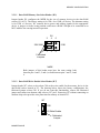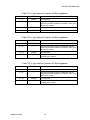
1
M68MPFB1632/D June 1994 M68MPFB1632 MODULAR PLATFORM BOARD USER’S MANUAL © MOTOROLA, INC., 1993, 1994; All Rights Reserved Motorola reserves the right to make changes without further notice to any products herein to improve reliability, function or design. Motorola does not assume any liability arising out of the application or use of any product or circuit described herein; neither does it convey any license under its patent rights nor the rights of others. Motorola products are not designed, intended, or authorized for use as components in systems intended for surgical implant into the body, or other applications intended to support or sustain life, or for any other application in which the failure of the Motorola product could create a situation where personal injury or death may occur. Should Buyer purchase or use Motorola products for any such unintended or unauthorized application, Buyer shall indemnify and hold Motorola and its officers, employees, subsidiaries, affiliates, and distributors harmless against all claims, costs, damages, and expenses, and reasonable attorney fees arising out of, directly or indirectly, any claim of personal injury or death associated with such unintended or unauthorized use, even if such claim alleges that Motorola was negligent regarding the design or manufacture of the part. The M68ICD16 In-Circuit Debugger with IASM16 development software and M68ICD32 InCircuit Debugger with IASM32 development software are © P & E Microcomputer Systems, Inc.*, 1990, 1992; All Rights Reserved. Portions of the software are © Borland International, 1987, 1993. Portions of the software are © TurboPower Software, 1988, 1993. * P & E Microcomputer Systems, Inc., PO Box 2044 Woburn, MA 01888-2044 (617)-353-9206 TABLE OF CONTENTS TABLE OF CONTENTS CHAPTER 1 GENERAL INFORMATION 1.1 1.2 1.3 1.4 1.5 Introduction......................................................................................................................... 1-1 Features............................................................................................................................... 1-1 Specifications...................................................................................................................... 1-2 General Description ............................................................................................................ 1-3 Equipment Required ........................................................................................................... 1-4 CHAPTER 2 HARDWARE PREPARATION AND INSTALLATION 2.1 2.2 Introduction......................................................................................................................... 2-1 Hardware Preparation ......................................................................................................... 2-1 2.2.1 J10, J11 +5 Volt Select Header (W9).......................................................................... 2-7 2.2.2 Voltage Standby Select Header (W15)........................................................................ 2-7 2.2.3 MODCLK Select Header (W16)................................................................................. 2-8 2.2.4 BERR Select Header (W17)........................................................................................ 2-8 2.2.5 J13 +5 Volt Select Header (W21) ............................................................................... 2-9 2.2.6 MCU Type Select Header (W22) ................................................................................ 2-9 2.2.7 MPFB LED Descriptions .......................................................................................... 2-10 2.2.8 DS2 Control Insertion Point (E1).............................................................................. 2-10 2.3 Installation Instructions .................................................................................................... 2-10 2.3.1 Power Supply – MPFB Connection .......................................................................... 2-10 2.3.2 Personal Computer – BDM Connection (J6) ............................................................ 2-12 2.3.3 RESET Switch (S2)................................................................................................... 2-13 2.3.4 Logic Analyzer Connections (J7 – J20) .................................................................... 2-13 2.4 Starting Evaluation Activities........................................................................................... 2-14 CHAPTER 3 MEMORY CONFIGURATION 3.1 Introduction......................................................................................................................... 3-1 3.2 Memory Configuration ....................................................................................................... 3-2 3.2.1 Data RAM Configuration (U1 and U3)....................................................................... 3-4 3.2.1.1 Data RAM Memory Size Select Header (W1) ................................................. 3-7 3.2.1.2 Data RAM Write Enable Select Header (W7).................................................. 3-7 3.2.1.3 Data RAM Output Enable Select Header (W8)................................................ 3-8 3.2.1.4 Data RAM Write Enable Select Header (W11)................................................ 3-8 3.2.1.5 A19 Disconnect Select Header (W19).............................................................. 3-9 3.2.2 Pseudo ROM Configuration (U2 and U4)................................................................. 3-10 3.2.2.1 Pseudo ROM Pin 1 Select Header (W2)......................................................... 3-13 3.2.2.2 Pseudo ROM Package Size Select Header (W3)............................................ 3-13 M68MPFB1632/D iii TABLE OF CONTENTS CHAPTER 3 MEMORY CONFIGURATION (continued) 3.2.2.3 Pseudo ROM Port Size Select Header (W4) .................................................. 3-14 3.2.2.4 Pseudo ROM Memory Type Select Header (W10)........................................ 3-14 3.2.2.5 Pseudo ROM Memory Size Select Header (W12) ......................................... 3-15 3.2.2.6 Pseudo ROM Chip Select Header (W14) ....................................................... 3-16 3.2.2.7 Pseudo ROM Write Protection Select Header (W18) .................................... 3-17 3.2.2.8 A19 Disconnect Select Header (W19)............................................................ 3-18 3.2.3 Fast RAM Configuration (U9 and U10).................................................................... 3-19 3.2.3.1 Fast RAM Chip Select Header (W14) ............................................................ 3-21 3.2.4 MPFB Memory Devices............................................................................................ 3-22 CHAPTER 4 RS-232 I/O PORT CONFIGURATION 4.1 Introduction......................................................................................................................... 4-1 4.2 Jumper Header and I/O Port Configuration........................................................................ 4-1 4.2.1 RS-232 Port 1 Protocol Select Header (W20)............................................................. 4-2 4.2.2 RS-232 Port 2 Protocol Select Header (W23)............................................................. 4-3 4.2.3 RS-232 Port Connections (J21, J22) ........................................................................... 4-5 4.2.4 Serial Data Wire-Wrap Connection (J23) ................................................................... 4-8 4.3 Advanced RS-232 Configuration ..................................................................................... 4-10 CHAPTER 5 EEPROM PROGRAMMING 5.1 5.2 Introduction......................................................................................................................... 5-1 MPFB Power Circuit Overview.......................................................................................... 5-1 5.2.1 VPP-MCU Select Header (W13)................................................................................. 5-2 5.2.2 Flash EEPROM Voltage Control Switch (S1) ............................................................ 5-3 5.2.3 VPP Insertion Point (E2)............................................................................................. 5-3 CHAPTER 6 PORT REPLACEMENT UNIT OPERATION 6.1 6.2 6.3 6.4 Introduction......................................................................................................................... 6-1 Using an MCU with SIM.................................................................................................... 6-1 Using an MCU with SCIM ................................................................................................. 6-1 Jumper Header Configuration............................................................................................. 6-2 6.4.1 PRU OEALL Select Header (W5) .............................................................................. 6-2 6.4.2 PRU Reset Data Control Header (W6)........................................................................ 6-3 CHAPTER 7 SUPPORT INFORMATION 7.1 7.2 Introduction......................................................................................................................... 7-1 Connector Signal Descriptions ........................................................................................... 7-1 M68MPFB1632/D iv TABLE OF CONTENTS LIST OF FIGURES Figure 2-1 3-1 3-2 3-3 3-4 3-5 3-6 3-7 4-1 4-2 4-3 4-4 4-5 4-6 4-7 Page MPFB Jumper Header, Connector, and Switch Location Diagram.................................... 2-2 Memory Socket Diagram.................................................................................................... 3-3 Data RAM Device Configuration....................................................................................... 3-5 Pseudo ROM Device Configuration................................................................................. 3-12 Fast RAM Device Configuration...................................................................................... 3-20 MPFB Supported RAM Devices ...................................................................................... 3-22 MPFB Supported EPROM Devices ................................................................................. 3-23 MPFB Supported EEPROM Devices ............................................................................... 3-24 DCE/DTE Protocol Wiring Diagrams ................................................................................ 4-4 RS-232 Port Connector J21 (Port 1)................................................................................... 4-5 RS-232 Port Connector J22 (Port 2)................................................................................... 4-6 RS-232 Cable Assembly (Optional) ................................................................................... 4-7 J23 Port Connections for DCE Operation .......................................................................... 4-9 J23 Port Connections for DTE Operation........................................................................... 4-9 DCD/DSR Selection Using a DTE Port ........................................................................... 4-12 LIST OF TABLES Table 1-1 2-1 2-2 3-1 3-2 7-1 7-2 7-3 7-4 7-5 7-6 7-7 7-8 7-9 7-10 7-11 7-12 7-13 Page MEVB Specifications ......................................................................................................... 1-2 Jumper Header Types ......................................................................................................... 2-3 MPFB Jumper Header Descriptions ................................................................................... 2-3 Valid MPFB U1, U3 Memory Configurations ................................................................... 3-6 W4 Pseudo ROM Port Size Configuration....................................................................... 3-10 Input Power Connector J5 Pin Assignments ...................................................................... 7-2 Computer – BDM Connector J6 Pin Assignments ............................................................. 7-2 Logic Analyzer Connector J7 Pin Assignments ................................................................. 7-3 Logic Analyzer Connector J8 Pin Assignments ................................................................. 7-3 Logic Analyzer Connector J9 Pin Assignments ................................................................. 7-3 Logic Analyzer Connector J10 Pin Assignments ............................................................... 7-4 Logic Analyzer Connector J11 Pin Assignments ............................................................... 7-4 Logic Analyzer Connector J12 Pin Assignments ............................................................... 7-5 Logic Analyzer Connector J13 Pin Assignments ............................................................... 7-7 Logic Analyzer Connector J14 Pin Assignments ............................................................... 7-8 Logic Analyzer Connector J15 Pin Assignments ............................................................... 7-9 Logic Analyzer Connector J16 Pin Assignments ............................................................... 7-9 Logic Analyzer Connector J17 Pin Assignments ............................................................... 7-9 M68MPFB1632/D v TABLE OF CONTENTS LIST OF TABLES (continued) Table 7-14 7-15 7-16 7-17 7-18 7-19 Page Logic Analyzer Connector J18 Pin Assignments ............................................................. 7-10 Logic Analyzer Connector J19 Pin Assignments ............................................................. 7-10 Logic Analyzer Connector J20 Pin Assignments ............................................................. 7-10 RS-232 Evaluation Port Connector J21 Pin Assignments................................................ 7-11 RS-232 Evaluation Port Connector J22 Pin Assignments................................................ 7-11 Serial Data Wire-Wrap Connector J23 Pin Assignments ................................................. 7-12 M68MPFB1632/D vi GENERAL INFORMATION CHAPTER 1 GENERAL INFORMATION 1.1 INTRODUCTION This manual provides general information, hardware preparation, installation instructions, and support information for the M68MPFB1632 Modular Platform Board (MPFB). The MPFB is part of Motorola’s modular approach to microcontroller unit-based product development. This modular approach lets you easily configure our development systems to fit your requirements. The MPFB is one component of the M68MEVB1632 Modular Evaluation Board (MEVB). The MEVB consists of the M68MPFB1632 Platform Board, a microcontroller unit personality board (MPB), and either the In-Circuit Debugger 16 (ICD16) or In-Circuit Debugger 32 (ICD32) hardware assembly and development software. The development software is from P&E Microcomputer Systems. For MEVB operating instructions when evaluating an M68HC16 MCU device, see the ICD16 In-Circuit Debugger User’s Manual, M68ICD16/D. For MEVB operating instructions when evaluating an M68300 MCU device, see the ICD32 In-Circuit Debugger User’s Manual, M68ICD32/D. The MPFB only operates with MPBs that support system integration module (SIM) or single-chip integration module (SCIM) MCUs. 1.2 FEATURES MPFB features include: • A platform which provides interface and power connections for the MPB. • On-board support for multiple memory devices, types (RAM, EPROM, and flash EEPROM), and sizes (32 kilobytes to 512 kilobytes). • Two RS-232C terminal input/output (I/O) ports for user evaluation of the serial communication interface (SCI). • Logic analyzer pod connectors (for all MCU pins). • Port replacement unit (PRU) to rebuild I/O ports lost to address/data/control. • On-board VPP (+12Vdc) generation for MCU and flash EEPROM programming. • On-board wire-wrap area. • Development software: — ICD16/ICD32 – user interface for the MEVB debugger — PROG16/PROG32 – programmer for M68HC16 and M68300 family MCUs — IASM – integrated assembler/editor M68MPFB1632/D 1-1 GENERAL INFORMATION 1.3 SPECIFICATIONS Table 1-1 lists MPFB specifications. Table 1-1. MEVB Specifications CHARACTERISTIC SPECIFICATIONS Data RAM maximum memory (locations U1, U3) RAM: 32 K, 128 K, or 512 K x 16 (word mode) 32 K, 128 K, or 512 K x 8 (byte mode) Pseudo ROM maximum memory (locations U2, U4) RAM: 32 K, 128 K, or 512 K x 16 (word mode) 32 K, 128 K, or 512 K x 8 (byte mode) EPROM & EEPROM: 32 K, 64 K, 128 K, 256 K, or 512 K x 16 (word mode) 32 K, 64 K, 128 K, 256 K, or 512 K x 8 (byte mode) Fast RAM maximum memory (locations U9, U10) RAM: 32 K or 128 K x 16 (word mode only) MCU I/O ports HCMOS compatible Monitor interface PC parallel (printer) port to BDM connector (J6) via ICD16/32. Refer to the ICD16/32 User’s Manual. Optional development interface RS-232C compatible (two connectors) Temperature Operating Storage -10° to +50° C -40° to +85° C Relative humidity 0 to 90% (non-condensing) Power requirements +5Vdc (±10%) @ 1.0 A (max.) – fuse protected @ 1.5 Amps VPP +12Vdc (±5%) @ 0.50 mA (max.) – current limiting circuit Dimensions Modular Platform Board M68MPFB1632/D 8.5 x 11 in. (216 x 279 mm) 1-2 GENERAL INFORMATION 1.4 GENERAL DESCRIPTION The MPFB and MPB together form the MEVB. The MEVB is an economical tool for designing, debugging, and evaluating MCU operation of the MC68HC16 and MC68300 MCU Families. By providing the essential MCU timing and I/O circuitry, the MEVB simplifies user evaluation of prototype hardware/software products. The MEVB requires a user-supplied power supply and host computer. For communication with the MEVB, you need a personal computer with a parallel port; MEVB development software uses the parallel port for communications. The MEVB also has two RS232 serial ports, which let you evaluate the on-chip serial communication interface (SCI). (These serial ports are available to you at all times; the ICD16 and ICD32 development system monitor interface does not require these ports.) The MEVB debugger (ICD) operates in background mode (BDM); a backdoor method of talking to the CPU core. You may also use any debugger which interfaces via the standard 10-pin BDM. There are two methods of generating MCU code: 1. Using the MEVB one-line assembler/disassembler. 2. Assembly code with IASM and download assembled code from an external source to MEVB RAM or MCU RAM via ICD16 or ICD32 through the background mode port. NOTE You may use any assembler that has S-record or MAP file capabilities. The MPFB includes jumper-selectable options such as chip select usage, memory type selection and memory size selection for the pseudo ROM sockets, and reset data control. The MPFB offers various operating configurations for byte-wide or word-wide memory sizing. The MEVB allows programming of internal-MCU flash EEPROM as well as external EEPROM devices. To reset MEVB circuitry, you may use the on-board reset switch or the software RESET command. NOTE The MPFB must be configured for the specific MPB. For a detailed description of the MPB jumper header selections refer to the specific MPB user’s manual. M68MPFB1632/D 1-3 GENERAL INFORMATION 1.5 EQUIPMENT REQUIRED The external requirements for MPFB operation are a +5Vdc (±10%) power supply. When using the supplied ICD16 or ICD32 development software, an MS-DOS compatible computer and interface cable are required. For ICD16 or ICD32 computer and interface cable requirements refer to the ICD16 In-Circuit Debugger User's Manual, M68ICD16/D or the ICD32 In-Circuit Debugger User's Manual, M68ICD32/D. M68MPFB1632/D 1-4 HARDWARE PREPARATION AND INSTALLATION CHAPTER 2 HARDWARE PREPARATION AND INSTALLATION 2.1 INTRODUCTION This chapter provides unpacking instructions, hardware preparation information, and installation instructions for the MPFB. When you unpack the MPFB from its shipping carton, verify that all items are in good condition. Save packing material for storing and shipping the MPFB. NOTE Should the product arrive damaged, save all packing material, and contact the carrier’s agent. 2.2 HARDWARE PREPARATION This portion of the manual explains how to prepare the MPFB before use, as well as how to configure the MPFB for system operation. Consult either the ICD16 or ICD32 manual as part of your system hookup. Refer to Chapter 3 for installing or configuring memory in the on-board sockets at locations U1 through U4, U9, and U10. Refer to Chapter 4 for RS-232 I/O port configuration. Refer to Chapter 5 for EEPROM programming. Refer to Chapter 6 for PRU operation. Refer to Chapter 7 for support information. Figure 2-1 shows the locations of memory sockets, jumper headers, connectors, light emitting diodes (LEDs), and switches. Table 2-1 is a general explanation of the jumper header types found on the MPFB. Table 2-2 lists the MPFB jumper headers and a description of the function in each position. Refer to paragraphs 2.2.1 through 2.2.6 for a more complete definition of the jumper headers for general MPFB configuration. Refer to the specific chapter for details on other MPFB jumper headers. M68MPFB1632/D 2-1 J20 J14 J3 J18 J17 J2 J4 J1 W17 J16 W16 J15 W23 J22 J21 S1 J5 F1 W20 S2 W1 W22 W2 W21 J13 W3 W4 W14 W13 W5 W15 W7 W8 W11 W18 W10 W19 W12 J7 J10 J19 W9 J8 J11 J12 J9 W6 HARDWARE PREPARATION AND INSTALLATION Figure 2-1. MPFB Jumper Header, Connector, and Switch Location Diagram M68MPFB1632/D 2-2 HARDWARE PREPARATION AND INSTALLATION Table 2-1. Jumper Header Types Jumper Header Type Symbol Description two-pin Two-pin jumper header and designated as WX (X = the jumper header number). Use a fabricated jumper to create a short between the two pins of the jumper header. two-pin with jumper Two-pin jumper header with jumper, designated as WX (X = the jumper header number). three-pin Three-pin jumper header, designated as WX (X = the jumper header number). Use a fabricated jumper to create a short between two of the three pins of the jumper header. three-pin with jumper Three-pin jumper header with jumper and designated as WX (X = the jumper header number). To change the factory jumper header configuration, move the jumper to the two desired pins. Table 2-2. MPFB Jumper Header Descriptions Jumper Header Type W1 246 Jumper between pins 1 and 3 and 2 and 4 (factory default); 32K x 8 or 128Kx 8 RAMs installed in the data RAM sockets (U1 & U3). 135 Jumper between pins 3 and 5 and 4 and 6; 512K x 8 RAMs installed in the data RAM sockets (U1 & U3). 123 Jumper installed on pins 1 and 2 (factory default); configures pin 1 of the memory devices in the pseudo ROM sockets (U2 & U4) as a standard address line. Data RAM Size W2 Pseudo ROM Pin 1 Selection W3 Jumper installed on pins 2 and 3; connects +12Vdc (VPP) to pin 1 of the pseudo ROM sockets and lets you program flash EEPROM memory devices. 123 Pseudo ROM Package Size W4 PRU OE(ALL) Selection M68MPFB1632/D Jumper installed on pins 1 and 2 (factory default); 28-pin memory devices in the pseudo ROM sockets (U2 & U4). Jumper installed on pins 2 and 3; 32-pin memory devices in the pseudo ROM sockets. 123 Pseudo ROM Port Size W5 Description Jumper installed on pins 1 and 2 (factory default); pseudo ROM port size (memory data width) is word. Jumper installed on pins 2 and 3; pseudo ROM port size is byte. 123 Jumper installed on pins 1 and 2 (factory default); disables the PRU. Jumper installed on pins 2 and 3; user enables/disables the PRU by controlling OE(ALL) from logic analyzer connector J7. 2-3 HARDWARE PREPARATION AND INSTALLATION Table 2-2. MPFB Jumper Header Descriptions (continued) Jumper Header Type Description W6 123 W6 selects the MCU operation mode. Each 3-pin jumper header set corresponds to an MCU data line. While the reset pin is low, the reset data values are driven on the data bus (D0 – D15). (The MEVB reset data circuit is open drain; a high state is provided via a pull-up resistor.) Each reset data line may be set high (H) or low (L). Consult the appropriate MCU user's manual, data book, or technical summary for reset data information. PRU Reset Data Control W7 Jumper installed (factory default); CS0 is used as the write enable for the device in the data RAM socket U3. 1 2 U3 Data RAM Write Enable No jumper; CS0 is not used as the write enable for the device in socket U3. You must connect an alternate signal to pin 2 of jumper header W7 or you can not write to the device in the data RAM socket U3. W8 Jumper installed (factory default); CS5 is used as the output enable for the devices in the data RAM sockets (U1 & U3). 1 2 Data RAM Output Enable No jumper; CS5 is not used as the output enable for the device in sockets U1 and U3. You must connect an alternate signal to pin 2 of jumper header W8 or you can not read the devices in the data RAM sockets. W9 Jumper installed (factory default); +5-volt power appears on pin 1 of logic analyzer connectors J10 and J11. 12 J10, J11 +5Vdc Selection W10 Pseudo ROM Memory Type No jumper; no signal on pin 1 of logic analyzer connectors J10 and J11. 1 3 5 2 4 6 Jumper installed on pins 1 and 2 (factory default); RAM is installed in the pseudo ROM sockets (U2 & U4). Jumper installed on pins 3 and 4; EPROM is installed in the pseudo ROM sockets. Jumper installed on pins 5 and 6; flash EEPROM is installed in the pseudo ROM sockets. W11 U1 Data RAM Write Enable M68MPFB1632/D 1 2 Jumper installed (factory default); CS3 is used as the write enable for the device in the data RAM socket U1. No jumper; CS3 is not used as the write enable for the device in socket U1. You must connect an alternate signal to pin 2 of jumper header W11 or you can not write to the device in the data RAM socket U1. 2-4 HARDWARE PREPARATION AND INSTALLATION Table 2-2. MPFB Jumper Header Descriptions (continued) Jumper Header W12 Pseudo ROM Memory Size Type 1 3 5 7 9 Description 2 4 6 8 10 Jumper installed on pins 1 and 2 (factory default); 32K x 8 devices are installed in the pseudo ROM sockets (U2 & U4). Jumper installed on pins 3 and 4; 64K x 8 devices are installed in the pseudo ROM sockets. Jumper installed on pins 5 and 6; 128K x 8 devices are installed in the pseudo ROM sockets. Jumper installed on pins 7 and 8; 256K x 8 devices are installed in the pseudo ROM sockets. Jumper installed on pins 9 and 10; 512K x 8 devices are installed in the pseudo ROM sockets. W13 VPP to MCU Selection W14 1 2 Jumper installed (factory default); connects +12Vdc power (as controlled by S1) to the MCU programming voltage pin(s). No jumper; +5Vdc power is applied to the MCU programming voltage pin(s) and the +12Vdc power is disconnected. 123 Pseudo ROM/ Fast RAM Chip Select Jumper header W14 selects the MCU signal for the memory devices in the fast RAM sockets (U9 & U10) and pseudo ROM sockets (U2 & U4). Pins 1 and 2 select the MCU chip select for the memory devices in the fast RAM sockets. While pins 2 and 3 of jumper header W14 select the chip select for the memory devices in the pseudo ROM sockets. Jumper installed on CSBOOT pins 2 and 3 (factory default); use CSBOOT as the memory device chip enable for memory devices in the pseudo ROM sockets. Jumper installed on CS1/CSM pins 1 and 2 (factory default); use CS1/CSM as the memory device chip select for the fast RAM sockets. W15 12 VSTBY Selection W16 No jumper installed and an external power source connect to pin 2; battery backup for the internal RAM in the MPB on-board MCU device. 12 MODCLK Selection W17 BERR Selection M68MPFB1632/D Jumper installed (factory default); voltage standby (VSTBY) is connected to ground. No battery backup for the MCU internal RAM. No jumper installed (factory default); the MCU MODCLK signal is pulled high (logic 1) via a resistor during reset. Jumper installed; the MCU MODCLK signal is driven low (logic 0) during reset. 12 No jumper installed (factory default); the BERR signal is pulled high (logic 1) via a resistor during reset. Jumper installed; the BERR signal is driven low (logic 0) during reset. 2-5 HARDWARE PREPARATION AND INSTALLATION Table 2-2. MPFB Jumper Header Descriptions (continued) Jumper Header Type Description W18 123 Jumper installed on pins 1 and 2 (factory default); unrestricted writes to the memory devices in the pseudo ROM sockets (U2 & U4). Pseudo ROM Write Protection Jumper installed on pins 2 and 3; allows writing to the memory devices in the pseudo ROM sockets only in background debug mode. W19 Jumper installed on pins 1 and 2 (factory default); disconnects the MCU A19 pin from the MPFB memory array, pseudo ROM sockets (U2 & U4), and data RAM sockets (U1 & U3) and drives the memory array’s A19 pin to a logic low. 123 A19 Disconnect Jumper installed on pins 2 and 3; connects the A19 signal to the MPFB memory arrays. W20 RS-232 Port 1 Protocol 2 4 6 8 10 12 14 16 1 3 5 7 9 11 13 15 W21 Jumper installed (factory default); +5-volt power appears on pin 1 of logic analyzer connector J13. 12 J13 +5Vdc Selection No jumper; no signal on pin 1 of logic analyzer connector J13. W22 Jumper installed on pins 1 and 2 (factory default); selects the emulation MCU (on the MPB) as an M68300 MCU device. 123 MCU Type Selection W23 RS-232 Port 2 Protocol Jumper header W20 configures RS-232 port 1 (J21) protocol as DTE or DCE. The factory configuration (shown) is the fabricated jumpers positioned for DCE protocol. Jumper installed on pins 2 and 3; selects the emulation MCU (on the MPB) as an M68HC16 MCU device. 1 3 5 7 9 11 13 15 M68MPFB1632/D 2 4 6 8 10 12 14 16 Jumper header W23 configures RS-232 port 2 (J22) protocol as DTE or DCE. The factory configuration (shown) is the fabricated jumpers positioned for DCE protocol. 2-6 HARDWARE PREPARATION AND INSTALLATION 2.2.1 J10, J11 +5 Volt Select Header (W9) Jumper header W9 selects or de-selects +5Vdc power to pin 1 of logic analyzer connectors J10 and J11. The drawing below shows the factory configuration: the fabricated jumper connecting +5Vdc power to pin 1 of J10 and J11. If you do not want this functionality, remove the fabricated jumper. W9 1 2 Fabricated Jumper 2.2.2 Voltage Standby Select Header (W15) Jumper header W15 connects voltage standby (VSTBY) to ground when battery backup for RAM in the MCU device is not available. The drawing below shows the factory configuration: the fabricated jumper grounds the voltage standby pin on the MCU. To apply backup power to VSTBY, remove the fabricated jumper and connect the external power source to pin 2 and external power ground to pin 1. W15 1 2 VSTBY GND Fabricated Jumper M68MPFB1632/D 2-7 HARDWARE PREPARATION AND INSTALLATION 2.2.3 MODCLK Select Header (W16) Jumper header W16 lets the MPFB pull down the MCU’s MODCLK pin during reset. This is an MCU configuration option and specific to each MCU. Because MCU MODCLK usage varies with each device, refer to the MCU user’s manual for a description of the MODCLK signal. The factory configuration (shown below) is no fabricated jumper in W16. When no fabricated jumper is installed the MODCLK pin is pulled high by a resistor on the MPFB. W16 1 2 MODCLK CAUTION When allowing the MPFB to drive MODCLK low during reset (W16 installed), make sure your circuits in the wire-wrap area are not driving the MODCLK pin at J14 pin 4. This may damage the MPFB or your circuit. 2.2.4 BERR Select Header (W17) Jumper header W17 lets the MPFB pull down the MCU’s BERR pin during reset. This is an MCU configuration option. The factory configuration (shown below) is no fabricated jumper in W17. When no fabricated jumper is installed the BERR pin is pulled high by a resistor on the MPFB. W17 1 2 BERR CAUTION The MPFB must have all memory devices removed from their sockets and the PRU set to OFF (a jumper on W5 pins 1 and 2). This function is for final evaluation of an MCU with internal ROM/EEPROM. M68MPFB1632/D 2-8 HARDWARE PREPARATION AND INSTALLATION 2.2.5 J13 +5 Volt Select Header (W21) Jumper header W21 selects or de-selects +5Vdc power to pin 1 of logic analyzer connector J13. The drawing below shows the factory configuration: the fabricated jumper connecting +5Vdc power to pin 1 of J13. If you do not want this functionality, remove the fabricated jumper. W21 Fabricated Jumper 2.2.6 MCU Type Select Header (W22) Jumper header W22 configures the MPFB for the MPB type installed on the MPFB. The factory setting, a jumper on pins 1 and 2, indicates that an M68300 MPB is installed on the MPFB. If your MPB has an M68HC16 MCU move the jumper to pins 2 and 3. W22 CPU TYPE 1 2 3 16 32 Fabricated Jumper NOTE Jumper header W22 does not inhibit MEVB operation, it tells the pipe de-muxing programmable array logic (PAL) chip which CPU type is installed. The PAL creates the latched DSO and DSI (LAT-DSO and LAT-DSI) signals on J12. The LAT-DSO and LAT-DSI signals are used by the logic analyzer to perform disassembly. If you are not using a logic analyzer, W22 setting is inconsequential. M68MPFB1632/D 2-9 HARDWARE PREPARATION AND INSTALLATION 2.2.7 MPFB LED Descriptions There are four LEDs on the MPFB. Their functions are: • DS1 – POWER: ON = power is applied to the MPFB. • DS2 – ERROR: ON = an error has occurred in the memory configuration jumper settings or E1 is low. Check jumper headers W10 and W12 against memory in the pseudo ROM sockets (U2 & U4). Refer to paragraph 2.2.8 and for information on configuring memory refer to Chapter 3. • DS3 – VPP: ON = program voltage is available for programming MCU flash EEPROM or memory devices in the pseudo ROM sockets (U2 & U4). • DS4 – RUN: ON = MEVB is running user code (in foreground); OFF = MEVB is running in background debug mode or reset is low. 2.2.8 DS2 Control Insertion Point (E1) The LED at location DS2 is controlled by the output of the PAL (location U7). DS2 turns ON if the memory configuration jumpers are set incorrectly. You may also wire an external circuit to E1 and use DS2 as a visual indicator for your program. DS2 turns on when E1 is driven low. Connect E1 to any output signal. Driving insertion point E1 low does not effect the MCU RESET signal. 2.3 INSTALLATION INSTRUCTIONS The MEVB is designed for table-top operation. A user-supplied power supply and host computer are required. The host computer must have a parallel port and must run MS-DOS, as required by ICD16 or ICD32. The following paragraphs explain MPFB connections. 2.3.1 Power Supply – MPFB Connection Use MPFB connector J5 to connect a user-supplied power supply to the MEVB. Contact 1 is ground; black lever. Contact 2 is VDD (+5 volts); red lever. Use 20 or 22 AWG wire for power connections. For each wire, trim back the insulation 1/4 in. (.635 cm), lift the appropriate lever of J5 to release tension on the contacts, then insert the bare wire into J5 and close the lever. The MEVB requires a +5Vdc @ 1.0 amp power supply for operation. A 1.5 amp fuse is installed on the MPFB +5Vdc power supply input line. M68MPFB1632/D 2-10 HARDWARE PREPARATION AND INSTALLATION BLK RED GND J5 +5V CAUTIONS Do not use wire larger than 20 AWG in connector J5. Such wire could damage the connector. Turn off MEVB power when installing or removing the MPB from the MPFB. Sudden power surges could damage MEVB integrated circuits. M68MPFB1632/D 2-11 HARDWARE PREPARATION AND INSTALLATION 2.3.2 Personal Computer – BDM Connection (J6) As the MEVB does not have on-board debug firmware, debugging does not consume MCU resources. Motorola ships the MEVB with the ICD16 or ICD32 debug monitor, which easily connects to the MPFB’s standard background-mode header (connector J6). For additional information about the ICD software, including debugging and assembly information, see either the ICD16 or ICD32 user’s manual. Alternately, any debugger which uses the 10-pin BDM interface may be used with the MEVB. CAUTIONS Turn off MEVB power when connecting or disconnecting the BDM cable. Sudden power surges could damage MEVB integrated circuits. Connect the ICD16 or ICD32 debugger to the MEVB by connecting the integral 10-pin cable assembly of the debugger to MPFB connector J6. Make sure that the red wire of the cable connects to pin 1 of connector J6. Connect the DB-25 parallel port of the ICD16 or ICD32 to the parallel port of your computer. The drawing below shows signal assignments for connector J6; for pin assignments and signal descriptions, refer to Chapter 7. For a complete description of PC to MPFB interconnection (via the BDM connector), refer to the ICD16 or ICD32 user manual. J6 DS GND GND RESET VDD 1 3 5 7 9 2 BERR 4 BKPT 6 FREEZE 8 DSI 10 DSO BACKGROUND MODE CONNECTOR M68MPFB1632/D 2-12 HARDWARE PREPARATION AND INSTALLATION 2.3.3 RESET Switch (S2) Push-button switch (S2) resets the MEVB. A reset initializes the MEVB to its startup point. The reset switch is located in the lower left-hand corner of the MPFB. To manually reset your system press S2 to trip the switch. The MPFB provides a single reset signal. Thus the system, MPFB and MCU, can be reset from the following sources: • S2, manual reset switch, as described above • Low voltage detection IC, U12B or U12A (SMT footprint) • ICD16 or ICD32 software command via the BDM connector (J6) • Logic analyzer connector J14 pin 6 • Incorrect memory configuration on W10 or W12 • MCU, i.e., watchdog ...etc. 2.3.4 Logic Analyzer Connections (J7 – J20) Use connectors J7 through J20 to connect the logic analyzer to the circuit being evaluated. For signal descriptions, refer to Chapter 7 and to the appropriate MPB user’s manual. The MPFB has extra holes next to connectors J7 through J20 that give you space for 10-pin Berg-type strips (shown below). To use such strips, install them on the bottom of the board, and solder the pins on the top. Wire wrap from the bottom of the MPFB to the user-wire-wrap area. Be sure to put standoffs in the corner mounting holes to protect the wire wrapping on the bottom of the MPFB. BERG STRIP HOLES 1 J14 2 SPARE BERR FREEZE LAT-DSI DSI DSACK0 FC1 SIZ1 R/W GND SPARE CLKOUT BKPT LAT-DSO DSO DSACK1 FC2/CS5 FC0/CS3 SIZ0 BGACK/CS2/CSE 19 M68MPFB1632/D BERG STRIP HOLES 20 2-13 HARDWARE PREPARATION AND INSTALLATION 2.4 STARTING EVALUATION ACTIVITIES When you have configured MPFB and MPB jumpers (refer to the MPB user’s manual for MPB configuration instructions), and made cable connections, your MEVB is ready to use. To start assembly or debugging activities, follow the instructions of the ICD16 or ICD32 user’s manual. A typical startup is: 1. Install MPB on the MPFB as per instructions in the MPB user’s manual. 2. Install MCU overlay over the logic analyzer connectors (J12 through J20). 3. Install ICD ribbon cable to J6 of the MPFB. 4. Connect parallel port cable to ICD DB-25 connector. 5. Connect +5Vdc power supply to connector J5. 6. Install ICD software on your personal computer (follow the instructions in the ICD user’s manual). 7. Turn on the +5Vdc power supply 8. Check that the DS1 LED is on (marked PWR). If LED does not illuminate then: — +5 volt power is not connected or supply is not on — Input power is reversed (+5Vdc on GND and GND on +5V). — Fuse is blown. M68MPFB1632/D 2-14 HARDWARE PREPARATION AND INSTALLATION Execute ICD software ICD16 Software ICD32 Software 1. Enter: ICD16 and a carriage return (<CR>) 1. Enter: ICD32 <CR> 2. Enter: <CR> to bring up debugger screen 2. Enter: <CR> to bring up debugger screen 3. Wait for debugger prompt then 3. Wait for debugger prompt then 4. Enter: A=55 <CR> 4. Enter: D0=55 <CR> 5. Check window for Register A Register A should equal 55. 5. Check window for Register D0 Register D0 should equal 55. If register does not change: 1. Check parallel port connections – good cable connections and proper cable type. and that the correct PC parallel port selected, i.e., LPT1, LPT2 or LPT3. 2. MPB is not seated on the MPFB MAPI connectors (J1, J2, J3, and J4). 3. MPB Clock Select Header installed incorrectly or no oscillator in socket. Verify MPB input clock by measuring CLOCKOUT wave form on logic analyzer connector J12 or J13. 4. If the reset signal at J14 remains low: — Wrong crystal frequency, and the VCO can not lock. — Power at J5 is less than or equal to 4.5 volts and has tripped the low voltage detection IC. — Your circuit may be holding reset low. — Incorrect memory configuration on W10 or W12 (DS2 is ON). 5. MCU device is not seated properly in the socket on the MPB. M68MPFB1632/D 2-15 HARDWARE PREPARATION AND INSTALLATION M68MPFB1632/D 2-16 MEMORY CONFIGURATION CHAPTER 3 MEMORY CONFIGURATION 3.1 INTRODUCTION This chapter provides information for configuring memory in the expansion sockets U1, U2, U3, U4, U9, and U10. There are six memory device sockets on the MPFB; two data RAM sockets (U1 & U3), two pseudo ROM sockets (U2 & U4), and two fast RAM sockets (U9 & U10). Figure 3-1 is a diagram of the MPFB memory sockets. The open design structure of the MPFB lets you configure and use each memory socket to fit your system requirements. A brief overview of each memory type (data RAM, pseudo ROM, and fast RAM) is given below. For more detailed information refer to the appropriate paragraph within this chapter. The data RAM sockets accept either 32K x 8, 128K x 8, or 512K x 8 static RAM devices. The data RAM sockets allow evaluation of MCU chip select functions. Each data RAM device is connected to a unique MCU chip select for write enable generation. While the output enable (read enable) of each data RAM device is connected to a common MCU chip select. This memory is connected directly to the MCU without any MPFB device delays. This is ideal for fast termination (2 clock cycle) memory cycle evaluations. The pseudo ROM sockets provide a generic memory socket, and accepts a variety of RAM, EPROM, or EEPROM devices. The size of these devices range from 32K x 8 to 512K x 8 bytes. A programmable array logic (PAL) chip on the MPFB controls the signal configuration to the pseudo ROM sockets. This PAL creates a delay on some memory signals and may require faster memory or a wait state to the memory cycle. These full featured sockets allow easy evaluation of many memory types with the use of a single MCU chip select. The fast RAM sockets provide emulation for internal ROM memory operating at the maximum speed. Most MCU-internal ROM can be accessed with fast termination. The signal delay created by the PAL may inhibit the usage of the pseudo ROM sockets for ROM code emulation. Therefore the fast RAM sockets are directly connected to the MCU to provide the fastest possible access times. RAM accesses are controlled with a single chip select. If you choose to use the fast RAM sockets as general purpose RAM, please read the caution in paragraph 3.2.3. The fast RAM sockets accept either 32K x 8 or 128K x 8 fast static RAM devices. This provides emulation for ROM modules as large as 512K bytes. The MPFB also provides a physical bus structure for implementing both byte memory ports (8bits at a time on the data bus) or word memory ports (16-bits at a time on the data bus) for the data RAM or pseudo ROM. The fast RAM sockets only provide a word memory port. The factory supplies 64K bytes of RAM in the pseudo ROM sockets. M68MPFB1632/D 3-1 MEMORY CONFIGURATION 3.2 MEMORY CONFIGURATION Before modifying MPFB memory setup, it is important to understand the port concepts. Since all memory sockets are designed for MCU chip select usage, you should be familiar with the operation and setup of each MCU chip select you intend to connect to the memories. The following port discussion relates only to the data RAM and pseudo ROM memory sockets. The MPFB provides a method for connecting a single memory to the MCU. This memory operates as a byte port. When accessed by an instruction requesting a byte, it provides the data byte. When accessed by an instruction requesting a word, the memory provides the data word via two byte memory cycles. The design of the MCU specifies that all byte port memory operations occur on the most significant byte of the data bus, D8-D15. Therefore the MPFB implements sockets for the MSB of the data RAM and pseudo ROM memory. The sockets provide the physical interface for the byte and word ports. When using the memory sockets as a word port, the MCU does not need to provide address A0 to memory. The address signal A0 is not needed for word ports since data is accessed in words. For example, on a byte read of a word port, the memory provides the MCU with a word of data. Internally, the MCU uses only the LSB or MSB to complete the operation. With a byte write, the data byte is placed on both the MSB and LSB of the data bus. If MCU chip selects are used, such as the data RAM area, the MCU chip select that controls the RAM’s write enable determines which memory is written. These MCU chip selects must be configured as an upper write-only on a word port or lower write-only on a word port. When using a single chip select, such as the pseudo ROM area, the external MCU control signals must be decoded to determine the memory cycle type. Without this decoding, such as the fast RAM area, the MCU would write a word of data to memory during a byte write operation. The memory PAL provides the memory cycle decoding; LSB enable, and MSB enable functions for the pseudo ROM sockets. When using a single MSB memory socket as a byte port, the MCU must provide the memory with address A0. This is required since each sequential memory access, MSB and LSB data, is provided by the same memory device. The dual sockets provide an easy method of connecting each memory to the address bus. The word sockets (right shifted) connect MCU address A1 to the memory’s A0 address input and A2 to A1, etc. The byte sockets (left shifted) connect MCU address A0 to the memory’s A0 address input and A1 to A1, etc. As you can see, reconnecting eighteen address signals to each of the MSB memories would be a sizable and messy jumper array. It is usually easiest to envision the dual sockets as word port socket overlaid on a byte port socket. The confusion is greatly increased since the MPFB provides sockets for 300 mil and 600 mil memory devices. Each memory section below includes pictorial diagrams to help you with memory placements. M68MPFB1632/D 3-2 MEMORY CONFIGURATION When installing memory devices in the on-board memory sockets, each matching pair of devices (U1 & U3, U2 & U4, and U9 & U10) must be functionally identical. This implies that you cannot place a RAM in the MSB socket and an EPROM in the LSB socket. It is also recommended that you keep the MSB and LSB the same memory size. If the MSB and LSB memory differs in size, such as an 64K x 8 EPROM and 128K x 8 EPROM, you must evaluate each memory pin-out for possible MPFB conflicts and damage. Refer to Figures 3-5 through 3-7 for memory pin-outs used by the MPFB. Before attempting memory modifications to the MPFB, scan the paragraph relating to the specific memory sockets you plan to modify. These paragraphs provide detailed information relating to each memory interface. U1 LSB DATA RAM U2 LSB U3A U3B BYTE PSEUDO ROM U9 U10 FAST RAM U4A U4B WORD DATA RAM 400 SOJ SOCKET LSB MSB 400 SOJ SOCKET MSB Figure 3-1. Memory Socket Diagram M68MPFB1632/D 3-3 BYTE MSB WORD PSEUDO ROM MEMORY CONFIGURATION 3.2.1 Data RAM Configuration (U1 and U3) Data RAM refers to memory locations U1 & U3. These sockets are intended for static RAM devices. The data RAM sockets accept 32K x 8, 128K x 8, or 512K x 8 static RAM devices (refer to Figure 3-5 for package pin-outs). The data RAM sockets support two package widths: either 300 mil or 600 mil wide DIP devices, and two package sizes: either 28- or 32-pin packages. The data RAM sockets allow evaluation of the MCU chip select functions. Each data RAM device is connected to a unique MCU chip select for write enable generation. While the output enable (read enable) of each data RAM device is connected to a common MCU chip select. This memory is directly connected to the MCU without any MPFB device delays. This is ideal for fast termination (2 clock cycle) memory cycle evaluations. The three MCU chip selects for the data RAM sockets are connected to the memory via jumper headers W7, W8, and W11. These jumper headers connect the default MCU chip select signals, CS0, CS3, and CS5 to the data RAM devices. Alternately, you may connect different MCU chip select signals via these jumper headers (refer to paragraphs 3.2.1.2 through 3.2.1.4 for definitions of these jumper headers). Data RAM can be configured as a byte memory port (8-bits at a time on the data bus) or a word memory port (16-bits at a time on the data bus). For a word port, place the RAMs into sockets U1 and U3B. For a byte port, a RAM should be placed in socket U3A. When configured as a byte port, the RAM in U1 is unused by the MCU (removal of the device in location U1 is not required). Figure 3-2 illustrates memory device positioning within the data RAM sockets. Once your software configures the connected MCU chip selects, memory can be accessed with byte, word, or long word memory cycles for both the word and byte port configurations. The examples in Table 3-1 provide MCU chip select configuration for byte and word port memory operation. The example uses the default MCU chip selects, CS0, CS3, and CS5, for data RAM operation. NOTES Memory data bus structure may be either byte or word in length. Byte or word bus structure is configured by positioning the memory devices in the proper socket area (refer to Figure 3-2). The memory configurations shown in Figure 3-2 are only four of the possible methods for configuring memory in sockets U1 & U3. You must configure jumper headers W1, W7, W8, W11, and W19 for correct data RAM operation. Paragraphs 3.2.1.1 through 3.2.1.5 give detailed descriptions of the jumper header settings for devices in the data RAM sockets. M68MPFB1632/D 3-4 MEMORY CONFIGURATION WORD CONFIGURATION, U1 32-PIN, 600 MIL U2 U3 U4 BYTE CONFIGURATION, 28-PIN, 600 MIL U1 U2 U3 U4 WORD CONFIGURATION, U1 28-PIN, 300 MIL U2 U3 U4 BYTE CONFIGURATION, 32-PIN, 300 MIL U2 U3 U4 U1 Figure 3-2. Data RAM Device Configuration M68MPFB1632/D 3-5 MEMORY CONFIGURATION Table 3-1 is a summary of valid configurations for RAM devices at locations U1 & U3. Table 31 shows the relationships of chip selects CS3, CS0, and CS5 to the BYTE and R/W fields of the corresponding chip select option registers. This table also shows data bus size setting for chip select pin assignment register 0. Refer to the descriptions of jumper headers W7, W8, and W11 (paragraphs 3.2.1.2, 3.2.1.3, and 3.2.1.4) for information on connecting the MCU chip selects CS0, CS5, and CS3 to the data RAM sockets. Table 3-1. Valid MPFB U1, U3 Memory Configurations(1) PART I: 16-Bit Data Bus Size, RAMS in U1 and U3B CS3 (U1 Write Enable) CS0 (U3 Write Enable) CS5 (U1, U3 Output Enable) CSOR3 BYTE: lower CSOR0 BYTE: upper CSOR5 BYTE: both CSOR3 R/W: write only CSOR0 R/W: write only CSOR5 R/W: read only CSPAR0: 16-bit port CSPAR0: 16-bit port CSPAR0: 16-bit port PART II: 8-Bit Data Bus Size, RAM in U3A(2) CS3 (U1 Write Enable) CS0 (U3 Write Enable) CS5 (U1, U3 Output Enable) CSOR3 BYTE: disable(3) CSOR0 BYTE: X CSOR5 BYTE: X CSOR3 R/W: write only CSOR0 R/W: write only CSOR5 R/W: read only CSPAR0: 16-bit port CSPAR0: 8-bit port CSPAR0: 8-bit port 1. KEY: CSORx BYTE is the BYTE field of the chip select option register for CSx. CSORx R/W is the R/W (read/write) field of the chip select option register for CSx. CSPAR0 is chip select pin assignment register 0. X means don’t care internally to the MCU. 2. The MCU does not use a device at U1: the socket must be empty or contain an identical device to the one at U3 (word mode). 3. If no device is in the U1 socket or no jumper on jumper header W11 pins 1 and 2, you may use the CS3 pin in the wire-wrap area; otherwise, you must disable the field. M68MPFB1632/D 3-6 MEMORY CONFIGURATION 3.2.1.1 Data RAM Memory Size Select Header (W1) Jumper header W1 configures the MPFB for the size of memory devices in the data RAM sockets (U1 & U3). The factory setting is for 32K x 8 or 128K x 8 devices. The alternate setting is for 512K x 8 devices. W1 connects device power and address signals for the appropriate device. A jumper set in the wrong position could cause a RAM VDD pin to be connected to an MCU address line causing incorrect operation. W1 4 2 6 32K/128K 512K 1 5 3 Fabricated Jumpers NOTE Both jumpers of this header must have the same setting: both between pins 1 and 3; 2 and 4, or both between pins 3 and 5; 4 and 6. 3.2.1.2 Data RAM Write Enable Select Header (W7) Jumper header W7 selects or de-selects CS0 as the write enable for the memory device in the data RAM socket located at U3. The drawing below shows the factory configuration: the fabricated jumper selects CS0. If you do not want this functionality, remove the fabricated jumper and connect an alternate chip select to W7 pin-2. Removing W7 without connecting an alternate chip select provides write protection for memory at location U3. W7 1 CS0 2 U3 Write Enable Fabricated Jumper M68MPFB1632/D 3-7 MEMORY CONFIGURATION 3.2.1.3 Data RAM Output Enable Select Header (W8) Jumper header W8 selects or de-selects CS5 as the output enable for the memory devices in the data RAM sockets located at U1 and U3. The drawing below shows the factory configuration: the fabricated jumper selects CS5. If you do not want this functionality, remove the fabricated jumper and connect an alternate chip select to W8 pin-2. Removing W8 without connecting an alternate chip select inhibits memory read operations for memory at locations U1 & U3. W8 1 CS5 2 U1 & U3 Output Enable Fabricated Jumper 3.2.1.4 Data RAM Write Enable Select Header (W11) Jumper header W11 selects or de-selects CS3 as the write enable for the memory device in the data RAM socket located at U1. The drawing below shows the factory configuration: the fabricated jumper selects CS3. If you do not want this functionality, remove the fabricated jumper and connect an alternate chip select to W11 pin-2. Removing W11 without connecting an alternate chip select provides write protection for memory at location U1. W11 1 CS3 2 U1 Write Enable Fabricated Jumper M68MPFB1632/D 3-8 MEMORY CONFIGURATION 3.2.1.5 A19 Disconnect Select Header (W19) Jumper header W19 lets you disconnect the A19 signal from the MEVB data RAM sockets (U1 & U3) and pseudo ROM (U2 & U4). This jumper option lets you evaluate the MCU’s A19 pin with its alternate functions (CS6 or PC3) and maintain proper memory operation. The factory setting (jumper on pins 1 and 2) disconnects the MCU’s A19 pin from the memory array and forces low the memory array’s A19 signal (pull-down on W19 pin-1). When using 512K x 8 memory devices in a word port configuration (512K x 16) and W19 is set on pins 1 and 2; the amount of accessible memory is limited to 128K x 16. Alternately, you can wire-wrap another port signal to W19 pin-2, then toggle the port pin as a memory bank select to regain memory accessibility. All other memory sizes and port configurations are not effected by W19 or the MCU’s A19 operation (they do not use the A19 signal). The alternate setting, the jumper on pins 2 and 3, connects the MCU’s A19 signal to the pseudo ROM and data RAM sockets. In this setting, 512K x 16 memory operation (data RAM and pseudo ROM) may not function properly if the MCU’s A19 pin is set to its alternate functions (CS6 or PC3). 1 W19 2 Logic Low A19 Fabricated Jumper M68MPFB1632/D 3 3-9 MEMORY CONFIGURATION 3.2.2 Pseudo ROM Configuration (U2 and U4) Pseudo ROM refers to memory locations U2 & U4. The two pseudo ROM sockets provide a generic memory socket, and accepts a variety of RAM, EPROM, or EEPROM devices. Refer to Figures 3-5 through 3-7 for each device pin-out supported. Pseudo ROM sockets may contain: • RAM – 32K x 8, 128K x 8, or 512K x 8 • EPROM – 32K x 8, 64K x 8, 128K x 8, 256K x 8, or 512K x 8 • EEPROM – 32K x 8, 64K x 8, 128K x 8, 256K x 8, or 512K x 8 The pseudo ROM sockets accept memory devices of two widths: either 300 mil or 600 mil DIP devices, and two package sizes: either 28- or 32-pin packages. The pseudo ROM sockets provide an interface for a variety of memory types. The memory in the pseudo ROM sockets are controlled by the memory controller PAL at location U7. The MCU supplies a single chip signal as the pseudo ROM interface. The jumper W14 lets you select any MCU chip select signals to connect to the pseudo ROM sockets. The PAL provides several automated functions; memory device signal routing, write protection, and byte or word cycle decoding. The PAL also introduces a 15 (max.) nanosecond delay in several MCU address and control signals. This delay may require insertion of an extra wait state within the memory cycle. Pseudo ROM can be configured as a byte memory port (8-bits at a time on the data bus) or a word memory port (16-bits at a time on the data bus). For a word port, memory should be placed in sockets U2 and U4B and set the port size via jumper header W4. For a byte port, memory should be placed in socket U4A and set the port size via jumper header W4. While configured as a byte port, the memory in U2 is unused by the MCU (removal of the device in location U2 is not required). Figure 3-3 illustrates memory device positioning in the pseudo ROM sockets. The pseudo ROM port size configuration is determined by the jumper setting of W4 (see Table 3-2). Table 3-2. W4 Pseudo ROM Port Size Configuration W4 Setting Pseudo ROM Port Width U2 Memory Access 1 U4A Memory Access 1 U4B Memory Access 1 16 Word - 16 Bit All reads, Word writes LSB byte writes Use U4B socket All reads, Word writes MSB byte writes 8 Byte - 8 Bit De-selected by PAL All reads, All word writes All byte writes Use U4A socket 1) Qualified by a valid MCU chip select. M68MPFB1632/D 3-10 MEMORY CONFIGURATION The simplest function the memory PAL provides is device signal routing. Each memory type (RAM, EPROM, and EEPROM) has unique device pin-outs. The PAL connects the proper signal for the device type and size selected. For 28-pin devices, jumper header W3 connects the power pin (pin-28) to the MPFB +5Vdc supply. For 32-pin devices, W3 connects the proper PAL interconnect signal to the memory device. The PAL also provides a write protection method for pseudo ROM devices. When enabled by W18, the PAL de-selects the pseudo ROM devices during all non-background mode write cycles. This lets the debugger software modify the pseudo ROM devices in background mode, i.e. loading programs, modify memory commands, etc. When your program begins execution, memory is write protected and appears as if ROM devices were installed in the pseudo ROM sockets (U2 & U4). The write protect feature is implemented for both RAM and EEPROM memory devices. As described above, the pseudo ROM devices are selected by a single MCU chip select. When the devices are configured as a word port (16-bit), bus cycle decoding is required. During a byte write cycle, only one memory must be enabled. Otherwise a byte write will corrupt the memory contents by writing 16-bits on the data bus. The PAL uses the MCU’s R/W, A0 and SIZ0 signals to determine the cycle type. It then enables or disables the proper MSB and LSB memory device(s) for each qualified memory cycle. NOTES There is a 15 nanosecond (max.) delay on memory control signals and some address lines for devices in the pseudo ROM sockets. Please determine MCU wait states accordingly. Memory data bus structure may be either byte or word in length. Byte or word bus structure is configured by positioning the memory devices in the proper socket area (refer to Figure 3-3). The memory configurations shown in Figure 3-3 are only four of the possible methods for configuring memory in sockets U2 & U4. Flash EEPROM devices in the pseudo ROM sockets may be programmed by setting the appropriate jumper headers. Jumper header W2 connects the programming voltage from the DCDC converter to pin-1 of the pseudo ROM sockets (refer to paragraphs on S1 (5.2.2), W2 (3.2.2.1), VPP generation description (5.2)). You must provide the MCU programming algorithm code for the specific EEPROM device. The write protect jumper (W18) may also be used to inhibit flash EEPROM programming. Jumper headers W2, W3, W4, W10, W12, W14, W18, and W19 effect pseudo ROM operation and need to be set appropriately. Paragraphs 3.2.2.1 through 3.2.2.8 give detailed descriptions of the jumper header settings for devices in the pseudo ROM sockets. M68MPFB1632/D 3-11 MEMORY CONFIGURATION WORD CONFIGURATION, U1 32-PIN, 600 MIL U2 U3 U4 BYTE CONFIGURATION, 28-PIN, 600 MIL U1 U2 U3 U4 WORD CONFIGURATION, U1 28-PIN, 300 MIL U2 U3 U4 BYTE CONFIGURATION, 32-PIN, 300 MIL U2 U3 U4 U1 Figure 3-3. Pseudo ROM Device Configuration M68MPFB1632/D 3-12 MEMORY CONFIGURATION 3.2.2.1 Pseudo ROM Pin 1 Select Header (W2) Jumper header W2 configures the signal for pin-1 of a 32-pin memory devices in the pseudo ROM sockets (U2 & U4). (28-pin devices installed in U2 & U4 are not affected by the setting of W2.) The drawing below shows the factory configuration: the fabricated jumper between pins 1 and 2. With the jumper between pins 1 and 2, pin-1 of the pseudo ROM sockets is a standard address line. The alternate configuration (jumper between pins 2 and 3) connects VPP to pin-1 of the pseudo ROM sockets and lets you program flash EEPROM memory devices. To activate VPP, switch S1 must be set to ON (refer to paragraph 5.2.2). If S1 is OFF and W13 is installed, +5Vdc appears on W2 pin-3. If S1 is OFF and W13 has no jumper installed, then W2 pin-3 floats. W2 1 2 3 Address +12V Fabricated Jumper 3.2.2.2 Pseudo ROM Package Size Select Header (W3) Jumper header W3 configures the MEVB memory device package size for memory devices in the pseudo ROM sockets (U2 & U4). The drawing below shows the factory configuration: the fabricated jumper between pins 1 and 2 for 28-pin packages. When using 32-pin memory devices in the pseudo ROM sockets move the jumper to pins 2 and 3. W3 connects either device power or an address signal for the appropriate device. 1 W3 2 28 Pin 32 Pin Fabricated Jumper M68MPFB1632/D 3 3-13 MEMORY CONFIGURATION 3.2.2.3 Pseudo ROM Port Size Select Header (W4) Jumper header W4 configures the port size for memory devices in the pseudo ROM sockets (U2 & U4) as word or byte memory width. The drawing below shows the factory configuration: the fabricated jumper between pins 1 and 2 for word operation. When using a byte port in the pseudo ROM sockets, reposition the memory device in socket U4 (paragraph 3.2.2 and Figure 3-3) and move the jumper to pins 2 and 3. 1 W4 2 3 8 16 Fabricated Jumper 3.2.2.4 Pseudo ROM Memory Type Select Header (W10) Jumper header W10 configures the pseudo ROM (U2 & U4) memory device type. The drawing below shows the factory setting: the fabricated jumper between pins 1 and 2 is correct for RAM devices. To configure for EPROM devices reposition the W10 jumper between pins 3 and 4. To configure for EEPROM devices reposition the W10 jumper between pins 5 and 6. Jumper header W10 in conjunction with jumper header W12 selects the proper signals for the memory devices in the pseudo ROM sockets. (If no jumper or more than one jumper is installed, MCU RESET is held low and LED DS2 lights.) W10 1 2 RAM 3 4 EPROM 5 6 EEPROM Fabricated Jumper M68MPFB1632/D 3-14 MEMORY CONFIGURATION 3.2.2.5 Pseudo ROM Memory Size Select Header (W12) Jumper header W12 configures the pseudo ROM sockets (U2 & U4) for the proper memory size. The drawing below shows the factory configuration: the fabricated jumper between pins 1 and 2 configures the pseudo ROM for 32K x 8 devices. Reposition the jumper on the jumper header for the correct pseudo ROM memory size. Jumper header W12 in conjunction with jumper header W10 selects the proper signals for the memory devices in the pseudo ROM sockets. (If no jumper is installed, more than one jumper is installed, or memory selected (via W10 & W12) is not supported, MCU RESET is held low and LED DS2 lights.) W12 1 2 32K x 8 3 4 64K x 8 5 6 128K x 8 7 8 256K x 8 9 10 512K x 8 Fabricated Jumper M68MPFB1632/D 3-15 MEMORY CONFIGURATION 3.2.2.6 Pseudo ROM Chip Select Header (W14) Jumper header W14 selects the MCU chip select for the memory devices in the pseudo ROM sockets (U2 & U4) and fast RAM sockets (U9 & U10). Pins in columns 2 and 3 of jumper header W14 select the chip select for the memory devices in the pseudo ROM sockets. While pins in columns 1 and 2 select the chip select for the memory devices in the fast RAM sockets. The drawing below shows the factory configuration for the memory devices in the pseudo ROM sockets: the fabricated jumper between pins 2 and 3 selecting the CSBOOT chip select. To use a different chip select for the memory devices in the pseudo ROM sockets, reposition the W14 jumper to select pins 2 and 3 of the desired MCU chip select. For information regarding fast RAM chip selects refer to paragraph 3.2.3.1. W14 1 2 3 CSBOOT CS0 CS1/CSM CS2/CSE CS3 CS4 CS5 CS6 CS7 CS8 CS9 CS10 FAST RAM M68MPFB1632/D PSEUDO ROM 3-16 MEMORY CONFIGURATION 3.2.2.7 Pseudo ROM Write Protection Select Header (W18) Jumper header W18 enables or disables write protection for memory devices in the pseudo ROM sockets (U2 & U4). The drawing below shows the factory configuration: the fabricated jumper between pins 1 and 2 disables write protection. This allows the MCU to write to the memory devices in the pseudo ROM sockets at any time. To write-protect memory devices in the pseudo ROM sockets, reposition the jumper on jumper header W18 to pins 2 and 3. 1 W18 2 OFF 3 ON Fabricated Jumper NOTE If write protect is enabled you will not be able to write to the pseudo ROM while executing user code. You can still write to pseudo ROM (using the ICD command set) via the BDM interface. M68MPFB1632/D 3-17 MEMORY CONFIGURATION 3.2.2.8 A19 Disconnect Select Header (W19) Jumper header W19 lets you disconnect the A19 signal from the MEVB pseudo ROM (U2 & U4) and data RAM sockets (U1 & U3). This jumper option lets you evaluate the MCU’s A19 pin with its alternate functions (CS6 or PC3) and maintain proper memory operation. The factory setting (jumper on pins 1 and 2) disconnects the MCU’s A19 pin from the memory array and forces low the memory array’s A19 signal (pull-down on W19 pin-1). When using 512K x 8 memory devices in a word port configuration (512K x 16) and W19 is set on pins 1 and 2; the amount of accessible memory is limited to 128K x 16. Alternately, you can wire-wrap another port signal to W19 pin-2, then toggle the port pin as a memory bank select to regain memory accessibility. All other memory sizes and port configurations are not effected by W19 or the MCU’s A19 operation (they do not use the A19 signal). The alternate setting, the jumper on pins 2 and 3, connects the MCU’s A19 signal to the pseudo ROM and data RAM sockets. In this setting, 512K x 16 memory operation (data RAM and pseudo ROM) may not function properly if the MCU’s A19 pin is set to its alternate functions (CS6 or PC3) 1 W19 2 Logic Low A19 Fabricated Jumper M68MPFB1632/D 3 3-18 MEMORY CONFIGURATION 3.2.3 Fast RAM Configuration (U9 and U10) Devices installed in the fast RAM sockets (U9 & U10) provide emulation for internal ROM memory with maximum speed interfacing. While most MCU-internal ROM can be accessed with fast termination, the signal delay created from the PAL may inhibit the usage of the pseudo ROM sockets for ROM code emulation. Therefore, to provide the fastest access times, the fast RAM sockets are connected directly to the MCU. The fast RAM sockets accept: 32K x 8, or 128K x 8 fast static RAM devices that fit the standard pin-outs as shown in Figure 3-5. The fast RAM sockets accept memory devices of three types: 300 mil or 400 mil DIP devices, or 400 mil SOJ devices. The 400 mil SOJ devices require a SOJ to ZIP test socket. One recommended manufacturer of the SOJ to ZIP test socket is: Wells Electronics Inc., Welcon Part # 644-2320312. Fast RAM is enabled by a single MCU chip select. Jumper header W14 lets you select any MCU chip select signal as the fast RAM chip select (refer to paragraph 3.2.3.1 for a description of jumper header W14). Fast RAM is configured as a word port. Fast RAM is directly connected to the MCU and controlled by a single MCU chip select. Fast RAM supports all memory read cycles (byte, word, or long word). Since fast RAM is a word port, it can only support aligned word or aligned long word write cycles. The fast RAM sockets cannot be used as a byte port. The MCU’s A0 address signal is not connected to the memory sockets. CAUTION Byte, mis-aligned word or mis-aligned long word writes to fast RAM devices corrupts memory contents by performing a word write operation. Always write data with aligned word or aligned long word operations. When using high-level languages, such as C, an operation modifying a single bit of a word/long word variable may generate a byte accessing instruction, such as bit set or bit clear. NOTE The memory configurations shown in Figure 3-4 are only three of the possible methods for configuring memory in sockets U9 & U10. M68MPFB1632/D 3-19 MEMORY CONFIGURATION 32-PIN, 400 MIL U9 U10 28-PIN, 300 MIL U9 U10 400 SOJ SOCKET 32-PIN, 400 MIL U9 U10 Figure 3-4. Fast RAM Device Configuration M68MPFB1632/D 3-20 MEMORY CONFIGURATION 3.2.3.1 Fast RAM Chip Select Header (W14) Jumper header W14 selects the MCU chip select for the memory devices in the pseudo ROM sockets (U2 & U4) and fast RAM sockets (U9 & U10). Pins in columns 2 and 3 of jumper header W14 select the chip select for the memory devices in the pseudo ROM sockets. While pins in columns 1 and 2 select the chip select for the memory devices in the fast RAM sockets. The drawing below shows the factory configuration for the memory devices in the fast RAM sockets: the fabricated jumper between pins 1 and 2 selecting the CS1/CSM chip select. To use a different chip select for the memory devices in the fast RAM sockets, reposition the W14 jumper to select pins 1 and 2 of the desired MCU chip select. For information regarding pseudo ROM chip selects refer to paragraph 3.2.2.6. W14 1 2 3 CSBOOT CS0 CS1/CSM CS2/CSE CS3 CS4 CS5 CS6 CS7 CS8 CS9 CS10 FAST RAM M68MPFB1632/D PSEUDO ROM 3-21 MEMORY CONFIGURATION 3.2.4 MPFB Memory Devices Figures 3-5 through 3-7 show the memory devices supported by the MPFB. These figures will help the design engineer in selecting the appropriate memory for the MPFB. A18 A16 A14 A12 A7 A6 A5 A4 A3 A2 A1 A0 D1 D2 D3 GND 1 2 3 4 5 6 7 8 9 10 11 12 13 14 15 16 — — A14 A12 A7 A6 A5 A4 A3 A2 A1 A0 D1 D2 D3 GND 1 2 3 4 5 6 7 8 9 10 11 12 13 14 15 16 512K 32K 32 31 30 29 28 27 26 25 24 23 22 21 20 19 18 17 VDD A15 A17 W*(1) A13 A8 A9 A11 G* A10 E* D8 D7 D6 D5 D4 32 31 30 29 28 27 26 25 24 23 22 21 20 19 18 17 — — VDD W* A13 A8 A9 A11 G* A10 E* D8 D7 D6 D5 D4 NC A16 A14 A12 A7 A6 A5 A4 A3 A2 A1 A0 D1 D2 D3 GND 1 2 3 4 5 6 7 8 9 10 11 12 13 14 15 16 1. An asterisk (*) on a signal indicates an active low signal. Figure 3-5. MPFB Supported RAM Devices M68MPFB1632/D 3-22 128K 32 31 30 29 28 27 26 25 24 23 22 21 20 19 18 17 VDD A15 E2 W* A13 A8 A9 A11 G* A10 E1* D8 D7 D6 D5 D4 MEMORY CONFIGURATION VPP(1) A16 A15 A12 A7 A6 A5 A4 A3 A2 A1 A0 D1 D2 D3 GND 1 2 3 4 5 6 7 8 9 10 11 12 13 14 15 16 VPP(1) A16 A15 A12 A7 A6 A5 A4 A3 A2 A1 A0 D1 D2 D3 GND 1 2 3 4 5 6 7 8 9 10 11 12 13 14 15 16 — — VPP(1) A12 A7 A6 A5 A4 A3 A2 A1 A0 D1 D2 D3 GND 1 2 3 4 5 6 7 8 9 10 11 12 13 14 15 16 512K 128K 32K 32 31 30 29 28 27 26 25 24 23 22 21 20 19 18 17 VDD A18 A17 A14 A13 A8 A9 A11 G*(2) A10 E* D8 D7 D6 D5 D4 32 31 30 29 28 27 26 25 24 23 22 21 20 19 18 17 VDD PGM*(1) NC A14 A13 A8 A9 A11 G* A10 E* D8 D7 D6 D5 D4 32 31 30 29 28 27 26 25 24 23 22 21 20 19 18 17 — — VDD A14 A13 A8 A9 A11 G* A10 E* D8 D7 D6 D5 D4 VPP(1) A16 A15 A12 A7 A6 A5 A4 A3 A2 A1 A0 D1 D2 D3 GND 1 2 3 4 5 6 7 8 9 10 11 12 13 14 15 16 — — A15 A12 A7 A6 A5 A4 A3 A2 A1 A0 D1 D2 D3 GND 1 2 3 4 5 6 7 8 9 10 11 12 13 14 15 16 256K 64K 1. Memory function not supported; driven to a logic high. 2. An asterisk (*) on a signal indicates an active low signal. Figure 3-6. MPFB Supported EPROM Devices M68MPFB1632/D 3-23 32 31 30 29 28 27 26 25 24 23 22 21 20 19 18 17 VDD PGM*(1) A17 A14 A13 A8 A9 A11 G* A10 E* D8 D7 D6 D5 D4 32 31 30 29 28 27 26 25 24 23 22 21 20 19 18 17 — — VDD A14 A13 A8 A9 A11 G* A10 E* D8 D7 D6 D5 D4 MEMORY CONFIGURATION A18 A16 A15 A12 A7 A6 A5 A4 A3 A2 A1 A0 D1 D2 D3 GND 1 2 3 4 5 6 7 8 9 10 11 12 13 14 15 16 VPP A16 A15 A12 A7 A6 A5 A4 A3 A2 A1 A0 D1 D2 D3 GND 1 2 3 4 5 6 7 8 9 10 11 12 13 14 15 16 VPP NC NC A12 A7 A6 A5 A4 A3 A2 A1 A0 D1 D2 D3 GND 1 2 3 4 5 6 7 8 9 10 11 12 13 14 15 16 512K 128K 32K 32 31 30 29 28 27 26 25 24 23 22 21 20 19 18 17 VDD W*(1) A17 A14 A13 A8 A9 A11 G* A10 E* D8 D7 D6 D5 D4 VPP A16 A15 A12 A7 A6 A5 A4 A3 A2 A1 A0 D1 D2 D3 GND 1 2 3 4 5 6 7 8 9 10 11 12 13 14 15 16 32 31 30 29 28 27 26 25 24 23 22 21 20 19 18 17 VDD W* NC A14 A13 A8 A9 A11 G* A10 E* D8 D7 D6 D5 D4 VPP NC A15 A12 A7 A6 A5 A4 A3 A2 A1 A0 D1 D2 D3 GND 1 2 3 4 5 6 7 8 9 10 11 12 13 14 15 16 32 31 30 29 28 27 26 25 24 23 22 21 20 19 18 17 VDD W* NC A14 A13 A8 A9 A11 G* A10 E* D8 D7 D6 D5 D4 256K 1. An asterisk (*) on a signal indicates an active low signal. Figure 3-7. MPFB Supported EEPROM Devices M68MPFB1632/D 3-24 64K 32 31 30 29 28 27 26 25 24 23 22 21 20 19 18 17 VDD W* A17 A14 A13 A8 A9 A11 G* A10 E* D8 D7 D6 D5 D4 32 31 30 29 28 27 26 25 24 23 22 21 20 19 18 17 VDD W* NC A14 A13 A8 A9 A11 G* A10 E* D8 D7 D6 D5 D4 RS-232 I/O PORT CONFIGURATION CHAPTER 4 RS-232 I/O PORT CONFIGURATION 4.1 INTRODUCTION This chapter provides instructions for configuring the RS-232 I/O ports. The MEVB provides a flexible approach to implementing an MCU-to-RS-232 interface. The MEVB lets you select which RS-232 signals are used and to which MCU port pins they are assigned. 4.2 JUMPER HEADER AND I/O PORT CONFIGURATION There are two RS-232 I/O ports on the MPFB. These ports can be configured as either data computer equipment (DCE) or data terminal equipment (DTE) protocol using jumper headers W20 and W23. (An example of DCE is a modem and DTE a computer terminal). The I/O port connectors are J21 and J22. J21 (port 1) is a DB-9 connector and J22 (port 2) is a DB-25 connector. While the wire-wrap connector J23 lets you define the RS-232 circuitry connections to the MCU. M68MPFB1632/D 4-1 RS-232 I/O PORT CONFIGURATION 4.2.1 RS-232 Port 1 Protocol Select Header (W20) Jumper header W20 configures RS-232 port 1 (J21) protocol as DTE or DCE. The drawing below shows both configurations (refer to Figure 4-1 for DCE/DTE wiring diagram). The factory configuration is the fabricated jumpers positioned for DCE protocol (labeled DCE SETTINGS). This configures port 1 as DCE, refer to Figure 4-4 for RS-232 signal flow. For DTE protocol position the jumpers per the drawing below labeled DTE SETTINGS. For custom interface configurations, remove necessary jumpers and wire wrap pins as needed (refer to the schematic for W20 pin assignments). DTE SETTINGS DCE SETTINGS 1 2 1 2 3 4 3 4 5 6 5 6 7 8 7 8 9 10 9 10 11 12 11 12 13 14 13 14 15 16 15 16 W20 W20 SAME HEADER WITH DIFFERENT CONFIGURATION M68MPFB1632/D 4-2 RS-232 I/O PORT CONFIGURATION 4.2.2 RS-232 Port 2 Protocol Select Header (W23) Jumper header W23 configures RS-232 port 2 (J22) protocol as DTE or DCE. The drawing below shows both configurations (refer to Figure 4-1 for DCE/DTE wiring diagram). The factory configuration is the fabricated jumpers positioned for DCE protocol (labeled DCE SETTINGS). This configures port 2 as DCE, refer to Figure 4-4 for RS-232 signal flow. For DTE protocol position the jumpers per the drawing below labeled DTE SETTINGS. For custom interface configurations, remove necessary jumpers and wire wrap pins as needed (refer to the schematic for W23 pin assignments). DCE SETTINGS DTE SETTINGS 1 2 1 2 3 4 3 4 5 6 5 6 7 8 7 8 9 10 9 10 11 12 11 12 13 14 13 14 15 16 15 16 W23 W23 SAME HEADER WITH DIFFERENT CONFIGURATION M68MPFB1632/D 4-3 RS-232 I/O PORT CONFIGURATION J21/J22 W20/W23 U15/U16 J23 DCE Protocol Fabricated Jumpers J21/J22 W20/W23 U15/U16 DTE Protocol Fabricated Jumpers Figure 4-1. DCE/DTE Protocol Wiring Diagrams M68MPFB1632/D 4-4 J23 RS-232 I/O PORT CONFIGURATION 4.2.3 RS-232 Port Connections (J21, J22) You can connect an RS-232C compatible device to either of two ports on the MPFB. This connection requires a user-supplied cable assembly. One end of the cable assembly needs either a male DB-9 or DB-25 connector; this end of the cable connects to one of the MPFB user interface ports (connectors J21 (DB-9) or J22 (DB-25)). Connectors J21 or J22 are configured from the factory as RS-232 DCE ports but you may configure them as DTE ports (refer to paragraphs 4.2.1 and 4.2.2). The other end of either cable assembly needs the appropriate connections for the RS-232C compatible port of your terminal or host computer. Figures 4-2 and 4-3 show MPFB default signal assignments for J21 and J22. NOTE To use connectors J21 or J22, make sure to connect the appropriate MCU signals to jumper header J23. The drawing below shows signal assignments for connector J21. For J21 pin assignments and signal descriptions, refer to Chapter 7. DCD RXD TXD DTR GND 1 2 3 4 5 6 7 8 9 DSR RTS CTS NC Figure 4-2. RS-232 Port Connector J21 (Port 1) M68MPFB1632/D 4-5 RS-232 I/O PORT CONFIGURATION The drawing below shows signal assignments for connector J22. For J22 pin assignments and signal descriptions, refer to Chapter 7. GND TXD RXD RTS CTS 1 2 3 4 5 DSR GND DCD NC 6 7 8 9 14 NC NC 10 NC 11 NC 12 NC 13 15 16 17 18 19 20 NC NC NC NC NC DTR 21 22 23 24 25 NC NC NC NC NC Figure 4-3. RS-232 Port Connector J22 (Port 2) M68MPFB1632/D 4-6 RS-232 I/O PORT CONFIGURATION The drawing below represents correct flow of signals for connector J22. DCE DTE GND 1 1 GND TXD 2 2 TXD RXD 3 3 RXD RTS 4 4 RTS CTS 5 5 CTS DSR 6 6 DSR GND 7 7 GND DCD 8 8 DCD DTR 20 20 DTR J22 TERMINAL / COMPUTER Figure 4-4. RS-232 Cable Assembly (Optional) M68MPFB1632/D 4-7 RS-232 I/O PORT CONFIGURATION 4.2.4 Serial Data Wire-Wrap Connection (J23) The MEVB lets you define your own MCU to RS-232 interface via wire-wrap connector J23 by providing a flexible approach to implementing an MCU-to-RS-232 interface. It lets you select which RS-232 signals are used and to which MCU port pins they are assigned. The RS-232 circuitry, as shipped, interfaces directly with an RS-232C compatible device by connecting only the MCU’s RXD and TXD pins to J23. For pin assignments and signal descriptions of this connector, refer to Chapter 7. Jumper header J23 is the digital interface from the MCU to the RS-232 ports, J21 and J22. Digital MCU signals connected to jumper header J23 pass through the level translators, U15 and U16. These level translators provide three RS-232 drivers and receivers for each RS-232 port on the MPFB and convert the digital signals to RS-232 voltage levels. The typical voltage levels for RS-232 signals are +12 and -12 volts, but the voltage levels on the MEVB, via the level translators, are +8 to -10 volts. These voltages can be seen on J21 and J22. Figure 4-5 and 4-6 indicate the type of MCU pin (input or output) to be connected to the wire wrap pins of J23. J23 pins 1-4, typically are connected to the MCU RXD and MCU TXD pins. While J23 pins 5-12 provide an interface to the common RS-232 control signals. Since J23 is user configured, you may choose to connect J23 to a UART device placed in the wire wrap area or generate a software UART within the MCU. Figure 4-5 describes the signal flow and connections for each RS-232 port when configured as a DCE port via W20 or W23. Conversely Figure 4-6 describes a DTE port configuration. Both Figure 4-5 and 4-6 indicate the signal flow, driver or receiver, for each signal with an arrow. You should exercise caution when connecting signals to J21, J22, and J23. If you connect two drivers together, you may damage you system or the level translators (U15 and U16) on the MPFB1632. NOTE The RS-232 standard defines each signal with a name, i.e., RXD but the signal flow (input or output) is determined by the port definition, DCE or DTE. This implies that RS-232 RXD can be an output pin. When you interface the MCU to J23, the MCU’s RXD pin is always serial data input. M68MPFB1632/D 4-8 RS-232 I/O PORT CONFIGURATION J21 J22 Port 1 Port 2 DCD 1 8 ← +10V TXD 3 2 → → RXD 2 3 ← D DTR 4 20 → DSR 6 6 ← RTS 7 4 CTS 8 5 W20 / W23 U15 / U16 J23 Port 1 Port 2 → 1 2 ← ← 3 4 C → → 5 6 E ← ← 7 8 → → → 9 10 ← ← ← 11 12 Figure 4-5. J23 Port Connections for DCE Operation J21 J22 Port 1 Port 2 DCD 1 8 → NC RXD 2 3 → → TXD 3 2 ← D DSR 6 6 → DTR 4 20 ← CTS 8 5 RTS 7 4 W20 / W23 U15 / U16 J23 Port 1 Port 2 → 1 2 ← ← 3 4 T → → 5 6 E ← ← 7 8 → → → 9 10 ← ← ← 11 12 Figure 4-6. J23 Port Connections for DTE Operation M68MPFB1632/D 4-9 RS-232 I/O PORT CONFIGURATION The drawing below shows the connector pin assignments. The wire-wrap pins in these headers connect the signals to the RS-232 level converters at locations U15 and U16. From the level converters, these signals are available at the RS-232 user interface ports: PORT 1 Ð J21 and PORT 2 Ð J22. Run your wire-wrap connections from the appropriate pins of connector J23 to the wire-wrap area of a logic analyzer connector, J7 through J20. When connecting the MCU RXD and TXD pins to port 1 or 2, you must connect the MCU RXD signal to J23 pins 1 or 2 and the MCU TXD signal to J23 pins 3 or 4. J23 pins 5 through 12 may be connected to user-designated input or output port pins of the MCU. PORT 2 PORT 1 2 4 6 8 10 12 MCU RXD 1 MCU TXD 3 MCU Port Input 5 MCU Port Output 7 MCU Port Input 9 MCU Port Output 11 MCU RXD MCU TXD MCU Port Input MCU Port Output MCU Port Input MCU Port Output J23 NOTE When using connector J23, check the configuration of jumper headers W20 and W23, per paragraphs 4.2.1 and 4.2.2. 4.3 ADVANCED RS-232 CONFIGURATION The RS-232 ports provide a variety of connection options. This section contains several ideas for connecting RS-232 signals to the MPFB. This section does not provide detailed information on the RS-232 standard. You should be familiar with RS-232 signal definitions before attempting new configurations. The MPFB provides you with two independent RS-232 level translator chips, U15 and U16. The RS-232 level I/O signals are connected to the D-SUB connectors at J21 and J22 and the digital I/O signals are connected to J23. The translators, U15 and U16 are totally independent of each other. So all 6 input and 6 output signals can be implemented on one RS-232 port when the other port is unused. This is accomplished by interconnecting D-SUB connectors on the bottom of the MPFB with wires to W20 or W23. As an example, suppose you want to provide the MCU with the ring indicator, RI, value on port 1 and port 2 is currently unused. The RI signal is available to J21 at pin 9. You solder a wire on J21 pin 9 and wire-wrap the other end to W23 pin 15. The digital signal for RI is available for the MCU at J23 pin 2. Because W20 and W23 are connected directly to U15 and U16, it is recommended you connect to W20 or W23. Refer to the schematic for detailed connections of W20 or W23. M68MPFB1632/D 4-10 RS-232 I/O PORT CONFIGURATION W20 and W23 also give you easy access to the RS-232 signal DCD. When the port jumpers configure the port as a DCE, the DCD signal is pulled high with a resistor. This provides the DTE with a known default state. If DCD needs to be driven by your software, follow the above example and borrow a transmitter from the unused port (or an unused transmitter on the same port). Then remove the jumper connecting pins 3 and 4 of W20 or W23, and wire the borrowed transmitter to pin 4 (W20 or W23). When the port is configured as a DTE, the jumpers on W20 and W23 allow you direct access to the DCD signal. In return for selecting DCD, the translated DSR signal is no longer available. The configuration jumpers, W20 or W23, typically connect pin 2 (a no connect) to pin 4 (DCD) and pin 6 (receiver input) to pin 8 ( DSR) for DTE port operation. By removing the two jumpers and connecting pin 4 to pin 6 (on W20 or W23), the DCD signal is sent to the receiver (see Figure 4-7). The DSR signal on pin 8 of W20 or W23 is open and not connected. NOTE Connecting two transmitters together may cause damage to the system. When making RS-232 connections always check the flow of each signal. M68MPFB1632/D 4-11 RS-232 I/O PORT CONFIGURATION J21 / J22 W20 / W23 2 DCD → → J23 Port 1 Port 2 5 6 NC 4 6 DSR U15 / U16 → → 8 DSR Selection J21 / J22 W20 / W23 2 DCD → → J23 Port 1 Port 2 5 6 NC 4 6 DSR U15 / U16 → → 8 DCD Selection Figure 4-7. DCD/DSR Selection Using a DTE Port M68MPFB1632/D 4-12 EEPROM PROGRAMMING CHAPTER 5 EEPROM PROGRAMMING 5.1 INTRODUCTION The MEVB lets you program external EEPROM via the pseudo ROM sockets and internal-MCU EEPROM. 5.2 MPFB POWER CIRCUIT OVERVIEW The DC-DC converter IC at location U8 generates the programming voltage (VPP). Voltage regulation is provided by the feedback voltage divider network of R15, R17, R55, and R56. The DC-DC converter increases or decreases the output voltage until feedback voltage is 1.2 volts. The resistor network provides a 12.3 volt output, but the converter and resistors’ tolerance (1%), can cause as much as a ± 0.5 volt deviation. If higher voltage accuracy is needed, you must either re-select matched resistors or wire in a potentiometer and tune in the voltage. The output voltage was set at 12.3 volts to allow an estimated 0.3 volt drop across output-control-transistor Q1 (Q1 supplies VPP to the MCU or memory sockets). Q1 is controlled by S1 (via Q2) and a low voltage detection IC (U12). This circuit provides two important functions when S1 is ON. It insures proper MPFB power-up sequencing for +5Vdc and VPP. The MPFB supply voltage (+5Vdc) must rise to at least +4.5Vdc before Q1 supplies VPP. And, it provides proper MPFB powerdown sequencing. The VPP voltage from Q1 is disabled whenever the +5Vdc supply drops below +4.5Vdc. These two functions protect the MCU and memory from over-voltage when S1 is ON and the supply voltage is accidentally removed or applied. Switch S1 simply connects the +5Vdc MPFB supply voltage to the low voltage detector IC when S1 is ON and ground when S1 is OFF. Jumper header W13 lets you disconnect the MCU Vfpe pin(s) from the VPP supply. This is required when your flash EEPROM memory device voltage exceeds MCU input voltage ratings. Applying voltages higher than those recommended by Motorola for proper MCU operation, could damage the MCU and cause MCU flash EEPROM programming failures. If the VPP voltage needed is greater than +12V you can either modify the resistor feedback values (as described above) or connect an external supply to W2 pin 3. Before connecting an external supply make sure the jumper on jumper header W13 is removed, S1 is OFF, and +5Vdc is supplied at power connector J5. M68MPFB1632/D 5-1 EEPROM PROGRAMMING Since most MCU flash EEPROM modules require the minimum Vfpe pin voltage to be at least VDD (±0.3Vdc), the MPFB has a protection diode. The diode at location CR6 maintains Vfpe pin at approximately VDD minus 0.2Vdc when the VPP voltage is not applied. This diode also supplies voltage to W2 pin 3 when the jumper on jumper header W13 is installed. In order to avoid damaging the MCU, CR6, or a memory device always check W13 before applying an external VPP voltage to the system. The DC-DC converter output is current limited for short-circuit protection. The DC-DC converter supplies a +12Vdc ±5% output for a 50 milliamp (max.) load. Exceeding the 50 milliamp limit causes the VPP voltage to drop. If the devices you want to program in sockets U2 & U4 require more than 50 milliamps VPP current, you must connect an external VPP supply to the MPFB. You may short VPP to ground and not damage the MPFB circuit. 5.2.1 VPP-MCU Select Header (W13) Jumper header W13 connects or disconnects the programming voltage (VPP) from the MCU on the MPB. If using VPP to program other devices, such as flash EEPROM in the pseudo ROM sockets (U2 & U4), it may be necessary to use voltages that may damage the MCU. In that case disconnecting the MCU from the on-board VPP power source would be required. The drawing below shows the factory configuration: the fabricated jumper connects the programming voltage to the MCU. To disconnect VPP from the MCU on the MPB, remove the fabricated jumper. To activate VPP switch S1 must be set to ON (refer to paragraph 5.2.2). W13 1 VPP 2 VPP–MCU Fabricated Jumper If W13 is removed, a protection diode provides a default +5Vdc power source to the VPP pin of the MPB MCU. This protects the Vfpe pin on MCUs with internal EEPROM. The Vfpe pin must be maintained within a diode drop of VDD, otherwise the Vfpe pin may be damaged. M68MPFB1632/D 5-2 EEPROM PROGRAMMING 5.2.2 Flash EEPROM Voltage Control Switch (S1) Slide switch S1 controls flash EEPROM programming voltage (VPP) to the MPB MCU and memory devices in the pseudo ROM sockets (U2 & U4). The S1 default setting is OFF. ON OFF S1 Before applying VPP, by turning S1 to ON, check jumper headers W2 and W13 settings (refer to paragraphs 3.2.2.1 and 5.2.1). The MPFB contains an on-board step-up power circuit to generate VPP. The output voltage of the step-up power circuit is set to +12Vdc ±5% for programming the flash EEPROM. CAUTION Turning S1 to the ON position could damage devices in the pseudo ROM sockets or the MCU on the MPB. When programming EEPROM in the pseudo ROM sockets, set the jumper on jumper header W2 to pins 2 and 3 and remove the jumper from W13 pins 1 and 2. When programming the MCU flash EEPROM on the MPB, set the jumper on jumper header W2 to pins 1 and 2 and install the jumper on W13 pins 1 and 2. 5.2.3 VPP Insertion Point (E2) Insertion point E2 is a plate through hole that lets you connect to the VPP ON/OFF control circuit and toggle the programming voltage (VPP). Some programmable memory devices may require VPP to be pulsed on and off during programming. To do this you can connect E2 with a control circuit to turn VPP on and off. You can connect E2 directly to an MCU output pin. To setup user VPP control: 1. Turn the MPFB power OFF. 2. Insert a control source in E2 and solder it into the plate-through hole. 3. Turn the MPFB power ON. 4. When your program is ready to control VPP, turn ON S1 and execute your programming algorithm. 5. When done, turn S1 OFF before turning the MPFB power OFF. Otherwise the low voltage indicator (MC34164) will turn VPP OFF when +5Vdc drops to +4.5Vdc. M68MPFB1632/D 5-3 EEPROM PROGRAMMING M68MPFB1632/D 5-4 PRU Operation CHAPTER 6 PORT REPLACEMENT UNIT OPERATION 6.1 INTRODUCTION This chapter provides instructions for configuring the port replacement unit (PRU), located at U6 on the MPFB. The PRU provides extra I/O pins and drives the selected reset data configuration onto the data bus. The PRU can be used as either an I/O expander for all MCU devices or for MCUs with the single chip integration module (SCIM) as a port replacement device. The PRU is connected to the MCU chip select 2/chip select enable (CS2/CSE) signal. The PRU can not be disconnected from this chip select and re-connected to another chip select. The PRU I/O ports are connected to connectors J7, J8, and J9. 6.2 USING AN MCU WITH SIM An MCU with an internal system integration module (SIM) does not have a CSE signal for decoding the internal MCU port addresses. An MCU with SIM has a CS2 signal for general purpose peripheral selection. The CS2 is connected to the PRU and can map the PRU to any memory location. The PRU operates as an I/O expander for the MCU. You must initialize CS2 to your desired memory address, as a 16 bit read/write port, and for fast termination memory cycles. Then your program can use the PRU I/O pins just like any other MCU I/O port. If you are going to use CS2 for another purpose, then disable the PRU via W5 (see paragraph 6.4.1). If you do not disable the PRU, you will get read memory collisions from the PRU when the CS2 pin goes low. 6.3 USING AN MCU WITH SCIM An MCU with a SCIM can be configured to provide the CSE signal. The CSE signal is automatically asserted during memory operations to port registers (A, B, E, G, or H) within the MCU. This lets the PRU replace or emulate these ports on an MCU with a SCIM. Ports A, B, E, G, or H on the MCU provide the address bus, data bus, and memory control signals needed for code development using external memory. Your program does not need a special setup program. The PRU I/O ports are accessed with memory operations to the internal MCU port addresses. Thus direct port emulation is provided. If you are going to use bus grant acknowledge (BGACK), CSE’s secondary function on most MCUs, then disable the PRU via W5 (see paragraph 6.4.1). If you do not disable the PRU, you will get read memory collisions from the PRU when the BGACK signal goes low. M68MPFB1632/D 6-1 PRU Operation 6.4 JUMPER HEADER CONFIGURATION There are two jumper headers on the MPFB that are relevant to the PRU: W5 and W6. Use W5 to turn the PRU ON and OFF and W6 to configure the reset data value. 6.4.1 PRU OEALL Select Header (W5) Jumper header W5 enables or disables the MPFB PRU at location U6. The PRU is disabled by driving the OEALL signal low. When the PRU is disabled all PRU outputs are placed in a high impedance state; the PRU is not de-selected from memory operations. All valid memory writes to the disabled PRU are stored in the PRU registers. You can not output the new register values until the PRU is enabled. This is similar for memory read operations at PRU addresses. The PRU performs an internal read cycle although the data bus pins can not be driven. This may only be important to you if your program is controlling the PRU on/off state. The factory setting, a jumper on W5 pins 1 and 2, disables the PRU and is for MCU devices with a system integration module (SIM). In the alternate configuration, a jumper on pins 2 and 3, lets you control OEALL from logic analyzer connector J7 pin 3. J7 pin 3 has a pull-up resistor enabling the PRU without need for external circuits. For further information about the PRU, refer to the MC68HC33 Port Replacement Unit Technical Summary, MC68HC33TS/D. 1 W5 2 3 J7-3 OFF Fabricated Jumper NOTE Although the default PRU setting indicates it is disabled or OFF, the MEVB circuit always enables the PRU during reset. This lets the PRU drive the reset data values onto the data bus (RD0 - RD2 and RD8 - RD15). After reset the PRU OEALL pin returns to the state you have selected using W5. M68MPFB1632/D 6-2 PRU Operation 6.4.2 PRU Reset Data Control Header (W6) The MCU reset data configuration is one of the most important functions on the MPFB. This setting determines the MCU operational mode at the rising edge of the RESET signal. The MPFB always enables the PRU to drive the reset data settings found on W6, while RESET is low. The jumper setting on jumper header W5 and a high RESET signal determines PRU operation. If you want your circuit to drive a specific reset data pattern, your circuit should drive the MCU data bus and all W6 RDx signals should be set to high. Select RDx high (H) or low (L) using jumper header W6. Jumper positions on W6 depend on the desired data bus state when reset is asserted. For a complete description of RD0 – RD2 and RD8 – RD15 signals, consult the MC68HC33 Port-Replacement Unit Technical Summary, MC68HC33TS/D. For a complete description of MCU reset conditions, consult the appropriate MCU user's manual. The RDx signals are in two groups: • Group 1: RD0 - 2 and RD8 - 15 connect to the PRU which drives configuration data on D0 - 2 and D8 - 15 during reset. • Group 2: RD3 - 7 connect to MEVB logic which drives configuration data on D3 - 7 during reset. For group 1 signals, when the PRU is enabled and recognizes reset, any data bus pin (D0 - 2 and D8 - 15) is driven low if its associated reset data control input (RD0 - 2 and RD8 - 15) is tied low. If a reset data control pin is high, the corresponding data bus pin is not driven by the PRU when reset is asserted. Since the data bus pin is allowed to float (RDx = 1) an external device may pull the pin low. The behavior of RD8 is an exception to this scheme. Pulling the RD10 signal low (positioning the RD10 jumper between pins 2 and 3), inhibits the RD8 signal. In this situation, the configuration of header RD8, which otherwise controls the D8 signal, becomes irrelevant and D8 remains high during reset. For group 2 signals, when the MEVB logic recognizes reset, any data bus pin (D3 - 7) is driven low if its associated reset data control input (RD3 - 7) is tied low. If a reset data control pin is high, the corresponding data bus pin is disconnected from the MEVB logic letting it float. M68MPFB1632/D 6-3 PRU Operation NOTES Damage may occur if more than one device is driving reset configuration data on the data bus. If you wish to use alternate reset configuration circuitry, care must be taken to disable the MEVB’s reset configuration circuitry by setting the respective RDX pins high. The MCU provides weak internal pull-up resistors on all data bus pins. The MPFB also provides pull-up resistors on the data bus to ensure a valid high state when all the memory sockets are populated. You should evaluate data bus pin loading when connecting external circuitry. If a data bus pin is overloaded then the MCU will not read a high state (logic 1) as a reset data value. The drawing below shows the factory configuration. W6 1 2 3 RD0 RD1 RD2 RD3 RD4 RD5 RD6 RD7 RD8 RD9 RD10 RD11 RD12 RD13 RD14 RD15 H M68MPFB1632/D L 6-4 SUPPORT INFORMATION CHAPTER 7 SUPPORT INFORMATION 7.1 INTRODUCTION The tables of this chapter describe MEVB connector signals. 7.2 CONNECTOR SIGNAL DESCRIPTIONS Connector J5 connects external power to the MEVB. Connector J6 connects to the ICD16/32 board (which connects to the parallel port of your computer). Connectors J7 through J20 connect a logic analyzer to the MEVB. Connectors J21 and J22 are MEVB RS-232C I/O ports. Wirewrap connector J23 allows user configurable interface to the level converter devices at locations U15 (J21) and U16 (J22). NOTE The signal descriptions in the following tables are for quick reference only. For a complete description of the MCU signals consult the appropriate MCU user’s manual, data book, or technical summary. Tables 7-1 through 7-19 list pin assignments for these connectors: Table 7-1. Input power connector J5 Table 7-11. Logic analyzer connector J15 Table 7-2. Computer – BDM connector J6 Table 7-12. Logic analyzer connector J16 Table 7-3. Logic analyzer connector J7 Table 7-13. Logic analyzer connector J17 Table 7-4. Logic analyzer connector J8 Table 7-14. Logic analyzer connector J18 Table 7-5. Logic analyzer connector J9 Table 7-15. Logic analyzer connector J19 Table 7-6. Logic analyzer connector J10 Table 7-16. Logic analyzer connector J20 Table 7-7. Logic analyzer connector J11 Table 7-17. RS-232 DB-9 port connector J21 Table 7-8. Logic analyzer connector J12 Table 7-18. RS-232 DB-25 port connector J22 Table 7-9. Logic analyzer connector J13 Table 7-19. Serial data wire-wrap connector J23 Table 7-10. Logic analyzer connector J14 M68MPFB1632/D 7-1 SUPPORT INFORMATION Table 7-1. Input Power Connector J5 Pin Assignments PIN MNEMONIC SIGNAL 1 GND GROUND 2 +5V +5 VDC POWER – Input voltage (+5 Vdc @ 1.0 A) used by the MEVB logic circuits. Table 7-2. Computer – BDM Connector J6 Pin Assignments PIN MNEMONIC SIGNAL 1 DS DATA STROBE – Active-low output signal. During a read cycle, indicates that an external device should place valid data on the data bus. During a write cycle, indicates that valid data is on the data bus. 2 BERR BUS ERROR – Active-low input signal of an invalid bus operation attempt. 3, 5 GND GROUND 4 BKPT / BREAKPOINT – Active-low input signal that signals a hardware breakpoint to the CPU. DSCLK Development Serial Clock – Clock input signal for the background debug mode. 6 FREEZE 7 RESET 8 DSI FREEZE – Active high signal that the CPU has acknowledged a breakpoint. RESET – Active-low, bi-directional signal to start a system reset. DEVELOPMENT SERIAL IN – Serial data input signal for background debug mode. Signal is also: INSTRUCTION PIPE 1 for CPU16-based MCUs. INSTRUCTION FETCH for CPU32-based MCUs. 9 VDD VOLTAGE DRAIN – DRAIN – ICD system power. 10 DSO DEVELOPMENT SERIAL OUT – Serial data output signal for background debug mode. Signal is also: INSTRUCTION PIPE 0 for CPU16-based MCUs. INSTRUCTION PIPE for CPU32-based MCUs. M68MPFB1632/D 7-2 SUPPORT INFORMATION Table 7-3. Logic Analyzer Connector J7 Pin Assignments PIN MNEMONIC SIGNAL 1, 2 SPARE No connection 3 OE(ALL) I/O PRU OUTPUT ENABLE – Input, active high; when low disables all PRU outputs. 4 – 11 PEPAR7 – PEPAR0 PEPAR OUTPUTS – Output signals that show the complement (negated contents) of the PEPAR register. 12 – 19 PE7 – PE0 PORT E I/O SIGNALS – PRU replacement of the Port E function. 20 GND GROUND Table 7-4. Logic Analyzer Connector J8 Pin Assignments PIN MNEMONIC SIGNAL 1, 2 SPARE 3 OE(ABG) I/O PRU OUTPUT ENABLE – Input, active high; when low disables port A, port B, and port G outputs. 4 – 11 PA7 – PA0 PORT A I/O SIGNALS – PRU replacement of the Port A function. 12 – 19 PB7 – PB0 PORT B I/O SIGNALS – PRU replacement of the Port B function. 20 GND No connection GROUND Table 7-5. Logic Analyzer Connector J9 Pin Assignments PIN MNEMONIC 1, 2 SPARE No connection 3 OE(H) I/O PRU OUTPUT ENABLE – Input, active high; when low disables the port H outputs. 4 – 11 PH7 – PH0 PORT H I/O SIGNALS – PRU replacement of the Port H function. 12 – 19 PG7 – PG0 PORT G I/O SIGNALS – PRU replacement of the Port G function. 20 GND M68MPFB1632/D SIGNAL GROUND 7-3 SUPPORT INFORMATION Table 7-6. Logic Analyzer Connector J10 Pin Assignments PIN MNEMONIC SIGNAL 1 +5V +5 VDC POWER – Input voltage (+5 Vdc @ 1.0 A) used by the MEVB logic circuits. (To make this pin no connection, remove the jumper from header W9.) 2 SPARE 3 AS 4 – 19 A15 – A0 20 GND No connection ADDRESS STROBE – Active-low output signal that indicates whether a valid address is on the address bus. ADDRESS BUS BITS 15 – 0 – Sixteen bits of the 24-bit address bus. GROUND Table 7-7. Logic Analyzer Connector J11 Pin Assignments PIN MNEMONIC SIGNAL 1 +5V +5 VDC POWER – Input voltage (+5 Vdc @ 1.0 A) used by the MEVB logic circuits. (To make this pin no connection, remove the jumper from header W9.) 2 SPARE 3 DS DATA STROBE – Active-low output signal. During a read cycle, indicates that an external device should place valid data on the data bus. During a write cycle, indicates that valid data is on the data bus. 4 – 19 D15 – D0 DATA BUS BITS 15 – 0 – MCU bi-directional data bus lines. 20 GND M68MPFB1632/D No connection GROUND 7-4 SUPPORT INFORMATION Table 7-8. Logic Analyzer Connector J12 Pin Assignments PIN MNEMONIC 1, 2 SPARE 3 CLKOUT 4 BERR BUS ERROR – Active-low signal that indicates that a memory access error has occurred. 5 BKPT / BREAKPOINT – Active-low input signal that signals a hardware breakpoint to the CPU. DSCLK Development Serial Clock – Clock input signal for the background debug mode. FREEZE FREEZE – Output signal that indicates the CPU has acknowledged a breakpoint. 6 QUOT 7 SIGNAL No connection SYSTEM CLOCK OUT – Output signal that is the MCU internal system clock. QUOTIENT OUT – Output signal that furnishes the quotient bit of the polynomial divider for test purposes. LAT-DSO LATCHED INSTRUCTION PIPE 0 – Latched output (Latched IPIPE0) signal of the first state of IPIPE0 for CPU16-based MCUs; indicates instruction pipeline activity. Logic low for CPU32-based MCUs. 8 LATCHED INSTRUCTION PIPE 1 – Latched output LAT-DSI (Latched IPIPE1) signal of the first state of IPIPE1 for CPU16-based MCUs; indicates instruction pipeline activity. (Latched IFETCH) 9 DSO LATCHED INSTRUCTION FETCH (INVERTED) – Latched output signal of the inverted state of IFETCH for CPU32-based MCUs; indicates instruction pipeline activity. DEVELOPMENT SERIAL OUT – Serial data output signal for background debug mode. Signal is also: INSTRUCTION PIPE 0 for CPU16-based MCUs. INSTRUCTION PIPE for CPU32-based MCUs. 10 DSI DEVELOPMENT SERIAL IN – Serial data input signal for background debug mode. Signal is also: INSTRUCTION PIPE 1 for CPU16-based MCUs. INSTRUCTION FETCH for CPU32-based MCUs. 11 DSACK1 DATA AND SIZE ACKNOWLEDGE 1 – Active-low input signal that allows asynchronous data transfers and dynamic bus sizing between the MCU and external devices. 12 DSACK0 DATA AND SIZE ACKNOWLEDGE 0 – Active-low input signal that allows asynchronous data transfers and dynamic bus sizing between the MCU and external devices. M68MPFB1632/D 7-5 SUPPORT INFORMATION Table 7-8. Logic Analyzer Connector J12 Pin Assignments (continued) PIN MNEMONIC SIGNAL 13 FC2 / FUNCTION CODE 2 – Output signal that identifies the processor state and address space of the current bus cycle. CS5 CHIP SELECT 5 – Output signal that selects peripheral or memory devices at programmed addresses. FC1 / FUNCTION CODE 1 – Output signal that identifies the processor state and address space of the current bus cycle. CS4 CHIP SELECT 4 – Output signal that selects peripheral or memory devices at programmed addresses. FC0 / FUNCTION CODE 0 – Output signal that identifies the processor state and address space of the current bus cycle. CS3 CHIP SELECT 3 – Output signal that selects peripheral or memory devices at programmed addresses. 16 SIZ1 TRANSFER SIZE – Output signal that indicate the number of bytes still to be transferred during this cycle. 17 SIZ0 TRANSFER SIZE – Output signal that indicate the number of bytes still to be transferred during this cycle. 18 R/W READ/WRITE – Output signal that indicates the direction of data transfer on the bus. 19 BGACK / 14 15 20 M68MPFB1632/D BUS GRANT ACKNOWLEDGE – Active-low input signal that indicates that an external device has assumed control of the bus. CS2 / CHIP SELECT 2 – Output signal that selects peripheral or memory devices at programmed addresses. CSE EMULATOR CHIP SELECT – Active-low output signal asserted low whenever a port A, B, E, G, or H data or data direction register is addressed. GND GROUND 7-6 SUPPORT INFORMATION Table 7-9. Logic Analyzer Connector J13 Pin Assignments PIN MNEMONIC SIGNAL 1 +5V +5 VDC POWER – Input voltage (+5 Vdc @ 1.0 A) used by the MEVB logic circuits. (To make this pin no connection, remove the jumper from header W21.) 2 SPARE 3 DSACK1 DATA AND SIZE ACKNOWLEDGE 1 – Active-low input signal that allows asynchronous data transfers and dynamic bus sizing between the MCU and external devices. 4 AVEC AUTOVECTOR – Active-low input signal that requests an automatic vector during an interrupt acknowledge cycle. 5 HALT HALT – Active-low input/output signal that suspends external bus activity for signal-step operation or, used with the BERR signal, to request a retry. 6 AS ADDRESS STROBE – Active-low output signal that indicates whether a valid address is on the address bus. 7 DS DATA STROBE – Active-low output signal. During a read cycle, indicates that an external device should place valid data on the data bus. During a write cycle, indicates that valid data is on the data bus. 8 BR / BUS REQUEST – Active-low input signal that indicates an external device request for bus mastership. CS0 9 No connection CHIP SELECT 0 – Output signal that selects peripheral or memory devices at programmed addresses. BG / BUS GRANT – Active-low output signal that indicates completion of the current bus cycle and MCU relinquishment of the bus. CS1 / CHIP SELECT 1 – Output signal that selects peripheral or memory devices at programmed addresses. CSM INTERNAL MODULE CHIP SELECT – Active-low output signal that selects an external emulation device at internally-mapped address. 10 CSBOOT BOOT CHIP SELECT – Active-low output signal that selects peripheral or memory devices at programmed addresses. 11 CLKOUT SYSTEM CLOCK OUTPUT – MCU internal clock output signal. M68MPFB1632/D 7-7 SUPPORT INFORMATION Table 7-9. Logic Analyzer Connector J13 Pin Assignments (continued) PIN MNEMONIC 12 – 16 A23 – A19 / ADDRESS BUS BITS 23 – 19 – Five bits of the 24-bit address bus. CS10 – CS6 CHIP SELECTS 10 – 6 – Output signals that select peripheral or memory devices at programmed addresses. 17 – 19 A18 – A16 20 GND SIGNAL ADDRESS BUS BITS 18 – 16 – Three bits of the 24-bit address bus. GROUND Table 7-10. Logic Analyzer Connector J14 Pin Assignments PIN MNEMONIC 1, 2 SPARE 3 DSACK0 DATA AND SIZE ACKNOWLEDGE 0 – Active-low input signal that allows asynchronous data transfers and dynamic bus sizing between the MCU and external devices. 4 MODCLK CLOCK MODE SELECT – Input signal that configures the MCU internal clock at reset. 5 TSTME / TEST MODE ENABLE – Input signal that enables hardware for test mode. TSC SIGNAL No connection THREE STATE CONTROL – Input signal that forces all output drivers to a high-impedance state. 6 RESET RESET – Active-low, bi-directional signal to start a system reset. 7 RMC / READ-MODIFY-WRITE CYCLE – Active-low output signal that identifies the bus cycle as part of an indivisible read-modify-write operation. PE3 8 SPARE 9 – 15 — 16 – 19 SPARE 20 GND M68MPFB1632/D PORT E BIT 3 – I/O signal for MCU port E. No connection These signals originate from the MAPI bus and are defined by the MCU installed on the MPB. Refer to the MPB user's manual. No connection GROUND 7-8 SUPPORT INFORMATION Table 7-11. Logic Analyzer Connector J15 Pin Assignments PIN MNEMONIC 1–3 SPARE 4 – 17 — 18, 19 SPARE 20 GND SIGNAL No connection These signals originate from the MAPI bus and are defined by the MCU installed on the MPB. Refer to the MPB user's manual. No connection GROUND Table 7-12. Logic Analyzer Connector J16 Pin Assignments PIN MNEMONIC SIGNAL 1–4 SPARE 5 – 12 — 13 – 19 SPARE No connection 20 GND1 GROUND or VSSA as defined by the MPB. Refer to the MPB user's manual. No connection These signals originate from the MAPI bus and are defined by the MCU installed on the MPB. Refer to the MPB user's manual. Table 7-13. Logic Analyzer Connector J17 Pin Assignments PIN MNEMONIC 1–4 SPARE 5 – 16 — 17 – 19 SPARE No connection 20 GND2 GROUND or VSSA as defined by the MPB. Refer to the MPB user's manual. M68MPFB1632/D SIGNAL No connection These signals originate from the MAPI bus and are defined by the MCU installed on the MPB. Refer to the MPB user's manual. 7-9 SUPPORT INFORMATION Table 7-14. Logic Analyzer Connector J18 Pin Assignments PIN MNEMONIC SIGNAL 1–4 SPARE 5 – 16 — 17 – 19 SPARE No connection 20 GND3 GROUND or VSSA as defined by the MPB. Refer to the MPB user's manual. No connection These signals originate from the MAPI bus and are defined by the MCU installed on the MPB. Refer to the MPB user's manual. Table 7-15. Logic Analyzer Connector J19 Pin Assignments PIN MNEMONIC SIGNAL 1–4 SPARE 5 – 12 — 13 – 19 SPARE No connection 20 GND4 GROUND or VSSA as defined by the MPB. Refer to the MPB user's manual. No connection These signals originate from the MAPI bus and are defined by the MCU installed on the MPB. Refer to the MPB user's manual. Table 7-16. Logic Analyzer Connector J20 Pin Assignments PIN MNEMONIC 1–4 SPARE 5 – 18 — 19 SPARE 20 GND M68MPFB1632/D SIGNAL No connection These signals originate from the MAPI bus and are defined by the MCU installed on the MPB. Refer to the MPB user's manual. No connection GROUND 7-10 SUPPORT INFORMATION Table 7-17. RS-232 Evaluation Port Connector J21 Pin Assignments PIN MNEMONIC SIGNAL 1 DCD DATA CARRIER DETECT – Output signal to the DTE device that indicates an acceptable carrier signal. 2 RXD RECEIVE DATA – Output for sending serial data to the DTE device. 3 TXD TRANSMIT DATA – Input for receiving serial data output from the DTE device. 4 DTR DATA TERMINAL READY – Input for receiving online/in-service/active status from the DTE device. 5 GND GROUND 6 DSR DATA SET READY – Output signal that indicates online/in-service/active status to the DTE device. 7 RTS REQUEST TO SEND – Input for receiving a DTEdevice request to send data. 8 CTS CLEAR TO SEND – Output signal that indicates to a DTE device that a DCE device is ready to receive data. 9 — No connection Table 7-18. RS-232 Evaluation Port Connector J22 Pin Assignments PIN MNEMONIC 1, 7 GND GROUND 2 TXD TRANSMIT DATA – Input for receiving serial data output from the DTE device. 3 RXD RECEIVE DATA – Output for sending serial data to the DTE device. 4 RTS REQUEST TO SEND – Input for receiving a DTEdevice request to send data. 5 CTS CLEAR TO SEND – Output signal that indicates to a DTE device that a DCE device is ready to receive data. 6 DSR DATA SET READY – Output signal that indicates online/in-service/active status to the DTE device. 8 DCD DATA CARRIER DETECT – Output signal to the DTE device that indicates an acceptable carrier signal. 9 – 19, 21 – 25 ----- No connection 20 DTR DATA TERMINAL READY – Input for receiving online/in-service/active status from the DTE device. M68MPFB1632/D SIGNAL 7-11 SUPPORT INFORMATION Table 7-19. Serial Data Wire-Wrap Connector J23 Pin Assignments PIN MNEMONIC 1 P1-RX3 SIGNAL Output, TXD data read from Port 1 (W20 = DCE) Output, RXD data read from Port 1 (W20 = DTE) (Serial data to be connected to MCU’s RXD pin) 2 P2-RX3 Output, TXD data read from Port 2 (W22 = DCE) Output, RXD data read from Port 2 (W22 = DTE) (Serial data to be connected to MCU’s RXD pin) 3 P1-TX3 Input, RXD value driven at Port 1 (W20 = DCE) Input, TXD value driven at Port 1 (W20 = DTE) (Serial data to be connected to MCU’s TXD pin) 4 P2-TX3 Input, RXD value driven at Port 2 (W22 = DCE) Input, TXD value driven at Port 2 (W22 = DTE) (Serial data to be connected to MCU’s TXD pin) 5 P1-RX1 Output, DTR value read from Port 1 (W20 = DCE) Output, DSR value read from Port 1 (W20 = DTE) 6 P2-RX1 Output, DTR value read from Port 2 (W22 = DCE) Output, DSR value read from Port 2 (W22 = DTE) 7 P1-TX1 Input, DSR value driven at Port 1 (W20 = DCE) Input, DTR value driven at Port 1 (W20 = DTE) 8 P2-TX1 Input, DSR value driven at Port 2 (W22 = DCE) Input, DTR value driven at Port 2 (W22 = DTE) 9 P1-RX2 Output, RTS value read from Port 1 (W20 = DCE) Output, CTS value read from Port 1 (W20 = DTE) 10 P2-RX2 Output, RTS value read from Port 2 (W22 = DCE) Output, CTS value read from Port 2 (W22 = DTE) 11 P1-TX2 Input, CTS value driven at Port 1 (W20 = DCE) Input, RTS value driven at Port 1 (W20 = DTE) 12 P2-TX2 Input, CTS value driven at Port 2 (W22 = DCE) Input, RTS value driven at Port 2 (W22 = DTE) M68MPFB1632/D 7-12