
1
Piece-wise Linear Electrical Circuit Simulation ... circuit simulation at system level User Manual Version 1.5 How to Contact Plexim: % +41 44 445 24 10 Phone +41 44 445 24 11 Fax ) Plexim GmbH Technoparkstrasse 1 8005 Zurich Switzerland Mail @ [email protected] Email http://www.plexim.com Web PLECS User Manual c 2002–2007 by Plexim GmbH The software PLECS described in this manual is furnished under a license agreement. The software may be used or copied only under the terms of the license agreement. No part of this manual may be photocopied or reproduced in any form without prior written consent from Plexim GmbH. PLECS has been developed under license of ETH Zurich. PLECS is a registered trademark of Plexim GmbH. MATLAB and Simulink are registered trademarks of The MathWorks, Inc. Other product or brand names are trademarks or registered trademarks of their respective holders. Contents Contents 10 Before You Begin 11 Installing PLECS . . . . . . . . . . . . . . . . . . . . . . . . . . . . . . . . 11 Microsoft Windows . . . . . . . . . . . . . . . . . . . . . . . . . . . . 11 Mac OS X / Linux / Solaris . . . . . . . . . . . . . . . . . . . . . . . 12 Configuring PLECS . . . . . . . . . . . . . . . . . . . . . . . . . . . . 13 Installing Different PLECS Versions in Parallel . . . . . . . . . . . 13 What’s New in Version 1.5 . . . . . . . . . . . . . . . . . . . . . . . . . . . 14 What’s New in Version 1.4 . . . . . . . . . . . . . . . . . . . . . . . . . . . 14 What’s New in Version 1.3 . . . . . . . . . . . . . . . . . . . . . . . . . . . 15 What’s New in Version 1.2 . . . . . . . . . . . . . . . . . . . . . . . . . . . 15 Licensing . . . . . . . . . . . . . . . . . . . . . . . . . . . . . . . . . . . . . 17 Student Version . . . . . . . . . . . . . . . . . . . . . . . . . . . . . . 17 Full Version . . . . . . . . . . . . . . . . . . . . . . . . . . . . . . . . 17 How to Use This Manual . . . . . . . . . . . . . . . . . . . . . . . . . . . 18 1 Introduction 19 Concepts of PLECS . . . . . . . . . . . . . . . . . . . . . . . . . . . . . . . 19 Integration into Simulink . . . . . . . . . . . . . . . . . . . . . . . . 19 Ideal Switches . . . . . . . . . . . . . . . . . . . . . . . . . . . . . . . 20 Contents 2 Getting Started 23 Where to Find PLECS . . . . . . . . . . . . . . . . . . . . . . . . . . . . . 23 A Simple Passive Network . . . . . . . . . . . . . . . . . . . . . . . . . . . 23 Components . . . . . . . . . . . . . . . . . . . . . . . . . . . . . . . . 24 Connections . . . . . . . . . . . . . . . . . . . . . . . . . . . . . . . . 25 Component Properties . . . . . . . . . . . . . . . . . . . . . . . . . . 26 Units . . . . . . . . . . . . . . . . . . . . . . . . . . . . . . . . . . . . 26 Signals . . . . . . . . . . . . . . . . . . . . . . . . . . . . . . . . . . . 27 Adding More Measurements . . . . . . . . . . . . . . . . . . . . . . . 27 Importing Signals . . . . . . . . . . . . . . . . . . . . . . . . . . . . . 28 Buck Converter . . . . . . . . . . . . . . . . . . . . . . . . . . . . . . . . . 28 Switches . . . . . . . . . . . . . . . . . . . . . . . . . . . . . . . . . . 29 Gate Signals . . . . . . . . . . . . . . . . . . . . . . . . . . . . . . . . 29 3 Using PLECS 4 31 Configuring PLECS . . . . . . . . . . . . . . . . . . . . . . . . . . . . . . . 31 Creating a New Circuit . . . . . . . . . . . . . . . . . . . . . . . . . . . . 32 Using the Component Browser . . . . . . . . . . . . . . . . . . . . . . . . 33 Components . . . . . . . . . . . . . . . . . . . . . . . . . . . . . . . . . . . 34 Specifying Component Parameters . . . . . . . . . . . . . . . . . . . 34 Displaying Parameters in the Schematic . . . . . . . . . . . . . . . 34 Changing Component Names . . . . . . . . . . . . . . . . . . . . . . 35 Changing the Orientation of Components . . . . . . . . . . . . . . . 35 Getting Component Help . . . . . . . . . . . . . . . . . . . . . . . . . 35 Libraries . . . . . . . . . . . . . . . . . . . . . . . . . . . . . . . . . . . . . 36 Creating a New Library . . . . . . . . . . . . . . . . . . . . . . . . . 36 Creating a Library Reference . . . . . . . . . . . . . . . . . . . . . . 36 Updating a Library Reference . . . . . . . . . . . . . . . . . . . . . . 37 Breaking a Library Reference . . . . . . . . . . . . . . . . . . . . . . 37 Connections . . . . . . . . . . . . . . . . . . . . . . . . . . . . . . . . . . . 38 Wires . . . . . . . . . . . . . . . . . . . . . . . . . . . . . . . . . . . . 38 Contents Signals . . . . . . . . . . . . . . . . . . . . . . . . . . . . . . . . . . . 38 Creating Branches . . . . . . . . . . . . . . . . . . . . . . . . . . . . 39 Annotations . . . . . . . . . . . . . . . . . . . . . . . . . . . . . . . . . . . 39 Subcircuits . . . . . . . . . . . . . . . . . . . . . . . . . . . . . . . . . . . . 40 Creating a Subcircuit by Adding the Subcircuit Block . . . . . . . . 40 Creating a Subcircuit by Grouping Existing Blocks . . . . . . . . . 40 Arranging Subcircuit Terminals . . . . . . . . . . . . . . . . . . . . 41 Resizing a Subcircuit Block . . . . . . . . . . . . . . . . . . . . . . . 41 Placing the Subcircuit Label . . . . . . . . . . . . . . . . . . . . . . . 42 Masking Subcircuits . . . . . . . . . . . . . . . . . . . . . . . . . . . . . . 43 Mask Icon . . . . . . . . . . . . . . . . . . . . . . . . . . . . . . . . . 43 Mask Parameters . . . . . . . . . . . . . . . . . . . . . . . . . . . . . 45 Mask Probe Signals . . . . . . . . . . . . . . . . . . . . . . . . . . . . 46 Mask Documentation . . . . . . . . . . . . . . . . . . . . . . . . . . . 47 Unprotecting Masked Subcircuits . . . . . . . . . . . . . . . . . . . . 48 Circuit Browser . . . . . . . . . . . . . . . . . . . . . . . . . . . . . . . . . 49 Showing Masked Subcircuits . . . . . . . . . . . . . . . . . . . . . . 49 PLECS Probe . . . . . . . . . . . . . . . . . . . . . . . . . . . . . . . . . . 50 Copying a Probe . . . . . . . . . . . . . . . . . . . . . . . . . . . . . . 51 Controlling Access to Circuits and Subcircuits . . . . . . . . . . . . . . . 52 Encrypting Circuits and Subcircuits . . . . . . . . . . . . . . . . . . 52 Exporting Circuits for the PLECS Viewer . . . . . . . . . . . . . . . . . . 53 Circuit Simulation Parameters . . . . . . . . . . . . . . . . . . . . . . . . 54 Working Principle of PLECS . . . . . . . . . . . . . . . . . . . . . . 54 Diode Turn-On Threshold Voltage . . . . . . . . . . . . . . . . . . . 55 Continuous State-Space Method . . . . . . . . . . . . . . . . . . . . 55 Discrete State-Space Method . . . . . . . . . . . . . . . . . . . . . . 55 5 Contents 4 Thermal Modeling Heat Sink Concept . . . . . . . . . . . . . . . . . . . . . . . . . . . . . . . 59 Implementation . . . . . . . . . . . . . . . . . . . . . . . . . . . . . . 60 Thermal Loss Dissipation . . . . . . . . . . . . . . . . . . . . . . . . . . . 60 Semiconductor Losses . . . . . . . . . . . . . . . . . . . . . . . . . . 60 Ohmic Losses . . . . . . . . . . . . . . . . . . . . . . . . . . . . . . . 64 Heat Sinks and Subcircuits . . . . . . . . . . . . . . . . . . . . . . . . . . 64 5 Command Line Interface 67 Reading Parameters of Components . . . . . . . . . . . . . . . . . . . . . 67 Setting Parameters of Components . . . . . . . . . . . . . . . . . . . . . . 67 Other CLI commands . . . . . . . . . . . . . . . . . . . . . . . . . . . . . . 68 Examples . . . . . . . . . . . . . . . . . . . . . . . . . . . . . . . . . . . . . 68 6 Block Reference 6 59 69 Sources & Meters . . . . . . . . . . . . . . . . . . . . . . . . . . . . . . . . 70 Controlled Voltage Source . . . . . . . . . . . . . . . . . . . . . . . . 70 DC Voltage Source . . . . . . . . . . . . . . . . . . . . . . . . . . . . 71 AC Voltage Source . . . . . . . . . . . . . . . . . . . . . . . . . . . . 72 Controlled Current Source . . . . . . . . . . . . . . . . . . . . . . . . 74 DC Current Source . . . . . . . . . . . . . . . . . . . . . . . . . . . . 75 AC Current Source . . . . . . . . . . . . . . . . . . . . . . . . . . . . 76 Voltmeter . . . . . . . . . . . . . . . . . . . . . . . . . . . . . . . . . . 78 Ammeter . . . . . . . . . . . . . . . . . . . . . . . . . . . . . . . . . . 79 Passive Components . . . . . . . . . . . . . . . . . . . . . . . . . . . . . . 80 Resistor . . . . . . . . . . . . . . . . . . . . . . . . . . . . . . . . . . . 80 Inductor . . . . . . . . . . . . . . . . . . . . . . . . . . . . . . . . . . 81 Mutual Inductor . . . . . . . . . . . . . . . . . . . . . . . . . . . . . . 83 Capacitor . . . . . . . . . . . . . . . . . . . . . . . . . . . . . . . . . . 85 Transformer . . . . . . . . . . . . . . . . . . . . . . . . . . . . . . . . 87 Linear 2-Winding Transformer . . . . . . . . . . . . . . . . . . . . . 89 Contents Linear 3-Winding Transformer . . . . . . . . . . . . . . . . . . . . . 91 2-Winding Mutual Inductance . . . . . . . . . . . . . . . . . . . . . . 93 3-Winding Mutual Inductance . . . . . . . . . . . . . . . . . . . . . . 95 Pi-Section Line . . . . . . . . . . . . . . . . . . . . . . . . . . . . . . 97 Nonlinear . . . . . . . . . . . . . . . . . . . . . . . . . . . . . . . . . . . . . 99 Saturable Inductor . . . . . . . . . . . . . . . . . . . . . . . . . . . . 99 Variable Inductor . . . . . . . . . . . . . . . . . . . . . . . . . . . . . 101 Variable Resistor with Variable Series Inductor . . . . . . . . . . . 103 Variable Resistor with Constant Series Inductor . . . . . . . . . . . 105 Saturable Capacitor . . . . . . . . . . . . . . . . . . . . . . . . . . . . 107 Variable Capacitor . . . . . . . . . . . . . . . . . . . . . . . . . . . . 109 Variable Resistor with Variable Parallel Capacitor . . . . . . . . . 111 Variable Resistor with Constant Parallel Capacitor . . . . . . . . . 113 Saturable Transformers . . . . . . . . . . . . . . . . . . . . . . . . . 115 Switches . . . . . . . . . . . . . . . . . . . . . . . . . . . . . . . . . . . . . 117 Switch . . . . . . . . . . . . . . . . . . . . . . . . . . . . . . . . . . . . 117 Double Switch . . . . . . . . . . . . . . . . . . . . . . . . . . . . . . . 118 Triple Switch . . . . . . . . . . . . . . . . . . . . . . . . . . . . . . . . 119 Breaker . . . . . . . . . . . . . . . . . . . . . . . . . . . . . . . . . . . 120 Set/Reset Switch . . . . . . . . . . . . . . . . . . . . . . . . . . . . . . 121 Diode . . . . . . . . . . . . . . . . . . . . . . . . . . . . . . . . . . . . 123 Diode with Reverse Recovery . . . . . . . . . . . . . . . . . . . . . . 125 Zener Diode . . . . . . . . . . . . . . . . . . . . . . . . . . . . . . . . 128 Thyristor . . . . . . . . . . . . . . . . . . . . . . . . . . . . . . . . . . 130 GTO . . . . . . . . . . . . . . . . . . . . . . . . . . . . . . . . . . . . . 132 IGBT . . . . . . . . . . . . . . . . . . . . . . . . . . . . . . . . . . . . 134 IGBT with Diode . . . . . . . . . . . . . . . . . . . . . . . . . . . . . 136 MOSFET . . . . . . . . . . . . . . . . . . . . . . . . . . . . . . . . . . 138 MOSFET with Diode . . . . . . . . . . . . . . . . . . . . . . . . . . . 140 TRIAC . . . . . . . . . . . . . . . . . . . . . . . . . . . . . . . . . . . 142 Machines . . . . . . . . . . . . . . . . . . . . . . . . . . . . . . . . . . . . . 144 7 Contents Induction Machine . . . . . . . . . . . . . . . . . . . . . . . . . . . . 144 Squirrel-Cage Induction Machine . . . . . . . . . . . . . . . . . . . . 149 Induction Machine with Open Stator Windings . . . . . . . . . . . 152 Saturable Induction Machine . . . . . . . . . . . . . . . . . . . . . . 155 Salient Pole Synchronous Machine . . . . . . . . . . . . . . . . . . . 161 Round Rotor Synchronous Machine . . . . . . . . . . . . . . . . . . 167 Permanent Magnet Synchronous Machine . . . . . . . . . . . . . . 172 DC Machine . . . . . . . . . . . . . . . . . . . . . . . . . . . . . . . . 175 Brushless DC Machine . . . . . . . . . . . . . . . . . . . . . . . . . . 178 Simple Brushless DC Machine . . . . . . . . . . . . . . . . . . . . . 182 Switched Reluctance Machine . . . . . . . . . . . . . . . . . . . . . . 185 Signals & Systems . . . . . . . . . . . . . . . . . . . . . . . . . . . . . . . 189 Continuous Input . . . . . . . . . . . . . . . . . . . . . . . . . . . . . 189 Gate Input . . . . . . . . . . . . . . . . . . . . . . . . . . . . . . . . . 191 Continuous Output . . . . . . . . . . . . . . . . . . . . . . . . . . . . 192 Gate Output . . . . . . . . . . . . . . . . . . . . . . . . . . . . . . . . 194 Electrical Port . . . . . . . . . . . . . . . . . . . . . . . . . . . . . . . 195 Continuous Mux . . . . . . . . . . . . . . . . . . . . . . . . . . . . . . 196 Gate Mux . . . . . . . . . . . . . . . . . . . . . . . . . . . . . . . . . . 197 Continuous Demux . . . . . . . . . . . . . . . . . . . . . . . . . . . . 198 Gate Demux . . . . . . . . . . . . . . . . . . . . . . . . . . . . . . . . 199 Wire Mux . . . . . . . . . . . . . . . . . . . . . . . . . . . . . . . . . . 200 Electrical Ground . . . . . . . . . . . . . . . . . . . . . . . . . . . . . 201 Subcircuit . . . . . . . . . . . . . . . . . . . . . . . . . . . . . . . . . 202 Continuous Function . . . . . . . . . . . . . . . . . . . . . . . . . . . 203 Compare Function . . . . . . . . . . . . . . . . . . . . . . . . . . . . 205 Gate Function . . . . . . . . . . . . . . . . . . . . . . . . . . . . . . . 207 Integrator . . . . . . . . . . . . . . . . . . . . . . . . . . . . . . . . . 209 Fourier Series . . . . . . . . . . . . . . . . . . . . . . . . . . . . . . . 210 Constant . . . . . . . . . . . . . . . . . . . . . . . . . . . . . . . . . . 211 1D Look-Up Table . . . . . . . . . . . . . . . . . . . . . . . . . . . . . 212 8 Contents 2D Look-Up Table . . . . . . . . . . . . . . . . . . . . . . . . . . . . . 214 3D Look-Up Table . . . . . . . . . . . . . . . . . . . . . . . . . . . . . 216 Op-Amps . . . . . . . . . . . . . . . . . . . . . . . . . . . . . . . . . . . . . 218 Op-Amp . . . . . . . . . . . . . . . . . . . . . . . . . . . . . . . . . . . 218 Limited Op-Amp . . . . . . . . . . . . . . . . . . . . . . . . . . . . . . 219 Converters . . . . . . . . . . . . . . . . . . . . . . . . . . . . . . . . . . . . 220 Diode Rectifier . . . . . . . . . . . . . . . . . . . . . . . . . . . . . . . 220 Thyristor Rectifier/Inverter . . . . . . . . . . . . . . . . . . . . . . . 222 2-Level IGBT Converter . . . . . . . . . . . . . . . . . . . . . . . . . 224 3-Level IGBT Converter . . . . . . . . . . . . . . . . . . . . . . . . . 226 2-Level MOSFET Converter . . . . . . . . . . . . . . . . . . . . . . . 228 2-Level Converter . . . . . . . . . . . . . . . . . . . . . . . . . . . . . 230 3-Level Converter . . . . . . . . . . . . . . . . . . . . . . . . . . . . . 231 3-Phase Transformers . . . . . . . . . . . . . . . . . . . . . . . . . . . . . 232 2-Winding 3-Phase Transformers . . . . . . . . . . . . . . . . . . . . 232 3-Winding 3-Phase Transformers . . . . . . . . . . . . . . . . . . . . 235 Thermal . . . . . . . . . . . . . . . . . . . . . . . . . . . . . . . . . . . . . 238 Heat Sink . . . . . . . . . . . . . . . . . . . . . . . . . . . . . . . . . 238 Controlled Temperature . . . . . . . . . . . . . . . . . . . . . . . . . 240 Constant Temperature . . . . . . . . . . . . . . . . . . . . . . . . . . 241 Controlled Heat Flow . . . . . . . . . . . . . . . . . . . . . . . . . . . 242 Constant Heat Flow Thermometer . . . . . . . . . . . . . . . . . . . . . . . . . . . 243 . . . . . . . . . . . . . . . . . . . . . . . . . . . . . . . 244 Heat Flow Meter . . . . . . . . . . . . . . . . . . . . . . . . . . . . . 245 Thermal Resistor . . . . . . . . . . . . . . . . . . . . . . . . . . . . . 246 Thermal Capacitor . . . . . . . . . . . . . . . . . . . . . . . . . . . . 247 Thermal Ground . . . . . . . . . . . . . . . . . . . . . . . . . . . . . . 249 Ambient Temperature . . . . . . . . . . . . . . . . . . . . . . . . . . 250 Thermal Port . . . . . . . . . . . . . . . . . . . . . . . . . . . . . . . . 251 Modulators . . . . . . . . . . . . . . . . . . . . . . . . . . . . . . . . . . . . 252 Symmetrical PWM . . . . . . . . . . . . . . . . . . . . . . . . . . . . 252 9 Contents Sawtooth PWM . . . . . . . . . . . . . . . . . . . . . . . . . . . . . . 255 Symmetrical PWM (3-Level) . . . . . . . . . . . . . . . . . . . . . . . 257 Sawtooth PWM (3-Level) . . . . . . . . . . . . . . . . . . . . . . . . . 260 3-Phase Overmodulation . . . . . . . . . . . . . . . . . . . . . . . . . 262 Blanking Time . . . . . . . . . . . . . . . . . . . . . . . . . . . . . . . 264 Blanking Time (3-Level) . . . . . . . . . . . . . . . . . . . . . . . . . 265 6-Pulse Generator . . . . . . . . . . . . . . . . . . . . . . . . . . . . . 266 2-Pulse Generator . . . . . . . . . . . . . . . . . . . . . . . . . . . . . 267 Transformations . . . . . . . . . . . . . . . . . . . . . . . . . . . . . . . . . 268 3-Phase To Stationary Reference Frame . . . . . . . . . . . . . . . . 268 Stationary Reference Frame To 3-Phase . . . . . . . . . . . . . . . . 269 Stationary To Rotating Reference Frame . . . . . . . . . . . . . . . 270 Rotating To Stationary Reference Frame . . . . . . . . . . . . . . . 271 3-Phase To Rotating Reference Frame . . . . . . . . . . . . . . . . . 272 Rotating Reference Frame To 3-Phase . . . . . . . . . . . . . . . . . 273 Discrete Analysis . . . . . . . . . . . . . . . . . . . . . . . . . . . . . . . . 274 Discrete Mean Value . . . . . . . . . . . . . . . . . . . . . . . . . . . 274 Discrete RMS Value . . . . . . . . . . . . . . . . . . . . . . . . . . . . 276 Discrete Fourier Transform . . . . . . . . . . . . . . . . . . . . . . . 278 Discrete Total Harmonic Distortion . . . . . . . . . . . . . . . . . . 280 Control Blocks . . . . . . . . . . . . . . . . . . . . . . . . . . . . . . . . . . 282 Timer . . . . . . . . . . . . . . . . . . . . . . . . . . . . . . . . . . . . 282 10 Before You Begin Installing PLECS Installing PLECS on your system is pretty easy. You do not need to have system administrator permissions. Since PLECS requires MATLAB and Simulink make sure these programs are installed on your system. Table 1 shows the platforms and MATLAB versions that are currently supported by PLECS. Table 1: System requirements Platform MATLAB Version 5.3 6.0 6.1 6.5 7.0 . . . 7.3 4 4 4 4 4 4 4 Microsoft Windows Mac OS X Linux 4 4 4 Solaris 4 4 4 The various platforms and MATLAB versions require different install packages. Table 2 indicates which package is required in your case. The packages can be found in the root directory of the PLECS CD-ROM. Microsoft Windows • Unzip the appropriate package file in a directory of your choice either with pkzip -d filename.zip Before You Begin Table 2: Install packages Platform MATLAB Version Package File Microsoft Windows 5.3 . . . 7.3 plecs-1-5-0_pc_r11.zip Mac OS X 6.5 . . . 7.3 plecs-1-5-0_mac_r13.tar Solaris 6.1 . . . 7.3 plecs-1-5-0_sol_r12p1.tar 6.1 . . . 6.5 plecs-1-5-0_glx_r12p1.tar 7.0 . . . 7.3 plecs-1-5-0_glx_r14.tar 7.1 . . . 7.3 plecs-1-5-0_a64_r14p3.tar Linux 32 Linux 64 or with WinZIP. This will create a new sub-directory named plecs containing the required files. If you use WinZIP make sure that “Use Folder Names” is checked in the “Extract” menu. • Copy the license file license.dat into the just created directory named plecs. (See section “Licensing” (on page 17) for more information. There is no license.dat file for the student version.) • In MATLAB, add the new directory plecs and the subdirectory demos to your search path using the Path Browser. The Path Browser is found under the menu item “File Õ Set Path Õ Add Folder”. • If you previously had installed an older version of PLECS execute plecsclear rehash toolboxcache (only for MATLAB version 6.0 or higher) in the MATLAB command line. Mac OS X / Linux / Solaris • If applicable, unzip with gunzip filename.tar.gz • Untar with tar -xf filename.tar in a directory of your choice. This will create a new sub-directory named plecs containing the required files. 12 Installing PLECS • Copy the license file license.dat into the just created directory named plecs. (See section “Licensing” (on page 17) for more information. There is no license.dat file for the student version.) • In MATLAB, add the new directory plecs and the subdirectory demos to your search path. Use the Path Browser under the menu item “File Õ Set Path Õ Add Folder”. Alternatively, edit directly the file pathdef.m in the directory matlabroot/toolbox/local/. If you do not have file system permission to modify the file pathdef.m add the commands addpath(’plecs_directory’); addpath(’plecs_directory/demos’); to the file ~/matlab/startup.m. (In case the file does not exist create an empty file startup.m in the subdirectory matlab of your home directory.) • If you previously had installed an older version of PLECS execute plecsclear rehash toolboxcache (only for MATLAB version 6.0 or higher) in the MATLAB command line. Configuring PLECS For information about setting global configuration options for PLECS see “Configuring PLECS” (on page 31). Installing Different PLECS Versions in Parallel If you want to keep different versions of PLECS installed in parallel on one computer, you must ensure that only one version is on your MATLAB path at any time during a MATLAB session. Otherwise, loss of data may occur. Before changing the MATLAB path, be sure to clear the currently loaded PLECS module by entering plecsclear at the MATLAB command prompt. As an additional precaution you should restart MATLAB after the change. 13 Before You Begin What’s New in Version 1.5 The following list describes new features and enhancements added in PLECS 1.5 since version 1.4: • The Thermal library enables you to include the thermal design with the electronics design of your power circuit. See “Thermal Modeling” (on page 59). • The PLECS Viewer lets you share your circuit models with users that do not have a license for PLECS. See “Exporting Circuits for the PLECS Viewer” (on page 53). • The simulation parameter "Refine factor" of the Discrete State-Space Method allows you to simulate the discretized circuit model with a smaller time step than the Simulink model. See “Circuit Simulation Parameters” (on page 54). • Enhanced three-phase transformer models for three-leg and five-leg transformers including saturation: 2-Winding 3-Phase Transformer (see page 232), 3-Winding 3-Phase Transformer (see page 235). • New machine model: Simple Brushless DC Machine (see page 182). • New semiconductor model: Zener Diode (see page 128). • New function block: 3D Look-Up Table (see page 216). What’s New in Version 1.4 The following list describes new features and enhancements added in PLECS 1.4 since version 1.3: • New saturable machine models: Saturable Induction Machine (see page 155), Salient Pole Synchronous Machine (see page 161), Round Rotor Synchronous Machine (see page 167). • An advanced behavioral reverse-recovery diode model (see page 125). • Define custom probe signals for masked subcircuits. See “Masking subcircuits” (on page 43). • Library references enable you to ensure that your models always use the most current version of custom components from the library. See “Libraries” (on page 36). • Additional signal blocks, e.g. the Constant Block (see page 211), the 1D Look-Up Table (see page 212), and the 2D Look-Up Table (see page 214). 14 What’s New in Version 1.3 What’s New in Version 1.3 The following list describes new features and enhancements added in PLECS 1.3 since version 1.2: • New machine models: Brushless DC Machine (see page 178), Switched Reluctance Machine (see page 185). • Additional power semiconductor models: MOSFET (see page 138), MOSFET with Diode (see page 140), 2-Level MOSFET Converter (see page 228), TRIAC (see page 142). • Advanced models for nonlinear passive components, e.g. the Variable Resistor with Variable Series Inductor (see page 103) or the Saturable Capacitor (see page 107). • New components with variable number of coupled windings: Mutual Inductor (see page 83) and Ideal Transformer (see page 87). • All switches can now be vectorized, e.g. the Circuit Breaker (see page 120). • Command Line Interface (CLI). See “Command Line Interface” (on page 67). What’s New in Version 1.2 The following list describes new features and enhancements added in PLECS 1.2 since Version 1.1: • Fixed time step simulations (circuit discretization). See section “Circuit Simulation Parameters” (on page 54). • Possibility to encrypt and password protect PLECS circuits. See section “Controlling Access to Circuits and Subcircuits” (on page 52). • Automatic creation of subcircuits. See section “Subcircuits” (on page 40). • Vectorized electrical wires. See the Wire Mux component (see page 200). Most intrinsic components can be used with vectorized wires. • Additional blocks and components in the PLECS library, e.g. the Electrical Ground (see page 201), the Integrator (see page 209), discretizable machines. • Many enhanced components in the PLECS library, e.g. the Inductor (see page 81). • Configure the graphical representation of resistors and capacitors. See section “Configuring PLECS” (on page 31). 15 Before You Begin • Possibility to change the placement of subcircuit labels. See section “Placing the Subcircuit Label” (on page 42). • Annotations in circuits. See section “Annotations” (on page 39). • Specify the initial conditions for switch components in the component dialog. See for example the Thyristor (see page 130). 16 Licensing Licensing Student Version The free Student Version is offered as a special service to the student community. It permits you to simulate models containing no more than one PLECS block. This PLECS block in turn may contain no more than six state variables and six switches. The Student Version may be used in conjunction with courses at a degreegranting institution only. If you are using the software at a company or government lab, as an instructor at a university, for research, or for commercial or industrial purposes, you must acquire a commercial resp. academic license. A splash screen reminds you of these license terms once in each MATLAB session the first time you use PLECS. Full Version License File When you install the full version of PLECS you must have a valid license file license.dat. This file will be sent to you by email when you purchase a license for PLECS. Copy the file license.dat into the directory where you have installed PLECS. If the license file is not present or contains invalid data you will still be able to open or save models containing PLECS circuits. However, you cannot modify a circuit or run a simulation. Note PLECS scans the license file only once when the module is loaded by MATLAB. Therefore, if you reinstall the license file you need to clear the PLECS module before the changes can become effective. You can do this by entering plecsclear at the MATLAB command prompt. 17 Before You Begin Network Licensing If you purchase one or more concurrent licenses for PLECS, the license server program FLEXlm is employed to control access to PLECS. FLEXlm is a product of Macrovision Corporation. The license sent to you must be installed on the license server. This file contains information that identifies the computer running the license manager and specifies the number of concurrent licenses you have purchased. On the client computer(s), you need to use a text editor to create the license file license.dat in the PLECS directory with the following content: SERVER hostname ANY USE_SERVER where hostname is the name of the computer running the license manager. PLECS tries to obtain a license from the server the first time you load a model or library containing a PLECS circuit. If the license is not granted – either because the server is down or unreachable or because the licensed number of concurrent users is already reached – PLECS will fall back to an unlicensed mode. In this mode you cannot modify a circuit or run a simulation; saving a model is still possible. In order to retry to obtain a license you first need to close all models (including the PLECS library). Once granted, a license is returned to the server when you close the last model containing a PLECS circuit. If the connection to the license server is lost after you have obtained a license, PLECS will temporarily switch to the unlicensed mode. Upon successful reconnection to the server, PLECS will switch back to normal operation. How to Use This Manual In this manual we presume that you are already familiar with Simulink. If you are new to both Simulink and PLECS you should get to know Simulink first. Not only because you cannot use PLECS without it. Also, the user interface of PLECS resembles Simulink, so if you know Simulink you will intuitively be able to use PLECS. 18 1 Introduction PLECS stands for Piece-wise Linear Electrical Circuit Simulation. It is a toolbox for the fast simulation of electrical circuits within the Simulink environment. It is specially designed for power electronics systems, but is also a powerful tool for any combined simulation of electrical circuits and controls. Concepts of PLECS This chapter introduces the two basic concepts underlying PLECS, i.e. its integration in Simulink and the use of ideal switches. You need to understand these concepts in order to take full advantage of the features of PLECS. Integration into Simulink Many electrical systems consist of an electrical circuit and controllers. Take power electronic systems as an example, where high power semiconductor valves are switched on and off according to sophisticated control schemes. If you want to study the behavior of such systems thoroughly, you will probably need computer simulations. During the design phase this is usually the only way to predict how the system will behave under normal and faulty operating conditions. For the simulation of purely electrical circuits there is a number of powerful programs available. They allow the user to enter circuits as netlists or schematics. However, incorporating complex control structures requires a profound knowledge of the specific program. With some programs the integration of controls is extremely difficult. The program Simulink is ideally suited for the simulation of controls. Therefore, Simulink is also a convenient tool for the design of closed loop controlled 1 Introduction electrical systems. Unfortunately, it is rather difficult to model electrical circuits directly in Simulink, because Simulink does not accept schematics or netlists. If you want to do it you have to represent the circuits by mathematical formulae which must be set up anew for every change in the circuit. This process takes a lot of time and is prone to errors. PLECS is a toolbox that enhances Simulink with the capability to simulate electrical circuits directly. You can simply enter a circuit as a schematic of electrical components. At Simulink block level the circuit is then represented as a subsystem, so you can build controls and other non-electrical elements around it and take full advantage of the Simulink environment. With PLECS you can arbitrarily assemble circuits from library components or you can use your own elements. The list of library components includes various voltage and current sources, meters, passive components, switches, and complex components such as electrical machines. Sources, meters, and switches form the interface between the electrical circuit and the control system. The inputs of the Simulink subsystem that represents the circuit are the commands for controlled sources and switches. The outputs provide the measurements taken by volt- and ammeters. The concept of integration into Simulink has the advantage that only the part of the system in which electrical units are of interest needs to be modeled as an electrical circuit. The simulation of all non-electrical parts can be done in Simulink. Although PLECS also provides some signal processing features, these should be used as little as possible. It is Simulink that has its strengths in this field. Ideal Switches Most circuit simulation programs model switches as highly nonlinear elements. Due to steep voltage and current flanks, the simulation becomes slow when switches are toggled. In the simplest case a switch is modeled as a variable resistance between 0 an ∞. In other cases, it is represented by a sophisticated semiconductor model. When we simulate complex power electronic systems, however, the processes during switching are of little interest. Here, it is more appropriate to use ideal switches that toggle instantaneously between a closed and an open circuit. This approach, which is implemented in PLECS, has two major advantages: Firstly, it yields systems that are linear between two switching instants. Secondly, to handle discontinuities at the switching instants only two integration steps are required. Both speed up the simulation considerably. 20 Concepts of PLECS You should use ideal switches as the basis for all power electronic components. Switches can be controlled externally or internally or by a combination of both. External in this context means that the control signal does not directly depend on voltages or currents in the circuit. Instead, this signal is supplied by the overlaying control system. Examples for externally controlled switches are breakers and half-bridges of voltage source inverters. Internal control variables are voltages or currents that can be measured in the circuit. The simplest example of a purely internally controlled switch is a diode. A diode is switched on by a positive voltage and off by a negative current. Power electronic components such as thyristors, GTOs and IGBTs operate according to a logical combination of external and internal switching conditions. Sometimes other non-linear components like a saturable inductor may also be approximated as piece-wise linear. They can be assembled by combining linear elements and switches. True nonlinearities, however, must be modeled by voltage controlled current sources (or vice versa). Their characteristics must be computed in an external feedback loop. Since this method reduces the performance you should employ it as little as possible. 21 1 22 Introduction 2 Getting Started Let us have a quick tour and see how PLECS is used. Our aim is to show the essential elements of PLECS in real applications without regarding all the details, rules, and exceptions. At this stage, we are not trying to be complete. We want to get you as soon as possible to the point where you can set up useful applications. Many of the details are not necessary at the beginning and can be studied later. Where to Find PLECS To access PLECS you simply need to enter plecslib in the MATLAB command line. This will bring up a Simulink model that contains a generic PLECS block named “Circuit” and various component libraries. In the libraries you find electrical components, from which you can create your circuits. Alternatively, you may access the PLECS toolbox by opening it in the Simulink library browser. A Simple Passive Network The only way to become familiar with a new program is by using it. For this reason we are presenting here two example circuits that you can reconstruct on your computer. The examples are based on each other, since the features of PLECS will be explained step by step. The first electrical system we are going to model is a simple RLC network as shown in Fig. 2.1. A capacitor is charged by a DC voltage source via an RLbranch and its voltage is monitored with a voltmeter. 2 Getting Started 10 mH 10 Ω 10 V 100 µF vC Figure 2.1: Simple RLC network In order to enter the circuit in PLECS we have to open a new Simulink model. Into the model window we copy the block “Circuit” from the PLECS library by dragging it with the mouse. Our Simulink model should now look like Fig. 2.2. Figure 2.2: Simulink model Components A double click on the PLECS block will open an empty schematic window with a menu bar quite similar to the one of a Simulink window. The components required for our circuit must be copied into this window from the components libraries. Like in Simulink, this is done by dragging them with the mouse. If you want to copy components within the same window hold down the Ctrl control key or use the right mouse button. After you have copied all components the schematic window should look like Fig. 2.3. If not, move the components with the left mouse button. To rotate selected components press Ctrl-R, to flip them horizontally press Ctrl-F. All these functions can also be accessed via the menu bar. 24 A Simple Passive Network Figure 2.3: PLECS schematic Note You cannot place Simulink objects in a PLECS schematic and vice versa since both programs do not share the same Graphical User Interface. Connections The unconnected electrical terminals of a component are marked with little hollow circles. If we bring the pointer close to such a terminal the pointer shape changes from an arrow to a cross. We now can drag a connection to another component by holding the left mouse button down. When we approach another terminal or an existing connection the pointer shape changes into a double cross. As soon as we release the mouse button an electrical connection will be created. For drawing a branch connection place the pointer on an existing connection where you want the branch to start. With the right mouse button or with the left mouse button while holding down the Ctrl key you can create a connection from there to the desired destination. Note PLECS does not allow you to create a connection between two points that already are connected via another path. 25 2 Getting Started Component Properties A double click on a component opens a dialog box in which you can set the name of the component and its parameters. Each component is identified by a unique name, which is chosen automatically. You may change it as you wish. The name is intended only for documentation purposes and does not affect the simulation. Fig. 2.4 shows the dialog box for an inductor. Figure 2.4: Inductor dialog box Of greater importance are the parameters that determine, for example, the inductance of an inductor, the capacity of an capacitor, or the voltage of a DC voltage source. If you want the name and selected parameters to be displayed in the schematic, you must check the little button on the right side of the edit field. For reasons of clarity we prefer to display only the most important parameters of a component. Units Like Simulink PLECS does not know anything about units. It is your responsibility that variables are scaled correctly. For power electronics we recommend the use of SI quantities. However, if you want to employ PLECS for the simulation of power systems it may be more appropriate to work with “per unit” quantities. For every component enter the values according to the schematic in Fig. 2.1. In the dialog boxes of the inductor and the capacitor you can additionally set the initial current resp. the initial voltage. Please leave both values at zero. 26 A Simple Passive Network Signals Up to now our electrical circuit lacks a connection with the Simulink environment. You will notice this from the fact that the PLECS block in Simulink does not have inputs or outputs. In order to add inputs and outputs we must copy the respective port blocks from the library “Signals & Systems” into the schematic. In our case we want to access in Simulink the voltage measured by the voltmeter. Therefore, we need the “Out1” block that exports a continuous signal into the parent system. Signals in PLECS correspond to the connections between Simulink blocks. They provide unidirectional information interchange between components and with Simulink. Unlike Simulink PLECS distinguishes two kinds of signals: Continuous signals, displayed in green, are used to control voltage and current sources. Voltmeters and ammeters also deliver continuous signals. In contrast, gate signals are used exclusively for controlling switches. They are displayed in brown. Connect the output of the voltmeter with the input of the port block. In Simulink, connect a Scope to the output of the PLECS block and start the simulation. In order to see something of the more interesting part of the simulation you probably need to set the stop time to 0.1. By this time you should have something like Fig. 2.5 and Fig. 2.6 on your screen. Figure 2.5: Complete model Adding More Measurements If you want to measure other quantities in the circuit, simply add the required voltmeters and ammeters. The measured signals can be exported to Simulink with additional port blocks. Alternatively you can bundle the measured signals into a vector by using the multiplexer for continuous signals “CMux” 27 2 Getting Started Figure 2.6: Simulation result from the library “Signals & Systems”. Before you can connect the blocks you need to set the parameter “Width” in the dialog boxes of the multiplexer and the port block to the desired value. Importing Signals You have already learned how to export signals from the electrical circuit to Simulink via the output block. In the same manner you can also import signals from Simulink into your circuit, usually to control sources. Let us see how the capacitor in our example charges and discharges if we apply a pulsed voltage. In the schematic we replace the DC voltage source by a controlled one. Copy the input block “In1” into the schematic and connect it to the voltage source. The PLECS block in Simulink now also has an input terminal. Any Simulink signal that you connect to this terminal will be translated into a voltage in the electrical circuit. In Fig. 2.7 we used a pulse generator with a period of 0.04 sec and an amplitude of 10. Buck Converter In the next example we will introduce the concept of ideal switches, which distinguishes PLECS from other simulation programs. It will be shown how switches are controlled, i.e. either by voltages and currents in the system or by external gate signals. 28 Buck Converter Figure 2.7: RLC network with a pulsed voltage source isrc vsrc 25 mH 220 µF vC 2Ω Figure 2.8: Schematic of buck converter Switches In the buck converter outlined in Fig. 2.8 we will model the transistor as an entirely controllable switch and bear in mind that it may conduct current only in one direction. We also need a free-wheeling diode. The diode is a switch that closes as the voltage across it becomes positive, and opens as the current through it becomes negative. Both the diode an the switch can be found in the library “Switches”. All components in this library are based on ideal switches that have zero onresistance and infinite off-resistance. They open and close instantaneously. In some components like the diode you may add a forward voltage or a non-zero on-resistance. If you are unsure about these values leave them to zero. Gate Signals As mentioned above, we must use gate signals instead of continuous signals for controlling switches. In order to control the switch in our buck converter 29 2 Getting Started we import a gate signal from Simulink by means of the gate block “Gate1” from the library “Signals & Systems” and connect its output to the switch. By default, the gate signal evaluates to false if the corresponding Simulink signal is zero, and else to true. Therefore, the switch will close upon a non-zero signal and open when the signal goes back to zero. Figure 2.9: Electrical part of buck converter By now you should be able to model the electrical part of the buck converter as shown in Fig. 2.9. For the buck converter we will implement a hysteresis type control that keeps the capacitor voltage roughly in a ±0.2 V band around 6 V. To make things a bit more interesting we apply a step change from 12 V down to 8 V to the input voltage during the simulation. Figure 2.10: Simulation of buck converter with hysteresis control 30 3 Using PLECS The user interface of PLECS very closely resembles that of Simulink. Circuits are built using the same simple click and drag procedures that you use to build a model. This chapter explains those aspects of PLECS that either are unique to PLECS or work differently from Simulink. Configuring PLECS PLECS reads global configuration parameters from a file called plecsconfig.m. The file is located in the installation directory of PLECS. For more information see “Installing PLECS” (on page 11). Edit the file plecsconfig.m to configure PLECS (Type edit plecsconfig at the MATLAB command prompt). It contains entries in the form: config.parameter = value; Change the values in these lines to your needs. The parameter drawANSI sets whether resistors and capacitors are drawn in DIN (0) or ANSI (1) style. Table 3.1 shows the different component representation for both settings. Note You may also copy the file plecsconfig.m to your MATLAB home directory, to your working directory, or anywhere else on your MATLAB path if you want to configure PLECS per user. To find the path to the currently active configuration file type which plecsconfig at the MATLAB command prompt. 3 Using PLECS Table 3.1: Components Drawn in DIN or ANSI format DIN (0) ANSI (1) Creating a New Circuit Open the PLECS library by typing plecslib at the MATLAB command prompt. On Windows you can also use the Simulink library browser and click on the entry PLECS. Copy the Circuit block from the PLECS library into your Simulink model, then double-click the block to open the schematic editor. 32 Using the Component Browser Using the Component Browser A double-click on the Components block in the PLECS library opens the component browser window shown below. You can navigate through the component library either by clicking on the list entries on the left side of the window. Alternatively, you can double-click on the icons on the right side. Drag the components you need from the component browser into the schematic editor. Note You cannot place Simulink blocks in a PLECS schematic or PLECS components in a Simulink model since both programs do not share the same Graphical User Interface. 33 3 Using PLECS Components Specifying Component Parameters Every component has a dialog box to view and modify the component parameters. The dialog box appears when you double-click on the component icon. Any MATLAB constant, variable, or expression that evaluates to an acceptable result can be used to specify the value of a parameter. Parameter expressions are evaluated when you start a simulation or update the Simulink model. In case an error occurs during evaluation of the parameters, an error dialog appears and the corresponding component is highlighted. Displaying Parameters in the Schematic You can cause PLECS to display any component parameter beneath the block icon in the schematic. You specify the parameters to be displayed using the check boxes next to the edit fields in the dialog box. 34 Components Changing Component Names The component name is also entered in the dialog box. All component names in the same schematic must be unique and must contain at least one nonspace character. Trailing spaces are removed from the names. Changing the Orientation of Components You can change the orientation of a component by choosing one of these commands from the Format menu: • The Rotate command rotates a component clockwise 90 degrees (Ctrl-R). • The Flip left/right command flips a component horizontally (Ctrl-F). • The Flip up/down command flips a component vertically (Ctrl-I). Note Unlike in Simulink, flipping a component is not equivalent to rotating it 180 degrees. Getting Component Help Use the Help button in the dialog box to get online help about the component. 35 3 Using PLECS Libraries Libraries enable you to ensure that the custom components or masked subcircuits used in your circuit are always up-to-date. Or, the other way round, if you are developing your own custom components you can use a library to ensure that changes you make to your component models are automatically propagated to a user’s circuit upon loading. Creating a New Library To create a new component library, open the PLECS Extras library and copy the PLECS Library block into a Simulink model or library. The Simulink model must be named (i.e. saved) before you can copy components from the component library. Creating a Library Reference When you copy a library component – either into a circuit schematic or into another or even the same component library – PLECS automatically creates a reference component rather than a full copy. You can modify the parameters of the reference component but you cannot mask it or, if it is already masked, edit the mask. You can recognize a library reference by the string "(link)" displayed next to the mask type in the dialog box or by the string "Link" displayed in the title bar of the underlying schematic windows. The reference component links to the library component by its full path, i.e. the Simulink path of the PLECS Library block and the path of the component within the component library as they are in effect at the time the copy is made. If PLECS is unable to resolve a library reference it highlights the reference component and issues an error message. You can fix an unresolved library reference in two ways • Delete the reference component and make a new copy of the library component. • Add the directory that contains the required Simulink model to the MATLAB path and reload the circuit. 36 Libraries Updating a Library Reference Library references are only resolved upon loading of a circuit. If you make changes to a library component you will need to close and reload all circuits that reference this component in order to propagate the changes. Breaking a Library Reference You can break the link between a library reference and the library component. The reference then becomes a simple copy of the library component; changes to the library component no longer affect the copy. In order to break the link between a reference and its library component, select the reference component, then choose Break library link from the Edit menu or from the component’s context menu. 37 3 Using PLECS Connections Connections define the relationship and interaction between components. PLECS knows different connection types that are explained in this section. Wires Wires are ideal electrical connections between two points. They are drawn in black color. A wire can connect one electrical port with another. Several electrical ports can be connected using wire branches. All points connected by a wire or wire branches have the same electrical potential. The schematic editor does not allow to create wire loops, i.e. connect two points that already have the same potential. Signals Signals are similar to Simulink signals in that they represent a directed flow of values from the output of one component to the input of one or several other components. Values can be either scalars or vectors. The width of a signal is determined at the time you draw the connection. You can only draw a signal between an output and an input that have the same width and type (i.e. continuous signal or gate signal, see below). Continuous Signals Continuous signals are drawn in green color. They represent signals that change continuously in time. Continuous signals are used e.g. to control voltage or current sources or to measure voltages or currents in a circuit. Gate Signals Gate signals are drawn in brown color. They represent signals that change at discrete instants in time and are used to control switches. Gate signals can either be imported from Simulink by placing a Gate Input component in the top-level schematic of a circuit. Or they can be generated from continuous signals using the Compare Function block (see page 205). 38 Annotations If you generate a gate signal by comparing one ore more continuous signals, PLECS automatically generates the necessary zero-crossing signals so that Simulink can determine the precise time at which the value of the gate signal changes. On the other hand, a gate signal imported from Simulink is taken "as is"; the origin of the signal is responsible for the zero-crossing signal generation. Note The Simulink blocks Signal Generator, Signal Builder and Repeating Sequence should not be used as sources for gate signals. These blocks do not use zero-crossing detection to ensure that a simulation step is taken at the instant when a discontinuity occurs. Creating Branches For drawing a branch connection place the pointer on an existing connection or node where you want the branch to start. With the right mouse button or with the left mouse button while holding down the Ctrl key you can create a connection from there to the desired destination. Annotations Like in Simulink you can annotate circuits with text labels. Create an annotation by double-clicking in an unoccupied area of your PLECS circuit and start typing. You can move an annotation by selecting and dragging it with the mouse. Choose Text alignment from the Format menu to change the text alignment of the annotation. 39 3 Using PLECS Subcircuits In analogy to Simulink subsystems, subcircuits allow you to simplify a circuit diagram by establishing a hierarchy, where a Subcircuit block is on one layer and the elements that make up the subcircuit are on another. Subcircuits also enable you to create your own reusable components. For more information see “Masking Subcircuits” (on page 43). You can create a subcircuit in two ways: • Add a Subcircuit block to your schematic, then open that block and add the blocks it contains to the subcircuit. • Select a number of blocks, then group those blocks into a subcircuit. Creating a Subcircuit by Adding the Subcircuit Block To create a new subcircuit, first add a Subcircuit block to the schematic, then add the elements that make up the subcircuit: 1 Copy the Subcircuit block from the Signals & Systems library into your schematic. 2 Double-click on the Subcircuit block in order to open it. 3 In the empty Subcircuit window, build the subcircuit. Use the different terminal blocks (i. e. Inports, Outports and the Electrical Port) to configure the interface of the subcircuit. Creating a Subcircuit by Grouping Existing Blocks If a schematic already contains the blocks you want to convert to a subcircuit, you can create the subcircuit by grouping those blocks: 1 Select the blocks and connections that you want to include in the subcircuit within a bounding box. 2 Choose Create subcircuit from the Edit menu. PLECS replaces the selected blocks with a Subcircuit block. 40 Subcircuits Arranging Subcircuit Terminals When you add a terminal block to a subcircuit schematic, a corresponding terminal appears at a free slot on the border of the Subcircuit block. If necessary, the Subcircuit block is resized automatically in order to accommodate the new terminal. You can move a terminal to another free slot on the border by dragging it with the center mouse button. While you hold down the mouse button, a circle shows the free slot nearest to the mouse pointer. When you release the mouse button, the terminal is moved. The figures below show a Subcircuit block before, during and after moving a terminal. Notice how the shape of the cursor changes to crosshairs as you move it into the capture radius of the terminal. When you press and hold down the center mouse button, the cursor shape changes to a pointing hand. Resizing a Subcircuit Block To change the size of a Subcircuit block, select it, then drag one of its selection handles. While you hold down the mouse button, a dashed rectangle shows the new size. When you release the mouse button, the block is resized. The minimum size of a Subcircuit block is limited by the number of terminals on each side. The figures below show a Subcircuit block before, during and after resizing. 41 3 Using PLECS Notice how the terminals on the right edge of the Subcircuit block are shifted after you release the mouse button in order to fit into the new frame. The block height cannot be reduced further because the terminals cannot be shifted any closer. Placing the Subcircuit Label The label of a Subcircuit block can be placed at any of the following nine positions: at the middle of the four edges, at the four corners, or in the center of the block. To change the placement of the label, drag it to a new location. While you hold down the mouse button, a dashed rectangle shows the new position. When you release the mouse button, the label is moved. 42 Masking Subcircuits Masking Subcircuits Masking a subcircuit allows you to create a custom user interface for a Subcircuit block that hides the underlying schematic, making it appear as an atomic component with its own icon and dialog box. Many of the components in the PLECS component library are in fact masked subcircuits. To mask a subcircuit, select the Subcircuit block, then choose Mask subcircuit from the Edit menu or from the block’s context menu. The mask editor appears. The mask editor consists of four tabbed panes that are described in detail below. Mask Icon The Icon pane enables you to create icons that show descriptive text or labels, graphics and images. 43 3 Using PLECS Mask Icon Drawing Commands The available drawing commands are described below. If you enter more than one command, the graphic objects are drawn in the order in which the commands appear. In case an error occurs during evaluation of the commands PLECS displays three question marks (? ? ?) in the mask icon. Note Unlike with Simulink masks, the PLECS drawing commands do not have access to variables defined in the mask or base workspace. Text text(’text’) displays a text in the center of the icon. text(x, y, ’text’ [, fontsize]) places the text at the coordinates x and y. The optional argument fontsize allows you to specify the font size. The displayed text does not rotate or flip together with the icon. It is always displayed from left to right and it is centered both horizontally and vertically at its position. Line line(xvec, yvec) plots the vector yvec against the vector xvec. Both vectors must have the same length. The vectors may contain NaN and inf values. When NaNs or infs are encountered, the line is interrupted and continued at the next point that is not NaN or inf. Patch patch(xvec, yvec) draws a solid polygon whose vertices are specified by the vectors xvec and yvec. Both vectors must have the same length. Circle circle(x, y, r) draws a circle at the coordinates x and y with the radius r. Image image(xvec, yvec, imread(’filename’) [, ’on’]) reads an image from the file filename in the MATLAB path and displays it on the mask icon. The twoelement vectors xvec and yvec specify the minimum and maximum coordinates of the image’s extent. Use the optional flag ’on’ to indicate that the image data should rotate or flip together with the mask icon. By default, this is set to ’off’, and the image data remains stationary. 44 Masking Subcircuits Mask Icon Coordinates All coordinates used by the mask drawing commands are expressed in pixels. The origin of the coordinate system is always the center of the block icon; it is moved when the block is resized. Use the icon frame and/or the terminal locations as reference points in order to position graphic elements. Both the frame and the terminals snap to a grid of 10 by 10 pixels. Mask Icon Properties Icon frame The icon frame is the rectangle that encloses the block. You can choose to show or hide the frame by setting the Icon frame property to Visible or Invisible. Icon transparency The icon can be set to Opaque or Transparent, either hiding or showing the terminal labels underneath the icon. Mask Parameters The Parameters pane enables you to define the parameters that will appear in the dialog box of the masked subcircuit. Prompts and Associated Variables Mask parameters are defined by a prompt and a variable name. The prompt provides information that helps the user identify the purpose of a parameter. The variable name specifies the variable that is to store the parameter value. Mask parameters appear on the dialog box as edit fields in the order they appear in the prompt list. You can add or remove parameters or change their order by using the four buttons to the left of the prompt list. Variable Scope PLECS associates a local variable workspace with each masked subcircuit that has one or more mask parameters defined. Components in the underlying schematics can only access variables that are defined in this mask workspace. 45 3 Using PLECS Initialization Commands The mask initialization commands are evaluated in the mask workspace when a simulation is started. You can enter any valid MATLAB expression, consisting of MATLAB functions, operators, and variables defined in the mask workspace. Variables defined in the base workspace cannot be accessed. Mask Probe Signals The Probes pane enables you to define the probe signals that the masked subcircuit will provide to the PLECS Probe. Mask probe signals appear in the probe editor in the order they appear in the mask signal list. You can add or remove signals or change their order by using the four buttons to the left of the signal list. Mask probe signals are defined as vectors of probe signals from components below the subcircuit mask. For this reason the controls in the lower half of the dialog are identical to those of the probe editor. In order to define a mask signal, select the signal in the list and then drag the desired components into the dialog window. The new components are added to the bottom of the list 46 Masking Subcircuits of probed components. Next, select the components one by one and enable the desired component signals in the list on the right side by using the check boxes. Mask Documentation The Documentation pane enables you to define the descriptive text that is displayed in the dialog box of the masked subcircuit. Mask Type The mask type is a string used only for purposes of documentation. PLECS displays this string in the dialog box and appends "(mask)" in order to differentiate masked subcircuits from built-in components. Mask Description The mask description is informative text that is displayed in the dialog box in the frame under the mask type. Long lines of text are automatically wrapped 47 3 Using PLECS to fit into the dialog box. You can force line breaks by using the Enter or Return key. Unprotecting Masked Subcircuits If you define a mask icon for a Subcircuit block, PLECS automatically protects the block and the underlying schematic. You can no longer resize the Subcircuit block or modify the sub-schematic. The purpose of this protection is to prevent the user from making unintentional changes that might render the icon useless. If you want to change a masked Subcircuit block, you can unprotect it by choosing Unprotect from the Edit menu or from the block’s context menu. You can later protect it again by choosing Protect from the same menus. 48 Circuit Browser Circuit Browser The Circuit Browser enables you to navigate a circuit diagram hierarchically. To display the Circuit Browser, select Show circuit browser from the Circuit browser options submenu of the View menu of the schematic editor. The editor window splits into two panes. The left pane shows a treestructured view of the circuit hierarchy. The right pane displays the schematic of the selected (sub-)circuit. The first entry in the tree view corresponds to the top-level schematic of your circuit. A “+” or “–” sign next to a name indicates that the corresponding schematic contains one or more subcircuits. By double-clicking on the entry you can expand or collapse the list of these subcircuits. To view the schematic of any (sub-)circuit listed in the tree view, select the entry by clicking on it. Showing Masked Subcircuits By default the Circuit Browser does not list masked subcircuits. You can change this behavior by selecting Show masked subcircuits from the Circuit browser options submenu of the View menu of the schematic editor. 49 3 Using PLECS PLECS Probe The PLECS Probe enables you to monitor various quantities in a circuit. Most intrinsic components provide one or more probe signals that describe their current state, input, or output signals. For instance, an inductor provides a probe signal that monitors the inductor current; the probe signals of a diode are the diode voltage, current and conduction state. In order to use the PLECS Probe, drag the Probe block from the library into the Simulink model that contains the circuit which you want to probe. Doubleclick the icon to open the probe editor window. This window contains the following information. Probed circuit The text box across the top shows the name of the circuit that you are probing and its path, i.e. the Simulink system containing the Circuit block. Probed components The list box on the left side shows the components that you have selected for probing. The components are identified by their type, name and path within the circuit. For adding components to this list, simply select them in the schematic editor and drag them into the probe editor. The new components are appended at the bottom of the list. You can reorder the components by using the Up, Down and Remove buttons. Available signals The list box on the right side shows the available probe signals for the selected component. Use the check boxes next to the signal names in order to enable or disable individual signals. You can simultaneously edit the signal states of several components provided that the compo50 PLECS Probe nents have the same type. In order to select multiple components, hold the Shift or Ctrl key while clicking on a list entry. The output of the Probe block is a vector signal consisting of all enabled probe signals. If no probe signal is enabled a warning message will be printed to the command window and the block will output a scalar zero. Note The Probe block must be in the same Simulink model as the Circuit block whose components you want to monitor. In addition, a Probe block only accepts components from one single Circuit block at a time. Copying a Probe When you copy a Probe block within the same Simulink model, the component list and the states of the individual probe signals are duplicated. You can edit the copied Probe block independently from the original. When you copy a Probe block into a different Simulink model, all data is cleared from the copied block. This is due to the fact that a Probe block can only monitor components from a circuit residing in the same Simulink model (see the note above). 51 3 Using PLECS Controlling Access to Circuits and Subcircuits PLECS allows you to control user access to individual subcircuits or to complete circuits. In particular, you can prevent a user from viewing or modifying a schematic while still allowing the user to simulate a circuit. To change the access settings of a circuit, open the permissions dialog box by choosing Circuit permissions from the File menu. To change the settings of a subcircuit, choose Subcircuit permissions from the Edit menu or from the block’s context menu. You can grant or deny the following privileges: • The View privilege controls whether a user can view the schematic of a circuit or subcircuit. • The Modify privilege controls whether a user can modify the schematic of a circuit or subcircuit. For a subcircuit it also controls whether the mask definition may be modified. If you apply access restrictions you will be asked for a password to prevent an unauthorized person from lifting these restrictions. The access settings can only be changed again if the correct password is provided. Encrypting Circuits and Subcircuits When PLECS saves a circuit with access restrictions to the Simulink model file, it encrypts the respective sections to protect the circuit description from unauthorized access. 52 Exporting Circuits for the PLECS Viewer Exporting Circuits for the PLECS Viewer The PLECS Viewer enables you to share your circuit models with users that do not have a license for PLECS. The PLECS Viewer is available for free and allows a user to simulate and optionally view – but not modify – a circuit model, provided that it bears a special signature. In particular, the PLECS Viewer does not permit changing a component parameter, nor is it possible to specify parameters as variables from the MATLAB workspace. In order to export a circuit for use with the PLECS Viewer, choose Export for PLECS Viewer from the File menu. If the Simulink model has unsaved changes you will be asked to save them before you can proceed. Afterwards a dialog allows you to specify a filename for the Viewer version of the model. PLECS will then automatically copy the current model to the specified export file, replace component parameters that access the MATLAB workspace with their actual values, break any links to component libraries, and sign it for use with the Viewer. The original model itself remains unchanged. Note An exported circuit can not be changed by anyone – not even by its creator. It is therefore advisable that you keep the original model for later use and that you choose export filenames that are easily distinguished from the original. 53 3 Using PLECS Circuit Simulation Parameters PLECS allows you to specify various simulation options, such as the method used for simulating a circuit and related parameters. To open the parameter dialog, select PLECS parameters from the Simulation menu of the schematic editor. Working Principle of PLECS PLECS is based on a piece-wise linear state-space approach: A circuit containing only linear components can be described mathematically by one set of time-invariant equations: ẋ = Ax + Bu y = Cx + Du where x is the state variable vector with the inductor currents and capacitor voltages, and u is the input vector with the source voltages and currents. The output vector y contains voltages and currents measured in the circuit. If a circuit consists not only of linear components but also of one or more ideal switches, every combination of switch positions (i.e. open/closed) is described by a different set of matrices. The basic working principle of PLECS is outlined in the figure below. When you start a simulation, PLECS analyzes your circuit schematic and builds the state-space model for the initial switch positions (i.e. in general: all open). During the simulation, the Switch Manager monitors the gate signals of the 1 s B + A D gate inputs PLECS S-function 54 C measurements + Switch manager continuous inputs Circuit Simulation Parameters switches and the currents and voltages measured in the circuit and decides whether a switching action is necessary. If any switching occurs, a new set of state-space matrices is calculated on the fly. Diode Turn-On Threshold Voltage This parameter globally controls the turn-on behavior of line commutated devices such as diodes, thyristors, GTOs and similar semiconductors. A diode starts conducting as soon as the voltage across it becomes larger than the sum of the forward voltage and the threshold voltage. Similar conditions apply to the other line commutated devices. The default value for this parameter is 1e-3. For most applications the threshold voltage could also be set to zero. However, in certain cases it is necessary to set this parameter to a small positive value to prevent line commutated devices from bouncing. Bouncing occurs if a switch receives an opening command and a closing command repeatedly in subsequent simulation steps or even within the same simulation step. Such a situation can arise in large, stiff systems that contain many interconnected switches. Continuous State-Space Method When simulating a circuit with the continuous method, PLECS employs the Simulink solver to solve the differential equation and integrate the state variables. The Switch Manager communicates with the solver in order to ensure that switching occurs at the correct time. This is done with Simulink’s zerocrossing detection capability. For this reason the continuous method can only be used with a variable-step solver. In general, the default solver of Simulink, ode45, is recommended. However, your choice of circuit parameters may lead to stiff differential equations, e.g. if you have large resistors connected in series with inductors. In this case you should choose one of Simulink’s stiff solvers. Discrete State-Space Method When simulating a circuit with the discrete method, PLECS transforms the circuit into a discrete state-space model with fixed time steps. The continuous state-space equations are discretized using the bilinear transformation (also 55 3 Using PLECS known as Tustin’s method). The integration of the state variables is thus replaced with a simple update rule: xn = Ad xn−1 + Bd (un + un−1 ) 1− Ad = Bd = ∆t A 2 ∆t 1− A 2 −1 ∆t · 1+ A 2 −1 · ∆t B 2 where ∆t is the discretization time step. With line commutated power electronic devices such as diodes and thyristors, the natural switching instants will generally not coincide with a time step of the discretized circuit model. The Switch Manager detects such non-sampled events and uses an interpolation scheme to ensure that the state variables are always consistent with the switch positions. Options Sample time This parameter determines the rate with which Simulink samples the circuit. A setting of auto or -1 means that the sample time is inherited from the Simulink model. Refine factor This parameter controls the internal step size which PLECS uses to discretize the state-space equations. The discretization time step ∆t in the equations above is thus calculated as the sample time divided by the refine factor. The refine factor must be a positive integer. The default is 1. Choosing a refine factor larger than 1 allows you to use a sample time that is convenient for your discrete controller while at the same time taking into account the usually faster dynamics of the electrical system. ZC step size This parameter is used by the Switch Manager when a nonsampled event (usually the zero crossing of a current or voltage) is detected. It controls the relative size of a step taken across the event. The default is 1e-9. Tolerances The error tolerances are used to check whether the state variables are consistent after a switching event. The defaults are 1e-3 for the relative tolerance and 1e-6 for the absolute tolerance. 56 Circuit Simulation Parameters Note The discrete method cannot be used with circuits that contain direct non-linear feedbacks because in conjunction with Tustin’s method this would lead to algebraic loops. This applies for instance to the standard models for the induction machine and the two synchronous machines with wound rotor. For these machines the library contains discretizable equivalents, in which the feedback loops have been broken using the Integrator block (see page 209). 57 3 58 Using PLECS 4 Thermal Modeling Thermal management is an important aspect of power electronic systems and is becoming more critical with increasing demands for higher packaging and power density. PLECS enables you to include the thermal design with the electronics design at an early stage in order to provide a cooling solution suitable for each particular application. Heat Sink Concept The core component of the thermal library is an idealized heat sink depicted as a dashed box in the figure below. A heat sink absorbs the thermal losses dissipated by the components within its boundaries. At the same time a heat sink defines an isotherm environment and propagates its temperature to the components which it encloses. Rth T: 60 Brake Resistor Tm Brake Chopper Diode Module m IGBT Module Heat conduction from one heat sink to another or to an ambient temperature is modeled with lumped thermal resistances and capacitances that are con- 4 Thermal Modeling nected to the heat sinks. This approach allows you to control the level of detail of the thermal model. Implementation Each heat sink has an intrinsic thermal capacitance versus the thermal reference node. All thermal losses absorbed by the heat sink flow into this capacitance and therefore raise the heat sink temperature. Heat exchange with the environment occurs via the external connectors. T Thermal losses Heatsink temperature HeatSink You may set the intrinsic capacitance to zero, but then you must connect the heat sink either to an external thermal capacitance or to a fixed temperature, i.e. the Constant Temperature block (see page 241) or the Controlled Temperature block (see page 240). Thermal Loss Dissipation There are two classes of intrinsic components that dissipate thermal losses: semiconductor switches and ohmic resistors. Semiconductor Losses Power semiconductors dissipate losses due to their non-ideal nature. These losses can be classified as conduction losses and switching losses. For completeness the blocking losses due to leakage currents need to be mentioned, but these can usually be neglected. Conduction Losses The conduction losses can be computed in a straightforward manner as the product of the device current and the device voltage. By default the on-state voltage is calculated from the electrical device parameters as v = Vf + Ron · i. 60 Thermal Loss Dissipation However, PLECS also allows you to specify the on-state voltage used for the loss calculation as an arbitrary function of the device current and the device temperature: v = von (i, T ). This function is defined by the parameter On-state voltage (therm.) as a 2D look-up table in form of a struct with two index vectors i, T and an output matrix v. 50 T=25°C i [A] 40 Von.i = [0 0 5 15 35 50]; Von.T = [25 125]; Von.v = [0 0.8 1.3 1.7 2.3 2.7 0 0.6 1.1 1.6 2.6 3.2]’; 30 T=125°C 20 10 0 0 1 2 3 v [V] You can omit any of the index vectors if the voltage does not depend on the corresponding variable. The number of dimensions of the output table must correspond to the number of index vectors. If you do not specify any index vector, the output table must be a scalar. In this case you can also specify the voltage directly as a scalar rather than as a struct with a single scalar field. A setting of 0 means no conduction losses. If you specify an empty matrix ([]), the default will be used, i.e. the losses are calculated from the electrical device parameters. Note Unless you specify the default losses, the dissipated thermal power does not correspond to the electrical power that is consumed by the device. This must be taken into account when you use the thermal losses for estimating the efficiency of a circuit. Switching Losses Switching losses occur because the transitions from on-state to off-state and vice versa do not occur instantaneously. During the transition interval both 61 4 Thermal Modeling the current through and the voltage across the device are substantially larger than zero which leads to large instantaneous power losses. This is illustrated in the figure below. The curves show the simplified current and voltage waveforms and the dissipated power during one switching cycle of an IGBT in an inverter leg. iC(t) vCE(t) iC(t) vCE(t) t Eon p(t) Eoff t In other simulation programs the computation of switching losses is usually challenging because it requires very detailed and accurate semiconductor models. Furthermore, very small simulation time-steps are needed since the duration of an individual switching transition is in the order of a few hundred nanoseconds. In PLECS this problem is bypassed by using the fact that for a given circuit the current and voltage waveforms during the transition and therefore the total loss energy are principally a function of the pre- and post-switching conditions and the device temperature: E = Eon (vpre , ipost , T ), E = Eoff (vpost , ipre , T ). These functions are defined by the parameters Turn-on loss (therm.) and Turn-off loss (therm.) as 3D look-up tables in form of structs with three index vectors v, i, T and an output array E. You can omit any of the index vectors if the switching loss does not depend on the corresponding variable. The number of dimensions of the output table must correspond to the number of index vectors and the dimensions must be in the above order. If you do not specify any index vector, the output table must be a scalar. In this case you can also specify the voltage directly as a scalar rather than as a struct with a single scalar field. A setting of 0 or [] means no switching losses. 62 Thermal Loss Dissipation 4 3 E [mJ] Eon.v = [100 200 300]; Eon.i = [13 23 32 50]; Eon.T = [25 125]; Eon.E = 1e−3 * ... [0.083 0.167 0.250 0.567 0.167 0.333 0.500 1.133 0.250 0.500 0.750 1.700]; Eon.E(:,:,2) = 1e−3 * ... [0.167 0.333 0.500 1.133 0.333 0.667 1.000 2.267 0.500 1.000 1.500 3.400]; T=125°C 2 T=25°C 1 300 50 200 v [V] 25 100 0 i [A] Note Due to the instantaneous nature of the switching transitions, the dissipated thermal energy cannot be consumed electrically by the device. This must be taken into account when you use the thermal losses for estimating the efficiency of a circuit. Semiconductor components that implement this loss model are • • • • • • • • the the the the the the the the Diode (see page 123), Thyristor (see page 130), GTO (see page 132), IGBT (see page 134), IGBT with Diode (see page 136), MOSFET (see page 138), MOSFET with Diode (see page 140) and TRIAC (see page 142). In addition, the Set/Reset Switch (see page 121) is also included in this group to enable you to build your own semiconductor models. 63 4 Thermal Modeling Ohmic Losses Ohmic losses are calculated as i2 · R resp. u2 /R. They are dissipated by the following components: • • • • • the the the the the Resistor (see page 80), Variable Resistor with Variable Series Inductor (see page 103), Variable Resistor with Constant Series Inductor (see page 105), Variable Resistor with Variable Parallel Capacitor (see page 111) and Variable Resistor with Constant Parallel Capacitor (see page 113). Heat Sinks and Subcircuits By default, if you place a subcircuit on a heat sink, the heat sink temperature is propagated recursively into all subschematics of the subcircuit and all thermal losses dissipated in all subschematics flow into the heat sink. In some cases this is not desirable. The implicit propagation mechanism is disabled if a subschematic contains one or more heat sinks or the Ambient Temperature block (see page 250). This latter block provides a thermal connection to the heat sink enclosing the parent subcircuit block. Anode Ambient f(u) iD A vAC*iD R: Ron vAC V R: Roff Vf: Vf L: Lrr R: RL V f(u) K * v_L f(u): K*u Cathode As an example the figure above shows the subschematic of the Diode with Reverse Recovery (see page 125). By default, this diode model would only dissipate the ohmic losses from the three resistors and the conduction losses of the 64 Heat Sinks and Subcircuits internal ideal diode. However, the losses from the reverse recovery current injected by the current source would be neglected because current sources (and also voltage sources) do not dissipate thermal losses. The Diode with Reverse Recovery therefore uses a Controlled Heat Flow block (see page 242) to inject the electrical power loss into the thermal model via the Ambient Temperature block. The power loss is calculated by multiplying the device voltage and the device current. 65 4 66 Thermal Modeling 5 Command Line Interface PLECS offers a Command Line Interface (CLI) to access component and circuit parameters directly from the MATLAB command line. The command for the CLI is plecsedit(’cmd’, ’parameter1’, ’parameter2’,...) where cmd is one of the following commands: get, set, version, hostid. Reading Parameters of Components The command plecsedit(’get’, ’componentPath’[, ’parameter’]) returns the value of parameter of the PLECS component indicated by the componentPath as a string. If parameter is omitted a cell aray with all available parameters is returned. Setting Parameters of Components plecsedit(’set’, ’componentPath’, ’parameter’, ’value’) sets the value of parameter of the PLECS component indicated by the componentPath to value. 5 Command Line Interface Other CLI commands The command plecsedit(’version’) returns the PLECS version information as a string and plecsedit(’hostid’) returns a struct with hostid and MATLAB license information. Examples Some examples for using the command line interface: plecsedit(’get’, ’mdl/Circuit1’) returns the parameters of Circuit1 in the simulink model mdl. plecsedit(’get’, ’mdl/Circuit1’, ’Name’) returns the name of Circuit1. plecsedit(’get’, ’mdl/Circuit1’, ’CircuitModel’) returns the circuit simulation method of Circuit1. plecsedit(’get’, ’mdl/Circuit1/R1’) returns the parameters of component R1 in circuit Circuit1. plecsedit(’set’, ’mdl/Circuit1/R1’, ’R’, ’2’) sets the resistance of component R1 in circuit Circuit1 to 2. 68 6 Block Reference 6 Block Reference Controlled Voltage Source Purpose Generate a variable voltage. Library Sources & Meters Description The Controlled Voltage Source generates a variable voltage between its two electrical terminals. The voltage is considered positive at the terminal marked with a “+”. The momentary voltage is determined by the continuous signal fed into the input of the component. Note A voltage source must not be short-circuited or connected in parallel to a capacitor or any other voltage source. Parameters and Dialog Box Width The width of the component. This affects both the width of the electrical ports and the width of the input signal. The default is 1. Probe Signals 70 Source voltage The source voltage in volts (V). DC Voltage Source DC Voltage Source Purpose Generate a constant voltage. Library Sources & Meters Description The DC Voltage Source generates a constant voltage between its two electrical terminals. The voltage is considered positive at the terminal marked with a “+”. Note A voltage source must not be short-circuited or connected in parallel to a capacitor or any other voltage source. Parameters and Dialog Box Width The width of the component. The default is 1. Voltage The magnitude of the constant voltage, in volts (V). This parameter may either be a scalar or a vector with the width of the component. The default value is 1. Probe Signals Source voltage The source voltage in volts (V). 71 6 Block Reference AC Voltage Source Purpose Generate a sinusoidal voltage. Library Sources & Meters Description The AC Voltage Source generates a sinusoidal voltage between its two electrical terminals. The voltage is considered positive at the terminal marked with a “+”. The momentary voltage v is determined by the equation v = A · sin(ω · t + ϕ) where t is the simulation time. Note A voltage source must not be short-circuited or connected in parallel to a capacitor or any other voltage source. Parameters and Dialog Box Width The width of the component. The default is 1. Each of the following parameters may either be a scalar or a vector with the width of the component: 72 AC Voltage Source Amplitude The amplitude A of the voltage, in volts (V). The default is 1. Frequency The angular frequency ω, in s−1 . The default is 2*pi*50 which corresponds to 50 Hz. Phase The phase shift ϕ, in radians. The default is 0. Probe Signals Source voltage The source voltage in volts (V). 73 6 Block Reference Controlled Current Source Purpose Generate a variable current. Library Sources & Meters Description The Controlled Current Source generates a variable current between its two electrical terminals. The direction of a positive current through the component is marked with an arrow. The momentary current is determined by the continuous signal fed into the input of the component. Note A current source must not be open-circuited or connected in series to an inductor or any other current source. Parameters and Dialog Box Width The width of the component. This affects both the width of the electrical ports and the width of the input signal. The default is 1. Probe Signals 74 Source current The source current in amperes (A). DC Current Source DC Current Source Purpose Generate a constant current. Library Sources & Meters Description The DC Current Source generates a constant current between its two electrical terminals. The direction of a positive current through the component is marked with an arrow. Note A current source must not be open-circuited or connected in series to an inductor or any other current source. Parameters and Dialog Box Width The width of the component. The default is 1. Current The magnitude of the constant current, in amperes (A). This parameter may either be a scalar or a vector with the width of the component. The default value is 1. Probe Signals Source current The source current in amperes (A). 75 6 Block Reference AC Current Source Purpose Generate a sinusoidal current. Library Sources & Meters Description The AC Current Source generates a sinusoidal current between its two electrical terminals. The direction of a positive current is marked with an arrow. The momentary current i is determined by the equation i = A · sin(ω · t + ϕ) where t is the simulation time. Note A current source must not be open-circuited or connected in series to an inductor or any other current source. Parameters and Dialog Box Width The width of the component. The default is 1. Each of the following parameters may either be a scalar or a vector with the width of the component: 76 AC Current Source Amplitude The amplitude A of the current, in amperes (A). The default is 1. Frequency The angular frequency ω, in s−1 . The default is 2*pi*50 which corresponds to 50 Hz. Phase The phase shift ϕ, in radians. The default is 0. Probe Signals Source current The source current in amperes (A). 77 6 Block Reference Voltmeter Purpose Output the measured voltage. Library Sources & Meters Description The Voltmeter measures the voltage between its two electrical terminals and provides it as a continuous signal at the output of the component. A positive voltage is measured when the potential at the terminal marked with a “+” is greater than at the unmarked one. The output signal can be made accessible in Simulink with a Continuous Output block (see page 192) or by dragging the component into the dialog box of a Probe block. Note The Voltmeter is ideal, i.e. it has an infinite internal resistance. Hence, if multiple voltmeters are connected in series the voltage across an individual voltmeter is undefined. This produces a run-time error. Likewise, if switches connected in series are all in open position the voltages across the individual switches are not properly defined. Although this does not produce a run-time error it may lead to unexpected simulation results. Parameters and Dialog Box Width The width of the component. This affects both the width of the electrical ports and the width of the output signal. The default is 1. Probe Signals 78 Measured voltage The measured voltage in volts (V). Ammeter Ammeter Purpose Output the measured current. Library Sources & Meters Description The Ammeter measures the current through the component and provides it as a continuous signal at the output. The direction of a positive current is indicated by the small arrow at one of the electrical terminals. The output signal can be made accessible in Simulink with a Continuous Output block (see page 192) or by dragging the component into the dialog box of a Probe block. Note The Ammeter is ideal, i.e. it has zero internal resistance. Hence, if multiple ammeters are connected in parallel the current through an individual ammeter is undefined. This produces a run-time error. Likewise, if switches connected in parallel are all in closed position the current through the individual switches is not properly defined. Although this does not produce a run-time error it may lead to unexpected simulation results. Parameters and Dialog Box Width The width of the component. This affects both the width of the electrical ports and the width of the output signal. The default is 1. Probe Signals Measured current The measured current in amperes (A). 79 6 Block Reference Resistor Purpose Ideal resistor. Library Passive Components Description This component provides an ideal resistor between its two electrical terminals. See section “Configuring PLECS” in chapter “Using PLECS” for information on how to change the graphical representation of resistors. Note Like all other parameters of PLECS components, the resistance cannot be changed during the simulation. Parameters and Dialog Box Width The width of the electrical ports resp. the number of ideal resistors represented by the component. Resistance The resistance in ohms (Ω). All positive and negative values are accepted, including 0 and inf (∞). The default is 1. If the parameter is a scalar, all internal resistors have the same resistance. To specify individually the resistances in a vectorized component use a vector [R1 R2 . . . Rn ] . The length n of the vector must correspond to the width of the component. 80 Inductor Inductor Purpose Ideal inductor. Library Passive Components Description This component provides one or multiple ideal inductors between its two electrical terminals. If the component is vectorized, a magnetic coupling can be specified between the internal inductors. Inductors may be switched in series only if their momentary currents are equal. Parameters and Dialog Box Width The width of the electrical ports resp. the number of ideal inductors represented by the component. Inductance The inductance in henries (H). All finite positive and negative values are accepted, including 0. The default is 0.001. If the parameter is a scalar, all internal inductors have the same inductance. To specify individually the inductances in a vectorized component use a vector [L1 L2 . . . Ln ] . The length n of the vector must correspond to the parameter ’Width’: 81 6 Block Reference v1 L1 0 ··· 0 d dt i1 v2 .. . 0 = .. . 0 L2 .. . ··· .. . 0 .. . · d dt i2 vn 0 · · · Ln .. . d dt in In order to model a magnetic coupling between the internal inductors enter a square matrix. The size n of the matrix corresponds to the width of the component. Li is the self inductance of the internal inductor and Mi,j the mutual inductance: d v1 L1 M1,2 · · · M1,n i 1 dt d L2 · · · M2,n dt i2 v2 M2,1 = · .. .. .. .. .. .. . . . . . . vn Mn,1 Mn,2 ··· Ln d dt in Initial current The initial current through the inductor at simulation start, in amperes (A). This parameter may either be a scalar or a vector with the width of the component. The direction of a positive initial current is indicated by a small arrow in the component symbol. The default of the initial current is 0. Probe Signals 82 Inductor current The current flowing through the inductor. The direction of a positive current corresponds to the small arrow in the component symbol. Mutual Inductor Mutual Inductor Purpose Mutual inductor. Library Passive Components Description This component provides two or more coupled inductors. Electrically, it is equivalent with a vectorized Inductor (see page 81). In contrast to the vectorized Inductor, this component displays the individual inductors in the schematic as separate windings. In the symbol of the mutual inductor, the positive terminal of winding 1 is marked with a little circle. The positive terminals of all other windings are marked with dots. Parameters and Dialog Box Number of windings The number of ideal inductors represented by the component. Inductance The inductance in henries (H). All finite positive and negative values are accepted, including 0. If the parameter is a scalar or a vector no coupling exists between the windings. In order to model a magnetic coupling between the windings a square matrix must be entered. The size n of the matrix corresponds to the number of windings. Li is the self inductance of the internal inductor and Mi,j the mutual inductance: 83 6 Block Reference v1 v2 .. . M2,1 = .. . Mn,1 vn L1 M1,2 · · · M1,n d dt i1 L2 .. . · · · M2,n .. .. . . · d dt i2 Mn,2 ··· Ln .. . d dt in Initial current The initial current in the windings at simulation start, in amperes (A). This parameter may either be a scalar or a vector corresponding to the number of windings. The direction of the initial current inside the component is from the positive to the negative terminal. The default of the initial current is 0. Probe Signals 84 Winding i current The current flowing through winding i. The direction of a positive current corresponds to the small arrow in the component symbol. Capacitor Capacitor Purpose Ideal capacitor. Library Passive Components Description This component provides one or more ideal capacitors between its two electrical terminals. If the component is vectorized, a coupling can be modeled between the internal capacitors. Capacitors may be switched in parallel only if their momentary voltages are equal. See section “Configuring PLECS” in chapter “Using PLECS” for information on how to change the graphical representation of capacitors. Parameters and Dialog Box Width The width of the electrical ports resp. the number of ideal capacitors represented by the component. Capacitance The value of the capacitor, in farads (F). All finite positive and negative values are accepted, including 0. The default is 100e-6. If the parameter is a scalar, all internal capacitors have the same value. To specify individually the capacitances in a vectorized component use a vector [C1 C2 . . . Cn ] . The length n of the vector must correspond to the parameter ’Width’: 85 6 Block Reference i1 C1 0 ··· 0 d dt v1 i2 .. . 0 = .. . 0 C2 .. . ··· .. . 0 .. . · d dt v2 in 0 · · · Cn .. . d dt vn In order to model a coupling between the internal capacitors enter a square matrix. The size n of the matrix corresponds to the width of the component: d i1 C1 C1,2 · · · C1,n v 1 dt d v2 C2,1 C2 · · · C2,n dt i2 = · .. .. .. .. .. .. . . . . . . d in Cn,1 Cn,2 · · · Cn dt vn Initial voltage The initial voltage of the capacitor at simulation start, in volts (V). This parameter may either be a scalar or a vector with the width of the component. The positive pole is marked with a “+”. The initial voltage default is 0. Probe Signals 86 Capacitor voltage The voltage measured across the capacitor. A positive voltage is measured when the potential at the terminal marked with “+” is greater than the potential at the unmarked terminal. Transformer Transformer Purpose Ideal transformer. Library Passive Components Description This component represents a transformer with two or more ideally coupled windings. At all windings w, the voltage vw across the winding divided by the corresponding number of turns nw is the same: v2 v3 v1 = = = ... n1 n2 n3 The currents iw of all windings multiplied with the corresponding number of turns add up to zero: 0 = i1 · n1 + i2 · n2 + i3 · n3 + . . . In the transformer symbol, the first primary side winding is marked with a little circle. The orientation of the other windings is indicated by a dot. To change the orientation of a specific winding w make the corresponding number of turns nw negative. Parameters and Dialog Box Width The width of the electrical ports resp. the number of ideal transformers represented by the component. 87 6 Block Reference Number of windings A two-element vector [w1 w2 ] containing the number of windings on the primary side w1 and on the secondary side w2 . The default is [1 1], which represents a two-winding transformer with opposite windings. Number of turns A row vector specifying the number of turns for each winding. The vector length must match the total number of primary and secondary side windings. First, all primary side windings are specified, followed by the specifications for all secondary side windings. 88 Linear 2-Winding Transformer Linear 2-Winding Transformer Purpose Two-winding transformer. Library Passive Components Description This transformer models two coupled windings on the same core. The magnetization inductance Lm and the core loss resistance Rm are modeled as linear elements. Their values are referred to the primary side. A stiff solver is recommended if Rm is not infinite. The electrical circuit for this component is given below: i1 L1 L2 R1 Lm Rm n1 R2 i2 n2 In the transformer symbol, the primary side winding is marked with a little circle. The secondary side winding is marked with a dot. Parameters and Dialog Box Leakage inductance A two-element vector containing the leakage inductance of the primary side L1 and the secondary side L2 . The inductivity is given in henries (H). Winding resistance A two-element vector containing the resistance of the primary winding R1 and the secondary winding R2 , in ohms (Ω). Winding ratio The ratio n1 /n2 between the number of turns of the primary and secondary winding. Magnetization inductance The magnetization inductance Lm , in henries (H). The value is referred to the primary side. 89 6 Block Reference Core loss resistance An equivalent resistance Rm representing the iron losses in the transformer core. The value in ohms (Ω) is referred to the primary side. Initial current A two-element vector containing the initial currents on the primary side i1 and the secondary side i2 , in amperes (A). The currents are considered positive if flowing into the transformer at the marked terminals. The default is [0 0]. 90 Linear 3-Winding Transformer Linear 3-Winding Transformer Purpose Three-winding transformer. Library Passive Components Description This transformer models three coupled windings on the same core. The magnetization inductance Lm and the core loss resistance Rm are modeled as linear elements. Their values are referred to the primary side. A stiff solver is recommended if Rm is not infinite. The electrical circuit for this component is given below: i1 L1 R1 L2 R2 i2 L3 R3 i3 n2 Lm Rm n1 n3 In the transformer symbol, the primary side winding is marked with a little circle. The secondary winding is marked with a dot at the outside terminal, the tertiary winding with a dot at the inside terminal. Parameters and Dialog Box Leakage inductance A three-element vector containing the leakage inductance of the primary side L1 , the secondary side L2 and the tertiary side L3 . The inductivity is given in henries (H). Winding resistance A three-element vector containing the resistance of the primary winding R1 , the secondary winding R2 and the tertiary winding R3 , in ohms (Ω). No. of turns A three-element vector containing the number of turns of the primary winding n1 , the secondary winding n2 and the tertiary winding n3 . Magnetization inductance The magnetization inductance Lm , in henries (H). The value is referred to the primary side. 91 6 Block Reference Core loss resistance An equivalent resistance Rm representing the iron losses in the transformer core. The value in ohms (Ω) is referred to the primary side. Initial current A three-element vector containing the initial currents on the primary side i1 , the secondary side i2 and the tertiary side i3 , in amperes (A). The currents are considered positive if flowing into the transformer at the marked terminals. The default is [0 0 0]. 92 2-Winding Mutual Inductance 2-Winding Mutual Inductance Purpose Magnetic coupling between two windings. Library Passive Components Description This component implements a magnetic coupling between two separate windings. For both windings the self inductance and resistance are specified individually. The mutual inductance and resistance are modeled as linear elements. The electrical circuit for this component is given below: i1 L1 −Lm R1 −Rm L2 −Lm R2 −Rm i2 Lm Rm 1:1 In the symbol of the mutual inductance, the primary winding is marked with a little circle. The secondary winding is marked with a dot. Parameters and Dialog Box Self inductance A two-element vector containing the self inductance for the primary winding L1 and the secondary winding L2 . The inductivity is given in henries (H). Winding resistance A two-element vector containing the self resistance of the primary winding R1 and the secondary winding R2 , in ohms (Ω). Mutual inductance The mutual inductance Lm , in henries (H). Mutual resistance The mutual resistance Rm , in ohms (Ω). 93 6 Block Reference Initial current A two-element vector containing the initial currents on the primary side i1 and the secondary side i2 , in amperes (A). The direction of positive currents is indicated by little arrows in the component symbol. The default value is [0 0]. 94 3-Winding Mutual Inductance 3-Winding Mutual Inductance Purpose Magnetic coupling between three windings. Library Passive Components Description This component implements a magnetic coupling between three separate windings. For all windings the self inductance and resistance are specified individually. The mutual inductance and resistance are modeled as linear elements. The electrical circuit for this component is given below: i1 L1 −Lm R1 −Rm L2 −Lm R2 −Rm i2 L3 −Lm R3 −Rm i3 Lm Rm 1:1:1 In the symbol of the mutual inductance, the primary winding is marked with a little circle. The secondary and tertiary windings are marked with dots. Parameters and Dialog Box Self inductance A three-element vector containing the self inductance for the primary winding L1 , the secondary winding L2 and the tertiary winding L3 . The inductivity is given in henries (H). Winding resistance A three-element vector containing the self resistance of the primary winding R1 , the secondary winding R2 and the tertiary winding R3 , in ohms (Ω). Mutual inductance The mutual inductance Lm , in henries (H). Mutual resistance The mutual resistance Rm , in ohms (Ω). 95 6 Block Reference Initial current A three-element vector containing the initial currents on the primary side i1 , the secondary side i2 and the tertiary side i3 , in amperes (A). The direction of positive currents is indicated by little arrows in the component symbol. The default value is [0 0 0]. 96 Pi-Section Line Pi-Section Line Purpose Single-phase pi-section transmission line. Library Passive Components Description The Pi-Section Line implements a single-phase transmission line with parameters lumped in pi sections. A transmission line is characterized by a uniform distribution of inductance, resistance, capacitance and conductance along the line. However, in many cases these distributed parameters can be approximated by cascading multiple pi sections with discrete components. The figure below illustrates the electrical circuit used for the line model. L G 2 C 2 R L C R G L C G R C 2 G 2 Let l be the length of the line and n the number of pi sections representing the line. The inductance L, the resistance R, the capacitance C and the conductance G of the discrete elements can then be calculated from their perunit-length counterparts L0 , R0 , C 0 and G0 using the following equations: L= Parameters and Dialog Box l 0 L, n R= l 0 R, n C= l 0 C, n G= l 0 G n Inductance per unit length The series line inductance L0 per unit length. If the length l is specified in meters (m) the unit of L0 is henries per meter (H/m). Resistance per unit length The series line resistance R0 per unit length. If the length l is specified in meters (m) the unit of R0 is ohms per meter (Ω/m). Capacitance per unit length The capacitance C 0 between the line conductors per unit length. If the length l is specified in meters (m) the unit of C 0 is farads per meter (F/m). 97 6 Block Reference Conductance per unit length The conductance G0 between the line conductors per unit length. If the length l is specified in meters (m) the unit of G0 is siemens per meter (S/m). Length The length l of the line. The unit of l must match the units L0 , R0 , C 0 and G0 are based on. Number of pi sections Number of sections used to model the transmission line. The default is 3. 98 Saturable Inductor Saturable Inductor Purpose Saturable inductor. Library Nonlinear Description This component provides a saturable inductor between its two electrical terminals. The inductor has a symmetrical piece-wise linear saturation characteristic defined by positive current/flux pairs. Ψ Ψ(3) Ψ(2) Ψ(1) 1 L0 i(1) Parameters and Dialog Box i(2) i(3) i Current values A vector of positive current values i in amperes (A) defining the piece-wise linear saturation characteristic. The current values must be positive and strictly monotonic increasing. At least one value is required. Flux values A vector of positive flux values Ψ in Vs defining the piece-wise linear saturation characteristic. The flux values must be positive and strictly monotonic increasing. The number of flux values must match the number of current values. Initial current The initial current through the inductor at simulation start, in A. The direction of a positive initial current is indicated by a small arrow at one of the terminals. The initial current default is 0. 99 6 Block Reference Probe Signals Inductor current The current flowing through the inductor, in amperes (A). The direction of a positive current corresponds to the small arrow at one of the terminals. Saturation level The saturation level indicates which sector of the piece-wise linear characteristic is currently applied. During linear operation, i.e. operation in the first sector, the saturation level is 0. The saturation level is negative for negative flux and current values. 100 Variable Inductor Variable Inductor Purpose Variable inductor. Library Nonlinear Description This component models a variable inductor. The inductance is determined by the continuous signal fed into the input of the component. The voltage across a variable inductance is determined by the equation v= d d d (L · i) = L · i + L · i dt dt dt Therefore, the control signal is a vector twice as wide as the width of the component. It contains both the momentary inductance values and their derivad d d tives with respect to time: L1 L2 . . . Ln dt L1 dt L2 . . . dt Ln . It is the responsibility of the user to provide the correct derivatives. The momentary inductance may not be set to zero. Note • The variable inductor is based on a voltage controlled current source. It may therefore not be connected in series with other current sources or inductors. • The control signal for the momentary inductance values must be continuous. Discontinuous changes will produce non-physical results. Parameters and Dialog Box 101 6 Block Reference Width The width of the electrical ports resp. the number of variable inductors represented by the component. Initial current The initial current through the inductor at simulation start, in amperes (A). This parameter may either be a scalar or a vector with the width of the component. The direction of a positive initial current is indicated by a small arrow in the component symbol. The default of the initial current is 0. Probe Signals 102 Inductor current The current flowing through the inductor, in amperes (A). The direction of a positive current corresponds to the small arrow at one of the terminals. Variable Resistor with Variable Series Inductor Variable Resistor with Variable Series Inductor Purpose Variable resistor with variable series inductor. Library Nonlinear Description This component models a variable resistor with a variable inductor connected in series. The resistance and inductance are determined by the continuous signals fed into the inputs of the component. The voltage across this component is determined by the equation d d d (L · i) = R + L · i + L · i v =R·i+ dt dt dt Therefore, the control signal for the inductor is a vector twice as wide as the width of the component. It contains both the values momentaryd inductance d d and their derivatives with respect to time: L1 L2 . . . Ln dt L1 dt L2 . . . dt Ln . It is the responsibility of the user to provide the correct derivatives. The momentary inductance may not be set to zero. Note • This component is based on a voltage controlled current source. It may therefore not be connected in series with other current sources or inductors. • The control signal for the momentary inductance values must be continuous. Discontinuous changes will produce non-physical results. Parameters and Dialog Box 103 6 Block Reference Width The width of the electrical ports resp. the number of resistors/inductors represented by the component. Initial current The initial current through the component at simulation start, in amperes (A). This parameter may either be a scalar or a vector with the width of the component. The direction of a positive initial current is indicated by a small arrow in the component symbol. The default of the initial current is 0. Probe Signals 104 Inductor current The current flowing through the inductor, in amperes (A). The direction of a positive current corresponds to the small arrow at one of the terminals. Variable Resistor with Constant Series Inductor Variable Resistor with Constant Series Inductor Purpose Variable resistor with constant series inductor. Library Nonlinear Description This component models a variable resistor with a constant inductor connected in series. The resistance is determined by the continuous signal fed into the input of the component. Note This component is based on a voltage controlled current source. It may therefore not be connected in series with other current sources or inductors. Parameters and Dialog Box Width The width of the electrical ports resp. the number of resistors/inductors represented by the component. Inductance The inductance in henries (H). All finite positive and negative values are accepted, excluding 0. The default is 1e-3. If the parameter is a scalar, all internal inductors have the same inductance. To specify the inductances individually in a vectorized component 105 6 Block Reference use a vector [L1 L2 . . . Ln ] . The length n of the vector must correspond to the parameter ’Width’. Initial current The initial current through the component at simulation start, in amperes (A). This parameter may either be a scalar or a vector with the width of the component. The direction of a positive initial current is indicated by a small arrow in the component symbol. The default of the initial current is 0. Probe Signals 106 Inductor current The current flowing through the inductor, in amperes (A). The direction of a positive current corresponds to the small arrow at one of the terminals. Saturable Capacitor Saturable Capacitor Purpose Saturable capacitor. Library Nonlinear Description This component provides a saturable capacitor between its two electrical terminals. The capacitor has a symmetrical piece-wise linear saturation characteristic defined by positive voltage/charge pairs. Parameters and Dialog Box Voltage values A vector of positive voltage values in volts (V) defining the piece-wise linear saturation characteristic. The voltage values must be positive and strictly monotonic increasing. At least one value is required. Charge values A vector of positive charge values in As defining the piece-wise linear saturation characteristic. The charge values must be positive and strictly monotonic increasing. The number of charge values must match the number of voltage values. Initial voltage The initial voltage across the capacitor at simulation start, in volts (V). The positive pole is marked with a “+”. The initial voltage default is 0. 107 6 Block Reference Probe Signals Capacitor voltage The voltage measured across the capacitor, in volts (V). A positive voltage is measured when the potential at the terminal marked with “+” is greater than the potential at the unmarked terminal. Saturation level The saturation level indicates which sector of the piece-wise linear characteristic is currently applied. During linear operation, i.e. operation in the first sector, the saturation level is 0. The saturation level is negative for negative charge and voltage values. 108 Variable Capacitor Variable Capacitor Purpose Variable capacitor. Library Nonlinear Description This component models a variable capacitor. The capacitance is determined by the continuous signal fed into the input of the component. The current through a variable capacitance is determined by the equation i= d d d (C · v) = C · v + C · v dt dt dt Therefore, the control signal is a vector twice as wide as the width of the component. It contains both the momentary capacitance values and their derivad d d C1 dt C2 . . . dt Cn . It is the respontives with respect to time: C1 C2 . . . Cn dt sibility of the user to provide the correct derivatives. The momentary capacitance may not be set to zero. Note • The variable capacitor is based on a current controlled voltage source. It may therefore not be connected in parallel with other voltage sources or capacitors. • The control signal for the momentary capacitance values must be continuous. Discontinuous changes will produce non-physical results. Parameters and Dialog Box 109 6 Block Reference Width The width of the electrical ports resp. the number of variable capacitors represented by the component. Initial voltage The initial voltage of the capacitor at simulation start, in volts (V). This parameter may either be a scalar or a vector with the width of the component. The positive pole is marked with a “+”. The initial voltage default is 0. Probe Signals 110 Capacitor voltage The voltage measured across the capacitor, in volts (V). A positive voltage is measured when the potential at the terminal marked with “+” is greater than the potential at the unmarked terminal. Variable Resistor with Variable Parallel Capacitor Variable Resistor with Variable Parallel Capacitor Purpose Variable resistor with variable parallel capacitor. Library Nonlinear Description This component models a variable resistor with a variable capacitor connected in parallel. The resistance and capacitance are determined by the continuous signals fed into the inputs of the component. The current through this component is determined by the equation d 1 d d v + (C · v) = + C ·v+C · v i= R dt R dt dt Therefore, the control signal for the capacitor is a vector twice as wide as the width of the component. It contains both the values momentarydcapacitance d d and their derivatives with respect to time: C1 C2 . . . Cn dt C1 dt C2 . . . dt Cn . It is the responsibility of the user to provide the correct derivatives. The momentary capacitance and the resistance may not be set to zero. Note • This component is based on a current controlled voltage source. It may therefore not be connected in parallel with other voltage sources or capacitors. • The control signal for the momentary capacitance values must be continuous. Discontinuous changes will produce non-physical results. Parameters and Dialog Box 111 6 Block Reference Width The width of the electrical ports resp. the number of resistors/capacitors represented by the component. Initial voltage The initial voltage of the capacitor at simulation start, in volts (V). This parameter may either be a scalar or a vector with the width of the component. The positive pole is marked with a “+”. The initial voltage default is 0. Probe Signals 112 Capacitor voltage The voltage measured across the capacitor, in volts (V). A positive voltage is measured when the potential at the terminal marked with “+” is greater than the potential at the unmarked terminal. Variable Resistor with Constant Parallel Capacitor Variable Resistor with Constant Parallel Capacitor Purpose Variable resistor with constant parallel capacitor. Library Nonlinear Description This component models a variable resistor with a constant capacitor connected in parallel. The resistance is determined by the continuous signal fed into the input of the component. It may not be set to zero. Note This component is based on a current controlled voltage source. It may therefore not be connected in parallel with other voltage sources or capacitors. Parameters and Dialog Box Width The width of the electrical ports resp. the number of resistors/capacitors represented by the component. Capacitance The value of the capacitor, in farads (F). All finite positive and negative values are accepted, excluding 0. The default is 100e-6. If the parameter is a scalar, all internal capacitors have the same value. To specify the capacitances individually in a vectorized component use a vector [C1 C2 . . . Cn ] . The length n of the vector must correspond to the parameter ’Width’. 113 6 Block Reference Initial voltage The initial voltage of the capacitor at simulation start, in volts (V). This parameter may either be a scalar or a vector with the width of the component. The positive pole is marked with a “+”. The initial voltage default is 0. Probe Signals 114 Capacitor voltage The voltage measured across the capacitor, in volts (V). A positive voltage is measured when the potential at the terminal marked with “+” is greater than the potential at the unmarked terminal. Saturable Transformers Saturable Transformers Purpose Single-phase transformers with two or three windings and core saturation. Library Nonlinear Description These transformers model two or three coupled windings on the same core. Ψm Ψm(3) Ψm(2) Ψm(1) 1 Lm,0 im(1) im(2) im(3) im The core saturation characteristic is piece-wise linear. The magnetizing current im and flux Ψm value pairs are referred to the primary side. To model a transformer without saturation enter 1 as the magnetizing current values and the desired magnetizing inductance Lm as the flux values. A stiff Simulink solver is recommended if the iron losses are not negligible, i.e. Rfe is not infinite. In the transformer symbol, the primary side winding is marked with a little circle. The secondary winding is marked with a dot at the outside terminal, the tertiary winding with a dot at the inside terminal. Parameters and Dialog Box Leakage inductance A vector containing the leakage inductance of the primary side L1 , the secondary side L2 and, if applicable, the tertiary side L3 . The inductivity is given in henries (H). Winding resistance A vector containing the resistance of the primary winding R1 , the secondary winding R2 and, if applicable, the tertiary winding R3 , in ohms (Ω). 115 6 Block Reference No. of turns A vector containing the number of turns of the primary winding n1 , the secondary winding n2 and the tertiary winding n3 , if applicable. Magnetizing current values A vector of positive current values in amperes (A) defining the piece-wise linear saturation characteristic of the transformer legs. The current values must be positive and strictly monotonic increasing. At least one value is required. Magnetizing flux values A vector of positive flux values in Vs defining the piece-wise linear saturation characteristic. The flux values must be positive and strictly monotonic increasing. The number of flux values must match the number of current values. Core loss resistance An equivalent resistance Rfe representing the iron losses in the transformer core. The value in ohms (Ω) is referred to the primary side. Initial current A vector containing the initial currents on the primary side i1 , the secondary side i2 and the tertiary side i3 , if applicable. The currents are given in amperes (A) and considered positive if flowing into the transformer at the marked terminals. The default is [0 0 0]. 116 Switch Switch Purpose Ideal single switch. Library Switches Description This Switch provides an ideal short or open circuit between its two electrical terminals. The switch is open when the gate input signal is zero, otherwise closed. Parameters and Dialog Box Width The width of the component. This affects both the width of the electrical ports and the width of the gate input signal. The default is 1. Initial conductivity Initial conduction state of the switch. The switch is initially open if the parameter evaluates to zero, otherwise closed. This parameter may either be a scalar or a vector with the width of the component. The default value is 0. Probe Signals Switch conductivity Conduction state of the switch. The signal outputs 0 if the switch is open, and 1 if it is closed. 117 6 Block Reference Double Switch Purpose Ideal changeover switch. Library Switches Description This changeover switch provides an ideal short or open circuit. If the gate input signal is zero the switch is in the upper position. For all other values the switch is in the lower position. Parameters and Dialog Box Width The width of the component. This affects both the width of the electrical ports and the width of the gate input signal. The default is 1. Initial position Initial position of the switch. The switch is initially in the upper position if the parameter evaluates to zero. For all other values it is in the lower position. This parameter may either be a scalar or a vector with the width of the component. The default value is 0. Probe Signals 118 Switch position State of the internal switches. The signal outputs 0 if the switch is in the upper position, and 1 if it is in the lower position. Triple Switch Triple Switch Purpose Ideal changeover switch. Library Switches Description This changeover switch provides an ideal short or open circuit. The switch position drawn in the icon applies if the gate input signal is zero. For values greater than zero the switch is the lower position. For values less than zero it is in the upper position. Parameters and Dialog Box Width The width of the component. This affects both the width of the electrical ports and the width of the gate input signal. The default is 1. Initial position Initial position of the switch. The switch is initially in the middle position if the parameter evaluates to zero. For values greater than zero it is in the lower position, for values less than zero it is in the upper position. This parameter may either be a scalar or a vector with the width of the component. The default value is 0. Probe Signals Switch position State of the internal switches. The signal outputs 0 if the switch is in the middle position, 1 if it is in the lower position and -1 if it is in the upper position. 119 6 Block Reference Breaker Purpose Ideal AC circuit breaker. Library Switches Description This component provides an ideal short or open circuit between its two electrical terminals. The switch closes when the controlling gate signal becomes non-zero. It opens when both the gate signal and the current are zero. Therefore, this circuit breaker can be used to interrupt inductive AC currents. Parameters and Dialog Box Width The width of the component. This affects both the width of the electrical ports and the width of the gate input signal. The default is 1. Initial conductivity Initial conduction state of the breaker. The breaker is initially open if the parameter evaluates to zero, otherwise closed. This parameter may either be a scalar or a vector with the width of the component. The default value is 0. Probe Signals Breaker current The current through the component in amperes (A). A positive current flows from the left to the right terminal in the above breaker icon. Breaker conductivity Conduction state of the internal switch. The signal outputs 0 if the breaker is open, and 1 if it is closed. 120 Set/Reset Switch Set/Reset Switch Purpose Ideal switch with RS-flipflop behavior. Library Switches Description This component provides an ideal short or open circuit between its two electrical terminals. The switch closes when the closing gate signal (the upper input in the component icon) becomes non-zero. It opens when the opening gate signal (the lower input) becomes non-zero. The Set/Reset Switch provides the basis for all other switches and power semiconductor models in PLECS. Parameters and Dialog Box Width The width of the component. This affects both the width of the electrical ports and the width of the gate input signals. The default is 1. Initial conductivity Initial conduction state of the switch. The switch is initially open if the parameter evaluates to zero, otherwise closed. This parameter may either be a scalar or a vector with the width of the component. The default value is 0. 121 6 Block Reference The following parameters define the thermal behavior of the component. For more information see chapter “Thermal Modeling” (on page 59). On-state voltage drop (therm.) A 2-D function von (i, T ) defining the voltage drop in volts (V) that is used for calculating the thermal conduction losses. The default is [] meaning no thermal conduction losses. Turn-on loss (therm.), Turn-off loss (therm.) 3-D functions Eon (vpre , ipost , T ) and Eoff (vpost , ipre , T ) defining the total thermal losses dissipated during a switching transition, in joule (J). The default is [] meaning no thermal turn-on resp. turn-off losses. Probe Signals Switch conductivity Conduction state of the switch. The signal outputs 0 if the switch is open, and 1 if it is closed. Switch conduction loss Continuous thermal conduction losses in watt (W). Only defined if the component is placed on a heat sink. Switch switching loss Instantaneous thermal switching losses in joule (J). Only defined if the component is placed on a heat sink. 122 Diode Diode Purpose Ideal diode with or without forward voltage and on-resistance. Library Switches Description The Diode is a semiconductor device controlled only by the voltage across it and the current through the device. The Diode model is basically an ideal switch that closes if the voltage between anode and cathode becomes positive and opens again if the current through the component becomes zero. In addition to the ideal switch, a forward voltage and an on-resistance may be specified. If unsure set both values to 0. Parameters and Dialog Box Width The width of the component. The default is 1. Each of the following parameters may either be a scalar or a vector with the width of the component: 123 6 Block Reference Forward voltage Additional dc voltage Vf in volts (V) between anode and cathode when the diode is conducting. The default is 0. On-resistance The resistance Ron of the conducting device, in ohms (Ω). The default is 0. The following parameters define the thermal behavior of the component. For more information see chapter “Thermal Modeling” (on page 59). On-state voltage drop (therm.) A 2-D function von (i, T ) defining the voltage drop in volts (V) that is used for calculating the thermal conduction losses. The default is [] meaning the voltage drop is calculated as von = Vf + Ron · i. Turn-on loss (therm.), Turn-off loss (therm.) 3-D functions Eon (vpre , ipost , T ) and Eoff (vpost , ipre , T ) defining the total thermal losses dissipated during a switching transition, in joule (J). The default is [] meaning no thermal turn-on resp. turn-off losses. Probe Signals Diode voltage The voltage measured between anode and cathode. Diode current The current through the diode flowing from anode to cathode. Diode conductivity Conduction state of the internal switch. The signal outputs 0 when the diode is blocking, and 1 when it is conducting. Diode conduction loss Continuous thermal conduction losses in watt (W). Only defined if the component is placed on a heat sink. Diode switching loss Instantaneous thermal switching losses in joule (J). Only defined if the component is placed on a heat sink. 124 Diode with Reverse Recovery Diode with Reverse Recovery Purpose Behavioral model of a diode with reverse recovery. Library Switches Description This component is a behavioral model of a diode which reproduces the effect of reverse recovery. This effect can be observed when a forward biased diode is rapidly turned off. It takes some time until the excess charge stored in the diode during conduction is removed. During this time the diode represents a short circuit instead of an open circuit, and a negative current can flow through the diode. The diode finally turns off when the charge is swept out by the reverse current and lost by internal recombination. The following figure illustrates the relationship between the diode parameters and the turn-off current waveform. If0 and dIr /dt denote the continuous forward current and the rated turn-off current slope under test conditions. The turn-off time trr is defined as the period between the zero-crossing of the current and the instant when it becomes equal to 10% of the maximum reverse current Irrm . The reverse recovery charge is denoted Qrr . Only two out of the three parameters trr , Irrm , and Qrr need to be specified since they are linked geometrically. The remaining parameter should be set to 0. If all three parameters are given, Qrr is ignored. iD If0 dIr/dt trr t Qrr −Irrm/10 −Irrm The equivalent circuit of the diode model is shown below. It is composed of a resistance, and inductance, and a controlled current source which is linearly dependent on the inductor voltage. The values of these internal elements are automatically calculated from the diode parameters. 125 6 Block Reference Ron Roff Lrr RL vL K · vL Parameters and Dialog Box Forward voltage Additional dc voltage Vf in volts (V) between anode and cathode when the diode is conducting. The default is 0. On-resistance The resistance Ron of the conducting device, in ohms (Ω). The default is 0. 126 Diode with Reverse Recovery Off-resistance The resistance Roff of the blocking device, in ohms (Ω). The default is inf. Continuous forward current The continuous forward current If0 under test conditions. Current slope at turn-off The turn-off current slope dIr /dt under test conditions. Reverse recovery time The turn-off time trr under test conditions. Peak recovery current The absolute peak value of the reverse current Irrm under test conditions. Reverse recovery charge The reverse recovery charge Qrr under test conditions. If both trr and Irrm are specified, this parameter is ignored. Lrr This inductance acts as a probe measuring the di/dt. It should be set to a very small value. The default is 10e-10. Probe Signals Diode voltage The voltage measured between anode and cathode. Diode current The current through the diode flowing from anode to cathode. Diode conductivity Conduction state of the internal switch. The signal outputs 0 when the diode is blocking, and 1 when it is conducting. References A. Courtay, "MAST power diode and thyristor models including automatic parameter extraction", SABER User Group Meeting Brighton, UK, Sept. 1995. 127 6 Block Reference Zener Diode Purpose Zener diode with controlled reverse breakdown voltage. Library Switches Description The Zener diode is a type of diode that permits current to flow in forward direction like a normal diode (see page 123), but also in reverse direction if the voltage is larger than the rated breakdown or Zener voltage. Zener diodes are widely used to regulate the voltage across a circuit. Parameters and Dialog Box Zener voltage Breakdown voltage Vz in reverse direction, in volts (V). If the diode is reverse conducting the voltage drop across the diode is determined by this Zener voltage plus the voltage across the Zener resistance. Zener resistance The resistance Rz , in ohms (Ω), if the diode is reverse conducting. Forward voltage Additional dc voltage Vf in volts (V) between anode and cathode when the diode is forward conducting. The default is 0. 128 Zener Diode On-resistance The resistance Rf of the forward conducting device, in ohms (Ω). The default is 0. Probe Signals Diode voltage The voltage measured between anode and cathode. Diode current The current through the diode flowing from anode to cathode. Forward conductivity Conduction state of the positive internal switch. The signal outputs 1 when the diode is conducting in forward direction, and 0 otherwise. Reverse conductivity Conduction state of the negative internal switch. The signal outputs 1 when the diode is conducting in reverse direction, and 0 otherwise. 129 6 Block Reference Thyristor Purpose Ideal thyristor with or without forward voltage and on-resistance. Library Switches Description The Thyristor can conduct current only in one direction—like the diode. In addition to the diode it can be controlled by an external gate signal. The thyristor is modeled by an ideal switch that closes if the voltage between anode and cathode is positive and a non-zero gate signal is applied. The switch remains closed until the current becomes zero. A thyristor cannot be switched off via the gate. Parameters and Dialog Box Width The width of the component. This affects both the width of the electrical ports and the width of the gate input signal. The default is 1. Each of the following parameters may either be a scalar or a vector with the width of the component: Forward voltage Additional dc voltage Vf in volts (V) between anode and cathode when the thyristor is conducting. The default is 0. 130 Thyristor On-resistance The resistance Ron of the conducting device, in ohms (Ω). The default is 0. Initial conductivity Initial conduction state of the thyristor. The thyristor is initially blocking if the parameter evaluates to zero, otherwise it is conducting. The following parameters define the thermal behavior of the component. For more information see chapter “Thermal Modeling” (on page 59). On-state voltage drop (therm.) A 2-D function von (i, T ) defining the voltage drop in volts (V) that is used for calculating the thermal conduction losses. The default is [] meaning the voltage drop is calculated as von = Vf + Ron · i. Turn-on loss (therm.), Turn-off loss (therm.) 3-D functions Eon (vpre , ipost , T ) and Eoff (vpost , ipre , T ) defining the total thermal losses dissipated during a switching transition, in joule (J). The default is [] meaning no thermal turn-on resp. turn-off losses. Probe Signals Thyristor voltage The voltage measured between anode and cathode. Thyristor current The current through the thyristor flowing from anode to cathode. Thyristor conductivity Conduction state of the internal switch. The signal outputs 0 when the thyristor is blocking, and 1 when it is conducting. Thyristor conduction loss Continuous thermal conduction losses in watt (W). Only defined if the component is placed on a heat sink. Thyristor switching loss Instantaneous thermal switching losses in joule (J). Only defined if the component is placed on a heat sink. 131 6 Block Reference GTO Purpose Ideal GTO with or without forward voltage and on-resistance. Library Switches Description The Gate Turn Off Thyristor can also be switched off via the gate. Like a normal thyristor it closes if the voltage between anode and cathode is positive and a positive gate signal is applied. It opens if the current becomes zero or if the gate signal becomes negative. Parameters and Dialog Box Width The width of the component. This affects both the width of the electrical ports and the width of the gate input signal. The default is 1. Each of the following parameters may either be a scalar or a vector with the width of the component: Forward voltage Additional dc voltage Vf in volts (V) between anode and cathode when the GTO is conducting. The default is 0. On-resistance The resistance Ron of the conducting device, in ohms (Ω). The default is 0. 132 GTO Initial conductivity Initial conduction state of the GTO. The GTO is initially blocking if the parameter evaluates to zero, otherwise it is conducting. The following parameters define the thermal behavior of the component. For more information see chapter “Thermal Modeling” (on page 59). On-state voltage drop (therm.) A 2-D function von (i, T ) defining the voltage drop in volts (V) that is used for calculating the thermal conduction losses. The default is [] meaning the voltage drop is calculated as von = Vf + Ron · i. Turn-on loss (therm.), Turn-off loss (therm.) 3-D functions Eon (vpre , ipost , T ) and Eoff (vpost , ipre , T ) defining the total thermal losses dissipated during a switching transition, in joule (J). The default is [] meaning no thermal turn-on resp. turn-off losses. Probe Signals GTO voltage The voltage measured between anode and cathode. GTO current The current through the GTO flowing from anode to cathode. GTO conductivity Conduction state of the internal switch. The signal outputs 0 when the GTO is blocking, and 1 when it is conducting. GTO conduction loss Continuous thermal conduction losses in watt (W). Only defined if the component is placed on a heat sink. GTO switching loss Instantaneous thermal switching losses in joule (J). Only defined if the component is placed on a heat sink. 133 6 Block Reference IGBT Purpose Ideal IGBT with or without forward voltage and on-resistance. Library Switches Description The Insulated Gate Bipolar Transistor is a semiconductor switch that is controlled via the external gate. It conducts a current from collector to emitter only if the gate signal is not zero. Parameters and Dialog Box Width The width of the component. This affects both the width of the electrical ports and the width of the gate input signal. The default is 1. Each of the following parameters may either be a scalar or a vector with the width of the component: Forward voltage Additional dc voltage Vf in volts (V) between collector and emitter when the IGBT is conducting. The default is 0. On-resistance The resistance Ron of the conducting device, in ohms (Ω). The default is 0. 134 IGBT Initial conductivity Initial conduction state of the IGBT. The IGBT is initially blocking if the parameter evaluates to zero, otherwise it is conducting. The following parameters define the thermal behavior of the component. For more information see chapter “Thermal Modeling” (on page 59). On-state voltage drop (therm.) A 2-D function von (i, T ) defining the voltage drop in volts (V) that is used for calculating the thermal conduction losses. The default is [] meaning the voltage drop is calculated as von = Vf + Ron · i. Turn-on loss (therm.), Turn-off loss (therm.) 3-D functions Eon (vpre , ipost , T ) and Eoff (vpost , ipre , T ) defining the total thermal losses dissipated during a switching transition, in joule (J). The default is [] meaning no thermal turn-on resp. turn-off losses. Probe Signals IGBT voltage The voltage measured between collector and emitter. IGBT current The current through the IGBT flowing from collector to emitter. IGBT conductivity Conduction state of the internal switch. The signal outputs 0 when the IGBT is blocking, and 1 when it is conducting. IGBT conduction loss Continuous thermal conduction losses in watt (W). Only defined if the component is placed on a heat sink. IGBT switching loss Instantaneous thermal switching losses in joule (J). Only defined if the component is placed on a heat sink. 135 6 Block Reference IGBT with Diode Purpose Ideal IGBT with ideal anti-parallel diode. Library Switches Description This model of an Insulated Gate Bipolar Transistor has an integrated antiparallel diode. The diode is usually required in AC applications such as voltage source inverters. Dialog Box Width The width of the component. This affects both the width of the electrical ports and the width of the gate input signal. The default is 1. Initial conductivity Initial conduction state of the device. The device is initially blocking if the parameter evaluates to zero, otherwise it is conducting. This parameter may either be a scalar or a vector with the width of the component. The default value is 0. 136 IGBT with Diode The following parameters define the thermal behavior of the component. For more information see chapter “Thermal Modeling” (on page 59). On-state voltage drop (therm.) A 2-D function von (i, T ) defining the voltage drop in volts (V) that is used for calculating the thermal conduction losses. The default is [] meaning no thermal conduction losses. Turn-on loss (therm.), Turn-off loss (therm.) 3-D functions Eon (vpre , ipost , T ) and Eoff (vpost , ipre , T ) defining the total thermal losses dissipated during a switching transition, in joule (J). The default is [] meaning no thermal turn-on resp. turn-off losses. Probe Signals Device voltage The voltage measured between collector/cathode and emitter/anode. The device voltage can never be negative. Device current The current through the device. The current is positive if it flows through the IGBT from collector to emitter and negative if it flows through the diode from anode to cathode. Device conductivity Conduction state of the internal switch. The signal outputs 0 when the device is blocking, and 1 when it is conducting. Device conduction loss Continuous thermal conduction losses in watt (W). Only defined if the component is placed on a heat sink. Device switching loss Instantaneous thermal switching losses in joule (J). Only defined if the component is placed on a heat sink. 137 6 Block Reference MOSFET Purpose Ideal MOSFET with or without on-resistance. Library Switches Description The Metal Oxide Semiconductor Field Effect Transistor is a semiconductor switch that is controlled via the external gate. It conducts a current from drain to source (or vice-versa) only if the gate signal is not zero. Parameters and Dialog Box Width The width of the component. This affects both the width of the electrical ports and the width of the gate input signal. The default is 1. Each of the following parameters may either be a scalar or a vector with the width of the component: 138 MOSFET On-resistance The resistance Ron of the conducting device, in ohms (Ω). The default is 0. Initial conductivity Initial conduction state of the MOSFET. The MOSFET is initially blocking if the parameter evaluates to zero, otherwise it is conducting. The following parameters define the thermal behavior of the component. For more information see chapter “Thermal Modeling” (on page 59). On-state voltage drop (therm.) A 2-D function von (i, T ) defining the voltage drop in volts (V) that is used for calculating the thermal conduction losses. The default is [] meaning the voltage drop is calculated as von = Ron · i. Turn-on loss (therm.), Turn-off loss (therm.) 3-D functions Eon (vpre , ipost , T ) and Eoff (vpost , ipre , T ) defining the total thermal losses dissipated during a switching transition, in joule (J). The default is [] meaning no thermal turn-on resp. turn-off losses. Probe Signals MOSFET voltage The voltage measured between drain and source. MOSFET current The current through the MOSFET flowing from drain to source. MOSFET conductivity Conduction state of the internal switch. The signal outputs 0 when the MOSFET is blocking, and 1 when it is conducting. MOSFET conduction loss Continuous thermal conduction losses in watt (W). Only defined if the component is placed on a heat sink. MOSET switching loss Instantaneous thermal switching losses in joule (J). Only defined if the component is placed on a heat sink. 139 6 Block Reference MOSFET with Diode Purpose Ideal MOSFET with ideal anti-parallel diode. Library Switches Description This model of a Metal Oxide Semiconductor Field Effect Transistor has an integrated anti-parallel diode. The diode is usually included in power MOSFET packages. Dialog Box Width The width of the component. This affects both the width of the electrical ports and the width of the gate input signal. The default is 1. Initial conductivity Initial conduction state of the device. The device is initially blocking if the parameter evaluates to zero, otherwise it is conducting. This parameter 140 MOSFET with Diode may either be a scalar or a vector with the width of the component. The default value is 0. The following parameters define the thermal behavior of the component. For more information see chapter “Thermal Modeling” (on page 59). On-state voltage drop (therm.) A 2-D function von (i, T ) defining the voltage drop in volts (V) that is used for calculating the thermal conduction losses. The default is [] meaning no thermal conduction losses. Turn-on loss (therm.), Turn-off loss (therm.) 3-D functions Eon (vpre , ipost , T ) and Eoff (vpost , ipre , T ) defining the total thermal losses dissipated during a switching transition, in joule (J). The default is [] meaning no thermal turn-on resp. turn-off losses. Probe Signals Device voltage The voltage measured between drain and source. The device voltage can never be negative. Device current The current through the device. The current is positive if it flows through the MOSFET from drain to source and negative if it flows through the diode from source to drain. Device conductivity Conduction state of the internal switch. The signal outputs 0 when the device is blocking, and 1 when it is conducting. Device conduction loss Continuous thermal conduction losses in watt (W). Only defined if the component is placed on a heat sink. Device switching loss Instantaneous thermal switching losses in joule (J). Only defined if the component is placed on a heat sink. 141 6 Block Reference TRIAC Purpose Ideal TRIAC with or without forward voltage and on-resistance. Library Switches Description The TRIAC can conduct current in both directions. It is built using two antiparallel thyristors (see page 130) and controlled by an external gate signal. The TRIAC is modeled by two ideal switches that close if the voltage is positive and a non-zero gate signal is applied. The conducting switch remains closed until the current becomes zero. A TRIAC cannot be switched off via the gate. Parameters and Dialog Box Width The width of the component. The default is 1. Each of the following parameters may either be a scalar or a vector with the width of the component: Forward voltage Additional dc voltage Vf in volts (V) when one of the thyristors is conducting. The default is 0. On-resistance The resistance Ron of the conducting device, in ohms (Ω). The default is 0. 142 TRIAC Initial conductivity Initial conduction state of the TRIAC. The TRIAC is initially blocking if the parameter evaluates to zero, otherwise it is conducting. The following parameters define the thermal behavior of the component. For more information see chapter “Thermal Modeling” (on page 59). On-state voltage drop (therm.) A 2-D function von (i, T ) defining the voltage drop in volts (V) that is used for calculating the thermal conduction losses. The default is [] meaning the voltage drop is calculated as von = Vf + Ron · i. Turn-on loss (therm.), Turn-off loss (therm.) 3-D functions Eon (vpre , ipost , T ) and Eoff (vpost , ipre , T ) defining the total thermal losses dissipated during a switching transition, in joule (J). The default is [] meaning no thermal turn-on resp. turn-off losses. Probe Signals TRIAC voltage The voltage measured between the terminals. TRIAC current The current flowing through the device to the terminal with the gate. TRIAC conductivity Conduction state of the internal switch. The signal outputs 0 when the TRIAC is blocking, and 1 when it is conducting. TRIAC conduction loss Continuous thermal conduction losses in watt (W). Only defined if the component is placed on a heat sink. TRIAC switching loss Instantaneous thermal switching losses in joule (J). Only defined if the component is placed on a heat sink. 143 6 Block Reference Induction Machine Purpose Non-saturable induction machine with slip-ring rotor. Library Machines Description This model of a slip-ring induction machine can only be used with the continuous state-space method. If you want to use the discrete state-space method or if you need to take saturation into account, please use the Saturable Induction Machine (see page 155). The machine model is based on a stationary reference frame (Clarke transformation). A sophisticated implementation of the Clarke transformation facilitates the connection of external inductances in series with the stator windings. However, external inductors cannot be connected to the rotor windings due to the current sources in the model. In this case, external inductors must be included in the leakage inductance of the rotor. The machine operates as a motor or generator; the sign of the mechanical torque determines the mode of operation (positive for motoring, negative for generating). All electrical variables and parameters are viewed from the stator side. In the component icon, phase a of the stator and rotor windings is marked with a dot. In order to inspect the implementation, please select the component in your circuit and choose Look under mask from the Edit menu. If you want to make changes, you must first choose Break library link and then Unprotect, both from the Edit menu. Electrical System is,d vs,d Rs Lls L′lr i′r,d ′ vr,d Lm d−axis 144 −ω · Ψ′r,q R′ k,q Induction Machine Rs is,q vs,q −ω · Ψ′r,d R′ k,q L′lr Lls i′r,q ′ vr,q Lm q−axis The rotor flux is computed as Ψr,d = L0lr i0r,d + Lm is,d + i0r,d Ψr,q = L0lr i0r,q + Lm is,q + i0r,q The three-phase voltages vs,ab and vs,bc at the stator terminals are transformed into dq quantities: 2 1 vs,d v 3 s,ab = 3 · 0 √13 vs,q vr,bc Likewise, the stator currents in the stationary reference frame are transformed back into three-phase currents: i 1 0 s,a √ is,d 1 3 · is,b = − 2 2 √ is,q is,c − 12 − 23 Similar equations apply to the voltages and currents at the rotor terminals with θ being the electrical rotor position: 0 0 v vr,d cos θ − cos θ − 2π 2 r,ab 3 = · 0 2π 0 3 v v sin θ − sin θ − r,q i0r,a 0 ir,b i0r,c r,bc 3 cos θ = cos θ + cos θ − sin θ 2π 3 2π 3 0 i r,d · sin θ + 2π 3 i0r,q sin θ − 2π 3 145 6 Block Reference Electro-Mechanical System Electromagnetic torque: Te = 3 p Lm is,q i0r,d − is,d i0r,q 2 Mechanical System Mechanical rotor speed ωm : 1 (Te − F ωm − Tm ) J ω = p ωm ω̇m = Mechanical rotor angle θm : θ̇m = ωm θ = p θm Parameters and Dialog Box 146 Induction Machine Stator resistance Stator winding resistance Rs in ohms (Ω). Stator leakage inductance Stator leakage inductance Lls in henries (H). Rotor resistance Rotor winding resistance Rr0 in ohms (Ω), referred to the stator side. Rotor leakage inductance Rotor leakage inductance L0lr in henries (H), referred to the stator side. Magnetizing inductance Magnetizing inductance Lm in henries (H), referred to the stator side. Inertia Combined rotor and load inertia J in Nms2 . Friction coefficient Viscous friction F in Nms. Number of pole pairs Number of pole pairs p. Initial rotor speed Initial mechanical rotor speed ωm,0 in s−1 . Initial rotor position Initial mechanical rotor angle θm,0 in radians. If θm,0 is an integer multiple of 2π/p the stator windings are aligned with the rotor windings at simulation start. Initial stator currents A two-element vector containing the initial stator currents is,a,0 and is,b,0 of phases a and b in amperes (A). Initial stator flux A two-element vector containing the initial stator flux Ψ0s,d,0 and Ψ0s,q,0 in the stationary reference frame in Vs. Inputs and Outputs Mechanical torque The input signal Tm represents the mechanical torque at the rotor shaft, in Nm. The output vector “m” contains the following 3 signals: (1) Rotational speed The rotational speed ωm of the rotor in radians per second (s−1 ). (2) Rotor position The mechanical rotor angle θm in radians. 147 6 Block Reference (3) Electrical torque The electrical torque Te of the machine in Nm. Probe Signals Stator phase currents The three-phase stator winding currents is,a , is,b and is,c , in A. Currents flowing into the machine are considered positive. Rotor phase currents The three-phase rotor winding currents i0r,a , i0r,b and i0s,c in A, referred to the stator side. Currents flowing into the machine are considered positive. Stator flux (dq) The stator flux linkages Ψs,d and Ψs,q in the stationary reference frame in Vs: Ψs,d = Lls is,d + Lm is,d + i0r,d Ψs,q = Lls is,q + Lm is,q + i0r,q Magnetizing flux (dq) The magnetizing flux linkages Ψm,d and Ψm,q in the stationary reference frame in Vs: Ψm,d = Lm is,d + i0r,d Ψm,q = Lm is,q + i0r,q Rotor flux (dq) The rotor flux linkages Ψ0r,d and Ψ0r,q in the stationary reference frame in Vs. Rotational speed The rotational speed ωm of the rotor in radians per second (s−1 ). Rotor position The mechanical rotor angle θm in radians. Electrical torque The electrical torque Te of the machine in Nm. 148 Squirrel-Cage Induction Machine Squirrel-Cage Induction Machine Purpose Non-saturable induction machine with squirrel-cage rotor. Library Machines Description This model of a squirrel-cage induction machine can only be used with the continuous state-space method. If you want to use the discrete state-space method or if you need to take saturation into account, please use the Saturable Induction Machine (see page 155) and short-circuit the rotor terminals. The machine model is based on a stationary reference frame (Clarke transformation). A sophisticated implementation of the Clarke transformation facilitates the connection of external inductances in series with the stator windings. The machine operates as a motor or generator; the sign of the mechanical torque determines the mode of operation (positive for motoring, negative for generating). All electrical variables and parameters are viewed from the stator side. In the component icon, phase a of the stator winding is marked with a dot. In order to inspect the implementation, please select the component in your circuit and choose Look under mask from the Edit menu. Electrical System is,d vs,d Rs Lls L′lr −ω · Ψ′r,q R′ k,q i′r,d Lm d−axis The rotor flux is computed as Ψr,d = L0lr i0r,d + Lm is,d + i0r,d Ψr,q = L0lr i0r,q + Lm is,q + i0r,q 149 6 Block Reference is,q Rs vs,q L′lr Lls −ω · Ψ′r,d R′ k,q i′r,q Lm q−axis The three-phase voltages vs,ab and vs,bc at the stator terminals are transformed into dq quantities: 2 1 vs,d v 3 s,ab = 3 · 0 √13 vs,q vr,bc Likewise, the stator currents in the stationary reference frame are transformed back into three-phase currents: 1 0 is,a √ i s,d 3 · is,b = − 12 2 √ is,q is,c − 12 − 23 Electro-Mechanical System Electromagnetic torque: 3 Te = p Lm is,q i0r,d − is,d i0r,q 2 Mechanical System Mechanical rotor speed ωm : 1 (Te − F ωm − Tm ) ω̇m = J ω = p ωm Mechanical rotor angle θm : θ̇m = ωm θ = p θm 150 Squirrel-Cage Induction Machine Parameters Same as for the Induction Machine with slip-ring rotor (see page 144). Inputs and Outputs Same as for the Induction Machine with slip-ring rotor (see page 144). Probe Signals Most probe signals for the Induction Machine with slip-ring rotor (see page 144) are also available with this squirrel-cage machine. Only the following probe signal is different: Rotor currents The rotor currents i0r,d and i0r,q in the stationary reference frame in A, referred to the stator side. 151 6 Block Reference Induction Machine with Open Stator Windings Purpose Non-saturable induction machine with squirrel-cage rotor and open stator windings. Library Machines Description This model of a squirrel-cage induction machine can only be used with the continuous state-space method. The machine model is based on a stationary reference frame (Clarke transformation). A sophisticated implementation of the Clarke transformation facilitates the connection of external inductances in series with the stator windings. The machine operates as a motor or generator; the sign of the mechanical torque determines the mode of operation (positive for motoring, negative for generating). All electrical variables and parameters are viewed from the stator side. In the component icon, the positive terminal of phase a of the stator windings is marked with a dot. In order to inspect the implementation, please select the component in your circuit and choose Look under mask from the Edit menu. Electrical System: is,d Rs vs,d Lls L′lr −ω · Ψ′r,q R′ k,q i′r,d −ω · Ψ′r,d R′ k,q i′r,q Lm d−axis is,q vs,q Rs Lls L′lr Lm q−axis 152 Induction Machine with Open Stator Windings Rs is,0 vs,0 Lls 0−axis The rotor flux is computed as Ψr,d = L0lr i0r,d + Lm is,d + i0r,d Ψr,q = L0lr i0r,q + Lm is,q + i0r,q The three-phase voltages vs,a , vs,b and vs,c across the individual stator windings are transformed into dq0 quantities: 2 1 1 − − v vs,d s,a 3 3 3 1 √ · vs,q = 0 √1 − 3 v 3 r,b 1 1 1 vr,c vs,0 3 3 3 Likewise, the stator currents in the stationary reference frame are transformed back into three-phase currents: is,a 1 0 1 is,d √ 3 · is,b = − 21 1 i s,q 2 √ is,c − 12 − 23 1 is,0 Electro-Mechanical System Electromagnetic torque: Te = 3 p Lm is,q i0r,d − is,d i0r,q 2 Mechanical System Mechanical rotor speed ωm : ω̇m = 1 (Te − F ωm − Tm ) J 153 6 Block Reference ω = p ωm Mechanical rotor angle θm : θ̇m = ωm θ = p θm Parameters Most parameters for the Induction Machine with slip-ring rotor (see page 144) are also applicable for this machine. Only the following parameter differs: Initial stator currents A three-element vector containing the initial stator currents is,a,0 , is,b,0 and is,c,0 of phase a, b and c in amperes (A). Inputs and Outputs Same as for the Induction Machine with slip-ring rotor (see page 144). Probe Signals Most probe signals for the Induction Machine with slip-ring rotor (see page 144) are also available with this machine. Only the following probe signal is different: Rotor currents The rotor currents i0r,d and i0r,q in the stationary reference frame in A, referred to the stator side. 154 Saturable Induction Machine Saturable Induction Machine Purpose Induction machine with slip-ring rotor and main flux saturation. Description The Saturable Induction Machine models main flux saturation by means of a continuous function. The model is implemented with machine equations in the stationary reference frame (Clarke transformation). Since the machine terminals have current-source characteristic, no external inductors may be connected. They must be included in the leakage inductances. This machine model can be used with both the continuous and the discrete state-space method. To facilitate the discretization of the model the Integrator block (see page 209) is used which allows non-linear feedback in the circuit. The machine operates as a motor or generator; the sign of the mechanical torque determines the mode of operation (positive for motoring, negative for generating). All electrical variables and parameters are viewed from the stator side. In the component icon, phase a of the stator and rotor winding is marked with a dot. Electrical System: is,d Rs vs,d Lls L′lr −ω · Ψ′r,q R′ k,q i′r,d ′ vr,d Lm d−axis is,q vs,q Rs Lls L′lr −ω · Ψ′r,d R′ k,q i′r,q ′ vr,q Lm q−axis 155 6 Block Reference The rotor flux is defined as Ψr,d = L0lr i0r,d + Lm is,d + i0r,d Ψr,q = L0lr i0r,q + Lm is,q + i0r,q . The electrical system of the machine model is implemented with state-variable equations that are derived from the equivalent circuit in the stationary reference frame. The value of the main flux inductance Lm is not constant but depends on the main flux linkage Ψm as illustrated in the Ψm /im diagram. For Ψm ∂Ψ/∂i = Lm,0 ∂Ψ/∂i = Lm,sat ΨT fT = 0.5 fT = 1 fT = 2 fT = 4 im flux linkages far below the transition flux ΨT , the relationship between flux and current is almost linear and determined by the unsaturated magnetizing inductance Lm,0 . For large flux linkages the relationship is governed by the saturated magnetizing inductance Lm,sat . ΨT defines the knee of the transition between unsaturated and saturated main flux inductance. The tightness of the transition is defined with the form factor fT . If you do not have detailed information about the saturation characteristic of your machine, fT = 1 is a good starting value. The function plsaturation(Lm0, Lmsat, PsiT, fT) plots the main flux vs. current curve and the magnetizing inductance vs. current curve for the parameters specified. The model accounts for steady-state cross-saturation, i.e. the steady-state magnetizing inductances along the d-axis and q-axis are functions of the currents in both axes. In the implementation, the stator currents and the main 156 Saturable Induction Machine flux linkage are chosen as state variables. With this type of model, the representation of dynamic cross-saturation can be neglected without affecting the machine’s performance. The computation of the time derivative of the main flux inductance is not required. In order to inspect the implementation, please select the component in your circuit and choose Look under mask from the Edit menu. If you want to make changes, you must first choose Break library link and then Unprotect, both from the Edit menu. Electro-Mechanical System Electromagnetic torque: Te = 3 p (is,q Ψs,d − is,d Ψs,q ) 2 Mechanical System Mechanical rotor speed ωm : 1 (Te − F ωm − Tm ) J ω = p ωm ω̇m = Mechanical rotor angle θm : θ̇m = ωm θ = p θm Parameters and Dialog Box Stator resistance Stator winding resistance Rs in ohms (Ω). Stator leakage inductance Stator leakage inductance Lls in henries (H). Rotor resistance Rotor winding resistance Rr0 in ohms (Ω), referred to the stator side. Rotor leakage inductance Rotor leakage inductance L0lr in henries (H), referred to the stator side. Unsaturated magnetizing inductance Unsaturated main flux inductance Lm,0 , in henries (H), referred to the stator side. 157 6 Block Reference Saturated magnetizing inductance Saturated main flux inductance Lm,sat in henries (H), referred to the stator side. If you do not want to model saturation, set Lm,sat = Lm,0 . Magnetizing flux at saturation transition Transition flux linkage ΨT , in Vs, defining the knee between unsaturated and saturated main flux inductance. Tightness of saturation transition Form factor fT defining the tightness of the transition between unsaturated and saturated main flux inductance. The default is 1. Inertia Combined rotor and load inertia J in Nms2 . Friction coefficient Viscous friction F in Nms. 158 Saturable Induction Machine Number of pole pairs Number of pole pairs p. Initial rotor speed Initial mechanical rotor speed ωm,0 in s−1 . Initial rotor position Initial mechanical rotor angle θm,0 in radians. If θm,0 is an integer multiple of 2π/p the stator windings are aligned with the rotor windings at simulation start. Initial stator currents A two-element vector containing the initial stator currents is,a,0 and is,b,0 of phases a and b in amperes (A). Initial stator flux A two-element vector containing the initial stator flux Ψs,d,0 and Ψs,q,0 in the stationary reference frame in Vs. Inputs and Outputs Mechanical torque The input signal Tm represents the mechanical torque at the rotor shaft, in Nm. The output vector “m” contains the following 3 signals: (1) Rotational speed The rotational speed ωm of the rotor in radians per second (s−1 ). (2) Rotor position The mechanical rotor angle θm in radians. (3) Electrical torque The electrical torque Te of the machine in Nm. Probe Signals Stator phase currents The three-phase stator winding currents is,a , is,b and is,c , in A. Currents flowing into the machine are considered positive. Rotor phase currents The three-phase rotor winding currents i0r,a , i0r,b and i0s,c in A, referred to the stator side. Currents flowing into the machine are considered positive. Stator flux (dq) The stator flux linkages Ψs,d and Ψs,q in the stationary reference frame in Vs. Magnetizing flux (dq) The magnetizing flux linkages Ψm,d and Ψm,q in the stationary reference frame in Vs. 159 6 Block Reference Rotor flux (dq) The rotor flux linkages Ψ0r,d and Ψ0r,q in the stationary reference frame in Vs, referred to the stator side. Rotational speed The rotational speed ωm of the rotor in radians per second (s−1 ). Rotor position The mechanical rotor angle θm in radians. Electrical torque The electrical torque Te of the machine in Nm. References K. A. Corzine, B. T. Kuhn, S. D. Sudhoff, H. J. Hegner, “An improved method for incorporating magnetic saturation in the Q-D synchronous machine model”, IEEE Transactions on Energy Conversion, Vol. 13, No. 3, Sept. 1998. E. Levi, “A unified approach to main flux saturation modelling in D-Q axis models of induction machines”, IEEE Transactions on Energy Conversion, Vol. 10, No. 3, Sept. 1995. E. Levi, “Impact of cross-saturation on accuracy of saturated induction machine models”, IEEE Transactions on Energy Conversion, Vol. 12, No. 3, Sept. 1997. 160 Salient Pole Synchronous Machine Salient Pole Synchronous Machine Purpose Salient pole synchronous machine with main flux saturation. Library Machines Description The Salient Pole Synchronous Machine models main flux saturation by means of a continuous function. The model is implemented with machine equations in the rotor reference frame (Park transformation). Since the machine terminals have current-source characteristic, no external inductors may be connected. They must be included in the leakage inductances. The machine can be used with both the continuous and the discrete state-space method. The machine operates as a motor or generator; the sign of the mechanical torque determines the mode of operation (positive for motoring, negative for generating). All electrical variables and parameters are viewed from the stator side. In the component icon, phase a of the stator winding and the positive pole of the field winding are marked with a dot. Electrical System id Rs ωm · Ψ q Lls L′lk,d R′k,d if′ L′ lf vd i′k,d R′ f Lm,d vf′ d−axis iq vq Rs ωm · Ψ d Lls L′lk,q R′k,q i′k,q Lm,q q−axis 161 6 Block Reference Stator flux linkages: Ψd = Lls id + Lm,d id + i0f + i0k,d Ψq = Lls iq + Lm,q iq + i0k,q The electrical system of the machine model is implemented with state-variable equations that are derived from the equivalent circuit in the rotor reference frame. The value of the main flux inductances Lm,d and Lm,q are not constant but depend on the main flux linkage Ψm as illustrated in the Ψm /im diagram. In this machine model, the anisotropic factor Ψm ∂Ψ/∂i = Lm,0 ∂Ψ/∂i = Lm,sat ΨT fT = 0.5 fT = 1 fT = 2 fT = 4 im m= q Lm,q,0 /Lm,d,0 ≡ q Lm,q /Lm,d = const. is assumed to be constant at all saturation levels. The equivalent magnetizing flux Ψm in an isotropic machine is defined as q Ψm = Ψ2m,d + Ψ2m,q /m2 . For flux linkages Ψm far below the transition flux ΨT , the relationship between flux and current is almost linear and determined by the unsaturated magnetizing inductance Lm,0 . For large flux linkages the relationship is governed by the saturated magnetizing inductance Lm,sat . ΨT defines the knee of the transition between unsaturated and saturated main flux inductance. The tightness of the transition is defined with the form factor fT . If you do not have detailed information about the saturation characteristic of your machine, fT = 1 is a good starting value. The function plsaturation(Lm0, Lmsat, PsiT, fT) 162 Salient Pole Synchronous Machine plots the main flux vs. current curve and the magnetizing inductance vs. current curve for the parameters specified. The model accounts for steady-state cross-saturation, i.e. the steady-state magnetizing inductances along the d-axis and q-axis are functions of the currents in both axes. In the implementation, the stator currents, the field current and the main flux linkage are chosen as state variables. With this type of model, the representation of dynamic cross-saturation can be neglected without affecting the machine’s performance. The computation of the time derivative of the main flux inductance is not required. Electro-Mechanical System Electromagnetic torque: Te = 3 p (is,q Ψd − is,d Ψq ) 2 Mechanical System Mechanical rotor speed ωm : ω̇m = 1 (Te − F ωm − Tm ) J θ̇m = ωm Parameters and Dialog Box Stator resistance Armature or stator winding resistance Rs in ohms (Ω). Stator leakage inductance Armature or stator leakage inductance Lls in henries (H). Unsaturated magnetizing inductance A two-element vector containing the unsaturated stator magnetizing inductance Lm,d,0 and Lm,q,0 of the d-axis and the q-axis. The values in henries (H) are referred to the stator side. Saturated magnetizing inductance The saturated stator magnetizing inductance Lm,d,sat along the d-axis, in H. If no saturation is to be modeled, set Lm,d,sat = Lm,d,0 . Magnetizing flux at saturation transition Transition flux linkage ΨT , in Vs, defining the knee between unsaturated and saturated main flux inductance. 163 6 Block Reference Tightness of saturation transition Form factor fT defining the tightness of the transition between unsaturated and saturated main flux inductance. The default is 1. Field resistance d-axis field winding resistance Rf0 in ohms (Ω), referred to the stator side. Field leakage inductance d-axis field winding leakage inductance L0lf in henries (H), referred to the stator side. Damper resistance 0 A two-element vector containing the damper winding resistance Rk,d and 0 Rk,q of the d-axis and the q-axis. The values in ohms (Ω) are referred to 164 Salient Pole Synchronous Machine the stator side. Damper leakage inductance A two-element vector containing the damper winding leakage inductance L0lk,d and L0lk,q of the d-axis and the q-axis. The values in henries (H) are referred to the stator side. Inertia Combined rotor and load inertia J in Nms2 . Friction coefficient Viscous friction F in Nms. Number of pole pairs Number of pole pairs p. Initial rotor speed Initial mechanical speed ωm,0 in radians per second (s−1 ). Initial rotor position Initial mechanical rotor angle θm,0 in radians. If θm,0 is an integer multiple of 2π/p the d-axis is aligned with phase a of the stator windings at simulation start. Initial stator currents A two-element vector containing the initial stator currents is,a,0 and is,b,0 of phase a and b in amperes (A). Initial field current Initial current i0f,0 in the field winding in amperes (A), referred to the stator side. Initial stator flux A two-element vector containing the initial stator flux Ψ0s,d,0 and Ψ0s,q,0 in the rotor reference frame in Vs. Inputs and Outputs Mechanical torque The input signal Tm represents the mechanical torque at the rotor shaft, in Nm. The output vector “m” contains the following 3 signals: (1) Rotational speed The rotational speed ωm of the rotor in radians per second (s−1 ). (2) Rotor position The mechanical rotor angle θm in radians. (3) Electrical torque The electrical torque Te of the machine in Nm. 165 6 Block Reference Probe Signals Stator phase currents The three-phase stator winding currents is,a , is,b and is,c , in A. Currents flowing into the machine are considered positive. Field currents The excitation current i0f in A, referred to the stator side. Damper currents The damper currents i0k,d and i0k,q in the stationary reference frame, in A. Stator flux (dq) The stator flux linkages Ψs,d and Ψs,q in the stationary reference frame in Vs. Magnetizing flux (dq) The magnetizing flux linkages Ψm,d and Ψm,q in the stationary reference frame in Vs. Rotational speed The rotational speed ωm of the rotor in radians per second (s−1 ). Rotor position The mechanical rotor angle θm in radians. Electrical torque The electrical torque Te of the machine in Nm. References K. A. Corzine, B. T. Kuhn, S. D. Sudhoff, H. J. Hegner, “An improved method for incorporating magnetic saturation in the Q-D synchronous machine model”, IEEE Transactions on Energy Conversion, Vol. 13, No. 3, Sept. 1998. E. Levi, “Saturation modelling in D-Q axis models of salient pole synchronous machines”, IEEE Transactions on Energy Conversion, Vol. 14, No. 1, March 1999. E. Levi, “Impact of cross-saturation on accuracy of saturated synchronous machine models”, IEEE Transactions on Energy Conversion, Vol. 15, No. 2, June 2000. 166 Round Rotor Synchronous Machine Round Rotor Synchronous Machine Purpose Smooth air-gap synchronous machine with main flux saturation. Library Machines Description The Round Rotor Synchronous Machine models main flux saturation by means of a continuous function. The model is implemented with machine equations in the rotor reference frame (Park transformation). Since the machine terminals have current-source characteristic, no external inductors may be connected. They must be included in the leakage inductances. The machine can be used with both the continuous and the discrete state-space method. The machine operates as a motor or generator; the sign of the mechanical torque determines the mode of operation (positive for motoring, negative for generating). All electrical variables and parameters are viewed from the stator side. In the component icon, phase a of the stator winding and the positive pole of the field winding are marked with a dot. In order to inspect the implementation, please select the component in your circuit and choose Look under mask from the Edit menu. If you want to make changes, you must first choose Break library link and then Unprotect, both from the Edit menu. Electrical System id Rs ωm · Ψ q Lls R′k,d L′lk,d if′ L′ lf vd i′k,d R′ Lm,d f vf′ d−axis Stator flux linkages: Ψd = Lls id + Lm,d id + i0f + i0k,d Ψq = Lls iq + Lm,q iq + i0g + i0k,q 167 6 Block Reference iq Rs ωm · Ψ d L′lk,q1 Lls ′ R′k,q1 i k,q1 ik′ L′ lk,q 2 vq Lm,q ,q2 R′ k,q2 q−axis The electrical system of the machine model is implemented with state-variable equations that are derived from the equivalent circuit in the rotor reference frame. The value of the main flux inductance Lm is not constant but depends on the main flux linkage Ψm as illustrated in the Ψm /im diagram. For flux linkages Ψm far below the transition flux ΨT , the relationship between flux and current is almost linear and determined by the unsaturated magnetizing inductance Lm,0 . For large flux linkages the relationship is governed by the saturated magnetizing inductance Lm,sat . ΨT defines the knee of the transition between unsaturated and saturated main flux inductance. The tightness of the transition is defined with the form factor fT . If you do not have detailed information about the saturation characteristic of your machine, fT = 1 is a good starting value. The function plsaturation(Lm0, Lmsat, PsiT, fT) plots the main flux vs. current curve and the magnetizing inductance vs. current curve for the parameters specified. The model accounts for steady-state cross-saturation, i.e. the steady-state magnetizing inductances along the d-axis and q-axis are functions of the currents in both axes. In the implementation, the stator currents, the field current and the main flux linkage are chosen as state variables. With this type of model, the representation of dynamic cross-saturation can be neglected without affecting the machine’s performance. The computation of the time derivative of the main flux inductance is not required. Electro-Mechanical System Electromagnetic torque: 3 Te = p (is,q Ψd − is,d Ψq ) 2 168 Round Rotor Synchronous Machine Ψm ∂Ψ/∂i = Lm,0 ∂Ψ/∂i = Lm,sat ΨT fT = 0.5 fT = 1 fT = 2 fT = 4 im Mechanical System Mechanical rotor speed ωm : ω̇m = 1 (Te − F ωm − Tm ) J θ̇m = ωm Parameters and Dialog Box Most parameters for the Salient Pole Synchronous Machine (see page 161) are also applicable to this round rotor machine. The following parameters are different: Unsaturated magnetizing inductance The unsaturated magnetizing inductance Lm,0 . The value in henries (H) is referred to the stator side. Saturated magnetizing inductance The saturated magnetizing inductance Lm,sat , in H. If no saturation is to be modeled, set Lm,sat = Lm,0 . Damper resistance 0 A three-element vector containing the damper winding resistance Rk,d , 0 0 Rk,q1 and Rk,q2 of the d-axis and the q-axis. The values in ohms (Ω) are referred to the stator side. Damper leakage inductance A three-element vector containing the damper winding leakage inductance L0lk,d , L0lk,q1 and L0lk,q2 of the d-axis and the q-axis. The values in henries (H) are referred to the stator side. 169 6 Block Reference Initial field/damper current A two-element vector containing the initial currents i0f,0 in the field winding and i0ikq1,0 in one of the damper windings in amperes (A), referred to the stator side. 170 Inputs and Outputs Same as for the Salient Pole Synchronous Machine (see page 161). Probe Signals Most probe signals for the Salient Pole Synchronous Machine (see page 161) are also available with this machine. Only the following probe signal is different: Round Rotor Synchronous Machine Damper currents The damper currents i0k,d , i0k,q1 and i0k,q2 in the stationary reference frame in A, referred to the stator side. References K. A. Corzine, B. T. Kuhn, S. D. Sudhoff, H. J. Hegner, “An improved method for incorporating magnetic saturation in the Q-D synchronous machine model”, IEEE Transactions on Energy Conversion, Vol. 13, No. 3, Sept. 1998. E. Levi, “Modelling of magnetic saturation in smooth air-gap synchronous machines”, IEEE Transactions on Energy Conversion, Vol. 12, No. 2, March 1997. E. Levi, “Impact of cross-saturation on accuracy of saturated synchronous machine models”, IEEE Transactions on Energy Conversion, Vol. 15, No. 2, June 2000. 171 6 Block Reference Permanent Magnet Synchronous Machine Purpose Synchronous machine excited by permanent magnets. Library Machines Description This machine is modeled in the rotor reference frame. The machine operates as a motor or generator; the sign of the mechanical torque determines the mode of operation (positive for motoring, negative for generating). All electrical variables and parameters are viewed from the stator side. In the component icon, phase a is marked with a dot. Electrical System id Rs ω m · ϕq vd Ld d−axis iq Rs ω m · ϕd vq Lq q−axis Stator flux linkages: ϕq = Lq iq ϕd = Ld id + ϕ0m Electromagnetic torque: Te = 172 3 p (ϕd iq − ϕq id ) 2 Permanent Magnet Synchronous Machine Mechanical System Mechanical rotor speed ωm : ω̇m = 1 (Te − F ωm − Tm ) J θ̇m = ωm Parameters and Dialog Box Stator resistance Armature or stator resistance Rs in Ω. Stator inductance A two-element vector containing the combined stator leakage and magnetizing inductance. Ld is referred to the d-axis and Lq to the q-axis of the rotor. The values are in henries (H). Flux induced by magnets Constant flux linkage ϕ0m in Vs induced by the magnets in the stator windings. Inertia Combined rotor and load inertia J in Nms2 . 173 6 Block Reference Friction coefficient Viscous friction F in Nms. Number of pole pairs Number of pole pairs p. Initial rotor speed Initial mechanical rotor speed ωm,0 in radians per second (s−1 ). Initial rotor position Initial mechanical rotor angle θm,0 in radians. Initial stator currents A two-element vector containing the initial stator currents is,a,0 and is,b,0 of phase a and b in amperes (A). Inputs and Outputs Mechanical torque The input signal Tm represents the mechanical torque at the rotor shaft, in Nm. The output vector “m” contains the following 3 signals: (1) Rotor speed The rotational speed ωm of the rotor in radians per second (s−1 ). (2) Rotor position The mechanical rotor angle θm in radians. (3) Electrical torque The electrical torque Te of the machine in Nm. 174 DC Machine DC Machine Purpose Simple model of DC machine. Library Machines Description The machine operates as a motor or generator; the sign of the mechanical torque determines the mode of operation (positive for motoring, negative for generating). In the component icon, the positive poles of armature and field winding are marked with dots. Electrical System ia Ra La Lf va Rf if Ea vf Electromagnetic torque: Te = Laf · if · ia Induced voltage of the armature winding: Ea = Laf · if · ωm Mechanical System ω̇m = Parameters and Dialog Box 1 (Te − F ωm − Tm ) J Armature resistance Armature winding resistance Ra in ohms (Ω). Armature inductance Armature winding inductance La in henries (H). Field resistance Field winding resistance Rf in ohms (Ω). 175 6 Block Reference Armature inductance Field winding inductance Lf in henries (H). Field-armature mutual inductance Field-armature mutual inductance Laf in henries (H). Inertia Combined rotor and load inertia J in Nms2 . Friction coefficient Viscous friction F in Nms. Number of pole pairs Number of pole pairs p. Initial rotor speed Initial mechanical speed ωm,0 in radians per second (s−1 ). Initial armature current Initial current ia,0 in the armature winding in amperes (A). Initial field current Initial current if,0 in the field winding in amperes (A). 176 DC Machine Inputs and Outputs Mechanical torque The input signal Tm represents the mechanical torque at the rotor shaft, in Nm. The output vector “m” contains the following 2 signals: (1) Rotor speed The rotational speed ωm of the rotor in radians per second (s−1 ). (2) Electrical torque The electrical torque Te of the machine in Nm. 177 6 Block Reference Brushless DC Machine Purpose Detailed model of a brushless DC machine excited by permanent magnets. Library Machines Description A brushless DC machine is a type of permanent magnet synchronous machine in which the back electromotive force (EMF) is not sinusoidal but has a more or less trapezoidal shape. Additionally, the variation of the stator inductance with the rotor position is not necessarily sinusoidal. The machine operates as a motor or generator; the sign of the mechanical torque determines the mode of operation (positive for motoring, negative for generating). In the component icon, phase a of the stator winding is marked with a dot. Electrical System ia R La (θe ) ea (θe , ωm ) The back EMF voltages are determined by a shape function ke and the mechanical rotor speed ωm . The shape function in turn is expressed as a fourier series of the electrical rotor angle θe : ex (θe , ωm ) = ke,x (θe ) · ωm X ke,a (θe ) = Kc,n cos(nθe ) + Ks,n sin(nθe ) n ke,b (θe ) = X Kc,n cos(nθe − 2πn 2πn ) + Ks,n sin(nθe − ) 3 3 Kc,n cos(nθe + 2πn 2πn ) + Ks,n sin(nθe + ) 3 3 n ke,c (θe ) = X n 178 Brushless DC Machine The stator self inductance is also expressed as a fourier series of the electrical rotor angle. The mutual inductance M between the stator phases is assumed to be constant. Since the stator windings are star connected, the mutual inductance can simply be subtracted from the self inductance: X Lc,n cos(nθe ) + Ls,n sin(nθe ) La (θe ) = L0 − M + n Electromechanical System The electromagnetic torque is a superposition of the torque caused by the permanent magnet and a reluctance torque caused by the non-constant stator inductance: X p dLx 2 ke,x ix + Te = i 2 dθe x x=a,b,c The cogging torque is again expressed as a fourier series of the electrical rotor angle: X Tc,n cos(nθe ) + Ts,n sin(nθe ) Tcog (θe ) = n Mechanical System Mechanical rotor speed: 1 (Te + Tcog (θe ) − F ωm − Tm ) J Mechanical and electrical rotor angle: ω̇m = θ̇m = ωm θe = p · θm 179 6 Block Reference Parameters and Dialog Box Back EMF shape coefficients Fourier coefficients Kc,n and Ks,n of the back EMF shape function ke,a (θe ) in volts per second (Vs−1 ). Stator resistance The stator resistance R in ohms (Ω). Stator inductance The constant inductance L0 − M and the fourier coefficients Lc,n , Ls,n of the phase a inductance La (θe ) in henries (H). Cogging torque coefficients Fourier coefficients Tc,n , Ts,n of the cogging torque Tcog (θe ) in Nm. Inertia Combined rotor and load inertia J in Nms2 . 180 Brushless DC Machine Friction coefficient Viscous friction F in Nms. Number of pole pairs Number of pole pairs p. Initial rotor speed Initial mechanical speed ωm,0 in radians per second (s−1 ). Initial rotor angle Initial mechanical rotor angle θm,0 in radians. Initial stator currents A two-element vector containing the initial stator currents ia,0 and ib,0 of phase a and b in amperes (A). Inputs and Outputs Mechanical torque The input signal Tm represents the mechanical torque at the rotor shaft, in Nm. The output vector “m” contains the following 7 signals: (1) Rotor speed The rotational speed ωm of the rotor in radians per second (s−1 ). (2) Rotor position The mechanical rotor angle θm in radians. (3) Electrical torque The electrical torque Te of the machine in Nm. (4) Cogging torque The cogging torque Tcog of the machine in Nm. (5-7) Back EMF voltages The back EMF voltages ea , eb , ec in volts (V). References D. Hanselman, "Brushless permanent magnet motor design, 2nd ed.", The Writers’ Collective, Mar. 2003. P. Pillay, R. Krishnan, "Modeling, simulation, and analysis of permanentmagnet motor drives, Part II: The brushless DC motor drive", IEEE Trans. on Ind. App., Vol. 25, No. 2, Mar./Apr. 1989. 181 6 Block Reference Simple Brushless DC Machine Purpose Simple model of a brushless DC machine excited by permanent magnets. Library Machines Description The Simple Brushless DC Machine is a model of a permanent magnet synchronous machine with trapezoidal back EMF. The machine operates as a motor or generator; the sign of the mechanical torque determines the mode of operation (positive for motoring, negative for generating). In the component icon, phase a of the stator winding is marked with a dot. Electrical System ia R L ea (θe , ωm ) The back EMF voltages are determined by a shape function ke and the mechanical rotor speed ωm . The shape function is an ideal trapezoidal function scaled with the back EMF constant KE . ex (θe , ωm ) = ke,x (θe ) · ωm ke,a KE π/6 −KE 182 5π/6 π 2π θe Simple Brushless DC Machine Electromechanical System The electromagnetic torque is: X Te = ke,x ix x=a,b,c Mechanical System Mechanical rotor speed: 1 (Te − F ωm − Tm ) J Mechanical and electrical rotor angle: ω̇m = θ̇m = ωm θe = p · θm Parameters and Dialog Box Back EMF constant The back EMF constant KE in Vs. 183 6 Block Reference Stator resistance The stator resistance R in ohms (Ω). Stator inductance The stator inductance L − M in henries (H). Inertia Combined rotor and load inertia J in Nms2 . Friction coefficient Viscous friction F in Nms. Number of pole pairs Number of pole pairs p. Initial rotor speed Initial mechanical speed ωm,0 in radians per second (s−1 ). Initial rotor angle Initial mechanical rotor angle θm,0 in radians. Initial stator currents A two-element vector containing the initial stator currents ia,0 and ib,0 of phase a and b in amperes (A). Inputs and Outputs Mechanical torque The input signal Tm represents the mechanical torque at the rotor shaft, in Nm. The output vector “m” contains the following 6 signals: (1) Rotor speed The rotational speed ωm of the rotor in radians per second (s−1 ). (2) Rotor position The mechanical rotor angle θm in radians. (3) Electrical torque The electrical torque Te of the machine in Nm. (4-6) Back EMF voltages The back EMF voltages ea , eb , ec in volts (V). References D. Hanselman, "Brushless permanent magnet motor design, 2nd ed.", The Writers’ Collective, Mar. 2003. P. Pillay, R. Krishnan, "Modeling, simulation, and analysis of permanentmagnet motor drives, Part II: The brushless DC motor drive", IEEE Trans. on Ind. App., Vol. 25, No. 2, Mar./Apr. 1989. 184 Switched Reluctance Machine Switched Reluctance Machine Purpose Detailed model of a switched reluctance machine with open windings. Library Machines Description These components represent analytical models of three common switched reluctance machine types: three-phase 6/4 SRM, four-phase 8/6 SRM and fivephase 10/8 SRM. The machines operate as motor or generator; the sign of the mechanical torque determines the mode of operation (positive for motoring, negative for generating). In the component icon, the positive terminals of the stator windings are marked with a dot. Note The Switched Reluctance Machine models can only be simulated with the Continuous State-Space Method. The machine flux linkage is modeled as a nonlinear function of the stator current and rotor angle Ψ(i, θ) accounting for both the magnetization characteristic of the iron and the variable air gap. Ψ Ψsat ∂Ψ/∂i = Lsat ∂Ψ/∂i = La ∂Ψ/∂i = Lu i 185 6 Block Reference In the unaligned rotor position the flux linkage is approximated as a linear function: Ψu (i) = Lu · i In the aligned rotor position the flux linkage is a nonlinear function of the stator current: Ψa (i) = Ψsat · 1 − e−K·i + Lsat · i where K= La − Lsat Ψsat For intermediate rotor positions the flux linkage is written as a weighted sum of these two extremes Ψ(i, θ) = Ψu (i) + f (θ) · (Ψa (i) − Ψu (i)) using the weighting function x 1 1 f (θ) = + cos Nr θ + 2π · 2 2 Ns where Nr is the number of rotor poles, Ns is the number of stator poles, and x = 0 . . . (Ns /2 − 1) is the index of the stator phase. Electrical System i R ∂Ψ ∂i ∂Ψ ∂θ ·ω v The terminal voltage of a stator phase is determined by the equation dΨ ∂Ψ di ∂Ψ dθ =R·i+ · + · dt ∂i dt ∂θ dt The electromagnetic torque produced by one phase is the derivative of the coenergy with respect to the rotor angle: Z i ∂ T (i, θ) = Ψ(i0 , θ)di0 ∂θ 0 v =R·i+ The total torque Te of the machine is given by the sum of the individual phase torques. 186 Switched Reluctance Machine Mechanical System Rotor speed: d 1 ω = (Te − F ω − Tm ) dt J Rotor angle: d θ=ω dt Parameters and Dialog Box Stator resistance Stator resistance R in ohms (Ω). Unaligned stator inductance Stator inductance Lu in the unaligned rotor position, in henries (H). Initial aligned stator inductance Initial stator inductance La in the aligned rotor position, in henries (H). Saturated aligned stator inductance Saturated stator inductance Lsat in the aligned rotor position, in henries (H). 187 6 Block Reference Aligned saturation flux linkage Flux linkage Ψsat at which the stator saturates in the aligned position, in Vs. Inertia Combined rotor and load inertia J in Nms2 . Friction coefficient Viscous friction F in Nms. Initial rotor speed Initial mechanical speed ωm,0 in radians per second (s−1 ). Initial rotor angle Initial mechanical rotor angle θm,0 in radians. Initial stator currents A three-element vector containing the initial stator currents ia,0 , ib,0 and ic,0 of phases a, b and c in amperes (A). Inputs and Outputs Mechanical torque The input signal Tm represents the mechanical torque at the rotor shaft, in Nm. The output vector “m” contains the following 7 signals: (1) Rotor speed The rotational speed ωm of the rotor in radians per second (s−1 ). (2) Rotor position The mechanical rotor angle θm in radians. (3) Electrical torque The electrical torque Te of the machine in Nm. (4-6) Flux linkages The flux linkages in the individual phases of the machine in Vs. References D.A. Torrey, J.A. Lang, “Modelling a nonlinear variable-reluctance motor drive”, IEE Proceedings, Vol. 137, Pt. B, No. 5, Sept. 1990. D.A. Torrey, X.-M. Niu, E.J. Unkauf, “Analytical modelling of variablereluctance machine magnetisation characteristic”, IEE Proceedings Electric Power Applications, Vol. 142, No. 1, Jan. 1995. 188 Continuous Input Continuous Input Purpose Create an input terminal for a continuous signal. Library Signals & Systems Description Continuous inputs are used to feed continuous signals from Simulink into a PLECS circuit or from a circuit into a subcircuit. If you copy an input block into a schematic an input terminal will be created on the corresponding subsystem block. The name of the input block will appear as the terminal label. If you choose to hide the block name by unselecting the show button in the dialog box the terminal label will also disappear. The Continuous Input block can be distinguished from the Gate Input block (see page 191) by the green instead of a brown output terminal. Input Blocks in a Top-Level Circuit If an input block for a continuous or gate signal is placed in a top-level circuit a unique number is assigned to the block. In Simulink, the relative position of the corresponding input terminals is determined by the order of block numbers. You may change the block number in order to change the relative terminal position. Input Blocks in a Subcircuit If placed in a subcircuit the inputs are not identified by numbers since the terminals of the subcircuit can be freely positioned. Which terminal corresponds to which input block can only be seen from the block name. In order to move an unconnected terminal with the mouse around the edges of a subsystem hold down the Shift key or use the middle mouse button. Parameters and Dialog Box Width The width of the input signal. The default is 1. Port number The terminal number of the input block. This parameter appears only if the block is placed in a top-level circuit. 189 6 190 Block Reference Gate Input Gate Input Purpose Create an input terminal for a gate signal. Library Signals & Systems Description Gate inputs are used to feed gate signals from Simulink into a PLECS circuit or from a circuit into a subcircuit. If you copy an input block into a schematic an input terminal will be created on the corresponding subsystem block. The name of the input block will appear as the terminal label. If you choose to hide the block name by unselecting the show button in the dialog box the terminal label will also disappear. The Gate Input block can be distinguished from the Continuous Input block (see page 189) by the brown instead of a green output terminal. Parameters and Dialog Box Width The width of the input signal. The default is 1. Port number The terminal number of the input block. This parameter appears only if the block is placed in a top-level circuit. 191 6 Block Reference Continuous Output Purpose Create an output terminal for a continuous signal. Library Signals & Systems Description Continuous outputs are used to feed continuous signals from a PLECS circuit back to Simulink or from a subcircuit to the parent circuit. If you copy an output block into a schematic an output terminal will be created on the corresponding subsystem block. The name of the output block will appear as the terminal label. If you choose to hide the block name by unselecting the show button in the dialog box the terminal name will also disappear. The Continuous Output block can be distinguished from the Gate Output block (see page 194) by the green instead of a brown input terminal. Output Blocks in a Top-Level Circuit If an output block for a continuous or gate signal is placed in a top-level circuit a unique number is assigned to the block. In Simulink, the relative position of the corresponding input terminals is determined by the order of block numbers. You may change the block number in order to change the relative terminal position. Output Blocks in a Subcircuit If placed in a subcircuit the outputs are not identified by numbers since terminals on subcircuit blocks can be freely positioned. Which terminal corresponds to which output block can be seen from the block name. In order to move an unconnected terminal with the mouse around the edges of a subsystem hold down the Shift key or use the middle mouse button. Parameters and Dialog Box 192 Width The width of the output signal. The default is 1. Port number The terminal number of the output block. This parameter appears only if the block is placed in a top-level circuit. Continuous Output 193 6 Block Reference Gate Output Purpose Create an output terminal for a gate signal. Library Signals & Systems Description Gate outputs are used to feed discontinuous gate signals from a PLECS circuit back to Simulink or from a subcircuit to the parent circuit. If you copy an output block into a schematic an output terminal will be created on the corresponding subsystem block. The name of the output block will appear as the terminal label. If you choose to hide the block name by unselecting the show button in the dialog box the terminal label will also disappear. The Gate Output block can be distinguished from the Continuous Output block (see page 192) by the brown instead of a green input terminal. Parameters and Dialog Box Width The width of the output signal. The default is 1. Port number The terminal number of the output block. This parameter appears only if the block is placed in a top-level circuit. 194 Electrical Port Electrical Port Purpose Provide an electrical port for a subcircuit. Library Signals & Systems Description Electrical ports are used to establish electrical connections between a PLECS circuit and a subcircuit (see page 202). If you copy an Electrical Port block into the schematic of a subcircuit a terminal will be created on the subcircuit block. The name of the port block will appear as the terminal label. If you choose to hide the block name by unselecting the show button in the dialog box the terminal label will also disappear. Unconnected terminals can be moved around the edges of the subcircuit by holding down the Shift key or by using the middle mouse button. Note Since you cannot make electrical connections in Simulink PLECS does not permit to place electrical port blocks into top-level circuits. Dialog Box 195 6 Block Reference Continuous Mux Purpose Combine several continuous signals into a vector. Library Signals & Systems Description This multiplexer combines several continuous signals into a vectorized signal. The input signals may be scalars or vectors. In the block icon, the first input is marked with a dot. When you change the number of inputs all signals will be disconnected from the block. If you want to combine gate signals use the Gate Mux block (see page 197). The Continuous Mux icon can be distinguished from the Gate Mux by green instead of brown terminals. Parameters and Dialog Box Number of inputs This parameters allows you to specify the number and width of the input signals. You can choose between the following formats for this parameter: Scalar: A scalar specifies the number of scalar inputs to the block. If this format is used the block accepts only signals with a width of 1. Vector: The length of the vector determines the number of inputs. Each element specifies the width of the corresponding input signal. 196 Gate Mux Gate Mux Purpose Combine several gate signals into a vector. Library Signals & Systems Description This multiplexer combines several gate signals into a vectorized signal. The input signals may be scalars or vectors. In the block icon, the first input is marked with a dot. When you change the number of inputs all signals will be disconnected from the block. If you want to combine continuous signals use the Continuous Mux block (see page 196). The Gate Mux icon can be distinguished from the Continuous Mux by brown instead of green terminals. Parameters and Dialog Box Number of inputs This parameters allows you to specify the number and width of the input signals. You can choose between the following formats for this parameter: Scalar: A scalar specifies the number of scalar inputs to the block. If this format is used the block accepts only signals with a width of 1. Vector: The length of the vector determines the number of inputs. Each element specifies the width of the corresponding input signal. 197 6 Block Reference Continuous Demux Purpose Split a vectorized continuous signal. Library Signals & Systems Description This demultiplexer extracts the components of a continuous input signal and outputs them as separate signals. The output signals may be scalars or vectors. In the block icon, the first output is marked with a dot. When you change the number of outputs all signals will be disconnected from the block. If you want to split a vectorized gate signal use the Gate Demux block (see page 199). The Continuous Demux icon can be distinguished from the Gate Mux by green instead of brown terminals. Parameters and Dialog Box Number of outputs This parameters allows you to specify the number and width of the output signals. You can choose between the following formats for this parameter: Scalar: A scalar specifies the number of scalar outputs. If this format is used all output signals have a width of 1. Vector: The length of the vector determines the number of outputs. Each element specifies the width of the corresponding output signal. 198 Gate Demux Gate Demux Purpose Split a vectorized gate signal. Library Signals & Systems Description This demultiplexer extracts the components of a gate input signal and outputs them as separate signals. The output signals may be scalars or vectors. In the block icon, the first output is marked with a dot. When you change the number of outputs all signals will be disconnected from the block. If you want to split vectorized continuous signals use the Continuous Demux block (see page 198). The Gate Demux icon can be distinguished from the Continuous Mux by brown instead of green terminals. Parameters and Dialog Box Number of outputs This parameters allows you to specify the number and width of the output signals. You can choose between the following formats for this parameter: Scalar: A scalar specifies the number of scalar outputs. If this format is used all output signals have a width of 1. Vector: The length of the vector determines the number of outputs. Each element specifies the width of the corresponding output signal. 199 6 Block Reference Wire Mux Purpose Combine several wires into a bus or vice versa. Library Signals & Systems Description This multiplexer combines several individual wires into a wire bus. The individual wires may themselves be buses. In the block icon, the first individual wire is marked with a dot. When you change the number of wires all wires will be disconnected from the block. Parameters and Dialog Box Width This parameters allows you to specify the number and/or width of the individual wires. You can choose between the following formats for this parameter: Scalar: A scalar specifies the number of individual wires each having a width of 1. Vector: The length of the vector determines the number of individual wires. Each element specifies the width of the corresponding individual wire. 200 Electrical Ground Electrical Ground Purpose Provide an electrical ground connection. Library Signals & Systems Description The ground block implements an electrical connection to the ground. Note PLECS does not require a circuit to be grounded at one or more points. The ground block just provides a convenient means to connect distant points to a common potential. Parameters and Dialog Box Width The width of the ground port. The default is 1. 201 6 Block Reference Subcircuit Purpose Represent a circuit within another circuit. Library Signals & Systems Description A subcircuit block represents a circuit within another circuit. In order to create a subcircuit, copy the subcircuit block from the library into your schematic. You can then open the subcircuit block and copy components into the subcircuit’s window. The input, output, and electrical terminals on the block icon correspond to the input, output, and electrical port blocks in the subcircuit’s schematic. If the block names are not hidden, they appear as terminal labels on the subcircuit block. You can move unconnected terminals with the mouse around the edges of the subcircuit by holding down the Shift key or using the middle mouse button. Dialog Box 202 You can create a dialog box for your Subcircuit by masking the block. Continuous Function Continuous Function Purpose Apply an arithmetic expression to a continuous signal. Library Signals & Systems Description The Continuous Function block applies an arithmetic expression specified in C language syntax to its input. The input may be a scalar or vectorized continuous signal, the output is always a scalar continuous signal. The expression may consist of one or more of the following components: • u — the input of the block. If the input is vectorized, u(i) or u[i] represents the ith element of the vector. To access the first element, enter u(1), u[1], or u alone. • Brackets • Numeric constants • Arithmetic operators (+ - * / ˆ) • Mathematical functions — abs, acos, asin, atan, atan2, cos, cosh, exp, log, log10, pow, sgn, sin, sinh, sqrt, tan, and tanh. • MATLAB workspace variables Parameters and Dialog Box Expression The expression applied to the input signal, in C language syntax. Input width The width of the input signal. The default is 2. 203 6 Block Reference Probe Signals Input The input signal. Output The output signal. 204 Compare Function Compare Function Purpose Apply a compare expression to a continuous signal. Library Signals & Systems Description The Compare Function block generates a gate signal from a continuous signal by means of relational operators. The input may be a scalar or vectorized continuous signal, the output is always a scalar gate signal. The expression has C language syntax and may consist of one or more of the components listed below. Arithmetic and relational operators as well as mathematical functions may only be applied on continuous signals. Logical operators may only be applied on the results of comparisons. • u — the input of the block. If the input is vectorized, u(i) or u[i] represents the ith element of the vector. To access the first element, enter u(1), u[1], or u alone. • Brackets • Numeric constants • Arithmetic operators (+ - * / ˆ) • Relational operators (> < >= <=) • Logical operators (&& || !) • Mathematical functions — abs, acos, asin, atan, atan2, cos, cosh, exp, log, log10, pow, sgn, sin, sinh, sqrt, tan, and tanh. • MATLAB workspace variables The Compare Function icon can be distinguished from the Gate Function (see page 207) by the green instead of a brown input terminal. Note This block is intended for compound components that contain internally and/or externally controlled switches. It is for expert use only. The block shall not be used to implement controllers like a hysteresis type control, since this may lead to unexpected simulation results. Controllers should always be implemented directly in Simulink. 205 6 Block Reference Parameters and Dialog Box Expression The expression applied to the input signal, in C language syntax. Input width The width of the input signal. The default is 2. Probe Signals Input The input signal. Output The output signal. 206 Gate Function Gate Function Purpose Apply a relational or logical expression to a gate signal. Library Signals & Systems Description The Gate Function block applies a relational or logical expression specified in C language syntax to its input. The input may be a scalar or vectorized gate signal, the output is always a scalar gate signal. The expression may consist of one or more of the following components: • u — the input of the block. If the input is vectorized, u(i) or u[i] represents the ith element of the vector. To access the first element, enter u(1), u[1], or u alone. • Brackets • Numeric constants • Relational operators (!= == > < >= <=) • Logical operators (&& || !) • MATLAB workspace variables The Gate Function icon can be distinguished from the Compare Function by the brown instead of a green input terminal. Parameters and Dialog Box Expression The expression applied to the input signal, in C language syntax. Input width The width of the input signal. The default is 2. 207 6 Block Reference Probe Signals Input The input signal. Output The output signal. 208 Integrator Integrator Purpose Integrate a continuous signal. Library Signals & Systems Description The Integrator block outputs the integral of its continuous input signal at the current time step. Simulation with the Continuous State-Space Method When simulated with the continuous method, the input signal is simply passed on to the Simulink solver along with the derivatives of the electrical states. Simulation with the Discrete State-Space Method When simulated with the discrete method, the input signal is integrated within PLECS using the Forward Euler method. Parameters and Dialog Box Width The width of the input and output signal. The default is 1. Initial condition The initial condition of the integrator. Probe Signals State The internal state of the integrator. 209 6 Block Reference Fourier Series Purpose Calculate a fourier series. Library Signals & Systems Description The Fourier Series block calculates the series X y = a0 + an · cos(nx) + bn · sin(nx) n as a function of the continuous input signal x. Parameters and Dialog Box Fourier coefficients The coefficients a0 , an , and bn of the fourier series. The vectors an and bn must have the same length. Probe Signals Input The input signal. Output The output signal. 210 Constant Constant Purpose Output a constant signal. Library Signals & Systems Description The Constant block outputs a constant signal. Parameters and Dialog Box Width The width of the component. The default is 1. Value The constant value. This parameter may either be a scalar or a vector with the width of the component. The default value is 1. Probe Signals Output The constant signal. 211 6 Block Reference 1D Look-Up Table Purpose Output an approximated one-dimensional function using intrapolation/extrapolation. Library Signals & Systems Description The 1D Look-Up Table block maps a continuous input signal to a continuous output signal. You define the mapping function by specifying a vector of input values and a vector of output values. If the input signal lies within the range of the input vector, the output value is calculated by linear interpolation between the appropriate two points. If the input signal is out of bounds, the block extrapolates using the first or last two points. Step transitions are achieved by repeating an input value with different output values. If the input signal exactly matches the input value of such a discontinuity, the output signal will be the output value of the mapping function that is first encountered when moving away from the origin. If the discontinuity is at input value 0, the output signal will be the average of the two output values. This behavior can be overridden by defining three output values for the same input value; in this case the middle output value will be chosen. Use the 2D Look-Up Table block (see page 214) to map two continuous input signals to a continuous output signal. Parameters and Dialog Box Vector of input values x The vector of input values x. This vector must be the same size as the output vector and monotonically increasing. It should not contain more than three identical values. 212 1D Look-Up Table Vector of output values f(x) The vector containing the output values f (x). This vector must be the same size as the input vector. Probe Signals Input The block input signal. Output The block output signal. 213 6 Block Reference 2D Look-Up Table Purpose Output an approximated two-dimensional function using intrapolation/extrapolation. Library Signals & Systems Description The 2D Look-Up Table block maps two continuous input signals to a continuous output signal. You define the mapping function by specifying two vectors of input values and a matrix of output values. The input vector x corresponds to the rows of the output matrix, the input vector y, to the columns. The output value is interpolated or extrapolated from the block parameters using the technique described for the 1D Look-Up Table block (see page 212). Parameters and Dialog Box Vector of input values x The vector of input values x. This vector must be the same size as the number of rows in the output matrix and monotonically increasing. It should not contain more than three identical values. Vector of input values y The vector of input values y. This vector must be the same size as the number of columns in the output matrix and monotonically increasing. It should not contain more than three identical values. Matrix of output values f(x,y) The matrix containing the output values f (x, y). The number of rows and columns must match the size of the input vectors. 214 2D Look-Up Table Probe Signals Input x The block input signal x. Input y The block input signal y. Output The block output signal. 215 6 Block Reference 3D Look-Up Table Purpose Output an approximated three-dimensional function using intrapolation/extrapolation. Library Signals & Systems Description The 3D Look-Up Table block maps three continuous input signals to a continuous output signal. You define the mapping function by specifying three vectors of input values and an array of output values. The input vectors x, y and z correspond to the first, second and third dimension of the output array. The output value is interpolated or extrapolated from the block parameters using the technique described for the 1D Look-Up Table block (see page 212). Parameters and Dialog Box Vector of input values x The vector of input values x. This vector must be the same size as the size of the first dimension in the output array and monotonically increasing. It should not contain more than three identical values. Vector of input values y The vector of input values y. This vector must be the same size as the size of the second dimension in the output array and monotonically increasing. It should not contain more than three identical values. 216 3D Look-Up Table Vector of input values z The vector of input values z. This vector must be the same size as the size of the third dimension in the output array and monotonically increasing. It should not contain more than three identical values. 3D array of output values f(x,y,z) The array containing the output values f (x, y, z). The dimensions must match the size of the input vectors. Probe Signals Input x The block input signal x. Input y The block input signal y. Input z The block input signal z. Output The block output signal. 217 6 Block Reference Op-Amp Purpose Ideal Op-Amp with finite gain. Library Op-Amps Description This Op-Amp amplifies a voltage between the non-inverting “+” and inverting “–” input with a specified gain. The resulting voltage is applied between the output and ground terminal. Output and ground are electrically isolated from the inputs. If you want to build a linear amplifier the output voltage must somehow be fed back to the inverting input. The demo models plOpAmps and plActiveLowPass demonstrate different applications with op-amps. Parameters and Dialog Box Open-loop gain The voltage gain of the Op-Amp. The default is 1e6. 218 Limited Op-Amp Limited Op-Amp Purpose Ideal operational amplifier with finite gain and limited output voltage. Library Op-Amps Description This component amplifies a voltage between the non-inverting “+” and inverting “–” input with a specified gain, taking into account the specified output voltage limits. The resulting voltage is applied between the output and ground terminal. Output and ground are electrically isolated from the inputs. If you want to build a linear amplifier the output voltage must somehow be fed back to the inverting input. The demo model plOpAmps shows a possible application of the Limited Op-Amp. Parameters and Dialog Box Open-loop gain The voltage gain of the amplifier if operating in linear mode. The default is 1e6. Output voltage limits A two-element vector containing the minimum and maximum output voltage Vmin and Vmax in volts (V). The default is [−10 10]. 219 6 Block Reference Diode Rectifier Purpose Three-phase diode rectifier. Library Converters Description Implements a three-phase rectifier based on the Diode model (see page 123). The electrical circuit for the rectifier is given below: D1 D3 D5 D4 D6 D2 a b c Parameters and Dialog Box For a description of the parameters see the documentation of the Diode (on page 123). 220 Diode Rectifier Probe Signals The Diode Rectifier provides five probe signals, each a vector containing the appropriate quantities of the six individual diodes: voltage, current, conductivity, conduction loss and switching loss. The vector elements are ordered according to the natural sequence of commutation. 221 6 Block Reference Thyristor Rectifier/Inverter Purpose Three-phase thyristor rectifier/inverter. Library Converters Description Implements a three-phase rectifier or inverter based on the Thyristor model (see page 130). The gate input is a vector of six signals ordered according to the natural sequence of commutation. This sequence corresponds to the numbering of the thyristors in the electrical circuits below. The rectifier is shown on the left side, the inverter on the right: Thy 1 Thy 5 Thy 4 Thy 6 Thy 2 a a b b c c Thy 4 222 Thy 3 Thy 6 Thy 2 Thy 1 Thy 3 Thy 5 Parameters and Dialog Boxes For a description of the parameters see the documentation of the Thyristor (on page 130). Probe Signals The thyristor converters provide five probe signals, each a vector containing the appropriate quantities of the six individual thyristors: voltage, current, conduction loss and switching loss. The vector elements are ordered according to the natural sequence of commutation. Thyristor Rectifier/Inverter 223 6 Block Reference 2-Level IGBT Converter Purpose Three-phase two-level IGBT converter. Library Converters Description Implements a three-phase two-level IGBT converter with reverse diodes. The gate input is a vector of three signals – one per leg. The upper IGBT, connected to the positive dc level, is on if the corresponding gate signal is positive. The lower IGBT is on if the gate signal is negative. If the gate signal is zero both IGBTs in the leg are switched off. You can choose between two different converter models: • The basic 2-Level IGBT Converter is modeled using the component IGBT with Diode (see page 136). PLECS needs only six internal switches to represent this converter, so the simulation is faster compared to the detailed converter. No electrical parameters can be entered, but the thermal losses may be specified. • The Detailed 2-Level IGBT Converter is based on individual IGBT (see page 134) and Diode (see page 123) components. In this model you may specify all electrical and thermal parameters separately for the IGBTs and the diodes. The electrical circuit for the converter is shown below: + a b c – Parameters and Dialog Boxes 224 For a description of the parameters see the documentation of the IGBT with Diode (on page 136), the IGBT (on page 134) and the Diode (on page 123). 2-Level IGBT Converter Probe Signals The two-level IGBT converters provide five or ten probe signals, each a vector containing the appropriate quantities of the individual devices: voltage, current, conductivity, conduction loss and switching loss. The vector elements are ordered top-to-bottom, left-to-right: a+, a-, b+, b-, c+, c-. 225 6 Block Reference 3-Level IGBT Converter Purpose Three-phase three-level neutral-point clamped IGBT converter. Library Converters Description Implements a three-phase three-level IGBT converter with neutral point clamping. The gate input is a vector of three signals – one per leg. The topmost IGBT, connected to the positive dc level, is turned on if the corresponding gate signal is ≥ 1, and the second IGBT if the signal is ≥ 0. The third IGBT is turned on for signals ≤ 0 and the lowest one for signals ≤ −1. Gate signal values of 1, 0 and −1 connect the phase output to the positive, neutral and negative dc level. By applying a non-zero signal at the inhibit input marked with “x” you can turn off all IGBTs. You can choose between two different converter models: • The basic 3-Level IGBT Converter is modeled using the component IGBT with Diode (see page 136). No parameters can be entered. • The Detailed 3-Level IGBT Converter is based on individual IGBT (see page 134) and Diode (see page 123) components. In this model you may specify forward voltages and on-resistances separately for the IGBTs and the diodes. The electrical circuit for the converter is shown below: + a b 0 c – 226 3-Level IGBT Converter Parameters and Dialog Boxes For a description of the parameters see the documentation of the IGBT with Diode (on page 136), the IGBT (on page 134) and the Diode (on page 123). Probe Signals The three-level IGBT converters provide 30 probe signals grouped by leg. Each signal is a vector containing the appropriate quantities of the individual devices: voltage, current, conductivity, conduction loss and switching loss. The vector elements are ordered top-to-bottom. For the Detailed 3-Level IGBT Converter the diode probe signal vectors are in the order: anti-parallel diodes (top-to-bottom), clamping diodes (top-tobottom). 227 6 Block Reference 2-Level MOSFET Converter Purpose Three-phase two-level MOSFET converter. Library Converters Description Implements a three-phase two-level MOSFET converter with reverse diodes. The gate input is a vector of three signals – one per leg. The upper MOSFET, connected to the positive dc level, is on if the corresponding gate signal is positive. The lower MOSFET is on if the gate signal is negative. If the gate signal is zero both MOSFETs in the leg are switched off. You can choose between two different converter models: • The basic 2-Level MOSFET Converter is modeled using the component MOSFET with Diode (see page 140). PLECS needs only six internal switches to simulate this converter. Only the on-resistances of the MOSFETs can be entered. • The Detailed 2-Level MOSFET Converter is based on individual MOSFET (see page 138) and Diode (see page 123) components. In this model you may specify forward voltages and on-resistances separately for the MOSFETs and diodes. Parameters and Dialog Boxes 228 2-Level MOSFET Converter For a description of the parameters see the documentation of the MOSFET with Diode (on page 140), the MOSFET (on page 138) and the Diode (on page 123). Probe Signals The two-level MOSFET converters provide five or ten probe signals, each a vector containing the appropriate quantities of the individual devices: voltage, current, conductivity, conduction loss and switching loss. The vector elements are ordered top-to-bottom, left-to-right: a+, a-, b+, b-, c+, c-. 229 6 Block Reference 2-Level Converter Purpose Ideal three-phase two-level converter. Library Converters Description Implements a three-phase two-level converter with ideal bi-positional switches. The converter is modeled using the Double Switch component (see page 118). The gate input is a vector of three signals – one per leg. The phase output is connected to the positive dc level upon a positive gate signal, and else to the negative dc level. The electrical circuit for the converter is shown below: + a b c – Dialog Box 230 3-Level Converter 3-Level Converter Purpose Ideal three-phase three-level converter. Library Converters Description Implements a three-phase three-level converter with ideal switches. The converter is modeled using the Triple Switch component (see page 119). The gate input is a vector of three signals – one per leg. The phase output is connected to the positive, neutral, and negative dc level according to the sign of the corresponding gate signal. The electrical circuit for the converter is shown below: + a b 0 c – Dialog Box 231 6 Block Reference 2-Winding 3-Phase Transformers Purpose Three-phase transformers in Yy, Yd, Yz, Dy, Dd and Dz connection. Library 3-Phase Transformers Description This group of components implements two-winding, three-phase transformers with a three-leg or five-leg core. The transformer core is assumed symmetrical, i.e. all phases have the same parameters. Depending on the chosen component , the windings are wired in star (Y) or delta (D) connection on the primary side. On the secondary side, the windings are either in star (y), delta (d) or zig-zag (z) connection. Star and zig-zag windings have an accessible neutral point. The phase angle difference between the primary and the secondary side can be chosen. For Yy and Dd connections, the phase lag must be an integer multiple of 60 ◦ . For Yd and Dy connections the phase lag must be an odd integer multiple of 30 ◦ . The phase lag of zig-zag windings can be chosen arbitrarily. The windings of the secondary side are allocated to the transformer legs according to the phase lag. Please √ note that the phase-to-phase voltage of delta windings is by a factor of 1/ 3 lower than the voltage of star or delta windings if the number of turns are equal. Ψm Ψm(3) Ψm(2) Ψm(1) 1 Lm,0 im(1) im(2) im(3) im The core saturation characteristic of the transformer legs is piece-wise linear. The magnetizing current im and flux Ψm value pairs are referred to the primary side. To model a transformer without saturation enter 1 as the magnetizing current values and the desired magnetizing inductance Lm as the flux 232 2-Winding 3-Phase Transformers values. A stiff Simulink solver is recommended if the iron losses are not negligible, i.e. Rfe is not infinite. Parameters and Dialog Box Leakage inductance A two-element vector containing the leakage inductance of the primary side L1 and the secondary side L2 . The inductivity is given in henries (H). Winding resistance A two-element vector containing the resistance of the primary winding R1 and the secondary winding R2 , in ohms (Ω). No. of turns A two-element vector containing the number of turns of the primary winding n1 and the secondary winding n2 . Magnetizing current values A vector of positive current values in amperes (A) defining the piece-wise linear saturation characteristic of the transformer legs. The current values must be positive and strictly monotonic increasing. At least one value is required. 233 6 Block Reference Magnetizing flux values A vector of positive flux values in Vs defining the piece-wise linear saturation characteristic. The flux values must be positive and strictly monotonic increasing. The number of flux values must match the number of current values. Core loss resistance An equivalent resistance Rfe representing the iron losses in the transformer core. The value in ohms (Ω) is referred to the primary side. No. of core legs The number of legs of the transformer core. This value may either be 3 or 5. Phase lag of secondary side The phase angle between the primary side and the secondary side, in degrees. Unless the secondary side is in zig-zag connection, the angle can only be varied in steps of 60 ◦ . Initial currents wdg. 1 A vector containing the initial currents on the primary side i1,a , i1,b and, if the winding has a neutral point, i1,c . The currents are given in amperes (A) and considered positive if flowing into the transformer. The default is [0 0 0]. Initial currents wdg. 2 A vector containing the initial currents on the secondary side i2,a , i2,b and, if the winding has a neutral point, i2,c . The currents are given in amperes (A) and considered positive if flowing into the transformer. The default is [0 0 0]. 234 3-Winding 3-Phase Transformers 3-Winding 3-Phase Transformers Purpose Three-phase transformers in Ydy and Ydz connection. Library 3-Phase Transformers Description This group of components implements three-winding, three-phase transformers with a three-leg or five-leg core. The transformer core is assumed symmetrical, i.e. all phases have the same parameters. The primary winding is in star connection with an accessible neutral point and the secondary winding is in delta connection. Depending on the chosen component, the tertiary winding is wired either in star (y) or zig-zag (z) connection. The phase angle difference between the primary and the secondary side must be an odd integer multiple of 30 ◦ . If the tertiary winding is in star connection the phase lag against the primary side must be an integer multiple of 60 ◦ . If it is in zig-zag connection, the phase lag can be chosen arbitrarily. The windings of the secondary and tertiary side are allocated to the transformer legs according to the phase lags. Please √ note that the phase-to-phase voltage of delta windings is by a factor of 1/ 3 lower than the voltage of star or delta windings if the number of turns are equal. Ψm Ψm(3) Ψm(2) Ψm(1) 1 Lm,0 im(1) im(2) im(3) im The core saturation characteristic of the transformer legs is piece-wise linear. The magnetizing current im and flux Ψm value pairs are referred to the primary side. To model a transformer without saturation enter 1 as the magnetizing current values and the desired magnetizing inductance Lm as the flux 235 6 Block Reference values. A stiff Simulink solver is recommended if the iron losses are not negligible, i.e. Rfe is not infinite. Parameters and Dialog Box Leakage inductance A three-element vector containing the leakage inductance of the primary side L1 , the secondary side L2 and the tertiary side L3 . The inductivity is given in henries (H). Winding resistance A three-element vector containing the resistance of the primary winding R1 , the secondary winding R2 and the tertiary winding R3 , in ohms (Ω). No. of turns A three-element vector containing the number of turns of the primary winding n1 , the secondary winding n2 and the tertiary winding n3 . Magnetizing current values A vector of positive current values in amperes (A) defining the piece-wise linear saturation characteristic of the transformer legs. The current values 236 3-Winding 3-Phase Transformers must be positive and strictly monotonic increasing. At least one value is required. Magnetizing flux values A vector of positive flux values in Vs defining the piece-wise linear saturation characteristic. The flux values must be positive and strictly monotonic increasing. The number of flux values must match the number of current values. Core loss resistance An equivalent resistance Rfe representing the iron losses in the transformer core. The value in ohms (Ω) is referred to the primary side. No. of core legs The number of legs of the transformer core. This value may either be 3 or 5. Phase lag of secondary side The phase angle between the primary side and the secondary side, in degrees. Unless the secondary side is in zig-zag connection, the angle can only be varied in steps of 60 ◦ . Initial currents wdg. 1 A vector containing the initial currents on the primary side i1,a , i1,b and i1,c . The currents are given in amperes (A) and considered positive if flowing into the transformer. The default is [0 0 0]. Initial currents wdg. 2 A vector containing the initial currents on the secondary side i2,a and i2,b . The currents are given in amperes (A) and considered positive if flowing into the transformer. The default is [0 0 0]. Initial currents wdg. 3 A vector containing the initial currents on the tertiary side i3,a , i3,b and i3,c . The currents are given in amperes (A) and considered positive if flowing into the transformer. The default is [0 0 0]. 237 6 Block Reference Heat Sink Purpose Model an idealized heat sink. Library Thermal Description The Heat Sink absorbs the thermal losses dissipated by the components within its boundaries. At the same time it defines an isotherm environment and propagates its temperature to the components which it encloses. To change the size of a Heat Sink, select it, then drag one of its selection handles. With the parameter Number of terminals you can add and remove thermal connectors to the heat sink in order to connect it to an external thermal network. The connectors can be dragged along the edge of the heat sink with the mouse by holding down the Shift key or using the middle mouse button. In order to remove a thermal connector, disconnect it, then reduce the Number of terminals. PLECS will not allow you to remove connected terminals. For additional information see chapter “Thermal Modeling” (on page 59). Parameters and Dialog Box Number of terminals This parameter allows you to change the number of external thermal connectors of a heat sink. The default is 0. 238 Heat Sink Thermal capacitance The value of the internal thermal capacitance, in J · K−1 . The default is 1. If the capacitance is set to zero the heat sink must be connected to an external thermal capacitance or to a fixed temperature. Initial temperature The initial heat sink temperature, in degrees Celsius (◦ C). The default is 0. Probe Signals Temperature The heat sink temperature, in degrees Celsius (◦ C). 239 6 Block Reference Controlled Temperature Purpose Generate a variable temperature. Library Thermal Description The Controlled Temperature generates a variable temperature difference between its two thermal connectors or between the thermal connector and the thermal reference. The temperature difference is considered positive if the terminal marked with a “+” has a higher temperature. The momentary temperature difference is determined by the continuous signal fed into the input of the component. Parameters and Dialog Box Probe Signals 240 Temperature The temperature difference in kelvin (K). Constant Temperature Constant Temperature Purpose Generate a constant temperature. Library Thermal Description The Constant Temperature generates a constant temperature difference between its two thermal connectors or between the thermal connector and the thermal reference. The temperature difference is considered positive if the terminal marked with a “+” has a higher temperature. Dialog Box Temperature The temperature difference generated by the component, in kelvin (K). The default is 0. Probe Signals Temperature The temperature difference in kelvin (K). 241 6 Block Reference Controlled Heat Flow Purpose Generate a controlled heat flow. Library Thermal Description The Controlled Heat Flow generates a variable heat flow between the two thermal ports. The direction of a positive heat flow through the component is marked with an arrow. The momentary heat flow is determined by the continuous signal fed into the input of the component. Dialog Box Probe Signals 242 Heat flow The heat flow in watts (W). Constant Heat Flow Constant Heat Flow Purpose Generate a constant heat flow. Library Thermal Description The Constant Heat Flow generates a constant heat flow between the two thermal ports. The direction of a positive heat flow through the component is marked with an arrow. Parameters and Dialog Box Heat flow The magnitude of the heat flow, in watts (W). The default is 1. Probe Signals Heat flow The heat flow in watts (W). 243 6 Block Reference Thermometer Purpose Output the measured temperature. Library Thermal Description The Thermometer measures the temperature difference between its two thermal ports or between the thermal port and thermal reference and provides it as a continuous signal at the output of the component. The output signal can be made accessible in Simulink with a Continuous Output block (see page 192) or by dragging the component into the dialog box of a Probe block. Dialog Box Probe Signals 244 Measured temperature The measured temperature in kelvin (K). Heat Flow Meter Heat Flow Meter Purpose Output the measured heat flow. Library Thermal Description The Heat Flow Meter measures the heat flow through the component and provides it as a continuous signal at the output. The direction of a positive heat flow is indicated by the small arrow at one of the thermal ports. The output signal can be made accessible in Simulink with a Continuous Output block (see page 192) or by dragging the component into the dialog box of a Probe block. Dialog Box Probe Signals Measured heat flow The measured heat flow in watts (W). 245 6 Block Reference Thermal Resistor Purpose Ideal thermal resistor. Library Thermal Description This component provides an ideal one-dimensional thermal resistor between its two thermal ports. See section “Configuring PLECS” in chapter “Using PLECS” for information on how to change the graphical representation of thermal resistors. Parameters and Dialog Box Thermal resistance The resistance in (K/W). All positive and negative values are accepted, including 0 and inf (∞). The default is 1. 246 Thermal Capacitor Thermal Capacitor Purpose Ideal thermal capacitor. Library Thermal Description This component provides an ideal thermal capacitance between its two thermal ports or between the thermal port and the thermal reference. See section “Configuring PLECS” in chapter “Using PLECS” for information on how to change the graphical representation of thermal capacitors. Parameters and Dialog Box Capacitance The value of the capacitor, in farads (F). All finite positive and negative values are accepted, including 0. The default is 1. Initial temperature The initial temperature difference between the thermal ports or between the thermal port and thermal reference at simulation start, in kelvins (K). The default is 0. 247 6 Block Reference Probe Signals 248 Temperature The temperature difference measured across the capacitance. A positive value is measured when the temperature at the terminal marked with “+” is greater than the temperature at the unmarked terminal. Thermal Ground Thermal Ground Purpose Provide a connection to the thermal reference. Library Thermal Description The Thermal Ground implements a connection to the thermal reference. Dialog Box 249 6 Block Reference Ambient Temperature Purpose Provide a connection to the ambient temperature. Library Thermal Description The Ambient Temperature is only useful in subcircuits. When placed in a subcircuit, it provides a thermal connection to the heat sink that encloses the subcircuit. For more information see section “Heat Sinks and Subcircuits” (on page 64). Note Ambient Temperature blocks may not be used in schematics that contain Thermal Port blocks (see page 251). Dialog Box 250 Thermal Port Thermal Port Purpose Provide a thermal port for a subcircuit. Library Thermal Description Thermal ports are used to establish thermal connections between a PLECS circuit and a subcircuit (see page 202). If you copy a Thermal Port block into the schematic of a subcircuit a terminal will be created on the subcircuit block. The name of the port block will appear as the terminal label. If you choose to hide the block name by unselecting the show button in the dialog box the terminal label will also disappear. Terminals can be moved around the edges of the subcircuit by holding down the Shift key or by using the middle mouse button. Note Thermal Port blocks cannot be placed in top-level circuits nor may they be used in schematics that contain Ambient Temperature blocks (see page 250). Dialog Box 251 6 Block Reference Symmetrical PWM Purpose PWM generator with symmetrical triangular carrier. Library Extras/Modulators Description 2-level PWM generator with a symmetrical triangular carrier. The input m is the modulation index with a linear range of [-1 1]. The switching function s outputs either 1 or -1. If the modulation index is a vector, the switching function is also a vector of the same width. The block can be used to control the 2-Level IGBT Converter (see page 224) or the ideal 2-Level Converter (see page 230). In these cases the modulation index must have a width of 3 according to the number of inverter legs. The block offers different sampling methods for the modulation index. The figure below illustrates Natural Sampling. Natural Sampling Modulation index 1 0 −1 1/f Switching function 1 0 −1 The following figures illustrate the different Regular Sampling methods. In the figure on the left, double edge sampling is used, i.e. the modulation index is updated at both tips of the triangular carrier. In the right figure, single 252 Symmetrical PWM edge sampling is employed. Here, the modulation index is updated only at the upper tips of the carrier. Double edge sampling Single edge sampling Modulation index 1 0 −1 1/f 1/f Switching function 1 0 −1 Parameters and Dialog Box Sampling Select a sampling method. If you select Natural Sampling the carrier signal may begin with 0 or 1 at simulation start. The Regular Sampling method lets you choose between double edge or single edge sampling. 253 6 Block Reference Carrier frequency The frequency f of the triangular carrier signal. 254 Sawtooth PWM Sawtooth PWM Purpose PWM generator with sawtooth carrier. Library Extras/Modulators Description 2-level PWM generator with a sawtooth carrier. The input m is the modulation index with a linear range of [-1 1]. The switching function s outputs either 1 or -1. If the modulation index is a vector, the switching function is also a vector of the same width. The block can be used to control the 2-Level IGBT Converter (see page 224) or the ideal 2-Level Converter (see page 230). In these cases the modulation index must have a width of 3 to match the number of inverter legs. The following figures illustrate different sampling methods offered by the modulator block. In the figure on the left, Natural Sampling is used. The right figure shows Regular Sampling, i.e. the modulation index is updated at the vertical flanks of the carrier. In both figures carrier signals with falling ramps are employed. Natural Sampling Regular Sampling Modulation index 1 0 −1 1/f 1/f Switching function 1 0 −1 255 6 Block Reference Parameters and Dialog Box Sampling Choose between Natural and Regular Sampling. Ramp Choose between rising and falling ramps in the carrier signal. Carrier frequency The frequency f of the carrier signal. 256 Symmetrical PWM (3-Level) Symmetrical PWM (3-Level) Purpose 3-level PWM generator with symmetrical triangular carrier. Library Extras/Modulators Description 3-level PWM generator with two symmetrical triangular carriers. The input m is the modulation index with a linear range of [-1 1]. The switching function s outputs either 1, 0 or -1. If the modulation index is a vector, the switching function is also a vector of the same width. The block can be used to control the 3-Level IGBT Converter (see page 226) or the ideal 3-Level Converter (see page 231). In these cases the modulation index must have a width of 3 according to the number of inverter legs. The figures below illustrate the Natural Sampling method. In the left figure, the negative carrier signal is obtained by flipping the positive carrier vertically around the time axis. In the right figure, the positive carrier is vertically shifted to construct the negative carrier. The latter technique reduces the switching frequency and hence the semiconductor stress in three-phase converters. Negative carrier flipped Negative carrier shifted Modulation index 1 0 −1 1/f 1/f Switching function 1 0 −1 257 6 Block Reference The figures below illustrate the different Regular Sampling methods offered by this block. With double edge sampling (left figure) the modulation index is updated at the carrier tips and zero-crossings. With single edge sampling (right figure) the modulation index is updated only at the outer tips. Double edge sampling Single edge sampling Modulation index 1 0 −1 Switching function 1 0 −1 Parameters and Dialog Box 258 1/f 1/f Symmetrical PWM (3-Level) Sampling Select a sampling method. If you select Natural Sampling the carrier signal may begin with 0 or 1 at simulation start. The Regular Sampling method lets you choose between double edge and single edge sampling. Carrier frequency The frequency f of the triangular carrier signals. Negative carrier Select the phase shift between the negative and positive carrier signals. The negative carrier may be constructed from the positive carrier either by flipping or shifting. 259 6 Block Reference Sawtooth PWM (3-Level) Purpose 3-level PWM generator with sawtooth carrier. Library Extras/Modulators Description 3-level PWM generator with a sawtooth carrier. The input m is the modulation index with a linear range of [-1 1]. The switching function s outputs either 1, 0 or -1. If the modulation index is a vector, the switching function is also a vector of the same width. The block can be used to control the 3-Level IGBT Converter (see page 226) or the ideal 3-Level Converter (see page 231). In these cases the modulation index must have a width of 3 to match the number of inverter legs. The figures below illustrate different sampling methods offered by the modulator block. In the left figure, Natural Sampling is used. The right figure shows Regular Sampling, i.e. the modulation index is updated at the vertical flanks of the carrier. In both figures carrier signals with rising ramps are employed. Natural sampling Regular sampling Modulation index 1 0 −1 Switching function 1 0 −1 260 1/f 1/f Sawtooth PWM (3-Level) Parameters and Dialog Box Sampling Choose between Natural and Regular Sampling. Ramp Choose between rising and falling ramps in the carrier signal. Carrier frequency The frequency f of the carrier signal. 261 6 Block Reference 3-Phase Overmodulation Purpose Extend the linear range of the modulation index for three-phase converters. Library Extras/Modulators Description For three-phase signals, this block extends the linear range of the modulation index from [-1 1] to [-1.154 1.154] by adding a zero-sequence offset. This block may be used for the control of three-phase converters without neutral point connection such as the 2-Level IGBT Converter (see page 224). The figures below illustrates the working principle of the 3-Phase Overmodulation block in conjunction with the Symmetrical PWM (see page 252). Original modulation indices 1 0 −1 Offset 1 0 −1 Corrected modulation indices 1 0 −1 Resulting pulses 1 0 −1 262 3-Phase Overmodulation Dialog Box 263 6 Block Reference Blanking Time Purpose Generate a commutation delay for 2-level inverter bridges. Library Extras/Modulators Description This block generates a blanking time for 2-level inverter bridges so that the turn-on of one switch is delayed with respect to the turn-off of the other switch in the same inverter leg. The input s is a switching function generated by a 2-level modulator such as the Symmetrical PWM generator (see page 252). The values of the output s’ are either 1 (upper switch turned on), 0 (both switches off) or -1 (lower switch on). If the input is a vector, the output is also a vector of the same width. Parameters and Dialog Box Delay time The delay in seconds (s) between the turn-off of one switch and the turn-on of the other switch in an inverter leg. 264 Blanking Time (3-Level) Blanking Time (3-Level) Purpose Generate a commutation delay for 3-level inverter bridges. Library Extras/Modulators Description This block generates a blanking time for 3-level inverter bridges so that the turn-on of one switch is delayed with respect to the turn-off of the other switch in the same inverter leg. The input s is a switching function generated by a 3-level modulator such as the Symmetrical PWM (3-Level) generator (see page 257). The values of the output s’ are either 1, 0.5, 0, -0.5 or -1. If the input is a vector, the output is also a vector of the same width. Parameters and Dialog Box Delay time The delay in seconds (s) between the turn-off of one switch and the turn-on of another switch in an inverter leg. 265 6 Block Reference 6-Pulse Generator Purpose Generate firing pulses for a three-phase thyristor converter. Library Extras/Modulators Description This block generates the pulses used to fire the thyristors of a 6-pulse rectifier or inverter. The inputs of the block are a logical enable signal, a ramp signal ϕ (produced e.g. by a PLL), and the firing angle alpha. If the “Double pulses” option is checked, each thyristor receives two pulses: one when the firing angle is reached, and a second, when the next thyristor is fired. Parameters and Dialog Box Pulse width The width of the firing pulses in radians with respect to one period of fundamental frequency. Double pulses Enables a second firing pulse for each thyristor. 266 2-Pulse Generator 2-Pulse Generator Purpose Generate firing pulses for an H-bridge thyristor converter. Library Extras/Modulators Description This block generates the pulses used to fire the thyristors of an H-bridge rectifier. The inputs of the block are a logical enable signal, a ramp signal ϕ (produced e.g. by a PLL), and the firing angle alpha. Dialog Box 267 6 Block Reference 3-Phase To Stationary Reference Frame Purpose Transform a three-phase signal into the stationary reference frame. Library Extras/Transformations Description This block transforms a three-phase signal [xa xb xc ] into a two-dimensional vector [yα yβ ] in the stationary reference frame: 2 y 3 α = yβ 0 1 − 3 1 √ 3 1 − 3 xa · xb 1 −√ 3 xc Any zero-sequence component in the three-phase signals is discarded. Dialog Box 268 Stationary Reference Frame To 3-Phase Stationary Reference Frame To 3-Phase Purpose Transform a vector into a three-phase signal. Library Extras/Transformations Description This block transforms a two-dimensional vector [xα xβ ] in the stationary reference frame into a three-phase signal [ya yb yc ]. 1 y a 1 − yb = 2 yc 1 − 2 0 √ 3 2 √ 3 − 2 xα · xβ The resulting three-phase signal does not have any zero-sequence component. Dialog Box 269 6 Block Reference Stationary To Rotating Reference Frame Purpose Transform a vector from the stationary to a rotating reference frame. Library Extras/Transformations Description This block transforms a two-dimensional vector [xα xβ ] in the stationary reference frame into a vector [yd yq ] in a rotating reference frame. The first input is the vector [xα xβ ]. The second input is the angle ϕ between the rotating and the stationary frame. ϕ is given in radians. Dialog Box 270 yd yq = cos ω1 t − sin ω1 t sin ω1 t cos ω1 t · xα xβ Rotating To Stationary Reference Frame Rotating To Stationary Reference Frame Purpose Transform a vector from a rotating to the stationary reference frame. Library Extras/Transformations Description This block transforms a two-dimensional vector [xd xq ] from a rotating reference frame into a vector [yα yβ ] in the stationary reference frame. The first input of the block is the vector [xd xq ]. The second input is the angle ϕ between the rotating and the stationary frame. ϕ is given in radians. yα yβ = cos ω1 t sin ω1 t − sin ω1 t cos ω1 t · xd xq Dialog Box 271 6 Block Reference 3-Phase To Rotating Reference Frame Purpose Transform a three-phase signal into a rotating reference frame. Library Extras/Transformations Description This block transforms a three-phase signal [xa xb xc ] into a two-dimensional vector [yd yq ] in a rotating reference frame. The first input is the three-phase signal. The second input is the rotation angle ϕ of the rotating reference frame. ϕ is given in radians. cos ϕ − sin ϕ T 2 = cos (ϕ − 120◦ ) − sin (ϕ − 120◦ ) 3 yq cos (ϕ + 120◦ ) − sin (ϕ + 120◦ ) yd xa · xb xc Any zero-sequence component in the three-phase signals is discarded. Dialog Box 272 Rotating Reference Frame To 3-Phase Rotating Reference Frame To 3-Phase Purpose Transform a vector in a rotating reference frame into a three-phase signal. Library Extras/Transformations Description This block transforms a two-dimensional vector [xd xq ] in a rotating reference frame into a three-phase signal [ya yb yc ]. The first input of the block is the vector [xd xq ]. The second input is the rotation angle ϕ of the rotating reference frame. ϕ is given in radians. y cos ϕ − sin ϕ a x d yb = cos (ϕ − 120◦ ) − sin (ϕ − 120◦ ) · xq ◦ ◦ yc cos (ϕ + 120 ) − sin (ϕ + 120 ) The resulting three-phase signal does not have any zero-sequence component. Dialog Box 273 6 Block Reference Discrete Mean Value Purpose Calculate the running mean value of the input signal. Library Extras/Discrete Analysis Description This block calculates the running mean of the input signal based on discrete samples. The sample time and the number of samples can be specified. The block is implemented with a shift register and an accumulator. The sample entering the shift register is added to the accumulator, the sample exiting the shift register is subtracted from the accumulator. The output of the block is the current accumulator value divided by the number of samples. Note This block is only available for Matlab 7.0 or newer. Parameters and Dialog Box Initial condition The initial condition describes the input signal before simulation start. This parameter may either be a scalar or a vector matching the number of samples. The default is 0. Sample time The time interval between samples. 274 Discrete Mean Value Number of samples The number of samples used to calculate the mean value. 275 6 Block Reference Discrete RMS Value Purpose Calculate the root mean square (RMS) value of the input signal. Library Extras/Discrete Analysis Description This block calculates the RMS value of a periodic input signal based on discrete samples. The sample time and the number of samples can be specified. The fundamental frequency f of the running window is f= 1 . sample time × number of samples The Discrete RMS Value block is implemented with the Discrete Mean Value block (see page 274). Note This block is only available for Matlab 7.0 or newer. Parameters and Dialog Box Initial condition The initial condition describes the input signal before simulation start. This parameter may either be a scalar or a vector matching the number of samples. The default is 0. 276 Discrete RMS Value Sample time The time interval between samples. Number of samples The number of samples used to calculate the RMS value. 277 6 Block Reference Discrete Fourier Transform Purpose Perform a discrete Fourier transform of the input signal. Library Extras/Discrete Analysis Description This block calculates the discrete Fourier transform of a periodic input signal based on discrete samples. The sample time, the number of samples and the harmonic order(s) can be specified. The fundamental frequency f1 of the running window is f1 = 1 . sample time × number of samples The outputs of the block are the magnitude and phase angle of the specified harmonics. If you specify more than one harmonic, the outputs will be vectors with the corresponding width. Alternatively you can specify a single harmonic and feed a vector signal into the block. Note Parameters and Dialog Box 278 This block is only available for Matlab 7.0 or newer. Discrete Fourier Transform Sample time The time interval between samples. Number of samples The number of samples used to calculate the Fourier transform. Harmonic orders n A scalar or vector specifying the harmonic component(s) you are interested in. Enter 0 for the dc component, 1 for the fundamental component, etc. This parameter should be scalar if the input signal is a vector. 279 6 Block Reference Discrete Total Harmonic Distortion Purpose Calculate the total harmonic distortion (THD) of the input signal. Library Extras/Discrete Analysis Description This block calculates the total harmonic distortion of a periodic input signal based on discrete samples. The sample time and the number of samples can be specified. The THD is defined as vP u s Uν2 u 2 t ν≥2 Urms − U02 − U12 = THD = U12 U12 where Uν is the RMS value of the νth harmonic of the input signal and Urms is its overall RMS value. The fundamental frequency f1 of the running window is 1 . f1 = sample time × number of samples Note This block is only available for Matlab 7.0 or newer. Parameters and Dialog Box Sample time The time interval between samples. 280 Discrete Total Harmonic Distortion Number of samples The number of samples used to calculate the THD. 281 6 Block Reference Timer Purpose Generate a piece-wise constant signal. Library Extras/Control Blocks Description The Timer block generates a signal that changes at discrete instants and is otherwise constant. You can use the Timer block e.g. in order to control switches such as circuit breakers. Note This block is only available for Matlab 7.0 or newer. Parameters and Dialog Box Time values A vector containing the transition times. This vector must have the same length as the vector of output values. Before the first transition time the output is zero. Output values A vector containing the output values corresponding to the transition times. This vector must have the same length as the vector of time values. 282 Plexim GmbH +41 44 445 24 10 [email protected] www.plexim.com plexim


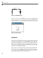
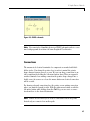

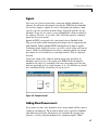

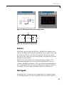
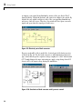
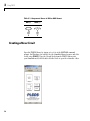
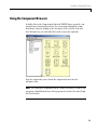


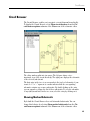


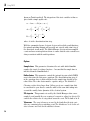


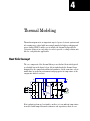
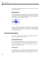
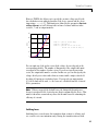
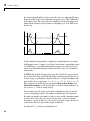
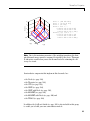
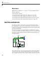


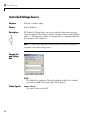
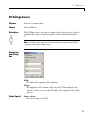
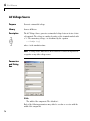

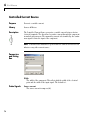
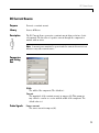
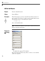

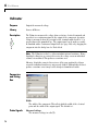


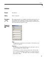
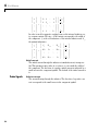

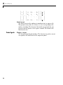
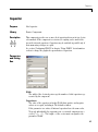
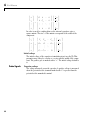


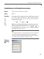

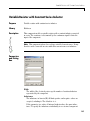


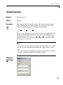

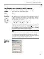

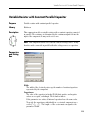

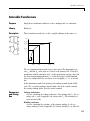
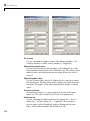


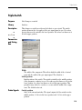

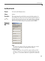


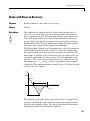


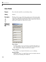

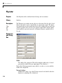


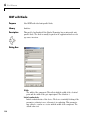

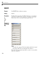

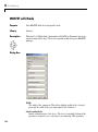


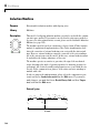
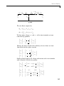

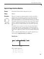
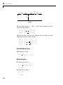

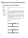
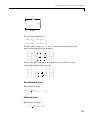

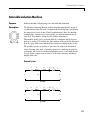
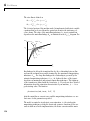


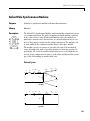
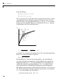


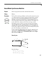
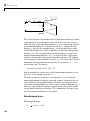
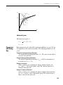


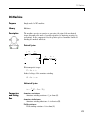


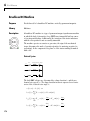
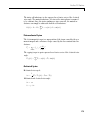

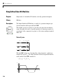


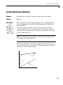
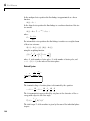


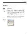

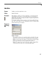

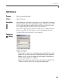


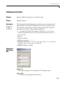


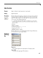


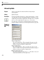

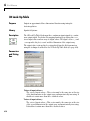


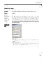
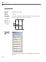

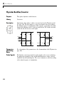

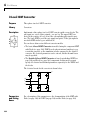

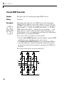


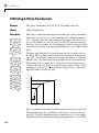


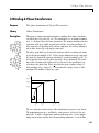


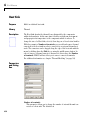


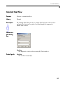
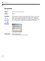
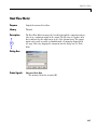

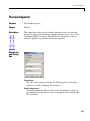


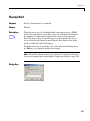
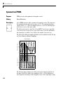
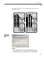

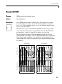

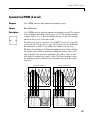
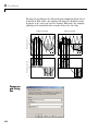

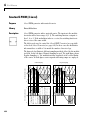

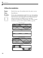


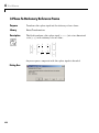
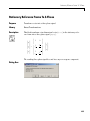
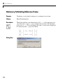
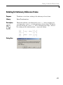
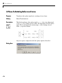
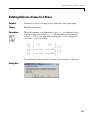


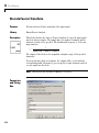


![Télécharger la documentation de conducteö [s]](http://vs1.manualzilla.com/store/data/006373371_1-af26308087bf5a6b266368401065138b-150x150.png)