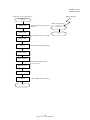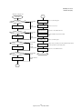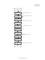
1
To our customers,
Old Company Name in Catalogs and Other Documents
On April 1st, 2010, NEC Electronics Corporation merged with Renesas Technology
Corporation, and Renesas Electronics Corporation took over all the business of both
companies. Therefore, although the old company name remains in this document, it is a valid
Renesas Electronics document. We appreciate your understanding.
Renesas Electronics website: http://www.renesas.com
April 1st, 2010
Renesas Electronics Corporation
Issued by: Renesas Electronics Corporation (http://www.renesas.com)
Send any inquiries to http://www.renesas.com/inquiry.
Notice
1.
2.
3.
4.
5.
6.
7.
All information included in this document is current as of the date this document is issued. Such information, however, is
subject to change without any prior notice. Before purchasing or using any Renesas Electronics products listed herein, please
confirm the latest product information with a Renesas Electronics sales office. Also, please pay regular and careful attention to
additional and different information to be disclosed by Renesas Electronics such as that disclosed through our website.
Renesas Electronics does not assume any liability for infringement of patents, copyrights, or other intellectual property rights
of third parties by or arising from the use of Renesas Electronics products or technical information described in this document.
No license, express, implied or otherwise, is granted hereby under any patents, copyrights or other intellectual property rights
of Renesas Electronics or others.
You should not alter, modify, copy, or otherwise misappropriate any Renesas Electronics product, whether in whole or in part.
Descriptions of circuits, software and other related information in this document are provided only to illustrate the operation of
semiconductor products and application examples. You are fully responsible for the incorporation of these circuits, software,
and information in the design of your equipment. Renesas Electronics assumes no responsibility for any losses incurred by
you or third parties arising from the use of these circuits, software, or information.
When exporting the products or technology described in this document, you should comply with the applicable export control
laws and regulations and follow the procedures required by such laws and regulations. You should not use Renesas
Electronics products or the technology described in this document for any purpose relating to military applications or use by
the military, including but not limited to the development of weapons of mass destruction. Renesas Electronics products and
technology may not be used for or incorporated into any products or systems whose manufacture, use, or sale is prohibited
under any applicable domestic or foreign laws or regulations.
Renesas Electronics has used reasonable care in preparing the information included in this document, but Renesas Electronics
does not warrant that such information is error free. Renesas Electronics assumes no liability whatsoever for any damages
incurred by you resulting from errors in or omissions from the information included herein.
Renesas Electronics products are classified according to the following three quality grades: “Standard”, “High Quality”, and
“Specific”. The recommended applications for each Renesas Electronics product depends on the product’s quality grade, as
indicated below. You must check the quality grade of each Renesas Electronics product before using it in a particular
application. You may not use any Renesas Electronics product for any application categorized as “Specific” without the prior
written consent of Renesas Electronics. Further, you may not use any Renesas Electronics product for any application for
which it is not intended without the prior written consent of Renesas Electronics. Renesas Electronics shall not be in any way
liable for any damages or losses incurred by you or third parties arising from the use of any Renesas Electronics product for an
application categorized as “Specific” or for which the product is not intended where you have failed to obtain the prior written
consent of Renesas Electronics. The quality grade of each Renesas Electronics product is “Standard” unless otherwise
expressly specified in a Renesas Electronics data sheets or data books, etc.
“Standard”:
8.
9.
10.
11.
12.
Computers; office equipment; communications equipment; test and measurement equipment; audio and visual
equipment; home electronic appliances; machine tools; personal electronic equipment; and industrial robots.
“High Quality”: Transportation equipment (automobiles, trains, ships, etc.); traffic control systems; anti-disaster systems; anticrime systems; safety equipment; and medical equipment not specifically designed for life support.
“Specific”:
Aircraft; aerospace equipment; submersible repeaters; nuclear reactor control systems; medical equipment or
systems for life support (e.g. artificial life support devices or systems), surgical implantations, or healthcare
intervention (e.g. excision, etc.), and any other applications or purposes that pose a direct threat to human life.
You should use the Renesas Electronics products described in this document within the range specified by Renesas Electronics,
especially with respect to the maximum rating, operating supply voltage range, movement power voltage range, heat radiation
characteristics, installation and other product characteristics. Renesas Electronics shall have no liability for malfunctions or
damages arising out of the use of Renesas Electronics products beyond such specified ranges.
Although Renesas Electronics endeavors to improve the quality and reliability of its products, semiconductor products have
specific characteristics such as the occurrence of failure at a certain rate and malfunctions under certain use conditions. Further,
Renesas Electronics products are not subject to radiation resistance design. Please be sure to implement safety measures to
guard them against the possibility of physical injury, and injury or damage caused by fire in the event of the failure of a
Renesas Electronics product, such as safety design for hardware and software including but not limited to redundancy, fire
control and malfunction prevention, appropriate treatment for aging degradation or any other appropriate measures. Because
the evaluation of microcomputer software alone is very difficult, please evaluate the safety of the final products or system
manufactured by you.
Please contact a Renesas Electronics sales office for details as to environmental matters such as the environmental
compatibility of each Renesas Electronics product. Please use Renesas Electronics products in compliance with all applicable
laws and regulations that regulate the inclusion or use of controlled substances, including without limitation, the EU RoHS
Directive. Renesas Electronics assumes no liability for damages or losses occurring as a result of your noncompliance with
applicable laws and regulations.
This document may not be reproduced or duplicated, in any form, in whole or in part, without prior written consent of Renesas
Electronics.
Please contact a Renesas Electronics sales office if you have any questions regarding the information contained in this
document or Renesas Electronics products, or if you have any other inquiries.
(Note 1) “Renesas Electronics” as used in this document means Renesas Electronics Corporation and also includes its majorityowned subsidiaries.
(Note 2) “Renesas Electronics product(s)” means any product developed or manufactured by or for Renesas Electronics.
Manual for Using Sample Program Functions
Standby Functions
(V850E/IA3, V850E/IA4, V850ES/IK1, V850ES/IE2)
This manual explains the sample program functions of the standby function for the V850E/IA4 microcontroller.
The explanations are based on usage with the V850E/IA4 microcontroller. Refer to this manual when using the
V850E/IA3, V850ES/IK1, and V850ES/IE2 microcontrollers.
Caution
This sample program is provided for reference purposes only and operations are therefore not
subject to guarantee by NEC Electronics Corporation. When using this sample program, customers
are kindly advised to sufficiently evaluate this product based on their system before usage.
Document No. U18243EJ1V0AN00 (1st edition)
Date Published November 2006 N CP(K)
1
2006
NOTES FOR CMOS DEVICES
1
VOLTAGE APPLICATION WAVEFORM AT INPUT PIN
Waveform distortion due to input noise or a reflected wave may cause malfunction. If the input of the
CMOS device stays in the area between VIL (MAX) and VIH (MIN) due to noise, etc., the device may
malfunction. Take care to prevent chattering noise from entering the device when the input level is fixed,
and also in the transition period when the input level passes through the area between VIL (MAX) and
VIH (MIN).
2
HANDLING OF UNUSED INPUT PINS
Unconnected CMOS device inputs can be cause of malfunction. If an input pin is unconnected, it is
possible that an internal input level may be generated due to noise, etc., causing malfunction. CMOS
devices behave differently than Bipolar or NMOS devices. Input levels of CMOS devices must be fixed
high or low by using pull-up or pull-down circuitry. Each unused pin should be connected to VDD or GND
via a resistor if there is a possibility that it will be an output pin. All handling related to unused pins must
be judged separately for each device and according to related specifications governing the device.
3
PRECAUTION AGAINST ESD
A strong electric field, when exposed to a MOS device, can cause destruction of the gate oxide and
ultimately degrade the device operation. Steps must be taken to stop generation of static electricity as
much as possible, and quickly dissipate it when it has occurred.
Environmental control must be
adequate. When it is dry, a humidifier should be used. It is recommended to avoid using insulators that
easily build up static electricity. Semiconductor devices must be stored and transported in an anti-static
container, static shielding bag or conductive material. All test and measurement tools including work
benches and floors should be grounded.
The operator should be grounded using a wrist strap.
Semiconductor devices must not be touched with bare hands. Similar precautions need to be taken for
PW boards with mounted semiconductor devices.
4
STATUS BEFORE INITIALIZATION
Power-on does not necessarily define the initial status of a MOS device. Immediately after the power
source is turned ON, devices with reset functions have not yet been initialized. Hence, power-on does
not guarantee output pin levels, I/O settings or contents of registers. A device is not initialized until the
reset signal is received. A reset operation must be executed immediately after power-on for devices
with reset functions.
5
POWER ON/OFF SEQUENCE
In the case of a device that uses different power supplies for the internal operation and external
interface, as a rule, switch on the external power supply after switching on the internal power supply.
When switching the power supply off, as a rule, switch off the external power supply and then the
internal power supply. Use of the reverse power on/off sequences may result in the application of an
overvoltage to the internal elements of the device, causing malfunction and degradation of internal
elements due to the passage of an abnormal current.
The correct power on/off sequence must be judged separately for each device and according to related
specifications governing the device.
6
INPUT OF SIGNAL DURING POWER OFF STATE
Do not input signals or an I/O pull-up power supply while the device is not powered. The current
injection that results from input of such a signal or I/O pull-up power supply may cause malfunction and
the abnormal current that passes in the device at this time may cause degradation of internal elements.
Input of signals during the power off state must be judged separately for each device and according to
related specifications governing the device.
2
Application Note
U18243EJ1V0AN
These commodities, technology or software, must be exported in accordance
with the export administration regulations of the exporting country.
Diversion contrary to the law of that country is prohibited.
• The information in this document is current as of July, 2006. The information is subject to change
without notice. For actual design-in, refer to the latest publications of NEC Electronics data sheets or
data books, etc., for the most up-to-date specifications of NEC Electronics products. Not all
products and/or types are available in every country. Please check with an NEC Electronics sales
representative for availability and additional information.
• No part of this document may be copied or reproduced in any form or by any means without the prior
written consent of NEC Electronics. NEC Electronics assumes no responsibility for any errors that may
appear in this document.
• NEC Electronics does not assume any liability for infringement of patents, copyrights or other intellectual
property rights of third parties by or arising from the use of NEC Electronics products listed in this document
or any other liability arising from the use of such products. No license, express, implied or otherwise, is
granted under any patents, copyrights or other intellectual property rights of NEC Electronics or others.
• Descriptions of circuits, software and other related information in this document are provided for illustrative
purposes in semiconductor product operation and application examples. The incorporation of these
circuits, software and information in the design of a customer's equipment shall be done under the full
responsibility of the customer. NEC Electronics assumes no responsibility for any losses incurred by
customers or third parties arising from the use of these circuits, software and information.
• While NEC Electronics endeavors to enhance the quality, reliability and safety of NEC Electronics products,
customers agree and acknowledge that the possibility of defects thereof cannot be eliminated entirely. To
minimize risks of damage to property or injury (including death) to persons arising from defects in NEC
Electronics products, customers must incorporate sufficient safety measures in their design, such as
redundancy, fire-containment and anti-failure features.
• NEC Electronics products are classified into the following three quality grades: "Standard", "Special" and
"Specific".
The "Specific" quality grade applies only to NEC Electronics products developed based on a customerdesignated "quality assurance program" for a specific application. The recommended applications of an NEC
Electronics product depend on its quality grade, as indicated below. Customers must check the quality grade of
each NEC Electronics product before using it in a particular application.
"Standard": Computers, office equipment, communications equipment, test and measurement equipment, audio
and visual equipment, home electronic appliances, machine tools, personal electronic equipment
and industrial robots.
"Special": Transportation equipment (automobiles, trains, ships, etc.), traffic control systems, anti-disaster
systems, anti-crime systems, safety equipment and medical equipment (not specifically designed
for life support).
"Specific": Aircraft, aerospace equipment, submersible repeaters, nuclear reactor control systems, life
support systems and medical equipment for life support, etc.
The quality grade of NEC Electronics products is "Standard" unless otherwise expressly specified in NEC
Electronics data sheets or data books, etc. If customers wish to use NEC Electronics products in applications
not intended by NEC Electronics, they must contact an NEC Electronics sales representative in advance to
determine NEC Electronics' willingness to support a given application.
(Note)
(1) "NEC Electronics" as used in this statement means NEC Electronics Corporation and also includes its
majority-owned subsidiaries.
(2) "NEC Electronics products" means any product developed or manufactured by or for NEC Electronics (as
defined above).
M8E 02. 11-1
3
Application Note
U18243EJ1V0AN
INTRODUCTION
Cautions 1.
Download the program used in this manual from the NEC Electronics Website
(http://www.necel.com/).
2.
When using this sample program, reference the following startup file and link directive file
and adjust them if as necessary.
3.
• Startup file:
IA4_start.s
• Link directive file:
IA4_link.dir
In this sample program, control after releasing each standby mode varies depending on
whether interrupt is enabled or disabled.
After the HALT mode and IDLE mode are released and an interrupt is enabled, the control
branches to the handler, and after the STOP mode is released and interrupt is disabled, the
next instruction is executed.
4
Application Note
U18243EJ1V0AN
Conventions
The function lists are structured as follows.
Hardware name (symbol)
[Function]
Function description
[Function name]
Name of sample function
[Argument]
Type and overview of argument
[Processing content]
Processing content of sample function
[Starting method]
Conditions for calling a function
[SFR(s) used]
Register name and setting content
[call function(s)]
Name and function of call function(s)
[Variable(s)]
Type, name, and overview of variable(s) used in sample function
[Interrupt(s)]
Name of function
[Interrupt source(s)]
Name
[File name]
Name of corresponding sample program file
[Caution(s)]
Caution(s) upon function usage
Interrupt function
[Function name]
Name of interrupt function
[Processing content]
Processing content of interrupt function
[SFR(s) used]
Register name and setting content
[call function(s)]
None
[Variable(s)]
Name of variable, function
[File name]
Name of corresponding sample program file
[Caution(s)]
None
5
Application Note
U18243EJ1V0AN
Product Differences
The differences between the V850E/IA4 and the V850E/IA3, V850ES/IK1, and
V850ES/IE2 related to the standby functions are shown below.
Item
Conditions for
V850E/IA4
V850E/IA3
• Non-maskable
• Non-maskable
V850ES/IK1
V850ES/IE2
• Non-maskable interrupt request signal (INTWDT)
releasing HALT
interrupt request
interrupt request
• Unmasked maskable interrupt request signal
mode
signal (INTWDT)
signal (INTWDT)
• Reset signal (RESET pin input, WDTRES signal
• Unmasked maskable
Conditions for
releasing IDLE mode
• Unmasked maskable
interrupt request
interrupt request
signal
signal
• Reset signal (RESET
• Reset signal (RESET
pin input, WDTRES
pin input, WDTRES
signal generation)
signal generation)
• Unmasked external
• Unmasked external
interrupt request
interrupt request
signal (INTP0 to
signal (INTP0, INTP2
INTP5, INTP7 pin
to INTP5, INTP7 pin
input)
input)
• Unmasked internal
interrupt request
interrupt request
signal from peripheral
signal from peripheral
functions operable in
functions operable in
IDLE mode (interrupt
IDLE mode (interrupt
request signal related
request signal related
to CSIB in slave
to CSIB in slave
• Unmasked external interrupt request signal
(INTP0 to INTP5 pin input)
• Unmasked internal interrupt request signal
(INTLVI)
peripheral functions operable in IDLE mode
(interrupt request signal related to CSIB in slave
mode).
• Reset signal (RESET pin input, LVIRES signal
generation, POCRES signal generation)
mode).
• RESET pin input
• RESET pin input
• Unmasked external
• Unmasked external
releasing STOP
interrupt request
interrupt request
mode
signal (INTP0 to
signal (INTP0, INTP2
INTP5, INTP7 pin
to INTP5, INTP7 pin
input)
input)
Conditions for
signal generation)
• Unmasked internal interrupt request signal from
• Unmasked internal
mode).
generation, LVIRES signal generation, POCRES
• Unmasked external interrupt request signal
(INTP0 to INTP5 pin input)
• Unmasked internal interrupt request signal
(INTLVI)
• Unmasked internal interrupt request signal from
• Unmasked internal
• Unmasked internal
interrupt request
interrupt request
signal from peripheral
signal from peripheral
functions operable in
functions operable in
STOP mode
STOP mode
(interrupt request
(interrupt request
signal related to CSIB
signal related to CSIB
in slave mode).
in slave mode).
• RESET pin input
• RESET pin input
peripheral functions operable in STOP mode
(interrupt request signal related to CSIB in slave
mode).
• Reset signal (RESET pin input, LVIRES signal
6
Application Note
U18243EJ1V0AN
generation, POCRES signal generation)
Related Documents
The related documents indicated in this publication may include preliminary versions.
However, preliminary versions are not marked as such.
Documents related to V850E/IA3, V850E/IA4, V850ES/IK1, and V850ES/IE2
Document Name
V850E1
Architecture
Document No.
User’s Manual
U14559E
V850E/IA3, V850E/IA4
Hardware
U16543E
V850ES
User’s Manual
Architecture
User’s Manual
U15943E
V850ES/IK1
Hardware
User’s Manual
U16910E
V850ES/IE2
Hardware
User’s Manual
U17716E
Inverter Control by V850 Series
Vector Control by Hole Sensor
Application Note
Inverter Control by V850 Series
Vector Control by Encoder
Inverter Control by V850 Series
120° Excitation Method Control by Zero-Cross Detection
Application Note
U17338E
U17324E
U17209E
Application Note
Manual for Using Sample Program Functions
(V850E/IA3, V850E/IA4, V850ES/IK1, V850ES/IE2)
Manual for Using Sample Program Functions
V850E/IA4, V850ES/IK1, V850ES/IE2)
Serial Communication (UARTA)
U18233E
Application Note
Serial Communication (CSIB) (V850E/IA3,
U18234E
Application Note
Manual for Using Sample Program Functions
DMA Functions (V850E/IA3, V850E/IA4)
U18235E
Application Note
Manual for Using Sample Program Functions
V850ES/IK1, V850ES/IE2)
Manual for Using Sample Program Functions
V850ES/IK1, V850ES/IE2)
Timer M (V850E/IA3, V850E/IA4,
U18236E
Watchdog Timer (V850E/IA3, V850E/IA4,
U18237E
Application Note
Application Note
Manual for Using Sample Program Functions
V850ES/IK1, V850ES/IE2)
Timer P (V850E/IA3, V850E/IA4,
U18238E
Timer Q (V850E/IA3, V850E/IA4,
U18239E
Timer ENC (V850E/IA3, V850E/IA4)
U18240E
Port Functions (V850E/IA3, V850E/IA4,
U18241E
Clock Generator (V850E/IA3, V850E/IA4,
U18242E
Application Note
Manual for Using Sample Program Functions
V850ES/IK1, V850ES/IE2)
Application Note
Manual for Using Sample Program Functions
Application Note
Manual for Using Sample Program Functions
V850ES/IK1, V850ES/IE2)
Application Note
Manual for Using Sample Program Functions
V850ES/IK1, V850ES/IE2)
Application Note
Manual for Using Sample Program Functions
V850ES/IK1, V850ES/IE2)
This manual
Interrupt Functions (V850E/IA3, V850E/IA4,
U18244E
Application Note
Manual for Using Sample Program Functions
V850ES/IK1, V850ES/IE2)
Standby Functions (V850E/IA3, V850E/IA4,
Application Note
Manual for Using Sample Program Functions
V850E/IA4, V850ES/IK1, V850ES/IE2)
A/D Converters 0 and 1 (V850E/IA3,
U18245E
Application Note
Manual for Using Sample Program Functions
A/D Converter 2 (V850E/IA3, V850E/IA4)
Application Note
7
Application Note
U18243EJ1V0AN
U18246E
CONTENTS
Standby functions
HALT mode........................................................................................................................................................ 9
Standby functions
IDLE mode....................................................................................................................................................... 12
Standby functions
STOP mode ..................................................................................................................................................... 18
8
Application Note
U18243EJ1V0AN
Standby functions
HALT mode
[Function]
Sets standby function (HALT mode).
[Function name]
halt_main
[Argument]
None
[Processing content]
Sets from normal operation mode to HALT mode. The HALT mode is released by an
external interrupt request signal.
[Starting method]
None
[SFR used]
None
[call functions]
halt_init, halt_mode
[Variable]
None
[Interrupt]
external_int
[Interrupt source]
INTP7
[File name]
halt.c
[Caution]
Interrupts not to be used must be masked before setting to HALT mode.
[Function name]
halt_init
[Processing content]
Sets an external interrupt request signal (INTP7) for releasing HALT mode.
[SFRs used]
PMC0:
0x80 (Sets to alternate-function pin.)
INTR0:
0x80 (Sets valid edge to rising edge.)
INTF0:
0x00 (Sets valid edge to rising edge.)
PIC7.PIF7:
0 (Clears INTP7 interrupt request flag.)
IMR3:
0xFFFF (Masks interrupt.)
IMR2:
0xFFFF (Masks interrupt.)
IMR1:
0xFFFF (Masks interrupt.)
IMR0:
0xFFFF (Masks interrupt.)
PIC7.PMK7:
0 (Enables INTP7 interrupt servicing.)
[call function]
None
[Variable]
None
[File name]
halt.c
[Caution]
None
9
Application Note
U18243EJ1V0AN
[Function name]
halt_mode
[Processing content]
Executes HALT instruction.
[SFR used]
None
[call function]
None
[Variable]
None
[File name]
halt.c
[Caution]
Insert five or more NOP instructions after the HALT instruction.
Interrupt function
[Function name]
external_int
[Processing content]
There is no particular processing because this is used for confirmation of external
interrupt occurrence.
[SFR used]
None
[call function]
None
[Variable]
None
[File name]
halt.c
[Caution]
None
10
Application Note
U18243EJ1V0AN
Standby functions
HALT mode
halt_main
DI
Disables maskable interrupt request
HALT mode release setting function
halt_init
EI
Enables maskable interrupt request
HALT mode function
halt_mode
HALT mode release setting function
halt_init
PMC0 = 0x80
ret
Sets alternate-function pin to
INTP7 input pin
HALT mode function
halt_mode
INTR0 = 0x80
Sets edge detection to rising edge
HALT
Executes HALT instruction
NOP instruction × 5
Inserts five or more NOP
instructions
INTF0 = 0x00
PIF7 = 0
Clears INTP7 interrupt request flag
ret
IMR3 = 0xFFFF
INTP7 interrupt
IMR2 = 0xFFFF
Masks all maskable interrupts
not to be used
INTP7 interrupt function
IMR1 = 0xFFFF
external_int
IMR0 = 0xFFFF
reti
PMK7 = 0
Enables INTP7 interrupt servicing
ret
11
Application Note
U18243EJ1V0AN
Standby functions
IDLE mode
[Function]
Sets standby function (IDLE mode).
[Function name]
idle_main
[Argument]
None
[Processing content]
Sets from normal operation mode to IDLE mode. The IDLE mode is released by an
external interrupt request signal.
[Starting method]
None
[SFR used]
None
[call functions]
idle_init, idle_mode
[Variable]
None
[Interrupt]
external_int
[Interrupt source]
INTP7
[File name]
idle.c
[Caution]
Interrupts not to be used must be masked before setting to IDLE mode.
[Function name]
idle_init
[Processing content]
Sets an external interrupt request signal (INTP7) for releasing IDLE mode.
[SFRs used]
PMC0:
0x80 (Sets to alternate-function pin.)
INTR0:
0x80 (Sets valid edge to rising edge.)
INTF0:
0x00 (Sets valid edge to rising edge.)
PIC7.PIF7:
0 (Clears INTP7 interrupt request flag.)
IMR3:
0xFFFF (Masks interrupt.)
IMR2:
0xFFFF (Masks interrupt.)
IMR1:
0xFFFF (Masks interrupt.)
IMR0:
0xFFFF (Masks interrupt.)
PIC7.PMK7:
0 (Enables INTP7 interrupt servicing.)
[call function]
None
[Variable]
None
[File name]
idle.c
[Caution]
None
12
Application Note
U18243EJ1V0AN
[Function name]
idle_mode
[Processing content]
Executes IDLE mode by forcibly terminating all DMA transfers.
[SFRs used]
DCHC0.TC0
DMA0 transfer status bit
DCHC0.E00:
1 (Enables DMA0 transfer.)
DCHC0.INIT0:
1 (Forcibly terminates DMA0 transfer.)
DCHC1.TC1
DMA1 transfer status bit
DCHC1.E11:
1 (Enables DMA1 transfer.)
DCHC1.INIT1:
1 (Forcibly terminates DMA1 transfer.)
DCHC2.TC2
DMA2 transfer status bit
DCHC2.E22:
1 (Enables DMA2 transfer.)
DCHC2.INIT2:
1 (Forcibly terminates DMA2 transfer.)
DCHC3.TC3
DMA3 transfer status bit
DCHC3.E33:
1 (Enables DMA3 transfer.)
DCHC3.INIT3:
1 (Forcibly terminates DMA3 transfer.)
PRCMD:
0x03 (Writes to command register
(used when writing to a special register).)
PCC:
0x03 (Selects clock as fXX/8.)
PSMR:
0x00 (Sets to IDLE mode.)
PRCMD:
0x02 (Writes to command register
(used when writing to a special register).)
PSC:
0x02 (Enables standby mode release and sets to standby mode.)
[call function]
None
[Variable]
None
[File name]
idle_mode.c
[Cautions]
• DMA transfer is forcibly terminated in this sample program, because all DMA transfers
must be terminated before performing data setting to the special register.
• PCC and PSC registers are special registers and can therefore only be written in
combination of specific sequences.
• When setting to IDLE mode, set in the order of, the PCC register (set to 03H), the
PSMR.PSM0 bit, and the PSC.STB bit.
13
Application Note
U18243EJ1V0AN
Interrupt function
[Function name]
external_int
[Processing content]
There is no particular processing because this is used for confirmation of external
interrupt occurrence.
[SFR used]
None
[call function]
None
[Variable]
None
[File name]
idle.c
[Caution]
None
14
Application Note
U18243EJ1V0AN
Standby functions
IDLE mode (1/3)
idle_main
DI
idle_init
EI
Disables maskable interrupt request
IDLE mode release setting function
Enables maskable interrupt request
idle_mode
PRERR == 1
IDLE mode function
No
Checks protection error flag
Yes
ret
15
Application Note
U18243EJ1V0AN
Standby functions
IDLE mode (2/3)
IDLE mode release setting function
INTP7 interrupt
idle_init
INTP7 interrupt function
PMC0 = 0x80
Sets alternate-function pin to INTP7
input pin
INTR0 = 0x80
reti
Sets edge detection to rising edge
INTF0 = 0x00
PIF7 = 0
Clears INTP7 interrupt request flag
IMR3 = 0xFFFF
IMR2 = 0xFFFF
Masks all maskable interrupts
not to be used
IMR1 = 0xFFFF
IMR0 = 0xFFFF
PMK7 = 0
external_int
Enables INTP7 interrupt servicing
ret
16
Application Note
U18243EJ1V0AN
Standby functions
IDLE mode (3/3)
IDLE mode setting function
A
idle_mode
TC0 == 0 && E00 == 1
No
Checks DMA0
PRCMD = 0x03
Writes to command register
transfer
Yes
PCC = 0x03
Forcibly
terminates DMA0
INIT0 = 1
NOP instruction × 5
TC1 == 0 && E11 == 1
No
PSMR = 0x00
Specifies standby mode operation as IDLE
mode
Forcibly
terminates DMA1
INIT1 = 1
PRCMD = 0x02
No
Checks DMA2
transfer
PSC = 0x02
Yes
Writes to command register
Enables release of standby control via maskable interrupt request
Specifies operation mode as standby mode
Forcibly
INIT2 = 1
TC3 == 0 && E33 == 1
Inserts five or more NOP instructions
Checks DMA1
transfer
Yes
TC2 == 0 && E22 == 1
Selects clock as f fXX/8
terminates DMA2
No
NOP instruction × 5
Checks DMA3
transfer
Inserts five or more NOP instructions
ret
Yes
INIT3 = 1
Forcibly terminates
DMA3
A
17
Application Note
U18243EJ1V0AN
Standby functions
STOP mode
[Function]
Sets standby function (STOP mode).
[Function name]
stop_main
[Argument]
None
[Processing content]
Sets from normal operation mode to STOP mode. The STOP mode is released by an
external interrupt request signal.
[Starting method]
None
[SFR used]
None
[call functions]
stop_init, stop_mode
[Variable]
None
[Interrupt]
None
[Interrupt source]
None
[File name]
stop.c
[Cautions]
• Interrupts not to be used must be masked before setting to STOP mode.
• The INTP7 interrupt request signal is kept set after releasing STOP mode.
[Function name]
stop_init
[Processing content]
Sets an external interrupt request signal (INTP7) for releasing STOP mode.
[SFRs used]
OSTS:
0x07 (Sets oscillation stabilization time to 16.4 ms)
PMC0:
0x80 (Sets to alternate-function pin.)
INTR0:
0x80 (Sets valid edge to rising edge.)
INTF0:
0x00 (Sets valid edge to rising edge.)
PIC7.PIF7:
0 (Clears INTP7 interrupt request flag.)
IMR3:
0xFFFF (Masks interrupt.)
IMR2:
0xFFFF (Masks interrupt.)
IMR1:
0xFFFF (Masks interrupt.)
IMR0:
0xFFFF (Masks interrupt.)
PIC7.PMK7:
0 (Enables INTP7 interrupt servicing.)
[call function]
None
[Variable]
None
[File name]
stop.c
[Caution]
None
18
Application Note
U18243EJ1V0AN
[Function name]
stop_mode
[Processing content]
Executes STOP mode by forcibly terminating all DMA transfers.
[SFRs used]
DCHC0.TC0
DMA0 transfer status bit
DCHC0.E00:
1 (Enables DMA0 transfer.)
DCHC0.INIT0:
1 (Forcibly terminates DMA0 transfer.)
DCHC1.TC1
DMA1 transfer status bit
DCHC1.E11:
1 (Enables DMA1 transfer.)
DCHC1.INIT1:
1 (Forcibly terminates DMA1 transfer.)
DCHC2.TC2
DMA2 transfer status bit
DCHC2.E22:
1 (Enables DMA2 transfer.)
DCHC2.INIT2:
1 (Forcibly terminates DMA2 transfer.)
DCHC3.TC3
DMA3 transfer status bit
DCHC3.E33:
1 (Enables DMA3 transfer.)
DCHC3.INIT3:
1 (Forcibly terminates DMA3 transfer.)
PRCMD:
0x03 (Writes to command register
(used when writing to a special register).)
PCC:
0x03 (Selects clock as fXX/8.)
PSMR:
0x01 (Sets to STOP mode.)
PRCMD:
0x02 (Writes to command register
(used when writing to a special register).)
PSC:
0x02 (Enables standby mode release and sets to standby mode.)
[call function]
None
[Variable]
None
[File name]
stop.c
[Cautions]
• DMA transfer is forcibly terminated in this sample program, because all DMA transfers
must be terminated before performing data setting to the special register.
• PCC and PSC registers are special registers and can therefore only be written in
combination of specific sequences.
• When setting to STOP mode, set in the order of, the PCC register (set to 03H), the
PSMR.PSM0 bit, and the PSC.STB bit.
19
Application Note
U18243EJ1V0AN
Standby functions
STOP mode (1/3)
stop_main
DI
stop_init
stop_mode
PRERR == 1
Disables maskable interrupt request
STOP mode release setting function
STOP mode function
No
Checks protection error flag
Yes
ret
20
Application Note
U18243EJ1V0AN
Standby functions
STOP mode (2/3)
STOP mode release setting function
stop_init
OSTS = 0x07
Sets oscillation stabilization time to
16.4 ms
PMC0 = 0x80
Sets alternate-function pin to INTP7
input pin
INTR0 = 0x80
Sets edge detection to rising edge
INTF0 = 0x00
PIF7 = 0
Clears INTP7 interrupt request flag
IMR3 = 0xFFFF
IMR2 = 0xFFFF
Masks all maskable interrupts not
to be used
IMR1 = 0xFFFF
IMR0 = 0xFFFF
Enables INTP7 interrupt servicing
PMK7 = 0
ret
21
Application Note
U18243EJ1V0AN
Standby functions
STOP mode (3/3)
STOP mode setting function
A
stop_mode
TC0 == 0 && E00 == 1
No
PRCMD = 0x03
Writes to command register
Checks DMA0
transfer
Yes
Forcibly
terminates DMA0
INIT0 = 1
PCC = 0x03
NOP instruction × 5
TC1 == 0 && E11 == 1
No
PSMR = 0x01
Specifies standby mode operation as STOP mode
Forcibly
terminates DMA1
INIT1 = 1
PRCMD = 0x02
No
Checks DMA2
transfer
PSC = 0x02
Yes
Forcibly
terminates DMA2
INIT2 = 1
TC3 == 0 && E33 == 1
Inserts five or more NOP instructions
Checks DMA1
transfer
Yes
TC2 == 0 && E22 == 1
Selects clock as fXX/8
No
NOP instruction × 5
Checks DMA3
transfer
Writes to command register
Enables release of standby control via maskable interrupt request
Specifies operation mode as standby mode
Inserts five or more NOP instructions
ret
Yes
INIT3 = 1
Forcibly terminates
DMA3
A
22
Application Note
U18243EJ1V0AN
For further information,
please contact:
NEC Electronics Corporation
1753, Shimonumabe, Nakahara-ku,
Kawasaki, Kanagawa 211-8668,
Japan
Tel: 044-435-5111
http://www.necel.com/
[America]
[Europe]
[Asia & Oceania]
NEC Electronics America, Inc.
2880 Scott Blvd.
Santa Clara, CA 95050-2554, U.S.A.
Tel: 408-588-6000
800-366-9782
http://www.am.necel.com/
NEC Electronics (Europe) GmbH
Arcadiastrasse 10
40472 Düsseldorf, Germany
Tel: 0211-65030
http://www.eu.necel.com/
NEC Electronics (China) Co., Ltd
7th Floor, Quantum Plaza, No. 27 ZhiChunLu Haidian
District, Beijing 100083, P.R.China
Tel: 010-8235-1155
http://www.cn.necel.com/
NEC Electronics Shanghai Ltd.
Room 2511-2512, Bank of China Tower,
200 Yincheng Road Central,
Pudong New Area, Shanghai P.R. China P.C:200120
Tel: 021-5888-5400
http://www.cn.necel.com/
Hanover Office
Podbielskistrasse 166 B
30177 Hannover
Tel: 0 511 33 40 2-0
Munich Office
Werner-Eckert-Strasse 9
81829 München
Tel: 0 89 92 10 03-0
NEC Electronics Hong Kong Ltd.
12/F., Cityplaza 4,
12 Taikoo Wan Road, Hong Kong
Tel: 2886-9318
http://www.hk.necel.com/
Stuttgart Office
Industriestrasse 3
70565 Stuttgart
Tel: 0 711 99 01 0-0
United Kingdom Branch
Cygnus House, Sunrise Parkway
Linford Wood, Milton Keynes
MK14 6NP, U.K.
Tel: 01908-691-133
Succursale Française
9, rue Paul Dautier, B.P. 52
78142 Velizy-Villacoublay Cédex
France
Tel: 01-3067-5800
Sucursal en España
Juan Esplandiu, 15
28007 Madrid, Spain
Tel: 091-504-2787
NEC Electronics Taiwan Ltd.
7F, No. 363 Fu Shing North Road
Taipei, Taiwan, R. O. C.
Tel: 02-8175-9600
http://www.tw.necel.com/
NEC Electronics Singapore Pte. Ltd.
238A Thomson Road,
#12-08 Novena Square,
Singapore 307684
Tel: 6253-8311
http://www.sg.necel.com/
NEC Electronics Korea Ltd.
11F., Samik Lavied’or Bldg., 720-2,
Yeoksam-Dong, Kangnam-Ku,
Seoul, 135-080, Korea
Tel: 02-558-3737
http://www.kr.necel.com/
Tyskland Filial
Täby Centrum
Entrance S (7th floor)
18322 Täby, Sweden
Tel: 08 638 72 00
Filiale Italiana
Via Fabio Filzi, 25/A
20124 Milano, Italy
Tel: 02-667541
Branch The Netherlands
Steijgerweg 6
5616 HS Eindhoven
The Netherlands
Tel: 040 265 40 10
G06.11A
23
Application Note
U18243EJ1V0AN