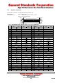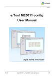
1
PCIe4-SIO8BX2 User’s Manual EIGHT CHANNEL HIGH PERFORMANCE SERIAL I/O PCIe CARD FEATURING RS422/RS485/RS232 SOFTWARE CONFIGURABLE TRANSCEIVERS AND 32K BYTE FIFO BUFFERS (512K BYTE TOTAL) RS-485 RS-422/V.11 RS-232/V.28 General Standards Corporation 8302A Whitesburg Drive Huntsville, AL 35802 Phone: (256) 880-8787 Fax: (256) 880-8788 URL: www.generalstandards.com E-mail: [email protected] Revision NR PREFACE Revision History 1. Rev NR – Mar 2013 – Original rev from PMC66-SIO4BXR manual. Additional copies of this manual or other General Standards Corporation literature may be obtained from: General Standards Corporation 8302A Whitesburg Drive Huntsville, Alabama 35802 Telephone: (256) 880-8787 Fax: (256) 880-8788 URL: www.generalstandards.com The information in this document is subject to change without notice. General Standards Corporation makes no warranty of any kind with regard to this material, including, but not limited to, the implied warranties of merchantability and fitness for a particular purpose. Although extensive editing and reviews are performed before release to ECO control, General Standards Corporation assumes no responsibility for any errors that may exist in this document. No commitment is made to update or keep current the information contained in this document. General Standards Corporation does not assume any liability arising out of the application or use of any product or circuit described herein, nor is any license conveyed under any patent right of any rights of others. General Standards Corporation assumes no responsibility resulting from omissions or errors in this manual, or from the use of information contained herein. General Standards Corporation reserves the right to make any changes, without notice, to this product to improve reliability, performance, function, or design. All rights reserved No parts of this document may be copied or reproduced in any form or by any means without prior written consent of General Standards Corporation. Copyright © 2013 General Standards Corporation i Rev NR RELATED PUBLICATIONS ZILOG Z16C30 USC® User’s Manual ZILOG Z16C30 USC® Product Specifications Databook ZILOG, Inc. 210 East Hacienda Ave. Campbell, CA 95008-6600 (408) 370-8000 http://www.zilog.com/ PLX PCI 9056 Data Book PLX Technology Inc. 390 Potrero Avenue Sunnyvale, CA 4085 (408) 774-3735 http://www.plxtech.com/ EIA-422-A – Electrical Characteristics of Balanced Voltage Digital Interface Circuits (EIA order number EIA-RS-422A) EIA-485 – Standard for Electrical Characteristics of Generators and Receivers for Use in Balanced Digital Multipoint Systems (EIA order number EIA-RS-485) EIA Standards and Publications can be purchased from: GLOBAL ENGINEERING DOCUMENTS 15 Inverness Way East Englewood, CO 80112 Phone: (800) 854-7179 http://global.ihs.com/ PCI Local Bus Specification Revision 2.2 December 18, 1998 Copies of PCI specifications available from: PCI Special Interest Group NE 2575 Kathryn Street, #17 Hillsboro, OR 97124 http://www.pcisig.com/ ii Rev NR TABLE OF CONTENTS EIGHT CHANNEL HIGH PERFORMANCE SERIAL I/O PCIe CARD ..................................................... I CHAPTER 1: INTRODUCTION ..............................................................................................................................1 1.0 1.1 1.2 1.3 1.4 1.5 1.6 1.7 GENERAL DESCRIPTION ..................................................................................................................................1 Z16C30 UNIVERSAL SERIAL CONTROLLER ....................................................................................................2 DEEP TRANSMIT/RECEIVE FIFOS ...................................................................................................................2 MULTIPROTOCOL TRANSCEIVERS ...................................................................................................................3 PMC/PCI INTERFACE .....................................................................................................................................3 GENERAL PURPOSE IO ...................................................................................................................................3 CONNECTOR INTERFACE ................................................................................................................................ 3 NEW FEATURES ..............................................................................................................................................3 CHAPTER 2: LOCAL SPACE REGISTERS ..........................................................................................................4 2.0 REGISTER MAP ...............................................................................................................................................4 2.1 GSC FIRMWARE REGISTERS ...........................................................................................................................4 2.1.1 FIRMWARE REVISION: LOCAL OFFSET 0X0000 ..............................................................................................5 2.1.2 BOARD CONTROL: LOCAL OFFSET 0X0004 ....................................................................................................6 2.1.3 BOARD STATUS: LOCAL OFFSET 0X0008........................................................................................................7 2.1.4 TIMESTAMP: LOCAL OFFSET 0X000C .............................................................................................................7 2.1.5 CHANNEL TX ALMOST FLAGS: LOCAL OFFSET 0X0010 / 0X0020 / 0X0030 / 0X0040 ....................................7 2.1.6 CHANNEL RX ALMOST FLAGS: LOCAL OFFSET 0X0014 / 0X0024 / 0X0034 / 0X0044 ....................................8 2.1.7 CHANNEL FIFO: LOCAL OFFSET 0X0018 / 0X0028 / 0X0038 / 0X0048 ..........................................................8 2.1.8 CHANNEL CONTROL/STATUS: LOCAL OFFSET 0X001C / 0X002C / 0X003C / 0X004C ....................................8 2.1.9 CHANNEL SYNC DETECT BYTE: LOCAL OFFSET 0X0050 / 0X0054 / 0X0058 / 0X005C ..................................9 2.1.10 INTERRUPT REGISTERS ...................................................................................................................................9 2.1.10.1 INTERRUPT CONTROL: LOCAL OFFSET 0X0060 ....................................................................................10 2.1.10.2 INTERRUPT STATUS/CLEAR: LOCAL OFFSET 0X0064............................................................................10 2.1.10.3 INTERRUPT EDGE/LEVEL: LOCAL OFFSET 0X0068 ...............................................................................11 2.1.10.4 INTERRUPT HI/LO: LOCAL OFFSET 0X006C..........................................................................................11 2.1.11 CHANNEL PIN SOURCE: LOCAL OFFSET 0X0080 / 0X0084 / 0X0088 / 0X008C ............................................11 2.1.12 CHANNEL PIN STATUS: LOCAL OFFSET 0X0090 / 0X0094 / 0X0098 / 0X009C .............................................14 2.1.13 PROGRAMMABLE CLOCK REGISTERS: LOCAL OFFSET 0X00A0 / 0X00A4 / 0X00A8 / 0XAC .......................15 2.1.14 FIFO COUNT REGISTER: LOCAL OFFSET 0X00D0 / 0X00D4 / 0X00D8 / 0X00DC .......................................15 2.1.15 FIFO SIZE REGISTER: LOCAL OFFSET 0X00E0 / 0X00E4 / 0X00E8 / 0X00EC .............................................15 2.1.16 FW TYPE ID REGISTER: LOCAL OFFSET 0X00F8 .........................................................................................15 2.1.17 FEATURES REGISTER: LOCAL OFFSET 0X00FC ............................................................................................16 2.2 UNIVERSAL SERIAL CONTROLLER REGISTERS .............................................................................................. 16 2.2.1 USC RESET ..................................................................................................................................................16 2.2.2 8-BIT USC REGISTER ACCESS ......................................................................................................................17 2.2.3 USC DATA TRANSFER ..................................................................................................................................17 2.2.4 USC REGISTER MEMORY MAP .....................................................................................................................18 CHAPTER 3: PROGRAMMING ...........................................................................................................................19 3.0 3.1 3.2 3.2.1 3.2.2 INTRODUCTION .............................................................................................................................................19 RESETS .........................................................................................................................................................19 FIFOS...........................................................................................................................................................19 FIFO FLAGS .................................................................................................................................................19 FIFO COUNTERS ..........................................................................................................................................20 iii Rev NR 3.2.3 3.3 3.4 3.5 3.6 3.7 3.8 3.9 3.10 3.11 FIFO SIZE ....................................................................................................................................................20 BOARD VS. CHANNEL REGISTERS .................................................................................................................20 PROGRAMMABLE OSCILLATOR / PROGRAMMABLE CLOCKS .........................................................................21 CLOCK SETUP ...............................................................................................................................................21 MULTIPROTOCOL TRANSCEIVER CONTROL ..................................................................................................23 DCE/DTE MODE .........................................................................................................................................23 LOOPBACK MODES .......................................................................................................................................23 GENERAL PURPOSE IO .................................................................................................................................24 INTERRUPTS .................................................................................................................................................24 PCI DMA.....................................................................................................................................................24 CHAPTER 4: PCI INTERFACE ............................................................................................................................26 4.0 4.1 4.1.1 4.1.2 4.1.3 4.1.4 4.1.4.1 PCI INTERFACE REGISTERS ..........................................................................................................................26 PCI REGISTERS.............................................................................................................................................26 PCI CONFIGURATION REGISTERS..................................................................................................................26 LOCAL CONFIGURATION REGISTERS .............................................................................................................27 RUNTIME REGISTERS ....................................................................................................................................27 DMA REGISTERS..........................................................................................................................................27 DMA CHANNEL MODE REGISTER: (PCI 0X80 / 0X94) .................................................................................27 CHAPTER 5: HARDWARE CONFIGURATION ................................................................................................ 28 5.0 5.1 5.2 5.3 5.4 BOARD LAYOUT ...........................................................................................................................................28 BOARD ID JUMPER J1 ..................................................................................................................................28 TERMINATION RESISTORS............................................................................................................................. 29 LEDS ...........................................................................................................................................................29 INTERFACE CONNECTOR .............................................................................................................................. 30 CHAPTER 6: ORDERING OPTIONS ...................................................................................................................32 6.0 6.1 6.2 6.3 ORDERING INFORMATION ............................................................................................................................. 32 INTERFACE CABLE........................................................................................................................................32 DEVICE DRIVERS ..........................................................................................................................................32 CUSTOM APPLICATIONS................................................................................................................................ 32 APPENDIX A: PROGRAMMABLE OSCILLATOR PROGRAMMING .........................................................33 APPENDIX B: FIRMWARE REVISIONS / FEATURES REGISTER .............................................................. 36 iv Rev NR CHAPTER 1: INTRODUCTION 1.0 General Description The PCIe4-SIO8BX2 is an eight channel serial interface card which provides high speed, full-duplex, multi-protocol serial capability for PCIe applications. The PCIe4-SIO8BX2 combines multi-protocol Dual Universal Serial Controllers, deep external FIFOs, and software selectable multi-protocol transceivers to provide eight fully independent synchronous/asynchronous serial channels. These features, along with a high performance four lane PCIe interface engine, give the PCIe4-SIO8BX2 unsurpassed performance in a serial interface card. The PCIe4-SIO8BX2 is board based on the SIO4BX product line from General Standards Corporation. In order to maintain software compatibility, the PCIe4-SIO8BX2 is implemented as two independent four channel SIO4BX cards. This manual applies to a each of the 4 channel cards. Features: Four Lane PCI Express (PCIe4) Interface Eight Independent RS422/RS485/RS232 Serial Channels Serial Mode Protocols include Asynchronous, Monosync, Bisync, SDLC, HDLC, Nine-Bit, and IEEE 802.3 Synchronous Serial Data Rates up to 10Mbps Asynchronous Serial Data Rates up to 1Mbps Independent Transmit and Receive FIFOs for each Serial Channel – 32K byte each Multi-protocol Transceivers support RS422/RS485 and RS232 Parity and CRC detection capability Programmable Oscillators provide increased flexibility for Baud Rate Clock generation Low Force Helix (LFH) type 160 pin front edge I/O Connector Eight signals per channel, configurable as either DTE or DCE: 3 Serial Clocks (TxC,RxC,AuxC), 2 Serial Data signals (TxD,RxD), CTS, RTS, DCD Unused signals may be reconfigured as General Purpose IO Fast RS422/RS485 Differential Cable Transceivers Provide Data Rates up to 10Mbps RS232 Cable Transceivers Provide Data Rates up to 250kbps Industry Standard Zilog Z16C30 Multi-Protocol Universal Serial Controllers (USC®) Standard Cable to eight DB25 connectors and Custom Cables available Available drivers include VxWorks, WinNT, Win2k, WinXP, Linux, and Labview Industrial Temperature Option Available 1 Rev NR Functional Diagram: Universal Serial Controller Chan 1-4 32kb Rx FIFO Multi-protocol Transceiver Receiver DTE 32kb Tx FIFO 66MHz 32 bit PCI Interface Transmitter DCE Cable Interface Control Logic LFH 160 pin PCIe Bus Prog Osc P1 PCIe4-PCI Bridge P2 Universal Serial Controller Chan 5-8 32kb Rx FIFO Multi-protocol Transceiver Receiver DTE 32kb Tx FIFO 66MHz 32 bit PCI Interface Transmitter DCE Control Logic Prog Osc Figure 1-1 Block Diagram of PCIe4-SIO8BX2 1.1 Z16C30 Universal Serial Controller The PCIe4-SIO8BX2 is designed around the Z16C30 Universal Serial Controller( USC). The Z16C30 is a dual channel multi-protocol serial controller which may be software configured to satisfy a wide variety of serial communications applications. The USC supports most common asynchronous and synchronous serial protocols. The USC provides many advanced features, including: Completely independent transmitter and receiver operation Odd/Even/Space/Mark parity Two 16-bit or one 32-bit CRC polynomial Eight Data Encoding methods – NRZ, NRZB, NRZI-Mark, NRZI-Space, Biphase-Mark, Biphase-Space, Biphase-Level, and Differential Biphase-Level 1.2 Deep Transmit/Receive FIFOs Data is transferred to/from the serial interface through Transmit and Receive FIFOs. Each of the four serial channels has an independent Transmit FIFO and a Receive FIFO for a total of eight separate on-board FIFOs. These FIFOs are always 32K bytes deep. FIFOs allow data transfer to continue to/from the IO interface independent of PCI interface transfers and software overhead. The required FIFO size may depend on several factors including data transfer size, required throughput rate, and the software overhead (which will also vary based on OS). Generally, faster baud rates (greater than 500kbps) will require deeper FIFOs. Deeper FIFOs help ensure no data is lost for critical systems. 2 Rev NR The SIO8BX2 provides access to complete FIFO status to optimize data transfers. In addition to Empty and Full indicators, each FIFO has a programmable Almost Empty Flag and a programmable Almost Full Flag. These FIFO flags may be used as interrupt sources to monitor FIFO fill levels. In addition, real-time FIFO counters showing the exact number of words in the FIFO are also provided for each FIFO. By utilizing these FIFO counters, data transfers can be optimized to efficiently send and receive data. 1.3 Multiprotocol Transceivers The SIO8BX2 data is transferred over the user interface using high-speed multiprotocol transceivers. These multiprotocol transceivers are software selectable as RS422/RS485, or RS232 on a per channel basis. Each channel direction may also be configured as DTE or DCE configuration. This allows for either full duplex or half duplex configurations. 1.4 PMC/PCI Interface The control interface to the SIO8BX2 is through the PMC/PCI interface. An industry standard PCI9056 bridge chip from PLX Technology is used to implement PCI Specification 2.2. The PCI9056 provides the 32bit, 66MHz (264MBit/sec) interface between the PCI bus and the Local 32 bit bus. It also provides for high-speed DMA transfers to efficiently move data to and from the board. 1.5 General Purpose IO Since some signals may not be used in all applications, the SIO8BX2 provides the flexibility to remap unused signals to be used as general purpose IO. For example, this would allow support for an application requiring DTR/DSR signals to be implemented on an unused DCD or TxAuxC signals. This also allows signals from unused channels to be available as general purpose IO. 1.6 Connector Interface The SIO8BX2 provides a user IO interface through a front-side card edge connector. All four serial channels interface through this high-density, 68 pin SCSI-3 type connector, and are grouped to simplify separating the cable into four distinct serial connectors. Standard cables are available from General Standards in various lengths to adapt the single 68 pin SCSI-3 connector into four DB25 connectors (one per channel). A standard cable is also available with a single 68 pin SCSI-3 connector on one end and open on the other. This allows the user to add a custom connector (or connect to a terminal block). General Standards will also work with customers to fabricate custom cables. Consult factory for details on custom cables. 1.7 New Features The PCIe4-SIO8BX2 has been enhanced with several new features. These include improved receive data status recording, timestamping of data, flexible FIFO memory allocation, sync/standard channel select, and channel reset. 3 Rev NR CHAPTER 2: LOCAL SPACE REGISTERS 2.0 Register Map The SIO8BX2 is accessed through three sets of registers – PCI Registers, USC Registers, and GSC Firmware Registers. The GSC Firmware Registers and USC Registers are referred to as Local Space Registers and are described below. The PCI registers are discussed in Chapter 3. The Local Space Registers are divided into two distinct functional register blocks – the GSC Firmware Registers and the USC Registers. The GSC Firmware Registers perform the custom board control functions, while the USC Registers map the Zilog Z16C30 registers into local address space. The register block for each USC channel is accessed at a unique address range. The table below shows the address mapping for the local space registers. Local Address Range 0x0000 – 0x00FF 0x0100 – 0x013F 0x0140 – 0x01FF 0x0200 – 0x023F 0x0240 – 0x02FF 0x0300 – 0x033F 0x0340 – 0x03FF 0x0400 – 0x043F Base Address Offset 0x0000 0x0100 0x0200 0x0300 0x0400 Register Block Description GSC Firmware Registers Channel 1 USC Registers Reserved Channel 2 USC Registers Reserved Channel 3 USC Registers Reserved Channel 4 USC Registers The GSC Firmware Registers are detailed in Section 2.1. The USC Registers are briefly touched on in Section 2.2 of this manual, but are described in much greater detail in the Zilog Z16C30 Users Manuals. 2.1 GSC Firmware Registers The GSC Firmware Registers provide the primary control/status for the SIO8BX2 board. The following table shows the GSC Firmware Registers. Offset Address 0x0000 0x0004 0x0008 0x000C 0x0010 0x0014 0x0018 0x001C 0x0020 0x0024 0x0028 0x002C 0x0030 0x0034 0x0038 Size D32 D32 D32 D32 D32 D32 D32 D32 D32 D32 D32 D32 D32 D32 D32 Access* Read/Write Read/Write Read Only Read/Write Read/Write Read/Write Read/Write Read/Write Read/Write Read/Write Read/Write Read/Write Read/Write Read/Write Read/Write Register Name Firmware Revision Board Control Board Status Timestamp Ch 1 Tx Almost Full/Empty Ch 1 Rx Almost Full/Empty Ch l 1 Data FIFO Ch 1 Control/Status Ch 2 Tx Almost Full/Empty Ch 2 Rx Almost Full/Empty Ch 2 FIFO Ch 2 Control/Status Ch 3 Tx Almost Full/Empty Ch 3 Rx Almost Full/Empty Ch 3 Data FIFO 4 Default Value (Hex) E50001XX 00000000 000000XX 00000000 00070007 00070007 000000XX 0000CC00 00070007 00070007 000000XX 0000CC00 00070007 00070007 000000XX Rev NR 0x003C 0x0040 0x0044 0x0048 0x004C 0x0050 0x0054 0x0058 0x005C 0x0060 0x0064 0x0068 0x006C 0x0070-0x007C 0x0080 0x0084 0x0088 0x008C 0x0090 0x0094 0x0098 0x009C 0x00A0 0x00A4 0x00A8 0x00AC 0x00B0-0x00CC 0x00D0 0x00D4 0x00D8 0x00DC 0x00E0 0x00E4 0x00E8 0x00EC 0x00F0-0x00F4 0x00F8 0x00FC D32 D32 D32 D32 D32 D32 D32 D32 D32 D32 D32 D32 D32 --D32 D32 D32 D32 D32 D32 D32 D32 D32 D32 D32 D32 --D32 D32 D32 D32 D32 D32 D32 D32 --D32 D32 Read/Write Read/Write Read/Write Read/Write Read/Write Read/Write Read/Write Read/Write Read/Write Read/Write Read/Write Read Only Read/Write -Read/Write Read/Write Read/Write Read/Write Read Only Read Only Read Only Read Only Read/Write Read/Write Read/Write Read/Write -Read Only Read Only Read Only Read Only Read Only Read Only Read Only Read Only -Read Only Read Only Ch 3 Control/Status Ch 4 Tx Almost Full/Empty Ch 4 Rx Almost Full/Empty Ch 4 Data FIFO Ch 4 Control/Status Ch 1 Sync Byte Ch 2 Sync Byte Ch 3 Sync Byte Ch 4 Sync Byte Interrupt Control Interrupt Status Interrupt Edge/Level Interrupt High/Low RESERVED Ch 1Pin Source Ch 2 Pin Source Ch 3 Pin Source Ch 4 Pin Source Ch 1Pin Status Ch 2 Pin Status Ch 3 Pin Status Ch 4 Pin Status Programmable Osc RAM Addr Programmable Osc RAM Data 1 Programmable Osc Control/Status Programmable Osc RAM Data 2 RESERVED Ch1 FIFO Count Ch2 FIFO Count Ch3 FIFO Count Ch4 FIFO Count Ch1 FIFO Size Ch2 FIFO Size Ch3 FIFO Size Ch4 FIFO Size RESERVED FW Type Register Features Register 0000CC00 00070007 00070007 000000XX 0000CC00 00000000 00000000 00000000 00000000 00000000 00000000 FFFF7777 FFFFFFFF -------00000020 00000020 00000020 00000020 000000XX 000000XX 000000XX 000000XX 00000000 00000000 00000000 00000000 -------00000000 00000000 00000000 00000000 XXXXXXXX XXXXXXXX XXXXXXXX XXXXXXXX -------01010101 00197AF4 2.1.1 Firmware Revision: Local Offset 0x0000 The Firmware ID register provides version information about the firmware on the board. This is useful for technical support to identify the firmware version. See Appendix B for more detailed information. D31:16 HW Board Rev D15:8 Firmware Type ID D7:0 Firmware Revision E500 = PCIE4-SIO8BX2 Rev NR 01 = SIO4B Standard Firmware Version 5 Rev NR 2.1.2 Board Control: Local Offset 0x0004 The Board Control Register defines the general control functions for the board. D31 D30 D29 D28:27 D26 D25 D24 D23 D22 D21:9 D8 D7 D6:4 D3 D2:0 Board Reset 1 = Reset all Local Registers and FIFOs to their default values Notes: This bit will automatically clear to 0 following the board reset. Board Reset will NOT reset programmable oscillator. Following a Board Reset, Reset-In-Progress bit (D31) of the Board Status Register will remain set until the Board reset is complete; RESERVED (Debug Test) FIFO Test (Debug Test) 0 = Normal Mode - FIFO Write to Tx FIFO / FIFO Read from Rx FIFO 1 = Test Mode - FIFO Write to Rx FIFO / FIFO Read from Tx FIFO FIFO Allocation (Unused) RESERVED LED D1/D6 1 = Turn on Red LED D1/D6 LED D1/D6 1 = Turn on Green LED D1/D6 Timestamp Clear 0 = timestamp counter is enabled 1 = reset timestamp count to zero Timestamp Source 0 = timestamp counter runs off internal 1us clock RESERVED Rx FIFO Stop on Full 1 = If Rx FIFO becomes full, stop receiving data (disable receiver). Demand Mode DMA Channel 1 Single Cycle Disable Demand Mode DMA Channel 1 Request 000 = Ch1 Rx 100 = Ch1 Tx 010 = Ch2 Rx 110 = Ch2 Tx 001 = Ch3 Rx 101 = Ch3 Tx 011 = Ch4 Rx 111 = Ch4 Tx Demand Mode DMA Channel 0 Single Cycle Disable Demand Mode DMA Channel 0 Request 000 = Ch1 Rx 100 = Ch1 Tx 010 = Ch2 Rx 110 = Ch2 Tx 001 = Ch3 Rx 101 = Ch3 Tx 011 = Ch4 Rx 111 = Ch4 Tx 6 Rev NR 2.1.3 Board Status: Local Offset 0x0008 The Board Status Register gives general overall status for a board. The Board Jumpers (D1:D0) are physical jumpers which can be used to distinguish between boards if multiple SIO4 boards are present in a system. D31:9 D8 D7:D6 D5:D4 D3:D0 D3 D2 D1 D0 RESERVED 0 = Standard 1 = Sync RESERVED FIFO Size 10 = 256K Board Jumper (J1) Board ID4 0=J1:7-J1:8 jumper installed Board ID3 0=J1:5-J1:6 jumper installed Board ID2 0=J1:3-J1:4 jumper installed Board ID1 0=J1:1-J1:2 jumper installed 2.1.4 Timestamp: Local Offset 0x000C The Timestamp is a new feature added with firmware rev 106. The timestamp will add a 24 bit timestamp value for each data value in the data stream. Timestamp is controlled D31:24 D23:0 RESERVED Current timestamp value 2.1.5 Channel TX Almost Flags: Local Offset 0x0010 / 0x0020 / 0x0030 / 0x0040 The Tx Almost Flag Registers are used to set the Almost Full and Almost Empty Flags for the transmit FIFOs. The Almost Full/Empty Flags may be read as status bits in the Channel Control/Status Register, and are also edgetriggered interrupt sources to the Interrupt Register. D31:16 D15:0 TX Almost Full Flag Value Number of words from FIFO Full when the Almost Full Flag will be asserted (i.e. FIFO contains {FIFO Size – Almost Full Value} words or more.) TX Almost Empty Flag Value Number of words from FIFO Empty when the Almost Empty Flag will be asserted 7 Rev NR 2.1.6 Channel RX Almost Flags: Local Offset 0x0014 / 0x0024 / 0x0034 / 0x0044 The Rx Almost Flag Registers are used to set the Almost Full and Almost Empty Flags for the transmit FIFOs. The Almost Full/Empty Flags may be read as status bits in the Channel Control/Status Register, and are also edgetriggered interrupt sources to the Interrupt Register. D31:16 D15:0 RX Almost Full Flag Value Number of words from FIFO Full when the Almost Full Flag will be asserted (i.e. FIFO contains {FIFO Size – Almost Full Value} words or more.) RX Almost Empty Flag Value Number of words from FIFO Empty when the Almost Empty Flag will be asserted 2.1.7 Channel FIFO: Local Offset 0x0018 / 0x0028 / 0x0038 / 0x0048 The Channel FIFO Register passes serial data to/from the serial controller. The same register is used to access both the Transmit FIFO (writes) and Receive FIFO (reads). D31:8 D7:0 RESERVED Channel FIFO Data 2.1.8 Channel Control/Status: Local Offset 0x001C / 0x002C / 0x003C / 0x004C The Channel Control/Status Register provides the reset functions and data transceiver enable controls, and the FIFO Flag status for each channel. D31:24 D23:20 RESERVED LED Control Each Channel controls 2 LEDs on the back of the PCB. See Section 5.3 for more detailed information about the LEDs. D19 RESERVED D18:8 Channel Status Bits D18 D17 D16 D15 D14 D13 D12 D11 D10 D9 D8 Rx FIFO Underflow Tx FIFO Overflow (Latched) Rx FIFO Overflow (Latched) 1= Rx Data was lost due to Rx Overflow. Note: This bit is latched. Write D16=1 to clear. Rx FIFO Full Flag Lo (0 = Rx FIFO Full) Rx FIFO Almost Full Flag Lo (0 = Rx FIFO Almost Full) Rx FIFO Almost Empty Flag Lo (0 = Rx FIFO Almost Empty) Rx FIFO Empty Flag Lo (0 = Rx FIFO Empty) Tx FIFO Full Flag Lo (0 = Tx FIFO Full) Tx FIFO Almost Full Flag Lo (0 = Tx FIFO Almost Full) Tx FIFO Almost Empty Flag Lo (0 = Tx FIFO Almost Empty) Tx FIFO Empty Flag Lo (0 = Tx FIFO Empty) 8 Rev NR D7:0 Channel Control Bits 1 = Reset USC ((Pulsed - will automatically clear to ‘0’) Notes: Following a USC Reset, the next access to the USC must be a write of 0x00 to Local Offset 0x100 (Ch1/2) or Local Offset 0x300 (Ch3/4). Since two channels share each USC (Ch1 & Ch2, Ch3 & Ch4), resetting a USC will affect both channel. D6 1 = Reset Channel (Pulsed - will automatically clear to ‘0’) D5:D4 RESERVED (FIFO Rx/Tx Allocation ) D3 Receive Status Word Enable 1 = Receive status word (RSR) is saved in data stream with every received data word. D2 Timestamp Enable 1 = 24-bit timestamp word is saved in data stream with every received data word. D1 1 = Reset Channel Rx FIFO (Pulsed - will automatically clear to ‘0’) D0 1 = Reset Channel Tx FIFO (Pulsed - will automatically clear to ‘0’). 2.1.9 Channel Sync Detect Byte: Local Offset 0x0050 / 0x0054 / 0x0058 / 0x005C The Sync Detect Byte allows an interrupt to be generated when the received data matches the Sync Detect Byte. D31:8 D7:0 RESERVED Channel Sync Detect Byte If the data being loaded into the Receive FIFO matches this data byte, an interrupt request (Channel Sync Detect IRQ) will be generated. The interrupt source must be enabled in the Interrupt Control Register in order for an interrupt to be generated. 2.1.10 Interrupt Registers There are 32 on-board interrupt sources (in addition to USC interrupts and PLX interrupts) which may be individually enabled. Four interrupt registers control the on-board interrupts – Interrupt Control, Interrupt Status, Interrupt Edge/Level, and Interrupt Hi/Lo. The 32 Interrupt sources are: IRQ # IRQ0 IRQ1 IRQ2 IRQ3 IRQ4 IRQ5 IRQ6 IRQ7 IRQ8 IRQ9 IRQ10 IRQ11 IRQ12 IRQ13 Source Channel 1 Sync Detected Channel 1 Tx FIFO Almost Empty Channel 1 Rx FIFO Almost Full Channel 1 USC Interrupt Channel 2 Sync Detected Channel 2 Tx FIFO Almost Empty Channel 2 Rx FIFO Almost Full Channel 2 USC Interrupt Channel 3 Sync Detected Channel 3 Tx FIFO Almost Empty Channel 3 Rx FIFO Almost Full Channel 3 USC Interrupt Channel 4 Sync Detected Channel 4 Tx FIFO Almost Empty Default Level Rising Edge Rising Edge Rising Edge Level Hi Rising Edge Rising Edge Rising Edge Level Hi Rising Edge Rising Edge Rising Edge Level Hi Rising Edge Rising Edge 9 Alternate Level NONE Falling Edge Falling Edge NONE NONE Falling Edge Falling Edge NONE NONE Falling Edge Falling Edge NONE NONE Falling Edge Rev NR IRQ14 IRQ15 IRQ16 IRQ17 IRQ18 IRQ19 IRQ20 IRQ21 IRQ22 IRQ23 IRQ24 IRQ25 IRQ26 IRQ27 IRQ28 IRQ29 IRQ30 IRQ31 Channel 4 Rx FIFO Almost Full Channel 4 USC Interrupt Channel 1 Tx FIFO Empty Channel 1 Tx FIFO Full Channel 1 Rx FIFO Empty Channel 1 Rx FIFO Full Channel 2 Tx FIFO Empty Channel 2 Tx FIFO Full Channel 2 Rx FIFO Empty Channel 2 Rx FIFO Full Channel 3 Tx FIFO Empty Channel 3 Tx FIFO Full Channel 3 Rx FIFO Empty Channel 3 Rx FIFO Full Channel 4 Tx FIFO Empty Channel 4 Tx FIFO Full Channel 4 Rx FIFO Empty Channel 4 Rx FIFO Full Rising Edge Level Hi Rising Edge Rising Edge Rising Edge Rising Edge Rising Edge Rising Edge Rising Edge Rising Edge Rising Edge Rising Edge Rising Edge Rising Edge Rising Edge Rising Edge Rising Edge Rising Edge Falling Edge NONE Falling Edge Falling Edge Falling Edge Falling Edge Falling Edge Falling Edge Falling Edge Falling Edge Falling Edge Falling Edge Falling Edge Falling Edge Falling Edge Falling Edge Falling Edge Falling Edge For all interrupt registers, the IRQ source (IRQ31:IRQ0) will correspond to the respective data bit (D31:D0) of each register. (D0 = IRQ0, D1 = IRQ1, etc.) All FIFO interrupts are edge triggered active high. This means that an interrupt will be asserted (assuming it is enabled) when a FIFO Flag transitions from FALSE to TRUE (rising edge triggered) or TRUE to FALSE (falling edge). For example: If Tx FIFO Empty Interrupt is set for Rising Edge Triggered, the interrupt will occur when the FIFO transitions from NOT EMPTY to EMPTY. Likewise, if Tx FIFO Empty Interrupt is set as Falling Edge Triggered, the interrupt will occur when the FIFO transitions from EMPTY to NOT EMPTY. All Interrupt Sources share a single interrupt request back to the PCI9056 PLX chip. Likewise, all USC interrupt sources share a single interrupt request back to the interrupt controller and must be further qualified in the USC. 2.1.10.1 Interrupt Control: Local Offset 0x0060 The Interrupt Control register individually enables each interrupt source. A ‘1’ enables each interrupt source; a ‘0’ disables. An interrupt source must be enabled for an interrupt to be generated. 2.1.10.2 Interrupt Status/Clear: Local Offset 0x0064 The Interrupt Status Register shows the status of each respective interrupt source. If an interrupt source is enabled in the Interrupt Control Register, a ‘1’ in the Interrupt Status Register indicates the respective interrupt has occurred. The interrupt source will remain latched until the interrupt is cleared, either by writing to the Interrupt Status/Clear Register with a ‘1’ in the respective interrupt bit position, or the interrupt is disabled in the Interrupt Control register. If an interrupt source is not asserted or the interrupt is not enabled, writing a ‘1’ to that bit in the Interrupt Status/Clear Register will have no effect on the interrupt. If the interrupt source is a level triggered interrupt (USC interrupt), the interrupt status may still be ‘1’ even if the interrupt is disabled. This indicates the interrupt condition is true, regardless of whether the interrupt is enabled. 10 Rev NR Likewise, if a level interrupt is enabled and the interrupt source is true, the interrupt status will be reasserted immediately after clearing the interrupt, and an additional interrupt will be requested. 2.1.10.3 Interrupt Edge/Level: Local Offset 0x0068 The Interrupt Edge Register is an information only (read only) register. This register can be used by a generic driver to determine if the interrupt source is edge or level triggered. Only the USC interrupts are level triggered. All other interrupt sources on the SIO8BX2 are edge triggered. 2.1.10.4 Interrupt Hi/Lo: Local Offset 0x006C The Interrupt Edge Register is an information only register which denotes all interrupt sources as edge triggered. The Interrupt Hi/Lo Register defines each interrupt source as rising edge or falling edge. For example, a rising edge of the TX Empty source will generate an interrupt when the TX FIFO becomes empty. Defining the source as falling edge will trigger an interrupt when the TX FIFO becomes “NOT Empty”. 2.1.11 Channel Pin Source: Local Offset 0x0080 / 0x0084 / 0x0088 / 0x008C The Channel Pin Source Register configures the Output source for the Clocks, Data, RTS, and DCD outputs. 31 30 29 28 Transceiver Enable Termination Disable Loopback Enable DCE/DTE Mode 23 22 Int Lp X 21 20 TxD Source D31 19 18 17 Unused 16 15 DCD Source 14 13 RTS Source 27 26 25 24 Transceiver Protocol Mode 12 11 USC_DCD Direction 10 9 USC_CTS Direction 8 7 TxC Source 6 5 4 USC_RXC Source 3 2 1 0 USC_TxC Source Pin Source Register Cable Transceiver Enable Setting this bit turns on the cable transceivers. If this bit is cleared, the transceivers are tristated. D30 Termination Disable For RS422/RS485, the receive signals (RxC, RxD, RxAuxC, CTS, and DCD) have built in termination at the transceivers. These internal terminations may be disabled to allow external terminations (or no terminations) to be used. Setting this bit will disable the internal transceiver termination resistors. D29 External Loopback Mode When DCE/DTE Mode is enabled (Bit D31=1), this bit will automatically loopback the TxC/RxC, TxD/RxD, and RTS/CTS signals at the cable (transceivers enabled). This allows the transceivers to be tested in a standalone mode. Notes: The DCE/DTE mode will select the set of signals (DCE or DTE) to be looped back Since the transceivers will be enabled in this mode, all external cables should be disconnected to prevent interference from external sources. 11 Rev NR D28 DCE/DTE Mode When DCE/DTE Mode is enabled (Bit D31=1), this bit set the mode to DCE (1) or DTE (0). DCE/DTE mode changes the direction of the signals at the IO Connector. D27:24 Transceiver Protocol Mode D27 0 0 0 0 0 1 D26 0 0 0 0 1 X D25 0 0 1 1 X X D24 0 1 0 1 X X Transceiver Mode RS-422 / RS-485 RESERVED RS-232 RESERVED RESERVED RESERVED D23 Internal Loopback Mode When DCE/DTE Mode is enabled (Bit D31=1), this bit will automatically loopback the TxC/RxC, TxD/RxD, and RTS/CTS signals internal to the board. D22 Reserved D21:19 Cable TxD Output Control Allows TxD output to be used as a general purpose output. D21 0 0 0 1 1 1 1 D20 0 0 1 0 0 1 1 D19 X 0 1 0 1 0 1 TxD Source USC_TxD Output ‘0’ Output ‘1’ Differential Biphase Mark Differential Biphase Space Level Differential Biphase Level D18:17 Cable TxAuxC Output Control Defines the Clock Source for the TxAuxC signal to the IO connector. D18 0 0 1 1 D17 0 1 0 1 TxAuxC Source Tristate On-board Programmable Clock Output ‘0’ Output ‘1’ D16:15 Cable DCD Output Source D16 0 0 1 1 D15 0 1 0 1 Output Source USC_DCD Output RTS Output ‘0’ ‘1’ 12 Notes USC_DCD field (D12:D11) must equal ‘11’ Rx FIFO Almost Full Drive low Drive Hi Rev NR D14:13 Cable RTS Output Source D14 0 0 1 1 D13 0 1 0 1 Output Source USC_CTS Output RTS Output ‘0’ ‘1’ Notes USC_CTS field (D10:D9) must equal ‘11’ Rx FIFO Almost Full Drive low Drive Hi D12:11 USC_DCD Direction Setup If DCD is used as GPIO, set this field to ‘00’ and set Pin Source Register D16:D15 for output / Pin Status Register D3 for input. If set, the DCD direction must agree with the USC DCD setup (USC IOCR D13:12) to ensure proper operation. If field set to ‘11’ (Output), DCD Source field (D16:15) must be set to ‘00’. D12 0 0 1 1 D10:9 DCD Buffer Direction Buffer Disabled Input from IO Connector - DCD Reserved Output to IO Connector USC IOCR D13:D12 Setup XX (Don’t Care) 0X (Input) XX (Don’t Care) 1X (Output) USC_CTS Direction Setup If CTS is used as GPIO, set this field to ‘00’ and set Pin Source Register D14:D13 for output / Pin Status Register D2 for input. If set, the CTS direction must agree with the USC CTS setup (USC IOCR D15:14) to ensure proper operation. If field set to ‘11’ (Output), RTS Source field (D14:13) must be set to ‘00’. D10 0 0 1 1 D8:6 D11 0 1 0 1 D9 0 1 0 1 CTS Buffer Direction Tristate Input from IO Connector – CTS Reserved Output to IO Connector USC IOCR D15:D14 Setup XX (Don’t Care) 0X (Input) XX (Don’t Care) 1X (Output) Cable TxC Source D8 0 0 0 0 1 1 1 1 D7 0 0 1 1 0 0 1 1 D6 0 1 0 1 0 1 0 1 TxC Source Prog Clock Inverted Prog Clock ‘0’ (Drive Line Lo) ‘1’ (Drive Line Hi) USC_TxC USC_RxC Cable RxC Input Cable RxAuxC Input 13 Rev NR D5:3 USC_RxC Source The clock source must agree with the USC Clock setup (USC I/O Control Reg D5:3) to ensure the signal is not being driven by both the USC and the FPGA. D5 0 0 0 0 1 1 1 1 D2:0 D4 0 0 1 1 0 0 1 1 D3 0 1 0 1 0 1 0 1 USC_RxC Source Prog Clock Inverted Prog Clock ‘0’ ‘1’ Cable RxC Input Cable RxAuxC Input RESERVED Driven from USC USC IOCR D2:D0 Setup 000 (Input) 000 (Input) 000 (Input) 000 (Input) 000 (Input) 000 (Input) -------IOCR D2:D0 != 000 (Output) USC_TxC Source Since this signal is bidirectional (it may be used as either an input or output to the USC), the clock source must agree with the USC Clock setup (USC IO Control Reg D2:0) to ensure the signal is not being driven by both the USC and the FPGA. D2 0 0 0 0 1 1 1 1 D1 0 0 1 1 0 0 1 1 D0 0 1 0 1 0 1 0 1 USC_TxC Source Prog Clock Inverted Prog Clock ‘0’ ‘1’ Cable RxC Input Cable RxAuxC Input RESERVED Driven from USC USC IOCR D5:D3 Setup 000 (Input) 000 (Input) 000 (Input) 000 (Input) 000 (Input) 000 (Input) -------IOCR D5:D3 != 000 (Output) 2.1.12 Channel Pin Status: Local Offset 0x0090 / 0x0094 / 0x0098 / 0x009C Unused inputs may be utilized as general purpose input signals. The Channel Pin Status Register allows the input state of all the IO pins to be monitored. Output signals as well as inputs are included to aid in debug operation. D31:D10 D9 D8 D7 D6 D5 D4 D3 D2 D1 D0 RESERVED TxAuxC Output RxAuxC Input DCD Output RTS Output TxD Output TxC Output DCD Input CTS Input RxD Input RxC Input 14 Rev NR 2.1.13 Programmable Clock Registers: Local Offset 0x00A0 / 0x00A4 / 0x00A8 / 0xAC The Programmable Clock Registers allow the user to program the on-board programmable oscillator and configure the channel clock post-dividers. As GSC should provide software routines to program the clock, the user should have no need to access these registers. See section 3.6 for more information. 2.1.14 FIFO Count Register: Local Offset 0x00D0 / 0x00D4 / 0x00D8 / 0x00DC The FIFO Count Registers display the current number of words in each FIFO. This value, along with the FIFO Size Registers, may be used to determine the amount of data which can be safely transferred without over-running (or under-running) the FIFOs. D31:16 D15:0 Number of words in Rx FIFO Number of words in Tx FIFO 2.1.15 FIFO Size Register: Local Offset 0x00E0 / 0x00E4 / 0x00E8 / 0x00EC The FIFO Size Registers display the sizes of the installed data FIFOs. This value is calculated at power-up. This value, along with the FIFO Count Registers, may be used to determine the amount of data which can be safely transferred without over-running (or under-running) the FIFOs. D31:16 D15:0 Size of installed Rx FIFO Size of installed Tx FIFO 2.1.16 FW Type ID Register: Local Offset 0x00F8 This register allows boards to be designed with different functionality on each channel. For example, a board could contain two Standard SIO channels (with Z16C30), and two Raw Synchronous channels. Each byte corresponds to a channel. This register is read only – it reflects the implemented logic. D31:D24 D23:D16 D15:D8 D7:D0 Channel 4 FW Type – 01 = Standard Channel 3 FW Type – 01 = Standard Channel 2 FW Type – 01 = Standard Channel 1 FW Type – 01 = Standard 15 Rev NR 2.1.17 Features Register: Local Offset 0x00FC The Features Register allows software to account for added features in the firmware versions. Bits will be assigned as new features are added. See Appendix B for more details. D31:21 D20 D19:D18 D17:D16 D15:D14 D13 D12 D11:8 D7 D6 D5 D4 D3:0 2.2 RESERVED 1 = No Rx Status byte (std only) 10 = Internal Timestamp (std only) 01 = FPGA Reprogram field 01 = Configurable FIFO space 1 = FIFO Test Bit 1 = FW Type Reg Features Rev Level OA = BX level 1 = Demand Mode DMA Single Cycle Disable feature implemented 1 = Board Reset 1 = FIFO Counters/Size 1 Programmable Clock Configuration 0x4 = Two CY22393 - 6 Oscillators Universal Serial Controller Registers The internal registers of the Zilog Z16C30 Universal Serial Controller (USC) are memory mapped into Local Address space. It is beyond the scope of this manual to provide comprehensive USC programming information. For detailed programming information, please refer to the Zilog High Speed Communication Controller Product Specifications Databook for the Z16C30 and the Zilog Z16C30USC User’s Manual. These manuals may be obtained directly from Zilog (www.zilog.com), or copies of these manuals may be downloaded from the General Standards website (www.generalstandards.com). Some specific setup information may be needed for a driver to interface to the USC. Typically, the driver will handle the hardware specific characteristics and the end user will only need to be concerned with the driver interface - the following hardware setup information may be safely ignored. If you aren’t sure if you need this information, you probably don’t. 2.2.1 USC Reset The four serial channels are implemented in two Z16C30 Universal Serial Controllers – Channels 1 and 2 share one USC, and Channels 3 and 4 share the other. This implementation is important to realize since resetting a Z16C30 chip will have an effect on two serial channels. Since the USC chips are typically reset upon initialization, this means a “Reset USC” for Channel 1 will also “Reset USC” for Channel 2. In addition to making the second reset redundant and unnecessary, a Reset USC on one channel may inadvertently adversely affect normal operation on the second channel. Therefore, care must be exercised when resetting a USC (USC Reset bit in the Board Control Register), especially in multithreaded environments. 16 Rev NR Since the USC Reset physically resets the USC, the first access to the USC following the reset must reinitialize the BCR in the USC. To complete the Reset process, the user should write data 0x00 to USC base address offset 0x100 or 0x300 to correctly initialize the BCR. Following this initial byte write, the USC may be accessed normally. Due to the ability for a USC Reset to affect two channels, it is recommended that a single USC Channel be Reset via the RTReset bit of the USC Channel Command/Address Register (CACR). 2.2.2 8-Bit USC Register Access As the USC has a configurable bus interface, the USC must be set to match the 8-bit non-multiplex interface implementation of the SIO8BX2. This setup information must be programmed into the USC Bus Configuration Register (BCR) upon initial power up and following every hardware reset of the USC. The BCR is accessible only following a USC hardware reset – the first write to the USC following a USC Reset programs the BCR. Even though the Zilog manual states the BCR has no specific address, the driver must use the channel USC base address – 0x100 for Ch 1 & Ch 2, 0x300 for Ch 3 & Ch 4 – as the BCR address. Failure to do so may result in improper setup. Since the user interface to the USC is an 8 bit interface, the software only needs to set the lower byte to 0x00 (hardware implementation will program the upper byte of the BCR). 2.2.3 USC Data Transfer Although the Z16C30 USC contains 32 byte internal FIFOs for data transfer, these are typically not used on the SIO8BX2. Since the SIO8BX2 has much deeper external FIFOs (or internal FPGA FIFOs), the internal USC FIFOs are setup to immediately transfer data to/from the external FIFOs. Immediate transfer of received data to the external FIFOs eliminates the possibility of data becoming “stuck” in the USC internal receive FIFOs, while bypassing the USC internal transmit FIFOs ensures better control of the transmit data. In order to automatically transfer data to and from the external FIFOs, the USC should use DMA to request a data transfer whenever one byte is available in the USC internal FIFOs. This “DMA” should not be confused with the DMA of data from the SIO8BX2 external FIFOs to the PCI interface. To accomplish the USC-to-External FIFO DMA transfer, the TxReq/RxReq pins should be set as DMA Requests in the IOCR, and the TxAck/RxAck pins should be set as DMA Acknowledge inputs in the HCR. In addition, the Tx Request Level should be set to 0x1F (31) using TCSR/TICR and the Rx Request Level should be set to 0 using RCSR/RICR. See Z16C30 manual for further details on programming the DMA request levels. 17 Rev NR 2.2.4 USC Register Memory Map To access the USC in 8-bit mode, the driver is required to access the upper and lower bytes of each register independently. The odd address byte will access the upper byte of each register (D15-D8), and the even address byte will access the lower byte (D7-D0). Each USC register must be accessed independently as a byte access– the software cannot perform word or long word accesses to the USC registers. The USC register map is provided below. The Channel Offset Address depicted is from the Channel Base Address – (Ch 1 Base Address = 0x100, Ch 2 Base Address = 0x200, Ch 3 Base Address = 0x300, Ch 4 Base Address = 0x400). For further programming details, please refer to the Zilog Z16C30 data books. Channel Offset Address 0x01 / 0x00 0x03 / 0x02 0x05 / 0x04 0x07 / 0x06 0x11 / 0x10 0x13 / 0x12 0x17 / 0x16 0x19 / 0x18 0x1B / 0x1A 0x1D / 0x1C 0x1F / 0x1E 0x20 0x23 / 0x22 0x25 / 0x24 0x27 / 0x26 0x29 / 0x28 0x2B / 0x2A 0x2D / 0x2C 0x2F / 0x2E 0x30 0x33 / 0x32 0x35 / 0x34 0x37 / 0x36 0x39 / 0x38 0x3B / 0x3A 0x3D / 0x3C 0x3F / 0x3E Access* CCAR Hi / Lo CMR Hi / Lo CCSR Hi / Lo CCR Hi / Lo CMCR Hi / Lo HCR Hi / Lo IOCR Hi/Lo ICR Hi / Lo DCCR Hi / Lo MISR Hi / Lo SICR Hi / Lo RDR RMR RCSR Hi / Lo RICR Hi / Lo RSR Hi / Lo RCLR Hi / Lo RCCR Hi / Lo TC0R TDR RMR TCSR Hi / Lo TICR Hi / Lo TSR Hi / Lo TCLR Hi / Lo TCCR Hi / Lo TC1R Register Name Channel Command / Address Register Channel Mode Register Channel Command / Status Register Channel Control Register Clock Mode Control Register Hardware Configuration Register I/O Control Register Interrupt Control Register Daisy Chain Control Register Miscellaneous Interrupt Status Register Status Interrupt Control Register Receive Data Register Receive Mode Register Receive Command / Status Register Receive Interrupt Control Register Receive Sync Register Receive Count Limit Register Receive Character Count Register Time Constant 0 Register Transmit Data Register Transmit Mode Register Transmit Command / Status Register Transmit Interrupt Control Register Transmit Sync Register Transmit Count Limit Register Transmit Character Count Register Time Constant 1 Register 18 Rev NR CHAPTER 3: PROGRAMMING 3.0 Introduction This section addresses common programming questions when developing an application for the SIO8BX2. General Standards has developed software libraries to simplify application development. These libraries handle many of the low-level issues described below, including Resets, FIFO programming, and DMA. These libraries may default the board to a “standard” configuration (one used by most applications), but still provide low-level access so applications may be customized. The following sections describe the hardware setup in detail for common programming issues. 3.1 Resets Each serial channel provides control for four unique reset sources: a USC Reset, a Channel Reset, a Transmit FIFO Reset, and a Receive FIFO Reset. All resets are controlled from the GSC Channel Control/Status Registers. In addition, a Board Reset has been implemented in the Board Control Register. This board reset will reset all local registers to their default state as well as reset all FIFOs and USCs (all channels will be reset). It is important to realize that since each Zilog Z16C30 chip contains two serial channels, a USC Reset to either channel will reset the entire chip (both channels affected). Due to the limitation of a USC Reset to affecting two channels, it is recommended that a single USC Channel be Reset via the RTReset bit of the USC Channel Command/Address Register (CCAR), as well as the Channel Reset. The FIFO resets allow each individual FIFO (Tx and Rx) to be reset independently. Setting the FIFO reset bit will clear the FIFO immediately. 3.2 FIFOs Deep transmit and receive FIFOs are the key to providing four high speed serial channels without losing data. Several features have been implemented to help in managing the on-board FIFOs. These include FIFO flags (Empty, Full, Almost Empty and Almost Full) presented as both real-time status bits and interrupt sources, and individual FIFO counters to determine the exact FIFO fill level. DMA of data to/from the FIFOs provides for fast and efficient data transfers. A single memory address is used to access both transmit and receive FIFOs for each channel. Data written to this memory location will be written to the transmit FIFO, and data read from this location retrieves data from the receive FIFO. Individual resets for the FIFOs are also provided in the Channel Control/Status Register. 3.2.1 FIFO Flags Four FIFO flags are present from each on-board FIFO: FIFO Empty, FIFO Full, FIFO Almost Empty, and FIFO Almost Full. These flags may be checked at any time from the Channel Control/Status Register. Note these flags are presented as active low signals (‘0’ signifies condition is true). The Empty and Full flags are asserted when the FIFO is empty or full, respectively. The Almost Empty and Almost Full flags are software programmable such that they may be asserted at any desired fill level. This may be useful in determining when a data transfer is complete or to provide an indicator that the FIFO is in danger of overflowing and needs immediate service. 19 Rev NR The Almost Flag value represents the number of bytes from each respective “end” of the FIFO. The Almost Empty value represents the number of bytes from empty, and the Almost Full value represents the number of bytes from full (NOT the number of bytes from empty). For example, the default value of “0x0007 0007” in the FIFO Almost Register means that the Almost Empty Flag will indicate when the FIFO holds 7 bytes or fewer. It will transition as the 8th byte is read or written. In this example, the Almost Full Flag will indicate that the FIFO contains (FIFO Size – 7) bytes or more. For the standard 32Kbyte FIFO, an Almost Full value of 7 will cause the Almost Full flag to be asserted when the FIFO contains 32761 (32k – 7) or more bytes of data . The values placed in the FIFO Almost Registers take effect immediately, but should be set while the FIFO is empty (or the FIFO should be reset following the change). Note that this is a little different than the method for FIFO Flag programming which has previously been implemented on SIO4 boards. No FIFO programming delay is necessary. 3.2.2 FIFO Counters The FIFO Size and FIFO count registers can be used to determine the exact amount of data in a FIFO as well as the amount of free space remaining in a FIFO. The size of each FIFO is auto-detected following a board reset. Realtime FIFO counters report the exact number of data words currently in each FIFO. By utilizing this information, the user can determine the exact amount of data which can safely be transferred to the transmit FIFOs or transferred from the receive FIFO. This information should help streamline data transfers by eliminating the need to continuously check empty and full flags, yet still allow larger data blocks to be transferred. 3.2.3 FIFO Size Unlike previous SIO4 boards which had ordering options for different FIFO sizes, the PCIe-SIO4BX2 always uses 32k byte deep FIFOs. 3.3 Board vs. Channel Registers Since four serial channels are implemented on a single board, some registers apply to the entire board, while others are unique to each channel. It is intended that each channel can act independently, but the user must keep in mind that certain accesses will affect the entire board. Typically, the driver will adequately handle keeping board and channel interfaces separate. However, the user must also be mindful that direct access to certain registers will affect the entire board, not just a specific channel. The Board Control and Board Status registers provide board level controls. Fundamentally, a board reset will do just that, reset all the GSC registers and FIFOs to their default state. Interrupt control is also shared among all registers, although local bits are segregated by channel. The device driver should take care of appropriately handling the inter-mixed channel interrupts and pass them on to the application appropriately. 20 Rev NR 3.4 Programmable Oscillator / Programmable Clocks Two On-Board Programmable Oscillator provides each channel with a unique programmable clock source using Cypress Semiconductor CY22393 Programmable Clock generators. In order to program the oscillator, it is necessary to calculate and program values for different clock frequencies. General Standards has developed routines to calculate the necessary values for a given setup and program the clock generator. As these routines are written in C on a windows based PC, they may need to be ported for user specific applications. Contact GSC for help in porting these routines. The default clock configuration at power-up for the programmable clock on all channels is 20MHz. See Appendix A for more detailed information concerning programming the on-board clock frequencies. 3.5 Clock Setup Figure 3-1 shows the relationship of the various clock sources on the SIO8BX2 board. These clock sources can be most simply viewed in three sections: On-Board Programmable Clocks, IO Connector Clocks, and USC Clocks. The Programmable Clocks consist of a one on-board programmable PLL (with postdivider) per channel. This allows each channel to have a unique programmable clock (ProgClk). The IO Connector Clocks consist of a Receive Clock (RxC), a Transmit Clock (TxC), and a bidirectional Auxillary Clock (AuxC) for each channel. RxC is always an input and may be used as a clock source for either TxC or the USC Clocks. The Auxiliary clock may be set as an input (RxAuxC) or output (TxAuxC). TxC is always an output. It may be generated from ProgClk, inverted ProgClk, RxC, RxAuxC , either of the USC clocks (USC_TxC or USC_RxC), or forced hi or low (for software control). The TxC Source is controlled by bits D8-D6 of the Pin Source Register. The USC Clocks (USC RxC and USC TxC) are bidirectional signals. Even though the names of these clocks seem to imply a receive clock and a transmit clock, both clocks are fully programmable and identical in function – either clock may be used for transmit or receive. The USC clocks may be sourced from either the USC or the FPGA (via the Pin Source register). The user must be careful to ensure that both the USC and Pin Source Register are setup to agree. If a USC clock is set as an output in the USC, it should be programmed as an input in the Pin Source register. Likewise, if a USC clock source is driven from the Pin Source register, the user should program the pin as an input to the USC. 21 Rev NR FPGA CLOCK CONTROL ProgClk TxAuxC Source TxAuxC Pin Source Reg D18:D17 RxAuxC RxC RxC IO Connector TxC RxC On-Board Programmable Oscillator RxAuxC / TxAuxC RxAuxC TxC Source ProgClk Pin Source Reg D8:D6 USC TxC Source Pin Source Reg D2:D0 USC TxC USC TxC USC RxC Source USC USC RxC USC RxC Pin Source Reg D5:D3 Figure 3-1 – Clock Configuration The programmable clocks on the SIO8BX2 provide flexibility to handle almost any clock configuration scenario. However, this flexibility can also complicate the clock setup, especially for simple setups. The following guidelines are typical asynchronous and synchronous setups which should work for most setups. In asynchronous mode, the clock does not need to be transmitted with the data. Therefore, the USC Clock pins will be used for the input baud rate clock. Since the RxC and TxC pins have identical functions, the RxC and TxC pins may be used interchangeably. The async baud rate clock will be 16x / 32x / or 64x the actual baud rate due to the async oversampling. This oversample rate is set in the USC Channel Mode Register when async mode is selected. The simplest method will be to program the channel programmable clock to be 16/32/64 times the desired baudrate and use this clock as the source for the TxC/RxC pin. Section 2.1.11 describes how to program the Pin Source Register to set TxC / RxC = Programmable Clock. The USC should be programmed such that TxC / RxC is an input (in the USC I/O Control Register), and the USC baudrate generator will be bypassed completely. If both Rx and Tx are operating at the same baud rate, the same USC clock pin can be used for both the transmit and receive clocks. For synchronous modes, the clock is transmitted and received on the cable along with the data. This can present a problem since the USC only has two clock pins. Since one clock is necessary for receive clock and the other is necessary for the transmit clock, there is no clock pin available for an input to the USC baud rate generators. The on-board programmable clocks provide a solution for this situation. By using the programmable oscillator and the programmable clock post-divider, the on-board programmable clock can usually be set directly to the desired transmit baud rate. The USC TxC pin and the Cable TxC are both set equal to the Programmable Clock in the Pin Source Register. The USC RxC pin is used for the receive clock from the cable interface, so it will be set to the 22 Rev NR cable RxC in the Pin Source Register. Since the FPGA will source both USC clocks, they must be programmed as inputs in the USC I/O Control Register. The preceding suggestions should work for most applications. The default Pin Source Register value should set the clocks to work with both scenarios – USC TxC pin = Programmable Clock, USC RxC Pin = Cable RxC, Cable TxC = Programmable Clock. (For async, use USC TxC is input clock). 3.6 Multiprotocol Transceiver Control The SIO8BX2 has multiprotocol transceivers which allow RS422/RS485 and RS232 modes. The mode is set by the Protocol Mode field in the Pin Source Register. Mode RS-422/RS-485 RS-232 3.7 TxC RS-422 RS-232 RxC RS-422 RS-232 AuxC RS-422 RS-232 TxD RS-422 RS-232 RxD RS-422 RS-232 RTS RS-422 RS-232 CTS RS-422 RS-232 DCD RS-422 RS-232 DCE/DTE Mode As all signals are bidirectional, the DCE or DTE mode will set the direction for each signal. For the transceivers to be configured as either DTE or DCE, set the DCE/DTE Enable bit in the Pin Source register (D31). The following table gives the input/output configuration for each signal: The DCD and AuxC direction is set in the Pin Source register fields, independent of DCE/DTE mode. Signal TxC RxC TxD RxD RTS CTS DCD AuxC 3.8 DTE DCE TxC Out RxC In RxC In TxC Out TxD Out RxD In RxD In TxD Out RTS Out CTS In CTS In RTS Out Direction controlled by Pin Source Reg D16:15 Direction controlled by Pin Source Reg D18:17 Loopback Modes For normal operation, the Cable Transceiver Enable bit of the Pin Source Register will turn on the cable transceivers, and the DTE/DCE Mode bit will set the transceiver direction. These bits must be set before any data is transmitted over the user interface. Additionally, there are several ways to loopback data to aid in debug operations. Data may be physically looped back externally by connecting one channel to another. For DB25 cable applications, this simple loopback method will require a gender changer to connect one channel to another. One channel will be set to DTE mode, the other to DCE mode. Data sent from one channel will be received on the other. An External Loopback mode (External Loopback bit set in the Pin Source Register) is also provided to loop back data on the same channel without requiring any external cabling. In this mode, the DTE/DCE mode will control the 23 Rev NR location for the transmit signals (TxC, TXD, RTS), and the receive signals will use these same signals as the receive inputs. Since signals are transmitted and received through the transceivers, this mode allows the setup to be verified (including signal polarity) without any external connections. Since external signals could interfere with loopback operation, all cables should be disconnected when running in external loopback mode. An Internal Loopback Mode is also provided which loops back on the same channel internal to the board. This provides a loopback method which does not depend on DTE/DCE mode or signal polarity. This can remove cable transceiver and signal setup issues to aid in debugging.. If the Cable Transceivers are enabled, the transmit data will still appear on the appropriate transmit pins (based on DTE/DCE Mode setting). The Pin Status register will not reflect internally looped back signals, only signals to/from the transceivers. 3.9 General Purpose IO Unused signals at the cable may be used for general purpose IO. The Pin Source and Pin Status Registers provide for simple IO control of all the cable interface signals. For outputs, the output value is set using the appropriate field in the Pin Source Register. All inputs can be read via the Pin Status register. 3.10 Interrupts The SIO8BX2 has a number of interrupt sources which are passed to the host CPU via the PCI Interrupt A. Since there is only one physical interrupt source, the interrupts pass through a number of “levels” to get multiplexed onto this single interrupt. The interrupt originates in the PCI9056 PCI Bridge, which combines the internal PLX interrupt sources (DMA) with the local space interrupt. The driver will typically take care of setting up and handling the PCI9056 interrupts. The single Local Interrupt is made up of the interrupt sources described in Section 2.1.10. In addition, the Zilog USC contains a number of interrupt sources which are combined into a single Local Interrupt. The user should be aware that interrupts must be enabled at each level for an interrupt to occur. For example, if a USC interrupt is used, it must be setup and enabled in the USC, enabled in the GSC Firmware Interrupt Control Register, and enabled in the PCI9056. In addition, the interrupt must be acknowledged and/or cleared at each level following the interrupt. 3.11 PCI DMA The PCI DMA functionality allows data to be transferred between host memory and the SIO4BXR onboard FIFOs with the least amount of CPU overhead. The PCI9056 bridge chip handles all PCI DMA functions, and the device driver should handle the details of the DMA transfer. (Note: DMA refers to the transfer of Data from the on-board FIFOs over the PCI bus. This should not be confused with the DMA mode of the USC – transfer of data between the USC and the on-board FIFOs. This On-Board DMA is setup by the driver and should always be enabled). There are two PCI DMA modes – Demand Mode DMA and Non-Demand Mode DMA. Demand Mode DMA refers to data being transferred on demand. For receive, this means data will be transferred as soon as it is received into the FIFO. Likewise, for transmit, data will be transferred to the FIFOs as long as the FIFO is not full. The disadvantage to Demand Mode DMA is that the DMA transfers are dependent on the user data interface. If the user data transfer is incomplete , the Demand mode DMA transfer will also stop. If a timeout occurs, there is no way to determine the exact amount of data transferred before it was aborted. Non-Demand Mode DMA does not check the FIFO empty/full flags before or during the data transfer – it simply assumes there is enough available FIFO space to complete the transfer. If the transfer size is larger than the available 24 Rev NR data, the transfer will complete with invalid results. This is the preferred mode for DMA operation. The FIFO Counters may be used to determine how much space is available for DMA so that the FIFO will never over/under run. Demand Mode DMA requires less software control, but runs the risk of losing data due to an incomplete transfer. The GSC library uses this method (Non-Demand DMA and checking the FIFO counters) as the standard transfer method. 25 Rev NR CHAPTER 4: PCI INTERFACE 4.0 PCI Interface Registers The PMC/PCI interface is handled by a PCI9056 I/O Accelerator from PLX Technology. The PCI interface is compliant with the 5V, 66MHz 32-bit PCI Specification 2.2. The PCI9056 provides dual DMA controllers for fast data transfers to and from the on-board FIFOs. Fast DMA burst accesses provide for a maximum burst throughput of 264MB/s to the PCI interface. To reduce CPU overhead during DMA transfers, the controller also implements Chained (Scatter/Gather) DMA, as well as Demand Mode DMA. Since many features of the PCI9056 are not utilized in this design, it is beyond the scope of this document to duplicate the PCI9056 User’s Manual. Only those features, which will clarify areas specific to the PCIe4-SIO8BX2 are detailed here. Please refer to the PCI9056 User’s Manual (See Related Publications) for more detailed information. Note that the BIOS configuration and software driver will handle most of the PCI9056 interface. Unless the user is writing a device driver, the details of this PCI Interface Chapter may be skipped. 4.1 PCI Registers The PLX 9056 contains many registers, many of which have no effect on the SIO8BX2 performance. The following section attempts to filter the information from the PCI9056 manual to provide the necessary information for a SIO8BX2 specific driver. The SIO8BX2 uses an on-board serial EEPROM to initialize many of the PCI9056 registers after a PCI Reset. This allows board specific information to be preconfigured correctly. 4.1.1 PCI Configuration Registers The PCI Configuration Registers allow the PCI controller to identify and control the cards in a system. PCI device identification is provided by the Vendor ID/Device ID (Addr 0x0000) and Sub-Vendor ID/Sub-Device ID Registers (0x002C). The following definitions are unique to the General Standards SIO8BX2 boards. All drivers should verify the ID/Sub-ID information before attaching to this card. These values are fixed via the Serial EEPROM load following a PCI Reset, and cannot be changed by software. Vendor ID Device ID Sub-Vendor ID Sub-Device ID 0x10B5 0x9056 0x10B5 0x3198 PLX Technology PCI9056 PLX Technology GSC SIO4BXR The configuration registers also setup the PCI IO and Memory mapping for the SIO8BX2. The PCI9056 is setup to use PCIBAR0 and PCIBAR1 to map the internal PLX registers into PCI Memory and IO space respectively. PCIBAR2 will map the Local Space Registers into PCI memory space, and PCIBAR3 is unused. Typically, the OS will configure the PCI configuration space. For further information of the PCI configuration registers, please consult the PLX Technology PCI9056 Manual. 26 Rev NR 4.1.2 Local Configuration Registers The Local Configuration registers give information on the Local side implementation. These include the required memory size. The SIO8BX2 memory size is initialized to 4k bytes. All other Local Registers initialize to the default values described in the PCI9056 Manual. 4.1.3 Runtime Registers The Runtime registers consist of mailbox registers, doorbell registers, and a general-purpose control register. The mailbox and doorbell registers are not used and serve no purpose on the SIO8BX2. All other Runtime Registers initialize to the default values described in the PCI9056 Manual. 4.1.4 DMA Registers The Local DMA registers are used to setup the DMA transfers to and from the on-board FIFOs. DMA is supported only to the four FIFO locations. The SIO8BX2 supports both Demand (DREQ# controlled) and NonDemand mode DMA. Both Channel 0 and Channel 1 DMA are supported. 4.1.4.1 DMA Channel Mode Register: (PCI 0x80 / 0x94) The DMA Channel Mode register must be setup to match the hardware implementation. Bit D1:0 Description Local Bus Width Value 11 = 32 bit 00 = 8 bit D5:2 D6 D7 D8 Internal Wait States Ready Input Enable Bterm# Input Enabled Local Burst Enable 0000 = Unused 1 = Enabled 0 = Unused 1 = Supported D9 D10 D11 D12 D13 D14 D15 D16 D17 D31:18 Chaining Enable (Scatter Gather DMA) Done Interrupt Enable Local Addressing Mode Demand Mode Enable Write & Invalidate Mode DMA EOT Enable DMA Stop Data Transfer Enable DMA Clear Count Mode DMA Channel Interrupt Select Reserved X X 1 = No Increment X Notes Although the serial FIFOs only contain 8 bits of data, the register access is still a 32bit access. It is possible to “pack” the data by setting the Local Bus Width to 8, but this is only guaranteed to work with Non-Demand Mode DMA Bursting allows fast back-to-back accesses to the FIFOs to speed throughput DMA source addr, destination addr, and byte count are loaded from memory in PCI Space. DMA Done Interrupt DMA to/from FIFOs only Demand Mode DMA is supported for FIFO accesses on the SIO4BXR. (See Section 3.3) X 0 = Unused 0 = BLAST terminates DMA 0 = Unused X 0 27 Rev NR CHAPTER 5: HARDWARE CONFIGURATION 5.0 Board Layout RP2 1 RP1 7 The following figure is a drawing of the physical components of the PCIe4-SIO8BX2: J2 D11 2 D6 D7 D8 D9 D10 8 D1 D2 D3 D4 D5 J1 P 2 D12 RP6 RP8 RP9 RP10 RP12 RP14 RP15 RP16 RP18 D13 USC USC FPGA FPGA USC USC RP20 RP21 RP22 RP23 PCIe Bridge PCI Bridge PCIe4-SIO4BX2 REV B GENERAL STANDARDS CORP. (C)2012 RP4 PCI Bridge Figure 5-1: Board Layout – Top 5.1 Board ID Jumper J1 Jumper J1 allows the user to set the Board ID in the GSC Board Status Register (See Section 2.1.3). This is useful to uniquely identify a board if more than one SIO8BX2 card is in a system. When the Board ID jumper is installed, it will read ‘1’ in the Board Status Register. The Board Status Register bit will report ‘0’ when the jumper is removed. Refer to Figure 5-1 for Jumper J1 location. J1 Jumper 1-2 3-4 5-6 7-8 Description Board ID 1 Board ID 2 Board ID 3 Board ID 4 Notes Board ID 1 in Board Status Register (D0) Board ID 2 in Board Status Register (D1) Board ID 3 in Board Status Register (D2) Board ID 4 in Board Status Register (D3) 28 Rev NR 5.2 Termination Resistors The PCIE4-SIO8BX2 transceivers have built in termination resistors for RS-422 mode. The built in RS-422 termination is a 120 Ohm parallel termination only on the high speed receiver signals – RxC, RxD, RxAuxC, and DCD. If desired, the internal termination resistors may be disabled by setting bit D30 in the Pin Source Register. The board is designed with socketed external parallel termination (if a different value than the internal termination is required). The external termination resistors are 8 pin SIPs. There are 16 termination SIPs – RP1, RP2, RP4, RP6, RP8, RP9, RP10, RP12, RP14, RP15, RP16, RP18, RP20, RP21, RP22, and RP23. The external parallel resistors are for RS422/RS485 termination only. Refer to Figure 5-1 for resistor pack locations. Please contact [email protected] if a different termination value is required. 5.3 LEDs Ten green LEDs (D1-D10) are accessible via software, five to each 4 channel board Refer to Figure 5-2 for these LED locations. LED D1/D6 is controlled from the Board Control Register. LED D1/D6 Red is controlled by D25, and LED D1/D6 Green is controlled D24. The remaining 4 LEDs are controlled from D23:D20 of the four Channel Control Registers. Each Channel Control Register controls 1 LED. If D23:D22="10", the Red LED will turn off. Likewise, if D23:D22="11", the Red LED will turn on. D21:D20 controls the Green LED in the pair. LED_D2/D7 is controlled by Ch 4 LED_D3/D8 is controlled by Ch 3 LED_D4/D9 is controlled by Ch 2 LED_D5/D10 is controlled by Ch 1 Additionally, if all the LED controls are set to 0 in all four of the Channel Control Registers (power up default), the LEDs will display the lower 4 bits of the firmware revision in Green LED_D2/D7 to LED_D5/D10. The remaining 2 LEDs (D12/D13) display the firmware status. Both LEDs should flash at power up or after a PCIe reset, then will turn off. These LEDs should be off during normal operation. 29 Rev NR 5.4 Interface Connector User Interface Connector: 160-pin LFH connector (female) - P2. Part Number: Molex 51-24-1040. Mating Connector: Molex 70984-4009 (contacts – qty 4) Molex 71624-3000 (housing). Pin 41 Pin 40 Pin 1 Pin 80 Pin 160 Pin 81 Pin 68 Pin 120 Pin 121 Note: RS422/RS485 mode or RS232 mode is set on a per channel basis Pin 1 2 3 4 5 6 7 8 9 10 11 12 13 14 15 16 17 18 19 20 21 22 23 24 25 26 27 28 29 30 31 32 33 34 35 36 37 38 39 40 RS422/RS485 DTE DCE TXC1+ RXC1+ TXC1RXC1RXC1+ TXC1+ RXC1TXC1AUXC1+ AUXC1Unused Unused RTS1+ CTS1+ RTS1CTS1TXC2+ RXC2+ TXC2RXC2 RXC2+ TXC2+ RXC2 TXC2AUXC2+ AUXC2Unused Unused RTS2+ CTS2+ RTS2CTS2TXC5+ RXC5+ TXC5RXC5RXC5+ TXC5+ RXC5TXC5AUXC5+ AUXC5Unused Unused RTS5+ CTS5+ RTS5CTS5TXC6+ RXC6+ TXC6RXC6RXC6+ TXC6+ RXC6TXC6AUXC6+ AUXC6Unused Unused RTS6+ CTS6+ RTS6CTS6- RS232 DTE DCE Unused (Hi) TXC1 RXC1 Unused (Hi) RXC1 TXC1 Unused (Hi) AUXC1 Unused Unused Unused (Hi) RTS1 CTS1 Unused (Hi) TXC2 RXC2 Unused (Hi) RXC2 TXC2 Unused (Hi) AUXC2 Unused Unused Unused (Hi) RTS2 CTS2 Unused (Hi) TXC5 RXC5 Unused (Hi) RXC5 TXC5 Unused (Hi) AUXC5 Unused Unused Unused (Hi) RTS5 CTS5 Unused (Hi) TXC6 RXC6 Unused (Hi) RXC6 TXC6 Unused (Hi) AUXC6 Unused Unused Unused (Hi) RTS6 CTS6 Pin 80 79 78 77 76 75 74 73 72 71 70 69 68 67 66 65 64 63 62 61 60 59 58 57 56 55 54 53 52 51 50 49 48 47 46 45 44 43 42 41 RS422/RS485 DTE DCE TXD1+ RXD1+ TXD1RXD1RXD1+ TXD1+ RXD1TXD1DCD1+ DCD1CTS1+ RTS1+ CTS1RTS1SGND1 Unused Unused SGND2 TXD2+ RXD2+ TXD2RXD2RXD2+ TXD2+ RXD2TXD2DCD2+ DCD2CTS2+ RTS2+ CTS2RTS2TXD5+ RXD5+ TXD5RXD5RXD5+ TXD5+ RXD5TXD5DCD5+ DCD5CTS5+ RTS5+ CTS5RTS5SGND5 Unused Unused SGND6 TXD6+ RXD6+ TXD6RXD6RXD6+ TXD6+ RXD6TXD6DCD6+ DCD6CTS6+ RTS6+ CTS6RTS6- RS232 DTE DCE Unused (Hi) TXD1 RXD1 Unused (Hi) RXD1 TXD1 Unused (Hi) DCD1 Unused (Hi) CTS1 RTS1 SGND1 Unused Unused SGND2 Unused (Hi) TXD2 RXD2 Unused (Hi) RXD2 TXD2 Unused (Hi) DCD2 Unused (Hi) CTS2 RTS2 Unused (Hi) TXD5 RXD5 Unused (Hi) RXD5 TXD5 Unused (Hi) DCD5 Unused (Hi) CTS5 RTS5 SGND5 Unused Unused SGND6 Unused (Hi) TXD6 RXD6 Unused (Hi) RXD6 TXD6 Unused (Hi) DCD6 Unused (Hi) CTS6 RTS6 Table 1- Front Panel (P2) IO Connections 30 Rev NR System I/O Connections (cont): Pin 41 Pin 40 Pin 1 Pin 80 Pin 160 Pin 81 Pin 68 Pin 120 Pin 121 Note: RS422/RS485 mode or RS232 mode is set on a per channel basis Pin # 81 82 83 84 85 86 87 88 89 90 91 92 93 94 95 96 97 98 99 100 101 102 103 104 105 106 107 108 109 110 111 112 113 114 115 116 117 118 119 120 RS422/RS485 DTE DCE TXD3+ RXC3+ TXD3RXC3RXD3+ TXC3+ RXD3TXC3DCD3+ DCD3CTS3+ RTS3+ CTS3RTS3SGND3 Unused Unused SGND4 TXD4+ RXD4+ TXD4 RXD4RXD4+ TXD4+ RXD4TXD4DCD4+ DCD4CTS4+ RTS4+ CTS4RTS4TXD7+ RXD7+ TXD7RXD7RXD7+ TXD7+ RXD7TXD7DCD5+ DCD7CTS7+ RTS7+ CTS7RTS7SGND7 Unused Unused SGND8 TXD8+ RXD8+ TXD8RXD8RXD8+ TXD8+ RXD8TXD8DCD8+ DCD8CTS8+ RTS8+ CTS8RTS8- RS232 DTE DCE Unused (Hi) TXD3 RXD3 Unused (Hi) RXD3 TXD3 Unused (Hi) DCD3 Unused (Hi) CTS3 RTS3 SGND3 Unused Unused SGND4 Unused (Hi) TXD4 TXD4 Unused (Hi) RXD4 TXD4 Unused (Hi) DCD4 Unused (Hi) CTS4 RTS4 Unused (Hi) TXD7RXD7Unused (Hi) RXD7TXD7Unused (Hi) DCD7 Unused (Hi) CTS7 RTS7 SGND7 Unused Unused SGND8 Unused (Hi) TXD8 RXD8 Unused (Hi) RXD8 TXD8 Unused (Hi) DCD8 Unused (Hi) CTS8 RTS8 Pin # 160 159 158 157 156 155 154 153 152 151 150 149 148 147 146 145 144 143 142 141 140 139 138 137 136 135 134 133 132 131 130 129 128 127 126 125 124 123 122 121 RS422/RS485 DTE DCE TXC3+ RXC3+ TXC3RXC3RXC3+ TXC3+ RXC3TXC3AUXC3+ AUXC3Unused Unused RTS3+ CTS3+ RTS3CTS3TXC4+ RXC4+ TXC4RXC4RXC4+ TXC4+ RXC4TXC4AUXC4+ AUXC4Unused Unused RTS4+ CTS4+ RTS4CTS4TXC7+ RXC7+ TXC7RXC7RXC7+ TXC7+ RXC7TXC7AUXC7+ AUXC7Unused Unused RTS7+ CTS7+ RTS7CTS7TXC8+ RXC8+ TXC8RXC8RXC8+ TXC8+ RXC8TXC8AUXC8+ AUXC8Unused Unused RTS8+ CTS8+ RTS8CTS8- RS232 DTE DCE Unused (Hi) TXC3 RXC3 Unused (Hi) RXC3 TXC3 Unused (Hi) AUXC3 Unused Unused Unused (Hi) RTS3 CTS3 Unused (Hi) TXC4 RXC4 Unused (Hi) RXC4 TXC4 Unused (Hi) AUXC4 Unused Unused Unused (Hi) RTS4 CTS4 Unused (Hi) TXC7 RXC7 Unused (Hi) RXC7 TXC7 Unused (Hi) AUXC7 Unused Unused Unused (Hi) RTS7 CTS7 Unused (Hi) TXC8 RXC8 Unused (Hi) RXC8 TXC8 Unused (Hi) AUXC8 Unused Unused Unused (Hi) RTS6 CTS6 Table 1- Front Panel IO (P2) Connections (continued) 31 Rev NR CHAPTER 6: ORDERING OPTIONS 6.0 Ordering Information PCIe4 – SIO8BX2 - <Temperature> Option Temperature Valid Selections <blank> I Description 0oC to +70oC – Commercial (Standard) -40oC to +85oC – Industrial Please consult our sales department with your application requirements to determine the correct ordering options. ([email protected]). 6.1 Interface Cable General Standards Corporation can provide an interface cable for the SIO8BX2 board. This standard cable is a twisted pair cable for increased noise immunity. Several standard cable lengths are offered, or the cable length can be custom ordered to the user’s needs. Versions of the cable are available with connectors on both ends, or the cable may be ordered with a single connector to allow the user to adapt the other end for a specific application. A standard cable is available which will breakout the serial channels into eight DB25 connectors. Shielded cable options are also available. Please consult our sales department for more information on cabling options and pricing. 6.2 Device Drivers General Standards has developed many device drivers for The SIO8BX2 boards, including VxWorks, Windows, Linux, and LabView. As new drivers are always being added, please consult our website (www.generalstandards.com) or consult our sales department for a complete list of available drivers and pricing. 6.3 Custom Applications Although the SIO8BX2 board provides extensive flexibility to accommodate most user applications, a user application may require modifications to conform to a specialized user interface. General Standards Corporation has worked with many customers to provide customized versions based on the SIO8BX2 boards. Please consult our sales department with your specifications to inquire about a custom application. 32 Rev NR APPENDIX A: PROGRAMMABLE OSCILLATOR PROGRAMMING The 4 on-baord clock frequencies are supplies via two Cypress Semiconductor CY22393 Programmable Clock Generatosr. In order to change the clock frequencies, this chip must be reprogrammed. This document supplies the information necessary to reprogram the on-board clock frequencies. GSC has developed routines to calculate and program the on-board oscillator for a given set of frequencies, so it should not be necessary for the user need the following information – it is provided for documentation purposes. Please contact GSC for help in setting up the onboard oscillator. The CY22393 contains several internal address which contain the programming information. GSC has mirrored this data internal to the FPGA (CLOCK RAM) to allow the user to simply setup the data in the FPGA RAM and then command the on-board logic to program the clock chip. This isolates the user from the hardware serial interface to the chip. For detailed CY22393 programming details, please refer to the Cypress Semiconductor CY22393 dat sheet. For the SIO8BX2, a second programmable oscillator has been added to assure that each channel has a dedicated PLL. (The older SIO4BX uses 3 PLLs in a single CY22393 to generate all four clocks). To implement this, a second CLOCK RAM block was added. CLOCK RAM1 programs the first CY22393 (using CLKA=Ch1_Clk, CLKB=Ch2_Clk, CLKC=Ch3_Clk), and CLOCK_RAM2 programs the second CY22393 (using CLKD=Ch4_Clk). Since the original SIO4BX (with a single CY22393) used CLKD for Ch4_Clk, the same code can be made to support both schemes by simply programming CLKD of the first CY22393. Each CLOCK RAM block is accessed through 2 registers – Address Offset at local offset 0x00A0 and Data at local ffset at 0x00A4 (CLOCK RAM1) or 0x00AC (CLOCK RAM2). The user simply sets the RAM Address register to the appropriate offset, then reads or writes the the RAM data. The Programmable Osc Control/Status register allows the user to program the CY22393 or setup the clock post-dividers. The GSC Local Programmable Clock Registers are defined as follows: 0x00A0 – RAM Address Register Defines the internal CLOCK RAM address to read/write 0x00A4 – RAM Data1 Register Provides access to the CLOCK RAM1 pointed to by the RAM Addr Register. 0x00AC – RAM Data2 Register Provides access to the CLOCK RAM2 pointed to by the RAM Addr Register. 0x00A8 – Programmable Osc Control/Status Register Provides control to write the contents of the CLOCK RAM to the CY22393 and setup additional postdividers for the input clocks. Control Word (Write Only) D0 D1 D2 Program Oscillator 1 = Program contents of CLOCK RAM to CY22393. Automatically resets to 0. Measure Channel 1 Clock Measure Channel 2 Clock 33 Rev NR D3 D4 D5 D6 D7 D11-D8 D15-D12 D19-D16 D23-D20 D31-D24 Measure Channel 3 Clock Measure Channel 4 Clock Reserved (Unused) Status Word Readback Control 0 => Status Word D31-D8 == Measured Channel Value 1 => Status Word D31-D8 == Control Word D23-D0 Post-divider set 0 = Ignore D23-D8 during Command Word Write 1 = Set Channel Post-Dividers from D23-D8 during Command Word Write Channel 1 Post-Divider Channel 2 Post-Divider Channel 3 Post-Divider Channel 4 Post-Divider Reserved (Unused) Status Word (Read Only) D0 D1 D2 D7-D3 D31-D8 Program Oscillator Done 0 = Oscillator Programming in progress. Program Oscillator Error 1 = Oscillator Programming Error has occurred. Clock Measurement complete. 0 = Clock Measurement in progress. Reserved (Unused) If Command Word D6 = 0, Measured Channel Clock Value If Command Word D6 = 1, Control Word D23-D0 Channel Clock Post-Dividers: The Control Word defines 4 fields for Channel Clock Post-dividers. These post-dividers will further divide down the input clock from the programmable oscillator to provide for slow baud rates. Each 4 bit field will allow a post divider of 2^n. For example, if the post-divider value=0, the input clock is not post-divided. A value of 2 will provide a post-divide of 4 (2^2). This will allow for a post-divide value of up to 32768 (2^15) for each input clock. Bit D7 of the Control word qualifies writes to the post-divide registers. This allows other bits in the command register to be set while the post-divide values are maintained. Channel Clock Measurement: The Control Word defines 4 bits which will select one of the 4 channel clocks (input clock + post-divide) for a measurement. This will allow the user feedback as to whether the programmable oscillator was programmed correctly. To measure a clock, select the clock to measure in the Control word, and also clear Bit D6 to allow for readback of the result. Read back the Status Word until D2 is set. Status Word D31-D8 should contain a value representing 1/10 the measured clock frequency (Value * 10 = Measured Frequency in MHz). Keep in mind that this value will not be exactly the programmed frequency due to the 100ppm (0.01%) accuracy of the on-board reference. 34 Rev NR The Internal RAM is defined as follows: RAM Address 0x08–0x57 correspond directly to the CY22393 registers. Address 0x00 – 0x05 0x06 0x07 0x08 0x09 0x0A 0x0B 0x0C 0x0D 0x0E 0x0F 0x10 0x11 0x12 0x13 0x14 0x15 0x16 0x17 0x18 0x19 0x1A 0x1B 0x1C-0x3F 0x40 0x41 0x41 0x43 0x44 0x45 0x46 0x47 0x48 0x49 0x4A 0x4B 0x4C 0x4D 0x4E 0x4F 0x50 0x51 0x52 0x53 0x54 0x55 0x56 0x57 0x58-0xFF Description Reserved (Unused) Reserved Reserved ClkA Divisor (Setup0) ClkA Divisor (Setup1) ClkB Divisor (Setup0) ClkB Divisor (Setup1) ClkC Divisor ClkD Divisor Source Select Bank Select Drive Setting PLL2 Q PLL2 P Lo PLL2 Enable/PLL2 P Hi PLL3 Q PLL3 P Lo PLL3 Enable/PLL3 P Hi OSC Setting Reserved Reserved Reserved Reserved Reserved (Unused) PLL1 Q (Setup0) PLL1 P Lo 0 (Setup0) PLL1 Enable/PLL1 P Hi (Setup0) PLL1 Q (Setup1) PLL1 P Lo 0 (Setup1) PLL1 Enable/PLL1 P Hi (Setup1) PLL1 Q (Setup2) PLL1 P Lo 0 (Setup2) PLL1 Enable/PLL1 P Hi (Setup2) PLL1 Q (Setup3) PLL1 P Lo 0 (Setup3) PLL1 Enable/PLL1 P Hi (Setup3) PLL1 Q (Setup4) PLL1 P Lo 0 (Setup4) PLL1 Enable/PLL1 P Hi (Setup4) PLL1 Q (Setup5) PLL1 P Lo 0 (Setup5) PLL1 Enable/PLL1 P Hi (Setup5) PLL1 Q (Setup6) PLL1 P Lo 0 (Setup6) PLL1 Enable/PLL1 P Hi (Setup6) PLL1 Q (Setup7) PLL1 P Lo 0 (Setup7) PLL1 Enable/PLL1 P Hi (Setup7) Reserved (Unused) Default Value 0x00 0xD2 0x08 0x01 0x01 0x01 0x01 0x01 0x01 0x00 0x50 0x55 0x00 0x00 0x00 0x00 0x00 0x00 0x00 0x00 0x00 0xE9 0x08 0x00 0x00 0x00 0x00 0x00 0x00 0x00 0x00 0x00 0x00 0x00 0x00 0x00 0x00 0x00 0x00 0x00 0x00 0x00 0x00 0x00 0x00 0x00 0x00 0x00 0x00 35 Rev NR APPENDIX B: FIRMWARE REVISIONS / FEATURES REGISTER Since SIO4 boards can exist across multiple form factors and with various hardware features, the firmware/features registers attempt to help identify the exact version of a SIO4 board. This appendix provides a more detailed breakdown of what the firmware and features registers, and detail differences between the firmware revisions. Firmware Register - Local Offset 0x00 (0xE5000101) D31:16 HW Board Rev 0xE00 PCIe4-SIO8BX2 Rev NR D31 1 = Features Register Present D30 1 = Complies with this standard D29 1 = 66MHz PCI bus interface 0 = 33MHz PCI bus interface D28 1 = 64 bit PCI bus interface 0 = 32 bit bus interface D27:D24 Form Factor 0 = Reserved 1 = PCI 2 = PMC 3 = cPCI 4 = PC104P 5 = PCIe 6 = XMC D23:D20 HW Board (sub-field of form factor) 0 = PCIe4-SIO8BX2 1 = PCIe-SIO4BX D19:D16 HW Board Rev (lowest rev for firmware version) 0=NR 1=A, 2=B D15:8 Firmware Type ID 0x01 - Std Firmware default 0x04 - Sync Firmware default D7:0 Firmware Revision XX Firmware Version 0x00 – Original Release 0x01 – fix possible data corruption through FIFO 36 Rev NR Feature Register - Local Offset 0xFC (0x00197AF4) D31:D21 D20 D19:D18 D17:D16 D15:D14 D13 D12 D11:D8 D7 D6 D5 D4 D3:D0 Unused 1 - Rx Status byte inserted in FIFO Timestamp 01 = single external clock 10 = single internal clock FPGA Reprogram field 01 = Present 00 = Not Present Configurable FIFO space 01 - Rx/Tx select. Up to 32k deep FIFOs 1 = FIFO Test Bit 1 = FW Type Reg FW Feature Level (Set at common code level) 0x01 = RS232 support, Pin Source Change 0x02 = Multi-Protocol support 0x03 = Common Internal/External FIFO Support 0x04 = FIFO Latched Underrun/Overrun/Level 0x05 = Demand mode DMA Single Cycle for Tx 0x06 = DMA_Single_Cycle_Dis, updated Pin_Src 0x07 = Rx Underrun Only, Reset Status 0x08 = Clock to 50Hz with 10Hz resolution 0x09 = No Legacy Support (No Clock Control Register) 0x0A = Falling Int fix 1 = DMA Single Cycle Disable 1 = Board Reset, FIFO present bits 1 = FIFO Size/Counters present 1 = FW ID complies with this standard Clock Oscillator 0x0 = Fixed 0x1 = ICD2053B (1 Osc) 0x2 = ICD2053B (4 Osc) 0x3 = CY22393 (4 Osc) 0x4 = 2 x CY22393 (6 Osc) 37 Rev NR