1
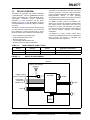
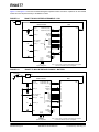
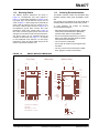
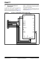
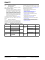
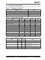
RN4677 Bluetooth® 4.0 Dual Mode Module Features Antenna • Complete, fully certified, embedded 2.4 GHz Bluetooth® version 4.0 module • Bluetooth Classic (BR/EDR) and Low Energy (LE) • Bluetooth SIG certified • On-board embedded Bluetooth stack • Transparent UART mode for seamless serial data over Bluetooth Classic uses Serial Port Profile (SPP), and Bluetooth Low Energy uses Generic Attribute (GATT) Profile. • Capability to open data connection in both Bluetooth Classic (Master) and Low Energy (Central) roles • Easy to configure with ASCII commands, PC UI utility, or PIC® MCU driver library • Firmware is upgradeable via UART • Compact surface mount module: 22 x 12 x 2.4 mm • Castellated surface mount pads for easy and reliable host PCB mounting • Environmentally friendly, RoHS compliant • Perfect for Portable Battery-Operated Devices • Internal Battery Regulator Circuitry • Worldwide regulatory certifications • Ceramic Chip Antenna (RN4677) • External Antenna Connection via RF Pad (RN4677U) Operational • • • • Single operating voltage: 3.2V to 4.3V Temperature range: -20°C to 70°C Simple, UART interface Integrated Crystal, Internal Voltage Regulator, and Matching Circuitry • Multiple I/O pins for control and status RF/Analog • Frequency: 2.402 to 2.480 GHz • Receive Sensitivity: -90 dBm (Classic); -92 dBm (LE) • Power Output: 2 dBm (typical) Data Throughput • 50 kilobytes (Classic on Android) • 8 kilobytes (LE on iOS7) Compliance • Bluetooth SIG QDID: B021961 • Modular Certified for the United States (FCC) and Canada (IC) • European R&TTE Directive Assessed Radio Module General Description The RN4677 is a fully certified Bluetooth version 4.0 (BR/EDR/LE) module, which enables the designers to easily add dual mode Bluetooth wireless capability to their products. Delivering local connectivity for the Internet of Things (IoT), the RN4677 bridges the product to Smart Phones and Tablets for convenient data transfer, control and access to cloud applications. This Bluetooth SIG certified module provides a complete wireless solution with Bluetooth stack onboard, integrated antenna, and worldwide radio certifications in a compact surface mount package, 22 x 12 x 2.4 mm. It supports GAP, SDP, SPP, and GATT profiles. Data is transferred over the Bluetooth link by sending/receiving data via transparent UART mode, making it easy to integrate with any processor or Microcontroller with a UART interface. Configuration is made easy using a ASCII commands via UART. Windows® based GUI, or PIC MCU configuration driver are also used to access configuration settings over UART. Applications • • • • • • • • • Mobile Point of Sales (mPOS) LED lighting Wearables Digital Sports Fitness Devices Health Care/Medical Automotive Accessories Home Automation Remote Control Toys MAC/Baseband/Higher Layer • Secure AES128 encryption • GAP, SDP, SPP, and GATT profiles 2015 Microchip Technology Inc. Advance Information DS50002370A-page 1 RN4677 Table of Contents 1.0 Device Overview .......................................................................................................................................................................... 3 2.0 Application Information................................................................................................................................................................11 3.0 Regulatory Approval ................................................................................................................................................................... 13 4.0 Electrical Characteristics ............................................................................................................................................................ 17 5.0 Ordering Information .................................................................................................................................................................. 19 Appendix A: Revision History............................................................................................................................................................... 21 The Microchip Web Site ....................................................................................................................................................................... 23 Customer Change Notification Service ................................................................................................................................................ 23 Customer Support ................................................................................................................................................................................ 23 Product Identification System............................................................................................................................................................... 25 TO OUR VALUED CUSTOMERS It is our intention to provide our valued customers with the best documentation possible to ensure successful use of your Microchip products. To this end, we will continue to improve our publications to better suit your needs. Our publications will be refined and enhanced as new volumes and updates are introduced. If you have any questions or comments regarding this publication, please contact the Marketing Communications Department via E-mail at [email protected]. We welcome your feedback. Most Current Data Sheet To obtain the most up-to-date version of this data sheet, please register at our Worldwide Web site at: http://www.microchip.com You can determine the version of a data sheet by examining its literature number found on the bottom outside corner of any page. The last character of the literature number is the version number, (e.g., DS30000000A is version A of document DS30000000). Errata An errata sheet, describing minor operational differences from the data sheet and recommended workarounds, may exist for current devices. As device/documentation issues become known to us, we will publish an errata sheet. The errata will specify the revision of silicon and revision of document to which it applies. To determine if an errata sheet exists for a particular device, please check with one of the following: • Microchip’s Worldwide Web site; http://www.microchip.com • Your local Microchip sales office (see last page) When contacting a sales office, please specify which device, revision of silicon and data sheet (include literature number) you are using. Customer Notification System Register on our web site at www.microchip.com to receive the most current information on all of our products. DS50002370A-page 2 Advance Information 2015 Microchip Technology Inc. RN4677 1.0 DEVICE OVERVIEW The RN4677 can independently maintain a low-power wireless connection. Low-power usage and flexible power management maximize the module's lifetime in battery-operated devices. A wide operating temperature range enables use in indoor and outdoor environments (industrial temperature range). The RN4677 is a complete, fully certified, embedded 2.4 GHz Bluetooth® version 4.0 (BR/EDR/LE) wireless module. It incorporates an on-board Bluetooth stack, cryptographic accelerator, power management subsystem, 2.4 GHz transceiver and RF power amplifier, see Figure 1-1. With the RN4677, designers can embed Bluetooth functionality rapidly into virtually any device. The RN4677 module comes in two varieties. The RN4677 is a complete, fully regulatory certified module with integral ceramic chip antenna and shield. The RN4677U is a lower cost alternative with external antenna and no shield. The integrator is responsible for the antenna, antenna matching, and regulatory certifications. The RN4677 provides cost and time-to-market savings as a self-contained module solution. The module has been designed to provide integrators with a simple Bluetooth solution that contains the following features: • • • • • The RN4677 is a small, compact, surface mount module with castellated pads for easy and reliable host PCB mounting. The module is compatible with standard pick-and-place equipment. Ease of integration and programming Vastly reduced development time Minimum system cost Interoperability with Bluetooth hosts Maximum value in a range of applications. TABLE 1-1: RN4677 MODULE FAMILY TYPES Device Antenna Shield Regulatory Certifications RN4677 Integral ceramic chip Yes FCC, IC, CE RN4677U External No CE FIGURE 1-1: RN4677 BLOCK DIAGRAM RN4677 Ceramic Chip Antenna (RN4677) Integral Ceramic Antenna (RN4677U) IS1677SM 16 MHz RF Matching Configurable Control and Indication I/O UART Power I2C 8 Kbit Serial EEPROM 2015 Microchip Technology Inc. Advance Information DS50002370A-page 3 RN4677 1.1 Interface Description Figure 1-2 shows the RN4677 pin diagram and Figure 1-3 shows the RN4677U. Table 1-2 describes the module’s pins. RN4677 PIN DIAGRAM *1' *1' *1' *1' *1' %$7B,1 6:B%71 /'2B2 9''B,2 /'2B2 :$.(83 308/'2B2 3 3 36&/ 36'$ *1' /(' 3 3 3 3 3 3 7;' 5;' 3&76 3 3576 3 3 ($1 567B1 FIGURE 1-2: FIGURE 1-3: RN4677U PIN DIAGRAM *1' %$7B,1 6:B%71 /'2B2 9''B,2 /'2B2 :$.(83 308/'2B2 3 3 36&/ 36'$ %7B5) 3&76 3 3576 3 3 ($1 567B1 *1' /(' 3 3 3 3 3 3 7;' 5;' DS50002370A-page 4 Advance Information 2015 Microchip Technology Inc. RN4677 TABLE 1-2: PIN DESCRIPTION RN4677 Pin RN4677U Pin 1 — GND Power Ground reference 2 — GND Power Ground reference Name Type Description 3 1 GND Power Ground reference 4 2 BAT_IN Power Battery input. Main positive supply input. Connect to 10 µF low ESR ceramic capacitor. 5 3 SW_BTN DI Software Button - H: Power On; L: Power Off. See Section 1.6 “Software Button (SW_BTN)”. 6 4 LDO33_O Power Internal 3.3V LDO regulator output. Connect to 10 µF low ESR ceramic capacitor. 7 5 VDD_IO Power I/O positive supply input. Ensure VDD_IO and MCU I/O voltages are compatible. 8 6 LDO18_O Power Internal 1.8V LDO regulator output. Connect to 10 µF low ESR ceramic capacitor. DI 9 7 WAKEUP 10 8 PMULDO_O Power Power management unit output. Connect to 1 µF low ESR ceramic capacitor. 11 9 P04 DO Status Indicator 2 (STATUS_IND_2). See Section 1.5 “Status Indication I/O Pins”. 12 10 P15 DO Status Indicator 1 (STATUS_IND_1). See Section 1.5 “Status Indication I/O Pins”. 13 11 P12/SCL DO I2C SCL (Do not connect) 14 12 P13/SDA DIO I2C SDA (Do not connect) 15 13 P17/CTS DIO Configurable control or indication pin or UART CTS (input) 16 14 P05 DIO Configurable control or indication pin 17 15 P00/RTS DIO Configurable control or indication pin or UART RTS (output) 18 16 P20 DI System configuration (internal pull up). See Section 1.10 “System Configuration”. 19 17 P24 DI System configuration (internal pull up). See Section 1.10 “System Configuration”. 20 18 EAN DI System configuration (internal pull down). See Section 1.10 “System Configuration”. 21 19 RST_N DI Module Reset (active-low; internal pull up). Apply a pulse of at least 63 ns. 22 20 RXD DI UART data input 23 21 TXD DO UART data output 24 22 P31 DIO Configurable control or indication pin. If configured as input; internal pull up. 25 23 P32 DIO Configurable control or indication pin. If configured as input; internal pull up. 26 24 P33 DIO Configurable control or indication pin If configured as input; internal pull up. 27 25 P34 DIO Configurable control or indication pin If configured as input; internal pull up. 28 26 P36 DIO Do not connect 29 27 P37 DIO Configurable control or indication pin (when configured as input: internal pull up) 30 28 LED1 DO Status LED. See Section 1.9 “Status LED (LED1)”. 2015 Microchip Technology Inc. Wakeup from shutdown mode (active-low; internal pull up) Advance Information DS50002370A-page 5 RN4677 TABLE 1-2: RN4677 Pin RN4677U Pin Name Type Description 31 29 GND Power Ground reference — 30 BT_RF AIO External antenna connection (50 Ohm) 32 — GND Power Ground reference 33 — GND Power Ground reference Note: 1.2 PIN DESCRIPTION (CONTINUED) Pin type abbreviation: A = Analog, D = Digital, I = Input, O = Output. Configuring the RN4677 1.4 Configuring the RN4677 features are performed using either RN-style ASCII command documented in the “RN4677 Bluetooth® Low Energy Dual Mode Module User’s Guide”. Alternatively, it is possible to configure the RN4677 using the interface as described in Section 2.2 “External Configuration and Programming”, along with either external PC configuration utility (UI Tool or EEPROM Tool), or the PIC MCU configuration library. For more information, visit www.microchip.com/rn4677. 1.3 The configurable control and indication I/O pins are P00, P05, P17, P31, P32, P33, P34 and P37. The RN4677 uses control signal as the input, whereas indication signals are the output. Table 1-3 shows configurable I/O pin assignments to the control and indication signals. Note: RTS is only assigned to P00 and CTS to P17. TABLE 1-3: UART Interface Figure 1-4 and Figure 1-5 show power and MCU interface examples. The RN4677 UART pins TXD and RXD connect to the UART pins of the host MCU. It is highly recommended to use hardware flow control pins RTS and CTS. By default, the RN4677 hardware flow control is disabled and must be configured to become enabled. The UART Baud is configurable and the available signal rates are listed in Table 4-5. DS50002370A-page 6 Control and Indication I/O Pins Pin Name P00 CONFIGURATION AND INDICATION I/O ASSIGNMENTS Default Configuration UART_RTS P05 NO_USE P17 UART_CTS P31 INQUIRY_CONFIGURE P32 LINK_DROP P33 UART_RX_IND P34 PAIRING_KEY P37 LOW_BATTERY_IND Advance Information 2015 Microchip Technology Inc. RN4677 1.5 Status Indication I/O Pins I/O pins P15 and P04 are Status Indicator 1 and 2 signals, respectively, which both provide status indication to the MCU as shown in Table 1-4. TABLE 1-4: STATUS INDICATION P04/STATUS_IND_2 P15/STATUS_IND_1 H H Power default/Shutdown state H L Access state L H Link state (no UART data being transmitted) L L Link state (UART data being transmitted) 1.6 Indication Software Button (SW_BTN) 1.10 The Software Button (SW_BTN) input pin powers the RN4677 on (high) or off (low). 1.7 To turn RN4677 into operation modes, set configuration for I/O pins P20, P24 and EAN, see Table 1-5. Both P20 and P24 have internal pull ups, whereas EAN has internal pull down. WAKE UP (WAKEUP) The Wake Up (WAKEUP) input pin wakes the RN4677 from shutdown mode (active-low). 1.8 1.11 Figure 1-5 shows an example power scheme using a 3.7V lithium-ion battery. The RN4677 has an internal 3.3V LDO regulator. Battery power is applied to BAT_IN pin. The regulated 3.3V output is on the LDO33_O pin. From the LDO33_O pin, voltage is routed to the VDD_IO pin and external circuitry including the MCU. This power scheme ensures that RN4677 and MCU I/O voltages are compatible. Status LED (LED1) The status LED (LED1) indicates: • • • • • • Standby Inquiry Link Link Back Low Battery Page CAUTION The internal 3.3V LDO current source: 50 mA maximum. Otherwise, damage to RN4677 PICtail may occur. Each indication is a configurable flashing sequence. LED brightness can also be configured. TABLE 1-5: Power Figure 1-4 shows an example power scheme using a 3.3V Low Dropout (LDO) regulator supplying 3.3 V to both the RN4677 (BAT_IN and VDD_IO) and MCU VDD. This power scheme ensures that RN4677 and MCU I/O voltages are compatible. RESET (RST_N) The Reset (RST_N) input pin resets the RN4677 (active-low pulse for at least 63 ns). 1.9 System Configuration SYSTEM CONFIGURATION SETTINGS P20 P24 EAN High High Low Low High Low Test (Write EEPROM) Low Low High Write Flash (Firmware programming) 2015 Microchip Technology Inc. Operational Mode Normal operation Advance Information DS50002370A-page 7 RN4677 Figure 1-4 and Figure 1-5 show the recommended bypass capacitor location and values. Capacitors can be low ESR ceramic and must be placed closely to the RN4677 module. FIGURE 1-4: VIN LDO RN4677 TO MCU INTERFACE EXAMPLE - LDO (3.3V) RN4677 Module BAT_IN (3.2 – 4.3V) 10uF NC P15/STATUS_IND_1 P04/STATUS_IND_2 I/O I/O SW_BTN WAKEUP RST_N I/O I/O I/O P37 P34 P33 P32 P31 P05 I/O I/O I/O I/O I/O I/O LDO33_O VDD_IO (Note 1) (2.8 – 3.63V) NC Note 2 LDO18_O MCU PMULDO_O RX TX TXD RXD P12/SCL P13/SDA P36 P20 P24 EAN LED1 NC NC NC Note: 1. Ensure VDD_IO and MCU VDD voltages are compatible. 2. Control and indication ports are configurable. System Configuration FIGURE 1-5: RN4677 TO MCU INTERFACE EXAMPLE - BATTERY Li-ion Battery (3.7V) LDO (3.3V) RN4677 Module BAT_IN (3.2 – 4.3V) 10uF I/O I/O SW_BTN WAKEUP RST_N I/O I/O I/O P37 P34 P33 P32 P31 P05 I/O I/O I/O I/O I/O I/O 10uF VDD_IO (Note 1) (2.8 – 3.63V) NC LDO18_O MCU P15/STATUS_IND_1 P04/STATUS_IND_2 LDO33_O Note 2 NC VDD Note 1 CTS RTS P00/RTS P17/CTS PMULDO_O RX TX TXD RXD P20 P24 EAN LED1 P12/SCL P13/SDA P36 System Configuration DS50002370A-page 8 Note 1 CTS RTS P00/RTS P17/CTS NC VDD NC NC NC Note: 1. Ensure VDD_IO and MCU VDD voltages are compatible. 2. Control and indication ports are configurable. Advance Information 2015 Microchip Technology Inc. RN4677 Mounting Details 1.13 The RN4677 physical dimensions are shown in Figure 1-6, recommended host PCB footprint in Figure 1-7, and mounting suggestion in Figure 1-8. No top copper layer must be near the test pin area as shown in Figure 1-7. When laying out the host PCB, the areas under the antenna must not contain any top, inner layer, or bottom copper as shown in Figure 1-8. A low-impedance ground plane ensures best radio performance (best range; lowest noise). Figure 1-8 also shows a minimum ground plane area to the left and right of the module for best antenna performance. The ground plane can be extended beyond the minimum recommended, see Figure 1-7, as required for host PCB EMC noise reduction. For best range performance, keep all external metal away from the ceramic chip antenna at least 31 mm. The module can be soldered to the host PCB using standard leaded and lead-free solder reflow profiles. To avoid damaging the module, the following recommendations are given: • Microchip Technology Application Note “AN233 Solder Reflow Recommendation” (DS00233) provides solder reflow recommendations • Do not exceed peak temperature (TP) of 250°C Refer to the solder paste data sheet for specific reflow profile recommendations • Use no-clean flux solder paste • Do not wash as moisture can be trapped under the shield • Use only one flow. If the PCB requires multiple flows, apply the module on the final flow. RN4677 MODULE DIMENSIONS %RWWRP9LHZ 6LGH9LHZ 7RS9LHZ VKLHOGPRXQWLQJKROH PP PP %RWWRP9LHZ PP 'LPHQWLRQVDUHLQPLOOLPHWHUV 7ROHUDQFHV PP PP VKLHOG PRXQWLQJ KROH The RN4677 wireless module was assembled using standard lead-free reflow profile IPC/JEDEC J-STD020. FIGURE 1-6: Soldering Recommendations 1.12 3&%2XWOLQHPP 3&%7KLFNQHVVPP PP 3DG'HWDLO 2015 Microchip Technology Inc. Advance Information DS50002370A-page 9 RN4677 FIGURE 1-7: RN4677 RECOMMENDED PCB FOOTPRINT 7RS9LHZ 7RS&RSSHU .HHS2XW$UHD PP PP PP PP FIGURE 1-8: DS50002370A-page 10 RN4677 HOST PCB MOUNTING SUGGESTION Advance Information 2015 Microchip Technology Inc. RN4677 2.0 APPLICATION INFORMATION 2.1 RN4677 Ceramic Chip Antenna The RN4677 module contains an integral ceramic chip antenna. The antenna performance on the module is shown in Figure 2-1. FIGURE 2-1: RN4677 ANTENNA RADIATION PATTERN Frequency 2015 Microchip Technology Inc. 2450 MHz Max Gain 1.63 dBi Efficiency 71.55% Advance Information DS50002370A-page 11 RN4677 2.2 External Configuration and Programming To configure the RN4677 module and program the firmware, use the external configuration and programming tool available from Microchip. Figure 2-2 shows the connections between the RN4677 and FIGURE 2-2: header J1, a standard 8-pin 0.100" (2.54 mm) spaced header. It is recommended to include this header on the host PCB for development. Configuration and firmware programming modes are entered according to the system configuration I/O pins as described in Table 1-5. EXTERNAL PROGRAMMING HEADER CONNECTIONS RN4677 Module BAT_IN GND LED1 J1 8 7 6 5 P24 GND TXD 4 3 RXD 5V_USB EAN 2 1 BAT_IN P20 NC SW_BTN P37 LDO33_O VDD_IO LDO18_O P36 WAKEUP P33 PMULDO_O P32 P04 P15 P31 P34 DS50002370A-page 12 Advance Information RST_N P20 P24 EAN RTS/P00 TXD RXD P05 CTS/P17 P12/SCL P13/SDA 2015 Microchip Technology Inc. RN4677 3.0 REGULATORY APPROVAL This section outlines the regulatory information for the RN4677 module for the following countries: • United States • Canada • Europe 3.1 United States The RN4677 module has received Federal Communications Commission (FCC) CFR47 Telecommunications, Part 15 Subpart C “Intentional Radiators” modular approval in accordance with Part 15.212 Modular Transmitter approval. Modular approval allows the end user to integrate the RN4677 module into a finished product without obtaining subsequent and separate FCC approvals for intentional radiation, provided no changes or modifications are made to the module circuitry. Changes or modifications could void the user's authority to operate the equipment. The end user must comply with all of the instructions provided by the Grantee, which indicate installation and/or operating conditions necessary for compliance. The finished product is required to comply with all applicable FCC equipment authorizations regulations, requirements and equipment functions not associated with the transmitter module portion. For example, compliance must be demonstrated to regulations for other transmitter components within the host product; to requirements for unintentional radiators (Part 15 Subpart B “Unintentional Radiators”), such as digital devices, computer peripherals, radio receivers, etc.; and to additional authorization requirements for the non-transmitter functions on the transmitter module (i.e., Verification, or Declaration of Conformity) (e.g., transmitter modules may also contain digital logic functions) as appropriate. 3.1.1 LABELING AND USER INFORMATION REQUIREMENTS The RN4677 module has been labeled with its own FCC ID number, and if the FCC ID is not visible when the module is installed inside another device, then the outside of the finished product into which the module is installed must also display a label referring to the enclosed module. This exterior label can use wording as follows: Contains Transmitter Module FCC ID: A8TBM77SPPSYC2A or Contains FCC ID: A8TBM77SPPSYC2A This device complies with Part 15 of the FCC Rules. Operation is subject to the following two conditions: (1) this device may not cause harmful interference, and (2) this device must accept any interference received, including interference that may cause undesired operation. A user's manual for the finished product should include the following statement: This equipment has been tested and found to comply with the limits for a Class B digital device, pursuant to part 15 of the FCC Rules. These limits are designed to provide reasonable protection against harmful interference in a residential installation. This equipment generates, uses and can radiate radio frequency energy, and if not installed and used in accordance with the instructions, may cause harmful interference to radio communications. However, there is no guarantee that interference will not occur in a particular installation. If this equipment does cause harmful interference to radio or television reception, which can be determined by turning the equipment off and on, the user is encouraged to try to correct the interference by one or more of the following measures: • Reorient or relocate the receiving antenna. • Increase the separation between the equipment and receiver. • Connect the equipment into an outlet on a circuit different from that to which the receiver is connected. • Consult the dealer or an experienced radio/TV technician for help. Additional information on labeling and user information requirements for Part 15 devices can be found in KDB Publication 784748 available at the FCC Office of Engineering and Technology (OET) Laboratory Division Knowledge Database (KDB) https:// apps.fcc.gov/oetcf/kdb/index.cfm 2015 Microchip Technology Inc. Advance Information DS50002370A-page 13 RN4677 3.1.2 RF EXPOSURE All transmitters regulated by FCC must comply with RF exposure requirements. KDB 447498 General RF Exposure Guidance provides guidance in determining whether proposed or existing transmitting facilities, operations or devices comply with limits for human exposure to Radio Frequency (RF) fields adopted by the Federal Communications Commission (FCC). From the RN4677 FCC Grant: Output power listed is conducted. This grant is valid only when the module is sold to OEM integrators and must be installed by the OEM or OEM integrators. This transmitter is restricted for use with the specific antenna(s) tested in this application for Certification and must not be co-located or operating in conjunction with any other antenna or transmitters within a host device, except in accordance with FCC multi-transmitter product procedures. 3.1.3 HELPFUL WEB SITES Federal Communications Commission (FCC): http:// www.fcc.gov FCC Office of Engineering and Technology (OET) Laboratory Division Knowledge Database (KDB): https://apps.fcc.gov/oetcf/kdb/index.cfm 3.2 Canada The RN4677 module has been certified for use in Canada under Industry Canada (IC) Radio Standards Specification (RSS) RSS-210 and RSS-Gen. Modular approval permits the installation of a module in a host device without the need to recertify the device. 3.2.1 LABELING AND USER INFORMATION REQUIREMENTS Labeling Requirements for the Host Device (from Section 3.2.1, RSS-Gen, Issue 3, December 2010): The host device shall be properly labeled to identify the module within the host device. The Industry Canada certification label of a module shall be clearly visible at all times when installed in the host device, otherwise the host device must be labeled to display the Industry Canada certification number of the module, preceded by the words “Contains transmitter module”, or the word “Contains”, or similar wording expressing the same meaning, as follows: radio apparatus shall contain the following or equivalent notice in a conspicuous location in the user manual or alternatively on the device or both: This device complies with Industry Canada licenseexempt RSS standard(s). Operation is subject to the following two conditions: (1) this device may not cause interference, and (2) this device must accept any interference, including interference that may cause undesired operation of the device. Le présent appareil est conforme aux CNR d'Industrie Canada applicables aux appareils radio exempts de licence. L'exploitation est autorisée aux deux conditions suivantes: (1) l'appareil ne doit pas produire de brouillage, et (2) l'utilisateur de l'appareil doit accepter tout brouillage radioélectrique subi, même si le brouillage est susceptible d'en compromettre le fonctionnement. Transmitter Antenna (from Section 7.1.2 RSS-Gen, Issue 3, December 2010): User manuals for transmitters shall display the following notice in a conspicuous location: Under Industry Canada regulations, this radio transmitter may only operate using an antenna of a type and maximum (or lesser) gain approved for the transmitter by Industry Canada. To reduce potential radio interference to other users, the antenna type and its gain should be so chosen that the equivalent isotropically radiated power (e.i.r.p.) is not more than that necessary for successful communication. Conformément à la réglementation d'Industrie Canada, le présent émetteur radio peut fonctionner avec une antenne d'un type et d'un gain maximal (ou inférieur) approuvé pour l'émetteur par Industrie Canada. Dans le but de réduire les risques de brouillage radioélectrique à l'intention des autres utilisateurs, il faut choisir le type d'antenne et son gain de sorte que la puissance isotrope rayonnée équivalente (p.i.r.e.) ne dépasse pas l'intensité nécessaire à l'établissement d'une communication satisfaisante. The above notice may be affixed to the device instead of displayed in the user manual. Contains transmitter module IC: 12246A-BM77SPPSYC2. User Manual Notice for License-Exempt Radio Apparatus (from Section 7.1.3 RSS-Gen, Issue 3, December 2010): User manuals for license-exempt DS50002370A-page 14 Advance Information 2015 Microchip Technology Inc. RN4677 User manuals for transmitters equipped with detachable antennas shall also contain the following notice in a conspicuous location: This radio transmitter (identify the device by certification number, or model number if Category II) has been approved by Industry Canada to operate with the antenna types listed below with the maximum permissible gain and required antenna impedance for each antenna type indicated. Antenna types not included in this list, having a gain greater than the maximum gain indicated for that type, are strictly prohibited for use with this device. Conformément à la réglementation d'Industrie Canada, le présent émetteur radio peut fonctionner avec une antenne d'un type et d'un gain maximal (ou inférieur) approuvé pour l'émetteur par Industrie Canada. Dans le but de réduire les risques de brouillage radioélectrique à l'intention des autres utilisateurs, il faut choisir le type d'antenne et son gain de sorte que la puissance isotrope rayonnée équivalente (p.i.r.e.) ne dépasse pas l'intensité nécessaire à l'établissement d'une communication satisfaisante. Immediately following the above notice, the manufacturer shall provide a list of all antenna types approved for use with the transmitter, indicating the maximum permissible antenna gain (in dBi) and required impedance for each. 3.2.2 than 10 milliwatts, the total antenna gain shall be added to the measured RF output power to demonstrate compliance to the specified radiated power limits. 3.2.4 HELPFUL WEB SITES Industry Canada: http://www.ic.gc.ca/ 3.3 Europe The RN4677 module is an R&TTE Directive assessed radio module that is CE marked and has been manufactured and tested with the intention of being integrated into a final product. The RN4677 module has been tested to R&TTE Directive 1999/5/EC Essential Requirements for Health and Safety (Article (3.1(a)), Electromagnetic Compatibility (EMC) (Article 3.1(b)), and Radio (Article 3.2) and are summarized in Table 3-1: European Compliance Testing. A Notified Body Opinion has also been issued. All test reports are available on the product web page at http://www.microchip.com. The R&TTE Compliance Association provides guidance on modular devices in document Technical Guidance Note 01 available at http://www.rtteca.com/html/download_area.htm. Note: RF EXPOSURE All transmitters regulated by IC must comply with RF exposure requirements listed in RSS-102 - Radio Frequency (RF) Exposure Compliance of Radiocommunication Apparatus (All Frequency Bands). 3.2.3 APPROVED EXTERNAL ANTENNA TYPES Transmitter Antenna (from Section 7.1.2 RSS-Gen, Issue 3, December 2010): The RN4677U module can only be sold or operated with antennas with which it was approved. Transmitter may be approved with multiple antenna types. An antenna type comprises antennas having similar inband and out-of-band radiation patterns. Testing shall be performed using the highest gain antenna of each combination of transmitter and antenna type for which approval is being sought, with the transmitter output power set at the maximum level. Any antenna of the same type having equal or lesser gain as an antenna that had been successfully tested with the transmitter, will also be considered approved with the transmitter, and may be used and marketed with the transmitter. 3.3.1 To maintain conformance to the testing listed in Table 3-1: European Compliance Testing, the module shall be installed in accordance with the installation instructions in this data sheet and shall not be modified. When integrating a radio module into a completed product the integrator becomes the manufacturer of the final product and is therefore responsible for demonstrating compliance of the final product with the essential requirements of the R&TTE Directive. LABELING AND USER INFORMATION REQUIREMENTS The label on the final product which contains the RN4677 module must follow CE marking requirements. The “R&TTE Compliance Association Technical Guidance Note 01” provides guidance on final product CE marking. When a measurement at the antenna connector is used to determine RF output power, the effective gain of the device's antenna shall be stated, based on measurement or on data from the antenna manufacturer. For transmitters of output power greater 2015 Microchip Technology Inc. Advance Information DS50002370A-page 15 RN4677 3.3.2 EXTERNAL ANTENNA REQUIREMENTS From R&TTE Compliance Association document Technical Guidance Note 01: Provided the integrator installing an assessed radio module with an integral or specific antenna and installed in conformance with the radio module manufacturer's installation instructions requires no further evaluation under Article 3.2 of the R&TTE Directive and does not require further involvement of an R&TTE Directive Notified Body for the final product. [Section 2.2.4] The European Compliance Testing listed in Table 3-1 was performed using the integral ceramic chip antenna. 3.3.3 HELPFUL WEB SITES A document that can be used as a starting point in understanding the use of Short Range Devices (SRD) in Europe is the European Radio Communications TABLE 3-1: Additional helpful web sites are: • Radio and Telecommunications Terminal Equipment (R&TTE): http://ec.europa.eu/enterprise/sectors/rtte/ regulatory-framework/index_en.htm • European Conference of Postal and Telecommunications Administrations (CEPT): http://www.cept.org • European Telecommunications Standards Institute (ETSI): http://www.etsi.org • European Radio Communications Office (ERO): http://www.ero.dk/ • The Radio and Telecommunications Terminal Equipment Compliance Association (R&TTE CA): http://www.rtteca.com/ EUROPEAN COMPLIANCE TESTING Certification Standards Article Safety EN 60950-1:2006 [3.1(a)] +A11:2009+A1:2010+A12:2011 Health EN 62479:2010, A.3. EMC Committee (ERC) Recommendation 70-03 E, which can be downloaded from the European Radio Communications Office (ERO) at: http://www.ero.dk/. EN 301 489-1 V1.9.2 Laboratory Report Number TUV Rhein- 10049470 001 land Date 2015-01-09 10047932 001 (FHSS-BT) 2014-09-17 10047939 001 (DTS) [3.1(b)] 10046663 001 2015-01-12 (3.2) 10047932 001 (FHSS-BT) 2014-09-17 10047939 001 (DTS) EN 301 489-17 V 2.2.1 Radio EN 300 328 V1.8.1 Notified Body Opinion DS50002370A-page 16 0197 TUV Rhein- 10048878 001 land Advance Information 2015-02-05 2015 Microchip Technology Inc. RN4677 4.0 ELECTRICAL CHARACTERISTICS Table 4-1 and Table 4-2 show the environmental conditions and the electrical characteristics of the module. Table 4-3 and Table 4-4 provide the supply consumption of the module. TABLE 4-1: ENVIRONMENTAL CONDITIONS Parameter Value Temperature Range (Operating) -20°C to 70°C Temperature Range (Storage) -30°C to 85°C Relative Humidity (Operating) 10% to 90% Relative Humidity (Storage) 10% to 90% Moisture Sensitivity Level TABLE 4-2: 2 ELECTRICAL CHARACTERISTICS Parameter Min. Typ. Max. Units Supply Voltage (BAT_IN) 3.2 — 4.3 V I/O Supply Voltage (VDD_IO) 2.8 3.3 3.63 V I/O Voltage Levels VIL Input Logic Levels Low -0.3 — 0.8 V VIH Input Logic Levels High 2.0 — 3.6 V — 0.4 V 2.4 — — V — 1.6 — V Pull-up Resistor — 65 — KOhm Leakage Current -10 — 10 µA TX mode — — 70 mA RX mode — — 70 mA VOL Output Logic Levels Low VOH Output Logic Levels High RESET VTH Threshold Voltage Input and Tri-State Current Supply Current SUPPLY CONSUMPTION-CLASSIC(1) TABLE 4-3: Parameter Current (avg.) Units Notes Standby mode 2.543 mA — Deep Power-Down mode 0.343 mA — Connected + Sniff, Master (No data) 0.858 mA No data was transmitted Sniff interval = 500 ms Connected + Sniff, Slave (No data) 0.864 mA No data was transmitted Sniff interval = 500 ms Data, Master 23.03 mA Data transmitted at 115200 bps; block size = 500 Data, Slave 25.597 mA Data transmitted at 115200 bps; block size = 500 Note 1: Classic BR/EDR, RX_IND Function Enabled 2015 Microchip Technology Inc. Advance Information DS50002370A-page 17 RN4677 TABLE 4-4: SUPPLY CONSUMPTION-LOW ENERGY(1) Current (avg.) Units Notes Standby mode (Discoverable and Connectable mode) 1.237 mA LE fast advertising interval = 160 ms, standby at 0 ~ 30 sec Standby mode (Discoverable and Connectable mode) 0.765 mA LE Reduced Power advertising interval = 961 ms, standby after 30 sec Deep Power-Down mode 0.348 mA — Connected (No data), connection interval = 500 ms 0.679 mA No data was transmitted connection interval = 500 ms, latency = 2 Connected (Transfer data), connection interval = 500 ms 13.073 mA Connection interval = 500 ms, latency = 2 Connected (No data), connection interval = 20 ms 1.648 mA No data was transmitted connection interval = 20 ms, latency = 2 Connected (Transfer data), connection interval = 20 ms 18.581 mA Connection interval = 20 ms, latency = 2 Parameter Note 1: Low Energy, RX_IND Function Enabled Table 4-5 shows the UART Baud. TABLE 4-5: UART BAUD Baud Crystal Frequency (MHz) Actual Baud Error Rate (%) 921600 16 941176 2.12 460800 16 457143 -0.79 307200 16 307692 0.16 230400 16 231884 0.64 115200 16 117647 2.1 57600 16 57145 -0.97 38400 16 38462 0.16 28800 16 28623 -0.62 19200 16 19231 0.16 14400 16 14480 0.55 9600 16 9615 0.16 4800 16 4808 0.16 2400 16 2399 -0.03 DS50002370A-page 18 Advance Information 2015 Microchip Technology Inc. RN4677 5.0 ORDERING INFORMATION Table 5-1 provides ordering information for the RN4677 module. TABLE 5-1: ORDERING INFORMATION Part Number Description RN4677-V/RM Bluetooth® 4.0 Dual Mode, Class 2, Surface Mount module with integral antenna, with shield RN4677U-V/RM Bluetooth® 4.0 Dual Mode, Class 2, Surface Mount module, external antenna, no shield RN-4677-PICtail PICtail™/PICtail Plus Daughter Board for 8, 16, 32-bit PIC® MCU Explorer Development Board Note: For custom applications, contact Microchip representative. Go to http://www.microchip.com for current pricing and a list of distributors carrying Microchip products. 2015 Microchip Technology Inc. Advance Information DS50002370A-page 19 RN4677 NOTES: DS50002370A-page 20 Advance Information 2015 Microchip Technology Inc. RN4677 APPENDIX A: REVISION HISTORY Revision A (May 2015) This is the initial release of this document. 2015 Microchip Technology Inc. Advance Information DS00000A-page 21 RN4677 NOTES: DS00000A-page 22 Advance Information 2015 Microchip Technology Inc. RN4677 THE MICROCHIP WEB SITE CUSTOMER SUPPORT Microchip provides online support via our WWW site at www.microchip.com. This web site is used as a means to make files and information easily available to customers. Accessible by using your favorite Internet browser, the web site contains the following information: Users of Microchip products can receive assistance through several channels: • Product Support – Data sheets and errata, application notes and sample programs, design resources, user’s guides and hardware support documents, latest software releases and archived software • General Technical Support – Frequently Asked Questions (FAQ), technical support requests, online discussion groups, Microchip consultant program member listing • Business of Microchip – Product selector and ordering guides, latest Microchip press releases, listing of seminars and events, listings of Microchip sales offices, distributors and factory representatives • • • • Distributor or Representative Local Sales Office Field Application Engineer (FAE) Technical Support Customers should contact their distributor, representative or Field Application Engineer (FAE) for support. Local sales offices are also available to help customers. A listing of sales offices and locations is included in the back of this document. Technical support is available through the web site at: http://microchip.com/support CUSTOMER CHANGE NOTIFICATION SERVICE Microchip’s customer notification service helps keep customers current on Microchip products. Subscribers will receive e-mail notification whenever there are changes, updates, revisions or errata related to a specified product family or development tool of interest. To register, access the Microchip web site at www.microchip.com. Under “Support”, click on “Customer Change Notification” and follow the registration instructions. 2015 Microchip Technology Inc. DS50002370A-page 23 RN4677 NOTES: DS50002370A-page 24 2015 Microchip Technology Inc. RN4677 PRODUCT IDENTIFICATION SYSTEM To order or obtain information, e.g., on pricing or delivery, refer to the factory or the listed sales office. PART NO. I RM XXX Device Temperature Range Package Device: RN4677: Integral Ceramic Chip Antenna RN4677U External Antenna Connection Temperature Range: V = -20C to +70C Package: RM = 2015 Microchip Technology Inc. Firmware Revision Number Examples: RN4677-V/RM Radio Module Advance Information DS50002370A-page 25 RN4677 NOTES: DS50002370A-page 26 Advance Information 2015 Microchip Technology Inc. Note the following details of the code protection feature on Microchip devices: • Microchip products meet the specification contained in their particular Microchip Data Sheet. • Microchip believes that its family of products is one of the most secure families of its kind on the market today, when used in the intended manner and under normal conditions. • There are dishonest and possibly illegal methods used to breach the code protection feature. All of these methods, to our knowledge, require using the Microchip products in a manner outside the operating specifications contained in Microchip’s Data Sheets. Most likely, the person doing so is engaged in theft of intellectual property. • Microchip is willing to work with the customer who is concerned about the integrity of their code. • Neither Microchip nor any other semiconductor manufacturer can guarantee the security of their code. Code protection does not mean that we are guaranteeing the product as “unbreakable.” Code protection is constantly evolving. We at Microchip are committed to continuously improving the code protection features of our products. Attempts to break Microchip’s code protection feature may be a violation of the Digital Millennium Copyright Act. If such acts allow unauthorized access to your software or other copyrighted work, you may have a right to sue for relief under that Act. Information contained in this publication regarding device applications and the like is provided only for your convenience and may be superseded by updates. It is your responsibility to ensure that your application meets with your specifications. MICROCHIP MAKES NO REPRESENTATIONS OR WARRANTIES OF ANY KIND WHETHER EXPRESS OR IMPLIED, WRITTEN OR ORAL, STATUTORY OR OTHERWISE, RELATED TO THE INFORMATION, INCLUDING BUT NOT LIMITED TO ITS CONDITION, QUALITY, PERFORMANCE, MERCHANTABILITY OR FITNESS FOR PURPOSE. Microchip disclaims all liability arising from this information and its use. Use of Microchip devices in life support and/or safety applications is entirely at the buyer’s risk, and the buyer agrees to defend, indemnify and hold harmless Microchip from any and all damages, claims, suits, or expenses resulting from such use. No licenses are conveyed, implicitly or otherwise, under any Microchip intellectual property rights. Trademarks The Microchip name and logo, the Microchip logo, dsPIC, FlashFlex, flexPWR, JukeBlox, KEELOQ, KEELOQ logo, Kleer, LANCheck, MediaLB, MOST, MOST logo, MPLAB, OptoLyzer, PIC, PICSTART, PIC32 logo, RightTouch, SpyNIC, SST, SST Logo, SuperFlash and UNI/O are registered trademarks of Microchip Technology Incorporated in the U.S.A. and other countries. The Embedded Control Solutions Company and mTouch are registered trademarks of Microchip Technology Incorporated in the U.S.A. Analog-for-the-Digital Age, BodyCom, chipKIT, chipKIT logo, CodeGuard, dsPICDEM, dsPICDEM.net, ECAN, In-Circuit Serial Programming, ICSP, Inter-Chip Connectivity, KleerNet, KleerNet logo, MiWi, MPASM, MPF, MPLAB Certified logo, MPLIB, MPLINK, MultiTRAK, NetDetach, Omniscient Code Generation, PICDEM, PICDEM.net, PICkit, PICtail, RightTouch logo, REAL ICE, SQI, Serial Quad I/O, Total Endurance, TSHARC, USBCheck, VariSense, ViewSpan, WiperLock, Wireless DNA, and ZENA are trademarks of Microchip Technology Incorporated in the U.S.A. and other countries. SQTP is a service mark of Microchip Technology Incorporated in the U.S.A. Silicon Storage Technology is a registered trademark of Microchip Technology Inc. in other countries. GestIC is a registered trademarks of Microchip Technology Germany II GmbH & Co. KG, a subsidiary of Microchip Technology Inc., in other countries. All other trademarks mentioned herein are property of their respective companies. © 2015, Microchip Technology Incorporated, Printed in the U.S.A., All Rights Reserved. ISBN: 978-1-63277-382-1 QUALITYMANAGEMENTSYSTEM CERTIFIEDBYDNV == ISO/TS16949== 2015 Microchip Technology Inc. Microchip received ISO/TS-16949:2009 certification for its worldwide headquarters, design and wafer fabrication facilities in Chandler and Tempe, Arizona; Gresham, Oregon and design centers in California and India. The Company’s quality system processes and procedures are for its PIC® MCUs and dsPIC® DSCs, KEELOQ® code hopping devices, Serial EEPROMs, microperipherals, nonvolatile memory and analog products. In addition, Microchip’s quality system for the design and manufacture of development systems is ISO 9001:2000 certified. Advance Information DS50002370A-page 27 Worldwide Sales and Service AMERICAS ASIA/PACIFIC ASIA/PACIFIC EUROPE Corporate Office 2355 West Chandler Blvd. Chandler, AZ 85224-6199 Tel: 480-792-7200 Fax: 480-792-7277 Technical Support: http://www.microchip.com/ support Web Address: www.microchip.com Asia Pacific Office Suites 3707-14, 37th Floor Tower 6, The Gateway Harbour City, Kowloon China - Xiamen Tel: 86-592-2388138 Fax: 86-592-2388130 Austria - Wels Tel: 43-7242-2244-39 Fax: 43-7242-2244-393 China - Zhuhai Tel: 86-756-3210040 Fax: 86-756-3210049 Denmark - Copenhagen Tel: 45-4450-2828 Fax: 45-4485-2829 India - Bangalore Tel: 91-80-3090-4444 Fax: 91-80-3090-4123 France - Paris Tel: 33-1-69-53-63-20 Fax: 33-1-69-30-90-79 India - New Delhi Tel: 91-11-4160-8631 Fax: 91-11-4160-8632 Germany - Dusseldorf Tel: 49-2129-3766400 Atlanta Duluth, GA Tel: 678-957-9614 Fax: 678-957-1455 Hong Kong Tel: 852-2943-5100 Fax: 852-2401-3431 Australia - Sydney Tel: 61-2-9868-6733 Fax: 61-2-9868-6755 China - Beijing Tel: 86-10-8569-7000 Fax: 86-10-8528-2104 Austin, TX Tel: 512-257-3370 China - Chengdu Tel: 86-28-8665-5511 Fax: 86-28-8665-7889 Boston Westborough, MA Tel: 774-760-0087 Fax: 774-760-0088 China - Chongqing Tel: 86-23-8980-9588 Fax: 86-23-8980-9500 Chicago Itasca, IL Tel: 630-285-0071 Fax: 630-285-0075 Cleveland Independence, OH Tel: 216-447-0464 Fax: 216-447-0643 Dallas Addison, TX Tel: 972-818-7423 Fax: 972-818-2924 Detroit Novi, MI Tel: 248-848-4000 Houston, TX Tel: 281-894-5983 Indianapolis Noblesville, IN Tel: 317-773-8323 Fax: 317-773-5453 Los Angeles Mission Viejo, CA Tel: 949-462-9523 Fax: 949-462-9608 New York, NY Tel: 631-435-6000 San Jose, CA Tel: 408-735-9110 Canada - Toronto Tel: 905-673-0699 Fax: 905-673-6509 China - Dongguan Tel: 86-769-8702-9880 China - Hangzhou Tel: 86-571-8792-8115 Fax: 86-571-8792-8116 India - Pune Tel: 91-20-3019-1500 Japan - Osaka Tel: 81-6-6152-7160 Fax: 81-6-6152-9310 Japan - Tokyo Tel: 81-3-6880- 3770 Fax: 81-3-6880-3771 Korea - Daegu Tel: 82-53-744-4301 Fax: 82-53-744-4302 China - Hong Kong SAR Tel: 852-2943-5100 Fax: 852-2401-3431 Korea - Seoul Tel: 82-2-554-7200 Fax: 82-2-558-5932 or 82-2-558-5934 China - Nanjing Tel: 86-25-8473-2460 Fax: 86-25-8473-2470 Malaysia - Kuala Lumpur Tel: 60-3-6201-9857 Fax: 60-3-6201-9859 China - Qingdao Tel: 86-532-8502-7355 Fax: 86-532-8502-7205 Malaysia - Penang Tel: 60-4-227-8870 Fax: 60-4-227-4068 China - Shanghai Tel: 86-21-5407-5533 Fax: 86-21-5407-5066 Philippines - Manila Tel: 63-2-634-9065 Fax: 63-2-634-9069 China - Shenyang Tel: 86-24-2334-2829 Fax: 86-24-2334-2393 Singapore Tel: 65-6334-8870 Fax: 65-6334-8850 China - Shenzhen Tel: 86-755-8864-2200 Fax: 86-755-8203-1760 Taiwan - Hsin Chu Tel: 886-3-5778-366 Fax: 886-3-5770-955 China - Wuhan Tel: 86-27-5980-5300 Fax: 86-27-5980-5118 Taiwan - Kaohsiung Tel: 886-7-213-7828 China - Xian Tel: 86-29-8833-7252 Fax: 86-29-8833-7256 Germany - Munich Tel: 49-89-627-144-0 Fax: 49-89-627-144-44 Germany - Pforzheim Tel: 49-7231-424750 Italy - Milan Tel: 39-0331-742611 Fax: 39-0331-466781 Italy - Venice Tel: 39-049-7625286 Netherlands - Drunen Tel: 31-416-690399 Fax: 31-416-690340 Poland - Warsaw Tel: 48-22-3325737 Spain - Madrid Tel: 34-91-708-08-90 Fax: 34-91-708-08-91 Sweden - Stockholm Tel: 46-8-5090-4654 UK - Wokingham Tel: 44-118-921-5800 Fax: 44-118-921-5820 Taiwan - Taipei Tel: 886-2-2508-8600 Fax: 886-2-2508-0102 Thailand - Bangkok Tel: 66-2-694-1351 Fax: 66-2-694-1350 01/27/15 DS50002370A-page 28 2015 Microchip Technology Inc.