1
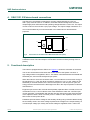
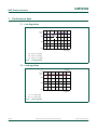
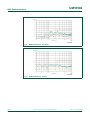
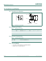
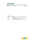
UM10582 SSL21151 5 W universal non-dimmable flyback GU10 demo board Rev. 1 — 11 December 2012 User manual Document information Info Content Keywords SSL21151, SSL21151DB1090, LED Driver, LED retrofit lamp, universal input, isolated, primary sensing Abstract This user manual describes the operation of an SSL21151 5 W universal non-dimmable flyback GU10 demo board UM10582 NXP Semiconductors SSL21151 5 W universal non-dimmable flyback demo board Revision history Rev Date Description v.1 20121211 first issue Contact information For more information, please visit: http://www.nxp.com For sales office addresses, please send an email to: [email protected] UM10582 User manual All information provided in this document is subject to legal disclaimers. Rev. 1 — 11 December 2012 © NXP B.V. 2012. All rights reserved. 2 of 15 UM10582 NXP Semiconductors SSL21151 5 W universal non-dimmable flyback demo board 1. Introduction This user manual describes the performance, technical data and connection of the SSL21151 5 W universal non-dim flyback GU10 demo board. The SSL2115x series is an NXP Semiconductors driver IC intended to provide a low cost, small form factor LED driver. This board is designed for universal mains input operation. UM10582 User manual Fig 1. SSL21151 5 W demo board (front view) Fig 2. SSL21151 5 W demo board (back view) All information provided in this document is subject to legal disclaimers. Rev. 1 — 11 December 2012 © NXP B.V. 2012. All rights reserved. 3 of 15 UM10582 NXP Semiconductors SSL21151 5 W universal non-dimmable flyback demo board 2. Safety Warning This board is connected to the mains voltage. Avoid touching the board while it is connected to the mains voltage. An isolated housing is mandatory when used in uncontrolled, non-laboratory environments. Galvanic isolation of the mains phase using a variable transformer is always recommended. 019aab174 019aab173 a. isolated Fig 3. b. non-isolated Variable transformer isolation symbols 3. Specifications Table 1. Specifications for the SSL21151 5 W demo board Symbol Parameter Value Vmains mains input voltage 85 V (AC) to 265 V (AC); 50 Hz or 60 Hz fmains mains input frequency 50 Hz or 60 Hz VO(LED) LED output voltage 6 V (DC) to 12 V (DC) IO(LED) LED output current 310 mA (typical) VO(ovp) overvoltage protection output voltage 14 V (DC) at R9 = 10 k IO(LED)/Vmains line regulation 4 % at input voltage between 85 V (AC) and 265 V (AC) IO(LED)/VO(LED) load regulation 2 % at output voltage between 6 V (DC) and 12 V (DC) Iripple current ripple 15 % Po(max) maximum output power 4W efficiency 80 % at Vmains = 230 V (AC) and 12 V (DC) output voltage at Tamb = 30 C PF Power Factor >0.5 at 230 V (AC) input voltage fSW switching frequency 25 kHz to 48 kHz at output voltage between 6 V (DC) and 12 V (DC) Toper operating temperature 20 C to +105 °C ambient PCB size (L W H) 30 mm 18 mm 20 mm Remark: EMC Compliance - FCC15 CE/RE and EN55015 CE/RE UM10582 User manual All information provided in this document is subject to legal disclaimers. Rev. 1 — 11 December 2012 © NXP B.V. 2012. All rights reserved. 4 of 15 UM10582 NXP Semiconductors SSL21151 5 W universal non-dimmable flyback demo board 4. SSL21151 5 W demo board connections The SSL21151 5 W board is optimized for a mains supply between 85 V (AC) to 265 V (AC) at 50 Hz to 60 Hz. In addition, the board has been designed to work with multiple high-power LEDs with a total operating voltage between 6 V and 12 V. The output current is set to 310 mA at 230 V (AC) input voltage. The output voltage is limited to 14 V. It is recommended that you mount the board in an isolated box for demonstration purposes. /(' 1 / /(' DDD Fig 4. Connection to the SSL21151 5 W demo board front (view) If a galvanic isolated transformer is used, place it between the AC source and the evaluation board. The board output is connected to a series of LEDs (a string of 2 to 4 pieces). 5. Functional description The board is equipped with the SSL21151. Figure 11, shows the schematic of the board. The IC has several internal functions that control and drive the flyback converter. A high-voltage switch is integrated in the IC. This switch is situated between the DRAIN and SOURCE pins, and controls the flyback input power. When this switch is set to the conductive state, a current starts to run that stores energy in the transformer T1. If the duty factor exceeds a maximum of 75 %, or the voltage on the SOURCE pin exceeds 0.555 V, this current is interrupted. In the next part of cycle, the energy stored in the transformer is discharged over D4 in the output capacitor C6 and the load absorbs it. Equip the input circuit of the converter with a partially capacitive filter. This filter, which is a combination of C2, L2 and C7 blocks most of the disturbance which the converter input current generates. The drawback with this filter is that it reduces the power factor because of the capacitive load. A lower converter power in relation to the capacitive value of this filter causes a lower power factor. Feedback input senses the voltage on the auxiliary winding using a resistive divider during the secondary stroke. The sense voltage represents the voltage on the output winding. At no-load output voltage (CV mode), the sensed voltage is regulated at 2.5 V. When the UM10582 User manual All information provided in this document is subject to legal disclaimers. Rev. 1 — 11 December 2012 © NXP B.V. 2012. All rights reserved. 5 of 15 UM10582 NXP Semiconductors SSL21151 5 W universal non-dimmable flyback demo board sensed voltage (at high-load) drops below 2.5 V, the regulation changes to Constant Current (CC) mode. The overvoltage protection (OVP latch) level on the SENSE pin is 3.2 V. 5.1 VCC supply The charging current flows from the high-voltage DRAIN pin via an internal start-up current source to the VCC pin. The IC starts switching when the voltage on the VCC pin (VCC) exceeds the start-up level of 19 V (maximum). After start-up, an auxiliary winding connection provides an external supply. Design the voltage of the auxiliary winding to ensure that VCC has a minimum value of 9.5 V (maximum UVLO). When VCC drops below the VCC(UVLO) level of 8.5 V (typical), the IC stops switching and is reset. When VCC is above 35 V, a leakage current occurs. Never apply a VCC above 35 V. If an open-circuit occurs on the LEDs, the output voltage increases at each cycle of the AC/DC converter. Energy is no longer transferred to the LEDs. The energy accumulated at the primary side is transferred to the supply of the IC using the auxiliary winding. On this demo board, a small pre-load R9 provides a proper working application. The output voltage is regulated at 14 V while the LEDs are being disconnected. Use IC internal overtemperature protection in this board. The OTP threshold temperature is 150 C (typical) and the OTP trip hysteresis temperature is 50 C. An external temperature-dependent resistor can be applied for LED OTP. To provide this OTP, place an NTC between the SENSE and GND pins (not implemented on this board). 6. System Optimization The following modifications can be made to meet application specifications. 6.1 Change the output ripple current The LED voltage, the LED dynamic resistance and the output capacitor determine the output current ripple. The current value of C6 is chosen to optimize capacitor size with light output. A ripple of 15 % results in an expected deterioration of light output <1 % (M. Weiland 28-07-2006). The size for the buffer capacitor can be estimated from the following equation: I O LED 1 C6 = ----------------------- --------------------------------------------I 6 f mains R dyn (1) When using a series of LEDs, the dynamic resistance of each LED can be added to the total dynamic resistance. fmains is the AC mains frequency using 50 Hz or 60 Hz. 6.2 Change the output current The power component and transformer train are dimensioned for output currents up to 350 mA, but losses increase as the current increases. Resistor R6 limits the primary peak current and thus maximum output power. The output current can be set by varying the value of R6. R6 can be estimated using the following equations: UM10582 User manual All information provided in this document is subject to legal disclaimers. Rev. 1 — 11 December 2012 © NXP B.V. 2012. All rights reserved. 6 of 15 UM10582 NXP Semiconductors SSL21151 5 W universal non-dimmable flyback demo board I L pri = V ref high pk R6 (2) Where Vref(high)pk = 0.555 V. I LED U max L = -----------------------------------------------------------------------------------0.85 f sw high 0.5 I pk 2 (3) Where: • is the efficiency of converter • fsw(high) is the high switching frequency • Umax is the maximum combined voltage of the connected LEDs and the voltage drop of the output rectifier • L is the the primary inductance of the flyback transformer • Ipk is the peak current of the primary side in the flyback transformer • ILED is the output LED current 6.3 High accuracy design recommendations • Good coupling of auxiliary winding and secondary winding Np1 : Ns : Nf : Np2 • Use 1 % (or better) devices for resistors connected to the SOURCE and SENSE pins. • Use 5 % (or better) inductance tolerance for the primary winding of the flyback transformer. 6.4 LED voltage select recommendations The converter must be able to handle the lowest specified LED voltage. The auxiliary winding of the transformer generates the supply voltage of the IC. The minimum and maximum requirements for the supply voltage of the IC have a given ratio. Therefore, the ratio of the lowest and highest LED voltage is also determined. Choose the auxiliary voltage carefully if a large LED voltage ratio is required. An LED voltage ratio up to three can be realized with this IC. UM10582 User manual All information provided in this document is subject to legal disclaimers. Rev. 1 — 11 December 2012 © NXP B.V. 2012. All rights reserved. 7 of 15 UM10582 NXP Semiconductors SSL21151 5 W universal non-dimmable flyback demo board 7. Performance data 7.1 Line Regulation DDD ,2/(' $ 9PDLQV9 (1) VO(LED) = 9 V (DC) (2) VO(LED) = 6 V (DC) (3) VO(LED) = 12 V (DC) Fig 5. Line Regulation 7.2 Load regulation DDD ,2/(' $ 92/('9 (1) Vin = 230 V (AC) (2) Vin = 120 V (AC) Fig 6. UM10582 User manual Load regulation All information provided in this document is subject to legal disclaimers. Rev. 1 — 11 December 2012 © NXP B.V. 2012. All rights reserved. 8 of 15 UM10582 NXP Semiconductors SSL21151 5 W universal non-dimmable flyback demo board 7.3 Electromagnetic Conductance (EMC) UM10582 User manual Fig 7. Conducted Emission: Line Fig 8. Conducted Emission: Neutral All information provided in this document is subject to legal disclaimers. Rev. 1 — 11 December 2012 © NXP B.V. 2012. All rights reserved. 9 of 15 UM10582 NXP Semiconductors SSL21151 5 W universal non-dimmable flyback demo board Fig 9. Radiated Emission: Horizontal Fig 10. Radiated Emission: Vertical UM10582 User manual All information provided in this document is subject to legal disclaimers. Rev. 1 — 11 December 2012 © NXP B.V. 2012. All rights reserved. 10 of 15 UM10582 NXP Semiconductors SSL21151 5 W universal non-dimmable flyback demo board 8. SSL21151 5 W demo board schematic / ' ) 7 ' & & / & 5 5 & 5 ' 1 *1' *1' *1' & 6(16( ) 8 '5$,1 6285&( 9&& 5 ) & 5 &< 5 ' 5 DDD Fig 11. SSL21151 5 W demo board schematic UM10582 User manual All information provided in this document is subject to legal disclaimers. Rev. 1 — 11 December 2012 © NXP B.V. 2012. All rights reserved. 11 of 15 UM10582 NXP Semiconductors SSL21151 5 W universal non-dimmable flyback demo board 9. Bill of Materials (BOM) Table 2. Bill of Materials Reference Description and Value Part number Manufacturer C2 capacitor; electrolytic; 4.7 F; 400 V; 8 12 mm - Yonming C3 capacitor; 470 pF; 630 V; X7R; 1206 - Murata C4 capacitor; 10 pF; 35 V; X7R; 0603 - Murata C5 capacitor; 4.7 F; 35 V; X7R; 0805 - Murata C6 capacitor; electrolytic; 470 F; 16 V; 8 12 mm - Yonming C7 capacitor; 47 nF; 400 V; pitch 5 mm - Fara CY1 Y capacitor; 1 nF; 250 V; 1812 GA352QR7GF102KW01L Murata D1 rectifier bridge; fast; 0.5 A; 600 V; MBS MB6S Vishay D2 diode; 1 A; 700 V; M7 - SIYU D3 diode; 1 A; 700 V; M7 - SIYU D4 diode; Schottky; 2 A; 100 V SSL210A SIYU F1 fuse; slow; lead type; 250 V; 1 A - Conquer L2 inductor; axial; 1 mH; 5 7 mm; 0508 - ABC TW R2 resistor; 10 k; 5 %; 1206 - Yageo R3 resistor; 100 k; 5 %; 1206 - Yageo R5 resistor; 5.1 k; 5 %; 0603 - Yageo R6 resistor; 2 ; 1 %;1206 - Yageo R7 resistor; 150 ; 5 %; 0603 - Yageo R8 resistor; 56 k; 1 %; 0603 - Yageo R9 resistor; 10 k; 5 %;1206 - Yageo T1 transformer; 5 pin + 5 pin EPC13 WE U1 IC controller; SO-7 SSL21151 NXP Semiconductors UM10582 User manual All information provided in this document is subject to legal disclaimers. Rev. 1 — 11 December 2012 © NXP B.V. 2012. All rights reserved. 12 of 15 UM10582 NXP Semiconductors SSL21151 5 W universal non-dimmable flyback demo board 10. Transformer specification 10.1 Transformer pin allocation 0 SLQ 1S 1V 1S 1I 1 2 SLQ 3 'LPHQVLRQVLQPP DDD Fig 12. Transformer pin allocation 10.2 Winding specifications Table 3. Winding Specifications Number Section Wire Layers Turns Start pin End pin 1 Np 1 Ø 0.1 mm 2 100 2 5 2 Nf Ø 0.1 mm 2 70 3 4 3 Ns Ø 0.25 mm 1 30 9 8 4 Np2 Ø 0.1 mm 100 5 1 2 10.3 Electrical characteristics Table 4. Electrical characteristics Section Inductance Np1 + Np2 2 mH 5 % at 50 kHz at 1 V Ns 48 H 5 % at 50 kHz at 1 V 10.4 Core and Bobbin • Core: FEE-13 NC-2H Nicera or equivalent material • Bobbin: EPC-13 TAIWAN SHULIN UM10582 User manual All information provided in this document is subject to legal disclaimers. Rev. 1 — 11 December 2012 © NXP B.V. 2012. All rights reserved. 13 of 15 UM10582 NXP Semiconductors SSL21151 5 W universal non-dimmable flyback demo board 11. Legal information 11.1 Definitions Draft — The document is a draft version only. The content is still under internal review and subject to formal approval, which may result in modifications or additions. NXP Semiconductors does not give any representations or warranties as to the accuracy or completeness of information included herein and shall have no liability for the consequences of use of such information. 11.2 Export control — This document as well as the item(s) described herein may be subject to export control regulations. Export might require a prior authorization from competent authorities. Disclaimers Limited warranty and liability — Information in this document is believed to be accurate and reliable. However, NXP Semiconductors does not give any representations or warranties, expressed or implied, as to the accuracy or completeness of such information and shall have no liability for the consequences of use of such information. NXP Semiconductors takes no responsibility for the content in this document if provided by an information source outside of NXP Semiconductors. In no event shall NXP Semiconductors be liable for any indirect, incidental, punitive, special or consequential damages (including - without limitation - lost profits, lost savings, business interruption, costs related to the removal or replacement of any products or rework charges) whether or not such damages are based on tort (including negligence), warranty, breach of contract or any other legal theory. Notwithstanding any damages that customer might incur for any reason whatsoever, NXP Semiconductors’ aggregate and cumulative liability towards customer for the products described herein shall be limited in accordance with the Terms and conditions of commercial sale of NXP Semiconductors. Right to make changes — NXP Semiconductors reserves the right to make changes to information published in this document, including without limitation specifications and product descriptions, at any time and without notice. This document supersedes and replaces all information supplied prior to the publication hereof. Suitability for use — NXP Semiconductors products are not designed, authorized or warranted to be suitable for use in life support, life-critical or safety-critical systems or equipment, nor in applications where failure or malfunction of an NXP Semiconductors product can reasonably be expected to result in personal injury, death or severe property or environmental damage. NXP Semiconductors and its suppliers accept no liability for inclusion and/or use of NXP Semiconductors products in such equipment or applications and therefore such inclusion and/or use is at the customer’s own risk. Applications — Applications that are described herein for any of these products are for illustrative purposes only. NXP Semiconductors makes no representation or warranty that such applications will be suitable for the specified use without further testing or modification. Customers are responsible for the design and operation of their applications and products using NXP Semiconductors products, and NXP Semiconductors accepts no liability for any assistance with applications or customer product design. It is customer’s sole responsibility to determine whether the NXP Semiconductors product is suitable and fit for the customer’s applications and products planned, as well as for the planned application and use of customer’s third party customer(s). Customers should provide appropriate design and operating safeguards to minimize the risks associated with their applications and products. UM10582 User manual NXP Semiconductors does not accept any liability related to any default, damage, costs or problem which is based on any weakness or default in the customer’s applications or products, or the application or use by customer’s third party customer(s). Customer is responsible for doing all necessary testing for the customer’s applications and products using NXP Semiconductors products in order to avoid a default of the applications and the products or of the application or use by customer’s third party customer(s). NXP does not accept any liability in this respect. Evaluation products — This product is provided on an “as is” and “with all faults” basis for evaluation purposes only. NXP Semiconductors, its affiliates and their suppliers expressly disclaim all warranties, whether express, implied or statutory, including but not limited to the implied warranties of non-infringement, merchantability and fitness for a particular purpose. The entire risk as to the quality, or arising out of the use or performance, of this product remains with customer. In no event shall NXP Semiconductors, its affiliates or their suppliers be liable to customer for any special, indirect, consequential, punitive or incidental damages (including without limitation damages for loss of business, business interruption, loss of use, loss of data or information, and the like) arising out the use of or inability to use the product, whether or not based on tort (including negligence), strict liability, breach of contract, breach of warranty or any other theory, even if advised of the possibility of such damages. Notwithstanding any damages that customer might incur for any reason whatsoever (including without limitation, all damages referenced above and all direct or general damages), the entire liability of NXP Semiconductors, its affiliates and their suppliers and customer’s exclusive remedy for all of the foregoing shall be limited to actual damages incurred by customer based on reasonable reliance up to the greater of the amount actually paid by customer for the product or five dollars (US$5.00). The foregoing limitations, exclusions and disclaimers shall apply to the maximum extent permitted by applicable law, even if any remedy fails of its essential purpose. Safety of high-voltage evaluation products — The non-insulated high voltages that are present when operating this product, constitute a risk of electric shock, personal injury, death and/or ignition of fire. This product is intended for evaluation purposes only. It shall be operated in a designated test area by personnel that is qualified according to local requirements and labor laws to work with non-insulated mains voltages and high-voltage circuits. The product does not comply with IEC 60950 based national or regional safety standards. NXP Semiconductors does not accept any liability for damages incurred due to inappropriate use of this product or related to non-insulated high voltages. Any use of this product is at customer’s own risk and liability. The customer shall fully indemnify and hold harmless NXP Semiconductors from any liability, damages and claims resulting from the use of the product. Translations — A non-English (translated) version of a document is for reference only. The English version shall prevail in case of any discrepancy between the translated and English versions. 11.3 Trademarks Notice: All referenced brands, product names, service names and trademarks are the property of their respective owners. All information provided in this document is subject to legal disclaimers. Rev. 1 — 11 December 2012 © NXP B.V. 2012. All rights reserved. 14 of 15 UM10582 NXP Semiconductors SSL21151 5 W universal non-dimmable flyback demo board 12. Contents 1 2 3 4 5 5.1 6 6.1 6.2 6.3 6.4 7 7.1 7.2 7.3 8 9 10 10.1 10.2 10.3 10.4 11 11.1 11.2 11.3 12 Introduction . . . . . . . . . . . . . . . . . . . . . . . . . . . . 3 Safety Warning. . . . . . . . . . . . . . . . . . . . . . . . . . 4 Specifications. . . . . . . . . . . . . . . . . . . . . . . . . . . 4 SSL21151 5 W demo board connections . . . . . 5 Functional description . . . . . . . . . . . . . . . . . . . 5 VCC supply . . . . . . . . . . . . . . . . . . . . . . . . . . . . 6 System Optimization . . . . . . . . . . . . . . . . . . . . . 6 Change the output ripple current . . . . . . . . . . . 6 Change the output current . . . . . . . . . . . . . . . . 6 High accuracy design recommendations . . . . . 7 LED voltage select recommendations . . . . . . . 7 Performance data. . . . . . . . . . . . . . . . . . . . . . . . 8 Line Regulation. . . . . . . . . . . . . . . . . . . . . . . . . 8 Load regulation . . . . . . . . . . . . . . . . . . . . . . . . . 8 Electromagnetic Conductance (EMC) . . . . . . . 9 SSL21151 5 W demo board schematic. . . . . . 11 Bill of Materials (BOM). . . . . . . . . . . . . . . . . . . 12 Transformer specification . . . . . . . . . . . . . . . . 13 Transformer pin allocation . . . . . . . . . . . . . . . 13 Winding specifications . . . . . . . . . . . . . . . . . . 13 Electrical characteristics . . . . . . . . . . . . . . . . . 13 Core and Bobbin. . . . . . . . . . . . . . . . . . . . . . . 13 Legal information. . . . . . . . . . . . . . . . . . . . . . . 14 Definitions . . . . . . . . . . . . . . . . . . . . . . . . . . . . 14 Disclaimers . . . . . . . . . . . . . . . . . . . . . . . . . . . 14 Trademarks. . . . . . . . . . . . . . . . . . . . . . . . . . . 14 Contents . . . . . . . . . . . . . . . . . . . . . . . . . . . . . . 15 Please be aware that important notices concerning this document and the product(s) described herein, have been included in section ‘Legal information’. © NXP B.V. 2012. All rights reserved. For more information, please visit: http://www.nxp.com For sales office addresses, please send an email to: [email protected] Date of release: 11 December 2012 Document identifier: UM10582