1
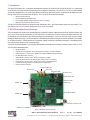
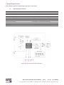
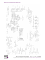
Wi125
Evaluation Kit
User Manual
Available at Digi-Key
www.digikey.com
Issue: R01
Bulletin
Revision
Date
SG172-DKUM
R01
06 May 2010
Table of Contents
1.
Introduction
3
2.
Wi125 Evaluation Board Overview
3
3.
General Specifications
4
3.1 Operating Specifications
4
4.
Interfaces
5
4.1 Power
5
4.2 Wi125 (U3)
5
4.3 UART Connections (J1, J2, J3)
5
4.4 Antenna Connection (J8)
5
4.5 Power On and Reset Switches
5
4.6 LED Indicators
5
4.7 Timing Outputs
6
5.
Operating Instructions
6
6.
Connector Pin outs
7
6.1 Jumper Description & Settings
7
6.2 RS232 DB9 Connectors
7
6.3 DC Power Connector
7
6.4 SMA Timing and Event-In Connectors
7
6.5 TNC Antenna Connector
7
6.6 External Clock Connector
8
6.7 Auxiliary Connector
8
6.8 JTAG Connector
8
Appendix 1 Evaluation Board Schematic
SG172 Wi125 Evaluation Kit User Manual
9
Page 2
Rev: 01
Date: 05/06/10
© Copyright 2010 The Connor-Winfield Corp. All Rights Reserved Specifications subject to change without notice
1. Introduction
The Wi125 Evaluation Kit is a complete development platform for the Wi125 GPS receiver (Wi125). It is comprised
of the Wi125 Evaluation Board and peripherals that support its operation. The Wi125 is a small size OEM module
specifically designed for use in weak signal GPS environments and where there is a requirement for highly accurate
timing. Refer to Wi125 User Manual for details. The Full Wi125 Evaluation Kit includes:
•
•
•
•
Wi125 Evaluation Board
Interface DB9 Serial RS232 Cable
Power Supply Adaptor (Region Specific) with 2.1 mm plug.
Magnetic Patch Antenna with a 3m lead
The Wi125 Evaluation Board can be purchased individually with a pick-and-choose option for accessories. This
may reduce cost if the customer already possesses such accessories.
2. Wi125 Evaluation Board Overview
The main purpose of the Wi125 Evaluation Board is to provide a power supply, battery backup, RS232 interface and
easy access to the Wi125 functionality. A TNC connector is available for an active antenna and SMA connectors are
on board for easy connection to the 1PPS and frequency timing outputs. Access to the Event-In pin is also available
through an SMA connection. The antenna power is provided by on-board circuitry. A connection point (BT1) is available
as an alternate to the 2.1 Barrel Socket for a DC power supply. If field tests need to be carried out, a 4AA battery pack
can also be attached to the BT1 connection port.
The Wi125 Evaluation Board is a stand-alone GPS board, providing simple interfaces to host systems such as a PC.
The Evaluation Board provides:
•
•
•
•
•
•
•
•
•
On-board Wi125
3.3VDC Power Regulation, which allowing input voltage of 4.5VDC to 25VDC
RS232 Interface to each of the 3 UARTs of the Wi125: NMEA, Debug, Net Assist
RF-IN Female TNC connector
SMA CO-AX connector for the 1PPS and Frequency outputs
Battery Backup Circuit for the Wi125’s RTC when power is not applied.
LED Indicators for GPS status, Power status and a 1PPS blinking LED
Current measuring headers at the Wi125 power supply inputs
Reset and Power switches
Event In (J7)
Frequency Out (J6)
1 PPS (J5)
DC Power (BT1)
DC Power (J4)
Power Switch (S1)
Antenna Power
Jumper (J4)
UART1 (J1)
Wi125
Reset Switch (SW1)
UART2 (J2)
Timing Outputs
Antenna Connector (J8)
UART3 (J3)
LEDs
Figure 1 Wi125 Evaluation Board
SG172 Wi125 Evaluation Kit User Manual
© Copyright 2010 The Connor-Winfield Corp.
Page 3
Rev: 01
Date: 05/06/10
All Rights Reserved Specifications subject to change without notice
3. General Specifications
If not otherwise specified, all performance data refers to the Wi125.
3.1
Operating Specifications
Parameter Min Operating Temperature
-30 Power Supply Voltage (VDC)
4.5
Power Consumption
Typical
Max
Units
+65
°C
25
VCC
5
0.62
UART Interfaces (x3) J1, J2, J3
D-SUB 9-WAY, RS232
Active Antenna Connector TNC Socket Female
W
Power Connector (DC)2.1mm Barrel, Center Positive [Cliff DC-10]
Dimensions 125 x 120 x 30mm (approx, Board Only)
Weight 128g (approx, Board Only)
Wi125
GPS
Receiver
Figure 2 Wi125 Evaluation Board Block Diagram
SG172 Wi125 Evaluation Kit User Manual
Page 4
Rev: 01
Date: 05/06/10
© Copyright 2010 The Connor-Winfield Corp. All Rights Reserved Specifications subject to change without notice
4. Interfaces
4.1Power
The Wi125 Evaluation Board can be operated from two sources of DC power: a standard DC Power adaptor with a
2.1mm DC Plug connected to J4, or the alternative connection point BT1, a battery pack or DC cables which can
be soldered directly to the ± terminals.
4.2Wi125 (U3)
The Wi125 is soldered on the board. Please see the Wi125 data sheet along with the Wi125 User Manual for detailed
information.
4.3UART Connections (J1, J2, J3)
The Wi125 Evaluation Board provides RS232 level shifting (TX, RX, GND) to interface the Wi125 GPS receiver with
a PC via either a standard serial port or a USB-serial adapter (example Roline USB Type A -serial DB9ST). For
detailed information of data streams and command format refer to User Manual.
UART 1 (J1) - Main UART of the Wi125, for NMEA message and Command Configurations
UART 2 (J2) - Debug Messages
UART 3 (J3) - Net Assist
4.4Antenna Connection (J8)
The antenna is connected using the female socket TNC connector, J8, on the Wi125 Evaluation Board. A patch
antenna is supplied with the kit. If the necessary antenna has a different connector, a suitable adaptor is required.
The Evaluation Board provides 3.3VDC at the antenna jack to power active antennas. Higher voltage antenna can
be accommodated (up to +15VDC) by routing the input power Vin to power the antenna. Jumper header JP4
determines the source power for the antenna. The jumper is placed in the‘P2’ position for direct DC-IN or P1 for the
standard 3.3VDC on-board supply. If the ‘P2’ position is used the board supply input voltage must remain below
15VDC. Care must be taken to insure that no more than 50mA is drawn from the Antenna connection otherwise
damage may be caused to the Wi125 unit.
4.5Power On and Reset Switches
The Power-On Slide Switch, S1, enables the 3.3VDC Regulator. When power is connected to the board and S1 is
in the ‘ON’ position, the yellow LED, D1 will be on continuously.
The Reset Push switch, SW1, is connected to the NPOR signal of the Wi125 unit. This can be pushed to reset the Wi125.
4.6LED Indicators
Power-ON LED, D1
This yellow LED is fully on when 3.3VDC is applied to the Board.
1PPS LED, D2
This 1PPS LED toggles ON/OFF when the 1PPS signal is present.
GPS Status Red, D3
On the standard Wi125 software builds, the GPS Red works as follows:
- Long red flash for invalid GPS fix
- Short red flashes for satellites tracked, but not used in solution.
GPS Status Green, D4
On the standard Wi125 software builds, the GPS Green works as follows;
- Long green flash for a valid 2D/3D fix
- Short green flashes for number of satellites used in solution
SG172 Wi125 Evaluation Kit User Manual
© Copyright 2010 The Connor-Winfield Corp.
Page 5
Rev: 01
Date: 05/06/10
All Rights Reserved Specifications subject to change without notice
4. Indicators continued
4.7Timing Outputs
1PPS Output
SMA, J5 - female standard socket. The 1PPS signal from the Wi125 is available here. It is directly connected
to Pin 38 through a 33 ohm resistor.
A buffered 1PPS is also available on Pin 1 of each of the DB9 connectors. This signal can be inverted by
selecting the ‘P2’ position of jumper header, JP5. Otherwise the Jumper is placed on ‘P1’ for the standard
non-inverting buffered 1PPS.
Please note that these buffered 1PPS signals are CMOS levels, not RS232 levels.
Frequency Output
SMA, J6 - female standard socket. The default frequency from the Wi125 is 10Mhz. The SMA conductor
is directly connected to Pin 39 through a 33 ohm resistor.
Event –In Input
SMA, J7 - female standard socket. Connected to the Event-In (Pin 39) of the Wi125. This is connected
through a 33 ohm resistor.
5. Operating Instructions
1. Connect the Antenna to the TNC socket, J8
2. Place the Patch antenna in a sky view location
3. Connect a RS232 data cable (also an available accessory) to the NMEA Port, J3
4. Connect the remaining end of the cable to the RS232 COM port on a PC
5. Open Terminal Window or NavSync NS3K View GPS parser on the PC, with communications setting
set to match the COM port used and the baud rate set to 38400 (default)
6. Connect the Power supply to the Board
7. Place the Slide Switch, S1, to position 1 to switch Power ON
8. The unit should start to stream data
9. Once the unit achieves a GPS lock, timing outputs will be valid and present
SG172 Wi125 Evaluation Kit User Manual
Page 6
Rev: 01
Date: 05/06/10
© Copyright 2010 The Connor-Winfield Corp. All Rights Reserved Specifications subject to change without notice
6. Connector Pin outs
6.1Jumper Description & Settings
JUMPER
DESCRITPION
Normal Position
JP1
DIG Power to Wi125, 3.3VDC
ON
JP2
RF Power to Wi125, 3.3VDC
ON
JP3
DIG Power to Wi125, 1.8VDC
ON
JP4
Antenna Supply, P1: 3.3VDCP2: Powered directly from J4/BT1
P1
JP5
Buffered 1PPS to J1/J2/J3(Pin1) SelectionP1: 1PPS+(NON-INV)P2: 1PPS-(INV)
P1
JP6
Bootsel, Only to be placed when programming
OFF
JP7
Freq out to Event-in
ON
JP8
VBAT POWER TO Wi125
ON
6.2RS232 DB9 Connectors
J1 - NMEA and Command J2- Debug
J3 - Net Assist
Pins Description
Pins Description
Pins Description
1
1PPS+/1PPS- Buffered
1
1PPS+/1PPS- Buffered
1
1PPS+/1PPS- Buffered
2
TX0 RS232 Levels
2
TX1 RS232 Levels
2
TX2 RS232 Levels
3
RX0 RS232 Levels
3
RX1 RS232 Levels
3
RX2 RS232 Levels
5
GND
5
GND
5
GND
6.3DC Power Connector
The DC power connector is a 2.1mm Barrel center positive socket connector [Cliff Component: DC-10A]
J4- DC -IN
Pins
Description
CENTER
DC Power in + (4.5-25v)
OUTER
DC Power in - (GND)
6.4SMA Timing and Event-In Connectors
J5 1PPS
J6 Frequency Out
Connected directly to Pin 38 of the Wi125 via a 33ohm resistor
Connected directly to Pin 39 of the Wi125 via a 33ohm resistor
J7 Event In
Connected directly to Pin 37 of the Wi125 via a 33ohm resistor
6.5TNC Antenna Connector
This TNC is a standard TNC socket.
J8 RF-IN
A GPS TNC active antenna can be connected here. Power is supplied to the antenna from the Evaluation Board, see
JP4 description.
SG172 Wi125 Evaluation Kit User Manual
© Copyright 2010 The Connor-Winfield Corp.
Page 7
Rev: 01
Date: 05/06/10
All Rights Reserved Specifications subject to change without notice
6. Connector Pin outs continued
6.6External Clock Connector
J9- Not fitted on Evaluation Board, only used for special hardware builds of the Wi125
6.7Auxiliary Connector
The pins on this non-fitted connector are directly connected to the Wi125
J10 Auxiliary Connections
Pins Description
1
GPIO1(PIN 40)
2
Pins
Description
9
TX1(PIN 5)
GND
10
RX1(PIN 6)
3
GPIO2(PIN 41)
11
TX2(PIN 3)
4
GND
12
RX2(PIN 4)
5
GPIO3(PIN 42)
13
N2WDA(PIN 29)
6
GND
14
N2WCK(PIN 28)
7
TX0(PIN 1)
15
USBP(PIN 30)
8
RX0(PIN 2)
16
USBN(PIN 31)
6.8JTAG Connector
The pins on this non-fitted connector are directly connected to the Wi125
J11 JTAG Connections
Pins Description
Pins
Description
1
VCC 3.3VDC
11
JSEL (PIN 21)
2
VCC 3.3VDC
12
GND
3
NTRST (PIN 15)
13
TDO (PIN 13)
4
GND
14
GND
5
TDI (PIN 14)
15
NRESET (PIN 10)
6
GND
16
GND
7
TMS (PIN 22)
17
NC
8
GND
18
GND
9
TCK (TDI)
19
NC
10
GND
20
GND
SG172 Wi125 Evaluation Kit User Manual
Page 8
Rev: 01
Date: 05/06/10
© Copyright 2010 The Connor-Winfield Corp. All Rights Reserved Specifications subject to change without notice
Appendix 1 Evaluation Board Schematic
SG172 Wi125 Evaluation Kit User Manual
© Copyright 2010 The Connor-Winfield Corp.
Page 9
Rev: 01
Date: 05/06/10
All Rights Reserved Specifications subject to change without notice
Wi125
Evaluation Kit
User Manual
Available at Digi-Key
www.digikey.com
Issue: R01
Revision
Revision Date
Notes
P00
02/03/09
Release
R00
02/16/09
Public Release
R01
05/06/10
Updates to Schematics & Drawings
NavSync, Ltd. Europe
Bay 143
Shannon Industrial Estate
Shannon, Co. Clare, Ireland
Phone: +353 61 475 666
E-mail: [email protected]
North America
2111 Comprehensive Drive
Aurora, IL 60505, USA
Phone: 630.236.3026
E-mail: [email protected]
www.navsync.com