1
SYS'l'EMASTER
User Manual
Copyr ight '( c)
1982
Teletek ,Enterprises, Inc.
Sacramento,
C~lifornla,
Revision3,~July
USA
1982,
Table of Contents
I.
PRODUCT DESCRIPTION
II.
SPECIFICATIONS
III. INSTALLATION
3.1
peripheral Connections
Serial Ports
Parallel Ports
Floppy Disk Drive
3.2
Options
Write Compensation
Extended Head Load
Wait State Generator
eTC Timing
EPROM/RAM Options
IV.
THEORY OF OPERATION
V.
IN CASE OF TROUBLE
Appendix A - Board Layout, Schematics
Appendix B - Disk Drive Interfacing
Appendix C - NEe uPD765 Manual
I.
PRODUCT DESCRIPTION
The SYSTEMASTER is a
microcomputer on a board.
It
incorporates most of the features required in a small computing
system including a CPU, 64k bytes of RAM, serial and parallel
I/O, and a floppy disk controller.
On board is a Z80A CPU which operates at 4 MHz for highspeed, efficient processing of information. The Z80A provides the
capability to support many sophisticated applications.
The
interrupt structure of the Z80A is particularly "important for
systems which perform multiple tasks concurrently.
The
SYSTEMASTER utilizes the structured interrupt system of the Z8SA
in all of "its I/O capabilities.
The on-board memory of
bytes of storage in EPROM/ROM
SYSTEMASTER is set up for 2k
board initialization routines)
available allowing the RAM to
SYSTEMASTER can provide up to 8k
and 64k bytes of RAM. The standard
bytes of EPROM (to be used for onand 64k bytes of RAM. Options are
be bank switched.
providing two independent serial ports, the Z80A SIO
provides RS23.2C-compatible serial ports which can be operated
under interrupt control.
Both serial ports include full
handshaking for connection to external devices as a printer, CRT
terminal, or MODEM.
Also on board is a counter-timer chip which provides
software-settable clocks for both serial ports and a real time
clock.
The real time clock is used by the software to provide
timekeeping functions.
It normally functions under interrupt
control requiring a minimum of overhead. This real time clock
can be used by software for any time-related functions, such as
time. dating of files, as top watch or timing loops for external
operations.
.,;.
The Z80A PIO provides two parallel ports.
One of these two
ports is bidirectional with 8 data and 4 handshake lines.
Normally" this port is configured as a printer output, but because
it is under software control, it can be reconfigured by the user
to be a device input or a truly bidirectional port. The second
parallel port has 8 data lines available which can be set
independently to be input or output lines.
Using the NEC 765AC FDC and Zilog Z80 DMA res, SYSTEMASTER
provides single- and double-density data storage on both miniand maxi-floppy disk dr~ves providing capabilities which minimize
the overhead burden on the CPU~and software. Use of the DMA
controller allows the CPU to be available at all times for
interrupts, a very important feature when the board· is used in a
multi-user or real time enviroment.
3
Some additional capabilities are: single- and double-density
performance of simultaneous
seek operations on all drives connected to the system; IBM
data transfer under software control;
compatible formatting for ease
of information
exchangt~
with
controllers
using
similar operating system software;
compatibility with both single- and double-sided
drives; ANSI
standard 50 pin disk drive connector; automatic reading of
sequential sectors on a diskette;
automatic reading
of both
tracks of a two-sided diskette; automatic error-checking detected
via eRe; under software control, possible selection of sector
size to be 128, 256, 512, or 1,024 bytes.
The floppy disk control section of SYSTEMASTER also
incorporates a field proven phase-locked oscillator (PLO) which
is used to stabilize the separated information and clock for
precise data recovery.
A reset-jump circuit on SYSTEMASTER makes the CPU jump to
the EPROM software on board whenever the system reset button is
activated: This is useful for systems which do not have a front
panel.
For systems with a front panel, reset-jump will override
the functions of the front panel.
Also, incorporated as part of
the reset-jump circuit, a power-an-clear function is included
which automatically generates a reset when power is first
applied.
SYSTEMASTER can be used as n
cost effective stand-alone
microcomputer board or as the basis for a high-performance multiuser multi-processing system.
«1
II.
SPECIFICATIONS
Z80A CPU - 4 MHz operation.
Central processor:
Memory:
64k bytes
x 1 devices, 200nS
dynamic RAM, bank selectable~
Uses eight 64k
(or faster), 128 cycle refresh.
Se.rial:
Z80A SIO ll~ to 19200 baud.
2 HS-232C, independent operation. Speeds from
Timer:
Z80A CTC - 4 channels, 2 used for serial ports, 2 used
for real-time clock.
Parallel:
Z80A PIO - 1 bidirectional port with 4 handshake
lines, 1 ·port with 8 independent input or output lines.
Floppy disk controller: NEe uPO 765AC, single- or double-density
and single- or double-sided operation, mini- or maxi-drives, ANSI
standard 50 p~n connector, IBM compatible format.
DMA:
Z80A DMA controller handles floppy disk transfers
Disk data transfer rates:
Single density
5-1/4" - 12Sk bits/sec
Double density
5-1/4" - 2S0k bits/sec
EPROM/ROM:
to ta 1 •
8" - 2S0k bits/sec
8" - 500k bits/sec
2716, 2732, 2764, 2316, 2332, ::.164;
up to 8k byte(i;
5-100 Bus:
Bus pins used by the SYSTEMASTER are shown on the
next .page~
Note the definition of pin 66 as the RFSH* signal
fro m . the Z8 0 CPU.
A·I so. not e t hat P H '\ N TOM * i san 0 p t ion and
.requires modification to the standard board.
Note:
SYSTEM ASTER does not provide 8080-type I/O addressing;
only the lower 8 address lines contain the I/O address.
Dimensions:
Power
5.05"
requirements:
X
10.0",
+8v @
excluding edge
2.0 amp, +16v
connector.
@ 50mA,
-16v @ 50mA.
Workmanship conforms to the requirements of MIL-STD-454.
Forced air cooling is required.
S-10~
BUS
Connections
Pin #
Function
Pin ~
Function
1
+8V
+16V
51
+8V
.....
L.
3
4
XRDY
52
-16V
53
GND
SLAVE CLR*
54
5
6
55
56
7
8
9
10
57
58
59
11
12
13
14
15
16
17
18
19
20
21
22
60
61
62
NMI*
(,3
64
f)S
66
67
68
69
SDSB*
CDSB*
GND
23
ADSB*
DODSB*
24
(])
25
pSTVAL*
26
pHLDA
27
28
29
30
AS
A4
31
35
A3
A15
A12
A9
001
36
D00
37
A10
D04
005
006
DI2
32
:33
34
38
39
40
41
42
43
44
45
46
sXTRQ*
R F~)H *
PHl\NTOM*
MWhT
70
71
72
73
74
7S
'If)
77
78
79
8 ,~
81
GND
ti2
A6
83
84
A7
RDY
INT*
HOLD*
RESET*
pSYNC
*
;:.\~.; H
pDBIN
'd..)
Al
A2
AS,"
A13
85
86
A14
87
All
88
89
90
D03
q. ,
~
D02
007
014
Dr3
92
DIS
017
93
DIG
sM1
94
OIl
sOUT
95
DI0
47
sINP
sMEMR
48
49
50
sHLTA
CLOCK
GND
()
" 96
sINP
97
98
99
s\...;o*
1 ~Hl
GND
POC*
(optional)
III.
INSTALLATION
Upon receipt of SYSTEMASTER, check the shipping package for
signs of abuse which may indicate possible damage. Check the
board physically to look for any parts which may have been
damaged during shipping.
If any diskettes were shipped with
SYSTEMASTER, check the diskettes for signs of damage which might
be any bending or signs of a sharp object placed against the
diskettes. Diskettes are quite fragile and any warping of the
surface of the diskette will render it inoperative.
Notify
the shipper of any damage.
SYSTEMASTER is ready for immediate use upon receipt.
It
requires' only that the peripherals which will be used with it be
connected to the appropriate female connector which will then
plug into the headers along the top of tbe board.
For the
particular connections required, see the section
entitled
"Peripheral Connections".
SYSTEMASTER need only be plugged into a standard 5-100 bus
for power and it will be functional, able to utilize the
peripherals connected to it with the memory on board.
The
SYSTEMASTER ne-eds to be in a well ventilated area due to the high
density of leis on board. Ideally, the board should be mounted
vertically in a stream of air which will be moving across the
face of the board. Whatever the mounting position, forced-ai.J:
cooling is mandatory.
Bring peripheral cables neatly away from
the board with enough slack to prevent -any tension being applied
to the cable, as this may cause the cable to separate from its
crimp connection causing intermittent problems.
For serial console devices, SIO B is the prim~ry port. With
the standard software, SIO 8 can determine the baud rate of a
carriage return and thus set the appropriate speed automatically
after a reset.
The serial speed must be
a standard value
between 110 and 19200 baud. Note: Up to eight carraige returns
are required for a terminal operating at 110 baud. Also, SIO B
requires the handshake lines of the RS-232-C interface before it
will function. See "Serial Ports" for further information.
Once the system has been brought up the console port speed
may, as an option, be statically set to allow the system to boot
fully on RESET.
This can be done by running the utility
CONSYS.COM on the system disk.
Some versions of SYSTEMASTER, upon request, do-not have RAM
on board. If no RAM is provided, it must be supplied by the user
before the SYSTEMASTER will function. Care must be exercised in
choosing the right RAM device for use on the board.
See the
SYSTEMASTER specifications for further infor-matio! ••
7
3.1
peripheral Connections
Serial Ports
SIO A
(17 )
(15)
2
4
TxC
[SIOA]
( 2)
_. 1
3
DATA
IN
and SIO-B
6
(20)
10
8
12
RxC
[5 IDA]
( 3)
(4 )
5
DATA
7
RTS
OUT
IN
(5 )
9
CTS
GUT
(6 )
14
DTR
IN
(7)
11
13
DSR
OUT
GND
16
(8 )
15
OeD
OUT
EIA pins are shown in parentheses.
These are the connections going into channels A and B of the
SIO chip.
In this configuration, each channel appears as a data
communication device and will connect to a terminal or a printer.
..
IN and OUT refer to data direction with respect to the
SYSTEMASTER.
Data from an external device is IN to SYSTEMASTER,
and data to an external device is OUT.
The signals TxC and RxC are clock inputs for synchronous
com m'u n i cat ion s • The y are pro v ide don s e ria 1 po r tAo n 1 y.
If
these inputs are to be used then jumper E22 tp E23, and E25 to
E26.
These modifications connect the clock iriputs of the SIO to
the externally supplied clock on the ETA connector.
CTS (Clear To Send) and DSR (Data Set Ready) are outputs to
the external device and are at +12V when the SIO channel is ready
to function.
RTS (Request To Send) and DTR (Data Terminal Ready)
are inputs which must be at +12V for the SIO channel to function
if the Auto Enables option is activated through software. This
option is normally enabled in the standard SYSTEMASTER software.
Either channel can be crimp-connected to a 25-pin RS-232
connector by aligning pin 1 of the cable from the SYSTEMASTER
connector with pin 1 of the 25 pin RS-232 connector.
In this
configuration, the channel connects directly to a. terminal or
pr inter.
8
NOTE:
If the terminal or printer does not provide the
necessary handshake lines, EIA pins 4, 5, and 20 should be
jumpered together.
This ensures that the required handshake
signals to the SIO port are provided. ,The connections can be made
oh the serial cable or at the SID connector on the SYSTEMASTER.
At the SIO connector this requires that pins?, 9, and 14 be
j umpered.
An alternative to providing a hardware handshake is to
disable the "Auto Enables Option" on the SIO.
This can be
accomplished by altering the initialization software.
EIA Serial Data Transfer Protocol
prior to sending or receiving data, the four handshake lines
should be active.
However, the SIO will allow control of'its
receive and transmit functions independently.
If the "Auto
Enables" function of the SIO channel is enabled (standard), the
SIO wil'1 not send data until DTR is active.
(This function is
labelled neTS" on the SIO chip.)
This
is handy for buffered
printers which need to stop receiving data until the buffer is
printed. By pulling DTR inactive, the printer will stop the flow
of data from the S I 0 • When i t is ready to receive more d a t at it
reactivates DTR. Similarly, if "Auto Enables" is enabled, the
SIO will not accept information until RTS is active.
(This
function is labelled "DeD" on the SIO chip.)
This is primarily
used with a communications link where, if signal conditions
deteriorate, the data may be garbled.
In summary, the handshake 1 ines provide a convenient means
o f con t r 0 1 1 i n 9 the flo W '.1 fin for III a t ion ina s e ria 1 c han n e 1 • ~f
any line is pulled inactive, transfer ceases.
RS-232-C Voltage Levels
A logic high (a binary ONE), or marking condition, is any
voltage less than -3 volts to a minimum of ~25 volts. A logic
low (a binary ZERO), or spacing condition, is any voltage greater
than +3 volts to a maximum of +25 volts.
Any level between -3
and +3 volts is undeEined.
This is called the transition region.
The maximum transition time between bit cell~ is four per cent of
the basic clock period.
The maximum voltage rate of change (slew
rate) is 30 volts/uSee.
Thus the maximum RS-232-C transmission
speed, based on voltage swings of -12 to +12 volts, is 50,000
baud.
9
Serial Data Timing
Prior to transmitting data
the signal line is held high, or
marking.
It goes low (spacing) to indicate the start of a
character. The bits representing the character are then sent
Least Significant Bit first, then a parity bit (if used), and
finally 2 stop bits.
The stop bits indicate the end of the
character and are always logic ONEs. The standard SYSTEMASTER is
set up for 8 data bits, no parity, and 2 stop bits.
The value
length of each
the basic clock
Thus for 9600
Sec=1/96G0).
of each character bit is held for the entire
bit cell. The length in time of each bit cell is
period, equal to the reciprocal of the baud rate.
baud, each bit cell is 104 uSec long (.0001041
MODEM Connections
If ·connection to a MODEM
connections must be made:
SYSTEMASTER
Pin #
5
3
11
14
7
13
9
is desired
then
the
following
EIA
Pin #
Direction
Function
2
3
OUT
IN
OUT
IN
Oa ta to MODEM
Data to SYSTEMASTER
RTS (Request To Send)
CTS (Clear To Send)
DSR (Da ta Set Ready)
Signal Ground
DTR (Data Terminal Ready)
4
5
6
IN
7
20
OUT
IN refers to data sent to SYSTEMASTER,
data sent to the MODEM.
10
and OUT refers to
Parallel Ports
PIO A
2
4
6
+5
RESET*
1
D7
3
D6
8
GND
10
B 8TB
7
9
D3
5
05
D4
12
B RDY
11
D2
14
A STB
13
D1
16
A RDY
15
00
PIO B
2
GND
4
1
3
D3
D4
8
10
D2
D0
c...J
7
D7
D6
9
05
6
01
These are the connections into the PIO chip. The PIO chip
has two parallel ports, A and B. As configured,~IO A may be
used as an input, output, bidirectional or control port with four
handshake lines." PIO B is the same except that it does not have
bidirectional capabilties or handshake lines.
The signals are:
D0 -
07
8 data lines
A 5TB
Strobe input pulse from a device.
Depending on
the mode of operation, it means:
1. Output mode:
Positive edge of this strobe is
issued by the device to acknowl~dge the receipt of
data made available by PIa A.
2. Input mode:
The strobe is issued by the device
to load data from the device into PIO A.
3. Bidirectional mode:
Same as 1, except output
data are present only while A 8TB is low.
4. Control mode:
The strobe is inhibited
internally.
A RDY
Ready output to a device. Depending on the mode
of operation, it means:
1. Output mode:
Indicates that the data bus is
stable for transfer to the device.
2. Input mode:
When active, it indicates that PIO
A is ready to accept data from the device.
3. Bidirectional mode:
Same as 1.
4. Control mode: Always in a low state.
11
RESET*
The active-low reset line on the SYSTEMASTER.
This can be used to reset a hard disk connected to
PIO A.
B
STB
Used when PIO A is in the bidirectional mode;
strobes data from the device into PIO A.
B
ROY
Used when PIO A is in the bidirectional mode; it
goes high to indicate that PIO A is ready for data
from the device.
The software supplied by Teletek allows PIO A to be set up
as an input port or an output port. PIO B is set up in the
control mode with all eight data lines available individually.as
input or output lines.
Parallel Printer Connection
A Centronics type parallel rrinter may be connected to PIOA
on the SYSTEMASTER board.
The following table lists the pin
connections required to make a cable that will interface this
type of printer.
SYSTEMASTER
Function
pin I
Pin
printer
Function
rr
~
1
D7
1
DATA
15
13
11
9
D0
2
D1
D2
03
D4
7
Dl
D2
D3
D4
05
5
3
D6
14
ASTB
3
4
5
6
7
8
10
STB*
05
06
D7
ACK*
NOTE:
The SYSTEMASTER provides a software strobe to the
printer using data bit 7 from PIOA.
Therefore data bit 8 on the
printer is not connected.
On most printers this bit controls
special print modes and should be jumpered to ground to enable
normal printing.
Also remember that there are no drivers on the
PIO signal lines therefore the cable length must be kept short
(less than five feet depending upon your printer termination).
Floppy Disk Drive
Ground
Pin t
Signal
pin #
1
2
3
4
5
6
8
7
'9
11
Input .- I
Output-- 0
0
a
Description
Above track 43
Not used
Not used
Above track 43
Dual sided
10
12
14
16
18
0
19
21
20
I
Index
22
I
23
24
25
27
26
28
1
Ready
Not used
Drive select 0
Drive select 1
Drive select 2
Drive select 3
Direction
Step pulse
Write data
Write gate
Track 00
Wri te protected
Read da ta, composite
fJ
Motor control
13
15
17
29
30
31
33
35
32
34
36
37
38
39
41
43
4S
47
49
40
42
44
46
I
0
0
0
0
0
0
0
0
0
I
I
Not used
48
S"
Not used
Head 1
Not used
Head load
Input/Output are referenced to SYSTEMASTER. Input is a
signal from the disk drive to SYS'I'EI1ASTER, and-'output is a signal
to the disk d rive.
More detailed information regarding floppy disk drive
interfacing is available in appendix B.
Please refer to that
section of the manual when installing disk drives on the
SYSTEMASTER.
13
3.2
Options
Write Compensation
To help compensate for the shifting- of data bits during the
read process of the floppy disk drive, the write data bits are
compensated. This is particularly critical for double-density
operation.
Different drives require different amounts of write
compensation.
The symptoms of too much or not enough write
compensation are as follows:
1. Too much write compensation
shows up as read errors (usually eRe) in the outer tracks (0-42);
2. Not enough write compensation shows up as read errors in the
inner tracks (43-76).
SYSTEMASTER provides selectable compensation for both 5 1/4"
and 8" drives in the following combinations:
Jumper
Compensation
P0
PI
P2
5 1/4"
1
1
1
None
None
None
125· nSee
None
250 nSec
250 nSee
125 nSee
250 nSec
250 nSee
125 nSee
500 nSee
250 nSec
500 nSec
Illegal, no w rite da ta output
1
0
1
1
1
1
1
1
1
0
0
0
0
"
" "
0
1
0
" "
8"
A 1 indicates the jumper is in place, while a 0 indicates
the option pins are open.
Compensation is automatically switched as the on-board drive
size control is switched from 5 1/4" to 8" drives.
Compensation depends on the recommendations of the drive
manufacturer. Both 5 1/4" and 8" drives usually
require 250 nSec
compensation.
Track 43 Selectable Compensation
In addi tion to the above options, SYSTEMASTER provides one
more:
if the P3 jumper is in place, the compensation for tracks
0-42 will be one step less than that in the above table.
At
track 43 and higher, write compensation will be equal to the
table value.
This option is provided because most drives require
more compensation on the inner tracks where the recQrding density
is higher.
For 5 1/4" drives which do not have more than 42
tracks, select compensation one step greater than that required.
14
For example, assume an 8" drive which requires 250 nSec
compensation, and a 5 1/4" drive with 40 tracks which requires
250 nSec compensation. option jumper P3 is in place:
Select P0=1, Pl=0, P2=0
At Tracks 0-42, 5 1/4" compensation is 250 nSec, and 8"
compensation is 125 nSec.
For tracks 43 and above, the 8" drive
will have 250 nSec compensated data.
Extended Head Load
The uPD-765AC floppy disk controller has a maximum head
unload time of 240 mSec.
In some applications this will cause an
undue amount of head loading and unloading. To increase this
and reduce the number of head load actions, a
74LS123 monostable can be wired into the head drive circuit.
With the addition of a 6 volt capacitor, the head unload time is
extended.
This increases the life of the media and the heads
where there would normally be a great deal of head load activity.
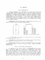
The following table gives the effective head load time for
several different capacitor values:
head unload time
Capacitor
(uP)
10
30
50
70
90
110
130
150
170
190
210
230
250
Head Load Ti me _(sec)
0.5
1.4
2.3
3.2
4.1
5.0
5.9
6.8
7.7
8.6
9.5
10.4
11.3
The time values are approximate (normally resistor values
are + 10% and capacitor values + 20%) and are derived from the
following equation:
HLT =
(45
*
C)/(lE03),
where C is
in microFarads.
To enable the head load option,
jumper option pin E-19 to
E-20 and install the desired capacitor value at location C-12.
If this option is not desired then pin E-19 should be connected
to E-18.
Wait State Generator
The wait-state generator can generate a wait-state during
all memory accesses, MI accesses, or only when the on-board ROM
is accessed. The choice of wait-st-ate generation is dictated by
the requirements of the system. For the standard SYSTEMASTER,
one wait state is generated for every access to the on-board ROM.
With a faster ROM (less than 360 nSee access time), the wait
state is not needed.
The following wait-state options are
available:
Option
No wait state
On-board ROM only
All memory
All memory, Ml only
Jumper
EI open
E1 to E4
El to E3
E1
:0
E2
NOTE: if the RDY or XROY input of the S-100 bus is low, this
will be gated into the CPU wait input causing the CPU to wait
until ROY and XROY are released to an inactive high state.
CAUTION:
An
extended
wait
state
will
cause a
loss of
refresh to the dynamic RAMs on the SYSTEMASTER.
CTC Timing
The trigger inputs to CTC channels 0 through 2 connect to a
1.2288 MHz source.
Thus all standard baud rates from 150 to
76,800 can be generated by programming the eTC for the counter
mode, with a time constant between 1 and 256 (0).
The SIO
divider is set for 16 or 32 as necessary.
For baud rates that
are non-standard or below 150, use the eTC in the timer mode with
a divide by 16 presca1er, and the SIO divider set for 16 or 32.
To
sum mar i z e :
Baud rate 300 to 76,800SIO divider set to 16, eTC in the
counter mode, time constant set from 1 to 256.
Baud rate 150- SIO divider set to 32,
mode, time constant set to 256.
eTC in the counter
Baud rates less than 150:
(eTC in the timer mode, prescaler set to 16)
Baud Rate
45
60
75
110
Time Constant
SIO divider
32
32
174
130
208
142
16
16
16
Error
~.22%
0.16%
0.16%
0.04%
Real Time Clock;
Channels 2 and 3 of the eTC are chained together to provide
a l-second interrupt real-time clock. Channel 2 is programmed in
the timer mode, pre-scaler set to 256, and time constant set to
125. Channel 3 is set to the counter mode, time constant set to
125, and interrupt enabled. For a multi-user operating system
which requi res a fast clock interrupt, enable the interrupt for
channel 2 also. The interrupt routine for channel 2 can count
down to provide periods which are integral multiples of the 8
~illisecond interrupt.
The standard system software stores the time and date in
system RAM in six consecutive bytes:
SEC,MIN,HOUR,YEAR,DAY, and
MONTH.
The CPU is interrupted every second and the time is
up d ate d • The d ate i s a Iso u pd ate d i f n e c e s s a r y, but 1 e a p yea r s
and turn of the century occurances are not accounted for.
All of
the valq~s are kept in binary.
The user may set or read the time and date by accessing
these six bytes of data. The following code in a user program
will return the address of SEC in the HL register:
iselect function 12
;call BIOS function handler
LD
C,12
CALL 40H
Note that the clock is not initialized on reset.
It is up
to the user's software to set the time and date, and until they
are set they should be considered invalid.
EPROM/RAM Options
The on-board ROM socket (U41) can accolnmodate 24 or 28-pin
EPRGMs or ROMs occupying 2k, 4k, or 8k bytes of memory space.
This ROM can originate at 0000H, E000H, F000H, or F800H depending
on the setting of the option jumpers on LA-5:·-I
ROr-1
ROM
origin
2316,2716
2332,2732
2364,2764
0000H
0000H
2316,2716
2332,2732
2364,2764
Memory Space Options
End
07FFH
Space
Jumpers
E14 to E16, E1S to El7
El4 to E16, G to E17
G to E16, G to E17
E14 to E16, EIS to E17
E14 to E16, E13 to E17
E13 to E16, E13 to E17
0000H
IFFFH
2k
4k
8k
F800H
FFFFH
2k
. F000H
E000H
FFFFH
FFFFH
4k
0FFFH
8k
17
The type of ROM used determines the socket and jumpers used
at the socket:
ROM
2316
2332
2364
2716
2732
2764
Size Socket
2k
24 pin
4k
24
8k
24
24
2k
4k
24
8k
28
Jumpers
E5 to E8,
E5 to Ell,
E5 to E9,
£5 to E8,
E5 to Ell
E5 to Ell,
E6
to E10, E7 to E12
E6 to E10, E7 to E12
E6 to E 12, E7 to Ell
E6 to E10, E7 to E12
E6 to E10, E7 to E12
E6 to E10, E7 to E12
The chip select options for the 2316 and 2332 must
specified as follows for the above jumper connections:
2316
2332
Pin
pin
Pin
Pin
Pin
18 active
20 active
21 active
18 active
20 active
be
low
low
high
low
low
NOTE:
when the 24-pin 2364 is used, underlying RAM
be written when the ROM is enabled.
cannot
Except for" the 24-pin 2364, when the ROM is enabled, either
during reset-jump or otherwise, the underlying RAM can be written
to but not read.
Memory other than that occupied by the ROM can
be accessed normally. Thus on reset the R.JM monitor could copy
its elf i n to RA M the n dis a b 1 e the ROM and co i1 tin u e ex e cut ion f rt> m
RAM.
RAM Select
SYSTEMASTER contains 64k bytes of RAM.
This RAM is
partitioned into a fixed and a selectable bldck.
The selecta~le
block can be disabled allowing CPU access to additional external
memory. "The fixed block is always resident in the CPU memory
space.
This combination of fixed and selectable memory
accommodates such multi-user operating systems as MP/M from
Digital Research, which requires a fixed block of RAM for the
operating system.
18
The size of the fixed block of RAM can be varied by option
jumpers AJ-l, 2, and 3:
Fixed Block Size
Range
Jumpers
32k
S{100H-FFFFH
AJ-1
AJ-2
AJ-3
Open
Open
Open
16k
C000H-FFFFH
AJ-I
AJ-2
AJ-3
Open
Open
Connected
8k
E000H-FFfo"'FH
AJ-l
AJ-2
AJ-3
Open
Connected
Connected
4k
F000H-FFFFH
AJ-l
AJ-2
AJ-3
Connected
Connected
Connected
The selectable block of RAM occupies the memory space from
0000H up to the fixed block of RAM.
The select~ble block is
enabled when /RAMEN islow. (/RAMEN is bit 7 of the control
register.)
When disabled, the selectable block of RAM is not
affected by memory accesses in its memory space.
NOTE:
The on-board RAM cannot
temporary bus masters.
19
be accessed by off-board
IV.
THEORY OF OPERATION
5Y5TEMASTER is a single-board computer for the 5-100 bus.
It contains 2k- 8k bytes of ROM, 64k bytes of RAM, a flexibledisk controller, two parallel ports, two serial ports, a DMA
controller, a CTC, and a cpu.
With appropriate software,
SYSTEMASTER comprises a complete stand-alone single-user
computer.
The following discussion details the operation of the
various functional areas ·.of SYSTEMASTER.
Please refer to
Appendix A for the board layout and schematics when reading the
following information.
Central Processor Operations
The heart of SYSTEMASTER is a 4 MHz Z80A CPU. It provides
the intelligence to operate the on-board support chips and to
provide the information interchange to the 5-100 bus.
Connections to the bus are made through tri-state buffers and
control logic to provide the correct timing signals and status
signals to operate other boards within the microco~puter.
The 4MHz clock for the CPU is derived from a l6MHz
oscillator (U16) and a counter IC (U39).
This circuit also
provides clock signals to the disk controller section and a 2MHz
signal for the S-100 bus.
The SYSTEMASTER CPU is configured in interrupt mode 2.
In
this mode, a requesting device generates· an interrupt and when
that interrupt is acknowledged, the CPU expects the device to
place an-8 bit address vector on the data lines.
The CPU then
adds this 8 bit vector with another 8 bit register internal to
the CPU to form a 16 bit absolute memory addt"ess. This address
points to a 2 byte location in memory which contains the absolute
address of the desired subroutine to service the interrupt.
In the case of the Z80A DMA, SIO, PIO and CTC, the necessary
interrupt vectors are loaded to internal registers during
initialization. For the case of the floppy controller Ie, the
interrupt vector is simply composed of that vector formed by the
pull-up resistors on the data lines, an FE.
The Z80 support Ie's
normally begin on an even memory location because bit 0 ~s always
low during their interrupt response.
20
,-
When a device external to the CPU requests an interrupt, the
external device must provide an interrupt vector on the data bus
when interrupt acknowledge status 1 ine goes ;active high. The
Z80A support Ie's are series connected to .provide priority
interrupts.
The last device in the chain,; namely the PIO,
provides an interrupt enable signal for - external devices.
When
this line is high, interrupts are enabled for .external requests.
When this line is low, external devices must ~e prevented from
generating a response to an interrupt acknowledge signal. The
vector that external devices place on the bus, when combined with
the internal high order vector of the CPU, must point to a
location in memory which provides the absolute address of the
subroutine used for servicing that particular interrupt.
Following is
the on board interrupt daisy chain in order of
priority:
1.
2.
OMA
SIO
3.
eTC
4.
PIO
DMA Controller
SYSTEM ASTER incorporates a
DMA controller
to provide
efficient, transparent flexible-disk data transfer without
requiring CPU intervention. Interrupts can be enabled during DMA
operations.
Prior to a series of DMA data
transfers the DMA
controller must be set up as necessary for the particular
operation desired.
No CPU intervention is required during a DMA
transfer process.
At the completion of the series of data
t ran s fer s the D M A co n t roIl e r will i n t err u p t the. CPU •
At t h Ps
time, the CPU performs any operations necessary to terminate the
data transfer.·
The sequence of operations should be:
set up the DMA
cont-roller for the I of bytes to transfer (the sector size) and
the starting memory address for toe transfe~, and finally sen.d
the read or write command to the 765.
When the DMA controller
interrupts the CPU at the end of the data transfer, the interrupt
routine must immediately issue a terminal count to the 765 by
doing an input from port 14H. The DMA controller accesses port
10H to transfer data to or from the 765. This port connects to
the DACK (DMA acknowledge) pin of the 765.
The DMA controller is a single-channel device which can
execute only one series of operations at a time.
Although it is
connected to the uPD765 flexible-disk controller, when the uPD765
is idle the DMA controller can perform block moves of data
bet wee n me m 0 r y a nd I/O de vic e s. . T his i s don e by 'r e pro g ram min 9
the control registers of the DMA controller with the appropriate
information and forcing the transfer through the use~ of a special
software command.
21
Dynamic RAM Control'
Logic Array LA-1 (U1S) controls the access to the on-board
dynamic RAM.
A RAM cycl~ is started by MI* going low, or by
MREQ* active low in conjunction with RD*, "WR*, or RFSH*.
If the
RAM-select options match RAMEN* and the option ~ddress jumpers,
MSTRT* goes low.
Both sections of U-19, a dual J-K flip-flop,
are clocked active by the action of MSTRT*. One section of U19
activates the RAS* line of the dynamic RAM res.
RAS* clocks the
lower 8 bits of the memory address into the RAM les. The second
section of U19 sends a posi~ive pulse into the delay line, U-47.
The 20% tap of the delay line resets this section of U-19 to
terminate the positive pulse, and in addition clocks one section
of U-S4. The output of U-54 causes the address multiplexers, U-42
and U-43, to select the upper 8 bits of "the memory address.
When the po sit i ve p u 1 s e in the del a y 1 i n"e rea c h e s t he 40%
tap it clocks the remaining section of U-54, which generates a
CAS* signal to complete the RAM access.
After the RAM access
time has elapsed, data lines are stable at the RAM outputs. When
the positive pulse in the delay line reaches the 100% tap, the
first section of U-19 is cleared which resets the RAS* signal.
This allows the RAM RAS circuit to pre-charge in preparation for
the next memory access.
As long as CAS* is low, the RAM outputs are stable.
When
the CPU terminates the memory request, LA-1 resets U-54 which
returns the address multiplexers to the low-order
address lines
and resets the CAS* signal.
A memory write operation does not begin until WR* from the
CPU is active. This ensures that the R/WR* line to the RAM ICs
is active when the RAM res are accessed.
This precaution allows
the. DATA IN and DATA OUT lines of the RAM les to be connected
together, simplifying the memory c"ircuitry.
A refresh operation begins when RFSH* and MREQ* from the CPU
are both active low. A normal memory cycle is started, but the
address multiplexer and CAS* circuits are held idle.
The CPU
outputs a refresh address during this time to refresh one of 128
consecutive locations in the RAM necessary to retain data.
Because the CPU supplies the refresh address the only RAM devices
that can be used are those that are compatible with a 128 cycle
refresh.
NOTE:
An extended RESET* or Wait State condition will cause
a loss of refresh in the on board dynamic RAM.
Wait State
Generato~
The wait-state generator functions by holding the CPU wait
input low until one clock cycle after MREQ* from the CPU is
active. U-53, a J-K flip-flop, has its "K" input connected to
MREQ* from the cpu.
The inverted state of MREQ* connects to the
"J" input.
Initially, prior to a memory cycle, MREQ* is high
causing U-53 to clock its "Q" output low. The "Q" output of US3
is gated with the desired condition (active MI*, ROM*, or all
memory accesses). The resulting signal is gated wit.h MREQ* and
connected to the wait input of the cpu.
If the current CPU cycle meets the desired conditions the
wait input of the CPU is held low. On the next negative edge of
the CPU clock, because MREQ* is low and the "J" input of U-53 is
now high, the "Q" output of U-53 will go high.
This in turn
releases the wait input of the CPU allowing completion of the
cycle. U-53 resets itself at the end of the memory cycle ~hen
MREQ* again goes inactive.
ROM- I/O
Decode r
U-26, a logic array (LA-5), provides the logic necessary to
access the on-board ROM, select I/O, and control the RAM data
buffer.
When the CPU accesses memory, LA-S decode_s the address
and option lines to determine if the on-board ROM is being
accessed.
If the CPU is accessing ROM, the RAM data buffer is
held inactive, otherwise it is enabled if LA-l has determined
that on-board memory is to be accessed.
During an I/O operation, if the CPU address is less than
the on-board I/O decoder is selected. If Ml.* is active a.t
the same time as IORQ*, an interrupt acknowledge cycle is in
process and neither ROM, RAM nor I/O is selected.
2~H,
On-board Control Register
U-l3, an octal O-type
several areas of SYSTEMASTER.
Bit
Name
7
RAMEN*
6
4
ROMEN*
JMP*
MOT*
3
FLa*
5
0-2
flip-flop,
Th{~
provides
control
for
output lines of U-13 are:
Function
When low, enables the selectable block of onboa rd RAM.
With JMP*, controls the on-board ROM
With ROMEN*, controls the on-board ROM
When low, turns on the flexible-disk drive
spindle motor
When low, allows 3" flexible-disk data
t r a 'n s fer s.
When h i 9 h, 5 1 / 4" fIe x i b 1 e - dis k
data transfers are enabled.
Not presently used
All these bits are reset low when a reset pulse occurs.
The
control register bits are set simultaneously by a CPU output to
port lCH.
The outputs follow the inputs directly.
Reset-Jump
After a reset operation SYSTEMASTER begins execution of the
instructions in the ROM to initialize the system.
Because the
ROM may reside at 0000H or a higher memory address, special
circuitry enables the ROM independent of its actual location.
The outputs of U-13, ~he on-board control register, are
cleared by a reset pulse.
Therefore, outputs JMP* and ROMEN* are
low.
This combination causes LA-5, the ROM-I/O decoder, to
enable the ROM for any CPU memory access. If the ROM options are
set for a ROM location at E000H, F000H, or F800H, the first
instruction in the ROM should be an absolute jump to the ROM
location plus three.
For example, a SYSTEMASTER set up for a
2716 has the ROM options set for an address 0f F800H. The first
instruction in the ROM is a jump to F803H.
This sets the CPU
program counter to the actual ROM address space.
While JMP* and ROMEN* are both active RAM cannot be
accessed.
After the CPU begins executing the ROM in the correct
address space, RAM can be enabled by setting JMP* high if the ROM
occupies high address space (F000H or higher), or setting ROMEN*
high if the ROM occupies memory starting at 0000H. If the RAMEN*
signal is active low then both ROM and RAM can be accessed at
this time.
In order to disable ROM both signals JMP* and ROMEN*
should be inactive.
NOTE:
If ROM is addressed at 0000H, ROMEN*
JMP* is low, then RAMEN* must be low to enable ROM.
is high, and
To sum mar i z e :
RAMEN *
ROMEN*
JMP*
Hesult
X
0
0
0
0
1
0
1
0
1
1
0
1
1
1
X
ROM enabled, RAM disabled
F000 ROM enabled, RAM enabled
0000 ROM enabled, RAM enabled
ROM disabled, RAM enabled
F000 ROM enabled, RAM disabled
ROM and RAM disabled
1
"
(0 - low, 1 - high, X - don't care)
7.4
Parallel ports
The parallel ports consist primarily of the Z80A PIO.
Port
A is used as an 8 bit input, output or bidirectional port. The
fopr handshaking lines of the PIO are used with port A.
Normally, port A is configured as an output for such parallel
items as a printer.
Under so-ftware control, port A can be
configured as an input or as a bidirectional port where input
data and output data as well as direction are controlled by the
four handshaking lines.
Port B of the PIO is used in a bit control mode. This port
individual control lines for
interfacing to parallel devic?s such as hard disk drives.
is normally used to provide
Serial Ports
The Z80A SIO is used to generate two entirely independent
serial ports. Both serial ports incorporate all the handshaking
lines required by an RS232C data interconnection device. Each
channel of the SIO is driven by an independent section of the
eTC. This means that baud rates for the tW0 channels can be
independently selected..
In fact, the baud rates may range
anywhere from 45 baud up to 19200 baud. These frequencies are
determined during initialization of the eTC. The ~ata lines to
and from the SIO channels are buffered by RS-232-C level
translators. These buffers are also inherently protected from
short circuits on the external lines.
Both serial ports will interconnect with terminal equipment
(printer, CRT terminal, etc) using standard insulationdisplacement connectors..
Connection to a ~10DEM requires
transposition of all six serial lines as required by the MODEM
(see "Per i phe--ral Connecti ons").
When- connec t i ng to a synchronous
MODEM, which provides the receive and transmit cloCks, the clock
inpu.~s to SIO A must be connected to the MODEM:
SIO A clocks
Internal, eTC
From MODEM
£22 to E21, E25 to £24
E22 to E23, E25 to E26
The transmit and receive clocks for SIO A are provided by
Those for S10 B are provided by eTC channell.
eTC channel 0.
?5
Floppy Disk Controller Operation
The heart of the flexible-disk controller is the NEe
uPD765AC. Capable of single- and double-density, single- and
double-sided
5 1/4" and 8" data recording, the 765 provides a
flexible, reliable disk controller for SYSTEMASTER. Circuitry
on board SYSTEMASTER supports the 765 in stabilizing the read
data from the disk drive, compensating data written to the disk
drive, and buffering status signals to and from the disk drive.
The fo llow ing discuss ion deta i Is the c i reu i try surround ing the
765.
To reduce the number of its pins the 765 multiplexes dual
signals on four of its control lines. pin 39 of the 765 selects
the seek mode when high and the data read-write mode when low.
One section of U-56, an inverting buffer, inver~s the signal from
pin 39 to enable the appropriate drivers when the 765 is in its
seek mode. When in the seek mode, the 765 positions the disk
drive head over the desired track on the diskette. In this mode,
the 765 looks at the dual-sided and track 0 signals and outputs
drive control signals to the direction and step lines. In the
read-write mode, these four function lines become write-protect,
write-fault, low-current (track greater than 42), and write-fault
reset. The 765 also has two drive-select outputs. U-49, a dual
decoder, decodes US0 and USI from the 765 to develop four drive
select signals.
The 765 generates an interrupt request to the CPU when it
detects an error or completes an operation. The 765 interrupt
output on pin 18 is active high, thus it is inverted by U-57 a1\d
activates the output of U-7, a tri-state buffer. U-7 pulls down
the CPU interrupt request l'ine~ When the CPU acknowledges the
interrupt, LA-4 will pull down data line 0 if no other interrupts
are~active on SYSTEMASTER.
Because the other data lines to the
CPU have resistor pull ups to +5 volts, the CPU sees FEH on its
d a tab usa n d w i 11 ex e cut e the a b sol ute add r e"s sst 0 red a t FE H i n
the interrupt table. The data input buffer from the S-100 busvis
held inactive by LA-4 during the interrupt acknowledge operation
when the 765 interrupt line is active.
The read data from the disk drive may vary in frequency due
to disk drive rotation speed variations.
To maintain reliable
read data, a phase-locked loop oscillator follows the frequency
of the read data and provides a stabilized read clock for the
765.
The action of the phase-lock loop is such that the read
data pulses will occur in the center of the high or low portion
of the read data cl~ck sent to the 765.
This provides the
maximum margin for error in disk read operations.
26
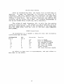
Disk Data Encoding
Physically, double density disk drives do not differ
significantly from t.heir single density counterparts.
Improvements in double density record and playback heads and
changes in mechanics often provide less expensive and more
durable drives.
These changes are minor compared to the
differences in reading and writing functions.
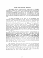
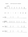
Figure 1 reviews
encoding methods used in single and double density. The standard
recording formats are FM (for frequency modulation), MFM (for
modified frequency modulation-double density), and MMFM (for
modified modified frequency modulation) which is a refinement of
MFM.
Line 1 of Figure 1 indicates the basic clock frequency
which designates the bit dell in which information will be
passed. The next line illustrates a sample of information; the
line following shows the pulses which generate that information
in a single- density PM format. Notice that information actually
sent to and received from the drive is a combination of the basic
clock frequency and data pulses. Refer to the next line which is
r.'fFM.
Here, only the data plJlses will be sent to the drive and
their orientation within the bit cell determines the value of
t. hat par tic u I a r d a tap Ill:·) e (a .1 0 r a ~~).
Eve r y 0 i s rep res e n ted
by a data pulse that coincides with the basic clock frequency.
Every 1 is represented by a pulse that occurs midway between two
clock pulses.
Thus, when the d.::lta pulse occurs in t.he middle of
a bit cell, it is a 1; when it occurs in the beginning of a bit
cell, it is a 0.
Look at the nE-xt line which represents MMFM.
T his i s a s 1. i 9 h t
ref i n em e r I t o f f"i F M ;
i nth i s i n s tan c e
t k-e
data pulses once again represent l's and O's via their placement
within thebi..t cell. However,. the,· rules change slightly. If the
preceding data pulse W<1S a iJ an<l the present datum is a 0, then
the data pulse will occur.
[f the 13St data pulse was a 1 and
the ~resent datum is a 0, the present data pulse does not appear.
If the last data pulse was c1 1 and the present- datum is a 1, that
data pulse appears. Every ti.me there is a 1, a data pulse will
appear in the middle of a bit cell. But whether or not a " data
pulse occurs depends 0n the preced ing datum. Note that the
density of data pulses for MFM is almost exactly one-half the
density of data pulses for FM.
Thus, for the same density of
pulses on the diskette, MFM will record twice as much information
as FM.
MMFM has sliqhtly less dense data pulses than MFM, but
its complexity of encoding and decoding outweighs the slight
advantage it might enjoy due to slightly less density.
The basic clock freqllency for FM encodir1g is 250 KHz for an
8 - inc h dis k e t t e • Whe j' Vi C d (~ 1 ~~ t: f~ t 11 eel 0 C k and 1 e a ve 0 n 1 v the
dat;} pulses in
data transfer
MfM,
that. clock [ate changes t.o ~J00 KHz..
Th~ MFM
rate is t\.Jice .:1~~; fc]~3t as ?M. The density and the
speed are both doubled, which means that twice as much
information can be stored in the same physical space and
manipulated twice as fast.
'"\/
~.
i
FIGURE
FLOPPY DISK DATA ENCODING
BASE
CLOCK
DATA
DATA
PULSE.
FM
COMBINED
OAli\.
_~rLJL
n
_------'I L '_ _ _ _ _ _ __
WJJUl·
n~n,----
MFM
MM FM
~~~;£ nL--..__---'n~____ JL _ _._- -_ .____ Jl~__---,n,--_____
5-100 Bus Interface
The signals generated by SYSTEMASTER are compatible with the
proposed IEEE-696 standard.
U-14, a logic array (LA-4)
transforms the Z-80 family status signals to those of the S-lee
bus.
In addition, U-14 controls the data input bus driver, U-12,
to prevent conflicts with on-board I/O and memory devices.
If a
conflict could occur, 5YSTEMASTER ignores the off-board device.
SYSTEMASTER generates the S-100 standard memory write strobe
by the logical equation: MWRT= pWR AND /SOUT.
In addition to the standard 8-100 signals, SYSTEMASTER
brings the 2-S0 CPU refresh signal to pin 66 of the bus for those
memory boards which need this signal.
U-5, a dual monostable, generates the pSYNC and pSTVAL*
signals.
Whenever the CPU activates a status line (Ml, MREQ, or
IORQ), U-14 outputs an active-low signal to trigger U-SA. The
output of U-SA appears on the bus as pSYNC and also triggers uSB.
U-58 generates a pSTVAL* signal whose active edge occurs
after status is valid, and during the pSYNC pulse.
Power-On Clear
SYSTEMASTER generates a reset pulse when power is applied to
automatically initialize the system. Thus during the start-up
operation operator intervention is not required.
To develop the
power-on reset pulse, circuitry on-board SYSTEMASTER detects the
first application of power:
Capacitor C-26 is initially
discharged.
C-26 holds the plus input of U-17
(a
dual
comparator) low, which causes the output of U-17to be low. Toe
output of U-17 enables two drivers of U-6, a he~ inverting bus
driver, which pull RESET* and SLAVE CLR* Iowan the S-10~ bus.
In addition, the output of U-17
is buffered by U-IS to drive
poe. low. When C-26 charges above the level on the minus input
pin of U-17, the .output of U-17
goes high.
RESET* and SLAVE
CLR* are released and pulled high by resist~rs connected to +5
volts, and POC* goes high.
At this time
the CPU on board
SYSTEMASTER begins execution of the instructions in the on-board
ROM. When power is turned off, diode D-l discharges C-26 quickly
to provide a reset action if power is shortly reapplied. (Such a
sequence can occur during a temporary power outage.)
29
SYSTEMASTER Port Assignments
Port
Device
Function
00H
SIO
01
02
II
A-Data
A-Control
B-Data
B-Control
A-Data
A-Control
B-Data
B-Control
Channel 0, SIO-A baud rate
Channel 1, SI0-B baud rate
Channel 2, Real-time clock
Channel 3, Real-time clock-connects
to the output of Channel 2.
Status register
Data
Not used
DMA acknowledge to 765
Not used
Terminal count to 765
Not used
DMA processor control registers
Not used
On-board control register
Not used
03
"n
04
05
PIO
06
"
07
08
09
0A
0B
0C
0D
0E-0F
10
11-13
14
15-17
18
19-18
IC
ID-IF
n
II
CTC
n
"
"
765
."
DACK
TC
"
DMA
"
CONT
II
10
v.
IN CASE OF TROUBLE
If the SYSTEMASTER does not respond the first time it's
connected, relax.
Due to its complexity, there are many areas
that may have inadvertently been overlooked.
Take time to read
the "Peripheral Connections" section.
The following troubleshooting guide lists the. major functional areas of the
SYSTEMASTER and some typical problems associated with each.
Suggested solutions are offered for each. But remember:
it is
highly recommended that the entire manual be read.
TROUBLESHOOTING GUIDE
Once the SYSTEMASTER board has been plugged into your
mainframe, a disk drive cable attached to the 50 pin connector
on-board, and the system console cable connected, then the
typical boot procedure should be as follows:
.
a)
Insert the SYSTEMASTER CP/M disk supplied by Teletek
into drive A: and RESET the system.
b)
A disk access should take place.
c)
The system will then wait for you to enter a series of
carraige returns (up to eight may be required) so that
the baud rate of your console device can be determined.
(This procedure can be bypassed by choosing the static
option for SlOB when running the CONSYS.COM utility.)
d)
Once the console port speed has been successfully
determined a sign-on message will appear on your console
followed by a CP/M prompt.
SYMPTOM
POSSIBLE CAUSES
There is no disk
1)
Missing power and ground, check
+5V supply_
Make sure your
mainframe provides ground on pins 20
and 70 of the S-100 bus.
2) Check that the 50-pin
drive
cable is connected correctly.
3)
verify that the drives are
configured as recommended in the
drive appendix of this manual.
access on RESET.
Disk access occurs but
nothing appears on the
terminal upon entering
many carraige returns.
1) Make sure the terminal is
connected to SlOB, the port next to
the disk drive cable.
2)
verify that the terminal cable
is connected correctly and that the
terminal
provides
hardware
handshake.
If not, then follow the
suggestions given in the "peripheral
Connections" sect~on for the serial
ports.
3)
Check the + and -12V supply.
List device does not
function.
1)
Verify that the Bros has been
configured correctly for your list
device by running the CONSYS.COM
utility.
Make sure the correct
protocols and
port speeds are
selected for your printer. Remember
that the system must be reboott!d
before any changes -that are made
will take effect.
2)
For a parallel printer verify
the cable connection to PIOA (see
Ulperipheral Connections").
Also
rem e ni b e r t hat "t h e P I 0 i s a M 0 S
device and is not capable of driving
long
cables without adding an
external driver adapter.
Board dies after a
short period of
operatioin.
1)
Check the cooling ability of
your mainframe.
If the temperature
of the +SV regulator is high enough
i t will shut down.
Forced airflow
across the face of the board is
required.
Also verify that the
supply voltages are not more than
are required by the S-100 standard.
Any excess voltage will cause the
regulator to operate" at a higher
temperature than is necessary.
32
TELETEK
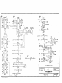
SYSTEUASTER ®
Board l.ayout
~.------~------rr-----n-----~--.-.-~--~----------~
FDe
J5
RN3
. UI
_ _ _ _ _ _ _ _---1
S:rOB
J2
SIOA
JI
.
~
~
Z-80 CPU
RN.'
--------;6 ~.. 2.. '--0 RO
RN·7
vee
z-80
DMA
.- .
---,
,..-
,--~.-
9
~D
8
WR 1--......._4~-<) WR
ViR
INT
SAO
Ii-iT
19
12
10
IORQ
S'liSRQ
2
13
07
U25
D~
04
7~ ()4
31
e~.
32
2
!2
Ol!l
02
a=--;
AI3
0/.13
I
- - - - - - - - 0 All
1010
40
--_.--0
f,1O
/1'1
J<)
...~
~.
A8
~-··----OAB
----oA7
37
...~
36
------OA6
.... -
A4
A3
33
-----<>A:5
----<:lA4
----OA3
42
t-;.-~--,.~---oO A2
AI
~----oAI
A~
REID
NMl
U40
~_--OA~
.a6
17
28
A2
RArJ
.!~.----L-15
01
~~t-5-J
II
---
R-4
!56
Mi
2
.,2.
~
"
~-
I
56
19
R6
!56
o
18
14
Il
AI2
All
AIO
~
A9
R-3
AS
-JVV-r t
22
A7
A6
A!5
~~o
A4
A3
S~ltcl:
A2
fot
1'>0
Otl.,. aU jumper.
Wait Slalll
AI
24 ~RFSH
18
Nott. All rUltior valli"
art in ohms.
• . ...... a..&A . . . ,""
•
n
-() 0-
.11
sJUMP!R
~SOLOER PAD
TP =TEST 'POINT'
TPI
(Adjac."110J51
CPU, DMA. Dynamic RAM Control, ROM
A/J
NMm,p.4
__
A7Tti
CAs
R/WR
17
AI"I
FlESET, P.4
WAiT
Rli:l
iiis
R-5
-to-RAMEN,P2
40
.....~
?
RA2
RAI
API
MSTRT
02
19
... 20
A7
34
AIO
AI
4 - AI3
... 24
3~
All
04
AI5
18
..!~
A5
_
17
. -' ,. ()J.'1
A6
~.
~7
- - - - 0 AJ4
RA:I
RA4
RA3
43
35
4-
y,PI
RA7
RAI
AS
.-
--()A15
2
AI.a ·-------oAI2
All
--"FORO,P3
~
16-----0
A 14
il-+ROM,P2.
Dp
09l
________________
14
BAI
_
MI
I~
AI,s
~£12
25
34
--'001
RN·e
_127
MI
9
ROY
14
A5
A9
33
RN·8
~l~_3
_,,5
~--......
~IEO
AI~
lor 2716, 2316
05
03
-003
RIi· 8
14
CS
29
RH-S
02
OE
06
05
!i3
0Ml
07
Ct6
-
IE I
38,. t5
36
£5/£9
Jump''' Mown or.
A12
ill
u-+
.5
E6
EIO
--B-iil--- fiO ROM
SELECT
E7
Ell
If-.-AII
28
RN-8
06
9
16
lEO
~
07
10
~
11-.+ 5
t5
15
27
RN ·8
27
23
13
E8
2!!.,.. ~
~.':i
C£
iiREQ
MREO
ROM
I:
OND
37
ONO
vee
TELETEK
Dynamic Ram Array
RAG
RA5
RA4
10
II
A6
7
RA~
.. :
RAS
-
CAS
_
./
6~"'5
A4
IS
13
II
U37
A~38
U35
U36
U34
U32
U33
12
U31
9
A~
10
7
15
3 CAS
WR
Q
Q
0
0
Q
Q
0
9
IJl
37
AI
loiii
36
A2
fNl
AO
A3
A4
B/A
t
A6
AD
0 - - - - 1 AT
8
3
18
16 0--:-+:-::;-; AROY
Q 0
I"
5
'l-51
'17K
U63
16 ASTB
"<>--(1
21 !
RN-8
4.7K
100-
.ROY
BSTB
10
~6~Bl
271
IOo----l BD
~ ~ :;I:~
~,-~
3
a
5 0--
P
.
'If\I~'''frL~, -J
1\!'1"~
.~ "'-II A~"",
tI3
fit>
4
EI4,,/'
PI, AI2 . - - .
[IT
f'15 , / •
PI ,1411.-.
G
.
I
IU26
--.!.1
~-oA~
~.WP
17
1
PI
4MsfRT
... tORO
AT ... 7
II
AS"
10
A5
"ROMEN
N/C
!!..RO
14
---
6
{-. {
,~
r----
MI
1
J;ff
m
Ta3
A/8
T02
f
TOI
iffi
TOP
07
D7
06
06
05
T62
T61
05
D4
02
o
~
Ol~"
09'
20
MI
RESET, P4
9
03
02
vee
17
TG_
CE
04
03
14
091
19..
26
lEI
IEO
01
IE S, P.3
DI
.'5
I
C'~~PiOI 1'2
+5
65
lEI
24 ., __ _
34 87
lEO _22
II
'''
I 2
f
Control Register
•
IS
P.,I
·~~~]~?_t,
8
*
09 ... -. 0
015
0
.3 0
04 .. ~- l}
~
:
AU2111
6
fC
os .. ~
0
02
0
.~-
01 .14 0
13
.~o
0_
.~-o R'oin"'N
Q
7
DECODE
__
0 [ 1 : RAMEN
06"'~
15
-1ft>
110 Select
. . I~
19
UP
12
ROM
AI
35
1~:;:./C ------ ).
.~~_ ...':5 .. !..~_~~_~
Pol
..
INr
~
25
10
31 B4
so..--.B.
7~ 86
j
.~
6
eTe-
.•
IORQ
23'
C/O
A!S
5
J -3
iliA'·
RAS
'¥WR
14
13
M!.PI"..
PIO
8~1!5
~--i0PF
A5
~J
a 0 - - . RESIT,P4
5
C-4-11
::~~::1::
RAI
r:.+
~~-~
RA7~~-:"'13
Parallel Parts
UI3
Q.
2
I
6
--0
Qr-.--'.I
JMP
Mor
c;,t~-O nil
Q ..!._-W RF'U
Q
~~--N/C
! 12
•
O~,./c
7 t:r----------14_~-~-f-SE-TI P,4
110, ROM
eTC; Control Register
, AnttOVa • ., •
..:AU,
DAT1I,
~elect) RAM; PIOi
f.-/¥-B2
DRAWN II\'
, ,~I;()'
SYSTEMASTER
REVISION 2
TEL,ETEK
R
JP
Flexible-Disk Control
!~.IA
~n
J-5
I
S10
Sena I Port 8
DIN
J-~o- __ ~60
28
6
l.1s
:3 Dour
4
RTS
1'4 Ie
~~/C
50--0('59 2 _ _
3
13
C1S
J.2! 6
8
OSR
DC D
~'I
.·r 22
SYNC8
OC08
.-~--~Hie _
II
I11.0
,
orR
14
"-.'
•.,0
,,0----,
h
DeOA
DTRA l
1&
SYNCA
i Z
RTSA rl::c-7_ _ _ _
(lNO 31
CE
23 C"'.
CTo>
"i
·~RTC8
07--~3ID7
~I
I?Z.SCK8 ......
"::;;J0.
~
05 _
04
.58
~
_'4_--.
RXCAI
"t:
I .....
"..
33
A(;--
C/o
ijj
_Mi-- 85-'NT _
1Ni'
U50
10
Fro
ROY
R£~T
"000
---<>140T"
20
m
E25
12
SCI<A, P2
32 0 RO't:A
.~
1!
RESET, P.4
21
,
FI ex ibis - Disk Controll&r Serinl ports
Data Separalor
SYSTEMASTER
REVISION 2
R
8 Rxe
N/G
TEl 67
IEO,P.I
I E---O IE S
TELETEK
•
E2~=l
~" f23~'
•
61
.. lXC
N/e
24
- I
f26 1~ll
.
•••61
j
;,: lOt: ~"'
02 _ .•
~
II DSR
.u'lE--
--"~
"I..~
TXeA
05
04
392 03
03
9 CTS-
..
I?_,13~1
fHS8
PZ, SIO
RIC
2~~
NIC
30 OTRB
ROY8
!;:fZ
o---~~
' DOUr 1
19~iO
. 4 61
1 RTS
25
~13
°J..,...,.~r------··~
;~ o.
EI
IS
7 ()-._--.jGo
MEAD
LOAD
9
29 TX08
9()-~
..... ~6
TXOArl_S_ _ _ _
26
\...--N/C
12
5
Serial Port A
12
6
RXOAt----~r-4---.J-I Pin
-;fJ
03011'1
2
RXD8
136NO T
5-100
5-100
)01
90
,OUT
106
",0
)05
390--
'0"
3a
)03
89
)01
)O~
BUS
.. s
19
16
46
18
,MEMR
PI
5
H
aINU
96
s wo* 97
0.27
)02
5-100
BUS
BUS
9
,)
~M!m.P.1
JEP.,P2
~j7
O-ti4
72
t:~~~:"}
UI4
88 0 - 12
35 09'
~
2
*
HOLD
wA
sa
C-2"
RN-6C-Z5
Pf 2 4.71(
68 PF
I. 6
: -~~'
B
.... '-;l:-t!'J Jl
I-;;'~~:i~ ---r~~
-=s,,-.6 -.--.- 1·_·· ...... - ..... .
! I ,_. --.. . . .
RN-
11141
sHl.TA
44
48
o-...-.(>:: ....~
ij
I
I
J
:;IOI~O r .. !5
'.
~
',; rL."
I~
l?
~
1)6
'I
8~
o·
.,
Ij
'"
,t:
lJ
81
~
: Ct
37
~
'3
H
,8
8 ..
9
O-~
16 I
c··•
I
~ ~
a
31
1.2
II
q,
.
~
eo
7'
UIO
"
·-·AII
2
-'-AIO
17
-A9
AB
r""
<>-~,
-
~
15
13
I
68
~A"
+
24
AI
A"
. . - . . . - _ tIIO, . . . . C.L.AA ...... W't
J
~~--
: ...:-
J
1
I
j
l III
_
~8
I~i'
CLOCK 049
t8
.. '\J'\I'-ti- t 5
f8
116
-16
GNO
20
GHO
10
-"-~Jl
'8'
S-IOO BUS Interface
. ----
PI
15
'
99 0........- -....
"NO SO
- , - _ . - U21l
0--'7"-' t.
/-RN-;'r-
o-2L~6
7S
.~.D.~ !:.I~_~l
RFSH
1~~4
54
;I-
BUS
_
1
I
poe
S·IOO
RN~~tl[--
t
Sl.AVE elfi
GND 100
--
8
.;Etl<?1339i fII -- - fNT, P.I
73
_,i
~{~~.
RN·S
10
I
~_8um.P.1
41~ ~ R-38J,:S
... t 5
RES£. r
i
I
10
14~
15
.'0, PI
.::':: ::=·f-~'2~-W.~.'~
MWRT
..
~. ~!Al
A2
"".
o- ....
1'5
~
17
C)- ._-
CDSS. 19
15
_
6 A6
~...:.....
.-.
I
6
1j I
1\
~ U29 12
76 :.~_~;.'8e·.}~:_-· .....
4
3 I
I~
}.~l:] 2
pSTVAL"25,.,
pilL DA
_.
111 '''~_1~,.
'--"
tINT
)
15
1
II. II
HALr,p.I
i'
i
/J'O
78 0--0('8
--Al2
16
&,
b
pSVNC
··--AI3
J.A7
~201t5
'" -<;}
8.5 0 '
82
30
/I
- --Al1
pOBIN
9
I
__
12
•...• J
o-/\./\./\r-t 5
1/
~~
~~
'4
"!
18 1
.7
U
<"1· }
14
I~.III!)
,6
RN-S
I
I
J"-' • M"1. P!
,J:1roo .....
0--'-
R.N-S
HI<
1-l1-..~~-t5ri55C!
t5
1
14 _.•_,~L_
,
6
T
U5
5
·_-· . ·· __ ·_-_··-z"""'rf US ol.. L !Q
15
t5 ...--l . . {
CL ~..b::...9
Cl
Q
WAIT,P.t
~N"iil1I
6..
..
>RN-6
PI
,.ifD
13
RNOS
__
5
12
" . . .1
36
J:
8
1O.fl2
I
IMn. , - 1'1- 8'2
SYSTEUASTER
REV.SlON2
TELETEK'
APPENDIX B
SYSTEMASTER DRIVE INTERFACING
. ,In controlling a disk drive from SYSTEMASTER, proper
connections must be made to the disk drive in order for it to be
operational.
The drive options must be configured as outlined in
the appropriate manufacturer's section following
this
i ntrod uct ion.
Pa rticula r 1 y i mportan t is the fact tha t the uPD7~5 continuously polls all drives in,the system to keep track of
their status. with some drives this will interfere with their
seek function (positioning of the head).
Thus, most drives will
have a stepper motor enable option, or simultanious seek option,
that powers the stepper motor continuously, rather than just when
the drive is selected.
If the d~ive won't read initially, check
for thi~. option.
Drive interfacing deals with the proper connection of
functional signals and the satisfying of electrical and
mechanical requirements.
To help ease the shock of trans i tion from the- interchang ing
of varioOs disk drives to other host controllets, a standard
known as ANSI .was developed which standardized the means of
intercommunication between disk drive and host controller by
specifying power requirements and voltage levels, edge connector
and cable specifications, and specific pin numbers of the
connector to particular functional signals.
ANSI Standards
Funeti6nal signals assigned to specific pin numbers of the
connector are shown on the next p~ge for a 5.25-inch disk drive
and an 8-inch disk drive.
~
Mini-Floppy Drives
Use of mini-floppy drives requires the use of a special 5(17
to 34 pin adapter board.
The following is a diagram of this
board and its options.
Eight inch to five and a quarter inch drive p.c. adaptor board:
8" DS 1
(0)
0
5.25" DSI
(1)
0
8" DS3 (2)
0
5.25" DS3/RDY (3)
0
I
0
(4)
5.25" DS3/RDY
I
a"
ROY
(S)
0
GND
(6)
0
I
8n
DS0
(7)
0--0
0
(9)
8" DS2
(8 )
5.25" DS0
Options:
I} pad
1.
~
to 1 - 8" drive select 1 connected
2) Pad 1 to 2 1.
to 5.25" drive select
8" drive select 2 connected to 5.25" drive select
pad 2 to 3 - 8" drive select 3 connected to 5.25" pin 6.
Normally this pin is drive select 3 for 5.25" drives but is the
READV signal for Micropolis drives.
3)
4 ) Pad 2 to 4 - 8 II d r i ve s e 1 e c t 3 con n e c ted to 5 • 2 5 " pin 3,4 •
This pin is drive select 3 for Micropolis drives or READY for
Pertee drives.
5) pad 5 to 3
8" READY connected to 5.25" pin 6.
READY pin for Micropolis drives.
This pin is
th~
6) Pad 5 to 6 - 8" READY connected to GROUND.
Since most 5.25"
drives do not provide a READY signal it is neccessary to ground
this 1 ine.
7) Pad 7
0.
to·8 -
8" driv.e select 0 connected
8 ) Pad 9 to 8 - 8 n d r i ve
0.
5
e 1e c t
2 con nee ted
to 5.25" drive select
to 5.2 5 nO'· d r i ve s e 1 e c t
Electrical
1.
Multi Drop; Bus:
Multiple drives may be connected to the
same host controller as shown in Figure 1.
Only one drive is
logically connected to the interface at a time.
2.
voltage Levels (as measured at the driver)
Logical true
Active low
+0V to +0.4V
Logical false
Active high
+2.4V to +5.SV
~.
Termination: Signal lines shall be terminated by one of two
resistive networks.
Either the signal line will have i a pull-up
res i s to r 0 f 1 5 0 0 h mS 0 r i t w i 11 h a ve a p u 11- up res i s ,to r 0 f 22"
ohms in addition to a 330 ohm resistor connecting the'signal to
ground.
4.
Signal Drivers:
The signal drivers should have open
collectox output stages capable of sinking a minimum of 40mA at
logical true (low) level, with maximum voltage of 0.4V as
measured at the driver output.
5. Signal Receivers: The signal receivers should not unduly
load the multi drop bus and should not require mote than 4euA
current from the driver at input high (2.4V) nor supply more than
1.6mA to a current sink at input low (0.4V) level.
Interconnecting Cable
Conductor Size
Copper- AWG #30 or larger for ~olid conductor
AWG #28 or larger for stranded conductor
Non-copper- Sufficient size as to yield a dc resistance not
to
exceed 110 Ohms per 1000 ft. per conductor.
Stray capacitance- Capacitance between 'One wire in a cable
and all others in the cable with all others connected to
ground shall not exceed 40pF/ft. and the value shall be
reasonably uniform over the length of the cable.
Mutual pair capacitance- Capacitance between one wire of the
pair to the other shall not exceed 20pF/ft. and the value
should be reasonably uniform over the length of the cable.
ANSI Standard for 5.25 Inch Drive
Signal
Pin No.
2
4
Ground
pin No.
1
3
6
5
8
10
7
9
11
13
15
17
19
12
14
16
18
20
22
24
26
28
30·'
32
34
21
23
25
27
29
31
33
Signal
Not assigned (Head load)
In use control
Drive select 3 (Ready)
Index/sector
Drive select
Drive select 1
Drive select 2
Motor on
Direction select
Step
Composi te write data
Wr i te gate
Track 0
Wr i te protected
Compos i te read data
Side one select
Disk change (Dr i ve select 3)
"
ANSI Standard for 8-Inch Drive
Signal
Pin No.
2
4
Ground
pin No.
1
8
10
12
14
3
5
7
9
11
13
16
15
18
20
17
19
22
24
21
23
26
28
30
25
27
29
32
31
34
36
33
35
38
40
42
37
6
44
46
48
50
~9
41
43
45
,17
49
Signal
Head current switch
Not assigned
Not assigned
Drive busy
Two-sided
Disk change
Side one select
In use control
Head load
Index
Drive ready
Sector
Drive select 0
Drive select 1
Drive select 2
Drive select 3
Direction select
Step
Com pas i te wr i te data
Wr i te ga te
Track 0
Wr i te protected
Composi te read data
Separated read data
separated read clock
landon TMIOO Disk Drive
Required configuration:
1. MX
2. HS
3. HM
3. NOSO-NDS3
Open
Jumper
Open
Select appropriate drive address
Install the termination network 2F in the last drive only.
Eaen drive. requires +12 volts at O.9A and +5 volts at O.6A.
Required Pre-write Compensation:
none.
23
Shugart 850/851 ~ Drive
Required configuration:
(Shunts with
1. X *
*
next to them are on shunt block at IC location 4E)
Shunt intact
2. DC
Open
3. D
Open
Jumper
4. C
5. I
*
Shunt intact
6. R *
7. S*
8. OSl-4
*
9. HL
10. OS
Open
i~: ~~ }l~~.it -
13. Y
14.
15.
16· ~
17.
18.
Z *
850
851
A *
B *
19. IB
2U.
21.
22.
23.
24.
25.
26.
t
~~:~: ~ ~~:~~
Open
Shunt intact
Jumper
Open
Shunt intact
Snunt open
2B, 33, 4B
25
Ope n
Jumper
WP'}lt'li
NP
S1
Shunt intact
Snunt intact
Select appropriate drive address
Snunt open
i:: Jr.";-I
S2
53
DL
Trace in tdC t
Open
Open
Jumper
Open
Jumper
27. M
Jurnper
28. IS
Open
29. FS
~
30. IWr
Jumper
Jumper
31.
32.
"33.
34.
35.
WE SUGGEST BENDING "
THE P INS ON THE SHUNT
BLOCK AT 4E TO OPEN
THKH INSTEAD OF CUTTING .
THE SHlmT THROUGH.
RS
RM
HLL
IT
HI
36. Fnn
Open
Open
Jumper
Open
Open
37. ~M 1::"'"
38. IfF /1'12 Fh1
Open
[ .. :r-~ f..:
Jumper
~~ /;fe. Ltt'G:""
~·)/I(:·/V' .Lt.:.';;"C
Install tne termination network t~ in tne last drive only.
Eacn drive requires +24 volts at 1.OA and +5 volts at 1.lA.
Required Pre-write Compensation:
250 ns.
22
Snugart 800/801 Disk Drive
Required drive configuration:
1. X
2. DC
3. 0
4. C
5. I
6. R
7. S
8. OS 1-4
9. T l~ 3, 4, 5, 6
10. T2
11.. HL
Jumper
Open
Open
Jumper
Trace intact
Trace intact
Trace intact
Select appropriate drive address
Jumper on last drive"in system
Jumper
Open
12. OS
Open
13. RI
14. RR
Trace intact
Trace intact
Open
Jumper
Jumper
15. Y
..16. Z
17. 800
18. 801
Open
19. A
Jumper
20. B
Open
Each drive requires 24 volts at 1.7A, +5 volts at l.OA, and-5
volts at O.07A. Note: Many power supplies for floppy drives do
not have tne requi red current capabi 1 i ty for 2 or more Shugart
drives.
Required Pre-write compensation:
250 ns.
13
Qume OT-8 Disk Drlve
---------Required drive configurdtion:
L A
Jumper
2. B
R
Open
Jumper
Jumper
Open
Jumper
I
jumper
3.
4.
5.
b.
7.
8.
9.
:0.
X
Z
HL
RI
RR
C
lI. D
12. DC
13 .. ?S
14. DS
.15. y
16. DL
17 .. \~ P
lB. NP
194
~.;2
;~O.
S 1, S3
Trace intact
Trace intact
Jumper
Open
Open
Jumper
Open
Open
Open
Trctce intact
0pt:n
T;-ac(: lntact
Upen
21. 051-4
Select appropriate drive address
22 .. 131,2,3,4
Open
instd11 2 reS.lstor term1tldtor modules into the last dnve in the
dalSY
Cdcri
cr.ain.
cirive requires
(~4 volts dt U.9(\ and 5
Required Pre-write Compcnsdtlon:
none.
12
volts at l.lA.