1
ACCES I/O PRODUCTS INC
10623 Roselle Street, San Diego, CA 92121
TEL (858)550-9559
FAX (858)550-7322
MODEL RDG-24
USER MANUAL
FILE: MRDG-24.C2c
Notice
The information in this document is provided for reference only. ACCES does not assume any liability
arising out of the application or use of the information or products described herein. This document may
contain or reference information and products protected by copyrights or patents and does not convey any
license under the patent rights of ACCES, nor the rights of others.
IBM PC, PC/XT, and PC/AT are registered trademarks of the International Business Machines Corporation.
Printed in USA. Copyright 1995 by ACCES I/O Products Inc, 10623 Roselle Street, San Diego, CA 92121.
All rights reserved.
Page iii
Warranty
Prior to shipment, ACCES equipment is thoroughly inspected and tested to applicable specifications.
However, should equipment failure occur, ACCES assures its customers that prompt service and support
will be available. All equipment originally manufactured by ACCES which is found to be defective will be
repaired or replaced subject to the following considerations.
Terms and Conditions
If a unit is suspected of failure, contact ACCES' Customer Service department. Be prepared to give the unit
model number, serial number, and a description of the failure symptom(s). We may suggest some simple
tests to confirm the failure. We will assign a Return Material Authorization (RMA) number which must
appear on the outer label of the return package. All units/components should be properly packed for handling
and returned with freight prepaid to the ACCES designated Service Center, and will be returned to the
customer's/user's site freight prepaid and invoiced.
Coverage
First Three Years: Returned unit/part will be repaired and/or replaced at ACCES option with no charge for
labor or parts not excluded by warranty. Warranty commences with equipment shipment.
Following Years: Throughout your equipment's lifetime, ACCES stands ready to provide on-site or in-plant
service at reasonable rates similar to those of other manufacturers in the industry.
Equipment Not Manufactured by ACCES
Equipment provided but not manufactured by ACCES is warranted and will be repaired according to the
terms and conditions of the respective equipment manufacturer's warranty.
General
Under this Warranty, liability of ACCES is limited to replacing, repairing or issuing credit (at ACCES
discretion) for any products which are proved to be defective during the warranty period. In no case is
ACCES liable for consequential or special damage arriving from use or misuse of our product. The
customer is responsible for all charges caused by modifications or additions to ACCES equipment not
approved in writing by ACCES or, if in ACCES opinion the equipment has been subjected to abnormal use.
"Abnormal use" for purposes of this warranty is defined as any use to which the equipment is exposed other
than that use specified or intended as evidenced by purchase or sales representation. Other than the above,
no other warranty, expressed or implied, shall apply to any and all such equipment furnished or sold by
ACCES.
Page iv
Table of Contents
Chapter 1: Introduction . . . . . . . . . . . . . . . . . . . . . . . . . . . . . . . . . . . . . . . . . . . . . . 1-1
Description . . . . . . . . . . . . . . . . . . . . . . . . . . . . . . . . . . . . . . . . . . . . . . . . . . . . . . . . . . . 1-1
Specifications . . . . . . . . . . . . . . . . . . . . . . . . . . . . . . . . . . . . . . . . . . . . . . . . . . . . . . . . . 1-3
Chapter 2: Installation . . . . . . . . . . . . . . . . . . . . . . . . . . . . . . . . . . . . . . . . . . . . . . 2-1
CD Installation . . . . . . . . . . . . . . . . . . . . . . . . . . . . . . . . . . . . . . . . . . . . . . . . . . . . . . . . .
3.5-Inch Diskette Installation . . . . . . . . . . . . . . . . . . . . . . . . . . . . . . . . . . . . . . . . . . . . . .
Directories Created on the Hard Disk . . . . . . . . . . . . . . . . . . . . . . . . . . . . . . . . . . . . . . .
Installing the Pod . . . . . . . . . . . . . . . . . . . . . . . . . . . . . . . . . . . . . . . . . . . . . . . . . . . . . . .
Digital Input/Output Pin Connections . . . . . . . . . . . . . . . . . . . . . . . . . . . . . . . . . . . . . . . .
2-1
2-1
2-2
2-5
2-7
Chapter 3: Software . . . . . . . . . . . . . . . . . . . . . . . . . . . . . . . . . . . . . . . . . . . . . . . . . 3-1
Command Functions . . . . . . . . . . . . . . . . . . . . . . . . . . . . . . . . . . . . . . . . . . . . . . . . . . . . 3-3
Error Codes . . . . . . . . . . . . . . . . . . . . . . . . . . . . . . . . . . . . . . . . . . . . . . . . . . . . . . . . . . 3-14
Appendix A: Application Considerations . . . . . . . . . . . . . . . . . . . . . . . . . . . . . . A-1
Introduction . . . . . . . . . . . . . . . . . . . . . . . . . . . . . . . . . . . . . . . . . . . . . . . . . . . . . . . . . . . A-1
Balanced Differential Signals . . . . . . . . . . . . . . . . . . . . . . . . . . . . . . . . . . . . . . . . . . . . . . A-1
RS485 Data Transmission . . . . . . . . . . . . . . . . . . . . . . . . . . . . . . . . . . . . . . . . . . . . . . . A-3
Page v
List of Figures
Figure 1-1:
Figure 1-2:
Figure 2-1:
Figure A-1:
Connecting External Voltage (EXV) . . . . . . . . . . . . . . . . . . . . . . . . . . . . . . . . . .
Block Diagram . . . . . . . . . . . . . . . . . . . . . . . . . . . . . . . . . . . . . . . . . . . . . . . . . .
Option Selection Map . . . . . . . . . . . . . . . . . . . . . . . . . . . . . . . . . . . . . . . . . . . . .
Typical RS485 Two-Wire Multidrop Network . . . . . . . . . . . . . . . . . . . . . . . . . . .
1-4
1-6
2-6
A-3
List of Tables
Table 2-1:
Table 2-2:
Table A-1:
Table A-2:
Page vi
50 Pin Connector Assignments . . . . . . . . . . . . . . . . . . . . . . . . . . . . . . . . . . . . . .
37 Pin Connector Assignments . . . . . . . . . . . . . . . . . . . . . . . . . . . . . . . . . . . . . .
Connections Between Two RS422 Devices . . . . . . . . . . . . . . . . . . . . . . . . . . . .
RS422 Specification Summary . . . . . . . . . . . . . . . . . . . . . . . . . . . . . . . . . . . . . .
2-8
2-9
A-1
A-2
Chapter 1: Introduction
Features
•
•
•
•
•
•
•
•
•
•
Opto-Isolated RS485 Serial Interface to Host Computer.
24-Bit Digital I/O Programmable Bit-by-Bit, in 8-Bit Bytes, or in 24-Bit Words.
Digital Input and Output Voltages up to 50VDC.
Open Collector Digital Outputs for Loads up to 350mA.
Protective Steel Enclosure.
Type 8031 Microcontroller with 8K x 8 RAM and 8K x 8 EEPROM (32K x 8 optional).
All Programming in Software, No Switches to Set. Jumper to Set 2-Wire or 4-Wire modes,
and Jumpers (3) to By-Pass Opto-Isolators if Desired.
16-Bit Digital-Input Software Counters.
Change of State Flag Readable via the Serial Port.
Digital Outputs May Be Either Level or Pulse.
Description
RDG-24 is an intelligent, 24-bit parallel, digital-I/O-to-computer interface unit. Communication
with the host computer is via EIA RS485, full- or half-duplex, serial communications protocol.
ASCII-based command/response protocol permits communication with virtually any computer
system. RDG-24 is one of a series of remote intelligent pods called the "REMOTE ACCES Series".
As many as 32 REMOTE ACCES Series pods (or other RS485 devices) may be connected on a
single two- or four-wire multidrop RS485 network. Each unit has a unique address. Communication
uses a master/slave protocol wherein the pod talks only if questioned by the computer.
A type 8031 microcontroller (with 8x8K RAM, 8x8K non-volatile EEPROM, and a watchdog timer
circuit) gives RDG-24 the capability and versatility expected from a modern distributed control
system. To accommodate special programs, the RAM and EEPROM can each be expanded to
8x32K. The unit contains CMOS low-power circuitry, an optically-isolated receiver/transmitter, and
power conditioners for local and external isolated power. It can operate at baud rates up to 57.6
Kbaud and distances up to 4000 feet with low-attenuation twisted-pair cabling.
All programming of RDG-24 is in ASCII-based software. ASCII-based programming permits you
to write applications in any high-level language that supports ASCII string functions and you can use
ACCES "R" series pods with virtually any computer.
Manual MRDG-24.C2c
Page 1-1
RDG-24 Manual
The module, or pod, address is programmable from 00 to FF hex and whatever address is assigned
is stored in EEPROM and used as the default address at the next Power-ON. Similarly, the baud rate
is programmable for 1200, 2400, 4800, 9600, 14400, 19200, 28800, and 57600. The address is
stored in EEPROM and used as default at the next Power-ON.
The time base, used in all time-relevant operations is also software selectable between:
a.
b.
Digital input sample rate from 14 Hz to 1 KHz
Digital output square wave pulse from 7 Hz to 500 Hz
Digital inputs of up to 50V may be read individually, or in 8-bit bytes, or in 24-bit word groups.
There are also digital software counters on each input. Selectable edges can be counted for up to
65,535 transitions. These counters support Read and Reset commands. Moreover, change-of-state
flags can be set on any enabled input bits and can be read via the serial port. This is particularly
useful in applications where it's necessary to detect contact closures or openings. This
change-of-state detection capability is enabled on a bit-by-bit basis for all bits programmed for input.
Digital outputs may be programmed individually, or in 8-bit bytes, or in 24-bit words. These outputs
may be latched, pulsed, or set to free-run for a prescribed period of time. The digital output drivers
are open collector circuits that have 350 mA drive capability at a logic "low". The unit can comply
with up to 50 VDC (voltage supplied by you). With no external voltage (EXV) supplied the outputs
are pulled up by a 10 KS resistor to 5 VDC.
The built-in watchdog timer resets the pod if, for some unexpected reason, the microcontroller
"hangs up". Data collected by the pod can be stored in local RAM and accessed later through the
computer's serial port. This facilitates a stand-alone pod mode of operation.
Page 1-2
Manual MRDG-24.C2c
Specifications
Serial Communications Interface
•
•
•
•
•
•
Serial Port:
Opto-isolated Matlabs type LTC491 Transmitter/Receiver. Compatible
with RS485 specification. Up to 32 drivers and receivers allowed on line.
I/O bus programmable from 00 to FF hex (0 to 255 decimal). Whatever
address is assigned is stored in EEPROM and used as default at next
Power-On.
Input Common Mode Voltage:
300V minimum (opto-isolated). If opto-isolators
are by-passed: -7V to +12V.
Receiver Input Sensitivity:
±200 mV, differential input.
Receiver Input Impedance:
12KW minimum.
Transmitter Output Drive Capability: 60 mA, 100 mA short circuit current capability.
Serial Data Rates:
Programmable for 1200, 2400, 4800, 9600, 14400,
19200, 28800, and 57600 baud. Crystal oscillator
provided.
Digital Inputs
•
•
•
•
•
•
•
•
Number:
Up to 24. Can be programmed, on a bit-by-bit basis, on an 8-bit
byte basis, or on a 24-bit word basis. In this latter case, there
would be no capability for digital outputs.
Sample Rate:
Programmable from 14 Hz to 1 KHz.
Software Counters:
There are 16-bit software counters on all bits programmed to be
inputs. These can be programmed to increment on either rising or
falling edges.
Change of State Detection:
Change-of-state flags can be set on any enabled input bits
and can be read via the serial port.
Logic Input Low:
-0.5V to +0.8V.
Logic Input High:
+2.0V to +50.0V.
Low-level Input Current:
-450 mA maximum.
All digital I/O lines are pulled up to +5VDC via 10KS resistors. This is useful for
monitoring dry contacts.
Manual MRDG-24.C2c
Page 1-3
RDG-24 Manual
Digital Outputs
•
•
•
•
Number:
Up to 24. Can be programmed, on a bit-by-bit basis, on an 8-bit byte basis,
or on a 24-bit word basis. In this latter case, there would be no capability
for digital inputs. (The inputs would read back the output value only.).
Type:
Outputs can be latched, pulsed, or set to free-run for a prescribed period of
time. Pulsed outputs are square wave and programmable from 7 Hz to 500
Hz.
High-Level Output Voltage:
Open Collector, compliance with up to 50VDC. With no
external voltage (EXV) supplied the outputs are pulled up
by a 10 KS resistor to 5 VDC.
Logic-Low Output Current:
350 mA maximum. (See note below.) Inductive
suppression diode included in the each circuit.
Note
Maximum allowable current per output bit is 350 mA but, for each six-bit group, there is a maximum
cumulative total of 650 mA. Output groups are bits 0-5, 6-11, 12-17, and 18-23 (decimal).
Figure 1-1: Connecting External Voltage (EXV)
Page 1-4
Manual MRDG-24.C2c
Environmental
•
•
Operating Temperature Range: 0 °C. to 65 °C. (Optional -40 to +80 C).
Temperature De-rating:
Ambient temperature de-rating must be considered based
on the power level applied. When 7.5VDC is applied, the
temperature rise inside the enclosure is 7.3 °C. above the
ambient temperature.
The equation to determine maximum temperature de-rating is:
VI(TJ = 120) < 22.5 - 0.2 TA
Where TA is the ambient temperature in °C. and VI(TJ = 120) is the voltage at which the integral voltage
regulator junction temperature will rise to a temperature of 120 °C. (Note: The junction temperature
is rated to 150 °C. maximum.)
For example, at an ambient temperature of 25 °C., the voltage VI can be up to 18.4V. At an ambient
temperature of 100 °F. (37.8 °C.), the voltage VI can be up to 16.6V.
•
•
•
Storage Temperature Range:
Humidity:
Size:
-50 °C. to +120 °C.
5% to 95% RH non-condensing.
Enclosure 8.5" long by 5.25" wide by 2" high.
Power Required
•
•
•
Power can be applied from the computer's +12VDC power supply for the opto-isolated
section via the serial communication cable and from a local power supply for the rest of the
unit.
Opto-Isolated Section: 7.5 to 25 VDC @ 40 mA. (Note: Due to the small amount of
current required, voltage drop in the communication cable is not
significant.)
Local Power (PWR+): 7.5 to 16 VDC @ 150mA. (See box below.)
If the local power supply has an output voltage greater than 16VDC, you can install a zener diode
in series with the supply voltage. The voltage rating of the zener diode (VZ) should be equal to VI-16
where VI is the power supply voltage. The power rating of the zener diode should be $ VZ x 0.12
watts. Thus, for example, a 24VDC power supply would require using an 8.2V zener diode with a
power rating of 8.2 x 0.12 . 1 watt.
Manual MRDG-24.C2c
Page 1-5
RDG-24 Manual
Figure 1-2: Block Diagram
Page 1-6
Manual MRDG-24.C2c
Chapter 2: Installation
The software provided with this card is contained on either one CD or multiple diskettes and must
be installed onto your hard disk prior to use. To do this, perform the following steps as appropriate
for your software format and operating system. Substitute the appropriate drive letter for your
CD-ROM or disk drive where you see d: or a: respectively in the examples below.
CD Installation
DOS/WIN3.x
a.
b.
c.
d.
Place the CD into your CD-ROM drive.
Type d:K to change the active drive to the CD-ROM drive.
Type installK to run the install program.
Follow the on-screen prompts to install the software for this card.
WIN95/98/NT
a.
b.
c.
Place the CD into your CD-ROM drive.
The CD should automatically run the install program after 30 seconds. If the install program
does not run, click START | RUN and type d:install, click OK or press K.
Follow the on-screen prompts to install the software for this card.
3.5-Inch Diskette Installation
As with any software package, you should make backup copies for everyday use and store your
original master diskettes in a safe location. The easiest way to make a backup copy is to use the DOS
DISKCOPY utility.
In a single-drive system, the command is:
diskcopy a: a:K
You will need to swap disks as requested by the system.
In a two-disk system, the command is:
diskcopy a: b:K
This will copy the contents of the master disk in drive A to the backup disk in drive B.
Manual MRDG-24.C2c
Page 2-1
RDG-24 Manual
To copy the files on the master diskette to your hard disk, perform the following steps.
a.
Place the master diskette into a floppy drive.
b.
Change the active drive to the drive that has the diskette installed. For example, if the
diskette is in drive A, type a:K.
c.
Type installK and follow the on-screen prompts.
Directories Created on the Hard Disk
The installation process will create several directories on your hard disk. If you accept the
installation defaults, the following structure will exist.
[CARDNAME]
Root or base directory containing the SETUP.EXE setup program used to help you configure
jumpers and calibrate the card.
DOS\PSAMPLES:
DOS\CSAMPLES:
Win32\language:
A subdirectory of [CARDNAME] that contains Pascal samples.
A subdirectory of [CARDNAME] that contains "C" samples.
Subdirectories containing samples for Win95/98 and NT.
WinRisc.exe
A Windows dumb-terminal type communication program designed for RS422/485 operation.
Used primarily with Remote Data Acquisition Pods and our RS422/485 serial communication
product line. Can be used to say hello to an installed modem.
ACCES32
This directory contains the Windows 95/98/NT driver used to provide access to the hardware
registers when writing 32-bit Windows software. Several samples are provided in a variety of
languages to demonstrate how to use this driver. The DLL provides four functions (InPortB,
OutPortB, InPort, and OutPort) to access the hardware.
This directory also contains the device driver for Windows NT, ACCESNT.SYS. This device driver
provides register-level hardware access in Windows NT. Two methods of using the driver are
available, through ACCES32.DLL (recommended) and through the DeviceIOControl handles
provided by ACCESNT.SYS (slightly faster).
Page 2-2
Manual MRDG-24.C2c
SAMPLES
Samples for using ACCES32.DLL are provided in this directory. Using this DLL not only
makes the hardware programming easier (MUCH easier), but also one source file can be used
for both Windows 95/98 and WindowsNT. One executable can run under both operating
systems and still have full access to the hardware registers. The DLL is used exactly like any
other DLL, so it is compatible with any language capable of using 32-bit DLLs. Consult the
manuals provided with your language's compiler for information on using DLLs in your specific
environment.
VBACCES
This directory contains sixteen-bit DLL drivers for use with VisualBASIC 3.0 and Windows 3.1
only. These drivers provide four functions, similar to the ACCES32.DLL. However, this DLL is
only compatible with 16-bit executables. Migration from 16-bit to 32-bit is simplified because of
the similarity between VBACCES and ACCES32.
PCI
This directory contains PCI-bus specific programs and information. If you are not using a PCI card,
this directory will not be installed.
SOURCE
A utility program is provided with source code you can use to determine allocated resources at
run-time from your own programs in DOS.
PCIFind.exe
A utility for DOS and Windows to determine what base addresses and IRQs are allocated to
installed PCI cards. This program runs two versions, depending on the operating system. Windows
95/98/NT displays a GUI interface, and modifies the registry. When run from DOS or Windows3.x,
a text interface is used. For information about the format of the registry key, consult the
card-specific samples provided with the hardware. In Windows NT, NTioPCI.SYS runs each time
the computer is booted, thereby refreshing the registry as PCI hardware is added or removed. In
Windows 95/98/NT PCIFind.EXE places itself in the boot-sequence of the OS to refresh the registry
on each power-up.
This program also provides some COM configuration when used with PCI COM ports. Specifically,
it will configure compatible COM cards for IRQ sharing and multiple port issues.
WIN32IRQ
This directory provides a generic interface for IRQ handling in Windows 95/98/NT. Source code
is provided for the driver, greatly simplifying the creation of custom drivers for specific needs.
Samples are provided to demonstrate the use of the generic driver. Note that the use of IRQs in
near-real-time data acquisition programs requires multi-threaded application programming
techniques and must be considered an intermediate to advanced programming topic. Delphi, C++
Builder, and Visual C++ samples are provided.
Manual MRDG-24.C2c
Page 2-3
RDG-24 Manual
Findbase.exe
DOS utility to determine an available base address for ISA bus , non-Plug-n-Play cards. Run this
program once, before the hardware is installed in the computer, to determine an available address
to give the card. Once the address has been determined, run the setup program provided with the
hardware to see instructions on setting the address switch and various option selections.
Poly.exe
A generic utility to convert a table of data into an nth order polynomial. Useful for calculating
linearization polynomial coefficients for thermocouples and other non-linear sensors.
Risc.bat
A batch file demonstrating the command line parameters of RISCTerm.exe.
RISCTerm.exe
A dumb-terminal type communication program designed for RS422/485 operation. Used primarily
with Remote Data Acquisition Pods and our RS422/485 serial communication product line. Can be
used to say hello to an installed modem. RISCTerm stands for Really Incredibly Simple
Communications TERMinal.
Page 2-4
Manual MRDG-24.C2c
Installing the Pod
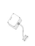
The RDG-24 enclosure is an easily-mounted steel enclosure. Outside dimensions of the enclosure
are: 8.5" long by 5.25" wide by 2" high. The cover is secured to the body by four Phillips-head
screws. Four threaded bosses inside the enclosure provide for mounting the printed circuit card
assemblies. The enclosure has a notch at one end for external power wiring and a deeper notch at
the other end for input and output wiring.
Electrical power RS485 connections to the pod are made at Terminal Board TB1.
markings and their functions are as follows:
Terminal
ISO GND and ISO.PWR:
This is the power connection from the computer's +12VDC supply
via telephone cable on the RS485 network or from a central power
supply. This powers the isolator section and is independent of
"local power". The voltage level can be from 7.5 VDC to 35
VDC. (An on-board voltage regulator regulates the power to +5
VDC.) RDG-24 will require only about 7 mA of current and, thus,
any voltage drop of computer power will be inconsequential. If
separate power is not available, then, with some loss of isolation,
these terminals can be jumpered to the "local power" terminals.
RX+ and RX- :
These are the differential "receive" inputs for four-wire RS485
communications. If two-wire connection is to be used, install
jumpers from RX+ to TX+ and from RX- to TX-.
TX+ and TX- :
These are the differential "transmit" outputs for four-wire RS485
communications. If two-wire connection is to be used, install
jumpers as described above.
EXV:
This terminal is for the "application power" or the voltage level to
which digital inputs and outputs are connected through the loads
or external signal sources.Open-collector Darlington amplifiers are
used at the outputs. Inductive suppression diodes are included and
the application power level can be as high as 50 VDC.
PWR + and GND:
These terminals can be used to apply power to the pod from a local
power supply. If a local power supply is used, the voltage can be
anywhere in the range from 7.5 VDC to 16 VDC. Higher local
power can be used, 24 VDC for example, if an external zener diode
is used to reduce the voltage applied to the RDG-24. ( See the
Specification section of this manual to determine the zener diode
power rating required.)
Manual MRDG-24.C2c
Page 2-5
RDG-24 Manual
Figure 2-1: Option Selection Map
Page 2-6
Manual MRDG-24.C2c
There are three jumper locations on the card. Locations are as shown on the Option Selection Map
and their functions are as follows:
JP2, JP3, and JP4:
Normally these jumpers should be in the "ISL" position. If you
wish to by-pass the opto-isolators, then you can move these
jumpers to the "/ISL" position.
Digital Input/Output Pin Connections
Digital input and output connections can be made in any of three ways: (a) at Euro style screw
terminals TB2, TB3, TB4, and TB5; or (b) at 50-pin, keyed, male, insulation-displacement type,
ribbon cable connector J2; or (c) at 37-pin, male, sub-D connector J1.
Screw Terminal Connections
Digital I/O connection points at the screw terminal connectors are as marked on the printed circuit
board at terminals TB2 and TB3. Bit locations are numbered 00 through 23 (decimal). Note also
that a terminal labeled XRST is provided at TB5 for Reset signals to the microprocessor. The other
terminals on TB5 and TB4 provide ground returns for the I/O signals.
Manual MRDG-24.C2c
Page 2-7
RDG-24 Manual
50-Pin Connector
Connector pin assignments for the 50-pin connector are listed below. Note that alternate wires in
the ribbon cable will be connected to ground. This provides means to isolate the digital signals from
each other in the cabling.
Pin
Signal
Pin
Signal
1
I/O23
26
Gnd
2
Gnd
27
I/O10
3
I/O22
28
Gnd
4
Gnd
29
I/O09
5
I/O21
30
Gnd
6
Gnd
31
I/O08
7
I/O20
32
Gnd
8
Gnd
33
I/O07
9
I/O19
34
Gnd
10
Gnd
35
I/O06
11
I/O18
36
Gnd
12
Gnd
37
I/O05
13
I/O17
38
Gnd
14
Gnd
39
I/O04
15
I/O16
40
Gnd
16
Gnd
41
I/O03
17
I/O15
42
Gnd
18
Gnd
43
I/O02
19
I/O14
44
Gnd
20
Gnd
45
I/O01
21
I/O13
46
Gnd
22
Gnd
47
I/O00
23
I/O12
48
Gnd
24
Gnd
49
Ext Reset
25
I/O11
50
Gnd
Table 2-1: 50 Pin Connector Assignments
Page 2-8
Manual MRDG-24.C2c
37 Pin Connector J1 (Optional)
Connector pin assignments for the 37-pin connector are listed below. Note that, since this connector
would normally not mate with a ribbon cable, alternate-ground pins are not provided (there would
not be enough pins anyway). Also, note that there is provision for external Reset, for a Timer signal,
and for Interrupts 0 and 1.
Pin
Signal
Pin
Signal
1
I/O 00
19
I/O 18
2
I/O 01
20
I/O 19
3
I/O 02
21
I/O 20
4
I/O 03
22
I/O 21
5
I/O 04
23
I/O 22
6
I/O 05
24
I/O 23
7
I/O 06
25
Gnd
8
I/O 07
26
Resv'd (/Int 1)
9
I/O 08
27
Resv'd (TMR 0)
10
I/O 09
28
Resv'd (Int 0)
11
I/O 10
29
Gnd
12
I/O 11
30
PWR+
13
I/O 12
31
R(+)
14
I/O 13
32
R(-)
15
I/O 14
33
Isolator Pwr
16
I/O 15
34
Isolator Pwr Gnd
17
I/O 16
35
EXV
18
I/O 17
36
EXV Gnd
37
Reset
Table 2-2: 37 Pin Connector Assignments
Units that are marked for CE (European) Certification are installed in a NEMA 4 enclosure rather
than the T-BOX metal enclosure referred to earlier. Further, to ensure that there is minimum
susceptibility to EMI and minimum radiation, it is important that there be a positive chassis ground.
Proper EMI cabling techniques (cable connected to chassis ground at the aperture, tristed pair wiring,
and, in extreme cases, ferrite-level of EMI protection) must be used.
CE-marked versions of RDG-24 meet the requirements of EN50081-1:1992 (Emissions),
EN50082-1:1992 (Immunity), and EN60950:1992 (Safety).
Manual MRDG-24.C2c
Page 2-9
RDG-24 Manual
Page 2-10
Manual MRDG-24.C2c
Chapter 3: Software
General
You received ASCII-based software on CD for use with RDG-24. ASCII programming permits you
to write applications in any high level language that supports ASCII string functions.
The communication protocol has two forms: addressed and non-addressed. Non-addressed protocol
can be used when only one RDG-24 is in use. If more than one RDG-24 is in use, you must use
addressed protocol. The difference is that an address command is sent to enable the specific pod.
The address command is only sent once during communication between the pod and the host
computer. It enables communication with that specific pod and disables all other devices on the
network.
Command Structure
All communication must be 7 data bits, even parity, 1 stop bit. All numbers sent to or received from
the pod are in hexadecimal form. The factory default baud rate is 9600 Baud. The pod is considered
to be in addressed mode any time its pod address is not 00. The factory default pod address is 00
(non-addressed mode).
Addressed Mode
The address select command must be issued before any other command to the addressed pod. The
address command is as follows:
"!xx[CR]" where xx is the pod address from 01 to FF hex, and [CR] is Carriage Return, ASCII
character 13.
The pod responds with either "xxN[CR]" or "xxY[CR]" if an input change of state has occurred on
enabled bits since the last "Y" or address command. Once the address select command has been
issued, all further commands (other than a new address select) will be executed by the selected pod.
The addressed mode is required when using more than one pod.
Non-Addressed Mode
When there's only one pod connected, no address select command is needed. You can merely issue
commands listed in the following table. Terminology used is as follows:
a.
b.
c.
d.
e.
f.
g.
The single lower case letter 'x' designates any valid hex digit (0-F).
The single lower case letter 'b' designates either a '1' or '0'.
The symbol '±' designates either a '+' or a '-'.
All commands are terminated with CR, the ASCII character #13.
Wherever xx is used to designate a bit number, only 00-17 hex are valid.
Commands are not case-sensitive; i.e., upper- or lower case letters may be used..
The symbol '*' means zero or more valid characters (total msg length<255 decimal)
Manual MRDG-24.C2c
Page 3-1
RDG-24 Manual
Command List
Sxxxx
Scxxxx
Mlxx
Mmxx
Mhxx
I
Ixx
IL
IM
IH
Oxxxxxx
Ox±
Oxx±
Ox±xx
Oxx±xx
OLxx
OMxx
OHxx
Oxx±xx
Fxx,xx
Y
TLxx
TMxx
THxx
Dx±
Dxx±
Cxx
or
Rxx
Rall
V
N
H*
BAUD=xxx
POD=xx
PROGRAM=
D
FASTDATAL
FASTDATAM
FASTDATAH
!xx
Page 3-2
Set a new timebase. 039A<xxxx<=FFFF
Set a new timebase, and reset all free-run and pulse DOs
Configure bits 00-07 as input/output. 0=in, 1=out
Configure bits 08-0F as input/output. 0=in, 1=out
Configure bits 10-17 as input/output. 0=in, 1=out
Read all 24 digital bits.
Read a single digital bit. (00<=xx<=17)
Read digital bits 00-07
Read digital bits 08-0F
Read digital bits 10-17
Output all 24 digital bits.
Output either high or low on bit x
Output either high or low on bit xx
Output either high or low on bit x for time xx
Output either high or low on bit xx for time xx
Output xx on bits 00-07
Output xx on bits 08-0F
Output xx on bits 10-17
Output either high or low on bit xx for time xx
Set Digital Output xx to free run with period xx
Read digital input Change Of State bit and clear bit
Y or N
Set bit 00-07 Mask for COST bit flag, 1=change will set COST
Set bit 08-0F Mask for COST bit flag
Set bit 10-17 Mask for COST bit flag
Set digital input active state high or low on bit x
Set digital input active state high or low on bit xx
Read digital input xx counter (counts each active pulse)
Read pulse/free-run output xx counter and reload value
Reset digital input counter xx to 0000
Reset all digital input counters to 0000
Read the Firmware version number
Resend last response
Greeting message: copyright, firmware version number
Set new baud rate. Each x is code number for new baud
Set pod address to xx
Begin process of uploading custom program to pod
Download historical storage of digital input data again
Acquire bits 0-7 as fast as possible, then display
Acquire bits 8-F as fast as possible, then display
Acquire bits 10-17 as fast as possible, then display
Address Select Command, Selects the POD at address 'xx'
for communication.
CR
CR
CR
CR
CR
xxxxxxCR
bCR
xxCR
xxCR
xxCR
CR
CR
CR
CR
CR
CR
CR
CR
CR
CR
CR
CR
CR
CR
CR
xxxxCR
xxxxCR
CR
CR
x.xxCR
varies
varies
=:Baud:0x
varies
special
varies
varies
varies
varies
CR
Manual MRDG-24.C2c
Command Functions
The following paragraphs give details of the command functions, describe what the commands
cause, and give examples. Please note that all commands have an acknowledgment response. You
must wait for a response from a command before sending another command.
Set Time Base
Sxxxx
Scxxxx
Set Time Base
Set Time Base with Output Synchronization
This function sets the pod-global timebase which is used in all time-sensitive operations. Valid
values range from 039A to FFFF. Any invalid value will result in the pod-default timebase of 2400
(10ms/100Hz).
039A corresponds to 1KHz, 2400 is 100Hz, and the longest timebase of FFFF corresponds to 14Hz.
(11,059,200 Hz / 12 / timebase = Hz rate of time base)
The SCxxxx variant sets the timebase as normal, then causes all free-run and pulse outputs to change
on the next timebase tick.
Examples:
Program the RDG-24 to a 1msec timebase.
SEND:
S039A
RECEIVE:
[CR]
Program the RDG-24 to a 50msec timebase, and synchronize outputs.
SEND:
SC4800
RECEIVE:
[CR]
Note:
The timebase configured is stored in EEPROM on the pod, and will be used as the default
(power-on) timebase. The factory default timebase (100Hz) can be restored by sending
"S0000" to the pod.
Application Note
If it is necessary to synchronize free-running outputs, the SCxxxx command will assist in this. First,
configure all desired free-run bits as outputs. Then initialize each bit as free-run using the fxx,xx
command. Now, by issuing an SCxxxx command, synchronize all the free-run outputs to toggle on
the next time-base tick. Now, all free-run outputs with the same time-duration will toggle on the
same tick. (20usec skew max. per byte).
Manual MRDG-24.C2c
Page 3-3
RDG-24 Manual
Configure Bits as Input or Output
Mlxx
Mmxx
Mhxx
Configure bits 0-7 as input/output.
Configure bits 8-F as input/output.
Configure bits 10-17 as input/output.
These functions program, on a bit-by-bit basis, the digital bits as input or output, in groups of eight.
The MLxx command control input/output on bits 0-7, MMxx control bits 8-F, and MHxx controls
bits 10-17. A "zero" in any bit position of the xx control byte designates the corresponding bit as
an input. Conversely, a "one" designates a bit to be configured as an output.(Note: Any bit
configured as an output can still be read as an input if the current value output is a "one".
Examples:
Program even bits as outputs, and odd bits as inputs.
SEND:
MLAA
RECEIVE:
[CR]
SEND:
MMAA
RECEIVE:
[CR]
SEND:
MHAA
RECEIVE:
[CR]
Program bits 0-7 as input, and bits 8-F as output.
SEND:
ML00
RECEIVE:
[CR]
SEND:
MMFF
RECEIVE:
[CR]
Read Digital Inputs
I
Ixx
IL
IM
IH
Read 24 bits
Read bit number xx
Read bits 00-07
Read bits 08-0F
Read bits 10-17
These commands read the digital input bits from the pod. All byte or word wide responses are sent
most-significant nibble first.
Page 3-4
Manual MRDG-24.C2c
Examples:
Read ALL 24 bits.
SEND:
I
RECEIVE:
FFFFFF[CR]
Read only bit 17 (23 decimal, the highest bit on the card).
SEND:
I17
RECEIVE:
1[CR]
Read only bit 2.
SEND:
RECEIVE:
I02
1[CR]
Read bits 8-F.
SEND:
RECEIVE:
IM
FF[CR]
Write Digital Outputs
Oxxxxxx
Ox±
Oxx±
Ox±xx
Oxx±xx
Olxx
Omxx
Ohxx
bx±xx
bxx±xx
Write to all 24 digital output bits
Set bit x hi or low
Set bit xx hi or low
Pulse bit x hi or low for time xx
Pulse bit xx hi or low for time xx
Write to bits 0-7
Write to bits 8-F
Write to bits 10-17
Identical to Ox±xx
Identical to Oxx±xx
These commands write outputs to digital bits. Any attempt to write to a bit configured as input will
fail. Writing to a byte or word wherein some bits are input and some are output will cause the output
latches to change to the new value, but the bits which are inputs will not output the value until/unless
they are placed in output mode.
Single bit commands will return an error (4) if an attempt is made to write to a bit configured as an
input.
Writing a "one" to a port asserts the pull-down. Writing a zero de-asserts the pull-down. Therefore,
if the factory installed +5V pull-up is installed, writing a one will cause zero volts to be at the
connector, and writing a zero will cause +5 volts to be asserted. If the factory installed pull-up has
been removed, the user supplied pull-up will be asserted.
Manual MRDG-24.C2c
Page 3-5
RDG-24 Manual
Pulsing a bit high or low uses the currently configured timebase. The bit will be set to 5V (-) or 0V
(+) for a period equal to xx time-ticks, where one time-tick occurs every timebase. So, if the default
timebase of 2400 (3916 dec, or 100Hz) is currently selected, and 32 (hex) was specified for a pulse
duration, the bit will pulse high or low for 50 counts, or one half second.
(50x10ms=500ms=half-a-second)
Examples:
Write a one to bit 13 (set output to zero volts, assert the pull-down).
SEND:
O13+
RECEIVE:
[CR]
Write a zero to bit 2 (set output to +5V or user pull-up).
SEND:
O2or
SEND:
O02RECEIVE:
[CR]
Write zeros to bits 0-7.
SEND:OL00
RECEIVE:[CR]
Write zeros to every odd bit.
SEND:OAAAAAA
RECEIVE:[CR]
Cause bit 7 to pulse to 0 Volts for 20ms (assuming S039A was issued).
SEND:O7+14
RECEIVE:[CR]
Write zeros to bits 0-9, 13-17, and ones on all other bits.
SEND:O07FC00
RECEIVE:[CR]
Page 3-6
Manual MRDG-24.C2c
Generate a Square Wave Output
fxx,xx
Produce a free-running square wave on bit xx with period xx.
This function will cause bit xx to change state every xx timebase units, effectively generating a
square wave with period xx, or frequency 1 div (xx*2).
Examples:
Start a 1Hz square wave on bit 2. Bit two must be configured as output using ML, such as
ML02. Also, the timebase is assumed to have been configured to the default (2400, or 10ms),
using S2400, or S0000.
SEND:
RECEIVE:
f02,32
[CR]
Note: It is possible to synchronize the starting edges of any free-running outputs by following the
procedure outlined in the application note of the Set Timebase command. (SCxxxx)
Read Change-of-State
Y
Read COST bit.
The pod can set a change-of-state flag for any input that has been configured to do so. This
command will read and then reset that bit. Therefore, this command will always return "N[CR]"
unless the T command has first been used to enable change-of-state detect for any given bit.
If a change-of-state has been detected since the last "Y" command (see note), the pod will return
"Y[CR]" otherwise "N[CR]" will be returned.
Example:
Read COST bit.
SEND:
RECEIVE:
Note:
Y
N[CR]
The address command for any given pod will also return "Y" or "N" and clear the
Change-of-state flag in the pod.
Enable Change-of-State Detection
Tlxx
Tmxx
Thxx
Set COST mask for bits 0-7
Set COST mask for bits 8-F
Set COST mask for bits 10-17
These commands configure the bit-by-bit mask to enable a change-of-state to set the COST flag at
the pod for readback by the "Y" or address commands. If a "one" is set for a particular bit, that bit
will set the COST flag if/when the bit changes state. A "zero" will disable change-of-state detection.
Manual MRDG-24.C2c
Page 3-7
RDG-24 Manual
Examples:
Allow bit 13 and only bit 13 to set the COST flag.
SEND:
TL00
RECEIVE:
[CR]
SEND:
TM00
RECEIVE:
[CR]
SEND:
TH08
RECEIVE:
[CR]
Allow a change of
SEND:
RECEIVE:
SEND:
RECEIVE:
SEND:
RECEIVE:
Note:
state on ANY bit to set the COST flag.
TLFF
[CR]
TMFF
[CR]
THFF
[CR]
The COST Flag is read via either the "Y" command or a valid address command. The
COST Flag is reset to FALSE by either command.
Select Which Edge Will Increment Counters
dx±
dxx±
Set Digital input active state on bit x
Set Digital input active state on bit xx
These commands allow you to set whether a rising or falling edge will increment the digital input
counter; i.e., if all bits are set to rising edge, the digital input counter for any given bit will increment
each time a rising edge is detected. "+" is rising edge, "-" is falling edge.
Examples:
Set bit 1 to rising edge active.
SEND:
D1+
or
SEND:
D01+
RECEIVE:
[CR]
Set bit 17 to falling edge active.
SEND:
D17RECEIVE:
[CR]
Note:
Page 3-8
The digital input counters are read with the "cxx" command, and reset with the "rxx"
command.
Manual MRDG-24.C2c
Read Digital Input Counter & Read Time Left on Pulse or Free Run Output
cxx
cxx
Read digital input counter xx
Read pulse or free-run status and reload counters
This command performs two duties, depending on whether the bit is configured as input or output.
If the bit is configured as an input, this command will read how many times bit xx has changed to
its active state (as configured with dx± or dxx±) since the last reset command (rxx).
If this bit is configured as an output, this command will indicate how much time (in time-base units)
remains in a pulse-output or free-run-output before the pulse terminates. If the output is configured
as free-run, it also returns what period is programmed into the output counter.
Input counters are configured as 16-bit counters. Counter content is provided most significant bit
first.
Output return values are divided into two eight-bit counters. The first byte of the output counters
is the time-remaining before the output pulse expires, the second byte is the originally-programmed
period of free-run outputs. The second byte is zero for pulse outputs.
Examples:
Read digital input counter for bit #1.
SEND:
C01
RECEIVE:
0213[CR]
Read pulse output counter for bit #F.
SEND:
C0F
RECEIVE:
1F00
Read free-run output counter for bit 17.
SEND:
c17
RECEIVE:
045F
Note:
;assuming 213hex edges since last reset of counter
;1F is number of timebase units remaining before
pulse expires, 00 indicates pulse, not free-run.
;04 is number of timebase units remaining before
pulse expires, 5F indicates that the duration of
each period is 5F units.
It is possible to cause pulse and free-run outputs to prematurely expire or change state by
using the SCxxxx variant of the Set TimeBase command. Also, it is possible to terminate
pulse and free-run outputs without toggling the outputs by issuing a
counter reset
command (rxx) for each output to be terminated.
Manual MRDG-24.C2c
Page 3-9
RDG-24 Manual
Reset Counter & Turn off Pulse or Free-Run Output
rxx
rxx
Reset digital input counter xx
Turn-off digital output pulse or free-run xx
This command is normally used to reset a digital input counter to zero. It can also be used to stop
digital output pulses (Oxx±xx) or free-run outputs (fxx,xx)
Examples:
Reset digital input counter for digital input number 3.
SEND:
r03
RECEIVE:
[CR]
Stop free-run digital output on output number 14.
SEND:
r14
RECEIVE:
[CR]
Read Firmware Revision Number
V
Read the firmware revision number
This command is used to read the version of firmware installed in the pod. It returns "X.XX[CR]".
Example:
Read the RDG-24 version number.
SEND:
V
RECEIVE:
1.00[CR]
Note:
The "H" command returns the version number along with other information.
Resend Last Response
n
Resend last response
This command will cause the pod to return the same thing it just sent. This command works for all
responses less than 255 characters in length. Normally this command is used if the host detected a
parity or other line fault while receiving data, and needs the data to be sent a second time. The "n"
command may be repeated.
Example:
Assuming the last command was "I", ask pod to resend last response.
SEND:
n
RECEIVE:
FFFFFF[CR]
;or whatever the data was
Note:
Page 3-10
This command may not be used for the FASTDATA-L, -M, or -H commands, as they
exceed the 255 character limit. Use the "D" command to perform the same task for these
three commands.
Manual MRDG-24.C2c
Hello Message
H*
Hello message
Any string of characters starting with "H" will be interpreted as this command. ("H[CR]" alone is
also acceptable.) The return from this command takes the form (without the quotes):
"=Pod aa, RDG-24 Rev rr Firmware Ver:x.xx ACCES"
aa
rr
x.xx
is the pod address
is the hardware revision, such as "B1"
is the software revision, such as "1.00"
Example:
Read the greeting message.
SEND:
Hello?
RECEIVE:
=Pod 00, RDG-24 Rev B1 Firmware Ver:1.00 ACCES[cr]
Set a New Baud Rate (When Shipped by Acces, the Baud Rate Is Set at 9600.)
BAUD=xxx
Program the pod with a new baud rate
This command sets the pod to communicate at a new baud rate. The parameter passed, xxx, is
slightly unusual. Each x is the same digit from the following table:
Code
Bau d Rate
0
1200
1
2400
2
4800
3
9600
4
14400
5
19200
6
28800
7
57600
Therefore, valid values for the command's "xxx" are 000, 111, 222, 333, 444, 555, 666, or 777.
The pod returns a message indicating it will comply. The message is sent in the old baud rate, not
the new one. Once the message is transmitted, the pod changes to the new baud rate. The new baud
rate is stored in EEPROM and will be used even after power-reset, until the next "BAUD=xxx"
command is issued.
Manual MRDG-24.C2c
Page 3-11
RDG-24 Manual
Example:
Set the pod to 19200 baud.
SEND:
BAUD=555
RECEIVE:
=:Baud:05[CR]
Set the pod to 9600 baud.
SEND:
BAUD=333
RECEIVE:
=:Baud:03[CR]
Note:
There is an undocumented Code 7 which selects 57600 baud. This code can be used for
testing but only with short cables. Use of this code is not recommended due to possible
difficulty with character drop-out and other line noise problems.
Program the Pod Address
A=xx
Program the currently selected pod to respond at address xx
This command changes the pod's address to xx. If the new address is 00, the pod will be placed into
non-addressed mode. If the new address is not 00, the pod will not respond to further
communications until a valid address command is issued. Hex numbers 00-FF are considered valid
addresses. The R specification allows only 32 drops on the line, so some addresses may be unused.
The new pod address is saved in EEPROM and will be used even after power-down until the next
"A=xx" command is issued. Note that, if the new address is not 00 (i.e., the pod is configured to be
in addressed mode), it is necessary to issue an address command to the pod at the new address before
it will respond.
The pod returns a message containing the pod number as confirmation.
Example:
Set the pod address to 01.
SEND:
A=01
RECEIVE:
=:Pod#01[CR]
Set the pod address to F3.
SEND:
A=F3
RECEIVE:
=:Pod#F3[CR]
Take the pod out of addressed mode.
SEND:
A=00
RECEIVE:
=:Pod#00[CR]
Page 3-12
Manual MRDG-24.C2c
Read and Store Digital Input Data
FASTDATAL
Read digital bits 0-7 as fast as possible
FASTDATAM
Read digital bits 8-F as fast as possible
FASTDATAH
Read digital bits 10-17 as fast as possible
These commands read the respective byte of digital input data and store it in RAM at the fastest
possible rate: 21 microseconds between samples. The commands will store as much data as the pod
can hold: RAM size-1KByte. Typically, this is 7Kbytes of data, however, a 32k RAM version is
optionally available, which would provide 31Kbytes of data storage.
Once the data has been stored, it is dumped to the serial port. The data is formatted into 3-byte
chunks, followed by a space: xxxxxx xxx...etc. There are no carriage returns until the last byte has
been sent.
All normal pod activities (parsing commands, receiving commands, pulse output countdowns,
free-run generation, COST detect, etc.) STOP until the serial data is done transmitting. NOTHING
else works until the data has been dumped.
Re-send Data
D
This will dump the last stored historical data to the serial port.
Data can be resent by issuing a "D" command. This will dump the last stored historical data to the
serial port and can be used, for example, if line noise or similar problems are suspected.
This command should only be used after FASTDATAL, FASTDATAM, or FASTDATAH have
been issued, because random data fills the buffer until one of these commands acquire data.
The format of the data is identical to the FASTDATAx commands. See the previous description of
the FASTDATAx command for more information about the format and length of returned data.
Example:
Resend the data buffer.
SEND:
D
RECEIVE:
xxxxxx xxxxxx xxxxxx ... xxxxxx for size of buffer.
Enter a New Program
PROGRAM= This command initiates transfer of a new program to the RDG-24.
This command should be used carefully. If you accidentally issue a "PROGRAM=" command, ESC
(ASCII 27) will restart the pod as if power had been reset. This feature is designed to allow ACCES
to provide field-upgrades to the RDG-24 firmware, and, for advanced users, the opportunity to
customize the firmware in the pod. Documentation relating to use of this command is provided or
is available separately for a small fee.
Manual MRDG-24.C2c
Page 3-13
RDG-24 Manual
Error Codes
The following error codes can be returned from the pod:
1:
3:
4:
9:
Invalid channel number (too large, or not a number. All channel numbers must be between
00 and 17, in hex. (0-24 decimal)).
Improper Syntax. (Not enough parameters is the usual culprit).
Channel number is invalid for this task (For example if you try to output to a bit that is set
as an input bit, that will cause this error).
Parity error. (This occurs when some part of the received data contains a parity or framing
error).
Additionally, several full-text error codes are returned. All begin with "Error, " and are useful when
using a terminal to program the pod.
Error, Unrecognized Command: {command received}[CR]
This occurs if the command is not recognized.
Error, Command not fully recognized: {Command received}[CR]
This occurs if the first letter of the command is valid, but the remaining letters are not.
Error, Address command must be CR terminated[CR]
This occurs if the address command (!xx[CR]) has extra characters between the pod number and
the [CR].
Page 3-14
Manual MRDG-24.C2c
Appendix A: Application Considerations
Introduction
Working with RS422 and RS485 devices is not much different from working with standard RS232
serial devices and these two standards overcome deficiencies in the RS232 standard. First, the cable
length between two RS232 devices must be short; less than 50 feet at 9600 baud. Second, many
RS232 errors are the result of noise induced on the cables. The RS422 standard permits cable
lengths up to 5000 feet and, because it operates in the differential mode, it is more immune to
induced noise.
Connections between two RS422 devices (with CTS ignored) should be as follows:
Device #1
Device #2
Signal
Pin No.
Signal
Pin No.
Gnd
7
Gnd
7
+
TX -
TX
RX
+
RX
-
24
RX
+
12
25
RX -
13
12
+
24
-
25
13
TX
TX
Table A-1: Connections Between Two RS422 Devices
A third deficiency of RS232 is that more than two devices cannot share the same cable. This is also
true for RS422 but RS485 offers all the benefits of RS422 plus allows up to 32 devices to share the
same twisted pairs. An exception to the foregoing is that multiple RS422 devices can share a single
cable if only one will talk and the others will all receive.
Balanced Differential Signals
The reason that RS422 and RS485 devices can drive longer lines with more noise immunity than
RS232 devices is that a balanced differential drive method is used. In a balanced differential system,
the voltage produced by the driver appears across a pair of wires. A balanced line driver will
produce a differential voltage from ±2 to ±6 volts across its output terminals. A balanced line driver
can also have an input "enable" signal that connects the driver to its output terminals. If the "enable
signal is OFF, the driver is disconnected from the transmission line. This disconnected or disabled
condition is usually referred to as the "tristate" condition and represents a high impedance. RS485
drivers must have this control capability. RS422 drivers may have this control but it is not always
required.
Manual MRDG-24.C2c
Page A-1
RDG-24 Manual
A balanced differential line receiver senses the voltage state of the transmission line across the two
signal input lines. If the differential input voltage is greater than +200 mV, the receiver will provide
a specific logic state on its output. If the differential voltage input is less than -200 mV, the receiver
will provide the opposite logic state on its output. A maximum operating voltage range is from +6V
to -6V allows for voltage attenuation that can occur on long transmission cables.
A maximum common mode voltage rating of ±7V provides good noise immunity from voltages
induced on the twisted pair lines. The signal ground line connection is necessary in order to keep
the common mode voltage within that range. The circuit may operate without the ground connection
but may not be reliable.
Parameter
Conditions
Driver Output Voltage (unloaded)
Driver Output Voltage (loaded)
LD and LDGND
jump ers in
M in.
M ax.
4V
6V
-4V
-6V
2V
-2V
Driver Output Resistance
50W
Driver Output Short-Circuit Current
±150 mA
Driver Output Rise Time
10% unit interval
Receiver S ensitivity
±200 mV
Receiver Comm on M ode V oltage Range
±7V
Receiver Input Resistance
4KW
Table A-2: RS422 Specification Summary
To prevent signal reflections in the cable and to improve noise rejection in both the RS422 and
RS485 mode, the receiver end of the cable should be terminated with a resistance equal to the
characteristic impedance of the cable. (An exception to this is the case where the line is driven by
an RS422 driver that is never "tri-stated" or disconnected from the line. In this case, the driver
provides a low internal impedance that terminates the line at that end.)
Page A-2
Manual MRDG-24.C2c
RS485 Data Transmission
The RS485 Standard allows a balanced transmission line to be shared in a party-line mode. As many
as 32 driver/receiver pairs can share a two-wire party line network. Many characteristics of the
drivers and receivers are the same as in the RS422 Standard. One difference is that the common
mode voltage limit is extended and is +12V to -7V. Since any driver can be disconnected (or
tri-stated) from the line, it must withstand this common mode voltage range while in the tristate
condition.
The following illustration shows a typical multidrop or party line network. Note that the
transmission line is terminated on both ends of the line but not at drop points in the middle of the
line.
Figure A-1: Typical RS485 Two-Wire Multidrop Network
Manual MRDG-24.C2c
Page A-3
RDG-24 Manual
Page A-4
Manual MRDG-24.C2c
Customer Comments
If you experience any problems with this manual or just want to give us some feedback, please email
us at: [email protected].. Please detail any errors you find and include your mailing
address so that we can send you any manual updates.
10623 Roselle Street, San Diego CA 92121
Tel. (619)550-9559 FAX (619)550-7322
www.accesioproducts.com