1
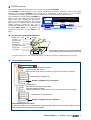
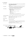
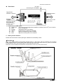
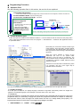
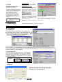
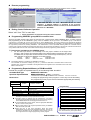
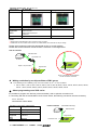
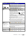
Flash memory MCU PROGRAMMER
FLASH2
USER'S MANUAL
For the Operation Procedures
Windows Japanese Environment
Contents
●
●
COVER&CONTENTS
IMPORTANT ......................................................................................... 1
MATTERS ON SAFETY ............................................................................... 1
THINGS OF IMPORTANCE ......................................................................... 1
LIMITED GUARANTEE................................................................................ 1
WHAT THIS GUARANTEE DOES NOT INCLUDE ...................................... 1
FLASH2 Features ................................................................................ 2
Product and contained accessories ............................................................. 2
The provided CD includes ............................................................................ 2
Specifications ............................................................................................... 3
Parts Name .................................................................................................. 4
Connectors & Cables ................................................................................... 5
How to Purchase the Upgrading Control Software....................................... 5
High Speed Clocked Synchronous Communication of FLASH MATE 5V1 .. 6
●
Preparation –Control Software Install- ............................................ 6
●
Programming Procedure .................................................................... 7
Operation Flow............................................................................................. 7
Control Software Open................................................................................. 7
Parameters................................................................................................... 8
File Loading ................................................................................................. 9
Execute programming ................................................................................ 10
Ending Control Software Operation ........................................................... 10
Programming GENERIC group MCU in common boot............................... 10
Programming Expanded Memory of ROM-less MCU................................. 10
◆ About programming onto R8C,M16C,R32C,M32C series ....................... 12
Writing restriction by on-chip oscillator of R8C group................................. 13
◆ About programming onto V850 series ..................................................... 13
◆ Command line option............................................................................... 14
●
Dealing with Errors ........................................................................... 15
Error Message Table - F2WinV2- ............................................................ 15
LED Status of FLASH2 and Trouble Shootings .......................................... 16
Timing chart of boot mode control .............................................................. 17
●
Correspondence MCU....................................................................... 18
●
Version upgrade ................................................................................ 18
●
Optional items ................................................................................... 18
●
Includes .............................................................................................. 18
FLASH2 control software requires Windows95, Windows98, WindowsMe,
WindowsNT, Windows2000, WindowsXP, WindowsVista, Windows7 & Windows8.1
Japanese version as OS environment, Microsoft products.
REV.2.0.0.0
HOKUTO DENSHI CO,.LTD.
●
IMPORTANT
MATTERS ON SAFETY
Do not use the FLASH2 before reading this user’s manual.
Make sure that you fully understood this user’s manual, before using the FLASH2 and power adapter.
Reading the manual is the responsibility of the FLASH2 users to fully understand all the matters.
THINGS OF IMPORTANCE
The FLASH2 and attached software are products made by HokutoDenshi Co., Ltd.
● The FLASH2 is to be used by connecting with systems containing the Renesas Electronics made MCU
with flash memory built-in microcomputer. The FLASH2 is not to be used for any other purpose other than
that which is specified in the manual.
● THE FLASH2 MUST NOT BE ALTERED IN ANY CASE.
HokutoDenshi Co., Ltd. is always improving the product design and performance. These changes will be
notified with releases of future product releases.
Users of FLASH2: Users only who have fully read and understood the manual should use the
FLASH2.Users who have not read and not fully understood the manual must not use the FLASH2.
● Possession/Ownership/Copyright: The FLASH2 described in the manual is protected by copyright and
this copyright is the property of HokutoDenshi Co., Ltd
● Product Diagrams: There may be cases where a product diagram in the manual differs from the product.
● HokutoDenshi Co., Ltd. has no responsibility for damages and dangers that may come about from
incorrect use of the FLASH2. All incorrect usage's and subsequent warnings against these usages, that
may not have been thought, are the responsibility of the users of FLASH2 who use the FLASH2 according
to the usage as is specified in the manual.
●
WARNINGS
Failure to adhere to the following warnings may result in possible heat, smoke and fire damage
to the FLASH2 and surrounding systems.
1. Don't disconnect and don't reconnect power cables while power is on.
2. Don't remove and don't replace any circuit while power is on.
3. Don't use power voltages other than what is specified in circuit diagram.
4. Be sure to use the correct connector cables when connecting between the FLASH2, MCU
and peripheral systems.
LIMITED GUARANTEE
HokutoDenshi Co., Ltd. guarantees that the FLASH2 can be used by the usage described in this manual by
HokutoDenshi Co., Ltd., and guarantees that the FLASH2 has been produced correctly and is free of any
defects per the products specification. The FLASH2 is guaranteed for 1 year after purchase of the FLASH2.
WHAT THIS GUARANTEE DOES NOT INCLUDE
HokutoDenshi Co., Ltd. guarantees the product only when the product is used correctly as described in
the manual. This guarantee is not valid if the product is misused for purposes other than that specified in the
manual. The guarantee is valid only for the materials used to construct the product.
● HokutoDenshi Co.,Ltd accepts no responsibility for whatever costs associated directly(or indirectly) with
damaged(or faulty) goods.
● This guarantee is valid for only the original purchaser of the product.
For the damages arose cumulatively, when the guarantee explicitly covers the damages, the guarantee is
limited to received value of the product price no matter what the reasonsare.
Any application for retailing the product by a third party cannot be accepted. The purchaser of the product
assumes all responsibility after the FLASH2 purchase.
●
This guarantee is not valid in the following cases.
1. Fire, earthquake, flood, an accident caused by a third party, etc.
2. Incorrect use, misuse, abuses user mistake and / or use in an improper environment.
3. The product has been altered in any way or tampered with.
4. The method of use has resulted in damage to the product, or a defect with the product.
1
HOKUTO DENSHI CO;LTD;
FLASH2
株式会社
●
FLASH2 Features
We would like to thank you for the purchase of our on-board programmer FLASH2.
This FLASH2 has been designed for the on-board programming of Renesas Electronics’s Flash memory MCU
enhanced Microcomputer. FLASH2 circuit management at programming to flash memory is fully automated.
Programming to the target MCU from the user's PC can be carried out smoothly without switch operation.
Only upgrading the control software, FLASH2 can
Only for Boot Mode Programming
adapt to every new single power supply MCU of
PC
On-chip flash memory is all-erased at programming
Flash memory MCU, releasing one after another.
F2WinV2
RS232C
And more, its convenience reaches to the expanded
Straight
FLASH2
Target board
flash memory of ROM-less MCU. The enclosed
Cable
sample programs provide the easy way of
programming confirmation with the LED blinking on
MCU with flash memory
the boards HSB series, of our products. We
MOT/HEX
Transfer user’s program with boot mode
recommend smart choice of using HSB as your
target.
Product and contained accessories
Package size
212 × 277 × 62 mm
Contents
Packing sheet
Software CD
Packing sheet
Programmer FLASH2
Target cable
AC adaptor
This AC adaptor is restricted only for Japanese domestic use.
For direct shipping abroad, AC adapter is taken off for safety.
*Instruction manual (how to use) and Information book is supposed to be recorded in an attached CD from Mar.05.2008.
The provided CD includes
For English OS
Demonstration(Categorized by HSB)
Program Expanded memory
Manual (English PDF manual) and The list of supported flash memory MCU(PDF)
Installation file for English OS
Double click (When using in English)
For Japanese OS
Demonstration(Categorized by HSB)
Program Expanded memory
Manual(Japanese PDF manual) and The list of supported flash memory MCU(PDF)
nstallation file for Japanese OS
Double click (When using in Japanese)
About Demonstration Program
In the demo folder, there are LED’s blinking programs with reference sources. MOT/HEX file among
them is realized quick evaluation of each board.
HOKUTO DENSHI CO;LTD;
FLASH2
株式会社
2
Specifications
MCU available:
Renesas Electronics’s Flash memory MCU of single power supply and Expanded
memory of H8SX/1650 and H8SX/1651.
See the available type name list at the end.
* MCU that appears in this document is the flash memory edition.( H8SX/1650, H8SX/1651 group is
excluded.)
PC interface:
RS232C-serial-port
(the straight cable is required for the connection.)
The DUSB 25 pins socket is equipped as the programmer’s PC interface connector.
See the note in the “User’s Guide” about the connection in the straight cable.
Power Supply:
AC adapter (DC9V) or 2 alkaline drycells (LR6/1.5 volt)
The provided AC adapter is verified for Japanese domestic use only.
Specifications of AC adapter
Input
Voltage :AC100~240V
Frequency :50~60Hz Electric current: Under 300mA
Output
Voltage :DC9V
Maximum electric current :1.33A
Jack
Form :Center-minus
Dimension :Outside diameter φ5.5mm /Inside diameterφ2.0mm
In use with drycells, we recommend to exchange the drycells in every 1 hour for successively programming.
Programming Voltage: 5V or 3.3V
(depend on “VIN”, that is target Vcc power supply to Interface 20th)
PC available:
F2WinV2:Windows95, 98, Me, NT, 2000, XP, Vista, 7 and 8.1
Japanese version - Some types are not available -
Body Case Size:
89 mm×134 mm×36 mm
Weight:
180g (without drycells)
Operating conditions
Programmer Operating Temperature
*Confirmed Operating Temperature
0℃~+40℃, less than 80%RH without bedewing
with ACadapter -10℃~+50℃
with drycells
+10℃~+50℃ depends on the cell spec
AC adapter Operating Temperature
0℃~+40℃
Storage Temperature -25℃~+60℃, less than 80%RH without bedewing
Package Seal and Products Serial Number
Package
Sealed
Product Serial
FALSH2
3
HOKUTO DENSHI CO;LTD;
FLASH2
株式会社
Upside of the box, Back side of the Programmer body,
Inside of the drycell box,
And On the Enclosed CD
Parts Name
DC Input
Connecting the AC adapter
Target Board
Interface Connector
RS232C Interface
connector
To PC
To MCU
Equipped Connecter is
FL20A2MA
(Oki Electric Cable Company)
MIL standard 2.54 pitch
box plug with latch
DSUB 25 pin Socket
With Inch bolt
1) 2) 3) 4)
5) 6)
FL20A2FO is equipped on
the enclosed cable.
□ Explanation of LED Status
(1) USER VCC The power from the target board supplies to Interface VIN of 20th pin as UserVcc.
(2) ERR
Error is recognized.
(3) ERASE
Target flash-memory is erasing.
(4) WRITE
Programming or verifying is executing.
(5) TXD
Signal is transporting to host-computer.
(6) RXD
Signals is receiving from host-computer.
□
Battery Holder Guidance
Please read <Precaution> before placing the batteries into the battery holder.
<Precaution>
Some of the alkaline batteries contain flexible insulating label to it. When placing that kind of batteries into the battery
holder, negative terminal (-) of the battery holder could come into contact with positive terminal (+) inside of the flexible
insulating label as shown in the diagram below. It causes electrical short-circuit.
Please do not use the batteries described above. Electrical short-circuit may cause smoke and fire.
HOKUTO DENSHI CO;LTD;
FLASH2
株式会社
4
FLASH2 Power Operations – Important –
UserVcc LED indicates the status of FLASH2 power on/off. Both 2 dry alkaline
cells and AC adapter can be used as a power supply for the FLASH2 itself. And
also FLASH2 needs UserVcc from the connected target board. UserVcc LED can
light when the both power supply are enough to operate.
□
The Order of Power Supply
We recommend the procedure below to avoid troubles.
Power ON: FLASH2 body first, then the target board. -
1. Power In
PC
F2WinV2
RS232S
FLASH2
Straight
Target Board
Cable
1. FLASH2 Power Supply
2. Target Board Power Supply
2.
Power In
MCU with flash memory
Power OFF: The target board first, then FLASH2 body -
2. Power OFF
PC
F2WinV2
RS232C
Straight
FLASH2
1. Target Board Power Off
2. FLASH2 Power Off
Target Board
1. Power OFF
Cable
MCU with flash memory
Connectors & Cables
Please refer to the “User’s Guide” about the connectors and the signal-names.
How to Purchase the Upgrading Control Software
Only upgrading the control software, FLASH2 can adapt to every new MCU of Flash memory MCU
Microcomputers. For the series of single power supply, we present the new version for all Flash memory MCU
Microcomputers releasing one after another. In using R8C・M16C series MCU, firmware in the programmer
must be updated. (Charged. For further information, see the end of a book.)
If you need your control software to upgrade, please feel free to ask by E-mail.
URL:http://www.hokutodenshi.co.jp (Japanese site only)
5
HOKUTO DENSHI CO;LTD;
FLASH2
株式会社
E-mail:[email protected]
High Speed Clocked Synchronous Communication of FLASH MATE 5V1
Clocked synchronous mode writing cannot be carried out by FLASH2. Only our FLASH MATE 5V1 can
realize the fast transfer in writing. As for FLASH2 and FLASH MATE 5V1 you can choose both solution
without modification about connector, signal and reference circuit diagram; these are in common.
●
Preparation
–Control Software Install-
This page is for
See the PC’s Windows manual to install properly for each PC.
Before this install, we recommend closing all the other application as possible, or the install must be
uncompleted with the access refusal from the required files. Please be careful that Install failure is
sometimes difficult to be recovered.
<Procedure>
1.
Open the enclosed CD, double click
the “setup.exe”.
2.
The starting dialogue of the installer is
appeared, then confirm the message
and click the ”次へ” (next).
If the MDAC install message is
appeared, see the right guidance to
install the MDAC before redo from 1.
3.
In the next dialogue “インストールフォル
ダ の 選 択 ”(select install folder),
confirm the
folder where this
F2WinV2 install to. If it is necessary to
change the default directory, click the
“参照” (refer to) and select the folder
as it is needed. The file size
information is indicated below. Click
the “次へ”(next) to progress.
4.
In the next dialogue”インスト
ールの確認” (confirm to start),
the install will start to click “次
へ ” (next). The progress is
indicated in the dialogue.
5.
The dialogue “インストールが
完 了 し ま し た ” (install
completed) is the successful
complete message, then click
the ” 閉 じ る ” (close the
installer)
to
finish
the
procedure.
If there is the message of the
PC reset, it is necessary to
reset
the
PC
before
“F2WinV2 ” open.
Windows95/98
Japanese Environment
See about the preliminary
monitor version for English
environment is described in the
other enclosed document.
Attention!
While the install, it is necessary to overwrite the
required files, if the message is appeared.
“F2WinV2” needs all the required files to execute
properly. Please be careful about the overwrite
influence for your present environment.
If you have questions, our support desk
is [email protected].
HOKUTO DENSHI CO;LTD;
FLASH2
株式会社
6
●
Programming Procedure
Operation Flow
See the following operation flow. In this section, the rest 4 to 8 are explained.
1. Target Board Preparation
See “User’s Guide” to arrange the target board, where the reference circuit diagrams, interface connection etc.
2. Control Software Install See the preceding page.
3. Connect PC, FLASH2 and Target See below.
4. Control Software Open
5. Power supply ON
6. Parameters
Power On
PC
F2WinV2
Communication rate and PC port
MCU type name
MCU port control status
7. Target Program Select
8. Programming Execute
Complete
RS232C
Straight
Cable
AC adapter or alkaline cells
Target Cable
FLASH2
Target Board
Power
ON
MCU with flash memory
See the following descriptions about operation procedures.
Control Software Open
At first, let’s open the installed control software “F2WinV2”. It can be started to click the name form the pull-up menu
“start” button at the left bottom of the corner, from “program” -> “HokutoDenshi” -> “F2WinV2” then application window
is opened like below.
7.File Load
6.Parameter
File-loading can not be done without the MCU type
name selecting. At the file loading, the data address
is examined with the selected MCU type name. If
MCU type name is need to change, close the loaded
file at first.
8.Excecute
Version Information
When this control software is closed, all the
parameters are save in the system folder
“¥windows” as the file name is “FLASH2.INI”. The
control software must be damaged if the initial file
“FLASH2.INI” is moved or delete, while the control
software is opened.
The file box for the third area is indicated only when
it is necessary. One box of the upper step is
indicated with the usual MCU.
Language select dialogue is in the
“Display Language” in the menu of “Set.
Shortcut with Function Key
The shortcuts assignments for function keys are always indicated on the status-bar and in the pull down menu.
□ Display Language
At the first open of “F2WinV2”, the display language confirmation is appeared automatically. Select from English and
Japanese. The selected language can be changed to click the “Other” in the “Set” menu.
□ Power On
To start the operation, FLASH2 power status must be checked, that is indicated with the UserVCC LED on the
programmer body. It is necessary to supply both power into programmer itself with AC adapter or alkaline dry
cells and with UserVcc from the target. Be careful about the User Vcc voltage steady and properly. It is
important because the FLASH2 uses it as programming voltage to the MCU.
7
HOKUTO DENSHI CO;LTD;
FLASH2
株式会社
Parameters
All the parameters must be selected properly that are described following. These parameters are in the “Set” menu of the
menu bar.
Select the group at first, then the type name of the target
□ MCU Group & MCU. It is incapable to program that are not listed here.
Type Name
Be careful about the confusing musk type.
Short Cut Key: F3
The input dialogue of the target board clock frequency is
appeared, if it is necessary. The frequency input must be until 2
dismals, and also the required CMK is fixed like the following
example. Especially, The MCU in Generic group can be
programmed with common boot control program. Please
confirm the proper CMK according to the Hard ware Manual of
the target MCU.
SH7058
H8/3069RF
4 2 x (System 4 Peripheral 2)
1 x x (No Multiplied)
When the H8SX/1650 is selected, writing control program
select box appears soon. For this ROM-less MCU, it is
necessary to prepare the proper writing control program in
MOT/HEX file format according to the user’s expanded FLASH
memory.
See “Programming Expanded Memory of ROM-less MCU”
about the programming control program.
□ Communications
Short Cut Key: F4
In the case of H8SX/1650
Transfer Rate at the start
The initial transfer rate at the beginning of the handshake with
the MCU.It is important to select the proper rate that is
described in the each MCU hardware manual.
Maximum Transfer Rate
After transfer the programming control program, FLASH2 raise
the rate until the maximum in the environment. As the target
board clock, we recommend the serial communication error
rate below 0.16. See the bit rate register descriptions in the
MCU hardware manual of the chapter about “Serial
Communications”. The communication between PC and
FLASH2 are ordinary realized 38400 bps at the maximum, even
if the parameters set at 76800 bps. If the communication error
often occurs after the erase, we recommend examining the
other combination of the initial rate and maximum rate. In using
R8C・M16C series, a transfer rate should be fixed at 9600 bps,
and 76800 bps, the maximum transfer rate, cannot be selected.
COM Port
Select the port of your environments. USB port with
□ Terminal Status
RS232C converter is not supported with FLASH2. It is not
enable to communicate properly with some USB to RS232C
converter.
To control the connected MD port or FWE port into the boot
mode, select the required status from the dialogue.
Operating Mode and Ports States
The target board must be prepared in the proper Operating Mode to execute the user
program. FLASH2 executes the reset-start automatically to run the user program just after
completion of programming.
The other side, specified port must be controlled in proper level, High or Low, for starting the
boot mode. The reference circuit diagrams indicate one idea to start boot mode with control
by FLASH2. User can arrange mode ports in FLASH2 control software with selecting the
button in the Terminal State window. If user would like to manage into boot mode before the
operation with the own idea, those ports do not have to connect with FLASH2. Refer to the
HSB series *; the MCU boards series of Hokuto
advices for arrangements in “User’s Guide”.
5
7
9
11
13
3
products.
Number at the Interface Connecter (20Pin)
HOKUTO DENSHI CO;LTD;
FLASH2
株式会社
8
No Optional Verify
Only in programming, data is verified in
prescribed byte unit.
Comparing by check sum
After programming, data is verified by
check sum. Note) Check sum is the lowest
□ Verify
The optional verify can be
selected in this menu.
This verify is started after programming
complete. The data transfer to PC and
compare with the loaded file data. This
verify is different from the Hitachi
Flash memory MCU on-board
programming ordinary flow. The
prescribed verify in programming is
done without select this verify. The
result must be used by the user’s own
decisions.
It is recommended to do Verify
to enhance the reliability of
the programming.
1 Byte Check sum displays
after verifying
digit of every data summation in all the flash
memory. If 2 files are selected, check sum are
showed in each. In the use of R8C series
MCU, Comparing by check sum cannot be
selected.
Comparing by byte unit.
After programming, data is verified by
byte unit.
Because, at the beginning of the boot
mode, the on-chip ROM is all-erased
automatically, it is impossible to verify
without programming.
Check the box if programming log file is
required.
Programming Log File
The file format is text at default with extension is
“.log” if there is no description in the file
information box.
Programming Log File
Select the display language from Japanese and English
□ Display Language
All the parameters are saved when the control software are closed.
File Loading
□ Open/Close
To load the file for programming, select “Open” from
the pull down menu in “File”. The MOT/HEX file
must be named “.MOT/HEX” as its extension.
We recommend loading the file after the MCU setting.
Close the file before changing the MCU type.
Open
Cancel
The demo programs in the enclosed CD are useful as the sample MOT/HEX files. Please copy from the CD if you need.
If the date address error of the loaded program is indicated at the file load, we recommend to examining the programs not
to fail in the generation with the proper link, confusing with RAM address etc. In the on-board programming, the user
programs transfer into on-chip ROM only.
□ Secondary file
Some MCU have secondary mat in its on-chip ROM like
“user boot mat” of H8/3069F. If the MCU type is selected
from MCU list that can be able to use secondary mat, “User
boot mat Open/Close” and secondary file box will be
automatically appeared.
H8/3069F
On-chip ROM
User mat
512KB
Ordinary mat
Secondary mat
User boot mat
8KB Secondary
For each mat, the program must be arranged form the begging.
□ Third file
When the MCU which has the user boot mat and the
date flash was selected, the file menu and the file
information box is indicated as follows.
9
HOKUTO DENSHI CO;LTD;
FLASH2
株式会社
Execute programming
All the settings and the file loading are completed, and then choose “Exec Write” from pull down menu of “Write”.
The progress bar indicates programming.
If MOT/HEX file does not have “.MOT/HEX“ as its file name
extension, a different address is appeared at the progress
indicator. If MOT/HEX file format is correct, it can be renamed in its
extension to “.MOT/HEX”.
Ending Control Software Operation
Select “exit” from “File” in menu bar.
*
All the parameters are saved at closing the control software.
Programming GENERIC group MCU in common boot
All the 0.18μFlash memory MCU have the common boot control program called “GENERIC Boot”. FLASH2 supports
this programming as in the “GENERIC” group. When the GENERIC as its type name in the GENERIC group is selected, the
programming is controlled with common boot program for all the GENERIC MCU. At the MCU selecting, the automatically appeared
CMK input boxes must be filled as the proper value, according to the Hardware Manual of the MCU. The examined MCU’s are added in
the Type Name pull-down list, following “GENERIC”. The unlisted MCU of the 0.18μFlash memory MCU are controlled with the
common boot program specified with the Renessas Technology. Be careful about the address in the program, because the data to the
wrong address that exist out of the internal flash ROM are all ignored at the programming without warning.
□ Restrictions and Advices for GENERIC group
For the CMK input boxes, it is necessary to set the proper numbers as the target clock
frequency with according to its Renesas Electronics Hadware Manual descriptions. Be careful
for H8S/2172F, the input value must be doubled of the mounted target clock frequency. For the
other examples, SH7058 and H8/3069F are set like following;
SH7058
H8/3069F
●
CMK1: 4
CMK1: 1
CMK2:2
CMK2: Don’t Care
CMK3:Don’t Care
CMK3:Don’t Care
The following attention is necessary for GENERIC group MCU.
n
The calculation of checksum is 8Kbyt×2 (n=0,1,2・・・). When the ROM size of the MCU doesn’t arrive at the
regulation size, checksum is calculated in the big size fitted to the regulation size. All the data on the area which
doesn’t exist are 0xFF.
Programming Expanded Memory of ROM-less MCU
FLASH2 can program the expanded memory of the following ROM- less MCU.
Available MCU Type
Specified Expanded ROM
H8SX/1650, H8SX/1651
MBM29LV800BA-70 (Fujitsu)
or equivalents
*TC58FVM5T2AFT-65(TOSHIBA)、S29GL032M90TFIR4(SPANSION)
Restrictions
MCU Type Name
H8SX/1650
H8SX/1651
finished the confirmation
To change the programming control program, it is ness carry from the file loading.
The programming control program must be addressed appropriately like following.
Base Address
User program area
FF6800h
FF6800h~FFBFFFh
Base Address+0h
Base Address+4h
~+3h
~+7h
Top of the flash memory (put 0 into here)
Bottom of the flash memory (put the last
address into here)
Base Address+8h ~+Fh
Version of the programming control program
Base Address+10h
"write_init" routine
Base Address+100h
"write_flash" routine
The programming control program must be differed appropriately
according to the flash memory expanded of the MCU.
If the flash memory is different from the specified one, it is able to
generate the appropriate MOT/HEX file from the source recompiling
in the FMWR folders with rearranging the tables and so on.
For the specified flash memory above, there is appropriate MOT/HEX
file as a content of this product.
Make sure that writing in the program expanded memory of ROMless
MCU should be up to 1MB.
Please feel free to ask more information about the minute
specifications for the other types expanded memories. And we can
provide the MOT/HEX file for the different flash memory. But we
can’t support the user’s original programming control program.
HOKUTO DENSHI CO;LTD;
Programming
Start Boot Mode
Call "write_init" routine
Bus initializing and clear up flash memory
Start programming
Call "write_flash" routine 128 byte unit
Programming complete
End Boot Mode
Each routine is contained in the MCU type
named folder of the enclosed CD, with its source
files. See the directory descriptions below.
FLASH2
株式会社
10
Programming procedure
It is the same steps to program the memory except selecting the programming control program.
1.
Open the control software, F2WinV2.
Click twice the icon of F2WinV2.
2.
Select the MCU type name “H8SX/1650” or “H8SX/1650”
from the list.
From “MCU Type” in the menu of “Set”, select “H8SX/1650” in the
pull-down list. Istantly the pull-down box appears next to it, to select the
MOT/HEX file of the programming control program. All the MOT/HEX files
in the specified folder described below are listed in the pull-down list.
3.
Attention!
The execution of programming must
be clicked after selecting the
programming control program. To
start programming without selecting
the program can’t be guaranteed.
Select the transfer rate.
Both initial rate at the beginning of boot mode and maximum rate to
transfer the user’s program must be appropriately selected.
4.
Select the port status.
According to the connections of the interface, select the buttons in
the port status window to control the target boot mode.
5.
Check the option flags.
It is able to set the options, auto erase, fast boot and erase check.
The optional verifies can be selected here.
6.
7.
Load the target file.
Click “Exec Write” from the menu of “Write”.
The Directory for the Original Programming Control Program
The programming control program can’t be selected, if the MOT/HEX file doesen’t exist in the
appropriate folders like in the right description.
Ex. C:¥Program Files¥FLASH 2¥FMWR¥H8Sx1650¥
The interface of the target board
See the description in H8SX/1650 in the User’s Guide.
11 HOKUTO DENSHI CO;LTD;
FLASH2
株式会社
◆
About programming onto R8C,M16C,R32C,M32C series
It’s possible to program onto devices ( shown as below ) with an optional conversion unit.
Format…MOT/HEX
new elements will be added.
【Outlines of each unit】(R8C/M16C Series,R8C Series)
Cable Name
20-10pin FOUSB*1
20-14pin R8C*2
20-14pin M16C*1
Conversion unit
20<->10pin FOUSB
20<->14pin R8C
20<->14pin M16C
Included
10pins straight cable is attached
14pins straight cable is attached
14pins straight cable is attached
Specification
Connecting to USB Writer and
M16C Flash Starter*3
R8C/10~13,
R8C/18,19,1A,1B
R8C/20~29
R8C/2A,2B,2C,2D
R8C/2E,2F,2K,2L
R8C/32A,32C,32D,32G,32H
R8C/32M,33A,33C,33D,33G
R8C/33H,33M,33T,34C,34E
R8C/34F,34G,34H,34K,34M
R8C/34P,34R,34U,34W,34X
R8C/34Y,34Z,35A,35C
R8C/35D,35M,36A,36E,36F
R8C/36G,36H,36M,36W,36X
R8C/36Y,36Z,38A,38C
R8C/38E,38F,38G,38H,38M
R8C/38W,38X,38Y,38Z
R8C/3GA,3GC,3GD
R8C/3JA,3JC,3JT
R8C/3MK,3MU,3MQ
R8C/36T-A
R8C/54E,54F,54G,54H
R8C/56E,56F,56G,56H
R8C/L35A,L35B,L35C,L35M
R8C/L36A,L36B,L36C,L36M
R8C/L38A,L38B,L38C,L38M
R8C/L3AA,L3AB,L3AC,L3AM
R8C/LA3A,LA5A,LA6A,LA8A
R8C/LAPS
R8C/M11A,M12A,M13B
M16C/26,26A,28,29,1N
M16C/30P,57, 5M,5L
M16C/62P,62A,62N,62M
M16C/63,64,64A,65
M32C/83,84,85,86,87
R32C/116,118,120,121
R32C/152,153,156
Connecting to Emulator E8a *4
Connecting to Emulator E8a *4
R8C/10~13
M16C/26,26A,28,29,1N
M16C/30P, 57, 5M, 5L
M16C/62P,62A,62N,62M
M16C/63,64,64A,65
M32C/83,84,85,86,87
¥2,000
¥2,000
Group of
supported
MCU
Price
¥2,000
Notes:
*1 Please connect “mode pin of R8C/14~17” to GND on the board side, to use “20<->10Pin FoUSB” and “20<->14Pin m16c” converter.
*2 Please output TX and RX to program.
*3 Please refer to MCU hardware manual for examples of connection Serial Programmer and MCU.
*4 Please refer to “E8a Emulator user’s manual” for this pin assign.
Please use programming tools with appropriate version of control software.
Please refer to the instruction manual for each connection on the target board.
HOKUTO DENSHI CO;LTD;
FLASH2
株式会社
12
【Outlines of each unit】(RX,740 Series)
Cable Name
20-14pin RX
20-14pin 740
Conversion unit
20<->14pin RX
20<->14pin 740
Included
Specification
Group of
supported
MCU
14pins straight cable is attached
Connecting to Emulator E1 and E20*5
RX111
RX210,21A,220
RX621,62N,62T,62G,63T
RX630,631
14pins straight cable is attached
Connecting to Emulator E8a *4
740/3803,38D5
¥2,000
¥2,000
Price
Notes:
*4 Please refer to “E8a Emulator user’s manual” for this pin assign.
*5 Please refer to “E1 Emulator user’s manual” or “E20 Emulator user’s manual” for this pin assign.
Please use programming tools with appropriate version of control software.
Please refer to the instruction manual for each connection on the target board.
how to connect
Attached cable
Conversion unit
FLASH2
10pins or 14pins cable
Target board
10-14P conversion connector
(TOE8)
Some of the boards needs attached
10-14P conversion connector.
Writing restriction by on-chip oscillator of R8C group
The following items of MCU group cannot be written by an on-chip oscillator:
R8C10、R8C11、R8C12、R8C13、R8C18、R8C19、R8C1A、R8C1B、R8C20、R8C21、R8C22、R8C23、R8C24、R8C25、
R8C26 、R8C27、R8C28、R8C29、R8C2A、R8C2B、R8C2C、R8C2D、R8C2E、R8C2F
◆
About programming onto V850 series
It’s possible to program onto devices ( shown as below ) with an optional conversion unit.
In connecting with the recommendation circuit of each series, the following conversion units are necessary.
Format…MOT/HEX
new elements will be added.
how to connect (conversion unit only)
【Outlines of each unit】(V850 Series)
Cable Name
20-16pin V850
Conversion unit
20<->16pin V850
Included
Group of
supported
MCU
Price
-
V850ES/Jx2,Jx3-L
V850E/Ix3
Attached cable
FLASH2
Target board
Conversion unit
¥2,000
13 HOKUTO DENSHI CO;LTD;
FLASH2
株式会社
Please use “F2WinV2” for control software.
◆
Command line option
When the FLASH2 starts, programming can be done in the command line. The form is as follows.
<path>F2Win,exe△Otion1△Option2 (△=space)
Option1:The name of the programming file to set in the primary area.
Option2:The name of the programming file to set in the secondary area.
※ Parameter should be full path.
The setup of variety in the control software is necessary to use the command line option.
Note:F2WinV2 has supportes command line option after the version.2.1.1.0.
Please do the designation of the file referring to the following example.
<path>”C:/Program△Files/FLASH2/F2WinV2.exe”△”△-o1=XXXX△-o2=YYYY△-o3=ZZZZ△-e”
The definition of F2WinV2
User Mat
-o1=XXXX
User Boot Mat
-o2=YYYY
Data Flash
-o3=ZZZZ
No error output
-e
(△= space, XXXX,YYYY,ZZZZ=MOT/HEX file name)
HOKUTO DENSHI CO;LTD;
FLASH2
株式会社
14
●
Dealing with Errors
Error Message Table
F2WinV2
Error#
#0
#1
#2
#3
- F2WinV2-
Message
#14
#15
#19
COM ポートがありません。
メモリが足りません。
ファイルの形式が異常です。
通信ポートを開けません。ポートの設定を変
更してください。
書込み制御プログラムが異常です。
ファイルが選択されていません。
ブートモードの起動に失敗しました。
フラッシュメモリの消去に失敗しました。
ビットレートの最適化に失敗しました。
フラッシュメモリの書き込みに失敗しました。
ベリファイエラー。
通信エラーが発生しました。
通信エラーが発生しました。
エラー (上記以外のエラーです)
ボーレート設定失敗
ID 照合失敗
ファームウェアが古い為実行不可
#12
処理を中断しました。
#4
#5
#6
#7
#8
#9
#10
#13
#20
Nothing Com Port.
Memory Shortage.
Illegal File format.
Can't open port. (Check the port select)
Invalid write control program.
File is not selected.
Can't start in the boot mode.
Can't Erase Flash memory.
Failure to optimize the bit rate.
Failure to writing memory.
Verify error.
Communication error. FLASH2←→Target MCU
Communication error. PC←→FLASH2
Error. (Unexpected error occurred.)
Failure to setting baud rate
Failure to ID checking
Due to the old-fashioned firmware, writing is not
possible.
User Break.
Note 1:
FLASH2 is not guaranteed to the correct processing with other appreciations. Especially, the conflict at the transmission
processing will be brought the communication errors. Communication error will be also occurred when more than one
FLASH2 are started at the same time, because time out error will be caused in waiting for the others’ processing.
Note 2:
In the same situation of the target board, cables and PC, if FLASH2 often have error #6 but sometimes success, we
recommend to examine the status of supplied power voltage, or miss-arrangement of required MCU port. See the User’s
Guide of the arrangement about the proper reference circuit diagrams for the target board. The serial communication error
also occurs with depending on the target board clock frequency. In the other case that the error number is not specified,
cable’s disconnection or connector contact failure must be examined, too.
F2VinV2
MCU with flash memory
15 HOKUTO DENSHI CO;LTD;
FLASH2
株式会社
LED Status of FLASH2 and Trouble Shootings
Programming Flow
Connection and Power on
DC supply into FLASH2, then Target
board power on.
LED Status and Frequently Occurred Troubles
Turn off →All LED do not light.
User Vcc
User Vcc
Start of Writing
Click Start or push F6
Starting boot mode
Bit rate adjusting, and erasing
all data
ERR
ERASE
WRITE
TXD
RXD
TXD
RXD
Ready →Only USER VCC lights.
ERR
ERASE
WRITE
¶UserVcc LED does not light.
Check Power supply to FLASH2 and the target board.
Especially, be careful about the dry cell’s power level.
We recommend the new ones to ensure the writing.
→USER VCC, ERASE and WRITE light. TXD and RXD are blinking.
User Vcc
ERR
ERASE
WRITE
TXD
RXD
¶“#6 Can't start in the boot mode.” is appeared, and stopped.
No signal reached the target MCU.
Communications are disturbed by RS232C cable
misuse/breaking/contact
failure,
or
FLASH2
breakdown. Sometimes Windows operations have
some troubles in its environment. Check the
RS232C cable, and also check the signals correctly
transferring from the FLASH2_17 and controlling of
1/3/5/7/9/11/13 at its target interface. If some signals
are uncontrolled correctly, error must be occurred
before FLASH2 output.
Test point by
Oscilloscope
No answer from the target MCU.
In spite of the correct communications from FLASH2, the target MCU makes no reply. Check
the circuit around the MCU in writing, especially the port MD/FWE/RESET and SCI port are
controlled correctly. Sometimes, Xtal oscillation failures influence in transferring.
¶#6 Some Error occurred in progress.
As acceptable transmission error ratio in serial communications, less than 0.16 is
recommended. If transmission is successes on border at first, error can be occurred in
progress. Unsoldered MCU pins or program reset like “WDT” also disturb transmission
progress.
¶“#7 Can't Erase Flash memory.” is appeared, and stopped.
MCU does not reply correct H’AA, although the first part of transmission is succeeded.
Check the correct MCU type name is selected, communication Failure by noise or Xtal
oscillation failures. Transferring rate combination change is sometimes effective. Unsoldered
MCU pins or program reset like “WDT” also disturb transmission progress.
On writing
Bit rate optimizing at
maximum rate.
Transferring user program in
prescribed block size and
compare.
(Verifying in option)
→USER VCC and WRITE light. TXD and RXD are blinking.
User Vcc
ERR
ERASE
WRITE
TXD
RXD
¶Communications Errors are often occurred.
Communication state is influenced by cable breaking/defects/misuse. The cable length for
the target cable is guaranteed in the attached one, 30 cm in max. Power supply is also
important, especially in the case of the dry cells. Check the voltage and the UserVcc LED
status. When transmissions failure is often occurred in specified address, check the port
status of the target to examine the wandering in processing.
¶Optional Verify is failed.
Guaranteed programming by Hitachi is finished except this optional verify. Optional verify is
sometimes omit the correct ones.
Completing of writing
Completed correctly→Only USER VCC lights.
User Vcc
Error occured
※ERR LED does not distinguish
until starting next writing.
ERR
ERASE
WRITE
TXD
RXD
TXD
RXD
→USER VCC and ERR light.
User Vcc
ERR
ERASE
WRITE
HOKUTO DENSHI CO;LTD;
FLASH2
株式会社
16
Timing chart of boot mode control
<<At Start>>
About 1000 msec
RESET1
st
H
About 1000 msec
H
(Open collector)
3
rd
9
th
th
5
7
About 500msec
H・L・Hi-Z
th
FWE・MD0・MD1
I/O0・I/O1・I/O2
11
th
13
Hi-Z
th
H *1 Transfer of "00"
H
th
To RXD port 17
Hi-Z
(Data transferred)
L
*1 From the 17th line of the interface transfer of "00" is repeated within the 512
times limit until reply from the target. When nothing reply from the target MCU
th
at the 15 line of the interface, the job is canceled as an error.
<<At Ending>>
About 500msec
RESET st
1
(Open collector)
3rd
5th
H
H
L
7th
FWE・MD0・MD1
I/O0・I/O1・I/O2
9th
11th
About 500msec
Hi-Z
13th
th
17
To RXD port
These escriptions are
outline, refer to the
Renesas Electronics
hardware manual in
detail.
MCU clock displayed
in operation of writing
is the estimated value
from transfer rate etc.
This value may differ
from the real value.
Hi-Z
(Data transferred)
For the target board clock, 0.16% or less is recommended as the serial communication error rate. Refer to the table of the
bit-rate-register in the chapter of “Serial Communications” of Renesas Electronics hardware manual for the concerned
MCU. If this error rate is more than above recommended 0.16%, the rate can’t be raised at the target program transfer.
FLASH2 can control the target MCU into boot mode in programming procedure. For this automatic control function, the
user’s interface must be organized for the connections to MCU ports that specified in Renesas Electronics hardware
manual for the concerned MCU. In the reference circuit diagrams in our “the User’s Guide” we inform the connections
including this function. Be careful about the interface signal names are named in convenient for the parameter setting.
These terminal state select box can be used with the user’s own idea, “MD0”, “MD1”, “I/O0”, “I/O1”, “I/O2” can be set at
three levels of Low, High and High-Z, “FWE” can be set at two levels of Low and High; these terminal state can be set and
remain in the memory corresponding to the MCU type. FLASH2 can progress the procedure, if these Mode control
function does not work with their disconnections. Select “High-Z”, when the mode control is arranged with the target board
switches.
17 HOKUTO DENSHI CO;LTD;
FLASH2
株式会社
●
Correspondence MCU
Please refer to “The list of supported flash memory MCU” (PDF) recorded on the provided CD for
what MCU FLASH2 supports.
●
Version upgrade
Version upgrade
FLASH2
Price
¥6000
Notes
Prior to version upgrade, the product serial number is made sure.
Windows95, 98, Me, NT, 2000, XP, Vista, 7 and
8.1 Japanese version - Some types are not available -
Version upgrade control soft ware
Consult us when you use our control ware in other
environments.
FLASH2 1.02 firm ware upgrade*
1.00 or 1.01 firm ware of FLASH2 can be
upgraded to 1.02.
Please send FLASH2 to our company.
FLAHS2 1.02 firm ware upgrade comes with the
newest control CD for upgrading the soft ware
version.
¥7000
FLASH2 Software and Programmer ¥10000
upgrade compatible to 1.02 firm ware*
*Upgrading compatible to 3v and R8C/M16C MCU series are included in this upgrade.
Upgrading Control Software information
Only upgrading the control software, FLASH2 can adapt to every new MCU of Flash memory MCU
Microcomputers. For the series of single power supply, we present the new version for all Flash memory MCU
Microcomputers releasing one after another. If you need your control software to upgrade, please refer our
URL and send E-mail to our company. Our homepages helps you to confirm the adapted MCU types in the
newest version.
URL:http://www.hokutodenshi.co.jp
●
E-mail:[email protected]
Optional items
The followings are the optional items for FLASH2.
●
Name
20-10pin FoUSB
Price
¥2000
20-14pin
20-14pin
20-14pin
20-14pin
20-16pin
¥2000
¥2000
¥2000
¥2000
¥2000
R8C
M16C
RX
740
V850
Notes
A conversion unit for R8C/M16C and a 10pins target
cable.
A conversion unit for R8C and a 14pins target cable.
A conversion unit for R16C and a 14pins target cable.
A conversion unit for RX and a 14pins target cable.
A conversion unit for 740 and a 14pins target cable.
A conversion unit for V850.
Includes
These includes are purchasable.
Name
AC 100 volt Adapter
Price
¥2500
Notes
FLASH2 Target Cable (20P)
¥1000
The provided AC adapter is verified for Japanese
domestic use only.
-
CD
¥6000
Please purchase version up software.
Please reconfirm about the charges for above.
FLASH2 USER'S MANUAL – For Windows –
©2000-2014 北斗電子 Printed in Japan
st
May 1st,2000 1 ED
HOKUTO DENSHI CO,.LTD
株式会社
phone+81-011-640-8800 fax+81-011-640-8801
e-mail:[email protected] (Technical support),
URL:http://www.hokutoelectronic.com
REV.2.0.0.0(140411)
3-7, Odori-nishi 16, Chuoku Sapporo Hokkaido, 060-0042, Japan
[email protected] (Order and inquiries)
HOKUTO DENSHI CO;LTD;
FLASH2
株式会社
18


![[ITA] RX40 Manuale v1-5](http://vs1.manualzilla.com/store/data/006119954_1-2ba2af64dd7b8b55c335fa8e9797796a-150x150.png)