1
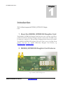
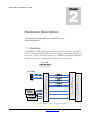
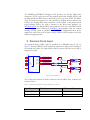
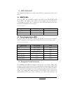
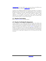
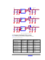
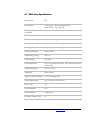
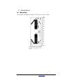
THE DINI GROUP
LOGIC Emulation Source
User Manual
DNMEG_INTERCON
LOGIC EMULATION SOURCE
DNMEG_INTERCON User Manual Version
1.0
© The Dini Group
7469 Draper Ave.
La Jolla, CA92037
Phone 858.454.3419 • Fax 858.454.1278
[email protected]
www.dinigroup.com
Copyright Notice and Proprietary Information
Copyright © 2007 The Dini Group. All rights reserved. No part of this copyrighted work may be
reproduced, modified or distributed in any form or by any means, without the prior written permission of
The Dini Group.
Right to Copy Documentation
The Dini Group permits licensee to make copies of the documentation for its internal use only. Each copy
shall include all copyrights, trademarks, disclaimers and proprietary rights notices.
Disclaimer
The Dini Group has made reasonable efforts to ensure that the information in this document is accurate and
complete. However, The Dini Group assumes no liability for errors, or for any incidental, consequential,
indirect, or special damages, including, without limitation, loss of use, loss or alteration of data, delays, or
lost profits or savings, arising from the use of this document or the product which it accompanies.
Table of Contents
INTRODUCTION ..................................................................................................................................................................................................................... 1
1
2
3
4
5
ABOUT THE DNMEG_INTERCON DAUGHTER CARD .................................................................................................................................. 1
DNMEG_INTERCON DAUGHTER CARD FEATURES .................................................................................................................................... 1
PACKAGE CONTENTS: ..................................................................................................................................................................................... 2
INSPECT THE BOARD ....................................................................................................................................................................................... 2
ADDITIONAL INFORMATION ............................................................................................................................................................................ 2
HARDWARE DESCRIPTION ................................................................................................................................................................................................ 4
1
2
3
OVERVIEW ....................................................................................................................................................................................................... 4
EXTERNAL CLOCK INPUT ................................................................................................................................................................................ 5
LED INDICATORS ............................................................................................................................................................................................ 6
3.1
RESET LED’s .......................................................................................................................................................................................................... 6
3.2
Power Supply Status LED’s .................................................................................................................................................................................... 6
4
DAUGHTER CARD HEADERS ........................................................................................................................................................................... 6
4.1
Daughter Card clocking.......................................................................................................................................................................................... 7
4.2
Daughter Card Header Pin Assignments ............................................................................................................................................................... 7
Special Pins on the Daughter Card Header..................................................................................................................................................... 9
4.2.1
VREF .................................................................................................................................................................................................................................. 9
4.3
VCCO Power Supply .................................................................................................................................................................................................. 9
4.4
Daughter Card Header IO Connections ............................................................................................................................................................... 10
4.5
Power and Reset .................................................................................................................................................................................................... 18
4.6
Insertion/Removal of Daughter Card ................................................................................................................................................................... 18
4.7
MEG Array Specifications .................................................................................................................................................................................... 20
5
MECHANICAL ................................................................................................................................................................................................ 21
5.1
Dimensions ............................................................................................................................................................................................................ 21
List of Figures
Figure 1 - DNMEG_INTERCON Daughter Card ............................................................................................................................................................................................. 1
Figure 2 - DNMEG_INTERCON Daughter Card Block Diagram ................................................................................................................................................................. 4
Figure 3 – External Clock Input .............................................................................................................................................................................................................................. 5
Figure 4 - Daughter Card Header Pin Assignments ............................................................................................................................................................................................. 8
Figure 5 - VCCO Adjustable Linear Power Supplies ......................................................................................................................................................................................... 10
Figure 6 - Daughter Card Header Power & RESET .......................................................................................................................................................................................... 18
List of Tables
Table 1 – Connections between External Clock Input and MEG-Array Connector ..................................................................................................................................... 5
Table 2 - RESET LED's ........................................................................................................................................................................................................................................... 6
Table 3 – Power Supply Status LED’s .................................................................................................................................................................................................................... 6
Table 4 - Daughter Card Header IO Connections ............................................................................................................................................................................................. 10
Table 5 – Daughter Card Reset Signal (DC_RSTn) ........................................................................................................................................................................................... 18
1
Chapter
I N T R O D U C T I O N
Introduction
This User Manual accompanies the DNMEG_INTERCON Daughter
Card.
1 About the DNMEG_INTERCON Daughter Card
The DNMEG_INTERCON Daughter Card allows the user to expand on the FPGAto-FPGA interconnect utilizing the daughter card IO as interconnect. The MEG-Array
IO banks are connected 1:1, thus providing a bridging function between the headers.
The DNMEG_INTERCON Daughter Card can be used on any of the Dini Group
products that have two adjacent MEG-Array Daughter Card Headers, e.g.
DN9000K10PCI, DN9000K10PCI.
2 DNMEG_INTERCON Daughter Card Features
Figure 1 - DNMEG_INTERCON Daughter Card
DNMEG_INTERCONN User Manual
www.dinigroup.com
1
I N T R O D U C T I O N
DNMEG_INTERCON Daughter Card features the following:
•
Daughter Card Headers (x3) LVDS – MEG-Array (400-pin) interface to
DN900xK10xxx products
•
External Clock Input - LVDS (SMA x 2)
•
Power Supply Status LED’s (x6)
•
VCCO Linear Power Supplies (x3)
3 Package Contents:
The DNMEG_INTERCON Daughter Card would normally accompany one of the
The Dini Group Logic Emulations products, but could be ordered as a separate item.
4 Inspect the Board
Place the board on an anti-static surface and inspect it to ensure that it has not been
damaged during shipment. Verify that all components are on the board and appear
intact.
5 Additional Information
For additional information, please visit http://www.dinigroup.com/. The following
table lists some of the resources you can access from this website. You can also directly
access these resources using the provided URLs.
Resource
User Manual
Description/URL
This is the main source of technical information. The manual
should contain most of the answers to your questions
Demonstration Videos MEG-Array Daughter Card header insertion and removal
video
Dini Group Web Site
The web page will contain the latest user manual, application
notes, FAQ, articles, and any device errata and manual
addenda. Please visit and bookmark:
http://www.dinigroup.com
E-Mail
You may direct questions and feedback to the Dini Group
DNMEG_INTERCONN User Manual
www.dinigroup.com
2
I N T R O D U C T I O N
Resource
Description/URL
using this e-mail address: [email protected]
Phone Support
Call us at 858.454.3419 during the hours of 8:00am to
5:00pm Pacific Time.
FAQ
The download section of the web page may contain a
document called DNMEG_INTERCON Frequently
Asked Questions (FAQ). This document is periodically
updated with information that may not be in the Users
Manual.
DNMEG_INTERCONN User Manual
www.dinigroup.com
3
H A R D W A R E
2
Chapter
D E S C R I P T I O N
Hardware Description
This chapter describes the functional blocks of the design and focuses on the
Hardware implementation.
1 Overview
LED7
LED6
LED5
LED3
LED4
LED2
LED1
LED0
The DNMEG_INTERCON Daughter Card allows the user to expand on the FPGAto-FPGA interconnect utilizing the MEG-Array Daughter Card header IO banks as
interconnect. A high level block diagram of the DNMEG_INTERCON Daughter
Card is shown in Figure 2, followed by a brief description of each section.
MEG ARRAY – Receptacle (400Pin) – Bottom (P2)
74390-101LF
MEG ARRAY – Plug (400Pin) – Top (P3)
84520-102LF
MEG ARRAY – Receptacle (400Pin) – Bottom (P1)
74390-101LF
Figure 2 - DNMEG_INTERCON Daughter Card Block Diagram
DNMEG_INTERCON User Manual
www.dinigroup.com
4
The DNMEG_INTERCON Daughter Card provides two 400-pin MEG-Array
connectors (P1, P2) on the bottom of the printed circuit board assembly (PCBA) and
an additional 400-pin MEG-Array connector (P3) on the top of the PCBA. The MEGArray IO banks are connected 1:1, thus providing a bridging function between the
headers. The 400-pin MEG-Array connectors on the bottom of the printed circuit
board assembly (PCBA) are used to interface to the Dini Group products, e.g.
DN9000K10PCI. The 400-pin MEG-Array connector on the top of the PCBA can be
used for IO expansion utilizing the DNMEG_Obs Daughter Card. An external
clocking (LVDS) option is provided via an SMA pair. Independent linear power
supplies are used to drive the IO bank voltages. Discrete LED’s indicate reset status
and power supply presence.
2 External Clock Input
An external clocking (LVDS) option is provided via a 50Ω SMA pair (J1, J2), see
Figure 3. Resistors (R4, R5) can be replaced by capacitors to allow for AC-coupling of
the external clock input. For single ended solutions, resistors (R2, R6) can be used to
terminate the signal.
P1-1
C1
H1
B2
D2
G2
J2
GCAP
GCAN
P12V_1
P12V_2
P5V_1
P5V_2
P3.3V_1
P3.3V_2
P3.3V_3
1A PER PIN
A1
K1
GCBP
GCBN
GCCP
GCCN
E1
F1
CLK_DC_B_0p
CLK_DC_B_0n
E3
F3
CLK_DC_B_1p
CLK_DC_B_1n
E5
F5
CLK_DC_EXT_2p
CLK_DC_EXT_2n
J1
R2
(DNI-49.9R)
R4
0R
R5
0R
2
3
142-0701-501
J2
R6
(DNI-49.9R)
RSTn
5
1
4
Clock, Power, Reset
5
1
4
2
3
142-0701-501
74390-101LF
Figure 3 – External Clock Input
The connections between the SMA connectors and the MEG-Array connector are
shown in Table 1.
Table 1 – Connections between External Clock Input and MEG-Array Connector
Signal Name
SMA (Pin)
MEG-Array (Pin)
CLK_DC_EXT_2p
J1.1
P1.E5
CLK_DC_EXT_2n
J2.1
P1.F5
DNMEG_INTERCONN User Manual
The Dini Group
5
3 LED Indicators
The DNMEG_INTERCON provides various LED’s to indicate that status of the
board.
3.1 RESET LED’s
Two red LED’s are provided to indicate the status of the DC_B_RSTn and
DC_T_RSTn reset signals. The LED’s can be turned ON by driving the
corresponding pin LOW. Table 2 describes the user LED’s and their associated pin
assignments on the MEG-Array connector.
Table 2 - RESET LED's
Signal Name
MEG-Array (pin)
LED
DC_B_RSTn
P1.J2
DS1
DC_T_RSTn
P2.J2
DS2
3.2 Power Supply Status LED’s
Five green LED’s are provided to indicate the presence of various power supplies.
Table 3 describes the power supply status LED’s and their associated voltage source.
Table 3 – Power Supply Status LED’s
Signal Name
Power Supply
LED
P12V
P1.A1, P1.K1
DS3
P5V
P1.C1, P1.H1
DS4
P1.B2, P1.D2, P1.G2
DS5
VCCO_DC_B0
U1.1
DS6
VCCO_DC_B1
U2.1
DS7
VCCO_DC_B2
U3.1
DS8
P3.3V
4 Daughter Card Headers
The DNMEG_INTERCON Daughter Card provides two 400-pin MEG-Array
connectors (P1, P2) on the bottom of the printed circuit board assembly (PCBA) and
an additional 400-pin MEG-Array connector (P3) on the top of the PCBA. The MEGArray IO banks are connected 1:1, thus providing a bridging function between the
headers. The 400-pin MEG-Array connectors on the bottom of the printed circuit
board assembly (PCBA) are used to interface to the Dini Group products, e.g.
DNMEG_INTERCONN User Manual
The Dini Group
6
DN9000K10PCI. The 400-pin MEG-Array connector on the top of the PCBA can be
used for IO expansion utilizing the DNMEG_Obs Daughter Card.
All signals on the DNMEG_INTERCON Daughter Card Headers are all routed as
differential, 50-Ohm transmission lines. No length-matching is done on the PCB for
Daughter Card signals, (except within a differential pair) because the Virtex-5 FPGA is
capable of variable-delay input using the built-in IDELAY capabilities. Other
connections on the daughter card connector system include three dedicated,
differential clock connections for inputting global clocks from an external source,
power connections, bank VCCO power, and a reset signal.
4.1 Daughter Card clocking
Refer to External Clock Input in this User Manual.
4.2 Daughter Card Header Pin Assignments
The pin assignments of the DNMEG_INTERCON Daughter Card Headers were
designed to reduce cross talk to manageable levels while operating at full speed of the
Virtex-5 LVDS standards. The Daughter Card Header is divided into three banks. The
ground-to-signal ratio of the connector is 1:1, refer to Figure 4. General purpose IO is
arranged in a GSGS pattern to allow high speed single-ended or differential use. On
the host, these signals are routed as loosely-coupled differential signals, meaning when
used differentially, they benefit from the noise-resistant properties of a differential pair,
but when used in a single-ended configuration, they do not interfere with each other
excessively.
DNMEG_INTERCONN User Manual
The Dini Group
7
A B C D E F G H J K
1
2
3
4
5
6
+12V
+5V
+3.3V
B0
L1P
B0
L2P
B0
L5P
7
8
B0
L9P
9
10
B0
L13P
11
12
B0
L17P
13
14
B0
L21P
15
16
B0
L25P
17
18
B1
L3P
19
20
21
22
23
24
25
26
27
28
29
30
31
32
B1
L7P
B0
L10P
B1
L4N
B1
L7N
B1
L8N
B1
L11N
B1
L15N
B1
L19N
B1
L23N
B2
L1N
33
34
35
36
B2
L13P
37
38
39
40
B2
L17P
B2
L5N
B2
L9N
B1
L31N
B2
L25P
B2
L25N
B2
L26P
B2
L26N
B2
L27P
B2
L27N
B2
L28P
B2
L28N
B2
L13N
B2
L22P
B2
L22N
B1
L10P
19
20
21
22
23
24
25
26
27
28
29
30
31
32
VCCO
1
B1
L26N
B2
L4P
B2
L4N
B2
L8P
B2
L8N
B2
L11P
VCCO
2
B2
L12P
33
34
B2
L16P
35
36
B2
L20P
37
38
39
40
B2
L12N
B2
L15P
B2
L15N
B2
L16N
B2
L19P
B2
L19N
B2
L20N
B2
L23P
B2
L23N
17
18
B1
L26P
B2
L7P
B2
L31N
B1
L6P
B1
L22P
B2
L3P
B2
L11N
B2
L31P
15
16
B1
L22N
B2
L7N
B2
L18N
B1
L2P
B1
L18P
B1
L25P
B2
L30N
13
14
B1
L18N
B2
L3N
B2
L30P
B0
L24P
B1
L14N
B1
L21P
B2
L29N
11
12
B1
L14P
B1
L17P
B1
L25N
B2
L14N
B2
L17N
B1
L13P
B1
L21N
B2
L29P
B2
L18P
B1
L10N
B1
L17N
B2
L10N
B2
L14P
B2
L21N
B1
L31P
B2
L6N
B2
L10P
B1
L9P
B1
L13N
B2
L2N
B2
L6P
B2
L21P
B1
L30N
B1
L24N
B2
L2P
B2
L5P
B1
L30P
B1
L20N
B1
L24P
B2
L1P
B1
L29N
B1
L16N
B1
L20P
B1
L23P
B1
L29P
B0
L20P
B1
L6N
B1
L9N
B1
L12N
B1
L16P
B1
L5P
B1
L28N
9
10
B1
L2N
B1
L5N
B1
L28P
B1
L12P
B1
L1P
B1
L27N
B0
L16P
B0
L24N
B1
L1N
B1
L27P
B1
L8P
B0
L23P
B0
L31N
7
8
B0
L20N
B0
L23N
B0
L31P
B1
L4P
B1
L19P
B0
L30N
B0
L26N
B1
L3N
B2
L9P
B0
L30P
B0
L26P
B0
L19P
1
2
3
4
5
6
B0
L12P
B0
L16N
B0
L19N
B0
L22N
B0
L25N
B0
L15P
B0
L29N
VCCO
0
B0
L12N
B0
L15N
B0
L29P
B0
L22P
B0
L21N
B0
L11P
B0
L28N
B0
L18N
B0
L8P
B0
L8N
B0
L11N
B0
L28P
B0
L18P
B1
L15P
B0
L27N
B0
L14N
B0
L17N
B1
L11P
B0
L7N
B0
L27P
B0
L4P
B0
L4N
B0
L7P
GCCN
B0
L10N
B0
L14P
RSTn
B0
L3N
GCCP
+12V
B0
L3P
GCBN
B0
L6N
B0
L13N
VCCO
2
GCBP
B0
L6P
B0
L9N
VCCO
1
+3.3V
B0
L2N
B0
L5N
+5V
GCAN
+3.3V
B0
L1N
VCCO
0
GCAP
B2
L24P
B2
L24N
A B C D E F G H J K
Figure 4 - Daughter Card Header Pin Assignments
DNMEG_INTERCONN User Manual
The Dini Group
8
4.2.1
Special Pins on the Daughter Card Header
VREF
These pins are connected 1:1 on the board and the function is determined be the
mother board.
GCAp/n, GCBp/n, and GCCp/n
These pins are connected 1:1 on the board and the function is determined be the base
board.
4.3 VCCO Power Supply
On the Virtex-5 FPGA each IO bank has its own VCCO pins. VCCO is determined by the
IO standard for that particular IO bank. Since a daughter card will not always be
present on a daughter card connector, a VCCO bias generator is used on the
motherboard for each daughter card bank to keep the VCCO pin on the FPGA within
its recommended operating range. The Daughter Card drives VCCO to the required level
for the particular IO standard. The VCCO impressed by the Daughter Card needs to
satisfy the VIH(MAX) of the FPGA on the host board. There are three Adjustable Linear
Power Supplies (U1, U1, and U2) on the DNMEG_INTERCON Daughter Card,
refer to Figure 5. Refer to the datasheet for the LT1963A from Linear Technology on
how to adjust the output voltages.
DNMEG_INTERCONN User Manual
The Dini Group
9
TP1
1
P3.3V
GND
U1
8
5
C3
10uF
16V
20%
CERAMIC
C4
0.1uF
3
6
7
IN
OUT
SHDN SENSE/ADJ
GND
GND
GND
NC
VCCO_DC_B0
VCCO_DC_B0
1
2
R1
1.1K
4
R3
1K
LT1963AES8/SO8
C5
10uF
16V
20%
CERAMIC
C6
0.1uF
TP2
1
P3.3V
GND
U2
8
5
C9
10uF
16V
20%
CERAMIC
C10
0.1uF
3
6
7
IN
OUT
SHDN SENSE/ADJ
GND
GND
GND
NC
VCCO_DC_B1
VCCO_DC_B1
1
2
R8
1.1K
4
R9
1K
LT1963AES8/SO8
C11
10uF
16V
20%
CERAMIC
C12
0.1uF
TP3
1
P3.3V
GND
U3
8
5
C15
10uF
16V
20%
CERAMIC
C16
0.1uF
3
6
7
IN
OUT
SHDN SENSE/ADJ
GND
GND
GND
NC
VCCO_DC_B2
VCCO_DC_B2
1
2
R11
1.1K
4
R12
1K
LT1963AES8/SO8
C17
10uF
16V
20%
CERAMIC
C18
0.1uF
Figure 5 - VCCO Adjustable Linear Power Supplies
4.4 Daughter Card Header IO Connections
Table 4 lists the interconnect between the Daughter Card Headers.
Table 4 - Daughter Card Header IO Connections
Signal Name
MEG-Array
(Pin)
MEG-Array
(Pin)
MEG-Array
(Pin)
CLK_DC_B_0N
P1-F1
P2-F1
P3-F1
CLK_DC_B_0P
P1-E1
P2-E1
P3-E1
CLK_DC_B_1N
P1-F3
P2-F3
P3-F3
CLK_DC_B_1P
P1-E3
P2-E3
P3-E3
CLK_DC_B_2N
P2-F5
P3-F5
CLK_DC_B_2P
P2-E5
P3-E5
DNMEG_INTERCONN User Manual
The Dini Group
10
Signal Name
MEG-Array
(Pin)
CLK_DC_EXT_2N
P1-F5
CLK_DC_EXT_2P
P1-E5
DC_B_RSTN
P1-J2
DC_T_RSTN
MEG-Array
(Pin)
MEG-Array
(Pin)
P2-J2
P3-J2
DC_B0N1
P1-B4
P2-B4
P3-B4
DC_B0N10
P1-D8
P2-D8
P3-D8
DC_B0N11
P1-G8
P2-G8
P3-G8
DC_B0N12
P1-J8
P2-J8
P3-J8
DC_B0N13
P1-B10
P2-B10
P3-B10
DC_B0N14
P1-D10
P2-D10
P3-D10
DC_B0N15
P1-G10
P2-G10
P3-G10
DC_B0N16
P1-J10
P2-J10
P3-J10
DC_B0N17
P1-B12
P2-B12
P3-B12
DC_B0N18
P1-D12
P2-D12
P3-D12
DC_B0N19
P1-G12
P2-G12
P3-G12
DC_B0N2
P1-D4
P2-D4
P3-D4
DC_B0N20
P1-J12
P2-J12
P3-J12
DC_B0N21
P1-B14
P2-B14
P3-B14
DC_B0N22
P1-D14
P2-D14
P3-D14
DC_B0N23
P1-G14
P2-G14
P3-G14
DC_B0N24
P1-J14
P2-J14
P3-J14
DC_B0N25
P1-B16
P2-B16
P3-B16
DC_B0N26
P1-D16
P2-D16
P3-D16
DC_B0N27
P1-F7
P2-F7
P3-F7
DC_B0N28
P1-F9
P2-F9
P3-F9
DC_B0N29
P1-F11
P2-F11
P3-F11
DNMEG_INTERCONN User Manual
The Dini Group
11
Signal Name
MEG-Array
(Pin)
MEG-Array
(Pin)
MEG-Array
(Pin)
DC_B0N3
P1-G4
P2-G4
P3-G4
DC_B0N30
P1-F13
P2-F13
P3-F13
DC_B0N31
P1-F15
P2-F15
P3-F15
DC_B0N4
P1-J4
P2-J4
P3-J4
DC_B0N5
P1-B6
P2-B6
P3-B6
DC_B0N6
P1-D6
P2-D6
P3-D6
DC_B0N7
P1-G6
P2-G6
P3-G6
DC_B0N8
P1-J6
P2-J6
P3-J6
DC_B0N9
P1-B8
P2-B8
P3-B8
DC_B0P1
P1-A3
P2-A3
P3-A3
DC_B0P10
P1-C7
P2-C7
P3-C7
DC_B0P11
P1-H7
P2-H7
P3-H7
DC_B0P12
P1-K7
P2-K7
P3-K7
DC_B0P13
P1-A9
P2-A9
P3-A9
DC_B0P14
P1-C9
P2-C9
P3-C9
DC_B0P15
P1-H9
P2-H9
P3-H9
DC_B0P16
P1-K9
P2-K9
P3-K9
DC_B0P17
P1-A11
P2-A11
P3-A11
DC_B0P18
P1-C11
P2-C11
P3-C11
DC_B0P19
P1-H11
P2-H11
P3-H11
DC_B0P2
P1-C3
P2-C3
P3-C3
DC_B0P20
P1-K11
P2-K11
P3-K11
DC_B0P21
P1-A13
P2-A13
P3-A13
DC_B0P22
P1-C13
P2-C13
P3-C13
DC_B0P23
P1-H13
P2-H13
P3-H13
DC_B0P24
P1-K13
P2-K13
P3-K13
DNMEG_INTERCONN User Manual
The Dini Group
12
Signal Name
MEG-Array
(Pin)
MEG-Array
(Pin)
MEG-Array
(Pin)
DC_B0P25
P1-A15
P2-A15
P3-A15
DC_B0P26
P1-C15
P2-C15
P3-C15
DC_B0P27
P1-E7
P2-E7
P3-E7
DC_B0P28
P1-E9
P2-E9
P3-E9
DC_B0P29
P1-E11
P2-E11
P3-E11
DC_B0P3
P1-H3
P2-H3
P3-H3
DC_B0P30
P1-E13
P2-E13
P3-E13
DC_B0P31
P1-E15
P2-E15
P3-E15
DC_B0P4
P1-K3
P2-K3
P3-K3
DC_B0P5
P1-A5
P2-A5
P3-A5
DC_B0P6
P1-C5
P2-C5
P3-C5
DC_B0P7
P1-H5
P2-H5
P3-H5
DC_B0P8
P1-K5
P2-K5
P3-K5
DC_B0P9
P1-A7
P2-A7
P3-A7
DC_B1N1
P1-G16
P2-G16
P3-G16
DC_B1N10
P1-J20
P2-J20
P3-J20
DC_B1N11
P1-B22
P2-B22
P3-B22
DC_B1N12
P1-D22
P2-D22
P3-D22
DC_B1N13
P1-G22
P2-G22
P3-G22
DC_B1N14
P1-J22
P2-J22
P3-J22
DC_B1N15
P1-B24
P2-B24
P3-B24
DC_B1N16
P1-D24
P2-D24
P3-D24
DC_B1N17
P1-G24
P2-G24
P3-G24
DC_B1N18
P1-J24
P2-J24
P3-J24
DC_B1N19
P1-B26
P2-B26
P3-B26
DC_B1N2
P1-J16
P2-J16
P3-J16
DNMEG_INTERCONN User Manual
The Dini Group
13
Signal Name
MEG-Array
(Pin)
MEG-Array
(Pin)
MEG-Array
(Pin)
DC_B1N20
P1-D26
P2-D26
P3-D26
DC_B1N21
P1-G26
P2-G26
P3-G26
DC_B1N22
P1-J26
P2-J26
P3-J26
DC_B1N23
P1-B28
P2-B28
P3-B28
DC_B1N24
P1-D28
P2-D28
P3-D28
DC_B1N25
P1-G28
P2-G28
P3-G28
DC_B1N26
P1-J28
P2-J28
P3-J28
DC_B1N27
P1-F17
P2-F17
P3-F17
DC_B1N28
P1-F19
P2-F19
P3-F19
DC_B1N29
P1-F21
P2-F21
P3-F21
DC_B1N3
P1-B18
P2-B18
P3-B18
DC_B1N30
P1-F23
P2-F23
P3-F23
DC_B1N31
P1-F25
P2-F25
P3-F25
DC_B1N4
P1-D18
P2-D18
P3-D18
DC_B1N5
P1-G18
P2-G18
P3-G18
DC_B1N6
P1-J18
P2-J18
P3-J18
DC_B1N7
P1-B20
P2-B20
P3-B20
DC_B1N8
P1-D20
P2-D20
P3-D20
DC_B1N9
P1-G20
P2-G20
P3-G20
DC_B1P1
P1-H15
P2-H15
P3-H15
DC_B1P10
P1-K19
P2-K19
P3-K19
DC_B1P11
P1-A21
P2-A21
P3-A21
DC_B1P12
P1-C21
P2-C21
P3-C21
DC_B1P13
P1-H21
P2-H21
P3-H21
DC_B1P14
P1-K21
P2-K21
P3-K21
DC_B1P15
P1-A23
P2-A23
P3-A23
DNMEG_INTERCONN User Manual
The Dini Group
14
Signal Name
MEG-Array
(Pin)
MEG-Array
(Pin)
MEG-Array
(Pin)
DC_B1P16
P1-C23
P2-C23
P3-C23
DC_B1P17
P1-H23
P2-H23
P3-H23
DC_B1P18
P1-K23
P2-K23
P3-K23
DC_B1P19
P1-A25
P2-A25
P3-A25
DC_B1P2
P1-K15
P2-K15
P3-K15
DC_B1P20
P1-C25
P2-C25
P3-C25
DC_B1P21
P1-H25
P2-H25
P3-H25
DC_B1P22
P1-K25
P2-K25
P3-K25
DC_B1P23
P1-A27
P2-A27
P3-A27
DC_B1P24
P1-C27
P2-C27
P3-C27
DC_B1P25
P1-H27
P2-H27
P3-H27
DC_B1P26
P1-K27
P2-K27
P3-K27
DC_B1P27
P1-E17
P2-E17
P3-E17
DC_B1P28
P1-E19
P2-E19
P3-E19
DC_B1P29
P1-E21
P2-E21
P3-E21
DC_B1P3
P1-A17
P2-A17
P3-A17
DC_B1P30
P1-E23
P2-E23
P3-E23
DC_B1P31
P1-E25
P2-E25
P3-E25
DC_B1P4
P1-C17
P2-C17
P3-C17
DC_B1P5
P1-H17
P2-H17
P3-H17
DC_B1P6
P1-K17
P2-K17
P3-K17
DC_B1P7
P1-A19
P2-A19
P3-A19
DC_B1P8
P1-C19
P2-C19
P3-C19
DC_B1P9
P1-H19
P2-H19
P3-H19
DC_B2N1
P1-B30
P2-B30
P3-B30
DC_B2N10
P1-D34
P2-D34
P3-D34
DNMEG_INTERCONN User Manual
The Dini Group
15
Signal Name
MEG-Array
(Pin)
MEG-Array
(Pin)
MEG-Array
(Pin)
DC_B2N11
P1-G34
P2-G34
P3-G34
DC_B2N12
P1-J34
P2-J34
P3-J34
DC_B2N13
P1-B36
P2-B36
P3-B36
DC_B2N14
P1-D36
P2-D36
P3-D36
DC_B2N15
P1-G36
P2-G36
P3-G36
DC_B2N16
P1-J36
P2-J36
P3-J36
DC_B2N17
P1-B38
P2-B38
P3-B38
DC_B2N18
P1-D38
P2-D38
P3-D38
DC_B2N19
P1-G38
P2-G38
P3-G38
DC_B2N2
P1-D30
P2-D30
P3-D30
DC_B2N20
P1-J38
P2-J38
P3-J38
DC_B2N21
P1-B40
P2-B40
P3-B40
DC_B2N22
P1-D40
P2-D40
P3-D40
DC_B2N23
P1-G40
P2-G40
P3-G40
DC_B2N24
P1-J40
P2-J40
P3-J40
DC_B2N25
P1-F27
P2-F27
P3-F27
DC_B2N26
P1-F29
P2-F29
P3-F29
DC_B2N27
P1-F31
P2-F31
P3-F31
DC_B2N28
P1-F33
P2-F33
P3-F33
DC_B2N29
P1-F35
P2-F35
P3-F35
DC_B2N3
P1-G30
P2-G30
P3-G30
DC_B2N30
P1-F37
P2-F37
P3-F37
DC_B2N31
P1-F39
P2-F39
P3-F39
DC_B2N4
P1-J30
P2-J30
P3-J30
DC_B2N5
P1-B32
P2-B32
P3-B32
DC_B2N6
P1-D32
P2-D32
P3-D32
DNMEG_INTERCONN User Manual
The Dini Group
16
Signal Name
MEG-Array
(Pin)
MEG-Array
(Pin)
MEG-Array
(Pin)
DC_B2N7
P1-G32
P2-G32
P3-G32
DC_B2N8
P1-J32
P2-J32
P3-J32
DC_B2N9
P1-B34
P2-B34
P3-B34
DC_B2P1
P1-A29
P2-A29
P3-A29
DC_B2P10
P1-C33
P2-C33
P3-C33
DC_B2P11
P1-H33
P2-H33
P3-H33
DC_B2P12
P1-K33
P2-K33
P3-K33
DC_B2P13
P1-A35
P2-A35
P3-A35
DC_B2P14
P1-C35
P2-C35
P3-C35
DC_B2P15
P1-H35
P2-H35
P3-H35
DC_B2P16
P1-K35
P2-K35
P3-K35
DC_B2P17
P1-A37
P2-A37
P3-A37
DC_B2P18
P1-C37
P2-C37
P3-C37
DC_B2P19
P1-H37
P2-H37
P3-H37
DC_B2P2
P1-C29
P2-C29
P3-C29
DC_B2P20
P1-K37
P2-K37
P3-K37
DC_B2P21
P1-A39
P2-A39
P3-A39
DC_B2P22
P1-C39
P2-C39
P3-C39
DC_B2P23
P1-H39
P2-H39
P3-H39
DC_B2P24
P1-K39
P2-K39
P3-K39
DC_B2P25
P1-E27
P2-E27
P3-E27
DC_B2P26
P1-E29
P2-E29
P3-E29
DC_B2P27
P1-E31
P2-E31
P3-E31
DC_B2P28
P1-E33
P2-E33
P3-E33
DC_B2P29
P1-E35
P2-E35
P3-E35
DNMEG_INTERCONN User Manual
The Dini Group
17
4.5 Power and Reset
The +3.3V, +5V and +12V power rails are supplied to the DNMEG_INTERCON
Daughter Card Headers from the host Dini Card, eg. DN8000K10PCI. Each pin on
the MEG-Array connector is rated to tolerate 1A of current without thermal overload.
Each power rail supplied from the Daughter Card Header is fused, refer to Figure 6.
P12V
C1
0.1uF
P5V
P1-1
P12V
A1
K1
P5V
C1
H1
P3.3V
B2
D2
G2
DC_B_RSTn
J2
P3.3V
C7
0.1uF
P3.3V
GCAP
GCAN
P12V_1
P12V_2
P5V_1
P5V_2
P3.3V_1
P3.3V_2
P3.3V_3
1A PER PIN
C2
0.1uF
GCBP
GCBN
GCCP
GCCN
E1
F1
E3
F3
E5
F5
RSTn
DS1
Clock, Power, Reset
R7
300R
74390-101LF
RED LED
Figure 6 - Daughter Card Header Power & RESET
The DC_RSTn signal is driven by a pushbutton switch (S1) and pulled up on the
DNMEG_INTERCON Daughter Card. The signal is also routed to the FPGA (U15)
and can be used as a reset to the logic, refer to Table 5.
Table 5 – Daughter Card Reset Signal (DC_RSTn)
Signal Name
DC_RSTn
FPGA
U5.AE13
Pushbutton Switch
S1.4
4.6 Insertion/Removal of Daughter Card
Due to the high density MEG-Array connectors, the pins on the plug and receptacle of
the MEG-Array connectors are very delicate. When plugging in a daughter card, make
sure to align the daughter card first before pressing on the connector. Be absolutely certain
that both the small and the large keys at the narrow ends of the MEG-Array headers line up
BEFORE applying pressure to mate the connectors!
DNMEG_INTERCONN User Manual
The Dini Group
18
Place it down flat, then press down gently.
DNMEG_INTERCONN User Manual
The Dini Group
19
4.7 MEG Array Specifications
Manufacturer
FCI
Part Number
74390-101LF – Bottom Receptacle (P5)
84520-102LF – Top Plug (P4)
RoHS
Lead
Compatible
Free yes
Total Number Of Positions
400
Contact Area Plating
0.76 µm (30 µin.) gold over 0.76 µm (30 µin.) nickel
Mating Force
30 grams per contact average
Unmating Force
20 grams per contact average
Insulation Resistance
1000 M ohms
Withstanding Voltage
200 VAC
Current Rating
0.45 amps
Contact Resistance
20 to 25 m ohms max (initial), 10 m ohms max increase
(after testing)
Temperature Range
-40 °C to +85 °C
Trademark
MEG-Array®
Approvals and Certification
UL and CSA approved
Product Specification
GSe -12-100, from FCI websit
Pick-up Cap
yes
Housing Material
LCP
Contact Material
Copper Alloy
Durability (Mating Cycles)
50
DNMEG_INTERCONN User Manual
The Dini Group
20
5 Mechanical
5.1 Dimensions
The DNMEG_INTERCON Daughter Card measures 55mm x 148mm.
DNMEG_INTERCONN User Manual
The Dini Group
21