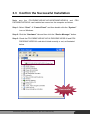
1
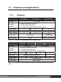
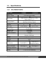
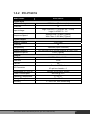
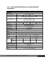
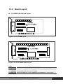
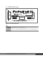
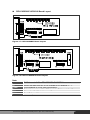
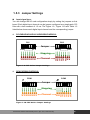
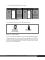
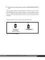
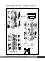
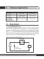
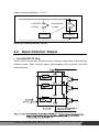
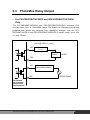
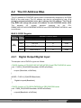
PCI-P16R16 Series Includes PCI-P8R8/P16R16, PCI-P8POR8/P16POR16, PCI-P16C16 and PEX-P8POR8i/P16POR16i User Manual Version 2.8 Apr. 2011 Warranty All products manufactured by ICP DAS are warranted against defective materials for a period of one year from the date of delivery to the original purchaser. Warning ICP DAS assumes no liability for damages consequent to the use of this product. ICP DAS reserves the right to change this manual at any time without notice. The information furnished by ICP DAS is believed to be accurate and reliable. However, no responsibility is assumed by ICP DAS for its use, nor for any infringements of patents or other rights of third parties resulting from its use. Copyright Copyright © 2011 by ICP DAS. All rights are reserved. Trademark Names are used for identification only and may be registered trademarks of their respective companies. PCI-P16R16 Series User Manual (Ver.2.8, Apr. 2011, PMH-013-28) 1 Tables of Contents 1 . INTRODUCTION ............................................................................................................................. 1 1.1 FEATURES AND APPLICATIONS ........................................................................................................ 3 1.1.1. Features ......................................................................................................................................... 3 1.1.2. Applications ................................................................................................................................... 4 1.2 BLOCK DIAGRAM ............................................................................................................................ 4 1.3 SPECIFICATIONS .............................................................................................................................. 5 1.3.1 PCI-P8R8/P16R16 ........................................................................................................................ 5 1.3.2 PCI-P16C16 .................................................................................................................................. 6 1.3.3 PCI-P8POR8/P16POR16 and PEX-P8POR8i/ P16POR16i......................................................... 7 1.4 PRODUCT CHECK LIST ..................................................................................................................... 8 1.5 HARDWARE CONFIGURATION .......................................................................................................... 9 1.5.1 Unpacking ...................................................................................................................................... 9 1.5.2 Board Layout................................................................................................................................ 10 1.5.3 Jumper Setting............................................................................................................................. 14 1.6 PIN ASSIGNMENTS ......................................................................................................................... 17 1.6.1 PCI-P8R8/P16R16 ........................................................................................................................ 17 1.6.2 PCI-P16C16 .................................................................................................................................. 18 1.6.3 PCI-P8POR8/P16POR16i and PEX-P8POR8i/P16POR16i......................................................... 19 2 3 . HARDWARE APPLICATIONS.................................................................................................... 20 2.1 RELAY OUTPUT ............................................................................................................................. 20 2.2 OPEN COLLECTOR OUTPUT ........................................................................................................... 21 2.3 PHOTOMOS RELAY OUTPUT .......................................................................................................... 22 2.4 ISOLATED INPUT ............................................................................................................................ 23 . SOFTWARE INSTALLATION GUIDE....................................................................................... 25 3.1 SOFTWARE INSTALLING PROCEDURE ................................................................................................... 25 3.2 PNP DRIVER INSTALLATION ................................................................................................................. 26 3.3 CONFIRM THE SUCCESSFUL INSTALLATION .......................................................................................... 27 4 . I/O CONTROL REGISTER ............................................................................................................ 28 4.1 HOW TO FIND THE I/O ADDRESS ........................................................................................................... 28 4.2 THE I/O ADDRESS MAP ........................................................................................................................ 34 4.2.1 Digital Output/Digital Input........................................................................................................ 34 4.2.2 D/O Readback Register................................................................................................................ 35 4.2.3 Card ID Register.......................................................................................................................... 35 5 DEMO PROGRAMS ........................................................................................................................... 36 5.1 DEMO PROGRAMS FOR WINDOWS ................................................................................................. 36 5.2 DEMO PROGRAMS FOR DOS.......................................................................................................... 37 5.3 PIO_PISO.EXE FOR WINDOWS .................................................................................................... 38 PCI-P16R16 Series User Manual (Ver.2.8, Apr. 2011, PMH-013-28) 1 1 . Introduction Model Number Isolated Digital Input Output Type PCI-P8R8 8 Channel 8 Channel Relay Output PCI-P16R16 16 Channel 16 Channel Relay Output PCI-P16C16 16 Channel 16 Channel Open Collector Output PCI-P8POR8 PEX-P8POR8i 8 Channel 8 Channel PhotoMos-Relay Output PCI-P16POR16 16 Channel PEX-P16POR16i 16 Channel PhotoMos-Relay Output • PCI-P8R8/PCI-P16R16 The PCI-P16R16/PCI-P8R8 is a PCI card supporting 5 V PCI bus and "Plug & Play" feature to get I/O address automatically without manually setting. This card contains 16/8 photo coupler digital input channels that provide 5000 Vrms isolation protection, allowing the input signals to be completely floated so as to prevent ground loops. They are also equipped with 16/8 relay output channels to enable the control of the ON/OFF state of external devices, drive external relays or small power switches, or activate alarms, etc. • PCI-P16C16 The PCI-P16C16 is a 5 V PCI card that support “Plug & Play” functionality to automatically obtain I/O resources from the BIOS. This card contains 16 optically isolated digital input channels and 16 open collector (sink, NPN) digital output channels. The DI channels provide 5000 Vrms isolation protection that allows the input signals to be completely floated so as to prevent ground loops and isolate the host computer from damaging voltages. The open collector output (DO) channels are typically used for alarm and warning notification, control of signal output, control of external circuits that require a higher voltage level, and signal transmission applications, etc. The PCI-P16C16 contains a single DB-37 connector and a single 40-pin box header and includes a 40-pin to DB-37 flat cable for easy wiring. PCI-P16R16 Series User Manual (Ver.2.8, Apr. 2011, PMH-013-28) 1 • PCI-P8POR8/P16POR16 and PEX-P8POR8i/P16POR16i The PCI-P8ROR8/P16POR16 supports 5 V PCI bus while the PEXP8POR8i/P16POR16i supports PCI Express bus. Each contain 8 or 16 optically isolated input channels and 8 or 16 PhotoMos relay output channels. Both the isolated DI channels and the PhotoMos relay channels use a short optical transmission path to transfer an electronic signal between elements of a circuit and keep them electrically isolated. The DI channels provide 5000 Vrms isolation protection, allowing the input signals to be completely floated so as to cut down ground loops, block voltage spikes, and isolate the host computer from damaging voltages. PhotoMos relays are used where it is necessary to control a circuit using a low-power signal (with complete electrical isolation between the control and controlled circuits), or where several circuits must be controlled by one signal. The PCI-P8POR8/P16POR16 and PEX-P8POR8i/P16POR16i can be used in various applications, such as controlling the ON/OFF state of external devices, driving external relays or small power switches, activating alarms, contact closure, sensing external voltages or switches, etc. The card can be installed in PCI/PCI Express slot and supports true "Plug & Play", with two DB-37 connectors provided for easy wiring. PCI-P16R16 Series User Manual (Ver.2.8, Apr. 2011, PMH-013-28) 2 1.1 Features and Applications 1.1.1. Features PCI-P8R8 PCI-P16R16 Bus Type Common Features PCI-P16C16 5 V PCI Bus z z z Optically Isolated Digital Input AC/DC Digital Signed Input AC Digital Input With Filter By Jumper Setting Input Channel 8 Input Type 16 16 Optically Isolated Digital Input Output Channel 8 Output Type Led Indicators 16 16 Relay Output Transistor (Open Collector) None External Power status Table 1-1: Features of PCI-P8R8/P16R16/P16C16 card PCI-P8POR8 PCI-P16POR16 PEX-P8POR8i PEX-P16POR16i Bus Type Common Features Input Channel 5 V PCI Bus z z z Optically Isolated Digital Input AC/DC Digital Signed Input AC Digital Input With Filter By Jumper Setting 8 Input Type Output Channel Output Type Led Indicators PCI Express x 1 16 8 16 8 16 Optically Isolated Digital Input 8 16 PhotoMos Relay Output Status Table 1-2: Features of PCI-P8POR8/P16POR16 and PEX-P8POR8i/P16POR16i card PCI-P16R16 Series User Manual (Ver.2.8, Apr. 2011, PMH-013-28) 3 1.1.2. Applications Factory automation Laboratory automation Communication switching Security control Product test Energy management 1.2 Block Diagram PCI BUS P8R8 / P16R16 EEPROM PCI Controller Relay P16C16 Relay Transistor Buffers & Drivers Transistor PhotoMos Relay PhotoMos Relay Transistor P16POR16 Transistor PhotoMos PhotoMos Photo Couple Buffers & Filters Photo Couple Photo Couple Photo Couple Figure 1-1: Functional Block diagram. PCI-P16R16 Series User Manual (Ver.2.8, Apr. 2011, PMH-013-28) 4 1.3 Specifications 1.3.1 PCI-P8R8/P16R16 Model Name PCI-P8R8 PCI-P16R16 Digital Input Isolation Voltage Channels Input Voltage Response Speed 3750 Vrms (Photo-couple) 8 16 Logic 1:AC/DC 5 ~ 24 V(AC 50 ~ 1 kHz) Logic 0: AC/DC 0 ~ 1 V Without Filter: 50 kHz (Typical) With Filter: 0.455 kHz (Typical) Relay Output Channels Relay Type 8 16 4 SPDT 4SPST 8 SPDT 8 SPST Contact Rating AC:120 [email protected] A DC: 24 V@1 A Operating Time 5 ms (typical) Release Time 10 ms (typical) 1000 MΩ Insulation Resistance Life Mechanical: 5000000 ops. Electrical: 100000 ops. General Bus Type 5 V PCI, 32-bit, 33 MHz Data Bus 16-bit Card ID I/O Connector Dimensions (L x W x D) Power Consumption Operating Temperature Storage Temperature Humidity No Female DB37 x 1 Female DB37 x 1 40-pin box header x 1 183 mm x 105 mm x 22 mm 500 mA @ +5 V 800 mA @ +5 V 0 ~ 60 °C -20 ~ 70 °C 5 ~ 85% RH, non-condensing PCI-P16R16 Series User Manual (Ver.2.8, Apr. 2011, PMH-013-28) 5 1.3.2 PCI-P16C16 Model Name PCI-P16C16 Digital Input Isolation Voltage 3750 Vrms (Photo-couple) Channels Input Voltage Response Speed 16 Logic 1:AC/DC 5 ~ 24 V(AC 50 ~ 1 kHz) Logic 0: AC/DC 0 ~ 1 V Without Filter: 50 kHz (Typical) With Filter: 0.455 kHz (Typical) Digital Output Isolation Voltage 3750 Vrms Channels Compatibility 16 Transistor(Open Collector) Output Capability DC:600 mA/+30 V for one channel @ 100% duty Response Speed 1 kHz (Typical) General Bus Type 5 V PCI, 32-bit, 33 MHz Data Bus 16-bit Card ID I/O Connector Dimensions (L x W x D) Power Consumption Operating Temperature Storage Temperature Humidity No Female DB37 x 1 40-pin box header x 1 183 mm x 105 mm x 22 mm 800 mA @ +5 V 0 ~ 60 °C -20 ~ 70 °C 5 ~ 85% RH, non-condensing PCI-P16R16 Series User Manual (Ver.2.8, Apr. 2011, PMH-013-28) 6 1.3.3 PCI-P8POR8/P16POR16 and PEX-P8POR8i/ P16POR16i Model Name PCI-P8POR8 PCI-P16POR16 PEX-P8POR8i PEX-P16POR16i Digital Input Isolation Voltage Channels 3750 Vrms (Photo-couple) 8 16 8 16 Logic 1:AC/DC 5 ~ 24 V(AC 50 ~ 1 kHz) Input Voltage Logic 0: AC/DC 0 ~ 1 V Without Filter: 50 kHz (Typical) Response Speed With Filter: 0.455 kHz (Typical) Relay Output Channels 8 16 Relay Type 8 16 PhotoMos Relay (Form A) Contact Rating AC:350 V/130 mA (Peak AC) Operating Time 0.7 ms (typical) Release Time 0.05 ms (typical) 23 Ω Insulation Resistance Special LED Indicators Output status General Bus Type 5 V PCI, 32-bit, 33 MHz Data Bus 16-bit Card ID Female DB37 I/O Connector 40-pin box header Dimensions (L x W x D) Power Consumption No Yes (4-bit) 1 1 1 1 - 1 - 1 183 mm x 105 mm x 22 mm 800 mA @ +5 V Operating Temperature Storage Temperature Humidity PCI Express x1 0 ~ 60 °C -20 ~ 70 °C 5 ~ 85% RH, non-condensing PCI-P16R16 Series User Manual (Ver.2.8, Apr. 2011, PMH-013-28) 7 1.4 Product Check List The shipping package includes the following items: One PCI boards as follows: • PCI-P8R8/PCI-P16R16 • PCI-P16C16 • PCI-P8POR8/PCI-P16POR16 • PEX-P8POR8i/PEX-P16POR16i One software utility PCI CD. One Quick Start Guide. It is recommended that you read the Quick Start Guide first. All the necessary and essential information is given in the Quick Start Guide, including: Where to get the software driver, demo programs and other resources. How to install the software. How to test the card. Attention! If any of these items is missing or damaged, contact the dealer from whom you purchased the product. Please save the shipping materials and carton in case you need to ship or store the product in the future. PCI-P16R16 Series User Manual (Ver.2.8, Apr. 2011, PMH-013-28) 8 1.5 Hardware Configuration This chapter describes how to unpack this I/O card and how to install it to your system. Both the unpacking information and the jumper settings are described in the following text. This manual should be carefully read before installation. 1.5.1 Unpacking This I/O card was well-tested and inspected both mechanically and electrically before shipping. It was free of marks and scratches our quality delivery policy requires that all equipment be in perfect order before delivery. However, some unconditional damages may occur while unpacking!! Please read this section before unpacking the card. Feel free to contact your carrier and retain your carton in case there is error. CAUTION: This card contains sensitive electronic components that can be easily damaged by static electricity. 1. This card should be packed with an anti-static mat. 2. The user should wear an anti-static wristband, grounded at the same point to the anti-static mat. 3. Inspect the carton for obvious damage. Either shipping or handing may cause damages!! Be sure there are no shipping and handing damages on the card before using. 4. After opening the carton, place the system board handle on a grounded antistatic surface and let the component side up. CAUTION: Do not apply power to the board if it has been damaged! 5. You are now ready to install your card. PCI-P16R16 Series User Manual (Ver.2.8, Apr. 2011, PMH-013-28) 9 1.5.2 Board Layout PCI-P8R8/P16R16 Board Layout Figure 1-2: PCI–P8R8 Layout Figure 1-3: PCI–P16R16 Board Layout Note: CN1 JP1 ~ JP8 CN2 JP9 ~ JP16 D/I/O channel 0~7 for PCI-P8R8/P16R16. Select the input AC or DC signals of D/I channel 0 ~ 7 for CN1. D/I/O channel 8~15 for PCI-P16R16. Select the input AC or DC signals for D/I channel 8 ~ 15 for CN2. PCI-P16R16 Series User Manual (Ver.2.8, Apr. 2011, PMH-013-28) 10 PCI-P16C16 Board Layout Figure 1-4: PCI-P16C16 Layout Note: CN1 JP1 ~ JP8 CN2 JP9 ~ JP16 D/I/O channel 0~7 for PCI-P16C16. Select the input AC or DC signals of D/I channel 0 ~ 7 for CN1. D/I/O channel 8~15 for PCI-P16C16. Select the input AC or DC signals for D/I channel 8 ~ 15 for CN2. PCI-P16R16 Series User Manual (Ver.2.8, Apr. 2011, PMH-013-28) 11 PCI-P8POR8/P16POR16 Board Layout LED indicator PCI - P8POR8 JP8...........JP1 Figure 1-5: PCI-P8POR8 Layout LED indicator CN1 JP8...........JP1 CN2 PCI - P16POR16 JP16 —— JP9 Figure 1-6: PCI-P16POR16 Layout Note: CN1 JP1 ~ JP8 CN2 JP9 ~ JP16 D/I/O channel 0~7 for PCI-P8POR8/P16POR16. Select the input AC or DC signals of D/I channel 0 ~ 7 for CN1. D/I/O channel 8~15 for PCI-P16POR16. Select the input AC or DC signals for D/I channel 8 ~ 15 for CN2. PCI-P16R16 Series User Manual (Ver.2.8, Apr. 2011, PMH-013-28) 12 PEX-P8POR8i/P16POR16i Board Layout Figure 1-7: PEX-P8POR8i Board Layout Figure 1-8: PEX-P16POR16i Board Layout Note: CON1 J1 CON2 J2 JP2 SW1 D/I/O channel 0~7 for PEX-P8POR8i/P16POR16i. Select the input type AC or DC signals for D/I channel 0 ~ 7. D/I/O channel 8~15 for PEX-P16POR16i. Select the input type AC or DC signals for D/I channel 8 ~ 15. Ground isolated protection Card ID dip-switch PCI-P16R16 Series User Manual (Ver.2.8, Apr. 2011, PMH-013-28) 13 1.5.3 Jumper Settings Input signal type: You can change the I/O card configuration simply by setting the jumpers on this board. Each digital input channel can be jumper-configured as a single-pole, RC filter with a time constant of 1.2 ms. The Figure 1-9 , Figure 1-10 and Table 1-2 listed below shows each digital input channel and the corresponding jumper. • PCI-P8R8/P16R16/P16C16/P8POR8/P16POR16: CN1 CN2 Jumper Mapping DI8 DI9 DI10 DI11 DI12 DI13 DI14 DI15 DI0 DI1 DI2 DI3 DI4 DI5 DI6 DI7 Channel Figure 1-9: PCI Series Jumper Settings • PEX-P8POR8i/P16POR16i: CON1 CON2 Jumper 1 .......................... 9 ............................. 8 16 Mapping DI15 DI14 DI13 DI12 DI11 DI10 DI9 DI8 DI7 DI6 DI5 DI4 DI3 DI2 DI1 DI0 Channel Figure 1-10: PEX Series Jumper Settings PCI-P16R16 Series User Manual (Ver.2.8, Apr. 2011, PMH-013-28) 14 • Jumper Mapping Digital Input Channel Table: Jumper PCI series PEX series JP1 1 JP2 2 JP3 3 JP4 4 J1 JP5 5 JP6 6 JP7 7 JP8 8 Channel DI0 DI1 DI2 DI3 DI4 DI5 DI6 DI7 Jumper PCI series PEX series JP9 9 JP10 10 JP11 11 JP12 12 J2 JP13 13 JP14 14 JP15 15 JP16 16 Channel DI8 DI9 DI10 DI11 DI12 DI13 DI14 DI15 Table 1-2: Jumper assignment The figure below shows how to select the digital input type: 1 2 3 1 2 3 Without Filter For DC Signal (Default Setting) With AC Filter For AC Signal Figure 1-11: Jumper Settings If you are using AC input signals, you must short AC FILTER pin2-3 of the corresponding jumpers. If you are using DC input signals, the AC FILTER is optional. If the DC input signal response is less than 20 μs, set the filter to off. If you want a slow response (about 5 to 10 ms) to reject either noise or contact bouncing, short AC FILTER Pin2-3. PCI-P16R16 Series User Manual (Ver.2.8, Apr. 2011, PMH-013-28) 15 JP2: Ground isolated protection jumper for PEX-P8POR8i/P16POR16i only This JP2 jumper is used to select the isolated or non-isolated of ground for PEXP8POR8i/P16POR16i only. As shown in Figure 1-7, the user needs to connect Pin1-2 to obtain the ground isolation protection, which is the default setting. However, for the ground non-isolation, the Pin2-3 for the JP2 jumper should be connected. The figure below shows how to select the ground isolation type: JP2 1 2 3 GND Isolation Protection (Default Setting) JP2 1 2 3 GND Non-Isolation Protection Figure 1-12: Jumper Settings PCI-P16R16 Series User Manual (Ver.2.8, Apr. 2011, PMH-013-28) 16 1.6 Pin Assignments 1.6.1 PCI-P8R8/P16R16 CON 1 PCI CON 2 CON 2 Extender Cable NO: Normally Open COM: Common NC: Normally Closed DIA: Digital Input (Point A) DIB: Digital Input (Point B) PCI-P16R16 Series User Manual (Ver.2.8, Apr. 2011, PMH-013-28) 17 1.6.2 PCI-P16C16 CON 1 CON 2 CON 2 External Cable Ext. Power: External Power Input GND: External Power Ground OUT: Open Collector Output DIA: Digital Input (Point A) DIB: Digital Input (Point B) PCI-P16R16 Series User Manual (Ver.2.8, Apr. 2011, PMH-013-28) 18 1.6.3 PCI-P8POR8/P16POR16i and PEX-P8POR8i/P16POR16ii CON 1 CON 2 CON 2 External Cable NO DIA: Digital Input (Point A) DIB: Digital Input (Point B) PCI-P16R16 Series User Manual (Ver.2.8, Apr. 2011, PMH-013-28) CM 19 2 . Hardware Applications Model Number PCI-P8R8 PCI-P16R16 PCI-P16C16 PCI-P8POR8 PCI-P16POR16 PEX-P8POR8i PEX-P16POR16i 2.1 OUTPUT INPUT Relay Output Optical isolation Transistor Output (Open Collector) Optical isolation PhotoMos Relay Output Optical isolation Relay Output • For PCI-P8R8/P16R16 Only Whenever data is written data to the output control register, the relays will switch to NC or NO as specified by the control code. A`1'in the control register will energize the corresponding relay. The relay will switch from COM to NO (normally open). A `0' in the control register will turn off the corresponding relay and the relay will be switch from COM to NC (normally closed). The control register powers-on in NC mode. Hardware reset signal or programmable reset signal will also turn the relay to NC. The following figures show how to use the relay. Basic Circuitry: (Current Rating < 0.3 A): Relay Contact COM NO Load AC/ DC Power Supply Figure 2-1: Basic Relay Circuit PCI-P16R16 Series User Manual (Ver.2.8, Apr. 2011, PMH-013-28) 20 Heavy Loading Application ( > 0.3 A ) : P16R16DI O Relay Power Relay Contact Power Relay Heavy Loading Figure 2-3. Heavy load relay circuit. 2.2 Open Collector Output • For PCI-P16C16 Only The PCI-P16C16 provides 16-channel open collector outputs and 4 channels per common power. Each common power has designed fuse protection and LED indicated status. PCI-P16R16 Series User Manual (Ver.2.8, Apr. 2011, PMH-013-28) 21 2.3 PhotoMos Relay Output • For PCI-P8POR8/P16POR16 and PEX-P8POR8i/P16POR16i Only The PCI-P8POR8/P16POR16 and PEX-P8POR8i/P16POR16i includes 8/16 normally open, form A, PhotoMOS relays. The board can eliminate ground-loop problems and isolate the computer from damaging voltages. Use the PCIP8POR8/P16POR16 and PEX-P8POR8i/P16POR16i to switch loads, up to 350 VAC and 130 mA. 130 A @ 350 VAC (max.) NO Load Power AC/DC CM NO Measurement Meter CM AC/DC Signal PCI-P8POR8 PCI-P16POR16 PEX-P8POR8i PEX-P16POR16i PCI-P16R16 Series User Manual (Ver.2.8, Apr. 2011, PMH-013-28) 22 2.4 Isolated Input • For PCI-P8R8/P16R16/P16C16/P8POR8/P16POR16 and PEXP8POR8i/P16POR16i Reading the isolation input register will give the digital input state of the photocouple (isolation input). Figures 2-3 and 2-4 show the basic circuit of the digital input. Switch DIA 0 Internal Circuit If Using AC Signal, JP1 must be shorted 2-3!! 5 ~ 24 VAC/DC DIB 0 Figure 2-3. Basic Digital Input Circuit. PCI-P16R16 Series User Manual (Ver.2.8, Apr. 2011, PMH-013-28) 23 Although the normal input voltage range is 5 to 24 VAC or VDC, the input can still be changed to a larger range by choosing suitable external resistors. The following figure shows how to connect to a larger input. Please note that the input current should be limited between 2 mA to 20 mA; too large an input current will burn down the internal resistor Ri, while too low of an input current will not active the photo-coupler isolator. Calculate input voltage and current, then replace resister Ri. Ri = 1.2 kΩ /1 W Vin External Circuit If 20mA On board circuits PC - 814 Figure 2-4. Isolated Digital Input If = 2 mA ~ 20 mA A rough estimate: if Vin = 120 V and we ignore photo-coupler turn-on voltage. We’ll get: Vin / If = Ri Vin = 120(V) , If =10(mA) , Ri = Vin/ If 120(V) / 0.01 (A) = 12000 (Ω) If you replace 12 kΩ as resistor Ri, we can calculate the power consumption of Ri as follows: 2 2 P = I Rex = (10 mA) * 12 KΩ = 1.2 W The power consumption is 1.2 watts, but choosing 1.5 or 2 watts is better. Thus, we can choose a 12 K/2 W resistor to replace the resistor Ri. PCI-P16R16 Series User Manual (Ver.2.8, Apr. 2011, PMH-013-28) 24 3 . Software Installation Guide The PCI-P8R8/P16R16/P16C16/P8POR8/P16POR16 and PEX-P8POR8i/ P16POR16i series can be used in DOS and Windows 98/NT/2K and 32-bit/64bit Windows XP/2003/Vista/7. The recommended installation procedure for windows is given in Sec. 3.1 ~ 3.2. Or refer to Quick Start Guide (CD:\NAPDOS\PCI\PCI-P16R16\ Manual\QuickStart\). http://ftp.icpdas.com/pub/cd/iocard/pci/napdos/pci/pci-p16r16/manual/quickstart/ 3.1 Software Installing Procedure UniDAQ SDK driver (32-bit/64-bit Windows XP/2003/Vista/7): Step 1: Insert the companion CD into the CD-ROM drive and after a few seconds the installation program should start automatically. If it doesn’t start automatically for some reason, double-click the AUTO32.EXE file in the NAPDOS folder on this CD. Step 2: Click the item: “PCI Bus DAQ Card”. Step 3: Click the item: “UniDAQ”. Step 4: Click the item: “DLL for Windows 2000 and XP/2003/Vista 32-bit”. Step 5: Double-Click “UniDAQ_Win_Setup_x.x.x.x_xxxx.exe” file in the Driver folder. Windows driver (Windows 98/NT/2K and 32-bit Windows XP/2003/Vista/7): Step 1: Insert the companion CD into the CD-ROM drive and after a few seconds the installation program should start automatically. If it doesn’t start automatically for some reason, double-click the AUTO32.EXE file in the NAPDOS folder on this CD. Step 2: Click the item: “PCI Bus DAQ Card”. Step 3: Click the item: “PCI-P16R16/PCI-P8R8”. Step 4: Click the item “DLL and OCX for Windows 98/NT/2K/XP/2003”. Step 5: Choose the Win2K_XP, Win98 or WinNT folders for setup according to your PC platform and then double-Click “.exe” to install driver. PCI-P16R16 Series User Manual (Ver.2.8, Apr. 2011, PMH-013-28) 25 The setup program will then start the driver installation and copy the relevant files to the specified directory and register the driver on your computer. The directory where the drive is stoned is different for different windows versions, as shown below. Windows 64-bit Windows XP/2003/Vista/7: The UniDAQ.DLL file will be copied into the C:\WINNT\SYSTEM32 folder The NAPWNT.SYS and UniDAQ.SYS files will be copied into the C:\WINNT\SYSTEM32\DRIVERS folder ! For more detailed UniDAQ.DLL function information, please refer to UniDAQ SDK user manual (CD:\NAPDOS\PCI\UniDAQ\Manual\). http://ftp.icpdas.com/pub/cd/iocard/pci/napdos/pci/unidaq/maunal/ Windows NT/2K and 32-bit Windows XP/2003/Vista/7: The P16R16.DLL file will be copied into the C:\WINNT\SYSTEM32 folder The NAPWNT.SYS and P16R16.SYS files will be copied into the C:\WINNT\SYSTEM32\DRIVERS folder Windows 95/98/ME: The P16R16.DLL and Nappci.Vxd files will be copied into the C:\Windows\SYSTEM folder ! For more detailed P16R16.DLL function information, please refer to “PCI-P16R16 Series Software Manual.pdf” (CD:\NAPDOS\PCI\PCIP16R16\Manual\). http://ftp.icpdas.com/pub/cd/iocard/pci/napdos/pci/pcip16r16/manual/ 3.2 PnP Driver Installation Power off the computer and install the PCI-P8R8/P16R16/P16C16/ P8POR8P16POR16 and PEX-P8POR8i/P16POR16i cards. Turn on the computer and Windows 98/ME/2K and 32-bit/64-bit Windows XP/2003/Vista/7 should automatically defect the new PCI device(s) and then ask for the location of the driver files for the hardware. If a problem is encountered during installation, refer to the PCI-P16R16_PnP_Driver_Installation.pdf (CD:\NAPDOS\PCI\PCI-P16R16\Manual\) for more information. PCI-P16R16 Series User Manual (Ver.2.8, Apr. 2011, PMH-013-28) 26 3.3 Confirm the Successful Installation Make sure the PCI-P8R8/P16R16/P16C16/P8POR8P16POR16 and PEXP8POR8i/P16POR16i card installed are correct on the computer as follows: Step 1: Select “Start” Æ “Control Panel” and then double click the “System” icon on Windows. Step 2: Click the “Hardware” tab and then click the “Device Manager” button. Step 3: Check the PCI-P8R8/P16R16/P16C16/ P8POR8P16POR16 and PEXP8POR8i/P16POR16i card which listed correctly or not, as illustrated below. Successful PCI-P16R16 Series User Manual (Ver.2.8, Apr. 2011, PMH-013-28) 27 4 . I/O Control Register 4.1 How to find the I/O Address The Plug&Play BISO assigns a proper I/O address to every PCI-P8R8/P16R16/ P16C16/P8R8/P16POR16 and PEX-P8POR8i/P16POR16i card in the power-on stage. The IDs of PCI-P8R8/P16R16/ P16C16/P8R8/P16POR16 and PEXP8POR8i/P16POR16i are as follows: PCI-P8R8 PCI-P8POR8 PEX-P8POR8i PCI-P16R16 PCI-P16C16 PCI-P16POR16 PEX-P16POR16i Vendor ID 0x1234 0x1234 Device ID 0x0808 0x1616 Sub Vendor ID 0x0000 0x0000 Sub Device ID 0x0000 0x0000 Model Name We provide the following necessary functions: 1. PCI_DriverInit (&wBoards) This function detects how many PCI-P8R8/P16R16 series cards are installed in the system, and also records all their I/O resources information in the library. The function is implemented based on the PCI Plug & Play mechanism. Please refer to “PCI-P16R16 Series Software Manual”. 2. PCI_GetConfigAddressSpace(wBoards, &wTypeID, &wAddress0, &wAddress1, &wAddress2, &wAddress3,&wAddress4,&wAddress5); Use this function to get I/O resources information of a PCI-P8R8/P16R16 series card installed in this system. Then the application program can control all functions of PCI-P8R8/P16R16 series card directly. Please refer to “PCIP16R16 Series Software Manual”. ! Note: The PCI-P8R8/P16R16 series card is to use the BAR 2 (&wAddress2) to control all functions, please refer to Sec. 4.2 The I/O Address Map. PCI-P16R16 Series User Manual (Ver.2.8, Apr. 2011, PMH-013-28) 28 The First 16 double words of a PCI device's configuration space are referred to as the device's configuration region. Within these the 16 (0-15) double words, the 04, 05, 06, 07, 08 and 09 double words are referred to as Base Address0, Base Address1, Base Address2, Base Address3, Base Address4 and Base Address5. For more detailed information for about these 16 double words, please referring the book titled PLUG AND PLAY SYSTEM ARCHITECTURE (written by Tom Shanley, Addison-Wesley Publish Company, 1995). These base addresses are utilized as control register and/or I/O register for many data acquisition boards. On PCI-P16R16 and PCI-P8R8 series boards, the base address2 is utilized as the base address of digital input and digital output. So the Digital I/O functions for PCIP16R16 and PCI-P8R8 series are coded as follows: #define WORD unsigned int #define UCHAR unsigned char void P16R16_DO(WORD BaseAddr, WORD wOutData) { outport(BaseAddr,wOutData); } WORD P16R16_DI(WORD BaseAddr) { WORD DigitalIn; DigitalIn=inport(BaseAddr); return DigitalIn; } void P8R8_DO(WORD BaseAddr, WORD wOutData) { outportb(BaseAddr,wOutData); } UCHAR P8R8_DI(WORD BaseAddr) { UCHAR DigitalIn; DigitalIn=inportb(BaseAddr); return DigitalIn; } PCI-P16R16 Series User Manual (Ver.2.8, Apr. 2011, PMH-013-28) 29 Please refer to the following program code to get these six base addresses for PCI-P16R16 and PCI-P8R8. These codes are based on PCI Plug & Play mechanism 2. /******************************************************/ /* Reading PCI card's configuration address space */ /******************************************************/ WORD GetAddress(void) { DWORD dConfigAddress,dBaseAddress; WORD HiWord,LoWord; WORD ReturnCode; UCHAR Bus,Device,Function,WhichLong; WORD VendorID,DeviceID; WORD wIrqNumber; wTotalBoards=0; /* initial board number is 0 */ Bus=0; for(Bus=0; Bus<10; Bus++) { Function=0; WhichLong=1; for(Device=0; Device<32; Device++) { WhichLong=0; WriteAddress(Bus,Device,Function,WhichLong); VendorID=inport(0xcfc); DeviceID=inport(0xcfe); if( VendorID==0x1234 && DeviceID==0x1616 ) { /*----------- PCI-P16R16 --------------* WhichLong=4; // Base Address 0 WriteAddress(Bus,Device,Function,WhichLong); dBaseAddress=_inpd(0xcfc); wBaseAddr0=(WORD)(dBaseAddress&0xfffe); wConfigSpace[wTotalBoards][0]=wBaseAddr0; PCI-P16R16 Series User Manual (Ver.2.8, Apr. 2011, PMH-013-28) 30 /*----------------------------------------*/ WhichLong=5; /* Base Address 1 */ WriteAddress(Bus,Device,Function,WhichLong); dBaseAddress=_inpd(0xcfc); wBaseAddr1=(WORD)(dBaseAddress&0xfffe); wConfigSpace[wTotalBoards][1]=wBaseAddr1; /*------------------------------------------*/ WhichLong=6; /* Base Address 2 */ WriteAddress(Bus,Device,Function,WhichLong); dBaseAddress=_inpd(0xcfc); wBaseAddr2=(WORD)(dBaseAddress&0xfffe); wConfigSpace[wTotalBoards][2]=wBaseAddr2; /*------------------------------------------*/ WhichLong=7; /* Base Address 3 */ WriteAddress(Bus,Device,Function,WhichLong); dBaseAddress=_inpd(0xcfc); wBaseAddr3=(WORD)(dBaseAddress&0xfffe); wConfigSpace[wTotalBoards][3]=wBaseAddr3; /*------------------------------------------*/ WhichLong=8; /* Base Address 4 */ WriteAddress(Bus,Device,Function,WhichLong); dBaseAddress=_inpd(0xcfc); wBaseAddr4=(WORD)(dBaseAddress&0xfffe); wConfigSpace[wTotalBoards][4]=wBaseAddr4; /*-------------------------------------------*/ WhichLong=9; /* Base Address 5 */ WriteAddress(Bus,Device,Function,WhichLong); dBaseAddress=_inpd(0xcfc); wBaseAddr5=(WORD)(dBaseAddress&0xfffe); wConfigSpace[wTotalBoards][5]=wBaseAddr5; /*----------- store the type name ID --------*/ wConfigSpace[wTotalBoards][6]=TYPE_P16R16; PCI-P16R16 Series User Manual (Ver.2.8, Apr. 2011, PMH-013-28) 31 /*-------------------------------------------*/ wTotalBoards++; /* increment board number */ wGetAddress=1; } if( VendorID==0x1234 && DeviceID==0x0808 ) { /*---------- PCI-P8R8 -----------*/ WhichLong=4; /* Base Address 0 */ WriteAddress(Bus,Device,Function,WhichLong); dBaseAddress=_inpd(0xcfc); wBaseAddr0=(WORD)(dBaseAddress&0xfffe); wConfigSpace[wTotalBoards][0]=wBaseAddr0; /*------------------------------------------*/ WhichLong=5; /* Base Address 1 */ WriteAddress(Bus,Device,Function,WhichLong); dBaseAddress=_inpd(0xcfc); wBaseAddr1=(WORD)(dBaseAddress&0xfffe); wConfigSpace[wTotalBoards][1]=wBaseAddr1; /*------------------------------------------*/ WhichLong=6; /* Base Address 2 */ WriteAddress(Bus,Device,Function,WhichLong); dBaseAddress=_inpd(0xcfc); wBaseAddr2=(WORD)(dBaseAddress&0xfffe); wConfigSpace[wTotalBoards][2]=wBaseAddr2; /*------------------------------------------*/ WhichLong=7; /* Base Address 3 */ WriteAddress(Bus,Device,Function,WhichLong); dBaseAddress=_inpd(0xcfc); wBaseAddr3=(WORD)(dBaseAddress&0xfffe); wConfigSpace[wTotalBoards][3]=wBaseAddr3; /*------------------------------------------*/ WhichLong=8; /* Base Address 4 */ WriteAddress(Bus,Device,Function,WhichLong); dBaseAddress=_inpd(0xcfc); wBaseAddr4=(WORD)(dBaseAddress&0xfffe); wConfigSpace[wTotalBoards][4]=wBaseAddr4; PCI-P16R16 Series User Manual (Ver.2.8, Apr. 2011, PMH-013-28) 32 /*-------------------------------------------*/ WhichLong=9; /* Base Address 5 */ WriteAddress(Bus,Device,Function,WhichLong); dBaseAddress=_inpd(0xcfc); wBaseAddr5=(WORD)(dBaseAddress&0xfffe); wConfigSpace[wTotalBoards][5]=wBaseAddr5; /*---------- store the type name ID --------*/ wConfigSpace[wTotalBoards][6]=TYPE_P8R8; wTotalBoards++; /* increment board number */ wGetAddress=1; } } } if( wTotalBoards>16 ) return( NotFoundBoard ); else return( NoError ); } void WriteAddress(UCHAR bBus, UCHAR bDevice, UCHAR bFunction, UCHAR bWhichLong) { DWORD dOutData; WORD HiWord,LoWord; UCHAR HiByte,LoByte; HiWord=0x8000|bBus; HiByte=(bDevice<<3)|bFunction; LoByte=(bWhichLong<<2) & 0xfc; LoWord=( (WORD)HiByte<<8 )|LoByte; dOutData=( (DWORD)HiWord<<16 ) | LoWord; _outpd(0xcf8,dOutData); } PCI-P16R16 Series User Manual (Ver.2.8, Apr. 2011, PMH-013-28) 33 4.2 The I/O Address Map The I/O address for PIO/PISO series cards is automatically assigned by the ROM BIOS of the main board. The I/O address can also be re-assigned by user. It is strongly recommended that users don’t change the I/O address. The Plug & Play BIOS will assign the proper I/O address to each PIO/PISO series card. The detailed I/O register address mapping for the PCIP8R8/P16R16/P16C16/P8POR8/P16POR16 and PEX-P8POR8i/P16POR16i card is as follows: BAR 2: DI/DO Register Bar No. 2 (DIO) Offset Name Register Function Script Operation Access 0x00 DI Port R 16-bit 0x00 DO Port W 16-bit 0x0C Read D/O Readback R 16-bit 0x3C Read Card ID R 16-bit 4.2.1 Digital Output/Digital Input The sample code of DI/DO is given as follows: // DI/DO function of PCI-P16R16/P16C16/P16POR16 and PEX-P16POR16i series void P16R16_DO(WORD BaseAddr, WORD wOutData) { outport (BaseAddr, wOutData); } WORD P16R16_DI(WORD BaseAddr) { DigitalIn=inportb(BaseAddr); } // DI/DO function of PCI-P8R8 /P8POR8 and PEX-P8POR8i series void P8R8_DO(WORD BaseAddr, WORD wOutData) { outportb(BaseAddr, wOutData); } PCI-P16R16 Series User Manual (Ver.2.8, Apr. 2011, PMH-013-28) 34 UCHAR P8R8_DI(WORD BaseAddr) { DigitalIn=inportb(BaseAddr); } 4.2.2 D/O Readback Register The format of the D/O readback register is given as follows: BaseAddr +0x0C Bit7 Bit6 Bit5 Bit4 Bit3 Bit2 Bit1 Bit0 The sample code of reading the given as follows: // D/O Readback function of PEX-P8POR8i and PEX-P16POR16i DigitalIn=inportb(BaseAddr+0x0C); 4.2.3 Card ID Register The format of the Card ID register is given as follows: BaseAddr +0x3C X X X X Bit3 Bit2 Bit1 Bit0 It can be used to read the card ID set from SW1 switch The sample code of reading the given as follows: // Card ID function of PEX-P8POR8i and PEX-P16POR16i *wID=inportb(BaseAddr+ 0x3C)&0x000f; N ! Note: 1. Refer to Sec. 4.1 for more information regarding BaseAddr. 2. The Card ID and D/O Readback function is only supported by the PEXP8POR8i and PEX-P16POR16i (Ver1.0 or above) PCI-P16R16 Series User Manual (Ver.2.8, Apr. 2011, PMH-013-28) 35 5 Demo Programs 5.1 Demo Programs for Windows Please note that none of the demo programs will work normally if the DLL driver has not been installed correctly. During the DLL driver installation process, the install shield will register the correct kernel driver to the operating system and copy the DLL driver and demo programs to the correct location depending on the driver software package you have selected (Win98/Me/NT/2000 and 32-bit Win XP/2003/Visa/7). After installing the driver, the related demo programs, development library and declaration header files for the different development environments will be available in the following folders. The demo program is contained in: CD:\NAPDOS\PCI\PCI-P16R16\DLL_OCX\Demo\ http://ftp.icpdas.com/pub/cd/iocard/pci/napdos/pci/pci-p16r16/dll_ocx/demo/ BCB 3 Æ For Borland C++ Builder 3 P16R16.H Æ Header files P16R16.LIB Æ Linkage library for BCB Delphi3 Æ For Delphi 3 P16R16.PAS Æ Declaration files A list of available demo programs is as follows: DIO: D/I/O demo VB6 Æ For Visual Basic 6 P16R16.BAS Æ Declaration files VC6 Æ For Visual C++ 6 P16R16.H Æ Header files P16R16.LIB Æ Linkage library for VC6 VB.NET2005 Æ For VB.NET2005 P16R16.vb Æ Declaration files CSharp2005 Æ For C#.NET2005 P16R16.cs Æ Declaration files PCI-P16R16 Series User Manual (Ver.2.8, Apr. 2011, PMH-013-28) 36 5.2 Demo Programs for DOS The related DOS software and demos are located on the CD as below: CD:\NAPDOS\PCI\PCI-P16R16\dos\ http://ftp.icpdas.com/pub/cd/iocard/pci/napdos/pci/pci-p16r16/dos/ After installing the software, the following drivers will be installed onto your hard disk: Demo code, Lib for Borland C++ ...\P16R16\BC\HUGE\DEMO Æ huge mode demo programs. ...\P16R16\BC\HUGE\LIB Æ huge mode library, P16R16H.LIB ...\P16R16\BC\LARGE\DEMO Æ large mode demo programs ...\P16R16\BC\LARGE\LIB Æ large mode library, P16R16L.LIB Demo code, Lib for MSC ...\P16R16\MSC\HUGE\DEMO ...\P16R16\MSC\HUGE\LIB ...\P16R16\MSC\LARGE\DEMO ...\P16R16\MSC\LARGE\LIB Æ huge mode demo programs Æ huge mode library, P16R16H.LIB Æ large mode demo programs Æ large mode library, P16R16L.LIB Demo code, Lib for TC ...\P16R16\TC\HUGE\DEMO ...\P16R16\TC\HUGE\LIB ...\P16R16\TC\LARGE\DEMO ...\P16R16\TC\LARGE\LIB Æ huge mode demo programs Æ huge mdoe library, P16R16H.LIB Æ large mode demo programs Æ large mode library, P16R16H.LIB Please see readme.txt in sub-directory of DEMO and LIB for further information. PCI-P16R16 Series User Manual (Ver.2.8, Apr. 2011, PMH-013-28) 37 5.3 PIO_PISO.EXE for Windows The PIO_PISO.exe utility is located on the CD as below and is useful for all PIO/PISO series cards. CD:\NAPDOS\PCI\Utility\Win32\PIO_PISO\ http://ftp.icpdas.com/pub/cd/iocard/pci/napdos/pci/utility/win32/pio_piso/ After executing the utility, detailed information for all PIO/PISO cards that are installed in the PC will be shown, as illustrated below: Note: The PIO_PISO.EXE application is valid for all PIO/PISO cards. The user can execute the PIO_PISO.EXE file to retrieve the following information: List all PIO/PISO cards installed in the PC List the resources allocated to each PIO/PISO card List the wSlotBus and wSlotDevice details for identification of specific PIO/PISO cards. (Refer to Sec. 4.1 for more information) PCI-P16R16 Series User Manual (Ver.2.8, Apr. 2011, PMH-013-28) 38