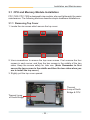
1
FPC-7300 / FPC-7302
Fanless Intel Socket P Core™ 2 Duo
Box PC
User’s Manaul
Version 1.1
P/N: 4012730001110P
2010.07
This page is intentionally left blank.
Index
Contents
Copyright Notice.................................................................i
FCC Class A........................................................................i
Important Safety Instructions...........................................ii
About This User’s Manual................................................iii
Warning.............................................................................iii
Replacing the Lithium Battery.........................................iii
Technical Support.............................................................iii
Warranty............................................................................iv
Ordering Information........................................................iv
Chapter 1 - General Information................................ 1
1.1
1.2
1.3
1.4
1.5
1.6
1.7
1.8
Introduction.................................................................2
Packing List................................................................3
The Installation Paths of CD Driver..........................3
Specifications.............................................................4
Power Information......................................................5
Dimensions.................................................................6
Locating Controls and Connectors...........................7
Connecting Peripherals.............................................9
1.8.1
1.8.2
1.8.3
1.8.4
1.8.5
1.8.6
1.8.7
1.8.8
1.8.9
VGA/DVI/DisplayPort Video Outputs.....................9
Serial Ports (COM1 ~4)..........................................10
LAN Ports............................................................... 11
USB Ports...............................................................12
Keyboard and Mouse............................................13
Expansion PCI Slots..............................................13
S-Video Connector................................................14
Audio Line-out/Mic-in............................................14
DC Power Input and Power ON/OFF Button........15
Chapter 2 - The Engine of FPC-7300/FPC-7302..... 17
2.1 Board Layout.............................................................18
2.2 Jumpers and Connectors........................................19
2.2.1 Jumpers & Connectors List..................................19
2.2.2 Jumper Setting.......................................................20
-I-
Index
2.2.3 Pin Assignments for Connectors.........................21
PWRIN1 (Power Receptacle)......................................... 21
TV1 (S-Video).................................................................. 21
KBM1 (Keyboard & Mouse)........................................... 21
CN1 (COM1 ~ COM4)..................................................... 22
USB1/2 (USB Ports)....................................................... 23
LAN1/2 (LAN Ports)........................................................ 23
AUDIO1 (Audio Jacks)................................................... 23
VGA1 (VGA Connector)................................................. 24
DP1 (DisplayPort Connector)........................................ 24
SATA1/2 (Serial ATA Connectors)................................. 25
PWR1/2 (HDD/SSD Power Connectors)....................... 25
DVI1 (DVI)........................................................................ 26
LPT1 (Parallel Port)........................................................ 27
DIO1 (Digital I/O Port).................................................... 28
CFD1 (CompactFlash Slot)............................................ 29
Chapter 3 - Installation and Maintenance............... 31
3.1 CPU and Memory Module Installation....................32
3.1.1 Removing Top Cover.............................................32
3.1.2 Installing CPU........................................................33
3.1.3 Installing Memory Module.....................................34
3.2 How to Access CF Card...........................................35
3.3 Hard Disk Drive and PCI Card Installation.............37
3.3.1 Removing Bottom Cover.......................................37
3.3.2 Installing Hard Disk Drive.....................................37
3.3.3 Installing PCI Card.................................................39
3.4 Wall Mounting (Optional).........................................40
3.5 DIN Rail Mounting (Optional)...................................41
3.5.1 Face-Left/Right DIN Rail Mounting.......................42
3.5.2 Face-Up/Down DIN Rail Mounting........................43
3.5.3 Removing the Box PC from the DIN Rail.............44
3.6 Grounding the Box PC.............................................45
3.7 Wiring the DC-Input Power Source.........................46
Chapter 4 - BIOS....................................................... 47
4.1 BIOS Main Setup.......................................................48
4.2 Advanced Settings...................................................49
4.2.1 CPU Configuration................................................50
- II -
4.2.2
4.2.3
4.2.4
4.2.6
IDE Configuration.................................................51
Super IO Configuration........................................52
Hardware Health Configuration...........................54
USB Configuration................................................55
4.3 Chipset Settings.......................................................56
4.3.1 North Bridge Configuration.................................57
4.3.2 South Bridge Configuration.................................59
4.4 PCIPnP Settings........................................................60
4.5 Boot Settings............................................................61
4.5.1 Boot Settings Configuration.................................62
4.5.2 Boot Device Priority..............................................64
4.5.3 Hard Disk Drives....................................................65
4.6 Security.....................................................................66
4.7 Exit Options...............................................................68
Chapter 5 - Appendix............................................... 71
5.1
5.2
5.3
5.4
I/O Port Address Map...............................................72
Interrupt Request Lines (IRQ)..................................75
Memory Mapping......................................................76
Digital I/O Setting......................................................78
5.4.1 Source Code in Assembly.....................................78
5.4.2 Source Code in C...................................................82
5.5 Watchdog Timer (WDT) Setting...............................84
5.5.1 Source Code in Assembly.....................................84
5.5.2 Source Code in C...................................................86
- III -
This page is intentionally left blank.
- IV -
Copyright Notice
All Rights Reserved.
The information in this document is subject to change without prior notice in
order to improve the reliability, design and function. It does not represent a
commitment on the part of the manufacturer.
Under no circumstances will the manufacturer be liable for any direct, indirect,
special, incidental, or consequential damages arising from the use or inability
to use the product or documentation, even if advised of the possibility of such
damages.
This document contains proprietary information protected by copyright. All
rights are reserved. No part of this document may be reproduced by any
mechanical, electronic, or other means in any form without prior written
permission of the manufacturer.
FCC Class A
This equipment has been tested and found to comply with limits for a Class A
digital device, pursuant to Part 15 of the FCC rules. These limits are designed
to provide reasonable protection against harmful interference installations.
This equipment generates, uses and can radiate radio frequency energy,
and if not installed and used in accordance with the instructions, may cause
harmful interference to radio communications. However, there is no guarantee
that interference will not occur in a particular installation.
If this equipment does cause interference to radio or television equipment
reception, which can be determined by turning the equipment off and on, the
user is encouraged to try to correct the interference by one or more of the
following measures:
•
•
•
•
Reorient or relocate the receiving antenna
Move the equipment away from the receiver
Plug the equipment into an outlet on a circuit different from that to
which the receiver is connected
Consult the dealer or an experienced radio/television technician for
additional suggestions
You are cautioned that any change or modifications to the equipment not
expressly approved by the party responsible for compliance could void Your
authority to operate such equipment.
-i-
Important Safety Instructions
Read these safety instructions carefully
1. Read all cautions and warnings on the equipment.
2. Place this equipment on a reliable surface when installing. Dropping it or
letting it fall may cause damage
3. Make sure the correct voltage is connected to the equipment.
4. For pluggable equipment, the socket outlet should be near the equipment
and should be easily accessible.
5. Keep this equipment away from humidity.
6. Disconnect this equipment from the A/C outlet before cleaning it. Use a moist
cloth. Do not use liquid or sprayed detergent for cleaning.
7. The openings on the enclosure are for air convection and protect the equipment
from overheating. DO NOT COVER THE OPENINGS.
8. Position the power cord so that people cannot step on it. Do not place
anything over the power cord.
9. If the equipment will not be used for a long time, disconnect it from the power
source to avoid damage by transient overvoltage.
10. Never pour any liquid into opening. This may cause fire or electrical
shock.
11. Never open the equipment. For safety reasons, the equipment should be
opened only by qualified service personnel.
12. If one of the following situations arises, get the equipment checked by
service personnel:
a. The power cord or plug is damaged.
b. Liquid has penetrated into the equipment.
c. The equipment has been exposed to moisture.
d. The equipment does not work well, or you cannot get it to work according
to the user's manual.
e. The equipment has been dropped or damaged.
f. The equipment has obvious signs of breakage.
13. The sound pressure level at the operator's position, according to
IEC 704-1:1982, is no more than 70dB(A).
14. Keep this User’s Manual for later reference.
- ii -
About This User’s Manual
This User’s Manual is intended for experienced users and integrators with
hardware knowledge of personal computers. If you are not sure about any
description in this User’s Manual, please consult your vendor before further
handling.
Warning
The Box PC and its components contain very delicately Integrated Circuits
(IC). To protect the Box PC and its components against damage caused by
static electricity, you should always follow the precautions below when handling it:
1. Disconnect your Box PC from the power source when you want to work on
the inside.
2. Use a grounded wrist strap when handling computer components.
3. Place components on a grounded antistatic pad or on the bag that came
with the Box PC, whenever components are separated from the system.
Replacing the Lithium Battery
Incorrect replacement of the lithium battery may lead to a risk of explosion.
The lithium battery must be replaced with an identical battery or a battery type
recommended by the manufacturer.
Do not throw lithium batteries into the trashcan. It must be disposed of in
accordance with local regulations concerning special waste.
Technical Support
If you have any technical difficulties, please consult the user’s manual first
at:
ftp://ftp.arbor.com.tw/pub/manual
Please do not hesitate to call or e-mail our customer service when you still
cannot find out the answer.
http://www.arbor.com.tw
E-mail:[email protected]
- iii -
Warranty
This product is warranted to be in good working order for a period of one year
from the date of purchase. Should this product fail to be in good working order
at any time during this period, we will, at our option, replace or repair it at no
additional charge except as set forth in the following terms. This warranty
does not apply to products damaged by misuse, modifications, accident or
disaster.
Vendor assumes no liability for any damages, lost profits, lost savings or any
other incidental or consequential damage resulting from the use, misuse of,
or inability to use this product. Vendor will not be liable for any claim made by
any other related party.
Vendors disclaim all other warranties, either expressed or implied, including but
not limited to implied warranties of merchantibility and fitness for a particular
purpose, with respect to the hardware, the accompanying product’s manual(s)
and written materials, and any accompanying hardware. This limited warranty
gives you specific legal rights.
Return authorization must be obtained from the vendor before returned
merchandise will be accepted. Authorization can be obtained by calling or
faxing the vendor and requesting a Return Merchandise Authorization (RMA)
number. Returned goods should always be accompanied by a clear problem
description.
Ordering Information
FPC-7300/FPC7302 Barebone system w/o storage device, CPU, memory
PAC-B120W
120W AC/DC adapter kit
DRK-001
DIN rail kit for FPC series
WMK-7000
Wall-mount kit of FPC-7XXX
CBL-7100-COM
COM converter cable (1*44-pin female to 4*DB9
male + 1*DB9 female) L=200mm
SSD-25080
Intel® 2.5" 80GB SATAII SSD kit
- iv -
General Information
1
Chapter 1
General Information
Chapter 1 - General Information
-1-
General Information
1.1 Introduction
Both Box PCs, FPC-7300 and FPC-7302, are targeted at many different
application fields. By adopting it, you can pinpoint specific markets, such as
Thin Client, KIOSK, information booth, GSM Server, environment-critical and
space-critical applications.
•
•
•
•
•
•
•
All-In-One Platform
The CPU, DRAM and even software are integrated to provide a plugand-play machine.
Compact-sized
The kernel of FPC-7300 / FPC-7302 is FMB-i45M3, which is a nonstandard form factor embedded board. The whole system consumes
only a few space.
Fanless and Modular CPU Board
By using a low power processor, the system does not have to rely on
fans, which are often unreliable and cause dust to circulate inside the
equipment. The modular design facilitates maintenance or possible
upgrades on the CPU board. Modular Box PC can be easily modified
to fit many different applications according to customers' requests.
Powerful Communication Capability
The FPC-7300 / FPC-7302 provides COM, LPT, Ethernet, USB, Mini
Card slot, DVI and Digital I/O expansion slot.
Numerous Display/Video Output
With Mobile Intel® Graphics Media Accelerator 4500MHD graphics
core embedded, FPC-7300 / FPC-7302 improves graphics and
3D rendering performance and supports numerous display/video
output options includes VGA, DVI, S-Video/Composite Video and
DisplayPort.
Advanced Storage Solution
FPC-7300 / FPC-7302 comes with Compact Flash slot, which offers
a better, faster and more cost-effective expansibilities for various
applications.
Trustworthy
The onboard Watchdog Timer can invoke an NMI or system RESET
when your application loses control over the system.
-2-
General Information
1.2 Packing List
After opening the package, carefully inspect the contents. If any of the items is
missing or appears damaged, please contact with your local dealer or distributor.
The package should contain the following items:
Standard:
•
•
1 x FPC-7300 / FPC-7302 Box PC
1 x Accessory Box
(Driver CD/User’s Manual/Screws/Cable/Terminal Block)
Options:
The following items are normally optional, but some vendors may include
them as a standard package, or some vendors may not to carry all the items.
•
•
•
•
AC/DC Adapter Kit
DIN Rail Kit
Wall-mount Kit
COM Converter Cable (1x44-pin male to 4xDB9 male + 1xDB9
female) L=200mm
1.3 The Installation Paths of CD Driver
Windows 2000 & XP
Driver
Path
CHIPSET
\CHIPSET\INTEL\INF 9
VGA
\GRAPHICS\INTEL_2K_XP_32\1436
LAN
\ETHERNET\REALTEK\8111B_WIN5698
AUDIO
\AUDIO\REALTEK_HD\WINDOWS_R198
Windows Vista
Driver
Path
CHIPSET
\CHIPSET\INTEL\INF 9
VGA
\GRAPHICS\INTEL_VISTA_32\1598
LAN
\ETHERNET\REALTEK\VISTA_6206_0619
AUDIO
\AUDIO\REALTEK_HD\VISTA_R198
-3-
General Information
1.4 Specifications
System Kernel
Processor
Intel Socket P (Penryn/Merom) Core™ 2 Duo/
Celeron M
FSB
667/800/1066 MHz
BIOS
AMI Flash BIOS
Chipset
Intel GM45 + Intel ICH9-M
Graphics
GMA 4500MHD
System Memory
• 2 x 200-pin SO-DIMM sockets
• Dual-channel DDR2 667/800
• Support max. 4GB
Serial ATA
2 x SATA 300MB/s
Expansion Bus
1 x Mini-card slot
1 x PCI slot (FPC-7300)
2 x PCI slots (FPC-7302)
Ethernet Controller
2 x Realtek RTL8111C Gigabit Ethernet
Watchdog Timer
1 ~ 255 levels reset
I/O Ports
Serial Port
• 4 x serial port via one DB-44 female connector
• COM1 ~ COM3: RS-232
• COM4: RS-232/422/485
*Selectable Port
• 1 x DVI-D (equipped by default)
• 1 x LPT
• 1 x 16-bit Digital I/O (8-in/8-out)
USB Port
8 x USB 2.0 ports
LAN Port
2 x RJ-45
Video Port
1 x DB-15 for Analog RGB
1 x DisplayPort
KB/MS
1 x 6-pin mini-DIN for keyboard & mouse
TV-out
1 x 6-pin mini-DIN connector for S-Video output,
or composite output via an external cable
Audio
Mic-in/Line-out (6W pre-amplified)
Storage
HDD/SSD
1 x 2.5" drive bay for HDD or SSD
-4-
General Information
CF
1 x CompactFlash Type II slot
(outside accessible)
Safety
FCC
Class A certified
CE
Certified
Environment
Operating Temp.
-20 ~ 55ºC (-4 ~ 104ºF), ambience w/ air flow
Storage Temp.
-40 ~ 85ºC (-40 ~ 185ºF)
Relative Humidity
10 ~ 95% @ 40oC (non-condensing)
Vibration
1.5 grms/5 ~ 500 Hz/random operation
Shock & Crash
Operating 20G, 11ms; Non-operating 40G with
HDD, 11ms
Operating 40G, 11ms; Non-operating 60G with
CF/SSD, 11ms
Crash 80G, 11ms
Mechanical
Construction
Aluminum alloy
Mounting
Wall mounting and DIN rail mounting
Weight
FPC-7300:
3.9 kg (8.6 lb)
FPC-7302:
4.2 kg (9.24 lb)
Dimensions (W x D x H)
FPC-7300:
195 x 268 x 80 mm (7.68" x 10.55" x 3.15")
FPC-7302:
195 x 268 x 100 mm (7.68" x 10.55" x 3.93")
* The selectable ports, including DVI-D, LPT and Digital I/O, are options that only one of which can be equipped.
1.5 Power Information
Power Connector
1 x 4-pin DC input receptacle combined with
a power on/off switch for remote control
Input Voltage
DC 10 ~ 28V
Power Consumption
60W (Max.)
-5-
General Information
1.6 Dimensions
FPC-7300
•
Dimension (W x D x H): 195 x 268 x 80 mm (7.68" x 10.55" x 3.15")
268.00
224.00
92.00
92.00
4.00
6.00
NUT #6-32
Ant.
+ DC IN SW
10V~28V
COM1~COM4
Optional
207.00
195.00
S-VIDEO
DISPLAYPORT
86.00
80.00
Unit: mm
FPC-7302
Dimension (W x D x H): 195 x 268 x 100 mm (7.68" x 10.55" x 3.94")
268.00
264.00
224.00
106.00
184.00
PWR
HDD
S/W
COM1~COM4
+
-
SW
LNK1
ACT1
Ant.
LNK2
ACT2
DC IN
10V~28V
Optional
219.00
S-VIDEO
DisplayPort
100.00
195.00
207.00
•
Unit: mm
-6-
General Information
1.7 Locating Controls and Connectors
Both FPC-7300 and FPC-7302 have the same I/O ports and connectors at
the front panel.
Please take a moment to identify those controls and connectors shown in the
following figures.
Front panel
LAN2 Active LED
LAN1 Active LED
USB Ports
HDD status LED
ACT2
ACT1
HDD
S/W
LNK2
CompactFlash
Type II Slot
Keyboard/Mouse
Port
LNK1
PWR
Power
On/Off
Switch
Power Status LED
LAN1 Link LED
LAN2 Link LED
-7-
General Information
Rear panel
FPC-7300
Antenna
Port
Ant.
DC IN
10V~28V
SW
DC-IN
LAN Ports
DVI (Optional)
Line-out
VGA
Optional
COM1~COM4
S-VIDEO
COM1~4
Ports
USB Ports
Mic-in
DISPLAYPORT
DISPLAYPORT
S-VIDEO
PCI Slots
FPC-7302
Antenna
Port
Ant.
+
-
DC IN
10V~28V
SW
DC-IN
LAN Ports
DVI (Optional)
Line-out
VGA
Optional
COM1~COM4
S-VIDEO
COM1~4
Ports
USB Ports
PCI Slots
-8-
Mic-in
DisplayPort
DisplayPort
S-VIDEO
General Information
1.8 Connecting Peripherals
The user can use the I/O interfaces located at the rear side of the chassis
to connect to external peripheral devices, such as a mouse, a keyboard, a
monitor, serial devices or parallel printer, etc. Before connection, make sure
that the computer and the peripheral devices are turned off.
1.8.1 VGA/DVI/DisplayPort Video Outputs
Both FPC-7300 and FPC-7302 are equipped with three video outputs—one 15pin VGA, one DisplayPort and one optional DVI (comes with the unit by default)
located at the rear side of the chassis for multiple display connections.
The new DisplayPort video interface features small USB sized connector, long
cable support especially for digital projectors or remote displays, WQXGA High
Definition(2560x1600),interoperabilitywithDVIandHDMIoverDisplayPort
connector, etc.
FPC-7300
Ant.
DC IN
10V~28V
SW
Optional
COM1~COM4
S-VIDEO
DISPLAYPORT
S-VIDEO
DisplayPort
FPC-7302
Ant.
+
-
DC IN
10V~28V
SW
Optional
COM1~COM4
-9-
General Information
1.8.2 Serial Ports (COM1 ~4)
Both FPC-7300 and FPC-7302 are built with an integrated serial ports that
combines COM1 ~ COM4 into a D-sub 44-pin female connector. Each port
supports RS-232; in addition, COM4 supports RS-232/422/485 selectable.
To connect to any serial device, follow the steps below:
1. Turn off the BOX PC system and the serial devices.
2. Attach the interface cable of the serial device to the serial connector. Be
sure to fasten the retaining screws.
3. Turn on the computer and the attached serial devices.
4.Refertotheserialdevice'smanualforinstructionstoconfiguretheoperation
environment to recognize the new attached devices.
5.IftheserialdeviceneedsspecifiedIRQoraddress,youmayneedtorun
the CMOS setup to change the hardware device setup.
FPC-7300
Ant.
DC IN
10V~28V
SW
Optional
COM1~COM4
S-VIDEO
DISPLAYPORT
FPC-7302
Ant.
+
-
DC IN
10V~28V
SW
Optional
COM1~COM4
S-VIDEO
- 10 -
DisplayPort
General Information
1.8.3 LAN Ports
Both FPC-7300 & FPC-7302 provide two Realtek 8111C 10/100/1000BaseT Ethernet (RJ-45) interface. For network connection, follow the instructions
below:
1. Turn off the BOX PC system and the Ethernet hubs.
2. Plug in one end of cable of a 10/100/1000Base-T hub to the system's
RJ-45 jack.
FPC-7300
Ant.
DC IN
10V~28V
SW
Optional
COM1~COM4
S-VIDEO
DISPLAYPORT
S-VIDEO
DisplayPort
FPC-7302
Ant.
+
-
DC IN
10V~28V
SW
Optional
COM1~COM4
- 11 -
General Information
1.8.4 USB Ports
Both FPC-7300 & FPC 7302 have four USB ports on the front panel and four
USB ports on the rear panel to connect to external USB devices. USB ports
and devices are hot-pluggable. Therefore, any USB device can be connected
at all time without turning off your system.
Front panel
ACT2
ACT1
HDD
LNK2
LNK1
PWR
S/W
Rear panel
FPC-7300
Ant.
SW
DC IN
10V~28V
Optional
COM1~COM4
S-VIDEO
DISPLAYPORT
S-VIDEO
DisplayPort
FPC-7302
Ant.
+
-
DC IN
10V~28V
SW
Optional
COM1~COM4
Notethatformanyofthesedevices,youwillfirsthavetoinstallproperdevicedriversbeforethey
can be recognized by the system.
- 12 -
General Information
1.8.5 Keyboard and Mouse
Both FPC-7300 & FPC-7302 have one PS/2 keyboard/mouse connector
located at the front panel.
ACT2
ACT1
HDD
LNK2
LNK1
PWR
S/W
To connect an AT keyboard, an adapter between the PS/2 interface and the AT Keyboard is
needed.
1.8.6 Expansion PCI Slots
FPC-7300 has one PCI slot located at the rear panel while FPC-7302
provides two.
FPC-7300
Ant.
DC IN
10V~28V
SW
Optional
COM1~COM4
S-VIDEO
DISPLAYPORT
FPC-7302
Ant.
+
-
DC IN
10V~28V
SW
Optional
COM1~COM4
S-VIDEO
- 13 -
DisplayPort
General Information
1.8.7 S-Video Connector
A 7-pin mini-DIN female connector for S-Video output, or composite output
via an external cable.
FPC-7300
Ant.
DC IN
10V~28V
SW
Optional
COM1~COM4
S-VIDEO
DISPLAYPORT
FPC-7302
Ant.
+
-
DC IN
10V~28V
SW
Optional
COM1~COM4
S-VIDEO
DisplayPort
1.8.8 Audio Line-out/Mic-in
Two audio jacks for Line-out and Mic-in located at the rear panel.
FPC-7300
Ant.
DC IN
10V~28V
SW
Optional
COM1~COM4
S-VIDEO
DISPLAYPORT
S-VIDEO
DisplayPort
FPC-7302
Ant.
+
-
DC IN
10V~28V
SW
Optional
COM1~COM4
- 14 -
General Information
1.8.9 DC Power Input and Power ON/OFF Button
For DC power input, the computer is equipped with a 4-pin terminal block
receptacle on the rear panel. The “S/W” button located on the front panel is
usedtopowerON/OFFthecomputer.Seethefiguresbelow.
Front panel
ACT2
ACT1
HDD
S/W
LNK2
LNK1
PWR
Rear panel
FPC-7300
Ant.
DC IN
10V~28V
SW
Optional
COM1~COM4
S-VIDEO
DISPLAYPORT
FPC-7302
Ant.
+
-
DC IN
10V~28V
SW
Optional
COM1~COM4
S-VIDEO
- 15 -
DisplayPort
This page is intentionally left blank.
- 16 -
The Engine of FPC-7300/FPC-7302
2
Chapter 2
The Engine of
FPC-7300/FPC-7302
Chapter 2 - The Engine of
FPC-7300-KS
- 17 -
The Engine of FPC-7300/FPC-7302
2.1 Board Layout
The engine of FPC-7300 / FPC-7302 is constructed by the combination of one
PCBA board. Such a combination makes system customization feasible.
Main Board Top View
FPC-7302 Bottom View
- 18 -
The Engine of FPC-7300/FPC-7302
2.2 Jumpers and Connectors
2.2.1 Jumpers & Connectors List
Label
Function
PWRIN1
4-pin DC input receptacle
CN1
Serial Port 1 ~ 4
LAN1
Ethernet connector (includes 2 USB connectors)
LAN2
Ethernet connector (includes 2 USB connectors)
AUDIO1
Audio jacks
TV1
S-Video/Composite output
DP1
DISPLAYPORT connector
VGA1
D-sub 15 Female connector
MC1
Mini card PCIE X1 Interface slot
JBAT1
CMOS clear jumper
U4
CPU socket
SODIMM2
200-Pin dual-channel DDR2 SO-DIMM slot
CFD1
CompactFlash Disk slot
USB2
2 USB connectors
USB1
2 USB connectors
KBM1
PS/2 Keyboard and Mouse connector
SW1
Power ON/OFF button
SODIMM1
200-Pin dual-channel DDR2 SO-DIMM slot
DVI1
DVI Display box header
DIO1
Digital I/O Connector
LPT1
Parallel Port
JCP1
COM port power selection
JV1 ~ JV4
Pin 9 selection for COM port
PCI1
32-bit PCI connector
SATA1/2
Serial ATA connectors
PWR1/2
HDD/SSD Power connectors
- 19 -
The Engine of FPC-7300/FPC-7302
2.2.2 Jumper Setting
Label
Function
Jumper Settings
1-2: Keep CMOS (default)
JBAT1
Clear CMOS
3
2
1
3
2
1
3
2
1
3
2
1
3
2
1
2
1
2-3: Clear CMOS
1-2: +5V (default)
JCP1
COM Port Power Selection
2-3: +12V
1-2: RI (default)
JV1~JV4
RI/5V/12V (Pin 9) Selection
for COM Port
2-3: 5V or 12V
(depends on JCP1)
3
JPB1
Mode RS-232
RS-422
RS-485
Pin
1
17
2
18
1-2
OFF
ON (Term.)
ON (Term.)
3-4
OFF
ON (Term.)
ON (Term.)
5-6
OFF
OFF
ON
7-8
OFF
ON
OFF
9-10
OFF
ON
ON
11-12
ON
OFF
OFF
13-14
OFF
OFF
ON
15-16
OFF
OFF
ON
17-18
OFF
OFF
ON
- 20 -
The Engine of FPC-7300/FPC-7302
2.2.3 Pin Assignments for Connectors
PWRIN1 (Power Receptacle)
Power Input terminal block receptacle
1
2
3
4
SW
DC IN
10V~28V
Pin
Description
1
DCIN_VCC
2
GND
3
+5VSB
4
EXT_PBTN#
Pin
Description
TV1 (S-Video)
7-pin mini-DIN connector
7
3
4
1
2
6
5
1
GND
2
GND
3
VIDEO-Y
4
VIDEO-C
5
NC
6
NC
7
VIDEO-CVBS
KBM1 (Keyboard & Mouse)
PS/2 keyboard & Mouse connector
Pin
5
6
3
4
2
1
- 21 -
Description
1
KB_DAT
2
MS_DAT
3
GND
4
VCC5
5
KBCLK
6
MSCLK
The Engine of FPC-7300/FPC-7302
CN1 (COM1 ~ COM4)
DB-44 female connector: serial port 1 ~ 4
1
15
44
Pin
31
Description
Pin
Description
1
COM1_DCD#
23
COM3_TXD
2
COM1_RXD
24
COM3_DTR#
3
COM1_TXD
25
GND
4
COM1_DTR#
26
COM3_DSR#
5
GND
27
COM3_RTS#
6
COM1_DSR#
28
COM3_CTS#
7
COM1_RTS#
29
COM3_RI#
8
COM1_CTS#
30
GND
9
COM1_RI#
31
COM4_DCD#
10
GND
32
COM4_RXD
11
COM2_DCD#
33
COM4_TXD
12
COM2_RXD
34
COM4_DTR#
13
COM2_TXD
35
GND
14
COM2_DTR#
36
COM4_DSR#
15
GND
37
COM4_RTS#
16
COM2_DSR#
38
COM4_CTS#
17
COM2_RTS#
39
COM4_RI#
18
COM2_CTS#
40
GND
19
COM2_RI#
41
RX -
20
GND
42
RX +
21
COM3_DCD#
43
TX -
22
COM3_RXD
44
TX +
- 22 -
The Engine of FPC-7300/FPC-7302
USB1/2 (USB Ports)
USB 2.0 type A connector
Pin
Description
1
VCC5
2
Data-
3
Data+
1 2 3 4
4
GND
LAN1/2 (LAN Ports)
RJ-45 connector
Pin
8
1
Description
1
BI_DA+
2
BI_DA-
3
BI_DB+
4
BI_DB-
5
BI_DC+
6
BI_DC-
7
BI_DD+
8
BI_DD-
AUDIO1 (Audio Jacks)
Jack
Description
Green
Line-out
Pink
- 23 -
Microphone
The Engine of FPC-7300/FPC-7302
VGA1 (VGA Connector)
Three-row/15-pin VGA Connector
5
1
15
11
Pin
Description
Pin
Description
Pin
Description
1
RED
6
GND
11
N/C
2
GREEN
7
GND
12
VDDAT
3
BLUE
8
GND
13
HSYNC
4
N/C
9
VCC
14
VSYNC
5
GND
10
GND
15
VDCLK
DP1 (DisplayPort Connector)
Digital Audio/Video Connector
Pin
19
1
20
2
Description
Pin
Description
1
LANE_0P
11
GND
2
GND
12
LANE_3N
3
LANE_0N
13
GND
4
LANE_1P
14
GND
5
GND
15
GND
6
LANE_1N
16
COM3_CTS#
7
LANE_2P
17
AUX_N
8
GND
18
HPD
9
LANE_2N
19
RTN_PWR
10
LANE_3P
20
PWR
- 24 -
The Engine of FPC-7300/FPC-7302
SATA1/2 (Serial ATA Connectors)
On-board Serial ATA connector
Pin
7
1
Description
1
GND
2
TX+
3
TX-
4
GND
5
RX-
6
RX+
7
GND
PWR1/2 (HDD/SSD Power Connectors)
On-board HDD/SSD Power connector
Pin
4
1
- 25 -
Description
1
VCC5
2
GND
3
GND
4
+12V
The Engine of FPC-7300/FPC-7302
DVI1 (DVI)
On-board Digital Visual Interface Connector
Connector type: 2.00mm pitch 2x17-pin box header
1 2
33 34
Pin
Description
Pin
Description
1
Analog GND
2
Analog GND
3
T.M.D.S. Data2-
4
T.M.D.S. Data2+
5
GND
6
N/C
7
N/C
8
DDC Clock
9
DDC Data
10
N/C
11
T.M.D.S. Data1-
12
T.M.D.S. Data1+
13
Analog GND
14
N/C
15
N/C
16
+5V
17
Analog GND
18
Hot Plug Detect
19
T.M.D.S. Data0-
20
T.M.D.S. Data0+
21
Analog GND
22
N/C
23
N/C
24
GND
25
T.M.D.S. CLK+
26
T.M.D.S. CLK-
27
GND
28
GND
29
N/C
30
N/C
31
N/C
32
Analog GND
33
Analog GND
34
N/C
- 26 -
The Engine of FPC-7300/FPC-7302
LPT1 (Parallel Port)
On-board Parallel Port Connector
Connector type: 2.00mm pitch 2x13-pin box header
Pin
1 14
13 26
Description
Pin
Description
1
XP_STB#
14
P_AFD#
2
XP_D0
15
P_ERR#
3
XP_D1
16
P_INIT#
4
XP_D2
17
P_SLIN#
5
XP_D3
18
GND
6
XP_D4
19
GND
7
XP_D5
20
GND
8
XP_D6
21
GND
9
XP_D7
22
GND
10
P_ACK#
23
GND
11
P_BUSY
24
GND
12
P_PE
25
GND
13
P_SLCT
26
N/C
- 27 -
The Engine of FPC-7300/FPC-7302
DIO1 (Digital I/O Port)
On-board Digital I/O Connector
Connector type: 2.00mm pitch 2x13-pin box header
Pin
1 14
13 26
Description
Pin
Description
1
DIO0
14
DIO1
2
DIO2
15
DIO3
3
DIO4
16
DIO5
4
DIO6
17
DIO7
5
DIO8
18
DIO9
6
DIO10
19
DIO11
7
DIO12
20
DIO13
8
DIO14
21
DIO15
9
VCC5
22
GND
10
VCC5
23
GND
11
N/C
24
N/C
12
N/C
25
N/C
13
N/C
26
N/C
- 28 -
The Engine of FPC-7300/FPC-7302
CFD1 (CompactFlash Slot)
CompactFlash Disk Type II slot
Connector type: 50-pin CompactFlash Type I/II
Pin
1
2
24
25
26
27
49
50
Description
Pin
Description
1
GND
26
N/C
2
PDD3
27
PDD11
3
PDD4
28
PDD12
4
PDD5
29
PDD13
5
PDD6
30
PDD14
6
PDD7
31
PDD15
7
PDCS#1
32
PDCS#3
8
GND
33
N/C
9
GND
34
PDIOR#
10
GND
35
PDIOW#
11
GND
36
VCC5
12
GND
37
INTP
13
VCC5
38
VCC5
14
GND
39
CSEL
15
GND
40
N/C
16
GND
41
PCIRST#
17
GND
42
PIORDY
18
PDA 2
43
PDREQ
19
PDA1
44
PDACK#
20
PDA0
45
PATALED#
21
PDD0
46
P66DET
22
PDD1
47
PDD8
23
PDD2
48
PDD9
24
N/C
49
PDD10
25
N/C
50
GND
- 29 -
This page is intentionally left blank.
- 30 -
Installation and Maintenance
3
Chapter 3
Installation and
Maintenance
Chapter 3 - Maintenance
- 31 -
Installation and Maintenance
3.1 CPU and Memory Module Installation
FPC-7300 / FPC-7302 is designed to be modular, slim and lightweight for easier
maintenance. The following sections describe simple hardware installations.
3.1.1 Removing Top Cover
1. Locate the six screws which secure the top cover.
2. Use a screwdriver to remove the top cover screws. First unscrew the four
screws in each corner, and then the two screws in the middle of the two
sides. Keep the screws safely for later use. (Note: Remember to first
secure the two screws in the middle and then the two sides when you
are to install the top cover.)
3. Slightly pull the top cover upward.
Thermal
Lump of North
Bridge & CPU
Thermal Lump
of South Bridge
- 32 -
Installation and Maintenance
3.1.2 Installing CPU
1. Locate the six screws which secure the Thermal Lump.
2. Use a screwdriver to remove the six screws and keep them safely for later
use.
3. The processor socket comes with a screw to secure the CPU. As shown in
thepicturebelow,loosethescrewfirstbeforeinsertingtheCPU.
4. Place the CPU into the socket by making sure the notch on the corner of
the CPU corresponding with the notch on the inside of the socket. Once the
CPU is slid into the socket, lock the screw.
5. The contact area and gap between the processor and the heatsink
require a thermal pad or thermal paste. Make sure that heatsink of the
CPU top surface is in complete contact to avoid the CPU overheating
problem. If not, it would cause your system or CPU to be hanged, unstable,
or damaged.
- 33 -
Installation and Maintenance
3.1.3 Installing Memory Module
1. Locate the 200-pin SO-DIMM slots and press down the clips.
2. Align the SO-DIMM on the slot and let the notch on the SO-DIMM meet
the break on the slot.
3. Hold the SO-DIMM with both hands, and gently insert the SO-DIMM
into the slot until the clips of the SO-DIMM slot close to lock the memory
module in place.
4. To remove the memory module, just press down the clips of the SO-DIMM
slot with both your hands. And then the memory module will be lifted up
for removing.
- 34 -
Installation and Maintenance
3.2 How to Access CF Card
1. Make sure you have turned off the power before inserting or ejecting the
CF card (if OS is installed on CF card).
2. Locate the CF card door on the front panel.
3. Use a crosshead screwdriver (#1 tip) to remove the screw that secures
the CF card door. Pull down the door.
4.InsertyourCFcardintotheslotuntilitstaysfirmlyinplace.Whenitis
done, the card ejection button pops up.
- 35 -
Installation and Maintenance
5. After inserting the CF card, close the card door and screw it on clockwise.
6. To remove thc CF card, follow steps 1, 2 and 3 above. And then press the
ejection button inwards to pop up the CF card.
- 36 -
Installation and Maintenance
3.3 Hard Disk Drive and PCI Card Installation
3.3.1 Removing Bottom Cover
1. Place the Box PC upside down. Unscrew the six screws which secure the
bottom cover.
2. Use screwdriver to remove the bottom cover screws and keep them safely
for later use.
3.3.2 Installing Hard Disk Drive
1. Remove the Bottom Cover.
2. Locate the four screws securing the HDD Holder Bracket to the main unit.
HDD Holder
Bracket
- 37 -
Installation and Maintenance
3. Unscrew the screws and remove the HDD Holder Bracket. Keep the
screws safely for later use.
4. Put the HDD into the HDD Holder Bracket and screw it on.
5. Connect the SATA cable between the HDD and the Main Board.
- 38 -
Installation and Maintenance
3.3.3 Installing PCI Card
1. Use a crosshead screwdriver to loose the screw that secure the expansion
slot bracket. And then you can install a PCI card to this expanxion slot.
2. If you want to install the PCI card to the lower slot, please push the rubber
cover out of the unit and, through the hole, use the screwdriver to loose
the screw securing the lower expansion slot bracket.
- 39 -
Installation and Maintenance
3.4 Wall Mounting (Optional)
1. Place the main unit upside down on a flat surface and locate the 8 screw
holes on the bottom cover.
2. Place the wall-mount brackets horizontally along with bottom cover so that
the screw holes are aligned with the ones of the bottom cover.
3. Secure the brackets to the main unit with the accompanying screws.
- 40 -
Installation and Maintenance
3.5 DIN Rail Mounting (Optional)
1. Please use the accompanying DIN rail kit to mount your computer to a
standard DIN rail.
2. Place the main unit upside down on a flat surface and locate the 8 screw
holes on the bottom cover.
3. As the figure shown below, align the screw holes of the DIN rail bracket with
the ones of the main unit. Use the screwdriver to secure the bracket to the
main unit with the accompanying screws.
4. You can mount the BOX PC on a DIN rail in the horizontal or vertical
direction.
5. Fasten a pair of DIN rail clips to the DIN rail bracket which was attached to
the main unit. Please refer to the following figures for horizontal and vertical
orientation mounting.
- 41 -
Installation and Maintenance
3.5.1 Face-Left/Right DIN Rail Mounting
1. For panel face-left/right mounting,
please secure the two DIN rail clips
to the DIN rail bracket according to
the illustration.
2. Position the bracket side of the box
PC directly in front of the DIN rail.
Make sure the top of the DIN rail clip
hooks over the top of the DIN rail.
Box PC mounted on the DIN rail
- 42 -
Installation and Maintenance
3.5.2 Face-Up/Down DIN Rail Mounting
1. For panel face-up/down mounting,
please secure the two DIN rail clips
to the DIN rail bracket according to
the illustration.
2. Position the bracket side of the box
PC directly in front of the DIN rail.
Make sure the top of the DIN rail clip
hooks over the top of the DIN rail.
Box PC mounted on the DIN rail
- 43 -
Installation and Maintenance
3.5.3 Removing the Box PC from the DIN Rail
1. Make sure that power is removed from the computer, and disconnect all
cables from the computer.
2. Hold the Box PC in both hands and push downwards. As the clip releases,
lift the bottom of Box PC slightly.
- 44 -
Installation and Maintenance
3.6 Grounding the Box PC
Follow the instructions below to ground the computer on the ground. Make
sure to follow any grounding requirements at your site.
Warning When installing the unit, the ground connection must
alwaysbemadefirstanddisconnectedlast.
1.Asthefigureillustratesabove,removethegroundscrewlocatedonthe
bottom left of the rear panel.
2. Attach the ground wire to the rear panel with the screw.
- 45 -
Installation and Maintenance
3.7 Wiring the DC-Input Power Source
Warning Onlytrainedandqualifiedpersonnelshouldbe allowed to install or replace this equipment.
Follow the instructions below for connecting the computer to a DC-input power
source.
1. Before wiring, make sure the power source is disconnected.
2. Locate the terminal block that shipped in the accessory box with your
computer.
3. Using the wire-stripping tool, strip a short piece of insulation from the
output wires of the DC power source. The wire guage must be in the range
between 14-22 AWG.
4. Identify the positive and negative feed positions for the terminal block
connection. See the symbols printed on the rear panel indicating the
polarities and DC-input power range in voltage.
5. Insert the exposed wires into the terminal block plugs. Only wires with
insulation should extend from the terminal block plugs. Note that the
polarities between the wires and the terminal block plugs must be positive
to positive and negative to negative.
6. Use a slotted screwdriver to tighten the captive screws. Plug the terminal
blockfirmly,whichwired,intothereceptacleontherearpanel.
Terminal Block
+ DC-IN SW
+ -
SW
- 46 -
BIOS
4
Chapter 4
BIOS
Chapter 4 - BIOS
- 47 -
BIOS
4.1 BIOS Main Setup
The AMI BIOS provides a setup utility program for specifying the system
configurations and settings which are stored in the BIOS ROM of the system.
When you turn on the computer, the AMI BIOS is immediately activated. After
you have entered the setup utility, use the left/right arrow keys to highlight a
particular configuration screen from the top menu bar or use the down arrow
key to access and configure the information below.
NOTE: In order to increase system stability and performance, our engineering
staff are constantly improving the BIOS menu. The BIOS setup screens and
descriptions illustrated in this manual are for your reference only, and may not
completely match what you see on your screen.
- 48 -
BIOS
System Time
Set the system time.
The time format is:
Hour : 00 to 23
Minute : 00 to 59
Second : 00 to 59
System Date
Set the system date. Note that the ‘Day’ automatically changes when you set
the date.
The date format is:
Day : Sun to Sat
Month : 1 to 12
Date : 1 to 31
Year : 1999 to 2099
4.2 Advanced Settings
- 49 -
BIOS
4.2.1 CPU Configuration
The CPU Configuration setup screen varies depending on the installed
processor.
Execute-Disable Bit Capability
This item is a toggle to enable or disable the processor’s Execute Disable Bit
feature.
When enabled, the processor prevents the execution of code in data-only
memory pages. This provides some protection against buffer overflow attacks.
When disabled, the processor will not restrict code execution in any memory
area. This makes the processor more vulnerable to buffer overflow attacks.
Intel® SpeedStep™ Tech
Maximum: CPU speed is set to maximum.
Minimum: CPU speed is set to minimum.
Automatic: CPU speed controlled by Operating system.
Disabled: Default CPU speed.
- 50 -
BIOS
4.2.2 IDE Configuration
Primary IDE Master/Slave
Select one of the hard disk drives to configure it. Press <Enter> to access its
submenu.
Secondary IDE Master/Slave
Select one of the hard disk drives to configure it. Press <Enter> to access its
submenu.
- 51 -
BIOS
4.2.3 Super IO Configuration
Parallel Port Address
Select an address for the parallel port.
The options:
3BC
378
278
Disabled
Parallel Port Mode
Select an operating mode for the onboard parallel port.
The options:
SPP, EPP, ECP, ECP + EPP, Normal
- 52 -
BIOS
Parallel Port IRQ
Select an interrupt for the parallel port.
The options:
IRQ5
IRQ7
Serial Port1 / Port2 / Port3 / Port4 Address
Select an address and corresponding interrupt for the first and second serial
ports.
The options:
3F8/IRQ4
2E8/IRQ3
3E8/IRQ4
2F8/IRQ3
Disabled
Auto
Serial Port1 / Port2 / Port3 / Port4 IRQ
Select an interrupt for the first and second serial ports.
The options:
3F8/IRQ4
2E8/IRQ3
3E8/IRQ4
2F8/IRQ3
Disabled
Auto
- 53 -
BIOS
4.2.4 Hardware Health Configuration
H/W Health Configuration
This item allows you to enable/disable the hardware health monitoring device.
- 54 -
BIOS
4.2.6 USB Configuration
Legacy USB Support
Enables support for legacy USB. AUTO option disables legacy support if no
USB devices are connected.
USB 2.0 Controller Mode
Configures the USB 2.0 controller in High Speed (480Mbps) or Full Speed
(12MBPS).
BIOS EHCI Hand-Off
Allows you to enable support for operating systems without an EHCI
hand-off feature. Configuration options: [Disabled] [Enabled]
Do not disable the BIOS EHCI Hand-Off option if you are running a
Windows® operating system with USB device.
USB Mass Storage Device Configuration
This item displays information when USB devices detected.
- 55 -
BIOS
4.3 Chipset Settings
This submenu allows you to configure the specific features of the chipset installed
on your system. The chipset manage bus speeds and access to system memory
resources, such as DRAM. It also coordinates communications with the PCI bus.
Notice
Beware of that setting inappropriate values in items of this menu may
cause system to malfunction.
- 56 -
BIOS
4.3.1 North Bridge Configuration
IGD SW Trigger Select
This item allows you to switch between SWSCI and SWSMI.
Boots Graphic Adapter Priority
Select which graphics controller to use as the primary boot device.
Internal Graphics Mode Select
This setting allows you to select the amount of system memory that is allocated
to the integrated graphics processor when the system boots up.
The options: Enabled, 8MB (Default) / Enabled,1MB / Disabled
- 57 -
BIOS
DVMT Mode Select
When Dynamic Video Memory Technology (DVMT) mode is selected, the
system can dynamically allocate memory resources in accordance with the
demands of the system and release back to the system once the requesting
application has been terminated.
When Fixed mode is selected, the graphics driver will reserve a fixed portion
of the system memory as graphics memory. The downside is once allocated,
this memory cannot be used by the operating system even when it is not in
use.
The options: DVMT Mode (Default), Fixed Mode, Combo Mode
DVMT/FIXED Memory
This setting allows you to set the maximum amount of system memory that
can be allocated as graphics memory.
The options: 128MB (Default), 64MB, Maximum DVMT
Boot Display Device
This item allows you to select the display device.
The options: CRT (Default), TV
Flat Panel Type
This item allows you to select the type of LCD panel connected to the
motherboard’s built-in graphics chip.
TV Standard
This item allows you to select the TV standard.
The options:
VBIOS-Default (Default), NTSC, PAL, SECAM, SMPTE240M,
ITU-R television, SMPTE295M, SMPTE296M, EIA-770.2
TV Sub-Type
This item allows you to select the subtype of TV standard.
- 58 -
BIOS
4.3.2 South Bridge Configuration
USB Funtions
The item determines the activation of USB port.
USB 2.0 Controller
If your system contains a Universal Serial Bus 2.0 (USB 2.0) controller and
you have USB peripherals, please enable this function.
The options: Enabled (Default), Disabled
HDA Controller
This item allows you to enable/disable High Definition Audio Controller.
The options: Enabled (Default), Disabled
PCIE Port 0/PCIE Port 1
These items allow you to enable/disable the PCI-E ports.
The options: Enabled (Default), Disabled
- 59 -
BIOS
4.4 PCIPnP Settings
Plug & Play O/S
When set to YES, BIOS will only initialize the PnP cards used for the boot
sequence (VGA, IDE, SCSI). The rest of the cards will be initialized by the
PnP operating system like Window™ 95. When set to NO, BIOS will initialize
all the PnP cards. For non-PnP operating systems (DOS, Netware™), this
option must set to NO.
The options: No (Default), Yes
PCI Latency Timer
This item controls how long a PCI device can hold the PCI bus before another
takes over. The longer the latency, the longer the PCI device can retain control
of the bus before handing it over to another PCI device.
The options: 64 (Default), 32, 96, 128, 160, 192, 224, 248
Allocate IRQ to PCI VGA
This item allows BIOS to choose an IRQ to assign for the PCI VGA card.
The options: Yes (Default), No
- 60 -
BIOS
4.5 Boot Settings
The Boot menu items allow you to change the system boot options. Select an
item then press the Enter key to access the sub-menu.
- 61 -
BIOS
4.5.1 Boot Settings Configuration
Quick Boot
During the power on self test, the BIOS checks the hardware devices and
counts the system memory. But all of these system tests are needed every
time you boot, and can be turned off to save time. Enable this setting to turn
those tests which are not needed.
Bootup Num-Lock
This setting determines whether the Num Lock key should be activated at
boot up.
Wait For 'F1' If Error
When enabled, the BIOS will halt the boot sequence when an error is detected.
Users will need to press the F1 button to enter the BIOS setup menu where
users can adjust the settings to fix the problem. When disabled, the BIOS will
not halt the boot sequence, even when an error is detected.
- 62 -
BIOS
Hit 'DEL' Message Display
This setting determines whether the Hit "DEL" to enter Setup message is
displayed during memory initialization.
When enabled, the Hit "DEL" to enter Setup message will shows up. When
disabled, the message will not shows up.
LAN Boot Function
This setting allows you to enable/disable the LAN controller’s boot ROM.
- 63 -
BIOS
4.5.2 Boot Device Priority
Items in this sub-menu specify the boot device priority from the available
devices. The number of device items that appears on the screen depends on
the number of devices installed in the system.
- 64 -
BIOS
4.5.3 Hard Disk Drives
The BIOS will attempt to arrange the hard disk boot sequence automatically.
You can also change the booting sequence. The number of device items that
appears on the screen depends on the number of devices installed in the
system.
- 65 -
BIOS
4.6 Security
Supervisor Password
Set Change Supervisor Password to enter and change the options of the
setup menus. When you enter this function, the following message will
appear at the center of the screen to assist you in creating a password.
Enter New Password:
Type the password, up to six characters in length, and press <Enter>. The
password typed now will substitute for any previously entered password from
CMOS memory. You will be asked to confirm the password. Type the password
again and press <Enter>. You may also press <ESC> to abort the selection
and not enter a password.
- 66 -
BIOS
With a password enabled, a Password Check item appears. Set this item to
Setup, you will be prompted to enter the password every time you try to enter
the BIOS Setup utility. This prevents an unauthorized person from changing
any part of your system configuration.
You can also require the BIOS to request a password every time your system
is rebooted by setting it to Always. This would prevent unauthorized use of
your computer.
To clear a password, just leave the field blank and press <Enter> when you
are prompted to enter a new password. Once the password is cleared, the
following message will appear at the center of the screen.
Password Uninstalled.
- 67 -
BIOS
4.7 Exit Options
Save Changes and Exit
Pressing <Enter> on this item and it asks for confirmation:
Save configuration changes and exit setup?
Pressing <OK> stores the selection made in the menus in CMOS - a special
section of memory that stays on after you turn your system off. The next
time you boot your computer, the BIOS configures your system according to
the Setup selections stored in CMOS. After saving the values the system is
restarted again.
- 68 -
BIOS
Discard Changes and Exit
Exit system setup without saving any changes.
<ESC> key can be used for this operation.
Load Optimal Defaults
When you press <Enter> on this item you get a confirmation dialog box with
a message:
Load Optimal Defaults?
[OK] [Cancel]
Pressing [OK] loads the BIOS Optimal Default values for all the setup
questions.
<F9> key can be used for this operation.
- 69 -
BIOS
This page is intentionally left blank.
- 70 -
Appendix
5
Chapter 5
Appendix
Chapter 5 - Appendix
- 71 -
Appendix
5.1 I/O Port Address Map
Each peripheral device in the system is assigned a set of I/O port addresses
which also becomes the identity of the device.
The following table lists the I/O port addresses used.
Address
Device Description
00000000 - 0000000F
DMA Controller
00000000 - 00000CF7
PCI bus
00000010 - 0000001F
Motherboard resources
00000020 - 00000021
Programmable interrupt controller
00000022 - 0000003F
Motherboard resources
00000040 - 00000043
System Timer
00000044 - 0000005F
Motherboard resources
00000060 - 00000060
Standard 101/102-Key or Microsoft Natural PS/2
Keyboard
00000061 - 00000061
System speaker
00000062 - 00000063
Motherboard resources
00000064 - 00000064
Standard 101/102-Key or Microsoft Natural PS/2
Keyboard
00000065 - 0000006F
Motherboard resources
00000070 - 00000071
System CMOS/real time clock
00000072 - 0000007F
Motherboard resources
00000080 - 00000080
Motherboard resources
00000081 - 00000083
Direct memory access controller
00000084 - 00000086
Motherboard resources
00000087 - 00000087
Direct memory access controller
00000088 - 00000088
Motherboard resources
00000089 - 0000008B
Direct memory access controller
0000008C - 0000008E
Motherboard resources
0000008F - 0000008F
Direct memory access controller
00000090 - 0000009F
Motherboard resources
000000A0 - 000000A1
Programmable interrupt controller
- 72 -
Appendix
000000A2 - 000000BF
Motherboard resources
000000C0 - 000000DF
Direct memory access controller
000000E0 - 000000EF
Motherboard resources
000000F0 - 000000FF
Numeric data processor
00000170 - 00000177
Secondary IDE Channel
000001F0 - 000001F7
Primary IDE Channel
00000274 - 00000277
ISAPNP Read Data Port
00000279 - 00000279
ISAPNP Read Data Port
000002E8 - 000002EF
Communications Port (COM4)
000002F8 - 000002FF
Communications Port (COM2)
00000376 - 00000376
Secondary IDE Channel
00000378 - 0000037F
Printer Port (LPT1)
000003B0 - 000003BB
Mobile Intel® 4 Series Express Chipset Family
000003C0 - 000003DF
Mobile Intel® 4 Series Express Chipset Family
000003E8 - 000003EF
Communications Port (COM3)
000003F6 - 000003F6
Primary IDE Channel
000003F8 - 000003FF
Communications Port (COM1)
00000400 - 0000041F
Intel® ICH9 Family SMBus Controller - 2930
000004D0 - 000004D1
Motherboard resources
00000500 - 0000057F
Motherboard resources
00000800 - 0000087F
Motherboard resources
00000A00 - 00000A0F
Motherboard resources
00000A60 - 00000A6F
Motherboard resources
00000A79 - 00000A79
ISAPNP Read Data Port
00000D00 - 0000FFFF
PCI bus
0000A000 - 0000A007
Mobile Intel® 4 Series Express Chipset Family
0000A080 - 0000A09F
Intel® ICH9 Family USB Universal Host Controller - 2939
0000A400 - 0000A41F
Intel® ICH9 Family USB Universal Host Controller - 2938
0000A480 - 0000A49F
Intel® ICH9 Family USB Universal Host Controller - 2937
- 73 -
Appendix
0000A800 - 0000A81F
Intel® ICH9 Family USB Universal Host Controller - 2936
0000A880 - 0000A89F
Intel® ICH9 Family USB Universal Host Controller - 2935
0000AC00 - 0000AC1F Intel® ICH9 Family USB Universal Host Controller - 2934
0000B000 - 0000B00F
Intel® ICH9M/M-E 2 port Serial ATA Storage
Controller 2 - 292D
0000B080 - 0000B08F
Intel® ICH9M/M-E 2 port Serial ATA Storage
Controller 2 - 292D
0000B400 - 0000B403
Intel® ICH9M/M-E 2 port Serial ATA Storage
Controller 2 - 292D
0000B480 - 0000B487
Intel® ICH9M/M-E 2 port Serial ATA Storage
Controller 2 - 292D
0000B800 - 0000B803
Intel® ICH9M/M-E 2 port Serial ATA Storage
Controller 2 - 292D
0000B880 - 0000B887
Intel® ICH9M/M-E 2 port Serial ATA Storage
Controller 2 - 292D
0000C000 - 0000CFFF Intel® ICH9 Family PCI Express Root Port 1
- 2940
0000C800 - 0000C8FF Realtek PCIe GBE Family Controller
0000D000 - 0000DFFF Intel® ICH9 Family PCI Express Root Port 2
- 2942
0000D800 - 0000D8FF Realtek PCIe GBE Family Controller #2
0000E000 - 0000EFFF
Intel® ICH9 Family PCI Express Root Port 4
- 2946
0000E400 - 0000E40F
Standard Dual Channel PCI IDE Controller
0000E480 - 0000E483
Standard Dual Channel PCI IDE Controller
0000E800 - 0000E807
Standard Dual Channel PCI IDE Controller
0000E880 - 0000E883
Standard Dual Channel PCI IDE Controller
0000EC00 - 0000EC07 Standard Dual Channel PCI IDE Controller
0000FF90 - 0000FF9F
Intel® ICH9M/M-E 2 port Serial ATA Storage
Controller 1 - 2928
0000FFA0 - 0000FFAF
Intel® ICH9M/M-E 2 port Serial ATA Storage
Controller 1 - 2928
- 74 -
Appendix
5.2 Interrupt Request Lines (IRQ)
Peripheral devices use interrupt request lines to notify CPU for the service
required. The following table shows the IRQ used by the devices on board.
Level
Function
IRQ 0
System Timer
IRQ 1
Standard 101/102-Key or Microsoft Natural PS/2 Keyboard
IRQ 4
Intel® ICH9 Family SMBus Controller - 2930
IRQ 8
System CMOS/real time clock
IRQ 9
Microsoft ACPI-Compliant System
IRQ 11
Communications Port (COM1/COM2/COM3/COM4)
IRQ 12
Microsoft PS/2 Mouse
IRQ 13
Numeric data processor
IRQ 14
Primary IDE Channel
IRQ 15
Secondary IDE Channel
IRQ 16
Intel® ICH9 Family PCI Express Root Port 2 - 2942
Intel® ICH9 Family USB Universal Host Controller - 2937
Mobile Intel® 4 Series Express Chipset Family
Realtek PCIe GBE Family Controller
IRQ 17
Intel® ICH9 Family PCI Express Root Port 1 - 2940
Realtek PCIe GBE Family Controller #2
IRQ 18
Intel® ICH9 Family USB Universal Host Controller - 2936
Intel® ICH9 Family USB2 Enhanced Host Controller - 293C
IRQ 19
Intel® ICH9 Family PCI Express Root Port 4 - 2946
Intel® ICH9 Family USB Universal Host Controller - 2939
Intel® ICH9 Family USB Universal Host Controller - 2935
Intel® ICH9M/M-E 2 port Serial ATA Storage Controller 2 - 292D
Standard Dual Channel PCI IDE Controller
IRQ 21
Intel® ICH9 Family USB Universal Host Controller - 2938
IRQ 22
Microsoft UAA Bus Driver for High Definition Audio
IRQ 23
Intel® ICH9 Family USB Universal Host Controller - 2934
Intel® ICH9 Family USB2 Enhanced Host Controller - 293A
- 75 -
Appendix
5.3 Memory Mapping
Address
Device Description
00000000 - 0009FFFF
System board
000A0000 - 000BFFFF
Mobile Intel® 4 Series Express Chipset Family
000A0000 - 000BFFFF
PCI bus
000C0000 - 000CFFFF
System board
000D0000 - 000DFFFF
PCI bus
000E0000 - 000DFFFF
System board
00100000 - 7DBFFFFF
System board
7DC00000 - DFFFFFFF PCI bus
D0000000 - DFFFFFFF
Mobile Intel® 4 Series Express Chipset Family
E0000000 - EFFFFFFF
Motherboard resources
F0000000 - FED8FFFF
PCI bus
FDE00000 - FDEFFFFF Intel® ICH9 Family PCI Express Root Port 1
- 2940
FDEF0000 - FDEFFFFF Realtek PCIe GBE Family Controller
FDF00000 - FDFFFFFF
Intel® ICH9 Family PCI Express Root Port 2
- 2942
FDFF0000 - FDFFFFFF Realtek PCIe GBE Family Controller #2
FE300000 - FE3FFFFF
Mobile Intel® 4 Series Express Chipset Family
FE400000 - FE7FFFFF
Mobile Intel® 4 Series Express Chipset Family
FE8F8000 - FE8FBFFF
Microsoft UAA Bus Driver for High Definition Audio
FE8FF400 - FE8FF7FF
Intel® ICH9 Family USB2 Enhanced Host Controller - 293C
FE8FF800 - FE8FFBFF
Intel® ICH9 Family USB2 Enhanced Host Controller - 293A
FE8FFC00 - FE8FFCFF Intel® ICH9 Family SMBus Controller - 2930
FE900000 - FE9FFFFF
Intel® ICH9 Family PCI Express Root Port 1
- 2940
FE9FF000 - FE9FFFFF
Realtek PCIe GBE Family Controller
FEA00000 - FEAFFFFF
Intel® ICH9 Family PCI Express Root Port 2
- 2942
- 76 -
Appendix
FEAFF000 - FEAFFFFF Realtek PCIe GBE Family Controller #2
FEB00000 - FEBFFFFF
Intel® ICH9 Family PCI Express Root Port 4
- 2946
FEC00000 - FEC00FFF
Motherboard resources
FED00000 - FED003FF
High precision event timer
FED10000 - FED19FFF
Motherboard resources
FED1C000 - FED1FFFF Motherboard resources
FED20000 - FED3FFFF Motherboard resources
FED40000 - FED8FFFF Motherboard resources
FED90000 - FFFFFFFF
System board
FEE00000 - FEE00FFF
Motherboard resources
FFB00000 - FFBFFFFF
Intel® 82802 Firmware Hub Device
FFC00000 - FFEFFFFF
Motherboard resources
FFF00000 - FFFFFFFF
Intel® 82802 Firmware Hub Device
- 77 -
Appendix
5.4 Digital I/O Setting
Digital I/O can read from or write to a line or an entire digital port, which is a collection
of lines. This mechanism can be used to meet user’s various applications such
as industrial automation, customized circuit, and laboratory testing. The source
code below written in assembly & C is the applicable sample for programming.
5.4.1 Source Code in Assembly
;
; SMBus base address : 0400h
;
; F75111R device index address: 6eh
;
; For more detail information, please refer to Intel datasheet
; & Fintek datasheet.
;Set I/O Group1
mov ax,0402h
mov dx,ax
mov ax,ffh
out
dx,al
; clear smbus
mov
mov
mov
out
ax,0400h
dx,ax
ax,00h
dx,al
; clear smbus status
mov
mov
mov
out
ax,0404h
dx,ax
ax,6eh
dx,al
; write : Index address
;
mov
mov
mov
out
ax,0403h
dx,ax
ax,10h
dx,al
; Reg10h : Input/Output selecter
;
- 78 -
Appendix
mov
mov
mov
out
ax,0405h
dx,ax
ax,0ffh
dx,al
mov ax,0402h
mov dx,ax
mov ax,048h
out
dx,al
;End of Set I/O Group1
;Set I/O Group1 value
mov ax,0402h
mov dx,ax
mov ax,ffh
out
dx,al
; set I/O Group1 : 1=output ; 0=intput
;
; start work
;
; clear smbus
mov
mov
mov
out
ax,0400h
dx,ax
ax,00h
dx,al
; clear smbus status
mov
mov
mov
out
ax,0404h
dx,ax
ax,6eh
dx,al
; write : Index address
;
mov
mov
mov
out
ax,0403h
dx,ax
ax,11h
dx,al
; Reg11h : Input/Output data regiser
;
mov
mov
mov
out
ax,0405h
dx,ax
ax,0ffh
dx,al
; set I/O Group1 all output hi
;
mov
mov
mov
ax,0402h
dx,ax
ax,048h
; start work
- 79 -
Appendix
out
dx,al
;End of Set I/O Group1 value
;Set I/O Group2
mov ax,0402h
mov dx,ax
mov ax,ffh
out
dx,al
;
; clear smbus
mov
mov
mov
out
ax,0400h
dx,ax
ax,00h
dx,al
; clear smbus status
mov
mov
mov
out
ax,0404h
dx,ax
ax,6eh
dx,al
; write : Index address
;
mov
mov
mov
out
ax,0403h
dx,ax
ax,20h
dx,al
; Reg20h : Input/Output selecter
;
mov
mov
mov
out
ax,0405h
dx,ax
ax,0ffh
dx,al
; set I/O Group2 : 1=output ; 0=intput
;
mov ax,0402h
mov dx,ax
mov ax,048h
out
dx,al
;End of Set I/O Group2
;Set I/O Group2 value
mov ax,0402h
mov dx,ax
mov ax,ffh
; start
;
- 80 -
Appendix
out
dx,al
; clear smbus
mov
mov
mov
out
ax,0400h
dx,ax
ax,00h
dx,al
; clear smbus status
mov
mov
mov
out
ax,0404h
dx,ax
ax,6eh
dx,al
; write : Index address
;
mov
mov
mov
out
ax,0403h
dx,ax
ax,21h
dx,al
; Reg21h : Input/Output data register
;
mov
mov
mov
out
ax,0405h
dx,ax
ax,000h
dx,al
; set I/O Group2 all output low
;
mov ax,0402h
mov dx,ax
mov ax,048h
out
dx,al
;End of Set I/O Group2 Value
; start work
;
- 81 -
Appendix
5.4.2 Source Code in C
/*----- Include Header Area -----*/
#include "math.h"
#include "stdio.h"
#include "dos.h"
/*----- routing, sub-routing -----*/
void main(int argc, char *argv[])
{
int SMB_PORT_AD = 0x400;
int SMB_DEVICE_ADD = 0x6e;
int i,j;
/*75111R's Add=6eh */
/*
Index 10, GPIO1x Output pin control
*/
SMB_Byte_WRITE(SMB_PORT_AD,SMB_DEVICE_ADD,0x10,0xff);
/* Set 1=output, 0=input*/
delay(500);
/*
Index 20, GPIO1x Output pin control
*/
SMB_Byte_WRITE(SMB_PORT_AD,SMB_DEVICE_ADD,0x20,0xff);
/* Set 1=output, 0=input*/
delay(10);
/*
Index 11, GPIO1x Output Data value
*/
SMB_Byte_WRITE(SMB_PORT_AD,SMB_DEVICE_ADD,0x11,0x00);
delay(500);
/*
Index 21, GPIO1x Output Data value */
SMB_Byte_WRITE(SMB_PORT_AD,SMB_DEVICE_ADD,0x21,0x00);
delay(3000);
/*
Index 11, GPIO1x Output Data value
*/
SMB_Byte_WRITE(SMB_PORT_AD,SMB_DEVICE_ADD,0x11,0xff);
delay(500);
/*
Index 21, GPIO1x Output Data value */
SMB_Byte_WRITE(SMB_PORT_AD,SMB_DEVICE_ADD,0x21,0xff);
}
- 82 -
Appendix
SMB_Byte_READ(int SMPORT, int DeviceID, int REG_INDEX)
{
outportb(SMPORT+02, 0x00);
/* clear smbus*/
outportb(SMPORT+00, 0xff);
/* clear smbus status */
delay(10);
outportb(SMPORT+04, DeviceID+1);
/* set device */
outportb(SMPORT+03, REG_INDEX);
/* set device register */
outportb(SMPORT+02, 0x48);
/* Starting read_byte */
delay(10);
data=inportb(SMPort+05);
/* get read data */
}
SMB_Byte_WRITE(int SMPORT, int DeviceID, int REG_INDEX, int REG_
DATA)
{
outportb(SMPORT+02, 0x00);
/* clear smbus*/
outportb(SMPORT+00, 0xff);
/* clear smbus status */
delay(10);
outportb(SMPORT+04, DeviceID);
/* set device */
outportb(SMPORT+03, REG_INDEX);
/* set device register */
outportb(SMPORT+05, REG_DATA);
/* set device data */
outportb(SMPORT+02, 0x48);
/* Starting write byte */
delay(10);
}
- 83 -
Appendix
5.5 Watchdog Timer (WDT) Setting
WDT is widely applied to industry computers to monitor activities of CPU. The
programmed application triggers WDT with adequate timer setting depending
on its requirement. Before WDT counts down to zero, the functional system
will reset the counter. In case the WDT counter is not reset by an abnormal
system, it will counts down to zero and then reset the system automatically.
This computer supports the watchdog timer up to 255 levels for users for
software programming. Below please take the source code written in assembly
& C for a WDT application example.
5.5.1 Source Code in Assembly
mov
mov
mov
out
out
ax,2eh
dx,ax
ax,87h
dx,al
dx,al
mov
mov
mov
out
inc mov
out
ax,2eh
dx,ax
al,07h
dx,al
dx
al,08h
dx,al
mov
mov
mov
out
inc mov
out
ax,2eh
dx,ax
al,30h
dx,al
dx
al,01h
dx,al
mov
mov
mov
ax,2eh
dx,ax
al,0f0h
; initial IO port twice
; point to logical device selector
; select logical device 8
; select CR30
; update CR30 to 01h, WDTO enable
; select CRF0
- 84 -
Appendix
out
inc mov
out
dx,al
dx
al,00h
dx,al
mov
mov
mov
out
inc mov
out
ax,2eh
dx,ax
al,0f5h
dx,al
dx
al,00h
dx,al
mov
mov
mov
out
inc mov
out
ax,2eh
dx,ax
al,0f6h
dx,al
dx
al,05h
dx,al
mov
mov
mov
out
ax,2eh
dx,ax
ax,0aah
dx,al
; update CRF0 bit3, 0:sec; 1:Min.
; select CRF5 to set timer unit
; update CRF5 bit3, 0:sec; 1:Min.
; select CRF6
; update CRF6 to 05h (5 sec)
;stop program W83627HG, Exit
- 85 -
Appendix
5.5.2 Source Code in C
/*
*/
/* Winbond W83627HG Watch Dog Timer Demo Code */
/*
*/
/*----- Include Header Area -----*/
#include "math.h"
#include "stdio.h"
#include "dos.h"
/*----- routing, sub-routing -----*/
void main()
{
outportb(0x2e, 0x87);
outportb(0x2e, 0x87);
/* initial IO port twice */
outportb(0x2e, 0x07);
outportb(0x2e+1, 0x08);
outportb(0x2e, 0x30);
outportb(0x2e+1, 0x01);
outportb(0x2e, 0xf0);
outportb(0x2e+1, 0x00);
outportb(0x2e, 0xf5);
outportb(0x2e+1, 0x00);
outportb(0x2e, 0xF6);
outportb(0x2e+1, 0x05);
/* point to logical device selector */
/* select logical device 8 */
/* select CR30 */
/* update CR30 to 01h */
/* select CRF0 */
/* update CRF0 to 00h */
/* select CRF5 to set timer unit */
/* update CRF5 bit3, 0:sec; 1:Min. */
/* select CRF6 */
/* update CRF6 to 05h (5 sec) */
outportb(0x2e, 0xAA);
/* stop program W83627HG, Exit */
}
- 86 -