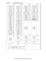
1
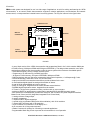
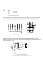
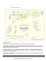
1
EB88 Development Board
User’s Manual
Indice :
1.
2.
3.
4.
5.
6.
7.
8.
Introduction
Overview
Pin assignment in 16F88
Bootloader FLASH memory programmer
Machine cycle in 16F88
16F88 microcontroller architecture
Memory organization
Special Function Registers SFR
8.1 PCL y PCLATH registers
8.2 Status register
9. Digital ports
9.1 Leds and microswitches
9.2 Relay
9.3 Keypad and AUX
9.4 LCD header
10. Start up
11.Technical spec.
11.1 Specifications
11.2 Lay out
11.3 Electronic diagram
IMPORTANT NOTICE
1
2
3
5
5
5
6
6
8
8
8
9
9
10
10
11
11
11
12
13
13
1. Introduction:
The design philosophy of this module is focused on maximizing the number of functions available to the user at minimal
cost. EVOLUPIC Bootloader 16F88 (EB88) retains compatibility with 16F628 and 16F84, making only minimal changes
in the programs.
With the ability of self-programming of 16F88 microcontroller's flash memory, the EB88 does not need the ICSP
programming hardware which greatly simplifies the electronics and allows, through the Bootloader firmware (preloaded )
programming via a serial cable DB9-DB9or any USB-DB9 interface, using software that runs on the PC.
We recommend you go directly to Chapter 10, "Start Up" to get the system running quickly. This manual is accompanied
by technical specifications as well as diagrams and detailed explanation of each of its interfaces.
Please call tel. (52) (55) 5653- 5801 to clarify any questions about EVOLUPIC Bootloader 16F88 (EB88). You can also
send your emails to: [email protected] Juan Martinez, Punto Flotante, SA, January 2011
EVOLUPIC Bootloader 16F88 Punto Flotante, S.A. 2011
2
2.Overview.
EB88 module system was designed for use in a wide range of applications: as a kit for training and learning the 16F88
microcontroller, or as central module instrumentation equipment, robotics applications, communications and network
access control, or incorporated into industrial control or security systems. The Lay Out is shown in the figure below.
DISPLAY LCD
14
B7
8
LEDS
B0
S2
MAX232
temperature sensor
16F88
RELAY
CONTACTS
1
1
MICRO
SWITC HES
S1
WALL
TRANSFORMER
RESET
KEYPAD
6
AUX
1
DB9
FIGURE 1
- It uses 18-pin version of the 16F88 microcontroller with encapsulated "dual in line", which contains 4096 bytes
of FLASH memory, 368 bytes of RAM and 256 bytes of EEPROM, y. The design makes extensive use of ports
and interfaces offered by the microcontroller to offer the user a system with a maximum of available options.
- 16F88 Microcontroller, running a 4-MHz external crystal.
- Programmer of FLASH memory via RS232 serial port.
- 4K bytes of FLASH memory, 256 bytes of EEPROM, 368 bytes of RAM.
- CMOS technology with very low power consumption during normal operation, <1 milliamperes @ 5 volts.
- Harvard architecture, RISC with a set of only 35 instructions.
- output port 8-bit LEDs connected as witnesses to provide evidence for the user ..
- 4 microswitches digital signals for testing and emulation of alarms.
- A total of 16-bit programmable as inputs or outputs.
- Relay 127VAC @ 1A, integrated into the card to activate external devices.
- DS18B20 digital temperature sensor, integrated into the module.
- 3 Timers 8 / 16 bits for the generation of delay, real time clock or event counters.
- serial port USART for asynchronous communication standard RS232 with DB9 connector output.
- SSP (Serial Port SYNCRONOUS) synchronous serial port, with 2 modes: SPI (Serial Peripheral Interface
Master mode / Slave) and I2C (Integrated, Integrated Circuit. Slave Mode)
- 1 analog reference voltage output
- 2 analog comparators.
- 1 capture module / digital comparison.
- 1 special outing to generate PWM (Pulse wide modulation), with 10 bit resolution.
- 7 channel ADC converters with 10 bit resolution.
- 14-pin connector for connection to LCD display 16 x 1
- 8-pin connector for 16-key matrix keyboard.
- Header Connector 6x auxiliary for connecting to external applications.
- Programmable Watch Dog Circuit to prevent the microcontroller is out of operation.
EVOLUPIC Bootloader 16F88 Punto Flotante, S.A. 2011
3
- Brown Out Protection Circuit Reset, which generates an automatic reset if detects peaks in the voltage of 5 v.
- mode of operation of low power SLEEP, with a virtual consumption of 0 (<1 ua).
- CODE PROTECTION to avoid possible copy of the firmware of the circuit.
- system interrupts, generated from various devices, including signals at the ports, the timer and the USART,
writing in the EEPROM.
- EB88 can be activated by an external wall transformer, which feeds a 5 volt regulator integrated into the card, or
can work independently using a standard battery of 9 volts .
SOFTWARE:
- a CD is provided with the system: the MPLAB IDE program (executable from a PC with any Windows platform),
which includes editor, macroassembler, simulator and C compiler.
- Also included is the Free Open Source software called "TINY", for programming the 16F88 FLASH memory via
its RS232 serial port and a preloaded firmware Bootloader also called TINY.
- Dozens of sample programs for testing or development of peripherals and each of the functions of the system.
3. Pins assignment in 16F88.
1
18
PIC 16F88
RA2/AN2/CVref/VrefRA3/AN3/CMP1/Vref+
RA4/AN4/T0CLKI/CMP2
MCLR/RA5/Vpp
VSS
RB0/INT/CCP1
RB1/SDI/SDA
RB2/RX/SDO/DT
RB3/CCP1/PGM
9
10
RA1/AN1
RA0/AN0
OSC1/CLKIN/RA7
OSC2/CLKOUT/RA6
VDD
RB7/AN6/T1OSI/PGD
RB6/AN5/T1OSO/T1CLKI/PGC
RB5/TX/SS/CK
RB4/SCK/SCL
EVOLUPIC Bootloader 16F88 Punto Flotante, S.A. 2011
4
Pin
1
2
3
4
5
6
7
8
9
10
11
12
13
14
15
16
17
18
Name
RA2/ AN2/ CVref / Vref-
Tipo Function
RA2 INPUT/OUTPUT PORT A
AN2 INPUT ANALOG 2
Vref OUTPUT VOLTAGE REFERENCE
Vref- LOW VOLTAJE REFERENCE FOR A/D.
RA3/ AN3/ Vref+/ C1out
RA3 INPUT/OUTPUT PORT A
AN3 INPUT ANALOG 3
Vref+ HIGH VOLTAJE REFERENCE FOR A/D
C1out OUTPUT OF COMPARADOR ANALOG 1
RA4/ AN4/ T0CKI/ C2out
RA4 INPUT/OUTPUT PORT A. OUTPUT ES OPEN DRAIN.
AN4 INPUT ANALOG 4
T0CKI INPUT CLOCK TIMER 0
C2out OUTPUT ANALOG COMPARATOR 2
MCLR/ RA5/ Vpp
MCLR MASTER RESET
RA5 INPUT PORT A
Vpp PROGRAMMING VOLTAJE ICSP
VSS
GND 16F88
RB0/ INT / CCP1
RB0 INPUT/OUTPUT PORT B
INT EXTERNAL INTERRUPT
CCP1 INPUT CAPTURE MODULE
OUTPUT PWM
RB1/ SDI / SDA
RB1 INPUT/OUTPUT PORT B
SDI INPUT DATA SPI
SDA TRANSMITTER DATA I2C
RB2/ SDO/ RX /DT
RB2 INPUT/OUTPUT PORT B
SD0 OUTPUT DATA SPI
RX USART ASYNCRONOUS RCV DATA
DT SYNC DETECTION USART
RB3/ PGM/ CCP1
RB3 INPUT/OUTPUT PORT B
PGM LOW VOLTAJE PROGRAMMING ICSP
CCP1 CAPTURE MODULE
OUTPUT DE PWM
RB4/ SCK/ SCL
RB4 INPUT/OUTPUT PORT B
SCK INPUT/ OUTPUT SYNC FOR SPI
SCL INPUT SYNC FOR I2C
RB5/ SS/ TX/ CK
RB5 INPUT/OUTPUT PORT B
SS SLAVE MODE SELECTOR SPI
TX TRASMITTER DATA ASYNCRONOUS USART
CK CLOCK SYNC SPI
RB6/ AN5/ PGC/ T1OSO/
RB6 INPUT/OUTPUT PORT B
AN5 INPUT ANALOG 5
T1CKI
PGC INPUT CLOCK PROGRAMMING ICSP
T1OSO OSCILLATOR TIMER 1
T1CKI INPUT EXTERNAL CLOCK TIMER 1
RB7/ T1OSI/ PGD/ AN6
RB7 INPUT/OUTPUT PORT B
T1OSCI INPUT OSCILLATOR TIMER 1
PGD INPUT DE DATA PROGRAMMING ISCP
AN6 INPUT ANALOG 6
VDD
5 VOLTS VOLTAGE 16F88
OSC2/ CLKO/ RA6
OSC2 INPUT OSCILLATOR CRYSTAL 4 MHZ
CLKO IF OSCILLATOR RC EXTERNAL, OUTPUT ¼ OF FREQUENCY
RA6 INPUT/OUTPUT BIDIRECTIONAL
OSC1/ CLKI/ RA7
OSC2 INPUT OSCILLATOR EXTERNAL CRYSTAL 4 MHZ
CLKIN INPUT OSCILADOR EXTERNAL
RA7 INPUT/OUTPUT PORT A
RA0/ AN0
RA0 INPUT/OUTPUT PORT A
AN0 INPUT ANALOG 0
RA1/ AN1
RA1 INPUT/OUTPUT PORT A
AN1 INPUT ANALOG 1
EVOLUPIC Bootloader 16F88 Punto Flotante, S.A. 2011
5
4. Bootloader FLASH memory programming:
EVOLUPIC Bootloader 16F88 (EB88) board is based on the ability of self-programming the 16F88. The so-called Tiny
Bootloader is a firmware preloaded at the top of the code memory 16F88. Through the Bootloader, and a software called
"tinybldWin.exe" it is quick and easy to program the FLASH memory, without using an ICSP programmer, or additional
electronic circuitry.
Programming is done from the computer PC via a DB9-DB9 serial cable or via a USB-Serial interface cable, whose driver
installer creates a virtual COM port.
5. The 16F88 machine cycle
The 16F88 can work with an internal oscillator or an external crystal for applications that require accurate time base. For
EB88 board, an external 4 MHz crystal is installed. The master oscillator is divided by 4 to form the pulses Q1, Q2, Q3
and Q4, the 4 pulses cause a machine cycle. The following diagram shows the basic diagram of the clock operation,
where the main oscillator is divided into 4 cycles for each machine cycle.
FIGURE 4
6. 16F88 PIC microcontroller architecture
The PIC16F88 belongs to the type of processors with Harvard architecture, ie the data memory and code are separated,
the microcontroller has the following elements: 4K program memory FLASH type, electrically erasable programmable,
256 bytes of memory EEPROM for parameter storage, addresses or passwords, depending on the application, 368 bytes
of RAM., port A and B with 8 signals each, a total of 16 input and output signals. Additionally, the microcontroller has 3
timers.
Thanks to a RISC instruction set (Reduced Instruction Set Computer), the CPU processes only 35 instructions. All
instructions have a word length of 14 bits and execute in instruction cycle, with the exception of statements that modify
the contents of the program counter: JUMP, BRANCH, CALL, RETURN, RETFIE, RETLW. This scheme is due to the
pipeline used in the Harvard architecture allows the processor to perform the FETCH and EXECUTE simultaneously with
the exception of jump instructions mentioned. The following diagram shows the execution of the example program with a
system type pipeline. Note that in all clock cycles, fetch and execute execute at the same time, except TCY4 cycle.
FIGURE 5
The 16F88 microcontroller contains the following registers: the W register of 8 bits, and the PC register (program
counter) which is a 12-bit pointer which points to the next memory location to be read and executed. The STACK, used
for handling instructions CALL, RETURN, RETFIE, RETLW, of 8 levels. Addresses are stored and retrieved after
EVOLUPIC Bootloader 16F88 Punto Flotante, S.A. 2011
6
subroutine calls. It is important to note that since this is a stack of only 8 locations, can only be nested up to 8 calls to
subroutines or interrupts within the program.
7. Memory organization
HARVARD architecture allows the use of two separate data buses for program memory and data. Program memory is
FLASH type, capable of up to 10,000 program and erase cycles and has 4096 locations of 14 bits, with addresses 000H
to FFFH.
Addresses 0 and 4 are used for RESET and interrupt vectors respectively, ie after RESET, the program counter points to
address 0 and after the occurrence of an interrupt (which is allowed) The program counter will point to the address 4.
The data memory is 8-bit locations, including 368 locations in RAM, and 256 locations in EEPROM (with ability to
program and erase up to 10 million times.) RAM data memory is organized into 4 banks. Available RAM addresses are:
BANK 0: 20H to 7FH (96 bytes), Bank 1: A0H to EFH (80 bytes), Bank 2: 110H to 16FH (96 bytes) and BANK 3: 190 to
1EF (96 bytes) . The locations can be accessed with direct or indirect addressing.
The following diagram shows the two types of architecture used in computers: the Harvard architecture and Von
Neumann.
FIGURE 6
8. Special Function Registers, SFR:
The so-called SFR (Special Function Registers), allow the programmer to select the various options of the functions of
the microcontroller. The bank is selected by bits RP0 and RP1 of STATUS register. Some of the registers are repeated in
the banks.
EVOLUPIC Bootloader 16F88 Punto Flotante, S.A. 2011
7
EVOLUPIC Bootloader 16F88 Punto Flotante, S.A. 2011
8
8.1 PCL, PCLATH registers:
PCLATH (PC Latch) register, may be modified with MOVWF, instructions but its execution does not modifies the upper
part of the program counter.
The PCL register can be accessed by ADDWF and MOVWF instructions. His execution directly modify the lower part of
the program counter and also load PCLATH register at the upper part of PC, and thus induces an immediate jump to
another location. In short, by modifying PCL, care should be taken well in advance to initialize PCLATH correctly,
otherwise the program may make a jump to a location in a page not desired.
8.2 Status register:
STATUS (ADDRESS 03H)
IRP
Bit 7
RP1
RP0
TO
PD
Z
DC
C
Bit 0
- Bits 0, 1 and 2 are the CARRY, CARRY HALF AND ZERO, are flags that are activated with a value equal to 1 when the
result of an operation or instruction generates a carry, a half carry or if it is equal to zero respectively.
- Bit 3 is called POWER DOWN and its value is 1 after an instruction CLRWDT (CLEAR WATCH DOG TIMER) or after
turning on the system (POWER UP). The value is 0 after executing the SLEEP instruction.
- Bit 4, is called "TIMER OUT"will have a value of 1 after POWER UP, SLEEP, CLRWDT or have a value of 0 if the WDT
(Watch Dog Timer) activates.
- Bits 5 and 6 RP0, RP1 select the memory bank to be accessed. If RP0 = 0, RP1 = 0 Bank 0 is selected. If RP0 = 1 Bank
1 RP1 = 0, RP0 = 0, RP1 = 1 bank 2, RP0 = 1, RP1 = 1 bank 3.
- The IRP bit is used for indirect addressing, along with the FSR register to select the bank registers. IRP = 0, select
banks 0 and 1, IRP = 1, select banks 2 and 3
9. Digital ports:
16F88 system has two digital ports, port A, and B with 8-bit available each. Both ports are bidirectional, that is, can be
programmed as input or output, according to data address registers, called "TRISA" and "TRISB. In EB88 card, signals
have been connected with 4 microswitches for port A and 8 outputs LEDS for port, and a relay connected to pin RA0. The
allocation of functions in each of the bits is shown in the table below. Please note that each input and output are available
in various connectors (LCD, keypad and AUX) on the card, so that users can connect external devices.
PORT
PORT A
RA0
RA1
RA2
RA3
RA4
PORT B
RB0
RB1
RB2
RB3
RB4
RB5
RB6
RB7
PIN IN HEADER 16x
FUNCTION
PIN 1
PIN 3
PIN 5
PIN 7
PIN 9
ACTIVA/DESACTIVA RELEVADOR
MICROSWITCH A1, CONTROL LCD
MICROSWITCH A2, CONTROL LCD
MICROSWITCH A3, TEMPERATURE SENSOR
MICROSWITCH A4
PIN 2
PIN 4
PIN 6
PIN 8
PIN 10
PIN 12
PIN 14
PIN 16
LED B0, KEYPAD Y1
LED B1, KEYPAD Y2,
LED B2, KEYPAD Y3, RECEIVER SERIAL RX
LED B3, KEYPAD Y4
LED B4, KEYPAD X1
LED B5, KEYPAD X2, TRASMITTER SERIAL TX
LED B6, KEYPAD X3
LED B7, KEYPAD X4
Before you can write and read ports, you must first set which bits are inputs and outputs, using the following macros, and
working with TRISA and TRISB registers.
EVOLUPIC Bootloader 16F88 Punto Flotante, S.A. 2011
9
BANK0
BANK1
MACRO
BCF
BCF
ENDM
MACRO
BSF
BCF
ENDM
STATUS,RP0
STATUS,RP1
STATUS,RP0
STATUS,RP1
9.1 LEDS AND MICROSWITCHES:
Once initialized the ports as shown, information can be written to the LEDs or read from the microswitches, considering
the electronic charts shown below. The aim of the LEDs and microswitches is to give the user the ability to make
emulations of digital sensors and outputs for activating actuators. All signal ports are available in 14x LCD header
connector, for connection to external interfaces.
5 v.
47k
RBO
RB7
RA1
RA2
RA3
RA4
1k
L3
L10
SW1
SW4
FIGURE 8: DIAGRAM OF LEDS AND MICROSWITCHES
9.2 RELAY
By using the RA0 bit of port A, the processor can activate the relay. The nominal data of this relay are: 9 volts DC
activation coil and contacts 127 VAC @ 10 Amps. This relay can be used as an actuator to activate external devices such
as lights, valves, solenoids, motors.
LED
L1
RA0
5.6K
RAS0910
BC337
CONTACTS
5 V.
RELAY
FIGURE 9: RELAY CONNECTION
EVOLUPIC Bootloader 16F88 Punto Flotante, S.A. 2011
10
9.3 KEYPAD AND AUX. CONNECTORS.
The keypad connector has 8 signals marked with numbers from 1 to 8, for ... RB0 RB7 respectively, to insert the keypad.
There is also an auxiliary header with 6 signals, marked with numbers from 1 to 6. The signals are respectively RA1 ...
RA4, 5 volts and GND. Please see the diagram below.
9.4 LCD 14X CONNECTOR:
LCD
1
2
3 INT
4 RS
5 R/W
6 EN
7 DB0
EB88
GND
5 VOLT
RA1
GND
RA2
RB0
FUNCTION
GND
5 volts.
Intensity control
0=command 1=data
0=write en LCD 1=read
Enable
DATA
LCD
8 DB1
9 DB2
10 DB3
11 DB4
12 DB5
13 DB6
14 DB7
FUNCTION
EB88
RB1
RB2
RB3
RB4
RB5
RB6
RB7
DATA
DATA
DATA
DATA
DATA
DATA
DATA
SIGNALS USED IN LCD, KEYPAD AND AUXILIARY HEADERS
AUX
KEYPAD
EVOLUPIC Bootloader 16F88 Punto Flotante, S.A. 2011
11
DISPLAY LCD
14
B7
RELAY
CONTACTS
1
8
LEDS
B0
S2
MAX232
16F88
temperature sensor
1
MICRO
SWITC HES
S1
WALL
TRANSFORMER
RESET
KEYPAD
6
AUX
1
DB9
10. Start up:
STEP 1: REVIEW OF PARTS AND INITIAL TEST:
Please review the kit includes the following: EB88 board, wall transformer, serial cable (or USB-Serial interface), hex
keypad, LCD display, temperature sensor DS18B20 and support CD. To use the support disc, you need a computer with
Windows XP, Vista, Windows7 with a CD drive, and a DB9 serial port connector or a USB port.
S1 and S2 must be set to "RS232". The 4 microswitches must be set to "OFF. " Insert the LCD display 14-pin connector.
Position wall transformer switch to 6.0 or 7.5 volts and connect to EB88. The program loaded in 16F88 FLASH memory
works immediately, displaying a message in LCD if microswitch SW4=”OFF”, or reading the DS18B20 sensor and
showing in the LCD the room temperature if SW4=”ON”
STEP 2: COPY THE CD, AND PROGRAM FLASH MEMORY OF 16F88
Insert the support disk in the CD drive of your computer. Open the disk and copy the entire folder "EB88 DEVELOPMENT
BOARD" to your computer. To program the 16F88 FLASH memory, please see the following document, included in the
CD :
“EB88 programming the system with TINY software.pdf”
11. Technical Information:
Processor: PIC16F88 microcontroller, crystal of 4 MHz, with low-power CMOS technology.
Architecture: Harvard, with code memory (14 bits) and data (8 bits) separated. Processing pipeline.
Technology: RISC (reduced instruction set computer), with 35 instructions in 14-bit word length.
Memory: 4K locations (14 bit) FLASH, 368 locations (8 bits) of RAM, 128 locations (8 bit) EEPROM.
Bootloader: preloaded firmware capable of self-programming Flash memory.
Cycles to read / write: up to 10,000 cycles on flash memory and up to 10,000,000 in the EEPROM.
Digital Ports: 5-bit port A, port B of 8 bits, a total of 13-bit programmable as inputs or outputs.
Pull up resistors, available on port B, when programmed as inputs.
EVOLUPIC Bootloader 16F88 Punto Flotante, S.A. 2011
12
LED digital outputs: the 8-bit port B connected to LEDS.
Output Capacity: Each output bit can take ("sink"), or generate ("source"), up to 25 milliamps.
Microswitches digital inputs: a total of 4 in Port A.
Output to relay: relay RAS-0910 model, contacts 127 V @ 1 A. Departure connector screws.
Auxiliary Header: 6 contacts, signals RA4… RA1 available, GND and 5 v. Can be extended with the keypad connector to
make a single header 14 signals expansion.
Keypad connector: RB0 .. RB7 signals included in the header 8x Keypad 4 x 4 matrix.
LCD Connector: 14 contacts, standard and ready for connecting an LCD or other interfaces.
Serial Ports: USART RS232 compatible with its own port DB9. SSP Synchronous Serial Port.
AD converters: 7 channels, 10 bit resolution.
Additional functions: power-on reset, power up timer, watch dog, code protection, sleep (low power).
Timer / event counter: 3 timers. PWM generator
Interrupts: interrupt sources: external pin RBO / INT, timer overflow, change in the levels of inputs RB4 ... RB7. For the
EEPROM write complete. The USART.
Size: 9.5 cms x 7.9 cms, fiberglass board, thru hole.
Consumption: normal <2 mA @ 5V. and 4 MHz., in SLEEP mode only 15 uA.
Power: Wall transformer 300 ma. @ 6 v. or 7.5 v.
Programmer 16F88: integrated into the card, the programming is done from a PC via serial port, using the Bootloader
firmware.
Software Development: MPLAB, which includes editor, assembler, simulator and compiler. Software "TINY" Programmer
of 16F88 flash memory.
11.2. LAY OUT
EVOLUPIC Bootloader 16F88 Punto Flotante, S.A. 2011
13
11.3 ELECTRONIC DIAGRAM:
IMPORTANT NOTICE
THE EB88 SYSTEM HAS A PRELOADED BOOTLOADER FIRMWARE IN FLASH MEMORY.
16F88 MICROCONTROLLER HAS A SAFETY MECHANISM TO PREVENT ACCIDENTAL WRITE IN THE AREA OF
FLASH MEMORY WHERE THE ABOVE FIRMWARE IS LOADED. THIS MECHANISM IS SIMILAR TO THAT USED TO
PROTECT EEPROM MEMORY CONTENTS.
HOWEVER, EVEN THOUGH IT IS A VERY LOW PROBABILITY EVENT, THE SYSTEM MAY BE PERFORMING AN
ACCIDENTAL WRITE IN THIS AREA, WHICH WOULD MAKE IT NECCESARY TO PROGRAM IN THE 16F88 THE
BOOTLOADER ORIGINAL FIRMWARE.
IN THIS CASE YOU SHOULD USE A ICSP PROGRAMMER, NOT INCLUDED WITH THE KIT EB88. INSTRUCTIONS
TO DO SO ARE IN THE FILE
“EB88 programming the system with TINY software.pdf”
EVOLUPIC Bootloader 16F88 Punto Flotante, S.A. 2011