1
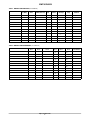
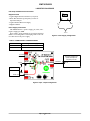
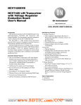
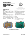
EMITSOP6EVB
EMI TSOP6 EVB Universal
Evaluation Board User's
Manual
Board Description
http://onsemi.com
The EMI TSOP6 EVB universal Evaluation Board was
designed to provide a flexible and convenient platform to
quickly evaluate, characterize and verify the performance
and operation of all twelve NB2XXXA EMI devices, and all
of their possible configurations. This user’s manual
provides detailed information on board contents, layout and
its use. It should be used in conjunction with the appropriate
NB2XXXA datasheet: (www.onsemi.com). See Table 1.
EVAL BOARD USER’S MANUAL
Board Features
• Accommodates the Electrical Characterization of the
•
•
•
•
NB2XXXA, Reduced EMI Series in the
TSOP−6 Package
Multiple Configurations − Refer to NB2XXXA
Configurations Tables 1 and 2
26 W Series Termination Resistor Installed on
MODOUT
15 pF Output Load Capacitor Installed on MODOUT
Selectable Jumpers for SELECT Pin Logic Levels
In or Out
1
6
VSS (GND)
XO
2
5
MODOUT
XI / CLKIN
3
4
VDD
Twelve EMI products share the same TSOP−6 (TSOT−23−6)
package, but have minor pin configuration differences. See
Table 2.
Figure 1. NB2XXXA TSOP−6 Pinout
Figure 2. Evaluation Board
© Semiconductor Components Industries, LLC, 2011
August, 2011 − Rev. 1
1
Publication Order Number:
EVBUM2034/D
EMITSOP6EVB
Table 1. NB2XXX PIN FUNCTION (see datasheet)
EMI Device
fin (MHz)
XTAL
CLKIN (External)
PD
SSON
Mod Eqn
Freq.
REFOUT
NB2579A
13 − 30
Y
Y
N
Y
fin ÷ 640
$1%
N
NB2669A
6 − 13
N
Y
Y
N
fin ÷ 256
$1%
N
NB2760A
6 − 13
Y
Y
Y
N
fin ÷ 256
$0.75%
N
NB2762A
6 − 13
Y
Y
Y
N
fin ÷ 256
−1.25%
N
NB2769A
6 − 13
Y
Y
Y
N
fin ÷ 256
$1%
N
NB2779A
13 − 30
Y
Y
Y
N
fin ÷ 640
$1%
N
NB2780A
30 − 50
Y
Y
Y
N
fin ÷ 1280
$0.75%
N
NB2869A
6 − 13
Y
Y
N
N
fin ÷ 256
$1%
Y
NB2870A
13 − 30
Y
Y
N
N
fin÷640
$0.75%
Y
NB2872A
15 − 30
Y
Y
N
N
fin ÷ 640
−1.25%
Y
NB2879A
15 − 30
Y
Y
N
N
fin ÷ 640
$1%
Y
NB2969A
6 − 13
Y
Y
N
N
fin ÷ 256
$1%
Y, REFOUT ÷2
Table 2. NB2XXX PIN ASSIGNMENT (see datasheet)
EMI Device
Pin 1
Pin 2
Pin 3
Pin 4
Pin 5
Pin 6
See Table 4
NB2579A
I
XO
XI / CLKIN
VDD
MODOUT
VSS (GND)
R1 = 0 W
NB2669A
I
NC
CLKIN
VDD
MODOUT
VSS (GND)
R1 = 0 W
NB2760A
I
XO
XI / CLKIN
VDD
MODOUT
VSS (GND)
R1 = 0 W
NB2762A
I
XO
XI / CLKIN
VDD
MODOUT
VSS (GND)
R1 = 0 W
NB2769A
I
XO
XI / CLKIN
VDD
MODOUT
VSS (GND)
R1 = 0 W
NB2779A
I
XO
XI / CLKIN
VDD
MODOUT
VSS (GND)
R1 = 0 W
NB2780A
I
XO
XI / CLKIN
VDD
MODOUT
VSS (GND)
R1 = 0 W
NB2869A
O
XO
XI / CLKIN
VDD
MODOUT
VSS (GND)
R1 = 26 W
NB2870A
O
XO
XI / CLKIN
VDD
MODOUT
VSS (GND)
C1
NB2872A
O
XO
XI / CLKIN
VDD
MODOUT
VSS (GND)
C1
NB2879A
O
XO
XI / CLKIN
VDD
MODOUT
VSS (GND)
C1
NB2969A
O
XO
XI / CLKIN
VDD
MODOUT
VSS (GND)
C1
http://onsemi.com
2
EMITSOP6EVB
LAB SETUP PROCEDURE
Lab Setup and Measurement Procedure
Power Supply
Equipment Used
• Agilent Signal Generator #81110A (or Crystal)
• Real−Time Oscilloscope, Frequency Counter or
•
•
+3.3 V
+
Spectrum Analyzer
Agilent #6624A DC Power Supply
Digital Voltmeter
−
GND
VDD
Power Supply Connections
The NB2XXXA has a positive supply pin, VDD, and a
negative supply pin, GND.
Power supply “anvil” terminals are provided for VDD and
GND. Use of “minigrabber” banana plug cables work well
for connections to the power supply.
+3.3 V
Figure 3. Power Supply Configuration
Table 3. POWER SUPPLY CONFIGURATIONS
Device Pin
Single Power Supply
VDD
VDD = +3.3 V
GND
GND = 0 V
In or Out
Real Time Oscilloscope
Spectrum Analyzer or
Frequency Counter
MODOUT
Crystal
Signal Generator
LVTTL Out
or
CLKIN
Figure 4. Input / Output Configuration
http://onsemi.com
3
Hi−Z
EMITSOP6EVB
NB2XXXA
If Pin 1 is an output, C1 can be used to install an output load
capacitor, ie. a 15 pF capacitor. C1 and C3 can be used to
parallel two output load capacitors. Also, a 26 W series
termination resistor should be installed at R1.
When Pin 1 is an input, the select header pins, HI and LO,
can manually control the Pin 1 logic level via the appropriate
jumper/shunt. A connection from each header must then be
made to the Pin 1 metal trace. When either HI or LO are
jumpered, Pin 1 is forced to VDD (logic High) or GND (logic
Low).
Lab Test Set−up Procedure
To monitor the MODOUT output on an oscilloscope,
spectrum analyzer or frequency counter:
1. Connect a power supply to the evaluation board.
(see Figure 3)
Connect VDD to +3.3 V
Connect GND to 0 V
2. Connect an external clock reference to the CLKIN
Pin 3 or install a crystal and appropriate (see
CLKIN) crystal load capacitors to Pins 2 and 3.
3. Connect the MODOUT output to the measurement
instrument.
4. For the MODOUT output, the NB2XXXA board
provides a series 26 W source termination resistor
and a load capacitor pad for each output; 15 pF is
installed.
MODOUT Output Series Resistor
An R2 resistor pad is provided to series terminate the
MODOUT output and is installed with a 26 W resistor. This
series resistor complements an internal 24 W resistor to
match the 50 W trace impedance.
MODOUT Output Load Capacitor
An output load capacitor pad is provided to load the
MODOUT output and is installed with a 15 pF capacitor.
C4 and C5 can be used to parallel two output load capacitors
for various combinations of capacitive loads, if needed.
Board Layout
The evaluation board is constructed with FR4 material
and 50 W trace impedance, designed to minimize noise and
crosstalk.
CLKIN
An SMA connector is provided for CLKIN if an external
clock source is used on Pin 3. The metal trace at the crystal
pad is intentionally open for crystal use, and must be
shorted for a connection to Pin 3 for external clock use.
The unused component pad labeled C6 (used for the crystal
load capacitor) may be used for a 50 W resistor to ground to
terminate a signal generator.
Layer Stack
L1
L2
L3
L4
Signal (top)
Ground
VDD (positive power supply)
Blank (bottom)
Pin 1 − IN / OUT Configuration
Pin 1 of the EMI TSOP6 EVB universal evaluation board
can be configured to serve as an input or output, depending
on device.
See Tables 1 and 2.
An SMA connector is provided to access Pin 1.
If Pin 1 is an input, a 0 W resistor may be used at R1.
Table 4. PIN 1 INPUT/OUTPUT
Device
Pin #1
R1
C1 (or C3)
See Table 2
Input
0W
Open
See Table 2
Output
26 W
15 pF
http://onsemi.com
4
EMITSOP6EVB
NB2XXXA Output Loading
VDD
Series Termination Resistor
Clock output traces over one inch should use series
termination. To series terminate a 50 W trace (a commonly
used trace impedance), place a 26 W resistor in series with
the clock line, as close to the clock output pin as possible.
The nominal impedance of the clock output is 24 W.
Hi−Z
Probe−to−Scope
NB2XXXA
RS = 26 W
MODOUT
Zo = 50 W
Rint = 24 W
CLoad
Figure 5. Output Loading for Test / Evaluation
In or Out
1
SMA
VSS (GND)
6
Out
VSS (GND)
2
5
SMA
0.1 mF
SMA
3
CLKIN
Small Gap Here for
Crystal Use; Short for
External Clock Source
VSS (GND)
4
VDD
VSS (GND)
Figure 1. NB2XXXA Evaluation Board Schematic
Table 5. NB2XXXA EVALUATION BOARD BILL OF MATERIALS
Component
Description
Qty
SMA 1 − 3
Connector
SMA Connector
1−3
C2
Capacitor
0.1 mF, 10%, KEMET, C0603C104K5RAC, Installed
1
C6 − C7
Capacitor (Crystal Load)
27 pF, Not Installed
2
C1, C3, C4,
C5
Capacitor
15 mF, C5 Installed
1−4
Jumper Header
100 mil, Berg
4
Jumper
2
R1 − R2
Resistor
26 W or 0 W, R2 Installed with 26 W
2
C6
Resistor (optional)
50 W, 0.1%, 0.25 W
1
Power Supply Connector
Anvil − Keystone #5016
2
U1
NB2XXXA
TSOP−6 device (Installed by User)
1
X1
Crystal (See Crystal Chart)
Fundamental Mode, Parallel Resonant, Ecliptek www.ecliptek.com
1
Pin Recepticle
Through−Hole Crystal Connector
2
Capacitor
VDD to GND Bypass Capacitors
http://onsemi.com
5
10 mF − 22 mF
0.01 mF − 0.1 mF
1
1
EMITSOP6EVB
Table 6.
Table 7.
Crystal Frequency
(MHz)
Ecliptek Part #
ESR
(W MAX)
6.000
ECX−6074−6.000M
125
8.000
ECX−6075−8.000M
10.000
Crystal Parameter
Specification
Nominal Frequency
See Chart
Frequency Tolerance at 25°C/
Stability over OTR
±15 ppm / ±20 ppm
70
ECX−6078−10.000M
50
Operating Temperature Range
0°C to +70°C
12.000
ECX−6081−12.000M
50
Load Capacitance (CL)
18 pF
13.500
ECX−6082−13.500M
50
See Chart
14.31818
ECX−6083−14.31818M
50
Equivalent Series Resistance
(W) (Maximum)
15.000
ECX−6084−15.000M
50
Mode of Operation and Crystal
Cut
AT−Cut Fundamental
16.000
ECX−6087−16.000M
50
Storage Temperature
−40°C to +85°C
16.660
ECX−6090−16.660M
50
Drive Level
18.750
ECX−6125−18.750M
50
100 mWatts Correlation
1 mW Maximum
19.440
ECX−6091−19.440M
50
Aging (at 25°C)
19.531
ECX−6126−19.531M
50
±3 ppm / 1st year,
±15 ppm / 10 year
Maximum
20.000
ECX−6094−20.000M
50
Insulation Resistance
500 MW Minimum,100 V
20.1416
ECX−6127−20.1416M
50
5 pF Maximum
20.480
ECX−6099−20.480M
50
Shunt Capacitance (pF
(Maximum)
24.000
ECX−6102−24.000M
40
Package
E2S (HC−49/UP SMD)
25.000
ECX−6105−25.000M
40
26.5625
ECX−6110−26.5625M
40
26.6000
ECX−6128−26.6000M
50
27.000
ECX−6115−27.000M
40
28.000
ECX−6118−28.000M
40
30.000
ECX−6119−30.000M
40
32.000
ECX−6120−32.000M
40
ON Semiconductor and
are registered trademarks of Semiconductor Components Industries, LLC (SCILLC). SCILLC reserves the right to make changes without further notice
to any products herein. SCILLC makes no warranty, representation or guarantee regarding the suitability of its products for any particular purpose, nor does SCILLC assume any liability
arising out of the application or use of any product or circuit, and specifically disclaims any and all liability, including without limitation special, consequential or incidental damages.
“Typical” parameters which may be provided in SCILLC data sheets and/or specifications can and do vary in different applications and actual performance may vary over time. All
operating parameters, including “Typicals” must be validated for each customer application by customer’s technical experts. SCILLC does not convey any license under its patent rights
nor the rights of others. SCILLC products are not designed, intended, or authorized for use as components in systems intended for surgical implant into the body, or other applications
intended to support or sustain life, or for any other application in which the failure of the SCILLC product could create a situation where personal injury or death may occur. Should
Buyer purchase or use SCILLC products for any such unintended or unauthorized application, Buyer shall indemnify and hold SCILLC and its officers, employees, subsidiaries, affiliates,
and distributors harmless against all claims, costs, damages, and expenses, and reasonable attorney fees arising out of, directly or indirectly, any claim of personal injury or death
associated with such unintended or unauthorized use, even if such claim alleges that SCILLC was negligent regarding the design or manufacture of the part. SCILLC is an Equal
Opportunity/Affirmative Action Employer. This literature is subject to all applicable copyright laws and is not for resale in any manner.
PUBLICATION ORDERING INFORMATION
LITERATURE FULFILLMENT:
Literature Distribution Center for ON Semiconductor
P.O. Box 5163, Denver, Colorado 80217 USA
Phone: 303−675−2175 or 800−344−3860 Toll Free USA/Canada
Fax: 303−675−2176 or 800−344−3867 Toll Free USA/Canada
Email: [email protected]
N. American Technical Support: 800−282−9855 Toll Free
USA/Canada
Europe, Middle East and Africa Technical Support:
Phone: 421 33 790 2910
Japan Customer Focus Center
Phone: 81−3−5773−3850
http://onsemi.com
6
ON Semiconductor Website: www.onsemi.com
Order Literature: http://www.onsemi.com/orderlit
For additional information, please contact your local
Sales Representative
EVBUM2034/D