1
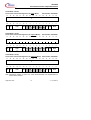
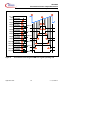
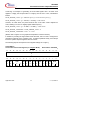
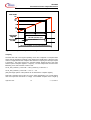
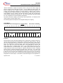
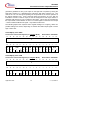
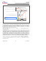
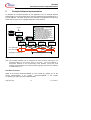
App lica tion No te , V 1 .0 , Jan . 200 5
AP32084
TriCore
Sinusodial
3-Phase
Output
Generation Using The TriCore
General Purpose Timer Array
M i c ro c o n trollers
N e v e r
s t o p
t h i n k i n g .
TriCore
Revision History:
2005-01
Previous Version:
Page
Subjects (major changes since last revision)
V 1.0
Controller Area Network (CAN): License of Robert Bosch GmbH
We Listen to Your Comments
Any information within this document that you feel is wrong, unclear or missing at all?
Your feedback will help us to continuously improve the quality of this document.
Please send your proposal (including a reference to this document) to:
[email protected]
Edition 2005-01
Published by
Infineon Technologies AG
81726 München, Germany
© Infineon Technologies AG 2006.
All Rights Reserved.
LEGAL DISCLAIMER
THE INFORMATION GIVEN IN THIS APPLICATION NOTE IS GIVEN AS A HINT FOR THE
IMPLEMENTATION OF THE INFINEON TECHNOLOGIES COMPONENT ONLY AND SHALL NOT BE
REGARDED AS ANY DESCRIPTION OR WARRANTY OF A CERTAIN FUNCTIONALITY, CONDITION OR
QUALITY OF THE INFINEON TECHNOLOGIES COMPONENT. THE RECIPIENT OF THIS APPLICATION
NOTE MUST VERIFY ANY FUNCTION DESCRIBED HEREIN IN THE REAL APPLICATION. INFINEON
TECHNOLOGIES HEREBY DISCLAIMS ANY AND ALL WARRANTIES AND LIABILITIES OF ANY KIND
(INCLUDING WITHOUT LIMITATION WARRANTIES OF NON-INFRINGEMENT OF INTELLECTUAL
PROPERTY RIGHTS OF ANY THIRD PARTY) WITH RESPECT TO ANY AND ALL INFORMATION GIVEN
IN THIS APPLICATION NOTE.
Information
For further information on technology, delivery terms and conditions and prices please contact your nearest
Infineon Technologies Office (www.infineon.com).
Warnings
Due to technical requirements components may contain dangerous substances. For information on the types
in question please contact your nearest Infineon Technologies Office.
Infineon Technologies Components may only be used in life-support devices or systems with the express
written approval of Infineon Technologies, if a failure of such components can reasonably be expected to
cause the failure of that life-support device or system, or to affect the safety or effectiveness of that device or
system. Life support devices or systems are intended to be implanted in the human body, or to support
and/or maintain and sustain and/or protect human life. If they fail, it is reasonable to assume that the health
of the user or other persons may be endangered.
AP32084
Sinusodial 3-Phase Output Generation
Table of Contents
Table of Contents
Page
1
Introduction ................................................................................................... 4
2
2.1
2.2
2.3
2.4
2.5
Sinusoidal Weighted Pulse Width Modulation ............................................... 6
Pulse Width Modulation Basics ..................................................................... 6
Varying the Duty Cycle.................................................................................. 6
Bridge Configurations.................................................................................... 7
Dead-time Considerations............................................................................. 9
Center-Aligned vs. Edge-Aligned Outputs..................................................... 9
3
3.1
3.2
3.2.1
3.2.2
3.2.3
3.2.4
3.3
3.4
General Purpose Timer Array ..................................................................... 10
Overview ..................................................................................................... 10
Local Timer Cells ........................................................................................ 12
Operating Modes..................................................................................... 12
Inter-Cell Communications ...................................................................... 13
Control Register ...................................................................................... 14
The Typical Logical Operating Unit ......................................................... 17
3-Phase PWM Logical Operating Unit Configuration .................................. 17
Making Sine Waves! ................................................................................... 29
4
The Peripheral Control Processor ............................................................... 32
5
Example Software Implementation.............................................................. 34
6
Summary..................................................................................................... 39
7
Additional Application Notes of Interest....................................................... 40
8
Abbreviations .............................................................................................. 41
Application Note
3
V 1.0, 2005-01
AP32084
Sinusodial 3-Phase Output Generation
Introduction
1
Introduction
The need to generate three-phase sinusoidal signals, that is, 3 sine waves with the
same frequency and amplitude but with a constant phase shift of 120 degrees relative
to each other, as shown in Figure 1, arises in many practical motor applications. AC
induction motors, for example, are driven by three-phase sinusoidal signals which are
not required to be synchronized to the rotor position, with the delivered speed and
torque of the motor being determined by the sinusoidal frequency and amplitude.
Brushless DC (BLDC) motors, which are increasingly being used in automotive and
other applications, can also be driven by three-phase sinusoidal signals. Unlike AC
induction motors, brushless DC motors are synchronous machines (technically,
Permanent Magnet Synchronous Motors, PMSM’s), so the applied sine waves must be
synchronized to the angular position of the rotor to achieve useful torque. The
knowledge of the rotor angular position allows the motor commutation that was in the
past performed through the use of mechanical brushes to be performed electronically.
The position of the rotor is often determined by the use of incremental encoders,
although sensorless techniques have also been developed. Infineon has a number of
application notes with further details concerning motors, and the interested reader is
referred to those for more details (refer to Section 7 for a list of these). Rather than
focusing on those details here, the intent of this application note is to outline how such
three-phase sinusoidal signals can be generated with minimal application software
overhead using the flexible General Purpose Timer Array peripheral module available
in several of Infineon’s TriCore Family 32-bit processors. This application note also
describes how the Peripheral Control Processor (PCP) which is available in several of
Infineon’s TriCore Family processors can be used to service the interrupts required to
generate the three-phase sinusoidal outputs, thereby eliminating all overhead burden
from the software application executing in the TriCore CPU. By understanding the
concepts presented here for the specific case of 3-phase PWM generation, the reader
will be able to readily apply the GPTA and PCP within the TriCore to other complex
signal generation and signal processing tasks.
Application Note
4
V 1.0, 2005-01
AP32084
Sinusodial 3-Phase Output Generation
Introduction
PERIOD (=1/f)
PERIOD/3
(120°)
I(t)
PERIOD/3
(120°)
Amplitude, Ψ
t
0
Phase X
Figure 1
Phase Y
Phase Z
Three Phase Sinusoidal Outputs
Application Note
5
V 1.0, 2005-01
AP32084
Sinusodial 3-Phase Output Generation
Sinusoidal Weighted Pulse Width Modulation
2
Sinusoidal Weighted Pulse Width Modulation
2.1
Pulse Width Modulation Basics
A common method for generating a variable voltage output signal using a
microcontroller is through the use of pulse width modulation (PWM). By pulse width
modulating a digital output from the microcontroller through an external low-pass filter
an analog voltage output can be generated (see Figure 2).
The microcontroller drives the digital output at a fixed frequency but has the ability to
vary the digital output’s duty cycle (the ratio of the on-time of the digital output to the
period of the digital output). When this digital output is then applied as the input to a
low-pass filter, the resulting output from the filter varies directly (to a large extent) with
the PWM duty cycle.
Microcontroller PWM Output
Low Pass Filter
V(t)
Voltage Output
Figure 2
2.2
t
Pulse Width Modulation
Varying the Duty Cycle
For the problem at hand here, generating three-phase sinusoidal signals, here is the
key: if the PWM frequency is high enough relative to the desired sinusoidal frequency
Application Note
6
V 1.0, 2005-01
AP32084
Sinusodial 3-Phase Output Generation
Sinusoidal Weighted Pulse Width Modulation
and the PWM duty cycle varies sinusoidally over time, then the resulting output of the
filter will vary sinusoidally as well (or will be a very good approximation of a sinusoidal
output). This method of generating three-phase sinusoidal outputs is often referred to
as Sinusoidal Weighted PWM (SWPMW), reflecting the relationship between the PWM
duty cycle at any angular position and the sine of that angular position. Other methods
are also available for generating three-phase outputs, such as Space Vector
Modulation, but will not be discussed further here, other than to note that these
methods could also be readily implemented with little overhead using the concepts
presented here. (Again, the interested reader is referred to other Infineon application
notes for a discussion of the alternatives). Of course the underlying assumption when
using SWPMW is that the low pass filter characteristics are such that the filter properly
smoothes the PWM output from the microcontroller into a close approximation of a
sine wave. For the case of motors, the inductance of the motor itself often provides
the appropriate low pass filtering needed to transform the microcontroller PWM output
into a sinusoidal phase current. PWM frequencies for many motor applications
typically range from 20 KHz to 25 KHz.
2.3
Bridge Configurations
Microcontroller outputs do not have adequate voltage and current capability to directly
drive motors, so a half-bridge comprised of two power transistors is used to amplify the
microcontroller PWM output to each motor phase (see Figure 3). When the high-side
transistor, T1, is on while the low side transistor, T2, is off, the phase is connected to
the positive supply voltage. Conversely, when T2 is on while T1 is off, the phase is
connected to ground. Configured this way, with a sinusoidal weighted PWM signal
driving T1 and the complement of that PWM signal driving T2, a sine wave can be
generated at the phase (see Figure 4).
Supply
High
Side
T1
Output
Low
Side
Figure 3
T2
Half Bridge Driver
Application Note
7
V 1.0, 2005-01
AP32084
Sinusodial 3-Phase Output Generation
Sinusoidal Weighted Pulse Width Modulation
Supply
Sinusoidal Phase Current
High Side PWM Output
T1
Motor
Integrates
T2
Low Side PWM Output
Figure 4
Single Phase Sinusoidal Weighted PWM Generation
To drive a 3-phase motor, three half-bridges are combined into a 3-phase bridge
configuration and connected to the motor as shown in Figure 5. The desired
sinusoidal three-phase output is achieved by driving each of the individual half-bridges
with a sinusoidal weighted PWM signal that generates a sine wave that is 120 degrees
phase shifted relative to the sine waves generated on the other half bridges.
Supply
Phase X
High Side
Phase X
Phase X
Low Side
Phase Y
High Side
Phase Y
Low Side
Motor
Phase Y
Phase Z
High Side
Phase Z
Phase Z
Low Side
Figure 5
Three Phase Bridge
Application Note
8
V 1.0, 2005-01
AP32084
Sinusodial 3-Phase Output Generation
Sinusoidal Weighted Pulse Width Modulation
2.4
Dead-time Considerations
However, the PWM generation is slightly more complicated than indicated above as
real transistors do not instantaneously switch off. Transistors continue to conduct for
some short amount of time after they are commanded off. If the transistors in the halfbridge are simply driven by an microcontroller output signal and its complement, the
switching times of the transistors would lead to situations where both transistors are
conducting, thereby creating a very low resistance path between power and ground
which in turn results in a large shoot-through current. To avoid this, a dead-time must
be implemented prior to turning a transistor in the half-bridge on to assure that the
complementary transistor in the half-bridge is completely turned off.
2.5
Center-Aligned vs. Edge-Aligned Outputs
A further consideration when using PWM for generating several time-varying outputs,
such as sine waves, is whether the PWM outputs from the microcontroller should be
center-aligned or edge-aligned relative to each other. Center-aligned and edgealigned refer to the placement of the on-time of the PWM outputs within the common
PWM output period. As shown in Figure 6, center-aligned PWM outputs have the ontime centered (as the name implies) within the period. In contrast to this, edge-aligned
PWM outputs place the on-time on either the left or right side of the period. For
example, in a left-aligned PWM output, the outputs go to their active state (assumed to
be high in Figure 6) at the beginning of the period, stay on for an amount of time
determined by their duty cycle, then turn off for the remainder of the period, after which
time the process would repeat. Since center-alignment is commonly used in many
multi-phase motor applications, this application note focuses on implementing center
aligned PWM signals, but the concepts presented here can be easily and readily
extended for generating edge aligned signals.
Center Aligned PWM
Left Edge Aligned PWM
Right Edge Aligned PWM
Phase X (High Side)
Phase Y (High Side)
Phase Z (High Side)
PWM Period
Figure 6
PWM Period
PWM Period
Comparison of Center-Aligned Versus Edge-Aligned PWM Outputs
Application Note
9
V 1.0, 2005-01
AP32084
Sinusodial 3-Phase Output Generation
General Purpose Timer Array
3
General Purpose Timer Array
3.1
Overview
Several members of the TriCore family of microcontrollers include the flexible General
Purpose Timer Array (GPTA) Module which can be used to generate 3 phase PWM
outputs. Rather than providing a number of unique peripheral modules for different
timer functions, the GPTA provides a number of basic building blocks which can be
combined in many different ways to generate arbitrarily complex outputs and/or to
process arbitrarily complex inputs, all with extremely low or no software overhead. The
basic building blocks consist of the following (see Figure 7):
• Filter and Prescaler Cells (FPC) – for input noise filtering and prescaling.
• Phase Discrimination Logic Units (PDL) – for decoding the direction information
output by a rotation tracking system.
• Duty Cycle Measurement Cells (DCM) – for pulse width measurement.
• Digital Phase Locked Loop Unit (PLL) – for increasing the resolution available when
using an input signal for timer compare and/or capture functions by generating a
programmable number of clock ticks during the input signal’s period.
• Clock Distribution Unit – for selecting the clocks that are distributed for use by other
building blocks in the GPTA.
• Global Timer units (GT) – for generating the common time bases used by the Global
Timer Cells.
• Global Timer Cells (GTC) – for generating simple or complex events and outputs
(compare) and/or measuring complex input signals (capture) using the global time
bases.
• Local Timer Cells (LTC) – for generating simple or complex events and outputs
(compare) and/or measuring complex input signals (capture) using one of several
local clock sources (timer cells)
In addition, multiplexers are used within the GPTA to flexibly route input signals from
ports and various internal sources to these building blocks and to flexibly route output
signals from the building blocks to output ports and other internal destinations.
A single GPTA peripheral module contains multiple instances of these building blocks.
For example, there are 32 Global Timer Cells and 64 Local Timer Cells within a GPTA
peripheral module. And to further enhance the signal generation and processing
capabilities, some members of the TriCore family, such as the TC1796, include two
GPTA peripheral modules plus an additional bank of 64 local timer cells!
The Global Timer Cells are particularly well suited for automotive engine control
applications. In these applications, one of the global time bases distributed to the
GTC’s would track the angular position of the engine (derived from the crank and CAM
sensors with increased angular resolution provided by the Digital Phase Lock Loop
Application Note
10
V 1.0, 2005-01
AP32084
Sinusodial 3-Phase Output Generation
General Purpose Timer Array
Unit) and the other global time base would track elapsed time duration. Using these
time bases, the GTC’s can then implement the spark and fuel output schedule based
on combinations of angular position and time with very little software overhead.
Although the GTC’s could certainly be used for 3-phase PWM generation, the LTC’s
would likely be a better choice in most system designs because of the added flexibility
within the LTC to implement a reset timer for a subset of the LTC cells that is
synchronized to the desired PWM frequency.
A detailed description of the operation of all these GPTA building blocks is beyond the
scope of this application note, and the interested reader is referred to the peripheral
units user’s manual for the device being used for further details. The remainder of this
application note will focus on the LTC’s as they are needed to generate the three
phase PWM signals.
Figure 7
General Purpose Timer Array
Application Note
11
V 1.0, 2005-01
AP32084
Sinusodial 3-Phase Output Generation
General Purpose Timer Array
3.2
Local Timer Cells
The following discussion is intended as only an overview of the LTC functionality. The
interested reader is referred to the peripheral units user’s manual of the device being
used for additional details.
3.2.1
Operating Modes
The basic structure of each LTC is depicted in Figure 8 (with the exception of the last
LTC, LTC63, which is somewhat different and will not be discussed here). At a high
level, each LTC cells consists of a multi-purpose register (LTCXR), a control register
(LTCCTR), a comparator, output generation logic, and control logic. By programming
the control register, LTCCTR, each LTC cell can be configured to operate in one of 4
modes:
• Free Running Timer Mode – In this mode, the LTC provides a 16-bit timer that is
incremented by a selected input signal, with the timer value being available for use
in “downstream” LTC’s (that is, LTC’s with a higher cell number). In this case, the
multi-purpose LTCXR register holds the timer count. When the timer reaches its
overflow value (65535, or FFFFh), an interrupt request and/or an output action (hold,
clear, set, or toggle an output) can be generated, depending on the configuration of
the cell. Typically, one of the signals on the clock distribution bus is used as the
input source to clock the timer, providing a high degree of flexibility in the choice of
the operating frequency for the timer.
• Reset Timer Mode – This mode is similar to the Free Running Timer mode, with the
added feature that the timer value in the multi-purpose LTCXR register is reset when
a compare or capture event occurs in a downstream LTC. Note here that “reset”
means that the timer value is set to a value of 65535 (FFFFh) and would continue
counting up from that value on the next clock edge, meaning that the next timer
count would be 0 (zero).
• Capture Mode – In this mode, the value of the timer generated in the nearest
upstream LTC (that is, the timer or reset timer LTC with the next lowest cell number)
is captured in the multi-purpose LTCXR register at a selected transition of the LTC’s
input signal. Upon the occurrence of the capture event, an interrupt request and/or
an output action can be generated, depending on the configuration of the cell.
• Compare Mode – In this mode, the value of the timer generated in the nearest
upstream LTC is compared with the value in the multi-purpose LTCXR register. If
there is a match, then an output action and/or an interrupt request can be
generated, depending on the configuration of the cell.
Application Note
12
V 1.0, 2005-01
AP32084
Sinusodial 3-Phase Output Generation
General Purpose Timer Array
Figure 8
GPTA Local Timer Cell (LTC)
Additional, each cell can be configured (by programming its control register) to operate
in its selected mode continuously or can be configured for “one-shot” operation. In
one-shot operation, once the configured event occurs (for example, a compare or a
capture), the cell is automatically disabled and must be re-enabled by software before
the event can be recognized again.
3.2.2
Inter-Cell Communications
The flexibility and power of the LTC’s arises from the communications channels that
are in place between the LTC’s. The clock bus and the various control signals
between the LTC’s enable contiguous LTC’s to be grouped into a logical operating unit
that can perform complex output signal generation and input signal processing
functions with little (in some cases, no) software overhead. Among these signals are
the following:
• Local Data Bus (YO, YI) – Used to carry the timer value from a Timer cell or a
Reset Timer cell to downstream LTC’s for use in compare and capture operations.
• Event In/Out Signals (EI, EO) – Used to signal the occurrence of a compare or
capture event to an upstream LTC for purposes of resetting a timer in a LTC that is
configured in Reset Timer Mode. Note that the Event In/Out signal chain does not
flow upstream through an enabled Capture Mode or Compare Mode LTC.
Therefore, a LTC configured in Reset Timer Mode is reset only by a compare or
capture event in the nearest enabled downstream LTC.
• Select In/Out Signals (SI, SO) – Used to enable compare functions in downstream
LTC’s. By using these signals, two LTC’s can be grouped together to form a buffer
to enable a coherent (glitchless) update of an output signal. While the compare
value in one of the LTC’s is being used to generate the output, the compare value in
the alternate LTC can be updated. Once updated, the state of the select signal is
Application Note
13
V 1.0, 2005-01
AP32084
Sinusodial 3-Phase Output Generation
General Purpose Timer Array
then automatically toggled at the appropriate time so that the updated compare
value is subsequently used without causing an unintended glitch in the output.
• Mode In/Out Signals (M0I, M1I, M0O, M1O) – Used to signal an output action to
downstream LTC’s. An output action results from an event in an LTC, either a timer
reset, a capture, or a compare, depending on how the LTC is configured. The
output action can be configured to either hold an output in its current state, to clear
the output, to set the output, or to toggle the output. The output actions generated
by events in a given LTC can be passed to downstream LTC’s, thereby allowing a
single physical output to be controlled by multiple LTC’s. (Since there are four
possible output actions – hold, clear, set, toggle - two signal lines are needed to
communicate the action to the next downstream LTC, M0O and M1O). In other
words, an output from an LTC that is multiplexed to a single output port pin can be
altered not only by an event in the LTC (a local event) but also by events that occur
in upstream LTC’s. As an example, two LTC’s could be configured to control a
single output signal, with the one of the LTC’s being used to set the output on the
occurrence of a certain compare event and they other LTC being used to clear the
output on the occurrence of a different compare event. For even more flexibility, the
most recent GPTA version also includes the ability to bypass a LTC, meaning that
the cell’s local action is not communicated downstream yet upstream actions from
the cell are communicated downstream. This feature reduces the number of cells
needed to implement multiple signals that share a period and a common edge (such
as edge-aligned PWM signals).
3.2.3
Control Register
The operation of each LTC is easily programmed by using the cell’s control register,
LTCCTR. The values written to the bits and bit fields in the control register determine
the mode that the cell operates in as well as how the cell interconnects to adjacent
cells. The following page depicts the various bits and bit fields in the control register,
taking into consideration that the use of certain bits changes depending on the
selected operating mode.
Shaded bits represent differences between Timer Mode, Capture Mode, and Compare
Mode.
Application Note
14
V 1.0, 2005-01
AP32084
Sinusodial 3-Phase Output Generation
General Purpose Timer Array
LTCCTRk (k = 00-62)
Local Timer Cell Control Register k (in Timer Mode)
31
30
29
28
27
26
25
24
Reset Value: 0000 0000H
23
22
21
20
19
18
17
16
7
6
5
4
3
2
1
0
0
r
15
14
13
OUT OIA
rh
12
11
9
8
FED RED
CUD
CEN CUD ILM CLR SLO or
or REN OSM
AIL PEN
rh rwh rw
w
rwh rw
rw
rw
rw
OCM
rw
10
rw
LTCCTRk (k = 00-62)
Local Timer Cell Control Register k (in Capture Mode)
31
30
29
28
27
26
25
24
MOD
rw
Reset Value: 0000 0000H
23
22
21
20
19
18
17
16
7
6
5
4
3
2
1
0
0
r
15
14
13
OUT OIA
rh
12
11
OCM
rw
10
9
8
CEN SLL ILM EOA BYP FED RED REN OSM
rw
rh
rh
rw
rwh
rw
rw
rw
rw
MOD
rw
rw
LTCCTRk (k = 00-62)
Local Timer Cell Control Register k (in Compare Mode) Reset Value: 0000 0000H
31
30
29
28
27
26
25
24
23
22
21
20
19
18
17
16
7
6
5
4
3
2
1
0
0
r
15
14
13
OUT OIA
rh
rw
12
OCM
rw
11
10
9
8
CEN SLL ILM EOA BYP SOH SOL REN OSM
rh
rh
rw
rwh
rw
rw
rw
rw
rw
MOD
rw
Note: Description applies to GPTA V4; some bits/functionality not implemented on
earlier GPTA versions
Application Note
15
V 1.0, 2005-01
AP32084
Sinusodial 3-Phase Output Generation
General Purpose Timer Array
A brief description of the bits most relevant to using the LTC’s for 3-phase PWM
generation follows. The reader is referred to the peripheral units user’s manual of the
device being used for additional details concerning these or any of they other bits in
the register.
MOD: This bit field is used to select the cell’s operating mode, setting the cell to be
either a free running timer cell, a reset timer cell, a capture cell, or a compare cell. The
operating mode determines how the cell’s multi-purpose register, LTCXR, is used –
whether it acts as a timer register, a capture register, or a compare register. Implicitly,
the operating mode also determines the use of the Local Data Bus connection
between cells (refer to the multiplexer, MUX, in Figure 8). When a cell is operating in
one of the timer modes, the input Local Data Bus (YI) from the upstream cell is, in
essence, ignored while the timer value (which is contained in LTCXR) is made
available to downstream cells on the output Local Data Bus (YO). Alternately, when a
cell is operating either in compare mode or capture mode, then the input Local Data
Bus (YI) is directly connected to the output Local Data Bus (YO), thereby making a
timer value generated in an upstream LTC available to downstream LTC’s as well. Of
course, when operating in capture or compare mode, the value available on the input
Local Data Bus is also used within the cell for capture and compare operations. For
example, when configured as a compare cell, the value on the input Local Data Bus
(which should be the timer value from an upstream LTC) is compared against the
contents of the cell’s LTCXR. The operating mode also determines how the Event In
(EI) and Event Out (EO) signals are used, as discussed previously. Note that when a
cell is configured in one of the timer modes or in capture mode, the LTC input
multiplexer must be configured to route the desired clock or input signal to the cell;
please consult the peripheral units user’s manual for details related to configuring the
LTC input multiplexer.
REN: This bit is used to enable an interrupt request from the cell when the cell’s
programmed event (a timer overflow, a compare, or a capture, depending on the cell’s
mode) occurs. (To acually generate an interrupt corresponding to this event the service
request node corresponding to the cell must also be enabled.)
SOL, SOH (in Compare Mode): These bits, in combination, are used to determine the
logical state of the Select In (SI) signal during which compares are enabled. As
discussed previously, the Select In and Select Out signal chain is used to provide
coherent update functionality. Since that functionality is not needed for the 3-phase
PWM generation, both these bits are set to enable compare operations regardless of
the logical state of the Select In signal.
OCM: This bit field is used to program the desired output action from the cell. The first
two bits in this field (bits 11 and 12 in the register) determine the output action that
should be generated if and when the cell’s programmed event (a timer overflow, a
capture, or a compare, depending on the cell’s mode) occurs. The third bit in the field
Application Note
16
V 1.0, 2005-01
AP32084
Sinusodial 3-Phase Output Generation
General Purpose Timer Array
(bit 13 in the register) determines if the output action from upstream LTC’s,
communicated over the Mode In (M0I and M1I) signals, also impacts this cell’s output
action. The output action of the cell is also communicated over the Mode Out (M0O
and M1O) signals (unless the bypass function is enabled using the BYP bit) to
downstream LTC’s.
3.2.4
The Typical Logical Operating Unit
Given all of what we know about LTC’s now, the typical arrangement of a logical
operating unit is to configure the first LTC (the LTC with the lowest cell number) in the
logical operating unit in Timer Mode or Reset Timer mode. This cell then provides the
common time-base that is passed to downstream LTC’s over the Local Data Bus and
that can be used by the downstream LTC’s for compare and/or capture operations. If
the functionality of the logical operating unit involves the generation of periodic
outputs, then the second LTC in the unit is typically configured in Compare mode and
is used to reset the timer at the desired periodic rate; for this to work properly, then the
first cell must be set to Reset Timer mode. (If a coherent update of the period is
required, then the second and third LTC’s would be used in combination to provide the
period, with the Select In/Out Signals used to alternate between the two LTC’s.)
Subsequent downstream LTC’s are then configured as needed to generate the desired
output signals and/or to measure or otherwise process input signals. It should be clear
from the discussion so far that the capability of each individual LTC combined with the
communication signals between the LTC’s provides a highly flexible yet easily
configurable method of generating or measuring and processing simple or arbitrarily
complex waveforms.
3.3
3-Phase PWM Logical Operating Unit Configuration
Referring to Figure 9, the logical operating unit for 3-phase center-aligned PWM
generation requires 15 contiguous LTC’s configured as follows (where “N” refers to the
LTC number of the first LTC in the logical operating unit):
LTC[N]
The first LTC in the logical operating unit is configured in Reset Timer Mode. The
value of this timer will be used by the downstream LTC’s in the logical operating unit
when performing compare functions so that all the generated signals will be based off
a common time-base. An appropriately scaled version of the GPTA module clock must
be selected as the input to this LTC (this input selection is accomplished through use
of the input multiplexer array). The necessary input clock frequency is a function of the
required PWM frequency and the desired resolution of the PWM signal. For example,
Application Note
17
V 1.0, 2005-01
AP32084
Sinusodial 3-Phase Output Generation
General Purpose Timer Array
for a 20 KHz PWM frequency with 9 bits of resolution, the LTC input clock frequency
must be at least 20.48 MHz, calculated as:
Minimum LTC Clock Frequency = PWM Frequency * 2(Required Bits of Resolution + 1)
Minimum LTC Clock Frequency = 20 KHz * 2(9+1) = 20.48 MHz
Note: Since a center-aligned PWM signal is symmetric around the middle of the period,
the smallest change that can be affected in the output signal is 2 counts:
1 count to the left and 1 count to the right of center. The required timer size is always 1
bit more than the required bits of resolution, hence the need to include the addition of
“1” in the exponent of the equation above. For edge-aligned PWM generation, this
would not be the case.
The driver implementation example developed along with this application note utilizes
a 30MHz LTC clock input to generate a 20 KHz PWM output, for a resolution
somewhat better than 9 bits.
The following depicts the required control register settings for LTC[N]:
LTCCTR[N]
Local Timer Cell Control Register (in Timer Mode)
31
30
29
28
27
26
25
24
Reset Value: 0000 0000H
23
22
21
20
19
18
17
16
7
6
5
4
3
2
1
0
0
r
15
14
13
OUT OIA
0
0
rh
rw
12
11
0
rw
9
8
CUD
CEN CUD ILM CLR SLO FED RED REN OSM
OCM
0
10
0
0
0
0
0
0
0
1
0
0
rh
rwh
rw
w
rwh
rw
rw
rw
rw
MOD
1
1
rw
Note: DAvE, the ‘Digital Application virtual Engineer’ software development tool
available from Infineon, provides a graphical means to readily generate the
required “C” code to initialize registers and interface with the GPTA and all
TriCore peripherals.
Application Note
18
V 1.0, 2005-01
AP32084
Sinusodial 3-Phase Output Generation
General Purpose Timer Array
LTC[N+1]
The second cell in the logical operating unit is configured in Compare Mode and is
used to generate the period of the PWM outputs. When the timer value in LTC[N]
matches the compare value stored in LTC[N+1], the Event Out signal from LTC[N+1] is
activated and passed upstream to LTC[N] as the Event In signal which then resets the
timer to the value of 65535 (0xFFFF). Since the timer resets to 65535 (-1, as a signed
number) and then counts through 0 up to (and including) the compare value, the
compare value used to generate a periodic interval is somewhat different than what
might be expected. To generate a periodic interval of P clocks, the compare value
must be set to (P-2). The example software developed here also has the additional
restriction that the compare value used for the period must be odd to assure that there
is 1 timer count left at the end of 100% duty cycle period where the low side can be
activated. (This restriction will be evident later, when the details of how the compare
values for the subsequent cells are presented. For now, note that without this
restriction one of the compare values for a 100% duty cycle signal would exceed the
maximum timer value by 1 count, meaning the compare event would not occur. This
restriction leads to a slight asymmetry in the output signal but assures that the
calculated compare values are always less than or equal to the maximum timer value.
Alternatively, an even compare value could be used, which would eliminate the slight
asymmetry but would lead to a slight distortion for one PWM period when the duty
cycle changes from 100% to some value less than 100%, and even this distortion
could be eliminated with a little more software overhead. Using the flexible GPTA
concept, choices like this are left up to the system designer based on the needs of the
specific application.)
Application Note
19
V 1.0, 2005-01
AP32084
Sinusodial 3-Phase Output Generation
General Purpose Timer Array
A
clock
Rese t Timer Mode
LTC[N]
B
reset
LTC[N+1]
Compare Mode
(Period)
LTC[N+2]
Compare Mode
(50% of Period)
B
LTC[N+3]
Compare Mode
(X HI - Active)
C
LTC[N+4]
Compare Mode
(X HI - InActive)
D
LTC[N+5]
Compare Mode
(X LO - InActive)
E
LTC[N+6]
Compare Mode
(X LO - Active)
F
LTC[N+7]
Compare Mode
(Y HI - Active)
G
A
C
D
E
F
PHASE X -HI
PHASE X -LO
G
H
PHASE Y -HI
LTC[N+8]
Compare Mode
(Y HI - InActive)
H
LTC[N+9]
Compare Mode
(Y LO - InActive)
I
LTC[N+10]
Compare Mode
(Y LO - Active)
J
LTC[N+11]
Compare Mode
(Y HI - Active)
K
LTC[N+12]
Compare Mode
(Y HI - InActive)
L
LTC[N+13]
Compare Mode
(Y LO - InActive)
M
LTC[N+14]
Compare Mode
(Y LO - Active)
N
Figure 9
A
I
J
PHASE Y -LO
K
L
PHASE Z -HI
M
N
PHASE Z -LO
Three-Phase Center-Aligned PWM LTC Logical Operating Unit
Application Note
20
V 1.0, 2005-01
AP32084
Sinusodial 3-Phase Output Generation
General Purpose Timer Array
Continuing our example of generating 20 KHz PWM signals with a 30 MHz clock
applied to LTC[N], the compare value in LTC[N+1] must be set to 1497, calculated as
follows:
PWM_PERIOD_CNTS = [(1 / PWM Frequency) * LTC Clock Frequency]
PWM_PERIOD_CNTS = [(1 / 20KHz) * 30 MHz] = 1500 counts
However, as noted above, the period must be odd, so the value 1500 is adjusted to
1499, resulting in an ever so slightly higher PWM frequency:
PWM_PERIOD_CNTS = [(1 / 20 KHz) * 30 MHz] = 1499 counts
PWM_PERIOD_COMPARE = PWM_PERIOD_CNTS - 2
PWM_PERIOD_COMPARE = 1499 – 2 = 1497
(Please refer to Figure 10 for a graphical interpretation of these numbers.)
In addition to providing the signal which resets the timer, this LTC also is configured to
generate an interrupt on the compare event. As will be explained shortly, this interrupt
is used to update compare registers with new values.
The following depicts the required control register settings for LTC[N+1]:
LTCCTR[N+1]
Local Timer Cell Control Register (in Compare Mode)
31
30
29
28
27
26
25
24
Reset Value: 0000 0000H
23
22
21
20
19
18
17
16
7
6
5
4
3
2
1
0
0
r
15
14
13
OUT OIA
0
0
rh
rw
12
11
OCM
0
Application Note
0
rw
10
9
8
CEN SLL ILM EOA BYP SOH SOL REN OSM
0
0
0
0
0
0
1
1
1
0
rh
rwh
rw
w
rwh
rw
rw
rw
rw
21
MOD
0
1
rw
V 1.0, 2005-01
AP32084
Sinusodial 3-Phase Output Generation
General Purpose Timer Array
Timer Counts
1497
1213
1198
748
298
283
-1
Phase Output
High Side
Phase Output
Low Side
450
450
900 counts (60% duty cycle)
15 counts deadtime
1499 counts @ 30MHz = 50 usec period (20KHz frequency)
Figure 10
Example Timer Operation for a Single Phase
LTC[N+2]
The third timer cell in the logical operating unit is also configured in Compare Mode
and is used to generate an interrupt in the middle of the PWM period. When the timer
value in LTC[N] matches the compare value stored in LTC[N+2], the interrupt request
is generated. The value stored in the compare register should be half of the value
stored in period compare register in LTC[N+1]. For the example that we have been
illustrating so far, this would be a value of 748:
PWM_MID_PERIOD_COMPARE = PWM_PERIOD_COMPARE / 2
PWM_MID_PERIOD_COMPARE = 1497 / 2 = 748
(Only the integer portion of the quotient can be stored in the compare register.)
Note that a compare event in this LTC (or any other downstream LTC, for that matter)
does not impact the reset timer in LTC[N]. The enabled compare cell at LTC[N+1]
Application Note
22
V 1.0, 2005-01
AP32084
Sinusodial 3-Phase Output Generation
General Purpose Timer Array
“blocks” downstream compare and capture events so they do not reach LTC[N] and
only an LTC[N+1] event will reset the timer. From a digital logic point-of-view, the
Event Out signal, EO, from LTC[N+1], which is connected as the Event In signal, EI, to
LTC[N], is only activated in response to compare events in LTC[N+1] when LTC[N+1]
is configured as an enabled compare cell. (That being said, note however that if LTC
cell is disabled, such as could be done with the Select In signal, then a downstream
event would flow upstream through the cell. This is the mechanism used when pairing
two LTC’s together for a coherent update of the period.)
As was the case with LTC[N+1], the interrupt request generated in LTC[N+2] is also
used to update compare register values.
The following depicts the required control register settings for LTC[N+2]:
LTCCTR[N+2]
Local Timer Cell Control Register (in Compare Mode)
31
30
29
28
27
26
25
24
Reset Value: 0000 0000H
23
22
21
20
19
18
17
16
7
6
5
4
3
2
1
0
0
r
15
14
13
OUT OIA
0
0
rh
rw
12
11
OCM
0
0
rw
10
9
8
CEN SLL ILM EOA BYP SOH SOL REN OSM
0
0
0
0
0
0
1
1
1
0
rh
rwh
rw
w
rwh
rw
rw
rw
rw
MOD
0
1
rw
LTC[N+3]
The fourth timer cell in the logical operating unit is configured in compare mode and is
used to switch the output for the high side of a phase (let’s call it Phase X, with the
other two phases being Phase Y and Phase Z) to its active state (which could be either
high or low, depending on external circuitry). This is done by programming the output
action of the cell to force the output either high or low (depending on which is the
active state) when a compare event occurs. The output action from this cell is
communicated to the next downstream LTC, LTC[N+4], via the Mode Out signal; the
actual output port is driven by the output of LTC[N+4], with both the event in LTC[N+3]
and the event in LTC[N+4] influencing the state of the output port. (As a side note
here, when several LTC’s are chained together in this way to control a common output
in the last LTC of the chain and simultaneous events occur in the LTC’s, the event in
the last LTC in the chain “wins”, in the sense that its programmed output action would
be applied to the actual output. This feature is taken advantage of in this application to
Application Note
23
V 1.0, 2005-01
AP32084
Sinusodial 3-Phase Output Generation
General Purpose Timer Array
generate a glitchless 0% duty cycle output on the high side of a phase by having the
high side’s inactive LTC, described below, follow the high side’s inactive LTC. The
order of the LTC’s in the logical operating unit is important for the correct operation of
the logical operating unit.) Since LTC[N+3] starts the sequence of LTC’s that are
intended to control a common output, it must be configured so that output actions in
upstream cells previous to it do not influence the output. This is done by programming
the output mode control selection in the LTC’s control register so that the LTC’s output
– which includes the Mode Out signal – only reflects local events.
The following depicts the required control register settings for LTC[N+3], where two
possible settings are shown, depending on whether the PWM output signal is active
high or active low:
LTCCTR[N+3] active HIGH
Local Timer Cell Control Register (in Compare Mode)
31
30
29
28
27
26
25
24
Reset Value: 0000 0000H
23
22
21
20
19
18
17
16
7
6
5
4
3
2
1
0
0
r
15
14
13
OUT OIA
0
0
rh
rw
12
11
OCM
0
1
10
9
8
CEN SLL ILM EOA BYP SOH SOL REN OSM
1
rw
0
0
0
0
0
1
1
0
0
rh
rwh
rw
w
rwh
rw
rw
rw
rw
LTCCTR[N+3] active LOW
Local Timer Cell Control Register (in Compare Mode)
31
30
29
28
27
26
25
24
MOD
0
1
rw
Reset Value: 0000 0000H
23
22
21
20
19
18
17
16
7
6
5
4
3
2
1
0
0
r
15
14
13
OUT OIA
0
0
rh
rw
12
11
OCM
0
Application Note
1
rw
10
9
8
CEN SLL ILM EOA BYP SOH SOL REN OSM
0
0
0
0
0
0
1
1
0
0
rh
rwh
rw
w
rwh
rw
rw
rw
rw
24
MOD
0
1
rw
V 1.0, 2005-01
AP32084
Sinusodial 3-Phase Output Generation
General Purpose Timer Array
LTC[N+4]
The fifth cell in the logical operating unit is configured in compare mode and is used to
switch the output of the high side of PHASE-X to its inactive state. The output from
this cell is physically routed through the GPTA output multiplexer array to the PHASEX output port bit. This LTC is configured so that its output is driven by both the local
compare event, which drives the output inactive, or by the output action of the previous
upstream cell, LTC[N+3], which drives the output active.
The compare value used in this LTC, in combination with the compare value used in
LTC[N+3], determines the on-time (and therefore the duty cycle) of the output applied
to PHASE-X. Continuing our example, if LTC[N+3]’s compare value is 298 and
LTC[N+4]’s compare value is 1198, then the output would be on for 1198 – 298 = 900
counts, as shown in Figure 10. These values would generate a 60% duty cycle output:
900 count on-time / 1499 count period = 60% duty cycle
Also note, as is evident from the Figure 10, that the LTC[N+3] and LTC[N+4] compare
values were appropriate chosen such that half of the on-time is on each side of the
middle of the PWM period. More on this later.
The following depicts the required control register settings for LTC[N+4], where two
possible settings are shown, depending on whether the PWM output signal is active
high or active low:
LTCCTR[N+4] active HIGH
Local Timer Cell Control Register (in Compare Mode)
31
30
29
28
27
26
25
24
Reset Value: 0000 0000H
23
22
21
20
19
18
17
16
7
6
5
4
3
2
1
0
0
r
15
14
13
OUT OIA
0
0
rh
rw
12
11
OCM
1
Application Note
1
rw
10
9
8
CEN SLL ILM EOA BYP SOH SOL REN OSM
0
0
0
0
0
0
1
1
0
0
rh
rwh
rw
w
rwh
rw
rw
rw
rw
25
MOD
0
1
rw
V 1.0, 2005-01
AP32084
Sinusodial 3-Phase Output Generation
General Purpose Timer Array
LTCCTR[N+4] active LOW
Local Timer Cell Control Register (in Compare Mode)
31
30
29
28
27
26
25
24
Reset Value: 0000 0000H
23
22
21
20
19
18
17
16
7
6
5
4
3
2
1
0
0
r
15
14
13
OUT OIA
0
0
rh
rw
12
11
OCM
1
1
rw
10
9
8
CEN SLL ILM EOA BYP SOH SOL REN OSM
1
0
0
0
0
0
1
1
0
0
rh
rwh
rw
w
rwh
rw
rw
rw
rw
MOD
0
1
rw
LTC[N+5]
The sixth cell is functionally identical to the fourth cell (LTC[N+3]) except that it is used
to switch the low side of PHASE-X to its inactive state. To provide the dead-time that
is needed to prevent shoot-through, the compare value for this cell should be set to a
value that is several counts less than the value programmed in LTC[N+3], with the
exact number of counts of difference determined by the required deadtime. By doing
this, the low side of the phase will be switched inactive “deadtime counts” prior to the
high side of the phase being switched active. For instance, with a 30 MHz LTC clock,
a deadtime of 0.5 microseconds would require a difference of 15 timer counts between
LTC[N+3] and LTC[N+5]:
DEADTIME_CNTS = DEADTIME * LTC Clock Frequency
DEADTIME_CNTS = 0.5 microseconds * 30 MHz = 15 counts
So, if the compare value in LTC[N+3] is 298, then the compare value in LTC[N+5]
should be set to 283 (= 298 – 15) to meet the required dead-time prior to switching the
high side active.
The following depicts the required control register settings for LTC[N+5], where two
possible settings are shown, depending on whether the PWM output signal is active
high or active low:
Application Note
26
V 1.0, 2005-01
AP32084
Sinusodial 3-Phase Output Generation
General Purpose Timer Array
LTCCTR[N+5] active HIGH
Local Timer Cell Control Register (in Compare Mode)
31
30
29
28
27
26
25
24
Reset Value: 0000 0000H
23
22
21
20
19
18
17
16
7
6
5
4
3
2
1
0
0
r
15
14
13
OUT OIA
0
0
rh
rw
12
11
OCM
0
1
10
9
8
CEN SLL ILM EOA BYP SOH SOL REN OSM
0
rw
0
0
0
0
0
1
1
0
0
rh
rwh
rw
w
rwh
rw
rw
rw
rw
LTCCTR[N+5] active LOW
Local Timer Cell Control Register (in Compare Mode)
31
30
29
28
27
26
25
24
MOD
0
1
rw
Reset Value: 0000 0000H
23
22
21
20
19
18
17
16
7
6
5
4
3
2
1
0
0
r
15
14
13
OUT OIA
0
0
rh
rw
12
11
OCM
0
1
rw
10
9
8
CEN SLL ILM EOA BYP SOH SOL REN OSM
1
0
0
0
0
0
1
1
0
0
rh
rwh
rw
w
rwh
rw
rw
rw
rw
MOD
0
1
rw
LTC[N+6]
The seventh cell is functionally identical to the fifth cell (LTC[N+4]) except that it is
used to switch the low side of PHASE-X to its active state. Similar to LTC[N+5], this
cell must be programmed to provide the deadtime required prior to switching the low
side to its active state. However, in this case the compare value will be several counts
more than the compare value used in LTC[N+4] since the low side should not go to its
active state until after the high side has been switch inactive.
The following depicts the required control register settings for LTC[N+6], where two
possible settings are shown, depending on whether the PWM output signal is active
high or active low:
Application Note
27
V 1.0, 2005-01
AP32084
Sinusodial 3-Phase Output Generation
General Purpose Timer Array
LTCCTR[N+6] active HIGH
Local Timer Cell Control Register (in Compare Mode)
31
30
29
28
27
26
25
24
Reset Value: 0000 0000H
23
22
21
20
19
18
17
16
7
6
5
4
3
2
1
0
0
r
15
14
13
OUT OIA
0
0
rh
rw
12
11
OCM
1
1
10
9
8
CEN SLL ILM EOA BYP SOH SOL REN OSM
1
rw
0
0
0
0
0
1
1
0
0
rh
rwh
rw
w
rwh
rw
rw
rw
rw
LTCCTR[N+6] active LOW
Local Timer Cell Control Register (in Compare Mode)
31
30
29
28
27
26
25
24
MOD
0
1
rw
Reset Value: 0000 0000H
23
22
21
20
19
18
17
16
7
6
5
4
3
2
1
0
0
r
15
14
13
OUT OIA
0
0
rh
rw
12
11
OCM
1
1
10
9
8
CEN SLL ILM EOA BYP SOH SOL REN OSM
0
rw
0
0
0
0
0
1
1
0
0
rh
rwh
rw
w
rwh
rw
rw
rw
rw
MOD
0
1
rw
LTC[N+7] to LTC[N+10]
These LTC’s are functionally equivalent to LTC[N+3] to LTC[N+6] except the two
outputs from these cells should be externally connected to the high-side and low-side
of PHASE-Y.
LTC[N+7] to LTC[N+10]
These LTC’s are functionally equivalent to LTC[N+3] to LTC[N+6] except the two
outputs from these cells should be externally connected to the high-side and low-side
of PHASE-Z.
Application Note
28
V 1.0, 2005-01
AP32084
Sinusodial 3-Phase Output Generation
General Purpose Timer Array
Extensions of the Concept
Although the details will not be provided here, the logical operating unit described
above could be readily modified to accomplish different functionality, such as coherent
updates of the period and/or compare values or edge-aligned PWM generation.
3.4
Making Sine Waves!
Once the LTC’s in the GPTA are configured as above, the LTC’s could autonomously
(without any software intervention) generate the three-phase PWM output signals at a
fixed frequency and duty cycle indefinitely. However, generating signals with a fixed
duty cycle is not particularly interesting for most applications. In the case at hand
here, our interest is in generating sinusoidal 3-phase outputs, so some additional
software intervention is required to change the duty cycles over time to generate the
properly shaped sinusoidal signals. But even then, as we will see, the signal
generation software overhead is minimal, and will amount to simply calculating and
writing several values to the LTC’s compare registers.
The following outlines how to calculate the LTC compare values to generate the
sinusoidal weighted PWM output corresponding to an angular position of “ω” degrees
with amplitude of “Ψ”. The sinusoidal output is then generated by varying the angular
position “ω” over time, either at a fixed rate in an open-loop fashion to achieve a
desired motor velocity in an asynchronous motor application or in response to position
feedback from the motor in a synchronous motor application. Please refer to Figure 11
for a graphical interpretation of these equations.
To calculate the on-time, in terms of timer counts, of the sinusoidal weighted PWM
output for a given angle “ω” and amplitude “Ψ”, first note that the sine function varies
between -1 and 1. Since the on-time should always be a positive number, the sine
value must be adjusted in the on-time calculation. This is done by adding “1” and then
multiplying the result by 0.5, yielding a result that is always between 0 and 1, inclusive.
In addition, the need to enforce the deadtime requirements must also be considered
when calculating the on-time. The on-time of the high-side should be such that is not
possible to violate the deadtime requirement either after the low side was switched off
in the previous PWM output cycle or before the low side is switched on in the current
PWM output cycle. Therefore, the maximum on-time cannot be the entire period
(PWM_PERIOD_CNTS) but must be slightly less to allow for adequate dead-time.
Finally, the on-time must also be weighted by the desired amplitude, where the
amplitude is a value between 0 and 1, inclusive. With all this in mind, we have the
following equation for the on-time, in terms of timer counts, as a function of “ω” and
“Ψ”:
ON_TIME(ω,Ψ) = 0.5 * (sin(ω) + 1) * (PWM_PERIOD_CNTS – 2 * DEADTIME_CNTS ) * Ψ
Application Note
29
V 1.0, 2005-01
AP32084
Sinusodial 3-Phase Output Generation
General Purpose Timer Array
PWM_PERIOD_CNTS / 2 = 1499/2 = 749
DEADTIME_CNTS = 15
PWM_PERIOD_CNTS / 2 – DEADTIME_CNTS = 749 - 15 = 734
0.5*[sin(ω)+1]*[PWM_PERIOD_CNTS / 2 – DEADTIME_CNTS]
0.5*[sin(200°)+1]*[PWM_PERIOD_CNTS / 2 – DEADTIME_CNTS]
= 241
0
ω
200°
PWM_PERIOD_COMPARE = PWM_PERIOD_CNTS – 2 = 1499 – 2 = 1497
Timer
748 + (241 * Ψ) = 748 + (241 * 0.91) = 748 + 219 = 967
PWM_MID_PERIOD_COMPARE = PWM_PERIOD_COMPARE / 2 = 748
241 * Ψ = 241 * 91% = 219
748 - (241 * Ψ) = 748 – (241 * 0.91) = 748 - 219 = 529
EXAMPLE HIGH SIDE COMPARE VALUE CALCULATIONS FOR:
Angular position = ω = 200°
Amplitude = Ψ = 91%
t
-1
14.6 usec
50 usec (20 KHz)
Figure 11
Example Sinusoidal Weighted PWM Calculations
As noted previously, for generating centered aligned outputs, half of the on-time of the
sinusoidal weighted PWM output should be distributed on each side of the middle of
the PWM period, leading (after a little bit of algebraic manipulation) to the following
equation for the on-time counts on each side:
HALF_ON_TIME(ω, Ψ) = Ψ * 0.5 * (sin(ω) + 1) * (PWM_PERIOD_CNTS/2 –
DEADTIME_CNTS )
Knowing the amount of on-time on each side, now the compare values for the active
and inactive edges can be easily calculated by either adding this amount to or
subtracting this amount from, respectively, the number of timer counts at the middle of
the PWM period. Recalling that LTC[N+3] performs the compare operation for
activating the high side of Phase X and LTC[N+4] performs the compare operation for
deactivating the high side of Phase X, the compare register values for LTC[N+3] and
LTC[N+4], as a function of “ω” and “Ψ”, are calculated by the following equations:
LTC[N+3] compare value = PWM_MID_PERIOD_COMPARE - HALF_ON_TIME(ω, Ψ)
= PWM_MID_PERIOD_COMPARE - Ψ * 0.5 * (sin(ω) + 1) * (PWM_PERIOD_CNTS/2 –
DEADTIME_CNTS )
Application Note
30
V 1.0, 2005-01
AP32084
Sinusodial 3-Phase Output Generation
General Purpose Timer Array
LTC[N+4] compare value = PWM_MID_PERIOD_COMPARE + HALF_ON_TIME(ω, Ψ)
= PWM_MID_PERIOD_COMPARE - Ψ * 0.5 * (sin(ω) + 1) * (PWM_PERIOD_CNTS/2 –
DEADTIME_CNTS )
Once these values have been determined, the corresponding values for deactivating
and activating the low side of Phase X can be calculated by observing that the low side
of Phase X must be deactivated slightly before the high side is activated and the low
side of Phase X must be activated slightly after the high side is deactivated to account
for the dead-time. Recalling that LTC[N+5] performs the compare operation for
inactivating the low side of Phase X and LTC[N+6] performs the compare operation for
activating the low side of Phase X, the compare register values for LTC[N+5] and
LTC[N+6] are calculated as follows:
LTC[N+5] compare value = LTC[N+3] compare value - DEADTIME
LTC[N+6] compare value = LTC[N+4] compare value + DEADTIME
The values for the remaining compare registers are calculated in a similar fashion,
except the angle “ω” utilized is offset by 120 degrees for Phase Y and by 240 degrees
for Phase Z. For example, recalling that LTC[N+7] performs the compare operation for
activating the high side of Phase Y and that LTC[N+11] performs the compare
operation for activating the high side of Phase Z, we have the following equations:
LTC[N+7] compare value = PWM_MID_PERIOD_COMPARE - HALF_ON_TIME(ω+120°, Ψ)
= PWM_MID_PERIOD_COMPARE - Ψ * 0.5 * (sin(ω+120°) + 1) * (PWM_PERIOD_CNTS/2 –
DEADTIME_CNTS )
LTC[N+11] compare value = PWM_MID_PERIOD_COMPARE - HALF_ON_TIME(ω+240°, Ψ)
= PWM_MID_PERIOD_COMPARE - Ψ * 0.5 * (sin(ω+240°) + 1) * (PWM_PERIOD_CNTS/2 –
DEADTIME_CNTS )
By calculating the values as indicated above according to the desired angular position
and amplitude and updating the LTC’s compare registers with these values at the
appropriate time, the desired signals are generated.
Application Note
31
V 1.0, 2005-01
AP32084
Sinusodial 3-Phase Output Generation
The Peripheral Control Processor
4
The Peripheral Control Processor
In many processors, the calculations and updates discussed above compete for
execution time with other application and driver software. While the TriCore can be
configured this way as well, with the CPU handling everything, several members of the
family also offer a Peripheral Control Processor (PCP) that can be used for these and
other input/output processing tasks. By using the PCP, nearly the entire throughput of
the TriCore CPU can be made available for application specific tasks as it is no longer
burdened with mundane (but critical) input/output processing. For a given set of
application requirements, the result is either that a lower frequency processor is
needed or that improved system performance or additional functions can be achieved
at the same operating frequency.
In nearly every respect, the PCP is a conventional microprocessor. It has a 32-bit
Harvard architecture RISC core, has access to program and data memory (including
the memory used by the TriCore CPU), and has access to the same peripherals that
the TriCore CPU has access to. The primary difference between a conventional
microprocessor and the PCP is that the PCP only executes code in response to an
interrupt service request, unlike conventional microprocessors which support a
background task operating independent of any interrupt source. Because the PCP
operates this way, it is also referred to as a channel processor. While the PCP can
easily perform the typical Direct Memory Access (DMA) operations required to
interface with many peripherals, its programmability also allows it to do processing
operations on data being read from or written to peripherals, freeing the TriCore CPU
to do higher level application tasks.
Interrupt requests (or, in TriCore-speak, service requests) can readily be directed
either to the TriCore CPU or to the PCP for handling. Assuming for simplicity’s sake
that the PCP is inactive (not executing code), when an interrupt that has been directed
to the PCP occurs, the PCP restores the channel’s context (the register set used by
the channel). Once this is complete, then the PCP begins execution of the channel’s
code, either starting at a fixed location based on the channel’s service request priority
number or continuing execution from where the channel previously stopped (which is
ideal for state-machine implementations). Note that the selection of where to begin
execution is configured globally for all PCP channels. The channel executes until an
exit condition occurs, typically the exit instruction, at which point the PCP stores the
channel’s context and returns to an inactive state waiting for another interrupt to occur.
Since the PCP has access to all of the TriCore peripherals and memory areas, it can
perform any interrupt handling task, passing the results back to the TriCore CPU
through memory interfaces. Conversely, the TriCore CPU has access to the PCP’s
local resources, particularly its data memory (where each channel’s context is stored),
allowing the TriCore CPU to easily pass information to the PCP. Additional, the PCP
can initiate service requests to the TriCore CPU and the TriCore CPU can initiate
Application Note
32
V 1.0, 2005-01
AP32084
Sinusodial 3-Phase Output Generation
The Peripheral Control Processor
service requests to the PCP, providing additional paths of communications between
the two processors. Because of this, any interrupt service that has been developed for
the TriCore CPU can be easily adapted for the PCP by translating the TriCore CPU
software to the PCP assembly language software.
Application Note
33
V 1.0, 2005-01
AP32084
Sinusodial 3-Phase Output Generation
Example Software Implementation
5
Example Software Implementation
To illustrate the concepts discussed in this application note, an example software
implementation of the three-phase driver has been developed and implemented on a
TC1796 TriBoard. The major functions of this software are explained in the following.
Please refer to Figure 12 for a graphical depiction of this software.
Position Change
Interrupt
Amplitude
Drv3PhSinUpdtISR()
Position
SINE Table
1
PWM counts
for each phase
Buffered
PWM counts
for each phase
2
Drv3PhPWMUpdtISR()
if (MID PERIOD)…
1 Each time the motor position changes, the required
PWM output for each phase is determined based on
the position and amplitude
2 The PWM output is buffered to assure a consistent
output throughout an entire PWM period
3 The high side active edge compare value for each
phase is written in the middle of the PWM cycle
4 The low side inactive edge compare value for each
phase is written in the middle of the PWM cycle
5 The high side inactive edge compare value for each
phase is written at the end of the PWM cycle
6 The low side active edge compare value for each phase
is written at the end of the PWM cycle
Drv3PhPWMUpdtISR()
if (END PERIOD)…
3
Interrupt
5
Interrupt
Drv3PhPWMUpdtISR()
if (MID PERIOD)…
Drv3PhPWMUpdtISR()
if (END PERIOD)…
Interrupt
Interrupt
6
4
Phase – High Side Output
Phase – Low Side Output
PWM Period (50 usec)
(Remaining phases not shown for clarity)
Figure 12
Software Operation
Note: The example software can be configured to allow the driver interrupts to be
processed either by the TriCore CPU or the PCP. The PCP software is
functionally identical to the corresponding CPU software, except the PCP
software is implemented in the PCP assembly language while the CPU software
is implemented in “C”.
Sine Wave Generation
(Refer to the function Drv3PhSinUpdtISR () in the module drv_3phase_tc.c for the
TriCore implementation or the routine __Drv3PhSinUpdtISR in the module
drv_3phase_pcp.pcp for the PCP implementation.)
Application Note
34
V 1.0, 2005-01
AP32084
Sinusodial 3-Phase Output Generation
Example Software Implementation
The calculations necessary to determine the sinusoidal weighted PWM outputs for
each motor position are performed in an interrupt service routine which is intended to
be executed whenever the motor position changes. This interrupt service routine does
not write the calculated values directly to the LTC compare registers, but rather stores
the values so that they can be subsequently written at an appropriate time in the PWM
period by another interrupt service routine, as will be discussed shortly.
The calculations to determine the sinusoidally weighted PWM outputs utilize a table of
values to eliminate the calculation of sine values during run-time. As you recall, the
calculation for the number of timer counts on each side of the middle of the PWM
period is:
HALF_ON_TIME(ω, Ψ) = Ψ * 0.5 * (sin(ω) + 1) * (PWM_PERIOD_CNTS/2 –
DEADTIME_CNTS )
If it is assumed that the PWM period and the deadtime are constant (are not required
to change during run-time) and if we remove the amplitude weighting factor, “Ψ”, from
the equation, the remaining portion of the equation is then constant for any angular
position “ω”:
0.5 * ( sin(ω) + 1 ) * (PWM_PERIOD_CNTS/2 – DEADTIME_CNTS )
→ CONSTANT FOR ANY ω
For each angular position “ω” of interest, this portion of the equation can therefore be
stored as a constant in a table (a one-dimensional array), thereby replacing the runtime calculation of a sine value by a much simpler (and faster) table lookup. For the
implementation here, a sine wave table of 256 entries, corresponding to angular
positions of 0° to 358.6°, is utilized.
During this interrupt service routine, the sine wave table is accessed three times, one
time for each phase. Each time, the value extracted from the sine wave table is
multiplied by the amplitude weighting factor, “Ψ”, which completes the
HALF_ON_TIME(ω, Ψ) calculation for the phase. The resulting value is stored in a
global variable for subsequent use by the PWM interrupt service routine (discussed
below). For Phase X, the current motor angular position, scaled from 0 to 255 (since
the sine table has 256 entries for 360° of rotation), is used as the sine wave table
index. For Phase Y, the current motor angular position is adjusted by 120° and used
as the sine wave table index. For Phase Z, the current motor angular position is
adjusted by 240° and used as the sine wave table index. Of course, when adjusting
the indexes, care must be taken to wrap the indexes back to the beginning of the table.
Note that alternate implementations of the sine wave table are possible that could
either reduce the size of the sine table or provide better resolution for a given size
table by taking advantage of the symmetry in the sine function. It would be expected
that such alternate implementations would require slightly more execution time to
Application Note
35
V 1.0, 2005-01
AP32084
Sinusodial 3-Phase Output Generation
Example Software Implementation
complete the calculations outlined above, illustrating the classic tradeoff between
execution time and memory utilization.
PWM Update
(Refer to the function Drv3PhPWMUpdtISR() in the module drv_3phase_tc.c for the
TriCore implementation or the routine __Drv3PhPWMUpdtISR in the module
drv_3phase_pcp.pcp for the PCP implementation.)
Updates to the LTC compare registers which generate the PWM outputs are
performed in an interrupt service routine that executes in the middle and at the end of
each PWM period. In response to the interrupt corresponding to the middle of the
PWM period, the compare registers for the leading edges (the high side active edge
and low side inactive edge) of the output signals for the next PWM period are written.
Since we are generating center aligned signals, these leading edges always occur in
the first half of a PWM period. In response to the interrupt corresponding to the end of
the PWM period, the compare registers for the trailing edges (the high side inactive
edge and low side active edge) of the output signals for the next PWM period are
written. These trailing edges always occur in the second half of a PWM period.
Utilizing two interrupts in this way, one in the middle and one at the end of the period,
minimizes the opportunity for an incoherent update of the compare values by allowing
at least ½ of a PWM period for the interrupt response time. (If the system design is
such that a ½ PWM period interrupt response time can not be guaranteed, additional
LTC’s could be utilized to assure coherent updates under all conditions.)
This interrupt service routine utilizes the HALF_ON_TIME values (one for each phase)
calculated in the sine wave generation interrupt. For each high side output compare
register, the HALF_ON_TIME value is either added to or subtracted from
PWM_PERIOD_CNTS/2, depending on which edge is being update. A similar
calculation is performed for each low side output compare register, except that the
DEADTIME_CNTS must also be included in the calculation.
As implemented here, the PWM update interrupt occurs in the middle and at the end of
every PWM period. However, if the desired sinusoidal frequency is low enough such
that the compare register values are not changing every PWM period, then the
software could be readily modified to only execute the PWM update interrupt when
different compare values need to be written to the LTC’s, thereby reducing the average
cycles (throughput) used for PWM updates. (Recall that the LTC’s can autonomously
continue to generate the same PWM signals without software intervention.)
Motor Position Updates
(Refer to the function MotorPositionUpdate() in the module main.c.)
Application Note
36
V 1.0, 2005-01
AP32084
Sinusodial 3-Phase Output Generation
Example Software Implementation
For illustrating the 3 phase sinusoidal PWM generation, the example software drives
the 3 phase output at a desired frequency indicated by the variable
sine_frequency. Calculations are performed on a periodic basis (50 us in this
example) using the desired frequency to update the angular motor position. The
desired sinusoidal frequency is first used to determine the motor position change
during each periodic interval corresponding to the desired frequency. This is done by
multiplying sine_frequency by a constant factor that represents the amount of
change in the sine wave table index every 50 microseconds needed to generate a 1
Hz sinusoidal output frequency. At lower frequencies, this result will be less than 1, so
fixed point fractional math is utilized to keep track of the fractional portion of the
change. Then this change is added to or subtracted from (depending on the sign of
sine_frequency, which indicates the desired motor direction) the previous motor
position to arrive at the updated motor position. Finally, the integral portion of the
updated motor position is extracted since this portion directly represents the motor
position in terms of the sine wave table index value. If the index value is different than
previous index value, the sine wave generation interrupt is initiated which, as
described previously, recalculates the PWM values that will be applied during the next
complete PWM period (and will continue to be applied in subsequent periods until
changed again). The sine wave table size of 256 entries (a power of 2) used in this
example simplifies the handling of rollover in the motor position. Note that an overflow
would occur in the internal calculations if the value of sine_frequency exceeds 156
(Hz).
LTC Initialization
(Refer to function: Drv3PhInit() in module drv_3phase_tc.c.)
This is the initialization function which set-ups the following:
• The port pins which are used to output the 6 output signals are assigned to the
GPTA0 alternate function, enabling each signal which is multiplexed from a specific
LTC to a specific port pin to be used as the actual output on that port pin.
• The compare registers for the LTC’s in the logical operating unit.
• The control registers for the LTC’s in the logical operating unit.
• The PCP’s context memory, if the PCP is being used.
• The service request registers to direct service requests to either the CPU or the
PCP, depending on how the system is configured.
Configuration Settings
(Refer
to
the
files
example_3phase_cfg.def.)
Application Note
example_3phase_cfg.c,
37
example_3phase_cfg.h
and
V 1.0, 2005-01
AP32084
Sinusodial 3-Phase Output Generation
Example Software Implementation
Several key parameters of the 3-phase driver can be readily changed by altering #
define values (or the equivalent for the PCP assembler, .equ’s) and by initialization of
the configuration data structure, which is of type _3PH_PWM_CONFIG. In particular,
the following parameters can be readily changed for different system configurations:
• The PWM frequency (PWM_FREQ);
• The required deadtime (DEADTIME);
• The number of steps (entries) in the sine wave table (SINE_STEPS). Changes to
the number of steps in the sine wave table must also be accompanied by
correponding changes to the sine wave table itself (in the file
example_3phase_cfg.c) so that the number of table entries matches the number of
steps and so that the sine value used for each entry is correct; an Excel
spreadsheet is included with the code to facilitate updates to the table.
• The interrupt priority levels for the sine wave generation and PWM update interrupts
(DRV_3PH_PWM_UPDT_ISR_LVL and DRV_3PH_SIN_UPDT_ISR_LVL);
• The base address of the LTC logical operating unit, along with the related service
request registers (in structure of type _3PH_PWM_CONFIG);
• The ports used for the outputs (in structure of type _3PH_PWM_CONFIG).
Note that a pointer to the structure containing the configuration information for the
driver is passed to the various driver functions. This allows common driver software to
be used to drive multiple motors, if needed by an application, since the configuration
information is contained in a data structure external to the driver software itself.
In addition, the selection of whether the CPU or the PCP handles the service requests
is configured in the files drv_3phase.h and drv_3phase.def.
Note, however, that if different LTC’s are used or if different outputs are used, then the
GPTA multiplexer configuration must also change. The multiplexers are configured in
the file gpta_io_cfg.h.
Main Routine
(Refer to the files main.c)
The main routine calls the 3 phase driver initialiation function and also calls the
function to update the motor position, as described previously. In addition, a simple
interface is provided through the serial port on a TriBoard to allow a user to alter the
sinusoidal frequency value and the sinusoidal ampitude value.
Application Note
38
V 1.0, 2005-01
AP32084
Sinusodial 3-Phase Output Generation
Summary
6
Summary
This application note has described the flexible GPTA peripheral module available on
many of Infineon’s 32-bit TriCore processors and, specifically, how to configure the
GPTA to generate sinusoidally weighted 3-phase PWM outputs. In addition, the use of
the PCP was also discussed as a means of providing a “no overhead” solution (from
the application software point of view) to servicing GPTA interrupts. Finally, the
implementation of an example software driver to generate 3-phase sinusoidally
weighted PWM outputs was also detailed, along with the related software needed to
generate a constant sinusoidal frequency output, such as would be needed to drive an
asynchronous AC motor at a constant speed. By detailing the use of the GPTA and
PCP for 3-phase PWM generation, hopefully the reader has gained insight into how
these peripherals can also be configured and used for other complex output
generation and input processing tasks with minimal overhead.
Although the example developed here focused primarily on the PWM output
generation capability of the TriCore processor, it should be noted that the TriCore
includes other capabilities that makes it ideal for use in motor control applications. The
GPTA, for example, also includes the phase discrimination logic needed to easily
interface to encoders if they are used for providing rotational position in synchronous
AC motor applications. The GPTA can also interface with the analog to digital
converter modules on the TriCore to enable conversions synchronized to the PWM
output such as would be required for current-based motor control using a single DC
link shunt current sensor; a dual current sensor approach, with simultaneous
conversions using sensor in 2 of the 3 phases, is also supported.
Application Note
39
V 1.0, 2005-01
AP32084
Sinusodial 3-Phase Output Generation
Additional Application Notes of Interest
7
Additional Application Notes of Interest
AP08022
Generating sinusoidal 3-Phase Currents for Induction Machines
with a time-optimized algorithm for the Capture Compare Unit
AP16057
Space Vector Modulation
AP1676
Sensorless Regulation of a Brushless DC Motor with a C164CM (
Voltage Detection Mode )
AP16084
Field Oriented Control of a PMSM using a Single DC Link Shunt
Application Note
40
V 1.0, 2005-01
AP32084
Sinusodial 3-Phase Output Generation
Abbreviations
8
Abbreviations
BLDC
Brushless DC
CPU
Central Processing Unit
GTC
Global Timer Cell
GPTA
General Purpose Timer Array
LTC
Local Timer Cell
LTCCTR
Local Timer Cell Control Register
LTCXR
Local Timer Cell X (Multi-Purpose) Register
PCP
Peripheral Control Processor
PMSM
Permanent Magnet Synchronous Motors
PWM
Pulse Width Modulation
SWPMW
Sinusoidal Weighted Pulse Width Modulation
Application Note
41
V 1.0, 2005-01
http://www.infineon.com
Published by Infineon Technologies AG