1
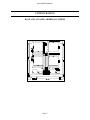
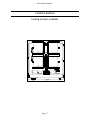
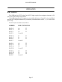
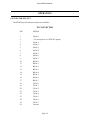
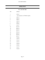
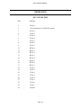
4I24I PARALLEL PORT MANUAL
Version 1.0
Copyright 1997 by MESA ELECTRONICS Richmond, CA. Printed in the United States of America.
All rights reserved. This document and the data disclosed herein is not to be reproduced, used,
disclosed in whole or in part to anyone without the written permission of MESA ELECTRONICS.
Mesa Electronics
4175 Lakeside Drive, Suite #100
Richmond, CA 94806-1950
Tel (510) 223-9272 - Fax (510) 223-9585
E-Mail: [email protected] - Website: www.mesanet.com
4I24I USER'S MANUAL
TABLE OF CONTENTS
HANDLING PRECAUTIONS
Static electricity . . . . . . . . . . . . . . . . . . . . . . . . . . . . . . . . . . . . . . . . . . . . . . . . . . . . . . . . . . . . . . . . . . . . . . . . 4
INTRODUCTION
General . . . . . . . . . . . . . . . . . . . . . . . . . . . . . . . . . . . . . . . . . . . . . . . . . . . . . . . . . . . . . . . . . . . . . . . . . . . . . . . . 5
CONFIGURATION
General . . . . . . . . . . . . . . . . . . . . . . . . . . . . . . . . . . . . . . . . . . . . . . . . . . . . . . . . . . . . . . . . . . . . . . . . . . . . . . . . 6
Default jumper settings . . . . . . . . . . . . . . . . . . . . . . . . . . . . . . . . . . . . . . . . . . . . . . . . . . . . . . . . . . . . . . . . 6
Base address selection . . . . . . . . . . . . . . . . . . . . . . . . . . . . . . . . . . . . . . . . . . . . . . . . . . . . . . . . . . . . . . . . . 8
Aliased address selection. . . . . . . . . . . . . . . . . . . . . . . . . . . . . . . . . . . . . . . . . . . . . . . . . . . . . . . . . . . . . . . 8
+5V Enable Jumper . . . . . . . . . . . . . . . . . . . . . . . . . . . . . . . . . . . . . . . . . . . . . . . . . . . . . . . . . . . . . . . . . . . 10
INSTALLATION
General . . . . . . . . . . . . . . . . . . . . . . . . . . . . . . . . . . . . . . . . . . . . . . . . . . . . . . . . . . . . . . . . . . . . . . . . . . . . . . . 12
I/O connector orientation . . . . . . . . . . . . . . . . . . . . . . . . . . . . . . . . . . . . . . . . . . . . . . . . . . . . . . . . . . . . . 12
OPERATION
Port mapping . . . . . . . . . . . . . . . . . . . . . . . . . . . . . . . . . . . . . . . . . . . . . . . . . . . . . . . . . . . . . . . . . . . . . . . . . 13
Connector pinout . . . . . . . . . . . . . . . . . . . . . . . . . . . . . . . . . . . . . . . . . . . . . . . . . . . . . . . . . . . . . . . . . . . . . 14
PPLOOPBK . . . . . . . . . . . . . . . . . . . . . . . . . . . . . . . . . . . . . . . . . . . . . . . . . . . . . . . . . . . . . . . . . . . . . . . . . . 18
REFERENCE INFORMATION
Specifications . . . . . . . . . . . . . . . . . . . . . . . . . . . . . . . . . . . . . . . . . . . . . . . . . . . . . . . . . . . . . . . . . . . . . . . . . 19
Warranty. . . . . . . . . . . . . . . . . . . . . . . . . . . . . . . . . . . . . . . . . . . . . . . . . . . . . . . . . . . . . . . . . . . . . . . . . . . . . . 20
Schematic diagrams . . . . . . . . . . . . . . . . . . . . . . . . . . . . . . . . . . . . . . . . . . . . . . . . . . . . . . . . . . . . . . . . . . . 21
4I24I USER'S MANUAL
HANDLING PRECAUTIONS
STATIC ELECTRICITY
The CMOS integrated circuits on the 4I24I can be damaged by exposure to electrostatic
discharges. The following precautions should be taken when handling the 4I24I to prevent
possible damage.
A. Leave the 4I24I in its antistatic bag until needed.
B. All work should be performed at an antistatic workstation.
C. Ground equipment into which 4I24I will be installed.
D. Ground handling personnel with conductive bracelet through 1 megohm resistor to
ground.
E. Avoid wearing synthetic fabrics, particularly Nylon.
4I24I USER'S MANUAL
INTRODUCTION
GENERAL
The MESA 4I24 series of cards are 96 bit parallel I/O interfaces implemented on the PC/104 bus.
The 4I24 uses 4 (4I24, 4I24I) or 3 (4I24M) socketed 82C55 PIO chips to give for a total of 96 I/O bits
(4I24, 4I24I) or 72 I/O bits (4I24M). 3.3K Pullup resistors are provided on all ports to simplify
interfacing to contact closure, opto-isolators, etc.
The 4I24 includes three models with different I/O connectors. The standard 4I24 uses two 50 pin
headers for I/O connections. The 50 pin connectors each have 48 I/O bits, ground, and power. The
4I24I uses four 26 pin headers with ISO standard pinout (24 I/O bits per 26 pin connector, pin 2 =
GND, pin 26= 5V). The 4I24M has I/O module rack compatible pinouts with three 50 pin connectors
each having 24 I/O bits with interleaved grounds. 5V power on the I/O connectors is fused on the
4I24.
All 4I24 models can use the 16 bit stack through type PC/104 bus architecture. Four layer circuit
card construction is used to minimize radiated EMI and provide optimum ground and power
integrity. All CMOS design keeps power consumption to a minimum. The 4I24 requires only +5V for
operation
The 4I24 base address is set with jumpers, and can be located anywhere in the 1024 byte I/O
address space of the PC/104 bus. 4I24 cards use 16 contiguous I/O address's, but where multiple
cards are used, an aliased addressing capability allows up to four 4I24 cards to share the same 10 bit
base address, conserving I/O address space.
A partially loaded 48 bit version of the 4I24 and 4I24I can be provided if needed, contact MESA
for availability.
Page 5
4I24I USER'S MANUAL
CONFIGURATION
GENERAL
The 4I24I port address and I/O power connection options are set with jumpers. Each group of
jumpers will be discussed separately by function. In the following discussions, when the words "up",
"down", "right", and "left" are used it is assumed that the 4I24I I/O card is oriented with its bus
connectors J1 and J2 at the bottom edge of the card (nearest the person doing the configuration).
DEFAULT JUMPER SETTINGS
Factory default 4I24I jumpering is as follows:
FUNCTION
JUMPER(S)
SETTING
4I24I Base address
W4,W5,W6,W7,W8,W9
0200H
4I24I Aliased address
W1,W2
0000H
Power Option
W3
Ground
Page 6
4I24I USER'S MANUAL
CONFIGURATION
DEFAULT JUMPER SETTINGS
Page 7
4I24I USER'S MANUAL
CONFIGURATION
BASE ADDRESS SELECTION
The I/O addresses of the four 82C55's on the 4I24I are selected by placing shorting jumpers on
jumper blocks W1, W2, W4 through W9. These jumper blocks have three pins and two valid shorting
jumper locations, up, and down. The position of the jumpers is a binary representation of the 4I24I
base address. When a jumper is in the up position, it matches a high address line.
The following table shows some example base address settings
BASE ADDRESS
W4
W5
W6
W7
W8
W9
(A9)
(A8)
(A7)
(A6)
(A5)
(A4)
0200H (Default)
up
down
down
down
down
down
0290H
up
down
up
down
down
up
0360H
up
up
down
up
up
down
ALIASED ADDRESS SELECTION
If multiple 4I24I's are used in a single system, I/O address space can be conserved by using aliased
address's. Aliased addresses are an artifact caused by the partial (only 10 bit) address decoding used
by most PC-bus cards. 4I24I cards actually decode A15 and A14 in addition to A0 through A9. This
makes it possible to have up to four 4I24I's located at what appears to other cards in the system to be a
single 16 byte block of I/O addresses. This is done by selecting the same base addresses on all cards,
but selecting differing high order (aliased) addresses.
The aliased address used by a 4I24I is selected via shorting jumpers W1 and W2.
Note that aliased addressing only makes sense when using multiple 4I24I's in a single system,
and when all base address's used are the same.
The following table shows all four of the possible aliased address settings:
ALIASED ADDRESS
W1
W2
(A15)
(A14)
BASE + 0000H (Default)
down
down
BASE + 4000H
down
up
BASE + 8000H
up
down
BASE + C000H
up
up
Page 8
4I24I USER'S MANUAL
CONFIGURATION
BASE AND ALIASED ADDRESS JUMPERS
Page 9
4I24I USER'S MANUAL
CONFIGURATION
+5V ENABLE JUMPER
Pin 2 on all of the 4I24I I/O connectors can either be grounded or connected to system +5V
through a fuse. +5V is provided on pin 2 to supply power to I/O module racks. This option is selected
by the position of the shorting jumper on jumper block W3. When the jumper is in the left hand
position, fused +5V power is routed to pin 2 on the I/O connectors. When W3 is in the right hand
position, pin 2 is used as an additional ground. This is the default position of the +5V enable jumper.
Note that the +5V fuse is rated at 1 Amp and can be replaced without soldering. Replacement part
number is LittleFuse PN 250001.
Page 10
4I24I USER'S MANUAL
CONFIGURATION
POWER OPTION JUMPERS
Page 11
4I24I USER'S MANUAL
INSTALLATION
GENERAL
When the 4I24I has been properly configured for its application, it can be inserted into a PC/104
stack. The standoffs should then be tightened to secure the 4I24I in its place. When the 4I24I is
secured in the stack the 26 pin headers can be plugged in from the sides.
I/O CONNECTOR ORIENTATION
The 26 pin connectors on the 4I24I have their pin one ends marked with a white square on the
circuit card. This corresponds with the colored stripe on typical flat cable assemblies. If more positive
polarization is desired, center polarized IDC header connectors should be used. These connectors
will not fully mate with the pins on the 4I24I if installed backwards. A suggested center polarized 26
pin IDC header is AMP PN 746285-6.
Page 12
4I24I USER'S MANUAL
OPERATION
PORT MAPPING
The 4I24I has four 82C55 chips. Each 82C55 chip occupies four contiguous locations in I/O
space, for a total of sixteen I/O locations.
In the following table and I/O connector pinout tables the letters A, B, and C refer to individual
ports on a 8255 chip (the standard 8255 port names), while the numeric suffix 0, 1, 2, or 3 refers to the
specific chip.
The 82C55 ports are addressed as follows:
ADDRESS
PORT CONNECTOR
BASE +0
BASE +1
BASE+2
BASE+3
A0
B0
C0
Control 0
P3
P3
P3
BASE+4
BASE +5
BASE+6
BASE+7
A1
B1
C1
Control 1
P1
P1
P1
BASE+8
BASE +9
BASE+A
BASE+B
A2
B2
C2
Control 2
P2
P2
P2
BASE+C
BASE +D
BASE+E
BASE+F
A3
B3
C3
Control 3
P4
P4
P4
Page 13
4I24I USER'S MANUAL
OPERATION
CONNECTOR PIN-OUT
The 4I24I 26 pin I/O connector pinouts are as follows:
P3 CONNECTOR
PIN
SIGNAL
1
A0 bit 0
2
+5V fused power or GND (W3 option)
3
A0 bit 1
4
A0 bit 2
5
A0 bit 3
6
A0 bit 4
7
A0 bit 5
8
A0 bit 6
9
A0 bit 7
10
B0 bit 0
11
B0 bit 1
12
B0 bit 2
13
B0 bit 3
14
B0 bit 4
15
B0 bit 5
16
B0 bit 6
17
B0 bit 7
18
C0 bit 0
19
C0 bit 1
20
C0 bit 2
21
C0 bit 3
22
C0 bit 4
23
C0 bit 5
24
C0 bit 6
25
C0 bit 7
26
Ground
Page 14
4I24I USER'S MANUAL
OPERATION
P1 CONNECTOR
PIN
SIGNAL
1
A0 bit 0
2
+5V fused power or GND (W3 option)
3
A0 bit 1
4
A0 bit 2
5
A0 bit 3
6
A0 bit 4
7
A0 bit 5
8
A1 bit 6
9
A1 bit 7
10
B1 bit 0
11
B1 bit 1
12
B1 bit 2
13
B1 bit 3
14
B1 bit 4
15
B1 bit 5
16
B1 bit 6
17
B1 bit 7
18
C1 bit 0
19
C1 bit 1
20
C1 bit 2
21
C1 bit 3
22
C1 bit 4
23
C1 bit 5
24
C1 bit 6
25
C1 bit 7
26
Ground
Page 15
4I24I USER'S MANUAL
OPERATION
P2 CONNECTOR
PIN
SIGNAL
1
A2 bit 0
2
+5V fused power or GND (W3 option)
3
A2 bit 1
4
A2 bit 2
5
A2 bit 3
6
A2 bit 4
7
A2 bit 5
8
A2 bit 6
9
A2 bit 7
12
B2 bit 0
11
B2 bit 1
12
B2 bit 2
13
B2 bit 3
14
B2 bit 4
15
B2 bit 5
16
B2 bit 6
17
B2 bit 7
18
C2 bit 0
19
C2 bit 1
20
C2 bit 2
21
C2 bit 3
22
C2 bit 4
23
C2 bit 5
24
C2 bit 6
25
C2 bit 7
26
Ground
Page 16
4I24I USER'S MANUAL
OPERATION
P4 CONNECTOR
PIN
SIGNAL
1
A3 bit 0
2
+5V fused power or GND (W3 option)
3
A3 bit 1
4
A3 bit 2
5
A3 bit 3
6
A3 bit 4
7
A3 bit 5
8
A3 bit 6
9
A3 bit 7
12
B3 bit 0
11
B3 bit 1
12
B3 bit 2
13
B3 bit 3
14
B3 bit 4
15
B3 bit 5
16
B3 bit 6
17
B3 bit 7
18
C3 bit 0
19
C3 bit 1
20
C3 bit 2
21
C3 bit 3
22
C3 bit 4
23
C3 bit 5
24
C3 bit 6
25
C3 bit 7
26
Ground
Page 17
4I24I USER'S MANUAL
OPERATION
PPLOOPBK
A simple test program is supplied with the 4I24I for functional testing and verification. This
program is called PPLOOPBK.EXE. PPLOOPBK is what's called a loopback test program. It works
by sending rotating bit patterns out on all 24 bits of a 8255 programmed for all outputs, then checking
to see that the same pattern has been received on a second 8255 programmed for all inputs. After this
is done, PPLOOPBK reverses the roles of the input and output chips and repeats the test.
The connection between the two 8255's is done with an external cable (a loopback cable!).
PPLOOPBK will detect most common I/O port problems including stuck bits, shorts, and opens.
PPLOOPBK is not very smart about major problems like incorrect port addresses, missing loopback
cables etc., and will cheerfully report bit errors even if no 4I24I card is present.
To use PPLOOPBK you must have a 26 conductor flat cable with female headers on each end.
Because the 4I24I has four I/O connectors, you must run PPLOOPBK with 2 different cable
arrangements First connect P1 and P2 together with the flat cable. Make sure that the cable is properly
polarized (pin1 to pin 1). Then run PPLOOPBK. Next connect the loopback cable to P3 and P4, and
run PPLOOPBK again.
PPLOOPBK is invoked with 2 hexadecimal addresses on the command line. These are the
addresses of the two 8255's that will be tested. If a 4I24I is set to its default (0200H) address, and has a
(good) loopback cable installed, the following sequence of commands will do a fairly thorough test of
the card.
(Connect loopback cable to P1 and P2)
PPLOOPBK 204 208
(Connect loopback cable to P3 and P4)
PPLOOPBK 200 20C
Page 18
4I24I USER'S MANUAL
REFERENCE INFORMATION
SPECIFICATIONS
MIN
MAX
UNIT
Voltage
4.5
5.5
V
Supply current
---
50
mA
Input capacitance
---
15
pF
Input leakage current
---
5
uA
Output drive capability
150
---
pF
Output sink current
12
---
mA
Input logic low
-.3
.8
V
Input logic high
2.0
5.5
V
Output low
---
.4
V
2.5 mA sink
Output high
3.0
---
V
2.5 mA source
-40
+85
o
o
POWER SUPPLY
(no ext. load)
BUS LOADING:
I/O PORT LOADING:
ENVIRONMENTAL:
Operating temperature range
-I version
-C version
0
+70
Relative humidity
0
90
C
C
Percent
Non-condensing
Page 19
4I24I USER'S MANUAL
REFERENCE INFORMATION
WARRANTY
Mesa Electronics warrants the products it manufactures to be free effects in material and
workmanship under normal use and service for the period of 2 years from date of purchase. This
warranty shall not apply to products which have been subject to misuse, neglect, accident, or
abnormal conditions of operation.
In the event of failure of a product covered by this warranty, Mesa Electronics, will repair any
product returned to Mesa Electronics within 2 years of original purchase, provided the warrantor's
examination discloses to its satisfaction that the product was defective. The warrantor may at its
option, replace the product in lieu of repair.
With regard to any product returned within 2 years of purchase, said repairs or replacement will be
made without charge. If the failure has been caused by misuse, neglect, accident, or abnormal
conditions of operation, repairs will be billed at a nominal cost.
THE FOREGOING WARRANTY IS IN LIEU OF ALL OTHER WARRANTIES,
EXPRESS OR IMPLIED. INCLUDING BUT NOT LIMITED TO ANY IMPLIED
WARRANTY OF MERCHANTABILITY, FITNESS, OR ADEQUACY FOR ANY
PARTICULAR PURPOSE OR USE. MESA ELECTRONICS SHALL NOT BE LIABLE FOR
ANY SPECIAL, INCIDENTAL, OR CONSEQUENTIAL DAMAGES, WHETHER IN
CONTRACT, TORT, OR OTHERWISE.
If any failure occurs, the following steps should be taken:
1. Notify Mesa Electronics, giving full details of the difficulty. On receipt of this information,
service data, or shipping instructions will be forwarded to you.
2. On receipt of the shipping instructions, forward the product, in its original protective
packaging, transportation prepaid to Mesa Electronics. Repairs will be made at Mesa Electronics and
the product returned transportation prepaid.
Page 20
4I24I USER'S MANUAL
REFERENCE INFORMATION
SCHEMATICS
Page 21