1
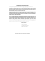
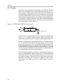
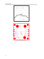
2−GBPS Differential Repeater Evaluation Module User’s Guide November 2002 High-Performance Linear/Interface Products SLLU040A IMPORTANT NOTICE Texas Instruments Incorporated and its subsidiaries (TI) reserve the right to make corrections, modifications, enhancements, improvements, and other changes to its products and services at any time and to discontinue any product or service without notice. Customers should obtain the latest relevant information before placing orders and should verify that such information is current and complete. All products are sold subject to TI’s terms and conditions of sale supplied at the time of order acknowledgment. TI warrants performance of its hardware products to the specifications applicable at the time of sale in accordance with TI’s standard warranty. Testing and other quality control techniques are used to the extent TI deems necessary to support this warranty. Except where mandated by government requirements, testing of all parameters of each product is not necessarily performed. TI assumes no liability for applications assistance or customer product design. Customers are responsible for their products and applications using TI components. To minimize the risks associated with customer products and applications, customers should provide adequate design and operating safeguards. TI does not warrant or represent that any license, either express or implied, is granted under any TI patent right, copyright, mask work right, or other TI intellectual property right relating to any combination, machine, or process in which TI products or services are used. Information published by TI regarding third-party products or services does not constitute a license from TI to use such products or services or a warranty or endorsement thereof. Use of such information may require a license from a third party under the patents or other intellectual property of the third party, or a license from TI under the patents or other intellectual property of TI. Reproduction of information in TI data books or data sheets is permissible only if reproduction is without alteration and is accompanied by all associated warranties, conditions, limitations, and notices. Reproduction of this information with alteration is an unfair and deceptive business practice. TI is not responsible or liable for such altered documentation. Resale of TI products or services with statements different from or beyond the parameters stated by TI for that product or service voids all express and any implied warranties for the associated TI product or service and is an unfair and deceptive business practice. TI is not responsible or liable for any such statements. Mailing Address: Texas Instruments Post Office Box 655303 Dallas, Texas 75265 Copyright 2002, Texas Instruments Incorporated EVM IMPORTANT NOTICE Texas Instruments (TI) provides the enclosed product(s) under the following conditions: This evaluation kit being sold by TI is intended for use for ENGINEERING DEVELOPMENT OR EVALUATION PURPOSES ONLY and is not considered by TI to be fit for commercial use. As such, the goods being provided may not be complete in terms of required design-, marketing-, and/or manufacturing-related protective considerations, including product safety measures typically found in the end product incorporating the goods. As a prototype, this product does not fall within the scope of the European Union directive on electromagnetic compatibility and therefore may not meet the technical requirements of the directive. Should this evaluation kit not meet the specifications indicated in the EVM User’s Guide, the kit may be returned within 30 days from the date of delivery for a full refund. THE FOREGOING WARRANTY IS THE EXCLUSIVE WARRANTY MADE BY SELLER TO BUYER AND IS IN LIEU OF ALL OTHER WARRANTIES, EXPRESSED, IMPLIED, OR STATUTORY, INCLUDING ANY WARRANTY OF MERCHANTABILITY OR FITNESS FOR ANY PARTICULAR PURPOSE. The user assumes all responsibility and liability for proper and safe handling of the goods. Further, the user indemnifies TI from all claims arising from the handling or use of the goods. Please be aware that the products received may not be regulatory compliant or agency certified (FCC, UL, CE, etc.). Due to the open construction of the product, it is the user’s responsibility to take any and all appropriate precautions with regard to electrostatic discharge. EXCEPT TO THE EXTENT OF THE INDEMNITY SET FORTH ABOVE, NEITHER PARTY SHALL BE LIABLE TO THE OTHER FOR ANY INDIRECT, SPECIAL, INCIDENTAL, OR CONSEQUENTIAL DAMAGES. TI currently deals with a variety of customers for products, and therefore our arrangement with the user is not exclusive. TI assumes no liability for applications assistance, customer product design, software performance, or infringement of patents or services described herein. Please read the EVM User’s Guide and, specifically, the EVM Warnings and Restrictions notice in the EVM User’s Guide prior to handling the product. This notice contains important safety information about temperatures and voltages. For further safety concerns, please contact the TI application engineer. Persons handling the product must have electronics training and observe good laboratory practice standards. No license is granted under any patent right or other intellectual property right of TI covering or relating to any machine, process, or combination in which such TI products or services might be or are used. Mailing Address: Texas Instruments Post Office Box 655303 Dallas, Texas 75265 Copyright 2002, Texas Instruments Incorporated EVM WARNINGS AND RESTRICTIONS It is important to operate this EVM within the supply voltage range of 3 V to 3.6 V. Exceeding the specified input range may cause unexpected operation and/or irreversible damage to the EVM. If there are questions concerning the supply range, please contact a TI field representative prior to connecting the input power. Applying loads outside of the specified output range may result in unintended operation and/or possible permanent damage to the EVM. Please consult the EVM User’s Guide prior to connecting any load to the EVM output. If there is uncertainty as to the load specification, please contact a TI field representative. During normal operation, some circuit components may have case temperatures greater than 125°C. The EVM is designed to operate properly with certain components above 125°C as long as the input and output ranges are maintained. These components include but are not limited to linear regulators, switching transistors, pass transistors, and current sense resistors. These types of devices can be identified using the EVM schematic located in the EVM User’s Guide. When placing measurement probes near these devices during operation, please be aware that these devices may be very warm to the touch. Mailing Address: Texas Instruments Post Office Box 655303 Dallas, Texas 75265 Copyright 2002, Texas Instruments Incorporated Information About Cautions and Warnings Preface Read This First About This Manual This EVM user’s guide provides information about the 2-GBPS differential repeater evaluation module. How to Use This Manual This document contains the following chapters: - Chapter 1 — Introduction - Chapter2 — Setup and Equipment Required - Chapter 3 — EVM Construction Information About Cautions and Warnings This book may contain cautions and warnings. This is an example of a caution statement. A caution statement describes a situation that could potentially damage your software or equipment. This is an example of a warning statement. A warning statement describes a situation that could potentially cause harm to you. The information in a caution or a warning is provided for your protection. Please read each caution and warning carefully. v Related Documentation From Texas Instruments Related Documentation From Texas Instruments To obtain a copy of any of the following TI document, call the Texas Instruments Literature Response Center at (800) 477-8924 or the Product Information Center (PIC) at (972) 644-5580. When ordering, identify this booklet by its title and literature number. Updated documents can also be obtained through our website at www.ti.com. Data Sheet: Literature Number: SN65LVDS100/101 SLLS516 SN65CML100 SLLS547 FCC Warning This equipment is intended for use in a laboratory test environment only. It generates, uses, and can radiate radio frequency energy and has not been tested for compliance with the limits of computing devices pursuant to subpart J of part 15 of FCC rules, which are designed to provide reasonable protection against radio frequency interference. Operation of this equipment in other environments may cause interference with radio communications, in which case the user at his own expense will be required to take whatever measures may be required to correct this interference. vi Contents Contents 1 Introduction . . . . . . . . . . . . . . . . . . . . . . . . . . . . . . . . . . . . . . . . . . . . . . . . . . . . . . . . . . . . . . . . . . . . . 1-1 1.1 Overview . . . . . . . . . . . . . . . . . . . . . . . . . . . . . . . . . . . . . . . . . . . . . . . . . . . . . . . . . . . . . . . . . . 1-2 1.2 Signal Paths . . . . . . . . . . . . . . . . . . . . . . . . . . . . . . . . . . . . . . . . . . . . . . . . . . . . . . . . . . . . . . . 1-3 2 Setup and Equipment Required . . . . . . . . . . . . . . . . . . . . . . . . . . . . . . . . . . . . . . . . . . . . . . . . . . . 2.1 Overview . . . . . . . . . . . . . . . . . . . . . . . . . . . . . . . . . . . . . . . . . . . . . . . . . . . . . . . . . . . . . . . . . . 2.2 Applying an Input . . . . . . . . . . . . . . . . . . . . . . . . . . . . . . . . . . . . . . . . . . . . . . . . . . . . . . . . . . . 2.3 Observing an Output . . . . . . . . . . . . . . . . . . . . . . . . . . . . . . . . . . . . . . . . . . . . . . . . . . . . . . . . 2.4 Typical Test Results . . . . . . . . . . . . . . . . . . . . . . . . . . . . . . . . . . . . . . . . . . . . . . . . . . . . . . . . . 2-1 2-2 2-3 2-5 2-6 3 EVM Construction . . . . . . . . . . . . . . . . . . . . . . . . . . . . . . . . . . . . . . . . . . . . . . . . . . . . . . . . . . . . . . . 3.1 Schematic . . . . . . . . . . . . . . . . . . . . . . . . . . . . . . . . . . . . . . . . . . . . . . . . . . . . . . . . . . . . . . . . . 3.2 Bill of Materials . . . . . . . . . . . . . . . . . . . . . . . . . . . . . . . . . . . . . . . . . . . . . . . . . . . . . . . . . . . . . 3.3 Board Stackup . . . . . . . . . . . . . . . . . . . . . . . . . . . . . . . . . . . . . . . . . . . . . . . . . . . . . . . . . . . . . 3.4 Board Layer Patterns . . . . . . . . . . . . . . . . . . . . . . . . . . . . . . . . . . . . . . . . . . . . . . . . . . . . . . . 3-1 3-2 3-3 3-4 3-5 Figures 1-1 1-2 2-1 2-2 2-3 2-4 2-5 EVM With SN65LVDS100 Installed . . . . . . . . . . . . . . . . . . . . . . . . . . . . . . . . . . . . . . . . . . . . . . Schematic of EVM Signal Path . . . . . . . . . . . . . . . . . . . . . . . . . . . . . . . . . . . . . . . . . . . . . . . . . . TIA/EIA-644-A LVDS Driver Test Load . . . . . . . . . . . . . . . . . . . . . . . . . . . . . . . . . . . . . . . . . . . EVM Power Connections for SN65LVDS100 Evaluation . . . . . . . . . . . . . . . . . . . . . . . . . . . . External Termination for Differential CML or LVPECL Inputs to EVM . . . . . . . . . . . . . . . . . External Termination for Single-Ended LVPECL Inputs to EVM . . . . . . . . . . . . . . . . . . . . . . Typical Output From SN65LVDS100 EVM . . . . . . . . . . . . . . . . . . . . . . . . . . . . . . . . . . . . . . . . 1-2 1-3 2-2 2-3 2-4 2-5 2-7 Tables 1-1 Ordering Information . . . . . . . . . . . . . . . . . . . . . . . . . . . . . . . . . . . . . . . . . . . . . . . . . . . . . . . . . . 1-2 vii Contents viii Chapter 1 Introduction The 2-GBPS differential repeater evaluation module (EVM) allows evaluation of the SN65LVDS100, SN65LVDS101, and SN65CML100 differential repeaters/ translators. This user’s guide gives a brief overview of the EVM, setup and operation instructions, and typical test results that can be expected. Topic Page 1.1 Overview . . . . . . . . . . . . . . . . . . . . . . . . . . . . . . . . . . . . . . . . . . . . . . . . . . . . . 1-2 1.2 Signal Paths . . . . . . . . . . . . . . . . . . . . . . . . . . . . . . . . . . . . . . . . . . . . . . . . . . 1-3 Introduction 1-1 Overview 1.1 Overview The 2-GBPS differential repeater evaluation module (EVM) is designed for evaluation of the SN65LVDS100, SN65LVDS101, and SN65CML100 differential repeaters/ translators. The SN65LVDS100 and SN65LVDS101 devices both incorporate wide common-mode range receivers, allowing receipt of LVDS, LVPECL, or CML input signals. The SN65LVDS100 provides an LVDS output, the SN65LVDS101 incorporates an LVPECL output driver, and the SN65CML100 delivers a CML output. Both devices provide a VBB reference voltage to support receiving of single-ended LVPECL input signals, or biasing of ac-coupled inputs. The EVM can be ordered with the SN65LVDS100, SN65LVDS101, or SN65CML100 installed. Orderable EVM part numbers are shown in Table 1-1. Table 1-1. Ordering Information EVM Part Number Installed Device SN65LVDS100EVM SN65LVDS100DGK SN65LVDS101EVM SN65LVDS101DGK SN65CML100EVM SN65CML100DGK Detailed information relating to the SN65LVDS100, SN65LVDS101, and SN65CML100 can be found in the device data sheet, a copy of which is shipped as part of the EVM or available from www.ti.com. A picture of the EVM, with an SN65LVDS100 device installed, is shown in Figure 1-1. Figure 1-1. EVM With SN65LVDS100 Installed 1-2 Signal Paths 1.2 Signal Paths A partial schematic of the EVM is shown in Figure 1-2 and a full schematic is in chapter 3. Edge-mount SMA connectors (J4, J5, J6, and J7) are provided for data input and output connections. Three power jacks (J1, J2, and J3) are used to provide power to and a ground reference, for the EVM. The use of these power jacks is addressed later. Chapter 3 also provides a parts list for the EVM, as well as an indication of which components are installed when shipped. Figure 1-2. Schematic of EVM Signal Path VCC C11 .010 µF DUT1 J4 GND J5 GND 1 1 R1 100 Ω 1 2 3 4 R5 Uninstalled 8 VCC NC 7 Y A 6 B Z 5 GND Vbb DUT_MSOP8 R2 Uninstalled 1 VCC01 JMP2 1 2 GND R4 Uninstalled 1 R3 J6 J7 GND Uninstalled C12 .010 µF Introduction 1-3 1-4 Chapter 2 Setup and Equipment Required This chapter examines the setup and use of the evaluation module and the results of operation. Topic Page 2.1 Overview . . . . . . . . . . . . . . . . . . . . . . . . . . . . . . . . . . . . . . . . . . . . . . . . . . . . . 2-2 2.2 Applying an Input . . . . . . . . . . . . . . . . . . . . . . . . . . . . . . . . . . . . . . . . . . . . . 2-3 2.3 Observing an Output . . . . . . . . . . . . . . . . . . . . . . . . . . . . . . . . . . . . . . . . . . 2-5 2.4 Typical Test Results . . . . . . . . . . . . . . . . . . . . . . . . . . . . . . . . . . . . . . . . . . . 2-6 Setup and Equipment Required 2-1 Overview 2.1 Overview LVDS driver output characteristics are specified in the TIA/EIA-644 standard. LVDS drivers nominally provide a 350-mV differential signal, with a 1.25-V offset from ground. These levels are attained when driving a 100-Ω differential line-termination test load (see Figure 2-1). In real applications, there may be a ground potential between a driver and receiver(s). The driver must drive the common-mode load presented by the receiver inputs and the differential load. A TIA/EIA-644-A compliant LVDS driver is required to maintain its differential output with up to 32 standard receivers. The receiver load is represented by the 3.74-kΩ resistors shown in Figure 2-1. Figure 2-1. TIA/EIA-644-A LVDS Driver Test Load 3.74 kΩ A D B VOD 100 Ω 3.74 kΩ + _ 0 V ≤ Vtest ≤ 2.4 V LVPECL drivers are generally loaded with 50-Ω resistors to a termination bias voltage, VT. VT is usually 2-V below the supply voltage of the driver circuit. When the driver operates from a 3.3-V supply, VT is set to approximately 1.3 V. CML drivers are generally loaded with 50-Ω resistors to a termination voltage, VTT. VTT can either be equivalent to the supply voltage of the driver circuit (equal to VCC) or set to 2.5 V or 1.8 V, irrelevant to the supply voltage. If desired, the SN65CML100 can be configured to drive a dual 50-Ω load. In this configuration one 50-Ω resistor (tied to the termination voltage VTT) is placed near the output of the SN65CML100 and a second 50-Ω resistor (also tied to VTT) is placed near the end of the transmission line. The EVM has been designed to support the SN65LVDS100 LVDS-output device, the SN65LVDS101 LVPECL-output device, and the SN65CML100 CML-output device. By using the three power jacks (J1, J2, and J3), as well as installing termination resistors (R2, R3, and R4), different methods of termination and probing can be used to evaluate the device output characteristics. The typical setup for the SN65LVDS100 is shown in Figure 2-2. 2-2 Applying an Input Figure 2-2. EVM Power Connections for SN65LVDS100 Evaluation Power Supply 1 + 3.3V - Power Supply 2 + 1.22V J3 DUT GND J2 EVM GND J4 J5 J1 VCC J6 100 Ω J7 50 Ω Pattern Generator Matched Cables SMA to SMA 50 Ω Matched Cables SMA to SMA EVM Oscilloscope Warning Power jacks J1, J2, and J3 are not insulated on the backside of the EVM. Place on a nonconductive surface. 2.2 Applying an Input LVDS inputs should be applied to SMA connectors J4 and J5, while keeping R1 installed. The EVM comes with a 100-Ω termination resistor (R1) installed across the differential inputs. This 100-Ω resistor represents an LVDS termination. When using a general-purpose signal generator with 50-Ω output impedance, make sure that the signal levels are between 0 V to 4 V with respect to J3. A signal generator such as the Advantest D3186 can simulate LVDS, LVPECL, or CML inputs. When using LVPECL or CML drivers for the input signal, termination external to the EVM must be provided (see Figure 2-3). LVPECL drivers should be terminated with 50-Ω pulldowns to VT, while CML drivers should be terminated Setup and Equipment Required 2-3 Applying an Input with 50-Ω pullups to VTT. When using external terminations, the onboard termination resistor R1 should be removed from the EVM. It should be noted that the signal quality at the receiver input may be degraded when external terminations are used, as a significant stub exists from the external termination network to the receiver input. The user needs to verify that the transition time of the input signal, coupled with the stub length, does not lead to reflection problems. These concerns would be addressed in a real application where the terminations are placed close to the receiver input. Figure 2-3. External Termination for Differential CML or LVPECL Inputs to EVM Select VT for LVPECL or Select VTT for CML 50 Ω A OUT Signal Source Y EVM BOARD B OUT Z 50 Ω Select VT for LVPECL or Select VTT for CML NOTES: A. Locate 50-Ω resistors as close to the EVM as possible B. Remove R1 Finally, as mentioned above, the SN65LVDS100, SN65LVDS101, and SN65CML100 devices provide a VBB reference voltage output. This output can be used with an externally terminated, single-ended, LVPECL input to convert from a single-ended input to a differential output. The same cautions that are mentioned above concerning signal quality and reflections apply. When using VBB as a single-ended reference, R1 should be removed while R5 and JMP2 should be installed. The single-ended input signal is applied to J4. This setup directly connects the VBB output to the DUT receiver B input via a 0-Ω connection (see Figure 2-4). 2-4 Observing an Output Figure 2-4. External Termination for Single-Ended LVPECL Inputs to EVM A OUT Y 50 Ω Signal Source EVM BOARD B Z NOTES: A. Add jumper Jmp2 and 0-Ω R5 B. Remove R1 2.3 Observing an Output Direct connection to an oscilloscope with 50-Ω internal terminations to ground is accomplished without R2, R3, and R41. The outputs are available at J6 and J7 for direct connection to oscilloscope inputs. Matched length cables must be used when connecting the EVM to a scope to avoid inducing skew between the noninverting (+) and inverting (-) outputs. The three power jacks (J1, J2, and J3) are used to provide power and a ground reference for the EVM. The power connections to the EVM determine the common-mode load to the device. As mentioned earlier, LVDS drivers have limited common-mode driver capability. When connecting the EVM outputs directly to oscilloscope inputs, setting of the oscilloscope common-mode offset voltage is required, as the oscilloscope presents low common-mode load impedance to the device. Returning to Figure 2-2, power supply 1 is used to provide the required 3.3 V to the EVM. Power supply 2 is used to offset the EVM ground relative to the DUT ground. The EVM ground is connected to the oscilloscope ground through the returns on SMA connectors J6 and J7. With power applied as shown in Figure 2-2, the common-mode voltage seen by the SN65LVDS100 is approximately equal to the reference voltage being used inside the device preventing significant common-mode current to flow. Optimum device setup can be confirmed by adjusting the voltage on power supply 2 until its current is minimized. It is important to note that use of the dual supplies and offsetting the EVM ground relative to the DUT ground are simply steps needed for the test and evaluation of devices. Actual designs would include high-impedance receivers, which would not require the setup steps outlined above. 1 As delivered R2, R3, and R4 are not installed Setup and Equipment Required 2-5 Typical Test Results LVPECL drivers need a 50-Ω termination to VT. A modification of Figure 2-2 and the above instructions are used when evaluating an SN65LVDS101 with a direct connection to a 50-Ω oscilloscope. With power supply 1 in Figure 2-2 set to 3.3 V, power supply 2 should be set to 1.3 V (2 V below VCC) to provide the correct termination voltage. CML drivers need a 50-Ω termination to VTT (VTT is either VCC, 2.5 V, or 1.8 V). A modification of Figure 2-2 and the instructions for the SN65LVDS100 are used when evaluating a SN65CML100 with direct connection to a 50-Ω oscilloscope. With power supply 1 in Figure 2-2 set to 3.3 V, power supply 2 should be set to either VCC (3.3 V), 2.5 V, or 1.8 V to provide the correct termination voltage. Dual termination of the output can be achieved by placing 49.9-Ω resistors at R2 and R3 and connecting to an oscilloscope as described above. If the EVM outputs are to be evaluated with a high-impedance probe, direct probing on the EVM is supported via installation of R2, R3, and R4. LVDS outputs can be observed by installing R4, a 100-Ω resistor. LVPECL outputs can be observed by installing R2 and R3 (49.9-Ω resistors), and setting power supply 2 to 1.3 V. CML outputs can be observed by setting power supply 2 to VTT and installing 49.9-Ω resistors at R2 and R3 for single termination, or 24.9-Ω resistors at R2 and R3 for dual termination (Note that power supply 2 must be able to sink current.) 2.4 Typical Test Results Figure 2-5 shows a typical test result obtained with the EVM. Figure 2-5 shows the output of an SN65LVDS100 being driven directly into a 50-Ω oscilloscope. For this figure, the SN65LVDS100 was stimulated with an HP 3-GBPS BERT. The input data was pseudorandom data at 2 GBPS and with a random record length of 223-1. The BERT drove two electrically matched one-meter cables with an electrical length of 3.667 ns. These cables were then connected to the EVM inputs. The EVM outputs were connected through another set of electrically matched one-meter cables and terminated by a TDS8000 oscilloscope’s 50-Ω resistors to ground. 2-6 Typical Test Results Figure 2-5. Typical Output From SN65LVDS100 EVM Setup and Equipment Required 2-7 2-8 Chapter 3 EVM Construction This chapter lists the EVM components and examines the construction of the evaluation module. Topic Page 3.1 Schematic . . . . . . . . . . . . . . . . . . . . . . . . . . . . . . . . . . . . . . . . . . . . . . . . . . . . 3-2 3.2 Bill of Materials . . . . . . . . . . . . . . . . . . . . . . . . . . . . . . . . . . . . . . . . . . . . . . . 3-3 3.3 Board Stackup . . . . . . . . . . . . . . . . . . . . . . . . . . . . . . . . . . . . . . . . . . . . . . . . 3-4 3.4 Board Layer Patterns . . . . . . . . . . . . . . . . . . . . . . . . . . . . . . . . . . . . . . . . . . 3-5 EVM Construction 3-1 Schematic 3.1 Schematic VCC J1 -1 + C1 10 µF + C6 10 µF + C2 68 µF C5 0.001 µF C4 0.1 µF C3 1 µF J2 -1 + C8 1 µF C7 68 µF 109 0.001 µF C9 0.1 µF J3 -1 VCC01 VCC J4 GND J5 GND 1 R1 100 Ω 1 R5 Uninstalled DUT1 1 VCC NC 2 Y A 3 B Z 4 GND Vbb DUT_MSOP8 MNTH4 MNTH3 MNTH2 1 VCC01 C12 .010 µF J6 GND R4 Uninstalled 1 Uninstalled 2 MNTH1 C11 .010 µF 8 7 6 5 R3 JMP2 1 3-2 R2 Uninstalled J7 GND Bill of Materials 3.2 Bill of Materials † ITEM QTY MFG MFG PART NO. REF. DES. DESCRIPTION VALUE OR FUNCTION 1 2 Sprague 293D106X0035D2W C1,C6 Capacitor, SMT, TANT 35 V, 10%, 10 µF 2 2 AVX 12063G105ZATRA C3,C8 Capacitor, SMT1206 25 V, 80 -20%, 1.0 µF 3 2 AVX 12065C104JATMA C4,C9 Capacitor, SMT1206 50 V, 5%, 0.1 µF 4 2 Sprague 592D686X0010R2T C2,C7 Capacitor, SMT, TANT 10 V, 20%, 68 µF, Low ESR 5 2 Murata GRM39X7R103K50V C11, C12 Capacitor, SMT0603 50 V,±10%, 0.010 µF 6 2 AVX 06033G102JATMA C5,C10 Capacitor, SMT0603 25 V, 5%, 0.001 µF 7 3 ITT-Pomona 3267 J1, J2, J3 Connector, banana jack Bannana jack 8 4 EF Johnson 142-0701-801 J4, J5, J6, J7 Connector SMA Jack, end launch, 0.062 Dale CRCW0603100F NOT INSTALLED 9 1 R1 Resistor, SMT,0603 100 Ω 10 2 R2, R3 Resistor, SMT, 0603 49.9 Ω R2, R3 11 1 R4 Resistor, SMT, 0603 100 Ω R4 12 1 R5 Resistor, SMT, 0603 0Ω R5 13 1 AMP 4-103239-0x2 JMP2 Header Male, 2 pin, 0.100 CC 14 1 TI SN65LVDS100† SN65LVDS101† DUT1 IC, SMT, 8P 2-GBPS differential repeater/translator 15 3 Screws 16 3 Nuts 17 1 User’s manual 18 1 Data sheet Only one is installed EVM Construction 3-3 Board Stackup 3.3 Board Stackup GENERAL NOTES: UNLESS OTHERWISE SPECIFIED 1. ALL FABRICATION ITEMS MUST MEET OR EXCEED BEST INDUSTRY PRACTICE. IPC-A 600C ( Commercial Std.) 2.LAMINATE MATERIAL: NELCO N4000-13 (DO NOT USE - 13SI) 3. COOPER WEIGHT:1 OZ. START INTERNAL AND 1/2 OZ. START EXTERNAL 4. FINISHED BOARD THICKNESS: .062 ±10% 5. MAXIMUM WARP AND TWIST TO BE .005 INCH PER INCH 6 MINIMUM COPPER WALL THICKNESS OF PLATED-THRU HOLES TO BE .001 INCH 7 MINIMUM ANNULAR RING OF PLATED-THRU HOLES TO BE .002 INCH 8. MINIMUM ALLOWABLE LINE REDUCTION TO BE 20% OR .002 WHICHEVER IS GREATER 9. 0.013 INCH SIGNAL LINES ON LAYER 1 TO BE IMPEDANCE CONTROLLED 50 OHMS TO GND ±10% 0.010 INCH SIGNAL LINES ON LAYER 1 TO BE IMPEDANCE CONTROLLED 100 OHMS TO EACH OTHER ±10% 10. DIELECTRIC CONSTANTS ARE: CORE: 3.2 PREPREG:3.2 PROCESS NOTES: 1. CIRCUITRY ON OUTER LAYERS TO BE PLATED WITH TIN LEAD 2. SOLDERMASK BOTH SIDES PER ARTWORK: GREEN LPI 3. SILKSCREEN BOTH SIDE PER ARTWORK: COLOR=WHITE 9 Copper Foil CH A1 TOP SIDE-SIGNAL/GND FILL (LAYER 1) .0062 PREPREG CORE .015 C1/0 A1 .0122 PREPREG CORE .015 C0/1 A1 .0062 PREPREG INT1-GND PLANE (LAYER 2) 3.000 INT2-VCC SPLIT PLANE (LAYER 3) 9 A A 3.000 0.250 TOP SIDE SHOWN DRILL 6434666A 3-4 Symbol N N N DATUM 0,0 BOTTOM SIDE-GND PLANE (LAYER 4) Through Holes Diameter (in) Plated 0.0160 0.0320 0.0400 0.0500 0.1250 0.2720 Yes Yes Yes Yes Yes Yes Quantity SECTION A - A NO SCALE 49 8 2 3 4 3 THIS IS AN IMPEDANCE CONTROLLED BOARD. 0.250 PWA, BENCH, EVALUATION BOARD, SN65LVDS100/101D, EVM 10/31/01 Copper Foil CH A1 4 Board Layer Patterns 3.4 Board Layer Patterns (Not to Scale) Layer 1 - Signal/GND Fill (Top Side) Layer 2 - GND Plane (INT1) EVM Construction 3-5 Board Layer Patterns Layer 3 - VCC Split Plane (INT2) Layer 4 - GND Plane (Bottom Side) 3-6 Mouser Electronics Authorized Distributor Click to View Pricing, Inventory, Delivery & Lifecycle Information: Texas Instruments: SN65LVDS100EVM SN65LVDS101EVM SN65CML100EVM