1
PLATFORM APPLICATION NOTE
Creating Analog Behavioral Models
VERILOG-AMS ANALOG MODELING
February 2003
TABLE OF CONTENTS
Incisive Verification Platform ........................................................................................................................................1
1
Application Note Overview ...........................................................................................................................................1
2
Introduction ..................................................................................................................................................................1
3
Verilog-A Language Overview .....................................................................................................................................2
4
Analog Modeling Considerations..................................................................................................................................8
5
Verilog-D Language Overview ...................................................................................................................................16
6
Verilog-AMS Language Overview ..............................................................................................................................20
7
Available Cadence Online Documentation .................................................................................................................22
8
References ................................................................................................................................................................22
CADENCE INCISIVE VERIFICATION PLATFORM
Verifying today’s complex ICs requires the speed and efficiency that can be provided only in a unified verification
methodology. The Cadence Incisive™ verification platform enables the development of a unified methodology from system
design to system design-in for all design domains. A unified verification methodology consists of many different tools,
technologies and processes all working together in a common environment. The Incisive verification platform provides the
tools, technologies, a common user environment, and the support needed to develop a unified methodology. This
application note details specific topics for using the tools and technologies in the Incisive platform to help create a unified
methodology to verify your design.
1
APPLICATION NOTE OVERVIEW
Analog behavioral modeling can help speed up verifications for larger, complex circuits where simulations are longer and
more difficult to complete. This application note is an introduction to analog behavioral modeling using Verilog-A running in
Spectre™. It gives examples to help you understand the basic modeling concepts. It also includes explanations of Verilog-D
and Verilog-AMS, which is a true fully analog mixed-signal language working with Incisive™-AMS. Most of the content in this
application note was derived and summarized from the AMS Behavioral Modeling Workshop (see reference [1]).
2
INTRODUCTION
Analog Behavioral Modeling deals with creating and simulating models based on a desired external circuit behavior. Models
are best used to represent circuit block behavior and not simply replicate individual transistor characteristics. Models can be
as complex as necessary. Often, initial behavioral models need to carry only the basic properties, such as an operational
amplifier might have voltage swings, impedances, and gain. In other cases, there might be a need to model slew rates,
differential signals and bandwidth properties. Adjustable parameters can be added to model and preview design tradeoffs in
a circuit. The more complex a model is, the more impact it will have on the simulation time and convergence. It is important
to consider what tradeoffs are important and necessary before starting to write a model. Creating a detailed macro-model is
often an important first step in determining what to model, rather than using a trial and error approach. There are six main
reasons to consider modeling:
• Design exploration
• Verify connectivity
• Verify functionality
• Speed up simulations
• Reuse in future designs
• To create a portable design IP
Modeling is best when used early in the design cycle.
Analog behavioral modeling is part of a wider design methodology called “top-down design.” This may seem obvious, but
there are a number of aspects that require careful consideration to take full advantage of modeling. Top-down design starts
with creating a hierarchical design. This is a common design practice today, especially for large designs. However, the key
is to make all circuit blocks in the hierarchy pin-to-pin compatible so that each can be represented by either a model or an
actual transistor-level circuit block. Later, the views can be toggled between model and transistor for mixed-level simulation.
One of the biggest advantages of using modeling is to take well-behaved transistor-level circuit blocks that are slow to
simulate, and switch them to a model to shorten simulation time. Sub-circuit blocks not in the signal path, such as PLLs, lend
themselves well to being run as a model because they have well-behaved feedback properties. In other cases, modeling the
entire design might be of interest to run system-like simulations for architectural exploration while designing the IC. With
hierarchical design, it is possible to create models at any level of the hierarchy. Generally, the higher the level of modeling,
the faster the simulation runs. In addition, it is also possible to represent digital functional and behavioral models in VerilogA. Where there is only a small number of digital blocks, it is advantageous to represent these in Verilog-A. This cuts down
on the overhead of having a mixed-mode simulator. In other cases, where there is a large Verilog-A, models lend
themselves well to creating basic signal sources and measurement blocks in testbenches. This is especially true for wireless
systems where pseudo-random signal sources can be easily set up and where measurement blocks can calculate Bit Error
Rates (BER) or plot Eye Diagrams after a long simulation.
Another important aspect of modeling is “bottom-up” modeling—taking finished transistor-level circuit block results and
exactly modeling them. This may require some effort and characterization. Sometimes the behavioral model is simply a
1
PLATFORM APPLICATION NOTE
matter of writing a few mathematical expressions. In other cases, it might require curve fitting of non-linear behavior in all
modes of operation. Look-up tables can also be used. The end result is a close replica of the transistor-level circuit block,
which can be used with confidence and reused in other designs. Over time, commonly used blocks that go through this
process can create a reuse library that will greatly enhance simulating designs that otherwise would take longer. The one
common goal in modeling is to eventually simulate top-level behavior. The other is to determine if it is correctly wired and if it
works. Top-level simulations of large IC designs are often not possible without some type of modeling.
Admittedly, most integrated circuit designers do not like modeling. It takes some skill to write models and there is no time for
designers to write models. Some think model writing is boring or that modeling will never be accurate enough to use. But
these points are only partially true. In the initial design phases, second and third order effects, especially from layout
parastics, are not needed for functional simulations. These can be added later as needed. To really do modeling well, it will
take some time to master. However, to learn the basics and to reuse and adapt previously written models is not difficult. The
Verilog-A language constructs are basically simple to follow by example. A designer can extend a set of design aids
tremendously with modeling. And because Verilog-A is a standardized language, it is portable between simulators and can
have wide adoption. Learning Verilog-A is very worthwhile for many designers.
3
VERILOG-A LANGUAGE OVERVIEW
Verilog-A was derived from Verilog HDL in 1996 by the Open Verilog International (OVI) organization, and was later
extended to Verilog-AMS. Verilog-AMS is based on Verilog-A and Verilog-D, which are covered in IEEE standards 13641995. OVI, which is now called Accellera, approved Verilog-AMS version 2.0 in January 2000. Verilog-AMS is a superset of
Verilog-D and Verilog-A and a true mixed-language, where both are written into a model. Many of the Verilog-A constructs
are the same in Verilog-AMS, with minimal differences. Verilog-D in Verilog-AMS is extended to support both Verilog-A and
Verilog-AMS connections.
Verilog-AMS is a true mixed-signal language, interacting with the analog and digital sections by an Application Program
Interface (API) between the analog and digital simulators. Verilog-AMS is designed to work well in Incisive-AMS, a fully
capable mixed-signal simulator. Interface elements (IEs) connect the two disciplines and are automatically inserted by the
simulator based on a relationship defined by the discipline.
3.1 LANGUAGE BASICS
Before going into Verilog-A modeling examples, it is important to understand some of the language basics. Verilog-A has the
ability to model a variety of disciplines, the most common of which are electrical, magnetic, thermal, kinematic, and
rotational. You can also define your own disciplines. For the most part, the electrical discipline, which is expressed as
voltages and currents, is used primarily for integrated circuit modeling. Along with disciplines, there
Discipline electrical
are three basic modeling styles: Conservative, Signal-Flow, and Event. The Conservative modeling
domain = electrical;
style includes both a potential and a flow. For an electrical system, these would be voltage and
potential = Voltage;
current, respectively. The Signal-Flow model includes only a potential. This is useful for high-level
flow = Current;
modeling or in cases where there is no need to express a current in an electrical discipline. The
enddiscipline
third style is Event models, which only evaluate events. This is useful in digital, mixed-signal, and
high-level models. Verilog-AMS allows any combination of these modeling styles. Using Kirchhoff’s law, Nodes are defined
as being where branches interconnect and branches are the paths between nodes. Disciplines are described by Natures,
which describe the tolerance (abstol), evaluated units (units), and name (access). Usually,
Nature Voltage
Disciplines and Natures are described in a file called
abstol = 1u;
include “disciplines.h”
disciplines.h (disciplines.vams for Verilog-AMS) which
units = “V”;
include “constants.h”
is included during netlisting. These can also be
access = V;
included in the actual model file. A constants.h
huge = 1e5;
module rlc (a,b);
(constants.vams for Verilog-AMS) file. The constants.h
endnature
electrical a,b;
parameter R=1 exclude 0;
file which carries commonly used mathematical and
parameter C=1;
physical constants is also included. Mathematical constants have an `M_ prefix and
parameter L=1 exclude 0;
physical constant `P_ prefix (examples: `M_TWO_PI = 2π and `P_Q = Q).
Verilog-A modules have pin connections (called ports) and behave like any
component in a circuit, such as a transistor or resistor. The syntax of the model file,
outside of including the disciplines.h and constant.h files, starts with a module
declaration which carries the module name and declared pin names. The pin
connections have declared port directions and disciplines. In IC design, the
discipline will likely be electrical, but there are cases where only a voltage or current
will be used. In other cases, cross-discipline models can be described where
electrical is coupled to magnetic and rotational disciplines. An example of this could
2
branch (a,b) res, cap, ind;
analog begin
I(a,b) <+ idt(V(a,b))/L;
V(res) <+ R*I(res);
I(cap ) <+ C*ddt(V(cap));
end
endmodule;
PLATFORM APPLICATION NOTE
be a disk drive controller. Parameter declarations follow which optionally allow the parameter to be passed from module to
schematic without editing the model file. Where components share the same nodes and are often referenced, a branch
statement can provide a name to each branch. If there are variables used in the model, such as real and integers, these
need to be declared before use. Variable names must start with a letter or _, and are case sensitive.
The analog begin line is where analog behavior begins. Often, this section is where voltage and currents from outside pins
are sensed, checked for signal crossings, mathematically conditioned, then pushed back out to the circuit or stored in a file.
The equals sign (=) is used to equate relations evaluating a new value with each step of the simulator. The simulator
interprets the model in sequential steps. For example, at each timestep for a transient, each relationship is evaluated and
can depend on previous lines. Inside a controlled loop, such as conditional expressions, all expressions are evaluated
together and dependent on outside the loop. The Contribution Operator (<+) is a line in the model that passes conditioned
signals back to the rest of the circuit being simulated. This can be additive, such that there could be multiple expressions
passing signals to the same outside pin. All lines in the model file end with a “;” except basically, begin, else and end
statements. The model file is closed with an endmodule statement.
3.2 Mathematical Functions and Operators
Verilog-A has mathematical functions and operators which include standard mathematical functions (standard math,
logarithms, trigonometry, hyperbolics), random numbers (uniform, Gaussian, exponential, Poisson, chi-squared, students-T,
Erlang), analog operators (derivative, integral, analog delay), and analog filters (transition, slew, Laplace, Z).
There is a standard set of operators in Verilog-A similar to other programming languages to write expressions. Built-in math
functions cover a set of commonly used relationships. Analog Operators can evaluate derivatives and integrals which often
occur in signal conditioning along with adding built-in time delays.
Verilog-A Built-In Math Functions
Function
ln(x)
log(x)
exp(x)
sqrt(x)
min(x,y)
max(x,y)
abs(x)
pow(x,y)
floor(x)
ceil(x)
sin(x)
cos(x)
tan(x)
asin(x)
acos(x)
atan(x)
atan2(x,y)
hypot(x)
sinh(x)
cosh(x)
tanh(x)
asinh(x)
acosh(x)
atanh(x)
Verilog-A Operators
Description
natural log
decimal log
exponential
square root
minimum
maximum
absolute
y
power x
Domain
x>0
x>0
x<80
x>=0
all x, all y
all x, all y
all x
if x>=0, all y
if x<0, int(y)
floor
all x
ceiling
all x
sine
all x
cosine
all x
tangent
x !=n(π/2), n is odd
arc-sine
-1 <=x<=1
arc-cosine
-1 <=x<=1
arc-tangent
all x
arc-tangent x/y all x, y, except 0
2
2
all x, y
sqrt(x + y )
hyperbolic sin all x
hyperbolic cos all x
hyperbolic tan all x
a-hyperbolic sin all x
a-hyperbolic cos x=>1
a-hyperbolic tan -1<=x<=1
3
+
*
/
%
<
>
<=
>=
!==
===
!=
(?:)
==
!
&&
||
~
&
|
^
^~,~^
<<
>>
or
plus
minus
multiply
divide
modulus
less than
greater than
less than, equal to
greater than, equal to
case inequality
case equality
logical not equal
ternary
logical equal
logical negation
logical and
logical or
bit negation
bit and
bit or
bit xor
bit equivalence
left shift
right shift
event or
PLATFORM APPLICATION NOTE
3.3 Analog Operators
Analog Operators, which maintain an internal state, produce a return value as a function of an input expression. Analog
operators cannot be used in functions, repeat, while, or for statements. If if or case statements are used, the controlling
expression must consist entirely of literal numerical constants, parameters, or the analysis function. The following is a list of
analog operators:
1.
Differentiator: ddt(x)
Example: Basic Sinusoidal VCO
- Time derivative of its argument
- For second derivative, use ! y = ddt(x), then z = ddt(y)
2.
Integrator: idt(x)
- Time integral of its argument, with optional initial condition
Example: y = idt(x) + c;
3.
Circular Integrator: idtmod(x)
analog begin
freq = k*V(in);
phase = idtmod(freq,0,1);
V(out) <+ cos(2*`M_PI*phase);
$bound_step(1/(10*freq));
end
endmodule
example
- Time integral of its argument, passed through a
modulus operation
- Periodic integration
4.
module vco(out,in);
voltage out,in;
parameter real k = 1M;
real phase, freq;
Time Delay: absdelay(x)
- Delayed argument
5.
Last Zero Crossing: last_crossing(x)
- Time of last crossing
6.
Analog Transition Filter: transition(input_signal, time-delay, risetime, falltime)
- Filters piecewise constant waveforms to piecewise linear
- Adds delay, finite rise and fall times
- Not for smoothly varying inputs, use slew
filter instead
7.
Slew Filter: slew(input_signal, slew_pos,
slew_neg)
- Bounds the signal rate-of-change to the
output
Example: V(out) <+ slew(V(in), sr_pos,
sr_neg);
8.
Laplace Filters
- Linear continuous-time filter functions
(fixed poles and zeroes)
- See user manual for further description
Example: Analog D Flip-Flop
module dff (q,d,clk);
voltage q, d, clk;
input clk, d;
output q;
parameter real td=0 from [0:inf], tr=0 from [0:inf];
parameter integer dir=1 from [-1:1] exclude 0;
parameter real Vdd=5 from (0:inf);
integer state;
analog begin
@cross(V(clk) – Vdd/2, dir)
state = (V(d) > Vdd/2);
V(q) <+ transition(state*Vdd,td,tr);
end
endmodule
4
PLATFORM APPLICATION NOTE
9.
Z Filters
- Linear discrete-time filter functions
(fixed period, poles, and zeroes)
- See user manual for further description
3.4 Analog Event-Driven Modeling
1.
@ (event)
- When an event edge is needed, an “@(event) command“ is used to execute the command. The following table
describes the most common event commands that can be used.
2.
Analog Event Types
Description
cross(expr,dir)
At analog signal crossings
above(expr)
At signal low-to-high crossing, and when above at DC
timer(time,dt)
Periodically or at specific times
Initial_step
At the beginning of simulation
final_step
At the end of the simulation
exprTol
Cross Event Operator
- Syntax: cross( expr, direction, timeTol, exprTol )
- Generates event when expr crosses 0 in a specified direction
- Timepoint is placed just after the crossing, within tolerances
- To know the exact time of crossing, use last_crossing( expr )
timeTol
Example: Phase/Frequency Detector
module pfd_cp (out, ref, vco);
current out; voltage ref, vco;
output out; input ref, vco;
parameter Iout = 100u;
integer state;
analog begin
@(cross(V(ref)), +1)
if (state > -1) state = state – 1;
@(cross(V(vco)), +1)
if (state < 1) state = state +1;
I(out) <+ transition(Iout*state);
end
endmodule
5
PLATFORM APPLICATION NOTE
3.5 Looping and Conditional Statements
Verilog-A provides a complete set of loops and conditional statements.
1.
If-else: The If-else is a binary conditional set of statements under control of specified conditional expressions.
if (expression1) statement1;
else if (expression2) statement2;
else statement3;
Example:
if (x >= 1) y = 3;
else if (x <= 1) y = 2;
else y = 1;
Result: y is binned between 1, 2, and 3 dependent on x
2.
The case expression controls of a series of statements to run depending on what the expression is equal to.
case (expression)
value1: statement1;
value2: statement2;
value3: statement3;
default: statement;
endcase
Example:
y = 2;
case(y)
1 : x = 5;
2 : x = 1;
default : y = 10;
endcase
Result: case 2 is selected where x=1
3.
The repeat loop statement runs for a fixed number of times as determined by the constant_value.
repeat (constant_value) statement;
Example: repeat (5) begin I = I + 1; total = total + 1; end
Result: The loop will repeat 5 times and total will = 5.
4.
The while loop statement is used when you want to leave the loop when an expression is no longer valid.
while (expression) statement;
Example: while (x>y) begin count = count + 1; end
Result: Conditionally, when x is greater than y, count will increment 1 each time.
5.
The for loop statement runs a fixed number of time.
for (initial_statement; expression; step_statement) statement;
Example: for (j=2; j > 22; j = j +2 ) total = total + j;
Result: Loop will execute and continue from j=2 to j=22 incrementing by 2 and then stop.
6
PLATFORM APPLICATION NOTE
3.6 Simulator Interface Functions
Verilog-A can provide conditional controls, information commands, and small-signal stimulus functions.
1.
analysis(): Analysis done on a condition basis
Example:
module cap1 (a,b);
electrical a,b;
parameter real c=0, ic=0;
analog begin
if (analysis (“ic”)) " excute on transient IC analysis only
V(a,b) <+ ic;
else
I(a,b,) <+ ddt(c*V(a,b));
end
endmodule
2.
" execute all other analyses
$discontinuity(): Used to make a model discontinuity at current point. A discontinuity(0) announces a discontinuity in a
descriptive equation. A discontinuity(1) indicates a discontinuity in the first derivative (slope) of the equation.
Examples:
analog begin
@(timer(0, wavelength)) begin
slope = +1;
wstart = $abstime;
discontinuity(1) " “1” done for a negative to positive slope change
end
analog
@(cross(V(pin, nin) – 1, 0.01n) discontinuity (0); " “0” used in an equation
3.
$abstime, $temperature, $vt, $vt(): These are environment functions that provide information about the current
simulation environment.
Examples:
therm_volt = `P_K * $temperature / (`P_Q * emis_coef); //ambient temperature in degees Kelvin
V(out) <+ sin (2 * `M_PI * freq * $abstime); // at current simulation time
$strobe(“Simulation time = %e”, $abstime); // at current simulation time
thermal_voltage = $vt; // at current simulation temperature
vt_temp = $vt(76); //thermal voltage at 76 degees Kelvin
4.
ac_stim(), white_noise(), flicker_noise(), noise_table(): Used for small-signal noise modeling.
Example: I(diode) <+ white_noise(2 * `P_Q * I(diode), “source1” );
5.
$bound_step(): Limits the timestep for the simulation, but does not force a point at any particular time.
Example: $bound_step(10n);
7
PLATFORM APPLICATION NOTE
4
ANALOG MODELING CONSIDERATIONS
Good behavioral modeling should consider how the analog simulator will interpret the model and work at the various
conditions required, whether it be the circuit, temperature, supply, or process change. If possible, discontinuities should be
anticipated and avoided to minimize non-convergence and decrease simulation time. Common desired analog effects can
be achieved by carefully studying what is needed and then taking a macro-model approach to creating the model. Modeling
can start from a simple top-down functional model to a detailed bottom-up model that closely resembles the transistor circuit.
4.1 Continuity in Analog Behavioral Modeling
The analog simulator uses a Newton-Raphson iteration method to solve for non-linear electrical components. If the
equations are not continuous, the simulator may not converge on a solution. When the simulator estimates the timestep and
error, it assumes there is continuity. If it is not continuous, it may take a long time to converge, or not do so at all. So, a
continuous equation is better than a piecewise-linear or discontinuous equation. For linear feedback systems, analog
dependencies should be continuous values with the derivatives continuous, and the signal monotonic. Step functions should
be used only while driving circuits with some capacitive load.
In the analog circuits, electrical signals tend to be continuous and smoothly shaped. When signals are simplified to be piecewise, often less accuracy is possible and the results can have sharp corners and steps. The modeling efficiency can then be
judged by having continuous signals with longer time constants as being fast and abrupt signals or short time constants as
slow, discontinuous, and prone to convergence failures. When modeling an ideal discontinuity, it is easy to block the regions
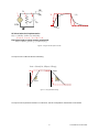
of discontinuity. For finer detail, it is better to consider smoothing functions, such as a spline transitions. Spline transitions
are easy to implement and will create a more natural output. See figures 1 and 2 for examples of different spline and
hyperbolic tangent transitions.
analog function real Icubefn;
input x; K; real x.K;
Icubefn = (x<=0) ? 1 : (x>=1) ? K : pow(K,(3-2*x)*x*x);
endfunction
Icubefn(x,100K)
sinefn(x)
cubefn(x)
analog function real cubefn;
input x; real x;
cubefn = (x<=0) ? 0 : (x>=1) ? 1 : (3 -2*x)*x*x;
endfunction
analog function real sinfn;
input x; real x;
sinefn = (x<=0) ? 0 : (x>=1) ? 1 : x-sin(`twopi*x)/`twopi;
endfunction
Figure 1 – Using Spline Transition Smoothing
8
PLATFORM APPLICATION NOTE
tanhc(x,0.5)
tanhc(x,1)
tanhc(x,-0.5)
tanhc(x,-1)
analog function real tanhc;
input x,c; real x,c;
tanhc = tanh( c==0? x : c>0?
x*(1+c/3*x*x) :
x*pow(1-c*x*x,-0.3333) );
endfunction
analog function real ftanhc;
input x,gain,ios,lo,hi,c; real x,gain,ios,lo,hi,c,dv;
begin
dv=(hi-lo)/2;
ftanhc = lo+dv*(1+tanhc(gain/dv*(x-ios),c));
end
endfunction
Figure 2 – Using Adjustable Hyperbolic Tangent Smoothing
It is important to limit the timestep and frequency where there are fast transitions (<1pS), or high pole frequencies (>1THz)
which will cause very tiny timesteps and long simulation times. Consider realistic rise and fall times (>1nS) and bandwidth
responses (<10MHz), which may help reduce the simulation time. It is possible that just one circuit block with a high
frequency oscillation can have a dramatic impact, pulling the whole simulation down. Timestep and breakpoint controls can
also be helpful improving the waveshaping accuracy. Both time and voltage tolerances can also be used to window-in
thresholds and avoid overstepping sharp nonlinearities. This is explained in detail in the Verilog-A user’s guide.
An example of timestep and breakpoint controls:
1.
Input threshold detection: @(cross(expression, direction, time_tolerance, voltage_tolerance)) statement;
2.
DC state & transient edge: @(above(expression, time_tolerance, voltage_tolerance)) statement;
3.
Output timestep control: @(timer(next_time)) statement; or $bound_step(time_increment);
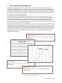
The modeling of a switch is a good example whether to use a sharp or smooth transition. When
a switch is ideal, it could cause trouble working correctly in all conditions. A good practice is to
include realistic effects for impedances and sweep characteristics. Table 1, below, shows some
of the tradeoffs.
RANGE OF SWITCH IMPEDANCE CHANGE
An ideal switch going from zero to infinite
15
Non-convergence
-6
Extreme max & min values (10 to 10 ohms)
+7
Reasonable values (10
SIMULATOR EFFECT
Numerical problems
to 1 ohm)
Efficient evaluation
-12
Simulator default (GMIN = 10 )
Roff <= 1012 ohms
Numerical limit: GMAX = GMIN * 1014
Ron >= 0.01 ohms
SWITCH SWEEP IMPEDANCE BETWEEN LEVELS
Step resistance change
Non-convergence
Linear transfer function (R vs. Vcontrol)
Center = Roff/2
Logarithmic or Log-Cubic function
Center = sqrt(Ron * Roff)
Table 1 – Switch Impedances vs. Simulator Effects
9
PLATFORM APPLICATION NOTE
4.2 Modeling Common Analog Effects
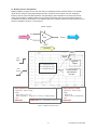
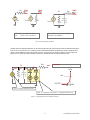
Modeling amplifiers are likely to be one of the most basic, but challenging models to add extra effects to. The amplifier
output can be as simple as a gain stage multiplying the input. Included can be input offsets, slew rate, small-signal
frequency response, input and output impedances, and signal clipping. Output impedances can be fine-tuned to track
closely real circuit effects. In addition, effects from power supply, temperature, and process can be added. Taking into
consideration accurate DC transfer effects, curve fitting the output from a clipped to hyperbolic tangent response may be of
interest, as explained in section 4.1 of this document.
power supply
In+
INPUT
Gain
OUTPUT
Output
InVREF
TRANSFER
Cubic
Clipped
Ideal
Digital
Ideal
Analog
A = `clip(40*Vin,-9,9);
B = fcube(40*Vin,-9,9);
C = ftanh(40*Vin,-9,9);
analog function real fcube;
input x,L,H; real x,L,H,arg;
begin
arg = x/(H-L) / 1.5 + 0.5;
fcube = (arg<0)? L : (arg>1)? H : L+( H-L)*( 3-2*arg)*arg*arg;
end
`define clip(x,L,H) min(H,max(L,x+(H+L)/2))
endfunction
Hyperbolic
Tangent
All three functions
output center for
input zero
analog function real ftanh;
input x,L,H; real x,L,H,dv;
begin
dv=(H-L) / 2;
ftanh = L+ dv*(1+ tanh(x/dv));
end
endfunction
Figure 3 – Amplifier DC Transfer Choices
10
PLATFORM APPLICATION NOTE
module Vhys(in,out);
input in; output out; electrical in,out;
parameter real K=40, Vos=0, Vhys=0.1;
parameter real Vol=-9, Voh=9;
real Vo,Offset;
Upward
`include “simple.fun”
path
Downward
analog begin
path
@(initial_step) Offset = Vio+Vhys;
Vo = fcube( K*(Vin-Offset), Vol, Voh)
Vio-Hys
Vio+Hys
if (Vo==Vol) Offset = Vio+abs(Vhys);
if (Vo==Voh) Offset = Vio-abs(Vhys);
V(out) <+ Vo;
end
endmodule
Figure xx – Modeling Hystersis
Figure 4 – Including Hysteresis
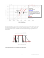
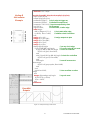
When passing the signal to the output of a model, it is almost always necessary to use a transition statement, which in some
cases makes it easier for the simulator to converge on a solution. The transition statement can work from a discrete digital
input and waveshape. The delay, rise, and fall times can be added, which will define the digital signal at the output in an
analog simulation.
Vout = $transition(Vin,Td,Tr,Tf);
Vout
Vin
Td
Tr
Td
Tf
Figure 5 – Using Transition Limiting
Transient output waveshaping can be done with RC and the Laplace transfer.
11
PLATFORM APPLICATION NOTE
1
V1/Ro
N
I(N)
2
3
Ro
V(N)
V1
V(N)
Co
RoCo
RC direct behavioral implementation:
I(N) <+ V(N)/Ro -V1/Ro +Co*ddt(V(N));
2
1
3
Equivalent Laplace voltage transfer relationship:
V(N) <+ laplace_zp( V1, {}, {-1/(Ro*Co),0} );
Figure 6 – Using RC and the Laplace Transfer
The output can be conditioned with slew rate limiting.
Vout = $slew(Vin, SRpos, SRneg);
Vin
Vout
SRpos
SRneg
Figure 7 – Using Slew Rate Limiting
The output can be expressed as resistance or conductance, and DC and impedance characteristics can be defined.
12
PLATFORM APPLICATION NOTE
Ro
I(out)
I(out)
V(out)
V(out)
Voc/Ro
Voc
Rac
N
I(out)
V(out)
Ro
Voc/Ro
If (Ro>1) I(out) <+ (V(out)-Voc)/Ro;
else
V(out) <+ Voc + I(out)*Ro;
Ro
Co
I(N) <+ (V(N) - Voc)/Ro + Co*ddt(V(N));
I(out,N) <+ V(out,N)/Rac;
Figure 8 – Modeling Output Impedances
Separate active and saturated resistance can aid in shaping the output. By using a ftanh() function as described can limit the
input current. An `fclip function can, as defined, produce well-defined diode-like voltage limiting, with zero voltage at isat. A
capacitor can be added for simple pole low-pass response. Limiting the current driving the capacitor can act as slew rate
limiting. The DC active region output resistance is Ro+Rac, and saturated and AC output resistance is Rac.
cur
N
res
R
Rac
cap
out
`define fclip(V,isat,dV) isat*exp(4.6*(V)/dV)
lim
fclip
isat
C
isat/100
-dV 0
V
I(cur) <+ ftanh(-Vnom/Ro,Isat,-Isat);
I(lim) <+ `fclip(V(lim)-Voh,Isat,0.1) - `fclip(Vo)V(lim),Isat,0.1);
Figure 9 – Using Separate Active and Saturated Resistance
13
PLATFORM APPLICATION NOTE
module simpleAmp(inp,inm,out);
input inp,inm;
output out;
electrical inp,inm,out,N,gnd;
branch (N,gnd) cur, res, cap, lim;
parameter real Gain=1k; // gain of amplifier
parameter real Vio=0; // input offset
parameter real Voh=5; // output high voltage
parameter real Vol=0; // output low voltage
parameter real GBW=10M; // gain bandwidth
parameter real SR=20M; // slew rate
parameter real Rdc=300; // output resistance DC
parameter Rac=100; // output resistance AC
real Ro, Co, Isat, Vnom; // establish internal variables used in expressions
`define fclip(V,isat,dV) isat*exp(4.6*(V)/dV) // define a parameterized expression
analog function real ftanh; // define a tanh function for output smoothing
input x,L,H; real x,L,H,dv;
begin
dv=(H-L) / 2;
ftanh = L+ dv*(1+ tanh(x/dv));
end
endfunction
analog begin
@(initial_step) begin // to establish initial fixed constants
Ro = Rdc-Rac;
Co = 1/(`M_TWO_PI*Ro*GBW/Gain);
Isat = Co*SR;
end
Vnom = Gain*(V(inp,inm)-Vio); // output voltage gain expression
V(gnd) <+ 0; // establish ground reference, actually not need with Verilog-A coding
I(cur) <+ ftanh(-Vnom/Ro,Isat,-Isat); // pass current using tanh smoothing function
I(res) <+ (V(res)-(Voh+Vol)/2)/Ro; // pass output current
I(cap) <+ ddt(Co*V(cap)); // pass current effects from output capacitance
I(lim) <+ `fclip(V(lim)-Voh,Isat,0.1) - `fclip(Vol-V(lim),Isat,0.1); // limit output swing
I(out,N) <+ V(out,N)/Rac; // add current from output impedance
end
endmodule
Figure 10 – Simple Amplifier Verilog-A Model
Resistor-dividers can be used to model the output impedance.
14
PLATFORM APPLICATION NOTE
Vcc
Vcc
General
Resistor
Topology
RH
Vo = Vee+(Vcc-Vee)
RH=Roh
Resistors for
High Output
Vo = Vcc
RL
RH+RL
RL=big
Vee
Vcc
RL
RH=big
Vee
Resistors for
Low Output
// Given relative output level of Kout = 0 to 1.
// Gx term allows additional current at midpoint.
Gx = Kout*(1-Kout)*Ipk/VpsNOM+1n;
I(VCC,Y) <+ V(VCC,Y)*(Kout/Roh+Gx);
I(Y,VEE) <+ V(Y,VEE)*(1-Kout)/Rol+Gx);
Vo = Vee
RL=Rol
Vee
Figure 11 – Using Resistor Dividers to Model Output Impedance
There are other effects that can also be modeled, such as additional enable control pins, input impedance and range
limitations, power supply current, parametric supply variations, response to common mode or supply interference, power-on
or off conditions, and warning messages to indicate invalid operating regions. There are many choices as far as specialized
effects to model. But, with complexity, there are tradeoffs. For example, output impedances modeled in a nonlinear fashion
may decrease simulation efficiency. This may also involve more time to develop, extract parameters, and simulate. One
must decide what level of modeling is needed and what is not important. If necessary, you can create both simple and
complex models.
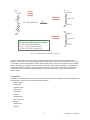
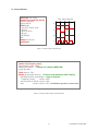
4.4 Modelwriter
Modelwriter is a model utility that is menu driven and allows ready use of a generic model that can be parameterized, placed
in the schematic, and used. There are 11 Cadence library categories:
• Analog Models
• Components
• Continuous Time
• Discrete Time
• Instruments
• Interface
• OpAmp Models
• PLL Components
• Sources
• System Level
• Telecom
15
PLATFORM APPLICATION NOTE
Figure 12 – Modelwriter™ User Menus and Automatically Created Verilog-A Model
5
VERILOG-D LANGUAGE OVERVIEW
Verilog-D is an event-driven language that supports behavioral as well as structural modeling. It is interrupted and runs with
the simulator or Incisive-AMS. The digital simulator evaluates all events in the current time. Some events can be schedule
additional events at the current or a future time. The simulator timesteps continue until all events are complete. The
language contains only the concept of going forward, and multiple events can occur at the same timepoint.
16
PLATFORM APPLICATION NOTE
Symbol
DFF1
Data
Q
Clock
Qb
Reset
Description
Initially, set Q to Q initial.
At each Clock positive edge,
if Reset is not high,
then set Q to Data.
At each Reset positive edge,
set Q low.
Qb is always the inverse of Q.
Actual Verilog-D Code
module DFF1 (Q,Qb,Data,Clock,Reset);
output Q,Qb; input Data,Clock,Reset; // signals assume single-bit
parameter Qinit = 0;
// digital default
reg Q;
// a `reg’ is a 1-bit variable
initial Q=Qinit;
// initial section evaluates just once
always @(posedge(Clock)) // Always is a loop that runs constantly:
if (!Reset) Q=Data;
// wait for positive clock edge, then
// if the Reset signal isn’t high, set
// register Q to equal the Data input.
always @(posedge(Reset)) Q=1’b0; // wait for positive edge of Reset,
// then set Q to equal zero (1-bit bin)
assign Qb = ~Q;
// define Qb to be a logical inversion of
endmodule
// Q . Qb updates whenever Q changes.
Figure 13 – Modeling a Data Flip-Flop with Verilog-D
5.4 Common Language Constructs and Statements
Verilog-D carries common language constructs, primary module statements, and event-driven constructs. Table 3, below,
lists a sample of the most common.
Verilog-D Constructs
Definitions
`timescale 1ns / 10ps
Defines time units (1nS0 and minimum digital timestep (10pS)
parameter n=2, y=2.0;
Defines an integer (2) and a real parameter (2.0) denoted by decimal place
reg A, B;
A reg is a 1-bit digital variable
C=1’bx; D=4’b1001;
Binary value specification format
reg[0:15] X[0:1023];
Declare a 1K by 16bit memory
Primary Statements
Initial begin … end
Executed only once at the beginning of the simulation, multiples run concurrently
Always begin …end
Executed repeatedly throughout the simulation, multiples run concurrently
Assign P = <expression>
Assigns a definition to an output pin with known registers, can’t be assigned to other
Event-Driven Constructs
#2.1
@(event)
@(posedge a or negedge b)
@(a or b)
wait(a & b)
Time delay before continuing (in `timescale units)
Occurs only on the event
Wait until the specified edge of either signal
Wait until either single changes
Wait until the expression becomes true
Table 3 – Example of Common Verilog-D Constructs
17
PLATFORM APPLICATION NOTE
5.5 Verilog-D Examples
`timescale 1ns / 10ps;
module Test_Input (a,b,sel,ck);
output a,b,sel,ck;
reg a,b,sel,ck;
initial begin
a=0; b=1; sel=0; ck=0;
#5 b=0;
#5 b=1; sel=1;
#5 a=1;
#5 $finish;
end
always #3 ck=~ck;
endmodule
Test_Input Outputs
a
b
se
c
0
5
10
15
20
Figure 14 – Example of Basic Verilog-D Module
module counter4
(result, clock, asynch_reset);
input asynch_reset, clock;
output [3:0] result; // Output is a 4-bit bus (MSB:LSB)
reg [3:0] result;
initial result = 1'b0;
always @ (posedge clock or // Execute code whenever either leading
posedge asynch_reset) begin // edge is detected.
if (asynch_reset)
result = 1'b0;
else if (result == 4'd15) result = 1'b0;
else
result = result + 1'b1; // Arithmetic operation on bus value
Figure 15 – Example of Basic Verilog-D Counter Expressions
18
PLATFORM APPLICATION NOTE
`timescale 1ns / 100ps
Verilog-D
4-bit counter
Example
module Count4bit_d(up,dn,ck,res,q0,q1,q2,q3,ov);
input up,dn,ck,res;
output q0,q1,q2,q3,ov;
parameter Edge=1; // clock edge to trigger on
parameter Kinit=0; // initial/reset output level
parameter Td=1.0e-9; // input-to-output delay time
reg [3:0] q;
// 4-bit output
reg Kov,ckHi;
// overflow bit, ck after edge
initial begin
ckHi = (Edge==1)? 1:0;
// clock state after edge
q = Kinit; Kov = !ckHi;
// initialize clock & overflow
end
assign q0 = q&1;
// assign outputs to pins
assign q1 = (q>>1)&1;
assign q2 = (q>>2)&1;
assign q3 = q>>3;
assign ov = Kov;
always @(ck) begin
// on any clock edge,
if (ck==ckHi && !res) begin
// if correct edge & not reset:
if (q==15 && up && !dn) begin // check for overflow
#(Td/1.e-9) q=0; Kov=ckHi;
end
else if (q==0 && !up && dn) begin // check for underflow
#(Td/1.e-9) q=15; Kov=ckHi;
end
else begin
// normal increment or
decrement
#(Td/1.e-9) q=q+up-dn; Kov=!ckHi;
end
end
else Kov=!ckHi;
// clear overflow on other
edge
end
always @(posedge res) begin
// asynch reset
#(Td/1.e-9) q = Kinit;
Kov = !ckHi;
end
endmodule
Count4bit
Outputs
Figure 16 – Example of Verilog-D 4-Bit Counter
19
PLATFORM APPLICATION NOTE
6
VERILOG-AMS LANGUAGE OVERVIEW
The Verilog-AMS language is a combination of both Verilog-D and Verilog-A statements that run in Incisive-AMS. There are
two types of domains in Verilog-AMS: Discrete and Continuous. Discrete is for digital circuits, and continuous is reserved for
analog circuits. The two domains are partitioned and co-simulated with their respective solver. Interface Elements (IEs) are
automatically placed between analog and digital blocks when simulated. All analog and mixed-signal modules require that
ports and nodes associated with respective behavioral code have disciplines declared for them. See example below.
In general, digital behavior is defined in
the initial or always blocks, and analog
in a single analog block. There can be
only one analog block, but many digital
blocks. Continuous time signals can
only be written from within the analog
block, and discrete time signals are
written outside the analog block.
Analog variables can appear in digital
expressions and digital variables can
be used in analog expressions.
Mixed-signal models are not just
Verilog-D and Verilog-A. They are
combined into one model. This can
result in design free interface elements
(IEs) which are more closely controlled
within the model. Mixed-signal blocks
can be all behavioral, all structural, or
any combination. The full capabilities
of both Verilog-D and Verilog-A can be
realized using Incisive-AMS. The
digital and analog sections interact by
sharing data and controlling each
other’s events. This allows for event
driven analog blocks. Verilog-D can
extend to support real value nets,
which are called wreal.
module verilog-ams_example (a,b,c,d); // module name / pins
input a,b,c; // port declarations
output d;
electrical a,b,d,e; // analog discipline
logic c; // digital wire type
parameter load = 100 from (0:1k); // analog parameter
real x; //variable declarations
ground b; // digital global ground node
resistor #(.r(load)) rout(e,d); // structural description
initial begin // initialize variable to something other than “0”
x=1;
end
always @(posedge(c)) begin // digital behavior block
x=(x<12 ? x+1 : 1); // digital event
end
analog begin // analog behavior block
@(cross(V(a) -2.5, 1)) // analog event
V(e) <+ (V(a) - V(b)) * x; // mixed signal interaction
end
endmodule // end of model declaration
20
PLATFORM APPLICATION NOTE
module F2V_ams (In,Out);
input In; logic In; output Out; wreal Out;
parameter real Vnom=1, Fnom=1M;
real Tup,Tdn, Freq;
Freq (digital)
All-digital model
Wreal output
No effect on analog
portion of the simulation
initial begin
Tup=0; Tdn=0; Freq=Fnom;
end
always @(posedge In) begin
if (Tup>0) Freq = 1/($abstime-Tup);
Tup=$abstime;
end
always @(negedge In) begin
if (Tdn>0) Freq = 1/($abstime-Tdn);
Tdn=$abstime;
end
assign Out = Freq*Vnom/Fnom;
endmodule
On leading edge of digital signal ...
Or on trailing edge ...
Out pin is real value following Freq value.
Figure 17 – Using Wreal to Create an Analog Effect in the Digital Domain
VIN
Figure 18 – Using Wreal to Do a Frequency-to-Voltage Conversion
With Incisive-AMS there is a closer connection between the analog and digital solver. In the past, the interprocess
communication (IPC) with Verimix™ was slower and limited.
21
PLATFORM APPLICATION NOTE
7
8
AVAILABLE CADENCE ONLINE DOCUMENTATION
• Cadence Verilog-AMS Language Reference
Analog and Mixed-Signal constructs
• Cadence Verilog-A Language Reference
Verilog-A language for Spectre
• Cadence AMS Simulator User Guide
Operation of AMS Simulator
• Cadence AMS Environment User Guide
Using AMS from DFII
• Verilog-XL Reference
Verilog-D language
• Cadence NC-Verilog Simulator Help
NC-Verilog language limitation and enhancements
• Cadence NC-Verilog Simulator Tutorial
Tutorial on NC environment
REFERENCES
[1] Ron Vogelsong. AMS Behavioral Modeling Workshop, Cadence User’s Group Meeting, 2002.
[2] Analog Modeling with Verilog-A, Training Manual 4.4.6, Cadence Educational Services, 2001
[3] Dan Fitzpatrick, et al. Analog Behavioral Modeling with the Verilog-A Language, Kluwer, 1998.
© 2003 Cadence Design Systems, Inc. All rights reserved.
Cadence and the Cadence logo are registered trademarks
of Cadence Design Systems, Inc. All others are properties
of their respective holders.
22
PLATFORM APPLICATION NOTE