1
Interfacing neural network chips
with a personal computer
master thesis of J.J.M. van Teeffelen
supervisor: prof.dr.ir. W.M.G. van Bokhoven
coach: ddr. J.A. Hegt
period: January - August 1993
Eindhoven University of Technology
Faculty of Electrical Engineering,
Electronic Circuit Design Group
August 1993
Eindhoven University of Technology accepts no responsibility for the contents of theses
and reports written by students.
Abstract
The research in the field of neural networks is no longer restricted to theoretical analysis
or simulation of these networks on serial computers. More and more networks are
implemented on chips, which is of crucial importance if full advantage of the neural
networks is wished to be taken when using them in real time applications like speech
processing or character recognition.
The Electronic Circuit Design Group at the Eindhoven University of Technology currently
is implementing several neural networks with a multi-layered perceptron architecture
together with their learning algorithms on VLSI chips. In order to test these chips and to
use them in an application they will be connected with a personal computer with help of
an interface.
This interface, that has to be as versatile as possible, meaning that it must be able to
connect all kinds of neural network chips to it, can be realized either by making use of
commercially available interfaces or by designing an own interface with help of off-theshelf components. Two interfaces will be discussed, one for the rather slow AT-bus and
one for the high speed VFSA local bus.
Although the commercially available interfaces are not as versatile as wished, and the
prices may seem rather high, they turn out to be the best way to realize the interface at
the moment. They are guaranteed to work and can be used immediately. The discussed
interfaces for the AT-bus and the VFSA local bus still have to be tested and implemented
on a printed circuit board.
i
Contents
List of figures
5
1 Introduction
7
2 Introduction to neural networks
2.1 Basic model of a neuron
2.2 Multi-layered perceptrons . . . . . . . . . . . . . . . . . . . . . . . . . . . . . . . . . . . . . ..
2.3 Back-propagation
2.4 Weight perturbation
9
9
11
12
14
3 Specifications for a neural network interface
3.1 Existing hardware implementations
3.1.1 Architecture of the network
3.1.2 Kind of implementation
3.1.3 Processing speed. . . . . . . . . . . . . . . . . . . . . . . . . . . . . . . . . . . . . ..
3.1.4 Training algorithms. . . . . . . . . . . . . . . . . . . . . . . . . . . . . . . . . . . ..
3.1.5 The Intel80170NX Electrically Trainable Neural Network Chip ..
3.2 Chips under development .. '.' . . . . . . . . . . . . . . . . . . . . . . . . . . . . . . . . . ..
3.3 Specifications for neural interface . . . . . . . . . . . . . . . . . . . . . . . . . . . . . . . ..
15
15
15
16
17
17
18
19
20
4 The personal computer . . . . . . . . . . . . . . . . . . . . . . . . . . . . . . . . . . . . . . . . . . . . . . ..
4.1 Memory organization
4.1.1 Main memory
. . . . . . . . . . . . . ..
4.1.2 Shadow RAM
4.1.3 Cache memory
4.1.4 I/O
4.2 The AT-Bus . . . . . . . . . . . . . . . . . . . . . . . . . . . . . . . . . . . . . . . . . . . . . . . . ..
4.2.1 Introduction
4.2.2 AT-bus signals
4.2.3 AT-bus timing . . . . . . . . . . . . . . . . . . . . . . . . . . . . . . . . . . . . . . . ..
23
23
23
24
25
25
26
26
26
29
1
Contents
4.3 The Vesa local bus
4.3.1 Introd.uction
4.3.2 VL-bus signals. . . . . . . . . . . . . . . . . . . . . . . . . . . . . . . . . . . . . . . ..
4.3.3 VL-bus timing . . . . . . . . . . . . . . . . . . . . . . . . . . . . . . . . . . . . . . . ..
4.3.4 IX Characteristics
4.4 Software aspects
30
30
31
34
35
36
5 Design of an interface
37
5.1 General survey
37
5.1.1 General scheme of interface
37
5.1.2 Commercially available interfaces. . . . . . . . . . . . . . . . . . . . . . . . .. 40
. . . . . . . . . . . . . . . . . . . . . .. 41
5.1.3 Design of a board
5.2 Analog I/O
43
5.2.1 Analog to digital conversion
, 43
5.2.2 Digital to analog conversion
, 47
50
5.2.3 Analog I/O circuit
5.3 Interface to the AT-bus
. . . . . . . . . . . . . . . . . . . . . .. 51
5.3.1 Digital 1/0
51
5.3.2 Bus interface circuit. . . . . . . . . . . . . . . . . . . . . . . . . . . . . . . . . . . .. 52
5.3.3 speed of the neural interface . . . . . . . .
, 54
5.4 Interface to the VL-bus
56
5.4.1 Digital 1/0
56
5.4.2 Bus interface circuit . . . . . . . . . . . . . . . . . . . . . . . . . . . . . . . . . . . .. 56
5.4.3 Speed of the neural interface
58
5.5 Realization of a printed circuit board
, 60
5.5.1 Analog I/O PCB . . . . . . . . . . . . . . . . . . . . . . . . . . . . . . . . . . . . . .. 60
5.5.2 At-bus interface PCB . . . . . . . . . . . . . . . . . . . . . . . . . . . . . . . . . . .. 61
5.5.3 VL-bus interface PCB
61
5.6 Costs of the neural interface . . . . . . . . . . . . . . . . . . . . . . . . . . . . . . . . . . . .. 62
5.7 Software for the neural interface . . . . . . . . . . . . . . . . . . . . . . . . . . . . . . . . .. 63
5.7.1 Data formats
. . . . . . . . . . . . . . . . . . . . . .. 63
5.7.2 Basic input and output routines . . . . . . . . . . . . . . . . . . . . . . . . . .. 64
5.7.3 Example: Back-propagation program
66
6 Conclusions . . . . . . . . . . . . . . . . . . . . . . . . . . . . . . . . . . . . . . . . . . . . . . . . . . . . . . . ..
69
7 Recommendations . . . . . . . . . . . . . . . . . . . . . . . . . . . . . . . . . . . . . . . . . . . . . . . . . . ..
71
2
Contents
Bibliography
73
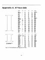
Appendix A. AT-bus data
"
77
Appendix B. VL-bus data
83
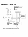
Appendix C. Design data
89
Appendix D. Software . . . . . . . . . . . . . . . . . . . . . . . . . . . . . . . . . . . . . . . . . . . . . . . . .. 101
3
List of figures
Fig. 2.1: Basic model of a neuron . . . . . . . . . . . . . . . . . . . . . . . . . . . . . . . . . . . . . . . . . ..
Fig. 2.2: Sigmoid function f~(h) . . . . . . . . . . . . . . . . . . . . . . . . . . . . . . . . . . . . . . . . . . ..
Fig. 2.3: A two-layer perceptron . . . . . . . . . . . . . . . . . . . . . . . . . . . . . . . . . . . . . . . . . ..
Fig. 4.1: Memory of original PC . . . . . . . . . . . . . . . . . . . . . . . . . . . . . . . . . . . . . . . . . ..
Fig. 4.2: VL-bus architecture. . . . . . . . . . . . . . . . . . . . . . . . . . . . . . . . . . . . . . . . . . . . ..
Fig. 4.3: General VL-bus timing
Fig. 5.1: Scheme neural network system
Fig. 5.2: General scheme neural interface . . . . . . . . . . . . . . . . . . . . . . . . . . . . . . . . . . ..
Fig. 5.3: Scheme designed neural interface . . . . . . . . . . . . . . . . . . . . . . . . . . . . . . . . . ..
Fig. 5.4: Direct AID conversion . . . . . . . . . . . . . . . . . . . . . . . . . . . . . . . . . . . . . . . . . ..
Fig. 5.5: Multiplexed AID conversion . . . . . . . . . . . . . . . . . . . . . . . . . . . . . . . . . . . . ..
Fig. 5.6: 16-channel analog input circuit. . . . . . . . . . . . . . . . . . . . . . . . . . . . . . . . . . . ..
Fig. 5.7: Timing requirements for AID circuit . . . . . . . . . . . . . . . . . . . . . . . . . . . . . . ..
Fig. 5.8: Data formats AID circuit .. . . . . . . . . . . . . . . . . . . . . . . . . . . . . . . . . . . . . . ..
Fig. 5.9: Direct D I A conversion .. . . . . . . . . . . . . . . . . . . . . . . . . . . . . . . . . . . . . . . . ..
Fig. 5.10: Multiplexed D I A conversion
Fig. 5.11: Four analog output channels
Fig. 5.12: Timing requirements for D I A circuit . . . . . . . . . . . . . . . . . . . . . . . . . . . . . ..
Fig. 5.13: Data formats D I A circuit
. . . . . . . . . . . . . . . . . . . . . . . . . . . . . . . . . . . ..
Fig. 5.14: Input and output latch
Fig. 5.15: Control of VL-bus cycle length . . . . . . . . . . . . . . . . . . . . . . . . . . . . . . . . . . ..
Fig. 5.16: VL-bus cycle length timing. . . . . . . . . . . . . . . . . . . . . . . . . . . . . . . . . . . . . ..
Fig. 5.17: Imaginary neural network system
Fig. A.1: Pin identification and signals of AT-bus
Fig. A.2: 8-bit lOx zero waitstate cycle . . . . . . . . . . . . . . . . . . . . . . . . . . . . . . . . . . . . ..
Fig. A.3: 16-bit lOx standard cycle. . . . . . . . . . . . . . . . . . . . . . . . . . . . . . . . . . . . . . . ..
Fig. A.4: 16-bit lOx ready cycle
Fig. A.5: 16-bit MEMx zero waitstate cycle
Fig. A.6: 16-bit MEMx standard cycle
Fig. A.7: 16-bit MEMx ready cycle . . . . . . . . . . . . . . . . . . . . . . . . . . . . . . . . . . . . . . . ..
Fig. A.8: Physical layout ISA-bus board. . . . . . . . . . . . . . . . . . . . . . . . . . . . . . . . . . . ..
Fig. B.l: Pin identification and signals of VL-bus
Fig. B.2: Physical layout VL-bus board
Fig. B.3: VL-bus read/write timing
Fig. B.4: VL-bus reset timing
5
9
10
11
23
31
34
37
38
42
43
43
44
46
46
47
47
49
49
50
51
57
57
66
77
78
78
79
79
80
80
81
83
84
85
86
List of figures
Fig. B.5: Timing relative to LCLK . . . . . . . . . . . . . . . . . . . . . . . . . . . . . . . . . . . . . . . . ..
Fig. C.l: Overview TMS32OC30 digital signal processor board
Fig. C.2: Overview Intel's ETANN chip. . . . . . . . . . . . . . . . . . . . . . . . . . . . . . . . . . . ..
Fig. C.3: Scheme analog I/O circuit. . . . . . . . . . . . . . . . . . . . . . . . . . . . . . . . . . . . . . ..
Fig. C.4: AT-bus interface circuit
Fig. C.S: Timing AT-bus interface circuit . . . . . . . . . . . . . . . . . . . . . . . . . . . . . . . . . . ..
Fig. C.6: VL-bus interface circuit
Fig. C.7: Timing VL-bus interface circuit .. . . . . . . . . . . . . . . . . . . . . . . . . . . . . . . . . ..
6
86
89
90
93
95
96
98
99
1 Introduction
The functioning of the brain has occupied mankind for centuries. There has been a lot of
research to gain more insight in the processes that are taking place in our brain. The
densely interconnected nerve cells present in our brain can perform difficult tasks like
speech recognition and processing visual information much better than the most
advanced computers. Artificial neural networks, simplified models of these nerve cells,
are a better alternative than traditional computers with their sequential execution of
instructions when tackling problems of which the exact solution is not known or the
mathematical description of the solution is very complicated and difficult to implement
on a computer.
The brain has several features that are desired to be present in artificial neural networks.
It is robust and fault tolerant. The death of nerve cells does not decrease the performance
significantly. It is flexible, capable of adapting to new situations by learning, in contrast to
a computer that has to be reprogrammed in such a case. It can deal with fuzzy,
probabilistic, noisy or inconsistent information. It works in a highly parallel manner and
it is small, compact and dissipates very little power.
The history of neural networks started in 1943 when a simple model of a neuron as a
binary threshold unit was proposed by McCulloch and Pitts. These threshold networks
were the main subject of research for the next 15 years. Around 1960 the research
concentrated on networks called perceptrons that were investigated by the group of
Rosenblatt. In these networks, the neurons were organized in a layer with feed forward
connections from the inputs to that layer.
The fact that some elementary computations could not be done with a one-layer
perceptron, and there was no learning algorithm to determine the weights in a
multi-layered perceptron so that it could perform a given computation simmered the
research of these networks for about 20 years. Still people kept working on the
development of learning algorithms and the invention of the back propagation algorithm,
first by Werbos in 1974 and then independently rediscovered by Parker in 1985 and
Rumelhart, Hinton and Williams in 1986, revived the interest for the perceptron networks.
7
Introduction
Almost everything in the field of neural computation has been done by simulating the
networks on serial computers, or by theoretical analysis. The implementation of neural
networks on VISI chips has been staying behind for years, mainly because of technology
reasons. Current research however is also focused on the implementation of several
networks on chips. Efficient hardware is crucially important if the full advantage of the
neural networks is wished to be taken when using them in real time applications like
speech processing or character recognition.
The Electronic Circuit Design Group at the Eindhoven University of Technology is
implementing several neural networks with a multi-layered perceptron architecture
together with their learning algorithms on VISI chips. To test the realized chips and to
use them in an application they will be connected to a personal computer. In this thesis
the design of an interface that is needed to accomplish this will be treated. This interface
has to be as versatile as possible. It must be able to interface several different chips with a
personal computer without having many changes to be made to the interface.
The design of such an interface will be treated later on in this thesis. First a short
introduction into the perceptron networks together with their training algorithms will be
given. Then the specifications of the interface will be formulated by investigating some
existing hardware implementations of neural networks. On the basis of these
specifications and a description of the personal computer the design of the interface will
be treated.
8
2 Introduction to neural networks
2.1 Basic model of a neuron
The brain is composed of about 1011 neurons of different types. These neurons are
interconnected with tree-like networks of nerve fiber. Signals are transported from one
neuron to another through the axon, a single long fiber, which eventually branches into
strands that are connected to the synapses of other neurons. H the signals that are
received by the synapses reach a certain level, the neuron is activated and transmits a
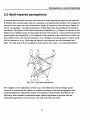
signal along its axon. In figure 2.1 a model of a neuron is shown as it is used in the
artificial networks.
Xl
X
N
Fig. 2.1: Basic model of a neuron
The neuron computes the weighted sum of the inputs Xi' which can be binary or
continuous-valued, and outputs a signal y according to a certain transfer function f:
(2.1)
with 8 a certain bias. This bias can also be modeled as an input Xo with value -1 and
connected to the neuron with a connection strength W o equal to 8. The output of the
neuron than equals:
(2.2)
9
Introduction to neural networks
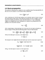
An often used transfer function is the sigmoid function which is defined as:
(2.3)
with Il the steepness parameter. In figure 2.2 an example is given of this sigmoid function
with three different values for the parameter Il (Ill > ~ > Pa ).
'eCh)
h
Fig. 2.2: Sigmoid function fJl(h)
There are two ways to learn the network (change the weights w) to perform a certain
task:
... Supervised learning. In this case the learning is done on the basis of a comparison of the
output of the network with known correct answers.
... Unsupervised learning. In this case the network is expected to form output classes
without additional information about the correct classes.
After the training phase is completed, the network will be able to generalize to new
situations. It then can produce correct outputs for inputs it has never seen before. At least,
this is the purpose of the training phase. The topology of the network and the number of
training iterations that are needed to learn a network will be related to the application it
is used in. Next a particular architecture, the multi-layered feed forward networks, also
known as multi-layered perceptrons, together with some training algorithms will be
described.
10
Introduction to neural networks
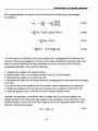
2.2 Multi-layered perceptrons
In layered feed-forward networks, also known as multi-layered perceptrons, the network
is divided into several layers that are connected in a feed-forward manner. The outputs of
neurons in one layer are only connected to inputs of neurons in the next layer. Figure 2.3
shows an example, a two-layer perceptron. In this figure also the notational conventions
are shown. The inputs of the neural network are denoted by ~. Outputs of neurons in the
hidden layer (hidden layers are the layers between the inputs of a neural network and the
output layer) are denoted by vj• The outputs of the neurons in the second layer which are
the outputs of the network are referred to as Yk. Weights connecting layer i to layer j (kj)
will be referred to as w~. Note that the inputs of the network are not considered as a
layer. The bias factors 9 are modeled as extra inputs with value -1 as mentioned before.
-1 x1 Xi
XI
Fig. 2.3: A two-layer perceptron
The weights can be updated in several ways. The Electronic Circuit Design group
currently is examining the update of weights according to the back-propagation and
weight perturbation algorithms. These two methods will be briefly described in the
following. More detailed information about update algorithms in general and the
mentioned algorithms can be found in [2], [11], [14], [16], and [18].
11
Introduction to neural networks
2.3 Back-propagation
One method to determine new weights is to use a gradient descent learning algorithm. In
this case an error measure or cost function E[w] is defined by:
(2.4)
with Jl indicating one of the M input patterns, dkl' the desired. output of neuron k and ykl'
the actual output of that neuron. Given this error function, the set of weights w can be
improved by sliding downhill the surface that E[w] defines in w space. Specifically,
weight wlcj is changed once every M patterns by an amount Awlcj proportional to the
gradient of E at the present location:
(2.5)
with Tl representing a certain learning rate. In the case of the two-layer perceptron as
shown in figure 2.3 this yields the following results. The error E[w] becomes:
(2.6)
with hi" the total input to neuron j in the hidden layer:
hi = l:wjiXi
(2.7)
I
The change for the weights between the hidden layer and the output layer is given by:
(2.8a)
(2.8b)
with gkl' the total input to neuron k in the output layer:
g: .~wkjf(hi)
J
12
(2.9)
Introduction to neural networks
The weights between the inputs of the network and the hidden layer are changed
according to:
dE
dEdV:
Aw..}t = -11dw = -11~-=--~
L ':l-Il ::l..••
Ilk
ji
(210a)
UClk uWji
(210b)
(21Oc)
(21Od)
As can be seen in (2.1Od) the error of the output layer is propagated back through the
network. This back-propagation of errors can be easily extended for networks with more
than two layers following the same procedure as in (2.6), (2.8) and (2.10). The backpropagation algorithm now does the following:
1. initialize the weights with random values;
and desired output vector d.t to the network;
3. determine the output Yk)1, and the error a.,1l;
4. determine the deltas for the hidden layers by propagating the error backward according
to (2.1Od);
5. go back to step 2 and repeat for the next pattern until all M patterns are presented;
6. update the weights of the network by an amount Aw according to (2.8) and (210);
7. repeat by going to step 2 until the error has reached a desired value.
2. present input vector
'Xjll
Although the algorithm is described with an update rate of once per M patters, the
update usually is done after each input pattern. The calculation of the derivative of the
transfer function f, turns out to be very Simple in case of the sigmoid function (3). The
derivative then namely equals:
f' (h) = 2J3f(l-f)
13
(2.11)
Introduction to neural networks
2.4 Weight perturbation
Another method to update the weights of a network is weight perturbation. This also is a
gradient descent method, only here the gradient is not calculated but approximated. By
disturbing a weight wji with a small perturbation pert; and using the forward difference
method the weight update aWji is given by:
aw. • -11
E(wj.+pert ..)- E(w ..)
'
}t
p
pert}I..
}I
(2.11)
The error E usually is the mean square error according to (4). When a better
approximation is desired, the central difference method can be used resulting in an
update aWji equal to:
(2.12)
The update of the weights is done in the following way (when using the forward
difference method):
1. initialize the weights with small random values;
2. present input pattern and determine the output error E[wji];
3. disturb weight wji by an amount pertp;
4. present the same input pattern again and determine E[wji+pertji];
5. update weight wji according to (10);
6. repeat by going to step 2 until the error has reached a desired value.
As in the case of the back propagation algorithm the error E can also be determined after
M input patterns, instead of after each pattern as is done in the given procedure.
14
3 Specifications for a neural network
interface
The implementation of neural networks in hardware has been staying behind for years,
mainly because of technological constraints. Yet, if these networks are wanted to be used
in real applications like processing visual information, it is a prerequisite to implement
them in hardware. Optimum benefit can only be acquired when data actually is processed
in a highly parallel way, and this again can only be done efficiently in hardware.
Although this field of research still is in a beginning phase, more and more chips
exhibiting desired features in a neural network are becoming available. To be able to state
requirements for an interface, some chips that were connected to a computer in some way
(not necessarily a personal computer), have been examined in literature. The features of
these chips form, together with a short description of the chips that are being developed
by the Electronic Circuit Design Group the basis for the specifications of the interface.
3.1 Existing hardware implementations
The following aspects are of importance when looking at hardware implementations:
1. architecture of the network;
2. kind of implementation;
3. processing speed;
4. training of the network.
These aspects will be clarified in the following.
3.1.1 Architectu re of the network
The topology of multi-layered perceptron chips can be:
1. fixed. In this case a fixed network architecture, e.g. a single layer perceptron, is
implemented on a chip. Extension of the network may be possible by interconnecting
several chips. Examples of these networks can be found in [7], [12], [13], and [22].
2: reconfigurable. In this case a number of basic neurons with a certain number of inputs
and synapses is implemented on the chip. The topology of the network on this chip can
15
Specifications for a neural network interface
be altered by the user e.g. by changing the contents of some registers ([9], [21], [24], [25],
and [33]). Extension of the network to a larger one may also be possible by
interconnecting several chips.
The number of neurons and weights that are present on the chip differs in each
implementation. In [21] only one neuron is present on the chip, while in [33] 288 neurons
can be found. The number of synaptic weights in the examined chips differs from 1024
([20» to 262144 ([9]).
3.1.2 Kind of implementation
The kind of implementation can be:
1. digital. All signals are digital in this case (see [6], [20], [21] and [33]). Data enters and
leaves the chip through a digital bus, is processed by digital components on the chip and
the chip is controlled. with digital control lines.
2. analog. All signals, besides a few digital control lines, are analog <Current or voltage) in
this case ([2], [4], [12], [13], [22], [23], [25]). Data is processed in an analog way on the
chip by analog components, e.g. analog multipliers. The weights are usually stored in offchip RAM and special circuitry is needed to refresh the on-ehip weights. All chips that
are being developed by the Electronic Circuit Design Group fall into this category.
3. mixed digital-analog. In this case data is processed both in a digital and an analog way
([7], [24]). Inputs and outputs of the chip, as well as the control lines, usually are digital.
Data enters the chip via shift registers. Only inside the chip operations are done in an
analog way, e.g. the multiplication of the inputs with the weights is performed with
analog multipliers.
4. optical. Data can also be processed using optical signals. However, because of the
completely different nature of these signals, chips using them will be left out of
consideration.
The resolution of the weights and the neurons is problem dependant. Variations between
1 bit and 16 bit are encountered. in the mentioned articles.
16
Specifications for a neural network Interface
3.1.3 Processing speed
Speed. is an important aspect in the neural net chips. Processing of data during normal
operation and updating weights in the learning phase should be done as fast as possible.
The speed of the digital chips mainly is determined by the clock frequency at which the
chips operate (e.g. 15 MHz in [21]). In analog chips the settling times of the various
components determine the speed (the chip in [12], [13] and [22] for example has a
maximum processing delay of 3}lS per layer in normal operating mode).
3.1.4 Training algorithms
The training algorithm can either be:
1. implemented on the chip;
2. run on a host computer.
The first option places great demands on the hardware, but results in faster training of
the network (an example can be found in [33]). The second option on the other hand
requires number crunching computers. Training with a host computer can be done in the
following ways:
1. chip in loop training. After presenting inputs to the chip, new weights are calculated
on the host computer and changed on the chip, on the basis of the outputs that are
generated by the chip (see e.g. [12], [13], [22], and [25]) . This kind of training is
preferable since the neural net chip processes data much faster than a general purpose
computer. Only when the weights of the network can be changed difficultly (meaning it
takes too much time to change them), the next method will be chosen.
2. simulation on host. In this case the complete network is simulated on the host
computer in the training phase (e.g. [9]). When the training is completed, the weights are
loaded on the chip that resumes operation in normal mode.
3. a combination of the methods 1. and 2. First the weights of the network are determined
by simulating the complete network on the host computer. Then a sort of fine-tuning is
performed by executing a few chip in loop training iterations.
17
Specifications for a neural network interface
3.1.5 The Intel 80170NX Electrically Trainable Neural Network
Chip
One chip that is especially interesting, since it is commercially available, is the Intel
80170NX Electrically Trainable Neural Network chip ([12], [13], and [22]). The features of
this chip are already roughly mentioned in the foregoing (paragraphs 3.1.1. to 3.1.4). In
figure C.2 (Appendix C) a general overview of this chip is shown. Here, also more precise
data on some signals can be found.
The chip contains 64 neurons and 10,240 individually addressable synapses with on-ehip
storage of weights in EEPROM. A maximum of 128 inputs can be led to the 64 neurons in
a feedback mode (64 inputs at a time). The gain of the sigmoids can be controlled
externally (with the V GAIN signal). The sigmoids can also be used as a comparator for 0 V
or 5 V output (ITL-eompatible operating mode). High programming voltages are needed
to change the weights on the chip. The maximum processing delay of the chip is 3J1s.
Since the Electronic Circuit Design Group does not have any neural networks
implemented in hardware at its disposal at the moment, an interface that will be used to
control future chips must also be able to control the Intel80170NX so it will be possible to
test the interface. This, however does not mean that all features of this chip must be used
by the interface.
18
Specifications for a neural network Interface
3.2 Chips under development
The Electronic Circuit Design Group currently is developing two neural net chip-sets. The
first one is a chip-set, with the neurons and synapses implemented on different chips. The
back-propagation algorithm, explained in paragraph 2.3, is implemented on-ehip, meaning
that a backward path will be present on the chip that can propagate the errors of the
outputlayer back through the chip. The errors will be calculated by the host computer.
The exact specifications of this chip-set are not known at the time being. All that is certain
is that the chips are completely analog. The neuron chips will have a certain number of
analog (pulsed-eurrent) inputs and analog outputs, and the synapse chips will contain a
certain number of analog weights that cannot be addressed individually. A complete
neural network can be made by interconnecting several chips. The processing speed
probably will be less than 1.5J1S per layer. More detailed information can be found in [4}
and [23}.
The other chip-set is suited for the weight perturbation algorithm, as explained in
paragraph 2.4. Again the exact specifications are not known at the time being. This analog
chip-set, also with the neurons and synapses on different chips, will accommodate a
certain number of analog (voltage) inputs and analog outputs, a topology that can be
determined by interconnection of chips, and a processing speed of probably less than
1.5J1S per layer.
The weights of this chip-set are stored in off-ehip RAM, and special circuitry is needed to
refresh the on-ehip capacitors that hold these weights. The use of RAM results in
individually addressable weights. The output error will be determined by the host
computer. The way in which the weights will be perturbed still is not known. This can be
done either by the host computer or by dedicated circuitry (see [2} for more information
on this chip-set).
19
Specifications for a neural network Interface
3.3 Specifications for neural interface
In the foregoing some features of existing neural net chips and chips that are being
developed have been examined. It is clear that an interface that must be able to connect
these chips to a personal computer at least must have:
.. a number of analog data input and data output channels;
.. a number of digital data input and data output channels;
.. a number of digital andlor analog control lines.
The number of digital and analog lines should be as high as possible, since a single chip
can have as many as 64 inputs and 64 outputs ([12], [13], and [22]). The speed at which
data is transported to and from the chip should be as high as possible since the neural net
chips process data much faster than a computer.
Many operations involved in controlling neural network chips are specific to these chips.
That is why no dedicated circuitry, e.g. to shift data into a chip, can be placed on the
interface. Besides the requirements imposed by the neural network chips, the interface
should comply with two extra requirements:
.. it must be designed with off-the-shelf components;
.. it must exhibit a reasonable cost to performance ratio. In practice this means that the
components have to be as cheap as possible, and that the area that is occupied by these
components should be as small as possible (the costs of a printed circuit board form a
very substantial part of the total costs of the interface; it is very well possible that the
board costs more than the components that are placed on it).
In first instance the interface now should exhibit the following:
1.32 analog voltage inputs and 32 analog voltage outputs, with adjustable ranges;
2. 4 analog voltage control lines;
3. 32 digital inputs and 32 digital outputs;
4. 8 digital control lines;
5. 12 bit resolution for analog lines;
6. less than 10 J1S processing time for 32 analog channels. The processing time is the time
needed to transfer digital data from the host to the interface, perform the D I A conversion
of thirty-two channels, perform the AID conversion of thirty-two channels and transfer
the resulting digital data back to the host.
20
Specifications for a neural network Interface
A hardware design of an interface should:
1. occupy as little area as possible;
. 2. be made with off-the-shelf components;
3. cost not more than fl 2,500.
Above specifications are set up a little bit arbitrarily, on basis of the examined articles and
ideas living in the Electronic Circuit Design Group. For the analog lines, voltages are
chosen. H needed these can be converted into currents. The update of weights can be
done either by the personal computer, or by a dedicated processor on the neural interface,
whatever turns out to be the most convenient. Still, an interface that meets these
specifications should be able to control several completely different neural net chips,
albeit partially (the Intel80170NX cannot be controlled completely by an interface with
these specifications. Special circuitry will be needed to generate the programming
voltages to update the weights, and to use all of the sixty-four analog inputs and
outputs>.
21
4 The personal computer
The neural network chips eventually must be able to communicate with a personal
computer. The personal computer (PC) will be an IBM compatible computer with an
80386 or 80486 microprocessor. Three features of this computer will be described in the
following. First of all the memory organization will be amplified on. Next, two busses
that can be present in the computer will be described, and last of all something will be
said about the software running on the computer.
4.1 Memory organization
4.1.1 Main memory
The original PC with a 8086 microprocessor could address 1,D48,576 unique 8 bit memory
locations. Because the 8086 had 16 bit registers, the 20 bit physical addresses were
generated by multiplying the contents of a segment register by 16 and adding the
contents of an offset register to the result (the addresses are referred to as segment:offset,
e.g. AOOO:OO10 represents physical address AOO10). In this way the address space is
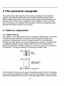
divided into 64K blocks of memory. In figure 4.1 an overview is given of the memory of
the original Pc. The segment addresses are numbered from ססoo to FOOO.
lO~f5 ~
384K
Reserved
AOOO
640K
9000
640K Conventional
memory for dos
OK
ססoo
Fig. 4.1: Memory of original PC
The lowest 640K of memory can be used by the operating system (DOS) to run programs
in. The memory between 640K and 1024K is reserved for the system. In this area several
ROM blocks (COOOO-eFFFF is reserved for video ROM, FOOOO-FFFFF is reserved for ROM
23
The personal computer
BIOS), and the video RAM (AOOOO-BFFFF is reserved for this memory) can be found.
Segment E (EOOOQ-EFFFF) sometimes is used to set up a page frame. Through this page
frame expanded memory, present on a peripheral card, can be addressed, 64K at a time.
Physical addresses of memory places not in use in the reserved area actually are wasted.
The 80386 and the 80486 inherited the segmented memory scheme as described. before.
This memory also still is byte oriented. The reserved area of 384K still is reserved area.
Only more memory can be addressed by the 32 bit processors with their 32 bit address
busses and more operating modes are available. The memory above 1024K is called the
extended memory. The physical limit is 4Gbytes, but it will take a long time before a
computer will be equipped with such an amount of memory. The 80386 and 80486 can
operate in the following modes:
.. real mode. In this mode the processors operate as a 32 bit version of the 8086 using the
previous mentioned segmentation scheme. Yet some 32 bit extensions are possible since
the operands and addresses are allowed to be 32 bit.
.. protected mode. In the protected mode the CPU can address more than 1M of physical
memory space and facilities are offered to maintain data integrity in a multitasking
environment.
.. virtual 8086 mode. This mode can be used to have the processor imitating several real
mode 8086 processors running at the same time.
Other changes in 80386 and 80486 with regard to the 8086 are the segmentation and
paging schemes allowing programmers to address 41bytes of logical addresses. These
logical addresses do not correspond directly with the physical addresses anymore as they
did in the 8086. More detailed information about these features can be found in [3] and
[17]. It must be noted that no matter how much memory is present, OOS can only access
the first megabyte of it.
4.1.2 Shadow RAM
Most new computers based on a 80386 or 80486 have a user option to copy the contents
of slow ROM into an area of extra onboard RAM. This area is called shadow RAM. When
DOS tries to access the ROM blocks, a pointer now refers to the shadow RAM, instead.
This shadow RAM usually is mapped somewhere in the reserved memory area.
24
The personal computer
1
.~ .
4.1.3 Cache memory
Besides the main memory newer 80386 computers also ive a cache memory, fast
memory that holds blocks of data (typically 2, 4,8 or 16 bytes) of the slower main
memory. The 80486 computers usually also have this external cache memory in addition
to the on chip cache. This internal cache of the 80486, capable of storing 8K of code and
data in 16 byte blocks is a fully associative cache, with write-through memory update.
This cache can be disabled and flushed in software. Flushing the internal cache also
results in flushing the external cache in a 80486 computer. In a 80386 computer the
external cache cannot be flushed by software since the 80386 has no instruction to do that.
4.1.4 1/0
External devices can be addressed with:
- available isolated I/O addresses. The 80386 and 80486 allow for 64K I/O addresses,
which can be mapped on 64K 8 bit ports, 32K 16 bit ports or 16K 32 bit ports. Special
instructions are available to input and output data of these ports. It must be noted that
the I/O addresses 00OO-03FF usually are in use by the system, leaving 64,512 addresses to
be used by additional I/O devices.
- memory mapped I/O addresses. In this case the external devices respond to ordinary
memory addresses. All instructions can be used on these addresses allowing
programming flexibility. Care has to be taken when using this method in combination
with a cache. H new data is read from an external device, data is read out of the cache if
the address is present, instead. This problem can be solved by flushing the cache before
reading a memory mapped I/O device or by excluding the memory that is occupied by
the I/O device from the cacheable memory.
25
The personal computer
4.2 The AT-Bus
4.2.1 Introduction
Although the bus that can be found in the current personal computers has been given the
name Industrial Standard Architecture bus (ISA-bus) one could hardly speak of a
standard until recently. This may be explained by the fact that the ISA-bus is not a true
bus in the narrow definition of the word. Unlike other standard busses, this bus is
designed around a specific processor family (the Intel 8Ox86) rather than an universal
architecture.
To stop the proliferation of chip-sets and peripheral cards with their own specifications
that are all slightly different, the Institute of Electrical and Electronic Engineers decided
on recommendation P996 in 1990. And even though the P stands for preliminary this
really is a step forward. In the following the specification of the AT-bus according to IEEE
P996 will be described. More detailed information can be found in [27] and [28].
4.2.2 AT-bus signals
In figure Al (Appendix A) the pin identification and the signals of the AT-bus are shown.
The AT-bus is a mainly asynchronous bus with some synchronous components. It is
meant to deal with memory and I/O accesses to and from peripheral devices. The AT-bus
supports the following buscycles:
1. CPU - memory, transfer of data between the CPU and memory;
2. CPU - I/O, transfer of data between the CPU and I/O;
3. Busmaster - memory, transfer of data between a busmaster and memory;
4. Busmaster -I/O, transfer of data between a busmaster and I/O;
5. DMA - I/O and memory, transfer of data between peripheral components and memory
or I/O on a basis of Direct Memory Access;
6. Refresh, cycle needed to refresh the dynamic memory chips.
The first five cycles can be further divided into:
1.8 and 16 bit;
2. read and write;
3. standard, ready and 0 waitstate cycles.
26
The personal computer
The signals on the bus will be briefly described in the following. Active low signals are
preceded by I.
lOWS, Zero Waitstate.
The zero waitstate signal is used to indicate that the buscycle can be completed without
the insertion of waitstates. lOWS is the only signal that is synchronous to the bus clock.
AEN, Address Enable.
Address enable allows a DMA controller to take over the busses. During a DMA transfer
this signal remains high, prohibiting I/O ports of responding falsely to the memory
addresses present on the bus.
BALE, Bus Address Latch Enable.
The falling edge of BALE indicates that the latched addresses SAO..5A19, AEN and
ISBHE are valid. During a DMA transfer BALE must be high during the entire buscycle.
IBCKL, Bus Oock
The bus clock may vary between 6 and 8 MHz with a duty cycle of 50% (±5%).
DRQO,1,2,3,5,6,7, DMA Request Channel x,
IDACKO,1,2,3,5,6,7, DMA Acknowledge Channel x.
A DMA transfer is requested with the DRQx signal. After an acknowledge with
IDACI<x, the DMA controller can take over the busses, and perform the transfer.
IIOCHK, VO Channel Check.
Errors that occur on a peripheral card, e.g. a parity error, can be reported to the CPU by
taking IIOCHCK low.
IOCHRDY, VO Channel Ready.
Waitstates can be inserted on the bus by deactivating IOCHRDY. All necessary signals
then remain on the bus for a time between I25ns and I5.6ps.
IIOCS16, VO Chip Select 16 BiL
This signal is used to indicate that the I/O access will be a I6-bit access.
IIOW, VO Write,
IIOR, VO Read,
IMEMW, Memory Write,
IMEMR, Memory Read,
ISMEMW, Small Memory Write,
ISMEMR.. Small Memory Read.
The kind of buscycle, a write or read cycle is indicated by these signals. In case of a
memory write or read, ISMEMx is only active with addresses in the lowest IMByte.
IMEMx is active for all addresses.
27
The personal computer
IIRQ3..7, IIRQ9..12, IIRQ14..15, Interrupt Request
Interrupts can be generated with these lines. The interrupts are prioritized, with IRQ9
through IRQ12 and IRQ14 through IRQ15 having the highest priority (IRQ9 is the highest)
and IRQ3 through IRQ7 having the lowest priority (IRQ 7 is the lowest).
LA17..LA23, Large Addresses.
These lines form the upper seven address lines of the address bus. They are present on
the bus before the small addresses, but unlike these addresses, they are not latched and
do not remain on the bus for the entire cycle.
/MASTER, Master.
This signal is used by a busmaster to indicate that it is ready to control the busses.
IMEMCS16, Memory Chip Select 16 Bit.
This signal must be activated by a peripheral card in the case of a 16-bit access. It must be
returned in time, requiring fast decoders.
OSC, Oscillator
This is a 14.31818 MHz clock.
IREF, Refresh.
/REF is a signal that indicates a refresh cycle, needed to refresh dynamic memory chips.
RESORV, Reset Orive.
The reset signal is only active in case of power-up, power supply failure, or system-reset.
SAO..SA19, Small Addresses.
These 20 signals address the lowest IMByte. They remain on the bus during the entire
buscycle.
ISBHE, System Bus High Enable.
This signal is active when data is transferred over the upper eight bits of the data bus
(SD8..SD15).
SOO..S07, System Oata Lo-Byte,
508..5015, System Data Hi-Byte.
These signals form the 16-bit wide data bus.
TC, Terminal Count.
Terminal count is used to indicate the end of a DMA transfer. This is done by generating
a pulse when the last data transfer is reached.
Power supplies
+5V: 4.875 .. 5.25 V, 3.0/4.5 A, SOmV noise
-5V: -4.5 .. -5.5V, O.2A, SOmV noise
+12V: 11.4 .. 12.6V, 1.5A, 120mV noise
-12V: -10.8 .. -13.2V, O.3A, 120mV noise
Gnd: ground
28
The personal computer
4.2.3 AT-bus timing
The signals that are generated by the buslogic must travel some distance over the
mainboard before reaching a peripheral card. Together with the present capacities this
results in a delay of about Ilns per signal line when 8 slots are present on the mainboard.
So signals returning from the peripheral cards can have additional delays of up to 22ns.
Special attention must be paid to the open collector signals. H an open collector line
returns to non active state, it can last a while before this state actually is reached. This
time depends on the pull-up resistors and the line capacities. With TTL levels (Vex; = 4.5V,
VL = 0.5V, VH =2.4 V) the following formula can be used to determine the rise time:
Rise time • 0.65 *R *C
(4.1)
Pull-up resistors of 300 Ohm are required for IIOCS16, lOWS, IMEMCS16 and
lMASTER. A lK Ohm pull-up is needed for IOCHRDY. The IIRQx signals use a 2.2K
Ohm pull-up and the signals IIOW, IIOR, IMEMW, IMEMR, /IOCHO< and IREF
require a 4.7K Ohm pull-up resistor.
In Appendix A the most important timing diagrams (16-bit I/O and 16-bit memory CPU
buscycles) are shown. The bus operates at a frequency of 8 MHz although some
manufacturers are offering speeds of up to 12 MHz at the moment. At 8 MHz, the
maximum data transfer rate that can be attained is 8.00 MByte/s. To complete the
description of the bus also the physical dimensions of a peripheral card for the AT-bus
are shown in Appendix A. In a hardware design, the lines coming from the bus connector
may be connected to not more than two TTL-ports on the peripheral card.
29
The personal computer
4.3 The Vesa local bus
4.3.1 Introduction
Since the introduction of the personal computer, the performance of this computer kept
growing by the introduction of newer, faster microprocessors. The 80486 can deliver 54
MIPS, quite something more than the 8086, which can deliver about 0.75 MIPS. The only
component in the PC that kept behind was the bus that formed the connection to the
outside world. The only major change was the upgrading of this original 8-bit bus to the
previously described 16-bit bus. However, the data transfer rate of this bus (8 MByte/s) in
no way satisfies the demands of the current users.
A solution to this problem is the use of a local bus that connects peripherals directly to
the CPU. Several manufacturers thought of this and supplied their systems with such a
local bus resulting in various different non compatible busses. To stop the development of
more of these systems, VESA, the Video Electronics Standards Association, and Intel
worked on the development of a standard. Since the Intel bus standard is not available
yet, and the Vesa local bus is already being used by many manufacturers, producing
mainboards with this bus at small additional costs, only this local bus will be described.
The Vesa local bus (VL-bus) is a full electrical, mechanical, timing and connector
specification, allowing high speed peripheral devices to interface, either directly or
indirectly, to the local bus of a CPU, providing data transfer rates of up to 130 MByte/s.
The bus supports 386 and 486-type CPUs. Other types of CPU can be used but than the
signals of that CPU have to be converted to the signals of a 80386 or 80486. In practice
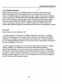
however, only 80486-type computers are provided with a Vesa local bus. Figure 4.2 shows
the structure of a Vesa local bus system.
In the figure the logical flow of information is shown. A module that resides lower in the
hierarchy may not claim ownership of address and data busses if these are claimed by a
module with a higher priority.
30
The personal computer
Hierarchy
2
3
4
Motherboard Slots
Motherboard Chipset
Fig. 4.2: VL-bus architecture
4.3.2 VL-bus signals
The VL-bus is modeled after the 80486 CPU. This means that most of the signals on this
(synchronous to the CPU clock) bus are directly related to the CPU signals. In Appendix
B these signals are shown together with the pin identification of the VL-bus connector.
This connector (a 16-bit micro channel connector) physically resides directly in-line with
the ISA connector on the motherboard. In Appendix B, also the physical layout of a VLbus card is shown.
In the following the signals of the VL-bus will be described briefly. The emphasis will be
on 32 bit CPU memory and I/O cycles. Detailed information on other cycles (busmaster,
DMA and 16 bit cycles) and more detailed information on the several signals can be
found in [31] and [32].
The following abbreviations are used in the description of the signals:
LBC: VL-bus local bus controller. This controller physically resides on the motherboard.
LBT: VL-bus local bus target. This is a device that responds to transfers initiated
elsewhere in the system.
Active low signals are indicated with # (and not with / to make a clear distinction
between AT-bus and VL-bus signals).
31
The personal computer
Signals from the system logic.
ID<4..O>, Identifier pins.
A LBT can identify the type and speed of the host CPU with the help of the 10 pins, static
pins that contain valid data only during power on reset (they should be latched on the
trailing edge of RESET#). 10<4> is reserved for future use. The CPU type is identified
with 10<1> and 10<0> (a 80386 is indicated with 10<1,0>=01, a 80486 is indicated with
10<1,0>=10, other combinations of 10<1,0> are reserved). 10<2> indicates whether the
LBC is capable of handling high speed zero wait state write transfers (ID<2>=l). It can be
ignored by the LBT, if it cannot complete a write with zero wait states.The LBT may
default to a minimum of one wait states in this case (this mode is indicated with
10<2>=0). Read transfers are not affected by the setting of 10<2>. The speed of the CPU is
indicated by 10<3> (ID<3>=1 if speed is less than or equal to 33.3 MHz, 10<3>=0 if the
speed is greater than 33 MHz).
LCLK, Local CPU Cock.
The VL-bus clock signal is lx clock that is in phase with the 486 system clock. The
maximum frequency is 66 MHz. CPU state changes are signified with the rising edge of
LCLK. The duty cycle of this signal is between 40% and 60%. The high state of LCLK is
2.0V and the low state is 0.8V. The maximum rise and fall times are 2ns. Although the
highest specified frequency is 66 MHz, the used VL-bus connector is limited to
frequencies of up to 40 MHz. This is why the fastest personal computer with a local bus
available at the moment is a computer with a 80486DX2 microprocessor, externally
operating at 33 MHz (this is also the frequency at which the bus operates) and internally
operating at 66 MHz.
Power, ground, and reserved.
All power and ground pins must be used by a VL-bus device. All power lines Va:. are 5V
power lines, with a tolerance of 5%. Power must be drawn equally from these power pins.
A maximum of lOW may be drawn from a slot by a VL-bus device. Reserved pins may
not be used by any VL-bus device.
RESET#, System Reset.
The reset signal is activated after system power up and before any valid CPU cycles take
place.
RDYRTN#, Ready Return.
This signal usually is equivalent to the processor RDY# signal. A LBT can recognize the
end of a cycle with RDYRTN# .
WBACK#, Write Back.
This signal is reserved for future use with write-back cache systems. LBTs may ignore this
signal.
32
The personal computer
Signals from the CPU
ADR<31..02>, Address Bus.
On this bus the addresses are transferred .
ADS#, Address Data Strobe.
This signal indicates that data on the address bus is valid. ADS# signifies the beginning of
every memory or I/O cycle.
BE<3..0>#, Byte Enables.
The data bus is divided into 4 byte lanes. BE<3..0> indicate which lanes are involved in a
transfer.
BLAST#, Burst Last.
BLAST# is used to indicate the end of a burst cycle.
DAT<31..00>, Data Bus.
Data is transferred on this 32 bit bus. The valid byte lanes are determined by BE<3..0>#.
D/C#, Data or Code Status.
This signal is used to indicate whether data or code is being transferred on the bus.
MlIO#, Memory or VO Status.
The type of access, memory or I/O, is indicated by this signal. In case of a memory access
M/IO# is high, in case of an I/O access it is low.
W/R#, Write or Read Status.
A write access is indicated by W /R# high, a read access is indicated by W /R# low.
Signals from the VL-bus controller.
LEADS#, Local External Address Data Strobe.
Whenever an address is present on the VL-bus that performs a CPU cache invalidation
cycle, this signal is activated. LEADS# is not active for CPU writes.
LGNT<x>#, Local Bus Grant.
A request of a bus master to gain control over the busses (by LREQ<x>#) can be
acknowledged with LGNT<x>#. As long as LGNT <X># is asserted the bus master is in
control of the busses. Each slot has one pair of LREQ# and LGNT# signals.
LKEN#, Local Cache Enable.
If a VL-bus transfer is cacheable, LKEN# is activated.
Signals from the VL-bus tcuget.
BRDY#, Burst Ready.
BROY# is used to end the current active burst cycle. This signal also must be
synchronized to LCLK. A LBT that doesn't support burst cycles may leave this signal
unconnected. If BROY# and LROY# are asserted at the same time, BROY# is ignored and
33
The personal computer
the remainder of the current burst cycle is concluded as non-burst cycles.
IRQ9, Interrupt Request Line 9.
This interrupt request line, electrically connected to IRQ9 of the ISA bus, is present on the
VL-bus for stand alone VL-bus devices, that have no ISA signals available.
LBS16#, Local Bus Size 16.
A LBT that cannot accept 32 bits of data in a single clock cycle can force the CPU to run
multiple 16 bit transfers by asserting LBS16#.
LDEV<x>#, Local Device.
A LBT signals the LBC that the current cycle is a VL-bus cycle with LOEV<x>#. Each slot
has its own LOEV# signal. All VL-bus devices must drive this signal to valid TIL levels at
all times.
LREQ<x>#, Local Request.
LREQ<x># is used to request control of the VL-bus by a device. LBTs that don't act as a
bus master must leave this signal unconnected.
LROY#, Local Ready.
LROY# is used in the handshake procedure that ends the current active bus cycle. LROY#
is synchronized to LCLK so appropriate setup and hold times to LCLK must be satisfied.
4.3.3 VL-bus timing
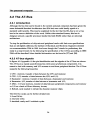
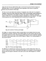
In figure 4.3 the general timing of the VL-bus is shown. A CPU transfer starts when valid
information is present on ADR<31.02>, M/IO#, W IR#, D/C# and BE<3..0>#. ADS# is
strobed to begin the transfer. H a LBT must respond to the address, it has 20ns to assert
LOEV#. The assertion of LOEV# prevents the ISA-bus controller to start a cycle.
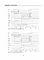
LCLK
ADR<31 ..02>
:..----'X,l----_;....c:V:..::aJ::..:::id_----...;:;....c,X'--_-----i
ADS#
\
LDEV.
LADY.
RDYRTN#
1: <=33MHz
2:>",40MHz
Fig. 4.3: General VL-bus timing
34
.
~--___:,_____-
The personal computer
Depending on the speed of the CPU and the VL-bus controller design, LDEV# is sampled.
at either the LCLK edge following ADS# or two LCLK cycles after ADS#. LRDY# is driven
by a LBT after ADS# is high again. After completion of the transfer the LBT asserts
LRDY# for one LCLK cycle and then makes it high again for one-half LCLK cycle prior to
releasing it. The VL-bus controller responds to the assertion of LRDY# by asserting
RDYRTN#. This can be done either immediately or on the next LCLI< cycle (in case of
speeds greater than 33MHz). H a read transfer is performed, the LBT must hold the read
data on the bus until the LCLK on which RDYRTN# is asserted. More detailed timing
diagrams involving CPU transfers can be found in appendix B (timing specifications of
burst, busmaster or DMA cycles can be found in [31] and [32]).
4.3.4 DC Characteristics
Steady state voltages on the bus may not be higher than Vee and lower than ground. An
overshoot over Vcc and undershoot under ground may be no more than O.5V for 5ns. The
length of traces from the VL-bus connector to add-in board circuitry is limited to two
inches (in case of branched traces, the sum of the branches may be no more than two
inches). Each add-in board may have a maximum of one TTL load on each VL-bus input
signal. All shared VL-bus signals on an add-in board must be capable of driving a 100pf
capacitive load. Non-shared signals, such as LDEV#, must be capable of driving a 20pf
load. The signal impedance on each trace, should be equal to or less than 50 Ohm. This
signal impedance can be calculated with the following formula:
ZII'IIor
Z$igtttll • ------------
~
~~~~
with:
= signal loaded trace impedance;
Ztrace = the impedance of the board trace;
C trace = the capacitance of the board trace;
Ccomponent = the load capacitance from components and connectors.
The sink current requirements of the output drivers are given in appendix B.
Zsignal
35
(4.2)
The personal computer
4.4 Software aspects
Programs generally can be written in two ways:
1. using a high level programming language like C;
2. using assembly language.
The first method is the easiest and allows flexible, well-organized programs, while the
second method is more difficult, and usually results in less readable programs. On the
other hand, the second method provides full control of all present hardware and can
result in faster programs. This can be useful when optimum benefit of the hardware
resources must be acquired. A middle course can be the use of assembly routines that are
incorporated in a program written in a high level language. In this way both flexible
programming and fast programs are possible.
Software can be written independently from the bus that is present in the computer. The
bus hardware that is present is completely transparent to software. The mode in which
the processor operates however influences the way in which physical addresses are
generated. In real mode, the logical addresses used in programs, correspond directly to
physical addresses (they are equal). In the other modes, the physical addresses usually do
not correspond to the used logical addresses, but a translation is performed.
36
5 Design of an interface
5.1 General survey
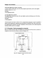
5.1.1 General scheme of interface
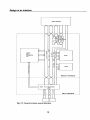
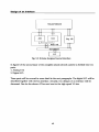
In figure 5.1 a scheme is given of a complete neural network system, containing a neural
network, a personal computer and an interface in between. The task of the interface is to
convert the signals of the computer's bus to signals that can be used by the neural
network. The personal computer is in full control of the neural network.
Neural Network
Neural Interlace
Fig. 5.1: Scheme neural network system
As can be seen in fig. 5.1 the system can be divided into 4 layers:
1. neural network
2. neural interface
3. bus interface
4. personal computer
The neural network is one of the networks as described in chapter 3. The neural interface
provides the signals required by the neural network and the bus interface, i.e. digital and
analog signals. The third layer, the bus interface, forms the connection to the PC's bus,
either an AT-bus or a VL-bus. Finally the computer, a 80386- or 80486-based PC, provides
facilities to control the neural network and process data from the network. A more
detailed scheme of the neural interface, inspired by test circuits given in [7], [9], [lO], [20],
[22], and [25], is the scheme shown in figure 5.2.
37
Design of an Interface
Neural Network
_·~o-···············_··_······_···_··
S/H "
fI
DA
mux
~J=i=
II
AD
l{"tV
~
a
control
and
processing
unit
r
rv
d
d
r
d
C-
:
,...-
~
RAM
a
s
I->------1\
c
o
C
n
t
ROM
11"'--
r
------'
o
I
Neural Interface
----.- ... ····--·-··-····-----------·---·-···--·-----·····-·-l
'/
interl. PC -> Neural netw.
inter!.
•
!
:.-. -.-.--.-----.--------------.-.-- -
r
:
'"
.
:
:
t
~
:
Bus interface
······(1--···0---···-·····--············------------· - --.- -:1
I
'ol .}>
PC
Fig. 5.2: General scheme neural interface
38
Design of an Interface
The following components can be found in figure 5.2:
1. control and processing unit. The neural network usually is several times faster than the
personal computer. Transferring data between memory and the neural network (the speed
at which this is done, is determined by the computer's bus speed) and processing data
(updating weights) can be done faster by a dedicated processor, capable of performing
floating point calculations, e.g. a digital signal processor. The personal computer then only
has to monitor the working of this processor. It downloads programs on the processor
and occasionally acquires the results of the simulations on the neural network.. A slow bus
in the personal computer does not decrease the performance of the neural interface
significantly, allowing for high speed operation of the neural network..
2. RAM. This type of memory can be used to store programs for the control and
processing unit, data of this unit and data of the neural network (weights, input
testvectors, output results and configuration data). Both the control and processing unit
on the interface and the personal computer must have access to this memory.
3. ROM Programs for the control and processing unit, as well as data of the neural
network (input testvectors, configuration data) can also be stored in ROM. This can be
useful if this kind of data does not have to be changed. The personal computer does not
need to have access to this memory.
4. Analog to digital and digital to analog converters together with some multiplexers.
These converters are used in case of an analog neural network.. The multiplexers can be
used to increase the number of analog channels, without adding more converters..
The interconnection of layer 2 and the personal computer is provided by layer 3. This
layer converts signals if needed, and provides facilities to address all the components on
the neural interface and on the neural network..
A neural interface as shown in figure 5.2 can be realized in two ways:
1. by making use of commercially available interface boards;
2. by designing an own interface board
These two possibilities will be amplified on in the following.
39
Design of an interface
5.1.2 Commercially available interfaces
Several boards are available as add-in card for a personal computer that exhibit some
features of the scheme shown in figure 5.2. A short description of a signal processor
board, is given in figure C.l (appendix C, see also [30]). Efficient processing of data is
possible with help of the two parallel data busses and the peak processor performance of
16.7 MIPS and 33.3 MFLOPS. Using such a board has some advantages. It is available at
wish, requiring no development time. Also it is guaranteed to function and no basic
software routines have to be written. Of course there are also some disadvantages. Not all
the desired functions are standard available. The analog channels for example have to be
added, requiring development time and additional costs. With regard to the costs it must
be noted that these can be rather high. The board shown in fig. C.l together with the
necessary software costs about fl. 10,000. The board of figure C.l is very useful when
trying to achieve a very high speed neural interface, without looking at the costs of it.
Next to the previously mentioned board also more simple boards are available,
specialized in acquisition of analog data. These boards only contain some analog channels
and are not as expensive as a signal processor board. The number of analog channels
however usually is very limited, the conversion speed is not very high (sampling rates of
up to 50 KHz are normal for boards costing less than fl. 1,500), and processing of data
must be done by the computer. So if the specified number of analog channels (32 inputs
and 32 outputs) should be available, probably more than one data acquisition board
would be needed, costing much more than the allowed price of fl 2,500. Maintaining the
speed requirement results in even more expensive boards, costing more than fl. 4,000 for a
thirty-two channel neural interface.
IT it is no longer required to use a personal computer, an alternative is offered by the
interface described in [15]. This VME based interfaces can be used in conjunction with e.g.
a SUN workstation. The processing speed of such a station is higher than that of a
personal computer (even when using a 80486). The interface accommodates 64 digital and
64 analog channels. The analog channels can be either configured as input or as output
channels. The conversion of 32 analog input channels takes less than 56 ps while the
conversion of 32 analog output channels only takes 3 J1S.
A disadvantage of the board is the fact that the voltage ranges of the input and output
channels are fixed. The output is a voltage between 0 and 5 V, while the input voltage
must be between -5 and +5 V. Since the 12 bit resolution is mapped on these ranges,
resolution is thrown away if the actual voltage ranges are not equal to the interface's
40
Design of an interface
ranges, or additional circuitry must be used to adapt the voltage ranges of the neural
network to those of the interface. The price may be another disadvantage. A complete
working system, together with software, costs about fl. 17,000.
Considering the prices of the commercially available boards and the fact that none of
these boards meets all the specifications given in chapter three, the design of an own
neural network interface board can be a good alternative. The design of an own interface
will be described in the following paragraphs.
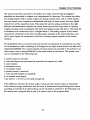
5.1.3 Design of a board
There are several possibilities to realize an own neural interface board:
1. realization of a board according to figure 5.2, containing a digital signal processor,
RAM, ROM (if needed) and the necessary analog channels. Although this method results
in a fast, versatile interface, a few remarks must be made. The development of such a
board (design, realization and testing) namely takes a lot of time. It is very unlikely that a
properly functioning board can be made in half a year. The costs can also grow to an
unreasonable height. Although the components themselves need not to be that expensive,
the printed circuit board that has to accommodate them, can cost quite a lot of money,
since it will very likely be a large multi-layer print.
2. realization of a data acquisition board. In this case only some digital and analog input
and output channels are realized. The task that the control and processing unit in fig. 5.2
was meant to perform, now will be done by the personal computer. The speed at which
an update algorithm can be executed now completely depends on the speed of the
computer. The data transfer speed will be determined by the bus speed and the
conversion times of the converters. Advantages of this method are the smaller
development time, the smaller size of the printed circuit board and the smaller costs.
Considering the remarks in the foregoing, the second method has been chosen to design
an interface at a reasonable price and in a short period of time. The scheme of the
interface now changes in the one shown in figure 5.3.
41
Design of an interface
Neural Network
A/D
D/A
11
I
11
Dig. I/O
Anal. I/O
I
bus'
11
I
PC
I
Fig. 5.3: Scheme designed neural interface
In figure 5.3 the second layer of the complete neural network system is divided into two
parts:
1. Analog I/O;
2. Digital I/O.
These parts will be covered in more detail in the next paragraphs. The digital I/O will be
described together with the bus interface. Actually, two designs of an interface will be
discussed. One for the slower AT-bus and one for the high speed VL-bus.
42
Design of an Interface
5.2 Analog 1/0
The analog I/O block consists of two parts:
1. analog to digital conversion;
2. digital to analog conversion.
These parts will be described separately in the following. At the end of this chapter, a
complete analog I/O circuit will be presented.
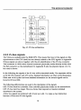
5.2.1 Analog to digital conversion
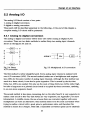
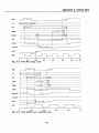
The analog to digital conversion will be done with 12-bit Analog to Digital (A/D)
converters. There are two basic methods to realize thirty-two analog input channels,
shown in the figures 5.4 and 5.5.
a---@--7~
d
i
g
i
:~~
I
t
o
a
9
I
i
0
analog in _ _
~ M~ I--~ ~
o
u
n~~
t
Fig. 5.4: Direct
A/D conversion
Fig. 5.5: Multiplexed A/D conversion
The first method is rather straightforward. Every analog input channel is realized with
one A/D converter (ADC). The second method makes use of multiplexers and requires
less ADCs for the same number of analog input channels. Although the first method can
result in a faster circuit, it can also be quite expensive. This is caused by the fact that
thirty-two ADCs are needed. Not only are the costs of these thirty-two ADCs rather high,
but also a large area on a printed circuit board is occupied by these converters, resulting
in an even more expensive board.
The second method is less space consuming, but on the other hand it is very expensive to
realize a fast circuit in this way (fast ADCs are very expensive, see Appendix C for more
information). A middle course, the use of more than one converter together with some
multiplexers can form an alternative. This method seems to be the most convenient when
trying to realize a circuit with a good price to performance ratio, and therefore this
method is chosen (it is cheaper, while still a reasonable conversion speed can be attained).
43
Design of an Interface
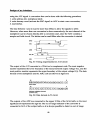
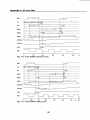
The circuit will be made up of two ADCs with two 16-channel multiplexers. The
converter that will be used is the AD1671JQ from Analog Devices. This 12-bit converter is
a true 1.25 MSample/s converter, meaning that it can complete a conversion every 800ns.
So theoretically, sixteen channels can be converted in 12.8 ps. The multiplexer is the 16channel, ADG526AKN from Analog Devices. Since the input range of the AID converter
is fixed, the converter is preceded by an operational amplifier (opamp) circuit to adapt the
output voltage of the neural network to the fixed range of the converter. The opamp also
acts as an input buffer for the converter. A scheme of sixteen analog input channels is
shown in figure 5.6.
O.
DO
DO
D4
1tl
··
·•
n
I
DO
5••
5 ••
5 ••
SIS
5 ••
511
5 ••
SIl
sa
57
SlI
SIi
1M
so
52
8'
DO
Q'
Do
os
Q4
os
QO
D1
Q1
DO
QO
CIJ(
BPCWPO
D
_.
A3
AN
_OUT
REF ..
FEFOUT
A2
A.
B••
Bll
B••
BI
BI
B7
IlO
B5
,.
AJJ
Bl
JlS
WR
AD<l52eOI
O.
D4
Q3
Q4
III
112
01
Q1
DO
QO
ENe
I
I
os
DO
DAY
OTR
.•
Q.
Do
1M
DO
d
I
I
OC
DO
DO
LSB
QO
cue
OC
,_"
AD1871
Pd...... 2
Fig. 5.6: 16-channel analog input circuit
The output voltage of the neural network is denoted by VNN' the input voltage of the AID
converter by V AD. The potentiometers 1 and 2 can be used to adapt the output range of
the neural network (VL S VNN S VH) to the fixed voltage range of the converter (0 SVAD SS).
The input voltage of the AID converter is given by:
(5.1)
with ~tl the total resistance of potentiometer 1 and R1 a part of this resistance.
The settings of potentiometer 1 and Vbias can be determined with:
44
Design of an Interface
R
0-2
potl
-~
R
v-V
L
potl
/IiIIs
(5.2)
and
R
5 -2
potl
-~
VH-V/IiIIs
(5.3)
Rpotl
yielding:
5VL
V Mil - V-V
H
L
(5.4)
~
2.5
(5.5)
Rpotl
VH-VL
and:
- - -1-
The output range of the neural network must satisfy:
VH~
V L +2.5
(5.6)
(the output range is made the same as the input range that will be discussed in the next
paragraph). Offset and gain errors of the AID converter are not taken into account in the
foregoing formulas. Should these errors occur than the potentiometers can be adjusted so
that the errors are compensated for. The operation of the circuit can be controlled by the
following control lines:
It ENC: start conversion;
It IOC: read result of conversion from output latches;
It IWR: write address (A3..AO) of a multiplexer channel;
It IRS: reset multiplexer.
The timing requirements for these signals are shown in figure 5.7. A conversion is started
by activating the ENC signal. This causes the AOC to sample and hold the signal at its
input and convert this signal to a digital code. To determine the input channel that will be
converted, the right address of the channel is written into the multiplexer's input latch
using the /WR signal. When a conversion is completed, the output of the AOC
automatically is clocked into the latches. This output code can be read from these latches
45
Design of an interface
using the IOC signal. A conversion thus can be done with the following procedure:
1. write address into multiplexer latch;
2. write dummy word (activate the ENe signal) to ADC to start a new conversion;
3. read latches.
The time between 1 and 2 must be more than 450ns to allow the signals to settle.
However, when more than one conversion is done consecutively, the next channel of the
multiplexer can be chosen directly after a conversion start, since the ADC contains a
sample and hold circuit. The latches can be read BOOns after the conversion is started.
~f-->800
ENC
10C
->100-
twR
_1->1110- ->10-1
A3•.AO
~
Valid
X,-.~_-_-_-_-_-_-_-_-_-_-=--=--=--=--=--=
IRS
Fig. 5.7: Timing requirements for AID circuit
The output of the AID converter is a 12-bit two's complement code. The most negative
number represents the lower boundary of the neural network output voltage (VL)' and the
most positive number represents the upper boundary of the output voltage (VH). The data
formats of the multiplexer and the ADC code are shown in figure 5.8.
ACe output
Address multiplexer channel
(X=don't care)
Fig. 5.8: Data formats AID circuit
The outputs of the ADC are connected to the upper 12 bits of the 16 bit latch, so the most
significant bit represents the sign bit. The out of range indicator of the converter is
connected to bit 3 of the output latch, so it is always possible to detect an out of range
46
Design of an Interface
error (this error occurs whenever the input of the ADC is outside of the fixed range,
OSVAD S 5). The lowest 3 bits (bit 2..0) of the output latch are always zero. The address
that is used to choose one of the sixteen channels of the multiplexer must be present in
the lower four bits of the 16-bit word. The required thirty-two analog input channels
simply are formed by two identical circuits as shown in figure 5.6.
5.2.2 Digital to analog conversion
Analog inputs of the neural network all have to be stable at the same time. The digital to
analog conversion therefore can be done in the two ways shown in the figures 5.9 and
5.10.
d
--@--7
a
n
i
g~a
i~'
t
0
a
9
I
i
n
--@--7
o
u
t
Fig. 5.9: Direct D/ A
conversion
Fig. 5.10: Multiplexed D/A
conversion
In the direct method all analog channels have their own D/A converter (DAC), while the
multiplexed method increases the number of outputs with the help of sample/hold (S/ro
devices. The use of S/H devices brings along several disadvantages. Although in this case
a few fast D/ A converters can be chosen costing not too much, the speed of the circuit is
negatively influenced by the acquisition time of the S/R devices (this is the time that the
device needs to track the signal again when changing from hold to sample mode). Cheap
S/R devices have a large acquisition time, while the fast devices on the other hand result
in an expensive board, because their prices are much higher (see appendix C for more
data on some sample/hold devices).
Another problem that arises is the fact that each analog channel needs a sample/hold
device. This results in a large printed circuit board, and this again results in an expensive
design. The use of rcs with more than one sample/hold device does not solve the cost
47
Design of an interface
problem since these les are very expensive.
Providing every analog channel its own D / A converter seems to be more attractive.
With regard to the D / A converters the following must be noted:
1. the output range of the DAC must be adjustable between given lower and upper
voltages;
2. if a current output DAC is used, the output has to be buffered by a fast opamp, that
does not increase the conversion time significantly.
In case of a current output DAC, the buffer opamp can be used to adjust the output
range, requiring no large additional circuitry. The best candidates to realize the analog
output channels are the AD7568BP and the DAC8412EP, 12-bit converters from Analog
Devices.
The AD7568BP contains eight current output converters, so the realization of thirty-two
analog output channels requires only four of these ICs. Together with the buffer opamps
(a suitable opamp is the AD713JN from Analog Devices) only twelve ICs are needed to
realize the thirty-two voltage output channels. A serious disadvantage of this converter is
the fact that digital data enters the chip serially. Complex circuitry is needed to control
the input of digital data.
The DAC8412EP on the other hand is an IC containing four voltage output D / A
converters. The output range is fully adjustable, with the only restriction that the range
must be larger than 2.5 V. Although the price of this converter is higher than that of the
AD7568BP, and the output range must be larger than 2.5 V, this converter has been
chosen. The fact that the needed printed circuit board area is smaller, and the control
logic is simpler outweighs the smaller costs of a circuit using the AD7568BP. In figure 5.11
a simple circuit, realizing four analog output channels is shown.
The output of the D / A converter is a voltage between VIlEFL and VREm:
(5.7)
with N the digital code in decimal. VREFL and V REm can be set up with the potentiometers
3 and 4.
48
Design of an Interface
-..;.,11ellj...;...._...,
YSS
-
YllD
L . . . - _ ...........
Fig. 5.11: Four analog output channels
The operation can be controlled by the following signals:
.. /reset: reset all 0/A converters to mid-scale
.. /ldac: the converter can either be in update mode or in load mode. In the update mode
the outputs of the converters are changed according to the codes present in the internal
latches. In the load mode the contents of the internal latches can be changed, without
changing the output voltages. /ldac is used to set the operating mode, on the rising edge
of /ldac bit 0 of the databus is clocked into the flip-flop (1 for load mode and 0 for
update mode).
.. /cs: write a new code in the internal register of a OAC.
The timing requirements for these signals can be seen in figure 5.12. In figure 5.13 the
data formats for the D/A circuit are depicted.
Fig. 5.12: Timing requirements for 0/A circuit
49
Design of an interface
DACinput
DACmode
(X=don't care)
Fig. 5.13: Data formats
DI A circuit
The conversion process now is done with the following procedure:
1. set the operating mode to load by writing a 1 into the mode flip-flop using the /ldac
signal.
2. write the digital codes into the latches of the DACs. This is done by writing words
according to the format shown in fig. 5.13 into the DAC's latches by using the Ics signal.
3. start the conversion by setting the converters in the update mode. This is done by
writing a 0 into the mode flip-flop.
As can be seen in figure 5.13, the 12-bit two's complement code is supposed to occupy the
highest twelve bits of the digital input word. The lowest two bits are used to address one
of the four DACs that are present in each Ie. The conversion time of all channels (all
channels perform the conversion at the same time) is typically 6ps.
Extension of the circuit to more output channels can easily be done by adding converters.
A thirty-two output channel circuit can be formed with eight converters connected in the
way shown in figure 5.11.
5.2.3 Analog 1/0 circuit
A complete circuit with sixteen analog input and twenty analog output channels is shown
in figure e.3 (Appendix C). It consists of the the subcircuits that are described in the
foregoing. A circuit with thirty-two analog channels, just consists of two identical circuits
as shown in figure e.3. The connectors shown in figure C.3 are used to connect the
various signal to the bus interface and to the neural network. The power supplies are not
shown in figure C.3. They must be realized externally since the power signals on the ATbus and VL-bus connectors do not comply with the given specifations of the analog I/O
circuit in appendix C. In Appendix C also the complete specifications of the analog I/O
circuit are given. The realization of the given circuits on a printed circuit board will be
discussed later. First, the interface to the bus will be discussed.
50
Design of an Interface
5.3 Interface to the AT-bus
The bus interface must provide all the signals required by the analog I/O circuit, the
digital I/O circuit, and the neural network. This means that it should:
1. provide means to connect the databus to the components in the analog I/O circuit, the
components in the digital I/O circuit, and the neural network circuitry;
2. provide means to address all components in the:
- analog I/O circuit;
- digital 1/0 circuit;
- neural network (including possible RAM).
The first point can be done by using some bus drivers. Provision of (a part 00 the
computer's address bus to the neural network, also can be done with some bus drivers.
Addressing all possible components requires some address decoding circuitry. A choice
must be made whether to use ordinary memory addresses, or the special I/O addresses.
This however will be discussed later, first the digital I/O circuit will be described. At the
end of this paragraph the speed at which the complete interface can operate will be
discussed.
5.3.1 Digital I/O
The digital I/O can easily be accomplished with some latches. In figure 5.14 two latches
are shown, one configured as input and one configured as output.
input latch
output latch
b
u
s
0
u
t
C
t
'11
01
D2
D3
D4
D5
OS
07
De
e
oe
Q1
Q2
Q3
Q4
as
Q6
Q7
as
n
8
u
r
a I
I n
n
8 t
t
C
w
0
r
k
b
u
s
I
n
C
t
Q1
Q2
Q3
Q4
Q5
01
D2
D3
D4
D5
Q6
OS
Q7
Q8
07
De
e
oc
74LS573
n
u
8
r
0
n
C
a u
I t
Tt
w
0
~
vee
74LS573
lOe
Fig. 5.14: Input and output latch
Data can be written in the output latches by making the C signal high. The outputs of
these latches are always enabled. Digital data from the neural network can be read by the
51
Design of an Interface
computer by activating the IOC signal of the latch (making it low). The latches are
included in the schemes shown in the figures C.3 and C.4 (the complete neural interface
will contain twelve of the latches as shown in figure 5.14, six configured as input and six
configured as output).
5.3.2 Bus interface circuit
As mentioned in chapter three, data should be transferred between the computer and the
neural network as fast as possible. Also the interface must be as versatile as possible. The
versatility is maintained by allowing all components to be addressed individually
(especially the RAM of the neural network). There are two ways to address components:
1. by mapping them on ordinary memory;
2. by making use of the special I/O addresses. In this case there could even be made use
of Direct Memory Access (DMA). When using DMA data is directly transported between
I/O and memory without intervention of the CPU. This method is efficient when larger
blocks of data have to be transferred.
Considering the fact that the interface has to be as versatile as possible, it is decided that
all components (including RAM of the neural network) must be individually addressable
in an efficient way. This excludes the use of DMA, since this method of transferring data
brings along much overhead when used for single accesses to memory. However, in a
memory-cached system, with pipelined execution of instructions as is the case in the
80386 and 80486 processor based systems, the use of ordinary (memory or I/O) buscycles
should not be crucially slower (see [27] and [28] for data on DMA cycles).
As described in chapter four, the AT-bus supports several buscycles, with a predefined
length. Since the speed of the bus directly influences the speed at which the neural
interface operates, the length of the buscycles must be as small as possible. An
examination of the timing diagrams of the buscycles (figures A.1 to A.6, appendix A),
shows that the fastest data transfer rates can be achieved with zero waitstate 1~bit
memory buscycles. Although the use of these cycles results in a somewhat larger circuitry
for decoding and bus logic as with I/O buscycles, this method is chosen.
Now it is clear that the I/O will be mapped on memory, the actual bus interface can be
designed. First of all, the memory addresses that the bus interface will respond to have to
be chosen. There are two possibilities:
1. make use of the reserved address area;
2. make use of addresses above 1 MByte that are not in use by the system.
52
Design of an Interface
The first possibility is the most favorable. It results in simpler address decoding, since not
all address lines have to be involved in the decoding (the ISMEMx signals that are only
active for addresses in the lower 1 MByte memory can be used in the decoding circuitry),
and future extension of the system memory is not prohibited by the fact that the
addresses already are in use.
In figure C.4 (appendix C), a complete bus interface scheme is shown. The computer's
data bus is buffered with 74l.S245 bus transceivers. Address lines and other control
signals are buffered with 74l.S244 bus receivers. The circuit can be set up to one of two
memory segments, namely the D or E segment (physical addresses DOOOO-DFFFF or
EOODO-EFFFF). A segment valid signal indicates that the segment is being addressed. This
segment valid signal is also available on the neural network extension connector, a
connector that also provides the lower 16 address lines, the ISMEMR, ISMEMW and the
lRESET signals.
The analog and digital I/O circuits consist of about 25 components that must be
addressed. This is done with help of four decoders, capable of addressing thirty-two
addresses. The signals required by the circuit as shown in figure C3 are connected to a
connector in figure C4. Two of these connectors make it possible to address all
components on the analog I/O, consisting of two identical circuits as shown in figure C3.
The remaining 65,504 addresses can be used by the neural network, e.g. to address
weights stored in off-ehip RAM.
The use of zero waitstate 16-bit memory cycles requires the bus interface to return two
signals to the bus logic on the mainboard during a buscycle, namely /MEMCS16 and
lOWS. The timing of the lOWS signal is very critical. The signal must be returned within
10 ns after activation of the IMEMx signal. This is done by using the IMEMx signals, the
segment valid signal (this is present before the IMEMx signals, since the addresses are
earlier available) and with help of fast logic. The open collector nand gate 74F3038
(capable of driving a 30 n load resistance) is used to generate the lOWS signal.
The IMEMCS16 signal must be returned within 80 ns after the large address signals are
valid. The easiest way to do this, is to use a 74F3038 connected to the large address bits
18 and 19. In this way all addresses on the bus above 768 K <segments C, 0, E and F) are
seen as 16-bit addresses, but this should not cause any problems in practice.
In appendix C, the exact physical addresses are shown of all the available analog and
digital channels on the neural interface.
53
Desig n of an interface
Care must be taken with the choice for the segment in which the neural interface will be
installed. This segment may not be in use by another peripheral card, nor may it be used
by a memory manager (the segment must be excluded for the memory manager). The
reason for this is the fact that a memory manager allows DOS to make a call to an
address in the reserved memory area, even if no physical memory is present. The
memory manager takes care that the address is translated into an existing physical
address that is outside the memory range that can be addressed by DOS. Should there be
physical memory in the reserved area, e.g. the neural interface, then this memory will not
be seen by DOS.
The reserved area also best can be excluded from the cacheable memory, so no problems
such as those mentioned in chapter four, can arise when using cache memory.
5.3.3 speed of the neural interface
As stated before, the speed of the neural interface mainly will be determined by the
length of the buscycles. A 16-bit zero waitstate buscycles can be completed in about
375ns. As described earlier a complete input cycle consists of the following actions:
1. choose input channel (write address to multiplexer);
2. start conversion (write dummy word to ADC);
3. read result of conversion.
All these actions require a buscycle, so the total process would last 3x375+800=1925ns.
However, the total time needed for buscycles and conversion time can be shortened due
to the possibility to have the cycles overlapping each other. If more than one conversion
is performed consecutively, the next input channel can be chosen directly after the
previous conversion is started. Also the buscycle that is needed to start the conversion
overlaps with the actual conversion time. Further, the two present ADCs can operate in
parallel, so the conversion time for two channels is the same as the time needed to
convert a single channel. Estimates of the actual times needed for a complete input cycle
are shown in table 5.1.
It must be noted that the CPU overhead (instruction and operand fetch from memory and
execution of instruction) must be added to these times. These times however are of minor
importance in a system that uses a memory cache and performs the instruction execution
with help of a pipeline.
54
Design of an Interface
Table 5.1: Estimate of AT-bus input cycle times
number of input channels
time {JIS}
1
1.55
2
2.675
16
18.75
32
36.75
An output cycle consists of the following actions:
1. write data to DAC;
2. set update mode;
3. start conversion;
4. set load mode.
All these cycles again require a buscycle. Actions 2,3,4 only have to be taken when the
desired number of DACs has received new data. The conversion time is independent of
the number of channels that have to be converted, since all channels are being converted
at the same time. In table 5.2 estimates are given for the times needed to complete an
output cycle. Again the CPU overhead has to be added to these times to get the exact
time needed to complete the cycle, so in practice the performance will be somewhat
worse.
Table 5.2: Estimate of AT-bus output cycle times
number of output channels
time {JIS}
1
7.125
2
7.5
16
12.75
32
18.75
The time needed to update thirty-two input- and output channels is equal to 55.5 JIS
excluding CPU overhead. This means that the maximum processing rate of the interface is
smaller than 18,000 vectors/so
55
Design of an interface
5.4 Interface to the VL-bus
The speed that can be achieved with the AT-bus interface is not very high. This, however
is not surprisingly, since the AT-bus is a 16-bit bus, and the fastest buscycles still take 375
ns. The high-speed 32-bit VL-bus thus can be a very good alternative when trying to
decrease the processing time of the neural interface. In the following a bus interface
circuit for the VL-bus will be described. First, the digital I/O will be discussed, then again
the address decoding circuitry will be described, and finally the speed at which the
neural interface can operate will be discussed.
5.4.1 Digital 1/0
The digital I/O does not have to be changed. The same circuit as shown in figure 5.14 can
be used to provide digital inputs and outputs. Only now, data will be transferred with
thirty-two bits at a time, instead of with sixteen bits.
5.4.2 Bus interface circuit
Although the data transfer rate is more than doubled when using the VL-bus instead of
the AT-bus, the bus interface circuit will not be as small and simple. The length of the
buscycles is not predefined and has to be determined by the peripheral card. The bus
interface now will be designed for a 32-bit analog I/O circuit and neural network circuit.
To save logic, only 32-bit accesses are allowed, so possible RAM of the neural network,
also has to be accessed with thirty-two bits at a time. Since the fastest personal computer
with a VESA local bus, available at the moment is a computer with the 804860X2-66
processor, externally operating at 33 MHz and internally at 66 MHz, the bus interface will
be designed for a 33 MHz bus.
A 32-bit analog I/O circuit can be formed by connecting two of the circuits as shown in
figure C.3 to the 32-bit databus. The data formats for the circuit stay the same as shown
in the figures 5.8 and 5.13, only now the 32-bit double word is made up of two 16-bit
words. Again a choice must be made whether to use memory or I/O addresses. The
difference in buscycle length of memory and I/O cycles no longer exists, since the cycles
are not predefined. However, because of the fact that memory addresses are easier to deal
with in software, the bus interface again will be memory mapped. To save logic it will be
no longer possible to select the data segment, the circuit will respond·to. Only the 0
segment will be used. Since all thirty-two address lines are available, more decoding logic
is needed if the circuit is allowed to respond only to the addresses assigned to it. By
56
Design of an Interface
using only the lower 24 address bits, logic is saved, but the circuit will also respond to
addresses above 16 M. So to guarantee correct operation of the circuit, no physical
• memory may be present in this range.
The bus can be used without the insertion of waitstates, but in this case it is possible to
complete a buscycle in three clockcycles (about lOOns), and this again causes problems for
the slower components in the analog I/O circuit, that require a minimum write pulse
width of lOOns. So to overcome these problems, waitstates have to be inserted. The length
of the buscycles now can be determined by the circuit shown in figure 5.15.
•
•
'11
C
D
QA
Q8
QC
CD
E'"
ENT
,....
LClOD
etA
,..,.,
Fig. 5.15: Control of VL-bus cycle length
The begin of a transfer resets the 74F161 counter (that is only enabled when the circuit
actually has to respond, with help of the LDEV# signal). On each positive edge of LCLK,
the counter enters a new state. On the fourth positive edge the cycle is ended by disabling
the 74Fl25 output buffer again (of the LRDY# signal). In figure 5.16 a timing diagram of
the circuit is shown.
LCLK
ADSI
~
~
r~--"':""--~~----";"'----i~L-_~
!\I-----+----+-----+-I_-----J! ~
LRDYM
~'----__!rr---f~--
r
Fig. 5.16: VL-bus cycle length timing
No difference is made between read and write cycles, so both will last about 165 ns. In
case of a read cycle, the return of the RDYRTN# signal is not awaited to stop driving the
busses, since this signal is returned in the same cycle as the LRDY# signal in a 33 MHz
system.
57
Design of an interface
The address decoding circuit is made up of some address decoders (74Fl38 and 74F538).
This part of the circuit does not differ significantly from the AT-bus circuit.
. A complete circuit for the VL-bus interface is shown in figure C.6 (appendix C), a detailed
timing diagram of this circuit is shown in figure C.7. The physical addresses are also
given in appendix C.
Although the idea to realize the circuit in this way seems to be good, the timing of the
circuit cannot meet the required specifications as described in chapter four when fast logic
components are used. The LDEV# signal still can be returned in time with the circuit
shown in figure C.6, but the LRDY# signal definitely cannot be returned in time. The
maximum delay with regard to the positive edge of LCLK namely is lOns (see figure B.5).
In the timing diagram (figure
it can be seen that the actual time is about 25 ns. This
is caused by the fact that the signals must pass at least five layers of logic, all with delay
times greater than 4 ns. The specification would allow only two layers of logic. It seems
that this problem only can be solved by integrating the circuit on a single VLSI chip, e.g.
a programmable logic device. This also would greatly reduce the area the circuit occupies.
c.n
However, if the mentioned timing problem is solved, and a correct circuit to define the
length of a buscycle is realized, it must be possible to design a VL-bus interface circuit
based on the circuit shown in figure C.S.
Further it must be noted that the circuit is designed under the assumption that the
address and data lines remain valid until the LRDY# signal is returned by the LBT. The
timing diagrams are not completely clear about this, and to be sure it would be best to
check this in practice.
5.4.3 Speed of the neu ral interface
The speed of a circuit that is designed in the way described above will be much higher
than in the case of the AT-bus circuit. A complete buscycle now only lasts 165 ns. The
input cycle now consists of the following actions:
1. choose two input channels (write 32-bit double word to multiplexers);
2. insert delay to allow signals to settle;
3. start conversion (write dummy word to ADCs);
4. read result after conversion is completed.
Action 2 is only needed when only two channels have to be converted. In the case of the
AT-bus, no additional delay had to be inserted because the time between two consecutive
58
Design of an Interface
bus cycles was long enough to allow the signals to settle. In case of the VL-bus, this time
is not long enough anymore, and the processor has to wait before the conversion can be
started (about 300 ns). When more than two channels have to be converted, the new
channels can be chosen directly after a conversion is started, since the ADCs sample and
hold the input voltages. Estimate of conversion times are given in table 5.3. The CPU
overhead again must be added to get the actual times.
Table 5.3: Estimate of VL-bus input cycle times
number of input channels
time (ps)
2
1.43
16
8.43
32
16.43
The output cycle actions still are the same as in the case of the AT-bus interface:
1. write data to two DACs;
2. setup update mode;
3. start conversion;
4. set load mode.
All these actions require a buscycle. Actions 2,3 and 4 only have to be taken when the
desired number of DACs has received new data. In table 5.4 estimates are given for the
times needed to complete an output cycle.
Table 5.4: Estimate of VL-bus output cycle times
number of output channels
time (ps)
2
6.5
16
7.65
32
8.97
Thirty-two input- and output channels now can be updated in about 25 ps excluding CPU
overhead. The maximum processing rate thus will be smaller than 40,000 vectors/s.
59
Design of an Interface
5.5 Realization of a printed circuit board
The circuits eventually have to be realized on a printed circuit board that can be inserted
in a slot of the personal computer. The neural network then can be connected to this
board with help of some cables and connectors. However, the size of this printed circuit
board greatly influences the total costs of the interface. During the design it is already
taken into account that the circuits have to be as small as possible. Attempts to realize
layouts of the circuits shown in appendix C, failed in an early stage. It appears that much
experience and time is needed to develop a layout that is as small as possible. This the
reason why no layout will be made. The design of a layout best can be farmed out to
people experienced at these matters. Yet, there are some guidelines that have to be
reviewed when implementing the circuits on a printed circuit board. The guidelines for
the different parts, analog I/O, digital I/O and bus interface circuit will be discussed
separately.
It must be noted that all circuits are designed on basis of the
manufacturer's specifications (data sheets of used components). To
ensure that the timing specifications are met, the circuits should be
tested in practice before being implemented on a printed circuit board.
5.5.1 Analog I/O PCB
The analog components in the analog I/O circuit are very sensitive to good grounding. A
ground plane is highly recommended for this circuit. Also the ground references of the
AD1671 AOC should be star connected. Since the power supplies available on the AT-bus
connector have a too great tolerance, external power supplies must be used. Adequate
power supply bypassing is required, the capacitors for this purpose are shown in the
schemes in appendix C. The fact that in figure C.3 only a 16-channel analog I/O is shown
is no coincidence. It is namely possible to realize two identical PCBs of this circuit,
costing less than one PCB that contains the complete circuit. Especially with respect to the
fact that the PCB must have more than one layer, this can reduce the costs significantly.
Two lOx10 cm cards (with four layers) cost about fl. 1,300, whereas one 20x10 cm card
costs about fl. 1,800. However, this way of implementing the circuit can only be done in
connection with the AT-bus interface. The AT-bus circuit, namely can be realized on a
separate PCB, providing connectors to connect both the analog I/O circuits and the neural
network (the cables between the connectors should be as short as possible however). The
bus interface circuit of figure C.4 is designed under this assumption. When interfacing to
60
Design of an Interface
the faster VL-bus this method probably cannot be chosen. Problems will arise when trying
to connect the 33 MHz bUspes to other circuits with help of cables and connectors.
5.5.2 At-bus interface PCB
The circuit shown in figure C.4 can be realized on a separate PCB. The complexity of this
circuit is not very high, and it should be possible to implement the circuit on a 1Ox16 em
large PCB. Such a card would cost about fl. 350 (not including the components). Also this
card can be connected directly with the AT-bus, no external power supplies are required.
Only care has to be taken when dealing with the fast logic components. All unused
inputs of these components, even those on unused gates, should be tied to a voltage
source of relatively low impedance.
5.5.3 VL-bus interface PCB
Since the circuit for the VL-bus interface of figure C.6 does not operate correctly, this
circuit will not have to be implemented on a printed circuit board However, if a VL-bus
interface circuit that does meet the specifications is implemented, the result probably will
be an expensive board. This is caused by the fact that the circuit operates at 33 MHz,
bringing along several restrictions when designing the layout. Further the following
guidelines must be taken into account:
- the distance between a line from the VL-bus connector to a component may be no more
than two inches;
- power must be drawn equally from the power lines;
- the signal impedance on each trace should be less than 50 o. This impedance can be
calculated with formula 4.2.
The realization of separate analog I/O cards also will be problematic, since the busses
that connect the cards operate at 33 MHz.
Considering the foregoing remarks it will be very unlikely that a PCB with a VL-bus
interface can be realized costing less than fl. 2,000.
61
Design of an Interface
5.6 Costs of the neural interface
The costs of the neural interface mainly will be determined by the costs of the printed
circuit board. As mentioned before, the design of two separate analog I/O cards and one
bus interface card, will result in a price of fl. 1,650 (providing that the analog I/O circuit
can be implemented on a lOx10cm PCB). The components needed to realize the analog
I/O circuit cost about fl. 2,200 and the components for the bus interface circuits cost
about fl. 200. So the complete neural interface for the AT-bus will cost about fl. 4,000.
However, this will be the price for a first version of the interface. Should any errors occur
and a redesign would be needed, the costs will be much higher.
Interfacing to the VL-bus probably will be more expensive. The analog I/O part will cost
the same as in the case of the AT-bus interface. The components for the VL-bus interface
circuit (as mentioned earlier this interface must be made using programmable devices or
dedicated VLSI chips) will be more expensive. Also the PCB will cost more than in the
case of the AT-bus interface. It is very well possible that a first version of a VL-bus neural
interface will cost fl. 6,000. Should a redesign be necessary, then the costs are very likely
to be larger than fl. 8,000.
62
Design of an Interface
5.7 Software for the neural interface
The neural interface must be operated with software. In the following, basic input and
output routines will be discussed for the AT-bus interface. In first instance the routines
will be written in the C programming language. To show how the basic routines can be
used, an example will be discussed, in which a neural network chip-set with the backpropagation implemented in hardware, will be controlled by the neural interface. This
example however is only a rough indication since no exact information on the hardware
is available. At this moment it is not possible to write complete, correctly functioning,
programs. First of all the data formats of variables that are used in conjunction with the
neural interface will be discussed.
5.7.1 Data formats
The data formats of the neural interface have been discussed in paragraph 5.2. The 12-bit
two's complement code that is written to and read from the DACs and AOCs must
occupy the upper twelve bits of a 16-bit word. Integer values to be sent to a DAC must
have the lower four bits set to zero. In this way the sign of the code is preserved, and the
16-bit word can be dealt with as an ordinary integer (in C integers have a length of 16
bits), although the actual value of the integer is the 12-bit code used by the neural
interface multiplied by sixteen. Also it still is possible to add the address of the output
channel in a single DAC IC, without changing the 12-bit code that is sent to this DAC.
When processing data of the neural network, operations can be performed on these
integers without many problems. Only in case of multiplication and division care must be
taken. When performing a multiplication, the result must be divided by 16, and when
performing a division, the result must be multiplied by 16 to maintain the special format.
However, should the 12-bit code have occupied the lower 12 bits of a 16-bit integer, a
conversion would be needed for every operation (the sign bit of the code would have to
be present in the most significant bit, bit 16, instead of in bit 12), and this would be more
inefficient than scaling the results of a multiplication or a division.
If floating point operations are needed, the special integer values can be converted to
floating point values. This can be done with the following functions (see also Appendix
D):
float integer_to_float(int integer, float lower, float upper)
This function converts an integer according to the format of figure 5.13 to a floating point
63
Design of an interface
variable representing the actual voltage (between the boundaries lower and upper).
int float30_integer(float floating, float lower, float upper)
This function converts a floating point value representing a voltage (between the
boundaries lower and upper) to an integer according to the format shown in figure 5.13.
5.7.2 Basic input and output routines
Since the complete neural interface is memory mapped, all components can be accessed
with pointers in C (far pointers must be used, since the D and E segment will be outside
the code and data segment that are in use by a C program). The base addresses of these
pointers can be defined by adding the following lines to a C program (the interface is
chosen to occupy the D segment as an example):
#define
#define
#define
#define
#define
dac_base
dac_mode
mux_base
adc_base
dig..base
OxDOOOO
OxDO014
OxDOO16
OxDO020
OxDOO24
I" base address of D I A converter ICs "I
I" base address of mode llip-flop "I
I" bsae address of two multiplexers" I
I" base address of two AID converters" I
I" base address of three 16-bit digital latches "I
Before the input latches of the D / A converters can be loaded the mode flip-flop must be
reset (all other components are automatically reset by the system reset). This can be done
with:
long
far "modeptr;
modeptr=dac_mode;
"lnodeptr=O; I" write 0 into mode flip-flop" I
The following basic input and output functions are available (see Appendix D):
void load_single_dac (int channel, int value)
This function loads a single value into the latch of one of the forty output channels. The
parameter value must contain a 12-bits word (two's complement) in the upper twelve bits,
the lower four bits must be zero (the addresses of the right output channel in a single IC
are added by the function).
Example of a function call:
load_single_dac(23,Ox30).
64
Design of an interface
void load_alCdacs (int "'value, int number)
A number of channels (up to forty) that are in use as input by the neural network can be
loaded with this function. The values that will be loaded are passed to the function by a
pointer that indicates the first element of an array of integers (the length of this array
must be equal to number). The lower four bits of the integers again must be zero (same as
with the previous function).
Example:
load_all_dacs(&v[O), 32).
void update_dacs (void)
The outputs of the DACs are changed by calling update_dacs. Note that the loading of
new values in the DACs and the update of the output of these DACs can be done
independently. Output channels that are not changed remain unchanged after the update.
int read_single_adc (int channel)
This function returns the result of a conversion of a single input channel (one of thirtytwo). The format of the result is in agreement with figure 5.8.
Example:
i=read_single_adc (l 7).
void read_alCadcs (int "'value, int number)
A number of input channels (this number must be even and smaller than or equal to
thirty-two) can be read with this function. The results are stored in an array of integers, of
which a pointer to the first element must be passed to the function.
Example:
read_all_adcs(&v[O),32).
void process_alCdacs_adcs (int "'dacvalues, int "'adcvalues)
This function performs a complete input and output of thirty-two analog channels. It is a
combination of the functions load_all_dacs, update_dacs, and read_all_adcs. The
parameters dacvalues and adcvalues are pointers to the first elements of two arrays of
thirty-two integers, one containing data to be output, and one in which the input results
will be stored.
Example:
process_all_dacs_adcs(&d[O),&a[O).
65
Design of an Interface
void write_digital (int number, int value)
A 16-bit word is written into one of the three digital output latches with write_digital.
Number must be 0, 1, or 2.
Example:
write_digita1(2,Ox34A8).
int read_digital (int number)
The digital input latches are read with read_digital, number indicating one of the three
16-bit input latches.
Example:
x=read_digital(1).
All the functions have been written in the C programming language. It may be possible to
speed up the programs by replacing some functions by assembly code. This can be done
by optimizing the assembly code after compilation of the functions. In the following these
functions will be used in an example.
5.7.3 Example: Back-propagation program
Since no neural networks chips are available yet, the functions will be used to control an
imaginary neural network system, as shown in figure 5.17.
Neural network circuit
Neural
inputs Network
,---------'\
,-{ (32)
mode
outputs I - - (10)
r-
errors(10)
I
---1
m
II
: analog
switches
ad
•
on
I
"'i
"'i
~
digital out
(1 )
analog out
(32)
~
analog in
(10)
Neural interface
Fig. 5.17: Imaginary neural network system
66
Design of an Interface
The neural network is assumed to be made up of chips with the back-propagation
algorithm (as described in chapter two) implemented in hardware. The system has thirtytwo analog inputs (with a certain range), ten analog outputs (also with a certain range),
ten error inputs (new weights are determined with help of these errors), and one digital
mode bit to set the operation mode. This mode bit sets the analog switches in the right
direction and determines whether the neural network processes input data, or updates
weights (normal mode is indicated with bit=O and update mode with bit= 1). The mode bit
is assumed to be connected to bit 3 of digital latch O. The analog outputs of the neural
network are connected to the first 10 analog input channels of the neural interface, and
the 10 error inputs are connected to the first 10 analog output channels of the neural
interface.
The testpatterns that are used to learn the network are assumed to be present in an array
of 100 testpattems, each consisting of 32 integers in the right format Gower four bits zero):
testpatterns[lOO][32]. The correct outputs for these inputs are assumed to be present in an
other array: correcCoutputs[lOO][10], in the same format as the inputs. The system now
can be controlled in the following way:
1.
2.
3.
4.
5.
6.
7.
8.
9.
present input to network;
wait until inputs are processed by network and outputs are valid;
read outputs;
determine errors;
set update mode;
present errors to network;
wait until all weights are updated;
set normal mode again;
go back to 1. if error is not small enough yet.
If the difference between the actual output values and the desired values is calculated
with ordinary integer subtraction and the error is determined using floating point values
according to formula (2.4), these actions can be encoded in software in the following way
(the action that a program line is part of is shown next to the program line):
67
Design of an interface
while (error /2> 1e-3)
{
for (i=O;i<l00;i++)
(
load_all_dacs(&testpattems[i][O),32);
update_dacs;
for (j=O~<l000~++);
read_all_adcs(&test_output[O),lO);
for (j=O~<10~++)
1
1
2
3
(
difference[j)=correct_output[i)m-test_output[j);
4
}
write_digital(O,Ox04);
load_all_dacs(&difference[O),10);
update_dacs;
for (j=O~<1000~++);
write_digital(O,OxOO);
for (j=O,i<10~++)
5
6
6
7
8
(
floaUlif=integer_to_float(difference[j),-2.5,2.5);
error+=float_difI\2;
9
9
}
if (error/2<1e-3) i=lOO;
9
}
Intermediate results are stored in the arrays tesCoutput[10] (used to store the outputs of
the neural network), and difference[10] (used to store the difference between the desired
output and the actual output of the network). The voltage range of the neural network in
the example is chosen to be: -2.5 ::;; VNN ::;; 2.5. The program is stopped if the error becomes
smaller than 1.10.3 • Two for-loops are used to insert delays to allow the neural network to
process data. The number of times these loops are executed are a measure for this
processing time.
68
6 Conclusions
The design of a versatile interface between neural network chips and a personal computer
is not as easy as it might look in first instance. Many problems are encountered,
especially if all given specifications have to be met. The use of commercially available
interfaces is no solution if not much money can be spent. A fast and reasonably versatile
interface costs more than fl. 10,000. However, such an interface is guaranteed to work and
can be used immediately without having to write basic software routines. The design of
an own interface can be done at a lower price but the performance will be worse
(although the versatility can be greater). Of the two discussed designs, one for the AT-bus
and one for the VL-bus, the AT-bus interface seems to be the least expensive, while still a
reasonable performance can be attained. Both designs however do not meet all the
specifications given in chapter three. Especially the required processing speed can not be
attained at the allowed price of fl. 2,500.
With respect to the AT-bus interface the following remarks can be made:
the interface is versatile, it contains 32 analog voltage inputs, 40 analog
voltage outputs, 48 digital inputs, 48 digital outputs, fully adjustable
voltage ranges;
the maximum processing rate is 18,000 vectors/s (32-ehannel analog
vectors);
a first version of the interface will cost about fl. 4,000;
a printed circuit board still must be developed (the circuit also must be
tested in practice before realizing the printed circuit board) if the circuit
actually is to be used;
software can be written in a high level programming language like C
without any problems;
a 80486-type computer is highly recommended to run the software on,
especially when the update of weights has to be done by this computer;
With resPect to the VL-bus interface the following can be said:
it is impossible to design such an interface without using fast
programmable devices or dedicated VISI chips;
the price of such an interface very likely will be higher than fl. 6,000;
the maximum processing speed of an interface that uses the same analog
I/O circuit as the AT-bus interface is 40,000 vectors/s (32-ehannel analog
69
Conclusions
•
vectors);
since the VL-bus is restricted to frequencies below 40 MHz, the fastest
personal computer with a VFSA local bus available at the moment is a
computer based upon the 80486DX2-66 processor, internally operating at 66
MHz and externally operating at 33 MHz (so the local bus also operates at
33 MHz);
With respect to the software for the neural interface the following remarks can be made:
all software still must be tested when real hardware is available;
it may be possible to speed up the programs by writing routines in
assembly language and call these routines in the C-program;
the development of complete programs for the control of neural network
chips, cannot be done before exact information is available about the
hardware of the neural network circUitry.
70
7 Recommendations
At the moment, the best option for a neural network interface seems to be a commercially
available interface. Although this may be not as versatile as an own interface, the
functioning of such an interface is guaranteed and it can be used immediately. The
processing speed can even be higher if it is no longer required to use a personal
computer. The interface discussed in [15] than is a very good alternative.
Since the circuits presented in this thesis still must be tested and layouts for a printed
circuit board have to be made, it can not be guaranteed that the total costs of the interface
will be not more than fl. 5,000 and none of the circuits meets all the specifications given
in chapter 3, a commercially available interface is a very good alternative to test realized
VLSI chips containing neural networks.
If the chips really have to be used at their normal processing speed, the design of an own
interface (possibly based on the circuits discussed in this thesis) can be reconsidered.
However, a budget of over fl. 10,000 is highly recommended in that case.
71
Bibliography
[1]
Bailes, L. et aI.
Memory management and multitasking beyond 640k.
Blue Ridge Summit: Windcrest, 1992.
[2]
Bruin, P.P.FM.
A weight perturbation neural net chip set.
Eindhoven: Eindhoven University of Technology, Electronic Circuit Design Group, 1993.
[3]
Brumm, P. et al.
80486 programming.
Blue Ridge Summit: Windcrest, 1991.
[4]
Claasen-Vujcic, T.
Implementation of a multi-layer perceptron using pulse-stream techniques.
Eindhoven: Eindhoven University of Technology, Electronic Circuit Design Group, 1993.
[5]
Cram, RM.
Microcomputer busses.
San Diego: Academic Press, 1991.
[6]
Duranton, M. et al.
A digital VLSI module for neural networks.
In: Proceedings of 'nEuro',
Paris, 6-8 July 1988.
[7]
Fang, W., et al.
A VLSI neural processor for image data compression using self-organization networks.
IEEE Transactions on neural networks, vol. 3(1992), no. 3, pp. 506-517.
[8]
Forney, J.
MS-DOS beyond 640k working with extended and expanded memory.
Blue Ridge Summit: Windcrest, 1989.
[9]
Graf, H.P. et al.
Reconfigurable neural net chip with 32K connections.
In: Advances in neural information processing systems 3 (1991),
Ed. by 0.5. Touretzky and R. Lippman,
San Mateo, CA: Morgan Kaufmann.
73
Bibliography
[10]
Graf, H.P.
A neural-net board system for machine vision applications.
Proceedings of international conference on neural networks, 1991, pp. 1-481 - 1-486.
[11]
Hertz, J., Krogh, A. and Palmer, R.G.
Introduction to the theory of neural computation.
Redwood City: Addison~Wesley Publishing Company, 1991.
[12]
Holler, M. et al.
An electrically trainable artificial neural network (ETANN) with 10240 "floating gate"
synapses.
In: The proceedings of the international annual conference on neural networks, VoL IT,
Washington D.C., June 1989, pp. 191-196.
[13]
Intel80170NX electrically trainable analog neural network.
Intel, June 1991.
Order number: 290408-002.
[14]
labri, M. et al.
Weight perturbation: an optimal architecture and leaming technique for analog VISI
feedforward and recurrent multi-layer networks.
IEEE Transactions on neural networks, vol. 3(1992), no. 1, pp.154-157.
[15]
Jiggle's user manual.
Sydney: University of Sydney, Department of Electrical Engineering, Systems Engineering
and Design Laboratory, 1993.
[16]
Kate, R. ten
A study of the weight perturbation algorithm in neural networks.
Eindhoven: Eindhoven University of Technology, Electronic Circuit Design Group, 1993.
[17]
Leventhal, L.A.
Lance Leventhal's 80386 programming guide.
Toronto: Bantam Books, 1987.
[18]
Lippmann, R.P.
An introduction to computing with neural nets.
IEEE ASSP Magazine, April 1987, pp. 4-22.
74
Bibliography
[19]
Marshall, T.
Fast transit. Slow slots? VL-Bus, PCI and Quickring will break system bottlenecks
without walloping your wallet.
Byte, October 1992, pp. 122-136.
[20]
Mauduit, N. et al.
Lneuro 1.0: A piece of hardware lego for building neural network systems.
IEEE Transactions on neural networks, voL 3(1992), no. 3, pp. 414-422.
[21]
Melton, S.M. et al.
The TInMANN VLSI chip.
IEEE Transactions on neural networks, voL 3(1992), no. 3, pp. 375-384.
[22]
Mumford, L. et al.
The mod 2 neurocomputer system design.
IEEE Transactions on neural networks, voL 3(1992), no. 3, pp. 423-433.
[23]
P~tin,
[24]
Sackinger, E. et al.
Application of the ANNA neural network chip to high-speed character recognition.
IEEE Transactions on neural networks, voL 3(1992), no. 3, pp. 498-505.
[25]
Satyanarayana, S. et al.
A reconfigurable VLSI neural network.
IEEE Journal of solid-state circuits, voL 27(1992), no. 1, pp. 67-81.
[26]
Schnurer, G.
Local-Matadoren. Local-Bus-Systeme im Uberblick.
C'T Magazine, Heft 9, 1992, pp. 99-108.
[27]
Stiller, A.
AT-Bus, Die Busspezifikation des PCI AT gemaB IEEE P996.
C'T Magazine, Heft 11, 1991, pp.336-342.
[28]
Stiller, A.
AT-Bus Timing, Timing-Diagramme fUr die Buszyklen gemaB IEEE P996.
C'T Magazine, Heft 12, 1991, pp. 313-318.
Y.A.
Implementation of a multi-layer perceptron including back propagation training algorithm.
Eindhoven: Eindhoven University of Technology, Electronic Circuit Design Group, 1993.
75
Bibliography
[29]
The Engineering Staff of Analog Devices, Inc., ed. by Sheingold, D.H.
Analog-Digital conversion handbook.
Englewood Cliffs: Prentice-Hall, 1986.
[30]
lMS32OC30 PC processor board. Technical reference manual.
Loughborough: Loughborough Sound Images, 1991.
[31]
VESA Local Bus Proposal: general design overview.
San Jose, CA: VESA Video Electronic Standards Association, 1992.
[32]
VESA VL-Bus local bus standard, revision 1.0.
San Jose, CA: VESA Video Electronic Standards Association, 1992.
[33]
Yasunaga, M. et al.
A self-learning neural network composed of 1152 digital neurons in wafer-scale LSIs
IEEE International joint conference on neural networks, voL 3(1991), pp. 1844-1849.
76
Appendix A. AT-bus data
110
Signal
61
A1
GNO
RESORV
+5V
IRQ2
-5V
ORQ2
-12 V
lOWS
+12 V
GNO
ISMEMW
/SMEMR
A31
Pil
110
Signal
b1
b2
b3
b4
b5
I
I/O
nOCHCK
b31
a1
a2
a3
a4
a5
a6
a7
a8
a9
a10
a11
a12
a13
a14
a15
a16
a17
a18
a19
a20
a21
a22
a23
a24
a25
a26
a27
a28
a29
a30
a31
110
Pil
0(/1)
0(/1)
d1
d2
d3
d4
d5
d6
d7
d8
d9
d10
d11
d12
d13
d14
d15
d16
d17
d18
0
b6
b7
b8
0
0
110
110
0
naN
631
Pin
noR
/OACK3
ORQ3
/OACK1
ORQ1
/REF
CLOCK
IRQ7
IRaG
IROS
IRQ4
IRQ3
/OACK2
TC
BALE
+5V
I
0
I
110
0
I
I
I
I
I
0
0
0
0
OSC
GNO
01
018
C1
C18
AlC: component side
BID: solder side
Signal
JY.AEMCS16
IIOCS16
/IRQ10
IIRQ11
IIRQ12
IIRQ13
IIRQ14
/DACKO
/DRQO
/DACKS
/ORQ5
/OACK6
/DRQ6
/DACK7
/DRQ7
+5v
/MASTER
GNO
I
I
I
I
I
0
I
0
I
0
I
0
I
b9
b10
b11
b12
b13
b14
b15
b16
b17
b18
b19
b20
b21
b22
b23
b24
b25
b26
b27
b28
b29
b30
Fig. A.I: Pin identification and signals of AT-bus
77
110
I/O
I/O
IDl
so:;
S[!i
110
SD4
SD3
110
S02
I/O
I/O
I
SD1
0
AEN
I/O
110
SA19
SA18
SA17
SA16
SA15
SA14
SA13
SA12
SA11
SA10
110
110
I/O
I/O
110
110
I/O
110
110
S[X)
lOCf-R)y
I/O
I/O
SA9
SA8
S/Jil
W
Sf6
110
110
110
SA4
SA'3
SA2
I/O
I/O
SA1
Pin
I/O
Signal
01
110
110
1S6HE
L.A23
L.A22
L.A21
L.A20
LA19
LA18
LA17
/MEMR
/MEMW
S08
S09
S010
S011
S012
S013
S014
S015
c2
03
c4
c5
c6
07
c8
110
110
110
110
110
I/O
I/O
110
c9
I/O
010
011
012
013
014
015
016
017
018
110
I/O
110
110
110
110
110
110
I/O
S"O
Appendix A. AT-bus data
LAx
~-~
:--1
,
.
t?-~_tx--------------:-:---------~~-:-~-:-:--~:-~_-::-::-:-:-:-:--~:-:,
:L:-~-~:-L:-:----:-:-::::~~:-~~~-::-:-:~~~~~~ ~:~~~~~:-~~~~~~-::::-::~:~-~~~~
i
/lOx
~S
~1
:
I~
:.154
\
~1.
L-C74-~
1IOCS16
IOCHRDY
.....
------:=====~~
l---C72~
1_---------,'--__---
>188
!
2
I
o
100
I
3lO
300
rs
400
Fig. A.2: 8-bit lOx zero waitstate cycle
~
LAx
X
...,-------\\
:-.>&----j
I. .,&01(::::::::::::::::::::::::::::::::::L::::::::::::::::::::::::::::::::::::
.1..
,
·::::::::::E~
,
::::::::::::t:::::::::::::::::::::::::::::~:: :::::: ~~~::::::::: X
SD(W)x
IIOx
~F{::::::::::::::::::::::::::::::
,
Ex::: t:::::::::::::::::::::::::::::
:::::::L::::::::::::::::~:---------Ia--t:----::--::--:---:---------:
:-',- -.. ----.~.f:===.~,.~. ==:::::::i i .,.......- -----\\\
1
~.
~10<>===\L_~---------~...;...,.....-r--
IIOCS16
IOCHROY
lOWS
---------,'-~_.~
BCl.K
2
o
100
3
200
300
Fig. A.3: 16-bit lOx standard cycle
78
400
500
ns
Appendix A. At-bus data
LAx
.~::::::F"'~·
.
..
SO(W)x
nOll
:-~:::::::::::::::::::::::::
.
'
~
~
-~
,_'-<'00---\
nOCS18
··
:
.t7t
.
~:::::::':::::::::::'::::::::
~
i_ :- . ,..~
.
\
..16. - - - . \
i::
,,
:
•
~
I
L.0c6,L
IOCHRDY
lOWS
F····
::::::::E:::::::::::::·:::x:;···..····..···
..,
~
i
I
126..16eoo-=
~'---------"""'-
- - - - - - - - - i - : ! .!
.....~
ElC1.K
o
100
200
300
400
600
500
118
700
Fig. A.4: 16-bit lOx ready cycle
------'F...~'----____t_! _."_--f
LAx
SIllc
SO(~
X ., ,
"3::::::::::::::::::::::::::::::::::::::::::::::::::::::::::::::::::::::::::
.t:::::::::.E~i·:
~2{::::::::::::::::::::::::::::.~::::::::::::::::::::::::::
:[:::::::::::L:::::::::::J=:-3
·
..
.~::::::::::::::: :::::::::::::::::.::::::::::::::::::::::::::
i
g
"
.
,
SO(W)x
IMEMx
IMEMCS16
~·····-······i··"······"··~':":":":::·3
.~
1.-----.._
_~
_~
I
,
!~
~~
i'"
.
1--<!O---t=\
·:,
,
;
I
.
-
_-
.
i ........--f-~====:;======\\
:."
I
.07
,'-
_
,
:...."; ~
,
'
IOCHRDY
lOWS
ElC1.K
2
o
100
200
300
Fig. A.S: 16-bit MEMx zero waitstate cycle
79
400
lIS
Appendix A. AT-bus data
LAx
SO(FQx
SO(W)x
- - - 4\L -
IMEMx
IMEMCS16
.1-7
:-c~
IOCHRDY
lOWS
~~
---------~--~
2
o
100
200
300
400
500
n&
Fig. A.6: 16-bit MEMx standard cycle
LAx
SO(FQx
SO(W)x
IMEMx
IMEMCS16
IOCHRDY
L .. \
lOWS
: ..."...:----
:
_____
'
~"O::"__""__:
E!QJ(
2
o
100
200
300
400
Fig. A.7: 16-bit MEMx ready cycle
80
500
800
ne
700
Appendix A. At-bus data
(
~1.08&7
)
12.330
con1llClpoa'l
(Allronl, 82 blIck)
--)
-
r
4.80
!'lUI
I
I
I• ~ 0.100x17.1.7oo-71I
I(
!~0._.003
I
I
I
I
I
!
~I
I
I
I
~r----l
Un_ ClIh_ _ epecifiod
........""" ... O.llX± 0.01
O.llXX ± 0.005
~0.370
~
0.400
0.1_.000
I
I
I
I~
I
)1
lr-'" ·---->f-
I
i
~-:-)l
i
Ir - - - - - - -;S/J--1
i
~0.210
~1.890~
(
3.180
Fig. A.S: Physicallayout !SA-bus board
81
)
-l
3-
-
1
i
O.32rrin
j
Appendix
B. VL-bus data
B1
A1
Signal
Pin
Pil
Signal
DO
02
04
06
08
GNO
010
012
+5V
014
016
018
020
GNO
022
024
026
028
030
+5V
A31
GNO
A29
A27
A25
A23
A21
A19
GNO
A17
A15
+5V
A13
A11
b1
b2
b3
b4
b5
01
03
GNO
05
07
09
011
013
015
GNO
017
+5V
019
021
023
025
GNO
027
029
031
A30
A28
A26
GNO
A24
A22
+5V
A20
A18
A16
A14
A12
A10
A9
AS
b35
b36
b37
GNO
b38
A3
b39
b40
b41
b42
b43
a1
a2
a3
a4
a5
a6
a7
a8
a9
a10
a11
a12
a13
a14
a15
a16
a17
a18
a19
820
821
822
823
824
825
826
827
828
829
a30
a31
a32
a33
a34
a35
a36
a37
a38
a39
840
a41
842
843
a44
a45
a46
847
848
a49
850
851
852
a53
a54
855
a56
857
a58
A7
A2
NC
RESET#
0/C#
858
A58
MJlO#
WIR#
KEY
KEY
A: component side
B: solder side
RDYRlN
GND
IRQ9
BRDY#
BLAST#
100
011
GND
LCLK
+5V
LBS16#
b6
b7
b8
b9
b10
b11
b12
b13
b14
b15
b16
b17
b18
b19
b20
b21
b22
b23
b24
b25
b26
b27
b28
b29
b30
b31
b32
b33
b34
b44
b45
b46
b47
b48
b49
b50
b51
b52
b53
b54
b55
b56
b57
b58
Fig. B.l: Pin identification and signals of VL-bus
83
AS
GNO
A6
A4
NC
BEO#
+5v
BE1#
BE2#
GNO
BE3#
ADS#
KEY
KEY
LREAOY
LDEV<X>#
LREO<X>#
GNO
LGNT<X>#
+5V
102
103
104
LKEN#
LEADS#
:r>
"'C
"'C
(1)
=-
Co
;<"
,~(,----------------------12.330--------------------~)1
~1.~
"Tj
qq'
If--------------conI8ct
o:l
--
--------------~)I
conl8C1
(A1 lrolll. B1 ~
C
tn
Co
I»
I»
1
0.OSOx10..Q.500
4.110
I
~.
I
(m..)
0.075
i
I• ~ 0.100X17-1.700~1I
!(--
0.5OO:tO.003
A~
g'
$ll
a..:......-----+--.~iI!I
~ II ~
~ ! ~0.074:tO.OO2
n ..v
~i(I
~
!
..---71
O'~I
~0.075
1 ~(- - 0.100x30-3.000---~)I
I
0.400 1(--
I
I
I
I
1
0.085--),
llt-=::'l
1
(lype)
I
~
!I
0.03x48
~.06S
(ax)
~
section A.A
2.310 - - 4 1
0.610. ( - -
I ~(,------ 2.1120 ----)~ I
(REF)
Un_ otherwise opeclled
t........... ... O.xx ~ 0.01
O.xxx ~ 0.005
3.llSC
~
l
0.30
A~
(-- 0.370
..---7
( - - 0.210
i
0.082
40
I
c::r
poe ...
I
!r
g
8.485
poe ...
(A1 lront, B~
h>
'<
m
<
r"
~1.81lO~
I~---- 3.180
-----4)1
i
0.32 min
....'TJ
qq
Idle
c::l
Write
B
A
~
A
C/D
Writ~
Read
B
c/O
B
A
Idle
(2Ws)
C
D
~LCLK
& ADReS1 ..ll2>
c
{JI
BEeS..1l>
Mile»
Unstaole ~
Valid
:x
Unstable X
!Valid
OC
Unstable X
Valid
:
.~
Uhstable
~ W/R#
:
Ql
Q..
~DAT<31 ..00>
it ADS#
~
5'
O'Q
i
X
:Write
t\
:Read
LCL~-I'
/
j->1
V
t\
:
LDEV#
LRDY#
Ur Istable
\J
--;- <20nst- 1
'.i
y
I
/
/Unstable..
: Unstable
T1
T2
T2
T1
\
/
'-i
~'-------!Y;
\'----="',...-----.JV~------f-----l\
RDYRTN#
Write:
T2
IX
V
r
V
:
X
(Instable
!r'"--~V
'i
V.--------f-----+-----i\\...._--'V
T2
T1
T2
T2
):.
A: LRDY' may not yet be driven
B: LRDYt may only be driven in this clock cycl9 when high speed writing is allowed (10<2>-1)
C: LDEV' Is sampl9d on the rising edge of LCU<, LRDY' must be driven, additional wait states are added after this phase but before D
D: LRDYt is asserted for one LCLK cycle by the LBT. The LBC directly asserts RDYRTNt or resynchronlzes and asserts RDYRTN' In the next LCLK cycle.
The LBT stops driving the data bus when receiving ADYRTN'. LADY' must be negated on the next one half LCLK cycle before being released.
• data on the data bus may be sampled during the first T2 state if 10<2>-1, otherwise the LBT must wait until the second T2
""
a.
CD
~
i<
.m
<
~
c::r
c
en
a.
CD
CD
Appendix B. VL-bus data
LCLK
Unstable
Stable
>= 16 cycles
>1.5us
RESET#
/
>10ns
->200ns--
ID<4..0>
<
Undefined
~
Valid
Undefined
Fig. B.4: VL-bus reset timing
LCLK
Valid
Signal
) <
<
A
) H
B
Signal name
ADR<31 ..02>, BE<3..0>#, MlIO#,
W/R#, D/C#, ADS#, BLAST#, RESET#,
RDYRTN#, LGNT<x>#, LEADS#,
LKEN#
C
min
A
max
7
3
LRDY#, LREQ#, BRDY#, LBS16#
3
10
DAT<31..00>
3
15
Fig. B.5: Timing relative to LCLK
86
min
B
max
C
min
3
3
7
3
max
Appendix B. VL·bus data
Table B.t Output driver sink current requirements
unbuffered
(rnA)
buffered
(rnA)
LCLK
8
8
Address and data
4
8
BE<3..0>, M/IO#, W /R#, ADS#, RDYRTN#,
D/C#, LEADS#, BLAST#
5
8
lGNT#
4
4
ID<4..0>
8
8
Controller outputs:
LBT outputs:
Data bus
8
LDEV#
4
IRQ9
8
LRDY#, BRDY#, LI<EN#, LBSl6#
8
87
Appendix C. Design data
User prototyping area
_.M
.... ......-._nw__
. . . . . . .M
-.....c.-.....
..pUil·
*"IAlt
Parallel expansion (DSPlink)
...............
_
....... - ......-
_
_
C\II~
,...
.....
.....
·"-
........
--.
........
w.
""
Hl, ....................... ' ..
'1Iil
"""
ClJlRI,I'IAI,R.. cuo:-.DAI,Db
CUlRt,BA1,fUl.QJlXI.CJl1D:rl
a
d
d
r
d
a
......
......
,.....
-
""
a
.
~
~
......
.~~~ expansion
·..-w-ar ......
I
CDIfPNI·_.....
"-./
-..,
"
......
,....---
Serial
Exp.
I
t
e
s
s
I-I--
a
TMS320C30
-
....
....""".
"
-
a
t
a
e
IIlID'
......
.........
.......
......
d
d
d
r
.......
s
s
r
PC interface
TMS320C30:
2048x32 bit on-chip RAM
4096x32 bit on-chip ROM
16.7 MHz clock
16.7 MIPS
33.3 MFLOPS
-..IO--r..---.
............... _
.........................IIC
.... ne32CI3IPC,.,...
".-.
IlId.......,IO
CIt
...
~
MtnI ,....,
........
. . . . o.cr¥.l
.M·" .............,
aASfd DQllCHt
..1
.......
.I~
...... ~1iII1...
..... lIOl:A!'IIItt ..I2!3·
USf.. e1RAJiI'
~.""'flMI
fW1
....+C . . . . . . . . . ,....
/
PC
Fig. C.l: Overview TMS32OC30 digital signal processor board
89
........
"T_
Appendix C. Design data
ADDRESS
INPUTS
PROGRAM
VOLTAGES
MODE
INPUTS
[J
[J
(J
I
I
I
MODE
CONTROL
LOGIC
HIGH
VOLTAGE
SWITCHING
r--7
ADDRESS:
BUFFERS
L
~ ~
RESETI e
HOlD
ANALOG INPUTS
Vreft
A12
BIAS
16X64
e
~
~~
64
e
e
I
~
'" I~
I~
I
HOLD
I
t-
INPUT
SYNAPSE
ARRAY
64X64
ROW
DECODE
BIAS
16X64
I
I
I
SAMP~l
&HOLD
>-
FEEDBACK
SYNAPSE
ARRAY
f--64X64
I
64
r
'-
~
10F20K
MUX
""--
~
10F64
MUX
r
1 OF 64
MUX
r
I
ANALOG
SUMME S
p
SYNAPSE
WEIGHT
OUTPUT
P
SINGLE SUMMIN
NODE OUTPUT,
PERTURB INPL
eLK C
J
RESETC
64
lJ
64
Y
()
0 ()
Vrefo
Hgain Vgain
1
0
NEURON
ENABLE
SIGMOID
OUTPUT
BUFFERS
,\
64
0
ANALOG OUTPUTS!
FEEDBACK INPUTS
Fig. C.2: Overview Intel's ETANN chip
90
2
p
SINGLE
SIGMOID
OUTPUT
(NMO)
Appendix C. Design data
Characteristics of INTEL 80170NX
Symbol
Parameter
Min
Max
Units
VIA
Analog input voltage
0
3.5
V
VOA
Analog output voltage
0
4.0
V
VP1
VPPl High-voltage switch voltage
18
19
V
VP2.
VPP2. Weight modify pulse voltage
12.5
18
V
VREFi
Input reference voltage
0
1.7
V
VREFo
Output reference voltage
0.5
2.0
V
VGAJN
Gain control voltage
0.0
5.0
V
Tpv
Processing delay VGAIN
3
ps
TpH
Processign delay ~
1.5
ps
91
Appendix C. Design data
Ie data
DiiWal to analoi converters 112bit)
converter
settl. time to
output
latched
output range
(buffered)
current
inputs
no
current
no
1/2 l.SB (ps)
AD565AJD (AD)
AD668JQ (AD)
0.25
0.05
#circuits/IC
price
remarks
(fl)
fixed
1
o to Vnf
o to -Vnf
o to -Vnf
1
160
1
35
93
AD7545AKN (AD) 1
current
yes
AD7542KN (AD)
2
current
yes
1
30
AD7568BP (AD)
0.5
current
Oto-Vnf
8
150
DAC8412EP (AD) 6
AD664KNuni (AD) 10
voltage
yes
yes
Vroll to V-.
4
134
t...;..~ 80ns
voltage
yes
o to Vnf
4
172
t...;,~
80ns
AD75069 (AD)
voltage
yes
fixed
8
t...;,.~
80ns
#circuits/IC
price (fl) remars
10
Analoi to diiPtal converters (J2bit)
settl. time (ps)
price (£1)
632
converter
AD872JD (AD)
0.1
AD1671JQ (AD)
0.8
210
ADS7800JP (BB)
2.7
120
AD7572]N5 (AD)
5
91
Sample/hold devices
device
acquisition time to 0.01 % (ps)
HTC0300A (AD)
HAI-5330-5 (HA)
0.170
0.5
AD684JQ (AD)
LF398D (pH)
1
8
1
640
1
58
4
125
1
4
serial input
Cw=lnF
Multiplexers
multiplexer
tro.-.(ns)
#channels
latched inputs
price (fl) remarks
22
ADG509AKN (AD)
400
2x4
no
ADG529AKN (AD)
400
2x4
yes
21
ADG506AKN (AD)
400
lx16
no
33
ADG526AKN (AD)
400
lx16
yes
34
settl. time to 0.01 % (ps)
Vas (mV)
#circuits/Ie
price (fl)
1
1
4
4
1
2
2
0.35
4
1
30
C>.1>amps
opamp
AD711]N (AD)
AD713]N (AD)
AD843]N (AD)
AD: Analog Devices
BB: Burr-Brown
PH: Philips
Note: given prices are a random indication and are subject to change at any moment.
92
23
t...;~I00ns
t...;~I00ns
-o
.........
n
~.
S.
....
·•
•
".
...SI.
l
...'"'"'"
:
,: FiiRl-------I
II
II
::
~~
II
IS
~:
~:
"
II
II
"'os
.....
I l l ' ...
'IS
.DD
power
f[[
0
~I
supply bypassing
~
Ie .. *
ILeI'''x
1M ....T "'VL h
II
CI
fU:~~:'."'
L __
ID"t!
-
_I
I cuI cuI luI cuI u .. I till (til
tuT IU:r ",;r ,u:T II,;r ''';[ ,..:r ,u;r
1-
_
Cit
UI"
_____ J
'OI O.--,--n---..--.----,--..."...,...--,--"-...- .......-,.---nr-..,...r--r--,--...,,.---r--,..--..--.--,.--,r--Y--I"-,--::Jl
us Do-..l-...aa.......~........aI&.ll'-"'-&l......-IJ~IL.o'"''-I .... n .. I
TwIL.lJa.;:AoJL.L~f..:....
...L...LlJa..a...&.l....
UC J • •
.L.LIIooJL......"'-
---lu......a...Ll.c"-
....J~U.sJI
"Irll
Appendix C. Design data
Specifications analog I/O circuit
•
min
typ
max
units
Vcr:.
4.75
5.0
5.25
V
VEE
-5.25
-5.0
-4.75
V
Von
12
15
V
15V recommended
Vss
-15
-12
V
-15V recomm.
remarks
POWER SUPPLIES
INPUfS
input resistance
1
MCl
conversion time
1.3
ps
address mux valid
to output valid
converter specifications:
integral nonlinearity
±1.5
differential nonlinearity
±2
bits
11
offset
0.1
gain error
LSB
±8
LSB
0.25
%FSR
OUTPUfS
settling time to 0.01 %
6
output current I"..t
-5
lIs
5
mA
±0.5
LSB
LSB
converter specifications:
integral nonlinearity
0.25
-1
differential nonlinearity
linearity matching dacs in
Ie
LSB
±1
INPUTS/OUTPUfS
positive reference VH
-10.0
10.0
V
negative reference VL
-7.5
7.5
V
reference range VH-VL
2.5
V
VH~VL
two's complement
digital code
94
....
'Tl
~
()
~
>
~
0"
C
Vl
S'
to
'"l
C1"
(j
~
(j
output
~.
E.
..,.
R
T
,".,1I1IIIU'lIln
UU'"12/I1'UUU
.114111,H.n./1"4
. . . . /III.' . . 211IU •
•••• I •• I I I •• U ' . . . .
B
U
5
lfit::;-;-;l!~~~:-:;;:-~I....
un
RnCl10g
boord
Rno1og
boord
....
....
. . . t1
.nc
"'"
...r
\0
01
....
"11
r':'-'--::-w--",,,-,,d ::~:
"11
1
.1:1.
In)
1124
'12'
Neu~ol
neTwork
board
Po .... er
5Upp 1 Y
bYP055
ng
2
Appendix C. Design data
.'00--.G={:::::::::::::::::::::::::::::::::::::::::::::::::::::::::::::::::::::::::: ~
~
r
:tMEMx
t---;:=::;;;==:i~--~:....
1!
~lIIl:\''''~
i
L.~.±X
l~
t -.L
00Ar00UTPliT
:
:~EMCS16"8
•
f
::
1
~.-
~
.
UJrP.:
:x:NIS
:ISMEMx
:
:.
3
' ....
_
~::::: . :::::::::::::::::::::::: :::::::::..:.: : :. :::~
::
---J---+----------------. .
::::::::::::t*
~r-:::-----------
, : x::::::-::::::::::::::::::::-::::::::::::::::::
i
.r~s~,------;-:---t-:-~.
~
1~--l
: "nll.I..tO
'lIdao
---~----_:,----;;;.xowp
: encldt ..a
:W"CIIgI ..3
__~__----+.~i
bo-------------... \'_
~ ~ r
'-.---'""7"":'-;:'-Ir
:"'11II11I:1."
i
,
.
.:111"
f:
~
:IWRDA1 ..8
:". .1.1
;ldcIlgI ..J
""'
1.5"'_::
: :
'd"'1- ~
•
•
i '
~
I
: SA1..15
r=t:: : : :: : : : : : : ::::::~ : : : . : ::~:::::::~:::~
~l
·····f.
----'------~'_~p
___'d~
:_1_\
Segm
•
o
100
Fig. C.S: Timing AT-bus interface circuit
96
,I..-.
_
Appendix C. Design data
Physical addresses neural interface (AT-bus)
All given addresses are offsets to the chosen segment 0 or E (physical addresses DOOOO or EOOOO)
Analog board 1:
D/A conversion:
DACI (output channels
DAC2 (output channels
DAC3 (output channels
DAC4 (output channels
DACS (output channels
mode flip-flop: 0014
Analog board 2:
1..4): 0000
5..8): 0002
9..12): 0004
13..16): 0006
17..20): 0008
AID conversion:
Mill(l: 0016
DAC6 (output channels 21..24): oooA
DAC7 (output channels 25••28): OOOC
DAC8 (output channels 29..32): oooE
DAC9 (output channels 33..36): 0010
DACI0 (output channels 37..40): 0012
mode flip-flop: 0014
AOCI (encode): 0020
AOCI (read output): ססOO/0010/0020/0030
MUX2:oo18
ADC2 (encode): 0022
ADC2 (read output): 0002/0012/0022/0032
Digital input/output:
digital output 1 (16 bit): 0024
digital input 1 (16 bit): 0004/0014/0024/0034
digital output 2 (16 bit): 0026
digital input 2 (16 bit): 0006/0016/0026/0036
digital output 3 (16 bit): 0028
digital input 3 (16 bit): 0008/0018/0028/0038
Neural network:
Addresses to be used by neural network: OO4O-FFFF (note: only 16-bit accesses possible).
The correct DAC channel must be selected with the right address present in the word
written into the DAC's latches (according to fig. 5.13). The first channel of a DAC is
chosen with the last two bits equal to 00 and the fourth channel is chosen with the last
two bits equal to 11. The same procedure must be followed when choosing an input
channel. The last four bits of the word written to the multiplexer'S latches contain the
right channel (0000 for channel 0 and 1111 for channel 15).
97
Dotebus
Analog
..
boards
D YIlUD
.,
Neurol
network
boord
pover
suppl~
b~passlng
'" ..o--I,---I..,------,I,----X'--Ir--I'-,-I'-,-,-I',-.----:IL,-.-Xr-,=-,:-.-:xr-,,-,-II:-,-:,,---:IL:,-:-,,:-:ITL:,=,-:-.-:ITr:-:,,::.""""]I=-:,:-:..:-:+L:,-:-,,:-:+L.,=,=-.-:ITr:-:,,::.""""]IT=-:,,::.---:ITL.,=-..::IL:,=,=-,-:ITr::,,=.J:rIL:,=-..:-:JOLT '"
.~
T UtnT HinT HinT
HhT ~:InI ,I"I "anT 'linT '''eT !linT 'linT ,,,,T ,",
lilA
'linT "'n
'''0
IIIn
IIIn
,",
,,,:C
IIIn
"'
II"
IIh
Digital
input
....
'Tj
qq
n
~
[::s
O'Q
~
LCLK
IU~-\_j-~~~~
:
:
I
,
'
I
I
.
ADR<31 ..02>
Mil 0#
:
:
I
I
t
I
valid
W/R#
&
cCt> ADS#
S'
..
ttl
"1
\0
\0
S' LDEV#
t"l
ttl
t"l
,,
I'------O'------!----+-------', j
-2~
fj' LRDY#
,
,
:-25- 1
....S.
~
I
'f-25-1
1
---33~
2
,,
,
,,
1: wrda5, wrda4, wrda3, wrda2, wrda1, Idac, wrmux, rd_ad, rddig1, rddig2
2: encad, wrdig1, wrdig2
~3-
-25-'
Appendix C. Design data
Physical addresses neural interface (VL-bus)
All given addresses are offsets to the chosen segment 0 (physical address DOOOO)
DIA convertersion:
DACI/6 (output channels 1..8):
ססoo
DAC2/7 (output channels 9..16): 0004
DAC3/8 (output channels 17..24): 0008
DAC4/9 (output channels 25..32): OOOC
DACS/I0 (output channels 33..40): 0010
mode flip-flop: 0014
AID conversion:
MUXI/2: 0018
ADCl/2 (encode): oolC
ADCl/2 (read output): ססOO/0020
Digital input/output:
digital output 1 (32 bit): 0020
digital input 1 (32 bit): 0004/0024
digital output 2 (32 bit): 0024
digital input 2 (32 bit): 0008/0028
Neural network:
Addresses to be used by neural network: OO4O-FFFF (note: only 32-bit accesses possible).
The correct DAC channels must be selected with the right address present in the word
written into the DAC's latches (according to fig. 5.13). The first channel of a DAC is
chosen with the last two bits equal to 00 and the fourth channel is chosen with the last
two bits equal to 11. The same procedure must be followed when choosing an input
channel. The last four bits of the word written to the multiplexer's latches contain the
right channel (ססoo for channel 0 and 1111 for channel 15).
100
Appendix D. Software
Conversion functions
float integer_to_floatCint integer, float lower, float upper)
(r
convert integer containing 12-bit two's complement code to actual voltage •/
float
zero, step;
zero=(upper-Iower)/2+lower; r zero voltage·/
step=(upper-lower)/65536; r step size in case of 16-bit code·/
return (integer"step+zero);
int floaUo_integer(float floating, float lower, float upper)
(r
r
convert floating point value between lower and upper to integer according to • /
format required by analog I/O board •/
float
zero, step;
int
i;
zero=(upper-Iower) /2+lower; /. zero voltage •/
step=(upper-Iower)/65536; r step in case of 12-bit code·/
i= (floating-zero)/step;
return (i/16)·16;
r
r
conversion to 16-bit integer ./
return in special format required by analog 1/0 board (quantized to 12-bit) •/
Analog output functions
void load_single_dae (int channel, int value)
{
r load channel (0-31) with value (format according to fig. 5.13) ./
int
far ·daptr;
dapt:r=dac_base+2·(channel/4) r set pointer to right IC·/
·dapl:r=value+(channel%4); r send value to DAC (number of DAC in IC is added with channel%4) ./
void load_all_dacs(int ~alue, int number)
{
r value must point to first element of array of a total of number integer values·/
int
far ·daptr;
int
i~,
dachannel=O, i; /. ic indicates DAC IC, dachannel indicates one of four DACs in that IC •/
r
daptr=dac_base;
setpointer to first DAC IC •/
for (i=O; i<number; i++)
·dapt:r=·(value+i)+dachannel;
r
one of four channels (indie. by dachanne1) of converter IC (indie. by ic) is loaded with value·/
dachannel=(dachannel+1)%4;
if (dachanne1%4==0)
{
r all daes in single DAC IC loaded •/
ic+=2;
set pointer to next DAC IC·/
daplr+=ie;
r
101
Appendix D. Software
void update_dacs(void)
{
r
int
update outputs of all DAC ICs •/
far ·daptr;
daptr=dac_base;
·daptr=l; /. set update mode·/
·daptr=O; /. set load mode again •/
Analog input functions
int read_single_adc (int channel)
{
r
int
read single input channel (0..31) • /
far ~uxptr, far ·adptr, i;
muxptr=2·(channel/16)+mux_base; r set pointer to address right multiplexer Ie • /
~uxptr=channel% 16; r choose right mux channel (one of sixteen) • /
r
adptr=2·(channel!16)+adc_base;
set pointer to address right ADC Ie •/
·adptr=O; /. write dummy word to start ronversion •/
for (i=0;i<20;i++); /. delay of about 600 ns, the right number in the for loop must be determined in practice •/
return ·adptr;
void read_an_adcs(int
r read result of ronversion • /
~alue,
int number)
r
value must point to array of total of number integers, number must be even •/
int
far ~uxptrl, far ~uxptr2, far ·adptrl, f~adptr2;
int
L ~ channel=O;
muxptrl=mux_base;
muxptr2=mux_base+2; /. set pointers to addresses multiplexer ICs·/
adptrl=adc_base;
adptr2=adc_base+2;
~uxptrl=~uxptr2=channel;
r set pointers to addresses ADC ICs • /
r
set mux channels • /
·adptrl=·adptr2=O; /. start ronversions ./
for (i=O; knumber /2; i++)
{
channel+=I;
~uxptrl=~uxptr2=channel; rset
new channel of multiplexers·/
·(value+channel-l)=·adptrl; r read results of ronversions, no delay has to be inserted because two ./
·(value+channel+1S)=·adptr2;
two buscycles are needed to set new channels of multiplexers ./
·adptrl=·adptr2=O; r start new ronversion ./
r
102
Appendix D. Software
void process_all_dacs_adcs(int ·dacvalues, int ·adcvalues)
{ r dacvalues is pointer to array of 32 integers to be output, adcvalue is pointer to array of 32 integers to be read •/
int
far ·daptr, far "lnuxptr1, far "lnuxptr2, far ·adptr1, far ·adptr2;
int
ic=O, adchannel=O, dachannel=O, i. j;
muxptr1=mux_base;
adptr1=adc_base;
muxptr2=mux_base+2; /. set pointers to addresses multiplexer ICs •/
adptr2=adc_base+2; /. set pointers to addresses ADC ICs •/
daptr=dac_base; /. set pointer to address first DAC IC •/
"lnuxptr1="lnuxptr2=adchannel; /·set mux channel •/
·adptr1=·adptr2=O; /. start conversion •/
for (i=O, i<16; i++)
adchannel+=l;
"lnuxptr1="lnuxptr2=adchannel; r set new mux channel •/
·daptr=·(dacvalues+2"O+dachannel; /. load latch of DAC, right channel in single DAC IC is added •/
·daptr=·(dacvalues+2"i+l)+dachannel+1; /. with dachannel •/
dachannel+=2;
if (dachannel%4==O)
{ /. all four latches in single DAC IC loaded •/
ic+=2;
daptr+=ic; /. gato next dac IC •/
r read result of a/d conversion and plare the result •/
·(adcvalues+adchannel+15)=·adptr2; r in adcvalue •/
·(adcvalues+adchannel-1)=·adptr1;
}
daptr=dac_mode; /. set pointer to address mode flip-flop •/
·daptr=l;
·daptr=O;
r set update mode •/
r return to load mode again •/
Digital input and output functions
void write_digita1(int number, int value)
( /. write value into one of three digital latches •/
r number=O,l,2 ./
int
far ·digptr;
digptr=dig...base+2~umber;/.
·digptr=value;
set pointer to address right latch •/
r write latch •/
int read_digita1(int number)
{ /. read one of three latches •/
int
far ·digptr;
digptr=dig...base+2~umber;/. set pointer ro address right latch •/
return ·digptr; /. read latch •/
103