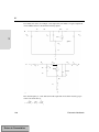
1
multiSIM and Electronics Workbench copyright 1989, 1992-1999 Interactive Image
Technologies Ltd. All rights reserved.
All other brand or product names are trademarks or registered trademarks of their respective
companies or organizations.
Portions of this product are provided under license from:
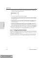
•
•
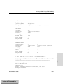
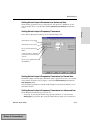
Return to Presentation
Green Mountain Computing Systems
Metamor, Inc.
ISBN 1-55169-091-8 1999 Interactive Image Technologies Ltd. All rights reserved. Published May 1999. Printed in Canada.
Preface
Congratulations on choosing Multisim from Electronics Workbench. We are confident that it
will deliver years of increased productivity and superior designs.
Electronics Workbench is the world’s leading supplier of circuit design tools. Our products
are used by more customers than those of any other EDA vendor, so we are sure you will be
pleased with the value delivered by Multisim, and any other Electronics Workbench products
you may select.
Documentation Conventions
When Multisim manuals refer to a toolbar button, an image of the button appears in the left
column.
The manuals show circuits in black and white—although Multisim is configured to use color
by default, you can change the color scheme.
When you see this icon, the functionality described is only available in certain version of
Multisim, or to users who have purchased add-in modules.
Multisim manuals use the convention Menu/Item to indicate menu commands. For example,
File/Open means choose the Open command from the File menu.
Multisim manuals use the convention of an arrow (¾) to indicate procedural information.
The Multisim Documentation Set
Multisim documentation consists of a Getting Started and Tutorial manual, this User Guide,
and on-line help. All Multisim users receive PDF versions of the Getting Started and Tutorial
manual and the User Guide. Depending on your version of Multisim, you may also receive a
printed version of the manuals.
Return to Presentation
Getting Started and Tutorial
The Getting Started and Tutorial manual introduces you to the Multisim interface. It also
offers an introductory tutorial that takes you through the stages of circuit design, simulation,
analysis and reporting.
User Guide
The User Guide describes Multisim and its many functions in detail. The manual is organized
based on the stages of circuit design, and explains all aspects of using Multisim, in detail.
On-Line Help
Multisim offers a full help file system to support your use of the product. Choose Help/Multisim Manual to display the help file that explains the Multisim program in detail, or choose
Help/Multisim Reference to display the help file that contains reference material (from the
printed appendices) such as details on all the components families provided with Multisim.
Both are standard Windows help files, offering a table of contents and index.
In addition, you can display context-sensitive help by pressing F1 from amy command or window, or by clicking the Help button on any dialog that offers it.
Adobe PDF Files
Both the Getting Started and Tutorial manual and the full User Guide are provided on the
Multisim CD as Adobe PDF files and are accessible from the Multisim program folder on the
Windows Start menu.
License Agreement
Please read the license agreement included in the Multisim Getting Started and Tutorial Manual carefully before installing and using the software contained in this package. By installing
and using the software, you are agreeing to be bound by the terms of this license. If you do not
agree to the terms of this license, simply return the unused software within thirty days to the
place where you obtained it and your money will be refunded.
Return to Presentation
Table of C ontents
C h a p te r 1
Introduction
1.1
1.2
1.3
1.4
1.5
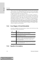
About this Chapter . . . . . . . . . . . . . . . . . . . . . . . . . . . . . . . . . . . . . . . . . . . . . . . . . . .
About this Manual. . . . . . . . . . . . . . . . . . . . . . . . . . . . . . . . . . . . . . . . . . . . . . . . . . . .
What is Multisim? . . . . . . . . . . . . . . . . . . . . . . . . . . . . . . . . . . . . . . . . . . . . . . . . . . . .
Multisim Features Summary. . . . . . . . . . . . . . . . . . . . . . . . . . . . . . . . . . . . . . . . . . . .
About the Circuit Design Process. . . . . . . . . . . . . . . . . . . . . . . . . . . . . . . . . . . . . . . .
1-1
1-1
1-1
1-2
1-4
C h a p te r 2
User Interface
2.1
2.2
2.3
2.4
2.5
2.6
2.7
About this Chapter . . . . . . . . . . . . . . . . . . . . . . . . . . . . . . . . . . . . . . . . . . . . . . . . . . . 2-1
Introduction to the Multisim Interface . . . . . . . . . . . . . . . . . . . . . . . . . . . . . . . . . . . . . 2-2
Introduction to the Design Bar . . . . . . . . . . . . . . . . . . . . . . . . . . . . . . . . . . . . . . . . . . 2-3
Customizing the Interface. . . . . . . . . . . . . . . . . . . . . . . . . . . . . . . . . . . . . . . . . . . . . . 2-4
2.4.1 About User Preferences . . . . . . . . . . . . . . . . . . . . . . . . . . . . . . . . . . . . . . . . . 2-4
2.4.2 Other Customization Options . . . . . . . . . . . . . . . . . . . . . . . . . . . . . . . . . . . . . 2-4
2.4.3 Controlling Circuit Display. . . . . . . . . . . . . . . . . . . . . . . . . . . . . . . . . . . . . . . . 2-5
2.4.4 Controlling Circuit Window Display. . . . . . . . . . . . . . . . . . . . . . . . . . . . . . . . . 2-6
2.4.5 Setting Autosave and Symbol Set . . . . . . . . . . . . . . . . . . . . . . . . . . . . . . . . . 2-8
2.4.6 Print Page Setup Tab . . . . . . . . . . . . . . . . . . . . . . . . . . . . . . . . . . . . . . . . . . . 2-8
Working with Multiple Circuit Windows. . . . . . . . . . . . . . . . . . . . . . . . . . . . . . . . . . . . 2-9
System Toolbar Buttons . . . . . . . . . . . . . . . . . . . . . . . . . . . . . . . . . . . . . . . . . . . . . 2-10
Menus and Commands . . . . . . . . . . . . . . . . . . . . . . . . . . . . . . . . . . . . . . . . . . . . . . 2-10
2.7.1 File Menu . . . . . . . . . . . . . . . . . . . . . . . . . . . . . . . . . . . . . . . . . . . . . . . . . . . 2-10
2.7.2 Edit Menu . . . . . . . . . . . . . . . . . . . . . . . . . . . . . . . . . . . . . . . . . . . . . . . . . . . 2-13
2.7.3 View Menu . . . . . . . . . . . . . . . . . . . . . . . . . . . . . . . . . . . . . . . . . . . . . . . . . . 2-16
2.7.4 Simulate Menu . . . . . . . . . . . . . . . . . . . . . . . . . . . . . . . . . . . . . . . . . . . . . . . 2-18
2.7.5 Transfer Menu . . . . . . . . . . . . . . . . . . . . . . . . . . . . . . . . . . . . . . . . . . . . . . . 2-23
2.7.6 Tools Menu . . . . . . . . . . . . . . . . . . . . . . . . . . . . . . . . . . . . . . . . . . . . . . . . . . 2-25
2.7.7 Window Menu . . . . . . . . . . . . . . . . . . . . . . . . . . . . . . . . . . . . . . . . . . . . . . . . 2-25
2.7.8 Help Menu . . . . . . . . . . . . . . . . . . . . . . . . . . . . . . . . . . . . . . . . . . . . . . . . . . 2-25
Multisim User Guide
Return to Presentation
i
C h a p te r 3
Schematic Capture
3.1
3.2
3.3
About this Chapter . . . . . . . . . . . . . . . . . . . . . . . . . . . . . . . . . . . . . . . . . . . . . . . . . . . 3-1
Introduction to Schematic Capture . . . . . . . . . . . . . . . . . . . . . . . . . . . . . . . . . . . . . . . 3-1
Setting up Your Circuit Window . . . . . . . . . . . . . . . . . . . . . . . . . . . . . . . . . . . . . . . . . 3-1
3.3.1 Setting up a Sheet Size . . . . . . . . . . . . . . . . . . . . . . . . . . . . . . . . . . . . . . . . . 3-2
3.3.2 Displaying or Hiding Grid, Title Block and Page Borders . . . . . . . . . . . . . . . . 3-2
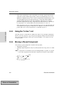
3.3.3 Selecting a Symbol Set. . . . . . . . . . . . . . . . . . . . . . . . . . . . . . . . . . . . . . . . . . 3-3
3.4
Selecting Components from the Database . . . . . . . . . . . . . . . . . . . . . . . . . . . . . . . . 3-3
3.5
Placing Components . . . . . . . . . . . . . . . . . . . . . . . . . . . . . . . . . . . . . . . . . . . . . . . . . 3-4
3.5.1 Choosing a Component Using the Component Group Toolbars and
Browser Screen . . . . . . . . . . . . . . . . . . . . . . . . . . . . . . . . . . . . . . . . . . . . . . . 3-4
3.5.2 Choosing a Component with the Place Component Command . . . . . . . . . . 3-6
3.5.3 Using the “In Use” List . . . . . . . . . . . . . . . . . . . . . . . . . . . . . . . . . . . . . . . . . . . 3-8
3.5.4 Moving a Placed Component . . . . . . . . . . . . . . . . . . . . . . . . . . . . . . . . . . . . . 3-8
3.5.5 Copying a Placed Component . . . . . . . . . . . . . . . . . . . . . . . . . . . . . . . . . . . . . 3-9
3.5.6 Controlling Component Color . . . . . . . . . . . . . . . . . . . . . . . . . . . . . . . . . . . . . 3-9
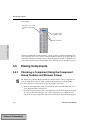
3.6
Wiring Components . . . . . . . . . . . . . . . . . . . . . . . . . . . . . . . . . . . . . . . . . . . . . . . . . . 3-9
3.6.1 Wiring Components Automatically . . . . . . . . . . . . . . . . . . . . . . . . . . . . . . . . 3-10
3.6.2 Wiring Components Manually. . . . . . . . . . . . . . . . . . . . . . . . . . . . . . . . . . . . 3-10
3.6.3 Combining Automatic and Manual Wiring. . . . . . . . . . . . . . . . . . . . . . . . . . . 3-11
3.6.4 Modifying Wire Path . . . . . . . . . . . . . . . . . . . . . . . . . . . . . . . . . . . . . . . . . . . 3-12
3.6.5 Controlling Wire Color. . . . . . . . . . . . . . . . . . . . . . . . . . . . . . . . . . . . . . . . . . 3-12
3.7
Manually Adding a Junction (Connector) . . . . . . . . . . . . . . . . . . . . . . . . . . . . . . . . . 3-13
3.8
Rotating/Flipping Components . . . . . . . . . . . . . . . . . . . . . . . . . . . . . . . . . . . . . . . . . 3-13
3.9
Placed Component Properties . . . . . . . . . . . . . . . . . . . . . . . . . . . . . . . . . . . . . . . . . 3-14
3.9.1 Displaying Identifying Information about a Placed Component . . . . . . . . . . 3-15
3.9.2 Viewing a Placed Component’s Value/Model . . . . . . . . . . . . . . . . . . . . . . . 3-16
3.9.3 Controlling How a Placed Component is Used in Analyses . . . . . . . . . . . . . 3-18
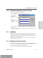
3.10 Finding Components in Your Circuit. . . . . . . . . . . . . . . . . . . . . . . . . . . . . . . . . . . . . 3-19
3.11 Labelling . . . . . . . . . . . . . . . . . . . . . . . . . . . . . . . . . . . . . . . . . . . . . . . . . . . . . . . . . . 3-19
3.11.1 Modifying Component Labels . . . . . . . . . . . . . . . . . . . . . . . . . . . . . . . . . . . . 3-19
3.11.2 Modifying Node Numbers . . . . . . . . . . . . . . . . . . . . . . . . . . . . . . . . . . . . . . . 3-20
3.11.3 Adding a Title Block . . . . . . . . . . . . . . . . . . . . . . . . . . . . . . . . . . . . . . . . . . . 3-21
3.11.4 Adding Miscellaneous Text. . . . . . . . . . . . . . . . . . . . . . . . . . . . . . . . . . . . . . 3-21
3.12 Virtual Wiring . . . . . . . . . . . . . . . . . . . . . . . . . . . . . . . . . . . . . . . . . . . . . . . . . . . . . . 3-22
ii
Return to Presentation
Electronics Workbench
3.13 Subcircuits and Hierarchy . . . . . . . . . . . . . . . . . . . . . . . . . . . . . . . . . . . . . . . . . . . .
3.13.1 Subcircuits vs. Hierarchy . . . . . . . . . . . . . . . . . . . . . . . . . . . . . . . . . . . . . . .
3.13.2 Setting up a Circuit for Use as a Subcircuit . . . . . . . . . . . . . . . . . . . . . . . . .
3.13.3 Adding Subcircuits to a Circuit . . . . . . . . . . . . . . . . . . . . . . . . . . . . . . . . . . .
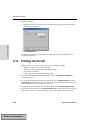
3.14 Printing the Circuit . . . . . . . . . . . . . . . . . . . . . . . . . . . . . . . . . . . . . . . . . . . . . . . . . .
3.15 Placing a Bus . . . . . . . . . . . . . . . . . . . . . . . . . . . . . . . . . . . . . . . . . . . . . . . . . . . . . .
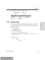
3.16 Using the Pop-up Menu . . . . . . . . . . . . . . . . . . . . . . . . . . . . . . . . . . . . . . . . . . . . . .
3.16.1 From Circuit Window, with no Component Selected . . . . . . . . . . . . . . . . . .
3.16.2 From Circuit Window, with Component or Instrument Selected . . . . . . . . . .
3.16.3 From Circuit Window, with Wire Selected. . . . . . . . . . . . . . . . . . . . . . . . . . .
3-23
3-23
3-24
3-25
3-26
3-27
3-29
3-29
3-30
3-31
C h a p te r 4
Components
4.1
4.2
4.3
4.4
4.5
About this Chapter . . . . . . . . . . . . . . . . . . . . . . . . . . . . . . . . . . . . . . . . . . . . . . . . . . . 4-1
Structure of the Component Database . . . . . . . . . . . . . . . . . . . . . . . . . . . . . . . . . . . . 4-1
4.2.1 Database Levels . . . . . . . . . . . . . . . . . . . . . . . . . . . . . . . . . . . . . . . . . . . . . . . 4-1
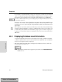
4.2.2 Displaying Database Level Information . . . . . . . . . . . . . . . . . . . . . . . . . . . . . . 4-2
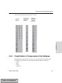
4.2.3 Classification of Components in the Database . . . . . . . . . . . . . . . . . . . . . . . . 4-3
Locating Components in the Database . . . . . . . . . . . . . . . . . . . . . . . . . . . . . . . . . . 4-19
4.3.1 Browsing for Components . . . . . . . . . . . . . . . . . . . . . . . . . . . . . . . . . . . . . . 4-19
4.3.2 Standard Searching for Components . . . . . . . . . . . . . . . . . . . . . . . . . . . . . 4-19
4.3.3 Advanced Searching for Components . . . . . . . . . . . . . . . . . . . . . . . . . . . . . 4-22
Types of Information Stored for Components . . . . . . . . . . . . . . . . . . . . . . . . . . . . . 4-23
4.4.1 Pre-Defined Fields . . . . . . . . . . . . . . . . . . . . . . . . . . . . . . . . . . . . . . . . . . . . 4-24
4.4.2 User Fields . . . . . . . . . . . . . . . . . . . . . . . . . . . . . . . . . . . . . . . . . . . . . . . . . . 4-26
Component Nominal Values and Tolerances . . . . . . . . . . . . . . . . . . . . . . . . . . . . . . 4-26
C h a p te r 5
Component Editor
5.1
5.2
5.3
5.4
About this Chapter . . . . . . . . . . . . . . . . . . . . . . . . . . . . . . . . . . . . . . . . . . . . . . . . . . .
Introduction to the Component Editor. . . . . . . . . . . . . . . . . . . . . . . . . . . . . . . . . . . . .
General Procedures for Starting the Component Editor . . . . . . . . . . . . . . . . . . . . . .
5.3.1 Editing Components . . . . . . . . . . . . . . . . . . . . . . . . . . . . . . . . . . . . . . . . . . . .
5.3.2 Adding Components . . . . . . . . . . . . . . . . . . . . . . . . . . . . . . . . . . . . . . . . . . . .
5.3.3 Removing Components . . . . . . . . . . . . . . . . . . . . . . . . . . . . . . . . . . . . . . . . .
Specifying or Editing General Component Properties . . . . . . . . . . . . . . . . . . . . . . . .
5.4.1 Specifying a Component’s User Properties . . . . . . . . . . . . . . . . . . . . . . . . . .
Multisim User Guide
Return to Presentation
5-1
5-1
5-2
5-3
5-5
5-5
5-6
5-8
iii
5.5
5.6
5.7
5.8
5.9
Editing and Creating a Component Symbol . . . . . . . . . . . . . . . . . . . . . . . . . . . . . . . 5-8
5.5.1 Copying a Component’s Symbol . . . . . . . . . . . . . . . . . . . . . . . . . . . . . . . . . 5-10
5.5.2 Creating and Editing a Component’s Symbol with the Symbol Editor . . . . . 5-11
Creating or Editing a Component Model . . . . . . . . . . . . . . . . . . . . . . . . . . . . . . . . . 5-18
5.6.1 Editing a Component’s Model Information . . . . . . . . . . . . . . . . . . . . . . . . . . 5-20
5.6.2 Copying a Component’s Model . . . . . . . . . . . . . . . . . . . . . . . . . . . . . . . . . . 5-21
5.6.3 Loading an Existing Model . . . . . . . . . . . . . . . . . . . . . . . . . . . . . . . . . . . . . . 5-21
Creating and Editing Component Packages/Footprints . . . . . . . . . . . . . . . . . . . . . . 5-24
5.7.1 Pin Group Naming Convention . . . . . . . . . . . . . . . . . . . . . . . . . . . . . . . . . . . 5-26
5.7.2 Pin Type Naming Convention . . . . . . . . . . . . . . . . . . . . . . . . . . . . . . . . . . . . 5-26
Creating a Component Model Using the Model Makers. . . . . . . . . . . . . . . . . . . . . . 5-28
5.8.1 BJT Model Maker . . . . . . . . . . . . . . . . . . . . . . . . . . . . . . . . . . . . . . . . . . . . . 5-29
5.8.2 Diode Model Maker. . . . . . . . . . . . . . . . . . . . . . . . . . . . . . . . . . . . . . . . . . . . 5-41
5.8.3 MOSFET (Field Effect Transistor) Model Maker. . . . . . . . . . . . . . . . . . . . . . 5-46
5.8.4 Operational Amplifier Model Maker . . . . . . . . . . . . . . . . . . . . . . . . . . . . . . . 5-55
5.8.5 Silicon Controlled Rectifier Model Maker . . . . . . . . . . . . . . . . . . . . . . . . . . . 5-63
5.8.6 Zener Model Maker. . . . . . . . . . . . . . . . . . . . . . . . . . . . . . . . . . . . . . . . . . . . 5-67
Creating a Model Using Code Modeling. . . . . . . . . . . . . . . . . . . . . . . . . . . . . . . . . . 5-72
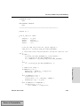
5.9.1 What is Code Modeling?. . . . . . . . . . . . . . . . . . . . . . . . . . . . . . . . . . . . . . . . 5-73
5.9.2 Creating a Code Model. . . . . . . . . . . . . . . . . . . . . . . . . . . . . . . . . . . . . . . . . 5-73
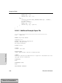
5.9.3 The Interface File (Ifspec.ifs) . . . . . . . . . . . . . . . . . . . . . . . . . . . . . . . . . . . . 5-74
5.9.4 The Implementation File (Cfunc.mod) . . . . . . . . . . . . . . . . . . . . . . . . . . . . . 5-80
C h a p te r 6
Instruments
6.1
6.2
6.3
6.4
6.5
6.6
6.7
About this Chapter . . . . . . . . . . . . . . . . . . . . . . . . . . . . . . . . . . . . . . . . . . . . . . . . . . . 6-1
Introduction to the Multisim Instruments. . . . . . . . . . . . . . . . . . . . . . . . . . . . . . . . . . . 6-1
Working with Multiple Instruments . . . . . . . . . . . . . . . . . . . . . . . . . . . . . . . . . . . . . . . 6-4
Default Instrument Analysis Settings . . . . . . . . . . . . . . . . . . . . . . . . . . . . . . . . . . . . . 6-4
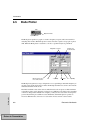
Bode Plotter . . . . . . . . . . . . . . . . . . . . . . . . . . . . . . . . . . . . . . . . . . . . . . . . . . . . . . . . 6-6
6.5.1 Magnitude or Phase . . . . . . . . . . . . . . . . . . . . . . . . . . . . . . . . . . . . . . . . . . . . 6-7
6.5.2 Vertical and Horizontal Axes Settings. . . . . . . . . . . . . . . . . . . . . . . . . . . . . . . 6-7
6.5.3 Readouts . . . . . . . . . . . . . . . . . . . . . . . . . . . . . . . . . . . . . . . . . . . . . . . . . . . . 6-8
Distortion Analyzer . . . . . . . . . . . . . . . . . . . . . . . . . . . . . . . . . . . . . . . . . . . . . . . . . . 6-9
6.6.1 Harmonic Distortion . . . . . . . . . . . . . . . . . . . . . . . . . . . . . . . . . . . . . . . . . . . 6-10
6.6.2 SINAD. . . . . . . . . . . . . . . . . . . . . . . . . . . . . . . . . . . . . . . . . . . . . . . . . . . . . . 6-10
Function Generator . . . . . . . . . . . . . . . . . . . . . . . . . . . . . . . . . . . . . . . . . . . . . . . . . 6-10
6.7.1 Waveform Selection . . . . . . . . . . . . . . . . . . . . . . . . . . . . . . . . . . . . . . . . . . . 6-11
iv
Return to Presentation
Electronics Workbench
6.8
6.9
6.10
6.11
6.12
6.13
6.14
6.15
6.16
6.7.2 Signal Options . . . . . . . . . . . . . . . . . . . . . . . . . . . . . . . . . . . . . . . . . . . . . . .
6.7.3 Rise Time . . . . . . . . . . . . . . . . . . . . . . . . . . . . . . . . . . . . . . . . . . . . . . . . . . .
Logic Converter . . . . . . . . . . . . . . . . . . . . . . . . . . . . . . . . . . . . . . . . . . . . . . . . . . . .
6.8.1 Deriving a Truth Table from a Circuit . . . . . . . . . . . . . . . . . . . . . . . . . . . . . .
6.8.2 Entering and Converting a Truth Table. . . . . . . . . . . . . . . . . . . . . . . . . . . . .
6.8.3 Entering and Converting a Boolean Expression . . . . . . . . . . . . . . . . . . . . . .
Logic Analyzer . . . . . . . . . . . . . . . . . . . . . . . . . . . . . . . . . . . . . . . . . . . . . . . . . . . . .
6.9.1 Start, Stop & Reset . . . . . . . . . . . . . . . . . . . . . . . . . . . . . . . . . . . . . . . . . . . .
6.9.2 Clock. . . . . . . . . . . . . . . . . . . . . . . . . . . . . . . . . . . . . . . . . . . . . . . . . . . . . . .
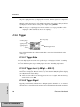
6.9.3 Triggering . . . . . . . . . . . . . . . . . . . . . . . . . . . . . . . . . . . . . . . . . . . . . . . . . . .
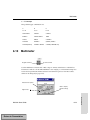
Multimeter . . . . . . . . . . . . . . . . . . . . . . . . . . . . . . . . . . . . . . . . . . . . . . . . . . . . . . . .
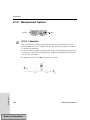
6.10.1 Measurement Options . . . . . . . . . . . . . . . . . . . . . . . . . . . . . . . . . . . . . . . . .
6.10.2 Signal Mode (AC or DC) . . . . . . . . . . . . . . . . . . . . . . . . . . . . . . . . . . . . . . . .
6.10.3 Internal Settings . . . . . . . . . . . . . . . . . . . . . . . . . . . . . . . . . . . . . . . . . . . . . .
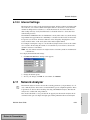
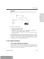
Network Analyzer . . . . . . . . . . . . . . . . . . . . . . . . . . . . . . . . . . . . . . . . . . . . . . . . . . .
Oscilloscope . . . . . . . . . . . . . . . . . . . . . . . . . . . . . . . . . . . . . . . . . . . . . . . . . . . . . .
6.12.1 Time Base (0.1 ns/Div — 1s/Div) . . . . . . . . . . . . . . . . . . . . . . . . . . . . . . . . .
6.12.2 Grounding . . . . . . . . . . . . . . . . . . . . . . . . . . . . . . . . . . . . . . . . . . . . . . . . . . .
6.12.3 Channel A and Channel B Settings . . . . . . . . . . . . . . . . . . . . . . . . . . . . . . .
6.12.4 Trigger . . . . . . . . . . . . . . . . . . . . . . . . . . . . . . . . . . . . . . . . . . . . . . . . . . . . .
6.12.5 Using Cursors and Readouts . . . . . . . . . . . . . . . . . . . . . . . . . . . . . . . . . . . .
Spectrum Analyzer . . . . . . . . . . . . . . . . . . . . . . . . . . . . . . . . . . . . . . . . . . . . . . . . . .
Wattmeter . . . . . . . . . . . . . . . . . . . . . . . . . . . . . . . . . . . . . . . . . . . . . . . . . . . . . . . .
Word Generator . . . . . . . . . . . . . . . . . . . . . . . . . . . . . . . . . . . . . . . . . . . . . . . . . . . .
6.15.1 Entering Words . . . . . . . . . . . . . . . . . . . . . . . . . . . . . . . . . . . . . . . . . . . . . . .
6.15.2 Controls . . . . . . . . . . . . . . . . . . . . . . . . . . . . . . . . . . . . . . . . . . . . . . . . . . . .
6.15.3 Creating, Saving and Reusing Word Patterns . . . . . . . . . . . . . . . . . . . . . . .
6.15.4 Addressing . . . . . . . . . . . . . . . . . . . . . . . . . . . . . . . . . . . . . . . . . . . . . . . . . .
6.15.5 Triggering . . . . . . . . . . . . . . . . . . . . . . . . . . . . . . . . . . . . . . . . . . . . . . . . . . .
6.15.6 Frequency and Data Ready . . . . . . . . . . . . . . . . . . . . . . . . . . . . . . . . . . . . .
Ammeter and Voltmeter . . . . . . . . . . . . . . . . . . . . . . . . . . . . . . . . . . . . . . . . . . . . . .
6-11
6-12
6-12
6-13
6-14
6-14
6-15
6-17
6-17
6-18
6-19
6-20
6-22
6-23
6-23
6-24
6-26
6-26
6-27
6-28
6-29
6-29
6-30
6-31
6-32
6-32
6-33
6-33
6-34
6-34
6-34
C h a p te r 7
Simulation
7.1
7.2
About this Chapter . . . . . . . . . . . . . . . . . . . . . . . . . . . . . . . . . . . . . . . . . . . . . . . . . . .
Introduction to Simulation . . . . . . . . . . . . . . . . . . . . . . . . . . . . . . . . . . . . . . . . . . . . . .
7.2.1 What Type of Simulation Should I Use? . . . . . . . . . . . . . . . . . . . . . . . . . . . . .
7.2.2 What Kind of Simulation Does Multisim Support? . . . . . . . . . . . . . . . . . . . . .
Multisim User Guide
Return to Presentation
7-1
7-1
7-1
7-2
v
7.3
7.4
7.5
7.6
7.7
Using Multisim Simulation . . . . . . . . . . . . . . . . . . . . . . . . . . . . . . . . . . . . . . . . . . . . . 7-2
7.3.1 Start/Stop/Pause Simulation. . . . . . . . . . . . . . . . . . . . . . . . . . . . . . . . . . . . . . 7-3
7.3.2 Interactive Simulation . . . . . . . . . . . . . . . . . . . . . . . . . . . . . . . . . . . . . . . . . . . 7-4
7.3.3 Circuit Consistency Check . . . . . . . . . . . . . . . . . . . . . . . . . . . . . . . . . . . . . . . 7-4
7.3.4 Miscellaneous SPICE Simulation Capabilities . . . . . . . . . . . . . . . . . . . . . . . . 7-4
Multisim SPICE Simulation: Technical Detail . . . . . . . . . . . . . . . . . . . . . . . . . . . . . . . 7-5
7.4.1 BSpice/XSpice Support . . . . . . . . . . . . . . . . . . . . . . . . . . . . . . . . . . . . . . . . . 7-5
7.4.2 Circuit Simulation Mechanism . . . . . . . . . . . . . . . . . . . . . . . . . . . . . . . . . . . . 7-5
7.4.3 Four Stages of Circuit Simulation . . . . . . . . . . . . . . . . . . . . . . . . . . . . . . . . . . 7-6
7.4.4 Equation Formulation . . . . . . . . . . . . . . . . . . . . . . . . . . . . . . . . . . . . . . . . . . . 7-6
7.4.5 Equation Solution . . . . . . . . . . . . . . . . . . . . . . . . . . . . . . . . . . . . . . . . . . . . . . 7-7
7.4.6 Numerical Integration . . . . . . . . . . . . . . . . . . . . . . . . . . . . . . . . . . . . . . . . . . . 7-8
7.4.7 User Setting: Maximum Integration Order . . . . . . . . . . . . . . . . . . . . . . . . . . . 7-9
7.4.8 Convergence Assistance Algorithms . . . . . . . . . . . . . . . . . . . . . . . . . . . . . . . 7-9
RF Simulation . . . . . . . . . . . . . . . . . . . . . . . . . . . . . . . . . . . . . . . . . . . . . . . . . . . . . . 7-10
VHDL Simulation . . . . . . . . . . . . . . . . . . . . . . . . . . . . . . . . . . . . . . . . . . . . . . . . . . . 7-10
Verilog Simulation . . . . . . . . . . . . . . . . . . . . . . . . . . . . . . . . . . . . . . . . . . . . . . . . . . 7-11
C h a p te r
Analyses
8.1
8.2
8.3
8.4
8.5
8.6
8
About this Chapter . . . . . . . . . . . . . . . . . . . . . . . . . . . . . . . . . . . . . . . . . . . . . . . . . . . 8-1
Introduction to Multisim Analyses . . . . . . . . . . . . . . . . . . . . . . . . . . . . . . . . . . . . . . . . 8-1
Working with Analyses . . . . . . . . . . . . . . . . . . . . . . . . . . . . . . . . . . . . . . . . . . . . . . . . 8-1
8.3.1 General Instructions . . . . . . . . . . . . . . . . . . . . . . . . . . . . . . . . . . . . . . . . . . . . 8-2
8.3.2 The Analysis Parameters Tab. . . . . . . . . . . . . . . . . . . . . . . . . . . . . . . . . . . . . 8-2
8.3.3 The Output Variables Tab . . . . . . . . . . . . . . . . . . . . . . . . . . . . . . . . . . . . . . . . 8-3
8.3.4 The Miscellaneous Options Tab . . . . . . . . . . . . . . . . . . . . . . . . . . . . . . . . . . . 8-6
8.3.5 The Summary Tab . . . . . . . . . . . . . . . . . . . . . . . . . . . . . . . . . . . . . . . . . . . . . 8-8
8.3.6 Incomplete Analyses. . . . . . . . . . . . . . . . . . . . . . . . . . . . . . . . . . . . . . . . . . . . 8-8
DC Operating Point Analysis . . . . . . . . . . . . . . . . . . . . . . . . . . . . . . . . . . . . . . . . . . . 8-9
8.4.1 About the DC Operating Point Analysis . . . . . . . . . . . . . . . . . . . . . . . . . . . . . 8-9
8.4.2 Setting DC Operating Point Analysis Parameters . . . . . . . . . . . . . . . . . . . . . 8-9
8.4.3 Troubleshooting DC Operating Point Analysis Failures . . . . . . . . . . . . . . . . 8-10
AC Analysis . . . . . . . . . . . . . . . . . . . . . . . . . . . . . . . . . . . . . . . . . . . . . . . . . . . . . . . 8-11
8.5.1 About the AC Analysis . . . . . . . . . . . . . . . . . . . . . . . . . . . . . . . . . . . . . . . . . 8-11
8.5.2 Setting AC Analysis Frequency Parameters. . . . . . . . . . . . . . . . . . . . . . . . . 8-11
Transient Analysis . . . . . . . . . . . . . . . . . . . . . . . . . . . . . . . . . . . . . . . . . . . . . . . . . . 8-13
8.6.1 About the Transient Analysis . . . . . . . . . . . . . . . . . . . . . . . . . . . . . . . . . . . . 8-13
vi
Return to Presentation
Electronics Workbench
8.7
8.8
8.9
8.10
8.11
8.12
8.13
8.14
8.15
8.16
8.17
8.6.2 Setting Transient Analysis Parameters. . . . . . . . . . . . . . . . . . . . . . . . . . . . .
8.6.3 Troubleshooting Transient Analysis Failures . . . . . . . . . . . . . . . . . . . . . . . .
Noise Analysis . . . . . . . . . . . . . . . . . . . . . . . . . . . . . . . . . . . . . . . . . . . . . . . . . . . . .
8.7.1 About the Noise Analysis . . . . . . . . . . . . . . . . . . . . . . . . . . . . . . . . . . . . . . .
8.7.2 Noise Analysis Example . . . . . . . . . . . . . . . . . . . . . . . . . . . . . . . . . . . . . . . .
8.7.3 Setting Noise Analysis Parameters . . . . . . . . . . . . . . . . . . . . . . . . . . . . . . .
Distortion Analysis . . . . . . . . . . . . . . . . . . . . . . . . . . . . . . . . . . . . . . . . . . . . . . . . . .
8.8.1 About the Distortion Analysis . . . . . . . . . . . . . . . . . . . . . . . . . . . . . . . . . . . .
8.8.2 Setting Distortion Analysis Parameters . . . . . . . . . . . . . . . . . . . . . . . . . . . .
DC Sweep Analysis . . . . . . . . . . . . . . . . . . . . . . . . . . . . . . . . . . . . . . . . . . . . . . . . .
8.9.1 About the DC Sweep Analysis . . . . . . . . . . . . . . . . . . . . . . . . . . . . . . . . . . .
8.9.2 Setting DC Sweep Analysis Parameters . . . . . . . . . . . . . . . . . . . . . . . . . . .
DC and AC Sensitivity Analyses . . . . . . . . . . . . . . . . . . . . . . . . . . . . . . . . . . . . . . .
8.10.1 About the Sensitivity Analyses . . . . . . . . . . . . . . . . . . . . . . . . . . . . . . . . . . .
8.10.2 Sensitivity Analyses Example . . . . . . . . . . . . . . . . . . . . . . . . . . . . . . . . . . . .
8.10.3 Setting Sensitivity Analysis Parameters . . . . . . . . . . . . . . . . . . . . . . . . . . . .
Parameter Sweep Analysis . . . . . . . . . . . . . . . . . . . . . . . . . . . . . . . . . . . . . . . . . . .
8.11.1 About the Parameter Sweep Analysis . . . . . . . . . . . . . . . . . . . . . . . . . . . . .
8.11.2 Setting Parameter Sweep Analysis Parameters. . . . . . . . . . . . . . . . . . . . . .
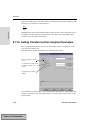
Temperature Sweep Analysis . . . . . . . . . . . . . . . . . . . . . . . . . . . . . . . . . . . . . . . . .
8.12.1 About the Temperature Sweep Analysis . . . . . . . . . . . . . . . . . . . . . . . . . . .
8.12.2 Setting Temperature Sweep Analysis Parameters . . . . . . . . . . . . . . . . . . . .
Transfer Function Analysis . . . . . . . . . . . . . . . . . . . . . . . . . . . . . . . . . . . . . . . . . . . .
8.13.1 About the Transfer Function Analysis. . . . . . . . . . . . . . . . . . . . . . . . . . . . . .
8.13.2 Setting Transfer Function Analysis Parameters . . . . . . . . . . . . . . . . . . . . . .
Worst Case Analysis . . . . . . . . . . . . . . . . . . . . . . . . . . . . . . . . . . . . . . . . . . . . . . . .
8.14.1 About the Worst Case Analysis . . . . . . . . . . . . . . . . . . . . . . . . . . . . . . . . . .
8.14.2 Setting Worst Case Analysis Parameters . . . . . . . . . . . . . . . . . . . . . . . . . . .
Pole Zero Analysis . . . . . . . . . . . . . . . . . . . . . . . . . . . . . . . . . . . . . . . . . . . . . . . . . .
8.15.1 About the Pole Zero Analysis . . . . . . . . . . . . . . . . . . . . . . . . . . . . . . . . . . . .
8.15.2 Setting Pole Zero Analysis Parameters . . . . . . . . . . . . . . . . . . . . . . . . . . . .
Monte Carlo Analysis . . . . . . . . . . . . . . . . . . . . . . . . . . . . . . . . . . . . . . . . . . . . . . . .
8.16.1 About the Monte Carlo Analysis . . . . . . . . . . . . . . . . . . . . . . . . . . . . . . . . . .
8.16.2 Setting Monte Carlo Analysis Parameters . . . . . . . . . . . . . . . . . . . . . . . . . .
Fourier Analysis . . . . . . . . . . . . . . . . . . . . . . . . . . . . . . . . . . . . . . . . . . . . . . . . . . . .
8.17.1 About the Fourier Analysis . . . . . . . . . . . . . . . . . . . . . . . . . . . . . . . . . . . . . .
8.17.2 Setting Fourier Analysis Parameters . . . . . . . . . . . . . . . . . . . . . . . . . . . . . .
Multisim User Guide
Return to Presentation
8-13
8-15
8-16
8-16
8-17
8-17
8-20
8-20
8-20
8-22
8-22
8-23
8-24
8-24
8-25
8-26
8-28
8-28
8-28
8-31
8-31
8-31
8-33
8-33
8-34
8-35
8-35
8-37
8-38
8-38
8-42
8-43
8-43
8-46
8-46
8-46
8-47
vii
8.18 Trace Width Analysis . . . . . . . . . . . . . . . . . . . . . . . . . . . . . . . . . . . . . . . . . . . . . . . .
8.18.1 About Trace Width Analysis . . . . . . . . . . . . . . . . . . . . . . . . . . . . . . . . . . . . .
8.18.2 Setting Trace Width Analysis Parameters . . . . . . . . . . . . . . . . . . . . . . . . . .
8.19 RF Analyses . . . . . . . . . . . . . . . . . . . . . . . . . . . . . . . . . . . . . . . . . . . . . . . . . . . . . . .
8.20 Nested Sweep Analyses . . . . . . . . . . . . . . . . . . . . . . . . . . . . . . . . . . . . . . . . . . . . .
8.21 Batched Analyses. . . . . . . . . . . . . . . . . . . . . . . . . . . . . . . . . . . . . . . . . . . . . . . . . . .
8.22 User-Defined Analyses. . . . . . . . . . . . . . . . . . . . . . . . . . . . . . . . . . . . . . . . . . . . . . .
8.23 Noise Figure Analysis. . . . . . . . . . . . . . . . . . . . . . . . . . . . . . . . . . . . . . . . . . . . . . . .
8.24 Viewing the Analysis Results: Error Log/Audit Trail . . . . . . . . . . . . . . . . . . . . . . . . .
8.25 Viewing the Analysis Results—Grapher. . . . . . . . . . . . . . . . . . . . . . . . . . . . . . . . . .
8.26 Working with Pages . . . . . . . . . . . . . . . . . . . . . . . . . . . . . . . . . . . . . . . . . . . . . . . . .
8.27 Working with Graphs . . . . . . . . . . . . . . . . . . . . . . . . . . . . . . . . . . . . . . . . . . . . . . . .
8.27.1 Grids and Legends . . . . . . . . . . . . . . . . . . . . . . . . . . . . . . . . . . . . . . . . . . . .
8.27.2 Cursors . . . . . . . . . . . . . . . . . . . . . . . . . . . . . . . . . . . . . . . . . . . . . . . . . . . . .
8.27.3 Zoom and Restore . . . . . . . . . . . . . . . . . . . . . . . . . . . . . . . . . . . . . . . . . . . .
8.27.4 Title . . . . . . . . . . . . . . . . . . . . . . . . . . . . . . . . . . . . . . . . . . . . . . . . . . . . . . . .
8.27.5 Axes . . . . . . . . . . . . . . . . . . . . . . . . . . . . . . . . . . . . . . . . . . . . . . . . . . . . . . .
8.27.6 Traces. . . . . . . . . . . . . . . . . . . . . . . . . . . . . . . . . . . . . . . . . . . . . . . . . . . . . .
8.28 Viewing Charts . . . . . . . . . . . . . . . . . . . . . . . . . . . . . . . . . . . . . . . . . . . . . . . . . . . . .
8.29 Cut, Copy and Paste . . . . . . . . . . . . . . . . . . . . . . . . . . . . . . . . . . . . . . . . . . . . . . . .
8.30 Print and Print Preview . . . . . . . . . . . . . . . . . . . . . . . . . . . . . . . . . . . . . . . . . . . . . . .
8.31 Analysis Options. . . . . . . . . . . . . . . . . . . . . . . . . . . . . . . . . . . . . . . . . . . . . . . . . . . .
8-50
8-50
8-52
8-53
8-54
8-55
8-57
8-57
8-58
8-58
8-60
8-61
8-62
8-63
8-64
8-65
8-66
8-67
8-68
8-68
8-69
8-70
C h a p te r 9
Postprocessor
9.1
9.2
9.3
9.4
9.5
About this Chapter . . . . . . . . . . . . . . . . . . . . . . . . . . . . . . . . . . . . . . . . . . . . . . . . . . .
Introduction to the Postprocessor. . . . . . . . . . . . . . . . . . . . . . . . . . . . . . . . . . . . . . . .
Using the Postprocessor . . . . . . . . . . . . . . . . . . . . . . . . . . . . . . . . . . . . . . . . . . . . . .
9.3.1 Basic Steps. . . . . . . . . . . . . . . . . . . . . . . . . . . . . . . . . . . . . . . . . . . . . . . . . . .
9.3.2 Working with Pages, Graphs and Charts . . . . . . . . . . . . . . . . . . . . . . . . . . . .
Postprocessor Variables . . . . . . . . . . . . . . . . . . . . . . . . . . . . . . . . . . . . . . . . . . . . . .
Available Functions . . . . . . . . . . . . . . . . . . . . . . . . . . . . . . . . . . . . . . . . . . . . . . . . . .
viii
Return to Presentation
9-1
9-1
9-2
9-2
9-7
9-8
9-8
Electronics Workbench
C h a p te r 1 0
HDLs and Programmable Logic
10.1 About this Chapter . . . . . . . . . . . . . . . . . . . . . . . . . . . . . . . . . . . . . . . . . . . . . . . . . . 10-1
10.2 Overview of HDLs within Multisim . . . . . . . . . . . . . . . . . . . . . . . . . . . . . . . . . . . . . . 10-1
10.2.1 About HDLs . . . . . . . . . . . . . . . . . . . . . . . . . . . . . . . . . . . . . . . . . . . . . . . . . 10-1
10.2.2 Using Multisim with Programmable Logic . . . . . . . . . . . . . . . . . . . . . . . . . . . 10-2
10.2.3 Using Multisim for Modeling Complex Digital ICs . . . . . . . . . . . . . . . . . . . . . 10-3
10.2.4 How to Use HDLs in Multisim . . . . . . . . . . . . . . . . . . . . . . . . . . . . . . . . . . . . 10-3
10.2.5 Introduction to VHDL . . . . . . . . . . . . . . . . . . . . . . . . . . . . . . . . . . . . . . . . . . 10-3
10.2.6 Introduction to Verilog. . . . . . . . . . . . . . . . . . . . . . . . . . . . . . . . . . . . . . . . . . 10-5
10.3 Simulating a Circuit Containing a VHDL-Modeled Device . . . . . . . . . . . . . . . . . . . . 10-6
10.4 Designing, Simulating, and Debugging with Multisim’s VHDL . . . . . . . . . . . . . . . . . 10-7
10.4.1 What is Multisim’s VHDL? . . . . . . . . . . . . . . . . . . . . . . . . . . . . . . . . . . . . . . 10-7
10.4.2 Creating a Project and Using the Hierarchy Browser . . . . . . . . . . . . . . . . . . 10-9
10.4.3 Using the VHDL Wizard . . . . . . . . . . . . . . . . . . . . . . . . . . . . . . . . . . . . . . . 10-15
10.4.4 Using the Test Bench Wizard . . . . . . . . . . . . . . . . . . . . . . . . . . . . . . . . . . . 10-23
10.4.5 Using Simulation. . . . . . . . . . . . . . . . . . . . . . . . . . . . . . . . . . . . . . . . . . . . . 10-28
10.4.6 Working with Waveforms and Cursors . . . . . . . . . . . . . . . . . . . . . . . . . . . . 10-37
10.4.7 Using the Debug Window . . . . . . . . . . . . . . . . . . . . . . . . . . . . . . . . . . . . . 10-38
10.4.8 Using Multisim’s LIB . . . . . . . . . . . . . . . . . . . . . . . . . . . . . . . . . . . . . . . . . . 10-46
10.5 VHDL Synthesis and Programming of FPGAs/CPLDs. . . . . . . . . . . . . . . . . . . . . . 10-48
10.5.1 What does VHDL Synthesis do? . . . . . . . . . . . . . . . . . . . . . . . . . . . . . . . . 10-48
10.5.2 Multisim’s VHDL Synthesis Features . . . . . . . . . . . . . . . . . . . . . . . . . . . . . 10-49
10.5.3 Using Multisim’s VHDL Synthesis. . . . . . . . . . . . . . . . . . . . . . . . . . . . . . . . 10-50
10.6 Simulating a Circuit Containing a Verilog-Modeled Device . . . . . . . . . . . . . . . . . . 10-55
10.7 Design, Simulation and Debug with Multisim’ Verilog . . . . . . . . . . . . . . . . . . . . . . 10-55
10.8 Verilog Synthesis and Programming of CPLDs/FPGAs . . . . . . . . . . . . . . . . . . . . . 10-56
C h a p te r 11
Reports
11.1
11.2
11.3
11.4
About this Chapter . . . . . . . . . . . . . . . . . . . . . . . . . . . . . . . . . . . . . . . . . . . . . . . . . .
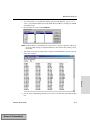
Bill of Materials (BOM) . . . . . . . . . . . . . . . . . . . . . . . . . . . . . . . . . . . . . . . . . . . . . . .
Database Family List . . . . . . . . . . . . . . . . . . . . . . . . . . . . . . . . . . . . . . . . . . . . . . . .
Component Detail Report . . . . . . . . . . . . . . . . . . . . . . . . . . . . . . . . . . . . . . . . . . . . .
Multisim User Guide
Return to Presentation
11-1
11-1
11-2
11-4
ix
C h a p te r 1 2
Transfer/Communication
12.1 About this Chapter . . . . . . . . . . . . . . . . . . . . . . . . . . . . . . . . . . . . . . . . . . . . . . . . . .
12.2 Introduction to Transfer/Communication . . . . . . . . . . . . . . . . . . . . . . . . . . . . . . . . .
12.3 Transferring Data . . . . . . . . . . . . . . . . . . . . . . . . . . . . . . . . . . . . . . . . . . . . . . . . . . .
12.3.1 Transferring from Multisim to Ultiboard for PCB Layout . . . . . . . . . . . . . . . .
12.3.2 Transferring to Other PCB Layout . . . . . . . . . . . . . . . . . . . . . . . . . . . . . . . .
12.4 Exporting Simulation Results . . . . . . . . . . . . . . . . . . . . . . . . . . . . . . . . . . . . . . . . . .
12.4.1 Exporting to MathCAD . . . . . . . . . . . . . . . . . . . . . . . . . . . . . . . . . . . . . . . . .
12.4.2 Exporting to Excel. . . . . . . . . . . . . . . . . . . . . . . . . . . . . . . . . . . . . . . . . . . . .
12-1
12-1
12-1
12-1
12-2
12-2
12-2
12-3
C h a p te r 1 3
Project/Team Design Module
13.1 About this Chapter . . . . . . . . . . . . . . . . . . . . . . . . . . . . . . . . . . . . . . . . . . . . . . . . . .
13.2 Introduction to the Multisim Project/Team Design Module . . . . . . . . . . . . . . . . . . . .
13.3 Project Management and Version Control . . . . . . . . . . . . . . . . . . . . . . . . . . . . . . . .
13.3.1 Setting up Projects . . . . . . . . . . . . . . . . . . . . . . . . . . . . . . . . . . . . . . . . . . . .
13.3.2 Working with Projects . . . . . . . . . . . . . . . . . . . . . . . . . . . . . . . . . . . . . . . . . .
13.3.3 Working with Files Contained in Projects . . . . . . . . . . . . . . . . . . . . . . . . . . .
13.3.4 Version Control . . . . . . . . . . . . . . . . . . . . . . . . . . . . . . . . . . . . . . . . . . . . . .
13.4 Hierarchical Design . . . . . . . . . . . . . . . . . . . . . . . . . . . . . . . . . . . . . . . . . . . . . . . . .
13.4.1 About Hierarchical Design . . . . . . . . . . . . . . . . . . . . . . . . . . . . . . . . . . . . . .
13.4.2 Setting up and Using Hierarchical Design . . . . . . . . . . . . . . . . . . . . . . . . . .
13.5 Remote Control/Design Sharing. . . . . . . . . . . . . . . . . . . . . . . . . . . . . . . . . . . . . . . .
13.6 Working with “Corporate” Level Data . . . . . . . . . . . . . . . . . . . . . . . . . . . . . . . . . . . .
13.7 Working with User Fields . . . . . . . . . . . . . . . . . . . . . . . . . . . . . . . . . . . . . . . . . . . . .
13-1
13-1
13-1
13-1
13-3
13-3
13-4
13-5
13-5
13-6
13-6
13-7
13-7
C h a p te r 1 4
RF
14.1 About this Chapter . . . . . . . . . . . . . . . . . . . . . . . . . . . . . . . . . . . . . . . . . . . . . . . . . .
14.2 Introduction to the Multisim RF Module . . . . . . . . . . . . . . . . . . . . . . . . . . . . . . . . . .
14.3 Components . . . . . . . . . . . . . . . . . . . . . . . . . . . . . . . . . . . . . . . . . . . . . . . . . . . . . . .
14.3.1 About RF Components . . . . . . . . . . . . . . . . . . . . . . . . . . . . . . . . . . . . . . . . .
14.3.2 Multisim’s RF Components . . . . . . . . . . . . . . . . . . . . . . . . . . . . . . . . . . . . . .
14.3.3 Theoretical Explanation of the RF Models . . . . . . . . . . . . . . . . . . . . . . . . . .
x
Return to Presentation
14-1
14-1
14-2
14-2
14-3
14-3
Electronics Workbench
14.4 RF Instruments . . . . . . . . . . . . . . . . . . . . . . . . . . . . . . . . . . . . . . . . . . . . . . . . . . . . . 14-9
14.4.1 Spectrum Analyzer . . . . . . . . . . . . . . . . . . . . . . . . . . . . . . . . . . . . . . . . . . . . 14-9
14.4.2 Network Analyzer . . . . . . . . . . . . . . . . . . . . . . . . . . . . . . . . . . . . . . . . . . . . 14-15
14.5 RF Analyses . . . . . . . . . . . . . . . . . . . . . . . . . . . . . . . . . . . . . . . . . . . . . . . . . . . . . . 14-18
14.5.1 RF Characterizer Analysis . . . . . . . . . . . . . . . . . . . . . . . . . . . . . . . . . . . . . 14-18
14.5.2 Matching Network Analysis. . . . . . . . . . . . . . . . . . . . . . . . . . . . . . . . . . . . . 14-20
14.5.3 Noise Figure Analysis . . . . . . . . . . . . . . . . . . . . . . . . . . . . . . . . . . . . . . . . . 14-24
14.6 RF Model Makers . . . . . . . . . . . . . . . . . . . . . . . . . . . . . . . . . . . . . . . . . . . . . . . . . . 14-26
14.6.1 Waveguide . . . . . . . . . . . . . . . . . . . . . . . . . . . . . . . . . . . . . . . . . . . . . . . . . . 14-27
14.6.2 Microstrip Line . . . . . . . . . . . . . . . . . . . . . . . . . . . . . . . . . . . . . . . . . . . . . . . 14-28
14.6.3 Open End Microstrip Line . . . . . . . . . . . . . . . . . . . . . . . . . . . . . . . . . . . . . . 14-29
14.6.4 RF Spiral Inductor. . . . . . . . . . . . . . . . . . . . . . . . . . . . . . . . . . . . . . . . . . . . 14-30
14.6.5 Strip Line Model . . . . . . . . . . . . . . . . . . . . . . . . . . . . . . . . . . . . . . . . . . . . . 14-31
14.6.6 Stripline Bend . . . . . . . . . . . . . . . . . . . . . . . . . . . . . . . . . . . . . . . . . . . . . . . 14-32
14.6.7 Lossy Line . . . . . . . . . . . . . . . . . . . . . . . . . . . . . . . . . . . . . . . . . . . . . . . . . 14-33
14.6.8 Interdigital Capacitor. . . . . . . . . . . . . . . . . . . . . . . . . . . . . . . . . . . . . . . . . . 14-35
14.7 Tutorial: Designing RF Circuits. . . . . . . . . . . . . . . . . . . . . . . . . . . . . . . . . . . . . . . . 14-36
14.7.1 Selecting Type of RF Amplifier . . . . . . . . . . . . . . . . . . . . . . . . . . . . . . . . . . 14-37
14.7.2 Selecting an RF Transistor . . . . . . . . . . . . . . . . . . . . . . . . . . . . . . . . . . . . . 14-37
14.7.3 Selecting a DC-operating Point . . . . . . . . . . . . . . . . . . . . . . . . . . . . . . . . . 14-38
14.7.4 Selecting the Biasing Network . . . . . . . . . . . . . . . . . . . . . . . . . . . . . . . . . . 14-38
A p p e n d ix A
VHDL Primer
A p p e n d ix B
Verilog Primer
A p p e n d ix C
Sources Components
A p p e n d ix D
Basic Components
A p p e n d ix E
Diodes Components
Multisim User Guide
Return to Presentation
xi
A p p e n d ix F
Transistors Components
A p p e n d ix G
Analog Components
A p p e n d ix H
TTL Components
A p p e n d ix I
CMOS Components
A p p e n d ix J
Misc. Digital Components
A p p e n d ix K
Mixed Components
A p p e n d ix L
Indicators Components
A p p e n d ix M
Misc. Components
A p p e n d ix N
Controls Components
A p p e n d ix O
RF Components
A p p e n d ix P
Electro-Mechanical Components
xii
Return to Presentation
Electronics Workbench
A p p e n d ix Q
Functions (4000 Series)
A p p e n d ix R
Functions (74XX Series)
Index
Multisim User Guide
Return to Presentation
xiii
xiv
Return to Presentation
Electronics Workbench
Introduction
C h a p te r
1
Introduction
1.1
About this Chapter . . . . . . . . . . . . . . . . . . . . . . . . . . . . . . . . . . . . . . . . . . . . . . . . . . . 1-1
1.2
About this Manual. . . . . . . . . . . . . . . . . . . . . . . . . . . . . . . . . . . . . . . . . . . . . . . . . . . . 1-1
1.3
What is Multisim? . . . . . . . . . . . . . . . . . . . . . . . . . . . . . . . . . . . . . . . . . . . . . . . . . . . . 1-2
1.4
Multisim Features Summary. . . . . . . . . . . . . . . . . . . . . . . . . . . . . . . . . . . . . . . . . . . . 1-2
1.5
About the Circuit Design Process. . . . . . . . . . . . . . . . . . . . . . . . . . . . . . . . . . . . . . . . 1-4
Multisim User Guide
Return to Presentation
Introduction
Electronics Workbench
Return to Presentation
Introduction
Chapter
1
Introduction
1.1
About this Chapter
This chapter briefly introduces you to this manual and to Multisim itself. It also provides a
summary of Multisim’s features and in which version they are available.
1.2
About this Manual
This manual is written for all Multisim users. It explains, in detail, all aspects of the Multisim
product. The manual contains both:
•
chapters, which explain features and functions, and which are organized based on the
Design Bar buttons
• appendices, which contain reference-type information.
Depending on your Multisim version, this manual, or just its appendices, may be available
only on-line, not in print.
This manual describes a number of functions that are available only in some versions of Multisim, or to users who have purchased optional modules. Such functions are identified by the
icon shown in the column to the left. To order optional modules, contact Electronics Workbench. For a list of features in each product, see page 1-2.
This manual assumes that you are familiar with Windows applications and know how, for
example, to choose a menu from a command, use the mouse to select an item, and enable/disable an option box. If you are new to Windows, see your Windows documentation for help.
1.3
What is Multisim?
Multisim is a complete system design tool that offers a large component database, schematic
entry, full analog/digital SPICE simulation, VHDL/Verilog design entry/simulation, FPGA/
CPLD synthesis, RF capabilities, postprocessing features and seamless transfer to PCB layout
Multisim User Guide
Return to Presentation
1-1
Introduction
Introduction
packages such as Ultiboard, also from Electronics Workbench. It offers a single, easy-to-use
graphical interface for all your design needs.
Multisim provides all the advanced functionality you need to take designs from specification
to production. And because the program tightly integrates schematic capture, simulation, PCB
layout and programmable logic, you can design with confidence, knowing that you are free
from the integration issues often found when exchanging data between applications from different vendors.
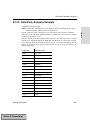
1.4
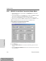
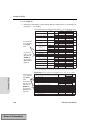
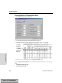
Multisim Features Summary
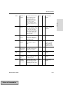
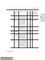
Module
Personal Version
Professional
Version
Power
Professional
Version
Basic Schematic Capture
9
9
9
Interactive Simulation
9
9
9
Symbol Editor
9
9
9
SPICE Analog/Digital Simulation
9
9
9
Editable Footprint Field
9
9
9
Electro-mechanical Components
9
9
9
DC Operating Point Analysis
9
9
9
AC Analysis
9
9
9
Transient Analysis
9
9
9
Fourier Analysis
9
9
9
Noise Analysis
9
9
9
Distortion Analysis
9
9
9
DC Sweep Analysis
9
9
9
AC and DC Sensitivity Analysis
9
9
9
Virtual Instruments
9
9
11
1-2
Return to Presentation
Electronics Workbench
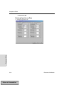
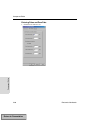
Module
Personal Version
Professional
Version
Power
Professional
Version
Component Database and Editor
standard, with
6,000 parts
standard, with
12,000 parts
advanced, with
16000 parts
Model Expansion Package
Optional
Optional
9
SPICE Import
9
9
Distortion Analysis Instrument
9
9
Virtual Wiring
9
9
Menu-driven Simulation from Netlist
(without schematic)
9
9
Multiple Circuit Windows
9
9
Parameter Sweep Analysis
9
9
Temperature Sweep Analysis
9
9
Pole Zero Analysis
9
9
Transfer Function Analysis
9
9
Worst Case Analysis
9
9
Monte Carlo Analysis
9
9
Trace Width Analysis
9
9
Component Search Engine
standard
advanced
Bill of Material
standard
advanced
VHDL
optional
design/debug
and simulation
Project/Team Design Module
optional
9
RF Module
optional
9
Analog & Digital Model Maker
optional
9
Code Modelling
9
Postprocessor
9
Multisim User Guide
Return to Presentation
1-3
Introduction
Multisim Features Summary
Introduction
Introduction
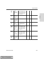
Module
1.5
Personal Version
Professional
Version
Power
Professional
Version
Batched Analysis
9
Nested Sweep Analysis
9
User Defined Analysis
9
PSpice Import
9
9
Network version
9
9
About the Circuit Design Process
Multisim supports every step of the overall circuit design process, which typically includes
the following phases:
1. Entering the design (using schematic capture, behavioral language formats or other methods) into the software tool being used.
2. Verifying that the behavior of the circuit matches expectations. This step is performed
using simulation, and analysis.
3. Modifying the circuit design if the behavior does not meet expectations, and returning to
step 2 as often as necessary.
4. Depending on how the circuit is to be physically implemented, passing the design through
the appropriate process. For example, if it is to be placed on a Printed Circuit Board
(PCB), the next step is to use a PCB layout program such as Electronic Workbench’s Ultiboard product. If it is to be placed on a programmable logic device (PLD, CPLD, FPGA,
etc.), the next step is to use a synthesis tool such as that available from Electronics Workbench.
1-4
Return to Presentation
Electronics Workbench
User Interface
C h a p te r
2
User Interface
2.1
About this Chapter . . . . . . . . . . . . . . . . . . . . . . . . . . . . . . . . . . . . . . . . . . . . . . . . . . . 2-1
2.2
Introduction to the Multisim Interface . . . . . . . . . . . . . . . . . . . . . . . . . . . . . . . . . . . . . 2-2
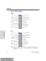
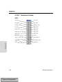
2.3
Introduction to the Design Bar . . . . . . . . . . . . . . . . . . . . . . . . . . . . . . . . . . . . . . . . . . 2-3
2.4
Customizing the Interface. . . . . . . . . . . . . . . . . . . . . . . . . . . . . . . . . . . . . . . . . . . . . .
2.4.1 About User Preferences. . . . . . . . . . . . . . . . . . . . . . . . . . . . . . . . . . . . . . . . . .
2.4.2 Other Customization Options . . . . . . . . . . . . . . . . . . . . . . . . . . . . . . . . . . . . . .
2.4.3 Controlling Circuit Display . . . . . . . . . . . . . . . . . . . . . . . . . . . . . . . . . . . . . . . .
2.4.4 Controlling Circuit Window Display . . . . . . . . . . . . . . . . . . . . . . . . . . . . . . . . .
2.4.5 Setting Autosave and Symbol Set . . . . . . . . . . . . . . . . . . . . . . . . . . . . . . . . . .
2.4.6 Print Page Setup Tab. . . . . . . . . . . . . . . . . . . . . . . . . . . . . . . . . . . . . . . . . . . .
2.5
Working with Multiple Circuit Windows. . . . . . . . . . . . . . . . . . . . . . . . . . . . . . . . . . . . 2-9
2.6
System Toolbar Buttons . . . . . . . . . . . . . . . . . . . . . . . . . . . . . . . . . . . . . . . . . . . . . 2-10
2.7
Menus and Commands . . . . . . . . . . . . . . . . . . . . . . . . . . . . . . . . . . . . . . . . . . . . . .
2.7.1 File Menu . . . . . . . . . . . . . . . . . . . . . . . . . . . . . . . . . . . . . . . . . . . . . . . . . . . .
2.7.2 Edit Menu . . . . . . . . . . . . . . . . . . . . . . . . . . . . . . . . . . . . . . . . . . . . . . . . . . . .
2.7.3 View Menu . . . . . . . . . . . . . . . . . . . . . . . . . . . . . . . . . . . . . . . . . . . . . . . . . . .
2.7.4 Simulate Menu . . . . . . . . . . . . . . . . . . . . . . . . . . . . . . . . . . . . . . . . . . . . . . .
2.7.5 Transfer Menu . . . . . . . . . . . . . . . . . . . . . . . . . . . . . . . . . . . . . . . . . . . . . . . .
2.7.6 Tools Menu . . . . . . . . . . . . . . . . . . . . . . . . . . . . . . . . . . . . . . . . . . . . . . . . . .
2.7.7 Window Menu . . . . . . . . . . . . . . . . . . . . . . . . . . . . . . . . . . . . . . . . . . . . . . . .
2.7.8 Help Menu . . . . . . . . . . . . . . . . . . . . . . . . . . . . . . . . . . . . . . . . . . . . . . . . . . .
Multisim User Guide
Return to Presentation
2-4
2-4
2-4
2-5
2-7
2-8
2-9
2-10
2-10
2-13
2-16
2-18
2-24
2-25
2-25
2-26
User Interface
Electronics Workbench
Return to Presentation
User Interface
Chapter
2
User Interface
2.1
About this Chapter
This chapter explains the basic operation of the Multisim user interface, and briefly describes
all available Multisim commands.
Some of the features described in this chapter may not be available in your version of Multisim. Such features have an icon in the column next to their description. See page 1-2 for a
description of the features available in your version.
Multisim User Guide
Return to Presentation
2-1
User Interface
2.2
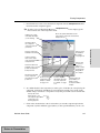
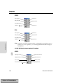
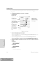
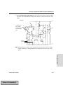
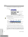
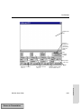
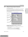
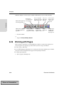
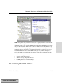
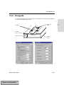
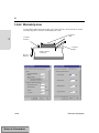
Introduction to the Multisim Interface
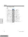
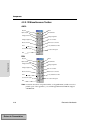
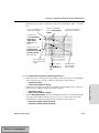
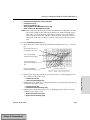
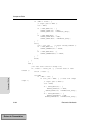
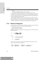
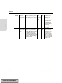
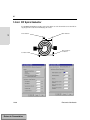
Multisim’s user interface consists of the following basic elements:
User Interface
Multisim
Design Bar
“In Use” list
Menus
System
toolbar
Component
toolbar
Circuit
window
Database
selector
Status line
Note Your circuit window may, by default, have a black background; however, for the purposes of this document, we show a white background. To change the background
color, see “Controlling Circuit Display” on page 2-5.
Menus are, as in all Windows applications, where you find commands for all functions.
The system toolbar contains buttons for commonly-performed functions, as described on
page 2-10.
The zoom toolbar allows you to zoom in and out on the circuit.
The Multisim Design Bar is an integral part of Multisim, and is explained in more detail
below.
The “In Use” list lists all the components used in the current circuit, for easy re-use.
2-2
Return to Presentation
Electronics Workbench
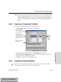
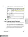
Introduction to the Design Bar
The component toolbar contains Parts Bin buttons that let you open component family toolbars (which, in turn, contain buttons for each family of components in the Parts Bin), as
described on page 3-4.
The circuit window is where you build your circuit designs.
The status line displays useful information about the current operation and a description of
the item the cursor is currently pointing to.
2.3
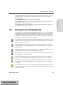
Introduction to the Design Bar
The Design Bar is a central component of Multisim, allowing you easy access to the sophisticated functions offered by the program. The Design Bar guides you through the logical steps
of building, simulating, analyzing and, eventually, exporting your design. Although Design
Bar functions are available from conventional menus, this manual assumes you are taking
advantage of the ease of use offered by the Design Bar.
The Component design button is selected by default, since the first logical activity is to place
components on the circuit window. The functions associated with this button are described in
detail in the “Components” chapter.
The Component Editor button lets you modify the components in Multisim, or add components. The functions associated with this button are described in detail in the “Component
Editor” chapter.
The Instruments button lets you attach instruments to your circuit. The functions associated
with this button are described in detail in the “Instruments” chapter.
The Simulate button lets you simulate your design. The details of how this function operates
are described in the “Simulation” chapter.
The Analysis button lets you choose the analysis you want to perform on your circuit. The
functions associated with this button are described in detail in the “Analyses” chapter.
The Postprocessor button lets you perform further operations on the results of your simulation. The functions associated with this button are described in detail in the the “Postprocessor” chapter.
The VHDL/Verilog button allows you to work with VHDL modeling (not available in all versions). The functions associated with this button are described in the the “HDLs and Programmable Logic” chapter.
Multisim User Guide
Return to Presentation
2-3
User Interface
The database selector allows you to choose which database levels are to be visible as Component toolbars, as described on page 4-1.
User Interface
User Interface
The Reports button lets you print reports about your circuits (Bill of Materials, list of components, component details). The functions associated with this button are described in detail in
the “Reports” chapter.
Finally, the Transfer button lets you communicate with and export to other PCB layout programs, such as Ultiboard, also from Electronics Workbench. You can also export simulation
results to programs such as MathCAD and Excel. The functions associated with this button
are described in detail in the “Transfer/Communication” chapter.
2.4
Customizing the Interface
2.4.1
About User Preferences
You can customize virtually any aspect of the Multisim interface, including the toolbars, colors in your circuit, page size, zoom factor, time for autosave, symbol set (ANSI or DIN) and
printer setup. Your customization settings are saved individually with each circuit file you use
so you could, for example, have one color scheme for one circuit and another for a different
circuit. You can also override the settings for individual instances (for example, change one
particular component from red to orange) or for the entire circuit.
To change settings for the current circuit, you generally right-click on the circuit window.
This is described in this section.
Your user preferences (set using Edit/User Preferences) form the default settings to be used
for all subsequent circuits, but do not (generally) affect the current circuit. Any newly created
circuit uses, by default, the user preferences of the current circuit. For example, if your current
circuit shows component labels, when you choose File/New and create a new circuit, that circuit will be set to show component labels as well.
2.4.2
Other Customization Options
You can also customize the interface by showing or hiding, dragging to a new location and,
optionally, resizing any of the following:
•
•
•
•
2-4
Return to Presentation
system toolbar
Design Bar
“In Use” list
database selector.
Electronics Workbench
Customizing the Interface
These changes apply to all circuits you are working with. Moved or resized items will return
to that location and size when next opened.
Finally, you can use the View menu to display or hide various elements, as described on page
2-16.
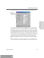
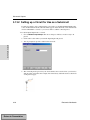
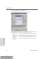
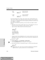
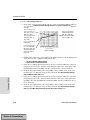
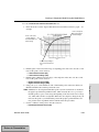
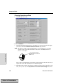
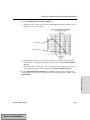
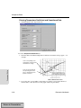
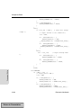
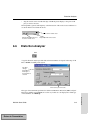
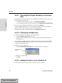
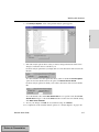
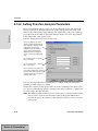
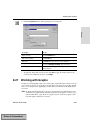
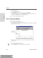
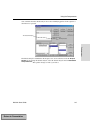
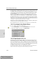
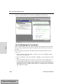
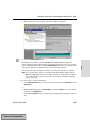
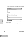
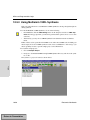
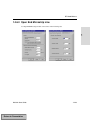
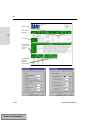
Controlling Circuit Display
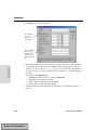
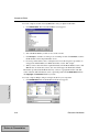
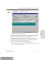
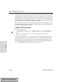
You can control the way your circuit and its components appear on the screen, and the level of
detail which appears.
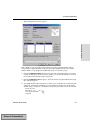
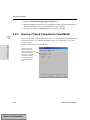
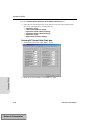
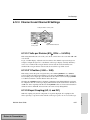
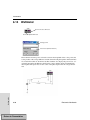
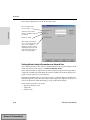
¾ To set the default circuit display options for subsequent circuits, choose Edit/User Preferences. The User Preferences screen appears, offering you four tabs of options, with the Circuit tab being the active tab. Use this tab to control the colors and display details for your
circuit.
Shows the results of
enabling the options on
the right
Enable those items you
want, by default, to be
shown. You can override
your choices for a particular
component, as described
in“Displaying Identifying
Information about a Placed
Component” on page 3-15.
Set up the desired color
scheme (see below)
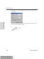
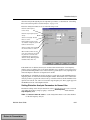
¾ To set the circuit options for the current circuit, right-click on the circuit window and choose
either Show, which displays a screen identical to the Show options in the Circuit tab of the
User Preferences screen (shown above), or Color, which displays a screen identical to the
Color options in the Circuit tab
Multisim comes with several color schemes that affect the circuit window background color,
wire color, and component color. You can also develop your own color scheme to meet your
individual needs.
Multisim User Guide
Return to Presentation
2-5
User Interface
2.4.3
User Interface
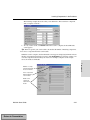
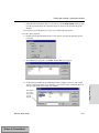
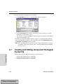
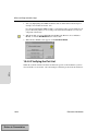
¾ To use one of the built-in color schemes:
1. Choose the scheme from the drop-down list.
2. A representation of the scheme’s settings appears in the preview box below the list.
User Interface
3. To save your settings and close the screen, click OK. To cancel your settings, click Cancel.
¾ To create a custom color scheme:
1. Choose Custom from the drop-down list.
2. Click on the color bar next to any items. A Color selector screen appears.
3. Click on the color you want to use for that item and click OK. You are returned to the User
Preferences screen. The results of your choice appear in the preview box.
4. Repeat until all your color settings are made.
5. To save your settings and close the screen, click OK. To cancel your settings, click Cancel.
2.4.4
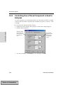
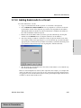
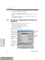
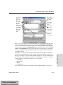
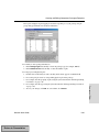
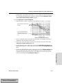
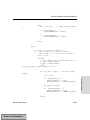
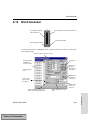
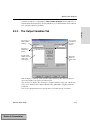
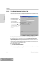
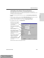
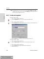
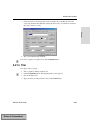
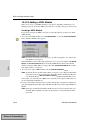
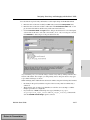
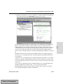
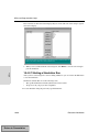
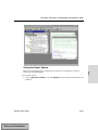
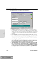
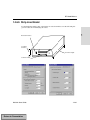
Controlling Circuit Window Display
Circuit window display options determine the appearance and behavior of the circuit window.
2-6
Return to Presentation
Electronics Workbench
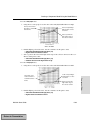
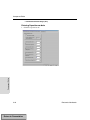
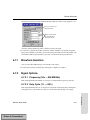
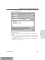
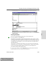
Customizing the Interface
¾ To set the default circuit window options for subsequent circuits, choose Edit/User Preferences and click the Workspace tab.
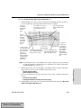
Shows the results of enabling
the options on the right
User Interface
Enable those items you
want, by default, to be
shown.
Set up the desired sheet
sizes.
Set up the desired zoom level
at which the component window appears.
¾ To set the circuit window options for the current circuit, do one or all of the following:
•
to show or hide the grid, page bounds or title block, right-click on the circuit window and
choose the corresponding command (Grid Visible, Show Page Bounds, or Show Title
Block and Border) from the menu that appears
• to set the sheet size, choose Edit/Set Sheet Size—a screen similar to the Default sheet
size of the User preferences screen appears
• to set the zoom level, choose View/Zoom, or use the zoom buttons.
Multisim comes with several sheet sizes that you can use for laying out your circuit. You can
modify any of the settings of these sizes.
¾ To use one of the provided sheet sizes as the default:
1. Choose the sheet size from the drop-down list. That size’s settings (orientation and measurements) appear.
2. To save your settings and close the screen, click OK. To cancel your settings, click Cancel.
¾ To modify the settings for a specific sheet size:
1. Choose the desired sheet size from the drop-down list. That size’s settings (orientation and
measurements) appear.
2. Change any of the settings.
Multisim User Guide
Return to Presentation
2-7
User Interface
User Interface
3. To save your settings and close the screen, click OK. To cancel your settings, click Cancel.
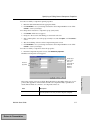
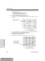
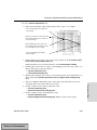
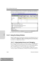
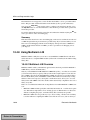
2.4.5
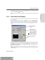
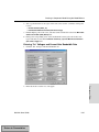
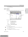
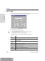
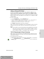
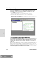
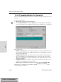
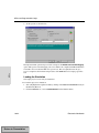
Setting Autosave and Symbol Set
¾ To set the autosave options and symbol set for both the current circuit and any subsequent circuits, set the default circuit visibility for subsequent circuits, choose Edit/User Preferences
and click the Preferences tab.
Enable or disable
autosave and specify
the interval at which
it will be performed.
Select the symbol
set to be used for
components. The
graphic changes to
represent the
selected symbol set.
To override this setting for individual
components, see
“Creating and Editing a Component’s
Symbol with the
Symbol Editor” on
page 5-11.
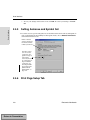
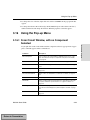
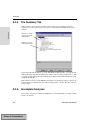
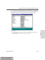
2.4.6
Print Page Setup Tab
2-8
Return to Presentation
Electronics Workbench
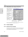
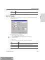
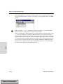
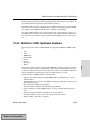
Working with Multiple Circuit Windows
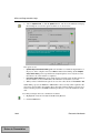
¾ To set the default print settings for subsequent circuits, choose Edit/User Preferences and
click the Print page setup tab.
User Interface
Enable to output circuit
in black and white (for
non-color printers).
When disabled, colored
components print in
shades of grey.
Enable to include
background in
printed copy. Use for
color printers or white
on black output.
Set page margins
for printed output.
Select an option to
scale the circuit
down or up in
printed output.
¾ To set these options for the current circuit, choose File/Print Setup and click Page Setup.
The above options are presented on a series of tabs.
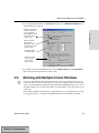
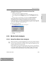
2.5
Working with Multiple Circuit Windows
If you are a Professional or Power Professional user, you can open as many circuits as you
want at the same time. Each circuit appears in its own circuit window. The active circuit window is, as in other Windows applications, the window with a highlighted title bar. You can use
the Window menu to move from circuit window to circuit window or just click on the one you
want to use.
Each window is distinct, and can have its own preferences, set of components and so on. You
can copy, but not move, a component or instrument from one circuit window to another.
Multisim User Guide
Return to Presentation
2-9
User Interface
2.6
System Toolbar Buttons
The system toolbar offers the following standard Windows functions:
User Interface
Saves the active circuit.
Copies the selected elements
and places them on the Windows clipboard.
Prints the active circuit.
Launches the Multisim
help file.
Creates a circuit
file.
Opens a circuit file.
2.7
Zooms in or out on the circuit,
increasing or decreasing the
view
Removes the selected elements and places them on the
Windows clipboard.
Inserts the contents of the
Windows clipboard at the
cursor location.
Menus and Commands
This section explains, in brief, all available Multisim commands. It is intended primarily as a
reference.
2.7.1
File Menu
Contains commands for managing circuit files created with Multisim.
2.7.1.1 File/New
Ctrl+N
Opens an untitled circuit window that can be used to create a circuit. The new window opens
using your circuit preferences. Until you save, the circuit window is named “Circuit#”, where
“#” is a consecutive number. For example, you could have “Circuit1”, “Circuit2”, “Circuit3”,
and so on.
You can create an unlimited number of circuits in one session.
Note Users of versions other than Professional or Power Professional can only have one circuit open at a time. For these users, the File/New command closes the currently open
circuit file.
2.7.1.2 File/Open
Ctrl+O
Opens a previously created circuit file or netlist. Displays a file browser. If necessary, change
to the location of the file you want to open.
2-10
Return to Presentation
Electronics Workbench
Menus and Commands
Note You can open files created with Version 5 of Electronics Workbench, files created in
Multisim and netlist files.
If you are a Professional or Power Professional user, you can open an unlimited number of
circuits in one session.
Closes the active circuit file. If any changes were made since the last save of the file, you are
prompted to save those changes before closing.
2.7.1.4 File/Save
Ctrl+S
Saves the active circuit file. If this is the first time the file is being saved, displays a file
browser. If you want, change to the desired location for saving the file. You can save a circuit
file with a name of any length.
The extension .msm is added to the file name automatically. For example, a circuit named
Mycircuit will be saved as Mycircuit.msm.
Tip To preserve the original circuit without changes, choose File/Save As.
2.7.1.5 File/Save As
Saves the current circuit with a new file name. The original circuit remains unchanged.
Tip Use this command to experiment safely on a copy of a circuit, without changing the
original.
2.7.1.6 File/New Project
Creates a new project for grouping together related circuit designs (for users with Project/
Team Design module only). For details, see “Setting up Projects” on page 13-1.
2.7.1.7 File/Open Project
Opens an existing project (for users with Project/Team Design module only). For details, see
“Working with Projects” on page 13-3.
2.7.1.8 File/Save Project
Saves a project (for users with Project/Team Design module only). For details, see “Working
with Projects” on page 13-3.
Multisim User Guide
Return to Presentation
2-11
User Interface
2.7.1.3 File/Close
User Interface
2.7.1.9 File/Close Project
Closes an open project (for users with Project/Team Design module only). For details, see
“Working with Projects” on page 13-3.
User Interface
2.7.1.10 File/Version Control
Backs up or restores a project (for users with Project/Team Design module only). For details,
see “Version Control” on page 13-4.
2.7.1.11 File/Prints
Prints all or some aspects of a circuit and/or its instruments on a printer attached to your system. You can choose one of the following to print:
•
circuit - see “Printing the Circuit” on page 3-26
•
•
•
Bill of Materials (B.O.M.) — see “Bill of Materials (BOM)” on page 11-1
list of components — see “Database Family List” on page 11-2
component details — see “Database Family List” on page 11-2.
2.7.1.12 File/Print Preview
Previews the circuit as it will be printed. Opens a separate window, where you can move from
page to page and zoom in for details. You can also print what you preview. For details, see
page 3-26.
2.7.1.13 File/Print Setup
Changes the page setup for a selected printer.
2-12
Return to Presentation
Electronics Workbench
Menus and Commands
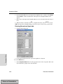
When you click Page Setup, you can set the page characteristics for this printer.
User Interface
These settings apply only to the current circuit. For details on these fields, see page 2-8.
2.7.1.14 File/Exit
Closes all open circuit windows and exits Multisim. If you have unsaved changes in any circuits, you are prompted to save or cancel them.
2.7.1.15 File/Recent Files
Displays a list of all recently opened circuit files. To re-open a file, select it from the list.
2.7.1.16 File/Recent Projects
Displays a list of all recently opened projects. To re-open a project, select it from the list.
2.7.2
Edit Menu
Contains commands for removing, duplicating or selecting information. If a command is not
applicable to the selected item (for example, a component), it is dimmed.
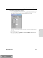
2.7.2.1 Edit/Place Component
Lets you browse the entire database (“Multisim master” level, “corporate” level and “user”
level) for components to be placed. For details, see page 3-6.
2.7.2.2 Edit/Place Junction
Ctrl+J
Places a connector when you click. For details, see page 3-13.
Multisim User Guide
Return to Presentation
2-13
User Interface
2.7.2.3 Edit/Place Bus
Ctrl+G
Places a bus with segments created as you click. For details, see page 3-27.
User Interface
2.7.2.4 Edit/Place Input/Output
Ctrl+I
Adds connecting nodes to a circuit for use as a subcircuit. For details, see page 3-24.
2.7.2.5 Edit/Place Hierarchical Block
Ctrl+H
Places a circuit in a hierarchical structure. For details, see page 3-25.
2.7.2.6 Edit/Place Text
Ctrl+T
Lets you place text on the circuit. For details, see page 3-21.
2.7.2.7 Edit/Undo
Ctrl+Z
Undoes the most recently performed delete action.
2.7.2.8 Edit/Redo
Ctrl+Y
Redoes the last undone actions.
2.7.2.9 Edit/Cut
Ctrl+X
Removes selected components, circuits or text. What you cut is placed on the Windows clipboard so you can paste it elsewhere.
2.7.2.10 Edit/Copy
Ctrl+C
Copies selected components, circuits or text. The copy is placed on the Windows clipboard.
You can then use the Paste command to paste the copy elsewhere, including other applications
such as word processors.
2.7.2.11 Edit/Paste
Ctrl+V
Places the contents of the clipboard. The cursor shows a “ghosted” image of the item to be
pasted. Click to indicate where the item is to be pasted.
2.7.2.12 Edit/Paste as Subcircuit/Macro
Ctrl+B
Places the contents of the clipboard as a subcircuit. For details, see page 3-25.
2-14
Return to Presentation
Electronics Workbench
Menus and Commands
2.7.2.13 Edit/Delete
Del
Permanently removes selected components or text. Does not place the selection on the clipboard and does not affect anything currently on the clipboard.
User Interface
Caution
Use the Delete command with care. Deleted information cannot be
retrieved, although the most recent deletion can be recovered using
the Undo command.
Note Deleting a component or instrument removes it from the circuit window, not from its
toolbar.
2.7.2.14 Edit/Select All
Ctrl+A
Selects all items in the active circuit window.
Tip To select all but a few items, use the Select All command and then deselect the ones you
don’t want by CTRL-clicking.
2.7.2.15 Edit/Flip Horizontal
Alt+X
Flips the selection vertically. For details, see “Rotating/Flipping Components” on page 3-13.
2.7.2.16 Edit/Flip Vertical
Alt+Y
Flips the selection horizontally. For details, see “Rotating/Flipping Components” on page 313.
2.7.2.17 Edit/90 Clockwise
Ctrl+R
Rotates the selection 90 degrees clockwise. For details, see “Rotating/Flipping Components”
on page 3-13.
2.7.2.18 Edit/90 CounterCW
Shift+Ctrl+R
Rotates the selection 90 degrees counter-clockwise. For details, see “Rotating/Flipping Components” on page 3-13.
Multisim User Guide
Return to Presentation
2-15
User Interface
2.7.2.19 Edit/Set Sheet Size
Sets the sheet size on which the circuit is designed. Choose from the drop-down list and modify settings (orientation and size) if necessary. For details, see page 3-2.
User Interface
2.7.2.20 Edit/Set Title Block
Lets you enter data to appear in the circuit’s title block. For details, see page 3-21.
2.7.2.21 Edit/User Preferences
Ctrl+U
Lets you specify default preferences for this circuit. For details, see page 2-4.
2.7.3
View Menu
2.7.3.1 View/Toolbars
Shows or hides the selected toolbar. Choose to show or hide any or all of the following toolbars:
• system toolbar
• design toolbar
• components toolbar
• instruments toolbar
• database selector
• zoom toolbar (the “zoom” buttons of the system toolbar)
• “In Use” list.
For information on these elements, see page 2-2.
2.7.3.2 View/Project Workspace
Shows/hides the project workspace on the left of the screen. See “Setting up Projects” on page
13-1.
2.7.3.3 View/Status Bar
Shows/hides the status bar, which provides useful information about the current operation and
a description of the item the cursor is currently pointing to.
2-16
Return to Presentation
Electronics Workbench
Menus and Commands
2.7.3.4 View/(Show/Hide) Simulation Error Log / Audit
Trail
Shows/hides the simulation log, which records all the events of a circuit simulation. For
details about this log, see “Start/Stop/Pause Simulation” on page 7-3.
Opens a window into which you can type Xspice commands to be executed. Press RETURN to
execute the command. The command is listed at the top part of the window and any errors are
reported in the error log/audit trail.
2.7.3.6 View/(Show/Hide) Grapher
Shows/hides the Grapher screen, which shows the results of simulation on a graph or chart.
For details about this screen, see “Viewing the Analysis Results—Grapher” on page 8-58.
2.7.3.7 View/Show Simulate Switch
Shows or hides the simulation on/off switch. An alternative to using the Design Bar button or
menu commands.
2.7.3.8 View/Grid Visible
Shows or hides grid in the background of the circuit window. This helps you place elements in
specific locations on a grid. For details, see page 3-2.
2.7.3.9 View/Show Page Bounds
Shows or hides page boundaries in the circuit window. This helps you note where circuits will
appear on printed output. For details, see page 3-2.
2.7.3.10 View/Show Title Block and Border
Shows or hides the circuit’s title block and border. For details, see page 3-2.
2.7.3.11 View/Color
Lets you choose or modify the color scheme for the circuit. Overrides the defaults set in File/
Preferences. For details, see page 2-5.
Multisim User Guide
Return to Presentation
2-17
User Interface
2.7.3.5 View/(Show/Hide) Command Line Interface
User Interface
2.7.3.12 View/Show
Lets you choose what component elements appear on the circuit window. Overrides the
defaults set in File/Preferences. For details, see page 2-6.
User Interface
2.7.3.13 View/Zoom
Lets you choose a magnification of 33%, 60%, 100%, 200% or other for viewing the circuit.
2.7.3.14 View/Find
Ctrl+F
Displays a list of the reference IDs in the current circuit. You can select one or more of these
reference IDs, which are then selected in the circuit window. For details, see page 3-19.
2.7.3.15 View/Refresh Component Toolbars
Refreshes the Component toolbar display so it reflects any additions made to the user or corporate toolbars, as described in the “Component Editor” chapter.
2.7.4
Simulate Menu
2.7.4.1 Simulate/Run/Stop
Runs or stops the circuit. Running a circuit starts a sequence of mathematical operations to
compute values for the nodes (testpoints) in the circuit.
Tip You can also activate a digital circuit from the word generator.
2.7.4.2 Simulate/Pause/Resume
Pauses/resumes the current simulation.
2.7.4.3 Simulate/Default Instrument Settings
Allows you to set defaults settings for instruments that are based on a transient analysis (such
as the oscilloscope, spectrum analyzer and logic analyzer). For details, see page 6-4.
2.7.4.4 Simulate/Instruments
Contains commands you use to place instruments (an alternative to using the instruments toolbar or the Design Bar). For details on these instruments, see the “Instruments” chapter.
2-18
Return to Presentation
Electronics Workbench
Menus and Commands
Note Ammeter and voltmeter instruments are available from the Indicators Component toolbar.
Simulate/Instruments/Multimeter
Simulate/Instruments/Function Generator
Places a function generator on the circuit window. A function generator is a voltage source
that supplies sine, triangular or square waves. It provides a convenient and realistic way to
supply power to a circuit. For details, see “Function Generator” on page 6-10.
Simulate/Instruments/Wattmeter
Places a wattmeter on the circuit window. A wattmeter provides the combined functions of a
voltmeter and an ammeter. It is used to measure the magnitude of the active power, that is, the
product of the voltage difference and the current flowing through the current terminals, in a
circuit. For details, see “Wattmeter” on page 6-30.
Simulate/Instruments/Oscilloscope
Places an oscilloscope on the circuit window. The dual-channel oscilloscope displays the
magnitude and frequency variations of electronic signals. It can provide a graph of the
strength of one or two signals over time, or allow comparison of one waveform to another. For
details, see “Oscilloscope” on page 6-24.
Simulate/Instruments/Bode Plotter
Places a Bode plotter on the circuit window. A Bode plotter produces a graph of a circuit’s frequency response and is useful for analyzing filter circuits. For details, see “Bode Plotter” on
page 6-6.
Simulate/Instruments/Word Generator
Places a word generator on the circuit window. A word generator sends digital words or patterns of bits into circuits to test them. For details, see “Word Generator” on page 6-31.
Simulate/Instruments/Logic Analyzer
Places a logic analyzer on the circuit window. A logic analyzer displays the levels of up to 16
digital signals in a circuit. It is used for fast data acquisition of logic states and advanced timing analysis to help design large systems and carry out troubleshooting. For details, see
“Logic Analyzer” on page 6-15.
Multisim User Guide
Return to Presentation
2-19
User Interface
Places a multimeter on the circuit window. A multimeter is used to measure AC or DC voltage
or current, resistance, or decibel loss between two nodes in a circuit. For details, see “Multimeter” on page 6-19.
User Interface
Simulate/Instruments/Logic Converter
User Interface
Places a logic converter on the circuit window. A logic converter is able to perform several
transformations of a circuit representation. It has no real world counterpart. For details, see
“Logic Converter” on page 6-12.
Simulate/Instruments/Distortion Analyzer
Places a distortion analyzer on the circuit window. A typical distortion analyzer provides distortion measurements for audio signals in the range of 20 Hz to 100 KHz. For details, see
“Distortion Analyzer” on page 6-9.
Simulate/Instruments/Spectrum Analyzer
Places a spectrum analyzer on the circuit window. The spectrum analyzer is used to measure
frequency versus amplitude. For details, see “Spectrum Analyzer” on page 6-29.
Simulate/Instruments/Network Analyzer
Places a network analyzer on the circuit window. The network analyzer is used to measure the
scattering parameters (or S-parameters) of a circuit, commonly used to characterize a circuit
intended to operate at higher frequencies. For details, see “Network Analyzer” on page 6-23.
2.7.4.5 Simulate/Analyses
Contains commands you use to set up and run the circuit’s analysis (an alternative to using the
Design Bar). For details on these analyses, see the “Analyses” chapter.
Simulate/Analyses/DC Operating Point
Sets up and runs DC operating point analysis, which determines the DC operating point of a
circuit. For details, see “DC Operating Point Analysis” on page 8-9.
Simulate/Analyses/AC Analysis
Sets up and runs AC analysis, in which the DC operating point is first calculated to obtain linear, small-signal models for all nonlinear components. Then a complex matrix (containing
both real and imaginary components) is created. For details, see “DC Operating Point Analysis” on page 8-9.
Simulate/Analyses/Transient Analysis
Sets up and runs Transient analysis, also called time-domain transient analysis, which computes the circuit’s response as a function of time. For details, see “Transient Analysis” on page
8-13.
2-20
Return to Presentation
Electronics Workbench
Menus and Commands
Simulate/Analyses/Noise Analysis
Sets up and runs Noise analysis, which is used to detect the magnitude of noise power in the
output of electronic circuits. For details, see “Enter the desired variables in the appropriate
fields.” on page 8-45.
Sets up and runs Distortion analysis, which measures harmonic distortion and intermodulation
distortion products. For details, see “Distortion Analysis” on page 8-20.
Simulate/Analyses/DC Sweep
Sets up and runs DC Sweep analysis, which computes the DC operating point of a node in the
circuit for various values of one or two DC sources in the circuit. For details, see “DC Sweep
Analysis” on page 8-22.
Simulate/Analyses/Sensitivity
Sets up and runs Sensitivity analysis, which calculates the sensitivity of an output node voltage or current with respect to the parameters of all components (DC sensitivity) or one component (AC sensitivity) in a circuit. For details, see “DC and AC Sensitivity Analyses” on
page 8-24.
Simulate/Analyses/Parameter Sweep
Sets up and runs Parameter Sweep analysis, which verifies the operation of a circuit by simulating it across a range of values for a component parameter. For details, see “Parameter
Sweep Analysis” on page 8-28.
Simulate/Analyses/Temperature Sweep
Sets up and runs Temperature Sweep analysis, which quickly verifies the operation of a circuit
by simulating it at different temperatures. The effect is the same as simulating the circuit several times, once for each different temperature. You control the temperature values. For
details, see “Temperature Sweep Analysis” on page 8-31.
Simulate/Analyses/Transfer Function
Sets up and runs Transfer Function analysis, which calculates the DC small-signal transfer
function between an input source and two output nodes (for voltage) or an output variable (for
current) in a circuit. It also calculates input and output resistances. For details, see “Transfer
Function Analysis” on page 8-33.
Multisim User Guide
Return to Presentation
2-21
User Interface
Simulate/Analyses/Distortion Analysis
User Interface
Simulate/Analyses/Worst Case
User Interface
Sets up and runs Worst Case analysis, a statistical analysis that lets you explore the worst possible effects on circuit performance of variations in component parameters. For details, see
“Worst Case Analysis” on page 8-35.
Simulate/Analyses/Pole Zero
Sets up and runs Pole Zero analysis, which finds the poles and zeros in the small-signal AC
transfer function of a circuit. For details, see “Pole Zero Analysis” on page 8-38.
Simulate/Analyses/Monte Carlo
Sets up and runs Monte Carlo analysis, a statistical analysis that lets you explore how changing component properties affects circuit performance. For details, see “Monte Carlo Analysis”
on page 8-43.
Simulate/Analyses/Fourier Analysis
Sets up and runs Fourier analysis, which evaluates the DC, fundamental and harmonic components of a time-domain signal. For details, see “Fourier Analysis” on page 8-46.
Simulate/Analyses/Trace Width Analysis
Contains information about setting trace width analysis parameters for normal or advanced
use. For details, see “Trace Width Analysis” on page 8-50.
Simulate/Analyses/Batched Analyses
Sets up and runs batched analyses, which let you set up a series of different analyses, or different variations on the same analysis, to be performed on a circuit in sequence. For details, see
“Batched Analyses” on page 8-55.
Simulate/Analyses/User-Defined Analysis
Sets up and runs a user-defined analysis. This command presents you with a screen into which
you can type the SPICE commands to be executed to perform the analysis. For details, see
“User-Defined Analyses” on page 8-57.
Simulate/Analyses/Noise Figure Analysis
This analysis is part of Multisim’s RF Design module (standard in the Power Professional version, optional in the Professional version) and is described in the “RF” chapter.
2-22
Return to Presentation
Electronics Workbench
Menus and Commands
Simulate/Analyses/RF Analyses
Included in the menu for the purposes of completeness. RF analyses are available from the
Network Analyzer instrument. This command places the Network Analyzer for you. For
details, see “Network Analyzer” on page 14-15.
User Interface
Simulate/Analyses/Stop
Stops the currently running analysis.
2.7.4.6 Simulate/Postprocess
Opens the Postprocessor screen, which you use to combine the results of several analyses in
different ways. To use the Postprocessor, you must have performed at least one analysis on
your circuit. For details, see the “Postprocessor” chapter.
2.7.4.7 Simulate/VHDL Simulation
Runs the VHDL simulation module. For details, see the “HDLs and Programmable Logic”
chapter.
2.7.4.8 Simulate/Verilog Simulation
Runs the Verilog simulation module. For details, see the “HDLs and Programmable Logic”
chapter.
2.7.4.9 Simulate/Auto Fault Option
Randomly applies faults to randomly selected components in the circuit. You choose the number of faults (either in total, or the number of each type of fault) to be applied. For details, see
the “Educator’s Notes” chapter.
2.7.4.10 Simulate/Global Component Tolerances
Multisim components are, by default, “ideal”— they have no internal resistance and their output is consistent. You can choose to use global components instead. These randomly introduce
variances to simulate the performance of actual, physical components. Global component settings affect the simulation results. See “Component Nominal Values and Tolerances” on page
4-26 for details.
2.7.5
Transfer Menu
Multisim User Guide
Return to Presentation
2-23
User Interface
2.7.5.1 Transfer/Transfer to Ultiboard
User Interface
Displays a file browser where you choose or enter a file name for the transferred data. A file
of the correct format is created. If you plan to use backannotation, you must save your file
immediately.
2.7.5.2 Transfer/Transfer to other PCB Layout
Displays a file browser where you choose or enter a file name for the transferred data. You
can also choose the appropriate file type from a list of available types.
2.7.5.3 Transfer/Backannotate from Ultiboard
Backannotates changes made to a circuit in Ultiboard (for example, deleted components) to
the Multisim circuit file. Displays a file browser where you choose the backannotation file
corresponding to your circuit file. The circuit file must be open
2.7.5.4 Transfer/VHDL Synthesis
Runs the VHDL Synthesis program on a file created from the current circuit. You are
prompted to save the file, and then VHDL Synthesis appears with the file loaded in it. For
details, see the “HDLs and Programmable Logic” chapter.
2.7.5.5 Transfer/Verilog Synthesis
Runs the VHDL Synthesis program on a file created from the current circuit. You are
prompted to save the file, and then VHDL Synthesis appears with the file loaded in it. For
details, see the “HDLs and Programmable Logic” chapter.
2.7.5.6 Transfer/Export Simulation Results to MathCAD
Exports the results of your simulation to a file format readable by MathCAD™. For details,
see the “Transfer/Communication” chapter.
2.7.5.7 Transfer/Export Simulation Results to Excel
Exports the results of your simulation to a file format readable by Excel™. For details, see the
“Transfer/Communication” chapter.
2.7.5.8 Transfer/Export Netlist
Exports the netlist of your design. Opens a standard file selector window where you can
choose the file name and folder.
2-24
Return to Presentation
Electronics Workbench
Menus and Commands
2.7.6
Tools Menu
2.7.6.1 Tools/Component Editor
2.7.6.2 Tools/Remote Control / Design Sharing
Allows you to communicate with and share designs with other members of your team, either
across a network or using the Internet. For Project/Team Design module users only. For
details, see the “Project/Team Design Module” chapter.
2.7.7
Window Menu
Contains commands used to control the display of Multisim windows. Lists all open circuit
windows.
2.7.7.1 Windows/Cascade
Arranges circuit windows so that they overlap.
2.7.7.2 Windows/Tile
Resizes all open circuit windows so they all show on the screen. Allows you to quickly scan
all open circuit files.
2.7.7.3 Windows/Arrange Icons
Lines up minimized windows.
2.7.7.4 Windows (open files)
Lists the open Multisim circuit files. Select one to display it.
2.7.8
Help Menu
Contains commands that display on-line help and Multisim version information.
Multisim User Guide
Return to Presentation
2-25
User Interface
Displays the Component Editor. For details on using this editor, see the “Component Editor”
chapter.
User Interface
User Interface
Tip If you want to be able to refer to Help information as you work on a circuit, use the Keep
Help on Top function in the Help window’s Options menu.
2-26
Return to Presentation
Electronics Workbench
C h a p te r
3
Schematic Capture
About this Chapter . . . . . . . . . . . . . . . . . . . . . . . . . . . . . . . . . . . . . . . . . . . . . . . . . . . 3-1
3.2
Introduction to Schematic Capture . . . . . . . . . . . . . . . . . . . . . . . . . . . . . . . . . . . . . . . 3-1
3.3
Setting up Your Circuit Window . . . . . . . . . . . . . . . . . . . . . . . . . . . . . . . . . . . . . . . . .
3.3.1 Setting up a Sheet Size . . . . . . . . . . . . . . . . . . . . . . . . . . . . . . . . . . . . . . . . . .
3.3.2 Displaying or Hiding Grid, Title Block and Page Borders. . . . . . . . . . . . . . . . .
3.3.3 Selecting a Symbol Set . . . . . . . . . . . . . . . . . . . . . . . . . . . . . . . . . . . . . . . . . .
3.4
Selecting Components from the Database . . . . . . . . . . . . . . . . . . . . . . . . . . . . . . . . 3-3
3.5
Placing Components . . . . . . . . . . . . . . . . . . . . . . . . . . . . . . . . . . . . . . . . . . . . . . . . .
3.5.1 Choosing a Component Using the Component Group Toolbars and Browser
Screen3-4
3.5.2 Choosing a Component with the Place Component Command . . . . . . . . . . .
3.5.3 Using the “In Use” List3-8
3.5.4 Moving a Placed Component . . . . . . . . . . . . . . . . . . . . . . . . . . . . . . . . . . . . . .
3.5.5 Copying a Placed Component3-9
3.5.6 Controlling Component Color. . . . . . . . . . . . . . . . . . . . . . . . . . . . . . . . . . . . . .
3-1
3-2
3-2
3-3
3-4
3-6
3-8
3-9
3.6
Wiring Components . . . . . . . . . . . . . . . . . . . . . . . . . . . . . . . . . . . . . . . . . . . . . . . . . . 3-9
3.6.1 Wiring Components Automatically . . . . . . . . . . . . . . . . . . . . . . . . . . . . . . . . . 3-10
3.6.2 Wiring Components Manually . . . . . . . . . . . . . . . . . . . . . . . . . . . . . . . . . . . . 3-11
3.6.3 Combining Automatic and Manual Wiring . . . . . . . . . . . . . . . . . . . . . . . . . . . 3-12
3.6.4 Modifying Wire Path . . . . . . . . . . . . . . . . . . . . . . . . . . . . . . . . . . . . . . . . . . . . 3-12
3.6.5 Controlling Wire Color . . . . . . . . . . . . . . . . . . . . . . . . . . . . . . . . . . . . . . . . . . 3-13
3.7
Manually Adding a Junction (Connector) . . . . . . . . . . . . . . . . . . . . . . . . . . . . . . . . . 3-13
3.8
Rotating/Flipping Components . . . . . . . . . . . . . . . . . . . . . . . . . . . . . . . . . . . . . . . . . 3-13
3.9
Placed Component Properties . . . . . . . . . . . . . . . . . . . . . . . . . . . . . . . . . . . . . . . . .
3.9.1 Displaying Identifying Information about a Placed Component . . . . . . . . . . .
3.9.2 Viewing a Placed Component’s Value/Model . . . . . . . . . . . . . . . . . . . . . . . .
3.9.3 Controlling How a Placed Component is Used in Analyses. . . . . . . . . . . . . .
Multisim User Guide
Return to Presentation
3-15
3-15
3-17
3-19
Schematic Capture
3.1
3.10 Finding Components in Your Circuit. . . . . . . . . . . . . . . . . . . . . . . . . . . . . . . . . . . . . 3-20
3.11 Labelling . . . . . . . . . . . . . . . . . . . . . . . . . . . . . . . . . . . . . . . . . . . . . . . . . . . . . . . . . .
3.11.1 Modifying Component Labels. . . . . . . . . . . . . . . . . . . . . . . . . . . . . . . . . . . . .
3.11.2 Modifying Node Numbers. . . . . . . . . . . . . . . . . . . . . . . . . . . . . . . . . . . . . . . .
3.11.3 Adding a Title Block . . . . . . . . . . . . . . . . . . . . . . . . . . . . . . . . . . . . . . . . . . . .
3.11.4 Adding Miscellaneous Text . . . . . . . . . . . . . . . . . . . . . . . . . . . . . . . . . . . . . .
3-20
3-20
3-22
3-22
3-23
3.12 Virtual Wiring . . . . . . . . . . . . . . . . . . . . . . . . . . . . . . . . . . . . . . . . . . . . . . . . . . . . . . 3-23
Schematic Capture
3.13 Subcircuits and Hierarchy . . . . . . . . . . . . . . . . . . . . . . . . . . . . . . . . . . . . . . . . . . . .
3.13.1 Subcircuits vs. Hierarchy . . . . . . . . . . . . . . . . . . . . . . . . . . . . . . . . . . . . . . . .
3.13.2 Setting up a Circuit for Use as a Subcircuit . . . . . . . . . . . . . . . . . . . . . . . . . .
3.13.3 Adding Subcircuits to a Circuit . . . . . . . . . . . . . . . . . . . . . . . . . . . . . . . . . . .
3-24
3-24
3-25
3-26
3.14 Printing the Circuit . . . . . . . . . . . . . . . . . . . . . . . . . . . . . . . . . . . . . . . . . . . . . . . . . . 3-27
3.15 Placing a Bus . . . . . . . . . . . . . . . . . . . . . . . . . . . . . . . . . . . . . . . . . . . . . . . . . . . . . . 3-28
3.16 Using the Pop-up Menu . . . . . . . . . . . . . . . . . . . . . . . . . . . . . . . . . . . . . . . . . . . . . .
3.16.1 From Circuit Window, with no Component Selected . . . . . . . . . . . . . . . . . . .
3.16.2 From Circuit Window, with Component or Instrument Selected. . . . . . . . . . .
3.16.3 From Circuit Window, with Wire Selected . . . . . . . . . . . . . . . . . . . . . . . . . . .
3-30
3-30
3-31
3-32
Electronics Workbench
Return to Presentation
Chapter
3
Schematic Capture
3.1
About this Chapter
Some of the features described in this chapter may not be available in your version of Multisim. Such features have an icon in the column next to their description. See page 1-2 for a
description of the features available in your version.
3.2
Introduction to Schematic Capture
Schematic capture is the first stage in developing your circuit. In this stage you choose the
components you want to use, place them on the circuit window in the desired position and orientation, wire them together, and otherwise prepare your design. Multisim also allows you to
modify component properties, orient your circuit on a grid, add text and a title block, add subcircuits and buses, and control the color of the circuit window background, components and
wires.
3.3
Setting up Your Circuit Window
Multisim lets you set up the circuit window to match your design requirements. In particular,
you can set:
•
•
•
sheet size
whether or not the grid, page bounds, page borders and title block are visible
the symbol set (ANSI or DIN) you want to use.
Multisim User Guide
Return to Presentation
3-1
Schematic Capture
This chapter describes all the basic functions involved in creating a circuit in the circuit window. This chapter explains the fundamental steps in circuit creation, but is not intended to
describe all the potential aspects of circuit design. For example, you should look to other
chapters for details on the component database, instructions on editing components, and information on adding instruments.
Schematic Capture
When you create a component file, the current settings in your user preferences (as described
on page 2-4) are used as the defaults for these options. You can override the defaults, as
described in this section. Your new settings are stored with the circuit file, allowing you to
have unique settings for each file you create.
3.3.1
Setting up a Sheet Size
¾ To set up the sheet size for this circuit:
Schematic Capture
1. Choose Edit/Set Sheet Size. The Sheet Size screen appears.
2. Choose the desired sheet size from the drop-down list.
3. Change any of the characteristics (orientation or size) necessary.
4. To confirm the sheet size, click OK. To cancel it, click Cancel.
3.3.2
Displaying or Hiding Grid, Title Block and Page
Borders
Multisim lets you display a background grid on the circuit window, to help you orient your
components. It also lets you show or hide the component’s title block (explained in more
detail on page 3-21), the page bounds that show the parameters of your sheet size, and the
page borders that offer a ruler marking the inches on your sheet.
As described on page 2-6, the default settings that specify which of these are displayed is set
in user preferences. User preferences are used when a new circuit is created. You can also use
the View menu to set these defaults for the current circuit only.
¾ To affect what is shown or hidden in the current circuit:, do one of the following:
•
enable View/Grid Visible, View/Show Page Bounds or View/Show Title Block and Border
3-2
Return to Presentation
Electronics Workbench
Selecting Components from the Database
•
3.3.3
right-click on the circuit window and choose Grid Visible, Page Bounds, or Title Block
and Border from the pop-up menu that appears.
Selecting a Symbol Set
Multisim allows you to use either ANSI or DIN symbols on your circuit window.
¾ To choose the desired symbol set, choose Edit/User Preferences, display the Preferences tab,
and select the desired symbol set.
3.4
Selecting Components from the Database
Note Multisim components are stored in a database that contains three levels of data: “Multisim master”, “corporate”, and “user”.
You can locate a component in this database using a variety of methods:
•
through component toolbars that let you browse through a specific level of the database, as
explained below
• through Edit/Place Component, which lets you browse all the component groups in a
specific level of the database, as explained on page 3-6
• by searching a specific level of the database, as explained in the “Components” chapter.
It is the first of these three choices that is used most commonly. When using this method, the
families of components you need to create a circuit are grouped into logical divisions, each
grouping represented by a Parts Bin button on the Component toolbar. This logical grouping
is a key advantage of Multisim, saving you time and frustration. You can toggle the Component toolbar on and off by clicking the Component button on the Design Bar.
Each Parts Bin button on the Component toolbar corresponds to group of components with
similar functionality. Placing your cursor over one of these buttons displays another toolbar,
the component family toolbar, containing a button for each component family contained in
that Parts Bin.
Using this first, most popular method of component toolbar with Parts Bins and Browser is
explained below in section 5.1 The other two methods are explained subsequently.
Note For a detailed look at the make-up of the component Parts Bins, see “Classification of
Components in the Database” on page 4-3.
Multisim User Guide
Return to Presentation
3-3
Schematic Capture
The first step in schematic capture is placing the appropriate components on your circuit window.
Schematic Capture
For example:
Placing the cursor on this
component toolbar Parts
Bin...
...reveals this component family toolbar.
Schematic Capture
Virtual components.
Electronics Workbench provides the unique concept of virtual components in Multisim. Virtual components are not “real”, that is, cannot be purchased, and have no footprint. They are
included for simulation flexibility. Virtual components appear by default in a different color
from other components on the circuit window. You control the color as described on page 2-5.
3.5
Placing Components
3.5.1
Choosing a Component Using the Component
Group Toolbars and Browser Screen
By default, the Component Design Bar button is enabled and one or more Component toolbars are visible. If no toolbar is visible, click the Component button on the Design Bar.
¾ To choose and place a component from a specific Parts Bin and family:
1. On the desired Component toolbar, place the cursor on the desired Parts Bin. The associated component family toolbar appears.
2. From the component family toolbar, click the button for the desired component family. If
the selected component family has only a single component, you can simply place the
component. For other components, a Browser screen for that component family appears.
3-4
Return to Presentation
Electronics Workbench
Placing Components
3. From the Browser screen, select the desired component from the Component List. Information about that component appears.
Tip To make your scroll through the Browser’s Components List faster, simply type the
first few characters of the component’s name.
Shows the symbol that will be used to
represent the component selected in the
Component List
Indicates the component family with which
you are working
Information about
the component
selected in the Component List
Click to search
the database.
For details,
see page 4-19.
Lists the manufacturers of the component selected in the
Component List
Click to enter
or view user
fields. For
details, see the
“Project/Team
Design Module” chapter.
Lists the model levels
available for the component selected in the
Component List
Shows the model data
for the component
selected in the Component List
Produces a list of the
components in the
family. For details,
see page 11-2.
Produces detailed
information about the
selected component.
For details, see page
11-4.
Launches the Component Editor. For
details, see the
“Component Editor”
chapter.
4. To confirm that this is the component you want to place, click OK. (To cancel placing the
component, click Cancel.) The Browser screen disappears and the cursor on the circuit
window changes to indicate a component is ready to be placed. The cursor looks like this:
Arrow points to the
upper left pin so you
can easily line up your
component to the
desired grid point.
5. Click on the circuit window at the location where you want the component placed. The
component’s symbol and labels appear (unless you have specified that they are not to be
Multisim User Guide
Return to Presentation
3-5
Schematic Capture
Lists the components
available in the family
Schematic Capture
displayed, as explained on page 3-19), as well as a unique reference ID made up of a character and number. The character represents the type of component and the number is a
sequential number that indicates the order in which the components were originally
placed. For example, the first digital component has the reference ID “U1”, the next is
“U2”, the first inductor has the reference ID “L1”, and so on.
Schematic Capture
Note If the component you place is a virtual component (that is, it has no equivalent in the
real world, and will therefore not be exported to Ultiboard), it is a different color from
real components and the Browser is not required (i.e. no Step 3 above). This is because
for virtual parts, you “set” their value once they are placed on the circuit window by
double-clicking them. This color is set in your preferences, as explained on page 2-5.
Note If you are placing a component whose package includes multiple “devices” (for example, four separate gates), you are prompted to specify which of the sections you want
to place. You can choose any one, and if desired, you can use all of the available
devices from one chip before starting to use a second.
3.5.2
Choosing a Component with the Place
Component Command
You can choose a component from any group or family by browsing through all the component groups in a specific level of the database to find an appropriate component to place.
To browse and place a component from any group or family:
1. Choose Edit/Place Component.
2. From the submenu that appears, choose the database level you are interested in.
3-6
Return to Presentation
Electronics Workbench
Placing Components
3. The following Browser screen appears:
Schematic Capture
This is identical to the screen that appears when you use the component family toolbars,
except that the component family is a drop-down list that alphabetically lists all available
families. There is no grouping by Parts Bins. The list is not sorted into groups.
4. From the Component Family drop-down list, select the component family you are interested in. To help find your selection more quickly, you can enter the first letter or few letters and the list automatically jumps to that point.
5. From the Component List that appears, select the desired component. Information about
that component appears.
6. To confirm that this is the component you want to place, click OK. (To cancel placing the
component, click Cancel.) The Browser screen disappears and the cursor on the circuit
window changes to indicate a component is ready to be placed. The cursor looks like this:
Arrow points to the
upper left pin so you
can easily line up your
component.
Multisim User Guide
Return to Presentation
3-7
Schematic Capture
7. Click on the circuit window at the location where you want the component placed. The
component’s symbol and label appear (unless you have specified that they are not to be
displayed, as explained on page 3-19), as well as a unique reference ID made up of a character and number. The character represents the type of component and the number is a
sequential number that indicates the order in which the components were originally
placed. For example, the first analog component has the reference ID “U1”, the next analog component is “U2”, the first inductor has the reference ID “L1”, and so on.
Schematic Capture
If the component you place is a virtual component (that is, it has no equivalent in the real
world, and will not be exported to Ultiboard), it is a different color from real-world components. This color is set in your preferences, as explained on page 2-5.
3.5.3
Using the “In Use” List
Each time you place a component, it is added to the “In Use” list (to the right of the Design
Bar) for easy re-use. To place a copy of any placed component, simply select it from the list.
The copied component appears at the top of your circuit window—you can move it to any
location you like.
3.5.4
Moving a Placed Component
You can move a placed component to another location by either:
•
•
dragging the component
selecting it and pressing the arrow keys on your keyboard to move it up, down, or to either
side
Note A component’s icon and labels can be moved independently or together—if you plan
to move the component, be sure the whole component is selected, not just its label.]
Labels
Icon
3-8
Return to Presentation
Electronics Workbench
Wiring Components
3.5.5
Copying a Placed Component
¾ To copy a placed component to another location:
1. Select the desired component, and choose Edit/Copy.
OR
1. Right-click on the desired component, and, from the pop-up menu that appears, choose
Copy.
2. From the Edit menu, choose Paste.
OR
3. Right-click anywhere on the circuit window and, from the pop-up menu that appears,
choose Paste.
Once you have placed the copied component, you can click and drag it to the desired location.
You can also copy a component using the Windows control keys for cut (x), copy (c) and
paste (v).
3.5.6
Controlling Component Color
The default color used for a component and the background color of the circuit window are
controlled by your user preferences, as described on page 2-5.
¾ To change the color of the placed component from its default values, right-click on the component and choose Color from the pop-up menu that appears. You are presented with a color
palette from which you can choose a color and click OK to apply it to the selected item.
¾ To change the color of the background, and the default color scheme used throughout the circuit, right-click on the circuit window. The window that appears allows you to set a different
color scheme. For more on color schemes, see page 2-5.
3.6
Wiring Components
Once you have placed components on the circuit window, you will want to wire them
together. All components have pins that you can use to wire them to other components or
instruments. You can choose to wire components either automatically or manually. Automatic
wiring, a feature unique to Multisim, means Multisim finds the path for wire placement for
you and avoids wiring through other components or overlapping wires. Manual wiring means
Multisim User Guide
Return to Presentation
3-9
Schematic Capture
4. The cursor shows a “ghosted” version of the copied component. Click at the location
where you want the copied component placed.
Schematic Capture
you control the flow of the wire on the circuit window. You can easily combine these methods
for a single connection, for example, by starting with manual wiring and then switching to
automatic.
Professional and Power Professional users can also create virtual connections for components
that are a long distance apart in the circuit window, as described on page 3-22.
3.6.1
Wiring Components Automatically
¾ To wire two components together, automatically:
Schematic Capture
1. Click on a pin from the first component to start the connection (your pointer turns into a +
sign) and drag. A wire appears, attached to your cursor.
2. Click on a pin on the second component to finish the connection. Multisim automatically
places the wire, which snaps to an appropriate configuration. The wire is numbered as a
node.
System-generated node number
Tip If the connection was not successful, you may be trying to place the wire too close to
other surrounding components. Try make the connection at a slightly different location,
or use manual wiring, as described in the following section.
For information on changing the color of the wire, see page 3-12.
Note To stop the wiring process at any time, press ESC.
¾ To delete a wire, click on it and press DELETE or right-click on it and choose Delete from the
pop-up menu that appears.
3.6.2
Wiring Components Manually
¾ To wire two components together, manually:
1. Click on a pin from the first component to start the connection (your pointer turns into a +
sign) and drag. A wire appears, attached to your cursor.
3-10
Return to Presentation
Electronics Workbench
Wiring Components
2. Control the flow of the wire by clicking on points as you drag. Each click “fixes” the wire
to that point. For example:
The mouse button was
clicked at these locations.
The wire “skips” this
component.
To pass through intermediary components instead, position the wire at the desired location
beside the intermediary component and press SHIFT while dragging the wire. For example:
The wire passes through
this component.
3. Click on the desired pin of the second component to finish the connection. The wire snaps
to an appropriate configuration and the connection is numbered.
Note To stop the wiring process at any time, press ESC.
¾ To delete a wire, click on it and press DELETE or right-click on it and choose Delete from the
pop-up menu that appears.
3.6.3
Combining Automatic and Manual Wiring
You can combine the two methods of wiring when placing a single wire. Multisim assumes
you always want to perform automatic wiring until you click somewhere, which “locks” the
Multisim User Guide
Return to Presentation
3-11
Schematic Capture
By default, Multisim avoids (“skips over”) components to which it is not connected. For
example:
Schematic Capture
wire to that point (this is manual wiring). Multisim then continues with automatic wiring,
until you click once more—either at a destination pin or wire to complete the connection, or at
another interim point on the wire you are placing. This method allows you to use automatic
wiring for most connections, and use manual wiring only for difficult paths or portions of
paths.
3.6.4
Modifying Wire Path
¾ To alter the shape of the path once it is placed:
1. Click on the wire. A number of drag points appear on the wire:
Schematic Capture
Drag points
2. Click any of these and drag to modify the shape.
You can add or remove drag points to give you even more control over the wire shape.
¾ To add or remove drag points, press CTRL and click on the wire at the location where you
want the drag point added or removed.
3.6.5
Controlling Wire Color
The default color used for wires is controlled by your user preferences, as described on page
2-5.
3-12
Return to Presentation
Electronics Workbench
Manually Adding a Junction (Connector)
¾ To change the color of the placed wire from its default values, right-click on the wire and
choose Color from the pop-up menu that appears. You are presented with a color palette from
which you can choose a color and click OK to apply it to the selected item.
¾ To change the color scheme (including the default wire color) for the current circuit only,
right-click on the circuit window. The window that appears allows you to set a different color
scheme. For more on color schemes, see page 2-5.
3.7
Manually Adding a Junction (Connector)
¾ To manually add a junction:
1. Choose Edit/Place Junction. Your cursor changes to indicate that a junction is ready to be
placed.
2. Click on the location where you want the junction placed. You are prompted with the
Node screen, where you set node properties. Complete this screen as necessary (you can
normally leave all settings unchanged; see page 3-20 for details) and click OK. A node
appears at the selected location.
Note To prevent wiring errors, Multisim prevents you wiring more than once to a single pin.
3.8
Rotating/Flipping Components
You can rotate or flip a component by either using the pop-up menu or selecting the component and using commands from the Edit menu. The instructions below describe the pop-up
menu method only.
¾ To rotate a component:
1. Right-click on the component.
2. From the pop-up menu that appears, choose 90 Clockwise to rotate the component 90
degrees clockwise.
or
Choose 90 CounterCW to rotate the component 90 degrees counter clockwise.
For example:
Unrotated:
Multisim User Guide
Return to Presentation
Rotated clockwise:
Rotated counter-clockwise:
3-13
Schematic Capture
If you want to start a wire at a position that is neither a pin nor a junction, you must add a
junction. Multisim automatically inserts junctions when you connect one wire to another wire
to differentiate them from wires simply crossing but not connected.
Schematic Capture
Note Text associated with the component, such as labels, values, and model information,
may be repositioned, but is not rotated. Any wires attached to the component are
rerouted automatically.
¾ To flip a component:
Schematic Capture
1. Right-click on the component.
2. From the pop-up menu that appears, choose Flip Horizontal to flip the component horizontally.
or
Choose Flip Vertical to flip the component vertically.
Note Text associated with the component, such as labels, values, and model information,
may be repositioned, but is not flipped. Any wires attached to the component are
rerouted automatically. Not all components can be rotated, or flipped.
For example:
Unrotated:
3.9
Flipped Horizontally
Flipped Vertically
Placed Component Properties
Each component placed on the circuit window has a set of properties that control certain
aspects of it beyond those stored in the Multisim database. These properties affect only the
placed component, not other instances of that component in other circuits or other locations in
3-14
Return to Presentation
Electronics Workbench
Placed Component Properties
this circuit. Depending on the type of component, these properties determine some or all of
the following:
•
the identifying information and labels about the placed component to be displayed on the
circuit window (for details, see “Modifying Component Labels” on page 3-19)
• the model of the placed component
• for some components, how the placed component will be used in analyses
• the faults to be used for the placed component’s nodes.
The properties also show the component’s value or model and footprint.
3.9.1
As described on page 2-5, the default settings for which of the three pieces of identifying
information (label, values and reference ID) are displayed is set in user preferences. User
preferences are used when a new circuit is created. You can also use View/Show to display a
window where you can set these defaults for the current circuit only. Finally, you can override
these settings for an individual placed component.
¾ To set the identifying information to be displayed for a placed component:
1. Double-click on the component. A “properties” screen for the selected component
appears.
2. Click the Display tab.
When this option is
enabled, the types of
identifying information
displayed for this individual component are controlled by this circuit’s
settings.
These options determine
which identifying information is displayed for this
individual component.
Multisim User Guide
Return to Presentation
3-15
Schematic Capture
Displaying Identifying Information about a Placed
Component
Schematic Capture
3. Disable the Use Schematic Option global setting option.
4. Enable the identifying information you want displayed for this component, and disable the
identifying information you do not want displayed for this component.
5. To cancel your settings, click Cancel. To save your settings, click OK.
3.9.2
Viewing a Placed Component’s Value/Model
The Values tab of the “component properties” screen for a component shows the value/model
being used for the placed component. Depending on the type of component, you see one of
two types of tabs.
Schematic Capture
For real components, the tab looks like this:
Identifies the model
currently used by the
component. (From the
Browser with the part
selected, you can view
the model by clicking
Detailed Report or you
can edit by clicking
Edit.)
3-16
Return to Presentation
Electronics Workbench
Placed Component Properties
For virtual components, whose “value” can be set manually, the tab looks similar to this:
Options let you
change the default
settings of the virtual component.
This ability to change the value of a part exists only for “virtual” components. It is important
that you understand these components. Virtual components are not real, that is, you could not
go to a supplier and purchase them. They are provided for your convenience. Multisim treats
them slightly differently from real parts in two ways. First, by default virtual components are
shown in a different color then real components on your schematic. This is to remind you that,
since they are not real, these components will not be exported to PCB Layout software, should
you perform this step later. You will see this difference in the next step, when you place a
resistor. Second, when you place such parts you do not need to choose from the Browser
(which is shown in the next step), since you can set the value of a virtual part to anything you
want.
Virtual parts include all sources, virtual resistors/inductors/capacitors, and numerous other
“ideal” devices intended to provide theoretical equivalents of, for example, the perfect opamp.
Multisim User Guide
Return to Presentation
3-17
Schematic Capture
You can modify any of these fields (if a field is not editable, be sure you have enabled its corresponding option).To cancel your changes, click Cancel. To save your changes, click OK.
Schematic Capture
3.9.3
Controlling How a Placed Component is Used in
Analyses
For some components, you can determine how they are to be used in any analyses you might
perform on the circuit. These components offer an additional “properties” screen tab — Analysis Setup.
¾ To control how the component is used in analyses:
1. Double-click on the component. The “properties” screen for the component appears.
2. Click the Analysis Setup tab:
Schematic Capture
Enable the options
for the analyses in
which you want
the component
used.
Choose which
magnitude and/or
phase is to be
used during the
analysis.
3. To cancel your changes, click Cancel. To save your changes, click OK.
3-18
Return to Presentation
Electronics Workbench
Finding Components in Your Circuit
3.10
Finding Components in Your Circuit
¾ To quickly find a component in the circuit window:
1. Choose View/Find. A list of the components in your circuit appears.
This is the list of the
reference IDs of all
components in the
circuit.
2. Select any number of components (hold down the SHIFT key while clicking to select more
than one).
3. Click Select Components. All selected components are also selected in the circuit window.
3.11
Labelling
Multisim assigns a label to a placed component, node or pin. You can modify or move the
component or node label. Pin labels are set in the Component Editor, as explained in the
“Component Editor” chapter. You can control which elements are displayed at the circuit or
component level, as described on page 3-15.
Multisim also allows you to add a title block (described on page 3-21) and additional text to
your circuit (described on page 3-21).
3.11.1 Modifying Component Labels
Labels and, for most components, a reference ID as well are assigned by Multisim to a placed
component. You can also assign this information using the Component Properties screen.
¾ To assign a label and/or reference ID to a placed component:
1. Double-click on the component. The Component Properties screen appears.
Multisim User Guide
Return to Presentation
3-19
Schematic Capture
Selected components will be
selected in the
circuit window.
Schematic Capture
2. Click the Label tab:
Schematic Capture
Enter or modify the
reference ID and/or
label here.
3. Enter or modify the label and/or reference ID text (which must be composed of letters or
numbers only — no special characters or spaces).
Note If you assign the same reference ID to more than one component, Multisim warns you
that this is not normally desirable. If you proceed, and are a Professional or Power Professional user, Multisim creates a “virtual connection” between the components with
the same reference ID (as described on page 3-22). If you are not a Professional or
Power Professional user, you cannot proceed with assigning the same reference ID to
multiple components.
4. To cancel your changes, click Cancel. To save your changes, click OK.
3.11.2 Modifying Node Numbers
Multisim automatically assigns a node number to each node in the circuit. You can modify
and move these labels.
3-20
Return to Presentation
Electronics Workbench
Labelling
¾ To modify a node label:
1. Double-click on the wire. The Node properties screen appears:
Node name that
appears on the circuit
window.
Node’s trace width, as
calculated by Multisim.
2. Make the desired settings.
3. To confirm your settings, click OK. To cancel them, click Cancel.
Note You should exercise caution when doing this, as node names are critical to your circuit’s connectivity as understood by simulation or PCB layout.
3.11.3 Adding a Title Block
You can enter information including title, description and size about your circuit using the
Title Block screen. Whether or not the title block appears is set as described on page 3-2.
¾ To enter information about your circuit:
1. Choose Edit/Set Title Block. The Title Block screen appears.
2. Enter information about your circuit and click OK. The title block appears at the bottom
right corner of the sheet. If the title block does not appear, it may be set to be hidden. See
page 3-2 for details.
¾ To edit the contents of a title block, choose Edit/Set Title Block and modify the text.
3.11.4 Adding Miscellaneous Text
Multisim allows you to add notes to a circuit, for example to explain a particular part of a circuit.
Multisim User Guide
Return to Presentation
3-21
Schematic Capture
Sets nodes’ values to
be used for these analyses.
Schematic Capture
¾ To add text:
1. Choose Edit/Place Text.
2. Click on the location where you want the text placed. A text box appears.
3. Type the text.
Text appears where
you click
Schematic Capture
4. Click elsewhere on the circuit window to stop adding text.
¾ To delete text, right-click on the text box and choose Delete from the pop-up menu that
appears or press DELETE.
¾ To change the color of text, right-click on the text box, choose Color from the pop-up menu
that appears, and choose the desired color.
3.12
Virtual Wiring
¾ To make a virtual connection between components (Professional and Power Professional
users only), modify the components’ node numbers (as explained on page 3-19) to give the
components the same node numbers. Multisim prompts you to confirm that you want this
duplication. Ignore the warning. Multisim creates a virtual connection between components
that have the same reference ID.
3-22
Return to Presentation
Electronics Workbench
Subcircuits and Hierarchy
3.13
Subcircuits and Hierarchy
3.13.1 Subcircuits vs. Hierarchy
Multisim allows you to use one circuit inside another. The embedded circuit, or subcircuit,
appears as a single icon on the circuit window of the circuit in which it is embedded, simplifying the appearance of the circuit.
Subcircuit
For users with the Project/Team Design module, the subcircuit capability is expanded to offer
hierarchical design. In this case, the subcircuit remains a separate schematic file which can be
edited. In this case, the connection between a subcircuit and the circuit in which it is placed is
an active link. That is, if you place the contents of circuit A as a subcircuit of circuit B, you
can open circuit A separately, make any changes necessary, and those changes are automatically reflected in circuit B and in any other circuits that use circuit A. This feature, called hierarchical design, is described in the “Project/Team Design Module” chapter.
Multisim’s hierarchical functionality allows you to build a hierarchy of inter-circuits, increasing the reusability of your circuit designs and ensuring consistency among a group of designers. For example, you might build a library of commonly used circuits, stored in a central
location. Those circuits could in turn be contained in other, more complex circuits, which
could be used to create yet another level of circuit design. Since Multisim’s Project/Team
Design module allows the interconnected circuits to be linked together, therefore updating
automatically, you can ensure that refinements made to one circuit are carried out in all related
circuits as well. This lets you, for example, divide a complex project into smaller, interconnected circuits for completion by individual team members. For more on this module, see the
“Project/Team Design Module” chapter.
For non-hierarchy users, the subcircuit becomes part of the circuit file in which it is embedded. The subcircuit can be modified, and its changes will affect the circuit in which it is
embedded, but you must open the subcircuit from within the circuit in which it is embedded.
You cannot open the subcircuit directly. When you save the file, the subcircuit is saved with it.
Multisim User Guide
Return to Presentation
3-23
Schematic Capture
Main circuit
Schematic Capture
3.13.2 Setting up a Circuit for Use as a Subcircuit
To make it possible to wire a subcircuit into your circuit, you should add Input/Output nodes
to the circuit which will be the subcircuit. These appear on the subcircuit’s icon when the subcircuit is embedded in a circuit, so you can see where to add the connecting wires.
¾ To add an input/output node to a circuit:
1. Choose Edit/Place Input/Output. The cursor changes to indicate a node is ready to be
placed.
2. Click at the location where you want the input/output node placed.
Schematic Capture
3. You are prompted to provide a label for the new node:
4. The connecting node is placed on your circuit window. You can wire it into your circuit as
with any other components. For example, here is the battery subcircuit used as a subcircuit
on the previous page:
3-24
Return to Presentation
Electronics Workbench
Subcircuits and Hierarchy
3.13.3 Adding Subcircuits to a Circuit
¾ To add a subcircuit to a circuit:
1. Copy or cut the desired circuit file or portion of a circuit file to the clipboard.
2. Choose Edit/Paste as Subcircuit/Macro. You are prompted for a new name for the subcircuit and the contents of the clipboard are pasted in a new, dependent circuit window.
Although this window looks like any other circuit window, it is linked to the window of
the circuit in which the subcircuit is placed.
3. Return to the circuit window where you want to place the subcircuit (by choosing that
window from the Window menu or closing the subcircuit’s circuit window).
5. The subcircuit appears in the desired location on the circuit window as a box with the original circuit file name inside it.
That box can be manipulated as with any other components. For example, you can right-click
on the icon and rotate it or set its color. You can also connect wires from the original circuit to
any appropriate location in the subcircuit (that is, where potential input/output connections are
available), as shown earlier in this section.
Multisim User Guide
Return to Presentation
3-25
Schematic Capture
4. Your cursor changes to indicate a subcircuit is ready to be placed, with the arrow on the
cursor figure pointing to the upper left pin so you can easily line up your subcircuit in the
appropriate place. Click on the location in the circuit where you want the subcircuit placed
(you can move it later, if necessary). You are prompted to label the subcircuit:
Schematic Capture
¾ To edit a subcircuit:
Schematic Capture
1. Double-click on the icon in the main circuit window that represents the subcircuit. The
Subcircuit screen appears:
2. Click Edit Subcircuit.
The subcircuit appears in its own window, from which you can edit the subcircuit as you
would any other circuit.
3.14
Printing the Circuit
Multisim allows you to control specific aspects of your printing, including:
•
•
•
•
whether to output in color or black and white
whether to include the background in the printed output,
page margins for printing
scaling of the circuit’s image fit the printed output.
¾ To set the default printing environment for future circuits, use Edit/User Preferences, as
described on page 2-8.
¾ To set the default printing environment for this circuit, choose File/Print Setup, then click
Page Setup. The window that appears offers three tabs which provide the same choices as in
the User Preferences screen. For details, see page 2-8.
¾ To print the circuit file using the specified environment, choose File/Prints/Print Circuit.
¾ To preview your printed file, choose File/Print Preview. The circuit appears in a preview window where you can zoom in, move from page to page, and send the circuit to the printer.
3-26
Return to Presentation
Electronics Workbench
Placing a Bus
The Print Preview screen offers the following toolbar:
Moves from page to
page in a multi-page
image.
Sends the previewed image to the
printer.
Toggles between
showing one page or
two pages at a time.
Closes the Print
Preview window.
Placing a Bus
Buses are a set of parallel paths in your schematic that are used to connect one group of pins
over a similar path to another group of pins. When implemented on a PCB, for example, it
may in fact be a single piece of copper or series of cables carrying several binary bits in parallel representing a digital word.
¾ To place a bus in your circuit:
1. Choose Edit/Place Bus.
2. Click on the first point for the bus.
3. Click on the next point for the bus.
4. Continue to click on points until the bus is complete.
5. Double-click to mark the ending point of the bus. The bus is drawn in the same color set
for virtual components.
Click at each
location of the
bus.
Multisim User Guide
Return to Presentation
3-27
Schematic Capture
3.15
Zooms in or out on
the image.
Schematic Capture
Schematic Capture
6. Wire the bus into your circuit by dragging a wire to any location on the bus. The Node
screen appears:
7. If necessary, change the name shown (this name is appended to the word “Bus” to form
the node name) and click OK. For example:
3-28
Return to Presentation
Electronics Workbench
Using the Pop-up Menu
¾ To change the color of the bus, right-click on it and choose Color from the pop-up menu that
appears.
¾ To change the reference ID of the bus (by default, Multisim gives it the reference ID “bus”),
double-click the bus and change the reference ID in the properties screen that appears.
3.16
Using the Pop-up Menu
3.16.1 From Circuit Window, with no Component
Selected
Command
Description
Place Component
Lets you browse the entire database (“Multisim master” level, “corporate” level and “user” level) for components to be placed. For details,
see page 3-6.
Place Junction
Places a connector when you click. For details, see page 3-13.
Place Bus
Places a bus with segments created as you click. For details, see page
3-27.
Place Input/Output
Places an external circuit within the current circuit. For details, see
page 13-5.
Place Hierarchical Block
Opens a file to be embedded as a subcircuit. For details, see page 324.
Place Text
Lets you place text on the circuit. For details, see page 3-21.
Grid Visible
Shows or hides grid in the background of the circuit window. This helps
you place elements in specific locations on a grid. For details, see
page 3-2.
Show Page Bounds
Shows or hides page boundaries in the circuit window. This helps you
note where circuits will appear on printed output. For details, see page
3-2.
Show Title Block and Border
Shows or hides the circuit’s title block and border. For details, see
page 3-2.
Multisim User Guide
Return to Presentation
3-29
Schematic Capture
If you right-click on the circuit window with no component selected, a pop-up menu of appropriate commands appears. These commands are:
Schematic Capture
Schematic Capture
Command
Description
Zoom
Lets you choose a magnification of 50%, 75%, 100%, 200% or other
for viewing the circuit.
Find
Displays a list of the reference IDs in the current circuit. You can select
one or more of these reference IDs, which are then selected in the circuit window. For details, see page 3-19.
Color
Lets you choose or modify the color scheme for the circuit. Overrides
the defaults set in File/Preferences. For details, see page 2-5.
Show
Lets you choose what component elements appear on the circuit window. Overrides the defaults set in File/Preferences. For details, see
page 2-6.
Help
3.16.2 From Circuit Window, with Component or
Instrument Selected
If you right-click on the circuit window with a component selected, a pop-up menu of appropriate commands appears. These commands are:
•
•
•
•
•
•
•
•
3-30
Return to Presentation
Cut — removes selected components, circuits or text.
Copy — copies selected components, circuits or text. For details, see “Copying a Placed
Component” on page 3-9.
Paste — pastes selected components, circuits or text that have been cut or copied. For
details, see “Copying a Placed Component” on page 3-9.
Flip Horizontal — flips the selection vertically. For details, see “Rotating/Flipping Components” on page 3-13.
Flip Vertical — flips the selection horizontally. For details, see “Rotating/Flipping Components” on page 3-13.
90 Clockwise — rotates the selection 90 degrees clockwise. For details, see “Rotating/
Flipping Components” on page 3-13.
90 CounterCW — rotates the selection 90 degrees counter-clockwise. For details, see
“Rotating/Flipping Components” on page 3-13.
Color — changes the color of the placed component from its default values. For details,
see “Controlling Component Color” on page 3-9.
Electronics Workbench
Using the Pop-up Menu
3.16.3 From Circuit Window, with Wire Selected
•
•
Delete — deletes the selected wire.
Color — changes the color of the selected wire from its default values.
Schematic Capture
Multisim User Guide
Return to Presentation
3-31
Schematic Capture
Schematic Capture
3-32
Return to Presentation
Electronics Workbench
C h a p te r
4
Components
About this Chapter . . . . . . . . . . . . . . . . . . . . . . . . . . . . . . . . . . . . . . . . . . . . . . . . . . . 4-1
4.2
Structure of the Component Database . . . . . . . . . . . . . . . . . . . . . . . . . . . . . . . . . . . . 4-1
4.2.1 Database Levels . . . . . . . . . . . . . . . . . . . . . . . . . . . . . . . . . . . . . . . . . . . . . . . 4-1
4.2.2 Displaying Database Level Information4-2
4.2.3 Classification of Components in the Database . . . . . . . . . . . . . . . . . . . . . . . . 4-3
4.2.3.1 Component Families List . . . . . . . . . . . . . . . . . . . . . . . . . . . . . . . . . . . 4-5
4.2.3.2 Sources Toolbar . . . . . . . . . . . . . . . . . . . . . . . . . . . . . . . . . . . . . . . . . . 4-6
4.2.3.3 Basic Toolbar . . . . . . . . . . . . . . . . . . . . . . . . . . . . . . . . . . . . . . . . . . . . 4-8
4.2.3.4 Diodes Toolbar . . . . . . . . . . . . . . . . . . . . . . . . . . . . . . . . . . . . . . . . . . . 4-9
4.2.3.5 Transistors Toolbar . . . . . . . . . . . . . . . . . . . . . . . . . . . . . . . . . . . . . . 4-10
4.2.3.6 Analog Toolbar . . . . . . . . . . . . . . . . . . . . . . . . . . . . . . . . . . . . . . . . . . 4-12
4.2.3.7 TTL Toolbar . . . . . . . . . . . . . . . . . . . . . . . . . . . . . . . . . . . . . . . . . . . . 4-13
4.2.3.8 CMOS Toolbar . . . . . . . . . . . . . . . . . . . . . . . . . . . . . . . . . . . . . . . . . . 4-14
4.2.3.9 Miscellaneous Digital Toolbar . . . . . . . . . . . . . . . . . . . . . . . . . . . . . . 4-15
4.2.3.10Mixed Chips Toolbar . . . . . . . . . . . . . . . . . . . . . . . . . . . . . . . . . . . . . 4-16
4.2.3.11Indicators Toolbar . . . . . . . . . . . . . . . . . . . . . . . . . . . . . . . . . . . . . . . 4-17
4.2.3.12Miscellaneous Toolbar . . . . . . . . . . . . . . . . . . . . . . . . . . . . . . . . . . . 4-18
4.2.3.13Controls Toolbar . . . . . . . . . . . . . . . . . . . . . . . . . . . . . . . . . . . . . . . . 4-19
4.2.3.14RF Toolbar . . . . . . . . . . . . . . . . . . . . . . . . . . . . . . . . . . . . . . . . . . . . 4-20
4.2.3.15Electromechanical Toolbar . . . . . . . . . . . . . . . . . . . . . . . . . . . . . . . . 4-21
4.3
Locating Components in the Database . . . . . . . . . . . . . . . . . . . . . . . . . . . . . . . . . .
4.3.1 Browsing for Components . . . . . . . . . . . . . . . . . . . . . . . . . . . . . . . . . . . . . . .
4.3.2 Standard Searching for Components . . . . . . . . . . . . . . . . . . . . . . . . . . . . . .
4.3.3 Advanced Searching for Components . . . . . . . . . . . . . . . . . . . . . . . . . . . . .
4.4
Types of Information Stored for Components . . . . . . . . . . . . . . . . . . . . . . . . . . . . . 4-26
4.4.1 Pre-Defined Fields . . . . . . . . . . . . . . . . . . . . . . . . . . . . . . . . . . . . . . . . . . . . . 4-27
4.4.1.1 General Information4-27
4.4.1.2 Common Parameters4-28
4.4.1.3 Component-Specific Data4-29
4.4.2 User Fields . . . . . . . . . . . . . . . . . . . . . . . . . . . . . . . . . . . . . . . . . . . . . . . . . . . 4-29
Multisim User Guide
Return to Presentation
4-21
4-21
4-22
4-24
Components
4.1
Component Nominal Values and Tolerances . . . . . . . . . . . . . . . . . . . . . . . . . . . . . . 4-29
Components
4.5
Electronics Workbench
Return to Presentation
Chapter
4
Components
4.1
About this Chapter
This chapter introduces you to the underlying structure and organization of the Multisim component database. It also explains how to access the database for parts and how to search the
database for information.
Some of the features described in this chapter may not be available in your version of Multisim. Such features have an icon in the column next to their description. See page 1-2 for a
description of the features available in your version.
Structure of the Component Database
The Multisim component database is designed to hold the information necessary to precisely
describe any component. It contains all the details needed for schematic capture (symbols),
simulation (models), and PCB layout (footprints), as well as other electrical information. The
power of the Multisim database comes from its structure: multiple levels, well-organized
component groupings, and detailed information fields.
4.2.1
Database Levels
Components are stored in a database which is made up of three levels:
• the “Multisim master” level stores the components as originally designed by Electronics
Workbench and shipped with Multisim, which remain the same for all users of Multisim
• the “corporate” level (available only for users with the Project/Team Design module)
stores components selected and, possibly, modified or created by an individual user but
remains available to any other selected users.
• the “user” level stores components modified, imported or created by you, which are available only to you.
Multisim User Guide
Return to Presentation
4-1
Components
4.2
Components
If you modify a component, thereby creating your own version, you must store it in either the
“user” or “corporate” level. You cannot modify the “Multisim master” level (this is a safety
precaution to prevent corruption of the component database shipped as part of Multisim).
You choose which database levels you want displayed by selecting from the database selector,
as explained on page 4-1.
The “user” and “corporate” levels of the database are empty when you first use Multisim. You
can use the “user” level to store frequently used components, favorite components or components that you create or import using the Component Editor (which is described in the following chapter).
The “corporate” level of the database (available only for users with the Project/Team Design
module) is primarily intended for companies or individuals who work on projects where components with specific attributes are shared within a group or project. It can be set up by your
company, or, if you wish, by Electronics Workbench. Contact us for more information about
this service.
4.2.2
Displaying Database Level Information
A separate Component toolbar exists for each database level, letting you build a circuit that
combines components from any or all of the available levels. By default, only the “Multisim
master” level Component toolbar is displayed.
Components
¾ To control which Component toolbars are displayed, in the database selector, enable each
level of database you want to use.
Note If the database selector does not appear on your screen, choose View/Toolbars/Database to show it.
4-2
Return to Presentation
Electronics Workbench
Structure of the Component Database
The associated Component toolbars appear as follows:
All levels
selected:
Only Multisim
master level
selected:
Multisim
master and
User level
selected:
Components
4.2.3
Classification of Components in the Database
Multisim divides components into logical groups, each represented by a Parts Bins. Each
Parts Bins contains families of related components. The Parts Bins are listed below:
•
•
•
•
Sources
Basic
Diodes
Transistors
Multisim User Guide
Return to Presentation
4-3
Components
•
•
•
•
•
•
•
•
Analog ICs
TTL
CMOS
Miscellaneous Digital ICs
Mixed Chips
Indicators
Miscellaneous
Controls
• RF (for users with RF module)
• Electromechanical
Each toolbar has two versions: ANSI (American standard) and DIN (European standard). The
two standards use different icons to represent the components. Both are shown in the sections
that follow.
Note The content of the toolbars may change as the database expands.
¾ To switch between ANSI and DIN symbol sets, choose Edit/User Preferences. In the Preferences tab, select the standard you wish to use.
4.2.3.1 Component Families List
The appendices of this manual list all the contents of each component family.
Components
¾ To see the contents of any family:
1. From the Browser screen that appears when you are placing a component, click List
Report.
4-4
Return to Presentation
Electronics Workbench
Structure of the Component Database
2. A Notepad window appears, listing all the components stored within the currently selected
family. For example:
Components
Multisim User Guide
Return to Presentation
4-5
Components
4.2.3.2 Sources Toolbar
ANSI:
Ground
Digital ground
DC voltage source
VCC voltage source
DC current source
AC voltage source
AC current source
Clock source
AM source
FM voltage source
FM current source
FSK source
Voltage-controlled
voltage source
Current-controlled voltage source
Voltage-controlled
current source
Voltage-controlled sine
wave
Voltage-controlled triangle
wave
Components
Piecewise linear voltage
source
Pulse voltage source
Current-controlled
current source
Voltage-controlled square
wave
Voltage-controlled piecewise linear source
Piecewise linear current
source
Pulse current source
Polynomial source
Exp. voltage source
Exp. current source
Controlled one-shot
4-6
Return to Presentation
Nonlinear dependent source
Electronics Workbench
Structure of the Component Database
DIN:
Ground
Digital ground
DC voltage source
VCC voltage source
DC current source
AC voltage source
AC current source
Clock source
AM source
FM voltage source
FM current source
FSK source
Voltage-controlled
voltage source
Current-controlled voltage source
Voltage-controlled
current source
Voltage-controlled sine
wave
Voltage-controlled triangle
wave
Piecewise linear voltage
source
Pulse voltage source
Current-controlled
current source
Voltage-controlled square
wave
Voltage-controlled piecewise linear source
Piecewise linear current
source
Pulse current source
Polynomial source
Controlled one-shot
Nonlinear dependent source
For details about these component families, see Appendix C.
Note If you did not receive a printed copies of the appendices, you can find Appendix B in
the PDF file shipped with Multisim.
Multisim User Guide
Return to Presentation
4-7
Components
Exp. voltage source
Exp. current source
Components
4.2.3.3 Basic Toolbar
ANSI:
Resistor
Resistor virtual
Capacitor
Capacitor virtual
Inductor
Inductor virtual
Potentiometer
Variable capacitor
Variable inductor
Rpack
Pullup
Switch
Non-linear transformer
Transformer
Magnetic core
Coreless coil
Relay
Connectors
Components
DIN:
Resistor
Resistor virtual
Capacitor
Capacitor virtual
Inductor
Inductor virtual
Potentiometer
Variable capacitor
Variable inductor
Rpack
Pullup
Switch
Non-linear transformer
Transformer
Magnetic core
Coreless coil
Relay
Connectors
Note For details about these component families, see Appendix D. If you did not receive a
printed copies of the appendices, you can find Appendix B in the PDF file shipped
with Multisim.
4-8
Return to Presentation
Electronics Workbench
Structure of the Component Database
4.2.3.4 Diodes Toolbar
ANSI:
Diode
Pin diode
Light-emitting diode (LED)
Zener diode
Schottky diode
FWB
DIAC
SCR
TRIAC
Varactor
DIN:
Diode
Pin diode
Light-emitting diode (LED)
Zener diode
Schottky diode
FWB
TRIAC
Varactor
Note For details about these component families, see Appendix E. If you did not receive a
printed copies of the appendices, you can find Appendix C in the PDF file shipped
with Multisim.
Multisim User Guide
Return to Presentation
4-9
Components
DIAC
SCR
Components
4.2.3.5 Transistors Toolbar
ANSI:
BJT_NPN
BJT_PNP
BJT_NRES
BJT_PRES
Darlington_NPN
Darlington_PNP
BJT Array
MOS_3TDP
MOS_3TDN
MOS_3TEN
MOS_3TEP
MOS_4TDN
MOS_4TDP
MOS_4TEN
MOS_4TEP
JFET_N
JFET_P
Power MOS_N
Power MOS_P
Power MOS_Comp
GaAsFET_N
GaAsFET_P
Components
IGBT
4-10
Return to Presentation
Electronics Workbench
Structure of the Component Database
DIN:
BJT_NPN
BJT_PNP
BJT_NRES
BJT_PRES
Darlington_NPN
Darlington_PNP
BJT Array
MOS_3TDP
MOS_3TDN
MOS_3TEN
MOS_3TEP
MOS_4TDN
MOS_4TDP
MOS_4TEN
MOS_4TEP
JFET_N
JFET_P
Power MOS_N
Power MOS_P
Power MOS_Comp
GaAsFET_N
IGBT
GaAsFET_P
4.2.3.6 Analog Toolbar
ANSI:
Opamp
Norton Opamp
Comparator
Wide bandwidth amplifiers
Special function
Multisim User Guide
Return to Presentation
4-11
Components
Note For details about these component families, see Appendix F. If you did not receive a
printed copy of the appendices, you can find Appendix D in the PDF file shipped with
Multisim.
Components
DIN:
Opamp
Norton Opamp
Comparator
Wide bandwidth amplifiers
Special function
F
Note For details about these component families, see Appendix G. If you did not receive a
printed copies of the appendices, you can find Appendix E in the PDF file shipped
with Multisim.
4.2.3.7 TTL Toolbar
ANSI:
74STD
74S
74LS
74F
Components
DIN:
74STD
74S
74LS
74F
Note For details about these component families, see Appendix H. If you did not receive a
printed copies of the appendices, you can find Appendix F in the PDF file shipped with
Multisim.
4-12
Return to Presentation
Electronics Workbench
Structure of the Component Database
4.2.3.8 CMOS Toolbar
ANSI:
CMOS_5V
CMOS_10V
CMOS_15V
74HC_2V
74HC_4V
74HC_6V
TinyLogic_2V
TinyLogic_3V
TinyLogic_5V
TinyLogic_4V
TinyLogic_6V
DIN:
CMOS_5V
CMOS_10V
CMOS_15V
74HC_2V
74HC_4V
Components
74HC_6V
TinyLogic_2V
TinyLogic_3V
TinyLogic_5V
TinyLogic_4V
TinyLogic_6V
Note For details about these component families, see Appendix I. If you did not receive a
printed copies of the appendices, you can find Appendix G in the PDF file shipped
with Multisim.
Multisim User Guide
Return to Presentation
4-13
Components
4.2.3.9 Miscellaneous Digital Toolbar
ANSI:
TIL
VHDL
Line receiver
Line transceiver
Line driver
DIN:
TIL
VHDL
Line receiver
Line transceiver
Line driver
Components
Note For details about these component families, see Appendix J. If you did not receive a
printed copies of the appendices, you can find Appendix H in the PDF file shipped
with Multisim.
4.2.3.10 Mixed Chips Toolbar
ANSI:
ADC_DAC
Analog switch
Timer
Mono stable
PLL
4-14
Return to Presentation
Electronics Workbench
Structure of the Component Database
DIN:
ADC_DAC
Analog switch
Timer
Mono stable
PLL
Note For details about these component families, see Appendix K. If you did not receive a
printed copies of the appendices, you can find Appendix I in the PDF file shipped with
Multisim.
4.2.3.11 Indicators Toolbar
ANSI:
Voltmeter
Ammeter
Probe
Lamp
Hex display
Buzzer
Bargraph
Components
DIN:
Voltmeter
Ammeter
Probe
Lamp
Hex display
Buzzer
Bargraph
Note For details about these component families, see Appendix L. If you did not receive a
printed copies of the appendices, you can find Appendix J in the PDF file shipped with
Multisim.
Multisim User Guide
Return to Presentation
4-15
Components
4.2.3.12 Miscellaneous Toolbar
ANSI:
Crystal
Motor
Optocoupler
Vacuum tube
Voltage reference
Voltage regulator
Voltage suppressor
Boost converter
Buck converter
Buck boost converter
Fuse
Lossy transmission line
Lossless line type1
Lossless line type2
Net
Components
DIN:
Crystal
Motor
Optocoupler
Vacuum tube
Voltage reference
Voltage regulator
Voltage suppressor
Boost converter
Buck converter
Buck boost converter
Fuse
Lossy transmission line
Lossless line type1
Lossless line type2
Net
Note For details about these component families, see Appendix M. If you did not receive a
printed copies of the appendices, you can find Appendix K in the PDF file shipped
with Multisim.
4-16
Return to Presentation
Electronics Workbench
Structure of the Component Database
4.2.3.13 Controls Toolbar
ANSI:
Multiplier
Divider
Transfer function block
Voltage gain block
Voltage differentiator
Voltage integrator
Voltage hysteresis block
Voltage limiter
Current limiter block
Voltage-controlled limiter
Voltage slew rate block
Voltage summer
DIN:
Divider
Transfer function block
Voltage gain block
Voltage differentiator
Voltage integrator
Voltage hysteresis block
Voltage limiter
Current limiter block
Voltage-controlled limiter
Voltage slew rate block
Voltage summer
Components
Multiplier
Note For details about these component families, see Appendix N. If you did not receive a
printed copies of the appendices, you can find Appendix L in the PDF file shipped
with Multisim.
4.2.3.14 RF Toolbar
This toolbar is available for users with the RF module.
Multisim User Guide
Return to Presentation
4-17
Components
ANSI:
RF capacitor
RF_BJT_NPN
RF inductor
RF_BJT_PNP
RF_MOS_3TDN
Strip line
Tunnel diode
DIN:
RF capacitor
RF_BJT_NPN
RF inductor
RF_BJT_PNP
RF_MOS_3TDN
Strip line
Tunnel diode
Components
Note For details about these component families, see Appendix O. If you did not receive a
printed copies of the appendices, you can find Appendix M in the PDF file shipped
with Multisim.
4.2.3.15 Electromechanical Toolbar
ANSI:
Sensing switches
Momentary switches
Supplementary contacts
Line transformer
Coils, relays
Timed contacts
Protection devices
Output devices
4-18
Return to Presentation
Electronics Workbench
Locating Components in the Database
DIN:
Same as ANSI.
Note For details about these component families, see Appendix P. If you did not receive a
printed copies of the appendices, you can find Appendix N in the PDF file shipped
with Multisim.
4.3
Locating Components in the Database
You can locate components in a specific component family within a specific database level by
either browsing through the available data, or by searching for a component that meets specific criteria, using either standard or advanced searching (available only for Power Professional users). These are described in this section.
4.3.1
Browsing for Components
4.3.2
Standard Searching for Components
Multisim comes with a powerful search engine to help you quickly locate components if you
know some information about the type of component you need. Multisim searches its database for components that meet your criteria and presents them to you, enabling you to choose
the component that most suits the needs of your application from the list of candidates. You
might need to select a component with a specific package because of space limitations, with a
specific power dissipation because of your design, with a specific electrostatic discharge
because of its relationship to other components, or with a specific manufacturer because of
company requirements.
¾ To perform a standard search of the database:
1. Display the Browser screen, normally by clicking on the appropriate Parts Bins and component family in which you want to search, or by choosing Edit/Place Component to
search the entire database.
Multisim User Guide
Return to Presentation
4-19
Components
When you are placing a component using the component toolbars and Parts Bins, the Browser
screen that appears lets you browse for components within the chosen component family and
database level. This is the usual way of selecting a component from the Multisim database,
and is explained in detail in “Selecting Components from the Database” on page 3-3. You can
also use Edit/Place Component to browse within an entire Multisim database level, regardless of family, as described in “Choosing a Component with the Place Component Command”
on page 3-6.
Components
2. Click Find. The Search screen appears:
These parameters are common to all
components.
These are defined
by you or your
company, if you
have the Project/
Team Design module.
Components
3. In the desired fields, enter your search criteria (you must enter at least one item). Enter
text or numbers using scientific notation. Numbers must be prefixed with a symbol (for
example, “=”). You can also use “>”, “<“, “>=”, and “<=” in conjunction with numbers, to
set a range. For text, case is not considered, and you can use the “*” wildcard to find partial strings.
For example, in the Footprint field:
• “CASE646-06” finds only the exact string “CASE646-06”
• “*06” finds any string ending with “06”
• “CASE*” finds any string starting with “CASE”
• “*646*” finds any string with “646” inside it
For more information about fields in the Search screen, see “Common Parameters” on
page 4-25.
4-20
Return to Presentation
Electronics Workbench
Locating Components in the Database
The following example shows the value you would enter to find a transistor component
with a footprint of “TO-18”:
4. To carry out the search, click Search. When the search is complete, the Search Results
screen appears.
Tip The more specific your search criteria, the smaller the number of matching components.
¾ To select a component from the search results:
When the search is complete, the Search Results screen appears, displaying information about
the first component that matched your criteria. The Component drop-down list contains a list
of all the components that matched your criteria. For example, using the search example
above, the results look like this:
Components
Number of components that matched
the search criteria
List of components
that matched the
search criteria
Details of the
component
selected from
the list
Multisim User Guide
Return to Presentation
4-21
Components
From the Component drop-down list, select the component you are interested in. To view
information about any component found by the search, simply choose it from the drop-down
list and the display fields change accordingly.
5. To place the selected component, click OK. You return to the circuit window, where you
can place the component by clicking the desired location on the screen.
To perform a more advanced search from your search results (as described below), click
Adv. Search.
To return to the Browser screen, click Back or Cancel.
4.3.3
Advanced Searching for Components
Power Professional users can search using parameters unique to a particular family (in addition to using parameters that are common to all components, as in the standard search). This
advanced search extends from the results of the standard search and allows you to pinpoint the
component that meets the specific needs of your application. For example, you might want to
search, or a specific response time to accommodate your design.
¾ To perform an advanced search:
Components
1. From the standard Search Results screen, click Adv. Search. The Advanced Search screen
appears. Because this screen is specific to a particular family, the screen differs depending
on the family being searched. Here is one example of this screen:
Note For information on these fields, see the component’s description in the corresponding
appendix or in the PDF included with Multisim.
4-22
Return to Presentation
Electronics Workbench
Types of Information Stored for Components
2. Enter your search criteria. For example, to search within the results of the initial search for
components with a Vceo between 30 and 50V, you would enter the following field:
3. To carry out the search, click Search. The Advanced Search Results screen appears, displaying the results of the search:
Number of components that matched
the search criteria
List of components
that matched the
search criteria
Details of the
component
selected from
the list
5. To place the selected component, click OK. You return to the circuit window, where you
can place the component by clicking the desired location on the screen.
To return to the Advanced Search screen, click Back.
To return to the Browser screen, click Cancel.
4.4
Types of Information Stored for
Components
The Multisim database stores information about components in both pre-defined fields (that
is, fields that are pre-filled in Multisim) and user fields (that is, fields you can use to capture
Multisim User Guide
Return to Presentation
4-23
Components
4. From the Component drop-down list, select the component you are interested in. To view
information about any component found by the search, simply choose it from the dropdown list and the display fields change accordingly.
Components
information that you want to record about a component). Both types of information appear in
the Browser and Search screens. User fields only appear if you have the Project/Team Design
module.
Multisim also offers a detailed report of information about components, their models, and
their packages.
¾ To see this report:
Components
From the Browser screen, click Detail Report. A detailed report appears for you to view or
print. For example:
4.4.1
Pre-Defined Fields
For each component, the following information is stored in the “Multisim master” database:
•
•
•
4-24
Return to Presentation
general information
common parameters
component-specific data.
Electronics Workbench
Types of Information Stored for Components
4.4.1.1 General Information
The following fields appear on the Browser screen:
Field
Description
Example
Component Family
Name of family to which the component belongs. Determines which toolbar icon is used to place the
component.
74S
Component
Name of individual component.
74S00D
Manufacturer
Name of company that manufactures
the component. Recorded in the Bill of
Materials.
Texas Instruments
Model
Used during simulation (could be
SPICE code, VHDL, Verilog, etc.)
Footprint
Footprint for the component (actual
components only). Used in Ultiboard
or other vendors’ PCB layout products.
Function
Symbol
DO14
QUAD 2-INPUT NAND
Components
Symbol used to represent the component during schematic capture.
4.4.1.2 Common Parameters
This is information specifying the parameters that are common to all components. This information can be searched using the basic search, and appears on the Search screen.
Field
Description
Example
Thermal Resistance Junction
The thermal resistance within the
component (watts or degrees centigrade).
0.00
Thermal Resistance Case
The thermal resistance of the whole
case/package (watts or degrees centigrade).
0.00
Multisim User Guide
Return to Presentation
4-25
Components
Field
Description
Example
Power Dissipation
The power dissipation of the whole
component (watts).
0.08
Derating Knee Point
The point at which the component’s
power starts being re-rated (degrees
centigrade).
0.00
Min. Operating Temperature
Minimum operating temperature for
the component (degrees centigrade).
0.00
Max. Operating Temperature
Maximum operating temperature for
the component (degrees centigrade).
0.70
ESD
Electrostatic discharge that the component can tolerate (degrees centigrade).
0.00
4.4.1.3 Component-Specific Data
Components
This is important electrical information that is different for each type of component. It is often
needed in advanced searches. For more details, see the component’s description in the corresponding appendix.
4.4.2
User Fields
In addition to the fields of data that are pre-defined and filled with information by Electronics
Workbench before Multisim is shipped, if you have the Project/Team Design module, you can
also create your own fields of data to be stored about components. For details on setting up
and entering data into user fields, see the “Project/Team Design Module” chapter.
4.5
Component Nominal Values and Tolerances
Multisim uses the nominal values for each part in simulation.
When you want to observe circuit behavior that is more typical of real world results, you can
choose to use tolerances instead. The components in this case randomly introduce variances to
simulate the performance of actual, physical components. Tolerance settings affect simulation
results. For example, a 1 Kohm resistor with a 10% variance could vary 100 ohms either way.
4-26
Return to Presentation
Electronics Workbench
Component Nominal Values and Tolerances
¾ To set the tolerances to be used for components:
1. Choose Simulate/Global Component Tolerances. If you have undeclared tolerances, you
see a screen that allows you to set a percentage to be applied to undeclared tolerances in
the circuit for each type of eligible component in the circuit. For example:
Only those components that exist in the active circuit can have values assigned to them in
this screen.
3. To cancel your changes, click Cancel. To save them, click OK. The simulation will now
use random values as specified.
Multisim User Guide
Return to Presentation
4-27
Components
2. Enter the desired variances.
Components
Components
4-28
Return to Presentation
Electronics Workbench
C h a p te r
5
Component Editor
5.1
About this Chapter . . . . . . . . . . . . . . . . . . . . . . . . . . . . . . . . . . . . . . . . . . . . . . . . . . . 5-1
5.2
Introduction to the Component Editor. . . . . . . . . . . . . . . . . . . . . . . . . . . . . . . . . . . . . 5-1
5.3
General Procedures for Starting the Component Editor . . . . . . . . . . . . . . . . . . . . . .
5.3.1 Editing Components. . . . . . . . . . . . . . . . . . . . . . . . . . . . . . . . . . . . . . . . . . . . .
5.3.2 Adding Components. . . . . . . . . . . . . . . . . . . . . . . . . . . . . . . . . . . . . . . . . . . . .
5.3.3 Removing Components . . . . . . . . . . . . . . . . . . . . . . . . . . . . . . . . . . . . . . . . . .
5.4
Specifying or Editing General Component Properties . . . . . . . . . . . . . . . . . . . . . . . . 5-6
5.4.1 Specifying a Component’s User Properties . . . . . . . . . . . . . . . . . . . . . . . . . . . 5-8
5.5
Editing and Creating a Component Symbol . . . . . . . . . . . . . . . . . . . . . . . . . . . . . . . 5-8
5.5.1 Copying a Component’s Symbol . . . . . . . . . . . . . . . . . . . . . . . . . . . . . . . . . . 5-10
5.5.2 Creating and Editing a Component’s Symbol with the Symbol Editor . . . . . . 5-11
5.5.2.1 Symbol Editor Menus . . . . . . . . . . . . . . . . . . . . . . . . . . . . . . . . . . . . . 5-12
5.5.2.2 Symbol Editor Palette . . . . . . . . . . . . . . . . . . . . . . . . . . . . . . . . . . . . 5-12
5.5.2.3 Working with the Symbol Editor . . . . . . . . . . . . . . . . . . . . . . . . . . . . . 5-14
5.5.2.4 Labels. . . . . . . . . . . . . . . . . . . . . . . . . . . . . . . . . . . . . . . . . . . . . . . . . 5-14
5.5.2.5 Shape . . . . . . . . . . . . . . . . . . . . . . . . . . . . . . . . . . . . . . . . . . . . . . . . . 5-14
5.5.2.6 Pins . . . . . . . . . . . . . . . . . . . . . . . . . . . . . . . . . . . . . . . . . . . . . . . . . . 5-15
5.6
Creating or Editing a Component Model . . . . . . . . . . . . . . . . . . . . . . . . . . . . . . . . .
5.6.1 Editing a Component’s Model Information . . . . . . . . . . . . . . . . . . . . . . . . . . .
5.6.2 Copying a Component’s Model . . . . . . . . . . . . . . . . . . . . . . . . . . . . . . . . . . .
5.6.3 Loading an Existing Model . . . . . . . . . . . . . . . . . . . . . . . . . . . . . . . . . . . . . .
5.7
Creating and Editing Component Packages/Footprints . . . . . . . . . . . . . . . . . . . . . . 5-25
5.7.1 Pin Group Naming Convention . . . . . . . . . . . . . . . . . . . . . . . . . . . . . . . . . . . 5-26
5.7.2 Pin Type Naming Convention . . . . . . . . . . . . . . . . . . . . . . . . . . . . . . . . . . . . 5-26
5.8
Creating a Component Model Using the Model Makers. . . . . . . . . . . . . . . . . . . . . .
5.8.1 BJT Model Maker . . . . . . . . . . . . . . . . . . . . . . . . . . . . . . . . . . . . . . . . . . . . . .
5.8.2 Diode Model Maker . . . . . . . . . . . . . . . . . . . . . . . . . . . . . . . . . . . . . . . . . . . .
5.8.3 MOSFET (Field Effect Transistor) Model Maker . . . . . . . . . . . . . . . . . . . . . .
Return to Presentation
5-18
5-20
5-21
5-22
5-29
5-29
5-42
5-47
Component Editor
Multisim User Guide
5-2
5-3
5-5
5-5
5.8.4 Operational Amplifier Model Maker . . . . . . . . . . . . . . . . . . . . . . . . . . . . . . . . 5-57
5.8.5 Silicon Controlled Rectifier Model Maker . . . . . . . . . . . . . . . . . . . . . . . . . . . . 5-64
5.8.6 Zener Model Maker . . . . . . . . . . . . . . . . . . . . . . . . . . . . . . . . . . . . . . . . . . . . 5-68
Creating a Model Using Code Modeling. . . . . . . . . . . . . . . . . . . . . . . . . . . . . . . . . .
5.9.1 What is Code Modeling? . . . . . . . . . . . . . . . . . . . . . . . . . . . . . . . . . . . . . . . .
5.9.2 Creating a Code Model . . . . . . . . . . . . . . . . . . . . . . . . . . . . . . . . . . . . . . . . .
5.9.3 The Interface File (Ifspec.ifs) . . . . . . . . . . . . . . . . . . . . . . . . . . . . . . . . . . . . .
5.9.3.1 Name Table . . . . . . . . . . . . . . . . . . . . . . . . . . . . . . . . . . . . . . . . . . . .
5.9.3.2 Port Table. . . . . . . . . . . . . . . . . . . . . . . . . . . . . . . . . . . . . . . . . . . . . .
5.9.3.3 Parameter Table. . . . . . . . . . . . . . . . . . . . . . . . . . . . . . . . . . . . . . . . .
5.9.3.4 Example Interface File . . . . . . . . . . . . . . . . . . . . . . . . . . . . . . . . . . . .
5.9.4 The Implementation File (Cfunc.mod) . . . . . . . . . . . . . . . . . . . . . . . . . . . . . .
5.9.4.1 Implementation File C Macros . . . . . . . . . . . . . . . . . . . . . . . . . . . . . .
5.9.4.2 Example Implementation File . . . . . . . . . . . . . . . . . . . . . . . . . . . . . . .
5.9.4.3 Additional Example ifspec File . . . . . . . . . . . . . . . . . . . . . . . . . . . . . .
5-75
5-75
5-76
5-77
5-77
5-79
5-80
5-82
5-83
5-84
5-92
5-94
Component Editor
5.9
Electronics Workbench
Return to Presentation
Chapter
5
Component Editor
5.1
About this Chapter
This chapter explains how to use the Component Editor to modify or create a component. It
also explains how to load any models that you may have developed, obtained or purchased
into the Multisim database, and how to create simulation models using Multisim’s Model
Makers or code modelling.
Some of the features described in this chapter may not be available in your version of Multisim. Such features have an icon in the column next to their description. See page 1-2 for a
description of the features available in your version.
5.2
Introduction to the Component Editor
The Component Editor allows you to modify any component stored in the Multisim component database. (See the “Components” chapter for more information on this database.) For
example, an existing component might now be available in a new package (originally pinthrough hole, now surface mount), so you can easily copy the component information and
change only the package details to create this new component. You can also create your own
component and place it into the database or load a component from another source.
As described in the “Components” chapter, in the component database each component is
identified by four types of information:
• general information (such as name, description, manufacturer, icon, family and electrical
characteristics) — see page 5-6 for details
• symbol (pictorial representation of the component for schematic capture) — see page 5-8
for details
Multisim User Guide
Return to Presentation
5-1
Component Editor
Note Multisim’s database stores extensive information about components. Creating a component, depending on its use, may require entering many details, Where possible, we
recommend that you use the Component Editor to modify an existing, similar component, rather than to create one.
Component Editor
•
model (information used to represent the actual operation/behavior of the component during simulation) — necessary only for a component that will be simulated. See page 5-28
for details.
• footprint (the package that Multisim uses when exporting a schematic containing this
component to a PCB Layout package such as Ultiboard) — see page 5-24 for details.
Note If you modify any information about a part in the “Multisim master” level, you must
store it in the “user” or “corporate” levels to prevent corruption of the “Multisim master” level.
Warning: If you modify any piece of information about any component in the “corporate” or “user” levels of the Multisim database, you
are prompted for a new name for the component. If you do not give a
new name, Multisim saves the changes to the original location, so
the original “user” level or “corporate” level component information is
lost. It is recommended that you do provide a new name, even for
minor variations to the original.
5.3
General Procedures for Starting the
Component Editor
The Component Editor consists of a number of screens you use to:
•
•
•
•
copy the properties of one component to another
edit a component’s properties
create a new component
remove a component from the database
Component Editor
¾ To invoke the Component Editor:
Click the Component Editor button on the Design Bar.
OR
Choose Tools/Component Editor.
5-2
Return to Presentation
Electronics Workbench
General Procedures for Starting the Component Editor
The Component Editor screen appears.
This is the first step: select the operation
you want to perform. The top fields of the
screen change depending on your selection.
You have three choices: editing an existing part, creating a new part, and removing a part.
These options are explained below, followed by instructions on how to use the four tabs that
appear after you finish this step of the main Component Editor screen.
5.3.1
Editing Components
¾ To edit an existing component:
1. Under the Operation options, enable Edit.
2. From the From list, choose the database level containing the component you want to edit.
4. From the Family list, choose the component family containing the component you want to
edit.
5. From the Component list, choose the component you want to edit.
6. If necessary, choose the Manufacturer and Model of the component you want to edit (if
more than one manufacturer or model exists).
The component’s symbol and icon appear on the screen.
Multisim User Guide
Return to Presentation
5-3
Component Editor
3. From the To list, choose the database level in which you want the edited component
stored. (“Corporate” and “user” level components may be edited and stored in the same
database. If you edit a “Multisim master” level components, you must store it in either the
“corporate” or “user” database.)
Component Editor
7. To continue, click Edit. (To cancel, click Quit.)
8. The Component Properties screen appears, consisting of four tabs:
To continue editing the component please see the subsequent sections of this chapter which
give detailed information on the tabs of the Component Properties screen:
Component Editor
• the General tab — see “Specifying or Editing General Component Properties” on page
5-6
• the Symbol tab — see “Editing and Creating a Component Symbol” on page 5-8
• the Model tab — see “Creating a Component Model Using the Model Makers” on
page 5-28
• the Footprint tab — see “Creating and Editing Component Packages/Footprints” on
page 5-24.
5-4
Return to Presentation
Electronics Workbench
General Procedures for Starting the Component Editor
5.3.2
Adding Components
¾ To add a new component:
1. Under the Operation options, enable New. The top of the screen changes:
2. From the list, choose the database level to which you want to add a component (“corporate” and “user” only).
3. Click New.
4. To continue editing the component please see the subsequent sections of this chapter
which give detailed information on the tabs of the Component Properties screen:
• the General tab — see “Specifying or Editing General Component Properties” on page
5-6
• the Symbol tab — see “Editing and Creating a Component Symbol” on page 5-8
• the Model tab — see “Creating a Component Model Using the Model Makers” on
page 5-28
• the Footprint tab — see “Creating and Editing Component Packages/Footprints” on
page 5-24.
Note If you wish to add your new component’s icon to the Component toolbar, choose View/
Refresh Component toolbars.
5.3.3
Removing Components
1. From the Operation options on the Component Editor screen, enable Remove. The top of
the screen changes:
3. From the Family list, choose the component family containing the component you want to
remove.
4. From the Component list, choose the component you want to remove.
Multisim User Guide
Return to Presentation
5-5
Component Editor
2. From the list, choose the database level containing the component you want to remove
(“corporate” and “user” only).
Component Editor
5. If necessary, choose the Manufacturer and Model of the component you want to remove
(if more than one manufacturer or model exists).
The component’s symbol and icon appear on the screen.
6. To continue, click Remove. You are prompted to confirm the deletion. To cancel, click
Quit.
7. To ensure that the component’s icon is removed from the Component toolbar, choose
View/Refresh Component toolbars.
5.4
Specifying or Editing General Component
Properties
The General tab of the Component Properties screen allows you to:
• modify descriptive information about a component
• modify the electronic properties of a component
• modify the user-defined information about a component
• modify a component’s group icon
• modify a component’s family icon.
Note A component’s group and family icons are rarely changed.
Lets you choose the
group in which the
component is stored
Lets you choose the
family in which the
component is stored
Component Editor
Lets you specify the
component’s name,
manufacturer, creation date and
author
Lets you choose
the icon that represents the
group
Lets you choose
the icon that
represents the
family
Lets you modify
electronic properties
of the component
Lets you modify
user-defined information about the
component
5-6
Return to Presentation
Electronics Workbench
Specifying or Editing General Component Properties
¾ To enter or modify a component’s general properties:
1. Enter the desired information in the appropriate fields.
2. Click Save/Exit to save your changes and return to the Component Editor screen. Click
Cancel to cancel your changes.
¾ To change the icon used for a component’s group (rarely used):
1. Click Select. A file browser appears.
2. Navigate to the location of the bitmap you want used as the icon.
3. Select a bitmap file to use as the group or family icon, and click Open, or click Cancel to
cancel.
4. The selected bitmap is shown on the Component Properties screen.
5. Click Save/Exit to save your changes and return to the Component Editor screen. Click
Cancel to cancel your changes.
¾ To enter or modify a component’s electronic properties:
1. From the Component Properties screen, click Electronic properties.
The Electronic Properties screen appears:
Unique properties. Note:
these are
searchable in
advanced
database
searches.
Common
properties
Field
Description
Thermal Resistance Junction
Enter or modify the thermal characteristics within the component
(from the junction to the case), in watts or degrees centigrade.
Multisim User Guide
Return to Presentation
5-7
Component Editor
The screen consists of two sets of fields. The right fields vary depending on the type of component. (The Appendices of this manual describe each component family’s parameters in
detail.) The left fields are common to all components. These are:
Component Editor
Field
Description
Thermal Resistance Case
Enter or modify the thermal characteristics of the whole package
(component) in watts or degrees centigrade.
Power Dissipation
Enter or modify the power dissipation of the component, in watts.
Derating Knee Point
Enter or modify the temperature at which the power of the component/package begins ro be de-rated, in order to operate the device in
its safe operating range. Use degrees centigrade.
Min. Operating Temperature
Enter or modify the lowest ambient temperature at which the component can operate reliably. Use degrees centigrade.
Max. Operating Temperature
Enter or modify the highest ambient temperature at which the component can operate reliably. Use degrees centigrade.
ESD Rating
Enter or modify the electro-static discharge for the component.
2. Enter the desired changes in the appropriate fields.
3. To save your changes and return to the General tab, click OK. To cancel them, click Cancel.
5.4.1
Specifying a Component’s User Properties
This feature is only available in some versions of Multisim. Please refer to Chapter 13 for
more information on this feature.
5.5
Editing and Creating a Component Symbol
The Symbol tab of the Component Properties screen allows you to:
Component Editor
•
•
5-8
Return to Presentation
edit a component’s symbol
give a component the same symbol as another component
Electronics Workbench
Editing and Creating a Component Symbol
•
create a symbol for a component.
The symbol assigned
to this component, if
any. This is what will
appear when this component is placed on
the circuit window.
Use to edit a
component’s
symbol.
Use to copy a
symbol from
one component to
another.
Use to create a
new symbol.
The symbol set
(ANSI or DIN) of the
displayed symbol.
Click to ignore
changes to a
symbol and
continue using
the original
one.
Component Editor
Multisim User Guide
Return to Presentation
5-9
Component Editor
5.5.1
Copying a Component’s Symbol
¾ To copy a symbol from another component:
1. From the Component Properties screen, click Copy From. The Select Symbol Data screen
appears.
2. Use the drop-down lists to identify the component whose symbol you want to copy and
click OK. (Click Cancel to cancel.) You return to the Component Properties screen, where
the symbol associated with the selected component appears.
Component Editor
3. If you want to change the symbol set to be associated with this component, select ANSI or
DIN from the Symbol Set drop-down list. The appropriate symbol appears in the upper
part of the screen.
4. To confirm the association of this symbol with your component, click Save/Exit.
If desired, you can also edit the copied symbol using the Symbol Editor, as described in the
following sections.
5-10
Return to Presentation
Electronics Workbench
Editing and Creating a Component Symbol
5.5.2
Creating and Editing a Component’s Symbol with
the Symbol Editor
¾ To edit a component symbol:
1. Under the Symbol tab of the Component Properties screen, from the Symbol Set dropdown list, select the desired symbol set (ANSI or DIN) whose symbol you would like to
edit. The appropriate symbol appears in the upper part of the screen.
2. Click Edit. The Symbol Editor appears, displaying the selected symbol for you to edit:
¾ To create a new symbol for the component, under the Symbol tab of the Component Properties screen, click New. The Symbol Editor appears with a blank screen and the three component labels (these are described in “Labels” on page 5-14).
The Symbol Editor looks like this:
Toolbar
Menu bar
Palette
Design
space
The Symbol Editor screen consists of:
•
•
•
•
•
the menu bar, which contains the menus with their associated commands
the toolbar, which gives quick access to some commonly used tools.
the design space, which is where you build or modify your symbols.
the palette, which provides quick access to the most common operations in the Symbol
Editor.
the status line, which gives information on the currently selected object or action.
Multisim User Guide
Return to Presentation
5-11
Component Editor
Status
line
Component Editor
The next sections describe the menus and palette in more detail.
5.5.2.1 Symbol Editor Menus
Menu
Use
File
Use the File menu to create a symbol for a component or open an existing file containing a
symbol. This menu also lets you preview, save, close or print the symbol. You also use this
menu to close the Symbol Editor.
Edit
Use the Edit menu to make changes to a symbol. You can choose to cut, copy, paste, or
delete selected text or graphics displayed in the Symbol Editor screen. This menu also contains commands used to flip or rotate the displayed graphic.
View
Use the View menu to show/hide the following screen elements: toolbar, status bar, palette,
grid and page boundaries. It also contains commands that let you change the grid and the
magnification of the symbol.
Structure
Use the Structure menu to group together selections and position them in front of or behind
each other.
Align
Use the Align menu to change the position of the selections in the window in relation to
each other or to the grid.
Graphics
Use the Graphics menu to change the characteristics (color, font, pattern, pen style, or
arrowheads) used for graphics and their accompanying text labels. You can also use this
menu to import a bitmap file into the currently opened file in the Symbol Editor.
Window
Use the Window menu to move among the different open symbol files in the Symbol Editor.
5.5.2.2 Symbol Editor Palette
Component Editor
The Symbol Editor palette gives you quick access to the most common operations in the Symbol Editor.
5-12
Return to Presentation
Electronics Workbench
Editing and Creating a Component Symbol
The following illustrations give information on the tools and their functions:
Use the select tool to
choose a symbol.
Use the rotate tool to select
symbol to rotate.
To draw a rectangle:
select the rectangle
tool; click and drag to
draw the rectangle.
To draw a circle or ellipse:
select the ellipse tool; click and
drag to draw the circle or
ellipse.
To draw a line: select
the line tool; click and
drag to draw the line.
To draw a multi-segment line: select
the multi-line tool; click for each
point of the line; double-click to
end.
To draw a polygon: select
the polygon tool; click for
each point of the polygon; double-click to end.
To draw an arc: select the arc
tool: click and drag to draw
the arc.
Select the text tool to
enter text. Click to
start; enter text; click
empty space to end.
Click the pin tool to add an input/
output pin to the symbol.
Use the name tool to
enter a symbol name.
Click to start; enter
name; click empty space
to end.
Use the part tool to enter a symbol part
name. Click to start; enter part; click
empty space to end.
Reserved for future use.
5.5.2.3 Working with the Symbol Editor
The Symbol Editor is essentially a graphics editor with the usual range of tasks (placing
graphics, changing, their color, size and fill, and so on), along with special additions.
Multisim User Guide
Return to Presentation
5-13
Component Editor
Use the value tool to enter a symbol
value. Click to start; enter value; click
empty space to end.
Component Editor
To use the Symbol Editor to create working symbols, however, you need to be familiar with
the elements required to make up a symbol in Multisim. The three key elements needed for a
symbol are:
• labels
• pins
• shape
These are described in more detail in the following sections.
5.5.2.4 Labels
Each symbol has three labels, variables that are replaced by values from the component’s
model. This allows the same symbol to be used for many different components in a family.
The variables are:
• the component’s reference ID (represented by the string “U?”)
• the component’s value or part number (represented by the string “Value?” or “Part?”)
• the component’s location (represented by the string “Loc?”; reserved for future use).
All symbols have these variables; if you choose to create a new symbol in the Symbol Editor,
these three variables are supplied automatically (although you control where they are located
with respect to the shape and how they are presented, for example, their color and font).
Information for the component's reference ID, identified as “U”, and component “value” or
“part” number are is extracted from the components database and automatically entered by
Multisim. For example, the “R1” indicates that the component is the first resistor placed on
the circuit window. The “R” is extracted from the component database and the “1” is a
sequential number placed on the component. Any additional resistors either placed on the circuit window using the component family toolbar or copied will increase sequentially i.e. R1,
R2, R3.
5.5.2.5 Shape
Component Editor
The symbol requires a shape to allow users to recognize its general function. For example, a
capacitor has a shape of
and a nor gate has a shape of
. You utilize the drawing
capabilities of Multisim’s Symbol Editor to construct a shape that makes logical sense for the
component you are creating or modifying. The simplest way to do this is to edit the shape of
an existing component. Once this is done, you will need to add pins.
5.5.2.6 Pins
There are three main parts to a pin: the “logical pin”, the “physical pin” and the shape of the
pin.
5-14
Return to Presentation
Electronics Workbench
Editing and Creating a Component Symbol
The “logical pin” is the name given to an actual pin. For example, most digital parts have a
pins named “Vc” and “GND”. These names are the “logical pin” names used to identify the
actual pin. The logical pin name can be anything you want as long as it is understood. You can
use the acronym “GND” or call the pin “Ground”. It is recommended, however, that you use
the logical pin names provided in the data book for a component.
The “physical pin” is the physical location of the pin on a given component. For example, if
you are creating a symbol that has 16 physical pins attached to it, then you would have physical pins numbered from 1 to 16. The numbering of the physical pins is what is used by PCB
layout software to ensure that connections from one component to another are made properly.
While it is recommended that you use the logical pin names given in a databook for a component, for the physical pin names you must use the names from the databook or your component will not work properly.
Note The relationship of logical and physical pins must follow the syntax in the databook in
order to work in Multisim.
The third part of a pin is its appearance or shape. Multisim provides eight pin shapes that you
can use:
dot
Negative Active Signal
•
dot-clock
Negative Active Clock
•
line
Positive Active Signal
•
short
Positive Active Signal short format
•
zero
length
Terminal Pin
•
clock
Positive Active Clock
Multisim User Guide
Return to Presentation
Component Editor
•
5-15
Component Editor
•
input
wedge
Negative Active Input
Signal (DIN symbols)
•
output
wedge
Negative Active Output
Signal (DIN symbols)
None of the pin shapes have any impact on the operation of the component. However, pin
shapes do have an impact on the component user. Each of the shapes is used for specific reasons. Again, it is recommended that you follow the pin shape from the data book when creating a symbol for a component.
Pins must be connected to the symbol shape correctly in order for the symbol to function
properly:
•
•
A pin must always be facing out with no shapes, lines or text blocking its way to be connected by a wire. If a pin is blocked, you may not be able to connect it.
A pin can only be connected at the far end of its the logical side:
The side marked “New
Pin” is the logical end of
the pin. Connect the pin
at the far end of the logical side.
Component Editor
•
All pins must fall on the grid. Multisim may not recognize a pin that is not placed on the
grid. Therefore, it is very important that the “snap to grid” function be enabled when you
place pins on a symbol.
¾ To add a pin to a symbol:
1. From the View menu, enable Grid Visible and Snap to Grid.
1. Click the Input/Output Pin button on the palette. A cursor appears.
2. Click on the screen where you want the pin to appear. A “new pin” placeholder appears:
Note When placing a pin to a shape, always use the side containing the logical pin name.
Multisim will not recognize a pin that has been connected backwards.
5-16
Return to Presentation
Electronics Workbench
Editing and Creating a Component Symbol
3. If the pin does not touch the shape as you want it to, disable Snap to Grid and draw a line
from the logical pin end to the component shape. Do not move the pin while the grid is
disabled.
Once you have placed the pin in its location, you can then edit its properties.
¾ To edit a pin’s properties:
4. Double-click the pin. The Pin Properties screen appears, showing the default properties
for the pin:
5. To modify the pin’s properties, click Edit. The Pin Edit screen appears:
This field lets
you set the
value for the
selected
property.
Multisim User Guide
Return to Presentation
5-17
Component Editor
6. Click on the pin attribute (Logical Pin, Physical Pin or Shape) you want to edit. A field
appears at the bottom of the screen, allowing you to enter the value of either the Physical
or Logical pin and change its shape. For example:
Component Editor
7. Enable or disable Visible to make the value visible or hidden by default.
Note It is recommended that you use databook names for logical pins. It is important that
you use the databook numbering for the physical pins.
8. To cancel your changes, click Cancel. To confirm them, click OK. The Pin Properties
screen appears again. Click OK to close the screen.
¾ To remove a logical or physical pin property, select it and click Remove. Once it is removed,
the Add button becomes available to add a physical or logical pin property again.
5.6
Creating or Editing a Component Model
A component that has an effect on the circuit must have a model if you wish to simulate that
component. The only components in Multisim that do not have models associated with them
are connectors and junctions. These components do not affect the simulation of the circuit.
The Model tab of the Component Properties screen offers you a number of options to choose
from to assign a model to your component. You can:
modify the model information of a component
load an existing model for a component
create a model for a component
copy a model of one component to another
Component Editor
•
•
•
•
5-18
Return to Presentation
Electronics Workbench
Creating or Editing a Component Model
You can edit
the component’s class,
name, version, model
data, template, and
copyright information, and
comments by
directly entering information in these
fields.
Use to make a
model with Multisim’s Model
Maker.
Use to load a
SPICE netlist
model.
Use to load a
VHDL model.
Use to load a
Code Model
Use to copy
data from
another model
First of all, you can directly modify the existing model data by using the fields of this screen,
or you can enter information from scratch in these fields. The Model Data and Template
fields contain the information that make up the model itself (and are thus the most important
part for simulation purposes). The Model Data field contains the model’s code (for example in
SPICE) and the Template field connects pins of the symbol to their respective nodes in the
model. See “Editing a Component’s Model Information” on page 5-20 for more information
on editing model data.
Alternatively, you can copy a model whose model template matches what you want. More
information on copying models is given in “Copying a Component’s Model” on page 5-21.
• Model Makers
• SPICE Netlists
• VHDL
• Code Modeling
These options are described in more detail in “Loading an Existing Model” on page 5-21.
Multisim User Guide
Return to Presentation
5-19
Component Editor
Finally, you can import or load an existing model by clicking one of the command buttons on
the right of the screen. (Depending on your version of Multisim, not all of these commands
will be available to you.) These commands give you four options:
Component Editor
5.6.1
Editing a Component’s Model Information
You can edit a component’s model information by entering information directly into the fields
under the Model tab of the Component Properties screen.
Component Editor
To modify model information, do any of the following:
To modify:
Do this:
The model’s class
Select the model’s class from the Class drop-down list. This information tells the user which category the model is formatted in, for
example, SPICE Subcircuit, VHDL, SPICE Model. The drop-down
list identifies the different formats (classes) that Multisim understands.
The model’s name (may be
same as component’s name)
Modify the information in the Name field.This name is used to
uniquely identify the model. The model’s name is normally taken
from the databook or from the model data information if loaded from
a file.
The model’s version number
Modify the information in the Version field. The model version number is used to keep track of revisions of the model. For example, a
model built for Multisim Version 6 will be identified with a version
number of Version 6. If that model gets revised in any way, the version number should change accordingly.
The model’s data
Modify the information in the Data field. The model data is the specific model information of any given component. In Multisim, model
data can be imported, copied, or edited. You can import model information from a SPICE netlist, VHDL file, Code Modeling file, or Verilog file. Importing model data is described in more detail in the
subsequent sections of this chapter.
The model’s template
Modify the information in the Template field, by typing directly in the
field, copying from another model, or editing information copied from
another model. The model’s template is used to connect the elements of the component symbol to the model.
The model’s copyright
Modify the information in the Copyright field. This field provides
information about who built/designed the model. It is for information
purposes only and has no impact on the functionality of the component.
Comments
Enter comments in the Comments field. This field can be used for
any information you feel should be attached to the model that has
not already been provided. This field has no impact on the functionality of the component.
5-20
Return to Presentation
Electronics Workbench
Creating or Editing a Component Model
Note If you choose to edit a model’s data or template directly, be very careful when entering
information. Making an typing error or removing a character by mistake could cause
the model to function improperly. Unless you are experienced at creating/editing models, it is recommended that copy a model that has the same Template information you
require.
5.6.2
Copying a Component’s Model
¾ To copy the model information from an existing component:
1. Click Copy From. The Select Model Data screen appears.
Select the database
level you want to
choose a model from.
Select the component family, name,
manufacturer, model
level that you want
from the drop-down
lists.
The model’s template
appears here.
The component’s
icon and
symbol
appear
here.
2. Select from among the available databases in the Database drop-down list.
4. Click OK to return to the Component Editor screen.
5.6.3
Loading an Existing Model
The models for a component can come from a variety of sources. Please note that some of
these options may not be available in your version of Multisim.
Multisim User Guide
Return to Presentation
5-21
Component Editor
3. Using the Family and Component drop-down lists, choose the component whose model
template most closely matches what you want
Component Editor
¾ To load or import a model created by Multisim’s analog or digital model maker:
1. Click Model Maker. The Select Model Maker screen appears:
2. Select the Model Maker you wish to use to make a model.
3. Click Accept to continue to start the process of making a model. Click Cancel to return to
the Model Tab of the Component Editor screen.
4. For analog model makers, refer to subsequent sections of this chapter for procedures on
using specific Model Makers. For RF model makers, see the “RF” chapter.
5. When you have entered in all the required information in the Model Maker screens, click
OK. The data for the model you have just created will appear in the Model tab fields.
Information provided with the Model data may consist of copyright information and additional comments. This information can be copied and pasted from the Model Data field into
the Copyright and Comments fields if you wish.
¾ To load or import a BSpice, XSpice or PSpice model for your component:
Component Editor
1. Click SPICE Netlist. The Load Model Data file browser appears:
5-22
Return to Presentation
Electronics Workbench
Creating or Editing a Component Model
Tip Before loading a netlist, make sure you know what folder it is in. Most Bspice, Xspice
and Pspice netlists end in extensions .cir and .net.
2. From the Files of type drop-down list, select the type of file you want to load.
3. Select the file to load and click OK. The model data appears in the Model tab fields.
Information provided with the Model data may consist of copyright information and additional comments. This information can be copied and pasted from the Model Data field into
the Copyright and Comments fields if you wish.
Note PSpice is not an industry standard, but is proprietary to the Orcad SPICE simulation
tool. Since some component vendors make models for their components available in
PSpice format, Multisim has been designed to support PSpice models as extensively as
possible. However, you will not be able to share models or circuits with other SPICE
users or tools.
¾ To load VHDL model data for your component:
1. Click VHDL. The Set a VHDL File Name file browser appears:
2. From the Files of type drop-down list, select the type of file you want to load. VHDL
component files end in the extension .vx.
3. Select the file to load and click OK. The model data appears in the Model tab fields.
Note The VHDL model must already exist for it to be loaded. For information on creating a
VHDL model, see the “HDLs and Programmable Logic” chapter.
Multisim User Guide
Return to Presentation
5-23
Component Editor
Information provided with the Model data may consist of copyright information and additional comments. This information can be copied and pasted from the Model Data field into
the Copyright and Comments fields if you wish.
Component Editor
¾ To load an existing code model for your component:
1. Click Code Model. The Select a Code Model DLL file browser appears:
2. From the Files of type drop-down list, select the type of file you want to load. Code
Model files have the extension .dll.
3. Select the file to load and click OK. The model data appears in the fields of the Model tab
of the Component Editor screen.
Information provided with the Model data may consist of copyright information and additional comments. This information can be copied and pasted from the Model Data field into
the Copyright and Comments fields if you wish.
Note The Code Model must already exist for it to be loaded. For information on creating a
Code Model, which can be complex, refer to “Creating a Model Using Code Modeling” on page 5-72.
5.7
Creating and Editing Component Packages/
Footprints
Component Editor
The Footprint tab of the Component Properties screen allows you to:
•
•
•
5-24
Return to Presentation
specify package information for a component
modify package information for a component
map physical and logical pins of a component
Electronics Workbench
Creating and Editing Component Packages/Footprints
The logical and physical pin mapping is needed for exporting to a layout package; the pin
group and type information is needed for simulation.
¾ To modify or enter package information:
1. In the Package Type field, modify or enter the package type (for example, DIP14).
2. In the Number of Pins field, modify or enter the number of pins.
¾ To map logical and physical pins:
1. Double-click on the field you want to modify, until a frame appears around the field.
2. For each logical pin, enter its corresponding physical pin on the package.
3. For each pin, enter the grouping of pins, using the syntax described in “Pin Group Naming
Convention” on page 5-26.
5. To save your changes, click OK. To cancel them, click Cancel.
Multisim User Guide
Return to Presentation
5-25
Component Editor
4. For each pin, enter the type, using the syntax described in “Pin Type Naming Convention”
on page 5-26.
Component Editor
5.7.1
Pin Group Naming Convention
For logical pins, use the following formats:
5.7.2
For:
Use:
Where:
pins associated with one section of a component
GRP:n
n is the section
pins common to several sections, but not all
sections
GRP:n:m
n and m are the sections
pins common to all sections
COM
pins associated with voltages)
PWR:V0
or
PWR: Vn
unused pins (no connects)
NC
V0 is ground
or
n is a voltage
Pin Type Naming Convention
For digital components, the pin type is used to link together the I/O models to the logical core
for each device. In other families, such as analog components where the simulation models
are self-contained units, pin types are for information purposes only.
Use the format:
TYPE: MODE: MODEL
where
is either A (analog) or D (digital)
Component Editor
Type
5-26
Return to Presentation
Electronics Workbench
Creating and Editing Component Packages/Footprints
Mode
is one of the following:
input
output
I/O
3-state
Open_drain
Open_source
Open_sink
I/O_open_drain
I/O_open_source
I/O_open_sink
Input_ECL
Output_ECL
I/O_ECL
Terminator
Power
NC
Model
pin model name (none for analog)
Component Editor
Multisim User Guide
Return to Presentation
5-27
Component Editor
This page intentionally left blank.
5.8
Creating a Component Model Using the
Model Makers
Multisim offers several advanced Model Makers which automatically generate simulation
models for you when you give them databook values as input. Using Model Makers will save
you time and effort but do require practice for you to become proficient with them.
When working with databooks, note that different databooks provide parameters for a component model in different styles. While some pieces of information are given numerically in
tables or lists for a specific operating point, others are given in the form of a chart or graph.
Both types of information are required by Multisim’s Model Makers. In the case of tables or
lists, you will need to enter the operating point and the value that you want. In the case of
charts or graphs, the way you select the points from the appropriate curves will have an
impact on the accuracy of the parameters of the final model. We give suggestions on methods
for selecting points in the procedures for each Model Maker. Also, note that the pieces of
information provided by databooks are usually the same from one manufacturer to another,
even though the names or labels and descriptions of parameters are different.
Component Editor
The following sections contain procedures for using each of the analog model makers available in Multisim, which are:
•
•
•
•
•
•
5-28
Return to Presentation
BJT model
Diode model
MOSFET model
Operational Amplifier model
Silicon Controlled Rectifier model
Zener model
Electronics Workbench
Creating a Component Model Using the Model Makers
For each Model Maker, preset values are provided for a specific model, as noted in each of the
following sections. However, these are not default values, and you can select numerical values
based on the component you are interested in.
For information on using Multisim’s digital and RF model makers, please see the “RF” chapter.
5.8.1
BJT Model Maker
1. From the Model tab of the Component Editor, click Model Maker. The Select Model
Maker screen appears.
2. From the Model Maker list, select BJT and, to continue, click Accept. (Click Cancel to
return to the Model tab.) The BJT Model screen appears.
3. Enter values on the BJT Model Maker screen as described in the following sections.
4. When all values are entered, click OK to complete the model, or click Cancel to cancel.
Note The BJT Model screen shows preset values for the MPS2222A model.
Entering General and Table Data
1. Click the General and Table Data tab:
Component Editor
2. Locate data information for the BJT model from a databook.
Multisim User Guide
Return to Presentation
5-29
Component Editor
¾ To enter General data:
1. Enter the appropriate BJT type (NPN or PNP) in the Type of BJT field. This is usually
found on the first page of the data book.
2. Enter the Component Name. This is usually found in the top right-hand corner of the
datasheet.
3. In the Semiconductor field, enter the type of semiconductor. This is usually found written
next to the component type.
4. If desired, change the default value set by Multisim for Model parameter nominal Temperature of 27 degrees.
5. If desired, change the default value for Base Temperature for Input Data. This is typically found in the top left corner of the “Electrical Characteristics” table in the databook.
¾ To enter Maximum Ratings data:
1. In the databook for the BJT, locate the “Maximum Ratings” table — for example:
Enter this information in the Emit-
ter-Base
Maximum Voltage field.
Component Editor
2. Find the value for Emitter-Base Voltage and enter the value in the Emitter-Base Maximum Voltage (VEBO) field.
5-30
Return to Presentation
Electronics Workbench
Creating a Component Model Using the Model Makers
¾ To enter Output Admittance data:
1. In the databook, locate the “Small Signal Characteristics” table, and find the values for
Output Admittance — for example:
Use this information
to enter data in the
Output Admittance fields.
If data are not available, enable Check if data not available.
2. Based on the table data, enter:
• Output Admittance (hoe)
• Collector Current (Ic)
• Collector-Emitter Voltage (Vce)
Note Databooks provide maximum and minimum values for the Output Admittance parameter. Select a typical value of output admittance.
¾ To enter Switching Characteristics data:
1. In the databook, find the “Switching Characteristics” table — for example:
Component Editor
Use this information to enter
data in the
Switching
Characteristics fields.
2. Based on the table data, enter:
• Storage Time (ts)
• Collector Current (lc)
• Base Current (Ib1)
Multisim User Guide
Return to Presentation
5-31
Component Editor
• Base Current (Ib2)
Entering Capacitances Data
Component Editor
1. Click the Capacitances tab:
5-32
Return to Presentation
Electronics Workbench
Creating a Component Model Using the Model Makers
1. In the databook, locate the “Ceb and Ccb vs. Reverse Voltages (RV)” graph — for example:
Point corresponding to the
lowest reverse voltage.
Select two intermediate
points for Intermediate
Values.
Point corresponding to the
highest reverse voltage
Use this curve to
enter Emitter-Base
Capacitance
(Input Capacitance) data. See
below.
Use this curve to enter
Collector-Base
Capacitance (Output Capacitance)
data. See below.
Point corresponding
to the lowest reverse
voltage.
Select two intermediate points for
Intermediate Values.
Point corresponding to the highest
reverse voltage.
¾ To enter Emitter-Base Capacitance (Input Capacitance) data:
2. On the Ceb curve, locate the point corresponding to the lowest voltage, or the beginning
point, of the Ceb curve. Use the coordinates of this point to enter values for:
• Capacitance (Ceb1)
• Lowest Value of Reverse Voltage
• Capacitance (Ceb4)
• Highest Value of Reverse Voltage
4. To enter Intermediate Values, select two intermediate points close to the left side in the
low voltage region. Ensure that they are not too close, to avoid excessive error in the
model. Use the coordinates of the first and second points to enter values for:
• Capacitance (Ceb2) at Reverse Voltage
• Capacitance (Ceb3) at Reverse Voltage
Multisim User Guide
Return to Presentation
5-33
Component Editor
3. On the same curve, locate the point corresponding to the maximum voltage, or the end
point. Use the coordinates of this point to enter values for:
Component Editor
¾ To enter Collector-Base Capacitance Chart (Output Capacitance) data:
1. Using the Ccb curve from the same “Ceb and Ccb vs. Reverse Voltages (RV) graph”,
repeat steps 2 through 4 above to enter values for:
•
•
•
•
•
•
Capacitance (Ccb1)
Lowest Value of Reverse Voltage
Capacitance (Ccb2) at Reverse Voltage
Capacitance (Ccb3) at Reverse Voltage
Capacitance (Ccb4)
Highest Value of Reverse Voltage
Entering DC Current Gain Chart data
1. Click the DC Current Gain Chart (hFE vs. Ic) tab:
Component Editor
2. In the databook for the BJT, locate the hFE vs. Ic graph.
5-34
Return to Presentation
Electronics Workbench
Creating a Component Model Using the Model Makers
¾ To enter DC Current Gain (hFE) at base Temperature data:
3. Among the hFE vs. Ic curves at the base temperature for the BJT, select the one whose
Vce is most likely the operating point for the transistor. For example:
Point corresponding to
minimal DC
Current
Gain
The fourth curve from top
is the hFE vs. Ic curve at
base temperature (Vce =
1V)
Point corresponding to
maximum DC Current
Gain
Select a
point to represent the
intermediate DC Current Gain in
the low Ic
region.
Ic value for point
corresponding to
0.5 of maximum
gain in the low Ic
region (see
“Entering “On”
Voltages and Current-Gain Bandwidth Data” on
page 5-37).
Point corresponding to 0.5
of the maximum DC Current
Gain in the low Ic region
Point corresponding to 0.5
of the maximum DC Current
Gain in the high Ic region
Ic value for
point corresponding to
maximum gain
(see “Entering
“On” Voltages
and CurrentGain Bandwidth
Data” on page 537).
Note You will need to select a curve with the same voltage as the Ic-Vbe curve you will use
to enter data on the last tab of this screen. See “Entering “On” Voltages and CurrentGain Bandwidth Data” on page 5-37.
4. Find the point on the curve corresponding to the minimal collector current, or the beginning point of the curve. Use the coordinates of this value to enter:
5. Select a point from the low Ic region of the same curve. Use the coordinates of this point
to enter:
• DC Current Gain (hFE2)
• Intermediate Collector Current (low values range)
6. Find the highest point on the curve, and enter its DC Current Gain value in the Max Value
of DC Current Gain (hFE_Max) field.
Multisim User Guide
Return to Presentation
5-35
Component Editor
• DC Current Gain (hFE1)
• Minimal Collector Current
Component Editor
Note You will need to note the Ic value of this point to plot points on the Ic-Vbe curve you
will use to enter data on the last tab of this screen. See “Entering “On” Voltages and
Current-Gain Bandwidth Data” on page 5-37.
7. Find the two points corresponding to 0.5 of the maximum DC current gain value, one in
the low Ic region and one in the high Ic region. Use these points to enter:
• Collector Current (IL) at 0.5 Max DC Current Gain (low values range)
• Collector Current (Ikf) at 0.5 Max DC Current Gain (high values range)
Note You will need to note the Ic value of the point in the low Ic region to plot points on the
Ic-Vbe curve you will use to enter data on the last tab of this screen. See “Entering
“On” Voltages and Current-Gain Bandwidth Data” on page 5-37.
¾ To enter DC Current Gain (hFE) at another Temperature data:
1. Using the hFE vs. Ic graph, find a curve at a different temperature from the base temperature. (This can be any other temperature.) For example:
The second from top
curve is hFE vs. Ic at
125° (Vce = 1V)
Point corresponding to
maximum DC
Current Gain
Point corresponding to
minimal DC
Current
Gain
Component Editor
Select a
point to represent the
intermediate DC Current Gain in
the low Ic
region.
Point corresponding to 0.5
of the maximum DC Current
Gain in the low Ic region
2. Enter the temperature of the selected curve in the Another temperature on the Chart (t2)
field.
3. Find the point on the curve corresponding to the minimal collector current, or the beginning point of the curve. Use the coordinates of this value to enter:
• DC Current Gain (hFE1_t2)
• Minimal Collector Current
5-36
Return to Presentation
Electronics Workbench
Creating a Component Model Using the Model Makers
4. Select a point from the low Ic region of the same curve. Use the coordinates of this point
to enter:
• DC Current Gain (hFE2_t2)
• Intermediate Collector Current (low values range)
5. Find the highest point on the curve, and enter its DC Current Gain value in the Max Value
of DC Current Gain (hFE_Maxt2) field.
6. Find a point corresponding to 0.5 of the maximum DC current gain value in the low Ic
region and enter its value in the Collector Current (IL_t2) at 0.5 Max DC Current Gain
(low values range) field.
Entering “On” Voltages and Current-Gain Bandwidth Data
1. Click the “On” Voltages, Current-Gain Bandw. tab:
Multisim User Guide
Return to Presentation
Component Editor
2. In the databook, locate the Ic vs. Vbe graph.
5-37
Component Editor
¾ To enter “On” Voltages Chart data:
3. On the graph, locate the curve with the same Vce as the one used in the hFE data. Enter its
Vce value in the Collector-Emitter Voltage for Vbe vs. Ic (same as hFE curve) field. For
example:
The second from top
curve is the Vbe vs. Ic
with same Vce as IchFE curve. (See
“Entering DC Current
Gain Chart data” on
page 5-34.)
Point corresponding to
maximum DC Current
gain. (See “Entering
DC Current Gain Chart
data” on page 5-34.)
Point corresponding to
minimal Vbe
Point corresponding to
0.5 of the maximum
DC Current gain. (See
“Entering DC Current
Gain Chart data” on
page 5-34.
4. Find the point on this curve corresponding to the minimal Ic value, or the beginning point
of the curve. Use the coordinates of this point to enter:
• “On” Base-Emitter Voltage (Vbe1)
• Lowest Value of Collector Current
5. Using the Ic vs. hFE graph from the previous section, locate the Ic-hFE curve at the base
temperature that was used to enter data on the third tab of this screen. At the point of the
maximum DC Current Gain (hFE), note the coordinate for the collector current (Ic).
6. On the Ic-Vbe graph, find the point corresponding to this coordinate for Ic on the curve
used in steps 1 to 4. Enter the voltage for this point in the “On” Base-Emitter Voltage
(Vbe_hFEMax) at Max Gain field.
Component Editor
7. Using the Ic vs. hFE graph from the previous section, locate the Ic-hFE curve at the base
temperature that was used to enter data on the third tab of this screen. At the point corresponding to 0.5 of the maximum DC Current Gain (hFE), note the coordinate for the collector current (Ic).
8. On the Ic-Vbe graph, find the point corresponding to this coordinate for Ic on the curve
used in steps 1 to 4. Enter the voltage for this point in the “On” Base-Emitter Voltage
(Vbe_iL) at 0.5 Max Gain Collector Current (low values range) field.
5-38
Return to Presentation
Electronics Workbench
Creating a Component Model Using the Model Makers
¾ To enter Vbe(sat)-Ic data:
1. Using the Ic vs. Vbe graph, locate the curve whose Vbe(Sat)@Ic/Ib=10. For example:
The top curve is Vbe-Ic
when Vbe is saturated
and Ic/Ib=10.
Point corresponding to
highest value of collector current
Select a point in the
high values range of
the collector current.
2. Find the highest point on the curve. Use the coordinates of this point to enter:
• Saturation Base-Emitter Voltage (Vbe2_sat)
• Highest Value of Collector Current
3. Select a point on the curve in the high values range of the collector current. Use the coordinates of this point to enter:
• Saturation Base-Emitter Voltage (Vbe1_sat)
• Collector Current in the high values range
¾ To enter Vce(sat)-Ic data:
1. Using the Ic vs. Vbe graph, locate the curve whose Vbe(Sat)@Ic/Ib=10. For example:
Point corresponding to
highest value of collector current
Component Editor
The bottom curve
is Vbe-Ic when Vce
is saturated and Ic/
Ib=10.
Select a point in the
high values range of
the collector current.
2. Find the highest point on the curve. Use the coordinates of this point to enter:
• Saturation Base-Emitter Voltage (Vce2_sat)
• Highest Value of Collector Current
Multisim User Guide
Return to Presentation
5-39
Component Editor
3. Select a point on the curve in the high values range of the collector current. Use the coordinates of this point to enter:
• Saturation Base-Emitter Voltage (Vce1_sat)
• Collector Current in the high values range
¾ To enter Current-Gain Bandwidth Product Chart (fT) data:
1. In the databook, locate the “Current-Gain Bandwidth Product versus Frequency” graph —
for example:
Point corresponding to the
maximum fT value
2. Locate the maximum fT value, or the highest point, of the curve. Enter this value in the
Maximum Value of Current-Gain Bandwidth Product field.
¾ To enter Temperature Coefficients Chart data:
Component Editor
1. In the databook, locate the “Temperature Coefficients” chart — for example:
Point representing the
lowest value of baseemitter voltage temperature coefficient
5-40
Return to Presentation
Electronics Workbench
Creating a Component Model Using the Model Makers
2. On the base-emitter temperature coefficient curve, find the minimum value, or the lowest
point, and enter this value in the Lowest Value of Base-Emitter Voltage Temperature
Coefficient field.
5.8.2
Diode Model Maker
1. From the Model tab of the Component Editor, click Model Maker. The Select Model
Maker screen appears.
2. From the Model Maker list, select Diode and, to continue, click Accept. (Click Cancel to
return to the Model tab.) The Diode Model screen appears.
3. Enter values on the Diode Model screen as described in the following sections.
4. When all values are entered, click OK to complete the model, or click Cancel to cancel.
Note The Diode Model screen shows preset values for the IN4001 model.
Entering General, Maximum Rates, Forward and Reverse Characteristics Data
1. Click the General, Max Rates, Forward and Reverse Characteristics tab:
Component Editor
2. Look up data information for the diode in a databook.
Multisim User Guide
Return to Presentation
5-41
Component Editor
¾ To enter General characteristics, enter the Component Name. This is usually found at the top
of the data sheet.
¾ To enter Reverse Characteristics data:
1. In the databook, find the “Maximum Ratings and Electrical Characteristics” table — for
example:
MAXIMUM RATINGS AND ELECTRICAL CHARACTERISTICS
Ratings at 25°C ambient temperature unless otherwise specified.
Enter this information in the
Reverse
Characteristics fields.
SYMBOLS
1N
4001
1N
4002
1N
4003
1N
4004
1N
4005
1N
4006
1N
4007
Maximum repetitive peak reverse voltage
V RRM
50
100
200
400
600
800
1000
Volts
Maximum RMS voltage
V RMS
35
70
140
280
420
560
700
Volts
Maximum DC blocking voltage
V DC
50
100
200
400
600
800
1000
Volts
UNITS
Maximum average forward rectified current
0.375 (9.5mm) lead length at T A=75°C
I(AV)
1.0
Amp
Peak forward surge current
8.3ms single half sine-wave superimposed on
rated load (JEDEC Method) TA=75°C
IFSM
30.0
Amps
Maximum instantaneous forward voltage at 1.0A
VF
1.1
Volts
Maximum full load reverse current
full cycle average 0.375 (9.5mm) lead length at
TL=75°C
I R(AV)
30.0
µA
IR
5.0
50.0
µA
Typical reverse recovery time (NOTE 1)
trr
30.0
µs
Typical junction capacitance (NOTE 2)
CJ
15.0
pF
RΘJA
RΘJL
50.0
25.0
°C/W
TA
150
°C
T J, TSTG
-50 to 175
°C
Maximum DC reverse current
at rated DC blocking voltage
T A= 25°C
TA=100°C
Typical thermal resistance (NOTE 3)
Maximum DC blocking voltage temperature
Operating junction and storage temperature range
NOTES:
(1) Measured on Tektronix Type S recovery plug-in. Tektronix 545 Scope or equivalent, I FM=20mA, IRM=1mA
(2) Measured at 1.0 MHz and applied reverse voltage of 4.0 Volts
(3) Thermal resistance from junction to ambient and from junction to lead at 0.375 (9.5mm) lead length, P.C.B. mounted
JEDEC registered value
2. Based on information in this table, enter the following values:
• Maximum repetitive peak reverse voltage (VRRM)
• Maximum DC reverse current at rated DC blocking voltage (IR)
• Typical reverse recovery time (trr).
Component Editor
¾ To enter Reverse Breakdown data:
1. In the databook, find the “Reverse Voltage vs. Reverse Current” chart.
If no data are available, enable Reverse Breakdown Data NOT available.
2. On the chart, locate the graph that indicates the ambient temperature of 25° C.
3. Select a point on the graph that represents the mid-point of the horizontal direction, as
indicated in the chart.
4. Use the coordinates of this point to enter values for:
• Reverse Breakdown Voltage (BV)
• Reverse Breakdown Current (IBV)
5-42
Return to Presentation
Electronics Workbench
Creating a Component Model Using the Model Makers
¾ To enter Instantaneous Forward Characteristics data:
1. In the databook, locate the “Typical Instantaneous Forward Characteristics” graph — for
example:
Point corresponding to the highest
forward voltage
Point on the curve
corresponding to
the intermediate forward voltage
Point corresponding to
the lowest forward voltage
2. Find the point of lowest forward voltage, at beginning point of the curve. Use the coordinates of this point to enter values for:
• Lowest forward current (IF1)
• Lowest forward voltage (VF1)
3. Find the point of highest forward voltage, or the end point on the curve. Use the coordinates of this point to enter values for:
• Highest forward current (IFM)
• Highest forward voltage (VFM).
Note Guidelines for selecting the intermediate point vary from one databook to another. If
the graph is provided in logarithmic format, which is usually the case, a good way to
find this point is to place a ruler along the beginning of the curve in the lower voltage
area, which will look like a straight line. Where the curve begins to diverge from your
ruler, use this point as your intermediate point. If the graph is provided in linear format, plot the data in logarithmic fashion and follow the ruler procedure.
5. Use the coordinates of this point to enter the values for:
• Intermediate forward current (IF2)
Multisim User Guide
Return to Presentation
5-43
Component Editor
4. Using your eye or a ruler, find the second or intermediate point on the curve which you
think best identifies the transition point in the curve.
Component Editor
• Intermediate forward voltage (VF2).
Entering Capacitances data
Component Editor
1. Click the Capacitances tab:
5-44
Return to Presentation
Electronics Workbench
Creating a Component Model Using the Model Makers
¾ To enter Junction Capacitances data:
1. In the databook, find the “Typical Junction Capacitance” chart — for example:
Point corresponding to the lowest reveverse voltage
Select a second point on the curve in the
lower voltage area for the second to lowest reverse voltage.
Select a third point on the curve in the
lower voltage area for the third to lowest/
second to highest reverse voltage
Point corresponding to the highest
reverse voltage
2. Find the junction capacitance at zero reverse voltage and enter it in the Junction capacitance at zero reverse voltage (CJO) field.
If this information is not given in the databook, enable CJO data NOT available.
3. Find the point of lowest reverse voltage, or the beginning point of the curve. Use the coordinates of this point to enter the values for:
• Junction capacitance (CJ1)
• Lowest Reverse Voltage (Vr1).
4. Find the point of highest reverse voltage, or the end point on the curve) and enter the coordinate values in the Junction capacitance (CJ4) and Highest Reverse Voltage (Vr4)
fields.
5. Select two additional intermediate points on the graph, greater than the lowest reverse
voltage but in the lower range of the reverse voltage.
Component Editor
6. Use the coordinate values of the second point to enter:
• Junction capacitance (CJ2)
• Second to Lowest Reverse Voltage (Vr2).
7. Use the coordinate values of the third point to enter:
• Junction Capacitance (CJ3)
• Second to Highest Reverse Voltage (Vr3) (Third to lowest reverse voltage)
Multisim User Guide
Return to Presentation
5-45
Component Editor
5.8.3
MOSFET (Field Effect Transistor) Model Maker
1. From the Model tab of the Component Editor, click Model Maker. The Select Model
Maker screen appears.
2. From the Model Maker list, select MOSFET and, to continue, click Accept. (Click Cancel to return to the Model tab.) The MOSFET Model screen appears.
3. Enter values on the MOSFET Model screen as described in the following sections.
4. When all values are entered, click OK to complete the model, or click Cancel to cancel.
Note The MOSFET Model screen shows preset values for the BSS83 model.
Entering General and Output Characteristics Data
Component Editor
1. Click the General, Output Characteristics tab:
2. Look up data information for the MOSFET in a databook.
¾ To enter General data:
1. Enter the Component Name. This can usually be found in the top right corner of the
datasheet.
2. Enter the Channel Type of MOSFET. This is the title of the datasheet and is found at the
top of the datasheet.
5-46
Return to Presentation
Electronics Workbench
Creating a Component Model Using the Model Makers
3. Find the “Ratings” table for the MOSFET — for example:
RATINGS
Limiting values in accordance with the Absolute Maximum System (IEC 134)
Enter this
information in
the Max
Drain current field.
Drain-source voltage
VDS
max.
10 V
Source-drain voltage
VSD
max.
10 V
Drain-substrate voltage
VDB
max.
15 V
Source-substrate voltage
VSB
max.
15 V
Drain current (DC)
ID
max.
50 mA
Total power dissipation up to Tamb = 25 °C(1)
Ptot
max.
230 mW
Storage temperature range
Tstg
−65 to + 150 °C
Junction temperature
Tj
max.
Rth j-a
=
125 °C
THERMAL RESISTANCE
From junction to ambient in free air(1)
430 K/W
4. From the data given in the table, enter the Max drain current
¾ To enter Output Characteristics in Ohmic Region data:
1. From the MOSFET data information, find the Id vs. Vds graph — for example:
Highest VGS value
The first curve corresponds to the highest
VGS value.
Component Editor
The sharply-rising section of the curves is the
Ohmic region of the
curves
2. Locate the curve with the highest VGS. Enter this VGS value in the VGS for the curve
(Vgs_ohmic).
Multisim User Guide
Return to Presentation
5-47
Component Editor
3. Locate a point in the ohmic region of the same curve.
4. Enter the Id value of this point in the Drain Current (Ids_Ohmic) field.
5. Enter the Vds value of this point in the Vds when drain current is Ids_Ohmic
(Vds_Ohmic) field.
¾ To enter Output Characteristics for Saturation Region data:
1. Using the same graph as above, locate the saturation region of the curves. The saturation
region is the steady state situation of the curves where points along the curve fit on a
straight line. (The curve corresponding to the highest VGS does not have a saturation
region.) For example:
The second from left curve corresponds to the highest VGS,
and has a saturation region
The region where the curves
exhibit a steady state, or
where points can be plotted
along a straight line, is the
Saturation region.
The fourth from left curve corresponds to the intermediate
curve with a saturation region.
The bottom curve corresponds
to the lowest VGS value.
Component Editor
2. To enter data for the Ids_Vds curve 1 (for lowest Vgs) fields, find the curve with the lowest Vgs value.
3. Enter the Vgs value of this curve in the Vgs for this curve (Vgs_f0) field.
4. Using your eye or a ruler, locate the beginning and end points of the saturation region, or
the area where the points fit along a straight line, for this curve.
5. Use the coordinates of the beginning point to enter:
• Drain Current (Ids_f00)
• Vds_f00 (lower Vds).
6. Use the coordinates of the end point to enter:
• Drain Current (Ids_f01)
5-48
Return to Presentation
Electronics Workbench
Creating a Component Model Using the Model Makers
• Vds_f01 (higher Vds).
7. To enter data for the Ids_Vds curve 3 (for highest Vgs) fields, find the curve with the
highest Vgs value, but which still has a saturation region. (This description excludes the
topmost curve of the Id-Vds graph.)
8. Repeat steps 4 through 7 to enter values for:
• Vgs for this curve (Vgs_f2)
• Drain Current
• Vds_f20 (lower Vds).
• Drain Current (Ids_f21)
• Vds_f21 (higher Vds).
9. To enter data for the Ids_Vds curve 2 (for intermediate Vgs) fields, find the curve in the
middle point between the curves corresponding to the lowest Vgs and the highest VGS
with a saturation region.
10. Repeat steps 4 through 7 to enter values for:
• Vgs for this curve (Vgs_f1)
• Drain Current (Ids_f10)
• Vds_f01 (lower Vds).
• Drain Current (Ids_f11)
• Vds_f11 (higher Vds).
Component Editor
Multisim User Guide
Return to Presentation
5-49
Component Editor
Entering Transfer Characteristics data
1. Click the Transfer Characteristics - Opt. 1 and 2 tab:
¾ To select Transfer Characteristics options:
1. In the databook, locate the Id vs. Vgs graph. Depending on the available data, under Vds
for Id-Vgs curve and Whether multi Id-Vgs curve available, enable the appropriate
options.
Note If the graph contains more than one Vsb curve, it implies that source and bulk (substrate) are not connected together.
Component Editor
If the latter option is not enabled, you will be prompted to enter data in the Option A or
Option B fields on the same screen.
If the latter option is enabled (as it is in our example), the screen will prompt you to Go to
Option C (Next Page).
5-50
Return to Presentation
Electronics Workbench
Creating a Component Model Using the Model Makers
2. To go to Option C, click the Transfer Characteristics - Opt. 3 tab:
Component Editor
Multisim User Guide
Return to Presentation
5-51
Component Editor
¾ To enter Transfer Characteristics (Drain Current vs. Gate-to-Source Voltage) data for all
three options:
1. Look at the data in the Ids vs. Vgs graph — for example:
The highest point on
the curves corresponds to the maximum Id value.
The leftmost curve
corresponds to the
lowest Vsb value.
The second from left
curve corresponds to
the intermediate Vsb
value.
Multiple Vsb curves
imply that source-bulk
(substrate) are not connected together.
The rightmost curve
corresponds to the
highest Vsb value.
Point corresponding to
10% of maximum Id
value
2. If you are using Option A, proceed to step 4.
If you are using Option B, proceed to step 3.
If you are using Option C, to enter data in the Ids-Vgs Curve for lowest Vsb fields, locate
the curve with the lowest Vsb.
3. If you are using Option B, enter the Vds value in the Vds for Ids-Vgs curve field.
If you are using Option C, enter the Vsb value in the Vsb for this curve (Vsb_C1) field.
Component Editor
4. Find the maximum Id, or the highest point of the curve. Use the coordinates for this point
to enter:
for Option A:
• Drain Current (Ids_A1)
• Vgs_A1 (lower Vgs)
for Option B:
• Drain Current Ids_B1
• Vgs_B1 (lower Vgs)
for Option C:
• Drain Current (Ids_C11)
5-52
Return to Presentation
Electronics Workbench
Creating a Component Model Using the Model Makers
• Vgs-C11 (lower Vgs)
5. Find the point on the curve which corresponds to 10% of the maximum Id on the same
curve. Use the coordinates of this point to enter:
for Option A:
• Drain Current (Ids_A2)
• Vgs_A2 (higher Vgs)
for Option B:
• Drain Current (Ids_B2)
• Vgs_B2 (higher Vgs)
for Option C:
• Drain Current (Ids_C12)
• Vgs_C12 (higher Vgs)
6. To complete the Option 3 screen, to enter data in the Ids-Vgs Curve for highest Vsb, find
the curve with the highest Vsb value, and repeat steps 3 through 5 above to enter data for:
•
•
•
•
•
Vbs for this curve (Vsb_C3)
Drain Current (Ids_C31)
Vgs_C21 (lower Vgs)
Drain Current (Ids_C32)
Vgs_C22 (highest Vgs)
7. To enter data in the Ids-Vgs Curve for Intermediate Vsb fields, select the curve corre-
sponding to a Vsb value in between the highest and lowest Vsb. Repeat steps 3 through 5
above to enter data for:
•
•
•
•
•
Vsb for this curve (Vsb_C2)
Drain Current (Ids_C21)
Vgs_C21 (lower Vgs)
Drain Current (Ids_C22)
Vgs_C22 (highest Vgs)
Component Editor
Multisim User Guide
Return to Presentation
5-53
Component Editor
Entering Capacitances Data
1. Click the Capacitances tab:
¾ To enter Conditions:
1. Determine whether the bulk and source of the model are connected, and select the appropriate answer from the Is Bulk and Source connected? drop-down list.
Component Editor
Note The substrate condition can be determined by two means. The first is to check the
schematic of the device where the internal connections of the MOS transistor are
shown — for example:
d
The schematic indicates
that bulk and source are not
connected.
b
g
s
The second is to check the Id-Vgs graph. If the graph contains more than one Vsb curve, it
suggests that source-bulk (substrate) are not connected together.
2. In the databook, locate the “Capacitances vs. Drain-to-Source Voltage” chart. If it is available, you may enter data in the Capacitances vs. Drain-to-Source Voltage fields. If it is
5-54
Return to Presentation
Electronics Workbench
Creating a Component Model Using the Model Makers
not available, enable Coss-Vds and Crss-Vds curve NOT available, and use the
datasheet to enter capacitances.
¾ To enter Capacitance values from the datasheet:
1. In the databook, find the “Characteristics” table — for example:
CHARACTERISTICS
Tamb = 25 °C unless otherwise specied
Drain-source breakdown voltage
VGS = VBS = −5 V; ID = 10 nA
V(BR)DSX
>
10 V
V(BR)SDX
>
10 V
V(BR)DBO
>
15 V
Source-drain breakdown voltage
VGD = VBD = −5 V; ID = 10 nA
Drain-substrate breakdown voltage
VGB = 0; ID = 10 nA; open source
Source-substrate breakdown voltage
VGB = 0; ID = 10 nA; open drain
V(BR)SBO
>
15 V
IDSoff
<
10 nA
ISDoff
<
10 nA
>
10 mS
Drain-source leakage current
VGS = VBS = −2 V; VDS = 6,6 V
Source-drain leakage current
VGD = VBD = −2 V; VSD = 6,6 V
Forward transconductance at f = 1 kHz
VDS = 10 V; VSB = 0; ID = 20 mA
gfs
typ.
15 mS
Gate-source threshold voltage
VDS = VGS; VSB = 0; ID = 1 µA
VGS(th)
>
0,1 V
<
2,0 V
Drain-source ON-resistance
ID = 0,1 mA;
VGS = 5 V; VSB = 0
RDSon
<
70 Ω
VGS = 10 V; VSB = 0
RDSon
<
45 Ω
VGS = 3,2 V; VSB = 6,8 V (see Fig.4)
Use this information to enter data
in the Capaci-
tance values
from the
datasheet
fields.
RDSon
typ.
80 Ω
<
120 Ω
Gate-substrate zener voltages
VDB = VSB = 0; −IG = 10 µA
VZ(1)
>
12,5 V
VDB = VSB = 0; +IG = 10 µA
VZ(2)
>
12,5 V
Capacitances at f = 1 MHz
VGS = VBS = −15 V; VDS = 10 V
Feed-back capacitance
Crss
typ.
0,6 pF
Input capacitance
Ciss
typ.
1,5 pF
Output capacitance
Coss
typ.
1,0 pF
ton
typ.
1,0 ns
toff
typ.
5,0 ns
Switching times (see Fig.2)
VDD = 10 V; Vi = 5 V
2. From the table, enter data for:
5.8.4
Feedback capacitance
Input capacitance
Output capacitance
Source-Gate Voltage
Component Editor
•
•
•
•
Operational Amplifier Model Maker
1. From the Model tab of the Component Editor, click Model Maker. The Select Model
Maker screen appears.
Multisim User Guide
Return to Presentation
5-55
Component Editor
2. From the Model Maker list, select Operational Amplifier and, to continue, click Accept.
(Click Cancel to return to the Model tab.) The Operational Amplifier Model screen
appears.
3. Enter values on the Operational Amplifier Model screen as described in the following sections.
4. When all values are entered, click OK to complete the model, or click Cancel to cancel.
Note The Operational Amplifier Model screen shows preset values for the µΑ741 model.
Entering General and Input data
Component Editor
1. Click the General Input tab:
2. Look up data information for the operational amplifier in a databook.
¾ To enter General data:
1. In the Component Name field, enter the appropriate name of the component. This is usually found in the top right corner of the datasheet.
5-56
Return to Presentation
Electronics Workbench
Creating a Component Model Using the Model Makers
2. In the Transistor Type in input stage field, select the type of transistor used in the input
stage. This can be determined by looking at the schematic of the internal structure of the
opamp.
schematic
VCC+
Schematic indicates that the
transistor type in
the input stage is
PNP.
IN
OUT
IN+
OFFSET N1
OFFSET N2
VCC
Note This information is optional, as the opamp model can be based on any type of input
transistor. If the type of the input transistor is not important, select the “Don’t Care”
option.
Component Editor
Multisim User Guide
Return to Presentation
5-57
Component Editor
¾ To enter Input data:
1. In the databook, find the two tables labelled “Electrical Characteristics at specified free-air
temperature” — for example:
±15 V (unless otherwise noted)
electrical characteristics at specified free-air temperature, VCC±
TEST
CONDITIONS
PARAMETER
Use this information to enter data
in the Input
fields.
VIO
Input offset voltage
VO = 0
∆VIO(adj)
Offset voltage adjust range
VO = 0
IIO
Input offset current
VO = 0
IIB
Input bias current
VICR
Common-mode input
voltage range
VOM
Use this information to enter
data under the
Output tab.
See “Entering
Output Data” on
page 5-62.
VO = 0
Maximum peak output
voltage swing
TA
µA741C
MIN
25°C
25°C
20
Full range
80
Full range
± 12
Full range
± 12
RL = 2 kΩ
25°C
± 10
RL ≥ 2 kΩ
Full range
± 10
ro
Output resistance
Ci
Input capacitance
CMRR
Common-mode rejection
j
ratio
kSVS
Supplyy voltage
g sensitivityy
(∆VIO /∆VCC)
IOS
Short-circuit output current
ICC
Supply current
VO = 00, No load
PD
Total power dissipation
VO = 00, No load
VO = 0, See Note 5
VIC = VICRmin
VCC = ± 9 V to ± 15 V
MAX
1
5
6
± 15
200
20
25°C
20
Full range
15
25°C
0.3
± 13
UNIT
mV
mV
200
nA
500
500
80
800
25°C
RL ≥ 10 kΩ
Input resistance
TYP
300
25°C
± 12
ri
MIN
7.5
± 12
VO = ±10 V
6
± 15
25°C
RL ≥ 2 kΩ
1
25°C
Full range
Large-signal
g g differential
voltage amplification
MAX
Full range
RL = 10 kΩ
AVD
µA741I, µA741M
TYP
500
nA
1500
± 12
± 13
V
± 12
± 14
± 12
± 14
± 12
± 13
± 10
V
± 13
± 10
200
50
200
V/mV
25
2
0.3
2
MΩ
25°C
75
75
Ω
25°C
1.4
1.4
pF
25°C
70
Full range
70
90
70
90
dB
70
25°C
30
150
25°C
± 25
25°C
1.7
Full range
30
150
± 40
± 25
± 40
2.8
1.7
2.8
150
Full range
150
3.3
25°C
50
Full range
3.3
85
50
100
85
100
µV/V
mA
mA
mW
All characteristics are measured under open-loop conditions with zero common-mode input voltage unless otherwise specified. Full range for
the µA741C is 0°C to 70°C, the µA741I is 40 °C to 85°C, and the µA741M is 55 °C to 125°C.
NOTE 5: This typical value applies only at frequencies above a few hundred hertz because of the effects of drift and thermal feedback.
electrical characteristics at specified free-air temperature, VCC ±
otherwise noted)
Component Editor
Use this information to enter data
in the Input
fields.
Use this information to enter
data under the
Output tab.
See “Entering
Output Data” on
page 5-62.
PARAMETER
VIO
∆VIO(adj)
Input offset voltage
IIO
IIB
Input offset current
VICR
Common-mode input voltage range
VOM
Maximum peak output voltage swing
AVD
ri
Large-signal differential voltage amplification
ro
Output resistance
Ci
Input capacitance
CMRR
Common-mode rejection ratio
kSVS
Supply voltage sensitivity (∆VIO /∆VCC)
IOS
ICC
Short-circuit output current
Offset voltage adjust range
Input bias current
±15 V, TA
TEST CONDITIONS
25 °C (unless
µA741Y
MIN
VO = 0
VO = 0
TYP
MAX
1
6
± 15
VO = 0
VO = 0
nA
80
500
nA
RL = 10 kΩ
± 12
± 14
RL = 2 kΩ
± 10
± 13
RL ≥ 2 kΩ
20
200
0.3
See Note 5
VIC = VICRmin
VCC = ± 9 V to ± 15 V
70
mV
200
± 13
VO = 0,
mV
20
± 12
Input resistance
UNIT
V
V
V/mV
2
MΩ
75
Ω
1.4
pF
90
dB
30
150
µV/V
± 25
± 40
mA
Supply current
VO = 0, No load
1.7
2.8
mA
PD
Total power dissipation
VO = 0, No load
50
85
mW
All characteristics are measured under open-loop conditions with zero common-mode voltage unless otherwise specified.
NOTE 5: This typical value applies only at frequencies above a few hundred hertz because of the effects of drift and thermal feedback.
5-58
Return to Presentation
Electronics Workbench
Creating a Component Model Using the Model Makers
2. Use the data from these tables to enter:
•
•
•
•
•
•
•
•
Input Capacitance (I)
Input Offset Current (I1o)
Input Bias Current ((I1b)
Input Offset Voltage (V1o)
Common-mode Input Resistance (Rcm)
Differential-mode Input Resistance (R1)
Common-mode Rejection Ratio (CMRR)
Voltage Gain Avd
Note The Common-Mode input resistance is usually very high. If its value is not available,
choose 2 Gohm as the default.
Note While the typical value for the Common-Mode Rejection Ratio (CMRR) is provided
in the “Electrical Characteristics” table, its variations with frequency are also provided
in a chart called “Common-Mode Rejection Rate Vs. Frequency”. If you use this chart,
use the CMRR value for the lowest frequency possible.
Note While the typical value for Large Signal Differential Voltage Amplification (Avd) is
provided in the “Electrical Characteristics” table, you can also find it in a chart called
“Open-Loop Large Signal Differential Voltage”. If you use this chart, use the Avd
value at the lowest frequency.
Note Databooks provide Avd gain in either dB or V/mV. If the value is provided in V/mV,
you can still enter the data in dB. However, you should convert the numerical values:
value in dB = 20 * log[1000 * (value in V/mv)]
Component Editor
Multisim User Guide
Return to Presentation
5-59
Component Editor
Entering Poles and Zero Data
Component Editor
1. Click the Poles and Zero tab:
5-60
Return to Presentation
Electronics Workbench
Creating a Component Model Using the Model Makers
¾ To enter Gain-frequency curve poles and Zero data:
1. In the databook, locate the “Avd-Open-Loop Single Differential Voltage Amplification vs.
Frequency” chart — for example:
The first pole
The second pole
2. Find the first pole on the curve, or the point on the curve where the first horizontal line
transitions into a slope. Enter the frequency value for this point in the Pole 1 frequency
(fr1) field.
3. Find the second pole on the curve, or the point where the slope transitions into a sharper
slope. Enter the frequency value for this point in the Pole 2 frequency (fr2) field.
¾ To enter High frequency pole and zero data, find higher frequency poles using the curve
mentioned above, web sites or books. If these pieces of information are not available, enable
Not Available.
Component Editor
Multisim User Guide
Return to Presentation
5-61
Component Editor
Entering Output Data
1. Click the Output tab:
2. In the databook, locate the “Operating Characteristics” table — for example:
Use this information to enter
data in the Output fields.
operating characteristics, VCC ±
PARAMETER
tr
Rise time
Overshoot factor
SR
Component Editor
±15 V, TA 25 °C
Slew rate at unity gain
TEST CONDITIONS
VI = 20 mV,,
CL = 100 pF,
RL = 2 kΩ,,
See Figure 1
VI = 10 V,
CL = 100 pF,
RL = 2 kΩ,
See Figure 1
µA741Y
MIN
TYP
0.3
MAX
UNIT
µs
5%
0.5
V/µs
3. Use the data from this table to enter:
• Slew Rate (SR+) (non-inverting mode)
• Slew Rate (SR-) (inverting mode)
Note Databooks may provide only one value for both inverted and non-inverted slew rates.
4. Refer to the “Electrical Characteristics” tables mentioned in the previous section. Use the
data from these tables to enter:
• Output Resistance (Ro)
• Maximum Source (Isr) Current
• Maximum Sink (Isn) Current
5-62
Return to Presentation
Electronics Workbench
Creating a Component Model Using the Model Makers
Note Databooks normally provide the short circuit output current. This is the maximum
value of the output current which the output node can provide if it is connected to the
negative power supply, or can accept if it is shorted to the positive power supply. You
should enter its value regardless of its sign.
5.8.5
Silicon Controlled Rectifier Model Maker
1. From the Model tab of the Component Editor, click Model Maker. The Select Model
Maker screen appears.
2. From the Model Maker list, select SCR and, to continue, click Accept. (Click Cancel to
return to the Model tab.) The SCR Model screen appears.
3. Enter values on the SCR Model screen as described in the following sections.
4. When all values are entered, click OK to complete the model, or click Cancel to cancel.
Note The SCR Model screen shows preset values for the 2N6504 SCR
Entering Electrical and Maximum Forward Voltage Data
1. Click the Electrical Data, Max Forward Voltage tab:.
Component Editor
2. Look up data information for the SCR in a databook.
Multisim User Guide
Return to Presentation
5-63
Component Editor
3. Enter the name of the model builder (optional).
4. Enter the device type number. This is usually found in the top right corner of the datasheet.
¾ To enter Electrical Characteristics data:
1. Locate the “Electrical Characteristics” table — for example:
Use this information
to enter data in the
Electrical Characteristics fields
under the Electrical
Data, Max Forward
Voltage tab.
Use this information to enter data in
the Electrical
Characteristics
fields of under the
Time Data, Max
Ratings tab. See
“Entering Time Data
and Maximum Ratings Data” on page
5-67.
2. Based on the data provided this table, enter:
Holding Current
Gate Trigger Current
Gate Trigger Voltage
Peak Forward Blocking Current
Critical Rate of Rise of Off-State Voltage
Component Editor
•
•
•
•
•
5-64
Return to Presentation
Electronics Workbench
Creating a Component Model Using the Model Makers
3. In the databook, locate the “Maximum Ratings” table — for example:
Enter this value
in the Peak
Forward
Blocking Voltage field of the
Electrical Data,
Max Forward
Voltage tab.
Enter this value in
the Forward
Current field of
the Time Data,
Max Ratings tab.
See “Entering
Time Data and
Maximum Ratings Data” on
page 5-67
4. Based on the data in the table, enter the value of the Peak Forward Blocking Voltage
field.
5. Multiply this value by 1.05 and enter the value in the 1.05 Peak Reverse Blocking Voltage field.
Component Editor
Multisim User Guide
Return to Presentation
5-65
Component Editor
¾ To enter Maximum Forward Voltage Chart data:
1. In the databook, locate the “Instantaneous Forward Current vs. Instantaneous Voltage”
graph, and find the If-Vf curve at 25°. For example:
Point corresponding to the maximum instantaneous forward current
Point corresponding to the intermediate instantaneous forward
current
Point corresponding to the minimum instantaneous forward
current
Component Editor
2. On the curve, find the point at the minimum If, or the beginning point of the curve. Use the
coordinates of this point to enter:
• Instantaneous Forward Current.
• Minimum Value of Instantaneous Voltage.
3. Find the point at the maximum If, or the end point of the curve. use the coordinates of this
point to enter:
• Instantaneous Forward Current
• Maximum Value of Instantaneous Voltage.
4. Locate an intermediate point on the curve corresponding to the transition point. Since the
graph is provided in logarithmic format, you can do this by using a ruler to draw a line
starting at the beginning point and following the straight line of the curve in the lower
5-66
Return to Presentation
Electronics Workbench
Creating a Component Model Using the Model Makers
voltage area. Where the curve begins to diverge from your ruler, use this point as your
intermediate point. Use the coordinates of this point to enter:
• Instantaneous Forward Current
• Intermediate Value of Instantaneous Voltage
Entering Time Data and Maximum Ratings Data
1. Click the Time Data, Max Ratings tab:
¾ To enter Electrical Characteristics data, refer to the “Electrical Characteristics” table mentioned in the previous section, and enter data in the Turn-On Time and Turn-Off Time fields.
¾ To enter Maximum Ratings Chart data:
1. Refer to the “Maximum Ratings” table mentioned in the previous section.
2. Find the Forward Current and enter this value in the Forward Current field.
3. For the Reverse Current field, find the reverse current (IRC) when the device is in offstate and enter this value, or, if this value is not provided, enter 0.
4. For the Reverse Voltage field, find the reverse voltage (VRC) when the device is in offstate or, if this value is not provided, enter 0.
5. For the Identifier field, enter 1 if Reverse Current and Reverse Voltage values are available, or 0 if they are unavailable.
6. For the first Parameter related to “off-state” field, enter 0 if the Reverse Current and
Reverse Voltage values are available, or, if they are not provided, enter the Forward Current value.
7. For the second Parameter related to “off-state” field, enter 0 if the Reverse Current and
Reverse Voltage values are available, or, if they are not provided, enter the Peak Reverse
Blocking Voltage value.
5.8.6
Zener Model Maker
2. From the Model Maker list, select Zener and, to continue, click Accept. (Click Cancel to
return to the Model tab.) The Zener Model screen appears.
3. Enter values on the Zener Model screen as described in the following sections.
4. When all values are entered, click OK to complete the model, or click Cancel to cancel.
Note The Zener Model screen shows preset values for the IN4728A model.
Multisim User Guide
Return to Presentation
5-67
Component Editor
1. From the Model tab of the Component Editor, click Model Maker. The Select Model
Maker screen appears.
Component Editor
Entering Electrical Characteristics Data
1. Click the Electrical Characteristics tab:
2. Look up data information for the Zener diode in a databook.
3. From the databook, locate the “Electrical Characteristics” table — for example:
Use the information from
this table to
enter data in
the Reverse
Component Editor
Characteristics fields.
4. Enter the name of the component in the Component Name field.
¾ To enter Reverse Characteristics data, use the information from the table for the following
fields:
•
•
5-68
Return to Presentation
Nominal Zener Voltage (Vzt)
Zener Test Current (Izt)
Electronics Workbench
Creating a Component Model Using the Model Makers
•
•
•
•
•
Nominal Zener Impedance at Zzt and Izt (Zzt)
Leakage Current (Ir)
Reverse Test Voltage (Vr)
Zener Impedance near Breakdown Knee (Zzk)
Zener Current near Breakdown Knee (Izk)
Note In the example, the databook only provides the maximum Zener impedance. To find a
typical value for Zzk, use 0.75 times the maximum value of Zzk. To find the typical
value of Zzt, you can use the Zz-Iz graph. Find or estimate a curve at the nominal
zener voltage given in the table, and choose the point which corresponds to the test
current given in the table. Use the Zz coordinate of this point to enter as the typical
value.
¾ To enter Forward Characteristics data:
1. In the databook, locate the If-Vf graph, and find the maximum curve at 25° — for example:
The sixth from left curve is
the maximum curve at 25°.
Point corresponding to
maximum forward voltage
Point corresponding to
intermediate forward voltage
Point corresponding to
minimum forward voltage
2. Find the point on the curve with the lowest forward voltage, or the beginning point. Use
the coordinates of this point to enter:
3. Find the knee point on the curve, or the point where the slope changes drastically. Use the
coordinates of this point to enter:
• Forward Current (If2)
• Intermediate Forward Voltage (Vf2)
4. Find the point of maximum forward voltage, or the highest point on the curve. Use the
coordinates of this point to enter:
• Highest Forward Current (Ifm)
• Highest Forward Voltage (Vfm)
Multisim User Guide
Return to Presentation
5-69
Component Editor
• Forward Current (If1)
• Lowest Forward Voltage (Vf1)
Component Editor
Entering Temperature Coefficient and Capacitance Data
1. Click the Temp. Coeff., Capacitance tab:
¾ To enter Temperature Coefficient data:
1. From the databook, find the Temperature Coefficient versus Zener Voltage graph — for
example:
Point corresponding to the
temperature coefficient at the
Nominal Zener voltage
Component Editor
Locate the Vzt and find the
corresponding point on the
curve to determine the temperature coefficient.
2. Locate the curve corresponding to the model’s test current as given in the “Electrical
Characteristics” table. (If it is not on the graph, estimate its placement.)
5-70
Return to Presentation
Electronics Workbench
Creating a Component Model Using the Model Makers
3. Find the point corresponding to the model’s Vz, as provided in the “Electrical Characteristics” table. Enter the Temperature Coefficient for this point in the Temperature Coefficient at Zener Nominal Voltage (THETA_vz) field.
¾ To enter Capacitance vs. Bias Voltage data:
1. In the databook, locate the “Capacitance versus Nominal Vz” graph — for example:
The capacitances at three bias
voltages
Locate the Vzt and plot the
points on the three curves to
determine capacitance values.
2. On each of the three curves in the graph, locate the point corresponding to the Vzt provided in the “Electrical Characteristics” table.
3. For the curve at zero bias voltage, use this point to enter the capacitance value in the
Capacitance at 0 Bias Voltage (CJ1) field.
4. For the intermediate curve, enter its bias voltage in the Intermediate Bias Voltage field
and enter the capacitance value for the point you have marked in the Capacitance (CJ2)
field.
5. For the curve with the highest voltage, enter its bias voltage in the Highest Voltage field.
(In our example, this value is 50% of the nominal Zener voltage (Vzt) of the model, as
provided in the “Electrical Characteristics” table.) Enter the capacitance value for the
point you have marked in the Capacitance (CJM) field.
Component Editor
Multisim User Guide
Return to Presentation
5-71
Component Editor
Component Editor
This page intentionally left blank.
5.9
Creating a Model Using Code Modeling
This section explains how to model a component using a high-level, industry-standard programming language: C. The component can then be added to the Multisim database using the
Component Editor as described in this chapter. To use code modeling you must have a C compiler such as Microsoft Visual C++, Version 4.1 or greater, and be familiar with programming
5-72
Return to Presentation
Electronics Workbench
Creating a Model Using Code Modeling
and compiling C code. This section is not designed for Multisim users without programming
exposure.
Multisim has built-in models for most types of devices, but it is impossible to provide models
for every possible device. The behavior of some devices may be extremely difficult to model
as groups of SPICE components, but may be easier to describe in terms of high-level, behavioral equations. As a result, the behavior of these devices can be modeled using code modeling.
5.9.1
What is Code Modeling?
Code modeling is the behavioral modeling of devices whose governing equations are known.
Note This section serves as a basic guide to code modeling and includes helpful examples.
However, code modeling is a complex process, so be aware that you need time and
practice to gain proficiency.
A code model consists of a set of interface definitions and a C function implementation
describing the device’s behavior. The naming and location of these files is important. The
model is created by combining two files (Ifspec.ifs and Cfunc.mod). The resulting
file, which is given the same name as the folder containing its source files, is placed in the
codemodl folder.
Cfunc.mod
Ifspec.ifs
modelname.dll
Creating a Code Model
¾ To create a code model:
1. Set up your environment variables for Microsoft Visual C++ by running VcVars32.bat
(installed, by default, in the c:/Program Files/DevStudio/Vc/Bin folder).
This step should be repeated each time you restart your computer and want to create a
code model.
Multisim User Guide
Return to Presentation
5-73
Component Editor
5.9.2
Component Editor
2. Create a folder under the codemodl folder (within the folder where you installed Multisim). Give the folder the same name as the model you are creating. For example, from the
codemodl subdirectory, create the folder
C:/Program Files/EWB/codemodl/testmodl
3. Create an interface file called Ifspec.ifs in the folder you just created. The interface
file describes the number and types of connections and parameters of the device. For
example, create the file C:/Program Files/EWB/codemodl/testmodl/
Ifspec.ifs
4. Create an implementation file called Cfunc.mod in the subdirectory. The implementation file gives the equations that govern the behavior of the device. For example, create the
file C:/Program Files/EWB/codemodl/testmodl/Cfunc.mod
5. To compile the files into a dynamically-linked library (DLL), go to the codemodl folder
and execute the command MakeDev “folder”, where “folder” is the name of the
folder containing the .ifs and .mod files. For example, execute
C:/Program Files/EWB/codemodl
cd
MakeDev “testing”
Errors and warnings may appear.
6. Place the resulting .dll file, which has the same name as the folder containing its source
files, in the codemodl folder (that is, above the folder with the model’s name). For
example, the file created is called C:/Program Files/EWB/codemodl/testing.dll
Note All of the code modeling files follow the C code syntax. For an overview of the general rules for the C code syntax, see any C code reference manual.
5.9.3
The Interface File (Ifspec.ifs)
Component Editor
The interface file sets out, in tables, the names used by the model, the electrical connections to
the devices (ports), and the user-defined variables (parameters) that provide finer control over
the behavior of the model. These tables are explained in this section, and examples given for
each table. An example of an interface file is shown on page 5-79. The interface file, along
with the implementation file, needs to be compiled into a DLL to complete the code model.
5.9.3.1 Name Table
The model name, description text, and C implementation function name are defined in the
name table. The model name must be the same as the subdirectory containing the code model
files. It is recommended that the model name be eight characters.
The name table has the following syntax:
5-74
Return to Presentation
Electronics Workbench
Creating a Model Using Code Modeling
NAME_TABLE:
C_Function_Name:function_name
Spice_ModelName:model_name
Description:
“text”
where:
function_name
is a valid C identifier which is the name of the main entry point (function) for the
code model. It may or may not be the same as the SPICE model name. To
reduce the chance of name conflicts, we recommend you use the prefix “UCM_”
for user code model, or use a prefix based on your own initials. The following
prefixes are used by the XSPICE simulator core and should not be used for user
code models:
D_NOR
D_OPEN_C
D_OPEN_E
D_OR
D_OSC
D_PULLDN
D_PULLUP
D_RAM
D_SOURCE
D_SRFF
D_SRLATC
D_STATE
D_TFF
D_TRISTA
D_VERI
D_VHDL
D_WGEN
D_XNOR
D_XOR
DAC_BRDG
DAC_HIZ
DEV
DIO
DIVIDE
ENH
EVT
EW_CAP
EW_IND
EW_RES
EW_SCR
EW_SWTCH
EW_VLT
FTE
GAIN
HLP
HYST
ICM
IDN
ILIMIT
IND
INDUCTOR
INP
INT
IPC
ISRC
JFET
LCOUPLE
LIMIT
LMETER
MES
MFB
MIF
MOS1
MOS2
MOS3
MULT
N1
NCO
ONESHOT
POLY
POT
PPT
PWL
R_2_V
RDELAY
RES
RGAIN
S_XFER
SINE
SLEW
SMP
SQUARE
SUMMER
SW
TRA
TRIANGLE
URC
VCCS
VCVS
VERIZA
VHDL2A
VSRC
XCAP
ZENER
model_name
is a valid SPICE identifier which will be used on SPICE deck .model records to
refer to this code model. It may or may not be the same as the C function name.
text
is a string describing the purpose and function of the code model.
Component Editor
A2VERI
A2VHDL
ADC_BRDG
ASRC
ASWITCH
BJT
BSIM
CAP
CCCS
CCVS
CKT
CLIMIT
CM
CMETER
CORE
CP
CSW
D_2_R
D_AND
D_BUFFER
D_CHIP
D_DFF
D_DLATCH
D_DT
D_FDIV
D_INV
D_JKFF
D_NAND
For example:
Multisim User Guide
Return to Presentation
5-75
Component Editor
NAME_TABLE:
Spice_Model_Name: capacitor
C_Function_Name: cm_capacitor
Description: “Capacitor with voltage initial condition”
5.9.3.2 Port Table
The device ports are defined in the port tables. The port table has the following syntax:
PORT_TABLE:
Port_Name:
Description:
Default_Type:
Allowed_Type:
Vector:
Vector_Bounds:
Direction:
Null_Allowed:
name
text
default
[type type type]
vector
size
dataflow
null
where:
is a valid SPICE identifier giving the name of the port.
text
is a string describing the purpose and function of the port.
default
specifies the type used for the port when no type is explicitly specified. Must be one of the
items listed in “type”.
type
lists the allowed types to which the port can be connected, with names separated by commas or spaces (for example, [d, g, h].
Component Editor
name
5-76
Return to Presentation
Type Name
Valid Directions
Description
d
in, out
digital
g
in, out
conductance (voltage input, current output)
gd
in, out
differential conductance (voltage input, current output)
h
in, out
resistance (current input, voltage output)
hd
in, out
differential resistance (current input, voltage output)
i
in, out
current
id
in, out
differential current
v
in, out
voltage
Electronics Workbench
Creating a Model Using Code Modeling
vd
in, out
differential voltage
vnam
in
current through named voltage source
vector
specifies whether or not port is a vector and can be considered a bus. Choose from:
• yes - this port is a vector
• no - this port is not a vector
size
for port that are vectors only, specifies upper and lower bounds on vector size. Lower bound
specifies minimum number of elements, upper bound specifies maximum number of elements. For unconstrained range, or ports that are not a vector, use a hyphen (“-”).
dataflow
specifies the dataflow direction through the port. Choose from:
• in
• out
• inout
null
specifies whether or not it is an error to leave the port unconnected. Choose from:
• yes - this port may be left unconnected
• no - this port must be connected
For example:
PORT_TABLE:
Port_Name:
Description:
Direction:
Default_Type:
Allowed_Types:
Vector:
Vector_Bounds:
Null_Allowed:
cap
“capacitor terminals”
inout
hd
[hd]
no
no
5.9.3.3 Parameter Table
PARAMETER_TABLE:
Parameter_Name:name
Description:
Data_Type:
Vector:
Vector_Bounds:
Default_Value:
Limits:
Multisim User Guide
Return to Presentation
text
type
vector
size
default
range
5-77
Component Editor
The device parameters are defined in the parameter tables. The parameter table has the following syntax:
Component Editor
Null_Allowed:
null
Component Editor
where:
name
is a valid SPICE identifier which will be used on SPICE deck .model cards to refer to this
parameter.
text
is a string describing the purpose and function of the parameter.
type
is the parameter data type. Corresponds to the underlying C data type (e.g. “double”), not the
conceptual type of the parameter (e.g. “voltage”). Choose from:
• boolean (if C data type is “Boolean_t” with valid values MIF_TRUE and MIF_FALSE)
• complex (if C data type is “Complex_t” with double members real and imag)
• int (if C data type is “int”)
• real (if C data type is “double”)
• string (if C data type is “char*”)
• pointer (if C data type is “void*”)
vector:
specifies whether parameter is vector or scalar. Choose from:
• yes - parameter is vector
• no - parameter is scalar
size:
for parameters that are vectors only, specifies upper and lower bounds on vector size. Lower
bound specifies minimum number of elements, upper bound specifies maximum number of elements. For unconstrained range, or parameters that are not a vector, use a hyphen (“-”). Alternatively, specifies the name of the port whose vector size is to be used for this parameter.
default
if Null_Allowed is “yes”, a default value to be used if the SPICE deck .model line does not supply a value for the parameter. Value must correspond to Data_Type (numeric, boolean, complex or string literal).
range
is a limited range of values (for “int” and “real” type parameters only).
null
specify whether or not parameter is allowed to be null. Choose from:
• yes - the corresponding SPICE deck .model card may omit a value for this parameter, and
the default value will be used or, if no default value, an undefined value will be passed to
the code model
• no - this parameter must have a value. XSPICE will flag an error if the corresponding
SPICE deck .model card omits a value for this parameter.
For example:
PARAMETER_TABLE:
Parameter_Name:
Description:
Data_Type:
Default_Value:
Limits:
Vector:
5-78
Return to Presentation
c
“capacitance”
real
no
ic
“voltage initial condition”
real
0.0
no
Electronics Workbench
Creating a Model Using Code Modeling
Vector_Bounds:
Null_Allowed:
no
no
5.9.3.4 Example Interface File
Here is an example interface file:
/* ====================================================
FILE
ifspec.ifs
MEMBER OF process XSPICE
Copyright 1991
Georgia Tech Research Corporation
Atlanta, Georgia 30332
All Rights Reserved
PROJECT A-8503
AUTHORS
9/12/91
Bill Kuhn
MODIFICATIONS
<date> <person name> <nature of modifications>
SUMMARY
This file contains the definition of a capacitor code model with voltage type initial conditions.
INTERFACES
None.
REFERENCED FILES
None.
Component Editor
NON-STANDARD FEATURES
None.
==================================================== */
NAME_TABLE:
Spice_Model_Name:
C_Function_Name:
Description:
capacitor
cm_capacitor
“Capacitor with voltage initial condition”
PORT_TABLE:
Multisim User Guide
Return to Presentation
5-79
Component Editor
Port_Name:
Description:
Direction:
Default_Type:
Allowed_Types:
Vector:
Vector_Bounds:
Null_Allowed:
cap
“capacitor terminals”
inout
hd
[hd]
no
no
PARAMETER_TABLE:
Parameter_Name:
Description:
Data_Type:
Default_Value:
Limits:
Vector:
Vector_Bounds:
Null_Allowed:
5.9.4
c
“capacitance”
real
no
no
ic
“voltage initial condition”
real
0.0
no
no
The Implementation File (Cfunc.mod)
At each simulation iteration for a circuit using the code model, Multisim’s XSpice simulation
engine calls the implementation file. An example of an implementation file is shown on page
5-88. The implementation file, along with the interface file, needs to be coupled into a DLL to
complete the code model.
Component Editor
The code model function then generates the code-modeled device’s output. This output is
based on the following:
• The input that XSpice presents to the code model function.
• The state of the model, which is stored and returned by XSpice.
The implementation file includes one or more of the macros, shown below, that provide the
API (Application Programming Interface) between XSpice and the code model.
This section lists the macros from which you can select. The example file shown on page 5-88
gives an example of how to implement a macro. The implementation file, along with the interface file, needs to be compiled into a DLL to complete the code model.
5-80
Return to Presentation
Electronics Workbench
Creating a Model Using Code Modeling
5.9.4.1 Implementation File C Macros
AC_GAIN(outputname, inputname)
Type
Complex_t
Args
y[i], x[i]
Applies to
Analog code models only (event-driven or digital code models should do nothing during AC analysis).
Description
Assigns a value to this macro to specify the gain from outputname to inputname at the
current frequency. The code model function is called once for each frequency point
simulated.
ANALYSIS
Type
enum
Args
none
Applies to
All code models, since their behavior typically changes depending on the type of analysis being performed, and this macro can be used to specify appropriate output macros.
Description
Returns the type of analysis being performed:
MIF_AC for AC
MIF_DC for DC operating point
MID_TRAN for transient
ARGS
Mif_Private_t
Args
none
Applies to
All code models.
Description
The code model function’s parameter list. Must be present and should not be modified.
CALL_TYPE
Type
enum
Args
none
Multisim User Guide
Return to Presentation
5-81
Component Editor
Type
Component Editor
Applies to
Only code models that are mixed-mode (analog and event-driven or digital).
Description
If the analog portion of the simulator requested the code model call, set to
MIF_ANALOG. If the digital portion of the simulator requested the code model call, set
to MIF_EVENT. Needed if a code model’s computation effort can be reduced based
on the type of call made.
INIT
Type
Boolean_t
Args
none
Applies to
All code models.
Description
If this is the first call to the code model function during the current analysis or batch of
analyses, set to MIF_TRUE. Otherwise, set to MIF_FALSE. Needed to let the code
model perform startup activities (for example, allocated memory) at the start of simulation only.
INPUT(inputname)
Type
double or void *
Args
name [i]
Applies to
Analog/mixed-mode code models.
Description
Only analog inputs are allowed (for event-driven, use INPUT_STATE and
INPUT_STRENGTH). Returns the value on the node or branch connected to inputname. Type/units of input value is specified when input type is specified in the
Ifspec.Ifs file.
Component Editor
INPUT_STATE(inputname)
Type
enum
Args
name [i]
Applies to
Digital/mixed-mode code models.
Description
Only event-driven/digital inputs are allowed (for analog, use INPUT). Returns the digital value (ZERO, ONE or UNKNOWN) at node at inputname. When a single output is
connected to that node, this will equal the value of the last output event. When multiple outputs are connected, conflict resolution is performed.
5-82
Return to Presentation
Electronics Workbench
Creating a Model Using Code Modeling
INPUT_STRENGTH(inputname)
Type
enum
Args
name [i]
Applies to
Digital/mixed-mode code models.
Description
Only event-driven/digital inputs are allowed (for analog, use INPUT). Returns the digital strength (STRONG, RESISTIVE, HI_IMPEDANCE or UNDETERMINED) of node
at inputname. When a single output is connected to that node, this will equal the
strength of the last output event. When multiple outputs are connected, conflict resolution is performed.
INPUT_TYPE(inputname)
Type
char *
Args
name [i]
Applies to
All code models.
Description
Any inputs allowed. Returns the type string (i.e.: “v” for voltage, “i” for digital, “hd” for
differential conductance, etc.) which describes the current usage of inputname.
Needed to distinguish between “simulation time” usage of an input or output with
more than one allowed type. For example, used for an input which has allowed types
[v, i] and behaves differently when the input is voltage vs. current.
LOAD(inputname)
double
Args
name [i]
Applies to
Digital/mixed-mode code models.
Description
Only event-driven/digital inputs are allowed. Assign a value to LOAD to set the input
load due to inputname on the connected node. The load is given as a capacitance
(normalized to 1ohm resistance) which is summed with all the other loads on the
event-driven node to yield the total delay of the node.
MESSAGE(outputname)
Type
Multisim User Guide
Return to Presentation
char *
5-83
Component Editor
Type
Component Editor
Args
name [i]
Applies to
Digital/mixed-mode code models.
Description
Only event-driven/digital outputs are allowed. A message string to be placed on an
event-driven node can be assigned to MESSAGE. Allows a code model to issue a
message associated with a node.
OUTPUT(outputname)
Type
double or void *
Args
name [i]
Applies to
Analog/mixed-mode code models.
Description
Only analog outputs are allowed (for event-driven, use OUTPUT_STATE and
OUTPUT_STRENGTH and OUTPUT_DELAY). Assigns a value to the node or branch
connected to outputname. Type/units of output value specified when output type is
specified in the Ifspec.Ifs file.
OUTPUT_CHANGED(outputname)
Type
Boolean_t
Args
name [i]
Applies to
Digital/mixed-mode code models.
Description
Only event-driven/digital inputs are allowed. Set to MIF_TRUE by default. Assign
MIF_FALSE to indicate no change on that output. Allows the code model to specify
that the event-driven output did not change and thereby speed up simulation.
Component Editor
OUTPUT_DELAY(outputname)
Type
none
Args
double
Applies to
Digital/mixed-mode code models.
Description
Only event-driven/digital inputs are allowed (for analog, use OUTPUT).
Sets the delay after which the transition event specified by OUTPUT_STATE occurs.
5-84
Return to Presentation
Electronics Workbench
Creating a Model Using Code Modeling
OUTPUT_STATE(outputname)
Type
none
Args
Digital_State_t
Applies to
Digital/mixed-mode code models.
Description
Only event-driven/digital outputs are allowed (for analog, use OUTPUT). Assigns the
digital value (ZERO, ONE or UNKNOWN) to node at outputname by creating an event
which is a transition to that value. When a single output is connected to that node, this
will equal the value of the last output event. When multiple outputs are connected,
conflict resolution is performed.
OUTPUT_STRENGTH(outputname)
Type
none
Args
Digital_State_t
Applies to
Digital/mixed-mode code models.
Description
Only event-driven/digital outputs are allowed (for analog, use OUTPUT). Assigns the
digital strength (STRONG, RESISTIVE, HI_IMPEDANCE or UNDETERMINED) at
node at outputname. When a single output is connected to that node, this will equal
the strength of the last output event. When multiple outputs are connected, conflict
resolution is performed.
OUTPUT_TYPE(inputname)
char *
Args
name [i]
Applies to
Digital/mixed-mode code models.
Description
Any output allowed. Returns the type string (i.e.: “v” for voltage, “i” for digital, “hd” for
differential conductance, etc.) which describes the current usage of outputname.
Needed to distinguish between “simulation time” usage of an input or output with
more than one allowed type. For example, used for an input which has allowed types
[v, i] and behaves differently when the input is voltage vs. current.
PARAM(paramname)
Type
Multisim User Guide
Return to Presentation
CD
5-85
Component Editor
Type
Component Editor
Args
name [i]
Applies to
Any code model.
Description
Applies to all parameters. Returns the value paramname. Needed to access model
parameters specified in the netlist.
PARAM_NULL(paramname)
Type
Boolean_t
Args
name [i]
Applies to
Only parameters allowed to be unspecified (Null allowed in the param table of the
Ifspec.Ifs file is yes).
Description
Returns MIF_TRUE if paramname was not specified in the netlist and MIF_FALSE if it
was specified. Allows the code model to tell if a parameter value equals its default
because the default value was actually specified.
PARAM_SIZE(paramname)
Type
int
Args
name
Applies to
Vector type parameters only.
Description
Returns the number of elements in a vector type parameter. Needed to iterate over
the vector parameter if the number of vector elements is not fixed.
Component Editor
PARTIAL
Type
double
Args
y[i], x[i]
Applies to
Analog/mixed-mode code models.
Description
Partial derivative of output y with respect to input x.
PORT_NULL
Type
5-86
Return to Presentation
Boolean_t
Electronics Workbench
Creating a Model Using Code Modeling
Args
name[i]
Applies to
Any code model.
Description
Has this port been specified as unconnected?
PORT_SIZE
Type
int
Args
name
Applies to
Any code model.
Description
Size of port vector.
RAD_FREQ
Type
double
Args
<none>
Applies to
Analog/mixed-mode code models.
Description
Current analysis frequency in radians per second.
T (<n>)
double
Args
<none>
Applies to
All code models.
Description
History of the previous nth analysis time (TIME = T[0]). Maximum of 8.
Component Editor
Type
TEMPERATURE
Type
double
Args
<none>
Multisim User Guide
Return to Presentation
5-87
Component Editor
Applies to
All code models.
Description
Current analysis temperature.
TIME
Type
double
Args
<none>
Applies to
All code models.
Description
Current analysis time (same as T[0]).
5.9.4.2 Example Implementation File
Here is an example implementation file:
/* ====================================================
FILE
cfunc.mod
MEMBER OF process XSPICE
Copyright 1991
Georgia Tech Research Corporation
Atlanta, Georgia 30332
All Rights Reserved
PROJECT A-8503
Component Editor
AUTHORS
9/12/91
Bill Kuhn
MODIFICATIONS
<date> <person name> <nature of modifications>
SUMMARY
This file contains the definition of a capacitor code model
with voltage type initial conditions.
INTERFACES
cm_capacitor()
5-88
Return to Presentation
Electronics Workbench
Creating a Model Using Code Modeling
REFERENCED FILES
None.
NON-STANDARD FEATURES
None.
==================================================== */
#define VC
0
void cm_capacitor (ARGS)
{
Complex_t
ac_gain;
double
partial;
double
ramp_factor;
double
*vc;
/* Get the ramp factor from the .option ramptime */
ramp_factor = cm_analog_ramp_factor(MIF_INSTANCE);
/* Initialize/access instance specific storage for capacitor volt
age */
if(INIT) {
cm_analog_alloc(MIF_INSTANCE,VC, sizeof(double));
vc = cm_analog_get_ptr(MIF_INSTANCE,VC, 0);
*vc = PARAM(ic) * cm_analog_ramp_factor(MIF_INSTANCE);
}
else {
vc = cm_analog_get_ptr(MIF_INSTANCE,VC, 0);
}
Multisim User Guide
Return to Presentation
Component Editor
/* Compute the output */
if(ANALYSIS == DC) {
OUTPUT(cap) = PARAM(ic) * ramp_factor;
PARTIAL(cap, cap) = 0.0;
}
else if(ANALYSIS == AC) {
ac_gain.real = 0.0;
ac_gain.imag = -1.0 / RAD_FREQ / PARAM(c);
AC_GAIN(cap, cap) = ac_gain;
}
else if(ANALYSIS == TRANSIENT) {
if(ramp_factor < 1.0) {
*vc = PARAM(ic) * ramp_factor;
5-89
Component Editor
OUTPUT(cap) = *vc;
PARTIAL(cap, cap) = 0.0;
}
else {
cm_analog_integrate(MIF_INSTANCE,INPUT(cap) / PARAM(c),
vc, &partial);
partial /= PARAM(c);
OUTPUT(cap) = *vc;
PARTIAL(cap, cap) = partial;
}
}
}
5.9.4.3 Additional Example ifspec File
/* ========================================================
FILE
ifspec.ifs
MEMBER OF process XSPICE
Copyright 1991
Georgia Tech Research Corporation
Atlanta, Georgia 30332
All Rights Reserved
PROJECT A-8503
AUTHORS
9/12/91
Bill Kuhn
Component Editor
MODIFICATIONS
<date> <person name> <nature of modifications>
SUMMARY
This file contains the definition of a capacitor code model with voltage type initial conditions.
INTERFACES
None.
REFERENCED FILES
None.
NON-STANDARD FEATURES
5-90
Return to Presentation
Electronics Workbench
Creating a Model Using Code Modeling
None.
=========================================================== */
NAME_TABLE:
Spice_Model_Name:
C_Function_Name:
Description:
capacitor
cm_capacitor
"Capacitor with voltage initial condition"
PORT_TABLE:
Port_Name:
Description:
Direction:
Default_Type:
Allowed_Types:
Vector:
Vector_Bounds:
Null_Allowed:
cap
"capacitor terminals"
inout
hd
[hd]
no
no
PARAMETER_TABLE:
Parameter_Name:
Description:
Data_Type:
Default_Value:
Limits:
Vector:
Vector_Bounds:
Null_Allowed:
c
"capacitance"
real
no
no
ic
"voltage initial condition"
real
0.0
no
no
Copyright 1991
Georgia Tech Research Corporation, Atlanta, Ga. 30332
All Rights Reserved
Multisim User Guide
Return to Presentation
5-91
Component Editor
/* $Id: cfunc.tpl,v 1.1 91/03/18 19:01:04 bill Exp $ */
/
*.......1.........2.........3.........4.........5.........6.........7
.........8
==============================================================
Additional Example cfunc File
FILE d_jkff/cfunc.mod
Component Editor
PROJECT A-8503-405
AUTHORS
21 Jun 1991
Jeffrey P. Murray
MODIFICATIONS
12 Aug 1991
Jeffrey P. Murray
30 Sep 1991
Jeffrey P. Murray
29 Jan 1992
Jeffrey P. Murray
SUMMARY
This file contains the functional description of the d_jkff code
model.
INTERFACES
FILE
CMutil.c
CMevt.c
ROUTINE CALLED
void cm_toggle_bit();
void *cm_event_alloc(MIF_INSTANCE)
void *cm_event_get_ptr(MIF_INSTANCE)
REFERENCED FILES
Inputs from and outputs to ARGS structure.
NON-STANDARD FEATURES
NONE
Component Editor
============================================================*/
/*=== INCLUDE FILES ====================*/
/*=== CONSTANTS ========================*/
/*=== MACROS ===========================*/
/*=== LOCAL VARIABLES & TYPEDEFS =======*/
/*=== FUNCTION PROTOTYPE DEFINITIONS ===*/
5-92
Return to Presentation
Electronics Workbench
Creating a Model Using Code Modeling
/*=============================================================
FUNCTION cm_toggle_bit()
AUTHORS
27 Sept 1991
Jeffrey P. Murray
MODIFICATIONS
NONE
SUMMARY
Alters the state of a passed digital variable to its
complement. Thus, a ONE changes to a ZERO. A ZERO changes
to a ONE, and an UNKNOWN remains unchanged.
INTERFACES
FILE
N/A
ROUTINE CALLED
N/A
RETURNED VALUE
No returned value. Passed pointer to variable is used
to redefine the variable value.
GLOBAL VARIABLES
NONE
NON-STANDARD FEATURES
NONE
============================================================*/
Component Editor
/*=== CM_TOGGLE_BIT ROUTINE ===*/
static void cm_toggle_bit(Digital_State_t *bit)
{
/* Toggle bit from ONE to ZERO or vice versa, unless the
bit value is UNKNOWN. In the latter case, return
without changing the bit value.
*/
if ( UNKNOWN != *bit ) {
if ( ONE == *bit ) {
*bit = ZERO;
Multisim User Guide
Return to Presentation
5-93
Component Editor
}
else {
*bit = ONE;
}
}
}
/*=============================================================
FUNCTION cm_eval_jk_result
AUTHORS
30 Sept 1991
Jeffrey P. Murray
MODIFICATIONS
NONE
SUMMARY
Evaluates the J and K input states, plus the last state of
the flip flop, and returns the expected output value.
INTERFACES
FILE
CMutil.c
ROUTINE CALLED
void cm_toggle_bit();
RETURNED VALUE
A Digital_State_t.
Component Editor
GLOBAL VARIABLES
NONE
NON-STANDARD FEATURES
NONE
============================================================*/
/*=== CM_EVAL_JK_RESULT ROUTINE ===*/
static Digital_State_t cm_eval_jk_result(Digital_State_t j_input,
Digital_State_t k_input,
Digital_State_t old_output)
{
Digital_State_t
output; /* returned output value */
5-94
Return to Presentation
Electronics Workbench
Creating a Model Using Code Modeling
switch (j_input) {
case ZERO:
switch (k_input) {
case ZERO:
output = old_output;
break;
case ONE:
output = ZERO;
break;
case UNKNOWN:
output = UNKNOWN;
break;
}
break;
case ONE:
switch (k_input) {
case ZERO:
output = ONE;
break;
case ONE:
output = old_output;
cm_toggle_bit(&output);
break;
case UNKNOWN:
output = UNKNOWN;
break;
}
break;
Component Editor
case UNKNOWN:
output = UNKNOWN;
break;
}
return output;
}
/*=============================================================
FUNCTION cm_d_jkff()
Multisim User Guide
Return to Presentation
5-95
Component Editor
AUTHORS
21 Jun 1991
Jeffrey P. Murray
MODIFICATIONS
12 Aug 1991
Jeffrey P. Murray
30 Sep 1991
Jeffrey P. Murray
29 Jan 1992
Jeffrey P. Murray
SUMMARY
This function implements the d_jkff code model.
INTERFACES
FILE
ROUTINE CALLED
CMutil.c
void cm_toggle_bit();
CMevt.c
void *cm_event_alloc(MIF_INSTANCE)
void *cm_event_get_ptr(MIF_INSTANCE)
RETURNED VALUE
Returns inputs and outputs via ARGS structure.
GLOBAL VARIABLES
NONE
NON-STANDARD FEATURES
NONE
============================================================*/
Component Editor
/*=== CM_D_JKFF ROUTINE ===*/
/************************************************
*
The following is the model for the
*
*
digital jk-type flip flop for the
*
*
ATESSE Version 2.0 system.
*
*
*
*
Created 6/21/91
J.P.Murray
*
************************************************/
void cm_d_jkff(ARGS)
5-96
Return to Presentation
Electronics Workbench
Creating a Model Using Code Modeling
{
/* generic loop counter index */
int i;
/* current clk value
*/
Digital_State_t*clk,
/* previous clk value */
*clk_old,
/* current set value for dff */
*set,
/* previous set value for dff */
*set_old,
/* current reset value for dff */
*reset,
/* previous reset value for dff */
*reset_old,
/* current output for dff
*/
*out,
/* previous output for dff */
*out_old,
/* current j input value
*/
j_input,
/* current k input value
*/
k_input,
/* temp storage for state values */
temp;
/*** Setup required state variables ***/
if(INIT) {
/* initial pass */
Component Editor
/* allocate storage */
cm_event_alloc(MIF_INSTANCE,0,sizeof(Digital_State_t));
cm_event_alloc(MIF_INSTANCE,1,sizeof(Digital_State_t));
cm_event_alloc(MIF_INSTANCE,2,sizeof(Digital_State_t));
cm_event_alloc(MIF_INSTANCE,3,sizeof(Digital_State_t));
clk = clk_old = (Digital_State_t *)
cm_event_get_ptr(MIF_INSTANCE,0,0);
set = set_old = (Digital_State_t *)
cm_event_get_ptr(MIF_INSTANCE,1,0);
reset = reset_old = (Digital_State_t *)
cm_event_get_ptr(MIF_INSTANCE,2,0);
Multisim User Guide
Return to Presentation
5-97
Component Editor
out = out_old = (Digital_State_t *)
cm_event_get_ptr(MIF_INSTANCE,3,0);
/* declare load values */
LOAD(j) = PARAM(jk_load);
LOAD(k) = PARAM(jk_load);
LOAD(clk) = PARAM(clk_load);
if ( !PORT_NULL(set) ) {
LOAD(set) = PARAM(set_load);
}
if ( !PORT_NULL(reset) ) {
LOAD(reset) = PARAM(reset_load);
}
}
else { /* Retrieve previous values */
/* retrieve storage for the outputs */
clk = (Digital_State_t *) cm_event_get_ptr(MIF_INSTANCE,0,0);
clk_old = (Digital_State_t *)
cm_event_get_ptr(MIF_INSTANCE,0,1);
set = (Digital_State_t *) cm_event_get_ptr(MIF_INSTANCE,1,0);
set_old = (Digital_State_t *)
cm_event_get_ptr(MIF_INSTANCE,1,1);
reset = (Digital_State_t *)
cm_event_get_ptr(MIF_INSTANCE,2,0);
reset_old = (Digital_State_t *)
cm_event_get_ptr(MIF_INSTANCE,2,1);
out = (Digital_State_t *) cm_event_get_ptr(MIF_INSTANCE,3,0);
out_old = (Digital_State_t *)
cm_event_get_ptr(MIF_INSTANCE,3,1);
}
Component Editor
/******** load current input values if set or reset
are not connected, set to zero... ********/
*clk = INPUT_STATE(clk);
if ( PORT_NULL(set) ) {
*set = *set_old = ZERO;
}
else {
*set = INPUT_STATE(set);
}
if ( PORT_NULL(reset) ) {
*reset = *reset_old = ZERO;
}
else {
5-98
Return to Presentation
Electronics Workbench
Creating a Model Using Code Modeling
*reset = INPUT_STATE(reset);
}
/******* Determine analysis type and output appropriate values
*******/
/****** DC analysis...output w/o delays ******/
if (0.0 == TIME) {
temp = PARAM(ic);
/** Modify output if set or reset lines are active **/
if ( (*set==ONE) && (*reset==ZERO) ) temp = ONE;
if ( (*set==ZERO) && (*reset==ONE) ) temp = ZERO;
if ( (*set==ONE) && (*reset==ONE) ) temp = UNKNOWN;
*out = *out_old = temp;
if ( !PORT_NULL(out) ) {
OUTPUT_STATE(out) = temp;
}
cm_toggle_bit(&temp);
if ( !PORT_NULL(Nout) ) {
OUTPUT_STATE(Nout) = temp;
}
}
else {
/****** Transient Analysis ******/
/***** Find input that has changed... *****/
Component Editor
/**** Test set value for change ****/
/* either set or set release */
if ( *set != *set_old ) { switch ( *set ) {
case ONE:
if ( ONE != *reset) {
/*set will change output */
if (*out_old != ONE) {
Multisim User Guide
Return to Presentation
5-99
Component Editor
/* output goes to ONE */
*out = ONE;
if ( !PORT_NULL(out) ) {
OUTPUT_STATE(out) = ONE;
OUTPUT_DELAY(out) = PARAM(set_delay);
}
if ( !PORT_NULL(Nout) ) {
OUTPUT_STATE(Nout) = ZERO;
OUTPUT_DELAY(Nout) = PARAM(set_delay);
}
}
else {
/* output already set */
*out = *out_old;
if ( !PORT_NULL(out) ) {
OUTPUT_CHANGED(out) = FALSE;
}
if ( !PORT_NULL(Nout) ) {
OUTPUT_CHANGED(Nout) = FALSE;
}
}
}
else {
if (*out_old != UNKNOWN) { /* set will change output */
/* output goes to UNKNOWN */
*out = UNKNOWN;
Component Editor
if ( !PORT_NULL(out) ) {
OUTPUT_STATE(out) = UNKNOWN;
OUTPUT_DELAY(out) = PARAM(set_delay);
}
if ( !PORT_NULL(Nout) ) {
OUTPUT_STATE(Nout) = UNKNOWN;
OUTPUT_DELAY(Nout) = PARAM(set_delay);
}
}
else {
*out = *out_old;
/* output already unknown
*/
if ( !PORT_NULL(out) ) {
OUTPUT_CHANGED(out) = FALSE;
}
if ( !PORT_NULL(Nout) ) {
5-100
Return to Presentation
Electronics Workbench
Creating a Model Using Code Modeling
OUTPUT_CHANGED(Nout) = FALSE;
}
}
}
break;
case ZERO:
if ( ONE != *reset) {
/* output remains at current value */
*out = *out_old;
if ( !PORT_NULL(out) ) {
OUTPUT_CHANGED(out) = FALSE;
}
if ( !PORT_NULL(Nout) ) {
OUTPUT_CHANGED(Nout) = FALSE;
}
}
else {
if (*out_old != ZERO) { /* set will change output
*/
/* output returns to reset condition */
*out = ZERO;
if ( !PORT_NULL(out) ) {
OUTPUT_STATE(out) = ZERO;
OUTPUT_DELAY(out) = PARAM(set_delay);
}
if ( !PORT_NULL(Nout) ) {
OUTPUT_STATE(Nout) = ONE;
OUTPUT_DELAY(Nout) = PARAM(set_delay);
}
}
break;
case UNKNOWN:
Multisim User Guide
Return to Presentation
5-101
Component Editor
}
else {
*out = *out_old;
/* output already reset */
if ( !PORT_NULL(out) ) {
OUTPUT_CHANGED(out) = FALSE;
}
if ( !PORT_NULL(Nout) ) {
OUTPUT_CHANGED(Nout) = FALSE;
}
}
Component Editor
if ( ONE == *reset ) {
/* output goes to ZERO */
*out = ZERO;
if ( !PORT_NULL(out) ) {
OUTPUT_STATE(out) = ZERO;
OUTPUT_DELAY(out) = PARAM(set_delay);
}
if ( !PORT_NULL(Nout) ) {
OUTPUT_STATE(Nout) = ONE;
OUTPUT_DELAY(Nout) = PARAM(set_delay);
}
}
else {
*out = *out_old;
/* output already unknown */
if ( !PORT_NULL(out) ) {
OUTPUT_CHANGED(out) = FALSE;
}
if ( !PORT_NULL(Nout) ) {
OUTPUT_CHANGED(Nout) = FALSE;
}
}
break;
}
}
else {
/**** Test reset value for change ****/
if ( *reset != *reset_old ) { /* either reset or reset
release */
switch ( *reset ) {
Component Editor
case ONE:
if ( ONE != *set) {
if (*out_old != ZERO) {
/* reset will change
output */
/* output goes to ZERO */
*out = ZERO;
if ( !PORT_NULL(out) ) {
OUTPUT_STATE(out) = ZERO;
OUTPUT_DELAY(out) = PARAM(reset_delay);
}
if ( !PORT_NULL(Nout) ) {
OUTPUT_STATE(Nout) = ONE;
OUTPUT_DELAY(Nout) = PARAM(reset_delay);
5-102
Return to Presentation
Electronics Workbench
Creating a Model Using Code Modeling
}
}
else {
*out = *out_old;
/* output already reset
*/
if ( !PORT_NULL(out) ) {
OUTPUT_CHANGED(out) = FALSE;
}
if ( !PORT_NULL(Nout) ) {
OUTPUT_CHANGED(Nout) = FALSE;
}
}
}
else {
if (*out_old != UNKNOWN) {
/* reset will change
output */
/* output goes to UNKNOWN */
*out = UNKNOWN;
if ( !PORT_NULL(out) ) {
OUTPUT_STATE(out) = UNKNOWN;
OUTPUT_DELAY(out) = PARAM(reset_delay);
}
if ( !PORT_NULL(Nout) ) {
OUTPUT_STATE(Nout) = UNKNOWN;
OUTPUT_DELAY(Nout) = PARAM(reset_delay);
}
}
else {
*out = *out_old;
/* output already
unknown */
Component Editor
if ( !PORT_NULL(out) ) {
OUTPUT_CHANGED(out) = FALSE;
}
if ( !PORT_NULL(Nout) ) {
OUTPUT_CHANGED(Nout) = FALSE;
}
}
}
break;
case ZERO:
if ( ONE != *set) {
/* output remains at current value */
*out = *out_old;
if ( !PORT_NULL(out) ) {
Multisim User Guide
Return to Presentation
5-103
Component Editor
OUTPUT_CHANGED(out) = FALSE;
}
if ( !PORT_NULL(Nout) ) {
OUTPUT_CHANGED(Nout) = FALSE;
}
}
else {
if (*out_old != ONE) {
/* reset will change
output */
/* output returns to set condition */
*out = ONE;
if ( !PORT_NULL(out) ) {
OUTPUT_STATE(out) = ONE;
OUTPUT_DELAY(out) = PARAM(reset_delay);
}
if ( !PORT_NULL(Nout) ) {
OUTPUT_STATE(Nout) = ZERO;
OUTPUT_DELAY(Nout) = PARAM(reset_delay);
}
}
else {
*out = *out_old;
/* output already reset
*/
if ( !PORT_NULL(out) ) {
OUTPUT_CHANGED(out) = FALSE;
}
if ( !PORT_NULL(Nout) ) {
OUTPUT_CHANGED(Nout) = FALSE;
}
Component Editor
}
}
break;
case UNKNOWN:
if ( ONE == *set ) {
/* output goes to ONE */
*out = ONE;
if ( !PORT_NULL(out) ) {
OUTPUT_STATE(out) = ONE;
OUTPUT_DELAY(out) = PARAM(reset_delay);
}
if ( !PORT_NULL(Nout) ) {
OUTPUT_STATE(Nout) = ZERO;
OUTPUT_DELAY(Nout) = PARAM(reset_delay);
5-104
Return to Presentation
Electronics Workbench
Creating a Model Using Code Modeling
}
}
else {
*out = *out_old;
/* output already unknown
*/
if ( !PORT_NULL(out) ) {
OUTPUT_CHANGED(out) = FALSE;
}
if ( !PORT_NULL(Nout) ) {
OUTPUT_CHANGED(Nout) = FALSE;
}
}
break;
}
}
else {
/**** Test
if ( (*clk
(*set
switch
clk value for change ****/
!= *clk_old) && (*reset != ONE) &&
!= ONE) ) { /* clock or clock release */
( *clk ) {
case ONE:
/* active edge...calculate new data output
j_input = INPUT_STATE(j);
k_input = INPUT_STATE(k);
temp =
cm_eval_jk_result(j_input,k_input,*out_old);
if (*out_old != temp) {
*/
/* clk will change
output */
*out = temp;
if ( !PORT_NULL(Nout) ) {
OUTPUT_STATE(Nout) = temp;
OUTPUT_DELAY(Nout) = PARAM(clk_delay);
}
}
else {
Multisim User Guide
Return to Presentation
5-105
Component Editor
if ( !PORT_NULL(out) ) {
OUTPUT_STATE(out) = temp;
OUTPUT_DELAY(out) = PARAM(clk_delay);
}
cm_toggle_bit(&temp);
Component Editor
*out = *out_old;
/* output same as
before */
if ( !PORT_NULL(out) ) {
OUTPUT_CHANGED(out) = FALSE;
}
if ( !PORT_NULL(Nout) ) {
OUTPUT_CHANGED(Nout) = FALSE;
}
}
break;
case ZERO:
case UNKNOWN:
/* inactive edge...return previous values */
*out = *out_old;
if ( !PORT_NULL(out) ) {
OUTPUT_CHANGED(out) = FALSE;
}
if ( !PORT_NULL(Nout) ) {
OUTPUT_CHANGED(Nout) = FALSE;
}
break;
}
}
/* data value must have changed...
return previous output value.
*out = *out_old;
if ( !PORT_NULL(out) ) {
OUTPUT_CHANGED(out) = FALSE;
}
if ( !PORT_NULL(Nout) ) {
OUTPUT_CHANGED(Nout) = FALSE;
}
Component Editor
else {
*/
}
}
}
/***** Add additional rise or fall delays, if appropriate
*****/
if ( *out != *out_old ) { /*** output value is changing ***/
switch ( *out ) {
5-106
Return to Presentation
Electronics Workbench
Creating a Model Using Code Modeling
/** fall to zero value **/
case 0:
if ( !PORT_NULL(out) ) {
OUTPUT_DELAY(out) += PARAM(fall_delay);
}
if ( !PORT_NULL(Nout) ) {
OUTPUT_DELAY(Nout) += PARAM(rise_delay);
}
break;
/** rise to one value **/
case 1:
if ( !PORT_NULL(out) ) {
OUTPUT_DELAY(out) += PARAM(rise_delay);
}
if ( !PORT_NULL(Nout) ) {
OUTPUT_DELAY(Nout) += PARAM(fall_delay);
}
break;
}
}
/*** output strength values ***/
if ( !PORT_NULL(out) ) {
Multisim User Guide
Return to Presentation
5-107
Component Editor
/** unknown output **/
default:
/* based on old value, add rise or fall delay */
if (0 == *out_old) { /* add rising delay */
if ( !PORT_NULL(out) ) {
OUTPUT_DELAY(out) += PARAM(rise_delay);
}
if ( !PORT_NULL(Nout) ) {
OUTPUT_DELAY(Nout) += PARAM(fall_delay);
}
}
else { /* add falling delay */
if ( !PORT_NULL(out) ) {
OUTPUT_DELAY(out) += PARAM(fall_delay);
}
if ( !PORT_NULL(Nout) ) {
OUTPUT_DELAY(Nout) += PARAM(rise_delay);
}
}
break;
}
Component Editor
OUTPUT_STRENGTH(out) = STRONG;
}
if ( !PORT_NULL(Nout) ) {
OUTPUT_STRENGTH(Nout) = STRONG;
}
Component Editor
}
5-108
Return to Presentation
Electronics Workbench
C h a p te r
6
Instruments
6.1
About this Chapter . . . . . . . . . . . . . . . . . . . . . . . . . . . . . . . . . . . . . . . . . . . . . . . . . . . 6-1
6.2
Introduction to the Multisim Instruments. . . . . . . . . . . . . . . . . . . . . . . . . . . . . . . . . . . 6-1
6.3
Working with Multiple Instruments . . . . . . . . . . . . . . . . . . . . . . . . . . . . . . . . . . . . . . . 6-4
6.4
Default Instrument Analysis Settings . . . . . . . . . . . . . . . . . . . . . . . . . . . . . . . . . . . . . 6-4
6.5
Bode Plotter . . . . . . . . . . . . . . . . . . . . . . . . . . . . . . . . . . . . . . . . . . . . . . . . . . . . . . . .
6.5.1 Magnitude or Phase . . . . . . . . . . . . . . . . . . . . . . . . . . . . . . . . . . . . . . . . . . . . .
6.5.2 Vertical and Horizontal Axes Settings . . . . . . . . . . . . . . . . . . . . . . . . . . . . . . .
6.5.2.1 Base Settings . . . . . . . . . . . . . . . . . . . . . . . . . . . . . . . . . . . . . . . . . . . .
6.5.2.2 Horizontal Axis Scale (.1 mHz — 999.9 GHz) . . . . . . . . . . . . . . . . . . .
6.5.2.3 Vertical Axis Scale . . . . . . . . . . . . . . . . . . . . . . . . . . . . . . . . . . . . . . . .
6.5.3 Readouts . . . . . . . . . . . . . . . . . . . . . . . . . . . . . . . . . . . . . . . . . . . . . . . . . . . . .
6.6
Distortion Analyzer . . . . . . . . . . . . . . . . . . . . . . . . . . . . . . . . . . . . . . . . . . . . . . . . . . 6-9
6.6.1 Harmonic Distortion . . . . . . . . . . . . . . . . . . . . . . . . . . . . . . . . . . . . . . . . . . . . 6-10
6.6.2 SINAD . . . . . . . . . . . . . . . . . . . . . . . . . . . . . . . . . . . . . . . . . . . . . . . . . . . . . . 6-10
6.7
Function Generator . . . . . . . . . . . . . . . . . . . . . . . . . . . . . . . . . . . . . . . . . . . . . . . . .
6.7.1 Waveform Selection . . . . . . . . . . . . . . . . . . . . . . . . . . . . . . . . . . . . . . . . . . . .
6.7.2 Signal Options . . . . . . . . . . . . . . . . . . . . . . . . . . . . . . . . . . . . . . . . . . . . . . . .
6.7.2.1 Frequency (1Hz — 999 MEGHz) . . . . . . . . . . . . . . . . . . . . . . . . . . . .
6.7.2.2 Duty Cycle (1% — 99%). . . . . . . . . . . . . . . . . . . . . . . . . . . . . . . . . . .
6.7.2.3 Amplitude (Ø — 999 kV) . . . . . . . . . . . . . . . . . . . . . . . . . . . . . . . . . .
6.7.2.4 Offset (-999 kV and 999 kV) . . . . . . . . . . . . . . . . . . . . . . . . . . . . . . . .
6.7.3 Rise Time . . . . . . . . . . . . . . . . . . . . . . . . . . . . . . . . . . . . . . . . . . . . . . . . . . . .
6-10
6-11
6-11
6-11
6-11
6-12
6-12
6-12
6.8
Logic Converter . . . . . . . . . . . . . . . . . . . . . . . . . . . . . . . . . . . . . . . . . . . . . . . . . . . .
6.8.1 Deriving a Truth Table from a Circuit . . . . . . . . . . . . . . . . . . . . . . . . . . . . . . .
6.8.2 Entering and Converting a Truth Table . . . . . . . . . . . . . . . . . . . . . . . . . . . . .
6.8.3 Entering and Converting a Boolean Expression . . . . . . . . . . . . . . . . . . . . . .
6-12
6-13
6-14
6-14
6.9
Logic Analyzer . . . . . . . . . . . . . . . . . . . . . . . . . . . . . . . . . . . . . . . . . . . . . . . . . . . . . 6-15
Return to Presentation
Instruments
Multisim User Guide
6-6
6-7
6-7
6-7
6-8
6-8
6-8
6.9.1 Start, Stop & Reset . . . . . . . . . . . . . . . . . . . . . . . . . . . . . . . . . . . . . . . . . . . . 6-17
6.9.2 Clock . . . . . . . . . . . . . . . . . . . . . . . . . . . . . . . . . . . . . . . . . . . . . . . . . . . . . . . 6-17
6.9.3 Triggering . . . . . . . . . . . . . . . . . . . . . . . . . . . . . . . . . . . . . . . . . . . . . . . . . . . . 6-18
6.10 Multimeter . . . . . . . . . . . . . . . . . . . . . . . . . . . . . . . . . . . . . . . . . . . . . . . . . . . . . . . .
6.10.1 Measurement Options . . . . . . . . . . . . . . . . . . . . . . . . . . . . . . . . . . . . . . . . . .
6.10.1.1Ammeter . . . . . . . . . . . . . . . . . . . . . . . . . . . . . . . . . . . . . . . . . . . . . .
6.10.1.2Voltmeter. . . . . . . . . . . . . . . . . . . . . . . . . . . . . . . . . . . . . . . . . . . . . .
6.10.1.3Ohmmeter . . . . . . . . . . . . . . . . . . . . . . . . . . . . . . . . . . . . . . . . . . . . .
6.10.1.4Decibels . . . . . . . . . . . . . . . . . . . . . . . . . . . . . . . . . . . . . . . . . . . . . .
6.10.2 Signal Mode (AC or DC) . . . . . . . . . . . . . . . . . . . . . . . . . . . . . . . . . . . . . . . .
6.10.3 Internal Settings . . . . . . . . . . . . . . . . . . . . . . . . . . . . . . . . . . . . . . . . . . . . . . .
6-19
6-20
6-20
6-21
6-21
6-22
6-22
6-23
6.11 Network Analyzer . . . . . . . . . . . . . . . . . . . . . . . . . . . . . . . . . . . . . . . . . . . . . . . . . . . 6-23
6.12 Oscilloscope . . . . . . . . . . . . . . . . . . . . . . . . . . . . . . . . . . . . . . . . . . . . . . . . . . . . . .
6.12.1 Time Base (0.1 ns/Div — 1s/Div) . . . . . . . . . . . . . . . . . . . . . . . . . . . . . . . . . .
6.12.1.1X Position (-5.00 — 5.00) . . . . . . . . . . . . . . . . . . . . . . . . . . . . . . . . .
6.12.1.2Axes (Y/T, A/B, and B/A). . . . . . . . . . . . . . . . . . . . . . . . . . . . . . . . . .
6.12.2 Grounding . . . . . . . . . . . . . . . . . . . . . . . . . . . . . . . . . . . . . . . . . . . . . . . . . . .
6.12.3 Channel A and Channel B Settings . . . . . . . . . . . . . . . . . . . . . . . . . . . . . . . .
6.12.3.1Volts per Division (010m V/Div — 5 kV/Div) . . . . . . . . . . . . . . . . . . .
6.12.3.2Y Position (-3.00 — 3.00) . . . . . . . . . . . . . . . . . . . . . . . . . . . . . . . . .
6.12.3.3Input Coupling (AC, 0, and DC) . . . . . . . . . . . . . . . . . . . . . . . . . . . .
6.12.4 Trigger . . . . . . . . . . . . . . . . . . . . . . . . . . . . . . . . . . . . . . . . . . . . . . . . . . . . . .
6.12.4.1Trigger Edge . . . . . . . . . . . . . . . . . . . . . . . . . . . . . . . . . . . . . . . . . . .
6.12.4.2Trigger Level (-.001mV — 999 kV) . . . . . . . . . . . . . . . . . . . . . . . . . .
6.12.4.3Trigger Signal . . . . . . . . . . . . . . . . . . . . . . . . . . . . . . . . . . . . . . . . . .
6.12.5 Using Cursors and Readouts . . . . . . . . . . . . . . . . . . . . . . . . . . . . . . . . . . . . .
6-24
6-26
6-26
6-26
6-27
6-27
6-27
6-27
6-28
6-28
6-28
6-28
6-29
6-29
6.13 Spectrum Analyzer . . . . . . . . . . . . . . . . . . . . . . . . . . . . . . . . . . . . . . . . . . . . . . . . . . 6-29
6.14 Wattmeter . . . . . . . . . . . . . . . . . . . . . . . . . . . . . . . . . . . . . . . . . . . . . . . . . . . . . . . . 6-30
6.15 Word Generator . . . . . . . . . . . . . . . . . . . . . . . . . . . . . . . . . . . . . . . . . . . . . . . . . . . .
6.15.1 Entering Words . . . . . . . . . . . . . . . . . . . . . . . . . . . . . . . . . . . . . . . . . . . . . . .
6.15.2 Controls . . . . . . . . . . . . . . . . . . . . . . . . . . . . . . . . . . . . . . . . . . . . . . . . . . . . .
6.15.3 Creating, Saving and Reusing Word Patterns . . . . . . . . . . . . . . . . . . . . . . . .
6.15.4 Addressing . . . . . . . . . . . . . . . . . . . . . . . . . . . . . . . . . . . . . . . . . . . . . . . . . . .
6.15.5 Triggering . . . . . . . . . . . . . . . . . . . . . . . . . . . . . . . . . . . . . . . . . . . . . . . . . . . .
6.15.6 Frequency and Data Ready . . . . . . . . . . . . . . . . . . . . . . . . . . . . . . . . . . . . . .
6-31
6-32
6-32
6-33
6-33
6-34
6-34
Instruments
6.16 Ammeter and Voltmeter . . . . . . . . . . . . . . . . . . . . . . . . . . . . . . . . . . . . . . . . . . . . . . 6-34
Return to Presentation
Electronics Workbench
Chapter
6
Instruments
6.1
About this Chapter
This chapter explains how to use the various virtual instruments provided as part of Multisim.
It explains both the general procedures for attaching and configuring the instruments, and the
specific steps in using each instrument.
Some of the features described in this chapter may not be available in your version of Multisim. Such features have an icon in the column next to their description. See page 1-2 for a
description of the features available in your version.
6.2
Introduction to the Multisim Instruments
Multisim provides a number of virtual instruments. You use these instruments to measure the
behavior of your circuits. These instruments are set, used and read just like their real-world
equivalents. They look and feel just like the instruments you’ve seen and used in a lab. Using
virtual instruments is one of the best and easiest ways of examining your circuit’s behavior
and showing the results of a simulation. These instruments can be placed in any level of circuit or subcircuit (for information on different circuit levels, see page 13-5; for information on
subcircuits, see page 3-23) but they are active only for the currently active circuit or subcircuit.
Return to Presentation
6-1
Instruments
Multisim User Guide
Instruments
Virtual instruments have two views: the Instrument icon you attach to your circuit, and the
opened instrument, where you set the instrument’s controls and display screen.
Opened instrument
Instrument identifier
Instrument icon
Terminal input/output indicators
The instrument’s icon indicates how the instrument is connected into the circuit. A black dot
inside the terminal input/output indicators shows that the instrument is connected to a node.
¾ To add an instrument to a circuit:
1. Click the Instruments button on the Design Bar. The Instruments toolbar appears, including one button for each instrument.
Distortion analyzer
Logic converter
Multimeter
Oscilloscope
Click to
select
objects on
the circuit
window.
Bode plotter
Wattmeter
Word generator
Function generator Logic analyzer
Network analyzer
Spectrum analyzer
2. From the Instruments toolbar, click the button of the instrument you want to use.
3. Move the cursor (which a small icon with an arrow indicating the left-most connection
point) to the location on the circuit window where you want to place the instrument and
click.
Instruments
The instrument icon and the instrument identifier appear. The instrument identifier identifies
the type of instrument and its instance. For example, the first multimeter you place on a circuit
is called “XMM1”, the second is “XMM2”, and so on. This numbering is unique within each
circuit. That is, if you create a second circuit, the first multimeter placed in it is “XMM1”, and
so on.
6-2
Return to Presentation
Electronics Workbench
Introduction to the Multisim Instruments
Note Not all Multisim versions support multiple instances of an instrument.
4. To wire the instrument into the circuit, click on a terminal on the instrument’s icon and
drag the wire to the desired location in the circuit (a pin, wire, or junction). All the rules
for component wiring, described in the “Schematic Capture” chapter, apply to instruments
as well.
Note To change the color of the Instrument icon, right-click on it and choose Color from the
pop-up menu that appears. Choose the desired color and click OK.
¾ To use the instrument:
1. To view and modify an instrument’s controls, double-click its icon. The instrument controls appear. Make any necessary changes to the control settings, just as you would on
their real-world equivalents. The control settings are different for each instrument, so if
you are unfamiliar with them or need instruction, refer to the section on that particular
instrument in this chapter.
It is critical that the control settings be appropriate for your circuit. If the settings are
incorrect, this may cause the simulation results to appear incorrect or difficult to read.
Note Not all areas of the open instrument are modifiable. A hand appears when your cursor
is on a control that can be modified.
2. To “activate” the circuit, click the Simulate button on the Design Bar and choose Run/
Stop from the pop-up menu that appears. Multisim begins to simulate the circuit’s behavior and the signals, as measured at the points to which you have connected the instrument,
are displayed.
The simulation results depend on the circuit’s construction. During simulation, messages
about the simulation results and any problems with the simulation are written to the simulation error log/audit trail. The error log/audit trail appears automatically when you stop
the simulation. If you want to keep an eye on the progress of the simulation, you can display the error log/audit trail during simulation. To display it, from the View menu choose
Show/Hide Simulation Error Log/Audit Trail. For more detailed information about simulation, see the “Simulation” chapter.
In most cases, you can make changes to the circuit (for example, moving components or
adjusting instrument settings) while it is activated., unless the changes invalidate the simulation (for example, if you add a component).
¾ To pause or resume the simulation, click the Simulate button on the Design Bar and choose
Pause/Resume from the pop-up menu that appears. The simulation is paused.
¾ To stop the simulation, click the Simulate button on the Design Bar and choose Run/Stop
from the pop-up menu that appears. The simulation ends, with the final results shown on the
instrument face and in the audit trail.
You can also run, stop, pause, or resume using commands from the Simulate menu.
Return to Presentation
6-3
Instruments
Multisim User Guide
Instruments
6.3
Working with Multiple Instruments
A single circuit can have multiple instruments attached to it, including (for some versions)
multiple instances of the same instrument. In addition, each circuit window can have its own
set of instruments. Setting up many different instruments or multiple instances of one instrument is done in exactly the same way as setting up one instrument.
Instruments that sample for an amount of time cause a transient analysis to be run. If you use
multiples of such instruments, only one transient analysis is run. The settings of this analysis
are derived from considering all the concurrent instruments and choosing settings that will
satisfy each. For example, if you have two oscilloscopes with two different time-bases (resolutions), Multisim uses the time-base of the oscilloscope with the smallest time-base (highest
resolution). As a result, both instruments will sample at a higher resolution than they would
individually.
The results from each instrument are recorded separately in the error log/audit trail.
6.4
Default Instrument Analysis Settings
Multisim lets you set default settings for instruments that are based on a transient analysis
(such as the oscilloscope, spectrum analyzer and logic analyzer).
Instruments
¾ To set the default instrument settings:
6-4
Return to Presentation
Electronics Workbench
Default Instrument Analysis Settings
1. Choose Simulate/Default Instrument Settings. The following screen appears:
Set initial conditions: Zero,
User-Defined, Calculate DC
Operating Point, or Automatically Determine Initial Conditions.
Start time of transient analysis
must be greater than or equal
to 0 and less than End time.
End time of transient analysis
must be greater than Start
time.
Enable to enter minimum
number of time points (number of points between start
and stop times).
Enable to enter the maximum time step the simulation can handle.
Enable to generate time steps
automatically.
Enable to set a time interval for
simulation output and graphing.
2. Enter settings as desired and click Accept, or click Cancel to cancel. These settings will
be in effect the next time you run a simulation.
You can control many aspects of the simulation, such as resetting error tolerances, selecting
simulation techniques, and viewing the results. The options you choose will determine the
efficiency of the simulation. See “Analysis Options” on page 8-70 for details on the analysis
options and their default values. You set these options through the Miscellaneous Options tab,
by clicking Analysis Options.
Return to Presentation
6-5
Instruments
Multisim User Guide
Instruments
6.5
Bode Plotter
Output terminals
Input terminals
The Bode plotter produces a graph of a circuit’s frequency response and is most useful for
analyzing filter circuits. The Bode plotter is used to measure a signal’s voltage gain or phase
shift. When the Bode plotter is attached to a circuit, a spectrum analysis is performed.
Magnitude or phase
Directional arrows
move vertical cursor
+V
−V(COM)
Vertical and
horizontal axes
Readouts
+V
−V(COM)
Instruments
The Bode plotter generates a range of frequencies over a specified spectrum. The frequency of
any AC sources in the circuit does not affect the Bode plotter. However, an AC source must be
included somewhere in the circuit.
The initial and final values of the vertical and horizontal scales are preset to their maximum
value. These values can be changed to see the plot on a different scale. If the scale is expanded
or the base changed after simulation is complete, you may need to activate the circuit again to
get more detail in the plot. Unlike most test instruments, if the Bode plotter’s probes are
moved to different nodes, it is best to re-activate the circuit to ensure accurate results.
6-6
Return to Presentation
Electronics Workbench
Bode Plotter
6.5.1
Magnitude or Phase
Magnitude measures the ratio of magnitudes (voltage gain, in decibels) between two nodes,
V+ and V-.
Phase measures the phase shift (in degrees) between two nodes.
Both gain and phase shift will be plotted against frequency (in hertz).
¾ If V+ and V- are single points in a circuit:
1. Attach the positive IN terminal and the positive OUT terminal to connectors at V+ and V-.
2. Attach the negative IN and OUT terminals to a ground component.
¾ If V+ (or V-) is the magnitude or phase across a component, attach both IN terminals (or both
OUT terminals) on either side of the component.
6.5.2
Vertical and Horizontal Axes Settings
Final value
Base settings
Log = logarithmic
Lin = linear
Initial value
6.5.2.1 Base Settings
A logarithmic base is used when the values being compared have a large range, as is generally
the case when analyzing frequency response. For example, if measuring a signal’s voltage
gain, the decibel value is calculated as follows:
dB = 20*log10 Vout
Vin
Return to Presentation
6-7
Instruments
Multisim User Guide
Instruments
The base scale can be changed from logarithmic (Log) to linear (Lin) without the circuit being
activated again. (Only when using a logarithmic scale is the resulting graph referred to as a
Bode plot.)
6.5.2.2 Horizontal Axis Scale (.1 mHz — 999.9 GHz)
The horizontal or x-axis always shows frequency. Its scale is determined by the initial (I) and
final (F) settings for the horizontal axis. Since a frequency response analysis requires a large
frequency range, a logarithmic scale is often used.
Note When setting the horizontal axis scale, the initial (I) frequency must be larger than the
final (F) frequency. Multisim will not let you set I smaller than F.
6.5.2.3 Vertical Axis Scale
The units and scale for the vertical axis depend on what is being measured and the base being
used, as shown in the table below.
When Measuring...
Using the Base...
Minimum Initial Value
is...
Maximum Final
Value is...
Magnitude (gain)
Logarithmic
-200 dB
200 dB
Magnitude (gain)
Linear
0
10e+09
Phase
Linear
-720°
720°
When measuring voltage gain, the vertical axis shows the ratio of the circuit’s output voltage
to its voltage. For a logarithmic base, the units are decibels. For a linear base, the vertical axis
shows the ratio of output voltage to input voltage. When measuring phase, the vertical axis
always shows the phase angle in degrees. Regardless of the units, you can set initial (I) and
final (F) values for the axis using the Bode plotter’s controls.
6.5.3
Readouts
Move the Bode plotter’s vertical cursor to get a readout of the frequency and magnitude or
phase at any point on the plot. The vertical cursor is stored at the left edge of the Bode plotter
display.
¾ To move the vertical cursor:
Instruments
• click the arrows near the bottom of the Bode plotter
or
6-8
Return to Presentation
Electronics Workbench
Distortion Analyzer
•
drag the vertical cursor from the left edge of the Bode plotter display to the point on the
plot you want to measure.
The magnitude (or phase) and frequency at the intersection of the vertical cursor and the trace
are shown in the boxes beside the arrows.
Phase at the vertical cursor
Click the directional arrows to
move the vertical cursor
6.6
Frequency at the vertical cursor
Distortion Analyzer
A typical distortion analyzer provides distortion measurements for signals in the range of 20
Hz to 100 KHz, including audio signals.
This label
changes
depending on
which type of
measurement is
selected.
Units used to present results.
The types of measurements performed are either Total Harmonic Distortion (THD) or Signal
Plus Noise and Distortion (SINAD). To set the way results are to be displayed for either type
of measurement, click Settings.
Return to Presentation
6-9
Instruments
Multisim User Guide
Instruments
6.6.1
Harmonic Distortion
Harmonic distortion produces signals at harmonics of the test frequency. For example, for a 1
KHz signal, the harmonics may be at 2 KHz, 3 KHz, 4 KHz, etc.
A very sharp tunable notch is required to measure harmonic distortion. The filter is tuned to
the test frequency such as 1 KHz, which will remove the 1KHz signal, leaving only the harmonics or the distortion. The distortion harmonics are measured and the resulting value is
compared to the amplitude of the test signal.
6.6.2
SINAD
This type of measurement measures the ratio of (signal plus noise and distortion)/(noise and
distortion).
6.7
Function Generator
Positive
terminal
Negative
terminal
Common or neutral
terminal
Instruments
The function generator is a voltage source that supplies sine, triangular or square waves. It
provides a convenient and realistic way to supply stimulus signals to a circuit. The waveform
can be changed and its frequency, amplitude, duty cycle and DC offset can be controlled. The
function generator’s frequency range is great enough to produce conventional AC as well as
audio- and radio-frequency signals.
6-10
Return to Presentation
Electronics Workbench
Function Generator
The function generator has three terminals through which waveforms can be applied to a cir-
Choose one of the possible waveforms.
Effect of signal option
choices depend on
waveform chosen.
cuit. The common terminal provides a reference level for the signal.
¾ To reference a signal from ground, connect the common terminal to the ground component.
The positive terminal (+) provides a waveform in the positive direction from the neutral common terminal. The negative terminal (-) provides a waveform in the negative direction.
6.7.1
Waveform Selection
You can select three different types of waveforms as the output.
¾ To select the waveform, click the Sine-, Triangular- or Square-wave button.
6.7.2
Signal Options
6.7.2.1 Frequency (1Hz — 999 MEGHz)
This setting determines the number of cycles per second the function generator generates.
6.7.2.2 Duty Cycle (1% — 99%)
This setting determines the ratio of on-period to off-period. It affects the shape of triangular
and square waves as shown below. A sine wave is not affected by the duty cycle setting.
Return to Presentation
6-11
Instruments
Multisim User Guide
Instruments
6.7.2.3 Amplitude (Ø — 999 kV)
This setting controls the signal’s voltage, measured from its DC level to its peak. If the leads
are connected to the common and either the positive or the negative terminal, the wave’s
peak-to-peak measurement is twice its amplitude. If the output comes from the positive and
negative terminals, the wave’s peak-to-peak measurement is four times its amplitude.
6.7.2.4 Offset (-999 kV and 999 kV)
This option controls the DC level about which the alternating signal varies. An offset of 0
positions the waveform along the oscilloscope’s x-axis (provided its Y POS setting is O). A
positive value shifts the DC level upward, while a negative value shifts it downward. Offset
uses the units set for Amplitude.
6.7.3
Rise Time
This option sets the time over which the square waveform is built (and, therefore, the angle of
the waveform). Only available for square waveforms.
6.8
Logic Converter
Instruments
The logic converter is able to perform several transformations of a circuit representation or
digital signal. This is a useful tool for digital circuit analysis, but has no real-world counterpart. It can be attached to a circuit to derive the truth table or Boolean expression the circuit
embodies, or to produce a circuit from a truth table or Boolean expression.
6-12
Return to Presentation
Electronics Workbench
Logic Converter
Inputs
Truth table
for specified inputs
Boolean
expression
Click to change from 0 to 1 or X (toggle).
See details on page 6-14.
Conversion options
Click circles or the label below them to display the inputs for that terminal.
6.8.1
Deriving a Truth Table from a Circuit
¾ To derive a truth table from a circuit schematic:
1. Attach the input terminals of the logic converter to up to eight nodes in the circuit.
2. Connect the single output of the circuit to the output terminal on the Logic Converter
icon.
3. Click the Circuit to Truth Table
button.
The truth table for the circuit appears in the logic converter’s display.
Return to Presentation
6-13
Instruments
Multisim User Guide
Instruments
6.8.2
Entering and Converting a Truth Table
¾ To construct a truth table:
1. Click the number of input channels you want, from A to H, across the top of the logic converter. The display area below the terminals fills up with the necessary combinations of
ones and zeros to fulfill the input conditions. The values in the output column on the right
are initially set to 0.
2. Edit the output column to specify the desired output for each input condition.
¾ To change an output value, click on it to move among the three possible settings: “0”, “1” and
“x” (an “x” indicates that either 1 or 0 is acceptable).
¾ To convert a truth table to a Boolean expression, click the Truth Table to Boolean Expression
button.
The Boolean expression will be displayed at the bottom of the logic converter.
¾ To convert a truth table to a simplified Boolean expression, or to simplify an existing Boolean
expression, click the Simplify
button.
The simplification is performed by the Quine-McCluskey method, rather than the more familiar Karnaugh mapping technique. Karnaugh mapping works for only small numbers of variables and requires human intuition, while Quine-McCluskey has proved to be exhaustive for
any number of variables but is too cumbersome for manual solutions.
Note Simplifying a Boolean expression requires substantial memory. If not enough memory
is available, Multisim may not be able to complete this operation.
6.8.3
Entering and Converting a Boolean Expression
A Boolean expression can be entered in the box at the bottom of the logic converter using
either sum-of-products or product-of-sums notation.
¾ To convert a Boolean expression to a truth table, click the Boolean Expression to Truth
Table
button.
¾ To convert a Boolean expression to a circuit, click the Boolean Expression to Circuit
button.
Instruments
The logic gates that fulfill the Boolean expression appear on the circuit window. The components are selected so you can move them to a different location on the circuit window or put
them in a subcircuit. Deselect the components by clicking on an empty spot on the circuit.
6-14
Return to Presentation
Electronics Workbench
Logic Analyzer
¾ To see a circuit that fulfills the conditions of the Boolean expression using only NAND gates,
button.
click the Boolean Expression to NAND
6.9
Logic Analyzer
Terminals for
input signals
External clock
Trigger qualifier
Clock qualifier
Return to Presentation
6-15
Instruments
Multisim User Guide
Instruments
The logic analyzer displays the levels of up to 16 digital signals in a circuit. It is used for fast
data acquisition of logic states and advanced timing analysis to help design large systems and
carry out troubleshooting.
The 16 circles on the left side of the icon correspond to the terminals and horizontal rows
across the instrument face. When the terminal is connected with a node, its circle is displayed
with a black dot and the node’s name and color are displayed. Otherwise the terminal circle is
displayed without a black dot.
When a circuit is activated, the logic analyzer records the input values on its terminals. When
the triggering signal is seen, the logic analyzer displays the pre- and post-trigger data. Data is
displayed as square waves over time. The top row displays values for channel 0 (generally the
first bit in a digital word), the next row displays values for channel 1, and so on. The binary
value of each bit in the current word is displayed in the terminals on the left side of the instrument face. The time axis is displayed as the top axis of the signal display screen. The screen
also displays the internal clock signal, external clock signal, external clock qualify signal and
trigger qualify signal.
Instruments
¾ To specify the number of samples stored before and after triggering, click Set in the Clock
box or use the default instrument settings, as explained on page 6-4.
6-16
Return to Presentation
Electronics Workbench
Logic Analyzer
The logic analyzer stores data until it reaches the pre-trigger number of samples. Then, it
begins discarding samples as new samples appear until it sees the trigger signal. After the trigger signal, samples are stored up to the value of the post-trigger samples.
The time position automatically displays the time position values of the two crosshair cursors,
T1 and T2, when sampling stopped. It also automatically moves the first crosshair cursor T1
to the position of time zero, when sampling stopped.
¾ To change the threshold voltage, use the default instrument settings, as explained on page 6-4.
6.9.1
Start, Stop & Reset
¾ To restart a new signal analysis, click Start. (The button toggles between Stop and Start.)
¾ To dump stored data when the logic analyzer is not triggered, click Stop. If the logic analyzer
is already triggered and displaying data, Stop has no effect.
¾ To clear the logic analyzer’s display, click Reset.
6.9.2
Clock
The clock informs the logic analyzer when to read an input sample. The clock can be internal
or external.
¾ To adjust the clock settings:
1. Click Set in the Clock area of the logic analyzer. The Clock Setup screen appears.
Connect to external
signal mode.
Clock frequency depends
on simulation speed.
Set clock rate.
Set amount of
data to show
before and after
sample.
Multisim User Guide
Return to Presentation
6-17
Instruments
2. Select external or internal clock mode.
Instruments
3. Set the internal clock rate. Clock qualifier is an input signal that filters the clock signal. If
it is set to “x”, then the qualifier is disabled and the clock signal determines when samples
are read. If it is set to “1” or “0”, the samples are read only when the clock signal matches
the selected qualifier signal.
4. Set how much data to show before (Pre-trigger samples) and after (Post-trigger samples) the sample.
5. Click Accept.
6.9.3
Triggering
The logic analyzer can be made to trigger upon reading a specified word or combination of
words or when meeting the increase edge or decrease edge of the clock signal.
Enter up to three
triggering 16 bit
words.
Choose a
trigger filter.
Choose among 21
combinations of A, B
and C.
¾ To specify up to three trigger words or word combinations:
1. Click Set in the Trigger box of the logic analyzer.
2. Select Positive, Negative or Both positive and negative clock edge.
3. Click in the box labeled Pattern A, Pattern B, or Pattern C and enter a binary word. An
“x” means either 1 or 0.
4. From the Trigger combinations drop-down list, select the desired combination. (See
below for a list of combinations.)
Instruments
5. From the Trigger qualifier drop-down list, select the desired trigger qualifier. Trigger
qualifier is an input signal that filters the triggering signal. If it is set to “x”, then the qualifier is disabled and the trigger signal determines when the logic analyzer is triggered. If it
is set to “1” or “0”, the logic analyzer is triggered only when the triggering signal matches
the selected trigger qualifier.
6-18
Return to Presentation
Electronics Workbench
Multimeter
6. Click Accept.
The possible trigger combinations are:
6.10
A
B
C
A or B
A or C
B or C
A OR B OR C
A AND B
A AND C
B AND C
A AND B AND C
NO B
A NO C
B NO C
A THEN B
A THEN C
B THEN C
(A OR B) THEN C
A THEN (B OR C)
A THEN B THEN C
A THEN (B WITHOUT C)
Multimeter
Negative terminal
Positive terminal
Use the multimeter to measure AC or DC voltage or current, and resistance or decibel loss
between two nodes in a circuit. The multimeter is auto-ranging, so a measurement range does
not need to be specified. Its internal resistance and current are preset to near-ideal values,
which can be changed (see page 6-23).
Measurement options
Click to display
internal settings.
Signal mode
Return to Presentation
6-19
Instruments
Multisim User Guide
Instruments
6.10.1 Measurement Options
Ammeter
Decibels
Voltmeter
Ohmmeter
6.10.1.1 Ammeter
This option measures current flowing through the circuit in a branch between two nodes.
Insert the multimeter in series with the load to measure current flow, just like a real ammeter
(as shown in diagram below).
¾ To measure current at another node in the circuit, connect another multimeter in series at that
load and activate the circuit again. When used as an ammeter, the multimeter’s internal resistance is very low (1n Ohm).
Instruments
¾ To change the resistance, click Set. See page 6-23 for details.
6-20
Return to Presentation
Electronics Workbench
Multimeter
6.10.1.2 Voltmeter
This option measures voltage between two nodes. Select V and attach the voltmeter’s probes
in parallel with the load (as shown in diagram below). After the circuit has been activated, you
may move the probes around to measure voltage between other nodes. When used as a voltmeter, the multimeter has a high internal resistance of 1 mohm, which can be changed by
clicking Set. See page 6-23 for details.
6.10.1.3 Ohmmeter
This option measures resistance between two nodes. The nodes and everything that lies
between them are referred to as the “component network”. To measure the resistance, select
this option and attach the multimeter’s probes in parallel with the component network (as
shown in the diagram below).
To get an accurate measurement, make sure that:
•
•
•
there is no source in the component network
the component or component network is grounded
the multimeter is set to DC (for more details, see “Signal Mode (AC or DC)” on page 622)
• there is nothing else in parallel with the component or component network.
The ohmmeter generates a 1-mA current, which can be changed by clicking Set. See page 623 for details. If the ohmmeter has been attached to different nodes, re-activate the circuit to
get a reading.
Return to Presentation
6-21
Instruments
Multisim User Guide
Instruments
6.10.1.4 Decibels
This option measures decibel voltage loss between two nodes in a circuit. To measure the
decibels, select this option and attach the multimeter’s probes in parallel with the load (as
shown in diagram below). The Decibel standard for calculating dB is preset to 1 V, but can be
changed by clicking Set. See page 6-23 for details. Decibel loss is calculated as follows:
dB = 20 * log10 Vout
V in
6.10.2 Signal Mode (AC or DC)
The Sine-wave button measures the root-mean-square (RMS) voltage or current of an AC
signal. Any DC component of the signal will be eliminated, so only the AC component of the
signal is measured.
The Straight-wave button measures the current or voltage value of a DC signal.
Note To measure the RMS voltage of a circuit with both AC and DC components, connect
an AC voltmeter as well as a “DC” voltmeter across the appropriate nodes and measure the AC and DC voltage.
The following formula can be used to calculate RMS voltage when both AC and DC
components are in the circuit. Be advised that this is not a universal formula and
should be used in conjunction with Multisim only.
Instruments
RMS voltage = (Vdc 2 + Vac 2 )
6-22
Return to Presentation
Electronics Workbench
Network Analyzer
6.10.3 Internal Settings
Ideal meters have no effect on the circuit being measured. An ideal voltmeter would have infinite resistance, so no current could flow through it while it is attached to a circuit. An ideal
ammeter would present no resistance to a circuit. Real meters do not achieve this ideal, so
their readings will very closely match theoretical, calculated values for a circuit, but never
with absolute precision.
The multimeter in Multisim, like a real multimeter, is nearly ideal. It uses very small and very
large numbers that approximate zero and infinity to calculate near-ideal values for the circuit.
For special cases, however, the meter’s behavior can be changed by changing these values
used to model its effect on the circuit. (The values must be higher than 0.)
For example, if testing the voltage of a circuit with very high resistance, increase the voltmeter’s resistance. If measuring the current of a circuit with very low resistance, decrease the
ammeter’s resistance even further.
Note Very low ammeter resistance in a high-resistance circuit may result in a mathematical
roundoff error.
¾ To display the default internal settings:
1. Click Set. The Multimeter Settings screen appears.
2. Change the desired options.
3. To save your changes, click OK. To cancel them, click Cancel.
6.11
Network Analyzer
The network analyzer is used to measure the scattering parameters (or S-parameters) of a circuit, commonly used to characterize a circuit intended to operate at higher frequencies. These
S-parameters are used to derive matching cells using other Multisim analyses. The network
analyzer also calculates H, Y, Z parameters.
The circuit is idealized as a two-port network. To properly use the network analyzer, the circuit must be left open at its input and output ports. During simulation the network analyzer
Return to Presentation
6-23
Instruments
Multisim User Guide
Instruments
completes the circuit being analyzed by inserting its sub-circuits. You need to remove these
sub-circuits from the circuit before performing other analysis and simulation.
The network analyzer is part of the RF Design Module. For more details, see the “RF” chapter.
6.12
Oscilloscope
Ground terminal
Trigger terminal
A channel terminal
B channel terminal
Instruments
The dual-channel oscilloscope displays the magnitude and frequency variations of electronic
signals. It can provide a graph of the strength of one or two signals over time, or allow comparison of one waveform to another.
6-24
Return to Presentation
Electronics Workbench
Oscilloscope
Graphical display
Reverses
background
color (toggles between
white and
black).
Save
results in
an ASCII
file.
Grounds the
oscilloscope.
Trigger
Readouts at vertical
cursor 1.
Return to Presentation
Difference between readouts at vertical cursors.
6-25
Instruments
Multisim User Guide
Readouts at vertical
cursor 2.
Instruments
6.12.1 Time Base (0.1 ns/Div — 1s/Div)
Value, in seconds, of the divisions on the x-axis
Signal’s starting point on the x-axis
Determines the axes of the oscilloscope display
(Y/T is voltage magnitude against time)
The time base setting controls the scale of the oscilloscope’s horizontal or x-axis when comparing magnitude against time (Y/T).
¾ To get a readable display, adjust the time base in inverse proportion to the frequency setting
on the function generator or AC source—the higher the frequency, the lower (or more magnified) the time base.
For example, if you want to see one cycle of a 1 kHz signal, the time base should be around 1
millisecond.
6.12.1.1 X Position (-5.00 — 5.00)
This setting controls the signal’s starting point on the x-axis. When X Position is 0, the signal
starts at the left edge of the display. A positive value (for example, 2.00) shifts the starting
point to the right. A negative value (for example, -3.00) shifts the starting point to the left.
6.12.1.2 Axes (Y/T, A/B, and B/A)
The axes of the oscilloscope display can be switched from showing waveform magnitude
against time (Y/T) to showing one input channel against the other (A/B or B/A). The latter
settings display frequency and phase shifts, known as Lissajous patterns, or they can display a
hysteresis loop. When comparing channel A’s input against channel B’s (A/B), the scale of the
x-axis is determined by the volts-per-division setting for channel B (and vice versa).
Tip To analyze waveforms in detail, click “Pause after each screen” in the Instruments tab of
the Circuit/Analysis Options dialog box or use the Design Bar button to stop and start. In
either case, continue the simulation when ready.
6.12.2 Grounding
Instruments
It is not necessary to ground the oscilloscope, as long as the circuit to which it is attached is
grounded.
6-26
Return to Presentation
Electronics Workbench
Oscilloscope
6.12.3 Channel A and Channel B Settings
Volts per division on the y-axis
Point of origin
on the y-axis
Input terminal indicators.
6.12.3.1 Volts per Division (010µ
µ V/Div — 5 kV/Div)
This setting determines the scale of the y-axis. It also controls the x-axis scale when A/B or B/
A is selected.
To get a readable display, adjust the scale in relation to the channel’s expected voltage. For
example, an input AC signal of 3 volts fills the oscilloscope’s display vertically when the yaxis is set to 1 V/Div. If the volts-per-division is increased, the waveform will become
smaller. If the volts-per-division is decreased, the waveform’s top will be cut off.
6.12.3.2 Y Position (-3.00 — 3.00)
This setting controls the point of origin for the y-axis. When Y position is set to 0.00, the
point of origin is the intersection with the x-axis. Increasing Y position to 1.00, for example,
moves 0 (the point of origin) up to the first division above the x-axis. Decreasing Y position
to -1.00 moves 0 down to the first division below the x-axis.
Changing the Y position setting for channels A and B may help distinguish their waveforms
for comparison. For the oscilloscope display illustrated below, the waveforms for channels A
and B were almost superimposed. Because the Y position value was increased for channel A
and decreased for channel B, the waveforms can now be clearly distinguished.
6.12.3.3 Input Coupling (AC, 0, and DC)
With AC coupling, only the AC component of a signal is displayed. AC coupling has the
effect of placing a capacitor in series with the oscilloscope’s probe. As on a real oscilloscope
Return to Presentation
6-27
Instruments
Multisim User Guide
Instruments
using AC coupling, the first cycle displayed is inaccurate. Once the signal’s DC component
has been calculated and eliminated during the first cycle, the waveforms will be accurate.
With DC coupling, the sum of the AC and DC components of the signal is displayed. Selecting 0 displays a reference flat line at the point of origin set by Y position.
Note Do not place a coupling capacitor in series with an oscilloscope probe. The oscilloscope will not provide a path for current, and the analysis will consider the capacitor
improperly connected. Instead, choose AC coupling.
6.12.4 Trigger
Descending edge
Ascending edge
Triggering level
Triggering signal
External trigger terminal
These settings determine the conditions under which a waveform is first displayed on the
oscilloscope.
6.12.4.1 Trigger Edge
¾ To start displaying the waveform on its positive slope or rising signal, click the “ascending
edge” button.
¾ To start with the negative slope or falling signal, select the “descending edge” button.
6.12.4.2 Trigger Level (-.001µ
µV — 999 kV)
The trigger level is the point on the oscilloscope’s y-axis that must be crossed by the waveform before it is displayed. The level can have any value between 3.00 (the top of the display)
and -3.00 (the bottom of the display).
Tip A flat waveform will not cross the trigger level. To see a flat signal, make sure the triggering signal is set to Auto.
6.12.4.3 Trigger Signal
Instruments
Triggering can be internal, with reference to the input signal for channel A or B, or external,
with reference to a signal through the external trigger terminal situated below the ground ter-
6-28
Return to Presentation
Electronics Workbench
Spectrum Analyzer
minal on the Oscilloscope icon. If a flat signal is expected, or if signals are to be displayed as
soon as possible, select Auto.
6.12.5 Using Cursors and Readouts
¾ To display the exact values of the wave, drag the vertical cursor until the desired portion
appears.
The boxes below the display show the time and the voltage at the probe connections, where
the vertical cursor intersects the sine wave, and the difference between the two positions.
Once a circuit has been activated and its behavior simulated, you may move the oscilloscope’s
probes to other nodes without re-activating the circuit. Moving the probes automatically
redraws the waveforms for the new nodes. If you fine-tune the oscilloscope’s settings either
during or after simulation, the display redraws automatically.
Note If the oscilloscope settings or analysis options are changed to provide more detail, the
waveforms may appear choppy or uneven. If so, activate the circuit again to get more
detail. You can also increase the precision of a waveform by increasing the simulation
time step using the default instrument settings, as explained on page 6-4.
6.13
Spectrum Analyzer
The spectrum analyzer is used to measure amplitude versus frequency. It performs a similar
function in the frequency domain as an oscilloscope performs in the time domain. It operates
by sweeping through a range of frequencies. The amplitude of the signal at the input of the
receiver is plotted against the frequency of the signal. This instrument is capable of measuring
a signal's power at various frequencies, and helps determine the existence of the frequency
components’ signal.
The spectrum analyzer is part of the RF Design Module. For more details, see the “RF” chapter.
Return to Presentation
6-29
Instruments
Multisim User Guide
Instruments
6.14
Wattmeter
Connect in series with load.
Connect in parallel with load.
Average power
Power factor (between 0 and 1)
Instruments
The wattmeter measures power. It is used to measure the magnitude of the active power, that
is, the product of the voltage difference and the current flowing through the current terminals
in a circuit. The results are shown in watts.The wattmeter also displays the power factor, calculated by measuring the difference between the voltages and the current, and multiplying
them together. The power factor is the cosine of the phase angle before the voltage and current.
6-30
Return to Presentation
Electronics Workbench
Word Generator
6.15
Word Generator
Least significant 16 bits
in the 32 bit word
Most significant 16 bits in the 32 bit word
Data-ready terminal
External trigger terminal
Use the word generator to send digital words or patterns of bits into circuits to provide stimulus to digital circuits:
Creates a subset of words for output
Input rate
Hex equivalent of
32-bit binary
words for output
Saves word
patterns or
generates preset patterns.
* Indicates break
point
Hexadecimal
equivalent of
current word
Scroll to view
other words in
the pattern.
ASCII equivalent of current word
Output terminals, correspond to
those on the word generator icon
Return to Presentation
6-31
Instruments
Multisim User Guide
Binary equivalent of current
word
Instruments
6.15.1 Entering Words
The left side of the word generator instrument face displays rows of 8-digit hexadecimal numbers, ranging from 00000000 to FFFFFFFF (0 to 4,294,967,265, in decimal). Each horizontal
row represents a binary 32-bit word. When the word generator is activated, a row of bits is
sent in parallel to the corresponding terminals at the bottom of the instrument.
¾ To change a bit value in the word generator, select the number you want to modify and type
the new value in the Hex, ASCII or Binary fields, using the appropriate number format.
As the words are transmitted by the word generator, the value of each bit appears in the circles
representing the output terminals at the bottom of the instrument.
6.15.2 Controls
Sends a continuous stream of words
Sends all the words from the initial to the final address in a stream
Sends one word at a time
Pauses the stream of input at selected words
Uses or creates saved pattern
¾ To inject the 32-bit words into a circuit, click Step, Burst or Cycle. The current word appears
in the box labeled Current.
¾ To transmit one word at a time into the circuit, click Step.
¾ To send all words in sequence, click Burst. Clicking Cycle sends a continuous stream of
words that can be stopped by clicking Cycle again, or by pressing CTRL+T.
Use Breakpoint when you want to pause and restart the stream of words at a specified word.
¾ To insert a breakpoint, select the word in the scroll list where you want the input to stop, then
click Breakpoint. An asterisk marks a breakpoint in the scroll list.
¾ To remove a breakpoint, click on an existing breakpoint (*) in the scroll list, then click Breakpoint.
Instruments
More than one breakpoint can be used. Breakpoints affect both Cycle and Burst.
6-32
Return to Presentation
Electronics Workbench
Word Generator
6.15.3 Creating, Saving and Reusing Word Patterns
Click Pattern to display a set of options that allow you to save word patterns entered in the
word generator to a file and load previously saved word patterns. This function can also be
used to generate useful patterns or to clear the display.
Changes all words to hex 0000
Opens previously saved pattern
Saves current pattern as a file
Creates pattern of subsequent words
increasing or decreasing by 1
Creates pattern such that the resulting binary words have a single 1
shifted to the left or right
Prompts you to choose the initial value
(when you click the Accept button.
6.15.4 Addressing
Changes the address of the
initial word to be output.
Displays the address of the word
selected in the scroll box.
Changes the address of the
final word to be output.
Displays the address of the current
word being output.
Each word in the word generator’s scroll window has an address, expressed as a 4-character
hexadecimal number. When a word in the scroll box is changed, its address appears in the Edit
box. As the word generator outputs words, each word’s address appears in the Current box.
¾ To create a subset of the words to be output, enter first and last addresses in the Initial and
Final fields.
Return to Presentation
6-33
Instruments
Multisim User Guide
Instruments
6.15.5 Triggering
Use input terminals
Use external trigger
terminal
Trigger on ascending edge of signal
Trigger on descending edge
of signal
To use the word generator clock to trigger input from the word generator’s input field to the
circuit, click Internal. To use input through the external terminal instead, with each input
cycle causing one word to be transmitted, click External.
Use the “ascending/descending edge” buttons to control whether the input signal triggers the
word generator on its ascending or descending edge.
6.15.6 Frequency and Data Ready
Set the clock frequency of the word generator in Hz, kHz or MHz. Each word is placed on the
output terminals for the duration of one clock cycle.
Enabling this option lets the circuit know that data from the word generator is ready.
6.16
Ammeter and Voltmeter
Instruments
These instruments are accessed through the Indicators toolbar. For details, see the “Indicators
Components” appendix.
6-34
Return to Presentation
Electronics Workbench
Simulation
C h a p te r
7
Simulation
7.1
About this Chapter . . . . . . . . . . . . . . . . . . . . . . . . . . . . . . . . . . . . . . . . . . . . . . . . . . . 7-1
7.2
Introduction to Simulation . . . . . . . . . . . . . . . . . . . . . . . . . . . . . . . . . . . . . . . . . . . . . . 7-1
7.2.1 What Type of Simulation Should I Use? . . . . . . . . . . . . . . . . . . . . . . . . . . . . . 7-1
7.2.2 What Kind of Simulation Does Multisim Support? . . . . . . . . . . . . . . . . . . . . . . 7-2
7.3
Using Multisim Simulation . . . . . . . . . . . . . . . . . . . . . . . . . . . . . . . . . . . . . . . . . . . . .
7.3.1 Start/Stop/Pause Simulation . . . . . . . . . . . . . . . . . . . . . . . . . . . . . . . . . . . . . .
7.3.2 Interactive Simulation. . . . . . . . . . . . . . . . . . . . . . . . . . . . . . . . . . . . . . . . . . . .
7.3.3 Circuit Consistency Check . . . . . . . . . . . . . . . . . . . . . . . . . . . . . . . . . . . . . . . .
7.3.4 Miscellaneous SPICE Simulation Capabilities . . . . . . . . . . . . . . . . . . . . . . . . .
7.3.4.1 Component Tolerances . . . . . . . . . . . . . . . . . . . . . . . . . . . . . . . . . . . .
7.3.4.2 Menu-Driven Simulation from Netlist Without Schematic . . . . . . . . . . .
7.4
Multisim SPICE Simulation: Technical Detail . . . . . . . . . . . . . . . . . . . . . . . . . . . . . . . 7-5
7.4.1 BSpice/XSpice Support . . . . . . . . . . . . . . . . . . . . . . . . . . . . . . . . . . . . . . . . . . 7-5
7.4.2 Circuit Simulation Mechanism . . . . . . . . . . . . . . . . . . . . . . . . . . . . . . . . . . . . . 7-6
7.4.3 Four Stages of Circuit Simulation. . . . . . . . . . . . . . . . . . . . . . . . . . . . . . . . . . . 7-6
7.4.4 Equation Formulation . . . . . . . . . . . . . . . . . . . . . . . . . . . . . . . . . . . . . . . . . . . . 7-7
7.4.5 Equation Solution . . . . . . . . . . . . . . . . . . . . . . . . . . . . . . . . . . . . . . . . . . . . . . . 7-7
7.4.6 Numerical Integration . . . . . . . . . . . . . . . . . . . . . . . . . . . . . . . . . . . . . . . . . . . . 7-8
7.4.7 User Setting: Maximum Integration Order . . . . . . . . . . . . . . . . . . . . . . . . . . . . 7-9
7.4.8 Convergence Assistance Algorithms . . . . . . . . . . . . . . . . . . . . . . . . . . . . . . . . 7-9
7.4.8.1 Gmin Stepping . . . . . . . . . . . . . . . . . . . . . . . . . . . . . . . . . . . . . . . . . . . 7-9
7.4.8.2 Source Stepping . . . . . . . . . . . . . . . . . . . . . . . . . . . . . . . . . . . . . . . . . 7-10
7.5
RF Simulation . . . . . . . . . . . . . . . . . . . . . . . . . . . . . . . . . . . . . . . . . . . . . . . . . . . . . . 7-10
7.6
VHDL Simulation . . . . . . . . . . . . . . . . . . . . . . . . . . . . . . . . . . . . . . . . . . . . . . . . . . . 7-10
7.7
Verilog Simulation . . . . . . . . . . . . . . . . . . . . . . . . . . . . . . . . . . . . . . . . . . . . . . . . . . 7-11
Multisim User Guide
Return to Presentation
7-3
7-3
7-4
7-4
7-4
7-4
7-5
Simulation
Electronics Workbench
Return to Presentation
Simulation
Chapter
7
Simulation
7.1
About this Chapter
This chapter explains the various types of simulation available in Multisim, the application for
which each type is appropriate, how the types of simulation are used separately and together,
and finally some of the underlying logic of Multisim simulation.
Some of the features described in this chapter may not be available in your version of Multisim. Such features have an icon in the column next to their description. See page 1-2 for a
description of the features available in your version.
7.2
Introduction to Simulation
Simulation is a mathematical way of emulating the behavior of a circuit. With simulation, you
can determine a circuit’s performance without physically constructing the circuit or using
actual test instruments. Although Multisim makes simulation intuitively easy-to-use, you
should be aware that the technology underlying the speed and accuracy of the simulation, as
well as its ease of use, is extremely complex. For that reason, explaining how Multisim performs its simulation is beyond the scope of this manual.
7.2.1
What Type of Simulation Should I Use?
The type of simulation that is appropriate for a circuit depends on the type of circuit and how
you plan to physically implement it. For example, analog, digital and mixed analog/digital circuits to be built as a PCB are, in general, best simulated with a SPICE simulation. Digital circuits to be implemented in Programmable Logic Devices are usually simulated at the
behavioral language level, most commonly with VHDL or Verilog. (See “HDLs and Programmable Logic” for details.) (See the “HDLs and Programmable Logic” chapter for details.)
Multisim User Guide
Return to Presentation
7-1
Simulation
Simulation
For very complex digital devices (LSI or VLSI chips) such as microprocessors or memory,
SPICE models are not usually practical, and in these cases, VHDL or Verilog is the preferred
solution.
7.2.2
What Kind of Simulation Does Multisim Support?
Multisim offers multiple simulators, optimized to meet the needs of various types of circuit
designs and implementation. These simulators include:
• SPICE (including specialized RF simulation)
• VHDL
• Verilog
• Co-simulation of all three together
When designing with programmable logic devices such as Field Programmable Gate Arrays
(FPGAs) or Complex Programmable Logic Devices (CPLDs), VHDL or Verilog simulators
have traditionally been used separately from each other and from SPICE. With Multisim,
these simulators can be also used in combination. For example, to simulate a PCB designed
using Multisim’s schematic capture front end, Multisim uses SPICE for most of the simulation (that is, components will use SPICE models) and VHDL or Verilog for modeling the most
complex digital parts (including programmable devices), all brought together in the co-simulation mode. Multisim’s simulation engine checks which type of model (SPICE, VHDL, Verilog, etc.) is used, as indicated in the component database, and calls the appropriate simulator.
It then controls the passing of information between these various simulators, all without
requiring your intervention.
To simulate a system- or board-level design, these simulators are used together in a co-simulation environment. This means that, for example, a chip that is modeled using VHDL or Verilog (whether a CPLD/FPGA or a complex digital chip such as a microcontroller) can be a
component in a PCB design. Multisim will simulate most of the board using SPICE, but automatically simulate the VHDL- or Verilog-modeled chip with VHDL or Verilog simulation.
This co-simulation environment is described in this chapter. Communications between the
multiple simulation engines in co-simulation mode are extremely complex, yet remain very
easy for you to use. All the results are combined together, so they can be displayed on a common set of instruments and analyses, as if all the devices were modeled using the same technology.
7.3
Using Multisim Simulation
This chapter explains the simulation of PCB-level circuits. This, by default, is primarily the
function of the Multisim SPICE simulator. In cases where the PCB circuit makes use of a
7-2
Return to Presentation
Electronics Workbench
complex digital chip modeled with VHDL or Verilog (including a programmable logic
device), Multisim automatically simulates that device with the correct VHDL or Verilog simulator. This process is invoked automatically during simulation of the PCB-level circuit, is
performed simultaneously with the SPICE simulation, and is transparent to you.
To view the results of your simulation, you will need to use either a virtual instrument or be
running an analysis (explained in the next chapter) in order to display the simulation output.
This output will include the combined results of all Multisim simulation engines (SPICE,
VHDL, Verilog), all brought together conveniently in common displays (instruments or Grapher).
Note For design entry, simulation and source code debugging of individual VHDL or Verilog modelled chips (on their own, not as part of a PCB circuit), likely as part of the
programmable logic design flow, see “VHDL Simulation” and “Verilog Simulation” in
this chapter for an introduction. For details, see “HDLs and Programmable Logic”,
which explains designing with VHDL and Verilog.
7.3.1
Start/Stop/Pause Simulation
¾ To simulate a circuit, click the Simulate button on the Design Bar and choose Run/Stop from
the pop-up menu that appears. Multisim begins to simulate the circuit’s behavior.
During simulation, messages about the simulation results and any problems with the simulation are written to the simulation error log/audit trail. The error log/audit trail appears automatically when you stop the simulation. If you want to keep an eye on the progress of the
simulation, you can display the error log/audit trail during simulation. To display it, from the
View menu choose Show/Hide Error Log/Audit Trail.
¾ To pause the simulation while it is running, click the Simulate button on the Design Bar and
choose Pause/Resume from the pop-up menu that appears. To resume the simulation from
the same point as when you paused, click the Simulate button and choose Pause/Resume
again.
¾ To stop a simulation, click the Simulate button on the Design Bar and choose Run/Stop from
the pop-up menu that appears. If you restart the simulation after stopping it, it will restart from
the beginning (unlike Pause/Resume, which allows you to restart from the point you
paused).
¾ Alternatively, you can run simulations by choosing Run/Stop and Pause/Resume from the
Simulation menu using the same instructions as above.
¾ A final option available to you for starting and stopping simulations is to use the simulation
switch. From the View menu, choose Show Simulation Switch to display a switch for “activating” your circuit. The switch can be used to start, stop, and pause the simulation.
Multisim User Guide
Return to Presentation
7-3
Simulation
Using Multisim Simulation
Simulation
Simulation
7.3.2
Interactive Simulation
In a capacity unique to Multisim, simulation is interactive. You can simply change the values
of “interactive” components (those whose behavior can be controlled through the keyboard)
and see the simulation results instantly. Interactive components include such devices as the
potentiometer, variable capacitor, variable inductor, and multiple switcher. For example,
changing a 100 kohm resistor to the next smaller resistor may alter the results more than
desired, but with Multisim, you could use a variable resistor, reducing its value gradually, all
the time seeing the simulation result change, until you reach the correct result.
7.3.3
Circuit Consistency Check
When you simulate your circuit or perform an analysis, a circuit consistency check is performed to determine if the circuit is “legal” — for example, if a ground is present. Errors are
written to the error log. This function speeds your simulation process, since it alerts you to
items that may cause simulation errors and allows you to correct them before simulating.
Keep in mind that the types of problems found by the circuit consistency check are those that
will cause simulation errors. The circuit consistency check does not necessarily indicate a circuit’s viability.
7.3.4
Miscellaneous SPICE Simulation Capabilities
Multisim offers the following SPICE-specific simulation capabilities.
7.3.4.1 Component Tolerances
As explained on page 4-26, Multisim allows you to use “real world components” that introduce variances to simulate the performance of actual, physical components. Real world component settings are based on component tolerances, and therefore vary from their nominal
values. This affects simulation results. For example, a 1 Kohm resistor with a 10% variance
could vary 100 ohms either way.
7.3.4.2 Menu-Driven Simulation from Netlist Without
Schematic
You can also run simulations from a command line.
7-4
Return to Presentation
Electronics Workbench
¾ To open the command line interface, choose View/Show Command Line. The following window appears:
You can enter commands directly in this window. The most important commands are:
SOURCE, PLOT, OP, SAVE, WRITE, TAN, SET and ANAC.
7.4
Multisim SPICE Simulation: Technical Detail
This section explains the basic technical methodology of circuit simulation in a SPICE-based
simulator, including an outline of the stages of circuit simulation and an explanation of the
methods of formulation and solution used in the circuit simulation. It is not necessary to comprehend this information to make use of Multisim’s simulation, but you may find it interesting. In addition, if you would like some advanced technical hints for user controllable
simulation settings, see page 7-9.
To fully understand the information in this section, you should be acquainted with the theory
of electronic circuit simulation and the mathematics involved.
7.4.1
BSpice/XSpice Support
Multisim incorporates SPICE3F5 and XSpice at the core of its simulation engine, with customized enhancements designed by Electronic Workbench specifically for optimizing simulation performance with digital and mixed-mode simulation. Both SPICE3F5 and XSpice are
industry-accepted, public-domain standards, unlike non-standard, proprietary formats such as
PSPICE. SPICE3F5 is the most recent version of the SPICE (Simulation Program with Integrated Circuit Emphasis) core designed by the University of California at Berkeley.
SPICE3F5 has evolved from the original program developed and released in 1972. It is commonly called BSpice. XSpice is a set of unique enhancements made to SPICE, under contract
to the US Air Force, which included specialized modeling subsystems.
7.4.2
Circuit Simulation Mechanism
Multisim User Guide
Return to Presentation
7-5
Simulation
Multisim SPICE Simulation: Technical Detail
Simulation
Simulation
After you create a circuit schematic and begin simulation, the solution of the circuit and generation of the data you see on instruments such as the oscilloscope is the role of the simulator.
More specifically, the simulator is the part of Multisim that calculates a numerical solution to
a mathematical representation of the circuit you created.
For this calculation to occur, each component in a circuit is represented by a mathematical
model. Mathematical models link the schematic in the circuit window with the mathematical
representation for simulation. The accuracy of the component models is one of the key items
that determines the degree to which simulation results match real-world circuit performance.
The mathematical representation of a circuit is a set of simultaneous, nonlinear differential
equations. The main task of the simulator is to solve these equations numerically. A SPICEbased simulator transforms the nonlinear differential equations into a set of nonlinear algebraic equations. These equations are further linearized using the modified Newton-Raphson
method. The resulting set of linear algebraic equations is efficiently solved using the sparse
matrix processing LU factorization method.
7.4.3
Four Stages of Circuit Simulation
The simulator in Multisim, like other general-purpose simulators, has four main stages: input,
setup, analysis and output (described below).
7.4.4
Stage
Description
Input stage
Simulator reads information about your circuit (after you have built a
schematic, assigned values and chosen an analysis).
Setup stage
Simulator constructs and checks a set of data structures that contain a
complete description of your circuit.
Analysis stage
The circuit analysis specified in the input stage is performed. This stage
occupies most of the CPU execution time and is actually the core of circuit simulation. The analysis stage formulates and solves circuit equations for the specified analyses and provides all the data for direct
output or post-processing.
Output stage
You view the simulation results. You can view results on instruments
such as the oscilloscope, on graphs that appear when you run an analysis, or in the log file/audit trail.
Equation Formulation
7-6
Return to Presentation
Electronics Workbench
In a circuit, each common point created by wires and connectors is called a node. The simulator calculates the voltage at each node. Each branch joining two nodes will have a separate
current flowing through it.
To calculate a circuit solution, a circuit is represented internally as a system of equations, in
the form:
A∗ X = B
where:
A
=
modified nodal admittance matrix with dimension n x n
X
=
vector of unknowns with dimension n
B
=
vector of constants, also with dimension n
n
=
number of unknowns.
The system of equations is formulated using a general circuit analysis method called the Modified Nodal Approach (MNA).
The unknowns (n) include each node voltage (excluding ground), as well as the voltage
source currents. B contains the voltage and current source constants, and the entries in the
admittance matrix (A) are determined by Ohm’s law and Kirchhoff’s current and voltage
laws.
The modified nodal admittance matrix is deemed sparse because it contains more zeros than
non-zeros. Making use of a linked list, the solution of circuit equations can be performed by
employing non-zero terms only. This method is called Sparse Matrix Technique. Generally, a
sparse matrix approach requires less memory consumption and achieves faster simulation.
7.4.5
Equation Solution
Multisim solves circuit equations for linear and nonlinear circuits using a unified algorithm.
The solution of a linear DC circuit is treated as a special case of general nonlinear DC circuits.
LU factorization is used to solve the system of sparse modified nodal matrix equations
described previously (a set of simultaneous linear equations). This involves decomposing the
matrix A into two triangular matrices (a lower triangular matrix, L, and an upper triangular
matrix, U) and solving the two matrix equations using a forward substitution and a backward
substitution.
Several efficient algorithms are used to avoid numerical difficulties due to the modified nodal
formulation, to improve numerical calculation accuracy and to maximize the solution efficiency. These include:
•
A partial pivot algorithm that reduces the round-off error incurred by the LU factorization
Multisim User Guide
Return to Presentation
7-7
Simulation
Multisim SPICE Simulation: Technical Detail
Simulation
Simulation
method.
• A preordering algorithm that improves the matrix condition.
• A reordering algorithm that minimizes nonzero terms for the equation solution.
A nonlinear circuit is solved by transforming it into a linearized equivalent circuit at each iteration and iteratively solving the linear circuit using the above-described method. Nonlinear
circuits are transformed into linear ones by linearizing all nonlinear components in the circuit
using the modified Newton-Raphson method.
A general nonlinear dynamic circuit is solved by transforming the circuit into a discretized
equivalent nonlinear circuit at each time point and solving it using the method for a nonlinear
DC circuit described above. A dynamic circuit is transformed into a DC circuit by discretizing
all dynamic components in the circuit using an appropriate numerical integration rule.
7.4.6
Numerical Integration
To approximate the value of the integral of the differential equations used in the time-domain
solution, Multisim optionally uses two numerical integration methods:
• the Trapezoidal (default) method
• the Gear (order from 1 to 6) method.
When the trapezoidal method is applied, the following approximation is used to discretize the
differential equations:
h dVn + 1 dVn
Vn + 1 = Vn +
+
2 dt
dt
where
Vn+1
Vn
=
present unknown voltage value
=
previous time-point solution
h
=
time step length
n
=
time interval.
The first-order Gear integration is the popular Backward Euler method. The second-order
variable step size Gear integration formula is:
2 hn + hn − 1
hn
hn + hn − 1
dVn + 1
=
Vn − 1
Vn +
Vn + 1 +
hn − 1( hn + hn − 1)
hn − hn − 1
dt
hn ( hn + hn − 1)
7-8
Return to Presentation
Electronics Workbench
where
7.4.7
Vn+1
Vn
Vn-1
hn
=
present unknown solution
=
previous first time-point solution
=
previous second time-point solution
=
present time step
hn-1
=
previous time step
User Setting: Maximum Integration Order
You can change the maximum order for integration method using the MAXORD analysis
option (see “Analysis Options” on page 8-70). Using a higher order (3 through 6) Gear
method theoretically leads to more accurate results, but slows down the simulation. Be aware
that the maximum order for integration method is the maximum order that could be used, but
that the simulator selects the most appropriate order based on the circuit.
Due to the nature of the nonlinear components, each time point may involve solving the
admittance matrix several times before converging to a solution. The point solution is reached
when the difference between consecutive voltage values is less than the tolerance calculated
internally in terms of the absolute and relative tolerances specified in the analysis options.
7.4.8
Convergence Assistance Algorithms
Multisim uses two modified Newton-Raphson continuation algorithms, Gmin stepping and
Source stepping, to help find the solution during a DC Operating Point analysis of general
nonlinear circuits.
7.4.8.1 Gmin Stepping
Gmin stepping is a multi-step iterative algorithm. This algorithm simply adds a conductance,
Gmin, to the diagonal elements of the modified nodal admittance matrix so that a solution will
converge more quickly. The basic concept is to keep the matrix well-conditioned.
Initially, a large Gmin value is applied and an approximate solution is found quickly. The initial value is set by the Gmin value times 10GminSteps Gmin. The Gmin value is taken from the
GMIN (Gmin Minimum Conductance) analysis option and the number of steps from GMINSTEPS (both options are described in more detail on page 8-70). The conductance is then
reduced by a factor of ten and the circuit is solved again by setting the previous solution as the
initial guess of the next iteration. When Gmin is reduced to zero, a final solution of the circuit
is performed and the correct answer is obtained. This actually divides one single-step solution
Multisim User Guide
Return to Presentation
7-9
Simulation
Multisim SPICE Simulation: Technical Detail
Simulation
Simulation
of the simple nonlinear iteration into a multi-step solution, which uses the same algorithm but
has many smaller steps.
7.4.8.2 Source Stepping
Source stepping is a convergence assistance algorithm. This algorithm solves a nonlinear circuit problem by setting a fraction of the source vector as a parameter variable to aid the convergence of the DC solution. Similar to the Gmin stepping method, Source stepping converts
a single nonlinear circuit problem into a multi-step nonlinear circuit problem. Starting from a
zero source vector, the source vector is slowly ramped up to its full DC value. At each source
step, a simple nonlinear iteration solution is performed. The ramp rate is controlled by the
SRCSTEPS (“Steps in source stepping algorithm”) analysis option (see “Analysis Options”
on page 8-70).
7.5
RF Simulation
RF simulation is included with Multisim Power Professional and is available as part of the
Professional Edition in an optional RF Design module. This section is simply a brief introduction to the simulation portion of the RF Design module.
You simulate an RF circuit the same way you simulate a board/system-level circuit in Multisim, as described on page 7-2. This is because Multisim’s RF Design module simulates RF
circuits using an optimized SPICE engine (as opposed to VHDL, Verilog, etc.). There is no
need to tell Multisim that your circuit is an RF circuit. RF simulation uses the SPICE simulation engine, but has been optimized to accurately simulate circuits designed to operate at
higher frequencies, or at faster clock speeds (which generate RF characteristics). This optimization uses parts specifically designed and modeled to simulate accurately at these higher frequencies.
For detailed information on RF simulation and the RF Design module, see the“RF” chapter.
7.6
VHDL Simulation
Multisim employs a specialized VHDL simulator which simulates, not at the SPICE level
using schematic design entry, but at the behavioral language level. VHDL is one of the two
most widely used behavioral languages, commonly used for designing and modeling:
• programmable logic devices such as CPLDs and FPGAs
• complex digital chips, such as memory, CPUs, microcontrollers, and other devices which
could not be reasonably modeled using SPICE.
7-10
Return to Presentation
Electronics Workbench
Even if you are not using such devices today, you will likely find it increasingly necessary to
do so in the future. Multisim offers the perfect environment for experienced and novice
VHDL users alike.
¾ The Multisim VHDL simulator can be used in two ways:
1. As part of the board/system design process, when components are modeled in VHDL
instead of SPICE. Multisim automatically invokes the VHDL simulator as needed (this is
called co-simulation). In this method, you do not need extensive VHDL knowledge, but
can simply take advantage of the broader library of simulatable models for complex digital
chips.
If you have VHDL simulation, it is invoked automatically by Multisim when you begin
simulation (as described on page 7-2) and a component that is part of your system- or
board-level circuit is modeled in VHDL.
You need not do anything different to simulate in this co-simulation mode than you do to
simulate a circuit with only SPICE-modeled parts. Just begin simulation as normal and
Multisim takes care of the rest, recognizing when VHDL models exist and reacting
accordingly.
2. As part of the programmable logic design process, in which you write, simulate and debug
VHDL source code. This is a much more involved process and does require knowledge of
the VHDL language on your part. Simulation of VHDL source code as part of the programmable logic design process is not explained in this chapter.
For details on this type of VHDL simulation, see the “HDLs and Programmable Logic”
chapter.
7.7
Verilog Simulation
Multisim employs a specialized Verilog simulator which simulates, not at the SPICE level
using schematic design entry, but at the behavioral language level. Verilog is, along with
VHDL, one of the most widely used behavioral languages, commonly used for designing and
modeling:
• programmable logic devices such as CPLDs and FPGAs
• complex digital chips, such as memory, CPUs, microcontrollers, and other devices which
could not be reasonably modeled using SPICE.
Even if you are not using such devices today, you will likely find it increasingly necessary to
do so in the future. Multisim offers the perfect environment for experienced and novice Verilog users alike.
The Multisim Verilog simulator can be used in two ways:
1. As part of the board/system design process, when components are modeled in Verilog
instead of SPICE. Multisim automatically invokes the Verilog simulator as needed (this is
Multisim User Guide
Return to Presentation
7-11
Simulation
Verilog Simulation
Simulation
Simulation
called co-simulation). In this method, you do not need extensive Verilog knowledge, but
can simply take advantage of the broader library of simulatable models for complex digital
chips.
If you have Verilog simulation, it is invoked automatically by Multisim when you begin
simulation (as described on page 7-2) and a component that is part of your system- or
board-level circuit is modeled in Verilog.
For details on Verilog simulation, see the “HDLs and Programmable Logic” chapter.You
need not do anything different to simulate in this co-simulation mode than you do to simulate a circuit with only SPICE-modeled parts. Just begin simulation as normal and Multisim takes care of the rest, recognizing when Verilog models exist and reacting accordingly.
2. As part of the programmable logic design process, in which you write, simulate and debug
Verilog source code.
For details on this type of Verilog simulation, see the “HDLs and Programmable Logic” chapter.
7-12
Return to Presentation
Electronics Workbench
Analyses
C h a p te r
8
Analyses
8.1
About this Chapter . . . . . . . . . . . . . . . . . . . . . . . . . . . . . . . . . . . . . . . . . . . . . . . . . . . 8-1
8.2
Introduction to Multisim Analyses . . . . . . . . . . . . . . . . . . . . . . . . . . . . . . . . . . . . . . . . 8-1
8.3
Working with Analyses . . . . . . . . . . . . . . . . . . . . . . . . . . . . . . . . . . . . . . . . . . . . . . . .
8.3.1 General Instructions . . . . . . . . . . . . . . . . . . . . . . . . . . . . . . . . . . . . . . . . . . . . .
8.3.2 The Analysis Parameters Tab . . . . . . . . . . . . . . . . . . . . . . . . . . . . . . . . . . . . .
8.3.3 The Output Variables Tab. . . . . . . . . . . . . . . . . . . . . . . . . . . . . . . . . . . . . . . . .
8.3.3.1 Choosing How Output Variables are to be Handled . . . . . . . . . . . . . . .
8.3.3.2 Filtering the Variable Lists . . . . . . . . . . . . . . . . . . . . . . . . . . . . . . . . . .
8.3.3.3 Adding Parameters to the Variable List . . . . . . . . . . . . . . . . . . . . . . . .
8.3.4 The Miscellaneous Options Tab . . . . . . . . . . . . . . . . . . . . . . . . . . . . . . . . . . . .
8.3.5 The Summary Tab . . . . . . . . . . . . . . . . . . . . . . . . . . . . . . . . . . . . . . . . . . . . . .
8.3.6 Incomplete Analyses . . . . . . . . . . . . . . . . . . . . . . . . . . . . . . . . . . . . . . . . . . . .
8.4
DC Operating Point Analysis . . . . . . . . . . . . . . . . . . . . . . . . . . . . . . . . . . . . . . . . . . . 8-9
8.4.1 About the DC Operating Point Analysis . . . . . . . . . . . . . . . . . . . . . . . . . . . . . . 8-9
8.4.2 Setting DC Operating Point Analysis Parameters . . . . . . . . . . . . . . . . . . . . . 8-10
8.4.3 Troubleshooting DC Operating Point Analysis Failures . . . . . . . . . . . . . . . . . 8-10
8.5
AC Analysis . . . . . . . . . . . . . . . . . . . . . . . . . . . . . . . . . . . . . . . . . . . . . . . . . . . . . . . 8-11
8.5.1 About the AC Analysis . . . . . . . . . . . . . . . . . . . . . . . . . . . . . . . . . . . . . . . . . . 8-11
8.5.2 Setting AC Analysis Frequency Parameters . . . . . . . . . . . . . . . . . . . . . . . . . 8-11
8.6
Transient Analysis . . . . . . . . . . . . . . . . . . . . . . . . . . . . . . . . . . . . . . . . . . . . . . . . . .
8.6.1 About the Transient Analysis . . . . . . . . . . . . . . . . . . . . . . . . . . . . . . . . . . . . .
8.6.2 Setting Transient Analysis Parameters . . . . . . . . . . . . . . . . . . . . . . . . . . . . .
8.6.3 Troubleshooting Transient Analysis Failures . . . . . . . . . . . . . . . . . . . . . . . . .
8-13
8-13
8-14
8-15
8.7
Noise Analysis . . . . . . . . . . . . . . . . . . . . . . . . . . . . . . . . . . . . . . . . . . . . . . . . . . . . .
8.7.1 About the Noise Analysis . . . . . . . . . . . . . . . . . . . . . . . . . . . . . . . . . . . . . . . .
8.7.2 Noise Analysis Example. . . . . . . . . . . . . . . . . . . . . . . . . . . . . . . . . . . . . . . . .
8.7.3 Setting Noise Analysis Parameters . . . . . . . . . . . . . . . . . . . . . . . . . . . . . . . .
8-16
8-16
8-17
8-18
8.8
Distortion Analysis . . . . . . . . . . . . . . . . . . . . . . . . . . . . . . . . . . . . . . . . . . . . . . . . . . 8-20
Multisim User Guide
Return to Presentation
8-2
8-2
8-3
8-3
8-4
8-4
8-5
8-6
8-8
8-9
8.8.1 About the Distortion Analysis . . . . . . . . . . . . . . . . . . . . . . . . . . . . . . . . . . . . . 8-20
8.8.2 Setting Distortion Analysis Parameters . . . . . . . . . . . . . . . . . . . . . . . . . . . . . 8-21
Analyses
8.9
DC Sweep Analysis . . . . . . . . . . . . . . . . . . . . . . . . . . . . . . . . . . . . . . . . . . . . . . . . . 8-23
8.9.1 About the DC Sweep Analysis . . . . . . . . . . . . . . . . . . . . . . . . . . . . . . . . . . . . 8-23
8.9.2 Setting DC Sweep Analysis Parameters . . . . . . . . . . . . . . . . . . . . . . . . . . . . 8-23
8.10 DC and AC Sensitivity Analyses . . . . . . . . . . . . . . . . . . . . . . . . . . . . . . . . . . . . . . .
8.10.1 About the Sensitivity Analyses . . . . . . . . . . . . . . . . . . . . . . . . . . . . . . . . . . . .
8.10.2 Sensitivity Analyses Example . . . . . . . . . . . . . . . . . . . . . . . . . . . . . . . . . . . .
8.10.3 Setting Sensitivity Analysis Parameters. . . . . . . . . . . . . . . . . . . . . . . . . . . . .
8-25
8-25
8-25
8-27
8.11 Parameter Sweep Analysis . . . . . . . . . . . . . . . . . . . . . . . . . . . . . . . . . . . . . . . . . . . 8-28
8.11.1 About the Parameter Sweep Analysis . . . . . . . . . . . . . . . . . . . . . . . . . . . . . . 8-28
8.11.2 Setting Parameter Sweep Analysis Parameters . . . . . . . . . . . . . . . . . . . . . . 8-29
8.12 Temperature Sweep Analysis . . . . . . . . . . . . . . . . . . . . . . . . . . . . . . . . . . . . . . . . . 8-31
8.12.1 About the Temperature Sweep Analysis . . . . . . . . . . . . . . . . . . . . . . . . . . . . 8-31
8.12.2 Setting Temperature Sweep Analysis Parameters. . . . . . . . . . . . . . . . . . . . . 8-32
8.13 Transfer Function Analysis . . . . . . . . . . . . . . . . . . . . . . . . . . . . . . . . . . . . . . . . . . . . 8-33
8.13.1 About the Transfer Function Analysis . . . . . . . . . . . . . . . . . . . . . . . . . . . . . . 8-33
8.13.2 Setting Transfer Function Analysis Parameters . . . . . . . . . . . . . . . . . . . . . . . 8-35
8.14 Worst Case Analysis . . . . . . . . . . . . . . . . . . . . . . . . . . . . . . . . . . . . . . . . . . . . . . . . 8-36
8.14.1 About the Worst Case Analysis . . . . . . . . . . . . . . . . . . . . . . . . . . . . . . . . . . . 8-36
8.14.2 Setting Worst Case Analysis Parameters . . . . . . . . . . . . . . . . . . . . . . . . . . . 8-39
8.15 Pole Zero Analysis . . . . . . . . . . . . . . . . . . . . . . . . . . . . . . . . . . . . . . . . . . . . . . . . . .
8.15.1 About the Pole Zero Analysis. . . . . . . . . . . . . . . . . . . . . . . . . . . . . . . . . . . . .
8.15.1.1About Circuit Stability . . . . . . . . . . . . . . . . . . . . . . . . . . . . . . . . . . . .
8.15.1.2About the Bode Phase Plot . . . . . . . . . . . . . . . . . . . . . . . . . . . . . . . .
8.15.2 Setting Pole Zero Analysis Parameters . . . . . . . . . . . . . . . . . . . . . . . . . . . . .
8-40
8-40
8-41
8-42
8-43
8.16 Monte Carlo Analysis . . . . . . . . . . . . . . . . . . . . . . . . . . . . . . . . . . . . . . . . . . . . . . . . 8-44
8.16.1 About the Monte Carlo Analysis. . . . . . . . . . . . . . . . . . . . . . . . . . . . . . . . . . . 8-44
8.16.2 Setting Monte Carlo Analysis Parameters . . . . . . . . . . . . . . . . . . . . . . . . . . . 8-47
8.17 Fourier Analysis . . . . . . . . . . . . . . . . . . . . . . . . . . . . . . . . . . . . . . . . . . . . . . . . . . . . 8-47
8.17.1 About the Fourier Analysis . . . . . . . . . . . . . . . . . . . . . . . . . . . . . . . . . . . . . . . 8-47
8.17.2 Setting Fourier Analysis Parameters . . . . . . . . . . . . . . . . . . . . . . . . . . . . . . . 8-49
8.18 Trace Width Analysis . . . . . . . . . . . . . . . . . . . . . . . . . . . . . . . . . . . . . . . . . . . . . . . . 8-51
8.18.1 About Trace Width Analysis . . . . . . . . . . . . . . . . . . . . . . . . . . . . . . . . . . . . . . 8-51
8.18.2 Setting Trace Width Analysis Parameters . . . . . . . . . . . . . . . . . . . . . . . . . . . 8-54
8.19 RF Analyses . . . . . . . . . . . . . . . . . . . . . . . . . . . . . . . . . . . . . . . . . . . . . . . . . . . . . . . 8-55
Electronics Workbench
Return to Presentation
8.20 Nested Sweep Analyses . . . . . . . . . . . . . . . . . . . . . . . . . . . . . . . . . . . . . . . . . . . . . 8-55
8.21 Batched Analyses. . . . . . . . . . . . . . . . . . . . . . . . . . . . . . . . . . . . . . . . . . . . . . . . . . . 8-57
8.22 User-Defined Analyses. . . . . . . . . . . . . . . . . . . . . . . . . . . . . . . . . . . . . . . . . . . . . . . 8-59
8.23 Noise Figure Analysis. . . . . . . . . . . . . . . . . . . . . . . . . . . . . . . . . . . . . . . . . . . . . . . . 8-60
8.25 Viewing the Analysis Results—Grapher. . . . . . . . . . . . . . . . . . . . . . . . . . . . . . . . . . 8-61
8.26 Working with Pages . . . . . . . . . . . . . . . . . . . . . . . . . . . . . . . . . . . . . . . . . . . . . . . . . 8-63
8.27 Working with Graphs . . . . . . . . . . . . . . . . . . . . . . . . . . . . . . . . . . . . . . . . . . . . . . . .
8.27.1 Grids and Legends. . . . . . . . . . . . . . . . . . . . . . . . . . . . . . . . . . . . . . . . . . . . .
8.27.2 Cursors. . . . . . . . . . . . . . . . . . . . . . . . . . . . . . . . . . . . . . . . . . . . . . . . . . . . . .
8.27.3 Zoom and Restore . . . . . . . . . . . . . . . . . . . . . . . . . . . . . . . . . . . . . . . . . . . . .
8.27.4 Title . . . . . . . . . . . . . . . . . . . . . . . . . . . . . . . . . . . . . . . . . . . . . . . . . . . . . . . .
8.27.5 Axes . . . . . . . . . . . . . . . . . . . . . . . . . . . . . . . . . . . . . . . . . . . . . . . . . . . . . . . .
8.27.6 Traces . . . . . . . . . . . . . . . . . . . . . . . . . . . . . . . . . . . . . . . . . . . . . . . . . . . . . .
8-64
8-64
8-65
8-66
8-68
8-68
8-69
8.28 Viewing Charts . . . . . . . . . . . . . . . . . . . . . . . . . . . . . . . . . . . . . . . . . . . . . . . . . . . . . 8-70
8.29 Cut, Copy and Paste . . . . . . . . . . . . . . . . . . . . . . . . . . . . . . . . . . . . . . . . . . . . . . . . 8-71
8.30 Print and Print Preview . . . . . . . . . . . . . . . . . . . . . . . . . . . . . . . . . . . . . . . . . . . . . . . 8-72
8.31 Analysis Options. . . . . . . . . . . . . . . . . . . . . . . . . . . . . . . . . . . . . . . . . . . . . . . . . . . . 8-73
Multisim User Guide
Return to Presentation
Analyses
8.24 Viewing the Analysis Results: Error Log/Audit Trail . . . . . . . . . . . . . . . . . . . . . . . . . 8-60
Analyses
Electronics Workbench
Return to Presentation
8.1
Analyses
Chapter
Analyses
8
About this Chapter
This chapter explains how to use the various analyses included in Multisim. It explains how to
work with analyses in general, the specific settings and options for each individual analysis,
and how to view and manipulate analyses results.
Some of the features described in this chapter may not be available in your version of Multisim. Such features have an icon in the column next to their description. See page 1-2 for a
description of the features available in your version.
8.2
Introduction to Multisim Analyses
Multisim offers you many analyses, all of which utilize simulation to generate the data for the
analysis you want to perform. These analyses can range from quite basic to extremely sophisticated, and can often require one analysis to be performed (automatically) as part of another.
For each analysis, you will need to decide upon some settings that will tell Multisim what you
want the analysis to do.
In addition to the analyses provided by Multisim, you can also create user-defined analyses
based on SPICE commands you enter.
When you activate an analysis, the results are displayed on a plot in Multisim’s Grapher
(unless you specify otherwise) and saved for use in the Postprocessor. Some results are also
written to an audit trail, which you can view.
8.3
Working with Analyses
You need to know how to work with analyses in general as well as the specific options for
each individual analysis. For each analysis, you can set:
Multisim User Guide
Return to Presentation
8-1
Analyses
Analyses
• the analysis parameters (all have default values)
• how output variables are to be handled (required)
• a title for the analysis (optional)
• custom values for analysis options (optional).
The next section describes the general procedures for performing analyses, and the following
sections describe the details of each particular analysis.
Note Guidelines for each analysis, including Standard and Advanced use, are included in
the on-line help. Click the Help button or press F1 on your keyboard.
8.3.1
General Instructions
¾ To perform an analysis:
1. Click the Analyses button on the Design Bar, or choose Simulate/Analyses. A menu
appears with the list of analyses available.
2. Select the desired analyses. Depending on the analysis selected, the screen that appears
will include some or all of the following tabs:
• the Analysis Parameters tab, where you set the parameters for this analysis
• the Output Variables tab, where you specify what is to be done with specific analysis
output (not present in all analyses)
• the Miscellaneous Options tab, where you choose a title for the plot produced by the
analysis, and set any custom values for analysis options
• the Summary tab, where you see a consolidated view of all the settings for the analysis.
The options and settings available under these tabs are described in the following sections of
this chapter.
¾ To save the settings as the defaults for future use, click Accept on the analysis screen.
¾ To run the simulation with the current settings, click Simulate on the analysis screen.
¾ To run several analyses in batch, see “Batched Analyses” on page 8-55.
Tip To stop an analysis, press ESC.
8.3.2
The Analysis Parameters Tab
The options available on the analysis parameters tab are different for each analysis, and so are
described in different subsections of this chapter, one per analysis. Each analysis description
includes guidelines for both normal and advanced use of the analysis.
8-2
Return to Presentation
Electronics Workbench
Working with Analyses
Some lists of items are accompanied by a Filter variables displayed function. This lets you
filter the items shown in that list, choosing whether or not to include internal nodes, submodules, open pins and device parameters.
The Output Variables Tab
Choose types of
output variables
to display.
Analyses
8.3.3
Choose types
of variables to
be used in
analysis.
Filter types of
variables displayed
Possible output
variables from the
circuit (of the
selected type)
Output variables to be
used in analysis
This tab displays, on the left, all the possible output variables for the current circuit. You
choose the variables you want to use in the analysis.
You can choose to display only certain types of output variables (voltage only, current only,
and so on) or whether or not to display internal nodes, submodules, open pins and device
parameters.
You can also add parameters from a specific device or model to the list of variables
Multisim User Guide
Return to Presentation
8-3
Analyses
8.3.3.1 Choosing How Output Variables are to be Handled
¾ To determine how the output variables are to be handled for a particular analysis, select a variable from the list on the left and:
Analyses
•
•
to include the output variable in the plot, click Plot During Simulation
to save the output variable for post processing only, click Keep Only for Postprocessing.
¾ To remove an item from the right hand list, select it and click Remove.
Using the Output Variables tab, you can also filter the variables list, filter the variables displayed, as well as add a wide range of device or model parameters.
By default, all variables are initially included in the Variables in Circuit list.
8.3.3.2 Filtering the Variable Lists
¾ To filter the variables list according to general variable type:
1. Click the Variables in Circuit drop-down list.
2. Click the general variable type (such as voltages, currents, device/model parameters) to
include in the list.
You can filter the variables displayed to include internal nodes (such as nodes inside a BJT
model or inside a SPICE subcircuits), open pins, as well as output variables from any submodules contained in the circuit.
¾ To filter the variables displayed:
1. Click the Filter Variables Displayed button. The Filter Nodes screen appears:
Enable the desired
settings.
2. Enable one or more settings.
3. Click OK.
8.3.3.3 Adding Parameters to the Variable List
¾ To add a parameter from a specific device or model to the list of variables:
8-4
Return to Presentation
Electronics Workbench
Working with Analyses
1. Click Add Device/Model Parameter. The Add Device/Model parameter screen appears,
allowing you to specify which parameter is to be added. For example:
Analyses
Choose whether
to add either a
device or model
parameter.
2. From the Parameter Type list, select whether you want to add a device parameter or
model parameter. These let you set how various internal parameters of a component or
model change during the analysis. You will find a complete list of model and component
(instance) parameters in the SPICE User’s Manual (Appendix B). Parameters are labelled
either input-output or output only.
3. From the Device Type drop-down list, select a device type from the devices in the circuit.
4. From the Name drop-down list, select a specific instance of the device type.
5. From the Parameter drop-down list, select a parameter from all available device/model
parameters. A brief description of the selected parameter appears in the Description list.
6. Click OK to add the selected parameter to the Variables in Circuit list. This variable can
now be included in the analysis.
7. To save the addition, click Save. To cancel the addition, click Cancel. To save it, click
Save.
The parameter appears in the left-hand list under the Output Variables tab on the analysis
screen, which is automatically set to show only device/model parameters.
¾ To delete a parameter added in this way, select it and click Delete selected variables.
¾ To show the values of all the components and models in the circuit at the end of the simulation, enable Show all output parameters at end of simulation.
Multisim User Guide
Return to Presentation
8-5
Analyses
8.3.4
The Miscellaneous Options Tab
Analyses
The options on this tab provide you with additional flexibility, but do not require that you set
them. Use this tab to set a title for the analysis results, to check if the circuit is valid for analysis and to set custom analysis options.
The title appears on the plot
produced by the analysis, and
is recorded in the audit trail
To set custom analysis
options, enable this option...
...and click this button.
To check if the circuit is
valid for analysis, enable
this option.
¾ To change the analysis title from its default, enter text in the Title for analysis field.
¾ To check if the circuit is a valid circuit for analysis, enable Perform consistency check
before starting analysis. This option automatically identifies inconsistencies such as open
capacitors, empty circuit files and ungrounded circuits.
Normally analyses run without further intervention. If an analysis does not perform as necessary, you may need to set custom analysis options.
¾ To set custom analysis options:
1. Enable Use custom analysis options.
Note You should have a general knowledge of the SPICE simulation engine before altering
the default settings under this option.
8-6
Return to Presentation
Electronics Workbench
Working with Analyses
2. Click Analysis Options. A list of the possible analysis options appears.
Analyses
3. Select the analysis options whose value you want to change. The bottom of the screen
changes to reflect the choices available to you.
For those analysis options that you simply turn on or off, the bottom of the screen looks
like this:
To control whether or not the option takes effect, enable or disable the Use this option
option. To reset the default value for the option, click Reset value to default.
For those analysis options for which you set values, the bottom of the screen looks like
this:
To use the default value, enable Use default value. To set a specific value, disable Use
default value and type a value in the Value field.To re-set the value to its default setting,
click Reset value to default.
4. To save your changes, click OK. To close without saving, click Cancel.
For a complete list of the available analysis options, see “Analysis Options” on page 8-70.
Multisim User Guide
Return to Presentation
8-7
Analyses
8.3.5
The Summary Tab
Analyses
This tab offers a quick overview of all the various settings for your analysis. It does not
require you to set any options, but you can use it to view summary information about your
analysis.
Click here to “roll up”
and conceal underlying information
Click here to reveal
underlying information
You navigate through this display as you do with Windows Explorer. The “+” beside an item
indicates that it has information underneath it, which can be revealed by clicking the “+”. The
“-” beside an item indicates that all its information is being revealed. That information can be
hidden by clicking the “-”.
This window also shows you the SPICE representation of your analysis options, as well as the
name of the file to which the analysis results are being saved (.raw file). This file is used for
postprocessing.
8.3.6
Incomplete Analyses
For a variety of reasons, the simulator in Multisim is occasionally unable to complete a simulation or an analysis.
8-8
Return to Presentation
Electronics Workbench
DC Operating Point Analysis
If the voltages or currents do not converge within a specified number of iterations, an error
message is produced and the simulation is aborted (typical messages include “Singular
matrix,” “Gmin stepping failed,” “Source stepping failed” and “Iteration limit reached”).
8.4
DC Operating Point Analysis
8.4.1
About the DC Operating Point Analysis
The DC operating point analysis determines the DC operating point of a circuit. For DC analysis, AC sources are zeroed out and steady state is assumed, that is, capacitors are open circuits and inductors are short circuits. The results of DC analysis are usually intermediate
values for further analysis. For example, the DC operating point obtained from DC analysis
determines approximate linearized, small-signal models for any nonlinear components such
as diodes and transistors for the AC frequency analysis.
Assumptions Digital components are treated as large resistances to ground.
Results include node DC voltages and branch currents.
Note You can specify whether or not specific node trace widths are to be used for this type
of analysis. For details, see page 3-20.
8.4.2
Setting DC Operating Point Analysis Parameters
There are no analysis parameters to be set for this analysis.
Multisim User Guide
Return to Presentation
8-9
Analyses
Multisim uses the modified Newton-Raphson method to solve nonlinear circuits. When a circuit includes nonlinear components, multiple iterations of a set of linear equations are used to
account for the non-linearities. The simulator makes an initial guess at the node voltages, then
calculates the branch currents based on the conductances in the circuit. The branch currents
are then used to recalculate the node voltages and the cycle is repeated. This cycle continues
until all of the node voltages and branch currents fall within user-defined tolerances, that is,
convergence occurs. You can specify tolerances and iteration limits for the analysis through
the analysis options described on page 8-70.
Analyses
8.4.3
Troubleshooting DC Operating Point Analysis
Failures
Analyses
DC operating point analysis may fail to converge for various reasons. The initial guesses for
the node voltages may be too far off, the circuit may be unstable or bi-stable (there may be
more than one solution to the equations), there may be discontinuities in the models or the circuit may contain unrealistic impedances.
Note All error messages generated during an analysis appear in the error log/audit trail.
Use the following techniques to solve many convergence problems and analysis failures.
Before you proceed, identify which analysis is causing the problem (keep in mind that DC
operating point analysis is often performed as the first step of other analyses). In each of the
following solutions, begin with step 1, then continue performing the subsequent steps, in
order, until the problem is solved.
1. Check the circuit topology and connectivity. Make sure that:
• The circuit is correctly wired, and includes no dangling nodes or stray parts.
• You haven’t confused zeros with the letter O.
• Your circuit has a ground node and every node in the circuit has a DC path to ground.
Make sure no sections of your circuit are completely isolated from ground by transformers, capacitors, etc.
• Capacitors and voltage sources are not in parallel.
• Inductors and current sources are not in series.
• All devices and sources are set to their proper values.
• All dependent source gains are correct.
• Your models/subcircuits have been correctly entered.
2. Increase operating point analysis iteration limit to 200-300. This allows the analysis to go
through more iterations before giving up.
3. Reduce the RSHUNT value by a factor of 100.
4. Increase the Gmin minimum conductance by a factor of 10.
5. Enable the option Use zero initial conditions.
8-10
Return to Presentation
Electronics Workbench
AC Analysis
8.5
AC Analysis
8.5.1
About the AC Analysis
Assumptions Analog circuit, small-signal. Digital components are treated as
large resistances to ground.
8.5.2
Setting AC Analysis Frequency Parameters
Before you perform the analysis, review your circuit and decide on the nodes for analysis.
You can specify magnitude and phase of a source for AC frequency analysis through the
placed component’s parameters, as described on “Controlling How a Placed Component is
Used in Analyses” on page 3-18.
Multisim User Guide
Return to Presentation
8-11
Analyses
In AC analysis, the DC operating point is first calculated to obtain linear, small-signal models
for all nonlinear components. Then a complex matrix (containing both real and imaginary
components) is created. To construct a matrix, DC sources are given zero values. AC sources,
capacitors, and inductors are represented by their AC models. Nonlinear components are represented by linear AC small-signal models, derived from the DC operating point solution. All
input sources are considered to be sinusoidal. The frequency of the sources is ignored. If the
function generator is set to a square or triangular waveform, it will automatically switch internally to a sinusoidal waveform for analysis. AC analysis then calculates the AC circuit
response as a function of frequency.
Analyses
AC Analysis Frequency parameters are set in the following screen:
Enter the start frequency for
the sweep.
Analyses
Enter the stop frequency for
the sweep.
Select a sweep type:
decade, linear, or octave.
Defines how points to be
calculated are distributed
across the frequency range.
Enter the number of points
to be calculated during the
analysis. For a linear sweep
type, use the number of
points between start and
end.
Select a vertical scale: linear,
logarithmic, decimal, or
octave. Vertical scale controls the y-axis scaling on the
output graph.
Note To reset all parameters to their default values, click Reset to default.
The result of the AC frequency analysis is displayed in two parts: gain versus frequency and
phase versus frequency.
If you have the Bode plotter connected to your circuit and activate the circuit, a similar analysis is performed.
Setting AC Analysis Frequency Parameters for Normal Use
In most cases, you only need to:
•
•
set a Start Frequency
set a Stop Frequency
Setting AC Analysis Frequency Parameters for Advanced Use
In addition to the frequency range, you can also:
•
8-12
Return to Presentation
choose a desired sweep type (decade, linear, or octave) from the Sweep type drop-down
list
Electronics Workbench
Transient Analysis
enter the number of points to be calculated in the Number of points per decade field
choose the vertical scale (linear, logarithmic, decimal or octave) from the Vertical scale
drop-down list.
Note The greater the number of points calculated, the more accurate the results will be;
however, the simulation speed will be adversely affected.
•
•
Transient Analysis
8.6.1
About the Transient Analysis
Analyses
8.6
In transient analysis, also called time-domain transient analysis, Multisim computes the circuit’s response as a function of time. Each input cycle is divided into intervals, and a DC analysis is performed for each time point in the cycle. The solution for the voltage waveform at a
node is determined by the value of that voltage at each time point over one complete cycle.
DC sources have constant values; AC sources have time-dependent values. Capacitors and
inductors are represented by energy storage models. Numerical integration is used to calculate
the quantity of energy transfer over an interval of time.
if initial conditions are set to be...
then the result is...
automatically determined
Multisim tries to start the simulation using the DC operating
point as the initial condition. If the simulation fails, it uses userdefined initial conditions.
based on the DC operating point
Multisim first calculates the DC operating point of the circuit,
then uses that result as the initial conditions of the transient
analysis
zero
the transient analysis starts from zero initial conditions
user-defined
the analysis starts from initial conditions as set in the transient
analysis screen.
Assumptions None.
8.6.2
Setting Transient Analysis Parameters
Before you perform the analysis, review your circuit and decide on the nodes for analysis.
Multisim User Guide
Return to Presentation
8-13
Analyses
Transient Analysis Parameters are set in the following screen:
Analyses
Set initial conditions: Zero,
User-Defined, Calculate DC
Operating Point, or Automatically Determine Initial Conditions.
Start time of transient analysis
must be greater than or equal
to 0 and less than End time.
End time of transient analysis
must be greater than Start
time.
Click to enter minimum number of time points (number of
points between start and
stop times).
Click to enter the maximum
time step the simulation can
handle.
Click to generate time steps
automatically.
Click to set a time interval for
simulation output and graphing.
The result of the transient analysis is a calculation of voltage versus time.
If you have the oscilloscope connected to your circuit and activate the circuit, a similar analysis is performed.
Setting Transient Analysis Parameters for Normal Use
The default settings are appropriate for normal use, providing the transient response of the
selected output variables starting at time 0 seconds and stopping after 1 ms. You can, if you
wish:
•
•
change the start time by entering a value greater than or equal to 0 and less than the End
time in the Start time field
change the end time by entering a value greater than the Start time in the End time field.
Setting Transient Analysis Parameters for Advanced Use
For advanced use, you can:
•
8-14
Return to Presentation
define the initial conditions at time 0 seconds by choosing an initial condition (Zero, UserDefined, Calculate DC Operating Point, or Automatically Determine Initial Conditions)
Electronics Workbench
Transient Analysis
from the Initial conditions list
You can have the initial conditions set to zero, or you can use the steady state values of the
circuit under analysis. During and/or after circuit construction, you can specify node voltages. These forced values can also be used as initial conditions for the analysis.
•
•
specify the number of points to be calculated
define the maximum time step to be taken by the simulation engine by enabling Maximum
timestep (TMAX) and entering the desired time step or by enabling Minimum number of
time points and entering the desired number of points to be calculated
Note The value of TMAX is determined by dividing the interval between the specified analysis start and end times by the minimum number of time points specified.
•
8.6.3
specify the plotting increment to be used by enabling Set plotting increment and entering
a value less than the specified maximum time step value in the Plotting increment
(TSTEP) field. If possible, the size of the time steps taken during the simulation will begin
with the plotting increment and will continue to increase to the value specified by the
maximum time step.
Troubleshooting Transient Analysis Failures
If transient analysis is being performed (time is being stepped) and the simulator cannot converge on a solution using the initial time step, the time step is automatically reduced, and the
cycle is repeated. If the time step is reduced too far, an error message (“Timestep too small”)
is generated and the simulation is aborted. If this occurs, try one or more of the following:
1. Check the circuit topology and connectivity. See step 1 of “Troubleshooting DC Operating
Point Analysis Failures” on page 8-10.
2. Set relative error tolerance to 0.01. By increasing the tolerance from 0.001 (0.1% accuracy), fewer iterations are required to converge on a solution and the simulation finishes
much more quickly.
3. Increase transient time point iterations to 100. This allows the transient analysis to go
through more iterations for each time step before giving up.
4. Reduce the absolute current tolerance, if current levels allow. Your particular circuit may
not require resolutions down to 1 µV or 1 pA. You should allow at least an order of magnitude below the lowest expected voltage or current levels of your circuit.
Multisim User Guide
Return to Presentation
8-15
Analyses
Note If you select Automatically determine initial conditions, Multisim will attempt to use
steady state conditions to run the analysis. If this is unsuccessful, Multisim will set initial conditions to zero. If simulation is still not possible, Multisim will use the specified user-defined conditions.
Analyses
5. Realistically model your circuit. Add realistic parasitics, especially junction capacitances.
Use RC snubbers around diodes. Replace device models with subcircuits, especially for
RF and power devices.
Analyses
6. If you have a controlled one-shot source in your circuit, increase its rise and fall times.
7. Change the integration method to Gear. Gear integration requires longer simulation time,
but is generally more stable than the trapezoid method.
8.7
Noise Analysis
8.7.1
About the Noise Analysis
Noise is any undesired voltage or current appearing in the output. One common result of noise
is “snowy” television reception caused by fluctuations across all frequencies of the television
signal.
Multisim can model three different kinds of noise:
1. Thermal noise (also known as Johnson, or white noise) is temperature dependent and
caused by the thermal interaction between free electrons and vibrating ions in a conductor.
Its frequency content is spread equally throughout the spectrum.
The power of this generated noise is given by Johnson’s formula:
P = k × T × BW
where
k
=
T
= resistor temperature in Kelvin (T = 273 + temperature in Celsius)
Boltzmann’s constant (1.38 × 10
– 23
J ⁄ K)
BW = frequency bandwidth of the system being considered
The thermal voltage could be represented by a mean-square voltage source in series with
the resistor
2
e = 4kTR × BW
or the resistor mean-square current generator
2
i = 4kTBW ⁄ R .
8-16
Return to Presentation
Electronics Workbench
Noise Analysis
2. Shot noise is caused by the discrete-particle nature of the current carriers in all forms of
semiconductors. It is the major cause of transistor noise. The equation for shot noise in a
diode is:
i = ( 2q × Idc × BW )
1⁄2
i
= shot noise (RMS amperes)
q
=
Idc
= DC current (A)
electron charge ( 1.6 × 10
– 19
Analyses
where
Coulomb)
BW = bandwidth (Hz)
For all other devices, such as transistors, no valid formula is available. See the manufacturer’s data sheet. Shot noise and thermal noise are additive.
3. Flicker noise (also known as excess noise, pink noise, or 1/f noise) is present in BJTs and
FETs and occurs at frequencies below 1kHz. It is inversely proportional to frequency and
directly proportional to temperature and DC current levels.
Assumptions Analog small-signal circuit. Non-conforming parts are ignored.
Noise models for SPICE components are used.
8.7.2
Noise Analysis Example
Noise analysis is used frequently when diagnosing problems in communications systems. It
calculates the noise contribution from each resistor and semiconductor at the specified output
node. Each noise source is assumed not to be statistically correlated with the other noise
sources in the circuit and their values are calculated independently. The total output noise at
the output node is the Root Mean Square (RMS) sum of the individual noise contributions.
The result is then divided by the gain between the input source (V0 in the sample circuit
below) and the output source (node 13) to give the equivalent input noise. Equivalent input
noise is the amount of noise that you would need to inject at the input source of a noiseless
circuit to give an output noise level matching the noisy circuit. The total output noise voltage
can be referenced to ground or to another node on the circuit. In this case, the total output
noise is taken across these two nodes.
8.7.3
Setting Noise Analysis Parameters
Before you perform the analysis, review your circuit and decide on an input noise reference
source, output node and reference node.
Multisim User Guide
Return to Presentation
8-17
Analyses
Noise Analysis Parameters are set in the following screen:
Choose an AC voltage
source as input.
Analyses
This is the node at which
all noise contributions will
be summed.
Reference voltage
When enabled, generates a
trace of the selected component’s noise contribution.
Number of frequency steps is
divided by the points per summary, which reduces the resolution of the output graph.
Setting Noise Analysis Parameters for Normal Use
Noise analysis performs an AC analysis to determine the noise. To copy the settings from the
current AC analysis to this analysis, click Reset to main AC values.
Noise analysis produces an output noise spectrum, an input noise spectrum and, optionally, a
component contribution spectrum. When the analysis is finished, its results are displayed as a
graph of voltage squared, V2, versus frequency.
The thick trace identifies the total output noise at node 13, while the thin trace identifies the
equivalent input noise at the AC source (V0). For this example, the output noise power is constant for all frequencies within the frequency sweep specified in the window.
On the analysis parameters tab, specify:
•
•
•
8-18
Return to Presentation
input noise reference source
output node
reference node.
Electronics Workbench
Noise Analysis
Setting Noise Analysis Parameters for Advanced Use
On the analysis parameters tab you can specify how often the noise contributions of each
noise generating device are produced by enabling Set points per summary and entering a
value.
Analyses
Setting Noise Analysis Frequency Parameters
Noise Analysis Frequency Parameters are set in the following screen:
Start frequency for the sweep
End frequency for the sweep
Choose from Decade/Linear/
Octave
For linear, number of frequency
points between start and end frequencies.
Choose from Logarithmic/Linear/
Decibel/Octave.
Setting Noise Analysis Frequency Parameters for Normal Use
The default settings on the Frequency Parameters tab are appropriate for most cases. You just
need to define a frequency range by typing a value in the Start Frequency field and in the
Stop Frequency field.
Once the required variables are selected and the frequency range has been defined, you can
then run the analysis.
Setting Noise Analysis Frequency Parameters for Advanced Use
On the Frequency Parameters tab you can also set:
•
sweep type, by choosing the desired sweep type (decade, linear, or octave) from the
Sweep type drop-down list. The sweep type defines how the points to be calculated are
Multisim User Guide
Return to Presentation
8-19
Analyses
distributed across the frequency range.
the number of points to be calculated during the analysis, by entering a value in the Number of points per decade field.
Note The greater the number of points calculated, the more accurate the results will be,
however, the simulation speed will be adversely affected.
•
the format of the analysis results by choosing the desired scale (linear, logarithmic, decimal, or octave) from the Vertical scale drop-down list.
Note Click Reset to Default to reset all parameters on the Frequency Parameters tab to their
default values.
Analyses
•
8.8
Distortion Analysis
8.8.1
About the Distortion Analysis
Signal distortions are usually the result of gain nonlinearity or phase nonuniformity in a circuit. Nonlinear gain causes harmonic distortion, while nonuniform phase causes intermodulation distortion.
Distortion analysis is useful for investigating small amounts of distortion that are normally
unresolvable in transient analysis. Multisim simulates harmonic distortion and intermodulation distortion products for analog small-signal circuits. If the circuit has one AC frequency,
the analysis determines the complex values of the second and third harmonics at every point
in the circuit. If the circuit has two AC frequencies, the analysis finds the complex values of
the circuit variables at three different frequencies: at the sum of the frequencies, at the difference of the frequencies, and at the difference between the lowest and highest frequencies of
the second harmonic.
The analysis carries out a small-signal distortion analysis of the circuit. A multi-dimensional
Volterra analysis is carried out using a multi-dimensional Taylor series to represent the nonlinearities at the operating point. The series expansion uses terms of up to the third order.
Assumptions Analog circuit, small-signal. Non-conforming parts are ignored.
Distortion models for SPICE components are used.
8.8.2
Setting Distortion Analysis Parameters
Before you perform the analysis, review your circuit and decide on one or two sources and
one or more nodes for analysis. You can also change the magnitude and phase of sources for
8-20
Return to Presentation
Electronics Workbench
Distortion Analysis
distortion analysis through the placed component’s parameters, as described on “Controlling
How a Placed Component is Used in Analyses” on page 3-18.
Distortion Analysis Parameters are set in the following screen:
Enter the start frequency
for the sweep.
Analyses
Enter the stop frequency for the
sweep.
Select a sweep type: decade,
linear, or octave.
Enter number of points. For linear, number of frequency points
between start and end.
Select a vertical scale: logarithmic, linear, decibel, or octave.
When enabled, if there are signals of two frequencies (F1 and
F2), then F2 is set to this ratio
multiplied by the start frequency
while F1 sweeps. Must be greater
than 0.0 and less than 1.0.
If the F2/F1 ratio is disabled, the analysis calculates harmonic distortion of one frequency
which is swept according to the screen entries. If F2/F1 ratio is enabled, a spectral analysis is
performed. Each independent source in the circuit may potentially have two (superimposed)
sinusoidal inputs for distortion at frequencies F1 and F2.
If the F2/F1 ratio is disabled, the analysis produces a graph of the second and third harmonics,
displaying them on a Distortion tab in the Grapher window. If the F2/F1 ratio is enabled, the
analysis produces a graph of the selected voltage or branch current at the intermodulation frequencies, F1 + F2, F1 - F2, 2*F1 - F2, versus the swept frequency, F1. These graphs appear in
the IM Distortion tab of the Grapher window.
Setting Distortion Analysis Parameters for Normal Use
The default settings on the Analysis Parameters tab are appropriate for most cases. You need
only define the frequency range by typing a value in the Start Frequency field and in the
Stop Frequency field.
Note Click Reset to main AC values to set the Analysis Parameters to the values defined
for the AC frequency analysis.
Multisim User Guide
Return to Presentation
8-21
Analyses
Setting Distortion Analysis Parameters for Advanced Use
Using the Analysis Parameters tab, you can set:
•
the sweep type, by choosing the desired sweep type (decade, linear, or octave) from the
Sweep type drop-down list. The sweep type defines how the points to be calculated are
distributed across the frequency range.
the number of points to be calculated during the analysis, by entering a value in the Number of points per decade field.
Note The greater the number of points calculated, the more accurate the results will be;
however, the simulation speed will be adversely affected.
Analyses
•
•
the type of vertical scale, by choosing the desired scale (linear, logarithmic, decimal, or
octave) from the Vertical scale drop-down list.
When you enable F2/F1 ratio, circuit variables are calculated at (F1+F2) , F1-F2, and
(2F1)-F2.
¾ To set the F2/F1 ratio for multiple AC source circuits:
1. Enable F2/F1 ratio.
2. Enter a value in the appropriate box. The value must be greater than zero and less than
one.
Note F1 is swept according to the values specified as the start and stop frequencies for the
analysis. F2 is kept at a single frequency as F1 sweeps. The value of F2 is determined
by multiplying the F2/F1 ratio by the start frequency (FSTART) specified.
Note Click Reset to Default to reset all parameters on the Analysis Parameters tab to their
default values.
8.9
DC Sweep Analysis
8.9.1
About the DC Sweep Analysis
The DC sweep analysis computes the DC operating point of a node in the circuit for various
values of one or two DC sources in the circuit.
Using a DC sweep analysis, you can quickly verify the DC operating point of your circuit by
simulating it across a range of values for one or two DC voltage or current sources. The effect
is the same as simulating the circuit several times, once for each different value or pair of values. You control the source values by choosing start, stop and increment values in the Analysis Parameters tab of the DC Sweep screen.
Assumptions
8-22
Return to Presentation
Digital components are treated as large resistances to ground.
Electronics Workbench
DC Sweep Analysis
8.9.2
Setting DC Sweep Analysis Parameters
Before setting Analysis Parameters, review your circuit and decide on one or two DC sources
to sweep, and a node for analysis.
DC Sweep Analysis parameters are set on the following screen:
Choose the source for
the sweep.
Click to filter the
items in the Source
list.
The values at which
the analysis will stop
and start.
The values by which
each sweep with
increase.
As above, but for
second source.
Setting DC Sweep Analysis Parameters for Normal Use
For normal use, you only need to set:
•
•
•
•
the source for the sweep, by choosing from the Source drop-down box in the Source 1
section of the window
a starting value for the sweep, by entering it in the Start Value field
a stop value for the sweep, by entering it in the Stop Value field.
an increment value for the sweep, by entering it in the Increment field.
Multisim User Guide
Return to Presentation
8-23
Analyses
DC sweep analysis plots the appropriate curves sequentially. If only one source is being
swept, a curve of the output node value versus source value is traced. If two sources are swept,
the number of curves equals the number of points for the second source. Each curve represents the output node value versus the first source value while the second source value is held
at each of its sweep values.
Analyses
The analysis will calculate the circuit’s bias point values beginning with the specified start
value. The Increment value will then be added to the start value and the circuit variables will
be recalculated. The Increment value is added again and the process continues until the stop
value is reached.
Analyses
Setting DC Sweep Analysis Parameters for Advanced Use
You can filter the variables displayed to include internal nodes (such as nodes inside a BJT
model or inside a SPICE subcircuits), open pins, as well as output variables from any submodules contained in the circuit.
¾ To filter the variables displayed:
1. Click Change Filter. The Filter Nodes screen appears.
2. Enable one or more settings.
3. Click OK.
8.10
DC and AC Sensitivity Analyses
8.10.1 About the Sensitivity Analyses
Sensitivity analysis helps to identify the components which affect a circuit's DC bias point the
most. This will focus efforts on reducing the sensitivity of the circuit to component variations
and/or drift, or it may provide evidence that a design is too conservative and that less expensive components, with more variation and/or drift, may be used.
Sensitivity analyses calculate the sensitivity of an output node voltage or current with respect
to the parameters of all components (DC sensitivity) or one component (AC sensitivity) in
your circuit.
Both analyses calculate the change produced in an output voltage or current by perturbing
each parameter independently. The results of DC sensitivity are sent to a table, whereas AC
sensitivity plots the AC graphs for each parameter of the component.
For DC sensitivity analysis, a DC analysis is first performed to determine the DC operating
point of the circuit. Then the sensitivity of each output for all of the device values (as well as
model parameters) is calculated.
Assumptions Analog circuit, small-signal. Models are linearized.
8-24
Return to Presentation
Electronics Workbench
DC and AC Sensitivity Analyses
8.10.2 Sensitivity Analyses Example
Consider the following example.
Note If the flat line overlapping X-axis gets displayed, this means that the output voltage/
current is not affected by the chosen component value.
What does the DC report mean? In the first line of the report, the change (increase) of one unit
of flicker noise (AF) of the Zener diode (D10) will cause the decrease of the output voltage by
1.583e-012 V. Note that the sensitivity number is negative -1.582e-012. This indicates that the
increase of one unit of a device parameter will cause the decrease of voltage. Each line is to be
similarly interpreted.
Component
Sensitivity (V/unit)
D10:af
-1.582e-012
D10:bv
0.00046414
D10:eg
-1.4252e-012
D10:fc
-3.1639e-012
D10:ibv
-0.0002668
D10:is
-38.487
D10:m
-4.7507e-012
D10:n
-1.582e-012
D10:rs
2.3913e-006
D10:tnom
-6.5352e-014
D10:vj
-2.1093e-012
D10:xti
-5.2732e-013
D10_area
-2.2575e-005
D10_temp
-8.6695e-008
D11:af
-3.9034e-013
D11:bv
1.4958
Multisim User Guide
Return to Presentation
8-25
Analyses
The DC sensitivity analysis generated a report of the output voltage at node 12 sensitivity
with respect to all components and their parameters. (Alternatively, you can choose to run DC
sensitivity of the current source.)
Analyses
Analyses
Component
Sensitivity (V/unit)
D11:eg
-3.5165e-013
D11:fc
-7.8067e-013
D11:ibv
-1.5478
D11:is
954.04
D11:m
-1.1722e-012.....
The AC small signal sensitivity is calculated if AC analysis is selected. For AC sensitivity
only, the analysis measures the sensitivity of the voltage or current with respect to the parameters of the chosen component.
In the example, the chosen component is BJT transistor Q18. The analysis calculates the AC
sensitivity of the output voltage at node 12 with respect to all parameters of Q18 transistor.
Note The AC sensitivity analysis does not generate any data (fails) if resistors are chosen as
components. The transistors seem to be very unpredictable as well.
8.10.3 Setting Sensitivity Analysis Parameters
Before you perform the analysis, review your circuit and decide on an output voltage or current. For an output voltage, choose nodes on either side of the circuit output. For an output
current, choose a source.
8-26
Return to Presentation
Electronics Workbench
DC and AC Sensitivity Analyses
Sensitivity Analysis Parameters are set in the following screen:
Analyses
For Voltage only, point in circuit for which you want to see
results.
For Voltage only, reference
voltage.
Click Edit Analysis to edit the
Analysis Parameters.
Sensitivity analyses produce the relevant parameters with their original values and their sensitivities. Sensitivity is expressed as the change in output per unit change of input both in values
and percentages.
Setting Sensitivity Analysis Parameters for Normal Use
For normal use, you only need to specify:
•
•
the output node or source current to use during the analysis, by enabling Voltage and
choose an output node from the Output node drop-down list or by enabling Current and
choosing a source current from the Output reference drop-down list.
the type of sensitivity analysis to run by enabling either DC Sensitivity or AC Sensitivity.
Setting Sensitivity Analysis Parameters for Advanced Use
From the Output scaling drop-down list, you can select the type of output scaling: absolute or
relative. You can also click Change filter to access the Filter Node screen. Using this screen,
you can include internal nodes, open pins, as well as output variables from any submodules in
the circuit.
Multisim User Guide
Return to Presentation
8-27
Analyses
When performing an AC sensitivity analysis, you can also edit the AC frequency Analysis
Parameters by clicking Edit Analysis. The Frequency Parameters tab appears. You can then
set the sweep type, the number of points, and the vertical scale.
Analyses
8.11
Parameter Sweep Analysis
8.11.1 About the Parameter Sweep Analysis
Using parameter sweep analysis, you can quickly verify the operation of your circuit by simulating it across a range of values for a component parameter. The effect is the same as simulating the circuit several times, once for each different value. You control the parameter values
by choosing a start value, an end, the sweep type, and an increment value.
You may perform three types of sweeps: DC Operating Point, Transient Analysis, and AC
Frequency Analysis.
Assumptions See selected analysis (DC operating point analysis described on
page 8-9, transient analysis described on page 8-13, or AC frequency analysis
described on page 8-9).
You will find that some components have more parameters that can be varied than other components. The number of varied parameters depends on the model of the component. That is,
active components such as op-amps, transistors, diodes and others have more parameters
available to perform a sweep than passive components such as resistors, inductors and capacitors. For example, an inductor has only inductance available as a parameter for analysis,
whereas a diode model contains a set of approximately 25 parameters such as Saturation current, Ohmic resistance, Junction potential, Break Down voltage and others available for analysis.
8.11.2 Setting Parameter Sweep Analysis Parameters
As shown above, you can see how the behavior of a circuit is affected when certain parameters in specific components change.
Before you perform the analysis, review your circuit and decide on a component and parameter to sweep, and a node for analysis.
8-28
Return to Presentation
Electronics Workbench
Parameter Sweep Analysis
Parameter Sweep Analysis Parameters are set in the following screen:
Enter the reference id of the
component to
sweep.*
Dictates how Multisim calculates the
interval between
the stop and start
values. Choose
from Decade,
Octave, Linear, or
List.
Choose the
device parameter
of the component
to be sweeped.*
For List sweep
only. A list of values to sweep over.
Items in the list
must be separated
by spaces, commas or semicolons.
Click to edit
parameters of the
chosen analysis.
For Nested
Sweep analysis,
see page 8-54.
If not enabled, each trace
appears on a separate plot.
Choose DC Operating Point, AC Analysis,
Transient Analysis, Nested Sweep.
*Not applicable to Temperature sweeps
Parameter sweep analysis plots the appropriate curves sequentially. The number of curves is
dependent on the type of sweep as shown below:
Type of Sweep
Curves
Linear
The number of curves is equal to the difference between the start and end
values divided by the increment step size.
Decade
The number of curves is equal to the number of times the start value can
be multiplied by ten before reaching the end value.
Octave
The number of curves is equal to the number of times the start value can
be doubled before reaching the end value.
Multisim User Guide
Return to Presentation
8-29
Analyses
Choose the type
of device to
sweep: BJT,
Capacitor or
Inductor.*
Choose sweep
parameter: Device
Parameter, Model
Parameter, Temperature.
Analyses
Setting Parameter Sweep Analysis Parameters for Normal Use
For normal use, you only need to:
•
select a sweep parameter by choosing a parameter type (Device or Model) from the
Sweep Parameter drop-down list, then entering information in the Device Type, Name,
and Parameter fields
Analyses
Note A brief description of the parameter appears in the Description field and the present
value of the parameter is displayed in the Present Value field.
•
set the sweep variation type by choosing a type of distribution (linear, decade, or octave)
from the Sweep Variation Type
• select the analysis to sweep by choosing from the Analysis to sweep drop-down list.
Optionally, you can set the analysis parameters by clicking Edit Analysis. Under the Analysis
Parameters screen that appears:
enter a start and stop value in the Start and End fields
enter the number of points in the Number of time points field. The increment value will
be calculated and automatically set.
Note If the analysis is unedited, the last values set for the analysis will be used. If the analysis has not been run previously, the default values will apply.
•
•
•
if want to sweep other than the list, type the desired parameter values, separated by a
space, in the Values field
Setting Parameter Sweep Analysis Parameters for Advanced Use
You can use the Analysis Parameters screen to select different sweep variation types while
setting Analysis Parameters. You can also perform nested sweeps, combining various levels
of device/model parameter sweeps (see “Nested Sweep Analyses” on page 8-54.)
¾ To set the sweep variation type and specify the range and number of points to sweep:
1. Choose the type of distribution (linear, decade, or octave) from the Sweep Variation Type
drop-down list.
2. Click Edit Analysis. A new Analysis Parameters screen appears.
3. Enter a start value for the sweep in the Start Time field.
4. Enter a stop value for the sweep in the Stop Time field.
5. Enter the number of points in the Time points field. The increment value will be calculated and automatically set.
8-30
Return to Presentation
Electronics Workbench
Temperature Sweep Analysis
8.12
Temperature Sweep Analysis
8.12.1 About the Temperature Sweep Analysis
You may perform three types of sweeps: DC Operating Point, Transient Analysis, and AC
Frequency Analysis.
Temperature sweep analysis affects only components whose model includes temperature
dependency, such as:
•
•
•
•
•
•
•
•
•
•
•
•
•
•
•
Virtual Resistor
3 - Terminal Depletion N-MOSFET
3 - Terminal Depletion P- MOSFET
3 - Terminal Enhancement N- MOSFET
3 - Terminal Enhancement P- MOSFET
4 - Terminal Depletion N- MOSFET
4 - Terminal Depletion P- MOSFET
4 - Terminal Enhancement N- MOSFET
4 - Terminal Enhancement P- MOSFET
Diode
LED
N-Channel JFET
NPN Transistor
P-Channel JFET
PNP Transistor
Assumptions See selected analysis (DC operating point analysis described on
page 8-9, transient analysis described on page 8-13, or AC frequency analysis
described on page 8-9).
8.12.2 Setting Temperature Sweep Analysis Parameters
Before you perform the analysis, review your circuit and decide on a node for analysis. The
Analysis Parameters are the same as for the parameter sweep. For details, see “Setting Parameter Sweep Analysis Parameters” on page 8-28.
Multisim User Guide
Return to Presentation
8-31
Analyses
Using temperature sweep analysis, you can quickly verify the operation of your circuit by
simulating it at different temperatures. The effect is the same as simulating the circuit several
times, once for each different temperature. You control the temperature values by choosing
start, stop and increment values.
Analyses
Analyses
Temperature sweep analysis plots the appropriate curves sequentially. The number of curves
is dependent on the type of sweep, as shown below. See the parameter sweep analysis on page
8-28 for an explanation of the number of curves.
Type of Sweep
Curves
Linear
The number of curves is equal to the difference between the start and end
values divided by the increment step size.
Decade
The number of curves is equal to the number of times the start value can
be multiplied by ten before reaching the end value.
Octave
The number of curves is equal to the number of times the start value can
be doubled before reaching the end value.
Setting Temperature Sweep Analysis Parameters for Normal Use
You can use the Analysis Parameters tab to define the temperature values to be swept, and the
type of analysis to be run at the various swept temperatures. You can also edit the analysis.
The Sweep Parameter field is set to Temperature by default and the default setting for the
Sweep Variation Type is List. You need only enter the desired list of temperatures to sweep,
and the type of analysis to be performed.
¾ To specify the list of temperatures and the analysis:
1. Enter the list of temperatures (separated by a space) in the Values field.
2. Choose the analysis to be performed by choosing from the Analysis to sweep drop-down
list.
3. Click Edit Analysis to specify the Analysis Parameters.
Note If the analysis is unedited, the last values set for the analysis will be used. If the analysis has not been run previously, the default values will apply.
Setting Temperature Sweep Analysis Parameters for Advanced
Use
You can select different sweep variation types while setting Analysis Parameters. You can
also perform nested sweeps, combining a device/model parameter sweep with a temperature
sweep. This allows you to sweep a device parameter, such as capacitance, at a range of temperature values. See “Nested Sweep Analyses” on page 8-54 for more information.
¾ To select a sweep parameter:
1. Choose a parameter type (Device or Model) from the Sweep Parameter drop-down list.
2. Enter values in the Device Type, Name, and Parameter fields.
8-32
Return to Presentation
Electronics Workbench
Transfer Function Analysis
Note A brief description of the parameter appears in the Description field and the present
value of the parameter is displayed in the Present Value field.
¾ To set the sweep variation type and specify the range and number of points to sweep:
1. Choose the type of distribution (linear, decade, or octave) from the Sweep Variation Type
drop-down list.
Analyses
2. Click Edit Analysis. A new Analysis Parameters screen appears.
3. Enter a start value for the sweep in the Start field.
4. Enter a stop value for the sweep in the End field.
5. Enter the number of points in the Number of points field. The increment value will be
calculated and automatically set.
¾ Choose the analysis to sweep from the Analysis to sweep drop-down list.
8.13
Transfer Function Analysis
8.13.1 About the Transfer Function Analysis
Transfer function analysis calculates the DC small-signal transfer function between an input
source and two output nodes (for voltage) or an output variable (for current) in a circuit. It
also calculates input and output resistances. Any nonlinear models are first linearized based
on the DC operating point and then small-signal analysis is performed. The output variable
can be any node voltage, while the input must be an independent source defined somewhere in
the circuit.
Assumptions Analog circuit, linear models. Models are linearized.
The DC small signal gain is the derivative of the output with respect to the input at the DC
bias-point (and zero frequency). For example:
dVOUT
dVIN
The input and output resistance of a circuit refers to the “dynamic” or small-signal resistance
at the input or output. Mathematically, small-signal DC resistance is the derivative or the
Multisim User Guide
Return to Presentation
8-33
Analyses
input voltage with respect to the input current at the DC bias-point (and zero frequency). The
following is an expression for input resistance:
dV IN
dI IN
Analyses
In Multisim, the results of the Transfer function analysis produce a chart showing the ratio of
the output to the input signal, the input resistance at the input source node and the output
resistance across the output voltage nodes.
8.13.2 Setting Transfer Function Analysis Parameters
Before you perform the analysis, review your circuit and decide on an output node, a reference node and an input source.
Transfer Function Analysis Parameters are set in the following screen:
Choose a voltage or current
source.
For Voltage only, point in circuit
for which you want to see
results
For Voltage only, reference
voltage
Transfer function analysis produces a chart showing the transfer function (output/input), input
resistance at the input source and output resistance across the output voltage nodes or at the
output variable.
8-34
Return to Presentation
Electronics Workbench
Worst Case Analysis
Setting Transfer Function Analysis Parameters for Normal Use
For normal use, you only need to:
choose an input source from the Input source drop-down list
enable the Voltage button and select an output node from the Output node drop-down list
and an output reference node (usually ground or node 0) from the Output reference dropdown list
• enable Current and select a source current from the Output source drop-down list
For more advanced use, a source current as well as output node voltage can be used for this
analysis.
•
•
You can filter the variables displayed to include internal nodes (such as nodes inside a BJT
model or inside a SPICE subcircuits), open pins, as well as output variables from any submodules contained in the circuit. Filtering the variables shortens the list of results.
¾ To filter the variables displayed:
1. Click the Change Filter button. The Filter Nodes screen appears.
2. Enable one or more settings.
3. Click OK.
8.14
Worst Case Analysis
8.14.1 About the Worst Case Analysis
Worst case analysis is a statistical analysis that lets you explore the worst possible effects of
variations in component parameters on the performance of a circuit.
The first simulation is performed with nominal values. Then, a sensitivity run (AC or DC) is
performed. This allows the simulator to calculate the sensitivity of the output waveform (voltage or current) with respect to each parameter. Expressing a specific component’s sensitivity
as a negative number yields the component’s minimum value for the worst case analysis. For
Multisim User Guide
Return to Presentation
8-35
Analyses
Setting Transfer Function Analysis Parameters for Advanced Use
Analyses
example, if the sensitivity of resistor R1 is -1.23V/Ohm, then the minimum sensitivity value
of this component is calculated with the following formula:
R1 min = ( 1 – Tol ) × R1 nom
Analyses
where
R1 min =
minimum value of the R1 resistor
Tol
tolerance specified in the dialog box divided by 100%
=
R1 nom =
nominal value of the resistor R1
Expressing a specific component’s sensitivity as a positive number yields the component’s
maximum value for the worst case analysis. The maximum value is calculated with the following formula:
R2 max = ( 1 + Tol ) × R2 nom .
Once all the sensitivities have been obtained, a final run provides the worst case analysis
result.
Data from the worst case simulation is gathered by collating functions. A collating function
acts as a highly selective filter by allowing only one datum to be collected per run.
The six collating functions are:
This collating function...
Captures...
Maximum voltage
the values of the Y-axis maxima.
Minimum voltage
the values of the Y-axis minima.
Frequency at maximum
the X value where the Y-axis maxima occurred.
Frequency at minimum
the X value where the Y-axis minima occurred.
Rising edge frequency
the X value the first time the Y value rises above the user-specified
threshold.
Falling edge frequency
the X value the first time the Y value falls below the user-specified
threshold.
Assumptions Analog circuit, DC and small-signal. Models are linearized.
Setting Worst Case Analysis Tolerance Parameters
Before you perform the analysis, review your circuit and decide on an output node.
8-36
Return to Presentation
Electronics Workbench
Worst Case Analysis
In the Model tolerance list tab, choose which tolerance parameters are to be used. You can do
this using any of the following methods:
¾ To load the tolerance parameters from your circuit, click Load tolerance parameters from
circuit.
¾ To delete a tolerance from the list, select it and click Delete tolerance entry.
¾ To manually add a tolerance, click Add tolerance.
The Tolerance screen appears:
Choose type of sweep to be performed: Model Parameter or
Device Parameter.
When selected, the current value
and a description of the parameter appear.
Choose the type of distribution:
Gaussian or Uniform.
Choose Unique (each random
number generation is distinct), or a
numbered lot (the same random
number generation for various
parameters).
Choose Absolute to enter a
value, or Percent to vary the
parameter by the specified percentage of its stated value.
Enter a percentage value, or a set
value depending on the tolerance
type selected.
Enter the desired variables in the appropriate fields.
8.14.2 Setting Worst Case Analysis Parameters
Multisim User Guide
Return to Presentation
8-37
Analyses
¾ To edit a tolerance in the list, select it and click Edit select tolerance. The tolerance’s current
variable settings appear. Modify the variables as desired and click OK to save.
Analyses
Worst Case Analysis Parameters are set in the following screen:
Choose DC Operating Point or AC
Analysis. For details on either
parameter, see page 8-9.
Analyses
Click to edit selected parameter.
Choose an output variable.
Click to change the filter that affects
the list of possible output variables.
Choose a function: MAX, MIN,
RISE_EDGE, FALL_EDGE.
Choose a direction: Default, Low
or High.
Enable to restrict the x-axis range
of the analysis being run. Set X
low (default is 0) and X high
(default is 1).
Click to group all traces on a single plot.
From RISE_EDGE and FALL_EDGE
functions only: enter a value for the
threshold voltage.
For DC circuits, the worst case analysis generates a plot of the circuit’s possible output voltages ranging from the nominal specification value (1 on the x-axis) to the worst case value (2
on the x-axis). A list of the components and their worst case values appears in tabular form.
For AC circuits, the worst case analysis generates separate plots for the nominal and worst
case runs. A list of the components and their worst case values appears in tabular form.
8.15
Pole Zero Analysis
8.15.1 About the Pole Zero Analysis
Pole zero analysis finds the poles and zeros in the small-signal AC transfer function of a circuit. The analysis begins by calculating the DC operating point and determining the linearized
small-signal models for all nonlinear devices. From the resulting circuit, the analysis finds the
poles and zeros of the transfer function.
8-38
Return to Presentation
Electronics Workbench
Pole Zero Analysis
Transfer functions are a convenient way of expressing the behavior of analog circuits in the
frequency domain. A transfer function is ratio of the LaPlace Transform of the output signal
to the LaPlace Transform of the input signal in a circuit. The LaPlace Transform of the output
signal is commonly referred to as
referred to as
V o ( s ) and the LaPlace Transform of the input signal is
V I ( s ) where the parameter s = jω , or more commonly s = j2πf . A
transfer function is in general a complex quantity the magnitude of which gives the magnitude
response (or transmission) and the angle of which gives the phase response. One way of
expressing the transfer function is the following:
VO ( s )
K ( s + z 1 ) ( s + z 2 ) ( s + z 3 ) ( s + z 4 )…
T ( s ) = -------------- = ------------------------------------------------------------------------------------( s + p 1 ) ( s + p 2 ) ( s + p 3 ) ( s + p 4 )…
VI ( s )
The numerator of the function contains the zeroes of the function ( – z 1,
and the denominator contains the poles of the function ( – p 1,
– z 2, – z 3, – z 4, … )
– p 2, – p 3, – p 4, … ).
The zeroes of the function are those frequencies at which the transmission will be zero. The
poles of the function are the natural modes of the network, and define natural frequencies.
Both poles and zeros can contain either real, complex, or purely imaginary numbers.
8.15.1.1 About Circuit Stability
As stated earlier, the stability of the circuit can be determined by examining the transfer function of the circuit. Since the transfer function is a representation of the circuit in the frequency
domain, the location of the poles and zeros will be referred to the Complex plane. The complex plane is the set of axis in which the horizontal is defined as the Real Axis(Re) and the
vertical is the Imaginary Axis(w).
Multisim User Guide
Return to Presentation
8-39
Analyses
Pole zero analysis is useful in determining the stability of electronic circuits. When designing
circuits, it is important to know whether the output signal remains bounded or increases indefinitely following the application of an input signal. An unbounded output could damage or
destroy the circuit; therefore, it is important to know if the circuit can accommodate the
expected output before applying the input signal. A circuit is said to have bounded inputbounded output (BIBO) stability if any bounded input results in bounded output. BIBO stability can be determined by examining the poles of the transfer function of the circuit. Your circuit should have poles with negative real parts; otherwise, it could have an unintentionally
large and potentially damaging response to certain frequencies.
Analyses
Analyses
When all the poles of the circuit have negative real parts, the poles are located on the left hand
side of the complex plane. In this situation the circuit is stable, that is, it does not generate signals on its own. The following diagram illustrates the behavior of a stable circuit:
If there are poles present on the right hand side of the complex plane, then the circuit will generate a signal of its own and, therefore, be considered unstable. The following diagram illustrates the behavior of an unstable circuit:
As stated earlier, for absolute stability there can be no poles with positive real parts, since
these may cause the output signal to become unbounded. Using the poles and zeros of the
transfer functions of the circuit, you can get a graphical representation of the behavior of the
circuit in the frequency domain. You can obtain the approximate plots of magnitude and phase
of the transfer function using Bode plots.
8-40
Return to Presentation
Electronics Workbench
Pole Zero Analysis
8.15.1.2 About the Bode Phase Plot
The Bode phase plot is done using the same concept; however, there are some differences.
The asymptotic plots consists of three lines. The first line is a horizontal one at a level of zero
up to s=0.1|p1|, the second line has a slope of -45°/decade and extends from s=0.1|p1| to
s=10|p1|, the third line has a slope of zero at a level of -90°. The complete phase response can
be found by adding the plots of the poles and zeros.
The frequency response of the low pass filter is an example of the above discussion.
The circuit is defined by the following transfer function:
T ( s) =
a0
−40
=
s + ω 0 s + 1592.4
where the natural frequency (expressed in radians) is
ω0 =
1
. KHz
= 159
2π (5µF )( 20Ω )
and the dc gain
a0 =
−20Ω
= −40
0.5Ω
As can be seen from the cursors, the break frequency in Hertz is 1.59KHz. This is the point at
which the slope of the magnitude plot is -20dB/decade due to the pole present at this frequency. The phase plot displays a slope of -45°/decade between 159 Hz and 159KHz.
In the case of higher order circuits, for example, the transfer functions contain multiple poles
or zeros at certain frequencies. The order of the pole or zero, n, is determined by the number
of times this pole is present at a certain frequency. In this case, when plotting the Bode magnitude plot each higher order pole has an asymptote of -20 ndB/decade and each higher order
zero has an asymptote of +20 ndB/decade.
Assumptions Analog circuit, small-signal. Digital pins are treated as large resistances to ground.
Multisim User Guide
Return to Presentation
8-41
Analyses
To obtain the Bode plot for the magnitude of transfer function, the asymptotic plot for each
pole and zero is first drawn. The slope of the high-frequency asymptote of the curve corresponding to a zero is +20dB/decade, and that for a pole is -20dB/decade. Then the plots are
added together, and the overall curve is shifted vertically by an amount determined by the
multiplicative constant of the transfer function (in this case K).
Analyses
8.15.2 Setting Pole Zero Analysis Parameters
Analyses
Before you perform the analysis, review your circuit and decide on input and output nodes
(positive and negative). The input nodes are the positive and negative points in the circuit
which are the transfer function inputs. Likewise, the output nodes are the positive and negative points in the circuit which are the transfer function outputs. You can use 0 (ground) for
both positive nodes or both negative nodes.
Pole Zero Analysis Parameters are set in this screen:
Choose an analysis type: Gain
Analysis (output voltage/input voltage), Impedance Analysis (output
voltage/input current), Input
Impedance (voltage/current as
seen from the input terminals),
Output Impedance (voltage/current as seen from the output terminals).
Choose input nodes on opposite
sides of the input.
Choose output nodes on opposite
sides of the output.
Choose analyses to be performed:
Pole Analysis (finds poles of transfer
function), Zero Analysis (finds zeros
of transfer function), Pole and Zero
Analysis (finds both).
Pole zero analysis produces the real and imaginary coordinates of the poles and/or zeros,
depending on which analyses are enabled.
The Pole Zero analysis provides precise results on circuits containing passive devices (resistors, capacitors and inductors). Circuits containing active devices (transistor or opamps) will
not always display the expected results.
Note The SPICE algorithm used in the pole zero analysis may occasionally result in an error
message such as “Pole zero iteration limit reached, giving up after 200 iterations.”
Note that the analysis may still have found all the poles and zeros even if you receive
this message.
8-42
Return to Presentation
Electronics Workbench
Monte Carlo Analysis
Setting Pole Zero Analysis Parameters for Normal Use
For normal use, you only need to:
•
•
•
Setting Pole Zero Analysis Parameters for Advanced Use
For more advanced use, you can filter the variables displayed to include internal nodes (such
as nodes inside a BJT model or inside a SPICE subcircuits), open pins, as well as output variables from any submodules contained in the circuit.
¾ To filter the variables displayed:
1. Click Change Filter. The Filter Nodes screen appears.
2. Enable one or more settings.
3. Click OK.
8.16
Monte Carlo Analysis
8.16.1 About the Monte Carlo Analysis
Monte Carlo analysis is a statistical technique that lets you explore how changing component
properties affects circuit performance. Multiple simulations are performed and, for each simulation, the component parameters are randomly varied according to the distribution type and
parameter tolerances that you set in the screen.
The first simulation is always performed with nominal values. For the rest of the simulations,
a delta value is randomly added to or subtracted from the nominal value. This delta value can
be any number within the standard deviation. The probability of adding a particular delta
value depends on the probability distribution. Two probability distributions are available:
Multisim User Guide
Return to Presentation
8-43
Analyses
•
select the analysis type by enabling the desired type
select an input node from the Input (+) drop-down list and the Input (-) drop-down list
select an output node from the Output (+) drop-down list and the Output (-) drop-down
list
select the analysis to be performed, by choosing from the Analysis performed list
Analyses
Uniform is a linear distribution that generates delta values uniformly within the tolerance
range. Any value in the tolerance range is equally likely to be chosen.
Gaussian distribution is generated with the following probability function:
Analyses
p( x ) =
1 u− x
1 − 2 σ 2
e
2π
where
u = the nominal parameter value
s
= the standard deviation value
x
= the independent variable
The standard deviation, s, is calculated from the parameter tolerance according to:
σ=
tolerance percentage∗ nominal value
100
The percentage of the population included in the tolerance band is determined by a component’s nominal parameter value plus or minus σ times the number of standard deviations, SD,
in the tolerance band. SD is related to the percentage of population included as shown:
SD
Percentage of Population Included
1.0
68.0
1.96
95.0
2.0
95.5
2.58
99.0
3.0
99.7
3.29
99.9
For example, if you set the tolerance percentage to 5%, then, for a 1 kΩ resistor in your circuit, σ is 50 Ω. One standard deviation leads to a tolerance band of 0.95 kΩ to 1.05 kΩ (1 kΩ
+/- 50 Ω), and 68.0% of the population is included. At 1.96 standard deviations, the tolerance
band is 0.902 kΩ to 1.098 kΩ (1 kΩ +/- 98 Ω), and 95.0% of the population is included.
Note that the tolerance percentage is applied globally to all components.
Assumptions See selected analysis (DC operating point, transient or AC frequency).
8-44
Return to Presentation
Electronics Workbench
Monte Carlo Analysis
Setting Monte Carlo Analysis Tolerance Parameters
Before you perform the analysis, review your circuit and decide on an output node.
In the Model tolerance list tab, choose which tolerance parameters are to be used. You can do
this using any of the following methods:
¾ To edit a tolerance in the list, select it and click Edit select tolerance. The tolerance’s current
variable settings appear. Modify the variables as desired and click OK to save.
¾ To delete a tolerance form the list, select it and click Delete tolerance entry.
¾ To manually add a tolerance, click Add tolerance.
The Tolerance screen appears:
Choose type of sweep to be performed: Model Parameter or
Device Parameter.
When selected, the current value
and a description of the parameter appear.
Choose the type of distribution:
Gaussian or Uniform.
Choose Unique (each random
number generation is distinct), or a
numbered lot (the same random
number generation for various
parameters).
Choose Absolute to enter a
value, or Percent to vary the
parameter by the specified percentage of its stated value.
Enter a percentage value, or a set
value depending on the tolerance
type selected.
Enter the desired variables in the appropriate fields.
Multisim User Guide
Return to Presentation
8-45
Analyses
¾ To load the tolerance parameters from your circuit, click Load tolerance parameters from
circuit.
Analyses
8.16.2 Setting Monte Carlo Analysis Parameters
Monte Carlo Analysis parameters are set in the following screen:
Analyses
Analysis to be swept for: DC
Operating Point, Transient Analysis, AC Analysis. To edit the
parameters of AC or Transient
Analysis, click Edit Analysis.
Number of runs must be greater
than or equal to 2.
Choose output variable. To change
the filter that affects the list of possible output variables, click
Change Filter and choose the
desired filter node.
Choose a collating function:
MAX, MIN, RISE_EDGE,
FALL_EDGE.
Option to restrict the x-axis
range of the analysis being run.
Set X low (default is 0) and X
high (default is 1).
Enable to have all traces
grouped on a single plot.
Choose from: All, Every, List,
First, and None. If you choose
Every, List or First, set the number of runs for which this applies.
For RISE_EDGE and
FALL_EDGE functions only,
enter a value for threshold
voltage.
Monte Carlo analysis produces the appropriate voltage curves sequentially. The number of
curves is equal to the number of runs you specified in the screen.
8.17
Fourier Analysis
8.17.1 About the Fourier Analysis
Fourier analysis is a method of analyzing complex periodic waveforms. It permits any nonsinusoidal period function to be resolved into sine or cosine waves (possibly an infinite number) and a DC component. This permits further analysis and allows you to determine the
effect of combining the waveform with other signals.
8-46
Return to Presentation
Electronics Workbench
Fourier Analysis
Given the mathematical theorem of a Fourier series, the period function f/t) can be written as
follows:
f ( t ) = A 0 + A 1 cos ωt + A 2 cos 2ωt + … + B1 sin ωt + B 2 sin 2ωt + …
where:
=
the DC component of the original wave
A 1 cos ωt + B 1 sin ωt
=
the fundamental component (has the same frequency and
period as the original wave)
A n cos nωt + B n sin nωt
=
the nth harmonic of the function
A, B
2π
-----T
=
the coefficients
=
the fundamental angular frequency, or 2π times the frequency of the original periodic wave
Analyses
A0
Each frequency component (or term) of the response is produced by the corresponding harmonic of the periodic waveform. Each term is considered a separate source. According to the
principle of superposition, the total response is the sum of the responses produced by each
term. Note that the amplitude of the harmonics decreases progressively as the order of the harmonics increases. This indicates that comparatively few terms yield a good approximation.
When Multisim performs Discrete Fourier Transform (DFT) calculations, only the second
cycle of the fundamental component of a time-domain or transient response (extracted at the
output node) is used. The first cycle is discarded for the settling time. The coefficient of each
harmonic is calculated from the data gathered in the time domain, from the beginning of the
cycle to time point “t”. That is set automatically and is a function of the fundamental frequency. This analysis requires a fundamental frequency matching the frequency of the AC
source or the lowest common factor of multiple AC sources.
Assumptions
None.
8.17.2 Setting Fourier Analysis Parameters
Before you perform the analysis, review your circuit and select an output node in the screen.
The output variable is the node from which the analysis extracts the voltage waveform.
Multisim User Guide
Return to Presentation
8-47
Analyses
Fourier Analysis Parameters are set in the following screen:
Analyses
Set to the frequency of an AC source
in your circuit. If you have several AC
sources, use the lowest common factor of frequencies.
Click to have Multisim estimate fundamental frequency.
Set the number of harmonics of the
fundamental frequency that are calculated.
Click to enter the amount of time during which sampling should occur (or
use Set Transient Analysis).
Enable this option and click Edit analysis to set parameters for associated
transient analysis.
Enable to enter number of points
to be sampled during period.
Enable to specify a sampling
frequency.
Enable to enter degree to be used
when interpolating between points on
simulation.
Enable to display results as phase.
Enable to normalize
graphs. Normalized
graphs are normalized
against the 1st harmonic.
Enable to display results as line graph.
If not enabled, results display as bargraph.
Choose a vertical scale: linear,
logarithmic, decibel, or octave.
Choose a display option: chart, graph,
or chart and graph.
Fourier analysis produces a graph of Fourier voltage component magnitudes and, optionally,
phase components versus frequency. By default, the magnitude plot is a bargraph but may be
displayed as a line graph.
The analysis also calculates Total Harmonics Distortion (THD) as a percentage. The THD is
generated by notching out the fundamental frequency, taking the square root of the sum of the
squares of each of the n harmonics, and then dividing this number by the magnitude of the
notched out fundamental frequency.
2
THD = [ ( Σ i = 2 V i ) ⁄ V 1 ] × 100 %, where V 1 is the magnitude of the ith harmonics.
Setting Fourier Analysis Parameters for Normal Use
For normal use, you just need to specify parameters for the following:
8-48
Return to Presentation
Electronics Workbench
Fourier Analysis
frequency under test, either by clicking Estimate to have a value selected based on the AC
sources in the circuit, or by entering a value in the Frequency under test field. This value
should be the lowest common factor for the frequencies present in the circuit.
• number of harmonics, by entering a value in the Number of harmonics field. You can
specify the stopping time for sampling to avoid unwanted transient results prior to the circuit reaching steady-state operation.
• stopping time for sampling by enabling Stopping time for sampling and entering a new
stopping time for sampling. Although the Nyquist rate specifies only two times the highest
frequency component being considered in the analysis as a suitable sampling rate, it is recommended that you specify a sampling frequency sufficient to obtain a minimum of 10
sampling points per period.
• sampling options by doing one of the following:
• enabling Sampling points per period and enter a value for sampling points per period
• enabling Sampling points per period and click Set Default to choose the default
value of 10
• enabling Sampling Frequency and enter a value in the appropriate field
• enabling Sampling Frequency and click Set Default to choose the default value.
Note The sampling frequency should be equal to (the frequency under test) times (the number of harmonics plus one) times at least 10 sampling points per period.
•
In addition to the basic procedures, you can also specify parameters for the following:
•
•
•
degree of polynomial for interpolation, by enabling Degree of polynomial for interpolation and entering a value in the appropriate field. The higher the degree of polynomial the
greater the accuracy of the results.
results display format by doing one or all of the following:
• choosing a vertical scale (linear, logarithmic, decibel or octave) from the Vertical
Scale list
• choosing a display option (chart, graph, or chart and graph) from the Display list
• enabling Display phase to display results as phase
• enabling Display as line graph to display the results as a line graph instead of a bargraph.
• enabling Normalize graphs to normalize the results with respect to the frequency
under test.
transient analysis option by enabling Set transient analysis and clicking Edit analysis to
edit the transient analysis setup. For details, see page 8-14.
Multisim User Guide
Return to Presentation
8-49
Analyses
Setting Fourier Analysis Parameters for Advanced Use
Analyses
8.18
Trace Width Analysis
8.18.1 About Trace Width Analysis
Analyses
The Trace Width analysis calculates the minimum trace width needed in the circuit to handle
the peak current to be carried by that trace, once the schematic’s connection is implemented as
a trace in PCB layout software. The peak current is derived from simulation. This trace width
becomes the default passed to Electronics Workbench’s Ultiboard program.
Each component, passive or active, dissipates power in the form of heat. The power is generally calculated using (V.I), where V is the voltage across the component and I is the current
passing through the component. Any wire in the network can be modeled by a resistor.
Depending on what the cross-section area of a wire is, the resistivity of wires differs: that is,
the smaller the cross-section area is, the higher the resistivity will be. Through power dissipation in a wire, its surface temperature is going to rise. The temperature rise is called ∆T, and is
calculated as (maximum allowed temperature) - (operating temperature). You provide the
value to Multisim as one of the input parameters, as described below.
There are practical limits to how much the temperature can rise above the nominal (operating)
temperature. One limit is the functionality of the PCB—that is, the circuit may not function
properly above a certain temperature. The cooling system provided for the PCB also affects
∆T. If heat emitted from the PCB is absorbed by air, the circuit, which works at room temperature, may not work at 100° C.
The PCB layout technology limits the thickness of the copper used for wires. This thickness is
related to the nominal weight, which is provided in OZ/ft2, in the form of a table. Multisim
uses the weight to provide the thickness to the calculator. Using transient analysis, the currents of each wire are calculated first. These currents are usually time dependent, that is, their
amplitude changes in time to a positive or negative value. The maximum absolute value of the
current passing through the wire is taken into account to find the width of the wire. Since the
transient analysis is performed for discrete time points, the accuracy of the maximum absolute
value depends on how many time points are selected. Here are a few recommendations to
increase the accuracy of trace width analysis:
•
•
•
8-50
Return to Presentation
Set the end time of the transient analysis (visible on the Analysis Parameters tab) to a time
point where at least one cycle of the signal is processed. This is particularly the case if the
signal is periodic. If not, you must set the end time to a value large enough for Multisim to
capture the correct maximum current.
Manually increase the number of points to 100 or more. The more points of the signal, the
more accurate the maximum value. Note that increasing the number of time points beyond
about 1000 will increase the execution time and slow down Multisim.
Consider the effect of the initial condition, which can change the maximum of the signal at
Electronics Workbench
Trace Width Analysis
starting time. It may slow down the simulation if the steady state (DC operating point, for
example) is far from the initial condition (say, zero IC).
Once it knows I and ∆T, Multisim uses the McHardy and Gandhi formula to find the width of
the wire. The formula is:
0.44 0.725
A
Analyses
I = KT
where:
I
=
K
=
maximum current in Amps
derating Constant (0.024 for inner)
T
=
maximum temperature rise above ambient in °C
A
=
cross-sectional area in square mils (not millimeters)
Note that one “mil” is 1/1000 of an inch.
Setting Trace Width Analysis Options
Trace Width Analysis options are set under the Trace Width Analysis tab:
For normal use, on the Trace Width Analysis tab, you only need to:
Multisim User Guide
Return to Presentation
8-51
Analyses
Enter a value in Maximum temperature above ambient. This is the maximum allowable
temperature increase, above the ambient temperature, for this design.
• Enter a value in Weight of plating in units of ounces per square foot.
Note Enable Set node trace widths using the results from this analysis if you would like
to have the node trace widths set according to the analysis results.
Analyses
•
8.18.2 Setting Trace Width Analysis Parameters
Trace Width Analysis Parameters are set in the following screen:
Set initial conditions: Zero,
User-Defined, Calculate DC
Operating Point, or Automatically Determine Initial Conditions.
Set start time of transient analysis (must be greater than or
equal to 0 and less than End
time.
Set End time of transient analysis (must be greater than Start
time).
Click to enter minimum number
of time points (number of
points between start and stop
times).
Click to enter maximum time
step the simulation can handle.
Click to generate time steps
automatically.
Click to set a time interval for
simulation output and graphing.
Setting Trace Width Analysis Parameters for Normal Use
For normal use, the default settings on the Analysis Parameters tab are appropriate. They
result in the transient response of the selected output variables starting at time 0 seconds and
stopping after 1 ms. You may want to change the start time by entering a value greater than or
equal to 0 and less than the End time in the Start time field, or the end time, by entering a
value greater than the Start time in the End time field.
8-52
Return to Presentation
Electronics Workbench
RF Analyses
Once you have selected the required variables and defined the Start and End times, you can
run the analysis.
Setting Trace Width Analysis Parameters for Advanced Use
You can also use the Analysis Parameters tab to do the following:
define the initial conditions at time 0 seconds by choosing an initial condition (Zero, UserDefined, Calculate DC Operating Point, or Automatically Determine Initial Conditions)
from the Initial conditions list
Note If you select Automatically Determine Initial Conditions, Multisim will attempt to
use steady state conditions to run the analysis. If this is unsuccessful, Multisim will set
initial conditions to zero. If simulation is still not possible, Multisim will use the specified user-defined conditions.
•
•
specify the number of points to be calculated
define the maximum time step to be taken by the simulation engine by enabling Maximum
timestep (TMAX) and entering the desired time step or by enabling Minimum number of
time points button and entering the desired number of points to be calculated
Note The value of TMAX is determined by dividing the interval between the specified analysis start and end times by the minimum number of time points specified.
•
specify the plotting increment to be used by enabling Set plotting increment and entering
a value less than the specified maximum time step value in the Plotting increment
(TSTEP) field. If possible, the size of the time steps taken during the simulation will begin
with the plotting increment and will continue to increase to the value specified by the
maximum time step.
You can have the initial conditions set to zero, or you can use the steady state values of the circuit under analysis. During and/or after circuit construction, you can specify node voltages.
These forced values can also be used as initial conditions for the analysis.
If possible, the size of the time steps taken during the simulation will begin with the plotting
increment and will continue to increase to the value specified by the maximum time step.
8.19
RF Analyses
RF analyses (Characterizer, Noise Figure and Matching Networks analyses) are performed
through the Network Analyzer instrument and are described in the the “RF” chapter on page
14-15.
Multisim User Guide
Return to Presentation
8-53
Analyses
•
Analyses
8.20
Nested Sweep Analyses
Analyses
Temperature Sweep, Parameter Sweep and DC Sweep analyses can be performed in a nested
fashion, with a series of sweeps being performed, each within the constraints of the sweep
before it. For example, you could perform a temperature sweep on the results of a parameter
sweep.
¾ To perform a Nested Temperature or Parameter Sweep Analysis:
1. Open the Parameter Sweep screen by choosing either Temperature Sweep or Parameter
Sweep from the Analyses menu.
1. In the Parameter Sweep screen, from the Analysis to Sweep drop-down list, select Nested
Sweep.
2. Click Edit Analysis.
3. The Nested Parameter Sweep screen appears. The top line indicates you are defining
nested sweep level 1.
The label of the
screen indicates this
is the first level
sweep.
Because you are
defining a portion of a
nested sweep analysis, you cannot simulate from this screen.
Click Accept or Cancel to display the previous nested sweep
level.
4. Set the parameters as desired.
5. To create another level of the nest, again select Nested sweep from the Analysis to sweep
drop-down list.
8-54
Return to Presentation
Electronics Workbench
Batched Analyses
6. Click Edit Analysis. A new Nested Parameter Sweep screen appears, this time indicating
that you are at nest Level 2.
You can continue to add nested sweeps by repeating this procedure.
7. To return to the higher level, saving your changes, click Accept. To return to the higher
level without saving your changes, click Cancel.
¾ To perform a Nested DC Sweep Analysis:
1. Select the source for the sweep from the Source drop-down list in the Source 2 section of
the screen.
2. Enter a value in each of the following fields: Start Value, Stop Value, Increment.
8.21
Batched Analyses
You can batch together different analyses, or different instances of the same analysis, to be
performed in sequence. This provides a convenient way for advanced users to perform multiple analyses from a single, interpreted command.
For example, you might use batched analyses to:
• repeatedly perform the same set of analyses, such as when trying to fine-tune a circuit
• prepare demonstrations of circuit principles, for educational purposes
• build a record of the analyses that you performed on the circuit
• set up a sequence of long analyses to run automatically.
¾ To set up batched analyses:
Multisim User Guide
Return to Presentation
8-55
Analyses
8. When all nested analyses have been defined, click Simulate.
Analyses
1. Choose Analysis/Batched Analyses. The Batched Analyses screen appears:
Analyses
This is the list of
analyses that
could be added
to the batch.
This is the list of
analyses to be
performed in the
batch. To see
summary information about an
analysis, click the
“+” beside the
analysis.
2. To add an analysis to the batch, select it and click the Add Analysis button. The parameters screen for the selected analysis, so you can set the parameters for the analysis. However, instead of an Accept button, the screen has an Add to Batch button.
3. When you have finished the settings for the analysis, click Add to Batch. The analysis is
added to the Analyses to Perform list on the right. Summary information can be revealed
by clicking the “+” beside the analysis.
4. Continue to add analyses as desired. Note that the settings for one instance of an analysis
become the default settings for that analysis during this operation. For example, if you set
your first DC Sweep to an increment of 0.6, the 0.6 increment is the default value when
you add your next DC Sweep to the batch.
5. To run just one of the analyses in the batch, select it and click Run Selected Analysis. To
run all of them, click Run All Analyses.
The Summary tab shows the results of the analyses performed in the session.
¾ To edit an analysis’ parameters in the batch, select it and click Edit Analysis. The selected
analysis’ parameters screen appears, allowing you to make any modifications you wish to the
analysis.
¾ To remove an analysis from the batch, select it and click Remove Analysis. To remove all
analyses, click Remove All Analyses.
8-56
Return to Presentation
Electronics Workbench
User-Defined Analyses
8.22
User-Defined Analyses
The user-defined analysis presents you with the following screen into which you can type
SPICE commands to be executed to perform the analysis.
Analyses
Enter the list of SPICE
commands to execute.
You require a working knowledge of SPICE to use this interface. IT provides an advanced,
fully customizable way for you to set up your own analyses.
8.23
Noise Figure Analysis
This analysis is part of Multisim’s RF Design module (standard in the Power Professional version, optional in the Professional version) and is described in the “RF” chapter.
Multisim User Guide
Return to Presentation
8-57
Analyses
8.24
Viewing the Analysis Results: Error Log/
Audit Trail
Analyses
When you click Simulate to begin simulating the circuit using the chosen analysis or analyses, you may see one or both of the following views of the results:
• the error log/audit trail, which displays the results in text format (explained here)
• the Grapher, which displays the results in graphical format (explained in the next section)
If you set the analysis option ACCT on, the error log/audit trail also includes errors or warning messages generated during simulation, and a chart of simulation statistics. For more on
analysis options, see “Analysis Options” on page 8-70.
To have the error log/audit trail appear, from the View menu choose Show/Hide Simulation
Error Log/Audit Trail.
The error log/audit trail display is useful for diagnosing the analysis and its results. Here is an
example display:
As with the summary information, you can show or hide details from this display. Each analysis you perform, either individually or in batch, during this Multisim session, is stored in the
audit trail. The file is cleared when you exit Multisim.
8.25
Viewing the Analysis Results—Grapher
To have the Grapher appear, from the View menu choose Show/Hide Grapher.
The Grapher is a multi-purpose display tool that lets you view, adjust, save, and export graphs
and charts. It is used to display:
• the results of all Multisim analyses in graphs and charts
• a graph of traces for some instruments (for example, oscilloscope and Bode Plot).
8-58
Return to Presentation
Electronics Workbench
Viewing the Analysis Results—Grapher
The display shows both graphs and charts. In a graph, data are displayed as one or more traces
along vertical and horizontal axes. In a chart, text data are displayed in rows and columns. The
window is made up of several tabbed pages.
Name of page. Click to
display that page.
Chart or graph area of
page. Note the red
arrow showing that
this is the active area.
Legend for multiple
traces
The window offers a number of buttons on a toolbar (which can be dragged to a new location):
Saves contents of current
pages in a graph file.
Presents menu of two
commands: New Page
and Delete All Pages
Opens previously saved
graph file.
Multisim User Guide
Return to Presentation
Shows preview of pages as
they will be printed. See
page 8-69.
Prints some or all of the current pages. See page 8-69.
Undoes most
recent action.
Cuts, copies and pastes pages or
graphs/charts. See page 8-68.
8-59
Analyses
Each page has two possible active areas, indicated by the red arrow: the whole page, or the
chart/graph displayed on that page. Some functions, such as cut/copy/paste, affect only the
active area, so be sure you have selected the desired area before performing a function.
Analyses
When the window is on the screen, it remains visible until you do one of the following:
Lets you reLets you set graph
properties. See page apply chart
8-60 and page 8-61. properties.
Lets you export
analysis results
to Excel. See
page 12-3.
Analyses
Displays/hides graph legend. See page 8-62.
Restores prezoom dimensions.
See page 8-64.
Applies/removes grid for
the selected graph. See
page 8-62.
Displays/hides cursors and data. See
page 8-63 for details.
Displays/hides
Undoes
negative image
chart properof graph or chart. ties.
Lets you export
analysis results
to MathCAD.
See page 12-2.
• Close the window.
or
•
8.26
Toggle off Analysis/Display Graphs.
Working with Pages
Every analysis you perform on a circuit displays its results on a separate page. Every trace
may also appear on a separate page, if that is how you have set up your analysis.
¾ To view a page, click its tab.
¾ To scroll through pages (when there are too many tabs to fit in the available space), click the
forward or reverse arrow buttons that appear at the right edge of the tabs.
¾ To change page properties:
1. Select a page by clicking its tab.
8-60
Return to Presentation
Electronics Workbench
Working with Graphs
2. Click the Properties button. The Page Properties screen appears.
Analyses
To change:
Do this:
Name of the tab
modify Tab Name field
Title of chart or graph
modify Title field
Title’s font
click Font button and choose from fonts displayed
Background color of page
select from Background Color drop-down list box
Which diagrams appear on the page
click Show/Hide Diagrams on Page and select from the
list that appears.
3. To apply the change and close the screen, click OK. To apply the change and leave the
screen open for additional selections, click Apply.
8.27
Working with Graphs
To help you examine graphical data, you can use a grid, a legend and vertical cursors. You can
also zoom in on any part of a graph. You can apply these tools separately or together. In addition, you can change several graph display characteristics from the tabs of the Graph Properties screen.
Note To display the Graph Properties screen or to use the buttons described in this section,
you must have a graph selected. If the Page Properties screen appears, you have a page
selected rather than a graph. Click on a graph to select it. A red arrow appears to the
left of the graph to indicate it is selected.
Multisim User Guide
Return to Presentation
8-61
Analyses
Analyses
Note The Graph Properties screen allows you to click either OK or Apply. Clicking OK
applies the change and closes the screen. Clicking Apply applies the change and leaves
the screen open for additional selections.
8.27.1 Grids and Legends
¾ To apply a grid to a graph:
1. Select a graph by clicking anywhere on it.
2. Click the Toggle Grid button. To remove the grid, click the button again.
or
1. Select a graph by clicking anywhere on it.
2. Click the Properties button. The Graph Properties screen appears. Click the General tab.
3. Enable the Grid On option. If desired, change the grid pen size and color.
¾ To apply a legend to a graph:
1. Select a graph by clicking anywhere on it.
2. Click the Toggle Legend button. To remove the legend, click the button again.
or
1. Select a graph by clicking anywhere on it.
2. Click the Properties button. The Graph Properties screen appears.
3. Select the General tab.
8-62
Return to Presentation
Electronics Workbench
Working with Graphs
4. Enable the Legend On option. If desired, change the labels of the traces using the Traces
tab. See page 8-67 for details.
8.27.2 Cursors
Cursors
Cursor data
The cursor data includes:
x1,y1
(x,y) co-ordinates for the left cursor
x2,y2
(x,y) co-ordinates for the right cursor
dx
x-axis delta between the two cursors
dy
y-axis delta between the two cursors
1/dx
reciprocal of the x-axis delta
1/dy
reciprocal of the y-axis delta
min x, min y
x and y minima within the graph ranges
max x, max y
x and y maxima within the graph ranges
¾ To activate the cursors:
1. Select a graph by clicking anywhere on it.
2. Click the Toggle Cursors button. To remove the cursors, click the button again.
or
1. Select a graph by clicking anywhere on it.
1. Click the Properties button. The Graph Properties screen appears.
Multisim User Guide
Return to Presentation
8-63
Analyses
When you activate the cursors, two vertical cursors appear on the selected graph. At the same
time, a window pops up, displaying a list of data for one or all traces.
Analyses
2. Select the General tab.
3. Enable the Cursors On option.
4. Select Single Trace to view cursor data for one trace or All Traces to
Analyses
5. cursor data for all traces. If you select Single Trace and there is more than one trace in
your graph, use the Trace field to select the one you want.
¾ To move a cursor, click and drag it horizontally.
8.27.3 Zoom and Restore
¾ To zoom in on any part of a graph:
1. Select a graph by clicking anywhere on it.
2. Click and drag the pointer until the dotted enlargement box covers the region of the graph
that you want to zoom in on
.
Enlargement box
for zooming
3. Release the mouse button. The axes are scaled and the graph redrawn based on the
enlargement box.
or
1. Select a graph by clicking anywhere on it.
2. Click the Properties button. The Graph Properties screen appears.
8-64
Return to Presentation
Electronics Workbench
Working with Graphs
3. Click an axis tab to zoom along that axis. For example, choose the Bottom Axis tab to
zoom along the horizontal dimension. (Check the Traces tab to see which axis is used for
the range you want to zoom.)
Analyses
4. Type a new minimum and maximum.
¾ To restore a graph to its original scale, click the Restore button.
8.27.4 Title
¾ To apply a title to a graph:
1. Select a graph by clicking anywhere on it.
2. Click the Properties button. The Graph Properties screen appears.
3. Choose the General tab.
4. Type a new title. To change the title’s font, click the Font button.
Multisim User Guide
Return to Presentation
8-65
Analyses
8.27.5 Axes
Analyses
You can change several characteristics of a graph’s axes from the four axes tabs in the Graph
Properties screen. The options are identical in each of the tabs.
¾ To change the characteristics of an axis:
1. Select a graph by clicking anywhere on it.
2. Click the Properties button. The Graph Properties screen appears.
3. Click the axis tab for the axis you want to change.
4. Change any of the axis’ characteristics, using the following fields:.
Field
Use
Label
Label for the axis. To change the axis font, click Font.
Pen Size
Controls thickness and color of axis and font of axis’ values. To change color or font,
click Color or Font.
Minimum/Maximum
Controls minimum and maximum values displayed. Values change when you zoom.
Number
Sets number of tick marks on axis.
Frequency
Sets occurrence of values on tick marks. For example, “2” means that a value
appears every two tick marks.
Precision
Sets number of significant digits for axis values.
Scale
Sets multiplication factor for axis values. Changes the scale of the axis.
8-66
Return to Presentation
Electronics Workbench
Working with Graphs
Field
Use
Enabled
Determines whether or not axis appears.
You can change several characteristics of each trace in a graph from the Traces tab in the
Graph Properties screen.
¾ To change the characteristics of a trace:
1. Select a graph by clicking anywhere on it.
2. Click the Properties button. The Graph Properties screen appears.
3. Click the Traces tab.
4. Select a trace.
5. Change any of the trace’s characteristics, using the following fields:
Field
Use
Trace
Specifies trace whose properties are being affected.
Label
Specifies label for trace. Appears in legend.
Pen Size
Controls thickness of trace.
Multisim User Guide
Return to Presentation
8-67
Analyses
8.27.6 Traces
Analyses
Analyses
8.28
Field
Use
Color
Controls color of trace. The Sample box shows a preview.
Bottom Axis/Top Axis
Controls X range of trace.
Left Axis/Right Axis
Controls Y range of trace.
X Offset/Y Offset
Value to offset trace from original coordinates.
Viewing Charts
To help you examine and organize a chart, you can sort rows, adjust column widths, change
precision and add a title.
¾ To sort a row of data, click the column name button of the column you want to sort by. Sorting
order is from low to high for numbers; otherwise, it is alphabetical.
¾ To adjust the width of a column, click and drag the left edge of the column name button.
¾ To change the chart’s column precision (number of significant digits) or title:
1. Select a chart by clicking anywhere on it.
2. Click the Properties button. The Chart Properties screen appears.
3. To change the chart title, type a new title. To change the font, click the Font button.
4. To change a column’s precision, select a column number and a precision (number of significant digits). Precision only affects columns that contain numerical values.
5. Click OK.
8.29
Cut, Copy and Paste
The Grapher window lets you cut, copy and paste pages, graphs and charts.
Note You must use the cut, copy and paste buttons from this window. You cannot use the
Multisim menus, buttons or keyboard shortcuts for these functions.
¾ To cut, copy and paste pages:
1. Select a page by clicking on its tab.
2. Click the Cut or Copy button.
3. Click the Paste button. The cut or copied page appears.
Note When a page is selected (the red arrow points to the tab), cut, copy and paste affect
page properties only. They do not affect the graphs or charts on the page.
8-68
Return to Presentation
Electronics Workbench
Print and Print Preview
¾ To cut, copy and paste graphs and charts:
1. Select a graph or chart.
2. Click the Cut or Copy button.
3. Click the Paste button to paste the graph or chart onto the same page.
Analyses
or, to paste onto a new page:
Click the New button.
4. Choose New Page.
5. Type a tab name and click OK.
6. Click the Paste button.
Note When a graph or chart is selected (the red arrow points to the graph or chart), cut, copy
and paste affect the selected graph or chart only. They do not affect overall page properties.
¾ To open a new page, click the New button and choose New Page.
¾ To delete all pages, click the New button and choose Delete All Pages.
¾ To open an existing graph file:
1. Click the Open button. A file browser appears.
2. Select the file you want to open. Graph files have the file extension .gra.
3. Click Open.
¾ To save a graph file:
1. Click the Save button. A file browser appears.
2. Select a file you want to overwrite or type a new filename. Graph files have the file extension .gra. The file extension is automatically added.
3. Click Save.
8.30
Print and Print Preview
¾ To view the printed pages before you print:
1. Click the Print Preview button. One or two pages appear in the window.
• Use Next Page and Prev Page to scroll through the pages.
• Use One Page/Two Page to toggle between viewing one or two pages at a time.
• Use Zoom In, Zoom Out to control the zoom on the pages.
2. Click Print to open the print screen and print the pages.
or
Multisim User Guide
Return to Presentation
8-69
Analyses
Click Close to close print preview.
¾ To print pages:
1. Click the Print button on the toolbar or from the print preview. The print screen appears.
2. If desired, enable Print to file.
Analyses
3. Choose a print range.
4. Choose the number of copies.
5. Enable Collate if required.
6. Click OK.
Printed graphs indicate a key to the line colors or styles (for black and white printers) and
label the names of all traces.
Note Colored lines are distinguished through different line styles for black and white printers.
8.31
Analysis Options
Multisim lets you control many aspects of the simulation used within the analyses, such as
resetting error tolerances, selecting simulation techniques and viewing the results. Simulation
efficiency is also dependent on the options you choose.
This section briefly describes the simulation options you have for controlling simulation used
within the analyses and lists their default values. You will find these options through the Miscellaneous Options tabs of the various analyses screens, as explained on page 8-6.
Code
Option Name
Description
Default
Unit
Recommendation
ACCT
Print simulation statistics
Turns on/off display of statistical data on simulation-related
information. Data may be
useful for debugging simulation-related problems. Data
appears in the Grapher
screen.
Off
-
-
8-70
Return to Presentation
Electronics Workbench
Analysis Options
Minimum conductance
Resets the minimum conductance used in any circuit
branch. Cannot be zero.
Increasing this may positively improve the convergence of the solution;
however, it will also negatively affect simulation accuracy.
1.0e-12
mho
Do not change
default.
RELTOL
Relative error
tolerance
Resets the relative error tolerance of the simulation, which
is the universal accuracy control. The value can significantly affect the convergence
of the solution and the simulation speed. Value must be
between 1 and 0.
0.001
-
Use typical values
between 1.0e-06
and 0.01.
ABSTOL
Absolute error
tolerance
Resets the absolute current
error tolerance. Default is
suitable for most bipolar transistor VLSI circuits.
1.0e-12
A
Generally, set to 6 to
8
VNTOL
Voltage error
tolerance
Resets the absolute voltage
error tolerance of the program.
1.0e-06
V
Generally, set to 6 to
8 orders of magnitude smaller than
the largest voltage
signal in the circuit.
TRTOL
Truncation
error overestimation factor
Resets transient error tolerance. Only used in the local
truncation error criterion.
7
-
Use default value
CHGTOL
Charge error
tolerance
Resets the charge tolerance
in coulombs.
1.0e-14
C
Do not change
default.
PIVTOL
Minimum
acceptable
pivot
Resets the absolute minimum
value for a matrix entry to be
accepted as a pivot.
1.0e-13
-
Do not change
default.
PIVREL
Minimum
acceptable
ratio of pivot
Resets the relative value
between the largest column
entry in the matrix and an
acceptable pivot value. Value
must be between 1 and 0.
0.001
-
Do not change
default.
Multisim User Guide
Return to Presentation
8-71
Analyses
GMIN
Analyses
TNOM
Nominal temperature
Resets the normal temperature at which model parameters are measured and
calculated.
27
°C
Do not change
unless you want
your circuit to match
data book specifications that were
extracted at a temperature other than
Analyses
27°C.
ITL1
DC iteration
limit
Resets the upper bound limit
to the number of NewtonRaphson iterations during a
DC operating point analysis.
100
ITL2
DC transfer
curve iteration limit
Resets the DC transfer curve
iteration limit.
50
ITL4
Upper transient iteration
limit
Resets the upper bound limit
to the number of NewtonRaphson iterations at each
transient time point. Increasing the value may slow down
transient simulation time.
Decreasing the value
increases the chance of inconvergence.
DEFL
Default MOSFET length
DEFW
DEFAD
8-72
Return to Presentation
-
If you receive the
error message “No
convergence in DC
analysis”, increase
the ITL1 value to
500 or 1000 and
rerun the analysis.
10
-
If you receive the
error message “Time
step too small” or
“No convergence in
transient analysis”,
increase the ITL4
value to 15 and
rerun the analysis.
Resets the value for MOS
channel length.
0.0001
µ
Use default value
unless you know
how to specify a
value from a MOS
device datasheet.
Default MOSFET width
Resets the value for MOS
channel width
0.0001
Default MOSFET area of
drain
Resets the value for MOS
drain diffusion area.
0
m
µ
m
m2
Use default value
unless you know
how to specify a
value from a MOS
device datasheet.
Use default value
unless you know
how to specify a
value from a MOS
device datasheet.
Electronics Workbench
Analysis Options
Default MOSFET area of
source
Resets the value for MOS
source diffusion area.
0
m2
Use default value
unless you know
how to specify a
value from a MOS
device datasheet.
BYPASS
Allow bypass
of unchanging elements
Turns off/on the device
bypass scheme for nonlinear
model evaluation. Turning off
may increase simulation time.
On
-
Do not change
default.
MAXORD
Maximum
integration
order
Sets the maximum order for
integration when GEAR chosen as transient analysis integration method. Must be
between 2 and 6. Using a
higher order theoretically
leads to more accurate
results, but slows down simulation.
2
-
Use the default
value for most circuit
simulation.
TEMP
Operating
temperature
Resets the temperature at
which the entire circuit will be
simulated. Setting in the
Analysis Parameters screen
will override.
27
°C
-
OLDLIMIT
Use SPICE2
MOSfet limiting‘
-
-
ITL6
Steps in
source stepping algorithm
Sets the number of steps in
the Gmin stepping algorithm.
Helps find a solution during a
DC operating point analysis.
See “Convergence Assistance Algorithms” on page 79 for more information.
10
--
-
GMINSTEPS
Number of
Gmin steps
Sets the number of steps in
the Gmin stepping algorithm.
Helps find a solution during
the DC operating point analysis. See “Convergence Assistance Algorithms” on page 79 for more information. If a
zero value is specified, the
Gmin stepping algorithm is
disabled.
10
-
-
Multisim User Guide
Return to Presentation
Analyses
DEFAS
8-73
Analyses
Analyses
MINBREAK
Minimum time
between
breakpoints
0
NOOPITER
Go directly to
Gmin stepping
-
-
METHO
D
Integration
method
Selects for transient analysis. Default provides faster
simulations with same
numerical accuracy, but can
produce unintended results.
TRAPEZOIDAL
-
Use GEAR (gear
integration method)
if unwanted numerical oscillations occur
during simulation or
if circuit contains
ideal switches. Use
default if circuit
operates in oscillation mode, for example, oscillator
circuits. Be aware
that Gear integration may overdamp
results.
TRYTOCOMPACT
Try compaction for LTRA
lines
Applicable only to lossy transmission line component.
When option turned on, Multisim tries to reduce data storage and memory usage
needed for transient simulation of circuits containing
lossy transmission lines.
Off
-
-
BADMO
S3
Use old mos3
model (discontinuous
with respect
to kappa)
-
-
KEEPOPINFO
Record operating point for
each smallsignal analysis
-
-
NOOPA
LTER
Do not do
analog/event
alternation in
DCOP
-
-
8-74
Return to Presentation
Retains the operating point
information whether an AC,
Distortion, or Pole-Zero analysis is run.
Particularly useful if
the circuit is large
and you do not want
to run a redundant
".OP" analysis.
Electronics Workbench
Analysis Options
Transient
analysis supply ramping
time
MAXEVTITER
Maximum
event iterations at analysis point
0
MAXOPALTER
Maximum
analog/event
alternations in
DCOP
0
CONVLIMIT
Enable convergence
assistance on
code models
Enables/disables a convergence algorithm used in
some built-in component
models.
CONVABSST
EP
Absolute step
allowed by
code model
inputs
between iterations
CONVSTEP
Fractional
step allowed
by code
model inputs
between iterations
AUTOPARTIAL
Use auto-partial computation for all
models
Multisim User Guide
Return to Presentation
Ramps independent sources,
capacitor and inductor initial
conditions from zero to their
final values during the time
period specified.
0
s
-
ON
-
-
Controls automatic convergence assistance by establishing an absolute step size
limit in solving for the DC
operating point.
0.1
-
-
Controls automatic convergence assistance by establishing a relative step size
limit in solving for the DC
operating point.
0.25
-
-
-
-
Analyses
RAMPTIME
8-75
Analyses
Shunt resistance from
analog nodes
to ground
Inserts resistance to ground
at all analog nodes in the circuit. Reducing value reduces
simulation accuracy.
Disabled
(1.0e12
when
disabled)
W
Should be set to
some very high
resistance, say
1e+12Ω. If you get
a “No DC path to
ground” or a “Matrix
is nearly singular”
error message, try
decreasing
Analyses
RSHUN
T
RSHUNT to 1e+9Ω
or 1e+6Ω.
Temporary file
size for simulation.
8-76
Return to Presentation
Allows you to adjust the file
size for storage of simulation
results. When the file reaches
its maximum size, you are
prompted to stop simulation,
use remaining disk space and
continue, or discard existing
data and continue.
10
Mb
If your circuit has
many nodes and
you want to scroll
the oscilloscope
back in time to the
start of the simulation, you may need
to increase the temporary file size.
Electronics Workbench
C h a p te r
9
Postprocessor
About this Chapter . . . . . . . . . . . . . . . . . . . . . . . . . . . . . . . . . . . . . . . . . . . . . . . . . . . 9-1
9.2
Introduction to the Postprocessor. . . . . . . . . . . . . . . . . . . . . . . . . . . . . . . . . . . . . . . . 9-1
9.3
Using the Postprocessor . . . . . . . . . . . . . . . . . . . . . . . . . . . . . . . . . . . . . . . . . . . . . .
9.3.1 Basic Steps . . . . . . . . . . . . . . . . . . . . . . . . . . . . . . . . . . . . . . . . . . . . . . . . . . .
9.3.1.1 Using the Default Analysis . . . . . . . . . . . . . . . . . . . . . . . . . . . . . . . . . .
9.3.1.2 Creating Multiple Traces . . . . . . . . . . . . . . . . . . . . . . . . . . . . . . . . . . .
9.3.2 Working with Pages, Graphs and Charts . . . . . . . . . . . . . . . . . . . . . . . . . . . . .
9.4
Postprocessor Variables . . . . . . . . . . . . . . . . . . . . . . . . . . . . . . . . . . . . . . . . . . . . . . 9-8
9.5
Available Functions . . . . . . . . . . . . . . . . . . . . . . . . . . . . . . . . . . . . . . . . . . . . . . . . . . 9-8
Multisim User Guide
Return to Presentation
9-2
9-2
9-4
9-6
9-7
Postprocessor
9.1
Postprocessor
Electronics Workbench
Return to Presentation
Chapter
9
Postprocessor
9.1
About this Chapter
To use the Postprocessor, you must have performed at least one analysis on your circuit. This
chapter assumes that you are familiar with the analyses offered by Multisim, and the Analysis
Graphs function that displays analysis results. For details, see the “Analyses” chapter.
Some of the features described in this chapter may not be available in your version of Multisim. Such features have an icon in the column next to their description. See page 1-2 for a
description of the features available in your version.
9.2
Introduction to the Postprocessor
The Postprocessor allows you to manipulate the output from analyses performed on a circuit
and plot the results on a graph or chart. The plotted results are referred to as “traces”. Types of
mathematical operations that can be performed on analysis results include: arithmetic, trigonometric, exponential, logarithmic, complex, vector, logic, etc.
The following examples illustrate possible uses of the Postprocessor:
•
•
•
Divide the output curve by the input curve obtained from a transient analysis, and observe
the results.
Multiply a voltage by a current to observe circuit power.
Assess the differences caused by minor changes to your circuit. For example, run an analysis on a circuit, then change one condition of the circuit (such as changing the input voltage of the component’s value) and run the analysis again. Subtract one set of results from
the other to show the effect of the circuit modification.
Multisim User Guide
Return to Presentation
9-1
Postprocessor
This chapter explains how to use the Postprocessor to mathematically manipulate the results
of simulation obtained through analyses in different ways. Several examples are provided at
the end of the chapter.
Postprocessor
9.3
Using the Postprocessor
The Postprocessor calculates the results of equations and plots these results as “traces” on
graphs and charts. To use the Postprocessor, you build the equations yourself by combining
the variables from previous circuit analysis results with mathematical functions.
To build equations for the Postprocessor, you must have performed at least one analysis.
When you perform an analysis on a circuit, the results appear in the Grapher screen and are
stored for use by the Postprocessor. Some analysis results may have been saved only for the
Postprocessor. For information on performing analyses, see the “Analyses” chapter.
9.3.1
Basic Steps
Postprocessor
ÿ To construct an equation from which a trace will be plotted, you select variables (from previous analyses) and mathematical operators, successively moving from the left side of the equation to the right. Follow the steps below:
1. Click the Postprocessor button on the Design Bar. The Postprocessor screen appears.
This is where you will
build your Postprocessor equations.
This is the name of
the circuit on which
analyses have been
performed in this
session.
This is an analysis
performed on this circuit.
These are the variables that resulted
from the selected
analysis.
These are the mathematical functions
available for use in your equations.
2. In the Analysis Results list, click the “+” sign beside the item naming the first analysis
whose results you want to work with. Each analysis is identified with a name followed by
a code in brackets. That code will be used to identify the variables from that analysis when
9-2
Return to Presentation
Electronics Workbench
Using the Postprocessor
the trace is plotted. The variables that resulted from that analysis appear in the Analysis
Variables list. For more about the syntax of these variables, see page 9-8.
To filter the Analysis Variables list to show only certain variables, choose from the dropdown list of options to show:
Here is the equation you
are building, which will
be used to plot the
trace. Note how the variables are prefixed with
the analysis code. In this
example, the first variable comes from the
analysis “disto03” and
the second from analysis “dc05”.
4. From the Available Functions list, select the mathematical function you want included in
the equation for this trace, and click Copy Function to Trace. To filter the list to show
only certain mathematical functions, choose from the drop-down list of options. For
details about the available functions, see page 9-8.
Note Although it is possible to manually type or modify a trace’s equation, manual intervention can introduce syntax errors. Wherever possible, use the “copy” buttons to build
your traces.
Multisim User Guide
Return to Presentation
9-3
Postprocessor
• all variables
• top level variables only (not those in subcircuits)
• subcircuit variables only
• open pins variables only
• device parameters variables only.
3. From the Analysis Variables list, select the variables you want included in the equations
being used to define the trace, and click Copy Variable to Trace. The variable appears in
the “Traces to plot” window, prefixed with the code of the analysis from which it is drawn
(unless the selected analysis is the default analysis — for details on using the default analysis, see page 9-4).
Postprocessor
5. Continue to choose analyses, variables and functions until the equation is complete. For
example, your equation might look like this:
6. To plot the traces defined by this equation, click Draw.
7. You are prompted for a page name. This is the name of the tabbed page that will display
the results in the Grapher. It is also the name given to the Postprocessor page on which the
trace will be stored.
Postprocessor
8. Depending on the trace, you are prompted for a Grapher graph name, plot name, or both.
If prompted for both, and you do not want to create one of them, click Cancel when
prompted for that name.
9. The results of the Postprocessor plotting the trace appear in the Grapher screen, on pages
with the names you specified (that is, one for a plot, one for a graph), along with the
results of the analyses previously performed. Results, including errors, are also recorded
in the audit trail. If the audit trail is not already open, you can open it from the View menu.
10. The equation as shown in the “Traces to plot” window moves down a line, leaving the top
line free for a new trace. For more on working with multiple traces, see page 9-6.
9.3.1.1 Using the Default Analysis
The equation you build using the Postprocessor contains variables that are prefixed with their
analysis’ code. To simplify the equation and the trace displayed on the graph, you can set one
of the analyses to be the default analysis.
The Analysis Results list always contains one analysis defined as the default. The default is
the analysis that, in the absence of any other indication, the Postprocessor uses for calcula-
9-4
Return to Presentation
Electronics Workbench
Using the Postprocessor
tions. Variables from the default analysis do not have identifying prefixes in the equation or
when the trace is plotted.
The default analysis
Postprocessor
The default analysis is identified on the Postprocessor screen at the bottom of the Analysis
Results list. To change the default analysis, select the desired analysis and click Set Default
Analysis Results. The equation changes to reflect your choice.
Multisim User Guide
Return to Presentation
9-5
Postprocessor
9.3.1.2 Creating Multiple Traces
The Postprocessor screen uses the same conventions as the Grapher screen, as shown below:
Postprocessor
Page name
Graph or chart name
ÿ To add another trace to a page:
1. Click on the tab of the page to which you want to add the trace.
2. Create the trace as usual.
3. When you click Draw, the trace is added to the current page. To add it without drawing,
click Add Trace.
9-6
Return to Presentation
Electronics Workbench
Using the Postprocessor
9.3.2
Working with Pages, Graphs and Charts
ÿ To add another page for holding traces, click New Page. You are prompted for a name for the
page. When you click OK, a tab with that name is added to the Postprocessor.
These tabs
represent the
available
pages.
Click the arrows to
browse through the
available pages.
Postprocessor
ÿ To add a graph or chart to an existing page:
1. Click on the tab of the page to which you want to add the graph or chart.
2. Click New Graph or New Chart. You are prompted for a name.
3. The name is added to the drop-down list for that page.
The drop-down list
shows the graphs and
charts in the page.
Each chart or graph on a page appears on the same tab in the Grapher screen.
ÿ To remove a trace, select it and click Delete Trace.
ÿ To delete a page, select it and click Delete Page.
ÿ To save the current set of pages, click Save Pages. Navigate to the location where you want
to save the file and provide a file name.
ÿ To load a saved set of pages, click Load Pages, navigate to the location of the saved file,
select it and click Open.
Multisim User Guide
Return to Presentation
9-7
Postprocessor
9.4
Postprocessor Variables
The variables that appear in the Analysis Variables list of the Postprocessor are based on the
selected analysis. They can include any or all of the following:
9.5
v(#)
voltage in node, where # represents the node number
vv# #branch
branch current through voltage source “vv#” (vv# represents the voltage source name)
expr.x#
expression within subcircuit x#
Available Functions
Postprocessor
The functions you can apply to the Postprocessor variables are:
Symbol
Type
Description
+
Algebraic
plus
-
Algebraic
minus
*
Algebraic
times
/
Algebraic
divided by
^
Algebraic
to the power of
%
Algebraic
percentage
,
Algebraic
complex 3,4 = 3 + j (4)
abs()
Algebraic
absolute value
sqrt()
Algebraic
square root
sin()
Trigonometric
sine
cos()
Trigonometric
cosine
tan()
Trigonometric
tangent
atan()
Trigonometric
inverse tangent
gt
Relationship
greater than
lt
Relationship
less than
ge
Relationship
greater than or equal to
9-8
Return to Presentation
Electronics Workbench
Available Functions
Type
Description
le
Relationship
less than or equal to
ne
Relationship
not equal to
eq
Relationship
equal to
and
Logic
and
or
Logic
or
not
Logic
not
db()
Exponential
20 log10(mag(vector))
log()
Exponential
logarithm (base 10)
ln()
Exponential
natural logarithm (base 3)
exp()
Exponential
e to the vector power
j()
Complex
i (sqrt(-1)) times vector
real()
Complex
real component of vector
image()
Complex
imaginary part of vector
vi()
Complex
vi(x) = image (v(x))
vr()
Complex
vr(x) = real (v(x))
mag()
Vector
magnitude
ph()
Vector
phase
norm()
Vector
vector normalized to 1 (that is, the largest magnitude of any component is 1)
rnd()
Vector
random
mean()
Vector
results in a scalar (a length 1 vector) that is the
mean of the elements of the vector
Vector(number)
Vector
results in a vector of length number, with elements
0, 1, ... number-1. If number is a vector than just
the first element is taken, and if it isn’t an image
then the floor of the magnitude is used.
length()
Vector
length of vector
Multisim User Guide
Return to Presentation
Postprocessor
Symbol
9-9
Postprocessor
Postprocessor
Symbol
Type
Description
deriv()
Vector
derivative of vector — uses numeric differentiation
by interpolating a polynomial and may not produce
satisfactory results, particularly with iterated differentiation. Only calculates the derivative with
respect to the real component of the vector’s scale.
max()
Vector
maximum value from vector
min()
Vector
minimum value from vector
vm()
Vector
vm(x) = mag (v(x))
vp()
Vector
vp(x) = ph (v(x))
yes
Constat
yes
true
Constat
true
no
Constat
no
false
Constat
false
pi
Constat
pi
e
Constat
natural logarithm base
c
Constat
speed of light in vacuum
i
Constat
square root of -1
kelvin
Constat
degrees kelvin
echarge
Constat
fundamental charge
boltz
Constat
Boltzman’s constant
planck
Constat
Planck’s constant
9-10
Return to Presentation
Electronics Workbench
Available Functions
Postprocessor
Multisim User Guide
Return to Presentation
9-11
Postprocessor
Postprocessor
9-12
Return to Presentation
Electronics Workbench
C h a p te r 1 0
HDLs and Programmable Logic
10.1 About this Chapter . . . . . . . . . . . . . . . . . . . . . . . . . . . . . . . . . . . . . . . . . . . . . . . . . . 10-1
10.2 Overview of HDLs within Multisim . . . . . . . . . . . . . . . . . . . . . . . . . . . . . . . . . . . . . .
10.2.1 About HDLs . . . . . . . . . . . . . . . . . . . . . . . . . . . . . . . . . . . . . . . . . . . . . . . . . .
10.2.2 Using Multisim with Programmable Logic . . . . . . . . . . . . . . . . . . . . . . . . . . .
10.2.3 Using Multisim for Modeling Complex Digital ICs . . . . . . . . . . . . . . . . . . . . .
10.2.4 How to Use HDLs in Multisim. . . . . . . . . . . . . . . . . . . . . . . . . . . . . . . . . . . . .
10.2.5 Introduction to VHDL . . . . . . . . . . . . . . . . . . . . . . . . . . . . . . . . . . . . . . . . . . .
10.2.5.1VHDL: A Standard Language . . . . . . . . . . . . . . . . . . . . . . . . . . . . . .
10.2.5.2A Brief History of VHDL. . . . . . . . . . . . . . . . . . . . . . . . . . . . . . . . . . .
10.2.6 Introduction to Verilog . . . . . . . . . . . . . . . . . . . . . . . . . . . . . . . . . . . . . . . . . .
10-2
10-2
10-2
10-3
10-3
10-4
10-5
10-5
10-5
10.3 Simulating a Circuit Containing a VHDL-Modeled Device . . . . . . . . . . . . . . . . . . . . 10-7
Multisim User Guide
Return to Presentation
HDLs
10.4 Designing, Simulating, and Debugging with Multisim’s VHDL . . . . . . . . . . . . . . . . . 10-8
10.4.1 What is Multisim’s VHDL? . . . . . . . . . . . . . . . . . . . . . . . . . . . . . . . . . . . . . . . 10-8
10.4.1.1Design Management Features . . . . . . . . . . . . . . . . . . . . . . . . . . . . . 10-8
10.4.1.2Simulation Features . . . . . . . . . . . . . . . . . . . . . . . . . . . . . . . . . . . . . 10-9
10.4.1.3Synthesis Features . . . . . . . . . . . . . . . . . . . . . . . . . . . . . . . . . . . . . . 10-9
10.4.1.4Feature Summary . . . . . . . . . . . . . . . . . . . . . . . . . . . . . . . . . . . . . . . 10-9
10.4.2 Creating a Project and Using the Hierarchy Browser. . . . . . . . . . . . . . . . . . 10-10
10.4.2.1Creating a Project File. . . . . . . . . . . . . . . . . . . . . . . . . . . . . . . . . . . 10-10
10.4.2.2Setting Project Options . . . . . . . . . . . . . . . . . . . . . . . . . . . . . . . . . . 10-11
10.4.2.3Adding a VHDL Module. . . . . . . . . . . . . . . . . . . . . . . . . . . . . . . . . . 10-13
10.4.2.4Examining the Project Hierarchy. . . . . . . . . . . . . . . . . . . . . . . . . . . 10-14
10.4.3 Using the VHDL Wizard . . . . . . . . . . . . . . . . . . . . . . . . . . . . . . . . . . . . . . . . 10-17
10.4.3.1Invoking the New Module Wizard . . . . . . . . . . . . . . . . . . . . . . . . . . 10-17
10.4.3.2Specifying the Port List . . . . . . . . . . . . . . . . . . . . . . . . . . . . . . . . . . 10-17
10.4.3.3Adding Functionality to a Module . . . . . . . . . . . . . . . . . . . . . . . . . . 10-19
10.4.3.4Compiling a Module . . . . . . . . . . . . . . . . . . . . . . . . . . . . . . . . . . . . 10-23
10.4.3.5Updating (Rebuilding) Your Project Hierarchy . . . . . . . . . . . . . . . . 10-24
10.4.4 Using the Test Bench Wizard. . . . . . . . . . . . . . . . . . . . . . . . . . . . . . . . . . . . 10-24
10.4.4.1Invoking the Test Bench Wizard . . . . . . . . . . . . . . . . . . . . . . . . . . . 10-25
HDLs
10.4.4.2Verifying the Port List . . . . . . . . . . . . . . . . . . . . . . . . . . . . . . . . . . .
10.4.4.3Modifying the Test Bench . . . . . . . . . . . . . . . . . . . . . . . . . . . . . . . .
10.4.5 Using Simulation . . . . . . . . . . . . . . . . . . . . . . . . . . . . . . . . . . . . . . . . . . . . .
10.4.5.1 Understanding Simulation . . . . . . . . . . . . . . . . . . . . . . . . . . . . . . .
10.4.5.2Loading the Project . . . . . . . . . . . . . . . . . . . . . . . . . . . . . . . . . . . . .
10.4.5.3Compiling Modules for Simulation. . . . . . . . . . . . . . . . . . . . . . . . . .
10.4.5.4Linking Modules for Simulation . . . . . . . . . . . . . . . . . . . . . . . . . . . .
10.4.5.5 Setting Simulation Options. . . . . . . . . . . . . . . . . . . . . . . . . . . . . . .
10.4.5.6Loading the Simulation Executable. . . . . . . . . . . . . . . . . . . . . . . . .
10.4.5.7Starting a Simulation Run . . . . . . . . . . . . . . . . . . . . . . . . . . . . . . . .
10.4.6 Working with Waveforms and Cursors. . . . . . . . . . . . . . . . . . . . . . . . . . . . .
10.4.7 Using the Debug Window . . . . . . . . . . . . . . . . . . . . . . . . . . . . . . . . . . . . . .
10.4.7.1 Understanding Source-Level Debugging . . . . . . . . . . . . . . . . . . . .
10.4.7.2A Sample Project . . . . . . . . . . . . . . . . . . . . . . . . . . . . . . . . . . . . . .
10.4.8 Using Multisim’s LIB. . . . . . . . . . . . . . . . . . . . . . . . . . . . . . . . . . . . . . . . . . .
10.4.8.1Multisim’s LIB Overview . . . . . . . . . . . . . . . . . . . . . . . . . . . . . . . . .
10.4.8.2Examining the Contents of a Library File . . . . . . . . . . . . . . . . . . . .
10.4.8.3Adding a .AN File to a Library . . . . . . . . . . . . . . . . . . . . . . . . . . . . .
10.4.8.4Deleting a .AN File Reference from a Library . . . . . . . . . . . . . . . . .
10-26
10-27
10-29
10-29
10-30
10-31
10-33
10-34
10-36
10-37
10-38
10-39
10-39
10-40
10-47
10-47
10-48
10-48
10-48
10.5 VHDL Synthesis and Programming of FPGAs/CPLDs. . . . . . . . . . . . . . . . . . . . . .
10.5.1 What does VHDL Synthesis do? . . . . . . . . . . . . . . . . . . . . . . . . . . . . . . . . .
10.5.2 Multisim’s VHDL Synthesis Features . . . . . . . . . . . . . . . . . . . . . . . . . . . . . .
10.5.3 Using Multisim’s VHDL Synthesis . . . . . . . . . . . . . . . . . . . . . . . . . . . . . . . .
10.5.3.1Working with Multiple Modules . . . . . . . . . . . . . . . . . . . . . . . . . . . .
10.5.3.2Design Partitioning Recommendations . . . . . . . . . . . . . . . . . . . . . .
10-49
10-49
10-50
10-51
10-52
10-55
10.6 Simulating a Circuit Containing a Verilog-Modeled Device . . . . . . . . . . . . . . . . . . 10-57
10.7 Design, Simulation and Debug with Multisim’ Verilog . . . . . . . . . . . . . . . . . . . . . . 10-57
10.8 Verilog Synthesis and Programming of CPLDs/FPGAs . . . . . . . . . . . . . . . . . . . . . 10-59
Electronics Workbench
Return to Presentation
Chapter
10
HDLs and Programmable Logic
10.1
About this Chapter
This chapter deals with Hardware Description Languages (HDLs) generally, and more specifically with the two most common HDLs: VHDL and Verilog, and their usage in Multisim. It
also addresses one of the most common applications of using HDLs — designing with programmable logic devices and the process of synthesis.
This chapter is divided into three main parts: section 10.2 provides a brief overview of HDLs
within Multisim, sections 10.3 to 10.5 deal with VHDL, and sections 10.6 to 10.8 deal with
Verilog. Important information, particularly for newcomers to HDLs, also exists in the VHDL
appendix.
Some of the features described in this chapter may not be available in your version of Multisim. Such features have an icon in the column next to their description. See page 1-2 for a
description of the features available in your version.
10.2
Overview of HDLs within Multisim
10.2.1 About HDLs
HDLs are designed specially to describe the behavior of complex digital devices. For this reason they are referred to as “behavioral level” languages. They can use behavioral level models
(instead of transistor/gate level, like SPICE) to describe the behavior of these devices. Using
Multisim User Guide
Return to Presentation
10-1
HDLs
This chapter is primarily of use to those with the VHDL or Verilog Design, Simulate and
Debug module of Multisim, included in the Power Professional version and available as an
add-on product to Professional Edition users. Also available is a separate add-on product that
includes the ability to simulate a circuit containing a device for which the model already
exists in VHDL or Verilog, but not the ability to write or design VHDL/Verilog source code.
HDLs and Programmable Logic
HDLs avoids the unwieldy task of describing such devices at the gate level, greatly simplifying the design process.
Designers typically choose from two different HDLs: VHDL and Verilog. Multisim supports
both of these languages.
HDLs are commonly used for modeling complex digital ICs that could not easily be modeled
in SPICE, or for designing circuits in programmable logic. Multisim supports both of these
applications of HDLs.
10.2.2 Using Multisim with Programmable Logic
HDLs
Designing circuits using programmable logic is becoming increasingly common as engineers
deal with the need for shorter design cycles, smaller products, and lower cost results. Programmable logic devices (PLDs) generally fall into three broad categories (listed in order of
increasing complexity):
• PLAs (the original Programmable Logic Devices, introduced just after the earlier, simpler
Programmable Array Logic)
• CPLDs (Complex PLDs)
• FPGAs (Field Programmable Gate Arrays).
All such devices share a common characteristic: they have standard blocks of digital logic and
a means of interconnecting these blocks on the semiconductor. This allows you to program the
device to perform a particular function. In spite of this common characteristic, however, each
of these three broad classes of devices uses a different architecture for its logic blocks and the
interconnections between them. Describing these varying architectures that the device vendors use for implementing blocks/interconnects within the semiconductor wafers is beyond
the scope of this chapter, but is covered sufficiently in many text books on the subject.
This chapter deals with CPLDs and FPGAs because simple PLDs are not often designed using
VHDL or Verilog. Such simple PLDs are now less common and typically programmed with
the older ABEL or CUPL languages, not addressed in Multisim. The following is a list of the
key steps in designing with CPLDs and FPGAs:
• creating/writing source code in VHDL or Verilog
• simulating/analyzing the operation/performance of that code
• debugging the code to generate final source code
• synthesizing the source code (specific to a particular device vendor)
• fitting (for CPLDs) or placing a routing (for FPGAs)
• physically programming the device.
The last two steps in the process must be done with tools provided by the programmable logic
device vendor and are therefore not a part of Multisim.
10-2
Return to Presentation
Electronics Workbench
Overview of HDLs within Multisim
10.2.3 Using Multisim for Modeling Complex Digital ICs
In addition to using Multisim for Programmable Logic design, you may also use it to write
VHDL or Verilog code, modeling the behavior of complex digital ICs. Alternatively, you may
accomplish the same thing by obtaining models for certain devices through the public domain,
from device vendors, or from others in your company who have written or obtained them. If
you already have a model, you do not need to program in VHDL or Verilog. Multisim will
simulate such components as part of a board level circuit, as long as the model exists. See
“Simulating a Circuit Containing a VHDL-Modeled Device” on page 10-6 for details.
10.2.4 How to Use HDLs in Multisim
¾ To use Multisim for writing, simulating and debugging HDL source code and/or for synthesizing HDLs, click the VHDL/Verilog button on the design bar. You are offered the following
choices:
• VHDL simulation
• VHDL synthesis
• Verilog simulation
• Verilog synthesis.
Each option brings up its own screen appropriate to the specific task. The options are
described in this chapter.
10.2.5 Introduction to VHDL
VHDL is a programming language that has been designed and optimized for describing the
behavior of digital hardware circuits and systems. As such, VHDL combines features of a
simulation modeling language, a design entry language, a test language, and a netlist language.
Multisim User Guide
Return to Presentation
10-3
HDLs
¾ To use Multisim to simulate a circuit containing a device for which the model exists in VHDL
or Verilog (instead of SPICE), just begin simulation, as described in the “Simulation” chapter.
As long as the model exists in Multisim, or you have added it using the Component Editor
(described in detail in the “Component Editor” chapter), Multisim will automatically select
the appropriate type of simulation engine when you begin simulation, as explained in “Simulating a Circuit Containing a VHDL-Modeled Device” on page 10-6. Multisim also deals with
the communication between the various simulation engines, without manual intervention.
This function is unique to Multisim and is described in “Simulating a Circuit Containing a
VHDL-Modeled Device” on page 10-6.
HDLs and Programmable Logic
VHDL is an extremely comprehensive and extensive language, and cannot be entirely covered in this manual. However, an introduction to programming in VHDL, including a detailed
primer and a set of examples, can be found in the “Verilog Primer” appendix.
As a simulation modeling language, VHDL includes many features appropriate for describing
the behavior of electronic components ranging from simple logic gates to complete microprocessors and custom chips. Features of VHDL allow electrical aspects of circuit behavior (such
as rise and fall times of signals, delays through gates, and functional operation) to be precisely
described. The resulting VHDL simulation models can then be used as building blocks in
larger circuits (using schematics, block diagrams or system-level VHDL descriptions) for the
purpose of simulation.
Just as high-level programming languages allow complex design concepts to be expressed as
computer programs, VHDL allows the behavior of complex electronic circuits to be captured
into a design system for automatic circuit synthesis or for system simulation. This process is
called “design entry”, and is the first step taken when a circuit concept is to be realized using
computer-aided design tools.
Design entry using VHDL is very much like software design using a software programming
language. Like Pascal, C and C++, VHDL includes features useful for structured design techniques, and offers a rich set of control and data representation features. Unlike these other programming languages, VHDL provides features allowing concurrent events to be described.
This is important because the hardware being described using VHDL is inherently concurrent
in its operation. Users of PLD programming languages such as PALASM, ABEL, CUPL and
others will find the concurrent features of VHDL quite familiar. Those who have only programmed using software programming languages will have some new concepts to grasp.
HDLs
One area where hardware design differs from software design is in the area of testing. One of
the most important (and under-utilized) aspects of VHDL is its use as a way to capture the
performance specification for a circuit, in the form of a test bench. Test benches are VHDL
descriptions of circuit stimulus and corresponding expected outputs that verify the behavior of
a circuit over time. Test benches should be an integral part of any VHDL project and should
be created in parallel with other descriptions of the circuit.
VHDL is also useful as a low-level form of communication between different tools in a computer-based design environment. VHDL’s structural language features allow it to be effectively used as a netlist language, replacing (or augmenting) other netlist languages such as
EDIF.
10.2.5.1 VHDL: A Standard Language
One of the advantages of using VHDL is that it is a standard in the electronic design community. As a result, you will be able to use your design concepts because the design entry method
you have chosen is supported in a newer generation of design tools.
10-4
Return to Presentation
Electronics Workbench
Overview of HDLs within Multisim
You will also be able to take advantage of the most up-to-date design tools and have access to
a knowledge base of thousands of other engineers, many of whom are solving problems similar to your own.
10.2.5.2 A Brief History of VHDL
VHDL (VHSIC [Very High-Speed Integrated Circuit] Hardware Description Language) was
developed in the early 1980s as a spin-off of a high-speed integrated circuit research project
funded by the U.S. Department of Defense. During the VHSIC program, researchers had to
describe circuits of enormous scale (for their time) and manage very large circuit design problems that involved multiple teams of engineers. With only gate-level design tools available, it
soon became clear that better, more structured design methods and tools would be needed.
There are a number of progressively more advanced standards that define VHDL in detail, as
described in the “VHDL Primer” appendix. All are supported by Multisim. The major milestones in the VHDL standards evolution are summarized below:
•
•
•
•
•
first introduction of publicly available version of VHDL (1985)
IEEE Standard 1076 — basis of almost all of today’s products, released in 1987 and
updated in 1993/94
IEEE Standard 1164 — solves problem of non-standard types
IEEE Standard 1076.3 — the standard for synthesis
IEEE Standard 1076.4 — adds timing information, known as VITAL.
HDLs
10.2.6 Introduction to Verilog
For future implementation.
Multisim User Guide
Return to Presentation
10-5
HDLs and Programmable Logic
Page intentionally left blank.
10.3
Simulating a Circuit Containing a VHDLModeled Device
This section explains the simulation of a device that has a VHDL model as part of a board
level circuit. The next two sections — “Designing, Simulating, and Debugging with Multisim’s VHDL” on page 10-7 and “VHDL Synthesis and Programming of FPGAs/CPLDs” on
page 10-48 — introduce you to the VHDL design capabilities of Multisim for FPGAs, CPLDs
or complex digital ICs. These sections are not intended as a VHDL reference, although you
will find a basic introduction to the VHDL language in the “VHDL Primer” appendix.
Multisim has a unique co-simulation capability that lets you run a simulation without knowing how to create the models for each component. This is standard for Multisim — after all,
when running a SPICE simulation of a board-level circuit, you do not need to create or understand the SPICE models of each component.
HDLs
If you have purchased a version of Multisim that includes VHDL, or a VHDL add-in product,
you can include, in your board level designs, devices for which VHDL models are available.
When you run a simulation, in the same way you run a standard board level simulation, Multisim uses the correct simulation engines. Multisim also manages the process of interactivity
among these multiple simulators and consolidates the results for analysis and display. You
need not know how to program in VHDL to use such components and their models.
To include a VHDL-modeled device in your board level simulation, it must have a model
written in VHDL and then compiled. Possible sources of such components are:
• public domain
• device vendors
• colleagues who have models for such devices or have written such models themselves.
Once you have such a model, you import it into Multisim using the Component Editor. See
the “Component Editor” chapter for details.
This functionality vastly increases the power of your simulation by expanding the types of
components that can be simulated to include even very complex digital parts, including programmable logic devices, for which SPICE models would be unreasonable.
¾ To simulate a circuit containing a VHDL modeled component, follow the same procedures as
outlined in the “Simulation” chapter.
10-6
Return to Presentation
Electronics Workbench
Designing, Simulating, and Debugging with Multisim’s VHDL
10.4
Designing, Simulating, and Debugging with
Multisim’s VHDL
This section describes the major programming, simulation/analysis and debugging capability
for working at the VHDL source code level. It also contains an example design to assist in
explaining the functionality of Multisim VHDL, which you may follow along with. You will
find this section useful if you are writing your own models of complex digital components or,
more likely, as the start of the programmable logic design process.
10.4.1 What is Multisim’s VHDL?
Multisim’s VHDL is a design entry and simulation system that is intended to help you use the
VHDL language for advanced circuit design projects. It is also an excellent way to learn
VHDL. The system includes a VHDL simulator, source code editor, hierarchy browser, source
level debugging, and on-line resources for VHDL users. If you have purchased a synthesis
option, Multisim’s VHDL allows you to control synthesis options and start the synthesis process from within the Multisim’s VHDL environment.
You can use Multisim’s VHDL to create and manage new or existing VHDL projects.
Because VHDL is a standard language, you can use Multisim’s VHDL in combination with
other tools, including schematic editors, high-level design tools, and other tools available
from third parties.
Multisim’s VHDL includes many useful features that help you to create, modify and process
your VHDL projects. Some of these features are as follows:
•
•
•
The Hierarchy Browser shows you an up-to-date view of the structure of your design as
you are entering it. This is particularly useful for projects that involve multiple VHDL
source files (called “modules”) and/or multiple levels of hierarchy.
The VHDL Wizard helps you create new VHDL design descriptions, by asking you a
series of questions about your design requirements, and generating VHDL source file templates for you based on those requirements.
The built-in dependency (“make”) features help you streamline the processing of your
design for simulation and for synthesis.
When you are ready to simulate your design, for example, you simply highlight the design
unit (a source file module, entity, architecture, etc.) you wish to have processed and click a
single button. There is no need to compile each VHDL source file in the design, or to keep
track of your source file dependencies. Multisim’s VHDL does it for you.
Multisim User Guide
Return to Presentation
10-7
HDLs
10.4.1.1 Design Management Features
HDLs and Programmable Logic
10.4.1.2 Simulation Features
The simulator built-in to Multisim’s is a complete system for the compilation and execution of
VHDL design descriptions. The simulator includes a VHDL compiler, linker, and simulator.
VHDL design descriptions are compiled into a 32-bit native Windows executable form. When
run, these executable files interact with the Multisim’s VHDL system to allow interactive
debugging of your circuit.
The Multisim VHDL compiler, linker and simulator are native 32-bit Windows applications;
meaning that they are fast and capable of processing very large design descriptions.
Simulation results (in the form of graphical waveforms and/or textual output) can be easily
saved for later or printed on any Windows-compatible printer.
10.4.1.3 Synthesis Features
The optional synthesis packages for Multisim’s VHDL allow design descriptions to be
quickly and easily processed into netlists optimized for specific target hardware, such as
FPGA devices. Synthesis options are controlled from within the Options screen of Multisim’s
VHDL. The Hierarchy Browser is used to invoke synthesis, allowing complete control over
the synthesis process. For details on Multisim’s Verilog synthesis capability, see “Simulating
a Circuit Containing a Verilog-Modeled Device” on page 10-55.
10.4.1.4 Feature Summary
The following features have been provided in Multisim’s VHDL:
HDLs
•
Source-Level Debugging
Source-level debugging is provided via a window that allows you to follow the execution
of your VHDL design at the level of VHDL source file statements. This is particularly
useful for debugging complex sequential statements, determining the order in which statements are processed, and understanding the impact of scheduling, delta cycles and other
complex aspects of model execution.
An important feature of the source-level debugging window is the ability to set break
points in your VHDL code. Break points are points at which the simulation will pause execution, making it easier for you to step through the code to analyze its execution and find
errors.
•
10-8
Return to Presentation
Multisim’s VHDL LIB
Multisim’s LIB program supplied with Multisim’s VHDL can be used to create and maintain Multisim’s VHDL library files from your previously-compiled VHDL object files.
Multisim’s LIB is a DOS application, and is described in detail in “Using Multisim’s LIB”
on page 10-46.
Electronics Workbench
Designing, Simulating, and Debugging with Multisim’s VHDL
10.4.2 Creating a Project and Using the Hierarchy
Browser
Multisim’s VHDL operates on one or more VHDL source files that are referenced in a project
file. This section describes how to create and use projects, and how to create or import VHDL
source files into a project. It assumes you have already clicked the VHDL/Verilog button on
the design bar, and then further selected VHDL Simulation from the pop-up menu that
appears.
A project is composed of a project file and one or more VHDL source files, which are referred
to as “modules”. The project file, in addition to containing references to the various VHDL
modules in your project, also includes various option settings that you have specified for the
project. Each module (VHDL source file) includes one or more VHDL design units that can
be selected as needed when the design is processed.
Project files (which are created with a .ACC file name extension when you choose File/Save
Project) include information about the VHDL modules used in the design, as well as the
project-specific options that you have specified. Project files do not include the actual VHDL
source statements for your design; instead, the VHDL source statements are maintained in
separate VHDL source files, which normally have .VHD file name extensions.
Note Multisim’s VHDL allows you to use alternative file name extensions, such as .VHDL
or VHO, but the built-in text editor will only recognize files with a .VHD file name
extension for the purpose of VHDL syntax coloring.
HDLs
10.4.2.1 Creating a Project File
¾ To create a project:
1. Click the VHDL/Verilog design bar button, and then choose VHDL Simulation. The Multisim’s VHDL interface appears.
2. Choose File/New Project, or click the New Project button.
Multisim User Guide
Return to Presentation
10-9
HDLs and Programmable Logic
A blank project is created, and the Hierarchy Browser appears.
HDLs
The Hierarchy Browser will contain references to each new VHDL module as it is added
or created. Before continuing, it is a good idea to establish a working folder and project
name by saving the project file.
¾ To save a project and give it a name, choose File/Save Project, or click the Save Project button.
After saving your project with a name, you are ready to begin creating or importing VHDL
source file modules. First, however, you may want to set a few project options.
10.4.2.2 Setting Project Options
Multisim’s VHDL includes a variety of program options that you can specify. Some options
available in Multisim’s VHDL (such as compile flags and library paths) are related to specific
projects, while others (such as the text editor font and toolbar settings) are more general and
system-wide. As you learn and use the many features of Multisim’s VHDL, you will find it
useful to customize the options settings for your own preferences, and for the requirements of
your projects.
¾ To set Multisim’s VHDL options:
10-10
Return to Presentation
Electronics Workbench
Designing, Simulating, and Debugging with Multisim’s VHDL
1. Open the Options screen, either by choosing any item from the Options menu, or by clicking the Options button in the Multisim’s VHDL toolbar.
The Options screen allows you to set a variety of options related to compilation, linking, simulation, synthesis and general program operation. (The options available to you will depend
on the product options that you have purchased, for example, Synthesis.)
Most options that you specify in the Options screen are saved with your project, so you can
tailor the options to the requirements of a specific project. If you wish to save the options
specified as the default options for all new projects, you can check the “Save options as
default” option before exiting the Multisim’s VHDL application.
When you have finished setting (or simply examining) the Options screen:
3. To exit the screen and save your new option settings, click OK. To exit the screen without
saving the new settings, click Cancel.
Multisim User Guide
Return to Presentation
10-11
HDLs
2. Click the desired tab, and make your setting.
HDLs and Programmable Logic
10.4.2.3 Adding a VHDL Module
There are two ways to add VHDL modules to your project, depending on whether you are
building a project from existing VHDL source files or are creating a new project from scratch.
Creating a VHDL Module
If you do not already have VHDL source files to work with, begin by creating a new, blank
VHDL module.
¾ .To create a new VHDL module, choose File/New Module, or click the Create New Module
button. The New Module screen appears.
Note If you have not already saved your project, you will be prompted to save it before the
New Module screen appears.
HDLs
The New Module screen has three buttons that allow you to create new modules. The Module
Wizard and Test Bench Wizard buttons invoke the VHDL Wizard, which is described in
detail in “Using the VHDL Wizard” on page 10-15. The Create Blank Module button adds a
new, empty module to your project.
¾ To create a new, empty VHDL module, click the Create Blank Module button.
Note By default, the new module will be added to your project so it is displayed in the Hierarchy Browser. If you do not wish to have the module added to the Hierarchy Browser,
you should disable the Add new module to project field in the New Module screen.
At this point, you could add some VHDL source statements to the empty module and save it
(by choosing File/Save Module As).
¾ To remove the module, delete the newly-created module by first closing the text editing window, then highlighting the module name in the Hierarchy Browser and choosing File/Remove
Module.
Note Removing a module from the Hierarchy Browser does not remove the file from your
hard disk. Remove Module only removes the reference to the specified file from the
project file.
10-12
Return to Presentation
Electronics Workbench
Designing, Simulating, and Debugging with Multisim’s VHDL
Adding an Existing VHDL Module
To import existing VHDL source files (created outside of Multisim’s VHDL) into your
project, or to copy and use a module (such as a test bench) from one of Multisim’s VHDL
standard examples, use the Add Module command to add one or more VHDL source file to
the Hierarchy Browser display, and to the project. To understand how this works, use the Add
Module command to import all the VHDL source file modules from one of Multisim’s VHDL
standard examples.
¾ To add an existing module:
1. Choose File/Add Module, or click the Add Module button.
2. Navigate to Multisim’s VHDL examples folder (typically “\acc-eda\examples”)
and select one of the example directories (for example, “vhdl93\cache”).
3. Highlight (press the SHIFT key and click) all .VHD files listed.
4. Click Open to add all selected .VHD files to your project.
When you import modules using Add Module, if the selected VHDL source files are not in the
current project folder, they will be copied to the current folder before being added to the
project.
Note It is not possible to create projects that directly reference VHDL files located in other
folders. You can, however, use the library features of Multisim’s VHDL to create precompiled modules in different folders on your system. For more details on the library
features of Multisim’s VHDL see “Using Multisim’s LIB” on page 10-46.
When you have created or imported one or more VHDL modules for your project, you can
easily examine the hierarchy of each module and see the relationships between design units
found within those modules.
¾ To examine the hierarchy of the project:
1. Make the Hierarchy Browser the active window (by clicking within it, or on its title bar).
2. Choose File/Rebuild Hierarchy, or click the Rebuild Hierarchy button on the Hierarchy
Browser toolbar.
Multisim User Guide
Return to Presentation
10-13
HDLs
10.4.2.4 Examining the Project Hierarchy
HDLs and Programmable Logic
When Rebuild Hierarchy is invoked, all modules in the project are analyzed and a hierarchy
tree is created. After the tree is created, you see small “+” icons appearing next to each VHDL
module:
You can use these “+” icons to examine the contents of a module, or you can use the Show
Hierarchy button to expand and view the entire project hierarchy.
HDLs
When you examine the complete hierarchy for a module (either by repeatedly clicking on the
“+” icons or by clicking once on the Show Hierarchy button), you see listed not only the
design units that exist in the current module, but those that exist in other modules referenced
from the current module as well. If you wish to examine the VHDL source file associated with
any design unit listed in a module’s hierarchy tree, double-click on the design unit name and
the source file is loaded into the built-in source file editor of Multisim’s VHDL. This editor
(shown below) is a full-featured text editor, and includes features such as search and replace,
keyword coloring, and drag-and-drop editing features.
10-14
Return to Presentation
Electronics Workbench
Designing, Simulating, and Debugging with Multisim’s VHDL
Note If you prefer to use your own text editor, you can specify an alternate source file editor
in the System Options screen.
•
•
•
•
•
adding or removing VHDL modules
changing compile library names
adding or removing component references
changing entity, architecture or component names
modifying references to external packages.
10.4.3 Using the VHDL Wizard
Multisim User Guide
Return to Presentation
10-15
HDLs
Although you can edit and compile VHDL modules without first rebuilding the project hierarchy, you will not be able to link or load a module for simulation, or invoke synthesis or optimization, without first bringing the project hierarchy up-to-date. In addition, you should keep
in mind that the project hierarchy is not updated automatically as you modify your project.
You should therefore be sure to rebuild the hierarchy any time you make a change to the
project that might affect the hierarchy of the project. Changes that can affect the hierarchy
include:
HDLs and Programmable Logic
The VHDL Wizard is a Multisim VHDL feature that allows you to quickly and easily create
new VHDL modules and test benches. If you are familiar with writing VHDL source code,
you do not need to use this wizard. Instead, you may simply begin design entry by clicking
Create Blank Module, entering a file name and typing your code in the resulting screen.
However, even some VHDL experts find the use of the VHDL Wizard a time-saver. If you
will not be using the wizard, you can skip directly to “Compiling a Module” on page 10-21.
The VHDL Wizard prompts you to enter a list of ports (input and output signals) describing
the interface to your new design module, and from that list of ports automatically generates a
template module or test bench. After the template module or test bench has been created, you
can modify it to add the desired functionality and/or test stimulus.
This section is a step-by-step tutorial designed to show you how Multisim’s VHDL Wizards
can make the creation of new design modules fast and easy.
Before beginning this tutorial, you should create a new, empty project as described earlier.
10.4.3.1 Invoking the New Module Wizard
¾ To create a VHDL module using the VHDL Wizard:
1. Choose File/New Module, or click the Create New Module button on the toolbar.
HDLs
2. When the New Module screen appears, click Module Wizard.
10.4.3.2 Specifying the Port List
The Module Wizard generates a template VHDL source file based on the I/O specification
(the port list) that you provide. Entering your I/O is easy: just enter the port names, one at a
time, along with their direction (or “mode”, in VHDL jargon) and type. The Module Wizard
helps you by providing commonly-used modes and types in drop-down selection lists, and by
checking to make sure the names that you enter are valid VHDL identifiers. If you are new to
the VHDL programming language, see the“VHDL Primer” appendix.
For this tutorial example, we will create a simple shift register that accepts 8-bit data, and
shifts (rotates) this data one bit position on the next rising edge of the clock.
10-16
Return to Presentation
Electronics Workbench
Designing, Simulating, and Debugging with Multisim’s VHDL
¾ To describe the top-level entity and interface to this sample design in the Module Wizard:
1. Enter the name of the new module (its VHDL entity name) in the Entity Name field.
2. Enter the name of the new module’s architecture in the Architecture Name field, or simply leave the field with its default value (architecture name behavior).
3. Use the Port Name, Mode and Type fields to add port declarations for each of the inputs,
as shown below. Be sure to select the correct mode (“in” or “out”) for each port as shown.
Click Add Port to add each port to the port declarations list.
HDLs
As you enter the ports, you can make changes to them at any time by clicking in the Port declarations edit window. For example, you will probably want to edit ports that are array types
to give them valid ranges as shown.
When modifying items within the Port declarations window, keep the following rules in mind:
•
•
•
Each entry in the port list, with the exception of the last entry, must be terminated by a
semicolon.
There must be only one entry (port identifier) on each line; do not attempt to combine
multiple port names on a single line.
If you make use of IEEE standard logic data types (including std_logic,
std_ulogic, std_logic_vector and std_ulogic_vector), you must make
sure the Use IEEE standard logic option is selected.
Multisim User Guide
Return to Presentation
10-17
HDLs and Programmable Logic
After you have entered all the ports for your design (and have verified that they have the
desired modes and types), you are ready to create the new module and save it to a file.
4. Click Create in the Module Wizard screen.
The Module Wizard prompts you for a file name (typically a .VHD file).
5. Enter a file name (such as SHIFTER.VHD) or accept the default file name.
HDLs
Multisim’s VHDL saves your new module to the specified file and adds a reference to the
file to your project, as shown below.
10.4.3.3 Adding Functionality to a Module
After the Module Wizard of Multisim’s VHDL has created your module, you need to edit the
module to add the appropriate functionality. Multisim’s VHDL makes the process easier by
generating sample code, and by inserting comments to help guide you as you modify your
VHDL code.
Because most new VHDL modules you create will include at least one registered element, the
Module Wizard inserts sample VHDL code and comments showing you how to write a synthesizable register element, with a suggested (synthesizable) style for describing the clock and
reset logic. For example, the following VHDL source code was generated by the Module Wizard from the port specifications described in the previous section:
10-18
Return to Presentation
Electronics Workbench
Designing, Simulating, and Debugging with Multisim’s VHDL
------------------------------------------- Auto-generated module template: SHIFTER
-- Note: comments beginning with WIZ should be left intact. Other comments are informational only.
library ieee;
use ieee.std_logic_1164.all;
-- use ieee.numeric_std.all; --- use ieee.std_logic_arith.all; -entity SHIFTER is
port (
-- WIZ BEGINPORTS (Multisim’s VHDL Entity Wizard command)
Clk: in std_logic;
Reset: in std_logic;
Data_in: in std_logic_vector(7 downto 0);
Shift: in std_logic;
Data_out: out std_logic_vector(7 downto 0)
-- WIZ ENDPORTS (Multisim’s VHDL Entity Wizard command)
);
end SHIFTER;
architecture BEHAVIOR of SHIFTER is
-- Note: signals, components and other objects may be
declared here if needed.
begin
HDLs
-- Sample clocked process (synthesizable) for use in registered
designs.
-- Note: replace _RESET_ and _CLOCK_ with your reset and clock names
as appropriate.(Delete this process if the design is not registered.)
P1: process(_RESET_, _CLOCK_ )
-- Note: variables may be declared here if needed.
begin
if _RESET_ = '1' then
-- Registers are reset here. Be sure you include reset values for all
signals that are assigned logic in the process.
elsif rising_edge(_CLOCK_) then
-- Note: registered assignments go here. Remember that signal assignments do not take effect until the process completes.
end if;
end process P1;
-- Note: concurrent statements (including concurrent assignments and
component instantiations) go here.
Multisim User Guide
Return to Presentation
10-19
HDLs and Programmable Logic
end BEHAVIOR;
This template source code can be quickly and easily modified to described the desired function (a shifter). The exact changes needed for this template source code are:
•
The template’s “dummy” clock and reset signals (_CLOCK_ and _RESET_) must be
replaced with the actual clock and reset lines for the design (Clk and Reset, in this example).
• Reset assignments must be added (after the first if statement).
• The clocked operation of the design must be described, using whatever VHDL statements
are appropriate.
• Concurrent statements (such as combinational assignments or component instantiations, if
any) must be entered where indicated.
Continuing with the shifter example, we might modify the template source code to describe
our shifter as follows:
------------------------------------------- Auto-generated module template: SHIFTER
-- Note: comments beginning with WIZ should be left intact. Other comments are informational only.
HDLs
library ieee;
use ieee.std_logic_1164.all;
-- use ieee.numeric_std.all;
-- use ieee.std_logic_arith.all;
entity SHIFTER is
port (
-- WIZ BEGINPORTS (Multisim’s VHDL Entity Wizard command)
Clk: in std_logic;
Reset: in std_logic;
Data_in: in std_logic_vector(7 downto 0);
Shift: in std_logic;
Data_out: out std_logic_vector(7 downto 0)
-- WIZ ENDPORTS (Multisim’s VHDL Entity Wizard command)
);
end SHIFTER;
architecture BEHAVIOR of SHIFTER is
-- Note: signals, components and other objects may be declared here if
needed.
begin
10-20
Return to Presentation
Electronics Workbench
Designing, Simulating, and Debugging with Multisim’s VHDL
-- Sample clocked process (synthesizable) for use in registered
designs.
P1: process(Reset, Clk )
begin
if Reset = '1' then
-- Registers are reset here.
Data_out <= (others => ‘0’);
elsif rising_edge(Clk) then
-- Note: registered assignments go here.
if Shift = ‘1’ then
Data_out <= Data_in(6 downto 0) & Data_in(7);
else
Data_out <= Data_in;
end if;
end if;
end process P1;
end BEHAVIOR;
For more complex (and realistic) designs, you will need to make many such changes and additions to achieve the desired functionality.
10.4.3.4 Compiling a Module
¾ To compile the file:
1. Select your new module by highlighting its entry in the Hierarchy Browser, as shown
below.
Multisim User Guide
Return to Presentation
10-21
HDLs
After you have modified your new module, you will need to compile it to verify that you have
entered your VHDL statements correctly.
HDLs and Programmable Logic
2. Choose Compile/Compile Selected, or click the Compile button on the toolbar.
A transcript window appears, displaying any error messages:
Note Depending on the number of syntax errors you have introduced during your editing
session, you may need to compile the module more than once. Refer to “Using Simulation” on page 10-28 for more details about finding and fixing syntax and other errors.
HDLs
10.4.3.5 Updating (Rebuilding) Your Project Hierarchy
After you have successfully compiled your new module, and any time you make a change to it
(or any other file) that might affect the hierarchy of your design, it is important to update the
information in the Hierarchy Browser by rebuilding the project.
¾ To rebuild your project, click the Rebuild Hierarchy button on the Hierarchy Browser toolbar.
10-22
Return to Presentation
Electronics Workbench
Designing, Simulating, and Debugging with Multisim’s VHDL
After you have rebuilt the project hierarchy, you can view the hierarchy for your new module
by clicking on the small plus sign icon to the left of the module name, or by clicking the Show
Hierarchy button to expand the hierarchy for the entire project.
10.4.4 Using the Test Bench Wizard
Before processing a module for simulation, you will need to provide Multisim’s VHDL with a
test bench. Test benches are VHDL modules that provide input stimulus (and, if desired, output value checking) for VHDL modules that are to be simulated. There are many ways to
write test benches (and you can examine many different test bench styles by perusing Multisim’s VHDL examples folder), but nearly all VHDL test benches have the following in common:
•
•
The Test Bench Wizard helps by automatically generating a basic framework of a test bench,
and reduces typing errors by automatically filling in such things as port lists, component declarations and component instantiations. The Test Bench Wizard also generates a sample process for a background clock, and generates informative comments that guide you as you
develop your test stimulus.
Just as with the VHDL Wizard, it is not required that you use the Testbench Wizard to generate a testbench for your VHDL module. However, even if you choose not to use the Testbench
Wizard, you must generate a testbench if you want to simulate the VHDL module. As a result,
if you do not use the wizard, you need to write the source code yourself, after clicking Create
Blank Module on the screen shown below.
10.4.4.1 Invoking the Test Bench Wizard
¾ To create a new VHDL test bench using the Test Bench Wizard:
Multisim User Guide
Return to Presentation
10-23
HDLs
They have an entity declaration with no input or output ports.
They have one or more component declarations describing the interface to the VHDL
module being tested (called the unit under test, or UUT).
• They have a series of signal declarations defining local (top-level) signals onto which
input values can be assigned, or from which output values can be observed.
• They have one or more component instantiations corresponding to the modules being
tested. These component instantiations connect the local signals of the test bench to the
corresponding ports of the unit under test (UUT).
• They have one or more process statements describing the sequence of inputs applied to the
UUT, and the tests to be performed (if any) on the UUT outputs.
Writing a test bench that includes all of these elements is not difficult, but it can be tedious if
the module being tested has many input and output ports.
HDLs and Programmable Logic
1. Select (by highlighting) the VHDL module that this test bench will be referencing. For
example, select module SHIFTER.VHD.
For a design with multiple VHDL modules, you would select the top-level module in your
project’s hierarchy, unless you are creating a test bench that is intended to test only one
component of the design.
2. With the module to be tested highlighted in the Hierarchy Browser, choose File/New
Module, or click the New Module button on the toolbar.
3. When the New Module screen appears, click Test Bench Wizard:
10.4.4.2 Verifying the Port List
HDLs
When the test bench wizard is invoked it examines the port list of the module that you have
selected (in this case SHIFTER.VHD) and attempts to fill in the port declarations edit box for
10-24
Return to Presentation
Electronics Workbench
Designing, Simulating, and Debugging with Multisim’s VHDL
you, as shown below. All you need to do is verify that all of the ports have been listed along
with their correct direction and type.
¾ To complete the test bench:
Note If you are generating a test bench for a module that was not created using the module
wizard, you may need to manually enter the port list. You can save time by pasting text
copied from an editor window.
2. When prompted, enter a name for the new test bench module, or accept the default name
(in this case TEST_SHIFTER.VHD).
Multisim User Guide
Return to Presentation
10-25
HDLs
1. Examine the port declarations to ensure they match the declarations show, then click
Create.
HDLs and Programmable Logic
Your new test bench module is now complete, and is displayed as shown below.
10.4.4.3 Modifying the Test Bench
HDLs
This test bench template source code must be modified to describe the desired test stimulus.
The exact changes needed to this template will depend on how extensively you want to test
the design.
¾ To create a simple test sequence for this shifter, make the following modifications to the
source code:
1. In process Clock1, replace the template’s “dummy” clock signal (_CLOCK_) with the
actual system clock signal Clk.
2. In process Stimulus1, replace the assignments to _RESET_ so they instead refer to signal
Reset.
3. Add some additional stimulus to this design as shown in the source file listing that follows. The sample stimulus assigns a value to signal data_in, then sets the shift input to ‘1’.
A subsequent wait statement will cause the simulation to move forward for some period of
simulated time (in this case 100ns). Similar sequences of assignments and wait statements
apply additional test inputs.
10-26
Return to Presentation
Electronics Workbench
Designing, Simulating, and Debugging with Multisim’s VHDL
CLOCK1: process
variable clktmp: std_ulogic := ‘0’;
begin
wait for PERIOD/2;
clktmp := not clktmp;
Clk <= clktmp; — Attach your clock here
if done = true then
wait;
end if;
end process CLOCK1;
STIMULUS1: process
begin
— Sequential stimulus goes here...
— Sample stimulus...
Reset <= ‘1’; — Reset the system
wait for PERIOD; — Wait one clock cycle
Reset <= ‘0’; — de-assert reset
— Enter more stimulus here...
HDLs
Data_in <= “11110000”;
wait for PERIOD;
Shift <= ‘1’;
wait for PERIOD * 4;
done <= true;
— Turn off the clock
wait;
— Suspend simulation
end process STIMULUS1;
end stimulus;
After you have made the above changes to your test bench template, save the module and
compile it.
¾ To compile the module:
1. Highlight the test bench module in the Hierarchy Browser and click Compile on the toolbar.
2. After you have successfully compiled your new test bench, click Rebuild Hierarchy to
bring the Hierarchy Browser display up-to-date.
Your project is now ready for simulation.
Multisim User Guide
Return to Presentation
10-27
HDLs and Programmable Logic
10.4.5 Using Simulation
This section describes how you can use the built-in simulator features of Multisim’s VHDL to
verify your VHDL design projects.
Note A Testbench is needed to simulate a VHDL module (the Testbench tells the simulator
which stimulus to use). You must have a Testbench for your design at this point. If you
have been working through the example used in this chapter, you have already created
a Testbench. If you do not have a Testbench, create one now, following the instructions
in “Using the Test Bench Wizard” on page 10-23.
10.4.5.1 Understanding Simulation
Simulation of a VHDL design description using Multisim VHDL involves three major steps:
1. Compiling the VHDL modules into an intermediate object file format.
2. Linking the object files to create a simulation executable.
3. Loading the simulation executable and starting the simulation.
Each of these three steps is represented by a toolbar button in the Multisim’s VHDL application. If the dependency features of the application are enabled, the application checks the date
and time stamps of files, and examines the hierarchy of your design to determine which files
must be compiled and linked at each step. When a simulation executable has been successfully linked and loaded, the Waveform Display appears and you are ready to start a simulation
run.
HDLs
To help you understand this process, this section explains how to load and simulate the sample
project developed in the previous section.
Note If you have not created a new project by following the example in this chapter, you can
follow these steps using one of the standard examples provided with Multisim’s
VHDL.
10.4.5.2 Loading the Project
¾ To load the project:
1. Invoke the Multisim’s VHDL application and choose File/Open Project.
10-28
Return to Presentation
Electronics Workbench
Designing, Simulating, and Debugging with Multisim’s VHDL
2. Navigate to the Examples\Shifter folder (or to your project folder created in the previous tutorial) and choose the Shifter.ACC file. The project is loaded.
The Hierarchy Browser does not provide any immediate indication of which module represents the “top” of your design. (The order of modules appearing in the Hierarchy Browser is
not significant.)
You may choose to select different top-level modules depending on whether you are invoking
simulation or synthesis, and depending on whether you want to simulate just a portion of the
circuit or simulate the entire circuit. You may also have more than one top-level test bench in
your project.
You can, however, display the hierarchy and file dependencies for any module displayed in
the Hierarchy Browser by clicking on the “+” icons to the left of the module.
The Hierarchy Browser is the point from which you initiate all processing of your design,
from compiling and linking to synthesis and simulation.
Multisim User Guide
Return to Presentation
10-29
HDLs
If you are following the example, you see that there are two modules listed in the Hierarchy
Browser (shown in the screen below). These modules (TESTSHIF and SHIFTER) are
VHDL modules that were entered to describe the operation of the sample circuit. TESTSHIF
is a test bench for the circuit, while SHIFTER describes the function of the shifter circuit
itself. You can examine or modify either of these modules by double-clicking on them to
invoke a Source Code Editor window as described in “Modifying the Test Bench” on page 1026.
HDLs and Programmable Logic
10.4.5.3 Compiling Modules for Simulation
Before compiling this design, take a moment to examine the compile options that have been
selected.
¾ To check compile options:
1. Highlight the module in the Hierarchy Browser.
HDLs
2. Choose Options/Compile or click the Options button to bring up the Compile Options
screen. For example, for the module SHIFTER, the options should be set as shown below.
The options set are:
•
Bottom up to selected. This option tells the compiler to examine the dependencies of the
project, and to compile lower-level VHDL modules before compiling higher-level modules that depend upon them.
• Compile only if out of date. This option enables the date and time stamp checking features so that modules are not compiled unless they are out of date. This can save time
when you are compiling a large project repeatedly (such as when fixing syntax errors in
higher-level modules).
• Compile Into Library. This option specifies that the current module, SHIFTER, is to be
compiled into a named library, in this case WORK.
3. When you have verified that the options are set to these values, click Cancel or OK.
The next step is to compile the source modules. With the Bottom up to selected option
selected, you have two choices:
10-30
Return to Presentation
Electronics Workbench
Designing, Simulating, and Debugging with Multisim’s VHDL
•
•
You can first compile the SHIFTER module, then compile the TESTSHIF module.
You can simply compile the TESTSHIF module, and let the dependency features automatically compile the lower-level SHIFTER module.
¾ To use the second method to compile the two source files:
1. Highlight the TESTSHIF module in the Hierarchy Browser and click the Compile button
on the toolbar.
During compilation, status and error messages are written to the Transcript window, as shown
below. If you wish, you can save these messages to a file or print them.
Note If system or other errors occur during the processing of this design example, you
should check to make sure you have properly installed and registered the Multisim’s
VHDL software. The software will not operate without first being registered.
10.4.5.4 Linking Modules for Simulation
Before linking the modules, take a moment to examine the link options.
¾ To examine the link options:
1. Highlight the module TESTSHIF in the Hierarchy Browser.
Multisim User Guide
Return to Presentation
10-31
HDLs
When compiled, each VHDL source file (module) in the project is processed to create an
intermediate output file (an object file). These files, which have a .O file name extension,
must be linked together to form a simulation executable.
HDLs and Programmable Logic
2. Choose Options/Link, or click the Options button, and choose the Link tab to bring up
the Link Options screen. The options should be set as shown below:
The options set are:
Update object files before linking. This tells the linker to examine the dependencies of
the project, and to compile lower-level VHDL modules before linking. (If the Compile
only if out of date option is specified in the Compile Options screen, only those source
files that are out of date will be re-compiled.)
• Link only if out of date. This option enables the date and time stamp checking features so
that the modules are not re-linked unless the simulation executable is out of date.
3. When you have verified that the options are set to the values shown, click Cancel or OK.
HDLs
•
When linking a project, the Multisim’s VHDL linker collects all object files required for the
selected top-level module, and combines these object files with any libraries you have specified in your design (such as the IEEE standard logic library) to create the simulation executable.
¾ To link your design and create a simulation executable:
1. Highlight the TESTSHIF module in the Hierarchy Browser.
2. Click the Link button.
10-32
Return to Presentation
Electronics Workbench
Designing, Simulating, and Debugging with Multisim’s VHDL
During the linking process, messages will be written to the Multisim’s VHDL Transcript
screen, as shown below:
The result of linking is a simulation executable file ready to be loaded for simulation.
10.4.5.5 Setting Simulation Options
Before loading the simulation executable, take a moment to examine the simulation options.
¾ To examine the simulation options:
1. Make sure the TESTSHIF module is still highlighted in the Hierarchy Browser.
HDLs
Multisim User Guide
Return to Presentation
10-33
HDLs and Programmable Logic
2. Choose Options/ Simulate, or click the Options button and choose the Simulate tab to
bring up the Simulate Options screen. The options should be set as shown below.
The options set are:
•
Update simulation executable before loading. This option tells the simulator to exam-
HDLs
ine the dependencies of the project and, if necessary, compile lower-level VHDL modules
and re-link them before loading.
• Vector display format. This option specifies how vector (array) data types should be displayed. This option should be set to “binary”.
• Run to time and Step value. These fields allow you to specify a default amount of time
that the simulation should run. These values can be changed during simulation if necessary.
• Time unit. This field specifies the unit of time (e.g. ns, ps) to be used during simulation.
3. When you have verified that the options are set to the values shown; click the Close button
to close the Options screen.
10.4.5.6 Loading the Simulation Executable
At this point, you have compiled each of the VHDL modules into an object file format, and
have linked all of the object files to form a simulation executable. To start the simulation process, you will use the Load Simulation button.
¾ To load the simulation executable:
10-34
Return to Presentation
Electronics Workbench
Designing, Simulating, and Debugging with Multisim’s VHDL
1. Make sure the TESTSHIF module is selected in the Hierarchy Browser:
2. Click the Load Simulation button.
You can select other signals within your design to probe important signals in your design.
Note You can add as many signals as you wish from the Signal Display window, but the
Multisim’s SIM application may be slowed if you select too many signals. For this reason you should select only those signals that are relevant for verification and debugging of your design.
¾ To select signals to observe in simulation:
1. Use the Add Primaries button to move the top-level signals from the Available list to the
Displayed list.
or
2. Highlight individual signals in the Available list and use the Add button to move individual signals to the Displayed list.
3. Use the Up and Down buttons to rearrange signals, putting them in any display order you
wish.
Multisim User Guide
Return to Presentation
10-35
HDLs
The simulation executable is loaded and the Multisim’s VHDL simulation application
appears, displaying a Select Display Objects screen. This screen allows you to choose signals
to observe during simulation. If you click the Add Primaries button (the top-most button), all
of the top-level signals in your design will be moved to the display window.
HDLs and Programmable Logic
The screen below shows the Select Display Objects screen with some of the design’s signals
selected for display:
4. When you are satisfied with the selected signals, click Close to close the screen and prepare the simulation.
HDLs
10.4.5.7 Starting a Simulation Run
After you have selected signals to observe during simulation, you can click on the GO button
to start the simulation.
Simulation will run until one of the following is true:
•
•
The specified simulation end time (duration) has been reached
All processes in your project have suspended.
¾ To start simulation using the previously-specified run time:
10-36
Return to Presentation
Electronics Workbench
Designing, Simulating, and Debugging with Multisim’s VHDL
1. Click Go to simulate this project. The resulting waveform should look similar to that
shown below.
2. Use the Zoom In button and the horizontal scroll bar to change the display range as
shown.
HDLs
10.4.6 Working with Waveforms and Cursors
The Multisim’s SIM Waveform Display offers a variety of features for examining waveform
results, saving and printing waveforms and measuring times between events.
¾ To quickly pan across a dense (zoomed out) waveform and observe values, move the mouse
pointer over the waveform display and observe the changing values displayed in the signal
display area (the small window to the left of the waveform).
The Waveform Display also includes selectable cursors that can be used to accurately measure
the distances between events, and to view the timing relationships between events on different
signals.
¾ To add a cursor to the Waveform Display, click within the Waveform Display window.
Multisim User Guide
Return to Presentation
10-37
HDLs and Programmable Logic
A new cursor is displayed each time you click. When you add multiple cursors, Multisim’s
SIM adds a measurement line and value allowing you to quickly determine the time between
two or more events (see the illustration below):
HDLs
¾ To delete the cursors you have placed, choose View/Remove All Cursors.
10.4.7 Using the Debug Window
Multisim’s VHDL includes a powerful feature called source-level debugging that allows you
to observe how your VHDL design is being executed during simulation. Using this feature,
you will be able to step through your VHDL code, set breakpoints, and more easily find and
fix problems in your VHDL design description.
10.4.7.1 Understanding Source-Level Debugging
The source-level debug window allows you to follow the execution of your VHDL design at
the level of VHDL source file statements. This is useful for debugging complex sequential
statements, determining the order in which statements are processed, and understanding the
impact of scheduling, delta cycles and other complex aspects of model execution.
To allow source-level debugging to be performed, the Multisim’s VHDL linker must insert
certain pre-compiled code statements into your simulation executable. These statements are
10-38
Return to Presentation
Electronics Workbench
Designing, Simulating, and Debugging with Multisim’s VHDL
not visible, but you may notice your compiled VHDL projects require more disk space after
linking with source-level debugging enabled.
During simulation of your design, Multisim’s VHDL keeps track of which VHDL source file
lines are related to the currently executing compiled and linked code, and displays the appropriate VHDL source file in a source file display window. In addition, Multisim’s VHDL maintains a list of breakpoints that you have requested and stops the simulation whenever one of
these break points is encountered. It then waits for you to either continue the simulation using
the Go or Step Time buttons, or single-step through your code using the Step Over or Step
Into buttons.
Whenever the simulator stops at a break point or is stepped to a new line in the VHDL source
file, the waveform window is updated to display the current values of all selected signals. This
feature allows you to observe the order in which signals and variables are updated in your
design, and allows you to (for example) determine when you have incorrectly specified a signal or variable assignment.
10.4.7.2 A Sample Project
To give you a better understanding of source-level debugging, a sample project will be presented so you can see how it is compiled and run. You can follow along with this example by
first opening the Multisim’s VHDL standard example getpizza, which can be found in the
examples folder of your Multisim’s VHDL installation folder.
This map shows three different types of roads: freeways, commercial streets, and residential
roads. The car being driven has only two possible speeds: fast and slow. When the car is
driven slowly, it advances from one point on the map (say, from Ramp1 to Ramp2) in a given
period of time. When driven fast, the car proceeds twice as far. There is no speed limit on the
freeway, so the car can travel at full speed without fear of getting a ticket. On commercial
streets, the car may exceed the speed limit just once and get away with it. On residential roads,
any attempt to drive fast will result in a ticket.
In our simulation, and in the underlying design description, a fixed period of time is represented by a single clock cycle. Inputs for the speed and initial direction of travel are represented by signals Speed and Dir. The location of the car at any point is represented internally
Multisim User Guide
Return to Presentation
10-39
HDLs
The getpizza example project is intended as an exercise in writing test benches, and is also
useful for demonstrating the concepts of source level debugging. At the center of getpizza
is a driving game that was inspired by the “ChipTrip” example first described by Altera Corporation using their AHDL PLD language. In this version of the design (which is described in
more detail in VHDL Made Easy, published in 1996 by Prentice Hall), the objective is to create a sequence of test inputs that will cause an imaginary work-weary engineer to proceed
from his office to the beach, as quickly as possible, without getting a speeding ticket. To make
the trip more interesting, our hero must stop and pick up a pizza on the way. The map illustrates the possible routes that can be taken.
HDLs and Programmable Logic
to the circuit by a state machine, but it is kept hidden at the top level of the design and in the
test bench itself. The current status and success or failure of a trip are observed on the signals
DriveTime, Tickets, and Party, which tell the player how long the drive has taken, how many
traffic tickets have accrued, and whether he or she has yet arrived at the beach with the pizza.
(The VHDL source files and Multisim’s VHDL project file for the entire design can be found
in your examples\vhdl93\getpizza installation folder.)
The test bench that we have written for this design reads symbolic test commands from a file,
allowing the game to be easily tested and various driving scenarios to be described without
having to re-compile the design each time.
Loading the Sample Project
¾ To load the sample project:
1. Invoke Multisim’s VHDL and choose File/Open Project or click the Open Project button.
2. Navigate to the examples\vhdl93\getpizza folder and select the getpizza.acc project file.
HDLs
After you have opened the project, you will see that there are four VHDL modules listed in
the Hierarchy Browser. (You can invoke the text editor to examine these source files if you
wish. To invoke the text editor, double-click on any entry in the Hierarchy Browser.) The
testpizza module describes the test bench for this project, so select that module by clicking
once on the MODULE TESTPIZZA entry in the Hierarchy Browser:
10-40
Return to Presentation
Electronics Workbench
Designing, Simulating, and Debugging with Multisim’s VHDL
Setting the Project Options
¾ To set these options:
1. Choose Options/Link Options or click the Options button from the toolbar and select the
Link tab.
Multisim User Guide
Return to Presentation
10-41
HDLs
Before processing this project for simulation, we’ll need to set certain project options to
enable source-level debugging.
HDLs and Programmable Logic
2. Set the options as shown below:
HDLs
The important Link option being set for this example is the Enable source level debugging
option. This option causes debugging code to be added to the compiled and linked simulation
executable. Also note that the 1076-1993 option is set. This is required because the getpizza example has been written using features of the IEEE 1076-1993 language specification.
Loading the Simulation
Our sample project is now ready for simulation.
¾ To load this project for simulation:
1. Select (highlight) the testpizza module by clicking on the MODULE TESTPIZZA entry in
the Hierarchy Browser.
2. Click the Load button, or select Load Selected from the Simulate menu.
10-42
Return to Presentation
Electronics Workbench
Designing, Simulating, and Debugging with Multisim’s VHDL
Before loading the project, Multisim’s VHDL compiles all VHDL modules and links them to
create a simulation executable. After the simulation executable has been loaded, Multisim’s
VHDL displays a Signal Selection screen, allowing you to select signals for display.
¾ To select signals:
Multisim User Guide
Return to Presentation
10-43
HDLs
1. Use the Available Signals window to select some or all of the signals in the design, or
click Add Primaries to select all top-level signals in the design.
HDLs and Programmable Logic
After you have selected signals for display, the waveform display and source-level debug windows appear as shown below.
HDLs
Setting a Break Point
You can set or remove breakpoints before starting the simulation, or at any time the simulation is stopped. Before starting a simulation run, set a break point in the pizzactl module.
¾ To set the break point:
1. Use the module name drop-down list box to select the pizzactl module.
10-44
Return to Presentation
Electronics Workbench
Designing, Simulating, and Debugging with Multisim’s VHDL
2. Scroll through the pizzactl module and find the source file line shown below:
Running Simulation
Now you can start the simulation and let it run to the selected break point.
¾ To start the simulation, click the Go button.
The simulation executes until it encounters the breakpoint that you have selected, or until it
reaches the specified simulation end time if no breakpoint is encountered. It then stops execution and displays the current module and source file line in the source file display window. It
also updates the waveform display so you can see the current values of all signals and variables being displayed.
At this point you could single-step the design to view exactly how the state machine represented by this section of code operates, or click the Go button to continue to the next breakpoint (or to the specified simulation end time, if there are no more breakpoints set).
You should try using the single stepping features.
¾ To single-step the simulation, click the Step Over button repeatedly until the current line
pointer (the green arrow icon) is at the position shown below.
Multisim User Guide
Return to Presentation
10-45
HDLs
3. Set a break point at the indicated line number by double-clicking or choosing Simulation/
Toggle Breakpoint.
HDLs and Programmable Logic
The simulation is now stopped at a source file line that includes a call to a procedure named
Drive. This procedure is defined elsewhere in the module (at the top of the architecture).
You can use the Step Over button at this point to continue to the next line in the file, or use
the Step Into button to cause the simulation to enter the Drive procedure and stop at the first
line in that procedure.
Try setting other breakpoints in the source files and continue the simulation (using the Go button) to get a feel for source-level debugging.
Summary
This tutorial has shown how source-level debugging can be used to examine the execution of
a VHDL design with more precision than is possible using only waveforms. When you combine source level-debugging with the waveform display and export features of Multisim’s
VHDL, and the text I/O features of VHDL, you have a powerful set of debugging tools at
your disposal.
10.4.8 Using Multisim’s LIB
Multisim’s LIB is a utility that you can use to create Multisim’s VHDL libraries and add or
delete references to compiled VHDL modules (in the form of .AN files) from within existing
library files.
HDLs
10.4.8.1 Multisim’s LIB Overview
Multisim’s LIB is a DOS (command line) application that has been provided for Multisim’s
VHDL library creation and maintenance.
Why do you need Multisim’s LIB? Multisim’s VHDL library files (.LIB files) are created for
you automatically when you specify a library name in the Compile Options screen and compile a VHDL source file from within Multisim’s VHDL. (If you have not specified a library
file, the default library name of WORK is assumed.) This method of automatically creating
libraries is fine for most projects, and is quite convenient because it allows you to associate
library names with VHDL source files and have them automatically compiled into the correct
library every time.
There are a few limitations inherent in creating libraries from within Multisim’s VHDL, however:
•
•
10-46
Return to Presentation
Multisim’s VHDL includes path (drive and folder) information in .LIB files that it generates. This makes it impossible to move existing projects to different drives or directories
without recompiling the project, and makes library files essentially non-portable.
Multisim’s VHDL does not provide any way to move existing .AN files from one library
to another without recompiling the VHDL source file. In some cases (such as when you
Electronics Workbench
Designing, Simulating, and Debugging with Multisim’s VHDL
•
have purchased proprietary simulation models) you might not have access to the original
VHDL source code.
Multisim’s VHDL does not provide any way to remove a library entry from an existing
library. For example, you may need to remove and replace entries in the IEEE library provided with Multisim’s VHDL if you are using other VHDL tools that have specific
requirements for IEEE library contents.
10.4.8.2 Examining the Contents of a Library File
Multisim’s VHDL library files (.LIB files) are ASCII text files (with the exception of the
first two characters in the file) and can be examined using any text editor, including the text
editor provided in Multisim’s VHDL. Each line of the library file includes a reference to a
specific design unit located in the library and a corresponding reference to a compiled VHDL
source file (an .AN file). The information in the library file is used by the Multisim’s VHDL
analyzer and elaborator (during the compile and link processes) to locate and use externallyreferenced design units such as packages, components and lower-level entities.
10.4.8.3 Adding a .AN File to a Library
You can use Multisim’s LIB to add an existing .AN file (compiled VHDL module) to a
library file. If the library file name you specify does not already exist, it will be created.
¾ To add an object file to a library or to create a new library, open a DOS window and type the
command:
\ACC-EDA\PEAKLIB.EXE libname.LIB filename.AN
10.4.8.4 Deleting a .AN File Reference from a Library
To delete object files from a library, use the -D command, as in:
\ACC-EDA\PEAKLIB.EXE -D libname.LIB filename.AN
The reference to the .AN file will be removed from the library file.
Multisim User Guide
Return to Presentation
10-47
HDLs
where libname is the name of the library (such as IEEE.LIB), and while filename is
the name of an object file (such as NUM_STD.AN).
HDLs and Programmable Logic
10.5
VHDL Synthesis and Programming of
FPGAs/CPLDs
Synthesis is the step of compiling VHDL source code into a netlist that can be used for programming a device. Multisim’s VHDL Synthesis accepts design descriptions expressed in
VHDL (either a single VHDL source file or a collection of many VHDL source files), and
analyzes these design descriptions to produce a functionally equivalent, optimized version of
the design in a format appropriate for the type of FPGA/CPLD you have specified. Multisim’s
VHDL Synthesis option is available in two forms: the first works with the programmable
devices of a single vendor while the second works with all vendors supported by Multisim.
Multisim’s VHDL Synthesis algorithms are specifically designed to quickly and easily process VHDL into netlists optimized for each FPGACPLD device family.
VHDL Synthesis is intended to provide excellent performance (speed as well as device space
optimization) using the simplest interface available. The user-interface is designed in a “clickand-go” style, meaning you simply configure a few options and Multisim does the synthesis
for you. There is no need to provide detailed instructions to the synthesis engine.
Assistance is available through the online help file or, for more detailed information, the
Technical Support department at Electronics Workbench.
10.5.1 What does VHDL Synthesis do?
HDLs
VHDL Synthesis checks the design to ensure that it is synthesizable and that it describes a
known type of digital hardware. It detects and generates such elements as flip-flops, latches,
and combinational logic networks and performs logic optimization appropriate for the specified FPGA device or vendor.
Synthesizing a VHDL design description into an FPGA implementation involves the following steps:
1. Selecting a target FPGA family and setting the appropriate synthesis options.
2. Selecting and synthesizing all or part of the design to create one or more FPGA-specific
netlists.
3. Importing the generated netlists into the appropriate vendor-supplied place-and-route software.
4. Merging and mapping the netlists (using the FPGA/CPLD vendor-supplied software) to
create a device-specific FPGA/CPLD programming data file.
The first two steps are performed within Multisim’s VHDL Synthesis. The second two steps
are performed using the place-and-route software (typically provided by the FPGA vendor) or
10-48
Return to Presentation
Electronics Workbench
VHDL Synthesis and Programming of FPGAs/CPLDs
the filter software (typically provided by the CPLD vendor). Once the process is complete, the
programming file must by physically downloaded into the device.
The VHDL Synthesis options controls the level of optimization performed, specifies whether
higher level macrocells (such as LPM primitives) should be automatically generated and indicates whether a given VHDL module describes a complete or partial design.
The result of VHDL Synthesis is one or more netlists ready for processing by a device vendor’s FPGA place-and-route software. These netlists can be combined with other netlists from
other sources (such as schematic capture systems) and merged during the place-and-route process.
10.5.2 Multisim’s VHDL Synthesis Features
The following device families of FPGA/CPLDs are supported by Multisim’s VHDL Synthesis:
Some key features of VHDL Synthesis are the following:
•
•
•
•
•
•
•
•
Support for all leading standards, including IEEE 1076-1987 and 1076-1993, as well as
1164 and 1076.3.
Supplied packages for source file compatibility with Synopsys, Exemplar, Viewlogic and
other synthesis products.
Direct generation of FPGA-specific netlists.
Automatic inference of higher-level, FPGA-specific primitives.
Partial compilation, allowing VHDL designs to be easily combined with other forms of
entry.
Automatic insertion of I/O pads and buffers for top-level modules.
Synthesis attributes for source-level control of place-and-route software.
Industry leading “click-and-go” simplicity.
Multisim User Guide
Return to Presentation
10-49
HDLs
• Actel
• Altera
• AMD/Vantis
• Generic PLD
• Laticce
• Lucent
• Quic Logic
• Xilinx
All but two of the above vendors are supported by Multisim, generating a single format netlist
for the entire vendor’s family, regardless of the specific device being used. That is, for those
six vendors, all their devices use the same netlist format. Only Actel and Xilinx use different
formats, depending upon which specific device from their portfolio you select.
HDLs and Programmable Logic
10.5.3 Using Multisim’s VHDL Synthesis
This section describes how to use Multisim’s VHDL Synthesis to manage design descriptions
during synthesis.
¾ To invoke Multisim’s VHDL Synthesis, do one of the following:
•
From Multisim, click the VHDL/Verilog button on the design bar and choose VHDL Synthesis from the pop-up menu (you must have purchased this option to have access to this
selection).
• Alternatively, you may choose VHDL Synthesis from either the Transfer or Simulate
menu.
Either of these actions opens the main VHDL screen, where most VHDL work, including synthesis, begins. To see how VHDL synthesis is done, and to see Multisim’s “click-and-go” synthesis capability in action, open the sample project as described below.
¾ To load the sample project:
1. Choose File/Open Project.
2. Navigate to C:\multisim\VHDL\example\VHDL\Syntutor directory and choose the syntutor.acc file.
HDLs
The syntutor.acc project is loaded, as shown below.
10-50
Return to Presentation
Electronics Workbench
VHDL Synthesis and Programming of FPGAs/CPLDs
The syntutor project contains four modules. Module testbnch describes a test bench for the
circuits, while count8, comp8 and toplevel form a synthesizable description of the design.
Any of these four modules can be examined or modified using a source code editor, Hierarchy
Browser as described in “Using Simulation” on page 10-28.
10.5.3.1 Working with Multiple Modules
When invoking synthesis while working with your project that contains more than one synthesizable module, select one of the synthesizable modules as the starting point for any given
synthesis operation. The following are two options associated with any selected synthesizable
module:
•
Synthesizing only selected module. All references to lower-level modules are left unresolved and unconnected, to be brought together during the later merge operation.
• Synthesizing the selected module in combination with all other lower-level modules upon
which the selected module depends.
The decision on how and when to combine different modules during synthesis depends on the
following:
•
•
•
capabilities of the FPGA vendor-supplied merging and mapping software
nature of your design description
overall design size.
Combining Multiple Modules for Synthesis, Generating a Single FPGA
Netlist
¾ To process one or more modules into a single synthesized netlist, select a target device architecture first and set various synthesis options.
1. Choose Options/Synthesize or click the Options button and select the Synthesize tab.
Multisim User Guide
Return to Presentation
10-51
HDLs
Setting Synthesis Options
HDLs and Programmable Logic
For this sample circuit, set the Synthesis options as shown below.
The options set are as follows:
HDLs
•
•
•
•
10-52
Return to Presentation
Bottom-up to selected. This option tells the synthesizer to examine the dependencies of
the selected module, and to include lower-level VHDL modules in the current synthesis
operation. If this option is not selected, only the selected module will be synthesized, and
any references to lower-level modules will be left as unresolved references in the generated netlist.
Device family. This option tells the synthesizer which device family is the target of synthesis. The device family you select for this option determines the type of netlist to be produced, instructs the synthesizer what sorts of device-specific optimizations to perform,
and determines what other synthesis options are available. For example, select the device
family Xilinx 4000 series (EDIF).
Generate implicit modules. This option specifies that the synthesizer should attempt to
infer higher-level functions (such as adders, comparators and multiplexers) from your
design description. This option is only available when you have selected a device family
that supports higher-level functions (or primitives) in the generated netlist.
Top-level module. This option specifies that the selected module is the top-most module
in the overall design hierarchy, and that I/O blocks, buffers or other I/O-related symbols
should be automatically inserted into the generated netlist. When the highest-level module
in your design description is also the highest-level module in your complete FPGA design,
and its inputs and outputs will be connected directly to the FPGAs I/O pads, then you must
select this option to allow I/O block or buffer symbols to be inserted.
Electronics Workbench
VHDL Synthesis and Programming of FPGAs/CPLDs
2. Click Apply, then OK to close the Options screen.
Selecting a Module to Synthesize
The design syntutor.acc project includes three synthesizable modules, any of which can be
selected for synthesis and be converted to a corresponding FPGA netlist.
¾ To create a single output netlist representing the entire project, do the following:
1. Select the highest-level synthesizable module, toplevel.vhd.
2. Click once on the MODULE TOPLEVEL.VHD entry in the Hierarchy Browser window.
The toplevel module will be synthesized with any lower-level modules that it references as a
result of the Bottom-up to selected option.
Starting Synthesis
¾ To start Synthesis, choose Synthesize/Synthesize selected. You have now completed synthesis. The status and error messages are written to a file called metamor.log, located in
your Project folder. These messages can then be printed as required.
Note The generated FPGA netlist is opened and displayed right after it is generated. For the
selected Xilinx device family, Xilinx 4000 series (EDIF), the generated netlist is
in.EDIF format, toplevel.edif. This netlist is ready to be used in the Xilinx environment.
Any status and error messages are written to the Transcript window. These messages can be
saved to a file and then printed as required.
HDLs
During the synthesis process, the synthesizer does the following:
1. Verifies that the design statements are syntactically correct and synthesizable.
2. Determines the logic necessary to create an equivalent netlist.
3. Generates the netlist in a format appropriate for the selected FPGA family.
Generating and Merging Multiple Netlists
In the previous example, three modules (count8, comp8 and toplevel) were synthesized to create a single FPGA netlist. This method, however, is not recommended for very large design
descriptions. It is easier and faster to synthesize the design in stages, each module in the
design into a separate netlist. The resulting netlists are then merged by the FPGA vendor supplied place-and-route software. The precise method of merging is different for each FPGA
vendor’s tools and is described in the appropriate documentation.
The process of creating multiple netlists through the independent synthesis of two or more
VHDL files introduces some additional constraints on the design description. The design
description must be written in such a way that each module is completely independent of others, that is, is synthesizable. Generics cannot be passed through component instances that are
Multisim User Guide
Return to Presentation
10-53
HDLs and Programmable Logic
to be synthesized separately. For more information on the constraints of synthesis, see “Synthesis Constraints for Partitioned Design” on page 10-55.
Setting Synthesis Options
¾ To process each module in the project syntutor individually, select a target device architecture
first, Xilinx 4000 series (EDIF) and set various synthesis options as follows:
1. Choose Options/Synthesize or click the Options button and select the Synthesize tab.
The options set are similar to those of the previous section but with the following changes:
•
Selected file only. Only the selected module will be synthesized. Any reference to a
lower-level module will be left as unresolved references in the generated netlist.
• Top-level module. For this example, do not select the Top-level module option.
Note Selecting Top-level module for modules that are not the highest level in the hierarchy
will result in an error during place-and-route. Similarly, failure to specify Top-level
module option for the highest-level module will create errors, or the place-and-route
tools will “optimize away” the entire design.
You should not select the Top-level module option if the FPGA project is to be combined with one or more higher level schematics. Instead, use the appropriate I/O block
symbols from the schematic library.
2. Click Apply, then OK to close the Options screen.
Selecting a Module to Synthesize and Starting Synthesis
HDLs
Any of the three synthesizabe modules can be selected in any order for synthesis and be converted to a corresponding FPGA netlist.
¾ To select the comp8 module, do the following:
1. Click once on the MODULE COMP8 entry in the Hierarchy Browser.
2. Choose Synthesize/Synthesize Selected.
The netlist file compare.edif has been created. Multisim VHDL Synthesis determines the
name of the generated netlist from the top-level entity in the module.
3. Repeat the previous steps to synthesize modules shift8 and toplevel.
The netlists are now ready for use in the Xilinx XACT tools.
10.5.3.2 Design Partitioning Recommendations
Due to some inherent limitations in synthesis and place-and-route tools, it is highly recommended that you partition the design into manageable partitions or segments of no more than
10,000 equivalent gates logic before synthesis. Generated multiple netlists can then be merged
into a single FPGA implementation.
10-54
Return to Presentation
Electronics Workbench
Simulating a Circuit Containing a Verilog-Modeled Device
The benefits of restricting the size of individual partitions or segments to no more than 10,000
equivalent gates include the following:
•
•
•
Your designs will synthesize faster, and you will not have to resynthesize the entire project
every time one VHDL source file is modified.
Place-and-route software will operate more efficiently because important design hierarchy
information will be preserved through synthesis.
Depending on the FPGA family and design tools used, you may have an easier time analyzing post-route simulations because your hierarchical signals will be preserved.
Synthesis Constraints for Partitioned Design
When you create multiple netlists from your design, you need to merge them after synthesis
using the capabilities of the FPGA vendor-supplied place-and-route software. Creating multiple FPGA netlists from the independent synthesis of two or more VHDL files introduces an
additional constraint on your design descriptions. You must write your design description in
such a way that each partition is completely independent of all others, in terms of its being
synthesizable. For example, it is not possible to pass generics through component instances
that are to be synthesized separately.
Generic statements and corresponding generic maps often imply that different logic is to be
generated from the lower-level VHDL description. It is not possible to support generics across
independently-synthesized modules because Multisim’s FPGA cannot preserve this information in the generated netlists (which do not have generic features).
Simulating a Circuit Containing a VerilogModeled Device
For future implementation.
10.7
Design, Simulation and Debug with
Multisim’ Verilog
For future implementation.
Multisim User Guide
Return to Presentation
10-55
HDLs
10.6
HDLs and Programmable Logic
10.8
Verilog Synthesis and Programming of
CPLDs/FPGAs
HDLs
For future implementation.
10-56
Return to Presentation
Electronics Workbench
C h a p te r 11
Reports
11.1 About this Chapter . . . . . . . . . . . . . . . . . . . . . . . . . . . . . . . . . . . . . . . . . . . . . . . . . . 11-1
11.2 Bill of Materials (BOM) . . . . . . . . . . . . . . . . . . . . . . . . . . . . . . . . . . . . . . . . . . . . . . . 11-1
11.3 Database Family List . . . . . . . . . . . . . . . . . . . . . . . . . . . . . . . . . . . . . . . . . . . . . . . . 11-2
11.4 Component Detail Report . . . . . . . . . . . . . . . . . . . . . . . . . . . . . . . . . . . . . . . . . . . . . 11-4
Reports
Multisim User Guide
Return to Presentation
Reports
Electronics Workbench
Return to Presentation
Chapter
Reports
11.1
11
About this Chapter
Multisim allows you to generate a number of reports. This chapter explains the three major
types of reports: Bill of Materials, Database Family List, and Component Detail Report.
Some of the features described in this chapter may not be available in your version of Multisim. Such features have an icon in the column next to their description. See page 1-2 for a
description of the features available in your version.
11.2
Bill of Materials (BOM)
A Bill of Materials lists the components used in your design and therefore provides a summary of the components needed to manufacture the circuit board. Information provided in the
Bill of Materials includes:
•
•
If you have purchased the Project/Team Design module, included in Power Professional and
optional in the Professional Edition, the Bill of Materials will include all user fields and their
values for each component that has such fields completed. For more on defining and completing user fields, see “Working with User Fields” on page 13-7.
¾ To create a BOM for your circuit:
1. Click the Reports button on the Design Bar and choose Bill of Materials from the pop-up
menu that appears.
Multisim User Guide
Return to Presentation
11-1
Reports
quantity of each component needed
description, including the type of component (for example, resistor) and value (for example, 5.1 Kohm)
• reference ID of each component
• package or footprint of each component
Note The Bill of Materials is intended primarily to assist in procurement and manufacturing,
therefore only includes “real” components.
Reports
2. The report appears, looking similar to this:
¾ To print the Bill of Materials, click the Print button. A standard Windows print screen appears,
allowing you to choose the printer, number of copies, and so on.
¾ To save the Bill of Materials to a file, click the Save button. A standard Windows file save
screen appears, allowing you to specify the path and file name.
Because the Bill of Materials is primarily intended to assist in procurement and manufacturing, it includes only “real” parts. That is, it excludes parts that are not real or able to be purchased, such as sources or virtual components.
¾ To see a list of components in your circuit that are not “real” components, click the Others
button. A separate window appears, showing these components only.
11.3
Database Family List
Reports
You can produce a Database Family List showing all the components in a family.
Note Although this report appears in the pop-up menu under the Reports Design Bar button, when you choose Database Family List you are reminded that this report is
accessed through the Browser screen only. The Database Family List report is included
in the Reports pop-up menu only as a way of listing all available Multisim reports in
one location.
¾ To produce a Database Family List showing all the components in a specific family:
11-2
Return to Presentation
Electronics Workbench
Database Family List
1. Access the database, as described in “Setting up Your Circuit Window” on page 3-1, to
select a component Parts Bin and a family within that Parts Bin (for example, the 74STD
of the TTL group).
2. From the Browser screen, click List Report.
Note Normally when you use the Browser you first select a specific component. This is not
necessary when creating a Component Family list, since the list shows all the parts in
this family.
3. A Notepad screen appears, listing all the components found within the currently selected
family. For example:
Reports
4. Use any of the standard Notepad functions to search, scroll, file, edit or print this information.
Multisim User Guide
Return to Presentation
11-3
Reports
5. When done, choose File/Exit.
11.4
Component Detail Report
You can produce a Database Detail Report showing all the information stored in the Multisim
database about a particular component.
Note Although this report appears in the pop-up menu under the Reports Design Bar button, when you choose Database Family List you are reminded that this report is
accessed through the Browser screen only. The Database Family List report is included
in the Reports pop-up menu only as a way of listing all available Multisim reports in
one location.
¾ To produce a database family list showing detailed information about a specific component:
1. Access the database, as described in “Setting up Your Circuit Window” on page 3-1, to
select a component Parts Bin and a family within that Parts Bin (for example, the 74STD
of the TTL group).
2. In the Browser screen, select a specific component in the family and click Detail Report.
3. This produces a screen that contains all the details about the selected component, including its schematic symbols, manufacturer, electrical parameters, simulation model and footprint (package). For example:
4. Scroll through the information as necessary.
Reports
5. To print the information, click Print. You are prompted, with a standard Windows print
screen, to choose a destination printer.
6. To close the screen, click OK.
11-4
Return to Presentation
Electronics Workbench
C h a p te r 1 2
Transfer/Communication
12.1 About this Chapter . . . . . . . . . . . . . . . . . . . . . . . . . . . . . . . . . . . . . . . . . . . . . . . . . . 12-1
12.2 Introduction to Transfer/Communication . . . . . . . . . . . . . . . . . . . . . . . . . . . . . . . . . 12-1
12.3 Transferring Data . . . . . . . . . . . . . . . . . . . . . . . . . . . . . . . . . . . . . . . . . . . . . . . . . . . 12-1
12.3.1 Transferring from Multisim to Ultiboard for PCB Layout. . . . . . . . . . . . . . . . . 12-1
12.3.2 Transferring to Other PCB Layout . . . . . . . . . . . . . . . . . . . . . . . . . . . . . . . . . 12-2
12.4 Exporting Simulation Results . . . . . . . . . . . . . . . . . . . . . . . . . . . . . . . . . . . . . . . . . . 12-3
12.4.1 Exporting to MathCAD . . . . . . . . . . . . . . . . . . . . . . . . . . . . . . . . . . . . . . . . . . 12-3
12.4.2 Exporting to Excel . . . . . . . . . . . . . . . . . . . . . . . . . . . . . . . . . . . . . . . . . . . . . 12-3
Transfer
Return to Presentation
Transfer
Return to Presentation
Chapter
12
Transfer/Communication
12.1
About this Chapter
This chapter explains how to use Multisim to transfer either circuit schematics (in whole or in
part) themselves, or the results of simulation.
Some of the features described in this chapter may not be available in your version of Multisim. Such features have an icon in the column next to their description. See page 1-2 for a
description of the features available in your version.
12.2
Introduction to Transfer/Communication
Multisim makes it easy to transfer schematic and simulation data to other programs for further
processing. It can even combine schematic information and simulation data for transfer
together, a capability unique to Multisim. For example, when transferring your schematic to
perform a PCB layout, Multisim can include optimized trace width information (calculated
using the Trace Width Analysis during simulation).
12.3
Transferring Data
12.3.1 Transferring from Multisim to Ultiboard for PCB
Layout
One of the most common applications to which you may want to transfer data is a PCB layout
program. Ultiboard, also from Electronics Workbench, is one of the industry’s leading PCB
layout tools and offers many advantages over other layout programs, including trace width
optimization synchronized with Multisim simulation.
Return to Presentation
12-1
Transfer
Multisim User Guide
Transfer/Communication
¾ To transfer a circuit design from Multisim to Ultiboard, in order to perform a PCB layout:
1. Click the Transfer button on the Design Bar.
2. From the menu that appears, choose Transfer to Ultiboard.
3. A standard file selector screen appears. Specify the name and location of the file to be created. Multisim then creates files that can then be loaded into Ultiboard.
4. Load the created files into Ultiboard, following the instructions in the Ultiboard User
Guide.
Note If changes are made to your design while in Ultiboard, you may want to backannotate
them in Multisim. This is done using the Transfer menu (not the Design Bar button)
and is explained in.
12.3.2 Transferring to Other PCB Layout
If you are using a PCB layout package produced by a vendor other than Electronics Workbench, you can create files in the necessary formats for transfer to the following third party
layout packages:
•
•
•
•
•
•
Eagle
Lay
OrCAD
Protel
Tango
PCAD
¾ To transfer the circuit design to a third party layout package:
1. Click the Transfer button on the Design Bar.
2. From the menu that appears, choose Transfer to Other PCB Layout.
3. A standard file selector screen appears. Navigate to the desired folder, enter a file name
and choose the desired manufacturer from the drop-down list. Multisim creates a file of
the appropriate format that can then be loaded into the layout package of your choice.
12.4
Exporting Simulation Results
Transfer
12.4.1 Exporting to MathCAD
12-2
Return to Presentation
Electronics Workbench
Exporting Simulation Results
You can export the results of your simulation to MathCAD, allowing you to perform sophisticated mathematical operations on your data.
Note This function is only available if you have MathCAD installed on your computer.
¾ To export the simulation results to a MathCAD session:
1. Click the Transfer button on the Design Bar.
2. From the list that appears, choose Export Simulation Results to MathCAD. A prompt
screen appears, asking you to confirm that you want to open the Analysis Graphs window
and continue with the export process.
3. Click OK. The Analysis Graphs window appears, showing the results of your simulation
and/or analysis.
4. You use the Analysis Graphs window to define which data will be transferred to MathCAD. By default, MathCAD will assign the x and y coordinates of the current trace to the
variables in1 and in2. If necessary, move the trace to the correct location by clicking on it
(to check which trace is current, enable the cursors).
5. Click the Transfer to MathCAD button.
6. A new MathCAD session is started.
Note MathCAD will shut down when Multisim shuts down.
12.4.2 Exporting to Excel
You can export your simulation results to Excel, allowing you to use the data for further processing in a spreadsheet.
Note This function is only available if you have Excel installed on your computer.
¾ To export the simulation results to an Excel spreadsheet:
1. Click the Transfer button on the Design Bar.
2. From the list that appears, choose Export Simulation Results to Excel. A prompt screen
appears, asking you to confirm that you want to open the Analysis Graphs window and
continue with the export process.
3. Click OK. The Analysis Graphs window appears, showing the results of your simulation
and/or analysis.
4. You use the Analysis Graphs window to define which data will be transferred to MathCAD. The Excel spreadsheet will contain the x and y coordinates of the current trace. If
necessary, move the trace to the correct location by clicking on it (to check which trace is
current, enable the cursors).
5. Click the Transfer to Excel button.
Return to Presentation
12-3
Transfer
Multisim User Guide
Transfer/Communication
6. A new Excel spreadsheet is created, with data from the x coordinates in column one and
data from the y coordinates in column two.
Transfer
7. If desired, save the Excel spreadsheet.
12-4
Return to Presentation
Electronics Workbench
Project/Team Design
C h a p te r 1 3
Project/Team Design Module
13.1 About this Chapter . . . . . . . . . . . . . . . . . . . . . . . . . . . . . . . . . . . . . . . . . . . . . . . . . . 13-1
13.2 Introduction to the Multisim Project/Team Design Module . . . . . . . . . . . . . . . . . . . . 13-1
13.3 Project Management and Version Control . . . . . . . . . . . . . . . . . . . . . . . . . . . . . . . .
13.3.1 Setting up Projects . . . . . . . . . . . . . . . . . . . . . . . . . . . . . . . . . . . . . . . . . . . .
13.3.2 Working with Projects. . . . . . . . . . . . . . . . . . . . . . . . . . . . . . . . . . . . . . . . . . .
13.3.3 Working with Files Contained in Projects. . . . . . . . . . . . . . . . . . . . . . . . . . . .
13.3.4 Version Control . . . . . . . . . . . . . . . . . . . . . . . . . . . . . . . . . . . . . . . . . . . . . . .
13-1
13-2
13-3
13-3
13-4
13.4 Hierarchical Design . . . . . . . . . . . . . . . . . . . . . . . . . . . . . . . . . . . . . . . . . . . . . . . . . 13-5
13.4.1 About Hierarchical Design . . . . . . . . . . . . . . . . . . . . . . . . . . . . . . . . . . . . . . . 13-5
13.4.2 Setting up and Using Hierarchical Design . . . . . . . . . . . . . . . . . . . . . . . . . . . 13-6
13.5 Remote Control/Design Sharing. . . . . . . . . . . . . . . . . . . . . . . . . . . . . . . . . . . . . . . . 13-6
13.6 Working with “Corporate” Level Data . . . . . . . . . . . . . . . . . . . . . . . . . . . . . . . . . . . . 13-7
13.7 Working with User Fields . . . . . . . . . . . . . . . . . . . . . . . . . . . . . . . . . . . . . . . . . . . . . 13-7
Multisim User Guide
Return to Presentation
Project/Team Design
Electronics Workbench
Return to Presentation
Project/Team Design
Chapter
13
Project/Team Design Module
13.1
About this Chapter
This chapter explains how you can use Multisim’s Project/Team Design module, included in
Power Professional versions and available as an optional module in Professional versions of
Multisim.
13.2
Introduction to the Multisim Project/Team
Design Module
Multisim’s Project/Team Design module allows you to group circuit files into projects to support multiple users on a single project, embed circuits within circuits for powerful hierarchical
design, develop the “corporate” database level for corporate-specific components, add userspecific information to the Multisim database, and share designs across a network or the Internet.
13.3
Project Management and Version Control
Multisim’s project management and version control allow you to group together circuit files
for fast retrieval and version control. If a user has opened a circuit file from a project and
another user attempts to open the same file, that user is told that the file is in use and can only
open it in read-only form. Individual users can also choose to open any circuit file as readonly, to avoid potential conflicts with other users.
13.3.1 Setting up Projects
¾ To create a project container for circuit files:
Multisim User Guide
Return to Presentation
13-1
Project/Team Design
Project/Team Design Module
1. Choose File/New Project. The New Project screen appears:
2. Specify the name for your project, the folder where the project files are to be stored, and
the folder where backups of the project file are to be placed. If the folders do not already
exist, they will be created. Click the button next to the location fields to browse for the
desired location.
3. To save your changes, click OK. To cancel, click Cancel.
A project browser appears on your screen:
¾ To add files to the project:
1. Right-click on the project name in the project browser. From the pop-up menu that
appears, choose Add file.
2. A standard file selector window appears. Navigate to the location of the file you want
included in the project, select it and click OK.
3. The file is added to the project and its name appears in the project browser.
Note A circuit file can be part of more than one project.
¾ To remove a file from a project, right-click on the file and choose Remove.
¾ To save a project, choose File/Save Project.
¾ To close the project, choose File/Close Project. Closed projects can be accessed quickly by
choosing File/Recent Projects and choosing from the displayed list.
13-2
Return to Presentation
Electronics Workbench
13.3.2 Working with Projects
¾ To open a file within a project:
1. Right-click on the circuit file name in the project browser.
2. From the pop-up menu that appears, choose either Open or Open as Read-Only. If the file
is already open by another user, the Open command will not be available. If you open the
file as read-only, you will not be able to save your changes to that file.
or
1. Double-click on a circuit file in the project browser. If the file is not in use by another user,
it will open. If it is in use, you are prompted to open it as read-only.
Note Files in use by another user are displayed with a different color in the project browser
than files which are not in use.
¾ To open a project:
1. Choose File/Open Project. A standard Windows file browser appears.
2. If necessary, navigate to the correct folder and open the project file (with a .msp extension).
OR
1. Choose File/Recent Projects and select the project from the list that appears.
2. Once the project is open, the project browser shows a list of all the files within that
project.
13.3.3 Working with Files Contained in Projects
You can lock, unlock and see summary information about any file in a project.
¾ To lock the file, preventing anyone else from opening it, right-click on the file name in the
project browser and choose Lock File from the pop-up menu that appears.
¾ To unlock a file, freeing it for use by someone else, right-click on the file name in the project
browser and choose Unlock File from the pop-up menu that appears.
Multisim User Guide
Return to Presentation
13-3
Project /Team Design
Project Management and Version Control
Project/Team Design
Project/Team Design Module
To see information on a file in a project, right-click on the file name in the project browser and
choose Properties from the pop-up menu that appears. A screen similar to the following
appears:
13.3.4 Version Control
At any given time, you can back up the contents of a project folder. You can then restore the
folder as of that day.
¾ To back up a project folder:
1. Choose File/Version Control. The Version Control screen appears:
2. Select Back up current version.
3. The system generates a name for the backup, based on the system date. If you wish, you
can change this by typing a new name in the field.
4. Click OK. The project file is backed up.
¾ To restore a backed up project folder:
Note Restoring a backed up project folder replaces the current folder. If you want to keep
the current folder as well as the backed up version, save the folder to a new location or
with a new name before proceeding.
1. Choose File/Version Control. The Version Control screen appears.
13-4
Return to Presentation
Electronics Workbench
2. Select Restore project. A screen listing the available backed up project folders appears.
3. Select the file you want and click OK.
4. You are prompted to confirm that you want to over-write the existing project folder contents with the backed up version.
13.4
Hierarchical Design
13.4.1 About Hierarchical Design
Multisim allows you to build a hierarchy of inter-connecting circuits, increasing the reusability of your circuit designs and ensuring consistency among a group of designers. Unlike the
subcircuits described on page 3-23, the circuits set up this way are linked together so that
changes are reflected in all associated circuit files. For example, you might build a library of
commonly used circuits, stored in a central location. Those circuits could be contained in
other circuits, which could, in turn, be used to create yet another level of circuit design. Since
Multisim allows the interconnected circuits to be linked together, therefore updating automatically, you can ensure that refinements made to one circuit are carried out in all related circuits
as well. In this way complex projects can be divided up into smaller interconnected circuits,
each of which is dealt with individually, and all circuits are always updated automatically.
Multisim User Guide
Return to Presentation
13-5
Project /Team Design
Hierarchical Design
Project/Team Design
Project/Team Design Module
13.4.2 Setting up and Using Hierarchical Design
¾ To set up a circuit for use in hierarchical design, add input/output nodes at the desired locations in the circuit, as described in “Setting up a Circuit for Use as a Subcircuit” on page 3-24.
¾ To link or embed a circuit to another:
1. Open the circuit to which you want another circuit linked.
2. Choose Edit/Place Hierarchical Block. A standard Windows file browser appears.
3. Locate the circuit file you want linked to the current circuit as a subcircuit and click OK.
The circuit appears in its own circuit window so you can make any changes necessary,
such as adding input/output nodes.
4. Click on the original circuit window. The cursor changes to indicate the linked circuit is
ready to be pasted.
5. Click where you want the subcircuit placed. You are prompted for a reference ID for the
subcircuit.
6. Enter a subcircuit name and click OK. The subcircuit’s icon appears on the circuit window,
so you can wire it into the schematic.
¾ To edit the subcircuit, either open it as usual or double-click on the subcircuit’s icon and, from
the screen that appears, click Edit Subcircuit. When you save your changes, they are immediately reflected in any other circuits that are linked to this subcircuit.
13.5
Remote Control/Design Sharing
Multisim’s Remote Control/Design Sharing module allows you to share your designs with
other Multisim users, and to control the PC of other users.
This module offers a way to share designs within a workgroup or engineering department,
allowing multiple people to work on a design at the same time and see the changes made to
the circuit by others. Electronic Workbench’s support department can also use this module to
run Multisim on your PC, helping them diagnose any problems you might be encountering.
To use Multisim’s Remote Control/Design Sharing capability, you must have access to a network or the Internet, and have the free Microsoft application Netmeeting installed. To install a
copy of this product, go to http://www.microsoft.com/netmeeting.
Once you have established a connection with another user, you can:
•
•
•
13-6
Return to Presentation
send text messages back and forth (in a “chat” mode)
see and/or talk to the user (if you have the necessary software and hardware to support
audio/video links)
use an electronic whiteboard to present ideas to other users
Electronics Workbench
•
•
•
send circuit files to other users
let other users (including Electronics Workbench support personnel) control Multisim on
your machine so you can work together
control other Multisim users’ machines, so you can show them the changes you are making to a circuit.
¾ To use the Remote Control/Design Sharing module:
1. Click the Transfer button on the Design Bar.
2. From the list that appears, choose Remote Control/Design Sharing. Netmeeting is
launched.
13.6
Working with “Corporate” Level Data
The “corporate” (Corp/Proj) level of the Multisim database is empty when you first use Multisim. It is intended to let you set up an area of the database with specific components that are
available to a group of users or for a specific project. For example, you could use this to provide your engineers with a set of approved components with which to work. Typically, a manager or project leader in your company would populate this level of the database.
Alternatively, Electronics Workbench offers a service to fill this database level with your
company’s data. Contact us for more information about this service.
13.7
Working with User Fields
User fields can be used for any purpose you wish. For example, you might use these fields to
record the cost of a component (the price you pay to the supplier or vendor), lead time for
ordering, preferred supplier, stock number, and so on. The information is particularly useful in
reports and in searching the database for the most appropriate component. Different user
fields are stored for each level of the database (for example, you might want to capture vendor
information at the “user” level, and price information at the “corporate” level).
Each component can have up to five user fields. Fields consist of two elements: the field title
and the field value. Field titles are shared across database levels (that is, all components in the
same level have the same user field titles), and field values are unique to an individual component. Typically, a manager or project leader in your company would populate this level of the
database. Alternatively, Electronics Workbench provides a service to fill such fields with data
for you to meet your specifications.
¾ To set up or modify user field titles for a specific database level:
1. Open the Browser screen for the database level you want to modify (either by clicking the
appropriate button on the component family toolbar or by choosing Edit/Place Component.
Multisim User Guide
Return to Presentation
13-7
Project /Team Design
Working with “Corporate” Level Data
Project/Team Design
Project/Team Design Module
2. Click User fields. The User Properties screen appears:
3. Double-click the appropriate title until a frame appears around it.
4. Enter or change the name for the title and press ENTER. This name will now appear in the
User Properties screen for all components in this database level.
¾ To enter or modify field values for a specific component:
1. Open the Browser screen for the component whose field values you want to enter or modify (either by clicking the appropriate button on the component family toolbar or by
choosing Edit/Place Component)
2. Click User fields. The User Properties screen appears, showing the field titles defined for
that database level.
3. Double-click the appropriate “field” column until a frame appears around it.
4. Enter or change the value, and press ENTER.
Click Save/Exit to save your changes and return to the Component Properties screen. To cancel your changes, click Cancel. To refresh the screen with the original user field information,
click Reset.
Note You can also enter or modify user field titles or values through the Component Editor.
13-8
Return to Presentation
Electronics Workbench
RF
C h a p te r 1 4
RF
14.1 About This Chapter . . . . . . . . . . . . . . . . . . . . . . . . . . . . . . . . . . . . . . . . . . . . . . . . . 14-1
14.2 Introduction to the Multisim RF Module . . . . . . . . . . . . . . . . . . . . . . . . . . . . . . . . . . 14-1
14.3 Components . . . . . . . . . . . . . . . . . . . . . . . . . . . . . . . . . . . . . . . . . . . . . . . . . . . . . . .
14.3.1 About RF Components. . . . . . . . . . . . . . . . . . . . . . . . . . . . . . . . . . . . . . . . . .
14.3.2 Multisim’s RF Components . . . . . . . . . . . . . . . . . . . . . . . . . . . . . . . . . . . . . .
14.3.3 Theoretical Explanation of the RF Models . . . . . . . . . . . . . . . . . . . . . . . . . . .
14.3.3.1Striplines/Microstrips/Waveguides . . . . . . . . . . . . . . . . . . . . . . . . . .
14.3.3.2RF Resistors . . . . . . . . . . . . . . . . . . . . . . . . . . . . . . . . . . . . . . . . . . .
14.3.3.3RF Capacitors . . . . . . . . . . . . . . . . . . . . . . . . . . . . . . . . . . . . . . . . . .
14.3.3.4RF Inductors . . . . . . . . . . . . . . . . . . . . . . . . . . . . . . . . . . . . . . . . . . .
14.3.3.5Active Devices. . . . . . . . . . . . . . . . . . . . . . . . . . . . . . . . . . . . . . . . . .
14-2
14-2
14-3
14-3
14-3
14-5
14-5
14-6
14-7
14.4 RF Instruments . . . . . . . . . . . . . . . . . . . . . . . . . . . . . . . . . . . . . . . . . . . . . . . . . . . . . 14-9
14.4.1 Spectrum Analyzer. . . . . . . . . . . . . . . . . . . . . . . . . . . . . . . . . . . . . . . . . . . . . 14-9
14.4.1.1About the Spectrum Analyzer . . . . . . . . . . . . . . . . . . . . . . . . . . . . . . 14-9
14.4.1.2Using Multisim’s Spectrum Analyzer. . . . . . . . . . . . . . . . . . . . . . . . . 14-9
14.4.1.3Frequency Range . . . . . . . . . . . . . . . . . . . . . . . . . . . . . . . . . . . . . . 14-10
14.4.1.4Frequency Spans . . . . . . . . . . . . . . . . . . . . . . . . . . . . . . . . . . . . . . 14-10
14.4.1.5Frequency Analysis. . . . . . . . . . . . . . . . . . . . . . . . . . . . . . . . . . . . . 14-11
14.4.1.6Amplitude Range. . . . . . . . . . . . . . . . . . . . . . . . . . . . . . . . . . . . . . . 14-12
14.4.1.7Reference Level . . . . . . . . . . . . . . . . . . . . . . . . . . . . . . . . . . . . . . . 14-12
14.4.1.8Frequency Resolution . . . . . . . . . . . . . . . . . . . . . . . . . . . . . . . . . . . 14-13
14.4.1.9Examples . . . . . . . . . . . . . . . . . . . . . . . . . . . . . . . . . . . . . . . . . . . . 14-13
14.4.2 Network Analyzer . . . . . . . . . . . . . . . . . . . . . . . . . . . . . . . . . . . . . . . . . . . . . 14-15
14.4.2.1About the Network Analyzer . . . . . . . . . . . . . . . . . . . . . . . . . . . . . . 14-15
14.4.2.2Using the Network Analyzer . . . . . . . . . . . . . . . . . . . . . . . . . . . . . . 14-16
14.4.2.3Marker Controls. . . . . . . . . . . . . . . . . . . . . . . . . . . . . . . . . . . . . . . . 14-17
14.4.2.4Trace Controls. . . . . . . . . . . . . . . . . . . . . . . . . . . . . . . . . . . . . . . . . 14-17
14.4.2.5Format Controls . . . . . . . . . . . . . . . . . . . . . . . . . . . . . . . . . . . . . . . 14-17
14.4.2.6Data Controls . . . . . . . . . . . . . . . . . . . . . . . . . . . . . . . . . . . . . . . . . 14-18
14.4.2.7Mode Controls. . . . . . . . . . . . . . . . . . . . . . . . . . . . . . . . . . . . . . . . . 14-18
Multisim User Guide
Return to Presentation
RF
14.5 RF Analyses . . . . . . . . . . . . . . . . . . . . . . . . . . . . . . . . . . . . . . . . . . . . . . . . . . . . . .
14.5.1 RF Characterizer Analysis . . . . . . . . . . . . . . . . . . . . . . . . . . . . . . . . . . . . . .
14.5.2 Matching Network Analysis . . . . . . . . . . . . . . . . . . . . . . . . . . . . . . . . . . . . .
14.5.3 Noise Figure Analysis . . . . . . . . . . . . . . . . . . . . . . . . . . . . . . . . . . . . . . . . .
14.5.3.1Noise Figure Analysis Tabs . . . . . . . . . . . . . . . . . . . . . . . . . . . . . .
14-18
14-18
14-20
14-24
14-25
14.6 RF Model Makers . . . . . . . . . . . . . . . . . . . . . . . . . . . . . . . . . . . . . . . . . . . . . . . . . .
14.6.1 Waveguide . . . . . . . . . . . . . . . . . . . . . . . . . . . . . . . . . . . . . . . . . . . . . . . . . .
14.6.2 Microstrip Line . . . . . . . . . . . . . . . . . . . . . . . . . . . . . . . . . . . . . . . . . . . . . . .
14.6.3 Open End Microstrip Line. . . . . . . . . . . . . . . . . . . . . . . . . . . . . . . . . . . . . . .
14.6.4 RF Spiral Inductor . . . . . . . . . . . . . . . . . . . . . . . . . . . . . . . . . . . . . . . . . . . .
14.6.5 Strip Line Model . . . . . . . . . . . . . . . . . . . . . . . . . . . . . . . . . . . . . . . . . . . . . .
14.6.6 Stripline Bend. . . . . . . . . . . . . . . . . . . . . . . . . . . . . . . . . . . . . . . . . . . . . . . .
14.6.7 Lossy Line . . . . . . . . . . . . . . . . . . . . . . . . . . . . . . . . . . . . . . . . . . . . . . . . . .
14.6.8 Interdigital Capacitor . . . . . . . . . . . . . . . . . . . . . . . . . . . . . . . . . . . . . . . . . .
14-26
14-27
14-28
14-29
14-30
14-31
14-32
14-34
14-35
14.7 Tutorial: Designing RF Circuits. . . . . . . . . . . . . . . . . . . . . . . . . . . . . . . . . . . . . . . .
14.7.1 Selecting Type of RF Amplifier. . . . . . . . . . . . . . . . . . . . . . . . . . . . . . . . . . .
14.7.2 Selecting an RF Transistor. . . . . . . . . . . . . . . . . . . . . . . . . . . . . . . . . . . . . .
14.7.3 Selecting a DC-operating Point . . . . . . . . . . . . . . . . . . . . . . . . . . . . . . . . . .
14.7.4 Selecting the Biasing Network . . . . . . . . . . . . . . . . . . . . . . . . . . . . . . . . . . .
14.7.4.1Selecting an Operating Frequency Point . . . . . . . . . . . . . . . . . . . .
14.7.4.2Analyzing the RF Network. . . . . . . . . . . . . . . . . . . . . . . . . . . . . . . .
14-36
14-37
14-37
14-38
14-38
14-40
14-40
Electronics Workbench
Return to Presentation
14.1
14
RF
Chapter
RF
About this Chapter
This chapter describes the key capabilities included in the RF Design Module. This module is
part of the Multisim Power Professional product, and is available as an optional add-in to the
Professional Edition.
This chapter contains descriptions of the elements (components, model makers, instruments,
analyses) of Multisim’s RF Design module, as well as a tutorial demonstrating their use and
some specific examples of RF functionality.
14.2
Introduction to the Multisim RF Module
The Multisim RF module is intended to provide fundamental RF circuit design features
needed by engineers to design, analyze and simulate RF circuits.
The Multisim RF module is made up of the following:
• RF-specific components, including customized RF SPICE models
• model makers for creating your own RF models
• two RF-specific instruments (Spectrum Analyzer and Network Analyzer)
• several RF-specific analyses (circuit characterizer, matching network cells, noise figure).
Elements of the RF Design module are fully integrated into Multisim. That is, the instruments,
analyses and components are installed in the same places and invoked in the same way as all
other instruments, analyses and components. You will not see a separate access to the RF
Design Module in Multisim’s interface. Instead, for example, the RF components go into their
own Parts Bin on the component toolbar and the RF instruments are accessed through the
Design Bar’s Instrument button. For example, the RF components go into their own Parts Bin
on the Component toolbar and the RF instruments are accessed through the Instrument button
on the Design Bar.
Multisim User Guide
Return to Presentation
14-1
RF
14.3
Components
14.3.1 About RF Components
RF
Components in the electronics field fall into two categories — “lumped” components and
“distributed” components. Lumped components are smaller than the wavelength, where:
c
λ = -f
In these cases, the wavelength of the voltages and currents at which they are operating is significantly larger than the components themselves. Ohm's Law, in this case, is valid. For example, a 1/4 Watt resistor is about 0.270 inch long and 0.090 inch in diameter.
RF components, on the other hand, are most often “distributed elements”, where the phase of
a voltage or current changes significantly over the physical extent of the device, because the
device dimensions are similar to, in some cases even larger than, the wavelength. Standard
circuit theory is therefore not always applicable to circuits that are working at a few MHz to
above GHz.
The usual models for lumped components are often not valid in the RF world. For example, a
capacitor can behave as an inductor or an inductor can behave like a capacitor at high frequencies.
RF components exhibit parasitic effects, and have models different from those used in low
frequencies. Connections between two nodes at high frequencies would exhibit different
behavior from those at low frequencies, and are modeled using capacitances and inductances.
These connections behave as transmission lines when implemented on a Printed Circuit Board
(PCB). The board itself becomes part of the circuit, interfering with the normal circuit function. That is why low frequency circuit simulation EDA tools can become unreliable at higher
frequencies.
Standard RF components include capacitors, inductors, toroids, ferrite beads, couplers, circulators, transmission lines or striplines, waveguides, and high frequency active devices such as
transistors and diodes. More complex components, such as quadrature hybrids, mixers, filters,
and attenuators, are built using these standard components. This chapter deals with the standard components and their models in high frequencies.
14-2
Return to Presentation
Electronics Workbench
Components
14.3.2 Multisim’s RF Components
The RF Design module contains over 100 parts and models specifically built for accuracy at
higher frequencies. This ability to handle higher frequencies helps overcome a typical problem with SPICE models, which tend to perform poorly at such frequencies.
RF component toolbar Parts Bin
RF component
family toolbar
You access RF components as you would any other Multisim components. There are several
Component Families in the RF Parts Bin, including: RF capacitors, RF inductors, RF npn
BJTs, RF pnp BJTs, RF MOSFETs, RF tunnel diodes and RF striplines/waveguides.
Families containing components with wide commercial availability (e.g. RF npn BJT) have a
large number of components within them. Families containing components that are not
readily available “off-the-shelf” (e.g. RF inductors) contain only a few components. The latter
were modelled using Multisim’s RF Model Makers, explained on page 14-9. RF Model Makers are also used to customise your own parts.
14.3.3 Theoretical Explanation of the RF Models
This section explains some of the scientific theory behind the operation of RF components
and why they must be modelled differently at higher frequencies. You do not need to understand this information to use the RF components in Multisim, but it may be of interest to you.
If it is not of interest, you may proceed to section 14.4 and begin using the RF components
immediately.
14.3.3.1 Striplines/Microstrips/Waveguides
Wires are used to connect two internal nodes on a circuit and show no difference in phase and
magnitude between two connecting nodes. Wires, however, behave differently at RF frequencies depending on their length and diameter. One effect at RF frequencies is called “skin
effect”, explained below.
A conductor, at low frequencies, utilizes its entire cross-sectional area as a transport medium
for charge carriers. As the frequency is increased, an increased magnetic field at the center of
Multisim User Guide
Return to Presentation
14-3
RF
These parts are found in the Component toolbar near the bottom in the Parts Bin that looks
like this:
RF
the conductor presents an impedance to the charge carriers, thus decreasing the current density at the center of the conductor and increasing it around its perimeter. This effect is called
the “skin effect”, and occurs in all conductors, including resistor leads, capacitor leads, and
inductor leads. As the frequency increases, this effect is more pronounced.
RF
A simple wire connecting two nodes in high frequencies behaves as a transmission line. The
following figure shows the equivalent circuit of a transmission line. There are four components. The capacitor is the result of an actual capacitance existing between the center of the
conductor and the ground. Between these two plates is the dielectric, which is not perfect.
This leakage is modeled using conductance G and is given per unit length of line. Also, due to
the resistance of the conductor itself, we have a series resistance R. Its value depends on the
resistivity of the material used, the length, the cross-section of the conductor, and the skin
effects.
Every transmission line has a resistance, called its “characteristic impedance”. Most microwave systems have a characteristic impedance of 50 Ohm. This value is a compromise
between maximum power handling capability and minimum attenuation. At 50 Ohm, there is
a reasonably low attenuation, and adequate power handling capability.
If the outer diameter of the conductor of a coaxial line is shown by “D”, and the inner diameter is shown in “d”, and ε is the dielectric constant of the cable, the characteristic impedance is
calculated by the following formula:
138
D
Z 0 = --------- log 10 ----
d
ε
The components C and L shown in the figure above are calculated as follows:
7.354ε
C = ----------------------------log 10 ( D ⁄ d )
( ( PF ) ⁄ ( ft ) )
L = 0 – 1404 log 10 ( D ⁄ d )
( ( µH ) ⁄ ( ft ) )
14-4
Return to Presentation
Electronics Workbench
Components
A stripline is a useful form of transmission line. The stripline consists of a conducting strip
lying between, and parallel to, two wide conducting planes. The region between the strip and
the planes is filled with a uniform dielectric.
A waveguide is a structure, or part of a structure, that causes a wave to propagate in a chosen
direction.
If the waveguide boundaries change direction, the wave is constrained to follow. Waveguides
come in a variety of types: simple parallel plate structure, cylindrical structures with conducting boundaries, rectangular waveguides, and circular waveguides. A transmission line or a
stripline is a special case of waveguide.
14.3.3.2 RF Resistors
Resistors find many applications as terminators or attenuators. The equivalent circuit of a
resistor at radio frequency is shown in the following figure. The inductor is calculated using
the physical geometry of the resistor.
4l
L = 0.002 l 2.3 log ------ - 0.75 ( µH )
d
l = length of wire in cm
d = diameter in cm
14.3.3.3 RF Capacitors
Capacitors are used for interstage coupling, for bypassing, in resonant circuits, and in filters.
RF capacitors must be chosen carefully to ensure the best performance for specific applications. RF capacitors consist of two metal plates separated by a dielectric. The capacitance of
an ideal capacitor has a direct relationship with the area (A), and is proportional inversely to
Multisim User Guide
Return to Presentation
14-5
RF
Microstrips are easy to fabricate using photolithographic processes. At the same time that a
transistor is placed on top of the board, for example, a microstrip can also be placed. Microstrip is, therefore, easily integrated with other passive and active devices. A conductor of width
W is printed on a thin, grounded dielectric substrate of thickness “d” and relative permittivity
“µr”.
RF
the thickness of the dielectric (d). Its relationship is expressed in the following formula, where
ε is the dielectric constant of the dielectric material.
A
C = ε --d
RF
The actual capacitor shows imperfection. One type of capacitor is modeled as shown in the
following figure.
In order to find the numerical values of the ideal elements in the model above, we need to consider a number of factors.
Let φ represent the phase of current compared to the voltage. This phase is ideally 90, but is
smaller for real components. The power factor (PF) is defined as COS (φ). This factor is a
function of temperature, frequency, and the dielectric material. The power factor is usually
used to describe the capacitor in low frequencies.
This factor in higher frequencies is sometimes referred to as the dissipation factor. This factor
describes how much power is dissipated, lost, or transformed to heat energy in RF frequencies. Another factor that defines the quality of the capacitor is closely related to power factor
and is called Q factor. This factor is the reciprocal of dissipation factor. The larger the Q, the
better the capacitor.
No dielectric material is perfect. Therefore, there is always leakage current between two
plates. This behavior is best described by Rp which is usually around 100,000 MOhm. The
series resistor is the AC resistance of the capacitor in high frequencies, and is obtained using
COS (φ)/Cw * 1e6. Here, ω =2*pi*f.
There is a frequency point above which the capacitor starts to behave like an inductor.
14.3.3.4 RF Inductors
Inductors are extensively used in resonant circuits, filters, and matching networks. The following figure shows a typical inductor modeled for RF frequencies. An inductor is a wire
wound or coiled. Each two windings are at close proximity, which creates a distributed capacitor, Cd. The inductor would behave like a capacitor at high frequencies. There is always a
series resistance which prevents the coil from resonating. The ratio of an inductor's reactance
14-6
Return to Presentation
Electronics Workbench
Components
to its series resistance is often used as a measure of the quality of the inductor. The larger the
ratio, the better the inductor is.
RF
14.3.3.5 Active Devices
In low frequencies, active devices are modeled using a number of ideal components such as
resistors and capacitors. In high frequencies, each of these ideal components should be
replaced by its equivalent, as discussed earlier. For example, a resistor should be replaced by a
resistor in series with an inductor. Some simplifications would reduce redundant components.
Multisim User Guide
Return to Presentation
14-7
RF
Two inductors in series, for example, can be replaced by one inductor. A typical equivalent
circuit of RF transistor is shown in the following figures.
Lb
rbb’
Cbe
Cb’c
Lc
rb’e
Cce
RF
Cb’e
gmVb’e
Re
Le
Rg
Lg
Ci
Cgd
+V
i
-
Rd
Ld
GmVi
rds
Vi
Cds
Rs
Ls
The cutoff frequency fc can be derived from the equivalent circuit and is inversely proportional to the transit time τc:
gm
vs
1
f c = --------------- = ------------- = -------------2π C i
2π τ c
2π Lg
14-8
Return to Presentation
Electronics Workbench
RF Instruments
where Lg is the effective length of the gate, and vs is the saturation velocity that electrons
travel.
Active components included in Multisim are RF_BJT_NPN, RF_BJT_PNP,
RF_MOS_3TDN, and tunnel diode. See the “RF Components” appendix for information on
these components.
RF
14.4
RF Instruments
Multisim’s RF Design module provides two key instruments for successful RF circuit design
and analysis: the Spectrum Analyzer and the Network Analyzer.
14.4.1 Spectrum Analyzer
14.4.1.1 About the Spectrum Analyzer
The spectrum analyzer is used to measure amplitude versus frequency. This instrument is
capable of measuring a signal's power and frequency components, and helps determine the
existence of harmonics in the signal.
One area that has an interest in spectrum measurement is communications. For example, cellular radio systems must be checked for harmonics of the carrier signal that might interfere
with other RF systems. Other interesting applications of spectrum analysis are distortions of
the message modulated onto a carrier.
The spectrum analyzer displays its measurements in the frequency domain rather than the
time domain. Usually the reference frame in signal analysis is time. In that case, an oscilloscope is used to show the instantaneous value as a function of time. Sometimes a sine waveform is expected but the signal, rather than being a pure sinusoidal, has a harmonic on it. As a
result, it is not possible to measure the waveform’s level. If the same signal were displayed on
a spectrum analyzer, its amplitude would be displayed, but so would its frequency components, that is, its fundamental frequency and any harmonics it may contain.
Time domain measurements such as rise and fall times, pulse width, repetition rates, delays,
etc., cannot be easily obtained in frequency domain measurements. Therefore, both techniques are important.
14.4.1.2 Using Multisim’s Spectrum Analyzer
The spectrum analyzer in Multisim does not generate the noise one normally expects in a real
spectrum analyzer. In reality, the noise generated by the spectrum analyzer itself (due to the
random electron motion through the various circuit elements of an analyzer) is amplified by
Multisim User Guide
Return to Presentation
14-9
RF
the various gain stages in the analyzer, and ultimately appears on the CRT as a noise signal
below which measurement cannot be made. With Multisim’s spectrum analyzer, no additional
noise is introduced by the instrument itself.
A number of parameters characterize a spectrum analyzer:
RF
• frequency range in which the instrument operates
• frequency spans
• reference level
• measurement range.
These are all represented on the Multisim spectrum analyzer, and must be set manually.
f-start and f-end
can be set manually.
14.4.1.3 Frequency Range
Frequency range is the range of frequencies over which the spectrum analyzer will analyze
signals. There are two frequencies that you manually set: f-start (minimum value 1kHz) is
entered in the Start field and f-end (maximum value of 4 Ghz) is entered in the End field.
Zero frequency is not allowed for any of the frequency settings.
14.4.1.4 Frequency Spans
This parameter indicates the following frequency range to be displayed:
•
•
•
14-10
Return to Presentation
If Full Span is selected, the entire instrument range, which is 1kHz to 4GHz, is displayed.
If Zero Span is selected, a single frequency defined by the Center field is displayed.
If Set span is selected, the frequency span is determined using either span control or frequency control, as explained below.
Electronics Workbench
RF Instruments
14.4.1.5 Frequency Analysis
There are two methods to select the frequency range:
•
•
span control
frequency control.
Span Control
RF
This technique sets the span and the center frequencies, i.e., f-center and f-span.
¾ To set the span and the center frequencies, do the following:
•
Click Enter (in the Frequency area of the instrument’s display) to automatically calculate
the values of f-start and f-end using the following expressions:
f-start = (f-center - f-span / 2)
f-end
= (f-center + f-span/2)
Frequency Control
You can define the starting and ending frequencies manually. In order to do this, you need to
enter the numerical values of frequencies in the Frequency area of the screen. Their values
should be non-zero values. When Enter is clicked, the center frequency (f-center) and the
range of frequency displayed on the spectrum analyzer (f-span) are calculated automatically.
The relationship among these parameters is expressed as follows:
f-center = (f-start +
f-end)/2
f-span
f-start)
= (f-end
-
These two techniques are interrelated, that is, it is not possible to set all four parameters independently. Both techniques are useful. For example, if you want to see frequency components
around one specific frequency such as100 Mhz +/- 100kHz, then the frequency control technique is easier to apply. The center frequency, in this example, is 100 Mhz, and the span is
2*(100kHz) = 200 kHz.
Multisim User Guide
Return to Presentation
14-11
RF
14.4.1.6 Amplitude Range
RF
You can set the amplitude range of the signal visible on the screen by choosing one of the following three options:
•
•
•
dB - This option stands for 20*log10(V), where log10 is the logarithm in base 10, and V is
the amplitude of the signal. When this option is used, the signal is displayed by “dB per
division”, shown in the right-hand side of the spectrum analyzer. The dB reading is of
interest when measuring the power of the signal.
dBm - This option stands for 10*log10(V/0.775). Zero dBm is the power dissipated in a
600 Ohm resistor when the voltage across it is 0.775 V. This power is equal to 1 mW. If
the level of a signal is +10 dBm, it means that its power is 10 mW. When this option is
used, the signal power is displayed based on the reference of 0 dBm. For applications in
which the terminating resistor is 600 Ohm, such as in telephone lines, it is more convenient to read dBm as it is directly proportional to the power dissipation. However, in dB,
you need to include the value of the resistor to find the dissipated power in the resistor. In
dBm, the value of the resistor has been accounted for already.
LIN - This option selects a linear display of the signal. To change the maximum amplitude
displayed on the screen, enter a voltage value in the Range field.
14.4.1.7 Reference Level
The reference level is used to set the range of the input signal that can be displayed on the
screen.
The axes of the spectrum analyzer are not marked by units and values. You can read the frequency and the amplitude of each point displayed on the screen by using the cursor. When the
cursor is moved and placed on the point of interest, the frequency and the amplitude in V, dB,
or dBm are displayed at the right-lower part of the analyzer.
You can observe more than one frequency and evaluate the results for the entire frequency
range shown. You may want to know when the amplitude (in dB or dBm) of some components is above a certain limit in dB or dBm. For example, say you were interested in the (3dB) amplitude. By locating (-3dB) points you can estimate the bandwidth of the amplifier.
By clicking Display-Ref, you can set the reference level to (-3dB) and, using the cursor at the
same time, you can find the lower edge and upper edge of the pass band.
You can also find out whether the amplitude of the signal is less than a certain value for a certain band of frequency. To do this, observe signals on the spectrum analyzer, and use the reference button. The maximum reference value in dB is set to (+30 dB). Display-Ref is available
only if either dB or dBm are activated.
14-12
Return to Presentation
Electronics Workbench
RF Instruments
14.4.1.8 Frequency Resolution
The frequency resolution is initially set to a minimum value of ∆ f = f_end/1024. However,
you can change it to a greater value and observe the spectrum. You need to select the frequency resolution so that the frequencies are integer multiples of frequency resolutions.
Note For an accurate reading, the frequency components should not be below ∆ f.
RF
14.4.1.9 Examples
Example 1
The following figure shows a mixer, which is often used in communications applications.
There are two input sinusoidal waveforms. Their frequencies are 0.8 MHz and 1.2 MHz. The
amplitudes are set at 8 V and 10 V, respectively. Note that the amplitude is the peak value of
the sinusoidal waveform—it is not the RMS value of the waveform. The mixer is set to multiply the signals with unity gain without introducing an offset in either of the input signals. You
can expect to find two components at the output placed at (1.2+0.8) = 2 MHz, and (1.2 - 0.8)
= 0.4 MHz.
¾ If you want to try this example for yourself, do the following:
1. Construct the network as shown above.
2. Double click on the multiplier and set the gains to 1 and the offsets to zeros.
3. Double-click on the spectrum analyzer and initialize it using one start and end frequencies
(example 3 in this chapter shows another way to initialize the spectrum analyzer).
• Set Span to 3MHz and Center to 1.8MHz.
• Click Enter. The frequency value of f-start is automatically set to (1.8MHz - 3/2 MHz)
= 300 kHz. The frequency value of f-end is automatically set to (1.8MHz + 3/2 MHz)
= 3.3MHz.
Multisim User Guide
Return to Presentation
14-13
RF
• Since the amplitude of the component is around (8*10)/2 = 40V, set the amplitude
range to 100 V in “LIN” mode.
4. Run the simulator.
5. Double-click on the spectrum analyzer.
6. Click Start and wait until the signal stabilizes
RF
The spectrum analyzer starts performing the Fourier Transform of the input signal in time
domain. However, since it begins with only a few samples, it does not provide accurate results
initially. You must wait until the screen is refreshed a few times to obtain accurate readings of
the frequency components and their magnitudes. At this time, the internal frequency resolution is equal to the user-defined frequency resolution. Both of these values are shown on the
device. Using the cursor on the screen, you can read the amplitude and frequency of each
component. In the example, the readings are the same as the calculated values, that is, two frequency components at 2MHz and 0.4 MHz, with 40 V magnitude.
Example 2
In order to run another example, you need to choose Run/Stop and stop the simulation running for the previous example. The second example has the same circuit structure, as shown
below.
However, DC offsets (1 V) to the input and the output signals are introduced. Due to the offsets, you will have components at DC, as well as 0.8 MHz and 1.2 MHz. The spectrum analyzer shows the components and their amplitude on the screen if the same setting used in the
previous example is also used here.
14-14
Return to Presentation
Electronics Workbench
RF Instruments
Example 3
This example considers an active device that works in saturation. This structure is shown
below:
RF
¾ To initialize the spectrum analyzer:
1. Double-click on the spectrum analyzer.
2. Set Start to 1kHz and End to 11MHz.
3. Click Enter. The frequency value of f-span is (11MHz - 1kHz) = 10.999kHz. The frequency value of f-center is (11MHz + 1kHz)/2 = 5.5005 MHz.
4. Set the range to 2 dB/division, and set the reference to 4 dB to demonstrate the application
of reference dB level.
The frequency values of f-start and f-end are set so that the frequency components of interest
are captured and their magnitudes can be studied. Using the spectrum analyzer, you can verify
that there are more than two frequency components present at the output node. There are three
components above 4 dB—zero frequency, 2MHz, and 4 MHz. Other frequency components
are at higher frequencies and have dB level less than 4 dB.
14.4.2 Network Analyzer
14.4.2.1 About the Network Analyzer
The network analyzer is used to measure the scattering parameters (or S-parameters) of a circuit, commonly used to characterize a circuit intended to operate at higher frequencies. These
S-parameters are used for a variety of purposes, including in Multisim RF analyses. The network analyzer also calculates H, Y, Z parameters.
Multisim User Guide
Return to Presentation
14-15
RF
14.4.2.2 Using the Network Analyzer
The circuit is idealized as a two-port network. To properly use the network analyzer, the circuit must be left open at its input and output ports. During simulation the network analyzer
completes the circuit being analyzed by inserting its sub-circuits. You need to remove these
sub-circuits from the circuit before performing other analysis and simulation.
RF
When you start simulation, the network analyzer automatically executes two AC analyses.
The first AC analysis is applied at the input port to compute the forward parameters S11 and
S21. The second analysis is applied at the output port to compute the reverse parameters S22
and S12. After the S-parameters are determined, you can use the network analyzer to view the
data in many ways and perform further analyses based on the data.
Select an
appropriate
representation for the
data.
Marker and circuit information
Show or hide
individual
traces.
Select a different set of
parameters to
be displayed
on the chart.
Chart display
Work with network analyzer
data.
Select a mode of operation.
The display of the network analyzer is divided into two regions:
•
•
The left region contains a chart display area and a text display area that shows marker and
circuit information.
The right region contains the controls for the network analyzer.
14.4.2.3 Marker Controls
Select from the Marker drop-down list how you want data represented:
•
14-16
Return to Presentation
Real/Imaginary
Electronics Workbench
RF Instruments
• Magnitude/Phase
• dB (Magnitude)/Phase.
Use the scroll bar below the list to step through each data point acquired for the circuit. Initially, the frequency points are selected in decade. The default frequency sweep range is
between 1 MHz and 10 GHz. You can also use the PAGE UP and PAGE DOWN keyboard keys
to navigate the data set.
RF
14.4.2.4 Trace Controls
Use the Trace buttons to show and hide each individual trace on the chart. When the network
analyzer is opened, S11 and S22 are shown in the trace area. The trace buttons change
depending on what parameter or analysis is being looked at. The possible sets in “Measurement” mode are {S11, S12, S21, S22}, {Z11, Z12, Z21, Z22}, {H11, H12, H21, H22}, {Y11,
Y12, Y21, Y22}, {K, |delta|}. The possible sets in “RF Characterizer” mode are {P.G., T.P.G.,
A.P.G.}, {V.G.}, and {Zin, Zout}. For more about these modes, see “Mode Controls” on page
14-18.
14.4.2.5 Format Controls
Parameter Options
Select the set of parameters to be displayed on the chart. The parameters available depend on
the network analyzer’s mode. In “Measurement” mode, you can choose from S-, Y-, H-, Zparameters, and stability factors K and |Delta|. In “RF Characterizer” mode, select from
Power gains, Voltage gains, and Impedances.
Format Buttons
Use these buttons to display data using different chart formats. The formats available depend
on the selected parameter group.
Setup Buttons
Use the Scale button to change the scaling of the current chart. Only Polar plot, Real/Imaginary plot and Magnitude/Phase plot can be changed.
Use the Auto Scale button to automatically scale the data so that it can be displayed within
the current chart.
Use the Setup button to change the various display properties of the network analyzer.
14.4.2.6 Data Controls
Use the Save button to save the current S-parameter data set to file.
Multisim User Guide
Return to Presentation
14-17
RF
Use the Load button to load a previously saved S-parameter data set into the network analyzer. Once the data is loaded, you can use all the functions provided by the network analyzer
to view and analyze the data. The saved S-parameter file has the file extension .sp.
Use the Exp button to export the data set of the selected parameter group to a text file. For
example, if the selected parameter group is Z-parameters displayed in magnitude/phase chart
format, Z-parameters will be exported, and their values will be in magnitude/phase format.
RF
Use the Print button to print the selected chart.
14.4.2.7 Mode Controls
From the Mode drop-down list, select the network analyzer mode:
•
•
measurement mode, which provides the parameters in different formats
RF Characterizer mode, which provides the power gains, voltage gains, and impedances
seen from input and output ports
• “Match net. designer” mode, which opens a new window, explained below.
Use the first of the above choices to use the Network analyzer to perform measurement (its
normal application). Use the second and third options to access the two RF analyses explained
below.
Use the Setup button to enter the measurement settings for computing the circuit’s S-parameters.
14.5
RF Analyses
14.5.1 RF Characterizer Analysis
Multisim’s RF characterizer analysis tool helps designers study RF circuits in terms of the
power gains, voltage gain, and input/output impedances. A typical application is an RF amplifier. The source signal at the input of an amplifier is usually provided by a receiver and its
power is relatively small. The RF designer often intends to magnify the input signal and provide an output signal in terms of both voltage and current: i.e., the output power delivered to
the load is considerably higher than that of the input signal. That is why the power transferability of the designed circuit is of interest. The power gains in Multisim are calculated by
assuming that source and load impedances are 50 Ohm. You can change these values by clicking the Setup button next to the Mode drop-down list to specify that the RF simulator
assumes
Zl = Zo and Zs = Zo or Γs = Γl = 0.
14-18
Return to Presentation
Electronics Workbench
RF Analyses
Another aspect of a circuit is the input and output impedances of the amplifier. An RF amplifier usually has more than one stage of amplification. Each stage of the amplifier is loaded by
the input port of the next stage.
¾ To use the simulator in order to read the desired variable:
1. Connect the network analyzer to the amplifier.
2. Run the simulator. Ignore the DC warnings and wait until the AC analyses are complete.
3. Double click on the network analyzer.
4. At the bottom of the right side of the control panel of the network analyzer, select “RF
characterizer” from the Mode drop-down list.
5. Under the Trace options, set the desired variable, from among T.G., A.P.G., and T.P.G.
While the curves are plotted versus frequency, the numerical values are displayed at the
top of curves for each frequency point.
6. From the Parameter drop-down list, select “Gains”. Here, the voltage gain (V.G>) is plotted versus frequency and its value is given at the top of the curve.
Note Use Auto Scale each time you change the parameters to get a better reading.
7. In the Parameter drop-down list, select “Impedances”. The input/output impedances are
provided in the form of a curve as well as printed out at the top of the curves.
8. Use the frequency scroll bar to select the desired frequency for a specific variable.
Power Gains
The Multisim RF Simulator calculates the General Power Gain (PG), Available Power Gain
(APG) and Transducer Power Gain (TPG) for Zo = 50Ohm at a given frequency. The dBMag
is derived as 10log10 |PG|.
PG is defined as the ratio of the power delivered to the load and the average power delivered
to the network from the input, and is given as PG = |S21|2/(1-|S11| 2).
The Transducer Power Gain, TPG is the ratio of the power delivered to the load to the power
available from the source. For Gs = GL= 0, TPG = |S21| 2 .
The Available Power Gain, APG is the ratio of the power available from the output port of the
network to the power available from the source and it is expressed as
Multisim User Guide
Return to Presentation
14-19
RF
The loading effect is best understood by studying the input/output impedances. Most engineers would like to design an amplifier which has maximum input impedance in low RF frequencies, to reduce its loading effect on previous stage. On the other hand, the smaller the
output impedance is, the better the output signal would be delivered. In higher RF frequencies, it is desirable to have an output impedance matching that of the load to minimize the
reflection of signals. The Multisim RF characterizer analysis toolbox helps designers to study
these impedances and choose the most appropriate frequency of operation.
RF
2
2
APG = |S21| / (1- |S22| )
Voltage Gain
Voltage Gain, VG, is obtained for Γs = Γl = 0 and is expressed as VG = S21/(1 + S11).
Voltage Gain expressed in dBMag is calculated as 20log 10 |VG|.
RF
If you observe the time domain signals of the input and output while the transistors are operating in the linear region, you find that the amplitude of the output voltage signal (when 50
Ohm load and source impedances are used) to the amplitude of the input voltage signal is the
same as V.G. given by Multisim. Note, however, that V.G. is calculated using S-parameters.
Input/Output Impedances
These values are calculated assuming Γs = Γl = 0. For this condition, we have:
Zin= ( 1 + Γin) / (1 - Γin) where Γin = S11 and
Zout= ( 1 + Γout) / (1 - Γout) where Γout = S22.
One must note that these values are normalized. The simulator prints denormalized values of
Zin and Zout.
14.5.2 Matching Network Analysis
While designing RF amplifiers using Multisim, RF engineers need to analyze and, if necessary, modify circuit behavior. The Matching Network Analysis provides three options for analyzing circuit behavior:
• Stability circles
• Unilateral gain circles
• Impedance matching.
These options are described in detail in this section. Depending on the application, one or
more of the options is used. For example, to design oscillators only stability circles are used.
On the other hand, to match an unconditionally stable circuit, the simulator first analyzes the
stability properties of the circuit then uses automatic impedance matching.
The three options are accessed from the Match Net. Designer window.
¾ To open the Match Net. Designer window:
1. Double-click the Network Analyzer on the circuit window.
2. From the Mode drop-down list, select “Match Net. Designer”. The Match Net. Designer
opens in a new window.
14-20
Return to Presentation
Electronics Workbench
RF Analyses
Stability Circles
Stability circles are used to analyze the stability of a circuit at different frequency points.
An RF engineer aims to minimize this “bounce” effect and deliver maximum signal to the
load. The stability circles in the network analyzer help achieve this goal.
¾ To perform the analysis:
1. Connect the biased amplifier to the network analyzer using two series capacitors (usually
100 F). The values of these capacitors are selected to minimize the numerical errors. In
practice, however, two capacitors must be used to isolate the amplifier from the pre- and
post-stage amplifiers in DC mode. Note that the impedance of these capacitors should not
contribute to the attenuation of the input or output signal. The impedance of a capacitor is
frequency dependant and is calculated using X_c = 1/(jwC) where “w” is (2*pi*f).
2. To activate the network analyzer, click the Simulate button on the Design Bar and choose
Run/Stop from the pop-up menu. Wait until the AC-analyses are complete. Ignore the
warning for DC-analysis.
3. Double-click on the Network Analyzer icon on the circuit window.
4. From the Mode drop-down list select “Matching Net. Designer.”
5. Select the operating frequency at the bottom of the window.
The result is a Smith Chart showing an input stability circle and an output stability circle. A
stability circle represents the boundary between the values of source or load impedance that
cause instability and those that do not. The perimeter of the circle thus represents the locus of
points which forces K=1. Note that either the inside or the outside of the circle may represent
an unstable region. Unstable region are hashed on the Smith Chart.
There are three possible scenarios on the Smith Chart, as described below:
•
•
None of the Smith Chart is hashed In this case the circuit is said to be “unconditionally
stable”, meaning that any area of the Smith Chart represents a valid passive source or load
impedance. The designer can, then, select the input or output impedances using other criteria (such as gain or noise criteria).
Parts of the Smith Chart are hashed In this case the circuit is “potentially unstable”,
meaning it is possible to select passive input or output impedance and still maintain the
stability of the circuit. An input impedance should fall outside the hashed area of the input
stability circle to achieve stability at the input port, while an output impedance should be
Multisim User Guide
Return to Presentation
14-21
RF
In an ideal design, when an input signal is delivered to the input port of a two-port network,
the entire source signal is delivered without any loss. In practice, however, part of the input
signal bounces back to the source. Then, when the amplified signal is delivered to the load
impedance, part of this signal bounces back to the output port of the amplifier. The amplifier,
if it is not unilateral, transfers the reflected wave back to the source impedance. A circuit is
considered unstable if the signal reflected is equal to the signal delivered in either the input or
the output port.
RF
selected outside the output stability circle to achieve stability at the output port.
The entire Smith Chart is hashed In this case, the circuit is unstable regardless of input
or output impedances. The designer has a number of options to achieve stability, including
changing the frequency of operation, changing the DC biasing of the transistor, changing
the transistor itself, or changing the entire structure of the amplifier.
In addition to stability circles, there are two numerical values printed on the “Matching Net.
Designer” window. They are ∆ and “K”. The design is unconditionally stable if (|∆| < 1) and
K>1. For K<1, for example, the circuit is potentially unstable, and will most likely oscillate
with certain combinations of source or load impedance.
RF
•
Unilateral Gain Circles
This option is used to analyze the unilateral property of a circuit. A transistor is said to be unilateral when there is no “bounce” effect, meaning the signal reflected from the output port to
the input port is zero. This occurs if the reverse transmission coefficient, S12 or the reverse
transducer power gain, |S12|2 is equal to 0. This means that the input section of the amplifier
is completely isolated from the output section. (Note that passive networks are usually not
unilateral.)
The unilateral property of a network is determined by calculating the “Unilateral Figure of
Merit” (U). If necessary, the frequency can be adjusted to improve the unilateral property.
¾ To calculate the “Unilateral Figure of Merit”:
1. In the Match Net. Designer window, select Unilateral Gain Circles.
2. Read the value of “U” or the “Unilateral Figure of Merit”.
3. Calculate the upper and lower limits of the following inequality using “U”.
1/(1 + U) 2 < GT/GTU < 1/(1-U) 2
where, GT – transducer power gain, is defined as the ratio of the output power delivered
to a load by a source and the maximum power available from the source, and GTU represents the transducer power gain assuming unilateral property (S12=0) for the network.
You need not calculate GT or GTU since only the limits are of interest here. If the limits
are close to one, or “U” is close to zero, the effect of S12 is small enough to assume unilateral property for the amplifier. If it is not, go to the next step.
4. Change the frequency so that the minimum “U” is read. This frequency suggests an operating point for the amplifier where the unilateral property is best met.
Note The operating frequency to achieve the best unilateral property for the amplifier does
not necessarily coincide with the maximum gain for the circuit. The unilateral gain circles are developed to identify the best load and source impedances to minimize the
error due to unilateral assumption and maintain a satisfactory level of gain. The gain
circles are also used for a trade off between the gain and the bandwidth.
14-22
Return to Presentation
Electronics Workbench
RF Analyses
Wide Band Amplifier
¾ To design a wide band amplifier, first find the maximum gain delivered by the circuit:
1. Open up the network analyzer.
2. From the Mode drop-down list, select “RF characterizer”.
3. Read the value of TPG (transducer power gain or GT). This value is printed in dB.
RF
4. From the Mode drop-down list, select “Matching Net. Designer”.
5. In the Match Net. Designer window, select Unilateral Gain Circles.
6. In the Match Net. Designer window, change the value of Gs and Gl manually and individually until the circles become a dot on the Smith Chart.
7. Calculate the maximum transferable power.
Gmax = Gs (dB) + TPG (dB) + Gl(dB)
The maximum gain is achieved only for a narrow band. Since the slightest change in the circuit component would change its performance, the maximum gain is not achievable in reality.
For a wider band of frequency, use a gain of less than the maximum.
¾ Knowing the level of gain you want to achieve, select input and output impedances:
1. Select the desired gain (should be less than the maximum gain calculated above).
2. Choose Gs and Gl so that these three conditions are met:
• Gs + GTU + Gl < Gmax
• Gs < Gsmax
• Gl < Glmax.
3. Enter the selected values for Gs and Gl and observe the circles. Select points on the circles
closest to the center of the Smith Chart. These points are shown on the Smith Chart and
circles by two triangles. The circle for Gl = 0 dB always passes through the center. Therefore, the best point of the Gl to produce Gl = 0 dB.
Any point selected on the Smith Chart is a normalized point. These points provide the impedances for the input and output ports that you then design manually.
Note To ensure these points will not cause instability, we recommend you follow instructions in “Stability Circles”. If the amplifier is “unconditionally stable”, it would be stable for any passive load or source network, so you need not check stability circles in
this case.
Impedance Matching
Occasionally, a design is considered “unconditionally stable”, meaning the amplifier does not
oscillate in the presence of any passive load or source impedance. In this case, you can use the
impedance matching option to automatically modify the structure of an RF amplifier to
achieve maximum gain impedance.
Multisim User Guide
Return to Presentation
14-23
RF
To deliver maximum power, a circuit must match at both its input and output ports. In other
words, there needs to be maximum matching between the output of the amplifier and the output impedance, and the input of the amplifier and the source impedance. There are eight possible structures for each port, although only a few of these provide complete matching.
¾ To use impedance matching to find a matching network:
RF
1. Connect the network analyzer to your amplifier as described on page 14-21. Do not forget
the capacitors in order to prevent DC loading of the network analyzer.
2. Run the simulator.
3. Double-click on the network analyzer.
4. From the Mode drop-down list, select “Matching Net. Designer”.
5. In the Match Net. Design window, select Impedance Matching.
6. Change the frequency to the desired operating point.
7. Click Auto Match.
The instrument provides the structure as well the numerical values of components. You can
click on the left and right sides of the Impedance Matching window and change the structure.
However, only a few of the eight structures can provide matching.
14.5.3 Noise Figure Analysis
A measure of signal quality is its signal/noise ratio. Noise accompanies any signal at the input
to a two-part device such as an amplifier or attenuator. Designers are interested to know how
much noise is added to the output signal of a two-part network since these networks contribute to the output noise. Passive components (i.e. resistors) add Johnson noise while active
components add shot or flicker noise. A measure of this signal/noise degradation is given by
the noise figure:
SS ⁄ NS
F = -----------------SO ⁄ NO
where Ss/Ns is the input signal to noise ratio and So/No is the output signal to noise ratio.
Multisim calculates the noise figure using the equation:
NO
F = ----------GNS
where No is the output noise power (which includes the noise due to two-part network and the
magnified input noise) Ns is the thermal noise of the source resistor (this resistor generates
noise equal to the output noise of the previous stage), and G is the AC gain of the circuit (the
14-24
Return to Presentation
Electronics Workbench
RF Analyses
ratio of the output signal to the input signal of the two-part network). Note that the bandwidth
of the signal has been considered in source resistor.
Finally, Multisim prints the Noise Figure in dB, that is 10 log10 (F).
14.5.3.1 Noise Figure Analysis Tabs
Analysis parameters are shown below:
Choose an input source.
Enter temperature in degrees
Kelvin.
Setting Noise Figure Analysis Parameters for Normal Use
For normal use, you only need to:
•
•
•
•
•
select an input source from the Input noise reference source drop-down list
select an output node from the Output node drop-down list
select a reference node from the Reference node drop-down list
enter a value in the Frequency field
enter a value in the Temperature field. The default setting of 300.15 degrees Kelvin is
equivalent to 27 degrees Celsius.
Multisim User Guide
Return to Presentation
14-25
RF
Just as for other Multisim analyses, you need to fill in the appropriate fields from the Analysis
Parameters tab.
RF
You can filter the variables displayed to include internal nodes (such as nodes inside a BJT
model or inside a SPICE subcircuits), open pins, as well as output variables from any submodules contained in the circuit.
¾ To filter the variables displayed:
RF
1. Click the Change Filter button. The Filter Nodes screen appears.
2. Enable one or more settings.
3. Click OK.
14.6
RF Model Makers
As with the other Multisim Model Makers, RF Model Makers automatically simulate models
based on the input you provide. Whereas input for other model makers usually comes from
data books, RF Model Makers can also receive other types of input, such as operating characteristics or physical dimensions, depending on the type of components you are modelling.
Multisim has RF Model Makers for the following types of components:
14-26
Return to Presentation
Electronics Workbench
RF Model Makers
14.6.1 Waveguide
For Waveguide models, enter values in the two tabs shown below. Use the following diagram
for assistance in identifying the values:
RF
Central strip
width
Slot width
Conductor
thickness
Dielectric thickness
Multisim User Guide
Return to Presentation
Relative dielectric
constant (εr)
Conductor
length
14-27
RF
14.6.2 Microstrip Line
For the Generic Microstrip Line models, enter values in the two tabs shown below. Use the
following diagram for assistance in identifying the values:
Conductor
width
RF
Conductor
thickness
Conductor
length
Relative dielectric
constant (εr)
Dielectric
thickness
14-28
Return to Presentation
Electronics Workbench
RF Model Makers
14.6.3 Open End Microstrip Line
For Open End Microstrip models, enter values on the following tabs:
RF
Multisim User Guide
Return to Presentation
14-29
RF
14.6.4 RF Spiral Inductor
For the RF Spiral Inductor models, enter values in the two tabs shown below. Use the following diagram for assistance in identifying the values:
Outer diameter
RF
Inner diameter
Conductor width
14-30
Return to Presentation
Space between
conductors
Electronics Workbench
RF Model Makers
14.6.5 Strip Line Model
For the Strip Line models, enter values in the two tabs shown below. Use the following diagram for assistance in identifying the values:
RF
Dielectric thickness
Conductor
thickness
εr
Conductor length
Conductor width
Multisim User Guide
Return to Presentation
14-31
RF
14.6.6 Stripline Bend
For the Stripline Bend models, enter values in the two tabs shown below. Use the following
diagram for assistance in identifying the values (refer to the Stripline diagram on page 14-31
for Relative dielectric constance (εr), Dielectric thickness and Conductor thickness):
RF
Stripline conductor width
Bend angle
14-32
Return to Presentation
Electronics Workbench
RF Model Makers
RF
14.6.7 Lossy Line
For Lossy Line models, enter values in the two tabs shown below. Use the following catalogue excerpt for assistance in identifying the values:
Multisim User Guide
Return to Presentation
14-33
RF
Phase velocity
RF
Characteristic
impedance
Line length
Nominal attenuation @ lower
frequency
bound
Nominal attenuation @
higher frequency bound
14-34
Return to Presentation
Electronics Workbench
RF Model Makers
14.6.8 Interdigital Capacitor
For Interdigital Capacitor models, enter values in the two tabs shown below. Use the following diagram for assistance in identifying the values:
Number of fingers = 7
Finger length
RF
Finger width
Space between
fingers
Finger end gap
Relative dielectric constant (εr)
Multisim User Guide
Return to Presentation
14-35
RF
RF
14.7
Tutorial: Designing RF Circuits
This tutorial is intended to:
•
•
provide an introduction to simple RF circuit design
demonstrate to engineers how to use Multisim for designing an RF circuit. Each design
step is accompanied by the required simulation steps in Multisim.
The methodology that an RF engineer uses to design an RF circuit differs from that used for a
low-frequency circuit design. An RF designer looks at performance parameters such as Sparameters, input/output impedances, power gain, noise figure, and stability factor. These
design parameters are not directly available from a SPICE simulation. Impedance matching is
a phase of RF circuit designs where the designer uses a Smith Chart, and calculates the values
of matching elements such that maximum power is transferred to the load impedance. The
Smith Chart or the calculations are not provided by SPICE simulation.
14-36
Return to Presentation
Electronics Workbench
Tutorial: Designing RF Circuits
14.7.1 Selecting Type of RF Amplifier
Select the type of amplifier based on the application. Amplifiers designed for low-power
applications are different than those for low-noise applications. Similarly, broad-band amplifiers are different in terms of design and structure than those for high-gain amplifiers. Some of
the possible applications are:
Maximum Power Transfer — These types of amplifiers operate in a very narrow band of
frequencies.
• Design for Specified Gain — Designers may intentionally introduce mismatching at the
input and/or the output ports to improve the bandwidth, even though the resulting power
transfer is not maximal.
• Low-Noise Amplifier Design — In receiver applications, you need a pre-amplifier with as
low a figure noise as possible since the first stage of a receiver front end has a dominant
effect on the noise performance of the overall system. It is not possible to obtain both minimum noise figure and maximum gain for an amplifier.
• Oscillators — To produce a sinusoidal steady-state RF signal, you can use active elements
and intentionally introduce negative resistance.
The network analyzer provided by Multisim is not intended for high-power RF amplifiers,
because the network analyzer performs small-signal analyses of the RF network only.
In this tutorial, we will design the amplifier for maximum power transfer. Then, we will provide design steps for constant gains.
¾ To prepare for the tutorial, open a new circuit window.
14.7.2 Selecting an RF Transistor
Different types of transistors are designed for a broad range of applications. For example, you
may find many transistors for low noise applications. Cost of the transistor plays a significant
role in choosing from those offered. In this tutorial, we will choose MRF927T1 because it is
used for low power, low noise applications at relatively high frequencies.
¾ To select the MRF927T1 transistor in Multisim, do the following:
1. Click the RF Parts Bin.
2. From the RF component family toolbar, click the RF_BJT_NPN bipolar transistor button. The Browser screen appears.
3. Scroll down in the component list until you find MRF927T1 and select it. Component data
for that component appears in the screen.
4. Click OK. The Product-RF screen closes and your cursor changes to indicate a transistor is
ready to be placed.
Multisim User Guide
Return to Presentation
14-37
RF
•
RF
RF
5. Click to place the transistor on the circuit window. The results look similar to this:
14.7.3 Selecting a DC-operating Point
DC-operating point is referred to as Vce and Ic. There are many reasons to select a specific
DC-operating point. You need to consider “maximum swing” at the output, small/portable
power source, and gain-bandwidth. Some DC-operating points are available in the data book,
and others must be decided based on the application.
Vce Settings
Vce is always less than Vcc, and it is usually around Vcc/2 for maximum swing in a commonemitter configuration. For this tutorial Vce=3V and Vcc=9V are selected.
Ic Settings
The nominal value of Ic for the selected transistor is 5mA. The power dissipated in transistor
at any time is Ic*Vce. For this tutorial, Ic=3mA is selected to dissipate less power and to be
close to the nominal value of Ic. This will let us achieve relatively good current-gain bandwidth and moderate voltage gain. (The voltage gain is maximum at Ic=1mA and the current
gain-bandwidth is maximum at Ic=5mA.)
14.7.4 Selecting the Biasing Network
There are a number of possible structures to select from for proper DC-biasing of the network.
It is important to note that the performance of the transistor and the amplifiers depends on
DC-operating points. The following figure shows one possible biasing network.
14-38
Return to Presentation
Electronics Workbench
Tutorial: Designing RF Circuits
• Vce=3V
• Ic=3mA
• Vcc=9V
• Vbe=0.7V
• Beta=100.
The initial values of Rc and Rb are calculated as shown below.
Rc
= (Vcc-Vce)/Ic = (9V - 3V)/ 3mA = 2 KOhm
Ib
= Ic/Beta = 3mA/100 = 30 µA
Rb
= (Vcc - Vbe)/Ib = (9V - 0.7V)/30 µA = 277 KOhm
¾ To select the DC operating points:
1. Draw the circuit shown above with Rb=277 KOhm and Rc=2KOhm. Note that Vcc=9V
and the transistor is MRF927T1.
2. Click the Analysis button on the Design Bar and choose DC Operating Point. The DC
Operating Point Analysis screen appears.
3. Select the nodes representing the collector and base of the transistor.
4. Click Plot during Simulation.
5. Click Simulate.
The results will show a reading of Vc and Vb. In the DC-biasing network, Vc is Vce and Vb is
Vbe. The first readings are Vce=3.33V and Vbe=0.8V. You can modify the value of either Rc
or Rb or both, to achieve the desired DC operating point. After a number of iterations, you
arrive at Rc=2KOhm and Rb=258KOhm. Reading the values of Vce and Vbe for the final
simulation, you will note that
Beta = Ic/Ib = Rb*(Vcc-Vce) / [Rc. (Vcc-Vbe)] = 94.36
which is close to the initial value of Beta.
Multisim User Guide
Return to Presentation
14-39
RF
This is the simplest structure for a biasing network. However, its thermal stability is poor. To
find the resistor values for this structure you need to know five values: Vce, Ic, Vcc, Vbe, and
Beta (which is the DC-current gain of the transistor and is given in most data books). Beta
relates Ic to Ib as Beta = Ic/Ib. Vbe is the base-emitter voltage of transistor when it is active,
and is typically 0.7 V. Both Beta and Vbe depend on the values of Ic and Ib. The initial design
process starts with typical values of Rc and Rb in the structure shown above. However, if
accuracy is critical, you should use Multisim to ensure that the values of Ic and Vce are as
intended. In this tutorial, these selections are used:
RF
14.7.4.1 Selecting an Operating Frequency Point
The operating frequency point chosen depends on the type of application, and is usually
defined in the design specifications. For this tutorial, you can assume a single (center) frequency analysis of 3.02 GHz.
RF
14.7.4.2 Analyzing the RF Network
¾ To perform the simulation:
1. Connect the biased transistor to the network analyzer using two series capacitors. These
capacitors are used to isolate the network analyzer from the biasing network in DC mode.
This step is necessary whenever the biasing network is important, that is, for active circuits only.
The connection should look like this:
2. Choose Simulate/Run and wait until the AC analyses are complete. Ignore the warning
for DC analyses.
3. Double-click on the Network Analyzer icon on circuit window, and from the Mode dropdown list, select “Match Net.Designer”.
4. On the Match Net.Designer window that appears, do the following:
• set the frequency to 3.02 GHz
• since the circuit is “unconditionally stable” for this frequency point, click Impedance
Matching
14-40
Return to Presentation
Electronics Workbench
Tutorial: Designing RF Circuits
• since the circuit is “unconditionally stable”, automatic impedance matching is possible. Click Auto Match.
The window provides the structure and the values necessary for conjugate matching; hence,
maximum power transfer is achieved.
Below is our design for maximum power transfer at f=3.02 GHz:
RF
Note 1F is needed to isolate the active network from its matching network to keep the transistor in its biasing state.
Impedance matching yields maximum power transfer for a very narrow bandwidth. In real
applications, however, you need to balance the power transfer and the bandwidth. For this reason, mismatching is intentionally introduced to the circuit.
¾ To design the amplifier for a constant gain less than the maximum possible gain, for better frequency response:
1. Open the DC biased transistor circuit discussed previously.
2. Open the network analyzer and change settings as follows:
•
•
•
•
•
select “RF Characterizer” from the Mode drop-down list
select “Power Gain” from the Parameter drop-down list
select “dB MAG” from the Marker drop-down list
set the frequency to 3.02 GHz
click TPG (Transducer Power Gain) under Trace and set its value to 4.3652 dB for our
example.
3. From the Mode drop-down list, select “Match Net. Designer” and, in the Match
Net.Designer screen, click Unilateral Gain Circles.
4. Change the value of Gs and Gl manually and individually until the circles become a dot on
the Smith Chart.The example shows Gs=0.042 dB and Gl=1.2650 dB.
Multisim User Guide
Return to Presentation
14-41
RF
5. Calculate the maximum transferable power. Pmax = 0.042 + 4.3652 + 1.2650 = 5.6722
dB.
6. Select the gain desired. This gain should be less than 5.6752 dB. 3.5302 dB was selected
as the power gain.
7. Choose Gs and Gl so that Gs + 4.3652 + Gl = 3.5302 dB and Gs < 0.042 dB and Gl <
1.2650 dB. You selected Gs = -0.08350 dB and Gl = 0 dB.
RF
8. Enter the selected values for Gs and Gl and observe the circles. Select point or points on
the circles which are closest to the center of the Smith Chart. The circle for Gl = 0 dB
always passes through the center. Therefore, the best point of the Gl is the center itself.
This means that 50 Ohm load is sufficient to produce Gl = 0 dB. The best point on Gs for
the example is Zl = 2 (normalized). Using this value, you can design the matching network
at the input port of the amplifier. You must make sure that the selected point or points are
stable. Therefore, it is recommended that you go back to “Stability Circles”, and confirm
the stability of the design. Since the amplifier is unconditionally stable, it would be stable
for any passive load or source network. Hence, you need not check the stability circles.
The complete amplifier is shown in the following figure:
Note The matching elements are calculated manually in this example.
14-42
Return to Presentation
Electronics Workbench
Index
Numerics
10-to-4 Priority Enc 308
12-In NAND w/3-state Out 304
12-stage Binary Counter 256
13-In NAND 303
13-input Checker/Generator 280
14-stage Bin Counter 248
1-of-10 Dec 252
1-of-16 Data Sel/MUX 310
1-of-16 Dec/DEMUX w/Input latches
4514 276
4515 277
1-of-8 Data Sel/MUX 311
2-bit Bin Full Adder 391
2-wide 4-In AND-OR-INVERTER 387
3 3-Input AND 309
3-to-8 Dec 305
3-to-8 line Dec/DEMUX 340
4000 series functions See functions
4000 series ICs 235
4-BCD to 10-Decimal Dec 375
4-bit BCD Down Counter 280
4-bit Bidirect Univ. Shift Reg 334
4-bit Bin Counter 243
40161 243
40193 248
4-bit Bin Down Counter 280
4-bit Bin Full Add 358
4-bit Bin Full Adder 392
4-bit Bin/BCD Dec Counter 253
4-bit Binary Counter
74xx293 359
74xx93 396
4-bit Binary Full Adder 237
4-bit Bistable Latches
74xx375 369
74xx75 389
74xx77 390
Ultiboard User Guide
Return to Presentation
4-bit Cascadable Shift Reg w/3-state Out 374
4-bit Comparator 286
4-bit Dec Counter
40160 242
40162 243
40192 248
4-bit D-type Reg w/3-state Out 325
4-bit Mag COMP 393
4-bit Parallel-Access Shift Reg 335
4-bit Shift Register
40194 248
40195 248
4035 254
4-bit Shifter w/3-state Out 362
4-to-16 Dec/DEMUX 313
4-to-16 Dec/DEMUX (OC) 316
4-Wide 2-In AND-OR-INVERTER 269
4-wide AND-OR-INVERTER 386
5-stage Johnson Counter
4017 243
4018 246
74xx series functions See functions
7-stage Binary Counter 249
8-Bit Bist Latch 296
8-bit Latch
4099 271
74xx259 354
8-bit Parallel-Out Serial Shift Reg 322
8-bit Priority Enc 281
8-bit Shift Reg 395
8-bit Shift Reg (sh/ld ctrl) 337
8-bit Shift Reg (shl/shr ctrl) 336
8-bit Static Shift Reg 240
8-bit Static Shift Register 249
8-In MUX w/3-state Out 274
8-In NAND
4068 259
74xx30 360
i
Index
8-In NOR 265
8-stage Serial Shift Register 270
8-to-3 Priority Enc 309
9-bit Odd/even Par GEN 327
9-bit odd/even parity generator/checker 358
A
about
manual 1-1
Multisim 1-1
AC analysis 8-11
AC current source 86
AC frequency model
capacitors 104
inductors 107
AC model 145
AC sensitivity analysis 8-24
AC small-signal model
bipolar junction transistors 141
diac 129
diodes 118
MOSFET 150
SCR 128
Shockley diode 133
AC voltage source 85
ADC DAC 187
adding components 5-5
addressing, word generator 6-33
advanced searching 4-22
algorithm
Gmin stepping 7-9
source stepping 7-10
Alu/Function Generator 327
AM source. See amplitude modulation source
ammeter
about 191
multimeter measurement options 6-20
amplifiers, wide bandwidth 173
amplitude modulation source 86
analog components
bipolar junction transistors (see also bipolar
junction transistors) 137
ii
Return to Presentation
BJT arrays (see also BJT arrays) 146
comparator 171
Darlington connection (see also Darlington
connection) 144
diac (see also diac) 128
diodes (see also diodes) 115
DMOS transistor 159
full-wave bridge rectifier (see also full-wave
bridge rectifier) 124
GaAsFET (see also GaAsFET) 156
IGBT-IGBT 159
LED (Light-Emitting Diode) (see also LED)
122
MOSFET (see also MOSFET) 147
Norton opamps 171
opamps (see also opamps) 163
optocoupler 196
PIN diode 119
Schottky diode 126
SCR (Silicon-Controlled Rectifier) (see also
SCR) 126
Shockley diode (see also Shockley diode)
132
triac 130
triode vacuum tube (see also triode vacuum
tube) 196
varactor diode 131
voltage reference 198
voltage regulator 198
voltage suppressor 200
voltage-controlled analog 187
wide bandwith amplifiers 173
zener diode (see also zener diode) 120
analog switch 187
analyses
about 8-1
AC 8-11
AC sensitivity 8-24
analysis parameter tab 8-2
audit trail 8-58
batched 8-55
cutting/copying/pasting pages, graphs, and
Electronics Workbench
charts 8-68
DC operating point 8-9
DC sensitivity 8-24
DC sweep 8-22
determining component use 3-18
distortion 8-20
Fourier 8-46
incomplete 8-8
miscellaneous options tab 8-6
Monte Carlo 8-43
nested sweep 8-54
noise 8-16
noise figure 14-18
output variables tab 8-3
parameter sweep 8-28
pole zero 8-38
printing graphs and charts 8-69
results 8-58
summary tab 8-8
temperature sweep 8-31
trace width 8-50
transfer function 8-33
transient 8-13
user-defined 8-57
viewing charts 8-68
viewing graphs 8-61
working with pages 8-60
worst case 8-35
analysis
performing (general instructions) 8-2
analysis graphs window 8-58
analysis options 8-70
analysis output, manipulating 9-1, 9-2, 9-7
analysis parameter tab, about 8-2
AND-gated JK MS-SLV FF (pre, clr) 387
AND-OR-INVERTER 386
arrays, BJT 146
audit trail 8-58
automatic wiring 3-10
autosave 2-8
axes, Bode plotter settings 6-7
Ultiboard User Guide
Return to Presentation
B
backing up projects 13-4
bargraph
about 192
batched analysis 8-55
battery 84
BCD up/down Counter 273
BCD-to-Decimal Dec
74xx145 307
74xx445 378
74xx45 379
BCD-to-seven segment dec
74xx246 343
74xx247 345
74xx248 347
74xx249 349
74xx46 380
74xx47 383
74xx48 384
BCD-to-seven segment latch/dec
4511 273
4544 283
BCD-to-seven segment latch/dec/driver 282
bill of materials 11-1
Binary up/down Counter 278
bipolar junction transistors
about 137
AC small-signal model 141
characteristic equations 138
parameters and defaults 142
time-domain model 140
BJT arrays
about 146
general-purpose high-current N-P-N
transistor array 147
general-purpose P-N-P transistor array 146
N-P-N/P-N-P transistor array 146
BJT model 5-29
BJT. See bipolar junction transistors
BJT_NRES 144
BJT_PNP 144
BJT_PRES 144
iii
Index
Bode plotter
about 6-6
axes settings 6-7
magnitude 6-7
phase 6-7
readouts 6-8
settings 6-7
Boolean expressions
entering 6-14
boost converter 200
Browser screen 3-5
browsing database 3-3
BSpice model 5-22
Bspice support 7-5
buck boost converter 201
buck converter 200
buzzer
about 192
C
capabilities
miscellaneous SPICE simulation 7-4
capacitor virtual 112
capacitors
about 102
AC frequency model 104
DC model 103
equations 103
time-domain model 103
change, component value/model 3-16
channel settings 6-27
charts
cut/copy/paste 8-68
printing 8-69
using in postprocessor 9-7
viewing 8-68
circuit
adding instruments to 6-2
consistency, checking in simulation 7-4
controlling display 2-5
equation 7-7
printing files 3-26
iv
Return to Presentation
simulation. See simulation
circuit window
placing components 3-4
circuit windows
multiple 2-9
clock 87
logic analyzer 6-17
code
model 5-24
code model 5-24
about 5-72
creating 5-73
implementation file 5-80
interface file 5-74
coil, types of 230
color
component 3-9
schemes 2-5
comparator
about 171
parameters and defaults 172
complex digital ICs, modeling 10-3
Complex Programmable Logic Device. See
CPLD
component
creating model 5-18
editing model 5-18
general properties 5-6
moving 3-8
package information 5-24
pins 5-24
placing 3-9
component color 3-9
component detail report 11-4
Component Editor
about 5-1
Footprint tab 5-24
general procedures 5-2
General tab 5-6
components
about 4-1
adding 5-5
Electronics Workbench
changing value/model 3-16
classification in database 4-3
copying symbols 5-10
corporate-level data 13-7
creating symbols 5-11
determining use in analyses 3-18
displaying information 3-15
editing 5-3
editing symbol 5-8
flipping 3-14
information stored 4-23
labels, assigning 3-19
models, entering 5-20
placed properties 3-14
placing 3-4
placing on circuit window 3-4
reference ID, assigning 3-19
removing 5-5
rotating 3-13
searching for 4-19
user fields 13-7
using global 4-26
virtual 3-4
wiring 3-9
COMS components
74HC_2V 179
74HC_4V 180
74HC_6V 180
CMOS_10V 179
CMOS_15V 179
CMOS_5V 179
TinyLogic_2V 180
TinyLogic_3V 180
TinyLogic_4V 180
TinyLogic_5V 181
TinyLogic_6V 181
connector, adding 3-13
connectors 99
control functions
current limiter block (see also current limiter
block) 216
differentiator (see also differentiator) 210
Ultiboard User Guide
Return to Presentation
divider (see also divider) 206
integrator (see also integrator) 212
limiter (see also limiter) 215
multiplier (see also multiplier) 205
three-way summer 220
transfer function block (see also transfer
function block) 208
voltage gain block
voltage hysteresis block 213
voltage slew rate block 219
voltage-controlled limiter 218
controlled one-shot 98
convergence assistance 7-9
copying a component’s symbol 5-10
coreless coil 113
corporate-level data, working with 13-7
CPLD 10-2
creating
component’s symbol 5-11
creating projects 13-1
crystal 195
current limiter block
about 216
parameters and defaults 217
current-controlled current source 88
current-controlled voltage source 88
customizing
interface 2-4
nonlinear transformer 109
cut/copy/paste pages, graphs, and charts 8-68
D
Darlington connection
about 144
AC model 145
DC bias model 145
darlington PNP 146
data ready 6-34
Data Sel/MUX 312
Data Sel/MUX w/3-state Out 351
database
browing 3-3
v
Index
classification of parts 4-3
component classification 4-3
levels 4-1
structure of 4-1
database family list 11-2
database levels, working with 4-2
databsae selector, using 4-2
DC bias model 145
DC current source 85
DC model
capacitors 103
diac 129
diodes 116
inductors 106
MOSFET 148
Shockley diode 132
zener diode 120
DC operating point analysis 8-9
DC sensitivity analysis 8-24
DC sweep analysis 8-22
DC voltage source 84
Debug window 10-38
Decade Counter 359, 394
decibels 6-22
default analysis, postprocessor 9-4
depletion MOSFET 147
design bar 2-3
design sharing 13-6
diac
about 128
AC small-signal model 129
DC model 129
parameters and defaults 129
time-domain model 129
differentiator
about 210
equations 211
parameters and defaults 212
sine wave 210
square wave 211
triangle waveform 211
digital ground 84
vi
Return to Presentation
DIN symbols 3-3
diode model maker 5-41
diodes 115
AC small-signal model 118
DC model 116
parameters and defaults 118
time-domain model 117
display details 2-5
display information about placed components
3-15
displaying or hiding grid, title block and page
borders 3-2
distortion analysis 8-20
distortion analyzer 6-9
harmonic distortion 6-10
SINAD 6-10
Divide-by-twelve Counter 396
divider
about 206
equations 207
parameters and defaults 207
DMOS transistor 159
Dual 1-of-4 Dec/DEMUX
4555 285
4556 286
Dual 2-to-4 Dec/DEMUX
74xx139 306
74xx155 314
Dual 2-to-4 Dec/DEMUX (OC) 315
Dual 2-Wide 2-In AND-OR-INVERTER 267
Dual 3-In NOR and INVERTER 235
Dual 4-bit Binary Counter
74xx393 373
74xx69 387
Dual 4-bit latch 272
Dual 4-bit latches (clr) 300
Dual 4-bit Static Shift Reg 242
Dual 4-In AND
4082 266
74xx21 339
Dual 4-In NAND
4012 239
Electronics Workbench
74xx20 338
74xx40 375
Dual 4-In NAND (OC) 340
Dual 4-In NOR 236
Dual 4-In NOR w/Strobe 351
Dual 4-In OR 261
Dual 4-input Multiplexer 282
Dual 4-to-1 Data Sel/MUX
74xx153 312
74xx352 363
Dual 4-to-1 Data Sel/MUX w/3-state Out
74xx253 352
74xx353 364
Dual BCD Counter 279
Dual Binary Counter 279
Dual Com Pair/Inv 237
Dual Data Sel/MUX w/3-state Out 362
Dual Div-by-2, Div-by-5 Counter 372
Dual D-type FF
(+edge) 240
(pre, clr) 389
Dual JK FF
(+edge, pre, clr) 4027 251
(+edge, pre, clr) 74xx109 297
(clr) 74xx107 296
(clr) 74xx73 388
(-edge, pre, clr) 298
(-edge, pre, com clk & clr) 299
(pre, clr) 390
(pre, com clk & clr) 391
Dual JK MS-SLV FF (-edge, pre) 299
dual-channel oscilloscope 6-24
E
Edit menu 2-13
editing a component’s symbol 5-8
editing components 5-3
enhancement MOSFET 148
entering info 5-20
equation solution 7-7
equations
bipolar junction transistors 138
Ultiboard User Guide
Return to Presentation
capacitors 103
differentiator 211
divider 207
full-wave bridge rectifier 124
GaAsFET 157
inductors 105
integrator 213
limiter 215
linear transformer 107
multiplier 205
relay 111
resistors 102
three-way summer 221
transfer function block 208
triode vacuum tube 197
voltage gain block 210
error log/audit trail 8-58
Exc-3-Gray-to-Decimal Dec 377
Exc-3-to-Decimal Dec 376
Excel
exporting simulation results to 12-2
exp. current source 96
exp. voltage source 96
exporting
simulation results to Excel 12-2
F
feature summary 1-2
features 1-2
Field Programmable Gate Array. See FPGA
file
opening with project 13-3
File menu 2-10
files
adding to project 13-2
locking and unlocking 13-3
flipping components 3-14
FM source. See frequency modulated source
Footprint tab 5-24
Fourier analysis 8-46
FPGA 10-2
frequency 6-34
vii
Index
frequency modulated source 86
frequency shift key modulated source 87
FSK source. See frequency shift key modulated
source
full-wave bridge rectifier
about 124
characteristic equation 124
model 124
parameters and defaults 125
function generator
about 6-10
rise time 6-12
signal options 6-11
functions
4000 235
4001 236
4002 236
4007 237
4008 237
4010 238
40106 238
4011 239
4012 239
4013 240
4014 240
4015 242
40160 242
40161 243
40162 243
40163 243
4017 243
40174 244
40175 245
4018 246
4019 247
40192 248
40193 248
40194 248
40195 248
4020 248
4021 249
4023 249
viii
Return to Presentation
4024 249
40240 250
40244 250
40245 250
4025 250
4027 251
4028 252
4029 253
4030 253
4032 254
4035 254
40373 255
40374 255
4038 255
4040 256
4041 256
4042 256
4043 257
4044 257
4049 258
4050 258
4066 259
4068 259
4069 259
4070 260
4071 260
4072 261
4073 262
4075 263
4076 263
4077 264
4078 265
4081 265
4082 266
4085 267
4086 269
4093 269
4094 270
4099 271
4502 271
4503 271
4508 272
Electronics Workbench
4510 273
4511 273
4512 274
4514 276
4515 277
4516 278
4518 279
4519 279
4520 279
4522 280
4526 280
4531 280
4532 281
4539 282
4543 282
4544 283
4555 285
4556 286
4585 286
74xx00 291
74xx02 291
74xx03 292
74xx04 293
74xx05 293
74xx06 293
74xx07 294
74xx08 294
74xx09 295
74xx10 295
74xx100 296
74xx107 296
74xx109 297
74xx11 298
74xx112 298
74xx113 299
74xx114 299
74xx116 300
74xx12 301
74xx125 301
74xx126 302
74xx132 303
74xx133 303
Ultiboard User Guide
Return to Presentation
74xx134 304
74xx135 304
74xx136 305
74xx138 305
74xx139 306
74xx14 306
74xx145 307
74xx147 308
74xx148 309
74xx15 309
74xx150 310
74xx151 311
74xx152 312
74xx153 312
74xx154 313
74xx155 314
74xx156 315
74xx157 315
74xx158 316
74xx159 316
74xx16 318
74xx160 318
74xx161 319
74xx162 320
74xx163 321
74xx164 322
74xx165 323
74xx166 323
74xx169 324
74xx17 325
74xx173 325
74xx174 326
74xx175 326
74xx180 327
74xx181 327
74xx182 328
74xx190 330
74xx191 331
74xx192 332
74xx193 333
74xx194 334
74xx195 335
ix
Index
74xx198 336
74xx199 337
74xx20 338
74xx21 339
74xx22 340
74xx238 340
74xx240 341
74xx241 341
74xx244 342
74xx246 343
74xx247 345
74xx248 347
74xx249 349
74xx25 351
74xx251 351
74xx253 352
74xx257 353
74xx258 354
74xx259 354
74xx26 355
74xx266 355
74xx27 356
74xx273 357
74xx279 357
74xx28 357
74xx280 358
74xx283 358
74xx290 359
74xx293 359
74xx298 360
74xx30 360
74xx32 361
74xx33 361
74xx350 362
74xx351 362
74xx352 363
74xx353 364
74xx365 365
74xx366 365
74xx367 366
74xx368 367
74xx37 367
x
Return to Presentation
74xx373 368
74xx374 368
74xx375 369
74xx377 369
74xx378 370
74xx379 370
74xx38 371
74xx39 371
74xx390 372
74xx393 373
74xx395 374
74xx40 375
74xx42 375
74xx43 376
74xx44 377
74xx445 378
74xx45 379
74xx46 380
74xx465 381
74xx466 382
74xx47 383
74xx48 384
74xx51 386
74xx54 386
74xx55 387
74xx69 387
74xx72 387
74xx73 388
74xx74 389
74xx75 389
74xx76 390
74xx77 390
74xx78 391
74xx82 391
74xx83 392
74xx85 393
74xx86 394
74xx90 394
74xx91 395
74xx92 396
74xx93 396
fuse 201
Electronics Workbench
G
GaAsFET
about 156
equations 157
parameters and defaults 158
GaAsFET_P 158
gain. See voltage gain block
general component properties 5-6
General tab 5-6
general-purpose high-current N-P-N transistor
array 147
general-purpose P-N-P transistor array 146
generator
function 6-10
sine wave 89
square wave 87
triangle wave 90
global components, using 4-26
Gmin stepping 7-9
graphs
about analysis graphs window 8-58
cut/copy/paste 8-68
printing 8-69
using in post processor 9-7
viewing 8-61
grid
displaying or hiding 3-2
showing 2-6
ground 83
grounding oscilloscope 6-26
H
hardware description language See HDL
harmonic distortion
distortion analyzer 6-10
HDL
about 10-1
HDLs in Multisim 10-3
Hex BUFFER
4010 238
4050 258
Ultiboard User Guide
Return to Presentation
Hex BUFFER (OC)
74xx07 294
74xx17 325
Hex Buffer/Driver w/3-state
74xx365 365
74xx367 366
hex display
about 192
Hex D-type
Flip-flop 244
Hex D-type FF
(clr) 326
w/en 370
Hex INVERTER
(OC) 74xx05 293
(OC) 74xx16 318
(Schmitt) 40106 238
(Schmitt) 74xx14 306
4049 258
4069 259
74xx04 293
Buffer/Driver w/3-state, 74xx366 365
Buffer/Driver w/3-state, 74xx368 367
Hex INVERTER (OC) 293
hierarchical block, using 13-6
hierarchical design
about 13-5
setting up and using 13-6
horizontal Bode plotter settings 6-7
hysteresis block
about 213
parameters and defaults 214
I
IBEW components
coils 230
output devices 231
pilot lights 232
protection devices 231
relays 230
supplementary contacts 229
switches 99
xi
Index
timed contacts 231
IEEE standard 1076 43
IEEE standard 1076.3 65
IEEE standard 1076.3 (numeric standard) 44
IEEE standard 1076.4 (VITAL) 44
IEEE standard 1164 43
IGBT-IGBT 159
implementation file (code model) 5-80
importing
to create a model 5-22, 5-23, 5-24
In Use list 3-8
incomplete analyses 8-8
inductor virtual 113
inductors
about 105
AC frequency model 107
DC model 106
equations 105
time-domain model 106
information stored for components 4-23
instruments
about 6-1
adding to a circuit 6-2
ammeter 191
bargraph 192
Bode plotter 6-6
buzzer 192
distortion analyzer 6-9
function generator 6-10
hex display 192
lamp 191
logic analyzer 6-15
logic converter 6-12
measurement options 6-20
multimeter 6-19
multiple 6-4
network analyzer 6-34
oscilloscope 6-24
probe 191
spectrum analyzer 6-29
using 6-3
voltmeter 191
xii
Return to Presentation
watt meter 6-30
word generator 6-31
integration
numerical 7-8
integration order, maximum 7-9
integrator
about 212
equations 213
parameters and defaults 213
interactive
simulation 7-4
interdigital model 14-35
interface 2-2
customizing 2-4
design bar 2-3
elements 2-2
interface file (code model) 5-74
internal settings of multimeter 6-23
J
JFET_N 153
JFET_P 156
junction, adding 3-13
L
labels
assigning to components 3-19
assigning to nodes 3-20
lamp
about 191
LED
about 122
parameters and defaults 123
levels of database 4-1
LIB 10-46
limiter
about 215
equations 215
parameters and defaults 215
line transformer 230
linear transformer
Electronics Workbench
about 107
equations 107
model 108
parameters and defaults 108
loading model 5-21
locking files 13-3
logic analyzer
about 6-15
adjusting clock 6-17
reset 6-17
start 6-17
stop 6-17
triggering 6-18
logic converter 6-12
constructing a truth table 6-14
deriving truth table from a circuit 6-13
entering Boolean expressions 6-14
Look-ahead Carry GEN 328
lossless line type 1 201
lossless line type 2 201
lossy line model 14-33
lossy transmission line 201
M
magnetic core 113
magnetic relay 110
magnitude 6-7
manual
about 1-1
manual wiring 3-10
maximum integration order 7-9
measurement options
ammeter 6-20
decibels 6-22
ohmmeter 6-21
voltmeter 6-21
menu
Edit 2-13
File 2-10
pop-up 3-29
Simulate 2-18
Symbol Editor 5-12
Ultiboard User Guide
Return to Presentation
Tools 2-25
Transfer 2-23
View 2-16
Window 2-25
microstrip line model 14-28
microstrip open end model 14-29
misc. digital components
line driver 184
line receiver 184
line transceiver 185
TIL 183
VHDL 183
miscellaneous options tab, about 8-6
model 5-20
3-terminal opamps 165
5-terminal opamp 168
BJT values 5-29
changing component 3-16
copying 5-21
creating See model creation
full-wave bridge rectifier 124
linear transformer 108
loading 5-21
relay 111
SCR 126
triode vacuum tube 197
model creation
by importing 5-22, 5-23, 5-24
using code modeling 5-72
model parameters
opamps 163
module
compiling 10-21
creating a VHDL module 10-16
RF 14-1
Module Wizard, using 10-16
module, adding functionality to 10-18
momentary switches 229
mono stable 188
Monte Carlo analysis 8-43
MOS_3TDP 152
MOS_3TEN 152
xiii
Index
MOS_3TEP 152
MOS_4TDN 152
MOS_4TDP 152
MOS_4TEN 152
MOS_4TEP 153
MOSFET
about 147
AC small-signal model 150
DC model 148
depletion 147
enhancement 148
parameters and defaults 150
time-domain model 149
MOSFET model maker 5-46
motor 196
moving component 3-8
multimeter 6-19
internal settings of 6-23
signal mode 6-22
using ammeter measurement option 6-20
using decibel measurement option 6-22
using ohmmeter measurement option 6-21
using voltmeter measurement option 6-21
multiple instruments 6-4
multiple traces, postprocessor 9-6
multiplier
about 205
equations 205
parameters and defaults 206
Multisim
features 1-2
interface 2-2
Multisim versions 1-2
Multisim’s VHDL
designment management features 10-7
feature summary 10-8
introduction to 10-7
simulation features 10-8
synthesis features 10-8
using 10-9
using VHDL Wizard 10-16
xiv
Return to Presentation
N
nested sweep analysis 8-54
net 202
Netmeeting 13-6
network analyzer 6-34, 14-15
nodes, assigning labels 3-20
noise analysis 8-16
noise figure analysis 14-18
nonlinear dependent source 96
nonlinear transformer
about 109
customizing 109
parameters and defaults 110
Norton opamps 171
NPN/PNP Resistor Biased BJT 159
N-P-N/P-N-P transistor array 146
numerical integration 7-8
O
Octal BUFFER w/3-state Out 341
74xx240 341
74xx244 342
74xx465 381
74xx466 382
Octal Bus Transceiver 250
Octal D-type
FF 357
FF (+edge) 368
FF w/en 369
Flip-flop 255
Transparent Latches 368
Octal Inv Buffer 250
Octal Non-inv Buffer 250
Octal Trans Latch 255
ohmmeter 6-21
OpAmp (operational amplifier) model maker 555
opamps
3-terminal
about 164
model 165
Electronics Workbench
parameters and defaults 167
5-terminal
about 167
interstage 169
model 168
output stage 170
parameters and defaults 170
7-terminal and 9-terminal 171
about 163
ideal model 163
model parameters 163
opening
file within project 13-3
project 13-3
optocoupler 196
oscillator
voltage-controlled sine wave 89
voltage-controlled square wave 89
voltage-controlled triangle wave 90
oscilloscope
about 6-24
channel settings 6-27
grounding 6-26
time base 6-26
trigger 6-28
output device, types of 231
output variables tab, about 8-3
P
package information 5-24
page borders
displaying or hiding 3-2
pages
cut/copy/paste 8-68
using in analyses 8-60
using in postprocessor 9-7
pagte bounds, showing 2-6
Parallel-load 8-bit Shift Reg
74xx165 323
74xx166 323
parameter sweep analysis 8-28
parameters and defaults
Ultiboard User Guide
Return to Presentation
3-terminal opamps 167
5-terminal opamp 170
bipolar junction transistors 142
comparator 172
current limiter block 217
diac 129
differentiator 212
diodes 118
divider 207
full-wave bridge rectifier 125
GaAsFET 158
integrator 213
LED 123
limiter 215
linear transformer 108
MOSFET 150
multipliers 206
nonlinear transformer 110
opamps 163
SCR 128
Shockley diode 133
three-way summer 221
transfer function block 208
triode vacuum tube 197
voltage gain block 210
voltage hysteresis block 214
voltage slew rate block 220
voltage-controlled limiter 218
zener diode 122
passive components
capacitors (see also capacitors) 102
crystal 195
inductors (see also inductors) 105
linear transformer (see also linear
transformer) 107
nonlinear transformer (see also nonlinear
transformer) 109
relay (see also relay) 110
resistors (see also resistors) 100
phase 6-7
piecewise linear current source 93
piecewise linear voltage source 91
xv
Index
pilot light, types of 232
PIN diode 119
pin information 5-24
pins
adding to symbols 5-16
Place Component command 3-6
placing
component 3-9
placing components 3-4
PLD, about 10-2
PLL 188
pole zero analysis 8-38
polynomial source 94
pop-up menu 3-29
port list, specifying 10-16
postprocessor
about 9-1, 9-2, 9-8
basic steps 9-2
creating multiple traces 9-6
functions 9-8
pages, graphs and charts 9-7
screen 9-2
using the default analysis 9-4
variables 9-8
potentiometer 89, 112
Power MOS_ 156
Power MOS_Comp 156
Power MOS_N 156
Power Pro
using code modeling 5-72
pre-defined fields in database 4-24
print page setup 2-8
printing
graphs and charts 8-69
printing circuit files 3-26
probe
about 191
Programmable Logic Device. See PLD
project 13-2
adding files to 13-2
opening 13-3
project hierarchy, updating 10-22
xvi
Return to Presentation
project management, about 13-1
Project/Team Design module 13-1
projects
backing up 13-4
creating 13-1
properties
place components 3-14
protection device, types of 231
PSpice model 5-22
pullup 113
pulse current source 94
pulse voltage source 94
push button switch 232
PWL source. See piecewise linear source
Q
Quad 2-In AND
(OC) 74xx09 295
4081 265
74xx08 294
Quad 2-in Exc-OR gate 305
Quad 2-In MUX 247, 360
Quad 2-In NAND
(Ls-OC) 74xx03 292
(OC) 74xx26 355
(OC) 74xx38 371
(OC) 74xx39 371
(Schmitt) 4093 269
(Schmitt) 74xx132 303
4011 239
74xx00 291
74xx37 367
Quad 2-In NOR
(OC) 74xx33 361
4001 236
74xx02 291
74xx28 357
Quad 2-In OR
4071 260
74xx32 361
Quad 2-In XNOR
(OC) 74xx266 355
Electronics Workbench
4077 264
Quad 2-In XOR
4030 253
4070 260
74xx86 394
Quad 2-to-1 Data Sel/MUX 315, 316
Quad 2-to-1 line Data Sel/MUX
74xx257 353
74xx258 354
Quad Analog Switches 259
Quad bus BUFFER w/3-state Out 301, 302
Quad D-latch 256
Quad D-type
FF (clr) 326
FF w/en 370
Flip-flop 245
Reg w/3-state Out 263
Quad Ex-OR/NOR Gate 304
Quad Multiplexer 279
Quad RS latch w/3-state Out 257
Quad SR latches 357
Quad True/Complement BUFFER 256
R
readouts 6-8
Recent Files 2-13
Recent Projects 2-13
reference ID, assigning to components 3-19
relay
about 110
equations 111
model 111
types of 230
remote control 13-6
removing components 5-5
reports
bill of materials 11-1
component detail 11-4
database family list 11-2
resistance
about 101
resistor virtual 112
Ultiboard User Guide
Return to Presentation
resistors
about 100
equations 102
resizing toolbars 2-4
RF BJT_NPN 225
RF BJT_PNP 226
RF components
about 14-2
interdigital model 14-35
lossy line model 14-33
microstrip line model 14-28
microstrip open end model 14-29
RF model makers 14-26
RF spiral inductor model 14-30
strip line model 14-31
stripline bend model 14-32
waveguide model 14-27
RF design module 14-1
RF inductor 225
RF instruments
network analyzer 14-15
spectrum analyzer 14-9
RF module 14-1
about 14-1
components (see also RF components) 142
instruments (see also RF instruments) 14-9
RF MOS_3TDN 226
RF simulation 7-10
RF spiral inductor model 14-30
RF tutorial 14-36
RFcapacitor 225
rise time 6-12
rotating components 3-13
rpack 113
S
saving 13-2
project 13-2
schematic capture 3-1
Schottky diode 126
SCR
xvii
Index
about 126
AC small-signal model 128
model 126
parameters and defaults 128
time-domain model 127
search results 4-21
searching for components 4-19
searching, advanced 4-22
sensing switches 229
settings, oscilloscope channel 6-27
sheet size 2-6
sheet size, setting up 3-2
Shockley diode
about 132
AC small-signal model 133
DC model 132
parameters and defaults 133
time-domain model 133
show
grid 2-6
page bounds 2-6
titleblock 2-6
signal mode 6-22
signal options 6-11
Simulate menu 2-18
simulating circuit containing VHDL-modeled
device 10-6
simulation
about 7-1
Bspice/Xspice support 7-5
checking circuit consistency 7-4
choosing type 7-1
circuit 7-6
circuit equation 7-7
equation solution 7-7
Gmin stepping 7-9
interactive 7-4
maximum integration order 7-9
miscellaneous SPICE capabilities 7-4
numerical integration 7-8
RF 7-10
source stepping 7-10
xviii
Return to Presentation
stages of 7-6
starting and stopping 7-3
supported types 7-2
using 7-2, 10-28
VHDL 7-10
SINAD 6-10
sine wave 210
sine wave generator 89
solution, equation 7-7
source
AC current 86
AC voltage 85
amplitude modulation 86
current-controlled current 88
current-controlled voltage 88
DC current 85
DC voltage 84
exp. current 96
exp. voltage 96
frequency modulated 86
frequency shift key modulated 87
nonlinear dependent 96
piecewise linear current 93
piecewise linear voltage source 91
polynomial 94
pulse current 94
pulse voltage 94
Vcc voltage 85
Vdd voltage 98
voltage-controlled current 88
voltage-controlled piecewise linear 91
voltage-controlled voltage 87
source stepping 7-10
spectrum analyzer 6-29, 14-9
SPICE simulation
BSpice/Xspice support 7-5
circuit 7-6
circuit equation 7-7
equation solution 7-7
Gmin stepping 7-9
maximum integration order 7-9
miscellaneous capabilities 7-4
Electronics Workbench
numerical integration 7-8
source stepping 7-10
spiral inductor, RF 14-30
square wave 211
square wave generator 87
standard searching 4-19
strip line 227
strip line model 14-31
stripline bend model 14-32
Strobed hex INVERTER 271
structure of database 4-1
summary tab, about 8-8
summer, three-way 220
summer, voltage 220
supplementary contact, types of 229
switch
push button 232
types of 99
symbol
editing 5-8
pin 5-14
shape 5-14
Symbol Editor
menus 5-12
palette 5-12
Symbol Editor screen 5-11
symbol set 2-8
symbol set, choosing 3-3
symbols
adding pins 5-16
copying 5-10
creating 5-11
labels 5-14
Sync 4-bit Bin Counter 319
Sync 4-bit Bin Up/down Counter 333
Sync 4-bit Binary Counter 321
Sync 4-bit Decade Counter 320
Sync 4-bit Decade Counter (clr) 318
Sync 4-bit up/down Binary Counter 324
Sync 4-bit up/down Counter 331
Sync BCD Up/down Counter 330, 332
system toolbar 2-10
Ultiboard User Guide
Return to Presentation
T
temperature sweep analysis 8-31
terminal, types of 232
test bench wizard 10-23
three-way summer
about 220
equations 221
parameters and defaults 221
time base 6-26
timed contact, types of 231
time-domain model
bipolar junction transistors 140
capacitors 103
diac 129
diodes 117
inductors 106
MOSFET 149
SCR 127
Shockley diode 133
timer 188
title block
displaying or hiding 3-2
title block, about 3-21
titleblock
showing 2-6
tolerances 4-26
toolbars
resizing 2-4
system 2-10
Tools menu 2-25
trace width analysis 8-50
transfer
to Multisim PCB Layout 12-2
transfer function analysis 8-33
transfer function block
about 208
equations 208
parameters and defaults 208
Transfer menu 2-23
transformer
linear 107
nonlinear 109
xix
Index
transient analysis 8-13
Tri 3-In AND
4073 262
74xx11 298
Tri 3-In NAND
(OC) 74xx12 301
4023 249
74xx10 295
Tri 3-In NOR
4025 250
74xx27 356
Tri 3-In OR 263
triac 130
triangle wave generator 90
triangle waveform 211
trigger 6-28
triggering
logic analyzer 6-18
word generator 6-34
triode vacuum tube
about 196
equations 197
model 197
parameters and defaults 197
Triple Serial Adder
4032 254
4038 255
Tri-state hex BUFFER w/Strobe 271
truth table
constructing 6-14
deriving from circuit 6-13
TTL components
74F 177
74LS 177
74S 177
74STD 177
tunnel diode 226
U
unlocking files 13-3
user fields
working with 13-7
xx
Return to Presentation
user interface
about 2-2
customizing 2-4
design bar 2-3
elements 2-2
user preferences, about 2-4
user-defined analysis 8-57
using instruments 6-3
V
value, changing component 3-16
varactor diode 131
variable capacitor 112
variable inductor 112
variables, postprocessor 9-8
Vcc voltage source 85
Vdd voltage source 98
version control
using 13-4
version control, about 13-1
vertical Bode plotter settings 6-7
VHDL
examples 65
introduction to 10-3
model 5-23
sample circuits 45
simulation 7-10
standards history 43
Wizard 10-16
VHDL model 5-23
VHDL synthesis
using 10-50
VHDL synthesis and programming of FPGAs/
CPLDs 10-48
VHDL synthesis features 10-49
VHDL Wizard, invoking 10-16
VHDL-modeled device, simulating circuit
containing 10-6
View menu 2-16
virtual components 3-4
voltage
gain 87
Electronics Workbench
voltage differentiator. See differentiator
voltage gain block
about 209
equations 210
parameters and defaults 210
voltage hysteresis block
about 213
parameters and defaults 214
voltage integrator. See integrator
voltage limiter. See limiter
voltage reference 198
voltage regulator 198
voltage slew rate block
about 219
parameters and defaults 220
voltage summer
about 220
voltage suppressor 200
voltage-controlled analog 187
voltage-controlled current source 88
voltage-controlled limiter
about 218
parameters and defaults 218
voltage-controlled piecewise linear source 91
voltage-controlled sine wave oscillator 89
voltage-controlled square wave oscillator 89
voltage-controlled triangle wave oscillator 90
voltage-controlled voltage source 87
voltmeter
about 191
multimeter measurement options 6-21
wiring
automatic 3-10
combining automatic and manual 3-11
manual 3-10
wiring components 3-9
word generator 6-31
addressing 6-33
enabling data 6-34
entering words 6-32
setting clock frequency 6-34
triggering 6-34
using word patterns in 6-33
worst case analysis 8-35
X
XSPICE
model 5-22
Xspice
simulation 7-5
Z
zener diode
about 120
DC model 120
parameters and defaults 122
zoom level, default 2-6
W
watt meter 6-30
Waveform Display 10-37
waveforms and cursors 10-37
waveguide model 14-27
wide bandwidth amplifiers 173
Window menu 2-25
wire color, color
wire 3-12
wire, re-shaping 3-12
Ultiboard User Guide
Return to Presentation
xxi