1
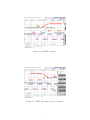
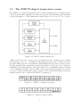
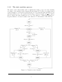
FYS4220 Lab. exercise 2
due September 29, 2014
Version 1.3
September 8, 2014
Introduction and requirements
In this assignment you will design a master controller for a Two Wire Interface (TWI)
based on the I2C protocol [1, 2, 3]. The controller will be implemented in VHDL using
a state machine approach, and will be used to interface the TMP175 digital temperature
sensor [4].
Requirements (due date: 29/09-2014):
• The i2c master.vhd design file.
• The tb lab2 gx.vhd test bench to validate correct behaviour of the I2C master
controller.
• A well structured report (with coverpage and in pdf-format) describing what you
have done and any problems you have encountered during the work.
• The report should include screenshots of the wave diagram generated by the test
bench simulation.
• The tb lab2 gx.vhd, i2c master.vhd and report (pdf-format) should be attached
and submitted by email to ketil.roed [at] fys.uio.no. The filename of the report
should contain your name(s) and group number (group numbers will be defined
soon). Avoid the use of spaces in the filename (an underscore can instead be used
as a separator if needed).
Version control
Version
1.0
1.1
Date
October 1, 2013
October 7, 2013
1.2
October 10, 2013
1.3
September 8, 2014
Comment
First published.
Updated info concerning the busy signal and
sMACK state (See table 1.4).
Corrected information in table 1.4 related to
the use of ack error (sIDLE) and busy (in
table caption).
Updated due date and references.
Table 1: Version control.
2
Part 1
1.1
The TWI/I2C bus
The Two Wire Interface (TWI) is a serial peripheral interface bus and compatible with
the I2C protocol. Only two wires are required for communicationg on the bus, a serial
data line (SDA) and a serial clock line (SCL). The lines are bidirectional with pull-up
resistors, as seen in figure 1.1, to keep a logic high level when no devices are driving the
bus.
Figure 1.1:
Some main features of the I2C bus are:
• Each device connected to the bus is addressable by a unique 7-bit (or 10-bit depending on the devive used) address space.
• It is a true multi-master bus, however, for this assignment we will design for the
simplified case of a single master.
• 8-bit serial data transfer
• Supports transfer speeds of upto 100 kbit/s in standard mode, up to 400 kbits/s in
fast mode, and up to 3.4 Mbit/s in high speed mode. For the TMP175 fast mode
is supported without any additional configuration. In order to operate at transfer
speeds above 400 kbit/s, the master devices must issue an high speed mode master
code as the first byte after a START condition [4]. High speed mode will not be
used in this. lab assignment. Keep in mind that the true data transfer rate will
be lower than the bus frequency due to the use of control bits during e.g. START,
STOP and ackhnowledge conditions.
3
• The number of ICs that can be connected to the same bus is limited only by the
maximum bus capacitance of 400 pF.
The device that initiates the transfer on the bus is called a master, and the devices
controlled by the master are slaves. The bus must be controlled by a master device that
generates the serial clock (SCL), controls the bus access, and generates the START and
STOP conditions. The main features of the message protocol are:
• Each message begins with a START conditions and ends with a STOP condition.
START and STOP conditions are always generated by the master. The bus is
considered to be busy after the START condition and free again a certain time
after the STOP condition.
• START condition: A HIGH to LOW transition on the SDA line while the SCL line
is HIGH (figure 1.2).
• STOP condition: A LOW to HIGH transistion on the SDA line while the SCL line
is HIGH (figure 1.3).
• Every byte on the SDA line must be 8-bits long. The number of bytes that can be
transmitted per transfer (between a START and a STOP condition is unrestricted
and determined by the master.
• Data is transferred with the most significant (MSB) bit first.
• During the transfer of a bit the SDA line must remain stable while SCL is high, as
any change in SDA while SCL is high will be interpreted as a control signal. This
is clearly seen in figure 1.2 where transitions on SDA takes place during the LOW
periods of the SCL, and where the level of SDA remains stable during the HIGH
periods of SCL.
• Each receiving device, when addressed, is obliged to generate an Acknowledge bit.
A device that acknowledges must pull down the SDA line in such a way that the
SDA line remains stable LOW during the HIGH period of SCL. Data transfer is sent
in eight clock pulses and followed by the Acknowledge bit during the ninth clock
cycle. Figure 1.3 shows an example where the SDA is kept low after the LSB to
indicate an Acknowledge condition. Afte the Acknowledge bit the SDA is released
for a short while before the master pulls it down again in order to prepare for a
LOW to HIGH transition indicating a STOP condition. the SCL
4
Figure 1.2: START condition.
Figure 1.3: STOP and Acknowledge conditions.
5
1.2
The TMP175 digital temperature sensor
The TMP175 is a digital temperature sensor with an internal Analog-to-Digital (A/D)
converter and internal configuration and storage registers. The internal register structure
is depicted in figure 1.4. The temperature register is used to store a 9-, 10-, 11-, or 12-bit
Figure 1.4: TMP175 register structure [4].
output of the most recent conversion. Two bytes must be read to obtain the data, of which
the respective 9-, 10-, 11-, or 12 MSBs are the temperature bits. The converter resolution
(see table VIII in [4]) can be determined by manipulating the respective resolution control
bits (R1 and R2) in the configuration registers (see figure 1.5). E.g., in order to enable the
maximum 12-bit temperature resolution, the value x”60” (b”01100000”) must be written
to the configuration register. The two LSBs of the pointer register(see figures 1.6 and 1.7)
are used to address the internal register of interest. More detailed information about the
internal registers can be found in the TMP175 datasheet [4].
Figure 1.5: TMP175 configuration register
Figure 1.6: TMP175 pointer register
6
Figure 1.7: Pointer addresses of the internal registers in the TMP175.
1.3
The I2C master controller: i2c master.vhd
In this lab. assignment you will implement a master controller module that must be able
to:
• Address the TMP175 on the I2C bus,
• write to the pointer register in order to address the internal registers of the TMP175,
• write or read data to or from the internal registers of the TMP175.
1.3.1
Top-level interface
The top-level signal and generic interfaces are listed in tables 1.1 and 1.2. Generics are
useful to increase the flexibility of the VHDL code and will in this case be used to determine internal enable signals in addition to the SCL clock frequency. More information
about generics can be found on page 127 in [5]. Internal signals to be used are listed in
table 1.3.
Signal name
clk
areset n
ena
addr
rnw
data wr
data rd
busy
ack error
sda
scl
Direction width Description
in
1
system clock
in
1
asynchronous active low reset
in
1
module enable
in
7
address of target slave
in
1
Read/nWrite command (’0’=write)
in
8
data to be written to slave
out
8
data read from slave
out
1
indicates transaction in progress
out
1
flagged if no acknowledge from slave
inout
1
bidirectional serial i2c data
inout
1
bidirectional serial i2c clock
Table 1.1: Top-level signal interface of the i2cmaster.vhd. All signals are of type std logic
or std logic vector.
7
Generic name
system clk
bus clk
Type Default value Description
integer
50 000 000
system clock in Hz
integer
400 000
i2c bus clock in Hz
Table 1.2: Top-level generic interface of the i2cmaster.vhd.
Signal name
state
state ena
Type
statetype
std logic
Width
1
Description
state machine signal
enables state transition
(duration 1 system clk cycle)
enable signal used for
START and STOP conditions,data sample, and
acknowledge
internal i2c clk signal
output enable for scl
Internal ack. error flag
(ack error <= ack error i)
internal
rnw
bit
(rnw i <= addr rnw(0))
interal sda signal
latched
address
and
Read/nWrite bit
latched data to slave
latched data from slave
to 7 counter to keep track of
data bit
scl high ena
std logic
1
scl clk
scl oe
ack error i
std logic
std logic
std logic
1
1
1
rnw i
std logic
1
sda int
addr rnw
std logic
std logic vector
1
8
data tx
data rx
bit count
std logic vector
8
std logic vector
8
integer
range 0
Table 1.3: Internal signals
8
1.3.2
The state machine process
The main control functionality will be implemented using a 1-process state machine
according to the transition state diagram shown in figur 1.8.To help you getting started
a brief description of each state is given in table 1.4. Note that the state machine process
will run synchronous to the system clk and that a dedicated signal, state ena, will be
used to trigger the state transitions, see 1.3.3. The purpose of this trigger signal is to
keep the duration of a state in units of the duration of a bit-transfer on the I2C bus.
Figure 1.8: Transition state diagram
9
State
sIDLE
sSTART
sADDR
sACK1
sWRITE
sREAD
sACK2
Description
In this state the state machine waits for an event on the external enable signal ena. If external signal ena = ’1’ then sample
inputs data wr, addr and rw. Concatenate addr and rw into
the 8-bit addr rnw. Release the SDA line (pull sda int high).
If ack error was active when entering sIDLE, it should only be
reset when ena = ’1’.
The purpose of this state is to generate a START condition
on the I2C bus at the center of the high period of SCL. On
entering sSTART pull sda int high. When scl high ena = ’1’
then pull sda int low (center point of SCL high period).
During this state the address bits in addition to the rnw bit
will be written to the I2C bus. Assign addr rnw(bit count) to
sda int. If bit count is not zero then decrement bit count. If
bit count is zero, assign default value of 7 to bit count.
After writing the address to the I2C bus, the corresponding
slave should acknowledge by pulling SDA LOW. The master must therefore release SDA. (Pull sda int high). When
scl high ena = ’1’ then check status of SDA line. If sda = ’1’
then assert ack error.
During this state the respective data bits will be written to the
I2C bus. Assign data tx(bit count) to sda int. If bit count is
not zero then decrement bit count. If bit count is zero, assign
default value of 7 to bit count.
During this state the slave will write data to the I2C bus. The
master must therefore release the SDA line (Pull sda int high).
If scl high ena = ’1’ then assign sda to data rx(bit count). If
bit count is not zero then decrement bit count. If bit count is
zero, assign default value of 7 to bit count.
When the master has transferred the 8-data bits the slave will
acknowledge this transfer by pulling SDA low during the ninth
SCL clock cycle. During this state the master can also accept
new commands. The master must therefore release the SDA
line (pull sda int high). Pull busy low. If the external enable
signal ena is kept high at the same time as the external rnw
signal is kept low, this initiates another byte write transaction
and the input data wr should be sampled into data tx. If the
external signal ena is kept high but external rnw is high, this
indicates a restart condition and both the input data wr and
addr should be sampled in addition to the rnw input. When
scl high ena = ’1’ then check status of SDA line. If sda = ’1’
then assert ack error. If the external signal ena is pulled low,
this indicates end of transactions and sda int should be pulled
low when moving to the sSTOP state.
10
sMACK
sSTOP
1.3.3
In the master acknowledge state the master can either ACK
(sda int = ’0’) in order to continue reading data from the slave
or it could NACK (sda int = ’1’) if no more data should be
read. The busy line should be pulled low during the sMACK.
If the external enable signal ena is kept high at the same time
as the external rnw signal is kept low, this indicates a restart
condition and both the input data wr and addr should be sampled in addition to the rnw input. If during sMACK the input
signal ena is pulled low, this indicates that the read transaction
is completed and no more data should be read from the slave.
In order to end the transaction, a NACK must be indicated
to the slave. (Tips: Set default value of sda int to ’1’. sda int
should then be pulled low either if ena = ’1’ to prepare for the
ACK, or when (state ena = ’1’ and ena = ’0’) to prepare for
a stop condition.).
The purpose of this state is to generate a STOP condition on
the I2C bus at the center of the high period of the SCL. When
scl high ena = ’1’ then pull sda int high.
Table 1.4: Description of state machine actions. The
busy output port should be active in all states expect
the sIDLE,sACK2 and sMACK2 states.
The internal timing and trigger signals process
The I2C master controller will use the external onboard 50 MHz crystal as the system
clock. In order to communicate on the I2C bus, generate the START and STOP conditions, sample the SDA line during reading of data and slave acknowledge, a dedicate
process is needed to generate the lower frequency SCL clock and the appropriate internal
trigger signals. Based on the generic inputs system clk and i2c clk, this process will use
a counter (use process internal variable) to generate the correct timing. This process
should generate the internal scl clk according to value of the generic i2c clk, in addition
to the two trigger signals state ena and scl high ena.
• Both trigger signals should be implemented with a duration of 1 system clock cycle.
• The state ena signal will be used to trigger the transition of the state machine and
should be generate at the center point of the low period of SCL.
• The scl high ena signal will be used to trigger the sampling of the SDA line during a
read transaction or acknowledge condition, and the START and STOP conditions.
It should therefore be generate at the center point of the high period of SCL.
1.3.4
Controlling the SDA and SCL line
The SDA and SCL lines of the I2C bus are bidirectional where pulling the line to ground
is considered a logical zero while letting the line float (high impedance ’Z’) is a logical
one. For the SCL line an internal output enable signal, scl oe, is used to control if the
internal scl clk signal or a high impedance value ,’Z’, is assigned to the output scl.
11
• When scl oe = ’1’ then assign the internal signal scl clk to the output port scl, else,
assign ’Z’ to scl. scl oe is controlled by the state machine and the scl output should
be active as long as the state machine is not in the state sIDLE.
An internal signal, sda int, is used as an intermediate signal for sda and controlled by
the state machine. sda int can take the values ’0’ or ’1’.
• When sda int = ’1’ assign ’Z’ to sda, else assign ’0’ to sda.
Both the sda and scl output should implemented as purely combinational and concurrent
statements.
12
Part 2
2.1
Testbench environment
To validate the correct behaviour of the I2C master controller you will implement a test
bench to perform the following two steps:
• Set the temperature resolution to 12-bit.
• Read back the value of the temparature register.
Tables 2.1 through 2.3 lists the write and read procedures needed to perform these steps.
Byte mode
1
write
2
write
3
write
Byte value
comment
“1001000” & rnw = ’0’ address slave and indicate write
“00000001”
Write the address of the configuration register in to the pointer register
“01100000”
write to the configuration register
and set 12-bit temperature resolution
Table 2.1: Write procedure to set 12-bit temperature resolution for the TMP175. The
transaction is initiated with a START condition and ended with a STOP condition.
Byte mode
1
write
2
write
Byte value
comment
“1001000” & rnw = ’0’ address slave and indicate write
“00000000”
Write the address of the temp. register in to the pointer register
Table 2.2: Write procedure to address the temperature register. The transaction is
initiated with a START condition and ended with a STOP condition.
13
Byte mode
Byte value
´
1
write ’1001000´’ & rnw = ’0’
read
2
3
read
-
comment
address slave and indicate read
read MSB from temperature register
read LSB from temperature register
Table 2.3: Read procedure to read the value of the temperature register. The transaction
is initiated with a START condition and ended with a STOP condition.
14
References
[1] I2C specifications. http://www.nxp.com/documents/user manual/UM10204.pdf.
[2] The I2C-bus and how to use it (Including specifications), Philips Semiconductors.
http://www.i2c-bus.org/fileadmin/ftp/i2c bus specification 1995.pdf.
[3] I2C Bus. http://www.i2c-bus.org.
[4] Digital Temperature Sensor with Two-Wire Interface, Burr-Brown Products from
Texas Instruments. http://www.ti.com/lit/ds/symlink/tmp175.pdf.
[5] Brian Mealy and Fabrizio Teppero, Free Range VHDL, Release 1.17 .
http://www.freerangefactory.org/dl/free range vhdl.pdf.
15