1
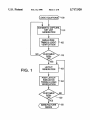
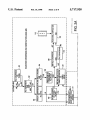
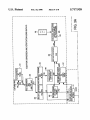
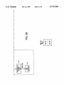
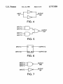
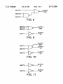
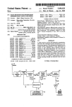
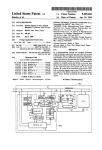
US005717928A
United States Patent [191
[11] Patent Number:
[45] Date of Patent:
Campmas et a].
5,717,928
Feb. 10, 1998
“A VLSI Design Veri?cation Strategy". Aharon Tran et a1;
IBM Research and Development vol. 26. No. 4, Jul. 1982,
p. 475-484.
[54] SYSTEM AND A METHOD FOR OBTAINING
A MASK PROGRAMMABLE DEVICE USING
A IJOGIC DESCRIPTION AND A FIELD
PROGRAMMABLE DEVICE
IMPLEMENTING THE LOGIC
DESCRIPTION
“The Weighted Random Test-Pattern Generato ”, Daniel
Schmurmann et al, IEEE transaction of computer, vol. c-24.
No. 7; Jul. 1975. pp. 695-700.
[75] Inventors: Michel J. Campmas. Palo Alto;
William A. Johnston. San Jose;
Gai-Bing Chen. Cupertino, all of Calif.
Dan Powers, “FGPA to Gate Array Migration: The Best of
Both Worlds,” May 1990. pp. 345-348, Electro Conference
Record, vol. 15. No. 9-11.
[73] Assignee: Matra Hachette SA. Paris, France
Primary Examiner-Meng-Ai T. An
Attorney Agent, or Fimr-Skjerven. Merrill. MacPherson,
[21] Appl. No.: 610,479
[22] Filed:
Nov. 7, 1990
[51]
Franklin & Friel; Edward C. Kwok
[57}
Int. Cl.‘5 .................................................... .. G06F 15/60
[52] U.S. Cl.
395/701; 395/500; 395/185.06;
In accordance with the present invention. a system and
395/ 183.13
[58] Field of Search
method for converting an implementation of a logic descrip
tion describing a ?eld programmable device into an imple
395/500. 600.
39500053641578, 488, 451. 452
[56]
mentation of the same logic in a factory-programmed device
are provided. In one embodiment of the present invention.
an expert system synthesizes a logic circuit model based on
References Cited
U.S. PATENT DOCUTVIENTS
4,590,581 5/1986
4,829,427 5/1989
4,901,259 2/1990
4,967,386 10/1990
Widdoes, Jr.
Green
Watkins
Maeda et a].
5,051,938
9/1991 Hyduke
364/578
2/1992 Chang et al.
4/1993 Goldberg et a1.
395/600
395/600
5,202,889
5,258,919
the logic description. An automatic test pattern generator
provides test vectors including expected response signals for
the logic circuit model generated by the expert system. The
364/578
395/600
364/578
364/578
5,089,985
5,201,046
ABSTRACT
automatically generated test vectors are provided to a tester
which applies the test vectors as input stimuli to the ?eld
programmable device. The output signals of the ?eld pro
grammable device are veri?ed against the expected response
signals. If the output signals of the ?eld programmable
4/1993 Aharon et a1. ........ ..
371/27
11/1993 Yamanouchi et al. ................ .. 364/489
device match the expected response signals, the computer
model is considered correct. and mask layout may begin for
the building a mask-programmable circuit which performs
the functions described in the logic description.
OTI-IBR PUBLICATIONS
“Dynamic process for generation of biased pseudo-random
test patterns for the functional veri?caiton of hardware
8 Claims, 8 Drawing Sheets
designs”; Aharon et :11, Apr. 1990 (Isarael).
LAYOUT
GENERATION
i
POST-LAYOUT
Sll/IKAATON
TIMING I. LOGIC
US. Patent
Feb. 10, 1998
Sheet 1 of 3
5,717,928
LOGIC EQUATIONS
SCH EMATIC CAPTURE,
NET LIST
GENERATION
"L101
I
SIMULATION:
TIMING & LOGIC @102
VERIFICATION
LAYOUT
FIG 1
GENERATION “103
I
AT
PSIIIIJIAYSIIT
TIMING & LOGIC “104
VERIFICATION
US. Patent
Feb. 10, 1998
Sheet 5 of 8
5,717,928
.GEmm
mm.wE
._.
_
_
_
'_
_ _
_ _
_
_
_
n
m8.8%.
"an:
_
I
a
_
_
x<>
on:E3_$2_5
_
_
1Ji‘tkI!
US. Patent
Feb. 10, 1998
INPUT_
IN
Sheet 6 of 8
:
5,717,928
_OUTPUT
INN
FIG. 4
INPUT
INPUT A
B ——_U_
-—
0UTPUT
OUT
INPUT c —:D_
INPUT D —‘
FIG. 5
INPUT D
INPUT CK
D
Q
OUTPUT 0
>CK QN O———OUTPUT QN
FIG. 6
INPUT A
INPUTB
ol?mm
INPUT 0
INPUTE
OUTPUT
>o— EN
FIG. 7
US. Patent
Feb. 10, 1998
INPUTA
INPUT B —
INPUTC —
Sheet 7 of 8
5,717,928
OUTPUT
OUT
“I
FIG. 8
INPUT A
INPUT B
INPUT C
INPUT E
I?
I
OUTPUT
NOR
OUTPUT
EN
FIG. 9
INPUT A
INPUT B
INPUTE
OUTPUT
NOFI
OUTPUT
OR
III
I
OUTPUT
EN
FIG. 10
INPUT A —
I
OUTPUT
AN
OUTPUT
INPUT B ——>0— BN
US. Patent
Feb. 10, 1998
Sheet 8 of 8
5,717,928
OUTPUT
NAN
'NPUT A _‘
OUTPUT
INPUT B —
AND
OUTPUT
INPUT E —1>0‘ EN
FIG. 12
INPUT
A
D
INPUT B
INPUT 0 D N
INPUT 0
FIG. 13
OUTPUT
OUT
5,717,928
1
2
SYSTEM AND A METHOD FOR OBTAINING
A MASK PROGRAMMABLE DEVICE USING
A LOGIC DESCRIPTION AND A FIELD
PROGRAMMABLE DEVICE
IMPLEMENTING THE DOGIC
DESCRIPTION
model shown in FIG. 1, is not always straight forward. For
FIELD OF THE INVENTION
This invention relates to the ?eld of integrated circuits. In
particular, this invention relates to the ?eld of programmable
example, it is common for a schematic representation to be
corrected and resimulated multiple times before arriving at
an acceptable ?nal representation. At this point. as illustrated
by decision point 110, the customer typically provides a
"sign-off” to the ASIC vendor. indicating permission to go
ahead to the next step 103, during which the layout of the
customized mask is generated (“layout generation”). The
10
logic devices.
Layout generation step 103 requires taking the netlist of
the schematic representation to create patterns of geometric
shapes on the customized “mask" layers. The customized
BACKGROUND OF THE INVH‘ITION
Field programmable logic devices. also commonly known
masks created from these patterns are used in some of the
as programmable logic devices (PLDs), are programmable
photolithographic steps in the circuit fabrication process.
These masks are generated according to the design rules of
the ASIC vendor’s fabrication process and circuit technol
integ'ated circuits sold to the user unprogrammed. The user
then programs the device to provide logic functions required
by his/her application. Examples of PLDs are discussed in
the “PAL Device Data Book.” third edition (1988), pub
lished by Advanced Micro Devices. Inc. of Sunnyvale,
Calif. incorporated herein by reference in its entirety. (PALs
ogy. The layout generation step 103 is also typically
achieved using a variety of design software programs and
20
(component) libraries.
The layout generated by step 103. is provided to a
commercially available programming equipment, PLDs pro
simulation and veri?cation program at step 104 to ensure
vide design ?exibility and quick tum-around, which are
important advantages for certain applications. For example.
in the development of a product prototype, debugging in the
?eld environment can be accomplished by simply replacing
that logic functions and timing parameters are accurately
preserved during the translation from the netlist representa
tion to the layout representation. These simulation and
veri?cation programs may be the same as those used in step
30
opment is stabilized.
A gate array circuit is a popular factory-programmed
substitute for a PLD. A gate array circuit is typically
40
pattern of interconnect metallization, to interconnect the
underlying generic array of transistors. The pattern of inter
tion and veri?cation steps (103 and 104) are often necessary.
After the customer is satis?ed with the layout generated.
another “sign-01f," represented in FIG. 1 as decision step
120, is provided to the ASIC vendor to indicate permission
to begin manufacturing the device. Again. the customer
bases his/her decision upon careful perusal of the simulation
and veri?cation results.
The generated layout of step 104 is then used to build
phowlithographic masks, which are used to manufacture the
connect metallization is provided using customized photo
gate array (step 106).
masks. The gate an'ay circuit emerging from the fabrication
process implements application-speci?c logic functions.
102 discussed above. At this point, many parameters speci?c
to the physical implementation of the circuit, such as timing,
may be more accurately estimated Once again. the layout
generation process is not always straight forward. Several
iterations of the layout generation and post-layout simula
compatible factory-programmed device, after product devel
programmed by providing during fabrication a customized
databases. Some examples of these software programs and
databases are place and route programs and “cell”
and FPLAs are types of PLDs.)
Because a PLD can be conveniently programmed using
a faulty PLD by one implementing the correct logic.
However. because each PLD must be individually
programmed, PLDs are more expensive than factory
programmed devices, which are mask programmed in large
batches during the fabrication process without additional
cost. It is therefore cost eifective, when a product is in high
volume production, to replace a PLD with a pin-for-pin
customer bases his/her go-ahead decision upon careful
perusal of the simulation and veri?cation results.
45
As can be readily seen, to achieve the conversion from a
Presently. the conversion from a PLD circuit to a factory
PLD implementation to a factory-programmed circuit
programmed circuit involves close cooperation between the
supplier of the factory-programmed circuit (hereinafter, the
implementation, expensive engineering time is often
“ASIC vendor”) and the user of the PLD (hereinafter, the
“customer”). FIG. 1 shows the steps required to accomplish
the conversion.
Referring to FIG. 1, the customer provides to the ASIC
vendor at step 100 the logic description implemented in the
PLD. As illustrated by step 101, this logic description is then
50
expended by the customer. Throughput time of the conver
sion process is also prolonged by the time necessary for the
customer to verify that the simulation results are acceptable.
Such engineering and veri?cation costs add to the cost and
time required to build the ?nal device. Hence, it is highly
desirable to have an automated mechanism by which the
customer's involvement, i.e. expensive engineering time as
translated into a schematic representation of a logic circuit. 55 Well as simulation veri?cation, is minimized if not elimi
nated.
This step is often accomplished using a software schematic
capture program. From this schematic representation, a
SUMMARY OF THE INVENTION
netlist is generated for use with simulators and veri?ers at
step 102. These simulators and veri?ers are software pro
In accordance with the present invention, a system and a
grams which simulate the operation of the circuit repre
method for converting a PLD device to a factory
sented by the netlist to ensure that the intended logic
programmed circuit are provided, wherein a logic descrip
functions are correctly provided. Often at this step, propa
tion of a PLD is used to generate a netlist. This netlist, in
gation delays exhibited by the logic circuit represented by
turn, is used to generate a test program. including test
the netlist are estimated to determine if timing perforrnanoe
vectors, for testing the PLD. The test program is then used
targets are met.
to test a PLD provided by the customer. and if the PLD
The process of generating an acceptable schematic rep
successfully passes the test, it is known that the netlist
resentation from logic descriptions as illustrated by the
accurately describes the PLD. Thus, the netlist can be used
5,717,928
3
4
to construct masks, and it is not necessary to involve the
customer in simulation veri?cation.
If the customer’s logic description is not in the ABEL
format, an optional conversion program can be provided,
such as shown in block 201 of FIG. 2. For example, in one
The present invention is better understood in light of the
embodiment, a program TOABEL (represented by block
201) translates PALASM format equations obtained from a
following detailed description and accompanying drawings.
?le having ?le name extension .PAL to ABEL format and
BRIEF DESCRIPTION OF THE DRAWINGS
place the output ABEL logic equations in a ?le having ?le
FIG. 1 illustrates the steps necessary to achieve a con
version from a PLD device to a factory-programmed device
name extension .ABL. (PALASM is well known in the 311.
and is described in “PAL Device Data Book.” incorporated
in the prior art.
FIG. 2 is a block diagram showing a ?rst embodiment of
herein by reference in its entirety above.) The progam
TOABEL is well known in the art. and is available also from
DATA I/O Corporation. mentioned above. TOABEL runs on
IBM PC machines and Sun workstations.
a system for converting a PLD device to a factory
programmed device in accordance with the present inven
tion.
Block 202 shows the .ABL ?le (Le. ABEL ?le) being
FIG. 3 is a block diagram showing a second embodiment 15 provided to an expert system known as GASP for generating
a netlist of a logic circuit. A script or command ?le ABEL___
of a system for converting a PLD device to a factory
TO_I-HLO is used to execute the various components of
programmed device in accordance with the present inven
GASP. GASP, also called GASP-LUCAS. is a rule-based
tion.
FIGS. 4. 5. 6. 7, 8. 9, 10, ll, 12 and 13 schematically
illusn'ate logic devices used in an example of a program
mable logic device being converted to a mask
expert system available from Genrad Limited. Fareham,
20
programmable device.
DETAILED DESCRIPTION
25
In accordance with the present invention. a system and a
method of designing a factory-programmed circuit to
UK. The GASP program takes as input ?les: 1) a ?le .ABL
containing the logic description in the ABEL format
(Appendix A1)‘, 2) a ?le .MPL which models the PLD
device type (Appendix A2); 3) a “methods h‘brary ?le”
.MET (Appendix A.3), which desrn'ibes how logic devices
are constructed in the ASIC vendor’s circuit technology; 4)
a MD.CEL library (Appendix AA) which lists logic func
tions that are available in the ASIC vendor’s circuit tech
replace a PLD are provided, using the logic description of
nology; and 5) a rule base ?le .RCP, compiled from a set of
the PLD circuit and a functioning PLD device.
FIG. 2 is a block diagram of a ?rst embodiment of the
system in accordance with the present invention. In accor
dance with the present invention, the customer needs only
.BAS ?les (Appendix A.5). which describe for GASP rules
for e?iciently converting the logic description into a netlist
describing interconnected logic cells of the types listed in
the MD.CEL library. In response to these input ?les, GASP
provides therefrom a netlist of a logic circuit which performs
provide the ASIC vendor with a logic description and a
functioning PLD device in which the logic desa'iption is
implemented. With substantially no further involvement by
35
the customer, the ASIC vendor provides the customer a
factory-programmed circuit suitable for mass production,
and which is pin-for-pin compatible with the PLD device.
circuit components, for example, the gates, buffers and
?ip-?ops in a circuit. The netlist identi?es the input and
output leads of each circuit component and its connections
to other circuit components.
As mentioned above, the .MPL ?le models the generic
PLD type. For example, to model an AMD 22Vl0, one
would provide a ?le such as provided in Appendix A.2
In the embodiment shown in FIG. 2, block nos. 201 to
108, 211 to 213 and 216 represent execution of programs on
data input ?les (described below). These programs can be
executed on an IBM Personal Computer or a machine
compatible with an IBM Personal Computer (hereinafter,
“IBM PC”), or a Sun Microsystems Model Sun-3 worksta
tion (hereinafter, “Sun-3”). However, other computers or
the functions described in the .ABL ?le. Information con
cerning the operation and use of GASP can be obtained from
GenRad Incorporated, Fareham, UK. As is known in the art,
a “netlist” is a type of circuit description which lists all
45
workstations may also be used.
As shown in FIG. 2, a method in accordance with our
invention commences when the customer provides a logic
attached hereto. If one were to use the present invention to
convert a device implemented in a different PAL type into a
mask programmable device, one would modify the .MPL ?le
appropriately.
description representing the logic functions implemented in
Attached as Appendix A6 is a netlist ?le (the .NET ?le)
which GASP prepares from the .ABL, .MPL, MD.CEL,
a PLD. The logic description can be expressed in a logic
equation description language such as ABEL. Details con
cerning ABEL can be found in “ABEL 3.0", published by
MET‘ and RC? ?les discussed above. In the .NET ?le of
Appendix A.7, after the line which states “BEGIN” is the
Data I/O Corporation, Redmond, Wash., incorporated herein
listing describing the logic performed by the circuit. The ?rst
by reference in its entirety. In otha embodiments, other
logic description languages may be used. Also, in other
embodiments, other methods are used to provide a logic
tam on each line in the Hating is a label associated with the
55
logic gate being described, the second item (enclosed in
parentheses) is the name or names of the output signal or
description, such as truth tables, or schematic representa
signals provided by the gate, the third item, after the “:="
tions of logic circuits.
An example of an input ?le containing ABEL logic
equations is included in Appendix A.1 attached hereto.
These equations describe logic to be implemented in an
AMD 22V10 logic array. available from Advanced Micro
punctuation, is the type of logic device represented by the
Devices, Inc. of Sunnyvale. Calif. However, in other
embodiments. other logic equations are used, which describe
PLDs other than the 22V10.
line, and the fourth item is the name or names of the input
signal or signals. Thus, for the device described in the ?rst
line following “BEGIN”, the gate is labeled GNISPD, its
output signal is N13PD, it is of device type BUFIN'I'I‘L (a
'I'I'L input buffer), which receives input signal PIN13. Table
I below lists the device types and abbreviations used in the
.NET ?le of Appendix A.6.
5,717,928
6
5
tern or fault simulator is used. The SYSTEM HlLO program
runs on the Sun-3.
TABLE I
The HITEST program takes as inputs the .CCT netlist ?le
described above, a .KDB ?le containing a “knowledge base”
description used in test vector generation, and a .DWL ?le
Device Type
Symbol
BUFIN'I'IL
INVP
'I‘I‘L compatible input buffer.
'Iwo parallel inverters (see Figure 4).
B03N4
'Il'istate output buffer with 24 mA
output drive.
Z-input NAND gate.
2 wide 2-2 input AND OR INVEKI‘ (see
hereby incorporated by reference in its entirety, is obtainable
Figure 5).
from GenRad Fareham Limited. Fareharn. UK. The de?ni
NANDZ
AOI2W22
DFFRNI
NANDIB
containing parameters of input and output waveforms. The
de?nition and use of the .KDB ?le is provided in the
“HH'EST Test Generator Reference Manual”. which is
D-Flip Flop (See Figure 6).
tion and use of the .DWL ?le is described in the “HITESI'
3-input NAND Gate with an inverter
DWL Reference Manual”. which is hereby incorporated by
(see Figure 7).
AOI2W2l
reference in its entirety. is obtainable also from GenRad
Fareham Limited. An example each of the .KDB and the
2 wide 2-1 input AND OR INVEKI‘ (see
Figure 8).
NORB
3 input NOR gate with an inverter (see
Figure 10).
.DWL ?les are attached hereto as Appendices A.8 and A9
respectively. The examples of the .KDB and DWL ?les are
appropriate when converting a device implemented in an
Two inverters (see Figure ll).
AMD 22Vl0 to a gate array implementation. If one were to
Figure 9).
ORI2
INVZ
ANDI2
2 input OR gate with an inverter (see
2 input AND gate with an inverter (see
convert from other generic device types (eg a PALZORAlO,
Figure 12).
NAND3
3 input NAND gate.
aiso available from AMD). one would have to modify the
POR
Power on reset.
0AI2W22
2 wide 2 input OR AND OR INVERI‘ (see
.KDB and .DWL ?les appropriately.
The above described input ?les allow the HITEST pro
Figure 13).
The library of logic devices used with GASP may contain
other logic devices. However, the circuit speci?ed by the
.ABL ?le of Appendix A.1 requires only devices listed in
25
block 204, to ensure proper fault coverage by the test
Table 1. Additional logic devices are described in
“GATELlB Macrocell and Macro Function libraries" pub
lished by Matra Design Semiconductor, Inc.. of Santa Clara,
Calif. in 1987.
As can be seen. the .NET ?le includes a circuit element
POR. used for a power on reset of output register ?ip ?ops
in the output circuitry of the 22Vl0. For simulation purpose,
POR can be modeled as a delay line. As implemented in this
embodiment. POR is a circuit with a large capacitance.
Part of the software represented by block 202 includes a
conversion program which receives the .NET ?le and gen
erates therefrom a ?le .CCT (Appendix A.7). As can be seen
from a cursory examination of the .NET and CCI‘ ?les from
35
40
vectors. HITBSI‘ provides a log ?le. identi?ed by ?le name
extension .LOG (Appendix A. 11), which summarizes any
exception condition encountered during fault simulation and
test vector generation. The LOG ?le is merely a user report,
which is not used as an input ?le for any programs.
Optionally, the HH’EST module may also receive a set of
“seed” test vectors. e.g. generated by the customer. HITESI‘
learns from and builds upon these seed vectors to more
rapidly generate a set of test vectors (which include the seed
vectors) to test the customer-provided PLD.
In one embodiment, the .CCI‘ and .TAB ?les are input to
a program ARCIS (block 207), which estimates the propa
gation delays of signals through a circuit having the logic
elements described in the .CCI‘ ?le, when the stimulus
signals provided in the .TAB ?le are applied to the circuit.
The operation and use of ARCIS as discussed in “GATEAID
Appendices A.6 and A.7. respectively, this conversion soft
ware merely rearranges, in a manner readily apparent, the
positions of the gate names, types, and signal names on each
line.
After the .CCI‘ ?le has been prepared, it is necessary to
gram to provide an output ?le .TAB including a set of test
vectors. This .TAB ?le (Appendix A10) is intended for use
as stimuli in testing the logic circuit described in the CC!‘
?le. Fault detection analysis is used at this step illustrated by
45
PLUS/PC 2.0 User’s Manual”, second edition (1988), pub
lished by Man-a Design Semiconductor, hereby incorporated
generate test vectors which can be used to test a sample PLD
by reference in its entirety.
provided by the customer. As is well known in the art, test
vectors, which are often expressed in table form, are stimu
lus input signals provided to a circuit and the expected
Prior to running ARCIS, it is necessary to convert the
.CCT and .TAB ?les into a format that ARCIS can accept.
Thus, block 206 represents a conversion program that
receives ?le .TAB and generates therefrom a tile SIM
circuit output signals responding to the input signals. A
program known as SYSTEM HILO (block 204) is used to
generate test vectors from the netlist. SYSTEM HILO is
available from Genrad, Limited of Fareham, UK.
A test pattern generation module HlTEST and a fault
simulator HIFAULT are separately purchased parts of SYS
TEM I-HLO. The operation of the HITEST module is
described in “SYSTEM l-IlLO HITEST-Plus Reference
Manual”. which is hereby incorporated by reference in its
entirety. obtainable from GenRad Incorporated, Fareham,
UK. The HIFAULT fault simulator, which is described in
(Appendix A12). As can be seen. the conversion program
represented by block 206 deletes the expected output signals
from ?le .TAB because ARCIS will recalculate these sig
55
nals. The conversion program also causes the columns of the
.SIM ?le to be in an order dilferent from that in the .TAB ?le.
60
Further, as shown in Appendix A12. the SIM ?le includes
the following cormnands to the ARCIS program.
1. $CYCLE1 is a multiplier (in this case, 1.0) for the times
listed in the .SIM ?le.
2. $LOAD 56 indicates that 50 pF loads are present on
pins 14 to 73.
3. VCC CLKO 100 describes the power input waveform
necessary to correctly simulate the POR function.
the “HIFAULT Reference Manual”, hereby incorporated by
reference in its entirety, is also obtainable from Genrad
Incorporated. Fareham, UK. Of course, other automatic test
pattern generation systems and fault simulators may also be
used. Appropriate format conversion programs may be
needed when another automatic test pattern generation sys
65
Speci?cally, the VCC input signal is initially low for 10
us, then goes high and remains high, thereby providing
a signal transition to the POR function.
5,717,928
8
7
A conversion program represented by block 203 receives
?le .CCI‘, and in response thereto genm'ates a ]N ?le, which
4. $PRINT lists the output signals to be printed by ARCIS.
5. SPATI'ERN is a truth table format for the input signals.
The lines immediately following $PA'ITERN list the
order in which input signals are provided in the .SIM
contain the same netlist information as the .CCT ?le. Of
?le. The $PATI‘ERN information terminates at the line
importance, the ,IN ?le is in a format which is received by
a conversion program PADPIN (block 205). The PADPIN
marked $EOP (end of pattern).
program extracts from a data base MDPAD and netlist ?le
.IN pin and pad (layout) information to provide an output ?le
.N'Pl (Appendix A16), which provides test set-up informa
6. $TIME 87000, 2000 instructs ARCIS to simulate, and
print at intervals of 200 us. until 8700 us have elapsed
(Times listed in the .SIM ?le are expressed in tenths of
nanoseconds).
tion. (PADPIN also generates a ?le .PAD, such as the one
10
As mentioned above, it is also necessary to put the CCT
?le into a format that can be accepted by ARCIS. Block 203
represents a program which converts ?le .CCI‘ to ?le .IN
(Appendix A13). As can readily be seen. the .IN ?le
contains all the information of .CCl‘, but the input/output
order is re-arranged slightly. ARCIS also receives informa
tion from a built-in library which contains all of the gate.
buffm' and ?ip ?op propagation delays. and calculates there
from signal changes at various nodes and output leads
throughout the device, taking into account the number of
input leads each device must drive (i.e. fan-out). Thus. if the
input ?le SIM instructs ARCIS that at time T=l000 us, a
signal applied to an input buffer goes high, ARCIS looks up
in a library parameters regarding the buffer delay and drive
capabilities and determines the propagation delay exhibited
by the buffer. based on bu?’er characteristics and the number
of input leads the buffer drives. If, based on the buffer
fan-out, that buffer has a delay time of 5 ns, ARCIS then
25
state at a time T=1005 ns.
The NH output ?le of the PADPIN is provided to a
ARCIS makes similar calculations concerning the propa
program NPITOSET (block 208) to provide NPITOSET
output ?les (identi?ed by ?le extensions SE!‘ and .PIN) for
gation of signals throughout the circuit.
35
timing targets.
ARCIS nmy also be used to provide an output ?le
indicating the state of the output signals at regular intervals
(e.g., every 200 ns). Attached as Appendix A14 is ARCIS
output ?le .OUT indicating the states of each input and
library MD.PAD (Appendix A18) which contains parameter
information for each type of buffer. (The abbreviations PU,
PD, and ON in the MD.PAD stand for “pullup", “pulldown”,
and “open drain”, respectively. “0/2” is a tn'state output.
“1/0” is a bidirectional pin.)
calculates that the output signal of that buffer will change
ARCIS can provide output ?les in various formats. For
example, ARCIS can provide an output ?le which indicates
the time of every signal transition in the circuit. This may be
used to deta'mine if the device being simulated meets device
listed in Appendix A.17, which is used during the device
layout process described below.) As shown in the listing of
Appendix A16, the information provided in the .NPI ?le
includes, for each pin number, whether the pin is an input or
output pin. the type of output buffer provided, the type of
input or output buffer provided (e.g. if the pin is an input pin,
TI'L or CMOS compatible and/or including a pullup or
pulldown), the IlL/IIH or IOIJIOH current limits (i.e., if the
pin is an input pin, the input current limits when the input
signal is low and high, respectively, or if the pin is an output
pin, output current limits when the output signal is low and
high. respectively), and which timing generator (T6) of the
tester is assigned. Of importance, since the .IN ?le indicates
which bu?er type is connected to each input pin, PADPIN
merely retrieves the DC parameter information from a
40
output pin at 200 ns intervals. The DU!‘ ?le is used to
generate the test vectors to test the customer-provided PLD.
It is noted that because .OUT merely contains the state of
the device every 200 ns, it contains essentially no informa
tester set up. The .SET ?le is the IMS tester program, and
de?nes in the tester’s supported format the tester resource
allocation and each pin’s attribute. An example of a .SET ?le
is attached ha'eto as Appendix A19. NPITOSET is pro
vided for interfacing the .NPI ?le with the IMS tester of this
embodiment. If another tester is to be used, a similar
software program may be needed to provide the tester
interface. The techniques used to convert the information
contained in the .NPI ?le to the accepted format of each
tester is known in the art.
The IMS tester requires a second ?le .IMS which contains
that can be used to test the PLD. Thus, one can pradice the
test vectors. This is provided by the translation software of
block 216 which receives the input and output waveforms
from the ARCIS simulation and the .PIN ?le from
NPlTOSET and generates therefrom an output ?le, identi
?ed by the ?le name extension .SIM, which is acceptable as
an input ?le by the IMS tester. An example of .IMS ?le is
attached hereto as Appendix A15. This IMS ?le will provide
to the tester the input waveforms to apply to the PLD under
test, and the expected output waveforms which the tester
present invention using either the I-III‘EST-genm'ated test
uses to verify the functional correctness of the GASP
tion concerning the timing performance of the device pro
45
vided in the netlist ?le .lN described above. Thus, the .OUT
?le provided by ARCIS does not re?ect timing tests on the
PLD. This is because, at this point, only functional testing is
performed.
While ARCIS is used to generate functional vectors to test
the PLD, it is noted that I-[lTESI‘ also provides test vectors
generated logic circuit by comparing the expected output
vectors or the ARCIS-generated vectors. In addition to
ARCIS, other gate level simulator may be used, e.g., HELO,
VIEWSIM (available from ViewLogic, Inc. of Santa Clara,
Calif). etc.
The next step in the method is to generate the actual test
program used to test the PLD. To accomplish this, the .OUT
55
pins of the PLD provided by the customer. The response of
the PLD is compared against the expected output waveforms
test vectors are converted to a format used by IMS tester 209
using a format conversion program (block 216). In this
in the .IMS ?le, This step is known as functional veri?cation.
If the logic circuit provided by GASP is an acceptable
embodiment. the tester used is an IMS testm'. IMS testers are
available from IMS, Inc., located in Beaverton, Oreg.
However. other testers. such as Sentry testers, obtainable
from Schlumberger Corporation, may also be used. Of
course, format conversion may need to be provided for each
tester type used.
waveforms with the actual output waveforms of the PLD
device.
Based on the input stimulus waveforms provided in the
.IMS ?le, and con?guration information from the .SET and
.PIN ?les, the tester applies the stimulus waveforms to the
65
replacement for the PLD device using a set of test vectors
with a high level of fault coverage (96-10096). the PLD
output waveforms and the expected output waveforms pro
vided by the circuit simulator ARCIS (or equivalent circuit
5,717,928
9
10
simulator) will be the same. Otherwise, the netlist must be
geometry of the circuit provides more accurate estimates of
circuit performance than are attainable from the previous
debugged and resirnulated.
Because the synthesized circuit is compared against the
pro-layout simulation performed by ARCIS. If another simu
actual PLD device using a set of test vectors with a high
lator other than ARCIS is used, it will be necessary to use the
back-annotation technique for that simulator. Such conver
sion techniques are also known in the art.
The post-layout simulation is carried out in the same
manner as the pre-layout simulation described above. The
level of fault coverage (96-10070). the accepted synthesized
circuit is necessarily an accurate model of the PLD device.
It can then be inferred that the implementation of this model
in the factory-programmed device will be a correct substi
tute for the PLD device, provided the characteristics of this
results of the post-layout simulation are analyzed against the
model is preserved through the layout generation process.
The layout generation process is illustrated by block 211.
timing speci?ed in the PLD manufacturer’s data sheet, (in
the present embodiment, the 22V10 data sheet available
from Advanced Micro Devices, Inc. of Sunnyvale, Calif.).
Again, if the simulation yields results which do not match
those provided by the PLD data sheet, the ASIC vendor
modi?es the layout generated, and resimulates the circuit.
without the customer’s intervention, until an acceptable
layout is obtained.
In this embodiment, the layout of the customized mask layer
is synthesized by GARDS, which is a program commer
cially available from Silvar-Lisco Corporation, Menlo Park.
Calif. Of course, other layout generation tools suitable for
application speci?c integrated circuit technologies (such as
gate arrays). may also be used. The GARDS system is
described in “Silvar-Lisco/GARDSm Command Reference
Manual”, Vol. 1, Document No. M-GDS-6.0-ClA, Jul.
1988, is hereby incorporated by reference in its entirety.
A software program ARCI‘OSDL translates the logic
netlist provided in the .IN ?le to the SDL format accepted by
the GARDS system. The SDL Format ?le is identi?ed by the
?le extension .SDL. An example of the SDL ?le is attached
hereto as Appendix A.20. The SDL format is described in
When the ASIC vendor is satis?ed with the functional and
20
design rules of the intended fabrication process. At this
point, the physical layout is completed by merging the
placement and routing information obtained above with the
physical layout libraries speci?c to the ASIC vendor’s
25
“SDL-The Structured Design Language Reference Manual”.
published in Jul., 1984 (Document No. M-037-2). available
from Silvar-Lisco, is hereby incorporated by reference in its
entirety. Of course, if another vendor's layout generation
software is used in place of GARDS. a conversion program
to convert the .IN ?le to the layout generation software’s
accepted format may be needed. GARDS also uses the .PAD
circuit technology. Although this step is normally done
manually on a layout workstation, an automated program
can be used. Whether the mask data implements the logic
circuit netlist provided to generate the layout may also be
checked at this point. These veri?cations are accomplished
30
respectively, in block 212 this embodiment. by DRC (design
rule checker) and LVS (logic veri?cation system), both
obtainable from Cadence Design Systems, Inc., San Jose,
Calif. DRC and LVS systems take as inputs the netlist and
35
provide error reports for any design rule violations or circuit
?le (Appendix A17), which contains pin-out information.
The GARDS system is provided with the design rules and
the designations of the mask layers. The design rules and
mask layer designations are speci?c to the ASIC vendor’s
intended manufacturing process. The GARDS system also
timing veri?cations, a ?nal design rule check is performed
to provide con?dence that the ?nal design complies with the
the complete physical circuit layout discussed above, and
mismatch, as the case may be.
For comparing the netlist with the mask data. in this
allows manual intervention in the place and route process to
embodiment, it is necessary to convert the .IN netlist ?le into
allow the layout designer to manually provide placement
the LOGIS netlist format acceptable by the LVS system The
LOGIS format is obtainable from Cadence Design Systems.
The technique for such conversion is well~known.
The DRC system also provides resized mask layers
and routing to suit speci?c needs. The output of the place
ment and routing process is provided in a ?le identi?ed by
?le extension .SLGDS, which is in the CALMA stream
format, well-known in the art. The .SLGDS ?le contains
only cell placement and routing information. As described
below, in order to generate the actual mask data, the physical
layouts of the cells and array will be merged after timing
veri?cation according to the placement and routing infor
adjusted for the intended fabrication process in an output ?le
identi?ed by the ?le extension .SIZED.GDS, which are
45
any other systems providing comparable functionalities.
mation.
A software program is provided to extract parasitic
impedances from the layout generated for “back annotation”
50
purpose. This program provides an output ?le .DLY
(Appendix All) which describes parasitic impedances from
the layout generated. As shown in the listing of Appendix
A21, each path of an electrical node is provided with a
delay. For example, on the ?rst line of ?le .DLY is shown,
Both DRC and LVS systems require libraries which are
speci?c to the circuit technology of the ASIC vendor.
Techniques for providing such libraries are known in the art.
Finally, the .SIZEDGDS format is “fractured” to the
input speci?cations of the mask manufacturing equipment
55
“LOAD N10PD”, indicating that the delay path or paths of
and provided in “MEBES” output ?les readable by such
equipment (block 213). The fracturing techniques are well
known in the art, and many commercially available pack
ages are suitable for this purpose. The output ?les are
provided to the mask vendor over a suitable medium. Masks
are then produced and used to build integrated circuits for
delivery to the customer.
In summary, the present invention provides a process for
accurately converting a PLD to a factory-programmed
device suitable for mass production. Furthermore, since the
node N10PD is to follow, and that the total capacitive load
on node N10PD is l56fF. In this instance. N10PD has only
one path, which is indicated on the next line preceded by
“DELAY N10PD”. As shown therein, the electrical path
between the “OUT” output of cell “GN10PD" and the “A”
input of cell “621231” is estimated to have a delay of 20 ps.
If an electrical node has multiple paths. such as node
“Z1021” shown on lines 36-42, each path is shown sepa
rately. The parasitic irnpedances are used to perform post
layout simulation. Such a post-layout simulation is desirable
because parasitic impedances estimated from the actual
expressed in the popular GDS 11 format. It should be noted
that the DRC and LVS systems may also be substituted by
65
process is highly automated, the throughput time from the
customer’s providing a functional PLD and the logic
description thereof to the point when mask layers are
synthesized is shortened from a matter of weeks in the prior
art, to a few days, or even a few hours, in accordance with
5,717,928
11
12
the present invention, depending upon the complexity of the
within the scope of the present invention are (i) the auto
matic layout generation software can be any other automati
PLD device. The advantages of such savings in time and cost
are self-evident.
cally layout generation software commercially available; (ii)
FIG. 3 illustrates a second embodiment of the present
invention using a PLD Programmer. obtainable from Data
the tester used in verifying the previously programmed PLD
device against the software model can also be any commer
1/0 Corporation. This PLD PROGRAMME is described in
cially available tester; and (iii) the various ?le- conversion
“USUSERMAN” (Document No. 98100 14008). published
Apr. 1. 1990 by Data I/O. which is hereby incorporated by
programs can be any commercially available or other ?le
conversion programs. as discussed above.
The PLD can be a fuse-programmable device. an antifuse
reference in its entirety. The difference between the ?rst and
second embodiments in FIGS. 2 and 3 is in the tester used
(i.e. IMS vs. Data 110). For ease of comparison, blocks in
programmable device. or a ?oating gate programmable
device. The circuit to be a mask-programmed substitute for
FIG. 3 identical to those in FIG. 2 are given the same
reference numerals as their counterparts in FIG. 2. For the
same reason. the descriptions of these corresponding blocks
are not provided below to avoid repetition. Only blocks 308
and 309. which are di?‘erent implementations of the blocks
2108. 216 and 2:09 of FIG. 2 are described.
As shown in FIG. 3. a conversion program (block 308)
operates on the ARCIS output ?le DDT and the PADPIN
output ?le .N'Pl for assembling the tester input ?le JED,
which contains not only con?guration directives to the
tested‘. but also the input stimulus waveforms to be applied
to the PLD device. and the output waveforms with which to
compare the output of the PLD device.
Block 309 is the Data I/O PLD programmer. obtainable
from Data 110 Corp. of Beaverton. Oreg.
Other than the di?’erences speci?cally provided above. the
operation of the embodiment illustrated in FIG. 3 is identical
to the embodiment illustrated by FIG. 2.
The above-detailed description is intended to illustrate the
speci?c embodiments of the present invention described
15
the PLD may be NMOS. PMOS. CMOS. BICMOS. bipolar.
or any other technology. The personalization of the mask
programmed device may be accomplished by mask
patterning interconnect metallization. providing vias in
mask-programmed locations. providing contacts at mask
programmed locations. providing transistor gates at mask
programmed locations or any combination of the above
20
mask programming techniques. The mask programmable
device may be a gate array. mask programmable PAL. a
custom cell logic circuit, or a full custom logic circuit. Also.
the present invention may be used to construct a mask
programmed device to be substituted for another mask
25
30
programmed device (instead of a PLD).
Although in the above-described embodiment. the ASIC
vendor receives logic equations from the customer. in other
embodiments. the ASIC vendor receives other types of logic
circuit descriptions. eg a truth table or a schematic descrip
tion. It should also be noted that the invention may also be
above. Numerous modi?cations and variations within the
practiced such that the user of the PLD is not a customm'
from another company. but within the same company as the
scope of the present invention are possible. Some examples
ASIC design group.
5,717,928
14
13
Appendix A.1 the .ABL File
@ Matra Design Semiconductor, Inc. 1987
351404
5,717,928
15
16
module m17l2_0l
title '
U2031MFB
U3031CFB: (Hwregs) Frame buffer CONTROL/STATUS register
Rev. A (11/30/87)
"this pal implements the Control and Status registers and generates interrupts.
"Revision History
"Rev. 0.01
"
(06/16/87) P. Treen:
Original Creation.
"Rev. 0.02
"
(09/23/87) P. Treen:
Modi?ed to adhere to naming standard.
"Rev. A
“
(1 1/30/87) P. Treen
Formal Release
"Device Type:
eval
device 'P22Vl0';
"Input Pins:
clk2S_
pin 1;
"inverted 25MHZ clock
db00
dbOl
db02
vsyne
pin 2;
pin 3;
pin 4;
pin 5;
"buffered data bit 0
"buffered data bit 1
"buffered data bit 2
"vertical sync bit
sccint_
hwcyc_
pin 6;
pin 7;
"SCC chip interupt
"decode of CS register
ba02
pin 8;
"buffered address bit 2 selects stat or cntl reg
rd_
pin 9;
"read low active
res_
ate_
pin 10; "system reset
pin ll; "tristate enable/disable for ate
ba04
pin 13;
"Output Pins:
"buffered address bit 4 lo to select hwcyc
5,717,928
17
18
vidon
sien
pin 23 = ‘pos_reg,feed_reg';
pin 22 = 'pos,reg,feed_reg';
vien
vi
vihld?
cycml_
csdone_
rdstal_
rdcntl‘
inlenb_
pin 21 = 'pos,reg,feed_reg';
pin 20 = 'pos.reg,feed_reg‘;
"video enable
"sccint mask
"vsync int mask
"latched vsyne
pin 19 = 'neg.reg,feed_reg‘: "int sig. holds vi
pin [6 == ‘neg,reg,feed_reg'; "int sig to gen done
pin 15 = ‘neg,reg';
done to gen ready
pin 18 = ’neg,com'; "status reg buff enable
pin 17 = ‘neg,com'; "control reg buff enable
pin 14 = 'neg,com‘; "interupt buff enable
"Internal Nodes:
ASYNC_RESET
node 25;
"Constant Declarations:
data
H,L,X,C,Z
out
= [db02,db0l ,dbOO];
= l,O,.X.,.C.,.Z.;
= [rdstat_,rdcntl_,imenb_,vihld_,vidon,cyentl_];
EQUATIONS
ASYNC_RESET
351404
= lresv;
116
32
5 ,7 17,928
01 reg read
d_ 8:. !ba02;"enable on control reg read
& !ba02;"enable on control reg read
& !ba04);"enable done when cycle valid
; "enable outputs unless low
TEST_VECTORS "CONTROL REG wr
([clk25_,data,hwcyc_,ba04,b402Jd
,
l
,
0
»
v
,
u
,
l
,
0
1
,
0
a
,
1
,
ha do
a
T
9
u
a
a
ie
)
dmXlO .WLO-l .ml ValIJ] 1niv>el
wJ,.,.,
1
..m
n
Oas
C
C
M
A55
m
5,717,928
22
21
C
C
aru9a
sas
’v
ia,v9
Z
Z];
10 as,’ XO XO IO X 1 1. 1] > ZO av,’ ZO 21, 6“
_
.
.
,,,
0o
TEST_VECTORS "VERTICAL SYNC HOLD"
([clk25
sa~ 1 0 X
9
OIX
s1a,
qvas
s
a
!
‘
v
.
-a
s
$
.s
sa9
9
REG BUFFER ENABLES"
SwT_w.VECTORS "CONTROL/STATUS
1 W
a0 2
m,
a,t
a
cOlX 1095. .NOIX e_0X1 mlu vn
.Q[ UC
_
,,s_
>Q,’,Ir
sa
a
Q
,
TEST_VECTORS "INTERUPTS“
4... 5 Amh, c
w
57
v
_,,
02
a
s
a
351404
X
l
I
l
a
a
a
s