1
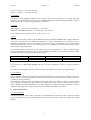
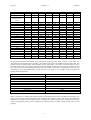
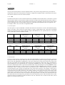
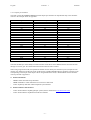
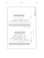
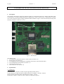
JL gach
Version 1.1
15/06/00
1250 Mb/s OPTICAL TRANSCEIVER MANUAL
1- Description
This module is designed to replace any multiwire cable as a virtual ribbon cable over a duplex optical fiber path.
It is designed in a versatile topology allowing reconfiguration in order to meet the user’s requirements. It accepts
one or two mezzanine boards to design application based interfaces. Figure 1 shows the board layout and points
the main components (references 1 to 6)
JP1
JP3
JP2
JP4
PIN 1
6
Figure 1: Board layout
The references are:
1- I/O interface for mezzanine boards or ribbon cable (see section 2.5)
2- Power supply (see section 2.3)
3- I/O interface for PLD reconfiguration (compatible with Lattice’s ISP download cable)
4- I/O reconfiguration microswitch (see section 3.1)
5- Link setup (see section 3.2)
6- Laser transceiver (see section 2.4)
2- Specifications
2.1- Dimensions
PCB dimensions : 105 mm x 122 mm. 4 layer high density board (class 5)
Overall dimensions (edge connectors and fibre transceiver included) : 118 mm x 130 mm
Height (without mezzanine board, with heatsink on chipset) : 26 mm
Fixing holes : 92mm x 115mm. 4 x M2.5 . Holes are connected to ground.
-1-
JL gach
Version 1.1
15/06/00
JP1 pin 1 to JP3 pin 1 : 48.3 mm (1900 mils)
JP1 pin 1 to JP2 pin 1 : 7.62 mm (300 mils)
2.2- EMI/RFI
This design is NOT EMI/RFI compliant since it uses RF microwave frequencies up to 1.5 GHz and upper
harmonics. This board should then be placed in a EMI/RFI appropriate housing (metallic shielded) in order to
decrease emissions and to protect it against outer perturbations.
2.3- Power
power supply is +5 Vdc. Power consumption is 1.1 A typical.
ABSOLUTE MAXIMUM RATING : +5.25 Vdc max, +4.75 Vdc min
Power supply connection pinout : pins 1,4 : GND / pins 2,3 +5V
2.4- link
The link is based on HP’s (Agilent) chipset HDMP-1022/1024 and InGaAsP HFBR-53D5 or HFCT-53D5 laser
transceivers. Note that these ICs should heat somewhat, it is then recommended to use a heatsink over the
SERDES chips (HDMP-1022/1024). Nevertheless, they’re built on HP’s 25 GHz Silicon process guaranteed to
work at temperatures up to 150 °C and is tested up to 230 °C, but lifetime is shortened and error rate is higher
when working at high temperatures.
The maximum distance of the link at 1250 Mbits/s and laser wavelenghts are in table 1. Duplex SC-type
connectors should be used with 62,5/125, 50/125 multimode fiber (MMF) or 9/125 single mode fiber (SMF).
Note that fiber quality is of prime importance for long path.
HFBR-53D5 (850 nm)
HFCT-53D5 (1500 nm)
62,5/125 MMF
50/125 MMF
220 m
500 m
550 m
550 m
Table 1: maximum path distance
9/125 SMF
N/A
10 km
The transceiver is a class I laser product and then is eye safe. Nevertheless, direct eye exposure should be
avoided.
The setup allows throughput rates from 150 Mbits/s up to 1250 Mbits/s (see section 3 for speed selection).
2.5- I/O interface
The I/O interface is made of high speed advanced CMOS technology drivers with TTL compatible inputs (ACT
family). Mating connectors for mezzanine boards are the same as for PC/104 specification : female, 2x20 pins,
2.54 mm pin spacing (100 mils).
The maximum synchronous clock speed depends on the link setup and is detailed in section 3.2. The internal
logic is rated up to 100 MHz and Tpd is about 12 ns. Minimal setup time is 0.40 ns and minimal hold time is
4.80 ns. Minimal clock half period width is 5 ns. When operating in double frame mode (see section 3.2) data is
sampled on both edges of the clock, therefore duty cycle should be maintained around 50%.
3- Setup and Operation
3.1- Pin configuration
Connectors pinout and Lattice IspLsi 2128 chip pin correspondence can be found in table 2 (used for program
and pin reconfiguration). The pins definitions can be defined using the microswitches, more detail can be found
hereafter.
-2-
JL gach
9,19,29,39
1,3,5,7,11,13,15,17,
23,25,27,31,33,
35,37
21
2
4
6
8
10
12
14
16
18
20
22
24
26
28
30
32
34
36
38
40
Version 1.1
JP1
function ISP pin
VCC
*
GND
*
Clkin
I15
I14
I13
I12
I11
I10
I9
I8
I7
I6
I5
I4
I3
I2
I1
I0
I19
I18
I17
I16
JP2
Function ISP pin
VCC
*
GND
*
15/06/00
JP3
Function ISP pin
VCC
*
GND
*
115
Clkout
116
Clkin
95
O0
105
I23
94
O1
104
I22
93
O2
103
I21
92
O3
102
I20
91
O4
101
I39
90
O5
99
I38
88
O6
97
I37
87
O7
96
I36
86
O8
76
I35
85
O9
75
I34
83
O10
73
I33
82
O11
72
I32
81
O12
71
I31
80
O13
70
I30
79
O14
68
I29
77
O15
67
I28
57
O16
66
I27
55
O17
65
I26
53
O18
63
I25
52
O19
62
I24
Table 2: I/O connectors pinout
115
51
50
48
47
46
45
44
43
42
41
39
38
37
36
35
33
32
31
28
27
JP4
Function ISP pin
VCC
*
GND
*
Clkout
O20
O21
O22
O23
O24
O25
O26
O27
O28
O29
O30
O31
O32
O33
O34
O35
O36
O37
O38
O39
116
61
60
59
58
18
17
16
15
14
12
9
8
7
6
5
4
3
2
176
175
the microswitch allows the I/O buffers to be redirected by banks of 8 lines. When a switch is set to “ON” this
means that the corresponding lines (see table 3) are configured as inputs. The CLKIN lines are always input, and
CLKOUT lines are always output. The maximum input or output lines is 40. When reconfiguring the I/O lines,
the Lattice IspLsi2128 chip internal configuration must be changed according to the I/O lines. For IspLsi design
tool, refer to the lattice IspDesignExpert system and user manual. Using Lattice’s IspDownlad cable, the new
configuration can be downloaded using the JP6 connector (see figure 1). An example design for IspLsi2128
could be found in appendix 1.
Signal banks
I0 to I7
I8 to I15
I16 to I23
I24 to I31
I32 to I39
O0 to O7
O8 to O15
O16 to O23
O24 to O31
O32 to O39
Microswitch
DIR1
DIR2
DIR3
DIR4
DIR5
DIR6
DIR7
DIR8
DIR9
DIR10
Table 3: microswitch allocation
When a signal bank is configured as INPUT and the corresponding Lattice pins are configured as OUTPUT, the
supply current should increase abnormally and the lattice chip overheats. This could lead to the IspLSI2128
destruction (if too much conflicts appear) due to overdissipation. When a signal bank is configured as OUTPUT
and the corresponding Lattice pins are configured as INPUTS, there is no effect, simply the link will not work
properly.
-3-
JL gach
Version 1.1
15/06/00
3.2- Link setup
3.2.1- Loop
The loop microswitch permits an internal loopback of data. This permits testing without using two modules or
without fiber. When set to OFF position, the system is configured in loopback. When in ON position, the system
uses the laser transceiver and is in normal condition.
3.2.2- MFD
The MFD switch allows to work in double frame mode (see HDMP-1032/1034 data sheet). This allows to extend
the bus width to 40 bits in each direction instead of 20 bits, but reduces the maximum system clock by a factor 2
(the throughput rate is the same). In this situation, the first 20 bits are sampled in the lower state of clock, and the
20 last in the higher state. This mux/demux operation is performed by the IspLSI2128 chip (see appendix 1 for
an example). When “ON”, the link is in single frame mode.
3.2.3- Link speed
The link speed is set by the DIV0/DIV1 switches that allows the internal PLL to lock in the defined frequency
ranges. The tables 4 and 5 shows the speed ranges in single or double frame rates. Note that the maximum
speeds are guaranteed speeds. Typical values are higher (1800 Mbaud/sec). The “parallel word rate” corresponds
to the system input clock rate (CLKIN) in MHz.
DIV1
ON
ON
OFF
OFF
DIV1
ON
ON
OFF
OFF
Serial Baud Rate
Serial Data Rate
Parallel word rate
(Mbaud/sec)
(Mbits/sec)
(Mwords/sec)
Range
Range
Range
ON
29.2
62.5
583
1250
700
1500
OFF
14.6
37.5
292
750
350
900
ON
7.3
18.8
146
375
175
450
OFF
6.3
9.4
125
187.5
150
225
Table 4 : clock rates in single frame mode (20 bits words). Baud rate = 24x frame rate
DIV0
Serial Baud Rate
Serial Data Rate
Parallel word rate
(Mbaud/sec)
(Mbits/sec)
(Mwords/sec)
Range
Range
Range
ON
14.6
31.3
583
1250
700
1500
OFF
7.3
18.8
292
750
350
900
ON
3.7
9.4
146
375
175
450
OFF
3.2
4.7
125
187.5
150
225
Table 5 : clock rates in double frame mode (40 bits words). Baud rate = 48x frame rate
DIV0
3.2.4- Link lock
The link is locked (ready to send and receive data) when BOTH SIDES are locked, this means that a clock must
be present in each side of the link. Both clock are not necessary the same, but the frequency range MUST be the
same in each side (DIV0/DIV1 configuration). The receive chip locks its clock and can deliver this clock to the
emit chip on the other side, the link then works with only one synchronous system clock. This is performed by a
special configuration in the IspLSI2128 chip, rerouting the STRBORX pin (120) to the STRBIN pin (124) on
one side. In double frame mode, a special care should be taken using this technique since the STRBORX clock is
twice the parallel word rate, it is then necessary to divide by two the STRBORX clock. Moreover, if perfect
synchronous clock is needed, the FLAG pin (174) should be used to synchronize these clocks because the
reconstructed emit clock could be 90° phased due to the divide-by-two operation. The problem is that FLAG is
active only when link is established on both sides. The turnover is to use a scheme as in appendix 1: the OR gate
resynchronizes the two clocks when they’re 90° phased, inducting a two-phase link setup : the first phase is the
clock lockup on both sides (FLAG is always low). When this lock is established, the FLAG pin indicates the
phase of the clock. If the two clock are 90° phased, the OR gate makes a 90° shift on the reconstructed clock.
This shift breaks the link lockup and it goes again in the clock acquisition process. When finished, the two clocks
(emit and receive) are perfectly in phase and data can be sent. When the link is locked on both sides, the led
lights up. Lock time is about 100 ms.
-4-
JL gach
Version 1.1
15/06/00
3.2.5- Chipset pin allocation
The table 6 shows the SERDES HDMP1022/1024 chipset pin allocation for IspLSI2128 setup. This should be
used as in the example shown in appendix 1.
Signal
D0
D1
D2
D3
D4
D5
D6
D7
D8
D9
D10
D11
D12
D13
D14
D15
D16
D17
D18
D19
CLOCK
RFD
DAV
Tx ISP pin
148
147
146
145
143
141
140
139
138
136
135
134
133
132
131
130
129
127
126
125
124
123
121
Table 6: Rx/Tx ISP pin allocation
Rx ISP pin
149
150
151
153
154
155
156
158
159
160
161
163
164
165
167
168
169
170
171
173
120
N/A
N/A
Note that the RFD pin means Ready For Data and DAV means DAta Valid. RFD should be connected to DAV
through an inverter gate. This allows data transmission when the link is locked.
When using single frame mode, the IspLSI2128 should connect directly the desired I/O pins (20 inputs and 20
outputs, user defined) to the Dx pins of the Tx/Rx chipset, and BCLKIN/BCLKOUT should be connected to the
corresponding CLOCK pin of the chipset. When using double frame mode, a MUX/DMUX scheme should be
used as presented in appendix 1.
4- Related documents
-
HDMP-1022/1024 serdes chips datasheet
HFBR-53D5/HFCT-53D5 InGaAsP Laser transceivers data sheet
Lattice Isp family data book and development system manual
5- Related software and hardware
-
Lattice Semiconductors IspDesignExpert system (free for download at www.latticesemi.com)
Lattice Semiconductors IspDownload cable and software
-5-
JL gach
Version 1.1
APPENDIX 1
LATTICE DESIGN EXAMPLE
Using Lattice’s ISPDesignExpert system
-6-
15/06/00
JL gach
Version 1.1
-7-
15/06/00
JL gach
Version 1.1
-8-
15/06/00