1
eCOG1X User Manual
Version 2.7
Cyan Technology
eCOG1X
16-bit Microcontroller
User Manual
V2.7
21 October 2009
Version 2.7
eCOG1X User Manual
Cyan Technology Ltd
21 October 2009
eCOG1X User Manual
Version 2.7
Confidential and Proprietary Information
© Cyan Technology Ltd., 2007-2008
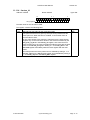
This document contains confidential and proprietary information of Cyan Technology Ltd. and is
protected by copyright laws. Its receipt or possession does not convey any rights to reproduce,
manufacture, use or sell anything based on information contained within this document.
Cyan TechnologyTM, the Cyan Technology logo and Max-eICETM are trademarks of Cyan
Holdings Ltd. CyanIDE® and eCOG® are registered trademarks of Cyan Holdings Ltd. Cyan
Technology Ltd. recognises other brand and product names as trademarks or registered
trademarks of their respective holders.
Any product described in this document is subject to continuous developments and
improvements. All particulars of the product and its use contained in this document are given by
Cyan Technology Ltd. in good faith. However, all warranties implied or expressed, including but
not limited to implied warranties of merchantability, or fitness for purpose, are excluded.
This document is intended only to assist the reader in the use of the product. Cyan Technology
Ltd. shall not be liable for any loss or damage arising from the use of any information in this
guide, any error or omission in such information, or any incorrect use of the product.
This product is not designed or intended to be used for on-line control of aircraft, aircraft
navigation or communications systems or in air traffic control applications or in the design,
construction, operation or maintenance of any nuclear facility, or for any medical use related to
either life support equipment or any other life-critical application. Cyan Technology Ltd.
specifically disclaims any express or implied warranty of fitness for any or all of such uses. Ask
your sales representative for details.
21 October 2009
Cyan Technology Ltd
Page i
Version 2.7
eCOG1X User Manual
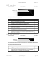
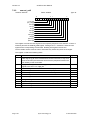
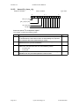
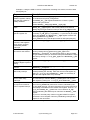
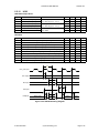
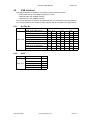
Revision History
Version
Date
Notes
V1.0
02/03/2007
First release.
V2.0
28/04/2008
Updated register addresses for use with CyanIDE 2.
Added more information on the DAC clock triggered conversion mode.
Added additional accuracy data for ADC and DAC.
Updated pin list for 2Z and 10Z variants.
V2.1
22/05/2008
Updated device options and pin diagrams.
V2.2
20/06/2008
Corrected application guidelines for unused crystal oscillator input connections.
Updated pad layout drawing for 100QFN package.
V2.3
01/08/2008
Added recommended eICE debug connections into Appendix B.1.
V2.4
17/09/2008
Added more details for DUART received parity bit.
Added notes on use of MMU ram_data2 translator in CyanIDE 2.
V2.5
04/12/2008
Included latest mechanical package drawings.
Corrected error in equations for temperature sensor ADC output value.
V2.6
17/07/2009
Revised applications information with pull-up resistors on nRESET and nTEST pins.
Corrected description of if_clk frequency in section 10.2.2.
V2.7
21/10/2009
Corrected input Vih value in electrical characteristics table.
Page ii
Cyan Technology Ltd
21 October 2009
eCOG1X User Manual
Version 2.7
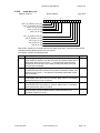
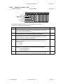
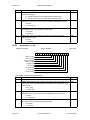
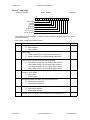
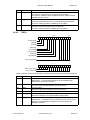
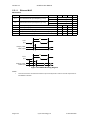
Contents
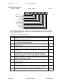
List of Figures . . . . . . . . . . . . . . . . . . . . . . . . . . . . . . . . . . . . . . . . . . . . . . . xiii
List of Tables. . . . . . . . . . . . . . . . . . . . . . . . . . . . . . . . . . . . . . . . . . . . . . . xvii
1
Introduction . . . . . . . . . . . . . . . . . . . . . . . . . . . . . . . . . . . . . . . . . . 1-1
1.1
1.2
1.3
1.4
1.5
1.6
2
Additional Documents . . . . . . . . . . . . . . . . . . . . . . . . . . . . . . . . . . . . .
Typographical Conventions . . . . . . . . . . . . . . . . . . . . . . . . . . . . . . . . .
Part Identification. . . . . . . . . . . . . . . . . . . . . . . . . . . . . . . . . . . . . . . . .
Glossary . . . . . . . . . . . . . . . . . . . . . . . . . . . . . . . . . . . . . . . . . . . . . . .
Registers and Bit Fields. . . . . . . . . . . . . . . . . . . . . . . . . . . . . . . . . . . .
Disclaimer . . . . . . . . . . . . . . . . . . . . . . . . . . . . . . . . . . . . . . . . . . . . . .
1-1
1-1
1-1
1-1
1-3
1-3
Overview . . . . . . . . . . . . . . . . . . . . . . . . . . . . . . . . . . . . . . . . . . . . 2-1
2.1
2.2
2.3
2.4
2.5
2.6
2.7
2.8
2.9
2.10
2.11
2.12
2.13
2.14
3
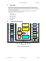
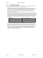
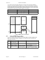
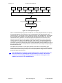
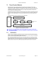
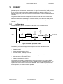
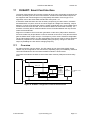
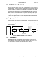
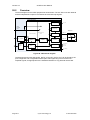
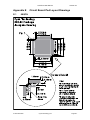
eCOG1X Block Diagram . . . . . . . . . . . . . . . . . . . . . . . . . . . . . . . . . . . 2-1
Feature List . . . . . . . . . . . . . . . . . . . . . . . . . . . . . . . . . . . . . . . . . . . . . 2-2
eCOG1X Options. . . . . . . . . . . . . . . . . . . . . . . . . . . . . . . . . . . . . . . . . 2-4
Pin Functions. . . . . . . . . . . . . . . . . . . . . . . . . . . . . . . . . . . . . . . . . . . . 2-5
CPU . . . . . . . . . . . . . . . . . . . . . . . . . . . . . . . . . . . . . . . . . . . . . . . . . . . 2-8
Memory . . . . . . . . . . . . . . . . . . . . . . . . . . . . . . . . . . . . . . . . . . . . . . . . 2-8
Interrupts . . . . . . . . . . . . . . . . . . . . . . . . . . . . . . . . . . . . . . . . . . . . . . . 2-8
Serial Peripherals . . . . . . . . . . . . . . . . . . . . . . . . . . . . . . . . . . . . . . . . 2-9
Timers . . . . . . . . . . . . . . . . . . . . . . . . . . . . . . . . . . . . . . . . . . . . . . . . . 2-9
Port Configurator . . . . . . . . . . . . . . . . . . . . . . . . . . . . . . . . . . . . . . . . . 2-9
External Host Interface . . . . . . . . . . . . . . . . . . . . . . . . . . . . . . . . . . . 2-10
Analogue Voltage and Temperature Sensors . . . . . . . . . . . . . . . . . . 2-10
eICE Debugger . . . . . . . . . . . . . . . . . . . . . . . . . . . . . . . . . . . . . . . . . 2-10
Recommended Approach for This Document . . . . . . . . . . . . . . . . . . 2-10
CPU . . . . . . . . . . . . . . . . . . . . . . . . . . . . . . . . . . . . . . . . . . . . . . . . 3-1
3.1
3.2
3.3
3.4
3.5
3.6
4
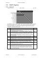
Programmer’s Model . . . . . . . . . . . . . . . . . . . . . . . . . . . . . . . . . . . . . . 3-2
Instruction Set . . . . . . . . . . . . . . . . . . . . . . . . . . . . . . . . . . . . . . . . . . . 3-5
Processor Operating Modes . . . . . . . . . . . . . . . . . . . . . . . . . . . . . . . . 3-8
Flags . . . . . . . . . . . . . . . . . . . . . . . . . . . . . . . . . . . . . . . . . . . . . . . . . 3-10
Instruction Formats . . . . . . . . . . . . . . . . . . . . . . . . . . . . . . . . . . . . . . 3-12
Instruction Timings . . . . . . . . . . . . . . . . . . . . . . . . . . . . . . . . . . . . . . 3-14
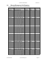
Memory Management Unit. . . . . . . . . . . . . . . . . . . . . . . . . . . . . . . 4-1
4.1
4.2
4.3
4.4
21 October 2009
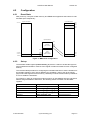
Operation. . . . . . . . . . . . . . . . . . . . . . . . . . . . . . . . . . . . . . . . . . . . . . .
Configuration . . . . . . . . . . . . . . . . . . . . . . . . . . . . . . . . . . . . . . . . . . . .
Internal RAM Organisation . . . . . . . . . . . . . . . . . . . . . . . . . . . . . . . . .
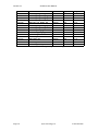
Memory Management Unit Registers . . . . . . . . . . . . . . . . . . . . . . . . .
Cyan Technology Ltd
4-2
4-5
4-6
4-7
Page iii
Version 2.7
5
eCOG1X User Manual
Instruction Cache. . . . . . . . . . . . . . . . . . . . . . . . . . . . . . . . . . . . . . 5-1
5.1
5.2
5.3
5.4
5.5
5.6
5.7
5.8
6
Overview . . . . . . . . . . . . . . . . . . . . . . . . . . . . . . . . . . . . . . . . . . . . . . .
Operation. . . . . . . . . . . . . . . . . . . . . . . . . . . . . . . . . . . . . . . . . . . . . . .
Initialisation . . . . . . . . . . . . . . . . . . . . . . . . . . . . . . . . . . . . . . . . . . . . .
Cache Tag Format . . . . . . . . . . . . . . . . . . . . . . . . . . . . . . . . . . . . . . .
Cache Locking. . . . . . . . . . . . . . . . . . . . . . . . . . . . . . . . . . . . . . . . . . .
Software Debugging with the Cache . . . . . . . . . . . . . . . . . . . . . . . . . .
Limitations . . . . . . . . . . . . . . . . . . . . . . . . . . . . . . . . . . . . . . . . . . . . . .
Instruction Cache Control Registers . . . . . . . . . . . . . . . . . . . . . . . . . .
Interrupts . . . . . . . . . . . . . . . . . . . . . . . . . . . . . . . . . . . . . . . . . . . . 6-1
6.1
6.2
6.3
6.4
6.5
6.6
6.7
6.8
6.9
6.10
6.11
6.12
6.13
6.14
6.15
7
Overview . . . . . . . . . . . . . . . . . . . . . . . . . . . . . . . . . . . . . . . . . . . . . . . 6-1
Interrupt Handler . . . . . . . . . . . . . . . . . . . . . . . . . . . . . . . . . . . . . . . . . 6-1
Interrupt Latency . . . . . . . . . . . . . . . . . . . . . . . . . . . . . . . . . . . . . . . . . 6-3
Interrupt Priority. . . . . . . . . . . . . . . . . . . . . . . . . . . . . . . . . . . . . . . . . . 6-4
Interrupt Vectors . . . . . . . . . . . . . . . . . . . . . . . . . . . . . . . . . . . . . . . . . 6-6
Timer Interrupts . . . . . . . . . . . . . . . . . . . . . . . . . . . . . . . . . . . . . . . . . . 6-8
DUSART Interrupts . . . . . . . . . . . . . . . . . . . . . . . . . . . . . . . . . . . . . . . 6-9
User Serial Port Interrupts. . . . . . . . . . . . . . . . . . . . . . . . . . . . . . . . . 6-10
Smart Card Interface Interrupts. . . . . . . . . . . . . . . . . . . . . . . . . . . . . 6-11
IFR Interrupts . . . . . . . . . . . . . . . . . . . . . . . . . . . . . . . . . . . . . . . . . . 6-12
UART Interrupts . . . . . . . . . . . . . . . . . . . . . . . . . . . . . . . . . . . . . . . . 6-12
SPI Interrupts . . . . . . . . . . . . . . . . . . . . . . . . . . . . . . . . . . . . . . . . . . 6-12
I2C Interrupts. . . . . . . . . . . . . . . . . . . . . . . . . . . . . . . . . . . . . . . . . . . 6-12
DUART Interrupts . . . . . . . . . . . . . . . . . . . . . . . . . . . . . . . . . . . . . . . 6-13
External Host Interface Interrupts . . . . . . . . . . . . . . . . . . . . . . . . . . . 6-14
System Support Module . . . . . . . . . . . . . . . . . . . . . . . . . . . . . . . . 7-1
7.1
7.2
7.3
7.4
7.5
7.6
7.7
7.8
7.9
8
System Clock Control . . . . . . . . . . . . . . . . . . . . . . . . . . . . . . . . . . . . . 7-1
PLL and VCO Frequencies . . . . . . . . . . . . . . . . . . . . . . . . . . . . . . . . . 7-7
Peripheral Clock Frequency Limits . . . . . . . . . . . . . . . . . . . . . . . . . . 7-10
Sleep . . . . . . . . . . . . . . . . . . . . . . . . . . . . . . . . . . . . . . . . . . . . . . . . . 7-11
Deep Sleep . . . . . . . . . . . . . . . . . . . . . . . . . . . . . . . . . . . . . . . . . . . . 7-13
Wakeup . . . . . . . . . . . . . . . . . . . . . . . . . . . . . . . . . . . . . . . . . . . . . . . 7-14
System Reset Control . . . . . . . . . . . . . . . . . . . . . . . . . . . . . . . . . . . . 7-16
Reset summary . . . . . . . . . . . . . . . . . . . . . . . . . . . . . . . . . . . . . . . . . 7-17
System Support Module Registers . . . . . . . . . . . . . . . . . . . . . . . . . . 7-18
Port Configurator . . . . . . . . . . . . . . . . . . . . . . . . . . . . . . . . . . . . . . 8-1
8.1
8.2
8.3
Page iv
5-1
5-2
5-2
5-2
5-3
5-3
5-3
5-4
Configuration Rules. . . . . . . . . . . . . . . . . . . . . . . . . . . . . . . . . . . . . . . 8-2
Low Power Considerations . . . . . . . . . . . . . . . . . . . . . . . . . . . . . . . . . 8-3
Port Configurator Registers. . . . . . . . . . . . . . . . . . . . . . . . . . . . . . . . . 8-4
Cyan Technology Ltd
21 October 2009
eCOG1X User Manual
9
General Purpose I/O . . . . . . . . . . . . . . . . . . . . . . . . . . . . . . . . . . . 9-1
9.1
9.2
9.3
9.4
9.5
9.6
9.7
9.8
9.9
10
Overview . . . . . . . . . . . . . . . . . . . . . . . . . . . . . . . . . . . . . . . . . . . . . . .
GPIO Inputs. . . . . . . . . . . . . . . . . . . . . . . . . . . . . . . . . . . . . . . . . . . . .
GPIO Outputs . . . . . . . . . . . . . . . . . . . . . . . . . . . . . . . . . . . . . . . . . . .
GPIO Configuration . . . . . . . . . . . . . . . . . . . . . . . . . . . . . . . . . . . . . . .
GPIO Interrupts . . . . . . . . . . . . . . . . . . . . . . . . . . . . . . . . . . . . . . . . . .
Interfacing to 5V Logic. . . . . . . . . . . . . . . . . . . . . . . . . . . . . . . . . . . . .
GPIO Register Bit Fields . . . . . . . . . . . . . . . . . . . . . . . . . . . . . . . . . . .
GPIO Register Functions. . . . . . . . . . . . . . . . . . . . . . . . . . . . . . . . . . .
GPIO Registers . . . . . . . . . . . . . . . . . . . . . . . . . . . . . . . . . . . . . . . . . .
Initialisation . . . . . . . . . . . . . . . . . . . . . . . . . . . . . . . . . . . . . . . . . . . .
Interrupts . . . . . . . . . . . . . . . . . . . . . . . . . . . . . . . . . . . . . . . . . . . . . .
Reload . . . . . . . . . . . . . . . . . . . . . . . . . . . . . . . . . . . . . . . . . . . . . . . .
Reading the Timer Count Registers . . . . . . . . . . . . . . . . . . . . . . . . .
Timer . . . . . . . . . . . . . . . . . . . . . . . . . . . . . . . . . . . . . . . . . . . . . . . . .
Counter . . . . . . . . . . . . . . . . . . . . . . . . . . . . . . . . . . . . . . . . . . . . . . .
PWM . . . . . . . . . . . . . . . . . . . . . . . . . . . . . . . . . . . . . . . . . . . . . . . . .
Capture Timer . . . . . . . . . . . . . . . . . . . . . . . . . . . . . . . . . . . . . . . . . .
Watchdog Timer . . . . . . . . . . . . . . . . . . . . . . . . . . . . . . . . . . . . . . . .
Long Interval Timer . . . . . . . . . . . . . . . . . . . . . . . . . . . . . . . . . . . . . .
Timer/Counter Registers . . . . . . . . . . . . . . . . . . . . . . . . . . . . . . . . . .
11-1
11-3
11-4
11-4
11-4
11-5
11-6
11-7
11-8
11-8
11-9
DUARTs . . . . . . . . . . . . . . . . . . . . . . . . . . . . . . . . . . . . . . . . . . . . 12-1
12.1
12.2
12.3
12.4
12.5
12.6
12.7
12.8
12.9
13
Overview . . . . . . . . . . . . . . . . . . . . . . . . . . . . . . . . . . . . . . . . . . . . . . 10-1
Performance . . . . . . . . . . . . . . . . . . . . . . . . . . . . . . . . . . . . . . . . . . . 10-2
Parallel I/O Registers. . . . . . . . . . . . . . . . . . . . . . . . . . . . . . . . . . . . . 10-3
Timer/Counter Module . . . . . . . . . . . . . . . . . . . . . . . . . . . . . . . . . 11-1
11.1
11.2
11.3
11.4
11.5
11.6
11.7
11.8
11.9
11.10
11.11
12
9-1
9-1
9-2
9-2
9-3
9-4
9-5
9-6
9-8
Parallel I/O . . . . . . . . . . . . . . . . . . . . . . . . . . . . . . . . . . . . . . . . . . 10-1
10.1
10.2
10.3
11
Version 2.7
Initialisation . . . . . . . . . . . . . . . . . . . . . . . . . . . . . . . . . . . . . . . . . . . . 12-2
Receive Sampling . . . . . . . . . . . . . . . . . . . . . . . . . . . . . . . . . . . . . . . 12-2
Transmit Sampling. . . . . . . . . . . . . . . . . . . . . . . . . . . . . . . . . . . . . . . 12-2
Baud Rates . . . . . . . . . . . . . . . . . . . . . . . . . . . . . . . . . . . . . . . . . . . . 12-3
Transmitter . . . . . . . . . . . . . . . . . . . . . . . . . . . . . . . . . . . . . . . . . . . . 12-4
Receiver . . . . . . . . . . . . . . . . . . . . . . . . . . . . . . . . . . . . . . . . . . . . . . 12-5
DUART Registers . . . . . . . . . . . . . . . . . . . . . . . . . . . . . . . . . . . . . . . 12-6
DUART1 Registers . . . . . . . . . . . . . . . . . . . . . . . . . . . . . . . . . . . . . . 12-8
DUART2 Registers . . . . . . . . . . . . . . . . . . . . . . . . . . . . . . . . . . . . . 12-23
DUSART . . . . . . . . . . . . . . . . . . . . . . . . . . . . . . . . . . . . . . . . . . . 13-1
13.1
13.2
13.3
13.4
13.5
13.6
13.7
13.8
21 October 2009
Configuration . . . . . . . . . . . . . . . . . . . . . . . . . . . . . . . . . . . . . . . . . . .
Initialisation . . . . . . . . . . . . . . . . . . . . . . . . . . . . . . . . . . . . . . . . . . . .
Receive Filter. . . . . . . . . . . . . . . . . . . . . . . . . . . . . . . . . . . . . . . . . . .
Sample Strobe and Synchroniser . . . . . . . . . . . . . . . . . . . . . . . . . . .
Parity Calculator . . . . . . . . . . . . . . . . . . . . . . . . . . . . . . . . . . . . . . . .
Transmit Serialiser. . . . . . . . . . . . . . . . . . . . . . . . . . . . . . . . . . . . . . .
Protocol Control Engines. . . . . . . . . . . . . . . . . . . . . . . . . . . . . . . . . .
DUSART Registers . . . . . . . . . . . . . . . . . . . . . . . . . . . . . . . . . . . . . .
Cyan Technology Ltd
13-1
13-2
13-2
13-3
13-3
13-3
13-4
13-5
Page v
Version 2.7
14
eCOG1X User Manual
DUSART: I2C Serial Interface . . . . . . . . . . . . . . . . . . . . . . . . . . . 14-1
14.1
14.2
14.3
14.4
14.5
14.6
14.7
14.8
14.9
15
Overview . . . . . . . . . . . . . . . . . . . . . . . . . . . . . . . . . . . . . . . . . . . . . .
Initialisation . . . . . . . . . . . . . . . . . . . . . . . . . . . . . . . . . . . . . . . . . . . .
Baud rates . . . . . . . . . . . . . . . . . . . . . . . . . . . . . . . . . . . . . . . . . . . . .
UART Serial Controller . . . . . . . . . . . . . . . . . . . . . . . . . . . . . . . . . . .
Operation. . . . . . . . . . . . . . . . . . . . . . . . . . . . . . . . . . . . . . . . . . . . . .
UART Registers . . . . . . . . . . . . . . . . . . . . . . . . . . . . . . . . . . . . . . . .
16-1
16-1
16-2
16-3
16-3
16-4
Overview . . . . . . . . . . . . . . . . . . . . . . . . . . . . . . . . . . . . . . . . . . . . . .
SCI Control Finite State Machine . . . . . . . . . . . . . . . . . . . . . . . . . . .
SCI Delay Timer . . . . . . . . . . . . . . . . . . . . . . . . . . . . . . . . . . . . . . . .
General Information. . . . . . . . . . . . . . . . . . . . . . . . . . . . . . . . . . . . . .
Smart Card Interface Registers. . . . . . . . . . . . . . . . . . . . . . . . . . . . .
17-1
17-2
17-4
17-4
17-5
DUSART: Infra-Red Interface . . . . . . . . . . . . . . . . . . . . . . . . . . . 18-1
18.1
18.2
18.3
18.4
18.5
18.6
Page vi
15-1
15-3
15-4
15-5
15-6
15-6
15-6
15-7
DUSART: Smart Card Interface. . . . . . . . . . . . . . . . . . . . . . . . . . 17-1
17.1
17.2
17.3
17.4
17.5
18
Overview . . . . . . . . . . . . . . . . . . . . . . . . . . . . . . . . . . . . . . . . . . . . . .
Clock Initialisation . . . . . . . . . . . . . . . . . . . . . . . . . . . . . . . . . . . . . . .
Serial Clock Polarity and Phase . . . . . . . . . . . . . . . . . . . . . . . . . . . .
SPI Controller . . . . . . . . . . . . . . . . . . . . . . . . . . . . . . . . . . . . . . . . . .
Chip Selects . . . . . . . . . . . . . . . . . . . . . . . . . . . . . . . . . . . . . . . . . . .
Operation. . . . . . . . . . . . . . . . . . . . . . . . . . . . . . . . . . . . . . . . . . . . . .
Limitations . . . . . . . . . . . . . . . . . . . . . . . . . . . . . . . . . . . . . . . . . . . . .
SPI Registers . . . . . . . . . . . . . . . . . . . . . . . . . . . . . . . . . . . . . . . . . .
DUSART: UART Serial Port . . . . . . . . . . . . . . . . . . . . . . . . . . . . 16-1
16.1
16.2
16.3
16.4
16.5
16.6
17
14-1
14-2
14-2
14-2
14-2
14-3
14-3
14-4
14-5
DUSART: SPI Serial Interface . . . . . . . . . . . . . . . . . . . . . . . . . . . 15-1
15.1
15.2
15.3
15.4
15.5
15.6
15.7
15.8
16
Overview . . . . . . . . . . . . . . . . . . . . . . . . . . . . . . . . . . . . . . . . . . . . . .
Initialisation . . . . . . . . . . . . . . . . . . . . . . . . . . . . . . . . . . . . . . . . . . . .
Interrupts . . . . . . . . . . . . . . . . . . . . . . . . . . . . . . . . . . . . . . . . . . . . . .
I2C Control . . . . . . . . . . . . . . . . . . . . . . . . . . . . . . . . . . . . . . . . . . . .
I2C Master. . . . . . . . . . . . . . . . . . . . . . . . . . . . . . . . . . . . . . . . . . . . .
I2C Slave. . . . . . . . . . . . . . . . . . . . . . . . . . . . . . . . . . . . . . . . . . . . . .
Arbitration . . . . . . . . . . . . . . . . . . . . . . . . . . . . . . . . . . . . . . . . . . . . .
Limitations . . . . . . . . . . . . . . . . . . . . . . . . . . . . . . . . . . . . . . . . . . . . .
I2C Registers. . . . . . . . . . . . . . . . . . . . . . . . . . . . . . . . . . . . . . . . . . .
Overview . . . . . . . . . . . . . . . . . . . . . . . . . . . . . . . . . . . . . . . . . . . . . .
Initialisation . . . . . . . . . . . . . . . . . . . . . . . . . . . . . . . . . . . . . . . . . . . .
Operation. . . . . . . . . . . . . . . . . . . . . . . . . . . . . . . . . . . . . . . . . . . . . .
IFR Counters . . . . . . . . . . . . . . . . . . . . . . . . . . . . . . . . . . . . . . . . . . .
IFR Datapath . . . . . . . . . . . . . . . . . . . . . . . . . . . . . . . . . . . . . . . . . . .
Infra-Red Interface Registers . . . . . . . . . . . . . . . . . . . . . . . . . . . . . .
Cyan Technology Ltd
18-1
18-1
18-2
18-3
18-3
18-5
21 October 2009
eCOG1X User Manual
19
DUSART: User Serial Port . . . . . . . . . . . . . . . . . . . . . . . . . . . . . . 19-1
19.1
19.2
19.3
19.4
19.5
19.6
19.7
20
Overview . . . . . . . . . . . . . . . . . . . . . . . . . . . . . . . . . . . . . . . . . . . . . .
Initialisation . . . . . . . . . . . . . . . . . . . . . . . . . . . . . . . . . . . . . . . . . . . .
Baud Rates . . . . . . . . . . . . . . . . . . . . . . . . . . . . . . . . . . . . . . . . . . . .
Design Description . . . . . . . . . . . . . . . . . . . . . . . . . . . . . . . . . . . . . .
USR Additional Functions . . . . . . . . . . . . . . . . . . . . . . . . . . . . . . . . .
Example Frame Transmit and Receive Sequences . . . . . . . . . . . . .
User Serial Port Registers . . . . . . . . . . . . . . . . . . . . . . . . . . . . . . . . .
19-1
19-1
19-2
19-2
19-3
19-4
19-6
External Memory Interface . . . . . . . . . . . . . . . . . . . . . . . . . . . . . . 20-1
20.1
20.2
20.3
20.4
20.5
20.6
20.7
20.8
20.9
20.10
20.11
20.12
21
Version 2.7
External Signals. . . . . . . . . . . . . . . . . . . . . . . . . . . . . . . . . . . . . . . . . 20-2
Bus Interface Mode . . . . . . . . . . . . . . . . . . . . . . . . . . . . . . . . . . . . . . 20-3
Bus Mode Connections . . . . . . . . . . . . . . . . . . . . . . . . . . . . . . . . . . . 20-5
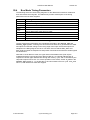
Bus Mode Timing Parameters . . . . . . . . . . . . . . . . . . . . . . . . . . . . . . 20-9
Bus Mode Timing Diagrams . . . . . . . . . . . . . . . . . . . . . . . . . . . . . . 20-10
SDRAM Interface Mode. . . . . . . . . . . . . . . . . . . . . . . . . . . . . . . . . . 20-14
SDRAM Connections. . . . . . . . . . . . . . . . . . . . . . . . . . . . . . . . . . . . 20-20
SDRAM Timing Parameters . . . . . . . . . . . . . . . . . . . . . . . . . . . . . . 20-21
SDRAM Timing Diagrams . . . . . . . . . . . . . . . . . . . . . . . . . . . . . . . . 20-23
SDRAM Mode Limitations . . . . . . . . . . . . . . . . . . . . . . . . . . . . . . . . 20-31
Address Error Interrupt . . . . . . . . . . . . . . . . . . . . . . . . . . . . . . . . . . 20-32
External Memory Interface Registers . . . . . . . . . . . . . . . . . . . . . . . 20-33
External Host Interface. . . . . . . . . . . . . . . . . . . . . . . . . . . . . . . . . 21-1
21.1
21.2
21.3
21.4
21.5
21 October 2009
Memory Mapped Peripheral (MMP) Port. . . . . . . . . . . . . . . . . . . . . .
Direct Memory Access (DMA) Port . . . . . . . . . . . . . . . . . . . . . . . . . .
Access Arbitration . . . . . . . . . . . . . . . . . . . . . . . . . . . . . . . . . . . . . . .
External Connections and Timing . . . . . . . . . . . . . . . . . . . . . . . . . . .
External Host Interface Registers . . . . . . . . . . . . . . . . . . . . . . . . . . .
Cyan Technology Ltd
21-2
21-4
21-5
21-6
21-8
Page vii
Version 2.7
22
eCOG1X User Manual
Embedded Flash Memory . . . . . . . . . . . . . . . . . . . . . . . . . . . . . . 22-1
22.1
22.2
22.3
22.4
22.5
22.6
22.7
22.8
22.9
22.10
22.11
22.12
22.13
22.14
22.15
22.16
22.17
22.18
22.19
23
Analogue Functions . . . . . . . . . . . . . . . . . . . . . . . . . . . . . . . . . . . 23-1
23.1
23.2
23.3
23.4
23.5
23.6
23.7
23.8
23.9
23.10
23.11
23.12
23.13
24
ADC. . . . . . . . . . . . . . . . . . . . . . . . . . . . . . . . . . . . . . . . . . . . . . . . . . 23-1
DAC. . . . . . . . . . . . . . . . . . . . . . . . . . . . . . . . . . . . . . . . . . . . . . . . . . 23-2
Voltage Reference. . . . . . . . . . . . . . . . . . . . . . . . . . . . . . . . . . . . . . . 23-2
Power On Reset . . . . . . . . . . . . . . . . . . . . . . . . . . . . . . . . . . . . . . . . 23-2
Low Voltage Sensor . . . . . . . . . . . . . . . . . . . . . . . . . . . . . . . . . . . . . 23-2
Temperature sensor . . . . . . . . . . . . . . . . . . . . . . . . . . . . . . . . . . . . . 23-3
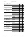
Supply Voltage Sensor . . . . . . . . . . . . . . . . . . . . . . . . . . . . . . . . . . . 23-3
Analogue Multiplexer. . . . . . . . . . . . . . . . . . . . . . . . . . . . . . . . . . . . . 23-4
Resolution and Scaling . . . . . . . . . . . . . . . . . . . . . . . . . . . . . . . . . . . 23-6
ADC Output Data . . . . . . . . . . . . . . . . . . . . . . . . . . . . . . . . . . . . . . . 23-7
ADC Conversion Modes . . . . . . . . . . . . . . . . . . . . . . . . . . . . . . . . . . 23-8
DAC Conversion Modes . . . . . . . . . . . . . . . . . . . . . . . . . . . . . . . . . . 23-9
Analogue Control Interface Registers . . . . . . . . . . . . . . . . . . . . . . . 23-10
ESPI. . . . . . . . . . . . . . . . . . . . . . . . . . . . . . . . . . . . . . . . . . . . . . . 24-1
24.1
24.2
24.3
24.4
24.5
24.6
24.7
24.8
24.9
Page viii
Overview . . . . . . . . . . . . . . . . . . . . . . . . . . . . . . . . . . . . . . . . . . . . . . 22-1
Reset Condition. . . . . . . . . . . . . . . . . . . . . . . . . . . . . . . . . . . . . . . . . 22-2
Wait States . . . . . . . . . . . . . . . . . . . . . . . . . . . . . . . . . . . . . . . . . . . . 22-2
Programming. . . . . . . . . . . . . . . . . . . . . . . . . . . . . . . . . . . . . . . . . . . 22-3
Write Protection. . . . . . . . . . . . . . . . . . . . . . . . . . . . . . . . . . . . . . . . . 22-3
Erase Methods . . . . . . . . . . . . . . . . . . . . . . . . . . . . . . . . . . . . . . . . . 22-4
Programming Methods . . . . . . . . . . . . . . . . . . . . . . . . . . . . . . . . . . . 22-6
Device ID. . . . . . . . . . . . . . . . . . . . . . . . . . . . . . . . . . . . . . . . . . . . . . 22-8
Status Monitoring . . . . . . . . . . . . . . . . . . . . . . . . . . . . . . . . . . . . . . . 22-9
Command Sequences. . . . . . . . . . . . . . . . . . . . . . . . . . . . . . . . . . . 22-11
MMU Setup for Flash Memory Access . . . . . . . . . . . . . . . . . . . . . . 22-12
Operation Timings . . . . . . . . . . . . . . . . . . . . . . . . . . . . . . . . . . . . . . 22-12
Low Power Modes. . . . . . . . . . . . . . . . . . . . . . . . . . . . . . . . . . . . . . 22-12
Flash Timer . . . . . . . . . . . . . . . . . . . . . . . . . . . . . . . . . . . . . . . . . . . 22-13
Flash Mode Changes . . . . . . . . . . . . . . . . . . . . . . . . . . . . . . . . . . . 22-15
Flash Operation in Slow Mode . . . . . . . . . . . . . . . . . . . . . . . . . . . . 22-16
Changing from Fast to Slow Mode . . . . . . . . . . . . . . . . . . . . . . . . . 22-17
Changing from Slow to Fast Mode . . . . . . . . . . . . . . . . . . . . . . . . . 22-17
Embedded Flash Memory Registers . . . . . . . . . . . . . . . . . . . . . . . . 22-18
Features . . . . . . . . . . . . . . . . . . . . . . . . . . . . . . . . . . . . . . . . . . . . . .
Overview . . . . . . . . . . . . . . . . . . . . . . . . . . . . . . . . . . . . . . . . . . . . . .
Clock Initialisation . . . . . . . . . . . . . . . . . . . . . . . . . . . . . . . . . . . . . . .
Serial Clock Polarity and Phase . . . . . . . . . . . . . . . . . . . . . . . . . . . .
Chip Selects . . . . . . . . . . . . . . . . . . . . . . . . . . . . . . . . . . . . . . . . . . .
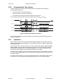
Programmable Time Delays . . . . . . . . . . . . . . . . . . . . . . . . . . . . . . .
Operation. . . . . . . . . . . . . . . . . . . . . . . . . . . . . . . . . . . . . . . . . . . . . .
Limitations . . . . . . . . . . . . . . . . . . . . . . . . . . . . . . . . . . . . . . . . . . . . .
ESPI Registers . . . . . . . . . . . . . . . . . . . . . . . . . . . . . . . . . . . . . . . . .
Cyan Technology Ltd
24-1
24-1
24-3
24-4
24-5
24-6
24-6
24-7
24-8
21 October 2009
eCOG1X User Manual
25
I2S . . . . . . . . . . . . . . . . . . . . . . . . . . . . . . . . . . . . . . . . . . . . . . . . 25-1
25.1
25.2
25.3
25.4
25.5
26
Features . . . . . . . . . . . . . . . . . . . . . . . . . . . . . . . . . . . . . . . . . . . . . . 26-1
Principles of Operation . . . . . . . . . . . . . . . . . . . . . . . . . . . . . . . . . . . 26-1
LCD Controller Registers. . . . . . . . . . . . . . . . . . . . . . . . . . . . . . . . . . 26-5
Features . . . . . . . . . . . . . . . . . . . . . . . . . . . . . . . . . . . . . . . . . . . . . .
Controlling Electric Motors. . . . . . . . . . . . . . . . . . . . . . . . . . . . . . . . .
Operation. . . . . . . . . . . . . . . . . . . . . . . . . . . . . . . . . . . . . . . . . . . . . .
MCPWM Registers . . . . . . . . . . . . . . . . . . . . . . . . . . . . . . . . . . . . . .
27-1
27-2
27-4
27-8
Dual Smart Card Interface . . . . . . . . . . . . . . . . . . . . . . . . . . . . . . 28-1
28.1
28.2
28.3
28.4
28.5
28.6
28.7
28.8
28.9
28.10
29
25-1
25-2
25-3
25-4
25-5
MCPWM. . . . . . . . . . . . . . . . . . . . . . . . . . . . . . . . . . . . . . . . . . . . 27-1
27.1
27.2
27.3
27.4
28
Overview . . . . . . . . . . . . . . . . . . . . . . . . . . . . . . . . . . . . . . . . . . . . . .
Features . . . . . . . . . . . . . . . . . . . . . . . . . . . . . . . . . . . . . . . . . . . . . .
Clock Initialisation . . . . . . . . . . . . . . . . . . . . . . . . . . . . . . . . . . . . . . .
Operation. . . . . . . . . . . . . . . . . . . . . . . . . . . . . . . . . . . . . . . . . . . . . .
I2S Registers . . . . . . . . . . . . . . . . . . . . . . . . . . . . . . . . . . . . . . . . . . .
LCD Controller . . . . . . . . . . . . . . . . . . . . . . . . . . . . . . . . . . . . . . . 26-1
26.1
26.2
26.3
27
Version 2.7
Features . . . . . . . . . . . . . . . . . . . . . . . . . . . . . . . . . . . . . . . . . . . . . . 28-1
Overview . . . . . . . . . . . . . . . . . . . . . . . . . . . . . . . . . . . . . . . . . . . . . . 28-2
Clock Generation. . . . . . . . . . . . . . . . . . . . . . . . . . . . . . . . . . . . . . . . 28-3
Activation and Deactivation Sequencing . . . . . . . . . . . . . . . . . . . . . . 28-4
Peripheral Clock Wakeup . . . . . . . . . . . . . . . . . . . . . . . . . . . . . . . . . 28-6
Data Transmission and Reception . . . . . . . . . . . . . . . . . . . . . . . . . . 28-7
Receiver Operation . . . . . . . . . . . . . . . . . . . . . . . . . . . . . . . . . . . . . . 28-8
Transmitter Operation . . . . . . . . . . . . . . . . . . . . . . . . . . . . . . . . . . . 28-10
Example Clock Configuration for EMV ATR . . . . . . . . . . . . . . . . . . 28-11
Dual Smart Card Interface Registers. . . . . . . . . . . . . . . . . . . . . . . . 28-12
Ethernet MAC. . . . . . . . . . . . . . . . . . . . . . . . . . . . . . . . . . . . . . . . 29-1
29.1
29.2
29.3
29.4
29.5
29.6
29.7
21 October 2009
Overview . . . . . . . . . . . . . . . . . . . . . . . . . . . . . . . . . . . . . . . . . . . . . . 29-1
System Configuration . . . . . . . . . . . . . . . . . . . . . . . . . . . . . . . . . . . . 29-2
Buffers and Buffer Descriptors . . . . . . . . . . . . . . . . . . . . . . . . . . . . . 29-3
Transmit Buffer Descriptor. . . . . . . . . . . . . . . . . . . . . . . . . . . . . . . . . 29-4
Receive Buffer Descriptor . . . . . . . . . . . . . . . . . . . . . . . . . . . . . . . . . 29-8
MAC Setup Buffer . . . . . . . . . . . . . . . . . . . . . . . . . . . . . . . . . . . . . . 29-12
EMAC Registers . . . . . . . . . . . . . . . . . . . . . . . . . . . . . . . . . . . . . . . 29-13
Cyan Technology Ltd
Page ix
Version 2.7
eCOG1X User Manual
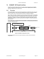
Appendix A eCOG1X Options . . . . . . . . . . . . . . . . . . . . . . . . . . . . . . . . . A-1
A.1
A.2
A.3
A.4
A.5
A.6
A.7
A.8
A.9
A.10
eCOG1X0A5 . . . . . . . . . . . . . . . . . . . . . . . . . . . . . . . . . . . . . . . . . . . . A-2
eCOG1X1A5 . . . . . . . . . . . . . . . . . . . . . . . . . . . . . . . . . . . . . . . . . . . . A-4
eCOG1X4A5 . . . . . . . . . . . . . . . . . . . . . . . . . . . . . . . . . . . . . . . . . . . . A-6
eCOG1X5A5 . . . . . . . . . . . . . . . . . . . . . . . . . . . . . . . . . . . . . . . . . . . . A-8
eCOG1X8A5 . . . . . . . . . . . . . . . . . . . . . . . . . . . . . . . . . . . . . . . . . . . A-10
eCOG1X9A5 . . . . . . . . . . . . . . . . . . . . . . . . . . . . . . . . . . . . . . . . . . . A-12
eCOG1X10B5 . . . . . . . . . . . . . . . . . . . . . . . . . . . . . . . . . . . . . . . . . . A-14
eCOG1X14B5 . . . . . . . . . . . . . . . . . . . . . . . . . . . . . . . . . . . . . . . . . . A-16
eCOG1X10Z5 . . . . . . . . . . . . . . . . . . . . . . . . . . . . . . . . . . . . . . . . . . A-18
eCOG1X14Z5 . . . . . . . . . . . . . . . . . . . . . . . . . . . . . . . . . . . . . . . . . . A-21
Appendix B Applications Information . . . . . . . . . . . . . . . . . . . . . . . . . . . . B-1
B.1
B.2
Connections . . . . . . . . . . . . . . . . . . . . . . . . . . . . . . . . . . . . . . . . . . . . B-1
Power Supplies and Decoupling . . . . . . . . . . . . . . . . . . . . . . . . . . . . . B-4
Appendix C Electrical Characteristics . . . . . . . . . . . . . . . . . . . . . . . . . . . C-1
C.1
C.2
C.3
C.4
C.5
C.6
C.7
C.8
Recommended Operating Conditions . . . . . . . . . . . . . . . . . . . . . . . . . C-1
Absolute Maximum Ratings. . . . . . . . . . . . . . . . . . . . . . . . . . . . . . . . . C-1
Supply Current . . . . . . . . . . . . . . . . . . . . . . . . . . . . . . . . . . . . . . . . . . C-2
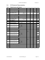
DC Electrical Characteristics. . . . . . . . . . . . . . . . . . . . . . . . . . . . . . . . C-3
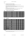
AC Electrical Characteristics . . . . . . . . . . . . . . . . . . . . . . . . . . . . . . . . C-5
Peripheral Clock Frequency Limits . . . . . . . . . . . . . . . . . . . . . . . . . . C-27
Embedded Flash Memory Characteristics . . . . . . . . . . . . . . . . . . . . C-29
Analogue Characteristics . . . . . . . . . . . . . . . . . . . . . . . . . . . . . . . . . C-30
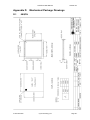
Appendix D Mechanical Package Drawings . . . . . . . . . . . . . . . . . . . . . . D-1
D.1
D.2
D.3
68QFN. . . . . . . . . . . . . . . . . . . . . . . . . . . . . . . . . . . . . . . . . . . . . . . . . D-1
100QFN. . . . . . . . . . . . . . . . . . . . . . . . . . . . . . . . . . . . . . . . . . . . . . . . D-2
208BGA. . . . . . . . . . . . . . . . . . . . . . . . . . . . . . . . . . . . . . . . . . . . . . . . D-3
Appendix E Circuit Board Pad Layout Drawings . . . . . . . . . . . . . . . . . . . E-1
E.1
E.2
E.3
68QFN. . . . . . . . . . . . . . . . . . . . . . . . . . . . . . . . . . . . . . . . . . . . . . . . . E-1
100QFN. . . . . . . . . . . . . . . . . . . . . . . . . . . . . . . . . . . . . . . . . . . . . . . . E-2
208BGA. . . . . . . . . . . . . . . . . . . . . . . . . . . . . . . . . . . . . . . . . . . . . . . . E-3
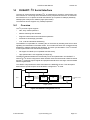
Appendix F eICE Debug Interface . . . . . . . . . . . . . . . . . . . . . . . . . . . . . . F-1
F.1
F.2
F.3
F.4
F.5
F.6
F.7
F.8
Signal Functions . . . . . . . . . . . . . . . . . . . . . . . . . . . . . . . . . . . . . . . . .
Handshake . . . . . . . . . . . . . . . . . . . . . . . . . . . . . . . . . . . . . . . . . . . . .
Abort . . . . . . . . . . . . . . . . . . . . . . . . . . . . . . . . . . . . . . . . . . . . . . . . . .
eICE Command and Data Shift . . . . . . . . . . . . . . . . . . . . . . . . . . . . . .
Clocking and Initial Operation . . . . . . . . . . . . . . . . . . . . . . . . . . . . . . .
eICE_LOADB and Reset. . . . . . . . . . . . . . . . . . . . . . . . . . . . . . . . . . .
eICE Registers . . . . . . . . . . . . . . . . . . . . . . . . . . . . . . . . . . . . . . . . . .
eICE Commands . . . . . . . . . . . . . . . . . . . . . . . . . . . . . . . . . . . . . . . . .
F-2
F-3
F-3
F-4
F-5
F-5
F-6
F-9
Appendix G Register Map . . . . . . . . . . . . . . . . . . . . . . . . . . . . . . . . . . . . G-1
Appendix H Interrupt Vectors . . . . . . . . . . . . . . . . . . . . . . . . . . . . . . . . . . H-1
Page x
Cyan Technology Ltd
21 October 2009
eCOG1X User Manual
Version 2.7
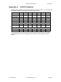
Appendix I Port Select Options. . . . . . . . . . . . . . . . . . . . . . . . . . . . . . . . . I-1
I.1
I.2
I.3
I.4
I.5
I.6
I.7
I.8
I.9
I.10
I.11
I.12
I.13
I.14
I.15
I.16
I.17
I.18
I.19
Port A. . . . . . . . . . . . . . . . . . . . . . . . . . . . . . . . . . . . . . . . . . . . . . . . . . . I-1
Port B. . . . . . . . . . . . . . . . . . . . . . . . . . . . . . . . . . . . . . . . . . . . . . . . . . . I-2
Port C . . . . . . . . . . . . . . . . . . . . . . . . . . . . . . . . . . . . . . . . . . . . . . . . . . I-3
Port D . . . . . . . . . . . . . . . . . . . . . . . . . . . . . . . . . . . . . . . . . . . . . . . . . . I-3
Port E. . . . . . . . . . . . . . . . . . . . . . . . . . . . . . . . . . . . . . . . . . . . . . . . . . . I-4
Port F. . . . . . . . . . . . . . . . . . . . . . . . . . . . . . . . . . . . . . . . . . . . . . . . . . . I-5
Port G . . . . . . . . . . . . . . . . . . . . . . . . . . . . . . . . . . . . . . . . . . . . . . . . . . I-5
Port H . . . . . . . . . . . . . . . . . . . . . . . . . . . . . . . . . . . . . . . . . . . . . . . . . . I-5
Port I . . . . . . . . . . . . . . . . . . . . . . . . . . . . . . . . . . . . . . . . . . . . . . . . . . . I-6
Port J . . . . . . . . . . . . . . . . . . . . . . . . . . . . . . . . . . . . . . . . . . . . . . . . . . . I-6
Port K. . . . . . . . . . . . . . . . . . . . . . . . . . . . . . . . . . . . . . . . . . . . . . . . . . . I-6
Port L . . . . . . . . . . . . . . . . . . . . . . . . . . . . . . . . . . . . . . . . . . . . . . . . . . . I-7
Port M . . . . . . . . . . . . . . . . . . . . . . . . . . . . . . . . . . . . . . . . . . . . . . . . . . I-7
Port N . . . . . . . . . . . . . . . . . . . . . . . . . . . . . . . . . . . . . . . . . . . . . . . . . . I-8
Port P. . . . . . . . . . . . . . . . . . . . . . . . . . . . . . . . . . . . . . . . . . . . . . . . . . . I-8
Port Q . . . . . . . . . . . . . . . . . . . . . . . . . . . . . . . . . . . . . . . . . . . . . . . . . . I-9
Port R . . . . . . . . . . . . . . . . . . . . . . . . . . . . . . . . . . . . . . . . . . . . . . . . . . I-9
Port S. . . . . . . . . . . . . . . . . . . . . . . . . . . . . . . . . . . . . . . . . . . . . . . . . . I-10
Port T. . . . . . . . . . . . . . . . . . . . . . . . . . . . . . . . . . . . . . . . . . . . . . . . . . I-11
Appendix J Peripheral Routing Options. . . . . . . . . . . . . . . . . . . . . . . . . . J-1
J.1
J.2
J.3
J.4
J.5
J.6
J.7
J.8
J.9
J.10
J.11
J.12
J.13
J.14
J.15
21 October 2009
GPIO . . . . . . . . . . . . . . . . . . . . . . . . . . . . . . . . . . . . . . . . . . . . . . . . . .
PIO . . . . . . . . . . . . . . . . . . . . . . . . . . . . . . . . . . . . . . . . . . . . . . . . . . .
DUART . . . . . . . . . . . . . . . . . . . . . . . . . . . . . . . . . . . . . . . . . . . . . . . .
DUSART . . . . . . . . . . . . . . . . . . . . . . . . . . . . . . . . . . . . . . . . . . . . . . .
Timers . . . . . . . . . . . . . . . . . . . . . . . . . . . . . . . . . . . . . . . . . . . . . . . . .
External Memory Interface (EMI). . . . . . . . . . . . . . . . . . . . . . . . . . . . .
External Host Interface (EHI). . . . . . . . . . . . . . . . . . . . . . . . . . . . . . . .
USB Interface . . . . . . . . . . . . . . . . . . . . . . . . . . . . . . . . . . . . . . . . . . .
Ethernet MAC . . . . . . . . . . . . . . . . . . . . . . . . . . . . . . . . . . . . . . . . . . .
ESPI . . . . . . . . . . . . . . . . . . . . . . . . . . . . . . . . . . . . . . . . . . . . . . . . . .
I2S . . . . . . . . . . . . . . . . . . . . . . . . . . . . . . . . . . . . . . . . . . . . . . . . . . . .
LCD Controller. . . . . . . . . . . . . . . . . . . . . . . . . . . . . . . . . . . . . . . . . . .
Motor Control PWM . . . . . . . . . . . . . . . . . . . . . . . . . . . . . . . . . . . . . . .
Dual Smart Card Interface (DSCI). . . . . . . . . . . . . . . . . . . . . . . . . . . .
Analogue I/O . . . . . . . . . . . . . . . . . . . . . . . . . . . . . . . . . . . . . . . . . . . .
Cyan Technology Ltd
J-1
J-1
J-1
J-2
J-3
J-4
J-4
J-5
J-6
J-6
J-6
J-7
J-7
J-8
J-8
Page xi
Version 2.7
eCOG1X User Manual
Appendix K External Peripheral Signals . . . . . . . . . . . . . . . . . . . . . . . . . K-1
K.1
K.2
K.3
K.4
K.5
K.6
K.7
K.8
K.9
K.10
K.11
K.12
K.13
K.14
GPIO . . . . . . . . . . . . . . . . . . . . . . . . . . . . . . . . . . . . . . . . . . . . . . . . . .
PIO . . . . . . . . . . . . . . . . . . . . . . . . . . . . . . . . . . . . . . . . . . . . . . . . . . .
DUART . . . . . . . . . . . . . . . . . . . . . . . . . . . . . . . . . . . . . . . . . . . . . . . .
DUSART . . . . . . . . . . . . . . . . . . . . . . . . . . . . . . . . . . . . . . . . . . . . . . .
Timers . . . . . . . . . . . . . . . . . . . . . . . . . . . . . . . . . . . . . . . . . . . . . . . . .
External Memory Interface . . . . . . . . . . . . . . . . . . . . . . . . . . . . . . . . .
External Host Interface . . . . . . . . . . . . . . . . . . . . . . . . . . . . . . . . . . . .
USB Interface . . . . . . . . . . . . . . . . . . . . . . . . . . . . . . . . . . . . . . . . . . .
Ethernet MAC . . . . . . . . . . . . . . . . . . . . . . . . . . . . . . . . . . . . . . . . . . .
ESPI . . . . . . . . . . . . . . . . . . . . . . . . . . . . . . . . . . . . . . . . . . . . . . . . . .
I2S . . . . . . . . . . . . . . . . . . . . . . . . . . . . . . . . . . . . . . . . . . . . . . . . . . . .
LCD Controller. . . . . . . . . . . . . . . . . . . . . . . . . . . . . . . . . . . . . . . . . . .
Motor Control PWM. . . . . . . . . . . . . . . . . . . . . . . . . . . . . . . . . . . . . . .
Dual Smart Card Interface. . . . . . . . . . . . . . . . . . . . . . . . . . . . . . . . . .
K-1
K-1
K-1
K-2
K-3
K-3
K-4
K-4
K-5
K-5
K-5
K-5
K-5
K-6
Appendix L Contact Information . . . . . . . . . . . . . . . . . . . . . . . . . . . . . . . L-1
Page xii
Cyan Technology Ltd
21 October 2009
eCOG1X User Manual
Version 2.7
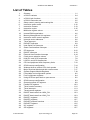
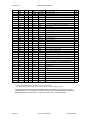
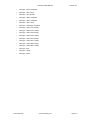
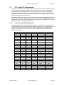
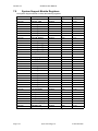
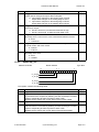
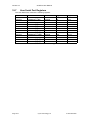
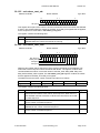
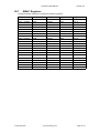
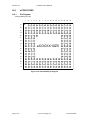
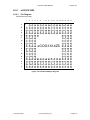
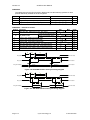
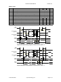
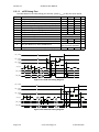
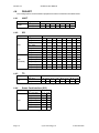
List of Figures
1:
2:
3:
4:
5:
6:
7:
8:
9:
10:
11:
12:
13:
14:
15:
16:
17:
18:
19:
20:
21:
22:
23:
24:
25:
26:
27:
28:
29:
30:
31:
32:
33:
34:
35:
36:
37:
38:
39:
40:
41:
42:
43:
44:
45:
21 October 2009
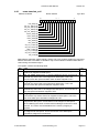
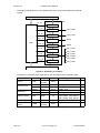
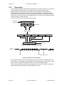
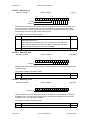
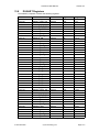
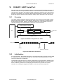
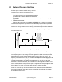
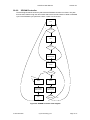
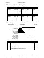
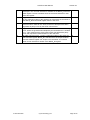
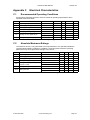
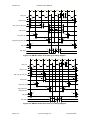
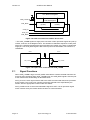
eCOG1X block diagram. . . . . . . . . . . . . . . . . . . . . . . . . . . . . . . . . . . . 2-1
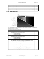
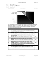
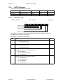
Programmer’s model . . . . . . . . . . . . . . . . . . . . . . . . . . . . . . . . . . . . . . 3-2
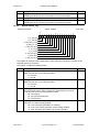
Memory organisation . . . . . . . . . . . . . . . . . . . . . . . . . . . . . . . . . . . . . . 3-3
Example instruction sequences. . . . . . . . . . . . . . . . . . . . . . . . . . . . . 3-14
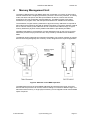
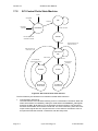
Abstract view of MMU operation.. . . . . . . . . . . . . . . . . . . . . . . . . . . . . 4-1
MMU translator blocks. . . . . . . . . . . . . . . . . . . . . . . . . . . . . . . . . . . . . 4-3
MMU reset configuration. . . . . . . . . . . . . . . . . . . . . . . . . . . . . . . . . . . 4-5
MMU example configuration.. . . . . . . . . . . . . . . . . . . . . . . . . . . . . . . . 4-6
Cache memory map . . . . . . . . . . . . . . . . . . . . . . . . . . . . . . . . . . . . . . 5-1
Cache tag format . . . . . . . . . . . . . . . . . . . . . . . . . . . . . . . . . . . . . . . . . 5-2
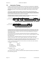
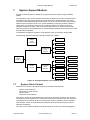
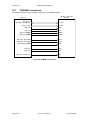
Interrupt flow diagram . . . . . . . . . . . . . . . . . . . . . . . . . . . . . . . . . . . . . 6-2
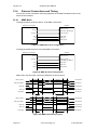
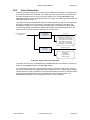
Principal modules in the eCOG1X SSM. . . . . . . . . . . . . . . . . . . . . . . . 7-1
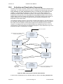
Detailed eCOG1X clocking scheme. . . . . . . . . . . . . . . . . . . . . . . . . . . 7-2
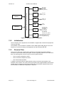
Port configuration overview . . . . . . . . . . . . . . . . . . . . . . . . . . . . . . . . . 8-1
GPIO peripheral module . . . . . . . . . . . . . . . . . . . . . . . . . . . . . . . . . . . 9-1
Connecting a 5V input signal. . . . . . . . . . . . . . . . . . . . . . . . . . . . . . . . 9-4
Connecting a 5V I/O signal . . . . . . . . . . . . . . . . . . . . . . . . . . . . . . . . . 9-4
GPIO register bit fields . . . . . . . . . . . . . . . . . . . . . . . . . . . . . . . . . . . . 9-5
Parallel I/O peripheral module . . . . . . . . . . . . . . . . . . . . . . . . . . . . . . 10-1
Timer peripheral module . . . . . . . . . . . . . . . . . . . . . . . . . . . . . . . . . . 11-1
Detailed view of timers . . . . . . . . . . . . . . . . . . . . . . . . . . . . . . . . . . . 11-2
DUART peripheral module . . . . . . . . . . . . . . . . . . . . . . . . . . . . . . . . 12-1
DUART transmitter structure . . . . . . . . . . . . . . . . . . . . . . . . . . . . . . . 12-4
UART serial data format . . . . . . . . . . . . . . . . . . . . . . . . . . . . . . . . . . 12-4
DUART receiver structure . . . . . . . . . . . . . . . . . . . . . . . . . . . . . . . . . 12-5
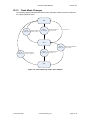
DUSART peripheral module . . . . . . . . . . . . . . . . . . . . . . . . . . . . . . . 13-1
DUSART overall configuration. . . . . . . . . . . . . . . . . . . . . . . . . . . . . . 13-2
DUSART configuration for I2C . . . . . . . . . . . . . . . . . . . . . . . . . . . . . 14-1
DUSART configuration for SPI . . . . . . . . . . . . . . . . . . . . . . . . . . . . . 15-1
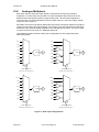
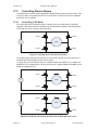
SPI master and slave configurations . . . . . . . . . . . . . . . . . . . . . . . . . 15-2
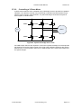
SPI clock polarity and phase selection . . . . . . . . . . . . . . . . . . . . . . . 15-4
DUSART configuration for UART . . . . . . . . . . . . . . . . . . . . . . . . . . . 16-1
UART serial data format . . . . . . . . . . . . . . . . . . . . . . . . . . . . . . . . . . 16-1
DUSART configuration for Smart Card Interface. . . . . . . . . . . . . . . . 17-1
SCI control finite state machine. . . . . . . . . . . . . . . . . . . . . . . . . . . . . 17-2
DUSART configuration for Infra-Red Interface . . . . . . . . . . . . . . . . . 18-1
Generic IFR frame format . . . . . . . . . . . . . . . . . . . . . . . . . . . . . . . . . 18-2
DUSART configuration for User Serial Port. . . . . . . . . . . . . . . . . . . . 19-1
External Memory Interface peripheral module. . . . . . . . . . . . . . . . . . 20-1
Using 8 bit memory with /RS and /WS . . . . . . . . . . . . . . . . . . . . . . . 20-5
Using 8 bit memory with R/W and /DS . . . . . . . . . . . . . . . . . . . . . . . 20-6
Using 16-bit memory with /RS and /WS . . . . . . . . . . . . . . . . . . . . . . 20-7
Using 16-bit memory with R/W and /DS . . . . . . . . . . . . . . . . . . . . . . 20-8
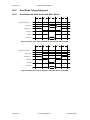
Read cycle timing diagram: 8 bit data with /RS and /WS . . . . . . . . 20-10
Write cycle timing diagram: 8 bit data with /RS and /WS . . . . . . . . 20-10
Cyan Technology Ltd
Page xiii
Version 2.7
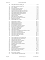
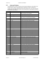
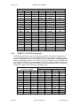
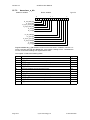
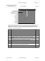
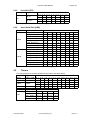
46:
47:
48:
49:
50:
51:
52:
53:
54:
55:
56:
57:
58:
59:
60:
61:
62:
63:
64:
65:
66:
67:
68:
69:
70:
71:
72:
73:
74:
75:
76:
77:
78:
79:
80:
81:
82:
83:
84:
85:
86:
87:
88:
89:
90:
91:
Page xiv
eCOG1X User Manual
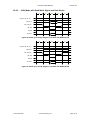
Read cycle timing diagram: 8 bit data with R/W and /DS . . . . . . . . 20-11
Write cycle timing diagram: 8 bit data with R/W and /DS . . . . . . . . 20-11
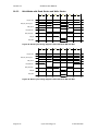
Read cycle timing diagram: 16 bit data with /RS and /WS . . . . . . . 20-12
Write cycle timing diagram: 16 bit data with /RS and /WS . . . . . . . 20-12
Read cycle timing diagram: 16 bit data with R/W and /DS . . . . . . . 20-13
Write cycle timing diagram: 16 bit data with R/W and /DS . . . . . . . 20-13
SDRAM controller flow diagram . . . . . . . . . . . . . . . . . . . . . . . . . . . 20-17
SDRAM connections . . . . . . . . . . . . . . . . . . . . . . . . . . . . . . . . . . . . 20-20
Single cycle accesses, idle disabled . . . . . . . . . . . . . . . . . . . . . . . . 20-24
Single cycle accesses, idle enabled . . . . . . . . . . . . . . . . . . . . . . . . 20-25
Single cycle accesses with initial precharge, idle disabled . . . . . . . 20-26
Single cycle accesses with initial precharge, idle enabled . . . . . . . 20-27
Burst read cycles. . . . . . . . . . . . . . . . . . . . . . . . . . . . . . . . . . . . . . . 20-28
Auto refresh cycles . . . . . . . . . . . . . . . . . . . . . . . . . . . . . . . . . . . . . 20-29
Custom command cycles . . . . . . . . . . . . . . . . . . . . . . . . . . . . . . . . 20-30
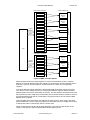
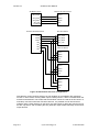
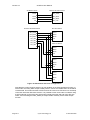
RAM, EHI and port configurator interconnection. . . . . . . . . . . . . . . . 21-1
EHI long word and word modes. . . . . . . . . . . . . . . . . . . . . . . . . . . . . 21-2
MMP 256 x 16 bit configuration. . . . . . . . . . . . . . . . . . . . . . . . . . . . . 21-6
MMP 8 x 32 bit configuration. . . . . . . . . . . . . . . . . . . . . . . . . . . . . . . 21-6
MMP read and write cycles . . . . . . . . . . . . . . . . . . . . . . . . . . . . . . . . 21-6
DMA configuration with eCOG1X as master. . . . . . . . . . . . . . . . . . . 21-7
DMA master mode read and write cycles . . . . . . . . . . . . . . . . . . . . . 21-7
DMA configuration with eCOG1X as slave.. . . . . . . . . . . . . . . . . . . . 21-7
DMA slave mode read and write cycles . . . . . . . . . . . . . . . . . . . . . . 21-7
Flash operating modes state diagram . . . . . . . . . . . . . . . . . . . . . . . 22-15
ADC input configurations. . . . . . . . . . . . . . . . . . . . . . . . . . . . . . . . . . 23-4
SPI master and slave configurations. . . . . . . . . . . . . . . . . . . . . . . . . 24-2
ESPI clock polarity and phase selection . . . . . . . . . . . . . . . . . . . . . . 24-4
ESPI multiple word transfers . . . . . . . . . . . . . . . . . . . . . . . . . . . . . . . 24-5
ESPI programmable time delays. . . . . . . . . . . . . . . . . . . . . . . . . . . . 24-6
I2S basic timing . . . . . . . . . . . . . . . . . . . . . . . . . . . . . . . . . . . . . . . . . 25-1
Static LCD connections and drive waveforms. . . . . . . . . . . . . . . . . . 26-1
Multiplexed LCD connections and drive waveforms . . . . . . . . . . . . . 26-2
Modified drive waveforms for multiplexed LCDs . . . . . . . . . . . . . . . . 26-3
LCD controller connections and waveforms for two backplanes. . . . 26-4
H-bridge drive circuit for a DC motor. . . . . . . . . . . . . . . . . . . . . . . . . 27-2
Forwards and reverse direction with an H-bridge drive circuit . . . . . 27-2
3-phase full bridge drive circuit . . . . . . . . . . . . . . . . . . . . . . . . . . . . . 27-3
Edge-aligned mode . . . . . . . . . . . . . . . . . . . . . . . . . . . . . . . . . . . . . . 27-5
Centre-aligned mode. . . . . . . . . . . . . . . . . . . . . . . . . . . . . . . . . . . . . 27-5
User-defined edge mode. . . . . . . . . . . . . . . . . . . . . . . . . . . . . . . . . . 27-6
Guard time in centre-aligned mode . . . . . . . . . . . . . . . . . . . . . . . . . . 27-7
Guard time in edge-aligned mode . . . . . . . . . . . . . . . . . . . . . . . . . . . 27-7
DSCI block diagram . . . . . . . . . . . . . . . . . . . . . . . . . . . . . . . . . . . . . 28-2
Smart card clock generation . . . . . . . . . . . . . . . . . . . . . . . . . . . . . . . 28-3
DSCI card session controller state machine . . . . . . . . . . . . . . . . . . . 28-4
Cyan Technology Ltd
21 October 2009
eCOG1X User Manual
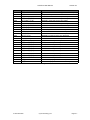
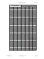
92:
93:
94:
95:
96:
97:
98:
99:
100:
101:
102:
103:
104:
105:
106:
107:
108:
109:
110:
111:
112:
113:
114:
115:
116:
117:
118:
119:
120:
121:
122:
123:
124:
125:
126:
127:
128:
129:
130:
131:
132:
133:
134:
135:
136:
137:
21 October 2009
Version 2.7
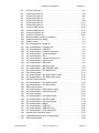
Activation sequence . . . . . . . . . . . . . . . . . . . . . . . . . . . . . . . . . . . . . 28-5
Deactivation sequence . . . . . . . . . . . . . . . . . . . . . . . . . . . . . . . . . . . 28-6
DSCI receiver timing . . . . . . . . . . . . . . . . . . . . . . . . . . . . . . . . . . . . . 28-8
DSCI transmitter timing . . . . . . . . . . . . . . . . . . . . . . . . . . . . . . . . . . 28-10
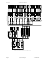
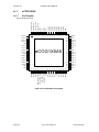
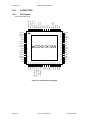
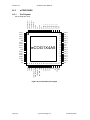
eCOG1X0A5 pin diagram . . . . . . . . . . . . . . . . . . . . . . . . . . . . . . . . . . A-2
eCOG1X1A5 pin diagram . . . . . . . . . . . . . . . . . . . . . . . . . . . . . . . . . . A-4
eCOG1X4A5 pin diagram . . . . . . . . . . . . . . . . . . . . . . . . . . . . . . . . . . A-6
eCOG1X5A5 pin diagram . . . . . . . . . . . . . . . . . . . . . . . . . . . . . . . . . . A-8
eCOG1X8A5 pin diagram . . . . . . . . . . . . . . . . . . . . . . . . . . . . . . . . . A-10
eCOG1X9A5 pin diagram . . . . . . . . . . . . . . . . . . . . . . . . . . . . . . . . . A-12
eCOG1X10B5 pin diagram . . . . . . . . . . . . . . . . . . . . . . . . . . . . . . . . A-14
eCOG1X14B5 pin diagram . . . . . . . . . . . . . . . . . . . . . . . . . . . . . . . . A-16
eCOG1X10Z5 pin diagram . . . . . . . . . . . . . . . . . . . . . . . . . . . . . . . . A-18
eCOG1X14Z5 pin diagram . . . . . . . . . . . . . . . . . . . . . . . . . . . . . . . . A-21
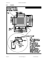
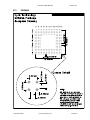
High reference oscillator external components . . . . . . . . . . . . . . . . . . B-1
Low reference oscillator external components . . . . . . . . . . . . . . . . . . B-1
Vref decoupling . . . . . . . . . . . . . . . . . . . . . . . . . . . . . . . . . . . . . . . . . . B-2
Low PLL filter external components . . . . . . . . . . . . . . . . . . . . . . . . . . B-2
eICE debug header connections . . . . . . . . . . . . . . . . . . . . . . . . . . . . . B-3
External clock source timing diagram . . . . . . . . . . . . . . . . . . . . . . . . . C-6
EMI bus mode 8-bit read cycle timing diagram . . . . . . . . . . . . . . . . . . C-9
EMI bus mode 8-bit write cycle timing diagram . . . . . . . . . . . . . . . . . . C-9
EMI bus mode 16-bit read cycle timing diagram . . . . . . . . . . . . . . . . C-10
EMI bus mode 16-bit write cycle timing diagram . . . . . . . . . . . . . . . . C-10
EMI SDRAM mode read cycle timing diagram . . . . . . . . . . . . . . . . . C-11
EMI SDRAM mode write cycle timing diagram . . . . . . . . . . . . . . . . . C-12
EHI MMP read cycle timing diagram . . . . . . . . . . . . . . . . . . . . . . . . . C-13
EHI MMP write cycle timing diagram. . . . . . . . . . . . . . . . . . . . . . . . . C-13
EHI DMA master read cycle timing diagram . . . . . . . . . . . . . . . . . . . C-14
EHI DMA master write cycle timing diagram . . . . . . . . . . . . . . . . . . . C-14
EHI DMA slave read cycle timing diagram . . . . . . . . . . . . . . . . . . . . C-15
EHI DMA slave write cycle timing diagram . . . . . . . . . . . . . . . . . . . . C-15
SPI timing diagram, master mode, clk_pha = 0. . . . . . . . . . . . . . . . . C-16
SPI timing diagram, master mode, clk_pha = 1. . . . . . . . . . . . . . . . . C-16
SPI timing diagram, slave mode, clk_pha = 0 . . . . . . . . . . . . . . . . . . C-17
SPI timing diagram, slave mode, clk_pha = 1 . . . . . . . . . . . . . . . . . . C-17
ESPI timing diagram, master mode, cpha = 0. . . . . . . . . . . . . . . . . . C-19
ESPI timing diagram, master mode, cpha = 1. . . . . . . . . . . . . . . . . . C-19
ESPI timing diagram, slave mode, cpha = 0 . . . . . . . . . . . . . . . . . . . C-20
ESPI timing diagram, slave mode, cpha = 1 . . . . . . . . . . . . . . . . . . . C-20
I2S master mode timing diagram. . . . . . . . . . . . . . . . . . . . . . . . . . . . C-21
I2S slave mode timing diagram . . . . . . . . . . . . . . . . . . . . . . . . . . . . . C-22
I2S clock signals timing diagram . . . . . . . . . . . . . . . . . . . . . . . . . . . . C-23
EMAC MII timing diagram . . . . . . . . . . . . . . . . . . . . . . . . . . . . . . . . . C-24
USB ULPI timing diagram . . . . . . . . . . . . . . . . . . . . . . . . . . . . . . . . . C-25
eICE read timing diagram . . . . . . . . . . . . . . . . . . . . . . . . . . . . . . . . . C-26
Cyan Technology Ltd
Page xv
Version 2.7
138:
139:
140:
141:
142:
143:
144:
145:
146:
147:
Page xvi
eCOG1X User Manual
eICE write timing diagram . . . . . . . . . . . . . . . . . . . . . . . . . . . . . . . . . C-26
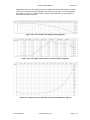
Vref variation with supply voltage (typical) . . . . . . . . . . . . . . . . . . . . C-33
Vref supply noise rejection versus frequency (typical) . . . . . . . . . . . C-33
Voltage reference standby current with temperature (typical). . . . . . C-33
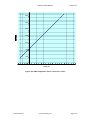
ADC temperature sensor conversion values. . . . . . . . . . . . . . . . . . . C-35
eICE connections at eCOG1 device level . . . . . . . . . . . . . . . . . . . . . . F-2
Open drain connection for eICE_LOADB . . . . . . . . . . . . . . . . . . . . . . F-2
eICE handshake . . . . . . . . . . . . . . . . . . . . . . . . . . . . . . . . . . . . . . . . . F-3
eICE timing for a write to slave . . . . . . . . . . . . . . . . . . . . . . . . . . . . . . F-4
eICE timing for a read from slave . . . . . . . . . . . . . . . . . . . . . . . . . . . . F-4
Cyan Technology Ltd
21 October 2009
eCOG1X User Manual
Version 2.7
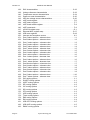
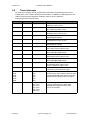
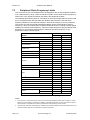
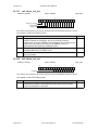
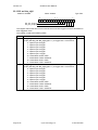
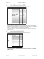
List of Tables
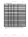
1:
2:
3:
4:
5:
6:
7:
8:
9:
10:
11:
12:
13:
14:
15:
16:
17:
18:
19:
20:
21:
23:
22:
24:
25:
26:
27:
28:
29:
30:
31:
32:
33:
34:
35:
36:
37:
38:
39:
40:
41:
42:
43:
44:
45:
21 October 2009
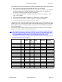
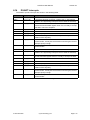
Glossary . . . . . . . . . . . . . . . . . . . . . . . . . . . . . . . . . . . . . . . . . . . . . . . 1-1
eCOG1X variants . . . . . . . . . . . . . . . . . . . . . . . . . . . . . . . . . . . . . . . . 2-4
eCOG1X pin functions. . . . . . . . . . . . . . . . . . . . . . . . . . . . . . . . . . . . . 2-5
eCOG1X instruction set. . . . . . . . . . . . . . . . . . . . . . . . . . . . . . . . . . . . 3-5
Sleep control: morning and evening bits . . . . . . . . . . . . . . . . . . . . . . . 3-8
Instruction prefix words . . . . . . . . . . . . . . . . . . . . . . . . . . . . . . . . . . . 3-12
Instruction formats . . . . . . . . . . . . . . . . . . . . . . . . . . . . . . . . . . . . . . . 3-13
Instruction cycles . . . . . . . . . . . . . . . . . . . . . . . . . . . . . . . . . . . . . . . . 3-15
MMU size register values. . . . . . . . . . . . . . . . . . . . . . . . . . . . . . . . . . . 4-4
Internal RAM organisation . . . . . . . . . . . . . . . . . . . . . . . . . . . . . . . . . . 4-6
Memory Management Unit registers . . . . . . . . . . . . . . . . . . . . . . . . . . 4-7
Instruction cache control registers. . . . . . . . . . . . . . . . . . . . . . . . . . . . 5-4
Interrupt vector addresses. . . . . . . . . . . . . . . . . . . . . . . . . . . . . . . . . . 6-6
Timer interrupts . . . . . . . . . . . . . . . . . . . . . . . . . . . . . . . . . . . . . . . . . . 6-8
DUSART interrupts . . . . . . . . . . . . . . . . . . . . . . . . . . . . . . . . . . . . . . . 6-9
User Serial Port interrupts . . . . . . . . . . . . . . . . . . . . . . . . . . . . . . . . . 6-10
Smart Card Interface interrupts . . . . . . . . . . . . . . . . . . . . . . . . . . . . . 6-11
IFR interrupts. . . . . . . . . . . . . . . . . . . . . . . . . . . . . . . . . . . . . . . . . . . 6-12
DUART interrupts . . . . . . . . . . . . . . . . . . . . . . . . . . . . . . . . . . . . . . . 6-13
External Host Interface interrupts . . . . . . . . . . . . . . . . . . . . . . . . . . . 6-14
Clock source selection values . . . . . . . . . . . . . . . . . . . . . . . . . . . . . . . 7-4
High PLL and VCO frequencies . . . . . . . . . . . . . . . . . . . . . . . . . . . . . 7-8
Low PLL and VCO frequencies . . . . . . . . . . . . . . . . . . . . . . . . . . . . . . 7-8
CPU and peripheral clock frequency limits . . . . . . . . . . . . . . . . . . . . 7-10
GPIO interrupt configuration . . . . . . . . . . . . . . . . . . . . . . . . . . . . . . . 7-14
Wakeup times at various CPU clock speeds. . . . . . . . . . . . . . . . . . . 7-15
Major functional blocks and their reset sources. . . . . . . . . . . . . . . . . 7-17
System Support Module Registers . . . . . . . . . . . . . . . . . . . . . . . . . . 7-18
Port widths and configuration options . . . . . . . . . . . . . . . . . . . . . . . . . 8-2
Port Configurator registers . . . . . . . . . . . . . . . . . . . . . . . . . . . . . . . . . 8-4
Using GPIO as open-drain or open-source . . . . . . . . . . . . . . . . . . . . . 9-2
GPIO interrupt configuration . . . . . . . . . . . . . . . . . . . . . . . . . . . . . . . . 9-3
General purpose I/O registers . . . . . . . . . . . . . . . . . . . . . . . . . . . . . . . 9-8
Parallel I/O registers . . . . . . . . . . . . . . . . . . . . . . . . . . . . . . . . . . . . . 10-3
Timer function summary . . . . . . . . . . . . . . . . . . . . . . . . . . . . . . . . . . 11-2
Timer interrupts . . . . . . . . . . . . . . . . . . . . . . . . . . . . . . . . . . . . . . . . . 11-3
Timer/counter registers . . . . . . . . . . . . . . . . . . . . . . . . . . . . . . . . . . . 11-9
DUART baud rates from HIGH_PLL . . . . . . . . . . . . . . . . . . . . . . . . . 12-3
DUART baud rates from LOW_PLL . . . . . . . . . . . . . . . . . . . . . . . . . 12-3
DUART1 registers . . . . . . . . . . . . . . . . . . . . . . . . . . . . . . . . . . . . . . . 12-6
DUART2 registers . . . . . . . . . . . . . . . . . . . . . . . . . . . . . . . . . . . . . . . 12-7
DUSART protocol functions. . . . . . . . . . . . . . . . . . . . . . . . . . . . . . . . 13-4
DUSART registers . . . . . . . . . . . . . . . . . . . . . . . . . . . . . . . . . . . . . . . 13-5
I2C registers . . . . . . . . . . . . . . . . . . . . . . . . . . . . . . . . . . . . . . . . . . . 14-5
SPI registers . . . . . . . . . . . . . . . . . . . . . . . . . . . . . . . . . . . . . . . . . . . 15-7
Cyan Technology Ltd
Page xvii
Version 2.7
46:
47:
48:
49:
50:
51:
52:
53:
54:
55:
56:
57:
58:
59:
60:
61:
62:
63:
64:
65:
66:
67:
68:
69:
70:
71:
72:
73:
74:
75:
76:
77:
78:
79:
80:
81:
82:
83:
84:
85:
86:
87:
88:
89:
90:
91:
Page xviii
eCOG1X User Manual
UART baud rates from HIGH_PLL . . . . . . . . . . . . . . . . . . . . . . . . . . 16-2
UART baud rates from LOW_PLL. . . . . . . . . . . . . . . . . . . . . . . . . . . 16-2
UART registers . . . . . . . . . . . . . . . . . . . . . . . . . . . . . . . . . . . . . . . . . 16-4
Smart Card Interface registers . . . . . . . . . . . . . . . . . . . . . . . . . . . . . 17-5
Infra-Red Interface registers . . . . . . . . . . . . . . . . . . . . . . . . . . . . . . . 18-5
User Serial Port baud rates from HIGH_PLL . . . . . . . . . . . . . . . . . . 19-2
User Serial Port baud rates from LOW_PLL . . . . . . . . . . . . . . . . . . . 19-2
USR example frame transmit sequence . . . . . . . . . . . . . . . . . . . . . . 19-4
USR example frame receive sequence. . . . . . . . . . . . . . . . . . . . . . . 19-5
User Serial Port registers . . . . . . . . . . . . . . . . . . . . . . . . . . . . . . . . . 19-6
EMI signal names . . . . . . . . . . . . . . . . . . . . . . . . . . . . . . . . . . . . . . . 20-2
EMI read/write control signals . . . . . . . . . . . . . . . . . . . . . . . . . . . . . . 20-3
Bus signals in 8-bit and 16-bit modes . . . . . . . . . . . . . . . . . . . . . . . . 20-4
EMI timing parameters . . . . . . . . . . . . . . . . . . . . . . . . . . . . . . . . . . . 20-9
SDRAM addressing modes . . . . . . . . . . . . . . . . . . . . . . . . . . . . . . . 20-14
SDRAM address signals . . . . . . . . . . . . . . . . . . . . . . . . . . . . . . . . . 20-15
SDRAM custom commands . . . . . . . . . . . . . . . . . . . . . . . . . . . . . . 20-19
SDRAM timing parameters . . . . . . . . . . . . . . . . . . . . . . . . . . . . . . . 20-21
SDRAM timing calculations . . . . . . . . . . . . . . . . . . . . . . . . . . . . . . . 20-22
External Memory Interface registers . . . . . . . . . . . . . . . . . . . . . . . . 20-33
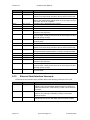
External Host Interface registers . . . . . . . . . . . . . . . . . . . . . . . . . . . . 21-8
Flash memory organisation . . . . . . . . . . . . . . . . . . . . . . . . . . . . . . . . 22-1
Flash memory wait states . . . . . . . . . . . . . . . . . . . . . . . . . . . . . . . . . 22-2
Flash erase summary . . . . . . . . . . . . . . . . . . . . . . . . . . . . . . . . . . . . 22-5
Flash memory manufacturer and device ID codes . . . . . . . . . . . . . . 22-8
Flash memory read status bits . . . . . . . . . . . . . . . . . . . . . . . . . . . . . 22-9
Flash memory command sequences . . . . . . . . . . . . . . . . . . . . . . . 22-11
Flash memory operation timings . . . . . . . . . . . . . . . . . . . . . . . . . . . 22-12
Flash memory low power modes. . . . . . . . . . . . . . . . . . . . . . . . . . . 22-12
Flash timer registers . . . . . . . . . . . . . . . . . . . . . . . . . . . . . . . . . . . . 22-13
Flash configuration slow_mode bit field . . . . . . . . . . . . . . . . . . . . . 22-13
Flash configuration pwr_save bit field . . . . . . . . . . . . . . . . . . . . . . . 22-13
Flash timer clock sources . . . . . . . . . . . . . . . . . . . . . . . . . . . . . . . . 22-14
Embedded flash memory registers . . . . . . . . . . . . . . . . . . . . . . . . . 22-18
ADC input channel selection . . . . . . . . . . . . . . . . . . . . . . . . . . . . . . . 23-5
ADC resolution and speed . . . . . . . . . . . . . . . . . . . . . . . . . . . . . . . . 23-6
Analogue Control Interface registers. . . . . . . . . . . . . . . . . . . . . . . . 23-10
ESPI registers . . . . . . . . . . . . . . . . . . . . . . . . . . . . . . . . . . . . . . . . . . 24-8
I2S registers . . . . . . . . . . . . . . . . . . . . . . . . . . . . . . . . . . . . . . . . . . . 25-5
LCD controller registers. . . . . . . . . . . . . . . . . . . . . . . . . . . . . . . . . . . 26-5
MCPWM registers . . . . . . . . . . . . . . . . . . . . . . . . . . . . . . . . . . . . . . . 27-8
Dual Smart Card Interface registers . . . . . . . . . . . . . . . . . . . . . . . . 28-12
EMAC minimum clock frequency . . . . . . . . . . . . . . . . . . . . . . . . . . . 29-2
MAC setup data buffer . . . . . . . . . . . . . . . . . . . . . . . . . . . . . . . . . . 29-12
Ethernet MAC registers . . . . . . . . . . . . . . . . . . . . . . . . . . . . . . . . . . 29-13
Transmit descriptor automatic polling . . . . . . . . . . . . . . . . . . . . . . . 29-14
Cyan Technology Ltd
21 October 2009
eCOG1X User Manual
92:
93:
94:
95:
96:
97:
98:
99:
100:
101:
102:
103:
104:
105:
106:
107:
108:
109:
110:
111:
112:
113:
114:
115:
116:
117:
118:
119:
120:
121:
122:
123:
124:
125:
126:
127:
128:
129:
130:
131:
132:
133:
134:
135:
136:
137:
21 October 2009
Version 2.7
eCOG1X variants . . . . . . . . . . . . . . . . . . . . . . . . . . . . . . . . . . . . . . . . A-1
eCOG1X0A5 pin list . . . . . . . . . . . . . . . . . . . . . . . . . . . . . . . . . . . . . . A-3
eCOG1X1A5 pin list . . . . . . . . . . . . . . . . . . . . . . . . . . . . . . . . . . . . . . A-5
eCOG1X4A5 pin list . . . . . . . . . . . . . . . . . . . . . . . . . . . . . . . . . . . . . . A-7
eCOG1X5A5 pin list . . . . . . . . . . . . . . . . . . . . . . . . . . . . . . . . . . . . . . A-9
eCOG1X8A5 pin list . . . . . . . . . . . . . . . . . . . . . . . . . . . . . . . . . . . . . A-11
eCOG1X9A5 pin list . . . . . . . . . . . . . . . . . . . . . . . . . . . . . . . . . . . . . A-13
eCOG1X10B5 pin list . . . . . . . . . . . . . . . . . . . . . . . . . . . . . . . . . . . . A-15
eCOG1X14B5 pin list . . . . . . . . . . . . . . . . . . . . . . . . . . . . . . . . . . . . A-17
eCOG1X10Z5 pin list. . . . . . . . . . . . . . . . . . . . . . . . . . . . . . . . . . . . . A-19
eCOG1X14Z5 pin list. . . . . . . . . . . . . . . . . . . . . . . . . . . . . . . . . . . . . A-22
Recommended operating conditions . . . . . . . . . . . . . . . . . . . . . . . . . . C-1
Absolute maximum ratings . . . . . . . . . . . . . . . . . . . . . . . . . . . . . . . . . C-1
Supply current . . . . . . . . . . . . . . . . . . . . . . . . . . . . . . . . . . . . . . . . . . . C-2
DC characteristics - digital I/O . . . . . . . . . . . . . . . . . . . . . . . . . . . . . . . C-3
DC characteristics - analogue I/O . . . . . . . . . . . . . . . . . . . . . . . . . . . . C-4
DC characteristics - USB PHY . . . . . . . . . . . . . . . . . . . . . . . . . . . . . . C-4
AC characteristics - relaxation oscillator . . . . . . . . . . . . . . . . . . . . . . . C-5
AC characteristics - crystal oscillators . . . . . . . . . . . . . . . . . . . . . . . . . C-5
AC characteristics - PLLs . . . . . . . . . . . . . . . . . . . . . . . . . . . . . . . . . . C-6
AC characteristics - external clock source. . . . . . . . . . . . . . . . . . . . . . C-6
AC characteristics - digital inputs . . . . . . . . . . . . . . . . . . . . . . . . . . . . C-7
AC characteristics - EMI clock. . . . . . . . . . . . . . . . . . . . . . . . . . . . . . . C-8
AC characteristics - EMI bus mode . . . . . . . . . . . . . . . . . . . . . . . . . . . C-8
AC characteristics - EMI SDRAM mode . . . . . . . . . . . . . . . . . . . . . . . C-8
AC characteristics - EHI MMP mode . . . . . . . . . . . . . . . . . . . . . . . . . C-13
EHI clock symbols . . . . . . . . . . . . . . . . . . . . . . . . . . . . . . . . . . . . . . . C-14
AC characteristics - EHI DMA master mode . . . . . . . . . . . . . . . . . . . C-14
AC characteristics - EHI DMA slave mode . . . . . . . . . . . . . . . . . . . . C-15
DUSART clock symbols . . . . . . . . . . . . . . . . . . . . . . . . . . . . . . . . . . C-15
AC characteristics - SPI master mode. . . . . . . . . . . . . . . . . . . . . . . . C-16
AC characteristics - SPI slave mode . . . . . . . . . . . . . . . . . . . . . . . . . C-17
ESPI clock symbols . . . . . . . . . . . . . . . . . . . . . . . . . . . . . . . . . . . . . . C-18
AC characteristics - ESPI master mode . . . . . . . . . . . . . . . . . . . . . . C-19
AC characteristics - ESPI slave mode. . . . . . . . . . . . . . . . . . . . . . . . C-20
I2S clock symbols . . . . . . . . . . . . . . . . . . . . . . . . . . . . . . . . . . . . . . . C-21
AC characteristics - I2S master mode . . . . . . . . . . . . . . . . . . . . . . . . C-21
AC characteristics - I2S slave mode . . . . . . . . . . . . . . . . . . . . . . . . . C-22
AC characteristics - I2S clock signals . . . . . . . . . . . . . . . . . . . . . . . . C-23
AC characteristics - EMAC . . . . . . . . . . . . . . . . . . . . . . . . . . . . . . . . C-24
AC characteristics - USB PHY. . . . . . . . . . . . . . . . . . . . . . . . . . . . . . C-25
AC characteristics - USB ULPI port. . . . . . . . . . . . . . . . . . . . . . . . . . C-25
AC characteristics - eICE debug port . . . . . . . . . . . . . . . . . . . . . . . . C-26
Internal clock frequency limits . . . . . . . . . . . . . . . . . . . . . . . . . . . . . . C-27
Embedded flash memory characteristics. . . . . . . . . . . . . . . . . . . . . . C-29
ADC characteristics . . . . . . . . . . . . . . . . . . . . . . . . . . . . . . . . . . . . . . C-30
Cyan Technology Ltd
Page xix
Version 2.7
138:
139:
140:
141:
142:
143:
144:
145:
146:
147:
148:
149:
150:
151:
152:
153:
154:
155:
156:
157:
158:
159:
160:
161:
162:
163:
164:
165:
166:
167:
168:
169:
170:
171:
172:
173:
174:
175:
176:
177:
178:
179:
180:
181:
182:
183:
Page xx
eCOG1X User Manual
DAC characteristics. . . . . . . . . . . . . . . . . . . . . . . . . . . . . . . . . . . . . . C-32
Voltage reference characteristics . . . . . . . . . . . . . . . . . . . . . . . . . . . C-32
Temperature sensor characteristics . . . . . . . . . . . . . . . . . . . . . . . . . C-34
Power-on reset characteristics . . . . . . . . . . . . . . . . . . . . . . . . . . . . . C-36
VDD low voltage sensor characteristics . . . . . . . . . . . . . . . . . . . . . . C-36
eICE mode register . . . . . . . . . . . . . . . . . . . . . . . . . . . . . . . . . . . . . . . F-6
eICE status register. . . . . . . . . . . . . . . . . . . . . . . . . . . . . . . . . . . . . . . F-7
eICE break enable register . . . . . . . . . . . . . . . . . . . . . . . . . . . . . . . . . F-8
eICE commands . . . . . . . . . . . . . . . . . . . . . . . . . . . . . . . . . . . . . . . . . F-9
eCOG1X register map. . . . . . . . . . . . . . . . . . . . . . . . . . . . . . . . . . . . . G-1
Ethernet MAC register map. . . . . . . . . . . . . . . . . . . . . . . . . . . . . . . . G-17
USB core registers . . . . . . . . . . . . . . . . . . . . . . . . . . . . . . . . . . . . . . G-18
Interrupt and exception vectors . . . . . . . . . . . . . . . . . . . . . . . . . . . . . . H-1
Port A select options – alternate view . . . . . . . . . . . . . . . . . . . . . . . . . . I-1
Port B select options – alternate view . . . . . . . . . . . . . . . . . . . . . . . . . . I-2
Port C select options – alternate view . . . . . . . . . . . . . . . . . . . . . . . . . . I-3
Port D select options – alternate view . . . . . . . . . . . . . . . . . . . . . . . . . . I-3
Port E select options – alternate view . . . . . . . . . . . . . . . . . . . . . . . . . . I-4
Port F select options – alternate view . . . . . . . . . . . . . . . . . . . . . . . . . . I-5
Port G select options – alternate view. . . . . . . . . . . . . . . . . . . . . . . . . . I-5
Port H select options – alternate view . . . . . . . . . . . . . . . . . . . . . . . . . . I-5
Port I select options – alternate view. . . . . . . . . . . . . . . . . . . . . . . . . . . I-6
Port J select options – alternate view . . . . . . . . . . . . . . . . . . . . . . . . . . I-6
Port K select options – alternate view . . . . . . . . . . . . . . . . . . . . . . . . . . I-6
Port L select options – alternate view . . . . . . . . . . . . . . . . . . . . . . . . . . I-7
Port M select options – alternate view. . . . . . . . . . . . . . . . . . . . . . . . . . I-7
Port N select options – alternate view . . . . . . . . . . . . . . . . . . . . . . . . . . I-8
Port P select options – alternate view . . . . . . . . . . . . . . . . . . . . . . . . . . I-8
Port Q select options – alternate view. . . . . . . . . . . . . . . . . . . . . . . . . . I-9
Port R select options – alternate view . . . . . . . . . . . . . . . . . . . . . . . . . . I-9
Port S select options – alternate view . . . . . . . . . . . . . . . . . . . . . . . . . I-10
Port T select options – alternate view . . . . . . . . . . . . . . . . . . . . . . . . . I-11
PIO routing options . . . . . . . . . . . . . . . . . . . . . . . . . . . . . . . . . . . . . . . .J-1
DUART routing options . . . . . . . . . . . . . . . . . . . . . . . . . . . . . . . . . . . . .J-1
UART routing options . . . . . . . . . . . . . . . . . . . . . . . . . . . . . . . . . . . . . .J-2
SPI routing options . . . . . . . . . . . . . . . . . . . . . . . . . . . . . . . . . . . . . . . .J-2
I2C routing options . . . . . . . . . . . . . . . . . . . . . . . . . . . . . . . . . . . . . . . .J-2
SCI routing options . . . . . . . . . . . . . . . . . . . . . . . . . . . . . . . . . . . . . . . .J-2
IFR routing options . . . . . . . . . . . . . . . . . . . . . . . . . . . . . . . . . . . . . . . .J-3
USR routing options . . . . . . . . . . . . . . . . . . . . . . . . . . . . . . . . . . . . . . .J-3
Timer routing options. . . . . . . . . . . . . . . . . . . . . . . . . . . . . . . . . . . . . . .J-3
EMI routing options . . . . . . . . . . . . . . . . . . . . . . . . . . . . . . . . . . . . . . . .J-4
EHI routing options . . . . . . . . . . . . . . . . . . . . . . . . . . . . . . . . . . . . . . . .J-4
USB OTG routing options . . . . . . . . . . . . . . . . . . . . . . . . . . . . . . . . . . .J-5
USB ULPI routing options . . . . . . . . . . . . . . . . . . . . . . . . . . . . . . . . . . .J-5
EMAC routing options . . . . . . . . . . . . . . . . . . . . . . . . . . . . . . . . . . . . . .J-6
Cyan Technology Ltd
21 October 2009
eCOG1X User Manual
184:
185:
186:
187:
188:
189:
190:
21 October 2009
Version 2.7
ESPI routing options . . . . . . . . . . . . . . . . . . . . . . . . . . . . . . . . . . . . . .
I2S routing options. . . . . . . . . . . . . . . . . . . . . . . . . . . . . . . . . . . . . . . .
LCD routing options. . . . . . . . . . . . . . . . . . . . . . . . . . . . . . . . . . . . . . .
MCPWM routing options . . . . . . . . . . . . . . . . . . . . . . . . . . . . . . . . . . .
DSCI channel A routing options . . . . . . . . . . . . . . . . . . . . . . . . . . . . .
DSCI channel B routing options . . . . . . . . . . . . . . . . . . . . . . . . . . . . .
Analogue I/O options . . . . . . . . . . . . . . . . . . . . . . . . . . . . . . . . . . . . . .
Cyan Technology Ltd
J-6
J-6
J-7
J-7
J-8
J-8
J-8
Page xxi
Version 2.7
Page xxii
eCOG1X User Manual
Cyan Technology Ltd
21 October 2009
eCOG1X User Manual
1
Version 2.7
Introduction
This document is a User Manual for the Cyan Technology eCOG1X family of 16-bit
microcontrollers.
1.1
Additional Documents
1.
CyanIDE V2.x User Manual
2.
CyanIDE V2.x C-Compiler User Manual
3.
CyanIDE V2.x eCOG1X Assembler User Manual
1.2
Typographical Conventions
bold
Indicates an internal signal.
bold_italic
Indicates the name of a register.
bold_italic.dot
Indicates the name of a register field or a bit within a register.
There may be several items separated by dots with each item
containing items to its right and being contained by items to its left.
0x or H’ prefix
Indicates a hexadecimal number.
Examples: 0xFF (= 255 decimal), H’0A (= 10 decimal).
Single quotes
or b suffix
Indicates a binary number.
Examples: 1000b (= 8 decimal), ‘11’ (= 3 decimal).
)
Notes within this document are used to highlight related or additional information
to the user which is of interest or can prevent incorrect or undesirable operation.
These notes are identified by the symbol shown on the left of this paragraph.
1.3
Part Identification
In this document any reference to eCOG1X means the generic chip and is applicable to all
versions. All eCOG1X devices are suffixed according to their version. Any reference to a
particular device such as eCOG1X0A5 is specific to that version.
1.4
Glossary
ACI
Analogue Control Interface
ADC
Analogue to Digital Converter
CAP
Capture Timer
CNT
General Purpose Counter/Timer
CPU
Central Processing Unit
CS
Chip Select
CSR
Control/Status Register
DMA
Direct Memory Access
DSCI
Dual Smart Card Interface
DUART
Dual UART
DUSART
Dual USART
EHI
External Host Interface
EMAC
Ethernet Media Access Controller
EMI
External Memory Interface
ESPI
Enhanced SPI
FIFO
First-In First-Out buffer (queue)
Table 1: Glossary
21 October 2009
Cyan Technology Ltd
Page 1-1
Version 2.7
GPIO
eCOG1X User Manual
General Purpose I/O
2
Inter-IC Communications
2
I S
Inter-IC Sound
IFR
Infra-Red
I/O
Input/Output
IRQ
Interrupt Request
ISR
Interrupt Service Routine
I C
LCD
Liquid Crystal Display
LIFO
Last-In First-Out buffer (stack)
LTMR
Long Interval Timer
MCPWM
Motor Control PWM
MII
Media Independent Interface
MISO
Master In Slave Out
MOSI
Master Out Slave In
MMP
Memory Mapped Peripheral
MMU
Memory Management Unit
OTG
On-The-Go (USB)
PHY
Physical layer transceiver device
PLL
Phase Locked Loop
PWM
Pulse Width Modulation Timer
RAM
Random Access Memory
ROM
Read Only Memory
RTC
Real Time Clock
RXD
Receive Data
SCI
Smart Card Interface
SCL
Serial Clock (I2C)
SDA
Serial Data (I2C)
SDRAM
Synchronous Dynamic RAM
SPI
Serial Peripheral Interface
SRAM
Static RAM
SSM
System Support Module
TIM
Timer/Counter Module
TMR
General Purpose Timer
TXD
Transmit Data
UART
Universal Asynchronous Receiver/Transmitter
ULPI
USB Low Pin count Interface
USART
Universal Synchronous/Asynchronous Receiver/Transmitter
USB
Universal Serial Bus
USR
User Serial Port
VCO
Voltage Controlled Oscillator
WDOG
Watchdog Timer
Table 1: Glossary
Page 1-2
Cyan Technology Ltd
21 October 2009
eCOG1X User Manual
1.5
Version 2.7
Registers and Bit Fields
The on-chip I/O registers may be accessed as complete registers, or as named bit fields
within the registers. The CyanIDE development tools provide the include file registers.h
which contains structure definitions for all on-chip registers and bit fields, and mask symbols
for use within the registers. To access any register, use the structure prefix rg. To access a
bit field within a register, use the structure prefix fd. For example:
// Write to baud rate register
rg.duart1.a_baud = 0xA55A;
// Write to data size bit field in frame configuration register
fd.duart1.frame_cfg.a_data_size = 0;
This convention for accessing the peripheral registers is used in all the source code
examples in this document.
Note that using the fd prefix to access bit fields within the registers generates a read-modifywrite code sequence, which reads the complete register, modifies the selected bits, then
writes the modified data back to the complete register. In some circumstances it may be
preferable to avoid the read-modify-write sequence by writing explicitly a bit pattern value to
the complete register.
1.6
Disclaimer
This product is not designed or intended to be used for on-line control of aircraft, aircraft
navigation or communications systems or in air traffic control applications or in the design,
construction, operation or maintenance of any nuclear facility, or for any medical use related to
life support equipment or systems intended to be surgically implanted into the body or any
other life-critical application, whose failure to perform per documented instructions, can be
reasonably expected to cause loss of life or significant injury. Cyan specifically disclaims any
express or implied warranty of fitness for any or all of such uses.
21 October 2009
Cyan Technology Ltd
Page 1-3
Version 2.7
Page 1-4
eCOG1X User Manual
Cyan Technology Ltd
21 October 2009
eCOG1X User Manual
2
Version 2.7
Overview
eCOG1X is a member of the Cyan Technology eCOG1 family of low cost, low power
microcontrollers targeting embedded communications applications. It shares the 16-bit
processor core with the eCOG1k devices and offers higher performance, more memory and
a number of new peripherals.
Development of application software for eCOG1X is supported by a comprehensive
software toolkit called CyanIDE that includes:
2.1
•
Project tools
•
Source code editor
•
ANSI C compiler
•
Macro assembler
•
eICE debugger
•
Simulator
eCOG1X Block Diagram
LCD
8/16 bit EMI
24KByte
SRAM
USB
OTG
16/32 bit
EHI
USART/SPI/
IR/I2C/SCI
Dual SCI
(smart card)
512KByte
Flash
Memory Manager
2 x DUART
SPI
POR, Clocks &
Clock
Distribution
Dual 12-bit
DACs
Code
Cache
I2S
Dual 12-bit
ADCs
Code
PIO
10/100
Ethernet
MAC
eICE
Debug
Data
16bit CPU Core
Dual
MUX
14
GPIO
Timers and
MCPWM
Internal Bus
Temp
Sensor
Vdd
Sensor
Pin Configuration Matrix
.....
External Ports
Figure 1: eCOG1X block diagram
21 October 2009
Cyan Technology Ltd
Page 2-1
Version 2.7
2.2
eCOG1X User Manual
Feature List
•
70MHz, 16 bit Harvard architecture CPU with 16 bit address range in data space and 24
bit address range in code space, vectored interrupts, interrupt register set, most
instructions complete in one cycle, low power sleep mode.
•
Powerful instruction set including arithmetic operations, flexible addressing modes and
register to register moves.
•
Embedded debug via eICE interface, allows code download, stop, run, step operations
and multiple break points. JTAG port provides access for test, boundary scan and fast
flash memory programming.
•
Memory management unit combines internal and external memories transparently into
single memory map, allowing memories to be mapped into both code and data space.
•
512K bytes (256K x 16 bits) of embedded flash memory, page erase, word
programmable by eICE or application.
•
24K bytes (12K x 16 bits) of internal high-speed SRAM.
•
External memory interface supporting a variety of standard SRAM and SDRAM
devices, available to both code and data spaces. Two external chip select outputs.
•
External Host Interface supporting DMA transfers, 16/32-bit data bus with handshaking
and circular buffers.
•
10/100 Mbits/s Ethernet MAC with standard MII interface to external PHY device. Fast,
efficient DMA to internal memory, supporting chained or ring based buffer descriptors.
•
USB 2.0 compatible peripheral supporting low speed, high speed and On-The-Go
modes. Internal PHY supports both low speed and high speed modes. Optional support
for external PHY and ULPI.
•
2 x dual UARTs giving a total of four asynchronous serial ports with programmable baud
rate, start, stop and parity generation, double buffered interface and received frame
error detection.
•
Dual independent synchronous/asynchronous multi-protocol serial ports supporting any
two of I2C, SPI, smart card, infra-red and user defined serial protocols.
•
Dedicated dual smart card interface supporting ISO-7816 and EMV 2000 standards.
•
I2S interface for digital audio data streams.
•
Enhanced SPI peripheral with up to four chip select signals in both master and slave
modes. Supports multiple data transfers with programmable delay times.
•
LCD controller supporting direct drive and multiplexed displays with up to four
backplane and 32 segment outputs.
•
120 GPIO bits individually configurable as input, output, normal or open drain, and can
generate interrupts on defined level or edge.
•
Two 8/16 bit parallel ports configured as input or output, normal or open drain, for
connection to external parallel devices.
•
Seven 16 bit timer/counters and one 24 bit long interval timer. Timers generate
interrupts which can be used to wake up the CPU.
•
Six-channel MCPWM timer block for motor control applications.
•
Two channel 12-bit successive approximation ADC with simultaneous sampling at up to
200kHz. Differential or single ended inputs with seven-way analogue multiplexer.
Internal or external reference voltage. Selectable resolution, sample rate and
conversion start.
•
Two channel 12-bit DAC with software or hardware triggered updates.
Page 2-2
Cyan Technology Ltd
21 October 2009
eCOG1X User Manual
Version 2.7
•
Integrated temperature sensor and supply voltage measurement.
•
32.768kHz and 8.0MHz crystal oscillators with phase locked loop multiplier/dividers.
Additional low power relaxation oscillator, with frequency set by an external resistor (on
the 208BGA package only). Automatic clock source selection at power on.
•
Extensive power control features with separate clock and reset signals to peripherals
and processor core.
•
Individual peripherals can remain powered up and active while the CPU is in Sleep
Mode.
•
Industrial operating temperature range: –40°C to +85°C.
The device pins are connected to 19 I/O ports labelled A to T, of which 8 ports are 4 bits
wide and 11 ports are 8 bits wide. Different peripheral functions can be mapped to these
ports to define the operation of each pin. The method for configuring the ports is described in
section 8, Port Configurator, and the relationship between ports and pins is described in
Appendix I.
21 October 2009
Cyan Technology Ltd
Page 2-3
Version 2.7
2.3
eCOG1X User Manual
eCOG1X Options
The eCOG1X is available in a range of packages and functional options. The following table
summarises the different devices available and gives their part numbers.
Product no.
Flash
ETH
USB
eCOG1X0A5
512K
eCOG1X1A5
512K
eCOG1X4A5
512K
Y
eCOG1X5A5
512K
Y
eCOG1X8A5
512K
Y
eCOG1X9A5
512K
eCOG1X10B5
ADC
DAC
I/Os
Package
44
68QFN
4
2
36
68QFN
40
68QFN
68QFN
4
2
32
44
68QFN
Y
4
2
36
68QFN
512K
Y
11
2
60
100QFN
eCOG1X14B5
512K
Y
11
2
56
100QFN
eCOG1X10Z5
512K
Y
14
2
120
208BGA
eCOG1X14Z5
512K
Y
14
2
120
208BGA
Y
Y
Table 2: eCOG1X variants
Package diagrams and pin descriptions for the eCOG1X device variants are given in
Appendix A.
Page 2-4
Cyan Technology Ltd
21 October 2009
eCOG1X User Manual
2.4
Version 2.7
Pin Functions
The following table lists eCOG1X pin names and functions. Note that not all pins are present
on all devices, depending on package or functional options.
Label
Function
ADC1_Vin1-7
ADC1 analogue inputs
I
ADC2_Vin1-7
ADC2 analogue inputs
I
AGND
Analogue GND
PWR
AVDD
Analogue power supply 1.8V
PWR
DAC1
DAC1 analogue output
O
DAC2
DAC2 analogue output
O
eICE clock input
I
eICE_CLOCK
eICE_LOADB
1
I/O
eICE Load Byte handshake signal
I/O
eICE_MISO
eICE Master In Slave Out
O
eICE_MOSI
eICE Master Out Slave In
I
EMAC_TXD0-3
Ethernet MAC Transmit Data
O
EMAC_RXD0-3
Ethernet MAC Received Data
I
EMAC_CLKT
Ethernet MAC Transmit Clock
I
EMAC_CLKR
Ethernet MAC Receive Clock
I
EMAC_RXER
Ethernet MAC Receive Error
I
EMAC_RXDV
Ethernet MAC Received Data Valid
I
EMAC_COL
Ethernet MAC Collision Detect
I
EMAC_CRS
Ethernet MAC Carrier Sense
I
EMAC_TXEN
Ethernet MAC Transmit Enable
O
EMAC_TXER
Ethernet MAC Transmit Error
O
FIL
2
External low PLL filter
GND 3
Digital GND
High_XTAL_In
4
High_XTAL_Out
4
PWR
High frequency crystal oscillator input
I
High frequency crystal oscillator output
O
IVDD
Internal core logic power supply 1.8V
JTCLK
JTAG Test Clock input
I
JTDI
JTAG Test Data Input
I
JTDO
JTAG Test Data Output
O
JTMS
JTAG Test Mode Select
I
Low_XTAL_In 5
Low frequency crystal oscillator input
I
Low frequency crystal oscillator output
O
Low_XTAL_Out
NC
6
No Connect
nRESET
7
Power-on reset (bidirectional, open-drain)
nRESET_IN 8
nRESET_OUT
nTEST
5
PWR
9
8
I/O
Power-on reset input
I
Power-on reset sense output
O
Test select input
I
PortA_0-7
Port A pins 0-7
I/O
PortB_0-7
Port B pins 0-7
I/O
PortC_0-3
Port C pins 0-3
I/O
PortD_0-3
Port D pins 0-3
I/O
PortE_0-7
Port E pins 0-7
I/O
Table 3: eCOG1X pin functions
21 October 2009
Cyan Technology Ltd
Page 2-5
Version 2.7
eCOG1X User Manual
Label
Function
I/O
PortF_0-3
Port F pins 0-3
I/O
PortG_0-3
Port G pins 0-3
I/O
PortH_0-7
Port H pins 0-7
I/O
PortI_0-7
Port I pins 0-7
I/O
PortJ_0-3
Port J pins 0-3
I/O
PortK_0-3
Port K pins 0-3
I/O
PortL_0-3
Port L pins 0-3
I/O
PortM_0-7
Port M pins 0-7
I/O
PortN_07
Port N pins 0-7
I/O
PortP_0-7
Port P pins 0-7
I/O
PortQ_0-7
Port Q pins 0-7
I/O
PortR_0-7
Port R pins 0-7
I/O
PortS_0-7
Port S pins 0-7
I/O
PortT_0-3
Port T pins 0-3
I/O
Rext
10
External resistor to set relaxation oscillator frequency
ULPI_CLK 11
USB ULPI Clock input
ULPI_DATA0-7
USB ULPI Data bus
I/O
USB_n
USB negative
I/O
USB_p
USB positive
USBVDD
USB power supply 3.3V
ULPI_STOP
USB ULPI Stop
O
ULPI_NXT
USB ULPI Next
I
ULPI_DIR
USB ULPI Direction
I
ULPI_RST
USB ULPI Reset
VDD
I
I/O
PWR
Digital power supply 3.3V
PWR
VPP
12
Flash memory high speed programming power supply
PWR
Vref
13
Analogue reference voltage
Table 3: eCOG1X pin functions
Page 2-6
Cyan Technology Ltd
21 October 2009
eCOG1X User Manual
Version 2.7
Notes:
1
The eICE_LOADB pin should be connected to VDD via a 100kΩ pull-up resistor for normal operation when the
eICE debug port is not in use or disconnected. When the eICE port is used for debugging, a 4.7kΩ pull-up
resistor is recommended to reduce the rise time on this open-drain signal and increase the speed of eICE data
transfers. If the system is used with an external eICE programming adaptor, then the external adaptor has the
4.7kΩ pull-up resistor fitted, and the target system only needs a 100kΩ pull-up resistor connected to this signal.
It is also recommended that the eICE input signals (eICE_CLK, eICE_MOSI) are connected to GND via 100kΩ
pull-down resistors as a precaution against noise when the eICE port is not in use or disconnected.
2
The FIL pin requires external low pass filter components for the low frequency PLL to be fitted. The filter
consists of a 2.2nF capacitor from FIL to GND, in parallel with a 68nF capacitor and an 8.2kΩ resistor in series.
3
The QFN packages have a large central body contact which forms the GND pad.
4
The external quartz crystal used with the 8MHz high reference oscillator requires two load capacitors. The
maximum load capacitance value for the high reference oscillator is 32pF, including any package and stray
capacitance due to the circuit board layout. The recommended load capacitor value is 22pF.
If an external clock source is used instead of the 8MHz quartz crystal oscillator, then the High_XTAL_Out pin is
not connected and the external clock signal is connected to High_XTAL_In.
If the high reference clock is not required, then High_XTAL_Out is not connected and High_XTAL_In is
connected to AGND via a 10kΩ resistor.
5
The external quartz crystal used with the 32.768kHz low reference oscillator requires two load capacitors. The
maximum load capacitance value for the low reference oscillator is 25pF, including any package and stray
capacitance due to the circuit board layout. The recommended load capacitor value is 10pF.
If an external clock source is used instead of the 32.768kHz quartz crystal oscillator, then the Low_XTAL_Out
pin is not connected and the external clock signal is connected to Low_XTAL_In.
If the low reference clock is not required, then Low_XTAL_Out is not connected and Low_XTAL_In is
connected to AGND via a 10kΩ resistor.
6
NC indicates a No Connect, these pins should not be connected in circuit.
7
On smaller package variants (QFN), the nRESET pin is bidirectional. It is driven low internally as an open-drain
output by the on-chip power-on reset supply voltage sense circuit, and is also connected as an input to the
device from the pin. This allows the use of an external reset circuit if required.
The nRESET input has a Schmitt trigger input circuit and an internal pull-up resistor. It is recommended that an
external 10kΩ pull-up resistor is fitted, connecting nRESET to VDD.
8
On larger package variants (BGA), the nRESET_OUT and nRESET_IN pins are not connected internally. This
allows the use of an external reset circuit if required. An active low power-on reset signal must be connected to
nRESET_IN for correct operation of the device, either from the internal reset circuit or from an external poweron reset circuit. To use the internal power-on reset circuit, connect nRESET_OUT to nRESET_IN, either
directly or via external logic for any additional external reset source such as a pushbutton switch.
The nRESET_IN input has a Schmitt trigger input circuit and an internal pull-up resistor. The nRESET_OUT
output is open-drain with an internal pull-up resistor, and can be used in a wired-OR connection with an external
power-on reset if the external device also has an active-low open-drain output. It is recommended that an
external 10kΩ pull-up resistor is fitted, connecting nRESET_IN to VDD.
9
The nTEST pin is not used in normal applications and should be connected to VDD, either directly or via a
10kΩ pull-up resistor.
10 The Rext pin for the external resistor to set the frequency of the relaxation oscillator is available only on the
208BGA package. For all devices in the smaller 68QFN and 100QFN packages, the relaxation oscillator runs at
the frequency corresponding to an open circuit at Rext with the external resistor not fitted.
11 The ULPI_CLK input should be pulled low or tied to GND if the ULPI high-speed USB connection is not used.
12 The VPP pin is used with a higher voltage supply to support fast programming of the internal flash memory via
JTAG. If this function is not required, then the VPP pin should be connected to GND to minimise power
consumption in normal operation. If this function is required, then connect VPP to GND via a pull-down resistor
or jumper link so that the fast programming supply can be connected.
13 Applications which use the analogue inputs or outputs with the internal reference voltage must have external
decoupling capacitors connected to the Vref pin. The recommended decoupling on this pin is a 100nF ceramic
capacitor in parallel with a 4.7µF tantalum or aluminium electrolytic capacitor.
21 October 2009
Cyan Technology Ltd
Page 2-7
Version 2.7
2.5
eCOG1X User Manual
CPU
The eCOG1X flash based microcontroller contains a 16-bit RISC processor with powerful
mathematical instructions. An instruction cache offers improved power consumption over
traditional flash based microcontrollers as well as substantial speed benefits. The chip has
support for two external 16M-word memories and includes an SDRAM controller.
eCOG1X has a flexible on-chip instruction cache. The cache can be used in multiple
configurations or as additional on-chip data RAM if necessary. The instruction cache may be
used to increase execution speed and reduce power consumption, by caching instructions
fetched from the flash.
A sophisticated clocking scheme allows users to control which parts of the chip are enabled
in order to satisfy the demands of low power consumption applications.
2.6
Memory
There are 512Kbytes (256K x 16 bits) of embedded flash memory available on-chip, which
can be used for both code and data storage. The flash memory may be programmed one
word at a time, and erased in pages of 512 bytes or mass erased all in one go. Blocks of
8Kbytes may be read or write protected.
In addition to the main flash memory block, there are two 4K word (x 16 bits) flash blocks
that may be used to store information such as configuration data or serial numbers.
There are 24Kbytes (12K x 16 bits) of internal SRAM which can be used as data or code
memory. There is also a 8 byte x 256 line instruction cache which may be disabled and used
as an additional 2560 bytes (1280 x 16 bits) of SRAM.
The external memory interface allows connection to a wide range of memory devices
including SDRAM, flash, ROM, SRAM and memory mapped peripherals. The chip contains
an SDRAM controller that supports a wide range of common SDRAMs and includes
automatic refresh hardware.
The internal Memory Management Unit (MMU) maps both internal and external physical
memories into the code and data space address maps of the CPU. There are separate
address translators for code and data space, meaning that the same physical memory can
appear in both sides of the memory map. There are 20 address translators in total for the
following memories:
•
Internal peripheral registers
•
Internal ROM
•
Internal RAM
•
Internal Cache RAM
•
External Memory on CS0
•
External Memory on CS1
2.7
Interrupts
A hardware interrupt structure provides vectored interrupts for all eCOG1X peripherals,
timers and I/O. A set of 64 vectors is available; many of these vectors have more than one
source. However, user software can determine from interrupt status registers the precise
source of any interrupt.
A hardware interrupt priority scheme handles multiple, simultaneous interrupts. All interrupt
sources may be selectively enabled or disabled to provide a high level of configurability for
the user application.
Page 2-8
Cyan Technology Ltd
21 October 2009
eCOG1X User Manual
2.8
Version 2.7
Serial Peripherals
The eCOG1X has a rich set of serial peripherals, including UARTs, I2C, SPI, smart card and
infra-red protocol engines. In addition, there is a customisable protocol engine for user
defined serial protocols.
The peripherals are implemented as two separate dual UARTs and a hardware dual
USART. The DUSART is a multi-protocol peripheral and can be configured to use any two of
the protocols listed below:
•
I2C
•
SPI
•
UART
•
Infra-red (consumer and IrDA)
•
Smart Card Interface
•
User Serial Port
Each of these peripheral functions has its own clock, reset and interrupt signals, and all can
be independently enabled and disabled.
Each UART and USART channel has selectable guard times and timeouts, frame sizes,
parity and data rates. They also have power saving features which allow their clocks to be
enabled only during reception and transmission. The CPU may also be put to sleep whilst
the serial ports are active and woken up on an interrupt.
2.9
Timers
A full set of hardware timer functions is available in eCOG1X, providing eight independent
timers capable of performing functions such as clock generation, PWM generation and infrared signal modulation, in addition to normal timer/counter functions. The user can configure
many parameters for each timer, including its clock rate, period or reload value and interrupt
enable/disable. Two timers can be configured as counters with an external clock signal. The
available timers include:
•
16 bit clock timer.
•
16 bit timer/counters (x2).
•
16 bit PWM timers (x2).
•
16 bit capture timer.
•
16 bit watchdog timer.
•
24 bit long interval timer.
•
8 bit sleep timeout counter.
2.10
Port Configurator
The eCOG1X device contains many more peripherals than can be routed simultaneously to
the physical port pins. It contains a flexible port configurator which allows users to choose
how the peripheral blocks are connected to the external pins. The result is that the chip has
a low pin count for the number of available peripherals and users can select the peripherals
they need for their application.
21 October 2009
Cyan Technology Ltd
Page 2-9
Version 2.7
2.11
eCOG1X User Manual
External Host Interface
The external host interface (EHI) enables fast data transfer between eCOG1X and an
external microprocessing device. 16 or 32 bit parallel data can be transferred between
eCOG1X and an external host in either Memory Mapped Peripheral (MMP) or Direct
Memory Access (DMA) modes.
In MMP mode, the EHI allows random access to the eCOG1X internal SRAM. In DMA
mode, rapid data transfer can be achieved using flow control handshaking.
2.12
Analogue Voltage and Temperature Sensors
The internal 12 bit ADCs can be used to measure external voltages in either single ended or
differential mode. In addition, two internal sensors allow the ADCs to measure the device
temperature and the analogue supply voltage.
2.13
eICE Debugger
The eCOG1X has an embedded In Circuit Emulator (eICE) that allows access to the CPU
and the entire register/memory space of the eCOG1X.
The eICE command set has been designed to support interactive debugging of eCOG1
applications. This powerful debugger allows users to develop code and system integrators
to debug target systems.
2.14
Recommended Approach for This Document
For users new to the eCOG1X, the following sections describe the essential functions which
must be configured to start working with the device:
•
CPU, see section 3.
•
Memory Management Unit and address map, see section 4.
•
Clock and reset control, see section 7, System Support Module.
Users wishing to develop typical embedded applications using eCOG1X should refer to the
following sections:
•
Digital I/O, see section 8, Port Configurator, section 10, Parallel I/O, and section 9,
General Purpose I/O.
•
Interrupts, see section 6.
•
Timers and counters, see section 11.
•
Serial ports, see section 12, DUARTs and section 13, DUSART.
•
Embedded Flash Memory, see section 22.
•
Analogue inputs and outputs, see section 23.
•
The following sections describe some of the more powerful features of the eCOG1X:
•
Instruction Cache for higher performance and low power, see section 5.
•
To connect external memory devices to the eCOG1X, see section 20, External Memory
Interface.
•
To connect the eCOG1X to a host processor, see section 21, External Host Interface.
Page 2-10
Cyan Technology Ltd
21 October 2009
eCOG1X User Manual
3
Version 2.7
CPU
eCOG1X has an advanced high speed, low power CPU with a powerful instruction set
targeted at high level languages, in particular C. The CPU is capable of operating at speeds
up to 70MHz. Full details of the instruction set are contained in the eCOG1 Macro
Assembler User Manual.
The main features of the processor are:
•
16-bit RISC
•
Sleep mode to support low power applications
•
Harvard architecture (separate address and data buses for faster memory accesses)
•
16-bit data space addressing range (64Kbytes)
•
25-bit code space addressing range (32Mbytes)
•
Support for debugging and multiple breakpoints
•
Single level of interrupt
•
Powerful mathematical functions including:
•
16 by 16 signed and unsigned multiply
•
32 by 16 unsigned divide
•
Single cycle barrel shifter
21 October 2009
Cyan Technology Ltd
Page 3-1
Version 2.7
3.1
eCOG1X User Manual
Programmer’s Model
Accumulator
16 bits
16 bits
AH
AL
8 bits
Flags
T
B
I
U
C
S
N
Z
7
6
5
4
3
2
1
0
Debug Interrupt
Flags Flags
Arithmetic /
Logic Flags
24 bits
X Index
UXH
UX
Y Index
X Index
User
Mode
UY
IXH
IX
Interrupt
Mode
Y Index
IY
Program Counter
PC
16 bits
Data space
Scratchpad RAM
0xFFFF
0xFFC0
User Mode:
Indexed
IY
64K bytes
(32K x 16 bits)
0x0000
16 bits
0x1FFFFFF
Code space
32Mbytes
(16M x 16 bits)
Interrupt Vectors
0x00007F
0x000000
Figure 2: Programmer’s model
Page 3-2
Cyan Technology Ltd
21 October 2009
eCOG1X User Manual
3.1.1
Version 2.7
Memory
The CPU has a Harvard architecture, which means it has separate buses for code and data
spaces. This allows the CPU to fetch instructions and access data at the same time.
The eCOG1 CPU is a 16-bit word orientated machine. The addressable data space is
64Kbytes. The addressable code space is 32Mbytes (16M x 16-bit words). Although the
internal memories are small compared to the addressing range, external memories can be
added to take advantage of the full addressing range. The internal memories are:
•
512Kbytes of flash (organised as 256K x 16 bits)
•
24Kbytes of SRAM (organised as 12K x 16 bits)
•
8 byte x 256 line cache, which can be used as 2560 bytes of SRAM (1280 x 16 bits)
The instruction set supports addressing high and low bytes of the 16-bit data words. The
data space can be viewed as either 32K (15-bit address) of 16-bit words, or 64K (16-bit
address) of 8-bit bytes.
Bytes are organised in a big-endian manner within 16-bit words or 32-bit long words. The
diagram below illustrates this. Big-endian means the most significant part of a data word is
stored at the lower address in memory.
Bytes
8-bits
7
0
0xFFFF
0xFFFE
Long words
Words
16-bits
32-bits
15
0x0005
0
31
0
0xFFFE
0xFFFF
0xFFFC
0xFFFD
0xFFFE
0xFFFF
0x0002
0x0004
0x0005
0x0008
0x0009
0x000A
0x000B
0x0001
0x0002
0x0003
0x0004
0x0005
0x0006
0x0007
0x0000
0x0000
0x0001
0x0000
0x0001
0x0002
0x0003
0x0004
0x0003
Figure 3: Memory organisation
The MMU allows the physical memories to be mapped into this logical address space. The
MMU and physical memories are described in section 4, Memory Management Unit.
3.1.2
Registers
The CPU contains the following registers:
AH/AL:
32-bit Accumulator or two 16-bit registers. All arithmetic and shift
instructions operate on the AH/AL registers.
Y:
16 bit variable/index register, typically used as a stack pointer.
XH/X:
24-bit variable/index register, typically used as a general purpose
pointer to code or data memory.
Flags:
status information for arithmetic instructions and interrupts.
BRK:
Debug register, used to implement hardware breakpoints.
PC:
24-bit program counter. Holds the address of the instruction currently
being executed.
21 October 2009
Cyan Technology Ltd
Page 3-3
Version 2.7
3.1.3
eCOG1X User Manual
Pseudo-Registers
The eCOG1 C Compiler uses the concept of pseudo-registers for temporary storage of
variables. This is used to supplement the limited core register resource to improve code
efficiency, at the cost of a small amount of RAM. The compiler uses addresses 0xFFC0 to
0xFFFF as pseudo-registers.
To support fast context switches, the IY register is used as the base address to redirect
accesses to data addresses 0xFFC0 to 0xFFFF when using direct addressing in User Mode.
When an address in this range is accessed by the program (in direct addressing mode only),
the actual address used is the value of the IY register plus the (signed) data address given.
This is to support a separate interrupt context and many user mode contexts, and context
switching takes place in Interrupt Mode. This means that a context switch does not require
storing the pseudo-registers.
In User Mode, direct addressed accesses to 0xFFC0 to 0xFFFF (64 bytes) are redirected to
addresses (IY – 64) to (IY – 1) respectively. The redirection does not take place for indirect
or indexed addressing modes. In Interrupt Mode, these direct addressed accesses are not
redirected and the literal address is used. An additional MMU translator for internal RAM is
provided specifically to support this memory region in Interrupt Mode.
The assembler code that executes before the compiled C code starts is responsible for
initialising the IY register. This code is provided with the CyanIDE tools as a template in the
file “cstartup.asm”.
Page 3-4
Cyan Technology Ltd
21 October 2009
eCOG1X User Manual
3.2
Version 2.7
Instruction Set
This section is a brief overview of the instruction set; the eCOG1 Macro Assembler User
Manual contains a complete description.
)
Users do not write the PREFIX or MODIFY words; these are inserted automatically
by the assembler.
In the descriptions below:
data
Refers to a number in a memory location.
reg
Refers to the contents of a register.
CSNZ
Arithmetic/Logic flags as described in section 3.4.1.
15
14
13
12
11
10
9
8
7
Operand
6
5
4
Opcode
Operand
Opcode
Reg
Mode
Assembler
-
0x1
-
-
LD
reg, data
†
3
2
Reg
1
0
7
6
5
4
3
2
1
0
Mode
T
B
I
U
C
S
N
Z
Operation
Flags
reg ← data
NZ
NZ
-
0x1
-
-
LD.B
reg, data
reg[15:0] ← data[7:0] or data[15:8] − sign extended
-
0x1
-
-
LD.BU†
reg, data
reg[15:0]← data[7:0] or data[15:8] – zero extended
NZ
-
0x0
01
01
LD flags,
@(<nn>,y)
flags ← @(<nn>,y)
ALL
-
0x0
01
10
LD UX,
@(<nn>,y)
UX[15:0] ← @(<nn>,y)
-
-
0x0
01
11
LD UY,
@(<nn>,y)
UY[15:0] ← @(<nn>,y)
-
-
0x0
11
10
LD XH,
@(<nn>,y)
(U==1) ? UX[23:16] : {IX[23:16], UX[23:16]}
← @(<nn>,y)
-
-
0x2
-
not-00
ST
reg, data
data ← reg
NZ
-
0x2
-
not-00
ST.B†
reg, data
data[7:0] ← reg[7:0]
NZ
-
0x0
00
01
ST flags,
@(<nn>,y)
@(<nn>,y) ← flags
-
-
0x0
00
10
ST UX,
@(<nn>,y)
@(<nn>,y) ← UX[15:0]
-
-
0x0
00
11
ST UY,
@(<nn>,y)
@(<nn>,y) ← UY[15:0]
-
-
0x0
10
10
ST XH,
@(<nn>,y)
@(<nn>,y) ← (U==1) ? UX[23:16]
: {IX[23:16], UX[23:16]}
-
0xEC
0x0
10
01
MOV
AL,X
AL[15:0] ← X[15:0]
-
0xED
0x0
10
01
MOV
AH,X
AH[15:0] ← X[15:0]
-
0xEE
0x0
10
01
MOV
Y,X
Y[15:0] ← X[15:0]
-
0xEF
0x0
10
01
MOV
X,Y
X[15:0] ← Y[15:0]
-
0xF0
0x0
10
01
MOV
AL,AH
AL[15:0] ← AH[15:0]
-
0xF1
0x0
10
01
MOV
AH,AL
AH[15:0] ← AL[15:0]
-
0xF2
0x0
10
01
TST
AL,flags
AL[15:0] ← flags[15:0] & AL[15:0]
-
0xF3
0x0
10
01
CLR
flags,AL
flags[15:0] ← flags[15:0] & ~AL[15:0]
CSNZ
0xF4
0x0
10
01
SET
flags,AL
flags[15:0] ← flags[15:0] | AL[15:0]
CSNZ
0xF5
0x0
10
01
MOVAX
XH[7:0] ← AH[7:0], X[15:0] ← AL[15:0]
-
0xF6
0x0
10
01
MOV
AH,Y
AH[15:0] ← Y[15:0]
-
0xF7
0x0
10
01
MOV
AL,Y
AL[15:0] ← Y[15:0]
-
0xF8
0x0
10
01
MOV
Y,AH
Y[15:0] ← AH[15:0]
-
0xF9
0x0
10
01
MOV
X,AH
X[15:0] ← AH[15:0]
-
0xFA
0x0
10
01
MOV
XH,AH
XH[7:0] ← AH[7:0]
-
0xFB
0x0
10
01
MOV
Y,AL
Y[15:0] ← AL[15:0]
-
0xFC
0x0
10
01
MOV
X,AL
X[15:0] ← AL[15:0]
-
0xFD
0x0
10
01
MOV
XH,AL
XH[7:0] ← AL[7:0]
-
0xFF
0x0
10
01
BC
for (AL; AL>0; AL--) @(Y++) ← @(X++)
-
-
0x3
-
-
ADD
reg, data
reg ← reg + data
CSNZ
-
0x4
-
-
ADDC
reg, data
reg ← reg + data + C
CSNZ
Table 4: eCOG1X instruction set
21 October 2009
Cyan Technology Ltd
Page 3-5
Version 2.7
eCOG1X User Manual
Operand
Opcode
Reg
Mode
Assembler
Operation
Flags
-
0x5
-
-
SUB
reg, data
reg ← reg – data
CSNZ
-
0x6
-
-
SUBC
reg, data
reg ← reg – data – C
CSNZ
CSNZ
-
0x7
-
-
NADD
reg, data
reg ← –reg + data
-
0x8
-
-
CMP
reg, data
flags ← reg – data
CSNZ
-
0x9
00
-
UMULT†
data
AH:AL ← AL * data; (unsigned)
-
-
0x9
00
-
SMULT
data
AH:AL ← AL * data; (signed)
-
-
0x9
01
-
UDIV
-
0x9
01
-
SDIV
†
data
AL ← AH:AL ÷ data; AH ← rem; (unsigned)
-
data
AL ← AH:AL ÷ data; AH ← rem; (signed)
-
-
0x9
10
-
TST
data
flags ← data
NZ
-
0xA
00
-
ASL
data
C ← [AH:AL] ← 0
C
-
0xA
00
-
LSL
data
C ← [AH:AL] ← 0
C
-
0xA
01
-
ASR
data
AH[15] → [AH:AL] → C
C
-
0xA
01
-
LSR†
data
0 → [AH:AL] → C
C
-
0xA
10
-
ROL
data
C ← [AH:AL] ← C
C
C
-
0xA
11
-
ROR
data
C → [AH:AL] → C
-
0xB
-
-
OR
reg, data
reg ← reg | data
NZ
-
0xC
-
-
AND
reg, data
reg ← reg & data
NZ
-
0xD
-
-
XOR
reg, data
reg ← reg ^ data
NZ
-
0xE
00
-
BRA
addr
PC ← branch_addr
-
-
0x9
11
-
BSR
addr
X ← PC + 1; PC ← branch_addr
-
-
0xE
01
-
BLT
addr
if S = 1, PC ← branch_addr
-
-
0xE
10
-
BPL
addr
if N = 0, PC ← branch_addr
-
-
0xE
11
-
BMI
addr
if N = 1, PC ← branch_addr
-
-
0xF
00
-
BNE
addr
if Z = 0, PC ← branch_addr
-
-
0xF
01
-
BEQ
addr
if Z = 1, PC ← branch_addr
-
-
0xF
10
-
BCC
addr
if C = 0, PC ← branch_addr
-
addr
if C = 1, PC ← branch_addr
-
PC ← PC + X[15:0] + 1; X[15:0] sign extended.
-
-
0xF
11
-
BCS
0xFE
0x0
10
01
BRXL
-
0x0
11
01
RTI
0x00
0x0
00
00
NOP
@(<nn>,y)
PC ← {IXH, IX}; flags ← data
ALL
No operation
-
0x00
0x0
01
00
BRK
Stop for debug
-
0x00
0x0
10
00
SLEEP
Enter sleep mode
-
0x00
0x0
11
00
SIF
Perform eICE (SIF) access during instruction
-
-
0x2
-
00
PRINT
reg, data
None. Debug request for simulators.
-
not 0x00
0x0
00
00
PREFIX
operand
ARG_EXT = (ARG_EXT<<8) + operand
-
0x00
0x0
10
01
MODIFY
Modifier word: unsigned
-
0x01
0x0
10
01
MODIFY
Modifier word: signed
-
Table 4: eCOG1X instruction set
†
Indicates UNSIGNED prefix instruction required for this instruction.
<nn> represents the instruction operand for instructions with a specific addressing mode.
The bit field values for the Reg and Mode fields in the instruction word are shown in the
following tables. These values are used for instructions that support different registers or
addressing modes, when there is no specific value given in the above table.
Page 3-6
Cyan Technology Ltd
21 October 2009
eCOG1X User Manual
Version 2.7
Reg Field (Register Access Code)
reg
Reg field
AH
00
AL
01
X
10
Y
11
Address Mode Field
mode
Data Address Modes (word accesses): source or destination
00
Immediate
data = 16 bit sign extended operand
01
Direct
data = 16 bit value @ address ({arg16[15..1], 0})
10
Indexed X
data = 16 bit value @ address ({arg16[15..1], 0} + X)
11
Indexed Y
data = 16 bit value @ address ({arg16[15..1], 0} + Y)
mode
00
Data Address Modes (byte accesses): source or destination
unused
Not used
01
Direct
data = 8 bit value @ address (arg16)
10
Indexed X
data = 8 bit value @ address (arg16 + X)
11
Indexed Y
data = 8 bit value @ address (arg16 + Y)
mode
Branch Address Modes
00
PC relative
PC + 25 bit offset ({arg25[24..1], 0})
01
Direct
25 bit address ({XH, X, 0} + {arg25[24..1], 0})
10
X Relative
25 bit address ({XH, contents of address at {arg16[15..1], 0}, 0})
11
Indexed Y
25 bit address ({XH, contents of address at {arg16[15..1], 0} + Y, 0})
{<a>, <b>} represents the bit concatenation of a and b.
<a>[<b>..<c>] represents bits <b> to <c> inclusive of value <a>.
arg16, arg25 represent a 16 or 25 bit sign extended operand, constructed using prefix words if required.
21 October 2009
Cyan Technology Ltd
Page 3-7
Version 2.7
3.3
eCOG1X User Manual
Processor Operating Modes
There are three aspects to the state of the processor, all of which are independent.
Processor State:
Whether the processor is awake or sleeping.
Processor Mode:
Whether the processor is handling an interrupt or not.
Program State:
Whether the program is running or stopped.
This is used for debug.
3.3.1
Processor State
This section should be read in conjunction with section 7.4 and section 7.6, which discuss
the SSM control of sleep and wakeup in more detail.
The processor can be asleep or awake. When the processor is awake, it fetches and
executes instructions as normal. When the processor is asleep, no instructions are
executed. The sleep instruction puts the processor into the sleep state, provided the
evening bit is asserted. If the morning bit is asserted, then the sleep instruction is
interpreted as a nop and has no effect.
The processor can be woken up in two ways:
Peripheral Interrupt
eICE Wake Up command
If the processor is woken by the eICE command, then execution starts at the instruction
following the sleep instruction that put the processor into sleep state.
If the processor is woken by an interrupt from a peripheral, then execution starts at the
associated interrupt handler as defined by the vector table. The interrupt handler can decide
whether the interrupt source should cause the processor to continue execution following the
interrupt, in which case it must assert the morning bit. When the end of the interrupt service
routine is reached and the rti (return from interrupt) instruction is executed, the CPU returns
to and executes the original sleep instruction. If the evening bit is set, the CPU returns to the
sleep state. If the morning bit is set, then the sleep is interpreted as a nop and execution
continues.
The table below gives an analogy for this sequence:
Person
eCOG1
1
In the evening a person goes to bed.
Software asserts the evening bit
2
The person goes to sleep.
Software executes the sleep instruction
3
The person wakes up as a result of
something happening.
Processor starts to execute the interrupt
handler
4
The person decides to go back to sleep.
Software examines the source of the
interrupt, decides not to stay awake and
returns from interrupt to the sleep state.
5
The person wakes up because of
something happening.
Processor starts to execute the interrupt
handler
6
It is morning so the person stays awake.
Software examines the source of the
interrupt, decides to wake up, asserts the
morning bit and returns from interrupt.
7
The person does a days work.
Processor continues execution after the
sleep instruction.
back to the top
back to the top
Table 5: Sleep control: morning and evening bits
Page 3-8
Cyan Technology Ltd
21 October 2009
eCOG1X User Manual
3.3.2
Version 2.7
Processor Mode
The two processor modes are interrupt mode and user mode. When the processor is in
interrupt mode, no interrupts can take place. When the processor is in user mode, an
interrupt from an enabled interrupt source takes the processor into interrupt mode.
Software can write to the FLAGS register to change the processor mode, which could be
used to implement semaphores by only changing the value of the semaphore when the
processor is in interrupt mode. The eCOG1X Macro Assembler User Manual contains
details of how to implement this mechanism.
3.3.3
Program State
The program that the processor is executing can be running or stopped. The stopped state
is normally used only for interactive debugging. When a product is in service, the program is
always running.
In order to stop the program, eICE commands must be used to enable break events. This
can be done using the CyanIDE debugger. Details of all the eICE commands are listed in
Appendix F.8. When break events are enabled, the processor can be stopped in four ways:
execution of a BRK instruction
PC register equals BRK register
eICE Stop command
When the program is stopped, eICE must be used to start the program running again.
21 October 2009
Cyan Technology Ltd
Page 3-9
Version 2.7
3.4
eCOG1X User Manual
Flags
The flags register has eight bits that can be put into three groups.
Arithmetic/Logic
Interrupt
Debug
3.4.1
Arithmetic/Logic
There are four arithmetic/logic flags:
C:
Carry: Set if previous arithmetic or shift operation produced a carry.
S:
Signed: Set if the result of the previous arithmetic operation was negative.
N:
Negative: This is the MSB of the result. This bit is set if the result of the
previous arithmetic operation was negative. This flag is only valid if the
operation did not overflow. The LD and ST instructions also change this flag.
Z:
Zero: This bit is set if the result of the previous arithmetic operation was
zero. This flag is only valid if the operation did not overflow. The LD and ST
instructions also change this flag.
The Macro Assembler User Manual contains a complete description of which instructions
affect these flags and how the flag value is calculated.
3.4.2
Interrupt
There are two interrupt flags:
I:
This bit is used for indication only and is asserted when a peripheral has
caused an interrupt. The software does not need to do anything with this bit.
Writes to this bit have no effect.
U:
When asserted the processor is in User Mode; when clear the processor is
in Interrupt Mode. See section 3.3.2, Processor Mode for a description of
User and Interrupt Mode. This flag bit is cleared by an interrupt event and
can be set or cleared by software.
When an interrupt occurs, the U bit is cleared and no further interrupts can take place. The
interrupt handler must reassert this bit and restore the other flags when returning from an
interrupt. Asserting the U bit takes the processor from Interrupt Mode to User Mode. In a
similar way, users can switch to Interrupt Mode from User Mode at any time by writing ‘0’ to
this bit in the flags register. This has the effect of globally disabling interrupts. This is useful
for implementing functions that must not be interrupted, such as setting and clearing
semaphores.
The mode of the processor determines which set of XH, X and Y registers are accessed by
the instructions. When the processor is in Interrupt Mode, instructions access the IXH, IX
and IY registers. When the processor is in User Mode, instructions access the UXH, UX and
UY registers.
)
There are some special instructions that access user mode registers in interrupt
mode.
Page 3-10
Cyan Technology Ltd
21 October 2009
eCOG1X User Manual
3.4.3
Version 2.7
Debug
This advanced feature is not normally used. These flags have an effect only when eICE
break events are disabled. Break events are described in Appendix F.8, eICE Commands.
These flags are not used by the eICE debugger.
There are two debug flags:
T:
When asserted, this flag causes a Debug Exception after each instruction.
B:
When asserted, this flag causes a Debug Exception when a break event occurs.
The code in the Debug Exception interrupt handler must test the values of the T and B flags
to determine the cause of the interrupt.
21 October 2009
Cyan Technology Ltd
Page 3-11
Version 2.7
3.5
eCOG1X User Manual
Instruction Formats
Instructions are made up of one or more instruction words. An instruction word is either a
basic instruction word, a PREFIX word or a MODIFY word.
All instruction words are 16 bits in size. Basic instructions can be prefixed with MODIFY or
PREFIX words. Each of these words adds a 16-bit instruction word to the size of an
instruction. The assembler is responsible for generating any MODIFY or PREFIX words, i.e.
they do not have to be added to the assembler, they are implied from the instruction
mnemonic and operands used.
A basic instruction contains 8 bits of signed operand, which is used to hold the literal value.
If an instruction needs a literal value that is larger than 8 bits, then PREFIX word is prefixed
to the basic instruction word. Each PREFIX word is 16 bits long and adds a further 8 bits of
information to the literal value. The largest literal used by the instruction set is 24 bits, so a
maximum of two PREFIX words may be prepended to the basic instruction word to hold
literal values.
Literal Size
Number of PREFIX words
8 bits (–128 to 127)
0
16 bits (–32768 to 32767)
1
24 bits (–8388608 to 8388607)
2
Table 6: Instruction prefix words
Some instructions require a MODIFY word to be added to the basic instruction word. The
MODIFY word changes the way in which the following instruction word is interpreted.
It is possible for basic instruction words to be prefixed by both a MODIFY word and up to two
PREFIX words. In this case the MODIFY word precedes the PREFIX word(s) and the
instruction. In the current instruction set none of the instructions that use a MODIFY
instruction word need two PREFIX words.
Page 3-12
Cyan Technology Ltd
21 October 2009
eCOG1X User Manual
Version 2.7
The table below shows all possible instruction formats:
Examples
instruction
bra 0x10
ld ah,#0x10
smult #0x10
PREFIX
bra 0x100
ld ah,#0x100
sdiv #0x100
bra 0x10000
bpl 0x10000
blt 0x10000
umult #0x10
udiv #0x10
ld.b ah, @0x10
umult #0x100
udiv #0x100
ld.b ah, @0x1000
instruction
PREFIX
PREFIX
instruction
MODIFY
instruction
MODIFY
PREFIX
instruction
MODIFY
none in current set
PREFIX
PREFIX
instruction
Table 7: Instruction formats
21 October 2009
Cyan Technology Ltd
Page 3-13
Version 2.7
3.6
eCOG1X User Manual
Instruction Timings
In order to explain the timings of instructions, the execution of an instruction is separated
into Fetch and Processing. During the Fetch, the CPU reads code memory and retrieves the
instruction word. During Processing, the CPU interprets the instruction word and performs
the implied processing. The processing may include the CPU making accesses to data
memory.
The CPU has a single instruction prefetch, which means the CPU does Fetches and
Processing in parallel. The Fetch for instruction word n+1 takes place at the same time as
the Processing for instruction word n. The CPU moves onto the next pair of Fetch/Process
when the previous Fetch and the Process have completed.
The diagram below illustrates two possible sequences of instructions. Execution time is
measured between the points where the Processing completes.
Instruction Fetch
Instruction Processing
Instruction Fetch
Instruction Processing
n
n+1
n-1
n+2
n
n
n+1
n+2
n-1
n
n+1
n+1
n+3
n+4
n+2
n+3
n+3
n+4
n+4
n+2
n+3
n+4
Figure 4: Example instruction sequences
In the first sequence, the instruction fetch takes longer than the processing for most of the
instructions; the result is that the processing of the previous instruction finishes before the
next instruction fetch is complete. This is the case for a typical application running from
internal flash memory.
The second sequence has shorter instruction fetch times that are completed within the
processing time of the previous instruction. This is the case for a typical application running
from internal cache.
This shows there is a significant benefit to running from cache rather than flash for the
majority of instructions, but not for the slower instructions such as SMULT and UDIV.
The number of clock cycles for a particular instruction varies according to how much of the
instruction fetch is overlapped with the processing time of the previous instruction.
In order to calculate the execution time of an instruction, we need to know the number of
clock cycles for three stages:
Fetch
tFETCH(n)
Processing
tPROC(n)
Processing for the
previous instruction
tPROC(n-1)
The execution time is:
max(0, tFETCH(n) – tPROC(n-1)) + tPROC(n)
The number of clock cycles for an instruction fetch is equal to the number of wait states on
the code memory plus one.
Page 3-14
Cyan Technology Ltd
21 October 2009
eCOG1X User Manual
Version 2.7
The number of clock cycles for instruction processing depends on the type of the instruction:
1.
Each word in the instruction takes at least one clock cycle to execute.
2.
If an instruction accesses data space memory or registers, the number of wait states for
the access is added. For internal data RAM this is usually zero. It is possible for
accesses to peripheral registers to require wait states.
3.
If an instruction word causes a read from data space memory or registers, an extra
clock cycle is added.
4.
If an instruction is an SMULT or UMULT, an extra 8 clock cycles are added.
5.
If an instruction is an SDIV or UDIV, an extra 16 clock cycles are added.
6.
If an instruction branches, an extra clock cycle is added.
The table below contains some example instruction timings. The Fetch Wait States column
contains (a) 0 or (b) 1; this reflects the usual number of wait states for (a) cache and (b) flash
memory when the CPU is running at 50MHz. The figures assume all data space accesses
have zero wait states.
For instructions with multiple words, the Cycles to Fetch and Cycles to Process columns
contain the number of clocks for each instruction word.
)
The number of cycles to execute an instruction is not always constant. When the
Fetch time is greater than one clock cycle, the amount of overlap between Fetch
and Process depends upon the Processing time of the previous instruction. For
the instructions that have a Fetch of one clock cycle, the duration of the
instruction is not variable. This is because the Fetch is always overlapped with the
previous instruction’s processing.
Instruction
Size
Memory
Access
Fetch
Wait
States
Cycles to
Fetch
Cycles to
Process
Cycles to
Execute
Instruction
ld ah,#0x40
1
-
0
1
1
1
ld ah,#0x4000
2
-
0
1+1
1+1
2
st al, @0x40
1
W
0
1
1+1
2
st al, @0x4000 2
W
0
1+1
1+1
2
ld al, @0x40
1
R
0
1
1+2
3
ld al, @4000
2
R
0
1+1
1+2
3
smult #0x40
1
-
0
1
9
8
sdiv #0x40
1
-
0
1
17
17
umult #0x40
2
-
0
1+1
1+9
10
udiv #0x40
2
-
0
1+1
1+17
18
smult #0x4000
2
-
0
1+1
1+9
10
sdiv #0x4000
2
-
0
1+1
1+17
18
umult #0x4000
3
-
0
1+1+1
1+1+9
11
udiv #0x4000
3
-
0
1+1+1
1+1+17
19
Table 8: Instruction cycles
21 October 2009
Cyan Technology Ltd
Page 3-15
Version 2.7
eCOG1X User Manual
Instruction
Size
Memory
Access
Fetch
Wait
States
Cycles to
Fetch
Cycles to
Process
Cycles to
Execute
Instruction
ld ah,#0x40
1
-
1
2
1
1-3
ld ah,#0x4000
2
-
1
2+2
1+1
3-5
st al, @0x40
1
W
1
2
1
1-3
st al, @0x4000 2
W
1
2+2
1+1
3-5
ld al, @0x40
1
R
1
2
2
2-4
ld al, @4000
2
R
1
2+2
1+2
4-6
smult #0x40
1
-
1
2
9
9-11
sdiv #0x40
1
-
1
2
17
17-19
umult #0x40
2
-
1
2+2
1+9
11-13
udiv #0x40
2
-
1
2+2
1+17
19-21
smult #0x4000
2
-
1
2+2
1+9
11-13
sdiv #0x4000
2
-
1
2+2
1+17
19-21
umult #0x4000
3
-
1
2+2+2
1+1+9
13-15
udiv #0x4000
3
-
1
2+2+2
1+1+17
21-23
Table 8: Instruction cycles
Page 3-16
Cyan Technology Ltd
21 October 2009
eCOG1X User Manual
4
Version 2.7
Memory Management Unit
The Memory Management Unit (MMU) allows the combination of a variety of internal and
external memories into a single logical memory structure. The memory structure, or memory
model, has both code space and data space address locations, because the Harvard
architecture CPU has a separate code and data bus. The MMU provides code space
translations for program code, and data space translations for variables and constants.
The translation of logical memory addresses to physical memory addresses is required as
almost all physical memories start with an address of 0x0000. To avoid any address conflicts
due to common memory base addresses and to create a linear address range, a logical
memory address to physical memory address translation is provided by the MMU.
All address translations, the translation of logical addresses seen by the CPU to physical
addresses presented to physical memories, are provided by translator blocks inside the
MMU.
The diagram shows graphically the operation of the MMU. The physical collection of memory
devices are arranged logically into a memory model, designed for the required application.
Figure 5: Abstract view of MMU operation.
The MMU allows full use of the available addresses and increases the range of memory
devices that the processor can access, without needing to increase its address range or to
add extra internal memory. A single physical memory can be mapped to both code and data
space if required.
21 October 2009
Cyan Technology Ltd
Page 4-1
Version 2.7
4.1
eCOG1X User Manual
Operation
The purpose of the MMU is to receive memory access requests from the CPU, select a
physical memory depending on the MMU configuration and translate the CPU logical
memory address into a physical memory address to the memory device. Address
translations are controlled using address translator blocks.
There are 20 translator blocks in the MMU, 7 for code and 13 for data space translations.
The following list shows both the code and data space translators and their order of
precedence.
Code Space Translations (read only):
1.
Internal flash memory block 0 (default translation at reset, always enabled)
2.
Internal RAM
3.
External chip select CS0 block 0
4.
External chip select CS1 block 0
5.
Internal flash memory block 1
6.
External chip select CS0 block 1
7.
External chip select CS1 block 1
Data Space Translations (read/write):
1.
Internal I/O registers (fixed at 0xF800 to 0xFFBF, always enabled)
2.
USB registers (fixed size 2048 bytes and physical address 0x0)
3.
Ethernet MAC registers (fixed size 512 bytes and physical address 0x0)
4.
Internal RAM block 0 (default translation at reset, always enabled)
5.
Internal RAM block 1
6.
Internal RAM block 2 scratchpad (fixed size 256 bytes and logical address 0x1FE00,
not accessible in CyanIDE 2)
7.
Internal flash memory block 0
8.
Internal flash memory block 1
9.
Cache as RAM (fixed size 4096 bytes and physical address 0x0)
10. External chip select CS0 block 0
11. External chip select CS1 block 0
12. External chip select CS0 block 1
13. External chip select CS1 block 1
The MMU provides a facility to overlap physical memory locations. For instance, in data
space, a small piece of flash memory can be located inside the address boundaries of a
larger piece of external memory. The result of this is that the two memories have a range of
addresses that are common to both. Accesses to this overlapping address range cause an
access to the flash memory only, as it has a higher precedence than the external memories
(from the above list, flash = 7 and external memories = 10 to 13). Furthermore, owing to the
higher priority of the flash, the overlapping address range in the external memory is
unavailable for access.
The following diagram shows the available translator blocks and the memories that can be
accessed by each block. Note that some physical memory blocks can be mapped into both
code and data space, while others can be mapped only into data space. In addition, some
physical memories can have more than one area mapped into the same address space, set
up with different values for the logical address, physical address and size.
Page 4-2
Cyan Technology Ltd
21 October 2009
eCOG1X User Manual
Physical Memories
CS1 block 1
External
Memory
CS1
CS0 block 1
CS0 block 0
External
Memory
CS0
Cache
Cache
Flash block 1
Flash
Flash block 0
Data
RAM block 2
RAM block 1
Data Space
Data Space Translators
CS1 block 0
Logical
Address
Version 2.7
RAM
RAM block 0
CPU
EMAC
EMAC
USB
USB
I/O registers
I/O registers
Code Space Translators
CS1 block 0
External
Memory
CS1
Logical
Address
CS0 block 1
Code
CS0 block 0
External
Memory
CS0
RAM
RAM
Code Space
CS1 block 1
Flash block 1
Flash
Flash block 0
Figure 6: MMU translator blocks
Most translator blocks have three registers to control the translation function: a logical
address, a physical address and a size register, as shown below. Some translators have a
fixed size, logical or physical address, and therefore do not have the corresponding
registers.
The logical address register defines the logical base address that the eCOG1 processor
core uses to access a physical memory. The physical address register defines the base
address used to access the actual block of memory. The size register controls the size of the
block of memory that is mapped by the translator; this is used to detect accesses to areas of
the logical address map that do not translate to a physical memory and to raise an MMU
address error exception.
Code and data space translators may address the same memory area (map to the same
physical address), in which case the programmer must take care not to modify the memory
in data space while it is also being used to execute code.
When configuring the logical and physical addresses, note that the value written to the
register is the logical or physical byte address shifted right by 9 bits.
21 October 2009
Cyan Technology Ltd
Page 4-3
Version 2.7
eCOG1X User Manual
A segment size must be an integer power of 2, with a lower limit of 512 bytes (29), and an
upper limit of 225 for code space and 217 for data space. For a segment size of 2n, the size
register is set to 2n – 1. Both the logical and physical start addresses of the segment must be
an integer multiple of the segment size.
The size can be calculated as follows…
size (in bytes) = 512 x (size register value + 1)
The size register must contain a value of 2n – 1 where n is an integer.
…or taken from the following table, which lists all valid register settings. Other register
values are not allowed and give unpredictable results.
Register
Contents
Size
Address range (hex)
0x0000
29 = 512 bytes
0x0000000 – 0x00001FF
0x0001
210 = 1024 (1 Kbytes)
0x0000000 – 0x00003FF
2
11
= 2048 (2 Kbytes)
0x0000000 – 0x00007FF
2
12
= 4096 (4 Kbytes)
0x0000000 – 0x0000FFF
0x000F
2
13
= 8192 (8 Kbytes)
0x001F
214 = 16384 (16 Kbytes)
0x0000000 – 0x0003FFF
0x003F
215 = 32768 (32 Kbytes)
0x0000000 – 0x0007FFF
0x0003
0x0007
0x0000000 – 0x0001FFF
2
16
= 65536 (64 Kbytes)
0x0000000 – 0x000FFFF
0x00FF
2
17
= 131072 (128 Kbytes)
0x0000000 – 0x001FFFF
0x01FF
218 = 262144 (256 Kbytes)
0x0000000 – 0x003FFFF
0x007F
2
19
= 524288 (512 Kbytes)
0x0000000 – 0x007FFFF
2
20
= 1048576 (1 Mbytes)
0x0000000 – 0x00FFFFF
0x0FFF
2
21
= 2097152 (2 Mbytes)
0x0000000 – 0x01FFFFF
0x1FFF
222 = 4194304 (4 Mbytes)
0x0000000 – 0x03FFFFF
0x03FF
0x07FF
0x3FFF
0x7FFF
0xFFFF
2
23
= 8388608 (8 Mbytes)
0x0000000 – 0x07FFFFF
2
24
= 16777216 (16 Mbytes)
0x0000000 – 0x0FFFFFF
2
25
= 33554432 (32 Mbytes)
0x0000000 – 0x1FFFFFF
Table 9: MMU size register values.
Page 4-4
Cyan Technology Ltd
21 October 2009
eCOG1X User Manual
4.2
Configuration
4.2.1
Reset State
Version 2.7
After power up, 512 bytes of flash memory and SRAM are mapped into the bottom of code
and data space respectively:
Logical Code Space
Logical Data Space
0x1FFFFFF
0xFFFF
0xFFC0
0xFFBF
Peripheral Registers
0xF800
0xF7FF
Physical Memory
0x5FFF
SRAM
24Kbytes
(12K x 16 bits)
0x0200
0x01FF
0x0000
0x7FFFF
0x0000200
0x00001FF
0x00200
0x001FF
0x0000000
0x00000
Flash
512Kbytes
(256K x 16 bits)
0x0200
0x01FF
0x0000
Figure 7: MMU reset configuration.
4.2.2
Set-up
The translate enable register (mmu.translate_en) acts as a switch to enable the logical to
physical address translation. Each bit of the register contains an enable for each configured
memory.
The recommended procedure for configuring the translation blocks is to set the enable bit of
the translate register to zero (hence disabling any translation), then to set up the logical,
physical and size registers for that memory, and finally to set the relevant memory enable bit
to one to enable the translation.
For example, in order to configure an external memory of size 8Mbytes into the code space
address range 0x800000 to 0xFFFFFF, the following values are written into the MMU
registers.
Address
Register Name
Value
0xFDCA
mmu.translate_en0
‘xxxxxxxxxxxxxx0x’
0xFDDA
mmu.ext_cs0_code0_log
0x4000
0xFDDC
mmu.ext_cs0_code0_phy
0x0000
0xFDDE
mmu.ext_cs0_code0_size
0x3FFF
0xFDCA
mmu.translate_en0
‘xxxxxxxxxxxxxx1x’
21 October 2009
Cyan Technology Ltd
Page 4-5
Version 2.7
eCOG1X User Manual
To increase the size of the flash mapped into code space from 512 bytes (0x00000 to
0x001FF) to 64K bytes (0x00000 to 0x0FFFF), the values in the table below are written to
the flash code space block zero translation registers. Note that in this case the logical and
physical addresses are unchanged, and the code space enable bit for this first internal flash
memory block is reserved as it is always mapped to code space.
Address
Register Name
Value
0xFDCE
mmu.flash_code0_log
0x0000
0xFDD0
mmu.flash_code0_phy
0x0000
0xFDD2
mmu.flash_code0_size
0x007F
Following the above setting, the final memory model is:
Physical Memory
Logical Code Space
Logical Data Space
0x0FFFFFF
0x1FFFFFF
0xFFFF
0xFFC0
0xFFBF
Peripheral Registers
0xF800
0xF7FF
External memory
0x1000000
0x0FFFFFF
0x0000000
0x5FFF
SRAM
24Kbytes
(12K x 16 bits)
0x0200
0x01FF
0x0000
0x7FFFF
0x0010000
0x000FFFF
0x10000
0x0FFFF
0x0000000
0x00000
Flash
512Kbytes
(256K x 16 bits)
0x0200
0x01FF
0x0000
Figure 8: MMU example configuration.
4.3
Internal RAM Organisation
The internal SRAM (IRAM) is divided into three banks. Bank 0 is always available, while
banks 1 and 2 may be enabled or disabled. The control bits for this are located in the
mmu.ram_ctrl register.
Bank
Physical address
Function
Control
0
0x0000 to 0x3FFF
(0 to 16K bytes)
Main IRAM block
Always available for IRAM access
1
0x4000 to 0x4FFF
(16K to 20K bytes)
Optional extra IRAM
Normally enabled
Can be disabled to save power
2
0x5000 to 0x5FFF
(20K to 24K bytes)
Optional extra IRAM,
also used for USB
endpoint data buffer
Normally enabled
Can be disabled to save power
Available for USB when disabled
Table 10: Internal RAM organisation
Page 4-6
Cyan Technology Ltd
21 October 2009
eCOG1X User Manual
4.4
Version 2.7
Memory Management Unit Registers
The Memory Management Unit contains the following registers:
Address
Name
Reset
Type
Page
0xFDCA
mmu.translate_en0
0x0000
RW
4-9
0xFDCC
mmu.translate_en1
0x0000
RW
4-10
0xFDCE
mmu.flash_code0_log
0x0000
RW
4-11
0xFDD0
mmu.flash_code0_phy
0x0000
RW
4-11
0xFDD2
mmu.flash_code0_size
0x0000
RW
4-11
0xFDD4
mmu.ram_code_log
0x0000
RW
4-12
0xFDD6
mmu.ram_code_phy
0x0000
RW
4-12
0xFDD8
mmu.ram_code_size
0x0000
RW
4-12
0xFDDA
mmu.ext_cs0_code0_log
0x0000
RW
4-13
0xFDDC
mmu.ext_cs0_code0_phy
0x0000
RW
4-13
0xFDDE
mmu.ext_cs0_code0_size
0x0000
RW
4-13
0xFDE0
mmu.ext_cs1_code0_log
0x0000
RW
4-14
0xFDE2
mmu.ext_cs1_code0_phy
0x0000
RW
4-14
0xFDE4
mmu.ext_cs1_code0_size
0x0000
RW
4-14
0xFDE6
mmu.flash_code1_log
0x0000
RW
4-15
0xFDE8
mmu.flash_code1_phy
0x0000
RW
4-15
0xFDEA
mmu.flash_code1_size
0x0000
RW
4-15
0xFDEC
mmu.ext_cs0_code1_log
0x0000
RW
4-16
0xFDEE
mmu.ext_cs0_code1_phy
0x0000
RW
4-16
0xFDF0
mmu.ext_cs0_code1_size
0x0000
RW
4-16
0xFDF2
mmu.ext_cs1_code1_log
0x0000
RW
4-17
0xFDF4
mmu.ext_cs1_code1_phy
0x0000
RW
4-17
0xFDF6
mmu.ext_cs1_code1_size
0x0000
RW
4-17
0xFDF8
mmu.ram_data0_log
0x0000
RW
4-18
0xFDFA
mmu.ram_data0_phy
0x0000
RW
4-18
0xFDFC
mmu.ram_data0_size
0x0000
RW
4-18
0xFDFE
mmu.ram_data1_log
0x0000
RW
4-19
0xFE00
mmu.ram_data1_phy
0x0000
RW
4-19
0xFE02
mmu.ram_data1_size
0x0000
RW
4-19
0xFE04
mmu.ram_data2_phy
0x0000
RW
4-20
0xFE06
mmu.flash_data0_log
0x0000
RW
4-21
0xFE08
mmu.flash_data0_phy
0x0000
RW
4-21
0xFE0A
mmu.flash_data0_size
0x0000
RW
4-21
0xFE0C
mmu.flash_data1_log
0x0000
RW
4-22
0xFE0E
mmu.flash_data1_phy
0x0000
RW
4-22
0xFE10
mmu.flash_data1_size
0x0000
RW
4-22
0xFE12
mmu.cache_data_log
0x0000
RW
4-23
0xFE14
mmu.ext_cs0_data0_log
0x0000
RW
4-24
0xFE16
mmu.ext_cs0_data0_phy
0x0000
RW
4-24
0xFE18
mmu.ext_cs0_data0_size
0x0000
RW
4-24
0xFE1A
mmu.ext_cs1_data0_log
0x0000
RW
4-25
0xFE1C
mmu.ext_cs1_data0_phy
0x0000
RW
4-25
Table 11: Memory Management Unit registers
21 October 2009
Cyan Technology Ltd
Page 4-7
Version 2.7
eCOG1X User Manual
Address
Name
Reset
Type
Page
0xFE1E
mmu.ext_cs1_data0_size
0x0000
RW
4-25
0xFE20
mmu.ext_cs0_data1_log
0x0000
RW
4-26
0xFE22
mmu.ext_cs0_data1_phy
0x0000
RW
4-26
0xFE24
mmu.ext_cs0_data1_size
0x0000
RW
4-26
0xFE26
mmu.ext_cs1_data1_log
0x0000
RW
4-27
0xFE28
mmu.ext_cs1_data1_phy
0x0000
RW
4-27
0xFE2A
mmu.ext_cs1_data1_size
0x0000
RW
4-27
0xFE2C
mmu.usb_data_log
0x0000
RW
4-28
0xFE2E
mmu.emac_data_log
0x0000
RW
4-28
0xFE30
mmu.flash_ctrl
0x0000
RW
4-29
0xFE32
mmu.ram_ctrl
0x0000
RW
4-30
0xFE34
mmu.dma_ctrl
0x0000
RW
4-31
0xFE36
mmu.adr_err
0x0000
RW
4-33
0xFE38
mmu.data_cache_sts
0x0000
RW
4-33
Table 11: Memory Management Unit registers
Page 4-8
Cyan Technology Ltd
21 October 2009
eCOG1X User Manual
4.4.1
Version 2.7
mmu.translate_en0
Address: 0xFDCA
Reset: 0x0000
15
8
Type: RW
7
0
0 0 0 0 0 0 0 0 0 0 0 0 0 0 0 0
usb_data [15]
ext_cs1_data1 [14]
ext_cs0_data1 [13]
ext_cs1_data0 [12]
ext_cs0_data0 [11]
cache_data [10]
flash_data1 [9]
flash_data0 [8]
ram_data2 [7]
ram_data1 [6]
ext_cs1_code1 [5]
ext_cs0_code1 [4]
flash_code1 [3]
ext_cs1_code0 [2]
ext_cs0_code0 [1]
ram_code [0]
MMU address translator enable register; setting a bit in this register enables the respective
address translator in the MMU. A translator may not be enabled or disabled while data or
code is being accessed through it.
The register contains the following fields.
Bits
Field
Type
15
usb_data: When set to ‘1’, this bit enables the USB interface register
block to be mapped into data space.
RW
14
ext_cs1_data1: When set to ‘1’, this bit enables the device connected to
external chip select CS1 to be mapped into data space. This is the
second of two data space translator block enables mapped to CS1.
RW
13
ext_cs0_data1: When set to ‘1’, this bit enables the device connected to
external chip select CS0 to be mapped into data space. This is the
second of two data space translations mapped to CS0.
RW
12
ext_cs1_data0: When set to ‘1’, this bit enables the device connected to
external chip select CS1 to be mapped into data space. This is the first of
two data space translations mapped to CS1.
RW
11
ext_cs0_data0: When set to ‘1’, this bit enables the device external
connected to chip select CS0 to be mapped into data space. This is the
first of two data space translations mapped to CS0.
RW
10
cache_data: When set to ‘1’, this bit enables the cache RAM block to be
mapped into data space. Cache RAM must be mapped to data space
when initialising the cache contents before enabling the instruction cache
function. The cache must be disabled for the memory mapping to
operate.
RW
9
flash_data1: When set to ‘1’, this bit enables the internal flash memory to
be mapped into data space. This is the second of two data space
translations mapped to internal flash.
RW
21 October 2009
Cyan Technology Ltd
Page 4-9
Version 2.7
eCOG1X User Manual
Bits
Field
Type
8
flash_data0: When set to ‘1’, this bit enables the internal flash memory to
be mapped into data space. This is the first of two data space translations
mapped to internal flash.
RW
7
ram_data2: When set to ‘1’, this bit enables a fixed 512 byte block of
internal RAM to be mapped into data space at the CPU scratchpad
logical address (0x1FE00).
Note that this translator cannot be used with the CyanIDE 2 gcc compiler.
RW
6
ram_data1: When set to ‘1’, this bit enables the internal RAM to be
mapped into data space. This is the second of two data space
translations mapped to internal RAM.
RW
5
ext_cs1_code1: When set to ‘1’, this bit enables the device external
connected to chip select CS1 to be mapped into code space. This is the
second of two code space translations mapped to CS1.
RW
4
ext_cs0_code1: When set to ‘1’, this bit enables the device connected to
external chip select CS0 to be mapped into code space. This is the
second of two code space translations mapped to CS0.
RW
3
flash_code1: When set to ‘1’, this bit enables a second translation for the
internal flash memory to be mapped into code space.
RW
2
ext_cs1_code0: When set to ‘1’, this bit enables the device connected to
external chip select CS1 to be mapped into code space. This is the first of
two code space translations mapped to CS1.
RW
1
ext_cs0_code0: When set to ‘1’, this bit enables the device connected to
external chip select CS0 to be mapped into code space. This is the first of
two code space translations mapped to CS0.
RW
0
ram_code: When set to ‘1’, this bit enables the internal RAM to be
mapped into code space.
RW
4.4.2
mmu.translate_en1
Address: 0xFDCC
Reset: 0x0000
15
8
Type: RW
7
0
0 0 0 0 0 0 0 0 0 0 0 0 0 0 0 0
emac_data [0]
MMU address translator enable register; setting a bit in this register enables the respective
address translator in the MMU. A translator may not be enabled or disabled while data or
code is being accessed through it.
The register contains the following fields.
Bits
Field
Type
0
emac_data: When set to ‘1’, this bit enables the Ethernet MAC register
block to be mapped into data space.
RW
Page 4-10
Cyan Technology Ltd
21 October 2009
eCOG1X User Manual
4.4.3
Version 2.7
mmu.flash_code0_log
Address: 0xFDCE
Reset: 0x0000
Type: RW
15
8
7
0
0 0 0 0 0 0 0 0 0 0 0 0 0 0 0 0
flash_code0_log [15:0]
This register specifies the top 16 bits of the 25-bit logical start address for the first flash
memory block mapped into code space. Both the logical and physical start addresses must
be an integer multiple of the segment size.
The register contains the following field.
Bits
Field
Type
15:0
flash_code0_log: Logical start address for the first segment of
internal flash memory mapped into code space. The value in the
register must be shifted up by 9 bits to get the actual start address.
RW
4.4.4
mmu.flash_code0_phy
Address: 0xFDD0
Reset: 0x0000
15
Type: RW
8
7
0
0 0 0 0 0 0 0 0 0 0 0 0 0 0 0 0
flash_code0_phy [9:0]
This register specifies the top 10 bits of the 19-bit physical start address for the first flash
memory block mapped into code space. Both the logical and physical start addresses must
be an integer multiple of the segment size.
The register contains the following field.
Bits
Field
Type
9:0
flash_code0_phy: Physical start address for the first segment of
internal flash memory mapped into code space. The value in the
register must be shifted up by 9 bits to get the actual start address.
RW
4.4.5
mmu.flash_code0_size
Address: 0xFDD2
Reset: 0x0000
15
Type: RW
8
7
0
0 0 0 0 0 0 0 0 0 0 0 0 0 0 0 0
flash_code0_size [9:0]
This register specifies the size of the first flash memory segment to be mapped into code
space. The size of the segment in bytes is 512 x (register value + 1) and only register values
of the form 2n – 1 (where n is an integer) are valid. Setting this register to any other value
produces erroneous behaviour.
The register contains the following field.
Bits
Field
Type
9:0
flash_code0_size: Size of segment of internal flash memory to be
mapped into code space. The allowed segment size range is 512
bytes (29) to 512K bytes (219).
RW
21 October 2009
Cyan Technology Ltd
Page 4-11
Version 2.7
4.4.6
eCOG1X User Manual
mmu.ram_code_log
Address: 0xFDD4
Reset: 0x0000
15
8
Type: RW
7
0
0 0 0 0 0 0 0 0 0 0 0 0 0 0 0 0
ram_code_log [15:0]
This register specifies the top 16 bits of the 25-bit logical start address for the internal RAM
memory block mapped into code space. Both the logical and physical start addresses must
be an integer multiple of the segment size.
The register contains the following field.
Bits
Field
Type
15:0
ram_code_log: Logical start address for a segment of internal
memory mapped into code space. The value in the register must be
shifted up by 9 bits to get the actual start address.
RW
4.4.7
mmu.ram_code_phy
Address: 0xFDD6
Reset: 0x0000
15
8
Type: RW
7
0
0 0 0 0 0 0 0 0 0 0 0 0 0 0 0 0
ram_code_phy [5:0]
This register specifies the top 6 bits of the 15-bit physical start address for the internal RAM
memory block mapped into code space. Both the logical and physical start addresses must
be an integer multiple of the segment size.
The register contains the following field.
Bits
Field
Type
5:0
ram_code_phy: Physical start address for a segment of internal
memory mapped into code space. The value in the register must be
shifted up by 9 bits to get the actual start address.
RW
4.4.8
mmu.ram_code_size
Address: 0xFDD8
Reset: 0x0000
15
8
Type: RW
7
0
0 0 0 0 0 0 0 0 0 0 0 0 0 0 0 0
ram_code_size [5:0]
This register specifies the size of the internal RAM memory segment to be mapped into code
space. The size of the segment in bytes is 512 x (register value + 1) and only register values
of the form 2n – 1 (where n is an integer) are valid. Setting this register to any other value
produces erroneous behaviour.
The register contains the following field.
Bits
Field
Type
5:0
ram_code_size: Size of segment of internal SRAM to be mapped
into code space. The allowed segment size range is 512 bytes (29)
to 32K bytes (215).
RW
Page 4-12
Cyan Technology Ltd
21 October 2009
eCOG1X User Manual
4.4.9
Version 2.7
mmu.ext_cs0_code0_log
Address: 0xFDDA
Reset: 0x0000
15
Type: RW
8
7
0
0 0 0 0 0 0 0 0 0 0 0 0 0 0 0 0
ext_cs0_code0_log [15:0]
This register specifies the top 16 bits of the 25-bit logical start address for the first external
memory segment on chip select CS0 mapped into code space. Both the logical and physical
start addresses must be an integer multiple of the segment size.
The register contains the following field.
Bits
Field
Type
15:0
ext_cs0_code0_log: Logical start address for the first external
memory segment on CS0 mapped into code space. The value in the
register must be shifted up by 9 bits to get the actual start address.
RW
4.4.10
mmu.ext_cs0_code0_phy
Address: 0xFDDC
Reset: 0x0000
15
Type: RW
8
7
0
0 0 0 0 0 0 0 0 0 0 0 0 0 0 0 0
ext_cs0_code0_phy [15:0]
This register specifies the top 16 bits of the 25-bit physical start address for the first external
memory segment on chip select CS0 mapped into code space. Both the logical and physical
start addresses must be an integer multiple of the segment size.
The register contains the following field.
Bits
Field
Type
15:0
ext_cs0_code0_phy: Physical start address for the first external
memory segment on CS0 mapped into code space. The value in the
register must be shifted up by 9 bits to get the actual start address.
RW
4.4.11
mmu.ext_cs0_code0_size
Address: 0xFDDE
Reset: 0x0000
15
Type: RW
8
7
0
0 0 0 0 0 0 0 0 0 0 0 0 0 0 0 0
ext_cs0_code0_size [15:0]
This register specifies the size of the first external memory segment on chip select CS0 to
be mapped into code space. The size of the segment in bytes is 512 x (register value + 1)
and only register values of the form 2n – 1 (where n is an integer) are valid. Setting this
register to any other value produces erroneous behaviour.
The register contains the following field.
Bits
Field
Type
15:0
ext_cs0_code0_size: Size of the first external memory segment on
CS0 to be mapped into code space. The allowed segment size range
is 512 bytes (29) to 32M bytes (225).
RW
21 October 2009
Cyan Technology Ltd
Page 4-13
Version 2.7
4.4.12
eCOG1X User Manual
mmu.ext_cs1_code0_log
Address: 0xFDE0
Reset: 0x0000
15
Type: RW
8
7
0
0 0 0 0 0 0 0 0 0 0 0 0 0 0 0 0
ext_cs1_code0_log [15:0]
This register specifies the top 16 bits of the 25-bit logical start address for the first external
memory segment on chip select CS1 mapped into code space. Both the logical and physical
start addresses must be an integer multiple of the segment size.
The register contains the following field.
Bits
Field
Type
15:0
ext_cs1_code0_log: Logical start address for the first external
memory segment on CS1 mapped into code space. The value in the
register must be shifted up by 9 bits to get the actual start address.
RW
4.4.13
mmu.ext_cs1_code0_phy
Address: 0xFDE2
Reset: 0x0000
15
Type: RW
8
7
0
0 0 0 0 0 0 0 0 0 0 0 0 0 0 0 0
ext_cs1_code0_phy [15:0]
This register specifies the top 16 bits of the 25-bit physical start address for the first external
memory segment on chip select CS1 mapped into code space. Both the logical and physical
start addresses must be an integer multiple of the segment size.
The register contains the following field.
Bits
Field
Type
15:0
ext_cs1_code0_phy: Physical start address for the first external
memory segment on CS1 mapped into code space. The value in the
register must be shifted up by 9 bits to get the actual start address.
RW
4.4.14
mmu.ext_cs1_code0_size
Address: 0xFDE4
Reset: 0x0000
15
Type: RW
8
7
0
0 0 0 0 0 0 0 0 0 0 0 0 0 0 0 0
ext_cs1_code0_size [15:0]
This register specifies the size of the first external memory segment on chip select CS1 to
be mapped into code space. The size of the segment in bytes is 512 x (register value + 1)
and only register values of the form 2n – 1 (where n is an integer) are valid. Setting this
register to any other value produces erroneous behaviour.
The register contains the following field.
Bits
Field
Type
15:0
ext_cs1_code0_size: Size of the first external memory segment on
CS1 to be mapped into code space. The allowed segment size range
is 512 bytes (29) to 32M bytes (225).
RW
Page 4-14
Cyan Technology Ltd
21 October 2009
eCOG1X User Manual
4.4.15
Version 2.7
mmu.flash_code1_log
Address: 0xFDE6
Reset: 0x0000
Type: RW
15
8
7
0
0 0 0 0 0 0 0 0 0 0 0 0 0 0 0 0
flash_code1_log [15:0]
This register specifies the top 16 bits of the 25-bit logical start address for the second flash
memory block mapped into code space. Both the logical and physical start addresses must
be an integer multiple of the segment size.
The register contains the following field.
Bits
Field
Type
15:0
flash_code1_log: Logical start address for the second segment of
internal flash memory mapped into code space. The value in the
register must be shifted up by 9 bits to get the actual start address.
RW
4.4.16
mmu.flash_code1_phy
Address: 0xFDE8
Reset: 0x0000
15
Type: RW
8
7
0
0 0 0 0 0 0 0 0 0 0 0 0 0 0 0 0
flash_code1_phy [9:0]
This register specifies the top 10 bits of the 19-bit physical start address for the second flash
memory block mapped into code space. Both the logical and physical start addresses must
be an integer multiple of the segment size.
The register contains the following field.
Bits
Field
Type
9:0
flash_code1_phy: Physical start address for the second segment of
internal flash memory mapped into code space. The value in the
register must be shifted up by 9 bits to get the actual start address.
RW
4.4.17
mmu.flash_code1_size
Address: 0xFDEA
Reset: 0x0000
15
Type: RW
8
7
0
0 0 0 0 0 0 0 0 0 0 0 0 0 0 0 0
flash_code1_size [9:0]
This register specifies the size of the second flash memory segment to be mapped into code
space. The size of the segment in bytes is 512 x (register value + 1) and only register values
of the form 2n – 1 (where n is an integer) are valid. Setting this register to any other value
produces erroneous behaviour.
The register contains the following field.
Bits
Field
Type
9:0
flash_code1_size: Size of second segment of internal flash memory
to be mapped into code space. The allowed segment size range is 512
bytes (29) to 512K words (219).
RW
21 October 2009
Cyan Technology Ltd
Page 4-15
Version 2.7
4.4.18
eCOG1X User Manual
mmu.ext_cs0_code1_log
Address: 0xFDEC
Reset: 0x0000
15
Type: RW
8
7
0
0 0 0 0 0 0 0 0 0 0 0 0 0 0 0 0
ext_cs0_code1_log [15:0]
This register specifies the top 16 bits of the 25-bit logical start address for the second
external memory segment on chip select CS0 mapped into code space. Both the logical and
physical start addresses must be an integer multiple of the segment size.
The register contains the following field.
Bits
Field
Type
15:0
ext_cs0_code1_log: Logical start address for the second external
memory segment on CS0 mapped into code space. The value in the
register must be shifted up by 9 bits to get the actual start address.
RW
4.4.19
mmu.ext_cs0_code1_phy
Address: 0xFDEE
Reset: 0x0000
15
Type: RW
8
7
0
0 0 0 0 0 0 0 0 0 0 0 0 0 0 0 0
ext_cs0_code1_phy [15:0]
This register specifies the top 16 bits of the 25-bit physical start address for the second
external memory segment on chip select CS0 mapped into code space. Both the logical and
physical start addresses must be an integer multiple of the segment size.
The register contains the following field.
Bits
Field
Type
15:0
ext_cs0_code1_phy: Physical start address for the second external
memory segment on CS0 mapped into code space. The value in the
register must be shifted up by 9 bits to get the actual start address.
RW
4.4.20
mmu.ext_cs0_code1_size
Address: 0xFDF0
Reset: 0x0000
15
Type: RW
8
7
0
0 0 0 0 0 0 0 0 0 0 0 0 0 0 0 0
ext_cs0_code1_size [15:0]
This register specifies the size of the second external memory segment on chip select CS0
to be mapped into code space. The size of the segment in bytes is 512 x (register value + 1)
and only register values of the form 2n – 1 (where n is an integer) are valid. Setting this
register to any other value produces erroneous behaviour.
The register contains the following field.
Bits
Field
Type
15:0
ext_cs0_code1_size: Size of the second external memory segment
on CS0 to be mapped into code space. The allowed segment size
range is 512 bytes (29) to 32M bytes (225).
RW
Page 4-16
Cyan Technology Ltd
21 October 2009
eCOG1X User Manual
4.4.21
Version 2.7
mmu.ext_cs1_code1_log
Address: 0xFDF2
Reset: 0x0000
15
Type: RW
8
7
0
0 0 0 0 0 0 0 0 0 0 0 0 0 0 0 0
ext_cs1_code1_log [15:0]
This register specifies the top 16 bits of the 25-bit logical start address for the second
external memory segment on chip select CS1 mapped into code space. Both the logical and
physical start addresses must be an integer multiple of the segment size.
The register contains the following field.
Bits
Field
Type
15:0
ext_cs1_code1_log: Logical start address for the second external
memory segment on CS1 mapped into code space. The value in the
register must be shifted up by 9 bits to get the actual start address.
RW
4.4.22
mmu.ext_cs1_code1_phy
Address: 0xFDF4
Reset: 0x0000
15
Type: RW
8
7
0
0 0 0 0 0 0 0 0 0 0 0 0 0 0 0 0
ext_cs1_code1_phy [15:0]
This register specifies the top 16 bits of the 25-bit physical start address for the second
external memory segment on chip select CS1 mapped into code space. Both the logical and
physical start addresses must be an integer multiple of the segment size.
The register contains the following field.
Bits
Field
Type
15:0
ext_cs1_code1_phy: Physical start address for the second external
memory segment on CS1 mapped into code space. The value in the
register must be shifted up by 9 bits to get the actual start address.
RW
4.4.23
mmu.ext_cs1_code1_size
Address: 0xFDF6
Reset: 0x0000
15
Type: RW
8
7
0
0 0 0 0 0 0 0 0 0 0 0 0 0 0 0 0
ext_cs1_code1_size [15:0]
This register specifies the size of the second external memory segment on chip select CS1
to be mapped into code space. The size of the segment in bytes is 512 x (register value + 1)
and only register values of the form 2n – 1 (where n is an integer) are valid. Setting this
register to any other value produces erroneous behaviour.
The register contains the following field.
Bits
Field
Type
15:0
ext_cs1_code1_size: Size of the second external memory segment
on CS1 to be mapped into code space. The allowed segment size
range is 512 bytes (29) to 32M bytes (225).
RW
21 October 2009
Cyan Technology Ltd
Page 4-17
Version 2.7
4.4.24
eCOG1X User Manual
mmu.ram_data0_log
Address: 0xFDF8
Reset: 0x0000
15
8
Type: RW
7
0
0 0 0 0 0 0 0 0 0 0 0 0 0 0 0 0
ram_data0_log [7:0]
This register specifies the top 8 bits of the 17-bit logical start address for the internal RAM
memory block mapped into data space. Both the logical and physical start addresses must
be an integer multiple of the segment size.
The register contains the following field.
Bits
Field
Type
7:0
ram_data0_log: Logical start address for a segment of internal
memory mapped into data space. The value in the register must be
shifted up by 9 bits to get the actual start address.
RW
4.4.25
mmu.ram_data0_phy
Address: 0xFDFA
Reset: 0x0000
15
8
Type: RW
7
0
0 0 0 0 0 0 0 0 0 0 0 0 0 0 0 0
ram_data0_phy [5:0]
This register specifies the top 6 bits of the 15-bit physical start address for the internal RAM
memory block mapped into data space. Both the logical and physical start addresses must
be an integer multiple of the segment size.
The register contains the following field.
Bits
Field
Type
5:0
ram_data0_phy: Physical start address for a segment of internal
memory mapped into data space. The value in the register must be
shifted up by 9 bits to get the actual start address.
RW
4.4.26
mmu.ram_data0_size
Address: 0xFDFC
Reset: 0x0000
15
8
Type: RW
7
0
0 0 0 0 0 0 0 0 0 0 0 0 0 0 0 0
ram_data0_size [5:0]
This register specifies the size of the internal RAM (block 0) memory segment to be mapped
into data space. The size of the segment in bytes is 512 x (register value + 1) and only
register values of the form 2n – 1 (where n is an integer) are valid. Setting this register to any
other value produces erroneous behaviour.
The register contains the following field.
Bits
Field
Type
5:0
ram_data0_size: Size of first segment of internal memory to be
mapped into data space. The allowed segment size range is 512 bytes
(29) to 32K bytes (215).
RW
Page 4-18
Cyan Technology Ltd
21 October 2009
eCOG1X User Manual
4.4.27
Version 2.7
mmu.ram_data1_log
Address: 0xFDFE
Reset: 0x0000
15
8
Type: RW
7
0
0 0 0 0 0 0 0 0 0 0 0 0 0 0 0 0
ram_data1_log [7:0]
This register specifies the top 8 bits of the 17-bit logical start address for the RAM memory
block mapped into data space. Both the logical and physical start addresses must be an
integer multiple of the segment size.
The register contains the following field.
Bits
Field
Type
7:0
ram_data1_log: Logical start address for a segment of memory
mapped into data space. The value in the register must be shifted up
by 9 bits to get the actual start address.
RW
4.4.28
mmu.ram_data1_phy
Address: 0xFE00
Reset: 0x0000
15
8
Type: RW
7
0
0 0 0 0 0 0 0 0 0 0 0 0 0 0 0 0
ram_data1_phy [5:0]
This register specifies the top 6 bits of the 15-bit physical start address for the RAM memory
block mapped into data space. Both the logical and physical start addresses must be an
integer multiple of the segment size.
The register contains the following field.
Bits
Field
Type
5:0
ram_data1_phy: Physical start address for a segment of RAM
memory mapped into data space. The value in the register must be
shifted up by 9 bits to get the actual start address.
RW
4.4.29
mmu.ram_data1_size
Address: 0xFE02
Reset: 0x0000
15
8
Type: RW
7
0
0 0 0 0 0 0 0 0 0 0 0 0 0 0 0 0
ram_data1_size [5:0]
This register specifies the size of the internal RAM (block 1) memory segment to be mapped
into data space. The size of the segment in bytes is 512 x (register value + 1) and only
register values of the form 2n – 1 (where n is an integer) are valid. Setting this register to any
other value produces erroneous behaviour.
The register contains the following field.
Bits
Field
Type
5:0
ram_data1_size: Size of second segment of internal memory to be
mapped into data space. The allowed segment size range is 512 bytes
(29) to 32K bytes (215).
RW
21 October 2009
Cyan Technology Ltd
Page 4-19
Version 2.7
4.4.30
eCOG1X User Manual
mmu.ram_data2_phy
Address: 0xFF02
Reset: 0x0000
15
8
Type: RW
7
0
0 0 0 0 0 0 0 0 0 0 0 0 0 0 0 0
ram_data2_phy [5:0]
This register specifies the top 6 bits of the 15-bit physical start address for the scratchpad
RAM memory block mapped into data space. This block of memory has a fixed size of 512
bytes and a fixed logical start address of 0x1FE00. The physical start address must be an
integer multiple of the segment size.
Note that this translator is hard wired to use logical byte address 0x1FE00 in data space.
The CyanIDE 2 gcc compiler only allows access to a 64Kbyte address range (0x0 - 0xFFFF)
in data space and so this translator is not available.
The register contains the following field.
Bits
Field
Type
5:0
ram_data2_phy: Physical start address for a segment of RAM
memory mapped into data space at logical address 0x1FE00. The
value in the register must be shifted up by 9 bits to get the actual start
address.
RW
Page 4-20
Cyan Technology Ltd
21 October 2009
eCOG1X User Manual
4.4.31
Version 2.7
mmu.flash_data0_log
Address: 0xFE06
Reset: 0x0000
15
8
Type: RW
7
0
0 0 0 0 0 0 0 0 0 0 0 0 0 0 0 0
flash_data0_log [7:0]
This register specifies the top 8 bits of the 17-bit logical start address for the first internal
flash memory block mapped into data space. Both the logical and physical start addresses
must be an integer multiple of the segment size.
The register contains the following field.
Bits
Field
Type
7:0
flash_data0_log: Logical start address for a segment of internal flash
memory mapped into data space. The value in the register must be
shifted up by 9 bits to get the actual start address.
RW
4.4.32
mmu.flash_data0_phy
Address: 0xFE08
Reset: 0x0000
15
8
Type: RW
7
0
0 0 0 0 0 0 0 0 0 0 0 0 0 0 0 0
flash_data0_phy [9:0]
This register specifies the top 10 bits of the 19-bit physical start address for the first internal
flash memory block mapped into data space. Both the logical and physical start addresses
must be an integer multiple of the segment size.
The register contains the following field.
Bits
Field
Type
9:0
flash_data0_phy: Physical start address for a segment of internal
flash memory mapped into data space. The value in the register must
be shifted up by 9 bits to get the actual start address.
RW
4.4.33
mmu.flash_data0_size
Address: 0xFE0A
Reset: 0x0000
15
8
Type: RW
7
0
0 0 0 0 0 0 0 0 0 0 0 0 0 0 0 0
flash_data0_size [7:0]
This register specifies the size of the first internal flash memory segment to be mapped into
data space. The size of the segment in bytes is 512 x (register value + 1) and only register
values of the form 2n – 1 (where n is an integer) are valid. Setting this register to any other
value produces erroneous behaviour.
The register contains the following field.
Bits
Field
Type
7:0
flash_data0_size: Size of segment of internal flash memory to be
mapped into data space. The allowed segment size range is 512 bytes
(29) to 128K bytes (217).
RW
21 October 2009
Cyan Technology Ltd
Page 4-21
Version 2.7
4.4.34
eCOG1X User Manual
mmu.flash_data1_log
Address: 0xFE0C
Reset: 0x0000
15
8
Type: RW
7
0
0 0 0 0 0 0 0 0 0 0 0 0 0 0 0 0
flash_data1_log [7:0]
This register specifies the top 8 bits of the 17-bit logical start address for the second internal
flash memory block mapped into data space. Both the logical and physical start addresses
must be an integer multiple of the segment size.
The register contains the following field.
Bits
Field
Type
7:0
flash_data1_log: Logical start address for a segment of internal flash
memory mapped into data space. The value in the register must be
shifted up by 9 bits to get the actual start address.
RW
4.4.35
mmu.flash_data1_phy
Address: 0xFE0E
Reset: 0x0000
15
8
Type: RW
7
0
0 0 0 0 0 0 0 0 0 0 0 0 0 0 0 0
flash_data1_phy [9:0]
This register specifies the top 10 bits of the 19-bit physical start address for the second
internal flash memory block mapped into data space. Both the logical and physical start
addresses must be an integer multiple of the segment size.
The register contains the following field.
Bits
Field
Type
9:0
flash_data1_phy: Physical start address for a segment of internal
flash memory mapped into data space. The value in the register must
be shifted up by 9 bits to get the actual start address.
RW
4.4.36
mmu.flash_data1_size
Address: 0xFE10
Reset: 0x0000
15
8
Type: RW
7
0
0 0 0 0 0 0 0 0 0 0 0 0 0 0 0 0
flash_data1_size [7:0]
This register specifies the size of the second internal flash memory segment to be mapped
into data space. The size of the segment in bytes is 512 x (register value + 1) and only
register values of the form 2n – 1 (where n is an integer) are valid. Setting this register to any
other value produces erroneous behaviour.
The register contains the following field.
Bits
Field
Type
7:0
flash_data1_size: Size of segment of internal flash memory to be
mapped into data space. The allowed segment size range is 512 bytes
(29) to 128K bytes (217).
RW
Page 4-22
Cyan Technology Ltd
21 October 2009
eCOG1X User Manual
4.4.37
Version 2.7
mmu.cache_data_log
Address: 0xFE12
Reset: 0x0000
15
Type: RW
8
7
0
0 0 0 0 0 0 0 0 0 0 0 0 0 0 0 0
cache_data_log [7:0]
This register specifies the top 8 bits of the 17-bit logical start address for the cache memory
block mapped into data space. The cache memory block has a fixed size of 2048 words and
a fixed physical start address of zero. The logical start address must be an integer multiple
of the segment size.
The register contains the following field.
Bits
Field
Type
7:0
cache_data_log: Logical start address for the cache memory block
mapped into data space. This segment is a fixed size of 4096 bytes.
RW
21 October 2009
Cyan Technology Ltd
Page 4-23
Version 2.7
4.4.38
eCOG1X User Manual
mmu.ext_cs0_data0_log
Address: 0xFE14
Reset: 0x0000
15
Type: RW
8
7
0
0 0 0 0 0 0 0 0 0 0 0 0 0 0 0 0
ext_cs0_data0_log [7:0]
This register specifies the top 8 bits of the 17-bit logical start address for the external
memory (cs0, data block0) segment mapped into data space. Both the logical and physical
start addresses must be an integer multiple of the segment size.
The register contains the following field.
Bits
Field
Type
7:0
ext_cs0_data0_log: Logical start address for a segment of external
memory mapped into data space. The value in the register must be
shifted up by 9 bits to get the actual start address.
RW
4.4.39
mmu.ext_cs0_data0_phy
Address: 0xFE16
Reset: 0x0000
15
Type: RW
8
7
0
0 0 0 0 0 0 0 0 0 0 0 0 0 0 0 0
ext_cs0_data0_phy [15:0]
This register specifies the top 16 bits of the 25-bit physical start address for the external
memory (cs0, data block0) segment mapped into data space. Both the logical and physical
start addresses must be an integer multiple of the segment size.
The register contains the following field.
Bits
Field
Type
15:0
ext_cs0_data0_phy: Physical start address for a segment of external
memory mapped into data space. The value in the register must be
shifted up by 9 bits to get the actual start address.
RW
4.4.40
mmu.ext_cs0_data0_size
Address: 0xFE18
Reset: 0x0000
15
Type: RW
8
7
0
0 0 0 0 0 0 0 0 0 0 0 0 0 0 0 0
ext_cs0_data0_size [7:0]
This register specifies the size of the external memory (cs0, data block0) segment to be
mapped into data space. The size of the segment in bytes is 512 x (register value + 1) and
only register values of the form 2n – 1 (where n is an integer) are valid. Setting this register to
any other value produces erroneous behaviour.
The register contains the following field.
Bits
Field
Type
7:0
ext_cs0_data0_size: Size of segment of external memory to be
mapped into data space. The allowed segment size range is 512 bytes
(29) to 128K bytes (217).
RW
Page 4-24
Cyan Technology Ltd
21 October 2009
eCOG1X User Manual
4.4.41
Version 2.7
mmu.ext_cs1_data0_log
Address: 0xFE1A
Reset: 0x0000
15
Type: RW
8
7
0
0 0 0 0 0 0 0 0 0 0 0 0 0 0 0 0
ext_cs1_data0_log [7:0]
This register specifies the top 8 bits of the 17-bit logical start address for the external
memory (cs1, data block0) segment mapped into data space. Both the logical and physical
start addresses must be an integer multiple of the segment size.
The register contains the following field.
Bits
Field
Type
7:0
ext_cs1_data0_log: Logical start address for a segment of external
memory mapped into data space. The value in the register must be
shifted up by 9 bits to get the actual start address.
RW
4.4.42
mmu.ext_cs1_data0_phy
Address: 0xFE1C
Reset: 0x0000
15
Type: RW
8
7
0
0 0 0 0 0 0 0 0 0 0 0 0 0 0 0 0
ext_cs1_data0_phy [15:0]
This register specifies the top 16 bits of the 25-bit physical start address for the external
memory (cs1, data block0) segment mapped into data space. Both the logical and physical
start addresses must be an integer multiple of the segment size.
The register contains the following field.
Bits
Field
Type
15:0
ext_cs1_data0_phy: Physical start address for a segment of external
memory mapped into data space. The value in the register must be
shifted up by 9 bits to get the actual start address.
RW
4.4.43
mmu.ext_cs1_data0_size
Address: 0xFE1E
Reset: 0x0000
15
Type: RW
8
7
0
0 0 0 0 0 0 0 0 0 0 0 0 0 0 0 0
ext_cs1_data0_size [7:0]
This register specifies the size of the external memory (cs1, data block0) segment to be
mapped into data space. The size of the segment in bytes is 512 x (register value + 1) and
only register values of the form 2n – 1 (where n is an integer) are valid. Setting this register to
any other value produces erroneous behaviour.
The register contains the following field.
Bits
Field
Type
7:0
ext_cs1_data0_size: Size of segment of external memory to be
mapped into data space. The allowed segment size range is 512 bytes
(29) to 128K bytes (217).
RW
21 October 2009
Cyan Technology Ltd
Page 4-25
Version 2.7
4.4.44
eCOG1X User Manual
mmu.ext_cs0_data1_log
Address: 0xFE20
Reset: 0x0000
15
Type: RW
8
7
0
0 0 0 0 0 0 0 0 0 0 0 0 0 0 0 0
ext_cs0_data1_log [7:0]
This register specifies the top 8 bits of the17-bit logical start address for the external memory
(cs0, data block1) segment mapped into data space. Both the logical and physical start
addresses must be an integer multiple of the segment size.
The register contains the following field.
Bits
Field
Type
7:0
ext_cs0_data1_log: Logical start address for a segment of external
memory mapped into data space. The value in the register must be
shifted up by 9 bits to get the actual start address.
RW
4.4.45
mmu.ext_cs0_data1_phy
Address: 0xFE22
Reset: 0x0000
15
Type: RW
8
7
0
0 0 0 0 0 0 0 0 0 0 0 0 0 0 0 0
ext_cs0_data1_phy [15:0]
This register specifies the top 16 bits of the 25-bit physical start address for the external
memory (cs0, data block1) segment mapped into data space. Both the logical and physical
start addresses must be an integer multiple of the segment size.
The register contains the following field.
Bits
Field
Type
15:0
ext_cs0_data1_phy: Physical start address for a segment of external
memory mapped into data space. The value in the register must be
shifted up by 9 bits to get the actual start address.
RW
4.4.46
mmu.ext_cs0_data1_size
Address: 0xFE24
Reset: 0x0000
15
Type: RW
8
7
0
0 0 0 0 0 0 0 0 0 0 0 0 0 0 0 0
ext_cs0_data1_size [7:0]
This register specifies the size of the external memory (cs0, data block1) segment to be
mapped into data space. The size of the segment in bytes is 512 x (register value + 1) and
only register values of the form 2n – 1 (where n is an integer) are valid. Setting this register to
any other value produces erroneous behaviour.
The register contains the following field.
Bits
Field
Type
7:0
ext_cs0_data1_size: Size of segment of external memory to be
mapped into data space. The allowed segment size range is 512 bytes
(29) to 128K bytes (217).
RW
Page 4-26
Cyan Technology Ltd
21 October 2009
eCOG1X User Manual
4.4.47
Version 2.7
mmu.ext_cs1_data1_log
Address: 0xFE26
Reset: 0x0000
15
Type: RW
8
7
0
0 0 0 0 0 0 0 0 0 0 0 0 0 0 0 0
ext_cs1_data1_log [7:0]
This register specifies the top 8 bits of the 17-bit logical start address for the external
memory (cs1, data block1) segment mapped into data space. Both the logical and physical
start addresses must be an integer multiple of the segment size.
The register contains the following field.
Bits
Field
Type
7:0
ext_cs1_data1_log: Logical start address for a segment of external
memory mapped into data space. The value in the register must be
shifted up by 9 bits to get the actual start address.
RW
4.4.48
mmu.ext_cs1_data1_phy
Address: 0xFE28
Reset: 0x0000
15
Type: RW
8
7
0
0 0 0 0 0 0 0 0 0 0 0 0 0 0 0 0
ext_cs1_data1_phy [15:0]
This register specifies the top 16 bits of the 25-bit physical start address for the external
memory (cs1, data block1) segment mapped into data space. Both the logical and physical
start addresses must be an integer multiple of the segment size.
The register contains the following field.
Bits
Field
Type
15:0
ext_cs1_data1_phy: Physical start address for a segment of external
memory mapped into data space. The value in the register must be
shifted up by 9 bits to get the actual start address.
RW
4.4.49
mmu.ext_cs1_data1_size
Address: 0xFE2A
Reset: 0x0000
15
Type: RW
8
7
0
0 0 0 0 0 0 0 0 0 0 0 0 0 0 0 0
ext_cs1_data1_size [7:0]
This register specifies the size of the external memory (cs1, data block1) segment to be
mapped into data space. The size of the segment in bytes is 512 x (register value + 1) and
only register values of the form 2n – 1 (where n is an integer) are valid. Setting this register to
any other value produces erroneous behaviour.
The register contains the following field.
Bits
Field
Type
7:0
ext_cs1_data1_size: Size of segment of external memory to be
mapped into data space. The allowed segment size range is 512 bytes
(29) to 128K bytes (217).
RW
21 October 2009
Cyan Technology Ltd
Page 4-27
Version 2.7
4.4.50
eCOG1X User Manual
mmu.usb_data_log
Address: 0xFE2C
Reset: 0x0000
15
Type: RW
8
7
0
0 0 0 0 0 0 0 0 0 0 0 0 0 0 0 0
usb_data_log [7:0]
This register specifies the top 8 bits of the 17-bit logical start address for the USB peripheral
register block mapped into data space. The USB register block has a fixed size of 2048
bytes and a fixed physical start address of zero. The logical start address must be an integer
multiple of the segment size.
The register contains the following field.
Bits
Field
Type
7:0
ext_usb_data_log: Logical start address for the USB peripheral
register block mapped into data space. The value in the register must
be shifted up by 9 bits to get the actual start address.
RW
4.4.51
mmu.emac_data_log
Address: 0xFE2E
Reset: 0x0000
15
Type: RW
8
7
0
0 0 0 0 0 0 0 0 0 0 0 0 0 0 0 0
emac_data_log [7:0]
This register specifies the top 8 bits of the 17-bit logical start address for the Ethernet MAC
peripheral register block mapped into data space. The Ethernet MAC register block has a
fixed size of 512 bytes and a fixed physical start address of zero. The logical start address
must be an integer multiple of the segment size.
The register contains the following field.
Bits
Field
Type
7:0
ext_emac_data_log: Logical start address for the Ethernet MAC
peripheral register block mapped into data space. The value in the
register must be shifted up by 9 bits to get the actual start address.
RW
Page 4-28
Cyan Technology Ltd
21 October 2009
eCOG1X User Manual
4.4.52
Version 2.7
mmu.flash_ctrl
Address: 0xFE30
Reset: 0x0000
15
8
Type: RW
7
0
0 0 0 0 0 0 0 0 0 0 0 0 0 0 0 0
cache_dis [15]
data_release[14:8]
wait_states [6:0]
Flash memory control register. Generally these bits should be considered as configuration
bits, but it is necessary to change their state while the processor is running. It is
recommended that a slow CPU clock is selected before this register is updated.
The register contains the following fields.
Bits
Field
Type
15
cache_dis: When set to ‘1’, this bit disables the data from the flash
from being written back to the code cache.
RW
14:8
data_release: Allows separate control over the flash read time when
the flash memory is set to slow mode operation. The flash memory
access controller counts down from the value in the wait_states field,
and the cycle completes after it reaches zero. When the flash memory
is configured in slow mode, it is useful to end the read cycle early
before the flash memory access cycle completes. In this mode, the
complete read cycle time is 60µs, but read data is available after only
2µs. This field specifies the access controller count value at which the
read cycle is released.
Note that it must never be set to a value greater than that in the
wait_states bit field. If this occurs, then the next access to flash locks
up the interface and the CPU stops execution.
RW
6:0
wait_states: This field specifies the number of additional CPU clock
cycles that are required for flash memory read cycles.
RW
Wait states (fast mode)
CPU clock frequency
0
0 to <22.5MHz
1
22.5MHZ to <45MHz
2
45MHz to <67.5MHz
3
>67.5MHz
21 October 2009
Cyan Technology Ltd
Page 4-29
Version 2.7
4.4.53
eCOG1X User Manual
mmu.ram_ctrl
Address: 0xFE32
Reset: 0x0000
15
8
Type: RW
7
0
0 0 0 0 0 0 0 0 0 0 0 0 0 0 0 0
bank2_dis [5]
bank1_dis [4]
if_clk_en [3]
dma1_little_endian [2]
cache_dis [1]
read_wait_state [0]
Internal RAM control register. Generally these bits should be considered as configuration
bits, but it is necessary to change their state while the processor is running. It is
recommended that a slow CPU clock is selected before this register is updated.
The internal RAM is divided into three banks. Bank 0 is always available, while banks 1 and
2 may be enabled or disabled by writing to the bank1_dis and bank2_dis bit fields.
Bank Physical address
Function
Control
0
0x0000 to 0x3FFF
(0 to 16K bytes)
Main IRAM block
Always available for IRAM access
1
0x4000 to 0x4FFF
(16K to 20K bytes)
Optional extra IRAM
Normally enabled
Can be disabled to save power
2
0x5000 to 0x5FFF
(20K to 24K bytes)
Optional extra IRAM,
also used for USB
endpoint data buffer
Normally enabled
Can be disabled to save power
Available for USB when disabled
The register contains the following fields.
Bits
Field
Type
5
bank2_dis: When set to ‘1’, internal RAM bank 2 is disabled to save
power (physical addresses 0x5000 to 0x5FFF). When this bank is
disabled, it is still available for use as the USB endpoint buffer area.
bank1_dis: When set to ‘1’, internal RAM bank 1 is disabled to save
power (physical addresses 0x4000 to 0x4FFF).
W
3
if_clk_en: In normal operation, the internal register interface clock
(if_clk) is enabled automatically only when required, to minimise
power consumption. Writing a ‘1’ to this bit field enables this clock at all
times and disables the automatic power-saving feature.
RW
2
dma1_little_endian: When set to ‘1’, 32 bit data on DMA channel 1 is
stored in little-endian format in the SRAM, otherwise big-endian format
is used. This bit must not be changed while a DMA operation is active.
RW
1
cache_dis: When set to ‘1’, this bit disables writes back to the code
cache when data is written to the internal RAM.
RW
0
read_wait_state: When set to ‘1’, this bit enables an extra clock cycle
for accesses to internal RAM. Default operation is single cycle access.
This bit is not required in normal operation, it is provided for testing.
RW
4
Page 4-30
Cyan Technology Ltd
W
21 October 2009
eCOG1X User Manual
4.4.54
Version 2.7
mmu.dma_ctrl
Address: 0xFE34
Reset: 0x0000
15
Type: RW
8
7
0
0 0 0 0 0 0 0 0 0 0 0 0 0 0 0 0
emac_rd_prefetch_force [12]
emac_rd_prefetch_dis [11]
emac_rd_fifo_clr [10]
emac_wr_fifo_clr [9]
emac_clk_en [8]
usb_rd_prefetch_force [4]
usb_rd_prefetch_dis [3]
usb_rd_fifo_clr [2]
usb_wr_fifo_clr [1]
usb_clk_en [0]
DMA control register for the USB and Ethernet MAC peripherals. These bits should not be
changed while any DMA transfers are in progress.
The register contains the following fields.
Bits
Field
Type
12
emac_rd_prefetch_force: Normal operation is for the EMAC DMA
read channel to prefetch only the next three long words of data after a
DMA read. When this bit is set to ‘1’, the DMA read channel always
prefetches the next long word of data, provided the DMA read FIFO
still has space available.
RW
11
emac_rd_prefetch_dis: Normal operation is for the EMAC DMA read
channel to prefetch the next three long words of data after a DMA read.
When this bit is set to ‘1’, this prefetch is disabled and all DMA reads
are on-demand.
RW
10
emac_rd_fifo_clr: When set to ‘1’, this bit disables the EMAC DMA
read transfer FIFO and clears its contents. When set to ‘0’, the EMAC
DMA read transfer FIFO is enabled.
RW
9
emac_wr_fifo_clr: When set to ‘1’, this bit disables the EMAC DMA
write transfer FIFO and clears its contents. When set to ‘0’, the EMAC
DMA write transfer FIFO is enabled.
RW
8
emac_clk_en: When set to ‘1’, this bit enables the clock to the
Ethernet MAC peripheral DMA interface. DMA transfers do not
complete if this bit is not set.
W
21 October 2009
Cyan Technology Ltd
Page 4-31
Version 2.7
eCOG1X User Manual
Bits
Field
Type
4
usb_rd_prefetch_force: Normal operation is for the USB DMA read
channel to prefetch only the next three long words of data after a DMA
read. When this bit is set to ‘1’, the DMA read channel always
prefetches the next long word of data, provided the DMA read FIFO
still has space available.
RW
3
usb_rd_prefetch_dis: Normal operation is for the USB DMA read
channel to prefetch the next three long words of data after a DMA read.
When this bit is set to ‘1’, this prefetch is disabled and all DMA reads
are on-demand.
RW
2
usb_rd_fifo_clr: When set to ‘1’, this bit disables the USB DMA read
transfer FIFO and clears its contents. When set to ‘0’, the USB DMA
read transfer FIFO is enabled.
RW
1
usb_wr_fifo_clr: When set to ‘1’, this bit disables the USB DMA write
transfer FIFO and clears its contents. When set to ‘0’, the USB DMA
write transfer FIFO is enabled.
RW
0
usb_clk_en: When set to ‘1’, this bit enables the clock to the USB
peripheral DMA interface. USB DMA transfers do not complete if this
bit is not set.
W
Page 4-32
Cyan Technology Ltd
21 October 2009
eCOG1X User Manual
4.4.55
Version 2.7
mmu.adr_err
Address: 0xFE36
Reset: 0x0000
15
8
Type: RW
7
0
0 0 0 0 0 0 0 0 0 0 0 0 0 0 0 0
word_int_clr [5]
word_sts [4]
data_int_clr [3]
data_sts [2]
code_int_clr [1]
code_sts [0]
Address error interrupt status and clear register.
The register contains the following fields.
Bits
Field
Type
5
word_int_clr: Writing a ‘1’ to this bit clears the word address error
status bit and the address error exception.
W
4
word_sts: This field is set to ‘1’ when there is a word address error,
caused by a CPU word access to an odd byte address.
R
3
data_int_clr: Writing a ‘1’ to this bit clears the data space address
error status bit and the address error exception.
W
2
data_sts: This field is set to ‘1’ when there is an MMU data space
address error, caused by a CPU access to a logical address in data
space that is not mapped.
R
1
code_int_clr: Writing a ‘1’ to this bit clears the code space address
error status bit and the address error exception.
W
0
code_sts: This field is set to ‘1’ when there is an MMU code space
address error, caused by a CPU access to a logical address in code
space that is not mapped.
R
4.4.56
mmu.data_cache_sts
Address: 0xFE38
Reset: 0x0000
15
8
Type: RW
7
0
0 0 0 0 0 0 0 0 0 0 0 0 0 0 0 0
rst_hit_sts [4]
hit_sts [3:0]
This register provides status information for the flash memory mini data cache (data prefetch
buffer).
The register contains the following fields.
Bits
Field
Type
4
rst_hit_sts: Writing a ‘1’ to this bit resets the hit status counter for the
flash memory mini data cache (data prefetch buffer).
W
3:0
hit_sts: This field is for indication only. It contains a 4-bit (modulo 16)
count of the number of mini data cache misses since the cache was
enabled or since a '1' was written to the rst_hit_sts bit.
R
21 October 2009
Cyan Technology Ltd
Page 4-33
Version 2.7
Page 4-34
eCOG1X User Manual
Cyan Technology Ltd
21 October 2009
eCOG1X User Manual
5
5.1
Version 2.7
Instruction Cache
Overview
eCOG1X contains an on-chip instruction cache, implemented using fast SRAM. It consists
of one bank of 2816 bytes of memory. This fast memory area can be configured as a direct
mapped four word 256 line instruction cache, or as additional on-chip RAM.
0xFFF
0xC00
0xBFF
Tag word bits
[23:16]
0xA00
0x9FF
Tag word bits [15:0]
0x800
0x7FF
Line data word 3
0x600
0x5FF
Line data word 2
0x400
0x3FF
Line data word 1
0x200
0x1FF
Line data word 0
0x000
Figure 9: Cache memory map
In addition to increasing the execution speed of the processor, the cache also reduces
power consumption when compared with running code from flash. This is because the
SRAM used for cache consumes less current than the flash, and the flash is powered down
until a cache miss is detected and a new instruction is fetched from flash. In addition, the
current consumed by the cache is proportional to the frequency of operation, whereas the
flash has a relatively high quiescent current draw whenever it is accessed. Hence if the code
for standby (low power) mode is locked into cache, or arranged so that it can all run from
cache, very low power standby operation can be achieved.
The MMU has an address translator for mapping the cache bank into data space. This
function is required when the cache is used as data RAM. The address translator can set the
base address (logical address) in data space where the cache RAM is mapped. There is no
physical address setting because the physical base address is always set to 0, and the
translator block size is fixed at 4K bytes. Note that the cache RAM does not fill this entire
area, and only physical addresses 0x0000 to 0x09FF are available for data storage. Odd
addresses between 0x0A00 and 0xBFF can be used to store 8 bit values, and addresses
0xC00 to 0xFFF are unavailable.
In addition to the main instruction cache, a dedicated eight byte prefetch buffer for code
space instruction fetch reads is implemented.
21 October 2009
Cyan Technology Ltd
Page 5-1
Version 2.7
5.2
eCOG1X User Manual
Operation
The cache holds copies of instructions read from program memory. Each cache location
holds a 16 bit instruction, a tag which contains the upper 14 bits of the program address from
which the instruction was read, a valid indication bit for each instruction and a lock bit for the
entire cache line. The lower bits of the program address come from the address of the
instruction within the cache.
During program execution, an instruction fetch first checks the prefetch buffer (if it is
enabled), then the main cache. When the main cache is enabled, each access to program
memory causes the corresponding location to be fetched from cache and compared against
the upper bits from the program address for a tag match (hit). If a hit is detected and the
valid bit for that word in the cache line is set, then the instruction from cache is returned and
executed. If a miss is detected, wait states are inserted while the correct instruction is
fetched from program memory.
Normally, the instruction fetched from program memory is written back into cache. This is
called the writeback operation. If the cache has been locked, either as a block or as an
individual line, then the instruction is not written back into cache. Instead, the old instruction
and tag information are preserved.
5.3
Initialisation
The cache is automatically initialised following reset, and becomes available 258 CPU clock
cycles later. The prefetch buffer is enabled following reset and is available immediately.
5.4
Cache Tag Format
The cache tag memory contains the tag value itself (the high 14 bits of the code space
address for the cached instruction words), the valid bits (one for each word in the line), and
the lock bit for the entire cache line.
24
16 15
8
7
0
0 0 0 0 0 0 0 0 0 0 0 0 0 0 0 0 0 0 0 0 0 0 0 0
lock [18]
word 3 valid [17]
word 2 valid [16]
word 1 valid [15]
word 0 valid [14]
tag [13:0]
Figure 10: Cache tag format
Page 5-2
Cyan Technology Ltd
21 October 2009
eCOG1X User Manual
5.5
Version 2.7
Cache Locking
The locking mechanism for the cache can operate in two ways. Either the entire cache can
be locked against writeback operations by setting the lk_en bit in the cache.cfg register, or
the lk_bit_en bit can be set in the cache.cfg register which allows the individual lines in the
cache to be locked against writeback.
Note that if individual lines are locked in the cache, then either the prefetch buffer should be
disabled, or it should be ensured that all the words in the line are valid. Otherwise, a cache
miss on an invalid word in a locked line causes all four words in that line to be read from
program memory into the prefetch buffer from program memory, and the instructions in the
prefetch buffer are read in preference to the locked instructions in the cache.
When locking individual lines in the cache, the memory must be mapped as data memory
and the line entries manipulated. Once the manipulation of the cache lines is complete, then
the memory must be set back to cache mode by setting the main_force_en field in the
cache.ctrl register. Do not simply clear the main_dis field in this register; if the lk_bit_en
and lk_en bits in the cache.cfg register are both ‘0’, then this automatically initialises the
cache before enabling it and the modifications to the cache contents are lost. Clearing the
main.dis bit field to ‘0’ has no effect when the lk_bit_en or lk_en bits are set to ‘1’, the
cache remains disabled.
When the cache is mapped as data memory, individual lines in the cache are located at a
series of locations offset through the memory.
A given program code address is mapped into the cache as follows. Address bit [0] is not
used as all instruction fetches are performed as word reads. Address bits [2..1] select the
individual instruction word in the cache line, address bits [10..3] select the line within the
cache, and address bits [25..11] are stored in the tag value together with the cache line lock
bit and the four word valid bits.
Thus an instruction word fetched from code address 0x123456 is stored as follows:
- at line 0x8A (= code address bits [10..3]),
- in the word 3 area (= code address bits [2..1]),
- with a tag value of 0x0246 (= code address bits [25..11]).
When the cache is mapped as data memory, the cached instruction word appears at
physical address 0x068A, the lower 16 bits of the tag are stored in 0x088A and the upper 8
bits of the tag in 0x0A8A.
5.6
Software Debugging with the Cache
The cache is used by the software development tools to insert breakpoints into code that is
stored in read-only memory such as the internal flash rom.
In order to use more than five breakpoints, the cache must be enabled. When the cache is
disabled, only the five hardware breakpoints are available for use with code in flash memory.
5.7
Limitations
The cache is designed for maximum performance when used with the internal flash memory
and the four word prefetch buffer. It operates correctly on instruction fetch cycles from
internal flash, and from external SDRAM with burst mode enabled.
The operation of the write back mechanism on a cache miss, when reading code from any
memory other than the internal flash or external SDRAM in burst mode, means that all the
other valid bits in the same cache line are cleared, regardless of whether the cache line tag
has changed. This renders the cache ineffective when executing code from any memory
other than the internal flash or external SDRAM in burst mode. SDRAM burst mode is
enabled by setting the burst_en bit in the emi.sdram_cfg register.
21 October 2009
Cyan Technology Ltd
Page 5-3
Version 2.7
5.8
eCOG1X User Manual
Instruction Cache Control Registers
The Instruction Cache contains the following registers:
Address
Name
Reset
Type
Page
0xFDC6
cache.cfg
0x0000
RW
5-4
0xFDC8
cache.ctrl
0x0000
RW
5-5
Table 12: Instruction cache control registers
5.8.1
cache.cfg
Address: 0xFDC6
Reset: 0x0000
15
8
Type: RW
7
0
0 0 0 0 0 0 0 0 0 0 0 0 0 0 0 0
lk_bit_en [3]
lk_en [1]
The cache configuration register contains the following fields.
Bits
Field
Type
3
lk_bit_en: This bit enables the cache locking function for individual
cache lines. If this bit is set to ‘1’, then the value of the lock bit in the
tag is checked before a writeback occurs for an instruction which
results in a cache miss. If the lock bit is set to ‘1’ then the instruction
fetched from program memory is not written back to that cache
location, the locked cache entry is preserved.
RW
1
lk_en: This bit locks the whole of the instruction cache against
writeback, so that it is not updated on a cache miss.
RW
Page 5-4
Cyan Technology Ltd
21 October 2009
eCOG1X User Manual
5.8.2
Version 2.7
cache.ctrl
Address: 0xFDC8
Reset: 0x0000
15
8
Type: RW
7
0
0 0 0 0 0 0 0 0 0 0 0 0 0 0 0 0
rst_hit_sts [15]
main_hit_sts [14:11]
mini_hit_sts [10:7]
main_force_init [5]
init_sts [4]
data_en [3]
main_dis [2]
main_force_en [1]
mini_dis [0]
The cache control register contains the following fields.
Bits
Field
Type
15
rst_hit_sts: Writing a ‘1’ to this bit resets the hit status counters for the
main code cache and the mini code cache (prefetch buffer).
W
14:11
main_hit_sts: This field is for indication only. It contains a 4-bit
(modulo 16) count of the number of main code cache misses since the
cache was enabled or since a '1' was written to the rst_hit_sts bit.
R
10:7
mini_hit_sts: This field is for indication only. It contains a 4-bit
(modulo 16) count of the number of mini code cache misses since the
cache was enabled or since a '1' was written to the rst_hit_sts bit.
R
5
main_force_init: This bit forces the main cache to be initialised. All the
valid and lock bits within the cache are cleared. This process takes
258 CPU clock cycles.
RW
4
init_sts: This bit indicates that the main cache is being initialised. This
process takes 258 CPU clock cycles. A ‘1’ in this bit field indicates that
the cache is in the process of initialising, while a ‘0’ in this bit field
indicates that the initialisation is complete.
R
3
data_en: Setting this bit to ‘1’ allows the main cache area to be used
as data memory. The cache must first be disabled before setting this
bit field to allow data access.
RW
2
main_dis: When this bit is set to ‘1’, the main cache is disabled. The
memory used by the cache can then be used as data memory by
setting the data_en bit to ‘1’. When this bit is cleared to ‘0’, the main
cache is initialised and then enabled, provided the lk_bit_en and
lk_en bits in the cache_cfg register are ‘0’.
This bit is ignored if the main_force_en bit is set.
RW
1
main_force_en: When this bit is set to ‘1’, the main cache is enabled
without initialising it first. This bit has priority over the main_dis bit.
RW
0
mini_dis: Set this bit to ‘1’ to disable the mini cache (prefetch buffer).
RW
21 October 2009
Cyan Technology Ltd
Page 5-5
Version 2.7
Page 5-6
eCOG1X User Manual
Cyan Technology Ltd
21 October 2009
eCOG1X User Manual
6
Version 2.7
Interrupts
6.1
Overview
The eCOG1X peripherals and I/O can generate interrupt requests in response to events
occurring either in the eCOG1X peripherals or off chip. For example, a serial transmit buffer
may have been transmitted, an event detected at a GPIO pin, or an ADC conversion
completed. Each peripheral has addressable registers which are configured by user
software to enable or disable interrupts either on a peripheral or individual interrupt basis.
User software also provides an Interrupt Service Routine (ISR) to detect and service the
interrupt source.
The eCOG1 CPU has two modes of operation, ‘User’ and ‘Interrupt’. Refer to section 3 of
this document, to the eCOG1 C Compiler Manual, and to the eCOG1 Macro Assembler User
Manual for further information and details of required actions by the user ISR.
6.2
Interrupt Handler
The eCOG1 CPU core supports up to 64 vectored interrupts from its peripherals. Most of the
on-chip peripherals may generate interrupts.
In addition, exceptions may be generated on a watchdog timer underflow, an address error,
and on DUSART or DUART errors. Exceptions have higher priority over interrupts, however
the mechanism for vector fetch and branch address generation is identical for both
exceptions and interrupts. Throughout the rest of this document, the term interrupt is used to
denote an exception or an interrupt. The priority of interrupts is as follows:
•
Exceptions (Highest)
•
Timer/counters
•
ESPI
•
EMAC
•
MCPWM
•
USB
•
ACI (ADCs and DACs)
•
I2S
•
DUSART
•
SCI
•
IFR
•
DUARTs
•
EHI
•
GPIO
•
Dual SCI (Lowest)
The following diagram describes the flow of interrupt from source to vector fetch and
address generation.
21 October 2009
Cyan Technology Ltd
Page 6-1
Version 2.7
MMU
eCOG1X User Manual
Timer/
Counters
DUART
Host
Interface
DUSART
GPIO
ADC
Priority Encode
6
Synchronise and Validate
Interrupt Request
1
Interrupt Vector
6
Address Generation
25
Address
Figure 11: Interrupt flow diagram
When an enabled interrupt signal is received form one of the peripheral blocks, the priority
encoder generates a six bit interrupt vector corresponding to the highest priority active
interrupt source. The interrupt vector is passed to the Sync and Validate block, which filters
the vector address to determine if a valid interrupt request is being made. The Sync and
Validate block then generates an interrupt request and passes the six bit vector to the
Address Generation block. The Address Generation block appends 19 ‘0’s to the six bit
vector to produce a 25-bit vector address, and a 16-bit value is read from that address in
code space. The 16-bit value is sign extended to form a 25-bit code space address, and
instruction execution for the interrupt service routine (ISR) starts from this address. It is up to
the user’s ISR to clear the interrupt status if required so that lower priority interrupts may be
detected and serviced.
Note that because the 25-bit code space address for the ISR is constructed by signextending the 16-bit value in the vector table, all interrupt service routines must be located
within the bottom 64K and top 64K bytes of code space (address ranges 0x0 to 0x00FFFF
and 0x1FF0000 to 0x1FFFFFF).
)
The watchdog timer exception operates differently from all other interrupts. The
first occurrence of a watchdog timeout generates an exception. The second
occurrence of a watchdog timeout generates a hardware reset signal on the
nRESET_OUT output or the nRESET I/O pin.
Page 6-2
Cyan Technology Ltd
21 October 2009
eCOG1X User Manual
6.3
Version 2.7
Interrupt Latency
Interrupt latency is slightly complicated by the fact that the interrupt signal nearly always has
to cross clock domains and be resynchronised. The following example shows the path of a
typical interrupt, the PWM1 count transition match:
Generation and capture in the PWM1 clock domain
= 2 cycles
Combinational delay through enable and priority encode logic
= unknown
Resynchronisation and sampling in CPU clock domain
= 4 cycles
Clocking through to vector fetch mechanism in CPU clock domain
= 2 cycles
The combinational delay may be estimated at a few nanoseconds, however this is small
compared to the total number of clock cycles and can be neglected. The total latency for this
interrupt is therefore 2 PWM1 clock cycles and 6 CPU clock cycles, from assertion at the
source to the start of vector fetch. The elapsed time may be calculated from the settings in
the SSM for the PWM1 clock and CPU clock frequencies.
In some circumstances this imposes a limit on the rate at which interrupts may be generated
repeatedly by a peripheral, because the logic that transfers the interrupt from the peripheral
clock domain to the CPU clock domain requires a minimum of three peripheral clock cycles
to reset and generate successive interrupts. For these interrupts to be triggered correctly,
the shortest interval between interrupts is three peripheral clocks.
21 October 2009
Cyan Technology Ltd
Page 6-3
Version 2.7
6.4
eCOG1X User Manual
Interrupt Priority
The full priority scheme is as follows:
•
Exception – Watchdog Timer
•
Exception – Address error
•
Exception – Timer
•
Exception – USART A
•
Exception – USART B
•
Exception – UART 1A
•
Exception – UART 1B
•
Exception – UART 2A
•
Exception – UART 2B
•
Interrupt – TMR expiry
•
Interrupt – CNT1 expiry
•
Interrupt – CNT2 expiry
•
Interrupt – CNT1 compare match
•
Interrupt – CNT2 compare match
•
Interrupt – PWM1 expiry
•
Interrupt – PWM2 expiry
•
Interrupt – PWM1 transition match
•
Interrupt – PWM2 transition match
•
Interrupt – CAP expiry
•
Interrupt – CAP 1 event
•
Interrupt – CAP 6 event
•
Interrupt – LTMR expiry
•
Interrupt – ESPI
•
Interrupt – EMAC
•
Interrupt – MCPWM
•
Interrupt – USB core
•
Interrupt – USB wakeup
•
Interrupt – USB FIFO
•
Interrupt – USB DMA
•
Interrupt – ACI (ADCs and DACs)
•
Interrupt – I2S
•
Interrupt – USART A rx ready
•
Interrupt – USART A tx ready
•
Interrupt – USART B rx ready
•
Interrupt – USART B tx ready
¦
Page 6-4
Cyan Technology Ltd
21 October 2009
eCOG1X User Manual
•
Interrupt – SCI tx complete
•
Interrupt – SCI tx error
•
Interrupt – SCI general
•
Interrupt – IFR tx complete
•
Interrupt – IFR rx complete
•
Interrupt – IFR rx error
•
Interrupt – IFR frame complete
•
Interrupt – UART 1A tx ready
•
Interrupt – UART 1A rx ready
•
Interrupt – UART 1B tx ready
•
Interrupt – UART 1B rx ready
•
Interrupt – UART 2A tx ready
•
Interrupt – UART 2A rx ready
•
Interrupt – UART 2B tx ready
•
Interrupt – UART 2B rx ready
•
Interrupt – EHI
•
Interrupt – GPIO
•
Interrupt – DSCI
21 October 2009
Cyan Technology Ltd
Version 2.7
Page 6-5
Version 2.7
6.5
eCOG1X User Manual
Interrupt Vectors
The following table is a full list of interrupt vectors and their addesses in code space for the
eCOG1X device. When the specified interrupt is detected, the CPU core fetches the
contents of the code space address derived from the interrupt vector. This value is then sign
extended from 16 to 25 bits, and execution of the interrupt service routine begins by fetching
the instruction at this address.
Address Interrupt
Source
0x00 to
0x07
reset
Reset vector at location 0x0. User must insert a
branch instruction at this address.
0x08
_ex_debug
Debug exception
0x0A
_ex_wdog_exp
Timer/counters, watchdog timer expired
0x0C
_ex_adr_err
MMU: access to an unmapped address
EMI: access to a chip select that is disabled
0x0E
_ex_reserved
0x10
_ex_tim
Exception interrupt from timer/counter module
0x12
_ex_v33
Exception interrupt from VDD 3.3V sense
0x14
_ex_usarta
Exception interrupt from DUSART channel A
0x16
_ex_usartb
Exception interrupt from DUSART channel B
0x18
_ex_uart1a
Exception interrupt from DUART1 channel A
0x1A
_ex_uart1b
Exception interrupt from DUART1 channel B
0x1C
_ex_uart2a
Exception interrupt from DUART2 channel A
0x1E
_ex_uart2b
Exception interrupt from DUART2 channel B
0x20
_int_tmr_exp
Timer/counters, timer TMR underflow
0x22
_int_cnt1_exp
Timer/counters, counter CNT1 underflow
0x24
_int_cnt2_exp
Timer/counters, counter CNT2 underflow
0x26
_int_cnt1_match
Timer/counters, counter CNT1 comparator match
0x28
_int_cnt2_match
Timer/counters, counter CNT2 comparator match
0x2A
_int_pwm1_exp
Timer/counters, PWM1 underflow
0x2C
_int_pwm2_exp
Timer/counters, PWM2 underflow
0x2E
_int_pwm1_match
Timer/counters, PWM1 transition value match
0x30
_int_pwm2_match
Timer/counters, PWM2 transition value match
0x32
_int_cap_exp
Timer/counters, input capture timer overflow
0x34
_int_cap1
Timer/counters, input capture timer event 1
0x36
_int_cap2
Timer/counters, input capture timer event 2
0x38
_int_cap3
Timer/counters, input capture timer event 3
0x3A
_int_cap4
Timer/counters, input capture timer event 4
0x3C
_int_cap5
Timer/counters, input capture timer event 5
0x3E
_int_cap6
Timer/counters, input capture timer event 6
0x40
_int_ltmr_exp
Timer/counters, long interval timer LTMR underflow
0x42
_int_espi
ESPI interrupts, tx ready, rx ready
0x44
_int_emac
Ethernet MAC interrupts
0x46
_int_mcpwm
MCPWM interrupts, period, transition
0x48
_int_usb_core
USB core interrupts
0x4A
_int_usb_wakeup
USB wakeup event interrupt
0x4C
_int_usb_fifo
USB FIFO interrupts
0x4E
_int_usb_dma
USB DMA interrupts
Table 13: Interrupt vector addresses
Page 6-6
Cyan Technology Ltd
21 October 2009
eCOG1X User Manual
Version 2.7
Address Interrupt
Source
0x50
_int_aci
ACI module, ADC/DAC ready (conversion complete)
0x52
_int_i2s
I2S port interrupts
0x54
_int_usarta_rx_rdy
DUSART channel A receive port ready
0x56
_int_usarta_tx_rdy
DUSART channel A transmit port ready
0x58
_int_usartb_rx_rdy
DUSART channel B receive port ready
0x5A
_int_usartb_tx_rdy
DUSART channel B transmit port ready
0x5C
_int_sci_tx_done
DUSART smart card transmit data complete
0x5E
_int_sci_tx_err
DUSART smart card transmit error detected
0x60
_int_sci
DUSART general smart card interrupt
0x62
_int_ifr_tx_done
DUSART infrared transmit data complete
0x64
_int_ifr_rx_done
DUSART infrared receive data complete
0x66
_int_ifr_rx_err
DUSART infrared receive error detected
0x68
_int_ifr_frame_done
DUSART infrared frame complete
0x6A
_int_uart1a_tx_rdy
UART1A transmit port ready
0x6C
_int_uart1a_rx_rdy
UART1A receive port ready
0x6E
_int_uart1b_tx_rdy
UART1B transmit port ready
0x70
_int_uart1b_rx_rdy
UART1B receive port ready
0x72
_int_uart2a_tx_rdy
UART2A transmit port ready
0x74
_int_uart2a_rx_rdy
UART2A receive port ready
0x76
_int_uart2b_tx_rdy
UART2B transmit port ready
0x78
_int_uart2b_rx_rdy
UART2B receive port ready
0x7A
_int_ehi
EHI module interrupt.
0x7C
_int_gpio
GPIO interrupt (edge or level detect)
0x7E
_int_dsci
DSCI interrupt (dual smart card interface)
Table 13: Interrupt vector addresses
21 October 2009
Cyan Technology Ltd
Page 6-7
Version 2.7
6.6
eCOG1X User Manual
Timer Interrupts
All of the timer modules can be programmed to generate interrupts depending on their
configuration, clock controls and asynchronous inputs. In addition the watchdog timer and
capture timers generate exception conditions when an error is detected.
Interrupts are listed below by timer:
Address
Timer
Interrupt
Description
0x20
TMR
tmr_exp
A TMR count strobe has occurred when the
TMR timer value is zero.
0x40
LTMR
ltmr_exp
An LTMR count strobe has occurred when
the LTMR timer value is zero.
0x2A
PWM1
pwm1_exp
A PWM1 count strobe has occurred when
the PWM1 timer value is zero.
0x2E
PWM1
pwm1_match
The PWM1 timer value is the same as the
tim.pwm2_val register.
0x2C
PWM2
pwm2_exp
A PWM2 count strobe has occurred when
the PWM2 timer value is zero.
0x30
PWM2
pwm2_match
The PWM2 timer value is the same as the
tim.pwm2_val register.
0x22
CNT1
cnt1_exp
A CNT1 count strobe has occurred when the
CNT1 timer/counter value is zero.
0x26
CNT1
cnt1_match
The CNT1 timer/counter value is the same
as the tim.cnt1_cmp register.
0x24
CNT2
cnt2_exp
A CNT2 count strobe has occurred when the
CNT2 timer/counter value is zero.
0x28
CNT2
cnt2_match
The CNT2 timer/counter value is the same
as the tim.cnt2_cmp register.
0x0A
WDOG
wdog_exp
A WDOG count strobe has occurred when
the watchdog timer value is zero.
This is a special exception case.
0x32
CAP
cap_exp
A CAP count strobe has occurred when the
CAP timer is at its maximum value.
0x34
0x36
0x38
0x3A
0x3C
0x3E
CAP
cap1
cap2
cap3
cap4
cap5
cap6
A trigger event has been detected on one of
the six asynchronous capture inputs and the
associated tim.cap_val* register has been
loaded with the current CAP count value.
0x10
CAP
cap1_ovwr
cap2_ovwr
cap3_ovwr
cap4_ovwr
cap5_ovwr
cap6_ovwr
A second trigger event has been detected on
a capture input before its associated
tim.cap_val* register has been read.
This is an exception.
Table 14: Timer interrupts
Page 6-8
Cyan Technology Ltd
21 October 2009
eCOG1X User Manual
6.7
Version 2.7
DUSART Interrupts
Refer to the independent descriptions of each protocol support engine for a description of
specific interrupts. Exception interrupts, used to signal error conditions, are grouped
together within the USART to provide a single exception for both channels. The following
table details what interrupt sources are supplied by the DUSART.
Vector
Interrupt
Description
0x14
0x16
ex_usart_a
ex_usart_b
Generated on a per channel basis when underflow or
overflow occurs on any of the four channels’ transmit or
receive data ports. Ports under/overflow when there is a
mismatch of accesses between their data source and
data sink. In addition, the exception is generated when a
channel experiences a frame error, frame timeout or
receive break condition.
0x54
0x56
0x58
0x5A
a_rx_rdy
a_tx_rdy
b_rx_rdy
b_tx_rdy
These interrupts are generated for each data port to
signal its ready condition. For transmit ports this is when
the transmit buffer is emptied, for receive this is when the
buffer becomes full. See also this table in ‘User Serial
Port Interrupts’.
0x54
0x58
0x56
0x5A
0x54
0x58
a_rx_cnt_done
b_rx_cnt_done
a_tx_cnt_done
a_tx_cnt_done
a_rx_edge_det
b_rx_edge_det
See table below in ‘User Serial Port Interrupts’.
0x5C
0x5E
0x60
0x60
0x60
0x60
0x60
0x60
0x60
sci_tx_rdy
sci_tx_done
sci_tx_grd_done
sci_tx_err
sci_pwr_up
sci_pwr_dn
sci_rst_done
sci_card_in
sci_card_out
See table below in ‘Smart Card Interface Interrupts’.
0x62
0x64
0x66
0x68
ifr_tx_done
ifr_rx_done
ifr_rx_err
ifr_frame_done
See table below in ‘IFR Interrupts’.
Table 15: DUSART interrupts
21 October 2009
Cyan Technology Ltd
Page 6-9
Version 2.7
6.8
eCOG1X User Manual
User Serial Port Interrupts
The User Serial Port (USR) specific interrupts are as follows.
Vector
Interrupt
Description
0x54
a_rx_cnt_done
The rx counter in USART A has reached the value of the
rx_match field in the dusart.usr_a_cfg3 register.
0x56
a_tx_cnt_done
The tx counter in USART A has reached the value of the
tx_match field in the dusart.usr_a_cfg3 register.
0x54
a_rx_edge_det
A matching edge has been detected on the selected
USART A input signal. The register dusart.usr_a_cfg1
contains the configuration for the input edge.
0x58
b_rx_cnt_done
The rx counter in USART B has reached the value of the
rx_match field in the dusart.usr_b_cfg3 register.
0x5A
b_tx_cnt_done
The tx counter in USART B has reached the value of the
tx_match field in the dusart.usr_b_cfg3 register.
0x58
b_rx_edge_det
A matching edge has been detected on the selected
USART B input signal. The register dusart.usr_b_cfg1
contains the configuration for the input edge.
Table 16: User Serial Port interrupts
Page 6-10
Cyan Technology Ltd
21 October 2009
eCOG1X User Manual
6.9
Version 2.7
Smart Card Interface Interrupts
The Smart Card Interface (SCI) specific interrupts are as follows.
Vector
Interrupt
Description
0x5C
sci_tx_done
The data portion of the transmitted data frame has been
completed.
This interrupt can be triggered in one of two conditions. If the SCI
is configured to have a single guard bit, then the interrupt occurs
as soon as the last bit of data and the parity bit have been sent.
Otherwise, the input data line is tested after the first guard etu. An
interrupt is only generated if no error condition is detected on this
line. This mode of operation allows the interrupt to be delayed
until the data byte has been successfully transmitted (where
retransmit on error is enabled).
0x60
sci_grd_done The guard time following successful data transmission has been
reached, and a new data byte may be transmitted.
If an error has been detected during the guard period, then the
interrupt depends on the retx_en setting in the dusart_sc_cfg
register. If retransmission is enabled, then the interrupt is delayed
until the byte is transmitted without any error response and the
associated guard time is complete. If retransmission is disabled,
then the interrupt is triggered regardless of error state.
In single guard bit mode there is never an error condition, so the
interrupt is always generated after the eleventh etu of the
character frame.
0x5E
sci_tx_err
The receiving device has signalled an error on reception of the
data byte.
The input data line is tested after the first guard etu at the end of a
transmitted data byte. If an error condition is detected, this
interrupt is generated instead of tx_done.
0x60
sci_pwr_up
The output control sequence to activate the smart card interface
has been completed. At this point the smart card power and clock
have been enabled, and the reset timer has begun.
0x60
sci_pwr_dn
The output control sequence to deactivate the smart card
interface has been completed.
0x60
sci_rst_done
The reset active duration has been reached and the reset control
output has been set to the reset inactive state.
The reset active period is timed in etus (symbol strobes) from the
point at which the smart clock is enabled. The number of etus to
count is configured in the most significant byte of the
dusart_sc_tim_cfg2 register.
0x60
sci_card_in
An edge has been detected on the SC_CARD_IN input signal,
indicating that a card has been inserted. The state machine has
moved from a “card not present” to a “card present” state.
0x60
sci_card_out
An edge has been detected on the SC_CARD_IN input signal,
indicating that a card has been removed. The state machine has
moved from a “card present” to a “card not present” state.
Table 17: Smart Card Interface interrupts
21 October 2009
Cyan Technology Ltd
Page 6-11
Version 2.7
6.10
eCOG1X User Manual
IFR Interrupts
The Infra Red Interface (IFR) specific interrupts are as follows.
Vector
Interrupt
Description
0x62
ifr_tx_done
The data portion of the transmitted data frame has been completed.
0x64
ifr_rx_done
The data portion of the received data frame has been completed.
0x66
ifr_rx_err
An error has been detected during a receive frame. This could
happen if the symbol value during the lead-in, data or lead-out
portion of a frame is out of sequence. For example, if the input data
during the lead-in or lead-out periods has the opposite polarity to
that expected, or if the data receiver/detector matches neither the
‘0’ nor the ‘1’ symbol pattern, the error interrupt is triggered and the
frame should be aborted.
0x68
ifr_frame_done The entire frame, consisting of a lead-in period, data portion, leadout period and a handover or guard time, is complete.
Table 18: IFR interrupts
)
Transmit and receive data queue controls and interrupts are supplied directly from
the associated USART.
6.11
UART Interrupts
There are no specific interrupts for the UART function of the DUSART; software uses the
generic data port flow control interrupts to provide real time feedback of packet exchanges.
6.12
SPI Interrupts
There are no specific interrupts for the SPI function of the DUSART; software relies on the
generic USART flow control interrupts to provide real time feedback of packet exchanges.
6.13
I2C Interrupts
There are no specific interrupts for the I2C function of the DUSART; software relies on the
generic USART flow control interrupts to provide real time feedback of packet exchanges.
Page 6-12
Cyan Technology Ltd
21 October 2009
eCOG1X User Manual
6.14
Version 2.7
DUART Interrupts
The DUART specific interrupts are shown in the following table.
Vector
Interrupt
Description
0x6A
1a_tx_rdy
The transmit block is ready for new data.
0x6C
1a_rx_rdy
A new byte has been received, a read of the rx_data register
results in one byte being read (from the low 8 bits of the word).
0x18
1a_tx_ofl
A transmit over write event has occurred, which is caused by a
write to the transmit data register when it is not ready to accept
new data. This is an exception.
0x18
1a_rx_brk
A break event is detected on the rxd line.
0x18
1a_rx_tmo
A timeout event occurs after the last data frame was received.
0x18
1a_rx_perr
A receive parity error has occurred.
0x18
1a_rx_frm_err A received framing error has occurred (indicated by incorrect
position of the stop bits).
0x18
1a_rx_ofl
A new receive frame overwrites the current frame in the
receiver buffer, usually due to the host not servicing the receive
interrupt quickly enough.
0x18
1a_rx_ufl
The host attempted to read data before it was transferred to the
receiver buffer.
0x6E
1b_tx_rdy
The transmitter block is ready for new data.
0x70
1b_rx_rdy
A new byte has been received, a read of the rx_data register
results in one byte being read (from the low 8 bits of the word).
0x1A
1b_tx_ofl
A transmit over write event has occurred, caused by a write to
the transmit data register before it is ready to accept new data.
0x1A
1b_rx_brk
A break event is detected on the rxd line.
0x1A
1b_rx_tmo
A timeout event occurs after the last data frame was received.
0x1A
1b_rx_perr
A receive parity error has occurred.
0x1A
1b_rx_frm_err A received framing error has occurred (indicated by incorrect
position of the stop bits).
0x1A
1b_rx_ofl
A new receive frame overwrites the current frame in the
receiver buffer, usually due to the host not servicing the receive
interrupt quickly enough.
0x1A
1b_rx_ufl
The host attempted to read data before it was transferred to the
receiver buffer.
Table 19: DUART interrupts
21 October 2009
Cyan Technology Ltd
Page 6-13
Version 2.7
eCOG1X User Manual
Vector
Interrupt
Description
0x72
2a_tx_rdy
The transmit block is ready for new data.
0x74
2a_rx_rdy
A new byte has been received, a read of the rx_data register
results in one byte being read (from the low 8 bits of the word).
0x1C
2a_tx_ofl
A transmit over write event has occurred, which is caused by a
write to the transmit data register when it is not ready to accept
new data. This is an exception.
0x1C
2a_rx_brk
A break event is detected on the rxd line.
0x1C
2a_rx_tmo
A timeout event occurs after the last data frame was received.
0x1C
2a_rx_perr
A receive parity error has occurred.
0x1C
2a_rx_frm_err A received framing error has occurred (indicated by incorrect
position of the stop bits).
0x1C
2a_rx_ofl
A new receive frame overwrites the current frame in the
receiver buffer, usually due to the host not servicing the receive
interrupt quickly enough.
0x1C
2a_rx_ufl
The host attempted to read data before it was transferred to the
receiver buffer.
0x76
2b_tx_rdy
The transmitter block is ready for new data.
0x78
2b_rx_rdy
A new byte has been received, a read of the rx_data register
results in one byte being read (from the low 8 bits of the word).
0x1E
2b_tx_ofl
A transmit over write event has occurred, caused by a write to
the transmit data register before it is ready to accept new data.
0x1E
2b_rx_brk
A break event is detected on the rxd line.
0x1E
2b_rx_tmo
A timeout event occurs after the last data frame was received.
0x1E
2b_rx_perr
A receive parity error has occurred.
0x1E
2b_rx_frm_err A received framing error has occurred (indicated by incorrect
position of the stop bits).
0x1E
2b_rx_ofl
A new receive frame overwrites the current frame in the
receiver buffer, usually due to the host not servicing the receive
interrupt quickly enough.
0x1E
2b_rx_ufl
The host attempted to read data before it was transferred to the
receiver buffer.
Table 19: DUART interrupts
6.15
External Host Interface Interrupts
The External Host Interface (EHI) module delivers the following interrupts to the CPU.
Vector
Interrupt
Description
0x7A
mmp_acc
The external host has made an access to the MMP port.
Software may read the mmp_access register to identify the
address and direction of the memory location which has been
accessed.
0x7A
dma_rdy
The DMA channel is ready to be programmed with a channel
request. This interrupt is cleared by making a new DMA
channel request.
0x7A
dma_done
The DMA channel has completed and remains unavailable for
transferring data until a new DMA channel request is made.
Table 20: External Host Interface interrupts
Page 6-14
Cyan Technology Ltd
21 October 2009
eCOG1X User Manual
7
Version 2.7
System Support Module
Internal clocks and resets for eCOG1X are generated by the System Support Module
(SSM).
The operations of the system support module are grouped into two main functional areas.
The SSM controls all internal clocks for the eCOG1X CPU and peripherals, and it also
controls all CPU and peripheral internal resets. Five clock sources are used to provide all
eCOG1X internal system clocks. Two crystal oscillators provide two accurate reference
clocks which can be driven into two PLLs providing a further two reference clocks. A
relaxation oscillator provides a fifth clock source that requires no external components.
eCOG1X provides a controlled power on reset and allows software reset control of the CPU
and individual peripherals.
The SSM also provides a module for controlling the CPU clock whilst in sleep mode.
The following diagram shows the principal modules of the SSM.
CPU
Wakeup
Event
Controller
Cache
CPU/Memory
Clock
Selector
System
Clocks
and PLLs
Divider
Chains
Peripheral
Clock
Selectors
Flash
EMI
EHI
DSCI
Timers
I2S
DUARTs
ESPI
DUSART
LCD
Analogue
USB
MCPWM
EMAC
Figure 12: Principal modules in the eCOG1X SSM.
7.1
System Clock Control
eCOG1X clock control is provided using four principal functional blocks.
System clocks and PLLs
CPU/memory clock selector
Divider chains
Peripheral clock selectors
Five primary clocks are generated by the system clock generator. These in turn drive the
CPU/memory clock select block to control the clocks for the eCOG1X CPU and memories.
The peripheral clock divider chains use the primary clocks to provide a series of divided
clock outputs. These are selected by the peripheral clock selector block for the various
eCOG1X peripherals.
The clock control functional blocks and relationships are shown in the following diagram.
21 October 2009
Cyan Technology Ltd
Page 7-1
Page 7-2
32kHz
8MHz
tuning resistor
Relaxation
oscillator
LOW_PLL
x2 to x305
HI_PLL
x2 to x50
System Clock Generation
rlx_osc
lo_pll
lo_ref
hi_pll
hi_ref
5
÷ 2, 22, … 216
÷ 2, 22, … 216
÷ 2, 22, … 216
÷ 2, 22, … 216
÷ 2, 22, … 216
hi_ref
hi_pll
lo_ref
lo_pll
rlx_osc
Divider Chains
cpu_clk
÷ 1,2,3,4,5,6,7,8
mem_clk
÷ 2,4,6,8,10,12,14,16
in_clk
Select/Detect
CPU/Memory Clock Selector
MMU
Cyan Technology Ltd
16
16
16
16
16
if_clk
CPU
EHI
EMI
Flash
Cache
80
clk_src
16
16
16
16
16
16
16
16
16
16
16
16
tmr_src
Figure 13: Detailed eCOG1X clocking scheme.
21 October 2009
16
16
16
16
16
16
16
16
16
clk_div
Peripheral Clock Selector
prescale
÷ 1 to 16
÷ 1 to 16
÷ 1 to 16
÷ 1 to 16
÷ 1 to 16
÷ 1 to 16
÷ 1 to 16
÷ 1 to 16
÷ 1 to 16
÷ 1 to 16
÷ 1 to 16
÷ 1 to 16
÷ 1 to 16
÷ 1 to 16
÷ 1 to 16
÷ 1 to 16
÷ 1 to 16
÷ 1 to 16
÷ 1 to 16
÷ 1 to 16
÷ 1 to 216
÷ 1 to 28
MCPWM
WDOG
LTMR
CAP
PWM2
PWM1
CNT2
CNT1
TMR
DSCI
EMAC
LCD
Sleep timeout
USB Wakeup
USB
I2S
ESPI
DACs
ADC2
ADC1
Flash timer
UART2B
UART2A
UART1B
UART1A
DUSART
Version 2.7
eCOG1X User Manual
eCOG1X User Manual
7.1.1
Version 2.7
Clock Configuration
The recommended order for system clock configuration is to set the PLLs as required in the
System Clock Generation block, configure the dividers in the CPU/Memory Clock Selector
block, configure the peripheral clock divider chains and then to select the clocks to the
peripherals as required in the Peripheral Clock Selector. In general, each peripheral can
select a divider chain, a divider tap output from the selected divider chain, and a clock
prescaler division factor.
7.1.2
System Clock Generation
This block controls the five primary system clocks.
Two crystal oscillator circuits are available for use with external quartz crystals. The low
reference oscillator is used with a low frequency crystal, such as a 32.768kHz watch crystal,
and generates the low reference clock. The high reference oscillator is used with a higher
frequency crystal, with a frequency between 5MHz and 10MHz, and generates the high
reference clock. The recommended high reference crystal frequency is 8.0MHz.
The external quartz crystals used with the two oscillators each require two load capacitors.
The maximum load capacitance value for the 32kHz oscillator is 25pF, and for the 8MHz
oscillator is 32pF. This includes any package and stray capacitance due to the circuit board
layout. The recommended load capacitor values are 10pF for the 32kHz oscillator and 22pF
for the 8MHz oscillator. Higher capacitor values increase slightly the power consumption of
the oscillator circuits.
A relaxation oscillator provides a third clock source which can be used with no external
components for minimum cost systems, provided the application does not require an
accurate clock frequency. On devices in the 208BGA package, the relaxation oscillator
frequency can be adjusted over a range from 1MHz to 11MHz by changing the value of an
external resistor connected from the Rext pin to GND. In the smaller 68QFN and 100QFN
packages, the relaxation oscillator runs at the frequency corresponding to an open circuit at
the Rext pin with the external resistor not fitted, nominally 1MHz.
Two PLL multipliers are provided to generate a further two higher frequency system clocks.
The low frequency PLL is driven by the low reference clock and multiplies the clock
frequency by a factor between x2 and x305, providing an output frequency from 65.536kHz
to 9.99MHz. The high frequency PLL is normally driven by the high reference clock for best
performance with low jitter. It multiplies the selected clock frequency by a factor between x2
and x50, providing an output frequency from 16MHz to 400MHz from the nominal 8.0MHz
crystal. The multiplication factors for the two PLLs are set under software control by writing
to the low_pll_sel and high_pll_sel fields in the ssm.pll_ctrl register.
The high PLL can also be driven by the low PLL clock or the relaxation oscillator clock. This
can save the external components used for the high reference crystal oscillator and the
power consumption of the oscillator, but has poorer clock jitter performance. Setting the
pll_stepup field in the ssm.pll_cfg register feeds the output of the low PLL into the input of
the high PLL. This allows the 32kHz crystal to generate high speed internal clocks up to
400MHz. Setting the relax_pll field in the ssm.pll_cfg register feeds the output of the
relaxation oscillator into the input of the high PLL. Note that the user must ensure that the
output frequency of the low PLL or the relaxation oscillator remains within the allowed input
frequency range for the high PLL (TBD) when either of these two options is enabled.
The oscillators and PLLs are enabled, disabled and their status read from the low_osc,
high_osc, relax_osc, low_pll and high_pll fields in the ssm.clk_en1, ssm.clk_dis1 and
ssm.sts1 registers. The clock sources are controlled by a hardware interlock to ensure that
they cannot be disabled if they are being used to generate the CPU clock and to prevent any
condition that might cause the eCOG1X to lockup.
21 October 2009
Cyan Technology Ltd
Page 7-3
Version 2.7
7.1.3
eCOG1X User Manual
CPU/Memory Clock Selector
The CPU/memory clock selector contains logic for detecting valid running clocks and
selecting the master clock from the available running clocks. It also provides a prescaler and
divider to control the frequencies of the clocks to the CPU and memory devices.
Control logic in this block selects the clock source for the master clock in_clk from the
available primary clocks. The master clock is used to generate clocks for the memory
devices and for the eCOG1X CPU. Two divider blocks are used to generate the memory and
cpu clocks mem_clk and cpu_clk. The first divider divides the master clock in_clk by a
factor determined by the prescaler field in the ssm.cpu register and generates mem_clk
for the on-chip memory blocks. The second divider divides mem_clk by a factor determined
by the cpu_clk_div field in the ssm.cpu register and generates cpu_clk for the processor
core. The smallest overall division from in_clk to cpu_clk is 2 and the largest is 128.
At power-on, either the high reference clock or low reference clock is selected, dependent
on which is available. Software selects the clock source for in_clk by writing to the clk_sel
field in the ssm.cfg register. A clock source is only selected successfully if it is enabled and
producing an output clock signal. The sts field in the ssm.cpu register indicates which clock
source is currently selected.
7.1.4
Divider Chains
There are five 16-bit divider chains, each clocked from one of the principal system clock
sources, and used to produce the source clock signals for all the peripheral modules. The
divider chains provide a range of clock frequencies to the internal peripherals, to be selected
according to the speed of the peripheral or any low power requirements of the application.
For each peripheral module, one output from one of the five divider chains is selected to
provide its clock signal.
Each of the 16 outputs from the five divider chains are fed into the peripheral clock selector
block, giving a total of 80 possible clock source frequencies for each peripheral.
7.1.5
Peripheral Clock Selector
Each peripheral can be set to use one of the five divider chains for its clock source. Note that
some peripherals are grouped together and share the same divider chain selection.
Three registers are used to select the clock source and divider chain for each peripheral or
group. Each peripheral or group has a three-bit field in one of these registers, which selects
one of the five clock sources and its associated divider chain.
Bit field value
Selected clock source
0
Off (disabled)
1
High reference oscillator
2
High PLL
4
Low reference oscillator
5
Low PLL
7
Relaxation oscillator
Table 21: Clock source selection values
Page 7-4
Cyan Technology Ltd
21 October 2009
eCOG1X User Manual
Version 2.7
ssm.clk_src1
This register contains bit fields for selecting the clock source and divider chain for the
DUART1, DUART2 and DUSART peripherals, and for timer groups 1 and 2.
ssm.clk_src2
This register contains bit fields for selecting the clock source and divider chain for the
USB and analogue peripherals, the flash memory auto power down timer, and for two
groups, (1) ESPI and I2S, and (2) LCD controller and sleep timeout counter.
ssm.clk_src3
This register contains a bit field for selecting the clock source and divider chain for the
Ethernet MAC and dual smart card (DSCI) peripherals.
An additional register ssm.tmr_src is used to select either timer group 1 or group 2 (and the
associated clock source and divider chain) for each of the timer peripherals CNT1, CNT2,
PWM1, PWM2, CAP, WDOG, TMR, LTMR and MCPWM.
Six registers, detailed below, are used to select one clock output from the divider chains.
The selected divider chain output is used as the clock input to the peripheral. Each
peripheral module has a four-bit field in one of these registers, which selects one of the 16
outputs from the divider chain driven by the selected clock source. Setting this field to ‘1111’
selects the fastest output of the divider chain, corresponding to a clock frequency equal to
the selected source clock divided by two. Setting the field to ‘0000’ selects the slowest
output, corresponding to a clock frequency equal to the selected source clock divided by
216. Other values select the outputs and associated division ratios between these two
extremes.
ssm.clk_div1
This register contains bit fields for selecting one of the sixteen divider chain outputs for
the sleep timeout counter, DUART1, DUART2 and DUSART peripherals.
ssm.clk_div2
This register contains bit fields for selecting one of the sixteen divider chain outputs for
the CNT1, CNT2, PWM1 and PWM2 peripherals.
ssm.clk_div3
This register contains bit fields for selecting one of the sixteen divider chain outputs for
the CAP, WDOG, TMR and LTMR peripherals.
ssm.clk_div4
This register contains bit fields for selecting one of the sixteen divider chain outputs for
the MCPWM, USB, USB wakeup and ESPI peripherals.
ssm.clk_div5
This register contains bit fields for selecting one of the sixteen divider chain outputs for
the I2S, LCD, ADC1 and ADC2 peripherals.
ssm.clk_div6
This register contains bit fields for selecting one of the sixteen divider chain outputs for
the DACs, flash auto power down timer, Ethernet MAC and dual smart card (DSCI)
peripherals.
21 October 2009
Cyan Technology Ltd
Page 7-5
Version 2.7
eCOG1X User Manual
Five registers are used to set a clock prescaler division factor for most peripherals. Note that
some peripheral modules do not have a clock prescaler at this point in the SSM, and the
LCD and MCPWM peripherals have their own separate prescalers within the peripheral
block itself. Each peripheral module with a prescaler in the SSM has a four-bit field in one of
these registers. The prescaler division factor is equal to one higher than the value of the bit
field, thus providing a range of division factors between 1 and 16.
ssm.prescale1
This register contains bit fields to set the clock prescaler division factor for the UART1A,
UART1B, UART2A and UART2B peripherals.
ssm.prescale2
This register contains bit fields to set the clock prescaler division factor for the DUSART,
CNT1, CNT2 and PWM1 peripherals.
ssm.prescale3
This register contains bit fields to set the clock prescaler division factor for the PWM2,
CAP, WDOG and TMR peripherals.
ssm.prescale4
This register contains bit fields to set the clock prescaler division factor for the LTMR,
USB, ESPI and I2S peripherals.
ssm.prescale5
This register contains bit fields to set the clock prescaler division factor for the ADC1,
ADC2, Ethernet MAC and dual smart card (DSCI) peripherals.
7.1.6
Peripheral Clock Enables
The clock oscillators, PLL multipliers and the associated divider chains are enabled and
disabled by setting bit fields in the ssm.clk_en1 and ssm.clk_dis1 registers. Similarly, the
peripheral clocks can be individually enabled and disabled.
Setting bit fields in the ssm.clk_en1 and ssm.clk_en2 registers enables the corresponding
peripheral clock signals. Setting the relevant fields in the ssm.clk_dis1 and ssm.clk_dis2
registers disables the corresponding peripheral clocks. Bit fields set to ‘1’ in the ssm.sts1
and ssm.sts2 registers indicate that the associated peripheral clocks have been enabled.
The peripheral functions include logic to detect a change of state on any external signal.
When a change occurs on a configured peripheral signal, the clock to the peripheral is
enabled automatically. This automatic clock activation is disabled by setting the associated
bits in the ssm.clk_deact1 and ssm.clk_deact2 registers.
ssm.clk_en1, ssm.clk_dis1, ssm.clk_deact1, ssm.sts1
These registers contain bit fields for enabling and disabling the clock signals for the high
PLL, low PLL, high reference oscillator, low reference oscillator and relaxation
oscillator, and for the Ethernet MAC, USB, LCD, ESPI, I2S, MCPWM, UART1A,
UART1B, UART2A, UART2B and DUSART peripherals.
ssm.clk_en2, ssm.clk_dis2, ssm.clk_deact2, ssm.sts2
These registers contain bit fields for enabling and disabling the clock signals for the
CNT1, CNT2, PWM1, PWM2, CAP, WDOG, TMR, LTMR, ADC1, ADC2, DACs, EMI
and DSCI peripherals, and for the flash memory auto power down timer. They also
contain a bit field for controlling the relaxation oscillator low power suspend mode.
Page 7-6
Cyan Technology Ltd
21 October 2009
eCOG1X User Manual
7.2
Version 2.7
PLL and VCO Frequencies
The two PLL multipliers support a wide range of output frequencies and multiplication factors
from a single input reference frequency. When quartz crystals or input clock signals are
used with the recommended frequencies, then all possible values for the multiplication
factors can be used. If a higher frequency crystal or input clock signal is used, then some
multiplication factors should not be used because either the PLL output or the VCO output
frequency exceeds the maximum limit.
Note that if the high PLL is used as the memory clock source and the EMI peripheral is used,
then the high PLL output frequency must be limited to a maximum of 385MHz. If the EMI
peripheral is not used, the maximum high PLL output frequency of 400MHz can be used to
generate the internal memory and CPU clocks.
7.2.1
Low PLL and VCO Frequencies
The following table lists the low PLL multiplication factors and shows the VCO and PLL
output frequencies for the recommended 32.768kHz crystal. The PLL multiplication factor N
is controlled by the value F[8:0] stored in the low_pll_sel bit field of the ssm.pll_ctrl
register. The maximum low PLL output frequency is 9.99MHz, and the maximum VCO
frequency is 50MHz.
Low PLL VCO and Output Frequencies
F[8:0]
N divider
V divider
NxV
VCO (MHz)
Output (kHz)
0
2
512
1024
33.55
66
1
3
256
768
25.17
98
2
4
256
1024
33.55
131
3
5
256
1280
41.94
164
4
6
128
768
25.17
197
5
7
128
896
29.36
229
6
8
128
1024
33.55
262
7
9
128
1152
37.75
295
8
10
64
640
20.97
328
9
11
64
704
23.07
360
10
12
64
768
25.17
393
11
13
64
832
27.26
426
12
14
64
896
29.36
459
13
15
64
960
31.45
492
14
16
64
1024
33.55
524
15
17
64
1088
35.65
557
16
18
32
576
18.87
590
17
19
32
608
19.92
623
18
20
32
640
20.97
655
19
21
32
672
22.02
688
20
22
32
704
23.07
721
21
23
32
736
24.12
754
…
…
…
21 October 2009
Cyan Technology Ltd
Page 7-7
Version 2.7
eCOG1X User Manual
Low PLL VCO and Output Frequencies
F[8:0]
N divider
V divider
NxV
VCO (MHz)
Output (MHz)
38
40
32
1280
41.94
1.31
39
41
32
1312
42.99
1.34
40
42
16
672
22.02
1.38
41
43
16
688
22.54
1.41
…
…
78
80
16
1280
41.94
2.62
79
81
16
1296
42.47
2.65
80
82
8
656
21.50
2.69
81
83
8
664
21.76
2.72
…
…
158
160
8
1280
41.94
5.24
159
161
8
1288
42.20
5.28
160
162
4
648
21.23
5.31
161
163
4
652
21.36
5.34
…
…
302
304
4
1216
39.85
9.96
303
305
4
1220
39.98
9.99
304
305
4
1220
39.98
9.99
…
…
511
305
4
1220
39.98
9.99
Table 22: Low PLL and VCO frequencies
7.2.2
High PLL and VCO Frequencies
The following table lists the high PLL multiplication factors, and shows the VCO and PLL
output frequencies both for the recommended 8.0MHz crystal and for a 10.0MHz crystal.
The PLL multiplication factor N is controlled by the value F[6:0] stored in the high_pll_sel bit
field of the ssm.pll_ctrl register. The maximum high PLL output frequency is 400MHz, and
the maximum VCO frequency is also 400MHz. Note that if a 10MHz crystal is used for the
high oscillator, some PLL multiplier selections cannot be used because the VCO frequency
exceeds the maximum limit. These are highlighted in red.
High PLL VCO and Output
Frequencies (MHz)
F[6:0]
N divider V divider
Input clock frequency
8.0MHz
10.0MHz
VCO
Output
VCO
Output
0
2
16
256
16
320
20
1
3
8
192
24
240
30
2
4
8
256
32
320
40
3
5
8
320
40
400
50
4
6
4
192
48
240
60
5
7
4
224
56
280
70
6
8
4
256
64
320
80
7
9
4
288
72
360
90
8
10
4
320
80
400
100
9
11
4
352
88
440
110
10
12
4
384
96
480
120
Table 23: High PLL and VCO frequencies
Page 7-8
Cyan Technology Ltd
21 October 2009
eCOG1X User Manual
High PLL VCO and Output
Frequencies (MHz)
F[6:0]
N divider V divider
Version 2.7
Input clock frequency
8.0MHz
10.0MHz
VCO
Output
VCO
Output
11
13
2
208
104
260
130
12
14
2
224
112
280
140
13
15
2
240
120
300
150
14
16
2
256
128
320
160
15
17
2
272
136
340
170
16
18
2
288
144
360
180
17
19
2
304
152
380
190
18
20
2
320
160
400
200
19
21
2
336
168
420
210
20
22
2
352
176
440
220
21
23
2
368
184
460
230
22
24
2
384
192
480
240
23
25
2
400
200
500
250
24
26
1
208
208
260
260
25
27
1
216
218
270
270
26
28
1
224
224
280
280
27
29
1
232
232
290
290
28
30
1
240
240
300
300
29
31
1
248
248
310
310
30
32
1
256
256
320
320
31
33
1
264
264
330
330
32
34
1
272
272
340
340
33
35
1
280
280
350
350
34
36
1
288
288
360
360
35
37
1
296
296
370
370
36
38
1
304
304
380
380
37
39
1
312
312
390
390
38
40
1
320
320
400
400
39
41
1
328
328
410
410
40
42
1
336
336
420
420
41
43
1
344
344
430
430
42
44
1
352
352
440
440
43
45
1
360
360
450
450
44
46
1
368
368
460
460
45
47
1
376
376
470
470
46
48
1
384
384
480
480
47
49
1
392
392
490
490
48
50
1
400
400
500
500
…
50
1
400
400
500
500
63
50
1
400
400
500
500
Table 23: High PLL and VCO frequencies
21 October 2009
Cyan Technology Ltd
Page 7-9
Version 2.7
7.3
eCOG1X User Manual
Peripheral Clock Frequency Limits
The clock sources, PLLs and SSM provide clock signals to the on-chip peripheral modules
over a wide frequency range. There are maximum (and in some cases minimum) frequency
limits on the clock signals provided by the SSM to the peripheral modules.
The following table lists any limits or constraints on input clock frequencies for the CPU and
the on-chip peripherals, after the SSM clock dividers and prescalers. Note that each
frequency listed here is the absolute maximum internal clock frequency for the peripheral.
This means only that the internal peripheral hardware can be clocked at this maximum
frequency, it does not mean that the complete peripheral function including external signals
operates successfully at this frequency. Input and output delay times and pin loadings must
be taken into account when determining the maximum operating frequency for any
peripheral including external signals.
Clock frequency (MHz)
Module
Min.
Max.
CPU
EMI
71
1
150
Timer
TMR
175
CNT1
192
CNT2
189
PWM1
206
PWM2
194
Capture timer
CAP
203
Watchdog timer
WDOG
196
Long interval timer
LTMR
140
UART1A
195
UART1B
215
UART2A
202
UART2B
202
Counter/timers
PWM timers
DUART
DUSART
86
Flash memory timer
175
12 bits
ADC
3.2
10 bits
4.9
8 bits
6.0
6 bits
8.0
DAC 2
0.25
ESPI
209
I2S
78
LCD
364
MCPWM
158
DSCI
EMAC
172
10Mb/s
3.0
100Mb/s
30
USB
87
87
48 ± 0.05%
Table 24: CPU and peripheral clock frequency limits
Notes:
1
If the high PLL is used as the memory clock source and the EMI peripheral is used, then the high PLL output
frequency must be limited to a maximum of 385MHz. If the EMI peripheral is not used, the maximum high PLL
output frequency of 400MHz can be used to generate the internal memory and CPU clocks.
2
The maximum useful DAC clock frequency is 250kHz since the DAC analogue output has a settling time of 4µs.
The DAC interface logic can be clocked at much higher frequencies.
Page 7-10
Cyan Technology Ltd
21 October 2009
eCOG1X User Manual
7.4
Version 2.7
Sleep
On executing a sleep instruction, the processor enters the sleep state. The CPU is woken
from the sleep state on any wakeup event: an interrupt from a peripheral device, an input
event on an external pin, or the expiry of the sleep timeout counter.
The SSM supports the CPU operating in the sleep state by controlling the way in which the
CPU responds to wakeup events. It is also possible to switch off the CPU and peripheral
clocks during the sleep state to save power if required by the application.
Two register bits are used to control the sleep mechanism. These bits are known as the
morning and evening bits and are bits 0 and 1 respectively of the sleep control register
ssm.sleep. Setting the evening bit clears the morning bit and allows the CPU to go into
sleep mode when it executes any subsequent sleep instructions. When the morning bit is
set, the CPU executes sleep instructions as nops (no operation), and the sleep mechanism
is disabled.
7.4.1
Sleep and Interrupts
If an interrupt is generated by a peripheral while the CPU is sleeping, it wakes up and starts
to execute the appropriate interrupt service routine. It continues to execute code until the
end of the ISR is reached and the rti (return from interrupt) instruction is executed. The CPU
then returns to and executes the original sleep instruction. What happens next depends on
the state of the morning and evening bits. If the evening bit is set, the CPU returns to sleep
mode; however if the morning bit was set by the ISR, then the sleep instruction executes as
a nop, resulting in the CPU staying awake, and code execution continues from the next
instruction after the sleep.
This mode of operation may be described as ‘doze’ mode, where the CPU sleeps and is
woken by external events. Normal operation is with doze mode enabled. When a wakeup
event occurs, the CPU clock and register interface clock are enabled. If the wakeup event
also causes an interrupt, then the CPU is awakened from sleep state to execute the interrupt
service routine. Setting the doze_dis field in the ssm.wakeup_cfg register inhibits the CPU
clock on a wakeup event and hence any further interrupts are not serviced. Conversely,
setting the clk_en bit in the ssm.wakeup_cfg register forces the CPU clock and register
interface clock to keep running even in the sleep state.
It is recommended that every sleep instruction is immediately followed by code to set the
evening bit. This ensures that the CPU is in the evening state when the next sleep
instruction is encountered. If the evening bit is not set, then any subsequent sleep
instructions are ignored and the CPU does not go into sleep mode.
It should be noted that if an interrupt service routine is running when another interrupt event
occurs, then the second interrupt is not serviced until the first service routine has completed
and returned.
If an interrupt service routine directly executes a sleep instruction (when the evening bit is
set), then the CPU goes into sleep mode, the ISR does not complete and consequently does
not return. The interrupt logic does not generate any further interrupts, as the first ISR has
not executed the rti instruction and the CPU does not return from interrupt mode to user
mode. The CPU stays in the sleep state until the device is reset, or, if enabled, the sleep
timeout counter expires causing the CPU to wake up.
21 October 2009
Cyan Technology Ltd
Page 7-11
Version 2.7
7.4.2
eCOG1X User Manual
Sleep and Peripheral Clock Control
It is possible to configure the eCOG1X such that the clocks that drive selected on-chip
peripherals are disabled automatically during sleep mode. This allows the user to leave
running only the peripherals that are intended to wake the CPU by generating interrupts.
The other peripherals then consume only a minimal amount of power during sleep mode as
their clock signal is disabled.
Four SSM registers control the behaviour of the peripheral clocks during sleep mode. These
are the clock disable on sleep registers ssm.clk_sleep_dis1/2 and the clock enable on
wakeup registers ssm.clk_wake_en1/2. These registers are used to select which clocks are
disabled automatically when the CPU goes into sleep mode, and which are re-enabled
automatically when the CPU wakes up. The contents of the sleep disable and wake enable
registers need not be the same; the user may decide to disable a clock on sleep but not
enable it automatically on wakeup. The application may later re-enable any clocks left
disabled by setting the appropriate bit in the clock enable registers ssm.clk_en1/2. In
addition, the clock deactivate registers ssm.clk_deact1/2 may be used to deactivate
peripheral clocks and prevent them being restarted on any wakeup event.
The CPU clock and register interface clock signals cpu_clk and if_clk are used to drive the
CPU and MMU/peripheral registers respectively. Setting the clk_en bit field to ‘1’ in the
ssm.wakeup_cfg register forces these clocks to continue to run whilst the CPU is in sleep
mode.
The sleep timeout counter provides a safeguard in case the interrupts that are intended to
wake the CPU do not occur. If it is disabled in sleep mode by setting the timeout field in the
ssm.clk_sleep_dis2 register, then this safeguard is absent; if the expected interrupts do not
occur, the CPU remains in sleep mode until the microcontroller is reset.
Note that the sleep timeout counter has no control field in the ssm.clock_wake_en2
register. This counter is only active in sleep mode.
Page 7-12
Cyan Technology Ltd
21 October 2009
eCOG1X User Manual
7.5
Version 2.7
Deep Sleep
In combination with the automatic power down of the flash memory, it is possible to
configure the eCOG1X to stop the clock from which it is running and so enter a completely
static state.
The only clock source that can be used in this way is the relaxation oscillator. When the CPU
enters the sleep state and the flash automatically powers down to Stop mode, the relaxation
oscillator can then be stopped. When a wakeup event occurs, the relaxation oscillator is
restarted and execution resumes.
With the CPU clock source set to the relaxation oscillator, the fd.ssm.clk_dis1.relax_osc
bit field must be set. Normally this disables the relaxation oscillator, but since it is selected
as the CPU clock source, it remains enabled. The fd.ssm.clk_dis2.relax_osc_suspend bit
field must also be set. This configures the relaxation oscillator such that when the CPU is in
Sleep state and the flash has automatically changed to the Stop mode, the oscillator is
disabled.
Note that when disabling other clock sources and peripheral clocks in this process, the
peripheral clock for the flash timer is left enabled. The following example code disables all
the clocks appropriately and leaves the flash timer running.
// Disable all the clocks except the flash power down timer
// This also enables the relax_osc_suspend mode
rg.ssm.clk_dis2 = 0x6FFF;
rg.ssm.clk_dis1 = 0xFFFF;
When a sleep instruction is executed and the fd.ssm.sleep.evening bit field is set, the CPU
enters the sleep state. Following this, as the CPU has now stopped performing instruction
fetch read cycles from the flash memory, the flash timer automatically powers down the flash
memory to Stop mode. Once the flash memory is in Stop mode, the relaxation oscillator is
disabled automatically and the eCOG1X enters a completely static state. This gives the
lowest possible power supply current.
When a wakeup event is received from a GPIO interrupt, the relaxation oscillator is enabled
and execution restarts in the same way as waking from normal sleep mode.
This mode is advantageous as it allows a fast start up from sleep mode, but retains the low
power consumption associated with using a low frequency clock. If the relaxation oscillator
frequency is adjusted to 10MHz with an external tuning resistor, then the wakeup time is
approximately 5µs. If the relaxation oscillator frequency is at its default value (approximately
1MHz) with no external tuning resistor, then the wakeup time is approximately 50µs.
A simple test using the eCOG1X processor daughter board from the development kit shows
that it requires a standby current of only 5µA on the 1.8V supply in this deep sleep mode.
Important Note:
All internal clocks are stopped in deep sleep mode. Since all eICE debug interface transfers
are clocked by the internal CPU clock source, this means that in deep sleep mode all eICE
commands are ignored and no debug operations are possible until the device is woken by
an external interrupt event. When debugging a system that will use deep sleep mode in the
final application, it is recommended that the CyanIDE project is set up for separate release
and debug build variants, with the debug build modified such that it does not set the
relax_osc_suspend bit in the ssm.clk_dis2 register. This leaves the relaxation oscillator
running during sleep mode and allows eICE operations to take place, and uses only slightly
more power than the fully stopped release build.
21 October 2009
Cyan Technology Ltd
Page 7-13
Version 2.7
7.6
eCOG1X User Manual
Wakeup
Wakeup events are generated by a number of sources: an interrupt from an on-chip
peripheral, an edge or level detected on a GPIO input, or expiry of the sleep timeout counter.
7.6.1
Input Events
An external input wakeup event is generated when an event from an external input to the
peripheral clock domain interacts with the CPU clock domain. The action of waking up the
CPU on an input wakeup event is disabled by setting the wakeon_if_dis field in the
ssm.wakeup_cfg register. The default is for input wakeup events to be enabled.
The GPIO signals may be configured to generate interrupts and wake up the processor core
on a high or low level, a rising or falling edge or any edge on the selected port pin. GPIO
interrupts are controlled by bit fields in three registers, gpio.xy.cfg_edge1,
gpio.xy.cfg_edge0 and gpio.xy.int_level. The combination of bit fields in these three
registers is used to select the interrupt event. The bit field values are shown in the table
below.
gpio.xy.
Interrupt Function
cfg_edge1
cfg_edge0
int_level
0
0
0
low level
0
0
1
high level
0
1
X
falling edge
1
0
X
rising edge
1
1
X
any edge
Table 25: GPIO interrupt configuration
GPIO interrupts are enabled by writing a ‘1’ to bit fields in the gpio.xy.int_en registers, and
disabled by writing a ‘1’ to bit fields in the gpio.xy.int_dis registers. Interrupt status is read
from the gpio.xy.int_sts registers, and interrupts are cleared by writing a ‘1’ to bit fields in
the gpio.xy.int_clr registers. See section 9.9 for further details of the GPIO control
registers.
7.6.2
Sleep Timeout
In the event that no interrupts are generated to wake the CPU from the sleep state, a
wakeup event may be generated after an interval governed by the sleep timeout counter.
This is an 8 bit counter that is clocked from the selected output of one of the five peripheral
clock dividers.
The counter is started each time a sleep instruction is executed. A wakeup event occurs
when its count reaches zero. When using the 8MHz high reference clock, the maximum
timeout period available is of the order of 2.1 seconds, while with the 32.768kHz reference it
is 512 seconds. The sleep timeout counter may be disabled by setting the timeout bit in the
clock disable on sleep register ssm.clk_sleep_dis2, as described earlier. Note that if no
interrupts occur to trigger a wakeup, this may result in the CPU remaining inactive until
reset.
Page 7-14
Cyan Technology Ltd
21 October 2009
eCOG1X User Manual
Version 2.7
Any of the five available clocks may be selected as the clock source for the sleep timeout
counter. The selection is made by the timeout_lcd bit field in the ssm.clk_src2 register.
Note that the sleep timeout counter and the LCD controller are grouped together and share
the same clock source selection. As these are both low speed peripherals, this is not a major
restriction.
The corresponding divider chain output tap is selected by setting the 4 bit timeout bit field in
the ssm.clk_div1 register. Setting this field to ‘1111’ selects the fastest output of the divider
chain, giving a timeout clock frequency equal to the selected source clock divided by two.
Setting the field to ‘0000’ selects the slowest output, giving a clock frequency equal to the
selected source clock divided by 216. Other values select the outputs and associated
division ratios between these two extremes.
7.6.3
Sleep Recovery Period
The CPU has a recovery period after a wakeup event, during which it does not go back into
sleep mode even if it executes another sleep instruction. The CPU must execute code for a
minimum of four CPU clock cycles before it is able to go back to sleep. If less than four
clocks have elapsed since the wakeup event, the CPU ignores the sleep command and
continues to run the subsequent code.
In the majority of cases this does not present a problem as it takes very little code to use up
the required minimum number of clock cycles. Care should be taken if two successive sleep
instructions are separated by only one or two lines of code in the application.
7.6.4
Time to Wakeup
There is a delay between the time at which the wakeup event occurs and the time at which
the CPU starts to execute code. This delay is nominally 16 CPU clock periods.
In the case where an interrupt is generated by an external signal on a GPIO port, the
interrupt occurs asynchronously with the CPU clock. This results in up to one extra clock
cycle being required, leading to a total of 16 to 17 CPU clock periods of the currently
selected CPU clock.
The table below shows the wakeup times for some possible CPU clock configurations.
Clock Source
Prescaler
Setting
CPU Clock
Frequency
Wakeup Time
Low Reference (32.768kHz)
Ref / 2
16.384kHz
0.98 – 1.04ms
Low PLL (8.192MHz)
Ref / 2
4.096MHz
3.9 – 4.2µs
Relaxation Oscillator (1MHz)
Ref / 2
500kHz
32 – 34µs
Relaxation Oscillator (10MHz)
Ref / 2
5MHz
3.2 – 3.4µs
High Reference (8.0MHz)
Ref / 2
4.0MHz
4.0 – 4.3µs
High PLL (256MHz)
Ref / 4
64MHz
0.25 – 0.27µs
Table 26: Wakeup times at various CPU clock speeds
21 October 2009
Cyan Technology Ltd
Page 7-15
Version 2.7
7.7
eCOG1X User Manual
System Reset Control
The SSM provides extended power on reset, CPU reset, and a means to control reset to
individual peripheral modules.
7.7.1
Power On Reset.
When the power supply falls below the power on reset threshold, eCOG1X is held in the
reset state. When the power supply rises above the power on reset threshold, the SSM
provides an extended version of the external power-on reset input. The reset signal to the
eCOG1X is extended and held active while the active clock sources are detected and a
master clock is selected. It is then held active for a further 3ms after the external reset signal
goes inactive, to prevent the internal reset going inactive before the supply is at the correct
operating voltage.
7.7.2
CPU Reset Generation
The SSM generates a CPU reset upon the following conditions:
•
Following a power on reset. The cpu_rst signal is held active for a further two clock
cycles after the external reset input goes inactive at power on.
•
A reset is requested from software.
•
A reset is requested from the eICE debug interface.
A CPU reset is achieved by writing a ‘1’ to the cpu_rst field in the ssm.rst_set2 register.
During the debug process, the eCOG1X CPU can be reset via the eICE interface by
applying the following routine:
1.
Put the CPU into a halt state (by using an eICE STOP command)
2.
Write a ‘1’ to the if_rst field of the ssm.rst_set2 register and wait for a period greater
than the current period of the if_clk clock signal. The register interface clock signal
if_clk is explained further in the next section.
3.
Send an eICE CPU reset command.
The CPU is now initialised.
7.7.3
Peripheral Reset Control
The SSM provides control logic to reset one or all of the eCOG1X peripherals whilst leaving
the CPU in its running state.
Individual reset of the peripheral devices is performed by setting and then clearing the
relevant peripheral set/clr fields in the ssm.rst_set1/2 and ssm.rst_clr1/2 registers.
Clearing a reset should be considered as bringing a module into service.
A register interface clock pervades throughout the eCOG1X device. This provides a clock
signal to the configuration registers, internal to each peripheral device. This register control
clock signal (if_clk) is used in conjunction with a register control reset signal (if_rst). All
peripheral devices that have internal configuration registers, and are hence controlled by
if_clk and if_rst, can be reset by the if_rst signal. Writing a ‘1’ to the if_rst bit field in the
ssm.rst_set2 register resets the peripherals as shown in the Reset Summary section.
Resetting the peripherals must be done with regard to the peripheral clock. The clock to the
peripheral should be disabled, the reset asserted then cleared, and then the clock
re-enabled. The five clock divider chains should be held in reset while any peripheral clocks
they drive are changed.
Page 7-16
Cyan Technology Ltd
21 October 2009
eCOG1X User Manual
7.8
Version 2.7
Reset summary
CPU / Peripheral
Power-on CPU Reset Register Interface Individual Software Reset
Reset
(cpu_rst)
Reset (if_rst)
(module.register.field)
CPU
Y
Y
MMU
Y
Y
CACHE
CONTROLLER
Y
SSM
Y
Y
FLASH
CONTROLLER
Y
Y
Low PLL divider
Y
Y
ssm.rst_set1.low_pll_div_chn
Y
Low OSC divider
Y
Y
ssm.rst_set1.low_ref_div_chn
High PLL divider
Y
Y
ssm.rst_set1.high_pll_div_chn
High OSC divider
Y
Y
ssm.rst_set1.high_ref_div_chn
Relaxation OSC
divider
Y
Y
ssm.rst_set1.relax_osc_div_chn
Ethernet MAC
Y
Y
ssm.rst_set1.emac
USB
Y
Y
ssm.rst_set1.usb
LCD
Y
Y
ssm.rst_set1.lcd
ESPI
Y
Y
ssm.rst_set1.espi
I S
Y
Y
ssm.rst_set1.i2s
MCPWM
Y
Y
ssm.rst_set1.mcpwm
DUART1
Y
Y
ssm.rst_set1.duart1
DUART2
Y
Y
ssm.rst_set1.duart2
2
DUSART
Y
Y
ssm.rst_set1.dusart
CNT1
Y
Y
ssm.rst_set1.cnt1
CNT2
Y
Y
ssm.rst_set1.cnt2
PWM1
Y
Y
ssm.rst_set2.pwm1
PWM2
Y
Y
ssm.rst_set2.pwm2
CAP
Y
Y
ssm.rst_se2.cap
WDOG
Y
Y
ssm.rst_set2.wdog
TMR
Y
Y
ssm.rst_set2.tmr
LTMR
Y
Y
ssm.rst_set2.ltmr
Analogue
Y
Y
ssm.rst_set2.aci
EMI
Y
Y
ssm.rst_set2.emi
EHI
Y
Y
Table 27: Major functional blocks and their reset sources.
Note that all peripheral reset signals controlled by the ssm.rst_set1 and ssm.rst_set2
registers are asserted by a power-on reset and remain in the reset state until cleared by
software.
21 October 2009
Cyan Technology Ltd
Page 7-17
Version 2.7
7.9
eCOG1X User Manual
System Support Module Registers
The System Support Module contains the following registers:
Address
Name
Reset
Type
Page
0xFE3A
ssm.rst_set1
0x0000
W
7-19
0xFE3C
ssm.rst_set2
0x0000
W
7-20
0xFE3E
ssm.rst_clr1
0x0000
RW
7-21
0xFE40
ssm.rst_clr2
0x0000
RW
7-22
0xFE42
ssm.clk_en1
0x0000
W
7-23
0xFE44
ssm.clk_en2
0x0000
W
7-24
0xFE46
ssm.clk_dis1
0x0000
W
7-25
0xFE48
ssm.clk_dis2
0x0000
W
7-26
0xFE4A
ssm.clk_deact1
0x0000
RW
7-27
0XFE4C
ssm.clk_deact2
0x0000
RW
7-28
0xFE4E
ssm.clk_sleep_dis1
0x0000
RW
7-29
0xFE50
ssm.clk_sleep_dis2
0x0000
RW
7-30
0xFE52
ssm.clk_wake_en1
0x0000
RW
7-31
0xFE54
ssm.clk_wake_en2
0x0000
RW
7-32
0xFE56
ssm.cpu
0x0000
RW
7-33
0xFE58
ssm.osc_sts
0x0000
R
7-34
0xFE5A
ssm.pll_cfg
0x0000
RW
7-35
0xFE5C
ssm.pll_ctrl
0x0000
RW
7-35
0xFE5E
ssm.sts1
0x0000
R
7-36
0xFE60
ssm.sts2
0x0000
R
7-37
0xFE62
ssm.clk_src1
0x0000
RW
7-38
0xFE64
ssm.clk_src2
0x0000
RW
7-39
0xFE66
ssm.clk_src3
0x0000
RW
7-40
0xFE68
ssm.clk_div1
0x0000
RW
7-41
0xFE6A
ssm.clk_div2
0x0000
RW
7-41
0xFE6C
ssm.clk_div3
0x0000
RW
7-42
0xFE6E
ssm.clk_div4
0x0000
RW
7-42
0xFE70
ssm.clk_div5
0x0000
RW
7-43
0xFE72
ssm.clk_div6
0x0000
RW
7-43
0xFE74
ssm.tmr_src
0x0000
RW
7-44
0xFE76
ssm.prescale1
0x0000
RW
7-45
0xFE78
ssm.prescale2
0x0000
RW
7-45
0xFE7A
ssm.prescale3
0x0000
RW
7-46
0xFE7C
ssm.prescale4
0x0000
RW
7-46
0xFE7E
ssm.prescale5
0x0000
RW
7-47
0xFE80
ssm.wakeup_cfg
0x0000
RW
7-48
0xFE82
ssm.sleep
0x0000
RW
7-48
0xFE84
ssm.test_cfg
0x0000
RW
7-49
Table 28: System Support Module Registers
Page 7-18
Cyan Technology Ltd
21 October 2009
eCOG1X User Manual
7.9.1
Version 2.7
ssm.rst_set1
Address: 0xFE3A
Reset: 0x0000
15
8
Type: W
7
0
0 0 0 0 0 0 0 0 0 0 0 0 0 0 0 0
cnt2 [15]
cnt1 [14]
dusart [13]
duart2 [12]
duart1 [11]
mcpwm [10]
i2s [9]
espi [8]
lcd [7]
usb [6]
emac [5]
relax_osc_div_chn [4]
high_ref_div_chn [3]
high_pll_div_chn [2]
low_ref_div_chn [1]
low_pll_div_chn [0]
This register controls the reset signals to the separate peripheral clock domains. It forms a
set/clear pair with the ssm.rst_clr1 register. Setting a bit to '1' asserts the internal reset
signal for the corresponding clock domain. Reading this register returns zero.
The five divider chains must be held in reset while any clocks they drive are changed.
The register contains the following fields.
Bits
Field
Type
15
cnt2: Writing a ‘1’ to this field resets the CNT2 counter/timer.
W
14
cnt1: Writing a ‘1’ to this field resets the CNT1 counter/timer.
W
13
dusart: Writing a ‘1’ to this field resets the DUSART peripheral.
W
12
duart2: Writing a ‘1’ to this field resets the DUART2 peripheral.
W
11
duart1: Writing a ‘1’ to this field resets the DUART1 peripheral.
W
10
mcpwm: Writing a ‘1’ to this field resets the MCPWM peripheral.
W
2
9
i2s: Writing a ‘1’ to this field resets the I S peripheral.
W
8
espi: Writing a ‘1’ to this field resets the ESPI peripheral.
W
7
lcd: Writing a ‘1’ to this field resets the LCD controller.
W
6
usb: Writing a ‘1’ to this field resets the reset for the USB peripheral.
W
5
emac: Writing a ‘1’ to this field resets the Ethernet MAC.
W
4
relax_osc_div_chn: Resets the relaxation oscillator divider chain.
W
3
high_ref_div_chn: Resets the high reference oscillator divider chain.
W
2
high_pll_div_chn: Resets the high frequency PLL clock divider chain.
W
1
low_ref_div_chn: Resets the low reference oscillator divider chain.
W
0
low_pll_div_chn: Resets the low frequency PLL clock divider chain.
W
21 October 2009
Cyan Technology Ltd
Page 7-19
Version 2.7
7.9.2
eCOG1X User Manual
ssm.rst_set2
Address: 0xFE3C
Reset: 0x0000
15
8
Type: W
7
0
0 0 0 0 0 0 0 0 0 0 0 0 0 0 0 0
if_rst [10]
cpu_rst [9]
dsci [8]
emi [7]
aci [6]
ltmr [5]
tmr [4]
wdog [3]
cap [2]
pwm2 [1]
pwm1 [0]
This register controls the reset signals to the separate peripheral clock domains. It forms a
set/clear pair with the ssm.rst_clr2 register. Setting a bit to '1' asserts the internal reset
signal for the corresponding clock domain. Reading this register returns zero.
The five divider chains must be held in reset while any clocks they drive are changed.
The register contains the following fields.
Bits
Field
Type
10
if_rst: Writing a ‘1’ to this bit triggers a pulse on the register interface
reset signal, if_rst. Care must be taken when this bit is set, it may force
erroneous interrupt and flow bits active if all the peripheral modules are
not already in their reset state.
W
9
cpu_rst: Writing a ‘1’ to this bit triggers a pulse on the internal reset
signal to the CPU core, cpu_rst.
W
8
dsci: Writing a ‘1’ to this field resets the DSCI peripheral.
W
7
emi: Writing a ‘1’ to this field resets the EMI peripheral.
W
6
aci: Writing a ‘1’ to this field resets the ACI analogue controller.
W
5
ltmr: Writing a ‘1’ to this field resets the LTMR timer.
W
4
tmr: Writing a ‘1’ to this field resets the TMR timer.
W
3
wdog: Writing a ‘1’ to this field resets the WDOG watchdog timer.
W
2
cap: Writing a ‘1’ to this field resets the CAP input capture timer.
W
1
pwm2: Writing a ‘1’ to this field resets the PWM2 timer.
W
0
pwm1: Writing a ‘1’ to this field resets the PWM1 timer.
W
Page 7-20
Cyan Technology Ltd
21 October 2009
eCOG1X User Manual
7.9.3
Version 2.7
ssm.rst_clr1
Address: 0xFE3E
Reset: 0x0000
15
8
Type: RW
7
0
0 0 0 0 0 0 0 0 0 0 0 0 0 0 0 0
cnt2 [15]
cnt1 [14]
dusart [13]
duart2 [12]
duart1 [11]
mcpwm [10]
i2s [9]
espi [8]
lcd [7]
usb [6]
emac [5]
relax_osc_div_chn [4]
high_ref_div_chn [3]
high_pll_div_chn [2]
low_ref_div_chn [1]
low_pll_div_chn [0]
This register controls the reset signals to the separate peripheral clock domains. It forms a
set/clear pair with the ssm.rst_set1 register. Setting a bit to '1' clears the internal reset
signal for the corresponding clock domain. Reading this register returns the current value of
the reset latch bits, with a ‘1’ indicating that the corresponding reset is cleared.
All reset signals are set at power on. It is recommended that the clock to the peripheral
module is inactive when the corresponding reset is cleared.
The register contains the following fields.
Bits
Field
Type
15
cnt2: Writing a ‘1’ to this field clears the CNT2 timer reset.
RW
14
cnt1: Writing a ‘1’ to this field clears the CNT1 timer reset.
RW
13
dusart: Writing a ‘1’ to this field clears the DUSART reset.
RW
12
duart2: Writing a ‘1’ to this field clears the DUART2 reset.
RW
11
duart1: Writing a ‘1’ to this field clears the DUART1 reset.
RW
10
mcpwm: Writing a ‘1’ to this field clears the MCPWM reset.
RW
2
9
i2s: Writing a ‘1’ to this field clears the I S reset.
RW
8
espi: Writing a ‘1’ to this field clears the ESPI reset.
RW
7
lcd: Writing a ‘1’ to this field clears the LCD controller reset.
RW
6
usb: Writing a ‘1’ to this field clears the USB reset.
RW
5
emac: Writing a ‘1’ to this field clears the Ethernet MAC reset.
RW
4
relax_osc_div_chn: Clears the relaxation oscillator divider reset.
RW
3
high_ref_div_chn: Clears the high oscillator divider chain reset.
RW
2
high_pll_div_chn: Clears the high PLL clock divider chain reset.
RW
1
low_ref_div_chn: Clears the low oscillator clock divider chain reset.
RW
0
low_pll_div_chn: Clears the low PLL clock divider chain reset.
RW
21 October 2009
Cyan Technology Ltd
Page 7-21
Version 2.7
7.9.4
eCOG1X User Manual
ssm.rst_clr2
Address: 0xFE40
Reset: 0x0000
15
8
Type: RW
7
0
0 0 0 0 0 0 0 0 0 0 0 0 0 0 0 0
dsci [8]
emi [7]
aci [6]
ltmr [5]
tmr [4]
wdog [3]
cap [2]
pwm2 [1]
pwm1 [0]
This register controls the reset signals to the separate peripheral clock domains. It forms a
set/clear pair with the ssm.rst_set2 register. Setting a bit to '1' clears the internal reset
signal for the corresponding clock domain. Reading this register returns the current value of
the reset latch bits, with a ‘1’ indicating that the corresponding reset is cleared.
All reset signals are set at power on. It is recommended that the clock to the peripheral
module is inactive when the corresponding reset is cleared.
The register contains the following fields.
Bits
Field
Type
8
dsci: Writing a ‘1’ to this field clears the DSCI reset.
RW
7
emi: Writing a ‘1’ to this field clears the EMI reset.
RW
6
aci: Writing a ‘1’ to this field clears the ACI analogue controller reset.
RW
5
ltmr: Writing a ‘1’ to this field clears the LTMR timer reset.
RW
4
tmr: Writing a ‘1’ to this field clears the TMR timer reset.
RW
3
wdog: Writing a ‘1’ to this field clears the WDOG timer reset.
RW
2
cap: Writing a ‘1’ to this field clears the CAP input capture timer reset.
RW
1
pwm2: Writing a ‘1’ to this field clears the PWM2 timer reset.
RW
0
pwm1: Writing a ‘1’ to this field clears the PWM1 timer reset.
RW
Page 7-22
Cyan Technology Ltd
21 October 2009
eCOG1X User Manual
7.9.5
Version 2.7
ssm.clk_en1
Address: 0xFE42
Reset: 0x0000
15
8
Type: W
7
0
0 0 0 0 0 0 0 0 0 0 0 0 0 0 0 0
dusart [15]
uart2b [14]
uart2a [13]
uart1b [12]
uart1a [11]
mcpwm [10]
i2s [9]
espi [8]
lcd [7]
usb [6]
emac [5]
relax_osc [4]
low_osc [3]
high_osc [2]
low_pll [1]
high_pll [0]
This is a real time control register used to enable the clocks in the system. It forms a set/
clear pair with the ssm.clk_dis1 register. Writing a ‘1’ to a bit field enables the internal clock
signal for the corresponding clock domain. Reading this register returns zero. The clock
enable status bits for these clock domains are read via the ssm.sts1 register.
The register contains the following fields.
Bits
Field
Type
15
dusart: Writing a ‘1’ to this field enables the DUSART peripheral clock.
W
14
uart2b: Writing a ‘1’ to this field enables the UART2B peripheral clock.
W
13
uart2a: Writing a ‘1’ to this field enables the UART2A peripheral clock.
W
12
uart1b: Writing a ‘1’ to this field enables the UART1B peripheral clock.
W
11
uart1a: Writing a ‘1’ to this field enables the UART1A peripheral clock.
W
10
mcpwm: Writing a ‘1’ to this field enables the MCPWM clock.
W
9
i2s: Writing a ‘1’ to this field enables the I2S peripheral clock.
W
8
espi: Writing a ‘1’ to this field enables the ESPI peripheral clock.
W
7
lcd: Writing a ‘1’ to this field enables the LCD controller clock.
W
6
usb: Writing a ‘1’ to this field enables the USB peripheral clock.
W
5
emac: Writing a ‘1’ to this field enables the EMAC peripheral clock.
W
4
relax_osc: Writing a ‘1’ to this field enables the relaxation oscillator.
W
3
low_osc: Writing a ‘1’ to this field enables the low ref oscillator.
W
2
high_osc: Writing a ‘1’ to this field enables the high ref oscillator.
W
1
low_pll: Writing a ‘1’ to this field enables the low frequency PLL.
W
0
high_pll: Writing a ‘1’ to this field enables the high frequency PLL.
W
21 October 2009
Cyan Technology Ltd
Page 7-23
Version 2.7
7.9.6
eCOG1X User Manual
ssm.clk_en2
Address: 0xFE44
Reset: 0x0000
15
Type: W
8
7
0
0 0 0 0 0 0 0 0 0 0 0 0 0 0 0 0
relax_osc_suspend [14]
dsci [13]
flash_tmr [12]
emi [11]
dacs [10]
adc2 [9]
adc1 [8]
ltmr [7]
tmr [6]
wdog [5]
cap [4]
pwm2 [3]
pwm1 [2]
cnt2 [1]
cnt1 [0]
This is a real time control register used to enable the clocks in the system. It forms a set/
clear pair with the ssm.clk_dis2 register. Writing a ‘1’ to a bit field enables the internal clock
signal for the corresponding clock domain. Reading this register returns zero. The clock
enable status bits for these clock domains are read via the ssm.sts2 register.
The register contains the following fields.
Bits
Field
Type
14
relax_osc_suspend: Writing a ‘1’ to this field prevents the relaxation
oscillator from being suspended in deep sleep mode. The
corresponding status bit in the ssm.sts2 register is set to ‘0’.
W
13
dsci: Writing a ‘1’ to this field enables the DSCI peripheral clock.
W
12
flash_tmr: Writing a ‘1’ to this field enables the peripheral clock for the
flash memory auto power-down timer.
W
11
emi: Writing a ‘1’ to this field enables the EMI peripheral clock.
W
10
dacs: Writing a ‘1’ to this field enables the DACs peripheral clock.
W
9
adc2: Writing a ‘1’ to this field enables the ADC2 peripheral clock.
W
8
adc1: Writing a ‘1’ to this field enables the ADC1 peripheral clock.
W
7
ltmr: Writing a ‘1’ to this field enables the long interval timer clock.
W
6
tmr: Writing a ‘1’ to this field enables the TMR timer clock.
W
5
wdog: Writing a ‘1’ to this field enables the watchdog timer clock.
W
4
cap: Writing a ‘1’ to this field enables the input capture timer clock.
W
3
pwm2: Writing a ‘1’ to this field enables the PWM2 timer clock.
W
2
pwm1: Writing a ‘1’ to this field enables the PWM1 timer clock.
W
1
cnt2: Writing a ‘1’ to this field enables the CNT2 timer clock.
W
0
cnt1: Writing a ‘1’ to this field enables the CNT1 timer clock.
W
Page 7-24
Cyan Technology Ltd
21 October 2009
eCOG1X User Manual
7.9.7
Version 2.7
ssm.clk_dis1
Address: 0xFE46
Reset: 0x0000
15
8
Type: W
7
0
0 0 0 0 0 0 0 0 0 0 0 0 0 0 0 0
dusart [15]
uart2b [14]
uart2a [13]
uart1b [12]
uart1a [11]
mcpwm [10]
i2s [9]
espi [8]
lcd [7]
usb [6]
emac [5]
relax_osc [4]
low_osc [3]
high_osc [2]
low_pll [1]
high_pll [0]
This is a real time control register used to disable the clocks in the system. It forms a set/
clear pair with the ssm.clk_en1 register. Writing a ‘1’ to a bit field disables the internal clock
signal for the corresponding clock domain. Reading this register returns zero. The clock
enable status bits for these clock domains are read via the ssm.sts1 register. When a clock
is disabled, it can be enabled automatically by the corresponding clock wakeup signal or by
a change of state on one of the peripheral signals. When a clock is deactivated, it cannot be
enabled by its respective hardware generated clock wakeup or state change signal.
The register contains the following fields.
Bits
Field
Type
15
dusart: Writing a ‘1’ to this field disables the DUSART peripheral clock.
W
14
uart2b: Writing a ‘1’ to this field disables the UART2B peripheral clock.
W
13
uart2a: Writing a ‘1’ to this field disables the UART2A peripheral clock.
W
12
uart1b: Writing a ‘1’ to this field disables the UART1B peripheral clock.
W
11
uart1a: Writing a ‘1’ to this field disables the UART1A peripheral clock.
W
10
mcpwm: Writing a ‘1’ to this field disables the MCPWM clock.
W
2
9
i2s: Writing a ‘1’ to this field disables the I S peripheral clock.
W
8
espi: Writing a ‘1’ to this field disables the ESPI peripheral clock.
W
7
lcd: Writing a ‘1’ to this field disables the LCD controller clock.
W
6
usb: Writing a ‘1’ to this field disables the USB peripheral clock.
W
5
emac: Writing a ‘1’ to this field disables the EMAC peripheral clock.
W
4
relax_osc: Writing a ‘1’ to this field disables the relaxation oscillator.
W
3
low_osc: Writing a ‘1’ to this field disables the low ref oscillator.
W
2
high_osc: Writing a ‘1’ to this field disables the high ref oscillator.
W
1
low_pll: Writing a ‘1’ to this field disables the low frequency PLL.
W
0
high_pll: Writing a ‘1’ to this field disables the high frequency PLL.
W
21 October 2009
Cyan Technology Ltd
Page 7-25
Version 2.7
7.9.8
eCOG1X User Manual
ssm.clk_dis2
Address: 0xFE48
Reset: 0x0000
15
Type: W
8
7
0
0 0 0 0 0 0 0 0 0 0 0 0 0 0 0 0
relax_osc_suspend [14]
dsci [13]
flash_tmr [12]
emi [11]
dacs [10]
adc2 [9]
adc1 [8]
ltmr [7]
tmr [6]
wdog [5]
cap [4]
pwm2 [3]
pwm1 [2]
cnt2 [1]
cnt1 [0]
This is a real time control register used to disable the clocks in the system. It forms a set/
clear pair with the ssm.clk_en2 register. Writing a ‘1’ to a bit field disables the internal clock
signal for the corresponding clock domain. Reading this register returns zero. The clock
enable status bits for these clock domains are read via the ssm.sts2 register. When a clock
is disabled, it can be enabled automatically by the corresponding clock wakeup signal or by
a change of state on one of the peripheral signals. When a clock is deactivated, it cannot be
enabled by its respective hardware generated clock wakeup or state change signal.
The register contains the following fields.
Bits
Field
Type
14
relax_osc_suspend: Writing a ‘1’ to this field allows the relaxation
oscillator to be suspended in deep sleep mode. The corresponding
status bit in the ssm.sts2 register is also set to ‘1’.
W
13
dsci: Writing a ‘1’ to this field disables the DSCI peripheral clock.
W
12
flash_tmr: Writing a ‘1’ to this field disables the peripheral clock for the
flash memory auto power-down timer.
W
11
emi: Writing a ‘1’ to this field disables the EMI peripheral clock.
W
10
dacs: Writing a ‘1’ to this field disables the DACs peripheral clock.
W
9
adc2: Writing a ‘1’ to this field disables the ADC2 peripheral clock.
W
8
adc1: Writing a ‘1’ to this field disables the ADC1 peripheral clock.
W
7
ltmr: Writing a ‘1’ to this field disables the long interval timer clock.
W
6
tmr: Writing a ‘1’ to this field disables the TMR timer clock.
W
5
wdog: Writing a ‘1’ to this field disables the watchdog timer clock.
W
4
cap: Writing a ‘1’ to this field disables the input capture timer clock.
W
3
pwm2: Writing a ‘1’ to this field disables the PWM2 timer clock.
W
2
pwm1: Writing a ‘1’ to this field disables the PWM1 timer clock.
W
1
cnt2: Writing a ‘1’ to this field disables the CNT2 timer clock.
W
0
cnt1: Writing a ‘1’ to this field disables the CNT1 timer clock.
W
Page 7-26
Cyan Technology Ltd
21 October 2009
eCOG1X User Manual
7.9.9
Version 2.7
ssm.clk_deact1
Address: 0xFE4A
Reset: 0x0000
15
8
Type: RW
7
0
0 0 0 0 0 0 0 0 0 0 0 0 0 0 0 0
dusart [15]
uart2b [14]
uart2a [13]
uart1b [12]
uart1a [11]
mcpwm [10]
i2s [9]
espi [8]
lcd [7]
emac [5]
This is a configuration register used to deactivate selected peripheral clocks. When a
peripheral clock is disabled, it can be enabled automatically by the corresponding clock
wakeup signal or by a change of state on one of the peripheral signals. When a clock is
deactivated by setting a bit in this register, it cannot be enabled by its respective hardware
generated clock wakeup or peripheral state change signal until the deactivate bit is cleared.
The register contains the following fields.
Bits
Field
Type
15
dusart: Setting this bit to ‘1’ deactivates the DUSART peripheral clock.
RW
14
uart2b: Setting this bit to ‘1’ deactivates the UART2B peripheral clock.
RW
13
uart2a: Setting this bit to ‘1’ deactivates the UART2A peripheral clock.
RW
12
uart1b: Setting this bit to ‘1’ deactivates the UART1B peripheral clock.
RW
11
uart1a: Setting this bit to ‘1’ deactivates the UART1A peripheral clock.
RW
10
mcpwm: Setting this field to ‘1’ deactivates the MCPWM clock.
RW
9
i2s: Setting this field to ‘1’ deactivates the I2S peripheral clock.
RW
8
espi: Setting this field to ‘1’ deactivates the ESPI peripheral clock.
RW
7
lcd: Setting this field to ‘1’ deactivates the LCD controller clock.
RW
5
emac: Setting this field to ‘1’ deactivates the EMAC peripheral clock.
RW
21 October 2009
Cyan Technology Ltd
Page 7-27
Version 2.7
7.9.10
eCOG1X User Manual
ssm.clk_deact2
Address: 0xFE4C
Reset: 0x0000
15
8
Type: RW
7
0
0 0 0 0 0 0 0 0 0 0 0 0 0 0 0 0
dsci [13]
dacs [10]
adc2 [9]
adc1 [8]
ltmr [7]
tmr [6]
wdog [5]
cap [4]
pwm2 [3]
pwm1 [2]
cnt2 [1]
cnt1 [0]
This is a configuration register used to deactivate selected peripheral clocks. When a
peripheral clock is disabled, it can be enabled automatically by the corresponding clock
wakeup signal or by a change of state on one of the peripheral signals. When a clock is
deactivated by setting a bit in this register, it cannot be enabled by its respective hardware
generated clock wakeup or peripheral state change signal until the deactivate bit is cleared.
The register contains the following fields.
Bits
Field
Type
13
dsci: Setting this field to ‘1’ deactivates the DSCI peripheral clock.
RW
10
dacs: Setting this field to ‘1’ deactivates the DACs peripheral clock.
RW
9
adc2: Setting this field to ‘1’ deactivates the ADC2 peripheral clock.
RW
8
adc1: Setting this field to ‘1’ deactivates the ADC1 peripheral clock.
RW
7
ltmr: Setting this field to ‘1’ deactivates the long interval timer clock.
RW
6
tmr: Setting this field to ‘1’ deactivates the TMR timer clock.
RW
5
wdog: Setting this field to ‘1’ deactivates the watchdog timer clock.
RW
4
cap: Setting this field to ‘1’ deactivates the input capture timer clock.
RW
3
pwm2: Setting this field to ‘1’ deactivates the PWM2 timer clock.
RW
2
pwm1: Setting this field to ‘1’ deactivates the PWM1 timer clock.
RW
1
cnt2: Setting this field to ‘1’ deactivates the CNT2 timer clock.
RW
0
cnt1: Setting this field to ‘1’ deactivates the CNT1 timer clock.
RW
Page 7-28
Cyan Technology Ltd
21 October 2009
eCOG1X User Manual
7.9.11
Version 2.7
ssm.clk_sleep_dis1
Address: 0xFE4E
Reset: 0x0000
15
8
Type: RW
7
0
0 0 0 0 0 0 0 0 0 0 0 0 0 0 0 0
dusart [15]
uart2b [14]
uart2a [13]
uart1b [12]
uart1a [11]
mcpwm [10]
i2s [9]
espi [8]
lcd [7]
emac [5]
This is a real time control register used to disable selected peripheral clocks automatically
when the CPU enters sleep mode. When a peripheral clock is disabled, it can be enabled
automatically by the corresponding clock wakeup signal or by a change of state on one of
the peripheral signals. When a peripheral clock is deactivated, it cannot be enabled by its
respective hardware generated clock wakeup or peripheral state change signal until the
deactivate bit is cleared.
The register contains the following fields.
Bits
Field
Type
15
dusart: When set, this field disables the DUSART clock in sleep mode.
RW
14
uart2b: When set, this field disables the UART2B clock in sleep mode.
RW
13
uart2a: When set, this field disables the UART2A clock in sleep mode.
RW
12
uart1b: When set, this field disables the UART1B clock in sleep mode.
RW
11
uart1a: When set, this field disables the UART1A clock in sleep mode.
RW
10
mcpwm: When set, disables the MCPWM clock in sleep mode.
RW
9
i2s: When set, disables the I2S peripheral clock in sleep mode.
RW
8
espi: When set, disables the ESPI peripheral clock in sleep mode.
RW
7
lcd: When set, disables the LCD controller clock in sleep mode.
RW
5
emac: When set, disables the Ethernet MAC clock in sleep mode.
RW
21 October 2009
Cyan Technology Ltd
Page 7-29
Version 2.7
7.9.12
eCOG1X User Manual
ssm.clk_sleep_dis2
Address: 0xFE50
Reset: 0x0000
15
8
Type: RW
7
0
0 0 0 0 0 0 0 0 0 0 0 0 0 0 0 0
timeout [14]
dsci [13]
dacs [10]
adc2 [9]
adc1 [8]
ltmr [7]
tmr [6]
wdog [5]
cap [4]
pwm2 [3]
pwm1 [2]
cnt2 [1]
cnt1 [0]
This is a real time control register used to disable selected peripheral clocks automatically
when the CPU enters sleep mode. When a peripheral clock is disabled, it can be enabled
automatically by the corresponding clock wakeup signal or by a change of state on one of
the peripheral signals. When a peripheral clock is deactivated, it cannot be enabled by its
respective hardware generated clock wakeup or peripheral state change signal until the
deactivate bit is cleared.
The register contains the following fields.
Bits
Field
Type
14
timeout: When set, this field disables the clock to the sleep timeout
counter in sleep mode. The sleep timeout function is used to wakeup
the CPU if no other wakeup event occurs within the timeout period.
Setting this bit means that the CPU stays in the sleep state indefinitely
if there are no interrupts to trigger a wakeup.
RW
13
dsci: When set, disables the clock to the DSCI in sleep mode.
RW
10
dacs: When set, disables the clock to the DACs in sleep mode.
RW
9
adc2: When set, disables the ADC2 peripheral clock in sleep mode.
RW
8
adc1: When set, disables the ADC1 peripheral clock in sleep mode.
RW
7
ltmr: When set, this field disables the LTMR timer clock in sleep mode.
RW
6
tmr: When set, this field disables the TMR timer clock in sleep mode.
RW
5
wdog: When set, disables the WDOG timer clock in sleep mode.
RW
4
cap: When set, this field disables the CAP timer clock in sleep mode.
RW
3
pwm2: When set, disables the PWM2 timer clock in sleep mode.
RW
2
pwm1: When set, disables the PWM1 timer clock in sleep mode.
RW
1
cnt2: When set, this field disables the CNT2 timer clock in sleep mode.
RW
0
cnt1: When set, this field disables the CNT1 timer clock in sleep mode.
RW
Page 7-30
Cyan Technology Ltd
21 October 2009
eCOG1X User Manual
7.9.13
Version 2.7
ssm.clk_wake_en1
Address: 0xFE52
Reset: 0x0000
15
8
Type: RW
7
0
0 0 0 0 0 0 0 0 0 0 0 0 0 0 0 0
dusart [15]
uart2b [14]
uart2a [13]
uart1b [12]
uart1a [11]
mcpwm [10]
i2s [9]
espi [8]
lcd [7]
emac [5]
This is a real time control register used to enable selected peripheral clocks automatically
when the CPU exits from sleep mode. When a peripheral clock is disabled, it can be enabled
automatically by the corresponding clock wakeup signal or by a change of state on one of
the peripheral signals. When a peripheral clock is deactivated, it cannot be enabled by its
respective hardware generated clock wakeup or peripheral state change signal until the
deactivate bit is cleared.
The register contains the following fields.
Bits
Field
Type
15
dusart: When set, this field enables the DUSART clock on wakeup.
RW
14
uart2b: When set, this field enables the UART2B clock on wakeup.
RW
13
uart2a: When set, this field enables the UART2A clock on wakeup.
RW
12
uart1b: When set, this field enables the UART1B clock on wakeup.
RW
11
uart1a: When set, this field enables the UART1A clock on wakeup.
RW
10
mcpwm: When set, this field enables the MCPWM clock on wakeup.
RW
9
i2s: When set, this field enables the I2S peripheral clock on wakeup.
RW
8
espi: When set, this field enables the ESPI peripheral clock on
wakeup.
RW
7
lcd: When set, this field enables the LCD controller clock on wakeup.
RW
5
emac: When set, enables the Ethernet MAC clock on wakeup.
RW
21 October 2009
Cyan Technology Ltd
Page 7-31
Version 2.7
7.9.14
eCOG1X User Manual
ssm.clk_wake_en2
Address: 0xFE54
Reset: 0x0000
15
8
Type: RW
7
0
0 0 0 0 0 0 0 0 0 0 0 0 0 0 0 0
dsci [13]
dacs [10]
adc2 [9]
adc1 [8]
ltmr [7]
tmr [6]
wdog [5]
cap [4]
pwm2 [3]
pwm1 [2]
cnt2 [1]
cnt1 [0]
This is a real time control register used to enable selected peripheral clocks automatically
when the CPU exits from sleep mode. When a peripheral clock is disabled, it can be enabled
automatically by the corresponding clock wakeup signal or by a change of state on one of
the peripheral signals. When a peripheral clock is deactivated, it cannot be enabled by its
respective hardware generated clock wakeup or peripheral state change signal until the
deactivate bit is cleared.
The register contains the following fields.
Bits
Field
Type
13
dsci: When set, this field enables the clock to the DSCI on wakeup.
RW
10
dacs: When set, this field enables the clock to the DACs on wakeup.
RW
9
adc2: When set, enables the ADC2 peripheral clock on wakeup.
RW
8
adc1: When set, enables the ADC1 peripheral clock on wakeup.
RW
7
ltmr: When set, this field enables the LTMR timer clock on wakeup.
RW
6
tmr: When set, this field enables the TMR timer clock on wakeup.
RW
5
wdog: When set, this field enables the WDOG timer clock on wakeup.
RW
4
cap: When set, this field enables the CAP timer clock on wakeup.
RW
3
pwm2: When set, this field enables the PWM2 timer clock on wakeup.
RW
2
pwm1: When set, this field enables the PWM1 timer clock on wakeup.
RW
1
cnt2: When set, this field enables the CNT2 timer clock on wakeup.
RW
0
cnt1: When set, this field enables the CNT1 timer clock on wakeup.
RW
Page 7-32
Cyan Technology Ltd
21 October 2009
eCOG1X User Manual
7.9.15
Version 2.7
ssm.cpu
Address: 0xFE56
Reset: 0x0000
15
8
Type: RW
7
0
0 0 0 0 0 0 0 0 0 0 0 0 0 0 0 0
sts [15:11]
clk_sel [10:6]
cpu_clk_div [5:3]
prescaler [2:0]
This is a real time control register used to set the clock source and divider values for the
memory interface clock mem_clk, the CPU clock cpu_clk and the register interface clock
if_clk.
The register contains the following fields.
Bits
Field
Type
15:11
sts: This bit field indicates the clock source which is being used to
generate the CPU clock and memory interface clock. This field can
have one of the following values.
'00001': relaxation oscillator clock
'00010': low_pll_clk
'00100': high_pll_clk
'01000': low_ref_clk
'10000': high_ref_clk
R
10:6
clk_sel: This bit field selects the clock source that is used to clock the
memory interface and CPU clock dividers. The clock source should be
changed only when the clock status field ssm.cpu.sts above indicates
that the previous change has taken effect. This field can have one of
the following values.
'00001': relax_osc_clk: Selects the relaxation oscillator clock.
'00010': low_pll_clk: Selects the low PLL clock.
'00100': high_pll_clk: Selects the high PLL clock.
'01000': low_ref_clk: Selects the low reference clock.
'10000': high_ref_clk: Selects the high reference clock.
RW
5:3
cpu_clk_div: This field selects the divider value used to generate
cpu_clk from the memory interface clock. The CPU clock frequency
must not exceed 71MHz. This field can have one of the following
values.
'000': div1: Clock is not divided.
'001': div2: Clock is divided by 2.
'010': div3: Clock is divided by 3.
'011': div4: Clock is divided by 4.
'100': div5: Clock is divided by 5.
'101': div6: Clock is divided by 6.
'110': div7: Clock is divided by 7.
'111': div8: Clock is divided by 8.
RW
21 October 2009
Cyan Technology Ltd
Page 7-33
Version 2.7
eCOG1X User Manual
Bits
Field
Type
2:0
prescaler: This field selects the divider value used to generate the
memory interface clock from the selected source clock. This field can
have one of the following values.
'000': div2: Clock is divided by 2.
'001': div4: Clock is divided by 4.
'010': div6: Clock is divided by 6.
'011': div8: Clock is divided by 8.
'100': div10: Clock is divided by 10.
'101': div12: Clock is divided by 12.
'110': div14: Clock is divided by 14.
'111': div16: Clock is divided by 16.
RW
7.9.16
ssm.osc_sts
Address: 0xFE58
Reset: 0x0000
15
8
Type: R
7
0
0 0 0 0 0 0 0 0 0 0 0 0 0 0 0 0
high_pll_lock [6]
low_pll_lock [5]
high_pll_ok [4]
low_pll_ok [3]
relax_osc_ok [2]
high_ref_ok [1]
low_ref_ok [0]
This read-only status register provides information about the clock oscillators and PLLs.
The register contains the following fields.
Bits
Field
Type
6
high_pll_lock: This field indicates the high frequency PLL lock state.
It returns a ‘1’ when the high PLL is locked (error < 1%).
R
5
low_pll_lock: This field indicates the low frequency PLL lock state.
It returns a ‘1’ when the low PLL is locked (error < 1%).
R
4
high_pll_ok: Returns ‘1’ when the high PLL is running.
R
3
low_pll_ok: Returns ‘1’ when the low PLL is running.
R
2
relax_osc_ok: Returns ‘1’ when the relaxation oscillator is running.
R
1
high_ref_ok: Returns ‘1’ when the high reference oscillator is running.
R
0
low_ref_ok: Returns ‘1’ when the low reference oscillator is running.
R
Page 7-34
Cyan Technology Ltd
21 October 2009
eCOG1X User Manual
7.9.17
Version 2.7
ssm.pll_cfg
Address: 0xFE5A
Reset: 0x0000
15
8
Type: RW
7
0
0 0 0 0 0 0 0 0 0 0 0 0 0 0 0 0
relax_pll [1]
pll_stepup [0]
This register selects the input clock source for the high frequency PLL. The default setting,
with both bits set to zero, selects the high reference oscillator (nominally 8MHz) as the clock
source for the high PLL.
The register contains the following fields.
Bits
Field
Type
1
relax_pll: When this bit is set to ‘1’, the output of the relaxation
oscillator is fed into the high frequency PLL clock input. This allows a
high frequency clock to be generated from the relaxation oscillator.
RW
0
pll_stepup: When this bit is set to ‘1’, the output of the low frequency
PLL is fed into the high frequency PLL clock input. This allows a high
frequency clock to be generated from the 32.768kHz crystal.
RW
7.9.18
ssm.pll_ctrl
Address: 0xFE5C
Reset: 0x0000
15
8
Type: RW
7
0
0 0 0 0 0 0 0 0 0 0 0 0 0 0 0 0
high_pll_sel [14:9]
low_pll_sel [8:0]
This register sets the multiplication factors for the high and low PLLs, and contains the low
PLL lock status bit. For both PLLs, the multiplication factor is two higher than the bit field
value; a bit field value of zero gives the minimum multiplication factor of two.
The register contains the following fields.
Bits
Field
Type
14:9
high_pll_sel: This field sets the multiplication factor for the high
frequency PLL. Allowed values are from 0 to 48, giving multiplication
factors from x2 to x50. Values larger than 48 also set the multiplication
factor to x50.
RW
8:0
low_pll_sel: This field sets the multiplication factor for the low
frequency PLL. Allowed values are from 0 to 303, giving multiplication
factors from x2 to x305. Values larger than 303 also set the
multiplication factor to x305.
RW
21 October 2009
Cyan Technology Ltd
Page 7-35
Version 2.7
7.9.19
eCOG1X User Manual
ssm.sts1
Address: 0xFE5E
Reset: 0x0000
15
8
Type: R
7
0
0 0 0 0 0 0 0 0 0 0 0 0 0 0 0 0
dusart [15]
uart2b [14]
uart2a [13]
uart1b [12]
uart1a [11]
mcpwm [10]
i2s [9]
espi [8]
lcd [7]
usb [6]
emac [5]
relax_osc [4]
low_osc [3]
high_osc [2]
low_pll [1]
high_pll [0]
This read-only status register shows the state of the internal enable signals for each of the
clocks in the system.
The register contains the following fields.
Bits
Field
Type
15
dusart: When set, this field indicates that the DUSART clock is enabled.
R
14
uart2b: When set, indicates that the UART2B clock is enabled.
R
13
uart2a: When set, indicates that the UART2A clock is enabled.
R
12
uart1b: When set, indicates that the UART1B clock is enabled.
R
11
uart1a: When set, indicates that the UART1A clock is enabled.
R
10
mcpwm: When set, indicates that the MCPWM clock is enabled.
R
9
2
i2s: When set, indicates that the I S peripheral clock is enabled.
R
8
espi: When set, indicates that the ESPI peripheral clock is enabled.
R
7
lcd: When set, indicates that the LCD controller clock is enabled.
R
6
usb: When set, indicates that the USB peripheral clock is enabled.
R
5
emac: When set, indicates that the Ethernet MAC clock is enabled.
R
4
relax_osc: When set, indicates that the relaxation oscillator is enabled.
R
3
low_osc: When set, the low frequency oscillator is enabled.
R
2
high_osc: When set, the high frequency oscillator is enabled.
R
1
low_pll: When set, indicates that the low frequency PLL is enabled.
R
0
high_pll: When set, indicates that the high frequency PLL is enabled.
R
Page 7-36
Cyan Technology Ltd
21 October 2009
eCOG1X User Manual
7.9.20
Version 2.7
ssm.sts2
Address: 0xFE60
Reset: 0x0000
15
Type: R
8
7
0
0 0 0 0 0 0 0 0 0 0 0 0 0 0 0 0
relax_osc_suspend [14]
dsci [13]
flash_tmr [12]
emi [11]
dacs [10]
adc2 [9]
adc1 [8]
ltmr [7]
tmr [6]
wdog [5]
cap [4]
pwm2 [3]
pwm1 [2]
cnt2 [1]
cnt1 [0]
This read-only status register shows the state of the internal enable signals for each of the
clocks in the system.
The register contains the following fields.
Bits
Field
Type
14
relax_osc_suspend: When set, indicates that the option to suspend the
relaxation oscillator in deep sleep mode is enabled.
R
13
dsci: When set, indicates that the DSCI peripheral clock is enabled.
R
12
flash_tmr: When set, this field indicates that the clock for the flash
memory auto power-down timer is enabled.
R
11
emi: When set, indicates that the EMI peripheral clock is enabled.
R
10
dacs: When set, indicates that the clock to the DACs is enabled.
R
9
adc2: When set, indicates that the ADC2 peripheral clock is enabled.
R
8
adc1: When set, indicates that the ADC1 peripheral clock is enabled.
R
7
ltmr: When set, indicates that the long interval timer clock is enabled.
R
6
tmr: When set, indicates that the TMR timer clock is enabled.
R
5
wdog: When set, indicates that the WDOG timer clock is enabled.
R
4
cap: When set, indicates that the CAP timer clock is enabled.
R
3
pwm2: When set, indicates that the PWM2 timer clock is enabled.
R
2
pwm1: When set, indicates that the PWM1 timer clock is enabled.
R
1
cnt2: When set, indicates that the CNT2 timer clock is enabled.
R
0
cnt1: When set, indicates that the CNT1 timer clock is enabled.
R
21 October 2009
Cyan Technology Ltd
Page 7-37
Version 2.7
7.9.21
eCOG1X User Manual
ssm.clk_src1
Address: 0xFE62
Reset: 0x0000
15
8
Type: RW
7
0
0 0 0 0 0 0 0 0 0 0 0 0 0 0 0 0
tmr_grp2 [14:12]
tmr_grp1 [11:9]
dusart [8:6]
duart2 [5:3]
duart1 [2:0]
This is a configuration register used to select the clock source and divider chain for each
peripheral or group. It should only be changed when the respective clock is disabled. Each
peripheral can be set to use one of the five divider chains for its clock source. Note that
some peripherals are grouped together and share the same divider chain selection.
Each peripheral or group has a three-bit field which selects one of the five clock sources and
its associated divider chain.
0
disabled
Disables the clock for this peripheral
1
high_ref_clk
Selects the high reference oscillator
2
high_pll_clk
Selects the high PLL clock
4
low_ref_clk
Selects the low reference oscillator
5
low_pll_clk
Selects the low PLL clock
7
relax_osc_clk
Selects the relaxation oscillator
This register contains the following fields.
Bits
Field
Type
14:12
tmr_grp2: This field selects the clock source and divider chain for the
timer group 2 clock.
RW
11:9
tmr_grp1: This field selects the clock source and divider chain for the
timer group 1 clock.
RW
8:6
dusart: This field selects the clock source and divider chain for the
DUSART peripheral.
RW
5:3
duart2: This field selects the clock source and divider chain for the
DUART2 peripheral.
RW
2:0
duart1: This field selects the clock source and divider chain for the
DUART1 peripheral.
RW
Page 7-38
Cyan Technology Ltd
21 October 2009
eCOG1X User Manual
7.9.22
Version 2.7
ssm.clk_src2
Address: 0xFE64
Reset: 0x0000
15
8
Type: RW
7
0
0 0 0 0 0 0 0 0 0 0 0 0 0 0 0 0
flash_tmr [14:12]
aci [11:9]
espi_i2s [8:6]
usb [5:3]
timeout_lcd [2:0]
This is a configuration register used to select the clock source and divider chain for each
peripheral or group. It should only be changed when the respective clock is disabled. Each
peripheral can be set to use one of the five divider chains for its clock source. Note that
some peripherals are grouped together and share the same divider chain selection.
Each peripheral or group has a three-bit field which selects one of the five clock sources and
its associated divider chain.
0
disabled
Disables the clock for this peripheral
1
high_ref_clk
Selects the high reference oscillator
2
high_pll_clk
Selects the high PLL clock
4
low_ref_clk
Selects the low reference oscillator
5
low_pll_clk
Selects the low PLL clock
7
relax_osc_clk
Selects the relaxation oscillator
This register contains the following fields.
Bits
Field
Type
14:12
flash_tmr: This field selects the clock source and divider chain for the
flash memory auto power-down timer.
RW
11:9
aci: This field selects the clock source and divider chain for the
analogue control interface (ADCs and DACs).
RW
8:6
espi_i2s: This field selects the clock source and divider chain for the
ESPI and I2S peripherals.
RW
5:3
usb: This field selects the clock source and divider chain for the USB
peripheral.
RW
2:0
timeout_lcd: This field selects the clock source and divider chain for
the sleep timeout counter and the LCD controller.
RW
21 October 2009
Cyan Technology Ltd
Page 7-39
Version 2.7
7.9.23
eCOG1X User Manual
ssm.clk_src3
Address: 0xFE66
Reset: 0x0000
15
8
Type: RW
7
0
0 0 0 0 0 0 0 0 0 0 0 0 0 0 0 0
dsci [5:3]
emac [2:0]
This is a configuration register used to select the clock source and divider chain for each
peripheral or group. It should only be changed when the respective clock is disabled. Each
peripheral can be set to use one of the five divider chains for its clock source.
Each peripheral or group has a three-bit field which selects one of the five clock sources and
its associated divider chain.
0
disabled
Disables the clock for this peripheral
1
high_ref_clk
Selects the high reference oscillator
2
high_pll_clk
Selects the high PLL clock
4
low_ref_clk
Selects the low reference oscillator
5
low_pll_clk
Selects the low PLL clock
7
relax_osc_clk
Selects the relaxation oscillator
This register contains the following fields.
Bits
Field
Type
5:3
dsci: This field selects the clock source and divider chain for the DSCI
peripheral.
RW
2:0
emac: This field selects the clock source and divider chain for the
Ethernet MAC peripheral.
RW
Page 7-40
Cyan Technology Ltd
21 October 2009
eCOG1X User Manual
7.9.24
Version 2.7
ssm.clk_div1
Address: 0xFE68
Reset: 0x0000
15
8
Type: RW
7
0
0 0 0 0 0 0 0 0 0 0 0 0 0 0 0 0
dusart [15:12]
duart2 [11:8]
duart1 [7:4]
timeout [3:0]
This configuration register is used to select one of the 16 outputs of the peripheral clock
divider chain (set by the ssm.clk_src* registers above) as the clock source for each
peripheral. It may be changed only when the respective clock is disabled. The smallest
division ratio is ÷2, selected by setting the field to 15 (0xf), and the largest division ratio is
÷216, selected by setting the field to zero.
This register contains the following fields.
Bits
Field
Type
15:12
dusart: Selects the divider tap for the DUSART clock input.
RW
11:8
duart2: Selects the divider tap for the DUART2 clock input.
RW
7:4
duart1: Selects the divider tap for the DUART1 clock input.
RW
3:0
timeout: Selects the divider tap for the sleep timeout counter clock.
RW
7.9.25
ssm.clk_div2
Address: 0xFE6A
Reset: 0x0000
15
8
Type: RW
7
0
0 0 0 0 0 0 0 0 0 0 0 0 0 0 0 0
pwm2 [15:12]
pwm1 [11:8]
cnt2 [7:4]
cnt1 [3:0]
This configuration register is used to select one of the 16 outputs of the peripheral clock
divider chain (set by the ssm.clk_src* registers above) as the clock source for each
peripheral. It may be changed only when the respective clock is disabled. The smallest
division ratio is ÷2, selected by setting the field to 15 (0xf), and the largest division ratio is
÷216, selected by setting the field to zero.
This register contains the following fields.
Bits
Field
Type
15:12
pwm2: Selects the divider tap for the PWM2 timer clock input.
RW
11:8
pwm1: Selects the divider tap for the PWM1 timer clock input.
RW
7:4
cnt2: Selects the divider tap for the CNT2 counter/ timer clock input.
RW
3:0
cnt1: Selects the divider tap for the CNT1 counter/ timer clock input.
RW
21 October 2009
Cyan Technology Ltd
Page 7-41
Version 2.7
7.9.26
eCOG1X User Manual
ssm.clk_div3
Address: 0xFE6C
Reset: 0x0000
15
8
Type: RW
7
0
0 0 0 0 0 0 0 0 0 0 0 0 0 0 0 0
ltmr [15:12]
tmr [11:8]
wdog [7:4]
cap [3:0]
This configuration register is used to select one of the 16 outputs of the peripheral clock
divider chain (set by the ssm.clk_src* registers above) as the clock source for each
peripheral. It may be changed only when the respective clock is disabled. The smallest
division ratio is ÷2, selected by setting the field to 15 (0xf), and the largest division ratio is
÷216, selected by setting the field to zero.
This register contains the following fields.
Bits
Field
Type
15:12
ltmr: Selects the divider tap for the LTMR long interval timer clock.
RW
11:8
tmr: Selects the divider tap for the TMR timer clock input.
RW
7:4
wdog: Selects the divider tap for the WDOG watchdog timer clock.
RW
3:0
cap: Selects the divider tap for the input capture timer clock input.
RW
7.9.27
ssm.clk_div4
Address: 0xFE6E
Reset: 0x0000
15
8
Type: RW
7
0
0 0 0 0 0 0 0 0 0 0 0 0 0 0 0 0
espi [15:12]
usb_wakeup [11:8]
usb [7:4]
mcpwm [3:0]
This configuration register is used to select one of the 16 outputs of the peripheral clock
divider chain (set by the ssm.clk_src* registers above) as the clock source for each
peripheral. It may be changed only when the respective clock is disabled. The smallest
division ratio is ÷2, selected by setting the field to 15 (0xf), and the largest division ratio is
÷216, selected by setting the field to zero.
This register contains the following fields.
Bits
Field
Type
15:12
espi: Selects the divider tap for the ESPI peripheral clock input.
RW
11:8
usb_wakeup: Selects the divider tap for the USB wakeup timer clock.
RW
7:4
usb: Selects the divider tap for the USB peripheral clock input.
RW
3:0
mcpwm: Selects the divider tap for the MCPWM timer clock input.
RW
Page 7-42
Cyan Technology Ltd
21 October 2009
eCOG1X User Manual
7.9.28
Version 2.7
ssm.clk_div5
Address: 0xFE70
Reset: 0x0000
15
8
Type: RW
7
0
0 0 0 0 0 0 0 0 0 0 0 0 0 0 0 0
adc2 [15:12]
adc1 [11:8]
lcd [7:4]
i2s [3:0]
This configuration register is used to select one of the 16 outputs of the peripheral clock
divider chain (set by the ssm.clk_src* registers above) as the clock source for each
peripheral. It may be changed only when the respective clock is disabled. The smallest
division ratio is ÷2, selected by setting the field to 15 (0xf), and the largest division ratio is
÷216, selected by setting the field to zero.
This register contains the following fields.
Bits
Field
Type
15:12
adc2: Selects the divider tap for the ADC2 clock input.
RW
11:8
adc1: Selects the divider tap for the ADC1 clock input.
RW
7:4
lcd: Selects the divider tap for the LCD controller clock input.
RW
3:0
7.9.29
i2s: Selects the divider tap for the
I2S
peripheral clock input.
RW
ssm.clk_div6
Address: 0xFE72
Reset: 0x0000
15
8
Type: RW
7
0
0 0 0 0 0 0 0 0 0 0 0 0 0 0 0 0
dsci [15:12]
emac [11:8]
flash_tmr [7:4]
dacs [3:0]
This configuration register is used to select one of the 16 outputs of the peripheral clock
divider chain (set by the ssm.clk_src* registers above) as the clock source for each
peripheral. It may be changed only when the respective clock is disabled. The smallest
division ratio is ÷2, selected by setting the field to 15 (0xf), and the largest division ratio is
÷216, selected by setting the field to zero.
This register contains the following fields.
Bits
Field
Type
15:12
dsci: Selects the divider tap for the DSCI peripheral clock input.
RW
11:8
emac: Selects the divider tap for the Ethernet MAC clock input.
RW
7:4
flash_tmr: Selects the divider tap for the flash memory auto powerdown timer clock input.
RW
3:0
dacs: Selects the divider tap for the clock input to the DAC controller.
RW
21 October 2009
Cyan Technology Ltd
Page 7-43
Version 2.7
7.9.30
eCOG1X User Manual
ssm.tmr_src
Address: 0xFE74
Reset: 0x0000
15
8
Type: RW
7
0
0 0 0 0 0 0 0 0 0 0 0 0 0 0 0 0
mcpwm [8]
ltmr [7]
tmr [6]
wdog [5]
cap [4]
pwm2 [3]
pwm1 [2]
cnt2 [1]
cnt1 [0]
This is a configuration register, used to select one of the two timer_grp clock sources for
each of the timer/counter peripherals. Writing a ‘0’ to a bit field selects the tmr_grp1 clock
source and divider chain for the associated timer/counter peripheral. Writing a ‘1’ selects the
tmr_grp2 clock source and divider chain.
The register contains the following fields.
Bits
Field
Type
8
mcpwm: Writing a ‘1’ to this bit selects the tmr_grp2 clock and divider
chain as the input clock to the MCPWM peripheral. Writing a ‘0’ to this
bit selects the tmr_grp1 clock and divider chain.
RW
7
ltmr: Writing a ‘1’ to this bit selects the tmr_grp2 clock and divider
chain as the input clock to the LTMR long interval timer. Writing a ‘0’ to
this bit selects the tmr_grp1 clock and divider chain.
RW
6
tmr: Writing a ‘1’ to this bit selects the tmr_grp2 clock and divider chain
as the input clock to the TMR timer. Writing a ‘0’ to this bit selects the
tmr_grp1 clock and divider chain.
RW
5
wdog: Writing a ‘1’ to this bit selects the tmr_grp2 clock and divider
chain as the input clock to the WDOG watchdog timer. Writing a ‘0’ to
this bit selects the tmr_grp1 clock and divider chain.
RW
4
cap: Writing a ‘1’ to this bit selects the tmr_grp2 clock and divider chain
as the input clock to the input capture timer. Writing a ‘0’ to this bit
selects the tmr_grp1 clock and divider chain.
RW
3
pwm2: Writing a ‘1’ to this bit selects the tmr_grp2 clock and divider
chain as the input clock to the PWM2 timer. Writing a ‘0’ to this bit
selects the tmr_grp1 clock and divider chain.
RW
2
pwm1: Writing a ‘1’ to this bit selects the tmr_grp2 clock and divider
chain as the input clock to the PWM1 timer. Writing a ‘0’ to this bit
selects the tmr_grp1 clock and divider chain.
RW
1
cnt2: Writing a ‘1’ to this bit selects the tmr_grp2 clock and divider
chain as the input clock to the CNT2 counter/timer. Writing a ‘0’ to this
bit selects the tmr_grp1 clock and divider chain.
RW
0
cnt1: Writing a ‘1’ to this bit selects the tmr_grp2 clock and divider
chain as the input clock to the CNT1 counter/timer. Writing a ‘0’ to this
bit selects the tmr_grp1 clock and divider chain.
RW
Page 7-44
Cyan Technology Ltd
21 October 2009
eCOG1X User Manual
7.9.31
Version 2.7
ssm.prescale1
Address: 0xFE76
Reset: 0x0000
15
8
Type: RW
7
0
0 0 0 0 0 0 0 0 0 0 0 0 0 0 0 0
uart2b [15:12]
uart2a [11:8]
uart1b [7:4]
uart1a [3:0]
This configuration register is used to set a clock prescaler division factor for each peripheral.
It may be changed only when the respective clock is disabled. The fields may be set to a
value between 0 and 15, corresponding to division factors between ÷1 and ÷16.
This register contains the following fields.
Bits
Field
Type
15:12
uart2b: Sets the clock prescaler for the UART2B peripheral.
RW
11:8
uart2a: Sets the clock prescaler for the UART2A peripheral.
RW
7:4
uart1b: Sets the clock prescaler for the UART1B peripheral.
RW
3:0
uart1a: Sets the clock prescaler for the UART1A peripheral.
RW
7.9.32
ssm.prescale2
Address: 0xFE78
Reset: 0x0000
15
8
Type: RW
7
0
0 0 0 0 0 0 0 0 0 0 0 0 0 0 0 0
pwm1 [15:12]
cnt2 [11:8]
cnt1 [7:4]
dusart [3:0]
This configuration register is used to set a clock prescaler division factor for each peripheral.
It may be changed only when the respective clock is disabled. The fields may be set to a
value between 0 and 15, corresponding to division factors between ÷1 and ÷16.
This register contains the following fields.
Bits
Field
Type
15:12
pwm1: Sets the clock prescaler for the PWM1 timer.
RW
11:8
cnt2: Sets the clock prescaler for the CNT2 counter/timer.
RW
7:4
cnt1: Sets the clock prescaler for the CNT1 counter/timer
RW
3:0
dusart: Sets the clock prescaler for the DUSART peripheral.
RW
21 October 2009
Cyan Technology Ltd
Page 7-45
Version 2.7
7.9.33
eCOG1X User Manual
ssm.prescale3
Address: 0xFE7A
Reset: 0x0000
15
8
Type: RW
7
0
0 0 0 0 0 0 0 0 0 0 0 0 0 0 0 0
tmr [15:12]
wdog [11:8]
cap [7:4]
pwm2 [3:0]
This configuration register is used to set a clock prescaler division factor for each peripheral.
It may be changed only when the respective clock is disabled. The fields may be set to a
value between 0 and 15, corresponding to division factors between ÷1 and ÷16.
This register contains the following fields.
Bits
Field
Type
15:12
tmr: Sets the clock prescaler for the TMR timer.
RW
11:8
wdog: Sets the clock prescaler for the WDOG watchdog timer.
RW
7:4
cap: Sets the clock prescaler for the input capture timer.
RW
3:0
pwm2: Sets the clock prescaler for the PWM2 timer.
RW
7.9.34
ssm.prescale4
Address: 0xFE7C
Reset: 0x0000
15
8
Type: RW
7
0
0 0 0 0 0 0 0 0 0 0 0 0 0 0 0 0
i2s [15:12]
espi [11:8]
usb [7:4]
ltmr [3:0]
This configuration register is used to set a clock prescaler division factor for each peripheral.
It may be changed only when the respective clock is disabled. The fields may be set to a
value between 0 and 15, corresponding to division factors between ÷1 and ÷16.
This register contains the following fields.
Bits
Field
Type
I 2S
15:12
i2s: Sets the clock prescaler for the
11:8
espi: Sets the clock prescaler for the ESPI peripheral.
7:4
usb: Sets the clock prescaler for the USB peripheral.
RW
3:0
ltmr: Sets the clock prescaler for the LTMR long interval timer.
RW
Page 7-46
peripheral.
Cyan Technology Ltd
RW
RW
21 October 2009
eCOG1X User Manual
7.9.35
Version 2.7
ssm.prescale5
Address: 0xFE7E
Reset: 0x0000
15
8
Type: RW
7
0
0 0 0 0 0 0 0 0 0 0 0 0 0 0 0 0
dsci [15:12]
emac [11:8]
adc2 [7:4]
adc1 [3:0]
This configuration register is used to set a clock prescaler division factor for each peripheral.
It may be changed only when the respective clock is disabled. The fields may be set to a
value between 0 and 15, corresponding to division factors between ÷1 and ÷16.
This register contains the following fields.
Bits
Field
Type
15:12
dsci: Sets the clock prescaler for the DSCI peripheral.
RW
11:8
emac: Sets the clock prescaler for the Ethernet MAC peripheral.
RW
7:4
adc2: Sets the clock prescaler for the ADC2 converter.
RW
3:0
adc1: Sets the clock prescaler for the ADC1 converter.
RW
21 October 2009
Cyan Technology Ltd
Page 7-47
Version 2.7
7.9.36
eCOG1X User Manual
ssm.wakeup_cfg
Address: 0xFE80
Reset: 0x0000
15
8
Type: RW
7
0
0 0 0 0 0 0 0 0 0 0 0 0 0 0 0 0
doze_dis [2]
wakeon_if_dis [1]
clk_en [0]
This is a configuration register used to control the way that the processor wakes up from
sleep mode and behaves while in sleep mode.
The register contains the following fields.
Bits
Field
Type
2
doze_dis: When set, this field disables the normal doze mode where
the CPU clock is enabled on a wakeup event. This inhibits automatic
interrupt detection in sleep state.
RW
1
wakeon_if_dis: When set, this bit disables CPU wakeup when any
internal wakeup event occurs. This inhibits the normal mechanism
through which the processor is awakened from sleep state on any
interrupt from internal peripherals. With this bit set, the CPU stays in
sleep state until the device is reset, or, if enabled, the sleep timeout
counter expires.
RW
0
clk_en: When set, this field forces the CPU clock and register interface
clock to run when the CPU is in sleep mode. This bit is primarily for
debug. If the doze_dis bit in this register is set to inhibit interrupt
detection in sleep state, then the only way to allow interrupts in sleep
state is to set this bit and enable the CPU clock.
RW
7.9.37
ssm.sleep
Address: 0xFE82
Reset: 0x0000
15
8
Type: RW
7
0
0 0 0 0 0 0 0 0 0 0 0 0 0 0 0 0
sts [2]
evening [1]
morning [0]
This register contains the morning and evening sleep mode control bits.
The register contains the following fields.
Bits
Field
Type
2
sts: Reading this bit returns ‘1’ in the morning state and ‘0’ in the
evening state.
R
1
evening: Writing a ‘1’ to this field forces the sleep state to evening.
This negates the effect of the morning bit.
W
0
morning: Writing a ‘1’ to this field forces the sleep state to morning,
forcing a wakeup if the CPU is in the sleep state. This bit can be used
in an interrupt service routine in conjunction with the doze_dis or the
clk_en bits to force a wakeup after returning to sleep mode. The user
must then set the evening bit, otherwise the processor executes all
subsequent sleep instructions as if they are nops.
W
Page 7-48
Cyan Technology Ltd
21 October 2009
eCOG1X User Manual
7.9.38
Version 2.7
ssm.test_cfg
Address: 0xFE84
Reset: 0x0000
15
8
Type: RW
7
0
0 0 0 0 0 0 0 0 0 0 0 0 0 0 0 0
ram_bist_clk_en [7]
high_pll_bypass [6]
low_pll_bypass [5]
clk_output [4:1]
source_ext_clks [0]
This register is used for device testing and should not be used in normal applications.
The register contains the following fields.
Bits
Field
Type
7
ram_bist_clk_en:
RW
6
high_pll_bypass:
RW
5
low_pll_bypass:
RW
4:1
clk_output:
RW
0
source_ext_clks:
RW
21 October 2009
Cyan Technology Ltd
Page 7-49
Version 2.7
Page 7-50
eCOG1X User Manual
Cyan Technology Ltd
21 October 2009
eCOG1X User Manual
8
Version 2.7
Port Configurator
The Port Configurator is used to select the peripheral signals that appear on the chip level
ports of eCOG1X.
Users must select which peripheral signals appear on the pins of the eCOG1X because the
eCOG1X contains more peripheral signals than can be fitted into the number of pins on the
chip. The eCOG1X contains hardware to allow users to select which peripheral signals
appear as external signals. In addition, users have some control over where on the chip the
peripheral signals appear.
This feature allows eCOG1X to contain many peripherals and achieve a relatively low pin
count for the number of available peripherals, which reduces the system cost.
PortA
GPIO
PortB
I2S
PortC
PortD
USB OTG
PortE
LCD
PortF
PortG
EMAC
PortH
PortI
PIO
Timers
Port
Configurator
UART
DUART 2
2
IC
Smart Card
Select 2 of 6
SPI
DUART 1
DUSART
PortJ
PortK
PortL
PortM
PortN
PortP
PortQ
EHI
PortR
Infra Red
EMI
PortS
User
PortT
Peripheral
Signals
Chip Level
Ports
Figure 14: Port configuration overview
The configurable pins are grouped into nineteen ports named PortA to PortT (with PortO not
included). Each port has either four or eight bits. These pins are named as PortX_n, where X
is the port letter and n is the pin number from 0 to 7 (or a number from 0 to 3 for the four bit
ports). The selection of peripheral signals is done on a per port rather than per pin basis.
The number of configuration options is different for each port.
The operation of the GPIO peripheral ports is slightly different to that of the other
peripherals. Each port bit can be configured individually to operate as a GPIO signal,
overriding the configuration set by the peripheral port configurator multiplexing. This is
discussed in further detail in the GPIO section.
For each port, there is a field in a register that selects the group of peripheral signals that are
routed to the port pins. Since each port bit can be set to a GPIO, it is possible to disable a
port by setting the respective GPIO port to high impedance. In a similar manner, it is also
possible to disable inputs to a peripheral, by using the GPIO feature to disable the input to
the peripheral.
21 October 2009
Cyan Technology Ltd
Page 8-1
Version 2.7
eCOG1X User Manual
The table below summarises the port names, number of pins and number of configuration
options.
Port
Width
Configuration Options
Port
Width
Configuration Options
A
8
9
K
4
8
B
8
14
L
4
7
C
4
13
M
8
8
D
4
8
N
8
8
E
8
14
P
8
4
F
4
5
Q
8
2
G
4
2
R
8
7
H
8
2
S
8
9
I
8
2
T
4
13
J
4
5
Table 29: Port widths and configuration options
8.1
Configuration Rules
8.1.1
Summary
It is possible to configure the chip so that the same peripheral signal appears on more than
one pin. This is allowed. For output signals, all duplicated pins are driven to the same state.
For input signals, the pin on the lowest port letter is used as the input and any other pins on
higher ports are ignored.
The DUSART supports six serial protocols, of which only two can be in use at the same
time. This is explained further in the DUSART section. It is allowed to use a configuration
that contains signals from more than two DUSART protocols; the signals belonging to the
unused protocol are tristated.
If the full External Memory Interface or External Host Interface is used, then ports D, E, F, G,
H, I and J are used for the selected interface. The EMI and EHI cannot both be used
simultaneously because they use the same ports.
Note that not all of these ports are required for all EMI configurations; for example, if the
external memory interface is configured for an 8 bit data bus and 16 bit address bus, then
port I is available for GPIO. If the address bus is also limited to 8 bits, then ports F and G are
available for other functions.
8.1.2
Configuration in CyanIDE
The CyanIDE development environment includes a graphical eCOG1 configuration file
editor, called the port configurator. This editor incorporates the rules and restrictions for the
eCOG1X I/O port and channel assignments. It allows the user to investigate possible chip
configurations and pin mappings, and automatically generates the source code for
initialising the port configuration registers. The configurator supports multiple eCOG1
devices and packages, including the eCOG1k and eCOG1X variants.
A brief summary of the configuration rules is given below. An understanding of these rules is
not necessary in order to use the CyanIDE configuration editor, but may be useful in some
cases.
Page 8-2
Cyan Technology Ltd
21 October 2009
eCOG1X User Manual
8.1.3
Version 2.7
Key Decisions
Some application requirements can impose significant restrictions on the eCOG1X
configuration options. The following sections highlight some of the main decisions to be
made before setting the device configuration.
•
Is the external memory interface (EMI) required?
The complete external memory interface fully occupies ports D-J. Note that the EMI and
the EHI are mutually exclusive.
•
Is the external host interface (EHI) required?
The complete external host interface fully occupies ports D-J. Note that the EHI and the
EMI are mutually exclusive.
•
Does the application require the full set of modem signals for the UARTs?
Using all 6 modem lines (via GPIO) requires the use of one complete I/O port. Two I/O
ports are required if two UARTs are used, both with full modem signalling.
8.2
Low Power Considerations
Note the following recommendations for achieving minimum power consumption when some
pins are not used and are left disconnected.
•
Some ports have the option of enabling an internal pull-up resistor and these can be
used to avoid allowing any unconnected pins to float. These pull-up resistors can be
enabled through the GPIO function.
•
Any unconnected output pins that do not use the internal pull-up resistors should be
driven low as outputs.
•
All unconnected input pins should be connected to an external driver or pull-up resistor
(either internal or external). In general it is possible for unconnected high impedance
inputs to float or oscillate, and thereby increase the power consumption.
•
If the application puts the device into sleep mode when the external memory interface is
enabled, then the external data bus pins should be connected to pull-up or pull-down
resistors to prevent them floating in the sleep state.
•
Devices in the 100QFN and 208BGA packages that include the USB peripheral option
have a dedicated high-speed clock input pin ULPI_CLK. If the ULPI interface is not
used in the application, then this pin should be pulled low or tied to GND. This applies to
the eCOG1X6B, 14B, 6Z and 14Z variants.
21 October 2009
Cyan Technology Ltd
Page 8-3
Version 2.7
8.3
eCOG1X User Manual
Port Configurator Registers
The Port Configurator contains the following registers:
Address
Name
Reset
Type
Page
0xFFBE
version.chip_id
R
8-4
0xFAA4
port.sel1
0x0000
RW
8-5
0xFAA6
port.sel2
0x0000
RW
8-6
0xFAA8
port.sel3
0x0000
RW
8-7
0xFAAA
port.sel4
0x0000
RW
8-8
0xFAAC
port.sel5
0x0000
RW
8-8
0xFAAE
port.disabled
R
8-8
Table 30: Port Configurator registers
8.3.1
version.chip_id
Address: 0xFFBE
Reset: 0x001X
15
Type: R
8
7
0
0 0 0 0 0 0 0 0 0 0 0 1 0 0 0 0
test [15]
arch [11:8]
build [7:4]
mode [3:0]
This read-only register can be read to determine the version of the chip and its configuration.
For the eCOG1X this returns a value 0x001X.
The register contains the following fields.
Bits
Field
Type
15
test: A ‘1’ in this field indicates that this is a test chip
R
11:8
arch: Device architecture: 0 = eCOG1
R
7:4
build: Device build version: 1 = eCOG1X
R
3:0
mode: Device configuration options
Bit 0:
‘0’ = EMAC enabled
‘1’ = EMAC disabled
Bit 1:
‘0’ = USB enabled
‘1’ = USB disabled
Bits 3-2: ‘00’ = Flash size 128KB
‘01’ = Flash size 256KB
‘11’ = Flash size 512KB
R
Page 8-4
Cyan Technology Ltd
21 October 2009
eCOG1X User Manual
8.3.2
Version 2.7
port.sel1
Address: 0xFAA4
Reset: 0x0000
15
8
Type: RW
7
0
0 0 0 0 0 0 0 0 0 0 0 0 0 0 0 0
d [15:12]
c [11:8]
b [7:4]
a [3:0]
This register selects the peripheral signals that are routed to the pins of ports A, B, C and D.
Each value in these fields corresponds to a set of peripheral signals.
The register contains the following fields.
Bits
Field
Type
15:12
d: Selects the peripheral signals that are routed to port D. Permitted
values are 0 to 8. A value of 0 ensures that no peripheral signals are
routed.
RW
11:8
c: Selects the peripheral signals that are routed to port C. Permitted
values are 0 to 13. A value of 0 ensures that no peripheral signals are
routed.
RW
7:4
b: Selects the peripheral signals that are routed to port B. Permitted
values are 0 to 14. A value of 0 ensures that no peripheral signals are
routed.
RW
3:0
a: Selects the peripheral signals that are routed to port A. Permitted
values are 0 to 9. A value of 0 ensures that no peripheral signals are
routed.
RW
21 October 2009
Cyan Technology Ltd
Page 8-5
Version 2.7
8.3.3
eCOG1X User Manual
port.sel2
Address: 0xFAA6
Reset: 0x0000
15
8
Type: RW
7
0
0 0 0 0 0 0 0 0 0 0 0 0 0 0 0 0
h [15:12]
g [11:8]
f [7:4]
e [3:0]
This register selects the peripheral signals that are routed to the pins of ports E, F, G and H.
Each value in these fields corresponds to a set of peripheral signals.
The register contains the following fields.
Bits
Field
Type
15:12
h: Selects the peripheral signals that are routed to port H. Permitted
values are 0 to 2. A value of 0 ensures that no peripheral signals are
routed.
RW
11:8
g: Selects the peripheral signals that are routed to port G. Permitted
values are 0 to 2. A value of 0 ensures that no peripheral signals are
routed.
RW
7:4
f: Selects the peripheral signals that are routed to port F. Permitted
values are 0 to 5. A value of 0 ensures that no peripheral signals are
routed.
RW
3:0
e: Selects the peripheral signals that are routed to port E. Permitted
values are 0 to 14. A value of 0 ensures that no peripheral signals are
routed.
RW
Page 8-6
Cyan Technology Ltd
21 October 2009
eCOG1X User Manual
8.3.4
Version 2.7
port.sel3
Address: 0xFAA8
Reset: 0x0000
15
8
Type: RW
7
0
0 0 0 0 0 0 0 0 0 0 0 0 0 0 0 0
l [15:12]
k [11:8]
j [7:4]
i [3:0]
This register selects the peripheral signals that are routed to the pins of ports I, J, K and L.
Each value in these fields corresponds to a set of peripheral signals.
The register contains the following fields.
Bits
Field
Type
15:12
l: Selects the peripheral signals that are routed to port L. Permitted
values are 0 to 7. A value of 0 ensures that no peripheral signals are
routed.
RW
11:8
k: Selects the peripheral signals that are routed to port K. Permitted
values are 0 to 8. A value of 0 ensures that no peripheral signals are
routed.
RW
7:4
j: Selects the peripheral signals that are routed to port J. Permitted
values are 0 to 5. A value of 0 ensures that no peripheral signals are
routed.
RW
3:0
i: Selects the peripheral signals that are routed to port I. Permitted
values are 0 to 2. A value of 0 ensures that no peripheral signals are
routed.
RW
21 October 2009
Cyan Technology Ltd
Page 8-7
Version 2.7
8.3.5
eCOG1X User Manual
port.sel4
Address: 0xFAAA
Reset: 0x0000
15
8
Type: RW
7
0
0 0 0 0 0 0 0 0 0 0 0 0 0 0 0 0
q [15:12]
p [11:8]
n [7:4]
m [3:0]
This register selects the peripheral signals that are routed to the pins of ports M, N, P and Q.
Each value in these fields corresponds to a set of peripheral signals.
The register contains the following fields.
Bits
Field
Type
15:12
q: Selects the peripheral signals that are routed to port Q. Permitted
values are 0 to 2. A value of 0 ensures that no peripheral signals are
routed.
RW
11:8
p: Selects the peripheral signals that are routed to port P. Permitted
values are 0 to 4. A value of 0 ensures that no peripheral signals are
routed.
RW
7:4
n: Selects the peripheral signals that are routed to port N. Permitted
values are 0 to 8. A value of 0 ensures that no peripheral signals are
routed.
RW
3:0
m: Selects the peripheral signals that are routed to port M. Permitted
values are 0 to 8. A value of 0 ensures that no peripheral signals are
routed.
RW
8.3.6
port.sel5
Address: 0xFAAC
Reset: 0x0000
15
8
Type: RW
7
0
0 0 0 0 0 0 0 0 0 0 0 0 0 0 0 0
t [11:8]
s [7:4]
r [3:0]
This register selects the peripheral signals that are routed to the pins of ports R, S and T.
Each value in these fields corresponds to a set of peripheral signals.
The register contains the following fields.
Bits
Field
Type
11:8
t: Selects the peripheral signals that are routed to port P. Permitted
values are 0 to 13. A value of 0 ensures that no peripheral signals are
routed.
RW
7:4
s: Selects the peripheral signals that are routed to port S. Permitted
values are 0 to 9. A value of 0 ensures that no peripheral signals are
routed.
RW
3:0
r: Selects the peripheral signals that are routed to port R. Permitted
values are 0 to 7. A value of 0 ensures that no peripheral signals are
routed.
RW
Page 8-8
Cyan Technology Ltd
21 October 2009
eCOG1X User Manual
8.3.7
Version 2.7
port.disabled
Address: 0xFAAE
Reset: 0x0000
15
8
Type: R
7
0
0 0 0 0 0 0 0 0 0 0 0 0 0 0 0 0
t [4]
n [3]
hipqrs [2]
g [1]
fjklm [0]
This read-only register indicates which I/O ports are disabled and not available in the current
device or package variant.
The register contains the following fields.
Bits
Field
Type
4
t: This bit returns a ‘1’ when port T is disabled.
R
3
n: This bit returns a ‘1’ when port N is disabled.
R
2
hipqrs: Returns a ‘1’ when ports H, I, P, Q, R and S are disabled.
R
1
g: This bit returns a ‘1’ when port G is disabled.
R
0
fjklm: Returns a ‘1’ when ports F, J, K, L and M are disabled.
R
21 October 2009
Cyan Technology Ltd
Page 8-9
Version 2.7
Page 8-10
eCOG1X User Manual
Cyan Technology Ltd
21 October 2009
eCOG1X User Manual
9
Version 2.7
General Purpose I/O
eCOG1X contains both General Purpose I/O (GPIO) and Parallel I/O (PIO) peripherals. PIO
allows users to control groups of 8 or 16 I/O signals at a time. GPIO provides users with a
set of signals that can be individually controlled.
PIO is typically used for bus signals where it is necessary for the whole bus to change
simultaneously, for example driving a parallel word into a DAC. GPIO is typically used for
controlling individual signals, for example the Output Enable of a DAC.
9.1
Overview
eCOG1X contains a maximum of 120 General Purpose I/O signals, grouped into 19 ports
named A to T. Most ports are 8 bits wide, some are only 4 bits wide. The GPIO signals are
named according to the ports to which they are connected, GPIOA_0-7 to GPIOT_0-3.
Interrupt and
Wake Up
Controller
CPU
GPIO
GPIOA_0-7
…
GPIOT_0-3
Port
Configurator
Ports A to T
Register Interface
Figure 15: GPIO peripheral module
Each GPIO signal can be individually configured as an input or output. When the GPIO
signal is configured as an output, the value driven onto the pin can be read at the input
register.
The GPIO signals are controlled by bit fields in registers. Each set of 16-bit registers controls
a pair of I/O ports, with 8 bits for each port. Note that ports C and D have only four bits for
each port.
At reset, all interrupts are disabled and all outputs are disabled. If a GPIO is enabled
following reset, it is driven low.
9.2
GPIO Inputs
The states of the GPIO pins are read as inputs from the gpio.xy.ip_state registers, provided
the port input function is enabled by setting bits in the gpio.xy.ip_en registers. The port
input function can be disabled to reduce power consumption for unused inputs. Disabled
inputs are read back as zero from the gpio.xy.ip_state registers. All inputs are
synchronised to the internal if_clk clock signal, derived from the CPU clock.
21 October 2009
Cyan Technology Ltd
Page 9-1
Version 2.7
9.3
eCOG1X User Manual
GPIO Outputs
For each GPIO signal, there are two bit field registers that control whether the signal is
enabled or disabled. When the GPIO is enabled, the eCOG1X drives a high or low signal
onto the pin; when the GPIO is disabled, the eCOG1X pin is in high impedance and acts as
an input to eCOG1X. These bits form set/clear pairs for the internal latched output enable
signals. Writing ‘1’ to bits in the gpio.xy.op_en register enables the corresponding outputs,
where xy represents the pair of ports controlled by the register; writing ‘1’ to bits in the
gpio.xy.op_dis register disables the outputs. Writing ‘0’ to bits in these registers leaves the
output enable state unchanged. Users should not use a read-modify-write technique to
control these fields.
For each GPIO signal, there are two bit field registers that control whether a GPIO
configured as an output is driven high or low. These fields also form set/clear pairs for the
latched output signals, similar to the gpio.xy.op_en and gpio.xy.op_dis registers. Writing
‘1’ to bits in the gpio.xy.op_set register sets the corresponding outputs high; writing ‘1’ to
bits in the gpio.xy.op_clr register sets the outputs low. Writing ‘0’ to bits in these registers
leaves the output state unchanged. The internal state of a GPIO output signal is preserved
when the output is disabled.
The GPIOs can be configured as open-drain signals, and on some ports an internal pull-up
resistor can be connected if required. Writing a ‘1’ to bits in the gpio.xy.op_mode register
configures the output as open-drain, ‘0’ configures it as normally driven. Writing a ‘1’ to bits
in the gpio.xy.pullup_en register connects the internal pull-up resistor (if present on the
selected port) to the pin, and writing a ‘1’ to bits in the gpio.xy.pullup_dis register
disconnects the internal pull-up resistor. The internal pull-up resistors are implemented only
on ports A, B, K, L, N, P, Q, R, S and T.
The GPIOs can be configured to behave as open-source signals. This is achieved by
permanently setting the signals and enabling/disabling the output stage manually. In this
mode an external pull-down resistor is necessary to prevent the pin floating when disabled.
The table below illustrates the use of the GPIO enable and disable to control them as opendrain and open-source signals.
Signal Properties
Mode
Resistor
open-drain
internal pull-up
open-source
GPIO Configuration
Logic Level
external pull-down
1
0
0
1
Signal
clear
set
Output
disabled
enabled
disabled
enabled
Table 31: Using GPIO as open-drain or open-source
9.4
GPIO Configuration
All I/O ports can be configured either for GPIO or for a peripheral function set by the port
configurator. The gpio.xy.op_sel register controls which port pins are used for GPIO.
Writing a ‘1’ to bit fields in this register selects the corresponding port outputs for GPIO,
overriding any peripheral signals selected by the port configurator select registers. Writing a
‘0’ to bit fields in this register returns the port pin to the peripheral function selected by the
port configurator.
Note that the GPIO input function is always available, even when the GPIO output function is
deselected and the port pin is controlled by another peripheral function.
Page 9-2
Cyan Technology Ltd
21 October 2009
eCOG1X User Manual
9.5
Version 2.7
GPIO Interrupts
The GPIO signals may be configured to generate edge or level triggered interrupts on a high
or low level, a rising, falling, or either edge on the selected port pin. Edge triggered and level
triggered interrupts set the corresponding interrupt status bits in the gpio.xy.int_sts
interrupt status registers when the selected edge or level is detected. All GPIO signals share
the same interrupt vector. If multiple GPIO signals are configured to generate an interrupt,
the interrupt handler is responsible for deciding which GPIO is the source of the interrupt by
reading the gpio.xy.int_sts registers.
When enabled, GPIO interrupts are configured by bit fields in three registers,
gpio.xy.cfg_edge1, gpio.xy.cfg_edge0 and gpio.xy.int_level. The combination of bit
fields in these three registers is used to select the interrupt event. The bit field values are
shown in the table below.
Register
Interrupt Function
cfg_edge1
cfg_edge0
int_level
0
0
0
low level
0
0
1
high level
0
1
X
falling edge
1
0
X
rising edge
1
1
X
any edge
Table 32: GPIO interrupt configuration
GPIO interrupts are enabled by writing a ‘1’ to bit fields in the gpio.xy.int_en registers, and
disabled by writing a ‘1’ to bit fields in the gpio.xy.int_dis registers. Interrupt status is read
from the gpio.xy.int_sts registers, and interrupts are cleared by writing a ‘1’ to bit fields in
the gpio.xy.int_clr registers.
GPIO interrupts cause the processor to wake up from sleep mode and begin executing
instructions at the interrupt handler for GPIO, unless input wakeup events are disabled by
setting the wakeon_if_dis bit field in the ssm.cfg register. The GPIO interrupt status
registers may be used to determine which pin caused the wakeup. Sleep mode is discussed
in section 3.3, Processor Operating Modes.
21 October 2009
Cyan Technology Ltd
Page 9-3
Version 2.7
9.6
eCOG1X User Manual
Interfacing to 5V Logic
The eCOG1X has several 5V tolerant GPIO pins, available on the following port signals:
PortB_0-4, PortK_0-3, PortL_0-3, PortN_0-7, PortP_0-7, PortQ_0-7.
These must be tristated or in open-drain mode when used with external 5V logic.
For inputs, the port pins are tristated by writing a ‘1’ to the appropriate bits in the
gpio.xy.op_dis register. The external 5V signal may be connected directly to the input pin.
5V Logic
eCOG1X
5V tolerant
GPIO
(input only)
5V output
Figure 16: Connecting a 5V input signal
For I/O operation, the port pins must be used in open-drain mode with the internal pull-up
resistors disabled. This configuration is selected by writing a ‘1’ to the appropriate bits in the
gpio.xy.op_mode and gpio.xy.pullup_dis registers. An external pull-up resistor to the 5V
supply is required.
+5V
5V Logic
eCOG1X
5V I/O
Open drain
5V tolerant
GPIO
Figure 17: Connecting a 5V I/O signal
The value of the external pull-up resistor should be chosen to balance power consumption
against noise immunity. Typical values are 10kΩ to 22kΩ; it is recommended that the value
is not less than 2.7kΩ to keep the load current within the eCOG1X output current sink
capability. Care should be taken to keep circuit board tracks short, especially for high speed
signals or high values of the pull-up resistor.
Page 9-4
Cyan Technology Ltd
21 October 2009
eCOG1X User Manual
9.7
Version 2.7
GPIO Register Bit Fields
All the GPIO control registers have similar bit fields. Each register has 16 bits controlling a
specific function for two ports, with 8 bits assigned to each port. The low 8 bits control the
lower lettered port, and the high 8 bits control the higher lettered port.
15
8
7
0
0 0 0 0 0 0 0 0 0 0 0 0 0 0 0 0
porty_7 [15]
porty_6 [14]
porty_5 [13]
porty_4 [12]
porty_3 [11]
porty_2 [10]
porty_1 [9]
porty_0 [8]
portx_7 [7]
portx_6 [6]
portx_5 [5]
portx_4 [4]
portx_3 [3]
portx_2 [2]
portx_1 [1]
portx_0 [0]
The GPIO registers for 4-bit ports such as C and D have only four bits for each port instead
of eight. Bits 0-3 control a 4-bit port in the lower half of the register, and bits 8-11 control a 4bit port in the higher half.
15
8
7
0
0 0 0 0 0 0 0 0 0 0 0 0 0 0 0 0
portd_3 [11]
portd_2 [10]
portd_1 [9]
portd_0 [8]
portc_3 [3]
portc_2 [2]
portc_1 [1]
portc_0 [0]
Figure 18: GPIO register bit fields
21 October 2009
Cyan Technology Ltd
Page 9-5
Version 2.7
9.8
eCOG1X User Manual
GPIO Register Functions
As described above, each GPIO register contains bit fields which provide full control over
the corresponding port inputs and outputs. Replace the characters “xy” with the appropriate
pair for the specific ports as listed in the table in section 9.9.
•
gpio.xy.cfg_edge1
Writing a ‘1’ to bits in this register enables edge-triggered interrupts for rising edges on
the selected signals. If the corresponding bits in both the gpio.xy.cfg_edge1 and
gpio.xy.cfg_edge0 registers are set to ‘1’, then interrupts are generated on both rising
and falling edges. If the corresponding bits in both these registers are set to ‘0’, then
interrupts are level-triggered rather than edge-triggered and the active level is set by the
gpio.xy.int_level register.
•
gpio.xy.cfg_edge0
Writing a ‘1’ to bits in this register enables edge-triggered interrupts for falling edges on
the selected signals. If the corresponding bits in both the gpio.xy.cfg_edge1 and
gpio.xy.cfg_edge0 registers are set to ‘1’, then interrupts are generated on both rising
and falling edges. If the corresponding bits in both these registers are set to ‘0’, then
interrupts are level-triggered rather than edge-triggered and the active level is set by the
gpio.xy.int_level register.
•
gpio.xy.op_mode
Configures the port output mode.
’1’ = open drain, ‘0’ = driven.
•
gpio.xy.op_sel
Selects the corresponding port outputs for GPIO, overriding any peripheral signals
selected by the port configurator select registers.
’1’ = GPIO, ‘0’ = port configurator function.
•
gpio.xy.ip_en
Writing a ‘1’ to bits in this register enables the input signal paths and synchronisers.
•
gpio.xy.op_set
Writing a ‘1’ to bits in this register sets the port outputs to ‘1’.
Reading this register returns the current state of the output port bits. Note that the actual
pin state may be different if the port pin is disabled or tristated.
•
gpio.xy.op_clr
Writing a ‘1’ to bits in this register sets the port outputs to ‘0’.
•
gpio.xy.op_en
Writing a ‘1’ to bits in this register enables the port outputs.
Reading this register returns the current state of the port enable bits.
•
gpio.xy.op_dis
Writing a ‘1’ to bits in this register disables the port outputs.
•
gpio.xy.pullup_en
Writing a ‘1’ to bits in this register enables the on-chip pull-up resistors for the selected
port pins. Reading this register returns the current state of the pull-up enable bits.
Note that the pull-up resistors are implemented only on ports A, B, K, L, N, P, Q, R, S, T.
•
gpio.xy.pullup_dis
Writing a ‘1’ to bits in this register disables the on-chip pull-up resistors for the selected
port pins. Note that the pull-up resistors are implemented only on ports A, B, K, L, N, P,
Q, R, S and T.
•
gpio.xy.ip_state
Reading this register returns the current state of the port input pins.
Page 9-6
Cyan Technology Ltd
21 October 2009
eCOG1X User Manual
Version 2.7
•
gpio.xy.int_level
Selects whether level-triggered interrupts are generated for a low or high level on the
input signal. Level-triggered interrupts are configured when the corresponding bit fields
in the gpio.xy.cfg_edge1 and gpio.xy.cfg_edge0 registers are both set to ‘0’.
’1’ = high level, ‘0’ = low level.
•
gpio.xy.int_en
Writing a ‘1’ to bits in this register enables interrupts.
Reading this register returns the current state of the interrupt enable bits.
•
gpio.xy.int_dis
Writing a ‘1’ to bits in this register disables interrupts.
•
gpio.xy.int_clr
Writing a ‘1’ to bits in this register clears the interrupt status bits.
•
gpio.xy.int_sts
Reading this register returns the interrupt status bits.
21 October 2009
Cyan Technology Ltd
Page 9-7
Version 2.7
9.9
eCOG1X User Manual
GPIO Registers
The General Purpose I/O peripheral block contains the following registers:
Address
Name
Reset
Type
0xFABC
gpio.ab.cfg_edge1
0x0000
RW
0xFABE
gpio.ab.cfg_edge0
0x0000
RW
0xFAC0
gpio.ab.op_mode
0x0000
RW
0xFAC2
gpio.ab.op_sel
0x0000
RW
0xFAC4
gpio.ab.ip_en
0x0000
RW
0xFAC6
gpio.ab.op_set
0x0000
RW
0xFAC8
gpio.ab.op_clr
0x0000
W
0xFACA
gpio.ab.op_en
0x0000
RW
0xFACC
gpio.ab.op_dis
0x0000
W
0xFACE
gpio.ab.pullup_en
0x0000
RW
0xFAD0
gpio.ab.pullup_dis
0x0000
W
0xFAD2
gpio.ab.ip_state
0x0000
R
0xFAD4
gpio.ab.int_level
0x0000
RW
0xFAD6
gpio.ab.int_en
0x0000
RW
0xFAD8
gpio.ab.int_dis
0x0000
W
0xFADA
gpio.ab.int_clr
0x0000
W
0xFADC
gpio.ab.int_sts
0x0000
R
0xFADE
gpio.cd.cfg_edge1
0x0000
RW
0xFAE0
gpio.cd.cfg_edge0
0x0000
RW
0xFAE2
gpio.cd.op_mode
0x0000
RW
0xFAE4
gpio.cd.op_sel
0x0000
RW
0xFAE6
gpio.cd.ip_en
0x0000
RW
0xFAE8
gpio.cd.op_set
0x0000
RW
0xFAEA
gpio.cd.op_clr
0x0000
W
0xFAEC
gpio.cd.op_en
0x0000
RW
0xFAEE
gpio.cd.op_dis
0x0000
W
0xFAF0
gpio.cd.pullup_en
0x0000
RW
0xFAF2
gpio.cd.pullup_dis
0x0000
W
0xFAF4
gpio.cd.ip_state
0x0000
R
0xFAF6
gpio.cd.int_level
0x0000
RW
0xFAF8
gpio.cd.int_en
0x0000
RW
0xFAFA
gpio.cd.int_dis
0x0000
W
0xFAFC
gpio.cd.int_clr
0x0000
W
0xFAFE
gpio.cd.int_sts
0x0000
R
Table 33: General purpose I/O registers
Page 9-8
Cyan Technology Ltd
21 October 2009
eCOG1X User Manual
Version 2.7
Address
Name
Reset
Type
0xFB00
gpio.ef.cfg_edge1
0x0000
RW
0xFB02
gpio.ef.cfg_edge0
0x0000
RW
0xFB04
gpio.ef.op_mode
0x0000
RW
0xFB06
gpio.ef.op_sel
0x0000
RW
0xFB08
gpio.ef.ip_en
0x0000
RW
0xFB0A
gpio.ef.op_set
0x0000
RW
0xFB0C
gpio.ef.op_clr
0x0000
W
0xFB0E
gpio.ef.op_en
0x0000
RW
0xFB10
gpio.ef.op_dis
0x0000
W
0xFB12
gpio.ef.pullup_en
0x0000
RW
0xFB14
gpio.ef.pullup_dis
0x0000
W
0xFB16
gpio.ef.ip_state
0x0000
R
0xFB18
gpio.ef.int_level
0x0000
RW
0xFB1A
gpio.ef.int_en
0x0000
RW
0xFB1C
gpio.ef.int_dis
0x0000
W
0xFB1E
gpio.ef.int_clr
0x0000
W
0xFB20
gpio.ef.int_sts
0x0000
R
0xFB22
gpio.gh.cfg_edge1
0x0000
RW
0xFB24
gpio.gh.cfg_edge0
0x0000
RW
0xFB26
gpio.gh.op_mode
0x0000
RW
0xFB28
gpio.gh.op_sel
0x0000
RW
0xFB2A
gpio.gh.ip_en
0x0000
RW
0xFB2C
gpio.gh.op_set
0x0000
RW
0xFB2E
gpio.gh.op_clr
0x0000
W
0xFB30
gpio.gh.op_en
0x0000
RW
0xFB32
gpio.gh.op_dis
0x0000
W
0xFB34
gpio.gh.pullup_en
0x0000
RW
0xFB36
gpio.gh.pullup_dis
0x0000
W
0xFB38
gpio.gh.ip_state
0x0000
R
0xFB3A
gpio.gh.int_level
0x0000
RW
0xFB3C
gpio.gh.int_en
0x0000
RW
0xFB3E
gpio.gh.int_dis
0x0000
W
0xFB40
gpio.gh.int_clr
0x0000
W
0xFB42
gpio.gh.int_sts
0x0000
R
Table 33: General purpose I/O registers
21 October 2009
Cyan Technology Ltd
Page 9-9
Version 2.7
eCOG1X User Manual
Address
Name
Reset
Type
0xFB44
gpio.ij.cfg_edge1
0x0000
RW
0xFB46
gpio.ij.cfg_edge0
0x0000
RW
0xFB48
gpio.ij.op_mode
0x0000
RW
0xFB4A
gpio.ij.op_sel
0x0000
RW
0xFB4C
gpio.ij.ip_en
0x0000
RW
0xFB4E
gpio.ij.op_set
0x0000
RW
0xFB50
gpio.ij.op_clr
0x0000
W
0xFB52
gpio.ij.op_en
0x0000
RW
0xFB54
gpio.ij.op_dis
0x0000
W
0xFB56
gpio.ij.pullup_en
0x0000
RW
0xFB58
gpio.ij.pullup_dis
0x0000
W
0xFB5A
gpio.ij.ip_state
0x0000
R
0xFB5C
gpio.ij.int_level
0x0000
RW
0xFB5E
gpio.ij.int_en
0x0000
RW
0xFB60
gpio.ij.int_dis
0x0000
W
0xFB62
gpio.ij.int_clr
0x0000
W
0xFB64
gpio.ij.int_sts
0x0000
R
0xFB66
gpio.kl.cfg_edge1
0x0000
RW
0xFB68
gpio.kl.cfg_edge0
0x0000
RW
0xFB6A
gpio.kl.op_mode
0x0000
RW
0xFB6C
gpio.kl.op_sel
0x0000
RW
0xFB6E
gpio.kl.ip_en
0x0000
RW
0xFB70
gpio.kl.op_set
0x0000
RW
0xFB72
gpio.kl.op_clr
0x0000
W
0xFB74
gpio.kl.op_en
0x0000
RW
0xFB76
gpio.kl.op_dis
0x0000
W
0xFB78
gpio.kl.pullup_en
0x0000
RW
0xFB7A
gpio.kl.pullup_dis
0x0000
W
0xFB7C
gpio.kl.ip_state
0x0000
R
0xFB7E
gpio.kl.int_level
0x0000
RW
0xFB80
gpio.kl.int_en
0x0000
RW
0xFB82
gpio.kl.int_dis
0x0000
W
0xFB84
gpio.kl.int_clr
0x0000
W
0xFB86
gpio.kl.int_sts
0x0000
R
Table 33: General purpose I/O registers
Page 9-10
Cyan Technology Ltd
21 October 2009
eCOG1X User Manual
Version 2.7
Address
Name
Reset
Type
0xFB88
gpio.mn.cfg_edge1
0x0000
RW
0xFB8A
gpio.mn.cfg_edge0
0x0000
RW
0xFB8C
gpio.mn.op_mode
0x0000
RW
0xFB8E
gpio.mn.op_sel
0x0000
RW
0xFB90
gpio.mn.ip_en
0x0000
RW
0xFB92
gpio.mn.op_set
0x0000
RW
0xFB94
gpio.mn.op_clr
0x0000
W
0xFB96
gpio.mn.op_en
0x0000
RW
0xFB98
gpio.mn.op_dis
0x0000
W
0xFB9A
gpio.mn.pullup_en
0x0000
RW
0xFB9C
gpio.mn.pullup_dis
0x0000
W
0xFB9E
gpio.mn.ip_state
0x0000
R
0xFBA0
gpio.mn.int_level
0x0000
RW
0xFBA2
gpio.mn.int_en
0x0000
RW
0xFBA4
gpio.mn.int_dis
0x0000
W
0xFBA6
gpio.mn.int_clr
0x0000
W
0xFBA8
gpio.mn.int_sts
0x0000
R
0xFBAA
gpio.pq.cfg_edge1
0x0000
RW
0xFBAC
gpio.pq.cfg_edge0
0x0000
RW
0xFBAE
gpio.pq.op_mode
0x0000
RW
0xFBB0
gpio.pq.op_sel
0x0000
RW
0xFBB2
gpio.pq.ip_en
0x0000
RW
0xFBB4
gpio.pq.op_set
0x0000
RW
0xFBB6
gpio.pq.op_clr
0x0000
W
0xFBB8
gpio.pq.op_en
0x0000
RW
0xFBBA
gpio.pq.op_dis
0x0000
W
0xFBBC
gpio.pq.pullup_en
0x0000
RW
0xFBBE
gpio.pq.pullup_dis
0x0000
W
0xFBC0
gpio.pq.ip_state
0x0000
R
0xFBC2
gpio.pq.int_level
0x0000
RW
0xFBC4
gpio.pq.int_en
0x0000
RW
0xFBC6
gpio.pq.int_dis
0x0000
W
0xFBC8
gpio.pq.int_clr
0x0000
W
0xFBCA
gpio.pq.int_sts
0x0000
R
Table 33: General purpose I/O registers
21 October 2009
Cyan Technology Ltd
Page 9-11
Version 2.7
eCOG1X User Manual
Address
Name
Reset
Type
0xFBCC
gpio.rs.cfg_edge1
0x0000
RW
0xFBCE
gpio.rs.cfg_edge0
0x0000
RW
0xFBD0
gpio.rs.op_mode
0x0000
RW
0xFBD2
gpio.rs.op_sel
0x0000
RW
0xFBD4
gpio.rs.ip_en
0x0000
RW
0xFBD6
gpio.rs.op_set
0x0000
RW
0xFBD8
gpio.rs.op_clr
0x0000
W
0xFBDA
gpio.rs.op_en
0x0000
RW
0xFBDC
gpio.rs.op_dis
0x0000
W
0xFBDE
gpio.rs.pullup_en
0x0000
RW
0xFBE0
gpio.rs.pullup_dis
0x0000
W
0xFBE2
gpio.rs.ip_state
0x0000
R
0xFBE4
gpio.rs.int_level
0x0000
RW
0xFBE6
gpio.rs.int_en
0x0000
RW
0xFBE8
gpio.rs.int_dis
0x0000
W
0xFBEA
gpio.rs.int_clr
0x0000
W
0xFBEC
gpio.rs.int_sts
0x0000
R
0xFBEE
gpio.t.cfg_edge1
0x0000
RW
0xFBF0
gpio.t.cfg_edge0
0x0000
RW
0xFBF2
gpio.t.op_mode
0x0000
RW
0xFBF4
gpio.t.op_sel
0x0000
RW
0xFBF6
gpio.t.ip_en
0x0000
RW
0xFBF8
gpio.t.op_set
0x0000
RW
0xFBFA
gpio.t.op_clr
0x0000
W
0xFBFC
gpio.t.op_en
0x0000
RW
0xFBFE
gpio.t.op_dis
0x0000
W
0xFC00
gpio.t.pullup_en
0x0000
RW
0xFC02
gpio.t.pullup_dis
0x0000
W
0xFC04
gpio.t.ip_state
0x0000
R
0xFC06
gpio.t.int_level
0x0000
RW
0xFC08
gpio.t.int_en
0x0000
RW
0xFC0A
gpio.t.int_dis
0x0000
W
0xFC0C
gpio.t.int_clr
0x0000
W
0xFC0E
gpio.t.int_sts
0x0000
R
Table 33: General purpose I/O registers
Page 9-12
Cyan Technology Ltd
21 October 2009
eCOG1X User Manual
10
Version 2.7
Parallel I/O
eCOG1X contains both General Purpose I/O (GPIO) and Parallel I/O (PIO) peripherals. PIO
allows users to control groups of 8 or 16 I/O signals at a time. GPIO provides users with
signals that can be individually controlled.
PIO is typically used for bus signals where it is necessary for the whole bus to change
simultaneously, for example driving a parallel word into a DAC. GPIO is typically used for
controlling individual signals, for example the Output Enable of a DAC.
10.1
Overview
eCOG1X contains two 16-bit wide parallel I/O buses that can be routed to the chip level
ports of the eCOG1X as described in section 8, Port Configurator. The ports are named
PIOA and PIOB. The signals within the port are named PIOA_0 to PIOA_15 and PIOB_0 to
PIOB_15.
PIOA, PIOB
PIO
Port
Configurator
Ports A to T
CPU
Register Interface
Figure 19: Parallel I/O peripheral module
Each PIO port can be individually configured as an input or output port. In addition, each port
can be configured in a number of different modes:
•
Totem-pole or open-drain output
•
On-chip pull-up resistor enabled or disabled
•
Input enabled or disabled
The pio.cfg register is used to configure each PIO port individually. The *_op_mode bit field
selects either open-drain or driven output mode, the *_pullup bit field enables or disables
the internal pull-up resistor for the port, and the *_ip_en bit field is used to enable or disable
the port input. If the input port is enabled, then the port input data register contains the
current pin states. Disabling the input port function can reduce power consumption when the
application does not need to read back the pin states. The internal pull-up resistors are
available only when the PIO peripheral signals are routed to ports N, P, Q, R or S.
The pio.ctrl register individually controls the output enable for each PIO port. Two bits
forming a set/clear pair are used for each port to enable and disable all the outputs of that
port. Writing a ‘1’ to the *_op_en field enables the output port; writing a ‘1’ to the *_op_dis
field disables the output port (Hi-Z). Writing ‘1’ to both *_op_en and *_op_dis bit fields
toggles the state of the internal output enable signal. Writing a ‘0’ to either field has no effect.
21 October 2009
Cyan Technology Ltd
Page 10-1
Version 2.7
10.2
eCOG1X User Manual
Performance
The PIO ports have been implemented with input synchronisation and change detection
circuitry, both to reduce the probability of erroneous values being propagated into the PIO
input register and to simplify the software driver implementation.
•
Dual input synchronisation registers to minimise the effect of metastability with
asynchronous inputs.
•
Circuitry that detects when inputs change and waits until they have stabilised before
passing the input value to the pio.pa_in and pio.pb_in registers
When reading from a PIO input port, it is necessary to be aware of these features, since they
add a delay between changes occurring on the external port pins and the change being
visible to software via the pio.pa_in and pio.pb_in registers.
10.2.1
Delay Due to Input Synchronisation
The input synchroniser samples the external asynchronous signal and sychronises it to the
local interface clock (if_clk). This introduces a delay time of between one and two peripheral
if_clk clock cycles between the external PIO port pins and the input change detection
circuitry,
Note the relationship between the input sychronisation delay and the frequency of the if_clk
clock signal to the PIO ports. In order to achieve the lowest delay time between changes
occurring on the external ports and the change being visible to the software in the pio.pa_in
and pio.pb_in registers, it is necessary to set if_clk to its maximum frequency.
10.2.2
Delay Due to Input Change Detection
The PIO ports have an additional delay of three if_clk clock cycles between the input
synchronisation circuitry (described above) and any input change being visible to software in
the pio.pa_in and pio.pb_in registers. This delay can be longer if the value on the PIO port
is not stable. This is due to the input change detection circuitry, which waits for the input
value on each input port to be stable (the same 16-bit value) for three if_clk clock cycles.
This reduces the probability of erroneous values being sampled. This also means that
software does not have to perform this same debounce action, so that now it just has to read
the pio.pa_in and pio.pb_in registers once and the value is known to be stable.
As for the input synchronisation delay, note the relationship between the change detection
delay and the if_clk peripheral clock frequency. The overall delay between a change
occurring on the external ports and it being visible to software in the pio.pa_in and
pio.pb_in registers is typically 4 to 5 if_clk cycles, but can be significantly longer.
The if_clk frequency depends on the CPU clock frequency, set by the cpu_clk_div and
prescaler bit fields in the ssm.cpu register. The if_clk frequency is equal to the CPU clock
frequency divided by 2.
Page 10-2
Cyan Technology Ltd
21 October 2009
eCOG1X User Manual
10.3
Version 2.7
Parallel I/O Registers
The Parallel I/O peripheral block contains the following registers:
Address
Name
Reset
Type
Page
0xFAB0
pio.cfg
0x0000
RW
10-3
0xFAB2
pio.ctrl
0x0000
RW
10-4
0xFAB4
pio.pa_out
0x0000
RW
10-5
0xFAB6
pio.pa_in
0x0000
R
10-5
0xFAB8
pio.pb_out
0x0000
RW
10-6
0xFABA
pio.pb_in
0x0000
R
10-6
Table 34: Parallel I/O registers
10.3.1
pio.cfg
Address: 0xFAB0
Reset: 0x0000
15
8
Type: RW
7
0
0 0 0 0 0 0 0 0 0 0 0 0 0 0 0 0
b_pullup [10]
b_ip_en [9]
b_op_mode [8]
a_pullup [2]
a_ip_en [1]
a_op_mode [0]
This register configures the PIOA and PIOB parallel ports.
The register contains the following fields.
Bits
Field
Type
10
b_pullup: Writing a ‘1’ to this bit enables internal pull-up resistors for
all signals on port PIOB. Writing a ‘0’ to this bit disables the pull-up
resistors. The internal pull-up resistors are available only when the PIO
peripheral signals are routed to ports N, P, Q, R or S.
RW
9
b_ip_en: Writing a ‘1’ to this bit enables the port input function for
PIOB. Writing a ‘0’ to this bit disables the input function and can be
used to reduce power consumption.
When the port input is enabled, reading the pio.pb_in register returns
the current state of the pins on port PIOB.
RW
8
b_op_mode: Writing a ‘1’ to this bit configures PIOB for open-drain
outputs. Writing a ‘0’ to this bit configures PIOB for normal outputs.
RW
2
a_pullup: Writing a ‘1’ to this bit enables internal pull-up resistors for
all signals on port PIOA. Writing a ‘0’ to this bit disables the pull-up
resistors. The internal pull-up resistors are available only when the PIO
peripheral signals are routed to ports N, P, Q, R or S.
RW
1
a_ip_en: Writing a ‘1’ to this bit enables the port input function for
PIOA. Writing a ‘0’ to this bit disables the input function and can be
used to reduce power consumption.
When the port input is enabled, reading the pio.pa_in register returns
the current state of the pins on port PIOA.
RW
0
a_op_mode: Writing a ‘1’ to this bit configures PIOA for open-drain
outputs. Writing a ‘0’ to this bit configures PIOA for normal outputs.
RW
21 October 2009
Cyan Technology Ltd
Page 10-3
Version 2.7
10.3.2
eCOG1X User Manual
pio.ctrl
Address: 0xFAB2
Reset: 0x0000
15
8
Type: RW
7
0
0 0 0 0 0 0 0 0 0 0 0 0 0 0 0 0
b_op_dis [9]
b_op_en [8]
a_op_dis [1]
a_op_en [0]
This register controls the output enable for PIOA and PIOB.
The register contains the following fields.
Bits
Field
Type
9
b_op_dis: Writing a ‘1’ to this bit disables the output of PIOB.
Reading this bit returns ‘0’.
RW
8
b_ op_en: Writing a ‘1’ to this bit enables the output of PIOB.
Reading this bit returns the current output enable status of PIOB.
This bit forms a set/clear pair with b_op_dis. Writing a '1' to both bits
toggles the internal output enable signal.
RW
1
a_ op_dis: Writing a ‘1’ to this bit disables the output of PIOA.
Reading this bit returns ‘0’.
RW
0
a_ op_en: Writing a ‘1’ to this bit enables the output of PIOA
Reading this bit returns the current output enable status of PIOA.
This bit forms a set/clear pair with a_op_dis. Writing a '1' to both bits
toggles the internal output enable signal.
RW
Page 10-4
Cyan Technology Ltd
21 October 2009
eCOG1X User Manual
10.3.3
Version 2.7
pio.pa_out
Address: 0xFAB4
Reset: 0x0000
15
8
Type: RW
7
0
0 0 0 0 0 0 0 0 0 0 0 0 0 0 0 0
pa_out [15:0]
This register is used to write data to PIOA.
The register contains the following field.
Bits
Field
Type
15:0
pa_out: Writing to this register writes 16 bits of data to PIOA. A read
from this register returns the last value written to this register, which
may be different to the actual values at the pins. The value at the pins
is read from pio.pa_in when the input port is enabled.
RW
10.3.4
pio.pa_in
Address: 0xFAB6
Reset: 0x0000
15
8
Type: R
7
0
0 0 0 0 0 0 0 0 0 0 0 0 0 0 0 0
pa_in [15:0]
This read only register contains the values at PIOA.
The register contains the following field.
Bits
Field
Type
15:0
pa_in: Reading this register returns the value of the signals at PIOA
when the input port is enabled. If the PIO port is set for open drain
outputs, this may be different from the last value written to the PIO
output register pio.pa_out.
R
21 October 2009
Cyan Technology Ltd
Page 10-5
Version 2.7
10.3.5
eCOG1X User Manual
pio.pb_out
Address: 0xFAB8
Reset: 0x0000
15
8
Type: RW
7
0
0 0 0 0 0 0 0 0 0 0 0 0 0 0 0 0
pb_out [15:0]
This register is used to write data to PIOB.
The register contains the following field.
Bits
Field
Type
15:0
pb_out: Writing to this register writes 16 bits of data to PIOB. A read
from this register returns the last value written to this register, which
may be different to the actual values at the pins. The value at the pins
is read from pio.pb_in when the input port is enabled.
RW
10.3.6
pio.pb_in
Address: 0xFABA
Reset: 0x0000
15
8
Type: R
7
0
0 0 0 0 0 0 0 0 0 0 0 0 0 0 0 0
pb_in [15:0]
This read only register contains the values at PIOB.
The register contains the following field.
Bits
Field
Type
15:0
pb_in: Reading this register returns the value of the signals at PIOB
when the input port is enabled. If the PIO port is set for open drain
outputs, this may be different from the last value written to the PIO
output register pio.pb_out.
R
Page 10-6
Cyan Technology Ltd
21 October 2009
eCOG1X User Manual
11
Version 2.7
Timer/Counter Module
The TIM timer/counter module provides a set of timing and counting functions to the
eCOG1X device. Eight independent timers support a range of functions. The control and
configuration structure is made up of a register bank, asynchronous interfaces between the
controlling processor and each of the counters, and logic that generates interrupts and
events to wake up a sleeping processor.
Available timer functions include a 16 bit timer which may be used as a real-time clock; two
general purpose 16 bit timer/counters, two 16 bit timers with logic to provide a PWM output
function, a 16 bit watchdog timer; a 16 bit event capture timer, and a 24 bit long interval
timer.
The diagram below shows the interfaces to the TIM module.
Interrupt and Wake Up Controller
CPU
Clocks
SSM
PWM1,2
Port
Configurator
TIM
Ports A to T
CNT1_TRIG
CNT2_TRIG
CAP_TRIG1-6
Register Interface
Figure 20: Timer peripheral module
)
11.1
Registers in the SSM module control and configure the separate clocks to the
timer functions. Registers in the Port Configurator configure chip I/O connections
to the timer functions.
Initialisation
Details of how to configure the frequencies of the clock sources for the timers are given in
section 7, System Support Module. Note that after a power on reset, all timers are disabled
and the values of the load/reload registers are cleared.
Each of the eight available timers has its own clock and reset input, individually controlled
via the SSM module control interface. Refer to the descriptions of the clock enable, clock
disable, reset set and reset clear registers for more details. Other SSM registers include bit
fields to select the clock source, divider tap and prescaler division factor for each timer.
21 October 2009
Cyan Technology Ltd
Page 11-1
Version 2.7
eCOG1X User Manual
The diagram below shows a more detailed view of the timers that includes the external
signals.
Interrupt and Wake Up Controller
TIM
tmr_clk
TMR
cnt1_clk
cnt2_clk
pwm1_clk
SSM
pwm2_clk
ltmr_clk
cap_clk
wdog_clk
CNT1
CNT1_TRIG
CNT2
CNT2_TRIG
PWM1
PWM1
PWM2
PWM2
CAP_TRIG1
LTMR
CAP_TRIG2
CAP_TRIG3
CAP
CAP_TRIG4
CAP_TRIG5
WDOG
CAP_TRIG6
Register Interface
Figure 21: Detailed view of timers
This table is a summary of the eight timers, their functions and the external signals.
Function
Name
Length
Timer
TMR
65536
(16 bits)
down
CNT1
65536
down
CNT1_TRIG
I
CNT2
65536
down
CNT2_TRIG
I
Pulse Width
Modulation
PWM1
65536
down
PWM1_OUT
O
PWM2
65536
down
PWM2_OUT
O
Capture Timer
CAP
65536
up
CAP_TRIG1, CAP_TRIG2,
CAP_TRIG3, CAP_TRIG4,
CAP_TRIG5, CAP_TRIG6
I
Watchdog Timer
WDOG
65536
down
Long Interval
Timer
LTMR
16777216
(24 bits)
down
Timer/Counter
Direction External Signals
I/O
Table 35: Timer function summary
Page 11-2
Cyan Technology Ltd
21 October 2009
eCOG1X User Manual
11.2
Version 2.7
Interrupts
All of the timer functions can be programmed to generate interrupts depending on their
current configuration, clock controls and input. In addition, the watchdog timer and the
capture timers generate exception conditions when an error is detected (WDOG underflow
or CAP capture timer overflow).
Interrupts are listed below by timer:
Timer
Interrupt
Description
System Interrupt
Vector
TMR
tmr_exp
A TMR count strobe has occurred when the
TMR timer value is zero.
_int_tmr_exp
0x20
CNT1
cnt1_exp
A CNT1 count strobe has occurred when the
CNT1 timer/counter value is zero.
_int_cnt1_exp
0x22
cnt1_match
The CNT1 timer/counter value is the same
as the tim.cnt1_cmp register.
_int_nt1_match
0x26
cnt2_exp
A CNT2 count strobe has occurred when the
CNT2 timer/counter value is zero.
_int_cnt2_exp
0x24
cnt2_match
The CNT2 timer/counter value is the same
as the tim.cnt2_cmp register.
_int_nt2_match
0x28
pwm1_exp
A PWM1 count strobe has occurred when
the PWM1 timer value is zero.
_int_pwm1_exp
0x2A
pwm1_match
The PWM1 timer value is the same as the
tim.pwm1_val register.
_int_pwm1_match
0x2E
pwm2_exp
A PWM2 count strobe has occurred when
the PWM2 timer value is zero.
_int_pwm2_exp
0x2C
pwm2_match
The PWM2 timer value is the same as the
tim.pwm2_val register.
_int_pwm2_match
0x30
WDOG wdog_exp
A WDOG count strobe has occurred when
the watchdog timer value is zero. This is a
special exception case.
_ex_wdog_exp
0x0A
LTMR
ltmr_exp
An LTMR count strobe has occurred when
the LTMR timer value is zero.
_int_ltmr_exp
0x20
CAP
cap_exp
A CAP count strobe has occurred when the
CAP timer is at its maximum value.
_int_cap_exp
0x32
cap1
cap2
cap3
cap4
cap5
cap6
An event on one of the 6 capture inputs has
caused the associated tim.cap_val* register
to be loaded with the current capture count
value.
_int_cap1
_int_cap2
_int_cap3
_int_cap4
_int_cap5
_int_cap6
0x34
0x36
0x38
0x3A
0x3C
0x3E
cap1_ovwr
cap2_ovwr
cap3_ovwr
cap4_ovwr
cap5_ovwr
cap6_ovwr
A second event has appeared on a capture _ex_tim
input before its associated tim.cap_val*
register has been read. This is an exception.
CNT2
PWM1
PWM2
0x10
Table 36: Timer interrupts
21 October 2009
Cyan Technology Ltd
Page 11-3
Version 2.7
11.3
eCOG1X User Manual
Reload
All timers can be reloaded manually. With the exception of the capture timer and the
watchdog timer, the timers can also be set to reload automatically on the next timer clock
after they reach a count value of zero. For the two timer/counters and the two PWM timers,
this reloads the compare and transition values as well as the period values. The auto reload
function for each timer is enabled by writing a ‘1’ to the *_auto_re_ld bits in the tim.ctrl_en
register. A manual reload can be forced at any time by writing a ‘1’ to the appropriate bits in
the tim.cmd register.
The timer period values are programmed via the tim.*_ld registers. The timer/counter
compare match values are programmed via the tim.cnt*_cmp registers, and the PWM timer
transition values via the tim.pwm*_val registers.
A manual reload of any timer takes four timer clock periods to complete. This is because the
CPU and timers are all in different asynchronous clock domains, and data transfers between
the timer registers and the CPU registers require a number of timer clock periods for data
synchronisation.
)
After a reset, the enable, control and load value registers are cleared to all ‘0’s.
Therefore, all timers are disabled, auto reload is disabled and load values are all
‘0’s. Software has to configure and enable any timer function it needs after a reset.
11.4
Reading the Timer Count Registers
It is important to understand that the CPU clock and the timer peripheral clocks are
asynchronous. This means that care is required when reading any of the three count value
registers tmr_cnt, cnt1_cnt or cnt2_cnt while the corresponding timer is running. Incorrect
values may be read from these registers because the count value may change during the
CPU read cycle.
If it is necessary to read one of the count value registers while the timer is running, then the
application should read it repeatedly until two successive reads return the same value. This
is a valid technique when the CPU clock is faster than the timer clock, since there is only a
small probability that the count value changes during the read cycle.
If the CPU clock is slower than the timer clock, then the count value always changes during
the read cycle and the value cannot be read successfully without first stopping the timer.
11.5
Timer
The clock timer TMR is a 16-bit down count timer. An interrupt is generated when the timer
counts past zero. The count duration may be preset or reset at any time. When enabled, the
timer counts at the tmr_clk timer input clock frequency, which is controlled via the SSM
register block. This timer may be configured for use as a real time clock.
When a new period value is written to the timer load register tim.tmr_ld, it is not transferred
immediately to the internal count register. The new period value is transferred either on the
next automatic timer reload when it passes zero, or on the next manual reload when a ‘1’ is
written to the appropriate timer load bit in the timer command register tim.cmd. A manual
reload of the timer takes four timer clock periods to complete.
Associated registers:
tim.tmr_ld
Page 11-4
tim.tmr_cnt
Cyan Technology Ltd
21 October 2009
eCOG1X User Manual
11.6
Version 2.7
Counter
The two timer/counters CNT1 and CNT2 are 16-bit down counters. An interrupt is triggered
when the counter passes the value stored in a compare register. A second interrupt is
generated when the counter passes zero. The count duration may be preset or reset at any
time, and reload can be manual or automatic. In addition these timers may be configured to
count on either or both edges of an external clock input by writing to the tim.cnt1_cfg.edge
bit field.
When enabled as a timer, it counts at the cnt1_clk (or cnt2_clk) counter input clock
frequency, which is controlled via the SSM register block. Alternatively, when enabled as a
counter, it counts when a selected edge occurs on an input clock signal. These timer/
counters are therefore suitable for counting external events in a target system.
When a new period value or match value is written to the timer/counter load register or
compare registers (tim.cnt*_ld and tim.cnt*_cmp), they are not transferred immediately to
the internal counter registers. The new period value and match value are transferred either
on the next automatic timer/counter reload when it passes zero, or on the next manual
reload when a ‘1’ is written to the appropriate timer/counter load bit in the timer command
register tim.cmd. A manual reload of the timer/counter takes four timer clock periods to
complete.
In counter mode, the external clock signal is sampled by the internal counter clock, and
when the selected edge is detected on this input signal, the count decrement strobe is
generated. The internal counter clocks are derived from the SSM via the peripheral clock
divider chains and the CNT1 or CNT2 prescalers. The counter clock must be set to at least
twice the maximum frequency of the external count input signal to guarantee that the input
signal is sampled correctly and every change of state is detected.
Associated registers:
tim.cnt1_ld
tim.cnt1_cmp
tim.cnt1_cfg
tim.cnt1_cnt
tim.cnt2_ld
tim.cnt2_cmp
tim.cnt2_cfg
tim.cnt2_cnt
21 October 2009
Cyan Technology Ltd
Page 11-5
Version 2.7
11.7
eCOG1X User Manual
PWM
The PWM timers are implemented as 16-bit down counters. An interrupt is generated when
the timer passes a ‘transition’ value stored in one of the configuration registers, and a
second interrupt is generated when the timer passes zero. The count duration may be
preset or reset at any time.
When enabled, a timer counts at the pwm1_clk (or pwm2_clk) pwm timer input clock
frequency, which is controlled via the SSM register block. An output clock signal inverts on
each interrupt (transition or zero value). The clock transition behaviour is programmable via
the pol bit in register tim.pwm*_cfg. The default action is to drive the clock to logic ‘1’ when
the count reaches the transition value and to logic ‘0’ when the timer reaches zero.
When a new period value or transition value is written to the PWM timer load register or
compare register (tim.pwm*_ld and tim.pwm*_val), they are not transferred immediately to
the internal counter registers. The new period value and match value are transferred on the
next automatic timer/counter reload when it passes zero. This buffering of the new period
and transition values allows them to be updated at any time in the current timer period, and
the new values are transferred synchronously to the timer with the automatic reload at the
start of the next period. This supports clean PWM output signal generation with no spurious
output transitions when the new values are written.
New period and transition values are reloaded manually by writing a ‘1’ to the appropriate
timer load bit in the timer command register tim.cmd. A manual reload of the PWM timer
takes four timer clock periods to complete.
Since the output of this timer is directly related to a clock signal, it can produce a highly
linear function with respect to time. Typical applications are to generate a variable frequency
output or a pulse width modulated output. Note that by adding an external RC low-pass filter,
it is possible to use a PWM output to generate a variable DC level.
The PWM1 timer may be used to generate a clock signal for the Smart Card Interface
function in the DUSART. When PWM1 is configured for hardware reload, the automatic
reload of the PWM1 count register at the end of the period is controlled by the smart card
clock enable signal.
The PWM2 timer may be used to generate a carrier frequency for the Infra-Red link function
in the DUSART. When PWM2 is configured for hardware reload, the automatic reload of the
PWM2 count register at the end of the period is controlled by the infra-red transmit data
output signal.
Associated registers:
tim.pwm1_ld
tim.pwm1_val
tim.pwm1_cfg
tim.pwm2_ld
tim.pwm2_val
tim.pwm2_cfg
Page 11-6
Cyan Technology Ltd
21 October 2009
eCOG1X User Manual
11.8
Version 2.7
Capture Timer
The input capture timer CAP is a 16-bit up counter. An interrupt is generated when the timer
wraps around to zero, and it may be reset to zero at any time. When enabled, the timer
counts at the cap_clk capture timer input clock frequency, which is controlled via the SSM
register block.
It is possible to configure this timer to monitor for a defined edge event on a port input by
setting up options in register tim.cap_cfg. When the specified edge is detected, an interrupt
is generated and the value of the timer is copied to a capture register. It is possible to trigger
on a rising, falling or either edge, on up to six chip inputs. The hardware monitors for the
defined edge(s) and copies the capture timer value into one of six registers. Capture inputs
1-4 store the all 16 bits of the capture timer value, while capture inputs 5 and 6 store only the
high 8 bits of the capture timer value. The application software has to configure and control
the clearing of the timer. If a subsequent capture edge event occurs before the software has
read the first edge event capture value, then the hardware overwrites the previous data in
the capture register.
Note that the external capture input signals are sampled by the internal capture timer clock,
and when the selected edge is detected on any of these input signals, the capture strobe is
generated. The internal capture timer clock is derived from the SSM via the peripheral clock
divider chains and the capture timer prescaler. It must be set to at least twice the maximum
frequency of the external capture input signal to guarantee that the input signal is sampled
correctly and every change of state is detected.
Associated registers:
tim.cap_val1
tim.cap_val2
tim.cap_val3
tim.cap_val4
tim.cap_val5
tim.cap_val6
tim.cap_cfg
21 October 2009
Cyan Technology Ltd
Page 11-7
Version 2.7
11.9
eCOG1X User Manual
Watchdog Timer
The watchdog timer WDOG is a 16-bit down counter module. The count duration may be
preset to a new value or reset to the current period value at any time. When enabled, the
watchdog timer counts at the wdog_clk watchdog timer input clock frequency, set up in the
SSM register block.
When the watchdog timer counts down past zero for the first time, a watchdog timeout
exception interrupt is generated and the counter restarts automatically to begin a new
countdown period. If the timer passes zero for a second time without being reset by the
application software, then a hardware watchdog timeout reset signal is generated on the
power-on reset output pin (nRESET or nRESET_OUT).
Associated registers:
tim.wdog_ld
11.10
Long Interval Timer
The long interval timer LTMR consists of a 24-bit down counter, allowing a maximum count
of 224. An interrupt is generated when the timer passes zero. The upper 16 bits of the timer
may be set at any time to the value in a load register; the lower 8 bits are reset to zero when
the upper 16 bits are written.
When enabled, the timer counts at the ltmr_clk long interval timer input clock frequency,
which is controlled via the SSM register block. By correct configuration of the SSM, it is
possible to set the LTMR input clock to 32kHz divided by 216. This timer can divide this by a
further 224 to produce a very long interval.
Associated registers:
tim.ltmr_ld
The LTMR long interval timer has one limitation. When the timer counts down to zero and
the corresponding auto_re_ld bit is set, it always reloads the previous period value, ignoring
any new period value written to the tim.ltmr_ld register. It does not automatically load the
new period value. The new period value can be loaded into the timer when it reaches zero
by writing a ‘1’ to the ltmr_ld bit in the tim.cmd register. This takes four timer clock periods
to complete.
Page 11-8
Cyan Technology Ltd
21 October 2009
eCOG1X User Manual
11.11
Version 2.7
Timer/Counter Registers
The Timer/Counter peripheral module contains the following registers:
Address
Name
Reset
Type
Page
0xFD7E
tim.cmd
0x0000
W
11-10
0xFD80
tim.ctrl_en
0x0000
RW
11-11
0xFD82
tim.ctrl_dis
0x0000
W
11-12
0xFD84
tim.tmr_ld
0x0000
RW
11-13
0xFD86
tim.cnt1_ld
0x0000
RW
11-14
0xFD88
tim.cnt1_cmp
0x0000
RW
11-14
0xFD8A
tim.cnt1_cfg
0x0000
RW
11-15
0xFD8C
tim.cnt2_ld
0x0000
RW
11-16
0xFD8E
tim.cnt2_cmp
0x0000
RW
11-16
0xFD90
tim.cnt2_cfg
0x0000
RW
11-17
0xFD92
tim.pwm1_ld
0x0000
RW
11-18
0xFD94
tim.pwm1_val
0x0000
RW
11-18
0xFD96
tim.pwm1_cfg
0x0000
RW
11-19
0xFD98
tim.pwm2_ld
0x0000
RW
11-20
0xFD9A
tim.pwm2_val
0x0000
RW
11-20
0xFD9C
tim.pwm2_cfg
0x0000
RW
11-21
0xFD9E
tim.cap_cfg
0x0000
RW
11-22
0xFDA0
tim.wdog_ld
0x0000
RW
11-23
0xFDA2
tim.ltmr_ld
0x0000
RW
11-23
0xFDA4
tim.tmr_cnt
0xFFFF
R
11-24
0xFDA6
tim.cnt1_cnt
0xFFFF
R
11-24
0xFDA8
tim.cnt2_cnt
0xFFFF
R
11-24
0xFDAA
tim.cap_val1
0x0000
R
11-25
0xFDAC
tim.cap_val2
0x0000
R
11-25
0xFDAE
tim.cap_val3
0x0000
R
11-25
0xFDB0
tim.cap_val4
0x0000
R
11-26
0xFDB2
tim.cap_val5
0x0000
R
11-26
0xFDB4
tim.cap_val6
0x0000
R
11-26
0xFDB6
tim.int_sts1
0x0000
R
11-27
0xFDB8
tim.int_sts2
0x0000
R
11-28
0xFDBA
tim.int_en1
0x0000
RW
11-29
0xFDBC
tim.int_en2
0x0000
RW
11-30
0xFDBE
tim.int_dis1
0x0000
W
11-31
0xFDC0
tim.int_dis2
0x0000
W
11-32
0xFDC2
tim.int_clr1
0x0000
W
11-33
0xFDC4
tim.int_clr2
0x0000
W
11-34
Table 37: Timer/counter registers
21 October 2009
Cyan Technology Ltd
Page 11-9
Version 2.7
eCOG1X User Manual
11.11.1 tim.cmd
Address: 0xFD7E
Reset: 0x0000
15
8
Type: W
7
0
0 0 0 0 0 0 0 0 0 0 0 0 0 0 0 0
ltmr_ld [7]
wdog_ld [6]
cap_cnt_clr [5]
pwm2_ld [4]
pwm1_ld [3]
cnt2_ld [2]
cnt1_ld [1]
tmr_ld [0]
Counters may be reloaded or cleared at any time by writing a ‘1’ to the corresponding bit in
the command register. Reading this register returns zero.
The register contains the following fields.
Bits
Field
Type
7
ltmr_ld: Writing a ‘1' to this bit sets the upper 16 bits of the long
interval timer (LTMR) register to the value in the tim.ltmr_ld register,
and the remaining lower 8 bits to zero.
W
6
wdog_ld: Writing a ‘1' to this bit sets the WDOG timer register to the
value in the tim.wdog_ld register.
W
5
cap_cnt_clr: Writing a ‘1' to this bit resets the capture timer register to
the value zero.
W
4
pwm2_ld: Writing a ‘1' to this bit sets the PWM2 timer register to the
value in the tim.pwm2_ld register and the timer compare register to
the value in the tim.pwm2_val register.
W
3
pwm1_ld: Writing a ‘1' to this bit sets the PWM1 timer register to the
value in the tim.pwm1_ld register and the timer compare register to
the value in the tim.pwm1_val register.
W
2
cnt2_ld: Writing a ‘1' to this bit sets the CNT2 timer/counter register to
the value in the tim.cnt2_ld register and the internal compare register
to the value in the tim.cnt2_cmp register.
W
1
cnt1_ld: Writing a ‘1' to this bit sets the CNT1 timer/counter register to
the value in the tim.cnt1_ld register and the internal compare register
to the value in the tim.cnt2_cmp register.
W
0
tmr_ld: Writing a ‘1' to this bit sets the clock timer (TMR) register to the
value in the tim.tmr_ld register.
W
Page 11-10
Cyan Technology Ltd
21 October 2009
eCOG1X User Manual
Version 2.7
11.11.2 tim.ctrl_en
Address: 0xFD80
Reset: 0x0000
15
8
Type: RW
7
0
0 0 0 0 0 0 0 0 0 0 0 0 0 0 0 0
ltmr_cnt [15]
wdog_cnt [14]
cap_cnt [13]
pwm2_cnt [12]
pwm1_cnt [11]
cnt2_cnt [10]
cnt1_cnt [9]
tmr_cnt [8]
ltmr_auto_re_ld [7]
pwm2_auto_re_ld [4]
pwm1_auto_re_ld [3]
cnt2_auto_re_ld [2]
cnt1_auto_re_ld [1]
tmr_auto_re_ld [0]
This register provides real time control of various timer functions. Writing a ‘1’ to the
appropriate bit position enables the corresponding function. Reading from this register
returns a ‘1’ in bit positions for functions that are enabled.
The register contains the following fields.
Bits
Field
Type
15
ltmr_cnt: Writing a ‘1' to this bit enables the long interval timer.
RW
14
wdog_cnt: Writing a '1' to this bit enables the watchdog timer.
RW
13
cap_cnt: Writing a '1' to this bit enables the capture timer.
RW
12
pwm2_cnt: Writing a '1' to this bit enables the PWM2 timer.
RW
11
pwm1_cnt: Writing a '1' to this bit enables the PWM1 timer.
RW
10
cnt2_cnt: Writing a '1' to this bit enables the CNT2 timer/counter.
RW
9
cnt1_cnt: Writing a '1' to this bit enables the CNT1 timer/counter.
RW
8
tmr_cnt: Writing a '1' to this bit enables the clock timer TMR.
RW
7
ltmr_auto_re_ld: Writing a '1' to this bit enables reload of the LTMR
long interval timer period value on reaching zero. The tim.ltmr_ld
register holds the reload value for the most significant 16 bits of the
timer. The least significant 8 bits are loaded with zero.
RW
4
pwm2_auto_re_ld: Writing a '1' to this bit enables reload of the PWM2
timer period and transition values on reaching zero.
RW
3
pwm1_auto_re_ld: Writing a '1' to this bit enables reload of the PWM1
timer period and transition values on reaching zero.
RW
2
cnt2_auto_re_ld: Writing a '1' to this bit enables reload of the CNT2
timer/counter period and compare values on reaching zero.
RW
1
cnt1_auto_re_ld: Writing a '1' to this bit enables reload of the CNT1
timer/counter period and compare values on reaching zero.
RW
0
tmr_auto_re_ld: Writing a '1' to this bit enables reload of the TMR
timer period value on reaching zero.
RW
21 October 2009
Cyan Technology Ltd
Page 11-11
Version 2.7
eCOG1X User Manual
11.11.3 tim.ctrl_dis
Address: 0xFD82
Reset: 0x0000
15
8
Type: W
7
0
0 0 0 0 0 0 0 0 0 0 0 0 0 0 0 0
ltmr_cnt [15]
wdog_cnt [14]
cap_cnt [13]
pwm2_cnt [12]
pwm1_cnt [11]
cnt2_cnt [10]
cnt1_cnt [9]
tmr_cnt [8]
ltmr_auto_re_ld [7]
pwm2_auto_re_ld [4]
pwm1_auto_re_ld [3]
cnt2_auto_re_ld [2]
cnt1_auto_re_ld [1]
tmr_auto_re_ld [0]
This register provides real time control of the various timer functions. Writing a ‘1’ to the
appropriate bit position disables the corresponding function. Reading from this register
returns zero.
The register contains the following fields.
Bits
Field
Type
15
ltmr_cnt: Writing a 1' to this bit disables the long interval timer.
W
14
wdog_cnt: Writing a '1' to this bit disables the watchdog timer.
W
13
cap_cnt: Writing a '1' to this bit disables the capture timer.
W
12
pwm2_cnt: Writing a '1' to this bit disables the PWM2 timer.
W
11
pwm1_cnt: Writing a '1' to this bit disables the PWM1 timer.
W
10
cnt2_cnt: Writing a '1' to this bit disables the CNT2 timer/counter.
W
9
cnt1_cnt: Writing a '1' to this bit disables the CNT1 timer/counter.
W
8
tmr_cnt: Writing a '1' to this bit disables the clock timer TMR.
W
7
ltmr_auto_re_ld: Writing a '1' to this bit disables reload of the LTMR
long interval timer period value on reaching zero.
W
4
pwm2_auto_re_ld: Writing a '1' to this bit disables reload of the
PWM2 timer period and transition values on reaching zero.
W
3
pwm1_auto_re_ld: Writing a '1' to this bit disables reload of the
PWM1 timer period and transition values on reaching zero.
W
2
cnt2_auto_re_ld: Writing a '1' to this bit disables reload of the CNT2
timer/counter period and compare values on reaching zero.
W
1
cnt1_auto_re_ld: Writing a '1' to this bit disables reload of the CNT1
timer/counter period and compare values on reaching zero.
W
0
tmr_auto_re_ld: Writing a '1' to this bit disables reload of the TMR
timer period value on reaching zero.
W
Page 11-12
Cyan Technology Ltd
21 October 2009
eCOG1X User Manual
Version 2.7
11.11.4 tim.tmr_ld
Address: 0xFD84
Reset: 0x0000
15
8
Type: RW
7
0
0 0 0 0 0 0 0 0 0 0 0 0 0 0 0 0
tmr_ld [15:0]
The load value for the clock timer TMR.
The register contains the following field.
Bits
Field
Type
15:0
tmr_ld: The load value for the clock timer TMR.
The period for the timer is given by the input clock period times this
value plus one. When the timer is enabled, it counts down from its
current value to zero.
A new value written to this register is transferred to the internal timer
register only on the next timer reload. If auto reload is enabled by the
tmr_auto_re_ld bit in the tim.ctrl_en register, then when the timer
value reaches zero, the next clock edge reloads the timer with the load
value in the tim.tmr_ld register. Writing a ‘1’ to the tmr_ld bit in the
tim.cmd register immediately loads the timer register with the load
value.
An interrupt when the timer passes zero is enabled by writing a ‘1’ to
the tmr_exp bit in the tim.int_en1 register and is disabled by writing a
‘1’ to the tmr_exp bit in the tim.int_dis1 register.
RW
21 October 2009
Cyan Technology Ltd
Page 11-13
Version 2.7
eCOG1X User Manual
11.11.5 tim.cnt1_ld
Address: 0xFD86
Reset: 0x0000
15
8
Type: RW
7
0
0 0 0 0 0 0 0 0 0 0 0 0 0 0 0 0
cnt1_ld [15:0]
The load value for timer/counter CNT1.
The register contains the following field.
Bits
Field
Type
15:0
cnt1_ld: The load value for timer/counter CNT1.
The period for the timer/counter is given by the input clock period times
this value plus one. When the timer/counter is enabled, it counts down
from its current value to zero.
A new value written to this register is transferred to the internal counter
register only on the next counter reload. If auto reload is enabled by the
cnt1_auto_re_ld bit in the tim.ctrl_en register, then when the counter
value reaches zero, the next clock edge reloads the counter with the
load value in this register. It also reloads the counter compare register
with the compare value in the tim.cnt1_cmp register. Writing a ‘1’ to
the cnt1_ld bit in the tim.cmd register immediately loads the counter
registers with the load value and compare value.
An interrupt when the timer/counter passes zero is enabled by writing a
‘1’ to the cnt1_exp bit in the tim.int_en1 register and is disabled by
writing a ‘1’ to the cnt1_exp bit in the tim.int_dis1 register.
RW
11.11.6 tim.cnt1_cmp
Address: 0xFD88
Reset: 0x0000
15
8
Type: RW
7
0
0 0 0 0 0 0 0 0 0 0 0 0 0 0 0 0
cnt1_cmp [15:0]
The compare value for CNT1.
The register contains the following field.
Bits
Field
Type
15:0
cnt1_cmp: The compare value for timer/counter CNT1.
When the timer/counter is enabled and reaches this compare value,
the next clock edge triggers a counter match event.
A new value written to this register is transferred to the counter internal
compare register only on the next counter reload. If auto reload is
enabled by the cnt1_auto_re_ld bit in the tim.ctrl_en register, then
when the counter value reaches zero, the next clock edge reloads the
counter with the load value in the tim.cnt1_ld register, and reloads the
compare register with the compare value in the tim.cnt1_cmp register.
Writing a ‘1’ to the cnt1_ld bit in the tim.cmd register immediately
loads the counter registers with the load value and compare value.
An interrupt on the timer/counter match event is enabled by writing a ‘1’
to the cnt1_match bit in the tim.int_en1 register and is disabled by
writing a ‘1’ to the cnt1_match bit in the tim.int_dis1 register.
RW
Page 11-14
Cyan Technology Ltd
21 October 2009
eCOG1X User Manual
Version 2.7
11.11.7 tim.cnt1_cfg
Address: 0xFD8A
Reset: 0x0000
15
8
Type: RW
7
0
0 0 0 0 0 0 0 0 0 0 0 0 0 0 0 0
ext [2]
edge [1:0]
Configuration value for timer/counter CNT1. This register should only be modified when the
associated counter is disabled.
The register contains the following fields.
Bits
Field
Type
2
ext: If set to '0', the timer counts at the internal timer clock rate.
If set to '1', the counter counts clock events on an asynchronous
external input. In this case, the active clock signal edges are defined by
the edge bit field below.
In counter mode, the external clock signal is sampled by the internal
counter clock for CNT1, and when the selected edge is detected on
this input signal, the count decrement strobe is generated. The internal
counter clock is derived from the SSM via the peripheral clock divider
chain and the CNT1 prescaler. The counter clock must be set to at
least twice the maximum frequency of the external count input signal to
guarantee that the input signal is sampled correctly and every change
of state is detected.
RW
1:0
edge: The counter may be set to clock on a rising or falling edge of the
external clock input, or on both edges. This field can have the following
values.
'00': both: Count on both rising and falling edges of the input.
'01': rising: Count on rising edges of the input.
'10': falling: Count on falling edges of the input.
RW
21 October 2009
Cyan Technology Ltd
Page 11-15
Version 2.7
eCOG1X User Manual
11.11.8 tim.cnt2_ld
Address: 0xFD8C
Reset: 0x0000
15
8
Type: RW
7
0
0 0 0 0 0 0 0 0 0 0 0 0 0 0 0 0
cnt2_ld [15:0]
The load value for CNT2.
The register contains the following field.
Bits
Field
Type
15:0
cnt2_ld: The load value for timer/counter CNT2.
The period for the timer/counter is given by the input clock period times
this value plus one. When the timer/counter is enabled, it counts down
from its current value to zero.
A new value written to this register is transferred to the internal counter
register only on the next counter reload. If auto reload is enabled by the
cnt2_auto_re_ld bit in the tim.ctrl_en register, then when the counter
value reaches zero, the next clock edge reloads the counter with the
load value in this register. It also reloads the counter compare register
with the compare value in the tim.cnt2_cmp register. Writing a ‘1’ to
the cnt2_ld bit in the tim.cmd register immediately loads the counter
registers with the load value and compare value.
RW
An interrupt when the timer/counter passes zero is enabled by writing a
‘1’ to the cnt2_exp bit in the tim.int_en1 register and is disabled by
writing a ‘1’ to the cnt2_exp bit in the tim.int_dis1 register.
11.11.9 tim.cnt2_cmp
Address: 0xFD8E
Reset: 0x0000
15
8
Type: RW
7
0
0 0 0 0 0 0 0 0 0 0 0 0 0 0 0 0
cnt2_cmp [15:0]
The compare value for CNT2.
The register contains the following field.
Bits
Field
Type
15:0
cnt2_cmp: The compare value for timer/counter CNT2.
When the timer/counter is enabled and reaches this compare value,
the next clock edge triggers a counter match event.
A new value written to this register is transferred to the counter internal
compare register only on the next counter reload. If auto reload is
enabled by the cnt2_auto_re_ld bit in the tim.ctrl_en register, then
when the counter value reaches zero, the next clock edge reloads the
counter with the load value in the tim.cnt2_ld register, and reloads the
compare register with the compare value in the tim.cnt2_cmp register.
Writing a ‘1’ to the cnt2_ld bit in the tim.cmd register immediately
loads the counter registers with the load value and compare value.
An interrupt on the timer/counter match event is enabled by writing a ‘1’
to the cnt2_match bit in the tim.int_en1 register and is disabled by
writing a ‘1’ to the cnt2_match bit in the tim.int_dis1 register.
RW
Page 11-16
Cyan Technology Ltd
21 October 2009
eCOG1X User Manual
Version 2.7
11.11.10 tim.cnt2_cfg
Address: 0xFD90
Reset: 0x0000
15
8
Type: RW
7
0
0 0 0 0 0 0 0 0 0 0 0 0 0 0 0 0
ext [2]
edge [1:0]
Configuration value for timer/counter CNT2. This register should only be modified when the
associated counter is disabled.
The register contains the following fields.
Bits
Field
Type
2
ext: If set to '0', the timer counts at the internal timer clock rate.
If set to '1', the counter counts clock events on an asynchronous
external input. In this case, the active clock signal edges are defined by
the edge bit field below.
In counter mode, the external clock signal is sampled by the internal
counter clock for CNT2, and when the selected edge is detected on
this input signal, the count decrement strobe is generated. The internal
counter clock is derived from the SSM via the peripheral clock divider
chain and the CNT2 prescaler. The counter clock must be set to at
least twice the maximum frequency of the external count input signal to
guarantee that the input signal is sampled correctly and every change
of state is detected.
RW
1:0
edge: The counter may be set to clock on a rising or falling edge of the
external clock input, or on both edges. This field can have the following
values.
'00': both: Count on both rising and falling edges of the input.
'01': rising: Count on rising edges of the input.
'10': falling: Count on falling edges of the input.
RW
21 October 2009
Cyan Technology Ltd
Page 11-17
Version 2.7
eCOG1X User Manual
11.11.11 tim.pwm1_ld
Address: 0xFD92
Reset: 0x0000
15
8
Type: RW
7
0
0 0 0 0 0 0 0 0 0 0 0 0 0 0 0 0
pwm1_ld [15:0]
The load value for timer PWM1.
The register contains the following field.
Bits
Field
Type
15:0
pwm1_ld: The load value for timer PWM1.
The period for the timer is given by the input clock period times this
value plus one. When the timer is enabled, it counts down from its
current value to zero.
A new value written to this register is transferred to the internal timer
register only on the next timer reload. If auto reload is enabled by the
pwm1_auto_re_ld bit in the tim.ctrl_en register, then when the timer
value reaches zero, the next clock edge reloads the timer with the load
value in this register and the timer compare register with the transition
value in the tim.pwm1_val register. Writing a ‘1’ to the pwm1_ld bit in
the tim.cmd register immediately loads the timer registers with the
load value and transition value.
An interrupt when the timer passes zero is enabled by writing a ‘1’ to
the pwm1_exp bit in the tim.int_en1 register and is disabled by writing
a ‘1’ to the pwm1_exp bit in the tim.int_dis1 register.
RW
11.11.12 tim.pwm1_val
Address: 0xFD94
Reset: 0x0000
15
8
Type: RW
7
0
0 0 0 0 0 0 0 0 0 0 0 0 0 0 0 0
pwm1_val [15:0]
The transition value for timer PWM1.
The register contains the following field.
Bits
Field
Type
15:0
pwm1_val: The transition value for timer PWM1.
When the timer is enabled and counts down to this transition value, the
associated output signal changes state on the next clock edge.
RW
A new value written to this register is transferred to the timer internal
compare register only on the next timer reload. If auto reload is
enabled by the pwm1_auto_re_ld bit in the tim.ctrl_en register, then
when the timer value reaches zero, the next clock edge reloads the
timer with the load value in the tim.pwm1_ld register and the compare
register with the transition value in the tim.pwm1_val register. Writing
a ‘1’ to the pwm1_ld bit in the tim.cmd register immediately loads the
timer registers with the load and transition values.
An interrupt on the timer match event is enabled by writing a ‘1’ to the
pwm1_match bit in the tim.int_en1 register and is disabled by writing
a ‘1’ to the pwm1_match bit in the tim.int_dis1 register.
Page 11-18
Cyan Technology Ltd
21 October 2009
eCOG1X User Manual
Version 2.7
11.11.13 tim.pwm1_cfg
Address: 0xFD96
Reset: 0x0000
15
Type: RW
8
7
0
0 0 0 0 0 0 0 0 0 0 0 0 0 0 0 0
pol [2]
hw_reload_polarity [1]
sw_reload [1:0]
Configuration value for timer PWM1. This register should only be modified when the
associated timer is disabled.
The register contains the following fields.
Bits
Field
Type
2
pol: This bit sets the initial value of the output signal following a load
command or a timer reload. The output signal is inverted when the
timer reaches the transition value.
RW
1
hw_reload_polarity: If hardware controlled automatic reload is
selected (auto_re_ld enabled, sw_reload disabled), then this bit selects
the sense of the hardware reload control. If set to '1', then automatic
reload is enabled when the hardware control signal is '0'.
For timer PWM1, the hardware reload signal is derived from the smart
card clock enable signal.
RW
0
sw_reload: Writing a '1' to this bit configures the PWM1 timer for
software controlled automatic reload. If the pwm1_auto_re_ld bit is
set to '1' in the tim.ctrl_en register, then the timer is automatically
reloaded with the values in registers tim.pwm1_ld and tim.pwm1_val
when the timer passes zero.
Writing a '0' to this bit selects hardware controlled automatic reload.
For timer PWM1, the smart card clock enable signal enables or
disables the automatic reload of the PWM1 registers that occurs when
the timer passes zero.
RW
21 October 2009
Cyan Technology Ltd
Page 11-19
Version 2.7
eCOG1X User Manual
11.11.14 tim.pwm2_ld
Address: 0xFD98
Reset: 0x0000
15
8
Type: RW
7
0
0 0 0 0 0 0 0 0 0 0 0 0 0 0 0 0
pwm2_ld [15:0]
The load value for PWM2.
The register contains the following field.
Bits
Field
Type
15:0
pwm2_ld: The load value for timer PWM2.
The period for the timer is given by the input clock period times this
value plus one. When the timer is enabled, it counts down from its
current value to zero.
A new value written to this register is transferred to the internal timer
register only on the next timer reload. If auto reload is enabled by the
pwm2_auto_re_ld bit in the tim.ctrl_en register, then when the timer
value reaches zero, the next clock edge reloads the timer with the load
value in this register and the timer compare register with the transition
value in the tim.pwm2_val register. Writing a ‘1’ to the pwm2_ld bit in
the tim.cmd register immediately loads the timer registers with the
load value and transition value.
An interrupt when the timer passes zero is enabled by writing a ‘1’ to
the pwm2_exp bit in the tim.int_en1 register and is disabled by writing
a ‘1’ to the pwm2_exp bit in the tim.int_dis1 register.
RW
11.11.15 tim.pwm2_val
Address: 0xFD9A
Reset: 0x0000
15
8
Type: RW
7
0
0 0 0 0 0 0 0 0 0 0 0 0 0 0 0 0
pwm2_val [15:0]
The transition value for timer PWM2.
The register contains the following field.
Bits
Field
Type
15:0
pwm2_val: The transition value for timer PWM2.
When the timer is enabled and counts down to this transition value, the
associated output signal changes state on the next clock edge.
RW
A new value written to this register is transferred to the timer internal
compare register only on the next timer reload. If auto reload is
enabled by the pwm2_auto_re_ld bit in the tim.ctrl_en register, then
when the timer value reaches zero, the next clock edge reloads the
timer with the load value in the tim.pwm2_ld register and the compare
register with the transition value in the tim.pwm2_val register. Writing
a ‘1’ to the pwm2_ld bit in the tim.cmd register immediately loads the
timer registers with the load and transition values.
An interrupt on the timer match event is enabled by writing a ‘1’ to the
pwm2_match bit in the tim.int_en1 register and is disabled by writing
a ‘1’ to the pwm2_match bit in the tim.int_dis1 register.
Page 11-20
Cyan Technology Ltd
21 October 2009
eCOG1X User Manual
Version 2.7
11.11.16 tim.pwm2_cfg
Address: 0xFD9C
Reset: 0x0000
15
Type: RW
8
7
0
0 0 0 0 0 0 0 0 0 0 0 0 0 0 0 0
pol [2]
hw_reload_polarity [1]
sw_reload [1:0]
Configuration value for timer PWM2. This register should only be modified when the
associated timer is disabled.
The register contains the following fields.
Bits
Field
Type
2
pol: This bit sets the initial value of the output signal, following a load
command or a reload/wrap. The output signal is inverted when the
timer reaches the transition value.
RW
1
hw_reload_polarity: If hardware controlled automatic reload is
selected (auto_re_ld enabled, sw_reload disabled), then this bit selects
the sense of the hardware reload control. If set to '1', then automatic
reload is enabled when the hardware control signal is '0'.
For timer PWM2, the hardware reload signal is derived from the IFR Tx
data output signal.
RW
0
sw_reload: Writing a '1' to this bit configures the PWM2 timer for
software controlled automatic reload. If the pwm2_auto_re_ld bit is
set to '1' in the tim.ctrl_en register, then the timer is automatically
reloaded with the value in registers tim.pwm2_ld and tim.pwm2_val
when the timer passes zero.
Writing a '0' to this bit selects hardware controlled automatic reload.
For timer PWM2, the IFR Tx data output signal enables or disables the
automatic reload of the PWM2 registers that occurs when the timer
passes zero.
RW
21 October 2009
Cyan Technology Ltd
Page 11-21
Version 2.7
eCOG1X User Manual
11.11.17 tim.cap_cfg
Address: 0xFD9E
Reset: 0x0000
15
8
Type: RW
7
0
0 0 0 0 0 0 0 0 0 0 0 0 0 0 0 0
edge_cap6 [11:10]
edge_cap5 [9:8]
edge_cap4l [7:6]
edge_cap3 [5:4]
edge_cap2 [3:2]
edge_cap1 [1:0]
Configuration values for the input capture timer. This register should only be modified when
the capture timer is disabled.
The register contains the following fields.
Bits
Field
Type
11:10
edge_cap6: Defines the trigger edge for capture events on input 6.
This field can have one of the following values.
'01': rising: Capture on rising edge.
'10': falling: Capture on falling edge.
'11': both: Capture on both edges.
RW
9:8
edge_cap5: Defines the trigger edge for a capture events on input 5.
This field can have one of the following values.
'01': rising: Capture on rising edge.
'10': falling: Capture on falling edge.
'11': both: Capture on both edges.
RW
7:6
edge_cap4: Defines the trigger edge for a capture events on input 4.
This field can have one of the following values.
'01': rising: Capture on rising edge.
'10': falling: Capture on falling edge.
'11': both: Capture on both edges.
RW
5:4
edge_cap3: Defines the trigger edge for a capture events on input 3.
This field can have one of the following values.
'01': rising: Capture on rising edge.
'10': falling: Capture on falling edge.
'11': both: Capture on both edges.
RW
3:2
edge_cap2: Defines the trigger edge for a capture events on input 2.
This field can have one of the following values.
'01': rising: Capture on rising edge.
'10': falling: Capture on falling edge.
'11': both: Capture on both edges.
RW
1:0
edge_cap1: Defines the trigger edge for a capture events on input 1.
This field can have one of the following values.
'01': rising: Capture on rising edge.
'10': falling: Capture on falling edge.
'11': both: Capture on both edges.
RW
Page 11-22
Cyan Technology Ltd
21 October 2009
eCOG1X User Manual
Version 2.7
11.11.18 tim.wdog_ld
Address: 0xFDA0
Reset: 0x0000
15
8
Type: RW
7
0
0 0 0 0 0 0 0 0 0 0 0 0 0 0 0 0
wdog_ld [15:0]
The load value for the watchdog timer WDOG.
The register contains the following field.
Bits
Field
Type
15:0
wdog_ld: The load value for the watchdog timer WDOG.
The watchdog timer period is given by the input clock period times the
load value plus one.
When the watchdog timer is enabled, it counts down from its current
value to zero. If the timer value reaches zero, the next clock edge
reloads the timer with the load value and triggers a watchdog interrupt.
If the watchdog counts down to zero a second time without being reset,
then it generates a hardware reset output signal.
Writing a ‘1’ to the wdog_ld bit in the tim.cmd register immediately
loads the timer with the load value in this register.
RW
11.11.19 tim.ltmr_ld
Address: 0xFDA2
Reset: 0x0000
15
8
Type: RW
7
0
0 0 0 0 0 0 0 0 0 0 0 0 0 0 0 0
ltmr_ld [15:0]
The load value for the upper 16 bits of the long interval timer LTMR.
The register contains the following field.
Bits
Field
Type
15:0
ltmr_ld: The load value for the long interval timer LTMR.
The period for the timer is given by the input clock period times this
value plus one, times 256.
When the LTMR is enabled, it counts down from its current value to
zero. If auto reload is enabled by the ltmr_auto_re_ld bit in the
tim.ctrl_en register, then when the timer value reaches zero, the next
clock edge reloads the timer with the previous load value.
Writing a ‘1’ to the ltmr_ld bit in the tim.cmd register immediately
loads the upper 16 bits of the timer with the new load value in this
register, and the lower 8 bits are reset to zero.
RW
21 October 2009
Cyan Technology Ltd
Page 11-23
Version 2.7
eCOG1X User Manual
11.11.20 tim.tmr_cnt
Address: 0xFDA4
Reset: 0xFFFF
15
8
Type: R
7
0
0 0 0 0 0 0 0 0 0 0 0 0 0 0 0 0
tmr_cnt [15:0]
The TMR timer register value. Note that reading this register while the timer is running may
return unstable values because the timer clock and CPU clock are asynchronous. If it is
necessary to read this register while the timer is running, then the application should read it
repeatedly until two successive reads return the same value.
The register contains the following field.
Bits
Field
Type
15:0
tmr_cnt: The current value of the TMR timer register.
R
11.11.21 tim.cnt1_cnt
Address: 0xFDA6
Reset: 0xFFFF
15
8
Type: R
7
0
0 0 0 0 0 0 0 0 0 0 0 0 0 0 0 0
cnt1_cnt [15:0]
The CNT1 timer/counter register value. Note that reading this register while the timer is
running may return unstable values because the timer clock and CPU clock are
asynchronous. If it is necessary to read this register while the timer is running, then the
application should read it repeatedly until two successive reads return the same value.
The register contains the following field.
Bits
Field
Type
15:0
cnt1_cnt: The current value of the CNT1 timer/counter register.
R
11.11.22 tim.cnt2_cnt
Address: 0xFDA8
Reset: 0xFFFF
15
8
Type: R
7
0
0 0 0 0 0 0 0 0 0 0 0 0 0 0 0 0
cnt2_cnt [15:0]
The CNT2 timer/counter register value. Note that reading this register while the timer is
running may return unstable values because the timer clock and CPU clock are
asynchronous. If it is necessary to read this register while the timer is running, then the
application should read it repeatedly until two successive reads return the same value.
The register contains the following field.
Bits
Field
Type
15:0
cnt2_cnt: The current value of the CNT2 timer/counter register.
R
Page 11-24
Cyan Technology Ltd
21 October 2009
eCOG1X User Manual
Version 2.7
11.11.23 tim.cap_val1
Address: 0xFDAA
Reset: 0x0000
15
8
Type: R
7
0
0 0 0 0 0 0 0 0 0 0 0 0 0 0 0 0
cap_val1 [15:0]
The capture timer value for capture input 1. Reading this register automatically clears the
cap1 interrupt status bit in the tim.int_sts2 register.
The register contains the following field.
Bits
Field
Type
15:0
cap_val1: The 16 bit capture timer value for capture input 1.
This register is cleared automatically when it is read.
R
11.11.24 tim.cap_val2
Address: 0xFDAC
Reset: 0x0000
15
8
Type: R
7
0
0 0 0 0 0 0 0 0 0 0 0 0 0 0 0 0
cap_val2 [15:0]
The capture timer value for capture input 2. Reading this register automatically clears the
cap2 interrupt status bit in the tim.int_sts2 register.
The register contains the following field.
Bits
Field
Type
15:0
cap_val2: The 16 bit capture timer value for capture input 2.
This register is cleared automatically when it is read.
R
11.11.25 tim.cap_val3
Address: 0xFDAE
Reset: 0x0000
15
8
Type: R
7
0
0 0 0 0 0 0 0 0 0 0 0 0 0 0 0 0
cap_val3 [15:0]
The capture timer value for capture input 3. Reading this register automatically clears the
cap3 interrupt status bit in the tim.int_sts2 register.
The register contains the following field.
Bits
Field
Type
15:0
cap_val3: The 16 bit capture timer value for capture input 3.
This register is cleared automatically when it is read.
R
21 October 2009
Cyan Technology Ltd
Page 11-25
Version 2.7
eCOG1X User Manual
11.11.26 tim.cap_val4
Address: 0xFDB0
Reset: 0x0000
15
8
Type: R
7
0
0 0 0 0 0 0 0 0 0 0 0 0 0 0 0 0
cap_val4 [15:0]
The capture timer value for capture input 4. Reading this register automatically clears the
cap4 interrupt status bit in the tim.int_sts2 register.
The register contains the following field.
Bits
Field
Type
15:0
cap_val4: The 16 bit capture timer value for capture input 4.
This register is cleared automatically when it is read.
R
11.11.27 tim.cap_val5
Address: 0xFDB2
Reset: 0x0000
15
8
Type: R
7
0
0 0 0 0 0 0 0 0 0 0 0 0 0 0 0 0
cap_val5 [7:0]
The capture timer value (high 8 bits only) for capture input 5. Reading this register
automatically clears the cap5 interrupt status bit in the tim.int_sts2 register.
The register contains the following field.
Bits
Field
Type
7:0
cap_val5: The 8 bit capture timer value for capture input 5.
This register is cleared automatically when it is read.
R
11.11.28 tim.cap_val6
Address: 0xFDB4
Reset: 0x0000
15
8
Type: R
7
0
0 0 0 0 0 0 0 0 0 0 0 0 0 0 0 0
cap_val6 [7:0]
The capture timer value (high 8 bits only) for capture input 6. Reading this register
automatically clears the cap6 interrupt status bit in the tim.int_sts2 register.
The register contains the following field.
Bits
Field
Type
7:0
cap_val6: The 8 bit capture timer value for capture input 6.
This register is cleared automatically when it is read.
R
Page 11-26
Cyan Technology Ltd
21 October 2009
eCOG1X User Manual
Version 2.7
11.11.29 tim.int_sts1
Address: 0xFDB6
Reset: 0x0000
15
8
Type: R
7
0
0 0 0 0 0 0 0 0 0 0 0 0 0 0 0 0
ltmr_exp [11]
wdog_exp [10]
pwm2_match [9]
pwm2_exp [8]
pwm1_match [7]
pwm1_exp [6]
cnt2_match [5]
cnt2_exp [4]
cnt1_match [3]
cnt1_exp [2]
tmr_exp [0]
Timer interrupt status. Shows the current status of each timer, and may also be used to
detect the source of an interrupt.
Bits
Field
Type
11
ltmr_exp: This bit is set on the next long interval timer clock when the
long interval timer value is zero.
R
10
wdog_exp: This bit is set on the next watchdog timer clock when the
watchdog timer value is zero.
R
9
pwm2_match: This bit is set on the next PWM2 timer clock when the
PWM2 timer value is equal to the transition value in the tim.pwm2_val
register.
R
8
pwm2_exp: This bit is set on the next PWM2 timer clock when the
PWM2 timer value is zero. It is set regardless of the value of the PWM2
timer auto reload control.
R
7
pwm1_match: This bit is set on the next PWM1 timer clock when the
PWM1 timer value is equal to the transition value in the tim.pwm1_val
register.
R
6
pwm1_exp: This bit is set on the next PWM1 timer clock when the
PWM1 timer value is zero. It is set regardless of the value of the PWM1
timer auto reload control.
R
5
cnt2_match: This bit is set on the next CNT2 timer/counter clock when
the CNT2 timer/counter value is equal to the compare value in the
cnt2_cmp_val register.
R
4
cnt2_exp: This bit is set on the next CNT2 timer/counter clock when
the CNT2 timer/counter value is zero. It is set regardless of the value of
the CNT2 auto reload control.
R
3
cnt1_match: This bit is set on the next CNT1 timer/counter clock when
the CNT1 timer/counter value is equal to the compare value in the
cnt1_cmp_val register.
R
2
cnt1_exp: This bit is set on the next CNT1 timer/counter clock when
the CNT1 timer/counter value is zero. It is set regardless of the value of
the CNT1 auto reload control.
R
0
tmr_exp: This bit is set on the next TMR timer clock when the TMR
timer value is zero. It is set regardless of the value of the TMR auto
reload control.
R
21 October 2009
Cyan Technology Ltd
Page 11-27
Version 2.7
eCOG1X User Manual
11.11.30 tim.int_sts2
Address: 0xFDB8
Reset: 0x0000
15
8
Type: R
7
0
0 0 0 0 0 0 0 0 0 0 0 0 0 0 0 0
cap6_ovwr [13]
cap6 [12]
cap5_ovwr [11]
cap5 [10]
cap4_ovwr [9]
cap4 [8]
cap3_ovwr [7]
cap3 [6]
cap2_ovwr [5]
cap2 [4]
cap1_ovwr [3]
cap1 [2]
cap_exp [0]
Input capture timer interrupt status register.
The register contains the following fields.
Bits
Field
Type
13
cap6_ovwr: A new trigger event occurred on capture input 6 before
the previous capture time value was read.
The new capture time is stored in the tim.cap_val6 register.
R
12
cap6: A trigger event has occurred on capture input 6.
The capture time is stored in the tim.cap_val6 register.
R
11
cap5_ovwr: A new trigger event occurred on capture input 5 before
the previous capture time value was read.
The new capture time is stored in the tim.cap_val5 register.
R
10
cap5: A trigger event has occurred on capture input 5.
The capture time is stored in the tim.cap_val5 register.
R
9
cap4_ovwr: A new trigger event occurred on capture input 4 before
the previous capture time value was read.
The new capture time is stored in the tim.cap_val4 register.
R
8
cap4: A trigger event has occurred on capture input 4.
The capture time is stored in the tim.cap_val4 register.
R
7
cap3_ovwr: A new trigger event occurred on capture input 3 before
the previous capture time value was read.
The new capture time is stored in the tim.cap_val3 register.
R
6
cap3: A trigger event has occurred on capture input 3.
The capture time is stored in the tim.cap_val3 register.
R
5
cap2_ovwr: A new trigger event occurred on capture input 2 before
the previous capture time value was read.
The new capture time is stored in the tim.cap_val2 register.
R
4
cap2: A trigger event has occurred on capture input 2.
The capture time is stored in the tim.cap_val2 register.
R
Page 11-28
Cyan Technology Ltd
21 October 2009
eCOG1X User Manual
Version 2.7
3
cap1_ovwr: A new trigger event occurred on capture input 1 before
the previous capture time value was read.
The new capture time is stored in the tim.cap_val1 register.
R
2
cap1: A trigger event has occurred on capture input 1.
The capture time is stored in the tim.cap_val1 register.
R
0
cap_exp: This bit is set if a count strobe (capture timer clock edge)
occurs when the capture timer has reached its maximum value.
R
11.11.31 tim.int_en1
Address: 0xFDBA
Reset: 0x0000
15
8
Type: RW
7
0
0 0 0 0 0 0 0 0 0 0 0 0 0 0 0 0
ltmr_exp [11]
wdog_exp [10]
pwm2_match [9]
pwm2_exp [8]
pwm1_match [7]
pwm1_exp [6]
cnt2_match [5]
cnt2_exp [4]
cnt1_match [3]
cnt1_exp [2]
tmr_exp [0]
Register tim.int_en1 enables the interrupt events described in the tim.int_sts1 register. It
forms a set/clear pair with the tim.int_dis1 register. Setting a bit to '1' enables the interrupt
for that bit. Reading this register returns the current value of the interrupt enable control for
each bit.
The register contains the following fields.
Bits
Field
Type
11
ltmr_exp: Enables the long interval timer interrupt.
RW
10
wdog_exp: Enables the watchdog timer interrupt.
RW
9
pwm2_match: Enables the PWM2 timer transition match interrupt.
RW
8
pwm2_exp: Enables the PWM2 timer interrupt.
RW
7
pwm1_match: Enables the PWM1 timer transition match interrupt.
RW
6
pwm1_exp: Enables the PWM1 timer interrupt.
RW
5
cnt2_match: Enables the CNT2 timer/counter compare interrupt.
RW
4
cnt2_exp: Enables the CNT2 timer/counter interrupt.
RW
3
cnt1_match: Enables the CNT1 timer/counter compare interrupt.
RW
2
cnt1_exp: Enables the CNT1 timer/counter interrupt.
RW
0
tmr_exp: Enables the TMR clock timer interrupt.
RW
21 October 2009
Cyan Technology Ltd
Page 11-29
Version 2.7
eCOG1X User Manual
11.11.32 tim.int_en2
Address: 0xFDBC
Reset: 0x0000
15
8
Type: RW
7
0
0 0 0 0 0 0 0 0 0 0 0 0 0 0 0 0
cap6_ovwr [13]
cap6 [12]
cap5_ovwr [11]
cap5 [10]
cap4_ovwr [9]
cap4 [8]
cap3_ovwr [7]
cap3 [6]
cap2_ovwr [5]
cap2 [4]
cap1_ovwr [3]
cap1 [2]
cap_exp [0]
Register tim.int_en2 enables the interrupt events described in the tim.int_sts2 register. It
forms a set/clear pair with the tim.int_dis2 register. Setting a bit to '1' enables the interrupt
for that bit. Reading this register returns the current value of the interrupt enable control for
each bit.
The register contains the following fields.
Bits
Field
Type
13
cap6_ovwr: Enables the input 6 capture overwrite interrupt.
RW
12
cap6: Enables the input 6 capture interrupt.
RW
11
cap5_ovwr: Enables the input 5 capture overwrite interrupt.
RW
10
cap5: Enables the input 5 capture interrupt.
RW
9
cap4_ovwr: Enables the input 4 capture overwrite interrupt.
RW
8
cap4: Enables the input 4 capture interrupt.
RW
7
cap3_ovwr: Enables the input 3 capture overwrite interrupt.
RW
6
cap3: Enables the input 3 capture interrupt.
RW
5
cap2_ovwr: Enables the input 2 capture overwrite interrupt.
RW
4
cap2: Enables the input 2 capture interrupt.
RW
3
cap1_ovwr: Enables the input 1 capture overwrite interrupt.
RW
2
cap1: Enables the input 1 capture interrupt.
RW
0
cap_exp: Enables the capture timer overflow interrupt.
RW
Page 11-30
Cyan Technology Ltd
21 October 2009
eCOG1X User Manual
Version 2.7
11.11.33 tim.int_dis1
Address: 0xFDBE
Reset: 0x0000
15
8
Type: W
7
0
0 0 0 0 0 0 0 0 0 0 0 0 0 0 0 0
ltmr_exp [11]
wdog_exp [10]
pwm2_match [9]
pwm2_exp [8]
pwm1_match [7]
pwm1_exp [6]
cnt2_match [5]
cnt2_exp [4]
cnt1_match [3]
cnt1_exp [2]
tmr_exp [0]
Register tim.int_dis1 disables the interrupt events described in the tim.int_sts1 register. It
forms a set/clear pair with the tim.int_en1 register. Setting a bit to '1' disables the interrupt
for that bit. If an interrupt is disabled, no interrupt is generated for that event, but the value of
the interrupt status register is still updated. Reading this register returns zero.
The register contains the following fields.
Bits
Field
Type
11
ltmr_exp: Disables the long interval timer interrupt.
W
10
wdog_exp: Disables the watchdog timer interrupt.
W
9
pwm2_match: Disables the PWM2 timer transition match interrupt.
W
8
pwm2_exp: Disables the PWM2 timer interrupt.
W
7
pwm1_match: Disables the PWM1 timer transition match interrupt.
W
6
pwm1_exp: Disables the PWM1 timer interrupt.
W
5
cnt2_match: Disables the CNT2 timer/counter compare interrupt.
W
4
cnt2_exp: Disables the CNT2 timer/counter interrupt.
W
3
cnt1_match: Disables the CNT1 timer/counter compare interrupt.
W
2
cnt1_exp: Disables the CNT1 timer/counter interrupt.
W
0
tmr_exp: Disables the TMR clock timer interrupt.
W
21 October 2009
Cyan Technology Ltd
Page 11-31
Version 2.7
eCOG1X User Manual
11.11.34 tim.int_dis2
Address: 0xFDC0
Reset: 0x0000
15
8
Type: W
7
0
0 0 0 0 0 0 0 0 0 0 0 0 0 0 0 0
cap6_ovwr [13]
cap6 [12]
cap5_ovwr [11]
cap5 [10]
cap4_ovwr [9]
cap4 [8]
cap3_ovwr [7]
cap3 [6]
cap2_ovwr [5]
cap2 [4]
cap1_ovwr [3]
cap1 [2]
cap_exp [0]
Register tim.int_dis2 disables the interrupt events described in the tim.int_sts2 register. It
forms a set/clear pair with the tim.int_en2 register. Setting a bit to '1' disables the interrupt
for that bit. If an interrupt is disabled, no interrupt is generated for that event, but the value of
the interrupt status register is still updated. Reading this register returns zero.
The register contains the following fields.
Bits
Field
Type
13
cap6_ovwr: Disables the input 6 capture overwrite interrupt.
W
12
cap6: Disables the input 6 capture interrupt.
W
11
cap5_ovwr: Disables the input 5 capture overwrite interrupt.
W
10
cap5: Disables the input 5 capture interrupt.
W
9
cap4_ovwr: Disables the input 4 capture overwrite interrupt.
W
8
cap4: Disables the input 4 capture interrupt.
W
7
cap3_ovwr: Disables the input 3 capture overwrite interrupt.
W
6
cap3: Disables the input 3 capture interrupt.
W
5
cap2_ovwr: Disables the input 2 capture overwrite interrupt.
W
4
cap2: Disables the input 2 capture interrupt.
W
3
cap1_ovwr: Disables the input 1 capture overwrite interrupt.
W
2
cap1: Disables the input 1 capture interrupt.
W
0
cap_exp: Disables the capture timer overflow interrupt.
W
Page 11-32
Cyan Technology Ltd
21 October 2009
eCOG1X User Manual
Version 2.7
11.11.35 tim.int_clr1
Address: 0xFDC2
Reset: 0x0000
15
8
Type: W
7
0
0 0 0 0 0 0 0 0 0 0 0 0 0 0 0 0
ltmr_exp [11]
wdog_exp [10]
pwm2_match [9]
pwm2_exp [8]
pwm1_match [7]
pwm1_exp [6]
cnt2_match [5]
cnt2_exp [4]
cnt1_match [3]
cnt1_exp [2]
tmr_exp [0]
Register tim.int_clr1 clears the interrupt events described in the tim.int_sts1 register.
Setting a bit to '1' clears the corresponding bit in the status register.
The register contains the following fields.
Bits
Field
Type
11
ltmr_exp: Clears the long interval timer interrupt.
W
10
wdog_exp: Clears the watchdog timer interrupt.
W
9
pwm2_match: Clears the PWM2 timer transition match interrupt.
W
8
pwm2_exp: Clears the PWM2 timer interrupt.
W
7
pwm1_match: Clears the PWM1 timer transition match interrupt.
W
6
pwm1_exp: Clears the PWM1 timer interrupt.
W
5
cnt2_match: Clears the CNT2 timer/counter compare interrupt.
W
4
cnt2_exp: Clears the CNT2 timer/counter interrupt.
W
3
cnt1_match: Clears the CNT1 timer/counter compare interrupt.
W
2
cnt1_exp: Clears the CNT1 timer/counter interrupt.
W
0
tmr_exp: Clears the TMR clock timer interrupt.
W
21 October 2009
Cyan Technology Ltd
Page 11-33
Version 2.7
eCOG1X User Manual
11.11.36 tim.int_clr2
Address: 0xFDC4
Reset: 0x0000
15
8
Type: W
7
0
0 0 0 0 0 0 0 0 0 0 0 0 0 0 0 0
cap6_ovwr [13]
cap5_ovwr [11]
cap4_ovwr [9]
cap3_ovwr [7]
cap2_ovwr [5]
cap1_ovwr [3]
cap_exp [0]
Register tim.int_clr2 clears the capture timer overflow interrupt events described in the
tim.int_sts2 register. Setting a bit to '1' clears the corresponding bit in the status register.
The input capture interrupts are cleared automatically when the corresponding capture value
registers are read.
The register contains the following fields.
Bits
Field
Type
13
cap6_ovwr: Clears the input 6 capture overwrite interrupt.
W
11
cap5_ovwr: Clears the input 5 capture overwrite interrupt.
W
9
cap4_ovwr: Clears the input 4 capture overwrite interrupt.
W
7
cap3_ovwr: Clears the input 3 capture overwrite interrupt.
W
5
cap2_ovwr: Clears the input 2 capture overwrite interrupt.
W
3
cap1_ovwr: Clears the input 1 capture overwrite interrupt.
W
0
cap_exp: Clears the capture timer overflow interrupt.
W
Page 11-34
Cyan Technology Ltd
21 October 2009
eCOG1X User Manual
12
Version 2.7
DUARTs
The eCOG1X includes two identical DUART modules, DUART1 and DUART2. Each
DUART module provides two separate UART channels, labelled A and B. DUART2
channels A and B may be labelled as channels C and D to avoid confusion.
The four UART channels support the following features:
•
Frame sizes of 5, 6, 7 or 8 bits of data; 1, 1.5 or 2 stop bits; even, odd or no parity.
•
Receive timeout detection of 1 to 63 bit periods.
•
Line Break (15 consecutive data zero bits) generation in software, detection in
hardware.
•
Prescaled UART clock to reduce power consumption.
•
Programmable bit rate generator. The maximum bit rate is FUART / 16 and the minimum
bit rate is FUART / 220. Transmit and receive run at the same bit rate. FUART is provided
by the SSM; for more details please refer to section 7.
•
8-bit and 16-bit transmit data registers (one and two data frames) with interrupts
generated on transmit ready and overflow.
•
8-bit receive data register (one data frame) with two byte receive FIFO. Receive data
ready interrupt generated on one or two bytes received.
•
Oversampled received data with noise filter, receiver error detection for false start bits
together with parity and frame error detection.
•
Configurable data polarity.
•
Power saving features to start the UART clock automatically when the receiver detects
a start bit and to hold the clock active during transmission.
•
Operates completely independently of the CPU, allowing the CPU to be put to sleep
while transmit or receive is active.
The position of the DUARTs in the eCOG1X is illustrated below.
Interrupt and Wake Up Controller
CPU
SSM
uarta_clk
UARTA_TX
uarta_rst
UARTA_RX
uartb_clk
DUART
uartb_rst
UARTB_TX
Port
Configurator
Ports A to T
UARTB_RX
Register Interface
Figure 22: DUART peripheral module
The two UART channels in each DUART are independent; each has a 16 bit divider that
produces the 16x oversampling clock enable for the receiver and the half bit time clock
enable for the transmitter. The lowest possible UART input clock frequency that allows for
the correct divided down baud rate should be used to minimise the power consumption.
21 October 2009
Cyan Technology Ltd
Page 12-1
Version 2.7
12.1
eCOG1X User Manual
Initialisation
The user must configure the frame parameters before the UART is used, they cannot be
changed dynamically.
Each UART has its own clock and reset, refer to section 7, System Support Module, for
further details. The reset must be deasserted before the clock is started.
12.2
Receive Sampling
The following example shows the setup and calculations to configure a DUART for a data
rate of 38400 baud. The normal oversampling rate for the UART is 16x, therefore:
16 x 38400 = 614.4kHz sampling rate required on the received serial data.
Assuming we are using the high PLL to generate a 96MHz clock, configure the relevant
registers in the SSM for a DUART clock derived from 96MHz divided by 8 (23); this produces
a DUAT clock of 12MHz.
The 12MHz DUART clock is divided by an integer value, set by the baud rate divider
register, to get as close as possible to the ideal oversampling frequency of 614.4kHz.
Dividing 12MHz by 20 gives 600kHz, and dividing by 19 gives 631.6kHz. Therefore, with a
DUART input clock of 12MHz, the baud rate divider register duart*.*_baud should be written
with a value of either 18 (= 19 – 1) or 19 (= 20 – 1) to obtain the nearest 16x sampling at
38400 baud.
This gives a small error in the receiver bit timing, since the periods of the ideal oversampling
clock and the achievable clocks are:
12MHz ÷ 20 = 600kHz
=> 1.67µs
38400 x 16 = 614.4kHz
=> 1.63µs
12MHz ÷ 19 = 631.6kHz
=> 1.58µs
Setting it to divide by 20, the error as a percentage is (614.4 - 600) x 100 ÷ 614.4 = 2.35%.
Over a 10 bit frame this produces an error of 10 x 2.35% = 23.5% of a bit time. The bit time
at 38400 baud is 26µs. An error occurs only when the cumulative frame errors over a
number of frames ‘slip’ by half a bit time, or 50%. Hence in this case the frame is received
without error. Since the receiver re-synchronizes on every start bit, it is only the error over
one frame which is important.
Using a faster clock input from the SSM to the DUART peripheral means that a closer match
to the ideal oversampling frequency is possible. For example, an input clock frequency of
24MHz divided by 39 gives an oversampling clock frequency of 615.4kHz, very close to the
ideal frequency for 38400 baud.
12.3
Transmit Sampling
An internal sample clock is required to transmit the serial data stream. The transmit clock is
derived internally as a fixed divide by 8 of the receiver oversampling clock. Since the
receiver clock oversamples at 16x the baud rate, this divide by 8 produces a transmit clock
at 2x the baud rate which is sufficient for clocking out the transmit data stream.
Based on the above example of a receiver oversampling clock frequency of 600kHz, the
transmit clock frequency is 600 ÷ 8 = 75kHz and the bit time is 1 / (75kHz ÷ 2) = 26.7µs.
At exactly 38400 baud, the bit time is 26µs. The bit time error is 0.7µs, or 2.4%. This relative
error rate is small; however, the tolerance to this error is determined by the oversampling
rate at the receiving device.
Page 12-2
Cyan Technology Ltd
21 October 2009
eCOG1X User Manual
12.4
Version 2.7
Baud Rates
The following tables list possible values for the baud rate divisor register for various
standard baud rates. These are only examples, other values may be used if desired.
Clock source set to HIGH_PLL
high reference crystal 8.0MHz
high PLL multiplier set to 12 => 96MHz
divider tap select set to 13 => divide by 23 = 8
prescaler set to divide by 1
=> DUART input clock = 12.0MHz.
Baud rate
duart*.*_baud
Actual Baud rate
% error
1200
624
1200.0
0.0%
2400
311
2403.8
0.16%
3600
207
3605.8
0.16%
4800
155
4807.7
0.16%
7200
103
7211.5
0.16%
9600
77
9615.4
0.16%
19200
38
19230.8
0.16%
38400
19
37500.0
2.3%
57600
12
57692.3
0.16%
115200
6
107142.9
7.0%
Table 38: DUART baud rates from HIGH_PLL
Clock source set to LOW_PLL
low reference crystal 32.768kHz
low PLL multiplier set to 150 => 4.9152MHz
divider tap select set to 14 => divide by 22 = 4
prescaler set to divide by 1
=> DUART input clock = 1.2288MHz.
Baud rate
duart*.*_baud
Actual Baud rate
% error
1200
63
1200
0.0%
2400
31
2400
0.0%
3600
20
3657.1
1.6%
4800
15
4800
0.0%
7200
10
6981.8
3.1%
9600
7
9600
0.0%
19200
3
19200
0.0%
38400
1
38400
0.0%
Table 39: DUART baud rates from LOW_PLL
21 October 2009
Cyan Technology Ltd
Page 12-3
Version 2.7
12.5
eCOG1X User Manual
Transmitter
The transmitter serialises and frames the transmit data. The user may write one or two bytes
to the transmit block dependent on the register address (registers duart*.*_tx8,
duart*.*_tx16). Two bytes are packed into the 16 bit buffer stage; the first byte to be
transmitted is in the upper 8 bits of the word (packed big-endian, consistent with the byte
packing of the eCOG1 CPU). If just one byte is being transmitted, it must be placed in the
lower 8 bits of the word and written to the tx8 register. Note that the least significant data bit
of each character is shifted out first.
The basic structure of the transmitter is shown below:
CPU Writes
to Register
16
duart*.*_tx*
16-bit Buffer
8
8
8
Start bit
Data
Parity
Stop bit(s)
Tx Serialiser
Guard time
UART*_TX
Figure 23: DUART transmitter structure
UARTA_TX
UARTB_TX
D0
D1
D2
D3
D4
D5
D6
START
D7
D0
PARITY
STOP bits + Guard time
Figure 24: UART serial data format
When enabled, a data write to the transmitter starts the transmission of a data frame. The
next frame is not transmitted until the guard time has expired; the guard time defines a delay
after the end of a character transmission before the next transmission begins.
When a frame has been transmitted and the transmitter is ready to be written with another
byte/word of data, the tx_rdy bit in register duart*.*_sts is set.
Page 12-4
Cyan Technology Ltd
21 October 2009
eCOG1X User Manual
12.6
Version 2.7
Receiver
The receiver block detects a start bit, then converts the received serial data bits to parallel
data. The received character is stored in a two-byte FIFO buffer. Interrupts may be
generated when a data byte is received in the FIFO. Received data bytes are read one at a
time from the 8-bit receive data register.
The basic structure of the receiver block is shown below:
Interrupts
UART*_RX
Data
Synchroniser
Noise
Filter
Break
Detect
Timeout
Counter
Start/Stop
Detect &
Frame Sync
Parity
Check
Rx Deserialiser
8
Two byte FIFO
(8-bits wide)
rx_rdy
8
duart*.*_rx
8
CPU reads
from register
Figure 25: DUART receiver structure
The receiver oversamples the serial data by 16 times; a change of state is only recognised
when at least two out of three consecutive samples are the same. When a start bit (data
zero) is detected, this synchronises the receiver bit clock generator which generates a
periodic sample strobe eight sample periods after the leading edge of the start bit. If the first
sampled data bit is not a data zero, then the start bit is ignored. Following detection of a valid
start bit, the remainder of the frame is received and placed in the receive data FIFO. The
received character can be read via the receive data register (duart*.*_rx).
If parity checking is enabled and the parity of the received character is incorrect, a parity
error bit is set in the status register. A frame error bit is set if the received character stop bit
is not present. The break detector generates a break interrupt status bit if it detects 15
consecutive data zero bits.
The received parity bit is returned in the rx_data register, together with the received
character. The parity bit is located in the next most significant bit above the character data
bits. For an 8-bit character, the received parity bit is returned in the 9th bit perr in the
rx_data register. For a 7-bit character, the received parity bit is returned in the 8th bit
data[7] in the rx_data register.
21 October 2009
Cyan Technology Ltd
Page 12-5
Version 2.7
eCOG1X User Manual
12.7
DUART Registers
12.7.1
DUART1
DUART1 contains the following registers:
Address
Name
Reset
Type
Page
0xFC10
duart1.ctrl
0x0000
RW
12-8
0xFC12
duart1.frame_cfg
0x0000
RW
12-9
0xFC14
duart1.a_tmr_cfg
0x0000
RW
12-11
0xFC16
duart1.a_baud
0x0000
RW
12-11
0xFC18
duart1.a_sts
0x0000
R
12-12
0xFC1A
duart1.a_int_en
0x0000
RW
12-13
0xFC1C
duart1.a_int_dis
0x0000
W
12-14
0xFC1E
duart1.a_int_clr
0x0000
W
12-15
0xFC20
duart1.a_rx
0x0000
R
12-16
0xFC24
duart1.a_tx8
0x0000
RW
12-16
0xFC26
duart1.a_tx16
0x0000
RW
12-16
0xFC28
duart1.b_tmr_cfg
0x0000
RW
12-17
0xFC2A
duart1.b_baud
0x0000
RW
12-17
0xFC2C
duart1.b_sts
0x0000
R
12-18
0xFC2E
duart1.b_int_en
0x0000
RW
12-19
0xFC30
duart1.b_int_dis
0x0000
W
12-20
0xFC32
duart1.b_int_clr
0x0000
W
12-21
0xFC34
duart1.b_rx
0x0000
R
12-22
0xFC38
duart1.b_tx8
0x0000
RW
12-22
0xFC3A
duart1.b_tx16
0x0000
RW
12-22
0xFC22
0xFC36
Table 40: DUART1 registers
Page 12-6
Cyan Technology Ltd
21 October 2009
eCOG1X User Manual
12.7.2
Version 2.7
DUART2
DUART2 contains the following registers:
Address
Name
Reset
Type
Page
0xFC3C
duart2.ctrl
0x0000
RW
12-23
0xFC3E
duart2.frame_cfg
0x0000
RW
12-24
0xFC40
duart2.a_tmr_cfg
0x0000
RW
12-26
0xFC42
duart2.a_baud
0x0000
RW
12-26
0xFC44
duart2.a_sts
0x0000
R
12-27
0xFC46
duart2.a_int_en
0x0000
RW
12-28
0xFC48
duart2.a_int_dis
0x0000
W
12-29
0xFC4A
duart2.a_int_clr
0x0000
W
12-30
0xFC4C
duart2.a_rx
0x0000
R
12-31
0xFC4E
0xFC50
duart2.a_tx8
0x0000
RW
12-31
0xFC52
duart2.a_tx16
0x0000
RW
12-31
0xFC54
duart2.b_tmr_cfg
0x0000
RW
12-32
0xFC56
duart2.b_baud
0x0000
RW
12-32
0xFC58
duart2.b_sts
0x0000
R
12-33
0xFC5A
duart2.b_int_en
0x0000
RW
12-34
0xFC5C
duart2.b_int_dis
0x0000
W
12-35
0xFC5E
duart2.b_int_clr
0x0000
W
12-36
0xFC60
duart2.b_rx
0x0000
R
12-37
0xFC64
duart2.b_tx8
0x0000
RW
12-37
0xFC66
duart2.b_tx16
0x0000
RW
12-37
0xFC62
Table 41: DUART2 registers
21 October 2009
Cyan Technology Ltd
Page 12-7
Version 2.7
eCOG1X User Manual
12.8
DUART1 Registers
12.8.1
duart1.ctrl
Address: 0xFC10
Reset: 0x0000
15
8
Type: RW
7
0
0 0 0 0 0 0 0 0 0 0 0 0 0 0 0 0
b_tx_brk_clr [11]
b_tx_brk_set [10]
b_rx_dis [9]
b_rx_en [8]
b_tx_dis [7]
b_tx_en [6]
a_tx_brk_clr [5]
a_tx_brk_set [4]
a_rx_dis [3]
a_rx_en [2]
a_tx_dis [1]
a_tx_en [0]
This register is used for real time control of both channels in DUART1. Note that some bit
pairs in these registers (*_en, *_dis and *_set, *_clr) are set/clear bit pairs for latched
control signals. Writing a '1' to both bits in a set/clear pair toggles the control signal.
The register contains the following fields.
Bits
Field
Type
11
b_tx_brk_clr: Writing a ‘1’ to this bit clears the DUART1 channel B
transmit break. If a transmit frame is being transmitted when the break
is cleared a partial frame may be sent.
RW
10
b_tx_brk_set: Writing a ‘1’ to this bit sets the DUART1 channel B
transmit break (drives the txd line low). Setting break active overrides
any current frame being transmitted and drives the txd line low. It is
therefore the user’s responsibility to check that a frame is not currently
being transmitted.
RW
9
b_rx_dis: Writing a ‘1’ to this bit turns off the channel B receiver.
RW
8
b_rx_en: Writing a ‘1’ to this bit turns on the channel B receiver.
Reading this bit shows the current status of the receive enable.
RW
7
b_tx_dis: Writing a ‘1’ to this bit turns off the channel B transmitter.
RW
6
b_tx_en: Writing a ‘1’ to this bit turns on the channel B transmitter.
Reading this bit shows the current status of the transmit enable.
RW
5
a_tx_brk_clr: Writing a ‘1’ to this bit clears the DUART1 channel A
transmit break. If a transmit frame is being transmitted when the break
is cleared a partial frame may be sent.
RW
4
a_tx_brk_set: Writing a ‘1’ to this bit sets the DUART1 channel A
transmit break active (drives the txd line low). Setting break active
overrides any current frame being transmitted and drives the txd line
low. It is therefore the user’s responsibility to check that a frame is not
currently being transmitted.
RW
Page 12-8
Cyan Technology Ltd
21 October 2009
eCOG1X User Manual
Version 2.7
3
a_rx_dis: Writing a ‘1’ to this bit turns off the channel A receiver.
RW
2
a_rx_en: Writing a ‘1’ to this bit turns on the channel A receiver.
Reading this bit shows the current status of the receive enable.
RW
1
a_tx_dis: Writing a ‘1’ to this bit turns off the channel A transmitter.
RW
0
a_tx_en: Writing a ‘1’ to this bit turns on the channel A transmitter.
Reading this bit shows the current status of the transmit enable.
RW
12.8.2
duart1.frame_cfg
Address: 0xFC12
Reset: 0x0000
15
8
Type: RW
7
0
0 0 0 0 0 0 0 0 0 0 0 0 0 0 0 0
b_tx_pol [15]
b_rx_pol [14]
b_stop_bits [13:12]
b_parity [11:10]
b_data_size [9:8]
a_tx_pol [7]
a_rx_pol [6]
a_stop_bits [5:4]
a_parity [3:2]
a_data_size [1:0]
This register is used for initial configuration of both channels in DUART1, it should not be
changed while they are active.
The register contains the following fields.
Bits
Field
Type
15
b_tx_pol: Determines the active sense of the transmit data port. This
field can have one of the following values.
'0': normal (active high)
'1': inverted (active low)
RW
14
b_rx_pol: Determines the active sense of the receive data port. This
field can have one of the following values.
'0': normal (active high)
'1': inverted (active low)
RW
13:12
b_stop_bits: This field specifies the number of stop bits transmitted at
the end of each frame. Only one stop bit is detected by the receiver.
This field can have one of the following values.
'00': one stop bit
‘01’: one and a half stop bits
'10': two stop bits
RW
11:10
b_parity: This field controls parity for DUART1 channel B. This field
can have one of the following values.
'00': none: No parity generation or checking.
'01': even: Even parity generation and checking enabled.
'11': odd: Odd parity generation and checking enabled.
RW
21 October 2009
Cyan Technology Ltd
Page 12-9
Version 2.7
eCOG1X User Manual
Bits
Field
Type
9:8
b_data_size: This field specifies the size of the data in the serial
frame. This field can have one of the following values.
'00': eight bits
'01': seven bits
'10': six bits
'11': five bits
RW
7
a_tx_pol: Determines the active sense of the transmit data port. This
field can have one of the following values.
'0': normal (active high)
'1': inverted (active low)
RW
6
a_rx_pol: Determines the active sense of the receive data port. This
field can have one of the following values.
'0': normal (active high)
'1': inverted (active low)
RW
5:4
a_stop_bits: This field specifies the number of stop bits transmitted at
the end of each frame. Only one stop bit is detected by the receiver.
This field can have one of the following values.
'00': one stop bit
‘01’: one and a half stop bits
'10': two stop bits
RW
3:2
a_parity: This field controls parity for DUART1 channel A. This field
can have one of the following values.
'00': none: No parity generation or checking.
'01': even: Even parity generation and checking enabled.
'11': odd: Odd parity generation or checking.
RW
1:0
a_data_size: This field specifies the size of the data in the serial
frame. This field can have one of the following values.
'00': eight bits
'01': seven bits
'10': six bits
'11': five bits
RW
Page 12-10
Cyan Technology Ltd
21 October 2009
eCOG1X User Manual
12.8.3
Version 2.7
duart1.a_tmr_cfg
Address: 0xFC14
Reset: 0x0000
15
8
Type: RW
7
0
0 0 0 0 0 0 0 0 0 0 0 0 0 0 0 0
tmo [11:6]
guard [5:0]
The register contains the following fields.
Bits
Field
Type
11:6
tmo: This field specifies the receiver timeout interval, which is the
number of idle (stop state) bit time intervals before a timeout interrupt
is generated (range 2 to 63 bit times).
If the field is set to zero then the timeout timer is disabled.
Setting this field to one causes a continuous timeout event.
RW
5:0
guard: This field specifies the transmit guard time interval as a number
of bit times inserted between consecutive transmit frames (range 1 to
63 bit times).
A value of zero disables the guard timer.
RW
12.8.4
duart1.a_baud
Address: 0xFC16
Reset: 0x0000
15
8
Type: RW
7
0
0 0 0 0 0 0 0 0 0 0 0 0 0 0 0 0
a_baud [15:0]
The register contains the following field.
Bits
Field
Type
15:0
a_baud: This 16 bit field specifies the number of DUART1 clocks in
one DUART1 channel A receive sample as (a_baud +1).
The clock input to DUART1 is divided by this value + 1 to produce the
16x oversampling clock.
RW
21 October 2009
Cyan Technology Ltd
Page 12-11
Version 2.7
12.8.5
eCOG1X User Manual
duart1.a_sts
Address: 0xFC18
Reset: 0x0000
15
8
Type: R
7
0
0 0 0 0 0 0 0 0 0 0 0 0 0 0 0 0
rx_act [13]
rx_ufl [12]
rx_ofl [11]
rx_frame_err [10]
rx_perr2 [9]
rx_perr1 [8]
rx_perr [7]
rx_tmo [6]
rx_brk [5]
rx_rdy2 [4]
rx_rdy [3]
tx_ofl [2]
tx_act [1]
tx_rdy [0]
This register contains the interrupt status for DUART1 channel A.
The register contains the following fields.
Bits
Field
Type
13
rx_act: Set when the receiver block is currently receiving a frame and
has not yet moved it into the receive FIFO buffer. This bit is primarily
used to determine when the duart1 input clock can be disabled.
R
12
rx_ufl: Set when the host reads the receive data register and there is
no new data available in the receive FIFO buffer.
R
11
rx_ofl: Set when a new receive frame overwrites the current frame in
the receiver buffer, usually due to the host not servicing the receive
interrupt quickly enough. One or more receive frames have been lost.
R
10
rx_frame_err: Set when a received character has a framing error
(indicated by incorrect position of the stop bits).
R
9
rx_perr2: Set when the second byte in the receive FIFO buffer has a
parity error.
R
8
rx_perr1: Set when the first byte in the receive FIFO buffer has a parity
error.
R
7
rx_perr: Set when any received character has a parity error.
R
6
rx_tmo: Set when a receive timeout event occurs after the last data
frame was received (see timeout register settings).
R
5
rx_brk: Set when a break event is detected on the receive data line.
R
Page 12-12
Cyan Technology Ltd
21 October 2009
eCOG1X User Manual
Version 2.7
4
rx_rdy2: Set when the receive FIFO contains two bytes. The receive
data ready interrupt rx_rdy is set (if enabled) when either or both of the
rx_rdy or rx_rdy2 status bits are set.
R
3
rx_rdy: Set when the receive FIFO contains at least one byte. The
receive data ready interrupt rx_rdy is set (if enabled) when either or
both of the rx_rdy or rx_rdy2 status bits are set.
R
2
tx_ofl: Set when a transmit overflow has occurred, caused by a write
to the transmit data register when it is not ready to accept new data.
R
1
tx_act: Set when the transmit block is currently transmitting a frame.
This bit is set when new data is written to one of the transmit data
registers, and is cleared after the last stop bit is sent.
R
0
tx_rdy: Set when the transmitter block is ready to send new data.
Writing data to one of the transmit data registers clears this bit; it is set
when the data has been transferred to the transmit serialiser.
R
12.8.6
duart1.a_int_en
Address: 0xFC1A
Reset: 0x0000
15
8
Type: RW
7
0
0 0 0 0 0 0 0 0 0 0 0 0 0 0 0 0
rx_ufl [12]
rx_ofl [11]
rx_frame_err [10]
rx_perr [7]
rx_tmo [6]
rx_brk [5]
rx_rdy [3]
tx_ofl [2]
tx_rdy [0]
Register duart1.a_int_en enables the interrupt events described in the duart1.a_sts
register. It forms a set/clear pair with the duart1.a_int_dis register. Setting a bit to '1'
enables the interrupt for that bit. Reading this register returns the current value of the
interrupt enable control for each bit.
The register contains the following fields.
Bits
Field
Type
12
rx_ufl: Enables the receiver underflow interrupt.
RW
11
rx_ofl: Enables the receiver overflow interrupt
RW
10
rx_frame_err: Enables the receiver frame error interrupt.
RW
7
rx_perr: Enables the receiver parity error interrupt.
RW
6
rx_tmo: Enables the receiver timeout interrupt.
RW
5
rx_brk: Enables the receiver break interrupt.
RW
3
rx_rdy: Enables the receiver data ready interrupt.
RW
2
tx_ofl: Enables the transmitter overflow interrupt.
RW
0
tx_rdy: Enables the transmitter ready interrupt.
RW
21 October 2009
Cyan Technology Ltd
Page 12-13
Version 2.7
12.8.7
eCOG1X User Manual
duart1.a_int_dis
Address: 0xFC1C
Reset: 0x0000
15
8
Type: W
7
0
0 0 0 0 0 0 0 0 0 0 0 0 0 0 0 0
rx_ufl [12]
rx_ofl [11]
rx_frame_err [10]
rx_perr [7]
rx_tmo [6]
rx_brk [5]
rx_rdy [3]
tx_ofl [2]
tx_rdy [0]
Register duart1.a_int_dis disables the interrupt events described in the duart1.a_sts
register. It forms a set/clear pair with the duart1.a_int_en register. Setting a bit to '1'
disables the interrupt for that bit. Reading this register returns zero.
The register contains the following fields.
Bits
Field
Type
12
rx_ufl: Disables the receiver underflow interrupt.
W
11
rx_ofl: Disables the receiver overflow interrupt
W
10
rx_frame_err: Disables the receiver frame error interrupt.
W
7
rx_perr: Disables the receiver parity error interrupt.
W
6
rx_tmo: Disables the receiver timeout interrupt.
W
5
rx_brk: Disables the receiver break interrupt.
W
3
rx_rdy: Disables the receiver data ready interrupt.
W
2
tx_ofl: Disables the transmitter overflow interrupt.
W
0
tx_rdy: Disables the transmitter ready interrupt.
W
Page 12-14
Cyan Technology Ltd
21 October 2009
eCOG1X User Manual
12.8.8
Version 2.7
duart1.a_int_clr
Address: 0xFC1E
Reset: 0x0000
15
8
Type: W
7
0
0 0 0 0 0 0 0 0 0 0 0 0 0 0 0 0
rx_ufl [12]
rx_ofl [11]
rx_frame_err [10]
rx_perr [7]
rx_tmo [6]
rx_brk [5]
tx_ofl [2]
Register duart1.a_int_clr clears the interrupt events described in the duart1.a_sts register.
Setting a bit to '1' clears the corresponding bit in the status register.
Note that the rx_rdy and tx_rdy interrupts are not cleared by writing to bits in this register.
The rx_rdy interrupt is cleared by reading received data from the a_rx register, and the
tx_rdy interrupt is cleared by writing data to the a_tx8 or a_tx16 register.
The register contains the following fields.
Bits
Field
Type
12
rx_ufl: Clears the receiver underflow interrupt.
W
11
rx_ofl: Clears the receiver overflow interrupt
W
10
rx_frame_err: Clears the receiver frame error interrupt.
W
7
rx_perr: Clears the receiver parity error interrupt.
W
6
rx_tmo: Clears the receiver timeout interrupt.
W
5
rx_brk: Clears the receiver break interrupt.
W
2
tx_ofl: Clears the transmitter overflow interrupt.
W
21 October 2009
Cyan Technology Ltd
Page 12-15
Version 2.7
12.8.9
eCOG1X User Manual
duart1.a_rx
Address: 0xFC20
Reset: 0x0000
15
8
Type: R
7
0
0 0 0 0 0 0 0 0 0 0 0 0 0 0 0 0
perr [8]
data [7:0]
Reading from this register returns the character at the top of the receive FIFO buffer. If the
FIFO contains two received characters, the first character received is returned and the
second character received moves to the top of the FIFO. Reading data from this register
automatically clears the rx_rdy receive data interrupt.
The register contains the following fields.
Bits
Field
Type
8
perr: This bit is set to ‘1’ when the received character in the 8-bit data
field has a parity error.
If the data size is less than 8 bits, then the parity error bit appears in
the next most significant bit above the data. For example, with 7-bit
data, the parity bit appears in the 8th bit data[7].
R
7:0
data: Receive read data.
R
12.8.10 duart1.a_tx8
Address: 0xFC24
Reset: 0x0000
15
8
Type: RW
7
0
0 0 0 0 0 0 0 0 0 0 0 0 0 0 0 0
data [7:0]
Writing a data byte to this register transmits a single character, and automatically clears the
tx_rdy interrupt.
The register contains the following field.
Bits
Field
Type
7:0
data: Transmit write data (one byte only).
RW
12.8.11 duart1.a_tx16
Address: 0xFC26
Reset: 0x0000
15
8
Type: RW
7
0
0 0 0 0 0 0 0 0 0 0 0 0 0 0 0 0
data [15:0]
Writing a data word to this register transmits two characters, and automatically clears the
tx_rdy interrupt. The high byte contains the first character transmitted and the low byte
contains the second character transmitted.
The register contains the following field.
Bits
Field
Type
15:0
data: Transmit write data (two bytes).
RW
Page 12-16
Cyan Technology Ltd
21 October 2009
eCOG1X User Manual
Version 2.7
12.8.12 duart1.b_tmr_cfg
Address: 0xFC28
Reset: 0x0000
15
8
Type: RW
7
0
0 0 0 0 0 0 0 0 0 0 0 0 0 0 0 0
tmo [11:6]
guard [5:0]
The register contains the following fields.
Bits
Field
Type
11:6
tmo: This field specifies the receiver timeout interval, which is the
number of idle (stop state) bit time intervals before a timeout interrupt
is generated (range 2 to 63 bit times).
If the field is set to zero then the timeout timer is disabled.
Setting this field to one causes a continuous timeout event.
RW
5:0
guard: This field specifies the transmit guard time interval as a number
of bit times inserted between consecutive transmit frames (range 1 to
63 bit times).
A value of zero disables the guard timer.
RW
12.8.13 duart1.b_baud
Address: 0xFC2A
Reset: 0x0000
15
8
Type: RW
7
0
0 0 0 0 0 0 0 0 0 0 0 0 0 0 0 0
b_baud [15:0]
The register contains the following field.
Bits
Field
Type
15:0
b_baud: This 16 bit field specifies the number of DUART1 clocks in
one DUART1 channel B receive sample as (b_baud +1).
The clock input to DUART1 is divided by this value + 1 to produce the
16x oversampling clock.
RW
21 October 2009
Cyan Technology Ltd
Page 12-17
Version 2.7
eCOG1X User Manual
12.8.14 duart1.b_sts
Address: 0xFC2C
Reset: 0x0000
15
8
Type: R
7
0
0 0 0 0 0 0 0 0 0 0 0 0 0 0 0 0
rx_act [13]
rx_ufl [12]
rx_ofl [11]
rx_frame_err [10]
rx_perr2 [9]
rx_perr1 [8]
rx_perr [7]
rx_tmo [6]
rx_brk [5]
rx_rdy2 [4]
rx_rdy [3]
tx_ofl [2]
tx_act [1]
tx_rdy [0]
This register contains the interrupt status for DUART1 channel B.
The register contains the following fields.
Bits
Field
Type
13
rx_act: Set when the receiver block is currently receiving a frame and
has not yet moved it into the receive FIFO buffer. This bit is primarily
used to determine when the duart1 input clock can be disabled.
R
12
rx_ufl: Set when the host reads the receive data register and there is
no new data available in the receive FIFO buffer.
R
11
rx_ofl: Set when a new receive frame overwrites the current frame in
the receiver buffer, usually due to the host not servicing the receive
interrupt quickly enough. One or more receive frames have been lost.
R
10
rx_frame_err: Set when a received character has a framing error
(indicated by incorrect position of the stop bits).
R
9
rx_perr2: Set when the second byte in the receive FIFO buffer has a
parity error.
R
8
rx_perr1: Set when the first byte in the receive FIFO buffer has a parity
error.
R
7
rx_perr: Set when any received character has a parity error.
R
6
rx_tmo: Set when a receive timeout event occurs after the last data
frame was received (see timeout register settings).
R
5
rx_brk: Set when a break event is detected on the receive data line.
R
Page 12-18
Cyan Technology Ltd
21 October 2009
eCOG1X User Manual
Version 2.7
4
rx_rdy2: Set when the receive FIFO contains two bytes. The receive
data ready interrupt rx_rdy is set (if enabled) when either or both of the
rx_rdy or rx_rdy2 status bits are set.
R
3
rx_rdy: Set when the receive FIFO contains at least one byte. The
receive data ready interrupt rx_rdy is set (if enabled) when either or
both of the rx_rdy or rx_rdy2 status bits are set.
R
2
tx_ofl: Set when a transmit overflow has occurred, caused by a write
to the transmit data register when it is not ready to accept new data.
R
1
tx_act: Set when the transmit block is currently transmitting a frame.
This bit is set when new data is written to one of the transmit data
registers, and is cleared after the last stop bit is sent.
R
0
tx_rdy: Set when the transmitter block is ready to send new data.
Writing data to one of the transmit data registers clears this bit; it is set
when the data has been transferred to the transmit serialiser.
R
12.8.15 duart1.b_int_en
Address: 0xFC2E
Reset: 0x0000
15
8
Type: RW
7
0
0 0 0 0 0 0 0 0 0 0 0 0 0 0 0 0
rx_ufl [12]
rx_ofl [11]
rx_frame_err [10]
rx_perr [7]
rx_tmo [6]
rx_brk [5]
rx_rdy [3]
tx_ofl [2]
tx_rdy [0]
Register duart1.b_int_en enables the interrupt events described in the duart1.b_sts
register. It forms a set/clear pair with the duart1.b_int_dis register. Setting a bit to '1'
enables the interrupt for that bit. Reading this register returns the current value of the
interrupt enable control for each bit.
The register contains the following fields.
Bits
Field
Type
12
rx_ufl: Enables the receiver underflow interrupt.
RW
11
rx_ofl: Enables the receiver overflow interrupt
RW
10
rx_frame_err: Enables the receiver frame error interrupt.
RW
7
rx_perr: Enables the receiver parity error interrupt.
RW
6
rx_tmo: Enables the receiver timeout interrupt.
RW
5
rx_brk: Enables the receiver break interrupt.
RW
3
rx_rdy: Enables the receiver data ready interrupt.
RW
2
tx_ofl: Enables the transmitter overflow interrupt.
RW
0
tx_rdy: Enables the transmitter ready interrupt.
RW
21 October 2009
Cyan Technology Ltd
Page 12-19
Version 2.7
eCOG1X User Manual
12.8.16 duart1.b_int_dis
Address: 0xFC30
Reset: 0x0000
15
8
Type: W
7
0
0 0 0 0 0 0 0 0 0 0 0 0 0 0 0 0
rx_ufl [12]
rx_ofl [11]
rx_frame_err [10]
rx_perr [7]
rx_tmo [6]
rx_brk [5]
rx_rdy [3]
tx_ofl [2]
tx_rdy [0]
Register duart1.b_int_dis disables the interrupt events described in the duart1.b_sts
register. It forms a set/clear pair with the duart1.b_int_en register. Setting a bit to '1'
disables the interrupt for that bit. Reading this register returns zero.
The register contains the following fields.
Bits
Field
Type
12
rx_ufl: Disables the receiver underflow interrupt.
W
11
rx_ofl: Disables the receiver overflow interrupt
W
10
rx_frame_err: Disables the receiver frame error interrupt.
W
7
rx_perr: Disables the receiver parity error interrupt.
W
6
rx_tmo: Disables the receiver timeout interrupt.
W
5
rx_brk: Disables the receiver break interrupt.
W
3
rx_rdy: Disables the receiver data ready interrupt.
W
2
tx_ofl: Disables the transmitter overflow interrupt.
W
0
tx_rdy: Disables the transmitter ready interrupt.
W
Page 12-20
Cyan Technology Ltd
21 October 2009
eCOG1X User Manual
Version 2.7
12.8.17 duart1.b_int_clr
Address: 0xFC32
Reset: 0x0000
15
8
Type: W
7
0
0 0 0 0 0 0 0 0 0 0 0 0 0 0 0 0
rx_ufl [12]
rx_ofl [11]
rx_frame_err [10]
rx_perr [7]
rx_tmo [6]
rx_brk [5]
tx_ofl [2]
Register duart1.b_int_clr clears the interrupt events described in the duart1.b_sts register.
Setting a bit to '1' clears the corresponding bit in the status register.
Note that the rx_rdy and tx_rdy interrupts are not cleared by writing to bits in this register.
The rx_rdy interrupt is cleared by reading received data from the b_rx register, and the
tx_rdy interrupt is cleared by writing data to the b_tx8 or b_tx16 register.
The register contains the following fields.
Bits
Field
12
rx_ufl: Clears the receiver underflow interrupt.
W
11
rx_ofl: Clears the receiver overflow interrupt
W
10
rx_frame_err: Clears the receiver frame error interrupt.
W
7
rx_perr: Clears the receiver parity error interrupt.
W
6
rx_tmo: Clears the receiver timeout interrupt.
W
5
rx_brk: Clears the receiver break interrupt.
W
2
tx_ofl: Clears the transmitter overflow interrupt.
W
21 October 2009
Type
Cyan Technology Ltd
Page 12-21
Version 2.7
eCOG1X User Manual
12.8.18 duart1.b_rx
Address: 0xFC34
Reset: 0x0000
15
8
Type: R
7
0
0 0 0 0 0 0 0 0 0 0 0 0 0 0 0 0
perr [8]
data [7:0]
Reading from this register returns the character at the top of the receive FIFO buffer. If the
FIFO contains two received characters, the first character received is returned and the
second character received moves to the top of the FIFO. Reading data from this register
automatically clears the rx_rdy receive data interrupt.
The register contains the following fields.
Bits
Field
Type
8
perr: This bit is set to ‘1’ when the received character in the 8-bit data
field has a parity error.
If the data size is less than 8 bits, then the parity error bit appears in
the next most significant bit above the data. For example, with 7-bit
data, the parity bit appears in the 8th bit data[7].
R
7:0
data: Receive read data.
R
12.8.19 duart1.b_tx8
Address: 0xFC38
Reset: 0x0000
15
8
Type: RW
7
0
0 0 0 0 0 0 0 0 0 0 0 0 0 0 0 0
data [7:0]
Writing a data byte to this register transmits a single character, and automatically clears the
tx_rdy interrupt.
The register contains the following field.
Bits
Field
Type
7:0
data: Transmit write data (one byte only).
RW
12.8.20 duart1.b_tx16
Address: 0xFC3A
Reset: 0x0000
15
8
Type: RW
7
0
0 0 0 0 0 0 0 0 0 0 0 0 0 0 0 0
data [15:0]
Writing a data word to this register transmits two characters, and automatically clears the
tx_rdy interrupt. The high byte contains the first character transmitted and the low byte
contains the second character transmitted.
The register contains the following field.
Bits
Field
Type
15:0
data: Transmit data (two bytes).
RW
Page 12-22
Cyan Technology Ltd
21 October 2009
eCOG1X User Manual
12.9
DUART2 Registers
12.9.1
duart2.ctrl
Address: 0xFC3C
Version 2.7
Reset: 0x0000
15
8
Type: RW
7
0
0 0 0 0 0 0 0 0 0 0 0 0 0 0 0 0
b_tx_brk_clr [11]
b_tx_brk_set [10]
b_rx_dis [9]
b_rx_en [8]
b_tx_dis [7]
b_tx_en [6]
a_tx_brk_clr [5]
a_tx_brk_set [4]
a_rx_dis [3]
a_rx_en [2]
a_tx_dis [1]
a_tx_en [0]
This register is used for real time control of both channels in DUART2. Note that some bit
pairs in these registers (*_en, *_dis and *_set, *_clr) are set/clear bit pairs for latched
control signals. Writing a '1' to both bits in a set/clear pair toggles the control signal.
The register contains the following fields.
Bits
Field
Type
11
b_tx_brk_clr: Writing a ‘1’ to this bit clears the DUART2 channel B
transmit break. If a transmit frame is being transmitted when the break
is cleared a partial frame may be sent.
RW
10
b_tx_brk_set: Writing a ‘1’ to this bit sets the DUART2 channel B
transmit break (drives the txd line low). Setting break active overrides
any current frame being transmitted and drives the txd line low. It is
therefore the user’s responsibility to check that a frame is not currently
being transmitted.
RW
9
b_rx_dis: Writing a ‘1’ to this bit turns off the channel B receiver.
RW
8
b_rx_en: Writing a ‘1’ to this bit turns on the channel B receiver.
Reading this bit shows the current status of the receive enable.
RW
7
b_tx_dis: Writing a ‘1’ to this bit turns off the channel B transmitter.
RW
6
b_tx_en: Writing a ‘1’ to this bit turns on the channel B transmitter.
Reading this bit shows the current status of the transmit enable.
RW
5
a_tx_brk_clr: Writing a ‘1’ to this bit clears the DUART2 channel A
transmit break. If a transmit frame is being transmitted when the break
is cleared a partial frame may be sent.
RW
4
a_tx_brk_set: Writing a ‘1’ to this bit sets the DUART2 channel A
transmit break active (drives the txd line low). Setting break active
overrides any current frame being transmitted and drives the txd line
low. It is therefore the user’s responsibility to check that a frame is not
currently being transmitted.
RW
21 October 2009
Cyan Technology Ltd
Page 12-23
Version 2.7
eCOG1X User Manual
3
a_rx_dis: Writing a ‘1’ to this bit turns off the channel A receiver.
RW
2
a_rx_en: Writing a ‘1’ to this bit turns on the channel A receiver.
Reading this bit shows the current status of the receive enable.
RW
1
a_tx_dis: Writing a ‘1’ to this bit turns off the channel A transmitter.
RW
0
a_tx_en: Writing a ‘1’ to this bit turns on the channel A transmitter.
Reading this bit shows the current status of the transmit enable.
RW
12.9.2
duart2.frame_cfg
Address: 0xFC3E
Reset: 0x0000
15
8
Type: RW
7
0
0 0 0 0 0 0 0 0 0 0 0 0 0 0 0 0
b_tx_pol [15]
b_rx_pol [14]
b_stop_bits [13:12]
b_parity [11:10]
b_data_size [9:8]
a_tx_pol [7]
a_rx_pol [6]
a_stop_bits [5:4]
a_parity [3:2]
a_data_size [1:0]
This register is used for initial configuration of both channels in DUART2, it should not be
changed while they are active.
The register contains the following fields.
Bits
Field
Type
15
b_tx_pol: Determines the active sense of the transmit data port. This
field can have one of the following values.
'0': inverted
'1': normal
RW
14
b_rx_pol: Determines the active sense of the receive data port. This
field can have one of the following values.
'0': inverted
'1': normal
RW
13:12
b_stop_bits: This field specifies the number of stop bits transmitted at
the end of each frame. Only one stop bit is detected by the receiver.
This field can have one of the following values.
'00': one stop bit
‘01’: one and a half stop bits
'10': two stop bits
RW
11:10
b_parity: This field controls parity for DUART2 channel B. This field
can have one of the following values.
'00': none: No Parity generation or checking.
'01': even: Even Parity generation and checking enabled.
'11': odd: Odd parity generation and checking enabled.
RW
Page 12-24
Cyan Technology Ltd
21 October 2009
eCOG1X User Manual
Version 2.7
Bits
Field
Type
9:8
b_data_size: This field specifies the size of the data in the serial
frame. This field can have one of the following values.
'00': eight bits
'01': seven bits
'10': six bits
'11': five bits
RW
7
a_tx_pol: Determines the active sense of the transmit data port. This
field can have one of the following values.
'0': inverted
'1': normal
RW
6
a_rx_pol: Determines the active sense of the receive data port. This
field can have one of the following values.
'0': inverted
'1': normal
RW
5:4
a_stop_bits: This field specifies the number of stop bits transmitted at
the end of each frame. Only one stop bit is detected by the receiver.
This field can have one of the following values.
'00': one stop bit
‘01’: one and a half stop bits
'10': two stop bits
RW
3:2
a_parity: This field controls parity for DUART2 channel A. This field
can have one of the following values.
'00': none: No Parity generation or checking.
'01': even: Even Parity generation and checking enabled.
'11': odd: Odd parity generation or checking.
RW
1:0
a_data_size: This field specifies the size of the data in the serial
frame. This field can have one of the following values.
'00': eight bits
'01': seven bits
'10': six bits
'11': five bits
RW
21 October 2009
Cyan Technology Ltd
Page 12-25
Version 2.7
12.9.3
eCOG1X User Manual
duart2.a_tmr_cfg
Address: 0xFC40
Reset: 0x0000
15
8
Type: RW
7
0
0 0 0 0 0 0 0 0 0 0 0 0 0 0 0 0
tmo [11:6]
guard [5:0]
The register contains the following fields.
Bits
Field
Type
11:6
tmo: This field specifies the receiver timeout interval, which is the
number of idle (stop state) bit time intervals before a timeout interrupt
is generated (range 2 to 63 bit times). If the field is set to zero then the
timeout timer is disabled.
Setting this field to one causes a continuous timeout event.
RW
5:0
guard: This field specifies the transmit guard time interval as a number
of bit times inserted between consecutive transmit frames (range 1 to
63 bit times).
A value of zero disables the guard timer.
RW
12.9.4
duart2.a_baud
Address: 0xFC42
Reset: 0x0000
15
8
Type: RW
7
0
0 0 0 0 0 0 0 0 0 0 0 0 0 0 0 0
a_baud [15:0]
The register contains the following field.
Bits
Field
Type
15:0
a_baud: This 16 bit field specifies the number of DUART2 clocks in
one DUART2 channel A receive sample as (a_baud +1).
The clock input to DUART2 is divided by this value + 1 to produce the
16x oversampling clock.
RW
Page 12-26
Cyan Technology Ltd
21 October 2009
eCOG1X User Manual
12.9.5
Version 2.7
duart2.a_sts
Address: 0xFC44
Reset: 0x0000
15
8
Type: R
7
0
0 0 0 0 0 0 0 0 0 0 0 0 0 0 0 0
rx_act [13]
rx_ufl [12]
rx_ofl [11]
rx_frame_err [10]
rx_perr2 [9]
rx_perr1 [8]
rx_perr [7]
rx_tmo [6]
rx_brk [5]
rx_rdy2 [4]
rx_rdy [3]
tx_ofl [2]
tx_act [1]
tx_rdy [0]
This register contains the interrupt status for DUART2 channel A.
The register contains the following fields.
Bits
Field
Type
13
rx_act: Set when the receiver block is currently receiving a frame and
has not yet moved it into the receive FIFO buffer. This bit is primarily
used to determine when the duart1 input clock can be disabled.
R
12
rx_ufl: Set when the host reads the receive data register and there is
no new data available in the receive FIFO buffer.
R
11
rx_ofl: Set when a new receive frame overwrites the current frame in
the receiver buffer, usually due to the host not servicing the receive
interrupt quickly enough. One or more receive frames have been lost.
R
10
rx_frame_err: Set when a received character has a framing error
(indicated by incorrect position of the stop bits).
R
9
rx_perr2: Set when the second byte in the receive FIFO buffer has a
parity error.
R
8
rx_perr1: Set when the first byte in the receive FIFO buffer has a parity
error.
R
7
rx_perr: Set when any received character has a parity error.
R
6
rx_tmo: Set when a receive timeout event occurs after the last data
frame was received (see timeout register settings).
R
5
rx_brk: Set when a break event is detected on the receive data line.
R
21 October 2009
Cyan Technology Ltd
Page 12-27
Version 2.7
eCOG1X User Manual
4
rx_rdy2: Set when the receive FIFO contains two bytes. The receive
data ready interrupt rx_rdy is set (if enabled) when either or both of the
rx_rdy or rx_rdy2 status bits are set.
R
3
rx_rdy: Set when the receive FIFO contains at least one byte. The
receive data ready interrupt rx_rdy is set (if enabled) when either or
both of the rx_rdy or rx_rdy2 status bits are set.
R
2
tx_ofl: Set when a transmit overflow has occurred, caused by a write
to the transmit data register when it is not ready to accept new data.
R
1
tx_act: Set when the transmit block is currently transmitting a frame.
This bit is set when new data is written to one of the transmit data
registers, and is cleared after the last stop bit is sent.
R
0
tx_rdy: Set when the transmitter block is ready to send new data.
Writing data to one of the transmit data registers clears this bit; it is set
when the data has been transferred to the transmit serialiser.
R
12.9.6
duart2.a_int_en
Address: 0xFC46
Reset: 0x0000
15
8
Type: RW
7
0
0 0 0 0 0 0 0 0 0 0 0 0 0 0 0 0
rx_ufl [12]
rx_ofl [11]
rx_frame_err [10]
rx_perr [7]
rx_tmo [6]
rx_brk [5]
rx_rdy [3]
tx_ofl [2]
tx_rdy [0]
Register duart2.a_int_en enables the interrupt events described in the duart2.a_sts
register. It forms a set/clear pair with the duart2.a_int_dis register. Setting a bit to '1'
enables the interrupt for that bit. Reading this register returns the current value of the
interrupt enable control for each bit.
The register contains the following fields.
Bits
Field
Type
12
rx_ufl: Enables the receiver underflow interrupt.
RW
11
rx_ofl: Enables the receiver overflow interrupt
RW
10
rx_frame_err: Enables the receiver frame error interrupt.
RW
7
rx_perr: Enables the receiver parity error interrupt.
RW
6
rx_tmo: Enables the receiver timeout interrupt.
RW
5
rx_brk: Enables the receiver break interrupt.
RW
3
rx_rdy: Enables the receiver data ready interrupt.
RW
2
tx_ofl: Enables the transmitter overflow interrupt.
RW
0
tx_rdy: Enables the transmitter ready interrupt.
RW
Page 12-28
Cyan Technology Ltd
21 October 2009
eCOG1X User Manual
12.9.7
Version 2.7
duart2.a_int_dis
Address: 0xFC48
Reset: 0x0000
15
8
Type: W
7
0
0 0 0 0 0 0 0 0 0 0 0 0 0 0 0 0
rx_ufl [12]
rx_ofl [11]
rx_frame_err [10]
rx_perr [7]
rx_tmo [6]
rx_brk [5]
rx_rdy [3]
tx_ofl [2]
tx_rdy [0]
Register duart2.a_int_dis disables the interrupt events described in the duart2.a_sts
register. It forms a set/clear pair with the duart2.a_int_en register. Setting a bit to '1'
disables the interrupt for that bit. Reading this register returns zero.
The register contains the following fields.
Bits
Field
Type
12
rx_ufl: Disables the receiver underflow interrupt.
W
11
rx_ofl: Disables the receiver overflow interrupt
W
10
rx_frame_err: Disables the receiver frame error interrupt.
W
7
rx_perr: Disables the receiver parity error interrupt.
W
6
rx_tmo: Disables the receiver timeout interrupt.
W
5
rx_brk: Disables the receiver break interrupt.
W
3
rx_rdy: Disables the receiver data ready interrupt.
W
2
tx_ofl: Disables the transmitter overflow interrupt.
W
0
tx_rdy: Disables the transmitter ready interrupt.
W
21 October 2009
Cyan Technology Ltd
Page 12-29
Version 2.7
12.9.8
eCOG1X User Manual
duart2.a_int_clr
Address: 0xFC4A
Reset: 0x0000
15
8
Type: W
7
0
0 0 0 0 0 0 0 0 0 0 0 0 0 0 0 0
rx_ufl [12]
rx_ofl [11]
rx_frame_err [10]
rx_perr [7]
rx_tmo [6]
rx_brk [5]
tx_ofl [2]
Register duart2.a_int_clr clears the interrupt events described in the duart2.a_sts register.
Setting a bit to '1' clears the corresponding bit in the status register.
Note that the rx_rdy and tx_rdy interrupts are not cleared by writing to bits in this register.
The rx_rdy interrupt is cleared by reading received data from the a_rx register, and the
tx_rdy interrupt is cleared by writing data to the a_tx8 or a_tx16 register.
The register contains the following fields.
Bits
Field
12
rx_ufl: Clears the receiver underflow interrupt.
W
11
rx_ofl: Clears the receiver overflow interrupt
W
10
rx_frame_err: Clears the receiver frame error interrupt.
W
7
rx_perr: Clears the receiver parity error interrupt.
W
6
rx_tmo: Clears the receiver timeout interrupt.
W
5
rx_brk: Clears the receiver break interrupt.
W
2
tx_ofl: Clears the transmitter overflow interrupt.
W
Page 12-30
Type
Cyan Technology Ltd
21 October 2009
eCOG1X User Manual
12.9.9
Version 2.7
duart2.a_rx
Address: 0xFC4C
Reset: 0x0000
15
8
Type: R
7
0
0 0 0 0 0 0 0 0 0 0 0 0 0 0 0 0
perr [8]
data [7:0]
Reading from this register returns the character at the top of the receive FIFO buffer. If the
FIFO contains two received characters, the first character received is returned and the
second character received moves to the top of the FIFO. Reading data from this register
automatically clears the rx_rdy receive data interrupt.
The register contains the following fields.
Bits
Field
Type
8
perr: This bit is set to ‘1’ when the received character in the 8-bit data
field has a parity error.
If the data size is less than 8 bits, then the parity error bit appears in
the next most significant bit above the data. For example, with 7-bit
data, the parity bit appears in the 8th bit data[7].
R
7:0
data: Receive read data.
R
12.9.10 duart2.a_tx8
Address: 0xFC50
Reset: 0x0000
15
8
Type: RW
7
0
0 0 0 0 0 0 0 0 0 0 0 0 0 0 0 0
data [7:0]
Writing a data byte to this register transmits a single character, and automatically clears the
tx_rdy interrupt.
The register contains the following field.
Bits
Field
Type
7:0
data: Transmit write data (one byte only).
RW
12.9.11 duart2.a_tx16
Address: 0xFC52
Reset: 0x0000
15
8
Type: RW
7
0
0 0 0 0 0 0 0 0 0 0 0 0 0 0 0 0
data [15:0]
Writing a data word to this register transmits two characters, and automatically clears the
tx_rdy interrupt. The high byte contains the first character transmitted and the low byte
contains the second character transmitted.
The register contains the following field.
Bits
Field
Type
15:0
data: Transmit write data (two bytes).
RW
21 October 2009
Cyan Technology Ltd
Page 12-31
Version 2.7
eCOG1X User Manual
12.9.12 duart2.b_tmr_cfg
Address: 0xFC54
Reset: 0x0000
15
8
Type: RW
7
0
0 0 0 0 0 0 0 0 0 0 0 0 0 0 0 0
tmo [11:6]
guard [5:0]
The register contains the following fields.
Bits
Field
Type
11:6
tmo: This field specifies the receiver timeout interval, which is the
number of idle (stop state) bit time intervals before a timeout interrupt
is generated (range 2 to 63 bit times). If the field is set to zero then the
timeout timer is disabled.
Setting this field to one causes a continuous timeout event.
RW
5:0
guard: This field specifies the transmit guard time interval as a number
of bit times inserted between consecutive transmit frames (range 1 to
63 bit times).
A value of zero disables the guard timer.
RW
12.9.13 duart2.b_baud
Address: 0xFEC56
Reset: 0x0000
15
8
Type: RW
7
0
0 0 0 0 0 0 0 0 0 0 0 0 0 0 0 0
b_baud [15:0]
The register contains the following field.
Bits
Field
Type
15:0
b_baud: This 16 bit field specifies the number of DUART2 clocks in
one DUART2 channel B receive sample as (b_baud +1).
The clock input to DUART2 is divided by this value + 1 to produce the
16x oversampling clock.
RW
Page 12-32
Cyan Technology Ltd
21 October 2009
eCOG1X User Manual
Version 2.7
12.9.14 duart2.b_sts
Address: 0xFC58
Reset: 0x0000
15
8
Type: R
7
0
0 0 0 0 0 0 0 0 0 0 0 0 0 0 0 0
rx_act [13]
rx_ufl [12]
rx_ofl [11]
rx_frame_err [10]
rx_perr2 [9]
rx_perr1 [8]
rx_perr [7]
rx_tmo [6]
rx_brk [5]
rx_rdy2 [4]
rx_rdy [3]
tx_ofl [2]
tx_act [1]
tx_rdy [0]
This register contains the interrupt status for DUART2 channel B.
The register contains the following fields.
Bits
Field
Type
13
rx_act: Set when the receiver block is currently receiving a frame and
has not yet moved it into the receive FIFO buffer. This bit is primarily
used to determine when the duart1 input clock can be disabled.
R
12
rx_ufl: Set when the host reads the receive data register and there is
no new data available in the receive FIFO buffer.
R
11
rx_ofl: Set when a new receive frame overwrites the current frame in
the receiver buffer, usually due to the host not servicing the receive
interrupt quickly enough. One or more receive frames have been lost.
R
10
rx_frame_err: Set when a received character has a framing error
(indicated by incorrect position of the stop bits).
R
9
rx_perr2: Set when the second byte in the receive FIFO buffer has a
parity error.
R
8
rx_perr1: Set when the first byte in the receive FIFO buffer has a parity
error.
R
7
rx_perr: Set when any received character has a parity error.
R
6
rx_tmo: Set when a receive timeout event occurs after the last data
frame was received (see timeout register settings).
R
5
rx_brk: Set when a break event is detected on the receive data line.
R
21 October 2009
Cyan Technology Ltd
Page 12-33
Version 2.7
eCOG1X User Manual
4
rx_rdy2: Set when the receive FIFO contains two bytes. The receive
data ready interrupt rx_rdy is set (if enabled) when either or both of the
rx_rdy or rx_rdy2 status bits are set.
R
3
rx_rdy: Set when the receive FIFO contains at least one byte. The
receive data ready interrupt rx_rdy is set (if enabled) when either or
both of the rx_rdy or rx_rdy2 status bits are set.
R
2
tx_ofl: Set when a transmit overflow has occurred, caused by a write
to the transmit data register when it is not ready to accept new data.
R
1
tx_act: Set when the transmit block is currently transmitting a frame.
This bit is set when new data is written to one of the transmit data
registers, and is cleared after the last stop bit is sent.
R
0
tx_rdy: Set when the transmitter block is ready to send new data.
Writing data to one of the transmit data registers clears this bit; it is set
when the data has been transferred to the transmit serialiser.
R
12.9.15 duart2.b_int_en
Address: 0xFC5A
Reset: 0x0000
15
8
Type: RW
7
0
0 0 0 0 0 0 0 0 0 0 0 0 0 0 0 0
rx_ufl [12]
rx_ofl [11]
rx_frame_err [10]
rx_perr [7]
rx_tmo [6]
rx_brk [5]
rx_rdy [3]
tx_ofl [2]
tx_rdy [0]
Register duart2.b_int_en enables the interrupt events described in the duart2.b_sts
register. It forms a set/clear pair with the duart2.b_int_dis register. Setting a bit to '1'
enables the interrupt for that bit. Reading this register returns the current value of the
interrupt enable control for each bit.
The register contains the following fields.
Bits
Field
Type
12
rx_ufl: Enables the receiver underflow interrupt.
RW
11
rx_ofl: Enables the receiver overflow interrupt
RW
10
rx_frame_err: Enables the receiver frame error interrupt.
RW
7
rx_perr: Enables the receiver parity error interrupt.
RW
6
rx_tmo: Enables the receiver timeout interrupt.
RW
5
rx_brk: Enables the receiver break interrupt.
RW
3
rx_rdy: Enables the receiver data ready interrupt.
RW
2
tx_ofl: Enables the transmitter overflow interrupt.
RW
0
tx_rdy: Enables the transmitter ready interrupt.
RW
Page 12-34
Cyan Technology Ltd
21 October 2009
eCOG1X User Manual
Version 2.7
12.9.16 duart2.b_int_dis
Address: 0xFC5C
Reset: 0x0000
15
8
Type: W
7
0
0 0 0 0 0 0 0 0 0 0 0 0 0 0 0 0
rx_ufl [12]
rx_ofl [11]
rx_frame_err [10]
rx_perr [7]
rx_tmo [6]
rx_brk [5]
rx_rdy [3]
tx_ofl [2]
tx_rdy [0]
Register duart2.b_int_dis disables the interrupt events described in the duart2.b_sts
register. It forms a set/clear pair with the duart2.b_int_en register. Setting a bit to '1'
disables the interrupt for that bit. Reading this register returns zero.
The register contains the following fields.
Bits
Field
Type
12
rx_ufl: Disables the receiver underflow interrupt.
W
11
rx_ofl: Disables the receiver overflow interrupt
W
10
rx_frame_err: Disables the receiver frame error interrupt.
W
7
rx_perr: Disables the receiver parity error interrupt.
W
6
rx_tmo: Disables the receiver timeout interrupt.
W
5
rx_brk: Disables the receiver break interrupt.
W
3
rx_rdy: Disables the receiver data ready interrupt.
W
2
tx_ofl: Disables the transmitter overflow interrupt.
W
0
tx_rdy: Disables the transmitter ready interrupt.
W
21 October 2009
Cyan Technology Ltd
Page 12-35
Version 2.7
eCOG1X User Manual
12.9.17 duart2.b_int_clr
Address: 0xFC5E
Reset: 0x0000
15
8
Type: W
7
0
0 0 0 0 0 0 0 0 0 0 0 0 0 0 0 0
rx_ufl [12]
rx_ofl [11]
rx_frame_err [10]
rx_perr [7]
rx_tmo [6]
rx_brk [5]
tx_ofl [2]
Register duart2.b_int_clr clears the interrupt events described in the duart2.b_sts register.
Setting a bit to '1' clears the corresponding bit in the status register.
Note that the rx_rdy and tx_rdy interrupts are not cleared by writing to bits in this register.
The rx_rdy interrupt is cleared by reading received data from the b_rx register, and the
tx_rdy interrupt is cleared by writing data to the b_tx8 or b_tx16 register.
The register contains the following fields.
Bits
Field
12
rx_ufl: Clears the receiver underflow interrupt.
W
11
rx_ofl: Clears the receiver overflow interrupt
W
10
rx_frame_err: Clears the receiver frame error interrupt.
W
7
rx_perr: Clears the receiver parity error interrupt.
W
6
rx_tmo: Clears the receiver timeout interrupt.
W
5
rx_brk: Clears the receiver break interrupt.
W
2
tx_ofl: Clears the transmitter overflow interrupt.
W
Page 12-36
Type
Cyan Technology Ltd
21 October 2009
eCOG1X User Manual
Version 2.7
12.9.18 duart2.b_rx
Address: 0xFC60
Reset: 0x0000
15
8
Type: R
7
0
0 0 0 0 0 0 0 0 0 0 0 0 0 0 0 0
perr [8]
data [7:0]
Reading from this register returns the character at the top of the receive FIFO buffer. If the
FIFO contains two received characters, the first character received is returned and the
second character received moves to the top of the FIFO. Reading data from this register
automatically clears the rx_rdy receive data interrupt.
The register contains the following fields.
Bits
Field
Type
8
perr: This bit is set to ‘1’ when the received character in the 8-bit data
field has a parity error.
If the data size is less than 8 bits, then the parity error bit appears in
the next most significant bit above the data. For example, with 7-bit
data, the parity bit appears in the 8th bit data[7].
R
7:0
data: Receive read data.
R
12.9.19 duart2.b_tx8
Address: 0xFC64
Reset: 0x0000
15
8
Type: RW
7
0
0 0 0 0 0 0 0 0 0 0 0 0 0 0 0 0
data [7:0]
Writing a data byte to this register transmits a single character, and automatically clears the
tx_rdy interrupt.
The register contains the following field.
Bits
Field
Type
7:0
data: Transmit data (one byte only).
RW
12.9.20 duart2.b_tx16
Address: 0xFC66
Reset: 0x0000
15
8
Type: RW
7
0
0 0 0 0 0 0 0 0 0 0 0 0 0 0 0 0
data [15:0]
Writing a data word to this register transmits two characters, and automatically clears the
tx_rdy interrupt. The high byte contains the first character transmitted and the low byte
contains the second character transmitted.
The register contains the following field.
Bits
Field
Type
15:0
data: Transmit data (two bytes).
RW
21 October 2009
Cyan Technology Ltd
Page 12-37
Version 2.7
eCOG1X User Manual
Page 12-38
Cyan Technology Ltd
21 October 2009
eCOG1X User Manual
13
Version 2.7
DUSART
The Dual Universal Synchronous Asynchronous Receiver Transmitter (DUSART) is a
general purpose dual serial port, each of which can support one of the many fixed protocols.
It also provides hooks so that simple serial protocols can be defined by software. The
hardware design has generic serial functions shared between a number of different protocol
controllers.
The generic USART serial port is duplicated for each channel and shared between each
protocol control engine using an array of multiplexers. This allows any of the protocols to be
selected for either channel, allowing for maximum flexibility. Note that each serial protocol
may only be used once, the same protocol cannot be used simultaneously on both
channels.
13.1
Configuration
The diagram below gives an overview of the DUSART in the eCOG1X system.
Interrupt and Wake Up Controller
dusart_clk
CPU
SSM
dusart_rst
DUSART
SPI_*
I2C_*
UART_*
IR_*
SC_*
USR_*
Port
Configurator
Ports A to T
Register Interface
Figure 26: DUSART peripheral module
The following protocols are supported and implemented within individual protocol
controllers.
•
Standard UART.
•
Serial Peripheral Interface (SPI).
•
I2C multi-master, multi-drop 2 wire bus.
•
Low rate IrDA and general purpose infrared controller protocol (IFR).
•
ISO 7816 smart card interface (SCI).
•
Generic User Serial Port (USR).
The DUSART functionality is implemented by the protocol engines, the generic USART
components and user software (see Figure 27, DUSART overall configuration below). The
register bank is the software interface to the DUSART. Each USART is implemented with
two transmit data ports and two receive data ports. One transmit/receive port pair is for
master operation, the other is for slave operation.
21 October 2009
Cyan Technology Ltd
Page 13-1
eCOG1X User Manual
Select two different protocols from the six
Version 2.7
USART A
USART B
SPI
SPI_SCLK
SPI_MOSI
SPI_MISO
SPI_CS0/1/2/3
I2C
I2C_SCL
I2C_SDA
UART
UART_TX
UART_RX
Infra
Red
Smart
Card
User
IR_IN
IR_OUT
SC_DATA_IN
SC_DATA_OUT
SC_RESET
SC_PWR_EN
SC_CLK_EN
SC_CARD_IN
USR_RX_CLK_IN/OUT
USR_TX_CLK_IN/OUT
USR_DATA_OUT
USR_DATA0/1/2_IN
Figure 27: DUSART overall configuration
13.2
Initialisation
Like the majority of the peripherals, the DUSART is supplied with interface and peripheral
clocks by the SSM.
The DUSART clock is enabled in software via the SSM register ssm_clk_en. The clock
frequency is chosen according to the application and the desired baud rate.
13.3
Receive Filter
Three receive filters are included which provide synchronisation and simple filtration
functions for up to three serial input signals. These are typically used for clock, frame and
data. The following filter functions may be used for glitch protection.
•
Two successive samples the same
•
Three successive samples the same
•
Two of three majority detect
In addition each filter performs edge detection and synchronises input signals to the
DUSART clock domain. The sense of the input signal is also programmable. Note that the
sample rate for the filter function above is defined by the DUSART peripheral input clock
from the SSM; no additional configuration is required.
Page 13-2
Cyan Technology Ltd
21 October 2009
eCOG1X User Manual
13.4
Version 2.7
Sample Strobe and Synchroniser
Each USART uses an internal sample clock which is a division of the DUSART input clock
frequency programmed in the SSM. This sample clock is used to:
(a) sample and perform edge detection on received clock and data signals, and
(b) generate transmitted clock and data signals.
Note that all input signals are sampled at the DUSART symbol sample clock frequency, set
by the period bit field in the dusart.*_smpl_cfg register. This clock must be fast enough to
sample correctly all required input signals and detect input state changes within a suitable
fraction of the serial bit time. For asynchronous protocols, this sample clock sets the
oversampling rate. For synchronous protocols, the required sample clock rate depends on
whether the DUSART is operating in master or slave mode. In master mode, when the
DUSART generates the transmit and receive clocks, then oversampling is not required and
the maximum serial bit rate is half the sample clock rate. In slave mode, when the transmit
and receive clocks are inputs to the DUSART, all input signals including the transmit and
receive clocks must be oversampled by the DUSART sample clock for correct operation.
When the eCOG1X is in slave mode (the clock for a synchronous protocol is being supplied
by an external master), each USART can be configured to sample the received data on
either the rising or falling edge of the received clock. Similarly the transmit data can be
output on either the rising or falling edge of the received clock. The transmit and receive
clocks are sampled at the DUSART sample clock rate, such that the accuracy of edge
detection on these clock inputs depends on the oversampling ratio. For correct edge
detection and data bit sampling, an oversampling ratio of at least 8x is recommended.
The baud rate is determined by the division ratios in the SSM generating the DUSART clock,
the sampled strobe generator generating the oversampling rate and the sum of the active
and inactive symbol strobe periods. The active and inactive symbol strobe periods are in
multiples of the oversampling clock period.
13.5
Parity Calculator
For those protocols which use parity, transmit parity is generated and received parity is
checked. Parity checking and generation may be set as odd, even or none by configuring
the parity field in register dusart.*_cfg.
13.6
Transmit Serialiser
The transmit serialiser can be configured to transmit data either most significant bit first or
least significant bit first.
There are 4 available transmit registers as follows:
•
dusart*_tx8 is used to transmit (up to) 8 bits of data without a following end of frame
indication.
•
dusart*_tx16 is used to transmit (up to) 16 bits of data without a following end of frame.
•
dusart*_tx8_last is used at the end of a frame to transmit (up to) 8 bits of data with a
following end of frame indication.
•
dusart*_tx16_last is used at the end of a frame to transmit (up to) 16 bits of data with a
following end of frame indication.
A more detailed description of these registers is given in section 13.8. They may be used
with the dusart.*_int_sts registers to implement a flow control mechanism.
21 October 2009
Cyan Technology Ltd
Page 13-3
Version 2.7
13.7
eCOG1X User Manual
Protocol Control Engines
The following table summarises the functions implemented in each protocol and therefore
those functions requiring configuration.
UART
I2C
SPI
SCI
IFR
USR
Endianness
N
N
N
N
N
Y
Parity
Y
N
N
Y
N
Y
Duty Cycle
N
Y
N
N
N
N
Guard Time
Y
N
Y
Y
N
N
Timeout Time
Y
N
Y
N
N
N
Tx Master/Slave
N
Y
Y
N
N
N
Rx Master/Slave
N
Y
Y
N
N
N
8/16 bit transfer
Y
Y
Y
8 only
Var
Y
Use of Last Tx
N
Y
Y
N
N
N
Use of Last Rx
N
Y
N
N
N
N
Async
Sync
Sync
Async
Async
Either
Sync/Async
Table 42: DUSART protocol functions
Page 13-4
Cyan Technology Ltd
21 October 2009
eCOG1X User Manual
13.8
Version 2.7
DUSART Registers
The DUSART peripheral contains the following registers:
Address
Name
Reset
Type
Page
0xFC68
dusart.a_cfg
0x0000
RW
13-6
0xFC6A
dusart.a_smpl_cfg
0x0000
RW
13-7
0xFC6C
dusart.a_sym_cfg
0x0000
RW
13-8
0xFC6E
dusart.a_tim_cfg
0x0000
RW
13-8
0xFC70
dusart.a0_tx8
0x0000
W
13-9
0xFC72
dusart.a0_tx16
0x0000
W
13-9
0xFC74
dusart.a0_tx8_last
0x0000
W
13-9
0xFC76
dusart.a0_tx16_last
0x0000
W
13-10
0xFC78
dusart.a1_tx8
0x0000
W
13-10
0xFC7A
dusart.a1_tx16
0x0000
W
13-10
0xFC7C
dusart.a1_tx8_last
0x0000
W
13-11
0xFC7E
dusart.a1_tx16_last
0x0000
W
13-11
0xFC80
dusart.a0_rx8
0x0000
R
13-12
0xFC82
dusart.a0_rx16
0x0000
R
13-12
0xFC84
dusart.a0_rx8_last
0x0000
R
13-12
0xFC86
dusart.a0_rx16_last
0x0000
R
13-13
0xFC88
dusart.a1_rx8
0x0000
R
13-13
0xFC8A
dusart.a1_rx16
0x0000
R
13-13
0xFC8C
dusart.a1_rx8_last
0x0000
R
13-14
0xFC8E
dusart.a1_rx16_last
0x0000
R
13-14
0xFC90
dusart.a_int_sts
0x0000
R
13-15
0xFC92
dusart.a_int_en
0x0000
RW
13-16
0xFC94
dusart.a_int_dis
0x0000
W
13-17
0xFC96
dusart.a_int_clr
0x0000
W
13-18
0xFC98
dusart.a_ex_sts
0x0000
R
13-19
0xFC9A
dusart.a_ex_en
0x0000
RW
13-20
0xFC9C
dusart.a_ex_dis
0x0000
W
13-21
0xFC9E
dusart.a_ex_clr
0x0000
W
13-22
0xFCA0
dusart.b_cfg
0x0000
RW
13-23
0xFCA2
dusart.b_smpl_cfg
0x0000
RW
13-24
0xFCA4
dusart.b_sym_cfg
0x0000
RW
13-25
0xFCA6
dusart.b_tim_cfg
0x0000
RW
13-25
0xFCA8
dusart.b0_tx8
0x0000
W
13-26
0xFCAA
dusart.b0_tx16
0x0000
W
13-26
0xFCAC
dusart.b0_tx8_last
0x0000
W
13-26
0xFCAE
dusart.b0_tx16_last
0x0000
W
13-27
0xFCB0
dusart.b1_tx8
0x0000
W
13-27
0xFCB2
dusart.b1_tx16
0x0000
W
13-27
0xFCB4
dusart.b1_tx8_last
0x0000
W
13-28
0xFCB6
dusart.b1_tx16_last
0x0000
W
13-28
0xFCB8
dusart.b0_rx8
0x0000
R
13-29
Table 43: DUSART registers
21 October 2009
Cyan Technology Ltd
Page 13-5
Version 2.7
eCOG1X User Manual
Address
Name
Reset
Type
Page
0xFCBA
dusart.b0_rx16
0x0000
R
13-29
0xFCBC
dusart.b0_rx8_last
0x0000
R
13-29
0xFCBE
dusart.b0_rx16_last
0x0000
R
13-30
0xFCC0
dusart.b1_rx8
0x0000
R
13-30
0xFCC2
dusart.b1_rx16
0x0000
R
13-30
0xFCC4
dusart.b1_rx8_last
0x0000
R
13-31
0xFCC6
dusart.b1_rx16_last
0x0000
R
13-31
0xFCC8
dusart.b_int_sts
0x0000
R
13-32
0xFCCA
dusart.b_int_en
0x0000
RW
13-33
0xFCCC
dusart.b_int_dis
0x0000
W
13-34
0xFCCE
dusart.b_int_clr
0x0000
W
13-35
0xFCD0
dusart.b_ex_sts
0x0000
R
13-36
0xFCD2
dusart.b_ex_en
0x0000
RW
13-37
0xFCD4
dusart.b_ex_dis
0x0000
W
13-38
0xFCD6
dusart.b_ex_clr
0x0000
W
13-39
Table 43: DUSART registers
13.8.1
dusart.a_cfg
Address: 0xFC68
Reset: 0x0000
15
8
Type: RW
7
0
0 0 0 0 0 0 0 0 0 0 0 0 0 0 0 0
parity [5:4]
endian [3]
protocol [2:0]
The register contains the following fields.
Bits
Field
Type
5:4
parity: Parity control for those protocols which have configurable
parity. This field can have one of the following values.
'00': none: No parity generation or checking.
'01': even: Even parity generation and checking enabled.
'11': odd: Odd parity generation and checking enabled.
RW
3
endian: Endian select for use with those protocols which have
configurable endianness. This field can have one of the following
values.
'0': little-endian (lsb first)
'1': big-endian (msb first)
RW
2:0
protocol: Selects which protocol is active for USART A. This field can
have one of the following values.
'000': I2C
'001': SPI
'010': IFR
'011': SCI
'100': UART
'111': USR
RW
Page 13-6
Cyan Technology Ltd
21 October 2009
eCOG1X User Manual
13.8.2
Version 2.7
dusart.a_smpl_cfg
Address: 0xFC6A
Reset: 0x0000
15
8
Type: RW
7
0
0 0 0 0 0 0 0 0 0 0 0 0 0 0 0 0
flt2 [13:12]
flt1 [11:10]
flt0 [9:8]
period [7:0]
This register configures the symbol sample rate and input filtering.
The three filter fields flt0, flt1 and flt2 can take the following values.
'00': none:
No input filtering.
'01': two:
Two consecutive samples must be the same before the filter output
changes.
'10': three:
Three consecutive samples must be the same before the filter output
changes.
'11': majority: Two out of three consecutive samples must be the same before the
filter output changes.
The register contains the following fields.
Bits
Field
Type
13:12
flt2: Specifies the filter style applied to USART A serial input 2.
RW
11:10
flt1: Specifies the filter style applied to USART A serial input 1.
RW
9:8
flt0: Specifies the filter style applied to USART A serial input 0.
RW
7:0
period: Specifies the duration of the sample period in units of
DUSART clock cycles. This is an (n+1) number; the DUSART input
clock is divided by this value + 1 to produce the sample strobe clock.
The strobe rate defined by this field is the fundamental unit used for the
clk_high and clk_low fields in register dusart.a_sym_cfg.
RW
21 October 2009
Cyan Technology Ltd
Page 13-7
Version 2.7
13.8.3
eCOG1X User Manual
dusart.a_sym_cfg
Address: 0xFC6C
Reset: 0x0000
15
8
Type: RW
7
0
0 0 0 0 0 0 0 0 0 0 0 0 0 0 0 0
clk_low [15:8]
clk_high [7:0]
Fields in this register configure the high (active) and low (inactive) times of the generated
serial clock. Both of these fields are one less than the resulting times. The resulting times for
high and low when added together give the period of the serial bit clock.
The register contains the following fields.
Bits
Field
Type
15:8
clk_low: Sets the low (inactive) time for the generated serial clock in
synchronous protocols, in units of the sample strobe period (set by the
period field in dusart.a_smpl_cfg). This is an (n+1) number; to set a
clock low time of 8 sample strobes, this field should be set to 7.
RW
7:0
clk_high: Sets the high (active) time for the generated serial clock in
synchronous protocols in units of the sample strobe period (set by the
period field in dusart.a_smpl_cfg). This is an (n+1) number; to set a
clock high time of 8 sample strobes, this field should be set to 7.
RW
13.8.4
dusart.a_tim_cfg
Address: 0xFC6E
Reset: 0x0000
15
8
Type: RW
7
0
0 0 0 0 0 0 0 0 0 0 0 0 0 0 0 0
tmo [15:8]
guard [7:0]
The register contains the following fields.
Bits
Field
Type
15:8
tmo: This field sets the timeout time for those protocols which have
configurable timeout times for detecting receive timeout.
RW
7:0
guard: This field sets the guard time for those protocols which have
configurable guard times between transmitted frames.
RW
Page 13-8
Cyan Technology Ltd
21 October 2009
eCOG1X User Manual
13.8.5
Version 2.7
dusart.a0_tx8
Address: 0xFC70
Reset: 0x0000
15
8
Type: W
7
0
0 0 0 0 0 0 0 0 0 0 0 0 0 0 0 0
tx_data [7:0]
This is one of the transmit registers for channel 0 of USART A, used to transmit an 8-bit
frame. Some serial protocols require the last frame of a packet to be sent using either
dusart.a0_tx8_last or dusart.a0_tx16_last.
The register contains the following field.
Bits
Field
Type
7:0
tx_data: 8-bit data to be transmitted.
W
13.8.6
dusart.a0_tx16
Address: 0xFC72
Reset: 0x0000
15
8
Type: W
7
0
0 0 0 0 0 0 0 0 0 0 0 0 0 0 0 0
tx_data [15:0]
This is one of the transmit registers for channel 0 of USART A, used to transmit a 16-bit
frame. Some serial protocols require the last frame of a packet to be sent using either
dusart.a0_tx8_last or dusart.a0_tx16_last.
The register contains the following field.
Bits
Field
Type
15:0
tx_data: 16-bit data to be transmitted.
W
13.8.7
dusart.a0_tx8_last
Address: 0xFC74
Reset: 0x0000
15
8
Type: W
7
0
0 0 0 0 0 0 0 0 0 0 0 0 0 0 0 0
tx_data [7:0]
This is one of the transmit registers for channel 0 of USART A, used to transmit the final 8-bit
frame of a packet. Some serial protocols require the last frame of a packet to be sent using
either dusart.a0_tx8_last or dusart.a0_tx16_last.
The register contains the following field.
Bits
Field
Type
7:0
tx_data: 8-bit data to be transmitted. Writing to this register triggers
any special signalling for the last frame of a packet.
W
21 October 2009
Cyan Technology Ltd
Page 13-9
Version 2.7
13.8.8
eCOG1X User Manual
dusart.a0_tx16_last
Address: 0xFC76
Reset: 0x0000
15
8
Type: W
7
0
0 0 0 0 0 0 0 0 0 0 0 0 0 0 0 0
tx_data [15:0]
This is one of the transmit registers for channel 0 of USART A, used to transmit the final
16-bit frame of a packet. Some serial protocols require the last frame of a packet to be sent
using either dusart.a0_tx8_last or dusart.a0_tx16_last.
The register contains the following field.
Bits
Field
Type
15:0
tx_data: 16-bit data to be transmitted. Writing to this register triggers
any special signalling for the last frame of a packet.
W
13.8.9
dusart.a1_tx8
Address: 0xFC78
Reset: 0x0000
15
8
Type: W
7
0
0 0 0 0 0 0 0 0 0 0 0 0 0 0 0 0
tx_data [7:0]
This is one of the transmit registers for channel 1 of USART A, used to transmit an 8-bit
frame. Some serial protocols require the last frame of a packet to be sent using either
dusart.a1_tx8_last or dusart.a1_tx16_last.
The register contains the following field.
Bits
Field
Type
7:0
tx_data: 8-bit data to be transmitted.
W
13.8.10 dusart.a1_tx16
Address: 0xFC7A
Reset: 0x0000
15
8
Type: W
7
0
0 0 0 0 0 0 0 0 0 0 0 0 0 0 0 0
tx_data [15:0]
This is one of the transmit registers for channel 1 of USART A, used to transmit a 16-bit
frame. Some serial protocols require the last frame of a packet to be sent using either
dusart.a1_tx8_last or dusart.a1_tx16_last.
The register contains the following field.
Bits
Field
Type
15:0
tx_data: 16-bit data to be transmitted.
W
Page 13-10
Cyan Technology Ltd
21 October 2009
eCOG1X User Manual
Version 2.7
13.8.11 dusart.a1_tx8_last
Address: 0xFC7C
Reset: 0x0000
15
8
Type: W
7
0
0 0 0 0 0 0 0 0 0 0 0 0 0 0 0 0
tx_data [7:0]
This is one of the transmit registers for channel 1 of USART A, used to transmit the last 8-bit
frame of a packet. Some serial protocols require the last frame of a packet to be sent using
either dusart.a1_tx8_last or dusart.a1_tx16_last.
The register contains the following field.
Bits
Field
Type
7:0
tx_data: 8-bit data to be transmitted. Writing to this register triggers
any special signalling for the last frame of a packet.
W
13.8.12 dusart.a1_tx16_last
Address: 0xFC7E
Reset: 0x0000
15
8
Type: W
7
0
0 0 0 0 0 0 0 0 0 0 0 0 0 0 0 0
tx_data [15:0]
This is one of the transmit registers for channel 1 of USART A, used to transmit the last
16-bit frame of a packet. Some serial protocols require the last frame of a packet to be sent
using either dusart.a1_tx8_last or dusart.a1_tx16_last.
The register contains the following field.
Bits
Field
Type
15:0
tx_data: 16-bit data to be transmitted. Writing to this register triggers
any special signalling for the last frame of a packet.
W
21 October 2009
Cyan Technology Ltd
Page 13-11
Version 2.7
eCOG1X User Manual
13.8.13 dusart.a0_rx8
Address: 0xFC80
Reset: 0x0000
15
8
Type: R
7
0
0 0 0 0 0 0 0 0 0 0 0 0 0 0 0 0
rx_data [7:0]
This is one of the receive registers for channel 0 of USART A, used to receive an 8-bit
frame. Some serial protocols require the last frame of a packet to be received using either
dusart.a0_rx8_last or dusart.a0_rx16_last.
The register contains the following field.
Bits
Field
Type
7:0
rx_data: 8-bit received data.
R
13.8.14 dusart.a0_rx16
Address: 0xFC82
Reset: 0x0000
15
8
Type: R
7
0
0 0 0 0 0 0 0 0 0 0 0 0 0 0 0 0
rx_data [15:0]
This is one of the receive registers for channel 0 of USART A, used to receive a 16-bit
frame. Some serial protocols require the last frame of a packet to be received using either
dusart.a0_rx8_last or dusart.a0_rx16_last.
The register contains the following field.
Bits
Field
Type
15:0
rx_data: 16-bit received data.
R
13.8.15 dusart.a0_rx8_last
Address: 0xFC84
Reset: 0x0000
15
8
Type: R
7
0
0 0 0 0 0 0 0 0 0 0 0 0 0 0 0 0
rx_data [7:0]
This is one of the receive registers for channel 0 of USART A, used to receive the last 8-bit
frame of a packet. Some serial protocols require the last frame of a packet to be received
using either dusart.a0_rx8_last or dusart.a0_rx16_last.
The register contains the following field.
Bits
Field
Type
7:0
rx_data: 8-bit received data. Reading from this register triggers any
special signalling for the last frame of a packet.
R
Page 13-12
Cyan Technology Ltd
21 October 2009
eCOG1X User Manual
Version 2.7
13.8.16 dusart.a0_rx16_last
Address: 0xFC86
Reset: 0x0000
15
8
Type: R
7
0
0 0 0 0 0 0 0 0 0 0 0 0 0 0 0 0
rx_data [15:0]
This is one of the receive registers for channel 0 of USART A, used to receive the last 16-bit
frame of a packet. Some serial protocols require the last frame of a packet to be received
using either dusart.a0_rx8_last or dusart.a0_rx16_last.
The register contains the following field.
Bits
Field
Type
15:0
rx_data: 16-bit received data. Reading from this register triggers any
special signalling for the last frame of a packet.
R
13.8.17 dusart.a1_rx8
Address: 0xFC88
Reset: 0x0000
15
8
Type: R
7
0
0 0 0 0 0 0 0 0 0 0 0 0 0 0 0 0
rx_data [7:0]
This is one of the receive registers for channel 1 of USART A, used to receive an 8-bit
frame. Some serial protocols require the last frame of a packet to be received using either
dusart.a1_rx8_last or dusart.a1_rx16_last.
The register contains the following field.
Bits
Field
Type
7:0
rx_data: 8-bit received data.
R
13.8.18 dusart.a1_rx16
Address: 0xFC8A
Reset: 0x0000
15
8
Type: R
7
0
0 0 0 0 0 0 0 0 0 0 0 0 0 0 0 0
rx_data [15:0]
This is one of the receive registers for channel 1 of USART A, used to receive a 16-bit
frame. Some serial protocols require the last frame of a packet to be received using either
dusart.a1_rx8_last or dusart.a1_rx16_last.
The register contains the following field.
Bits
Field
Type
15:0
rx_data: 16-bit received data.
R
21 October 2009
Cyan Technology Ltd
Page 13-13
Version 2.7
eCOG1X User Manual
13.8.19 dusart.a1_rx8_last
Address: 0xFC8C
Reset: 0x0000
15
8
Type: R
7
0
0 0 0 0 0 0 0 0 0 0 0 0 0 0 0 0
rx_data [7:0]
This is one of the receive registers for channel 1 of USART A, used to receive the last 8-bit
frame of a packet. Some serial protocols require the last frame of a packet to be received
using either dusart.a1_rx8_last or dusart.a1_rx16_last.
The register contains the following field.
Bits
Field
Type
7:0
rx_data: 8-bit received data. Reading from this register triggers any
special signalling for the last frame of a packet.
R
13.8.20 dusart.a1_rx16_last
Address: 0xFC8E
Reset: 0x0000
15
8
Type: R
7
0
0 0 0 0 0 0 0 0 0 0 0 0 0 0 0 0
rx_data [15:0]
This is one of the receive registers for channel 1 of USART A, used to receive the last 16-bit
frame of a packet. Some serial protocols require the last frame of a packet to be received
using either dusart.a1_rx8_last or dusart.a1_rx16_last.
The register contains the following field.
Bits
Field
Type
15:0
rx_data: 16-bit received data. Reading from this register triggers any
special signalling for the last frame of a packet.
R
Page 13-14
Cyan Technology Ltd
21 October 2009
eCOG1X User Manual
Version 2.7
13.8.21 dusart.a_int_sts
Address: 0xFC90
Reset: 0x0000
15
8
Type: R
7
0
0 0 0 0 0 0 0 0 0 0 0 0 0 0 0 0
rx_edge_det [10]
tx_cnt_done [9]
rx_cnt_done [8]
rx1_2b_rdy [5]
rx1_1b_rdy [4]
rx0_2b_rdy [3]
rx0_1b_rdy [2]
tx1_rdy [1]
tx0_rdy [0]
DUSART channel A interrupt status register.
The register contains the following fields.
Bits
Field
Type
10
rx_edge_det: (USR mode only.) An input edge has been detected.
The appropriate edge (rising, falling or either) and input source are
specified by the dusart.usr_a_cfg2 register.
R
9
tx_cnt_done: (USR mode only.) The USART A tx counter is enabled
(dusart.usr_a_en register) and has reached the value indicated by the
tx_cnt field of the dusart.usr_a_cfg3 register.
R
8
rx_cnt_done: (USR mode only.) The USART A rx counter is enabled
(dusart.usr_a_en register) and has reached the value indicated by the
rx_cnt field of the dusart.usr_a_cfg3 register.
R
5
rx1_2b_rdy: Receive data port 1 has two bytes available (may be
interpreted as receive buffer full).
Cleared by reading from one of the a1_rx* receive data registers.
R
4
rx1_1b_rdy: Receive data port 1 has one byte available (may be
interpreted as receive buffer half full).
Cleared by reading from one of the a1_rx* receive data registers.
R
3
rx0_2b_rdy: Receive data port 0 has two bytes available (may be
interpreted as receive buffer full).
Cleared by reading from one of the a0_rx* receive data registers.
R
2
rx0_1b_rdy: Receive data port 0 has one byte available (may be
interpreted as receive buffer half full).
Cleared by reading from one of the a0_rx* receive data registers.
R
1
tx1_rdy: Transmit data port 1 ready (transmit buffer empty).
Cleared by writing to one of the a1_tx* transmit data registers.
R
0
tx0_rdy: Transmit data port 0 ready (transmit buffer empty).
Cleared by writing to one of the a0_tx* transmit data registers.
R
21 October 2009
Cyan Technology Ltd
Page 13-15
Version 2.7
eCOG1X User Manual
13.8.22 dusart.a_int_en
Address: 0xFC92
Reset: 0x0000
15
8
Type: RW
7
0
0 0 0 0 0 0 0 0 0 0 0 0 0 0 0 0
rx_edge_det [10]
tx_cnt_done [9]
rx_cnt_done [8]
rx1_2b_rdy [5]
rx1_1b_rdy [4]
rx0_2b_rdy [3]
rx0_1b_rdy [2]
tx1_rdy [1]
tx0_rdy [0]
Register dusart.a_int_en enables the interrupt events described in the dusart.a_int_sts
register. It forms a set/clear pair with the dusart.a_int_dis register. Setting a bit to '1'
enables the interrupt for that bit. Reading this register returns the current value of the
interrupt enable control for each bit.
The register contains the following fields.
Bits
Field
Type
10
rx_edge_det: Enables the receiver input edge detect interrupt.
RW
9
tx_cnt_done: Enables the transmitter bit count complete interrupt.
RW
8
rx_cnt_done: Enables the receiver bit count complete interrupt.
RW
5
rx1_2b_rdy: Enables the receive port 1 two bytes ready interrupt.
RW
4
rx1_1b_rdy: Enables the receive port 1 one byte ready interrupt.
RW
3
rx0_2b_rdy: Enables the receive port 0 two bytes ready interrupt.
RW
2
rx0_1b_rdy: Enables the receive port 0 one byte ready interrupt.
RW
1
tx1_rdy: Enables the transmit port 1 ready interrupt.
RW
0
tx0_rdy: Enables the transmit port 0 ready interrupt.
RW
Page 13-16
Cyan Technology Ltd
21 October 2009
eCOG1X User Manual
Version 2.7
13.8.23 dusart.a_int_dis
Address: 0xFC94
Reset: 0x0000
15
8
Type: W
7
0
0 0 0 0 0 0 0 0 0 0 0 0 0 0 0 0
rx_edge_det [10]
tx_cnt_done [9]
rx_cnt_done [8]
rx1_2b_rdy [5]
rx1_1b_rdy [4]
rx0_2b_rdy [3]
rx0_1b_rdy [2]
tx1_rdy [1]
tx0_rdy [0]
Register dusart.a_int_dis disables the interrupt events described in the dusart.a_int_sts
register. It forms a set/clear pair with the dusart.a_int_en register. Setting a bit to '1'
disables the interrupt for that bit. If an interrupt is disabled, no interrupt is generated for that
event, but the value of the interrupt status register is still updated. Reading this register
returns zero.
The register contains the following fields.
Bits
Field
Type
10
rx_edge_det: Disables the receiver input edge detect interrupt.
W
9
tx_cnt_done: Disables the transmitter bit count complete interrupt.
W
8
rx_cnt_done: Disables the receiver bit count complete interrupt.
W
5
rx1_2b_rdy: Disables the receive port 1 two bytes ready interrupt.
W
4
rx1_1b_rdy: Disables the receive port 1 one byte ready interrupt.
W
3
rx0_2b_rdy: Disables the receive port 0 two bytes ready interrupt.
W
2
rx0_1b_rdy: Disables the receive port 0 one byte ready interrupt.
W
1
tx1_rdy: Disables the transmit port 1 ready interrupt.
W
0
tx0_rdy: Disables the transmit port 0 ready interrupt.
W
21 October 2009
Cyan Technology Ltd
Page 13-17
Version 2.7
eCOG1X User Manual
13.8.24 dusart.a_int_clr
Address: 0xFC96
Reset: 0x0000
15
8
Type: W
7
0
0 0 0 0 0 0 0 0 0 0 0 0 0 0 0 0
rx_edge_det [10]
tx_cnt_done [9]
rx_cnt_done [8]
Register dusart.a_int_clr clears the interrupt events described in the dusart.a_int_sts
register. Setting a bit to '1' clears the corresponding bit in the status register.
Note that the rx*_rdy and tx*_rdy interrupts are not cleared by writing to bits in this register.
The rx*_rdy interrupts are cleared by reading received data from one of the a_rx8 or a_rx16
registers, and the tx*_rdy interrupts are cleared by writing data to one of the a_tx8 or
a_tx16 registers.
The register contains the following fields.
Bits
Field
10
rx_edge_det: Clears the receiver input edge detect interrupt.
W
9
tx_cnt_done: Clears the transmitter bit count complete interrupt.
W
8
rx_cnt_done: Clears the receiver bit count complete interrupt.
W
Page 13-18
Type
Cyan Technology Ltd
21 October 2009
eCOG1X User Manual
Version 2.7
13.8.25 dusart.a_ex_sts
Address: 0xFC98
Reset: 0x0000
15
8
Type: R
7
0
0 0 0 0 0 0 0 0 0 0 0 0 0 0 0 0
rx_brk [11]
frame_tmo [10]
frame_err [9]
rx_perr [8]
rx1_ufl [7]
rx0_ufl [6]
tx1_ufl [5]
tx0_ufl [4]
rx1_ofl [3]
rx0_ofl [2]
tx1_ofl [1]
tx0_ofl [0]
DUSART channel A exception interrupt status register.
The register contains the following fields.
Bits
Field
Type
11
rx_brk: This interrupt is used only for the UART protocol; it indicates
that a line break has been detected.
R
10
frame_tmo: The frame timeout time has expired.
R
9
frame_err: A frame error has been detected.
R
8
rx_perr: A parity error has been detected in the received data.
R
7
rx1_ufl: Set when the host reads data from receive port 1 and there is
no new data available in the receive buffer.
R
6
rx0_ufl: Set when the host reads data from receive port 0 and there is
no new data available in the receive buffer.
R
5
tx1_ufl: Set when the host fails to write data to transmit port 1 fast
enough to satisfy the requirements of the serial protocol.
R
4
tx0_ufl: Set when the host fails to write data to transmit port 0 fast
enough to satisfy the requirements of the serial protocol.
R
3
rx1_ofl: Set when a new receive frame on data port 1 overwrites the
current frame in the receive buffer, usually due to the host not servicing
the receive interrupt quickly enough. One or more bytes of received
data have been lost.
R
2
rx0_ofl: Set when a new receive frame on data port 0 overwrites the
current frame in the receive buffer, usually due to the host not servicing
the receive interrupt quickly enough. One or more bytes of received
data have been lost.
R
1
tx1_ofl: Set when the host writes data to transmit port 1 before the
previous data is transferred to the transmit output register.
R
0
tx0_ofl: Set when the host writes data to transmit port 0 before the
previous data is transferred to the transmit output register.
R
21 October 2009
Cyan Technology Ltd
Page 13-19
Version 2.7
eCOG1X User Manual
13.8.26 dusart.a_ex_en
Address: 0xFC9A
Reset: 0x0000
15
8
Type: RW
7
0
0 0 0 0 0 0 0 0 0 0 0 0 0 0 0 0
rx_brk [11]
frame_tmo [10]
frame_err [9]
rx_perr [8]
rx1_ufl [7]
rx0_ufl [6]
tx1_ufl [5]
tx0_ufl [4]
rx1_ofl [3]
rx0_ofl [2]
tx1_ofl [1]
tx0_ofl [0]
Register dusart.a_ex_en enables the exception interrupt events described in the
dusart.a_ex_sts register. It forms a set/clear pair with the dusart.a_ex_dis register. Setting
a bit to '1' enables the exception interrupt for that bit. Reading this register returns the
current value of the exception interrupt enable control for each bit.
The register contains the following fields.
Bits
Field
Type
11
rx_brk: Enables the receiver break interrupt.
RW
10
frame_tmo: Enables the receiver timeout interrupt.
RW
9
frame_err: Enables the receiver frame error interrupt.
RW
8
rx_perr: Enables the receiver parity error interrupt.
RW
7
rx1_ufl: Enables the receive port 1 underflow interrupt.
RW
6
rx0_ufl: Enables the receive port 0 underflow interrupt.
RW
5
tx1_ufl: Enables the transmit port 1 underflow interrupt.
RW
4
tx0_ufl: Enables the transmit port 0 underflow interrupt.
RW
3
rx1_ofl: Enables the receive port 1 overflow interrupt.
RW
2
rx0_ofl: Enables the receive port 0 overflow interrupt.
RW
1
tx1_ofl: Enables the transmit port 1 overflow interrupt.
RW
0
tx0_ofl: Enables the transmit port 0 overflow interrupt.
RW
Page 13-20
Cyan Technology Ltd
21 October 2009
eCOG1X User Manual
Version 2.7
13.8.27 dusart.a_ex_dis
Address: 0xFC9C
Reset: 0x0000
15
8
Type: W
7
0
0 0 0 0 0 0 0 0 0 0 0 0 0 0 0 0
rx_brk [11]
frame_tmo [10]
frame_err [9]
rx_perr [8]
rx1_ufl [7]
rx0_ufl [6]
tx1_ufl [5]
tx0_ufl [4]
rx1_ofl [3]
rx0_ofl [2]
tx1_ofl [1]
tx0_ofl [0]
Register dusart.a_ex_dis disables the exception interrupt events described in the
dusart.a_ex_sts register. It forms a set/clear pair with the dusart.a_ex_en register. Setting
a bit to '1' disables the exception interrupt for that bit. If an exception interrupt is disabled, no
interrupt is generated for that event, but the value of the exception interrupt status register is
still updated. Reading this register returns zero.
The register contains the following fields.
Bits
Field
Type
11
rx_brk: Disables the receiver break interrupt.
W
10
frame_tmo: Disables the receiver timeout interrupt.
W
9
frame_err: Disables the receiver frame error interrupt.
W
8
rx_perr: Disables the receiver parity error interrupt.
W
7
rx1_ufl: Disables the receive port 1 underflow interrupt.
W
6
rx0_ufl: Disables the receive port 0 underflow interrupt.
W
5
tx1_ufl: Disables the transmit port 1 underflow interrupt.
W
4
tx0_ufl: Disables the transmit port 0 underflow interrupt.
W
3
rx1_ofl: Disables the receive port 1 overflow interrupt.
W
2
rx0_ofl: Disables the receive port 0 overflow interrupt.
W
1
tx1_ofl: Disables the transmit port 1 overflow interrupt.
W
0
tx0_ofl: Disables the transmit port 0 overflow interrupt.
W
21 October 2009
Cyan Technology Ltd
Page 13-21
Version 2.7
eCOG1X User Manual
13.8.28 dusart.a_ex_clr
Address: 0xFC9E
Reset: 0x0000
15
8
Type: W
7
0
0 0 0 0 0 0 0 0 0 0 0 0 0 0 0 0
rx_brk [11]
frame_tmo [10]
frame_err [9]
rx_perr [8]
rx1_ufl [7]
rx0_ufl [6]
tx1_ufl [5]
tx0_ufl [4]
rx1_ofl [3]
rx0_ofl [2]
tx1_ofl [1]
tx0_ofl [0]
Register dusart.a_ex_clr clears the exception interrupt events described in the
dusart.a_ex_sts register. Setting a bit to '1' clears the corresponding bit in the status
register.
The register contains the following fields.
Bits
Field
Type
11
rx_brk: Clears the receiver break interrupt.
W
10
frame_tmo: Clears the receiver timeout interrupt.
W
9
frame_err: Clears the receiver frame error interrupt.
W
8
rx_perr: Clears the receiver parity error interrupt.
W
7
rx1_ufl: Clears the receive port 1 underflow interrupt.
W
6
rx0_ufl: Clears the receive port 0 underflow interrupt.
W
5
tx1_ufl: Clears the transmit port 1 underflow interrupt.
W
4
tx0_ufl: Clears the transmit port 0 underflow interrupt.
W
3
rx1_ofl: Clears the receive port 1 overflow interrupt.
W
2
rx0_ofl: Clears the receive port 0 overflow interrupt.
W
1
tx1_ofl: Clears the transmit port 1 overflow interrupt.
W
0
tx0_ofl: Clears the transmit port 0 overflow interrupt.
W
Page 13-22
Cyan Technology Ltd
21 October 2009
eCOG1X User Manual
Version 2.7
13.8.29 dusart.b_cfg
Address: 0xFCA0
Reset: 0x0000
15
8
Type: RW
7
0
0 0 0 0 0 0 0 0 0 0 0 0 0 0 0 0
parity [5:4]
endian [3]
protocol [2:0]
The register contains the following fields.
Bits
Field
Type
5:4
parity: Parity control for those protocols which have configurable
parity. This field can have one of the following values.
'00': none: No parity generation or checking.
'01': even: Even parity generation and checking enabled.
'11': odd: Odd parity generation and checking enabled.
RW
3
endian: Endian select for use with those protocols which have
configurable endianness. This field can have one of the following
values.
'0': little-endian (lsb first)
'1': big-endian (msb first)
RW
2:0
protocol: Selects which protocol is active for USART B. This field can
have one of the following values.
'000': I2C
'001': SPI
'010': IFR
'011': SCI
'100': UART
'111': USR
RW
21 October 2009
Cyan Technology Ltd
Page 13-23
Version 2.7
eCOG1X User Manual
13.8.30 dusart.b_smpl_cfg
Address: 0xFCA2
Reset: 0x0000
15
8
Type: RW
7
0
0 0 0 0 0 0 0 0 0 0 0 0 0 0 0 0
flt2 [13:12]
flt1 [11:10]
flt0 [9:8]
period [7:0]
This register configures the symbol sample rate and input filtering.
The three filter fields flt0, flt1 and flt2 can take the following values.
'00': none:
No input filtering.
'01': two:
Two consecutive samples must be the same before the filter output
changes.
'10': three:
Three consecutive samples must be the same before the filter output
changes.
'11': majority: Two out of three consecutive samples must be the same before the
filter output changes.
The register contains the following fields.
Bits
Field
Type
13:12
flt2: Specifies the filter style applied to USART B serial input 2.
RW
11:10
flt1: Specifies the filter style applied to USART B serial input 1.
RW
9:8
flt0: Specifies the filter style applied to USART B serial input 0.
RW
7:0
period: Specifies the duration of the sample period in units of
DUSART clock cycles. This is an (n+1) number; the DUSART input
clock is divided by this value + 1 to produce the sample strobe clock.
The strobe rate defined by this field is the fundamental unit used for the
clk_high and clk_low fields in register dusart.a_sym_cfg.
RW
Page 13-24
Cyan Technology Ltd
21 October 2009
eCOG1X User Manual
Version 2.7
13.8.31 dusart.b_sym_cfg
Address: 0xFCA4
Reset: 0x0000
15
8
Type: RW
7
0
0 0 0 0 0 0 0 0 0 0 0 0 0 0 0 0
clk_low [15:8]
clk_high [7:0]
Fields in this register configure the high (active) and low (inactive) times of the generated
serial clock. Both of these fields are one less than the resulting times. The resulting times for
high and low when added together give the period of the serial bit clock.
The register contains the following fields.
Bits
Field
Type
15:8
clk_low: Sets the low (inactive) time for the generated serial clock in
synchronous protocols, in units of the sample strobe period (set by the
period field in dusart.b_smpl_cfg). This is an (n+1) number; to set a
clock low time of 8 sample strobes, this field should be set to 7.
RW
7:0
clk_high: Sets the high (active) time for the generated serial clock in
synchronous protocols in units of the sample strobe period (set by the
period field in dusart.b_smpl_cfg). This is an (n+1) number; to set a
clock high time of 8 sample strobes, this field should be set to 7.
RW
13.8.32 dusart.b_tim_cfg
Address: 0xFCA6
Reset: 0x0000
15
8
Type: RW
7
0
0 0 0 0 0 0 0 0 0 0 0 0 0 0 0 0
tmo [15:8]
guard [7:0]
The register contains the following fields.
Bits
Field
Type
15:8
tmo: This field sets the timeout time for those protocols which have
configurable timeout times for detecting receive timeout.
RW
7:0
guard: This field sets the guard time for those protocols which have
configurable guard times between transmitted frames.
RW
21 October 2009
Cyan Technology Ltd
Page 13-25
Version 2.7
eCOG1X User Manual
13.8.33 dusart.b0_tx8
Address: 0xFCA8
Reset: 0x0000
15
8
Type: W
7
0
0 0 0 0 0 0 0 0 0 0 0 0 0 0 0 0
tx_data [7:0]
This is one of the transmit registers for channel 0 of USART B, used to transmit an 8-bit
frame. Some serial protocols require the last frame of a packet to be sent using either
dusart.b0_tx8_last or dusart.b0_tx16_last.
The register contains the following field.
Bits
Field
Type
7:0
tx_data: 8-bit data to be transmitted.
W
13.8.34 dusart.b0_tx16
Address: 0xFCAA
Reset: 0x0000
15
8
Type: W
7
0
0 0 0 0 0 0 0 0 0 0 0 0 0 0 0 0
tx_data [15:0]
This is one of the transmit registers for channel 0 of USART B, used to transmit a 16-bit
frame. Some serial protocols require the last frame of a packet to be sent using either
dusart.b0_tx8_last or dusart.b0_tx16_last.
The register contains the following field.
Bits
Field
Type
15:0
tx_data: 16-bit data to be transmitted.
W
13.8.35 dusart.b0_tx8_last
Address: 0xFCAC
Reset: 0x0000
15
8
Type: W
7
0
0 0 0 0 0 0 0 0 0 0 0 0 0 0 0 0
tx_data [7:0]
This is one of the transmit registers for channel 0 of USART B, used to transmit the last 8-bit
frame of a packet. Some serial protocols require the last frame of a packet to be sent using
either dusart.b0_tx8_last or dusart.b0_tx16_last.
The register contains the following field.
Bits
Field
Type
7:0
tx_data: 8-bit data to be transmitted. Writing to this register triggers
any special signalling for the last frame of a packet.
W
Page 13-26
Cyan Technology Ltd
21 October 2009
eCOG1X User Manual
Version 2.7
13.8.36 dusart.b0_tx16_last
Address: 0xFCAE
Reset: 0x0000
15
8
Type: W
7
0
0 0 0 0 0 0 0 0 0 0 0 0 0 0 0 0
tx_data [15:0]
This is one of the transmit registers for channel 0 of USART B, used to send the last 16-bit
frame of a packet. Some serial protocols require the last frame of a packet to be sent using
either dusart.b0_tx8_last or dusart.b0_tx16_last.
The register contains the following field.
Bits
Field
15:0
tx_data: 16-bit data to be transmitted. Writing to this register triggers any W
special signalling for the last frame of a packet.
Type
13.8.37 dusart.b1_tx8
Address: 0xFCB0
Reset: 0x0000
15
8
Type: W
7
0
0 0 0 0 0 0 0 0 0 0 0 0 0 0 0 0
tx_data [7:0]
This is one of the transmit registers for channel 1 of USART B, used to transmit an 8-bit
frame. Some serial protocols require the last frame of a packet to be sent using either
dusart.b1_tx8_last or dusart.b1_tx16_last.
The register contains the following field.
Bits
Field
Type
7:0
tx_data: 8-bit data to be transmitted.
W
13.8.38 dusart.b1_tx16
Address: 0xFCB2
Reset: 0x0000
15
8
Type: W
7
0
0 0 0 0 0 0 0 0 0 0 0 0 0 0 0 0
tx_data [15:0]
This is one of the transmit registers for channel 1 of USART B, used to transmit a 16-bit
frame. Some serial protocols require the last frame of a packet to be sent using either
dusart.b1_tx8_last or dusart.b1_tx16_last.
The register contains the following field.
Bits
Field
Type
15:0
tx_data: 16-bit data to be transmitted.
W
21 October 2009
Cyan Technology Ltd
Page 13-27
Version 2.7
eCOG1X User Manual
13.8.39 dusart.b1_tx8_last
Address: 0xFCB4
Reset: 0x0000
15
8
Type: W
7
0
0 0 0 0 0 0 0 0 0 0 0 0 0 0 0 0
tx_data [7:0]
This is one of the transmit registers for channel 1 of USART B, used to transmit the last 8-bit
frame of a packet. Some serial protocols require the last frame of a packet to be sent using
either dusart.b1_tx8_last or dusart.b1_tx16_last.
The register contains the following field.
Bits
Field
Type
7:0
tx_data: 8-bit data to be transmitted. Writing to this register triggers
any special signalling for the last frame of a packet.
W
13.8.40 dusart.b1_tx16_last
Address: 0xFCB6
Reset: 0x0000
15
8
Type: W
7
0
0 0 0 0 0 0 0 0 0 0 0 0 0 0 0 0
tx_data [15:0]
This is one of the transmit registers for channel 1 of USART B, used to transmit the last
16-bit frame of a packet. Some serial protocols require the last frame of a packet to be sent
using either dusart.b1_tx8_last or dusart.b1_tx16_last.
The register contains the following field.
Bits
Field
Type
15:0
tx_data: 16-bit data to be transmitted. Writing to this register triggers
any special signalling for the last frame of a packet.
W
Page 13-28
Cyan Technology Ltd
21 October 2009
eCOG1X User Manual
Version 2.7
13.8.41 dusart.b0_rx8
Address: 0xFCB8
Reset: 0x0000
15
8
Type: R
7
0
0 0 0 0 0 0 0 0 0 0 0 0 0 0 0 0
rx_data [7:0]
This is one of the receive registers for channel 0 of USART B, used to receive an 8-bit
frame. Some serial protocols require the last frame of a packet to be received using either
dusart.b0_rx8_last or dusart.b0_rx16_last.
The register contains the following field.
Bits
Field
Type
7:0
rx_data: 8-bit received data.
R
13.8.42 dusart.b0_rx16
Address: 0xFCBA
Reset: 0x0000
15
8
Type: R
7
0
0 0 0 0 0 0 0 0 0 0 0 0 0 0 0 0
rx_data [15:0]
This is one of the receive registers for channel 0 of USART B, used to receive a 16-bit
frame. Some serial protocols require the last frame of a packet to be received using either
dusart.b0_rx8_last or dusart.b0_rx16_last.
The register contains the following field.
Bits
Field
Type
15:0
rx_data: 16-bit received data.
R
13.8.43 dusart.b0_rx8_last
Address: 0xFCBC
Reset: 0x0000
15
8
Type: R
7
0
0 0 0 0 0 0 0 0 0 0 0 0 0 0 0 0
rx_data [7:0]
This is one of the receive registers for channel 0 of USART B, used to receive the last 8-bit
frame of a packet. Some serial protocols require the last frame of a packet to be received
using either dusart.b0_rx8_last or dusart.b0_rx16_last.
The register contains the following field.
Bits
Field
Type
7:0
rx_data: 8-bit received data. Reading from this register triggers any
special signalling for the last frame of a packet.
R
21 October 2009
Cyan Technology Ltd
Page 13-29
Version 2.7
eCOG1X User Manual
13.8.44 dusart.b0_rx16_last
Address: 0xFCBE
Reset: 0x0000
15
8
Type: R
7
0
0 0 0 0 0 0 0 0 0 0 0 0 0 0 0 0
rx_data [15:0]
This is one of the receive registers for channel 1 of USART B, used to receive the last 16-bit
frame of a packet. Some serial protocols require the last frame of a packet to be received
using either dusart.b0_rx8_last or dusart.b0_rx16_last.
The register contains the following field.
Bits
Field
Type
15:0
rx_data: 16-bit received data. Reading from this register triggers any
special signalling for the last frame of a packet.
R
13.8.45 dusart.b1_rx8
Address: 0xFCC0
Reset: 0x0000
15
8
Type: R
7
0
0 0 0 0 0 0 0 0 0 0 0 0 0 0 0 0
rx_data [7:0]
This is one of the receive registers for channel 1 of USART B, used to receive an 8-bit
frame. Some serial protocols require the last frame of a packet to be received using either
dusart.b1_rx8_last or dusart.b1_rx16_last.
The register contains the following field.
Bits
Field
Type
7:0
rx_data: 8-bit received data.
R
13.8.46 dusart.b1_rx16
Address: 0xFCC2
Reset: 0x0000
15
8
Type: R
7
0
0 0 0 0 0 0 0 0 0 0 0 0 0 0 0 0
rx_data [15:0]
This is one of the receive registers for channel 1 of USART B, used to receive a 16-bit
frame. Some serial protocols require the last frame of a packet to be received using either
dusart.b1_rx8_last or dusart.b1_rx16_last.
The register contains the following field.
Bits
Field
Type
15:0
rx_data: 16-bit received data.
R
Page 13-30
Cyan Technology Ltd
21 October 2009
eCOG1X User Manual
Version 2.7
13.8.47 dusart.b1_rx8_last
Address: 0xFCC4
Reset: 0x0000
15
8
Type: R
7
0
0 0 0 0 0 0 0 0 0 0 0 0 0 0 0 0
rx_data [7:0]
This is one of the receive registers for channel 1 of USART B, used to receive the last 8-bit
frame of a packet. Some serial protocols require the last frame of a packet to be received
using either dusart.b1_rx8_last or dusart.b1_rx16_last.
The register contains the following field.
Bits
Field
Type
7:0
rx_data: 8-bit received data. Reading from this register triggers any
special signalling for the last frame of a packet.
R
13.8.48 dusart.b1_rx16_last
Address: 0xFCC6
Reset: 0x0000
15
8
Type: R
7
0
0 0 0 0 0 0 0 0 0 0 0 0 0 0 0 0
rx_data [15:0]
This is one of the receive registers for channel 1 of USART B, used to receive the last 16-bit
frame of a packet. Some serial protocols require the last frame of a packet to be received
using either dusart.b1_rx8_last or dusart.b1_rx16_last.
The register contains the following field.
Bits
Field
Type
15:0
rx_data: 16-bit received data. Reading from this register triggers any
special signalling for the last frame of a packet.
R
21 October 2009
Cyan Technology Ltd
Page 13-31
Version 2.7
eCOG1X User Manual
13.8.49 dusart.b_int_sts
Address: 0xFCC8
Reset: 0x0000
15
8
Type: R
7
0
0 0 0 0 0 0 0 0 0 0 0 0 0 0 0 0
rx_edge_det [10]
tx_cnt_done [9]
rx_cnt_done [8]
rx1_2b_rdy [5]
rx1_1b_rdy [4]
rx0_2b_rdy [3]
rx0_1b_rdy [2]
tx1_rdy [1]
tx0_rdy [0]
DUSART channel B interrupt status register.
The register contains the following fields.
Bits
Field
Type
10
rx_edge_det: (USR mode only.) An input edge has been detected.
The appropriate edge (rising, falling or either) and input source are
specified by the dusart.usr_b_cfg2 register.
R
9
tx_cnt_done: (USR mode only.) The USART A tx counter is enabled
(dusart.usr_b_en register) and has reached the value indicated by the
tx_cnt field of the dusart.usr_b_cfg3 register.
R
8
rx_cnt_done: (USR mode only.) The USART A rx counter is enabled
(dusart.usr_b_en register) and has reached the value indicated by the
rx_cnt field of the dusart.usr_b_cfg3 register.
R
5
rx1_2b_rdy: Receive data port 1 has two bytes available (may be
interpreted as receive buffer full).
Cleared by reading from one of the b1_rx* receive data registers.
R
4
rx1_1b_rdy: Receive data port 1 has one byte available (may be
interpreted as receive buffer half full).
Cleared by reading from one of the b1_rx* receive data registers.
R
3
rx0_2b_rdy: Receive data port 0 has two bytes available (may be
interpreted as receive buffer full).
Cleared by reading from one of the b0_rx* receive data registers.
R
2
rx0_1b_rdy: Receive data port 0 has one byte available (may be
interpreted as receive buffer half full).
Cleared by reading from one of the b0_rx* receive data registers.
R
1
tx1_rdy: Transmit data port 1 ready (transmit buffer empty).
Cleared by writing to one of the b1_tx* transmit data registers.
R
0
tx0_rdy: Transmit data port 0 ready (transmit buffer empty).
Cleared by writing to one of the b0_tx* transmit data registers.
R
Page 13-32
Cyan Technology Ltd
21 October 2009
eCOG1X User Manual
Version 2.7
13.8.50 dusart.b_int_en
Address: 0xFCCA
Reset: 0x0000
15
8
Type: RW
7
0
0 0 0 0 0 0 0 0 0 0 0 0 0 0 0 0
rx_edge_det [10]
tx_cnt_done [9]
rx_cnt_done [8]
rx1_2b_rdy [5]
rx1_1b_rdy [4]
rx0_2b_rdy [3]
rx0_1b_rdy [2]
tx1_rdy [1]
tx0_rdy [0]
Register dusart.b_int_en enables the interrupt events described in the dusart.b_int_sts
register. It forms a set/clear pair with the dusart.b_int_dis register. Setting a bit to '1'
enables the interrupt for that bit. Reading this register returns the current value of the
interrupt enable control for each bit.
The register contains the following fields.
Bits
Field
Type
10
rx_edge_det: Enables the receiver input edge detect interrupt.
RW
9
tx_cnt_done: Enables the transmitter bit count complete interrupt.
RW
8
rx_cnt_done: Enables the receiver bit count complete interrupt.
RW
5
rx1_2b_rdy: Enables the receive port 1 two bytes ready interrupt.
RW
4
rx1_1b_rdy: Enables the receive port 1 one byte ready interrupt.
RW
3
rx0_2b_rdy: Enables the receive port 0 two bytes ready interrupt.
RW
2
rx0_1b_rdy: Enables the receive port 0 one byte ready interrupt.
RW
1
tx1_rdy: Enables the transmit port 1 ready interrupt.
RW
0
tx0_rdy: Enables the transmit port 0 ready interrupt.
RW
21 October 2009
Cyan Technology Ltd
Page 13-33
Version 2.7
eCOG1X User Manual
13.8.51 dusart.b_int_dis
Address: 0xFCCC
Reset: 0x0000
15
8
Type: W
7
0
0 0 0 0 0 0 0 0 0 0 0 0 0 0 0 0
rx_edge_det [10]
tx_cnt_done [9]
rx_cnt_done [8]
rx1_2b_rdy [5]
rx1_1b_rdy [4]
rx0_2b_rdy [3]
rx0_1b_rdy [2]
tx1_rdy [1]
tx0_rdy [0]
Register dusart.b_int_dis disables the interrupt events described in the dusart.b_int_sts
register. It forms a set/clear pair with the dusart.b_int_en register. Setting a bit to '1'
disables the interrupt for that bit. If an interrupt is disabled, no interrupt is generated for that
event, but the value of the interrupt status register is still updated. Reading this register
returns zero.
The register contains the following fields.
Bits
Field
Type
10
rx_edge_det: Disables the receiver input edge detect interrupt.
W
9
tx_cnt_done: Disables the transmitter bit count complete interrupt.
W
8
rx_cnt_done: Disables the receiver bit count complete interrupt.
W
5
rx1_2b_rdy: Disables the receive port 1 two bytes ready interrupt.
W
4
rx1_1b_rdy: Disables the receive port 1 one byte ready interrupt.
W
3
rx0_2b_rdy: Disables the receive port 0 two bytes ready interrupt.
W
2
rx0_1b_rdy: Disables the receive port 0 one byte ready interrupt.
W
1
tx1_rdy: Disables the transmit port 1 ready interrupt.
W
0
tx0_rdy: Disables the transmit port 0 ready interrupt.
W
Page 13-34
Cyan Technology Ltd
21 October 2009
eCOG1X User Manual
Version 2.7
13.8.52 dusart.b_int_clr
Address: 0xFCCE
Reset: 0x0000
15
8
Type: W
7
0
0 0 0 0 0 0 0 0 0 0 0 0 0 0 0 0
rx_edge_det [10]
tx_cnt_done [9]
rx_cnt_done [8]
Register dusart.b_int_clr clears the interrupt events described in the dusart.b_int_sts
register. Setting a bit to '1' clears the corresponding bit in the status register.
Note that the rx*_rdy and tx*_rdy interrupts are not cleared by writing to bits in this register.
The rx*_rdy interrupts are cleared by reading received data from one of the b_rx8 or
b_rx16 registers, and the tx*_rdy interrupts are cleared by writing data to one of the b_tx8
or b_tx16 registers.
The register contains the following fields.
Bits
Field
10
rx_edge_det: Clears the receiver input edge detect interrupt.
W
9
tx_cnt_done: Clears the transmitter bit count complete interrupt.
W
8
rx_cnt_done: Clears the receiver bit count complete interrupt.
W
21 October 2009
Type
Cyan Technology Ltd
Page 13-35
Version 2.7
eCOG1X User Manual
13.8.53 dusart.b_ex_sts
Address: 0xFCD0
Reset: 0x0000
15
8
Type: R
7
0
0 0 0 0 0 0 0 0 0 0 0 0 0 0 0 0
rx_brk [11]
frame_tmo [10]
frame_err [9]
rx_perr [8]
rx1_ufl [7]
rx0_ufl [6]
tx1_ufl [5]
tx0_ufl [4]
rx1_ofl [3]
rx0_ofl [2]
tx1_ofl [1]
tx0_ofl [0]
DUSART channel B exception interrupt status register.
The register contains the following fields.
Bits
Field
Type
11
rx_brk: This interrupt is used only for the UART protocol; it indicates
that a line break has been detected.
R
10
frame_tmo: The frame timeout time has expired.
R
9
frame_err: A frame error has been detected.
R
8
rx_perr: A parity error has been detected in the received data.
R
7
rx1_ufl: Set when the host reads data from receive port 1 and no new
data is available in the receive buffer.
R
6
rx0_ufl: Set when the host reads data from receive port 1 and no new
data is available in the receive buffer.
R
5
tx1_ufl: Set when the host fails to write data to transmit port 1 fast
enough to satisfy the requirements of the serial protocol.
R
4
tx0_ufl: Set when the host fails to write data to transmit port 0 fast
enough to satisfy the requirements of the serial protocol.
R
3
rx1_ofl: Set when a new receive frame on data port 1 overwrites the
current frame in the receive buffer, usually due to the host not servicing
the receive interrupt quickly enough. One or more bytes of received
data have been lost.
R
2
rx0_ofl: Set when a new receive frame on data port 0 overwrites the
current frame in the receive buffer, usually due to the host not servicing
the receive interrupt quickly enough. One or more bytes of received
data have been lost.
R
1
tx1_ofl: Set when the host writes data to transmit port 1 before the
previous data is transferred to the transmit output register.
R
0
tx0_ofl: Set when the host writes data to transmit port 0 before the
previous data is transferred to the transmit output register.
R
Page 13-36
Cyan Technology Ltd
21 October 2009
eCOG1X User Manual
Version 2.7
13.8.54 dusart.b_ex_en
Address: 0xFCD2
Reset: 0x0000
15
8
Type: RW
7
0
0 0 0 0 0 0 0 0 0 0 0 0 0 0 0 0
rx_brk [11]
frame_tmo [10]
frame_err [9]
rx_perr [8]
rx1_ufl [7]
rx0_ufl [6]
tx1_ufl [5]
tx0_ufl [4]
rx1_ofl [3]
rx0_ofl [2]
tx1_ofl [1]
tx0_ofl [0]
Register dusart.b_ex_en enables the exception interrupt events described in the
dusart.b_ex_sts register. It forms a set/clear pair with the dusart.b_ex_dis register. Setting
a bit to '1' enables the exception interrupt for that bit. Reading this register returns the
current value of the exception interrupt enable control for each bit.
The register contains the following fields.
Bits
Field
Type
11
rx_brk: Enables the receiver break interrupt.
RW
10
frame_tmo: Enables the receiver timeout interrupt.
RW
9
frame_err: Enables the receiver frame error interrupt.
RW
8
rx_perr: Enables the receiver parity error interrupt.
RW
7
rx1_ufl: Enables the receive port 1 underflow interrupt.
RW
6
rx0_ufl: Enables the receive port 0 underflow interrupt.
RW
5
tx1_ufl: Enables the transmit port 1 underflow interrupt.
RW
4
tx0_ufl: Enables the transmit port 0 underflow interrupt.
RW
3
rx1_ofl: Enables the receive port 1 overflow interrupt.
RW
2
rx0_ofl: Enables the receive port 0 overflow interrupt.
RW
1
tx1_ofl: Enables the transmit port 1 overflow interrupt.
RW
0
tx0_ofl: Enables the transmit port 0 overflow interrupt.
RW
21 October 2009
Cyan Technology Ltd
Page 13-37
Version 2.7
eCOG1X User Manual
13.8.55 dusart.b_ex_dis
Address: 0xFCD4
Reset: 0x0000
15
8
Type: W
7
0
0 0 0 0 0 0 0 0 0 0 0 0 0 0 0 0
rx_brk [11]
frame_tmo [10]
frame_err [9]
rx_perr [8]
rx1_ufl [7]
rx0_ufl [6]
tx1_ufl [5]
tx0_ufl [4]
rx1_ofl [3]
rx0_ofl [2]
tx1_ofl [1]
tx0_ofl [0]
Register dusart.b_ex_dis disables the exception interrupt events described in the
dusart.b_ex_sts register. It forms a set/clear pair with the dusart.b_ex_en register. Setting
a bit to '1' disables the exception interrupt for that bit. If an exception interrupt is disabled, no
interrupt is generated for that event, but the value of the exception interrupt status register is
still updated. Reading this register returns zero.
The register contains the following fields.
Bits
Field
Type
11
rx_brk: Disables the receiver break interrupt.
W
10
frame_tmo: Disables the receiver timeout interrupt.
W
9
frame_err: Disables the receiver frame error interrupt.
W
8
rx_perr: Disables the receiver parity error interrupt.
W
7
rx1_ufl: Disables the receive port 1 underflow interrupt.
W
6
rx0_ufl: Disables the receive port 0 underflow interrupt.
W
5
tx1_ufl: Disables the transmit port 1 underflow interrupt.
W
4
tx0_ufl: Disables the transmit port 0 underflow interrupt.
W
3
rx1_ofl: Disables the receive port 1 overflow interrupt.
W
2
rx0_ofl: Disables the receive port 0 overflow interrupt.
W
1
tx1_ofl: Disables the transmit port 1 overflow interrupt.
W
0
tx0_ofl: Disables the transmit port 0 overflow interrupt.
W
Page 13-38
Cyan Technology Ltd
21 October 2009
eCOG1X User Manual
Version 2.7
13.8.56 dusart.b_ex_clr
Address: 0xFCD6
Reset: 0x0000
15
8
Type: W
7
0
0 0 0 0 0 0 0 0 0 0 0 0 0 0 0 0
rx_brk [11]
frame_tmo [10]
frame_err [9]
rx_perr [8]
rx1_ufl [7]
rx0_ufl [6]
tx1_ufl [5]
tx0_ufl [4]
rx1_ofl [3]
rx0_ofl [2]
tx1_ofl [1]
tx0_ofl [0]
Register dusart.b_ex_clr clears the exception interrupt events described in the
dusart.b_ex_sts register. Setting a bit to '1' clears the corresponding bit in the status
register.
The register contains the following fields.
Bits
Field
Type
11
rx_brk: Clears the receiver break interrupt.
W
10
frame_tmo: Clears the receiver timeout interrupt.
W
9
frame_err: Clears the receiver frame error interrupt.
W
8
rx_perr: Clears the receiver parity error interrupt.
W
7
rx1_ufl: Clears the receive port 1 underflow interrupt.
W
6
rx0_ufl: Clears the receive port 0 underflow interrupt.
W
5
tx1_ufl: Clears the transmit port 1 underflow interrupt.
W
4
tx0_ufl: Clears the transmit port 0 underflow interrupt.
W
3
rx1_ofl: Clears the receive port 1 overflow interrupt.
W
2
rx0_ofl: Clears the receive port 0 overflow interrupt.
W
1
tx1_ofl: Clears the transmit port 1 overflow interrupt.
W
0
tx0_ofl: Clears the transmit port 0 overflow interrupt.
W
21 October 2009
Cyan Technology Ltd
Page 13-39
Version 2.7
eCOG1X User Manual
Page 13-40
Cyan Technology Ltd
21 October 2009
eCOG1X User Manual
Version 2.7
DUSART: I2C Serial Interface
14
The Inter-IC Communication standard (I2C), is a bidirectional, multi-drop, multi-master, two
wire interface for connecting microcontrollers to their peripheral devices such as memories
and interface ICs. It is capable of serial data transfer up to speeds of 100kbps (standard),
400kbps (fast mode) and 3.4Mbits/s (high speed mode).
The eCOG1X device supports only 100kbps operation.
14.1
Overview
The I2C protocol engine supports •
start, stop, restart operations
•
address matching and arbitration
•
Supports multi-master and master/slave operations
•
Automatic acknowledge generation
•
7 bit, 10 bit and broadcast addressing.
The DUSART is responsible for controlling the I2C serial bus by handling all of the low level
signalling and serialisation of the data stream. This includes functions such as start and stop
bit detection, address matching and arbitration, and clock synchronisation. The I2C function
in this implementation has the following limitations.
•
No support for CBUS (not compatible with fast mode).
•
High speed mode is not supported (for simplicity).
The diagram below illustrates the functionality of I2C as implemented in the DUSART. It
shows how I2C can be configured for either USART channel and how both USART channels
and the I2C controller require register and peripheral interfaces to exchange control and data
with the register bank.
The USART components have been described in the DUSART section. This description
deals with the specific aspects of the DUSART configured in I2C mode.
Interrupt and Wake Up Controller
CPU
SSM
dusart_clk
DUSART
A or B
I2C
I2C_SCL
I2C_SDA
Port
Configurator
Ports A to T
Register Interface
Figure 28: DUSART configuration for I2C
21 October 2009
Cyan Technology Ltd
Page 14-1
Version 2.7
14.2
eCOG1X User Manual
Initialisation
The desired serial baud rate for I2C is determined by first selecting the clock source and
divider, then the divider tap and prescaler division for the DUSART clock rate (refer to the
DUSART and SSM sections). The DUSART input clock is then further divided to generate
an oversampling rate strobe which provides a local clock for counting the programmed I2C
clock active and inactive periods.
14.3
Interrupts
There are no I2C specific interrupts, software relies on the generic DUSART data port flow
control interrupts to provide real time feedback of packet exchanges.
I2C Control
14.4
The I2C specification, published by Philips, provides a full specification of the bus operation.
The following describes the eCOG1X I2C protocol engine only.
The controller operates in two modes, master or slave. The master addresses a slave,
provides the SCL clock, and initiates a transfer. In both modes data can be transmitted or
received but in general (for I2C) the terminology describing the direction of data transfer is
based upon whether the master is reading data from its slave or writing data to the slave.
Two pairs of ports are available from the DUSART, making it possible for the controller to
perform simultaneous master and slave transfers.
I2C Master
14.5
A master transaction is configured and initiated by a write to register
dusart.i2c_master_cmd. Software initiates a master transaction by writing the I2C slave
address, the transfer direction and the address size to this register. Alternatively the
eCOG1X can cause a start condition or send a general call packet by setting the appropriate
fields in this register. The DUSART flow control mechanism is used for master transmit and
receive.
A typical master write proceeds as follows:
1.
Write the dusart.i2c_master_cmd register with the I2C slave address and direction, in
this case ‘0’ for write. This causes the start condition to be generated, transmits the byte
and checks that the slave acknowledges.
2.
Wait until the dusart.*_int_sts register indicates the address has been transmitted.
3.
Depending on the number of bytes to be written:
4.
i
If more than 2, write 2 bytes to the dusart.*_tx16 register.
ii
If 2, then write the last 2 bytes to the dusart.*_tx16_last register
iii
If 1, then write the last byte to the dusart.*_tx8_last register.
Wait until the dusart.*_int_sts register indicates the bytes have been transmitted. If
there are more bytes to transmit, repeat step 3.
Page 14-2
Cyan Technology Ltd
21 October 2009
eCOG1X User Manual
Version 2.7
A typical master read proceeds as follows:
1.
Write the dusart.i2c_master_cmd register with the I2C slave address and direction, in
this case ‘1’ for read. This causes the start condition to be generated, transmits the byte
and checks that the slave acknowledges.
2.
Depending on the number of bytes to be read:
3.
14.6
i
If 1, then read a byte immediately from the dusart.*_rx8_last register and discard
it. This initiates the read of a single byte followed by the STOP condition. Wait until
the dusart.*_int_sts register indicates one byte has been received and read the
byte from the dusart.*_rx8_last register.
ii
If 2, then read 2 bytes immediately from the dusart.*_rx16_last register and
discard them. This initiates the read of 2 bytes followed by a STOP condition. Wait
until the dusart.*_int_sts register indicates 2 bytes have been received and read
the 2 bytes from the dusart.*_rx16_last register.
iii
If more than 2 bytes, read 2 bytes immediately from the dusart.*_rx16 register and
discard them. Wait until the dusart.*_int_sts register indicates 1 or 2 bytes have
been received and read the byte(s) from the dusart.*_rx8 or dusart.*_rx16
register respectively.
If there are more bytes to read then repeat step 2.
I2C Slave
Slave mode is the default mode for a device to initially connect to the I2C bus. Software must
however configure the register dusart.i2c_slave_cfg with the appropriate fields including
slave_en to enable slave mode transactions. It is possible to disable slave mode, but see
the next section on arbitration. The DUSART flow control mechanism is used for slave
transmit and receive.
14.7
Arbitration
An I2C master may only start a transfer if the bus is free. Since I2C is a multi master bus, it is
possible that two or more masters may start a transfer at the same time. In this case
arbitration takes place. Arbitration takes place by each master monitoring the state of the
bus SDA compared with its own internal data state. Refer to the Philips I2C spec for full
details. In the case of the eCOG1X I2C engine initiating a master transfer, if it wins, it goes
on to complete the transfer. If it loses arbitration, the software must abort the message, wait
until the bus is free and restart the message from the beginning.
Note however that it is possible that the eCOG1X I2C master (or another master) may be
attempting to address the eCOG1X I2C as a slave. The I2C specification requires that a
device capable of being either a master or a slave must switch to slave mode if it loses
arbitration. Therefore in general slave mode transactions should not be disabled whilst a
master command is being processed.
21 October 2009
Cyan Technology Ltd
Page 14-3
Version 2.7
eCOG1X User Manual
14.8
Limitations
14.8.1
I2C Master Address Transmission
A fault in the I2C function of the DUSART causes it to continuously transmit an address until
the address is acknowledged.
There are three suggested solutions to this problem:
1.
Ensure that all I2C addresses are valid within a system at all times.
2.
Implement a timeout in the application software that begins when the I2C address is
written to the dusart.i2c_master_cmd register, and is cleared when the first transmit or
receive interrupt occurs, according to the dir bit in the dusart.i2c_master_cmd
register. If a timeout is detected, then to recover normal operation, stop the DUSART
peripheral clock (in the SSM), set then clear its reset bit, and reinitialise the DUSART
clock. Note that this also resets the other channel of the DUSART peripheral.
3.
After the address is written to the dusart.i2c_master_cmd register, poll the nack_sts
bit in the dusart.i2c_cfg register. If this bit is set and neither of the transmit or receive
interrupts is asserted, then the fault has occurred. As before, when the fault is detected,
stop the DUSART peripheral clock (in the SSM), set then clear its reset bit, and
reinitialise the DUSART clock. Note that this also resets the other channel of the
DUSART peripheral.
14.8.2
I2C Nack_Hold Bit
The nack_hold bit in the dusart.i2c_cfg register should control the behaviour of the
DUSART I2C module when an address is not acknowledged on the I2C Bus. A fault in the
implementation means that it does not work correctly; if set to ‘1’, it prevents the I2C module
from operating correctly. Do not set this bit field to ‘1’.
Page 14-4
Cyan Technology Ltd
21 October 2009
eCOG1X User Manual
14.9
Version 2.7
I2C Registers
The I2C protocol module contains the following registers:
Address
Name
Reset
Type
Page
0xFCD8
dusart.i2c_cfg
0x0000
RW
14-5
0xFCDA
dusart.i2c_slave_cfg
0x0000
RW
14-6
0xFCDC
dusart.i2c_master_cmd
0x0000
RW
14-7
2
Table 44: I C registers
14.9.1
dusart.i2c_cfg
Address: 0xFCD8
Reset: 0x0000
15
8
Type: RW
7
0
0 0 0 0 0 0 0 0 0 0 0 0 0 0 0 0
idle_clr [7]
idle_sts [6]
nack_clr [5]
nack_sts [4]
nack_hold [3]
samp_del [1:0]
General I2C configuration register.
The register contains the following fields.
Bits
Field
7
idle_clr: Writing a ‘1’ to this bit field clears the latched idle_sts bit.
6
idle_sts: This bit is set to ‘1’ and latched whenever the I2C state
machine controller enters the idle state. It indicates that the controller
has completed the last frame operation and is ready to start a new
transfer. It can be used to detect error conditions where the controller
may be waiting indefinitely for a non-responding slave device.
5
nack_clr: Writing a ‘1’ to this bit field clears the latched nack_sts bit.
4
nack_sts: This bit is set to ‘1’ to indicate that the previous frame was
not acknowledged by the slave device.
3
nack_hold: This bit field controls the behaviour of the I2C controller
when a slave device does not acknowledge a transmitted address.
‘0’: The nacked frame is sent repeatedly. This behaviour is the
same as in the eCOG1k.
‘1’: The state machine controller does not enter the start state
until a nacked address is acknowledged by clearing the
nack_sts bit. This prevents it from continually retransmitting
the frame when a slave device fails to respond.
RW
1:0
samp_del: This bit sets the sample delay time or latency through the
input samplers used for the I2C SCL and SDA lines as a number of
DUSART clock cycles. The sample delay time is samp_del+1 clocks.
It should be set according to the flt0/1/2 selections made in the
dusart.*_smpl_cfg register, such that there is a sample delay time of
at least one clock more than the input filter latency time.
RW
21 October 2009
Type
Cyan Technology Ltd
Page 14-5
Version 2.7
14.9.2
eCOG1X User Manual
dusart.i2c_slave_cfg
Address: 0xFCDA
Reset: 0x0000
15
8
Type: RW
7
0
0 0 0 0 0 0 0 0 0 0 0 0 0 0 0 0
slave_en [15]
gen_call_en [12]
adr_size [10]
adr [9:0]
Slave role specific I2C configuration register.
The register contains the following fields.
Bits
Field
Type
15
slave_en: This bit is set to enable the slave role functionality. If this bit
is cleared then the slave device does not acknowledge any requests
for read/write data when addressed by a master.
RW
12
gen_call_en: This bit is set to allow the slave to accept packets
addressed to the general call address.
RW
10
adr_size: Set according to the addressing capabilities of the device in
slave role. This field can have one of the following values.
'0': seven_bit
'1': ten_bit
RW
9:0
adr: Specifies the device's I2C node address. If 10 bit addressing is
disabled, then only the least significant 7 bits are used.
RW
Page 14-6
Cyan Technology Ltd
21 October 2009
eCOG1X User Manual
14.9.3
Version 2.7
dusart.i2c_master_cmd
Address: 0xFCDC
Reset: 0x0000
15
8
Type: RW
7
0
0 0 0 0 0 0 0 0 0 0 0 0 0 0 0 0
abort [14]
start_byte_en [13]
gen_call_en [12]
dir [11]
adr_size [10]
adr [9:0]
This register is written to issue a new I2C transaction as a master.
The register contains the following fields.
Bits
Field
Type
14
abort: If the master wishes to abort the exchange and override the flow
control mechanism provided by the data ports then it may write a
master command with this bit set.
RW
13
start_byte_en: This bit is used to issue a start/restart condition before
the main transaction is started (see Philips I2C standard).
RW
12
gen_call_en: If set, the address and address size fields are ignored
and transmit data is written to all available slaves which can be
addressed using the general call address.
RW
11
dir: This bit is used to set the direction of the data transfer between the
master and the addressed slave. This field can have one of the
following values.
'0': write
'1': read
RW
10
adr_size: Set according to the addressing capabilities of the targeted
slave device. This field can have one of the following values.
'0': seven bit addressing
'1': ten bit addressing
RW
9:0
adr: Specifies the I2C node address of the targeted slave. If the slave
address size is 7 bits then only the least significant bits are used.
RW
21 October 2009
Cyan Technology Ltd
Page 14-7
Version 2.7
Page 14-8
eCOG1X User Manual
Cyan Technology Ltd
21 October 2009
eCOG1X User Manual
15
Version 2.7
DUSART: SPI Serial Interface
The Serial Peripheral Interface (SPI) is one of the protocols supported by the DUSART
module. This gives the eCOG1X both SPI master and slave capability with the option of
supporting multiple slaves in master mode.
15.1
Overview
SPI is implemented as one of the protocols supported by the DUSART module. This gives
the eCOG1X both SPI master and slave capability with the option of supporting multiple
slaves in master mode, see the SPI Master and Slave Configurations Diagram.
Only a master can initiate a transmission and the master provides the clock for the transfer
(SCLK). A slave must use the SCLK provided by the master for the transfer. The polarity of
the clock provided by the master is configurable with CPOL and the phase of the clock is
configurable by CPHA. The respective control fields are clk_pol and clk_pha in register
dusart.spi_tx_cfg. Refer to the SPI specification and to Figure 31, SPI clock polarity and
phase selection.
Some support logic is included in the SPI top level design to distinguish the data directions
of both controllers and to supply flow control mechanisms for linking the data ports with the
controllers’ framing functions.
Interrupt and Wake Up Controller
CPU
SSM
dusart_clk
DUSART
A or B
SPI_CS0,1,2,3
SPI_SCLK
SPI_MOSI
SPI_MISO
SPI
Port
Configurator
Ports A to T
Register Interface
Figure 29: DUSART configuration for SPI
The following diagram shows some simple examples of master and slave hardware
configurations.
21 October 2009
Cyan Technology Ltd
Page 15-1
Version 2.7
eCOG1X User Manual
SPI Master Device
eCOG1X SPI Slave Device
SPI_SCLK
SCLK
SPI_MOSI
MOSI
SPI_MISO
MISO
SPI_CS0
(or GPIO)
CS
eCOG1X SPI Master Device
SPI Slave Device
SCLK
SPI_SCLK
MOSI
SPI_MOSI
MISO
SPI_MISO
SPI_CS0
CS0
CS1
CS2
Other SPI Slaves
CS3
SCLK
MOSI
MISO
CS
SCLK
MOSI
MISO
CS
SCLK
MOSI
MISO
CS
Figure 30: SPI master and slave configurations
Note that the current eCOG1X device has one limitation in the DUSART SPI peripheral
function. In slave mode, the SPI_MISO output is always driven, it does not tristate when the
eCOG1X is deselected. This means that the eCOG1X cannot be used as an SPI slave in a
multi-drop connection with other SPI slave devices. It is possible to work around this in
software using a GPIO interrupt on the slave chip select input to detect the start and end of
the SPI chip select, and controlling the SPI_MISO pin output enable manually via the GPIO
output function.
Page 15-2
Cyan Technology Ltd
21 October 2009
eCOG1X User Manual
15.2
Version 2.7
Clock Initialisation
The SPI serial clock is derived from the DUSART input clock. If the DUSART is reset
(register ssm.rst_set/clr in the SSM), then the DUSART input clock must be disabled
before clearing the DUSART reset. The DUSART clock must then be re-enabled for the
DUSART to operate.
The desired bit rate for SPI is determined by configuring the DUSART clock rate. First select
a clock source (one of the external reference oscillators or internal PLL multipliers), a divider
tap, and a prescaler division for the DUSART module. Refer to section 7, System Support
Module for more details. The DUSART input clock is then further divided to generate an
oversampling rate strobe for incoming data, set by the period field in the register
dusart.*_smpl_cfg, and also to provide the required resolution for counting the transmit SPI
clock active and inactive periods, set by the clk_high and clk_low fields in the register
dusart.*_sym_cfg.
For example, with a DUSART input clock of 12.0MHz (96 / 8 MHz), a value of 5 placed in the
period field of register dusart.*_smpl_cfg divides the DUSART clock by a factor of 6 and
produces a sample strobe rate of 2.0MHz. This is a suitable 4x sample rate for a data bit rate
of 500kbits/s. To produce a transmit clock at 500kbits/s with a 50:50 mark space ratio and 4x
oversampling requires a value of 1 (giving 2 sample clock periods) in both the clk_high and
clk_low fields of register dusart.*_sym_cfg.
21 October 2009
Cyan Technology Ltd
Page 15-3
Version 2.7
15.3
eCOG1X User Manual
Serial Clock Polarity and Phase
In both master and slave modes, the fields clk_pol, clk_pha fields in registers
dusart.spi_rx_cfg and dusart.spi_tx_cfg are set according to the CPOL and CPHA
functions as detailed by the SPI specification. Note that the sense of clk_pol is opposite to
that of CPOL in other microcontrollers. In all cases, data changes on one edge of the clock
and is captured on the opposite edge of the clock, for both the master and slave devices.
The clk_pol bit field defines the initial and final state of the SCLK output signal.
clk_pol = ‘0’:
SCLK is active low, its initial and final state is high.
clk_pol = ‘1’:
SCLK is active high, its initial and final state is low.
The clk_pha bit field defines on which edges of SCLK the serial data is changed and
sampled.
clk_pha = ‘0’:
Serial input data is sampled on the leading edge and output data
changes on the trailing edge of SCLK.
clk_pha = ‘1’:
Serial input data is sampled on the trailing edge and output data
changes on the leading edge of SCLK.
SPI_CSn
clk_pol = 0
SPI_SCLK
clk_pol = 1
clk_pha = 0
D7
D6
D5
D4
D3
D2
D1
D0
SPI_MOSI
D7
clk_pha = 1
clk_pha = 0
D7
D6
D6
D5
D5
D4
D4
D3
D3
D2
D2
D1
D1
D0
D0
SPI_MISO
clk_pha = 1
D7
D6
D5
D4
D3
D2
D1
D0
Figure 31: SPI clock polarity and phase selection
Page 15-4
Cyan Technology Ltd
21 October 2009
eCOG1X User Manual
15.4
Version 2.7
SPI Controller
The SPI peripheral is used to connect the eCOG1X device to other SPI compliant devices. It
can operate in either master or slave mode according to whether or not the device supplies
the slave select and clock signals as outputs. The design has the following features.
•
Configurable chip select outputs (master mode) or inputs (slave mode).
•
Supports all combinations of SPI clock polarity and phase.
•
Guard time between frames for master framing (up to 255 bit times).
•
Receive timeout in slave mode (up to 255 bit times).
Transmit and receive operations are distinguished by the direction of data transfer. The
master device provides the serial clock and the slave chip select.
Software should program the following configuration options in registers dusart.spi_tx.cfg
and dusart.spi_rx.cfg to achieve SPI compatibility. It should be noted that these are the
only combinations supported at this time.
Master mode
Transmit Protocol Configuration
Receive Protocol Configuration
dusart.spi_tx_cfg
dusart.spi_rx_cfg
word_duration
= fixed
word_duration
= fixed
clock_source
= internal
clock_source
= external
clock_mode
= burst
clock_mode
= burst
frame_source
= internal
frame_source
= external
frame_mode
= burst
frame_mode
= burst
frame_duration
= word_long
frame_duration
= word_long
frame_sense
= active_low
frame_sense
= active_low
Slave mode
Transmit Protocol Configuration
Receive Protocol Configuration
dusart.spi_tx_cfg
dusart.spi_rx_cfg
word_duration
= fixed
word_duration
= fixed
clock_source
= external
clock_source
= external
clock_mode
= burst
clock_mode
= burst
frame_source
= external
frame_source
= external
frame_mode
= burst
frame_mode
= burst
frame_duration
= word_long
frame_duration
= word_long
frame_sense
= active_low
frame_sense
= active_low
In Motorola SPI, the master device drives the serial clock and the slave chip select as
outputs. In the eCOG1X SPI function, the chip select is derived from the DUSART frame
signal. The eCOG1X transmit clock source and frame source are set to internal for master
mode and external for slave mode. The receive clock source and frame source are set to
external for both master and slave modes, as these are driven internally by the transmit
clock and frame signals. These requirements give rise to the configuration settings
suggested above.In master mode, a guard timer similar to the one implemented in the UART
protocol can be configured in the register dusart.*_tmr_cfg. Similarly, in slave mode the
SPI protocol engine supports a receive timeout function.
In slave mode, if the slave chip select is deasserted by the external master mid-way through
the data transfer, a framing error may be detected.
21 October 2009
Cyan Technology Ltd
Page 15-5
Version 2.7
15.5
eCOG1X User Manual
Chip Selects
The SPI peripheral supports up to four chip select signals. The function of the chip select
pins is controlled by the rx_slave_sel and tx_slave_sel fields in the spi_frame_ctrl
register.
In master mode, the chip select pins are outputs, They can be used to select individually up
to four devices with no external logic, or up to 15 devices with an external 4-to-16 decoder.
The tx_slave_sel field defines the state of the four chip select outputs during a data
transfer, and the rx_slave_sel field defines the state of the chip select outputs in the idle
state before or after a completed transfer. Writing data to one of the tx* registers indicates
that this is not the last data transfer in a sequence, and the chip selects remain in the active
state defined by the tx_slave_sel field when the transfer is complete. Writing data to one of
the tx*_last registers indicates that this is the last data transfer in a sequence, and the chip
selects return to the idle state defined by the rx_slave_sel field when the transfer is
complete.
In slave mode, either single or multiple chip select inputs can be configured to enable data
transfers. The tx_slave_sel field now defines a chip select match pattern, such that the SPI
peripheral is enabled as a slave device when the four chip select inputs match this pattern.
The rx_slave_sel field now defines a mask pattern to set which bits in the match pattern
field are compared and which bits are ignored. If all mask bits are set to ignore, then the
pattern never matches and the SPI cannot be selected as a slave device.
15.6
Operation
There is no system interface logic specific to the SPI implementation. It shares the generic
USART data flow control mechanisms (registers dusart.*_tx8/16, dusart.*_rx8/16,
dusart.*_int_sts, dusart.*_ex_sts). There are no SPI specific interrupts, software relies on
the generic USART data flow interrupts as described here to provide information on the
status of data transfers.
When data is received, one or both of the received data ready flag bits rx_*_rdy is set in
register dusart.*_int_sts. Software can choose to read data one or two bytes at a time,
according to the application, by reading from the dusart.*_rx8 or dusart.*_rx16 registers.
The received data ready status bits indicate whether one or two bytes are available.
If software fails to read the receive port quickly enough and received data is lost, then a
receive overflow interrupt status bit is set in the exception status register dusart.*_ex_sts.
Conversely, if software reads the receive port when no data is ready, then a receive
underflow exception status bit is set.
The transmit case is similar to the receive case. To transmit a packet, software writes a
value to one of the transmit data registers. A transmit data ready flag bit tx_rdy is set in the
interrupt status register dusart.*_int_sts when the data has been transmitted. Again,
software can choose to send data one or two bytes at a time, by writing to either the
dusart.*_tx8 or the dusart.*_tx16 registers.
If data has not been written to the transmit data register when a data transfer takes place (in
slave mode), then a transmit underflow exception status bit is set in the exception status
register dusart.*_ex_sts. If data is written to the transmit data register and overwrites the
previous data, then a transmit overflow exception status bit is set.
15.7
Limitations
The current eCOG1X device has one limitation in the DUSART SPI function. In slave mode,
the SPI_MISO output is always driven, it does not tristate when the eCOG1X is deselected.
This means that the eCOG1X cannot be used as an SPI slave in a multi-drop connection
with other SPI slave devices. It is possible to work around this in software using a GPIO
interrupt on the slave chip select input to detect the start and end of the SPI chip select, and
controlling the SPI_MISO pin output enable manually via the GPIO output function.
Page 15-6
Cyan Technology Ltd
21 October 2009
eCOG1X User Manual
15.8
Version 2.7
SPI Registers
The SPI protocol module contains the following registers:
Address
Name
Reset
Type
Page
0xFCDE
dusart.spi_tx_cfg
0x0000
RW
15-7
0xFCE0
dusart.spi_rx_cfg
0x0000
RW
15-8
0xFCE2
dusart.spi_ctrl
0x0000
RW
15-9
0xFCE4
dusart.spi_frame_ctrl
0x0000
RW
15-10
0xFCE6
dusart.spi_sts
0x0000
R
15-11
Table 45: SPI registers
15.8.1
dusart.spi_tx_cfg
Address: 0xFCDE
Reset: 0x0000
15
8
Type: RW
7
0
0 0 0 0 0 0 0 0 0 0 0 0 0 0 0 0
frame_pol [8]
frame_dur [7]
frame_mode [6]
frame_src [5]
clk_pha [4]
clk_pol [3]
clk_mode [2]
clk_src [1]
word_dur [0]
The register contains the following fields.
Bits
Field
Type
8
frame_pol: Not used.
RW
7
frame_dur: Specifies the duration of the frame signal. Normally set to
word_long since the frame signal is asserted for the duration of each
data transfer.
'0': bit_long
'1': word_long
RW
6
frame_mode: Specifies the frame mode to be burst or continuous.
Normally set to burst since the frame signals delimits each word.
'0': burst
'1': continuous
RW
5
frame_src: Specifies the source of the SPI frame signal. Normally set
to internal for master mode and external for slave mode.
'0': internal
'1': external
RW
4
clk_pha: This bit determines on which phases of the serial clock the
output data is changed and input data is sampled.
‘0’: Input data is sampled on the leading edge of SCLK.
Output data changes on the trailing edge of SCLK.
‘1’: Input data is sampled on the trailing edge of SCLK.
Output data changes on the leading edge of SCLK.
RW
21 October 2009
Cyan Technology Ltd
Page 15-7
Version 2.7
eCOG1X User Manual
Bits
Field
Type
3
clk_pol: This bit determines the initial and final state of the SCLK
serial clock output.
‘0’: SCLK is active low, its initial and final state is high.
‘1’: SCLK is active high, its initial and final state is low.
RW
2
clk_mode: Specifies the clock mode to be burst or continuous.
Normally set to burst since the clock is deasserted between frames.
'0': burst
'1': continuous
RW
1
clk_src: Specifies the source of the SPI clock. Normally set to internal
for master mode and external for slave mode.
'0': internal
'1': external
RW
0
word_dur: Specifies whether the word size is fixed or variable.
Normally set to fixed.
'0': fixed
'1': variable
RW
15.8.2
dusart.spi_rx_cfg
Address: 0xFCE0
Reset: 0x0000
15
8
Type: RW
7
0
0 0 0 0 0 0 0 0 0 0 0 0 0 0 0 0
frame_pol [8]
frame_dur [7]
frame_mode [6]
frame_src [5]
clk_pha [4]
clk_pol [3]
clk_mode [2]
clk_src [1]
word_dur [0]
The register contains the following fields.
Bits
Field
Type
8
frame_pol: Not used.
RW
7
frame_dur: Specifies the duration of the frame signal. Normally set to
word_long since the frame signal is asserted for the duration of each
data transfer.
'0': bit_long
'1': word_long
RW
6
frame_mode: Specifies the frame mode to be burst or continuous.
Normally set to burst since the frame signals delimits each word.
'0': burst
'1': continuous
RW
5
frame_src: Specifies the source of the SPI frame signal. Normally set
to external for both master and slave modes.
'0': internal
'1': external
RW
Page 15-8
Cyan Technology Ltd
21 October 2009
eCOG1X User Manual
Version 2.7
Bits
Field
Type
4
clk_pha: This bit determines on which phases of the serial clock the
output data is changed and input data is sampled.
‘0’: Input data is sampled on the leading edge of SCLK.
Output data changes on the trailing edge of SCLK.
‘1’: Input data is sampled on the trailing edge of SCLK.
Output data changes on the leading edge of SCLK.
RW
3
clk_pol: This bit determines the initial and final state of the SCLK
serial clock output.
‘0’: SCLK is active low, its initial and final state is high.
‘1’: SCLK is active high, its initial and final state is low.
RW
2
clk_mode: Specifies the clock mode to be burst or continuous.
Normally set to burst since the clock is deasserted between frames.
'0': burst
'1': continuous
RW
1
clk_src: Specifies the source of the SPI clock. Normally set to external
for both master and slave modes.
'0': internal
'1': external
RW
0
word_dur: Specifies whether the word size is fixed or variable.
Normally set to fixed.
'0': fixed
'1': variable
RW
15.8.3
dusart.spi_ctrl
Address: 0xFCE2
Reset: 0x0000
15
8
Type: RW
7
0
0 0 0 0 0 0 0 0 0 0 0 0 0 0 0 0
rx_dis [9]
rx_en [8]
tx_dis [1]
tx_en [0]
The register contains the following fields.
Bits
Field
Type
9
rx_dis: Disables the receive data path.
RW
8
rx_en: Enables the receive data path. Writing a ‘1’ to this bit allows
receive data to be accepted by initiating new SPI exchanges in master
mode or responding to frame requests in slave mode.
Reading this bit returns the current status of the receive enable.
RW
1
tx_dis: Disables the transmit data path.
RW
0
tx_en: Enables the transmit data path. Writing a ‘1’ to this bit allows
transmit data to be released by initiating new SPI exchanges in master
mode or responding to frame requests in slave mode.
Reading this bit returns the current status of the transmit enable.
RW
21 October 2009
Cyan Technology Ltd
Page 15-9
Version 2.7
15.8.4
eCOG1X User Manual
dusart.spi_frame_ctrl
Address: 0xFCE4
Reset: 0x0000
15
8
Type: RW
7
0
0 0 0 0 0 0 0 0 0 0 0 0 0 0 0 0
rx_len [15:12]
rx_slave_sel [11:8]
tx_len [7:4]
tx_slave_sel [3:0]
This register determines the size of the transmit and receive data transfers, and controls the
operation of the four chip select pins in both master and slave modes.
In master mode, the tx_slave_sel field defines the state of the four chip select outputs
during a data transfer, and the rx_slave_sel field defines the state of the chip select outputs
in the idle state before or after a completed transfer.
Writing data to one of the tx* registers indicates that this is not the last data transfer in a
sequence, and the chip selects remain in the active state defined by the tx_slave_sel field
when the transfer is complete. Writing data to one of the tx*_last registers indicates that this
is the last data transfer in a sequence, and the chip selects return to the idle state defined by
the rx_slave_sel field when the transfer is complete.
In slave mode, the tx_slave_sel field defines a chip select match pattern, such that the SPI
peripheral is enabled as a slave device when the four chip select inputs match this pattern.
The rx_slave_sel field defines a mask pattern to set which bits in the match pattern field are
compared and which bits are ignored. Set bits in this field to ‘1’ for bits to be included in the
comparison between the tx_slave_sel field and the chip select inputs, and to ‘0’ for bits to
be ignored. If all mask bits are set to ‘0’ (ignore), then the pattern never matches and the SPI
cannot be selected as a slave device.
The register contains the following fields.
Bits
Field
Type
15:12
rx_len: This field specifies the frame size (number of data bits) for
receive data transfers. The number of data bits is one higher than the
value set in this field. For example, set this field to 7 for 8-bit transfers,
or to 15 for 16-bit transfers.
RW
11:8
rx_slave_sel: In master mode, defines the state of the four chip select
outputs in the idle state, before or after a completed transfer.
In slave mode, defines which of the four chip select inputs are
compared with the match pattern in the tx_slave_sel field. Set bits in
this field to ‘1’ for bits to be compared and to ‘0’ for bits to be ignored. If
all mask bits are set to ‘0’ (ignore), then the pattern never matches and
the SPI cannot be selected as a slave device.
RW
7:4
tx_len: This field specifies the frame size (number of data bits) for
transmit data transfers. The number of data bits is one higher than the
value set in this field. For example, set this field to 7 for 8-bit transfers,
or to 15 for 16-bit transfers.
RW
3:0
tx_slave_sel: In master mode, defines the state of the four chip select
outputs in the active state, during a data transfer and after a transfer
which is not the last in a sequence.
In slave mode, defines the 4-bit pattern to be compared with the chip
select inputs. The SPI peripheral is enabled in slave mode when the
chip select inputs match the pattern in this field, subject to the mask
defined in the rx_slave_sel field.
RW
Page 15-10
Cyan Technology Ltd
21 October 2009
eCOG1X User Manual
15.8.5
Version 2.7
dusart.spi_sts
Address: 0xFCE6
Reset: 0x0000
15
8
Type: R
7
0
0 0 0 0 0 0 0 0 0 0 0 0 0 0 0 0
rx_size [12:15]
rx_last [8]
tx_size [4:7]
tx_last [0]
This register provides internal status information for testing or debugging. It contains the
following fields.
Bits
Field
Type
15:12
rx_size:
R
8
rx_last:
R
7:4
tx_size:
R
0
tx_last:
R
21 October 2009
Cyan Technology Ltd
Page 15-11
Version 2.7
eCOG1X User Manual
Page 15-12
Cyan Technology Ltd
21 October 2009
eCOG1X User Manual
16
Version 2.7
DUSART: UART Serial Port
This document describes the implementation of the standard UART serial protocol within the
DUSART module. This implementation should not be confused with the dedicated UART
channels which operate in the DUART module. Note that the UART function in the DUART
and that in the DUSART are completely different implementations, the latter being the one
that shares general USART resources with a variety of other protocols in the one module.
16.1
Overview
The UART design is relatively simple; transmit and receive sections are separate modules
allowing full duplex operation. As the diagram below shows, the design is shared between
the two USART channels, although it should be noted that it is not possible to have one
channel operating in the transmit and the other in the receive direction.
Interrupt and Wake Up Controller
CPU
dusart_clk
SSM
UART_TX
DUSART
A or B
Port
Configurator
UART
Ports A to T
UART_RX
Register Interface
Figure 32: DUSART configuration for UART
UART_TX
D0
D1
D2
D3
D4
D5
D6
START
D7
D0
PARITY
STOP bits + Guard time
Figure 33: UART serial data format
16.2
Initialisation
In normal operation, the DUSART is taken out of reset and then its input clock from the SSM
is configured for the required serial baud rate. This order of events guarantees no reset
recovery problems in the hardware.
The desired serial baud rate for the UART is determined by first selecting a DUSART input
clock rate by selecting a clock source, divider tap and prescaler division. This clock is then
further divided to generate an oversampling rate strobe which provides the required
resolution for counting the programmed UART clock active and inactive periods.
21 October 2009
Cyan Technology Ltd
Page 16-1
Version 2.7
16.3
eCOG1X User Manual
Baud rates
The following tables give possible values for the sample clock period and symbol clock times
for various baud rates, minimising the error in the actual baud rate. Other combinations of
values are equally valid.
Clock source set to HIGH_PLL
high reference crystal 8.0MHz
high PLL multiplier set to 12 => 96MHz
divider tap select set to 13 => divide by 23 = 8
prescaler set to divide by 1
=> DUSART input clock = 12.0MHz.
Baud rate
a_smpl_cfg
a_sym_cfg
Actual Baud rate
% error
1200
155
0x0f0f
1201.9
0.16%
2400
155
0x0707
2403.8
0.16%
3600
103
0x0707
3605.8
0.16%
4800
77
0x0707
4807.7
0.16%
7200
51
0x0707
7211.5
0.16%
9600
38
0x0707
9615.4
0.16%
19200
17
0x0807
19608
2.1%
38400
8
0x0807
39216
2.1%
57600
5
0x0807
58824
2.1%
115200
2
0x0807
117647
2.1%
Table 46: UART baud rates from HIGH_PLL
Clock source set to LOW_PLL, tap select set to 0 => divide by 22 = 4
=> DUSART input clock = 1.2288MHz.
Baud rate
a_smpl_cfg
a_sym_cfg
Actual Baud rate
% error
1200
31
0x0707
1200
0.0%
2400
15
0x0707
2400
0.0%
3600
9
0x0807
3614.1
0.4%
4800
7
0x0707
4800
0.0%
7200
4
0x0807
7228.2
0.4%
9600
3
0x0707
9600
0.0%
19200
1
0x0707
19200
0.0%
38400
1
0x0303
38400
0.0%
Table 47: UART baud rates from LOW_PLL
Page 16-2
Cyan Technology Ltd
21 October 2009
eCOG1X User Manual
16.4
Version 2.7
UART Serial Controller
This UART implementation provides all of the common functions required to make serial
links with other UART terminals. Software needs to do initial configuration and sourcing/
sinking data frames. The following features are supported.
•
Configurable data size – 5, 6, 7 and 8 bit data frames
•
Choice of one, one and a half and two stop bits
•
Programmable transmit and receive data sense
•
Software friendly USART data ports
•
Transmit break control
•
Receive break interrupt and status bit
•
Receive frame error detection interrupt and status bit
•
Receive timeout (up to 128 bit times)
•
Transmit guard time (up to 128 bit times)
The receiver tracks the incoming data stream through idle, start bit, data frame, parity and
stop bits. There is additional hardware support for receive timeout, frame error and break
detection.
The transmitter generates an outgoing data stream through the same states; idle,
transmission of start bit, data frame, parity and stop bits. There is hardware support for a
programmable guard time separation between frames.
16.5
Operation
There is no system interface logic specific to the UART implementation. It shares the
generic USART data flow control mechanisms for data port 0 (registers dusart.*_tx8/16,
dusart.*_rx8/16, dusart.*_int_sts, dusart.*_ex_sts). There are no UART specific
interrupts, software relies on the generic USART data flow interrupts as described here to
provide information on the status of data transfers.
When data is received, one or both of the received data ready flag bits rx_*_rdy bit is set in
register dusart.*_int_sts. Software can choose to read data one or two bytes at a time,
according to the application, by reading from the dusart.*_rx8 or dusart.*_rx16 registers.
The received data ready status bits indicate whether one or two bytes are available.
If software fails to read the receive port quickly enough and received data is lost, then a
receive overflow interrupt status bit is set in the exception status register dusart.*_ex_sts.
Conversely, if software reads the receive port when no data is ready, then a receive
underflow exception status bit is set.
The transmit case is similar to the receive case. To transmit a character, software writes
data to one of the transmit data registers. A transmit data ready flag bit tx_rdy is set in the
interrupt status register dusart.*_int_sts when the data has been transmitted. Again,
software can choose to send data one or two bytes at a time, by writing to either the
dusart.*_tx8 or the dusart.*_tx16 registers.
If data is written to the transmit data register and overwrites the previous data, then a
transmit overflow exception status bit is set in the status register dusart.*_ex_sts.
21 October 2009
Cyan Technology Ltd
Page 16-3
Version 2.7
16.6
eCOG1X User Manual
UART Registers
The UART contains the following registers:
Address
Name
Reset
Type
Page
0xFCE8
dusart.uart_cfg
0x0000
RW
16-4
0xFCEA
dusart.uart_ctrl
0x0000
RW
16-5
Table 48: UART registers
16.6.1
dusart.uart_cfg
Address: 0xFCE8
Reset: 0x0000
15
8
Type: RW
7
0
0 0 0 0 0 0 0 0 0 0 0 0 0 0 0 0
tx_data_pol [7]
rx_data_pol [6]
stop_bits [5:4]
data_size [1:0]
This register controls the structure of the UART data frame. This register should not be
modified when the UART is in operation.
The register contains the following fields.
Bits
Field
Type
7
tx_data_pol: This field can have one of the following values.
'0': inverted (active low)
'1': normal (active high)
RW
6
rx_data_pol: This field can have one of the following values.
'0': inverted (active low)
'1': normal (active high)
RW
5:4
stop_bits: Specifies the number of stop bits in the UART frame. This
field can have one of the following values.
'00': one stop bit
'01': one and a half stop bits
'10': two stop bits
RW
1:0
data_size: Specifies the size of the data field in the UART frame. This
field can have one of the following values.
'00': eight data bits
'01': seven data bits
'10': six data bits
'11': five data bits
RW
Page 16-4
Cyan Technology Ltd
21 October 2009
eCOG1X User Manual
16.6.2
Version 2.7
dusart.uart_ctrl
Address: 0xFCEA
Reset: 0x0000
15
8
Type: RW
7
0
0 0 0 0 0 0 0 0 0 0 0 0 0 0 0 0
tx_brk_clr [5]
tx_brk_set [4]
rx_dis [3]
rx_en [2]
tx_dis [1]
tx_en [0]
This register controls the UART transmitter, receiver and break condition. The register
consists of set/clear bit pairs for latched control signals. Writing a '1' to both bits in a set/clear
pair toggles the control signal.
The register contains the following fields.
Bits
Field
Type
5
tx_brk_clr: Writing a '1' to this bit clears the transmit break condition.
RW
4
tx_brk_set: Writing a '1' to this bit sets the transmit break condition.
Reading this bit returns the current status of the break enable.
RW
3
rx_dis: Writing a '1' to this bit disables the UART receiver.
RW
2
rx_en: Writing a '1' to this bit enables the UART receiver.
Reading this bit returns the current status of the receive enable.
RW
1
tx_dis: Writing a '1' to this bit disables the UART transmitter.
RW
0
tx_en: Writing a '1' to this bit enables the UART transmitter.
Reading this bit returns the current status of the transmit enable.
RW
21 October 2009
Cyan Technology Ltd
Page 16-5
Version 2.7
Page 16-6
eCOG1X User Manual
Cyan Technology Ltd
21 October 2009
eCOG1X User Manual
17
Version 2.7
DUSART: Smart Card Interface
The Smart Card Interface (SCI) module contains all of the logic functionality required of the
terminal (controller) part of a smart card interface. Activation and deactivation sequences
are supported with various degrees of (configurable) automation. Protocol type T=0 is
supported, refer to the Smart Card standard ISO 7816 parts 1-10.
It should be noted that while all of the necessary sequencing for card insertion, activation
and deactivation is in place, there is no built-in support for voltage level switching, ‘tamper
detection’ or short circuit protection (there is usually a significant short circuit hazard during
insertion and removal of the card, as its connectors slide over the terminal contacts). It is
therefore necessary that an external interface circuit is included between the chip and the
smart card terminal itself.
Support is included for smart card clock generation via the timer (TIM) module. While the
SCI clock enable may be provided to control an external clock source, it may also be used to
gate the PWM1 timer output clock pin. The frequency of this clock is software configurable
via the TIM register interface. It is the responsibility of the device driver to ensure glitch free
transitions (compliant to the interface standard) during frequency changes on this clock
output, by disabling the clock before changing frequency.
17.1
Overview
An outline structure is shown below. The SCI makes up part of the Dual USART. Either
USART may be configured for use with the SCI, depending upon port availability. Data and
control flow between the SCI and other DUSART modules is shown below.
The smart card interface includes a control finite state machine (FSM) and an 8-bit delay
timer.
Interrupt and Wake Up Controller
pwm1_clk
CPU
PWM1
SSM
dusart_clk
DUSART
A or B
Smart Card
Interface
PWM1
SC_DATA_IN
SC_DATA_OUT
SC_DATA
SC_RESET
SC_PWR_EN
SC_CLK_EN
SC_CARD_IN
Port
Configurator
Ports A to T
Register Interface
Figure 34: DUSART configuration for Smart Card Interface
21 October 2009
Cyan Technology Ltd
Page 17-1
Version 2.7
17.2
eCOG1X User Manual
SCI Control Finite State Machine
Reset
SCI Disable
Idle
Complete
Deactivate
command
Deactivate
Yes
Activate command
Activate
Card removed & autodeactivation enabled
Complete
Data transmitted or no
retransmit on error
Data received or no
retransmit on error
Card Active
Idle
Yes
Start receive
Start transmit
Error detected:
request retransmission
Error detected:
retransmit
Rx data
Tx data
Rx guard &
error check
Tx guard &
error check
Figure 35: SCI control finite state machine
The SCI FSM may be viewed as four interlinked smaller state machines:
1.
Card Activation Sequencer
The FSM remains in an idle state following reset or a deactivation command. When the
smart card interface is enabled by setting the en bit field in the dusart.sc_ctrl register,
and then the pwr_up bit field is set, the activation sequencer begins. The sequencer
first waits until a smart card insertion is detected. The smart card reset, power and clock
output control signals are then sequenced in the correct order to activate the card. At
this point the FSM has reached a card active and idle-ready state.
Page 17-2
Cyan Technology Ltd
21 October 2009
eCOG1X User Manual
2.
3.
4.
Version 2.7
Data Transmitter Sequencer
A byte of data is output serially via the selected USART channel. The transmit guard
time and the response to an error returned from the receiving card are configurable.
The following options are supported:
•
Guard time configuration
The guard bit field in the dusart.sc_tim_cfg3 register is used to set the length in
etus of any additional guard time added after transmitting a data byte.
The one_guard_bit field in the dusart.sc_cfg register should be set for the special
case of (total) guard time = 1 etu.
•
Response to detected error
If the retx_en bit field (retransmit enable) in the dusart.sc_cfg register is set, then
a detected error response during the first guard time period automatically triggers a
retransmission of the same data byte. If the retx_en bit field is cleared, then no
retransmission takes place, and the state machine returns to the card active and
idle state. The tx_err interrupt is triggered each time an error is detected in either
case.
Data Receiver Sequencer
A byte of data is received serially via the selected USART channel. The response to a
detected parity error is configurable. The following options are supported:
•
Guard time configuration
If no error is detected, the FSM returns to the card active and idle state
immediately. If an error is detected and an error response is enabled, the FSM
returns to the card active and idle state when the error response is complete.
No further guard time is supported in the receiver.
•
Response to detected error
If the rx_nack_en bit field in the dusart.sc_cfg register is set (enable response on
receive error) and a parity error is detected, then an error response is output half
way through the first guard time. If the rx_nack_en bit field is cleared, then no error
response is output. The DUSART received parity error exception interrupt
(dusart.*_ex_sts.rx_perr) is generated in either case.
Card Deactivation Sequencer
The FSM follows the correct sequence of reset, clock and power output controls
required to deactivate the card, and then returns to its idle state. This deactivation
sequence is started following an SCI reset, and may be triggered manually or
configured to respond automatically to the removal of the smart card.
Setting the pwr_dn bit field or clearing the en bit field in the dusart.sc_ctrl register
begins the deactivation sequence. The dusart.sc_cfg configuration register contains a
further configuration bit auto_deact_en. If this bit field is set, the deactivation sequence
starts automatically when the card present input SC_CARD_IN changes from true to
false (when the card is removed from the terminal).
If an external device is used to supply the card activation and deactivation sequences, then
the activation and deactivation parts of the control state machine may be effectively disabled
at configuration time. This is easily achieved by setting the duration of the activation and
deactivation periods to zero.
The SCI always resets into a deactivation sequence. As all of the output signals have
configurable polarities, the deactivation sequence should be repeated once these have been
initialised. It is therefore not recommended that the SCI peripheral be reset while a smart
card terminal is in active use.
21 October 2009
Cyan Technology Ltd
Page 17-3
Version 2.7
17.3
eCOG1X User Manual
SCI Delay Timer
The delay timer is required during the activate and deactivate sequences, and to time the
length of the reset active period. It is an 8 bit down counter.
•
Activate sequence
When this sequence begins, the total activation sequence time, in DUSART clock
cycles, is loaded into the delay timer. The timer counts down to a threshold at which
time the smart card power is enabled via the SC_PWR_EN output. The timer continues
to count down to zero, when the smart card clock is enabled and the reset sequence is
ready to begin.
•
Deactivate sequence
In this mode, the total deactivation sequence time, again in DUSART clock cycles, is
loaded into the delay timer. The timer counts down to a threshold at which time the
smart card clock is disabled. The timer continues to count down to zero, when the smart
card power is switched off via the SC_PWR_EN output.
•
Reset timer
Following the enable of the clock output in the activation sequence, a reset period
begins. The delay timer is loaded with a new (register configured) reset time value, and
begins to count down at the symbol strobe rate, while the reset output signal SC_RST is
active. When the timer reaches zero, the reset output is disabled and an interrupt is
generated.
The SCI configuration registers which contain the load values for these timer delays are
described in detail later.
17.4
General Information
The output signal polarities are configured via the bit fields in the dusart.sc_cfg register
(data_pol, rst_pol, vcc_pol and clk_en_pol). The card_in_pol bit field defines the polarity
of the card present input signal SC_CARD_IN. In addition to these modes, setting the
inv_data_pol bit field, again in the dusart.sc_cfg register, enables the ISO7816 ‘inverse
convention’. Note that the input data polarity is controlled via the pol0 bit of the usr_a_cfg or
usr_b_cfg register depending on which DUSART channel is used for the smart card
interface.
The SCI provides the controls for reset, power and clock sequencing of the smart card
device. It should be noted that voltage level switching, short circuit protection, ‘tamper
detection’ and debouncing of the input card present signal are not included and should be
dealt with in external hardware if required.
The DUSART configuration register dusart.a_cfg or dusart.b_cfg (a or b depending on the
USART channel used for the SCI) should be initialised with the protocol bit field set to ‘011’
for SCI, and the parity bit field set to ‘01’ for even parity. Note that the SCI block
automatically adjusts parity as required for the ISO7816 inverse convention. The endian bit
field may be either set or cleared to control whether data is sent lsb or msb first.
Page 17-4
Cyan Technology Ltd
21 October 2009
eCOG1X User Manual
17.5
Version 2.7
Smart Card Interface Registers
The Smart Card Interface contains the following registers:
Address
Name
Reset
Type
Page
0xFCEC
dusart.sc_ctrl
0x0000
RW
17-5
0xFCEE
dusart.sc_sts
0x0000
R
17-6
0xFCF0
dusart.sc_int_en
0x0000
RW
17-7
0xFCF2
dusart.sc_int_dis
0x0000
W
17-8
0xFCF4
dusart.sc_int_clr
0x0000
W
17-9
0xFCF6
dusart.sc_fsm
0x0000
R
17-10
0xFCF8
dusart.sc_cfg
0x0000
RW
17-11
0xFCFA
dusart.sc_tim_cfg1
0x0000
RW
17-12
0xFCFC
dusart.sc_tim_cfg2
0x0000
RW
17-12
0xFCFE
dusart.sc_tim_cfg3
0x0000
RW
17-13
Table 49: Smart Card Interface registers
17.5.1
dusart.sc_ctrl
Address: 0xFCEC
Reset: 0x0000
15
8
Type: RW
7
0
0 0 0 0 0 0 0 0 0 0 0 0 0 0 0 0
start_rx [4]
start_tx [3]
pwr_dn [2]
pwr_up [1]
en [0]
This register provides overall control of the smart card interface functionality.
It contains the following fields.
Bits
Field
Type
4
start_rx: Begin scanning the rx input for a start condition - expect to
receive a byte of data.
RW
3
start_tx: May be written once the activation sequence has been
completed successfully, and there is a byte of data to transmit.
RW
2
pwr_dn: Writing a '1' to this bit location begins the deactivation
sequence of the smart card interface.
RW
1
pwr_up: Writing a '1' to this bit location when the smart card interface
is in the 'interface idle' state begins the power up and initialisation
sequence (activation sequence). The interface waits for a card present
indication and then begins the programmed reset sequence for the
data, power, reset and clock outputs. Writing a '1' to this bit location
when the smart card interface is not in the 'interface idle' state initiates
a warm reset sequence. Note that the interface idle state is the initial
state following reset, and the default state following a deactivation
sequence (card removed).
RW
0
en: Set this bit to '1' to enable the SCI.
Reading this bit returns the current SCI enable status.
RW
21 October 2009
Cyan Technology Ltd
Page 17-5
Version 2.7
17.5.2
eCOG1X User Manual
dusart.sc_sts
Address: 0xFCEE
Reset: 0x0000
15
8
Type: R
7
0
0 0 0 0 0 0 0 0 0 0 0 0 0 0 0 0
card_out [8]
card_in [7]
rst_done [6]
sc_pwr_dn [5]
sc_pwr_up [4]
tx_err [3]
tx_grd_done [2]
tx_done [1]
tx_rdy [0]
The current status of the smart card interface. This register also acts as the smart card
interface interrupt status register, when interrupts are enabled.
The register contains the following fields.
Bits
Field
Type
8
card_out: The card present input signal SC_CARD_IN has changed
from true to false.
R
7
card_in: The card present input signal SC_CARD_IN has changed
from false to true.
R
6
rst_done: This bit is set to '1' when the activation reset time is
complete (from clock enable to reset off).
R
5
sc_pwr_dn: The smart card has been powered down successfully
(deactivation sequence complete).
R
4
sc_pwr_up: The smart card has been powered up and initialised
successfully (activation sequence complete).
R
3
tx_err: The data line has been pulled low during the guard period
following the byte transmission. The transmission has not been
acknowledged.
R
2
tx_grd_done: The guard time after transmission of a data byte is
complete, including any retransmissions due to errors.
R
1
tx_done: The previous data byte has been transmitted successfully.
R
0
tx_rdy: The previous transmit data byte has been transferred to the
DUSART transmit shift register, and the transmit data register is ready
for the next data byte.
R
Page 17-6
Cyan Technology Ltd
21 October 2009
eCOG1X User Manual
17.5.3
Version 2.7
dusart.sc_int_en
Address: 0xFCF0
Reset: 0x0000
15
8
Type: RW
7
0
0 0 0 0 0 0 0 0 0 0 0 0 0 0 0 0
card_out [8]
card_in [7]
rst_done [6]
sc_pwr_dn [5]
sc_pwr_up [4]
tx_err [3]
tx_grd_done [2]
tx_done [1]
tx_rdy [0]
Register dusart.sc_int_en enables the interrupt events described in the dusart.sc_sts
register. It forms a set/clear pair with the dusart.sc_int_dis register. Setting a bit to '1'
enables the interrupt for that bit. Reading this register returns the current value of the
interrupt enable control for each bit.
The register contains the following fields.
Bits
Field
Type
8
card_out: Enables the card removed interrupt.
RW
7
card_in: Enables the card inserted interrupt.
RW
6
rst_done: Enables the reset complete interrupt.
RW
5
sc_pwr_dn: Enables the card powered down interrupt.
RW
4
sc_pwr_up: Enables the card powered up interrupt.
RW
3
tx_err: Enables the transmit error interrupt.
RW
2
tx_grd_done: Enables the transmit guard time complete interrupt.
RW
1
tx_done: Enables the transmit complete interrupt.
RW
0
tx_rdy: Enables the transmitter ready interrupt.
RW
21 October 2009
Cyan Technology Ltd
Page 17-7
Version 2.7
17.5.4
eCOG1X User Manual
dusart.sc_int_dis
Address: 0xFCF2
Reset: 0x0000
15
8
Type: W
7
0
0 0 0 0 0 0 0 0 0 0 0 0 0 0 0 0
card_out [8]
card_in [7]
rst_done [6]
sc_pwr_dn [5]
sc_pwr_up [4]
tx_err [3]
tx_grd_done [2]
tx_done [1]
tx_rdy [0]
Register dusart.sc_int_dis disables the interrupt events described in the dusart.sc_sts
register. It forms a set/clear pair with the dusart.sc_int_en register. Setting a bit to '1'
disables the interrupt for that bit. If an interrupt is disabled, no interrupt is generated for that
event, but the value of the interrupt status register is still updated. Reading this register
returns zero.
The register contains the following fields.
Bits
Field
Type
8
card_out: Disables the card removed interrupt.
W
7
card_in: Disables the card inserted interrupt.
W
6
rst_done: Disables the reset complete interrupt.
W
5
sc_pwr_dn: Disables the card powered down interrupt.
W
4
sc_pwr_up: Disables the card powered up interrupt.
W
3
tx_err: Disables the transmit error interrupt.
W
2
tx_grd_done: Disables the transmit guard time complete interrupt.
W
1
tx_done: Disables the transmit complete interrupt.
W
0
tx_rdy: Disables the transmitter ready interrupt.
W
Page 17-8
Cyan Technology Ltd
21 October 2009
eCOG1X User Manual
17.5.5
Version 2.7
dusart.sc_int_clr
Address: 0xFCF4
Reset: 0x0000
15
8
Type: W
7
0
0 0 0 0 0 0 0 0 0 0 0 0 0 0 0 0
card_out [8]
card_in [7]
rst_done [6]
sc_pwr_dn [5]
sc_pwr_up [4]
tx_err [3]
tx_grd_done [2]
tx_done [1]
tx_rdy [0]
Register dusart.sc_int_clr clears the interrupt events described in the dusart.sc_sts
register. Setting a bit to '1' clears the corresponding bit in the status register.
The register contains the following fields.
Bits
Field
Type
8
card_out: Clears the card removed interrupt.
W
7
card_in: Clears the card inserted interrupt.
W
6
rst_done: Clears the reset complete interrupt.
W
5
sc_pwr_dn: Clears the card powered down interrupt.
W
4
sc_pwr_up: Clears the card powered up interrupt.
W
3
tx_err: Clears the transmit error interrupt.
W
2
tx_grd_done: Clears the transmit guard time complete interrupt.
W
1
tx_done: Clears the transmit complete interrupt.
W
0
tx_rdy: Clears the transmitter ready interrupt.
W
21 October 2009
Cyan Technology Ltd
Page 17-9
Version 2.7
17.5.6
eCOG1X User Manual
dusart.sc_fsm
Address: 0xFCF6
Reset: 0x0000
15
8
Type: R
7
0
0 0 0 0 0 0 0 0 0 0 0 0 0 0 0 0
sts [3:0]
This register returns the current state of the internal smart card session controller state
machine and may be useful for debugging in some applications.
The register contains the following field.
Bits
Field
Type
0
sts: This field returns the current state of the internal smart card
session controller state machine and may be useful for debugging in
some applications. It can have the following values.
0: IDLE
1: WAIT_CARD_PRESENT
2: RESET_SEQUENCE
3: DEACTIVATE_SEQUENCE
4: CARD_READY_IDLE
5: TX_DATA
6: TX_ERROR_TEST
7: TX_COMPLETE_GUARD
8: TX_ERROR_GUARD
9: RX_START_DETECT
10: RX_DATA
11: RX_COMPLETE_ERROR_TEST
12: RX_ERROR_RESPONSE
13: RX_ERROR_GUARD
Refer to the state machine diagram in Figure 35 for more information.
R
Page 17-10
Cyan Technology Ltd
21 October 2009
eCOG1X User Manual
17.5.7
Version 2.7
dusart.sc_cfg
Address: 0xFCF8
Reset: 0x0000
15
8
Type: RW
7
0
0 0 0 0 0 0 0 0 0 0 0 0 0 0 0 0
card_in_pol [9]
clk_en_pol [8]
vcc_pol [7]
rst_pol [6]
data_pol [5]
inv_data_pol [4]
one_guard_bit [3]
auto_deact_en [2]
rx_nack_en [1]
retx_en [0]
Configuration and port polarity values for the smart card interface. This configuration register
allows options to be defined. Configuration registers should not be modified while the smart
card interface is actively transmitting or receiving data.
The register contains the following fields.
Bits
Field
Type
9
card_in_pol: Polarity of the card present input signal SC_CARD_IN.
When this input carries the same value as this register bit, the card is
deemed to be 'present'.
RW
8
clk_en_pol: Polarity of the clock enable control output signal
SC_CLK_EN. This allows for an inversion in the external signal driver.
RW
7
vcc_pol: Polarity of the VCC control output signal SC_PWR_EN. This
allows for an inversion in the external signal driver.
RW
6
rst_pol: Polarity of the card reset output signal SC_RST. This allows
for an inversion in the external signal driver.
RW
5
data_pol: Polarity of the external tx data signal SC_DATA_OUT. This
allows for an inversion in the external signal driver, and controls the
sense of the transmit data signal only. The polarity of the receive data
signal SC_DATA_IN is controlled using the pol0 bit of either the
usr_a_cfg1 or usr_b_cfg1 registers, depending on which USART
channel is used for the smart card interface.
RW
4
inv_data_pol: Setting this bit to ‘1’ inverts the data sense according to
the ISO 7816 specified 'inverse convention'.
RW
3
one_guard_bit: The TC1 ATR field can specify a shortened guard
time. Setting this bit to '1' reduces the guard time from the default value
of 2 etus to 1 etu.
RW
2
auto_deact_en: When this bit is set to ‘1’, the deactivation sequence
begins automatically when card removal is detected.
RW
1
rx_nack_en: Enables the error response (not acknowledge) on any
receive data error.
RW
0
retx_en: Enables automatic retransmission of the last data byte sent
when an error (not acknowledge) is returned from the card.
RW
21 October 2009
Cyan Technology Ltd
Page 17-11
Version 2.7
17.5.8
eCOG1X User Manual
dusart.sc_tim_cfg1
Address: 0xFCFA
Reset: 0x0000
15
8
Type: RW
7
0
0 0 0 0 0 0 0 0 0 0 0 0 0 0 0 0
deact_clk_off [15:8]
act_vcc_on [7:0]
A timing configuration register. The length of certain predefined sequences may be set up
via the timing configuration registers.
The register contains the following fields.
Bits
Field
Type
15:8
deact_clk_off: This is the internal counter value at which the smart
card clock is disabled. When the deactivation sequence begins, an
internal counter is loaded with deact (register dusart.sc_tim_cfg3)
and begins counting down to zero. When the counter reaches the
deact_clk_off threshold value, the smart card clock is stopped.
RW
7:0
act_vcc_on: This is the internal counter value at which the smart card
power is enabled. When the activation sequence begins and a card is
inserted, an internal counter is loaded with seq_len (register
dusart.sc_tim_cfg2) and begins counting down to zero. When the
counter reaches the act_vcc_on threshold value, the smart card
power is enabled.
RW
17.5.9
dusart.sc_tim_cfg2
Address: 0xFCFC
Reset: 0x0000
15
8
Type: RW
7
0
0 0 0 0 0 0 0 0 0 0 0 0 0 0 0 0
rst [15:8]
seq_len [7:0]
A timing configuration register. The length of certain predefined sequences may be set up
via the timing configuration registers.
The register contains the following fields.
Bits
Field
Type
15:8
rst: The delay, in etus, from the point at which the smart card clock is
enabled to the deactivation of the smart card reset signal. (Note ISO
7816 defines one Elementary Time Unit (etu), for a card having an
internal clock, as 1/9600 s (104 µs).
RW
7:0
seq_len: The total length of the activation sequence in DUSART clock
cycles, from activate start to smart card clock enabled. When a card is
inserted and the activation sequence begins, an internal counter is
loaded with this value and begins counting down to zero. When the
counter reaches the act_vcc_on threshold value, the smart card
power is enabled. When the counter reaches zero, the smart card
clock is enabled.
RW
Page 17-12
Cyan Technology Ltd
21 October 2009
eCOG1X User Manual
Version 2.7
17.5.10 dusart.sc_tim_cfg3
Address: 0xFCFE
Reset: 0x0000
15
8
Type: RW
7
0
0 0 0 0 0 0 0 0 0 0 0 0 0 0 0 0
deact [15:8]
guard [7:0]
A timing configuration register. The length of certain predefined sequences may be set up
via the timing configuration registers.
The register contains the following fields.
Bits
Field
Type
15:8
deact: The total length of the deactivate sequence in DUSART clock
cycles, from deactivate start to power off. When the deactivation
sequence begins, an internal counter is loaded with this value and
begins counting down to zero. When the counter reaches the
deact_clk_off threshold value, the smart card clock is stopped. When
the counter reaches zero, the smart card power is disabled.
RW
7:0
guard: The number of etus of extra guard time to add, as defined by
the TC1 Global Interface byte. Note that the value 255 should not be
used to set a guard time of 1 etu. To reduce the total guard time to 1
etu, set the one_guard_bit field in the dusart.sc_cfg register to '1'.
RW
21 October 2009
Cyan Technology Ltd
Page 17-13
Version 2.7
eCOG1X User Manual
Page 17-14
Cyan Technology Ltd
21 October 2009
eCOG1X User Manual
18
Version 2.7
DUSART: Infra-Red Interface
The IFR module is a configurable CODEC designed for the transmission and reception of
infra-red data frames. Input signals should be demodulated externally before being supplied
to the device for decoding. The IFR transmit data output signal may be provided both
modulated and unmodulated. For a modulated output signal, the IFR transmit data output
controls the PWM2 timer, and the output from this timer is the modulated data output. For an
unmodulated output signal, the normal IFR transmit data output is used.
The module is designed to be flexible, supporting current consumer protocols (RC-5, ASK,
PPM) and potentially future infra-red protocols via a programmable register interface. Some
support is also provided for low-rate IrDA. For specific details of these interfaces and the
related terminology used in this section, refer to the relevant standards documents.
It should be emphasised that while this module provides programmable operations and
parameters for infra-red link operation via a register interface, it is the application software
which implements a given protocol.
18.1
Overview
An outline structure of the IFR controller module is shown in below. The IFR function is part
of the Dual USART. Either USART may be configured for use with the IFR, depending upon
port availability. Data and control flow between the IFR and other DUSART modules is
shown.
Interrupt and Wake Up Controller
pwm2_clk
CPU
PWM2
PWM2
Port
Configurator
SSM
dusart_clk
DUSART
A or B
Infra Red
Ports A to T
IR_IN
IR_OUT
Register Interface
Figure 36: DUSART configuration for Infra-Red Interface
18.2
Initialisation
Initialisation of the Infra Red interface is achieved using the relevant DUSART clock and
reset signals, see the DUSART and SSM sections.
21 October 2009
Cyan Technology Ltd
Page 18-1
Version 2.7
18.3
eCOG1X User Manual
Operation
The operation of the IFR module is controlled by a finite state machine. The state machine
responds to processor controls and commands to generate and receive frames of
‘consumer infra-red’ or IrDA format data. To allow as much flexibility as possible, no specific
infra-red format is defined as part of the IFR module. Instead, a generic frame format is
defined as a template which may be adapted to many of the most popular infra-red frame
types.
The state machine provides the generic frame sequence in the form of one or more lead-in
periods, several bit periods of data, one or more lead-out periods and a handover period
before the start of the next frame.
Figure 37 below shows an example structure of the ‘generic’ frame. Each period or data bit
is represented by a number of symbols (samples) A of polarity polA, followed by a number of
symbols B of polarity polB. The descriptions of the bit fields in the IFR module registers later
in this chapter refer to this generic frame format.
The state machine preloads the IFR counters with the number of symbols in each period,
and monitors signals from the datapath during transmit and receive. After the lead-out phase
is complete, the FSM waits until the IFR counter module signals that the frame counter has
reached zero before returning to the idle state, ready for another frame to be transmitted or
received. Any signal activity during this time is lost.
Lead-in
A
Single bit period
representing a logic ‘0’
Data
B
A
Data 0
A B
A
Data 1
B
Lead-out
B
Single bit period
representing a logic ‘1’
Figure 37: Generic IFR frame format
To begin a frame transfer, initialise all the IFR related configuration registers, and then write
to the dusart.ir_ctrl register. The ifr_en bit must first be set. If this bit is ever cleared, the
IFR control state machine returns to the idle state. At the same time, the mode bit is set or
cleared to indicate the data direction. Finally (and in a separate register write cycle), write a
‘1’ to the start_frame bit. This triggers the beginning of the lead-in phase (or the scan for
lead-in start, if in receive mode). The start_frame control bit is a pulse trigger, so it is not
necessary to clear it to zero before the next frame.
Page 18-2
Cyan Technology Ltd
21 October 2009
eCOG1X User Manual
18.4
Version 2.7
IFR Counters
The IFR module includes 3 counters:
•
Frame counter: a 10-bit down counter that counts at the symbol strobe rate and stops at
zero. This counter is preloaded with the total number of symbols in the frame, as stored
in the dusart.ir_len_cfg register.
•
Symbol counter: a 7-bit down counter that counts at the symbol strobe rate and stops at
zero. This counter is loaded with the number of ‘symbols per bit’ of lead-in, data and
lead-out periods. The load values for each of these phases in the generic frame format
are stored in the dusart.ir_ldin_cfg, dusart.ir_d0_cfg, dusart.ir_d1_cfg and
dusart.ir_ldout_cfg registers.
•
Sample counter: an 8-bit down counter that counts at the sample strobe rate and stops
at zero. This counter is provided as part of the pulse shaping function.
During the lead-in and lead-out periods, a thresholding mechanism may be used. This
allows a certain level of tolerance to be applied to the initial lead-in and lead-out pulse
widths, and is useful when scanning for the start of the first input frame. As the symbol
counter is a down counter, the threshold values held in the dusart.ir_thresh_cfg register
are the counter values below which the lead-in ‘a’ or lead-out ‘a’ phase is accepted. Once
this threshold is reached, the IFR state machine waits for the correct input signal polarity to
start the ‘b’ phase of lead-in or lead-out. Thresholding is disabled when the threshold
register values are set to zero. This is the default condition following a reset.
18.5
IFR Datapath
The IFR datapath contains a receiver/detector, a pulse shaper and a selection of polarity
multiplexers. It is controlled directly by the IFR control state machine.
18.5.1
Receiver / Detector
The receiver/detector is a 6-bit shift and match register. The incoming data is shifted into the
register, preprocessed (masked) and compared with two match registers, one representing
logic ‘1’, the other logic ‘0’. A match indicates that the associated bit value has been
detected. The match pattern and mask pattern for logic one and zero are defined in the
registers dusart.ir_rx_d1_cfg and dusart.ir_rx_d0_cfg respectively. Matching takes place
only for those bits in the match field that correspond to ‘0’ bits in the mask field. Bits set to
‘1’ in the mask field are treated as don’t care in the match field. The following example
illustrates the detection sequence:
Example: An input data frame represents the bit value ‘1’ by the 3 symbols ‘100’, and the bit
value ‘0’ by the 2 symbols ‘10’. The IFR module configuration registers should be set as
follows:
// Set match field for data = 1 to 000100b
fd.dusart.ir_rx_d1_cfg.match = 0x04;
// Set mask field for data = 1 to 111000b: match bits 2-0
fd.dusart.ir_rx_d1_cfg.mask = 0x38;
// Set match field for data = 0 to 000100b
fd.dusart.ir_rx_d0_cfg.match = 0x04;
// Set mask field for data = 1 to 111001b: match bits 2,1 only
fd.dusart.ir_rx_d0_cfg.mask = 0x39;
// Set up bit config register
// Symbols per bit for a 1 = 3
fd.dusart.ir_rx_bit_cfg.sym1 = 3;
// Symbols per bit for a 0 = 2
fd.dusart.ir_rx_bit_cfg.sym0 = 2;
// Symbols per bit (initial) = 3
fd.dusart.ir_rx_bit_cfg.sym_init = 3;
// Priority = 1
fd.dusart.ir_rx_bit_cfg.priority = 1;
21 October 2009
Cyan Technology Ltd
Page 18-3
Version 2.7
eCOG1X User Manual
Initially three symbols are shifted into the shift register (defined by the sym_init field in the
dusart.ir_rx_bit_cfg register). The first transmitted bit value is ‘0’, the three symbols being
‘101’ (the final symbol being the first of the next bit). This triggers a ‘data0’ match (the least
significant symbol is a don’t care), but not a ‘data1’ match. The data value ‘0’ is therefore
detected. Two further symbols (defined by the sym0 field in the dusart.ir_rx_bit_cfg
register) are then shifted in and the process repeated for the next bit.
The next transmitted bit value is ‘1’, the three bits now being ‘100’. This triggers a match for
both ‘data0’ and ‘data1’. A check of the priority field (true) indicates that in this instance the
data value ‘1’ is detected. Three further symbols (defined by the sym1 field in the
dusart.ir_rx_bit_cfg register) are then shifted in and the process is repeated for the next
bit.
This sequence repeats until all of the data bits of the frame are detected.
Shift
Register
⇐
Initial state
000000
Shift in 3
symbols
000101
mask0 → 000100
mask1 → 000101
match0 = TRUE
match1 = FALSE
Detected = ‘0’
Shift in 2
symbols
010100
mask0 → 000100
mask1 → 000100
match0 = TRUE
match1 = TRUE
priority_1 = TRUE
Detected = ‘1’
18.5.2
Pulse Shaper
The pulse shaper is useful, particularly in IrDA modes of operation, in increasing the
frequency/phase tolerance of the receiver to the incoming signal. An incoming pulse can be
detected, and where necessary extended to a minimum pulse width, prior to further
processing. The 8-bit sample counter in the IFR counter module is provided to maintain up
to 255 sample periods of minimum pulse duration. The dusart.ir_rx_cfg configuration
register provides the necessary enable and minimum_pulse_duration values in the en and
min_pulse fields.
A further feature, bitwise synchronisation, is included to improve the frequency error
tolerance of incoming data streams. By taking advantage of some frame formats that begin
each bit period with the same data transition (edge), the USART symbol strobe may be
resynchronised several times within the frame data portion. This feature is enabled by
setting the bit_sync_en field in the dusart.ir_rx_bit_cfg register.
18.5.3
Polarity Controls
All of the signal polarities for the lead-in, data0, data1 and lead-out A and B phases are
configurable via the following registers:
•
dusart.ir_ldin_cfg
•
dusart.ir_d0_cfg
•
dusart.ir_d1_cfg
•
dusart.ir_ldout_cfg
Each has polarity_a and polarity_b configuration settings in the a_pol and b_pol fields,
which apply for both transmit and receive data directions.
At each stage of the transmit or receive frame, the IFR state machine determines which of
the polarity configuration registers is selected for the current stage of the frame.
Page 18-4
Cyan Technology Ltd
21 October 2009
eCOG1X User Manual
18.6
Version 2.7
Infra-Red Interface Registers
The Infra-Red Interface contains the following registers:
Address
Name
Reset
Type
Page
0xFD00
dusart.ir_ctrl
0x0000
RW
18-5
0xFD02
dusart.ir_sts
0x0000
R
18-6
0xFD04
dusart.ir_int_en
0x0000
RW
18-6
0xFD06
dusart.ir_int_dis
0x0000
W
18-7
0xFD08
dusart.ir_int_clr
0x0000
W
18-7
0xFD0C
dusart.ir_ldin_cfg
0x0000
RW
18-8
0xFD0E
dusart.ir_d0_cfg
0x0000
RW
18-8
0xFD10
dusart.ir_d1_cfg
0x0000
RW
18-9
0xFD12
dusart.ir_ldout_cfg
0x0000
RW
18-9
0xFD14
dusart.ir_thresh_cfg
0x0000
RW
18-10
0xFD16
dusart.ir_len_cfg
0x0000
RW
18-10
0xFD18
dusart.ir_rx_cfg
0x0000
RW
18-11
0xFD1A
dusart.ir_rx_bit_cfg
0x0000
RW
18-11
0xFD1C
dusart.ir_rx_d0_cfg
0x0000
RW
18-12
0xFD1E
dusart.ir_rx_d1_cfg
0x0000
RW
18-12
0xFD20
dusart.ir_frame_cfg
0x0000
RW
18-13
0xFD0A
Table 50: Infra-Red Interface registers
18.6.1
dusart.ir_ctrl
Address: 0xFD00
Reset: 0x0000
15
8
Type: RW
7
0
0 0 0 0 0 0 0 0 0 0 0 0 0 0 0 0
start_frame [2]
mode [1]
ifr_en [0]
The main control register for the IFR.
The register contains the following fields.
Bits
Field
Type
2
start_frame: Enables frame transmission or reception. This bit should
only be set when the IFR module is in the IDLE state.
RW
1
mode: The mode of operation. This bit is sampled when the IFR is in
the IDLE state and start_frame is '1'. Subsequent changes are not
read until the next start_frame pulse. This field can have one of the
following values.
'0': rx: Infra-red peripheral configured as a receiver.
'1': tx: Infra-red peripheral configured as a transmitter.
RW
0
ifr_en: Enables the IFR module. The IFR may be returned to the IDLE
state at any time by resetting this bit to '0'.
RW
21 October 2009
Cyan Technology Ltd
Page 18-5
Version 2.7
18.6.2
eCOG1X User Manual
dusart.ir_sts
Address: 0xFD02
Reset: 0x0000
15
8
Type: R
7
0
0 0 0 0 0 0 0 0 0 0 0 0 0 0 0 0
frame_done [3]
rx_err [2]
rx_done [1]
tx_done [0]
The transmit, receive and control interrupt status of the IFR.
The register contains the following fields.
Bits
Field
Type
3
frame_done: The entire frame, consisting of lead-in, data, lead-out
and handover periods, is complete.
R
2
rx_err: A receive error has been detected. A receive error occurs if an
unexpected symbol value (or sequence of values in the case of data
matching) is detected during the lead-in b, data or lead-out b portions
of a frame.
R
1
rx_done: The data portion of the frame has been received.
R
0
tx_done: The data portion of the frame has been transmitted.
R
18.6.3
dusart.ir_int_en
Address: 0xFD04
Reset: 0x0000
15
8
Type: RW
7
0
0 0 0 0 0 0 0 0 0 0 0 0 0 0 0 0
frame_done [3]
rx_err [2]
rx_done [1]
tx_done [0]
Register dusart.ir_int_en enables the interrupt events described in the dusart.ir_sts
register. It forms a set/clear pair with the dusart.ir_int_dis register. Setting a bit to '1'
enables the interrupt for that bit. Reading this register returns the current value of the
interrupt enable control for each bit.
The register contains the following fields.
Bits
Field
Type
3
frame_done: Enables the frame complete interrupt.
RW
2
rx_err: Enables the receive error interrupt.
RW
1
rx_done: Enables the receive complete interrupt.
RW
0
tx_done: Enables the transmit complete interrupt.
RW
Page 18-6
Cyan Technology Ltd
21 October 2009
eCOG1X User Manual
18.6.4
Version 2.7
dusart.ir_int_dis
Address: 0xFD06
Reset: 0x0000
15
8
Type: W
7
0
0 0 0 0 0 0 0 0 0 0 0 0 0 0 0 0
frame_done [3]
rx_err [2]
rx_done [1]
tx_done [0]
Register dusart.ir_int_dis disables the interrupt events described in the dusart.ir_sts
register. It forms a set/clear pair with the dusart.ir_int_en register. Setting a bit to '1'
disables the interrupt for that bit. If an interrupt is disabled, no interrupt is generated for that
event, but the value of the interrupt status register is still updated. Reading this register
returns zero.
The register contains the following fields.
Bits
Field
Type
3
frame_done: Disables the frame complete interrupt.
W
2
rx_err: Disables the receive error interrupt.
W
1
rx_done: Disables the receive complete interrupt.
W
0
tx_done: Disables the transmit complete interrupt.
W
18.6.5
dusart.ir_int_clr
Address: 0xFD08
Reset: 0x0000
15
8
Type: W
7
0
0 0 0 0 0 0 0 0 0 0 0 0 0 0 0 0
frame_done [3]
rx_err [2]
rx_done [1]
tx_done [0]
Register dusart.ir_int_clr clears the interrupt events described in the dusart.ir_sts
register. Setting a bit to '1' clears the corresponding bit in the status register.
The register contains the following fields.
Bits
Field
Type
3
frame_done: Clears the frame complete interrupt.
W
2
rx_err: Clears the receive error interrupt.
W
1
rx_done: Clears the receive complete interrupt.
W
0
tx_done: Clears the transmit complete interrupt.
W
21 October 2009
Cyan Technology Ltd
Page 18-7
Version 2.7
18.6.6
eCOG1X User Manual
dusart.ir_ldin_cfg
Address: 0xFD0C
Reset: 0x0000
15
8
Type: RW
7
0
0 0 0 0 0 0 0 0 0 0 0 0 0 0 0 0
b_pol [15]
b_sym [14:8]
a_pol [7]
a_sym [6:0]
The dusart.ir_ldin_cfg register holds the polarity and duration (number of symbols) of each
phase (a and b) within the lead-in part of a transmitted or received frame.
The register contains the following fields.
Bits
Field
Type
15
b_pol: The polarity of symbols in the lead-in 'b' phase.
'0': The signal at the pin is low (logic 0).
'1': The signal at the pin is high (logic 1).
RW
14:8
b_sym: The number of symbol strobes in the lead-in 'b' phase.
RW
7
a_pol: The polarity of symbols in the lead-in 'a' phase.
'0': The signal at the pin is low (logic 0).
'1': The signal at the pin is high (logic 1).
RW
6:0
a_sym: The number of symbol strobes in the lead-in 'a' phase.
RW
18.6.7
dusart.ir_d0_cfg
Address: 0xFD0E
Reset: 0x0000
15
8
Type: RW
7
0
0 0 0 0 0 0 0 0 0 0 0 0 0 0 0 0
b_pol [15]
b_sym [14:8]
a_pol [7]
a_sym [6:0]
The d0 configuration register holds the polarity and duration (number of symbols) of each
phase (a and b) within data = 0 parts of a transmitted frame. For received frames, data bits
are decoded according to the values in the ir_rx_bit_cfg, ir_rx_d0_cfg and ir_rx_d1_cfg
registers.
The register contains the following fields.
Bits
Field
Type
15
b_pol: The polarity of symbols in the data = 0 'b' phase.
'0': The signal at the pin is low (logic 0).
'1': The signal at the pin is high (logic 1).
RW
14:8
b_sym: The number of symbol strobes in the data = 0 'b' phase.
RW
7
a_pol: The polarity of symbols in the data = 0 'a' phase.
'0': The signal at the pin is low (logic 0).
'1': The signal at the pin is high (logic 1).
RW
6:0
a_sym: The number of symbol strobes in the data = 0 'a' phase.
RW
Page 18-8
Cyan Technology Ltd
21 October 2009
eCOG1X User Manual
18.6.8
Version 2.7
dusart.ir_d1_cfg
Address: 0xFD10
Reset: 0x0000
15
Type: RW
8
7
0
0 0 0 0 0 0 0 0 0 0 0 0 0 0 0 0
b_pol [15]
b_sym [14:8]
a_pol [7]
a_sym [6:0]
The d1 configuration register holds the polarity and duration (number of symbols) of each
phase (a and b) within data = 1 parts of a transmitted frame. For received frames, data bits
are decoded according to the values in the ir_rx_bit_cfg, ir_rx_d0_cfg and ir_rx_d1_cfg
registers.
The register contains the following fields.
Bits
Field
Type
15
b_pol: The polarity of symbols in the data = 1 'b' phase.
'0': The signal at the pin is low (logic 0).
'1': The signal at the pin is high (logic 1)
RW
14:8
b_sym: The number of symbol strobes in the data = 1 'b' phase.
RW
7
a_pol: The polarity of symbols in the data = 1 'a' phase.
'0': The signal at the pin is low (logic 0).
'1': The signal at the pin is high (logic 1).
RW
6:0
a_sym: The number of symbol strobes in the data = 1 'a' phase.
RW
18.6.9
dusart.ir_ldout_cfg
Address: 0xFD12
Reset: 0x0000
15
8
Type: RW
7
0
0 0 0 0 0 0 0 0 0 0 0 0 0 0 0 0
b_pol [15]
b_sym [14:8]
a_pol [7]
a_sym [6:0]
The dusart.ir_ldout_cfg register holds the polarity and duration (number of symbols) of
each phase (a and b) within the lead-out part of a transmitted or received frame.
The register contains the following fields.
Bits
Field
Type
15
b_pol: The polarity of symbols in the lead-out 'b' phase.
'0': The signal at the pin is low (logic 0).
'1': The signal at the pin is high (logic 1).
RW
14:8
b_sym: The number of symbol strobes in the lead-out 'b' phase.
RW
7
a_pol: The polarity of symbols in the lead-out 'a' phase.
'0': The signal at the pin is low (logic 0).
'1': The signal at the pin is high (logic 1).
RW
6:0
a_sym: The number of symbol strobes in the lead-out 'a' phase.
RW
21 October 2009
Cyan Technology Ltd
Page 18-9
Version 2.7
eCOG1X User Manual
18.6.10 dusart.ir_thresh_cfg
Address: 0xFD14
Reset: 0x0000
15
8
Type: RW
7
0
0 0 0 0 0 0 0 0 0 0 0 0 0 0 0 0
leadout_sym [14:8]
leadin_sym [6:0]
The symbol counters count from the initial a_sym and b_sym values down to zero. It is
conceivable that in receive mode, a tolerance is required when scanning for the beginning of
a frame. Threshold values allow a minimum symbol count value, beyond which the first ‘a’
phase of lead-in or lead-out is accepted. If an unexpected symbol polarity is detected before
this threshold is reached, a false trigger is assumed and the count down is re-initialised.
As an example, a lead-in 'a' count value of eight (in the a_sym field) with a threshold value
of six (in the leadin_sym field) implies a minimum lead-in 'a' pulse width of three symbols.
The lead-in ‘a’ phase is accepted at any time after the symbol counter has counted down
from eight to six.
The register contains the following fields.
Bits
Field
Type
14:8
leadout_sym: Threshold below which the lead-out ‘a’ phase is
accepted and the IFR begins to scan for the start of the lead-out ‘b’
phase.
RW
6:0
leadin_sym: Threshold below which the lead-in ‘a’ phase is accepted
and the IFR begins to scan for the start of the lead-in ‘b’ phase.
RW
18.6.11 dusart.ir_len_cfg
Address: 0xFD16
Reset: 0x0000
15
8
Type: RW
7
0
0 0 0 0 0 0 0 0 0 0 0 0 0 0 0 0
sym [9:0]
The frame counter measures the number of symbols in the entire frame. This is the sum of
lead-in symbols (multiplied by the number of lead-in loops), data symbols, lead-out symbols
(multiplied by the number of lead-out loops) and any symbols of handover or guard time
after the final lead-out repetition.
The register contains the following field.
Bits
Field
Type
9:0
sym: The total number of symbols representing a single frame.
RW
Page 18-10
Cyan Technology Ltd
21 October 2009
eCOG1X User Manual
Version 2.7
18.6.12 dusart.ir_rx_cfg
Address: 0xFD18
Reset: 0x0000
15
8
Type: RW
7
0
0 0 0 0 0 0 0 0 0 0 0 0 0 0 0 0
en [8]
min_pulse [7:0]
The pulse shaper allows received pulses to be extended. An example use is in IrDA mode
where a minimum pulse width is allowed; internally extending the received pulse width to
always be at least 3/16 of a bit period can increase the receiver's tolerance to frequency
drift.
The register contains the following fields.
Bits
Field
Type
8
en: When set, extends each pulse to the minimum pulse duration. Any
pulse longer than the set duration is unaffected.
RW
7:0
min_pulse: The width, in sample periods, to which a narrow pulse is
extended.
RW
18.6.13 dusart.ir_rx_bit_cfg
Address: 0xFD1A
Reset: 0x0000
15
8
Type: RW
7
0
0 0 0 0 0 0 0 0 0 0 0 0 0 0 0 0
bit_sync_en [13]
priority [12]
sym_init [11:8]
sym1 [7:4]
sym0 [3:0]
Bit detection configuration data for receive mode.
The register contains the following fields.
Bits
Field
Type
13
bit_sync_en: Allows resynchronisation within a frame. Useful in
consumer IR modes where every bit period begins with an edge.
Synchronisation is enabled following detection of the longer (in terms
of symbols per bit) of the two bits.
RW
12
priority: If the initial correlation results in a positive match of both logic
'0' and '1', choose which output value to select.
If the sym1 field is greater than the sym0 field, set the priority to '1'.
If the sym1 field is less than the sym0 field, set the priority to '0'.
RW
11:8
sym_init: The number of symbols to read before making an initial
correlation at the beginning of the receive data period.
RW
7:4
sym1: The number of consecutive symbols required to represent a
received '1' data bit.
RW
3:0
sym0: The number of consecutive symbols required to represent a
received '0' data bit.
RW
21 October 2009
Cyan Technology Ltd
Page 18-11
Version 2.7
eCOG1X User Manual
18.6.14 dusart.ir_rx_d0_cfg
Address: 0xFD1C
Reset: 0x0000
15
8
Type: RW
7
0
0 0 0 0 0 0 0 0 0 0 0 0 0 0 0 0
mask [13:8]
match [5:0]
Correlation values and don't care fields for input ‘0’ data bits.
The register contains the following fields.
Bits
Field
Type
13:8
mask: Don't care bits. Set bits in this field to ‘1’ to ignore the
corresponding bits in the match field.
RW
5:0
match: Compare value with shifted input data. If the input data shift
register is the same as the match register (ignoring the mask bit
positions), then there is a match.
RW
18.6.15 dusart.ir_rx_d1_cfg
Address: 0xFD1E
Reset: 0x0000
15
8
Type: RW
7
0
0 0 0 0 0 0 0 0 0 0 0 0 0 0 0 0
mask [13:8]
match [5:0]
Correlation values and don't care fields for input ‘1’ data bits.
The register contains the following fields.
Bits
Field
Type
13:8
mask: Don't care bits. Set bits in this field to ‘1’ to ignore the
corresponding bits in the match field.
RW
5:0
match: Compare value with shifted input data. If the input data shift
register is the same as the match register (ignoring the mask bit
positions), then there is a match.
RW
Page 18-12
Cyan Technology Ltd
21 October 2009
eCOG1X User Manual
Version 2.7
18.6.16 dusart.ir_frame_cfg
Address: 0xFD20
Reset: 0x0000
15
8
Type: RW
7
0
0 0 0 0 0 0 0 0 0 0 0 0 0 0 0 0
bit [15:8]
leadout [7:4]
leadin [3:0]
Configuration for higher level counters - bits per frame, number of lead-in cycles and number
of lead-out cycles.
The register contains the following fields.
Bits
Field
Type
15:8
bit: The total number of data bits carried by the frame.
RW
7:4
leadout: The number of lead-out cycles.
RW
3:0
leadin: The number of lead-in cycles. A lead-in count of zero is not
recommended in receive mode, as symbol synchronisation then
occurs at the beginning of the data period. This may cause some data
corruption or loss of the first frame.
RW
21 October 2009
Cyan Technology Ltd
Page 18-13
Version 2.7
eCOG1X User Manual
Page 18-14
Cyan Technology Ltd
21 October 2009
eCOG1X User Manual
19
Version 2.7
DUSART: User Serial Port
The User Serial Port (USR) module is an extension to the DUSART that allows direct
software access to the features of either USART A or USART B. This port may be used as
an additional UART. It is therefore possible to configure and use up to 6 separate UARTS in
eCOG1X, consisting of 4 UARTS from the two dedicated DUART sections, and the UART
and User Serial Port from the DUSART section.
The purpose of the USR function is to provide a flexible serial I/O port, with multiple word
parallel access and automatic parity insertion and checking, while minimising the required
amount of software bandwidth. User defined serial protocols may be adopted by simply
reconfiguring the USR register bank.
In addition to the standard USART functionality, support is provided to further assist and
‘semi-automate’ the port. These additional features may be enabled or disabled as
appropriate for the target application.
19.1
Overview
An outline structure of the User Serial Port module is shown. The USR makes up part of the
Dual USART. Data and control flow between the USR module and other DUSART modules
is shown. Note that the choice of DUSART channel A or B for the USR protocol depends on
the selected port configuration. If the USR function is selected on port A then it is controlled
by DUSART channel B, and if the USR function is selected on port B then it is controlled by
DUSART channel A.
Interrupt and Wake Up Controller
CPU
SSM
dusart_clk
DUSART
A or B
User Serial
Port
USR_RX_CLK_OUT
USR_TX_CLK_OUT
USR_DATA_OUT
USR_DATA0_IN
USR_DATA1_IN
USR_DATA2_IN
USR_RX_CLK_IN
USR_TX_CLK_IN
Port
Configurator
Ports A to T
Register Interface
Figure 38: DUSART configuration for User Serial Port
19.2
Initialisation
All of the modules in the DUSART are supplied with input clock and reset signals, configured
via the SSM register bank. The SSM feeds a source clock into a 2n divider, which then
provides selectable output clocks with division ratios in the range ÷2 to ÷216. This clock is
then divided further by a prescaler with a division ratio between 1 and 16.
21 October 2009
Cyan Technology Ltd
Page 19-1
Version 2.7
19.3
eCOG1X User Manual
Baud Rates
When the USR port is configured for UART operation, the following tables give possible
values for the sample clock period and symbol clock times for various baud rates,
minimising the error in the actual baud rate. Other combinations of values are equally valid.
Clock source set to HIGH_PLL
high reference crystal 8.0MHz
high PLL multiplier set to 12 => 96MHz
divider tap select set to 13 => divide by 23 = 8
prescaler set to divide by 1
=> DUSART input clock = 12.0MHz.
Baud rate
a_smpl_cfg
a_sym_cfg
Actual Baud rate
% error
1200
155
0x1f1f
1201.9
0.16%
2400
155
0x0f0f
2403.8
0.16%
3600
207
0x0707
3605.8
0.16%
4800
155
0x0707
4807.7
0.16%
7200
103
0x0707
7211.5
0.16%
9600
77
0x0707
9615.4
0.16%
19200
35
0x0807
19608
2.1%
38400
17
0x0807
39216
2.1%
57600
11
0x0807
58824
2.1%
115200
5
0x0807
117647
2.1%
Table 51: User Serial Port baud rates from HIGH_PLL
Clock source set to LOW_PLL, tap select set to 0 => divide by 22 = 4
=> DUSART input clock = 1.2288MHz.
Baud rate
a_smpl_cfg
a_sym_cfg
Actual Baud rate
% error
1200
63
0x0707
1200
0.0%
2400
31
0x0707
2400
0.0%
3600
19
0x0807
3614.1
0.4%
4800
15
0x0707
4800
0.0%
7200
9
0x0807
7228.2
0.4%
9600
7
0x0707
9600
0.0%
19200
3
0x0707
19200
0.0%
38400
1
0x0707
38400
0.0%
Table 52: User Serial Port baud rates from LOW_PLL
19.4
Design Description
The USR provides a link from a bank of DUSART registers into both DUSART A and
DUSART B. By using the combined DUSART and USR features, a very powerful and
flexible word based data interface can be controlled. This has obvious advantages over the
alternative ‘bit by bit’ software control function (which is also available using the GPIO ports).
Page 19-2
Cyan Technology Ltd
21 October 2009
eCOG1X User Manual
19.5
Version 2.7
USR Additional Functions
The USR adds some features to further enhance the USARTs in a software driven
environment:
•
Multi-word data frame support: In both transmit and receive modes of operation, the
normal transfer data width is a 16-bit word. Using the USR, an 8 bit count match register
supports multiple words of data in a frame – up to 255 bits in total. Every 16 bits, the
USR state machine automatically loads or unloads the next word into or from the
USART data register. The only requirement of the software driver is therefore to fill or
empty the data queues in response to the associated data ready interrupts. A further
interrupt is generated when the number of bits counted reaches the value in the count
match register.
Frame lengths of greater than 255 bits are possible only with parity controls disabled.
Every time the count match interrupt is detected, the counter should be disabled,
cleared and re-enabled. Care should always be made to ensure that any software
interactions with the USR register bank are made before the next symbol strobe. It is
recommended that the total length of the desired frame is some integer multiple of the
count match register value, as this configuration register should not be changed
dynamically.
•
Automatic parity insertion: In transmit mode the result of the parity calculation can be
automatically inserted into the output signal following the last bit of data. In receive
mode, data is parity checked as it is read into the shift register. The parity result is
therefore available as soon as the last bit has been received.
•
Input edge detect interrupts: Each USART may be connected to one of three USR
specific asynchronous input ports. The USR can be configured to generate an interrupt
on a rising, falling or either edge of the selected input.
•
Manual symbol and sync strobes. The USR command register permits the manual
triggering of the USART synchronisation. This can be a useful start or stop bit emulation
feature, either software only driven or in response to an edge interrupt from the selected
input port. The symbol strobe can also driven directly by software, or automatically
using the USART synchroniser module.
21 October 2009
Cyan Technology Ltd
Page 19-3
Version 2.7
19.6
eCOG1X User Manual
Example Frame Transmit and Receive Sequences
For an example showing how to use the User Serial Port as a standard UART, please refer
to Application Note AN016.
The examples here show how to implement a non-standard serial frame format.
Example 1: Using the USR to transmit a data frame consisting of a start bit, 43-bits of data
and a parity bit.
Sequence
Description
Configure the main
USART registers,
making sure that the
USART is initially
disabled.
Select USR in the dusart.*_cfg register. This register also contains
the endianness and parity configuration.
The dusart.usr_*_dis register disables the counters, symbol strobes
and synchroniser.
Initialise dusart._*_smpl_cfg, dusart.*_sym_cfg.
Generate a symbol
strobe to set the data
output signal to its
default polarity.
Set dusart.usr_*_cfg2 for tx_sym and tx_def configuration
(set tx_sym to ‘external’ for manual control of the strobe).
Writing to the tx_sym_strb bit in the dusart_usr_*_cmd register
generates the symbol strobe that updates the output.
Configure the USR
specific register set.
Reset the tx_sym configuration from ‘external’ to either strobe ‘0’ or
‘1’.
The dusart.usr_*_cfg1 register contains the fields last_par
(set_true), tx_clk_src (‘0’ = internal), tx_clk_pol (‘0’) and tx_mode
(‘1’ = synchronous).
The dusart.usr_*_cfg3 register contains the fields tx_match and
rx_match. Set tx_match to 44 (= start bit plus 43 bits of data). Parity
is added at the end of the frame.
Clear the USART
counters, shift registers,
parity engine, and any
outstanding USART
interrupts.
Registers dusart.usr_*_cmd and dusart.*_int_clr.
Wait for USART
transmitter ready status,
then load the tx data
register and enable the
USART.
Read dusart.*_int_sts for tx_rdy status.
Write 16 bits of data, the first of which should represent the start bit, to
the dusart.*_tx16 transmit data register.
The first data word must also be loaded manually into the USART shift
register by writing a ‘1’ to the tx_sr_wr field of the dusart.usr_*_cmd
register. Subsequent words in the same frame are loaded
automatically.
Wait for USART
transmitter ready status,
then load the next word
into the transmit data
register. Repeat until all
of the data has been
loaded into the transmit
data register.
Repeat tx_rdy interrupt, tx data write loop. It is not necessary to load
the shift register manually after the first word.
Wait for the transmit bit The frame is complete. Clear the interrupts and prepare for the next
count complete interrupt, frame.
signifying that the data
has been transmitted
and the parity bit added.
Table 53: USR example frame transmit sequence
Page 19-4
Cyan Technology Ltd
21 October 2009
eCOG1X User Manual
Version 2.7
Example 2: Using the USR to receive a data frame consisting of a start bit, 43-bits of data
and a parity bit.
Sequence
Description
Configure the main
USART registers, making
sure that the USART is
initially disabled.
Select USR in the dusart_*_cfg register. This register also contains
the endianness and parity configuration.
The dusart_usr_*_dis register disables the counters, symbol
strobes and synchroniser.
Initialise dusart_*_smpl_cfg, dusart_*_sym_cfg.
Configure the USART
input.
Choose one of the 3 input sources with the ip bit field in the
dusart_usr_*_cfg2 register, and set the polarity of the start bit
leading edge that generates an interrupt with the ip_edge bit field.
Configure the USR
specific register set.
The dusart_usr_*_cfg1 register contains the fields rx_clk_src (‘0’
= internal), rx_clk_pol (‘0’), rx_mode (‘1’ = synchronous) and input
sense bits pol0/1/2. The dusart_usr_*_cfg3 register contains the
fields tx_match and rx_match.
Set rx_match to 45 (= start bit plus 43 bits of data plus parity bit).
Clear the USART
counters, shift registers,
parity engine, and any
outstanding USART
interrupts.
Registers dusart_usr_*_cmd and dusart_*_int_clr.
Start the receive engine
and wait for the start bit.
Enable the receiver bit synchroniser and the sync edge detection
circuit by setting bits rx_sync and rx_sync_sync in the
dusart.usr_*_en register. The appropriate edge on the input data
port generates an interrupt. Clear the interrupt and disable the edge
detection by writing a ‘1’ to rx_sync_sync in the dusart.usr_*_dis
register.
Manually generate a sync
strobe to align the symbol
timing.
Write ‘1’ to the rx_sync_strb bit in dusart.usr_*_cmd.
Enable the receive bit
counter.
Write ‘1’s to the rx_cnt, rx_sym_strb, and rx_clk bits in the
dusart.usr_*_en register.
Wait for the first receive
data ready interrupt.
Read the dusart_*_rx16 holding register containing the first 16 bits
of data (including the start bit). Clear the receiver shift register by
writing a ‘1’ to rx_sr_clr in dusart.usr_*_cmd. It is necessary to
clear the shift register after every interrupt.
Wait for subsequent
receive data ready
interrupts.
The rx_rdy interrupt is generated for every 16 bits of received data.
On each interrupt, read the dusart_*_rx16 register and clear the
shift register by writing to a ‘1’ to rx_sr_clr in dusart.usr_*_cmd.
Following the final data
bit, expect a receive bit
count complete interrupt.
The frame is complete when the total number of bits in the frame
(set in the rx_match field) have been received, indicated by the
rx_cnt_done interrupt. The final received word (or part-word) must
be manually unloaded from the USART shift register. Write a ‘1’ to
rx_sr_rd in dusart_usr_*_cmd. This in turn causes a rx_rdy
interrupt indicating that data may be read from the dusart_*_rx16
register.
Any error in received parity causes a rx_perr USART exception.
The frame is now complete. Clear any outstanding interrupts and
prepare for the next frame.
Table 54: USR example frame receive sequence
21 October 2009
Cyan Technology Ltd
Page 19-5
Version 2.7
19.7
eCOG1X User Manual
User Serial Port Registers
The User Serial Port contains the following registers:
Address
Name
Reset
Type
Page
0xFD22
dusart.usr_a_en
0x0000
RW
19-7
0xFD24
dusart.usr_a_dis
0x0000
W
19-8
0xFD26
dusart.usr_b_en
0x0000
RW
19-9
0xFD28
dusart.usr_b_dis
0x0000
W
19-10
0xFD2A
dusart.usr_a_cmd
0x0000
W
19-11
0xFD2C
dusart.usr_b_cmd
0x0000
W
19-12
0xFD2E
dusart.usr_a_cfg1
0x0000
RW
19-13
0xFD30
dusart.usr_b_cfg1
0x0000
RW
19-14
0xFD32
dusart.usr_a_cfg2
0x0000
RW
19-15
0xFD34
dusart.usr_b_cfg2
0x0000
RW
19-16
0xFD36
dusart.usr_a_cfg3
0x0000
RW
19-17
0xFD38
dusart.usr_b_cfg3
0x0000
RW
19-17
Table 55: User Serial Port registers
Page 19-6
Cyan Technology Ltd
21 October 2009
eCOG1X User Manual
19.7.1
Version 2.7
dusart.usr_a_en
Address: 0xFD22
Reset: 0x0000
15
8
Type: RW
7
0
0 0 0 0 0 0 0 0 0 0 0 0 0 0 0 0
tx_clk_stall [13]
tx_sync [12]
tx_sync_sync [11]
tx_sym_strb [10]
tx_clk [9]
tx_cnt [8]
rx_clk_stall [5]
rx_sync [4]
rx_sync_sync [3]
rx_sym_strb [2]
rx_clk [1]
rx_cnt [0]
Register dusart.usr_a_en enables various control functions in DUSART channel A. It forms
a set/clear pair with the dusart.usr_a_dis register. Setting a bit to '1' enables the function
for that bit. Reading this register returns the current value of the function enable control for
each bit.
The register contains the following fields.
Bits
Field
Type
13
tx_clk_stall: Enables the transmit serial clock stall function.
RW
12
tx_sync: Enables the transmit bit synchroniser.
RW
11
tx_sync_sync: Enables the transmit bit synchroniser restart function.
RW
10
tx_sym_strb: Enables transmit symbol strobes.
RW
9
tx_clk: Enables the transmit bit synchroniser clock.
RW
8
tx_cnt: Enables the transmit bit counter.
RW
5
rx_clk_stall: Enables the receive serial clock stall function.
RW
4
rx_sync: Enables the receive bit synchroniser.
RW
3
rx_sync_sync: Enables the receive bit synchroniser restart function.
RW
2
rx_sym_strb: Enables receive symbol strobes.
RW
1
rx_clk: Enables the receive bit synchroniser clock.
RW
0
rx_cnt: Enables the receive bit counter.
RW
21 October 2009
Cyan Technology Ltd
Page 19-7
Version 2.7
19.7.2
eCOG1X User Manual
dusart.usr_a_dis
Address: 0xFD24
Reset: 0x0000
15
8
Type: W
7
0
0 0 0 0 0 0 0 0 0 0 0 0 0 0 0 0
tx_clk_stall [13]
tx_sync [12]
tx_sync_sync [11]
tx_sym_strb [10]
tx_clk [9]
tx_cnt [8]
rx_clk_stall [5]
rx_sync [4]
rx_sync_sync [3]
rx_sym_strb [2]
rx_clk [1]
rx_cnt [0]
Register dusart.usr_a_dis disables various control functions in DUSART channel A. It
forms a set/clear pair with the dusart.usr_a_en register. Setting a bit to '1' disables the
function for that bit. Reading this register returns zero.
The register contains the following fields.
Bits
Field
Type
13
tx_clk_stall: Disables the transmit serial clock stall function.
W
12
tx_sync: Disables the transmit bit synchroniser.
W
11
tx_sync_sync: Disables the transmit bit synchroniser restart function.
W
10
tx_sym_strb: Disables transmit symbol strobes.
W
9
tx_clk: Disables the transmit bit synchroniser clock.
W
8
tx_cnt: Disables the transmit bit counter.
W
5
rx_clk_stall: Disables the receive serial clock stall function.
W
4
rx_sync: Disables the receive bit synchroniser.
W
3
rx_sync_sync: Disables the receive bit synchroniser restart function.
W
2
rx_sym_strb: Disables receive symbol strobes.
W
1
rx_clk: Disables the receive bit synchroniser clock.
W
0
rx_cnt: Disables the receive bit counter.
W
Page 19-8
Cyan Technology Ltd
21 October 2009
eCOG1X User Manual
19.7.3
Version 2.7
dusart.usr_b_en
Address: 0xFD26
Reset: 0x0000
15
8
Type: RW
7
0
0 0 0 0 0 0 0 0 0 0 0 0 0 0 0 0
tx_clk_stall [13]
tx_sync [12]
tx_sync_sync [11]
tx_sym_strb [10]
tx_clk [9]
tx_cnt [8]
rx_clk_stall [5]
rx_sync [4]
rx_sync_sync [3]
rx_sym_strb [2]
rx_clk [1]
rx_cnt [0]
Register dusart.usr_b _en enables various control functions in DUSART channel B. It
forms a set/clear pair with the dusart.usr_b_dis register. Setting a bit to '1' enables the
function for that bit. Reading this register returns the current value of the function enable
control for each bit.
The register contains the following fields.
Bits
Field
Type
13
tx_clk_stall: Enables the transmit serial clock stall function.
RW
12
tx_sync: Enables the transmit bit synchroniser.
RW
11
tx_sync_sync: Enables the transmit bit synchroniser restart function.
RW
10
tx_sym_strb: Enables transmit symbol strobes.
RW
9
tx_clk: Enables the transmit bit synchroniser clock.
RW
8
tx_cnt: Enables the transmit bit counter.
RW
5
rx_clk_stall: Enables the receive serial clock stall function.
RW
4
rx_sync: Enables the receive bit synchroniser.
RW
3
rx_sync_sync: Enables the receive bit synchroniser restart function.
RW
2
rx_sym_strb: Enables receive symbol strobes.
RW
1
rx_clk: Enables the receive bit synchroniser clock.
RW
0
rx_cnt: Enables the receive bit counter.
RW
21 October 2009
Cyan Technology Ltd
Page 19-9
Version 2.7
19.7.4
eCOG1X User Manual
dusart.usr_b_dis
Address: 0xFD28
Reset: 0x0000
15
8
Type: W
7
0
0 0 0 0 0 0 0 0 0 0 0 0 0 0 0 0
tx_clk_stall [13]
tx_sync [12]
tx_sync_sync [11]
tx_sym_strb [10]
tx_clk [9]
tx_cnt [8]
rx_clk_stall [5]
rx_sync [4]
rx_sync_sync [3]
rx_sym_strb [2]
rx_clk [1]
rx_cnt [0]
Register dusart.usr_b_dis disables various control functions in DUSART channel B. It
forms a set/clear pair with the dusart.usr_b_en register. Setting a bit to '1' disables the
function for that bit. Reading this register returns zero.
The register contains the following fields.
Bits
Field
Type
13
tx_clk_stall: Disables the transmit serial clock stall function.
W
12
tx_sync: Disables the transmit bit synchroniser.
W
11
tx_sync_sync: Disables the transmit bit synchroniser restart function.
W
10
tx_sym_strb: Disables transmit symbol strobes.
W
9
tx_clk: Disables the transmit bit synchroniser clock.
W
8
tx_cnt: Disables the transmit bit counter.
W
5
rx_clk_stall: Disables the receive serial clock stall function.
W
4
rx_sync: Disables the receive bit synchroniser.
W
3
rx_sync_sync: Disables the receive bit synchroniser restart function.
W
2
rx_sym_strb: Disables receive symbol strobes.
W
1
rx_clk: Disables the receive bit synchroniser clock.
W
0
rx_cnt: Disables the receive bit counter.
W
Page 19-10
Cyan Technology Ltd
21 October 2009
eCOG1X User Manual
19.7.5
Version 2.7
dusart.usr_a_cmd
Address: 0xFD2A
Reset: 0x0000
15
8
Type: W
7
0
0 0 0 0 0 0 0 0 0 0 0 0 0 0 0 0
tx_sym_strb [13]
tx_sync_strb [12]
tx_sr_clr [11]
tx_sr_wr [10]
tx_par_clr [9]
tx_cnt_clr [8]
rx_sym_strb [5]
rx_sync_strb [4]
rx_sr_clr [3]
rx_sr_rd [2]
rx_par_clr [1]
rx_cnt_clr [0]
Commands for the USART A counters, parity generators, synchronisers and shift registers.
Writing a '1' to the relevant bit triggers the action, and the register reads back as all '0's.
The register contains the following fields.
Bits
Field
Type
13
tx_sym_strb: Triggers a transmit symbol strobe (end of frame).
W
12
tx_sync_strb: Restarts the transmit bit synchroniser timing.
W
11
tx_sr_clr: Clears the transmit shift register.
W
10
tx_sr_wr: Loads data from the dusart_a_tx* register into the transmit
shift register for transmission.
W
9
tx_par_clr: Clears the transmit parity register.
W
8
tx_cnt_clr: Clears the transmit bit counter.
W
5
rx_sym_strb: Triggers a receive symbol strobe (end of frame).
W
4
rx_sync_strb: Restarts the receive bit synchroniser timing.
W
3
rx_sr_clr: Clears the receive shift register.
W
2
rx_sr_rd: Unloads received data from the receive shift register into the
dusart_a_rx* register.
W
1
rx_par_clr: Clears the receive parity register.
W
0
rx_cnt_clr: Clears the receive bit counter.
W
21 October 2009
Cyan Technology Ltd
Page 19-11
Version 2.7
19.7.6
eCOG1X User Manual
dusart.usr_b_cmd
Address: 0xFD2C
Reset: 0x0000
15
8
Type: W
7
0
0 0 0 0 0 0 0 0 0 0 0 0 0 0 0 0
tx_sym_strb [13]
tx_sync_strb [12]
tx_sr_clr [11]
tx_sr_wr [10]
tx_par_clr [9]
tx_cnt_clr [8]
rx_sym_strb [5]
rx_sync_strb [4]
rx_sr_clr [3]
rx_sr_rd [2]
rx_par_clr [1]
rx_cnt_clr [0]
Commands for the USART B counters, parity generators, synchronisers and shift registers.
Writing a '1' to the relevant bit triggers the action, and the register reads back as all '0's.
The register contains the following fields.
Bits
Field
Type
13
tx_sym_strb: Triggers a transmit symbol strobe (end of frame).
W
12
tx_sync_strb: Restarts the transmit bit synchroniser timing.
W
11
tx_sr_clr: Clears the transmit shift register.
W
10
tx_sr_wr: Loads data from the dusart_a_tx* register into the transmit
shift register for transmission.
W
9
tx_par_clr: Clears the transmit parity register.
W
8
tx_cnt_clr: Clears the transmit bit counter.
W
5
rx_sym_strb: Triggers a receive symbol strobe (end of frame).
W
4
rx_sync_strb: Restarts the receive bit synchroniser timing.
W
3
rx_sr_clr: Clears the receive shift register.
W
2
rx_sr_rd: Unloads received data from the receive shift register into the
dusart_a_rx* register.
W
1
rx_par_clr: Clears the receive parity register.
W
0
rx_cnt_clr: Clears the receive bit counter.
W
Page 19-12
Cyan Technology Ltd
21 October 2009
eCOG1X User Manual
19.7.7
Version 2.7
dusart.usr_a_cfg1
Address: 0xFD2E
Reset: 0x0000
15
8
Type: RW
7
0
0 0 0 0 0 0 0 0 0 0 0 0 0 0 0 0
last_par [11]
tx_clk_src [10]
tx_clk_pol [9]
tx_mode [8]
rx_clk_src [5]
rx_clk_pol [4]
rx_mode [3]
pol2 [2]
pol1 [1]
pol0 [0]
USR mode USART A configuration. This register is one of three configuration registers
which must not be changed whilst this port is active.
The register contains the following fields.
Bits
Field
Type
11
last_par: ‘1’ configures the last bit in the frame as the parity bit.
RW
10
tx_clk_src: ‘0’ = internal, ‘1’ = external transmit clock.
RW
9
tx_clk_pol: Sets the transmit clock polarity.
RW
8
tx_mode: ‘0’ = asynchronous, ‘1’ = synchronous.
RW
5
rx_clk_src: ‘0’ = internal, ‘1’ = external receive clock.
RW
4
rx_clk_pol: Sets the receive clock polarity.
RW
3
rx_mode: ‘0’ = asynchronous, ‘1’ = synchronous.
RW
2
pol2: Sets the polarity for input data port 2.
RW
1
pol1: Sets the polarity for input data port 1.
RW
0
pol0: Sets the polarity for input data port 0.
RW
21 October 2009
Cyan Technology Ltd
Page 19-13
Version 2.7
19.7.8
eCOG1X User Manual
dusart.usr_b_cfg1
Address: 0xFD30
Reset: 0x0000
15
8
Type: RW
7
0
0 0 0 0 0 0 0 0 0 0 0 0 0 0 0 0
last_par [11]
tx_clk_src [10]
tx_clk_pol [9]
tx_mode [8]
rx_clk_src [5]
rx_clk_pol [4]
rx_mode [3]
pol2 [2]
pol1 [1]
pol0 [0]
USR mode USART B configuration. This register is one of three configuration registers
which must not be changed whilst this port is active.
The register contains the following fields.
Bits
Field
Type
11
last_par: ‘1’ configures the last bit in the frame as the parity bit.
RW
10
tx_clk_src: ‘0’ = internal, ‘1’ = external transmit clock.
RW
9
tx_clk_pol: Sets the transmit clock polarity.
RW
8
tx_mode: ‘0’ = asynchronous, ‘1’ = synchronous.
RW
5
rx_clk_src: ‘0’ = internal, ‘1’ = external receive clock.
RW
4
rx_clk_pol: Sets the receive clock polarity.
RW
3
rx_mode: ‘0’ = asynchronous, ‘1’ = synchronous.
RW
2
pol2: Sets the polarity for input data port 2.
RW
1
pol1: Sets the polarity for input data port 1.
RW
0
pol0: Sets the polarity for input data port 0.
RW
Page 19-14
Cyan Technology Ltd
21 October 2009
eCOG1X User Manual
19.7.9
Version 2.7
dusart.usr_a_cfg2
Address: 0xFD32
Reset: 0x0000
15
8
Type: RW
7
0
0 0 0 0 0 0 0 0 0 0 0 0 0 0 0 0
tx_def [8]
tx_sym [7:6]
rx_sym [5:4]
ip_edge [3:2]
ip [1:0]
USR mode USART A configuration. This register is one of three configuration registers
which must not be changed whilst this port is active.
The register contains the following fields.
Bits
Field
Type
8
tx_def: Sets the default state for the transmit data output signal.
RW
7:6
tx_sym: This field defines the active edge of the transmit clock signal.
It can have one of the following values.
'01': falling edge
'10': rising edge
'11': external (software)
RW
5:4
rx_sym: This field defines the active edge of the receive clock signal. It
can have one of the following values.
'01': falling edge
'10': rising edge
'11': external (software)
RW
3:2
ip_edge: This field defines the active edge of the input data signal for
the edge detect function. It can have one of the following values.
'01': any edge
'10': rising edge
'11': falling edge
RW
1:0
ip: This field selects one of the three USART input data ports for use
with the USR function. It can have one of the following values.
'01': data0
'10': data1
'11': data2
RW
21 October 2009
Cyan Technology Ltd
Page 19-15
Version 2.7
eCOG1X User Manual
19.7.10 dusart.usr_b_cfg2
Address: 0xFD34
Reset: 0x0000
15
8
Type: RW
7
0
0 0 0 0 0 0 0 0 0 0 0 0 0 0 0 0
tx_def [8]
tx_sym [7:6]
rx_sym [5:4]
ip_edge [3:2]
ip [1:0]
USR mode USART B configuration. This register is one of three configuration registers
which must not be changed whilst this port is active.
The register contains the following fields.
Bits
Field
Type
8
tx_def: Sets the default state for the transmit data output signal.
RW
7:6
tx_sym: This field defines the active edge of the transmit clock signal.
It can have one of the following values.
'01': falling edge
'10': rising edge
'11': external (software)
RW
5:4
rx_sym: This field defines the active edge of the receive clock signal. It
can have one of the following values.
'01': falling edge
'10': rising edge
'11': external (software)
RW
3:2
ip_edge: This field defines the active edge of the input data signal for
the edge detect function. It can have one of the following values.
'01': any edge
'10': rising edge
'11': falling edge
RW
1:0
ip: This field selects one of the three USART input data ports for use
with the USR function. It can have one of the following values.
'01': data0
'10': data1
'11': data2
RW
Page 19-16
Cyan Technology Ltd
21 October 2009
eCOG1X User Manual
Version 2.7
19.7.11 dusart.usr_a_cfg3
Address: 0xFD36
Reset: 0x0000
15
8
Type: RW
7
0
0 0 0 0 0 0 0 0 0 0 0 0 0 0 0 0
tx_match [15:8]
rx_match [7:0]
USR mode USART A configuration. This register is one of three configuration registers
which must not be changed whilst this port is active.
The register contains the following fields.
Bits
Field
Type
15:8
tx_match: The number of bits in the transmit data frame, including
start/stop and parity bits.
RW
7:0
rx_match: The number of bits in the receive data frame, including
start/stop and parity bits.
RW
19.7.12 dusart.usr_b_cfg3
Address: 0xFD38
Reset: 0x0000
15
8
Type: RW
7
0
0 0 0 0 0 0 0 0 0 0 0 0 0 0 0 0
tx_match [15:8]
rx_match [7:0]
USR mode USART B configuration. This register is one of three configuration registers
which must not be changed whilst this port is active.
The register contains the following fields.
Bits
Field
Type
15:8
tx_match: The number of bits in the transmit data frame, including
start/stop and parity bits.
RW
7:0
rx_match: The number of bits in the receive data frame, including
start/stop and parity bits.
RW
21 October 2009
Cyan Technology Ltd
Page 19-17
Version 2.7
eCOG1X User Manual
Page 19-18
Cyan Technology Ltd
21 October 2009
eCOG1X User Manual
20
Version 2.7
External Memory Interface
The External Memory Interface (EMI) allows connection of external memories to both code
and data space of the CPU via the memory manager.
The EMI supports two memory interface modes:
•
Bus Interface Mode:
(a) Independent 25-bit byte address and 8-bit data, or
(b) Multiplexed 24-bit word address and 16-bit data.
This interface can connect to devices such as flash, SRAM, ROM or memory mapped
peripherals.
•
SDRAM Interface Mode:
Supports direct connection to single data rate SDRAM with no external components.
The EMI has two chip select outputs that can be individually programmed to operate with
either the SDRAM or Bus interfaces. If both chip selects are configured for the same
interface type, then the settings are the same for both external memories. This means that
the memories’ timing parameters and control signals must be compatible.
Slow memories can add wait states to the memory manager by asserting the EMI_WAIT
input signal (active low).
code
MMU
CPU
data
SSM
EMI
EMI_A0..A13
EMI_A14_DQML
EMI_A15_DQMH
EMI_D0..D7
EMI_D8_A16..D15_A23
EMI_CS0,CS1
EMI_DS1_WS1_RAS
EMI_DS0_WS0_CAS
EMI_RW_RS_WEN
EMI_CKE,WAIT,CLK
Port
Configurator
I/O Ports
Register Interface
Figure 39: External Memory Interface peripheral module
In order to use the EMI, users must configure the SSM, MMU and Port Configurator.
The SSM provides the clock to the EMI peripheral (mem_clk) and this determines the speed
of accesses to memory. See section 7 for further details of the SSM. The maximum EMI
clock frequency is 150MHz, although the SSM can generate clock outputs at higher
frequencies. Each memory access takes an integer number of EMI clock periods. The
frequency of the EMI clock is set by the clock select field clk_sel in the ssm.cfg register and
the prescaler field in the ssm.cpu register.
The MMU is responsible for translating logical addresses from the CPU into physical
addresses for the actual memories, hence the MMU must be configured in order to access
external memory. When accesses from the CPU are translated into physical addresses in an
external memory, the EMI is responsible for performing the access and passing the data to/
from the MMU. See section 4 for further details of how to configure the MMU.
In order to use the EMI, the Port Configurator must be initialised so that the EMI signals
appear on the chip level ports. In order to use the EMI, ports E, F, G, H and I are required.,
See section 8 for further details about the Port Configurator and Appendix I for a full list of
the avaiable port select options.
21 October 2009
Cyan Technology Ltd
Page 20-1
Version 2.7
20.1
eCOG1X User Manual
External Signals
This section lists the EMI signals. Some of the signals have functions that are shared
between the SDRAM and Bus interfaces. Where the signal function is shared, the signal
name contains multiple function names. The table contains shortened signal names that are
used in the descriptions and timing diagrams that follow.
Signal Name
Shortened name for
Bus Interface Mode
Shortened name for
SDRAM Interface Mode
EMI_A0-A13
EMI_A0-A13
EMI_A0-A13
EMI_A14_DQML
EMI_A14
EMI_DQML
EMI_A15_DQMH
EMI_A15
EMI_DQMH
EMI_D0-D7
EMI_D0-D7
EMI_D0-D7
EMI_D8_A16-D15_A23
EMI_D8_A16-D15_A23
EMI_D8_A16-D15_A23
EMI_CS0/CS1
EMI_CS0/CS1
EMI_CS0/CS1
EMI_DS1_WS1_RAS
EMI_DS1 or EMI_WS1
EMI_RAS
EMI_DS0_WS0_CAS
EMI_DS0 or EMI_WS0
EMI_CAS
EMI_RW_RS_WEN
EMI_RW or EMI_ RS
EMI_WEN
EMI_CKE
not used
EMI_CKE
EMI_WAIT
EMI_WAIT
not used
EMI_CLK
not used
EMI_CLK
Table 56: EMI signal names
Note that the EMI uses a 16-bit data bus connection to extrenal memory. The address
signals A0-A23 represent a word address for this 16-bit bus. Byte addressing uses other
control signals to distinguish between high and low byte accesses.
Page 20-2
Cyan Technology Ltd
21 October 2009
eCOG1X User Manual
20.2
Version 2.7
Bus Interface Mode
The Bus Interface Mode supports memories with 8-bit and 16-bit wide data buses. The
registers allow users to control the timing of the read and write cycles and to select the
signals that are used to control read and write operations.
Byte addresses are ordered in a big-endian manner. Accesses to an even byte address are
for the upper 8 bits of the word and EMI_DS1/WS1 is asserted. Accesses to an odd byte
address are for the lower 8 bits of the word and EMI_DS0/WS0 is asserted.
In 16-bit data bus mode with a 24-bit address, the upper 8 data bits D8-15 are multiplexed
with the upper 8 address bits A16-23. In this mode, an external address latch is required to
hold the high address bits while the signals are used for data. For correct operation in this
mode, set the cs_en bit in the emi.bus_cfg1 register to ‘1’ to enable the tCS and tHAH states
in the bus cycle. If cs_en is set to ‘0’, then both these states are skipped. If the upper 8
address bits are not used, then the address latch is not required, and it may be possible to
reduce the cycle time by skipping these states.
20.2.1
Read/Write Control Signals
The EMI supports two types of read/write control signals, each of which can be used for both
8-bit or 16-bit bus operation. Both appear on the same pins, so the user can only choose
one. The selection is based on the type of memory chosen.
•
Read Strobe and Write Strobe
EMI_RS is asserted for reads, one or both of EMI_WSn are asserted for writes.
•
Data Strobe and Read/Write Signal
EMI_DSn are asserted for both reads and writes, EMI_RW indicates the data direction.
The table below shows the four modes in which the read/write control signals can be used:
Read Strobe and Write Strobe
Signal
8-bit
16-bit
Data Strobe and Read/Write
8-bit
16-bit
EMI_DS0_WS0_CAS
EMI_WS0
EMI_WS0
EMI_DS0
EMI_DS0
EMI_DS1_WS1_RAS
EMI_A0
EMI_WS1
EMI_A0
EMI_DS1
EMI_RW_RS_WEN
EMI_RS
EMI_RS
EMI_RW
EMI_RW
Table 57: EMI read/write control signals
In 8-bit mode, EMI_DS1_WS1_RAS is always used as the LSB of the (byte) address.
20.2.2
Achieving Fast Accesses
16-bit mode has better performance because two bytes are accessed simultaneously. For
8-bit wide memory, a 16-bit access is implemented as two successive 8-bit accesses.
Increasing the clock from the SSM gives finer granularity when selecting the timing
parameters at the cost of increased power consumption. This allows the user to better
match the required timings of the memory with the integer multiples of the EMI clock.
21 October 2009
Cyan Technology Ltd
Page 20-3
Version 2.7
20.2.3
eCOG1X User Manual
8-Bit and 16-Bit Modes
The word bit of register emi.bus_cfg1 selects whether the data bus is 8 or 16 bits wide.
When configured in 16-bit mode, the memory must support both byte and word accesses.
This is achieved either by using a memory that has byte select signals or by connecting two
8-bit wide memories to form a 16-bit wide interface. If the memory is going to be used only
for code, then separate byte select signals are not required as all code fetches are
performed as 16-bit reads.
For 16-bit reads, as in normal code and data fetches, both halves of the memory are
accessed simultaneously. For 8-bit reads, when the CPU executes a load byte instruction
(LD.B or LD.BU), the operation depends on which configuration is selected for the read/write
control signals. If the separate read and write strobes are selected, then the EMI_RS signal
is asserted and both halves of the memory are enabled for reading. If the data strobe and
direction signals are selected, then only one half of the memory is enabled for reading. A
byte read cycle from an even addressed byte asserts only the EMI_DS1 signal, and a byte
read cycle from an odd addressed byte asserts only the EMI_DS0 signal. In each case, the
memory interface selects internally either the high or low half of the data bus according to
whether the byte address is even or odd.
For 16-bit writes, again both halves of the memory are accessed simultaneously. Both the
EMI_DSn/WSn signals are asserted. For 8-bit writes, when the CPU executes a store byte
instruction (ST.B), only one half of the memory is enabled for writing according to whether
the byte address is odd or even. A byte write cycle to an even addressed byte asserts only
the EMI_DS1/WS1 strobe signal, and a byte write cycle to an odd addressed byte asserts
only the EMI_DS0/WS0 strobe signal. The 8-bit wide write data is duplicated on both halves
of the data bus.
When configured in 8-bit mode, the EMI normally performs two 8-bit accesses for each
16-bit access from the CPU. The only exceptions are the load byte and store byte
instructions (LD.B, LD.BU, ST.B), which require only one 8-bit memory access. The
EMI_DS1/WS1 signal is used as the least significant bit of the addresses, effectively the
byte selector for word accesses. As with the 16-bit interface, bytes are stored in a big-endian
manner.
Configuration
RS and WSn
Operation
Read
8-bit
Write
Address
even
odd
even
odd
R/W and DSn
8-bit
16-bit
8-bit
RS
RS
R/W=R, DS0
WS0
WS1
WS0
R/W=W, DS0
16-bit
R/W=R, DS1
R/W=R, DS0
R/W=W, DS1
R/W=W, DS0
Read
(even)
RS
RS
R/W=R, DS0
R/W=R,
DS0 and DS1
Write
(even)
WS0
WS0 and WS1
R/W=W, DS0
R/W=W,
DS0 and DS1
16-bit
Table 58: Bus signals in 8-bit and 16-bit modes
Page 20-4
Cyan Technology Ltd
21 October 2009
eCOG1X User Manual
20.3
Bus Mode Connections
20.3.1
8-bit Mode with Read Strobe and Write Strobe
Version 2.7
The diagram below shows a possible connection to an 8-bit wide memory using the EMI_RS
and EMI_DS0 signals as separate read and write strobe signals. The 25-bit address is
formed using EMI_DS1 as the LSB and EMI_A0 to EMI_A23 as the upper 24 bits. Where
signals have multiple functions, bold has been used to indicate which function is active.
eCOG1X
8-bit wide Memory
EMI_D0..D7
D0..D7
EMI_DS1_WS1_RAS
A0
EMI_A0..A13
A1..A14
EMI_A14_DQML
A15
EMI_A15_DQMH
A16
EMI_D8_A16..D15_A23
A17..A24
EMI_CS0 or EMI_CS1
/CS
EMI_DS0_WS0_CAS
/WE
EMI_RW_RS_WEN
/OE
EMI_WAIT
VDD
Figure 40: Using 8 bit memory with /RS and /WS
21 October 2009
Cyan Technology Ltd
Page 20-5
Version 2.7
20.3.2
eCOG1X User Manual
8-Bit Mode with Read/Write Signal and Data Strobe
The diagram below shows a possible connection to an 8-bit wide memory using the
EMI_RW and EMI_DS0 signals as read/write direction and data strobe signals. The 25-bit
address is formed using EMI_DS1 as the LSB and EMI_A0 to EMI_A23 as the upper 24 bits.
Where signals have multiple functions, bold has been used to indicate which function is
active.
eCOG1X
8-bit wide Memory
EMI_D0..D7
D0..D7
EMI_DS1_WS1_RAS
A0
EMI_A0..A13
A1..A14
EMI_A14_DQML
A15
EMI_A15_DQMH
A16
EMI_D8_A16..D15_A23
A17..A24
EMI_CS0 or EMI_CS1
/CS
EMI_DS0_WS0_CAS
/WE
EMI_RW_RS_WEN
EMI_WAIT
/OE
VDD
Figure 41: Using 8 bit memory with R/W and /DS
Page 20-6
Cyan Technology Ltd
21 October 2009
eCOG1X User Manual
20.3.3
Version 2.7
16-bit Mode with Read Strobe and Write Strobe
The diagram below shows a possible connection to 16-bit wide memory using the EMI_RS
and EMI_WS0/1 signals to control the reads and writes to the memory. If the upper 8 bits of
the address are not used, the address latch is not needed. The chip select signal is used to
latch the upper bits of the address for the rest of the access. If chip select is active low, latch
enable must be active high and vice versa. Where signals have multiple functions, bold has
been used to indicate which function is active.
eCOG1X
16-bit wide Memory
Low byte
(odd address)
EMI_D0..D7
High byte (even address)
D0..D7
D8..D15
Address Latch
EMI_D8_A16..D15_A23
D
Q
A16..A23
A16..A23
A0..A13
A0..A13
EMI_A14_DQML
A14
A14
EMI_A15_DQMH
A15
A15
EMI_CS0 or EMI_CS1
/CS
/CS
LE
EMI_A0..A13
EMI_DS0_WS0_CAS
/WE0
EMI_DS1_WS1_RAS
/WE1
EMI_RW_RS_WEN
EMI_WAIT
/OE
/OE
VDD
Figure 42: Using 16-bit memory with /RS and /WS
21 October 2009
Cyan Technology Ltd
Page 20-7
Version 2.7
20.3.4
eCOG1X User Manual
16-bit Mode with Read/Write Signal and Data Strobe
The diagram below shows a possible connection to a 16-bit wide memory using the
EMI_RW and EMI_DS0/1 signals to control reads and writes to the memory. If the upper 8
bits of address are not used, the address latch is not needed. The chip select signal is used
to latch the upper bits of the address for the rest of the access. If chip select is active low,
latch enable must be active high and vice versa. Where signals have multiple functions,
bold has been used to indicate which function is active.
eCOG1X
16-bit wide Memory
EMI_D0..D7
D0..D7
D8..D15
Address Latch
D
EMI_D8_A16..D15_A23
Q
A16..A23
LE
EMI_A0..A13
A0..A13
EMI_A14_DQML
A14
EMI_A15_DQMH
A15
EMI_CS0 or EMI_CS1
/CS
EMI_DS0_WS0_CAS
/LB
EMI_DS1_WS1_RAS
/UB
EMI_RW_RS_WEN
EMI_WAIT
R/W (or /WE)
VDD
GND
(and /OE)
Figure 43: Using 16-bit memory with R/W and /DS
Page 20-8
Cyan Technology Ltd
21 October 2009
eCOG1X User Manual
20.4
Version 2.7
Bus Mode Timing Parameters
The following sections include timing diagrams for the different bus interface modes and
their associated control signals. The table below provides a description of the timing
parameters used in these diagrams.
Parameter
Meaning
tCS
address to chip select setup time
tHAH
chip select to high address hold time
tDSW
data to data strobe setup time for writes
tDWW
data strobe width for writes
tCHW
data strobe to chip select hold time for writes
tDSR
data to data strobe setup time for reads
tDWR
data strobe width for reads
tCHR
data strobe to chip select hold time for reads
tAH
chip select to address hold time
Table 59: EMI timing parameters
The bus mode timing parameters are controlled by bit fields in the emi.bus_cfg1 and
emi.bus_cfg2 registers. All timings are derived from the EMI clock, generated in the SSM.
All outputs from the EMI change on the rising edge of the input clock and all inputs are
sampled on the falling edge of the clock. The effect of this is that the EMI_WAIT and
EMI_D0-D15 signals are sampled one half period of the EMI clock before the strobe signals
are deasserted.
Note that in 16 bit data bus mode, the upper 8 bits of the address bus (A16-23) are
multiplexed with the upper 8 bits of the data bus (D8-15). An external address latch is
required to hold the upper address bits through the memory cycle, and is controlled by the
chip select output CS0 or CS1. For correct operation in this mode, set the cs_en bit in the
emi.bus_cfg1 register to ‘1’ to enable the tCS and tHAH states in the bus cycle. If cs_en is
set to ‘0’, then both these states are skipped.
21 October 2009
Cyan Technology Ltd
Page 20-9
Version 2.7
eCOG1X User Manual
20.5
Bus Mode Timing Diagrams
20.5.1
8-bit Mode with Read Strobe and Write Strobe
W&6
W'65
(0,B'6(0,B$$
W':5
W&+5
W$+
DGGU>@
(0,B''
GDWD>@
(0,B&6&6
(0,B:6
(0,B56
(0,B:$,7
Figure 44: Read cycle timing diagram: 8 bit data with /RS and /WS
W&6
(0,B'6(0,B$$
W'6:
W'::
W&+:
W$+
DGGU>@
(0,B''
GDWD>@
(0,B&6&6
(0,B:6
(0,B56
(0,B:$,7
Figure 45: Write cycle timing diagram: 8 bit data with /RS and /WS
Page 20-10
Cyan Technology Ltd
21 October 2009
eCOG1X User Manual
20.5.2
Version 2.7
8-Bit Mode with Read/Write Signal and Data Strobe
W&6
W'65
(0,B'6(0,B$$
W':5
W&+5
W$+
DGGU>@
(0,B''
GDWD>@
(0,B&6&6
(0,B'6
(0,B5:
(0,B:$,7
Figure 46: Read cycle timing diagram: 8 bit data with R/W and /DS
W&6
(0,B'6(0,B$$
W'6:
W'::
W&+:
W$+
DGGU>@
(0,B''
GDWD>@
(0,B&6&6
(0,B'6
(0,B5:
(0,B:$,7
Figure 47: Write cycle timing diagram: 8 bit data with R/W and /DS
21 October 2009
Cyan Technology Ltd
Page 20-11
Version 2.7
20.5.3
eCOG1X User Manual
16-bit Mode with Read Strobe and Write Strobe
W&6
W+$+
W'65
W&+5
W$+
DGGU>@
(0,B$$
(0,B$B'$B'
W':5
DGGU>@
GDWD>@
GDWD>@
(0,B''
(0,B&6&6
(0,B:6:6
(0,B56
(0,B:$,7
Figure 48: Read cycle timing diagram: 16 bit data with /RS and /WS
W&6
W+$+
W'6:
W&+:
W$+
DGGU>@
(0,B$$
(0,B$B'$B'
W'::
DGGU>@
GDWD>@
GDWD>@
(0,B''
(0,B&6&6
(0,B:6:6
(0,B56
(0,B:$,7
Figure 49: Write cycle timing diagram: 16 bit data with /RS and /WS
Page 20-12
Cyan Technology Ltd
21 October 2009
eCOG1X User Manual
20.5.4
Version 2.7
16-bit Mode with Read/Write Signal and Data Strobe
W&6
W+$+
W'65
W&+5
W$+
DGGU>@
(0,B$$
(0,B$B'$B'
W':5
DGGU>@
GDWD>@
GDWD>@
(0,B''
(0,B&6&6
(0,B'6'6
(0,B5:
(0,B:$,7
Figure 50: Read cycle timing diagram: 16 bit data with R/W and /DS
W&6
W+$+
W'6:
W&+:
W$+
DGGU>@
(0,B$$
(0,B$B'$B'
W'::
DGGU>@
GDWD>@
GDWD>@
(0,B''
(0,B&6&6
(0,B'6'6
(0,B5:
(0,B:$,7
Figure 51: Write cycle timing diagram: 16 bit data with R/W and /DS
21 October 2009
Cyan Technology Ltd
Page 20-13
Version 2.7
20.6
eCOG1X User Manual
SDRAM Interface Mode
The SDRAM Interface Mode only supports memories with 16-bit wide data buses. Byte
addresses are ordered in a big-endian manner. Accesses to an even byte address are for
the upper 8 bits of the word and the DQMH output is asserted. Accesses to an odd byte
address are for the lower 8 bits of the word and the DQML output is asserted.
The SDRAM Interface supports up to 12 bits of row address, 10 bits of column address and
two bits of bank select. The SDRAM Interface can address devices up to a maximum size of
256 Mbits. If both chip selects are used for SDRAM, this gives a total addressable size of
512 Mbits.
When both chip selects are used for SDRAMs, both memories must have compatible timing
requirements. Timings for read, write and refresh cycles are controlled by a number of bit
fields in the EMI registers.
20.6.1
Control Signals
The EMI address bus is split into address, bank select and byte select regions. A0-A11 are
used for the row or column word address, A12-A13 for Bank select 0 and 1, and A14-A15 for
DQML and DQMH.
RAS and CAS signals control the column and row address phases of the address bus, with
the write enable strobe WEN controlling read/write access.
The clock and clock enable signals, EMI_CLK and EMI_CKE, are used to clock the external
SDRAM devices. Outputs from the EMI SDRAM controller block change on the rising edge
of the clock. Inputs to the SDRAM controller are sampled on the rising edge of the clock.
20.6.2
Addressing Modes
The SDRAM supports four combinations of row address, column address and bank select
signals. The external SDRAM must be 16-bits wide. This can be implemented as one 16-bit
wide memory, two 8-bit wide memories or four 4-bit wide memories. These combinations are
shown in the table below.
Total
Addressable
Memory
Number of memories, size
and organisation
Number of signals
Row
Address
Column
Address
Bank
Select
16 Mbit
11
8
1
4 Mbit
8 Mbit
16 Mbit
64 Mbit
12
8
2
16 Mbit
32 Mbit
64 Mbit
128 Mbit
12
9
2
32 Mbit
64 Mbit
128 Mbit
256 Mbit
12
10
2
64 Mbit
128 Mbit
256 Mbit
four x4
two x8
one x16
Table 60: SDRAM addressing modes
The EMI_DQML and EMI_DQMH signals are used to select whether the upper or lower
8 bits of the 16-bit word is to be accessed. These signals must be connected to the
appropriate external memory. When using 4-bit wide memories, EMI_DQML and
EMI_DQMH are each connected to two of the four memories. When using 8-bit wide
memories, EMI_DQML and EMI_DQMH are each connected to one of the two memories.
16-bit wide SDRAMs must support the use of the byte selector signals; EMI_DQML and
EMI_DQMH select the low or high byte respectively.
These combinations do not require any adjustments to the configuration registers. This is
because of the way that the physical address signals from the memory manager have been
mapped to the signals from the EMI.
The table below shows how the addresses from the memory manager are connected to the
SDRAM Interface
Page 20-14
Cyan Technology Ltd
21 October 2009
eCOG1X User Manual
Version 2.7
.
Row Address
Column Address
Precharge Bank
Physical
Address
SDRAM
Address
Physical
Address
SDRAM
Address
Physical
Address
SDRAM
Address
A21
A13/BA1
A21
A13/BA1
A21
A13/BA1
A20
A12/BA0
A20
A12/BA0
A20
A12/BA0
A19
A11/BA
A19
A11/BA
A19
A11/BA
A18
A10
Logic 0
A10
(All Banks)
A10
A17
A9
A23
A9
-
-
A16
A8
A22
A8
-
-
A15
A7
A7
A7
-
-
A14
A6
A6
A6
-
-
A13
A5
A5
A5
-
-
A12
A4
A4
A4
-
-
A11
A3
A3
A3
-
-
A10
A2
A2
A2
-
-
A9
A1
A1
A1
-
-
A8
A0
A0
A0
-
-
Table 61: SDRAM address signals
Two bank SDRAMs use EMI_A11 as the bank select signal and four bank SDRAMs use
EMI_A12, A13 as the bank select signals.
20.6.3
Refresh Setup
The SDRAM Interface supports automatic refresh with configurable period and burst size.
Users may refresh the SDRAM manually and disable the EMI_CLK when it is not required in
order to save power. Automatic refresh reduces the software overhead, but requires the
EMI_CLK signal to always be active, which increases the power consumption.
The automatic refresh can operate on between 1 and 1024 rows per refresh burst as
configured in the emi.sdram_refr_cnt register. The period between bursts is configured in
the emi.sdram_refr_per register and can be between 1 and 65521 EMI_CLKs.
The data sheet for the SDRAM contains details of how often the refresh must be done.
When choosing values for the period and burst length, it is recommended that the refresh is
performed in lots of small bursts rather than a few long bursts. This means that the
maximum delay when accessing the SDRAM is minimised, and avoids stalling the execution
of code for too long.
The SDRAM controller performs the refresh when the SDRAM cycle is in the INHIBIT state
of the diagram in section 20.6.6. If the SDRAM cycle is not in the INHIBIT state, the refresh
is delayed until the state returns to INHIBIT. Therefore, the selection of period and burst
length must allow for the longest path through the flow diagram. This length is dependent on
the selected timing parameters and the burst length.
The auto refresh burst timing can also be software controlled if required. Setting the
emi.sdram_refr_cnt register to zero causes the auto refresh burst to start as soon as it is
enabled. The auto refresh can then be disabled immediately; the current refresh burst is not
interrupted and completes normally. This allows the refresh burst to be triggered manually
and interleaved with any time-critical EMI accesses at a suitable point in the application
code. It is then up to the application software to ensure that all the SDRAM rows are
refreshed within the time required.
Software controlled refresh is implemented using the custom command mechanism as
described in section 20.6.8.
21 October 2009
Cyan Technology Ltd
Page 20-15
Version 2.7
20.6.4
eCOG1X User Manual
Code Burst Mode
When an external SDRAM is configured to appear in the code space of the memory map
and the code cache is enabled (see section 5, Instruction Cache), code fetches can be done
in bursts of 1 to 16 words and written into the cache. This offers power consumption and
speed benefits. The emi.sdram_cfg.burst_en field is used to enable burst reads from the
SDRAM. See section 4 for details of how to configure the Memory Management Unit.
Data bursting does not occur on data space accesses; each access to the SDRAM starts in
the INACTIVE state and performs one read or one write.
If the EMI_CLK is faster than the CPU clock, the cache is unable to collect all the data in the
burst read from the SDRAM. For example, if the CPU clock is 25MHz, the EMI_CLK is
50MHz and the burst size is 16, then each burst puts eight words into the cache. In the case
described, every other word is cached and the others are discarded. The words are written
into the correct locations in cache for the addresses from which they were read, so that
execution continues correctly. If the EMI burst reads 16 locations from address n, followed
by 16 locations from address n+1, the first access caches locations n, n+2…n+14 and the
second caches locations n+1, n+3…n+15. That is to say every other word read from the
SDRAM is cached.
The advantage of increasing the clock speed to the SDRAM is that data accesses are faster,
although code accesses do not benefit. There is a power consumption penalty for operating
in this manner as the SDRAM consumes more power at the higher clock speed.
20.6.5
Achieving Fast Accesses
There is a significant benefit to using burst reads from the SDRAM with the cache enabled. If
the SDRAM is only used for code accesses, there is no benefit to running the EMI_CLK any
faster than the CPU clock, as the cache is then unable to collect all the code from the
SDRAM. The penalty for the higher clock speed is power consumption. However, if the
SDRAM is used for data accesses, raising the EMI_CLK frequency results in faster data
space accesses. See section 20.6.4 for a discussion of burst mode.
Some general points:
•
Maximise the burst size depending on what the SDRAM device supports.
•
If the SDRAM is used for code space accesses, enable the cache and the burst read
mode of the SDRAM device.
•
The initial precharge is only necessary if the external SDRAM is connected to another
device that means the state of the SDRAM cannot be guaranteed at the beginning of
read/write cycles.
•
If the cache is not used, do not use burst mode as this just extends the cycle time
without any benefit.
Page 20-16
Cyan Technology Ltd
21 October 2009
eCOG1X User Manual
20.6.6
Version 2.7
SDRAM Controller
The flow diagram below shows the paths that the SDRAM controller can follow. The path
from the IDLE state through the other states and back to the IDLE state is called an SDRAM
cycle. Each SDRAM cycle performs a write, a read or a burst read.
IDLE
1
idle_dis
0
NOP
init_pre_ch
0
1
ALL BANK
PRECHARGE
t3
ACTIVE
Read
Direction
t1
Write
t1
Burst
READ
WRITE
t3
t3
t2
t2
ACTIVE BANK
PRECHARGE
ACTIVE BANK
PRECHARGE
NOP
SDRAM
Request?
t3
Yes
No
Figure 52: SDRAM controller flow diagram
21 October 2009
Cyan Technology Ltd
Page 20-17
Version 2.7
eCOG1X User Manual
Each state corresponds to a transition or set of transitions on the EMI_* signals, and is
described below.
IDLE: If automatic refresh is enabled, it takes place when in this state. A pending refresh is
delayed until the controller returns to this state. Setting the idle_dis bit in the
emi.sdram_cust_cmd register causes the SDRAM cycle to jump directly to the active state
before a read or write.
ALL BANK PRECHARGE: The initial precharge is not normally required. This is only
necessary if the state of the SDRAM cannot be guaranteed at the start of an SDRAM
access, which could happen if the SDRAM was shared with another processor. The SDRAM
cycle in eCOG1X always finishes with an active bank precharge so the initial precharge is
not necessary.
ACTIVE BANK PRECHARGE: At the end of a precharge the bank that has just been
accessed is ready to be accessed again. All reads and writes end with a precharge.
ACTIVE: In this state, the row address and bank select signals are presented to the
SDRAM.
READ: The column address is presented to the SDRAM and reads are performed. If
bursting is enabled, several reads can be performed before this state exits. Bursting only
takes place when the access is from code space.
WRITE: The column address and data are presented to the SDRAM and a write is
performed. A series of writes can be performed by looping back to the ACTIVE state. This
controller does not perform burst writes; each write presents a new row address regardless
of whether the last access was in the same row.
NOP: The NOP state is used to add delay to the SDRAM cycle so that the timing parameters
for a particular memory are met.
20.6.7
Important Note
After initialisation of the EMI for use with an external SDRAM, it is necessary for the CPU to
perform at least one dummy memory access to the SDRAM in order to complete the
initialisation and set the port outputs to the correct default state. Without this dummy access,
the first normal access to the SDRAM fails.
With many SDRAM devices it is also essential to send the device some custom initialisation
commands for normal operation, as described below. Check the device manufacturer’s data
sheet to find out what initialisation is required.
Page 20-18
Cyan Technology Ltd
21 October 2009
eCOG1X User Manual
20.6.8
Version 2.7
Custom Commands
The registers allow custom commands to be sent to the SDRAM in order to control and
initialise the various features of SDRAMs. Not all SDRAMs support the same command set,
so the register interface allows users complete control of the commands. Commands are
sent to SDRAM using the following signals:
EMI_CKE
EMI_RW_RS_WEN
EMI_DS0_WS0_CAS
EMI_DS1_WS1_RAS
EMI_CS0/CS1
EMI_A0-A13
The register interface is used to send three commands in a sequence. If less than three
commands are needed, NOP commands should be used to pad out the command
sequence. The emi.sdram_cust_adr register contains the values for the EMI_A0 to
EMI_A13 signals when the custom commands are applied. The emi.sdram_cust_cmd
register contains the values of the other signals. The same values for EMI_A0 to EMI_A13
signals are used for all three of the commands in the emi.sdram_cust_cmd register.
The act of writing to the emi.sdram_cust_cmd register starts the custom command
sequence. Therefore, it is necessary to write to the emi_sdram_cust_adr register before
the emi.sdram_cust_cmd register. As it is the act of writing to the emi.sdram_cust_cmd
register that starts the command sequence, all three commands must be written at the same
time, and therefore read-modify-write accesses should not be used with this register.
SDRAM data sheets contain information on the command sets that a particular SDRAM
command interface uses. The table below gives an example initialisation sequence; refer to
the SDRAM data sheet for the actual command details of a specific memory device.
EMI_* signals, these define the command
Command
Register values
sdram_
sdram_ sdram_
cust_
cust_
cust_
cmd
CS0/1 RAS CAS WEN CKE A0-A13 adr[13:0] cmd[14:0]
Precharge All
from power
down
cmd1
0
0
1
0
1
Precharge All
cmd2
0
0
1
0
0
NOP
cmd3
1
1
1
1
1
Mode Register cmd1
Select
0
0
0
0
1
Mode Register cmd2
Select
0
0
0
0
0
NOP
cmd3
1
1
1
1
1
Auto Refresh
cmd1
0
0
0
1
1
Auto Refresh
cmd2
0
0
0
1
1
Auto Refresh
cmd3
0
0
0
1
1
0x400
0x400
0x7C85
0x030
0x030
0x7C01
0x030
0x030
0x0C63
Table 62: SDRAM custom commands
The table shows command sequences padded with NOP commands.
If both chip selects are used for SDRAMs it is possible for the memories to have different
programming requirements. Users must disable one SDRAM while the other is initialised.
21 October 2009
Cyan Technology Ltd
Page 20-19
Version 2.7
20.7
eCOG1X User Manual
SDRAM Connections
The diagram below shows a possible connection to a 128 Mbit SDRAM.
128 Mbit, 16-bit wide
SDRAM
eCOG1X
EMI_D0..D7
EMI_D8_A16..D15_A23
D0..D15
EMI_A0..A11
A0..A11
EMI_A12
BA0
EMI_A13
BA1
EMI_A14_DQML
DQML
EMI_A15_DQMH
DQMH
EMI_DS1_WS1_RAS
/RAS
EMI_DS0_WS0_CAS
/CAS
EMI_RW_RS_WEN
/WE
EMI_CLK
CLK
EMI_CKE
CKE
EMI_CS0 or EMI_CS1
/CS
Figure 53: SDRAM connections
Page 20-20
Cyan Technology Ltd
21 October 2009
eCOG1X User Manual
20.8
SDRAM Timing Parameters
20.8.1
Timing Parameters
Version 2.7
Fields in the SDRAM control registers allow IDLE cycles to be added to the SDRAM bus
cycle at a number of places, and control selection of the CAS latency time. This allows a
variety of different part speed grades to be supported.
In the following sections, the timing diagrams for the different mode and control signals refer
to a number of timing parameters. The table below provides a description of these
parameters. The timing parameters must be set up before the memory is used. The values
must be chosen to suit the data sheet requirements of the memory device used.
Parameter
Meaning
SDRAM data sheet parameters
tRCD
ACTIVE to READ/WRITE delay time.
tRAS
ACTIVE to PRECHARGE delay time.
tRP
PRECHARGE command period
tRC
ACTIVE to ACTIVE command period.
tRFC
AUTO REFRESH period.
tCAS
CAS latency.
Register bit fields
t1
ACTIVE to READ/WRITE delay time.
t2
READ/WRITE to PRECHARGE delay time.
t3
PRECHARGE recovery time.
t4
AUTO REFRESH time.
tCAS
CAS latency.
Table 63: SDRAM timing parameters
These timing figures can be derived from the data sheet for the SDRAM. The
emi.sdram_cfg register contains the bit fields that are used to set these timing parameters.
Refer to section 7, System Support Module, for details of how to calculate and configure the
frequency of the clock that drives the EMI peripheral.
There are four timing control parameters, t1 to t4, which configure the number of NOP
commands between certain SDRAM commands. The tCAS parameter determines the CAS
latency, the number of clocks between the issuing the READ command and sampling the
data bus. The CAS latency is SDRAM device specific and can be found from the datasheet.
The values for these parameters are specified as a number of periods of the EMI clock from
the SSM module. Each of the timing parameters for the SDRAM cycle may be set to a value
between 0 and 3. A non-zero value causes NOP cycles to be added before the next state.
•
Bit field t1 determines the number of NOP commands between the ACTIVE command
and a READ or WRITE command when t3 is 0.
•
Bit field t2 determines the number of NOP commands between the READ or WRITE
and the PRECHARGE command.
•
Bit field t3 determines the number of NOP commands inserted after a PRECHARGE
command.
•
Bit field t4 determines the number of additional NOP commands after a REFR
command.
21 October 2009
Cyan Technology Ltd
Page 20-21
Version 2.7
20.8.2
eCOG1X User Manual
Timing Parameter Calculations
Table 64 shows the register bit field values t1 to t4, calculated from the data sheet parameter
values listed in Table 63 for a typical SDRAM device. All divisions must be rounded up to the
nearest integer, to make sure that the required timing margins are met.
t1 = (tRCD / tCLK) – 1
t2 = (tRAS / tCLK) – t1 – 2
t3 = (tRP / tCLK) – 1
(Initial precharge disabled)
t3 = (tRP / tCLK)
(Initial precharge enabled)
t4 = (tRFC / tCLK) – 2
If initial precharge is disabled, then the idle cycle also must be disabled by setting the
idle_dis bit in the sdram_cust_cmd register, otherwise the t3 count interferes with the t1
count.
If initial precharge is enabled, then the idle cycle also must be enabled by clearing the
idle_dis bit in the sdram_cust_cmd register, otherwise the address is not driven correctly.
Initial precharge disabled,
idle disabled
EMI clk (MHz)
50
70 100
tclk
20
14
10
Parameters
t1
0
1
1
t2
1
1
2
t3
0
1
1
t4
2
3
5
Times (ns)
trcd
20
29
20
tras
60
57
50
trp
20
29
20
trfc
80
71
70
trc
80
86
70
Initial precharge enabled,
idle enabled
50
70 100
20
14
10
0
1
1
2
1
1
2
3
1
2
2
5
20
60
20
80
120
29
57
29
71
129
20
50
20
70
100
SDRAM
spec. (ns)
20
45
20
66
65
Table 64: SDRAM timing calculations
The calculations to find the actual time values from the bit field values are as follows:
tRCD = tCLK x (t1 + 1)
tRAS = tCLK x (t1 + t2 + 2)
tRP = tCLK x (t3 + 1)
tRP = tCLK x t3
(Post Precharge)
(Initial Precharge)
tRFC = tCLK x (t4 + 2)
tRC = tRAS + tRP
Note that the required setting for t4 at 100MHz EMI clock cannot be achieved, because the
register bit field is only two bits wide, giving a range of 0 to 3. 100MHz refresh operation can
be achieved by setting the burst size to 1 and configuring the appropriate refresh period.
Page 20-22
Cyan Technology Ltd
21 October 2009
eCOG1X User Manual
20.9
Version 2.7
SDRAM Timing Diagrams
All timings are derived from the EMI clock, generated in the SSM.
All SDRAM accesses essentially use the same command sequence. The user has the
option of adding an initial precharge to the sequence, and changing the number of NOPs
between SDRAM commands.
The timing diagrams following the sections below show the SDRAM command sequences
for all access types. The diagrams use the following timing parameters:
t1 = 1, t2 = 2, t3 = 2, t4 = 1, tCAS = 2
20.9.1
Single Cycle Accesses
Nearly all accesses are preceded by a NOP before the ACTIVE command. The only
instance where this does not happen is when there are two back to back writes. This can
occur when a write has been stalled by a refresh burst.
During a write cycle, the data is driven onto the bus after the ACTIVE command, and held for
one clock cycle after the WRITE command.
See Figure 54 and Figure 55.
20.9.2
Single Cycle Accesses with Initial Precharge
The initial precharge is controlled by the init_pre_ch bit in the sdram_refr_per register.
This is used to guarantee the SDRAM state before an access starts. This is useful if the
SDRAM is also being used by another controller on a shared bus.
See Figure 56 and Figure 57.
20.9.3
Burst Read Cycles
Figure 58 shows two-word burst read cycles.
21 October 2009
Cyan Technology Ltd
Page 20-23
Page 20-24
123
Cyan Technology Ltd
!W5&'
'40
:5,7(
'$7$
123
W
!W5&'
%$1.
'40
5($'
''
52:
$&7,9(
W
123
W
%$1.
123
52:
$&7,9(
W
%$%$
(0,B$$
'40
&200$1'
(0,B&/.
6LQJOH:ULWH&\FOH
''
%$%$
(0,B$$
'40
&200$1'
(0,B&/.
6LQJOH5HDG&\FOH
!W5$6
&2/801
123
W
!W&$6
!W5$6
&2/801
123
W
123
'$7$
123
!W5&
!W5&
3&+*
3&+*
123
123
W
W
123
123
!W53
,'/(
!W53
,'/(
123
123
$&7,9(
$&7
Version 2.7
eCOG1X User Manual
Figure 54: Single cycle accesses, idle disabled
21 October 2009
21 October 2009
,'/(
Cyan Technology Ltd
'40
:5,7(
'$7$
!W5&'
123
''
52:
$&7,9(
W
%$1.
'40
5($'
!W5&'
123
%$1.
,'/(
52:
$&7,9(
W
%$%$
(0,B$$
'40
&200$1'
(0,B&/.
6LQJOH:ULWH&\FOH
''
%$%$
(0,B$$
'40
&200$1'
(0,B&/.
6LQJOH5HDG&\FOH
!W5$6
&2/801
123
W
!W&$6
!W5$6
&2/801
123
W
123
'$7$
123
!W5&
3&+*
!W5&
3&+*
123
123
W
W
123
123
!W53
,'/(
!W53
,'/(
,'/(
,'/(
$&7,9(
$&7,9(
eCOG1X User Manual
Version 2.7
Figure 55: Single cycle accesses, idle enabled
Page 20-25
Page 20-26
Cyan Technology Ltd
''
%$%$
(0,B$$
'40
&200$1'
(0,B&/.
:ULWH&\FOH:LWK
,QLWLDO3UHFKDUJH
''
%$%$
(0,B$$
'40
&200$1'
(0,B&/.
5HDG&\FOH:LWK
,QLWLDO3UHFKDUJH
123
123
3&+*
3&+*
W
W
$&7,9(
!W53
52:
123
$&7,9(
!W53
52:
123
'40
!W5&'
123
W
'40
%$1.
5($'
'$7$
%$1.
:5,7(
!W5&'
123
W
!W5$6
&2/801
123
W
!W&$6
!W5$6
&2/801
123
W
123
'$7$
123
!W5&
3&+*
!W5&
3&+*
123
123
W
W
123
123
!W53
!W53
,'/(
,'/(
$&7,9(
123
Version 2.7
eCOG1X User Manual
Figure 56: Single cycle accesses with initial precharge, idle disabled
21 October 2009
21 October 2009
Cyan Technology Ltd
''
%$%$
(0,B$$
'40
&200$1'
(0,B&/.
:ULWH&\FOH:LWK
,QLWLDO3UHFKDUJH
''
%$%$
(0,B$$
'40
&200$1'
(0,B&/.
5HDG&\FOH:LWK
,QLWLDO3UHFKDUJH
,'/(
,'/(
,'/(
,'/(
,'/(
,'/(
;;;
$&7,9(
;;;
$&7,9(
'40
!W5&'
123
W '40
'$7$
123
%$1.
!W5$6
123
W
123
'$7$
W
!W&$6
!W5$6
123
&2/801
%$1.
&2/801
5($'
:5,7(
!W5&'
123
W !W5&
3&+*
!W5&
3&+*
123
123
W
W
123
123
!W53
!W53
,'/(
,'/(
$&7,9(
123
eCOG1X User Manual
Version 2.7
Figure 57: Single cycle accesses with initial precharge, idle enabled
Page 20-27
Page 20-28
Cyan Technology Ltd
''
%$%$
(0,B$$
'40
&200$1'
(0,B&/.
%XUVW5HDG&\FOH
,GOH(QDEOHG
''
%$%$
(0,B$$
'40
&200$1'
(0,B&/.
,'/(
123
%XUVW5HDG&\FOH
,GOH'LVDEOHG
52:
52:
$&7,9(
$&7,9(
W 5($'
5($'
!W5&'
&2/801
123
W
!W5&'
&2/801
123
W 123
'$7$
&2/801
123
'$7$
!W&$6
!W5$6
%$1.
'40
5($'
W
123
'$7$
&2/801
123
'$7$
!W&$6
!W5$6
%$1.
'40
5($'
W
!W5&
3&+*
!W5&
3&+*
123
123
W
W
123
123
!W53
,'/(
!W53
,'/(
,'/(
123
$&7,9(
$&7,9(
Version 2.7
eCOG1X User Manual
Figure 58: Burst read cycles
21 October 2009
eCOG1X User Manual
20.9.4
Version 2.7
Auto Refresh Cycles
!W5)&
''
%$%$
(0,B$$
'40
&200$1'
(0,B&/.
$XWR5HIUHVK
3&+*
,'/(
!W53
5()5
123
123
W
5()5
123
123
W
,'/(
!W5)&
,'/(
123
$&7,9(
The SDRAM controller can be configured to issue a fixed number of refresh cycles to the
SDRAM device. There is always at least one NOP between REFRESH commands, and bit
field t4 sets the number of additional NOPs after each one.
Figure 59: Auto refresh cycles
21 October 2009
Cyan Technology Ltd
Page 20-29
Version 2.7
20.9.5
eCOG1X User Manual
Custom Command Cycles
Custom commands can be sent to the SDRAM controller using the sdram_cust_adr and
sdram_cust_cmd registers. Address bits 13:0 are set up initially, then the command
register is set to initiate the three command cycles.
&0'
&0'
&0'
''
%$%$
(0,B$$
'40
,'/(
&200$1'
(0,B&/.
&XVWRP&RPPDQGV
,'/(
,'/(
/'0
&0'
/'0
&0'
/'0
&0'
,'/(
,'/(
The address and bank select signals change at the start of the first command and stay valid
for all three commands.
Figure 60: Custom command cycles
Page 20-30
Cyan Technology Ltd
21 October 2009
eCOG1X User Manual
20.10
Version 2.7
SDRAM Mode Limitations
The SDRAM interface controller has a number of limitations.
•
•
If the idle disable bit field idle_dis is not set, initial precharge is disabled, and t3 is nonzero, then the t3 count overrides the t1 count. The t1 field should be set to zero, and t3
used to make sure tRCD is met as well as tRP.
•
If t3 is non-zero, then n–1 NOPs are inserted after the initial PRECHARGE, and n
NOPs are inserted after the final PRECHARGE.
•
The idle disable bit field idle_dis should be set if initial precharge is disabled, then
the bit fields t1, t2 and t3 work as expected.
If the idle disable bit is set and initial precharge is enabled, then the row address is not
driven onto the bus correctly.
•
Idle disable must not be set if initial precharge is used.
•
There is always one NOP after the final PRECHARGE command on a read cycle, even
if the t3 bit field is set to zero.
•
There are always two IDLE cycles after any refresh burst.
•
Bit field t4 is only 2 bits wide and therefore supports a maximum tRFC of only 5 clocks in
total. This is enough to support refresh burst operation at EMI clock speeds up to
75MHz maximum. This may be a restriction on the eCOG1X which can use an EMI
clock at higher frequencies. Above this limit, it is possible to set the refresh burst count
to 1 and reduce the refresh period count value to achieve the required refresh operation
for the device.
21 October 2009
Cyan Technology Ltd
Page 20-31
Version 2.7
20.11
eCOG1X User Manual
Address Error Interrupt
The EMI can be configured to generate an interrupt when the MMU attempts to access a
chip select that is not enabled. The emi.ctrl_sts.adr_err_en and emi.ctrl_sts.adr_err_dis
bits are used to enable and disable the generation of an interrupt. These bits form a set/clear
bit pair; writing a ‘1’ to both bits simultaneously toggles the state of the address error enable
control.
The emi.ctrl_sts.adr_err_clr and emi.ctrl_sts.adr_err_sts bits are used to clear and
check the status of the interrupt.
Page 20-32
Cyan Technology Ltd
21 October 2009
eCOG1X User Manual
20.12
Version 2.7
External Memory Interface Registers
The External Memory Interface contains the following registers:
Address
Name
Reset
Type
Page
0xFE86
emi.ctrl_sts
0x0000
RW
20-33
0xFE88
emi.bus_cfg1
0x0000
RW
20-35
0xFE8A
emi.bus_cfg2
0x0000
RW
20-37
0xFE8C
emi.sdram_cfg
0x0000
RW
20-38
0xFE8E
emi.sdram_cust_adr
0x0000
RW
20-39
0xFE90
emi.sdram_cust_cmd 0x0000
RW
20-39
0xFE92
emi.sdram_refr_per
0x0000
RW
20-40
0xFE94
emi.sdram_refr_cnt
0x0000
RW
20-40
Table 65: External Memory Interface registers
20.12.1 emi.ctrl_sts
Address: 0xFE86
Reset: 0x0000
15
8
Type: RW
7
0
0 0 0 0 0 0 0 0 0 0 0 0 0 0 0 0
refr_dis [12]
refr_en [11]
adr_err_sts [10]
adr_err_clr [9]
adr_err_dis [8]
adr_err_en [7]
bus_dis [6]
bus_en [5]
bus_bsy [4]
sdram_dis [3]
sdram_en [2]
sdram_bsy [1]
cmd_pending [0]
This register contains control and status information about the EMI.
21 October 2009
Cyan Technology Ltd
Page 20-33
Version 2.7
eCOG1X User Manual
The register contains the following fields.
Bits
Field
Type
12
refr_dis: Writing a ‘1’ to this bit disables the SDRAM interface refresh
function. Reading this bit always returns ‘0’.
See description of refr_en.
RW
11
refr_en: Writing a ‘1’ to this bit enables the SDRAM interface refresh
function. Reading this bit returns ‘1’ if the refresh is enabled.
The refr_en and refr_dis bits form a set/clear bit pair. Writing a ‘1’ to
both bits at the same time toggles the state of the refresh enable
control signal.
The SDRAM interface must be set-up and enabled before refresh
begins. The emi.sdram_refr_cnt and emi.sdram_refr_per registers
are used to configure the refresh behaviour; these must be set before
the refresh function is enabled.
RW
10
adr_err_sts: When this bit contains a ‘1’, an address error interrupt
has taken place. The interrupt is cleared using the adr_err_clr bit.
R
9
adr_err_clr: Writing a ‘1’ to this bit clears an address error interrupt.
RW
8
adr_err_dis: Writing a ‘1’ to this bit disables the address error
interrupt. Reading this bit always returns ‘0’.
See description of adr_err_en.
RW
7
adr_err_en: Writing a ‘1’ to this bit enables the address error interrupt.
Reading this bit returns ‘1’ if the interrupt is enabled. The address error
interrupt is generated when the MMU attempts to access a memory
that is not enabled.
The adr_err_en and adr_err_dis bits form a set/clear bit pair. Writing
a ‘1’ to both bits at the same time toggles the state of the address error
enable control signal.
RW
6
bus_dis: Writing a ‘1’ to this bit disables the bus interface. Reading
this bit always returns ‘0’.
See the description of bus_en.
RW
5
bus_en: Writing a ‘1’ to this bit enables the bus interface. Reading this
bit returns ‘1’ if the Bus Interface is enabled.
The bus_en and bus_dis bits form a set/clear bit pair. Writing a ‘1’ to
both bits at the same time toggles the state of the bus interface enable
control signal.
RW
4
bus_bsy: When set, this bit indicates that the bus interface is currently
performing an access.
R
3
sdram_dis: Writing a ‘1’ to this bit disables the SDRAM interface.
Reading this bit always returns ‘0’.
See the description of sdram_en.
RW
2
sdram_en: Writing a ‘1’ to this bit enables the SDRAM interface.
Reading this bit returns ‘1’ if the SDRAM interface is enabled.
The sdram_en and sdram_dis bits form a set/clear bit pair. Writing a
‘1’ to both bits at the same time toggles the state of the SDRAM
interface enable control signal.
RW
1
sdram_bsy: When set, this bit indicates that the SDRAM interface is
currently performing an SDRAM access.
R
0
cmd_pending: This field specifies the state of the SDRAM custom
command. When set, commands have been loaded but not executed;
when clear, commands have been executed. The
emi.sdram_cust_cmd register is used to start commands. This field
can be read to determine that a previous set of commands have
completed before sending a new set.
R
Page 20-34
Cyan Technology Ltd
21 October 2009
eCOG1X User Manual
Version 2.7
20.12.2 emi.bus_cfg1
Address: 0xFE88
Reset: 0x0000
15
8
Type: RW
7
0
0 0 0 0 0 0 0 0 0 0 0 0 0 0 0 0
cs1_pol [15]
cs0_pol [14]
rw_rs_pol [13]
ds_ws_pol [12]
thah [11:10]
tah [9:8]
tcs [7:6]
ah_en [5]
ds_en [4]
rw_mode [3]
wait_en [2]
word [1]
cs_en [0]
This register contains configuration information for the EMI Bus Interface Mode. The value in
this register must not be changed while the Bus Interface is active. This should be read in
conjunction with the description for the emi.bus_cfg2 register.
The register contains the following fields.
Bits
Field
Type
15
cs1_pol: If this bit is set, the EMI_CS1 signal is active high. This bit
must be ‘0’ if SDRAM is used, as EMI_CS1 is shared with the SDRAM
interface.
RW
14
cs0_pol: If this bit is set, the EMI_CS0 signal is active high. This bit
must be ‘0’ if SDRAM is used, as EMI_CS0 is shared with the SDRAM
interface.
RW
13
rw_rs_pol: If this bit is set, the EMI_RW or EMI_RS signals are active
high, depending on which set of signals are selected in the rw_mode
field. This bit must be ‘0’ if SDRAM is used, as these signals are
shared with the SDRAM interface.
RW
12
ds_ws_pol: If this bit is set, the EMI_WS0/1 or EMI_DS0/1 signals are
active high, depending on which set of signals are selected in the
rw_mode field. If the bus is 8-bits wide, then the EMI_DS1_WS1_RAS
signal is not affected as this signal is used as the LSB of the address.
This bit must be ‘0’ if SDRAM is used, as these signals are shared with
the SDRAM interface.
RW
11:10
thah: When cs_en is set, this controls the chip select to high address
hold time for 16-bit bus mode. The time tHAH is (thah+1) multiplied by
the clock period as selected in the SSM.
RW
9:8
tah: When ah_en is set, this controls the chip select to address hold
time. The time tAH is (tah+1) multiplied by the clock period as selected
in the SSM.
RW
7:6
tcs: When cs_en is set, this controls the address to chip select setup
time. The time tCS is (tcs+1) multiplied by the clock period as selected
in the SSM.
RW
5
ah_en: When set, tAH is non-zero according to the value in the tah
field; when clear tAH is zero.
RW
21 October 2009
Cyan Technology Ltd
Page 20-35
Version 2.7
eCOG1X User Manual
Bits
Field
Type
4
ds_en: When set, tDSW and tDSR are non-zero according to the value
in the tdsw and tdsr fields; when clear tDSW and tDSR are zero.
RW
3
rw_mode: This bit selects which type of read/write control signals are
used. This field can have one of the following values.
'0': ws_rs
'1': ds_rw
If rw_mode is set to ‘0’, then in 8-bit mode one write strobe
(EMI_WS0) and one read strobe (EMI_RS) are used, and in 16-bit
mode two write strobes (EMI_WS0/1) and one read strobe (EMI_RS)
are used.
If rw_mode is set to ‘1’, then in 8-bit mode one data strobe (EMI_DS0)
and the direction signal EMI_RW are used, and in 16-bit mode both
data strobes (EMI_DS0/1) and EMI_RW are used.
RW
2
wait_en: When set, the use of the EMI_WAIT signal is enabled. The
tdww and tdwr fields must be set to a value of one or greater if
EMI_WAIT is used. This is because EMI_WAIT is sampled one half
clock cycle before the EMI_DS/WS/RS signal is deasserted.
RW
1
word: When set, the bus interface uses 16 data bits; when clear, the
bus interface uses 8 data bits.
RW
0
cs_en: When set, tCS and tHAH are non-zero according to the value in
the tcs field; when clear tCS and tHAH are zero.
Note that in 16-bit data bus mode, the upper 8 bits of the address bus
(A16-23) are multiplexed with the upper 8 bits of the data bus (D8-15).
An external address latch is required to hold the upper address bits
through the memory cycle, and is controlled by the chip select output
CS0 or CS1. For correct operation in this mode, set cs_en to ‘1’ to
enable the tCS and tHAH states in the bus cycle. If cs_en is set to ‘0’,
both these states are skipped.
RW
Page 20-36
Cyan Technology Ltd
21 October 2009
eCOG1X User Manual
Version 2.7
20.12.3 emi.bus_cfg2
Address: 0xFE8A
Reset: 0x0000
15
8
Type: RW
7
0
0 0 0 0 0 0 0 0 0 0 0 0 0 0 0 0
cs1_cache_dis [15]
cs0_cache_dis [14]
tchr [13:12]
tdwr [11:9]
tdsr [8:7]
tchw [6:5]
tdww [4:2]
tdsw [1:0]
This register contains configuration information for the EMI Bus Interface Mode. The value in
this register should not be changed when the Bus Interface is active. This should be read in
conjunction with the description for the emi.bus_cfg1 register.
The register contains the following fields.
Bits
Field
Type
15
cs1_cache_dis: When set, this bit stops the cache from caching code
accesses from memory connected to EMI_CS1.
RW
14
cs0_cache_dis: When set, this bit stops the cache from caching code
accesses from memory connected to EMI_CS0.
RW
13:12
tchr: This field specifies the data strobe to chip select hold time for
reads. The time tCHR is (tchr+1) multiplied by the clock period as
selected in the SSM.
RW
11:9
tdwr: This field specifies the width of the data strobe signals for reads.
The time tDWR is (tdwr+1) multiplied by the clock period as selected in
the SSM.
RW
8:7
tdsr: When ds_en is set, this controls the data to data strobe setup
time for reads. The time tDSR is (tdsr+1) multiplied by the clock period
as selected in the SSM.
RW
6:5
tchw: This field specifies the data strobe to chip select hold time for
writes. The time tCHW is (tchw+1) multiplied by the clock period as
selected in the SSM.
RW
4:2
tdww: This field specifies the width of the data strobe signals for
writes. The time tDWW is (tdww+1) multiplied by the clock period as
selected in the SSM.
RW
1:0
tdsw: When ds_en is set, this controls the data to data strobe setup
time for writes. The time tDSW is (tdsw+1) multiplied by the clock
period as selected in the SSM.
RW
21 October 2009
Cyan Technology Ltd
Page 20-37
Version 2.7
eCOG1X User Manual
20.12.4 emi.sdram_cfg
Address: 0xFE8C
Reset: 0x0000
15
8
Type: RW
7
0
0 0 0 0 0 0 0 0 0 0 0 0 0 0 0 0
t2 [15:14]
t1 [13:12]
t3 [11:10]
burst_en [6]
cas_latency [3:2]
cs1_en [1]
cs0_en [0]
This register contains configuration information for the EMI SDRAM Interface. The value in
this register should not be changed when the SDRAM Interface is active.
The register contains the following fields.
Bits
Field
Type
15:14
t2: This field specifies the additional IDLE cycles that need to be added
after the READ or WRITE opcode to satisfy the minimum RAS active
time. The time t2 is equal to the value of the bit field t2 multiplied by the
period of the clock from the SSM.
RW
13:12
t1: This field specifies the row change delay time in terms of additional
IDLE cycles to add. The time t1 is equal to the value of the bit field t1
multiplied by the period of the clock from the SSM.
RW
11:10
t3: This field specifies the precharge recovery time in terms of
additional IDLE cycles to add. The time t3 is equal to the value of the bit
field t3 multiplied by the period of the clock from the SSM.
RW
6
burst_en: Set this bit to ‘1’ to enable the four word code prefetch buffer
on instruction fetch cycles from SDRAM.
RW
3:2
cas_latency: This bit field sets the CAS latency for SDRAM bus
cycles. It has a range of 1 to 3 EMI clocks. A value of zero also gives a
CAS latency of 1 clock.
RW
1
cs1_en: This bit determines the bus timing mode used for external
memory accesses mapped to chip select CS1.
‘0’: Bus (SRAM) mode.
‘1’: SDRAM mode.
RW
0
cs0_en: This bit determines the bus timing mode used for external
memory accesses mapped to chip select CS0.
‘0’: Bus (SRAM) mode.
‘1’: SDRAM mode.
RW
Page 20-38
Cyan Technology Ltd
21 October 2009
eCOG1X User Manual
Version 2.7
20.12.5 emi.sdram_cust_adr
Address: 0xFE8E
Reset: 0x0000
15
8
Type: RW
7
0
0 0 0 0 0 0 0 0 0 0 0 0 0 0 0 0
adr [13:0]
This register forms part of the custom command mechanism that is used when the SDRAM
is active. This register holds the values for the EMI_A0 to EMI_A13 signals that are applied
for the sequence of commands in emi.sdram_cust_cmd.
The register contains the following field.
Bits
Field
Type
13:0
adr: This register specifies the address that should be applied to the
SDRAM while the custom commands are running.
RW
20.12.6 emi.sdram_cust_cmd
Address: 0xFE90
Reset: 0x0000
15
8
Type: RW
7
0
0 0 0 0 0 0 0 0 0 0 0 0 0 0 0 0
idle_dis [15]
cmd3 [14:10]
cmd2 [9:5]
cmd1 [4:0]
Writes to this register start a sequence of three custom commands to the SDRAM. This
means that users must pad unused commands with NOPs. The register contains three
command fields all of which control the values of the EMI_CKE, EMI_WEN, EMI_CAS,
EMI_RAS and EMI_CS0/1 signals. The emi.sdram_cust_adr register contains the values
that are applied to the EMI_A0 to EMI_A13 signals.
The field format for the three custom command opcodes is as follows:
Bit
4
3
2
1
0
Signal
EMI_CS0/1
EMI_RAS
EMI_CAS
EMI_WEN
EMI_CKE
The register contains the following fields.
Bits
Field
Type
15
idle_dis: When set to ‘1’, the SDRAM controller does not execute an
IDLE instruction before each read or write sequence. When set to ‘0’,
the SDRAM controller executes an IDLE instruction before each read
or write sequence.
RW
14:10
cmd3: This field specifies the third opcode to be written to the SDRAM
for the custom command sequence.
RW
9:5
cmd2: This field specifies the second opcode to be written to the
SDRAM for the custom command sequence.
RW
4:0
cmd1: This field specifies the first opcode to be written to the SDRAM
for the custom command sequence.
RW
21 October 2009
Cyan Technology Ltd
Page 20-39
Version 2.7
eCOG1X User Manual
20.12.7 emi.sdram_refr_per
Address: 0xFE92
Reset: 0x0000
15
8
Type: RW
7
0
0 0 0 0 0 0 0 0 0 0 0 0 0 0 0 0
init_pre_ch [14]
t4 [13:12]
per [11:0]
The value of this register must not be changed when the SDRAM Interface is active.
The register contains the following fields.
Bits
Field
Type
14
init_pre_ch: When set, the SDRAM controller precedes all accesses
with an initial all row precharge. This is not normally required.
Applications where the SDRAM is shared between two controllers may
need to use this feature if the state of the SDRAM cannot be
guaranteed at the beginning of SDRAM cycles.
RW
13:12
t4: This field sets the time t4 as the number of additional IDLE cycles to
be added after each row refresh cycle.
RW
11:0
per: This field sets the period between refresh bursts in terms of 16
emi_clk periods.
RW
20.12.8 emi.sdram_refr_cnt
Address: 0xFE94
Reset: 0x0000
15
8
Type: RW
7
0
0 0 0 0 0 0 0 0 0 0 0 0 0 0 0 0
cnt [9:0]
The value of this register must not be changed when the SDRAM Interface is active.
The register contains the following field.
Bits
Field
Type
9:0
cnt: This field specifies the number of refresh row cycles within each
refresh burst. It takes a value between 0 and 1023, giving a refresh
cycle count between 1 and 1024.
RW
Page 20-40
Cyan Technology Ltd
21 October 2009
eCOG1X User Manual
21
Version 2.7
External Host Interface
The External Host Interface (EHI) allows eCOG1X and an external processor to share an
area of the eCOG1X internal RAM which can be directly accessed by both the eCOG1X
processor and the external device. The eCOG1X processor can write and read to the
locations via the MMU, whilst the external device can write and read to the locations via the
EHI.
The external device has two modes in which it can access the internal ram. The first is a
mode where the eCOG1X is seen as a memory mapped peripheral (MMP) in which the RAM
is mapped into the memory map of the external device. The second mode is DMA style,
where the external device access the eCOG1X RAM using the DMA controls. MMP mode is
intended for small random accesses, whilst DMA mode is intended for large block copy data
transfers. The EHI provides a means for enabling both modes to assist the interleaving of
large and small data accesses.
RAM
MMU
Access
Control
EHI
HOST_D0..D26
HOST_A0..A2
HOST_D27_A3..D31_A7
HOST_REQ
HOST_ACK
HOST_RW
HOST_CS
HOST_WAIT
Port
Configurator
I/O Ports
data
CPU
Register Interface
Figure 61: RAM, EHI and port configurator interconnection.
The EHI is split into separate MMP and DMA functions, controlled by a set of configuration
registers.
21 October 2009
Cyan Technology Ltd
Page 21-1
Version 2.7
21.1
eCOG1X User Manual
Memory Mapped Peripheral (MMP) Port
The memory mapped peripheral port allows an external host device to access a specified
segment of the 12Kwords internal RAM for read and write access.
21.1.1
Configuration
The MMP port has the following configuration options.
•
Configurable data width for 32 or 16 bit transfers.
•
RAM window address sizes of 8 or 256 locations.
•
Programmable senses for the chip flow control signals (select, wait and read/write).
It is recommended that the MMP port is disabled whilst being configured. Setting field
mmp_dis of the ehi.ctrl_sts register disables the MMP function.
The MMP should be configured to use one of the following modes.
•
Long word mode allows the maximum 24K bytes of internal SRAM to be segmented into
768 windows, each containing 8 x 32 bit words (768 x 8 x 4 = 24K).
•
Word mode allows the maximum 24K words of internal SRAM to be segmented into 48
windows, each containing 256 x 16 bit words (48 x 256 x 2 = 24K).
Internal SRAM (24K)
8 x 32-bit words
8 x 32-bit words
8 x 32-bit words
0x017F
0x0160
0x015F
0x0140
0x013F
0x0120
0x011F
0x0100
0x00FF
0x00E0
0x00DF
0x00C0
0x00BF
0x00A0
0x009F
0x0080
0x007F
0x0060
0x005F
0x0040
0x003F
0x0020
0x001F
0x0000
8 x 32-bit words
8 x 32-bit words
768
Windows
8 x 32-bit words
8 x 32-bit words
8 x 32-bit words
8 x 32-bit words
8 x 32-bit words
8 x 32-bit words
8 x 32-bit words
8 x 32-bit words
8 x 32-bit words
8 x 32-bit words
13
4 3
ehi.mmp_ram_phy
1
Internal SRAM (24K)
0x5FFF
0x5FFF
0x5FE0
0x5FDF
0x5FC0
0x5FBF
0x5FA0
0x5F9F
0x5F80
8 x 32-bit words
0
Physical Bus
256 x 16-bit words
0x5E00
0x05FF
256 x 16-bit words
48
Windows
0x0400
0x03FF
256 x 16-bit words
Memory
Address
0x0200
0x01FF
Memory
Address
256 x 16-bit words
0x0000
13
8 7
ehi.mmp_ram_phy
0
Physical Bus
ehi.cfg.mmp_ram_wnd = 0
ehi.cfg.mmp_ram_wnd = 1
ehi.cfg.data_size = 0
ehi.cfg.data_size = 1
Figure 62: EHI long word and word modes.
Page 21-2
Cyan Technology Ltd
21 October 2009
eCOG1X User Manual
Version 2.7
A window, referenced in the diagram above, is a segment of RAM that the external host
device is allowed to access via the MMP interface. To select long word mode, clear the
mmp_ram_wnd field to ‘0’ to select 8 locations and clear the data_size field to ‘0’ to select
a word size of 32 bits. To select word mode, set the mmp_ram_wnd field to’1’ to select 256
locations and set the data_size field to ‘1’ to select a word size of 16 bits. These two
combinations are the only valid configurations for these two fields.
The base address of the EHI common locations is controlled with the ehi.mmp_ram_phy
register. The mmp_ram_phy field controls a segment of the physical address of the
memory to be accessed.
The internal SRAM size of 24Kbytes (= 0.75 x 215 byte locations) requires a 15-bit address
to locate a single byte. When the mmp_ram_wnd field of the ehi.cfg register is cleared to
‘0’, then bits[9:0] of the ehi.mmp_ram_phy bit field and the three least significant bits from
the EHI address bus form a 13-bit long word address to the RAM, with implied least
significant address bits of zero (A0-1). When the mmp_ram_wnd field is set to ‘1’, then
bits[5:0] of the ehi.mmp_ram_phy bit field and the 8-bit address from the EHI address bus
form a 14-bit word address, with an implied least significant address bit of zero (A0).
A wait signal is available and can be used to pause an external host access. This allows the
hardware to operate a flow control mechanism to compensate for access delays through the
eCOG1X MMU, particularly for blocking read cycles. The sense of the MMP chip select, wait
and direction signals between the EHI and the external device are all controlled by setting
the mmp_cs_pol, mmp_wait_pol and mmp_rw_pol fields in the ehi.cfg register.
The chip select is provided to allow a host to communicate with multiple eCOG1X devices.
The MMP function is enabled by setting the mmp_en field of the ehi.ctrl_sts register.
21.1.2
Operation
Once enabled, an interrupt is generated every time an MMP access is made by the host
device. Setting the mmp_acc field of the ehi.int_en register enables the EHI access
interrupt each time a read or write access is made via the EHI. Setting the mmp_acc field of
the ehi.int_dis register disables the generation of the EHI access interrupt.
The interrupt status is read from the mmp_acc field of the ehi.int_sts register, which is set
each time an EHI access is made. The user must be aware that access events may be lost if
the software implementation is not fast enough to keep up with the external host’s access
rate. The interrupt is cleared by setting the mmp_acc field in the ehi.int_clr register.
Activity can be monitored on the MMP port by reading the ehi.mmp_hist register, which
logs the last address accessed by the external host. The adr field holds the address of the
last memory access and the rw field stores the access direction. The mmp_act field of the
mmp.ctrl_sts register is used to ascertain that an MMP read or write request is active.
21 October 2009
Cyan Technology Ltd
Page 21-3
Version 2.7
21.2
eCOG1X User Manual
Direct Memory Access (DMA) Port
Data transfer between RAM and the external host is managed using a two signal control
handshake protocol based upon request and acknowledge signals. DMA communication is
set-up and managed by software with the EHI hardware organising data transfers between
the host and the internal RAM.
The DMA port can be configured to operate in master or slave mode. In either case, the EHI
master device controls the transfer speed by driving the acknowledge output to the slave
device in response to a request input from the slave. In slave mode, the transfer is controlled
by the external host which drives the acknowledge signal in response to a request from the
eCOG1X. In master mode, the transfer is controlled by the eCOG1X which drives the
acknowledge signal in response to a request from the external host.
21.2.1
Configuration.
The DMA port has the following configuration options.
•
Configurable data width for 32 or 16 bit transfers.
•
Programmable direction – read from or write to internal RAM.
•
Master and slave modes.
•
Configurable flow control lines for both request and acknowledge signals.
•
Configurable period and duty cycle for acknowledge signal in master mode.
It is recommended that the DMA port is disabled whilst being configured. Setting the
dma_dis field of the ehi.ctrl_sts register disables the DMA function.
The data window base address is controlled by configuring the adr field of the ehi.dma_cfg
register, and the size of the data block to be read from the window is controlled by
configuring the size field of the ehi.dma_ctrl register. The data size (data port width) is
configured with the data_size field of the ehi.cfg register. The direction of data through the
DMA channel is configured by setting the rw field of the ehi.cfg register for a DMA read and
clearing the bit for write direction.
The wrap_en field of the ehi.dma_cfg enables DMA addresses to wrap around to the base
address location if the number of data transfers exceeds the number of data locations in the
block size.
The master or slave mode select for the DMA operation is configured with field dma_mode
of the ehi.cfg register. This field is set to select master mode and cleared to select slave
mode. In master mode, the request line is an input and the acknowledge is an output. In
slave mode the directions are reversed. The senses for the DMA request and acknowledge
signals are controlled with the dma_req_pol and dma_ack_pol fields of the ehi.cfg
register. Acknowledge active and inactive periods are configured by setting fields
dma_ack_active_prd1 and dma_ack_active_prd2 of the ehi_cfg register.
The DMA function is enabled by setting the dma_en field of the ehi.ctrl_sts register.
21.2.2
Operation
The operation of the DMA channel is controlled by an interface with two signals, request and
acknowledge. The EHI takes in a request for the DMA channel to be set up, specifying the
block start address and size (total number of transfers). Once the DMA is configured and the
data block address and block size are configured, a DMA channel request is made to
transfer the data. Interrupts can be configured to indicate the DMA transfer progress.
A wait output is provided so that software can stall the DMA transfer if necessary. This has
the effect of deasserting the ready signal to the DMA peripheral so that subsequent transfers
cannot be made. The state of the address and counter registers are maintained whilst the
channel is stalled. The stall is enabled and disabled by controlling fields stall_en and
stall_dis of the ehi.dma_ctrl register.
Page 21-4
Cyan Technology Ltd
21 October 2009
eCOG1X User Manual
Version 2.7
A DMA channel is initiated and data transferred by setting the req field of the ehi.dma_ctrl
register. The EHI can make transfers only when the channel is ready; the dma_rdy field of
the ehi.int_sts register is set to indicate that the DMA channel is ready. Each transfer is
qualified with a transfer size bit which is used to determine whether the transfer is a 16-bit or
32-bit operation, and hence to increment the count and address registers by steps of 1 or 2
words (2 or 4 bytes) respectively. The first transfer address is set up as soon as the DMA
channel becomes ready. The transfer signal is used to increment the address and counter in
advance of the next cycle.
The ehi.dma_xfr register provides an indication of how many transfers have been
completed. The capture register holds the count value before it is read and the capture event
is generated by first writing (any value) to the ehi.dma_xfr register before reading it. The
value field holds the number of data transfers whilst the invalid field indicates a valid or
invalid data capture.
An interrupt is generated once the DMA has completed or half completed the DMA cycle,
according to the setting or clearing of the int_cfg field of the ehi.dma_cfg register.
The DMA port generates the following interrupts according to the int_cfg configuration.
•
DMA channel complete. Asserts when the last DMA channel request has been
completed.
•
DMA channel ready. This is asserted when the DMA controller is in a position to accept
a new DMA channel request.
A completion event is generated when all transfers are complete, or optionally when half the
transfers are complete. The channel ready interrupt can be used to operate a flow control
scheme for software data buffering. Once a DMA request has been initiated and a channel
ready interrupt is set, the user is able to configure the adr and size fields for the next data
block to be sent or received and then to set the req field to inform the DMA that the next data
block is ready. The DMA channel complete interrupt is only set once all requests are
serviced and data transfer is finished. This allows DMA channel requests to be pipelined to
avoid cycles lost due to software latencies in responding to the completion interrupt. When
the current DMA channel is complete it can instruct the "one after next" and so on.
The dma_done field of the ehi_int_sts register is set to identify that DMA data transfer has
finished.
The DMA channel ready and DMA channel complete interrupts are enabled and disabled by
setting the dma_rdy and dma_done fields in the ehi.int_en and ehi.int_dis registers.
Setting the dma_done field of the ehi.int_clr register clears the DMA channel complete
interrupt.
The DMA channel is reset by setting the rst field of the ehi.dma_ctrl register.
21.3
Access Arbitration
When the DMA controller is configured in slave mode, DMA and MMP accesses can be
interleaved so that the EHI port can serve an external host with both interface styles
simultaneously.
21 October 2009
Cyan Technology Ltd
Page 21-5
Version 2.7
21.4
eCOG1X User Manual
External Connections and Timing
This section shows schematics and timing diagrams for the MMP and DMA modes of the
External Host Interface.
21.4.1
MMP Mode
The diagram below shows the 256 by 16-bit MMP connections.
External Host Processor
eCOG1X
HOST_A0..A2
HOST_D27_A3..D31_A7
A0..A7
D0..D15
HOST_D0..D15
RW
HOST_RW
CS
HOST_CS
WAIT
HOST_WAIT
Figure 63: MMP 256 x 16 bit configuration
The diagram below shows the 8 by 32-bit MMP connections.
External Host Processor
eCOG1X
A0..A2
HOST_A0..A2
HOST_D0..D26
HOST_D27_A3..D31_A7
D0..D31
RW
HOST_RW
CS
HOST_CS
WAIT
HOST_WAIT
Figure 64: MMP 8 x 32 bit configuration
MMP mode read and write cycle timing diagrams are shown below.
+267B$$$
DGGUHVVQ
+267B'''
)URP([W+RVW
DGGUHVVQ
GDWDQ
GDWDQ
)URPH&2*
+267B5:
)URP([W+RVW
+267B&6
)URP([W+RVW
+267B:$,7
+267B$$$
+267B'''
)URPH&2*
DGGUHVVQ
DGGUHVVQ
GDWDQ
GDWDQ
)URP([W+RVW
)URP([W+RVW
+267B5:
)URP([W+RVW
+267B&6
)URP([W+RVW
+267B:$,7
)URPH&2*
Figure 65: MMP read and write cycles
Page 21-6
Cyan Technology Ltd
21 October 2009
eCOG1X User Manual
21.4.2
Version 2.7
DMA Mode
The diagram below shows the connections for DMA with eCOG1X as the master. DMA
master mode read and write cycle timing diagrams are shown below.
External Host Processor
eCOG1X (Master)
HOST_D0..D26
HOST_D27_A3..D31_A7
D0..D31
REQ
HOST_REQ
ACK
HOST_ACK
Figure 66: DMA configuration with eCOG1X as master.
+267B5(4
)URP([W+RVW
+267B$&.
)URPH&2*
(0,B'''
GDWDQ
GDWDQ
GDWDQ
)URPH&2*
+267B5(4
)URP([W+RVW
+267B$&.
)URPH&2*
(0,B'''
GDWDQ
GDWDQ
GDWDQ
)URP([W+RVW
Figure 67: DMA master mode read and write cycles
The diagram below shows the connections for DMA with eCOG1X as the slave. DMA slave
mode read and write cycle timing diagrams are shown below.
External Host Processor
eCOG1X (Slave)
HOST_D0..D26
HOST_D27_A3..D31_A7
D0..D31
REQ
HOST_REQ
ACK
HOST_ACK
Figure 68: DMA configuration with eCOG1X as slave.
+267B5(4
)URPH&2*
+267B$&.
)URP([W+RVW
(0,B'''
GDWDQ
GDWDQ
GDWDQ
)URPH&2*
+267B5(4
)URPH&2*
+267B$&.
)URP([W+RVW
(0,B'''
GDWDQ
GDWDQ
GDWDQ
)URP([W+RVW
Figure 69: DMA slave mode read and write cycles
21 October 2009
Cyan Technology Ltd
Page 21-7
Version 2.7
21.5
eCOG1X User Manual
External Host Interface Registers
The External Host Interface contains the following registers:
Address
Name
Reset
Type
Page
0xFE96
ehi.cfg
0x0000
RW
21-8
0xFE98
ehi.ctrl_sts
0x0000
RW
21-10
0xFE9A
ehi.mmp_ram_phy
0x0000
RW
21-11
0xFE9C
ehi.mmp_hist
0x0000
R
21-11
0xFE9E
ehi.dma_cfg1
0x0000
RW
21-12
0xFEA0
ehi.dma_cfg2
0x0000
RW
21-12
0xFEA2
ehi.dma_ctrl
0x0000
RW
21-13
0xFEA4
ehi.dma_xfr
0x0000
RW
21-14
0xFEA6
ehi.int_sts
0x0000
R
21-15
0xFEA8
ehi.int_en
0x0000
RW
21-15
0xFEAA
ehi.int_dis
0x0000
W
21-16
0xFEAC
ehi.int_clr
0x0000
W
21-16
Table 66: External Host Interface registers
21.5.1
ehi.cfg
Address: 0xFE96
Reset: 0x0000
15
Type: RW
8
7
0
0 0 0 0 0 0 0 0 0 0 0 0 0 0 0 0
data_size [15]
dma_ack_act_prd2 [14:13]
dma_ack_act_prd1 [12:11]
dma_ack_pol [10]
dma_req_pol [9]
dma_mode [8]
dma_rw [7]
mmp_rw_pol [3]
mmp_wait_pol [2]
mmp_cs_pol [1]
mmp_ram_wnd [0]
The register contains the following fields.
Bits
Field
Type
15
data_size: Specifies the data port width. This field can have one of the
following values.
'0': => 32 bits data width.
'1': => 16 bits data width.
RW
14:13
dma_ack_act_prd2: Determines the number of clock cycles for which
the acknowledge line is inactive in master mode.
RW
12:11
dma_ack_act_prd1: Determines the number of clock cycles for which
the acknowledge line is active in master mode.
RW
Page 21-8
Cyan Technology Ltd
21 October 2009
eCOG1X User Manual
Version 2.7
Bits
Field
Type
10
dma_ack_pol: This bit is used to specify the sense of the DMA
acknowledge signal. This field can have one of the following values.
'0': active low
'1': active high
RW
9
dma_req_pol: Sets the sense of the DMA request signal.
This field can have one of the following values.
'0': active low
'1': active high
RW
8
dma_mode: In slave mode, the DMA request signal is an output and
the acknowledge an input. The directions, and hence the timing
regime, are reversed in master mode. In slave mode, the DMA and
MMP functionality can be used together.
This field can have one of the following values.
'0': slave
'1': master
RW
7
dma_rw: Sets the data direction of the DMA channel.
This field can have one of the following values.
'0': write
'1': read
RW
3
mmp_rw_pol: Sets the sense of the MMP read/write direction signal.
This field can have one of the following values.
'0': => low = read from eCOG1X, high = write to eCOG1X.
'1': => low = write to eCOG1X, high = read from eCOG1X.
RW
2
mmp_wait_pol: Sets the sense of the MMP wait signal.
This field can have one of the following values.
'0': active low
'1': active high
RW
1
mmp_cs_pol: Sets the sense of the MMP chip select signal.
This field can have one of the following values.
'0': active low
'1': active high
RW
0
mmp_ram_wnd: Specifies the MMP address port width.
This field can have one of the following values.
'0': => window is 8 words; use when data_size = 0 (32 bits)
'1': => window is 256 words; use when data_size = 1 (16 bits)
RW
21 October 2009
Cyan Technology Ltd
Page 21-9
Version 2.7
21.5.2
eCOG1X User Manual
ehi.ctrl_sts
Address: 0xFE98
Reset: 0x0000
15
8
Type: RW
7
0
0 0 0 0 0 0 0 0 0 0 0 0 0 0 0 0
dma_act [9]
mmp_act [8]
dma_dis [3]
dma_enl [2]
mmp_dis [1]
mmp_en [0]
The register contains the following fields.
Bits
Field
Type
9
dma_act: Reading this bit returns ‘1’ when a DMA cycle is active.
R
8
mmp_act: Reading this bit returns ‘1’ when an MMP cycle is active.
R
3
dma_dis: Write a '1' to this bit to disable the DMA function.
It should be disabled only when the corresponding status bit has been
read back as inactive.
RW
2
dma_en: Write a '1' to this bit to enable the DMA function.
Reading this bit returns ‘1’ if the DMA function is enabled.
RW
1
mmp_dis: Write a '1' to this bit to disable the MMP function.
It should be disabled only when the corresponding status bit has been
read back as inactive.
RW
0
mmp_en: Write a '1' to this bit to enable the MMP function.
Reading this bit returns ‘1’ if the MMP function is enabled.
RW
Page 21-10
Cyan Technology Ltd
21 October 2009
eCOG1X User Manual
21.5.3
Version 2.7
ehi.mmp_ram_phy
Address: 0xFE9A
Reset: 0x0000
15
8
Type: RW
7
0
0 0 0 0 0 0 0 0 0 0 0 0 0 0 0 0
mmp_ram_phy [11:0]
The register contains the following field.
Bits
Field
Type
11:0
mmp_ram_phy: The (word) base address of the address window in
SRAM. The internal SRAM size of 24Kbytes (= 0.75 x 215 bytes)
requires a 15-bit address to locate a single byte.
If the MMP address port is set to 3 bits wide (8 long words) with
ehi.cfg.mmp_ram_wnd = ‘0’, then bits[9:0] of ehi.mmp_ram_phy
and the three least significant bits from the EHI address bus form a 13bit long word address to internal memory, with implied least significant
address bits of zero (A0-1).
If the MMP address port is set to 8 bits wide (256 words) with
ehi.cfg.mmp_ram_wnd = ‘1’, then bits[5:0] of ehi.mmp_ram_phy
and the 8-bit address from the EHI address bus form a 14-bit word
address to internal memory, with an implied least significant address
bit of zero (A0).
RW
21.5.4
ehi.mmp_hist
Address: 0xFE9C
Reset: 0x0000
15
8
Type: R
7
0
0 0 0 0 0 0 0 0 0 0 0 0 0 0 0 0
rw [15]
adr [14:0]
The register contains the following fields.
Bits
Field
Type
15
rw: This bit records the direction of the last external host MMP access.
This field can have one of the following values.
'0': write
'1': read
R
14:0
adr: This field records the physical memory address within the internal
SRAM of the last external host MMP access.
R
21 October 2009
Cyan Technology Ltd
Page 21-11
Version 2.7
21.5.5
eCOG1X User Manual
ehi.dma_cfg1
Address: 0xFE9E
Reset: 0x0000
15
8
Type: RW
7
0
0 0 0 0 0 0 0 0 0 0 0 0 0 0 0 0
wrap_en [15]
adr [14:0]
The register contains the following fields.
Bits
Field
Type
15
wrap_en: When this bit is set to ‘1’, the DMA controller continues to
allow transfers when the number of words transferred exceeds the
value in ehi.dma_ctrl.size by wrapping the transfer address back to
the start address in ehi.dma_cfg.adr.
RW
14:0
adr: This field sets the physical (word) start address bits A1-A15 within
the internal SRAM for the DMA transfer. It should always be written
before a new transfer request is made. If wrap_en is set and a new
transfer request is not made, then the same block start address is
reused when the channel transfer pointer wraps around to the start
address again.
The internal SRAM size of 24Kbytes (= 0.75 x 215 bytes) requires a
15-bit address to locate a single byte. Address bit A0 is set implicitly to
zero, such that the DMA transfer starts on an even byte (word)
address.
RW
21.5.6
ehi.dma_cfg2
Address: 0xFEA0
Reset: 0x0000
15
8
Type: RW
7
0
0 0 0 0 0 0 0 0 0 0 0 0 0 0 0 0
int_cfg [0]
The register contains the following fields.
Bits
Field
Type
0
int_cfg: This field is used to specify when the transfer complete event
interrupt is generated. This field can have one of the following values.
'0': => interrupt when transfer is complete.
'1': => interrupt when transfer is half complete.
RW
Page 21-12
Cyan Technology Ltd
21 October 2009
eCOG1X User Manual
21.5.7
Version 2.7
ehi.dma_ctrl
Address: 0xFEA2
Reset: 0x0000
15
8
Type: RW
7
0
0 0 0 0 0 0 0 0 0 0 0 0 0 0 0 0
req [15]
rst [14]
stall_dis [13]
stall_en [12]
size [7:0]
The register contains the following fields.
Bits
Field
Type
15
req: This bit is used to request a new DMA transfer. Writing a ‘1’ to this
bit stores the block size and block address values, ready to generate
transfer addresses whilst the DMA transfer is active.
RW
14
rst: Writing a ‘1’ to this bit causes the current DMA transfer to abort. If
a new DMA transfer request was made before the current DMA
transfer had completed, then this request is also disregarded.
Setting this bit does not reset the state of stall_en.
RW
13
stall_dis: Writing a ‘1’ to this bit re-enables the DMA channel after it
has been stalled.
RW
12
stall_en: Writing a ‘1’ to this bit disables the DMA channel so that
subsequent transfer requests can be stalled.
Reading this bit returns ‘1’ if the DMA channel is disabled.
RW
7:0
size: This field, together with the ehi.dma_cfg.adr field, should always
be valid when a ‘1’ is written to the transfer request bit req. However,
this field need not be shadowed or preserved when writing to any other
field in this register because it is latched when the transfer request is
made. Reading this field returns the stored value set when the transfer
request was made.
R
21 October 2009
Cyan Technology Ltd
Page 21-13
Version 2.7
21.5.8
eCOG1X User Manual
ehi.dma_xfr
Address: 0xFEA4
Reset: 0x0000
15
8
Type: RW
7
0
0 0 0 0 0 0 0 0 0 0 0 0 0 0 0 0
invalid [15]
value [7:0]
This register can be used for monitoring the amount of data transferred by the DMA. A
dummy write (of any value) should be made to this register to capture the current transfer
count before reading it.
The register contains the following fields.
Bits
Field
Type
15
invalid: After writing to this register, software should poll this bit to
determine when the transfer count value has been captured.
R
7:0
value: Software should write to this register before reading it, to
provide the hardware with a capture event. It may then read this
register to obtain the transfer count value. If software reads the invalid
bit as ‘1’, then this field is read back as ‘0’ and the invalid content is
masked out.
RW
Page 21-14
Cyan Technology Ltd
21 October 2009
eCOG1X User Manual
21.5.9
Version 2.7
ehi.int_sts
Address: 0xFEA6
Reset: 0x0000
15
8
Type: R
7
0
0 0 0 0 0 0 0 0 0 0 0 0 0 0 0 0
dma_done [15]
dma_rdy [14]
mmp_acc [0]
Shows the current status of each interrupt from the External Host Interface. This register is
used to detect the specific source of an interrupt within the EHI interrupt handler.
The register contains the following fields.
Bits
Field
Type
15
dma_done: The DMA transfer is complete. This interrupt is cleared by
writing ‘1’ to the dma_done field in the ehi.int_dis register.
R
14
dma_rdy: The DMA channel is ready to be programmed with a new
transfer request. This interrupt is cleared by making a new DMA
transfer request.
R
0
mmp_acc: The external host has made an access to the MMP port.
The mmp_hist register contains the address of the memory location
accessed and the direction of the access.
R
21.5.10 ehi.int_en
Address: 0xFEA8
Reset: 0x0000
15
8
Type: RW
7
0
0 0 0 0 0 0 0 0 0 0 0 0 0 0 0 0
dma_done [15]
dma_rdy [14]
mmp_acc [0]
Register ehi._int_en enables the interrupt events described in the ehi.int_sts register. It
forms a set/clear pair with the ehi.int_dis register. Setting a bit to '1' enables the interrupt for
that bit. Reading this register returns the current value of the interrupt enable control for
each bit.
The register contains the following fields.
Bits
Field
Type
15
dma_done: Enables the DMA transfer complete interrupt.
RW
14
dma_rdy: Enables the DMA channel ready interrupt.
RW
0
mmp_acc: Enables the MMP access interrupt.
RW
21 October 2009
Cyan Technology Ltd
Page 21-15
Version 2.7
eCOG1X User Manual
21.5.11 ehi.int_dis
Address: 0xFEAA
Reset: 0x0000
15
8
Type: W
7
0
0 0 0 0 0 0 0 0 0 0 0 0 0 0 0 0
dma_done [15]
dma_rdy [14]
mmp_acc [0]
Register ehi.int_dis disables the interrupt events described in the ehi.int_sts register. It
forms a set/clear pair with the ehi.int_en register. Setting a bit to '1' disables the interrupt for
that bit. If an interrupt is disabled, no interrupt is generated for that event, but the value of the
interrupt status register is still updated. Reading this register returns zero.
The register contains the following fields.
Bits
Field
Type
15
dma_done: Disables the DMA transfer complete interrupt.
W
14
dma_rdy: Disables the DMA channel ready interrupt.
W
0
mmp_acc: Disables the MMP access interrupt.
W
21.5.12 ehi.int_clr
Address: 0xFEAC
Reset: 0x0000
15
8
Type: W
7
0
0 0 0 0 0 0 0 0 0 0 0 0 0 0 0 0
dma_done [15]
mmp_acc [0]
Register ehi.int_clr clears the interrupt events described in the ehi.int_sts register. Setting
a bit to '1' clears the corresponding bit in the status register.
The register contains the following fields.
Bits
Field
Type
15
dma_done: Clears the DMA transfer complete interrupt.
W
0
mmp_acc: Clears the MMP access interrupt.
W
Page 21-16
Cyan Technology Ltd
21 October 2009
eCOG1X User Manual
22
Version 2.7
Embedded Flash Memory
22.1
Overview
The eCOG1X contains a total of 528K bytes of on-chip flash memory for program and data
storage, organised as three blocks: one main block of 512Kbytes (256K words x 16 bits),
and two smaller blocks of 8K bytes (4K words x 16 bits). The flash memory is programmed
with and operates from the eCOG1X 3.3V supply, no external high voltages are required for
erasing or programming.
The MMU contains four address translators for the flash memory, two for program access
and two for data access. See section 4, Memory Management Unit, for full details.
Flash memory parameters are summarised as follows:
•
Complete programming of main flash memory block requires 12s typical.
•
Programming of a single word requires 35.6µs typical.
•
Sector Erase requires 400ms typical.
•
Guaranteed 1000 erase/program cycles (typical 10000).
In normal mode, the main 512K byte flash memory block contains 11 sectors of various
sizes. It also has two separate 8K byte sectors, BOOT and TROM, which are used for test
purposes; one or other of these may be selected instead of the main flash area by writing to
the flash control register. The following table shows the organisation of the flash memory:
A17
A16
A15
A14
A13
Sector size
(Kbytes)
Address Range
(hexadecimal)
Sector
A18
Notes
BOOT
0
0
0
0
0
0
8
00000h-01FFFh
BOOT selected
TROM
0
0
0
0
0
0
8
00000h-01FFFh
TROM selected
SA0
0
0
0
0
0
X
16
00000h-03FFFh
Normal mode
SA1
0
0
0
0
1
0
8
04000h-05FFFh
SA2
0
0
0
0
1
1
8
06000h-07FFFh
SA3
0
0
0
1
X
X
32
08000h-0FFFFh
SA4
0
0
1
X
X
X
64
10000h-1FFFFh
SA5
0
1
0
X
X
X
64
20000h-2FFFFh
SA6
0
1
1
X
X
X
64
30000h-3FFFFh
SA7
1
0
0
X
X
X
64
40000h-4FFFFh
SA8
1
0
1
X
X
X
64
50000h-5FFFFh
SA9
1
1
0
X
X
X
64
60000h-6FFFFh
SA10
1
1
1
X
X
X
64
70000h-7FFFFh
Table 67: Flash memory organisation
The flash memory can be used in three different operating modes, each with different power
consumption and timing requirements. These modes are:
)
Fast
The flash memory has its fastest access time, but it also requires the
largest power supply current.
Slow
The power consumption is decreased significantly. The access time is
increased such that the CPU clock speed must be reduced or the device
must be configured for a large number of wait states on flash memory read
cycles.
Stop
The flash memory draws only leakage current. However, it cannot be
accessed in this mode for either instruction fetch or data read cycles.
Code cannot be executed from any flash sector while the flash is being erased or
programmed. The code to perform the erase or program procedure must be run
from another physical memory (internal or external) from which code may be
executed.
21 October 2009
Cyan Technology Ltd
Page 22-1
Version 2.7
22.2
eCOG1X User Manual
Reset Condition
Following a power on reset, the MMU maps the first (lowest) 512 bytes of the main flash
memory block into the code space logical address range 0x000000 to 0x0001FF. This
provides space for the initialisation code, which then sets up address mappings for the rest
of the flash memory and any other sections of data or program held in other memories.
22.3
Wait States
Wait states are required to extend read accesses to flash memory when the processor core
is operating with an internal bus cycle time less than the flash access cycle time. The
purpose of wait states is to slow down accesses to the on-chip flash memory to avoid
violating this timing requirement. Software running from the on-chip cache memory runs at
the same speed as the processor and generally consumes less power. Use of the cache is
recommended to get the best mix of processing speed and power consumption.
The number of wait states is related to the processor core clock frequency being used. This
clock frequency is the frequency of the selected clock source, divided by the ratios set in the
ssm.cpu register bit fields. The minimum value of this division ratio is 2, with the prescaler
field set to 0 (÷1) and the cpu_clk_div field set to 0 (÷2). The maximum division is 128, with
the prescaler field set to 7 (÷8) and the cpu_clk_div field set to 7 (÷16).
For more information on setting up the CPU clock frequency, refer to section 7, System
Support Module.
Wait states are programmed in the MMU using the mmu.flash_ctrl.wait_states field.
CPU clock frequency
wait_states
0 to 22.5MHz
0
>22.5MHz to 45MHz
1
>45MHz to 67.5MHz
2
>67.5MHz
3
Table 68: Flash memory wait states
Page 22-2
Cyan Technology Ltd
21 October 2009
eCOG1X User Manual
22.4
)
Version 2.7
Programming
Code cannot be executed from any flash sector while the flash is being erased or
programmed. The code to perform the erase or program procedure must be run
from another physical memory (internal or external) from which code may be
executed.
The flash memory must first be erased before programming. Either a single sector or the
whole memory can be erased. Once erased, each 16-bit word must be programmed
individually.
Programming the flash memory does not require the application code to guarantee the
necessary timings, the flash memory controls the timings for write and erase operations
internally. The application code simply has to send the required sequence of unlock and
command codes to the correct addresses in order to begin the program or erase operation.
The VPP pin is used with a higher voltage supply to support fast programming of the internal
flash memory via JTAG. If this function is not required, then the VPP pin should be
connected to GND to minimise power consumption in normal operation. If this function is
required, then connect VPP to GND via a pull-down resistor or jumper link so that the fast
programming supply can be connected.
22.5
Write Protection
The flash memory is protected against accidental erasure or programming by two
mechanisms.
•
Program enable bit
•
Sector write enable bits
The program enable bit prg_en in the flash.cfg register provides an overall enable control
for erasing or writing to the flash. Set this bit to ‘1’ to enable erase and write operations.
When this bit is cleared, any writes to flash result in a data address exception. It is
recommended that this bit is set when required, immediately before any erase, write or
sequence of writes is performed, then cleared when the operation is complete.
The sector write enable bits in the flash.wr_en register provide write protection
independently for each sector in the flash memory. Each bit is set to ‘1’ to enable or ‘0’ to
disable erase and write operations in the corresponding sector. The write enable for sector
zero in the main flash array also controls erase and write operations in the BOOT and
TROM sectors. When the program enable bit prg_en is set and a write enable bit is cleared,
any writes to the protected sector fail silently with no error indication.
21 October 2009
Cyan Technology Ltd
Page 22-3
Version 2.7
22.6
)
eCOG1X User Manual
Erase Methods
Code cannot be executed from any flash sector while the flash is being erased or
programmed. The code to perform the erase or program procedure must be run
from another physical memory (internal or external) from which code may be
executed.
The user can erase either the complete flash memory (all the main array sectors and the
BOOT sector), or selected sectors in the main array, the BOOT sector, or the TROM sector.
The flash memory itself controls the timings for the erase operations. If a hardware reset
occurs during an erase operation, the erase is terminated early and the contents of the flash
memory are undefined.
22.6.1
Chip Erase
The Chip Erase function erases either all the main array sectors and the BOOT sector, or
the TROM sector, with a single command sequence. If the main sector array is selected, or
the BOOT sector is selected (by setting the boot_sector bit field in the flash.cfg register),
then the Chip Erase function sequentially erases all sectors in the main flash array and the
BOOT sector. If the TROM sector is selected (by setting the trom_sector bit field in the
flash.cfg register), then only the TROM sector is erased. The command for Chip Erase is a
sequence of six write cycles.
1.
Unlock cycle
2.
Unlock cycle
3.
Setup command cycle
4.
Unlock cycle
5.
Unlock cycle
6.
Chip Erase command
The erase cycle starts immediately following the last write containing the Chip Erase
command. The progress of the erase cycle can be determined with the Hardware Sequence
Flags bit DB7 (Data Polling Bit) and DB6 (Toggle Bit 1), or the prog_rdy field of the
flash.sts register.
Any command other than Erase Suspend written during the Chip Erase operation is ignored.
When the Chip Erase operation is complete, the flash memory returns to the Read Standby
state, unless the operation fails in which case it remains in the Chip Erase state and must be
released with the Software Reset command.
The time taken for a complete Chip Erase operation varies depending on the contents of the
flash memory. The manufacturer’s specification gives a worst-case value of 12 seconds for
Chip Erase when the flash is programmed with a checkerboard pattern of ‘0’s and ‘1’s.
Page 22-4
Cyan Technology Ltd
21 October 2009
eCOG1X User Manual
22.6.2
Version 2.7
Sector Erase
The Sector Erase function allows one or several selected sectors to be erased in a single
operation. The command for Sector Erase is a sequence of six write cycles.
1.
Unlock cycle
2.
Unlock cycle
3.
Setup command cycle
4.
Unlock cycle
5.
Unlock cycle
6.
Sector Erase command with selected sector address
The Sector Erase function supports a queued erase feature. The final write cycle in the
command sequence triggers an internal 60µs Erase Hold timer. During this Erase Hold time,
additional Sector Erase commands and sector addresses for different sectors in the main
array or the BOOT sector may be written. Each additional write cycle with a Sector Erase
command and sector address restarts the Erase Hold timer. Once the timer expires (when
no more Sector Erase commands are written), the Sector Erase operation begins at the first
sector address written.
The progress of the erase cycle(s) can be determined with the Hardware Sequence Flags bit
DB7 (Data Polling Bit), DB6 (Toggle Bit 1) and DB2 (Toggle Bit 2), or the prog_rdy field of
the flash.sts register.
Any command other than Sector Erase or Erase Suspend written during the Erase Hold time
returns the flash memory to the Read Standby state. Any command other than Erase
Suspend written during the Sector Erase operation is ignored. When the last Sector Erase
operation is complete, the flash memory returns to the Read Standby state, unless the
operation fails in which case it remains in the Sector Erase state and must be released with
the Software Reset command.
22.6.3
Erase Summary
The following table summarises the effect of the erase commands on the different flash
memory sectors, depending on which sector is currently selected.
Flash memory area selected
Operation
Main array
BOOT
TROM
Chip erase
Main array and
BOOT sector erased
Main array and
BOOT sector erased
TROM sector erased
Sector erase
Selected main array
sector erased
BOOT sector erased
TROM sector erased
Table 69: Flash erase summary
21 October 2009
Cyan Technology Ltd
Page 22-5
Version 2.7
22.7
eCOG1X User Manual
Programming Methods
Any location must be in the erased state (all bits set to ‘1’) prior to programming. The
programming function for flash memory changes bits from ‘1’ to ‘0’, but cannot change a ‘0’
to a ‘1’. This can only be done by an erase function.
22.7.1
Program Word
The Program Word command writes a single 16-bit word of data to an even byte address. It
is a sequence of four write cycles.
1.
Unlock cycle
2.
Unlock cycle
3.
Setup command cycle
4.
Program Word command
Programming is allowed in any sequence of addresses and across sector boundaries.
The progress of the programming cycle can be determined with the Hardware Sequence
Flags bit DB7 (Data Polling Bit), DB6 (Toggle Bit 1) and DB5 (Internal Timeout), or the
prog_rdy field of the flash.sts register.
When the programming operation is complete, the flash memory returns to the Read
Standby state, unless the operation fails in which case it remains in the Programming state
and must be released with the Software Reset command.
22.7.2
Program Buffer
The Program Buffer function provides a more efficient mechanism for writing large blocks of
data to the flash memory. It allows up to 32 words of data to be programmed in a single write
operation, significantly reducing the total time required to program the flash memory.
Once the specified number of data words have been written to the buffer as described
below, the final Program Buffer command cycle begins the programming of the buffered
data into the flash memory. Any other access to the flash memory, not according to this
sequence, aborts the Program Buffer operation.
The Program Buffer command is a sequence of 6 or more write cycles.
1.
Unlock cycle
2.
Unlock cycle
3.
Write Buffer command
4.
Write the word count to the destination sector address
5.
Write the first data word to the destination address
6.
Continue to write the remaining data words to their destination addresses within the
same target sector.
7.
Program Buffer command
There are a number of restrictions to be observed when using this Program Buffer function.
•
Write buffer locations must be written to the buffer in sequential address order.
•
All destination addresses must be within the range of the start address plus the word
count minus one.
•
All destination addresses must be within the same destination sector.
•
The number of locations to be programmed must not exceed the size of the write buffer;
if too many data words are written to the buffer then the operation is aborted.
Page 22-6
Cyan Technology Ltd
21 October 2009
eCOG1X User Manual
Version 2.7
Best performance and lowest power consumption are obtained by aligning the buffer start
address with a 32 word boundary, and writing data in blocks of 32 words.
The progress of the programming cycle can be determined with the Hardware Sequence
Flags bit DB7 (Data Polling Bit), DB6 (Toggle Bit 1), DB5 (Internal Timeout) and DB1 (Writeto-Buffer-Abort), or the prog_rdy field of the flash.sts register.
When the programming operation is complete, the flash memory returns to the Read
Standby state, unless the operation fails in which case it remains in the Program Buffer state
and must be released with the Software Reset command.
22.7.3
Erase/Program Suspend
The Erase/Program Suspend function allows the Program Word, Program Buffer or Sector
Erase states to be suspended and other sectors in the flash memory to be accessed.
When a Program Word or Program Buffer state is suspended, the flash enters the Program
Suspend state. Any sector not in the suspended state can then be read, or Software Reset,
Auto Select or Erase/Program Resume commands may be performed.
When a Sector Erase state is suspended, the flash enters the Erase Suspend state. Any
sector that is not in the Erase Suspended state can then be read or any program commands
may be issued to any sectors that are not Erase Suspended. When the flash is being
programmed in the Erase Suspend state, it is in the Erase Suspend Program state.
In the Erase Suspend Program state, successive reads from the Erase Suspended sector
cause DB2 to toggle. The end of the Erase Suspend Program state and the return to the
Erase Suspend state can be determined by reading DB7 (Data Polling Bit) or DB6 (Toggle
Bit 1). Note that DB7 must be read from the programmed address, while DB6 can be read
from any address with the sector.
In the Erase Suspend Program state, a further Erase/Program Suspend command may be
issued and the flash enters the Erase Suspend Program Suspend state. A read can then be
performed from any sector that is not in the Suspend state, or Software Reset, Auto Select
or Erase/Program Resume commands may be performed. A Resume command returns the
flash to the Erase Suspend Program state.
21 October 2009
Cyan Technology Ltd
Page 22-7
Version 2.7
eCOG1X User Manual
22.8
Device ID
22.8.1
Auto Select Mode
Auto Select mode allows the system to read a manufacturer ID and device ID from a readonly area in the flash memory. To put the flash memory into Auto Select mode requires two
unlock cycles followed by one setup command cycle. Once in Auto Select mode, a dummy
read cycle must be performed from any flash memory address and the data discarded
before attempting to read the manufacturer ID or device ID. To return from Auto Select mode
to the normal Read Standby state, a Software Reset command sequence is required. A
further dummy read cycle is required after the terminating Software Reset.
22.8.2
Manufacturer ID
When in Auto Select mode, a read from address 0x0000 returns the 16-bit manufacturer ID
code. The eCOG1X has the manufacturer ID code of TBD.
22.8.3
Device ID
When in Auto Select mode, a read from addresses 0x0001, 0x0003 and 0x0004 returns a
unique device ID code. The least significant bit in the second word of the device ID is ‘0’ for
top boot flash memory and ‘1’ for bottom boot flash memory devices. The flash memory in
the eCOG1X has a bottom boot sector arrangement, and so it returns a ‘1’ in this bit.
ID type
Address
Read data
Manufacturer ID
0x00000
TBD
Device ID
0x00001
TBD
0x00003
TBD
0x00004
TBD
Table 70: Flash memory manufacturer and device ID codes
Page 22-8
Cyan Technology Ltd
21 October 2009
eCOG1X User Manual
22.9
Version 2.7
Status Monitoring
The status of the flash during Program and Erase operations and the result of the operations
can be monitored through the Hardware Sequence Flags.
Upon successful completion of a Program or Erase operation, the flash memory controller
returns to the Read state, and is ready for read accesses from any location.
If the Program or Erase operation fails, then the flash remains in its present state and must
be released with the Software Reset command.
The following table lists the functions of the read status bits in different states.
prog
_rdy DB7 DB6 DB5 DB4 DB3 DB2 DB1 DB0
Status
Erase Operation Hold Time
0
0
Tog
0
N/A
0
Tog
N/A
N/A
Erase Operation after
Erase Hold Time
0
0
Tog
0
N/A
1
Tog
N/A
N/A
Program Operation
0
Inv
Tog
0
N/A
N/A
Std
0
N/A
Tog
N/A
N/A
Program
Suspend
In Progress
Erase
Suspend
Read from the
Suspended sector
1
Invalid (Not allowed)
Read from any nonsuspended sector
1
Data
Read from Erase
Suspended Sector
1
Read from non Erase
Suspended Sector
1
Program Operation of
non Suspended Sector
0
Inv
Tog
0
N/A
N/A
N/A
N/A
N/A
0
Inv
Tog
1
N/A
N/A
Std
N/A
N/A
Program Operation
Time Limit
Exceeded
Write to
Buffer
1
Std
0
N/A
N/A
Data
Program phase in Erase Operation
0
0
Tog
1
0
N/A
Tog
N/A
N/A
Erase Operation
0
0
Tog
1
1
N/A
Tog
N/A
N/A
Program during Erase Suspend
0
Inv
Tog
1
N/A
N/A
N/A
N/A
N/A
Busy
0
Inv
Tog
0
N/A
N/A
N/A
0
N/A
Abort
0
Inv
Tog
0
N/A
N/A
N/A
1
N/A
Table 71: Flash memory read status bits
Key:
22.9.1
Inv
Inverted.
Tog
State toggles between successive reads.
Std
State remains steady (constant) between successive reads.
N/A
State is undefined.
DB7 (Data Polling Bit)
DB7 outputs the inverse of the data bit written during a Program operation, and outputs the
actual data bit when the operation succeeds. The inverted data bit output is maintained if the
operation fails.
DB7 outputs a ‘0’ bit during an Erase operation and a ‘1’ bit when the operation succeeds.
The ‘0’ output bit is maintained if the operation fails.
22.9.2
DB6 (Toggle Bit 1)
DB6 alternately outputs a ‘0’ and ‘1’ on successive read cycles while a Program or Erase
operation is in progress.
The DB6 bit stops toggling when the operation succeeds and it returns the actual bit
information. If the operation fails, DB6 continues to toggle on successive reads.
21 October 2009
Cyan Technology Ltd
Page 22-9
Version 2.7
22.9.3
eCOG1X User Manual
DB5 (Internal Timeout)
If an internal timeout occurs during a Program or Erase operation, then DB5 outputs a ‘1’.
Any attempt to program a bit from a ‘1’ to a ‘0’ fails, and in this case DB5 also outputs a ‘1’.
A Software Reset command clears the DB5 Internal Timeout state and the flash returns to
the Read state.
22.9.4
DB4 (Erase Phase Indicator)
If the flash exceeds the internal timeout during an Erase Operation, then DB5 outputs a ‘1’
and DB4 indicates the phase of the algorithm that caused the timeout. A ‘0’ on DB4 indicates
that the Program Phase of the Erase operation failed, and a ‘1’ on DB4 indicates that the
Erase Phase of the Erase operation failed.
22.9.5
DB3 (Sector Erase Timer)
The Sector Erase operation starts a 60µs timer (the Erase Hold Time) after the last
command write cycle. DB3 outputs a ‘0’ for the duration of the of the Erase Hold Time and a
‘1’ when the Sector Erase operation starts. Additional Sector Erase commands may be
written only during the Erase Hold Time. Each Sector Erase command, written within the
Erase Hold Time, resets the timer allowing additional sectors to be marked for erasure.
22.9.6
DB2 (Toggle Bit 2)
DB2 indicates that the addressed sector has been selected for Queued Erase, or that the
flash is in the Erase Suspend state.
When data is read from a sector selected for Queued Erase, DB2 alternately outputs ‘0’ and
‘1’ on successive read cycles. If DB2 does not toggle, then the flash is not in the Erase
Suspend state.
When data is read from a sector which is not selected for Queued Erase while the flash is in
the Erase Suspend state, then DB2 outputs the actual data bit from that address.
22.9.7
DB1 (Write to Buffer Abort)
DB1 returns a ‘1’ when a Write to Buffer operation has been aborted. A Write to Buffer Abort
Reset command must be given to return the flash to the Read state.
The Write to Buffer Abort state is indicated by DB1 = ‘0’, DB7 = Inverted (for the last loaded
address), DB6 = Toggle and DB5 = ‘0’.
22.9.8
DB0
Not used.
22.9.9
prog_rdy
The prog_rdy bit in the flash.sts register indicates the state of the flash. It is read as ‘0’
(busy state) when a Program or Erase operation is in progress, or ‘1’ (ready state) when the
operation is complete and the flash memory can now accept a new command. The
prog_rdy bit continues to return ‘0’ (busy state) when an operation has failed.
The prog_rdy bit outputs a ‘1’ (ready state) during an Erase Suspend state.
Page 22-10
Cyan Technology Ltd
21 October 2009
eCOG1X User Manual
22.10
Version 2.7
Command Sequences
The following table lists the command sequences for the flash memory.
Bus Cycles
Command Sequence
Len
Read Reset
Third
Fourth
A
A
D
555 AA 2AA 55 555 A0
PA
PD
N+4 555 AA 2AA 55 555 25
SA
N
1
Program
4
Write to Buffer
First
A
D
X
F0
Second
A
D
Program Buffer to Flash
1
SA
Write to Buffer Abort Reset
3
555 AA 2AA 55
D
Fifth
A
D
Sixth
A
D
PA1 PD1 PA2 PD2
29
F0
Chip Erase
6
555 AA 2AA 55 555 80
555
AA
2AA
55
555
10
Sector Erase
6
555 AA 2AA 55 555 80
555
AA
2AA
55
SA
30
Erase/Program Suspend
1
X
B0
Erase/Program Resume
1
X
30
Auto
Select
Manufacturer ID
4
555 AA 2AA 55 555 90 X00 TBD
Device ID
6
555 AA 2AA 55 555 90 X01 TBD X03 TBD X04 TBD
Table 72: Flash memory command sequences
Key:
A
Address
D
Data
X
Any valid address within the flash
N
Number of words to be written to the Write Buffer
SA
Any valid address within the specific sector
PA
Program Address
PD
Program Data
Notes:
1.
All values are in Hexadecimal.
2.
The fourth cycle of the of the Auto Select Manufacturer ID command is a read cycle to
any valid address with the last eight bits of the address set to 0.
3.
The fourth, fifth and sixth cycles of the Auto Select Device ID command are read cycles
to any valid address with the last eight bits of the address set to 0x01, 0x03 and 0x04
respectively.
21 October 2009
Cyan Technology Ltd
Page 22-11
Version 2.7
22.11
eCOG1X User Manual
MMU Setup for Flash Memory Access
To allow write operations on the flash memory, it must be mapped into data space via the
MMU flash data translator. Three registers control the mapping of the flash memory into
data space:
•
mmu.flash_data_log
Sets the logical start address for internal flash memory in data space.
•
mmu.flash_data_phy
Sets the physical start address for internal flash memory in data space
•
mmu.flash_data_size
Sets the size of the internal flash memory block to be mapped into data space.
Once these registers are set, the MMU translation is enabled by setting the flash_data bit
field in the mmu.translate_en register to ‘1’.
The logical data space has a maximum size of 128K bytes, used by the CPU for all data
required by the application code. The MMU allows segments of logical data space to be
reassigned to different physical addresses. This is useful when programming the flash
memory, since it is much larger than this 128K limit.
Usually the flash memory is programmed sector by sector. The MMU data space mapping
for the flash memory provides a convenient method for accessing these sectors. The
physical address and size registers can be set to the start address and size of each sector in
turn, while leaving the logical start address unchanged at a suitable value. Then the sector
can be accessed at this logical start address. An ideal configuration is with the flash data
translation set for a size of 64K bytes, equal to the largest sector size, and allowing another
64K bytes of data space for use by the flash programming application code.
22.12
Operation Timings
The timings for some typical programming and erase operations are listed in the table
below. These figures are from the manufacturer’s data for the flash memory block.
Parameter
Notes
Typical value
Time to rewrite complete flash
Inverting a
checkerboard pattern
12s
Word programming time
35.6µs
Buffered word programming time
Data aligned to
32 word boundary
13.8µs
Sector erase time
Checkerboard pattern
to all ‘1’s
400ms
Table 73: Flash memory operation timings
22.13
Low Power Modes
The flash memory can be used in three different operating modes, each with different power
consumption and timing requirements.
Mode Cycle Time
Recovery Time
Total Power (Typical)
Fast
49ns cycle time
None
34ns access time
43.2mW when active
1.32mW when inactive
Slow
60µs cycle time
2µs access time
2µs from Slow to Fast
2.05mW when active
144µW when inactive
Stop
n/a
20µs from Stop to Slow Leakage current only
or Stop to Fast
Table 74: Flash memory low power modes
Page 22-12
Cyan Technology Ltd
21 October 2009
eCOG1X User Manual
22.14
Version 2.7
Flash Timer
The on-chip hardware flash timer within the flash controller block is used to control the
changes between the different flash operating modes. It is used both to change
automatically from Fast to either Slow or Stop mode after a period of inactivity, and to control
the recovery times from Stop to either Slow or Fast mode and from Slow to Fast mode.
The times used to change from Fast to Slow mode and from Slow to Stop mode are arbitrary
and up to the application. The recovery time to change from Stop to Slow mode or from Stop
to Fast mode is constrained by the hardware and is specified as a minimum of 20µs. The
recovery time to change from Slow to Fast mode is a minimum of 2µs.
Four registers are used to specify the time delays for the transitions between the different
operating states of the flash memory.
Timer Register
Function
flash.tmo_fast_slow
Timer register that specifies the flash idle time before the flash is
moved from Fast mode to Slow mode.
Delay = (N+1) x flash clock period.
flash.tmo_slow_stop
Timer register that specifies the flash idle time before the flash is
moved from Slow mode to Stop mode.
Delay = (N+1) x flash clock period.
fash.recover_slow
Timer register that specifies the recovery time from Slow mode
when the flash is accessed. This must be set so that the delay of
(N+1) x flash clock period ≥ 2µs.
flash.recover_stop
Timer register that specifies the recovery time from Stop mode
when the flash is accessed. This must be set so that the delay of
(N+1) x flash clock period ≥ 20µs.
Table 75: Flash timer registers
Two further register bit fields within the rg.flash.cfg register are used to control the mode in
which the flash memory is operating.
The first is fd.flash.cfg.slow_mode; this bit field is used to change the state of the flash
between Fast and Slow modes. When set to ‘1’, the flash is immediately changed to the
Slow mode. When set to ‘0’, the next flash access begins the slow-to-fast recovery delay
time and the flash changes back to the Fast mode when the delay timer expires.
slow_mode
Function
0 (default)
When accessed, the flash memory operates in Fast mode.
1
When accessed, the flash memory operates in Slow mode.
Table 76: Flash configuration slow_mode bit field
The second is fd.flash.cfg.pwr_save; this bit field controls the lowest power operating
mode to which the flash can power down automatically.
pwr_save
Function
00 (default)
The flash memory does not automatically power down but
remains in Fast mode.
01
The flash memory can power down automatically from Fast
to Slow mode.
10
The flash memory can power down automatically from Fast
to Slow mode and then from Slow to Stop mode.
11
Reserved – do not use.
Table 77: Flash configuration pwr_save bit field
21 October 2009
Cyan Technology Ltd
Page 22-13
Version 2.7
eCOG1X User Manual
The flash memory delay timer is driven from a peripheral clock called flash_tmr in the SSM.
This is configured by selecting a clock source and a divisor from the associated ripple
counter. The register field fd.ssm.clk_src2.flash_tmr selects the clock source and has one
of the following values:
0 (default) Disabled
Disables the clock source for the flash timer
1
high_ref_clk
Selects the high reference oscillator
2
high_pll_clk
Selects the high PLL clock
4
low_ref_clk
Selects the low reference oscillator
5
low_pll_clk
Selects the low PLL clock
7
relax_osc_clk Selects the relaxation oscillator
Table 78: Flash timer clock sources
The register bit field fd.ssm.clk_div6.flash_tmr selects one output from the clock divider
chain for the clock source selected by the fd.ssm.clk_src2.flash_tmr bit field. The smallest
division ratio is ÷2, selected by setting the field to 15 (0xf), and the largest division ratio is
÷216, selected by setting the field to zero.
The flash_tmr clock is enabled by setting the fd.ssm.clk_en2.flash_tmr bit field.
When setting the clock source and divider, it is important to ensure the appropriate divider
chain is released from reset. The reset clear bits for the five divider chains can be found in
bits 0 to 4 of the rg.ssm.rst_clr1 register.
Page 22-14
Cyan Technology Ltd
21 October 2009
eCOG1X User Manual
22.15
Version 2.7
Flash Mode Changes
The following diagram illustrates the flash memory operating modes and the mechanisms
for changing between them.
Fast
DELAY
recover_slow
Flash is accessed
and slow_mode = 0
DELAY
tmo_fast_slow
No flash access and
pwr_save != 00
slow_mode = 1
Slow
DELAY
recover_stop
DELAY
recover_stop
Flash is accessed
and slow_mode = 0
DELAY
tmo_slow_stop
Flash is accessed AND
slow_mode = 1
No flash access and
pwr_save = 10
Stop
Figure 70: Flash operating modes state diagram
21 October 2009
Cyan Technology Ltd
Page 22-15
Version 2.7
22.16
eCOG1X User Manual
Flash Operation in Slow Mode
When the flash memory is operating in Slow mode, the access time of the flash is increased
as outlined above. The flash timer does not ensure automatically that these timing
requirements are met and so the application must set the wait states to meet these
requirements before the flash memory is set to Slow mode.
The flash memory access timing is controlled by the wait_states and data_release bit fields
in the mmu.flash_ctrl register. These timing parameters are in units of the current CPU
clock period. The value of the data_release bit field must always be less than or equal to the
value of the wait_states bit field, otherwise a lockup occurs when accessing the flash.
The value N in the fd.mmu.flash_ctrl.wait_states bit field specifies one less than the total
flash access cycle time. In Slow mode, this should be set to give a total memory access time
of 60µs. This is used as the starting value for a wait state down counter, used to time each
read access to the flash memory.
The value N in the fd.mmu.flash_ctrl.data_release bit field specifies the count value in the
wait states down counter at which the read data is sampled. It is recommended this is set to
give a release time of at least 5µs in Slow mode.
With a 500kHz CPU clock (2µs clock period), the following values should be used:
fd.mmu.flash_ctrl.wait_states = 29 (60µs cycle time)
fd.mmu.flash_ctrl.data_release = 27 (6µs release time)
Note that if the application uses the low reference clock as the CPU clock source, then the
fastest CPU clock speed of 16kHz meets exactly the timing requirements for Slow mode and
can be used with zero wait states.
)
The data_release field must never be set to a value greater than that in the
wait_states field. If this occurs, the next access to the flash locks up the interface
and the CPU stops execution.
Page 22-16
Cyan Technology Ltd
21 October 2009
eCOG1X User Manual
22.17
Version 2.7
Changing from Fast to Slow Mode
Typically, applications require only Fast or Slow mode. If both modes are required in the
same application, then either the cycle and access times must be set for the worst case
(Slow mode) or the application must control the switch between the modes and update the
times appropriately.
To change from Fast to Slow mode, the following sequence must be observed:
1.
Set the cycle and access times for Slow mode.
(Set them simultaneously as they are in the same register.)
2.
Set the slow_mode request bit field in the flash.cfg register.
3.
To ensure synchronisation with the flash delay timers, poll the flash mode slow bit field
in the flash.sts register and wait until it is set to ‘1’ by the flash memory controller.
4.
Execute at least one read from flash memory after the flash.sts.slow bit field is set.
This last step is important for applications that require the flash to be in slow mode to reduce
power consumption before going to the CPU sleep state. The sleep instruction must be
executed after the flash has changed to slow mode, otherwise once the CPU is in the sleep
state, no further flash reads take place and it does not change to the slow mode low power
consumption state. The flash memory remains in the higher power consumption fast mode
until at least one read is performed after the sts.slow bit has been set. This can be further
complicated if the cache or prefetch buffer are enabled for accesses to flash memory, since
the read cycle must be performed on the flash itself, not the cache.
When running code normally (without going to the sleep state) after the slow_mode request
bit field has been set in the flash.cfg register, the flash low power slow mode is engaged
once the delay time set in the flash.tmo_fast_slow register has expired and at least one
flash read cycle is performed.
The precise time at which the flash enters the slow low power mode is dependent on a
number of factors, including the CPU clock speed, the flash timer clock source and divider
selection, the timeout value set in the tmo_fast_slow register and the actual code executed
following the timeout. The method described above, polling the slow mode status bit,
synchronises the flash mode and the software, such that any instructions executed after
step 3 above are guaranteed to be executed in slow mode and hence at lower power
consumption.
22.18
Changing from Slow to Fast Mode
To change from Slow to Fast mode the following sequence must be observed:
1.
Clear the slow_mode request bit field in the flash.cfg register.
2.
Set the cycle and access times for Fast mode.
When using the flash timer to control the flash power state in combination with the deep
sleep mode, it is recommended that the pwr_save bit field is set to Stop mode before the
sleep instruction and set back to Fast mode after the sleep instruction.
21 October 2009
Cyan Technology Ltd
Page 22-17
Version 2.7
22.19
eCOG1X User Manual
Embedded Flash Memory Registers
The Embedded Flash Memory contains the following registers:
Address
Name
Reset
Type
Page
0xFEF8
flash.cfg
0x0000
RW
22-19
0xFEFA
flash.wr_en
0x0000
RW
22-20
0xFEFC
flash.tmo_fast_slow
0x0000
RW
22-21
0xFEFE
flash.tmo_slow_stop
0x0000
RW
22-21
0xFF00
flash.recover_slow
0x0000
RW
22-22
0xFF02
flash.recover_stop
0x0000
RW
22-22
0xFF04
flash.sts
0x0000
R
22-22
Table 79: Embedded flash memory registers
Page 22-18
Cyan Technology Ltd
21 October 2009
eCOG1X User Manual
Version 2.7
22.19.1 flash.cfg
Address: 0xFEF8
Reset: 0x0000
15
8
Type: RW
7
0
0 0 0 0 0 0 0 0 0 0 0 0 0 0 0 0
prg_en [5]
pwr_save [4:3]
slow_mode [2]
trom_sector [1]
boot_sector [0]
This register is used to enable flash programming, to control low power operating modes,
and to select either the BOOT sector or the TROM sector instead of the main flash array.
The pwr_save bit field can take the following values.
‘00’:
Fast (default):
The flash does not power down automatically, it remains in Fast mode.
‘01’:
Slow:
The flash memory can power down automatically from Fast to Slow mode.
‘10’:
Stop:
The flash memory can power down automatically from Fast to Slow mode
and then from Slow to Stop mode.
‘11’:
Reserved - do not use
This register contains the following fields.
Bits
Field
Type
5
prg_en: Set this bit to ‘1’ to enable flash programming operations.
When this bit is set to ‘0’, any writes to the flash memory generate an
Address Error exception.
RW
4:3
pwr_save: This field selects the lowest power operating mode to
which the flash timer can set the flash memory.
RW
2
slow_mode: When this bit is set to ‘1’, the flash memory operates
continuously in Slow mode.
When this bit is changed from ‘1’ to ‘0’, the flash memory changes from
Slow mode to Fast mode on the next access.
RW
1
trom_sector: Set this bit to ‘1’ to enable access to the flash TROM
sector instead of the main flash array. Note that this bit must not be set
at the same time as the boot_sector bit.
RW
0
boot_sector: Set this bit to ‘1’ to enable access to the flash BOOT
sector instead of the main flash array. Note that this bit must not be set
at the same time as the trom_sector bit.
RW
21 October 2009
Cyan Technology Ltd
Page 22-19
Version 2.7
eCOG1X User Manual
22.19.2 flash.wr_en
Address: 0xFEFA
Reset: 0x0000
15
8
Type: RW
7
0
0 0 0 0 0 0 0 0 0 0 0 0 0 0 0 0
sector_10 [10]
sector_9 [9]
sector_8 [8]
sector_7 [7]
sector_6 [6]
sector_5 [5]
sector_4 [4]
sector_3 [3]
sector_2 [2]
sector_1 [1]
sector_0 [0]
This register is used to enable and disable program and erase operations in each flash
memory sector individually. Writing a ‘1’ enables programming and erasing in the
corresponding sector.
The register contains the following fields.
Bits
Field
Type
10
sector_10: Write enable bit for sector 10.
RW
9
sector_9: Write enable bit for sector 9.
RW
8
sector_8: Write enable bit for sector 8.
RW
7
sector_7: Write enable bit for sector 7.
RW
6
sector_6: Write enable bit for sector 6.
RW
5
sector_5: Write enable bit for sector 5.
RW
4
sector_4: Write enable bit for sector 4.
RW
3
sector_3: Write enable bit for sector 3.
RW
2
sector_2: Write enable bit for sector 2.
RW
1
sector_1: Write enable bit for sector 1.
RW
0
sector_0: Write enable bit for sector 0, BOOT and TROM sectors.
RW
Page 22-20
Cyan Technology Ltd
21 October 2009
eCOG1X User Manual
Version 2.7
22.19.3 flash.tmo_fast_slow
Address: 0xFEFC
Reset: 0x0000
15
8
Type: RW
7
0
0 0 0 0 0 0 0 0 0 0 0 0 0 0 0 0
data [15:0]
This register contains the following field.
Bits
Field
Type
15:0
data: Sets the time delay from the last flash access until the flash
powers down automatically from Fast to Slow mode.
Delay time = (data + 1) x flash_tmr input clock period.
RW
22.19.4 flash.tmo_slow_stop
Address: 0xFEFE
Reset: 0x0000
15
8
Type: W
7
0
0 0 0 0 0 0 0 0 0 0 0 0 0 0 0 0
data [15:0]
This register contains the following field.
Bits
Field
Type
15:0
data: Sets the time delay from the last flash access or entry into Slow
mode until the flash powers down automatically from Slow to Stop
mode.
Delay time = (data + 1) x flash_tmr input clock period.
RW
21 October 2009
Cyan Technology Ltd
Page 22-21
Version 2.7
eCOG1X User Manual
22.19.5 flash.recover_slow
Address: 0xFF00
Reset: 0x0000
15
8
Type: W
7
0
0 0 0 0 0 0 0 0 0 0 0 0 0 0 0 0
data [15:0]
This register contains the following field.
Bits
Field
Type
15:0
data: Sets the recovery time delay required by the flash to change
from Slow to Fast mode. This time must be set to at least 2µs.
Delay time = (data + 1) x flash_tmr input clock period.
RW
22.19.6 flash.recover_stop
Address: 0xFF02
Reset: 0x0000
15
8
Type: W
7
0
0 0 0 0 0 0 0 0 0 0 0 0 0 0 0 0
data [15:0]
This register contains the following field.
Bits
Field
Type
15:0
data: Sets the recovery time delay required by the flash to change
from Stop to Slow or Fast mode. This time must be set to at least 20µs.
Delay time = (data + 1) x flash_tmr input clock period.
RW
22.19.7 flash.sts
Address: 0xFF04
Reset: 0x0000
15
8
Type: R
7
0
0 0 0 0 0 0 0 0 0 0 0 0 0 0 0 0
stop [3]
slow [2]
fast [1]
prog_rdy [0]
This register shows the current status of the flash memory controller.
The register contains the following fields.
Bits
Field
Type
3
stop: Set to ‘1’ when the flash memory is in stop mode.
R
2
slow: Set to ‘1’ when the flash memory is in slow mode.
R
1
fast: Set to ‘1’ when the flash memory is in fast (normal) mode.
R
0
prog_rdy: Set to ‘1’ when the flash is ready for the next read cycle or
program/erase command.
R
Page 22-22
Cyan Technology Ltd
21 October 2009
eCOG1X User Manual
23
Version 2.7
Analogue Functions
The eCOG1X includes a flexible analogue control interface peripheral (ACI) providing
analogue inputs and outputs.
The main features of the Analogue Control Interface include:
•
Two-channel successive approximation Analogue to Digital Converter (ADC).
•
Two-channel 12-bit Digital to Analogue Converter (DAC).
•
Internal 1.2V nominal bandgap voltage reference.
•
Power on reset and low I/O supply voltage sensor.
•
Internal temperature sensor and analogue supply voltage sensor.
•
Analogue multiplexer with one internal and seven external input signals for each ADC.
•
SIngle-ended and differential input configurations.
•
Selectable resolution of 6, 8, 10 or 12 bits.
•
Maximum conversion rate of 200ks/s at 12 bits resolution on each ADC channel.
•
Simultaneous sampling on the two ADC channels.
•
Sample/hold time can be increased for higher source impedances.
•
Flexible software or hardware triggered conversion.
•
Automatic multiplexer channel scanning in hardware.
•
Interrupt on conversion scan complete.
23.1
ADC
Both channels of the ADC are identical, except for the two internal analogue signals which
are connected separately, one to each ADC channel multiplexer.
The analogue input to the ADC can be selected from any of the seven analogue input pins or
the internal analogue input signal for that channel. The external inputs can be used in singleended or differential mode. The internal temperature sensor is connected to input 0 on
ADC1 and the supply voltage sensor is connected to input 0 on ADC2.
The Analogue Control Interface (ACI) can convert any single input channel; the result is
stored in a register allocated to the selected input channel. The ACI can also be configured
to scan automatically any combination of the input signals in sequence and store their
results each into their own register. When configured in this way, the ACI converts the
selected set of signals and provides a conversion complete indication at the end of the scan
sequence.
The ADC conversion complete or ready signal may be set to generate interrupts to the CPU,
and these interrupts can trigger an internal wake-up signal to activate the CPU from its sleep
state. Conversions may be triggered under software control by writing to a register, or under
hardware control in either continuous conversion mode or timer-triggered mode. The on-chip
general-purpose timer/counters or the capture timer can be used to trigger the start of ADC
conversions.
When the ADC, temperature sensor and supply voltage sensor are not required, they may
be disabled to reduce power consumption.
21 October 2009
Cyan Technology Ltd
Page 23-1
Version 2.7
23.2
eCOG1X User Manual
DAC
The DAC is an asynchronous two channel 12-bit Digital to Analogue Converter. The
analogue output settles to 12 bits accuracy within 4µs from a DAC load operation.
The DAC output data registers are double-buffered. Output data is written to the DAC data
register, then separately transferred to the DAC output register on a software or hardware
triggered DAC load event. This allows the two DAC channels to be loaded with new output
data values, then both outputs to be updated simultaneously. Output data can also be
written to either DAC channel and output in a single operation if required.
DAC output conversions occur when new data values are transferred from the DAC data
register to the DAC output register. This can be triggered by software or by an on-chip
hardware timer. The two channels of the DAC may operate independently or
simultaneously.
23.3
Voltage Reference
The ACI module includes an internal bandgap voltage reference, nominally 1.22V, for use
with the ADCs and DACs. When the internal reference is enabled, the voltage reference is
present on the Vref pin. The internal voltage reference requires external decoupling
capacitors connected to this pin, at least a 4.7µF and a 0.1µF in parallel.
The internal reference can be disabled and an external reference voltage applied on the Vref
pin. The internal reference is selected by writing a ‘1’ to the vref_internal bit field in the
aci.adc_sts1 register. Writing a ‘0’ to this bit field disables the internal reference and selects
the external reference.
The voltage reference circuit is enabled automatically when any of the analogue conversion
functions is enabled. To minimise power consumption in standby operation, ensure that
ADC1, ADC2, DAC1 and DAC2 are all disabled.
When any function that requires the voltage reference is selected and the reference is
enabled, it requires up to a maximum of 6ms to stabilise and settle to its normal value.
Enabling and disabling the temperature sensor also causes a disturbance on the voltage
reference, which lasts for up to 20µs. Any conversions performed on any analogue input
channel within this time may give inaccurate results.
23.4
Power On Reset
The analogue block includes a power on reset module which senses the analogue supply
voltage AVDD. It generates a reset output signal when the 1.8V analogue supply AVDD falls
below 1.52V. The reset output is cleared when the supply rises above 1.55V.
23.5
Low Voltage Sensor
The power on reset module also includes a voltage sense circuit for the 3.3V digital and I/O
power supply VDD. It provides an output signal which is set to ‘1’ when the supply voltage
falls below 2.72V and is cleared to ‘0’ when the supply voltage rises above 2.78V (nominal).
There is hysteresis of 60mV nominal between the rising and falling threshold voltages. The
output of this voltage sense circuit is returned as the sts bit field in the aci.v33 register.
An interrupt may be generated when the low voltage sense bit is set, providing a mechanism
for low battery voltage detection. The interrupt enable, disable and clear bits are also located
in the aci.v33 register.
Page 23-2
Cyan Technology Ltd
21 October 2009
eCOG1X User Manual
23.6
Version 2.7
Temperature sensor
The internal voltage reference circuit also generates a voltage linearly proportional to
temperature; this internal signal is available to the ADC as a temperature sensor input.
The output of the temperature sensor circuit is connected to ADC1 input 0. The temperature
sensor is selected for conversion by setting bit 8 in the aci.adc_cfg1 register. Conversion
results are returned in the aci.adc1_data0 register. The temperature sensor is enabled
when selected and is disabled when not selected to reduce power consumption. Note that
enabling and disabling the temperature sensor causes a disturbance on the analogue
reference voltage which lasts for up to 20µs. Any conversions performed on any analogue
input channel within this time may give inaccurate results.
Although the linearity of the temperature sensor is good, its absolute accuracy is only ±18°C.
More accurate temperature measurements may be achieved after calibration.
The temperature sensor transfer function is:
V OUT = 0.547 + ( 0.00201 × T )
where VOUT is in Volts and T is the device temperature in °C. The ADC transfer function for
single-ended inputs is:
V IN
ADC output R = 4096 × ⎛ ------------⎞
⎝ V REF⎠
where VREF is 1.22V nominally. To calculate the temperature from the ADC result value:
( R – 1836 ) × V REF
T = -------------------------------------------4096 × 0.00201
T = ( R – 1836 ) × 0.1482
where R is the ADC conversion result.
23.7
Supply Voltage Sensor
The ACI module includes a resistive voltage divider connected across the 1.8V analogue
power supply AVDD. This provides a signal into the ADC proportional to this power supply
voltage.
The output of the supply voltage sensor circuit is connected to ADC2 input 0. The voltage
sensor is selected for conversion by setting bit 8 in the aci.adc_cfg2 register. Conversion
results are returned in the aci.adc2_data0 register. The voltage sensor is enabled when
selected and is disabled when not selected to reduce power consumption.
The supply voltage sensor transfer function is:
AV DD
V OUT = ------------KV
To calculate the AVDD supply voltage from the ADC result value:
R × V REF × K V
AV DD = ----------------------------------4096
R - = R × 0.000484
AV DD = ----------2066
where R is the ADC conversion result, VREF is the reference voltage, nominally 1.22V, and
KV is the supply voltage sensor division factor, nominally 13/8 = 1.625.
21 October 2009
Cyan Technology Ltd
Page 23-3
Version 2.7
23.8
eCOG1X User Manual
Analogue Multiplexer
Both ADC channels have their input signals connected via an eight-way analogue
multiplexer. For each ADC, this provides one internal analogue signal and up to seven
different external analogue signals in single-ended mode. The two internal signals are
connected to the on-chip temperature sensor for ADC channel 1 and to the supply voltage
sensor for ADC channel 2.
Each ADC can also be operated in differential mode, with the analogue multiplexer providing
inputs from three pairs of external signals. In this mode, each ADC measures the difference
between the two external analogue signals in the selected pairs of inputs. This can be used
to reject common mode noise on a balanced signal pair.
The following diagram shows the ADC input configurations in both single-ended and
differential modes.
VTEMP
VTEMP
Vin1
Vin1
Vin2
Vin2
+
Vin3
-
Vin4
Vin4
+
Vin5
Vin5
-
Vin6
Vin6
+
Vin7
Vin7
-
Vin3
ADC1
Data
aci.adc_cfg1.select
aci.adc_cfg1.select
aci.adc_ctrl_en1.adc_diff = 0
aci.adc_ctrl_en1.adc_diff = 1
VDD / 6
VDD / 6
Vin1
Vin1
Vin2
Vin2
+
Vin3
-
Vin4
Vin4
+
Vin5
Vin5
-
Vin6
Vin6
+
Vin7
Vin7
-
Vin3
ADC2
Data
aci.adc_cfg2.select
aci.adc_cfg2.select
aci.adc_ctrl_en2.adc_diff = 0
aci.adc_ctrl_en2.adc_diff = 1
ADC1
Data
ADC2
Data
Figure 71: ADC input configurations
Page 23-4
Cyan Technology Ltd
21 October 2009
eCOG1X User Manual
Version 2.7
ADC input channel selection is set in the aci.adc_cfg1 and aci.adc_cfg2 registers. The
select field in these registers selects the analogue multiplexer input channels to be scanned
for each ADC. Setting bits in these fields enables the corresponding input signals and
includes them in the scanned conversion sequence for the two ADCs. The sequence runs
from the lowest to the highest bits set. For each bit set to ‘1’, a conversion is performed on
the input channel and the result is stored in the associated result data register. The
conversion scan sequences for the two ADCs are independent, they may be configured for
different input channels and for different numbers of channels if required.
The tables below lists the select bit field values and the corresponding analogue multiplexer
input channels for both ADCs.
Single-ended mode
adc_cfg1
bit
Input signal
Output register
15
ADC1_Vin7
aci.adc1_data7
14
ADC1_Vin6
aci.adc1_data6
13
ADC1_Vin5
aci.adc1_data5
12
ADC1_Vin4
aci.adc1_data4
11
ADC1_Vin3
aci.adc1_data3
10
ADC1_Vin2
9
8
Differential mode
Input signal
Output register
ADC1_Vin6 – ADC1_Vin7
aci.adc1_data6
ADC1_Vin4 – ADC1_Vin5
aci.adc1_data4
aci.adc1_data2
ADC1_Vin2 – ADC1_Vin3
aci.adc1_data2
ADC1_Vin1
aci.adc1_data1
ADC1_Vin1
aci.adc1_data1
Temperature
sensor
aci.adc1_data0
Temperature
sensor
aci.adc1_data0
Single-ended mode
Differential mode
adc_cfg2
bit
Input signal
Output register
15
ADC2_Vin7
aci.adc2_data7
14
ADC2_Vin6
aci.adc2_data6 ADC2_Vin6 – ADC2_Vin7 aci.adc2_data6
13
ADC2_Vin5
aci.adc2_data5
Input signal
Output register
12
ADC2_Vin4
aci.adc2_data4 ADC2_Vin4 – ADC2_Vin5 aci.adc2_data4
11
ADC2_Vin3
aci.adc2_data3
10
ADC2_Vin2
aci.adc2_data2 ADC2_Vin2 – ADC2_Vin3 aci.adc2_data2
9
ADC2_Vin1
aci.adc2_data1
8
Supply voltage
aci.adc2_data0
sensor
ADC2_Vin1
aci.adc2_data1
Supply voltage
sensor
aci.adc2_data0
Table 80: ADC input channel selection
Notes:
1.
In differential mode, bits 11, 13 and 15 are not required, as they simply repeat the
conversions for bits 10, 12 and 14 on the same differential input signal. For example, if
bits 10 and 11 are both set, then two conversions are performed on the differential input
signal ADC2_Vin2 – ADC2_Vin3, with the two results stored in the aci.adc_data2 and
aci.adc_data3 output registers.
2.
Enabling and disabling the temperature sensor by setting and clearing bit 8 in the
aci.adc_cfg1 register causes a disturbance on the analogue reference voltage which
lasts for up to 20µs. Any conversions performed on any analogue input channel within
this time may give inaccurate results.
21 October 2009
Cyan Technology Ltd
Page 23-5
Version 2.7
23.9
eCOG1X User Manual
Resolution and Scaling
The resolution of both ADCs is selectable and can be set to 12, 10, 8 or 6 bits by writing to
the res bit field in the aci.adc_cfg1 and aci.adc_cfg2 registers.
At all resolutions, the output data values are aligned with the most significant bit in the same
position in the ADC result registers. For resolutions less than 12 bits, the unused lower bits
are set to zero. This maintains the same signal scale factor at all resolution settings.
In normal output mode using the separate result registers for each ADC channel, the output
data values are aligned with the most significant bit in the bit 11 position of the result
registers. The leading four bits (bits 15-12) in the output data registers are set to zero in
single-ended conversion mode and are sign-extended from the msb (bit 11) in differential
conversion mode.
In FIFO buffered output mode, the output data values are aligned left-justified, with the most
significant bit in the bit 15 position of the FIFO output registers. The bottom four bits contain
the analogue input channel number for the data sample.
The maximum ADC clock rate and the number of ADC clocks per conversion are dependent
on the selected resolution and the conversion trigger mode. These determine the maximum
possible conversion rate at each resolution setting.
Continuous mode
Software or timer triggered
Resolution
(bits)
Max. Clock
Frequency
(MHz)
Conversion
Time (clocks)
Conversion
Rate (ks/s)
Conversion
Time (clocks)
Conversion
Rate (ks/s)
12
3.2
16
200
17
188
10
4.9
14
350
15
326
8
6.0
12
500
13
461
6
8.0
10
800
11
727
Table 81: ADC resolution and speed
In single ended conversion mode, the input signal range is 0V to Vref (1.2V). The output
data is zero extended giving output values from 0 to 4095. In differential mode, the
(differential) input signal range is –Vref to +Vref. In this case, the output data is sign
extended giving output values from –2048 to +2047. The input signal voltage is the
difference between the positive and negative inputs of the differential pair.
The two DAC output channels always convert at 12 bits resolution. The output signal range
is from 0V to Vref (1.2V) for output data values from 0 to 4095.
Page 23-6
Cyan Technology Ltd
21 October 2009
eCOG1X User Manual
23.10
Version 2.7
ADC Output Data
The conversion results from the ADCs can be output in two ways, either with or without
using a FIFO queue output buffer.
23.10.1 Normal Mode
In normal mode, each ADC input channel has its own separate output data register.
Selected channels are converted in channel number order, lowest to highest. Conversion
results for each channel are stored in the corresponding output register for that channel as
soon as the conversion completes.
The output data registers are not buffered. When a conversion scan is complete and the
adc_rdy flags are set, the CPU must read the values from the output registers for the first
selected channel on both ADCs before they are overwritten with new values from the next
conversion. There is no indication if the result values are overwritten, the output registers
always contain the most recent conversion results. If more than one channel is selected,
then the ADC ready interrupt service routine should read the output data values in channel
number order, lowest to highest, as this allows the longest possible time for the software to
execute before any data value is overwritten by a new conversion result.
The output data values are aligned with the most significant bit in the bit 11 position of the
ADC result registers. For resolutions less than 12 bits, the unused lower bits are set to zero.
The leading four bits (bits 15-12) are set to zero in single-ended conversion mode and are
sign-extended from the msb (bit 11) in differential mode.
23.10.2 FIFO Mode
In applications which require high-speed sampling of a small number of ADC channels, the
software overhead in handling the ADC ready interrupts, one for each conversion scan, may
be significant. To reduce the overhead in such applications, the ACI module provides a
buffered FIFO output mode for both ADCs.
When buffered output mode is enabled for either ADC, all conversion results from that ADC
are written to a 16-word FIFO queue for the output data values. Two bit fields fifo_full and
fifo_empty in the adc_sts1 and adc_sts2 registers provide status information for the two
FIFO queues.
The fifo_empty bit is set automatically when the CPU reads a value from the adc*_fifo
output data register and the FIFO queue becomes empty. It is cleared when a new
conversion result value is stored in the FIFO.
The fifo_full bit is set automatically when a new conversion result is stored in the FIFO
queue and it becomes full. It is cleared when the CPU reads a value from the adc*_fifo
register. An interrupt may be generated on the FIFO full event if required. The interrupt
service routine may continue to read conversion result values from the adc*_fifo register
until the fifo_empty flag bit is set, indicating that no more data values are available.
The output data values are aligned left-justified, with the most significant bit in the bit 15
position of the FIFO output register. For resolutions less than 12 bits, the unused lower bits
down to bit 4 are set to zero. The FIFO queue contains a sequence of all output data values
for the selected ADC channels, and so the bottom four bits (bits 3-0) in each output value
are set to the analogue input channel number (0-7) for that value. It is necessary for
software to read the channel number in these bottom four bits to identify the source for each
data value, then to shift the 12-bit data value down by four bits, performing sign extension
from the msb (bit 15) in differential input mode if required.
21 October 2009
Cyan Technology Ltd
Page 23-7
Version 2.7
23.11
eCOG1X User Manual
ADC Conversion Modes
Three possible conversion modes are available on the ADCs.
•
Software triggered (single cycle)
•
Continuous cycle
•
Timer triggered
In software triggered or single cycle mode, ADC conversion is started by writing a ‘1’ to the
ws bit field in the aci.adc1_start or aci.adc2_start register. When the selected multiplexer
channels have been converted, the ACI sets the adc1_rdy or adc2_rdy bit in the aci.sts
status register.
Continuous cycle mode is enabled by writing a ‘1’ to the adc_cont bit field in the
aci.ctrl_en* register. In continuous mode, conversion is started initially by writing to the ws
bit field in the aci.adc*_start register as before. At the end of each conversion scan, the ACI
restarts a new scan automatically. The sample rate is therefore a function only of the ADC
input clock, the resolution and the number of multiplexer input channels selected. The
adc*_rdy status bit is set in the aci.sts register at the end of each conversion scan.
Timer triggered mode uses one of the on-chip timers from the TIM timer module to control
the ADC conversion scan triggering. This mode is enabled by writing a ‘1’ to the
adc_sync_tim bit field in the aci.ctrl_en* register. One of several possible timer events is
selected as the trigger source by writing to the adc_tim_sel field in the aci.tim_cfg1 or
aci.tim_cfg2 register. It is not necessary to enable interrupts in the timer module before
using one of these events as the ADC conversion trigger event.
To enable simultaneous sampling on the two ADC channels, write a ‘1’ to the
adc_sync_ch1 bit field in the aci.ctrl_en2 register. In this mode, ADC channel 1 becomes
the timing master and ADC channel 2 the slave. Any conversion trigger event on ADC1 also
starts conversion on ADC2 at the same time. Note that the two ADC channels must be set to
use the same multiplexer channels, resolution and sample time settings in order to achieve
synchronous conversion on the two channels for all selected inputs.
In continuous cycle mode, normal conversions (with extended sample time disabled) take
N + 4 periods of the ADC input clock, where N is the selected resolution. In software or timer
triggered modes, normal conversions take N + 5 clock periods. The extended sample time
function can be used in all modes to increase the number of clocks per conversion.
Page 23-8
Cyan Technology Ltd
21 October 2009
eCOG1X User Manual
23.12
Version 2.7
DAC Conversion Modes
The DACs have double buffered output data registers. This allows the analogue outputs to
be updated in two different ways.
•
Immediate update.
New data is written to the DAC data register and is immediately transferred to the DAC
output register, updating the analogue output in one single operation.
•
Deferred update.
New data is written to the DAC data register. At some time later, a second write cycle, a
clock edge or a timer event transfers the previously written data to the DAC output
register and updates the analogue output.
Three possible conversion modes are available on the DACs.
•
Software triggered (single cycle, asynchronous)
•
Clock triggered
•
Timer triggered
Immediate updates can be performed only in the software triggered DAC conversion mode,
as described below. Deferred updates can be performed in all three conversion modes.
Analogue output values are written to the DAC data registers aci.dac1 or aci.dac2. The
data value is right-justified in the low 12 bits (bits 0 to 11) of the register.
Software triggered mode is used as follows. If the load bit (bit 12) is also set when the data
value is written, then an immediate DAC update takes place. If the load bit is cleared when
the data is written, then the value is stored in the DAC data register but is not transferred
immediately to the DAC output register. Subsequently writing a ‘1’ to the ws bit field in the
aci.dac1_load or aci.dac2_load register transfers the stored data value from the DAC data
register to the DAC output register and the analogue output is driven to its new value. This is
a deferred update.
Clock triggered mode is enabled by writing a ‘1’ to the dac_sync_clock bit field in the
aci.ctrl_en* register. The DACs share a single peripheral clock, derived from the ACI
peripheral clock via the dacs prescaler. In clock triggered mode, data is written to the DAC
data register in the same way as for software triggered mode, including either writing the
data with the load bit set or subsequently writing a ‘1’ to the ws bit field in the aci.dac1_load
or aci.dac2_load registers. The data written is not transferred immediately to the output
register, instead it is transferred on the next DAC peripheral clock after either of these
events. A minimum of four DAC peripheral clock periods must elapse between successive
DAC output updates.
Timer triggered mode uses one of the on-chip timers from the TIM timer module to trigger
the DAC conversion. This mode is enabled by writing a ‘1’ to the dac_sync_tim bit field in
the aci.ctrl_en* register. Data written to the DAC data register is transferred to the output
register on the next selected timer trigger event. One of several possible timer events is
selected as the trigger source by writing to the dac_tim_sel field in the aci.tim_cfg1 or
aci.tim_cfg2 register. It is not necessary to enable interrupts in the timer module before
using one of these events as the DAC conversion trigger event.
To enable simultaneous updates on the two DAC channels, write a ‘1’ to the dac_sync_ch1
bit field in the aci.ctrl_en2 register. In this mode, DAC channel 1 becomes the timing master
and DAC channel 2 the slave. Any conversion trigger event on DAC1 also starts conversion
on DAC2 at the same time.
21 October 2009
Cyan Technology Ltd
Page 23-9
Version 2.7
23.13
eCOG1X User Manual
Analogue Control Interface Registers
The Analogue Control Interface contains the following registers:
Address
Name
Reset
Type
Page
0xFEAE
aci.ctrl_en1
0x0000
RW
23-11
0xFEB0
aci.ctrl_dis1
0x0000
W
23-12
0xFEB2
aci.adc_cfg1
0x0000
RW
23-13
0xFEB4
aci.tim_cfg1
0x0000
RW
23-14
0xFEB6
aci.adc1_start
0x0000
W
23-15
0xFEB8
aci.adc1_data0
0x0000
R
23-15
0xFEBA
aci.adc1_data1
0x0000
R
23-15
0xFEBC
aci.adc1_data2
0x0000
R
23-16
0xFEBE
aci.adc1_data3
0x0000
R
23-16
0xFEC0
aci.adc1_data4
0x0000
R
23-17
0xFEC2
aci.adc1_data5
0x0000
R
23-17
0xFEC4
aci.adc1_data6
0x0000
R
23-18
0xFEC6
aci.adc1_data7
0x0000
R
23-18
0xFEC8
aci.adc1_fifo
0x0000
R
23-18
0xFECA
aci.sts1
0x0000
R
23-20
0xFECC
aci.dac1
0x0000
RW
23-20
0xFECE
aci.dac1_load
0x0000
W
23-20
0xFED0
aci.ctrl_irq1
0x0000
RW
23-21
0xFED2
aci.ctrl_en2
0x0000
RW
23-22
0xFED4
aci.ctrl_dis2
0x0000
W
23-24
0xFED6
aci.adc_cfg2
0x0000
RW
23-25
0xFED8
aci.tim_cfg2
0x0000
RW
23-26
0xFEDA
aci.adc2_start
0x0000
W
23-27
0xFEDC
aci.adc2_data0
0x0000
R
23-27
0xFEDE
aci.adc2_data1
0x0000
R
23-27
0xFEE0
aci.adc2_data2
0x0000
R
23-28
0xFEE2
aci.adc2_data3
0x0000
R
23-28
0xFEE4
aci.adc2_data4
0x0000
R
23-29
0xFEE6
aci.adc2_data5
0x0000
R
23-29
0xFEE8
aci.adc2_data6
0x0000
R
23-30
0xFEEA
aci.adc2_data7
0x0000
R
23-30
0xFEEC
aci.adc2_fifo
0x0000
R
23-18
0xFEEE
aci.sts2
0x0000
R
23-31
0xFEF0
aci.dac2
0x0000
RW
23-32
0xFEF2
aci.dac2_load
0x0000
W
23-32
0xFEF4
aci.ctrl_irq2
0x0000
RW
23-21
0xFEF6
aci.v33
0x0000
RW
23-32
Table 82: Analogue Control Interface registers
Page 23-10
Cyan Technology Ltd
21 October 2009
eCOG1X User Manual
Version 2.7
23.13.1 aci.ctrl_en1
Address: 0xFEAE
Reset: 0x0000
15
8
Type: RW
7
0
0 0 0 0 0 0 0 0 0 0 0 0 0 0 0 0
dac_sync_clk [10]
dac_sync_tim [8]
dac [7]
adc_fifo [6]
adc_extend [4]
adc_sync_tim [3]
adc_cont [2]
adc_diff [1]
adc [0]
This register enables various control options for ADC1 and DAC1. It forms a set/clear pair
with the aci.ctrl_dis1 register. Setting a bit to ‘1’ enables the function for that bit. Reading
this register returns the current state of the enable control bits.
The register contains the following fields.
Bits
Field
Type
10
dac_sync_clk: Writing a ‘1’ to this bit enables synchronisation of
DAC1 to the peripheral input clock. When new data is written to the
aci.dac1.data field, it is transferred to the DAC1 output register on the
next DAC clock. Setting this bit at the same time as the dac_sync_tim
bit is likely to give unpredictable results.
RW
8
dac_sync_tim: Setting this bit field selects timer triggered mode for
DAC1. When new data is written to the aci.dac1.data field, it is
transferred to the DAC1 output register when the selected timer event
occurs. The trigger source timer event is set in the aci.tim_cfg1
register. Setting this bit at the same time as the dac_sync_clk bit is
likely to give unpredictable results.
RW
7
dac: Writing a ‘1’ to this bit enables DAC1 for all operations. The DAC
analogue output is driven and the DAC data register is reset to zero.
RW
6
adc_fifo: Writing a ‘1’ to this bit field enables the 16-word deep FIFO
output queue for ADC1. All conversion results for ADC1 are output
through this FIFO queue in sequence. The top four bits of each output
word contain the input channel number, above the 12-bit data value.
RW
4
adc_extend: Setting this bit field enables the extended sample time on
ADC1. The sample time window is increased from its default of two
clock periods to a value of one plus the extend_val field of the
aci.adc_cfg1 register. This allows more time for the internal sample/
hold signal to settle before conversion starts and is useful when the
analogue input signal source does not have a low output impedance.
RW
3
adc_sync_tim: Writing a ‘1’ to this bit field selects timer triggered
mode for ADC1. The selected timer event triggers the start of
conversion of the selected input signals. The trigger source timer event
is set in the aci.tim_cfg1 register. Setting this bit at the same time as
the adc_cont bit is likely to give unpredictable results.
RW
21 October 2009
Cyan Technology Ltd
Page 23-11
Version 2.7
eCOG1X User Manual
Bits
Field
Type
2
adc_cont: Writing a ‘1’ to this bit field selects continuous conversion
mode for ADC1. At the end of each conversion scan, the ACI restarts a
new conversion. Setting this bit at the same time as the adc_sync_tim
bit is likely to give unpredictable results.
RW
1
adc_diff: Writing a ‘1’ to this bit field disables single-ended mode and
selects differential mode for the ADC1 input analogue multiplexer.
RW
0
adc: Writing a ‘1’ to this bit field enables ADC1 for all operations.
RW
23.13.2 aci.ctrl_dis1
Address: 0xFEB0
Reset: 0x0000
15
8
Type: W
7
0
0 0 0 0 0 0 0 0 0 0 0 0 0 0 0 0
dac_sync_clk [10]
dac_sync_tim [8]
dac [7]
adc_fifo [6]
adc_extend [4]
adc_sync_tim [3]
adc_cont [2]
adc_diff [1]
adc [0]
This register disables various control options for ADC1 and DAC1. It forms a set/clear pair
with the aci.ctrl_dis1 register. Setting a bit to ‘1’ disables the function for that bit. Reading
this register returns zero.
The register contains the following fields.
Bits
Field
Type
10
dac_sync_clk: Writing a ‘1’ to this bit disables synchronisation of
DAC1 to the peripheral input clock.
W
8
dac_sync_tim: Writing a ‘1’ to this bit field disables timer triggered
mode for DAC1.
W
7
dac: Writing a ‘1’ to this bit disables DAC1 for all operations. The DAC
analogue output is undriven and the DAC data register is reset to zero.
W
6
adc_fifo: Writing a ‘1’ to this bit field disables the FIFO output queue
for ADC1.
W
4
adc_extend: Writing a ‘1’ to this bit field disables the extended sample/
hold time on ADC1. The sample time window is restored to its default
value of two ADC1 clock periods.
W
3
adc_sync_tim: Writing a ‘1’ to this bit field disables timer triggered
mode for ADC1.
W
2
adc_cont: Writing a ‘1’ to this bit field disables continuous conversion
mode for ADC1.
W
1
adc_diff: Writing a ‘1’ to this bit field disables differential mode and
selects single-ended mode for the ADC1 input analogue multiplexer.
W
0
adc: Writing a ‘1’ to this bit field disables ADC1 for all operations.
Terminates any conversion in progress and resets ADC1.
W
Page 23-12
Cyan Technology Ltd
21 October 2009
eCOG1X User Manual
Version 2.7
23.13.3 aci.adc_cfg1
Address: 0xFEB2
Reset: 0x0000
15
8
Type: RW
7
0
0 0 0 0 0 0 0 0 0 0 0 0 0 0 0 0
select [15:8]
extend_val [5:2]
res [1:0]
This register configures various options for ADC1, including resolution, input multiplexer
channel selection, and extended sample time for the sample and hold input.
The register contains the following fields.
Bits
Field
Type
15:8
select: This field selects the analogue multiplexer input channels to be
scanned for ADC1. Setting a bit in this field enables the corresponding
input signal and includes it in the scanned conversion sequence. The
sequence runs from the lowest to the highest bits set. For each bit set
to ‘1’, a conversion is performed on the input channel and the result is
stored in the associated result data register. See Table 80 for details of
the channel selections.
RW
5:2
extend_val: This is a four-bit field which defines the number of ADC1
clock periods for the sampling phase in extended sample mode. This
allows more time for the internal sample/hold signal to settle before
conversion starts and is useful when the analogue input signal source
does not have a low output impedance.
The default time for the sampling phase in non-extended mode
(aci.ctrl_dis1.extend = 1) is two ADC1 clock periods. In extended
mode (aci.ctrl_en1.extend = 1), the sampling time is increased to the
number of ADC1 clock periods in this field plus one. Values of 0 and 1
both give a sample time of two clocks. Higher values increase the
sample time to N+1 clocks, where N is the value in this bit field.
RW
1:0
res: This two bit field sets the resolution for ADC1 conversions. The
maximum ADC clock rate and the number of clocks per conversion are
dependent on the selected resolution. These determine the maximum
possible conversion rate at each resolution setting. See Table 81 for
details. This field takes one of the following values:
'00': 12 bits
'01': 10 bits
'10': 8 bits
'11': 6 bits
RW
21 October 2009
Cyan Technology Ltd
Page 23-13
Version 2.7
eCOG1X User Manual
23.13.4 aci.tim_cfg1
Address: 0xFEB4
Reset: 0x0000
15
8
Type: RW
7
0
0 0 0 0 0 0 0 0 0 0 0 0 0 0 0 0
dac_tim_sel [7:4]
adc_tim_sel [3:0]
This register selects the timer events used as the conversion triggers for ADC1 and DAC1 in
timer triggered mode.
The register contains the following fields.
Bits
Field
Type
7:4
dac_tim_sel: This field selects the timer event used in timer triggered
mode (aci.ctrl_en1.dac_sync_tim = 1) to trigger DAC1 conversions.
0: capture input 6 trigger
1: capture input 5 trigger
2: capture input 4 trigger
3: capture input 3 trigger
4: capture input 2 trigger
5: capture input 1 trigger
6: counter/timer CNT2 match
7: counter/timer CNT2 underflow
8: counter/timer CNT1 match
9: counter/timer CNT1 underflow
RW
3:0
adc_tim_sel: This field selects the timer event used in timer triggered
mode (aci.ctrl_en1.dac_sync_tim = 1) to trigger ADC1 conversions.
0: capture input 6 trigger
1: capture input 5 trigger
2: capture input 4 trigger
3: capture input 3 trigger
4: capture input 2 trigger
5: capture input 1 trigger
6: counter/timer CNT2 match
7: counter/timer CNT2 underflow
8: counter/timer CNT1 match
9: counter/timer CNT1 underflow
RW
Page 23-14
Cyan Technology Ltd
21 October 2009
eCOG1X User Manual
Version 2.7
23.13.5 aci.adc1_start
Address: 0xFEB6
Reset: 0x0000
15
8
Type: W
7
0
0 0 0 0 0 0 0 0 0 0 0 0 0 0 0 0
ws [0]
This register is used to trigger the start of a conversion scan from software.
The register contains the following fields.
Bits
Field
Type
0
ws: Writing a ‘1’ to this field triggers the start of conversion for the input
channels selected in the aci.adc_cfg1 register. When the conversion
scan sequence is complete, the adc1_rdy bit is set in the aci.sts
status register.
W
23.13.6 aci.adc1_data0
Address: 0xFEB8
Reset: 0x0000
15
8
Type: R
7
0
0 0 0 0 0 0 0 0 0 0 0 0 0 0 0 0
data [15:0]
Reading this register returns the latest conversion result for the internal temperature sensor,
connected to ADC1 input 0. At all resolutions, the output data is aligned with the most
significant bit in the bit 11 position. This maintains the same signal scale factor at all
settings. The leading four bits (bits 15-12) are set to zero. For resolutions less than 12 bits,
the lower unused bits are also set to zero.
The register contains the following field.
Bits
Field
Type
15:0
data: Returns the latest conversion result for ADC1 input 0.
R
23.13.7 aci.adc1_data1
Address: 0xFEBA
Reset: 0x0000
15
8
Type: R
7
0
0 0 0 0 0 0 0 0 0 0 0 0 0 0 0 0
data [15:0]
Reading this register returns the latest conversion result for the analogue input signal
ADC1_Vin1. At all resolutions, the output data is aligned with the most significant bit in the
bit 11 position. This maintains the same signal scale factor at all settings. The leading four
bits (bits 15-12) are set to zero. For resolutions less than 12 bits, the lower unused bits are
also set to zero.
The register contains the following field.
Bits
Field
Type
15:0
data: Returns the latest conversion result for ADC1 input 1.
R
21 October 2009
Cyan Technology Ltd
Page 23-15
Version 2.7
eCOG1X User Manual
23.13.8 aci.adc1_data2
Address: 0xFEBC
Reset: 0x0000
15
8
Type: R
7
0
0 0 0 0 0 0 0 0 0 0 0 0 0 0 0 0
data [15:0]
Reading this register returns the latest conversion result for the analogue input signal
ADC1_Vin2 in single-ended mode and for ADC1_Vin2 – ADC1_Vin3 in differential mode. At
all resolutions, the output data is aligned with the most significant bit in the bit 11 position.
This maintains the same signal scale factor at all settings. The leading four bits (bits 15-12)
are set to zero in single-ended conversion mode and are sign-extended from the msb in
differential mode. For resolutions less than 12 bits, the unused lower bits are set to zero.
The register contains the following field.
Bits
Field
Type
15:0
data: Returns the latest conversion result for ADC1 input 2.
R
23.13.9 aci.adc1_data3
Address: 0xFEBE
Reset: 0x0000
15
8
Type: R
7
0
0 0 0 0 0 0 0 0 0 0 0 0 0 0 0 0
data [15:0]
Reading this register returns the latest conversion result for the analogue input signal
ADC1_Vin3 in single-ended mode and for ADC1_Vin2 – ADC1_Vin3 in differential mode. At
all resolutions, the output data is aligned with the most significant bit in the bit 11 position.
This maintains the same signal scale factor at all settings. The leading four bits (bits 15-12)
are set to zero in single-ended conversion mode and are sign-extended from the msb in
differential mode. For resolutions less than 12 bits, the unused lower bits are set to zero.
The register contains the following field.
Bits
Field
Type
15:0
data: Returns the latest conversion result for ADC1 input 3.
R
Page 23-16
Cyan Technology Ltd
21 October 2009
eCOG1X User Manual
Version 2.7
23.13.10 aci.adc1_data4
Address: 0xFEC0
Reset: 0x0000
15
8
Type: R
7
0
0 0 0 0 0 0 0 0 0 0 0 0 0 0 0 0
data [15:0]
Reading this register returns the latest conversion result for the analogue input signal
ADC1_Vin4 in single-ended mode and for ADC1_Vin4 – ADC1_Vin5 in differential mode. At
all resolutions, the output data is aligned with the most significant bit in the bit 11 position.
This maintains the same signal scale factor at all settings. The leading four bits (bits 15-12)
are set to zero in single-ended conversion mode and are sign-extended from the msb in
differential mode. For resolutions less than 12 bits, the unused lower bits are set to zero.
The register contains the following field.
Bits
Field
Type
15:0
data: Returns the latest conversion result for ADC1 input 4.
R
23.13.11 aci.adc1_data5
Address: 0xFEC2
Reset: 0x0000
15
8
Type: R
7
0
0 0 0 0 0 0 0 0 0 0 0 0 0 0 0 0
data [15:0]
Reading this register returns the latest conversion result for the analogue input signal
ADC1_Vin5 in single-ended mode and for ADC1_Vin4 – ADC1_Vin5 in differential mode. At
all resolutions, the output data is aligned with the most significant bit in the bit 11 position.
This maintains the same signal scale factor at all settings. The leading four bits (bits 15-12)
are set to zero in single-ended conversion mode and are sign-extended from the msb in
differential mode. For resolutions less than 12 bits, the unused lower bits are set to zero.
The register contains the following field.
Bits
Field
Type
15:0
data: Returns the latest conversion result for ADC1 input 5.
R
21 October 2009
Cyan Technology Ltd
Page 23-17
Version 2.7
eCOG1X User Manual
23.13.12 aci.adc1_data6
Address: 0xFEC4
Reset: 0x0000
15
8
Type: R
7
0
0 0 0 0 0 0 0 0 0 0 0 0 0 0 0 0
data [15:0]
Reading this register returns the latest conversion result for the analogue input signal
ADC1_Vin6 in single-ended mode and for ADC1_Vin6 – ADC1_Vin7 in differential mode. At
all resolutions, the output data is aligned with the most significant bit in the bit 11 position.
This maintains the same signal scale factor at all settings. The leading four bits (bits 15-12)
are set to zero in single-ended conversion mode and are sign-extended from the msb in
differential mode. For resolutions less than 12 bits, the unused lower bits are set to zero.
The register contains the following field.
Bits
Field
Type
15:0
data: Returns the latest conversion result for ADC1 input 6.
R
23.13.13 aci.adc1_data7
Address: 0xFEC6
Reset: 0x0000
15
8
Type: R
7
0
0 0 0 0 0 0 0 0 0 0 0 0 0 0 0 0
data [15:0]
Reading this register returns the latest conversion result for the analogue input signal
ADC1_Vin7 in single-ended mode and for ADC1_Vin6 – ADC1_Vin7 in differential mode. At
all resolutions, the output data is aligned with the most significant bit in the bit 11 position.
This maintains the same signal scale factor at all settings. The leading four bits (bits 15-12)
are set to zero in single-ended conversion mode and are sign-extended from the msb in
differential mode. For resolutions less than 12 bits, the unused lower bits are set to zero.
The register contains the following field.
Bits
Field
Type
15:0
data: Returns the latest conversion result for ADC1 input 7.
R
Page 23-18
Cyan Technology Ltd
21 October 2009
eCOG1X User Manual
Version 2.7
23.13.14 aci.adc1_fifo
Address: 0xFEC8
Reset: 0x0000
15
8
Type: R
7
0
0 0 0 0 0 0 0 0 0 0 0 0 0 0 0 0
data [15:4]
channel [3:0]
Reading this register returns a conversion result from the 16-word FIFO output queue for
ADC1. At all resolutions, the output data is aligned left-justified with the most significant bit in
the bit 15 position. This maintains the same signal scale factor at all settings. For resolutions
less than 12 bits, the unused lower bits down to bit 4 are set to zero. The bottom four bits
(bits 3-0) contain the input channel number to allow application software to identify the
analogue input source for the data samples in the queue.
The register contains the following fields.
Bits
Field
Type
15:4
data: Conversion result value from the ADC1 FIFO output queue.
R
3:0
channel: Contains the analogue input channel number for the
conversion result data below.
R
23.13.15 aci.sts1
Address: 0xFECA
Reset: 0x0000
15
8
Type: RW
7
0
0 0 0 0 0 0 0 0 0 0 0 0 0 0 0 0
vref_internal [4]
dac_rdy [3]
fifo_full [2]
fifo_empty [1]
adc_rdy [0]
This register contains various status bits including the interrupt flags for ADC1 and DAC1. It
also contains the control bit for the internal voltage reference.
It contains the following fields.
Bits
Field
Type
4
vref_internal: Set this bit to ‘1’ to enable the internal voltage reference
for the ADCs and DACs. Set this bit to ‘0’ to use the Vref pin as an
input for an external voltage reference.
RW
3
dac_rdy: This bit is set when a pending output data value is
transferred to the DAC1 output register by one of the update events: a
write to the aci.dac1_load.ws field, a timer trigger or a DAC clock. A
new value may now be written to the DAC1 data register.
R
2
fifo_full: This bit is set to ‘1’ when the ADC1 FIFO output queue is full.
R
1
fifo_empty: This bit is set to ‘1’ when the ADC1 FIFO output queue is
empty.
R
0
adc_rdy: This bit is set when the conversions on the selected ADC1
input channels are complete. The conversion result values are read
from the aci.adc1_data* registers.
R
21 October 2009
Cyan Technology Ltd
Page 23-19
Version 2.7
eCOG1X User Manual
23.13.16 aci.dac1
Address: 0xFECC
Reset: 0x0000
15
8
Type: RW
7
0
0 0 0 0 0 0 0 0 0 0 0 0 0 0 0 0
load [12]
data [11:0]
This is the DAC1 data register. New data written to this register is transferred to the DAC1
output register and converted immediately if the load bit is also set.
The register contains the following fields.
Bits
Field
Type
12
load: When new data is written to the DAC1 data register with this bit
also set to ‘1’, the data is transferred immediately to the DAC1 output
register and the analogue output is driven to the new value.
W
11:0
data: This field is the DAC1 data register.
RW
23.13.17 aci.dac1_load
Address: 0xFECE
Reset: 0x0000
15
8
Type: W
7
0
0 0 0 0 0 0 0 0 0 0 0 0 0 0 0 0
ws [0]
This register is used to trigger an analogue output update on DAC1.
The register contains the following fields.
Bits
Field
Type
0
ws: Writing a ‘1’ to this field transfers previously written data from the
DAC1 data register into the DAC1 output register and drives the
analogue output to the new value.
W
Page 23-20
Cyan Technology Ltd
21 October 2009
eCOG1X User Manual
Version 2.7
23.13.18 aci.ctrl_irq1
Address: 0xFED0
Reset: 0x0000
15
8
Type: RW
7
0
0 0 0 0 0 0 0 0 0 0 0 0 0 0 0 0
dac_rdy_clr [8]
dac_rdy_dis [7]
dac_rdy_en [6]
fifo_full_clr [5]
fifo_full_dis [4]
fifo_full_en [3]
adc_rdy_clr [2]
adc_rdy_dis [1]
adc_rdy_en [0]
This register controls the conversion complete and FIFO full interrupts for ADC1 and DAC1.
It contains the following fields.
Bits
Field
Type
8
dac_rdy_clr: Writing a ‘1’ to this bit clears the dac_rdy interrupt flag.
W
7
dac_rdy_dis: Writing a ‘1’ to this bit disables the dac_rdy interrupt.
This bit forms a set/clear pair with dac_rdy_en.
W
6
dac_rdy_en: Writing a ‘1’ to this bit enables the dac_rdy interrupt for
DAC1. This bit forms a set/clear pair with dac_rdy_dis. Reading this
bit returns the current value of the dac_rdy interrupt enable control.
RW
5
fifo_full_clr: Writing a ‘1’ to this bit clears the adc_fifo_full interrupt
flag.
W
4
fifo_full_dis: disables the adc_fifo_full interrupt. This bit forms a set/
clear pair with fifo_full_en.
W
3
fifo_full_en: Writing a ‘1’ to this bit enables the adc_fifo_full interrupt.
This bit forms a set/clear pair with fifo_full_dis. Reading this bit
returns the current value of the adc_fifo_full interrupt enable control.
RW
2
adc_rdy_clr: Writing a ‘1’ to this bit clears the adc_rdy interrupt flag.
W
1
adc_rdy_dis: Writing a ‘1’ to this bit disables the adc_rdy interrupt.
This bit forms a set/clear pair with adc_rdy_en.
W
0
adc_rdy_en: Writing a ‘1’ to this bit enables the adc_rdy interrupt for
ADC1. This bit forms a set/clear pair with adc_rdy_dis. Reading this
bit returns the current value of the adc_rdy interrupt enable control.
RW
21 October 2009
Cyan Technology Ltd
Page 23-21
Version 2.7
eCOG1X User Manual
23.13.19 aci.ctrl_en2
Address: 0xFED2
Reset: 0x0000
15
8
Type: RW
7
0
0 0 0 0 0 0 0 0 0 0 0 0 0 0 0 0
dac_sync_clk [10]
dac_sync_ch1 [9]
dac_sync_tim [8]
dac [7]
adc_fifo [6]
adc_sync_ch1 [5]
adc_extend [4]
adc_sync_tim [3]
adc_cont [2]
adc_diff [1]
adc [0]
This register enables various control options for ADC2 and DAC2. It forms a set/clear pair
with the aci.ctrl_dis2 register. Setting a bit to ‘1’ enables the function for that bit. Reading
this register returns the current state of the enable control bits.
The register contains the following fields.
Bits
Field
Type
10
dac_sync_clk: Writing a ‘1’ to this bit enables synchronisation of
DAC2 to the peripheral input clock. When new data is written to the
aci.dac2.data field, it is transferred to the DAC2 output register on the
next DAC clock. Setting this bit at the same time as the dac_sync_tim
bit is likely to give unpredictable results.
RW
9
dac_sync_ch1: Writing a ‘1’ to this bit enables simultaneous updates
on the two DAC channels. In this mode, DAC channel 1 becomes the
timing master and DAC channel 2 the slave. Any conversion trigger
event on DAC1 also starts conversion on DAC2 at the same time.
RW
8
dac_sync_tim: Setting this bit field selects timer triggered mode for
DAC2. When new data is written to the aci.dac2.data field, it is
transferred to the DAC2 output register when the selected timer event
occurs. The trigger source timer event is set in the aci.tim_cfg2
register. Setting this bit at the same time as the dac_sync_clk bit is
likely to give unpredictable results.
RW
7
dac: Writing a ‘1’ to this bit enables DAC2 for all operations. The DAC
analogue output is driven and the DAC data register is reset to zero.
RW
6
adc_fifo: Writing a ‘1’ to this bit field enables the 16-word deep FIFO
output queue for ADC2. All conversion results for ADC2 are output
through this FIFO queue in sequence. The top four bits of each output
word contain the input channel number, above the 12-bit data value.
RW
5
adc_sync_ch1: Writing a ‘1’ to this bit enables simultaneous sampling
and conversion on the two ADC channels. In this mode, ADC channel
1 becomes the timing master and ADC channel 2 the slave. Any
conversion start trigger event on ADC1 also starts conversion on
ADC2 at the same time.
RW
Page 23-22
Cyan Technology Ltd
21 October 2009
eCOG1X User Manual
Version 2.7
4
adc_extend: Setting this bit field enables the extended sample time on
ADC2. The sample time window is increased from its default of two
clock periods to a value of one plus the extend_val field of the
aci.adc_cfg2 register. This allows more time for the internal sample/
hold signal to settle before conversion starts and is useful when the
analogue input signal source does not have a low output impedance.
RW
3
adc_sync_tim: Writing a ‘1’ to this bit field selects timer triggered
mode for ADC2. The selected timer event triggers the start of
conversion of the selected input signals. The trigger source timer event
is set in the aci.tim_cfg2 register. Setting this bit at the same time as
the adc_cont bit is likely to give unpredictable results.
RW
2
adc_cont: Writing a ‘1’ to this bit field selects continuous conversion
mode for ADC2. At the end of each conversion scan, the ACI restarts a
new conversion. Setting this bit at the same time as the adc_sync_tim
bit is likely to give unpredictable results.
RW
1
adc_diff: Writing a ‘1’ to this bit field disables single-ended mode and
selects differential mode for the ADC2 input analogue multiplexer.
RW
0
adc: Writing a ‘1’ to this bit field enables ADC2 for all operations.
RW
21 October 2009
Cyan Technology Ltd
Page 23-23
Version 2.7
eCOG1X User Manual
23.13.20 aci.ctrl_dis2
Address: 0xFED4
Reset: 0x0000
15
8
Type: W
7
0
0 0 0 0 0 0 0 0 0 0 0 0 0 0 0 0
dac_sync_clk [10]
dac_sync_ch1 [9]
dac_sync_tim [8]
dac [7]
adc_fifo [6]
adc_sync_ch1 [5]
adc_extend [4]
adc_sync_tim [3]
adc_cont [2]
adc_diff [1]
adc [0]
This register disables various control options for ADC2 and DAC2. It forms a set/clear pair
with the aci.ctrl_dis2 register. Setting a bit to ‘1’ disables the function for that bit. Reading
this register returns zero.
The register contains the following fields.
Bits
Field
Type
10
dac_sync_clk: Writing a ‘1’ to this bit disables synchronisation of
DAC2 to the peripheral input clock.
W
9
dac_sync_ch1: Writing a ‘1’ to this bit disables simultaneous updates
on the two DAC channels. Analogue output updates to DAC channels
1 and 2 are completely independent.
W
8
dac_sync_tim: Writing a ‘1’ to this bit field disables timer triggered
mode for DAC2.
W
7
dac: Writing a ‘1’ to this bit disables DAC2 for all operations. The DAC
analogue output is undriven and the DAC data register is reset to zero.
W
6
adc_fifo: Writing a ‘1’ to this bit field disables the FIFO output queue
for ADC2.
W
5
adc_sync_ch1: Writing a ‘1’ to this bit disables simultaneous sampling
and conversion on the two ADC channels. Sampling and start of
conversion on ADC channels 1 and 2 are completely independent.
W
4
adc_extend: Writing a ‘1’ to this bit field disables the extended sample/
hold time on ADC2. The sample time window is restored to its default
value of two ADC2 clock periods.
W
3
adc_sync_tim: Writing a ‘1’ to this bit field disables timer triggered
mode for ADC2.
W
2
adc_cont: Writing a ‘1’ to this bit field disables continuous conversion
mode for ADC2.
W
1
adc_diff: Writing a ‘1’ to this bit field disables differential mode and
selects single-ended mode for the ADC1 input analogue multiplexer.
W
0
adc: Writing a ‘1’ to this bit field disables ADC2 for all operations.
Terminates any conversion in progress and resets ADC2.
W
Page 23-24
Cyan Technology Ltd
21 October 2009
eCOG1X User Manual
Version 2.7
23.13.21 aci.adc_cfg2
Address: 0xFED6
Reset: 0x0000
15
8
Type: RW
7
0
0 0 0 0 0 0 0 0 0 0 0 0 0 0 0 0
select [15:8]
extend_val [5:2]
res [1:0]
This register configures various options for ADC2, including resolution, input multiplexer
channel selection, and extended sample time for the sample and hold input.
The register contains the following fields.
Bits
Field
Type
15:8
select: This field selects the analogue multiplexer input channels to be
scanned for ADC2. Setting a bit in this field enables the corresponding
input signal and includes it in the scanned conversion sequence. The
sequence runs from the lowest to the highest bits set. For each bit set
to ‘1’, a conversion is performed on the input channel and the result is
stored in the associated result data register. See Table 80 for details of
the channel selections.
RW
5:2
extend_val: This is a four-bit field which defines the number of ADC2
clock periods for the sampling phase in extended sample mode. This
allows more time for the internal sample/hold signal to settle before
conversion starts and is useful when the analogue input signal source
does not have a low output impedance.
The default time for the sampling phase in non-extended mode
(aci.ctrl_dis2.extend = 1) is two ADC2 clock periods. In extended
mode (aci.ctrl_en2.extend = 1), the sampling time is increased to the
number of ADC2 clock periods in this field plus one. Values of 0 and 1
both give a sample time of two clocks. Higher values increase the
sample time to N+1 clocks, where N is the value in this bit field.
RW
1:0
res: This two bit field sets the resolution for ADC2 conversions. The
maximum ADC clock rate and the number of clocks per conversion are
dependent on the selected resolution. These determine the maximum
possible conversion rate at each resolution setting. See Table 81 for
details. This field takes one of the following values:
'00': 12 bits
'01': 10 bits
'10': 8 bits
'11': 6 bits
RW
21 October 2009
Cyan Technology Ltd
Page 23-25
Version 2.7
eCOG1X User Manual
23.13.22 aci.tim_cfg2
Address: 0xFED8
Reset: 0x0000
15
8
Type: RW
7
0
0 0 0 0 0 0 0 0 0 0 0 0 0 0 0 0
dac_tim_sel [7:4]
adc_tim_sel [3:0]
This register selects the timer events used as the conversion triggers for ADC2 and DAC2 in
timer triggered mode.
The register contains the following fields.
Bits
Field
Type
7:4
dac_tim_sel: This field selects the timer event used in timer triggered
mode (aci.ctrl_en1.dac_sync_tim = 1) to trigger DAC1 conversions.
0: capture input 6 trigger
1: capture input 5 trigger
2: capture input 4 trigger
3: capture input 3 trigger
4: capture input 2 trigger
5: capture input 1 trigger
6: counter/timer CNT2 match
7: counter/timer CNT2 underflow
8: counter/timer CNT1 match
9: counter/timer CNT1 underflow
RW
3:0
adc_tim_sel: This field selects the timer event used in timer triggered
mode (aci.ctrl_en1.dac_sync_tim = 1) to trigger ADC1 conversions.
0: capture input 6 trigger
1: capture input 5 trigger
2: capture input 4 trigger
3: capture input 3 trigger
4: capture input 2 trigger
5: capture input 1 trigger
6: counter/timer CNT2 match
7: counter/timer CNT2 underflow
8: counter/timer CNT1 match
9: counter/timer CNT1 underflow
RW
Page 23-26
Cyan Technology Ltd
21 October 2009
eCOG1X User Manual
Version 2.7
23.13.23 aci.adc2_start
Address: 0xFEDA
Reset: 0x0000
15
8
Type: W
7
0
0 0 0 0 0 0 0 0 0 0 0 0 0 0 0 0
ws [0]
This register is used to trigger the start of a conversion scan on ADC2 from software.
The register contains the following fields.
Bits
Field
Type
0
ws: Writing a ‘1’ to this field triggers the start of conversion for the input
channels selected in the aci.adc_cfg2 register. When the conversion
scan sequence is complete, the adc2_rdy bit is set in the aci.sts
status register.
W
23.13.24 aci.adc2_data0
Address: 0xFEDC
Reset: 0x0000
15
8
Type: R
7
0
0 0 0 0 0 0 0 0 0 0 0 0 0 0 0 0
data [15:0]
Reading this register returns the latest conversion result for the internal supply voltage
sensor, connected to ADC2 input 0. At all resolutions, the output data is aligned with the
most significant bit in the bit 11 position. This maintains the same signal scale factor at all
settings. The leading four bits (bits 15-12) are set to zero. For resolutions less than 12 bits,
the lower unused bits are also set to zero.
The register contains the following field.
Bits
Field
Type
15:0
data: Returns the latest conversion result for ADC2 input 0.
R
23.13.25 aci.adc2_data1
Address: 0xFEDE
Reset: 0x0000
15
8
Type: R
7
0
0 0 0 0 0 0 0 0 0 0 0 0 0 0 0 0
data [15:0]
Reading this register returns the latest conversion result for the analogue input signal
ADC2_Vin1. At all resolutions, the output data is aligned with the most significant bit in the
bit 11 position. This maintains the same signal scale factor at all settings. The leading four
bits (bits 15-12) are set to zero. For resolutions less than 12 bits, the lower unused bits are
also set to zero.
The register contains the following field.
Bits
Field
Type
15:0
data: Returns the latest conversion result for ADC2 input 1.
R
21 October 2009
Cyan Technology Ltd
Page 23-27
Version 2.7
eCOG1X User Manual
23.13.26 aci.adc2_data2
Address: 0xFEE0
Reset: 0x0000
15
8
Type: R
7
0
0 0 0 0 0 0 0 0 0 0 0 0 0 0 0 0
data [15:0]
Reading this register returns the latest conversion result for the analogue input signal
ADC2_Vin2 in single-ended mode and for ADC2_Vin2 – ADC2_Vin3 in differential mode. At
all resolutions, the output data is aligned with the most significant bit in the bit 11 position.
This maintains the same signal scale factor at all settings. The leading four bits (bits 15-12)
are set to zero in single-ended conversion mode and are sign-extended from the msb in
differential mode. For resolutions less than 12 bits, the unused lower bits are set to zero.
The register contains the following field.
Bits
Field
Type
15:0
data: Returns the latest conversion result for ADC2 input 2.
R
23.13.27 aci.adc2_data3
Address: 0xFEE2
Reset: 0x0000
15
8
Type: R
7
0
0 0 0 0 0 0 0 0 0 0 0 0 0 0 0 0
data [15:0]
Reading this register returns the latest conversion result for the analogue input signal
ADC2_Vin3 in single-ended mode and for ADC2_Vin2 – ADC2_Vin3 in differential mode. At
all resolutions, the output data is aligned with the most significant bit in the bit 11 position.
This maintains the same signal scale factor at all settings. The leading four bits (bits 15-12)
are set to zero in single-ended conversion mode and are sign-extended from the msb in
differential mode. For resolutions less than 12 bits, the unused lower bits are set to zero.
The register contains the following field.
Bits
Field
Type
15:0
data: Returns the latest conversion result for ADC2 input 3.
R
Page 23-28
Cyan Technology Ltd
21 October 2009
eCOG1X User Manual
Version 2.7
23.13.28 aci.adc2_data4
Address: 0xFEE4
Reset: 0x0000
15
8
Type: R
7
0
0 0 0 0 0 0 0 0 0 0 0 0 0 0 0 0
data [15:0]
Reading this register returns the latest conversion result for the analogue input signal
ADC2_Vin4 in single-ended mode and for ADC2_Vin4 – ADC2_Vin5 in differential mode. At
all resolutions, the output data is aligned with the most significant bit in the bit 11 position.
This maintains the same signal scale factor at all settings. The leading four bits (bits 15-12)
are set to zero in single-ended conversion mode and are sign-extended from the msb in
differential mode. For resolutions less than 12 bits, the unused lower bits are set to zero.
The register contains the following field.
Bits
Field
Type
15:0
data: Returns the latest conversion result for ADC2 input 4.
R
23.13.29 aci.adc2_data5
Address: 0xFEE6
Reset: 0x0000
15
8
Type: R
7
0
0 0 0 0 0 0 0 0 0 0 0 0 0 0 0 0
data [15:0]
Reading this register returns the latest conversion result for the analogue input signal
ADC2_Vin5 in single-ended mode and for ADC2_Vin4 – ADC2_Vin5 in differential mode. At
all resolutions, the output data is aligned with the most significant bit in the bit 11 position.
This maintains the same signal scale factor at all settings. The leading four bits (bits 15-12)
are set to zero in single-ended conversion mode and are sign-extended from the msb in
differential mode. For resolutions less than 12 bits, the unused lower bits are set to zero.
The register contains the following field.
Bits
Field
Type
15:0
data: Returns the latest conversion result for ADC2 input 5.
R
21 October 2009
Cyan Technology Ltd
Page 23-29
Version 2.7
eCOG1X User Manual
23.13.30 aci.adc2_data6
Address: 0xFEE8
Reset: 0x0000
15
8
Type: R
7
0
0 0 0 0 0 0 0 0 0 0 0 0 0 0 0 0
data [15:0]
Reading this register returns the latest conversion result for the analogue input signal
ADC2_Vin6 in single-ended mode and for ADC2_Vin6 – ADC2_Vin7 in differential mode. At
all resolutions, the output data is aligned with the most significant bit in the bit 11 position.
This maintains the same signal scale factor at all settings. The leading four bits (bits 15-12)
are set to zero in single-ended conversion mode and are sign-extended from the msb in
differential mode. For resolutions less than 12 bits, the unused lower bits are set to zero.
The register contains the following field.
Bits
Field
Type
15:0
data: Returns the latest conversion result for ADC2 input 6.
R
23.13.31 aci.adc2_data7
Address: 0xFEEA
Reset: 0x0000
15
8
Type: R
7
0
0 0 0 0 0 0 0 0 0 0 0 0 0 0 0 0
data [15:0]
Reading this register returns the latest conversion result for the analogue input signal
ADC2_Vin7 in single-ended mode and for ADC2_Vin6 – ADC2_Vin7 in differential mode. At
all resolutions, the output data is aligned with the most significant bit in the bit 11 position.
This maintains the same signal scale factor at all settings. The leading four bits (bits 15-12)
are set to zero in single-ended conversion mode and are sign-extended from the msb in
differential mode. For resolutions less than 12 bits, the unused lower bits are set to zero.
The register contains the following field.
Bits
Field
Type
15:0
data: Returns the latest conversion result for ADC2 input 7.
R
Page 23-30
Cyan Technology Ltd
21 October 2009
eCOG1X User Manual
Version 2.7
23.13.32 aci.adc2_fifo
Address: 0xFEEC
Reset: 0x0000
15
8
Type: R
7
0
0 0 0 0 0 0 0 0 0 0 0 0 0 0 0 0
data [15:4]
channel [3:0]
Reading this register returns a conversion result from the 16-word FIFO output queue for
ADC2. At all resolutions, the output data is aligned left-justified with the most significant bit in
the bit 15 position. This maintains the same signal scale factor at all settings. For resolutions
less than 12 bits, the unused lower bits down to bit 4 are set to zero. The bottom four bits
(bits 3-0) contain the input channel number to allow application software to identify the
analogue input source for the data samples in the queue.
The register contains the following fields.
Bits
Field
Type
15:4
data: Conversion result value from the ADC2 FIFO output queue.
R
3:0
channel: Contains the analogue input channel number for the
conversion result data below.
R
23.13.33 aci.sts2
Address: 0xFEEE
Reset: 0x0000
15
8
Type: R
7
0
0 0 0 0 0 0 0 0 0 0 0 0 0 0 0 0
dac_rdy [3]
fifo_full [2]
fifo_empty [1]
adc_rdy [0]
This register contains various status bits including the interrupt flags for ADC2 and DAC2.
It contains the following fields.
Bits
Field
Type
3
dac_rdy: This bit is set when a pending output data value is
transferred to the DAC2 output register by one of the update events: a
write to the aci.dac2_load.ws field, a timer trigger or a DAC clock. A
new value may now be written to the DAC2 data register.
R
2
fifo_full: This bit is set to ‘1’ when the ADC2 FIFO output queue is full.
R
1
fifo_empty: This bit is set to ‘1’ when the ADC2 FIFO output queue is
empty.
R
0
adc_rdy: This bit is set when the conversions on the selected ADC2
input channels are complete. The conversion result values are read
from the aci.adc2_data* registers.
R
21 October 2009
Cyan Technology Ltd
Page 23-31
Version 2.7
eCOG1X User Manual
23.13.34 aci.dac2
Address: 0xFEF0
Reset: 0x0000
15
8
Type: RW
7
0
0 0 0 0 0 0 0 0 0 0 0 0 0 0 0 0
load [12]
data [11:0]
This is the DAC2 data register. New data written to this register is transferred to the DAC2
output register and converted immediately if the load bit is also set.
The register contains the following fields.
Bits
Field
Type
12
load: When new data is written to the DAC2 data register with this bit
also set to ‘1’, the data is transferred immediately to the DAC2 output
register and the analogue output is driven to the new value.
W
11:0
data: This field is the DAC2 data register.
RW
23.13.35 aci.dac2_load
Address: 0xFEF2
Reset: 0x0000
15
8
Type: W
7
0
0 0 0 0 0 0 0 0 0 0 0 0 0 0 0 0
ws [0]
This register is used to trigger an analogue output update on DAC2.
The register contains the following fields.
Bits
Field
Type
0
ws: Writing a ‘1’ to this field transfers previously written data from the
DAC2 data register into the DAC2 output register and drives the
analogue output to the new value.
W
Page 23-32
Cyan Technology Ltd
21 October 2009
eCOG1X User Manual
Version 2.7
23.13.36 aci.ctrl_irq2
Address: 0xFEF4
Reset: 0x0000
15
8
Type: RW
7
0
0 0 0 0 0 0 0 0 0 0 0 0 0 0 0 0
dac_rdy_clr [8]
dac_rdy_dis [7]
dac_rdy_en [6]
fifo_full_clr [5]
fifo_full_dis [4]
fifo_full_en [3]
adc_rdy_clr [2]
adc_rdy_dis [1]
adc_rdy_en [0]
This register controls the conversion complete and FIFO interrupts for ADC2 and DAC2.
It contains the following fields.
Bits
Field
Type
8
dac_rdy_clr: Writing a ‘1’ to this bit clears the dac_rdy interrupt flag.
W
7
dac_rdy_dis: Writing a ‘1’ to this bit disables the dac_rdy interrupt.
This bit forms a set/clear pair with dac_rdy_en.
W
6
dac_rdy_en: Writing a ‘1’ to this bit enables the dac_rdy interrupt for
DAC2. This bit forms a set/clear pair with dac_rdy_dis. Reading this
bit returns the current value of the dac_rdy interrupt enable control.
RW
5
fifo_full_clr: Writing a ‘1’ to this bit clears the adc_fifo_full interrupt
flag.
W
4
fifo_full_dis: disables the adc_fifo_full interrupt. This bit forms a set/
clear pair with fifo_full_en.
W
3
fifo_full_en: Writing a ‘1’ to this bit enables the adc_fifo_full interrupt.
This bit forms a set/clear pair with fifo_full_dis. Reading this bit
returns the current value of the adc_fifo_full interrupt enable control.
RW
2
adc_rdy_clr: Writing a ‘1’ to this bit clears the adc_rdy interrupt flag.
W
1
adc_rdy_dis: Writing a ‘1’ to this bit disables the adc_rdy interrupt.
This bit forms a set/clear pair with adc_rdy_en.
W
0
adc_rdy_en: Writing a ‘1’ to this bit enables the adc_rdy interrupt for
ADC2. This bit forms a set/clear pair with adc_rdy_dis. Reading this
bit returns the current value of the adc_rdy interrupt enable control.
RW
21 October 2009
Cyan Technology Ltd
Page 23-33
Version 2.7
eCOG1X User Manual
23.13.37 aci.v33
Address: 0xFEF6
Reset: 0x0000
15
8
Type: RW
7
0
0 0 0 0 0 0 0 0 0 0 0 0 0 0 0 0
sts [3]
int_clr [2]
int_dis [1]
int_en [0]
This register controls the conversion complete interrupts for both ADCs and DACs.
It contains the following fields.
Bits
Field
Type
3
sts: This bit is set to ‘1’ when the VDD 3.3V supply falls below 2.72V,
and is cleared to ‘0’ when the supply rises above 2.78V. When the
supply falls below the threshold, the v33 interrupt is triggered.
R
2
int_clr: Writing a ‘1’ to this bit clears the VDD 3.3V sense interrupt.
W
1
int_dis: Writing a ‘1’ to this bit disables the VDD 3.3V sense interrupt.
This bit forms a set/clear pair with aci.v33.int_en.
W
0
int_en: Writing a ‘1’ to this bit enables the VDD 3.3V sense interrupt.
This bit forms a set/clear pair with aci.v33.int_dis. Reading this bit
returns the current value of the VDD sense interrupt enable control.
RW
Page 23-34
Cyan Technology Ltd
21 October 2009
eCOG1X User Manual
24
Version 2.7
ESPI
The Enhanced Serial Peripheral Interface (ESPI) provides the eCOG1X with both SPI
master and slave capability, and has the option of supporting multiple slaves in master
mode. It is independent of the DUSART SPI function, and has further performance
improvements and additional features.
24.1
Features
The ESPI peripheral has the following main features.
•
New, enhanced SPI peripheral independent of the DUSART.
•
Supports both master and slave modes.
•
Programmable single transfer size up to 16 bits.
•
Programmable serial clock polarity and phase.
•
Supports the CPOL and CPHA configuration options.
•
Four chip select signals, outputs in master mode and inputs in slave mode.
•
Supports multiple data transfers (frames) in master mode.
•
Programmable timer values for chip select delay times.
24.2
Overview
SPI is a synchronous serial protocol which can transfer up to 16 bits in a single frame.
Multiple frames can be chained together for longer data transfers. The master device
provides the synchronous serial clock and chip select outputs to the slave device. Data is
transferred simultaneously in both directions for all transfers, although data in either
direction may be invalid or undefined; this is dependent on the specific slave devices used
and their data format or transfer protocol.
Only a master can initiate a data transfer and it provides the serial clock (SCLK) for the
transfer in both directions. A slave uses the SCLK signal provided by the master for the data
transfer.
The following diagram shows some simple examples of master and slave hardware
configurations.
21 October 2009
Cyan Technology Ltd
Page 24-1
Version 2.7
eCOG1X User Manual
SPI Master Device
eCOG1X SPI Slave Device
SCLK
SPI_SCLK
MOSI
SPI_MOSI
MISO
SPI_MISO
SPI_CS0
CS
eCOG1X SPI Master Device
SPI Slave Device
SPI_SCLK
SCLK
SPI_MOSI
MOSI
SPI_MISO
MISO
CS
SPI_CS0
SPI_CS1
SPI_CS2
Other SPI Slaves
SPI_CS3
SCLK
MOSI
MISO
CS
SCLK
MOSI
MISO
CS
SCLK
MOSI
MISO
CS
Figure 72: SPI master and slave configurations
Note that the current eCOG1X device has one limitation in the ESPI peripheral function. In
slave mode, the ESPI_MISO output is always driven, it does not tristate when the eCOG1X
is deselected. This means that the eCOG1X cannot be used as an SPI slave in a multi-drop
connection with other SPI slave devices. It is possible to work around this in software using
a GPIO interrupt on the slave chip select input to detect the start and end of the SPI chip
select, and controlling the ESPI_MISO pin output enable manually via the GPIO output
function.
Page 24-2
Cyan Technology Ltd
21 October 2009
eCOG1X User Manual
24.3
Version 2.7
Clock Initialisation
The ESPI serial clock output is derived from the ESPI input clock. If the ESPI peripheral is
reset (registers ssm.rst_set1/clr1 in the SSM), then the ESPI input clock must be disabled
before clearing the ESPI reset. The ESPI clock must then be re-enabled for the peripheral to
operate correctly.
To configure the ESPI peripheral input clock, first select a clock source (one of the external
reference oscillators or internal PLL multipliers) and a divider tap for the ESPI module
(registers ssm.clk_src2 and ssm.clk_div4). Then select a prescaler division factor for the
ESPI module (register ssm.prescale4). Note that the ESPI and I2S modules share the
same clock source and divider chain, but have different divider tap select and prescaler
values. Refer to section 7, System Support Module for more details.
The ESPI serial clock is then defined by setting the ph0_time and ph1_time registers which
define the number of input clocks for each phase of the ESPI clock. For example, with an
ESPI input clock of 12.0MHz (96 / 8 MHz), a value of 5 in both the ph0_time and ph1_time
registers configures the ESPI clock to 6 input clock periods for each phase, giving an output
clock frequency of 1.0MHz.
The maximum serial clock frequency is equal to the peripheral input clock frequency divided
by two, with both the clock high and low times set to one input clock period. If the clock
source divider tap is set to its fastest output (divide by two), then this is equal to the source
clock frequency divided by four.
21 October 2009
Cyan Technology Ltd
Page 24-3
Version 2.7
24.4
eCOG1X User Manual
Serial Clock Polarity and Phase
In both master and slave modes, the fields cpol and cpha in the espi.cfg2 register are set
according to the CPOL and CPHA requirements as detailed by the SPI specification. In all
cases, data changes on one edge of the clock and is captured on the opposite edge of the
clock, for both the master and slave devices.
The cpol bit field defines the initial and final state of the SCLK output signal.
cpol = ‘0’:
SCLK is active high, its initial and final state is low.
cpol = ‘1’:
SCLK is active low, its initial and final state is high.
The cpha bit field defines on which edges of SCLK the serial data is changed and sampled.
cpha = ‘0’:
Serial input data is sampled on the leading edge and output data
changes on the trailing edge of SCLK.
cpha = ‘1’:
Serial input data is sampled on the trailing edge and output data
changes on the leading edge of SCLK.
ESPI_CSn
cpol = 0
ESPI_SCLK
cpol = 1
cpha = 0
D7
D6
D5
D4
D3
D2
D1
D0
ESPI_MOSI
D7
cpha = 1
cpha = 0
D7
D6
D6
D5
D5
D4
D4
D3
D3
D2
D2
D1
D1
D0
D0
ESPI_MISO
cpha = 1
D7
D6
D5
D4
D3
D2
D1
D0
Figure 73: ESPI clock polarity and phase selection
Page 24-4
Cyan Technology Ltd
21 October 2009
eCOG1X User Manual
24.5
Version 2.7
Chip Selects
The ESPI peripheral supports up to four chip select signals. The function of the chip select
pins is controlled by the bit fields in the espi.cfg1 register.
In master mode, the chip select pins are outputs, They can be used to select individually up
to four devices with no external logic, or up to 15 devices with an external 4-to-16 decoder.
The cs_active bit field defines the state of the four chip select outputs during a data transfer,
and the cs_inactive field defines the state of the chip select outputs in the idle state before
or after a completed transfer.
The chip select outputs can be set to remain active over a number of successive data
transfers. This can be used to construct data transfers of more than 16 bits in a single
transaction, as required by some slave devices such as serial eeproms. Writing data to the
tx_data0 register indicates that this is not the last data transfer in a sequence, and the chip
selects remain in the active state defined by the cs_active field when the transfer is
complete. Writing data to the tx_data1 register indicates that this is the last data transfer in a
sequence, and the chip selects return to the idle state defined by the cs_inactive field when
the transfer is complete.
SPI_CS
Write first byte to tx_data1 register
Chip selects change to inactive after transfer
SPI_CS
Write first byte to tx_data0 register
Chip selects remain active between transfers
Write last byte to tx_data1 register
Chip selects change to inactive after transfer
SPI_SCLK
SPI_MOSI
SPI_MISO
D7
D7
D6
D5
D4
D3
D2
D1
D0
D7
D6
D5
D4
D3
D2
D1
D0
D6
D5
D4
D3
D2
D1
D0
D7
D6
D5
D4
D3
D2
D1
D0
CPOL = 0, CPHA = 0
Figure 74: ESPI multiple word transfers
In slave mode, either single or multiple chip select inputs can be configured to enable data
transfers. The cs_match field defines a chip select match pattern, such that the SPI
peripheral is enabled as a slave device when the four chip select inputs match this pattern.
The cs_mask field defines a mask pattern to set which bits in the match pattern field are
compared and which bits are ignored. If all mask bits are set to ignore, then the pattern
never matches and the ESPI peripheral cannot be selected as a slave device.
21 October 2009
Cyan Technology Ltd
Page 24-5
Version 2.7
24.6
eCOG1X User Manual
Programmable Time Delays
The ESPI peripheral provides hardware delay timers and implements the following
programmable delay times.
•
Chip select active to first SCLK edge (t1).
•
Last SCLK edge to chip select inactive (t2).
•
Time between successive frames with chip select inactive (t3).
It also supports programmable serial clock high and low times (tCKH and tCKL).
SPI_CS
t1
tCKH
t2
t3
SPI_SCLK
tCKL
SPI_MOSI
D7
D6
D5
D4
D3
D2
D1
D0
D7
D6
D5
D4
D3
D2
D1
D0
SPI_MISO
D7
D6
D5
D4
D3
D2
D1
D0
D7
D6
D5
D4
D3
D2
D1
D0
CPOL = 0, CPHA = 0
Figure 75: ESPI programmable time delays
All these programmable time values are defined as multiples of the ESPI peripheral input
clock from the SSM.
24.7
Operation
When data is received, the received data ready flag bit rx_rdy is set in the ESPI interrupt
status register espi.int_sts. Reading the received data word from the espi.rx_data register
clears the interrupt.
To transmit a packet, a value is written to one of the transmit data registers espi.tx_data0 or
espi.tx_data1. A transmit data ready flag bit tx_rdy is set in the status register when the
data has been transferred from the output data register to the output shift register, and a
second status bit tx_done is set when data transmission is complete.
If software fails to read the received data quickly enough and new received data overwrites
the value in the rx_data register, then the rx_ofl receive overflow interrupt status bit is set in
the status register.
If data has not been written to the transmit data register when a data transfer takes place (in
slave mode), then the tx_ufl transmit underflow status bit is set in the status register.
Page 24-6
Cyan Technology Ltd
21 October 2009
eCOG1X User Manual
24.8
Version 2.7
Limitations
The current eCOG1X device has the following limitations in the ESPI function.
•
In slave mode, the ESPI_MISO output is always driven, it does not tristate when the
eCOG1X is deselected. This means that the eCOG1X cannot be used as an SPI slave
in a multi-drop connection with other SPI slave devices. It is possible to work around
this in software using a GPIO interrupt on the slave chip select input to detect the start
and end of the SPI chip select, and controlling the ESPI_MISO pin output enable
manually via the GPIO output function.
•
In slave mode, the shift register bit counter is not reset asynchronously when the chip
select input is removed between transfers. In normal operation this does not cause any
problem. However, there are some situations where it may cause unexpected side
effects.
•
If the required bit count is set incorrectly, such that the received number of clocks
on the SCLK input is different from the number programmed into the frame_len bit
field of the espi.cfg2 register, then the difference accumulates in the bit counter on
each transfer. Subsequent transmitted and received data words are then bit shifted
by this accumulated difference.
•
If for any reason, such as electrical noise or interference, an extra SCLK active
edge is detected by the slave ESPI, then the extra bit count persists in the shift
register bit counter. All subsequent data transfers are bit shifted by the
accumulated bit count error.
Clearly the first problem can be avoided by programming the frame length correctly to
match the number of data bits transferred by the SPI master device. The second
problem is more difficult, as it may be very difficult to guarantee that bit count errors can
never occur due to noise or interference. Good hardware design practice can reduce
the probability of errors to a very low level, but under stress conditions such as testing a
system for ESD or susceptibility to interference it is possible that errors will occur. In
such applications, it is necessary for both devices to validate all received data words or
messages, either with parity or CRC checking, and implement a scheme to reset the
ESPI bit counter if an error is detected.
The bit counter can be reset synchronously between transfers by configuring the
external SPI master device to send an extra SCLK when the slave chip select input is
false, or asynchronously by asserting the ESPI peripheral reset from the SSM using the
ssm.rst_set1 and ssm.rst_clr1 registers.
21 October 2009
Cyan Technology Ltd
Page 24-7
Version 2.7
24.9
eCOG1X User Manual
ESPI Registers
The ESPI peripheral module contains the following registers:
Address
Name
Reset
Type
Page
0xFF44
espi.tx_data0
0x0000
RW
24-9
0xFF46
espi.tx_data1
0x0000
RW
24-9
0xFF48
espi.rx_data
0x0000
R
24-9
0xFF4A
espi.cs_clk_time
0x0000
RW
24-10
0xFF4C
espi.clk_cs_time
0x0000
RW
24-10
0xFF4E
espi.if_time
0x0000
RW
24-10
0xFF50
espi.ph0_time
0x0000
RW
24-11
0xFF52
espi.ph1_time
0x0000
RW
24-11
0xFF54
espi.int_en
0x0000
RW
24-12
0xFF56
espi.int_dis
0x0000
W
24-12
0xFF58
espi.int_sts
0x0000
R
24-13
0xFF5A
espi.int_clr
0x0000
W
24-14
0xFF5E
espi.cfg1
0x0000
RW
24-15
0xFF60
espi.cfg2
0x0000
RW
24-16
0xFF5C
Table 83: ESPI registers
Page 24-8
Cyan Technology Ltd
21 October 2009
eCOG1X User Manual
24.9.1
Version 2.7
espi.tx_data0
Address: 0xFF44
Reset: 0x0000
15
8
Type: RW
7
0
0 0 0 0 0 0 0 0 0 0 0 0 0 0 0 0
data [15:0]
This is one of two transmit data registers. Data is transferred automatically from this register
to the transmit shift register and the required number of data bits are clocked out on the
selected edges of SCLK. In master mode, data is written to this register when the chip select
outputs are required to remain in their programmed active state at the end of the data
transfer. Writing to this register clears the tx_rdy and tx_ufl interrupt status bits, if set.
The register contains the following field.
Bits
Field
Type
15:0
data: Transmit data.
RW
24.9.2
espi.tx_data1
Address: 0xFF46
Reset: 0x0000
15
8
Type: RW
7
0
0 0 0 0 0 0 0 0 0 0 0 0 0 0 0 0
data [15:0]
This is one of two transmit data registers. Data is transferred automatically from this register
to the transmit shift register and the required number of data bits are clocked out on the
selected edges of SCLK. In master mode, data is written to this register when the chip select
outputs are required to return to their programmed inactive state at the end of the data
transfer. Writing to this register clears the tx_rdy and tx_ufl interrupt status bits, if set.
The register contains the following field.
Bits
Field
Type
15:0
data: Transmit data.
RW
24.9.3
espi.rx_data
Address: 0xFF48
Reset: 0x0000
15
8
Type: R
7
0
0 0 0 0 0 0 0 0 0 0 0 0 0 0 0 0
data [15:0]
This is the receive data register. Received data is transferred from the receive shift register
into this register when the required number of data bits have been clocked in on the selected
edges of SCLK. Reading from this register clears the rx_rdy and rx_ofl interrupt status bits,
if they are set.
The register contains the following field.
Bits
Field
Type
15:0
data: Received data.
R
21 October 2009
Cyan Technology Ltd
Page 24-9
Version 2.7
24.9.4
eCOG1X User Manual
espi.cs_clk_time
Address: 0xFF4A
Reset: 0x0000
15
8
Type: RW
7
0
0 0 0 0 0 0 0 0 0 0 0 0 0 0 0 0
cs_clk_time [15:0]
This register sets the delay time from the chip select outputs going active to the first edge of
SCLK. This provides the slave device with a guaranteed minimum chip select access time.
The time is defined as a multiple of the peripheral input clock period from the SSM.
The register contains the following field.
Bits
Field
Type
15:0
cs_clk_time: Sets the chip select active to serial clock delay time.
Delay time = (cs_clk_time + 1) x ESPI input clock period.
RW
24.9.5
espi.clk_cs_time
Address: 0xFF4C
Reset: 0x0000
15
8
Type: RW
7
0
0 0 0 0 0 0 0 0 0 0 0 0 0 0 0 0
clk_cs_time [15:0]
This register sets the delay time from the last edge of SCLK to the chip select outputs going
inactive. This provides the slave device with a guaranteed minimum chip select hold time.
The time is defined as a multiple of the peripheral input clock period from the SSM.
The register contains the following field.
Bits
Field
Type
15:0
clk_cs_time: Sets the serial clock to chip select inactive delay time.
Delay time = (clk_cs_time + 1) x ESPI input clock period.
RW
24.9.6
espi.if_time
Address: 0xFF4E
Reset: 0x0000
15
8
Type: RW
7
0
0 0 0 0 0 0 0 0 0 0 0 0 0 0 0 0
if_time [15:0]
This register sets the delay time from the chip select outputs going inactive at the end of a
transfer to the chip select outputs going active again at the start of the next transfer. This
provides the slave device with a guaranteed minimum chip deselect time between transfers.
The time is defined as a multiple of the peripheral input clock period from the SSM.
The register contains the following field.
Bits
Field
Type
15:0
if_time: Sets the minimum chip select inactive delay time.
Delay time = (if_time + 1) x ESPI input clock period.
RW
Page 24-10
Cyan Technology Ltd
21 October 2009
eCOG1X User Manual
24.9.7
Version 2.7
espi.ph0_time
Address: 0xFF50
Reset: 0x0000
15
8
Type: RW
7
0
0 0 0 0 0 0 0 0 0 0 0 0 0 0 0 0
ph0_time [15:0]
This register sets the time for phase 0 of the serial clock SCLK. The time is defined as a
multiple of the peripheral input clock period from the SSM.
The register contains the following field.
Bits
Field
Type
15:0
ph0_time: Sets the time for SCLK phase 0.
Clock phase 0 time = (ph0_time + 1) x ESPI input clock period.
RW
24.9.8
espi.ph1_time
Address: 0xFF52
Reset: 0x0000
15
8
Type: RW
7
0
0 0 0 0 0 0 0 0 0 0 0 0 0 0 0 0
ph1_time [15:0]
This register sets the time for phase 1 of the serial clock SCLK. The time is defined as a
multiple of the peripheral input clock period from the SSM.
The register contains the following field.
Bits
Field
Type
15:0
ph1_time: Sets the time for SCLK phase 1.
Clock phase 1 time = (ph1_time + 1) x ESPI input clock period.
RW
21 October 2009
Cyan Technology Ltd
Page 24-11
Version 2.7
24.9.9
eCOG1X User Manual
espi.int_en
Address: 0xFF54
Reset: 0x0000
15
8
Type: RW
7
0
0 0 0 0 0 0 0 0 0 0 0 0 0 0 0 0
rx_rdy [4]
rx_ofl [3]
tx_done [2]
tx_rdy [1]
tx_ufl [0]
This register enables interrupts for the events described in the espi.int_sts interrupt status
register below. It forms a set/clear pair with the espi.int_dis register. Setting a bit to ‘1’
enables the corresponding interrupt. Reading this register returns the current state of the
interrupt enable bits.
The register contains the following fields.
Bits
Field
Type
4
rx_rdy: Enables the receive data ready interrupt.
RW
3
rx_ofl: Enables the receive data overflow interrupt.
RW
2
tx_done: Enables the transmit data complete interrupt
RW
1
tx_rdy: Enables the transmitter ready interrupt.
RW
0
tx_ufl: Enables the transmit data underflow interrupt.
RW
24.9.10 espi.int_dis
Address: 0xFF56
Reset: 0x0000
15
8
Type: W
7
0
0 0 0 0 0 0 0 0 0 0 0 0 0 0 0 0
rx_rdy [4]
rx_ofl [3]
tx_done [2]
tx_rdy [1]
tx_ufl [0]
This write-only register disables interrupts for the events described in the espi.int_sts
interrupt status register below. It forms a set/clear pair with the espi.int_en register. Setting
a bit to ‘1’ disables the corresponding interrupt. Reading this register returns zero.
The register contains the following fields.
Bits
Field
Type
4
rx_rdy: Disables the receive data ready interrupt.
W
3
rx_ofl: Disables the receive data overflow interrupt.
W
2
tx_done: Disables the transmit data complete interrupt
W
1
tx_rdy: Disables the transmitter ready interrupt.
W
0
tx_ufl: Disables the transmit data underflow interrupt.
W
Page 24-12
Cyan Technology Ltd
21 October 2009
eCOG1X User Manual
Version 2.7
24.9.11 espi.int_sts
Address: 0xFF58
Reset: 0x0000
15
8
Type: R
7
0
0 0 0 0 0 0 0 0 0 0 0 0 0 0 0 0
rx_rdy [4]
rx_ofl [3]
tx_done [2]
tx_rdy [1]
tx_ufl [0]
This read-only register provides interrupt status bits for the ESPI peripheral. Interrupts are
cleared by writing a ‘1’ to the corresponding bits in the espi.int_clr register. The rx_rdy
interrupt is also cleared by reading from the espi.rx_data register, and the tx_rdy interrupt
by writing to the espi.tx_data0 or espi.tx_data1 register.
The register contains the following fields.
Bits
Field
Type
4
rx_rdy: This bit is set to ‘1’ when a new data word is received. Since
SPI transfers data in both directions simultaneously, this bit should be
set at the same time as the tx_done bit. The received data is available
in the espi.rx_data receive data register. This bit is cleared when the
received data is read from this register.
R
3
rx_ofl: This bit is set to ‘1’ when a receive data overflow occurs. The
data in the espi.rx_data receive data register has been overwritten by
a new received data word.
R
2
tx_done: This bit is set to ‘1’ when transmission of a data word is
complete. Since SPI transfers data in both directions simultaneously,
this bit should be set at the same time as the rx_rdy bit.
R
1
tx_rdy: This bit is set to ‘1’ when a data word written to one of the two
transmit data registers espi.tx_data0 or espi.tx_data1 is transferred
to the output serialiser and the transmit register can accept a new data
word. It is cleared when new data is written to either transmit data
register.
R
0
tx_ufl: This bit is set to ‘1’ when a transmit data underflow occurs. A
data transfer has taken place when no new data was written to either of
the two transmit data registers. This can occur in slave mode.
R
21 October 2009
Cyan Technology Ltd
Page 24-13
Version 2.7
eCOG1X User Manual
24.9.12 espi.int_clr
Address: 0xFF5A
Reset: 0x0000
15
8
Type: W
7
0
0 0 0 0 0 0 0 0 0 0 0 0 0 0 0 0
rx_rdy [4]
rx_ofl [3]
tx_done [2]
tx_rdy [1]
tx_ufl [0]
This write-only register clears interrupts for the events described in the espi.int_sts interrupt
status register above. Setting a bit to ‘1’ clears the corresponding interrupt flag in the status
register. Reading this register returns zero.
The rx_rdy interrupt is also cleared by reading from the espi.rx_data register, and the
tx_rdy interrupt by writing to the espi.tx_data0 or espi.tx_data1 register.
The register contains the following fields.
Bits
Field
Type
4
rx_rdy: Clears the receive data ready interrupt.
W
3
rx_ofl: Clears the receive data overflow interrupt.
W
2
tx_done: Clears the transmit data complete interrupt
W
1
tx_rdy: Clears the transmitter ready interrupt.
W
0
tx_ufl: Clears the transmit data underflow interrupt.
W
Page 24-14
Cyan Technology Ltd
21 October 2009
eCOG1X User Manual
Version 2.7
24.9.13 espi.cfg1
Address: 0xFF5E
Reset: 0x0000
15
8
Type: RW
7
0
0 0 0 0 0 0 0 0 0 0 0 0 0 0 0 0
cs_inactive [15:12]
cs_active [11:8]
cs_match [7:4]
cs_mask [3:0]
This register controls the operation of the four chip select pins in both master and slave
modes. In master mode the chip selects are outputs, while in slave mode they are inputs.
In master mode, the cs_active field defines the state of the four chip select outputs during a
data transfer, and the cs_inactive field defines the state of the chip select outputs in the idle
state before or after a completed transfer.
Writing data to the tx_data0 register indicates that this is not the last data transfer in a
sequence, and the chip select outputs remain in the active state defined by the cs_active
field when the transfer is complete. Writing data to the tx_data1 register indicates that this is
the last data transfer in a sequence, and the chip select outputs return to the idle state
defined by the cs_inactive field when the transfer is complete.
In slave mode, the cs_match field defines a chip select match pattern, such that the SPI
peripheral is enabled as a slave device when the four chip select inputs match this pattern.
The cs_mask field defines a mask pattern to set which bits in the match pattern field are
compared and which bits are ignored. Set bits in this field to ‘1’ for bits to be included in the
comparison between the cs_match field and the chip select inputs, and to ‘0’ for bits to be
ignored. If all mask bits are set to ‘0’ (ignore), then the pattern never matches and the SPI
cannot be selected as a slave device.
The register contains the following fields.
Bits
Field
Type
15:12
cs_inactive: In master mode, defines the state of the four chip select
outputs in the idle state, before or after a completed transfer.
RW
11:8
cs_active: In master mode, defines the state of the four chip select
outputs in the active state, during a data transfer and after a transfer
which is not the last in a sequence.
RW
7:4
cs_match: In slave mode, defines the 4-bit pattern to be compared
with the chip select inputs. The ESPI peripheral is enabled in slave
mode when the chip select inputs match the pattern in this field,
subject to the mask defined in the cs_mask field.
RW
3:0
cs_mask: In slave mode, defines which of the four chip select inputs
are compared with the match pattern in the cs_match field. Set bits in
this field to ‘1’ for bits to be compared and to ‘0’ for bits to be ignored. If
all mask bits are set to ‘0’ (ignore), then the pattern never matches and
the SPI cannot be selected as a slave device.
RW
21 October 2009
Cyan Technology Ltd
Page 24-15
Version 2.7
eCOG1X User Manual
24.9.14 espi.cfg2
Address: 0xFF60
Reset: 0x0000
15
8
Type: RW
7
0
0 0 0 0 0 0 0 0 0 0 0 0 0 0 0 0
espi_en [9]
cpol [8]
cpha [7]
mode [6]
loopback [5]
spi_out_en [4]
frame_len [3:0]
This register controls a number of options for ESPI operation, including frame size, clock
phase and polarity.
The register contains the following fields.
Bits
Field
Type
9
espi_en: This bit enables and disables the ESPI peripheral.
‘0’: ESPI disabled
‘1’: ESPI enabled
RW
8
cpol: This bit determines the initial and final state of the SCLK serial
clock output.
‘0’: SCLK is active high, its initial and final state is low.
‘1’: SCLK is active low, its initial and final state is high.
RW
7
cpha: This bit determines on which phases of the serial clock the
output data is changed and input data is sampled.
‘0’: Input data is sampled on the leading edge of SCLK.
Output data changes on the trailing edge of SCLK.
‘1’: Input data is sampled on the trailing edge of SCLK.
Output data changes on the leading edge of SCLK.
RW
6
mode: This bit determines whether the ESPI peripheral operates in
master or slave mode.
‘0’: slave mode
‘1’: master mode
RW
5
loopback: This bit enables a local loopback test function, where the
SPI signals MOSI and MISO are connected internally.
‘0’: local loopback disabled
‘1’: local loopback enabled
RW
4
spi_out_en: This bit field enables and disables the ESPI data output.
‘0’: ESPI output disabled
‘1’: ESPI output enabled
RW
3:0
frame_len: This bit field sets the number of data bits in each SPI
transfer, from 1 to 16 bits. The data transfer size is frame_len + 1.
RW
Page 24-16
Cyan Technology Ltd
21 October 2009
eCOG1X User Manual
Version 2.7
I2 S
25
The I2S (Inter-IC Sound) standard bus was developed by Philips Semiconductors to provide
a simple, low pin count serial link for digital audio data. The eCOG1X I2S peripheral provides
both master and slave capability, programmable data size and clock frequencies, and
simultaneous bidirectional data transfers.
25.1
Overview
I2S is a synchronous serial protocol for sending and receiving digital audio data in stereo
PCM format. Details are available in the I2S bus specification. The specification does not
mandate any specific number of data bits, but typically systems use 16, 24 or 32 bits for
each of the two data values. A master device provides the synchronous serial clock SCLK
and word select WS signals, used by the transmitter and receiver. Simple systems may
consist of one transmitter and one receiver, with either device acting as the master and
generating the SCLK and WS signals. More complex systems may have several
transmitters and receivers; in such cases it is common to have one system master device
which provides SCLK and WS to control the data flow between all transmitters and
receivers.
Serial data is transmitted in two’s complement with the most significant bit (MSB) first. This
is to support the use of a transmitter and receiver with different word lengths. The transmitter
does not need to know how many bits the receiver can handle, and the receiver does not
need to know how many bits are transmitted. When the system word length is greater than
the transmitter word length, the transmitter pads the least significant bits with additional zero
bits as required. If the receiver is sent more bits than its word length, the additional bits are
ignored. The MSB has a fixed position, but the position of the LSB depends on the word
length. The transmitter always sends the MSB one clock period after a change of state of the
WS signal.
Serial data must be latched into the receiver on the leading edge (low to high) of the clock
signal. Transmitted data may be synchronised with either the leading edge or the trailing
edge of the clock. However, if the transmitter is also synchronised to the leading edge, the
same edge as the receiver, then it is likely that there will be other timing restrictions to
guarantee that all signals meet any required setup and hold times. It is more common for the
transmitted data to change on the trailing edge of the serial clock signal, allowing half the
clock period for propagation delays and setup/hold times.
The WS word select signal indicates which audio channel data is being transmitted. When
WS is low, the data is for channel 1 (left), and when WS is high, the data is for channel 2
(right). WS may change on the leading or trailing edge of the clock signal, but again it is
latched in the receiver on the leading edge of the clock. WS changes state one clock period
before the MSB is transmitted. This allows a slave transmitter to derive synchronous timing
for the serial data to be transmitted. It also allows the receiver to store the previous data
value and clear its input shift register for the next value.
6&/.
:6
6'B,1
6'B287
06%
:25'Q
5,*+7&+$11(/
/6%
:25'Q
/()7&+$11(/
06%
:25'Q
5,*+7&+$11(/
Figure 76: I2S basic timing
21 October 2009
Cyan Technology Ltd
Page 25-1
Version 2.7
25.2
eCOG1X User Manual
Features
The I2S peripheral has the following main features.
•
Programmable data word size up to 32 bits for each channel.
•
Internal or external clock source.
•
•
•
Internal clock source is set in the SSM.
•
Alternate clock input supports frequencies that cannot be achieved by the SSM.
Master or slave mode.
•
The master device outputs SCLK and WS to the slave device.
•
Selection of master or slave mode is independent of the clock source selection.
Master clock output, required by some CODECs for oversampling and digital filtering.
•
•
•
Programmable divider for bit clock SCLK.
•
SCLK is divided down from the selected input clock (= MCLK).
•
Division ratios: ÷ 2, 4, 8, 16, 32, 48, 64, 96, 128, 192, 256, 384, 512, 768, 1024.
•
Option to bypass MCLK and set SCLK = input clock.
Word select clock WS is set according to the number of data bits selected.
•
•
MCLK frequency = selected input clock frequency.
WS clock frequency = SCLK frequency divided by number of data bits x 2
(stereo audio has two data values per sample).
Programmable clock and data signal polarities.
Page 25-2
Cyan Technology Ltd
21 October 2009
eCOG1X User Manual
25.3
Version 2.7
Clock Initialisation
The I2S module peripheral input clock is derived from the SSM. If the I2S peripheral is reset
(registers ssm.rst_set1/clr1 in the SSM), then the I2S input clock must be disabled before
clearing the I2S reset. The I2S clock must then be re-enabled for the peripheral to operate
correctly.
To configure the I2S peripheral input clock, first select a clock source (one of the external
reference oscillators or internal PLL multipliers) and a divider tap for the I2S module
(registers ssm.clk_src2 and ssm.clk_div5). Then select a prescaler division factor for the
I2S module (register ssm.prescale4). Note that the I2S and ESPI modules share the same
clock source and divider chain, but have different divider tap select and prescaler values.
Refer to section 7, System Support Module for more details.
The clock used for the I2S data transfers is directly related to the required audio sample rate.
The word select signal has a frequency equal to the audio sample rate, and the bit clock
frequency is equal to the audio sample rate multiplied by the number of data bits per
transfer. Typical audio sample rates are 44.1kHz for CD audio, 48kHz and 96kHz for DVD
audio or encoded data such as Dolby Digital and DTS surround sound audio.
Some CODEC devices also require a higher frequency master clock signal, used for their
internal oversampling and digital filtering in the analogue input and output converters.
Typically this is a higher multiple such as 256 or 512 times the audio sample rate. Some
CODECs have their own crystal oscillator which generates this master clock as well as the
bit clock and word select clock, while others require external clock signals as inputs. The I2S
peripheral in eCOG1X has additional hardware support for the master clock, as an output,
and can derive both the bit clock and word select clock from the master clock signal.
Examples:
•
fS = 44.1kHz, 16 bits stereo PCM (standard CD audio)
32 bits per sample (16 bits x 2 channels)
fSCLK = 32fS = 1.4112MHz
fMCLK = 256fS = 11.2896MHz
•
fS = 48kHz, 24 bits stereo PCM
64 bits per sample (32 bits x 2 channels)
fSCLK = 64fS = 3.072MHz
fMCLK = 256fS = 12.288MHz
If the desired bit clock or master clock rate cannot be achieved using an internal clock
source from the standard crystal frequencies, then there are two possible solutions.
Either (a) choose a different crystal for the eCOG1X clock oscillator with a frequency
suitable for the I2S function (provided all other peripheral clock requirements are satisfied),
or (b) provide a suitable clock signal of the required frequency on the I2S alternate clock
input signal I2S_ALT_CLK_IN.
21 October 2009
Cyan Technology Ltd
Page 25-3
Version 2.7
25.4
eCOG1X User Manual
Operation
The I2S transmit and receive channels are similar in operation. There are two 16-bit data
registers for both the left and right channels in both transmit and receive directions. These
data registers are handled in pairs for sending and receiving data values up to 32 bits wide.
All registers are double-buffered, data can be read from or written to the registers while other
data is being transmitted and received. Data transmission and reception are simultaneous
and take place whenever the I2S clocks are present and the peripheral is enabled by setting
the i2s_en bit in the i2s.cfg2 register to ‘1’.
When data for the left audio channel is received, the corresponding received data ready flag
bit rx_left_rdy is set in the I2S interrupt status register i2s.int_sts. The received data is read
from the i2s.rx_left_lsw receive data register for data widths up to 16 bits, and also from the
i2s.rx_left_msw register for data widths up to 32 bits. The interrupt is cleared by writing a ‘1’
to the rx_left_rdy bit in the interrupt clear register i2s.int_clr. The right channel is similar,
uses the rx_right_rdy interrupt status bit and the right channel receive data registers.
To transmit data for the left audio channel, values are written to the transmit data register
i2s.tx_left_lsw for data widths up to 16 bits, and also to the i2s.tx_left_msw register for
data widths up to 32 bits. The left channel transmit data ready flag bit tx_left_rdy is set in
the status register when the data has been transferred from the output data register to the
output shift register, and a second status bit tx_left_done is set when data transmission is
complete. These interrupts are cleared by writing a ‘1’ to the corresponding bits in the
interrupt clear register. The right channel is similar, uses the interrupt status bits
tx_right_rdy and tx_right_done and the right channel transmit data registers.
If software fails to read the received data quickly enough and new received data overwrites
the values in the receive data registers, then one of the receive overflow interrupt status bits
rx_left_ofl or rx_right_ofl is set in the status register. If data has not been written to the
channel transmit data registers when a data transfer for that channel takes place, then one
of the transmit underflow status bits tx_left_ufl or tx_right_ufl is set in the status register.
Page 25-4
Cyan Technology Ltd
21 October 2009
eCOG1X User Manual
25.5
Version 2.7
I2S Registers
The I2S peripheral module contains the following registers:
Address
Name
Reset
Type
Page
0xFF88
i2s.tx_left_msw
0x0000
RW
25-6
0xFF8A
i2s.tx_left_lsw
0x0000
RW
25-6
0xFF8C
i2s.tx_right_msw
0x0000
RW
25-6
0xFF8E
i2s.tx_right_lsw
0x0000
RW
25-6
0xFF90
i2s.rx_left_msw
0x0000
R
25-7
0xFF92
i2s.rx_left_lsw
0x0000
R
25-7
0xFF94
i2s.rx_right_msw
0x0000
R
25-7
0xFF96
i2s.rx_right_lsw
0x0000
R
25-7
0xFF98
i2s.int_en
0x0000
RW
25-8
0xFF9A
i2s.int_dis
0x0000
W
25-9
0xFF9C
i2s.int_sts
0x0000
R
25-10
0xFF9E
i2s.int_clr
0x0000
W
25-11
0xFFA0
i2s.cfg1
0x0000
RW
25-12
0xFFA2
i2s.cfg2
0x0000
RW
25-13
Table 84:
21 October 2009
I2S
registers
Cyan Technology Ltd
Page 25-5
Version 2.7
25.5.1
eCOG1X User Manual
i2s.tx_left_msw
Address: 0xFF88
Reset: 0x0000
31
Type: RW
24 23
16
0 0 0 0 0 0 0 0 0 0 0 0 0 0 0 0
data [31:16]
Left channel transmit data, most significant word.
Bits
Field
Type
31:16
data: Left channel transmit data, most significant word.
RW
25.5.2
i2s.tx_left_lsw
Address: 0xFF8A
Reset: 0x0000
15
8
Type: RW
7
0
0 0 0 0 0 0 0 0 0 0 0 0 0 0 0 0
data [15:0]
Left channel transmit data, least significant word.
Bits
Field
Type
15:0
data: Left channel transmit data, least significant word.
RW
25.5.3
i2s.tx_right_msw
Address: 0xFF8C
Reset: 0x0000
31
Type: RW
24 23
16
0 0 0 0 0 0 0 0 0 0 0 0 0 0 0 0
data [31:16]
Right channel transmit data, most significant word.
Bits
Field
Type
31:16
data: Right channel transmit data, most significant word.
RW
25.5.4
i2s.tx_right_lsw
Address: 0xFF8E
Reset: 0x0000
15
8
Type: R
7
0
0 0 0 0 0 0 0 0 0 0 0 0 0 0 0 0
data [15:0]
Right channel transmit data, least significant word.
Bits
Field
Type
15:0
data: Right channel transmit data, least significant word.
RW
Page 25-6
Cyan Technology Ltd
21 October 2009
eCOG1X User Manual
25.5.5
Version 2.7
i2s.rx_left_msw
Address: 0xFF90
Reset: 0x0000
31
Type: RW
24 23
16
0 0 0 0 0 0 0 0 0 0 0 0 0 0 0 0
data [31:16]
Left channel receive data, most significant word.
Bits
Field
Type
31:16
data: Left channel receive data, most significant word.
R
25.5.6
i2s.rx_left_lsw
Address: 0xFF92
Reset: 0x0000
15
8
Type: RW
7
0
0 0 0 0 0 0 0 0 0 0 0 0 0 0 0 0
data [15:0]
Left channel receive data, least significant word.
Bits
Field
Type
15:0
data: Left channel receive data, least significant word.
R
25.5.7
i2s.rx_right_msw
Address: 0xFF94
Reset: 0x0000
31
Type: RW
24 23
16
0 0 0 0 0 0 0 0 0 0 0 0 0 0 0 0
data [31:16]
Left channel receive data, most significant word.
Bits
Field
Type
31:16
data: Right channel receive data, most significant word.
R
25.5.8
i2s.rx_right_lsw
Address: 0xFF96
Reset: 0x0000
15
8
Type: RW
7
0
0 0 0 0 0 0 0 0 0 0 0 0 0 0 0 0
data [15:0]
Right channel receive data, least significant word.
Bits
Field
Type
15:0
data: Right channel receive data, least significant word.
R
21 October 2009
Cyan Technology Ltd
Page 25-7
Version 2.7
25.5.9
eCOG1X User Manual
i2s.int_en
Address: 0xFF98
Reset: 0x0000
15
8
Type: RW
7
0
0 0 0 0 0 0 0 0 0 0 0 0 0 0 0 0
rx_right_rdy [9]
rx_left_rdy [8]
rx_right_ofl [7]
rx_left_ofl [6]
tx_right_done [5]
tx_left_done [4]
tx_right_ufl [3]
tx_left_ufl [2]
tx_right_rdy [1]
tx_left_rdy [0]
This register enables interrupts for the events described in the i2s.int_sts interrupt status
register below. It forms a set/clear pair with the i2s.int_dis register. Setting a bit to ‘1’
enables the corresponding interrupt. Reading this register returns the current state of the
interrupt enable bits.
The register contains the following fields.
Bits
Field
Type
9
rx_right_rdy: Enables the right channel receive data ready interrupt.
RW
8
rx_left_rdy: Enables the left channel receive data ready interrupt.
RW
7
rx_right_ofl: Enables the right channel receive data overflow interrupt.
RW
6
rx_left_ofl: Enables the left channel receive data overflow interrupt.
RW
5
tx_right_done: Enables the right channel transmit complete interrupt
RW
4
tx_left_done: Enables the left channel transmit complete interrupt
RW
3
tx_right_ufl: Enables the right channel transmit underflow interrupt.
RW
2
tx_left_ufl: Enables the left channel transmit underflow interrupt.
RW
1
tx_right_rdy: Enables the right channel transmitter ready interrupt.
RW
0
tx_left_rdy: Enables the left channel transmitter ready interrupt.
RW
Page 25-8
Cyan Technology Ltd
21 October 2009
eCOG1X User Manual
Version 2.7
25.5.10 i2s.int_dis
Address: 0xFF9A
Reset: 0x0000
15
8
Type: W
7
0
0 0 0 0 0 0 0 0 0 0 0 0 0 0 0 0
rx_right_rdy [9]
rx_left_rdy [8]
rx_right_ofl [7]
rx_left_ofl [6]
tx_right_done [5]
tx_left_done [4]
tx_right_ufl [3]
tx_left_ufl [2]
tx_right_rdy [1]
tx_left_rdy [0]
This write-only register disables interrupts for the events described in the i2s.int_sts
interrupt status register above. It forms a set/clear pair with the i2s.int_en register. Setting a
bit to ‘1’ disables the corresponding interrupt. Reading this register returns zero.
The register contains the following fields.
Bits
Field
Type
9
rx_right_rdy: Disables the right channel receive data ready interrupt.
W
8
rx_left_rdy: Disables the left channel receive data ready interrupt.
W
7
rx_right_ofl: Disables the right channel receive overflow interrupt.
W
6
rx_left_ofl: Disables the left channel receive data overflow interrupt.
W
5
tx_right_done: Disables the right channel transmit complete interrupt
W
4
tx_left_done: Disables the left channel transmit complete interrupt
W
3
tx_right_ufl: Disables the right channel transmit underflow interrupt.
W
2
tx_left_ufl: Disables the left channel transmit underflow interrupt.
W
1
tx_right_rdy: Disables the right channel transmitter ready interrupt.
W
0
tx_left_rdy: Disables the left channel transmitter ready interrupt.
W
21 October 2009
Cyan Technology Ltd
Page 25-9
Version 2.7
eCOG1X User Manual
25.5.11 i2s.int_sts
Address: 0xFF9C
Reset: 0x0000
15
8
Type: R
7
0
0 0 0 0 0 0 0 0 0 0 0 0 0 0 0 0
rx_right_rdy [9]
rx_left_rdy [8]
rx_right_ofl [7]
rx_left_ofl [6]
tx_right_done [5]
tx_left_done [4]
tx_right_ufl [3]
tx_left_ufl [2]
tx_right_rdy [1]
tx_left_rdy [0]
This read-only register provides interrupt status bits for the I2S peripheral. Interrupts are
cleared by writing a ‘1’ to the corresponding bits in the i2s.int_clr register.
The register contains the following fields.
Bits
Field
Type
9
rx_right_rdy: This bit is set to ‘1’ when new right channel data is
received. The received data is available in the i2s.rx_right_lsw and
i2s.rx_right_msw receive data registers.
R
8
rx_left_rdy: This bit is set to ‘1’ when new left channel data is
received. The received data is available in the i2s.rx_left_lsw and
i2s.rx_left_msw receive data registers.
R
7
rx_right_ofl: This bit is set to ‘1’ when a right channel receive data
overflow occurs. Any previous received data in the i2s.rx_right_lsw
and i2s.rx_right_msw receive data registers has been overwritten by
new received data.
R
6
rx_left_ofl: This bit is set to ‘1’ when a left channel receive data
overflow occurs. Any previous received data in the i2s.rx_left_lsw and
i2s.rx_left_msw receive data registers has been overwritten by new
received data.
R
5
tx_right_done: This bit is set to ‘1’ when transmission of right channel
data is complete.
R
4
tx_left_done: This bit is set to ‘1’ when transmission of left channel
data is complete.
R
3
tx_right_ufl: This bit is set to ‘1’ when a right channel transmit data
underflow occurs. A data transfer has taken place when no new data
was written to the right channel transmit data registers.
R
2
tx_left_ufl: This bit is set to ‘1’ when a left channel transmit data
underflow occurs. A data transfer has taken place when no new data
was written to the left channel transmit data registers.
R
1
tx_right_rdy: This bit is set to ‘1’ when data written to the right channel
transmit data registers i2s.tx_right_lsw and i2s.tx_right_msw is
transferred to the output serialiser and the transmit registers can
accept new data words.
R
0
tx_left_rdy: This bit is set to ‘1’ when data written to the left channel
transmit data registers i2s.tx_left_lsw and i2s.tx_left_msw is
transferred to the output serialiser and the transmit registers can
accept new data words.
R
Page 25-10
Cyan Technology Ltd
21 October 2009
eCOG1X User Manual
Version 2.7
25.5.12 i2s.int_clr
Address: 0xFF9E
Reset: 0x0000
15
8
Type: W
7
0
0 0 0 0 0 0 0 0 0 0 0 0 0 0 0 0
rx_right_rdy [9]
rx_left_rdy [8]
rx_right_ofl [7]
rx_left_ofl [6]
tx_right_done [5]
tx_left_done [4]
tx_right_ufl [3]
tx_left_ufl [2]
tx_right_rdy [1]
tx_left_rdy [0]
This write-only register clears interrupts for the events described in the i2s.int_sts interrupt
status register above. Setting a bit to ‘1’ clears the corresponding interrupt flag in the status
register. Reading this register returns zero.
The register contains the following fields.
Bits
Field
Type
9
rx_right_rdy: Clears the right channel receive data ready interrupt.
W
8
rx_left_rdy: Clears the left channel receive data ready interrupt.
W
7
rx_right_ofl: Clears the right channel receive overflow interrupt.
W
6
rx_left_ofl: Clears the left channel receive data overflow interrupt.
W
5
tx_right_done: Clears the right channel transmit complete interrupt
W
4
tx_left_done: Clears the left channel transmit complete interrupt
W
3
tx_right_ufl: Clears the right channel transmit underflow interrupt.
W
2
tx_left_ufl: Clears the left channel transmit underflow interrupt.
W
1
tx_right_rdy: Clears the right channel transmitter ready interrupt.
W
0
tx_left_rdy: Clears the left channel transmitter ready interrupt.
W
21 October 2009
Cyan Technology Ltd
Page 25-11
Version 2.7
eCOG1X User Manual
25.5.13 i2s.cfg1
Address: 0xFFA0
Reset: 0x0000
15
8
Type: RW
7
0
0 0 0 0 0 0 0 0 0 0 0 0 0 0 0 0
ws_in_invert [15]
sclk_out_invert [14]
sclk_in_invert [13]
rx_invert [12]
tx_invert [11]
clk_sel [10:9]
output_en [8]
mode [7]
loopback [6]
word_len [4:0]
This register controls a number of features of the operation of the I2S peripheral.
The register contains the following fields.
Bits
Field
Type
15
ws_in_invert: Set this bit to ‘1’ to invert the sense of the I2S_WS word
select clock input signal.
RW
14
sclk_out_invert: Set this bit to ‘1’ to invert the sense of the I2S_SCLK
bit clock output signal.
RW
13
sclk_in_invert: Set this bit to ‘1’ to invert the sense of the I2S_SCLK
bit clock input signal.
RW
12
rx_invert: Set this bit to ‘1’ to invert the sense of the received data
input signal I2S_SD_IN.
RW
11
tx_invert: Set this bit to ‘1’ to invert the sense of the transmit data
output signal I2S_SD_OUT.
RW
10:9
clk_sel: This bit field selects the clock source for I2S data transfers.
‘00’: clock source is the I2S input peripheral clock from the SSM.
‘10’: clock source is the alternate clock input I2S_ALT_CLK_IN.
‘X1’:clock source is the input bit clock signal I2S_SCLK.
RW
8
output_en: Set this bit to ‘1’ to enable the I2S_SCLK and I2S_WS
output signals in master mode.
RW
7
mode: This bit sets whether the I2S peripheral operates in master
mode or slave mode. In master mode, the eCOG1X generates the
serial bit clock and word clock signals SCLK and WS, while in slave
mode these signals are inputs from the external CODEC. The master
clock signal MCLK is always an output.
‘0’: slave mode
‘1’: master mode
RW
6
loopback: Writing a ‘1’ to this bit enables a local loopback test mode,
where the transmit data output is connected internally to the receive
data input.
‘0’: normal mode, local loopback disabled
‘1’: test mode, local loopback enabled
RW
4:0
word_len: Sets the number of bits in the I2S data transfers, from 1 to
32 bits. The number of bits is equal to the value in this register + 1.
RW
Page 25-12
Cyan Technology Ltd
21 October 2009
eCOG1X User Manual
Version 2.7
25.5.14 i2s.cfg2
Address: 0xFFA2
Reset: 0x0000
15
8
Type: RW
7
0
0 0 0 0 0 0 0 0 0 0 0 0 0 0 0 0
div_ratio [8:5]
mclk_en [4]
rx_en [3]
tx_en [2]
master_en [1]
ws_out_invert [0]
This register controls a number of features of the operation of the I2S peripheral.
The register contains the following fields.
Bits
Field
Type
8:5
div_ratio: This bit field sets the division ratio between the master clock
MCLK and the bit clock SCLK. It can have the following values.
0: divide by 2
1: divide by 4
2: divide by 8
3: divide by 16
4: divide by 32
5: divide by 48
6: divide by 64
7: divide by 96
8: divide by 128
9: divide by 192
10: divide by 256
11: divide by 384
12: divide by 512
13: divide by 768
14: divide by 1024
RW
4
mclk_en: Set this bit to ‘1’ to use the selected input clock as the
master clock, dividing it down to derive SCLK and WS.
Set this bit to ‘0’ to bypass the master clock divider and use the input
clock directly as the bit clock SCLK.
RW
3
rx_en: Set to ‘1’ to enable the receive data input I2S_SD_IN.
RW
2
tx_en: Set to ‘1’ to enable the transmit data output I2S_SD_OUT.
RW
1
i2s_en: Set this bit to ‘1’ to enable the I2S controller.
RW
0
ws_out_invert: Set this bit to ‘1’ to invert the sense of the I2S_WS
word select clock output signal.
RW
21 October 2009
Cyan Technology Ltd
Page 25-13
Version 2.7
eCOG1X User Manual
Page 25-14
Cyan Technology Ltd
21 October 2009
eCOG1X User Manual
26
Version 2.7
LCD Controller
The LCD controller provides the eCOG1X with hardware support for driving simple static or
multiplexed LCDs.
26.1
Features
The LCD controller peripheral has the following main features.
•
For use with simple static and multiplexed LCDs.
•
32 segment and 4 backplane (common) driver outputs.
•
Supports 1, 2, 3 or 4 way multiplexing.
•
Provides continuous control of up to 128 display segments.
•
Automatic display operation with static data.
•
Programmable 8-bit input clock prescaler.
•
The port multiplexer can enable subsets of the segment outputs.
26.2
Principles of Operation
All LCDs require that the drive signals across their display segments have a zero DC voltage
component. If there is a non-zero DC voltage component across any of the segments, then
electrolysis occurs and permanently damages the electrodes of the display. LCD driving
schemes use AC waveforms to control the segments while maintaining the zero DC voltage
component when averaged over a complete cycle.
Simple static displays have a number of segment connections and one single common or
backplane connection.
SEG F
SEG A
SEG B
Phase
0
1
0
COM
1
Segment
visibility
SEGn
COM
SEG E
SEG D
SEG C
SEG G
Figure 77: Static LCD connections and drive waveforms
This is very simple to implement and uses only two voltage levels on all signals. When the
common and segment waveforms are the same sense, then the r.m.s. voltage across the
segment is zero and it is off (light). When the common and segment waveforms are the
opposite sense, then the r.m.s. voltage across the segment is non-zero and it turns on
(dark).
For larger displays this is impractical because of the increase in the total number of
connections as more display elements are added. This adds cost to the display and requires
many more I/O signals from the microcontroller. Instead, most LCDs have their segments
connected in a matrix with multiple common or backplane signals. This allows the number of
display elements to be increased with fewer connections.
21 October 2009
Cyan Technology Ltd
Page 26-1
Version 2.7
eCOG1X User Manual
Multiplexed displays with more than one backplane connection require more complex drive
waveforms. Dedicated hardware LCD drivers often use signals as shown in the following
diagram.
Phase
COM 1
COM 2
COM 0
0
1
2
3
4
5
6
7
COM0
COM1
COM3
COM3
Segment
visibility
COM2
COM2
SEG 2
COM1
SEG 1
COM0
SEG 0
SEGn
Figure 78: Multiplexed LCD connections and drive waveforms
This method uses fewer pins for larger displays. It gives a bias ratio of 1.73 between the on
and off states. However, it requires four voltage levels on both the common backplane and
the segment signals. This is difficult to implement with a microcontroller and usually requires
dedicated driver circuits to generate and use the four voltage levels.
Page 26-2
Cyan Technology Ltd
21 October 2009
eCOG1X User Manual
Version 2.7
There is an alternate driving scheme for multiplexed LCDs which can be implemented easily
on a microcontroller using standard logic I/O signals.
Phase
COM 1
COM 2
COM 0
0
1
2
3
4
5
6
7
COM0
COM1
COM3
COM3
Segment
visibility
COM2
COM2
SEG 2
COM1
SEG 1
COM0
SEG 0
SEGn
Figure 79: Modified drive waveforms for multiplexed LCDs
This method again uses fewer pins for larger displays. It gives a bias ratio of 1.53 between
the on and off states. It requires three voltage levels on the common backplane signals and
only two levels on the segment signals. This is much easier to implement with a
microcontroller as the segment signals are standard logic outputs and the backplane signals
can be driven by tristate outputs with external resistors to set the intermediate voltage level.
21 October 2009
Cyan Technology Ltd
Page 26-3
eCOG1X User Manual
VDD
0
1
2
3
COM0
COM 3
COM 2
COM 1
COM 0
Segment
visibility
LCD
COM1
COM0
MCU
Phase
SEG xx
GND
COM1
Version 2.7
SEGn
Figure 80: LCD controller connections and waveforms for two backplanes
The above diagram shows an example connection to the microcontroller for this driving
scheme. The common backplane outputs must have tristate capability and the external
resistors provide the third voltage level at half the power supply voltage. The segment driver
outputs are standard logic outputs.
The eCOG1X LCD controller peripheral uses this driving scheme, with 1 to 4 common
backplane outputs and 32 segment outputs. It supports 1, 2, 3 or 4 way multiplexing to
provide control of up to 128 display segments. The port multiplexer assigns peripheral
functions to external device pins and can enable subsets of the LCD controller outputs for
applications using smaller displays. The LCD controller automatically generates the required
output waveforms on the backplane and segment outputs from the data values written into
the segment data registers. No software is required to maintain the display, new data is
written into the segment display registers by the processor whenever the display changes.
The mapping from segment data register bits to display elements depends on both the
hardware and the display matrix connections.
This driving scheme also can be used with PIO outputs for the segments and GPIO outputs
for the common backplane outputs, but this requires interrupt-driven software to update all
the output signals continuously and maintain the correct waveform sequencing.
Page 26-4
Cyan Technology Ltd
21 October 2009
eCOG1X User Manual
26.3
Version 2.7
LCD Controller Registers
The LCD controller peripheral module contains the following registers:
Address
Name
Reset
Type
Page
0xFF20
lcd.ctrl
0x0000
RW
26-6
0xFF22
lcd.cfg
0x0000
RW
26-6
0xFF24
lcd.seg_data0
0x0000
RW
26-7
0xFF26
lcd.seg_data1
0x0000
RW
26-8
0xFF28
lcd.seg_data2
0x0000
RW
26-9
0xFF2A
lcd.seg_data3
0x0000
RW
26-10
0xFF2C
lcd.seg_data4
0x0000
RW
26-11
0xFF2E
lcd.seg_data5
0x0000
RW
26-12
0xFF30
lcd.seg_data6
0x0000
RW
26-13
0xFF32
lcd.seg_data7
0x0000
RW
26-14
0xFF34
lcd.seg_data8
0x0000
RW
26-15
0xFF36
lcd.seg_data9
0x0000
RW
26-16
0xFF38
lcd.seg_data10
0x0000
RW
26-17
0xFF3A
lcd.seg_data11
0x0000
RW
26-18
0xFF3C
lcd.seg_data12
0x0000
RW
26-19
0xFF3E
lcd.seg_data13
0x0000
RW
26-20
0xFF40
lcd.seg_data14
0x0000
RW
26-21
0xFF42
lcd.seg_data15
0x0000
RW
26-22
Table 85: LCD controller registers
21 October 2009
Cyan Technology Ltd
Page 26-5
Version 2.7
26.3.1
eCOG1X User Manual
lcd.ctrl
Address: 0xFF20
Reset: 0x0000
15
8
Type: RW
7
0
0 0 0 0 0 0 0 0 0 0 0 0 0 0 0 0
dis [1]
en [0]
This is the LCD peripheral control register. Writing a ‘1’ to the appropriate bit field enables or
disables the LCD controller. Writing a ‘0’ to either bit field has no effect. The two bit fields
form a set/clear pair.
The register contains the following fields.
Bits
Field
Type
1
dis: Writing a ‘1’ to this bit field disables the LCD controller. All LCD
command and segment outputs are driven low when the LCD
controller is disabled.
W
0
en: Writing a ‘1’ to this bit field enables the LCD controller and its
output signals. Reading this bit returns a ‘1’ when the LCD controller is
enabled.
RW
26.3.2
lcd.cfg
Address: 0xFF22
Reset: 0x0000
15
8
Type: RW
7
0
0 0 0 0 0 0 0 0 0 0 0 0 0 0 0 0
bp_mode [10]
bp_mux [9:8]
prescaler [7:0]
This is the LCD controller configuration register.
The register contains the following fields.
Bits
Field
Type
10
bp_mode: This bit field must be set to ‘0’.
RW
9:8
bp_mux: This bit field sets the LCD controller multiplexing mode.
‘00’: mux1 (1 way multiplexed or direct drive).
Only COM0 is active. Supports 32 segments.
‘01’: mux2 (2 way multiplexed).
COM0 and COM1 active. Supports 64 segments.
‘10’: mux3 (3 way multiplexed).
COM0, COM1 and COM2 active. Supports 96 segments.
‘11’: mux4 (4 way multiplexed).
COM0-COM3 all active. Supports 128 segments.
RW
7:0
prescaler: This bit field sets the LCD controller clock prescaler division
factor. The prescaler divides down the LCD peripheral input clock from
the SSM by a factor equal to the bit field value + 1. The LCD controller
and all its output signals operate at this prescaled clock frequency.
RW
Page 26-6
Cyan Technology Ltd
21 October 2009
eCOG1X User Manual
26.3.3
Version 2.7
lcd.seg_data0
Address: 0xFF24
Reset: 0x0000
15
8
Type: RW
7
0
0 0 0 0 0 0 0 0 0 0 0 0 0 0 0 0
data [7:0]
This is one of the segment data registers. Writing a ‘1’ to a bit turns on the corresponding
display segment, and writing a ‘0’ turns off the segment.
The register contains the following fields.
Bits
Field
Type
7
seg1_com3: This bit controls the display segment addressed by the
SEG1 and COM3 outputs.
RW
6
seg1_com2: This bit controls the display segment addressed by the
SEG1 and COM2 outputs.
RW
5
seg1_com1: This bit controls the display segment addressed by the
SEG1 and COM1 outputs.
RW
4
seg1_com0: This bit controls the display segment addressed by the
SEG1 and COM0 outputs.
RW
3
seg0_com3: This bit controls the display segment addressed by the
SEG0 and COM3 outputs.
RW
2
seg0_com2: This bit controls the display segment addressed by the
SEG0 and COM2 outputs.
RW
1
seg0_com1: This bit controls the display segment addressed by the
SEG0 and COM1 outputs.
RW
0
seg0_com0: This bit controls the display segment addressed by the
SEG0 and COM0 outputs.
RW
21 October 2009
Cyan Technology Ltd
Page 26-7
Version 2.7
26.3.4
eCOG1X User Manual
lcd.seg_data1
Address: 0xFF26
Reset: 0x0000
15
8
Type: RW
7
0
0 0 0 0 0 0 0 0 0 0 0 0 0 0 0 0
data [7:0]
This is one of the segment data registers. Writing a ‘1’ to a bit turns on the corresponding
display segment, and writing a ‘0’ turns off the segment.
The register contains the following fields.
Bits
Field
Type
7
seg3_com3: This bit controls the display segment addressed by the
SEG3 and COM3 outputs.
RW
6
seg3_com2: This bit controls the display segment addressed by the
SEG3 and COM2 outputs.
RW
5
seg3_com1: This bit controls the display segment addressed by the
SEG3 and COM1 outputs.
RW
4
seg3_com0: This bit controls the display segment addressed by the
SEG3 and COM0 outputs.
RW
3
seg2_com3: This bit controls the display segment addressed by the
SEG2 and COM3 outputs.
RW
2
seg2_com2: This bit controls the display segment addressed by the
SEG2 and COM2 outputs.
RW
1
seg2_com1: This bit controls the display segment addressed by the
SEG2 and COM1 outputs.
RW
0
seg2_com0: This bit controls the display segment addressed by the
SEG2 and COM0 outputs.
RW
Page 26-8
Cyan Technology Ltd
21 October 2009
eCOG1X User Manual
26.3.5
Version 2.7
lcd.seg_data2
Address: 0xFF28
Reset: 0x0000
15
8
Type: RW
7
0
0 0 0 0 0 0 0 0 0 0 0 0 0 0 0 0
data [7:0]
This is one of the segment data registers. Writing a ‘1’ to a bit turns on the corresponding
display segment, and writing a ‘0’ turns off the segment.
The register contains the following fields.
Bits
Field
Type
7
seg5_com3: This bit controls the display segment addressed by the
SEG5 and COM3 outputs.
RW
6
seg5_com2: This bit controls the display segment addressed by the
SEG5 and COM2 outputs.
RW
5
seg5_com1: This bit controls the display segment addressed by the
SEG5 and COM1 outputs.
RW
4
seg5_com0: This bit controls the display segment addressed by the
SEG5 and COM0 outputs.
RW
3
seg4_com3: This bit controls the display segment addressed by the
SEG4 and COM3 outputs.
RW
2
seg4_com2: This bit controls the display segment addressed by the
SEG4 and COM2 outputs.
RW
1
seg4_com1: This bit controls the display segment addressed by the
SEG4 and COM1 outputs.
RW
0
seg4_com0: This bit controls the display segment addressed by the
SEG4 and COM0 outputs.
RW
21 October 2009
Cyan Technology Ltd
Page 26-9
Version 2.7
26.3.6
eCOG1X User Manual
lcd.seg_data3
Address: 0xFF2A
Reset: 0x0000
15
8
Type: RW
7
0
0 0 0 0 0 0 0 0 0 0 0 0 0 0 0 0
data [7:0]
This is one of the segment data registers. Writing a ‘1’ to a bit turns on the corresponding
display segment, and writing a ‘0’ turns off the segment.
The register contains the following fields.
Bits
Field
Type
7
seg7_com3: This bit controls the display segment addressed by the
SEG7 and COM3 outputs.
RW
6
seg7_com2: This bit controls the display segment addressed by the
SEG7 and COM2 outputs.
RW
5
seg7_com1: This bit controls the display segment addressed by the
SEG7 and COM1 outputs.
RW
4
seg7_com0: This bit controls the display segment addressed by the
SEG7 and COM0 outputs.
RW
3
seg6_com3: This bit controls the display segment addressed by the
SEG6 and COM3 outputs.
RW
2
seg6_com2: This bit controls the display segment addressed by the
SEG6 and COM2 outputs.
RW
1
seg6_com1: This bit controls the display segment addressed by the
SEG6 and COM1 outputs.
RW
0
seg6_com0: This bit controls the display segment addressed by the
SEG6 and COM0 outputs.
RW
Page 26-10
Cyan Technology Ltd
21 October 2009
eCOG1X User Manual
26.3.7
Version 2.7
lcd.seg_data4
Address: 0xFF2C
Reset: 0x0000
15
8
Type: RW
7
0
0 0 0 0 0 0 0 0 0 0 0 0 0 0 0 0
data [7:0]
This is one of the segment data registers. Writing a ‘1’ to a bit turns on the corresponding
display segment, and writing a ‘0’ turns off the segment.
The register contains the following fields.
Bits
Field
Type
7
seg9_com3: This bit controls the display segment addressed by the
SEG9 and COM3 outputs.
RW
6
seg9_com2: This bit controls the display segment addressed by the
SEG9 and COM2 outputs.
RW
5
seg9_com1: This bit controls the display segment addressed by the
SEG9 and COM1 outputs.
RW
4
seg9_com0: This bit controls the display segment addressed by the
SEG9 and COM0 outputs.
RW
3
seg8_com3: This bit controls the display segment addressed by the
SEG8 and COM3 outputs.
RW
2
seg8_com2: This bit controls the display segment addressed by the
SEG8 and COM2 outputs.
RW
1
seg8_com1: This bit controls the display segment addressed by the
SEG8 and COM1 outputs.
RW
0
seg8_com0: This bit controls the display segment addressed by the
SEG8 and COM0 outputs.
RW
21 October 2009
Cyan Technology Ltd
Page 26-11
Version 2.7
26.3.8
eCOG1X User Manual
lcd.seg_data5
Address: 0xFF2E
Reset: 0x0000
15
8
Type: RW
7
0
0 0 0 0 0 0 0 0 0 0 0 0 0 0 0 0
data [7:0]
This is one of the segment data registers. Writing a ‘1’ to a bit turns on the corresponding
display segment, and writing a ‘0’ turns off the segment.
The register contains the following fields.
Bits
Field
Type
7
seg11_com3: This bit controls the display segment addressed by the
SEG11 and COM3 outputs.
RW
6
seg11_com2: This bit controls the display segment addressed by the
SEG11 and COM2 outputs.
RW
5
seg11_com1: This bit controls the display segment addressed by the
SEG11 and COM1 outputs.
RW
4
seg11_com0: This bit controls the display segment addressed by the
SEG11 and COM0 outputs.
RW
3
seg10_com3: This bit controls the display segment addressed by the
SEG10 and COM3 outputs.
RW
2
seg10_com2: This bit controls the display segment addressed by the
SEG10 and COM2 outputs.
RW
1
seg10_com1: This bit controls the display segment addressed by the
SEG10 and COM1 outputs.
RW
0
seg10_com0: This bit controls the display segment addressed by the
SEG10 and COM0 outputs.
RW
Page 26-12
Cyan Technology Ltd
21 October 2009
eCOG1X User Manual
26.3.9
Version 2.7
lcd.seg_data6
Address: 0xFF30
Reset: 0x0000
15
8
Type: RW
7
0
0 0 0 0 0 0 0 0 0 0 0 0 0 0 0 0
data [7:0]
This is one of the segment data registers. Writing a ‘1’ to a bit turns on the corresponding
display segment, and writing a ‘0’ turns off the segment.
The register contains the following fields.
Bits
Field
Type
7
seg13_com3: This bit controls the display segment addressed by the
SEG13 and COM3 outputs.
RW
6
seg13_com2: This bit controls the display segment addressed by the
SEG13 and COM2 outputs.
RW
5
seg13_com1: This bit controls the display segment addressed by the
SEG13 and COM1 outputs.
RW
4
seg13_com0: This bit controls the display segment addressed by the
SEG13 and COM0 outputs.
RW
3
seg12_com3: This bit controls the display segment addressed by the
SEG12 and COM3 outputs.
RW
2
seg12_com2: This bit controls the display segment addressed by the
SEG12 and COM2 outputs.
RW
1
seg12_com1: This bit controls the display segment addressed by the
SEG12 and COM1 outputs.
RW
0
seg12_com0: This bit controls the display segment addressed by the
SEG12 and COM0 outputs.
RW
21 October 2009
Cyan Technology Ltd
Page 26-13
Version 2.7
eCOG1X User Manual
26.3.10 lcd.seg_data7
Address: 0xFF32
Reset: 0x0000
15
8
Type: RW
7
0
0 0 0 0 0 0 0 0 0 0 0 0 0 0 0 0
data [7:0]
This is one of the segment data registers. Writing a ‘1’ to a bit turns on the corresponding
display segment, and writing a ‘0’ turns off the segment.
The register contains the following fields.
Bits
Field
Type
7
seg15_com3: This bit controls the display segment addressed by the
SEG15 and COM3 outputs.
RW
6
seg15_com2: This bit controls the display segment addressed by the
SEG15 and COM2 outputs.
RW
5
seg15_com1: This bit controls the display segment addressed by the
SEG15 and COM1 outputs.
RW
4
seg15_com0: This bit controls the display segment addressed by the
SEG15 and COM0 outputs.
RW
3
seg14_com3: This bit controls the display segment addressed by the
SEG14 and COM3 outputs.
RW
2
seg14_com2: This bit controls the display segment addressed by the
SEG14 and COM2 outputs.
RW
1
seg14_com1: This bit controls the display segment addressed by the
SEG14 and COM1 outputs.
RW
0
seg14_com0: This bit controls the display segment addressed by the
SEG14 and COM0 outputs.
RW
Page 26-14
Cyan Technology Ltd
21 October 2009
eCOG1X User Manual
Version 2.7
26.3.11 lcd.seg_data8
Address: 0xFF34
Reset: 0x0000
15
8
Type: RW
7
0
0 0 0 0 0 0 0 0 0 0 0 0 0 0 0 0
data [7:0]
This is one of the segment data registers. Writing a ‘1’ to a bit turns on the corresponding
display segment, and writing a ‘0’ turns off the segment.
The register contains the following fields.
Bits
Field
Type
7
seg17_com3: This bit controls the display segment addressed by the
SEG17 and COM3 outputs.
RW
6
seg17_com2: This bit controls the display segment addressed by the
SEG17 and COM2 outputs.
RW
5
seg17_com1: This bit controls the display segment addressed by the
SEG17 and COM1 outputs.
RW
4
seg17_com0: This bit controls the display segment addressed by the
SEG17 and COM0 outputs.
RW
3
seg16_com3: This bit controls the display segment addressed by the
SEG16 and COM3 outputs.
RW
2
seg16_com2: This bit controls the display segment addressed by the
SEG16 and COM2 outputs.
RW
1
seg16_com1: This bit controls the display segment addressed by the
SEG16 and COM1 outputs.
RW
0
seg16_com0: This bit controls the display segment addressed by the
SEG16 and COM0 outputs.
RW
21 October 2009
Cyan Technology Ltd
Page 26-15
Version 2.7
eCOG1X User Manual
26.3.12 lcd.seg_data9
Address: 0xFF36
Reset: 0x0000
15
8
Type: RW
7
0
0 0 0 0 0 0 0 0 0 0 0 0 0 0 0 0
data [7:0]
This is one of the segment data registers. Writing a ‘1’ to a bit turns on the corresponding
display segment, and writing a ‘0’ turns off the segment.
The register contains the following fields.
Bits
Field
Type
7
seg19_com3: This bit controls the display segment addressed by the
SEG19 and COM3 outputs.
RW
6
seg19_com2: This bit controls the display segment addressed by the
SEG19 and COM2 outputs.
RW
5
seg19_com1: This bit controls the display segment addressed by the
SEG19 and COM1 outputs.
RW
4
seg19_com0: This bit controls the display segment addressed by the
SEG19 and COM0 outputs.
RW
3
seg18_com3: This bit controls the display segment addressed by the
SEG18 and COM3 outputs.
RW
2
seg18_com2: This bit controls the display segment addressed by the
SEG18 and COM2 outputs.
RW
1
seg18_com1: This bit controls the display segment addressed by the
SEG18 and COM1 outputs.
RW
0
seg18_com0: This bit controls the display segment addressed by the
SEG18 and COM0 outputs.
RW
Page 26-16
Cyan Technology Ltd
21 October 2009
eCOG1X User Manual
Version 2.7
26.3.13 lcd.seg_data10
Address: 0xFF38
Reset: 0x0000
15
8
Type: RW
7
0
0 0 0 0 0 0 0 0 0 0 0 0 0 0 0 0
data [7:0]
This is one of the segment data registers. Writing a ‘1’ to a bit turns on the corresponding
display segment, and writing a ‘0’ turns off the segment.
The register contains the following fields.
Bits
Field
Type
7
seg21_com3: This bit controls the display segment addressed by the
SEG21 and COM3 outputs.
RW
6
seg21_com2: This bit controls the display segment addressed by the
SEG21 and COM2 outputs.
RW
5
seg21_com1: This bit controls the display segment addressed by the
SEG21 and COM1 outputs.
RW
4
seg21_com0: This bit controls the display segment addressed by the
SEG21 and COM0 outputs.
RW
3
seg20_com3: This bit controls the display segment addressed by the
SEG20 and COM3 outputs.
RW
2
seg20_com2: This bit controls the display segment addressed by the
SEG20 and COM2 outputs.
RW
1
seg20_com1: This bit controls the display segment addressed by the
SEG20 and COM1 outputs.
RW
0
seg20_com0: This bit controls the display segment addressed by the
SEG20 and COM0 outputs.
RW
21 October 2009
Cyan Technology Ltd
Page 26-17
Version 2.7
eCOG1X User Manual
26.3.14 lcd.seg_data11
Address: 0xFF3A
Reset: 0x0000
15
8
Type: RW
7
0
0 0 0 0 0 0 0 0 0 0 0 0 0 0 0 0
data [7:0]
This is one of the segment data registers. Writing a ‘1’ to a bit turns on the corresponding
display segment, and writing a ‘0’ turns off the segment.
The register contains the following fields.
Bits
Field
Type
7
seg23_com3: This bit controls the display segment addressed by the
SEG23 and COM3 outputs.
RW
6
seg23_com2: This bit controls the display segment addressed by the
SEG23 and COM2 outputs.
RW
5
seg23_com1: This bit controls the display segment addressed by the
SEG23 and COM1 outputs.
RW
4
seg23_com0: This bit controls the display segment addressed by the
SEG23 and COM0 outputs.
RW
3
seg22_com3: This bit controls the display segment addressed by the
SEG22 and COM3 outputs.
RW
2
seg22_com2: This bit controls the display segment addressed by the
SEG22 and COM2 outputs.
RW
1
seg22_com1: This bit controls the display segment addressed by the
SEG22 and COM1 outputs.
RW
0
seg22_com0: This bit controls the display segment addressed by the
SEG22 and COM0 outputs.
RW
Page 26-18
Cyan Technology Ltd
21 October 2009
eCOG1X User Manual
Version 2.7
26.3.15 lcd.seg_data12
Address: 0xFF3C
Reset: 0x0000
15
8
Type: RW
7
0
0 0 0 0 0 0 0 0 0 0 0 0 0 0 0 0
data [7:0]
This is one of the segment data registers. Writing a ‘1’ to a bit turns on the corresponding
display segment, and writing a ‘0’ turns off the segment.
The register contains the following fields.
Bits
Field
Type
7
seg25_com3: This bit controls the display segment addressed by the
SEG25 and COM3 outputs.
RW
6
seg25_com2: This bit controls the display segment addressed by the
SEG25 and COM2 outputs.
RW
5
seg25_com1: This bit controls the display segment addressed by the
SEG25 and COM1 outputs.
RW
4
seg25_com0: This bit controls the display segment addressed by the
SEG25 and COM0 outputs.
RW
3
seg24_com3: This bit controls the display segment addressed by the
SEG24 and COM3 outputs.
RW
2
seg24_com2: This bit controls the display segment addressed by the
SEG24 and COM2 outputs.
RW
1
seg24_com1: This bit controls the display segment addressed by the
SEG24 and COM1 outputs.
RW
0
seg24_com0: This bit controls the display segment addressed by the
SEG24 and COM0 outputs.
RW
21 October 2009
Cyan Technology Ltd
Page 26-19
Version 2.7
eCOG1X User Manual
26.3.16 lcd.seg_data13
Address: 0xFF3E
Reset: 0x0000
15
8
Type: RW
7
0
0 0 0 0 0 0 0 0 0 0 0 0 0 0 0 0
data [7:0]
This is one of the segment data registers. Writing a ‘1’ to a bit turns on the corresponding
display segment, and writing a ‘0’ turns off the segment.
The register contains the following fields.
Bits
Field
Type
7
seg27_com3: This bit controls the display segment addressed by the
SEG27 and COM3 outputs.
RW
6
seg27_com2: This bit controls the display segment addressed by the
SEG27 and COM2 outputs.
RW
5
seg27_com1: This bit controls the display segment addressed by the
SEG27 and COM1 outputs.
RW
4
seg27_com0: This bit controls the display segment addressed by the
SEG27 and COM0 outputs.
RW
3
seg26_com3: This bit controls the display segment addressed by the
SEG26 and COM3 outputs.
RW
2
seg26_com2: This bit controls the display segment addressed by the
SEG26 and COM2 outputs.
RW
1
seg26_com1: This bit controls the display segment addressed by the
SEG26 and COM1 outputs.
RW
0
seg26_com0: This bit controls the display segment addressed by the
SEG26 and COM0 outputs.
RW
Page 26-20
Cyan Technology Ltd
21 October 2009
eCOG1X User Manual
Version 2.7
26.3.17 lcd.seg_data14
Address: 0xFF40
Reset: 0x0000
15
8
Type: RW
7
0
0 0 0 0 0 0 0 0 0 0 0 0 0 0 0 0
data [7:0]
This is one of the segment data registers. Writing a ‘1’ to a bit turns on the corresponding
display segment, and writing a ‘0’ turns off the segment.
The register contains the following fields.
Bits
Field
Type
7
seg29_com3: This bit controls the display segment addressed by the
SEG29 and COM3 outputs.
RW
6
seg29_com2: This bit controls the display segment addressed by the
SEG29 and COM2 outputs.
RW
5
seg29_com1: This bit controls the display segment addressed by the
SEG29 and COM1 outputs.
RW
4
seg29_com0: This bit controls the display segment addressed by the
SEG29 and COM0 outputs.
RW
3
seg28_com3: This bit controls the display segment addressed by the
SEG28 and COM3 outputs.
RW
2
seg28_com2: This bit controls the display segment addressed by the
SEG28 and COM2 outputs.
RW
1
seg28_com1: This bit controls the display segment addressed by the
SEG28 and COM1 outputs.
RW
0
seg28_com0: This bit controls the display segment addressed by the
SEG28 and COM0 outputs.
RW
21 October 2009
Cyan Technology Ltd
Page 26-21
Version 2.7
eCOG1X User Manual
26.3.18 lcd.seg_data15
Address: 0xFF42
Reset: 0x0000
15
8
Type: RW
7
0
0 0 0 0 0 0 0 0 0 0 0 0 0 0 0 0
data [7:0]
This is one of the segment data registers. Writing a ‘1’ to a bit turns on the corresponding
display segment, and writing a ‘0’ turns off the segment.
The register contains the following fields.
Bits
Field
Type
7
seg31_com3: This bit controls the display segment addressed by the
SEG31 and COM3 outputs.
RW
6
seg31_com2: This bit controls the display segment addressed by the
SEG31 and COM2 outputs.
RW
5
seg31_com1: This bit controls the display segment addressed by the
SEG31 and COM1 outputs.
RW
4
seg31_com0: This bit controls the display segment addressed by the
SEG31 and COM0 outputs.
RW
3
seg30_com3: This bit controls the display segment addressed by the
SEG30 and COM3 outputs.
RW
2
seg30_com2: This bit controls the display segment addressed by the
SEG30 and COM2 outputs.
RW
1
seg30_com1: This bit controls the display segment addressed by the
SEG30 and COM1 outputs.
RW
0
seg30_com0: This bit controls the display segment addressed by the
SEG30 and COM0 outputs.
RW
Page 26-22
Cyan Technology Ltd
21 October 2009
eCOG1X User Manual
27
Version 2.7
MCPWM
This peripheral module provides a flexible multi-channel PWM timer function, intended for
motor control applications.
27.1
Features
The MCPWM peripheral has the following main features.
•
Suitable for 3-phase motor control.
•
Six PWM timer outputs.
•
•
16 bits resolution.
•
Sufficient to control a 3-phase full-bridge drive circuit.
Two independent timebase period counters.
•
Use one timebase counter for 3-phase full bridge drive.
•
Use two timebase counters for two sets of 3-phase half bridge drive.
•
Double buffered transition value registers.
•
Programmable output sense.
•
Programmable 16-bit input clock prescaler.
•
Asymmetrical and symmetrical period counter modes.
•
•
In asymmetrical mode, the period counter runs from zero to max, and resets to zero
after one period.
•
In symmetrical mode, the period counter runs from zero to max and back to zero
over two periods.
Output toggle and return-to-zero modes.
•
In output toggle mode, the outputs change state at each transition match time.
•
In return-to-zero mode, the outputs are set at the start of each period and cleared
at their transition match times.
•
Supports edge-aligned, centre-aligned and user-defined PWM operating schemes.
•
Guard time or dead time mode.
21 October 2009
Cyan Technology Ltd
Page 27-1
Version 2.7
27.2
eCOG1X User Manual
Controlling Electric Motors
A full discussion of motor control applications is beyond the scope of this document. THis
section provides a very brief introduction to some basic concepts and how the MCPWM
peripheral may be applied.
27.2.1
Controlling a DC Motor
DC motors are often controlled using an H-bridge circuit to provide full four-quadrant
operation. This means that the controller can provide both acceleration and deceleration
torque with the motor running in either direction.
PWM1
VDC
PWM3
Motor
PWM2
PWM4
Figure 81: H-bridge drive circuit for a DC motor
Four PWM output channels are sufficient to control this H-bridge circuit and provide full
forwards and reverse speed control of a DC motor.
To apply torque in the forwards direction, outputs PWM1 and PWM4 are on, PWM2 and
PWM3 are off. To apply torque in the reverse direction, outputs PWM2 and PWM3 are on,
PWM1 and PWM4 are off.
PWM1
VDC
PWM3
Motor
PWM2
PWM4
PWM1
PWM3
VDC
Motor
PWM2
PWM4
Figure 82: Forwards and reverse direction with an H-bridge drive circuit
Page 27-2
Cyan Technology Ltd
21 October 2009
eCOG1X User Manual
27.2.2
Version 2.7
Controlling a 3-Phase Motor
3-phase motors also are often controlled using a full bridge circuit to provide four-quadrant
operation, such that the controller can provide both acceleration and deceleration torque
with the motor running in either direction. A 3-phase full bridge circuit has three pairs of
driver signals, as shown below.
PWM1
PWM3
PWM5
VDC
Motor
PWM2
PWM4
PWM6
Figure 83: 3-phase full bridge drive circuit
Six PWM output channels are required to control this 3-phase full bridge circuit and provide
full forwards and reverse speed control of the motor. Many different algorithms are used to
determine the correct transition values for the PWM outputs as the motor shaft rotates and
the speed changes.
21 October 2009
Cyan Technology Ltd
Page 27-3
Version 2.7
27.3
eCOG1X User Manual
Operation
The MCPWM peripheral supports a number of different PWM strategies or operating modes.
•
Edge-aligned mode
•
Centre-aligned mode
•
User-defined mode
•
Guard time mode
27.3.1
Clock Initialisation
To configure the MCPWM peripheral input clock, first select a clock source (one of the
external reference oscillators or internal PLL multipliers) for timer group 1 or 2 (register
ssm.clk_src1), assign the MCPWM to either timer group 1 or 2 (register ssm.tmr_src), and
select a divider tap for the MCPWM module (register ssm.clk_div4). Refer to section 7,
System Support Module for more details.
The MCPWM peripheral does not have a prescaler within the SSM, instead it has its own
16-bit clock prescaler which is set in the register mcpwm.prescaler. The output from this
prescaler provides the input clock to both MCPWM timebase period counters.
27.3.2
Configuration
The MCPWM peripheral has a number of configuration options.
The timebase period counters can be set to disabled, asymmetrical count mode, or
symmetrical count mode. In asymmetrical count mode, the period counters count up from
zero to their period value and reset to zero at the start of each period. In symmetrical count
mode, the period counters count up from 1 to the maximum value in one period and then
down to zero in a second period.
Each PWM timer channel can be assigned to either timebase period counter. This allows the
six PWM channels to be split into two independent groups if required, with one period
counter for each group.
The PWM channel outputs can be set for active high or active low, and for open-drain. Each
output can be connected to an internal pull-up resistor (available only when the MCPWM
signals are routed to ports B, R, S and T).
27.3.3
Interrupts
A flexible set of interrupts and options is provided. Interrupts can be enabled for the two
timebase period counters and for any of the PWM output channels. The period counter
interrupts can be triggered at the end of either or both phases. PWM channel interrupts can
be triggered at the start, end or both edges of the output.
Page 27-4
Cyan Technology Ltd
21 October 2009
eCOG1X User Manual
27.3.4
Version 2.7
Edge-Aligned Mode
In edge-aligned mode, the PWM output waveforms are always aligned at the leading edge
of the period. If the timebase period register value is m and the transition value is n, then the
output waveforms are as shown in the following diagram.
n
m
0
m
Period = m+1
Figure 84: Edge-aligned mode
The period counter is set to asymmetrical mode and the outputs are set to return-to-zero
mode. The period counter runs from zero to m, such that the actual PWM cycle time is m+1
clocks. The output is set at the start of the PWM cycle and cleared when the period counter
value matches the transition value n.
The output is always off (0%) for n=0, and is always on (100%) for n>m.
27.3.5
Centre-Aligned Mode
In centre-aligned mode, the PWM output waveforms are always aligned at the centre of the
total PWM period, which is now two timebase counter periods. If the timebase period
register value is m and the transition value is n, then the output waveforms are as shown in
the following diagram.
n
m
m-1
n
0
Phase 0
1
m
Phase 1
Period = 2m
Figure 85: Centre-aligned mode
The period counter is set to symmetrical mode and the outputs are set to toggle mode. The
period counter runs from zero to m and back to zero. The PWM period is divided into two
phases. In phase 0 the timebase period counter counts down from m-1 to zero, and in phase
1 it counts up from 1 to m, such that the actual PWM cycle time is 2m clocks. When the
period counter value matches the transition value n in either phase, the output is set if in
timebase phase 0 and is cleared if in phase 1.
The output is always off (0%) for n=0, and is always on (100%) for n>=m.
21 October 2009
Cyan Technology Ltd
Page 27-5
Version 2.7
27.3.6
eCOG1X User Manual
User-Defined Edge Mode
In user-defined mode, the application software controls directly both edges of the PWM
outputs. The total PWM period is two timebase counter periods. If the timebase period
register value is m and the transition value is n, then the output waveforms are as shown in
the following diagram.
n1
m
n2
0
m
Phase 0
0
m
Phase 1
Period = 2(m+1)
Figure 86: User-defined edge mode
The period counter is set to asymmetrical mode and the outputs are set to toggle mode. The
period counter runs from zero to m in both phases. The PWM period is divided into two
phases. In both phases the timebase period counter counts up from 0 to m, such that the
actual PWM cycle time is 2(m+1) clocks. When the period counter value matches the
transition value (n1, n2) in either phase, the output is set if in timebase phase 0 and is
cleared if in phase 1.
In this mode, the application software updates the transition value on every transition match
event, writing the new transition value for the following phase. The current phase of the
timebase period counter can be read in the transition match interrupt service routine and
used to decide which transition value should be written for the next phase.
Note that the transition value registers are double buffered, such that when a new value is
written to the register, it takes effect from the start of the next timebase period.
The output is always off (0%) for n=0, and is always on (100%) for n>m.
Page 27-6
Cyan Technology Ltd
21 October 2009
eCOG1X User Manual
27.3.7
Version 2.7
Guard Time Mode
In guard time mode, the PWM outputs are linked in pairs. One PWM channel in the pair
defines the transition value, and the second channel defines a guard time such that the two
outputs are guaranteed to be non-overlapping. This is often used with bridge drive circuits to
allow for the difference between the turn on and turn off times of the power switching
devices, or for the difference in switching times between the high-side and low-side devices.
Guard time mode can be used in conjunction with any of the three previous PWM timebase
modes. The odd PWM channel configuration is set for the desired timebase mode, and the
even channel is set to guard time mode. The following diagram shows an example of guard
time operation in centre-aligned mode. The timebase period register value is m, the
transition value is n and the guard time value is g.
Note that the guard time g is equal to the value in the even PWM channel register plus one,
and the minimum guard time is therefore one clock period.
n-g
Odd
n
n
n+g
Even
m
m-1
0
1
Phase 0
m
Phase 1
Period = 2m
Figure 87: Guard time in centre-aligned mode
For centre-aligned operation, the period counter is set to symmetrical mode and the outputs
are set to toggle mode. The period counter runs from zero to m and back to zero. The odd
PWM channel output is set when the period counter matches n–g in phase 0, and is cleared
when the counter matches n in phase 1. The even PWM channel output is set when the
period counter matches n in phase 0, and is cleared when the counter matches n+g in
phase 1. Thus the leading edge of the odd channel output and the trailing edge of the even
channel output are both delayed by the guard time g.
g
Odd
n-g
g
n+g
Even
m
0
m
0
Period = m+1
Figure 88: Guard time in edge-aligned mode
For edge-aligned operation, the period counter is set to asymmetrical mode and the outputs
are set to return-to-zero mode. The period counter runs from zero to m and resets to zero at
the start of each period. The odd PWM channel output is set g clocks after the start of the
period and is cleared when the counter matches n. The even PWM channel output is set at
the start of the period and is cleared when the counter matches n+g. Thus the leading edge
of the odd channel output and the trailing edge of the even channel output are both delayed
by the guard time g.
Either PWM channel output may be inverted to give complementary output signals.
21 October 2009
Cyan Technology Ltd
Page 27-7
Version 2.7
27.4
eCOG1X User Manual
MCPWM Registers
The MCPWM peripheral module contains the following registers:
Address
Name
Reset
Type
Page
0xFF62
mcpwm.cfg_period
0x0000
RW
27-9
0xFF64
mcpwm.cfg_pwm
0x0000
RW
27-10
0xFF66
mcpwm.cfg_irq
0x0000
RW
27-11
0xFF68
mcpwm.cfg_op
0x0000
RW
27-12
0xFF6A
mcpwm.pullup_en
0x0000
RW
27-13
0xFF6C
mcpwm.prescaler
0x0000
RW
27-14
0xFF6E
mcpwm.cnt1
0x0000
RW
27-14
0xFF70
mcpwm.cnt2
0x0000
RW
27-14
0xFF72
mcpwm.pwm1
0x0000
RW
27-15
0xFF74
mcpwm.pwm2
0x0000
RW
27-15
0xFF76
mcpwm.pwm3
0x0000
RW
27-15
0xFF78
mcpwm.pwm4
0x0000
RW
27-16
0xFF7A
mcpwm.pwm5
0x0000
RW
27-16
0xFF7C
mcpwm.pwm6
0x0000
RW
27-16
0xFF7E
mcpwm.sts
0x0000
R
27-17
0xFF80
mcpwm.int_en
0x0000
RW
27-18
0xFF82
mcpwm.int_dis
0x0000
W
27-19
0xFF84
mcpwm.int_clr
0x0000
W
27-20
0xFF86
mcpwm.int_sts
0x0000
R
27-21
Table 86: MCPWM registers
Page 27-8
Cyan Technology Ltd
21 October 2009
eCOG1X User Manual
27.4.1
Version 2.7
mcpwm.cfg_period
Address: 0xFF62
Reset: 0x0000
15
8
Type: RW
7
0
0 0 0 0 0 0 0 0 0 0 0 0 0 0 0 0
pwm6 [9]
pwm5 [8]
pwm4 [7]
pwm3 [6]
pwm2 [5]
pwm1 [4]
cnt2 [3:2]
cnt1 [1:0]
This configuration register sets the count mode for the two timebase period counters, and
sets which of the two counters is used for each of the six PWM channels. In all modes, the
period counter alternates between two phases, labelled phase 0 and phase 1. This is used
to distinguish between the up and down count periods in symmetrical count mode.
The register contains the following fields.
Bits
Field
Type
9
pwm6: This bit sets which period counter is used for PWM channel 6.
‘0’: Counter 1
‘1’: Counter 2
RW
8
pwm5: This bit sets which period counter is used for PWM channel 5.
RW
7
pwm4: This bit sets which period counter is used for PWM channel 4.
RW
6
pwm3: This bit sets which period counter is used for PWM channel 3.
RW
5
pwm2: This bit sets which period counter is used for PWM channel 2.
RW
4
pwm1: This bit sets which period counter is used for PWM channel 1.
RW
3:2
cnt2: This field sets the count mode for timebase period counter 2.
‘00’: Disabled
‘01’: Asymmetrical. It counts up from zero to the maximum count
value and resets to zero at the start of each period.
‘10’: Symmetrical. It counts down from the maximum count value
to zero in the first period (phase 0), then counts up to the
maximum count value in the second period (phase 1).
RW
1:0
cnt1: This field sets the count mode for timebase period counter 1.
RW
21 October 2009
Cyan Technology Ltd
Page 27-9
Version 2.7
27.4.2
eCOG1X User Manual
mcpwm.cfg_pwm
Address: 0xFF64
Reset: 0x0000
15
8
Type: RW
7
0
0 0 0 0 0 0 0 0 0 0 0 0 0 0 0 0
pwm6 [15:14]
pwm5 [13:12]
pwm4 [11:10]
pwm3 [9:8]
pwm2 [7:6]
pwm1 [5:4]
This configuration register sets the output mode for the six PWM channels. The options for
each PWM channel are as follows.
‘00’:
Disabled.
‘01’:
Return-to-zero mode. The PWM output is set at the start of each period and
cleared at each transition match time.
‘10’:
Toggle mode. The PWM output changes state at each transition match time.
The output is set when the transition match occurs in phase 0 of the
timebase period, and is cleared when the transition match occurs in phase 1.
‘11’:
Guard time mode (valid for even numbered channels only). This channel is
paired with the previous odd numbered channel. The two channels provide
output signals that are guaranteed to be non-overlapping, with transitions
separated by the guard time set in the PWM register for this channel. The
PWM output mode is set by the odd numbered channel of the pair.
The register contains the following fields.
Bits
Field
Type
15:14
pwm6: This bit field sets the output mode for PWM channel 6.
‘00’: Disabled.
‘01’: Return-to-zero mode.
‘10’: Toggle mode.
‘11’: Guard time mode (even channels only).
RW
13:12
pwm5: This bit field sets the output mode for PWM channel 5.
‘00’: Disabled.
‘01’: Return-to-zero mode.
‘10’: Toggle mode.
RW
11;10
pwm4: This bit field sets the output mode for PWM channel 4.
RW
9:8
pwm3: This bit field sets the output mode for PWM channel 3.
RW
7:6
pwm2: This bit field sets the output mode for PWM channel 2.
RW
5:4
pwm1: This bit field sets the output mode for PWM channel 1.
RW
Page 27-10
Cyan Technology Ltd
21 October 2009
eCOG1X User Manual
27.4.3
Version 2.7
mcpwm.cfg_irq
Address: 0xFF66
Reset: 0x0000
15
8
Type: RW
7
0
0 0 0 0 0 0 0 0 0 0 0 0 0 0 0 0
pwm6 [15:14]
pwm5 [13:12]
pwm4 [11:10]
pwm3 [9:8]
pwm2 [7:6]
pwm1 [5:4]
cnt2 [3:2]
cnt1 [1:0]
This configuration register sets which period counter and PWM channel events generate
interrupts. The available options are described below. Note that this register does not enable
the interrupts, it only defines which events trigger the interrupts. The MCPWM interrupts are
enabled and disabled by writing to the mcpwm.int_en and mcpwm.int_dis registers.
PWM events:
‘00’:
front_edge: Interrupts are generated on the leading edge of the PWM output.
‘01’:
back_edge: Interrupts are generated on the trailing edge of the PWM output.
‘10’:
both_edges: Interrupts are generated on both edges of the PWM output.
Period counter events:
‘00’:
max_cnt_ph0: Interrupts are generated when the period counter reaches its
maximum value in phase 0.
‘01’:
max_cnt_ph1: Interrupts are generated when the period counter reaches its
maximum value in phase 1.
‘10’:
max_cnt: Interrupts are generated when the period counter reaches its
maximum value in both phase 0 and phase 1.
The register contains the following fields.
Bits
Field
Type
15:14
pwm6: This bit field configures interrupts for PWM channel 6.
‘00’: front_edge.
‘01’: back_edge.
‘10’: both_edges.
RW
13:12
pwm5: This bit field configures interrupts for PWM channel 5.
RW
11:10
pwm4: This bit field configures interrupts for PWM channel 4.
RW
9:8
pwm3: This bit field configures interrupts for PWM channel 3.
RW
7:6
pwm2: This bit field configures interrupts for PWM channel 2.
RW
5:4
pwm1: This bit field configures interrupts for PWM channel 1.
RW
3:2
cnt2: This bit field configures interrupts for period counter 2.
‘00’: max_cnt_ph0.
‘01’: max_cnt_ph1.
‘10’: max_cnt.
RW
1:0
cnt1: This bit field configures interrupts for period counter 1.
RW
21 October 2009
Cyan Technology Ltd
Page 27-11
Version 2.7
27.4.4
eCOG1X User Manual
mcpwm.cfg_op
Address: 0xFF68
Reset: 0x0000
15
8
Type: RW
7
0
0 0 0 0 0 0 0 0 0 0 0 0 0 0 0 0
pwm6 [15:14]
pwm5 [13:12]
pwm4 [11:10]
pwm3 [9:8]
pwm2 [7:6]
pwm1 [5:4]
This configuration register sets up options for the PWM channel output signals.
The register contains the following fields.
Bits
Field
Type
15:14
pwm6: This bit field sets the output configuration for PWM channel 6.
‘00’: Driven, active high.
‘01’: Driven, active low.
‘10’: Open drain, active high.
‘11’: Open drain, active low.
RW
13:12
pwm5: This bit field sets the output configuration for PWM channel 5.
RW
11:10
pwm4: This bit field sets the output configuration for PWM channel 4.
RW
9:8
pwm3: This bit field sets the output configuration for PWM channel 3.
RW
7:6
pwm2: This bit field sets the output configuration for PWM channel 2.
RW
5:4
pwm1: This bit field sets the output configuration for PWM channel 1.
RW
Page 27-12
Cyan Technology Ltd
21 October 2009
eCOG1X User Manual
27.4.5
Version 2.7
mcpwm.pullup_en
Address: 0xFF6A
Reset: 0x0000
15
8
Type: RW
7
0
0 0 0 0 0 0 0 0 0 0 0 0 0 0 0 0
pwm6 [7]
pwm5 [6]
pwm4 [5]
pwm3 [4]
pwm2 [3]
pwm1 [2]
This register sets whether or not an internal pull-up resistor is connected to the
corresponding PWM output signal. Writing a ‘1’ to a bit field enables the pull-up resistor, and
writing a ‘0’ disables it. The internal pull-up resistors are available only when the MCPWM
signals are routed to ports B, R, S and T.
The register contains the following fields.
Bits
Field
Type
7
pwm6: This bit enables an internal pull-up resistor on output PWM6.
RW
6
pwm5: This bit enables an internal pull-up resistor on output PWM5.
RW
5
pwm4: This bit enables an internal pull-up resistor on output PWM4.
RW
4
pwm3: This bit enables an internal pull-up resistor on output PWM3.
RW
3
pwm2: This bit enables an internal pull-up resistor on output PWM2.
RW
2
pwm1: This bit enables an internal pull-up resistor on output PWM1.
RW
21 October 2009
Cyan Technology Ltd
Page 27-13
Version 2.7
27.4.6
eCOG1X User Manual
mcpwm.prescaler
Address: 0xFF6C
Reset: 0x0000
15
8
Type: RW
7
0
0 0 0 0 0 0 0 0 0 0 0 0 0 0 0 0
prescaler [15:0]
This register sets the MCPWM input clock prescaler division factor.
It contains the following field.
Bits
Field
Type
15:0
prescaler: This bit field sets the MCPWM clock prescaler division
factor. The prescaler divides down the MCPWM peripheral input clock
from the SSM by a factor equal to the bit field value + 1. The MCPWM
peripheral operates at this prescaled clock frequency.
RW
27.4.7
mcpwm.cnt1
Address: 0xFF6E
Reset: 0x0000
15
8
Type: RW
7
0
0 0 0 0 0 0 0 0 0 0 0 0 0 0 0 0
cnt1 [15:0]
This register sets the period value for timebase period counter 1. The period is equal to the
value in this register + 1. The counter is clocked by the MCPWM prescaler output, such that
the counter input frequency is equal to the MCPWM input clock frequency divided by the
prescaler value + 1.
The register contains the following fiels.
Bits
Field
Type
15:0
cnt1: This bit field sets the period value for timebase period counter 1.
RW
27.4.8
mcpwm.cnt2
Address: 0xFF70
Reset: 0x0000
15
8
Type: RW
7
0
0 0 0 0 0 0 0 0 0 0 0 0 0 0 0 0
cnt2 [15:0]
This register sets the period value for timebase period counter 2. The period is equal to the
value in this register + 1. The counter is clocked by the MCPWM prescaler output, such that
the counter input frequency is equal to the MCPWM input clock frequency divided by the
prescaler value + 1.
The register contains the following fiels.
Bits
Field
Type
15:0
cnt2: This bit field sets the period value for timebase period counter 2.
RW
Page 27-14
Cyan Technology Ltd
21 October 2009
eCOG1X User Manual
27.4.9
Version 2.7
mcpwm.pwm1
Address: 0xFF72
Reset: 0x0000
15
8
Type: RW
7
0
0 0 0 0 0 0 0 0 0 0 0 0 0 0 0 0
pwm1 [15:0]
This register sets the transition value for PWM channel 1.
The register contains the following fiels.
Bits
Field
Type
15:0
pwm1: Sets the transition value for PWM channel 1.
RW
27.4.10 mcpwm.pwm2
Address: 0xFF74
Reset: 0x0000
15
8
Type: RW
7
0
0 0 0 0 0 0 0 0 0 0 0 0 0 0 0 0
pwm2 [15:0]
This register sets the transition value for PWM channel 2.
The register contains the following fiels.
Bits
Field
Type
15:0
pwm2: Sets the transition value for PWM channel 2.
RW
27.4.11 mcpwm.pwm3
Address: 0xFF76
Reset: 0x0000
15
8
Type: RW
7
0
0 0 0 0 0 0 0 0 0 0 0 0 0 0 0 0
pwm3 [15:0]
This register sets the transition value for PWM channel 3.
The register contains the following fiels.
Bits
Field
Type
15:0
pwm3: Sets the transition value for PWM channel 3.
RW
21 October 2009
Cyan Technology Ltd
Page 27-15
Version 2.7
eCOG1X User Manual
27.4.12 mcpwm.pwm4
Address: 0xFF78
Reset: 0x0000
15
8
Type: RW
7
0
0 0 0 0 0 0 0 0 0 0 0 0 0 0 0 0
pwm4 [15:0]
This register sets the transition value for PWM channel 4.
The register contains the following fiels.
Bits
Field
Type
15:0
pwm4: Sets the transition value for PWM channel 4.
RW
27.4.13 mcpwm.pwm5
Address: 0xFF7A
Reset: 0x0000
15
8
Type: RW
7
0
0 0 0 0 0 0 0 0 0 0 0 0 0 0 0 0
pwm5 [15:0]
This register sets the transition value for PWM channel 5.
The register contains the following fiels.
Bits
Field
Type
15:0
pwm5: Sets the transition value for PWM channel 5.
RW
27.4.14 mcpwm.pwm6
Address: 0xFF7C
Reset: 0x0000
15
8
Type: RW
7
0
0 0 0 0 0 0 0 0 0 0 0 0 0 0 0 0
pwm6 [15:0]
This register sets the transition value for PWM channel 6.
The register contains the following fiels.
Bits
Field
Type
15:0
pwm6: Sets the transition value for PWM channel 6.
RW
Page 27-16
Cyan Technology Ltd
21 October 2009
eCOG1X User Manual
Version 2.7
27.4.15 mcpwm.sts
Address: 0xFF7E
Reset: 0x0000
15
8
Type: R
7
0
0 0 0 0 0 0 0 0 0 0 0 0 0 0 0 0
pwm6_level [7]
pwm5_level [6]
pwm4_level [5]
pwm3_level [4]
pwm2_level [3]
pwm1_level [2]
cnt2_phase [1]
cnt1_phase [0]
This read-only register provides status information for the period counters and PWM output
channels.
The register contains the following fields.
Bits
Field
Type
7
pwm6_level: This bit indicates the output level on PWM 6.
R
6
pwm5_level: This bit indicates the output level on PWM 5.
R
5
pwm4_level: This bit indicates the output level on PWM 4.
R
4
pwm3_level: This bit indicates the output level on PWM 3.
R
3
pwm2_level: This bit indicates the output level on PWM 2.
R
2
pwm1_level: This bit indicates the output level on PWM 1.
R
1
cnt2_phase: This bit indicates the phase for period counter 2.
R
0
cnt1_phase: This bit indicates the phase for period counter 1.
R
21 October 2009
Cyan Technology Ltd
Page 27-17
Version 2.7
eCOG1X User Manual
27.4.16 mcpwm.int_en
Address: 0xFF80
Reset: 0x0000
15
8
Type: RW
7
0
0 0 0 0 0 0 0 0 0 0 0 0 0 0 0 0
pwm6 [7]
pwm5 [6]
pwm4 [5]
pwm3 [4]
pwm2 [3]
pwm1 [2]
cnt2 [1]
cnt1 [0]
This register enables interrupts for the events described in the mcpwm.int_sts interrupt
status register below. It forms a set/clear pair with the mcpwm.int_dis register. Setting a bit
to ‘1’ enables the corresponding interrupt. Reading this register returns the current state of
the interrupt enable bits.
The register contains the following fields.
Bits
Field
Type
7
pwm6: Enables the interrupt for PWM channel 6.
RW
6
pwm5: Enables the interrupt for PWM channel 5.
RW
5
pwm4: Enables the interrupt for PWM channel 4.
RW
4
pwm3: Enables the interrupt for PWM channel 3.
RW
3
pwm2: Enables the interrupt for PWM channel 2.
RW
2
pwm1: Enables the interrupt for PWM channel 1.
RW
1
cnt2: Enables the interrupt for period counter 2.
RW
0
cnt1: Enables the interrupt for period counter 1.
RW
Page 27-18
Cyan Technology Ltd
21 October 2009
eCOG1X User Manual
Version 2.7
27.4.17 mcpwm.int_dis
Address: 0xFF82
Reset: 0x0000
15
8
Type: W
7
0
0 0 0 0 0 0 0 0 0 0 0 0 0 0 0 0
pwm6 [7]
pwm5 [6]
pwm4 [5]
pwm3 [4]
pwm2 [3]
pwm1 [2]
cnt2 [1]
cnt1 [0]
This write-only register disables interrupts for the events described in the mcpwm.int_sts
interrupt status register above. It forms a set/clear pair with the mcpwm.int_en register.
Setting a bit to ‘1’ disables the corresponding interrupt. Reading this register returns zero.
The register contains the following fields.
Bits
Field
Type
7
pwm6: Disables the interrupt for PWM channel 6.
W
6
pwm5: Disables the interrupt for PWM channel 5.
W
5
pwm4: Disables the interrupt for PWM channel 4.
W
4
pwm3: Disables the interrupt for PWM channel 3.
W
3
pwm2: Disables the interrupt for PWM channel 2.
W
2
pwm1: Disables the interrupt for PWM channel 1.
W
1
cnt2: Disables the interrupt for period counter 2.
W
0
cnt1: Disables the interrupt for period counter 1.
W
21 October 2009
Cyan Technology Ltd
Page 27-19
Version 2.7
eCOG1X User Manual
27.4.18 mcpwm.int_clr
Address: 0xFF84
Reset: 0x0000
15
8
Type: W
7
0
0 0 0 0 0 0 0 0 0 0 0 0 0 0 0 0
pwm6 [7]
pwm5 [6]
pwm4 [5]
pwm3 [4]
pwm2 [3]
pwm1 [2]
cnt2 [1]
cnt1 [0]
This write-only register clears interrupts for the events described in the mcpwm.int_sts
interrupt status register below. Setting a bit to ‘1’ clears the corresponding interrupt flag in
the status register. Reading this register returns zero.
The register contains the following fields.
Bits
Field
Type
7
pwm6: Clears the interrupt for PWM channel 6.
W
6
pwm5: Clears the interrupt for PWM channel 5.
W
5
pwm4: Clears the interrupt for PWM channel 4.
W
4
pwm3: Clears the interrupt for PWM channel 3.
W
3
pwm2: Clears the interrupt for PWM channel 2.
W
2
pwm1: Clears the interrupt for PWM channel 1.
W
1
cnt2: Clears the interrupt for period counter 2.
W
0
cnt1: Clears the interrupt for period counter 1.
W
Page 27-20
Cyan Technology Ltd
21 October 2009
eCOG1X User Manual
Version 2.7
27.4.19 mcpwm.int_sts
Address: 0xFF86
Reset: 0x0000
15
8
Type: R
7
0
0 0 0 0 0 0 0 0 0 0 0 0 0 0 0 0
pwm6 [7]
pwm5 [6]
pwm4 [5]
pwm3 [4]
pwm2 [3]
pwm1 [2]
cnt2 [1]
cnt1 [0]
This read-only register provides interrupt status bits for the MCPWM peripheral. Interrupts
are cleared by writing a ‘1’ to the corresponding bits in the mcpwm.int_clr register.
The register contains the following fields.
Bits
Field
Type
7
pwm6: This bit is set to ‘1’ when the selected event occurs on PWM
channel 6. The specific event that triggers the interrupt is set by the
pwm6 bit field in the mcpwm.cfg_irq register.
R
6
pwm5: This bit is set to ‘1’ when the selected event occurs on PWM
channel 5. The specific event that triggers the interrupt is set by the
pwm5 bit field in the mcpwm.cfg_irq register.
R
5
pwm4: This bit is set to ‘1’ when the selected event occurs on PWM
channel 4. The specific event that triggers the interrupt is set by the
pwm4 bit field in the mcpwm.cfg_irq register.
R
4
pwm3: This bit is set to ‘1’ when the selected event occurs on PWM
channel 3. The specific event that triggers the interrupt is set by the
pwm3 bit field in the mcpwm.cfg_irq register.
R
3
pwm2: This bit is set to ‘1’ when the selected event occurs on PWM
channel 2. The specific event that triggers the interrupt is set by the
pwm2 bit field in the mcpwm.cfg_irq register.
R
2
pwm1: This bit is set to ‘1’ when the selected event occurs on PWM
channel 1. The specific event that triggers the interrupt is set by the
pwm1 bit field in the mcpwm.cfg_irq register.
R
1
cnt2: This bit is set to ‘1’ when the selected event occurs on period
counter 2. The specific event that triggers the interrupt is set by the
cnt2 bit field in the mcpwm.cfg_irq register.
R
0
cnt1: This bit is set to ‘1’ when the selected event occurs on period
counter 1. The specific event that triggers the interrupt is set by the
cnt1 bit field in the mcpwm.cfg_irq register.
R
21 October 2009
Cyan Technology Ltd
Page 27-21
Version 2.7
eCOG1X User Manual
Page 27-22
Cyan Technology Ltd
21 October 2009
eCOG1X User Manual
28
Version 2.7
Dual Smart Card Interface
The Dual Smart Card Interface (DSCI) module provides two complete smart card interface
peripherals, independent of the single SCI function available within the DUSART peripheral.
28.1
Features
The DSCI peripheral has the following main features.
•
Two independent smart card interface blocks. The only shared resources are the
common peripheral clock and reset (from the SSM), and the interrupt vector.
•
Flexible smart card clock generation with support for clock stop. The smart card clock is
derived from the DSCI peripheral clock. Its frequency can be changed while running,
either by changing the DSCI peripheral clock in the SSM, or by changing the smart card
clock prescaler in the DSCI.
•
Dedicated serial port for each smart card.
•
•
•
Programmable bit polarity and character endianness.
•
Programmable guard time insertion from 1 to 256 etus.
•
Programmable baud rate derived from the DSCI peripheral clock.
•
Parity generation and checking (even or odd parity).
•
Double buffered receive and transmit data registers.
•
Programmable receive character timeout. This feature can be used for the EMV
Work Waiting Time function in the T=0 protocol, or for the Character Waiting Time
and/or Block Waiting Time functions in the T=1 protocol.
•
Programmable error detection and retransmission support for the T=0 protocol.
Card activation and deactivation sequences, with manual or automatic start on card
insertion and removal.
•
Programmable delay times for activation and deactivation sequences.
•
Programmable polarity for card detect, reset and power enable signals.
•
The DSCI can be deactivated to reduce power consumption until a card is inserted.
Flexible software interface with interrupt support.
•
Card insertion and removal.
•
Card activation and deactivation sequence complete.
•
Received data available.
•
Transmitter ready.
•
Error conditions
It should be noted that while all of the necessary sequencing for card insertion, activation
and deactivation is in place, there is no built-in support for voltage level switching, ‘tamper
detection’ or short circuit protection (there is usually a significant short circuit hazard during
insertion and removal of the card, as its connectors slide over the terminal contacts). It is
therefore necessary that an external interface circuit is included between the chip and the
smart card terminal itself.
21 October 2009
Cyan Technology Ltd
Page 28-1
Version 2.7
28.2
eCOG1X User Manual
Overview
The block diagram for the DSCI peripheral is shown below. The two SCI cores are identical
and are independent except for the shared clock and interrupt signals.
DSCI
Smart card core 0
Smart card core 1
Clock generator
shared
peripheral
clock
sc_clk
Receive timer
Port
configuration
interface clock domain
dsci peripheral clock
domain
Receiver
sc_data_in
0
SCI_0 registers
SCI_1 registers
shared
interrupt
interface side
register
synchronisation
Peripheral side
register
synchronisation
sc_data_out
Transmitter
Card session
controller
Card insertion
detect
sc_pwr_en
sc_rst
sc_clk
sc_card_in
Figure 89: DSCI block diagram
The data input and output signals SC_DATA_IN and SC_DATA_OUT can be linked by the
port configurator into a single bidirectional open-drain signal SC_DATA or left as two
separate signals, as appropriate for the hardware interface to any particular smart card.
Page 28-2
Cyan Technology Ltd
21 October 2009
eCOG1X User Manual
28.3
Version 2.7
Clock Generation
The DSCI requires a peripheral clock input from the SSM with a frequency of at least twice
that required by the smart card itself. The smart card clock output SC_CLK is derived from
the DSCI peripheral clock via a synchronous prescaler. The 4-bit field prescaler in the
dsci.cfg1 register sets the clock division factor; for a value of N written into this bit field, the
clock division factor is 2(N + 1).
The smart card clock prescaler determines the output frequency of the SC_CLK signal and
the timing resolution for the card session controller which manages the activation and
deactivation sequences. It does not change the peripheral clock input to the DSCI block.
The following diagram illustrates the relationship between the DSCI peripheral clock, the
smart card clock and the serial port baud rate or bit timing clock.
DSCI peripheral clock
from SSM
Clock divider
SC_CLK
(SC_CLK prescaler)
ٛ 2 x (pscale + 1)
Resolution for delay times:
card present to power enable
power enable to clock enable
clock enable to reset inactive
reset active to clock disable
clock disable to power disable
ETU divider
(Baud rate)
ٛ 2 x (etu_config + 1)
Serial port bit time
Resolution for:
guard time
resend delay time
receiver timeout
Figure 90: Smart card clock generation
The smart card clock can be disabled and re-enabled while the card session is ACTIVE by
writing to the clk_halt bit field in the dsci.cfg1 register.
In most applications, the SC_CLK prescaler is set to the minimum value of zero, causing
SC_CLK to be generated by dividing the DSCI peripheral clock by 2. Higher values may be
used to allow the system to interface to smart cards supporting clock rate conversion factors
(F) and baud rate adjustment factors (D) outside the subset required by EMV. The
prescaler bit field value can be changed when the SC_CLK is enabled.
21 October 2009
Cyan Technology Ltd
Page 28-3
Version 2.7
28.4
eCOG1X User Manual
Activation and Deactivation Sequencing
The DSCI card session controller controls the smart card contact activation and deactivation
sequencing. The card contact sequencing can be controlled manually through writes to the
start_activation and start_deactivation bit fields in the dsci.ctrl_en and dsci.ctrl_dis
registers, or automatically on detection of card insertion or removal by enabling the
automatic activation and/or deactivation functions. The contact control sequence can be
bypassed by writing directly to the set_active and set_inactive bit fields, which force the
session state to ACTIVE or INACTIVE respectively. The session state must be ACTIVE to
enable characters to be received from the smart card. Character transmission is not
dependent on the session state.
The following diagram shows the card session controller state machine. The delay times in
the activation and deactivation sequences are in units of the programmed SC_CLK period.
Each state shows the default contact polarity applied; these defaults may be inverted if
required. The diagram also shows the state transitions (in dashed lines) which occur if a
card insertion or removal sequence is aborted mid-sequence. These transitions only occur if
automatic activation or deactivation is enabled.
write to set_inactive
INACTIVE
card inserted & auto activation enabled
or write to start_activation
sc_pwr_en=deasserted (0)
sc_clk=disabled (0)
sc_rst=asserted (0)
sc_data_out=0
clk_pwr
card removed & auto
deactivation enabled
POWER_EN_DELAY
sc_pwr_en=deasserted (0)
sc_clk=disabled (0)
sc_rst=asserted (0)
sc_data_out=0
card inserted
& auto activation
en
POWER_DIS_DELAY
abled
sc_pwr_en=asserted (1)
sc_clk=disabled (0)
sc_rst=asserted (0)
act_delay1
sc_data_out=0
CLOCK_EN_DELAY
sc_pwr_en=asserted (1)
sc_clk=disabled (0)
sc_rst=asserted (0)
sc_data_out=0
&
moved bled
card re
na
ation e
tiv
ac
e
auto d
car
d
ins
ert
ed
&
rst_clk
au
to
act_delay2
RESET_DELAY
sc_pwr_en=asserted (1)
sc_clk=enabled (toggle)
sc_rst=asserted (0)
sc_data_out=1 (floating)
card remov
ed & auto
ion
deactivat
enabled
act
iva
tion
e
na
ble
d
CLOCK_DIS_DELAY
sc_pwr_en=asserted (1)
sc_clk=enabled (toggle)
sc_rst=asserted (0)
sc_data_out=1(floating)
act_delay3
ACTIVE
write to
start_activation
(warm reset)
sc_pwr_en=asserted (1)
sc_clk=enabled (toggle)
sc_rst=deasserted (1)
sc_data_out=1(floating)
card removed & auto deactivation enabled
or write to start_deactivation
write to set_active
Figure 91: DSCI card session controller state machine
A warm reset is initiated when in the ACTIVE state by a write to the start_activation field.
Page 28-4
Cyan Technology Ltd
21 October 2009
eCOG1X User Manual
28.4.1
Version 2.7
Card Detection
The SC_CARD_IN input is sampled in the interface clock domain (the clock domain used for
register access to all peripherals). This is normally running at half the CPU clock frequency.
A debounce pipeline rejects contact glitches of less than three clock periods duration. The
current state of the debounced input signal is available in the card_present bit field of the
dsci.sts status register.
28.4.2
Activation Sequence
The activation sequence is triggered either manually by writing to the start_activation bit
field in the dsci.ctrl_en register, or automatically (if enabled) when a card is inserted.
The DSCI supports the following programmable delay times for the activation sequence.
•
act_delay1
1 to 65535 clocks delay from the start of activation (card detected) to assertion of the
SC_PWR_EN output. This may be used as a switch debounce delay if required.
•
act_delay2
1 to 65535 clocks delay from SC_PWR_EN asserted to SC_CLK enabled and
SC_DATA_OUT floating.
•
act_delay3
1 to 65535 clocks delay from SC_CLK enabled to the deassertion of SC_RST.
Card inserted => card inserted IRQ
act_delay1
SC_PWR_EN
act_delay2
SC_DATA_OUT
output floating
active
SC_CLK
act_delay3
act_delay3
SC_RST
Activation start
activation_done IRQ
activation_done IRQ
Warm reset
Figure 92: Activation sequence
21 October 2009
Cyan Technology Ltd
Page 28-5
Version 2.7
28.4.3
eCOG1X User Manual
Deactivation Sequence
The deactivation sequence is triggered either manually by writing to the start_deactivation
bit field in the dsci.ctrl_dis register, or automatically (if enabled) when a card is removed.
The sequence starts by immediately asserting the SC_RST card reset output signal.
The DSCI supports the following programmable delay times for the deactivation sequence.
•
rst_clk
1 to 256 clocks delay from SC_RST asserted to SC_CLK disabled.
•
clk_pwr
1 to 256 clocks delay from SC_CLK disabled to SC_PWR_EN deasserted.
Card removed => card removed IRQ
deactivation done IRQ
SC_PWR_EN
clk_pwr_scclks
output driven to 0
SC_DATA_OUT
SC_CLK
active
rst_clk_scclks
SC_RST
Deactivation start
Figure 93: Deactivation sequence
28.5
Peripheral Clock Wakeup
Any DSCI interrupt can wake the CPU core from sleep mode. In addition, the DSCI
peripheral clock can be disabled automatically when the CPU is set to sleep mode. These
are normal functions of the SSM block.
Most interrupts from the DSCI cannot occur if its peripheral clock is disabled, but an
exception to this is the card inserted interrupt. A card inserted interrupt is triggered (if
enabled) even if the DSCI peripheral clock is disabled. The interrupt service routine can then
re-enable the DSCI clock, or the SSM can be configured to automatically enable the DSCI
when the CPU exits sleep mode. Once the DSCI peripheral clock is active, if automatic
contact activation is enabled then the activation sequence begins.
Page 28-6
Cyan Technology Ltd
21 October 2009
eCOG1X User Manual
28.6
Version 2.7
Data Transmission and Reception
Each half of the DSCI includes a dedicated UART serial port. The UART is programmed with
the required serial bit time or etu (= elementary time unit) for the particular smart card or
application. The etu time is derived from the DSCI peripheral clock via a separate divider,
and the division ratio is determined by the value written to the 12-bit field in the etu_cfg
register. For a value of N written to this field, the bit time division factor is 2(N + 1).
Note that the smart card clock and the serial port bit time (etu) divisors are independent.
Character data bit polarity and order are set for both the receiver and transmitter using the
char_pol and char_rev bits in the configuration register dsci.cfg2. Default parity generation
and checking is set for even parity, as required by the ISO/EMV standards, although odd
parity may be selected if required. In addition, the logic sense of the SC_DATA_OUT line
can be inverted using the data_out_pol field for use with external open-drain drivers.
Once the Answer To Reset sequence (ATR) has completed, the application may change the
value of etu_cfg to support higher baud rates. For example, EMV supports F/D ratios of
372, 186 and 93, depending upon the value of TA1 returned by the smart card, where F
represents the smart card clock frequency and D the serial port data bit frequency. Note that
the etu time should be changed only when no characters are being transmitted or received,
which the terminal application should be able to guarantee under normal circumstances.
The SCI block uses the latest programmed etu time at the start of every new character
transmission and reception.
Although the receiver and transmitter sections of the SCI block are separate, operation is
strictly half-duplex; only one can be active at any time even if the output port configuration is
set to use separate SC_DATA_IN and SC_DATA_OUT signals.
The transmitter is automatically enabled and started when a character is written to the
dsci.a_tx or dsci.b_tx transmit register, regardless of the smart card session state. In the
unlikely event that a character is being received when another character is written to the
transmit register (this would be a smart card protocol error), then transmission is delayed
until the incoming character reception is complete.
The receiver is enabled when all of the following are true:
•
The rx_inhibit bit field in the dsci.cfg1 register is set to ‘0’.
•
The smart card session state is ACTIVE. (This can be set automatically or manually.)
•
No character transmission is active.
There is no need to set rx_inhibit to ‘1’ for character transmission, as the DSCI inhibits
reception automatically once a character transmission has started. The receive inhibit
ensures that spurious characters cannot interrupt the CPU when not expected by the
application. For example, the application may wish to process the last batch of data from the
smart card and to inhibit the receiver until the application is ready to start another data
exchange. Again, the reception of any unexpected characters during this time would be a
smart card protocol error.
21 October 2009
Cyan Technology Ltd
Page 28-7
Version 2.7
28.7
eCOG1X User Manual
Receiver Operation
The receiver samples the SC_DATA_IN signal to detect the start of a new character, with a
sampling resolution of the DSCI peripheral clock. When a falling edge is detected, the
receiver counts (etu_cfg + 1) DSCI peripheral clocks to synchronise to the midpoint of the
start bit. Thereafter, incoming character bits are sampled every 2(etu_cfg + 1) DSCI
peripheral clocks, at the centre of each data bit period. The receiver timing is shown in the
diagram below. The receiver rejects characters in which the start bit is not zero at the
midpoint; this rejects glitches less than half a bit time in length.
Receiver – error notification disabled
Transmitter bit boundaries
Waiting for
1
edge
2
First
data bit
Last
data bit
Parity
Waiting for
guard
check 3
edge
etu_cfg+1
DSCI peripheral clocks
2(etu_cfg+1)
DSCI peripheral clocks
Receiver sample points
Receiver – error notification enabled and parity error detected
Earliest time the
transmitter may repeat
character
2 etus
guard bit
Waiting for
1
edge
2
First
data bit
Last
data bit
Parity
(error)
Error
recovery
bit
3
Waiting for
edge
1 etu
etu_cfg+1
DSCI peripheral clocks
Receiver drives
SC_DATA_OUT to 0
2(etu_cfg+1)
DSCI peripheral clocks
Key
Force 0
1
Receiver detects falling edge of SC_DATA
2
Receiver confirms start bit by verifying SC_DATA=0 (if =1, it resumes wait for edge)
3
Receiver is ready to receive a new character
Figure 94: DSCI receiver timing
The receiver samples eight data bits, a parity bit, and at least one guard (stop) bit. Any parity
error and/or frame error (first guard bit check) are reported in the interrupt status register.
Received characters are stored in the receive data register, whereupon the rx_rdy interrupt
status is set. Character polarity and bit order transformations are applied after the character
has been received, hence it is safe to change these settings (char_pol, char_rev) at any
time, even during character reception.
Characters are received without error provided that there is at least 0.5 etu of guard time
between consecutive transmissions. However, for reliable operation the smart card
transmitter should allow a minimum of one etu guard time for the T=1 protocol, where there
is no possibility of the receiver driving the data line low during the first guard bit, and a
minimum of two etus guard time for the T=0 protocol, where the smart card transmitter must
test the data line at the end of the first guard bit for error notification.
Page 28-8
Cyan Technology Ltd
21 October 2009
eCOG1X User Manual
28.7.1
Version 2.7
Character Retransmission Request (T=0 Protocol)
The T=0 protocol character retransmission request is enabled by setting the rx_err_nfy field
in the dsci.cfg2 register. In this mode, if a character is received with a parity error, then the
receiver drives the data line low starting at the midpoint of the first guard bit for one etu time.
Note that the receive data register is still loaded (and the rx_rdy bit set) even for characters
received with errors for which retransmissions are requested. Software must check that the
rx_perr interrupt status bit is clear before accepting a character as valid.
28.7.2
Disabling Character Reception
The serial port receiver is enabled implicitly when the session controller is in the ACTIVE
state. An application may explicitly disable the receiver if required, by setting the rx_inhibit
bit field in the dsci.cfg1 register.
28.7.3
Receive Character Timeout
EMV and ISO 7816-3 specify a number of conditions in which the terminal is required to
detect a non-functional card:
•
Work Waiting Time (WWT).
This applies in T=0 protocol sessions after the ATR sequence. It is defined as the
maximum time allowed between characters sent from the card to the terminal. WWT is
calculated as 960 x D x WI etus, where WI and D are returned in the ATR. For an EMV
application, D = 1, 2 or 4 and WI = 0x0A. (Although WI is returned in the optional TC2
ATR character, values other than 0x0A are not required to be supported.) Hence for
D=1, the WWT is 9600 etus, approximately one second.
•
Character Waiting Time (CWT).
This applies in T=1 sessions after the ATR. It is defined as the maximum time allowed
between characters sent from the card to the terminal during a block transfer. CWT is
calculated as 2CWI + 11 etus, where CWI = 0 to 5, returned in the ATR.
•
Block Waiting Time (BWT).
This applies in T=1 sessions after the ATR. It is defined as the maximum time allowed
by the card between the last character sent to it by the terminal and the first character of
the expected block from the card. BWT is calculated as 2BWI x 960 + 11 etus, where
BWI = 0 to 4, returned in the ATR. Hence the BWT ranges from 971 to 15371 etus, up
to approximately 1.5 seconds for D=1.
To implement timeouts equal to these maximum delays permitted by the card, each SCI
core incorporates a programmable timer which counts up to 32768 etus. The timer can be
started automatically from the last character received time (which can be used for
implementing WWT and CWT) or started manually by a register field write (which can be
used for implementing BWT).
The timer behaviour is as follows:
•
The timer is reset whenever a new character is received, or the timer is restarted
manually with a write to the rx_tmr_start bit field in the dsci.ctrl_en register.
•
The timer starts counting from the initial value in the tmr_cfg register, when either the
rx_tmr_start bit is written, or a character is received and the rx_tmr_mode bit is set in
the dsci.cfg1 register.
•
The timer stops when it reaches zero or if it is manually stopped by a write to the
rx_tmr_stop bit in the dsci.ctrl_dis register.
If required, the receive timeout timer can be used as a general-purpose delay timer. If the
character receive function is disabled by setting the rx_inhibit bit, then the timer is not reset
automatically by new characters appearing on the SC_DATA_IN signal.
21 October 2009
Cyan Technology Ltd
Page 28-9
Version 2.7
28.8
eCOG1X User Manual
Transmitter Operation
Character transmission is started automatically after a write to the serial transmit data
register, which clears the tx_rdy (transmitter ready) status bit. When the transmit data
register is ready to accept a new character for transmission, the tx_rdy bit is set. The
transmit data register is double buffered.
The transmit serialiser waits for the programmed guard time (guard_etus) before sending
the next character, if available. Transmit character bit times are synchronised to an etu timer
which counts 2(etu_cfg + 1) DSCI peripheral clocks for each bit. Hence the start times of
new characters are always aligned to the etu time.
Transmission with no frame error
Transmitter bit boundaries
Start
bit
First
data bit
Last
data bit
Parity
Guard time
1..256 etu
2(etu_cfg+1)
DSCI peripheral clocks
Transmitter frame
error sample time
Transmission with frame error and retransmission enabled
Resend start
Mandatory
frame error
delay 2 etus
guard bit
First
data bit
Last
data bit
Parity
Resend delay
0..7 etus
Receiver drives SC_DATA_OUT to 0 for 1..2 etus
Figure 95: DSCI transmitter timing
28.8.1
Character Retransmission
The transmitter always checks the first guard bit at the end of the character transmission,
regardless of the setting of the tx_err_retx bit field. After transmitting each character, the
SC_DATA_IN input is sampled at bit time 11 (the end of the first guard bit) to check if the
receiver has driven it low to indicate a received parity error. If so, the action the transmitter
takes is dependent upon the tx_err_retx bit field in the dsci.cfg2 register.
•
If tx_err_retx is ‘0’, then no character retransmission occurs, but the transmitter waits a
minimum of one extra etu, plus the programmed guard time (1 to 256 etus), before
transmitting any new character loaded into the transmit data register.
•
If tx_err_retx is ‘1’, the transmitter waits for two etus, plus a further 0 to 7 etus (set in
the retx_etus bit field) before retransmitting the character. Note that software does not
have to reload the transmit data register – this is done automatically by the transmitter.
The character retransmission feature should be enabled following the ATR, for smart cards
using the T=0 protocol, by setting the tx_err_retx bit field to ‘1’. A character is retransmitted
up to four times, five times in total including the first transmission. Separate interrupt status
bits are provided for a single frame error event and for a complete failure where all five
transmission attempts have errors.
28.8.2
Transmitter Lockout
By default, the transmitter is inhibited for a minimum of six etus after the receiver last
received a character. This is to enforce the EMV requirement that an interval of 16 etus must
be allowed between characters transmitted in opposite directions. This enforced delay may
be reduced to one etu minimum, if required by the application.
Page 28-10
Cyan Technology Ltd
21 October 2009
eCOG1X User Manual
28.9
Version 2.7
Example Clock Configuration for EMV ATR
An application requires a value for f (SC_CLK frequency) of 3.57MHz, with values of F and
D of 372 and 1 respectively. This represents a baud rate of 9600, from f / (F/D). The
following is one possible configuration for the DSCI and shows the registers for channel A.
•
Set up the SSM to provide a DSCI peripheral clock of 2 x 3.57MHz = 7.14MHz.
(The minimum input frequency must be twice that of the required SC_CLK frequency.)
For example, from a 200MHz high PLL clock source, set fd.ssm.clk_div6.dsci = 15
and fd.ssm.prescale5.dsci = 13, then f = 200 / 2 / 14 = 7.14MHz.
•
Set fd.dsci.a_cfg1.prescaler = 0 which sets the prescaler to divide by two, to produce
the 3.57MHz SC_CLK output.
•
Set rg.dsci.a_etu_cfg = 371 (= 372 - 1) which sets the half etu time in units of the DSCI
peripheral clock, 7.14MHz. This sets the baud rate to 7.14 / 372 / 2 = 9600.
•
Once the ATR has completed, if the smart card requests an increase of baud rate to
38400 baud (D = 4), then set rg.dsci.a_etu_cfg = 92 (= 93 - 1). The baud rate is now
equal to 7.14 / 93 / 2 = 38400.
21 October 2009
Cyan Technology Ltd
Page 28-11
Version 2.7
28.10
eCOG1X User Manual
Dual Smart Card Interface Registers
The Dual Smart Card Interface contains the following registers:
Address
Name
Reset
Type
Page
0xFD3A
dsci.a_cfg1
0x0000
RW
28-13
0xFD3C
dsci.a_cfg2
0x0000
RW
28-14
0xFD3E
dsci.a_etu_cfg
0x0000
RW
28-16
0xFD40
dsci.a_tmr_cfg
0x0000
RW
28-16
0xFD42
dsci.a_act_delay1
0x0000
RW
28-17
0xFD44
dsci.a_act_delay2
0x0000
RW
28-17
0xFD46
dsci.a_act_delay3
0x0000
RW
28-18
0xFD48
dsci.a_deact_delay
0x0000
RW
28-18
0xFD4A
dsci.a_ctrl_en
0x0000
W
28-19
0xFD4C
dsci.a_ctrl_dis
0x0000
W
28-20
0xFD4E
dsci.a_sts
0x0000
R
28-21
0xFD50
dsci.a_int_sts
0x0000
R
28-22
0xFD52
dsci.a_int_en
0x0000
RW
28-24
0xFD54
dsci.a_int_dis
0x0000
W
28-25
0xFD56
dsci.a_int_clr
0x0000
W
28-26
0xFD58
dsci.a_tx
0x0000
RW
28-27
0xFD5A
dsci.a_rx
0x0000
R
28-27
0xFD5C
dsci.b_cfg1
0x0000
RW
28-28
0xFD5E
dsci.b_cfg2
0x0000
RW
28-29
0xFD60
dsci.b_etu_cfg
0x0000
RW
28-31
0xFD62
dsci.b_tmr_cfg
0x0000
RW
28-31
0xFD64
dsci.b_act_delay1
0x0000
RW
28-32
0xFD66
dsci.b_act_delay2
0x0000
RW
28-32
0xFD68
dsci.b_act_delay3
0x0000
RW
28-33
0xFD6A
dsci.b_deact_delay
0x0000
RW
28-33
0xFD6C
dsci.b_ctrl_en
0x0000
W
28-34
0xFD6E
dsci.b_ctrl_dis
0x0000
W
28-35
0xFD70
dsci.b_sts
0x0000
R
28-36
0xFD72
dsci.b_int_sts
0x0000
R
28-37
0xFD74
dsci.b_int_en
0x0000
RW
28-39
0xFD76
dsci.b_int_dis
0x0000
W
28-40
0xFD78
dsci.b_int_clr
0x0000
W
28-41
0xFD7A
dsci.b_tx
0x0000
RW
28-42
0xFD7C
dsci.b_rx
0x0000
R
28-42
Table 87: Dual Smart Card Interface registers
Page 28-12
Cyan Technology Ltd
21 October 2009
eCOG1X User Manual
Version 2.7
28.10.1 dsci.a_cfg1
Address: 0xFD3A
Reset: 0x0000
15
Type: RW
8
7
0
0 0 0 0 0 0 0 0 0 0 0 0 0 0 0 0
clk_halt [13]
rx_inhibit [12]
rx_tmr_mode [11]
parity [10]
auto_deactivation [9]
auto_activation [8]
data_out_pol [7]
pwr_en_pol [6]
card_in_pol [5]
rst_pol [4]
prescaler [3:0]
This configuration register controls a number of functions of the smart card interface.
It contains the following fields.
Bits
Field
Type
13
clk_halt: When set to ‘0’, the smart card clock output SC_CLK is
enabled normally in the appropriate session states. When set to ‘1’, the
SC_CLK output is disabled in all session states.
RW
12
rx_inhibit: When set to ‘0’, the smart card serial port receives
characters normally, provided the session controller is in the active
state. When set to ‘1’, the receiver is disabled.
RW
11
rx_tmr_mode: This bit field controls the operation of the receive
timeout timer. When set to ‘0’, the timer is started only by writing a ‘1’ to
the rx_tmr_start bit in the ctrl_en register. When set to ‘1’, the timer
also starts automatically whenever a new character is received.
RW
10
parity: This bit field controls the parity checking and generation for the
smart card serial port.
‘0’: even parity
‘1’: odd parity
RW
9
auto_deactivation: This bit field controls whether the deactivation
sequence starts automatically when the SC_CARD_IN signal goes
false to indicate that a card is removed.
‘0’: automatic deactivation sequence disabled
‘1’: automatic deactivation sequence enabled
RW
8
auto_activation: This bit field controls whether the activation
sequence starts automatically when the SC_CARD_IN signal goes
true to indicate that a card is inserted.
‘0’: automatic activation sequence disabled
‘1’: automatic activation sequence enabled
RW
7
data_out_pol: This bit field controls the sense of the smart card serial
data output signal SC_DATA_OUT.
‘0’: SC_DATA_OUT is active high (non-inverted)
‘1’: SC_DATA_OUT is active low (inverted)
RW
21 October 2009
Cyan Technology Ltd
Page 28-13
Version 2.7
eCOG1X User Manual
6
pwr_en_pol: This bit field controls the sense of the smart card power
enable output signal SC_PWR_EN.
‘0’: SC_PWR_EN is active high
‘1’: SC_PWR_EN is active low
RW
5
card_in_pol: This bit field controls the sense of the smart card present
input signal SC_CARD_IN.
When set to ‘0’, the SC_CARD_IN input is active high; a ‘1’ on the input
indicates that a card is inserted and a ‘0’ that the card is removed.
When set to ‘1’, the SC_CARD_IN input is active low; a ‘0’ on the input
indicates that a card is inserted and a ‘1’ that the card is removed.
RW
4
rst_pol: This bit field controls the sense of the smart card reset output
signal SC_RST.
‘0’: SC_RST is active low
‘1’: SC_RST is active high
RW
3:0
prescaler: This four bit field sets the prescaler division factor for the
smart card clock output SC_CLK, derived from the DSCI peripheral
clock. The output clock frequency is equal to the input clock frequency
divided by 2 x (prescaler +1). This value can be written when the DSCI
is active; the new clock period takes effect at the start of the next cycle.
RW
28.10.2 dsci.a_cfg2
Address: 0xFD3C
Reset: 0x0000
15
8
Type: RW
7
0
0 0 0 0 0 0 0 0 0 0 0 0 0 0 0 0
char_rev [15]
char_pol [14]
rxtx_gap [13]
rx_err_nfy [12]
tx_err_retx [11]
retx_etus [10:8]
guard_etus [7:0]
This configuration register controls a number of functions of the smart card interface.
Page 28-14
Cyan Technology Ltd
21 October 2009
eCOG1X User Manual
Version 2.7
The register contains the following fields.
Bits
Field
Type
15
char_rev: This bit field controls bit reversal for character transmission
and reception. Normally characters are sent least-significant bit first,
similar to a standard UART. When reversed, characters are sent mostsignificant bit first.
‘0’: normal (lsb first)
‘1’: reversed (msb first)
RW
14
char_pol: This bit field enables character inversion according to the
ISO-7816 inverse convention. It affects only the data bits within the
character frame, not the start, parity or guard bits.
‘0’: normal polarity (non-inverted)
‘1’: inverse polarity
RW
13
rxtx_gap: This bit field controls the minimum time that the transmitter
is inhibited after a character is received (transmitter lockout).
‘0’: six etus
‘1’: one etu
RW
12
rx_err_nfy: This bit field controls the automatic signalling of parity
errors by the DSCI receiver. It signals to the smart card transmitter that
it has received a character with a parity error by pulling the
SC_DATA_IN signal low during the first guard bit time.
‘0’: automatic error signalling disabled
‘1’: automatic error signalling enabled
RW
11
tx_err_retx: This bit field controls the automatic retransmission of
characters by the DSCI transmitter when the smart card receiver
signals a parity error by pulling the data output signal low during the
first guard bit time.
‘0’: automatic retransmission disabled
‘1’: automatic retransmission enabled
RW
10:8
retx_etus: This field sets the delay time between successive character
retransmission attempts. The delay time between retransmissions is
equal to retx_etus + 2 (in etus).
RW
7:0
guard_etus: This field sets the guard time, the minimum delay time
that the transmitter waits after transmission of a character (including
any retransmissions due to errors) is complete, before it begins to send
the next character. The guard time is equal to guard_etus + 1 (in
etus). A change to this field takes effect at the start of the next
character transmission.
Note that this field is not directly equivalent to the value of the ATR
character TC1, which must be interpreted according to the link layer
protocol currently selected (T=0 or T=1).
RW
21 October 2009
Cyan Technology Ltd
Page 28-15
Version 2.7
eCOG1X User Manual
28.10.3 dsci.a_etu_cfg
Address: 0xFD3E
Reset: 0x0000
15
8
Type: RW
7
0
0 0 0 0 0 0 0 0 0 0 0 0 0 0 0 0
etu_cfg [11:0]
This register sets the number of DSCI peripheral clocks for each elementary time unit (etu)
or serial bit time for the smart card.
The register contains the following field.
Bits
Field
Type
11:0
etu_cfg: This bit field sets the number of DSCI peripheral clocks per
serial bit time (etu). The bit time is equal to 2 x (etu_cfg + 1) DSCI
clock periods.
RW
28.10.4 dsci.a_tmr_cfg
Address: 0xFD40
Reset: 0x0000
15
8
Type: RW
7
0
0 0 0 0 0 0 0 0 0 0 0 0 0 0 0 0
tmr_cfg [14:0]
This register sets the serial port receive character timeout interval, in etus. The receive
character timeout counter is started and stopped manually by writing to the rx_tmr_start bit
field in the dsci.a_ctrl_en register, and to the rx_tmr_stop bit field in the dsci.a_ctrl_dis
register. The timer can be configured automatically to reset and start counting whenever a
character is received by setting the rx_tmr_mode bit field in the dsci.a_cfg1 register to ‘1’.
The register contains the following field.
Bits
Field
Type
14:0
tmr_cfg: This bit field sets the receive character timeout in etus.
RW
Page 28-16
Cyan Technology Ltd
21 October 2009
eCOG1X User Manual
Version 2.7
28.10.5 dsci.a_act_delay1
Address: 0xFD42
Reset: 0x0000
15
8
Type: RW
7
0
0 0 0 0 0 0 0 0 0 0 0 0 0 0 0 0
act_delay1 [15:0]
This register sets the delay time between detecting that a smart card has been inserted
(SC_CARD_IN = true) and the assertion of the SC_PWR_EN output signal to the card. The
time is in units of the smart card clock output period as defined by the prescaler field in the
dsci.a_cfg1 register.
The register contains the following field.
Bits
Field
Type
15:0
act_delay1: This field sets the delay time (in SC_CLK periods)
between detecting SC_CARD_IN = true and asserting SC_PWR_EN.
Delay time = (act_delay1 + 1) x SC_CLK period.
W
28.10.6 dsci.a_act_delay2
Address: 0xFD44
Reset: 0x0000
15
8
Type: RW
7
0
0 0 0 0 0 0 0 0 0 0 0 0 0 0 0 0
act_delay2 [15:0]
This register sets the delay time between asserting the SC_PWR_EN output signal to the
smart card and enabling the SC_CLK output. The SC_DATA_OUT output is released at the
same time. The time is in units of the smart card clock output period as defined by the
prescaler field in the dsci.a_cfg1 register.
The register contains the following field.
Bits
Field
Type
15:0
act_delay2: This field sets the delay time (in SC_CLK periods)
between asserting SC_PWR_EN and enabling SC_CLK.
SC_DATA_OUT is released at the same time.
Delay time = (act_delay2 + 1) x SC_CLK period.
W
21 October 2009
Cyan Technology Ltd
Page 28-17
Version 2.7
eCOG1X User Manual
28.10.7 dsci.a_act_delay3
Address: 0xFD46
Reset: 0x0000
15
8
Type: RW
7
0
0 0 0 0 0 0 0 0 0 0 0 0 0 0 0 0
act_delay3 [15:0]
This register sets the delay time between enabling the SC_CLK output signal to the smart
card and deasserting the SC_RST output to the card. The time is in units of the smart card
clock output period as defined by the prescaler field in the dsci.a_cfg1 register. This delay
time is also used as the warm reset time.
The register contains the following field.
Bits
Field
Type
15:0
act_delay3: This field sets the delay time (in SC_CLK periods)
between enabling SC_CLK and deasserting SC_RST. This also sets
the warm reset time.
Delay time = (act_delay3 + 1) x SC_CLK period.
W
28.10.8 dsci.a_deact_delay
Address: 0xFD48
Reset: 0x0000
15
8
Type: RW
7
0
0 0 0 0 0 0 0 0 0 0 0 0 0 0 0 0
clk_pwr [15:8]
rst_clk [7:0]
This register sets the delay times for the automatic deactivation sequence, triggered by the
SC_CARD_IN signal going false. The rst_clk field sets the delay time between asserting the
SC_RST output to the smart card and disabling the SC_CLK output signal to the card. The
clk_pwr field sets the delay time between disabling the SC_CLK output and deasserting the
SC_PWR_EN output to the card. The two delay times are in units of the smart card clock
output period as defined by the prescaler field in the dsci.a_cfg1 register.
The register contains the following fields.
Bits
Field
Type
15:8
clk_pwr: This field sets the delay time (in SC_CLK periods) between
disabling SC_CLK and deasserting SC_PWR_EN.
Delay time = (clk_pwr + 1) x SC_CLK period.
W
7:0
rst_clk: This field sets the delay time (in SC_CLK periods) between
asserting SC_RST and disabling SC_CLK.
Delay time = (rst_clk + 1) x SC_CLK period.
Page 28-18
Cyan Technology Ltd
21 October 2009
eCOG1X User Manual
Version 2.7
28.10.9 dsci.a_ctrl_en
Address: 0xFD4A
Reset: 0x0000
15
8
Type: W
7
0
0 0 0 0 0 0 0 0 0 0 0 0 0 0 0 0
rx_tmr_start [4]
set_active [2]
start_activation [0]
This write-only register is used to start a number of events in the smart card interface.
Reading this register returns zero.
The register contains the following fields.
Bits
Field
Type
4
rx_tmr_start: Writing a ‘1’ to this bit field manually resets and starts
the receive character timeout counter.
W
2
set_active: Writing a ‘1’ to this bit forces the smart card session
controller to the ACTIVE state. This allows the automatic activation
sequence to be bypassed if required for a particular application.
W
0
start_activation: Writing a ‘1’ to this bit starts the automatic activation
sequence, regardless of the state of the SC_CARD_IN input. To
prevent the SC_CARD_IN signal aborting the manual activation
sequence, the auto_deactivation bit in the dsci.a_cfg1 register
should be set to ‘0’.
W
21 October 2009
Cyan Technology Ltd
Page 28-19
Version 2.7
eCOG1X User Manual
28.10.10 dsci.a_ctrl_dis
Address: 0xFD4C
Reset: 0x0000
15
Type: W
8
7
0
0 0 0 0 0 0 0 0 0 0 0 0 0 0 0 0
rx_tmr_stop [5]
set_inactive [3]
start_deactivation [1]
This write-only register is used to stop a number of events in the smart card interface.
Reading this register returns zero.
The register contains the following fields.
Bits
Field
Type
5
rx_tmr_stop: Writing a ‘1’ to this bit field manually stops the receive
character timeout counter.
W
3
set_inactive: Writing a ‘1’ to this bit forces the smart card session
controller to the INACTIVE state. This allows the deactivation
sequence to be bypassed if required for a particular application.
W
1
start_deactivation: Writing a ‘1’ to this bit starts the automatic
deactivation sequence, regardless of the state of the SC_CARD_IN
input. To prevent the SC_CARD_IN signal aborting the manual
deactivation sequence, the auto_activation bit in the dsci.a_cfg1
register should be set to ‘0’.
W
Page 28-20
Cyan Technology Ltd
21 October 2009
eCOG1X User Manual
Version 2.7
28.10.11 dsci.a_sts
Address: 0xFD4E
Reset: 0x0000
15
8
Type: R
7
0
0 0 0 0 0 0 0 0 0 0 0 0 0 0 0 0
rx_tmr_act [6]
session [5:3]
card_in [2]
rx_act [1]
tx_act [0]
This read-only register provides status information about the smart card interface.
The register contains the following fields.
Bits
Field
Type
6
rx_tmr_act: This bit field returns ‘1’ when the receive timeout counter
is running (active) and ‘0’ when the counter is stopped.
R
5:3
session: This field returns the current state of the internal smart card
session controller state machine and may be useful for debugging in
some applications. It can have the following values.
0: INACTIVE
1: POWER_EN_DELAY
2: CLOCK_EN_DELAY2
3: CLOCK_EN_DELAY1
4: POWER_DIS_DELAY
5: CLOCK_DIS_DELAY
6: RESET_DELAY
7: ACTIVE
Refer to the state machine diagram in Figure 91 for more details.
R
2
card_in: This bit field returns ‘1’ when the SC_CARD_IN input is true
and ‘0’ when the input is false. It is sensitive to the setting of the
card_in_pol bit field in the dsci.a_cfg1 register.
R
1
rx_act: This bit field returns ‘1’ when the serial port receiver is actively
receiving a character. This does not include times in between
retransmission requests.
R
0
tx_act: This bit field returns ‘1’ when the serial port transmitter is
actively transmitting a character. This includes the guard time and any
character retransmission attempts.
R
21 October 2009
Cyan Technology Ltd
Page 28-21
Version 2.7
eCOG1X User Manual
28.10.12 dsci.a_int_sts
Address: 0xFD50
Reset: 0x0000
15
Type: R
8
7
0
0 0 0 0 0 0 0 0 0 0 0 0 0 0 0 0
card_removed [13]
card_inserted [12]
deactivation_done [11]
activation_done [10]
rx_ofl [9]
rx_ferr [8]
rx_perr5 [7]
rx_perr [6]
rx_tmr [5]
rx_rdy [4]
tx_ofl [3]
tx_retx5 [2]
tx_ferr [1]
tx_rdy [0]
This read-only register provides interrupt status bits for the smart card interface. Most
interrupts are cleared by writing a ‘1’ to the corresponding bits in the dsci.a_int_clr register.
Exceptions are the rx_rdy and tx_rdy interrupts, which are cleared by reading from the
dsci.a_rx register and writing to the dsci.a_tx register respectively.
The register contains the following fields.
Bits
Field
Type
13
card_removed: This bit is set to ‘1’ when the SC_CARD_IN input
changes from true to false and the card_in field in the dsci.a_sts
register changes from ‘1’ to ‘0’.
R
12
card_inserted: This bit is set to ‘1’ when the SC_CARD_IN input
changes from false to true and the card_in field in the dsci.a_sts
register changes from ‘0’ to ‘1’.
R
11
deactivation_done: This bit is set to ‘1’ when the automatic
deactivation sequence completes.
R
10
activation_done: This bit is set to ‘1’ when the automatic activation
sequence completes.
R
9
rx_ofl: This bit is set to ‘1’ when a receive character overflow occurs.
The character in the dsci.a_rx receive data register has been
overwritten by a new received character.
R
8
rx_ferr: This bit is set to ‘1’ when a received character has a framing
error, where the guard bit was sampled by the receiver as ‘0’ instead of
‘1’. This check does not take place if a parity error has been detected
and the retransmission request function is enabled.
R
7
rx_perr5: This bit is set to ‘1’ when parity errors have been detected on
the last five received characters.
R
6
rx_perr: This bit is set to ‘1’ when a parity error has been detected on
the last received character.
R
5
rx_tmr: This bit is set to ‘1’ when the receive character timeout timer
exceeds its timeout value.
R
Page 28-22
Cyan Technology Ltd
21 October 2009
eCOG1X User Manual
Version 2.7
4
rx_rdy: This bit is set to ‘1’ when a new character is received by the
serial port. The received character is available in the dsci.a_rx receive
data register. This bit is cleared when the received character is read
from this register.
R
3
tx_ofl: This bit is set to ‘1’ when a transmit character overflow occurs.
A new character written to the register has overwritten the character in
the dsci.a_tx transmit data register before it was sent.
R
2
tx_retx5: This bit is set to ‘1’ when the transmitter has attempted to
send the same character five times, and all five attempts have been
signalled as parity errors by the smart card receiver.
R
1
tx_ferr: This bit is set to ‘1’ when a transmitted character has a framing
error, where the guard bit was sampled by the transmitter as ‘0’ instead
of ‘1’. This means that the smart card receiver has detected a parity
error and requested a retransmission of the character.
R
0
tx_rdy: This bit is set to ‘1’ when a character written to the serial port
transmit data register dsci.a_tx is transferred to the output serialiser
and the transmit register can accept a new character. It is cleared
when a new character is written to the dsci.a_tx register.
R
21 October 2009
Cyan Technology Ltd
Page 28-23
Version 2.7
eCOG1X User Manual
28.10.13 dsci.a_int_en
Address: 0xFD52
Reset: 0x0000
15
Type: RW
8
7
0
0 0 0 0 0 0 0 0 0 0 0 0 0 0 0 0
card_removed [13]
card_inserted [12]
deactivation_done [11]
activation_done [10]
rx_ofl [9]
rx_ferr [8]
rx_perr5 [7]
rx_perr [6]
rx_tmr [5]
rx_rdy [4]
tx_ofl [3]
tx_retx5 [2]
tx_ferr [1]
tx_rdy [0]
This register enables interrupts for the events described in the dsci.a_int_sts interrupt
status register above. It forms a set/clear pair with the dsci.a_int_dis register. Setting a bit
to ‘1’ enables the corresponding interrupt. Reading this register returns the current state of
the interrupt enable bits.
The register contains the following fields.
Bits
Field
Type
13
card_removed: Enables the card removed interrupt.
RW
12
card_inserted: Enables the card inserted interrupt.
RW
11
deactivation_done: Enables the deactivation complete interrupt.
RW
10
activation_done: Enables the activation complete interrupt.
RW
9
rx_ofl: Enables the receive character overflow interrupt.
RW
8
rx_ferr: Enables the receive frame error interrupt.
RW
7
rx_perr5: Enables the interrupt for five successive received parity
errors.
RW
6
rx_perr: Enables the received parity error interrupt.
RW
5
rx_tmr: Enables the receive character timeout interrupt.
RW
4
rx_rdy: Enables the receive data ready interrupt.
RW
3
tx_ofl: Enables the transmit overflow interrupt.
RW
2
tx_retx5: Enables the interrupt for five successive transmit errors, all
signalled as parity errors by the smart card receiver.
RW
1
tx_ferr: Enables the transmit framing error interrupt.
RW
0
tx_rdy: Enables the transmitter ready interrupt.
RW
Page 28-24
Cyan Technology Ltd
21 October 2009
eCOG1X User Manual
Version 2.7
28.10.14 dsci.a_int_dis
Address: 0xFD54
Reset: 0x0000
15
Type: W
8
7
0
0 0 0 0 0 0 0 0 0 0 0 0 0 0 0 0
card_removed [13]
card_inserted [12]
deactivation_done [11]
activation_done [10]
rx_ofl [9]
rx_ferr [8]
rx_perr5 [7]
rx_perr [6]
rx_tmr [5]
rx_rdy [4]
tx_ofl [3]
tx_retx5 [2]
tx_ferr [1]
tx_rdy [0]
This write-only register disables interrupts for the events described in the dsci.a_int_sts
interrupt status register above. It forms a set/clear pair with the dsci.a_int_en register.
Setting a bit to ‘1’ disables the corresponding interrupt. Reading this register returns zero.
The register contains the following fields.
Bits
Field
Type
13
card_removed: Disables the card removed interrupt.
W
12
card_inserted: Disables the card inserted interrupt.
W
11
deactivation_done: Disables the deactivation complete interrupt.
W
10
activation_done: Disables the activation complete interrupt.
W
9
rx_ofl: Disables the receive character overflow interrupt.
W
8
rx_ferr: Disables the receive frame error interrupt.
W
7
rx_perr5: Disables the interrupt for five successive received parity
errors.
W
6
rx_perr: Disables the received parity error interrupt.
W
5
rx_tmr: Disables the receive character timeout interrupt.
W
4
rx_rdy: Disables the receive data ready interrupt.
W
3
tx_ofl: Disables the transmit overflow interrupt.
W
2
tx_retx5: Disables the interrupt for five successive transmit errors, all
signalled as parity errors by the smart card receiver.
W
1
tx_ferr: Disables the transmit framing error interrupt.
W
0
tx_rdy: Disables the transmitter ready interrupt.
W
21 October 2009
Cyan Technology Ltd
Page 28-25
Version 2.7
eCOG1X User Manual
28.10.15 dsci.a_int_clr
Address: 0xFD56
Reset: 0x0000
15
Type: W
8
7
0
0 0 0 0 0 0 0 0 0 0 0 0 0 0 0 0
card_removed [13]
card_inserted [12]
deactivation_done [11]
activation_done [10]
rx_ofl [9]
rx_ferr [8]
rx_perr5 [7]
rx_perr [6]
rx_tmr [5]
tx_ofl [3]
tx_retx5 [2]
tx_ferr [1]
This write-only register clears interrupts for the events described in the dsci.a_int_sts
interrupt status register above. Setting a bit to ‘1’ clears the corresponding interrupt flag in
the status register. Reading this register returns zero.
The rx_rdy interrupt is cleared by reading from the dsci.a_rx register, and the tx_rdy
interrupt is cleared by writing to the dsci.a_tx register.
The register contains the following fields.
Bits
Field
Type
13
card_removed: Disables the card removed interrupt.
W
12
card_inserted: Disables the card inserted interrupt.
W
11
deactivation_done: Disables the deactivation complete interrupt.
W
10
activation_done: Disables the activation complete interrupt.
W
9
rx_ofl: Disables the receive character overflow interrupt.
W
8
rx_ferr: Disables the receive frame error interrupt.
W
7
rx_perr5: Disables the interrupt for five successive received parity
errors.
W
6
rx_perr: Disables the received parity error interrupt.
W
5
rx_tmr: Disables the receive character timeout interrupt.
W
3
tx_ofl: Disables the transmit overflow interrupt.
W
2
tx_retx5: Disables the interrupt for five successive transmit errors, all
signalled as parity errors by the smart card receiver.
W
1
tx_ferr: Disables the transmit framing error interrupt.
W
Page 28-26
Cyan Technology Ltd
21 October 2009
eCOG1X User Manual
Version 2.7
28.10.16 dsci.a_tx
Address: 0xFD58
Reset: 0x0000
15
8
Type: RW
7
0
0 0 0 0 0 0 0 0 0 0 0 0 0 0 0 0
data [7:0]
This register is written with characters to be transmitted via the serial port to the smart card.
Writing a character automatically transfers the written character to the transmit serialiser and
starts transmission. The tx_rdy interrupt status bit is set in the dsci.a_int_sts register
automatically when the character is transferred to the output serialiser and a new character
can be written to this register. The interrupt status bit is cleared again when a new character
is written.
The register contains the following field.
Bits
Field
Type
7:0
data: Transmit data character
RW
28.10.17 dsci.a_rx
Address: 0xFD5A
Reset: 0x0000
15
8
Type: R
7
0
0 0 0 0 0 0 0 0 0 0 0 0 0 0 0 0
data [7:0]
This read-only register returns characters received via the serial port from the smart card. A
received character is transferred automatically from the receive serialiser to the receive data
register when reception of a character frame is complete. The rx_rdy interrupt status bit is
set in the dsci.a_int_sts register automatically when the character is transferred to the
receive data register and is available for reading. The interrupt status bit is cleared again
when the received character is read from this register.
The register contains the following field.
Bits
Field
Type
7:0
data: Received data character
R
21 October 2009
Cyan Technology Ltd
Page 28-27
Version 2.7
eCOG1X User Manual
28.10.18 dsci.b_cfg1
Address: 0xFD5C
Reset: 0x0000
15
Type: RW
8
7
0
0 0 0 0 0 0 0 0 0 0 0 0 0 0 0 0
clk_halt [13]
rx_inhibit [12]
rx_tmr_mode [11]
parity [10]
auto_deactivation [9]
auto_activation [8]
data_out_pol [7]
pwr_en_pol [6]
card_in_pol [5]
rst_pol [4]
prescaler [3:0]
This configuration register controls a number of functions of the smart card interface.
It contains the following fields.
Bits
Field
Type
13
clk_halt: When set to ‘0’, the smart card clock output SC_CLK is
enabled normally in the appropriate session states. When set to ‘1’, the
SC_CLK output is disabled in all session states.
RW
12
rx_inhibit: When set to ‘0’, the smart card serial port receives
characters normally, provided the session controller is in the active
state. When set to ‘1’, the receiver is disabled.
RW
11
rx_tmr_mode: This bit field controls the operation of the receive
timeout timer. When set to ‘0’, the timer is started only by writing a ‘1’ to
the rx_tmr_start bit in the ctrl_en register. When set to ‘1’, the timer
also starts automatically whenever a new character is received.
RW
10
parity: This bit field controls the parity checking and generation for the
smart card serial port.
‘0’: even parity
‘1’: odd parity
RW
9
auto_deactivation: This bit field controls whether the deactivation
sequence starts automatically when the SC_CARD_IN signal goes
false to indicate that a card is removed.
‘0’: automatic deactivation sequence disabled
‘1’: automatic deactivation sequence enabled
RW
8
auto_activation: This bit field controls whether the activation
sequence starts automatically when the SC_CARD_IN signal goes
true to indicate that a card is inserted.
‘0’: automatic activation sequence disabled
‘1’: automatic activation sequence enabled
RW
7
data_out_pol: This bit field controls the sense of the smart card serial
data output signal SC_DATA_OUT.
‘0’: SC_DATA_OUT is active high (non-inverted)
‘1’: SC_DATA_OUT is active low (inverted)
RW
Page 28-28
Cyan Technology Ltd
21 October 2009
eCOG1X User Manual
Version 2.7
6
pwr_en_pol: This bit field controls the sense of the smart card power
enable output signal SC_PWR_EN.
‘0’: SC_PWR_EN is active high
‘1’: SC_PWR_EN is active low
RW
5
card_in_pol: This bit field controls the sense of the smart card present
input signal SC_CARD_IN.
When set to ‘0’, the SC_CARD_IN input is active high; a ‘1’ on the input
indicates that a card is inserted and a ‘0’ that the card is removed.
When set to ‘1’, the SC_CARD_IN input is active low; a ‘0’ on the input
indicates that a card is inserted and a ‘1’ that the card is removed.
RW
4
rst_pol: This bit field controls the sense of the smart card reset output
signal SC_RST.
‘0’: SC_RST is active low
‘1’: SC_RST is active high
RW
3:0
prescaler: This four bit field sets the prescaler division factor for the
smart card clock output SC_CLK, derived from the DSCI peripheral
clock. The output clock frequency is equal to the input clock frequency
divided by 2 x (prescaler +1). This value can be written when the DSCI
is active; the new clock period takes effect at the start of the next cycle.
RW
28.10.19 dsci.b_cfg2
Address: 0xFD5E
Reset: 0x0000
15
8
Type: RW
7
0
0 0 0 0 0 0 0 0 0 0 0 0 0 0 0 0
char_rev [15]
char_pol [14]
rxtx_gap [13]
rx_err_nfy [12]
tx_err_retx [11]
retx_etus [10:8]
guard_etus [7:0]
This configuration register controls a number of functions of the smart card interface.
21 October 2009
Cyan Technology Ltd
Page 28-29
Version 2.7
eCOG1X User Manual
The register contains the following fields.
Bits
Field
Type
15
char_rev: This bit field controls bit reversal for character transmission
and reception. Normally characters are sent least-significant bit first,
similar to a standard UART. When reversed, characters are sent mostsignificant bit first.
‘0’: normal (lsb first)
‘1’: reversed (msb first)
RW
14
char_pol: This bit field enables character inversion according to the
ISO-7816 inverse convention. It affects only the data bits within the
character frame, not the start, parity or guard bits.
‘0’: normal polarity (non-inverted)
‘1’: inverse polarity
RW
13
rxtx_gap: This bit field controls the minimum time that the transmitter
is inhibited after a character is received (transmitter lockout).
‘0’: six etus
‘1’: one etu
RW
12
rx_err_nfy: This bit field controls the automatic signalling of parity
errors by the DSCI receiver. It signals to the smart card transmitter that
it has received a character with a parity error by pulling the
SC_DATA_IN signal low during the first guard bit time.
‘0’: automatic error signalling disabled
‘1’: automatic error signalling enabled
RW
11
tx_err_retx: This bit field controls the automatic retransmission of
characters by the DSCI transmitter when the smart card receiver
signals a parity error by pulling the data output signal low during the
first guard bit time.
‘0’: automatic retransmission disabled
‘1’: automatic retransmission enabled
RW
10:8
retx_etus: This field sets the delay time between successive character
retransmission attempts. The delay time between retransmissions is
equal to retx_etus + 2 (in etus).
RW
7:0
guard_etus: This field sets the guard time, the minimum delay time
that the transmitter waits after transmission of a character (including
any retransmissions due to errors) is complete, before it begins to send
the next character. The guard time is equal to guard_etus + 1 (in
etus). A change to this field takes effect at the start of the next
character transmission.
Note that this field is not directly equivalent to the value of the ATR
character TC1, which must be interpreted according to the link layer
protocol currently selected (T=0 or T=1).
RW
Page 28-30
Cyan Technology Ltd
21 October 2009
eCOG1X User Manual
Version 2.7
28.10.20 dsci.b_etu_cfg
Address: 0xFD60
Reset: 0x0000
15
8
Type: RW
7
0
0 0 0 0 0 0 0 0 0 0 0 0 0 0 0 0
etu_cfg [11:0]
This register sets the number of DSCI peripheral clocks for each elementary time unit (etu)
or serial bit time for the smart card.
The register contains the following field.
Bits
Field
Type
11:0
etu_cfg: This bit field sets the number of DSCI peripheral clocks per
serial bit time (etu). The bit time is equal to 2 x (etu_cfg + 1) DSCI
clock periods.
RW
28.10.21 dsci.b_tmr_cfg
Address: 0xFD62
Reset: 0x0000
15
8
Type: RW
7
0
0 0 0 0 0 0 0 0 0 0 0 0 0 0 0 0
tmr_cfg [14:0]
This register sets the serial port receive character timeout interval, in etus. The receive
character timeout counter is started and stopped manually by writing to the rx_tmr_start bit
field in the dsci.b_ctrl_en register, and to the rx_tmr_stop bit field in the dsci.b_ctrl_dis
register. The timer can be configured automatically to reset and start counting whenever a
character is received by setting the rx_tmr_mode bit field in the dsci.b_cfg1 register to ‘1’.
The register contains the following field.
Bits
Field
Type
14:0
tmr_cfg: This bit field sets the receive character timeout in etus.
RW
21 October 2009
Cyan Technology Ltd
Page 28-31
Version 2.7
eCOG1X User Manual
28.10.22 dsci.b_act_delay1
Address: 0xFD64
Reset: 0x0000
15
8
Type: RW
7
0
0 0 0 0 0 0 0 0 0 0 0 0 0 0 0 0
act_delay1 [15:0]
This register sets the delay time between detecting that a smart card has been inserted
(SC_CARD_IN = true) and the assertion of the SC_PWR_EN output signal to the card. The
time is in units of the smart card clock output period as defined by the prescaler field in the
dsci.b_cfg1 register.
The register contains the following field.
Bits
Field
Type
15:0
act_delay1: This field sets the delay time (in SC_CLK periods)
between detecting SC_CARD_IN = true and asserting SC_PWR_EN.
Delay time = (act_delay1 + 1) x SC_CLK period.
W
28.10.23 dsci.b_act_delay2
Address: 0xFD66
Reset: 0x0000
15
8
Type: RW
7
0
0 0 0 0 0 0 0 0 0 0 0 0 0 0 0 0
act_delay2 [15:0]
This register sets the delay time between asserting the SC_PWR_EN output signal to the
smart card and enabling the SC_CLK output. The SC_DATA_OUT output is released at the
same time. The time is in units of the smart card clock output period as defined by the
prescaler field in the dsci.b_cfg1 register.
The register contains the following field.
Bits
Field
Type
15:0
act_delay2: This field sets the delay time (in SC_CLK periods)
between asserting SC_PWR_EN and enabling SC_CLK.
SC_DATA_OUT is released at the same time.
Delay time = (act_delay2 + 1) x SC_CLK period.
W
Page 28-32
Cyan Technology Ltd
21 October 2009
eCOG1X User Manual
Version 2.7
28.10.24 dsci.b_act_delay3
Address: 0xFD68
Reset: 0x0000
15
8
Type: RW
7
0
0 0 0 0 0 0 0 0 0 0 0 0 0 0 0 0
act_delay3 [15:0]
This register sets the delay time between enabling the SC_CLK output signal to the smart
card and deasserting the SC_RST output to the card. The time is in units of the smart card
clock output period as defined by the prescaler field in the dsci.b_cfg1 register. This delay
time is also used as the warm reset time.
The register contains the following field.
Bits
Field
Type
15:0
act_delay3: This field sets the delay time (in SC_CLK periods)
between enabling SC_CLK and deasserting SC_RST. This also sets
the warm reset time.
Delay time = (act_delay3 + 1) x SC_CLK period.
W
28.10.25 dsci.b_deact_delay
Address: 0xFD6A
Reset: 0x0000
15
8
Type: RW
7
0
0 0 0 0 0 0 0 0 0 0 0 0 0 0 0 0
clk_pwr [15:8]
rst_clk [7:0]
This register sets the delay times for the automatic deactivation sequence, triggered by the
SC_CARD_IN signal going false. The rst_clk field sets the delay time between asserting the
SC_RST output to the smart card and disabling the SC_CLK output signal to the card. The
clk_pwr field sets the delay time between disabling the SC_CLK output and deasserting the
SC_PWR_EN output to the card. The two delay times are in units of the smart card clock
output period as defined by the prescaler field in the dsci.b_cfg1 register.
The register contains the following fields.
Bits
Field
Type
15:8
clk_pwr: This field sets the delay time (in SC_CLK periods) between
disabling SC_CLK and deasserting SC_PWR_EN.
Delay time = (clk_pwr + 1) x SC_CLK period.
W
7:0
rst_clk: This field sets the delay time (in SC_CLK periods) between
asserting SC_RST and disabling SC_CLK.
Delay time = (rst_clk + 1) x SC_CLK period.
21 October 2009
Cyan Technology Ltd
Page 28-33
Version 2.7
eCOG1X User Manual
28.10.26 dsci.b_ctrl_en
Address: 0xFD6C
Reset: 0x0000
15
8
Type: W
7
0
0 0 0 0 0 0 0 0 0 0 0 0 0 0 0 0
rx_tmr_start [4]
set_active [2]
start_activation [0]
This write-only register is used to start a number of events in the smart card interface.
Reading this register returns zero.
The register contains the following fields.
Bits
Field
Type
4
rx_tmr_start: Writing a ‘1’ to this bit field manually resets and starts
the receive character timeout counter.
W
2
set_active: Writing a ‘1’ to this bit forces the smart card session
controller to the ACTIVE state. This allows the automatic activation
sequence to be bypassed if required for a particular application.
W
0
start_activation: Writing a ‘1’ to this bit starts the automatic activation
sequence, regardless of the state of the SC_CARD_IN input. To
prevent the SC_CARD_IN signal aborting the manual activation
sequence, the auto_deactivation bit in the dsci.b_cfg1 register
should be set to ‘0’.
W
Page 28-34
Cyan Technology Ltd
21 October 2009
eCOG1X User Manual
Version 2.7
28.10.27 dsci.b_ctrl_dis
Address: 0xFD6E
Reset: 0x0000
15
Type: W
8
7
0
0 0 0 0 0 0 0 0 0 0 0 0 0 0 0 0
rx_tmr_stop [5]
set_inactive [3]
start_deactivation [1]
This write-only register is used to stop a number of events in the smart card interface.
Reading this register returns zero.
The register contains the following fields.
Bits
Field
Type
5
rx_tmr_stop: Writing a ‘1’ to this bit field manually stops the receive
character timeout counter.
W
3
set_inactive: Writing a ‘1’ to this bit forces the smart card session
controller to the INACTIVE state. This allows the deactivation
sequence to be bypassed if required for a particular application.
W
1
start_deactivation: Writing a ‘1’ to this bit starts the automatic
deactivation sequence, regardless of the state of the SC_CARD_IN
input. To prevent the SC_CARD_IN signal aborting the manual
deactivation sequence, the auto_activation bit in the dsci.b_cfg1
register should be set to ‘0’.
W
21 October 2009
Cyan Technology Ltd
Page 28-35
Version 2.7
eCOG1X User Manual
28.10.28 dsci.b_sts
Address: 0xFD70
Reset: 0x0000
15
8
Type: R
7
0
0 0 0 0 0 0 0 0 0 0 0 0 0 0 0 0
rx_tmr_act [6]
session [5:3]
card_in [2]
rx_act [1]
tx_act [0]
This read-only register provides status information about the smart card interface.
The register contains the following fields.
Bits
Field
Type
6
rx_tmr_act: This bit field returns ‘1’ when the receive timeout counter
is running (active) and ‘0’ when the counter is stopped.
R
5:3
session: This field returns the current state of the internal smart card
session controller state machine and may be useful for debugging in
some applications. It can have the following values.
0: INACTIVE
1: POWER_EN_DELAY
2: CLOCK_EN_DELAY2
3: CLOCK_EN_DELAY1
4: POWER_DIS_DELAY
5: CLOCK_DIS_DELAY
6: RESET_DELAY
7: ACTIVE
Refer to the state machine diagram in Figure 91 for more details.
R
2
card_in: This bit field returns ‘1’ when the SC_CARD_IN input is true
and ‘0’ when the input is false. It is sensitive to the setting of the
card_in_pol bit field in the dsci.b_cfg1 register.
R
1
rx_act: This bit field returns ‘1’ when the serial port receiver is actively
receiving a character. This does not include times in between
retransmission requests.
R
0
tx_act: This bit field returns ‘1’ when the serial port transmitter is
actively transmitting a character. This includes the guard time and any
character retransmission attempts.
R
Page 28-36
Cyan Technology Ltd
21 October 2009
eCOG1X User Manual
Version 2.7
28.10.29 dsci.b_int_sts
Address: 0xFD72
Reset: 0x0000
15
Type: R
8
7
0
0 0 0 0 0 0 0 0 0 0 0 0 0 0 0 0
card_removed [13]
card_inserted [12]
deactivation_done [11]
activation_done [10]
rx_ofl [9]
rx_ferr [8]
rx_perr5 [7]
rx_perr [6]
rx_tmr [5]
rx_rdy [4]
tx_ofl [3]
tx_retx5 [2]
tx_ferr [1]
tx_rdy [0]
This read-only register provides interrupt status bits for the smart card interface. Most
interrupts are cleared by writing a ‘1’ to the corresponding bits in the dsci.b_int_clr register.
Exceptions are the rx_rdy and tx_rdy interrupts, which are cleared by reading from the
dsci.b_rx register and writing to the dsci.b_tx register respectively.
The register contains the following fields.
Bits
Field
Type
13
card_removed: This bit is set to ‘1’ when the SC_CARD_IN input
changes from true to false and the card_in field in the dsci.b_sts
register changes from ‘1’ to ‘0’.
R
12
card_inserted: This bit is set to ‘1’ when the SC_CARD_IN input
changes from false to true and the card_in field in the dsci.b_sts
register changes from ‘0’ to ‘1’.
R
11
deactivation_done: This bit is set to ‘1’ when the automatic
deactivation sequence completes.
R
10
activation_done: This bit is set to ‘1’ when the automatic activation
sequence completes.
R
9
rx_ofl: This bit is set to ‘1’ when a receive character overflow occurs.
The character in the dsci.b_rx receive data register has been
overwritten by a new received character.
R
8
rx_ferr: This bit is set to ‘1’ when a received character has a framing
error, where the guard bit was sampled by the receiver as ‘0’ instead of
‘1’. This check does not take place if a parity error has been detected
and the retransmission request function is enabled.
R
7
rx_perr5: This bit is set to ‘1’ when parity errors have been detected on
the last five received characters.
R
6
rx_perr: This bit is set to ‘1’ when a parity error has been detected on
the last received character.
R
5
rx_tmr: This bit is set to ‘1’ when the receive character timeout timer
exceeds its timeout value.
R
21 October 2009
Cyan Technology Ltd
Page 28-37
Version 2.7
eCOG1X User Manual
4
rx_rdy: This bit is set to ‘1’ when a new character is received by the
serial port. The received character is available in the dsci.b_rx receive
data register. This bit is cleared when the received character is read
from this register.
R
3
tx_ofl: This bit is set to ‘1’ when a transmit character overflow occurs.
A new character written to the register has overwritten the character in
the dsci.b_tx transmit data register before it was sent.
R
2
tx_retx5: This bit is set to ‘1’ when the transmitter has attempted to
send the same character five times, and all five attempts have been
signalled as parity errors by the smart card receiver.
R
1
tx_ferr: This bit is set to ‘1’ when a transmitted character has a framing
error, where the guard bit was sampled by the transmitter as ‘0’ instead
of ‘1’. This means that the smart card receiver has detected a parity
error and requested a retransmission of the character.
R
0
tx_rdy: This bit is set to ‘1’ when a character written to the serial port
transmit data register dsci.b_tx is transferred to the output serialiser
and the transmit register can accept a new character. It is cleared
when a new character is written to the dsci.b_tx register.
R
Page 28-38
Cyan Technology Ltd
21 October 2009
eCOG1X User Manual
Version 2.7
28.10.30 dsci.b_int_en
Address: 0xFD74
Reset: 0x0000
15
Type: RW
8
7
0
0 0 0 0 0 0 0 0 0 0 0 0 0 0 0 0
card_removed [13]
card_inserted [12]
deactivation_done [11]
activation_done [10]
rx_ofl [9]
rx_ferr [8]
rx_perr5 [7]
rx_perr [6]
rx_tmr [5]
rx_rdy [4]
tx_ofl [3]
tx_retx5 [2]
tx_ferr [1]
tx_rdy [0]
This register enables interrupts for the events described in the dsci.b_int_sts interrupt
status register above. It forms a set/clear pair with the dsci.b_int_dis register. Setting a bit
to ‘1’ enables the corresponding interrupt. Reading this register returns the current state of
the interrupt enable bits.
The register contains the following fields.
Bits
Field
Type
13
card_removed: Enables the card removed interrupt.
RW
12
card_inserted: Enables the card inserted interrupt.
RW
11
deactivation_done: Enables the deactivation complete interrupt.
RW
10
activation_done: Enables the activation complete interrupt.
RW
9
rx_ofl: Enables the receive character overflow interrupt.
RW
8
rx_ferr: Enables the receive frame error interrupt.
RW
7
rx_perr5: Enables the interrupt for five successive received parity
errors.
RW
6
rx_perr: Enables the received parity error interrupt.
RW
5
rx_tmr: Enables the receive character timeout interrupt.
RW
4
rx_rdy: Enables the receive data ready interrupt.
RW
3
tx_ofl: Enables