1
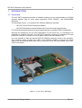
GR-TMTC Mezzanine
User Manual
GAISLER RESEARCH /
PENDER ELECTRONIC DESIGN
Rev. 0.1, 2007-10-07
GR-TMTC Mezzanine User Manual
2
Pender Electronic Design GmbH
[email protected]
GR-TMTC Mezzanine User Manual
Copyright © 2007 Gaisler Research / Pender Electronic Design GmbH
Permission is granted to make and distribute verbatim copies of this document provided the
copyright notice and this permission notice are preserved on all copies.
Third-party brands, names and trademarks are the property of their respective owners.
Pender Electronic Design GmbH
Rev. 0.1
GR-TMTC Mezzanine User Manual
3
TABLE OF CONTENTS
1
INTRODUCTION...........................................................................................................5
1.1
1.2
1.3
1.4
2
5
7
7
7
ELECTRICAL DESIGN.................................................................................................8
2.1
2.2
3
Overview......................................................................................................................
References...................................................................................................................
Handling.......................................................................................................................
Abbreviations...............................................................................................................
Block Diagram.............................................................................................................. 8
Configuration for FPGA VLDS signals....................................................................... 10
INTERFACES AND CONFIGURATION..................................................................... 11
3.1
3.2
List of Front Panel Connectors................................................................................... 11
List of Mezzanine Connectors.................................................................................... 17
Pender Electronic Design GmbH
Rev. 0.1
GR-TMTC Mezzanine User Manual
4
LIST OF TABLES
Table 3-1: List of Front Panel Connectors......................................................................................
Table 3-2: J1 DSU - Debug Support Unit connections ..................................................................
Table 3-3: J2 RJ45-ETHERNET Connector...................................................................................
Table 3-4: J3 FPGA – Programming Connector............................................................................
Table 3-5: SPW-0 : Spacewire interface connections ...................................................................
Table 3-6: SPW-1 : Spacewire interface connections ...................................................................
Table 3-7: TMTC : TMTC interface connections............................................................................
Table 3-8: TMTC-AUX : TMTC Auxilliary interface connections.....................................................
Table 3-9: List of Front Panel LED's and their driving signals........................................................
Table 3-10: List of Mezzanine Headers..........................................................................................
Table 3-11: JP1 - TMTC-Prime Header..........................................................................................
Table 3-12: JP2 - TMTC Aux I/O Header.......................................................................................
Table 3-13: JP3 - TMTC-Redundant Header ................................................................................
Table 3-14: JP4 – Auxilliary (Spare) Signal Header ......................................................................
Table 3-15: JP5 – GPIO Signal Header -1.....................................................................................
Table 3-16: JP6 – GPIO Signal Header -2.....................................................................................
Table 3-17: DIP Switch S1 definition..............................................................................................
Table 3-18: J5 : Spacewire interface connections .........................................................................
Table 3-19: J6 : Spacewire interface connections .........................................................................
Table 3-20: J12 : Spacewire interface connections .......................................................................
Table 3-21: J13 : Spacewire interface connections .......................................................................
11
12
12
12
13
13
14
15
15
17
18
18
18
18
19
19
19
20
20
20
20
LIST OF FIGURES
Figure
Figure
Figure
Figure
Figure
Figure
Figure
Figure
Figure
1-1: GR-TMTC Assembly...................................................................................................... 5
1-2: GR-TMTC Assembly mounted in Compact PCI rack..................................................... 6
2-1: Block Diagram of GR-TMTC assembly and harness...................................................... 8
2-2: GR-CPCI-XC4V board with GR-TMTC-FLEX Mezzanine and front-panel................... 10
3-1: Front Panel view (Pin1's marked with red circle).......................................................... 11
3-2: Assembly Photo Top view Oblique.............................................................................. 16
3-3: Assembly Photo Bottom view Oblique........................................................................ 16
3-4: Mezzanine Photo Top view ......................................................................................... 21
3-5: Mezzanine Photo Bottom view..................................................................................... 21
REVISION HISTORY
Revision
0.1
Date
Page
2006-09-07 All
Pender Electronic Design GmbH
Description
First issue
Rev. 0.1
GR-TMTC Mezzanine User Manual
1
5
INTRODUCTION
1.1 Overview
The GR-TMTC equipment provides a hardware platform for the implementation of LEON3
systems together with IP cores which implement TMTC (RS422) and SPACEWIRE
interfaces.
The assembly (Figure 1-1) consists of the following hardware elements:
•
GR-CPCI-XC4V FPGA Development Board
•
GR-TMTC Mezzanine Interface Board with Front Panel and wiring Harness
The FPGA development board must be programmed with an suitable FPGA configuration.
Although the equipment can be used 'stand-alone' on the bench top, it is intended to be
installed in a Compact PCI rack. The GR-TMTC assembly requires one Compact PCI back
plane slot. However, the width of the front panel requires two slot widths (8 TE).
It is also possible to add the optional GR-CPCI-RS232 accessory board to the assembly.
This accessory board provides two UART (serial RS232) interfaces connected by ribbon
cable to J4, and a Reset switch which can be connected to the JP5 reset header on the GRCPCI-XC4V board.
Figure 1-1: GR-TMTC Assembly
Pender Electronic Design GmbH
Rev. 0.1
GR-TMTC Mezzanine User Manual
6
Figure 1-2: GR-TMTC Assembly mounted in Compact PCI rack
The GR-TMTC mezzanine front panel provides circuits and connectors for:
•
serial Debug Support Unit interface (D9 Female connector)
•
Ethernet interface (RJ45 connector)
•
JTAG connector for FPGA programming
•
two LVDS (Spacewire type) electrical interfaces (Microminiature MDM9S connectors)
•
TMTC RS422 interfaces (HDD26 Male connector)
•
Auxilliary TMTC RS422 and TTL signals (0.1” Shrouded Headers)
•
power indicator (LED) and three user definable LED indicators
The GR-CPCI-RS232 front panel provides circuits and connectors for:
•
two serial RS232 interfaces (D9 Female connectors)
•
push button for system reset
To enable convenient connection to the interfaces, the connector types and pin-outs are
compatible with the standard connector types for these types of interfaces. The pin out
information is listed in section 3 of this document.
Pender Electronic Design GmbH
Rev. 0.1
GR-TMTC Mezzanine User Manual
7
1.2 References
More detailed information concerning the implementation and configuration of the elements
making up the GR-TMTC assembly is provided in the following documents:
RD-1
GR-CPCI-XC4V Leon Development Board Users Manual
RD-2
GR-CPCI-XC4V_schematic.pdf, Schematic
RD-3
GR-CPCI-XC4V_assy_drawing.pdf, Assembly Drawing
RD-4
GR-TMTC-MEZZ_schematic.pdf, Schematic
RD-5
GR-TMTC-MEZZ_assy_drawing.pdf, Assembly Drawing
RD-6
GR-TMTC-Harness_schematic.pdf, Schematic
1.3 Handling
ATTENTION : OBSERVE PRECAUTIONS FOR
HANDLING ELECTROSTATIC SENSITIVE DEVICES
This board contains sensitive electronic components which can be damaged by Electrostatic
Discharges (ESD). When handling or installing the board observe appropriate precautions
and ESD safe practices.
When not in use, store the board in an electrostatic protective container or bag.
When configuring the jumpers on the board, or connecting/disconnecting cables, ensure that
the board is in an unpowered state.
1.4 Abbreviations
ESD
FPGA
FT
GPIO
I/O
LVDS
PCB
SPW
Electro-Static Discharge
Field Programmable Gate Array
Fault-Tolerant
General Purpose Input / Output
Input/Output
Low Voltage Digital Signaling
Printed Circuit Board
Spacewire
Pender Electronic Design GmbH
Rev. 0.1
GR-TMTC Mezzanine User Manual
2
8
ELECTRICAL DESIGN
2.1 Block Diagram
The GR-TMTC assembly provides the electrical functions and interfaces as represented in
the block diagram, Figure 2-1.
GR-CPCI-XC4V
FPGA DEVELOPMENT BOARD
GR-CPCI-RS232
ACCESSORY BOARD
PIO
RS232
TRANSCEIVER
UART I/F
D9-F
D9-F
PIO
MEM_BUS
1M x 40 bit
SRAM
EXT_CLK
GR-TMTC
MEZZANINE BOARD
XTAL
GPIO
HEADER
SPW_0
SPW_2
LVDS TO/FROM FPGA
SPW_3
SPW I/F
MDM9-S MDM9-S
LVDS
DRIVER/
RECEIVERS
&
TERMINATION
SPW_1
FPGA
MDM9-S MDM9-S
GPIO
HEADER
LVDS TO/FROM FPGA
8
DIP SWITCH
RS422
DRIVERS
4
RS422
RECEIVERS
4
4
HDD26P
12
RS422
DIFFERENTIAL
4
PAIRS
12
1
1
0.1” SHROUDED
HEADER
3
3
12
LVTTL
SIGNALS
TMTC
I/F
TMTC
AUX
GR-TMTC-FRONT PANEL
Figure 2-1: Block Diagram of GR-TMTC assembly and harness
Pender Electronic Design GmbH
Rev. 0.1
GR-TMTC Mezzanine User Manual
9
As shown in the block diagram, the GR-TMTC Mezzanine contains the following circuits:
•
40Mbit (1MWord x 40 bit) SRAM memory (10ns)
•
8 pin DIL socket and SMA connector for user defined oscillator
•
Headers for 2 x 16 General Purpose I/O signals (LVTTL)
•
8 pole DIP Switch for general purpose use
•
Two sets of SPW signals: These signals are LVTTL input/ouputs to the FPGA and
are provided with driver/receiver IC's on the mezzanine to provide the level
conversion from single ended LVTTL to/from LVDS differential signals
•
Two sets of SPW signals: These signals are LVDS input/ouputs directly to the FPGA.
No driver/receiver circuits are required on the Mezzanine. However, the FPGA design
must be appropriately configured for LVDS levels and termination on these
inputs/outputs (more information in section 2.2).
•
RS422 differential drivers for 12 signal pairs
•
RS422 differential receivers for 12 signal pairs
•
12 single-ended LVTTL signals which can be defined as inputs or outputs
•
Wiring from two front panel MDM9S connectors
•
two 20 pin headers each providing an additional 16 general purpose LVTTL I/O
signals connected directyl to the FPGA
•
Wire and ribbon cable harness connecting from headers on mezzanine to connectors
on GR-TMTC Front Panel
Figure 2-2 shows the completed GR-TMTC assembly including the cabling and harness to
the front panel.
Pender Electronic Design GmbH
Rev. 0.1
GR-TMTC Mezzanine User Manual
10
Figure 2-2: GR-CPCI-XC4V board with GR-TMTC-FLEX Mezzanine and front-panel
2.2 Configuration for FPGA VLDS signals
In the GR-TMTC kit, for two of the SPW interfaces the LVDS receiver and transmitter pairs
are provided directly from LVDS pairs of the FPGA, and there are no discrete LVDS
receiver/transmitter devices on the mezzanine board. For these sets of signals.
This requires that the FPGA design must be appropriately configured for LVDS input/outputs
on the appropriate pins and that the FPGA bank voltage for the LVDS signals is set for 2.5V
(This is the default configuration for the GR-CPCI-XC4V board),
Also, the Virtex4 FPGA on the GR-CPCI-XC4V board provides the possiblity to provide 100
Ohm termination for the LVDS receiver pairs internally to the FPGA, eliminating the need to
provide termination on the mezzanine board itself. However, for this to operate, the following
resistors are require to be installed on the GR-CPCI-XC4V board: R112, (50Ohms) and
R137 (50 Ohms) which are not normally fitted in the default configuration for the GR-CPCIXC4V board.
Pender Electronic Design GmbH
Rev. 0.1
GR-TMTC Mezzanine User Manual
3
11
INTERFACES AND CONFIGURATION
3.1 List of Front Panel Connectors
Name
Function
Type
Description
J1
DSU
D9S
J2
ETHERNET
RJ45
Ethernet network connector
J3
JTAG-FPGA
2x7 pin shrouded 2mm header
FPGA configuration and programming
SPW-0
SPW-0
MDM9-S (female)
LVDS connections for Spacewire Interface-0
SPW-1
SPW-1
MDM9-S (female)
LVDS connections for Spacewire Interface-1
TMTC
TMTC
HDDP26
The connector pinning and naming for this
connector has been defined to be compoatible
with the
TMTCAUX
TMTC-AUX
26 pin shrouded 0.1” header
Table 3-1: List of Front Panel Connectors
Figure 3-1: Front Panel view (Pin1's marked with red circle)
Pender Electronic Design GmbH
Rev. 0.1
GR-TMTC Mezzanine User Manual
Pin
Name
12
Comment
1
No connect
6
2
No connect
DSU-TX
Transmit pin from DSU UART
7
3
No connect
DSU-RX
Receive pin to DSU UART
8
No connect
4
No connect
9
5
No connect
GND
Ground
Table 3-2: J1 DSU - Debug Support Unit connections
Pin
Name
Comment
1
TPFOP
Output +ve
2
TPFON
Output -ve
3
TPFIP
Input +ve
4
TPFOC
Output center-tap
5
No connect
6
TPFIN
7
TPFIC
Input -ve
Input Center-tap
8
No connect
Table 3-3: J2 RJ45-ETHERNET Connector
Pin
Name
Comment
1
DGND
Ground
VREF / VREF
3.3V
DGND
Ground
TMS / PROG
JTAG: TMS or Slave serial: PROG
DGND
Ground
TCK / CCLK
JTAG: TCK or Slave serial: CCLK
DGND
Ground
2
3
4
5
6
7
8
9
10
11
12
13
14
TDO / DONE
JTAG: TDO or Slave serial: DONE
DGND
Ground
TDI / DIN
JTAG: TDI or Slave serial: DIN
DGND
Ground
NC / NC
No connect
DGND
Ground
NC / INIT
JTAG: no connect or Slave serial: INIT
Table 3-4: J3 FPGA – Programming Connector
Pender Electronic Design GmbH
Rev. 0.1
GR-TMTC Mezzanine User Manual
13
Pin
Name
Comment
1
DIN0+
Data In +ve
DIN0-
Data In -ve
SIN0+
Strobe In +ve
7
SIN0-
Strobe In -ve
SHIELD
Inner Shield
8
SOUT0+
Strobe Out +ve
SOUT0-
Strobe Out -ve
DOUT0+
Data Out +ve
DOUT0-
Data Out -ve
6
2
3
4
9
5
Table 3-5: SPW-0 : Spacewire interface connections
Pin
Name
Comment
1
DIN1+
Data In +ve
DIN1-
Data In -ve
SIN1+
Strobe In +ve
SIN1-
Strobe In -ve
SHIELD
Inner Shield
SOUT1+
Strobe Out +ve
SOUT1-
Strobe Out -ve
DOUT1+
Data Out +ve
DOUT1-
Data Out -ve
6
2
7
3
8
4
9
5
Table 3-6: SPW-1 : Spacewire interface connections
Pender Electronic Design GmbH
Rev. 0.1
GR-TMTC Mezzanine User Manual
Pin
Name
10
1
Comment
N/C
Not connected
TC-CLK_N
TC Clock -ve
(RS422)
Prime
19 TC-CLK_N'
TC Clock -ve
(RS422)
Redundant
TM-CLK_N'
TM Clock -ve
TC-CLK_P
TC Clock +ve
(RS422)
Prime
20 TC-CLK_P'
TC Clock +ve
(RS422)
Redundant
TM-CLK_P'
TM Clock +ve
(RS422)
Redundant
TC-DATA_P
TC Data +ve
(RS422)
Prime
21 TC-DATA_P'
11
2
12
3
(RS422)
Redundant
TC Data +ve
(RS422)
Redundant
TM-CLK_P
TM Clock +ve
(RS422)
Prime
TC-DATA_N
TC Data -ve
(RS422)
Prime
22 TC-DATA_N'
TC Data -ve
(RS422)
Redundant
TM-CLK_N
TM Clock -ve
(RS422)
Prime
TC-Spare_P
TC Spare +ve
(RS422)
Prime
23 TC-Spare_N'
TC Spare -ve
(RS422)
Redundant
TM-DATA_N
TM Data -ve
(RS422)
Prime
TC-Spare_N
TC Spare -ve
(RS422)
Prime
24 TC-Spare_P'
TC Spare +ve
(RS422)
Redundant
TM-DATA_P
TM Data +ve
(RS422)
Prime
TC-Active_P
TC Active +ve
(RS422)
Prime
25 TC-Active_P'
TC Active +ve
(RS422)
Redundant
TM-Data_P'
TM Data +ve
(RS422)
Redundant
TC-Active_N
TC Active -ve
(RS422)
Prime
26 TC-Active_N'
TC Active -ve
(RS422)
Redundant
TM-Data_N'
TM Data -ve
(RS422)
Redundant
DGND
Ground
13
4
14
5
15
6
16
7
17
8
18
9
14
Table 3-7: TMTC : TMTC interface connections
Pender Electronic Design GmbH
Rev. 0.1
GR-TMTC Mezzanine User Manual
Pin
15
Name
Comment
1
CLCWIn_P0
CLCWIn0 +ve
(RS422)
2
CLCWIn_N0
CLCWIn0 -ve
(RS422)
3
CLCWIn_P1
CLCWIn1 +ve
(RS422)
4
CLCWIn_N1
CLCWIn1 -ve
(RS422)
5
CLCWOut_P0
CLCWOut0 +ve (RS422)
6
CLCWOut_N0
CLCWOut0 -ve
7
CLCWOut_P1
CLCWOut1 +ve (RS422)
8
CLCWOut_N1
CLCWOut1 -ve
(RS422)
(RS422)
9
CPDU_Clk
CPDU_Clk
(LVTTL)
10
CPDU_Data
CPDU_Data
(LVTTL)
11
CPDU_Arm
CPDU_Arm
(LVTTL)
12
CPDU_Strobe
CPDU_Strobe
(LVTTL)
13
TW_In_P
TW_In +ve
(RS422)
14
TW_In_N
TW_In -ve
(RS422)
15
TW_Out_P
TW_Out +ve
(RS422)
16
TW_Out_N
TW_Out -ve
(RS422)
17
Datation_0
Datation_0
(LVTTL)
18
Pulses_0
Pulses_0
(LVTTL)
19
Datation_1
Datation_1
(LVTTL)
20
Pulses_1
Pulses_1
(LVTTL)
21
Datation_2
Datation_2
(LVTTL)
22
Pulses_2
Pulses_2
(LVTTL)
23
Datation_3
Datation_3
(LVTTL)
24
Pulses_3
Pulses_3
(LVTTL)
25
DGND
DGND
26
+3.3V
+3.3V
Table 3-8: TMTC-AUX : TMTC Auxilliary interface connections
LED
FPGA
signal
FPGA Pin Comment
LED P
+3.3V
--
3.3V power present on board
LED 1
LED1
User definable LED – e..g connect to processor signal 'DSUACT'
LED 2
LED2
User definable LED – e..g connect to processor signal 'ERRORN'
LED 3
LED2
User definable LED – e..g connect to processor signal 'WATCHDOG'
Table 3-9: List of Front Panel LED's and their driving signals
Pender Electronic Design GmbH
Rev. 0.1
GR-TMTC Mezzanine User Manual
16
Figure 3-2: Assembly Photo Top view Oblique
Figure 3-3: Assembly Photo Bottom view Oblique
Pender Electronic Design GmbH
Rev. 0.1
GR-TMTC Mezzanine User Manual
17
3.2 List of Mezzanine Connectors
Figure 3-4 And Figure 3-5 show views of the Mezzanine board which is mounted to the GRCPCI-XC4V board. The following tables list
In the default configuration, only connectors JP1, JP2, J5 and J6 are connected to the front
panel. The connections from the mezzanine board to the front panel are described by the
schematic, RD-6.
The mezzanine board also provided a number of other headers which, if appropriate could
be used in other configurations to provide additional signal input/outputs
The following table list the headers and signals on the Mezzanine board.
In the tables, the name of the corresponding GENIO signal on the FPGA which drives the
function of the pin and its pin number are indicated in the tables. Note that signals which are
the negative pin of an differential pair driver/receiver are shown in brackets as they are
driven/receive the same effective signal as its corresponding positive pin of the pair.
In the event of discrepancies, please refer to the schematic drawings.
Name
Function
Type
Description
JP1
TMTC - Prime
2 row x 10 pin 0.1” Header RS422 TMTC signals (Prime set)
JP2
TMTC - AUX
2 row x 13 pin 0.1” Header Auxilliary RS422 and TTL signals
JP3
TMTC – Redun.
2 row x 10 pin 0.1” Header RS422 TMTC signals (Redundant set)
JP4
AUX
2 row x 2 pin 0.1” Header
JP5
GPIO Signal Header-1 2 row x 10 pin 0.1” Header General purpose TTL signals
JP6
GPIO Signal Header-2 2 row x 10 pin 0.1” Header General purpose TTL signals
JP7
RAMSN bank config.
2 row x 4 pin 0.1” Header
Jumpers to select RAM bank
JP8
RAMOEN bank config.
2 row x 4 pin 0.1” Header
Jumpers to select RAM bank
J5
SPW-0
MDM9S footprint
SPW interface with LVDS driver/receivers
J6
SPW-1
MDM9S footprint
SPW interface with LVDS driver/receivers
J12
SPW-2
MDM9S footprint
SPW interface direct to FPGA
J13
SPW-3
MDM9S footprint
SPW interface direct to FPGA
2 Auxilliary RS232 signals
Table 3-10: List of Mezzanine Headers
Pender Electronic Design GmbH
Rev. 0.1
GR-TMTC Mezzanine User Manual
FUNCTION
TC_Clk0_P
IN
18
FPGA
signal
FPGA
Pin
GENIO50
F28
CONNECTOR PIN
1
TC_Data0_P
IN
GENIO51
A26
3
TC_Active0_P
IN
GENIO52
G25
5
TC_Spare0_P
IN
GENIO53
E27
7
TM_Clk0_P
OUT
GENIO54
G26
9
TM_Data0_P
OUT
GENIO55
D27
11
TM_Spare1_P
OUT
GENIO57
D29
13
TM_Spare2_P
OUT
GENIO59
E29
15
n.c.
---
17
DGND
---
19
■□
□□
□□
□□
□□
□□
□□
□□
□□
□□
FPGA
Pin
2
FPGA
signal
FUNCTION
(GENIO50)
IN
TC_Clk0_N
4
(GENIO51)
IN
TC_Data0_N
6
(GENIO52)
IN
TC_Active0_N
TC_Spare0_N
8
(GENIO53)
IN
10
(GENIO54)
OUT
TM_Clk0_N
12
(GENIO55)
OUT
TM_Data0_N
14
(GENIO57)
OUT
TM_Spare1_N
16
(GENIO59)
OUT
TM_Spare2_N
18
---
n.c.
20
---
DGND
Table 3-11: JP1 - TMTC-Prime Header
FPGA
signal
FUNCTION
FPGA
Pin
CONNECTOR PIN
CLCWIn_P0
IN
GENIO28
L34
1
CLCWIn_P1
IN
GENIO29
M33
3
CLCWOut_P0
OUT
GENIO24
N34
5
CLCWOut_P1
OUT
GENIO25
P35
7
CPDU_Clk
BIDI
GENIO32
K33
9
CPDU_Arm
BIDI
GENIO35
U37
11
TW_In_P
IN
GENIO30
L33
13
TW_Out_P
OUT
GENIO26
M35
15
Datation_0
BIDI
GENIO139
AM5
17
Datation_1
BIDI
GENIO138
AN3
19
Datation_2
BIDI
GENIO137
AP4
21
Datation_3
BIDI
GENIO136
AN4
23
DGND
25
■□
□□
□□
□□
□□
□□
□□
□□
□□
□□
□□
□□
□□
FPGA
Pin
FPGA
signal
FUNCTION
2
(GENIO28)
IN
CLCWIn_N0
4
(GENIO29)
IN
CLCWIn_N1
6
(GENIO24)
OUT
CLCWOut_N0
8
(GENIO25)
OUT
CLCWOut_N1
10
GENIO33
BIDI
CPDU_Data
12
GENIO34
BIDI
CPDU_Strobe
14
(GENIO30)
IN
TW_In_N
16
(GENIO26)
OUT
TW_Out_N
18
GENIO135
BIDI
Pulses_0
20
GENIO134
BIDI
Pulses_1
22
GENIO133
BIDI
Pulses_2
24
GENIO132
BIDI
Pulses_3
26
+3.3V
Table 3-12: JP2 - TMTC Aux I/O Header
FUNCTION
TC_Clk0_P
IN
FPGA
signal
FPGA
Pin
GENIO47
N37
CONNECTOR PIN
1
TC_Data0_P
IN
GENIO46
J37
3
TC_Active0_P
IN
GENIO45
P37
5
TC_Spare0_P
IN
GENIO44
K36
7
TM_Clk0_P
OUT
GENIO43
P36
9
TM_Data0_P
OUT
GENIO42
L36
11
TM_Spare1_P
OUT
GENIO41
R37
13
TM_Spare2_P
OUT
GENIO40
M36
15
n.c.
---
17
DGND
---
19
■□
□□
□□
□□
□□
□□
□□
□□
□□
□□
FPGA
Pin
2
FPGA
signal
FUNCTION
(GENIO47)
IN
TC_Clk0_N
4
(GENIO46)
IN
TC_Data0_N
6
(GENIO45)
IN
TC_Active0_N
TC_Spare0_N
8
(GENIO44)
IN
10
(GENIO43)
OUT
TM_Clk0_N
12
(GENIO42)
OUT
TM_Data0_N
14
(GENIO41)
OUT
TM_Spare1_N
16
(GENIO40)
OUT
TM_Spare2_N
18
---
n.c.
20
---
DGND
Table 3-13: JP3 - TMTC-Redundant Header
FUNCTION
AUX_OUT_P
AUX_IN_P
OUT
IN
FPGA
signal
FPGA
Pin
GENIO27
N33
GENIO31
V37
CONNECTOR PIN
FPGA
Pin
FPGA
signal
FUNCTION
1
■□
2
(GENIO27)
OUT
3
□□
4
(GENIO31)
IN
AUX_OUT_N
AUX_IN_N
Table 3-14: JP4 – Auxilliary (Spare) Signal Header
Pender Electronic Design GmbH
Rev. 0.1
GR-TMTC Mezzanine User Manual
19
FUNCTION
FPGA
signal
FPGA
Pin
GPIO0
GENIO95
AD37
1
GPIO2
GENIO92
AL39
3
GPIO4
GENIO90
AM38
5
GPIO6
GENIO88
AM37
7
GPIO8
GENIO86
AC32
9
GPIO10
GENIO84
AB31
11
GPIO12
GENIO82
AB30
13
GPIO14
GENIO80
AC30
15
+3.3V
---
17
DGND
---
19
FPGA
Pin
FPGA
signal
FUNCTION
2
AL38
GENIO94
GPIO1
4
AC37
GENIO93
GPIO3
6
AD36
GENIO91
GPIO5
8
AD35
GENIO89
GPIO7
10
AF36
GENIO87
GPIO9
12
AE36
GENIO85
GPIO11
14
AG36
GENIO83
GPIO13
16
AG35
GENIO81
GPIO15
CONNECTOR PIN
■□
□□
□□
□□
□□
□□
□□
□□
□□
□□
18
---
+3.3V
20
---
DGND
Table 3-15: JP5 – GPIO Signal Header -1
FPGA
signal
FPGA
Pin
GPIO16
GENIO151
AM2
1
GPIO18
GENIO149
AP1
3
FUNCTION
FPGA
Pin
CONNECTOR PIN
GPIO20
GENIO147
AL5
5
GPIO22
GENIO145
AK6
7
GPIO24
GENIO143
AP2
9
GPIO26
GENIO141
AN2
11
GPIO28
GENIO131
AT3
13
GPIO30
GENIO129
AU3
15
+3.3V
---
17
DGND
---
19
■□
□□
□□
□□
□□
□□
□□
□□
□□
□□
FPGA
signal
FUNCTION
2
AG8
GENIO150
GPIO17
4
AK4
GENIO148
GPIO19
6
AL4
GENIO146
GPIO21
8
AM3
GENIO144
GPIO23
10
AL3
GENIO142
GPIO25
12
AL6
GENIO140
GPIO27
14
AR2
GENIO130
GPIO29
16
AR3
GENIO128
GPIO31
18
---
+3.3V
20
---
DGND
Table 3-16: JP6 – GPIO Signal Header -2
FUNCTION
FPGA signal
FPGA
PIN
OPEN
SWITCH
CLOSED
SWITCH0
GENIO159
AG7
'1'
1
'0'
SWITCH1
GENIO158
AK3
'1'
2
'0'
SWITCH2
GENIO157
AK1
'1'
3
'0'
SWITCH3
GENIO156
AH3
'1'
4
'0'
SWITCH4
GENIO155
AL1
'1'
5
'0'
SWITCH5
GENIO154
AH7
'1'
6
'0'
SWITCH6
GENIO153
AM1
'1'
7
'0'
SWITCH7
GENIO152
AK2
'1'
8
'0'
Table 3-17: DIP Switch S1 definition
1-2
RAM Bank 0
3-4
RAM Bank 1
5-6
RAM Bank 2
7-8
RAM Bank 3
Jumpers JP7 & JP8: RAM Bank selection
(Both jumpers must be set the same)
Pender Electronic Design GmbH
Rev. 0.1
GR-TMTC Mezzanine User Manual
20
Pin
Name
FPGA Signal
FPGA Pin
Comment
1
DIN0+
GENIO110
AF38
Data In +ve
DIN0-
(GENIO110)
SIN0+
GENIO111
SIN0-
(GENIO111)
6
2
7
3
Data In -ve
AG37
SHIELD
Inner Shield
8
SOUT0+
GENIO109
SOUT0-
(GENIO109)
9
DOUT0+
GENIO108
DOUT0-
(GENIO108)
4
5
Strobe In +ve
Strobe In -ve
AG38
Strobe Out +ve
AF39
Data Out +ve
Strobe Out -ve
Data Out -ve
Table 3-18: J5 : Spacewire interface connections
Pin
Name
FPGA Signal
FPGA Pin
Comment
1
DIN1+
GENIO106
AH39
Data In +ve
DIN1-
(GENIO106)
SIN1+
GENIO107
AB28
Strobe In +ve
SIN1-
(GENIO107)
6
2
7
3
Data In -ve
Strobe In -ve
SHIELD
8
4
9
5
Inner Shield
SOUT1+
GENIO105
SOUT1-
(GENIO105)
DOUT1+
GENIO104
DOUT1-
(GENIO104)
AB27
Strobe Out +ve
Strobe Out -ve
AJ39
Data Out +ve
Data Out -ve
Table 3-19: J6 : Spacewire interface connections
Pin
Name
FPGA Signal
FPGA Pin
Comment
1
DIN2+
GENIO126
AA34
Data In +ve
DIN2-
GENIO124
AA35
Data In -ve
SIN2+
GENIO127
AA31
Strobe In +ve
SIN2-
GENIO125
Y31
6
2
7
3
SHIELD
8
4
9
5
Strobe In -ve
Inner Shield
SOUT2+
GENIO120
AC35
Strobe Out +ve
SOUT2-
GENIO122
AB35
Strobe Out -ve
DOUT2+
GENIO121
Y29
Data Out +ve
DOUT2-
GENIO123
AA30
Data Out -ve
Table 3-20: J12 : Spacewire interface connections
Pin
1
6
2
7
3
FPGA Signal
FPGA Pin
Comment
Data In +ve
DIN3+
GENIO118
AC38
DIN3-
GENIO116
AC39
Data In -ve
SIN3+
GENIO119
AE34
Strobe In +ve
SIN3-
GENIO117
AD34
Strobe In -ve
SOUT3+
GENIO112
AE39
Strobe Out +ve
SOUT3-
GENIO114
AD39
Strobe Out -ve
DOUT3+
GENIO113
AD31
Data Out +ve
DOUT3-
GENIO115
AD32
Data Out -ve
SHIELD
8
4
9
5
Name
Inner Shield
Table 3-21: J13 : Spacewire interface connections
Pender Electronic Design GmbH
Rev. 0.1
GR-TMTC Mezzanine User Manual
21
Figure 3-4: Mezzanine Photo Top view
Figure 3-5: Mezzanine Photo Bottom view
Pender Electronic Design GmbH
Rev. 0.1