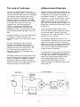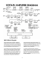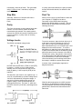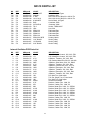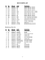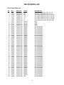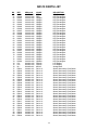
1
MODEL SR510
LOCK-IN AMPLIFIER
1290-D Reamwood Avenue
Sunnyvale, CA 94089 U.S.A.
Phone: (408) 744-9040 • Fax: (408) 744-9049
Email: [email protected] • www.thinkSRS.com
Copyright © 1985, 1987, 1989, 2003, 2013
Stanford Research Systems, Inc.
All Rights Reserved
Revision: 3.4 (11/2013)
TABLE OF CONTENTS
Condensed Information
SAFETY and Preparation for use
Symbols
Specifications
Front Panel Summary
Abridged Command List
Status Byte Definition
Configuration Switches
Guide to Operation
Front Panel
Signal Inputs
Signal Filters
Sensitivity
Dynamic Reserve
Status Indicators
Display Select
Output
Expand Function
Rel Function
Offset
Time Constants
Noise Measurements
Reference Input and Trigger Levels
Phase Controls
Power Switch
Local/Remote Operation
Default Settings
1
2
3
5
6
7
7
8
8
8
8
9
9
9
9
9
9
10
10
10
11
11
12
12
12
Rear Panel
AC Power
GPIB (IEEE-488) Connector
RS232 Interface
Signal Monitor Output
Pre-Amp Connector
A/D Inputs and D/A Outputs
Ratio Feature
Internal Oscillator
13
13
13
13
13
13
13
13
13
Guide to Programming
Communications
Command Syntax
Status LED's
RS232 Echo Feature
Try-out with an ASCII Terminal
15
15
15
16
16
Command List
Status Byte
Errors
Reset Command
Trouble-Shooting Interface Problems
Common Hardware Problems
Common Software Problems
17
20
20
20
21
21
21
i
RS232 Interface
Introduction to the RS232
Data Communications Equipment
Wait Command
Termination Sequence
21
22
22
22
GPIB (IEEE-488) Interface
Introduction to the GPIB
GPIB Capabilities
Response to Special GPIB commands
Serial Polls and SRQ's
Echo Mode using the RS232
Using Both the RS232 & GPIB
22
22
22
23
23
23
Lock-in Technique
Introduction to Lock-in Amplifiers
Measurement Example
Understanding the Specifications
Shielding and Ground Loops
Dynamic Reserve
Current Input
Auto-Tracking Bandpass Filter
Notch Filters
Frequency Range
Noise Measurements
Output Filters
Ratio Capability
Computer Interface
Internal Oscillator
24
24
25
25
26
26
26
27
27
27
27
27
27
27
SR510 Block Diagram
Block Diagram
Signal Channel
Reference Channel
Phase-Sensitive Detector
DC Amplifier and System Gain
Microprocessor System
28
29
29
29
29
29
Circuit Description
Introduction
Signal Amplifier
Current Amplifier
Notch Filters
Bandpass Filter
Reference Oscillator
PSD, LP Filters and DC Amplifier
Analog Output
A/D's
D/A's
Expand
Front Panel
Microprocessor Control
30
30
30
30
30
31
31
31
31
32
32
32
32
RS232 Interface
GPIB Interface
Power Supplies
Internal Oscillator
32
32
33
33
Calibration and Repair
Introduction
Multiplier Adjustments
Amplifier and Filter Adjustments
CMRR Adjustment
Line Notch Filter Adjustment
2xLine Notch Filter Adjustment
Repairing Damaged Front-End
34
34
34
34
35
35
35
Appendix A: Noise Sources and Cures
Johnson Noise
'1/f' Noise
Noise Spectrum
Capacitive Coupling
Inductive Coupling
Ground Loops
Microphonics
Thermocouple Effect
36
36
36
37
37
38
38
38
Appendix B: RS232
Simplest Case Using the RS232
Using Control Lines
Baud Rates
Stop Bits
Parity
Voltage Levels
'Eavesdropping'
39
39
39
40
40
40
40
ii
Appendix C: GPIB
Introduction to the GPIB
Bus Description
41
41
Appendix D: Program Examples
IBM PC, Microsoft Basic, via RS232
IBM PC, Microsoft Fortran, via RS232
IBM PC, Microsoft C, via RS232
IBM PC, Microsoft Basic, via GPIB
HP-85, HP Basic, via HPIB
42
43
45
47
49
Documentation
Part Numbering and Locations
Parts List, Main Assembly
Parts List, Internal Oscillator
Parts List, Miscellaneous
Parts List, Front Panel
Schematic Diagrams
50
51
65
66
67
71
Safety and Preparation for Use
***CAUTION***: This instrument may be damaged if operated with the LINE VOLTAGE SELECTOR set for
the wrong applied ac input-source voltage or if the wrong fuse is installed.
LINE VOLTAGE SELECTION
OPERATE WITH COVERS IN
PLACE
The SR510 operates from a 100V, 120V, 220V, or
240V nominal ac power source having a line
frequency of 50 or 60 Hz. Before connecting the
power cord to a power source, verify that the LINE
VOLTAGE SELECTOR card, located in the rear
panel fuse holder, is set so that the correct ac input
voltage value is visible.
To avoid personal injury, do not remove the
product covers or panels. Do not operate the
product without all covers and panels in place.
WARNING REGARDING USE
WITH PHOTOMULTIPLIERS
Conversion to other ac input voltages requires a
change in the fuse holder voltage card position and
fuse value. Disconnect the power cord, open the
fuse holder cover door and rotate the fuse-pull lever
to remove the fuse. Remove the small printed circuit
board and select the operating voltage by orienting
the printed circuit board to position the desired
voltage to be visible when pushed firmly into its slot.
Rotate the fuse-pull lever back into its normal
position and insert the correct fuse into the fuse
holder.
It is relatively easy to damage the signal inputs if
a photomultiplier is used improperly with the
lock-in amplifier. When left completely
unterminated, a PMT will charge a cable to a
few hundred volts in a very short time. If this
cable is connected to the lockin, the stored
charge may damage the front-end transistors.
To avoid this problem, provide a leakage path of
about 100 KΩ to ground inside the base of the
PMT to prevent charge accumulation.
LINE FUSE
Verify that the correct line fuse is installed before
connecting the line cord. For 100V and 120V, use a
1 Amp fuse and for 220V and 240V, use a 1/2 Amp
fuse.
LINE CORD
This instrument has a detachable, three-wire power
cord with a three-contact plug for connection to both
the power source and protective ground. The
protective ground contact connects to the accessible
metal parts of the instrument. To prevent electrical
shock, always use a power source outlet that has a
properly grounded protective-ground contact.
1
2
SR510 Specification Summary
General
Power
Mechanical
Warranty
100, 120, 220, 240 VAC (50/60 Hz); 35 Watts Max
17" x 17" x 3.5" (Rack Mount Included) 12 lbs.
Two years parts and labor.
Signal Channel
Inputs
Voltage:
Current:
Single-ended or True Differential
106 Volts/Amp
Impedance
Voltage:
100 MΩ + 25 pF, ac coupled
Full Scale
Current:
Voltage:
1 kΩ to virtual ground
100 nV (10 nV on expand) to 500 mV
Current:
Voltage:
100 fA to 0.5 µA
100 VDC, 10 VAC damage threshold
2 VAC peak-to-peak saturation
Current:
10 µA damage threshold
Sensitivity
Maximum
Inputs
1 µA ac peak-to-peak saturation
Noise
Voltage:
Common Mode
Current:
Range:
Gain Accuracy
Gain Stability
Signal Filters
Dynamic Reserve
7 nV/√Hz at 1 kHz
0.13 pA/√Hz at 1 kHz
1 Volt peak; Rejection: 100 dB dc to 1KHz
Above 1KHz the CMRR degrades by 6 dB/Octave
1% (2 Hz to 100KHz)
200 ppm/°C
60 Hz notch, -50 dB (Q=10, adjustable from 45 to 65 Hz)
120 Hz notch, -50 dB (Q=10, adjustable from 100 to 130 Hz))
Tracking bandpass set to within 1% of ref freq (Q=5)
20 dB LOW (1 µV to 500 mV sensitivity)
40 dB NORM (100 nV to 50 mV sensitivity)
60 dB HIGH (100 nV to 5 mV sensitivity)
Bandpass filter adds 20 dB to dynamic reserve
Line Notch filters increase dynamic reserve to 100 dB
Reference Channel
Frequency
0.5 Hz to 100 kHz
Input Impedance
Trigger
1 MΩ, ac coupled
SINE:
100 mV minimum, 1Vrms nominal
Mode
PULSE:
±1 Volt, 1 µsec minimum width
Fundamental (f) or 2nd Harmonic (2f)
3
Acquisition Time
Slew Rate
Phase Control
Phase Noise
Phase Drift
Phase Error
25 Sec at 1 Hz
6 Sec at 10 Hz
2 Sec at 10 kHz
1 decade per 10 S at 1 kHz
90° shifts
Fine shifts in 0.025° steps
0.01° rms at 1 kHz, 100 msec, 12 dB TC
0.1°/°C
Less than 1° above 10Hz
Demodulator
Stability
Time Constants
Offset
Harmonic Rej
5 ppm/°C on LOW dynamic reserve
50 ppm/°C on NORM dynamic reserve
500 ppm/°C on HIGH dynamic reserve
Pre:
1msec to 100 sec (6 dB/Octave)
Post: 1sec, 0.1 sec, none (6 dB/Octave) or none
Up to 1X full scale (10X on expand)
-55 dB (bandpass filter in)
Outputs & Interfaces
Outputs
Output Meter
Output LCD
Output BNC
Reference LCD
RS232
GPIB
A/D
D/A
Ratio
Internal Oscillator
X (RcosØ), X Offset, Noise
2% Precision mirrored analog meter
Four digit auto-ranging LCD display shows same values as the analog meters
±10 V output corresponds to full scale input
<1Ω output impedance
Four digit LCD display for reference phase shift or frequency
Interface controls all functions. Baud rates from 300 to 19.2 K
Interface controls all functions. (IEEE-488 Std)
4 BNC inputs with 13 bit resolution (±10.24 V)
2 BNC outputs with 13 bit resolution (±10.24 V)
Ratio output equals 10X output divided by the Denominator input.
Range:
1 Hz to 100 kHz, 1% accuracy
Stability:
150 ppm/°C
Distortion: 2% THD
Amplitude: 1% accuracy, 500 ppm/°C stability
4
Front Panel Summary
Signal Inputs
Single Ended (A), True Differential (A-B), or Current (I)
Signal Filters
Bandpass:
Q-of-5 Auto-tracking filter (In or Out)
Line Notch:
Q-of-10 Notch Filter at line frequency (In or Out)
2XLine Notch: Q-of-10 Notch Filter at twice line frequency (In or Out)
Sensitivity
Full scale sensitivity from 100 nV to 500 mV RMS for voltage inputs
or from 100 fA to 500 nA RMS for current inputs.
Dynamic Reserve
Select Dynamic Reserve
LOW
20 dB
NORM
40 dB
HIGH
60 dB
Status Indicators
OVLD
UNLK
ERR
ACT
REM
Display Select
X
Signal Amplitude at the selected phase (AcosØ)
OFST Display the offset which is being added to the signal output
NOISE Compute and display the noise on the signal
Analog Meters
Displays Signal, Offset, or Noise as a fraction of full scale
Output LCD's
Displays Signal, Offset, or Noise in absolute units
Output BNC's
Output follows Analog Meter, ± 10 V for ± full scale
Expand
Multiplies the Analog Meter and Output voltage by a factor X1 or X10.
REL
Set the Offset to null the output: subsequent readings are relative readings.
Offset
Enables or Disables Offset, and allows any offset (up to full scale) to be entered.
Time Constants
Pre-filter has time constants from 1 mS to 100 S (6 dB/Octave)
Post-filter has time constants of 0, 0.1 or 1.0 S (6 dB/Octave)
ENBW
Equivalent Noise Bandwidth. Specifies the bandwidth when making Noise
measurements. (1Hz or 10 Hz ENBW)
Reference Input
1 MΩ Input, 0.5 Hz to 100 KHz, 100 mV minimum
Stability
5 ppm
50 ppm
500 ppm
Sensitivity Ranges
1 µV to 500 mV
100 nV to 50 mV
100 nV to 5 mV
Signal Overload
PLL is not locked to the reference input
Illegal or Unrecognized command
RS232 or GPIB interface Activity
Remote mode: front panel has been locked-out
Reference Trigger Trigger on rising edge, zero crossing, or falling edge
f/2f Mode
PLL can lock to either X1 or X2 of the reference input frequency
Phase Controls
Adjust phase in smoothly accelerating 0.025° steps, or by
90° steps. Press both 90° buttons to zero the phase.
Reference LCD
Display reference phase setting or reference frequency
Power Switch
Instrument settings from the last use are recalled on power-up
5
Abridged Command List
A
A0
A1
Return the ‘REL’ Status
Turn the ‘REL’ off
Turn the ‘REL’ on
B
B0
B1
Return Bandpass Filter Status
Take out the Bandpass Filter
Put in the Bandpass Filter
C
C0
C1
Return the Reference LCD Status
Display the Reference Frequency
Display the Reference Phase Shift
D
D0
D1
D2
Return Dynamic Reserve Setting
Set DR to LOW range
Set DR to NORM range
Set DR to HIGH range
En
En,0
En,1
Return Expand Status
Turn Expand off
Turn Expand on
F
Return the Reference Frequency
G
G1
...
G24
Return the Sensitivity Setting
Select 10 nV Full-Scale
(G1-G3 with SRS preamp only)
Select 500 mV Full-Scale
H
N
N0
N1
Return the ENBW setting
Select 1 Hz ENBW
Select 10 Hz ENBW
O
O0
O1,v
Return Offset Status
Turn off Offset
Turn on Offset, v = offset
P
Pv
Return the Phase Setting
Set the Phase to v. Abs(v) < 999 deg
Q
Return the value shown on the Output
LCD
R
R0
R1
R2
Return the trigger mode
Set the trigger for rising edge
Set the trigger for + zero crossing
Set the trigger for falling edge
S
S0
S1
S2
Return the display status
Display X = AcosØ
Display Offset setting
Display Noise
Return pre-filter setting
Set the pre-filter TC to 1 mS
Return Preamp Status (1=installed)
T1
T1,1
...
T1,11
I
I0
I1
I2
Return the Remote/Local Status
Select Local: Front panel active
Select Remote: Front panel inactive
Select Remote with full lock-out
T2
T2,0
T2,1
T2,2
Return the post-filter setting
Remove post filter
Set the post filter TC to 0.1 S
Set the post filter TC to 1.0 S
J
Jn,m,o,p
Set RS232 End-of-Record to <cr>
Set End-of-record to n,m,o,p
V
Vn
Return the value of the SRQ mask
Set the SRQ Mask to the value n
(See the Status Byte definition)
K1
...
K32
Simulates Key-press of button #1
(see un-abridged command list)
Simulates Key-press of button #32
W
Wn
Return the RS232 wait interval
Set RS232 wait interval to nX4mS
L1
L1,0
L1,1
Return Status of Line Notch Filter
Remove Line Notch Filter
Insert Line Notch Filter
Xn
Return the voltage at the rear panel
analog port n. (n from 1 to 6)
L2
L2,0
L2,1
Return Status of 2XLine Filter
Remove 2XLine Notch Filter
Insert 2XLine Notch Filter
X5,v
X6,v
Set analog port 5 to voltage v
Set analog port 6 to voltage v
Y
Yn
Return the Status Byte value
Test bit n of the Status Byte
M
M0
M1
Return the f/2f Status
Set reference mode to f
Set reference mode to 2f
Z
Reset to default settings and cancel
all pending command
6
Set the pre-filter TC to 100 S
Status Byte Definition
Bit Meaning
0 Magnitude too small to calculate
phase
1 Command Parameter is out-of-range
2 No detectable reference input
3 PLL is not locked to the reference
4 Signal Overload
5 Auto-offset failed: signal too large
6 SRQ generated
7 Unrecognized or illegal command
Configuration Switches
There are two banks of 8 switches, SW1 and
SW2, located on the rear panel. SW1 sets the
GPIB address and SW2 sets the RS232
parameters. The configuration switches are read
continuously and any changes will be effective
immediately.
SW2:RS232 Mode Switches
SW1:GPIB Mode Switches
Bit Example
Function
1}
2}
3}
4}
5}
up
up
up
down
up
GPIB Address Switches
Address 0 to 30 allowed
'up' for bit = 1
'down' for bit = 0
(Most Significant Bit)
6
down
'down' to echo on RS232
(normally 'up')
7
8
up
up
Not Used
Not Used
If the GPIB mode switches are set as shown in the
example column above, then the lockin will be
addressed as GPIB device #23, and all GPIB
commands and data will be echoed over the
RS232 for de-bugging purposes.
Bit 1
Bit 2
Bit 3
Baud Rate
up
down
up
down
up
down
up
up
up
down
down
up
up
down
up
up
up
up
down
down
down
19200
9600
4800
2400
1200
600
300
Bit
Setting
Explanation
4
up
down
Odd parity
Even parity
5
up
down
No parity
Parity enabled
6
up
down
No echo (for computer)
Echo mode (for terminal)
7
up
down
Two stop bits
One stop bit
8
unused
Eight data bits are always sent, regardless of the
parity setting. The most significant bit is always
zero.
Example: Bit 1 'down' and all others 'up' for
RS232 communication at 9600 baud, no parity,
two stop bits, and no echo or prompts by the
SR510.
7
allowable signals at the inputs. The notch
frequencies are set at the factory to either 50 Hz
or 60 Hz. The user can adjust these frequencies.
(See the Maintenance and Repair section for
alignment details.) These filters precede the
bandpass filter in the signal amplifier.
SR510 Guide to Operation
Front Panel
The front panel has been designed to be almost
self-explanatory. The effect of each keypress is
usually reflected in the change of a nearby LED
indicator or by a change in the quantity shown on
a digital display. This discussion explains each
section of the front panel, proceeding left to right.
The bandpass filter has a Q of 5 and a 6 dB roll off
in either direction. Thus, the pass band (between
70% pass points) is always equal to 1/5th of the
center frequency. The center frequency is
continually adjusted to be equal to the internal
demodulator frequency. When the reference
mode is f, the filter tracks the reference. When the
mode is 2f, the filter frequency is twice the
reference input frequency. The center frequency
tracks as fast as the reference oscillator can slew
and may be used during frequency scans. The
bandpass filter adds up to 20 dB of dynamic
reserve for noise signals outside the pass band,
and increases the harmonic rejection by at least
13dB. (2nd harmonic attenuated by 13 dB, higher
harmonics attenuated 6dB/octave more.) If not
needed to improve the dynamic reserve or the
harmonic rejection then the filter should be left
OUT.
Signal Inputs
There are three input connectors located in the
SIGNAL INPUT section of the front panel. The
rocker switch located above the B input selects
the input mode, either single-ended, A, differential,
A-B, or current, I.
The A and B inputs are voltage inputs with 100
MΩ, 25 pF input impedance. Their connector
shields are isolated from the chassis ground by
10Ω. These inputs are protected to 100V dc but
the ac input should never exceed 10V peak. The
maximum ac input before overload is 1V peak.
Sensitivity
The I input is a current input with an input
impedance of 1 KΩ to a virtual ground. The
largest allowable dc current before overload is 1
µA. No current larger than 10 mA should ever be
applied to this input. The conversion ratio is 106
V/A, thus, the full scale current sensitivities range
from 100 fA to 500 nA with a max ac input before
overload of 1 µA peak. You should use short
cables when using the current input.
The sensitivity is displayed as a value (1-500) and
a scale (nV, µV, mV). When using the current
input, which has a gain of 106 V/A, these scales
read fA, pA, and nA. The two keys in the
SENSITIVITY section move the sensitivity up and
down. If either key is held down, the sensitivity will
continue to change in the desired direction four
times a second.
Signal Filters
The full scale sensitivity can range from 100 nV to
500 mV. The sensitivity indication is not changed
by the EXPAND function. The EXPAND function
increases the output sensitivity (Volts out /volts in)
as well as the resolution of the digital output
display.
There are three user selectable signal filters
available; a line frequency notch, a 2X line
frequency notch, and an auto-tracking bandpass.
Each of the filters has a pair of indicator LED's and
a function key located in the SIGNAL FILTERS
section of the front panel. Pressing a key will
toggle the status of the appropriate filter. The
status of each filter is displayed as IN, filter active,
or OUT, filter inactive.
Not all dynamic reserves are available at all
sensitivities. If the sensitivity is changed to a
setting for which the dynamic reserve is not
allowed, the dynamic reserve will change to the
next setting which is allowed. Sensitivity takes
precedence over the dynamic reserve. The
sensitivity range of each dynamic reserve is
shown below.
The notch filters have a Q of 10 and a depth of at
least 50 dB. Thus, the line frequency notch is 6
Hz wide and the 2X line notch has a width of 12
Hz. Both of these filters can increase the dynamic
reserve up to 50 dB at the notch frequencies. The
achievable reserve is limited by the maximum
8
Dynamic Reserve
Sensitivity Range
LOW
NORM
HIGH
1 µV through 500 mV
100 nV through 50 mV
100 nV through 5 mV
REM indicates that the unit is in the remote state
and that the front panel controls are not operative.
There are two remote states. The Remote-WithLockout will not allow any inputs from the front
panel. The Remote-Without-Lockout command
allows you to return the front panel to operation by
pressing the DISPLAY UP key.
Dynamic Reserve
Diplay Select
The dynamic reserve (DR) is set using the keys in
the DYNAMIC RESERVE section. The reserve is
displayed by the three indicator LED's, HIGH,
NORM, LOW. Only those dynamic reserve
settings available for the sensitivity are allowed
(see above table). For example, when the
sensitivity is 500 mV, the DR will always be LOW.
The keys in the DISPLAY section select the
parameter to be displayed on the output meters
and the output on the OUTPUT BNC connector.
The displayed parameter is indicated by one of the
three LED’s and can be either the demodulator
output (X), the offset (OFST), or the rms noise
(NOISE). When displaying NOISE, the equivalent
noise bandwidth (ENBW) is selected in the TIME
CONSTANT section.
The dynamic reserve and output stability of each
setting are shown below.
Setting
LOW
NORM
HIGH
Dynamic Reserve
20 dB
40 dB
60 dB
Output Stability
(ppm/°C)
5
50
500
Output
Since a higher DR results in degraded output
stability, you should use the lowest DR setting for
which there is no overload indication. Note that
using the Bandpass Filter provides about 20dB of
additional DR and so allows you to operate with a
lower DR setting.
The analog output is available at the OUTPUT
BNC. The input signal equal to the selected full
scale sensitivity will generate a ±10V output when
the EXPAND function is off. With the EXPAND on,
the output is multiplied by 10, effectively
increasing the full scale sensitivity by 10. The
ouptut impedance is <1Ω and the output current is
limited to 20 mA.
Status
The analog meter always displays the OUTPUT
voltage. Accuracy is 2% of full scale.
There are five STATUS LED's.
The OUTPUT LCD display provides a read-out of
the displayed parameter in real units. The scale of
the displayed quantity is indicated by the three
scale LED's to the right of the display. This readout auto ranges and will reflect the sensitivity
added when the EXPAND function is on.
OVLD indicates a signal overload. This condition
can occur when the signal is too large, the
sensitivity is too high, the dynamic reserve is too
low, the offset is on, the expand is on, the time
constant is not large enough, or the ENBW is too
large.
Expand
UNLK indicates that the reference oscillator is not
phase locked to the external reference input. This
can occur if the reference amplitude is too low, the
frequency is out of range, or the trigger mode is
incorrect for the reference signal waveform.
The output EXPAND is toggled by pressing the
key in the EXPAND section. The expand status is
indicated by the X10, expand on, and the X1,
expand off, LED's.
REL Function
ERR flashes when an error occurs on one of the
computer interfaces, such as an incorrect
command, invalid parameter, etc.
The relative (auto-zero) function is toggled by the
key in the REL section. Every time the rel status
LED is turned ON the offset value is set to minus
the value of the X output, thus zeroing the X
output. This function will work even if X is not the
ACT indicates activity on the computer interfaces.
This LED blinks every time a character is received
by the SR510 or transmitted by the SR510.
9
currently displayed parameter. If the output is
greater than 1.024 times full scale, the REL
function will not be able to zero the output and the
ON LED will blink. The offset value will then be set
to its max value. If NOISE is being displayed when
the REL function is turned on, the noise ouptut will
require a sew seconds to settle again.
Vout = 10Ae(AvVicosØ+Vos)
where...
Ae = 1 or 10 per the Expand setting
Av = 1/Sensitivity
Vi = magnitude of the signal
Ø = phase between signal & reference
Vos = offset (fraction of FS < 1.024)
If the manual OFFSET in ON when the REL
function is turned on, the manual OFFSET will be
turned OFF before the auto zero is done.
The REL function and the manual OFFSET are
both ways to enter the offset value. When the REL
function is turned off using the REL key the offset
is turned off but the value is not lost. If the manual
OFFSET is now turned ON, the offset will be that
set by the REL function.
Time Constant
There are two post demodulator low pass filters,
labeled PRE and POST. The PRE filter precedes
the POST filter in the output amplifier. Each filter
provides 6 dB/oct attenuation.
Offset
The PRE filter time constant ranges from 1 mS to
100 S and is selected by the two keys below the
PRE filter indicator LED's. Holding down either
key will advance the time constant twice a second
in the desired direction.
The OFFSET section controls the manual
OFFSET. The offset is turned ON and OFF using
the upper key in the OFFSET section. When the
offset is ON, the lower two keys are used to set
the amount of offset. A single key press will
advance the offset by 0.025% of full scale. If the
key is held down, the offset advances in larger and
larger increments, the largest increment being
10% of full scale. When the offset is turned OFF
the applied offset returns to zero but the offset
value is not lost. The next press of the upper
offset key (returns to ON) sets the offset to the
previously entered value.
The POST filter time constant can be set to 1 S or
0.1 S, or can be removed altogether, NONE, using
the two keys below the ENBW indicators. When
set to NONE, the total attenuation is that of the
PRE filter, or 6 dB/oct. When the POST filter is 1
S or 0.1S, the total attenuation is 12 dB/oct for
frequency components beyond the larger of the
POST and PRE filter bandwidths (reciprocal time
constant).
If an attempt is made to advance the offset value
beyond full scale, the OFFSET ON LED will blink.
An offset up to 1.024 times the full scale sensitivity
may be entered. When the expand is on, this is
10X the full scale output.
Noise
When the DISPLAY is set to NOISE, none of the
PRE and POST indicator LED's are on. Instead,
one of the two ENBW indicators will be on,
showing the Equivalent Noise Bandwidth of the
rms noise calculation. The ENBW is set using the
keys below the ENBW indicator LED's (same keys
as used to set the POST filter). The PRE filter
keys do nothing in this case. Pressing the upper
key when the bandwidth is already 1 Hz will reset
the rms noise average (output) to zero, restarting
the calculation. Likewise with pressing the lower
key when 10 Hz is already selected.
If the REL function is ON when the manual
OFFSET is turned ON, the REL function is turned
OFF but the offset value remains the same. The
OFFSET keys may now be used to adjust this
offset value.
Note that the offsets (either manual offset or those
generated by the REL function) represent a
fraction of the full scale reading, and so their
absolute value will change when the sensitivity
scale is changed. A signal which has been nulled
by an offset will not be nulled when the sensitivity
scale is changed. The analog meter and the
output BNC indicate the same value given by the
equation:
The noise is the rms deviation of the output within
a 1 or 10 Hz equivalent noise bandwidth about the
reference frequency. A dc output does not
contribute to the noise, the noise is determined
10
only by the ac 'wiggles' at the output. By
measuring the noise at different frequencies, the
frequency dependence of the noise density can be
found. This usually has the form of vnoise ~ 1/f.
The noise computation assumes that the noise
has a Gaussian distribution (such as Johnson
noise). Since the computation takes many time
constants (reciprocal bandwidth), the noise output
should be allowed to approach a steady value
before a reading is taken. For the 1 Hz ENBW,
this time is on the order of 15 to 30 seconds; for
the 10 Hz ENBW, the output stabilizes much
faster. The noise output will vary slightly since
there will always be noise variations that are slow
compared to the bandwidth. Any DC component
in the output will not contribute to the noise.
However, a large DC output will cause the noise
computation to initially rise to a large value before
approaching the final answer. As a result, the
computation will take longer to settle.
If the upper TRIGGER MODE LED is on, the
mode is POSITIVE. The trigger threshold is +1V
and the reference oscillator will lock to the positive
going transitions of the reference input. This
mode triggers on the rising edges of a TTL type
pulse train. The pulse width must be greater than
1 µS.
If the lower TRIGGER MODE LED is on, the mode
is NEGATIVE. The trigger threshold is -1V and
the reference oscillator will lock to the negative
going transitions of the reference input. This
mode triggers on a negative pulse train or on the
falling edges of a TTL type pulse train
(remembering that the input is ac coupled). The
pulse width must be greater than 1 µS.
Above the TRIGGER MODE indicators are the
REFERENCE MODE LED's. The key below the
REFERENCE MODE indicators toggles between f
and 2f. When the MODE is f, the lock-in will
detect signals at the reference input frequency.
When the MODE is 2f, the lock-in detects signals
at twice the reference input frequency. In either
case, the reference oscillator has a maximum
frequency of 100 KHz, thus, when in the 2f mode,
the reference input frequency may not exceed 50
KHz.
To obtain a value for the noise density, the noise
reading should be divided by the square root of
the ENBW. Thus, when the ENBW is 1 Hz, the
noise output is the noise density, and when the
ENBW is 10 Hz, the noise density is the noise
output divided by √10. For example, if the input
noise is measured to be 7 nV with the ENBW set
to 1 Hz, the noise density is 7 nV/√Hz. Switching
the ENBW to 10 Hz results in a faster
measurement and a reading of 22 nV on the
output. The noise density is 22 nV/√10 Hz or 7
The REFERENCE DIGITAL DISPLAY shows
either the reference oscillator frequency or
phaseshift. The displayed parameter toggles
between the two whenever the SELECT key is
pressed. The appropriate scale indicator below
the display will be on. It is useful to check the
frequency display to verify that the lock-in has
correctly locked to your reference. The reference
frequency is measured to 1 part in 256 resolution.
nV/√Hz. At frequencies » 10 Hz, the noise
density should be independent of the ENBW.
Reference and Trigger Level
The REFERENCE INPUT BNC is located in this
section. The input is ac coupled and the
impedance is 1 MΩ. The dc voltage at this input
should not exceed 100 V and the largest ac signal
should be less than 10 V peak. The three
indicators above the input BNC display the
TRIGGER MODE. The single key above the input
BNC is used to select the TRIGGER MODE.
Phase Controls
The phase shift between the reference oscillator
and the reference input is set using the four keys
in the PHASE section. The two keys below the
FINE label increment the phase setting in small
amounts. A single key press will change the
phase by 0.025 degrees in the desired direction.
Holding the key down will continue to change the
phase with larger and larger steps with the largest
step being 10 degrees. The two 90° keys are
used to change the phase by 90 degree
increments. The upper key will add 90 degrees
and the lower key will subtract 90 degrees.
Holding both keys down at once sets the phase
shift back to zero. The REFERENCE DIGITAL
DISPLAY automatically displays the phase
If the center TRIGGER MODE LED is on, the
mode is SYMMETRIC and the reference oscillator
will lock to the positive zero crossings of the ac
reference input. The ac signal must be symmetric
(e.g. sine wave, square wave, etc.) and have a
peak to peak amplitude greater than 100 mV. A
signal with 1 Vrms amplitude is recommended.
The phase accuracy of the reference channel is
specified for a 1Vrms sinewave in the symmetric
trigger mode.
11
whenever any of the PHASE keys are pressed.
The phase ranges from -180 degrees to +180
degrees and is the phase delay from the reference
input signal.
Defaults
If the REL key is held down when the POWER is
turned on, the instrument settings will be set to the
defaults shown below instead of the settings in
effect when the power was turned off.
Power
This is the instrument's POWER switch. When the
power is turned off, the front panel settings are
retained so that the instrument will return to the
same settings when the power is next turned on.
When the power is turned on, the OUTPUT
DIGITAL DISPLAY will show the SERIAL
NUMBER of the instrument and REFERENCE
DISPLAY shows the model number of the
instrument. All displays return to normal after 2
seconds.
Local and Remote
When the instrument is programmed via the
computer interface to be in the REMOTE state
WITHOUT LOCK-OUT, the DISPLAY UP key will
return the instrument to LOCAL front panel
control. If the instrument is in the REMOTE WITH
LOCK-OUT state, no front panel key will return the
status to LOCAL. In this case, a RETURN TO
LOCAL command must be sent over the computer
interface or the power must be turned off and back
on.
Parameter
Setting
BANDPASS
LINE
LINE X 2
SENSITIVITY
DYN RES
DISPLAY
EXPAND
REL
OFFSET
PRE TIME CONSTANT
POST TIME CONSTANT
ENBW
REFERENCE MODE
TRIGGER MODE
REFERENCE DISPLAY
PHASE
OUT
OUT
OUT
500 mV
LOW
X
OFF
OFF
OFF (value=0)
100 mS
0.1 S
1 Hz
f
SYMMETRIC
FREQUENCY
0°
Whenever default values are used at power up,
the red ERR LED will turn on for about 3 seconds.
If the ERR LED is on when the instrument is
powered on without the LOCAL key down, then
the instrument is ignoring the retained settings.
This can be due to a low battery.
12
SR510 Guide to Operation
Rear Panel
AC Power
The ac line voltage selector card, line fuse, and
line cord receptacle are located in the fuse holder
at the left side of the rear panel. See the section,
Preparation for Use at the front of this manual for
instructions on setting the ac voltage selector and
choosing the correct fuse.
Pin
Voltage Current Available
1
2
6
+20
+5
-20
7
8
Signal ground
Digital ground
100 mA
10 mA
100 mA
General Purpose A/D and D/A
There are four analog input ports, labeled X1
through X4. These inputs may be digitized and
read via the computer interfaces. The range is 10.24 V to +10.24 V and the resolution is 2.5 mV.
The input impedance is 1 MΩ. A digitization can
be performed in about 3 mS but the result may
take longer to transmit over the interface being
used.
GPIB Connector
The SR530 has an IEEE 488 (GPIB) interface built
in. The GPIB address is set using SW1 located to
the right of the interface connectors. Refer to
page 7 for switch setting details.
There are two analog output ports, labeled X5 and
X6. The voltages at these ports may be
programmed via the computer interfaces. The
range is -10.24 V to +10.24 V and the resolution is
2.5 mV. The output impedance is <1Ω and the
output current is limited to 20 mA.
RS232 Connector
The SR530 has an RS232 interface. The
connector is configured as a DCE. The baud rate,
parity, stop bits, and echo mode are selected
using SW2 located to the right of the interface
connectors. Refer to Page 7 for switch setting
details.
Ratio
Output X5 is the ratio output when not
programmed by the computer interface or set via
the front panel. X5 becomes the ratio output
whenever the unit is turned on.
Signal Monitor Output
This BNC provides the buffered output of the
signal amplifiers and filters. This is the signal just
before the demodulator. The output impedance is
<1Ω. When a full scale input is applied, the peakto-peak amplitude at this output is 20 mV, 200 mV
or 2 V for dynamic reserve settings of high, norm,
and low, respectively.
The voltage at X5 is the ratio of the detected
signal output, X, to the analog voltage at port X1.
An output of 10 V corresponds to a ratio of 1. The
ratio is computed by digitizing the demodulator
output and the voltage at port X1 and then taking
the ratio. The resolution is 0.0025 V. For best
accuracy, the sensitivity should be set to provide
at least a 50% full scale signal and the analog
denominator (X1) should be 5V or greater. The
ratio is updated approximately every 1.5 mS. For
the Ratio feature to work, the voltage at the
denominator input must exceed 40 mV.
Preamp Connector
This 9 pin "D" connector provides power and
control signals to external peripherals such as preamplifiers. The available power is described
below.
Internal Oscillator
The INTERNAL OSCILLATOR is a voltage
controlled oscillator with a sine wave output . To
use the oscillator as the reference source, connect
the REF OUTPUT on the rear panel to the REF
INPUT on the front panel. The REF OUTPUT is a
1 Vrms sine wave. The SINE OUTPUT may be
used as the stimulus to the experiment. The SINE
13
OUTPUT can be set to three amplitudes, 1 V, 100
mV, and 10 mV (rms) using the amplitude switch.
The output impedance is 600Ω. The AMP CAL
screw adjusts the amplitude.
2) If the VCO INPUT is left open, then the
oscillator will run at the top of its range (i.e. 10 Hz,
1 KHz, or 100 KHz).
3) A 10 KΩ potentiometer may be connected from
the VCO INPUT to ground. This pot will then set
the frequency.
The oscillator frequency is controlled by the VCO
INPUT voltage. A voltage from 0V to 10V will
adjust the frequency according to the VCO
RANGE selected. Three ranges are available, 1
Hz/V, 100 Hz/V, and 10 KHz/V. The input
impedance is 10 kΩ. The FREQUENCY CAL
screw adjusts the frequency.
4) Connect the VCO INPUT to an external voltage
source which can provide 0 to 10V.
In all four cases, if the REF OUTPUT is connected
to the REFERENCE INPUT on the front panel, the
frequency may be read on the front panel
REFERENCE DIGITAL DISPLAY or via the
computer interfaces.
There are four ways to set the frequency:
1) Connect X5 or X6 (D/A outputs) to the VCO
INPUT. The frequency is now controllable via the
computer interfaces by programming X5 or X6.
14
SR510 Guide to
Programming
An example of a multiple command is:
G 5; T 1,4; P 45.10 <cr>
It is not necessary to wait between commands.
The SR510 has a command input buffer of 256
characters and processes the commands in the
order received. Likewise, the SR510 has an
output buffer (for each interface) of 256
characters.
The SR510 Lock-in Amplifier is remotely
programmable via both RS232 and GPIB
interfaces. It may be used with laboratory
computers or simply with a terminal. All front
panel features (except signal input selection and
power) may be controlled and read via the
computer interfaces. The SR510 can also read
the analog outputs of other laboratory instruments
using its four general purpose analog input ports.
There are also two programmable analog output
ports available to provide general purpose control
voltages.
In general, if a command is sent without
parameters, it is interpreted as a request to read
the status of the associated function or setting.
Values returned by the SR510 are sent as a string
of ASCII characters terminated usually by carriage
return, line-feed. For example, after the above
command is sent, the following read commands
would generate the responses shown below.
Communicating with the SR510
Before using either the RS232 or GPIB interface,
the appropriate configuration switches need to be
set. There are two banks of 8 switches, SW1 and
SW2, located on the rear panel. SW1 sets the
GPIB address and SW2 sets the RS232
parameters. The configuration switches are read
continuously and any changes will be effective
immediately. For details on switch settings, see
page 7 at the front of this manual.
Command Response from the SR510
G <cr>
T 1 <cr>
P <cr>
5<cr><lf>
4<cr><lf>
45.10<cr><lf>
The choice of terminating characters sent by the
SR510 is determined by which interface is being
used and whether the 'echo' feature is in use. The
terminating sequence for the GPIB interface is
always <cr><lf> (with EOI). The default sequence
for RS232 is <cr> when the echo mode is off, and
<cr><lf> when the echo mode is on. The
terminating sequence for the RS232 interface may
be changed using the J command.
Command Syntax
Communications with the SR510 use ASCII
characters. Commands to the SR510 may be in
either UPPER or lower case.
Note that the terminating characters are sent with
each value returned by the SR510. Thus, the
response to the command string G;T1;P<cr> while
using the RS232 non-echo mode would be
5<cr>4<cr>45.10<cr>.
A command to the SR510 consists of one or two
command letters, arguments or parameters if
necessary, and an ASCII carriage return (<cr>) or
line-feed (<lf>) or both. The different parts of the
command do not need to be separated by spaces.
If spaces are included, they will be ignored. If
more than one parameter is required by a
command, the parameters must be separated by a
comma. Examples of commands are:
Front Panel Status LED's
The ACT LED flashes whenever the SR510 is
sending or receiving characters over the computer
interfaces.
G 5 <cr> set the sensitivity to 200 nV
T 1,4 <cr> set the pre filter to 30 mS
F <cr>
read the reference frequency
P 45.10 <cr>
set phase shift to 45.10°
X 5,-1.23E-1 <cr> set port X5 to -0.123 V
The ERR LED flashes whenever an error has
occurred, such as, an illegal command has been
received, a parameter is out of range, or a
communication buffer has exceeded 240
characters. This LED flashes for about three
seconds on power-up if the battery voltage is
insufficient to retain previous instrument settings.
Multiple commands may be sent on a single line.
The commands must be separated by a semicolon
(;) character. The commands will not be executed
until the terminating carriage return is sent.
15
The REM LED is on whenever the SR510 is
programmed to be in the remote state.
to the terminal.
Now read the gain using the sensitivity read
command, G<cr>. The response should be 24
meaning that the sensitivity is at the 24th setting or
500 mV. Change the sensitivity by typing
G19<cr>. The sensitivity should now be 10 mV.
Check the front panel to make sure this is so.
RS232 Echo and No Echo
Operation
In order to allow the SR510 to be operated from a
terminal, an echo feature has been included which
causes the unit to echo back commands received
over the RS232 port. This feature is enabled by
setting switch 6 on SW2 to the DOWN position. In
this mode, the SR510 will send line-feeds in
addition to carriage returns with each value
returned and will also send the prompts 'OK>' and
'?>' to indicate that the previous command line
was either processed or contained an error.
Operating the SR510 from a terminal is an ideal
way to learn the commands and responses before
attempting to program a computer to control the
SR510. When the unit is controlled by a
computer, the echo feature should be turned off to
prevent the sending of spurious characters which
the computer is not expecting.
The output of the lock-in is read by typing the
command, Q1<cr>. The response is a signed
floating point number with up to 5 significant digits
plus a signed exponent. Change the gain to 10 uV
using the G10 command. The response to the Q1
command will now be similar to the previous one
except that the exponent is different.
Attach a DC voltmeter to the X6 output on the rear
panel. The range should allow for 10V readings.
The voltage at the X6 output can be set using the
X6 command. Type X6,5.0<cr> and the X6 output
will change to 5.0V. To read this back to the
terminal, just type X6<cr>. When setting the X6
voltage, the voltage may be sent as an integer (5),
real (5.000), or floating point (0.500E1) number.
Now connect the X6 output to the X1 input (also
on the rear panel). X1 through X4 are analog
input ports. To read the voltage on X1, simply
type X1<cr>. The response 5.000 should appear
on the terminal. The analog ports X1 through X6
can be used by your computer to read outputs of
other instruments as well as to control other
laboratory parameters.
Try-Out with an ASCII Terminal
Before attempting any detailed programming with
the SR510, it is best to try out the commands
using a terminal. Connect a terminal with an
RS232 port to the RS232 connector on the rear
panel of the SR510. Set the baud rate, parity, and
stop bits to match the terminal by setting SW2 per
the switch setting table given on page 7. The
echo mode should be enabled (switch 6 DOWN).
After setting SW2 and connecting the terminal,
hold down the REL key while turning the unit on.
This causes the SR510 to assume its default
settings so that the following discussion will agree
with the actual responses of the SR510. The ACT
and ERR LED's on the front panel will flash for a
second and the sign-on message will appear on
the terminal. Following the message, the prompt
'OK>' will be displayed. This indicates that the
SR510 is ready to accept commands.
At this point, the user should experiment with a
few of the commands. A detailed command list
follows.
Type the letter 'P' followed by a carriage return
(P<cr>). The SR510 responds by sending to the
terminal the characters 0.00 indicating that the
phase is set to 0 degrees. In general, a command
with no arguments or parameters reads a setting
of the unit. To set the phase to 45 degrees, type
the command, P45<cr>. To see that the phase
did change, use the SELECT key on the front
panel to display the phase on the REFERENCE
DIGITAL DISPLAY. Typing the phase read
command, P<cr>, will now return the string 45.00
16
F
The F command reads the reference frequency.
For example, if the reference frequency is 100 Hz,
the F command returns the string "100.0". If the
reference frequency is 100.0 kHz, the string
"100.0E+3" is returned. The F command is a read
only command.
SR510 Command List
The first letter in each command sequence is the
command. The rest of the sequence consists of
parameters. Multiple parameters are separated by
a comma. Those parameters shown in {} are
optional while those without {} are required.
Variables m and n represent integer parameters
while v represents a real number. Parameters m
and n must be expressed in integer format while v
may be in integer, real, or floating point format.
G {n}
If n is included, the G command sets the gain
(sensitivity). If n is absent, the gain setting is
returned.
A {n}
If n is "1", the A command causes the auto offset
routine to run. Every time an "A 1" command is
received, the auto offset function is executed. If n
is "0", then the auto offset is turned off. If n is
absent, then the auto offset status is returned.
Note that if the manual offset is on, an "A 1"
command will turn off the manual offset before
executing the auto offset function.
n
1
2
3
4
5
6
7
8
9
10
11
12
13
14
15
16
17
18
19
20
21
22
23
24
B {n}
If n is "1", the B command sets the bandpass filter
in. If n is "0", the bandpass filter is taken out. If n
is absent, then the bandpass filter status is
returned.
C {n}
If n is "1", the C command sets the reference LCD
display to show the phase setting. If n is "0", the
LCD will display the reference frequency. If n is
absent, the parameter being displayed (frequency
or phase) is returned. Note that the P and F
commands are used to read the actual values of
the phase and frequency.
D {n}
If n is included, the D command sets the dynamic
reserve. If n is absent, the dynamic reserve
setting is returned.
n
0
1
2
Sensitivity
10
nV
20
nV
50
nV
100
nV
200
nV
500
nV
1
µV
2
µV
5
µV
10
µV
20
µV
50
µV
100
µV
200
µV
500
µV
1
mV
2
mV
5
mV
10
mV
20
mV
50
mV
100
mV
200
mV
500
mV
Note that sensitivity settings below 100 nV are
allowed only when a pre-amplifier is connected.
H
The H command reads the pre-amplifier status.
If a pre-amplifier is connected, a "1" is returned,
otherwise, a "0" is returned. The H command is a
read only command.
Dyn Res
LOW
NORM
HIGH
Note that not all dynamic reserve settings are
allowed at every sensitivity.
I {n}
If n is included, the I command sets the remotelocal status. If n is absent, the remote-local status
is returned.
E {n}
If n is "1", the E command turns the output expand
on. If n is "0", the expand is turned off. If n is
absent, the expand status is returned.
17
n
Status
0
Local: all front panel keys are operative
1
Remote: front panel keys are not
operative. The display up key returns the
status to local.
2
Lock-out: front panel keys are not
operative. No key returns the status to
local. Another I command is needed to
return to local.
20
21
22
23
24
25
26
27
L m {,n}
The L command sets and reads the status of the
line notch filters. If m is "1", then the 1X line
notch is selected, if m is "2", the 2X line notch is
selected. The parameter m is required. If n is "1",
the L command sets the selected filter in. If n is
"0", the selected filter is taken out. If n is absent,
the status of the selected filter is returned.
When using the GPIB interface, the REN, LLO,
and GTL commands are not implemented. The I
command is used by both interfaces to set the
remote-local status.
M {n}
If n is "1", the M command sets the reference
mode to 2f. If n is "0", the reference mode is set
to f. If n is absent, the reference mode is returned.
J {n1,n2,n3,n4}
The J command sets the RS232 end-of-record
characters sent by the SR510 to those specified
by the ASCII codes n1-n4. If no argument is
included, the end-of-record sequence returns to
the default (a carriage return), otherwise, up to
four characters may be specified. The end-ofrecord required by the SR510 when receiving
commands is not affected.
N {m}
If m is "1", the N command sets the ENBW to 10
Hz. If m is "0", the ENBW is set to 1 Hz. If m is
absent, the ENBW setting is returned.
O {n} {,v}
If n is "1", the O command turns the offset on. If n
is "0", the offset is turned off. If n is absent, the
offset status (on or off) is returned. (The value of
the offset is read using the S and Q commands.)
If n is included, then v may also be sent. v is the
offset value up to plus or minus full scale in units
of volts. For example, to offset half of full scale on
the 100 µV sensitivity, v should be "50.0E-6" or an
equivalent value. However, if the sensitivity is
then changed to 200 µV, the offset is now half of
the new full scale or 100 µV. When the sensitivity
is changed, the offset is retained as a constant
fraction of full scale rather than as a voltage
referred to the input. The expand function will, on
the other hand, preserve the value of the offset as
an input referred voltage. Once a value of v is
sent, the offset may be turned off and on without
losing the offset value by using the O command
without the v parameter. Note that if the auto
offset is on, an "O 1" command will turn the auto
offset off and turn the manual offset on without
changing the actual offset value.
Kn
The K command simulates a front panel key
press. The effect is exactly the same as pressing
the selected key once. The parameter n is
required.
n
1
2
3
4
5
6
7
8
9
10
11
12
13
14
15
16
17
18
19
Quad Down
Select Display (f/phase)
Sensitivity Up
Sensitivity Down
Dyn Res Up
Dyn Res Down
Display Up
Display Down
Key
Post Time Constant Up
Post Time Constant Down
Pre Time Constant Up
Pre Time Constant Down
Offset Up
Offset Down
Zero Phase (Simultaneous 90¡ Up and
Down)
Line Notch Filter
Bandpass Filter
Line X 2 Notch Filter
Relative (Auto Offset)
Offset (On/Off)
Expand
Local (Display Up when REMOTE)
Reference Trigger Mode
Reference Mode (f/2f)
Degrees Up
Degrees Down
Quad Up
P {v}
If v is absent, the P command returns the phase
setting from -180 to +180 degrees. When v is
included, the phase is set to the value of v up to
±999 degrees.
18
Q
The Q command returns the output reading in
units of volts. For an input signal of 50 µV on a full
scale sensitivity of 100 µV, the Q command will
return the string "50.00E-6". The parameter read
is the same as that being shown on the output
display and can be changed with the S command.
U m {,n}
The U command sets and reads the unit's ROM
calibration bytes. m is the address offset of the
byte, 0-255. If n is absent, the value of the
addressed calibration byte is returned. If n is
included, the addressed calibration byte is set to
the value of n, 0-255. The new value will be in
effect until the power is turned off or a reset
command is issued. Use of this command is not
recommended.
R {n}
If n is included, the R command sets the reference
input trigger mode. If n is absent, the trigger
mode is returned.
n
0
1
2
V {n}
If n is included, the V command sets the GPIB
SRQ (service request) mask to the value n. If n is
absent, the value of the SRQ mask is returned.
Mode
Positive
Symmetric
Negative
W {n}
The W command sets and reads the RS232
character wait interval. If n is included, the SR510
will wait n*4 mS between characters sent over the
RS232 interface. This allows slow computer
interfaces to keep up. n can range from 0 to 255.
If n is absent, the wait value is returned. The wait
interval is set to 6 on power-up.
S {n}
If n is included, the S command selects the
parameter shown on the analog meter and output
digital display as well as the output BNC. If n is
absent, the parameter being displayed is returned.
n
0
1
2
Display
X
Offset
Noise
X n {,v}
n designates one of the 6 general purpose analog
ports located on the rear panel. If n is 1,2,3, or 4,
the X command will return the voltage on the
designated analog input port (X1-X4) in volts. If n
is 5 or 6, then v may also be sent. If v is included,
the designated analog output port (X5 or X6) will
be set to v volts where v has the range -10.24V to
+10.24V. If v is absent, the output value of the
selected port is returned. On power-up, port X5 is
the ratio output. An "X 5" command will read the
ratio output. An "X 5" command with the
parameter v will set port X5 to v volts, overriding
the ratio output. Port X5 will return to the ratio
output on power-up or reset.
T m {,n}
The T command sets and reads the status of the
time constants. If m is "1", the pre time constant
is selected, if m is "2", the post time constant is
selected. The parameter m is required. If n is
included, the T command sets the selected time
constant. If n is absent, the setting of the selected
time constant is returned.
n
1
2
3
4
5
6
7
8
9
10
11
Pre Time Constant (m=1)
1 mS
3 mS
10 mS
30 mS
100 mS
300 mS
1 S
3 S
10 S
30 S
100 S
n
0
1
2
Post Time Constant (m=2)
none
0.1 S
1S
Y {n}
The Y command reads the status byte. (See
below for a definition of the Status Byte.) n
designates one bit, 0-7, of the status byte. If n is
included, the designated bit of the status byte is
returned. The bit which is read is then reset. If n
is absent, the value of the entire byte is returned
and all status bits are then reset. This status byte
may also be read over the GPIB using the serial
poll command.
Z
The Z command causes an internal reset. All
settings return to their default values. The ERR
19
Overload. This bit is set if there is a signal
overload. This can happen when the sensitivity is
too high, the dynamic reserve is too low, the offset
is on, or the expand is on. Overloads on the
general purpose A/D inputs or the ratio output are
not detected.
LED will be on for about 2 seconds to indicate that
the stored instrument settings are being ignored.
If the RS232 echo mode is on, the sign-on
message is sent over the RS232 interface.
Status Byte
Bit 5
Auto Offset Out of Range. This bit is set if the
auto offset function cannot zero the output
because the output exceeded 1.024X full scale.
The SR510 maintains an 8-bit status register
which the user may read to obtain information on
the unit's status. The status byte may be read in
two ways: by sending the Y command, which
returns the value of the byte in ASCII coded
decimal, or, when using the GPIB, by performing a
serial poll. The returned status byte reflects all of
the status conditions which have occurred since
the last time the byte was read. After the status
byte has been read, it is cleared. Thus, the status
byte should be read initially to clear all previous
conditions (especially after a power up or after
settings have been changed).
Bit 6
SRQ. This bit is high if the SR510 has generated
an SRQ on the GPIB interface. This bit is reset
after the SR510 has been serial polled. This bit is
set only for status reads via a serial poll, ie., Bit 6
always zero for the RS232.
Bit 7
Command Error. This bit is set when an illegal
command string is received.
The definitions for each bit of the status byte are
given below:
Errors
Bit 0
Busy. When this bit is set, it indicates the SR510
has unprocessed commands pending on its
command queue. For RS232 communications,
this bit is always high since the Y command itself
will be an unprocessed command. This bit is not
reset when read but only when there are no
pending commands. Since the SR510 buffers
incoming commands, it is not necessary to read
this bit before sending each command.
Commands received while the SR510 is executing
a previous command are stored until all previously
received commands have been executed.
Whenever a 'parameter out of range' or an
'unrecognized command' error occurs, the
appropriate status bits are set and the ERR LED
flashes. In addition, any commands remaining on
the current command line (up to the next <cr>) are
lost. The ERR LED will also light if any of the
internal communication buffers overflows. This
occurs when 240 characters are pending on the
command queue or output queue. The ERR LED
will go off as soon as all buffers drop below 200
characters again.
Reset
Bit 1
Command Parameter Out of Range. This bit is
set if a parameter associated with a command is
not in the allowed range.
The Z command resets the unit to its default state.
The default front panel settings are listed in the
DEFAULTS section of the Guide to Operations.
In addition, the interface status returns to LOCAL,
the SRQ mask is cleared, the RS232 character
WAIT interval is set to 6, and the terminating
sequence is reset to the proper defaults.
Bit 2
No Reference. This bit is set when no reference
input is detected, either because the amplitude is
too low or the frequency is out of range.
The command and output buffers are cleared by
the Z command. Therefore, it is bad practice to
use the Z command before all previous commands
have been processed and all responses have
been received.
Bit 3
Unlock. This bit is set when the reference
oscillator is not locked to the reference input. If
there is no reference input, bit 2 (no reference) will
be set but bit 3 (unlock) may not be.
Bit 4
20
seen Microsoft's Interpreted Basic on the IBM
PC occasionally send a curly bracket (ASCII
253) when it was supposed to have sent a
carriage return (ASCII 13).
Trouble-Shooting Interface
Problems
2) Your computer's baud rate has been changed
and no longer matches the SR510's baud rate.
If you are having difficulty getting your computer to
communicate with the SR510 look to the sections
on the RS232 and GPIB interfaces for some tips
specific to your particular interface.
3) The initial command sent to the SR510 was
invalid due to a garbage character left in the
command queue from power-up, or, the first
character in you computer's UART is garbage,
also due to power-up. It is good practice to
send a few carriage returns to the SR510
when your program begins, and have your
program clear-out its UART at the start of your
program.
An ASCII terminal is a valuable aid for debugging
interface problems. You can use it to:
1) become familiar with the SR510's command
structure,
2) see GPIB bus transactions by using the GPIB
echo mode,
4) The SR510 is not sending the correct 'end-ofrecord' marker for your computer. For
example, it appears that Microsoft's Rev 3.2
FORTRAN on the IBM PC under DOS 2.1
requires two carriage returns for an end-ofrecord marker. The J command can be used
to set the SR510 end-of-record marker to 2
carriage returns. [The end-of-record marker is
that sequence which indicates that the
response is complete. From the keyboard, a
single carriage return is the end-of-record
marker.]
3) eavesdrop on transactions when using the
RS232 interface,
4) substitute a human for the SR510 by using a
null modem cable ( to make the DTE a DCE )
and attaching the terminal to the port to which
you would normally have connected the
SR510. This allows you to test your program's
responses to inputs which you provide from
the terminal.
5) Answers are coming back from the SR510 too
fast, overwriting the end-of-record markers,
and causing the computer to hang waiting for
a complete response. In this case, the W
command can be used to slow down the
response time of the SR510 preventing
overwriting.
Common Hardware Problems include:
1) The RS232 or GPIB cables are not properly
attached.
2) The configuration switches for the RS232
characteristics or GPIB address are not set
correctly (Make sure the RS232 echo is off
when using the RS232 interface with a
computer. The GPIB with RS232 echo mode
should be off when not debugging the GPIB
interface.)
6) Answers are coming back from the SR510 too
slowly due to the W6 default setting for the
character interval time. Use the W command
to speed up the transmission from the SR510.
This can cause problems for the GPIB
interface if the echo mode is on (switch 6 of
SW21).
3) Your computer requires an RS232 control line
to be asserted, but your cable does not pass it
between the SR510 and the computer, or,
your computer is not asserting the DTR line on
the RS232.
The SR510 with the RS232 Interface
The RS232 is a popular serial interface standard
for bit serial communication. Despite the
existence of the standard there are many
permutations of control lines, baud rates, and data
formats. If you do not have a lot of experience
interfacing RS232 equipment you should read
Appendix B for a description of the RS232 and
interfacing tips.
Common Software Problems include:
1) You have sent the wrong command to ask for
data from the SR510. Your program will wait
forever for a response which is not going to
come. This may not be your fault; we have
21
Up to four terminating characters may be specified
by the J command. If no arguments are sent with
the J command, the terminating sequence returns
to the default (echo on: <cr><lf>; echo off: <cr>).
Data Communications Equipment
(DCE)
The SR510 is configured as DCE so that it may be
connected directly to a terminal. If the SR510 is to
be interfaced with another DCE device, a special
cable (sometimes referred to as a 'modem' cable)
is required. To use the RS232 interface you must
set the switches in SW2 to match your computer's
baud rate, parity, and number of stop bits. Refer
to Page 7 for details.
The J command does not affect the terminating
character (<cr>) required at the end of commands
received by the SR510. It also does not affect the
terminating sequence sent with data over the
GPIB interface.
The SR510 with the GPIB
Interface
Wait Command
For a brief introduction to the GPIB standard,
please read Appendix C at the back of this
manual. Before using the GPIB interface you
must set the switches in SW1 per the instructions
on page 7.
The SR510 normally waits until the RS232 'Clear
to Send' control line (CTS) is asserted before
sending characters. However, some computers
do not set and reset the CTS line, possibly
causing the SR510 to send data when the
computer is not ready to read it. The SR510 may
be 'slowed down' using the W command. Sending
'Wn' causes the unit to wait nX4 mS before
sending each character over the RS232 bus. The
command W0 sets the wait interval to zero and
results in the fastest transmission. The wait
interval is set to 6 (24 mS) on power-up.
GPIB Capabilities
The GPIB capabilities of the SR510 consistent
with IEEE standard 488 (1978) are shown in the
table below. Also shown are the responses of the
SR510 to some standard commands.
Termination Sequences
The default RS232 termination characters are
sufficient to interface with most computers,
however, it will occasionally be necessary to send
special terminating sequences to fit the
requirements of some computers. This can be
done with the J command. The format for the
command is:
Code
Function
SH1
AH1
T5
Source handshake capability
Acceptor handshake capability
Basic Talker, Serial Poll, Unaddressed to
talk if addressed to listen
Basic Listener, Unaddressed to listen if
addressed to talk
Service request capability
No parallel poll capability
Device Clear capability
REN,LLO, GTL not implemented.
'I' command sets Remote-Local.
L4
SR1
PP0
DC1
RL0
J {n1,n2,n3,n4}
where n1, n2, n3, and n4 are decimal values
between 0 and 255 corresponding to the decimal
ASCII codes of the desired termination characters.
For instance, if the desired termination sequence
is an asterisk, (ASCII 42), two carriage returns,
(ASCII 13), and a line feed, (ASCII 10), the
appropriate command is:
SR510 Response to GPIB Commands
Mnemonic Command
DCL
Device Clear
SDC
Selected
Device Clear
SPE
Serial Poll
Enable
J 42,13,13,10
If a G command is sent requiring an answer of 24
(sensitivity = 500 mV), the SR510 would respond
with the string
Response
Same as Z command
Same as Z command
Send Status Byte,
& clear status byte
Because the SR510 can be controlled by an
RS232 interface as well as the GPIB, the remotelocal functions are not standard. There is no local
with lock out state. When in the local state,
remote commands are processed, even without
the REN command being issued. This is because
24*<cr><cr><lf>
22
the RS232 interface has no provision for bus
commands and remote commands over the
RS232 interface would never be enabled.
GPIB with RS232 Echo Mode
It is sometimes useful when debugging a GPIB
system to have some way of monitoring exactly
what is going back and forth over the bus. The
SR510 has the capability to echo all characters
sent and received over the GPIB to its RS232 port.
This mode of operation is enabled by setting
switch 6 of SW1 to the DOWN position. The baud
rate, stop bits, and parity of the RS232 port are
still set by SW2. Of course, the RS232 port
operates at much lower speeds than the GPIB and
will slow down the GPIB data rate in this mode.
(Use the W0 command to allow the RS232
interface to run at full speed, otherwise, the GPIB
transactions may take so long that the controller
can hang.) During actual use, this mode should
be disabled.
Serial Polls and Service Requests
The status byte sent by the SR510 when it is serial
polled is the same status byte which is read using
the Y command (except for bit 6, SRQ). Of
course, when the SR510 is serial polled, it does
not encode the status byte as a decimal number.
The SR510 can be programmed to generate a
service request (SRQ) to the GPIB controller every
time a given status condition occurs. This is done
using the V{n} command. The mask byte, n (0255), is the SRQ mask byte. The mask byte is
always logically anded with the status byte. If the
result is non-zero, the SR510 generates an SRQ
and leaves the status byte unchanged until the
controller performs a serial poll to determine the
cause of the service request. When the unit has
been serial polled, the status byte is reset to
reflect all of the status conditions which have
occurred since the SRQ was generated.
The SR510 with BOTH Interfaces
If both interfaces are connected, commands may
be received from either interface. Responses are
always sent to the source of the request (except in
GPIB echo mode). It is unwise to send commands
from the two interfaces at the same time since the
characters from different sources can become
interleaved on the command queue and result in
'unrecognized command' errors.
For example, if we want to generate an SRQ
whenever there is an overload or unlock condition,
we need an SRQ mask byte equal to 00011000
binary, or 24 decimal ("V24" command). The byte
00011000 binary corresponds to the status byte
with the 'no reference' and 'unlock' status bits set.
If an overload occurs, then an SRQ will be
generated. The serial poll will return a status byte
showing SRQ and overload. If an unlock condition
occurs before the serial poll is concluded, another
SRQ will be generated as soon as the serial poll is
finished. A second serial poll will reflect the unlock
condition.
Any SRQ generated by the 'no reference, 'unlock',
'overload', and 'auto over-range' conditions will
also reset the corresponding bit in the SRQ mask
byte. This is to prevent a constant error condition
(such as no reference applied to the input) from
continually interrupting the controller. When such
an SRQ occurs, the controller should change
some parameter so as to solve the problem, and
then re-enable the SRQ mask bit again using the
V command.
23
The Lock-in Technique
A Measurement Example
The Lock-in technique is used to detect and
measure very small ac signals. A Lock-in amplifier
can make accurate measurements of small signals
even when the signals are obscured by noise
sources which may be a thousand times larger.
Essentially, a lock-in is a filter with an arbitrarily
narrow bandwidth which is tuned to the frequency
of the signal. Such a filter will reject most
unwanted noise to allow the signal to be
measured. A typical lock-in application may
require a center frequency of 10 KHz and a
bandwidth of 0.01 Hz. This 'filter' has a Q of 106 well beyond the capabilities of passive electronic
filters.
Suppose we wish to measure the resistance of a
material, and we have the restriction that we must
not dissipate very much power in the sample. If
the resistance is about 0.1Ω and the current is
restricted to 1 µA, then we would expect a 100 nV
signal from the resistor. There are many noise
signals which would obscure this small signal -60Hz noise could easily be 1000 times larger, and
dc potentials from dissimilar metal junctions could
be larger still.
In the block diagram shown below we use a
1Vrms sine wave generator at a frequency wr as
our reference source. This source is current
limited by the 1 MΩ resistor to provide a 1 µA ac
excitation to our 0.1Ω sample.
In addition to filtering, a lock-in also provides gain.
For example, a 10 nanovolt signal can be
amplified to produce a 10 V output--a gain of one
billion.
Two signals are provided to the lock-in. The
1VAC reference is used to tell the lock-in the exact
frequency of the signal of interest. The lock-in's
Phase-Lock Loop (PLL) circuits will track this input
signal frequency without any adjustment by the
user. The PLL output may be phase shifted to
provide an output of cos(wrt+Ø).
All lock-in measurements share a few basic
principles. The technique requires that the
experiment be excited at a fixed frequency in a
relatively quiet part of the noise spectrum. The
lock-in then detects the response from the
experiment in a very narrow bandwidth at the
excitation frequency.
The signal from the sample under test is amplified
by a high gain ac coupled differential amplifier.
The output of this amplifier is multiplied by the PLL
output in the Phase-Sensitive Detector (PSD).
This multiplication shifts each frequency
component of the input signal, ws, by the
reference frequency, wr, so that the output of the
PSD is given by:
Applications include low level light detection, Hall
probe and strain gauge measurement, micro-ohm
meters, C-V testing in semiconductor research,
electron spin and nuclear magnetic resonance
studies, as well as a host of other situations which
require the detection of small ac signals.
24
Vpsd
=
cos(wr+Ø) cos(wst)
=
1/2 cos[(wr + ws)t+Ø] +
1/2 cos[(wr - ws)t+Ø]
single pole filter is 1/4RC. The output will converge
exponentially to the final value with a 10 second
time constant. If we wait 50 seconds, the output
will have come to within 0.7% of its final value.
The dynamic reserve of 60 dB is required by our
expectation that the noise will be a thousand times
larger than the signal. Additional dynamic reserve
is available by using the bandpass and notch
filters.
The sum frequency component is attenuated by
the low pass filter, and only those difference
frequency components within the low pass filter's
narrow bandwidth will pass through to the dc
amplifier. Since the low pass filter can have time
constants up to 100 seconds, the lock-in can reject
noise which is more than .0025 Hz away from the
reference frequency input.
A phase-shift error of the PLL tracking circuits will
cause a measurement error equal to the cosine of
the phase shift error. The SR510’s 1° phase
accuracy will not make a significant contribution to
the measurement error.
For signals which are in phase with the reference,
the phase control is usually adjusted for zero
phase difference between the signal and the
reference. This can be done by maximizing the
output signal. A more sensitive technique would
be to adjust the phase to null the signal. This
places the reference oscillator at 90 degrees with
respect to the signal. The phase control can now
be shifted by 90 degrees to maximize the signal.
Alternatively, since the phase control is well
calibrated, the phase of the signal can be
measured by adding 90 degrees to the phase
setting which nulls the signal.
Specifications for the Example Measurement
Specification
Full Scale Sensitivity
Dynamic Reserve
Reference Frequency
Gain Accuracy
Output Stability
Front-End Noise
Output Time Constant
Total RMS Error
Value
100 nV
60 dB
5 kHz
1%
0.1%/°C
< 7 nV/√Hz
> 10 S
Error
1%
1%
1.2%
0.7%
2%
Shielding and Ground Loops
Understanding the Specifications
In order to achieve the 2% accuracy given in this
measurement example, we will have to be careful
to minimize the various noise sources which can
be found in the laboratory. (See Appendix A for a
brief discussion on noise sources and shielding)
While intrinsic noise (Johnson noise, 1/f noise and
alike) is not a problem in this measurement, other
noise sources could be a problem. These noise
sources can be reduced by proper shielding.
The table below lists some specifications for the
SR510 lock-in amplifier. Also listed are the error
contributions due to each of these items. The
specifications will allow a measurement with a 2%
accuracy to be made in one minute.
We have chosen a reference frequency of 5 kHz
so as to be in a relatively quiet part of the noise
spectrum. This frequency is high enough to avoid
low frequency '1/f' noise as well as line noise. The
frequency is low enough to avoid phase shifts and
amplitude errors due to the RC time constant of
the source impedance and the cable capacitance.
There are two methods for connecting the lock-in
to the experiment: the first method is more
convenient, but the second eliminates spurious
pick-up more effectively.
The full-scale sensitivity of 100 nV matches the
expected signal from our sample. The sensitivity
is calibrated to 1%. The instrument's output
stability also affects the measurement accuracy.
For the required dynamic reserve, the output
stability is 0.1%/°C. For a 10°C temperature
change we can expect a 1% error.
In the first method, the lock-in uses the 'A' input in
a 'quasi-differential' mode. Here, the lock-in
detects the signal as the voltage between the
center and outer conductors of the A input. The
lock-in does not force A's shield to ground, rather it
is connected to the lock-in's ground via a 10½
resistor. Because the lock-in must sense the
shield voltage (in order to avoid the large ground
loop noise between the experiment and the lockin) any noise pickup on the shield will appear as
noise to the lock-in. For a low impedance source
A front-end noise of 7 nV/√Hz will manifest itself
as a 1.2 nVrms noise after a 10 second low-pass
filter since the equivalent noise bandwidth of a
25
(as is the case here) the noise picked up by the
shield will also appear on the center conductor.
This is good, because the lock-in's 100 dB CMRR
will reject most of this common mode noise.
However, not all of the noise can be rejected,
especially the high frequency noise, and so the
lock-in may overload on the high sensitivity
ranges.
There are some additional considerations in
deciding how to operate the lock-in amplifier:
Dynamic Reserve (DR) is the ratio of the largest
noise signal that the lock-in can tolerate before
overload to the full scale input. Dynamic reserve
is usually expressed in dB. Thus a DR of 60 dB
means that a noise source 1000 times larger than
a full scale input can be present at the input
without affecting the measurement of the signal. A
higher DR results in a degraded output stability
since most of the gain is DC gain after the phase
sensitive detector. In general, the lowest DR
which does not cause an overload should be used.
The Current Input has a 1 kΩ input impedance
and a current gain of 106 Volts/Amp. Currents
from 500 nA down to 100 fA full scale can be
measured. The impedance of the signal source is
the most important factor to consider in deciding
between voltage and current measurements.
Quasi-Differential Connection
The second method of connecting the experiment
to the lock-in is called the 'true-differential' mode.
Here, the lock-in uses the difference between the
center conductors of the A & B inputs as the input
signal. Both of the signal sources are shielded
from spurious pick-up.
For high source impedances, (>1 MΩ) or small
currents, use the current input. Its relatively low
impedance greatly reduces the amplitude and
phase errors caused by the cable capacitancesource impedance time constant. The cable
capacitance should still be kept small to minimize
the high frequency noise gain of the current
preamplifier.
With either method, it is important to minimize both
the common mode noise and the common mode
signal. Notice that the signal source is held near
ground potential in both cases. A signal which
appears on both the A & B inputs will not be
perfectly cancelled: the common mode rejection
ratio (CMRR) specifies the degree of cancellation.
For low frequencies the CMRR of 100 dB indicates
that the common mode signal is canceled to 1 part
in 105, but the CMRR decreases by about 6
dB/octave (20 dB/Decade) starting at 1KHz. Even
with a CMRR of 105, a 10 mV common mode
signal behaves like 100nV differential signal.
For moderate source impedances or larger
currents, the voltage input is preferred. A small
value resistor may be used to shunt the source.
The lock-in then measures the voltage across this
resistor. Select the resistor value to keep the
source bias voltage small while providing enough
signal for the lock-in to measure.
The Auto-Tracking Bandpass Filter has a Q of 5
and follows the reference frequency. The
passband is therefore 1/5 of the reference
frequency. The bandpass filter can provide an
additional 20 dB of dynamic reserve for noise
signals at frequencies outside the passband. The
filter also improves the harmonic rejection of the
lock-in. The second harmonic is attenuated an
additional 13dB and higher harmonics are
attenuated by 6 dB/octave more. You may wish to
use the bandpass filter and select a low dynamic
reserve setting in order to achieve a better output
stability. Since the processor can only set the
bandpass filter's center frequency to within 1% of
the reference frequency, this filter can contribute
up to 5° of phase shift error and up to 5% of
amplitude error when it is used. In addition, the
True-Differential Connection
26
bandpass filter adds a few nanovolts of noise to
the front end of the instrument when it is in use.
In many servo applications, no output filtering is
needed. In this case, the SR510 may be modified
to reduce the output time constant to about 20 µS.
Contact the factory for details.
Line Notch Filters should be used in most
measurement situations. The filters will reject
about 50 dB of line frequency noise (about a factor
of 300). If your reference frequency is one octave
away, then these filters will introduce a 10° phase
shift error, and a few percent amplitude error.
Their effect on your signal is negligible if your
reference frequency is more than two octaves
away.
Ratio Capability allows the lock-in's output to be
divided by an external voltage input. This feature
is important in servo applications to maintain a
constant loop gain, and in experiments to
normalize a signal to the excitation level.
Computer Interface allows a computer to control
and to record data from the instrument. This is the
single most important feature for extending the
lock-in's capabilities and it's useful lifetime.
Measurements which are impractical without a
computer become simple when a computer is
used to coordinate various parts of the
experiment.
The frequency range of the SR510 lock-in
amplifier extends from 0.5Hz to 100KHz. No
additional cards are required for the instrument to
cover its full frequency range. The SR510 can be
used to detect a signal at the reference frequency
or at twice the reference frequency to allow for
convenient measurement of the harmonic of the
signal.
The Internal Oscillator provides a reference
source for the lock-in. This allows the lock-in's
frequency to be set without an additional signal
generator. It also provides a sine wave to be used
as the signal stimulus in an experiment. The
frequency may be set via the computer interface
as well as manually.
Noise measurement is a feature which allows
direct measurement of the noise density of the
signal at the reference frequency. This is a useful
feature to assess at what frequency you should
run your experiment.
Output Filters can have one pole (6 dB per
octave) or two poles (12 dB/octave). A two-pole
filter provides a signal to noise improvement over
a single-pole filter due to its steeper roll off and
reduced noise bandwidth. Single-pole filters are
preferred when the lock-in is used in a servo
system to avoid oscillation.
27
SR510 Block Diagram
Several new concepts are used to simplify the
design of SR510 lock-in amplifier. In addition to
implementing recent advances in linear integrated
circuit technology, the instrument was designed to
take full advantage of its microprocessor controller
to improve performance and to reduce cost.
some noise source, giving a spurious result. To
overcome this difficulty designers employed tuned
amplifiers or heterodyning techniques. All of these
'fix-ups' had drawbacks, including phase and
amplitude errors, susceptibility to drift, and cardswapping to change frequencies.
As an example of the new techniques used in the
SR510, consider the harmonic rejection problem.
Previously, lock-in amplifiers used a PLL with a
square wave output. The Fourier components of
the square wave created a serious problem -- the
lock-in would respond to signal and noise at f, 3f,
5f,.ad infinitum. Quite often, one component of
this picket fence of frequencies would land on
In contrast, the SR510 detects the signal by
mixing a reference sine wave in a precision analog
multiplier. Because of the low harmonic content of
this sine wave, the instrument is insensitive to
harmonics. This approach has eliminated the
difficulty, performance compromises, and cost of
the older techniques.
28
instrument. The output is most stable when most
of the gain is in the ac amplifier, however, high ac
gain reduces the dynamic reserve.
The Signal Channel
The instrument has both current and voltage
inputs. The current input is a virtual ground, and
the 100 MΩ voltage inputs can be used as singleended or true differential inputs.
For the most demanding applications, the user
may specify how the system gain is partitioned.
However, with prefilters that are able to provide up
to 100 dB of dynamic reserve, and with chopper
stabilized dc amplifiers, most users will not be
concerned with just how the system gain is
allocated.
There are three signal filters. Each of these filters
may be switched 'in' or 'out' by the user. The first
filter is a line notch filter. Set to either 50 or 60 Hz,
this filter provides 50 dB of rejection at the line
frequency. The second filter provides 50 dB of
rejection at the first harmonic of the line frequency.
The third filter is an auto-tracking bandpass filter
with a center frequency tuned by the microprocessor to the frequency of the signal. These
three filters eliminate most of the noise from the
signal input before the signal is amplified.
A Microprocessor Based Design
The instrument was designed to take full
advantage of its microprocessor controller. This
approach provides several key advantages...
The instrument may be interfaced to a laboratory
computer over the RS-232 and IEEE-488
interfaces. In addition to simply reading data from
the lock-in, the computer can control all of the
instrument settings with simple ASCII commands.
A high-gain ac amplifier is used to amplify the
signal before entering the phase sensitive
detector. The high gain which is available from this
programmable amplifier allows the lock-in to
operate with a lower gain in its dc amplifier. This
arrangement allows high stability operation even
when used on the most sensitive ranges.
A key feature of the instrument is its four A/D
inputs and two D/A outputs. These analog I/O
ports may be used to read and supply analog
voltages to an experiment or measurement. All of
the input and output ports have a full scale range
of ±10.24VDC with 2.5 mV resolution and 0.05%
accuracy.
Reference Channel
The processor controlled reference input
discriminator can lock the instrument's PLL to a
variety of reference signals. The PLL can lock to
sine waves or to logic pulses with virtually no
phase error. The PLL output is phase shifted and
shaped to provide a precision sine wave to the
phase sensitive detector.
Computer control can eliminate set-up errors,
reduce tedium, and allow more complete data
recording and post measurement analysis. Also,
the computer can play an active role in the data
acquisition by adjusting gains, etc., in response to
changing measurement conditions.
Phase Sensitive Detector
The microprocessor based design eliminates
many analog components to improve
performance, reliability, and reduce cost. Each
unit is computer calibrated at the factory, and
calibration constants are placed in the instrument's
read-only memory. The SR510 has only one-fifth
of the analog trimming components that are found
in older designs.
The Phase Sensitive Detector is a linear multiplier
which mixes the amplified and filtered signal with
the reference sine wave. The difference
frequency component of the multiplier's output is a
dc signal that is proportional to the amplitude of
the signal. The low-pass filter which follows can
reject any frequency components which are more
than a fraction of a Hertz away from the signal
frequency.
Creative programming on the user's part can
extend the instrument's capabilities. For example,
the lab computer can instruct the lock-in to
measure the signal at zero and ninety degrees of
phase. Doing so allows both the amplitude and
phase of the signal of interest to be measured.
DC Amplifier and System Gain
A dc amplifier amplifies the output of the low pass
filters. The total system gain is the product of the
ac and dc amplifier gains. The partitioning of the
system gain between these two amplifiers will
affect the stability and dynamic reserve of the
29
Circuit Description
between the two transistors and therefore their
gain match and common mode rejection.
Introduction
The output of the pre-amp is scaled by resistors
R119-R122 and analog switch U103 which make
up a 1-2-5-10 attenuator. The signal is then
amplified by 2/2 U102. Input overload is sensed
through diodes D101-D104.
The SR510 Lock-in amplifier is an integrated
instrument combining state of the art analog
design with advanced microprocessor based
control and interfaces. This discussion is intended
to aid the advanced user in gaining a better
understanding of the instrument.
Current Amplifier
When the input selector is set to current, the input
to the pre-amp comes from the output of the
current to voltage converter, 1/2 U102. U102 is a
low voltage-noise bipolar op amp. Q102 serves as
an input buffer to provide low current-noise to the
input. The op amp always maintains a null at the
gates of Q102 thus providing an input impedance
of 1KΩ (R128). The input current is converted to a
voltage by R135 and the op amp. Q103
bootstraps out the summing junction capacitance
of Q102.
The SR510 has 8 main circuit areas: the signal
amplifier, the reference oscillator, the demodulator, the analog output and controls, the front
panel, the microprocessor, the computer interfaces, and the power supplies. With the exception
of the front panel and a few pieces of hardware,
the entire lock-in is built on a single printed circuit
board. Each section is isolated from the others as
much as possible to prevent spurious signal
pickup. To aid in the location of individual
components, the first digit of each part number
generally refers to the schematic sheet number on
which it occurs. To help find the part on the circuit
board, the parts list includes a location on the
circuit board for each component.
Notch Filters
U107 is a high Q, line frequency, notch filter which
can be switched in and out by analog switch 1/4
U106. The frequency and depth of the filter can
be adjusted with P102 and P103. Resistors R146R149 and switch U108 make up a selectable
attenuator. U118 is a line frequency 2nd harmonic
notch filter selected by 2/4 U106. P104 and P105
adjust the frequency and depth. The second
notch filter has a gain of 3 and its output is scaled
by U110 and resistors R156-R159. The signal
then takes two paths; to inverting amplifier U111
and to the input of the tracking bandpass filter.
U111 has the same gain as the bandpass filter.
The output of either U111 or the bandpass filter is
selected by 3/4 U112 and 4/4 U106 and amplified
by U113. U114 and U115 provide a last stage of
gain and scaling and the final output is ac coupled
and buffered by 4/4 U208.
Signal Amplifier
Assuming the input selector switch is set to a
voltage input, the signal is coupled in through
capacitors C101 and C102. The input impedance
is set by the 100 MΩ resistors R101 and R102
over the operating frequency range. Note that
R103 isolates the signal shields from the
instrument ground forcing the return signal current
back along the cable shields. The signal is then
applied differentially to the gates of Q101. Q101 is
a low noise dual JFET. The drain current through
R109 is kept constant by 2/2 U101. The other half
of U101 maintains a virtual null between the drains
of the two transistors and thus an identical current
flows through R110. Any input that would cause a
differential between the two drains is amplified by
1/2 U101 and fed back via R112 in such a way as
to reduce that differential. Since the two
transistors are at equal and constant currents,
their gate-source potentials are constant. Thus,
the fed back signal which appears at the source of
the right hand transistor exactly matches the input.
Likewise, this signal will match the input to the left
hand transistor but with the opposite sign.
Resistors R112 and R110 attenuate the fed back
signal from the output of U101 resulting in a
differential input, single ended output, fixed gain of
10 amplifier. P101 adjusts the current balance
Bandpass Filter
The bandpass filter is a three op amp statevariable active filter. 3/4 of U201 make up the
three op amps of the standard filter. U203, U204,
and U205 are analog switches which select the
feedback capacitors for the 5 decades of
operation. The two halves of U202 are matched
transconductance amplifiers operating as
programmable, voltage controlled, current sources
which take the place of the normal, frequency
setting, resistors. A voltage proportional to the
30
The triangle output is divided by R363 and R362
before reaching transconductance amplifier 2/2
U322. The amplitude of the triangle input to this
amplifier is enough to just saturate the input and
provide a sine wave output. 2/2 U325 then
amplifies the sine wave before it goes to the
demodulator. U324 is a comparator which
generates a square wave in-phase with the sine
output. U326 divides the frequency of the square
wave by 8 and 2/2 U327 selects the frequency of
the square wave chopper.
reference frequency is converted into a current by
1/4 U208 and Q201. This current programs the
effective "resistance" of the two transconductance
amplifiers and thus, tunes the center frequency of
the filter to follow the reference. The output of the
filter is buffered by 4/4 U201. The two remaining
op amps in U208 are used to detect signal
overloads throughout the amplifier chain.
Reference Oscillator
The reference input signal is ac coupled and
buffered by U301. R378 isolates the reference
shield from the lock-in ground to prevent ground
loop currents. 1/2 U303 switches the polarity of
the reference reaching comparator U304. U305 is
a retriggerable one-shot whose output indicates a
no reference condition if no comparator pulses are
generated for 3 seconds.
Demodulator and Low Pass Amplifier
Amplifier U402 and switch U401 select the polarity
of the reference sine wave. This allows phase
shifts up to 360 degrees from the reference input.
The sine wave is ac coupled by U403 and inverted
by U404. U405 selects alternating polarities of the
sine wave at the chopper frequency, f/2 or f/16.
This chopped sine wave is then multiplied by the
output of the signal amplifiers by the analog
multiplier U406. The synchronous output of the
multiplier that corresponds to the in-phase signal
is a square wave at the chopper frequency. The
output is ac coupled by U407 to remove the dc
offset of the multiplier. U408 inverts the signal and
U405 chops the square wave to recover a dc
output. U409 buffers the chopper output before
the first low pass time constant. Op amps U416
and 2/2 U402 make up the first low pass amplifier
with relays U411-U415 and U417 selecting the
time constant. The second low pass amplifier is
U419. Analog switch U418 selects the time
constant and gain. The full scale output of U418 is
5 volts.
U309 is a dual transconductance amplifier in a
triangle VCO configuration. U310 selects the
integrating capacitor depending on the frequency
range. The VCO frequency is determined by the
programming current through R318 and therefore
by the output voltage of U308. C306 is the phaselocked loop low pass filter which is buffered by
U308. U307 is a programmable current source
used to charge and discharge C306. The amount
of current available to U307 is determined by the
VCO control voltage, thus, the tracking rate of the
VCO is proportional to the VCO frequency. The
triangle output is compared to a constant voltage
by U314. 1/2 U313 and 1/2 U312 select f or 2f
operation. This signal is fed back to the phase
detector U306 to be compared with the reference
output of U304. U315 compares the triangle
output with a variable voltage to generate a
square-wave signal phase-shifted from the
reference. The range of this fine phase shift
control is -5 to 95 degrees.
Analog Output and Control
The dc output of the demodulator/low pass
amplifiers is passed to the reference input of
multiplying DAC U502. The DAC is programmed
with the appropriate attenuation to calibrate the
overall gain of the lock-in. Every gain setting in
each dynamic reserve is calibrated independently
and the proper attenuations are stored in the unit's
ROM.
The output of U315 serves as the reference to a
second phase-locked loop. This second PLL uses
a similar proportional tracking triangle VCO.
Comparator U329 looks at the square wave output
of the VCO while comparator U328 detects the
zero crossings of the triangle output. 1/2 U327
selects one these comparators to feed back to the
phase detector, U316. Since the square and
triangle outputs are in quadrature, U327 selects
either an in-phase or quadrature relationship
between the two VCO's. Thus, the output of the
second VCO can be shifted from -5 to 185 deg
from the reference.
A/D's
Analog multiplexer U504 selects the signal to be
digitized by the microprocessor. This signal can
be either the lock-in output or one of the four
independent analog inputs buffered by U501.
These general purpose inputs are located on the
rear panel of the instrument. The selected signal
31
is sampled and held on capacitor C502 and
buffered by 4/4 U508. The A/D conversion is done
by successive approximation using comparator
U514 to compare the sampled and held signal with
known outputs of U505, a 12 bit DAC with a
precision reference. Note that the output of U506,
an 8 bit DAC is summed with the output of U505.
This 8 bit DAC corrects for offset errors which can
accumulate as analog voltages pass through
buffers, S/H amps, and comparators. These
offsets are measured after each unit is
manufactured, and values to compensate for
these offsets are placed in the unit's ROM. The
polarity of the offset-corrected 12 bit DAC is set by
2/4 U511 and the SIGN bit yielding 13 bits of
resolution from -10.24 to +10.24 volts.
Microprocessor Control
The microprocessor, U701, is a Z80A CPU
clocked at 4 Mhz. 16K bytes of firmware are
stored in the ROM, U702. U703 is a 2K byte static
RAM, backed-up by a lithium battery. A powerdown standby circuit, Q701, preserves the RAM
contents when the power is turned off. The
battery has a life of 5-10 years. The CPU has
power-up and power-down resets to prevent
erroneous execution during turn-on or short sags
in the line voltage.
U704 is a 3-channel counter. One channel
generates the baud rate for the RS232 interface
while the other two are used to measure the
frequency or period of the reference oscillator.
U709 provides a gate pulse to counter 0.
Multiplexer U708 selects whether the gate is a
single period of the reference (period
measurement) or a gate of known duration
(frequency measurement). Counter 1 is a
programmable divide by N counter whose output
is either counted for one period of the reference,
or, generates the gate pulse during which
reference pulses are counted.
D/A's
In addition to providing reference voltages for A/D
conversion, the DAC output voltage may be
multiplexed by U507 to one of eight sample and
hold amplifiers which provide analog output and
control voltages. The microprocessor refreshes
each S/H amplifier every few milliseconds to
prevent droop. Two of these outputs are available
as general programmable outputs on the rear
panel. Two are used to program the band pass
filter and the reference oscillator phase shift. One
output is subtracted from the lock-in output in
U508 to provide a variable offset and another is
the rms noise output. Two outputs are not used.
I/O addresses are decoded by U705, U706, and
U707. The microprocessor controls the lock-in
functions through I/O ports U714-U721. U713
generates an interrupt to the CPU every 4 msec to
keep the microprocessor executing in real time.
Expand
RS232 Interface
Amplifier 3/4 U511 is the X10 expand amplifier.
U516 selects the display and output, either the
output of U511 or one of the DAC outputs.
Overload is detected by 1/4 and 2/4 U515 and the
signal monitor is driven by 3/4 U515.
The RS232 interface uses an 8251A UART, U801,
to send and receive bytes in a bit serial fashion.
Any standard baud rate from 300 to 19.2K baud
may be selected with the configuration switches.
The X16 transmit and receive clock comes from
counter 2 of U704. The RS232 interface is
configured as DCE so that a terminal may be
connected with a standard cable. When a data
byte is received by the UART, the RxRDY output
interrupts the CPU to prevent the data from being
overwritten.
Front Panel
There are 62 led's on the front panel controlled by
8 serial-in, parallel-out shift registers. All 8 shift
registers are written to simultaneously and 8
consecutive write operations are required to set
the LED's. The liquid crystal displays are
managed by the display controllers, U601 and
U602. Exclusive-or gates U605 and U606 drive
the left over segments. Octal latch U604 provides
the logic bits for these extra segments as well as
the keyboard row strobes. U603 reads the switch
closures as the rows are scanned.
GPIB Interface
The interface to the GPIB is provided by U802, an
MC68488 General Purpose Interface Adapter
(GPIA). The GPIB data and control lines are
buffered by drivers U808 and U811. Because the
GPIA uses a 1 MHz clock, wait states are provided
by U805 to synchronize I/O transactions with the 4
MHz CPU. The GPIA interrupts the CPU
32
whenever a GPIB transaction occurs which
requires the CPU’s response. (The GPIB address
is set by switch bank SW1.)
Internal Oscillator
The internal oscillator is on a small circuit board
attached to the rear panel of the instrument. Local
regulators, Q1 and Q2, provide power to the
board. The VCO input is internally pulled up by
R12. This pulls the VCO input to 10V when the
VCO input is left open. 2/4 U1 translates the VCO
input voltage to provide a negative control voltage
to U2, the function generator. P3 adjusts the VCO
calibration. U2 is a sine wave generator whose
frequency range is selected by the VCO Range
switch and capacitors, C4-C6. P2 adjusts the sine
wave symmetry at low frequencies. 4/4 U1 buffers
the output of U2. P1 adjusts the amplitude of the
output sine wave. The output amplitude on the
SIne Out is selected by the amplitude switch. The
output impedance is 600Ω.
Power Supplies
The line transformer provides two outputs, 40VAC
and 15VAC, both center -tapped. The transformer
has dual primaries which may be selected by the
voltage selector card in the fuse holder. The
15VAC is rectified by diode bridge BR2 and
passed to 5V regulator U909. The output of U909
powers the microprocessor and its related
circuitry. The 40VAC output is half-wave rectified
by BR1 and regulated by U901 and U902 to
provide +20V and -20V. These two dc voltages
are then regulated again by 15V regulators U903U908. Each 15V regulator powers a separate
section of the lock-in to reduce coherent pick up
between sections. U911 and U912 provide plus
and minus 7.5V and U910 generates +5V for the
analog circuits.
33
Now set the both time constants to 1S. Adjust
P404 at location F4 to zero the output. This
adjustment has a range of 20% of full scale on the
HIGH dynamic reserve setting. (2% on NORM and
0.2% on LOW). This zeroes the DC output of the
unit on all dynamic reserve ranges.
Calibration and Repair
This section details calibration of the instrument.
Calibration should only be done by a qualified
electronics technician.
********** WARNING **********
Replace the top panel.
The calibration procedure requires adjusting the
instrument with power applied and so there is a
risk of personal injury or death by electric shock.
Please be careful.
Amplifier and Filter Adjustments
This section describes how to adjust the Common
Mode Rejection and Line notch filter frequencies.
An oscilloscope and a signal generator which can
provide an accurate line frequency and twice line
frequency signal are required.
Most of the calibration parameters are determined
by a computer aided calibration procedure after
burn-in at the factory. These calibration
parameters are quite stable and so will not need to
be adjusted. Calibration parameters which may
need field adjustment are detailed below.
Allow the unit to warm up for about 1 hour.
Reset the unit by turning it off and back on while
holding the REL key down.
Multiplier Adjustments
Remove the 4 screws holding down the top panel.
Slide the panel back about halfway.
On the HIGH dynamic reserve setting, there can
be some reference frequency feedthrough. This
section describes how to null this unwanted
output.
CMRR
Set the reference frequency to 100 Hz. It is
convenient to use the SYNC output of the signal
generator as the reference input if it is available.
Connect the sine output of the signal generator to
the A input and set the input selector to A. With
the SENSITIVITY at 100mV, adjust the amplitude
of the input signal to 100mV (full scale).
This adjustment requires an oscilloscope and a
signal generator which can proved a 500Hz
reference signal.
Allow the unit to warm up for about 1 hour.
Reset the unit by turning it off and back on while
holding the REL key down.
Now set the input selector to A-B and connect the
signal to both the A and B inputs. Set the
SENSITIVITY to 20µ
µV, the DYN RES to NORM
and the BANDPASS fiter IN. Connect the scope to
the SIGNAL MONITOR output on the rear panel.
Set the scope to AC coupled, 0.2V/div, and
10mS/div. Externally trigger the scope using the
reference input signal.
Select voltage input A and connect a 50Ω
terminator or shorting plug to the A input BNC
connector. Connect the 500 Hz reference signal to
the reference input. Set the SENSITVITY to 1mV
and DYN RES to HIGH. The PRE TIME
CONSTANT should be set to 1mS and the POST
TIME CONSTANT to NONE. Connect the scope
to the OUTPUT on the front panel. Set the scope
to 2V/div and 5mS/div. Externally trigger the scope
using the reference input signal.
The CMRR is adjusted by the single turn
potentionmeter located at A1 under the single hole
at the front of the signal shield. (The shield is the
aluminum box on the left side of the main board).
Using a small screwdriver, carefully adjust the pot
to minimize the 100 Hz output on the scope. After
nulling the output, set the sensitivity to 2µ
µV and
null the output again.
After about 60 seconds, the scope display should
show a 500 Hz sine wave on a 30 Hz (500/16 Hz)
square wave. Remove the 4 screws holding the
top panel on. Slide the top panel back about half
way. Using a small screwdriver, adjust P402 at
location D2 to minimize the 500 Hz output. Adjust
P403 at location C2 to minimize the 30 Hz output.
34
Notch Filters
Replacing the Front-End Transistors
Set the reference frequency to 60.0 Hz (50.0 Hz).
It is convenient to use the SYNC output of the
signal generator as the reference input if it is
available. Connect the sine output of the signal
generator to the A input and set the input selector
to A. With the SENSITIVITY at 100mV, adjust the
amplitude of the input signal to 100 mV (full scale).
Both the voltage and current front end transistors
(Q101 and Q102) are 2N6485 (IMF6485) dual
JFETS. These transistors are selected at the
factory to meet the noise specifications.
This section outlines their replacement procedure
in the event that they become damaged during
use.
Set the LINE NOTCH to IN, the SENSITIVITY to
10mV, and the DYN RES to LOW. Connect the
scope to the SIGNAL MONITOR output on the
rear panel. Set the scope to AC coupled, 0.2V/div,
10mS/div. Trigger the scope externally using the
reference input signal.
1) Remove the AC power cord from the unit.
2) Remove top and bottom panels.
3) Release the signal shields by removing the
four screws which hold it onto the circuit
board. Be careful not to lose the nuts.
Carefully slide the shields back and then lift
them out.
The LINE NOTCH frequency and depth are
adjusted by the pair of 20 turn potentiometers
located under the middle two holes in the signal
shield (row 4 on the circuit board). Using a small
screwdriver, carefully adjust one pot until the line
output on the scope is minimized. Then adjust the
other pot until the output is minimized. Iterate
between the two pots until there is no further
improvement. Set the SENSITIVITY to 5mV,
2mV, and 1mV, repeating the adjustments at each
sensitivity.
4) The input transistors are located on the main
board, just behind the input selector switch.
Q101 is the voltage (A, A-B) front end, and
Q102 is the current (I) front end. Desolder
and replace the appropriate transistor.
5) Replace the signal shields. Be careful to
check that the shields do not touch any circuit
board traces around their edges.
Repeat this procedure using a reference
frequency of 120.0 Hz (100.0 Hz) and the LINEX2
NOTCH filter. The LINEX2 NOTCH is adjusted by
the pair of 20 turn potentiometers located under
the back two holes in the signal shield (row 5 on
the circuit board).
6) Replace the top and bottom panels.
7) If Q101, the voltage front end has just been
replaced, the Common Mode Rejection needs
to be readjusted using the procedure
described in the Amplifier Adjustments
section.
Replace the top panel.
35
Appendix A:
Noise Sources and Cures
And Others. Other noise sources include flicker
noise found in vacuum tubes, and generation and
recombination noise found in semiconductors.
Noise, random and uncorrelated fluctuations of
electronic signals, finds its way into experiments in
a variety of ways. Good laboratory practice can
reduce noise sources to a manageable level, and
the lock-in technique can be used to recover
signals which may still be buried in noise.
Intrinsic Noise Sources
All of these noise sources are incoherent. Thus,
the total noise is the square root of the sum of the
squares of all the incoherent noise sources.
Non-Essential Noise Sources
In addition to the "intrinsic" noise sources listed
above there are a variety of "non-essential" noise
sources, i.e. those noise sources which can be
minimized with good laboratory practice. It is
worthwhile to look at what might be a typical noise
spectrum encountered in the laboratory
environment:
Johnson Noise. Arising from fluctuations of
electron density in a resistor at finite temperature,
these fluctuations give rise to a mean square
noise voltage,
_
V2 = ∫4kT Re[Z(f)] df = 4kTR ∆f
where k=Boltzman's constant, 1.38x10⁻²³J/°K; T
is the absolute temperature in Kelvin; the real part
of the impedance, Re[z(f)] is the resistance R; and
we are looking at the noise source with a detector,
or ac voltmeter, with a bandwidth of ∆f in Hz. For
a 1MΩ resistor,
_
(V2)1/2 = 0.13 µV/√Hz
To obtain the rms noise voltage that you would
see across this 1MΩ resistor, we multiply
0.13µV/√Hz by the square root of the detector
bandwidth. If, for example, we were looking at all
frequencies between dc and 1 MHz, we would
expect to see an rms Johnson noise of
_
(V2)1/2 = 0.13 µV/√Hz*(106 Hz)1/2 = 130 µV
Noise Spectrum
'1/f Noise'. Arising from resistance fluctuations in
a current carrying resistor, the mean squared
noise voltage due to '1/f' noise is given by
_
V2 = A R2 I2 ∆f/f
Some of the non-essential noise sources appear
in this spectrum as spikes on the intrinsic
background. There are several ways which these
noise sources work their way into an experiment.
where A is a dimensionless constant, 10-11 for
carbon, R is the resistance, I the current, ∆f the
bandwidth of our detector, and f is the frequency
to which the detector is tuned. For a carbon
resistor carrying 10 mA with R = 1k, ∆f = f = 1Hz,
we have
Vnoise = 3 µVrms
36
Capacitive Coupling. A voltage on a nearby
piece of apparatus (or operator) can couple to a
detector via a stray capacitance. Although Cstray
may be very small, the coupled in noise may still
be larger than a weak experimental signal.
Inductive Coupling. Here noise couples to the
experiment via a magnetic field:
Inductive Noise Coupling
A changing current in a nearby circuit gives rise to
a changing magnetic field which induces an emf in
the loop connecting the detector to the
experiment. (emf = dØB/dt.) This is like a
transformer, with the experiment-detector loop as
the secondary winding.)
Capacitive Noise Coupling
To estimate the noise current through Cstray into
the detector we have
i
=
Cstray dV = jwCstrayVnoise
dt
Cures for inductively coupled noise include:
where a reasonable approximation to Cstray can
be made by treating it as parallel plate capacitor.
Here, w is the radian frequency of the noise
source (perhaps 2 * π * 60Hz ), Vnoise is the noise
voltage source amplitude (perhaps 120 VAC). For
an area of A = (.01 m)2 and a distance of d =
0.1m, the 'capacitor' will have a value of 0.009 pF
and the resulting noise current will be 400pA. This
meager current is about 4000 times larger than the
most sensitive current scale that is available on
the SR510 lock-in.
1) removing or turning off the interfering noise
source (difficult to do if the noise is a broadcast
station),
Cures for capacitive coupling of noise signals
include:
4) measuring currents, not voltages, from high
impedance experiments.
2) reduce the area of the pick-up loop by using
twisted pairs or coaxial cables, or even twisting the
2 coaxial cables used in differential hook-ups,
3) using magnetic shielding to prevent the
magnetic field from inducing an emf (at high
frequencies a simple metal enclosure is
adequate),
1) removing or turning off the interfering noise
source,
2) measuring voltages with low impedance
sources and measuring currents with high
impedance sources to reduce the effect of istray,
3) installing capacitive shielding by placing both
the experiment and the detector in a metal box.
37
Resistive Coupling (or 'Ground Loops').
Currents through common connections can give
rise to noise voltages.
Microphonics provides a path for mechanical
noise to appear as electrical noise in a circuit or
experiment. Consider the simple circuit below:
The capacitance of a coaxial cable is a function of
its geometry so mechanical vibrations will cause
the cable capacitance to vary with time. Since
C=Q/V, we have
Resistive Coupling
C dV + V dC = dQ = i
dt
dt
dt
Here, the detector is measuring the voltage across
the experiment, plus the voltage due to the noise
current passing through the finite resistance of the
ground bus. This problem arises because we
have used two different grounding points which
are not at exactly the same potential. Some cures
for ground loop problems include:
so mechanical vibrations will cause a dC/dt which
in turn gives rise to a current i, which will affect the
detector. Ways to eliminate microphonic signals
include:
1) eliminate mechanical vibrations,
1) grounding everything to the same physical
point,
2) tie down experimental cables so they will not
sway to and fro,
2) using a heavier ground bus to reduce the
potential drop along the ground bus,
3) use a low noise cable that is designed to reduce
microphonic effects.
3) removing sources of large currents from ground
wires used for small signals.
Thermocouple Effect. The emf created by
dissimilar metal junctions can give rise to many
microvolts of dc potential, and can be a source of
ac noise if the temperature of the junction is not
held constant. This effect is large on the scale of
many low level measurements.
38
the terminal responds to a control line, it will
believe that the SR510 is not ready to accept data
(because the line is not passed in this example)
and will therefore not send any data.
Appendix B:
Introduction to the RS232
The 'RS232' is a standard for bit serial
asynchronous data communication. The standard
defines the format for data transmission, the
electrical specifications for the signal levels, and
the mechanical dimensions of connectors.
CASE 2 - RS232 with Control Lines.
Despite the definition of a standard, there are so
many permutations of control lines, data formats,
and transmission speeds, that getting two RS232
devices to communicate usually requires some
work.
The data lines are the same as in Case 1. In
addition to the data lines, there are two control
lines used:
In this section, we will provide some basic
information to aid you in connecting your RS232
device to the SR510 Computer Interface.
CTS - Pin 5
"Clear to send" is a signal asserted by the DCE to
tell the DTE that the DCE is ready to receive data.
CASE 1 - The Simplest Configuration.
DTR - Pin 20
"Data Terminal Ready" is a signal asserted by the
DTE to tell the DCE that the DTE is ready to
receive data.
The SR510 responds to the control lines as
follows:
In this case, one wire is used to send data from
device A to device B and another wire is used to
send data from device B to device A. Notice that
pin 2 is an output on device A and an input on
device B. (It is good practice to run the ground,
pin 7, between the devices as well). The RS232
defines two types of devices; DTE (Data Terminal
Equipment) and DCE (Data Communications
Equipment.) An RS232 port on a computer may
be either a DTE or DCE but nearly every terminal
with an RS232 port is a DTE. RS232 ports on a
computer which are intended to connect to a
modem, such as the COM1: port on the IBM PC,
are DTE. The SR530 is configured as DCE, and
so it may be directly connected to ASCII terminals
and to the COM: ports on IBM PC's and
compatibles.
1) If the lines are not connected, the SR510
assumes that you are ready to receive data.
2) Data will not be transmitted from the SR510 if
the DTR line (pin 20) is low. This is useful in the
case when your program is not yet ready to
receive data. If data transmission is not
suspended, then data may be overwritten in your
computer's UART (as it is not being retrieved by
the program and so will be lost.) When this
happens, the 'over-run' flag will be set in your
computer's UART and it may be recognized by the
operating system, generating an error message
such as "I/O Device Error" (See the "W" command
in the SR510 Command List for another way to
slow data transmission.)
Baud Rate
As an example, consider connecting an RS232
ASCII computer terminal to the SR510 using a 2
wire link. The terminal is a DTE and the SR510 is
a DCE. To operate correctly, the SR510 and the
terminal must have the same settings for baud
rate, parity, and number of stop bits. The control
lines in the RS232 Standard, which are used to
indicate that a device is ready to accept data, must
also be connected correctly at the terminal end. If
The RS232 baud rate of the SR510 is switch
selectable from 300 to 19.2K baud (see
configuration switch setting in the front of this
manual.) 19.2K baud means that data is
transmitted at 19,200 bits/second. With one start
bit, 2 stop bits, 8 data bits, and no parity bits, each
ASCII character requires 573 µsec to be
39
transmitted (11bits/19.2K baud.) The typical data
string 5.1270<cr> has 7 characters, requiring 4
msec to be sent.
If a parity option was selected, the parity bit would
be sent after the 8th data bit, but before the first
stop bit.
Stop Bits
Final Tip
Generally, selection of 2 stop bits will result in
fewer data transmission errors.
Parity
When you are trying to get the RS232 to work with
your computer, it is helpful to be able to
'eavesdrop' on the RS232 data lines going
between the SR510 and the computer. This can
be done with an ASCII RS232 terminal and the
following connector:
Parity
The Parity bit provides a check against faulty data
transfer. It is not commonly used in local data
transmission environments. If the parity option is
selected, the SR510 will transmit 8 data bits and a
parity bit, however, no parity check of incoming
data is done.
Voltage Levels
To test the connector, place the hook clip on pin 2
of the same connector (shorting pin 2 to pin 3.)
Now, when you type at the terminal keyboard,
data transmitted from pin 2 is received at pin 3 and
displayed on the terminal screen. To use as a
debugging tool, attach the hook clip to either pin 2
or pin 3 of the RS232 cable on the SR510 to show
either data sent from the Computer or the SR510.
The baud rate, parity, and stop bits of the terminal
must match those of the SR510 and the computer.
If your terminal has a mode which will display
control characters (such as carriage returns and
line feeds) it is helpful to operate in that mode.
The RS232 uses bipolar voltage levels:
A variant of the 'eavesdropping' approach is
diagrammed below:
The control lines use positive logic. For example,
the DCE tells the DTE that it is clear to send (CTS)
by placing > +3 VDC on pin 5 of the interface.
Similarly, the DTE can tell the DCE that it is not
ready by placing -3 VDC on pin 20 (DTR) of the
interface.
The data lines, pins 2 and 3, use negative logic. A
'zero' bit is represented by a positive voltage and a
'one' bit is represented by a negative voltage. A
start bit is a positive voltage and a stop bit is a
negative voltage. Data is transmitted with the
least significant bit first. The letter 'A', which has
the ASCII code 41H (0100 0001), would appear as
follows:
With this cable arrangement, the ASCII terminal
can listen to the data passing in both directions.
The only drawback is that the terminal will display
garbled data if both devices transmit data at the
same time.
40
Data Bus: There are eight data lines which use
negative logic and pass the bits of each byte in
parallel.
Appendix C:
Introduction to the GPIB
General Interface Lines: These five lines operate
independently of the handshake lines and use
negative logic.
The IEEE-488 Standard specifies the voltage
levels, handshake requirements, timing, hardware
details, pinout and connector dimensions for a 16
line, bit parallel bus. Many instruments may be
connected in series to communicate over the
same cable. Because the bits are passed in
parallel, the GPIB is faster than the RS232.
1) The EOI (End or Identify) line is used by the
talker to designate the end of message.
2) The SRQ (Service Request) line is used by any
device to ask for service. The controller can serial
poll each device (each device returns an 8 bit
status byte) to determine who needs attention. It
can also do a parallel poll using the EOI and ATN
lines where each device is assigned a single data
line.
The controller (generally your computer)
coordinates data transfer on the bus by
designating all participating instruments (including
itself) as either a talker or a listener. Listeners can
receive data placed on the bus by the Talker.
Devices can have the capacity to operate in either
mode. The address of each device is set by
switches in the device and must be between 0 and
30.
3) The ATN (Attention) line makes both talkers
and listeners accept information and passes
control of the DAV line to the controller. This line
is used by the controller to identify talkers and
listeners through their addresses.
Bus Description
4) The REN (Remote Enable) line changes the
status of an instrument from local to remote.
Byte Transfer Control Group. This consists of 3
negative logic lines that implement the GPIB
handshaking. The NRFD (Not Ready For Data)
line is held low by any designated listener who is
not ready to accept data. When every listener is
ready, the line goes high and the talker may
release data to the bus. After data is on the bus,
the talker pulls the DAV (Data Valid) line down. At
this point, each listener retrieves the data. Before
and during the retrieval of the data, the listener
holds the NDAC (No Data Accepted) line down.
When every listener has received the data, the
NDAC line goes high, allowing the talker to
release the DAV line high. Finally, the listener
pulls down the NDAC line until another transfer is
initiated.
5) The IFC (Interface Clear) line clears the bus of
all data and activity.
Though GPIB is a very powerful interface, strict
protocol must be observed for it to operate
successfully.
41
Appendix D:
Program Examples
All of the program examples which follow do the
same thing, only the computer, language, or
interface is changed. The programs read the
Channel 1 and 2 Outputs and write the results to
the computer screen. In addition, the X6 analog
output port is ramped from 0 to 10V.
Program Example 1:
IBM PC, Basic, via RS232
In this example, the IBM PC's ASYNC port (known
as COM1: or AUX: to DOS users) will be used to
communicate with the SR510. Only two wires
between the IBM PC's ASYNC port and the
SR510 are needed (pins #2 & #3 of the RS232),
but pins 5,6,8 and 20 should be connected
together on the connector at the IBM end.
10 ′ EXAMPLE PROGRAM TO READ THE SR510 OUTPUT AND RAMP THE X6 ANALOG OUTPUT
20 ′ USING IBM PC BASICA AND THE COM1: RS232 PORT.
30 ′
40 ′
50 ′ ON THE REAR PANEL OF THE SR510, SET SWITCH #1 OF SW2 DOWN
60 ′ AND ALL OTHER SWITCHES IN SW2 UP. (9600 BAUD, NO PARITY)
70 ′
80 OPEN ″COM1:9600,N,8,2,CS,DS,CD″ AS #1
90 ′ SET UP COM1: PORT TO 9600 BAUD, NO PARITY, 8 DATA BITS, 2 STOP BITS,
100 ′
IGNORE CTS (CLEAR TO SEND), DSR (DATA SET READY),
110 ′
AND CD (CARRIER DETECT).
120 ′
130 PRINT #1, ″ ″
′CLEAR UART BY SENDING SPACES
140 PRINT #1,″Z″ ′RESET SR510
150 FOR I = 1 TO 200: NEXT I
′WAIT FOR RESET TO FINISH
160 ′
170 X = 0
′INIT X6 OUTPUT TO ZERO
180 ′
190 PRINT #1, ″Q″ ′READ OUTPUT
200 INPUT #1,V1
′INTO V1
210 ′
220 PRINT ″OUTPUT = ″;V1
230 ′
240 X =X + .0025 ′INCREMENT X6 OUTPUT BY 2.5 MV
250 IF X > 10 THEN X = 0
′RESET X6 RAMP
260 PRINT #1, USING ″X6, ##.###″;X ′SET X6 OUTPUT VOLTAGE
270 ′
280 GOTO 190
′LOOP FOREVER
42
Program Example 2:
IBM PC, Microsoft Fortran
v3.3, via RS232
Machine language routines to interface to the
COM1: RS232 port are provided in the file
RS232.OBJ found on the SR575 disk. These
routines allow for simple interfacing to the SR510
at 19.2 kbaud from FORTRAN programs.
To use these routines, the file 'for232.inc' (also on
the SR575 disk) must be 'included' in the
FORTRAN source.
Only two wires between the IBM PC's ASYNC
port and the SR530 are needed (pins #2 & #3 of
the RS232), but pins 5,6,8 and 20 should be
connected together on the connector at the IBM
end.
$storage:2
$include: ′for232.inc′
[
for 232.inc must be included to call subroutines in RS232.OBJ
[
link with RS232.OBJ (on SR565 disk)
[
RS232.OBJ defines:
[
init
[
initializes COM1: to 19.2 kbaud
[
txstr (str) str is a string terminated with ′$′
[
transmits str to COM1:
[
rxstr (str) str must be declared with length of 15 or greater
[
fills str with string received from COM1:
[
if and error occurs, nocom is called.
[
Nocom should be a FORTRAN subroutine in your program.
program test
character *20 str1,str2
[
[
[
[
Example program to read the SR510 outputs and ramp the
X6 analog output using Microsoft FORTRAN v3.3 and the
COM1: port. Set all switches in SW2 to UP on SR510
for 19.2 kbaud.
[
initialize COM1: port to 19.2 kbaud
call init
set character wait interval to zero
call txstr(′w0$′)
[
[
reset X6 to zero
x6=0.0
[
20
read output into string variable str1
call txstr(′q$′)
call rxstr(str1)
[
convert string variable into real variable v1
read (str1,1000) v1
format (bn,f10.0)
1000
43
[
2000
print results to screen
write(*,2000) v1
format(′ Output 1=′,G10.3)
[
ramp x6 by 2.5 mV
x6 = x6 + .0025
if (x6.gt.10) x6 = 0.0
[
make x6 command string
write (str2,3000) x6
format (′x6,′,f7.3,′$′)
call txstr(str2)
3000
[
and loop forever
goto 20
stop
end
[
***********************************
subroutine nocom
[
[
in case of a timeout error, this routine runs
put your error handler here.
[
write(*,*) char (7)
write(*,*)′RS232 Tiemout Error!′
stop
end
44
Program Example 3:
IBM PC, Microsoft C v3.0,
via RS232
Machine language routines to interface to the
COM1: RS232 port are provided in the file
RS232.OBJ found on the SR565 disk. These
routines allow for simple interfacing to the SR510
at 19.2 kbaud from C programs.
To use these routines, the large model must be
used. Compile with the /AL switch and link with
RS232.OBJ.
Only two wires between the IBM PC's ASYNC port
and the SR530 are needed (pins #2 & #3 of the
RS232), but pins 5,6,8 and 20 should be
connected together on the connector at the IBM
end.
#include <stdio.h>
/*
Compile with >MSC program name/AL;
link with RS232.OBJ (on SR565 disk)
RS232.OBJ defines:
init ()
Initializes COM1: to 19.2 kbaud
txstr (str);
Char *str; str must terminate with ′$′ char
Sends string str to COM1:
rxstr (str);
str must be declared with 15 characters
or more length.
Fills str with string received from COM1:
If an error occurs, your procedure nocom() is called.
Nocom() must be a C procedure in your program.
Example program to read the SR510 outputs and ramp the x6 analog
Output using Microsoft C v3.0 (large model) and the COM1: port.
Set all switches in SW2 to UP on SR510 for 19.2 kbaud.
*/
main ()
{
char str1[20], str2[20];
float v1,x;
init ();
txstr (″w0$″);
/* init COM1: port to 19.2 kbaud */
/* set character interval to 0 */
x = 0;
while (1)
{
txstr (″q$″);
/* read channel 1 output */
rxstr (str1);
/* into str1 */
sscanf (str1, ″%f″, &v1); /* scan str1 for a float variable */
45
x += 0.0025;
/* increment x6 output by 2.5 mV */
if (x >= 10) x = 0;
sprintf (str2, ″X6,%f$″, x); /* make x6 command string */
txstr (str2);
/* send x6 command */
/* print results to screen */
printf (″Output = %10.36\n″, v1);
}
}
/* ********************************************* */
nocom ()
/* error handling routine goes here */
{
printf(″RS232 Timeout Error\n″);
putch (7);
exit ();
}
46
Program Example 4:
IBM PC,Microsoft Basic,
via GPIB
This program requires the Capital Equipment
Corporation GPIB card for the IBM PC or XT. It
has firmware in ROM to interface high level
languages to the GPIB.
In this program, the CEC card's ROM starts at
OC0000H, the system controller's address is 21,
and the SR530 has been assigned as GPIB
address 23.
Subroutine calls in Microsoft BASIC are done to
memory locations specified by the name of the
subroutine. The address is relative to the segment
address specified by the DEF SEG statement
preceding CALL.
To monitor the GPIB activity with an RS232
terminal, SW1-6 should be down, and the ASCII
terminal should be attached to the rear panel
RS232 connector.
10 ′ EXAMPLE PROGRAM TO READ THE SR510 OUTPUT AND RAMP THE X6 ANALOG OUTPUT
20 ′ USING IBM PC BASICA AND THE CAPITAL EQUIPMENT CORP. GPIB INTERFACE CARD
30 ′
40 ′
50 ′ ON THE SR510 REAR PANEL, SET SWITCHES #4 AND #6 ON SW1 TO DOWN (DEVICE
60 ′ ADDRESS = 23, RS232 ECHO ON) AND SWITCH # 1 ON SW2 TO DOWN (RS232 BAUD
70 ′ RATE = 9600). ALL OTHER SWITCHES SHOULD BE UP.
80 ′ NOTE THAT THE RS232 ECHO IS FOR DEBUGGING AND DEMOSTRATION PURPOSES,
90 ′ UNDER NORMAL CONDITIONING, SWITCH # 6 OF SW1 SHOULD BE UP SINCE THE RS232
100 ′ ECHO SLOWS DOWN THE GPIB INTERFACE.
110 ′
120 DEF SEG = &HC000
′BASE ADDRESS OF CEC CARD
130 INIT=0: TRANSMIT=3: RECV=6: ′ADDRESSES OF CEC FIRM WARE ROUTINES
140 ADDR%=21: SYS%=0
′CONTROLLER ADDRESS
150 INZ$ = ″IFC UNT UNL MTA LISTEN 23 DATA ′Z′ 13″
160 ′
170 Q$ = ″IFC MTA LISTEN 23 DATA ′Q′ 13″
180 X6$ = ″IFC MTA LISTEN 23 DATA ′X6,″
190 LISN$ = ″IFC UNT UNL MLA TALK 23″
200 ′
210 ′
220 CALL INIT(ADDR%,SYS%)
′INIT X6 OUTPUT TO ZERO
230 CALL TRANSMIT(INZ$,STATUS%) ′RESET SR510
240 GOSUB 540
′CHECK TRANSMIT STATUS
250 ′
260 X = 0
′INIT X6 OUTPUT TO ZERO
270 ′
280 CALL TRANSMIT(Q$,STATUS%)
′READ OUTPUT
290 GOSUB 540
300 GOSUB 450
′GET RESULT
310 V1 = VAL(ANS$)
′INTO V1
320 ′
330 ′
340 PRINT ″OUTPUT = ″;V1
350 ′
360 X = X + .0025
′INCREMENT X6 OUTPUT BY 2.5 MV
370 IF X>10 THEN X 0
′RESET RAMP
380 X$ = X6$ + STR$(X) + ″′ 13″ ′MAKE X6 COMMAND STRING
47
390
400
410
420
430
440
450
460
470
480
490
500
510
520
530
540
550
560
CALL TRANSMIT (X$,STATUS%)
′SET NEW X6 VOLTAGE
GOSUB 540
′
GOTO 280
′LOOP FOREVER
′
′ GET AN ANSWER STRING FROM THE SR510
CALL TRANSMIT(LISN$,STATUS%) ′MAKE SR510 A TALKER
GOSUB 540
ANS$=SPACE$(10)
′INIT ANSWER STRING
CALL RECV(ANS$,LENGTH%STATUS%) ′READ RESULT INTO ANS$
GOSUB 540
RETURN
′
′
′ CHECK STATUS OF LAST TRANSMISSION FOR ERRORS
IF STATUS%=0 THEN RETURN
′STATUS OKAY
PRINT ″STATUS CODE = ″;STATUS%;″ ON GPIB: ERROR″
STOP
48
Program Example 5:
HP85 via GPIB
This program provides an example of an HP85
program using the GPIB interface which could be
used to control the lockin amplifier. In this
example, the SR510 should be addressed as
device #16 by setting the switch bank SW1 per the
instructions Page 7.
10
20
30
40
50
60
70
80
x=0
OUTPUT 716 ; ″Q″
ENTER 716 : V1
DISP ″OUTPUT = ″ : V1
X = X + .0025
IF X>10 THEN X+0
OUTPUT 716 : ″X6,″:X
GOTO 20
49
Documentation
This section contains the parts lists and
schematics for the SR510 lock-in amplifier.
The first digit of any part number can be used
to locate the scematic diagram for the part.
For example, R415 is located on sheet 4 of
the schematic diagrams.
50
SR510 PARTS LIST
Main Assembly PCB Parts List
NO
1.
2.
3.
4.
5.
6.
7.
8.
9.
10.
11.
12.
13.
14.
15.
16.
17.
18.
19.
20.
21.
22.
23.
24.
25.
26.
27.
28.
29.
30.
31.
32.
33.
34.
35.
36.
37.
38.
39.
40.
41.
42.
43.
44.
45.
46.
47.
48.
49.
REF.
BR1
BR2
BT1
C 101
C 102
C 103
C 104
C 105
C 106
C 107
C 108
C 110
C 111
C 116
C 117
C 118
C 120
C 121
C 122
C 123
C 124
C 125
C 126
C 127
C 128
C 129
C 131
C 132
C 133
C 134
C 136
C 137
C 145
C 146
C 147
C 148
C 201
C 202
C 203
C 204
C 205
C 206
C 207
C 208
C 209
C 210
C 211
C 212
C 213
SRS part#
3-00062-340
3-00062-340
6-00001-612
5-00069-513
5-00069-513
5-00038-509
5-00008-501
5-00002-501
5-00008-501
5-00030-520
5-00030-520
5-00038-509
5-00081-516
5-00100-517
5-00035-521
5-00100-517
5-00100-517
5-00035-521
5-00100-517
5-00060-512
5-00060-512
5-00030-520
5-00030-520
5-00057-512
5-00057-512
5-00060-512
5-00060-512
5-00060-512
5-00052-512
5-00052-512
5-00003-501
5-00003-501
5-00009-501
5-00009-501
5-00003-501
5-00017-501
5-00020-501
5-00109-525
5-00048-566
5-00051-512
5-00055-512
5-00060-512
5-00059-512
5-00003-501
5-00109-525
5-00048-566
5-00051-512
5-00055-512
5-00060-512
VALUE
KBP201G/BR-81D
KBP201G/BR-81D
BR-2/3A 2PIN PC
.1U
.1U
10U
22P
100P
22P
2200U
2200U
10U
1P
2.2U
47U
2.2U
2.2U
47U
2.2U
1.0U
1.0U
2200U
2200U
.22U
.22U
1.0U
1.0U
1.0U
.01U
.01U
10P
10P
24P
24P
10P
47P
7.5P
150P
.0015U
.015U
.15U
1.0U
.47U
10P
150P
.0015U
.015U
.15U
1.0U
51
DESCRIPTION
Integrated Circuit (Thru-hole Pkg)
Integrated Circuit (Thru-hole Pkg)
Battery
Capacitor, Mylar/Poly, 50V, 5%, Rad
Capacitor, Mylar/Poly, 50V, 5%, Rad
Capacitor, Electrolytic, 50V, 20%, Rad
Capacitor, Ceramic Disc, 50V, 10%, SL
Capacitor, Ceramic Disc, 50V, 10%, SL
Capacitor, Ceramic Disc, 50V, 10%, SL
Capacitor, Electrolytic, 16V, 20%, Rad
Capacitor, Electrolytic, 16V, 20%, Rad
Capacitor, Electrolytic, 50V, 20%, Rad
Capacitor, Silver Mica, 500V, 5%, DM15
Capacitor, Tantalum, 35V, 20%, Rad
Capacitor, Electrolytic, 25V, 20%, Rad
Capacitor, Tantalum, 35V, 20%, Rad
Capacitor, Tantalum, 35V, 20%, Rad
Capacitor, Electrolytic, 25V, 20%, Rad
Capacitor, Tantalum, 35V, 20%, Rad
Cap, Stacked Metal Film 50V 5% -40/+85c
Cap, Stacked Metal Film 50V 5% -40/+85c
Capacitor, Electrolytic, 16V, 20%, Rad
Capacitor, Electrolytic, 16V, 20%, Rad
Cap, Stacked Metal Film 50V 5% -40/+85c
Cap, Stacked Metal Film 50V 5% -40/+85c
Cap, Stacked Metal Film 50V 5% -40/+85c
Cap, Stacked Metal Film 50V 5% -40/+85c
Cap, Stacked Metal Film 50V 5% -40/+85c
Cap, Stacked Metal Film 50V 5% -40/+85c
Cap, Stacked Metal Film 50V 5% -40/+85c
Capacitor, Ceramic Disc, 50V, 10%, SL
Capacitor, Ceramic Disc, 50V, 10%, SL
Capacitor, Ceramic Disc, 50V, 10%, SL
Capacitor, Ceramic Disc, 50V, 10%, SL
Capacitor, Ceramic Disc, 50V, 10%, SL
Capacitor, Ceramic Disc, 50V, 10%, SL
Capacitor, Ceramic Disc, 50V, 10%, SL
Capacitor, Polystyrene, 50V, 5%, Ax
Cap, Polyester Film 50V 5% -40/+85c Rad
Cap, Stacked Metal Film 50V 5% -40/+85c
Cap, Stacked Metal Film 50V 5% -40/+85c
Cap, Stacked Metal Film 50V 5% -40/+85c
Cap, Stacked Metal Film 50V 5% -40/+85c
Capacitor, Ceramic Disc, 50V, 10%, SL
Capacitor, Polystyrene, 50V, 5%, Ax
Cap, Polyester Film 50V 5% -40/+85c Rad
Cap, Stacked Metal Film 50V 5% -40/+85c
Cap, Stacked Metal Film 50V 5% -40/+85c
Cap, Stacked Metal Film 50V 5% -40/+85c
SR510 PARTS LIST
NO
50.
51.
52.
53.
54.
55.
56.
57.
58.
59.
60.
61.
62.
63.
64.
65.
66.
67.
68.
69.
70.
71.
72.
73.
74.
75.
76.
77.
78.
79.
80.
81.
82.
83.
84.
85.
86.
87.
88.
89.
90.
91.
92.
93.
94.
95.
96.
97.
98.
99.
100.
REF.
C 214
C 215
C 216
C 217
C 218
C 230
C 301
C 302
C 303
C 304
C 305
C 306
C 307
C 308
C 310
C 311
C 312
C 313
C 314
C 315
C 317
C 318
C 319
C 320
C 321
C 322
C 323
C 324
C 325
C 326
C 327
C 328
C 329
C 330
C 331
C 332
C 333
C 334
C 335
C 336
C 337
C 338
C 401
C 402
C 403
C 404
C 405
C 406
C 407
C 408
C 409
SRS part#
5-00059-512
5-00060-512
5-00056-512
5-00038-509
5-00038-509
5-00055-512
5-00060-512
5-00003-501
5-00009-501
5-00110-525
5-00038-509
5-00060-512
5-00049-566
5-00058-512
5-00008-501
5-00008-501
5-00017-501
5-00017-501
5-00056-512
5-00038-509
5-00060-512
5-00049-566
5-00058-512
5-00049-566
5-00003-501
5-00003-501
5-00035-521
5-00035-521
5-00100-517
5-00100-517
5-00100-517
5-00100-517
5-00033-520
5-00100-517
5-00100-517
5-00100-517
5-00100-517
5-00100-517
5-00016-501
5-00016-501
5-00100-517
5-00100-517
5-00060-512
5-00052-512
5-00052-512
5-00060-512
5-00060-512
5-00052-512
5-00052-512
5-00003-501
5-00056-512
VALUE
.47U
1.0U
.1U
10U
10U
.15U
1.0U
10P
24P
560P
10U
1.0U
.001U
.33U
22P
22P
47P
47P
.1U
10U
1.0U
.001U
.33U
.001U
10P
10P
47U
47U
2.2U
2.2U
2.2U
2.2U
47U
2.2U
2.2U
2.2U
2.2U
2.2U
470P
470P
2.2U
2.2U
1.0U
.01U
.01U
1.0U
1.0U
.01U
.01U
10P
.1U
DESCRIPTION
Cap, Stacked Metal Film 50V 5% -40/+85c
Cap, Stacked Metal Film 50V 5% -40/+85c
Cap, Stacked Metal Film 50V 5% -40/+85c
Capacitor, Electrolytic, 50V, 20%, Rad
Capacitor, Electrolytic, 50V, 20%, Rad
Cap, Stacked Metal Film 50V 5% -40/+85c
Cap, Stacked Metal Film 50V 5% -40/+85c
Capacitor, Ceramic Disc, 50V, 10%, SL
Capacitor, Ceramic Disc, 50V, 10%, SL
Capacitor, Polystyrene, 50V, 5%, Ax
Capacitor, Electrolytic, 50V, 20%, Rad
Cap, Stacked Metal Film 50V 5% -40/+85c
Cap, Polyester Film 50V 5% -40/+85c Rad
Cap, Stacked Metal Film 50V 5% -40/+85c
Capacitor, Ceramic Disc, 50V, 10%, SL
Capacitor, Ceramic Disc, 50V, 10%, SL
Capacitor, Ceramic Disc, 50V, 10%, SL
Capacitor, Ceramic Disc, 50V, 10%, SL
Cap, Stacked Metal Film 50V 5% -40/+85c
Capacitor, Electrolytic, 50V, 20%, Rad
Cap, Stacked Metal Film 50V 5% -40/+85c
Cap, Polyester Film 50V 5% -40/+85c Rad
Cap, Stacked Metal Film 50V 5% -40/+85c
Cap, Polyester Film 50V 5% -40/+85c Rad
Capacitor, Ceramic Disc, 50V, 10%, SL
Capacitor, Ceramic Disc, 50V, 10%, SL
Capacitor, Electrolytic, 25V, 20%, Rad
Capacitor, Electrolytic, 25V, 20%, Rad
Capacitor, Tantalum, 35V, 20%, Rad
Capacitor, Tantalum, 35V, 20%, Rad
Capacitor, Tantalum, 35V, 20%, Rad
Capacitor, Tantalum, 35V, 20%, Rad
Capacitor, Electrolytic, 16V, 20%, Rad
Capacitor, Tantalum, 35V, 20%, Rad
Capacitor, Tantalum, 35V, 20%, Rad
Capacitor, Tantalum, 35V, 20%, Rad
Capacitor, Tantalum, 35V, 20%, Rad
Capacitor, Tantalum, 35V, 20%, Rad
Capacitor, Ceramic Disc, 50V, 10%, SL
Capacitor, Ceramic Disc, 50V, 10%, SL
Capacitor, Tantalum, 35V, 20%, Rad
Capacitor, Tantalum, 35V, 20%, Rad
Cap, Stacked Metal Film 50V 5% -40/+85c
Cap, Stacked Metal Film 50V 5% -40/+85c
Cap, Stacked Metal Film 50V 5% -40/+85c
Cap, Stacked Metal Film 50V 5% -40/+85c
Cap, Stacked Metal Film 50V 5% -40/+85c
Cap, Stacked Metal Film 50V 5% -40/+85c
Cap, Stacked Metal Film 50V 5% -40/+85c
Capacitor, Ceramic Disc, 50V, 10%, SL
Cap, Stacked Metal Film 50V 5% -40/+85c
52
SR510 PARTS LIST
NO
101.
102.
103.
104.
105.
106.
107.
108.
109.
110.
111.
112.
113.
114.
115.
116.
117.
118.
119.
120.
121.
122.
123.
124.
125.
126.
127.
128.
129.
130.
131.
132.
133.
134.
135.
136.
137.
138.
139.
140.
141.
142.
143.
144.
145.
146.
147.
148.
149.
150.
151.
REF.
C 410
C 411
C 412
C 413
C 414
C 415
C 416
C 417
C 418
C 419
C 420
C 421
C 422
C 501
C 502
C 503
C 504
C 505
C 506
C 507
C 508
C 509
C 510
C 511
C 512
C 513
C 514
C 515
C 516
C 517
C 518
C 519
C 520
C 521
C 523
C 525
C 526
C 527
C 701
C 702
C 703
C 704
C 705
C 706
C 707
C 708
C 709
C 710
C 711
C 712
C 713
SRS part#
5-00056-512
5-00056-512
5-00056-512
5-00049-566
5-00053-512
5-00072-513
5-00056-512
5-00060-512
5-00052-512
5-00052-512
5-00049-566
5-00013-501
5-00013-501
5-00012-501
5-00136-519
5-00007-501
5-00002-501
5-00008-501
5-00054-512
5-00054-512
5-00054-512
5-00054-512
5-00054-512
5-00054-512
5-00054-512
5-00054-512
5-00049-566
5-00049-566
5-00049-566
5-00002-501
5-00056-512
5-00049-566
5-00052-512
5-00052-512
5-00052-512
5-00052-512
5-00023-529
5-00023-529
5-00007-501
5-00007-501
5-00040-509
5-00040-509
5-00052-512
5-00052-512
5-00052-512
5-00052-512
5-00052-512
5-00052-512
5-00052-512
5-00052-512
5-00014-501
VALUE
.1U
.1U
.1U
.001U
.033U
10U
.1U
1.0U
.01U
.01U
.001U
33P
33P
330P
.01U
220P
100P
22P
.047U
.047U
.047U
.047U
.047U
.047U
.047U
.047U
.001U
.001U
.001U
100P
.1U
.001U
.01U
.01U
.01U
.01U
.1U
.1U
220P
220P
1.0U
1.0U
.01U
.01U
.01U
.01U
.01U
.01U
.01U
.01U
390P
DESCRIPTION
Cap, Stacked Metal Film 50V 5% -40/+85c
Cap, Stacked Metal Film 50V 5% -40/+85c
Cap, Stacked Metal Film 50V 5% -40/+85c
Cap, Polyester Film 50V 5% -40/+85c Rad
Cap, Stacked Metal Film 50V 5% -40/+85c
Capacitor, Mylar/Poly, 50V, 5%, Rad
Cap, Stacked Metal Film 50V 5% -40/+85c
Cap, Stacked Metal Film 50V 5% -40/+85c
Cap, Stacked Metal Film 50V 5% -40/+85c
Cap, Stacked Metal Film 50V 5% -40/+85c
Cap, Polyester Film 50V 5% -40/+85c Rad
Capacitor, Ceramic Disc, 50V, 10%, SL
Capacitor, Ceramic Disc, 50V, 10%, SL
Capacitor, Ceramic Disc, 50V, 10%, SL
Capacitor, Polystyrene, 50V, 5%, Rad
Capacitor, Ceramic Disc, 50V, 10%, SL
Capacitor, Ceramic Disc, 50V, 10%, SL
Capacitor, Ceramic Disc, 50V, 10%, SL
Cap, Stacked Metal Film 50V 5% -40/+85c
Cap, Stacked Metal Film 50V 5% -40/+85c
Cap, Stacked Metal Film 50V 5% -40/+85c
Cap, Stacked Metal Film 50V 5% -40/+85c
Cap, Stacked Metal Film 50V 5% -40/+85c
Cap, Stacked Metal Film 50V 5% -40/+85c
Cap, Stacked Metal Film 50V 5% -40/+85c
Cap, Stacked Metal Film 50V 5% -40/+85c
Cap, Polyester Film 50V 5% -40/+85c Rad
Cap, Polyester Film 50V 5% -40/+85c Rad
Cap, Polyester Film 50V 5% -40/+85c Rad
Capacitor, Ceramic Disc, 50V, 10%, SL
Cap, Stacked Metal Film 50V 5% -40/+85c
Cap, Polyester Film 50V 5% -40/+85c Rad
Cap, Stacked Metal Film 50V 5% -40/+85c
Cap, Stacked Metal Film 50V 5% -40/+85c
Cap, Stacked Metal Film 50V 5% -40/+85c
Cap, Stacked Metal Film 50V 5% -40/+85c
Cap, Monolythic Ceramic, 50V, 20%, Z5U
Cap, Monolythic Ceramic, 50V, 20%, Z5U
Capacitor, Ceramic Disc, 50V, 10%, SL
Capacitor, Ceramic Disc, 50V, 10%, SL
Capacitor, Electrolytic, 50V, 20%, Rad
Capacitor, Electrolytic, 50V, 20%, Rad
Cap, Stacked Metal Film 50V 5% -40/+85c
Cap, Stacked Metal Film 50V 5% -40/+85c
Cap, Stacked Metal Film 50V 5% -40/+85c
Cap, Stacked Metal Film 50V 5% -40/+85c
Cap, Stacked Metal Film 50V 5% -40/+85c
Cap, Stacked Metal Film 50V 5% -40/+85c
Cap, Stacked Metal Film 50V 5% -40/+85c
Cap, Stacked Metal Film 50V 5% -40/+85c
Capacitor, Ceramic Disc, 50V, 10%, SL
53
SR510 PARTS LIST
NO
152.
153.
154.
155.
156.
157.
158.
159.
160.
161.
162.
163.
164.
165.
166.
167.
168.
169.
170.
171.
172.
173.
174.
175.
176.
177.
178.
179.
180.
181.
182.
183.
184.
185.
186.
187.
188.
189.
190.
191.
192.
193.
194.
195.
196.
197.
198.
199.
200.
201.
202.
REF.
C 714
C 801
C 802
C 803
C 804
C 805
C 806
C 807
C 808
C 809
C 810
C 901
C 902
C 903
C 904
C 905
C 906
C 907
C 908
C 909
C 910
C 911
C 912
C 913
C 914
C 915
C 916
C 917
C 918
C 919
C 920
C 923
C 924
C 925
C 926
C 927
C 928
C 929
C 930
C 931
C 932
C 933
C 934
C 935
C 936
C 937
C 938
C 939
CN801
CN802
CN803
SRS part#
5-00014-501
5-00012-501
5-00012-501
5-00012-501
5-00052-512
5-00052-512
5-00100-517
5-00100-517
5-00100-517
5-00100-517
5-00010-501
5-00100-517
5-00100-517
5-00100-517
5-00100-517
5-00100-517
5-00100-517
5-00100-517
5-00100-517
5-00100-517
5-00100-517
5-00100-517
5-00100-517
5-00035-521
5-00035-521
5-00100-517
5-00100-517
5-00100-517
5-00100-517
5-00035-521
5-00035-521
5-00192-542
5-00100-517
5-00046-510
5-00046-510
5-00192-542
5-00192-542
5-00034-526
5-00034-526
5-00034-526
5-00034-526
5-00103-524
5-00103-524
5-00036-522
5-00056-512
5-00056-512
5-00100-517
5-00100-517
1-00014-160
1-00016-160
1-00238-161
VALUE
390P
330P
330P
330P
.01U
.01U
2.2U
2.2U
2.2U
2.2U
270P
2.2U
2.2U
2.2U
2.2U
2.2U
2.2U
2.2U
2.2U
2.2U
2.2U
2.2U
2.2U
47U
47U
2.2U
2.2U
2.2U
2.2U
47U
47U
22U MIN
2.2U
2500U
2500U
22U MIN
22U MIN
100U
100U
100U
100U
1.0U
1.0U
6800U
.1U
.1U
2.2U
2.2U
9 PIN D
RS232 25 PIN D
GPIB SHIELDED
54
DESCRIPTION
Capacitor, Ceramic Disc, 50V, 10%, SL
Capacitor, Ceramic Disc, 50V, 10%, SL
Capacitor, Ceramic Disc, 50V, 10%, SL
Capacitor, Ceramic Disc, 50V, 10%, SL
Cap, Stacked Metal Film 50V 5% -40/+85c
Cap, Stacked Metal Film 50V 5% -40/+85c
Capacitor, Tantalum, 35V, 20%, Rad
Capacitor, Tantalum, 35V, 20%, Rad
Capacitor, Tantalum, 35V, 20%, Rad
Capacitor, Tantalum, 35V, 20%, Rad
Capacitor, Ceramic Disc, 50V, 10%, SL
Capacitor, Tantalum, 35V, 20%, Rad
Capacitor, Tantalum, 35V, 20%, Rad
Capacitor, Tantalum, 35V, 20%, Rad
Capacitor, Tantalum, 35V, 20%, Rad
Capacitor, Tantalum, 35V, 20%, Rad
Capacitor, Tantalum, 35V, 20%, Rad
Capacitor, Tantalum, 35V, 20%, Rad
Capacitor, Tantalum, 35V, 20%, Rad
Capacitor, Tantalum, 35V, 20%, Rad
Capacitor, Tantalum, 35V, 20%, Rad
Capacitor, Tantalum, 35V, 20%, Rad
Capacitor, Tantalum, 35V, 20%, Rad
Capacitor, Electrolytic, 25V, 20%, Rad
Capacitor, Electrolytic, 25V, 20%, Rad
Capacitor, Tantalum, 35V, 20%, Rad
Capacitor, Tantalum, 35V, 20%, Rad
Capacitor, Tantalum, 35V, 20%, Rad
Capacitor, Tantalum, 35V, 20%, Rad
Capacitor, Electrolytic, 25V, 20%, Rad
Capacitor, Electrolytic, 25V, 20%, Rad
Cap, Mini Electrolytic, 50V, 20% Radial
Capacitor, Tantalum, 35V, 20%, Rad
Capacitor, Electrolytic, 50V, 20%, Ax
Capacitor, Electrolytic, 50V, 20%, Ax
Cap, Mini Electrolytic, 50V, 20% Radial
Cap, Mini Electrolytic, 50V, 20% Radial
Capacitor, Electrolytic, 35V, 20%, Rad
Capacitor, Electrolytic, 35V, 20%, Rad
Capacitor, Electrolytic, 35V, 20%, Rad
Capacitor, Electrolytic, 35V, 20%, Rad
Capacitor, Tantalum, 50V, 20%, Rad
Capacitor, Tantalum, 50V, 20%, Rad
Cap, Electro. 25V 10% Ax, Mallory TCX
Cap, Stacked Metal Film 50V 5% -40/+85c
Cap, Stacked Metal Film 50V 5% -40/+85c
Capacitor, Tantalum, 35V, 20%, Rad
Capacitor, Tantalum, 35V, 20%, Rad
Connector, D-Sub, Right Angle PC, Female
Connector, D-Sub, Right Angle PC, Female
Connector, IEEE488, Reverse, R/A, Female
SR510 PARTS LIST
NO
203.
204.
205.
206.
207.
208.
209.
210.
211.
212.
213.
214.
215.
216.
217.
218.
219.
220.
221.
222.
223.
224.
225.
226.
227.
228.
229.
230.
231.
232.
233.
234.
235.
236.
237.
238.
239.
240.
241.
242.
243.
244.
245.
246.
247.
248.
249.
250.
251.
252.
253.
REF.
CY1
D 101
D 102
D 103
D 104
D 105
D 106
D 201
D 202
D 203
D 204
D 301
D 302
D 303
D 401
D 402
D 403
D 404
D 501
D 502
D 701
D 702
D 703
D 704
D 901
D 902
D 903
D 904
FU1
P 101
P 102
P 103
P 104
P 105
P 401
P 402
P 403
P 404
P 501
P 502
PC1
Q 101
Q 102
Q 103
Q 201
Q 202
Q 502
Q 701
Q 702
Q 703
R 101
SRS part#
6-00010-620
3-00004-301
3-00004-301
3-00004-301
3-00004-301
3-00004-301
3-00004-301
3-00004-301
3-00004-301
3-00004-301
3-00004-301
3-00004-301
3-00004-301
3-00004-301
3-00004-301
3-00004-301
3-00004-301
3-00004-301
3-00004-301
3-00004-301
3-00007-301
3-00203-301
3-00203-301
3-00004-301
3-00003-301
3-00003-301
3-00003-301
3-00003-301
6-00004-611
4-00006-440
4-00012-441
4-00012-441
4-00013-441
4-00014-441
4-00011-441
4-00011-441
4-00011-441
4-00011-441
4-00002-440
4-00002-440
7-00036-701
3-00016-323
3-00016-323
3-00031-325
3-00887-325
3-00026-325
3-00026-325
3-00026-325
3-00026-325
3-00026-325
4-00033-404
VALUE
4.000 MHZ
1N4148
1N4148
1N4148
1N4148
1N4148
1N4148
1N4148
1N4148
1N4148
1N4148
1N4148
1N4148
1N4148
1N4148
1N4148
1N4148
1N4148
1N4148
1N4148
1N747A
1N5711
1N5711
1N4148
1N4007
1N4007
1N4007
1N4007
1A 3AG
20
20K
20K
50K
5K
10K
10K
10K
10K
100
100
SR500
2N6485
2N6485
MPSA18
MPS2907A
2N5210
2N5210
2N5210
2N5210
2N5210
100M
DESCRIPTION
Crystal
Diode
Diode
Diode
Diode
Diode
Diode
Diode
Diode
Diode
Diode
Diode
Diode
Diode
Diode
Diode
Diode
Diode
Diode
Diode
Diode
Diode
Diode
Diode
Diode
Diode
Diode
Diode
Fuse
Trim Pot, Single Turn, In-Line Leads
Pot, Multi-Turn Trim, 3/8" Square Top Ad
Pot, Multi-Turn Trim, 3/8" Square Top Ad
Pot, Multi-Turn Trim, 3/8" Square Top Ad
Pot, Multi-Turn Trim, 3/8" Square Top Ad
Pot, Multi-Turn Trim, 3/8" Square Top Ad
Pot, Multi-Turn Trim, 3/8" Square Top Ad
Pot, Multi-Turn Trim, 3/8" Square Top Ad
Pot, Multi-Turn Trim, 3/8" Square Top Ad
Trim Pot, Single Turn, In-Line Leads
Trim Pot, Single Turn, In-Line Leads
Printed Circuit Board
Transistor, TO-71 Package
Transistor, TO-71 Package
Transistor, TO-92 Package
Transistor, TO-92 Package
Transistor, TO-92 Package
Transistor, TO-92 Package
Transistor, TO-92 Package
Transistor, TO-92 Package
Transistor, TO-92 Package
Resistor, Carbon Comp, 1/4W, 5%
55
SR510 PARTS LIST
NO
254.
255.
256.
257.
258.
259.
260.
261.
262.
263
264.
265.
266.
267.
268.
269.
270.
271.
272.
273.
274.
275.
276.
277.
278.
279.
280.
281.
282.
283.
284.
285.
286.
287.
288.
289.
290.
291.
292.
293.
294.
295.
296.
297.
298.
299.
300.
301.
302.
303.
304.
REF.
R 102
R 103
R 104
R 105
R 108
R 109
R 110
R 111
R 112
R 113
R 114
R 115
R 116
R 117
R 118
R 119
R 120
R 121
R 122
R 126
R 127
R 128
R 130
R 132
R 133
R 134
R 135
R 138
R 139
R 140
R 141
R 142
R 143
R 144
R 145
R 146
R 147
R 148
R 149
R 150
R 151
R 152
R 153
R 154
R 155
R 156
R 157
R 158
R 159
R 160
R 161
SRS part#
4-00033-404
4-00030-401
4-00031-401
4-00031-401
4-00130-407
4-00199-407
4-00199-407
4-00130-407
4-00130-407
4-00145-407
4-00145-407
4-00047-401
4-00196-407
4-00210-407
4-00130-407
4-00193-407
4-00180-407
4-00141-407
4-00141-407
4-00210-407
4-00130-407
4-00021-401
4-00082-401
4-00082-401
4-00179-407
4-00179-407
4-00131-407
4-00052-401
4-00052-401
4-00150-407
4-00174-407
4-00168-407
4-00150-407
4-00157-407
4-00157-407
4-00193-407
4-00180-407
4-00141-407
4-00141-407
4-00179-407
4-00201-407
4-00195-407
4-00176-407
4-00178-407
4-00211-407
4-00193-407
4-00180-407
4-00141-407
4-00141-407
4-00033-404
4-00204-407
VALUE
100M
10
100
100
1.00K
6.81K
6.81K
1.00K
1.00K
110
110
2.2
6.04K
9.09K
1.00K
499
301
100
100
9.09K
1.00K
1.0K
470K
470K
30.1K
30.1K
1.00M
20
20
13.0K
280
22.6K
13.0K
16.9K
16.9K
499
301
100
100
30.1K
634
54.9K
3.01K
3.83K
9.53K
499
301
100
100
100M
750
DESCRIPTION
Resistor, Carbon Comp, 1/4W, 5%
Resistor, Carbon Film, 1/4W, 5%
Resistor, Carbon Film, 1/4W, 5%
Resistor, Carbon Film, 1/4W, 5%
Resistor, Metal Film, 1/8W, 1%, 50PPM
Resistor, Metal Film, 1/8W, 1%, 50PPM
Resistor, Metal Film, 1/8W, 1%, 50PPM
Resistor, Metal Film, 1/8W, 1%, 50PPM
Resistor, Metal Film, 1/8W, 1%, 50PPM
Resistor, Metal Film, 1/8W, 1%, 50PPM
Resistor, Metal Film, 1/8W, 1%, 50PPM
Resistor, Carbon Film, 1/4W, 5%
Resistor, Metal Film, 1/8W, 1%, 50PPM
Resistor, Metal Film, 1/8W, 1%, 50PPM
Resistor, Metal Film, 1/8W, 1%, 50PPM
Resistor, Metal Film, 1/8W, 1%, 50PPM
Resistor, Metal Film, 1/8W, 1%, 50PPM
Resistor, Metal Film, 1/8W, 1%, 50PPM
Resistor, Metal Film, 1/8W, 1%, 50PPM
Resistor, Metal Film, 1/8W, 1%, 50PPM
Resistor, Metal Film, 1/8W, 1%, 50PPM
Resistor, Carbon Film, 1/4W, 5%
Resistor, Carbon Film, 1/4W, 5%
Resistor, Carbon Film, 1/4W, 5%
Resistor, Metal Film, 1/8W, 1%, 50PPM
Resistor, Metal Film, 1/8W, 1%, 50PPM
Resistor, Metal Film, 1/8W, 1%, 50PPM
Resistor, Carbon Film, 1/4W, 5%
Resistor, Carbon Film, 1/4W, 5%
Resistor, Metal Film, 1/8W, 1%, 50PPM
Resistor, Metal Film, 1/8W, 1%, 50PPM
Resistor, Metal Film, 1/8W, 1%, 50PPM
Resistor, Metal Film, 1/8W, 1%, 50PPM
Resistor, Metal Film, 1/8W, 1%, 50PPM
Resistor, Metal Film, 1/8W, 1%, 50PPM
Resistor, Metal Film, 1/8W, 1%, 50PPM
Resistor, Metal Film, 1/8W, 1%, 50PPM
Resistor, Metal Film, 1/8W, 1%, 50PPM
Resistor, Metal Film, 1/8W, 1%, 50PPM
Resistor, Metal Film, 1/8W, 1%, 50PPM
Resistor, Metal Film, 1/8W, 1%, 50PPM
Resistor, Metal Film, 1/8W, 1%, 50PPM
Resistor, Metal Film, 1/8W, 1%, 50PPM
Resistor, Metal Film, 1/8W, 1%, 50PPM
Resistor, Metal Film, 1/8W, 1%, 50PPM
Resistor, Metal Film, 1/8W, 1%, 50PPM
Resistor, Metal Film, 1/8W, 1%, 50PPM
Resistor, Metal Film, 1/8W, 1%, 50PPM
Resistor, Metal Film, 1/8W, 1%, 50PPM
Resistor, Carbon Comp, 1/4W, 5%
Resistor, Metal Film, 1/8W, 1%, 50PPM
56
SR510 PARTS LIST
NO
305.
306.
307.
308.
309.
310.
311.
312.
313.
314.
315.
316.
317.
318.
319.
320.
321.
322.
323.
324.
325.
326.
327.
328.
329.
330.
331.
332.
333.
334.
335.
336.
337.
338.
339.
340.
341.
342.
343.
344.
345.
346.
347.
348.
349.
350.
351.
352.
353.
354.
355.
REF.
R 162
R 163
R 165
R 166
R 167
R 168
R 169
R 170
R 171
R 172
R 173
R 174
R 175
R 176
R 177
R 178
R 201
R 202
R 203
R 204
R 205
R 206
R 207
R 208
R 209
R 210
R 211
R 212
R 213
R 214
R 215
R 216
R 217
R 218
R 219
R 220
R 221
R 222
R 223
R 224
R 225
R 226
R 227
R 228
R 229
R 301
R 302
R 303
R 304
R 305
R 306
SRS part#
4-00188-407
4-00035-401
4-00215-407
4-00141-407
4-00215-407
4-00141-407
4-00134-407
4-00144-407
4-00182-407
4-00035-401
4-00193-407
4-00180-407
4-00165-407
4-00211-407
4-00130-407
4-00035-401
4-00135-407
4-00194-407
4-00138-407
4-00138-407
4-00153-407
4-00138-407
4-00135-407
4-00130-407
4-00150-407
4-00033-404
4-00138-407
4-00135-407
4-00130-407
4-00150-407
4-00033-404
4-00032-401
4-00032-401
4-00035-401
4-00032-401
4-00177-407
4-00039-401
4-00096-401
4-00039-401
4-00094-401
4-00063-401
4-00094-401
4-00063-401
4-00021-401
4-00021-401
4-00034-401
4-00138-407
4-00138-407
4-00045-401
4-00032-401
4-00021-401
VALUE
4.99K
10M
909
100
909
100
1.24K
107
33.2
10M
499
301
200
9.53K
1.00K
10M
1.50K
5.11K
10.0K
10.0K
15.0K
10.0K
1.50K
1.00K
13.0K
100M
10.0K
1.50K
1.00K
13.0K
100M
100K
100K
10M
100K
3.48K
120K
62K
120K
6.8K
3.0K
6.8K
3.0K
1.0K
1.0K
10K
10.0K
10.0K
2.0K
100K
1.0K
DESCRIPTION
Resistor, Metal Film, 1/8W, 1%, 50PPM
Resistor, Carbon Film, 1/4W, 5%
Resistor, Metal Film, 1/8W, 1%, 50PPM
Resistor, Metal Film, 1/8W, 1%, 50PPM
Resistor, Metal Film, 1/8W, 1%, 50PPM
Resistor, Metal Film, 1/8W, 1%, 50PPM
Resistor, Metal Film, 1/8W, 1%, 50PPM
Resistor, Metal Film, 1/8W, 1%, 50PPM
Resistor, Metal Film, 1/8W, 1%, 50PPM
Resistor, Carbon Film, 1/4W, 5%
Resistor, Metal Film, 1/8W, 1%, 50PPM
Resistor, Metal Film, 1/8W, 1%, 50PPM
Resistor, Metal Film, 1/8W, 1%, 50PPM
Resistor, Metal Film, 1/8W, 1%, 50PPM
Resistor, Metal Film, 1/8W, 1%, 50PPM
Resistor, Carbon Film, 1/4W, 5%
Resistor, Metal Film, 1/8W, 1%, 50PPM
Resistor, Metal Film, 1/8W, 1%, 50PPM
Resistor, Metal Film, 1/8W, 1%, 50PPM
Resistor, Metal Film, 1/8W, 1%, 50PPM
Resistor, Metal Film, 1/8W, 1%, 50PPM
Resistor, Metal Film, 1/8W, 1%, 50PPM
Resistor, Metal Film, 1/8W, 1%, 50PPM
Resistor, Metal Film, 1/8W, 1%, 50PPM
Resistor, Metal Film, 1/8W, 1%, 50PPM
Resistor, Carbon Comp, 1/4W, 5%
Resistor, Metal Film, 1/8W, 1%, 50PPM
Resistor, Metal Film, 1/8W, 1%, 50PPM
Resistor, Metal Film, 1/8W, 1%, 50PPM
Resistor, Metal Film, 1/8W, 1%, 50PPM
Resistor, Carbon Comp, 1/4W, 5%
Resistor, Carbon Film, 1/4W, 5%
Resistor, Carbon Film, 1/4W, 5%
Resistor, Carbon Film, 1/4W, 5%
Resistor, Carbon Film, 1/4W, 5%
Resistor, Metal Film, 1/8W, 1%, 50PPM
Resistor, Carbon Film, 1/4W, 5%
Resistor, Carbon Film, 1/4W, 5%
Resistor, Carbon Film, 1/4W, 5%
Resistor, Carbon Film, 1/4W, 5%
Resistor, Carbon Film, 1/4W, 5%
Resistor, Carbon Film, 1/4W, 5%
Resistor, Carbon Film, 1/4W, 5%
Resistor, Carbon Film, 1/4W, 5%
Resistor, Carbon Film, 1/4W, 5%
Resistor, Carbon Film, 1/4W, 5%
Resistor, Metal Film, 1/8W, 1%, 50PPM
Resistor, Metal Film, 1/8W, 1%, 50PPM
Resistor, Carbon Film, 1/4W, 5%
Resistor, Carbon Film, 1/4W, 5%
Resistor, Carbon Film, 1/4W, 5%
57
SR510 PARTS LIST
NO
356.
357.
358.
359.
360.
361.
362.
363.
364.
365.
366.
367.
368.
369.
370.
371.
372.
373.
374.
375.
376.
377.
378.
379.
380.
381.
382.
383.
384.
385.
386.
387.
388.
389.
390.
391.
392.
393.
394.
395.
396.
397.
398.
399.
400.
401.
402.
403.
404.
405.
406.
REF.
R 307
R 308
R 309
R 310
R 311
R 312
R 313
R 314
R 315
R 316
R 317
R 318
R 319
R 320
R 321
R 322
R 323
R 324
R 325
R 326
R 327
R 328
R 329
R 330
R 332
R 333
R 334
R 335
R 336
R 337
R 338
R 339
R 340
R 341
R 342
R 343
R 344
R 345
R 346
R 347
R 348
R 349
R 350
R 351
R 352
R 353
R 354
R 355
R 356
R 357
R 358
SRS part#
4-00040-401
4-00193-407
4-00073-401
4-00021-401
4-00021-401
4-00021-401
4-00034-401
4-00069-401
4-00099-401
4-00099-401
4-00093-401
4-00138-407
4-00034-401
4-00034-401
4-00032-401
4-00170-407
4-00199-407
4-00199-407
4-00163-407
4-00150-407
4-00159-407
4-00029-401
4-00088-401
4-00021-401
4-00161-407
4-00029-401
4-00197-407
4-00088-401
4-00021-401
4-00035-401
4-00030-401
4-00032-401
4-00032-401
4-00025-401
4-00073-401
4-00046-401
4-00069-401
4-00022-401
4-00021-401
4-00021-401
4-00021-401
4-00069-401
4-00093-401
4-00138-407
4-00032-401
4-00034-401
4-00203-407
4-00187-407
4-00160-407
4-00163-407
4-00034-401
VALUE
13K
499
330K
1.0K
1.0K
1.0K
10K
300K
680K
680K
6.2K
10.0K
10K
10K
100K
249K
6.81K
6.81K
2.80K
13.0K
2.10K
1.8K
51K
1.0K
2.49K
1.8K
6.49K
51K
1.0K
10M
10
100K
100K
1.2M
330K
2.0M
300K
1.0M
1.0K
1.0K
1.0K
300K
6.2K
10.0K
100K
10K
75.0K
4.53K
2.26K
2.80K
10K
DESCRIPTION
Resistor, Carbon Film, 1/4W, 5%
Resistor, Metal Film, 1/8W, 1%, 50PPM
Resistor, Carbon Film, 1/4W, 5%
Resistor, Carbon Film, 1/4W, 5%
Resistor, Carbon Film, 1/4W, 5%
Resistor, Carbon Film, 1/4W, 5%
Resistor, Carbon Film, 1/4W, 5%
Resistor, Carbon Film, 1/4W, 5%
Resistor, Carbon Film, 1/4W, 5%
Resistor, Carbon Film, 1/4W, 5%
Resistor, Carbon Film, 1/4W, 5%
Resistor, Metal Film, 1/8W, 1%, 50PPM
Resistor, Carbon Film, 1/4W, 5%
Resistor, Carbon Film, 1/4W, 5%
Resistor, Carbon Film, 1/4W, 5%
Resistor, Metal Film, 1/8W, 1%, 50PPM
Resistor, Metal Film, 1/8W, 1%, 50PPM
Resistor, Metal Film, 1/8W, 1%, 50PPM
Resistor, Metal Film, 1/8W, 1%, 50PPM
Resistor, Metal Film, 1/8W, 1%, 50PPM
Resistor, Metal Film, 1/8W, 1%, 50PPM
Resistor, Carbon Film, 1/4W, 5%
Resistor, Carbon Film, 1/4W, 5%
Resistor, Carbon Film, 1/4W, 5%
Resistor, Metal Film, 1/8W, 1%, 50PPM
Resistor, Carbon Film, 1/4W, 5%
Resistor, Metal Film, 1/8W, 1%, 50PPM
Resistor, Carbon Film, 1/4W, 5%
Resistor, Carbon Film, 1/4W, 5%
Resistor, Carbon Film, 1/4W, 5%
Resistor, Carbon Film, 1/4W, 5%
Resistor, Carbon Film, 1/4W, 5%
Resistor, Carbon Film, 1/4W, 5%
Resistor, Carbon Film, 1/4W, 5%
Resistor, Carbon Film, 1/4W, 5%
Resistor, Carbon Film, 1/4W, 5%
Resistor, Carbon Film, 1/4W, 5%
Resistor, Carbon Film, 1/4W, 5%
Resistor, Carbon Film, 1/4W, 5%
Resistor, Carbon Film, 1/4W, 5%
Resistor, Carbon Film, 1/4W, 5%
Resistor, Carbon Film, 1/4W, 5%
Resistor, Carbon Film, 1/4W, 5%
Resistor, Metal Film, 1/8W, 1%, 50PPM
Resistor, Carbon Film, 1/4W, 5%
Resistor, Carbon Film, 1/4W, 5%
Resistor, Metal Film, 1/8W, 1%, 50PPM
Resistor, Metal Film, 1/8W, 1%, 50PPM
Resistor, Metal Film, 1/8W, 1%, 50PPM
Resistor, Metal Film, 1/8W, 1%, 50PPM
Resistor, Carbon Film, 1/4W, 5%
58
SR510 PARTS LIST
NO
407.
408.
409.
410.
411.
412.
413.
414.
415.
416.
417.
418.
419.
420.
421.
422.
423.
424.
425.
426.
427.
428.
429.
430.
431.
432.
433.
434.
435.
436.
437.
438.
439.
440.
441.
442.
443.
444.
445.
446.
447.
448.
449.
450.
451.
452.
453.
454.
455.
456.
457.
REF.
R 359
R 360
R 361
R 362
R 363
R 364
R 365
R 366
R 367
R 368
R 369
R 370
R 371
R 372
R 373
R 374
R 375
R 376
R 377
R 378
R 401
R 402
R 403
R 404
R 405
R 406
R 407
R 408
R 409
R 410
R 411
R 412
R 413
R 414
R 415
R 417
R 418
R 419
R 420
R 421
R 422
R 423
R 424
R 425
R 426
R 427
R 428
R 429
R 430
R 431
R 432
SRS part#
4-00045-401
4-00032-401
4-00084-401
4-00181-407
4-00132-407
4-00032-401
4-00045-401
4-00021-401
4-00151-407
4-00156-407
4-00130-407
4-00130-407
4-00030-401
4-00023-401
4-00033-404
4-00033-404
4-00033-404
4-00033-404
4-00187-407
4-00045-401
4-00217-408
4-00217-408
4-00085-401
4-00217-408
4-00217-408
4-00193-407
4-00130-407
4-00131-407
4-00022-401
4-00217-408
4-00193-407
4-00217-408
4-00203-407
4-00080-401
4-00142-407
4-00034-401
4-00132-407
4-00179-407
4-00183-407
4-00155-407
4-00184-407
4-00212-407
4-00161-407
4-00021-401
4-00045-401
4-00131-407
4-00131-407
4-00146-407
4-00140-407
4-00032-401
4-00021-401
VALUE
2.0K
100K
5.1K
32.4K
1.10K
100K
2.0K
1.0K
130K
16.2K
1.00K
1.00K
10
1.1M
100M
100M
100M
100M
4.53K
2.0K
1.000K
1.000K
5.1M
1.000K
1.000K
499
1.00K
1.00M
1.0M
1.000K
499
1.000K
75.0K
47
100K
10K
1.10K
30.1K
348K
150K
37.4K
9.76K
2.49K
1.0K
2.0K
1.00M
1.00M
110K
10.2K
100K
1.0K
DESCRIPTION
Resistor, Carbon Film, 1/4W, 5%
Resistor, Carbon Film, 1/4W, 5%
Resistor, Carbon Film, 1/4W, 5%
Resistor, Metal Film, 1/8W, 1%, 50PPM
Resistor, Metal Film, 1/8W, 1%, 50PPM
Resistor, Carbon Film, 1/4W, 5%
Resistor, Carbon Film, 1/4W, 5%
Resistor, Carbon Film, 1/4W, 5%
Resistor, Metal Film, 1/8W, 1%, 50PPM
Resistor, Metal Film, 1/8W, 1%, 50PPM
Resistor, Metal Film, 1/8W, 1%, 50PPM
Resistor, Metal Film, 1/8W, 1%, 50PPM
Resistor, Carbon Film, 1/4W, 5%
Resistor, Carbon Film, 1/4W, 5%
Resistor, Carbon Comp, 1/4W, 5%
Resistor, Carbon Comp, 1/4W, 5%
Resistor, Carbon Comp, 1/4W, 5%
Resistor, Carbon Comp, 1/4W, 5%
Resistor, Metal Film, 1/8W, 1%, 50PPM
Resistor, Carbon Film, 1/4W, 5%
Resistor, Metal Film, 1/8W, 0.1%, 25ppm
Resistor, Metal Film, 1/8W, 0.1%, 25ppm
Resistor, Carbon Film, 1/4W, 5%
Resistor, Metal Film, 1/8W, 0.1%, 25ppm
Resistor, Metal Film, 1/8W, 0.1%, 25ppm
Resistor, Metal Film, 1/8W, 1%, 50PPM
Resistor, Metal Film, 1/8W, 1%, 50PPM
Resistor, Metal Film, 1/8W, 1%, 50PPM
Resistor, Carbon Film, 1/4W, 5%
Resistor, Metal Film, 1/8W, 0.1%, 25ppm
Resistor, Metal Film, 1/8W, 1%, 50PPM
Resistor, Metal Film, 1/8W, 0.1%, 25ppm
Resistor, Metal Film, 1/8W, 1%, 50PPM
Resistor, Carbon Film, 1/4W, 5%
Resistor, Metal Film, 1/8W, 1%, 50PPM
Resistor, Carbon Film, 1/4W, 5%
Resistor, Metal Film, 1/8W, 1%, 50PPM
Resistor, Metal Film, 1/8W, 1%, 50PPM
Resistor, Metal Film, 1/8W, 1%, 50PPM
Resistor, Metal Film, 1/8W, 1%, 50PPM
Resistor, Metal Film, 1/8W, 1%, 50PPM
Resistor, Metal Film, 1/8W, 1%, 50PPM
Resistor, Metal Film, 1/8W, 1%, 50PPM
Resistor, Carbon Film, 1/4W, 5%
Resistor, Carbon Film, 1/4W, 5%
Resistor, Metal Film, 1/8W, 1%, 50PPM
Resistor, Metal Film, 1/8W, 1%, 50PPM
Resistor, Metal Film, 1/8W, 1%, 50PPM
Resistor, Metal Film, 1/8W, 1%, 50PPM
Resistor, Carbon Film, 1/4W, 5%
Resistor, Carbon Film, 1/4W, 5%
59
SR510 PARTS LIST
NO
458.
459.
460.
461.
462.
463.
464.
465.
466.
467.
468.
469.
470.
471.
472.
473.
474.
475.
476.
477.
478.
479.
480.
481.
482.
483.
484.
485.
486.
487.
488.
489.
490.
491.
492.
493.
494.
495.
496.
497.
498.
499.
500.
501.
502.
503.
504.
505.
506.
507.
508.
REF.
R 433
R 501
R 502
R 503
R 504
R 505
R 506
R 507
R 508
R 509
R 510
R 511
R 512
R 513
R 514
R 515
R 516
R 518
R 519
R 520
R 521
R 522
R 523
R 524
R 525
R 526
R 527
R 528
R 529
R 530
R 531
R 532
R 533
R 534
R 535
R 536
R 537
R 538
R 539
R 540
R 541
R 542
R 543
R 544
R 545
R 546
R 547
R 548
R 549
R 701
R 702
SRS part#
4-00021-401
4-00022-401
4-00022-401
4-00022-401
4-00022-401
4-00034-401
4-00034-401
4-00034-401
4-00034-401
4-00218-408
4-00219-408
4-00218-408
4-00219-408
4-00166-407
4-00207-407
4-00021-401
4-00021-401
4-00034-401
4-00021-401
4-00086-401
4-00086-401
4-00218-408
4-00218-408
4-00078-401
4-00059-401
4-00032-401
4-00021-401
4-00034-401
4-00057-401
4-00210-407
4-00130-407
4-00032-401
4-00032-401
4-00034-401
4-00057-401
4-00034-401
4-00057-401
4-00034-401
4-00057-401
4-00034-401
4-00057-401
4-00034-401
4-00034-401
4-00042-401
4-00034-401
4-00034-401
4-00042-401
4-00054-401
4-00032-401
4-00031-401
4-00079-401
VALUE
1.0K
1.0M
1.0M
1.0M
1.0M
10K
10K
10K
10K
10.00K
20.00K
10.00K
20.00K
200K
806K
1.0K
1.0K
10K
1.0K
51
51
10.00K
10.00K
39K
22K
100K
1.0K
10K
220
9.09K
1.00K
100K
100K
10K
220
10K
220
10K
220
10K
220
10K
10K
15K
10K
10K
15K
200K
100K
100
4.7K
DESCRIPTION
Resistor, Carbon Film, 1/4W, 5%
Resistor, Carbon Film, 1/4W, 5%
Resistor, Carbon Film, 1/4W, 5%
Resistor, Carbon Film, 1/4W, 5%
Resistor, Carbon Film, 1/4W, 5%
Resistor, Carbon Film, 1/4W, 5%
Resistor, Carbon Film, 1/4W, 5%
Resistor, Carbon Film, 1/4W, 5%
Resistor, Carbon Film, 1/4W, 5%
Resistor, Metal Film, 1/8W, 0.1%, 25ppm
Resistor, Metal Film, 1/8W, 0.1%, 25ppm
Resistor, Metal Film, 1/8W, 0.1%, 25ppm
Resistor, Metal Film, 1/8W, 0.1%, 25ppm
Resistor, Metal Film, 1/8W, 1%, 50PPM
Resistor, Metal Film, 1/8W, 1%, 50PPM
Resistor, Carbon Film, 1/4W, 5%
Resistor, Carbon Film, 1/4W, 5%
Resistor, Carbon Film, 1/4W, 5%
Resistor, Carbon Film, 1/4W, 5%
Resistor, Carbon Film, 1/4W, 5%
Resistor, Carbon Film, 1/4W, 5%
Resistor, Metal Film, 1/8W, 0.1%, 25ppm
Resistor, Metal Film, 1/8W, 0.1%, 25ppm
Resistor, Carbon Film, 1/4W, 5%
Resistor, Carbon Film, 1/4W, 5%
Resistor, Carbon Film, 1/4W, 5%
Resistor, Carbon Film, 1/4W, 5%
Resistor, Carbon Film, 1/4W, 5%
Resistor, Carbon Film, 1/4W, 5%
Resistor, Metal Film, 1/8W, 1%, 50PPM
Resistor, Metal Film, 1/8W, 1%, 50PPM
Resistor, Carbon Film, 1/4W, 5%
Resistor, Carbon Film, 1/4W, 5%
Resistor, Carbon Film, 1/4W, 5%
Resistor, Carbon Film, 1/4W, 5%
Resistor, Carbon Film, 1/4W, 5%
Resistor, Carbon Film, 1/4W, 5%
Resistor, Carbon Film, 1/4W, 5%
Resistor, Carbon Film, 1/4W, 5%
Resistor, Carbon Film, 1/4W, 5%
Resistor, Carbon Film, 1/4W, 5%
Resistor, Carbon Film, 1/4W, 5%
Resistor, Carbon Film, 1/4W, 5%
Resistor, Carbon Film, 1/4W, 5%
Resistor, Carbon Film, 1/4W, 5%
Resistor, Carbon Film, 1/4W, 5%
Resistor, Carbon Film, 1/4W, 5%
Resistor, Carbon Film, 1/4W, 5%
Resistor, Carbon Film, 1/4W, 5%
Resistor, Carbon Film, 1/4W, 5%
Resistor, Carbon Film, 1/4W, 5%
60
SR510 PARTS LIST
NO
509.
510.
511.
512.
513.
514.
515.
516.
517.
518.
519.
520.
521.
522.
523.
524.
525.
526.
527.
528.
529.
530.
531.
532.
533.
534.
535.
536.
537.
538.
539.
540.
541.
542.
543.
544.
545.
546.
547.
548.
549.
550.
551.
552.
553.
554.
555.
556.
557.
558.
559.
REF.
R 703
R 705
R 706
R 707
R 708
R 709
R 710
R 711
R 712
R 801
R 802
R 803
R 901
R 902
R 903
R 904
R 905
R 906
R 907
R 908
R 909
R 910
R 911
R 912
R 913
R 914
RN401
RN801
RN802
SO702
SW1
SW2
SW601
SW602
T1
U 101
U 102
U 103
U 104
U 105
U 106
U 107
U 108
U 109
U 110
U 111
U 112
U 113
U 114
U 115
U 117
SRS part#
4-00027-401
4-00021-401
4-00034-401
4-00034-401
4-00069-401
4-00034-401
4-00032-401
4-00034-401
4-00032-401
4-00034-401
4-00034-401
4-00065-401
4-00107-402
4-00107-402
4-00060-401
4-00024-401
4-00024-401
4-00060-401
4-00107-402
4-00107-402
4-00053-401
4-00063-401
4-00063-401
4-00053-401
4-00107-402
4-00107-402
4-00220-420
4-00225-425
4-00225-425
1-00026-150
2-00014-207
2-00014-207
2-00017-216
2-00004-213
6-00007-610
8-00085-860
8-00085-860
3-00076-340
3-00118-325
3-00124-325
3-00076-340
3-00130-340
3-00076-340
3-00088-340
3-00076-340
3-00089-340
3-00076-340
3-00089-340
3-00076-340
3-00089-340
3-00088-340
VALUE
1.5K
1.0K
10K
10K
300K
10K
100K
10K
100K
10K
10K
3.3K
10
10
240
1.2K
1.2K
240
10
10
200
3.0K
3.0K
200
10
10
10KX8
100KX9
100KX9
28 PIN 600 MIL
SPSTX8
SPSTX8
4PDT
DPDT
SR510/530
SR513 ASSY
SR513 ASSY
DG211
78L15
79L15
DG211
5532A
DG211
LF353
DG211
LF357
DG211
LF357
DG211
LF357
LF353
DESCRIPTION
Resistor, Carbon Film, 1/4W, 5%
Resistor, Carbon Film, 1/4W, 5%
Resistor, Carbon Film, 1/4W, 5%
Resistor, Carbon Film, 1/4W, 5%
Resistor, Carbon Film, 1/4W, 5%
Resistor, Carbon Film, 1/4W, 5%
Resistor, Carbon Film, 1/4W, 5%
Resistor, Carbon Film, 1/4W, 5%
Resistor, Carbon Film, 1/4W, 5%
Resistor, Carbon Film, 1/4W, 5%
Resistor, Carbon Film, 1/4W, 5%
Resistor, Carbon Film, 1/4W, 5%
Resistor, Carbon Comp, 1/2W, 5%
Resistor, Carbon Comp, 1/2W, 5%
Resistor, Carbon Film, 1/4W, 5%
Resistor, Carbon Film, 1/4W, 5%
Resistor, Carbon Film, 1/4W, 5%
Resistor, Carbon Film, 1/4W, 5%
Resistor, Carbon Comp, 1/2W, 5%
Resistor, Carbon Comp, 1/2W, 5%
Resistor, Carbon Film, 1/4W, 5%
Resistor, Carbon Film, 1/4W, 5%
Resistor, Carbon Film, 1/4W, 5%
Resistor, Carbon Film, 1/4W, 5%
Resistor, Carbon Comp, 1/2W, 5%
Resistor, Carbon Comp, 1/2W, 5%
Resistor Network, DIP, 1/4W,2%,8 Ind
Resistor Network SIP 1/4W 2% (Common)
Resistor Network SIP 1/4W 2% (Common)
Socket, THRU-HOLE
Switch, DIP
Switch, DIP
Switch, Rocker, PCB Mount (LHS of 510)
Switch, Rocker, PCB Mount (RHS of 510)
Transformer
SRS sub assemblies
SRS sub assemblies
Integrated Circuit (Thru-hole Pkg)
Transistor, TO-92 Package
Transistor, TO-92 Package
Integrated Circuit (Thru-hole Pkg)
Integrated Circuit (Thru-hole Pkg)
Integrated Circuit (Thru-hole Pkg)
Integrated Circuit (Thru-hole Pkg)
Integrated Circuit (Thru-hole Pkg)
Integrated Circuit (Thru-hole Pkg)
Integrated Circuit (Thru-hole Pkg)
Integrated Circuit (Thru-hole Pkg)
Integrated Circuit (Thru-hole Pkg)
Integrated Circuit (Thru-hole Pkg)
Integrated Circuit (Thru-hole Pkg)
61
SR510 PARTS LIST
NO
560.
561.
562.
563.
564.
565.
566.
567.
568.
569.
570.
571.
572.
573.
574.
575.
576.
577.
578.
579.
580.
581.
582.
583.
584.
585.
586.
587.
588.
589.
590.
591.
592.
593.
594.
595.
596.
597.
598.
599.
600.
601.
602.
603.
604.
605.
606.
607.
608.
609.
610.
REF.
U 118
U 201
U 202
U 203
U 204
U 205
U 206
U 207
U 208
U 301
U 303
U 304
U 305
U 306
U 307
U 308
U 309
U 310
U 311
U 312
U 313
U 314
U 315
U 316
U 317
U 318
U 319
U 320
U 321
U 322
U 323
U 324
U 325
U 326
U 327
U 328
U 329
U 401
U 402
U 403
U 404
U 405
U 406
U 407
U 408
U 409
U 410
U 411
U 412
U 413
U 414
SRS part#
3-00130-340
3-00087-340
3-00093-340
3-00073-340
3-00073-340
3-00076-340
3-00038-340
3-00038-340
3-00087-340
3-00088-340
3-00076-340
3-00094-340
3-00075-340
3-00072-340
3-00093-340
3-00066-340
3-00093-340
3-00076-340
3-00076-340
3-00076-340
3-00049-340
3-00094-340
3-00094-340
3-00072-340
3-00093-340
3-00076-340
3-00066-340
3-00076-340
3-00066-340
3-00093-340
3-00093-340
3-00094-340
3-00091-340
3-00068-340
3-00076-340
3-00094-340
3-00094-340
3-00076-340
3-00091-340
3-00090-340
3-00106-340
3-00074-340
3-00057-340
3-00090-340
3-00106-340
3-00090-340
3-00084-340
3-00126-335
3-00126-335
3-00126-335
3-00126-335
VALUE
5532A
LF347
LM13600
CD4052
CD4052
DG211
74HC139
74HC139
LF347
LF353
DG211
LM311
CD4538
CD4046
LM13600
CA3140E
LM13600
DG211
DG211
DG211
74HC74
LM311
LM311
CD4046
LM13600
DG211
CA3140E
DG211
CA3140E
LM13600
LM13600
LM311
LF412
CD4018
DG211
LM311
LM311
DG211
LF412
LF411
LT1007
CD4066
AD534
LF411
LT1007
LF411
ICL7650
51A05
51A05
51A05
51A05
DESCRIPTION
Integrated Circuit
Integrated Circuit
Integrated Circuit
Integrated Circuit
Integrated Circuit
Integrated Circuit
Integrated Circuit
Integrated Circuit
Integrated Circuit
Integrated Circuit
Integrated Circuit
Integrated Circuit
Integrated Circuit
Integrated Circuit
Integrated Circuit
Integrated Circuit
Integrated Circuit
Integrated Circuit
Integrated Circuit
Integrated Circuit
Integrated Circuit
Integrated Circuit
Integrated Circuit
Integrated Circuit
Integrated Circuit
Integrated Circuit
Integrated Circuit
Integrated Circuit
Integrated Circuit
Integrated Circuit
Integrated Circuit
Integrated Circuit
Integrated Circuit
Integrated Circuit
Integrated Circuit
Integrated Circuit
Integrated Circuit
Integrated Circuit
Integrated Circuit
Integrated Circuit
Integrated Circuit
Integrated Circuit
Integrated Circuit
Integrated Circuit
Integrated Circuit
Integrated Circuit
Integrated Circuit
Relay
Relay
Relay
Relay
62
(Thru-hole Pkg)
(Thru-hole Pkg)
(Thru-hole Pkg)
(Thru-hole Pkg)
(Thru-hole Pkg)
(Thru-hole Pkg)
(Thru-hole Pkg)
(Thru-hole Pkg)
(Thru-hole Pkg)
(Thru-hole Pkg)
(Thru-hole Pkg)
(Thru-hole Pkg)
(Thru-hole Pkg)
(Thru-hole Pkg)
(Thru-hole Pkg)
(Thru-hole Pkg)
(Thru-hole Pkg)
(Thru-hole Pkg)
(Thru-hole Pkg)
(Thru-hole Pkg)
(Thru-hole Pkg)
(Thru-hole Pkg)
(Thru-hole Pkg)
(Thru-hole Pkg)
(Thru-hole Pkg)
(Thru-hole Pkg)
(Thru-hole Pkg)
(Thru-hole Pkg)
(Thru-hole Pkg)
(Thru-hole Pkg)
(Thru-hole Pkg)
(Thru-hole Pkg)
(Thru-hole Pkg)
(Thru-hole Pkg)
(Thru-hole Pkg)
(Thru-hole Pkg)
(Thru-hole Pkg)
(Thru-hole Pkg)
(Thru-hole Pkg)
(Thru-hole Pkg)
(Thru-hole Pkg)
(Thru-hole Pkg)
(Thru-hole Pkg)
(Thru-hole Pkg)
(Thru-hole Pkg)
(Thru-hole Pkg)
(Thru-hole Pkg)
SR510 PARTS LIST
NO
611.
612.
613.
614.
615.
616.
617.
618.
619.
620.
621.
622.
623.
624.
625.
626.
627.
628.
629.
630.
631.
632.
633.
634.
635.
636.
637.
638.
639.
640.
641.
642.
643.
644.
645.
646.
647.
648.
649.
650.
651.
652.
653.
654.
655.
656.
657.
658.
659.
660.
661.
REF.
U 415
U 416
U 417
U 418
U 419
U 420
U 421
U 501
U 502
U 503
U 504
U 505
U 506
U 507
U 508
U 509
U 510
U 511
U 512
U 513
U 514
U 515
U 516
U 517
U 701
U 703
U 704
U 705
U 706
U 707
U 708
U 709
U 710
U 711
U 712
U 713
U 714
U 715
U 716
U 717
U 718
U 719
U 720
U 721
U 722
U 801
U 802
U 803
U 804
U 805
U 806
SRS part#
3-00126-335
3-00084-340
3-00126-335
3-00076-340
3-00090-340
3-00064-340
3-00035-340
3-00087-340
3-00058-340
3-00046-340
3-00077-340
3-00059-340
3-00058-340
3-00077-340
3-00087-340
3-00076-340
3-00076-340
3-00087-340
3-00087-340
3-00087-340
3-00094-340
3-00087-340
3-00076-340
3-00092-340
3-00132-340
3-00081-341
3-00491-340
3-00037-340
3-00037-340
3-00037-340
3-00040-340
3-00049-340
3-00045-340
3-00051-340
3-00047-340
3-00049-340
3-00042-340
3-00042-340
3-00044-340
3-00046-340
3-00039-340
3-00046-340
3-00046-340
3-00046-340
3-00045-340
3-00493-340
3-00111-340
3-00044-340
3-00044-340
3-00049-340
3-00109-340
VALUE
51A05
ICL7650
51A05
DG211
LF411
CA3081
74C74
LF347
AD7524
74HC374
DG528
AD7542JN
AD7524
DG528
LF347
DG211
DG211
LF347
LF347
LF347
LM311
LF347
DG211
LH0071
Z80A-CPU
2KX8-100
UPD71054C
74HC138
74HC138
74HC138
74HC157
74HC74
74HC32
74HCU04
74HC4040
74HC74
74HC175
74HC175
74HC244
74HC374
74HC14
74HC374
74HC374
74HC374
74HC32
UPD71051C
MC68488
74HC244
74HC244
74HC74
MC1488
DESCRIPTION
Relay
Integrated Circuit (Thru-hole Pkg)
Relay
Integrated Circuit (Thru-hole Pkg)
Integrated Circuit (Thru-hole Pkg)
Integrated Circuit (Thru-hole Pkg)
Integrated Circuit (Thru-hole Pkg)
Integrated Circuit (Thru-hole Pkg)
Integrated Circuit (Thru-hole Pkg)
Integrated Circuit (Thru-hole Pkg)
Integrated Circuit (Thru-hole Pkg)
Integrated Circuit (Thru-hole Pkg)
Integrated Circuit (Thru-hole Pkg)
Integrated Circuit (Thru-hole Pkg)
Integrated Circuit (Thru-hole Pkg)
Integrated Circuit (Thru-hole Pkg)
Integrated Circuit (Thru-hole Pkg)
Integrated Circuit (Thru-hole Pkg)
Integrated Circuit (Thru-hole Pkg)
Integrated Circuit (Thru-hole Pkg)
Integrated Circuit (Thru-hole Pkg)
Integrated Circuit (Thru-hole Pkg)
Integrated Circuit (Thru-hole Pkg)
Integrated Circuit (Thru-hole Pkg)
Integrated Circuit (Thru-hole Pkg)
STATIC RAM, I.C.
Integrated Circuit (Thru-hole Pkg)
Integrated Circuit (Thru-hole Pkg)
Integrated Circuit (Thru-hole Pkg)
Integrated Circuit (Thru-hole Pkg)
Integrated Circuit (Thru-hole Pkg)
Integrated Circuit (Thru-hole Pkg)
Integrated Circuit (Thru-hole Pkg)
Integrated Circuit (Thru-hole Pkg)
Integrated Circuit (Thru-hole Pkg)
Integrated Circuit (Thru-hole Pkg)
Integrated Circuit (Thru-hole Pkg)
Integrated Circuit (Thru-hole Pkg)
Integrated Circuit (Thru-hole Pkg)
Integrated Circuit (Thru-hole Pkg)
Integrated Circuit (Thru-hole Pkg)
Integrated Circuit (Thru-hole Pkg)
Integrated Circuit (Thru-hole Pkg)
Integrated Circuit (Thru-hole Pkg)
Integrated Circuit (Thru-hole Pkg)
Integrated Circuit (Thru-hole Pkg)
Integrated Circuit (Thru-hole Pkg)
Integrated Circuit (Thru-hole Pkg)
Integrated Circuit (Thru-hole Pkg)
Integrated Circuit (Thru-hole Pkg)
Integrated Circuit (Thru-hole Pkg)
63
SR510 PARTS LIST
No
662.
663.
664.
665.
666.
667.
668.
669.
670.
671.
672.
673.
674.
675.
676.
677.
678.
679.
680.
681.
682.
683.
684.
685.
686.
687.
688.
689.
690.
691.
692.
693.
694.
695.
696.
697.
698.
699.
700.
701.
702.
703.
704.
705.
706.
707.
708.
709.
710.
711.
712.
REF.
U 807
U 808
U 809
U 810
U 811
U 901
U 902
U 903
U 904
U 905
U 906
U 907
U 908
U 909
U 910
U 911
U 912
Z0
Z0
Z0
Z0
Z0
Z0
Z0
Z0
Z0
Z0
Z0
Z0
Z0
Z0
Z0
Z0
Z0
Z0
Z0
Z0
Z0
Z0
Z0
Z0
Z0
Z0
Z0
Z0
Z0
Z0
Z0
Z0
Z0
Z0
SRS part#
3-00110-340
3-00078-340
3-00117-325
3-00123-325
3-00079-340
3-00095-331
3-00099-331
3-00114-329
3-00114-329
3-00114-329
3-00120-329
3-00120-329
3-00120-329
3-00113-340
3-00116-325
3-00096-340
3-00100-340
0-00004-007
0-00014-002
0-00016-000
0-00017-002
0-00019-003
0-00025-005
0-00043-011
0-00048-011
0-00064-027
0-00079-031
0-00084-032
0-00089-033
0-00095-040
0-00096-041
0-00114-050
0-00117-053
0-00130-050
0-00132-053
0-00135-050
0-00136-053
0-00153-057
0-00185-021
0-00187-021
0-00207-003
0-00222-021
0-00225-052
0-00226-052
0-00227-052
0-00228-052
0-00231-043
0-00233-000
0-00241-021
0-00249-021
0-00256-043
VALUE
MC1489
DS75160A
78L12
79L12
DS75161A
LM317K
LM337K
7815
7815
7815
7915
7915
7915
7805CK
78L05
LM317L
LM337L
SR510
6J4
TIE ANCHOR
TRANSCOVER
MICA
3/8"
4-40 KEP
6-32 KEP
6-20X5/8P
4-40X3/16 M/F
36154
4"
#4 FLAT
#4 SPLIT
10-1/8"#18
12" #24
5-5/8" #18
6-1/2" #24
7-5/8" #18
8-1/2" #24
GROMMET2
6-32X3/8PP
4-40X1/4PP
TO-5
6-32X1/4PP
17" #22 BLACK
17" #22 WHITE
17" #22 RED
17" #22 GREEN
#4 SHOULDER
HANDLE1
4-40X3/16PP
6-32X1-1/2PP
#6 SHOULDER
DESCRIPTION
Integrated Circuit (Thru-hole Pkg)
Integrated Circuit (Thru-hole Pkg)
Transistor, TO-92 Package
Transistor, TO-92 Package
Integrated Circuit (Thru-hole Pkg)
Voltage Regulator, TO-3 Metal Can
Voltage Regulator, TO-3 Metal Can
Voltage Reg., TO-220 (TAB) Package
Voltage Reg., TO-220 (TAB) Package
Voltage Reg., TO-220 (TAB) Package
Voltage Reg., TO-220 (TAB) Package
Voltage Reg., TO-220 (TAB) Package
Voltage Reg., TO-220 (TAB) Package
Integrated Circuit (Thru-hole Pkg)
Transistor, TO-92 Package
Integrated Circuit (Thru-hole Pkg)
Integrated Circuit (Thru-hole Pkg)
Heat Sinks
Power_Entry Hardware
Hardware, Misc.
Power_Entry Hardware
Insulators
Lugs
Nut, Kep
Nut, Kep
Screw, Sheet Metal
Standoff
Termination
Tie
Washer, Flat
Washer, Split
Wire #18 UL1007 Stripped 3/8x3/8 No Tin
Wire #24 UL1007 Strip 1/4x1/4 Tin
Wire #18 UL1007 Stripped 3/8x3/8 No Tin
Wire #24 UL1007 Strip 1/4x1/4 Tin
Wire #18 UL1007 Stripped 3/8x3/8 No Tin
Wire #24 UL1007 Strip 1/4x1/4 Tin
Grommet
Screw, Panhead Phillips
Screw, Panhead Phillips
Insulators
Screw, Panhead Phillips
Wire #22 UL1007
Wire #22 UL1007
Wire #22 UL1007
Wire #22 UL1007
Washer, nylon
Hardware, Misc.
Screw, Panhead Phillips
Screw, Panhead Phillips
Washer, nylon
64
SR510 PARTS LIST
NO
713.
714.
715.
716.
717.
718.
719.
720.
721.
722.
723.
724.
725.
726.
727.
728.
729.
REF.
Z0
Z0
Z0
Z0
Z0
Z0
Z0
Z0
Z0
Z0
Z0
Z0
Z0
Z0
Z0
Z0
Z0
SRS part#
0-00371-026
0-00500-000
0-00521-048
0-00526-048
0-00893-026
1-00003-120
1-00010-130
1-00029-150
1-00053-172
7-00197-720
7-00201-720
7-00202-720
7-00205-720
9-00188-917
9-00215-907
9-00216-907
9-00217-907
VALUE
4-40X3/16PF
554808-1
3" #18
10-1/2" #18
8-32X3/8PF
BNC
20 PIN ELH
TO-3
USA
SR510-20
SR500-32
SR500-33
SR510-26
SR510/530 SER
1/16" BLACK
1/8" BLACK
3/16" BLACK
DESCRIPTION
Screw, Black, All Types
Hardware, Misc.
Wire, #18 UL1015 Strip 3/8 x 3/8 No Tin
Wire, #18 UL1015 Strip 3/8 x 3/8 No Tin
Screw, Black, All Types
Connector, BNC
Connector, Male
Socket, THRU-HOLE
Line Cord
Fabricated Part
Fabricated Part
Fabricated Part
Fabricated Part
Product Labels
Shrink Tubing
Shrink Tubing
Shrink Tubing
Internal Oscillator PCB Parts List
NO
1.
2.
3.
4.
5.
6.
7.
8.
9.
10.
11.
12.
13.
14.
15.
16.
17.
18.
19.
20.
21.
22.
23.
24.
25.
26.
27.
28.
29.
REF.
C1
C2
C3
C4
C5
C6
C7
C8
C9
C 10
C 11
P1
P2
P3
PC1
R1
R2
R3
R4
R5
R6
R7
R8
R9
R 10
R 11
R 12
R 13
R 14
SRS part#
5-00023-529
5-00023-529
5-00102-517
5-00054-512
5-00087-516
5-00102-517
5-00014-501
5-00034-526
5-00100-517
5-00034-526
5-00100-517
4-00016-445
4-00003-440
4-00016-445
7-00037-701
4-00079-401
4-00083-401
4-00202-407
4-00189-407
4-00186-407
4-00190-407
4-00186-407
4-00202-407
4-00078-401
4-00186-407
4-00022-401
4-00042-401
4-00070-401
4-00034-401
VALUE
.1U
.1U
4.7U
.047U
390P
4.7U
390P
100U
2.2U
100U
2.2U
10K
100K
10K
SR501
4.7K
47K
698
41.2K
4.22K
42.2K
4.22K
698
39K
4.22K
1.0M
15K
30K
10K
DESCRIPTION
Cap, Monolythic Ceramic, 50V, 20%, Z5U
Cap, Monolythic Ceramic, 50V, 20%, Z5U
Capacitor, Tantalum, 35V, 20%, Rad
Cap, Stacked Metal Film 50V 5% -40/+85c
Capacitor, Silver Mica, 500V, 5%, DM15
Capacitor, Tantalum, 35V, 20%, Rad
Capacitor, Ceramic Disc, 50V, 10%, SL
Capacitor, Electrolytic, 35V, 20%, Rad
Capacitor, Tantalum, 35V, 20%, Rad
Capacitor, Electrolytic, 35V, 20%, Rad
Capacitor, Tantalum, 35V, 20%, Rad
Pot, Multi-Turn, Side Adjust
Trim Pot, Single Turn, In-Line Leads
Pot, Multi-Turn, Side Adjust
Printed Circuit Board
Resistor, Carbon Film, 1/4W, 5%
Resistor, Carbon Film, 1/4W, 5%
Resistor, Metal Film, 1/8W, 1%, 50PPM
Resistor, Metal Film, 1/8W, 1%, 50PPM
Resistor, Metal Film, 1/8W, 1%, 50PPM
Resistor, Metal Film, 1/8W, 1%, 50PPM
Resistor, Metal Film, 1/8W, 1%, 50PPM
Resistor, Metal Film, 1/8W, 1%, 50PPM
Resistor, Carbon Film, 1/4W, 5%
Resistor, Metal Film, 1/8W, 1%, 50PPM
Resistor, Carbon Film, 1/4W, 5%
Resistor, Carbon Film, 1/4W, 5%
Resistor, Carbon Film, 1/4W, 5%
Resistor, Carbon Film, 1/4W, 5%
65
SR510 PARTS LIST
NO
30.
31.
32.
33.
34.
35.
36.
37.
38.
39.
40.
41.
42.
43.
44.
45.
46.
47.
48.
49.
REF.
R 15
R 16
R 17
R 18
R 19
R 20
R 21
R 22
R 23
R 24
R 25
SW1
SW2
U1
U2
U3
U4
Z0
Z0
Z0
SRS part#
4-00022-401
4-00079-401
4-00104-401
4-00034-401
4-00034-401
4-00188-407
4-00188-407
4-00022-401
4-00022-401
4-00031-401
4-00031-401
2-00013-215
2-00013-215
3-00087-340
3-00085-340
3-00118-325
3-00124-325
0-00100-040
0-00122-053
0-00136-053
VALUE
1.0M
4.7K
82K
10K
10K
4.99K
4.99K
1.0M
1.0M
100
100
DPDT
DPDT
LF347
ICL8038
78L15
79L15
1/4X1/16
2-1/4" #24
8-1/2" #24
DESCRIPTION
Resistor, Carbon Film, 1/4W, 5%
Resistor, Carbon Film, 1/4W, 5%
Resistor, Carbon Film, 1/4W, 5%
Resistor, Carbon Film, 1/4W, 5%
Resistor, Carbon Film, 1/4W, 5%
Resistor, Metal Film, 1/8W, 1%, 50PPM
Resistor, Metal Film, 1/8W, 1%, 50PPM
Resistor, Carbon Film, 1/4W, 5%
Resistor, Carbon Film, 1/4W, 5%
Resistor, Carbon Film, 1/4W, 5%
Resistor, Carbon Film, 1/4W, 5%
Switch, Toggle Right Angle PCB Mount
Switch, Toggle Right Angle PCB Mount
Integrated Circuit (Thru-hole Pkg)
Integrated Circuit (Thru-hole Pkg)
Transistor, TO-92 Package
Transistor, TO-92 Package
Washer, Flat
Wire #24 UL1007 Strip 1/4x1/4 Tin
Wire #24 UL1007 Strip 1/4x1/4 Tin
VALUE
SR500-35
27128-150
4-40 MINI
4-40X1 M/F
6-32X1/2RP
RIGHT FOOT
LEFT FOOT
6-32X3/8PP
4-40X1/4PP
REAR FOOT
4-40X3/8PP
6-32X1/4 TRUSSP
10-32X3/8TRUSSP
4-40X3/16PF
.375A 3AG
BAIL
SR510-23
SR510-24
SR510-25
SR500-34
DESCRIPTION
Fabricated Part
EPROM/PROM, I.C.
Nut, Mini
Standoff
Screw, Roundhead Phillips
Hardware, Misc.
Hardware, Misc.
Screw, Panhead Phillips
Screw, Panhead Phillips
Hardware, Misc.
Screw, Panhead Phillips
Screw, Black, All Types
Screw, Black, All Types
Screw, Black, All Types
Fuse
Fabricated Part
Fabricated Part
Fabricated Part
Fabricated Part
Fabricated Part
Miscellaneous Parts List
NO
1.
2.
3.
4.
5.
6.
7.
8.
9.
10.
11.
12.
13.
14.
15.
16.
17.
18.
19.
20.
REF.
Z0
U 702
Z0
Z0
Z0
Z0
Z0
Z0
Z0
Z0
Z0
Z0
Z0
Z0
Z0
Z0
Z0
Z0
Z0
Z0
SRS part#
7-00204-720
3-00161-342
0-00045-013
0-00078-031
0-00167-023
0-00179-000
0-00180-000
0-00185-021
0-00187-021
0-00204-000
0-00209-021
0-00247-026
0-00248-026
0-00371-026
6-00054-611
7-00147-720
7-00198-720
7-00199-720
7-00200-720
7-00203-720
66
SR510 PARTS LIST
Front Panel Parts List
NO
1.
2.
3.
4.
5.
6.
7.
8.
9.
10.
11.
12.
13.
14.
15.
16.
17.
18.
19.
20.
21.
22.
23.
24.
25.
26.
27.
28.
29.
30.
31.
32.
33.
34.
35.
36.
37.
38.
39.
40.
41.
42.
43.
44.
45.
46.
47.
48.
49.
REF.
C 601
C 602
C 603
C 604
C 605
C 606
C 607
D 601
D 602
D 603
D 604
DS601
DS602
DS603
DS604
DS605
DS606
DS607
DS608
DS609
DS610
DS611
DS612
DS613
DS614
DS615
DS616
DS617
DS618
DS619
DS620
DS621
DS622
DS623
DS624
DS625
DS626
DS627
DS628
DS629
DS630
DS631
DS632
DS633
DS634
DS635
DS636
DS637
DS638
SRS part#
5-00019-501
5-00019-501
5-00052-512
5-00052-512
5-00056-512
5-00056-512
5-00023-529
3-00004-301
3-00004-301
3-00004-301
3-00004-301
3-00012-306
3-00012-306
3-00012-306
3-00012-306
3-00012-306
3-00012-306
3-00012-306
3-00012-306
3-00012-306
3-00012-306
3-00012-306
3-00012-306
3-00012-306
3-00012-306
3-00012-306
3-00012-306
3-00012-306
3-00012-306
3-00012-306
3-00012-306
3-00012-306
3-00012-306
3-00012-306
3-00012-306
3-00012-306
3-00012-306
3-00012-306
3-00012-306
3-00012-306
3-00012-306
3-00012-306
3-00012-306
3-00012-306
3-00012-306
3-00012-306
3-00012-306
3-00012-306
3-00013-306
VALUE
68P
68P
.01U
.01U
.1U
.1U
.1U
1N4148
1N4148
1N4148
1N4148
GREEN
GREEN
GREEN
GREEN
GREEN
GREEN
GREEN
GREEN
GREEN
GREEN
GREEN
GREEN
GREEN
GREEN
GREEN
GREEN
GREEN
GREEN
GREEN
GREEN
GREEN
GREEN
GREEN
GREEN
GREEN
GREEN
GREEN
GREEN
GREEN
GREEN
GREEN
GREEN
GREEN
GREEN
GREEN
GREEN
GREEN
RED
DESCRIPTION
Capacitor, Ceramic Disc, 50V, 10%, SL
Capacitor, Ceramic Disc, 50V, 10%, SL
Cap, Stacked Metal Film 50V 5% -40/+85c
Cap, Stacked Metal Film 50V 5% -40/+85c
Cap, Stacked Metal Film 50V 5% -40/+85c
Cap, Stacked Metal Film 50V 5% -40/+85c
Cap, Monolythic Ceramic, 50V, 20%, Z5U
Diode
Diode
Diode
Diode
LED, Rectangular
LED, Rectangular
LED, Rectangular
LED, Rectangular
LED, Rectangular
LED, Rectangular
LED, Rectangular
LED, Rectangular
LED, Rectangular
LED, Rectangular
LED, Rectangular
LED, Rectangular
LED, Rectangular
LED, Rectangular
LED, Rectangular
LED, Rectangular
LED, Rectangular
LED, Rectangular
LED, Rectangular
LED, Rectangular
LED, Rectangular
LED, Rectangular
LED, Rectangular
LED, Rectangular
LED, Rectangular
LED, Rectangular
LED, Rectangular
LED, Rectangular
LED, Rectangular
LED, Rectangular
LED, Rectangular
LED, Rectangular
LED, Rectangular
LED, Rectangular
LED, Rectangular
LED, Rectangular
LED, Rectangular
LED, Rectangular
67
SR510 PARTS LIST
NO
50.
51.
52.
53.
54.
55.
56.
57.
58.
59.
60.
61.
62.
63.
64.
65.
66.
67.
68.
69.
70.
71.
72.
73.
74.
75.
76.
77.
78.
79.
80.
81.
82.
83.
84.
85.
86.
87.
88.
89.
90.
91.
92.
93.
94.
95.
96.
97.
98.
99.
100.
REF.
DS639
DS640
DS641
DS642
DS643
DS644
DS645
DS646
DS647
DS648
DS649
DS650
DS651
DS652
DS653
DS654
DS655
DS656
DS657
DS658
DS659
DS660
DS661
DS662
LD1
LD2
M1
PB601
PB602
PB603
PB604
PB605
PB606
PB607
PB608
PB609
PB610
PB611
PB612
PB613
PB614
PB615
PB616
PB617
PB618
PB619
PB620
PB621
PB622
PB623
PB624
SRS part#
3-00013-306
3-00013-306
3-00012-306
3-00012-306
3-00012-306
3-00012-306
3-00012-306
3-00012-306
3-00012-306
3-00012-306
3-00012-306
3-00012-306
3-00012-306
3-00012-306
3-00012-306
3-00012-306
3-00012-306
3-00012-306
3-00012-306
3-00012-306
3-00012-306
3-00012-306
3-00012-306
3-00012-306
8-00001-820
8-00001-820
8-00002-801
2-00001-201
2-00001-201
2-00001-201
2-00001-201
2-00001-201
2-00001-201
2-00001-201
2-00001-201
2-00001-201
2-00001-201
2-00001-201
2-00001-201
2-00001-201
2-00001-201
2-00001-201
2-00001-201
2-00001-201
2-00001-201
2-00001-201
2-00001-201
2-00001-201
2-00001-201
2-00001-201
2-00001-201
VALUE
RED
RED
GREEN
GREEN
GREEN
GREEN
GREEN
GREEN
GREEN
GREEN
GREEN
GREEN
GREEN
GREEN
GREEN
GREEN
GREEN
GREEN
GREEN
GREEN
GREEN
GREEN
GREEN
GREEN
FE0206
FE0206
#DIV/0!
D6-01-01
D6-01-01
D6-01-01
D6-01-01
D6-01-01
D6-01-01
D6-01-01
D6-01-01
D6-01-01
D6-01-01
D6-01-01
D6-01-01
D6-01-01
D6-01-01
D6-01-01
D6-01-01
D6-01-01
D6-01-01
D6-01-01
D6-01-01
D6-01-01
D6-01-01
D6-01-01
D6-01-01
DESCRIPTION
LED, Rectangular
LED, Rectangular
LED, Rectangular
LED, Rectangular
LED, Rectangular
LED, Rectangular
LED, Rectangular
LED, Rectangular
LED, Rectangular
LED, Rectangular
LED, Rectangular
LED, Rectangular
LED, Rectangular
LED, Rectangular
LED, Rectangular
LED, Rectangular
LED, Rectangular
LED, Rectangular
LED, Rectangular
LED, Rectangular
LED, Rectangular
LED, Rectangular
LED, Rectangular
LED, Rectangular
LCD Display
LCD Display
Analog Meter
Switch, Momentary
Switch, Momentary
Switch, Momentary
Switch, Momentary
Switch, Momentary
Switch, Momentary
Switch, Momentary
Switch, Momentary
Switch, Momentary
Switch, Momentary
Switch, Momentary
Switch, Momentary
Switch, Momentary
Switch, Momentary
Switch, Momentary
Switch, Momentary
Switch, Momentary
Switch, Momentary
Switch, Momentary
Switch, Momentary
Switch, Momentary
Switch, Momentary
Switch, Momentary
Switch, Momentary
68
Push Button
Push Button
Push Button
Push Button
Push Button
Push Button
Push Button
Push Button
Push Button
Push Button
Push Button
Push Button
Push Button
Push Button
Push Button
Push Button
Push Button
Push Button
Push Button
Push Button
Push Button
Push Button
Push Button
Push Button
SR510 PARTS LIST
NO
101.
102.
103.
104.
105.
106.
107.
108.
109.
110.
111.
112.
113.
114.
115.
116.
117.
118.
119.
120.
121.
122.
123.
124.
125.
126.
127.
128.
129.
130.
131.
132.
133.
134.
135.
136.
137.
138.
139.
140.
141.
142.
REF.
PB625
PC1
R 601
R 602
RN601
RN602
RN603
RN604
U 601
U 602
U 603
U 604
U 605
U 606
U 607
U 608
U 609
U 610
U 611
U 612
U 613
U 614
Z0
Z0
Z0
Z0
Z0
Z0
Z0
Z0
Z0
Z0
Z0
Z0
Z0
Z0
Z0
Z0
Z0
Z0
Z0
Z0
SRS part#
2-00001-201
7-00038-701
4-00034-401
4-00034-401
4-00223-425
4-00226-425
4-00226-425
4-00221-425
3-00086-340
3-00086-340
3-00044-340
3-00046-340
3-00071-340
3-00071-340
3-00053-340
3-00053-340
3-00053-340
3-00053-340
3-00053-340
3-00053-340
3-00053-340
3-00053-340
0-00042-010
0-00077-030
0-00102-042
0-00104-043
0-00106-044
0-00111-053
0-00112-053
0-00117-053
0-00128-053
0-00129-053
0-00132-053
0-00139-054
0-00203-032
1-00011-130
1-00073-120
1-00145-131
7-00294-710
7-00308-709
9-00554-913
9-00815-924
VALUE
D6-01-01
SR511
10K
10K
22KX7
150X9
150X9
150X5
ICM7211AM
ICM7211AM
74HC244
74HC374
CD4030
CD4030
74LS164
74LS164
74LS164
74LS164
74LS164
74LS164
74LS164
74LS164
4-40 HEX
3/16"X5/16"NYLN
#10 LOCK
#4 NYLON
CLEAR
1-3/4"#24B
1-3/4"#24R
12" #24
4" #24
5" #24
6-1/2" #24
9" #26 X20
323914
20 PIN IDP
INSL
20 PIN DIF POL
SR510-27
SR510
INDIRECT, MFG
DBL-SIDED 1/2"
69
DESCRIPTION
Switch, Momentary Push Button
Printed Circuit Board
Resistor, Carbon Film, 1/4W, 5%
Resistor, Carbon Film, 1/4W, 5%
Resistor Network SIP 1/4W 2% (Common)
Resistor Network SIP 1/4W 2% (Common)
Resistor Network SIP 1/4W 2% (Common)
Resistor Network SIP 1/4W 2% (Common)
Integrated Circuit (Thru-hole Pkg)
Integrated Circuit (Thru-hole Pkg)
Integrated Circuit (Thru-hole Pkg)
Integrated Circuit (Thru-hole Pkg)
Integrated Circuit (Thru-hole Pkg)
Integrated Circuit (Thru-hole Pkg)
Integrated Circuit (Thru-hole Pkg)
Integrated Circuit (Thru-hole Pkg)
Integrated Circuit (Thru-hole Pkg)
Integrated Circuit (Thru-hole Pkg)
Integrated Circuit (Thru-hole Pkg)
Integrated Circuit (Thru-hole Pkg)
Integrated Circuit (Thru-hole Pkg)
Integrated Circuit (Thru-hole Pkg)
Nut, Hex
Spacer
Washer, lock
Washer, nylon
Window
Wire #24 UL1007 Strip 1/4x1/4 Tin
Wire #24 UL1007 Strip 1/4x1/4 Tin
Wire #24 UL1007 Strip 1/4x1/4 Tin
Wire #24 UL1007 Strip 1/4x1/4 Tin
Wire #24 UL1007 Strip 1/4x1/4 Tin
Wire #24 UL1007 Strip 1/4x1/4 Tin
Wire #26 UL1061
Termination
Connector, Male
Connector, BNC
Connector, Female
Front Panel
Lexan Overlay
MISC. EXPENSE ITEMS - QUICK FIX!
Tape, All types