1
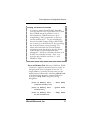
User’s Manual
Microid
Research,
Inc.
User’s Manual
Microid Research, Inc.
1538 Turnpike Street
North Andover, MA 01845
Phone
Fax
Sales
Internet
(508) 686-6468
(508) 683-1630
(800) 800-2467
www.mrbios.com
Warranty and Limitation of Liabilities
Microid Research, Inc. reserves the right to revise this document
and make changes in the specifications of the product described
herein at any time without notice and without obligation to
notify any person of any such revision or change. Microid
Research, Inc. makes no warranty, express, implied or statutory
concerning this document or its use and assumes no
responsibility for any omissions or errors which may appear in
this document, nor does it make a commitment to update the
information contained in this document. Microid Research, Inc.
SPECIFICALLY DISCLAIMS LIABILITY FOR INCIDENTAL OR
CONSEQUENTIAL DAMAGES RESULTING FROM THE
ACQUISITION, USE OR SALE OR OTHER TRANSFER,
PERMITTED OR OTHERWISE, OF THIS DOCUMENT OR THE
USE OF THE PRODUCTS DESCRIBED IN THIS DOCUMENT.
Microid Research, Inc. SPECIFICALLY DISCLAIMS ALL
WARRANTIES, EXPRESS, IMPLIED OR STATUTORY
REGARDING THE FREEDOM OF THIS DOCUMENT OR THE
PRODUCT DESCRIBED HEREIN FROM INFRINGEMENT OF
ANY INTELLECTUAL PROPERTY RIGHT OF ANY THIRD
PARTY. Microid Research, Inc. SPECIFICALLY DISCLAIMS ALL
WARRANTIES AND REPRESENTATIONS, EXPRESSED,
IMPLIED OR STATUTORY REGARDING THIS DOCUMENT OR
THE SPECIFICATIONS, QUALITY OF PERFORMANCE OF THE
PRODUCT DESCRIBED IN THIS DOCUMENT, ITS
MERCHANTABILITY OR ITS FITNESS FOR ANY PARTICULAR
PURPOSE.
MR BIOS ® is a registered trademark of Microid Research, Inc.
Other trademarks are the property of their respective owners.
Copyright ©1996, 1997 by Microid Research, Inc. All
rights reserved.
No part of this document may be photocopied, reproduced,
stored in a retrieval system, transcribed or translated to another
language, in any form or by any means, electronic, mechanical,
magnetic, optical, chemical, or otherwise, without the prior
written consent of Microid Research, Inc.
iv
Microid Research, Inc.
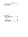
Table of Contents
Chapter 1 - Introduction . . . . . . . . . . . . . . . . . . . . . . 1
Manual Organization . . . . . . . . . . . . . . . . . . . . . . . 1
Icons . . . . . . . . . . . . . . . . . . . . . . . . . . . . . . . . . . . . 2
Getting Help . . . . . . . . . . . . . . . . . . . . . . . . . . . . . . 3
Before You Write or Call . . . . . . . . . . . . . . . . . . . . 4
Chapter 2 - MR BIOS Basics . . . . . . . . . . . . . . . . . . 5
What’s a BIOS? . . . . . . . . . . . . . . . . . . . . . . . . . . . 5
BIOS Setup Utility . . . . . . . . . . . . . . . . . . . . . . . . . 6
Invoking the BIOS Setup Utility . . . . . . . . . . . . . . 7
Exiting Setup Utility . . . . . . . . . . . . . . . . . . . . . . . 7
Navigating Within the Setup Utility . . . . . . . . . . . 8
Cursor . . . . . . . . . . . . . . . . . . . . . . . . . . . . . . . . . 9
Chapter 3 - Using the Setup Utility . . . . . . . . . . . . 13
Summary Screen . . . . . . . . . . . . . . . . . . . . . . . . . 13
Energy Management Configuration Screen . . . . . 22
Making Changes . . . . . . . . . . . . . . . . . . . . . . . . 23
Background Information . . . . . . . . . . . . . . . . . . 24
Clock Configuration Screen . . . . . . . . . . . . . . . . . 29
Background Information . . . . . . . . . . . . . . . . . . 29
Keyboard Configuration Screen . . . . . . . . . . . . . 32
Booting Without a Keyboard . . . . . . . . . . . . . . 34
Floppy Drive Configuration Screen . . . . . . . . . . . 35
2.8M Floppy Drives . . . . . . . . . . . . . . . . . . . . . 36
Four Floppy Support . . . . . . . . . . . . . . . . . . . . . 36
Advanced Topics . . . . . . . . . . . . . . . . . . . . . . . 38
ATA-Disc Configuration Screen . . . . . . . . . . . . . 41
Drive Definition . . . . . . . . . . . . . . . . . . . . . . . . 41
High-speed Data Transfer . . . . . . . . . . . . . . . . . 42
Microid Research, Inc.
v
Table of Contents
Raid-group . . . . . . . . . . . . . . . . . . . . . . . . . . . . 43
Anti-virus Feature . . . . . . . . . . . . . . . . . . . . . . . 43
ATA-Disc Setup . . . . . . . . . . . . . . . . . . . . . . . . 44
Boot Sequence Configuration Screen . . . . . . . . . 49
Boot Sequence . . . . . . . . . . . . . . . . . . . . . . . . . 53
Making Fixed Disk D: Bootable . . . . . . . . . . . . 57
Ports Configuration Screen . . . . . . . . . . . . . . . . . 59
Discussion: Defacto-Standard Serial Ports . . . . 61
Security Configuration Screen . . . . . . . . . . . . . . . 63
Cache Configuration Screen . . . . . . . . . . . . . . . . 67
Pentium System Cache . . . . . . . . . . . . . . . . . . . 68
Associativity . . . . . . . . . . . . . . . . . . . . . . . . . . . 68
Write-Thru / Write-Back . . . . . . . . . . . . . . . . . 69
Non-cache Blocks . . . . . . . . . . . . . . . . . . . . . . . 70
Non-cache Above .../ Cacheable Range . . . . . . 70
Cacheable Regions . . . . . . . . . . . . . . . . . . . . . . 70
Cacheable Video . . . . . . . . . . . . . . . . . . . . . . . . 71
Cacheable Remap . . . . . . . . . . . . . . . . . . . . . . . 71
Shadow RAM Configuration Screen . . . . . . . . . . 72
Upper Memory Blocks . . . . . . . . . . . . . . . . . . . 75
F000 UMB User Info . . . . . . . . . . . . . . . . . . . . 76
Chipset Configuration Screen . . . . . . . . . . . . . . . 77
Background . . . . . . . . . . . . . . . . . . . . . . . . . . . . . 79
Memory Timing . . . . . . . . . . . . . . . . . . . . . . . . 79
Pagemode and Interleave . . . . . . . . . . . . . . . . . 81
Memory Refresh . . . . . . . . . . . . . . . . . . . . . . . . 81
Remap to Extended-memory . . . . . . . . . . . . . . 82
Bus Timing . . . . . . . . . . . . . . . . . . . . . . . . . . . . 83
PCI-Bus . . . . . . . . . . . . . . . . . . . . . . . . . . . . . . . . 85
PCI-Bus Configuration . . . . . . . . . . . . . . . . . . . 86
Selecting Interrupts . . . . . . . . . . . . . . . . . . . . . . 88
Legacy PCI Devices . . . . . . . . . . . . . . . . . . . . . 88
PCI Questions . . . . . . . . . . . . . . . . . . . . . . . . . . 89
Final Thoughts . . . . . . . . . . . . . . . . . . . . . . . . . . . 90
vi
Microid Research, Inc.
Table of Contents
Chapter 4 - POST Codes . . . . . . . . . . . . . . . . . . . . . 91
DIAGNOSTIC PORT 80H POST-CODES . . . . . 91
BEEP CODES AND MESSAGES . . . . . . . . . . . 95
Appendix A - PCI Primer . . . . . . . . . . . . . . . . . . . 101
Index . . . . . . . . . . . . . . . . . . . . . . . . . . . . . . . . . . . . 119
Microid Research, Inc.
vii
List of Figures
Figure 1. Summary Screen . . . . . . . . . . . . . . . . . . . 9
Figure 2. Summary Screen . . . . . . . . . . . . . . . . . . 14
Figure 3. Energy Management Configuration
Screen . . . . . . . . . . . . . . . . . . . . . . . . . . . . . . . 22
Figure 4. Energy Configuration Edit Screen . . . . 23
Figure 5. Clock Configuration Screen . . . . . . . . . 29
Figure 6. Keyboard Configuration Screen . . . . . . 32
Figure 7. Floppy Drive Configuration Screen . . . 35
Figure 8. Floppy Edit Screen . . . . . . . . . . . . . . . . 38
Figure 9. IDE Fixed Disk Configuration Screen . 41
Figure 10. ATA-Disc Parameter Table . . . . . . . . 45
Figure 11. ATA/IDE Drive Parameters . . . . . . . . 46
Figure 12. Boot Sequence Configuration Screen . 49
Figure 13. Menu Boot Display . . . . . . . . . . . . . . 56
Figure 14. Ports Configuration Screen . . . . . . . . 59
Figure 15. Security Configuration Screen . . . . . . 63
Figure 16. Cache Configuration Screen . . . . . . . . 67
Figure 17. Shadow RAM Configuration Screen . 72
Figure 18. Chipset Configuration Screen . . . . . . 77
Figure 19. Chipset Edit Window . . . . . . . . . . . . . 78
Figure 20. PCI-Bus Configuration Screen . . . . . . 85
Figure 21. PCI-Bus Edit Window . . . . . . . . . . . . 87
Figure 22. The VESA Bus Based System . . . . . 104
Figure 23. PCI Bus Based System . . . . . . . . . . . 107
Microid Research, Inc.
viii
List of Tables
Table 1. Summary Screen Fields . . . . . . . . . . . . . 16
Table 2. Energy Configuration Options . . . . . . . 24
Table 3. PIO Mode Transfer Rates . . . . . . . . . . . 42
Table 4. Boot-Seq Setup Functions . . . . . . . . . . . 50
Table 5. Serial Port Locations and IRQs . . . . . . . 62
Table 6. PORT 80H POST-CODES . . . . . . . . . . 91
Table 7. BIOS Beep Codes . . . . . . . . . . . . . . . . . 95
Table 8. PCI Bus Specifications . . . . . . . . . . . . 105
ix
Microid Research, Inc.
x
Microid Research, Inc.
Chapter 1
Introduction
Congratulations! Your computer is equipped
with the state-of-the-art MR BIOS ® . This BIOS
has been designed to maximize the
performance of your system’s hardware and
software.
Manual Organization
This manual supplies information necessary
for configuring MR BIOS in your computer
system. It is divided into three main sections:
Chapter 1
Introduces this manual and how
to use it.
Chapter 2
Presents a general introduction
to the BIOS and the BIOS Setup
Utility.
Chapter 3
Describes each configuration
screen in the Setup Utility.
Chapter 4
Lists the POST codes included in
the BIOS for system trouble
shooting.
Microid Research, Inc.
1
An index is provided for easily locating
specific information.
In addition, the new (optional) RAID0
technology available in MR BIOS is available
from Microid Research’s web site 1 .
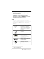
Icons
Icons are used throughout this manual to
guide you through procedures and to point out
specific pieces of information. These icons
include:
Marks the beginning of a
procedure or a major
step in a procedure that
requires you to make a
decision
Information to note and
consider.
Marks important
information that you
need to know
Marks vital information.
Do not ignore!
Marks the end of a
procedure or a set of
procedures.
1. http://www.mrbios.com
2
Microid Research, Inc.
Getting Help
All of the information needed to use the
MR BIOS in your computer system can be
found in this manual. Please consult the Table
of Contents and the Index to find specific
information.If you cannot find the answer to
your problems in the resources listed above,
you can get in touch with Microid Research,
Inc. in one of several ways:
By mail:
Microid Research, Inc.
Attn: Customer Service
1538 Turnpike Street
North Andover, MA 01845
By phone:
(508) 686-2204
By fax:
(508) 683-1630
Internet
http://www.mrbios.com
...but before you make that call
Microid Research, Inc.
☞
3
Before You Write or Call
Before writing or calling for help you must be
prepared. Gather the following information:
•
Brand and Model Number of your computer
•
Type and speed of your CPU (Pentium 75,
P-166, etc.)
•
Version number of your BIOS
BIOS information is usually displayed on
your computer screen when you first turn
on your system.
4
•
Your Operating System (Windows 3.x,
OS/2, Windows for Workgroups, etc.)
•
Brand, Model Number, and Size (in
Megabytes) of each of your hard disk
drives
•
A clear and concise description of the
problem including any error messages
and/or codes displayed.
•
If possible, be at the computer when you
call.
Microid Research, Inc.
Chapter 2
MR BIOS Basics
What’s a BIOS?
BIOS (pronounced "by-oss;" as in "buy floss,"
without the "fl") is an acronym for Basic
Input/Output System. The BIOS is a set of
software routines that work closely with the
hardware to support the transfer of
information between elements of the system
such as the memory, keyboard, disk drives,
and the display monitor. On most computer
systems, the BIOS resides in a special memory
device called a ROM (i.e. Read-Only-Memory)
and is frequently referred to as a ROM BIOS.
Traditional system designs use ROMs
programmed externally to the computer
system, but new systems use Flash-ROMs that
can be reprogrammed while still installed in
the computer. You computer ’s documentation
should tell you if you have a Flash-ROM for
storing your BIOS.
Even though the BIOS is critical to the
operation of your computer and is actively
operating whenever your computer is in use,
Microid Research, Inc.
5
BIOS Setup Utility
it’s functions are usually hidden from the user.
However, there is one critical function that the
user needs to be aware of:
How to set up the BIOS options
Once the BIOS is properly set up, it can be
virtually ignored. Most of the information in
this manual will guide you in using the BIOS
Setup Utility and making decisions on
available BIOS options.
BIOS Setup Utility
The custom features and hardware options in
your computer are user selectable for
maximum flexibility. You will need to
configure these features and options through
the built-in BIOS Setup Utility prior to using
your computer for the first time. MR BIOS will,
during the initial installation or in the absence
of valid CMOS data, automatically set these
features to what it feels is an optimum
configuration to allow the system to operate.
In most cases, you will want to fine tune these
configuration settings to gain maximum
performance from your computer.
The BIOS Setup Utility is a multi-screen, menu
driven program. It has been customized for,
and is contained within the BIOS used on your
motherboard. The information generated
during a configuration session is recorded in
special, low-power CMOS memory which is
battery-maintained when the main system
power is shut off. Since the battery may
become discharged, it is recommended that
you make a record of your BIOS settings. You
may be able to use <PrtSc> to make a
6
Microid Research, Inc.
Invoking the BIOS Setup Utility
hard-copy printout of each Setup Utility
screen.
Invoking the BIOS Setup Utility
A procedure called Power-On-Self-Test (POST)
occurs each time the computer is booted 1 .
This happens when you turn on the main
system power or when you use the
<Ctrl+Alt+Del> key combination to execute a
warm-boot. If the system status noted during
POST cannot be reconciled with the Setup
configuration stored in CMOS memory, the
BIOS Setup Utility will be invoked
automatically.
Alternately, the BIOS Setup Utility can be
accessed manually through the keyboard:
•
Press <Esc> during the power on Memory
Test, or...
•
Press <Ctrl+Alt+Esc> during run time
While the memory size is scrolling on the CRT
during cold-boot, you can press <Esc> to enter
Setup. Similar to the three key sequence
<Ctrl+Alt+Del> that causes a system
warm-boot, you can abort a current program
and enter Setup by pressing <Ctrl+Alt+Esc>.
Exiting Setup Utility
To exit Setup (and boot the computer), press
<F10>. All configuration changes edited in the
1. "Booting" a computer is the process of setting up the
hardware and software element of the system as necessary
for normal operation.
Microid Research, Inc.
7
Navigating Within the Setup Utility
various Setup screens are recorded into CMOS
memory at this time. Be aware that nothing is
recorded until then. Therefore, if you re-boot
the computer or turn off the power (instead of
pressing <F10>), these changes will be lost and
the original configuration will remain
unaltered.
To exit Setup without storing any changes,
either (1) press <Ctrl+Alt+Del>, or (2) turn
the main power off.
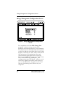
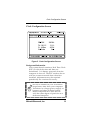
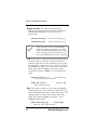
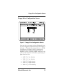
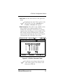
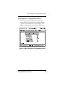
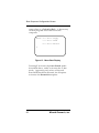
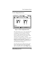
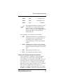
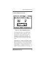
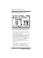
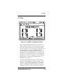
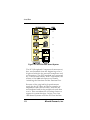
Navigating Within the Setup Utility
The BIOS Setup Utility screen is composed in
three sections, top to bottom, as shown in
Figure 1. The top section contains a menu
listing individual configuration screens. The
middle section contains the edit window
where an individual configuration screen is
viewed and edited. The bottom section is a
dynamic command prompt which indicates
currently valid key commands.
8
Microid Research, Inc.
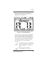
Navigating Within the Setup Utility
Figure 1. Summary Screen
Cursor
A reverse-video cursor is always present,
either on the menu line or in the edit window.
It directs your attention to the currently active
field. Although several keys can be used to
maneuver the cursor, the keyboard <Arrow>
keys are generally used. As the cursor is
moved from menu item to menu item, the edit
window is updated to reveal each
corresponding configuration screen.
When you want to edit a field within a
configuration screen, move the cursor until it
rests on the appropriate menu item and use the
<Down-Arrow>, <Enter>, or <PgDn> key to
move into the edit window. When the cursor is
in the edit window you can begin editing the
individual fields.
Microid Research, Inc.
9
Navigating Within the Setup Utility
The choices in the fields can generally be
scrolled with the <Space> key, while a few
fields require AlphaNumeric entry. Press
<PgUp> when you are done, and the cursor
will return to the menu.
The following command keys are always
available while the cursor is on the menu:
Right, Left Arrow
right and left movement
Space, BackSpace
right and left movement
Tab, Shift-Tab
right and left movement
Home, End
leftmost and rightmost
entry
Down-Arrow,
Enter, PgDn
move down into edit
window
Esc, PgUp
exit edit window, back up
to menu
F10
record and exit Setup
These keys are generally available within the
edit window:
10
Arrows
up, down, left, right
movement
Space, BackSpace
scroll choices in field
Plus, Minus
scroll choices in field
AlphaNumeric
letters and numbers
Microid Research, Inc.
Navigating Within the Setup Utility
Enter, (Esc)
Microid Research, Inc.
begin/end (abort) mode
or screen entry
11
12
Microid Research, Inc.
Chapter 3
Using the Setup Utility
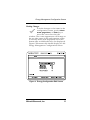
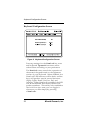
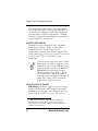
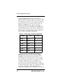
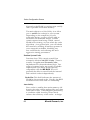
Summary Screen
This is the first screen you will see in the Setup
Utility. It is a view-only report of the
hardware configuration of your computer.
Some of this information is based on installed
hardware and the rest is based on user
selectable options. This information is useful
for confirming that the BIOS has properly
recognized a newly installed component, or if
you simply want to review your machine's
configuration. Figure 2, on the next page,
illustrates a typical summary screen.
Microid Research, Inc.
13
Summary Screen
.
Figure 2. Summary Screen
The following items represent the hardware
elements that the BIOS detects during POST.
These resources simply exist in the system, and
no Setup Configuration Utility is available or
required to manage them.
1.
2.
3.
4.
5.
CPU Type, Revision, MHz
Math Unit (Coprocessor)
Chipset (Core Logic)
Memory-Base and Total Memory
Keyboard and PS2-Mouse
The remaining items report on the values
established by selections made elsewhere in
the Setup Utility. There are some properties or
operational states of system resource that the
BIOS cannot determine or is optional. For
example, the Floppy drive type (1.2M, 1.4M,
etc.) cannot be autodetected by the BIOS, and
14
Microid Research, Inc.
Summary Screen
must be explicitly selected in the Floppy
configuration screen. Another example is the
Shadow-RAM operation (when this feature is
present) which is fully user-configurable in the
Shadow configuration screen.
In some designs, the Extended
Memory is effected (decreased) by the
amount allocated to Shadow-RAM.
In general, it is a good practice to
examine this Summary Screen after
making each configuration change
and prior to exiting the Setup Utility.
Again, the Summary Screen is view-only ;
nothing can be changed here. If you want to
make configuration changes or explore other
Setup Utility screens, press <Right Arrow> to
move the cursor rightward on the menu-line.
To exit the Setup Utility (and boot the
computer), press <F10>.
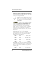
Table 1 describes each field found on the
Summary Screen.
Microid Research, Inc.
15
Summary Screen
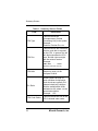
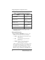
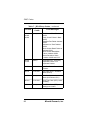
Table 1. Summary Screen Fields
Field
CPU Type
CPU Rev
Description
This field shows the
microprocessor (Central
Processing Unit) in the system.
Example:
Pentium, Pentium Pro, etc.
This field shows the model and
revision code that is reported
by the CPU. In general, the left
two digits represent the CPU
type, and the right two digits
are the revision number.
Example:
CPU Rev .... 0525
(Meaning: Pentium, Rev 25)
CPU MHz
This field shows the operating
frequency (clock) of the
computer in MHz.
PLL Ratio
Some systems provide for
clock oscillator multiplication.
Such clocks are typically PLL
(phase-locked-loop) designs
with the multiplication factor
indicated as nX, where n is the
numerical multiplier.
Example: 1.5X
CPU Code Cache
This field shows the size of the
CPU’s internal code cache.
16
Microid Research, Inc.
Summary Screen
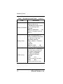
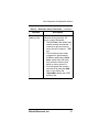
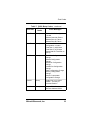
Table 1. Summary Screen Fields , continued
Field
Description
CPU Data Cache
This field shows the size of the
CPU’s internal data cache.
External Cache
This field shows the size of the
cache memory available
external to the CPU.
Memory-Base
This is the amount of Base
Memory (below the 640K
boundary) detected and in
working order.
Example:
Memory-Base ... 64K
(Meaning: 640 Kilobytes Base
Memory)
Memory-System
Many designs reserve a portion
of memory, typically 384K, for
special uses. Some may be
allocated to Shadow RAM, and
the remainder might
automatically be remapped to
the Extended Memory pool.
This field shows the amount of
memory retained for system
use.
Examples:
Memory-System ...
K
(Meaning: none, or fully reallocated)
Memory-System ... 384K
(Meaning: 384 Kilobytes Special
Memory)
Microid Research, Inc.
17
Summary Screen
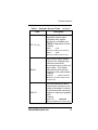
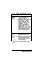
Table 1. Summary Screen Fields , continued
Field
Memory-Extended
Description
This is the amount of Extended
Memory (above the
1 Megabyte boundary) found
to be in working order.
Example:
Memory-Extended ... 7M
(Meaning: 7 Megabytes Extended
Memory)
Memory-Total
This is the total amount of
memory installed in the system.
It is the sum of the three
preceding quantities:
Base + System + Extended
= Total.
Example:
Memory-Total ... 8M
(Meaning: 8 Megabytes Total Memory)
COM1 (2,3,4)
These are the I/O addresses of
the serial ports configured in
the system. (More may be
available; see PORTS
Configuration Screen).
Example:
COM1 ... n/a
(Meaning: serial port not present)
COM4 ... 3F8
(Meaning: serial port at I/O 3F8)
18
Microid Research, Inc.
Summary Screen
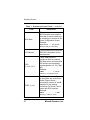
Table 1. Summary Screen Fields , continued
Field
LPT1 (2,3,4)
Description
These are the I/O addresses of
the parallel (printer) ports
configured in the system.
(More may be available; see
PORTS Configuration Screen).
Example:
LPT1 ... n/a
(Meaning: parallel port not present)
LPT3 ... 378
(Meaning: parallel port at I/O 378)
Chipset
Most modern system boards
contain a few, relatively large,
surface-mounted ASIC
components known as the core
logic chipset. This chipset
characterizes the functional
properties of the system board.
Example:
Chipset ... Intel Triton
(Meaning: Intel Triton chipset for the
Pentium CPU)
BIOS ID
This field identifies the BIOS
firmware that is present on the
system motherboard. It should
be referenced when reporting a
problem or ordering an upgrade
BIOS.
Example:
BIOS ID ... INTL5UU
(Meaning: MR BIOS for Pentium CPU)
Microid Research, Inc.
19
Summary Screen
Table 1. Summary Screen Fields , continued
Field
BIOS Date
Description
This field reports the date the
BIOS firmware was compiled.
Note that its format (dd/mm/yy
or mm/dd/yy) is selected in the
Clock Configuration Screen.
Example:
BIOS Date ... 05/02/96
(Meaning: May 2, 1996 (USA))
PS/2-Mouse
IDE0
(1,2,3,4,5,6,7)
This field reports on whether an
IBM PS/2 compatible mouse
was detected.
These fields show the
configured Size for installed
IDE hard drives. Non-hard drive
IDE devices are reported by
type designation (i.e. CD, Tape,
etc.).
Example:
IDE0 ........ 1.28 G
(Meaning: 1.28 Gigabyte drive)
FDD0 (1,2,3)
The Floppy Drives configured
in the system are shown here.
While Floppies 0 and 1
correspond to drives A: and B:
respectively, the naming
convention for Drives 2 and 3
varies with DOS versions.
Example:
FDD0 ......... 1.4M
(Meaning: 1.4Mb 3½" drive)
20
Microid Research, Inc.
Summary Screen
The balance of this chapter will examine each
of the configuration screens and how to use
them.
Microid Research, Inc.
21
Energy Management Configuration Screen
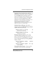
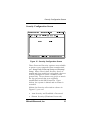
Energy Management Configuration Screen
Figure 3. Energy Management Configuration
Screen
For compliance with the EPA Energy Star
program, various energy conservation
methods can be integrated into your computer.
The objective is to automatically reduce power
to devices like the fixed disk drives and video
display when they are idle, and to restore their
full operation (with minimum delay and
inconvenience) upon detection of activity.
This is accomplished through use of idle timers
and event monitoring techniques. The
configuration screen in Figure 3 allows you to
select how rapidly the timers will expire; or,
you can disable them altogether if you find
they are interfering with the use of your
computer.
22
Microid Research, Inc.
Energy Management Configuration Screen
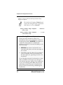
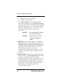
Making Changes
To make changes to the items in the
configuration screen, use the down
arrow, page down, or Enter key to
move the cursor into the edit
window. The screen appearance will change at
the top (the name of the configuration screen
is the only menu item displayed) and at the
bottom (the available edit keys are displayed).
Figure 4 illustrates this altered display for the
Energy Management Configuration Screen.
Figure 4. Energy Configuration Edit Screen
Microid Research, Inc.
23
Energy Management Configuration Screen
Table 2. Energy Configuration Options
Option
Valuea
IDE Spindown
*Off, 5, 10, or 20
Minutes
Standby Timer
*Off, 5, 10, or 20
Minutes
Suspend Timer
*Off, 1, 2, 3, 4, 5,
10, or 15 Minutes
Event Monitoring
Not available at
this time.
Factory Test Mode
*Off, Onb
a.
* = Default
b. IDE
Spindown = Off; Standby = 15 Sec; Suspend = 15 Sec;
Event Monitoring = Local
Background Information
Energy Standards. MR BIOS conforms to, and
makes use of several industry standards:
•
APM - Intel/Microsoft Advanced Power
Management
•
ATA
•
DPMS - Display Power Management
Signaling (VESA/Video)
- AT Attachments Specification
(IDE Drive)
APM coordinates the BIOS, Operating System,
and Application Programs to act together as
participants of Power Management. You will
generally realize best power savings under
DOS by using its APM driver, POWER.EXE, set
24
Microid Research, Inc.
Energy Management Configuration Screen
to "ADV:". Under WINDOWS, use its Setup
facility to enable POWER.DRV, then find the
Power icon in the Control Panel, and select
"ADVANCED" power management there.
Modern ATA compliant IDE Drives that
provide Spindown services can be
programmed to automatically turn off the
spindle motor when the drive has been idle
awhile. It will then wait silently for a new
access to cause it to turn the motor back on.
VESA/DPMS compliant video adapters and
monitors are designed to be used together as a
matched set. Special signals exist between the
pair that allow the CRT to be put into various
low power states. These functions are
generally not automatic, though, requiring
manual instruction from the System BIOS.
Four power management states are defined by
APM and DPMS:
1. Run
- Fully powered-up
2. Standby - Reduced power, can instantly be
returned to Run State
3. Suspend - Minimum power, may be slow to
return to Run State
4. Off
- Fully powered-down
Run. The Run state is the natural, full-power
state that you would expect when there is no
power management at all. If the computer is
allowed to sit idle for awhile, the Standby or
Suspend timer will expire and that respective
state will be engaged. Any activity (e.g.
keystrokes, mouse movement, etc.) will reset
Microid Research, Inc.
25
Energy Management Configuration Screen
those timers and restore the system to the Run
state.
If you want to disable power
management altogether, disable both
the Standby and Suspend timers.
Standby. The Standby state is an intermediate
state, between Run and Suspend. It uses a
short timer (a few minutes) to determine when
the system should be considered temporarily
idle. When no activity occurs and the Standby
Timer expires, measures are taken to reduce
power consumption which may include
slowing the CPU and, more noticably, blanking
the CRT. The DPMS Standby (screen blanking)
mode just partially powers-down the CRT,
allowing instant recovery when activities are
resumed.
Suspend. The Suspend state is the final
destination of power management, occurring
after the system has sat idle for a significant
period of time. It uses a long timer (up to one
hour) to determine when the computer should
be considered unattended. When the Suspend
Timer expires, measures to severely reduce
power may include slowing or halting the
CPU, and of particular interest, the video will
be disabled to the fullest extent possible. The
DPMS Suspend mode induces a cold
power-down of the CRT electronics, and it
may require a lengthy warm-up period (not
unlike turning on your monitor in the
morning) when activity is resumed.
26
Microid Research, Inc.
Energy Management Configuration Screen
VESA/DPMS defines a CRT Off mode that,
taken in its most literal sense, can turn off the
CRT power completely. When a monitor is
turned off by this method, it may (or may not)
require manual actuation of the power switch
(push-button) on the CRT to later turn it back
on. If you want the CRT to be fully turned off
upon entering the Suspend state, select Yes in
this field. Otherwise, select No to use the
more ordinary DPMS Suspend mode.
Spindown. Turn off the IDE Drive motor after
1, 5, 10, or 20 minutes of inactivity. Or, disable
the timer by selecting Off to leave the motor
running indefinitely.
Spindown .....2 Min
motor off after 2
min
Spindown .......Off
motor always
runs
Standby. Select a period of 1, 2, 3, 4, 5, 10, or 15
minutes inactivity after which the computer is
considered to be temporarily idle and a mildly
low power state will be put into effect. Or,
disable this timer by selecting Off to prevent
Standby mode altogether.
Standby ......5 Min
Standby if idle
for 5 min
Standby ........Off
never go to
Standby mode
Suspend. Select a longer period of 5 min to 1 hr
inactivity after which the computer is
considered to be unattended and severe power
reduction steps occur. Or, disable this timer by
Microid Research, Inc.
27
Energy Management Configuration Screen
selecting Off to prevent Suspend mode
altogether.
Suspend ..... 15 Min
Suspend if idle
for 15 min
Suspend ........ Off
never go to
Suspend mode
Factory Test Mode. For factory test and
demonstration purposes, the power
management state transitions can be
accelerated by selecting Yes here. Table 2 lists
the values associated with factory test mode.
Select No for normal operation.
Note
Factory Test Mode is automatically cancelled
and reverts back to normal (No) whenever the
computer is (re)booted.
28
Microid Research, Inc.
Clock Configuration Screen
Clock Configuration Screen
Figure 5. Clock Configuration Screen
Background Information
Your system board contains a Real Time Clock
(RTC) in which the time and date are
maintained. It is battery powered when the
computer is shut off. The RTC needs to be set
with the current time and date when first
installed. Adjustments may be required
periodically for continued accuracy.
AAA
AAAA
AAA
AAAAAAAA
AAAAAAAA
AAAAAAAA
AAAAAAAA
AAAAAAAA
AAAAAAAA
AAAAAAAA
AAAAAAAA
AAAAAAAA
AAAAAAAA
AAAAAAAA
AAAAAAAA
AAAAAAAA
AAAAAAAA
AAAAAAAA
AAAAAAAA
AAAAAAAA
AAAA
AA
AAA
AA
AAA
AA
Do
not
be
alarmed
if
your
wristwatch
AAA
AA
AAA
AA
AA
AAA
AAA
AA
keeps
better
time
than
your
computer.
AAA
AA
AAA
AAA
AA
Variations in voltage (power-supply or AA
AAA
AA
AAA
AA
AAA
AA
battery) and other technical issues
AAA
AA
AAA
AA
AAA
AA
make
it
impractical
to
tune
the
RTC
AAA
AA
AAA
AA
AAA
AA
AAA
AA
with
the
same
degree
of
precision
as
a
AAA
AA
AAA
AA
AAA
AA
dedicated
timepiece.
AAA
AA
AAAA
AAA
AAAA
AAAA
AAAA
AAAA
AAAA
AAAA
AAAA
AAAA
AAAA
AAAA
AAAA
AAAA
AAAA
AAAA
AAAA
AAAA
AAAA
AAAAAAAAAAAAAAAAAAAAAAAAAAAAAAAAAAAAAAAAAAAAAAAAAAAAAAAAAAAAAAAAAAAAAAAAAA
AAA
AA
Microid Research, Inc.
29
Clock Configuration Screen
Display Format. The time and date can be
selected to appear either in United States or
International format, according to your
preference.
United States
12 hour, mm/dd/yyyy
International
24 hour, dd/mm/yyyy
Note that the year is maintained
with four digits, not just two. This
helps to prevent problems that may
occur when your clock ticks over to
the year 2000 instead of the year 00.
Time . The time is shown in the selected Display
Format (above). If USA 12-hour format is
selected, the time of day indicator a or p (am/
pm) appears. Otherwise, it is a 24-hour clock.
To change the time, move the cursor onto this
field, then press <Enter> and edit. Upon
completion, press <Enter> to record the new
time.
Time hh:mm:ss t ..... 2:27:35 p
12-hr am/pm (USA format)
Time hh:mm:ss ........ 14:27:35
24-hr (International)
Date. The date is shown in the selected Display
Format (above). USA format is mm/dd/yyyy,
and International format is dd/mm/yyyy. To
change the date, move the cursor onto this
field, then press <Enter> and edit. Press
<Enter> when done.
Date mm/dd/yyyy ... 5/14/1991
May 14, 1991 (USA format)
30
Microid Research, Inc.
Clock Configuration Screen
Date dd/mm/yyyy ... 14/5/1991
14 May, 1991 (International)
Daylight Savings . The RTC can be instructed to
automatically correct the time on the two
daylight savings days of the year. Altering
this field will not cause an immediate
change - the RTC adjusts the time only when a
daylight savings transition occurs.
Daylight Savings ... Enable
RTC auto-adjusts time
Daylight Savings ... Disable
time not adjusted
Do not Enable the Daylight
Savings option if you are using
Windows95. This is because Win95 has its own
mechanism for keeping track of Daylight
Savings Time.
Microid Research, Inc.
31
Keyboard Configuration Screen
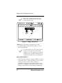
Keyboard Configuration Screen
Figure 6. Keyboard Configuration Screen
Powerup settings for the NumLock key state
and keyboard Typematic functions can be
selected here according to your preference.
The NumLock state controls the operation of
the numeric keypad found on the rightmost
section of your keyboard. When disabled, the
NumLock LED indicator will be dark, and the
keys will produce special control functions
(PgUp, PgDn, Home, End, Ins, Del, and
cursors). When NumLock is enabled, the LED
will be illuminated and the keystrokes will
produce numbers. This utility only establishes
the initial boot-time state; you can toggle it
whenever you like simply by pressing
<NumLock>.
32
Microid Research, Inc.
Keyboard Configuration Screen
Your PC/AT style keyboard has a built-in
Typematic feature which automatically repeats
the currently pressed key until it is released.
An initial delay allows sufficient time to
remove your fingers during ordinary typing.
If the key is held down long, it will begin to
repeat at a constant speed. Both of these
parameters can be selected according to your
preference, or, the keyboard can be left
unprogrammed (default) to produce
approximately 10 character per second (cps)
repeat rate after 0.5 second delay.
NumLock State at Bootup - The initial
NumLock state is programmable for cursor or
numeric operation. Off selects cursor control,
and On selects numeric entry.
NumLock State at Bootup ...... On
NumLock on (numeric)
NumLock State at Bootup ..... Off
NumLock off (cursor)
Keyboard Typematic Speed - A key will
eventually begin repeating after it is held
down. You can select repeat rates from a very
slow 2.0 cps up to a quick 30.0 cps, or you can
leave it unprogrammed by selecting Default
(approx 10 cps).
Keyboard Typematic Speed ... Default
native value
Keyboard Typematic Speed .. 30.0 cps
lively keyboard
Delay Before Keys Repeat - Choose a delay
from 0.25 to 1.0 second that comfortably
Microid Research, Inc.
33
Keyboard Configuration Screen
allows you to release the keys before they
begin to repeat.
This field will display Default and
cannot be changed if the Typematic
field above is set to Default.
Delay Before Keys Repeat .... Default
native value
Delay Before Keys Repeat ..... .5 sec
comfortable delay
Booting Without a Keyboard
There are some instances where it is
desirable to boot your computer without a
keyboard attached. MR BIOS does not have
a specific setup option to enable this
behavior. Instead, it has the flexibility to do
the following:
•
MR BIOS sees that a keyboard is not
attached and prints an error message to
the screen.
•
The BIOS waits for about 10 seconds for
you to respond, then it proceeds with
the boot process, ignoring the lack of a
keyboard.
If you decide to attach a keyboard at a later
time, the BIOS will accept it as though it
was always present. (Note: This is not true
is you are running SCO Unix because the
operating system must see a keyboard at
boot to set an internal flag validating the
keyboard.)
34
Microid Research, Inc.
Floppy Drive Configuration Screen
Floppy Drive Configuration Screen
Figure 7. Floppy Drive Configuration Screen
You may have as many as four diskette drives
in your computer, referred to here as Floppy 0
through 3. The familiar names Drive A: and B:
correspond to Floppy 0 and 1 respectively,
while the drive letters for Floppy 2 and 3
depend on your version of DOS. Each drive in
your system must be declared by specifying its
type from this list:
• 360K 5¼" low density
• 720K 3½" low density
• 1.2M 5¼" high density
• 1.4M 3½" high density
• 2.8M 3½" extra density
Microid Research, Inc.
35
Floppy Drive Configuration Screen
The step-rate (radial track-to-track speed of
the recording heads) is also programmable. It
should be set to Fast to exploit the improved
performance of modern equipment. A Slow
setting is provided for backward compatibility
with original PC standards 1 .
2.8M FLOPPY DRIVES
The BIOS in your computer fully supports
2.8M floppy drives. Many vendors are
suppling retrofit software drivers to
supplement systems that cannot support this
latest technology. There is no need to use such
a driver, and to do so will likely cause
problems.
If your system does not have a 2.8M
drive and you plan to upgrade your
controller card, check first that your
disk controller card has an i82077 or
NSC8744 (or equivalent) Floppy
Disk Controller chip (FDC). If not,
you will need to add a secondary
controller card equipped with one of
these FDC chips. (See Advanced
Topics later in this section.)
FOUR FLOPPY SUPPORT
MR BIOS has built-in support for four floppy
drives. Historically, BIOS support has been
limited to two floppies and software drivers
were used to extend it to four. There is no
1. The original disk drive standards were created long
before high speed, high density drives were available.
Older diskettes may not be readable on newer equipment
unless it is slowed down.
36
Microid Research, Inc.
Floppy Drive Configuration Screen
need to use such a driver here, and doing so
will likely cause problems.
MR BIOS can manage a single controller card
with four-floppy drive support, or it can
manage a pair of standard (dual-floppy)
controller cards. If your system contains two
cards (or you plan to add a second), refer to
the Advanced Topics later in this section.
Floppy (0,1,2,3). Figure 8 illustrates the Floppy
edit screen. The type of floppy drives installed
are specified here. Floppy 0 and 1 correspond
to Drive A: and B: respectively. The drive
letters for Floppy 2 and 3 depend on your
Operating System. Some of the options
available include:
Floppy . . . . . n/a
no adapter card
Floppy . . . .
marked absent
None
5¼ 36K
drive A: is 360K
Floppy 1 . . 3½ 2.8M
drive B: is 2.8M
Floppy . . .
Microid Research, Inc.
37
Floppy Drive Configuration Screen
Move the cursor down onto the
drive (by number) and select the
correct drive type.
Figure 8. Floppy Edit Screen
DriveA: It is possible to assign any of the
installed floppy disk drives as Drive A: for
booting purposes.
To select Drive A:, move the cursor
down to the last line in the edit
window. Use the space bar to scroll
through the available floppy drives
until the desired drive is indicated.
ADVANCED TOPICS
Most systems contain a single, ROM-less disk
controller card. If this describes your system,
skip over this section. (The primary/
secondary message in the figure above only
appears in systems with two controller cards.
Floppy controllers with ROM programming
38
Microid Research, Inc.
Floppy Drive Configuration Screen
will usually display a sign on banner during
POST indicating such).
FLOPPY CARDS WITH ROMS
ROM programming on floppy controller cards
is intended to supplement a system whose
BIOS cannot make use of the cards' special
features. If the BIOS already has the target
capabilities, the duplication in programming
will usually result in a malfunction. The
BIOS in your computer already supports all
state of the art floppy configurations. If you are
upgrading your floppy subsystem for 2.8M or
four-floppy operation, try to select a card
without a ROM on it. Otherwise, you should
disable or remove the ROM(s) according to the
manufacturer's documentation.
SECONDARY CONTROLLER
Setup for two-controller systems proceeds
almost exactly as described for
single-controller systems. The only difference
is that you also need to identify the controller
card attached to each drive. The card attached
to Floppy 0 (Drive A:) is called primary,
whereas the add-on card is called secondary.
They are indicated on this screen with
abbreviations p and s respectively.
The following technical information
will be of interest when installing a
second controller and cabling for the
drives:
•
The primary floppy card resides at I/O
address 3F0.
Microid Research, Inc.
39
Floppy Drive Configuration Screen
•
The secondary floppy card resides at I/O
address 370.
•
Both cards share Interrupt Level 6, IRQ6.
•
Both cards share DMA Request 2, DRQ2.
•
Drives are assigned sequentially without
gaps as Floppy 0,1,2,3.
•
Drive-Select 0 (DS0) on the primary card is
connected to Floppy 0.
•
The numerically lowest drive on the
secondary card responds to its DS0.
•
Drive-Selects are assigned sequentially on
each card, one per connected floppy.
When you indicate each drive type in a system
equipped with dual floppy controller cards, a
letter is appended to the configuration
information indicating the controller card
where the drive was detected by the BIOS.
Primary and Secondary cards are indicated by
p and s respectively. For example:
40
Floppy 3 ...... None
marked
absent or no
adapter card
Floppy 1 .... 1.2M p
floppy on
primary card
Floppy 3 ......2.8M s
floppy on
secondary
card
Microid Research, Inc.
ATA-Disc Configuration Screen
ATA-Disc Configuration Screen
Figure 9. IDE Fixed Disk Configuration Screen
This version of MR BIOS is the first to provide
support only for IDE drives 2 . It does not
support drive types directly. This reflects the
dominance of ATA/IDE drive technology in
computer systems today.
DRIVE DEFINITION
It is not necessary to manually define the
properties of each fixed disk installed in your
computer. ATA Mode-2 and Mode-3 drives
inform the system of the details of their
physical characteristics. Thus, you no longer
2. Note: MR BIOS does not support SCSI directly.
However, it is possible to have a SCSI interface card
installed in the system as either a stand-alone controller or
coexisting with your IDE controller.
Microid Research, Inc.
41
ATA-Disc Configuration Screen
need to enter information on the number of
heads, cylinders, tracks, and so on. It’s all
done automatically for you. Even so, there are
still some decisions to make.
HIGH-SPEED DATA TRANSFER
Several options are available to increase data
throughput.
The ATA standard defines four different PIO
modes that affect data transfer rates. Table 3
summarizes the most common transfer rates
for each PIO mode. The actual transfer rate is
determined by the drive and your supporting
hardware. If you want, the BIOS can make the
selection for you, or you can specify a fixed
transfer rate. Auto mode is limited to ATA
Mode 3 drives.
Table 3. PIO Mode Transfer Rates
PIO Mode
Cycle Time (ns)
Transfer Rate (MB/s)
0
600
3.3
1
383
5.2
2
240
8.3
3
180
11.1
4
120
16.6
5
90
22.2
PIO mode 0 conforms to original PC
standards, and is compatible with all fixed
disks. This method uses a hardware signal
42
Microid Research, Inc.
ATA-Disc Configuration Screen
(called an interrupt) to transfer a single sector
at-a-time. PIO mode 1 does not wait for the
interrupt, but instead polls the drive for its
readiness to transfer each sector. PIO mode 2
(aka Block-Transfer mode 2) makes use of
modern IDE drive capabilities to transfer a
group of sectors in a single burst. While the
preceding modes 0-2 perform industry
standard 16-bit word transfers, 32-Bit
Block-Transfer mode 3 (or PIO mode 3)
exploits the system board's 32-bit bus to
achieve the highest transfer-rate possible.
RAID-GROUP
Two or more drives can be interleaved and
managed as a single unit for improved random
access and large-file performance. This is an
optional technology exclusively found in
MR BIOS . Further information on this
technology breakthrough can be found on the
Microid Research web page:
http://www.mrbios.com
You must use the same drive
types for all members of a raidgroup. Dissimilar drives will not
work, even if they are the same
size.
ANTI-VIRUS FEATURE
The Anti-Virus option is intended to provide a
measure of protection against malicious
programs which infect the main boot sector or
low-level format (destroy) your data. Since
viruses often gain entry when an infected
floppy disk is booted, you should supplement
Microid Research, Inc.
43
ATA-Disc Configuration Screen
this defense with the C: 1st boot order in the
Boot-Sequence Utility.
A
AAAAAAAAAAAAAAAAAAAAAAAAAAAAAAAAAAAAAAAAAAAAAAAAAAAAAAAAAAAAAAAAAAAAAAA
AA
A
A
A
A
A
Many
classes
of
viruses
will
not
be
A
AA
A
A
A
detected,
and
even
when
a
virus
is
A
A
A
AA
A
detected,
it
may
have
already
A
A
A
AA
A
infected
the
disk,
corrupted
data,
A
A
A
A
A
AA
A
spread
through
a
network,
etc.
A
A
A
A
AAAAAAAAAAAAAAAAAAAAAAAAAAAAAAAAAAAAAAAAAAAAAAAAAAAAAAAAAAAAAAAAAAAAAAA
AA
Note - You will need to disable this
option while using certain fixed disk
maintenance programs (e.g. DOS
FDISK), because their actions would be
interpreted as a violation.
ATA-DISC SETUP
Drive C: Any of the fixed drives may be
designated as "Drive C." Tradition suggests
using Disk 0 as Drive C, but any disk 0
through 7 is valid.
Select the hard disk to be used as
Drive C: by moving the cursor to
highlight the Disc number. You can use
the <spacebar> to cycle through the
available disk drives.
Raid-Group. To select the drives to include in the
Raid0 configuration, specify the combination
here.
Highlight the Raid-Group option
with the cursor. Use the <spacebar> to
scroll through the available drive
combinations.
44
Microid Research, Inc.
ATA-Disc Configuration Screen
Anti-Virus. See the discussion on the previous
page.
Highlight the Anti-Virus option with
the cursor. Use the <spacebar> to
Enable or Disable this option.
Disk Parameters. The table in the middle of the
edit window lists eight possible drives,
numbered 0 through 7. Each drive’s storage
capacity, data throughput rate (in MB/s), the
ATA mode, and the manufacturer ’s model
code as detected from the drive itself. Figure
10 illustrates the ATA-Disc edit screen.
Figure 10. ATA-Disc Parameter Table
Scroll the cursor down beyond the
Anti-Virus option. The cursor will
jump up to Disc 0.
Microid Research, Inc.
45
ATA-Disc Configuration Screen
Note: You can disable any installed
drive by toggling its Disc number.
When the cursor is on a line in the table of
installed ATA disk drives, the information
displayed below the table changes as
illustrated in Figure 11.
Figure 11. ATA/IDE Drive Parameters
The data transfer rating for that drive is
reported as well as the type of IDE controller
that has been detected.
Only the MB/S field in the table may be edited
directly. In most cases, selecting Auto mode is
the best choice because it allows the hardware
to run as fast as possible. If necessary, the
transfer rate can be manually set to slow down
the throughput.
46
Microid Research, Inc.
ATA-Disc Configuration Screen
Move the cursor to the right to
highlight the entry in the MB/S
column. As you toggle through the
available options, you will see the
ATA mode number change in the next
column.
Microid Research, Inc.
47
ATA-Disc Configuration Screen
Discussion:
Fixed Disk Naming Conventions
Although C: and D: are the most
common names for the fixed disk units, it is
possible to configure a system such that other
drive letters are used. You may be familiar
with the concept of DOS Partitions, where a
single fixed disk is subdivided into as many
as four logical drives. In this case, they may
be referenced as drives C, D, E, and F. As
another example, you might have four floppy
disk drives, named A-D. Your fixed disks
might then appear as E and F. These
examples demonstrate that DOS can assign
the drive letters dynamically. In contrast, the
BIOS uses an invariant naming convention
for the floppy and fixed disks. Floppy drives
are referenced as FDD 0,1,2,3, and fixed disks
are accessed as Disc 0,1,2,3,.... Operating
Systems and other low-level programming
rely on this invariance when requesting disk
services from the BIOS. While you are
specifying your drives through this Setup
Utility, you should understand that the BIOS
is unaware of any partitions or other logical
mappings which might affect the drive
letters. The names C: and D: are used in
order to simplify the discussion for the
majority of readers.
48
Microid Research, Inc.
Boot Sequence Configuration Screen
Boot Sequence Configuration Screen
Four system start-up functions and four
miscellaneous functions are configured here.
Figure 12 illustrates the screen display and
Table 4 summarizes the available functions.
Figure 12. Boot Sequence Configuration Screen
Microid Research, Inc.
49
Boot Sequence Configuration Screen
Table 4. Boot-Seq Setup Functions
Function
Description
Boot Sequence
Specifies the order in which disk
drives are accessed while loading
the Operating Systema. The most
popular boot order is C: 1st, but
you may also select A: 1st,
Network 1st, or Menu according to
your preference.
Permit Boot
from A:
Allows the system to boot from the
A: drive. If set to No, the boot
sequence must provide an
alternative boot drive.
Permit Boot
from C:
Allows the system to boot from the
C: drive. If set to No, the boot
sequence must provide an
alternative boot drive.
Drive C:
Assignment
Selects whether the C: boot drive is
an ATA/IDE device or a SCSI
device. The default here is to boot
from an IDE device.
Note: If only using a SCSI drive,
this function must be assigned to
"SCSI."
50
Microid Research, Inc.
Boot Sequence Configuration Screen
Table 4. Boot-Seq Setup Functions, continued
Function
Power on
Memory Test
Description
Specifies the memory test that
executes during powerup: full,
quick, or skip it altogether.
• The Full Test is the default and
should normally be selected. It
conducts a rigorous memory
test at the rate of approx. 1 MB/
sec.
• This is relatively slow when
compared to approximately
8 MB/sec achieved by Quick
Scan, which does little other
than prime the memory and
parity by writing zeros to it.
• You can bypass the memory
test entirely by selecting Skip
here, or by striking the
<SpaceBar> during the POST
memory test.
Microid Research, Inc.
51
Boot Sequence Configuration Screen
Table 4. Boot-Seq Setup Functions, continued
Function
Description
System
Warmup
Delay
can provide additional powerup
time required by some slow
mechanical devices. A
conservative 3 second delay is the
default value. As an example,
some IDE drives malfunction if
accessed within a few seconds
after powerup. They can be
accommodated by enabling a
several second delay. A delay
period of 1 to 30 seconds can be
selected. Unless you experience
such problems, though, you may
wish to use the default delay or
even disable the delay by selecting
None.
<Ctrl Alt Esc>
for Setup
sets the hot key sequence used to
activate the BIOS setup utility
<Ctrl Alt 8 > for
menu
sets the hot key sequence used to
reboot at run time from the boot
device menu (only available if this
option is activated)
a.
The actual boot order depends, in part, on the Drive A: and Drive
C: selections you made in the Floppy and ATA-Disc configuration
screens.
52
Microid Research, Inc.
Boot Sequence Configuration Screen
Boot Sequence
The order in which the drives are accessed at
boot-time is programmed in this field. Select
the option that best serves your needs.
Boot Sequence ... A: 1st, C: 2nd
floppy 0 then fixed
Boot Sequence ... C: 1st, A: 2nd
fixed then floppy 0
Boot Sequence ... Auto-Search
all floppies, then fixed
Boot Sequence ... Network 1st
network boot-ROM
Boot Sequence ... Screen Prompt
select from menu
Note - A prompted warm-boot can also
be manually invoked by pressing
<Ctrl+Alt+Enter> during run time
(from DOS), or by pressing <Enter>
during the cold-boot memory test. (This
is a convenient way to occasionally boot
from a floppy disk when the C: 1st order
is selected here as the default).
Background Information: Each time you turn on
your computer or press <Ctrl+Alt+Del> to
restart it, an Operating System (such as DOS)
is loaded from one of the disk drives. When
several drives are installed in your computer,
you can select the order that BIOS searches the
disks for the Operating System.
Because the traditional boot devices are
Floppy A: and Fixed Disk C:, DOS and most
Microid Research, Inc.
53
Boot Sequence Configuration Screen
other O/S can only boot A: or C:. Yet you can
arrange through this utility to boot any disk in
the system, say B: or D:. In order to do this,
though, the BIOS needs to reassign the drive
letters to remain compatible with tradition. In
general, a Floppy that boots is named A:, and a
Fixed Disk that boots is named C:.
A: 1st, C: 2nd. Historically, only A: or C: could
be booted, and the order these drives were
checked was not selectable. Floppy A: would
be booted if it contained a diskette.
Otherwise, Fixed Disk C: would be booted.
This is the industry standard A: 1st, C: 2nd
order.
In some computers with more than one Floppy,
an Auto-Search function extends the standard
A: 1st order to search all Floppies 0,1,2,3 (A:,
B:,...) before defaulting to Fixed Disk C:. This
is useful if Drive A: is a different size than the
diskette you want to boot from. MR BIOS now
deals with this issue in a more controlled
manner: The desired boot drive can be
explicitly selected from any installed floppy in
the Floppy configuration edit window.
C: 1st. In computers with a Fixed Disk, the C: 1st
boot order can be selected to bypass the
Floppy Drive access. This option promotes
fastest bootup, and eliminates the annoying
non-bootable diskette error that occurs when a
diskette is unintentionally left in the Floppy
Drive. It also eliminates one opportunity for a
virus to infect your computer.
From time to time, you may still need to boot a
Floppy. This can be done conveniently
54
Microid Research, Inc.
Boot Sequence Configuration Screen
(without entering Setup) by pressing
<Ctrl+Alt+Enter>. See Screen Prompt, below.
Network 1st. It is a common practice in
businesses to interconnect PC's through cables
and hardware that is known collectively as a
network. Each computer in the network
contains a Network Adapter card, and often,
this Adapter contains a boot-ROM that loads
the O/S directly from the network (instead of
booting from disk). In these installations,
Fixed Disk C: is usually left unbootable
because it would be accessed (booted) before
the boot-ROM gains control. The Network 1st
option bypasses all disk access completely,
allowing you to boot directly from the network
even when Fixed Disk C: is bootable.
From time to time, you may still want to boot
from disk. This can be done conveniently
(without entering Setup) by pressing
<Ctrl+Alt+Enter> as described under Screen
Prompt, below.
Drive C: Assignment . You may want to run a
SCSI drive controller in you system and boot
from a SCSI drive. Set this field to SCSI to
allow this option.
Screen Prompt. A menu can be made to appear
on the CRT which requests your explicit
selection of the boot device. When Screen
Prompt is programmed as the default boot
method here, a menu like that in Figure 13 will
be displayed each time the computer is booted.
You can also invoke this Screen Prompt during
run time (e.g. from DOS) by pressing
<Ctrl+Alt+Enter>. Be aware that this has the
Microid Research, Inc.
55
Boot Sequence Configuration Screen
same effect as <Ctrl+Alt+Del> - it aborts any
current program and warm-boots the
computer.
Press F to Boot Floppy
C to Boot Fixed
N to Boot Network
>
Figure 13. Menu Boot Display
Pressing F activates the Auto-Search mode
described above, and C activates the C: 1st
mode. Appearing only when a Network
Boot-ROM has been detected, the N option
activates the Network 1st option.
56
Microid Research, Inc.
Boot Sequence Configuration Screen
AAAAAAAAAAAAAAAAAAAAAAAAAAAAAAAAAAAAAAAAAAAAAAAAAAAAAAAAAAAAAAAAAAAAAAAAA
AA
AA
AA
AA
AA
AA Making Fixed Disk D: Bootable
AA
AA
AA
AA
AA
AA
AA
AA
AA
In order to make Fixed Disk D: bootable,
AA
AA
AA
AA
AA
AA
you
will
need
to
SYS
it
(put
DOS
on
it),
and
AA
AA
AA
AA
AA
AA
AA
AA
have
FDISK
mark
its
partition
Active.
AA
AA
AA
AA
AA
AA
Unfortunately,
FDISK
refuses
to
do
it,
AA
AA
AA
AA
AA
AA
complaining
"Only
partitions
on
Drive
1
AA
AA
AA
AA
AA
AA
can
be
made
active".
To
get
around
this,
AA
AA
AA
AA
AA
AA
AA
AA
have a bootable floppy ready with FDISK
AA
AA
AA
AA
AA
on it, then try to boot drive D: (by invoking AA
AA
AA
AA
AA
AA
AA
the Screen Prompt, then pressing "D").
AA
AA
AA
AA
AA
AA
When
this
fails
and
the
Screen
Prompt
AA
AA
AA
AA
AA
AA
AA
AA
reappears,
boot
the
floppy.
At
this
point,
AA
AA
AA
AA
AA
AA
you
will
discover
that
the
BIOS
has
AA
AA
AA
AA
AA
AA
swapped
C:
and
D:
in
the
same
fashion
as
if
AA
AA
AA
AA
AA
AA
D:
had
successfully
booted.
Now
you
AA
AA
AA
AA
AA
AA
AA
AA
activate the partition on drive C:, and
AA
AA
AA
AA
AA
AA
FDISK is happy.
AA
AA
AA
AA
AA
AA
AA
AA
AA
AAAAAAAAAAAAAAAAAAAAAAAAAAAAAAAAAAAAAAAAAAAAAAAAAAAAAAAAAAAAAAAAAAAAAAAA
AA
Power on Memory Test. During Cold-Boot, BIOS
conducts a rigorous memory test to verify its
integrity and also to prepare it for use. In
large memory systems, bootup time can be
significantly reduced by selecting Quick Scan
to initialize the memory without extensive
testing, or Skip Test to bypass testing
altogether.
power on Memory Test ....Full Test
complete memory test
power on Memory Test ...Quick Scan
initialize only
power on Memory Test ....Skip Test
no test whatsoever
Microid Research, Inc.
57
Boot Sequence Configuration Screen
Note - Press <SpaceBar> during cold-boot
Memory Test to terminate it.
System Warmup Delay. A delay before
Power-On-Self-Test (POST) may be needed to
allow proper initialization of various slow
mechanical devices. This is especially true of
certain IDE drives that are unprepared for the
unusually swift execution of this BIOS. If you
experience powerup difficulties, try a delay of
1 to 30 seconds.
Cold-Boot Delay .......... None
no delay before POST
Cold-Boot Delay ......... 5 Sec
5 secs before POST
Note - Unless required, select None to avoid
inducing an unnecessary delay.
58
Microid Research, Inc.
Ports Configuration Screen
Ports Configuration Screen
Figure 14. Ports Configuration Screen
This utility allows you to view, and optionally
to change the Serial Port and Parallel Port
configuration of your computer. During
power on, BIOS identifies these ports and
assigns them the device names COM1-COM4
and LPT1-LPT4 according to industry
conventions. In special cases, you may want to
rearrange the default assignment, or even to
disable the ports altogether. Usually, no
changes need be made, and you should simply
confirm that an asterisk (*) appears next to
each field (default settings).
Note that there are two tables shown on this
screen: Serial Ports on the left, and Parallel
Ports on the right. When examining either
table, the familiar device name COMx or LPTx
Microid Research, Inc.
59
Ports Configuration Screen
is shown on the left. The right side reveals the
hardware I/O Port Address that is currently
associated with the COM/LPT name. (Or "n/a"
if no port is assigned there).
When the cursor illuminates a target
field, you can scroll the possible I/O
Port Address choices by pressing the
<SpaceBar>.
Unless you are simply disabling
a port, any rearrangement will
involve modifying two or more fields. At
some intermediate point in the process, a
single I/O Address may exist in multiple
fields. Prior to exiting this utility, you must
make sure that no duplicate I/O Address
assignments remain. Otherwise, they will all
be deleted.
COM (1,2,3,4) - The I/O Port Address
associated with each Serial ("COM") Port can
be changed here, or a Port can be disabled
altogether by selecting n/a.
COM1 ... 3F8 ..................... primary port
COM2 ... 2F8 .................secondary port
COM3 ... 2E8 .....................another port
COM4 ... n/a .......................... disabled
LPT (2,3,4) - The I/O Port Address associated
with each Parallel ("LPT") Port can be changed
here, or a Port can be disabled altogether by
selecting n/a.
LPT1 ... 3BC .................. on mono card
60
Microid Research, Inc.
Ports Configuration Screen
LPT2 ... 378 .................... primary port
LPT3 ... 278 ................ secondary port
LPT4 ... n/a .......................... disabled
Selecting the Mode setting for your
parallel port is important if you
want to use it for anything other
than running a printer. Highlight the
Mode parameter and select the
desired mode.
Four parallel port modes are available:
•
SPP
(Standard Parallel Port) Suitable for
driving printers or similar devices
requiring only unidirectional
communication. This is the default
option.
•
Bidir (Bidirectional Printer Port) Similar
to SPP but provides for bidirectional
communication through the parallel
port.
•
EPP
(Enhanced Parallel Port)
•
ECP
(Extended Capabilities Port)
Discussion: Defacto-Standard Serial Ports
The original PC computers were equipped
with up to two serial ports, although the
system BIOS was actually designed to service
as many as four. The primary serial adapter
uses a block of I/O Addresses based at 3F8,
and the secondary port resides at I/O Address
2F8. These original two serial ports are
typically accessed using logical device names
COM1 and COM2, together being referred to
Microid Research, Inc.
61
Ports Configuration Screen
as the standard serial ports. In order to
support more than two serial devices at a time
(e.g. printers, modems, FAXes, scanners), the
PC industry has come to recognize a group of
additional I/O ports known collectively as
defacto-standard ports. They are often
(mis)documented as COM3 and COM4 with
the assumption that they will be installed in
systems that already contain two serial ports.
This leads to the (confusing) table of the six
most widely available serial ports:
Table 5. Serial Port Locations and IRQs
Name
I/O
IRQ
COM1
3F8
4
COM2
2F8
3
COM3
3E8
4
COM4
2E8
3
COM3
3E0
4
COM4
2E0
3
During power on, the BIOS dynamically
allocates the logical device names COM1 COM4 to each serial port it encounters, in
numerically increasing order. Thus, if only
one serial port is present, it is named COM1
(without regard for the I/O Address it
occupies). This also means that the COM
device name cannot be predicted by an adapter
card manufacturer before you install that card
into your computer. The characteristic
property of the port is its hardware I/O Address.
62
Microid Research, Inc.
Security Configuration Screen
Security Configuration Screen
Figure 15. Security Configuration Screen
Three Password Security options are available
to protect your computer from unauthorized
use: Setup Only, Powerup/Setup and Bootup/
Setup. When one of these Security levels is
armed and that condition is triggered, the user
will be prompted to enter a Security Code
(password). Three chances are given to match
the key password that was originally
established in this BIOS function. Upon
failure, the system is halted and an alarm is
sounded.
Within the Security edit window shown in
Figure 15, you can:
•
Arm Security and Establish a Password
•
Disarm Security (Eliminate Password)
Microid Research, Inc.
63
Security Configuration Screen
•
Change the Security Option
•
Change the Password
The Video Jumper (or dipswitch) on the
motherboard functions as a Master Override,
either permitting or unconditionally disabling
this Security feature. (It is not needed by the
BIOS for video detection). You can use this
override in the event you forget your
password.
MONO
- Unconditionally disables
the Security Feature.
COLOR
- Permits Security to be
enabled through this
utility.
Setup Only. As the name suggests, the Setup
Only option prevents unauthorized access to
the Setup Utility. When the Setup Utility is
invoked, a Security prompt will appear at the
bottom of the Summary Screen. Access to
other Setup menus (i.e. the entire
configuration) will be denied unless a valid
Security Code (password) is entered at this
prompt.
Powerup/setup. In addition to restricting Setup
Utility access, the Powerup/Setup option also
prevents unauthorized entry into the
computer from powerup. Immediately after a
system powerup (or push-button reset), the
Security Prompt will appear in the center of
the screen. Access to the computer will be
denied unless a valid Security Code
(password) is entered.
64
Microid Research, Inc.
Security Configuration Screen
Bootup/setup. The most extreme setting, Bootup/
Setup, triggers the Security Prompt every time
the computer is booted. Beyond Setup and
Powerup protection, this Security level also
includes the standard warm-start
<Ctrl+Alt+Del>.
Keystrokes. When a password is being typed,
each keystroke is echoed to the CRT as an
asterisk (*). Practically any combination of 0 to
10 characters can be specified, including
Function keys, Shift, Alt and Ctrl sequences.
Notice that alphabetic characters are case
sensitive (e.g. "B" is different from "b"). Three
special keys are reserved for editing:
•
BackSpace - Delete last typed character
•
Enter - Final keystroke of password
•
Esc
- Restart (or abort in special cases)
Security - The currently selected Security
option appears in this field. Other choices are
selected by scrolling through the options, then
pressing <Enter> when the desired state is
visible. If Security is becoming armed or the
Code is being changed, you will be prompted
to establish a new password (see below).
Security .............. Disable
security disarmed
Security
.......... Setup Only
protect configuration
Security ........ Powerup/Setup
both powerup & config
Microid Research, Inc.
65
Security Configuration Screen
Security ......... Bootup/Setup
warm-boot too
Security .......... Change Code
change password
Select Security Code - Type a new password
consisting of 0 to 10 characters, followed by
<Enter>. You will then be instructed to retype
it for verification. If you abort the mode by
pressing <Esc>, all changes are abandoned.
Select Security Code: **********
enter 0 to 10 chars
Verify Security Code: **********
enter same code again
66
Microid Research, Inc.
Cache Configuration Screen
Cache Configuration Screen
Figure 16. Cache Configuration Screen
Cache implementations vary significantly
from system to system, requiring a custom
Setup Utility to fully exploit the unique
properties of each particular design. The
information in this section is therefore
intended to describe general concepts and
terms that will be encountered within this
Utility.
The purpose of a cache is to optimize system
performance by increasing throughput of the
memory subsystem. This is achieved through
use of a small quantity of high speed Static
RAM (SRAM). As data is fetched from slower
main memory, it is copied into the faster
SRAM. Subsequent references to this data are
Microid Research, Inc.
67
Cache Configuration Screen
directed to the SRAM, occurring more swiftly
than is possible from main memory.
The main objective of this Utility is to allow
you to enable the cache(s) in your system.
Depending on the complexity of your
particular design, you may also be able to
customize the cacheable ranges, exclude
certain regions from being cached, control
SRAM access timing, or even select the cache
algorithm. As a general rule, you will obtain
best results by making all memory present in
your computer cacheable, disabling any
non-cache blocks, and selecting the most
aggressive timing parameters.
Pentium System Cache
Pentium class CPUs contain a small, but
extremely efficient X86-CPU Cache. There is
usually a supplemental External Cache
implemented in the motherboard logic. Two
types of external cache are usually available:
Pipeline and Sync-Burst. Both types are
compatible with the MR BIOS . You will
generally be able to control both the internal
and external caches independently.
Cache Size. This field indicates the amount of
SRAM in the external cache. Usually, the BIOS
autodetects this value and it is view-only.
Associativity
Since cache is smaller than main memory, old
data in the cache will be replaced by new data
from time to time. If this happens persistently,
a condition called thrashing exists which
reduces the efficiency of the cache. A design
68
Microid Research, Inc.
Cache Configuration Screen
with programmable Associativity will allow
you to select an improved cache algorithm
based on the simple concept that if one is good,
two are better. A 2-Way-Set-Associative cache
reduces data thrashing seen with the simpler
Direct-Map design. However, the added
complexity of the 2-Way design can slow its
response, requiring additional Wait States in
high-speed systems. In this case, the
advantage is lost and possibly the Direct-Map
option will perform better.
Write-Thru / Write-Back
The single most important function of cache is
the acceleration of Memory Read cycles. A
Write-Through cache accomplishes this with
little consideration for Memory Write cycles,
which are always directed to System Memory,
and, simultaneously to Cache if it is a hit. If
the write to System Memory could be omitted,
further throughput improvement would be
realized. While it is impossible to avoid
System Memory writes altogether, a
Write-Back (or Copy-Back) cache suppresses
them until absolutely necessary. Ordinary
write-hits are captured in cache and are not
issued to System Memory. Whenever the CPU
fetches data that is not in the cache (a miss), a
two step line replacement occurs where first the
cache line is flushed to memory, followed by
reading the new data into the cache. A
read-miss penalty is incurred when the write
cycle is induced. By monitoring those cache
lines that have become modified by writes (are
dirty), unnecessary write-back (and its
penalty) can be eliminated. In practice, it is
found that very little is gained by qualifying
Microid Research, Inc.
69
Cache Configuration Screen
dirty cache lines. Many modern designs have
abandoned it, employing simpler (and more
cost effective) Blind-Write-Back strategy.
Non-cache Blocks
In most cases, you will want to disable this
function. A Non-Cache Block is a region of
memory that is specifically excluded from
entering the cache. This defeats the operation
of cache in that region, and programs will
suffer diminished performance when accessing
that memory. Under rare circumstances,
however, this may be exactly what is needed to
make a malfunctioning program work.
Note - Systems with an Austek cache
controller should construct a Non-Cache
Block over the video buffer at A0000-BFFFF.
Non-cache Above .../ Cacheable Range
If there are provisions to specify the maximum
cacheable range, be sure to specify an address
range no greater than the actual amount of
memory in your computer. Usually, the BIOS
autoselects this field correctly, and an asterisk
(*) will appear next to the correct value when
it is selected.
Cacheable Regions
In general, it is desirable to enable all regions
that can be cached. You may want to
experiment to see if improved performance
actually results. Also, you will be able to
disable the region should a software
compatibility problem occur.
70
Microid Research, Inc.
Cache Configuration Screen
Cacheable Video
When present, this field refers to the Video
Adapter ROM that contains code to operate
your VGA (or equivalent) graphics card.
Usually, this selection will have no effect
unless the video ROM is also Shadowed. (See
Shadow-RAM Setup, segments C000 and
C400).
Cacheable Remap
The term REMAP refers to the unused
Shadow-RAM that is allocated to the top of the
Extended Memory. The BIOS automatically
performs such a remapping to optimize
memory use. When this field appears, it is
because the system board manages this block
of memory differently than the rest. If you do
not explicitly make it cacheable, then it will
not be cached. Note that this field has no
effect unless memory has in fact been
remapped.
Microid Research, Inc.
71
Shadow RAM Configuration Screen
Shadow RAM Configuration Screen
Figure 17. Shadow RAM Configuration Screen
Most modern PC style computers provide a
mechanism to increase the execution speed of
programming that resides in
Read-Only-Memory (ROM). This mechanism
involves copying the ROM into faster main
memory, then substituting that memory image
for the original ROM. Memory that is
dedicated to this use is called Shadow-RAM.
BIOS and VGA Adapters are two main
examples of ROMs that demonstrate
significant performance gains when they are
shadowed.
Since ROMs are by definition Read-Only, it is
usually desirable to Write-Protect the
Shadow-RAM. However, Shadow-RAM can
also be used as general purpose memory by
72
Microid Research, Inc.
Shadow RAM Configuration Screen
certain programs, in which case it should be
enabled as Read-Write memory. While most
Adapter ROMs can be shadowed either way,
some permit only the RW or WP option, and a
rare few cannot be shadowed at all. You may
need to experiment a little.
When viewing the Cache Configuration
Screen, you will observe that unshadowed
segments display Vacant if no Adapter ROM is
present there. Unshadowed segments
containing a ROM will indicate ROM #n,
where n is a number from 0-9. Each ROM is
assigned a unique number so they can be
distinguished. Note that if a single ROM
spans several segments, then the same ROM #n
will appear multiple times. ROM #0 is always
the system BIOS.
Some segments may be used by PCI bus based
devices. If a segment is used by such a device,
it will be indicated with the read-only notation
<PCI>.
Shadow-RAM is obtained from a gap in the
otherwise contiguous memory space of the
computer. The 384K region between the 640K
and 1 Megabyte boundaries is occupied not by
memory, but instead by ROMs, video memory,
and possibly other system-level devices. The
memory that should appear there is simply
inaccessible and unused. One way to make
use of this lost memory is to activate it as
Shadow-RAM. Certain designs can also remap
a portion of this 384K into the Extended
Memory pool, provided it is not already
enabled as Shadow-RAM. In most designs
with this capability, remap will be prevented if
Microid Research, Inc.
73
Shadow RAM Configuration Screen
any Shadow segment is enabled in the D000
through E000 regions. View the Extended
Memory field in the Setup Summary screen to
see how (or if) a particular Shadow
configuration affects your computer's memory.
F000 SYSTEM - The system BIOS occupies
this 64K segment. For best results, always
enable WP-Shadow here.
F000 SYSTEM ............. ROM #
BIOS is NOT shadowed
F000 SYSTEM ......... WP-Shadow
read-only BIOS shadow
C800 thru E000 ADAPTER - If present,
Adapter ROMs for non-video devices (e.g.
disk controllers or LAN adapters) are found in
one or more of these seven segments. While
C800 - DC00 are 16K segments, E000 is 64K.
E000 ADAPTER ...... Vacant
no ROM present
DC00 ADAPTER ...... Vacant
no ROM present
D800 ADAPTER ...... Vacant
no ROM present
D400 ADAPTER ...... Vacant
no ROM present
D000 ADAPTER ... RW-Shadow
writable shadow
CC00 ADAPTER ...... ROM #2
ROM not shadowed
74
Microid Research, Inc.
Shadow RAM Configuration Screen
C800 ADAPTER ...... Vacant
no ROM present
C000 & C400 VIDEO - Video Adapter ROMs
(e.g. VGA) usually occupy both of these 16K
segments. Best performance is usually
obtained when shadow is enabled here.
C400 VIDEO ..ROM #1
video ROM
continued
C000 VIDEO ..ROM #1
unshadowed
video ROM
C400 VIDEO ...<PCI>
video shadow
continued
C000 VIDEO ...<PCI>
start of video
shadow
Upper Memory Blocks
Many programs are confined to Base Memory
because Extended Memory is difficult to
access. (It requires Protected Mode software).
A maximum of 640K can be installed as Base
Memory, thus limiting the amount of
device-drivers, TSRs, and programs that may
co-reside in this space. Various Memory
Manager programs are able to effectively
increase the Base Memory by reclaiming
unused gaps between the 640K and
1 MegaByte boundaries. When program
memory is mapped into this region
(traditionally reserved for BIOS, ROMs and
the like), it is referred to as an Upper Memory
Block (UMB).
Microid Research, Inc.
75
Shadow RAM Configuration Screen
F000 UMB User Info
Approximately the bottom 3/4 of the BIOS
EPROM contains expendable code that may be
reclaimed as UMB space. A view-only
breakdown of its content appears on the right
side of the Shadow configuration screen for
your reference. You will need to furnish this
information to your Memory Manager
software in order to create a UMB in the F000
BIOS region.
BIOS ..... Fzzz-FFFF
vital run time
BIOS
UTILS .... Fyyy-Fzzz
speed & cache
on/off
POST ..... Fxxx-Fyyy
powerup code
SETUP .... Fwww-Fxxx
Setup Utility
AVAIL .... F000-Fyyy
available for
UMBs
The critical run time programming in the BIOS
section cannot be assigned to UMB space. The
UTILS section should not be assigned to UMBs
either, since the speed and cache hot-key
functions <Ctrl+Alt+Plus> and
<Ctrl+Alt+Minus> are contained in this
section. Both the POST and SETUP regions
may always be reclaimed for UMBs since they
contain only powerup and boot-time code.
The AVAIL field shows the entire
recommended range beginning at the bottom
of the F000 EPROM.
76
Microid Research, Inc.
Chipset Configuration Screen
Chipset Configuration Screen
Figure 18. Chipset Configuration Screen
If this Chipset Setup Utility does not appear in
your system, skip over this section. When it is
present, this Utility permits optional fine
tuning of certain chipset parameters that are
very technical in nature. The preset values
denoted with an asterisk (*) are designed to
provide efficient, trouble-free operation, but
can be changed according to custom needs.
Usually, no adjustments are needed and you
should confirm that an asterisk appears next to
each field (default settings).
The figure appearing above is
an example, and may not exactly
match your Chipset Setup Utility screen.
Chipsets vary significantly from system to
system, requiring a custom Setup Utility to
Microid Research, Inc.
77
fully exploit the unique properties of each
particular design. The information in this section
is therefore intended to describe general concepts
that will be encountered within this Utility.
To edit elements of the chipset configuration,
enter the Chipset Configuration Edit screen
similar to that shown in Figure 18.
Figure 19. Chipset Edit Window
Move the cursor to the desired
parameter and use the <spacebar> to
toggle through the available options.
The information at the right side of the screen is
reference data that should be helpful in
evaluating and/or setting up other elements of
your system. The top box includes information on
the installed memory. The bottom box includes
information about system clock speeds.
78
Microid Research, Inc.
Background
Background
In modern designs, practically the entire PC/
AT motherboard logic is contained in just a
few large chips known simply as the chipset.
Its primary responsibility is to make your
computer operate in a PC/AT compatible
fashion.
The chipset is typically programmable by the
BIOS, allowing it to be adapted to a broad
range of designs and operating environments.
Most chipset functions are presented
elsewhere in the Setup Utility as standard
BIOS features. The more technical core-logic
functions, including Memory, AT-Bus, and
Local-Bus timing are managed here.
Memory Timing
Dynamic Random Access Memory (DRAM),
the main memory in your computer, is rated
according to minimum access time
requirements. If the CPU is allowed to access
the DRAM too swiftly, the data will become
corrupted and/or a Parity Failure will be
reported. In reverse, if the DRAM is accessed
very slowly, system performance will suffer.
The objective is therefore to select the most
aggressive timing that doesn't result in failure.
DRAM access speed is usually selected in
terms of a CPU timing unit called a Wait State.
Numerically lower WS values cause faster
access, thus better performance. (e.g. 0 WS is
faster than 1 WS). Another way that memory
timing is specified is by its nS Rating
(nanosecond). Common values range from 60
to 100 nS, and again, numerically lower values
Microid Research, Inc.
79
Background
refer to faster DRAM. The BIOS will require
that you specify the speed of your slowest
installed DRAM. For this reason it is usually
best to install all of your DRAM with the same
nS Rating.
DRAM technology has advanced to keep up
with the every faster modern CPU. In Pentium
class systems it is normal to use either Fast
Page Mode (FPM) or Extended Data Output
(EDO) DRAM. The BIOS can recognize the
type of memory installed and assign the
appropriate refresh sequence. MR BIOS can
actually recognize a mixture of FPM and EDO
DRAM, but will slow down the system to
accomodate the slowest installed DRAM.
When using EDO DRAM, be careful
to purchase the highest quality
DRAM you can. Some EDO DRAM
has been found to be marked with a
faster nS Rating than it should have.
When you purchase DRAM, have it
tested to determine the actual
nS Rating. If your supplier cannot
certify the DRAM, look elsewhere.
Upon receiving a Memory Command from the
CPU, the chipset enters into an Address
Decode phase that can last several Wait States.
During this period, the chipset translates the
linear CPU address into a memory bank-select
and multiplexed (Row and Column) address.
(DRAM chips operate as a matrix). Next, the
Read or Write Command phase is executed,
where the actual memory access occurs. Note
that Address Decode timing depends on
chipset characteristics and is independent of
80
Microid Research, Inc.
Background
the DRAM access requirements. However,
many chipsets do not allow you to program
the Address Decode timing directly. Instead,
Address Decode timing is automatically
increased when greater Read/Write wait states
are selected.
Pagemode and Interleave
Several memory access methods can enhance
performance and are independent of the
DRAM timing requirements.
Pagemode operation keeps the memory
activated after a memory cycle is completed,
allowing subsequent accesses in that
neighborhood (page) to proceed without
delay. In a few systems, you can program a
RAS-Timeout value to control the maximum
amount of time the DRAMs are kept activated.
The standard timeout is 10 uS (ten
microseconds), but even if the timer wasn't
present, Refresh cycles (see below) will
generally deactivate the memory within a
reasonable amount of time.
Word interleave causes accesses to alternate
between two or more memory banks in a
round-robin fashion. The recovery time
needed for the first bank is absorbed by the
access time of the second. (And so forth).
Block interleave is similar, except the
interleave occurs in increments of memory
pages. As you might guess, this method works
best when Pagemode is enabled.
Memory Refresh
General purpose memory is called Dynamic (as
opposed to Static) because it requires periodic
Microid Research, Inc.
81
Background
recharging to refresh its content. The CPU
cannot access memory during these brief
refresh cycles, and system performance is
degraded slightly. You may be able to improve
system performance by selecting parameters
that reduce refresh overhead.
The time interval, or period, required between
refresh cycles depends on the type of memory
being used. Common 256K DRAMs require 15
µS (microseconds), and many 1 Meg DRAMs
only need refresh each 30 µS. Slow Refresh
DRAMs can wait 60 uS or longer. Empirically,
most DRAM can be deprived of refresh for
much longer periods than their ratings
indicate.
The method used to refresh the memory can
also affect overall performance. Standard
refresh cycles begin with a process called Hold
arbitration, and proceed when the CPU releases
control of the memory. Burst refresh attempts
to reduce overhead by performing several
refresh cycles during a single Hold sequence.
Hidden refresh can refer to the way a refresh
cycle is formed, or to a technique where the
CPU is monitored for the most opportune
moment to initiate refresh.
Remap to Extended-memory
The region between 640K and 1Mb is
dedicated to special system resources,
including Video buffers, Adapter ROMs, and
System BIOS. The 384K of DRAM that would
naturally appear there is inaccessible and
essentially, it is wasted. It may be possible to
enable this memory in its natural location as
Shadow-RAM. (See Shadow-RAM Setup
82
Microid Research, Inc.
Background
Utility). As another alternative, some chipsets
can Remap a portion of this 384K to the very
top of memory, increasing the total Extended
Memory in the system. Often, the
un-Shadowed memory is Remapped
automatically and you need not be concerned
with it. In other designs though, you can
control Remap manually from within this
utility. To view the final memory
configuration, refer to the System and
Extended Memory fields in the Setup
Summary window.
Bus Timing
A bus is a group of lines (wires) that carry
signals on a printed circuit board (PCB). There
are various buses on your motherboard; a Data
Bus, an Address Bus, and so on. Two I/O buses
are common to Pentium computer systems:
1. The industry standard bus that is connected
to the 16-bit Adapter Card slots in your
computer is called the AT-Bus. Its signal
definition is the basis of the PC/AT
compatible peripheral card industry.
2. The PCI bus is a 32-bit, high-performance
Local-Bus extension to the AT-Bus.
The motherboard supplies a Clock frequency
to the AT-Bus that governs the rate which data
is exchanged between them. Although the
industry standard AT-Bus clock rate is defined
to be approximately 8 MHz (MegaHertz),
many newer peripheral cards can be run at
considerably higher rates for improved
performance.
Microid Research, Inc.
83
Background
The width of an AT-Bus cycle can be increased
in increments of AT-Bus clocks by adding Wait
States. While this effectively reduces the bus
performance, it is not quite the same as
decreasing the Clock speed.
The delay between Input/Output cycles is
referred to as I/O Recovery time. Many
AT-Bus devices (especially IDE drives) require
an extra delay between back-to-back cycles
when running with an increased AT-Bus clock
or in a high speed system.
84
Microid Research, Inc.
PCI-Bus
PCI-Bus
Figure 20. PCI-Bus Configuration Screen
The original 80286-based PC/AT ran at 6-8
MHz, often using the CPU clock to drive the
16-bit AT-Bus synchronously. While modern
32-bit systems run at much higher speeds, the
AT-Bus remains 16-bit / 8 MHz to allow
continued use of peripheral cards that were
designed to this specification. Ironically, the
bus-conversion and asynchronous clocking now
needed for AT-Bus compliance has restricted
advancement of the very peripherals it is
intended to support.
To overcome this bottleneck, the PC video
industry introduced a 32-bit extension to the
AT-Bus, called VESA Local-Bus or VL-Bus.
Widely adopted for 80486 based systems, it
connects directly to the CPU's local signals
Microid Research, Inc.
85
PCI-Bus
and clock, theoretically being able to run as
fast as 40 MHz without Wait States. To obtain
this speed, the system board chipset allows
these Adapter Cards the first opportunity to
intercept CPU cycles. The card claims the cycle
by immediately asserting a local-device signal
called LDEV, but the system board may need a
Wait State to receive this signal. The Adapter
Card asserts a local-ready signal called LRDY
when it has completed the bus cycle. It may
need to be re-synchronized with the system
board clock (i.e. a Wait State) due to signal
skew.
However, the VESA bus has not kept up with
the needs of faster Pentium class systems. The
PCI bus, an alternative approach to a 32-bit
local bus, has proven to have the higher
performance needed to fulfill the promise of
the faster Pentium CPU. A detailed look at PCI
bus technology can be found in Appendix B.
Take a moment to review this material if you
aren’t familiar with PCI.
PCI-Bus Configuration
It is common in today’s PCI equipped
motherboards to have from 2 to 4 PCI I/O
connectors available for system expansion.
While some PCI devices may not need to use
interrupts, many of the peripheral devices
used in your system need to have an interrupt
assigned to them. Multifunction PCI cards may
even use up to four interrupts! Since the
operating system has the final responsibility
for handling I/O, PCI device interrupts can be
mapped to any available IRQ needed by the
card installed in a given slot. By default, IRQs
9 and 10 are typically mapped to PCI devices,
86
Microid Research, Inc.
PCI-Bus
but any unused IRQ can be used. This
information is entered in the PCI-Bus Edit
Window shown in Figure 21.
Figure 21. PCI-Bus Edit Window
Two modes can be selected: Auto and Manual.
In Auto mode, the BIOS will query the PCI
device to identify it by type according to its
class code. However, the class code definitions
are a relatively recent development and may
not be used in older PCI cards. In this case,
you will need to enter the information
manually.
Select Manual mode by highlighting
the option with the cursor and then
use the <spacebar> to toggle the
option.
Move the cursor to the line
corresponding to the PCI slot
Microid Research, Inc.
87
PCI-Bus
number where the PCI card is
physically installed. If the PCI card
has a special Device number
requirement, change the IDSEL
number to reflect this. Otherwise,
try the default device number(s)
shown in Figure 21.
Selecting Interrupts
Up to four interrupts may be used with each
PCI device. All single function cards should
use Int A. Multifunction cards should use
Int A through Int D in that order. This will
avoid potential interrupt conflicts.
Move the cursor down to the line
corresponding to the desired
interrupt. Change the option to the
desired IRQ number.
Note that if you select one IRQ
number for Int A in Slot1, the same
IRQ number appears for Int B in
Slot2, Int C in Slot3, and Int D in
Slot4. This is done automatically by
the BIOS to avoid interrupt conflicts.
Legacy PCI Devices
There are some older PCI devices (referred to
as Legacy devices) that do not conform to the
current PCI specification for active low
interrupt signals. If such cards are used
exclusively in your system, active high
interrupts can be manually specified. The IRQ
numbers are displayed with a leading – or + to
indicate active low and active high,
respectively. However, if a mixture of old and
new PCI cards is installed in your system, then
88
Microid Research, Inc.
PCI-Bus
the IRQ numbers should be set with a leading
– to indicate compliant active low devices. The
BIOS will check each card and automatically
modify the IRQ status to active high as
necessary. (Note: this modification will not be
reflected in the displayed setup information.)
If you select active high IRQs, all
of your PCI interrupts will be
active high. Only use this option
if you know that all of your cards
require active high IRQs.
PCI Questions
If you have questions about configuring a
specific PCI bus card, please refer to the card
manufacturer ’s documentation for additional
information.
If you have questions about PCI in general,
please refer to Appendix A of this manual for
a detailed look at the PCI bus.
You have now completed setting
up MR BIOS. Press the <F10> key
to save your settings and reboot
your system.
Or, if you do not want to save your settings,
press <Ctrl+Alt+Del> to exit and reboot or
turn off system power to exit.
Microid Research, Inc.
89
Final Thoughts
Final Thoughts
Congratulations! At this point you have fully
configured your BIOS.
On the other hand, you may not be done yet.
Configuring a BIOS to work with your system
is relatively easy. Adjusting the BIOS
configuration to maximize your computer ’s
performance is a process of making small
changes and trying them out. Then repeat the
process until you are satisfied that it is the best
you can do.
As you work on your BIOS configuration,
KEEP NOTES!
It’s the best advice we can give you. When you
try a configuration that doesn’t work, but does
lock up your computer like a bank vault,
you’ll need to retrace your steps. Notes help.
And remember: CMOS batteries die.
It’s easier to restore your BIOS settings if you
write them down and keep the information in
a safe place.
90
Microid Research, Inc.
Chapter 4
POST Codes
DIAGNOSTIC PORT 80H POST-CODES
Table 6. PORT 80H POST-CODES
POST Code
Meaning
00/00H
Cold-Boot commences. (Not seen with
warm-boot).
01/01H
HOOK 00. OEM specific, typically resets
chipset to default.
02/02H
Disable critical I/O: 6845s, 8237s, 765,
and parity latches.
03/03H
BIOS checksum test.
04/04H
Page register test. (Ports 81-8F).
05/05H
8042 (Keyboard Controller) Selftest.
06/06H
Gang Port Init: 8237 m/s, 8254 ch2/1,
RTC REG F/A, 8259 m/s.
07/07H
HOOK 01. OEM specific, typically
disables cache, shadow.
08/08H
Refresh toggle test (PORTB).
Microid Research, Inc.
91
POST Codes
Table 6. PORT 80H POST-CODES , continued
POST Code
Meaning
09/09H
Pattern test master/slave 8237s, eight
16-bit regs each.
10/0AH
Base 64K memory test.
11/0BH
Pattern test master/slave 8259 mask regs.
12/0CH
8259 / IRQ tests, purge powerup ints.
13/0DH
8254 channel-0 test and initialization.
14/0E H
8254 channel-2 toggle test, test speaker
circuitry.
15/0F H
RTC tests/inits: Init REG-B, write/
readback NVRAM, PIE test.
19/13H
HOOK 02. OEM specific, select 8MHz
bus.
16/10H
Video Initialization.
17/11H
CMOS Checksum test.
18/12H
Signon msg, Accept KB BAT, perform 1st
try KB init, cold-boot delay.
20/14H
Size/Test base memory (low 64K already
done).
21/15H
Perform 2nd try KB init, if necessary.
22/16H
HOOK 03. OEM specific. Size/Test
cache.
23/17H
Test A20 gate, off then on.
24/18H
Size/Test extended memory.
25/19H
HOOK 04 and Size/Test system memory
("special" OEM memory).
26/1AH
Test RTC Update-In-Progress and
validate time.
92
Microid Research, Inc.
Post Codes
Table 6. PORT 80H POST-CODES , continued
POST Code
Meaning
27/1BH
Serial port determination, off-board/
on-board.
28/1CH
Parallel port determination, off-board/
on-board.
29/1DH
Coprocessor determination/initialization.
30/1EH
Floppy controller test/determination,
cmos validation.
31/1FH
Fixed Disk controller test/determination,
cmos validation.
32/20H
Rigorous CMOS parameter validation,
display other config changes.
33/21H
Front-Panel lock check, wait for user to
acknowledge errors.
34/22H
Set NumLock, Password-Security Trap,
dispatch to Setup-Utility.
35/23H
HOOK 05. OEM specific.
36/24H
Set typematic rate.
40/28H
HOOK 06. OEM specific, typically enables
shadow, cache, turbo.
37/25H
Floppy subsystem initialization.
38/26H
Fixed subsystem initialization.
39/27H
ACK errors, set primary adapter video
mode.
41/29H
Disable A20-gate, set low stack, install
C800-E000 ROMs.
42/2AH
ACK errors, set video mode, set DOS time
variables from RTC.
43/2BH
Enable parity checking and NMI.
Microid Research, Inc.
93
POST Codes
Table 6. PORT 80H POST-CODES , continued
POST Code
Meaning
44/2CH
Install E000 ROM.
45/2DH
ACK errors.
46/2EH
HOOK 07. OEM specific. Log-in EMS (if
built-in).
47/2FH
Pass control to INT19 (boot disk).
94
Microid Research, Inc.
Post Codes
BEEP CODES AND MESSAGES
Some errors may occur that prevent video
display of the POST error codes or other error
messages. To compensate for this, the
computer speaker is used to generate a pattern
of high and low beeps to signal the error
condition. These are known as beep codes.
Table 7 lists the available beep codes for the
MR BIOS and the corresponding value that
appears at Port 80H.
Note
Beep Codes: L=low tone and H=high tone
Table 7. BIOS Beep Codes
Port 80H
Beep
Codes
Error Messages
03/03H
LH-LLL
ROM-BIOS Checksum Failure
04/04H
LH-HLL
DMA Page Register Failure
05/05H
LH-LHL
Keyboard Controller Selftest
Failure
08/08H
LH-HHL
Memory Refresh Circuitry
Failure
09/09H
LH-LLH
Master (16 bit) DMA
Controller Failure
09/09H
LH-HLH
Slave (8 bit) DMA Controller
Failure
10/0AH
LH-LLLL
Base 64K Pattern Test Failure
10/0AH
LH-HLLL
Base 64K Parity Circuitry
Failure
Microid Research, Inc.
95
POST Codes
Table 7. BIOS Beep Codes, continued
Port 80H
Beep
Codes
Error Messages
10/0AH
LH-LHLL
Base 64K Parity Error
10/0AH
LH-HHLL
Base 64K Data Bus Failure
10/0AH
LH-LLHL
Base 64K Address Bus
Failure
10/0AH
LH-HLHL
Base 64K Block Access Read
Failure
10/0AH
LH-LHHL
Base 64K Block Access Read/
Write Failure
11/0BH
LH-HHHL
Master 8259 (Port 21) Failure
11/0BH
LH-LLLH
Slave 8259 (Port A1) Failure
12/0CH
LH-HLLH
Master 8259 (Port 20)
Interrupt Address Error
12/0CH
LH-LHLH
Slave 8259 (Port A0)
Interrupt Address Error
12/0CH
LH-HHLH
8259 (Port 20/A0) Interrupt
Address Error
12/0CH
LH-LLHH
Master 8259 (Port 20) Stuck
Interrupt Error
12/0CH
LH-HLHH
Slave 8259 (Port A0) Stuck
Interrupt Error
12/0CH
LH-LHHH
System Timer 8254 CH0 /
IRQ0 Interrupt Failure
13/0DH
LH-HHHH
8254 Channel 0 (System
Timer) Failure
14/0EH
LH-LLLLH
8254 Channel 2 (Speaker)
Failure
96
Microid Research, Inc.
Post Codes
Table 7. BIOS Beep Codes, continued
Port 80H
Beep
Codes
Error Messages
14/0EH
LH-HLLLH
8254 OUT2 (Speaker Detect)
Failure
15/0FH
LH-LHLLH
CMOS RAM Read/Write Test
Failure
15/0FH
LH-HHLLH
RTC Periodic Interrupt / IRQ8
Failure
16/10H
LH-LLHLH
Video ROM Checksum Failure
at Address XXXX
Mono Card Memory Error at
Address XXXX
Mono Card Memory Address
Line Error at Address XXXX
Color Graphics Card Memory
Error at Address XXXX
Color Graphics Card Address
Line Error at Address XXXX
17/11H
(None)
Real Time Clock (RTC)
Battery is Discharged
17/11H
(None)
Battery Backed Memory
(CMOS) is Corrupt
18/12H
LH-HLHLH
Keyboard Controller Failure
20/14H
24/18H
25/19H
LH-LHHLH
Memory Parity Error
20/14H
24/18H
25/19H
LH-HHHLH
I/O Channel Error
Microid Research, Inc.
97
POST Codes
Table 7. BIOS Beep Codes, continued
Port 80H
Beep
Codes
Error Messages
20/14H
24/18H
25/19H
(None)
RAM Pattern Test Failed at
XXXX
Parity Circuit Failure in Bank
XXXX
Data Bus Test Failed: Address
XXXX
Address Line Test Failed at
XXXX
Block Access Read Failure at
Address XXXX
Block Access Read/Write
Failure: Address XXXX
Banks Decode to Same
Location: XXXX and YYYY
18/12H
21/15H
(None)
Keyboard Error - Stuck Key
Keyboard Failure or no
Keyboard Present
23/17H
LH-LLLHH
A20 Test Failure Due to 8042
Timeout
23/17H
LH-HLLHH
A20 Gate Stuck in Disabled
State (A20=0)
23/17H
(None)
A20 Gate Stuck in Asserted
State (A20 Follows CPU)
26/1AH
LH-LHLHH
Real Time Clock (RTC) is Not
Updating
26/1AH
(None)
Real Time Clock (RTC)
Settings are Invalid
98
Microid Research, Inc.
Post Codes
Table 7. BIOS Beep Codes, continued
Port 80H
Beep
Codes
Error Messages
30/1EH
(None)
Diskette CMOS Configuration
is Invalid
Diskette Controller Failure
Diskette Drive A: Failure
Diskette Drive B: Failure
31/1FH
(None)
Fixed Disk CMOS
Configuration is Invalid
Fixed Disk C: (80) Failure
Fixed Disk D: (81) Failure
Please Wait for Fixed Disk to
Spin Up
32/20H
(None)
Fixed Disk Configuration
Change
Diskette Configuration
Change
Serial Port Configuration
Change
Parallel Port Configuration
Change
Video Configuration Change
Memory Configuration
Change
Numeric Coprocessor
Configuration Change
33/21H
(None)
System Key is in Locked
Position - Turn Key to
Unlocked Position
41/29H
(None)
Adapter ROM Checksum
Failure at Address XXXX
Microid Research, Inc.
99
100
Appendix A
PCI Primer
PCI — Back to the Future
A funny thing happened on the way to bigger
and better microprocessors. By the time the
i486 came along, the CPU’s performance was
beginning to outstrip the performance of the
system’s I/O bus (usually referred to as the
AT-bus or the ISA-bus). This meant that any
I/O based process, like reading or writing data
to a disk drive or video device, was slowing
down the system to the point where the
increased performance of the CPU wasn’t
giving much better system performance that
the previous generation’s technology.
Something had to be done about the I/O
bottleneck.
The obvious solution was to increase the
performance of the ISA bus. The industry
standard clock speed for the ISA bus was
8MHz 1 . This clock signal is used to
synchronize the activities of all of the system
hardware on the I/O bus. In a system designed
Microid Research, Inc.
101
Local Bus
with a CPU clocked at 33MHz or faster, the
disparity in processing time is obvious. Some
system designers experimented with higher
ISA bus clock speeds of 10MHz, 12 MHz, and
even up to 20 MHz. However, they discovered
that the architectural design of the bus and the
I/O cards designed to work with it were not
able to function reliably at these higher
speeds. Also, the ISA bus was only a 16-bit
bus, requiring more performance slow downs
to deal with 32-bit data. This performance
bottleneck was especially important for
servers and graphic-intensive software like
Windows and multimedia applications.
Something better was needed.
Local Bus
The I/O bottleneck was most obvious when
dealing with hard disk drive controllers and
video cards. Several proposals were put forth
to add an additional bus to the PC to act as
sort of a superhighway between the CPU and
these higher performance peripheral devices.
This superhighway became known as a local
bus because it was envisioned only for high
performance direct access to the CPU at CPUlevel clock speeds.
Putting it simply, a local bus takes highperformance peripherals off of the I/O bus
and connects them , together with the CPU
and the memory subsystem, to a wider and
faster pathway for data transfer. The result is
1. 8MHz = 8 million cycles per second; usually refers to a
clock frequency used by system hardware and software.
102
Microid Research, Inc.
Local Bus
faster data movement between the CPU and
the local bus based peripherals.
Some advocated scrapping the ISA bus
altogether (e.g. IBM’s microchannel bus) –
along with all of the installed base of ISA I/O
cards. Two contenders eventually moved to
the head of the pack: VESA and PCI.
VESA arrived first. Also known as VL bus (or
VLB), it is directly connected to the CPU bus of
processors ranging from the venerable i386 up
through the Pentium class processors. VESA
runs at the CPU’s bus clock frequency and has
a theoretical 32-bit data transfer rate of 133 to
160 MBytes/sec, and a 64-bit maximum
transfer rate of 267 MBytes/sec. The VESA bus
appeared in many i486 motherboard designs.
Figure 22 illustrates the VL bus concept.
Microid Research, Inc.
103
Local Bus
Figure 22.The VESA Bus Based System
The PCI (Peripheral Component Interconnect)
bus was intended from the beginning to be a
high-end solution for personal computers and
workstations. The PCI standard was proposed
by a consortium lead by Intel Corporation, the
maker of the ix86 microprocessor family
including the Pentium and the Pentium-Pro.
Because of the original high-performance
goals for the PCI bus, it is more complex to
implement than the VESA bus, both on the
motherboard and in the peripheral cards that
use it. This contributed to its being slower to
appear in system designs. In fact, very few
i486 based systems used the PCI bus and the
104
Microid Research, Inc.
The Need for Speed
ones that did were not widely popular. But
with the introduction of Pentium based
systems, the PCI bus grew to dominate the
system design. There are very good reasons for
this.
The Need for Speed
Intel’s microprocessor technology has doubled
its performance regularly every 18 months.
And the Pentium processor has become both
the workhorse and thoroughbred of its stable.
200MHz Pentium based systems and
multiprocessor systems loom large in our
future. These systems need a local bus that can
keep up with the CPU.
PCI by the Numbers
Table 8 lists a quick summary of the
architectural and performance characteristics
of the PCI bus. Figure 23 illustrates a typical
PCI system block diagram.
Table 8. PCI Bus Specifications
• CPU and local bus coupled indirectly via a
bridge circuit
• 32-bit bus with maximum 133 MBytes/sec
transfer rate; expansion to 64-bits has theoretical maximum 266 MBytes/sec transfer rate
• supports multiprocessor systems
• burst transfers of arbitrary length
Microid Research, Inc.
105
PCI by the Numbers
Table 8. PCI Bus Specifications , continued
• supports 5V and 3.3V power supplies
• write posting and read prefetching
• multimaster capabilities
• operating frequencies from 0 MHz to 33 MHz
• multiplexed address and data bus reduces the
number of pins needed in bus card connector
• supports existence of ISA/EISA/MCA busses
in same system
• PCI bus configuration is controlled via software
and registers
• PCI is a processor independent specification
106
Microid Research, Inc.
PCI by the Numbers
Figure 23.PCI Bus Based System
The most unique element of the PCI concept is
the strict decoupling of the CPU’s main memory
subsystems and the standard expansion bus.
This can easily be seen in Figure 23. The PCI
bridge is a special ASIC 2 chip that is the heart
of the PCI system design. Integrated onto the
motherboard with a collection of support
chips, it is the connection (or the "bridge") for
data flow between the CPU’s main memory
and the PCI bus. The PCI bridge is
2. Application Specific Integrated Circuit.
Microid Research, Inc.
107
PCI by the Numbers
considerably more intelligent than the bus
controllers for ISA or ESA buses. It switches
CPU accesses to the desired PCI unit, and even
filters the accesses for optimal data transfer
with the desired unit. In fact, it recognizes 12
types of data accesses (which we do not have
space to examine here 3 ).
The support chips (also known as PCI agents)
each have special functions such as LAN
Adaptor, I/O unit, Graphics Adaptor, and so
on. Intel recommends that the PCI agents be
integrated onto the motherboard for best
performance, but some, out of necessity or
choice, are left to be plugged into the PCI bus
via the PCI card connectors on the
motherboard. The PCI bus will support up to
ten PCI units, but most systems typically
provide between three and five plug-in PCI
expansion card connectors.
One important PCI agent that is almost always
integrated onto the motherboard is the
Expansion Bus Interface. This allows an ISA or
ESA I/O bus to be integrated onto the PCI
motherboard, allowing you to use your
existing investment in I/O cards.
The local bus that connects the CPU to the PCI
bridge is called the primary bus. The PCI bus to
the PCI units is called the secondary bus. Within
the PCI bridge, there is a collection of buffers
and registers. The registers (known as the
configuration address area) allows the
configuration data for the PCI bus system to be
3. Please see the bibliography at the end of this Appendix
for additional reference materials.
108
Microid Research, Inc.
PCI Burst Mode
stored. A configuration memory of up to 256
bytes is allowed for each unit. The buffers
provide temporary storage for data being read
or written to either the primary or secondary
buses.
It is worth noting that the PCI concept
provides for sufficient decoupling of the PCI
bus and the CPU’s memory subsystem to the
point where the PCI bridge and the CPU can
operate in parallel. As long as the CPU does
not access the PCI bus, it then becomes
possible to transfer data between two PCI
units through the PCI bridge.
PCI Burst Mode
PCI uses a multiplexing scheme that
alternately uses the same lines for addressing
and data transmission. This saves on the
number of physical lines required in hardware,
but forces an increase in the number of clock
cycles required for a single transfer. Three
clock cycles are required:
clock 1
clock 2
clock 3
address transferred
write data
read data
For this reason, the maximum data transfer
rate with a 32-bit bus width is only 66 MBytes/
sec (write access) and 44 MBytes/sec (read
access). This is hardly earth shaking
performance until you take into account PCI’s
very powerful burst mode which only transfers
the address once per burst. The addresses of
subsequent data reads and writes are
implicitly known from the reference of the
Microid Research, Inc.
109
PCI Burst Mode
initial address. Any number of data transfer
cycles can be performed with burst mode. In
fact, the PCI specification recommends long
burst transfers to increase performance. The
maximum transfer rate in burst mode
increases to 133 MBytes/sec with a 32-bit data
bus and 266 MBytes/sec with a 64-bit data bus.
Whether or not the PCI units, including the
PCI expansion cards, can keep up with these
transfer rates is another matter and a point to
consider when selecting third party PCI cards.
So how do you take advantage of burst mode?
Fortunately, you don’t have to worry about it.
The PCI bridge controls burst accesses
independently of your programs. The BIOS is
responsible for setting up the PCI
configuration and establishes the burst scheme
to be used. In general, the PCI bridge
independently joins together incoming data
transfer operations to form burst accesses if
the address of the individual accesses are
sequential. The implementation of PCI burst
mode has been characterized as elegant by
many designers as it can even allow for
staggered double-word sequencing common
on 32-bit systems. It can even create joined
burst mode transmissions of data that the CPU
cannot deal with in comparable burst modes,
such as accessing video RAM (in the absence
of a video processor) which must be done
sequentially but only as non-cacheable single
transfers.
Pentium single transfers are fully served by
such PCI joined burst transfers because,
during single transfers, only 32-bits of the 64bit address bus are used. Thus, a 66 MHz
110
Microid Research, Inc.
Busmasters
Pentium doing sequentially addressed single
transfers has a maximum data throughput of
133 MBytes/sec. The maximum transfer rate
for the Pentium in 64-bit pipelined burst mode
is 528 MBytes/sec, clearly faster than the 266
MBytes/sec limit for 64-bit PCI. This doesn’t
represent a bottleneck, though, because this
pipelined burst mode is intended for the
reloading or writing back of date to the L2
cache, not PCI.
Busmasters
Each data transfer through the PCI bridge
begins with an address phase. This is followed
by one or more data phases. In a burst cycle,
multiple data phases can follow a single
address phase. In the terminology of the PCI
world, the requesting PCI unit is known as the
initiator, and the addressed PCI unit as the
target. These are similar to the busmaster and
slave (respectively) of the ISA/ESA buses. The
PCI bridge functions almost like a fast buffer
between the initiator and the target. This is
necessary if the bridge is to be able to convert
CPU single transfers into a PCI burst.
Bus arbitration is performed separately for
each access. This means that an initiator
cannot hold up the PCI bus between to
accesses. In contrast, an ISA/ESA busmaster
can seize control of the bus, even between
accesses. However, a seeming conflict exists
with long PCI bursts. For purposes of bus
arbitration, a PCI burst (however long it may
be) is seen as a single access. This single access
does not tie up the PCI bus because its
Microid Research, Inc.
111
DMA
arbitration takes place behind the active bus.
Thus, a hidden arbitration takes place, which
means that the arbitration is still taking place
if the active bus is still running, and no PCI
bus cycles are required for the arbitration.
DMA
A strange thing happens if you look at the pin
layout of the PCI bus connector. Unlike ISA,
EISA, and microchannel (MCA), the standard
DREQx and DACKx signals are missing from
the PCI bus.
So what gives? Everyone worth their bit
bucket knows that you need DREQx and
DACKx to access DMA 4 and move large blocks
of data directly to and from memory. Without
going into the messy details, consider that the
busmastering concept makes direct memory
access superfluous. This is because the typical
DMA controller, located on the motherboard,
interacts with an I/O device located on the bus
(such as a hard disk controller) unresponsive
to the DREQ signal and using a host of bus
control signals generated in a manner very
much like a busmaster would do. In fact, if
you look at the signal interactions involved in
a simple single transfer DMA request and
compare them to the analogous process using
busmastering, the DMA approach is more
complex. It can even be argued that DMA
technology is a functional subset of the
4. Direct Memory Access. DREQx = Data Request to DMA
Channel x. DACKx = Data Acknowledge from DMA
Channel x.
112
Microid Research, Inc.
Interrupts
busmastering concept. The bottom line is that,
with PCI, traditional DMA has no advantage
to performance and, therefore, was not
included.
Interrupts
The use of interrupts is optional in the PCI
specification. One generic interrupt line,
INTA, is assigned to each PCI unit. Only
multifunctional units can make use of the
other three interrupt lines (INTB, INTC, and
INTD) provided by the standard. These
interrupt lines are generic because they can be
defined during the PCI bridge configuration to
match any specific IRQ required by the nature
of the PCI unit.
Interrupt requests are formed in the PCI
bridge in a manner similar to the traditional
AT architecture. As suggested above, the
system BIOS is vital to making this process
work properly. Depending on the slot that the
PCI card is plugged into, the corresponding
interrupt INTA for this slot must be set to the
appropriate IRQ number that would normally
be used in the AT architecture. For example:
A PCI IDE adaptor card in plugged into PCI
Slot 1. Its INTA is assigned IQR14, just as it
would be if it was installed in the standard
ISA bus.
Microid Research, Inc.
113
PCI and MR BIOS
Note
The PCI specification requires that
interrupt lines be level-triggered and
active-low. In the MR BIOS setup utility,
the IRQ assignment is preceded by a "-"
to indicate active-low. If an active-high
signal is needed for an older PCI card,
set the IRQ to have a "+" preceding it.
Only four possible interrupts are available per
PCI unit. Because the actual IRQ activated by
the PCI interrupt is set by software
configuration, PCI breaks down the
inflexibility in setting IRQs that exists in the
ISA/EISA/MCA bus based systems. MR BIOS
users will note how IRQ assignments are
automatically redistributed during BIOS
setup to alternate interrupts in other slots to
avoid conflicts.
PCI and MR BIOS
We have already mentioned some aspects of
how MR BIOS takes an active role in PCI bus
functions. The PCI specification provides for
BIOS interaction through a set of PCI specific
software routines. These routines have several
functions that we do not have room to examine
here. The key point is that each PCI
implementation requires a BIOS designed to
configure and interact with the PCI bus on a
very low level if maximum performance is to
be achieved. MR BIOS is designed to be just
such a BIOS for many different ix86 platforms.
114
Microid Research, Inc.
PCI and MR BIOS
Historically, the road to implementing PCI has
been a bumpy one. Because PCI is a complex
technology targeting high performance system
designs, the system designers have had to
revisit and redesign many design elements
formerly seen as design standards. Their falsestarts have created compatibility problems
that other designers have had to compensate
for.
In a recent article in EE Times 5 it was noted
that Microsoft has issued a technical bulletin
warning software developers of potential
incompatibilities between many existing PCI
implementations and its operating systems,
including Windows 95: "Windows 95 and
Windows NT stress PCI implementations and
have found numerous areas in which hardware
designs are not working correctly with the
operating system... Some reasons include
hardware designs that do not follow the PCI
specification or are based on different
interpretations of vague parts of the
specification." Indeed, Intel (a major supplier
of PCI bus chipsets) has issued technical
guidelines 6 attempting to minimize future
deviations from the specification.
Microsoft identified most of the problems
connected with the BIOS: "Microsoft has found
many problems with current implementations
of PCI run-time BIOSes. Problems include
incomplete or incorrect information on
5. PCI: bus to future or dead end? -- Though popular, PCI
faces a midlife crisis, by Alexander Wolfe, EE Times, 4/1/
96.
6. Efficient Use of PCI, a technical report by Intel, 4/29/96,
pci001.htm, available at http://www-techdoc.intel.com
Microid Research, Inc.
115
The Future of PCI Bus
existing PCI devices and bugs in 32-bit BIOS
calling interfaces." For these reasons, Windows
95 does not use the BIOS to detect PCI devices,
opting instead to go directly to the hardware
to detect installed devices. Windows NT, on
the other hand, uses the BIOS initialization
function to perform PCI device detection.
Neither operating system uses the PCI runtime BIOS after device detection. Windows 95
also does not yet support PCI-to-PCI bridging.
MR BIOS has been optimized to conform to the
mainstream interpretation of the PCI standard.
As such, it ensures the maximum system
functionality and maximum system
performance of your system’s PCI bus. As the
PCI specification evolves, MR BIOS will
evolve along with it.
The Future of PCI Bus
The PCI bus has become the heir apparent to
break out of the confines of merely being a
local bus, to becoming the new standard I/O
expansion bus.
Intel reports that over 170 companies (as of
4/96) have adopted PCI, including OEMs like
Compaq, Dell, DEC, Gateway 2000, IBM, NCR,
and NEC, as well as third party vendors such
as Adaptec, ATI Technologies, Diamond
Computers, STB, Tseng Labs, and Matrox. New
PCI peripheral cards are being introduced for
graphics, multimedia, and LANs.
116
Microid Research, Inc.
PCI Bibliography
PCI Bibliography
PCI System Architecture, 3rd edition, by
Mindshare Inc. (PC System Architecture
Series) ISBM 0-201-40993-3
The Indispensable PC Hardware Book, by HansPeter Messmer. ISBN 0-201-87697-3.
The Indispensable Pentium Book, by Hans-Peter
Messmer. ISBN 0-201-87727-9.
Plug and Play System Architecture, by
Mindshare Inc. (PC System Architecture
Series) ISBM 0-201-41013-3.
PCI Special Interest Group Web Page at
http://www.pcisig.com/
Microsoft Knowledgebase at
http://www.microsoft.com/kb/
Microid Research, Inc.
117
118
Microid Research, Inc.
Index
A
Anti-Virus option 43, 45
APA 24
under Windows 25
APM 24
POWER.EXE driver 24
ATA
data transfer rating 46
Disk Parameters 45
mode number 47
setup 44
ATA standard 42
ATA/IDE drives 41
ATA-disk setup 44
AT-Bus 83, 85
see also PCI bus
automatic configuration 6
B
Beep Codes 95
Bidirectional Printer
Port 61
BIOS 5
customized
Flash-ROM
Making Changes 23
options 6
record of settings 6
Setup Utility 1
setup utility 6, 13
setup utility command
keys 10
Microid Research, Inc.
BIOS continued
setup utility
navigation 8, 9
version number 4
BIOS Date 20
BIOS Setup Utility, see also
Chapter 3
BIOS, defined 5
Boot Sequence
Configuration 49,
50
Boot Sequence, discussion
53 – 56
Booting 7
Booting Without a
Keyboard 34
bus clock speeds 102
bus timing 83
C
Cache 67
Associativity 68 – 69
cacheable regions 70
Cacheable Video 71
External 68
hit 69
miss 69
Non-Cache Block 70
Pipeline 68
Shadow-RAM 71
Sync-Burst 68
thrashing 68
Write-Back 69
Write-Through 69
119
INDEX
X86-CPU Cache 68
Cache Size 68
Chipset 19, 79
core-logic functions 79
Memory Timing 79
Clock frequency 83
clock frequency,
defined 102
CMOS battery problems 6
CMOS data 6
CMOS memory 6, 7
cold-boot 7, 53, 58
COM1-COM4 59
command prompt 8
configuration screen
clock 29
floppy drive 35
keyboard 32
configuration screens
energy
management 22
configuring MR BIOS 1
Ctrl+Alt+Del 8
cursor, reverse-video 9
Customer Service 3
before calling 4
DRAM continued
memory access
methods 81
memory refresh 82
Pagemode 81
DRAM access speed 79
Drive A: 38
duplicate I/O Address
assignments 60
D
F
daylight savings 31
disk controller card 36
disk drives
number 35
secondary
controller 39
type 35
DPMS 24, 25, 27
DRAM
burst refresh 82
hidden refresh 82
F10 7, 8
Factory Test Mode 24,
Fast Page Mode DRAM
Fixed Disk Naming
Conventions 48
floppy controller ROM
BIOS 38, 39
floppy disk drives 35
2.8M 36
number 36
floppy drive type 14
120
Microid Research, Inc.
E
edit window 8
editing configuration
fields 9
EDO DRAM 80
Energy Standards 24
Enhanced Parallel Port
(EPP) 61
EPA Energy Star
program 22
EPP 61
exit Setup 7, 15
Extended Capabilities Port
(ECP) 61
Extended Memory 15, 82,
83
28
80
INDEX
four digit year
30
I
I/O bottleneck 101
I/O recovery time 84
i486 101
icons 2
IDE hard drives 20
idle timers 22
Intel Corporation 104
interleave 81
Internet 3
interrupts 43, 86
IRQ 88
IRQ, unused 87
ISA bus 101
16-bits 102
see also PCI bus
ISA/ESA busmaster 111
K
keystroke echo
65
L
local bus 102
LPT1-LPT4 59
M
Manual BIOS Access
Ctrl+Alt+Del 7
Ctrl+Alt+Esc 7
MCA-bus. see PCI bus
memory timing 79
menu 8
microchannel bus.
see PCI bus
Microsoft 115
Microid Research, Inc.
multiple floppy disk
controllers 37
N
Network 1st booting
Notes 90
NumLock 32, 33
55
P
Parallel Port 61
parallel port mode
setting 61
Password 63
master override 64
PCI
32-bits 105
64-bits 105
burst mode 109, 110
card connectors 108
class code 87
compatibility
issues 115
DACKx 112
device interrupts 86
DMA 112
DREQx 112
IDSEL 88
Interrupt requests 113
interrupts 88, 113
joined burst
transfers 110
local bus 102
multiplexing 109
processor
independent 106
questions 89
strict decoupling 107
PCI bus 73, 83, 85
buffers 109
121
INDEX
PCI bus continued
bus arbitration 111
busmaster 111
configuration address
area 108
Expansion Bus
Interface 108
hidden arbitration 112
initiator 111
Microsoft 115
MR-BIOS 114
operating
frequencies 106
PCI agents 108
PCI bridge 107
PCI card
connectors 108
PCI device
detection 116
PCI standard 104
Pentium 104
Pentium-Pro 104
performance
characteristics 105
slave 111
target 111
Windows 95 116
Windows NT 116
PCI bus configuration 86
PCI Bus Specifications 105
PCI bus technology,
see Appendix A
PCI Primer 101
PCI standard 104
PCIbus
PCI burst mode 110 –
111
Pentium System Cache
POST 7, 14, 39
122
68
POST Codes 91
POST codes 1
Power on Memory Test
51,
57
R
RAID0 2, 43
Real Time Clock
REMAP 71
ROM BIOS 5
29
S
SCO Unix 34
SCSI 41
Security 63,
Security Code
Shadow-RAM
65
66
15,
72 – 76, 82
C000 & C400 Video 75
C800 thru E000
ADAPTER 74
F000 SYSTEM 74
Spindown 27
SRAM 67
Standard Serial Ports 61
step-rate 36
Sumary Screen 13
System Warmup Delay 52,
58
T
time and date format
Typematic 32, 33,
30
34
U
UMB,
see Upper Memory
Block
Microid Research, Inc.
INDEX
Upper Memory Blocks
75
V
VESA bus 86, 103
VL bus, VLB. see VESA bus
VL-Bus, see VESA bus
W
Wait States 79, 84
warm-boot 7, 53
web site 2
Windows 102
Windows NT 115
Windows95 31, 115
Microid Research, Inc.
123
124
Microid Research, Inc.