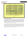
1
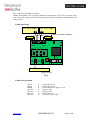
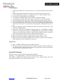
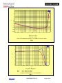
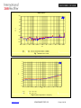
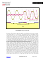
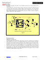
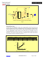
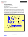
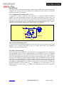
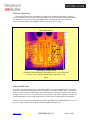
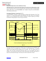
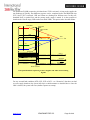
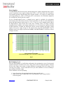
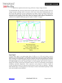
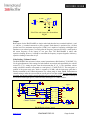
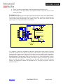
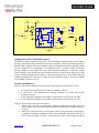
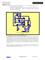
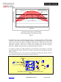
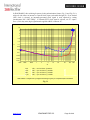
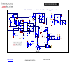
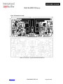
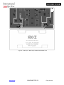
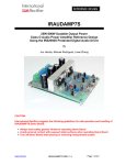
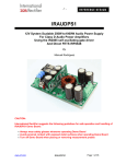
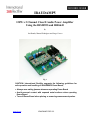
IRAUDAMP5 120W x 2 Channel Class D Audio Power Amplifier Using the IRS2092S and IRF6645 By Jun Honda, Manuel Rodríguez and Jorge Cerezo Fig 1 CAUTION: International Rectifier suggests the following guidelines for safe operation and handling of IRAUDAMP5 Demo Board; Always wear safety glasses whenever operating Demo Board Avoid personal contact with exposed metal surfaces when operating Demo Board Turn off Demo Board when placing or removing measurement probes www.irf.com IRAUDAMP5 REV 3.3 Table of Contents Page Introduction………………………………………………………………….. 2 Specifications………………………………………………………………… 3 Connection Setup……………………………………………………….…… 4 Test Procedure………………………………………………………………... 5 Typical Performance…………………………………………………………. 5-9 Theory of Operation…………………………………………………………. 9-10 IRS2092S System Overview………………………………………………… 10-11 Selectable Dead Time………………………………………………………… 11-12 Protection Features…………………………………………………………… 12-17 Efficiency…………………………………………………………………….. 17-18 Thermal Considerations……………………………………………………… 18 Click and Pop Noise Control…………………………………………………. 18-19 Startup and Shutdown Sequencing…………………………………………… 19-21 PSRR…………………………………………………………………………. 21-22 Bus Pumping………………………………………………………………….. 22-23 Input/Output Signal and Volume Control……………………………………. 23-26 Self Oscillating PWM Modulator…………………………………………….. 27 Switches and Indicators………………………………………………………. 28 Frequency Lock, Synchronization Feature…………………………………… 29 Schematics……………………………………………………………………. 31-35 Bill of Materials……………………………………………………………… 36-39 Hardware……………………………………………………………………… 40 PCB specifications……………………………………………………………. 41 Assembly Drawings…………………………………………………………... 42-48 Revision changes descriptions 49 www.irf.com IRAUDAMP5 REV 3.3 Page 1 of 49 Introduction The IRAUDAMP5 reference design is a two-channel, 120W half-bridge Class D audio power amplifier. This reference design demonstrates how to use the IRS2092S Class D audio controller and gate driver IC, implement protection circuits, and design an optimum PCB layout using the IRF6645 DirectFET MOSFETs. The resulting design requires no heatsink for normal operation (one-eighth of continuous rated power). The reference design provides all the required housekeeping power supplies for ease of use. The two-channel design is scalable for power and the number of channels. Applications AV receivers Home theater systems Mini component stereos Powered speakers Sub-woofers Musical Instrument amplifiers Automotive after market amplifiers Features Output Power: Residual Noise: Distortion: Efficiency: Multiple Protection Features: PWM Modulator: www.irf.com 120W x 2 channels, Total Harmonic Distortion (THD+N) = 1%, 1 kHz 170V, IHF-A weighted, AES-17 filter 0.005% THD+N @ 60W, 4Ω 96% @ 120W, 4Ω, single-channel driven, Class D stage Over-current protection (OCP), high side and low side Over-voltage protection (OVP), Under-voltage protection (UVP), high side and low side DC-protection (DCP), Over-temperature protection (OTP) Self-oscillating half-bridge topology with optional clock synchronization IRAUDAMP5 REV 3.3 Page 2 of 49 Specifications General Test Conditions (unless otherwise noted) Supply Voltage ±35V Load Impedance 8-4Ω Self-Oscillating Frequency 400kHz Gain Setting 26dB Notes / Conditions No input signal, Adjustable 1Vrms input yields rated power Electrical Data IR Devices Used Typical Notes / Conditions IRS2092S Audio Controller and Gate-Driver, IRF6645 DirectFET MOSFETs Modulator Self-oscillating, second order sigma-delta modulation, analog input Power Supply Range ± 25V to ±35V Bipolar power supply Output Power CH1-2: (1% THD+N) 120W 1kHz Output Power CH1-2: (10% THD+N) 170W 1kHz Rated Load Impedance 8-4Ω Resistive load Standby Supply Current ±100mA No input signal Total Idle Power Consumption 7W No input signal Channel Efficiency 96% Single-channel driven, 120W, Class D stage . Audio Performance Demodulator Class D Output THD+N, 1W THD+N, 10W THD+N, 60W THD+N, 100W 0.009% 0.003% 0.003% 0.008% 0.01% 0.004% 0.005% 0.010% Dynamic Range 101dB 101dB Residual Noise, 22Hz - 20kHzAES17 170V 170V 2000 95dB 85dB 75dB N/A 170 90dB 80dB 65dB ±1dB ±3dB Damping Factor Channel Separation Frequency Response : 20Hz-20kHz : 20Hz-35kHz Thermal Performance Idling 2ch x 15W (1/8 rated power) 2ch x 120W (Rated power) Physical Specifications Dimensions www.irf.com *Before Typical TC =30C TPCB=37C TC =54C TPCB=67C TC =80C TPCB=106C Notes / Conditions 1kHz, Single-channel driven A-weighted, AES-17 filter, Single-channel operation Self-oscillating – 400kHz 1kHz, relative to 4Ω load 100Hz 1kHz 10kHz 1W, 4Ω - 8Ω Load Notes / Conditions No signal input, TA=25C Continuous, TA=25C At OTP shutdown @ 150 sec, TA=25C 5.8”(L) x 5.2”(W) IRAUDAMP5 REV 3.3 Page 3 of 49 Note: Class D Specifications are typical *Before demodulator refers to audio performance measurements of the Class D output power stage only, with preamp and output filter bypassed this means performance measured before the low pass filter. Connection Setup 35V, 5A DC supply 35V, 5A DC supply 250W, Non-inductive Resistors 4 Ohm 4 Ohm G J3 CH1 Output J4 TP1 S1 CH2 Output J7 J9 TP2 LED Protection CH1 Input J8 J5 J6 CH2 Input Normal S2 S3 Volume R113 Audio Signal Generator Typical Test Setup Fig 2 Connector Description CH1 IN CH2 IN POWER CH1 OUT CH2 OUT EXT CLK DCP OUT www.irf.com J6 J5 J7 J3 J4 J8 J9 Analog input for CH1 Analog input for CH2 Positive and negative supply (+B / -B) Output for CH1 Output for CH2 External clock sync DC protection relay output IRAUDAMP5 REV 3.3 Page 4 of 49 Test Procedures 1. Connect 4, 250W load to outputs connectors, J3 and J4 and Audio Precision analyzer (AP). 2. Connect Audio Signal Generator to J6 and J5 for CH1 and CH2 respectively (AP). 3. Connect a dual power supply to J7, pre-adjusted to ±35V, as shown in Figure 2 above. 4. Set switch S3 to middle position (self oscillating). 5. Set volume level knob R108 fully counter-clockwise (minimum volume). 6. Turn on the power supply. Note: always apply or remove the ±35V at the same time. 7. Orange LED (Protection) should turn on almost immediately and turn off after about 3s. 8. Green LED (Normal) then turns on after orange LED is extinguished and should stay on. 9. One second after the green LED turns on; the two blue LEDS on the Daughter Board should turn on and stay on for each channel, indicating that a PWM signal is present at LO 10. With an Oscilloscope, monitor switching waveform at test points TP1 and TP2 of CH1 and CH2 on Daughter Board. 11. If necessary, adjust the self-oscillating switching frequency of AUDAMP5 to 400KHz 5kHz using potentiometer R29P. For IRAUDAMP5, the self-oscillating switching frequency is pre-calibrated to 400 KHz. To modify the AUDAMP5 frequency, change the values of potentiometers R21 and R22 for CH1 and CH2 respectively. 12. Quiescent current for the positive supply should be 70mA 10mA at +35V. 13. Quiescent current for the negative supply should be 100mA 10mA at –35V. 14. Push S1 switch, (Trip and Reset push-button) to restart the sequence of LEDs indicators, which should be the same as noted above in steps 6-9. Audio Tests: 15. Apply 1 V RMS at 1KHz from the Audio Signal Generator 16. Turn control volume up (R108 clock-wise) to obtain an output reading of 100Watts for all subsequent tests as shown on the Audio Precision graphs below, where measurements are across J3 and J2 with an AES-17 Filter Typical Performance The tests below were performed under the following conditions: ±B supply = ±35V, load impedance = 4 resistive load, 1kHz audio signal, Self oscillator @ 400kHz and internal volume-control set to give required output with 1Vrms input signal, with AES-17 Filter, unless otherwise noted. www.irf.com IRAUDAMP5 REV 3.3 Page 5 of 49 THD versus Power: 10 5 2 1 0.5 0.2 0.1 % 0.05 0.02 0.01 0.005 0.002 0.001 100m 200m 500m 1 2 5 10 20 50 100 200 W Blue, CH1 - 4 Ohm Red, CH2 - 4 Ohm Figure 18. Total Harmonics Distortion + Noise (THD+N) versus power output Fig 3 +4 +3 +2 +1 -0 -1 d B r A -2 -3 -4 -5 -6 -7 -8 -9 -10 20 50 100 200 500 1k 2k 5k 10k 20k 50k 100k 200k Hz Frequency Response: Red Blue CH1 - 4 Ohm, 2V Output CH1 - 8 Ohm, 2V Output Frequency Characteristics vs. Load Impedance Fig 4 www.irf.com IRAUDAMP5 REV 3.3 Page 6 of 49 . THD versus Frequency: 100 50 10 5 1 0.1 0.05 % 0.01 0.001 0.0005 0.0001 20 50 100 200 500 1k 2k 5k 10k 20k Hz Pink Blue Cyan Green CH1, 1W Output CH1, 10W Output CH1, 50W Output CH1, 100W Output THD+N Ratio vs. Frequency Fig 5 . Frequency Spectrum : +0 -10 -20 -30 -40 d B V -50 -60 -70 -80 -90 -100 -110 10 20 50 100 200 500 1k 2k 5k 10k 20k Hz Red Blue CH1, 1V, 1kHz, Self Oscillator @ 400kHz CH2, 1V, 1kHz, Self Oscillator @ 400kHz Fig 6 www.irf.com Frequency Spectrum IRAUDAMP5 REV 3.3 Page 7 of 49 . Floor Noise: +20 +0 -20 -40 d B V -60 -80 -100 -120 -140 10 20 50 100 200 500 1k 2k 5k 10k 20k Hz Red Blue CH1 - ACD, No signal, Self Oscillator @ 400kHz CH2 - ACD, No signal, Self Oscillator @ 400kHz Fig 7 Residual Noise (ACD) . Channel Separation: +0 -10 -20 -30 -40 -50 d B -60 -70 -80 -90 -100 -110 -120 20 50 100 200 500 1k 2k 5k 10k 20k Hz Red Blue CH1 – CH2, 60W CH2 – CH1, 60W Fig 8 Channel Separation vs. Frequency www.irf.com IRAUDAMP5 REV 3.3 Page 8 of 49 . Clipping Characteristics: Red Trace: Total Distortion + Noise Voltage Green Trace: Output Voltage 60W / 4, 1kHz, THD+N=0.008% 174W / 4, 1kHz, THD+N=10% Measured Output and Distortion Waveforms Fig 9 . IRAUDAMP5 Theory of Operation Referring to Fig 10 below, the input error amplifier of the IRS2092S forms a front-end secondorder integrator with C1, C21, C23 and R21. This integrator also receives a rectangular feedback waveform from R31, R33 and C17 into the summing node at IN- from the Class D power stage switching node (connection of DirectFET Q3 and DirectFET Q4). The quadratic oscillatory waveform of the switch node serves as a powered carrier signal from which the audio is recovered at the speaker load through a single-stage LC filter. The modulated signal is created by the fluctuations of the analog input signal at R13 that shifts the average value of this quadratic waveform through the gain relationship between R13 and R31 + R33 so that the duty cycle varies according to the instantaneous signal level of the analog input signal at R13. R33 and C17 act to immunize the rectangular waveform from possible narrow noise spikes that may be created by parasitic impedances on the power output stage. The IRS2092S input integrator then processes the signal from the summing node to create the required triangle wave amplitude at the COMP output. The triangle wave then is converted to Pulse Width Modulation, or PWM, signals that are internally level-shifted Down and Up to the negative and positive supply rails. The level shifted PWM signals are called LO for low output, and HO for high output, and have opposite polarity. A programmable amount of dead time is added between the gate signals to avoid cross conduction between the power MOSFETs. The IRS2092S drives two IRF6645 DirectFET MOSFETs in the power stage to provide the amplified PWM waveform. The amplified analog output is reconstructed by demodulating the powered PWM at the switch node, called VS. (Show as VS on the schematic)This is done by means of the LC low-pass filter (LPF) formed by L1 and C23A, which filters out the Class D switching carrier signal, leaving the audio powered output at the speaker load. A single stage output filter can be used with switching www.irf.com IRAUDAMP5 REV 3.3 Page 9 of 49 frequencies of 400 kHz and greater; lower switching frequencies may require additional filter components. +VCC is referenced to –B and provides the supply voltage to the LO gate driver. D6 and C5 form a bootstrap supply that provides a floating voltage to the HO gate driver. The VAA and VSS input supplies are derived from +B and -B via R52 and C18, and R50 and C12, respectively. Thus, a fully functional Class D PWM amplifier plus driver circuit is realized in an SO16 package with just a few small components. . R33 C17 R31 R52 +B C18 0V IRS2092S DirectFet VB R32 HO IN- Modulator and Shift level - . + GND Integrator 0V Q3 IRF6645 LP Filter C5 R13 COMP 0V VS VCC L1 D6 INPUT R21 0V C23 C1 C21 +VAA R30 LO Q4 C23A . IRF6645 DirectFet COM C3 -VSS +VCC C12 -B R50 . Simplified Block Diagram of IRAUDAMP5 Class D Amplifier Fig 10 System overview IRS2092S Gate Driver IC The IRAUDAMP5 uses the IRS2092S, a high-voltage (up to 200V), high-speed power MOSFET PWM generator and gate driver with internal dead-time and protection functions specifically designed for Class D audio amplifier applications. These functions include OCP and UVP. Bidirectional current protection for both the high-side and low-side MOSFETs are internal to the IRS2092S, and the trip levels for both MOSFETs can be set independently. In this design, the dead time can be selected for optimized performance by minimizing dead time while preventing shoot-through. As a result, there is no gate-timing adjustment on the board. Selectable dead time through the DT pin voltage is an easy and reliable function which requires only two external resistors, R11 and R9 as shown on Fig11 below. www.irf.com IRAUDAMP5 REV 3.3 Page 10 of 49 . +B CSH VAA AUDIO_INPUT HO CSD VS . VCC LO VSS VREF COM CSLO DT R13 R19 R18 CH1 VB INCOMP Feedback . GND IRS2092S +VCC R5 -B . System-level View of Class D Controller and Gate Driver IRS2092S Fig 11 Selectable Dead-Time The dead time of the IRS2092S is based on the voltage applied to the DT pin. (Fig 12) An internal comparator determines the programmed dead time by comparing the voltage at the DT pin with internal reference voltages. An internal resistive voltage divider based on different ratios of VCC negates the need for a precise reference voltage and sets threshold voltages for each of the four programmable settings. Shown in the table below are component values for programmable dead times between 25 and 105 ns. To avoid drift from the input bias current of the DT pin, a bias current of greater than 0.5mA is suggested for the external resistor divider circuit. Resistors with up to 5% tolerance can be used. Selectable Dead-Time Dead-time mode DT1 DT2 DT3 DT4 Dead time ~25ns ~40ns ~65ns ~105ns R5 3.3k 5.6k 8.2k open Operational Mode R13 8.2k 4.7k 3.3k <10k DT voltage 0.71 x Vcc 0.46 x Vcc 0.29 x Vcc 0 x Vcc Default Default 25nS 40nS Dead-time 65nS 105nS 0 0.23xVcc 0.36xVcc 0.57xVcc Vcc VDT Fig 12 Dead-time Settings vs. VDT Voltage www.irf.com IRAUDAMP5 REV 3.3 Page 11 of 49 Over-Current Protection (OCP) In the IRAUDAMP5, the IRS2092S gate driver accomplishes OCP internally, a feature discussed in greater detail in the “Protection” section. Offset Null (DC Offset) The IRAUDAMP5 is designed such that no output-offset nullification is required, thanks to closed loop operation. DC offsets are tested to be less than ±20mV. Protection The IRAUDAMP5 has a number of protection circuits to safeguard the system and speaker as shown in the figure 13 below, which fall into one of two categories – internal faults and external faults, distinguished by the manner in which a fault condition is treated. Internal faults are only relevant to the particular channel, while external faults affect the whole board. For internal faults, only the offending channel is stopped. The channel will hiccup until the fault is cleared. For external faults, the whole board is stopped using the shutdown sequencing described earlier. In this case, the system will also hiccup until the fault is cleared, at which time it will restart according to the startup sequencing described earlier. . CSH D1 R43 +B VB 1.2V R25 + R41 BAV19 Q3 R32 HO IRF6645 10R LP Filter . CSD VS . CSD OCSET VCC OCREF 5.1V D4 OCREF Green Yellow LEDs Q4 R30 LO IRF6645 10R R19 R18 OCSET Trip RESET -B COM UVP OVP OTP DCP To next channel Functional Block Diagram of Protection Circuit Implementation Fig 13 www.irf.com IRAUDAMP5 REV 3.3 Page 12 of 49 Internal Faults OCP and OTP are considered internal faults, which will only shutdown the particular channel by pulling low the relevant CSD pin. The channel will shutdown for about one-half a second and will hiccup until the fault is cleared. Over-Temperature Protection (OTP, Fig 14) A separate PTC resistor is placed in close proximity to the high-side IRF6645 DirectFET MOSFET for each of the amplifier channels. If the resistor temperature rises above 100C, the OTP is activated. The OTP protection will only shutdown the relevant channel by pulling the CSD pin low and will recover once the temperature at the PTC has dropped sufficiently. This temperature protection limit yields a PCB temperature at the MOSFET of about 100C, which is limited by the PCB material and not by the operating range of the MOSFET. Rp1 is thermally connected with Q3 Rp1 100K 100C Q7 C28 47nF OTP1 -B R47 R48 100K 1K Q3 2 2 3 3 1 -B R31 IRF6645 OTP CH1 Fig 14 Over-Current Protection (OCP) The OCP internal to the IRS2092S shuts down the IC if an OCP is sensed in either of the output MOSFETs. For a complete description of the OCP circuitry, please refer to the IRS2092S datasheet. Here is a brief description: Low-Side Current Sensing Fig 15 shows the low side MOSFET as is protected from an overload condition by measuring the low side MOSFET drain-to-source voltage during the low side MOSFET on state, and will shut down the switching operation if the load current exceeds a preset trip level. The voltage setting on the OCSET pin programs the threshold for low-side over-current sensing. Thus, if the VS voltage during low-side conduction is higher than the OCSET voltage, the IRS2092S will trip and CSD goes down. It is recommended to use VREF to supply a reference voltage to a resistive divider (R19 and R18 for CH1) to generate a voltage to OCSET; this gives better variability against VCC fluctuations. For IRAUDAMP5, the low-side over-current trip level is set to 0.65V. For IRF6645 DirectFET MOSFETs with a nominal RDS-ON of 28mOhms at 25C, this results in a ~23A maximum trip level. Since the RDS-ON is a function of temperature, the trip level is reduced to ~15A at 100C. www.irf.com IRAUDAMP5 REV 3.3 Page 13 of 49 . CSH D1 R43 +B VB 1.2V HO R25 + R41 BAV19 R32 10R Q3 IRF6645 LP Filter . VS CSD CSD OCSET VCC OCREF 5.1V OCREF R19 LO R30 10R R18 Q4 IRF6645 -B OCSET COM Simplified Functional Block Diagram of High-Side and Low-Side Current Sensing (CH1) Fig 15 High-Side Current Sensing (Fig15) The high-side MOSFET is protected from an overload condition and will shutdown the switching operation if the load current exceeds a preset trip level. High-side over-current sensing monitors detect an overload condition by measuring the high side MOSFET’s drain-to-source voltage (VDS) through the CSH and VS pins. The CSH pin detects the drain voltage with reference to the VS pin, which is the source of the high-side MOSFET. In contrast to the low-side current sensing, the threshold of CSH pin to engage OC protection is internally fixed at 1.2V. An external resistive divider R43+R25 and R41 (for Ch1) can be used to program a higher threshold. An additional external reverse blocking diode (D1 for CH1) is required to block high voltage feeding into the CSH pin during low-side conduction. By subtracting a forward voltage drop of 0.6V at D1, the minimum threshold which can be set for the high-side is 0.6V across the drain-to-source. For IRAUDAMP5, the high-side over-current trip level is set to 0.6V across the high-side MOSFET. For the IRF6645 MOSFETs with a nominal RDS-ON of 28 mOhms at 25C, this results in a ~21A maximum trip level. Since the RDS-ON is a function of temperature, the trip level is reduced to ~14A at 100C. For a complete description of calculating and designing the over-current trip limits, please refer to the IRS2092S datasheet. Positive and Negative Side of Short Circuit, versus switching output shut down: The plots below show the speed that the IRS2092S responds to a short circuit condition. Notice that the envelope behind the sine wave output is actually the switching frequency ripple. Bus pumping naturally affects this topology. www.irf.com IRAUDAMP5 REV 3.3 Page 14 of 49 Positive and Negative side of Short Circuit, versus switching output shut down: CSD pin CSD pin VS pin VS pin Load current CSD pin Load current CSD pin VS pin VS pin Load current Load current OCP Waveforms Showing Load Current and Switch Node Voltage (VS) Fig 16 . Short Circuit Response: CSD pin CSD pin VS pin VS pin Load current Load current OCP Waveforms Showing CSD Trip and Hiccup Fig 17 External Faults OVP, UVP and DCP are considered external faults. In the event that any external fault condition is detected, the shutdown circuit will disable the output for about three seconds, during which time the orange AUDAMP5 “Protection” LED will turn on. If the fault condition has not cleared, the protection circuit will hiccup until the fault is removed. Once the fault is cleared, the green “Normal” LED will turn on. There is no manual reset option. Over-Voltage Protection (OVP Fig 18) OVP will shut down the amplifier if the bus voltage between GND and -B exceeds 40V. The threshold is determined by the voltage sum of the Zener diode Z105, R140, and VBE of Q109. As a result, it protects the board from hazardous bus pumping at very low audio signal frequencies by shutting down the amplifier. OVP will automatically reset after three seconds. Since the +B and –B supplies are assumed to be symmetrical (bus pumping, although asymmetrical in time, www.irf.com IRAUDAMP5 REV 3.3 Page 15 of 49 will pump the bus symmetrically in voltage level over a complete audio frequency cycle), it is sufficient to sense only one of the two supply voltages for OVP. It is therefore up to the user to ensure that the power supplies are symmetrical. SD Q109 Over-Voltage Protection (OVP) R139 D105 R140 10k 47k OT 1N4148 Z107 18V R149 47K Z105 R145 47K 39V OT DCP R144 UVP 10k Q109 Q110 MMBT5551 R141 47k MMBT5551 -B R146 47K S1 SW-PB C119 0.1uF, 50V Trip and restart OVP Q110 Under-Voltage Protection (UVP) Fig 18 Under-Voltage Protection (UVP, Fig18) UVP will shutdown the amplifier if the bus voltage between GND and -B falls below 20V. The threshold is determined by the voltage sum of the Zener diode Z107, R145 and VBE of Q110. As with OVP, UVP will automatically reset after three seconds, and only one of the two supply voltages needs to be monitored. Speaker DC-Voltage Protection (DCP, Fig 19) DCP is provided to protect against DC current flowing into the speakers. This abnormal condition is rare and is likely caused when the power amplifier fails and one of the high-side or low-side IRF6645 DirectFET MOSFETs remain in the ON state. DCP is activated if either of the outputs has more than ±4V DC offset (typical). Under this fault condition, it is normally required to shutdown the feeding power supplies. Since these are external to the reference design board, an isolated relay P1 is provided for further systematic evaluation of DC-voltage protection. This condition is transmitted to the power supply controller through connector J9, whose pins are shorted during a fault condition. www.irf.com IRAUDAMP5 REV 3.3 Page 16 of 49 +B R125 10K Q106 R126 100K MMBT5401 Q105 MMBT5551 R130 47K To DCP DC protection DCP R131 47K R128 6.8k R124 10k Q104 C116 100uF, 16V R123 R122 1K 47k MMBT5401 R129 6.8k R121 R127 6.8k 47k From CH1 Output CH1 O CH2 O From CH2 Output -B Fig 19 Efficiency Figs 20 demonstrate that IRAUDAM5 is highly efficient, due to two main factors: a.) DirectFETs offer low RDS(ON) and very low input capacitance, and b). The PWM operates as Pulse Density Modulation. 100.0% 90.0% Power Stage Efficiency (%) 80.0% 70.0% 60.0% 50.0% 40.0% 30.0% 20.0% 10.0% 0.0% 0 20 40 60 80 100 120 140 160 180 Output Power (W) Efficiency vs. Output Power, 4 Single Channel Driven, ±B supply = ±35V, 1kHz Audio Signal Fig20 www.irf.com IRAUDAMP5 REV 3.3 Page 17 of 49 Thermal Considerations The daughter-board design can handle one-eighth of the continuous rated power, which is generally considered to be a normal operating condition for safety standards. Without the addition of a heatsink or forced air-cooling, the daughter board cannot handle fully rated continuous power. A thermal image of the daughter board is as shown in Fig 21 below. Thermal Distribution 67C 54C 67C 54C Thermal image of Daughter-Voard Two-Channel x 1/8th Rated Power (15W) in Operation, TC = 54°C at Steady State ±B supply = ±35V, 4 Load, 1kHz audio signal, Temp ambient = 25°C Fig 21 Click and POP noise: One of the most important aspects of any audio amplifier is the startup and shutdown procedures. Typically, transients occurring during these intervals can result in audible pop- or click-noise from the output speaker. Traditionally, these transients have been kept away from the speaker through the use of a series relay that connects the speaker to the audio amplifier only after the startup transients have passed and disconnects the speaker prior to shutting down the amplifier. Thanks to the click and pop elimination function in the IRS2092S, IRAUDAMP5 does not use any series relay to disconnect the speaker from the audible transient noise. www.irf.com IRAUDAMP5 REV 3.3 Page 18 of 49 Click-Noise Reduction Circuit (Solid-State Shunt) IRS2092S controller is relatively quiet with respect to class AB, but for additional click or POP noise reduction you may add a shunt circuit that further attenuates click or pop transients during turn on sequencing. The circuit is not populated on the present demo board; for implementation details, please refer to the IRAUDAMP4 user’s manual at http://www.irf.com/technicalinfo/refdesigns/audiokits.html Startup and Shutdown Sequencing (Fig 22) The IRAUDAMP5 sequencing is achieved through the charging and discharging of the CStart capacitor C117. Along with the charging and discharging of the CSD voltage (C10 on daughter board for CH1) of the IRS2092S, this is all that is required for complete sequencing. The startup and shutdown timing diagrams are show in Figure 22A below: CStart Ref2 CStart Ref1 CStart Ref1 CStart Ref2 CSD= 2/3VDD CSD CStart Time External trip Reset CHx_O SP MUTE Audio MUTE Music shutdown Class D shutdown Class D startup Music startup Click Noise Reduction Sequencing at Trip and Reset Fig 22A For startup sequencing, the control power supplies start up at different intervals depending on the ±B supplies. As the +/-B supplies reach +5 volts and -5 volts respectively, the +/-5V control supplies for the analog input start charging. Once +B reaches ~16V, VCC charges. Once –B reaches -20V, the UVP is released and CSD and CStart (C117) start charging. The Class D amplifier is now operational, but the preamp output remains muted until CStart reaches Ref2. At this point, normal operation begins. The entire process takes less than three seconds. www.irf.com IRAUDAMP5 REV 3.3 Page 19 of 49 For Shutdown (Fig22B) sequencing is initiated once UVP is activated. As long as the supplies do not discharge too quickly, the shutdown sequence can be completed before the IRS2092S trips UVP. Once UVP is activated, CSD and CStart are discharged at different rates. In this case, threshold Ref2 is reached first and the preamp audio output is muted. It is then possible to shutdown the Class D stage (CSD reaches two-thirds VDD). This process takes less than 200ms. +B CStart Ref2 CStart Ref1 CSD= 2/3VDD CSD CStart +5V Time -5V Vcc -B UVP@-20V CHx_O SP MUTE Audio MUTE Class D shutdown Music shutdown Conceptual Shutdown Sequencing of Power Supplies and Audio Section Timing Fig22B For any external fault condition (OTP, OVP, UVP or DCP – see “Protection”) that does not lead to power supply shutdown, the system will trip in a similar manner as described above. Once the fault is cleared, the system will reset (similar sequence as startup). www.irf.com IRAUDAMP5 REV 3.3 Page 20 of 49 Power Supplies The IRAUDAMP5 has all the necessary housekeeping power supplies onboard and only requires a pair of symmetric power supplies ranging from ±25V to ±35V (+B, GND, -B) for operation. The internally-generated housekeeping power supplies include a ±5V supply for analog signal processing (preamp etc.), while a +12V supply (VCC), referenced to –B, is included to supply the low and high side Class D gate-driver stages. For the externally-applied power, a regulated power supply is preferable for performance measurements, but is not always necessary. The bus capacitors, C31 and C32 on the motherboard, along with high-frequency bypass-caps C14, C15; C32 and C33 on the daughter board, address the high-frequency ripple current that results from switching action. In designs involving unregulated power supplies, the designer should place a set of external bus capacitors having enough capacitance to handle the audio-ripple current. Overall regulation and output voltage ripple for the power supply design are not critical when using the IRAUDAMP5 Class D amplifier as the power supply rejection ratio (PSRR) of the IRAUDAMP5 is excellent, as shown on Figure 23 below. Power Supply Rejection Ratio Green: IRAUDAMP5, Cyan: VAA/VSS are fed by Vbus Fig 23 Bus Pumping (Fig24) Since the IRAUDAMP5 is a half-bridge configuration, bus pumping does occur. Under normal operation during the first half of the cycle, energy flows from one supply through the load and into the other supply, thus causing a voltage imbalance by pumping up the bus voltage of the receiving power supply. In the second half of the cycle, this condition is reversed, resulting in bus pumping of the other supply. These conditions worsen bus pumping: 1. Lower frequencies (bus-pumping duration is longer per half cycle) 2. Higher power output voltage and/or lower load impedance (more energy transfers between supplies) www.irf.com IRAUDAMP5 REV 3.3 Page 21 of 49 3. Smaller bus capacitors (the same energy will cause a larger voltage increase) The IRAUDAMP5 has protection features that will shut down the switching operation if the bus voltage becomes too high (>40V) or too low (<20V). One of the easiest countermeasures is to drive both of the channels in a stereo configuration out of phase so that one channel consumes the energy flow from the other and does not return it to the power supply. Bus voltage detection is only done on the –B supply, as the effect of the bus pumping on the supplies is assumed to be symmetrical in amplitude (although opposite in phase) with the +B supply. Bus Pumping Figure: Cyan = Positive Rail voltage (+B) Green = Speaker Output Pink = Negative Rail voltage (-B) Fig 24 Input Signal A proper input signal is an analog signal below 20 kHz, up to ±3.5V peak, having a source impedance of less than 600 ohms. A 30-60 kHz input signal can cause LC resonance in the output LPF, resulting in an abnormally large amount of reactive current flowing through the switching stage (especially at 8 ohms or higher impedance towards open load), and causing OCP activation. The IRAUDAMP5 has an RC network (Fig25), or Zobel network (R47 and C25 [CH1]), to dampen the resonance and protect the board in such an event, but is not thermally rated to handle continuous supersonic frequencies. These supersonic input frequencies therefore should be avoided. Separate mono RCA connectors provide input to each of the two channels. Although both channels share a common ground, it is necessary to connect each channel separately to limit noise and crosstalk between channels. www.irf.com IRAUDAMP5 REV 3.3 Page 22 of 49 . 0V LP Filter 0V L1 C23A . R47 . C25 . Zobel Filter and Output filter demodulator Fig 25 Output Both outputs for the IRAUDAMP5 are single-ended and therefore have terminals labeled (+) and (-), with the (-) terminal connected to power ground. Each channel is optimized for a 4-Ohm speaker load for a maximum output power (120W), but is capable of operating with higher load impedances (at reduced power), at which point the frequency response will have a small peak at the corner frequency of the output LC low pass filter. The IRAUDAMP5 is stable with capacitive-loading; however, it should be noted that the frequency response degrades with heavy capacitive loading of more than 0.1μF. Gain Setting / Volume Control The IRAUDAMP5 has an internal volume control (potentiometer R108 labeled, ”VOLUME”, Fig 26) for gain adjustment. Gain settings for both channels are tracked and controlled by the volume control IC (U_2), setting the gain from the microcontroller IC (U_1). The maximum volume setting (clockwise rotation) corresponds to a total gain of +37.9dB (78.8V/V). The total gain is a product of the power-stage gain, which is constant (+23.2dB), and the input-stage gain that is directly-controlled by the volume adjustment. The volume range is about 100dB, with minimum volume setting to mute the system with an overall gain of less than -60dB. For best performance in testing, the internal volume control should be set to a gain of 21.9V/V, such that 1Vrms input will result in rated output power (120W into 4), allowing for a >11dB overdrive. +5V C109 +5V R108 CT2265-ND C107 4.7uF, 16V 8 7 6 C108 10nF, 50V 5 VSS VDD VR0 CS VR1 SDATA CLK SIMUL Audio in 4.7uF, 16V U_2 U_1 1 ZCEN R7 2 CS 4 47R CS 3 SDATAI R8 SDATAI AOUTL 10R +5V C1 10uF, 50V SCLK R10 100R 100K Level OUT 1 VD+ VA- -5V DGRD VA+ +5V SCLK AOUTR R2 SDATAOAGNDR MUTE R11 47R MUTE CS3310 AINR R1 Level OUT 2 47R Control Volume J5 R3 AGNDL 47R R9 3310S06S AINL R4 100R 100K J6 Audio in Fig 26 Digital volume Control www.irf.com IRAUDAMP5 REV 3.3 Page 23 of 49 Bridged Output The IRAUDAMP5 is not intended for a bridge-tied-load, or BTL configuration. However, BTL operation can be achieved by feeding out-of-phase audio input signals to the two input channels as shown in the figure 27 below. In BTL operation, minimum load impedance is 8 Ohms and rated power is 240W non-clipping. The installed clamping diodes D5 – D8 are required for BTL operation, since reactive energy flowing from one output to the other during clipping can force the output voltage beyond the voltage supply rails if not clamped. . R33 C17 R31 +VAA +B COMP INPUT C1 HO INCH1 GND Modulator and Shift level + +B VS L1 VCC 10k 1% LO . COM R34 Q4 -B IRF6645 -B . C18 R32 IRF6645 LP Filter Integrator 10k 1% 1 Q3 D5 . R13 0V VB IRS2092S D7 C23 R21 C21 +VAA +B VB IRS2092S COMP HO INCH2 GND IRF6645 +B LP Filter + Modulator and Shift level D6 R14 . 0V Q6 VS L2 VCC Integrator LO COM Q5 D8 C24 C2 C22 -B IRF6645 -B Bridged configuration Fig 27 Output Filter Design, Preamplifier and Performance The audio performance of IRAUDAMP5 depends on a number of different factors. The section entitled, “Typical Performance” presents performance measurements based on the overall system, including the preamp and output filter. While the preamp and output filter are not part of the Class D power stage, they have a significant effect on the overall performance. Output filter Since the output filter is not included in the control loop of the IRAUDAMP5, the reference design cannot compensate for performance deterioration due to the output filter. Therefore, it is important to understand what characteristics are preferable when designing the output filter: www.irf.com IRAUDAMP5 REV 3.3 Page 24 of 49 1) The DC resistance of the inductor should be minimized to 20 mOhms or less. 2) The linearity of the output inductor and capacitor should be high with respect to load current and voltage. Preamplifier (Fig 28) The preamp allows partial gain of the input signal, and controls the volume in the IRAUDAMP5. The preamp itself will add distortion and noise to the input signal, resulting in a gain through the Class D output stage and appearing at the output. Even a few micro-volts of noise can add significantly to the output noise of the overall amplifier. C5 10uF, 50V R13 R55 0.0 R1 J5 1 2 3 4 5 6 7 8 R3 100R 100K ZCEN CS AINL AGNDL SDATAI AOUTL VD+ VA- DGRD VA+ SCLK AOUTR SDATAOAGNDR MUTE CS3310 AINR R2 100K J6 Audio in R31 3.3K Audio in U_? Feedback IN-1 R71 OPEN +5V 16 15 R33 47k 1% 1K CH1 IN 4 5 6 1 2 3 C17 150pF, 500V OC -5V J1A C2 10uF, 50V R5 14 13 4.7R 4.7R 12 R6 11 IRS2092S MODULE -5V +5V J1B C3 10uF, 50V 10 9 R4 100R C6 10uF, 50V R14 -5V 3.3K 10 11 12 CH2 IN R72 OPEN 7 8 9 IN-2 VCC SD R56 0.0 VCC Feedback R32 R34 47k 1% 1K Preamplifier Fig28 It is possible to evaluate the performance without the preamp and volume control, by moving resistors R13 and R14 to R71 and R72, respectively. This effectively bypasses the preamp and connects the RCA inputs directly to the Class D power stage input. Improving the selection of preamp and/or output filter components will improve the overall system performance, approaching that of the stand-alone Class D power stage. In the “Typical Performance” section, only limited data for the stand-alone Class D power stage is given. For example, Fig 20 below shows the results for THD+N vs. Output Power are provided, utilizing a range of different inductors. By changing the inductor and repeating this test, a designer can quickly evaluate a particular inductor. www.irf.com IRAUDAMP5 REV 3.3 Page 25 of 49 I IRAUDAMP5 can be used as output inductors evaluation tool 100 TTTTTTT 10 1 % 0.1 0.01 0.001 0.0001 100m 200m 500m 1 2 5 10 20 50 100 200 W Results of THD+N vs. Output Power with Different Output Inductors Fig 29 Self-Oscillating PWM Modulator The IRAUDAMP5 Class D audio power amplifier features a self-oscillating type PWM modulator for the lowest component count, highest performance and robust design. This topology represents an analog version of a second-order sigma-delta modulation having a Class D switching stage inside the loop. The benefit of the sigma-delta modulation, in comparison to the carrier-signal based modulation, is that all the error in the audible frequency range is shifted to the inaudible upper-frequency range by nature of its operation. Also, sigma-delta modulation allows a designer to apply a sufficient amount of correction. The self-oscillating frequency (Fig 30) is determined by the total delay time inside the control loop of the system. The delay of the logic circuits, the IRS2092S gate-driver propagation delay, the IRF6645 switching speed, the time-constant of front-end integrator (e.g.R13, R33, R31, R21, P1, C17, C21, C23 and C1 for CH1) and variations in the supply voltages are critical factors of the self-oscillating frequency. Under nominal conditions, the switching-frequency is around 400kHz with no audio input signal and a +/-35V supply. www.irf.com IRAUDAMP5 REV 3.3 Page 26 of 49 . R33 P1 C17 R31 +B R21 C23 COMP IRS2092S . INPUT R13 Q3 IRF6645 LP Filter INCH1 0V VB HO C1 C21 - GND + Modulator and Shift level VS . VCC Q4 Integrator LO IRF6645 COM -B Self Oscillating determined components Fig 30 Adjustments of Self-Oscillating Frequency The PWM switching frequency in this type of self-oscillating switching scheme greatly impacts the audio performance, both in absolute frequency and frequency relative to the other channels. In absolute terms, at higher frequencies distortion due to switching-time becomes significant, while at lower frequencies, the bandwidth of the amplifier suffers. In relative terms, interference between channels is most significant if the relative frequency difference is within the audible range. Normally, when adjusting the self-oscillating frequency of the different channels, it is best to either match the frequencies accurately, or have them separated by at least 25kHz. With the installed components, it is possible to change the self-oscillating frequency from about 300kHz up to 450kHz, as shown on Fig 30 Switches and Indicators There are four different indicators on the reference design as shown in the figure 31 below: 1. An orange LED, signifying a fault / shutdown condition when lit. 2. A green LED on the motherboard, signifying conditions are normal and no fault condition is present. 3. A blue LED on the daughter board module, signifying there are HO pulses for CH1 4. A blue LED on the daughter board module signifying there are HO pulses for CH2 There are three switches on the reference design: 1. Switch S1 is a trip and reset push-button. Pushing this button has the same effect as a fault condition. The circuit will restart about three seconds after the shutdown button is released. 2. Switch S2 is an internal clock-sync frequency selector. This feature allows the designer to modify the switching frequency in order to avoid AM radio interference. With S3 set to INT, the two settings “H” and “L” will modify the internal clock frequency by about www.irf.com IRAUDAMP5 REV 3.3 Page 27 of 49 20 kHz to 40 kHz, either higher “H” or lower “L.” The actual internal frequency is set by potentiometer R113 - “INT FREQ.” 3. Switch S3 is an oscillator selector. This three-position switch is selectable for internal self oscillator (middle position – “SELF”), or either internal (“INT”) or external (“EXT”) clock synchronization. I E S SW-3WAY_A-B S3A SW S2 R109 1K D103 C110 R110 100k C112 1200pF, 50V 100pF, 50V C111 1N4148 1nF, 50V 1 2 SW_H-L R111 10K +5V R120 100R R112 820R U_3 1A VCC 1Y 6A 2A 6Y 2Y 5A 3A 5Y 3Y 4A GND 4Y Q103 C113 MMBT5551 100pF, 50V R113 5K POT S E I SW-3WAY_A-B S3B SW R116 47R R114 100R C114 10nF, 50V CLK CLK R115 47R 74HC14 +5V J8 BNC A24497 R118 1k EXT. CLK NORMAL R119 1k MUTE PROTECTION MUTE R117 47R LED, Switches and Sync frequencies Fig 31 Switching Frequency Lock / Synchronization Feature For single-channel operation, the use of the self-oscillating switching scheme will yield the best audio performance. The self-oscillating frequency, however, changes with the duty ratio. This varying frequency can interfere with AM radio broadcasts, where a constant-switching frequency with its harmonics shifted away from the AM carrier frequency is preferred. In addition to AM broadcasts, multiple channels can also reduce audio performance at low power, and can lead to increased residual noise. Clock frequency locking/synchronization can address these unwanted characteristics. Please note that the switching frequency lock / synchronization feature is not possible for all frequencies and duty ratios, and operates within a limited frequency and duty-ratio range around the self-oscillating frequency (Figure 32 below). www.irf.com IRAUDAMP5 REV 3.3 Page 28 of 49 600 Suggested clock frequency for maximum locking range Locking range Operating Frequency (kHz) 500 Self-oscillating frequency 400 300 200 Self-oscillating frequency 100 0 10% 20% 30% 40% 50% 60% 70% 80% 90% Duty Cycle Typical Lock Frequency Range vs. PWM Duty Ratio (Self-oscillating frequency set to 400 kHz with no input) Fig 32 The output power range, for which frequency-locking is successful, depends on what the locking frequency is with respect to the self-oscillating frequency. As illustrated in Figure 33, the locking frequency is lowered (from 450kHz to 400kHz to 350kHz and then 300kHz) as the output power range (where locking is achieved) is extended. Once locking is lost, however, the audio performance degrades, but the increase in THD seems independent from the clock frequency. Therefore, a 300 kHz clock frequency is recommended, as shown on Fig 34 It is possible to improve the THD performance by increasing the corner frequency of the high pass filter (HPF) (R17 and C15 for Ch1 Fig 33) that is used to inject the clock signal, as shown in Figure 33 below. This drop in THD, however, comes at the cost of reducing the locking range. Resistor values of up to 100 kOhms and capacitor values down to 10pF may be used. . +VAA +B C15 SYNC 0V . 33pF INPUT R22 COMP IRS2092S HO 22k R13 INCH1 GND 0V VB Q3 IRF6645 LP Filter + Modulator and Shift level VS . VCC Q4 Integrator LO COM IRF6645 -B Switching Frequency Lock / Synchronization Feature Fig 33 www.irf.com IRAUDAMP5 REV 3.3 Page 29 of 49 In IRAUDAMP5, this switching frequency lock/synchronization feature (Fig 31 and Fig 33) is achieved with either an internal or external clock input (selectable through S3). If an internal (INT) clock is selected, an internally-generated clock signal is used, adjusted by setting potentiometer R113 “INT FREQ.” If external (EXT) clock signal is selected, a 0-5V squarewave (~50% duty ratio) logic signal must be applied to BNC connector J17. 10 5 2 1 0.5 0.2 % 0.1 0.05 0.02 0.01 0.005 0.002 0.001 100m 200m 500m 1 2 5 10 20 50 100 200 W Red Pink Blue Cyan CH1, = Self Oscillator @ 400kHz CH1, = Sync Oscillator @ 400kHz CH1, = Sync Oscillator @ 450kHz CH1, = Sync Oscillator @ 350kHz THD+N Ratio vs. Output Power for Different Switching Frequency Lock/Synchronization Conditions Fig 34 www.irf.com IRAUDAMP5 REV 3.3 Page 30 of 49 Class D, Daughter Board IRS2092S Module CH1 Schematic -B Rp1 100K 100C MMBT5401DICT-ND Q7 +35V Bus R40 R52 open 33k C18 VSS OC 1 2 3 VSS 1k 2 10R GND 16 CSH 10k C5 15 VB R25 10K 22uF C30 1nF,250V 10nF R1 100R R3 VAA C21 SD -5V C10 1nF,250V C23 C1 1nF 4 5 INCOMP CSD D6 12 VCC 10uF 6 C12 R19 R26 VCC 8 R50 open R17 1.2k VSS 4.7R 11 LO VREF 10R OCSET 10 COM 9 DT IRS2092S R5 R9 R12 3.3K R13 10R 4.7K 8.2K -35V Bus C3 10uF . Fig 35 IRAUDAMP5 REV 3.3 +35V Bus Page 31 of 49 +B C32 0.1uF,100V C17 0.1uF C14 0.1uF,100V CH1 D-FET2 IRF6645 R30 7 8.2k 3.3uF www.irf.com 1 R32 13 VS D-FET1 IRF6645 10R 14 HO 1K D1 2 2 1K 3 3.01k VAA D4 P1 R46 A26568-ND SD 1 R21 Audio Gnd 1 IN-1 4 5 6 +5V 10R GND1 J1A 3.3uF 0.0 R41 R48 100K 2 2 VAA U1 R47 1 TP1 CH1 O J2A R37 1R 9 10 11 12 13 14 15 16 A26570-ND CH1 Output to LPF1 3 3 R7 -B R43 3 3 CH1 C28 47nF OTP1 OTP CH1 Rp1 is thermally connected with Q3 R31 DS1 -35V Bus -B +B Class D, Daughter Board IRS2092S Module CH2 Schematic OTP2 R39 R51 open 33k R8 VAA +5V 10R 2 3 D3 -5V R2 100R R4 10R CH2 -5V CSH GND VB 16 1nF,250V 1nF,1250V SD C11 C24 HO 1 R27 4 5 COMP CSD VS VCC 13 D5 12 R23 1K D-FET3 IRF6645 10R 14 10uF 6 C16 R20 7 8.2k 3.3uF 8 R49 open R18 1.2k D7 VSS LO VREF COM OCSET DT IRS2092S 4.7R 11 VCC 9 R10 R45 3.3K R14 10R 4.7K 8.2K -35V Bus 10uF Fig 36 IRAUDAMP5 REV 3.3 10R R6 C4 Page 32 of 49 +35V Bus +B C33 0.1uF,100V C13 0.1uF C15 0.1uF,100V CH2 D-FET4 IRF6645 R28 10 . www.irf.com R29 10K C2 1nF C22 IN- R24 100K D2 10k C6 15 R33 2 2 3.01k IN-2 VAA 0.0 R42 22uF SD R53 A26568-ND SD P2 1K 1k VCC C31 Audio Gnd 2 10 11 12 10nF,50V 7 8 9 VSS GND2 U2 1 R22 J1B -B R44 3.3uF C9 47nF OTP2 C19 -B 100C 2 2 MMBT5551 C29 47nF 100K MMBT5401 Q2 +35V Bus R36 10K Rp2 TP2 CH2 O J2B 3 3 R34 100K Q1 -B R11 100K R35 1 R38 1R 1 2 3 4 5 6 7 8 A26570-ND CH2 Output to LPF2 3 3 OTP1 OTP CH2 Rp2 is thermally connected with Q5 OC DS2 -35V Bus -B -B Class D, Daughter Board IRS2092S Module Schematic 33k HO COMP VS CSD VCC VSS LO 12 R26 10uF 6 7 VREF 8.2k 8 R17 1.2k OCSET R5 9 DT 3.3K R13 IRS2092S MMBT5551 -B C29 47nF P2 1K 2 3 -5V 100R R4 10R CH2 Rp2 is thermally connected with Q5 -5V 1nF,250V 1nF,1250V C22 C11 100K 100C 33k -B VAA CSH GND VB 0.0 R42 16 10k C6 15 IN- HO COMP VS R33 R24 100K 1K R29 10K D-FET3 IRF6645 5 10R 14 1 13 CSD VCC VSS LO 12 6 R23 C16 R20 VCC 8 R49 open R18 1.2k 10R VREF OCSET IRS2092S -35V Bus COM DT 10 9 R6 3.3K R14 R10 R45 10R 4.7K 1 8.2K 10uF Fig 37 www.irf.com TP2 CH2 O J2B IRAUDAMP5 REV 3.3 R38 1R 1 2 3 4 5 6 7 8 A26570-ND CH2 Output to LPF2 DS2 C4 C15 0.1uF,100V CH2 D-FET4 IRF6645 R28 7 8.2k 3.3uF 4.7R 11 +B C33 0.1uF,100V C13 0.1uF D5 C24 +35V Bus D2 R27 4 C9 47nF OTP2 10uF D7 Rp2 R39 C2 1nF SD R35 2 2 R2 10nF,50V 3.01k IN-2 -35V Bus -B DS1 22uF C31 SD 1 +B A26570-ND MMBT5401 Q2 U2 3.3uF SD R53 D3 4.7K C3 R44 1k VCC A26568-ND 10R 13 14 15 16 CH1 Output to LPF1 10uF R51 open R22 R37 1R 1 -B +5V 10R 9 10 11 12 8.2K R11 100K R36 10K VAA Audio Gnd 2 R12 +35V Bus J1B VSS GND2 R9 OTP2 R34 100K R8 10 11 12 10R 10 COM C19 7 8 9 D-FET2 IRF6645 4.7R 11 -35V Bus Q1 VCC R30 R19 3.3uF OTP1 TP1 CH1 O J2A OTP CH2 5 C12 OC CH1 13 D6 C23 R50 open C14 0.1uF,100V 1 3 3 C10 -5V 10R 10R 14 C17 0.1uF 2 2 C21 SD D-FET1 IRF6645 R32 4 1nF +B C32 0.1uF,100V R25 10K C1 1nF,250V +35V Bus 3 3 1nF,250V C30 R1 100R R3 IN- 10k C5 15 22uF 10nF VSS VB 2 2 2 3 3.01k VAA SD GND 16 1K R46 A26568-ND D4 CSH 1K D1 2 2 VSS 4 5 6 VAA 0.0 R41 R48 100K 3 3 IN-1 1 2 3 P1 1k C28 47nF R47 3 3 R21 Audio Gnd 1 J1A OC U1 1 10R GND1 -B R43 3.3uF +5V VAA 100C OTP1 C18 R7 100K R40 R52 open CH1 Rp1 MMBT5401DICT-ND Q7 +35V Bus SCH_DB_2092_Rev3.1 R31 OTP CH1 Rp1 is thermally connected with Q3 -B Page 33 of 49 -35V Bus -B -B Class D, Mother Board Control Volume and Power Supplies Schematic C19 R39 C15 R27 CLK 47R 74AHC1G04 Control Volume +5V C109 8 VSS 5 VR0 CS VR1 SDATA CLK SIMUL 1 2 CS 3 SDATAI 4 +5V R7 47R R8 47R R9 3 10R C1 10uF, 50V 3310S06S 4 5 6 SCLK R10 47R MUTE ZCEN 2 R13 R11 7 CS AGNDL SDATAI AOUTL VD+ VA- DGRD VA+ SCLK AOUTR SDATAO AGNDR 8 47R R3 100R AINL MUTE CS3310 AINR C5 10uF, 50V CH1 Feedback IN-1 R31 R55 0.0 4 5 6 +5V 13 4.7R 4.7R 12 9 R14 R4 100R -5V C6 10uF, 50V 3.3K MMBT5401 15V Q102 R107 4.7K CLK +B R28 47R 74AHC1G04 U4 VCC SD R56 0.0 2 1 3 C33 OPEN 5 6 7 8 R57 100K -B C31 1000uF,50V C34 OPEN Chassis Gnd R32 R34 47k 1% 1K L2 C32 1000uF,50V +B 22uH CH2 OUT D6 CH2 O C24 C28 D8 R48 0.47uF, 400V C18 150pF, 500V +35V Gnd -35V -B VCC +5V 33pF R58 100K 1 2 3 4 CH2 Feedback IN-2 C16 J7 J2B 10 11 12 CH2 IN Audio in 470 C25 0.1uF, 400V Trace under J7 7 8 9 + CH1 - -B +B IRS2092S_ MODULE J1B OPEN R40 10, 1W J2A -5V R72 J6 Z103 -5V OPEN R49 2.2k +B C3 10uF, 50V 10 100K VCC UVP OC 13 14 15 16 +5V R6 11 2.2uF,16V 9 10 11 12 J3 1 2 C27 D7 R47 0.47uF, 400V C17 150pF, 500V CH1 OUT D5 C23 J1A C2 10uF, 50V R5 14 C20 1 2 3 22uH 1K CH1 IN 15 R2 R33 47k 1% R71 OPEN 16 L1 CH1 O R50 2.2k 10, 1W J4 1 2 + CH2 - OPEN -B R18 C26 22k 0.1uF, 400V R106 47K R105 10R Q101 FX941 U_6 MC78M12 Vout VCC Z104 24V C106 10uF, 50V Heat Sink Z101 +B HS1 GND Vin +5V Power Supply VCC Power Supply R101 4.7V 47R, 1W ZM4732ADICT R102 47R, 1W C101 10uF, 50V C105 10uF, 50V U_4 Vin Vout C102 10uF, 50V Fig 38 IRAUDAMP5 REV 3.3 Z102 R103 -B 4.7V 47R, 1W ZM4732ADICT D101 MA2YD2300 -B www.irf.com -5V Power Supply +5V MC78M05 Page 34 of 49 R104 47R, 1W U_5 -5V MC79M05 IN OUT D102 MA2YD2300 GND C108 10nF, 50V 6 1 VDD +B 22k 3.3K 100K U_? R17 GND R108 7 U3 R1 J5 4.7uF, 16V U_2 33pF Audio in +5V C107 4.7uF, 16V +5V 470 2.2uF,16V C103 10uF, 50V C104 10uF, 50V Class D, Mother Board Clock and House Keeping Schematic +B 100k R111 10K R112 820R C113 SW-3WAY_A-B R113 5K POT SW 1A VCC 1Y 6A 2A 6Y 2Y 5A 3A 5Y 3Y 4A R116 47R R114 100R GND 4Y CLK Z108 8.2V C114 Q108 R118 EXT. CLK NORMAL MUTE Q110 MMBT5551 R141 47k Trip and restart OVP MMBT5551 R130 47K 47k DC protection DCP R131 47K -5V R128 6.8k R124 10k Q104 47R R122 47k C116 100uF, 16V R123 1K R150 47k MMBT5401 R129 6.8k R133 47k Q112 MMBT5551 R127 6.8k Q107 1 2 3 Z109 8.2V -5V +5V MMBT5551 R132 47k 6 5 4 PVT412 P1 -B Fig 39 www.irf.com IRAUDAMP5 REV 3.3 S1 C119 SW-PB 0.1uF, 50V R126 100K Q105 R151 47k R146 47K R125 10K MMBT5401 R137 D104 1N4148 +B UVP R135 82k R134 10k PROTECTION MUTE R117 R144 +B Q106 R119 1k R145 47K 39V DCP Q109 C115 10uF, 50V Z107 18V R149 47K Z105 10k R148 10k 10nF, 50V 1k 1N4148 -B 74HC14 +5V 4.7k OT OT R136 68k CLK J8 BNC A24497 D105 D107 C117 1N4148 100uF, 16V MMBT5551 R115 47R CStart 47k R138 MMBT5551 S E I S3B 100pF, 50V R120 100R U_3 Q103 MMBT5551 +5V R140 10k R139 Z106 18V Page 35 of 49 J9 2 1 CH2 O 100pF, 50V C111 1N4148 R110 C112 1200pF, 50V SP MUTE D103 1nF, 50V R142 68k D106 1N4148 MMBT5401 SW_H-L R109 1K C110 1 2 +5V CH1 O I E S S2 10K R147 47k Q111 SW R143 SD SW-3WAY_A-B S3A R121 47k DC_PS IRAUDAMP5 Bill of Materials Class D, Daughter Board: Amp5_DB_2092_Rev 3.1_BOM Designator Footprint PartType Quantity C1, C2, C21,C22,C23,C24 C3, C4 C5, C6 C9, C28, C29 C10, C11 C12, C16, C18, C19 C13, C17 C14, C15, C32, C33 C20 C30, C31 D1, D2 D3, D4 D5, D6 D7 DS1, DS2 J1A J1B J2A J2B Q1 805 TAN-A TAN-B 0805 TAN-B TAN-B 0805 1206 0805 0805 SOD-323 SOD-323 SMA SMA 805 CON EISA31 CON EISA31 CON_POWER CON_POWER SOT23-BCE 1nF,250V,COG 10uF, 16V, Tan 10uF, 16V, Tan 47nF,50V, X7R 10uF, 16V, Tan 3.3uF, 16V, X7R 0.1uF,100V, X7R 0.1uF,100V, X7R open 10nF,50V, X7R BAV19WS-7-F 1N4148WS-7-F MURA120T3G ES1D LTST-C171TBKT CON EISA31 CON EISA31 CON_POWER CON_POWER MMBT5551 6 2 2 3 2 4 2 3 1 2 2 2 2 1 2 1 1 1 1 1 Q2, Q7 SOT23-BCE MMBT5401-7 2 www.irf.com IRAUDAMP5 REV 3.3 Page 36 of 49 PART NO 445-2325-1-ND 495-2236-1-ND 399-3706-1-ND PCC1836CT-ND 399-3706-1-ND 445-1432-1-ND 399-3486-1-ND PCC2239CT-ND open PCC103BNCT-ND BAV19WS-FDICT-ND 1N4148WS-FDICT-ND MURA120T3GOSCT-ND ES1DFSCT-ND 160-1645-1-ND A26568-ND A26568-ND A26570-ND A26570-ND MMBT5551FSCT-ND MMBT5401-FDICT-ND VENDER DIGI KEY DIGI KEY DIGI KEY DIGI KEY DIGI KEY DIGI KEY DIGI KEY DIGI KEY DIGI KEY DIGI KEY DIGI KEY DIGI KEY DIGI KEY DIGI KEY DIGI KEY DIGI KEY DIGI KEY DIGI KEY DIGI KEY DIGI KEY IR 3 IRF6645 P100ACT-ND P10ACT-ND P3.3KACT-ND P10ECT-ND P100KACT-ND P4.7KACT-ND P8.2KACT-ND P1.0KACT-ND RHM1.2KARCT-ND P1.0KACT-ND P4.7ACT-ND P10KACT-ND P1.0ACT-ND RHM33KARCT-ND RHM0.0ARCT-ND open 594-2381-675-21007 DIGI KEY 3 ST32ETB102TR-ND RHM3.01KCCT-ND IRS2092S D-FET1, D-FET2, D-FET3, D-FET4 Direct Fet SJ IRF6645 4 R1, R2 0805 100R 2 R3,R4,R9,R10,R15,R16,R27,R28,R30,R32,R8 0805 10R 11 R5, R6 0805 3.3K 2 R7 1206 10R 1 R11, R31, R33, R34, R35, R47 0805 100K 2 R12, R45 0805 4.7K 2 R13, R14,R19,R20 0805 8.2K 2 R24, R48 0805 1K 2 R7,R18 805 1.2k R21, R22 0805 1k 2 R23, R26 0805 4.7R 2 R25, R29,R36,R41, R42 0805 10K 5 R37, R38 0805 1R 3 R39, R40 0805 33K 3 R43, R44 0805 0 3 R49, R50, R51, R52, 1206 open 3 Rp1, Rp2 805 100C P1,P2 ST-32 3mm SQ 1k R46,R53 805 3.01k U1, U2 SOIC16 IR Driver www.irf.com IRAUDAMP5 REV 3.3 Page 37 of 49 DIGI KEY DIGI KEY DIGI KEY DIGI KEY DIGI KEY DIGI KEY DIGI KEY DIGI KEY DIGI KEY DIGI KEY DIGI KEY DIGI KEY DIGI KEY DIGI KEY DIGI KEY MOUSER DIGI KEY IR Class D Motherboard: IRAUDAMP5 MOTHERBOARD BILL OF MATERIAL NO 1 2 3 4 5 6 7 8 9 10 11 Designator C1, C5, C6, C101, C102, C103, C104, C105, C106, C115 C2, C3 C7, C8, C9, C10 C11, C12, C13, C14 C15, C16 C17, C18 C19, C20 C119 C23, C24 # Footprint Part Type Part No Vender 10 RB2/5 10uF, 50V 565-1106-ND Digikey 2 4 4 2 2 2 1 2 RB2/5 open open 805 AXIAL0.19R 1206 1206 CAP MKP 2.2uF, 50V 565-1103-ND Digikey 33pF 150pF, 500V 2.2uF, 16V 0.1uF, 50V 0.47uF, 400V 478-1281-1-ND 338-2598-ND PCC1931CT-ND PCC104BCT-ND 495-1315-ND Digikey Digikey Digikey Digikey Digikey 495-1311-ND Digikey 14 15 16 17 18 19 20 21 22 23 24 25 26 27 C25, C26 C27, C28, C29, C30, C40, C41, C42, C43, C44, C45, C46, C47 R29, R30, R55, R56, R60, R61, R62, R63, R64, R65, R66, R67, R71, R72 C31, C32 C33, C34, C48, C49 C107, C109 C108, C114 C110 C111, C113 C112 C116, C117 D103, D104, D105, D106, D107 D5, D6, D7, D8 D101, D102 HS1 J1A, J1B J2A, J2B 28 J3, J4 2 MKDS5/2-9.5 29 J5, J6 2 Blue RCA RCJ-055 30 J7 1 J HEADER3 277-1272 277-1272-ND or 651-1714984 31 32 J8 J9 1 1 BNC_RA CON ED1567 BNC ED1567 A32248-ND ED1567 33 L1, L2 2 Inductor Sagami 7G17AOr 1D17A-220M Sagami 7G17AOr 1D17A-220M 34 35 36 37 38 NORMAL P1 PROTECTION Q101 Q102, Q104, Q106, Q111 Q103, Q105, Q107, Q108, Q109, Q110, Q112 R1, R2, R57, R58, R110, R126 R3, R4, R114 R5, R6 R7, R8, R10, R11, R27, R28, R115, R116, R117 R9, R105 R13, R14 R17, R18 R106, R121, R122, R130, R131, R132, R133, R137, R139, R141, R145, R146, R147, R149, R150, R151 R152 R55, R56 R39, R40 R21, R22, R23, R24 R120 R29P, R30P R31, R32 R33, R34 1 1 1 1 4 Led rb2/5 DIP-6 Led rb2/5 SOT89 SOT23-BCE 404-1106-ND PVT412 404-1109-ND FX941 MMBT5401-7-F 160-1143-ND PVT412PBF-ND 160-1140-ND FCX491CT-ND MMBT5401-FDICT-ND 7 SOT23-BCE MMBT5551 MMBT5551-FDICT-ND Digikey 6 3 2 805 805 1206 100K 100R 4.7R P100KACT-ND P100ACT-ND P4.7ECT-ND Digikey Digikey Digikey 9 805 47R P47ACT-ND Digikey 2 2 2 805 805 805 10R 3.3K, 1% 22k P10ACT-ND P3.3KZCT-ND P22KACT-ND Digikey Digikey Digikey 16 805 47k P47KACT-ND Digikey 1 2 2 4 1 2 2 2 805 805 805 open 1206 open 2512 1206 OPEN 0.0 Ohms 470R P0.0ACT-ND P470ACT-ND Digikey Digikey Digikey 100R P100ECT-ND Digikey 47K, 1% 1K PT47KAFCT-ND P1.0KECT-ND Digikey Digikey 12 13 39 40 41 42 43 44 45 46 47 48 49 50 51 52 53 54 55 www.irf.com 2 CAP MKPs 0.1uF, 400V 12 805 OPEN 14 805 OPEN 2 4 2 2 1 2 1 2 5 4 2 1 2 2 RB5/12_5 AXIAL0.1R 805 805 805 805 805 rb2/5 SOD-123 SMA SOD-123 Heat_S6in1 CON EISA-31 CON_POWER 1000uF,50V OPEN 4.7uF, 16V 10nF, 50V 1nF, 50V 100pF, 50V 1200pF, 50V 100uF, 16V 1N4148W-7-F 1N4148W-FDICT-ND MURA120T3G MA2YD2300 HEAT SINK CON EISA31 CON_POWER MURA120T3GOSCT-ND MA2YD2300LCT-ND 294-1086-ND A32934-ND A32935-ND 277-1022 277-1271-ND or 651-1714971 CP-1422-ND IRAUDAMP5 REV 3.3 565-1114-ND PCC2323CT-ND PCC103BNCT-ND PCC102CGCT-ND PCC101CGCT-ND 478-1372-1-ND 565-1037-ND Page 38 of 49 Digikey Digikey Digikey Digikey Digikey Digikey Digikey Digikey Digikey Digikey Digikey Digikey Digikey Digikey Digikey or Mouser Digikey Digikey or Mouser Digikey Digikey Inductors, Inc Or ICE Component s, Inc. Digikey Digikey Digikey Digikey Digikey 56 57 58 59 60 61 62 63 64 65 66 67 68 69 70 71 72 73 74 75 76 77 78 79 80 81 82 83 84 85 86 87 88 89 90 91 92 R109, R118, R119, R123 R47, R48 R49, R50 R68, R69 R101, R102, R103, R104 R107, R138 R108 R111, R124, R125, R134, R140, R143, R144, R148 R112 R113 R127, R128, R129 R135 R136, R142 S1 S2 S3 U1, U2 U3, U4 U7, U8 U9, U10 U_1 4 2 2 2 4 2 1 8 1 1 3 1 2 1 1 1 2 2 2 2 1 U_2 1 U_3 U_4 U_5 U_6 Z1, Z2, Z103 Z101, Z102 Z104 Z105 Z106, Z107 Z108, Z109 Volume Knob Thermalloy TO-220 mounting kit with screw 1/2" Standoffs 4-40 4-40 Nut No. 4 Lock Washer 1 1 1 1 3 2 1 1 2 2 1 3 5 5 5 805 2512 1206 AXIAL-0.3 2512 805 V_Control 1K 10, 1W 2.2k OPEN 47R, 1W 4.7K CT2265 P1.0KACT-ND PT10XCT P2.2KECT-ND PT47XCT-ND P4.7KACT-ND CT2265-ND Digikey Digikey Digikey Digikey Digikey Digikey Digikey 805 10K P10KACT-ND Digikey 805 POTs 1206 805 805 Switch SW-EG1908-ND SW-EG1944-ND open SOT25 MINI5 SO-8 SOIC16 820R 5K POT 6.8k 82k 68k SW-PB SW_H-L SW-3WAY P820ACT-ND P6.8KECT-ND P82KACT-ND P68KACT-ND P8010S-ND EG1908-ND EG1944-ND Digikey Digikey Digikey Digikey Digikey Digikey Digikey Digikey 74AHC1G04 open open CS3310 296-1089-1-ND open open 73C8016 or 72J5420 N8A 3310S06S 3310-IR01 M14A TO-220 TO-220 TO-220 SOD-123 SMA SOD-123 SOD-123 SOD-123 SOD-123 Blue Knob Kit screw, ROHS Standoff 100 per bag 100 per bag 74HC14 296-1194-1-ND MC78M05CTG LM79M05CT LM78M12CT MC78M05CTGOS-ND LM79M05CT-ND LM78M12CT-ND 15V 4.7V 24V 39V 18V 8.2V MC21060 AAVID 4880G BZT52C15-FDICT-ND 1SMA5917BT3GOSCT-ND BZT52C24-FDICT-ND BZT52C39-13-FDICT-ND BZT52C18-FDICT-ND BZT52C8V2-FDICT-ND 10M7578 82K6096 8401K-ND H724-ND H729-ND 3362H-502LF-ND *Tachyonix Corporation, 14 Gonaka Jimokuji Jimokuji-cho, Ama-gun Aichi, JAPAN 490-1111 http://www.tachyonix.co.jp [email protected] www.irf.com IRAUDAMP5 REV 3.3 Page 39 of 49 Digikey Newark *Tachyonix Digikey Digikey Digikey Digikey Digikey Digikey Digikey Digikey Digikey Digikey Newark Newark Digikey Digikey Digikey IRAUDAMP5 Hardware Voltage regulator mounting: Item Description 7 8 1 Insulator Thermalfilm 2 Shoulder Washer 3 Flat Washer #4 4 No. 4-40 UNC-2B Hex Nut 5 No. 4-40 UNC-2A X 1/2 Long Phillips Pan Head Screw 6 Lockwasher, No.4 7 Heatsink 8 PCB Item Description 7 8 1 Insulator Thermalfilm 2 Shoulder Washer 3 Flat Washer #4 4 No. 4-40 UNC-2B Hex Nut 5 No. 4-40 UNC-2A X 1/2 Long Phillips Pan Head Screw 6 Lockwasher, No.4 7 Heatsink 8 PCB Fig 40 www.irf.com IRAUDAMP5 REV 3.3 Page 40 of 49 IRAUDAMP5 PCB Specifications Figure 41 Motherboard and Daughter-board Layer Stack Daughter board: Material: FR4, UL 125C Layer Stack: 2 Layers, 1 oz. Cu each, Through-hole plated Dimensions: 3.125” x 1.52” x 0.062” Solder Mask: LPI Solder mask, SMOBC on Top and Bottom Layers Plating: Silkscreen: Open copper solder finish On Top and Bottom Layers Motherboard: Material: FR4, UL 125C Layer Stack: 2 Layers, 1 oz. Cu Dimensions: 5.2” x 5.8” x 0.062” Solder Mask: LPI Solder mask, SMOBC on Top and Bottom Layers Plating: Open copper solder finish Silkscreen: On Top and Bottom Layers www.irf.com IRAUDAMP5 REV 3.3 Page 41 of 49 IRAUDAMP5 PCB layers Class D, Daughter-board: Figure 42 PCB Layout – Top-Side Solder-Mask and Silkscreen www.irf.com IRAUDAMP5 REV 3.3 Page 42 of 49 Figure 43. PCB Layout – Bottom Layer and Pads and bottom silk screen www.irf.com IRAUDAMP5 REV 3.3 Page 43 of 49 PCB Layout Motherboard: Fig 44 Top Layer www.irf.com IRAUDAMP5 REV 3.3 Page 44 of 49 Fig 45 Top silk screen www.irf.com IRAUDAMP5 REV 3.3 Page 45 of 49 Fig 46 Bottom www.irf.com IRAUDAMP5 REV 3.3 Page 46 of 49 Fig 47 4.0 www.irf.com IRAUDAMP5 REV 3.3 Page 47 of 49 4.0 Fig 48 Bottom Silkscreen www.irf.com IRAUDAMP5 REV 3.3 Page 48 of 49 Revision changes descriptions Revision 3.0 3.1 3.2 3.3 3.4 3.5 Changes description Released Schematic error marked on red pages 31-33 R25 and R29 was connected to CSH Fig 40 and Fig 41 updated ROHS Compliant (BOM updated) Deleted drawings author and e-mail BOM updated :Ice Components as a second vender of the inductor Correct Deadtime setting graph Fig 12 Date 7/27/07 1/28/08 5/29/09 10/21/09 10/28/09 05/03/11 WORLD HEADQUARTERS: 233 Kansas St., El Segundo, California 90245 Tel: (310) 252-7105 Data and specifications subject to change without notice. 7/27/2007 www.irf.com IRAUDAMP5 REV 3.3 Page 49 of 49 www.irf.com IRAUDAMP5 REV 3.3 Page 50 of 49