1
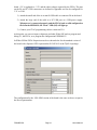
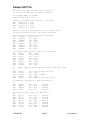
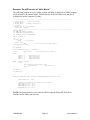
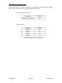
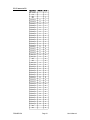
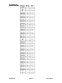
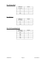
FPGADEVS6
FPGA Development Kit
User's Manual
Rev 12.03
www.hte.com/dev/
(800) 748-9172
Int’l:+1(858)679-1569
Fax: (800) 409-9172
www.hte.com/dev
[email protected]
FPGADEVS6
FPGA Development Kit
User's Manual
Manual
Revision 12.03
March 2012
hte.com/dev
[email protected]
Copyright © 2012 by HTE.
All rights reserved.
No part of this material may be reproduced, in any form or by any means, physical or electronic,
without the express prior written consent of HTE. Especially our competitiors. But university
faculty or students who may copy and distribute at will for any non-commercial purpose.
THE FINE PRINT
Disclaimer of warranty and limited warranty
HTE has attempted to produce a useful, high quality product at a reasonable price. Every Development Board unit has
been fully tested and checked for quality prior to shipment. It is warranted to be free of defects in material and
workmanship for a period of 90 days after date of purchase. During that time period, HTE will, at no charge to the
purchaser of record, repair or replace any defective unit returned to its Service Department in accordance with the
following instructions:
1.
Phone HTE at the number above between 10 am and 3 pm Pacific Time (GMT-0800) or e-mail
[email protected], and obtain a Return Material Authorization (RMA) number. Do not attempt to return the
product without an RMA number.
2.
Provide HTE with: Model, Serial Number, Proof of Purchase with date, Return Address, and preferred return
shipping method. Enclose a clear description of the problem experienced and any sample printouts showing
the problem, if possible.
3.
Take proper precautions to protect the product during shipping. Mark the package "FRAGILE", and ship via
UPS, Parcel Post, or Air Freight, insured and prepaid. Be sure the RMA number appears clearly on the box,
as well as any accompanying correspondence. Do not send COLLECT - collect shipments will be
refused and returned to sender.
This warranty is void in cases of misuse, abuse, abnormal conditions of operation, or attempts to alter or modify the
function of the product, or for use within 100 miles of detonation of a nuclear device. The product and written material are
provided "AS IS" without warranty of any kind, even if HTE has been advised of that purpose. The entire risk as to the
results and performance of the product is assumed by the user. In other words, if you do something any reasonable
person (see below) would consider stupid, it’s your own fault. Also, we do not recommend inserting the board in any body
cavities, as injury may result.
HTE makes no representations or warranties with respect to the contents or use of this product. HTE shall have no
liability or responsibility to purchaser or to any person or entity with respect to any liability, loss or damage caused or
alleged to be caused, directly or indirectly by this product, including but not limited to any interruption of service, loss of
business or anticipatory profits or consequential damage resulting from the use or operation of this product. This device is
not intended for use in life support or life critical equipment. Essentially, if you do something stupid, don’t blame us; you’re
on your own.
HTE reserves the right to make changes to any and all part of this product, at any time, without obligation to notify any
person or entity of such changes and does not represent a commitment on the part of HTE . So there.
On the other hand, we will consider any reasonable request from any reasonable customer (i.e.: not from a lawyer,
attorney, barrister, or solicitor, associates, their employees, contractors, legal consultants or their ilk), and we will often go
far out of our way to assist in any way we can.
Warranty Registration
Please take a moment to e-mail your contact info to [email protected]. This will assure prompt service in the unlikely
event a problem occurs. If your company insists on ISO900X certification, please be aware that this only means that we
will follow our documented procedures, no matter how foolish they may seem. Just so you know, our first documented
standard procedure following a customer request for ISO 900X certification is to laugh in your face and double the price.
Trademarks
HTE is a trademark of HTE
Xilinx, Spartan, and ISE are trademarks of Xilinx Inc.
Other trademarks are the property of their owners, whoever they may be.
Table of Contents
INTRODUCTION ........................................................................................................................................ 7
FEATURES .................................................................................................................................................. 7
COMPONENTS: ........................................................................................................................................... 8
Spartan 6 FPGA General Properties .................................................................................................. 9
GENERAL FEATURES ............................................................................................................................ 10
DESIGN CONSIDERATIONS, SIGNAL NAMES, AND LIMITATIONS.......................................... 11
GETTING STARTED USING A USB THUMB DRIVE: ...................................................................... 14
GETTING STARTED USING A JTAG CABLE: .................................................................................. 15
SAMPLE UCF FILE.................................................................................................................................. 17
EXAMPLE: THE LED VERSION OF “HELLO WORLD” ................................................................................ 18
PROGRAM FPGA DIRECTLY USING JTAG ............................................................................................... 19
PROGRAM SPI PROM CONFIGURATION MEMORY USING JTAG............................................................... 19
PROGRAM SPI PROM CONFIGURATION MEMORY USING USB DRIVE ...................................................... 19
BOARD LAYOUT ..................................................................................................................................... 25
USING THE FPGA WITH THE SWITCH/LED USER I/O BOARD .................................................. 27
SWITCH/LED USER I/O BOARD CONNECTOR PIN ASSIGNMENTS.......................................... 28
APPENDIX A.
BOARD DIMENSIONS, CONNECTOR LOCATIONS ...........................................A
APPENDIX B.
SUMMARY OF SPECIFICATIONS ...........................................................................B
APPENDIX C.
SCHEMATIC AND BILL OF MATERIALS .............................................................C
APPENDIX D.
DEVELOPMENT BOARD JUMPERS .......................................................................D
APPENDIX E.
MCS FILE FORMAT....................................................................................................E
APPENDIX F.
TROUBLESHOOTING................................................................................................. F
APPENDIX G.
OEM BOARD VERSION OPTIONS ......................................................................... G
APPENDIX H.
USING THE OEM VERSION OF THE SBC............................................................ H
NOTE: .......................................................................................................................................................... H
APPENDIX I.
USEFUL WEB SITES ..................................................................................................... I
APPENDIX J. OPTIONAL USER I/O BOARD LAYOUT .................................................................... J
APPENDIX K.
FPGADEVS6
PROBLEM REPORT AND COMMENT FORM ..................................................... K
Page 5
User's Manual
FPGADEVS6
Page 6
User's Manual
FPGA Board with optional User I/O Board
Introduction
If you’re anxious to start using the board, you can skip ahead to the
“Getting Started” section right now! See pages 13 and 14.
For those select few people who actually read the instructions first, the rest of this manual
provides a detailed description of the board. This manual has been written for the reader
who is familiar with digital logic systems. A specific knowledge of the Xilinx FPGA
family is not assumed, but it would be advisable for anyone not familiar with this family
to obtain and read the relevent documents from the IC manufacturers. A large number of
useful documents and sample programs are available from many different web sites,
listed on the HTE web site. The term “Development Board” or “Board” is used
throughout this manual for the FPGA development board. The term FPGA is used
throughout this manual to represent the Spartan 6 family from Xilinx. The abbreviation
uC refers to the FTDI USB microcontroller on the board. The terms EE or SPI PROM
are used to refer to the SPI serial interface EEPROM.
Features
• Operates as a stand alone FPGA board
• Incorporates standard JTAG to program the FPGA and serial EEPROM
• Connects to USB port of a PC for power and communication
• Can load configuration files from a USB thumb drive FAT file format
• FTDI USB microcontroller Program download / debug via USB
• Rapid product development, compatible with most development tools
• Low cost OEM version available for dedicated applications
The Development Board consists of a minimal configuration Spartan 6 FPGA board
containing the absolute minimum stand-alone design. It is suitable for OEM and
development applications. The Development Board provides the user with the ability to
FPGADEVS6
Page 7
User's Manual
download, test, and debug designs for a prototype or production system. The OEM
version of the board can be the final target for the application, or it can be customized.
The OEM board can be ordered with standard straight through, stackable, or right angle
50 pin connectors, or without any connectors. The Development Board can be stacked or
connected horizontally to expansion interfaces such as the optional user I/O board,
peripheral interface boards or customer specific designs for a specific application.
The FPGA board provides powerful functions to assist the designer in the integration,
debug and test phase of FPGA project development. The Development Board provides
GPIO pin interface pins on standard 0.1” grid header for connectors. The JTAG and
USB processor connectors allow for powering, debugging and downloading programs to
the FPGA, USB microcontroller, or serial EEPROM from a PC. In addition, the
Development Board can prove invaluable as an educational tool for learning about
FPGAs, microcontrollers, and USB interfacing.
Components:
• Xilinx Spartan-6 XC6SLX9 FPGA in a 144 pin TQFP package
9,152 logic cell equivalents
Thirty-two 18K-bit block RAMSs (576K bits)
Sixteen DSP48A Slices
Two Digital Clock Managers (DCMs)
Up to 102 user-defined I/O signals
• 4Mbit Serial SPI serial EEPROM, for in-system configuration PROM
• JTAG port for low-cost download cable
• Dual USB Controller (FTDI VNC2-32)
Type A USB Connector
Type Mini-B USB Connector
• 8 MHz Local Oscillator
• Two 50 Pin Expansion I/O Connectors with 84 Pre-Assigned I/O Pins
• 4 On-board LED 's
• On-Board Power Supply using National LP3906 Quad Regulator
+3.3V @ 1.5 A
(I/O Operating Voltage)
+1.2V @ 1.5 A
(FPGA Core Voltage)
+3.3V @ 300 mA
(FPGA Auxillary Voltage)
+1.8V @ 300 mA
(Secondary I/.O Operating Voltage)
(for an external +5V supply –- USB power typically limited to 500mA)
The user can easily:
• Design FPGA based products with Host/Device USB Interface
• Customize the Board for Small Volume Production
• Quickly Test and Debug new configurations
• Field Update configuration using only a USB Thumb Drive
• Install New Configurations in the Non-volatile SPI configuration PROM
In conjunction with any PC capable of running the free ISE Webpack development tools
from Xilinx and VNC2 IDE from FTDI, the Development Board becomes a powerful,
stand-alone, hardware and firmware development system. The board is capable of
supporting either the XC6SLX4 or the XC6SLX9. The development board ships with an
‘LX9, and the OEM version can be ordered with either the ‘LX4 or the ‘LX9. The key
FPGADEVS6
Page 8
User's Manual
capabilities are shown in the table below. Note that the ‘LX9 is has more than twice the
resources of the XC3S200 Spartan 3 device present on most FPGA development boards.
Spartan 6 FPGA General Properties
Notes:
The Data above is taken directly from the Xilinx Spartan 6 product selection guide.
FPGADEVS6
Page 9
User's Manual
General Features
FPGA
Xilinx Spartan 6 LX4 or LX9 FPGA in the 144 pin TQFP package, clocked by an 8 MHz
crystal oscillator. This frequency makes it easy to generate standard clock rates using the
FPGA’s internal clock resources.
USB Microcontroller
The FTDI VNC2 32 pin USB Microcontroller supports two USB interfaces, a “USB
peripheral device” interface with a mini-B connector to connect to a PC or power supply,
and a “USB host” type A connector that accommodates a flash USB thumb drive
containing a configuration file to be programmed into the Serial EEPROM.
Serial EEPROM Configuration Memory
An M25P40 non-volatile SPI serial EEPROM configuration memory. Upon power
application, the FPGA automatically loads its configuration data from this SPI serial
EEPROM. Depending upon what code is present in the USB processor, and whether an
external USB drive with a valid configuration fpga.sys file is present in the root
directory, the serial EEPROM or the FPGA may also be loaded with different
configuration file sources. When the file is not present or there is no USB drive at power
up, or if the USB processor is unprogrammed, the FPGA will load the previously
programmed configuration file from the serial EEPROM.
JTAG Port
The 0.1” single row 6 pin JTAG connector P10 allows the FPGA or the serial EEPROM
to be programmed using any Xilinx compatible JTAG programming cable (Xilinx
parallel or Platform USB cables). JTAG software to be used with the development board
includes Xilinx Impact and ChipScope.
USB Microcontroller Programming port
The 6 pin connector P11 can be used for programming and debug of the on-board FTDI
VNC2 USB microcontroller using the free FTDI C programming IDE development tools.
Power
Requires a single +5 volt supply at 500 mA typical from a standard PC USB port or an
external +5V power supply.
Dimensions
76,2mm by 76,2mm by 6,4mm high or 3 inches by 3 inches by 0.25 inch high
Environmental
Storage temperature range -25 to +100°C. Operating temperature range 0 to +50°C.
FPGADEVS6
Page 10
User's Manual
Design Considerations, Signal Names, and Limitations
A description of the Development Board's characteristics, signals, and allocation of
resources follows:
The Development Board uses approximately 60mA of the standard 500mA available
from a standard USB port, leaving approximately 400 mA for external devices. If an
external +5V power supply is used, additional power may be drawn from the on-board
regulators, subject to their limitations. An auxiliary +1.8V output is also available on a
pin that is adjacent to LED D4. The 1.2V FPGA core voltage supply is dedicated to U1.
The Development Board is configured to use either single ended or differential I/O
standards. Because of this, the pins are numbered by bank, port +/- type, and pin. For
example, adjacent pins 5 and 6 on connector P7 are labeled 3P12 and 3N12 to indicate
that the pins are connected to bank 3 pair 12, where 3P12 is the positive (+) signal pin
and 3N12 is the negative (-) pin of the pair. This facilitates the use of adjacent
differential wire pairs if a ribbon cable is connected to the 50 pin connector for
moderately high speed differential signalling.
Some FPGA and uC I/O pins are not connected or used internally on the board, so they
are not available on the external user I/O connectors.
The I/O pin banks of the FPGA are connected to +3.3V by default, however the board
can be reconfigured to use a different power supply voltage for the 50 pin I/O
connections. A jumper can be changed to select either the main +3.3V supply or the
auxiliary power supply. The voltage for the banks on either 50 pin connector can be
configured independently. The auxiliary supply can be used to operate the FPGA’s I/O
banks at any voltage between 1.2 and 3.3 volts, based on the power supply voltage input
on the VAR pins of P6 and P7. The I/O may also be supplied by the board’s +1.8V
supply by connecting the 1.8V pin to the VAR0 or VAR1 signal on P1, P2, P6 or P7.
This allows for the use of different logic voltage interface levels on connectors P6 and
P7.
Please Note:
This board has CMOS devices which can be damaged if exposed to electrostatic fields
and discharges. The metallized plastic electrostatic shielding bag provided with the
board should be used to protect the board during transport, and grounded conductive
workstations and standard ESD precautions should be used whenever possible when
handling the board to prevent device damage.
FPGADEVS6
Page 11
User's Manual
FPGA Board
FPGADEVS6
Page 12
User's Manual
Operating the Development Board
A typical configuration for debugging/development purposes would include:
• USB A to mini-B cable
• PC or USB Power source
• Xilinx ISE Web Pack Development System
USB Connections
There are two USB connectors:
1) P8 is the USB miniB connector which supplies power and can also be used to
communicate with a host PC, subject to appropriate the firmware in the USB
microcontroller.
2) P9 is a USB type A connector which will accommodate a USB thumb drive. The
standard firmware shipped with the unit will read the thumb drive on pwer up and
if a file named fpga.sys is present in the root directory it will be programmed into
the SPI configuration PROM on the board.
JTAG Connection
The JTAG connector, P10 allows programming the FPGA or SPI configuration PROM
using a compatible JTAG cable, such as the Xilinx Platform USB cable.
FTDI USB Microcontroller Programming Connection
P11 is the USB microcontroller chip programming and debug connector this connector
can be connected to the FTDI “VNC2 Debug Module” which is a PC board a little larger
than a USB type A connector that allows development, debug and programming of the
FTDI 16 bit USB microcontroller using the VNC.
FPGA Configuration Options
The three methods to configure the FPGA are:
1) Download the configuration file directly to the FPGA using a JTAG programmer
2) Program the SPI serial configuration EEPROM through the JTAG cable
3) Load the program from a USB thumb drive.
The development cycle for option 1 or 2 is as follows:
1. On a PC, compile your project using ISE and generate the programming file.
2. Use Impact to program the FPGA or the SPI configuration EEPROM.
3. Upon completion and after power-up, the FPGA will load from the EEPROM.
Note that programming the FPGA directly through JTAG will result in loss of that FPGA
configuration when power is removed, but it is the fastest programming method.
Programming the SPI EEPROM configuration memory using JTAG is done indirectly
through the FPGA, and takes more than a minute, but the result will be a non-volatile
configuration that loads automatically after every power cycle. It is slower because the
Impact utility program must first load an SPI programming file into the FPGA, then send
the file through the FPGA while the FPGA programs the SPI EEPROM configuration
memory, one bit at a time.
FPGADEVS6
Page 13
User's Manual
Getting Started Using a USB Thumb Drive:
GPIO
connector P7
Banks 0 & 3
+5V/Gnd pins
LEDs D1-D4
Done LED
GPIO
connector P6
Banks 1 & 2
P8 Power and
USB to PC
Insert USB Thumb
drive here
P8 provides power to the board using a powered USB port on a PC or a separate USB
power supply. As soon as powert is applied the FPGA will be loaded with the file that is
stored in the non-volatile configuration PROM, the Done LED lights, and the FPGA
runs.
To reprogram the configuration serial PROM using an external USB thumb drive:
1. Use ISE to create and place the desired “fpga.mcs” configuration file in the root
of a FAT formatted USB flash (thumb) drive. The fpga.mcs file must be created
for a single Spartan 6 FPGA part number XC6SLX9-2 in the TQG144 package
and a 4M bit SPI PROM, type M25P40.
2. With power to the board disconnected, plug the USB flash drive into USB
connector P9, and apply power. The USB drive acrtivity light flashes as the USB
microcontroller reads the fpga.mcs file from the thumb drive and programs the
SPI configuration PROM. This will take less than a minute, and when complete,
the activity LED on the thumb drive will stop flashing, then D5 (the “Done”
LED) will light up and the new FPGA configuration will begin running.
3. Once programming is complete, remove the USB drive, and the FPGA will be
configured from the serial PROM will be used on subsequent power cycles. This
process takes longer than loading the .bit file to the FPGA from JTAG.
For more details and programming using a JTAG cable, see the following pages.
FPGADEVS6
Page 14
User's Manual
Getting Started Using a JTAG Cable:
+5V/Gnd pins
LEDs D1-D4
GPIO
connector P7
Banks 0 & 3
Done LED
GPIO
connector P6
Banks 1 & 2
P8 Power and
USB to PC
Thumb drive
USB connector
P10 6 pin 0.1”
JTAG Connnector
For JTAG Programming:
Connector P10 - JTAG Connector Pinout
Pin Signal
Wire Color
1
Vcc
Red
2
Gnd
Blk
3
TCK
Grn
4
TDO
Orn
5
TDI
Blu
6
TMS
Brn
123456
P10 pinout
Connector P8 provides power to the board. Before configuring the FPGA or
configuration PROM, a powered USB port or separate USB power supply must be
connected to P8, or +5V must be supplied by the +5V/Gnd pins to supply power to the
FPGADEVS6
Page 15
User's Manual
board. +5V is regulated to +3.3V and the other voltages required by the FPGA. The pins
on the P6 and P7 GPIO connectors are defined in Appendix and can be configured for
3.3V or VAR.
1) Attach the small end of the A to mini-B USB cable to connector P8 on the board.
2) Attach the large end of the cable to a PC USB port or a USB power supply.
When power is connected properly and the FPGA loads a valid configuration
file from the EEPROM, the “Done” LED (D5) will light up.
3) Connect your JTAG programming cable to connector P10.
At this point, you can use impact, chipscope and other Xilinx ISE tools to program and
debug U1, the FPGA, or to program the configuration EEPROM U5.
In XIlinx ISE the FPGA Properties must be as shown below for the standard version of
the board with a Spartan 6 FPGA part number XC6SLX9-2 in the TQG144 package:
The configuration for the ‘LX4 OEM version of the board is the same as above except for
the Device part number.
FPGADEVS6
Page 16
User's Manual
Sample UCF File
#
# UCF file for FPGA P6 right angle to DevIO P1
# (note: P6/P1 odd/even pin numbers swapped)
# Not used: 8MHz clock input
# NET "CLOCK" LOC = P123;
# LEDs on the FPGA
NET
"LED1" LOC =
NET
"LED2" LOC =
NET
"LED3" LOC =
NET
"LED4" LOC =
board: Active Hi 1=ON 0=OFF
P117;
P116;
P115;
P114;
# Below: Signals on the optional User I/O Board, when
# boards are mated to with right angle connectors
# LEDs on the I/O board: Active Hi 1=ON 0=OFF
NET
"LEDX8"
LOC = P47;
NET
"LEDX7"
LOC = P48;
NET
"LEDX6"
LOC = P45;
NET
"LEDX5"
LOC = P46;
NET
"LEDX4"
LOC = P43;
NET
"LEDX3"
LOC = P44;
NET
"LEDX2"
LOC = P40;
NET
"LEDX1"
LOC = P41;
# 7 segment display drive: Active Low 0=ON 1=OFF
NET
"sega"
LOC = P102;
NET
"segb"
LOC = P105;
NET
"segc"
LOC = P101;
NET
"segd"
LOC = P97;
NET
"sege"
LOC = P98;
NET
"segf"
LOC = P100;
NET
"segg"
LOC = P104;
NET
"segdp"
LOC = P99;
# 7 segment display digit/colon drive: Active Low 0=ON 1=OFF
#
NET
"DIG1"
LOC = P92; # left most digit
NET
"DIG2"
LOC = P93;
NET
"L123"
LOC = P87; # COLON
NET
"DIG3"
LOC = P84;
NET
"DIG4"
LOC = P88; # right most digit
# Pushbutton switches S1-4 When Depressed = 0
#
NET
"PBS4"
LOC = P80
| PULLUP;
NET
"PBS3"
LOC = P81
| PULLUP;
NET
"PBS2"
LOC = P78
| PULLUP;
NET
"PBS1"
LOC = P79
| PULLUP;
# 8 position slide switch S5:
#
NET
"S5_1"
LOC = P55
NET
"S5_2"
LOC = P56
NET
"S5_3"
LOC = P57
NET
"S5_4"
LOC = P58
NET
"S5_5"
LOC = P61
NET
"S5_6"
LOC = P62
NET
"S5_7"
LOC = P66
NET
"S5_8"
LOC = P67
FPGADEVS6
ON=0 OFF = 1
|
|
|
|
|
|
|
|
PULLUP;
PULLUP;
PULLUP;
PULLUP;
PULLUP;
PULLUP;
PULLUP;
PULLUP;
Page 17
User's Manual
Example: The LED version of “Hello World”
The following program is a very simple example intended to show how a VHDL program
can be written to run on this board. It blinks the four on-board LEDs D1-4 and places
walking ones on the connector I/O pins.
----------------------------------------------------------------------------------- Create Date:
01:13:07 08/06/2009
-- Design Name:
-- Module Name:
DevFPGA - Behavioral
-- Revision:
-- Revision 0.01 - File Created
-- Additional Comments:
---------------------------------------------------------------------------------library IEEE;
use IEEE.STD_LOGIC_1164.ALL;
use IEEE.STD_LOGIC_ARITH.ALL;
use IEEE.STD_LOGIC_UNSIGNED.ALL;
entity DevFPGA is
port
(
-- Input Pins
CLOCK
: in std_logic;
-- Output Pins
LED
: out std_logic_vector(4 downto 1)
-- Bidirectional Pins
);
end DevFPGA;
architecture Behavioral of DevFPGA is
signal
LED_Counter
: std_logic_vector(23 downto 0);
begin
LED(4)
LED(3)
LED(2)
LED(1)
MAIN:
<=
<=
<=
<=
LED_Counter(23);
LED_Counter(22);
LED_Counter(21);
LED_Counter(20);
process (CLOCK)
begin
if CLOCK'event and CLOCK='1' then
LED_Counter
<=
LED_Counter + 1;
end if;
end process;
end Behavioral;
The pin definitions in the corresponding UCF File are:
NET "CLOCK" LOC = P123;
# LEDs on the FPGA
NET "LED[1]" LOC =
NET "LED[2]" LOC =
NET "LED[3]" LOC =
NET "LED[4]" LOC =
board: Active Hi 1=ON 0=OFF
P117;
P116;
P115;
P114;
NOTE: The program above was written in VHDL using the Xilinx ISE Web Pack
available on the xilinx.com web site.
FPGADEVS6
Page 18
User's Manual
Program FPGA Directly using JTAG
To program the FPGA using a JTAG cable, simply attach the programming cable to P10,
the JTAG cable, and use Impact to initialize the JTAG chain, detect, configure and
program the FPGA with a .bit file in iMPACT as described in the Xilinx documentation.
Program SPI PROM configuration memory using JTAG
The first step is to create an SPI file in .mcs format to program the configuration
EEPROM using the JTAG cable. See Xilinx application note 974 in the file xapp974.pdf
“Indirect Programming of SPI Serial Flash PROMs with Spartan-3A FPGAs.” The
procedure is the same for the Spartan 6 and the serial PROM on the development board.
Program SPI PROM configuration memory using USB drive
To program the configuration PROM using an external USB drive, you must first create
and place the desired “.mcs” configuration filefor a 4M bit SPI PROM type M25P40, and
the file must be named “fpga.mcs” and placed in the root of a FAT formatted USB drive.
FPGADEVS6
Page 19
User's Manual
Board Pinout and Configuration
Connector and FPGA I/O Pin Configuration: The following tables define the mapping
between the various resources on the board and the FPGA pins.
8 MHz On-Board Oscillator
Component
FPGA Pin
Clock Input (GCLK12)
123
On-Board LED's
Component
FPGA Pin
LED 1
117
LED 2
116
LED 3
115
LED 4
114
*Output Signal Logic 1 Turns LED ON
FPGADEVS6
Page 20
User's Manual
I/O Connector P6
Signal Name
FPGA Pin
1
+3.3V
2
GND
3
GND
4
IO_Bank2_P8
41
IO_Bank2_N8
40
6
IO_Bank2_P7
44
7
5
IO_Bank2_N7
43
8
IO_Bank2_P6
46
9
IO_Bank2_N6
45
10
IO_Bank2_P5
48
11
IO_Bank2_N5
47
12
13
IO_Bank2_P4
51
IO_Bank2_N4
50
14
IO_Bank2_P3
56
15
IO_Bank2_N3
55
16
IO_Bank2_P2
58
17
IO_Bank2_N2
57
18
19
IO_Bank2_P1
62
IO_Bank2_N1
61
20
IO_Bank2_P0
67
21
IO_Bank2_N0
66
22
IO_Bank1_P11
75
23
IO_Bank1_N11
74
GND
24
25
GND
FPGADEVS6
P6 Pin
Vin – Variable
26
IO_Bank1_P10
79
27
IO_Bank1_N10
78
28
29
IO_Bank1_P9
81
IO_Bank1_N9
80
30
IO_Bank1_P8
83
31
IO_Bank1_N8
82
32
IO_Bank1_P7
85
33
IO_Bank1_N7
84
34
IO_Bank1_P6
88
35
IO_Bank1_N6
87
36
IO_Bank1_P5
93
37
IO_Bank1_N5
92
38
39
IO_Bank1_P4
95
IO_Bank1_N4
94
40
IO_Bank1_P3
98
41
IO_Bank1_N3
97
42
IO_Bank1_P2
100
43
IO_Bank1_N2
99
44
IO_Bank1_P1
102
45
IO_Bank1_N1
101
46
IO_Bank1_P0
105
47
IO_Bank1_N0
104
48
GND
49
GND
50
Page 21
User's Manual
I/O Connector P7
Signal Name
FPGA Pin
Vin – Variable
1
+3.3V
2
GND
3
GND
IO_Bank3_P12
4
35
5
IO_Bank3_N12
34
6
IO_Bank3_P11
33
7
8
IO_Bank3_N11
32
IO_Bank3_P10
30
9
IO_Bank3_N10
29
10
IO_Bank3_P9
27
11
IO_Bank3_N9
26
12
IO_Bank3_P8
24
13
IO_Bank3_N8
23
14
IO_Bank3_P7
22
15
IO_Bank3_N7
21
16
IO_Bank3_P6
17
17
IO_Bank3_N6
16
18
IO_Bank3_P5
15
19
IO_Bank3_N5
14
20
IO_Bank3_P4
12
21
IO_Bank3_N4
11
22
IO_Bank3_P3
10
23
IO_Bank3_N3
9
24
GND
25
GND
FPGADEVS6
P7 Pin
26
IO_Bank3_P2
8
IO_Bank3_N2
7
27
28
IO_Bank3_P1
6
29
IO_Bank3_N1
5
30
31
IO_Bank3_P0
2
IO_Bank3_N0
1
32
IO_Bank0_P7
142
33
IO_Bank0_N7
141
34
IO_Bank0_P6
140
35
IO_Bank0_N6
139
36
IO_Bank0_P5
138
37
IO_Bank0_N5
137
38
IO_Bank0_P4
134
39
IO_Bank0_N4
133
40
IO_Bank0_P3
132
41
IO_Bank0_N3
131
42
IO_Bank0_P2
127
43
IO_Bank0_N2
126
44
IO_Bank0_P1
121
45
IO_Bank0_N1
120
46
IO_Bank0_P0
119
47
IO_Bank0_N0
118
48
GND
49
GND
50
Page 22
User's Manual
P8 - USB Type Mini-B
USB Signal
P8 Pin
+5V (Input)
1
D-
2
D+
3
nc
4
GND
5
USB Signal
P9 Pin
+5V (Output)
1
D-
2
D+
3
GND
4
P9 - USB Type A
P10 - JTAG Programming Header
FPGADEVS6
JTAG Signal
P10 Pin
+3.3V (Output)
1
GND
2
TCK
3
TDO
4
TDI
5
TMS
6
Page 23
User's Manual
Bank 1 and 2 Operating Voltage Configuration P1
Voltages
P1 Pin
+3.3V (Default)
1
VCCO_1
2
Vin_Variable
3
Bank 0 and 3 Operating Voltage Configuration P2
Voltages
P2 Pin
+3.3V (Default)
1
VCCO_0
2
Vin_Variable
3
FPGA Mode Configuration P5
Mode
P5-1 to P5-2
Master
Closed (Default)
Slave
Open
Status
LED D5
FPGA Configured
ON
FPGA Not Configured
OFF
Configuration LED D5
FPGADEVS6
Page 24
User's Manual
Board Layout
Component Locations and I/O Pins
FPGADEVS6
Page 25
User's Manual
Using the FPGA with the switch/LED user I/O Board
The FPGA board may be used with the general purpose switch/LED user I/O
board when connected as shown below. The two boards are designed to mate
horizontally as shown, or if ordered with custom connectors, they can be stacked so that
the user I/O board stacks on top of the FPGA board.
Connector P1 on user
I/O board mates to
P6 on FPGA board
Four digit 7 segment
common anode LED
display with DP & colon
123456
8 discrete LEDs
Power applied
through USB
cable here
4 pushbutton
switches
8 slide switches
P10 JTAG Pinout
Color-Signal-Pin#
Red - Vcc - 1
Blk - Gnd - 2
Grn - TCK - 3
Orn - TDO - 4
Blu - TDI - 5
Brn - TMS - 6
FPGADEVS6
Page 27
User's Manual
Switch/LED user I/O Board Connector Pin Assignments
Note that these pins are for the P1 connector on the I/O board, and if the board is
connected using right angle connectors to another board, the odd and even pin numbers
will be switched. If the board uses straight-through or stacking ribbon or header
connectors, then the pin numbering will be identical for boath boards. (See I/O board
schematic: “DevIO Rev ?? Schematic1.pdf” file for details.)
Pusbutton Inputs Switches S1-4
Signal
P1 Pin Number
PB-1
29
PB-2
30
PB-3
27
PB-4
28
Signal
P1 Pin Number
S5-1
15
S5-2
16
S5-3
17
S5-4
18
S5-5
19
S5-6
20
S5-7
21
S5-8
22
Signal
P1 Pin Number
LED 1
11
LED 2
12
LED 3
9
LED 4
10
LED 5
7
LED 6
8
LED 7
5
LED 8
6
8 Position Switch S5 Inputs
Discrete LEDs D1-8
FPGADEVS6
Page 28
User's Manual
Four Digit 7 Segment LED Display with Colon
I/O Board P1 Connector Pin Definitions
FPGADEVS6
Signal
P1 Pin Number
Vin
1,2
GND
3,4,25,26,49,50
Segment a
46
Segment b
48
Segment c
45
Segment d
41
Segment e
42
Segment f
44
Segment g
47
Segment dp
43
Character Enable 1
37
Character Enable 2
38
Character Enable 3
33
Character Enable 4
36
Colon Enable
35
Page 29
User's Manual
Sample UCF File for use with I/O Board
# UCF file for FPGA P6 right angle to DevIO P1
# (note: P6/P1 odd/even pin numbers swapped)
# Not used: 8MHz clock input
# NET "CLOCK" LOC = P123;
# LEDs on the FPGA
NET
"LED1" LOC =
NET
"LED2" LOC =
NET
"LED3" LOC =
NET
"LED4" LOC =
board: Active Hi 1=ON 0=OFF
P117;
P116;
P115;
P114;
# LEDs on the I/O board: Active Hi 1=ON 0=OFF
NET
"LEDX8"
LOC = P47;
NET
"LEDX7"
LOC = P48;
NET
"LEDX6"
LOC = P45;
NET
"LEDX5"
LOC = P46;
NET
"LEDX4"
LOC = P43;
NET
"LEDX3"
LOC = P44;
NET
"LEDX2"
LOC = P40;
NET
"LEDX1"
LOC = P41;
# 7 segment display drive: Active Low 0=ON 1=OFF
NET
"sega"
LOC = P102;
NET
"segb"
LOC = P105;
NET
"segc"
LOC = P101;
NET
"segd"
LOC = P97;
NET
"sege"
LOC = P98;
NET
"segf"
LOC = P100;
NET
"segg"
LOC = P104;
NET
"segdp"
LOC = P99;
# 7 segment display digit/colon drive: Active Low 0=ON 1=OFF
NET
"DIG1"
LOC = P92;
NET
"DIG2"
LOC = P93;
NET
"L123"
LOC = P87; # COLON
NET
"DIG3"
LOC = P84;
NET
"DIG4"
LOC = P88;
# Pushbutton switches S1-4 When Depressed=0
NET
"PBS4"
LOC = P80;
NET
"PBS3"
LOC = P81;
NET
"PBS2"
LOC = P78;
NET
"PBS1"
LOC = P79;
# 8 position slide switch S5: ON=0 OFF = 1
NET
"S5_1"
LOC = P55;
NET
"S5_2"
LOC = P56;
NET
"S5_3"
LOC = P57;
NET
"S5_4"
LOC = P58;
NET
"S5_5"
LOC = P61;
NET
"S5_6"
LOC = P62;
NET
"S5_7"
LOC = P66;
NET
"S5_8"
LOC = P67;
FPGADEVS6
Page 30
User's Manual
Appendix A.
FPGADEVS6
Board Dimensions, Connector Locations
Page A
User's Manual
Appendix B.
Summary of Specifications
The development board specs are standard:
Xilinx Spartan-6 XC6SLX9 FPGA in a 144 pin TQFP package
9,152 logic cell equivalents
Thirty-two 18K-bit block RAMSs (576K bits)
Sixteen DSP48A Slices
Two Digital Clock Managers (DCMs)
Up to 102 user-defined I/O signals
4Mbit Serial SPI EEPROM, for in-system configuration PROM
JTAG port for low-cost download cable
Dual USB Controller (FTDI VNC2-32)
USB 2.0 operation defined by VNC2 Specs
Type A USB Connector for flash drive
Type Mini-B USB Connector for power and PC communication
8 MHz Local Oscillator
Two 50 Pin Expansion I/O Connectors with 84 Pre-Assigned I/O Pins
4 On-board LEDs
On-Board Power Supply using National LP3906 Quad Regulator
+3.3V @ 1.5 A
(I/O Operating Voltage)
+1.2V @ 1.5 A
(FPGA Core Voltage)
+3.3V @ 300 mA
(FPGA Auxillary Voltage)
+1.8V @ 300 mA
(Secondary I/.O Operating Voltage)
Note:
Above load peaks apply only for an external +5V power supply.
USB power is typically limited to 500mA @5V = 2.5W max.
All specifications are subject to change.
FPGADEVS6
Page B
User's Manual
Appendix C.
Schematic and Bill of Materials
See separate schematic and BOM PDF files available at http://www.hte.com/dev
FPGADEVS6
Page C
User's Manual
Appendix D.
Development Board Jumpers
Jumper Pins
Name Shorted
Function
P1
1-2
*
Select I/O voltage for I/O banks 1 & 2 on P6
P2
1-2
*
Select I/O voltage for I/O banks 0 & 3 on P7
P5
1-2
*
Master Mode jumper (In=Master by default)
+5V
+5VDC Power
GND
Gnd Return for +5V power
* Note: Asterisk (*) means the default jumper is a trace on the the board. Normally, the
jumpers are not installed. The traces can be cut by the user or by special order at the
factory prior to being shipped, so 0.1” jumper pins and plugs can be installed.
FPGADEVS6
Page D
User's Manual
Appendix E.
MCS File Format
The .mcs file is generated using Xilinx ISE in the Implementation pane, on the Deisgn
Tab process “Generate Target PROM” to create the file. By default, the board will load a
file named fpga.sys from the root directory of a FAT formatted USB flash drive installed
at power up. The file format is described below.
The .mcs (Intel hex) data file formats begin with a 9-character prefix and end with a 2character suffix. The byte count must be equal to the number of data bytes in the record.
Data record and end-of-file record are the two types of records. The number of bytes per
record is variable. Each record begins with a colon, which is followed by a 2-character
byte count. The 4 characters following the byte count is the address of the first data byte.
Each byte is represented by 2 hex digits that equals to the number of bytes in each record.
It ends with the checksum.
:BCAAAATTHH . . . HHCC
:
Start character (colon)
BC
The hexadecimal number of bytes in the record. If BC = 0 the it is the end-offile record.
AAAA
Address in hexadecimal of first data byte in the record.
TT
Record type.
If TT = 00 then data record.
If TT = 01 then end-of-file record
HH
One data byte in hexadecimal notation.
CC
Checksum is the two's complement of binary summation of preceding bytes in
record including the byte count, address and record type.
FPGADEVS6
Page E
User's Manual
Appendix F.
Troubleshooting
No LEDs light up at all
Explanation: No power to board.
Action:
Check and correct power connection.
LEDs light, but are very dim
Explanation: No valid FPGA configuration loaded in the serial PROM.
Action:
FPGADEVS6
Program with a known good FPGA configuration file.
Page F
User's Manual
Appendix G.
OEM Board Version Options
You can use the development board and later purchase the OEM version populated with
those connectors and features that are actually used in your final application to customize
or reduce the cost of the board. Custom configurations may be subject to a minimum
order quantity. Contact HTE for more information.
The board can be ordered with either a Spartan 6 ‘LX9 or a ‘LX4 device.
The optional parts that can be left off the OEM board include:
• 50 pin GPIO connectors P6, P7
• USB microcontroller U3
• USB connectors P8, P9
The configuration options and jumpers that can be added include:
• Jumpers/plugs P1, P2, P5
• Customer Specified I/O power
• USB VNC2 microcontroller programming/debug connector P11
FPGADEVS6
Page G
User's Manual
Appendix H.
Using the OEM version of the SBC
Essentially, the OEM (Original Equipment Manufacturer) versions of the board is a
minimum configuration version of the Development Board. The OEM version is
typically a lower cost unit, as it does not have the components which are only needed for
development of programs. It does not have the following items that are included on the
development board:
1.
2.
3.
4.
5.
6.
50 Pin I/O Connector P6.
50 Pin I/O Connector P7.
Connector P8.
Connector P9.
The FTDI USB IC and crystal.
The OEM jumper connections are supplied with jumper pins in the default settings by
default.
Note that the OEM board may be ordered with some or all of the above and other custom
configurations. Contact HTE for more information.
Once development has been completed on the Development Board, the FPGA
configuration must be programmed into the SPI serial configuration EEPROM, typically
using the JTAG connector. Optionally, the USB thumb drive programming can also be
specified at time of order.
Power can be provided by the external connections at the top left corner of the board
using the pins labeled +5V and GND. The following is the pinout for the power
connector at the top left corner of the board:
Pin Description
1. +5v in. This pin can be used instead of the USB connector P8 if you have an
externally regulated +5v supply. This powers the on-board regulator to
deliver power to all components on the board.
2. Ground
NOTE:
The +5V power input is NOT reverse polarity protected. Reversing the +5V and Gnd
connections will damage the board.
FPGADEVS6
Page H
User's Manual
Appendix I.
Useful Web sites
Below is a list of useful web sites, related to the
board, accessories and development tools.
http://www.hte.com/dev/
The HTE web site has other resources.
http://www.xilinx.com
Xilinx is the manufacturer of the Spartan 6 ICs and
related FPGA architectures, and has documentation, app
notes, and free software utilities that will work with the
FPGA board.
FPGADEVS6
Page I
User's Manual
Appendix J. Optional User I/O Board Layout
Pin 1
FPGADEVS6
Page J
User's Manual
Appendix K.
Problem Report and Comment Form
Please complete this form if you discover any software
or hardware problems, documentation problems, or would like
to suggest product enhancements. Duplicate this form if you
need additional copies and/or attach extra pages if
necessary.
___ Hardware Problem
___ Programming Problem
___ Documentation Problem
___ Product Enhancement
Date: ________________________
Serial #: ______________
Product: ______________________
Version #: ____________
Name: ___________________________ Title: _____________
Company: _________________________________________
City: ________________________ State: _____ Zip: ________
Country: _____________________
Phone: (______) ____________________
Ext: ____________
Please describe the problem, how to reproduce it and your
suggested correction. Or, decscribe documention problems or
suggest enhancements that you would like to see added to
this product.
E-mail or fax form to:
HTE
Attn: Technical Support
(800) 748-9172
Fax: (800) 409-9172
http://www.hte.com
Or e-mail [email protected]
FPGADEVS6
Page K
User's Manual