1
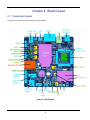
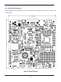
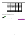
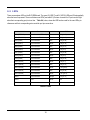
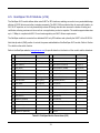
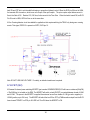
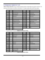
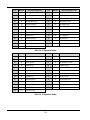
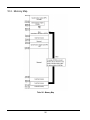
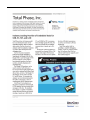
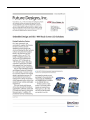
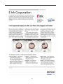
Renesas Demonstration Kit (RDK) for RL78G14 (REV 2)
User’s Manual: Hardware
RENESAS MCU
RL78G14 Family
Release 1.0
All information contained in these materials, including products and product specifications,
represents information on the product at the time of publication and is subject to change by
Renesas Electronics Corp. without notice. Please review the latest information published by
Renesas Electronics Corp. through various means, including the Renesas Electronics Corp.
website (http://www.renesas.com).
i
Disclaimer
By using this Renesas Demonstration Kit (RDK), the user accepts the following terms. The RDK is not guaranteed to be
error free, and the User assumes the entire risk as to the results and performance of the RDK. The RDK is provided by
Renesas on an “as is” basis without warranty of any kind whether express or implied, including but not limited to the
implied warranties of satisfactory quality, fitness for a particular purpose, title and non-infringement of intellectual
property rights with regard to the RDK. Renesas expressly disclaims all such warranties. Renesas or its affiliates shall in
no event be liable for any loss of profit, loss of data, loss of contract, loss of business, damage to reputation or goodwill,
any economic loss, any reprogramming or recall costs (whether the foregoing losses are direct or indirect) nor shall
Renesas or its affiliates be liable for any other direct or indirect special, incidental or consequential damages arising out
of or in relation to the use of this RDK, even if Renesas or its affiliates have been advised of the possibility of such
damages.
Precautions
This Renesas Demonstration Kit is only intended for use in a laboratory environment under ambient temperature and
humidity conditions. A safe separation distance should be used between this and any sensitive equipment. Its use
outside the laboratory, classroom, study area or similar such area invalidates conformity with the protection
requirements of the Electromagnetic Compatibility Directive and could lead to prosecution.
The product generates, uses, and can radiate radio frequency energy and may cause harmful interference to radio
communications. However, there is no guarantee that interference will not occur in a particular installation. If this
equipment causes harmful interference to radio or television reception, which can be determined by turning the
equipment off or on, you are encouraged to try to correct the interference by one or more of the following measures:
•
Ensure attached cables do not lie across the equipment
•
Reorient the receiving antenna
•
Increase the distance between the equipment and the receiver
•
Connect the equipment into an outlet on a circuit different from that which the receiver is connected
•
Power down the equipment when not in use
•
Consult the dealer or an experienced radio/TV technician for help NOTE: It is recommended that wherever
possible shielded interface cables are used.
The product is potentially susceptible to certain EMC phenomena. To mitigate against them it is recommended that the
following measures be undertaken:
•
The user is advised that mobile phones should not be used within 10m of the product when in use.
•
The user is advised to take ESD precautions when handling the equipment.
The Renesas Demonstration Kit does not represent an ideal reference design for an end product and does not fulfill the
regulatory standards for an end product.
ii
Table of Contents
Chapter 1. Preface ................................................................................................................ 1
Chapter 2. Purpose ............................................................................................................... 1
Chapter 3. Power Supply ...................................................................................................... 4
3.1. Requirements ................................................................................................................. 4
3.2. Power–Up Behavior ....................................................................................................... 4
Chapter 4. Board Layout ....................................................................................................... 5
4.1. Component Layout ......................................................................................................... 5
4.2. Board Dimensions .......................................................................................................... 6
Chapter 5. Block Diagram ..................................................................................................... 7
Chapter 6. User Circuitry ....................................................................................................... 9
6.1. Switches ......................................................................................................................... 9
6.2. Debug LCD Module ........................................................................................................ 9
6.3. E Ink Display ................................................................................................................ 10
6.4. LEDs ............................................................................................................................ 12
6.5. GainSpan Wi-Fi Module (U16) ..................................................................................... 13
6.6. Serial EPROM (U2) ...................................................................................................... 14
6.7. MicroSD Memory Card Slot (J9) .................................................................................. 14
6.8. Audio (Audio Out, Mic, Speaker, Volume Potentiometer)............................................. 14
6.9. Serial port (U14/J13) .................................................................................................... 14
6.10. 3-Axis Accelerometer (U13) ....................................................................................... 14
6.11. Digital Temp Sensor (U11) ......................................................................................... 15
6.12. Ambient Light Sensor (U4) ......................................................................................... 15
iii
6.13. Potentiometer (VR1)................................................................................................... 15
6.14. Infrared Emitter (D4) & Detector (U19) ....................................................................... 15
6.15. TRIAC (Q3) & Zero Crossing Detector (U3) ............................................................... 15
6.16. FET (Q2) .................................................................................................................... 16
6.17. Oscillator Sources ...................................................................................................... 17
6.18. Reset Circuit ............................................................................................................... 17
6.19. Total Phase Beagle Debug Header (J8)..................................................................... 17
Chapter 7. Mode Switch ...................................................................................................... 19
Chapter 8. Programming Methods ...................................................................................... 20
Chapter 9. Headers ............................................................................................................. 21
9.1. PMODTM Interfaces ...................................................................................................... 21
9.2. Application Header ....................................................................................................... 22
9.3. Expansion Headers (J1-J4) .......................................................................................... 23
Chapter 10. Code Development .......................................................................................... 25
10.1. Overview .................................................................................................................... 25
10.2. Memory Map .............................................................................................................. 26
Chapter 11. Component Placement .................................................................................... 27
11.1. Hardware Partner Information .................................................................................... 27
11.2. Renesas Contact Information ..................................................................................... 42
iv
Chapter 1. Preface
Cautions
This document may be, wholly or partially, subject to change without notice.
All rights reserved. The RDK design, documentation, and demo software are intended to improve understanding and
time-to-market for RL78-based designs. Duplication of the design, documentation, and demonstration software is
encouraged.
Trademarks
All brand or product names used in this manual are trademarks or registered trademarks of their respective
companies or organizations.
Copyrights
© 2012 Renesas Electronics America, Inc. All rights reserved.
© 2012 Renesas Electronics Corporation. All rights reserved.
© 2012 Renesas Electronics Europe. All rights reserved.
Website:
http://www.renesas.com/
Glossary
ADC
Analog to Digital Converter
MCU
Microcontroller Unit
CPU
Central Processing Unit
NC
No Connection
DAC
Digital to Analog Converter
PC
Program Counter
EMC
Electromagnetic compatibility
PMOD
Peripheral Module
ESD
Electrostatic Discharge
RAM
Random Access Memory
I/O
Input / Output
ROM
Read-Only Memory
LCD
Liquid Crystal Display
RDK
Renesas Demonstration Kit
LED
Light Emitting Diode
SDRAM
Wi-Fi
IEEE 802.11 standards
Synchronous Dynamic Random Access
Memory
E INK
Electronic Ink technology.
1
Chapter 2. Purpose
This RDK is an evaluation and demonstration tool for Renesas RL78 low-power microcontrollers. The goal is to provide
the user with a powerful debug and demonstration platform targeted at common applications. A set of human/machine
interfaces are tightly integrated with the features of the RL78 and the software demonstration programs providing the
user with an accessible platform to rapidly evaluate and customize.
Target Applications and Features:
Audio
•
Stereo audio driver connected to the PWM and DAC interfaces
•
Amplified on-board speaker and external Stereo audio jack.
•
On-board MEMS microphone to demonstrate sampling and recording capabilities (ADI)
•
Volume Control Potentiometer, connected to ADC input.
User Interface
•
OKAYA Graphical LCD
•
E Ink Corporation Display
•
User pushbutton switches and a reset switch.
•
12 on-board LEDs (LED Wheel pattern)
Communications
•
On-board Wi-Fi 802.11b Module from GainSpan Corporation
•
RS-232 Interface
•
I2C, SPI with Debug through the Beagle connector from Total Phase
•
Application Header to support several external Wi-Fi modules.
•
PMOD connections to support a variety of generic PMOD devices (Wi-Fi, Bluetooth, RF, motor control etc…).
Memory Storage
•
Micro SD card slot
•
512KB Serial EEPROM (Renesas)
1
•
256KB On-chip Flash Memory (program)
•
8KB On-Chip Flash Memory (Data)
•
8Mbit Serial Flash for Web Server data storage (Micron)
Digital Sensors
•
3 – Axis Accelerometer (ADI)
•
Temperature Sensor (ADI)
•
Ambient Light Sensor (CEL)
Power Control
•
FET Circuit for DC output
•
Fully isolated TRIAC Circuit for AC output with Zero Crossing Detector
User Code and Application Debugging
•
On-board debugger for high-quality source code debugging (TK interface)
•
User circuit breadboard area (located underneath E Ink unit)
2
Renesas Online
Each RDK has a dedicated website for additional information and software download.
•
www.renesas.com/rdkrl78G14
The Renesas RDK online experience is complemented by the online Renesas ecosystem.
•
Renesas Interactive: www.RenesasInteractive.com
o Free Online Learning
•
Renesas Rulz: www.RenesasRulz.com
o Online community
o Online user forums
o http://www.renesasrulz.com/community/demoboards/rdkrl78g14 - Online support site for this RDK
•
University Program: www.RenesasUniversity.com
o Support for Professors and Students
o Support for University Kits (QSKs)
•
Renesas Microcontroller Samples (America Customers)
o Free of charge
o Request directly from www.America.Renesas.com/samples
Develop and submit your sample programs to demonstrate these features to the online community:
www.RenesasRulz.com/community/renesas_products/rl78
3
Chapter 3.Power Supply
3.1. Requirements
This RDK gets its power from the debugger mini USB connection or optionally from a regulated 5V power supply. The
power jack is a center positive connector using a 2.1 mm barrel. An optional alternate power header is located next to the
power jack (J5). Power can also be provided with Connector J14 (application header).
Please watch to supply enough current to this kit, 500mA is recommended, especially when a lot of Wi-Fi
communications are ongoing, the new Wi-Fi module can take up to 150mA itself, when having high loads.
If a USB cable is used to provide Power, use preferably short cables and with low impedance from the power source
(5V/GND), if you notice coupling between Wi-Fi transmission and flickering in the displays or LEDs, that could mean that
your power source is not strong enough.
The RDK PCB is also be loaded with a 3.3V 0.08F super cap (C72), part number XH414HG, which offer battery backup
options for the Wi-Fi module.
Warning: The RDK is neither under nor over-voltage protected. To prevent damage, use a 5V REGULATED
center positive supply
3.2. Power–Up Behavior
The RL78G14 RDK is booting as a Wi-Fi network server or as a Wi-Fi client node. The Factory demo is divided in 4
operation modes, based on the reset switch and the 3 User push-button configurations at the time of power-up.
Here is a summary of these 4 factory boot modes:
o Limited Access Point with integrated Web Server
o Instant-on Exosite portal client, over Wi-Fi
o User-friendly Wi-Fi provisioning with auto-scanning capability with web interface
o User-friendly Over-the-Air upgrade utility with web interface
For more information about setting up and demoing these modes, please refer to the Renesas, Gainspan and Exosite
quick-start guides included inside the insert of your RDK.
4
Chapter 4. Board Layout
4.1. Component Layout
The following view shows the top layer component layout and placement
Figure 4-1: Board Layout
5
4.2. Board Dimensions
The following diagram gives the board dimensions (5.1”x5.1”) and connector locations. All through hole connectors are on a common 0.1” grid
for easy interfacing.
Figure 4-2: Board Dimensions
6
Chapter 5. Block Diagram
Figure 5-1 shows the CPU board components and their connectivity.
Figure 5-1: Block Diagram
7
Figure 5-2 shows host PC connection to the RDK board.
Figure 5-2: RDK Connections
8
Chapter 6. User Circuitry
6.1. Switches
There are four switches located on the RDK board. The function of each switch and its connection are shown in Table
6-1.
Switch
Function
RL78
SWITCH 1
Connects to an interrupt line for user controls.
INTP10, P76 (pin 34)
SWITCH 2
Connects to an interrupt line for user controls.
INTP8, P74 (pin 36)
SWITCH 3
Connects to an interrupt line for user controls.
INTP9, P75 (pin 35)
RESET
When pressed, the RL78 is reset.
/RESET , (pin 13)
Table 6-1: Switch Functions
6.2.Debug LCD Module
A debug LCD module is supplied on the RDK. The debug LCD module uses an SPI interface to reduce the pin allocation.
Software contrast control is also provided. The module supplied with the RDK uses 3.3v. The display is a 96 x 64
graphics display and uses a white LED backlight. The backlight is ON by DEFAULT and can be toggled OFF by setting
P00 (BL-ENA, pin 97) LOW. Table 6-2 shows the pin allocation and signal names used for the graphics LCD connector.
Pin
Circuit Net Name
RL78
Pin
Circuit Net Name
RL78
1
+5V Backlight Positive Anode
-
2
GND
-
3
GND
-
4
GND
-
5
GND
-
6
LCD-CS
P145 (pin 98)
7
RSTOUT#
P130 (pin 91)
8
LCD-RS
P146 (pin 73)
9
+3.3V
-
10
+3.3V
-
11
SCK
P70 (pin 40)
12
MOSI
P72 (pin 38)
13
MOSI
P72 (pin 38)
14
MOSI
P72 (pin 38)
15
+3.3V
-
16
+3.3V
-
17
+3.3V
-
18
+3.3V
-
19
GND
-
20
+3.3V
-
Table 6-2: Debug LCD Module Connections (J8)
9
6.3. E Ink Display
The E Ink segmented display is ultra-thin, rugged, and flexible enabling engineers and designers to add high contrast
displays to products where power and space limitations have made it impossible to do so before.
E Ink Display Icons
The E Ink display is driven by inverting level-shifter IC (74AHCT540) connected to several RL78G14 GPIO bits.
Refer to the RDK schematic for specific details on the operation of the E Ink Display interface circuitry or to the E Ink
website at: www.eink.com for details on the display technology.
The icon mapping is illustrated in the diagram below and detailed in Table 6-3.
E Ink Display Icon Mapping
10
Icon
Description
RL78G14 Pin
RL78G14 Port
1
Field (Background)
45
P81
2
Battery
50
P86
3
‘PWR’ Indicator
51
P87
4
E Ink Logo
44
P80
5
Clock
74
P147
6
Unused
N/A
N/A
7
Sleep Mode (Moon)
78
P154
8
Stop (Hand)
79
P153
N/A
Top Plane
67
P12
Table 6-3: E Ink Display Icon Mapping
WARNING : E Ink displays need to receive calibrated timings, do not drive these I/O lines listed above to exercise this
display manually but instead compile approved E ink driver libraries. Failure to apply the proper timing diagrams to these
I/Os could end up in electrical damages to this LCD unit !!
E Ink LCD drivers can be found on the main RDK website, download section (www.renesas.com/RDKRL78G14 ).
11
6.4. LEDs
There are seventeen LEDs on the RL78 RDK board. The green 5V (LED17) and 3V (LED16) LEDs are ON automatically
when the board is powered. There are thirteen user LEDs (see table 6-3) that are connected to IO ports and will light
when their corresponding port pin is set low. Table 6-4, below, shows the LED functions and for the user LEDs, pin
references and their corresponding microcontroller port pin connections.
Circuit Net Name
Function
Color
RL78
LED1 (FET-PWM)
User Controlled / FET Activity
Green
P11 (pin 68)
LED2 (TRIAC-PWM)
User Control / TRIAC Activity
Green
P10 (pin 69)
LED3 (RLED1)
User Controlled
Red
P62 (pin 26)
LED4 (GLED1)
User Controlled
Green
P42 (pin 10)
LED5 (RLED2)
User Controlled
Red
P63 (pin 27)
LED6 (GLED2)
User Controlled
Green
P43 (pin 9)
LED7 (RLED3)
User Controlled
Red
P64 (pin 29)
LED8 (GLED3)
User Controlled
Green
P44 (pin 8)
LED9 (RLED4)
User Controlled
Red
P65 (pin 30)
LED10 (GLED4)
User Controlled
Green
P45 (pin 7)
LED11 (RLED5)
User Controlled
Red
P66 (pin 31)
LED12 (GLED5)
User Controlled
Green
P152 (pin 80)
LED13 (RLED6)
User Controlled
Red
P67 (pin 32)
LED14 (GLED6)
User Controlled
Green
P101 (pin 70)
LED15
User Controlled
Orange
P41 (pin 11)
LED16
3.3V
Green
N/A
LED17
5V
Green
N/A
Table 6-4: LEDs
12
6.5. GainSpan Wi-Fi Module (U16)
The GainSpan Wi-Fi module utilizes either serial UART or SPI interfaces, enabling connection to any embedded design
utilizing a 8/16/32-bit microcontroller via simple commands. The GS1011M is an ideal solution for users with limited or no
Wi-Fi or RF expertise, as it not only dramatically reduces RF design time but also removes the burden of testing and
certification, allowing customers to focus on their core application, product or expertise. The module supports data rates
up to 11 Mbps, is compliant with 802.11b and meets regulatory and Wi-Fi Alliance requirements.
The GainSpan module is connected to a dedicated Wi-Fi-only SPI interface and optionally the UART3 of the RL78G14.
Note that dip switch (SW5) position 4 controls the power enable/disable of the GainSpan Wi-Fi module. Refer to Section
7 for details on the switch function.
Refer to the GainSpan website (www.gainspan.com) for specific details on the function of the module and the datasheet.
Pin
Circuit Net Name
RL78
Pin
Circuit Net Name
RL78
1
Ground
-
19
Ground
-
2
WIFI-SPI-IRQ (GPIO28)
INTP11 (pin 33)
20
Switched 3.3V (VDDIO)
-
3
N/C (GPIO31)
-
21
WI-FI NOTIFY (GPIO19)
P120 (pin 4)
4
N/C (ADC1)
-
22
WIFI-PWMOUT (PWMO)
P151 (pin 81)
5
WIFI-SPI-MOSI
SO31 (pin 56)
23
N/C (GPIO9)
-
6
WIFI-SPI-CS
P55 (pin 59)
24
N/C (GPIO8)
-
7
WIFI-SPI-CLK
SCK31 (pin 58)
25
WIFI-MODE (GPIO26)
P56 (pin 60)
8
WIFI-SPI-MISO
SI31 (pin 57)
26
WIFI-PGM (GPIO27)
P57 (pin 61)
9
WIFI-WAKE
P73 (pin 37)
27
N/C (GPIO3)
-
10
VBAT
-
28
N/C (GPIO2)
-
11
N/C (ALARM2)
-
29
WIFI-RXD (UART0_TX)
RXD3 (pin100)
12
Power Ctrl (DC-DC-CTRL)
-
30
WIFI-TXD (UART0_RX)
TXD3 (pin99)
13
N/C (GPIO21)
-
31
N/C (GPIO24)
-
14
MSPI-CS (EEPROM)
-
32
N/C (GPIO25)
-
15
MSPI-CLK (EEPROM)
-
33
RSTOUTn (EXT_RESETn)
P130 (pin 90)
16
N/C (EEPROM)
-
34
N/C (1V8)
-
17
MSPI-DIN (EEPROM)
-
35
WIFIVIN (VIN_3V3)
-
18
MSPI-DOUT (EEPROM)
-
36
Ground
-
Table 6-5: GainSpan Module Connections (U16)
13
6.6. Serial EPROM (U2)
A Renesas serial EPROM is provided for user non-volatile storage. This part, R1EX24512ASAAS0A, is 512Kb and is
accessed by the I2C Bus (IICA0) with the following address with 17 bits:
I2C Address: 0xA0 (1010aaxr)
aa = A2:A1 I2C address
x = A16 of memory address
r = R/W, Read/Write.
6.7. MicroSD Memory Card Slot (J9)
A MicroSD memory card slot is provided for file system data storage. This is accessed on the SPI bus (CSI10) using
chip select P142 (pin 1) on the RL78.
6.8. Audio (Audio Out, Mic, Speaker, Volume Potentiometer)
An amplified stereo headphone audio output jack is provided and connected to the timer circuit. TO02 is used for Right
audio channel and comes out on RL78 pin 62. TO01 is used for the Left audio channel and comes out on RL78 pin 63.
The headphone amp (U7) is an ON Semi NCP2811 and may be disabled by setting P04 (pin 93) low. The on-board
speaker is powered by a SCM2377 (U8) audio power amplifier with gain control via P102 (pin 92) and can be disabled by
setting P06 (pin 41) low. An on-board Analog Devices Inc. (ADI) Silicon microphone ADMP401 (U10) is connected to the
ADC channel ANI5 (pin 25) using an ADI SSM2167 (U9) low voltage Microphone preamplifier that may be disabled by
setting P05 (pin 42) low.
6.9. Serial port (U14/J13)
The Serial module allows the MCU to communicate to a Host PC through the RS-232 connector, J13, using UART1 on
the RL78. The serial port is configured in DCE mode allowing direct connection to a PC without a Null modem. The serial
module can also be used as a serial debug port. Table 6-6 contains details of the specific pin functions and their
locations.
Description
Function
MCU Pin
Connector Pin
TxD1
Serial Transmission Pin
95
J14.2
RxD1
Serial Reception Pin
94
J14.3
Table 6-6: Serial port pin details
6.10. 3-Axis Accelerometer (U13)
The RDK includes an Analog Devices ADXL345 3–axis accelerometer. The part is accessed by the I2C Bus (IICA0)
with the following address:
14
I2C Address: 0x3A (0011101r) where r = R/W
6.11. Digital Temp Sensor (U11)
The RDK includes an ADT75 (U11) Digital Temperature Sensor. An optional alternate sensor, ADT7410 (U12), may be
utilized. The part is accessed by the I2C Bus (IICA0) with the following address:
I2C Address: 0x90 (10010aar) where aa = A1:A0, r = R/Wn
6.12. Ambient Light Sensor (U4)
The RDK includes a Renesas Ambient Light Sensor (Part Number: PH5551A2NA1). This part is accessed by the I2C bus
(ICA0) with the following address:
I2C Address: 0x72 (0111001r) where r = R/Wn
6.13. Potentiometer (VR1)
A single turn potentiometer is connected to the ADC channel ANI8 (pin 82) of the microcontroller. This may be used to
vary the input analog voltage value to this pin between 3V3A and Ground.
Note: The potentiometer is fitted to offer an easy way of supplying a variable analog input to the controller. It does not
necessarily reflect the accuracy of the controllers ADC. Please see the device manual for details.
6.14. Infrared Emitter (D4) & Detector (U19)
An infrared emitter (IR-LED, part TSKS5400S) and infrared detector (IR-DET, part TSOP98238) are included on the
RDK. The IR emitter is designed to use the burst capabilities of the RL78 Clock/Buzzer Output (PCLBUZ0) and is output
on CPU pin 3. The IR detector can be used with either the TI03 or INTP4 interfaces on the RL78 to detect IR bursts on
CPU pin 28.
Note1: These IR emitter and IR detector are positioned close together on the board. The detector will receive the output
of the emitter.
Note2: These IR interfaces are designed to operate in a given range of carrier frequencies. Typically it is between 30kHz
and 50kHz.
6.15. TRIAC (Q3) & Zero Crossing Detector (U3)
A Renesas Triac, Part number: BCR3AS-12A, designed for low power use is included on the RDK. The Triac can be
turned ON by an I/O pin of the CPU to control an AC load. The Triac connections are to be in series with a low-voltage
AC source (48VAC RMS Maximum) and a load at J3 between 1 &3, as shown in the schematic below. It can turn the
15
load ON and OFF but is not intended for dimming or proportional (phase) control. When the RL78 pin 69 is set to HIGH,
the transistor Q6 is turned on, which turns on the input of the opto-coupler. The opto-coupler output allows current to
flow to the Gate of Q2. Resistor R10, 360 ohm, limits current to the Triac Gate. When the load is turned ON, as RL78
Pin 69 is set to HIGH, LED2 will turn on at the same time.
A Zero Crossing detector circuit is available for applications that require switching the TRIAC only during zero crossing
events. This signal, ‘ZERO-X’ is present on INTP0, RL78 pin 16.
Note: DO NOT USE LINE VOLTAGE! For safety, an isolation transformer is required.
6.16.FET (Q2)
A Renesas N-channel power switching MOSFET (part number: RQKD609CQDQS) Q7 with low on resistance (Rds(ON)
= 78mOHM typ.) is included on the RDK. The MOSFET will switch a load (ON/OFF) connected between header J5-5&6
and J5-3&4. The power to the MOSFET is supplied from external source from header J5-1&2 (ground or negative) to
J5-5&6 (positive, up to 60V max). The MOSFET will switch the load ON or OFF by PWM waveform output from the RL78
timer channel TRDIOD1 on CPU pin 68. LED1 will Turn ON when the MOSFET is ON.
16
A schottky flywheel diode which matches with the MOSFET ratings (2A at 60V) is added to catch flyback currents when
using inductive loads such as small motors. The below is an example of connection diagram when external motor or
lamp is connected to the MOSFET. Using PWM can vary the motor speed.
6.17.Oscillator Sources
All crystals are provided by NDK. The RDK supplies the RL78 with an external main system clock crystal unit (X1), part
number NX3225GA, and subsystem clock crystal unit (X2), part number NX3215SA. The TK debugger has a USB clock
crystal unit (X3), part number NX3225SA. Table 6-7 details the crystals that are fitted on the RL78 RDK.
Component
Function
Frequency
Crystal (X1)
Main System Clock (X1)
12 MHz
Crystal (X2)
Subsystem Clock (XT1)
32.768 KHz
Crystal (X3)
Debugger USB Clock
16 MHz
Table 6-7: Oscillators / Resonators
6.18. Reset Circuit
The RDK includes a user reset pushbutton switch (SW1) which is connected to the internal reset circuit on the RL78
(RESET#) and reset output from the TK Debugger (T-RESETn).
There is a peripheral reset control line connected to P130 (pin 91) on the RL78 which can be used to reset major
peripherals at once. This includes the Wi-Fi, Beagle Port, Application Header, and Debug LCD.
6.19.Total Phase Beagle Debug Header (J8)
The Beagle I2C/SPI Protocol Analyzer is a non-intrusive USB-based bus monitor that can capture, display, and filter I2C
and SPI data as it appears on the bus. Using both the Data Center Software and Beagle analyzer, users can easily view
17
I2C bus traffic (up to 4 MHz) and SPI bus traffic (up to 24 MHz) in real time. Additional functionality allows engineers to
filter data against a wide variety of parameters, or instantly search for specific hexadecimal or ASCII data patterns during
a live capture. The Beagle analyzer is fully supported on Windows, Linux, and Mac OS X, and comes with free software,
free APIs, free technical support, and free software/firmware upgrades.
Total Phase manufactures powerful and affordable USB, I2C, SPI, and CAN tools for embedded systems engineers. The
complete line of Total Phase host adapters and protocol analyzers are the development and debugging tools of choice for
Fortune 500 companies, small businesses, and research institutions all over the world.
For more technical information, online demos, and ordering information, visit www.totalphase.com.
18
Chapter 7. Mode Switch
This RDK has an on-board module with 4 switches (SW5) for controlling TK MUX Select, TK MUX Disable, and GainSpan
Wi-Fi Module Power Enable. Table 7-1 below shows common settings for SW5.
Mode
TK MUX Select
TK MUX Disable
Run
ON
ON
Debug
ON
OFF
Virtual COM
OFF
OFF
Table 7-1: Common Mode Configurations
TK MUX Select (SW5.1)
•
ON sets the USB connection (J16) for debugging purposes.
•
OFF sets the USB connection (J16) as a virtual communication port.
TK MUX Disable (SW5.2)
•
ON disables the TK debugger and puts the RL78 in normal operation.
•
OFF enables the TK debugger and puts the RL78 in debug operation.
SW5.3 is not used.
GainSpan Wi-Fi Power Enable/Disable (SW5.4)
•
ON Enables software control over the GainSpan power
•
OFF Disables the GainSpan power completely
19
Chapter 8.Programming Methods
The RDK is intended for use with IAR EWB, Renesas HEW and Renesas e2studio and includes an integrated Renesas
TK debugger. Refer to RL78 Family Hardware Manual for details of programming the microcontroller without using these
tools. The on-board TK debugger is pre-programmed at the factory and configured for normal operation. Should the TK
debugger become non-responsive, please check the position of the DIP switch #2 that should be in the OFF position.
Also a new connector footprint was added on the bottom-side of the board, to support alternately E1 type emulator (check
Chapter.10 for more details)
Note: SW5 must be set to debug mode to program the RL78. Please refer to the Mode Switch chapter for how to
configure the RDK for programming.
20
Chapter 9. Headers
9.1. PMODTM Interfaces
Two Digilent PMODTM (Interface Type 2A, expanded SPI) connection headers are available on the RDK. These
interfaces utilize separate SPI busses and can be accessed using chip selects P82 (pin 46) for PMOD1 and P83 (pin 47)
for PMOD2. PMODTM Interface connections are shown in Table 9-1.
PMOD1
Pin
Signal
Direction
Circuit Name
PMOD2
RL78
Circuit Name
RL78
1
SS
Out
PMOD1-CS
P82 (pin 46)
PMOD2-CS
P83 (pin 47)
2
MOSI
Out
PMOD1-MOSI
SO20 (pin 66)
MOSI
SO21 (pin 38)
3
MISO
In
PMOD1-MISO
SI20 (pin 65)
MISO
SI21 (pin 39)
4
SCK
Out
PMOD1-SCK
SCK20 (pin 64)
SCK
SCK21 (pin 40)
5
GND
-
Ground
-
Ground
-
6
VCC
-
3V3
-
3V3
-
7
INT
In
PMOD-IRQA
P46, INTP1 (pin 6)
PMOD-IRQB
P47, INTP2 (pin 5)
8
RESET/INT
Out
PMOD-IRQB
P47, INTP2 (pin 5)
PMOD-IRQA
P46, INTP1 (pin 6)
9
N/S
N/S
PMOD_PIN9
P110 (pin 71)
PMOD_PIN9
P110 (pin 71)
10
N/S
N/S
PMOD_PIN10
P111 (pin 72)
PMOD_PIN10
P111 (pin 72)
11
GND
-
Ground
-
Ground
-
12
VCC
-
3V3
-
3V3
-
Table 9-1: PMODTM Interfaces
21
9.2. Application Header
The application header J14 can be fitted with a WIFI module or other optional IO module like a Motor Control adapter.
These devices can be accessed UART2 or the SPI bus (CSI10) using chip select P73 (pin 26) on the RL78. WIFI
interrupt requests can be received on INTP8 (pin 25) on the RL78. As of November 2011, several Wi-Fi modules were
available and some units released for RL78 by Gainspan Corp. and RedPine Signals were qualified, more information at
:
-
http://www.gainspan.com/
-
http://www.redpinesignals.com/
J17 Pin
MCU Pin
1
-
3
-
5
RDK Function (MCU Port)
J17 Pin
MCU Pin
5V
2
-
Ground
3.3V
4
-
Ground
65
GPIO ( P14)
6
69
GPIO (P10)
7
64
GPIO (P15)
8
68
GPIO (P11)
9
63
GPIO (P16)
10
67
GPIO (P12)
11
62
GPIO (P17)
12
66
GPIO (P13)
13
79
GPIO (P153)
14
16
GPIO (P137)
15
48
APP-WIFI-CS (P84)
16
91
RSTOUT# (P130, inverted by U6)
17
49
APP-WIFI-PWROFF (P85)
18
78
GPIO (P154)
19
38
MOSI (P72/SO21)
20
40
SCK (P70/SCK21)
21
55
LIN-TXD (P51/TXD0)
22
39
MISO (P71/SI21)
23
52
APP-WIFI-IRQ (P30/INTP3)
24
54
LIN-RXD (P50/RXD0)
25
77
APP-WIFI-GPIO25 (P155)
26
76
APP-WIFI-GPIO26 (P156)
Table 9-2: Application Header
22
RDK Function (MCU Port)
9.3.Expansion Headers (J1-J4)
Table 9-3 through Table 9-4 show the controller pin headers and their corresponding microcontroller connections. The
header pins connect directly to the MCU pin. Note that the J1-J4 header numbers match the MCU pin numbers.
J1 Pin
MCU Pin
1
1
3
RDK Function (MCU Port)
J1 Pin
MCU Pin
RDK Function (MCU Port)
SD-CS (P142)
2
2
ALS-IRQ (P141)
3
IR-OUTPUT (P140)
4
4
Unused (P120)
5
5
PMOD-IRQB (P47)
6
6
PMOD-IRQA (P46)
7
7
GLED4 (P45)
8
8
GLED3 (P44)
9
9
GLED2 (P43)
10
10
GLED1 (P42)
11
11
ORLED (P410
12
12
TK TOOL0 (P40)
13
13
RESETn input to RL78
14
14
32.768KHz XTAL2 (P124)
15
15
32.768KHz XTAL1 (P123)
16
16
ZERO-X (P137)
17
17
12MHz XTAL2 (P122)
18
18
12MHz XTAL1 (P121)
19
19
REGC
20
20
Ground
21
21
Ground
22
22
3.3V
23
23
3.3V
24
24
(P60)
25
25
(P61)
Table 9-3: J1 Expansion Header
J4 Pin
MCU Pin
26
26
28
RDK Function (MCU Port)
J4 Pin
MCU Pin
RLED1 (P62)
27
27
RLED2 (P63)
28
IR-INPUT (P31)
29
29
RLED3 (P64)
30
30
RLED4 (P65)
31
31
RLED5 (P66)
32
32
RLED6 (P67)
33
33
WIFI-SPI-IRQ (P77)
34
34
SWITCH1 (P76)
35
35
SWITCH3 (P75)
36
36
SWITCH2 (P74)
37
37
WIFI-WAKE (P73)
38
38
MOSI (P72)
39
39
MISO (P71)
40
40
SCK (P70)
41
41
SPK-SHDNn (P06)
42
42
AMP-SHDNn (P05)
43
43
Ground
44
44
EINK-CS# (P80)
45
45
EINK-TP-HIGH# (P81)
46
46
PMOD1-CS (P82)
47
47
PMOD2-CS (P83)
48
48
APP-WIFI-CS (P84)
49
49
APP-WIFI-PWROFF (P85)
50
50
EINK-CLR# (P86)
Table 9-4: J4 Expansion Header
23
RDK Function (MCU Port)
J1 Pin
MCU Pin
51
51
53
RDK Function (MCU Port)
J1 Pin
MCU Pin
RDK Function (MCU Port)
Unused (P87)
52
52
APP-WIFI-IRQ (P30)
53
3.3V
54
54
LIN-RXD (P50)
55
55
LIN-TXD (P51)
56
56
WIFI-SPI-MOSI (P52)
57
57
WIFI-SPI-MISO (P53)
58
58
WIFI-SPI-CLK (P54)
59
59
WIFI-SPI-CS (P55)
60
60
WIFI-MODE (P56)
61
61
WIFI-PGM (P57)
62
62
PWMAUD-R (P17)
63
63
PWMAUD-L (P16)
64
64
PMOD1-SCK (P15)
65
65
PMOD1-MISO (P14)
66
66
PMOD1-MOSI (P13)
67
67
Unused (P12)
68
68
FET-PWM (P11)
69
69
TRIAC-PWM (P10)
70
70
GLED6 (P101)
71
71
PMOD-PIN9 (P110)
72
72
PMOD-PIN10 (P111)
73
73
LCD-RS (P146)
74
74
Unused (P147)
75
75
LINNSLP (P100)
Table 9-5: J3 Expansion Header
J2 Pin
MCU Pin
76
76
78
RDK Function (MCU Port)
J2 Pin
MCU Pin
APP-WIFI-GPIO26 (P156)
77
77
APP-WIFI-GPIO25 (P155)
78
Unused (P154)
79
79
Unused (P153)
80
80
GLED5 (P152)
81
81
WIFI-PWMOUT (P151)
82
82
VRES (P150)
83
83
PWMLP-IN (P27)
84
84
AUD-R-FB (P26)
85
85
MIC-INPUT (P25)
86
86
Unused (P24)
87
87
DACAUD-R (P23)
88
88
DACAUD-L (P22)
89
89
Unused (P21)
90
90
Unused (P20)
91
91
EXTRST (P130)
92
92
SPK-GAIN (P102)
93
93
HEADPH-SDn (P04)
94
94
DB9-RXD (P03)
95
95
DB9-TXD (P02)
96
96
PWMLP-OUT (P01)
97
97
BL-ENA (P00)
98
98
LCD-CS (P145)
99
99
WIFI-TXD (P144)
100
100
WIFI-RXD (P143)
Table 9-6: J2 Expansion Header
24
RDK Function (MCU Port)
Chapter 10.Code Development
10.1. Overview
Note: For all code debugging using RL78 IAR software tools, the CPU board must be connected to a PC USB port via
the on-board TK interface and debugger. It is also possible to connect an E1 type emulator, a connector footprint was
made available on the bottom side of the board, underneath the debug LCD.
You may need to lift up this display, during the installation of such connector for the E1 interface. The bottom silkscreen
shows the polarity of the connector for E1 debugger.
Due to the continuous process of improvements undertaken by Renesas and IAR, the user is recommended to review
the information provided on the Renesas website at http://www.renesas.com/RDKRL78G14 to check for the latest tool
updates and manuals.
25
10.2. Memory Map
Table 10-1: Memory Map
26
Chapter 11. Component Placement
11.1.Hardware Partner Information
Hardware partners played an integral role in the definition, development, and deployment of this RDK. Without their
numerous contributions, this project would not have been possible. Contributors include: Analog Devices supplied the
ADXL345 3-Axis Accelerometer, SSM2167 microphone preamplifier and ADMP401 digital microphone as well as the
ADT7410 temp sensor and ADM3101E RS-232 line driver / receiver. NDK contributed all 3 crystals for the board. Okaya
provided the 96 x 64 backlit graphics LCD. E Ink provided the segmented electronic ink Display. Total Phase provided
the connectors to interface to their beagle serial channel debugger, Seiko Instruments the Super Cap for the Wi-fi
module, Micron the Flash memory, Gainspan the Wi-Fi module, On Semi the audio amplifier, CEL the optical couplers .
And finally, Future Designs, Inc. provided the hardware customization, schematic capture, PCB design and layout,
manufacturing, and Supply Chain Management services for this RDK. For more information or to contact our partners
please refer to their websites:
•
Analog Devices – http://www.analog.com
•
Total Phase – http://www.totalphase.com
•
Okaya – http://www.okaya.com
•
NDK - http://www.ndk.com/en/
•
Future Designs Inc. – http://www.teamfdi.com
•
E Ink Display - http://www.eink.com
•
Seiko Instruments Inc. - www.sii-me.com
•
Micron – www.micron.com
•
On Semi – www.onsemi.com
•
PalConn – www.palpilot.com
•
GainSpan - www.gainspan.com
•
Exosite – www.exosite.com
•
CEL - http://www.cel.com/
27
28
29
30
31
32
33
34
35
36
37
38
39
40
41
11.2. Renesas Contact Information
For details on how to use Renesas Eclipse tools (e2studio), refer to the e2studio website at:
For information about the RL78 series microcontrollers refer to the RL78 Family hardware manual.
For information about the RL78 assembly language, refer to the RL78 Family Software Manual.
Online technical support and information is available at: http://www.renesas.com/renesas_starter_kits
Technical Contact Details
America: [email protected]
Europe: [email protected]
Japan: [email protected]
General information on Renesas Microcontrollers can be found on the Renesas website at: http://www.renesas.com/
42
Renesas Demonstration Kit (RDK) for RL78G14
User's Manual
Publication /
Date
Rev.1.00 /
Published by:
Renesas Electronics America, Inc.
Oct 12 2012
2880 Scott Boulevard
Santa Clara, CA 95050-2554, U.S.A
©2012 Renesas Electronics America, All Rights Reserved.
Mass-Market Group
Renesas Electronics America, Inc.
2880 Scott Boulevard
Santa Clara, CA 95050-2554, U.S.A