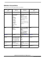
1
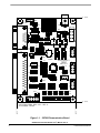
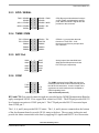
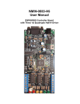
56F800 Demonstration Board
User Manual
56F800
16-bit Digital Signal Controllers
DSP56F800DBUM
Rev. 0
09/2005
freescale.com
TABLE OF CONTENTS
Preface
Chapter 1
Introduction
1.1
1.2
56F800 Demonstration Board Features . . . . . . . . . . . . . . . . . . . . . . . . . . . . . . . . . . . . 1-1
SPECIFICATIONS . . . . . . . . . . . . . . . . . . . . . . . . . . . . . . . . . . . . . . . . . . . . . . . . . . . . 1-3
Chapter 2
Technical Summary
2.1
2.1.1
2.1.2
2.2
2.2.1
2.2.2
2.2.3
2.2.4
2.2.5
2.2.6
2.2.7
2.2.8
2.3
2.3.1
2.3.2
2.4
OPTIONS . . . . . . . . . . . . . . . . . . . . . . . . . . . . . . . . . . . . . . . . . . . . . . . . . . . . . . . . . . .
HOST_ENABLE . . . . . . . . . . . . . . . . . . . . . . . . . . . . . . . . . . . . . . . . . . . . . . . . . . .
CUT_AWAY Options. . . . . . . . . . . . . . . . . . . . . . . . . . . . . . . . . . . . . . . . . . . . . . . .
PORTS AND CONNECTORS . . . . . . . . . . . . . . . . . . . . . . . . . . . . . . . . . . . . . . . . . . .
PWR Jack . . . . . . . . . . . . . . . . . . . . . . . . . . . . . . . . . . . . . . . . . . . . . . . . . . . . . . . .
POWER PORT . . . . . . . . . . . . . . . . . . . . . . . . . . . . . . . . . . . . . . . . . . . . . . . . . . . .
GPIO / SERIAL . . . . . . . . . . . . . . . . . . . . . . . . . . . . . . . . . . . . . . . . . . . . . . . . . . . .
TIMER / PWM . . . . . . . . . . . . . . . . . . . . . . . . . . . . . . . . . . . . . . . . . . . . . . . . . . . . .
ADC Port . . . . . . . . . . . . . . . . . . . . . . . . . . . . . . . . . . . . . . . . . . . . . . . . . . . . . . . . .
COM1 . . . . . . . . . . . . . . . . . . . . . . . . . . . . . . . . . . . . . . . . . . . . . . . . . . . . . . . . . . .
JTAG / OnCE . . . . . . . . . . . . . . . . . . . . . . . . . . . . . . . . . . . . . . . . . . . . . . . . . . . . .
P1 - HOST JTAG . . . . . . . . . . . . . . . . . . . . . . . . . . . . . . . . . . . . . . . . . . . . . . . . . .
USER FEATURES . . . . . . . . . . . . . . . . . . . . . . . . . . . . . . . . . . . . . . . . . . . . . . . . . . . .
MICROPHONE . . . . . . . . . . . . . . . . . . . . . . . . . . . . . . . . . . . . . . . . . . . . . . . . . . . .
POTENTIOMETER (POT) - R12. . . . . . . . . . . . . . . . . . . . . . . . . . . . . . . . . . . . . . .
Indicators . . . . . . . . . . . . . . . . . . . . . . . . . . . . . . . . . . . . . . . . . . . . . . . . . . . . . . . . . . .
2-1
2-1
2-1
2-2
2-2
2-2
2-2
2-3
2-3
2-3
2-3
2-4
2-4
2-4
2-5
2-5
Appendix A
56F800 Demonstration Board Schematics
Freescale Semiconductor
Preliminary
i
56F800 Demonstration Board User’s Manual, Rev. 0
ii
Freescale Semiconductor
LIST OF FIGURES
1-1
2-1
56F800 Demonstration Board . . . . . . . . . . . . . . . . . . . . . . . . . . . . . . . . . . . . . . . . . 1-2
Power Port . . . . . . . . . . . . . . . . . . . . . . . . . . . . . . . . . . . . . . . . . . . . . . . . . . . . . . . 2-2
A-1
56F800 Demonstration Board . . . . . . . . . . . . . . . . . . . . . . . . . . . . . . . . . . . . . . . . . . A-2
Freescale Semiconductor
iii
56F800 Demonstration Board User’s Manual, Rev. 0
iv
Freescale Semiconductor
TABLE OF CONTENTS
2-1
CUT_AWAY Options . . . . . . . . . . . . . . . . . . . . . . . . . . . . . . . . . . . . . . . . 2-1
2-2
Indicators . . . . . . . . . . . . . . . . . . . . . . . . . . . . . . . . . . . . . . . . . . . . . . . . . . 2-5
Freescale Semiconductor
Preliminary
i
56F800 Demonstration Board User’s Manual, Rev. 0
ii
Freescale Semiconductor
Preface
This reference manual describes in detail the hardware on the 56F800 Demonstration
Board.
Audience
This document is intended for application developers who are creating software for
devices using the Freescale 56F800 Demonstration Board.
Organization
This manual is organized into two chapters and one appendix.
•
Chapter 1, Introduction - provides an overview of the Demonstration Board and its
features.
•
Chapter 2, Technical Summary - describes the 56F800 Demonstration Board in
detail.
•
Appendix A, 56F800 Demonstration Board Schematics - contains the schematics of
the 56F800 Demonstration Board.
Suggested Reading
Related documentation for the 56F800 family of digital signal controllers may be found at:
http://www.freescale.com/dsc
Preface, Rev. 0
Freescale Semiconductor
3
Notation Conventions
This manual uses the following notational conventions:
Typeface, Symbol or
Term
Meaning
Examples
Typeface, Symbol or
Term
Courier
Monospaced Type
Code examples
//Process command
for line flash
Courier
Monospaced Type
Italic
Directory names,
project names,
calls,
functions,
statements,
procedures,
routines,
arguments,
file names,
applications,
variables,
directives,
code snippets
APIs
in text
...and contains these core
directories:
applications contains
applications software...
Italic
Bold
Reference sources,
paths,
emphasis
...refer to the Targeting DSP56F80x Platform
manual....
...see: C:\Program
Files\Embedded
SDK\help\tutorials
Bold
Blue Text
Linkable
...refer to Chapter 7,
License....
Blue Text
Number
Any number is considered a positive value,
unless preceded by a
minus symbol to signify a negative value
3V
-10
DES-1
Number
ALL CAPITAL LETTERS
# defines/
defined constants
# define
INCLUDE_STACK_CH
ECK
ALL CAPITAL LETTERS
Brackets [...]
Function keys
...by pressing function
key [F7]
Brackets [...]
...CodeWarrior project,
3des.mcp is...
...the pConfig argument....
...defined in the C header
file, aec.h....
56F800 Demonstration Board User’s Manual, Rev. 0
4
Freescale Semiconductor
Cautionary Notes
1. Electrostatic Discharge (ESD) prevention measures should be applied whenever
handling this product. ESD damage is not a warranty repair item.
2. EMC Information on the 56F800 Demonstration Board:
a. This product as shipped from the factory with associated power supplies and
cables, has been tested and meets with requirements of CE and the FCC as a
CLASS A product.
b. This product is designed and intended for use as a development platform for
hardware or software in an educational or professional laboratory.
c. In a domestic environment this product may cause radio interference in which
case the user may be required to take adequate prevention measures.
d. Attaching additional wiring to this product or modifying the products operation
from the factory default as shipped may effect its performance and also cause
interference with other apparatus in the immediate vicinity. If such interference
is detected, suitable mitigating measures should be taken.
Terminology
This development board applies option selection jumpers. Terminology for application of
the option jumpers is as follows:
Jumper on, in, or installed = jumper is a plastic shunt that fits across 2 pins and the shunt is
installed so that the 2 pins are connected with the shunt.
Jumper off, out, or idle = jumper or shunt is installed so that only 1 pin holds the shunt, no
2 pins are connected, or jumper is removed. It is recommended that the jumpers be idled
by installing on 1 pin so they will not be lost.
This development board applies CUT_AWAY option selections. These option selections
apply surface mount resistor locations with a printed circuit board trace connecting both
component pads. This type connection places an equivalent 0-ohm type resistor in series
with the I/O signal and the user component or I/O connector on the board. These
connections maybe cut with a razor blade or similar type knife between the component
pads to isolate the default connection provided. Reconnection of the cut-away type pads
can be made by either installing a 0 ohm 0805 size surface mount resistor or a small wire
jumper on the component pads.
Preface, Rev. 0
Freescale Semiconductor
5
Definitions, Acronyms, and Abbreviations
Definitions, acronyms and abbreviations for terms used in this document are defined below for
reference.
ADC
CTS
ESD
GPIO
JTAG
OnCETM
PC
POT
PWM
RTS
Analog-to-Digital Converter
Clear To Send
Electrostatic Discharge
General Purpose Input and Output Port
Joint Test Action Group. A bus protocol/interface used for test and
debug.
On-Chip Emulation, a debug bus and port created by Freescale to enable
designers to create a low-cost hardware interface for a professional
quality debug environment.
Personal Computer
Potentiometer
Pulse Width Modulation
Request To Send
References
The following sources were referenced to produce this manual:
DSP56800 Family Manual
DSP56F80x User’s Manual
Technical Data, 56F801 16-Bit Digital Signal Controller
56F800 Demonstration Board User’s Manual, Rev. 0
6
Freescale Semiconductor
Chapter 1
Introduction
The 56F800 Demonstration Board is used to demonstrate the abilities of the 56F800
family and to provide a hardware tool allowing the development of applications that use
the 56F800 devices.
1.1 56F800 Demonstration Board Features
•
56F801FA60 (60 MHz version)
•
RESET Switch
•
IRQ Switch
•
GPIO / SERIAL Port (10 pin) *
•
TIMER / PWM Port (10 Pin) *
•
ADC Port (10 Pin) *
•
JTAG / OnCE Port (14 pin) *
•
Host JTAG Port (P1- DB25P)
•
COM1 Port - SCI to RS232 (DB9S) *
•
PWR Jack supply connector
•
Power Port *
•
Power Indicator
•
10 User Indicators
•
User Potentiometer (R12)
•
Microphone with amplifier
•
Crystal Reference (Y1) *
* All components may not be installed at the factory. The user may install the components
to apply associated feature.
The 56F800 Demonstration Board is detailed in Figure 1-1.
Introduction, Rev. 0
Freescale Semiconductor
1
+3.3V
+VIN
6
COM1
5
RTS
9
5
CTS
6
1
4.200"
VDDA
GND
C16
PWR
R34
POWER
R15
RESET
C11
C10
C7
1
7
C13
R33
R22
R13
R30 C12
GND
4 Y1
R27
MICRO
PHONE RESET
REV.A
R1
R25 R20
C4
R26
+
DSP56F801
3
L1
C5
C3
1
C1
C2
GND
1
U4
2
1
R17 R19
25
13
R16 R23
1
74ACT05
74ACT05
74ACT00
U2
U6
R21 R28
R3
R2
ANALOG -PORT
74ACT125
C6
R12
1
TIMER -PORT
74LCX125
R24
IRQ
DSP56F801
DEMO
AXM-0311
U1
JTAG
GPIO -PORT
14
1
C8
R29
JP1
U5
D11
C9
R14
U7
P1
VR1
VR2
U8 SP3232
9
6 C14 C15
4
1
C18 C17
R31
R32
ON_OFF
U3
R5
R4
R7
R6
R9
R8
R11
R10
D1
D3
D5
D7
D9
D2
D4
D6
D8
D10
0.000"
AXIOM MANUFACTURING
DSP56F801DEMO AXM-0311 REV.A
SILKSREEN LAYER
3.000"
0.000"
Figure 1-1. 56F800 Demonstration Board
56F800 Demonstration Board User’s Manual, Rev. 0
2
Freescale Semiconductor
SPECIFICATIONS
1.2 SPECIFICATIONS
•
+9V DC input voltage typical, 200ma
•
Input voltage range: +7 to +15V DC
•
On board regulated +5V DC and +3.3V DC supplies
•
Board size: 3 x 4.2 inches
Introduction, Rev. 0
Freescale Semiconductor
3
56F800 Demonstration Board User’s Manual, Rev. 0
4
Freescale Semiconductor
Chapter 2
Technical Summary
This chapter describes the 56F800 Demonstration Board’s available options.
2.1 OPTIONS
2.1.1 HOST_ENABLE
The HOST_ENABLE option jumper is installed by default and enables the Host JTAG
interface on the board. With the option jumper installed, the 56F801 device will reset into
Debug mode and await Host commands on the Host JTAG port (P1). Removing the
HOST_ENABLE option jumper will allow the 56F801 device to reset normally and
execute program code contained in the device’s Flash memory.
•
HOST_ENABLE = INSTALLED: Debug Mode; host JTAG port is active
•
HOST_ENABLE = OPEN or IDLE: Normal Mode; executes user code in Flash
2.1.2 CUT_AWAY Options
CUT_AWAY options allow the user to disconnect dedicated 56F801 I/O port resources
from development board connectors or peripherals. The CUT_AWAY options also allow
for re-establishing the connection by installing surface-mount 0805-size 0 ohm resistors or
mod wire with the use of a soldering iron. Normal operation of the 56F800 Demonstration
Board generally does not require any manipulation of the CUT_AWAY options.
Table 2-1. CUT_AWAY Options
CUT_AWAY #
Description
56F801 Signal
Connection Signal
1
ADC reference supply
VREF
VDDA
2
User POT (R12) to ADC
ANA6
R12 wiper
3
Crystal oscillator isolation
XTAL / GPIOB3
GPIO / SERIAL pin 4
Technical Summary, Rev. 0
Freescale Semiconductor
1
Table 2-1. CUT_AWAY Options (Continued)
CUT_AWAY #
Description
56F801 Signal
Connection Signal
4
Crystal oscillator isolation
EXTAL / GPIOB2
GPIO / SERIAL pin 3
5
COM1 serial port
TXD0 / GPIO0
U8 pin 11 (COM1 TXD)
6
COM1 serial port
RXDO / GPIOB1
U8 pin 12 (COM1 RXD)
7
Microphone to ADC
ANA2
U7 pin 4 (Microphone output)
2.2 PORTS AND CONNECTORS
2.2.1 PWR Jack
This connector provides power input to the board by default. The PWR jack accepts a
standard 2.0 ~ 2.1mm center-barrel plug connector (positive voltage center) to provide the
+VIN supply of +9V DC at 200ma.
2.2.2 POWER PORT
Provides access to the +9V DC input, GND (power ground), +5V DC and +3.3V DC
power supplies. The +9V DC input should only be applied by PWR jack or Power Port,
but not both, or a supply conflict may occur and the 56F800 Demonstration Board could
be damaged. Power Port accepts a 3.5mm pin space terminal block.
GND
+3.3V DC
+5V DC
+9V DC
Figure 2-1. Power Port
56F800 Demonstration Board User’s Manual, Rev. 0
2
Freescale Semiconductor
PORTS AND CONNECTORS
2.2.3 GPIO / SERIAL
TXD0 / GPIOB0
GPIOB2
SCLK / GPIOB4
MISO / GPIOB6
IREQA*
1
3
5
7
9
2
4
6
7
10
1
3
5
7
9
2
4
6
7
10
1
3
5
7
9
2
4
6
7
10
GPIOB1 / RXD0
GPIOB3
GPIOB5 / MOSI
GPIOB7 / SS*
RESET*
GPIO B port provides alternate functions
as SCI (COM1 and indications) and SPI
ports. IREQ and RESET signals are also
provided on this connector.
2.2.4 TIMER / PWM
TD0 / GPIOA0
TD2 / GPIOA2
PWMA4
PWMA2
PWMA0
GPIOA1 / TD1
FAULTA0
PWMA5
PWMA3
PWMA1
GPIOA0 - 2 port provides alternate
functions of Timer TD0 - 2 I/O.
Note that most of these ports provide a
user indication.
2.2.5 ADC Port
ANA6
ANA4
ANA2
ANA0
VREF
ANA7
ANA5
ANA3
Analog inputs. Note that ANA2 and
ANA6 provide Microphone and User
POT R12 input, respectively.
ANA1
GND
2.2.6 COM1
1
TXD0
RXD0
4
GND
1
2
3
4
5
6
7
8
9
6
CTS
RTS
9
The COM1 port has a female DB9 connector that
interfaces to the 56F801 internal SCI0 serial port via
the U8 RS-232 transceiver. It uses a simple 2-wire
asynchronous serial interface and is translated to
RS-232 signaling levels.
1,4,6 connected (host null)
RTS and CTS flow control connection pads are provided on the 56F800 Demonstration Board to
apply unassigned 56F801 I/O to support flow control on COM1. The RTS pad provides RS-232
level output conversion to COM1 port pin 8. The CTS pad provides RS-232-converted input
from COM1 pin 7.
The 1, 4, 6, and 9 pins provide RS-232 status. The 1, 4, and 6 pins are connected on the bottom
of the development board to provide NULL status to the host. The user may isolate pins and
provide the status connections to the host by applying I/O signals and RS-232 level conversion.
Technical Summary, Rev. 0
Freescale Semiconductor
3
2.2.7 JTAG / OnCE
The JTAG 14-pin connector is compatible with the Freescale OnCE development port. This
connector allows the connection of a OnCE-style background debug cable for software
development, programming and debugging in real time.
TDI
TDO
TCK
RESET in
+3.3V DC
DE*
1
3
5
7
9
11
13
2
4
6
7
10
12
14
GND
GND
JTAG / OnCE BDM connection.
GND
(key)
TMS
TRST* in
Note: HOST_ENABLE option must be open or idle to apply this connector.
2.2.8 P1 - HOST JTAG
The P1 - Host JTAG connector provides development port interface to a hosting Personal
Computer’s LPT or Printer port. The HOST_ENABLE option jumper must be installed for this
port to operate.
Reset in
TMS
TCK
TDI
TRST*
DE* (Note R23)
Pin 15 tie
TDO
P-CON
1
2
3
4
5
6
7
8
9
10
11
12
13
14
15
16
17
18
19
20
21
22
23
24
25
Pin 8 tie
GND
GND
GND
GND
GND
GND
GND
GND
GND
P1 - HOST JTAG connector is a DB25
pin connector. Signals are organized for
direct connection to an IBM-compatible
PC with a straight-through DB25 cable.
Pin 7 / DE* signal, if supported, can be
enabled by installing R23 (51 ohms)
Note: HOST_ENABLE option must be installed to apply this connector.
2.3 USER FEATURES
Several circuits are provided for demonstration of 56F800 applications.
56F800 Demonstration Board User’s Manual, Rev. 0
4
Freescale Semiconductor
Indicators
2.3.1 MICROPHONE
A microphone with audio amplifier is provided on the 56F800 Demonstration Board for user
applications. The amplifier provides low-pass filtering starting at ~4000Hz for speech input.
The audio signal from the microphone amplifier is provided to the ADC ANA2 input channel via
CUT_AWAY option #7.
2.3.2 POTENTIOMETER (POT) - R12
The user POT R12 provides a 0 to +3.3V adjustable analog input to the 56F801’s ADC ANA6
channel. R12 can be removed from the ANA6 channel by CUT_AWAY option #2.
2.4 Indicators
User indicactions are provided that are active with a high level on the associated 56F801 device’s
I/O port. Table 2-2 details the indicators.
Table 2-2. Indicators
Indicator
56F800 Signal
Color
D1
PWMA0
Green
D2
PWMA1
Green
D3
PWMA2
Green
D4
PWMA3
Green
D5
PWMA4
Yellow
D6
PWMA5
Yellow
D7
GPIOB1 / RXD0
Yellow
D8
GPIOB0 / TXD0
Yellow
D9
GPIOA1 / TD1
Red
D10
GPIOA2 / TD2
Red
Technical Summary, Rev. 0
Freescale Semiconductor
5
56F800 Demonstration Board User’s Manual, Rev. 0
6
Freescale Semiconductor
Appendix A
56F800 Demonstration Board
Schematics
56F800 Demonstration Board Schematics, Rev. 0
Freescale Semiconductor
1
Figure A-1. 56F800 Demonstration Board
DSP56F801EVM Hardware User’s Manual, Rev. 0
2
Freescale Semiconductor
INDEX
A
J
ADC vi, 2-1, 2-4
Analog-to-Digital Converter
ADC vi
Joint Test Action Group
JTAG vi
JTAG vi
C
M
CE v
Clear To Send
CTS vi
COM1 serial port 2-1
Crystal oscillator isolation 2-1
CTS vi, 2-3
CUT_AWAY v, 2-4, 2-5
Microphone 2-2, 2-3
D
P
DS25 2-4
DSP56F801 Digital Signal Processor User’s Manual vi
Electrostatic Discharge
ESD v, vi
EMC v
ESD v, vi
PC vi
Personal Computer
PC vi
POT vi, 2-1, 2-3
Potentiometer
POT vi
Pulse Width Modulation
PWM vi
PWM vi
F
R
FCC v
R23 2-4
RS-232 2-3
RTS 2-3
E
G
General Purpose Input/Output Port
GPIO vi
GPIO vi
O
OnCE vi
On-Chip Emulation
OnCE vi
T
Technical Data, 56F801 16-Bit Hybrid Controller vi
H
HOST_ENABLE 2-4
I
I/O connector v
I/O signal v
Freescale Semiconductor
Index - i
How to Reach Us:
Home Page:
www.freescale.com
E-mail:
[email protected]
USA/Europe or Locations Not Listed:
Freescale Semiconductor
Technical Information Center, CH370
1300 N. Alma School Road
Chandler, Arizona 85224
+1-800-521-6274 or +1-480-768-2130
[email protected]
Europe, Middle East, and Africa:
Freescale Halbleiter Deutschland GmbH
Technical Information Center
Schatzbogen 7
81829 Muenchen, Germany
+44 1296 380 456 (English)
+46 8 52200080 (English)
+49 89 92103 559 (German)
+33 1 69 35 48 48 (French)
[email protected]
Japan:
Freescale Semiconductor Japan Ltd.
Headquarters
ARCO Tower 15F
1-8-1, Shimo-Meguro, Meguro-ku,
Tokyo 153-0064, Japan
0120 191014 or +81 3 5437 9125
[email protected]
Asia/Pacific:
Freescale Semiconductor Hong Kong Ltd.
Technical Information Center
2 Dai King Street
Tai Po Industrial Estate
Tai Po, N.T., Hong Kong
+800 2666 8080
[email protected]
For Literature Requests Only:
Freescale Semiconductor Literature Distribution Center
P.O. Box 5405
Denver, Colorado 80217
1-800-441-2447 or 303-675-2140
Fax: 303-675-2150
[email protected]
Information in this document is provided solely to enable system and software
implementers to use Freescale Semiconductor products. There are no express
or implied copyright licenses granted hereunder to design or fabricate any
integrated circuits or integrated circuits based on the information in this
document.
Freescale Semiconductor reserves the right to make changes without further
notice to any products herein. Freescale Semiconductor makes no warranty,
representation or guarantee regarding the suitability of its products for any particular purpose, nor does Freescale Semiconductor assume any liability arising
out of the application or use of any product or circuit, and specifically disclaims
any and all liability, including without limitation consequential or incidental damages. “Typical” parameters that may be provided in Freescale Semiconductor
data sheets and/or specifications can and do vary in different applications and
actual performance may vary over time. All operating parameters, including
“Typicals”, must be validated for each customer application by customer’s technical experts. Freescale Semiconductor does not convey any license under its
patent rights nor the rights of others. Freescale Semiconductor products are not
designed, intended, or authorized for use as components in systems intended
for surgical implant into the body, or other applications intended to support or
sustain life, or for any other application in which the failure of the Freescale
Semiconductor product could create a situation where personal injury or death
may occur. Should Buyer purchase or use Freescale Semiconductor products
for any such unintended or unauthorized application, Buyer shall indemnify and
hold Freescale Semiconductor and its officers, employees, subsidiaries, affiliates, and distributors harmless against all claims, costs, damages, and expenses, and reasonable attorney fees arising out of, directly or indirectly, any claim
of personal injury or death associated with such unintended or unauthorized
use, even if such claim alleges that Freescale Semiconductor was negligent regarding the design or manufacture of the part.
Freescale™ and the Freescale logo are trademarks of Freescale Semiconductor, Inc. All other
product or service names are the property of their respective owners.
This product incorporates SuperFlash® technology licensed from SST.
© Freescale Semiconductor, Inc. 2005. All rights reserved.
DSP56F800DBUM
Rev. 0
9/2005