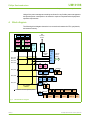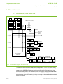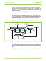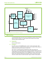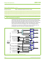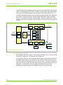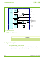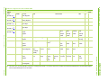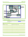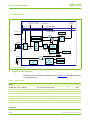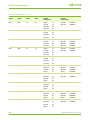
1
UM10198
LPC3180 User Manual
Rev. 01 — 1 June 2006
Document information
Info
Content
Keywords
LPC3180; ARM9; 16/32-bit ARM microcontroller
Abstract
User manual for LPC3180
User manual
UM10198
Philips Semiconductors
LPC3180 User Manual
Revision history
Rev
Date
Description
01
20060601
Initial version
Contact information
For additional information, please visit: http://www.semiconductors.philips.com
For sales office addresses, please send an email to: [email protected]
UM10198_1
User manual
© Koninklijke Philips Electronics N.V. 2006. All rights reserved.
Rev. 01 — 1 June 2006
2 of 396
UM10198
Chapter 1: Introductory information
Rev. 01 — 1 June 2006
User manual
1. Introduction
The LPC3180 is an ARM9-based microcontroller for embedded applications requiring
high performance combined with low power dissipation.
It achieves these objectives through the combination of Philips' state-of-the-art
90 nanometer technology with an ARM926EJ-S CPU core with a Vector Floating Point
co-processor and a large array of standard peripherals including USB On-The-Go.
The microcontroller can operate at over 200 MHz CPU frequency (about 220 MIPS per
ARM Inc.). The ARM926EJ-S CPU incorporates a 5-stage pipeline and has a Harvard
architecture with separate 32 kB Instruction and Data caches, a demand paged MMU,
DSP instruction extensions with a single cycle MAC, and Jazelle Java Byte-code
execution hardware. A block diagram of the microcontroller is shown in Figure 1.
Power optimization in this microcontroller was a key objective and has been accomplished
through process and technology development (Intrinsic Power), and architectural means
(Managed Power).
The LPC3180 also incorporates an SDRAM interface, NAND Flash interfaces, USB 2.0
Full Speed interface, seven UARTs, two I2C interfaces, two SPI ports, a Secure Digital
(SD) interface, and a 10-bit A/D converter in addition to many other features.
UM10198_1
User manual
© Koninklijke Philips Electronics N.V. 2006. All rights reserved.
Rev. 01 — 1 June 2006
3 of 396
UM10198
Philips Semiconductors
Chapter 1: Introductory information
External
Memory
Interfaces
CPU subsystem
ETB
ETM9
I-Cache
32kB
D-Cache
32kB
VFP9
ARM926EJ
Instr
NAND
Flash
On-Chip
Memory
Data
ROM
SD Card
64 kB
SRAM
DRAM
control
Bus matrix (Multi-layer AHB)
Interrupt
Controller
DMA
Controller
System
Control
Watchdog
PLLs
High Speed
Timer
Power
Control
Millisecond
Timer
System Functions
GPIO
Keyscan
10-bit
A/D
UART
1-5, 7
I2C1
I2C2
UART6
IrDA
RTC
SPI1
PWM1
PWM2
Other
Peripherals
USB OTG
SPI2
Communication
Peripherals
Fig 1. LPC3180 overview diagram
2. Features
• ARM926EJS processor, running at up to 208 MHz.
• 32 kB instruction cache and 32 kB data cache.
• 64 kB of SRAM.
UM10198_1
User manual
© Koninklijke Philips Electronics N.V. 2006. All rights reserved.
Rev. 01 — 1 June 2006
4 of 396
UM10198
Philips Semiconductors
Chapter 1: Introductory information
• Multilayer AHB system that provides a separate bus for each AHB master, including
both an instruction and a data bus for the CPU, two data busses for the DMA
controller. and another bus for the USB controller. There are no arbitration delays
unless two masters attempt to access the same slave at the same time.
• External memory controller that supports DDR and SDR SDRAM.
• Two NAND Flash controllers. One supports single level NAND Flash devices. The
other supports multi-level NAND Flash devices.
• Interrupt Controller, supporting 60 interrupt sources.
• General Purpose AHB DMA controller (GPDMA) that can be used with the SD card
port, the high-speed UARTs, and SPI interfaces, as well as for memory-to-memory
transfers.
• Serial Interfaces:
– USB Device, Host (OHCI compliant), and OTG block with on-chip Host/Device
PHY and associated DMA controller. A dedicated PLL provides the required
48 MHz USB clock.
– Four standard UARTs with fractional baud rate generation, one with IrDA support,
all with 64 byte FIFOs.
– Three high-speed UARTs. Intended for on-board communications up to 921,600
bps with a 13 MHz main oscillator.
– Two SPI controllers.
– Two single master only I2C-bus Interfaces with standard open drain pins.
• Other Peripherals:
– Secure Digital (SD) memory card interface.
– General purpose input, output, and I/O pins. Includes 12 GP input pins, 24 GP
output pins, and six GP I/O pins.
– 10 bit, 32 kHz A/D Converter with input multiplexing from 3 pins.
– Real Time Clock with separate power pin, clocked by a dedicated 32 kHz oscillator.
Includes a 32 byte scratchpad memory. The RTC is implemented in a separate
power domain so that it can remain active while the rest of the chip is not powered.
– 32-bit general purpose high speed timer with 16-bit pre-scaler. Includes one
external capture input and a capture connection to the RTC clock. Interrupts may
be generated using 3 match registers.
– 32-bit Millisecond timer driven from the RTC clock. Interrupts may be generated
using 2 match registers.
– Watchdog Timer. The watchdog timer is clocked by PERIPH_CLK.
– Two PWM blocks. Up to 50 kHz output rate with a 13 MHz system clock.
– Keyboard scanner function allows automatic scanning of up to an 8x8 key matrix.
– Up to 18 external interrupts.
• Standard ARM Test/Debug interface for compatibility with existing tools.
• Emulation Trace Buffer with 2K x 24 bit RAM allows trace via JTAG.
• Stop mode saves power, while allowing many peripheral functions to restart CPU
activity.
• On-chip crystal oscillator.
UM10198_1
User manual
© Koninklijke Philips Electronics N.V. 2006. All rights reserved.
Rev. 01 — 1 June 2006
5 of 396
UM10198
Philips Semiconductors
Chapter 1: Introductory information
• On-chip PLL allows CPU operation up to the maximum CPU rate without the need for
a high frequency crystal. Another PLL allows operation from the 32 kHz RTC clock
rather than the external crystal.
• Boundary Scan for simplified board testing.
• 320 pin TFBGA package.
3. Microcontroller CPU and peripherals
The ARM926EJ core is coupled to 32 kB each of Instruction and Data Cache and a further
64 kB of internal (on-chip) SRAM for very high performance. The E suffix means that the
core has DSP instructions such as single cycle multiply-accumulate and saturating
arithmetic and the J suffix means that the core has the ARM Jazelle Java execution
machine on-board. In addition, the ARM926EJ has a full MMU which enables large
Operating systems such as Linux, Windows CE, etc. to run with full task protection. Linux
ports are available for the ARM926EJ from various suppliers and it is a very popular Linux
machine. Its various sub-systems and peripherals are described as follows:
3.1 Vector Floating-Point (VFP) co-processor
This CPU co-processor provides full support for single-precision and double-precision
add, subtract, multiply, divide, and multiply-accumulate operations at CPU clock speeds. It
is compliant with the IEEE 754 standard. and enables advanced Motor control and DSP
applications. The VFP has 3 separate pipelines for Floating-point MAC operations, Divide
or square root operations, and Load/Store operations. These pipelines can operate in
parallel and can complete execution out of order. All single-precision instructions, except
divide and square root, take one cycle. Double-precision multiply and multiply-accumulate
instructions take two cycles. The VFP also provides format conversions between
floating-point and integer word formats.
The microcontroller has a Multi-layer AHB Matrix for inter-block communication. AHB is
the ARM High-speed Bus, which is part of the ARM Bus architecture. AHB is a
high-bandwidth low-latency bus that supports multi-master arbitration and a bus
grant/request mechanism. For systems where there is only one bus master (the CPU), or
where there are two masters (CPU and DMA) and the CPU does not generally need to
contend with the DMA for program memory access (because the CPU has access to
memory on its local bus or has caches or another AHB bus etc.), this arrangement works
well. However, if there are multiple bus masters and the CPU needs access to external
memory, a single AHB bus can cause a bottleneck. ARM’s solution to this was to invent
Multi-layer AHB which replaces the request/grant and arbitration mechanism with a
multiplexer fabric that pushes arbitration to the level of the devices. Thus, if a CPU and a
DMA controller want access to the same memory, the multi-layer fabric will arbitrate
between the two on granting access to that memory. This allows simultaneous access by
bus masters to different resources at the cost of increased arbitration complexity. As with
all trade-offs, the pros and cons must be analyzed. For a Microcontroller operating at
200 MHz, removing guaranteed central arbitration in case more than one bus master is
active in favor of occasional local arbitration gives better performance.
The blocks outside the CPU can be roughly split into Memory Controllers, Serial
Communication, I/O, Timers/Counters and Real-Time Clock, System Control, and Debug
and Trace Blocks. These are described as follows.
UM10198_1
User manual
© Koninklijke Philips Electronics N.V. 2006. All rights reserved.
Rev. 01 — 1 June 2006
6 of 396
UM10198
Philips Semiconductors
Chapter 1: Introductory information
3.2 Memory controllers
External Memory controller (EMC): This Peripheral can use high-speed SDRAM as well
as NAND Flash. A DMA engine is connected to the EMC to allow DMA bus-master driven
transfers from and to external memory. This memory controller has write buffering built in
and is able to prioritize between different masters. It has a peak bandwidth of 400 MB/s.
SDRAMs of up to 1 Gbit and up to 32-bits wide can be connected directly to the bus. If a
memory bus narrower than 32 bits is used, many of the unused data bus bits can be used
for GPIO.
NAND Flash Controller: Both Multi-level and single level NAND Flash can be connected
directly to the microcontroller. Up to 2 Gbit, 8-bit wide memory is supported. Internal ECC
circuitry calculates column and row error correction values, and single bit errors can be
detected and corrected by the software.
3.3 Serial communication peripherals
The LPC3180 has a large array of high-speed serial peripherals which are generally all
supported by DMA channels and have FIFO buffering to reduce CPU interrupt overhead.
The peripherals are:
USB 2.0 Full-Speed Triple Mode block — This IP Block is designed to offer the most
versatility to the user by operating in Device, Host, and On-The-Go (OTG) Modes under
Program control. An external Philips transceiver (ISP1301) is programmed via a
dedicated I2C-bus to set up the parameters for OTG transfers. OTG mode also has
Car-Kit compatibility allowing UART operation over the USB lines for certain applications.
The Host mode is OHCI compliant and includes the Root Hub function for one device
(since this is a point-to-point connection only). Sixteen logical (32 physical) Endpoints are
supported with full support for maximum packet size transfers in Isochronous and Bulk
modes. This peripheral has a 4 kB RAM as an Endpoint buffer which allows double
buffering of full-size Isochronous packets (1023 bytes each). Finally, it has a dedicated
DMA engine which can traverse a list of Transfer Descriptors to off-load the CPU of
packet transfer duties. USB Driver Software will be provided by Philips (as example
source code) and by 3rd parties as professional level software.
UARTs — The Microcontroller has 7 UARTs. Four of these are 16XC50 compatible and
two are Higher-speed devices. One has hardware flow control. All of the UARTs have
64-byte Receive/Transmit FIFOs with programmable watermark capability. Three of the
UARTs support DMA transfers and all have loopback modes for testing. Maximum data
transfer rate is 921.6 kbit/s. One of the UARTs also has an IrDA interface encoder and
decoder which converts the UART data to an IrDA frame.
SPI — There are two 3-wire SPI channels. These are Master SPI blocks and are
supported by DMA transfers for transmit and receive. The word length can be from 1 to 16
bits in length and both have 64 byte FIFOs. Data rates of up to 52 Mbits/sec are
supported.
I2C-bus — This interface is a 400 kHz master block. Transmit and Receive are buffered
by 4-word FIFOs and there is an interrupt dedicated to this block.
Secure Digital (SD) Card interface — The SD card standard is one of the fastest
growing plug-in card standards in the industry. The microcontroller has an SD Host
Controller which can transfer data at up to 25 MHz over the 4-bit SD data interface (100
Mbits/sec). The SD Controller has a 16 entry FIFO and supports DMA transfers.
UM10198_1
User manual
© Koninklijke Philips Electronics N.V. 2006. All rights reserved.
Rev. 01 — 1 June 2006
7 of 396
UM10198
Philips Semiconductors
Chapter 1: Introductory information
3.4 I/O
There are 42 multi-function general purpose I/O lines. If a 16-bit wide SDRAM data
interface is used, then a further 13 lines are made available. The GPIO lines have Atomic
Bit Set/Reset capability which allows pins to be allocated per software task and allows
each task to update its pin or pins without affecting any other pin state. This also allows
peripherals that have pins which reflect hardware events (such as interrupts) to not be
overwritten unknowingly. Atomic Bit Set/Reset is a necessity with RISC architectures
which do not support Read-Modify-Write at a hardware bit level basis (doing this in
software or at a bus controller level does not completely address the problem).
3.5 Timer/counters and Real-Time Clock (RTC)
The Microcontroller has a high-speed timer with 32-bit Capture and Match registers for
high-resolution capture and matching of events. There is also a one-millisecond timer with
an interrupt that can be used to provide a real-time tick to an OS.
A 32-bit Watchdog timer can generate internal as well as external resets. This capability
allows synchronizing hardware system resets with internal ones. It serves to notify the
system that a Watchdog Reset took place as well, which can be a sign that a software or
hardware malfunction has occurred.
Two 8-bit PWMs are provided which can be clocked separately by either the Real-Time
clock 32 kHz signal or the crystal input frequency.
The Real-Time Clock has a special power domain independent of the rest of the chip and
is designed both to be very low power as well as to work down to low voltage levels (follow
a discharging battery). It has 32 words of SRAM that can be used to hold data between
microcontroller power cycles. The RTC generates a one-second tick from a dedicated
32 kHz crystal oscillator and uses 32-bit registers which should never need resetting
(since it counts to maximum in 136 years, this is probably OK).
3.6 System control and analog blocks
These are the blocks responsible for Clock generation, Reset, Power-up and Booting of
the chip. There is also a 10-bit A/D converter on-chip that can run at up to 400 kHz
sampling frequency.
Clock generation: There are 2 main clock sources. The main crystal oscillator which
shares the power domain of the microcontroller and a 32 kHz oscillator which drives the
RTC and has its own power domain to keep the RTC alive. The main clock is multiplied up
by a PLL to generate the high-speed CPU clock (max. 208 MHz). The RTC 32 kHz clock
can also be multiplied up and used as an input to the main PLL so that the entire
microcontroller can run from the RTC oscillator clock. Note that having two PLLs in series
increases the jitter. Therefore the main crystal oscillator must be used to generate the
USB clock. All other sub-systems can use the up-multiplied RTC clock.
Boot-up on Powering on the chip is handled by an on-chip Boot Loader in ROM that looks
at the state of a pin to see if it should attempt to download a program over a serial link
(UART) or download a program from NAND Flash and then branch to it. Since the Boot
loader is in ROM it takes no user memory space.
UM10198_1
User manual
© Koninklijke Philips Electronics N.V. 2006. All rights reserved.
Rev. 01 — 1 June 2006
8 of 396
UM10198
Philips Semiconductors
Chapter 1: Introductory information
3.7 Debug and trace blocks
The microcontroller uses the standard ARM Enhanced JTAG Debug interface and,
therefore, works with all standard ARM Development tools and hardware. Evaluation and
development boards will be available from third party vendors. Software development and
debugging tools and compilers from many vendors including ARM are available now and
are well proven and mature.
Embedded Trace support is provided through use of an ETB (Embedded Trace Buffer)
RAM block which stores Trace information in on-chip RAM to be read out later via the
CPU or the E-JTAG interface. This saves over 20 pins and enables true Real-time
operation over the Trace window. Both Data and Instruction values can be traced. The
trace information is saved to a 45-byte FIFO whose contents are transferred to the ETB in
Real-time.
3.8 Architectural power management
Several techniques are employed to allow full user control and customizing of power
management as follows:
1. Programmable clock enabling: Each Peripheral and AHB Matrix has a selectable
Clock Enable bit. Thus the user can control which combinations of peripherals he
enables for his particular system design and also when to enable them. Further,
several peripherals have local power savings means (such as sleep modes) for more
power savings.
2. Low-Voltage Operation: The microcontroller is able to operate down to 0.9 Volts which
reduces power tremendously (dynamic power is reduced by more than 50 % over
1.2 V operation) but requires operation at lower clock frequencies. This is suitable for
very low power standby modes where system operation is required but performance
can be compromised. The chip has a pin indicating that the chip is in a low power
state so that the software can manage the system accordingly.
3. PLL Clock control: The system has full control over the PLL multiplier and can
therefore manage this aspect of power. Note that high-speed DRAM control must be
taken into account so that Refresh rates are maintained in low speed modes.
4. STOP mode: In this mode, the AHB Matrix clock is disabled and the ARM clock is
stopped. This is basically a Static-power-only mode.
5. AHB Bus Matrix Clock Control: The ARM CPU clock can be divided by a factor of 2, 4,
or 8 to derive the Peripheral Bus clock. This can be used as a power control
mechanism if only low bandwidth transfers are to be handled. Note that the CPU can
execute out of its local 64 kB of SRAM and does not need to access the DRAM
continuously (of course it also has caches).
6. System operation on RTC Clock: The RTC oscillator uses a 32 kHz crystal and runs at
much lower power than the main crystal oscillator. A dedicated PLL is available which
multiplies the RTC clock to a frequency where it can be further multiplied by the main
PLL to generate the > 200 MHz CPU clock. In the case where the increased jitter
caused by cascading PLLs is acceptable, this allows for lower power operation.
7. Power domain switching: The RTC clock is on a separate power domain and also has
32 words of low-power SRAM. To save the maximum amount of power, the
microcontroller power can be turned off altogether while keeping the RTC alive with
some critical system information that can be saved between power cycles. This also
eliminates leakage current power consumption.
UM10198_1
User manual
© Koninklijke Philips Electronics N.V. 2006. All rights reserved.
Rev. 01 — 1 June 2006
9 of 396
UM10198
Philips Semiconductors
Chapter 1: Introductory information
Using all the power management techniques allows for very flexible power management
and permits power consumption to be tailored to required computational and peripheral
operation requirements.
4. Block diagram
The following block diagram shows the bus connections between the CPU, peripherals,
and external memory.
VFP9
D-TCM
0 kB
ETB
ARM
D-cache 9EJS
32 kB
I-TCM
0 kB
I-cache
32 kB
D-side
I-side
MMU
controller
controller
Instr
Data
Master Layer
0
USB
transceiver
interface
ETM9
1
DMA Ctrl
PL080
M
1
M
0
2
USB-OTG
AHB
Master
GX175
SDRAM
Ctrl
32 bit,
104 MHz
AHB
3
32 bit wide
external
memory
Port 2
Port 3
Port 4
Port 0
Slave port 0
Slave port 1
Slave port 2
Slave port 3
SRAM
64 kB
ROM
16 kB
AHB slaves
Slave port 5
NAND
Ctrl
APB slaves
AHB2-APB
MLC
NAND Ctrl
SPI
x2
SD
Card
AHB slaves
Slave port 6
DMA
regs
Slave port 7
32 bit, 104 MHz
AHB Matrix
USB
config
SDRAM
confg
ETB
regs
AHB- APB slaves
2-APB
I2C UART
x2
x4
Master/Slave connection supported by matrix
PWM RTC
AHB- FAB slaves
2-FAB
GPIO
Watchdog
Timer
System
Control
High Speed
Timer
Key
Interrupt
Debug
Scan Controller x3
Millisecond
Timer
High Speed
UART x3
10-bit
ADC
Fig 2. LPC3180 block diagram
UM10198_1
User manual
© Koninklijke Philips Electronics N.V. 2006. All rights reserved.
Rev. 01 — 1 June 2006
10 of 396
UM10198
Chapter 2: Bus architecture and memory map
Rev. 01 — 1 June 2006
User manual
1. Bus architecture and memory map
Figure 2–3 shows the memory map for the AHB Matrix. This view represents all address
sources except the USB interface.
UM10198_1
User manual
© Koninklijke Philips Electronics N.V. 2006. All rights reserved.
Rev. 01 — 1 June 2006
11 of 396
UM10198
Philips Semiconductors
Chapter 2: Bus architecture and memory map
4.0 GB
0xFFFF FFFF
(RESERVED)
0x9FFF FFFF
off-chip SDRAM
memory
2.0 GB
SDRAM
0x8000 0000 to 0x9FFF FFFF
0x8000 0000
0x7FFF FFFF
(RESERVED)
0x5000 0000
0x4FFF FFFF
(RESERVED)
peripherals on AHB
matrix slave port 7
1.0 GB
APB peripherals
0x4008 0000 to 0x400F FFFF
FAB peripherals
0x4000 0000 to 0x4007 FFFF
0x4000 0000
0x3FFF FFFF
(RESERVED)
peripherals on AHB
matrix slave port 6
AHB peripherals
0x3000 0000 to 0x31FF FFFF
0x3000 0000
0x2FFF FFFF
768 MB
(RESERVED)
peripherals on AHB
matrix slave port 5
AHB peripherals
0x200A 0000 to 0x200B FFFF
APB peripherals
0x2008 0000 to 0x2009 FFFF
AHB peripherals
0x2000 0000 to 0x2007 FFFF
0x2000 0000
0x1FFF FFFF
(RESERVED)
IROM
0x0C00 0000 to 0x0FFF FFFF
IRAM
0x0800 0000 to 0x0BFF FFFF
dummy for DMA garbage
0x0400 0000 to 0x07FF FFFF
IROM or IRAM
0x0000 0000 to 0x03FF FFFF
0x1000 0000
0x0FFF FFFF
on-chip memory
0.0 GB
0x0000 0000
002aac163
Fig 3. Overall LPC3180 memory map
1.1 CPU memory space
The following table gives the address spaces for the LPC3180, as seen by the AHB
Matrix.
UM10198_1
User manual
© Koninklijke Philips Electronics N.V. 2006. All rights reserved.
Rev. 01 — 1 June 2006
12 of 396
UM10198
Philips Semiconductors
Chapter 2: Bus architecture and memory map
Table 1.
Overview of LPC3180 memory spaces
Address
Function
0x0000 0000 to
0x0FFF FFFF
On-Chip Memory on AHB Matrix slave 3 (see Figure 2–4):
0x0000 0000 to 0x03FF FFFF = IROM or IRAM.
0x0400 0000 to 0x07FF FFFF = Dummy space for DMA. Reads as all zeroes,
write has no effect.
0x0800 0000 to 0x0BFF FFFF = IRAM (64 kB populated).
0x0C00 0000 to 0x0FFF FFFF = IROM (16 kB populated).
0x1000 0000 to
0x1FFF FFFF
0x2000 0000 to
0x2FFF FFFF
Reserved
Peripherals on AHB Matrix slave 5 (see Figure 2–4):
0x2000 0000 to 0x2007 FFFF = AHB peripherals.
0x2008 0000 to 0x2009 FFFF = APB peripherals.
0x200A 0000 to 0x200B FFFF = AHB peripherals.
0x3000 0000 to
0x3FFF FFFF
Peripherals on AHB Matrix slave 6 (AHB peripherals)
0x4000 0000 to
0x4FFF FFFF
Peripherals on AHB Matrix slave 7 (see Figure 2–4):
0x4000 0000 to 0x4007 FFFF = FAB peripherals.
0x4008 0000 to 0x400F FFFF = APB peripherals.
0x5000 0000 to
0x7FFF FFFF
Reserved
0x8000 0000 to
0x9FFF FFFF
Off-Chip SDRAM Memory space, 512 MB in size.
Accessed as follows:
•
•
•
0xA000 0000 to
0xFFFF FFFF
ARM 9 instruction fetch via AHB Matrix slave port 0 to EMC port 3.
ARM 9 data access via AHB Matrix slave port 1 to EMC port 4.
DMA controller (both channels) via AHB Matrix slave port 2 to EMC
port 0.
Reserved
1.2 USB memory space
The USB interface exists on a separate AHB bus, and can only access the SDRAM. It
uses the same address mapping for SDRAM, but can only access the bottom half (256
MB) of the full SDRAM space. Addresses outside this space will alias back into the bottom
half of the SDRAM space, so care must be taken to avoid inadvertent address
wrap-around.
Table 2.
USB memory space
Address
Function
0x8000 0000 to 0x8FFF FFFF
Off-Chip SDRAM Memory space, 256 MB in
size.
2. Peripheral addresses
Table 2–3 shows the base addresses of the peripheral devices present on the LPC3180.
UM10198_1
User manual
© Koninklijke Philips Electronics N.V. 2006. All rights reserved.
Rev. 01 — 1 June 2006
13 of 396
UM10198
Philips Semiconductors
Chapter 2: Bus architecture and memory map
Table 3.
Peripheral devices on the LPC3180
Base Address
Peripheral
AHB Slave Port
Peripheral Type
0x2002 0000
SLC NAND Flash controller
5
AHB
0x2008 8000
SPI1
5
APB
0x2009 0000
SPI2
5
APB
0x2009 8000
SD card interface
5
APB
0x200A 0000
MLC NAND Flash controller
5
AHB
0x3100 0000
DMA controller
6
AHB
0x3102 0000
USB interface
6
AHB
0x311E 0000
ETB data
6
AHB
0x4000 4000
System control functions
7
FAB
0x4000 8000
Master interrupt controller
7
FAB
0x4000 C000
Slave interrupt controller 1
7
FAB
0x4001 0000
Slave interrupt controller 2
7
FAB
0x4001 4000
High speed UART 1
7
FAB
0x4001 8000
High speed UART 2
7
FAB
0x4001 C000
High speed UART 7
7
FAB
0x4002 4000
RTC
7
FAB
0x4002 4080
RTC internal SRAM
7
FAB
0x4002 8000
GPIO
7
FAB
0x4003 4000
Millisecond timer
7
FAB
0x4003 8000
High speed timer
7
FAB
0x4003 C000
Watchdog timer
7
FAB
0x4004 0000
Debug
7
FAB
0x4004 8000
ADC
7
FAB
0x4005 0000
Keyboard Scan
7
FAB
0x4005 4000
UART control register (general
UART control)
7
FAB
0x4005 C000
PWM1 and PWM2
7
FAB
0x4008 0000
UART 3
7
APB
0x4008 8000
UART 4
7
APB
0x4009 0000
UART 5
7
APB
0x4009 8000
UART 6
7
APB
0x400A 0000
I2C1
7
APB
0x400A 8000
I2C2
7
APB
UM10198_1
User manual
© Koninklijke Philips Electronics N.V. 2006. All rights reserved.
Rev. 01 — 1 June 2006
14 of 396
UM10198
Philips Semiconductors
Chapter 2: Bus architecture and memory map
3. Bus architecture
3.1 Block diagram, AHB matrix view
VFP9
D-TCM
0 kB
D-CACHE
32 kB
D-SIDE
CTRL
DATA
master layer 0
ETB
ARM
9EJS
MMU
ETM9
USB transceiver interface
I-TCM
0 kB
I-CACHE
32 kB
I-SIDE
CTRL
INSTR
1
DMA
CTRL
PL080
M
M
0
1
2
USB-OTG
AHB
MASTER
GX175
SDRAM
CTRL
32 bit,
104 MHz
AHB
3
PORT 2
slave port 0
PORT 3
slave port 1
PORT 4
slave port 2
PORT 0
32 bit wide
external
memory
slave port 3
SRAM
64 kB
ROM
16 kB
AHB slaves
slave port 5
NAND
CTRL
APB slaves
AHB2-APB
SPI
×2
MLC NAND
CTRL
SD
CARD
AHB slaves
slave port 6
DMA
REGS
AHB2-APB
slave port 7
USB
CONFIG
UART
×4
= master/slave connection supported by matrix
PWM
AHB2-FAB
ETB
REGS
APB slaves
I2C
×2
32 bit, 104 MHz
AHB matrix
SDRAM
CONFIG
FAB slaves
GPIO
WATCHDOG
TIMER
RTC
SYSTEM KEY
INTERRUPT
DEBUG
CTRL
SCAN CONTROLLER ×3
HIGH SPEED
TIMER
MILLISECOND
TIMER
HIGH SPEED 10-BIT
ADC
UART ×3
002aac162
Fig 4. LPC3180 block diagram, AHB matrix view
The AHB Bus Matrices connect AHB Masters to AHB slaves. One of the benefits using
Matrices is that it supports parallel AHB transfers. The maximum parallelism is that all 4
masters to the SDRAM controller can perform an AHB transfer at the same time. Note
however that the 4 ports to the SDRAM controller converge to a single physical SDRAM
bus which is limited to only one data transfer at a time. The SDRAM controller can still
take advantage of this architecture by its ability to overlap the data transfer with command
for the next transfer.
UM10198_1
User manual
© Koninklijke Philips Electronics N.V. 2006. All rights reserved.
Rev. 01 — 1 June 2006
15 of 396
UM10198
Philips Semiconductors
Chapter 2: Bus architecture and memory map
The AHB Matrix supports the AHB Lite bus standard. This means that there is no Bus
request / grant arbitration and no split/retry signaling.
3.2 AHB matrices
The AHB bus matrix and the AHB from the USB block to the SDRAM controller run from
HCLK. The clock to the AHB attached to the USB block can be stopped when the USB is
not in use. This will reduce power consumption.
The AHB Matrix schedules Master requests for each slave port as follows:
1. The master with the highest priority requesting the slave port will receive it regardless
of the underlying uniform scheduling algorithm.
2. If all masters have the same priority, then the master selected by the uniform
scheduler is given the slave port.
3. If no master is requesting the slave port, the slave port will generate idle cycles with
all HSEL signals inactive. No address or data signals will toggle.
4. When a master asserts its LOCK signal, once it has been granted the slave port it will
remain granted until the lock is removed.
Whenever a slave port’s current master issues a non sequential or idle access, and the
LOCK signal is inactive, the slave port is re-arbitrated.
The AHB Matrix has the following attributes:
•
•
•
•
No memory space access check. (All the 4 GB address range is valid).
32 bit wide data busses.
Master bus access control enabled.
Each master only has access to the slave ports shown in the block diagram.
The Master bus access control functionality is mainly used for stopping masters from
doing AHB transfers when the ARM enters debug mode. The ARM DBG_ACK signal is
used to activate the ‘disable_req’ signals going into the AHB Matrix. The Matrix allows the
current transfer for each master complete to before it inactivates the AHB_GRANT signal
to the master, so that no data is lost. It also activates the ‘disable_grant’ signal for the
ARM to read status. Software may also force the Matrix to disable AHB_GRANT to the
masters.
Note: A Fetch Abort or a Data Abort resulting from an access to any AHB slave is
considered a software bug. Software must treat such exceptions as unrecoverable errors.
3.3 Bus bridges
3.3.1 AHB to FAB bridge
A Fast Access Bus (FAB) bridge interfaces a number of FAB slaves to AHB Matrix Slave
Port 7. The registers in these slaves are clocked by HCLK.
Write accesses to FAB peripherals take a single HCLK cycle, read accesses take two
HCLK cycles. Write accesses are accomplished using write holding registers. Read
accesses are done directly from the slave. Logic is included to prevent read-back of
registers that have a write in the process of being completed.
UM10198_1
User manual
© Koninklijke Philips Electronics N.V. 2006. All rights reserved.
Rev. 01 — 1 June 2006
16 of 396
UM10198
Philips Semiconductors
Chapter 2: Bus architecture and memory map
FAB slaves are clocked by PERIPH_CLK even though they are connected to a bus
running at full HCLK speed.
3.3.2 AHB to APB bridges
There are two AHB to APB bridges, one on Slave Port 7 and one on Slave Port 5.
3.4 Transfer performance
3.4.1 Matrix throughput
Bandwidth is reduced if two or more Masters compete for the same slave layer. This
situation is likely to happen on SDRAM accesses even though there are 4 SDRAM slave
ports. To maximize CPU performance, one Slave Port is assigned to instruction fetch, and
another to data access.
3.4.2 SDRAM throughput
The SDRAM controller will have the highest throughput if many AHB slave ports are used
because it can buffer single write accesses and it may overlap the end of one transfer with
the start of a new one.
3.5 Arbitration
If there is more than one master accessing the same slave port, the AHB Matrix
schedules the accesses using an arbiter. The arbitration scheme used by the AHB Matrix
is a round robin scheduling. In general this is a good algorithm for avoiding extremely long
latencies since no master can occupy any slave port for more than one burst period. The
longest burst is 8. Masters with the same priority level will be arbitrated using round robin.
In addition to the AHB Matrix arbiter, the SDRAM controller also has an arbiter prioritizing
among requests from the four AHB data ports. AHB port 0 has highest priority. In addition,
each data port has a time-out counter with programmable time-out. Whenever a time-out
occurs, the priority is raised.
3.6 Data coherency
3.6.1 SDRAM
Data coherency between different AHB data ports is only guaranteed if write buffering is
disabled. This is done by programming the E bit to 0 in MPMCAHBControl0-4 registers.
However this will reduce write performance.
3.6.2 ARM CPU
Any address range being defined as copy-back cache type may have a data coherency
problem. There is no insurance that any other master can access the correct data.
Solutions is to change cache type for these kinds of data or to force cache write-backs
from ARM software.
UM10198_1
User manual
© Koninklijke Philips Electronics N.V. 2006. All rights reserved.
Rev. 01 — 1 June 2006
17 of 396
UM10198
Chapter 3: System control
Rev. 01 — 1 June 2006
User manual
1. System control block
The System Control Block includes system features and control registers that are not
directly related to specific chip functions. These include chip reset and Boot Map control.
1.1 Reset
Reset is accomplished by an active LOW signal on the RESET_N input pin. A reset pulse
with a minimum width of 10 oscillator clocks after the oscillator is stable is required to
guarantee a valid chip reset. At power-up, 10 milliseconds should be allowed for the
oscillator to start up and stabilize after VDD reaches operational voltage.
An internal reset with a minimum duration of 10 clock pulses will also be applied if the
watchdog generates an internal device reset. Details of Watchdog Timer operation may
be found in the Watchdog Timer chapter.
Most on-chip registers are loaded with a pre-defined value upon occurrence of an internal
or external reset. Note that only a few bits in the Real Time Clock are affected by an
internal or external reset. Other RTC registers and bits are not modified by reset so that
the RTC can continue operation independent of chip reset.
Power
Main
Oscillator
Oscillator startup time
Reset_n
Minimum 10
clock times
SYSCLK
Fig 5. Power-up reset
1.2 Boot Map control register (BOOT_MAP - 0x4000 4014)
Selects Internal ROM or Internal RAM to be located at the ARM reset vector. Upon reset,
the ARM will execute code beginning at address 0x0000 0000. By default this address will
map to IROM memory containing instructions from the boot code. Both IROM and IRAM
are available at other addresses at all times (see the Bus Architecture and Memory Map
chapter). IRAM is switched in during the boot process so that the application has IRAM for
all exception vectors. Code execution must not be within the switched address space
when the memory switch takes place.
UM10198_1
User manual
© Koninklijke Philips Electronics N.V. 2006. All rights reserved.
Rev. 01 — 1 June 2006
18 of 396
UM10198
Philips Semiconductors
Chapter 3: System control
Table 4.
Boot map control register (BOOT_MAP - 0x4000 4014)
Bit
Function
Reset value
0
0 = IROM located at address 0x0000 0000
0
1 = IRAM located at address 0x0000 0000
Additional information about the Boot procedure may be found in the Boot Process
chapter.
UM10198_1
User manual
© Koninklijke Philips Electronics N.V. 2006. All rights reserved.
Rev. 01 — 1 June 2006
19 of 396
UM10198
Chapter 4: Clocking and power control
Rev. 01 — 1 June 2006
User manual
1. Introduction
The LPC3180 provides detailed control of clock usage among chip functions, allowing fine
tuning of power consumption in the target application. Most clocks can be disabled either
globally or at an individual peripheral. Clock frequencies can be separately controlled
through the use of PLLs, multiplexers, and dividers.
This section describes the generation of the various clocks needed by the LPC3180 and
options of clock source selection, as well as power control and wakeup from reduced
power modes. Functions described in the following subsections include:
• Clocking and power control
– Clock identification
– Default clock settings
• Power reduction modes
– RUN, Direct RUN, and STOP modes
– Start controller
– Autoclocking
•
•
•
•
•
Oscillators
PLLs
Clock dividers
Clock usage in peripheral blocks
Register description
2. Overview
Clocking in the LPC3180 is designed to be versatile, so that system and peripheral
requirements may be met while allowing optimization of power consumption. Clocking
revolves primarily around the Main Oscillator, which is the basis for the clocks most chip
functions use by default. Optionally, many functions can be clocked instead by the output
of a PLL (with a fixed 397x rate multiplication) which runs from the Real Time Clock
oscillator. In this mode, the Main Oscillator may be turned off unless the USB interface is
enabled.
Whichever clock source is selected, a programmable PLL allows the CPU clock to be
raised as high as 208 MHz. The AHB bus clock can be derived from that clock and may
be as high as 104 MHz.
Clocks to most functions may be individually turned off when those features are not
required in the application. In addition, many functions have dedicated clock dividers that
may be tuned to provide the required performance without using power unnecessarily.
Another form of power reduction is provided in the form of alternate operational modes.
Typically, the CPU is operated from a high frequency clock provided by a PLL. This option
is called RUN Mode. At times when the application does not require such performance,
UM10198_1
User manual
© Koninklijke Philips Electronics N.V. 2006. All rights reserved.
Rev. 01 — 1 June 2006
20 of 396
UM10198
Philips Semiconductors
Chapter 4: Clocking and power control
the PLL may be bypassed and the CPU run at a lower rate. This is called Direct RUN
Mode. When the CPU has nothing to do but wait for an external event, clocking can be
stopped entirely until that event occurs. This is called STOP mode.
Switching between RUN mode and Direct RUN Mode is accomplished entirely under
software control. Since the CPU is halted in STOP Mode, hardware must restart clocking
when a selected event occurs. This hardware is called the Start Controller.
Details of clocking and power control are found in the following section.
3. Clocking and power control
The LPC3180 includes three operational modes that give control over processing speed
and power consumption. In addition, clock rates to different functional blocks may be
controlled by changing clock sources, re-configuring PLL values, or altering clock divider
configurations. This allows a trade-off of power versus processing speed based on
application requirements.
The LPC3180 also implements a separate power domain in order to allow turning off
power to the bulk of the device while maintaining operation of the Real Time Clock and a
small static RAM.
Power consumption is determined primarily by the clock frequencies used and by which
functional blocks are being clocked at any time. Therefore, to minimize power
consumption, it is important to turn off clocks to any functional blocks that are not being
used. Most functional blocks have a clock enable/disable control contained in a register
that is described in this chapter. Some blocks also have more elaborate clock controls.
3.1 Clock identification
All clocking in the LPC3180 is derived from one of two base clock sources. These are
OSC_CLK, the output of the main oscillator, and the 13.008896 MHz clock, which is
generated by multiplying the 32 kHz RTC clock by 397. This clock is referred to as the 13’
clock.The 13’ MHz clock has a nominal frequency of 13.008896 MHz and has more jitter
than the crystal-based OSC_CLK.
Table 4–5 shows the major clocks that are used throughout the LPC3180 and summarizes
how they are used.
Table 5.
Clocks and clock usage
Clock Name
Description
OSC_CLK
Main oscillator clock — This clock runs from an external crystal in the range
of 1 MHz to 20 MHz, typically 13 MHz.
Used by: USB PLL, HCLK PLL, SYSCLK.
RTC_CLK
RTC clock — Based on 32.768 kHz RTC oscillator.
Used by: PLL397, Keyscan, ADC, PWM, MS Timer.
SYSCLK
System Clock — Based on the main oscillator frequency (OSC_CLK) or the
13’ MHz PLL397 output.
Used by: clock generation logic.
UM10198_1
User manual
© Koninklijke Philips Electronics N.V. 2006. All rights reserved.
Rev. 01 — 1 June 2006
21 of 396
UM10198
Philips Semiconductors
Chapter 4: Clocking and power control
Table 5.
Clocks and clock usage
Clock Name
Description
ARM_CLK
ARM Clock — Based on the HCLK PLL output, SYSCLK, or PERIPH_CLK.
Clock switching and HCLK PLL settings give ARM_CLK a very wide range of
potential frequencies.
Used by: ARM9 CPU, MSSDCLK.
HCLK
AHB Bus Clock — Based on PERIPH_CLK, SYSCLK, or HCLK PLL output
divided by 1, 2, or 4.
The AHB HCLK will typically be ARM_CLK divided by 2 but can run at the
same frequency as the ARM or be divided by 4. The AHB HCLK frequency
should not be set higher than 104 MHz or lower than SYSCLK.
Used by: the AHB Matrix and USB AHB, AHB slaves, FAB slaves, and APB
slaves.
PERIPH_CLK
Peripheral Clock — Based on SYSCLK or HCLK PLL output divided by 1 to
32.
Typically, the PERIPH_CLK divider setting is chosen such that the
PERIPH_CLK frequency remains the same when switching from Direct RUN
mode to RUN mode, taking into account the HCLK PLL settings. This case
occurs when the PERIPH_CLK frequency equals the SYSCLK frequency in
RUN Mode.
Used by: Many peripheral functions.
USB_HCLK
USB AHB Clock — Based on HCLK, but can be separately disabled if the
USB is not in use.
Used by: USB AHB.
clk48mhz
USB 48 MHz clock — Based on OSC_CLK.
The USB interface must be run from a 48 MHz clock. The USB specification
has strict requirements for frequency (500 ppm) and jitter (500 ps). For this
reason, the crystal-based OSC_CLK is used as the source for this clock, and
must be running while the USB is active. OSC_CLK is divided by 13 before it
enters the USB PLL, which must multiply the frequency up to 48 MHz when
the USB is to be used.
Used by: USB block.
DDRAM_CLK
DDR SDRAM Clock — Based on the HCLK PLL output or SYSCLK, divided
by 1 or 2.
If DDR SDRAM is used, this clock must be programmed to be twice the HCLK
frequency. In RUN mode this is typically the same as the ARM_CLK
frequency, but there is support for ARM clocking 4 times as fast as HCLK as
well. In Direct RUN mode, it is not possible to generate this clock, so DDR
SDRAM cannot be accessed in Direct RUN mode.
Used by: SDRAM controller.
MSSDCLK
SD Card Clock — Based on ARM_CLK, divided by 1 to 15.
The overall clock generation and distribution for the LPC3180 is shown in Figure 4–6. The
Main oscillator and the RTC oscillator are shown at the lower left of the diagram. To the
right of the Main oscillator may be found the clock mode logic, governed by the Start
Controller. To the right of the clock mode logic is the HCLK PLL, clock switching logic and
clock dividers, which provide clocks to most of the chip. Certain peripherals that are partly
clocked by the RTC clock are shown at the lower right of Figure 4–6, while the USB block
and its special clocking logic are shown at the top.
Details of how clocks are enabled, switched, and otherwise controlled are contained in the
remainder of this chapter.
UM10198_1
User manual
© Koninklijke Philips Electronics N.V. 2006. All rights reserved.
Rev. 01 — 1 June 2006
22 of 396
UM10198
Philips Semiconductors
Chapter 4: Clocking and power control
USB_CTRL[17]
(USB_Clken1)
USB_HCLK
USB
PLL
÷13
48 MHz
USB_CTRL[18]
(USB-Clken2)
clk48mhz
USB
PWR_CTRL[2]
SYSCLK
0
PERIPH_CLK
HCLKDIV_CTRL[6:2]
÷1 to 32
PWR_CTRL[10]
1
1
SYSCLK_CTRL[1]
HCLK
0
0
00
SYSCLK
source switch
÷2
PWR_CTRL[6]
10
÷2
SYSCLK_CTRL[0]
USB_HCLK
1
01
HCLKDIV_CTRL[1:0]
1
ARM_CLK
0
OSC_CLK
0
Start
Controller
OSC_PD
1
0
HCLK
PLL
1
0
00
01
Main
Osc.
Power
-up
Clock
gating
÷2
13' MHz
(13,008896 MHz)
DDRAM_CLK
10
HCLKDIV_CTRL[8:7]
397x
PLL
ARM_CLK
MS_CTRL[5]
÷1 to 15
MSSDCLK
SD Card
Interface
MS_CTRL[3:0]
Reset-int
KEYCLK_CTRL[0]
RTC_CLK
32768 Hz
Reset_N
32768 Hz
RTC Osc.
RTC
ADCLK_CTRL[0]
PWMCLK_CTRL[2,0]
Keyscan
A/D
PWMs
MS Timer
RTC power domain
Fig 6. Clock generation for the LPC3180
3.2 Default clock settings
At reset, the main oscillator is turned on, providing OSC_CLK, which is routed to
SYSCLK. SYSCLK is then routed to all of the clocks that are enabled at reset: ARM_CLK;
HCLK; and PERIPH_CLK.
Following is a summary of clock related settings and other information:
•
•
•
•
•
•
•
•
•
OSC_CLK: Running, frequency determined by external crystal
RTC_CLK: Running, frequency = 32.768 kHz if the correct external crystal is present
SYSCLK: Running, frequency = OSC_CLK
ARM_CLK: Running, frequency = OSC_CLK
HCLK: Running, frequency = OSC_CLK
PERIPH_CLK: Running, frequency = OSC_CLK
USB_HCLK: Stopped
clk48mhz: Stopped
DDRAM_CLK: Stopped
UM10198_1
User manual
© Koninklijke Philips Electronics N.V. 2006. All rights reserved.
Rev. 01 — 1 June 2006
23 of 396
UM10198
Philips Semiconductors
Chapter 4: Clocking and power control
• MSSDCLK: Stopped
• PLL397x: Running, frequency = 13.008896 MHz if RTC_CLK is running and loop
control components are present
• HCLK PLL: Powered down, output off
• USB PLL: Powered down, output off
4. Operational modes
The LPC3180 supports three operational modes, two of which are specifically designed to
reduce power consumption. The modes are: RUN mode, Direct RUN mode, and STOP
mode.
4.1 RUN mode
RUN mode is the normal operating mode for applications that require the CPU, AHB bus,
or any peripheral function other than the USB block to run faster than the SYSCLK
frequency.
• HCLK is running from the HCLK PLL output divided by 1, 2, or 4. The maximum
allowed frequency is 104 MHz.
• ARM_CLK is running from the HCLK PLL output. The maximum allowed frequency is
208 MHz.
• Note that the CPU may be placed in the Wait for Interrupt mode while in RUN mode.
Details of the Wait for Interrupt mode may be found in ARM architecture
documentation, in register c7 of coprocessor 15.
4.2 Direct RUN mode
Direct RUN mode allows reducing the CPU, AHB, and possibly the PERIPH_CLK rates in
order to save power. Direct RUN mode can also be the normal operating mode for
applications that do not require the CPU, AHB bus, or any peripheral function other than
the USB block to run faster than the SYSCLK frequency. Direct RUN mode is the default
mode following chip reset.
• ARM_CLK, HCLK, and PERIPH_CLK are running from SYSCLK: either 13’ MHz or
OSC_CLK.
• AHB transfers are allowed.
• The HIGHCORE pin drives low and indicates the need for normal core voltage supply.
In this mode the core voltage may be stabilizing. It only needs to be stable at nominal
level when going to RUN Mode.
Note: the PERIPH_CLK divider (controlled by register bits HCLK_DIV_CTRL[6:2]) is
typically configured to produce the same frequency as SYSCLK, thus allowing peripheral
functions to operate at the same speed in both RUN and Direct RUN modes.
4.3 STOP mode
STOP mode causes all CPU and AHB operation to cease, and stops clocks to peripherals
other than the USB block.
• HCLK is stopped, preventing any AHB communication.
UM10198_1
User manual
© Koninklijke Philips Electronics N.V. 2006. All rights reserved.
Rev. 01 — 1 June 2006
24 of 396
UM10198
Philips Semiconductors
Chapter 4: Clocking and power control
• ARM_CLK is stopped, preventing any instruction execution.
• PERIPH_CLK is stopped, halting most peripheral blocks.
• The HIGHCORE pin drives high to indicates that a lowered core voltage supply is
possible.
Note that USB clock generation (from OSC_CLK through clk48mhz, including the main
oscillator) is not affected by transitions to RUN mode, Direct RUN mode, or STOP mode.
Control of the USB clock is completely separate from these modes.
Figure 4–7 shows the possible transitions between the power modes.
The STOP mode is entered when the “STOP” clock gating circuitry stops SYSCLK, which
is the base clock for the ARM subsystem, including all peripherals except the USB block.
STOP mode is entered when software writes a one to PWR_CTRL[0] and the “Start
activated” signal is inactive (see Figure 4–8). STOP mode is exited when one of the active
start signals generates the correct edge, which is programmable. This will automatically
clear PWR_CTRL[0].
When entering STOP mode, the CPU must run from either the main oscillator or the 13’
MHz clock from PLL397.
Asynch start
signal triggered
Software writes
PWR_CTRL[2] = 1
Direct
RUN
STOP
Software writes
PWR_CTRL[0] = 1
RUN
Software writes
PWR_CTRL[2] = 0
Fig 7. Power mode transitions
4.4 Start controller and related functions
4.4.1 Start controller
The Start controller provides a means to exit the STOP mode upon occurrence of a
number of potential events. These events include interrupts from peripherals that are able
to operate without any clock based on SYSCLK, and state changes on selected pins.
Each Start source can be individually configured, enabled/disabled, and monitored by
software.
The following list summarizes the potential Start sources.
• ADC interrupt
• USB interrupts
UM10198_1
User manual
© Koninklijke Philips Electronics N.V. 2006. All rights reserved.
Rev. 01 — 1 June 2006
25 of 396
UM10198
Philips Semiconductors
Chapter 4: Clocking and power control
•
•
•
•
•
•
•
•
•
•
•
•
•
•
USB_DAT_VP pin
Millisecond Timer interrupt
High Speed Timer capture input
RTC interrupt
Keyboard scanner interrupt
GPIO_00 through GPIO_05 pins
UART 2 and 7 HCTS pins (U2_HTCS and U7_HTCS)
UART 1 through 5, and UART 7 RX pins (Un_RX)
UART 6 IRRX pin (U6_IRRX)
SDIO_INT_N (MS_DIO[1]) pin
MSDIO_START condition (Logical OR of MS_DIO[3:0] pins)
GPI_00 through GPI_11 pins
SYSCLKEN pin
SPI1 and 2 DATIN pins
Figure 4–8 shows how the Start Controller works and the interaction of the Start feature
with other chip functions. Due to the number of potential Start sources, there are two
registers for each kind of function related to the Start Controller. One set of registers
includes internally generated Start sources, plus some pin sources. The related register
names end in ‘_INT’. The second set of registers includes only pin sources. The related
register names end in ‘_PIN’.
The bottom of Figure 4–8 shows details of the operation of a single Start source. At the left
is the signal that can trigger a Start. Moving to the right, there is a multiplexer that allows
selecting which polarity of the signal generates a Start condition. The polarity selection is
controlled by a bit in either the START_APR_INT or the START_APR_PIN register.
Continuing to the right, there is the flip-flop that records the occurrence of the Start event.
The output of this flip-flop provides the raw status of the Start signal (which may be read
as a bit in either the START_RSR_INT or the START_RSR_PIN register), prior to
masking. Finally, there is the gate that allows enabling or disabling the Start source, as
controlled by a bit in either the START_ER_INT or the START_ER_PIN register. The
output of this gate represents an event that will actually cause a Start to occur and may be
read in either the START_SR_INT or the START_SR_PIN register. Finally, all of the Start
sources are combined and used to generate the ‘Start activated’ signal that causes the
device to exit STOP Mode.
UM10198_1
User manual
© Koninklijke Philips Electronics N.V. 2006. All rights reserved.
Rev. 01 — 1 June 2006
26 of 396
UM10198
Philips Semiconductors
Chapter 4: Clocking and power control
SYSCLKEN pin level to Start Controller
START Source
SYSCLKEN output value
PWR_CTRL[4]
SYSCLKEN force control bit
PWR_CTRL[3]
HIGHCORE select
PWR_CTRL[1]
HIGHCORE output value
PWR_CTRL[5]
STOP Mode control bit
SYSCLKEN
pin
1
HIGHCORE
pin
0
PWR_CTRL[0]
Clear
PWR_CTRL[0]
PWR_CTRL[9]
D
SDRAM self refresh exit enable
PWR_CTRL[7]
Update SDRAM self refresh request
PWR_CTRL[8]
OSC_CLK
13' MHz
Dual
“STOP”
Clock
Gate
Other
Start
sources
Start
Signal
1
D
Q
Self Refresh request
to SDRAM Controller
OSC_CLK
SYSCLK
13' MHz
Start activated
SYSCLK
clock
switch
START_SR_INT[n] or
START_SR_PIN[n]
Q
Reset
START_ER_INT[n] or
START_ER_PIN[n]
START_APR_INT[n] or
START_APR_PIN[n]
START_RSR_INT[n] or
START_RSR_PIN[n]
START_RSR_INT[n] or
START_RSR_PIN[n]
Write ‘1’ to clear
Example of One
Start Source
Fig 8. Start controller with core voltage selection and SDRAM self refresh control
The STOP clock gate circuitry prevents any glitches on the output clocks for all timing
relationships between start events and clocks. If the “Start activated” signal goes active
any time before or at the same time as software writes PWR_CTRL[0] to a 1, STOP mode
will not be entered. In this case PWR_CTRL[0] will not be cleared by hardware. Software
should always read PWR_CTRL[0] after going out of STOP mode and clear
PWR_CTRL[0] if not cleared by hardware.
4.4.2 Core voltage selection
The HIGHCORE output pin may be used to save additional power during STOP Mode or
low frequency operation, by signaling external circuitry to lower the core supply voltage.
Nominal core supply voltage (1.2 V) must be supplied if all on-chip clocks are running at
or below 13 MHz. At 13 MHz or lower, or during STOP Mode, the core supply voltage may
be lowered to 0.9 V (see DC specifications for voltage limits). The logic related to the
HIGHCORE pin is shown in Figure 4–8.
UM10198_1
User manual
© Koninklijke Philips Electronics N.V. 2006. All rights reserved.
Rev. 01 — 1 June 2006
27 of 396
UM10198
Philips Semiconductors
Chapter 4: Clocking and power control
The HIGHCORE output pin is driven low after reset. A low indicates to an external power
supply controller that nominal core voltage is needed. If software writes a 0 to the
PWR_CTRL[1] bit, the HIGHCORE pin will drive high during STOP mode. The external
power supply controller may then cause the core voltage be lowered to 0.9 V if the
SYSCLK frequency is not above 13 MHz. After exit from STOP mode, the core voltage
needs to stabilize to the nominal voltage before the ARM can change to higher frequency
operation, if needed. The power supply must ensure that any over/under swing on the
core voltage is within the operating limits. The USB clock cannot be operated in the low
core voltage mode. It is important that software reads PWR_CTRL[0] after exiting from
STOP mode. If this bit is 1, it needs to be written to a 0 by software in order to guarantee
the correct level on the HIGHCORE pin.
In order to lower the operating voltage at low frequencies when not entering STOP Mode,
software must control the value of the HIGHCORE pin. This is accomplished by writing a 1
to the PWR_CTRL[1] bit, causing the value of the PWR_CTRL[5] bit to appear on the
HIGHCORE pin. When changing power supply voltages, all operating clocks must be at
13 MHz or lower prior to reducing the core supply voltage and remain there until the core
supply voltage has stabilized at the nominal voltage. Only then any of the clock speeds
can be increased to above 13 MHz.
4.4.3 SDRAM self-refresh control
The SDRAM Self Refresh Request signal (see MPMCSREFREQ, PWR_CTRL[9]) is an
input to the SDRAM controller and takes the SDRAM in and out of self refresh mode. Any
external SDRAM devices must be put in self refresh mode before the system enters
STOP mode. This is done by software writing a 1 to PWR_CTRL[9] and then writing a 1
and then a 0 to PWR_CTRL[8]. This will the SDRAM Self Refresh Request signal to be
asserted. Software must then wait for the SDRAM controller to indicate that it has put the
SDRAM in self refresh mode by polling an SDRAM controller register. Before entering
STOP mode, software must program PWR_CTRL[9] to 0 and PWR_CTRL[7] to a 1. This
will prepare the hardware for de-asserting the SDRAM Self Refresh Request signal as
soon as the system exits STOP mode. The logic controlling the SDRAM Self Refresh
Request signal is shown in Figure 4–8.
4.4.4 System clock request
The SYSCLK_EN pin can be used as a method to request external circuitry to provide a
clock to the Main oscillator input, SYSX_IN. This allows the possibility of turning off an
external clock source when the LPC3180 is in STOP Mode. This is not necessary if a
crystal is connected to the Main oscillator.
When the PWR_CTRL[3] bit = 0 (the default state), SYSCLKEN is driven high when the
chip is not in STOP Mode and can be turned off (high impedance) when STOP Mode is
entered.
If the SYSCLKEN function is not needed in the system, PWR_CTRL[3] can be used to
force the SYSCLKEN pin to always be turned on (not high impedance) and driven to the
level defined by PWR_CTRL[4]. This allows SYSCLKEN to be used as a simple General
Purpose output pin.
UM10198_1
User manual
© Koninklijke Philips Electronics N.V. 2006. All rights reserved.
Rev. 01 — 1 June 2006
28 of 396
UM10198
Philips Semiconductors
Chapter 4: Clocking and power control
4.5 Autoclocking
Some peripherals functions (listed in the AUTOCLK_CTRL register description later in this
chapter) have autoclocking functionality. This autoclock functionality can be disabled. The
autoclock circuitry enables when the device is accessed and disables HCLK automatically
when the HCLK is not accessed for a predefined number of cycles. Note that some
peripherals also have a software controlled clock gate which can stop all clocks to the
autoclock circuitry.
5. Oscillators
As shown in Figure 4–6, there are two crystal oscillators. One is a 32 kHz oscillator that
runs the Real Time Clock. This oscillator can be used to run the entire chip (with the
exception of the USB block), with SYSCLK equal to 13.008896 MHz through the use of
the 397x PLL. The value 13.008896 MHz is referred to as 13’ MHz. The USB block cannot
be connected to 13’ MHz because this would not meet the timing requirements set forth in
the USB specification.
If a SYSCLK frequency other than 13 MHz is required in the application, or if the USB
block is not used, the main oscillator may be used with a frequency of between 1 MHz and
20 MHz. For USB operation, a frequency of at least 13 MHz must be used in order to
satisfy the input requirements of the USB PLL. A 13 MHz crystal or an off the shelf crystal
of 16 MHz are recommended in a system requiring USB operation.
5.1 Main oscillator control
Register bit OSC_CTRL[0] will be 0 after reset, causing the main oscillator to run. The
external reset input RESET_N must be active until the oscillator outputs a stable clock
(typically 2 milliseconds, refer to the data sheet for details). During active reset the output
clock of the main oscillator is stopped by the ‘Power-up clock gating’ block. This prevents
any bad clocks from the oscillator during startup to propagate through the device. When
RESET_N goes inactive (high), the main oscillator output will be enabled. In addition the
Reset_int signal will be held low for another 16 clock cycles before going high. The
Reset_int signal is used for internal reset of the device. When RESET_N becomes active,
Reset_int will become active immediately.
The CPU begins execution using OSC_CLK. If the 13’ MHz clock will be used, software
must wait for it to be stable before it can be used as the SYSCLK clock source. In order for
switching from OSC_CLK to the 13’ MHz clock to function correctly, OSC_CLK must be
running at 13 MHz. This is a limitation of the clock switching circuitry.
Note that the main oscillator may use an external clock signal connected to SYSX_IN via
a 100 pF series capacitor instead of a crystal. The amplitude of the external clock must be
at least 200 mV rms.
The main oscillator has software controllable tuning capacitors. By default, there are
6.4 pF load capacitors added to the SYSX_IN and SYSX_OUT pins. The external load
capacitors should be configured to have a value which makes the sum of both capacitors
have the nominal value for the crystal. Software can then tune the range down by 6.4 pF,
or up by 6.3 pF.
UM10198_1
User manual
© Koninklijke Philips Electronics N.V. 2006. All rights reserved.
Rev. 01 — 1 June 2006
29 of 396
UM10198
Philips Semiconductors
Chapter 4: Clocking and power control
OSC_CTRL[8:2]
OSC_CTRL[1]
OSC_CTRL[0]
XTAL
test
mode
pd
Main
Oscillator
Power-up
Clock
gating
RESET_N
OSC_CLK
Reset int
Off
Chip
Fig 9. Main oscillator control
6. PLLs
The LPC3180 includes three PLLs: one allows boosting the RTC frequency to
13.008896 MHz for use as SYSCLK; one provides the 48 MHz clock required by the USB
block; and one provides the basis for HCLK, ARM_CLK, and PERIPH_CLK. All three
PLLs and how they are connected are shown in Figure 4–6.
The first PLL is a fixed 397x frequency multiplier and is controlled by the register
PLL397_CTRL, described in Section 4–10 “Register description”.
The other two PLLs, referred to as the HCLK PLL and the USB PLL, are identical in
operation. Both are described in the following sections.
6.1 PLL397
PLL397 multiplies the 32768 Hz RTC clock up to a 13.008896 MHz clock. The PLL is
designed for low power operation and low jitter. PLL397 requires an external low pass
loop filter for proper operation. This is shown in Figure 4–10 and detailed below.
UM10198_1
User manual
© Koninklijke Philips Electronics N.V. 2006. All rights reserved.
Rev. 01 — 1 June 2006
30 of 396
UM10198
Philips Semiconductors
Chapter 4: Clocking and power control
Digital lock detector
Spare Mixed signal
lock detector
Digital Phase/
Frequency
Detector
RTC_CLK
(32768 Hz
from RTC
OSC)
Charge Pump
PLL Lock
PLL MSLOCK
Voltage
Controlled
Oscillator
Div
by
2
13' MHz
Div by 397
PLL397_LOOP pin
C1
R
C2
Fig 10. PLL397 and external low pass filtering
Use the following external components for the loop filter.
Table 6.
External PLL397 component values
Component
Value - Type - package
Tolerance
R
120 kΩ - 0603
1%
C1
150 pF - C0G - 0603
5%
C2
3900 pF - C0G - 0805
5%
The signals are noise sensitive, so the PCB tracks must be short. Note that package type
indicated is the largest one to use. Smaller is better.
6.2 HLCK and USB PLL operation
The HCLK and USB PLLs accept an input clock frequency in the range of 1 MHz to
20 MHz. The input frequency is multiplied up to a higher frequency, then divided down to
provide the output clock.
The PLL input may initially be divided down by a pre-divider value ‘N’, which may have the
values 1, 2, 3, or 4. This pre-divider can allow a greater number of possibilities for the
output frequency. Refer to Figure 4–11 for a block diagram of the PLL.
Following the PLL input divider is the PLL multiplier. This can multiply the pre-divider
output by a value ‘M’, in the range of 1 through 256. The resulting frequency must be in
the range of 156 MHz to 320 MHz. The multiplier works by dividing the output of a Current
Controlled Oscillator (CCO) by the value of M, then using a phase detector to compare the
divided CCO output to the pre-divider output. The error value is used to adjust the CCO
frequency.
UM10198_1
User manual
© Koninklijke Philips Electronics N.V. 2006. All rights reserved.
Rev. 01 — 1 June 2006
31 of 396
UM10198
Philips Semiconductors
Chapter 4: Clocking and power control
At the PLL output, there is a post-divider that can be used to bring the CCO frequency
down to the desired PLL output frequency. The post-divider value ‘P’ can divide the CCO
output by 1, 2, 4, 8, or 16. The post-divider can also be bypassed, allowing the PLL CCO
output to be used directly.
An alternative connection allows feeding the PLL output back to the multiplier, rather than
using the CCO output directly, although this tends to reduce the PLL output frequency
options.
Each PLL is configured by a control register: HCLKPLL_CTRL for the HCLK PLL, and
USB_CTRL for the USB PLL. The PLL multiplier, pre-divider, and post-divider values are
contained in these registers, as well as other PLL controls and the PLL Lock status.
The PLLs are turned off following a chip Reset and must be enabled by software if they
are to be used. Software must fully configure the PLL, wait for the PLL to Lock, then cause
the PLL to be connected as a clock source.
Lock
PLL_CTRL[0]
Bypass
PLL_CTRL[15]
1
1
PLL_CLKOUT
1
1
FCLKIN
0
0
DIV-BY-2P
DIV-BY-N
Fcco
PHASE
DETECTOR
0
0
0
Direct
PLL_CTRL[14]
PLL_CTRL[12:11]
DIV-BY-M
1
PLL_CTRL[10:9]
PLL_CTRL[8:1]
Feedback
PLL_CTRL[13]
Fig 11. Block diagram of the HCLK and USB PLLs
6.3 PLL control bit descriptions
The PLLs are controlled by bits in the HCLKPLL_CTRL and USB_CTRL registers. The
USB_CTRL register also contains additional bits to control other USB functions. Refer to
Table 4–7.
Warning: Improper setting of PLL values may result in incorrect operation of any chip
function that is dependent on it.
UM10198_1
User manual
© Koninklijke Philips Electronics N.V. 2006. All rights reserved.
Rev. 01 — 1 June 2006
32 of 396
UM10198
Philips Semiconductors
Chapter 4: Clocking and power control
Table 7.
PLL control bits
Bit(s)
Description
Access
Reset value
16
PLL Power down. This bit is used to start and stop the PLL. The PLL output must not
be used until the PLL is in a Locked state, as indicated by the PLL LOCK bit.
R/W
0
R/W
0
R/W
0
R/W
0
R/W
00
R/W
PLL pre-divider (N) setting. Supplies the value ‘N’ in the PLL frequency calculations.
The pre-divider reduces the input frequency before it goes to the CCO phase detector.
The value stored here is N - 1, giving a range for N of 1 through 4:
00
0 = The PLL is in power down mode.
1 = The PLL is in operating mode.
15
Bypass control. Determines whether the PLL multiplier is used.
0 = The CCO output clock is sent to post divider (normal PLL operation).
1 = The PLL input clock bypasses the CCO and is sent directly to the post divider.
14
Direct output control. Determines whether the PLL post-divider is used.
0 = The output of the post-divider is used as output of the PLL.
1 = The output of the PLL is the undivided CCO output, bypassing the post divider.
13
Feedback divider path control. Determines whether the CCO output is fed directly to
the PLL feedback divider or whether it goes through the post-divider first.
0 = The feedback divider is clocked by the CCO output.
1 = The feedback divider is clocked by PLL_CLKOUT (the post-divider output).
12:11
PLL post-divider (P) setting. Supplies the value ‘P’ in the PLL frequency calculations.
This divider divides down the CCO output. This field is encoded as follows:
00 = divide by 2 (P=1)
01 = divide by 4 (P=2)
10 = divide by 8 (P=4)
11 = divide by 16 (P=8)
10:9
00 = 1
01 = 2
10 = 3
11 = 4
8:1
R/W
PLL feedback divider (M) setting. Supplies the value ‘M’ in the PLL frequency
calculations. The feedback divider divides the output frequency before it is fed back to
the CCO phase comparator. The value stored here is M - 1, giving a range for M of 1
through 256:
0x00
00000000 = 1
00000001 = 2
……
11111110 = 255
11111111 = 256
0
PLL LOCK status. This bit indicates the status of the PLL.
RO
0
0 = the PLL is not locked. The PLL output clock must not be used.
1 = the PLL is locked. The PLL output clock is stable and ready to be used.
6.4 PLL modes and frequency calculation
The PLLs have six basic modes of operation, with different properties and frequency
calculations.
The PLL equations in the following mode descriptions use the following parameters:
UM10198_1
User manual
© Koninklijke Philips Electronics N.V. 2006. All rights reserved.
Rev. 01 — 1 June 2006
33 of 396
UM10198
Philips Semiconductors
Chapter 4: Clocking and power control
•
•
•
•
•
FCLKIN, the frequency of the PLL input clock.
FREF, the frequency of the PLL reference clock, which is the output of the pre-divider.
FCCO, the frequency of PLL Current Controlled Oscillator.
FCLKOUT, the output frequency of the PLL.
N PLL, pre-divider setting based on the bits in the relevant control register. N can
have the values 1, 2, 3, or 4.
• M PLL, feedback divider setting based on bits in the relevant control register. M is an
integer from 1 through 256.
• P PLL, post-divider setting based on the bits in the relevant control register. P can
have the values 1, 2, 4, or 8.
Note: refer to the control register bit field description for information on how to store the
values of N, M, and P in the register.
6.4.1 Power-down mode
When the PLL power down bit (bit 16 of the PLL_CTRL register) is 0, the analog portion of
the PLL is turned off and the output divider is reset. In this mode, the PLL draws very little
power. The PLL can pass the input clock to the output if the other control bits are set to
enter Direct Bypass mode.
6.4.2 Direct mode
In Direct mode, the PLL output divider is not used, causing FCLKOUT to be equal to
FCCO. Direct Mode is entered when PLL_CTRL[15] = 0 and PLL_CTRL[14] = 1. The
related PLL equation is:
FCLKOUT = FCCO = ( M × FCLKIN ) ⁄ N
(1)
FREF = FCLKIN ⁄ N
6.4.3 Bypass mode
In Bypass mode, the analog portion of the PLL is placed in power down mode and the
input clock is routed through the post-divider. Bypass Mode is entered when
PLL_CTRL[15] = 1 and PLL_CTRL[14] = 0. The related PLL equation is:
FCLKOUT = FCLKIN ⁄ ( 2 × P )
(2)
6.4.4 Direct Bypass mode
The Direct Bypass mode is a combination of the preceding two mode. The analog portion
of the PLL is placed in power down mode, and the input clock is routed to the PLL output.
Direct Bypass Mode is entered when PLL_CTRL[15] and PLL_CTRL[14] both = 1. The
related PLL equation is:
(3)
FCLKOUT = FCLKIN
6.4.5 Integer mode
In Integer mode, the PLL CCO output is routed to the post divider, and the PLL feedback
loop is driven by FCLKOUT. Integer Mode is entered when PLL_CTRL[15] = 0,
PLL_CTRL[14] = 0, and PLL_CTRL[13] = 1. The related PLL equations are:
UM10198_1
User manual
© Koninklijke Philips Electronics N.V. 2006. All rights reserved.
Rev. 01 — 1 June 2006
34 of 396
UM10198
Philips Semiconductors
Chapter 4: Clocking and power control
FCLKOUT = M × ( FCLKIN ⁄ N )
FCCO = ( FCLKIN ⁄ N ) × ( M × 2P )
(4)
FREF = FCLKIN ⁄ N
6.4.6 Non-integer mode
In Non-Integer mode, the PLL CCO output is routed to the post divider, and the PLL
feedback loop is driven by the CCO output. Non-Integer Mode is entered when
PLL_CTRL[15], PLL_CTRL[14], and PLL_CTRL[13] all = 0. The related PLL equations
are:
FCLKOUT = ( M ⁄ ( 2 × P ) ) × ( FCLKIN ⁄ N )
FCCO = M × ( FCLKIN ⁄ N )
(5)
FREF = FCLKIN ⁄ N
In modes where the PLL is active (Integer Mode and Non-Integer Mode), the PLL inputs
and settings must meet the following conditions:
• FCLKIN must be in the range of 1 MHz to 20 MHz. Bear in mind that OSC_CLK is
divided by 13 in order to produce FCLKIN to the USB PLL.
• FCCO must be in the range of 156 MHz to 320 MHz.
• FREF must be in the range of 1 MHz to 27 MHz.
Note: selecting a low FCCO frequency will result in lower power consumption.
6.4.7 Notes about the USB PLL
There are constraints to the main oscillator selection if the application requires use of the
USB interface. USB requires that the FCCO of the USB PLL be 192 MHz. This is because
it is the only legitimate value for FCCO that allows the post-divider to produce a 48 MHz
output. This also fixes the post-divider at divide by 4 (P=2). The value of the crystal used
for the main oscillator then must be selected such that it can support the 192 MHz CCO
frequency. Note that there is a fixed divide by 13 between OSC_CLK and the USB PLL
input. A 13 MHz crystal, or standard 16 MHz crystal are recommended for this purpose.
For a system using the USB interface, the PLL and divider equations can be reduced to:
OSC_CLK = 2496 / M, where M = 104 to 192
OSC_CLK values that can produce a 48 MHz USB clock with no intrinsic rate error are:
13, 15.6, 16, 16.64, 19.2, 19.5, and 19.968 MHz.
6.4.8 Example settings for the HCLK PLL
Examples in the table have the following settings in common:
•
•
•
•
PLL Power Down: HCLKPLL_CTRL[16] = 1
Bypass control: HCLKPLL_CTRL[15] = 0
Direct output control: HCLKPLL_CTRL[14] = 1
Feedback divider path control: HCLKPLL_CTRL[13] = don’t care (due to
HCLKPLL_CTRL[14])
UM10198_1
User manual
© Koninklijke Philips Electronics N.V. 2006. All rights reserved.
Rev. 01 — 1 June 2006
35 of 396
UM10198
Philips Semiconductors
Chapter 4: Clocking and power control
• Pre-divider setting: HCLKPLL_CTRL[10:9] = 00
• Post-divider setting: HCLKPLL_CTRL[12:11] = don’t care (due to
HCLKPLL_CTRL[14])
Table 8.
HCLK PLL examples
Output clock
(MHz)
Source Frequency
Feedback
divider (M)
CCO frequency
(MHz)
208.14
13.008896 MHz (13’ MHz from RTC and 16
PLL397)
208.14
208
13.0000 MHz (from a crystal on the main 16
oscillator)
208
200
20.0000 MHz (from a crystal on the main 10
oscillator)
200
103.2192
14.7456 MHz (from a crystal on the main 7
oscillator)
103.2192
7. Clock dividers
Limited clock dividers are provided for PERIPH_CLK, HCLK, and DDRAM_CLK in the
clock generation circuitry. Many individual peripheral blocks have their own clock dividers
that are used as rate generators, etc. These are described in the chapter for the relevant
peripheral.
The divider associated with PERIPH_CLK is provided primarily to allow the PERIPH_CLK
rate to remain constant when the device is switched from RUN mode to Direct RUN mode.
The PERIPH_CLK divider allows dividing the HCLK PLL output by a value from 1 to 32.
This allows for matching PERIPH_CLK to the SYSCLK rate for the maximum HCLK PLL
output frequency (208 MHz) with a SYSCLK frequency as low as 6.5 MHz. The
PERIPH_CLK divider is controlled by bits 6 through 2 of the HCLKDIV_CTRL register.
The HCLK divider allows selection of the ratio of HCLK to ARM_CLK. HCLK can be the
same rate as ARM_CLK, or it can be divided by 2 or 4. The maximum rate for HCLK is
104 MHz. The HCLK divider is controlled by bits 1 through 0 of the HCLKDIV_CTRL
register.
If DDR SDRAM is used, DDRAM_CLK must be twice the HCLK rate. Typically, HLCK will
run at half the ARM_CLK rate, and DDRAM_CLK will be the same as ARM_CLK. If the
HCLK rate is set to one fourth of AMR_CLK, then DDRAM_CLK should be half of
ARM_CLK. DDRAM_CLK should be stopped (the default at reset) if DDR SDRAM is not
used. The DDRAM_CLK divider is controlled by bits 8 through 7 of the HCLKDIV_CTRL
register.
8. SYSCLK switching
If the Main Oscillator frequency is 13 MHz, it is possible to switch SYSCLK to the 13’ MHz
clock output by PLL397. If the Main Oscillator frequency is not 13 MHz, switching to 13’
MHz should not be attempted.
Figure 4–12 shows the basics of the SYSCLK clock switching circuitry. Details such as
synchronizer flip-flops, reset, clock gating and software triggering are not shown.
UM10198_1
User manual
© Koninklijke Philips Electronics N.V. 2006. All rights reserved.
Rev. 01 — 1 June 2006
36 of 396
UM10198
Philips Semiconductors
Chapter 4: Clocking and power control
ClockOut
OSC_CLK
D
D
Phase-NOK
Q
&
Q
SYSCLK_CTRL[0]
(SYSCLK mux status)
13' MHz
Reset
Trigger
10 bit
Counter
Compare
Compare out
10 bit Reg
OSC_CLK
13' MHz
ClockOut
Trigger
Phase-NOK
Compare out
Counter reset
Counting
SYSCLK_CTRL[0]
Fig 12. SYSCLK source clock switching
If the system is running from the RTC generated 13’ MHz clock (13.008896 MHz), the
main oscillator must be enabled, and the SYSCLK source switched to it when the USB
block is to be used.
The clock switcher circuit allows switching SYSCLK from the 13’ MHz to the main
oscillator clock (if it is running at 13 MHz) without stopping the PLLs. Clocks are switched
at a time when the 13 MHz clock has just slipped behind the 13’ MHz clock in phase. This
ensures that the output clock after the clock switching MUX will have a slightly longer high
period. The PLL output will go slightly down in frequency for a short period, but the effect
UM10198_1
User manual
© Koninklijke Philips Electronics N.V. 2006. All rights reserved.
Rev. 01 — 1 June 2006
37 of 396
UM10198
Philips Semiconductors
Chapter 4: Clocking and power control
will be limited by the fact that the high clock period during switchover is nearly as short as
the normal 13’ MHz period. The phase synchronization is controlled by the value in the
SYSCLK_CTRL register bits 11 to 2.
If the main oscillator has been started in order to switch to it, the CPU must wait a fixed
time in order to be sure that the main oscillator clock is stable. The CPU can then write to
bit 1 in the SYSCLK_CTRL register to trigger the circuitry shown in Figure 4–12. When the
main oscillator and 13’ MHz clocks have slipped to the wanted position, the switching will
occur without any further CPU intervention. The CPU can read the status in the
SYSCLK_CTRL[0] bit to determine which clock is being used at any given time.
8.1 Clock switching details
The sampling of the 13 MHz clock on 13’ MHz edges will check if the 13 MHz clock is low
on a rising 13’ MHz clock edge. This means that the 13 MHz is in the correct phase. The
switching point should be shortly after the 13 MHz clock has slipped behind the 13’ MHz
clock. First the 10 bit counter with compare will count a number of samples with the wrong
phase before outputting a high to the AND gate. On the first sample with correct phase
after this, the clock will be switched.
9. Clock usage in peripheral blocks
Peripheral blocks use one or more of the clocks produced by the clock generation block.
Many peripherals use one clock for the bus interface to the CPU, and another clock for the
peripheral function itself. In the case of the USB block, the USB function is operated from
the special 48 MHz clock generated by the USB PLL, while the bus interface to the CPU
operates from HCLK. The USB clock uses a third clock (PERIPH_CLK) to operate an
I2C-bus interface whose purpose is to communicate with an external USB transceiver.
Table 4–9 shows clocking for LPC3180 peripheral functions.
Table 9.
Clocks used by various peripheral blocks
Peripheral
Peripheral Type
Bus Clock
Source
Function Clock Source
System control functions
FAB
HCLK
HCLK
External Memory Controller AHB
HCLK
PERIPH_CLK, DDRAM_CLK
SLC NAND Flash interface
AHB
HCLK
HCLK
MLC NAND Flash controller AHB
HCLK
HCLK
Interrupt controllers
HCLK
PERIPH_CLK
FAB
GPIO
FAB
HCLK
PERIPH_CLK
USB interface
AHB
HCLK
clk48mhz, except I2C clocked by PERIPH_CLK
Standard UARTs
APB
HCLK
PERIPH_CLK or HCLK (selectable)
High speed UARTs
FAB
HCLK
PERIPH_CLK
SPI1 and SPI2
APB
HCLK
HCLK
SD card interface
APB
HCLK
HCLK
I2C1 and I2C2
APB
HCLK
HCLK
Keyboard Scan
FAB
HCLK
PERIPH_CLK; key scan clocked by 32 kHz RTC_CLK
High speed timer
FAB
HCLK
PERIPH_CLK
Millisecond timer
FAB
HCLK
32 kHz RTC_CLK
UM10198_1
User manual
© Koninklijke Philips Electronics N.V. 2006. All rights reserved.
Rev. 01 — 1 June 2006
38 of 396
UM10198
Philips Semiconductors
Chapter 4: Clocking and power control
Table 9.
Clocks used by various peripheral blocks …continued
Peripheral
Peripheral Type
Bus Clock
Source
Function Clock Source
PWM1 and PWM2
FAB
HCLK
PERIPH_CLK; PWM clocked by 32 kHz RTC_CLK or
PERIPH_CLK (selectable)
RTC
FAB
HCLK
32 kHz RTC_CLK
Watchdog timer
FAB
HCLK
PERIPH_CLK
ADC
FAB
HCLK
32 kHz RTC_CLK
DMA controller
AHB
HCLK
HCLK
Debug
FAB
HCLK
ARM_CLK, JTAG_TCK
ETB
AHB
HCLK
ARM_CLK
10. Register description
Table 4–10 shows the LPC3180 clocking and power control registers.
Table 10.
Clocking and power control registers
Address
Name
Description
Reset State
Access
0x4000 4044
PWR_CTRL
AHB/ARM power control register
0x0000 0012
R/W
0x4000 404C
OSC_CTRL
Main oscillator control register
0x0000 0100
R/W
0x4000 4050
SYSCLK_CTRL
SYSCLK control register
0x0000 0B48
R/W
0x4000 4048
PLL397_CTRL
PLL397 PLL control register
0
R/W
0x4000 4058
HCLKPLL_CTRL
ARM and HCLK PLL control register
0
R/W
0x4000 4040
HCLKDIV_CTRL
HCLK divider settings
0
R/W
0x4000 40A4
TEST_CLK
Clock testing control
0
R/W
0x4000 40EC
AUTOCLK_CTRL
Auto clock control register
0
R/W
0x4000 4020
START_ER_INT
Start Enable register - internal sources
0
R/W
0x4000 4030
START_ER_PIN
Start Enable register - pin sources
0
R/W
0x4000 4024
START_RSR_INT
Start Raw status register, internal
sources
0
R/W
0x4000 4034
START_RSR_PIN
Start Raw status register, pin sources
0
R/W
0x4000 4028
START_SR_INT
Start status register, internal sources
0
R/-
0x4000 4038
START_SR_PIN
Start status register, pin sources
0
R/-
0x4000 402C
START_APR_INT
Start activation Polarity register,
internal sources
0
R/W
0x4000 403C
START_APR_PIN
Start activation Polarity register, pin
sources
0
R/W
0x4000 40E8
DMACLK_CTRL
DMA clock control register
0x0000 0001
R/W
0x4000 40E4
UARTCLK_CTRL
General UART clock control register
0x0000 000F
R/W
0x4000 4064
USB_CTRL
USB PLL and pad control register
0x0008 0000
R/W
0x4000 4080
MS_CTRL
SD Card interface clock and pad
control
0
R/W
0x4000 40AC
I2CCLK_CTRL
I2C clock control register
0
R/W
0x4000 40B0
KEYCLK_CTRL
Keypad clock control
0
R/W
0x4000 40B4
ADCLK_CTRL
ADC clock control
0
R/W
UM10198_1
User manual
© Koninklijke Philips Electronics N.V. 2006. All rights reserved.
Rev. 01 — 1 June 2006
39 of 396
UM10198
Philips Semiconductors
Chapter 4: Clocking and power control
Table 10.
Clocking and power control registers …continued
Address
Name
Description
Reset State
Access
0x4000 40B8
PWMCLK_CTRL
PWM clock control
0
R/W
0x4000 40BC
TIMCLK_CTRL
Timer clock control
0
R/W
0x4000 40C4
SPI_CTRL
SPI1 and SPI2 clock and pin control
0
R/W
0x4000 40C8
FLASHCLK_CTRL Flash clock control
0x0000 0003
R/W
10.1 Power Control register (PWR_CTRL - 0x4000 4044)
The PWR_CTRL register contains controls for general power related functions.
Table 11.
Power Control register (PWR_CTRL - 0x4000 4044)
Bit
Function
Reset value
10
Force HCLK and ARMCLK to run from PERIPH_CLK in order to save power.
0
0 = Normal mode.
1 = ARM and AHB Matrix (HCLK) runs with PERIPH_CLK frequency.
9
MPMCSREFREQ value. MPMCSREFREQ is used by the SDRAM interface, refer to the
0
External Memory Controller chapter for details. This value is not reflected on MPMCSREFREQ
before either PWR_CTRL[8] is changed from 0 to 1 or the Start Controller brings the system out
of STOP mode.
0 = No SDRAM self refresh.
1 = SDRAM self refresh request.
8
0
Update MPMCSREFREQ (SDRAM self refresh request).
0 = No action.
1 = Update MPMCSREFREQ according to PWR_CTRL[9]. Software must clear this bit again.
7
SDRAM auto exit self refresh enable. If enabled, the SDRAM will automatically exit self refresh 0
mode when the CPU exits STOP mode. Note: software must always clear this bit after exiting
from STOP mode.
0 = Disable auto exit self refresh.
1 = Enable auto exit self refresh.
6
USB_HCLK control. Writing this bit to 1 will stop HCLK to the USB block. The clock can only be 0
stopped when the USB block is idle and no accesses are done to the slave port.
0 = HCLK to the USB block is enabled.
1 = HCLK to the USB block is disabled. Lower power mode.
5
HIGHCORE pin level. Allows the HIGHCORE pin to be used as a GPO if bit 1 in this register is 0
written with a 1.
0 = HIGHCORE will drive low.
1 = HIGHCORE will drive high.
4
SYSCLKEN pin level. Can be used if using SYSCLK_EN pin as GPO. Bit 3 in this register
should be set to 1 when using the pin as GPO.
1
0 = SYSCLKEN will drive low.
1 = SYSCLKEN will drive high.
3
SYSCLKEN pin drives high when an external input clock on SYSXIN is requested. The pin is in 0
high impedance mode when no external clock is needed.
0 = SYSCLKEN will drive high when not in STOP mode and 3-state in STOP mode.
1 = SYSCLKEN will always drive the level specified by bit 4.
UM10198_1
User manual
© Koninklijke Philips Electronics N.V. 2006. All rights reserved.
Rev. 01 — 1 June 2006
40 of 396
UM10198
Philips Semiconductors
Chapter 4: Clocking and power control
Table 11.
Power Control register (PWR_CTRL - 0x4000 4044) …continued
Bit
Function
Reset value
2
RUN mode control. In Direct RUN mode the ARM, HCLK is clocked directly from the SYSCLK
mux. This is the default setting. After the PLL outputs a stable clock, writing a 1 to this register
will switch all the above clock sources to the PLL clock or divided versions of the PLL clock.
0
Note: the HCLK PLL clock frequency must be higher than SYSCLK frequency.
0 = Direct RUN mode.
1 = Normal RUN mode. ARM, HCLK is sourced from the PLL output.
1
Core voltage supply level signalling control. The output pin HIGHCORE is defined to indicate
nominal Core voltage when low and a lowered core voltage when driving high.
1
0 = HIGHCORE pin will drive high during STOP mode and drive low in all other modes.
1 = HIGHCORE pin is always driving the level as specified in bit 5.
0
STOP mode control register. In STOP mode the two clock sources to the AHB/ARM clock mux
is stopped. This means that the ARM, the ARM-PLL, and HCLK clocks are stopped. The USB
clock is not stopped automatically by the STOP mode hardware. The USB clock may be left
running or stopped by software while the system is in STOP mode.
0
Read:
0 = The Device is not in STOP mode.
1 = An active start event has occurred after this bit has been written to a 1, but before STOP
mode has actually been entered by the hardware. Software must restore this bit to 0
immediately after exiting STOP mode.
Write:
0 = Restore value to 0 if STOP was never entered.
1 = Instruct hardware to enter STOP mode.
10.2 Main Oscillator Control register (OSC_CTRL - 0x4000 404C)
The OSC_CTRL register controls the operation of the main crystal oscillator.
Table 12.
Main Oscillator Control register (OSC_CTRL - 0x4000 404C)
Bit
Function
Reset value
8:2
0000000 = Don’t add any load capacitance to SYSX_IN and SYSX_OUT.
1000000
xxxxxxx = Add (xxxxxxx binary × 0.1) pF load capacitance to SYSX_IN and SYSX_OUT.
1000000 = Default setting of 6.4 pF added.
In total 12.7 pF (nominal value) can be added to the external load capacitors. Capacitor value
on the two pins is always programmed equal. Any difference must be on the external
capacitors.
1
Main oscillator test mode. In test mode the oscillator will not oscillate but pass the external clock 0
supplied at osc_in as the output clock. In typical applications, this bit should be left at the default
value.
0 = Normal mode. Either oscillation mode or power down mode.
1 = Test mode.
0
Main oscillator enable.
0
0 = Main oscillator is enabled.
1 = Main oscillator is disabled and in power down mode.
10.3 SYSCLK Control register (SYSCLK_CTRL - 0x4000 4050)
The SYSCLK_CTRL register controls switching SYSCLK between the main oscillator and
PLL397.
UM10198_1
User manual
© Koninklijke Philips Electronics N.V. 2006. All rights reserved.
Rev. 01 — 1 June 2006
41 of 396
UM10198
Philips Semiconductors
Chapter 4: Clocking and power control
Table 13.
SYSCLK Control Register (SYSCLK_CTRL - 0x4000 4050)
Bit
Function
Reset value
11:2
The number in this register is used by the clock switching circuitry to decide how long a bad
phase must be present before the clock switching is triggered. This register must always be
written with a value before the clock switch is used in phase detect mode. The recommended
value is 0x50, max value is 0xA9. (Higher values may result in no switching at all)
0x2D2
1
A write access to this bit triggers switching between the 13’ MHz clock source and the Main
oscillator.
0
Write:
0 = Switch to Main oscillator.
1 = Switch to 13’ MHz clock source (PLL397 output).
Read: Returns the last written value.
0
0
SYSCLK MUX status
Read only:
0 = Main oscillator selected as the clock source. (Default after external reset, not reset by
watchdog reset)
1 = 13’ MHz PLL397 output selected as the clock source.
10.4 PLL397 Control register (PLL397_CTRL - 0x4000 4048)
The PLL397_CTRL register controls the 397x PLL that runs from the RTC clock. The
output of this PLL can be selected as the source for SYSCLK.
Table 14.
PLL397 Control register (PLL397_CTRL - 0x4000 4048)
Bit
Function
Reset value
10
PLL MSLOCK status (Read only) This is a backup lock signal only to be used if the main lock
signal in bit 0 is not functional. This lock signal comes from a mixed signal lock detect circuit.
0
0 = PLL is not locked.
1 = PLL is locked. This means that the PLL output clock is stable.
9
PLL397 bypass control. For test only.
0
0 = No bypass.
1 = Bypass. PLL is bypassed and output clock is the input clock.
8:6
PLL397 charge pump bias control. Note that −12.5 % of resistance means +12.5 % of the
current.
0
000 = Normal bias setting.
001 = −12.5 % of resistance.
010 = −25 % of resistance.
011 = −37.5 % of resistance.
100 = +12.5 % of resistance.
101 = +25 % of resistance.
110 = +37.5 % of resistance.
111 = +50 % of resistance.
UM10198_1
User manual
© Koninklijke Philips Electronics N.V. 2006. All rights reserved.
Rev. 01 — 1 June 2006
42 of 396
UM10198
Philips Semiconductors
Chapter 4: Clocking and power control
Table 14.
PLL397 Control register (PLL397_CTRL - 0x4000 4048) …continued
Bit
Function
Reset value
5:2
Reserved, user software should not write ones to reserved bits. The value read from a reserved 0
bit is not defined.
1
PLL397 operational control. Generally, most of the LPC3180, including the PLLs, will run from
the main oscillator. In this case the PLL397 should be stopped to save power.
0
However, it is possible to use the 13’ MHz clock from PLL397 instead. Upon reset, PLL397 is
started by default, but it is the main oscillator clock that is used by the system. Note that after
power-up or being turned on by software, PLL397 needs time to stabilize and the PLL lock
status must go active before the output clock is used. Software can switch over to the PLL397
clock when it is locked.
0 = PLL397 is running.
1 = PLL397 is stopped and is in low power mode.
0
0
PLL LOCK status (Read only)
0 = PLL is not locked.
1 = PLL is locked. This means that the PLL output clock is stable.
10.5 HCLK PLL Control register (HCLKPLL_CTRL - 0x4000 4058)
The HCLKPLL_CTRL register controls the settings of HCLK PLL (see Figure 4–6) that
supplies the base clock that is normally used for the ARM CPU clock, the AHB HCLK, and
the DDR SDRAM clock. It can also be used as the basis for PERIPH_CLK. The input
clock to the PLL is SYSCLK. The output can be in the range of 26 MHz to 208 MHz.
Table 15.
HCLK PLL Control register (HCLKPLL_CTRL - 0x4000 4058)
Bit
Function
Reset value
16
PLL Power down. This bit is used to start/stop the PLL. Startup time must be respected from
when the PLL is started until the output clock is used. Startup time is indicated by PLL LOCK
going high.
0
0 = PLL is in power down mode.
1 = PLL is in operating mode.
15
Bypass control
0
0 = CCO clock is sent to post divider.
1 = PLL input clock bypasses the CCO and is sent directly to the post divider.
14
Direct output control
0
0 = The output of the post-divider is used as output of the PLL
1 = CCO clock is the direct output of the PLL, bypassing the post divider
13
0
Feedback divider path control.
0 = Feedback divider clocked by CCO clock.
1 = Feedback divider clocked by PLL_CLKOUT.
12:11
PLL post-divider (P) setting. This divider divides down the output frequency. If 50 % duty cycle
is needed, the post-divider should always be active.
0
00 = divide by 2 (P=1)
01 = divide by 4 (P=2)
10 = divide by 8 (P=4)
11 = divide by 16 (P=8)
UM10198_1
User manual
© Koninklijke Philips Electronics N.V. 2006. All rights reserved.
Rev. 01 — 1 June 2006
43 of 396
UM10198
Philips Semiconductors
Chapter 4: Clocking and power control
Table 15.
HCLK PLL Control register (HCLKPLL_CTRL - 0x4000 4058) …continued
Bit
Function
Reset value
10:9
PLL pre-divider (N) setting. This divider divides down the input frequency before going to the
phase comparator.
0
00 = 1
01 = 2
10 = 3
11 = 4
8:1
PLL feedback divider (M) setting. This divider divides down the output frequency before being
fed back to the phase comparator.
0
00000000 = 1
00000001 = 2
:
:
11111110 = 255
11111111 = 256
0
0
PLL LOCK status (Read only)
0 = PLL is not locked.
1 = PLL is locked. This means that the PLL output clock is stable.
10.6 HCLK Divider Control register (HCLKDIV_CTRL - 0x4000 4040)
The HCLKDIV_CTRL register controls the division factor for some of the clocks that may
be based on the HLCK PLL output clock. These clocks are PERIPH_CLK, HCLK (and
USB_HCLK which is based on HCLK), and DDRAM_CLK.
UM10198_1
User manual
© Koninklijke Philips Electronics N.V. 2006. All rights reserved.
Rev. 01 — 1 June 2006
44 of 396
UM10198
Philips Semiconductors
Chapter 4: Clocking and power control
Table 16.
HCLK Divider Control register (HCLKDIV_CTRL - 0x4000 4040)
Bit
Function
Reset value
8:7
DDRAM_CLK control. Note that the clock architecture does not support using DDR SDRAM in
Direct RUN mode. DDR SDRAM can only be accessed when in RUN mode and ARM runs
twice or 4 times HCLK frequency.
0
00 = DDRAM clock stopped. Use this setting if external SDR SDRAM is used.
01 = DDRAM nominal speed. DDRAM clock is same speed at ARM. Software needs to make
sure that HCLK is half of this frequency. This is the normal setting for DDRAM.
10 = DDRAM half speed. DDRAM clock is half the frequency of ARM clock. Can be used if ARM
runs 4 times HCLK frequency.
11 = Not used.
6:2
PERIPH_CLK divider control. PERIPH_CLK is the clock going to APB/FAB slaves. This setting 0
may be programmed once after power up and may not be changed afterwards. This setting
does not affect PERIPH_CLK frequency in Direct RUN mode.
00000 = PERIPH_CLK is ARM PLL clock in RUN mode.
00001 = PERIPH_CLK is ARM PLL clock divided by 2 in RUN mode.
……
11110 = PERIPH_CLK is ARM PLL clock divided by 31 in RUN mode.
11111 = PERIPH_CLK is ARM PLL clock divided by 32 in RUN mode.
1:0
HCLK divider control. This setting may typically be programmed once after power up and not
changed afterwards. This setting do not affect HCLK frequency in Direct RUN mode. HCLK
must not be set to a frequency higher than 104 MHz.
0
00 = HCLK is ARM PLL clock in RUN mode.
01 = HCLK is ARM PLL clock divided by 2 in RUN mode.
10 = HCLK is ARM PLL clock divided by 4 in RUN mode.
11 = Not used.
10.7 Test Clock Selection register (TEST_CLK - 0x4000 40A4)
For testing purposes, selected internal clocks may be output on the GPO_00 / TST_CLK1
pin or the TST_CLK2 pin. For TST_CLK1, the clocks that may be output are
PERIPH_CLK, RTC_CLK, or OSC_CLK. For TST_CLK2, the clocks that may be output
are HCLK, PERIPH_CLK, the USB 48 MHz clock, OSC_CLK, or the output of PLL397x.
The TEST_CLK register enables the clock output function and selects the clock that will
be output on GPO_00 / TST_CLK1 or TST_CLK2 pins.
UM10198_1
User manual
© Koninklijke Philips Electronics N.V. 2006. All rights reserved.
Rev. 01 — 1 June 2006
45 of 396
UM10198
Philips Semiconductors
Chapter 4: Clocking and power control
Table 17.
Test Clock Selection register (TEST_CLK - 0x4000 40A4)
Bit
Function
Reset value
6:5
The selected clock is output on GPO_00 / TEST_CLK1 pin if bit 4 of this register contains a 1.
0
00 = PERIPH_CLK. This clock stops in STOP mode.
01 = RTC clock, un-synchronized version. Available in STOP mode also (32.768 kHz)
10 = Main oscillator clock. Available in STOP mode as long as the main oscillator is enabled.
11 = Not used.
4
0 = GPO_00 / TST_CLK1 output is connected to the GPIO block.
0
1 = GPO_00 / TST_CLK1 output is the clock selected by register bits [6:5].
3:1
The selected clock is output on the TST_CLK2 pin if bit 0 of this register contains a 1.
0
000 = HCLK.
001 = PERIPH_CLK.
010 = USB clock (48 MHz output from USB PLL).
011 = reserved.
100 = reserved.
101 = Main oscillator clock. Available in STOP mode as long as the main oscillator is enabled.
110 = reserved.
111 = PLL397 output clock (13.008896 MHz).
0
0 = TST_CLK2 is turned off
0
1 = TST_CLK2 outputs the clock selected by register bits [3:1]
10.8 Autoclock Control register (AUTOCLK_CTRL - 0x4000 40EC)
For power saving purposes, a number of functional blocks are able to have their clocks
automatically turned off if they have been inactive for a predetermined amount of time.
This feature can be disabled on a block-by-block basis by settings bits in the
AUTOCLK_CTRL register.
Table 18.
Autoclock Control register (AUTOCLK_CTRL - 0x4000 40EC)
Bit
Function
7
Reserved, user software should not write ones to reserved bits. The value read from a reserved bit is not defined.
Reset value
6
0 = Autoclock enabled on USB Slave HCLK. Stops clocking after 128 HCLK of inactivity. There
is one clock additional latency to access the USB block if the clock has been stopped.
0
1 = Always clocked.
5:2
Reserved, user software should not write ones to reserved bits. The value read from a reserved bit is not defined.
1
0 = Autoclock enabled on IRAM. Stops clocking after 16 HCLKs of inactivity. There is one clock 0
additional latency to access the IRAM if the clock has been stopped.
0
0 = Autoclock enabled on IROM. Stops clocking after 8 HCLKs of inactivity. There is one clock
additional latency to access the IROM if the clock has been stopped.
1 = Always clocked.
0
1 = Always clocked.
UM10198_1
User manual
© Koninklijke Philips Electronics N.V. 2006. All rights reserved.
Rev. 01 — 1 June 2006
46 of 396
UM10198
Philips Semiconductors
Chapter 4: Clocking and power control
10.9 Start Enable register for Internal Sources (START_ER_INT - 0x4000
4020)
The START_ER_INT register allows individually enabling internal interrupt sources to start
up the chip from STOP mode. It is used in conjunction with the START_ER_PIN,
START_RSR_INT, START_RSR_PIN, START_SR_INT, START_SR_PIN,
START_APR_INT, and START_APR_PIN registers to control startup from STOP mode.
Refer to the Start Controller description in this chapter for more information.
Table 19.
Start Enable register for Internal Sources (START_ER_INT - 0x4000 4020)
Bit
Function
Reset value
31
AD_IRQ: ADC interrupt.
0
30:27
Reserved, user software should not write ones to reserved bits. The value read from a reserved bit is not defined.
26
USB_AHB_NEED_CLK
0
25
MSTIMER_INT
0
24
RTC_INT Interrupt from RTC
0
23
USB_NEED_CLK
0
22
USB_INT
0
21
USB_I2C_INT
0
20
USB_OTG_TIMER_INT
0
19
USB_OTG_ATX_INT_N
0
18:17
Reserved, user software should not write ones to reserved bits. The value read from a reserved bit is not defined.
16
KEY_IRQ: Keyboard scanner interrupt signal
15:6
Reserved, user software should not write ones to reserved bits. The value read from a reserved bit is not defined.
5
GPIO_05. See GPIO_00.
0
4
GPIO_04. See GPIO_00.
0
3
GPIO_03. See GPIO_00.
0
2
GPIO_02. See GPIO_00.
0
1
GPIO_01. See GPIO_00.
0
0
GPIO_00.
0
0
0 = Start signal is disabled.
1 = Start signal is enabled.
10.10 Start Enable register for Pin Sources (START_ER_PIN - 0x4000 4030)
The START_ER_PIN register allows individually enabling device pins to start up the chip
from STOP mode.
Table 20.
Start Enable register for Pin Sources (START_ER_PIN - 0x4000 4030)
Bit
Function
Reset value
31
U7_RX
0
30
U7_HCTS
0
29
Reserved, user software should not write ones to reserved bits. The value read from a reserved bit is not defined.
28
U6_IRRX
0
UM10198_1
User manual
© Koninklijke Philips Electronics N.V. 2006. All rights reserved.
Rev. 01 — 1 June 2006
47 of 396
UM10198
Philips Semiconductors
Chapter 4: Clocking and power control
Table 20.
Start Enable register for Pin Sources (START_ER_PIN - 0x4000 4030) …continued
Bit
Function
Reset value
27
Reserved, user software should not write ones to reserved bits. The value read from a reserved bit is not defined.
26
U5_RX / USB_DAT_VP
0
25
GPI_11
0
24
U3_RX
0
23
U2_HCTS
0
22
U2_RX
0
21
U1_RX
0
20:19
Reserved, user software should not write ones to reserved bits. The value read from a reserved bit is not defined.
18
SDIO_INT_N
17
MSDIO_START. Logical OR of MS_DIO[3:0]
(MS_DIO[1] pin)
0
0
16
GPI_06 / HSTIM_CAP
0
15
GPI_05
0
14
GPI_04
0
13
GPI_03
0
12
GPI_02
0
11
GPI_01 / SERVICE_N
0
10
GPI_00
0
9
SYSCLKEN pin
0
8
SPI1_DATIN
0
7
GPI_07
0
6
SPI2_DATIN
0
5
GPI_10 / U4_RX
0
4
GPI_09
0
3
GPI_08
0
2:0
Reserved, user software should not write ones to reserved bits. The value read from a reserved bit is not defined.
10.11 Start Raw Status Register for Internal Sources (START_RSR_INT 0x4000 4024)
The START_RSR_INT shows the current state of possible internal startup sources, prior
to masking.
UM10198_1
User manual
© Koninklijke Philips Electronics N.V. 2006. All rights reserved.
Rev. 01 — 1 June 2006
48 of 396
UM10198
Philips Semiconductors
Chapter 4: Clocking and power control
Table 21.
Start Raw Status Register for Internal Sources (START_RSR_INT - 0x4000 4024)
Bit
Function
Reset value
31:3
Same sources as for the START_ER_INT register.
0
Read:
0 = Pin or signal is inactive before masking.
1 = Pin or signal is active before masking.
Write:
0 = No effect.
1 = The captured state is cleared. Each source can be individually cleared.
2:0
Reserved, user software should not write ones to reserved bits. The value read from a reserved bit is not defined.
10.12 Start Raw Status Register for Pin Sources (START_RSR_PIN - 0x4000
4034)
The START_RSR_PIN shows the current state of possible device pin startup sources,
prior to masking.
Table 22.
Start Raw Status Register for Pin Sources (START_RSR_PIN - 0x4000 4034)
Bit
Function
Reset value
31:3
Same sources as for the START_ER_PIN register.
0
Read:
0 = Pin or signal is inactive before masking.
1 = Pin or signal is active before masking.
Write:
0 = No effect.
1 = The captured state is cleared. Each source can be individually cleared.
2:0
Reserved, user software should not write ones to reserved bits. The value read from a reserved bit is not defined.
10.13 Start Status Register for Internal Sources (START_SR_INT - 0x4000
4028)
The START_SR_INT shows the current state of possible internal startup sources, after
masking by START_ER_INT.
Table 23.
Start Status Register for Internal Sources (START_SR_INT - 0x4000 4028)
Bit
Function
Reset value
31:3
Same sources as for the START_ER_INT register. Unused bits in this register read as 0. This
allows the ARM to use the “find first bit set” instruction.
0
Read:
0 = Pin or signal is inactive before masking.
1 = Pin or signal is active before masking.
2:0
Reserved, user software should not write ones to reserved bits. The value read from a reserved bit is not defined.
10.14 Start Status Register for Pin Sources (START_SR_PIN - 0x4000 4038)
The START_SR_PIN shows the current state of possible device pin startup sources, after
masking by START_ER_PIN.
UM10198_1
User manual
© Koninklijke Philips Electronics N.V. 2006. All rights reserved.
Rev. 01 — 1 June 2006
49 of 396
UM10198
Philips Semiconductors
Chapter 4: Clocking and power control
Table 24.
Start Status Register for Pin Sources (START_SR_PIN - 0x4000 4038)
Bit
Function
Reset value
31:3
Same sources as for the START_ER_PIN register. Unused bits in this register read as 0. This
allows the ARM to use the “find first bit set” instruction.
0
Read:
0 = Pin or signal is inactive before masking.
1 = Pin or signal is active before masking.
2:0
Reserved, user software should not write ones to reserved bits. The value read from a reserved bit is not defined.
10.15 Start Activation Polarity Register for Internal Sources
(START_APR_INT - 0x4000 402C)
The START_APR_INT allows selecting the polarity that internal start signal sources use
as a start condition.
Table 25.
Start Activation Polarity Register for Internal Sources (START_APR_INT - 0x4000 402C)
Bit
Function
Reset value
31:3
Same sources as for the START_ER_INT register.
0
0 = Active state is captured on falling edge of start signal.
1 = Active state is captured on rising edge of start signal.
2:0
Reserved, user software should not write ones to reserved bits. The value read from a reserved bit is not defined.
10.16 Start Activation Polarity Register for Pin Sources (START_APR_PIN 0x4000 403C)
The START_APR_PIN allows selecting the polarity that device pin start signal sources
use as a start condition.
Table 26.
Start Activation Polarity Register for Pin Sources (START_APR_PIN - 0x4000 403C)
Bit
Function
Reset value
31:3
Same sources as for the START_ER_INT register.
0
0 = Active state is captured on falling edge of start signal.
1 = Active state is captured on rising edge of start signal.
2:0
Reserved, user software should not write ones to reserved bits. The value read from a reserved bit is not defined.
10.17 DMA Clock Control register (DMACLK_CTRL - 0x4000 40E8)
The DMACLK_CTRL register allows disabling the clock to the DMA controller in order to
save power if the DMA controller is not being used.
Table 27.
DMA Clock Control register (DMACLK_CTRL - 0x4000 40E8)
Bit
Function
Reset value
0
0 = All clocks to DMA stopped. No accesses to DMA registers are allowed.
1
1 = All clocks to DMA enabled.
UM10198_1
User manual
© Koninklijke Philips Electronics N.V. 2006. All rights reserved.
Rev. 01 — 1 June 2006
50 of 396
UM10198
Philips Semiconductors
Chapter 4: Clocking and power control
10.18 UART Clock Control register (UARTCLK_CTRL - 0x4000 40E4)
The UARTCLK_CTRL register allows turning off clocks to the standard (not high speed)
UARTs in order to save power when they are not used. High speed UARTs always operate
in autoclock mode. See the High Speed UART chapter for details.
Table 28.
UART Clock Control register (UARTCLK_CTRL - 0x4000 40E4)
Bit
Function
Reset value
3
0 = Uart6 HCLK disabled and in low power mode. No accesses to UART registers are allowed. 1
1 = Uart6 HCLK enabled.
2
0 = Uart5 HCLK disabled and in low power mode. No accesses to UART registers are allowed. 1
1 = Uart5 HCLK enabled.
1
0 = Uart4 HCLK disabled and in low power mode. No accesses to UART registers are allowed. 1
0
0 = Uart3 HCLK disabled and in low power mode. No accesses to UART registers are allowed. 1
1 = Uart4 HCLK enabled.
1 = Uart3 HCLK enabled.
10.19 USB Control register (USB_CTRL - 0x4000 4064)
The USB_CTRL register provides control of the USB clocks, PLL, and pads.
Table 29.
USB Control register (USB_CTRL - 0x4000 4064)
Bit
Function
Reset value
24
USB Slave HCLK control.
0
0 = Slave HCLK disabled.
1 = Slave HCLK enabled.
23
usb_i2c_enable. Control signal for mux. the mux drives a "0" out on USB_OE_TP_N when set. 0
This enables “transparent I2C mode” for communication with an external USB transceiver.
0 = ip_3506_otg_tx_en_n is fed to OE_TP_N pad.
1 = ’0’ is fed to OE_TP_N pad.
22
usb_dev_need_clk_en. During initialization the usb_dev_need_clk should not be fed to the
clock switch. After initializing the external USB transceiver, this bit should be programmed to
"1". Note that setting this bit to "0" also disables the software request in
OTG_CLOCK_CONTROL register.
0
0 = usb_dev_need_clk is not let into the clock switch.
1 = usb_dev_need_clk is let into clock switch.
21
usb_host_need_clk_en. During initialization the usb_host_need_clk_en should not be fed to the 0
clock switch. After initializing the external USB transceiver, this bit should be programmed to
"1". Note that setting this bit to "0" also disables the software request in
OTG_CLOCK_CONTROL register.
0 = usb_host_need_clk_en is not let into the clock switch.
1 = usb_host_need_clk_en is let into clock switch.
20:19
Pad control for USB_DAT_VP and USB_SE0_VM pads.
01
00 = Pull-up added to pad.
01 = Bus keeper. Retains the last driven value.
10 = No added function.
11 = Pull-down added to pad.
UM10198_1
User manual
© Koninklijke Philips Electronics N.V. 2006. All rights reserved.
Rev. 01 — 1 June 2006
51 of 396
UM10198
Philips Semiconductors
Chapter 4: Clocking and power control
Table 29.
USB Control register (USB_CTRL - 0x4000 4064) …continued
Bit
Function
Reset value
18
USB_Clken2 clock control. This bit must be written to a 1 after the PLL indicates stable output
clock.
0
0 = Stop clock going into USB block.
1 = Enable clock going into USB block.
17
USB_Clken1 clock control. This bit should be written to a 0 when USB is not active.
0
0 =Stop clock going into the USB PLL.
1 = Enable clock going into the USB PLL.
16
PLL Power down. This bit is used to start/stop the PLL. Startup time must be respected from
when the PLL is started until the output clock is used. Startup time is indicated by PLL LOCK
going high.
0
0 = PLL is in power down mode.
1 = PLL is in operating mode.
15
Bypass control.
0
0 = CCO clock is sent to post divider.
1 = PLL input clock bypasses the CCO and is sent directly to the post divider.
14
0
Direct output control.
0 = The output of the post-divider is used as output of the PLL.
1 = CCO clock is the direct output of the PLL, bypassing the post divider.
13
Feedback divider path control.
0
0 = Feedback divider clocked by CCO clock.
1 = Feedback divider clocked by post PLL_CLKOUT.
12:11
PLL post-divider (P) setting. This divider divides down the output frequency. If 50 % duty cycle
is needed, the post-divider should always be active.
0
00 = divide by 2 (P=1)
01 = divide by 4 (P=2)
10 = divide by 8 (P=4)
11 = divide by 16 (P=8)
10:9
PLL pre-divider (N) setting. This divider divides down the input frequency before going to the
phase comparator.
0
00 = 1
01 = 2
10 = 3
11 = 4
8:1
PLL feedback divider (M) setting. This divider divides down the output frequency before being 0
fed back to the phase comparator. Note: Remember that there is a fixed divide by 13 in front of
this PLL.
00000000 = 1
00000001 = 2
……
11111110 = 255
11111111 = 256
0
PLL LOCK status (Read only, write is don’t care)
0
0 = PLL not locked.
1 = PLL locked. This means that the PLL output clock is stable.
UM10198_1
User manual
© Koninklijke Philips Electronics N.V. 2006. All rights reserved.
Rev. 01 — 1 June 2006
52 of 396
UM10198
Philips Semiconductors
Chapter 4: Clocking and power control
10.20 Memory Card Control register (MS_CTRL - 0x4000 4080)
The MS_CTRL register selects whether the SD card interface is enabled. It also controls
pad pull-up and pull-down and clocks to the related peripheral blocks.
Table 30.
Memory Card Control register (MS_CTRL - 0x4000 4080)
Bit
Function
31:10
Reserved, user software should not write ones to reserved bits. The value read from a reserved bit is not defined.
Reset value
9
Enables pull-ups to MSSDIO pins. If the SD Card interface is not used, this bit should be
programmed to 0, and bits 6 through 8 should be programmed to 1.
0
0 = MSSDIO pull-up disabled.
1 = MSSDIO pull-up enable.
8
0
MSSDIO2 and MSSDIO3 pad control.
0 = MSSDIO2 and 3 pad has pull-up enabled.
1 = MSSDIO2 and 3 pad has no pull-up.
7
MSSDIO1 pad control.
0
0 = MSSDIO1 pad has pull-up enabled.
1 = MSSDIO1 pad has no pull-up.
6
MSSDIO0/MSBS pad control.
0
0 = MSSDIO0 pad has pull-up enable.
1 = MSSDIO0 pad has no pull-up.
5
SD Card clock control. This bit controls MSSDCLK to the SD Card block. The registers in the
peripheral block cannot be accessed if the clock is stopped.
0
0 = Clocks disabled.
1 = Clocks enabled.
4
Reserved, user software should not write ones to reserved bits. The value read from a reserved bit is not defined.
3:0
These register bits control the divider ratio when generating the clock from the ARM PLL output 0
clock. Software must insure that the maximum clock frequency of the targeted device is not
exceeded.
0000 = MSSDCLK stopped. Divider in low power mode.
0001 = MSSDCLK equals ARM PLL output clock divided by 1.
……
1110 = MSSDCLK equals ARM PLL output clock divided by 14.
1111 = MSSDCLK equals ARM PLL output clock divided by 15.
10.21 I2C Clock Control register (I2CCLK_CTRL - 0x4000 40AC)
The I2CCLK_CTRL register controls the clocks to the two I2C interfaces.
UM10198_1
User manual
© Koninklijke Philips Electronics N.V. 2006. All rights reserved.
Rev. 01 — 1 June 2006
53 of 396
UM10198
Philips Semiconductors
Chapter 4: Clocking and power control
Table 31.
I2C Clock Control register (I2CCLK_CTRL - 0x4000 40AC)
Bit
Function
Reset value
4
Driver strength control for USB_I2C_SCL and USB_I2C_SDA. For 1.8 V operation set this bit to 0
1.
0 = USB I2C pins operate in low drive mode.
1 = USB I2C pins operate in high drive mode.
3
I2C2_SCL and I2C2_SDA driver strength control. For 1.8 V operation set this bit to 1.
0
0 = I2C2 pins operate in low drive mode.
1 = I2C2 pins operate in high drive mode.
2
I2C1_SCL and I2C1_SDA driver strength control. For 1.8 V operation set this bit to 1.
0
0 = I2C1 pins operate in low drive mode.
1 = I2C1 pins operate in high drive mode.
1
Software must set this bit before using the I2C2 block. It can be cleared if the I2C2 block is not
in use.
0
0 = I2C2 HCLK stopped. No I2C registers are accessible.
1 = I2C2 HCLK enabled.
0
Software must set this bit before using the I2C1 block. It can be cleared if the I2C1 block is not
in use.
0
0 = I2C1 HCLK stopped. No I2C registers are accessible.
1 = I2C1 HCLK enabled.
10.22 Keyboard Scan Clock Control register (KEYCLK_CTRL - 0x4000
40B0)
The KEYCLK_CTRL register allows enabling or disabling the clock to the Keyboard Scan
peripheral.
Table 32.
Keyboard Scan Clock Control register (KEYCLK_CTRL - 0x4000 40B0)
Bit
Function
Reset value
0
0: Disable clock to Keyboard block.
0
1: Enable clock.
10.23 ADC Clock Control register (ADCLK_CTRL - 0x4000 40B4)
The ADCLK_CTRL register allows enabling or disabling the clock to the Analog to Digital
Converter.
Table 33.
ADC Clock Control register (ADCLK_CTRL - 0x4000 40B4)
Bit
Function
Reset value
0
0: Disable 32 kHz clock to ADC block.
0
1: Enable clock.
10.24 PWM Clock Control register (PWMCLK_CTRL - 0x4000 40B8)
The PWMCLK_CTRL register controls the clocks to the PWM blocks: enabling or
disabling clocks, selecting the clock source, and setting the clock divider for each PWM.
UM10198_1
User manual
© Koninklijke Philips Electronics N.V. 2006. All rights reserved.
Rev. 01 — 1 June 2006
54 of 396
UM10198
Philips Semiconductors
Chapter 4: Clocking and power control
Table 34.
PWM Clock Control register (PWMCLK_CTRL - 0x4000 40B8)
Bit
Function
Reset value
11:8
PWM2_FREQ. Controls the clock divider for PWM2.
0
0000: PWM2_CLK = off
0001: PWM2_CLK = CLKin
:
:
1111: PWM2_CLK = CLKin / 15
7:4
PWM1_FREQ. Controls the clock divider for PWM1. The encoding is the same as for
PWM2_CLK above.
0
3
PWM2 clock source selection:
0
0: 32 kHz RTC_CLK
1: PERIPH_CLK
2
0: Disable clock to PWM2 block.
0
1: Enable clock to PWM2 block.
1
PWM1 clock source selection:
0
0: 32 kHz RTC_CLK
1: PERIPH_CLK
0
0: Disable clock to PWM1 block.
0
1: Enable clock to PWM1 block.
10.25 Timer Clock Control register (TIMCLK_CTRL - 0x4000 40BC)
The TIMCLK_CTRL register allows enabling and disabling the clocks to the High Speed
Timer and the Watchdog Timer.
Table 35.
Timer Clock Control register (TIMCLK_CTRL - 0x4000 40BC)
Bit
Function
Reset value
1
HSTimer clock enable control.
0
0: Disable clock.
1: Enable clock.
0
Watchdog clock enable control.
0
0: Disable clock.
1: Enable clock.
10.26 SPI Block Control register (SPI_CTRL - 0x4000 40C4)
The SPI_CTRL register controls some aspects of the two SPI interfaces: enabling and
disabling clocks; connecting the interface to the related pins; and controlling pin output
values if the SPI interface is not used (use as a GPO).
UM10198_1
User manual
© Koninklijke Philips Electronics N.V. 2006. All rights reserved.
Rev. 01 — 1 June 2006
55 of 396
UM10198
Philips Semiconductors
Chapter 4: Clocking and power control
Table 36.
SPI Block Control register (SPI_CTRL - 0x4000 40C4)
Bit
Function
Reset value
7
SPI2_DATIO output level.
0
0: The pin drives low if bit 5 is 0.
1: The pin drives high if bit 5 is 0.
6
SPI2_CLK output level.
0
0: The pin drives low if bit 5 is 0.
1: The pin drives high if bit 5 is 0.
5
Output pin control. By default, the SPI2_DATIO and SPI2_CLK pins are driven to the values set 0
in bits 7 and 6. In order to use the SPI2 block, this bit must be written to a 1.
0: SPI2_DATIO and SPI2_CLK outputs the level set by bit 6 and 7.
1: SPI2_DATIO and SPI2_CLK are driven by the SPI2 block.
4
0
SPI2 clock enable control.
0: Disable clock.
1: Enable clock.
3
SPI1_DATIO output level.
0
0: The pin drives low if bit 1 is 0.
1: The pin drives high if bit 1 is 0.
2
SPI1_CLK output level.
0
0: The pin drives low if bit 1 is 0.
1: The pin drives high if bit 1 is 0.
1
Output pin control. By default, the SPI1_DATIO and SPI1_CLK pins are driven to the values set 0
in bits 3 and 2. In order to use the SPI1 block, this bit must be written to a 1.
0: SPI1_DATAIO and SPI1_CLK outputs the level set by bit 2 and 3.
1: SPI1_DATIO and SPI1_CLK are driven by the SPI1 block.
0
0
SPI1 clock enable control.
0: Disable clock.
1: Enable clock.
10.27 NAND Flash Clock Control register (FLASHCLK_CTRL - 0x4000 40C8)
The LPC3180 incorporates two NAND Flash controllers, one for single-level NAND Flash
(the SLC Flash controller), and one for multi-level NAND Flash (the MLC Flash controller).
The FLASHCLK_CTRL register controls some aspects of the two NAND Flash memory
interfaces: enabling and disabling clocks; selecting one of the controllers to be used; and
controlling interrupts and DMA.
UM10198_1
User manual
© Koninklijke Philips Electronics N.V. 2006. All rights reserved.
Rev. 01 — 1 June 2006
56 of 396
UM10198
Philips Semiconductors
Chapter 4: Clocking and power control
Table 37.
NAND Flash Clock Control register (FLASHCLK_CTRL - 0x4000 40C8)
Bit
Function
Reset value
5
Determines which NAND Flash controller interrupt is connected to the interrupt controller.
0
0: enable the SLC (single level) NAND Flash controller interrupt.
1: enable the MLC (multi-level) NAND Flash controller interrupt.
4
Enable NAND_DMA_REQ on NAND_RnB. This applies only to the MLC.
0
0: disable
1: enable
3
0
Enable NAND_DMA_REQ on NAND_INT. This applies only to the MLC.
0: disable
1: enable
2
SLC/MLC select. Selects either the single-level (SLC), or multi-level (MLC) NAND Flash
controller.
0
0: Select MLC flash controller.
1: Select SLC flash controller.
1
MLC NAND Flash clock enable control.
1
0: Disable clocks to the block, including the AHB interface.
1: Enable clock.
0
SLC NAND Flash clock enable control.
1
0: Disable clocks to the block, including the AHB interface.
1: Enable clock.
UM10198_1
User manual
© Koninklijke Philips Electronics N.V. 2006. All rights reserved.
Rev. 01 — 1 June 2006
57 of 396
UM10198
Chapter 5: SDRAM memory controller
Rev. 01 — 1 June 2006
User manual
1. Introduction
The SDRAM controller supports SDR SDRAM devices of 64, 128, 256, 512, or
1024 megabits in size, as well as DDR SDRAM devices of 64, 128, 256, 512, or
1024 megabits in size. The SDRAM controller uses four Data Ports to allow simultaneous
requests from multiple AHB bus masters.
A single chip select is supplied, supporting one group of SDRAM devices in the same
address range.
1.1 Features of the SDRAM controller
• Dynamic memory interface support including Single Data Rate and Double Data Rate
SDRAM.
•
•
•
•
•
•
•
Supports mobile SDRAM devices with 1.8 V I/O interface.
Low transaction latency.
Read and write buffers to reduce latency and to improve performance.
16-bit and 32-bit wide SDRAM memory support.
Power-saving modes dynamically control clock and clock enable to SDRAMs.
Dynamic memory self-refresh mode controlled by software.
Controller supports 2K, 4K, and 8K row address synchronous memory parts.
1.2 SDRAM controller pins
The SDRAM controller supports an SDR SDRAM memory bus up to 32-bits wide or a
16-bit DDR SDRAM bus. Additional signals are required for DDR SDRAM, which are
brought out on the same pins as RAM_D[16:18]. In DDR mode, RAM_D bits 19 through
31 may be used as additional parallel I/O pins. SDRAM controller pins are shown in both
Table 5–38 and Figure 5–13.
Table 38.
SDRAM pins in SDR and DDR operating modes
SDRAM interface pin(s)
SDR SDRAM function
DDR SDRAM function
RAM_A[00] - RAM[A14]
Address bus, bits 0 through 14
Address bus, bits 0 through 14
RAM_D[00] - RAM_D[15]
Data bus, bits 0 through 15
Data bus, bits 0 through 15
RAM_D[16] / DDR_DQS0
Data bus, bit 16
Data strobe, lower byte
RAM_D[17] / DDR_DQS1
Data bus, bit 17
Data strobe, upper byte
RAM_D[18] / DDR_nCLK
Data bus, bit 18
Inverted SDRAM clock
RAM_D[19] - RAM_D[31]
Data bus, bits 19 through 31
PIO_SD[12:0]
RAM_CLK
SDRAM clock
SDRAM clock
RAM_CLKIN
SDRAM clock feedback
SDRAM clock feedback
RAM_CKE
SDRAM clock enable
SDRAM clock enable
RAM_CS_N
SDRAM chip select
SDRAM chip select
RAM_WR_N
SDRAM write strobe
SDRAM write strobe
UM10198_1
User manual
© Koninklijke Philips Electronics N.V. 2006. All rights reserved.
Rev. 01 — 1 June 2006
58 of 396
UM10198
Philips Semiconductors
Chapter 5: SDRAM memory controller
Table 38.
SDRAM pins in SDR and DDR operating modes …continued
SDRAM interface pin(s)
SDR SDRAM function
DDR SDRAM function
RAM_CAS_N
SDRAM column address strobe SDRAM column address strobe
RAM_RAS_N
SDRAM row address strobe
SDRAM row address strobe
RAM_DQM[0] - RAM_DQM[3]
SDRAM byte write mask 0
through 3
SDRAM byte write mask 0
through 3
RAM_CLK
RAM_CLKIN
RAM_CKE
RAM_CS_N
DDRAM_CLK .
RAM_RAS_N
MPMCSREFREQ .
SDRAM
Controller
AHB Bus Ports
RAM_CAS_N
RAM_WR_N
RAM_DQM[3:0]
RAM_A[14:00]
RAM_D[31:00]
Fig 13. SDRAM controller connections
1.3 Bus hold circuits
In SDR SDRAM mode, all data bus pins (RAM_D[31:0] are configured to have bus hold
circuits. These cause the pins to retain the last logic level that was driven. In DDR SDRAM
mode, the bus hold configuration remains the same except that the inverted clock output
(the RAM_D[18] / DDR_nCLK pin) has the bus hold circuit turned off.
Table 5–39 shows the overall configuration of bus hold circuits when the entire data bus is
configured for SDRAM operation via the GPIO_SDRAM_SEL bit. The
GPIO_SDRAM_SEL control bit may be read as bit 3 of PIO_MUX_STATE register,
described in the GPIO chapter. The value of GPIO_SDRAM_SEL is controlled by the
PIO_MUX_SET and PIO_MUX_CLR registers. The DDR_SEL control bit is bit 1 of the
SDRAMCLK_CTRL register, described elsewhere in this chapter.
When the upper data bus (RAM_D[31:19]) is configured for GPIO operation, the bus hold
circuits for those pins are disabled.
UM10198_1
User manual
© Koninklijke Philips Electronics N.V. 2006. All rights reserved.
Rev. 01 — 1 June 2006
59 of 396
UM10198
Philips Semiconductors
Chapter 5: SDRAM memory controller
Table 39.
Bus hold configuration for RAM_D[31:0] when GPIO_SDRAM_SEL = ‘0’
Bus pin(s)
Bus hold when DDR_SEL = ‘0’
Bus hold when DDR_SEL = ‘1’
RAM_D[31:19]
On
On
RAM_D[18]
On
Off
RAM_D[17:0]
On
On
1.4 Supported memory devices
The SDRAM Controller supports a wide variety of SDRAM configurations. However, the
1.8 V interface levels are primarily supported by ‘Mobile’ SDRAMs. This section provides
examples of dynamic memory devices that are supported by the SDRAM Controller.
Table 5–40 and Table 5–41 show SDR and DDR SDRAM devices respectively.
Table 40.
Examples of compatible SDR SDRAM devices[1][2]
Manufacturer
Part number
Size
Organization
Micron
MT48H4M16LF
64 Mb
4M x 16
Samsung
K4M64163PH
64 Mb
4M x 16
Micron
MT48H8M16LF
128 Mb
8M x 16
Samsung
K4M28163PF
128 Mb
8M x 16
Infineon
HYB18L128160
128 Mb
8M x 16
Infineon
HYE18L128160
128 Mb
8M x 16
Micron
MT48H8M32LF
256 Mb
8M x 32
Micron
MT48H16M16LF
256 Mb
16M x 16
Samsung
K4S56163PF
256 Mb
16M x 16
Infineon
HYB18L256160
256 Mb
16M x 16
Infineon
HYE18L256160
256 Mb
16M x 16
Hynix
HY5S5B6ELF
256 Mb
16M x 16
Micron
MT48H32M16LF
512 Mb
32M x 16
Samsung
K4S51163PF
512 Mb
32M x 16
[1]
This table is not intended to be an exhaustive list of supported devices.
[2]
Devices listed in this table have been selected by comparing manufacturer data sheet specifications to
SDRAM memory controller features, and have not been tested in a system.
Table 41.
Examples of compatible DDR SDRAM devices[1][2]
Manufacturer
Part number
Size
Organization
Micron
MT46H8M16LF
128 Mb
8M x 16
Micron
MT46H16M16LF
256 Mb
16M x 16
Hynix
HY5MS5B6LF
256 Mb
16M x 16
Micron
MT46H32M16LF
512 Mb
32M x 16
[1]
This table is not intended to be an exhaustive list of supported devices.
[2]
Devices listed in this table have been selected by comparing manufacturer data sheet specifications to
SDRAM memory controller features, and have not been tested in a system.
UM10198_1
User manual
© Koninklijke Philips Electronics N.V. 2006. All rights reserved.
Rev. 01 — 1 June 2006
60 of 396
UM10198
Philips Semiconductors
Chapter 5: SDRAM memory controller
1.5 SDRAM self-refresh mode
The SDRAM Controller has logic to determine when it should go in and out of self-refresh
mode. This is described in the PWR_CTRL register description in the Clocking and Power
Control chapter. The SR bit in the MPMCDynamicControl register must always be written
to ‘0’.
2. Register description
This section describes the SDRAM Controller registers and provides details required
when programming the microcontroller. The SDRAM Controller registers are shown in
Table 5–42.
Table 42.
SDRAM controller register summary
Address
Register name
Description
Reset value Type
0x4000 4068 SDRAMCLK_CTRL
Controls various SDRAM configuration details.
0
0x3108 0000 MPMCControl
Controls operation of the memory controller.
0x3
R/W
0x3108 0004 MPMCStatus
Provides SDRAM Controller status information.
0x5
RO
0x3108 0008 MPMCConfig
Configures operation of the memory controller.
0
R/W
0x3108 0020 MPMCDynamicControl
Controls dynamic memory operation.
0x006
R/W
0x3108 0024 MPMCDynamicRefresh
R/W
Configures dynamic memory refresh operation.
0
R/W
0x3108 0028 MPMCDynamicReadConfig Configures the dynamic memory read strategy.
0
R/W
0x3108 0030 MPMCDynamictRP
Selects the precharge command period.
0x0F
R/W
0x3108 0034 MPMCDynamictRAS
Selects the active to precharge command period.
0xF
R/W
0x3108 0038 MPMCDynamictSREX
Selects the self-refresh exit time.
0xF
R/W
0x3108 0044 MPMCDynamictWR
Selects the write recovery time.
0xF
R/W
0x3108 0048 MPMCDynamictRC
Selects the active to active command period.
0x1F
R/W
0x3108 004C MPMCDynamictRFC
Selects the auto-refresh period.
0x1F
R/W
0x3108 0050 MPMCDynamictXSR
Selects the exit self-refresh to active command time
0x1F
R/W
0x3108 0054 MPMCDynamictRRD
Selects the active bank A to active bank B latency
0xF
R/W
0x3108 0058 MPMCDynamictMRD
Selects the load mode register to active command time
0xF
R/W
0x3108 005C MPMCDynamictCDLR
Selects the last data in to read command time.
0xF
R/W
0x3108 0100 MPMCDynamicConfig0
Selects the configuration information for the SDRAM.
0
R/W
0x3108 0104 MPMCDynamicRasCas0
Selects the RAS and CAS latencies for the SDRAM.
0x303
R/W
0x3108 0400 MPMCAHBControl0
Control register for AHB port 0.
0
R/W
0x3108 0404 MPMCAHBStatus0
Status register for AHB port 0.
0
R/W
0x3108 0408 MPMCAHBTimeOut0
Timeout register for AHB port 0.
0
R/W
0x3108 0440 MPMCAHBControl2
Control register for AHB port 2.
0
R/W
0x3108 0444 MPMCAHBStatus2
Status register for AHB port 2.
0
R/W
0x3108 0448 MPMCAHBTimeOut2
Timeout register for AHB port 2.
0
R/W
0x3108 0460 MPMCAHBControl3
Control register for AHB port 3.
0
R/W
0x3108 0464 MPMCAHBStatus3
Status register for AHB port 3.
0
R/W
0x3108 0468 MPMCAHBTimeOut3
Timeout register for AHB port 3.
0
R/W
0x3108 0480 MPMCAHBControl4
Control register for AHB port 4.
0
R/W
0x3108 0484 MPMCAHBStatus4
Status register for AHB port 4.
0
R/W
UM10198_1
User manual
© Koninklijke Philips Electronics N.V. 2006. All rights reserved.
Rev. 01 — 1 June 2006
61 of 396
UM10198
Philips Semiconductors
Chapter 5: SDRAM memory controller
Table 42.
SDRAM controller register summary …continued
Address
Register name
Description
Reset value Type
0x3108 0488 MPMCAHBTimeOut4
Timeout register for AHB port 4.
0
R/W
0x4000 406C DDR_LAP_NOM
Contains the nominal value for DDR DQS input delay.
0
R/W
0x4000 4070 DDR_LAP_COUNT
Value of the DDR SDRAM ring oscillator counter.
0
RO
0x4000 4074 DDR_CAL_DELAY
Current calibrated value of the DDR DQS input delay.
0
RO
0x4000 4088 RINGOSC_CTRL
Ring oscillator control and count value.
0
R/W
2.1 SDRAM Clock Control Register (SDRAMCLK_CTRL - 0x4000 4068)
The SDRAMCLK_CTRL register controls the enable, reset, and timing of the SDRAM
interface.
Table 43.
SDRAM Clock Control Register (SDRAMCLK_CTRL - 0x4000 4068)
Bit
Function
Reset value
22
SDRAM_PIN_SPEED3. This signal controls the slew rate of the pin SDRAM pin RAM_CLK. See bit
20 for details.
0
0 = Fast slew rate.
1 = Slower slew rate.
21
SDRAM_PIN_SPEED2. This signal controls the slew rate of the pins SDRAM pads RAM_A[14:0],
RAM_CKE, RAM_CS_N, RAM_RAS_N, RAM_CAS_N, and RAM_WR_N.
0
0 = Fast slew rate.
1 = Slower slew rate.
20
SDRAM_PIN_SPEED1. This signal controls the slew rate of the pins SDRAM pads RAM_D[31:0], and 0
RAM_DQM[3:0]. Normally fast slew rate is used.
0 = Fast slew rate.
1 = Slower slew rate.
19
SW_DDR_RESET. When writing from 0 to 1 a reset is applied to the SDRAM controller. Must be set
back to 0. This may be used when the SDRAM controller is in DDR mode and the clocks are not
properly synchronized when starting and stopping clocks. Note: DDRAM_CLK must not be running
while resetting the SDRAM controller (HCLKDIV_CTRL[8:7] must be [00])
0
0 = No SDRAM controller reset.
1 = Active SDRAM controller reset.
0
18:14 HCLKDELAY_DELAY. These bits control the delay of the HCLKDELAY input from the HCLK. The
HCLKDELAY clock is used to send command, data and address to SDRAM. Note that all timing is for
nominal process, temperature, voltage. The timing must be calibrated by software using the Ring
oscillator.
Delay = value programmed × 0.25ns.
Note: All bit combinations can be used. Max delay is 7.75 ns.
13
Delay circuitry Adder status. Reading a 1 here means that a value too close to min/max has been
programmed in DDR_CAL_DELAY or the sensitivity has been programmed too high in
SDRAMCLK_CTRL[12:10]
0
0 = No overflow or sign bit.
1 = Last calibration produced either an overflow or a negative number (underflow).
12:10 Sensitivity Factor for DDR SDRAM calibration. This value controls how much the error value is shifted 0
down. More shifting means less sensitivity of the calibration.
000 = No right shift.
….
111 = Shift right with 7.
UM10198_1
User manual
© Koninklijke Philips Electronics N.V. 2006. All rights reserved.
Rev. 01 — 1 June 2006
62 of 396
UM10198
Philips Semiconductors
Chapter 5: SDRAM memory controller
Table 43.
SDRAM Clock Control Register (SDRAMCLK_CTRL - 0x4000 4068) …continued
Bit
Function
Reset value
9
CAL_DELAY.
0
0 = Use un-calibrated delay settings for DDR SDRAM.
1 = Use calibrated delay settings for DDR SDRAM.
8
SW_DDR_CAL. When writing from 0 to 1 a DDR calibration is performed. Must be set back to 0.
0
0 = No manual DDR delay calibration.
1 = Perform a DDR delay calibration.
7
RTC_TICK_EN
0
0 = No automatic DDR delay calibration.
1 = Enable automatic DDR delay calibration on each RTC TICK.
6:2
DDR_DQSIN_DELAY. These bits control the delay of the DQS input from the DDR SDRAM device.
0
The DQS signal is used to capture read data from SDRAM. Note that all timing is for nominal process,
temperature, voltage. The timing must be calibrated by software using the Ring Oscillator. Refer to the
section on DDR DQS delay calibration in the SDRAM Controller chapter for details.
Delay = value programmed × 0.25ns.
Note: All bit combinations can be used. Max delay is 7.75 ns.
1
DDR_SEL. This affects the pin multiplexing as described elsewhere in this chapter.
0
0 = SDR SDRAM is used.
1 = DDR SDRAM is used. In this mode, the DQS delay circuitry is also enabled.
0
0 = SDRAM HCLK and Inverted HCLK enabled.
0
1 = All Clocks to SDRAM block disabled. Note that no masters can access the SDRAM controller in
this mode.
2.2 SDRAM Controller Control Register (MPMCControl - 0x3108 0000)
The MPMCControl register is a read/write register that controls operation of the memory
controller. This register must only be written while the SDRAM Controller is in the idle
state. Table 5–44 shows the bit assignments for the MPMCControl register.
Table 44.
SDRAM Controller Control Register (MPMCControl - 0x3108 0000)
Bits Name
Type Function
31:3 Reserved
-
Reserved, read undefined, do not modify.
UM10198_1
User manual
© Koninklijke Philips Electronics N.V. 2006. All rights reserved.
Rev. 01 — 1 June 2006
63 of 396
UM10198
Philips Semiconductors
Chapter 5: SDRAM memory controller
Table 44.
SDRAM Controller Control Register (MPMCControl - 0x3108 0000) …continued
Bits Name
Type Function
2
R/W
Low-power mode (L)
Indicates normal, or low-power mode:
0 = normal.
1 = low-power mode.
Entering low-power mode reduces memory controller
power consumption. Dynamic memory is refreshed as
necessary. The memory controller returns to normal
functional mode by clearing the low-power mode bit
(L), or by Reset.
This bit must only be modified when the SDRAM
Controller is in idle state.[1]
1
Reserved
0
SDRAM Controller Enable (E) R/W
-
Reserved, read undefined, do not modify.
Indicates if the SDRAM Controller is enabled or
disabled:
0 = disabled.
1 = enabled.
Disabling the SDRAM Controller reduces power
consumption. When the memory controller is disabled
the memory is not refreshed. The memory controller
is enabled by setting the enable bit, or by reset.
This bit must only be modified when the SDRAM
Controller is in idle state.[1]
[1]
The external memory cannot be accessed in low-power or disabled state. If a memory access is performed
an AHB error response is generated. The SDRAM Controller registers can be programmed in low-power
and/or disabled state.
2.3 SDRAM Controller Status Register (MPMCStatus - 0x3108 0004)
The read-only MPMCStatus register provides SDRAM Controller status information.
Table 5–45 shows the bit assignments for the MPMCStatus register.
Table 45.
SDRAM Controller Status Register (MPMCStatus - 0x3108 0004)
Bits Name
Type Description
31:3 Reserved
2
Reserved, read undefined.
Self-refresh acknowledge
(SA)
RO
This bit indicates the operating mode of the SDRAM
Controller:
0 = normal mode
1 = self-refresh mode.
1
Reserved
-
Reserved, read undefined, do not modify.
0
Busy (B)
RO
This bit is used to ensure that the memory controller
enters the low-power or disabled mode cleanly by
determining if the memory controller is busy or not:
0 = SDRAM Controller is idle.
1 = SDRAM Controller is busy performing memory
transactions, commands, auto-refresh cycles, or is in
self-refresh mode.
UM10198_1
User manual
© Koninklijke Philips Electronics N.V. 2006. All rights reserved.
Rev. 01 — 1 June 2006
64 of 396
UM10198
Philips Semiconductors
Chapter 5: SDRAM memory controller
2.4 SDRAM Controller Configuration Register (MPMCConfig - 0x3108
0008)
The MPMCConfig register configures the operation of the memory controller. It is
recommended that this register is modified during system initialization or when there are
no current or outstanding transactions. This can be ensured by waiting until the SDRAM
Controller is idle, and then entering low-power or disabled mode. This register is accessed
with one wait state. Table 5–46 shows the bit assignments for the MPMCConfig register.
Table 46.
SDRAM Controller Configuration Register (MPMCConfig - 0x3108 0008)
Bits Name
Type Description
31:1 Reserved
-
Reserved, read undefined, do not modify.
0
R/W
Endian mode:
Endian mode (N)
0 = little-endian mode.
1 = big-endian mode.
On power-on reset, the value of the endian bit is 0. All
data must be flushed in the SDRAM Controller before
switching between little-endian and big-endian
modes.
2.5 Dynamic Memory Control Register (MPMCDynamicControl - 0x3108
0020)
The MPMCDynamicControl register controls dynamic memory operation. The control bits
can be altered during normal operation. Table 5–47 shows the bit assignments for the
MPMCDynamicControl register.
Table 47.
Bits
Dynamic Memory Control Register (MPMCDynamicControl - 0x3108 0020)
Name
Type Description
31:14 Reserved
-
13
Low-power SDRAM
deep-sleep mode (DP)
R/W
12:9
Reserved
-
8:7
SDRAM initialization (I)
R/W
Reserved, read undefined, do not modify.
0 = normal operation.
1 = enter deep power down mode.
Reserved, read undefined, do not modify.
00 = issue SDRAM NORMAL operation command.
01 = issue SDRAM MODE command.[1]
10 = issue SDRAM PALL (precharge all) command.
11 = issue SDRAM NOP (no operation) command).
6
Reserved
-
5
Memory clock control (MMC)
R/W
Reserved, read undefined, do not modify.
0 = RAM_CLK enabled (POR reset value).
1 = RAM_CLK disabled.[2]
4
Inverted Memory Clock
Control (IMCC)
R/W
3
Self-Refresh Clock Control
(SRMCC)
R/W
0 = DDR_nCLK enabled.
1 = DDR_nCLK disabled.
0 = RAM_CLK and DDR_nCLK run continuously
during self-refresh mode.
1 = RAM_CLK and DDR_nCLK run are stopped
during self-refresh mode.
UM10198_1
User manual
© Koninklijke Philips Electronics N.V. 2006. All rights reserved.
Rev. 01 — 1 June 2006
65 of 396
UM10198
Philips Semiconductors
Chapter 5: SDRAM memory controller
Table 47.
Dynamic Memory Control Register (MPMCDynamicControl - 0x3108 0020)
Bits
Name
Type Description
2
Self-refresh request,
MPMCSREFREQ (SR)
R/W
0 = normal mode.
1 = enter self-refresh mode.
Note: this bit must be written to 0 by software for
correct operation.
1
Dynamic memory clock
control (CS)
R/W
0 = RAM_CLK stops when all SDRAMs are idle and
during self-refresh mode.
1 = RAM_CLK runs continuously.
When clock control is LOW the output clock
RAM_CLK is stopped when there are no SDRAM
transactions. The clock is also stopped during
self-refresh mode.
0
Dynamic memory clock
enable (CE)
R/W
0 = clock enable of idle devices are deasserted to
save power.
1 = all clock enables are driven HIGH continuously.[3]
[1]
For SDRAM chip selects that are configured for 32-bit wide transfers, single SDRAM bursts are used.
When SDRAM chip selects are configured for 16-bit wide transfers, a burst length of 2 is used. Mode
registers in related SDRAM devices must be programmed accordingly.
[2]
Disabling RAM_CLK or DDR_nCLK can be performed if there are no SDRAM memory transactions in
progress. When enabled this bit can be used in conjunction with the dynamic memory clock control (CS)
field.
[3]
Clock enable must be HIGH during SDRAM initialization.
2.6 Dynamic Memory Refresh Timer Register (MPMCDynamicRefresh 0x3108 0024)
The MPMCDynamicRefresh register configures dynamic memory operation. It is
recommended that this register is modified during system initialization, or when there are
no current or outstanding transactions. This can be ensured by waiting until the SDRAM
Controller is idle, and then entering low-power or disabled mode. However, these control
bits can, if necessary, be altered during normal operation. This register is accessed with
one wait state.
Note: This register is used for all four dynamic memory chip selects. Therefore the worst
case value for all of the chip selects must be programmed. Table 5–48 shows the bit
assignments for the MPMCDynamicRefresh register.
UM10198_1
User manual
© Koninklijke Philips Electronics N.V. 2006. All rights reserved.
Rev. 01 — 1 June 2006
66 of 396
UM10198
Philips Semiconductors
Chapter 5: SDRAM memory controller
Table 48.
Bits
Dynamic Memory Refresh Timer Register (MPMCDynamicRefresh - 0x3108 0024)
Name
Type Description
31:11 Reserved
-
Reserved, read undefined, do not modify.
10:0
R/W
Indicates the multiple of 16 clocks between SDRAM
refresh cycles.
Refresh timer (REFRESH)
0x0 = refresh disabled.
0x1 - 0x7FF = n × 16 = 16n clocks between SDRAM
refresh cycles.
For example:
0x1 = 1 × 16 = 16 clocks between SDRAM refresh
cycles.
0x8 = 8 × 16 = 128 clocks between SDRAM refresh
cycles.
For example, for the refresh period of 16 µs, and a clock frequency of 50 MHz, the
following value must be programmed into this register:
(16 × 10-6 × 50 × 106) / 16 = 50 or 0x32
Note: The refresh cycles are evenly distributed. However, there might be slight variations
when the auto-refresh command is issued depending on the status of the memory
controller.
2.7 Dynamic Memory Read Configuration Register
(MPMCDynamicReadConfig - 0x3108 0028)
The MPMCDynamicReadConfig register configures the dynamic memory read strategy.
This register must only be modified during system initialization. This register is accessed
with one wait state.
Note: This register is used for all four dynamic memory chip selects. Therefore the worst
case value for all of the chip selects must be programmed. Table 5–49 shows the bit
assignments for the MPMCDynamicReadConfig register.
Table 49.
Bits
Dynamic Memory Read Configuration Register (MPMCDynamicReadConfig 0x3108 0028)
Name
Type Description
31:13 Reserved
-
Reserved, read undefined, do not modify.
12
R/W
0 = data captured on the negative edge of HCLK.
DDR SDRAM read data
capture polarity (DRP)
11:10 Reserved
1 = data captured on the positive edge of HCLK.
-
Reserved, read undefined, do not modify.
UM10198_1
User manual
© Koninklijke Philips Electronics N.V. 2006. All rights reserved.
Rev. 01 — 1 June 2006
67 of 396
UM10198
Philips Semiconductors
Chapter 5: SDRAM memory controller
Table 49.
Dynamic Memory Read Configuration Register (MPMCDynamicReadConfig 0x3108 0028) …continued
Bits
Name
Type Description
9:8
DDR SDRAM read data
strategy (DRD)
R/W
00 = clock out delayed strategy, using RAM_CLK
(command not delayed, clock out delayed).
01 = command delayed strategy, using
MPMCCLKDELAY (command delayed, clock out not
delayed).
10 = command delayed strategy plus one clock
cycle, using MPMCCLKDELAY (command delayed,
clock out not delayed).
11 = command delayed strategy plus two clock
cycles, using MPMCCLKDELAY (command delayed,
clock out not delayed).
7:5
Reserved
-
Reserved, read undefined, do not modify.
4
SDR-SDRAM read data
capture polarity (SRP)
R/W
0 = data captured on the negative edge of HCLK.
3:2
Reserved
-
Reserved, read undefined, do not modify.
1:0
SDR-SDRAM read data
strategy (SRD)
R/W
00 = clock out delayed strategy, using RAM_CLK
(command not delayed, clock out delayed).
1 = data captured on the positive edge of HCLK.
01 = command delayed strategy, using
MPMCCLKDELAY (command delayed, clock out not
delayed).
10 = command delayed strategy plus one clock
cycle, using MPMCCLKDELAY (command delayed,
clock out not delayed).
11 = command delayed strategy plus two clock
cycles, using MPMCCLKDELAY (command delayed,
clock out not delayed).
2.8 Dynamic Memory Precharge Command Period Register
(MPMCDynamictRP - 0x3108 0030)
The MPMCDynamictRP register enables programming of the precharge command period,
tRP. It is recommended that this register is modified during system initialization, or when
there are no current or outstanding transactions. This can be ensured by waiting until the
SDRAM Controller is idle, and then entering low-power or disabled mode. This value is
normally found in SDRAM data sheets as tRP. This register is accessed with one wait
state.
Note: This register is used for all four dynamic memory chip selects. Therefore the worst
case value for all of the chip selects must be programmed.
Table 5–50 shows the bit assignments for the MPMCDynamictRP register.
Table 50.
Dynamic Memory Precharge Command Period Register (MPMCDynamictRP 0x3108 0030)
Bits Name
Type Description
31:4 Reserved
-
Reserved, read undefined, do not modify.
3:0
R/W
0x0 - 0xE = n + 1 clock cycles.
Precharge command period
(tRP)
0xF = 16 clock cycles.
UM10198_1
User manual
© Koninklijke Philips Electronics N.V. 2006. All rights reserved.
Rev. 01 — 1 June 2006
68 of 396
UM10198
Philips Semiconductors
Chapter 5: SDRAM memory controller
2.9 Dynamic Memory Active to Precharge Command Period Register
(MPMCDynamictRAS - 0x3108 0034)
The MPMCDynamictRAS register enables programming of the active to precharge
command period, tRAS. It is recommended that this register is modified during system
initialization, or when there are no current or outstanding transactions. This can be
ensured by waiting until the SDRAM Controller is idle, and then entering low-power or
disabled mode. This value is normally found in SDRAM data sheets as tRAS. This register
is accessed with one wait state.
Note: This register is used for all four dynamic memory chip selects. Therefore the worst
case value for all of the chip selects must be programmed.
Table 5–51 shows the bit assignments for the MPMCDynamictRAS register.
Table 51.
Dynamic Memory Active to Precharge Command Period Register
(MPMCDynamictRAS - 0x3108 0034)
Bits Name
Type Description
31:4 Reserved
-
3:0
Active to precharge command R/W
period (tRAS)
Reserved, read undefined, do not modify.
0x0 - 0xE = n + 1 clock cycles.
0xF = 16 clock cycles.
2.10 Dynamic Memory Self-refresh Exit Time Register
(MPMCDynamictSREX - 0x3108 0038)
The MPMCDynamictSREX register enables programming of the self-refresh exit time,
tSREX. It is recommended that this register is modified during system initialization, or
when there are no current or outstanding transactions. This can be ensured by waiting
until the SDRAM Controller is idle, and then entering low-power or disabled mode. This
value is normally found in SDRAM data sheets as tSREX, for devices without this
parameter you use the same value as tXSR. For some DDR-SDRAM data sheets, this
parameter is known as tXSNR. This register is accessed with one wait state.
Note: This register is used for all four dynamic memory chip selects. Therefore the worst
case value for all of the chip selects must be programmed.
Table 5–52 shows the bit assignments for the MPMCDynamictSREX register.
Table 52.
Dynamic Memory Self-refresh Exit Time Register (MPMCDynamictSREX - 0x3108
0038)
Bits Name
Type Description
31:7 Reserved
-
6:0
Self-refresh exit time (tSREX) R/W
Reserved, read undefined, do not modify.
0x0 - 0x7E = n + 1 clock cycles.
0x7F = 128 clock cycles.
2.11 Dynamic Memory Write Recovery Time Register (MPMCDynamictWR
- 0x3108 0044)
The MPMCDynamictWR register enables programming of the write recovery time, tWR. It
is recommended that this register is modified during system initialization, or when there
are no current or outstanding transactions. This can be ensured by waiting until the
UM10198_1
User manual
© Koninklijke Philips Electronics N.V. 2006. All rights reserved.
Rev. 01 — 1 June 2006
69 of 396
UM10198
Philips Semiconductors
Chapter 5: SDRAM memory controller
SDRAM Controller is idle, and then entering low-power or disabled mode. This value is
normally found in SDRAM data sheets as tWR, tDPL, tRWL, or tRDL. This register is
accessed with one wait state.
Note: This register is used for all four dynamic memory chip selects. Therefore the worst
case value for all of the chip selects must be programmed.
Table 5–53 shows the bit assignments for the MPMCDynamictWR register.
Table 53.
Dynamic Memory Write Recovery Time Register (MPMCDynamictWR - 0x3108
0044)
Bits Name
Type Description
31:4 Reserved
-
Reserved, read undefined, do not modify.
3:0
R/W
0x0 - 0xE = n + 1 clock cycles.
Write recovery time (tWR)
0xF = 16 clock cycles.
2.12 Dynamic Memory Active To Active Command Period Register
(MPMCDynamictRC - 0x3108 0048)
The MPMCDynamictRC register enables programming of the active to active command
period, tRC. It is recommended that this register is modified during system initialization, or
when there are no current or outstanding transactions. This can be ensured by waiting
until the SDRAM Controller is idle, and then entering low-power or disabled mode. This
value is normally found in SDRAM data sheets as tRC. This register is accessed with one
wait state.
Note: This register is used for all four dynamic memory chip selects. Therefore the worst
case value for all of the chip selects must be programmed.
Table 5–54 shows the bit assignments for the MPMCDynamictRC register.
Table 54.
Dynamic Memory Active To Active Command Period Register (MPMCDynamictRC
- 0x3108 0048)
Bits Name
Type Description
31:5 Reserved
-
4:0
R/W
Active to active command
period (tRC )
Reserved, read undefined, do not modify.
0x0 - 0x1E = n + 1 clock cycles.
0x1F = 32 clock cycles.
2.13 Dynamic Memory Auto-refresh Period Register (MPMCDynamictRFC 0x3108 004C)
The MPMCDynamictRFC register enables programming of the auto-refresh period, and
auto-refresh to active command period, tRFC. It is recommended that this register is
modified during system initialization, or when there are no current or outstanding
transactions. This can be ensured by waiting until the SDRAM Controller is idle, and then
entering low-power or disabled mode. This value is normally found in SDRAM data sheets
as tRFC, or sometimes as tRC. This register is accessed with one wait state.
Note: This register is used for all four dynamic memory chip selects. Therefore the worst
case value for all of the chip selects must be programmed.
Table 5–55 shows the bit assignments for the MPMCDynamictRFC register.
UM10198_1
User manual
© Koninklijke Philips Electronics N.V. 2006. All rights reserved.
Rev. 01 — 1 June 2006
70 of 396
UM10198
Philips Semiconductors
Chapter 5: SDRAM memory controller
Table 55.
Dynamic Memory Auto-refresh Period Register (MPMCDynamictRFC - 0x3108
004C)
Bits Name
Type Description
31:5 Reserved
-
Reserved, read undefined, do not modify.
4:0
R/W
0x0 - 0x1E = n + 1 clock cycles.
Auto-refresh period and
auto-refresh to active
command period (tRFC)
0x1F = 32 clock cycles.
2.14 Dynamic Memory Exit Self-refresh Register (MPMCDynamictXSR 0x3108 0050)
The MPMCDynamictXSR register enables programming of the exit self-refresh to active
command time, tXSR. It is recommended that this register is modified during system
initialization, or when there are no current or outstanding transactions. This can be
ensured by waiting until the SDRAM Controller is idle, and then entering low-power or
disabled mode. This value is normally found in SDRAM data sheets as tXSR, but is
sometimes called tXSNR in some DDR SDRAM data sheets. This register is accessed
with one wait state.
Note: This register is used for all four dynamic memory chip selects. Therefore the worst
case value for all of the chip selects must be programmed.
Table 5–56 shows the bit assignments for the MPMCDynamictXSR register.
Table 56.
Dynamic Memory Exit Self-refresh Register (MPMCDynamictXSR - 0x3108 0050)
Bits Name
Type Description
31:8 Reserved
-
Reserved, read undefined, do not modify.
7:0
R/W
0x0 - 0xFE = n + 1 clock cycles.
Exit self-refresh to active
command time (tXSR)
0xFF = 256 clock cycles.
2.15 Dynamic Memory Active Bank A to Active Bank B Time Register
(MPMCDynamictRRD - 0x3108 0054)
The MPMCDynamictRRD register enables programming of the active bank A to active
bank B latency, tRRD. It is recommended that this register is modified during system
initialization, or when there are no current or outstanding transactions. This can be
ensured by waiting until the SDRAM Controller is idle, and then entering low-power or
disabled mode. This value is normally found in SDRAM data sheets as tRRD. This
register is accessed with one wait state.
Note: This register is used for all four dynamic memory chip selects. Therefore the worst
case value for all of the chip selects must be programmed.
Table 5–57 shows the bit assignments for the MPMCDynamictRRD register.
Table 57.
Dynamic Memory Active Bank A to Active Bank B Time Register
(MPMCDynamictRRD - 0x3108 0054)
Bits Name
Type Description
31:4 Reserved
-
3:0
R/W
Active bank A to active bank
B latency (tRRD )
Reserved, read undefined, do not modify.
0x0 - 0xE = n + 1 clock cycles.
0xF = 16 clock cycles.
UM10198_1
User manual
© Koninklijke Philips Electronics N.V. 2006. All rights reserved.
Rev. 01 — 1 June 2006
71 of 396
UM10198
Philips Semiconductors
Chapter 5: SDRAM memory controller
2.16 Dynamic Memory Load Mode Register To Active Command Time
(MPMCDynamictMRD - 0x3108 0058)
The MPMCDynamictMRD register enables setting the load mode register to active
command time, tMRD. It is recommended that this register is modified during system
initialization, or when there are no current or outstanding transactions. This can be
ensured by waiting until the SDRAM Controller is idle, and then entering low-power or
disabled mode. This value is normally found in SDRAM data sheets as tMRD, or tRSA.
This register is accessed with one wait state.
Note: This register is used for all four dynamic memory chip selects. Therefore the worst
case value for all of the chip selects must be programmed.
Table 5–58 shows the bit assignments for the MPMCDynamictMRD register.
Table 58.
Dynamic Memory Load Mode Register To Active Command Time
(MPMCDynamictMRD - 0x3108 0058)
Bits Name
Type Description
31:4 Reserved
-
3:0
R/W
Load mode register to active
command time (tMRD)
Reserved, read undefined, do not modify.
0x0 - 0xE = n + 1 clock cycles.
0xF = 16 clock cycles.
2.17 Dynamic Memory Last Data In to Read Command Time
(MPMCDynamicCDLR - 0x3108 005C)
The MPMCDynamicCDLR register enables setting the last data in to read command time,
tCDLR. It is recommended that this register is modified during system initialization, or
when there are no current or outstanding transactions. This can be ensured by waiting
until the SDRAM Controller is idle, and then entering low-power or disabled mode. This
value is normally found in SDRAM data sheets as tCDLR. This register is accessed with
one wait state.
Table 5–59 shows the bit assignments for the MPMCDynamictCDLR register.
Table 59.
Dynamic Memory Last Data In to Read Command Time (MPMCDynamicCDLR 0x3108 005C)
Bits Name
Type Description
31:4 Reserved
-
3:0
Last data in to read command R/W
time (tCDLR)
Reserved, read undefined, do not modify.
0x0 - 0xE = n + 1 clock cycles.
0xF = 16 clock cycles.
2.18 Dynamic Memory Configuration Register (MPMCDynamicConfig0 0x3108 0100)
The MPMCDynamicConfig0 register enables programming of configuration information for
the relevant dynamic memory chip select. This register is normally only modified during
system initialization. This register is accessed with one wait state.
Table 5–60 shows the bit assignments for the MPMCDynamicConfig0 register.
UM10198_1
User manual
© Koninklijke Philips Electronics N.V. 2006. All rights reserved.
Rev. 01 — 1 June 2006
72 of 396
UM10198
Philips Semiconductors
Chapter 5: SDRAM memory controller
Table 60.
Bits
Dynamic Memory Configuration Register (MPMCDynamicConfig0 - 0x3108
0100)[1][2]
Name
Type Description
31:21 Reserved
-
Reserved, read undefined, do not modify.
20
R/W
0 = writes not protected.
19:15 Reserved
-
Reserved, read undefined, do not modify.
14:7
Address mapping (AM)
R/W
See Table 5–61.
6:3
Reserved
-
Reserved, read undefined, do not modify.
2:0
Memory device (MD)
R/W
000 = SDR SDRAM.
Write protect (P)
1 = write protected.
001 = reserved.
010 = low power SDR SDRAM.
011 = reserved.
100 = DDR SDRAM.
101 = reserved.
110 = low power DDR SDRAM.
111 = reserved.
[1]
The buffers must be disabled during SDRAM initialization, and be enabled during normal operation.
[2]
The SDRAM column and row width and number of banks are computed automatically from the address
mapping.
Address mappings that are not shown in Table 5–61 are reserved.
Table 61.
Address mapping
[14] [13:12] [11:9] [8:7] Description
16-bit external bus high-performance address mapping (Row, Bank, Column)
0
00
000
00
16Mb (2Mx8), 2 banks, row length = 11, column length = 9
0
00
000
01
16Mb (1Mx16), 2 banks, row length = 11, column length = 8
0
00
001
00
64Mb (8Mx8), 4 banks, row length = 12, column length = 9
0
00
001
01
64Mb (4Mx16), 4 banks, row length = 12, column length = 8
0
00
010
00
128Mb (16Mx8), 4 banks, row length = 12, column length = 10
0
00
010
01
128Mb (8Mx16), 4 banks, row length = 12, column length = 9
0
00
011
00
256Mb (32Mx8), 4 banks, row length = 13, column length = 10
0
00
011
01
256Mb (16Mx16), 4 banks, row length = 13, column length = 9
0
00
100
00
512Mb (64Mx8), 4 banks, row length = 13, column length = 11
0
00
100
01
512Mb (32Mx16), 4 banks, row length = 13, column length = 10
16-bit external bus low-power SDRAM address mapping (Bank, Row, Column)
0
01
000
00
16Mb (2Mx8), 2 banks, row length = 11, column length = 9
0
01
000
01
16Mb (1Mx16), 2 banks, row length = 11, column length = 8
0
01
001
00
64Mb (8Mx8), 4 banks, row length = 12, column length = 9
0
01
001
01
64Mb (4Mx16), 4 banks, row length = 12, column length = 8
0
01
010
00
128Mb (16Mx8), 4 banks, row length = 12, column length = 10
0
01
010
01
128Mb (8Mx16), 4 banks, row length = 12, column length = 9
0
01
011
00
256Mb (32Mx8), 4 banks, row length = 13, column length = 10
0
01
011
01
256Mb (16Mx16), 4 banks, row length = 13, column length = 9
UM10198_1
User manual
© Koninklijke Philips Electronics N.V. 2006. All rights reserved.
Rev. 01 — 1 June 2006
73 of 396
UM10198
Philips Semiconductors
Chapter 5: SDRAM memory controller
Table 61.
Address mapping …continued
[14] [13:12] [11:9] [8:7] Description
0
01
100
00
512Mb (64Mx8), 4 banks, row length = 13, column length = 11
0
01
100
01
512Mb (32Mx16), 4 banks, row length = 13, column length = 10
32-bit external bus high-performance address mapping (Row, Bank, Column)
1
00
000
00
16Mb (2Mx8), 2 banks, row length = 11, column length = 9
1
00
000
01
16Mb (1Mx16), 2 banks, row length = 11, column length = 8
1
00
001
00
64Mb (8Mx8), 4 banks, row length = 12, column length = 9
1
00
001
01
64Mb (4Mx16), 4 banks, row length = 12, column length = 8
1
00
001
10
64Mb (2Mx32), 4 banks, row length = 11, column length = 8
1
00
010
00
128Mb (16Mx8), 4 banks, row length = 12, column length = 10
1
00
010
01
128Mb (8Mx16), 4 banks, row length = 12, column length = 9
1
00
010
10
128Mb (4Mx32), 4 banks, row length = 12, column length = 8
1
00
011
00
256Mb (32Mx8), 4 banks, row length = 13, column length = 10
1
00
011
01
256Mb (16Mx16), 4 banks, row length = 13, column length = 9
1
00
011
10
256Mb (8Mx32), 4 banks, row length = 13, column length = 8
1
00
100
00
512Mb (64Mx8), 4 banks, row length = 13, column length = 11
1
00
100
01
512Mb (32Mx16), 4 banks, row length = 13, column length = 10
32-bit external bus low-power SDRAM address mapping (Bank, Row, Column)
1
01
000
00
16Mb (2Mx8), 2 banks, row length = 11, column length = 9
1
01
000
01
16Mb (1Mx16), 2 banks, row length = 11, column length = 8
1
01
001
00
64Mb (8Mx8), 4 banks, row length = 12, column length = 9
1
01
001
01
64Mb (4Mx16), 4 banks, row length = 12, column length = 8
1
01
001
10
64Mb (2Mx32), 4 banks, row length = 11, column length = 8
1
01
010
00
128Mb (16Mx8), 4 banks, row length = 12, column length = 10
1
01
010
01
128Mb (8Mx16), 4 banks, row length = 12, column length = 9
1
01
010
10
128Mb (4Mx32), 4 banks, row length = 12, column length = 8
1
01
011
00
256Mb (32Mx8), 4 banks, row length = 13, column length = 10
1
01
011
01
256Mb (16Mx16), 4 banks, row length = 13, column length = 9
1
01
011
10
256Mb (8Mx32), 4 banks, row length = 13, column length = 8
1
01
100
00
512Mb (64Mx8), 4 banks, row length = 13, column length = 11
1
01
100
01
512Mb (32Mx16), 4 banks, row length = 13, column length = 10
A chip select can be connected to a single memory device, in this case the chip select
data bus width is the same as the device width. Alternatively the chip select can be
connected to a number of external devices. In this case the chip select data bus width is
the sum of the memory device data bus widths.
For example, for a chip select connected to:
•
•
•
•
A 32-bit wide memory device, choose a 32-bit wide address mapping.
A 16-bit wide memory device, choose a 16-bit wide address mapping.
4 x 8-bit wide memory devices, choose a 32-bit wide address mapping.
2 x 8-bit wide memory devices, choose a 16-bit wide address mapping.
UM10198_1
User manual
© Koninklijke Philips Electronics N.V. 2006. All rights reserved.
Rev. 01 — 1 June 2006
74 of 396
UM10198
Philips Semiconductors
Chapter 5: SDRAM memory controller
2.19 Dynamic Memory RAS and CAS Delay Register
(MPMCDynamicRasCas0 - 0x3108 0104)
The MPMCDynamicRasCas0 register enables programming of RAS and CAS latencies
for the relevant dynamic memory. These registers must only be modified during system
initialization. These registers are accessed with one wait state.
Note: The values programmed into this register must be consistent with the values used to
initialize the SDRAM memory device.
Table 5–62 shows the bit assignments for the MPMCDynamicRasCas0 register.
Table 62.
Bits
Dynamic Memory RAS and CAS Delay Register (MPMCDynamicRasCas0 - 0x3108
0104)
Name
Type Description
31:11 Reserved
-
Reserved, read undefined, do not modify.
10:7
R/W
0000 = reserved.
CAS latency (CAS)
0001 = one half clock cycle.
0010 = one clock cycle.
0011 = one and a half clock cycles.
0100 = two clock cycles.
0101 = two and a half clock cycles.
0110 = three clock cycles.
0111 = three and a half clock cycles.
1000 = four clock cycles.
1001 = four and a half clock cycles.
1010 = five clock cycles.
1011 = five and a half clock cycles.
1100 = six clock cycles.
1101 = six and a half clock cycles.
1110 = seven clock cycles.
1111 = seven and a half clock cycles.
6:4
Reserved
-
Reserved, read undefined, do not modify.
3:0
RAS latency (active to
read/write delay) (RAS)
R/W
0000 = reserved.
0001 to 1110 = n clock cycles.
1111 = 15 clock cycles.
2.20 SDRAM Controller AHB Control Registers (MPMCAHBControl0, 2-4 0x3108 0400, 0440, 0460, 0480)
The MPMCAHBControl0, 2-4 registers are used to control operation of the AHB interfaces
to the SDRAM Controller. These registers can be altered during normal operation.
Table 5–63 shows the bit assignments for the MPMCAHBControl0, 2-4 registers.
UM10198_1
User manual
© Koninklijke Philips Electronics N.V. 2006. All rights reserved.
Rev. 01 — 1 June 2006
75 of 396
UM10198
Philips Semiconductors
Chapter 5: SDRAM memory controller
Table 63.
SDRAM Controller AHB Control Registers (MPMCAHBControl0, 2-4 - 0x3108 0400,
0440, 0460, 0480)
Bits Name
Type Description
31:1 Reserved
-
Reserved, read undefined, do not modify.
0
R/W
0 = disable buffer.
AHB Port Buffer Enable (E)
1 = enable buffer.
2.21 SDRAM Controller AHB Status Registers (MPMCAHBStatus0, 2-4 0x3108 0404, 0444, 0464, 0484)
The MPMCAHBStatus0, 2-4 registers status information on the AHB interface.
Table 5–64 shows the bit assignments for the MPMCAHBStatus0, 2-4 registers.
Table 64.
SDRAM Controller AHB Status Registers (MPMCAHBStatus0, 2-4 - 0x3108 0404,
0444, 0464, 0484)
Bits Name
Type Description
31:2 Reserved
-
Reserved, read undefined, do not modify.
1
RO
0 = buffer empty.
AHB Port Buffer Status (S)
1 = buffer contains data.
0
Reserved
-
Reserved, read undefined, do not modify.
2.22 SDRAM Controller AHB Timeout Registers (MPMCAHBTime0, 2-4 0x3108 0408, 0448, 0468, 0488)
The MPMCAHBTime0, 2-4 registers are used to ensure that each AHB port is serviced
within a specified number of cycles. When a request goes active, the values in the
MPMCAHBTime0, 2-4 registers are loaded into a down counter. If the transfer is not
processed before the counter reaches zero, the priority of the AHB port is increased until
the request is serviced. These registers can be altered during normal operation.
Table 5–65 shows the bit assignments for the MPMCAHBTime0, 2-4 registers.
Table 65.
Bits
SDRAM Controller AHB Timeout Registers (MPMCAHBTime0, 2-4 - 0x3108 0408,
0448, 0468, 0488)
Name
Type Description
31:10 Reserved
-
Reserved, read undefined, do not modify.
9:0
R/W
0x0 = timeout disabled.
AHB Timeout
(AHBTIMEOUT)
0x001 - 0x1FF = number of AHB cycles before
timeout is reached.
2.23 DDR Calibration Nominal Value (DDR_LAP_NOM - 0x4000 406C)
This register is part of the mechanism for calibrating the DQS input timing if DDR
SDRAMs are used. Refer to the section on DDR DQS delay calibration for details.
Table 66.
DDR Calibration Nominal Value (DDR_LAP_NOM - 0x4000 406C)
Bits Function
Reset value
31:0 A nominal count value corresponding to typical process, voltage, and
temperature conditions must be written here by software.
0
UM10198_1
User manual
© Koninklijke Philips Electronics N.V. 2006. All rights reserved.
Rev. 01 — 1 June 2006
76 of 396
UM10198
Philips Semiconductors
Chapter 5: SDRAM memory controller
2.24 DDR Calibration Measured Value (DDR_LAP_COUNT - 0x4000 4070)
This register is part of the mechanism for calibrating the DQS input timing if DDR
SDRAMs are used. DDR_LAP_COUNT is a Read-Only register. Refer to the section on
DDR DQS delay calibration for details.
Table 67.
DDR Calibration Measured Value (DDR_LAP_COUNT - 0x4000 4070)
Bits Function
Reset value
31:0 Value of DDR SDRAM ring oscillator counter.
0
2.25 DDR Calibration Delay Value (DDR_CAL_DELAY - 0x4000 4074)
Table 68.
DDR Calibration Delay Value (DDR_CAL_DELAY - 0x4000 4074)
Bits Function
Reset value
31:5 Reserved, user software should not write ones to reserved bits. The value
read from a reserved bit is not defined.
-
4:0
0
The current calibrated delay setting can be read out here. This value can
change for every calibration performed.
2.26 Ring Oscillator Control Register (RINGOSC_CTRL - 0x4000 4088)
This register is part of the mechanism for calibrating the DQS input timing if DDR
SDRAMs are used. Refer to the section on DDR DQS delay calibration for details.
The ring oscillator is a self-contained on-chip oscillator that can be started and stopped
under software control by writing to the RINGOSC_CTRL register. A counter value may
be read out that reflects existing process, voltage, and temperature conditions.
Table 69.
Ring Oscillator Control Register (RINGOSC_CTRL - 0x4000 4088)
Bits Function
10
Ring oscillator start measure control bit.
When this bit is written to a 1, the ring oscillator counter will start counting from 0. The
counter counts for 32 RTC clock periods and then stops. It will also stop if it has counted to
the maximum value. The start and stop of the counter will be synchronized to the 32.768 kHz
RTC clock edge.
0 = Ring oscillator in power down mode. The ring oscillator count value is cleared. Note that
this bit must stay low for at least one RTC clock period between measurements.
1 = Start one counter capture sequence. After 32 RTC clock periods, the counter value will
contain the number of Ring oscillator clocks counted.
9:0
Ring oscillator clock counter value. The counter will start counting from zero when control bit
10 is written to a 1. A typical value is about 300 decimal.
0000000000 = 0 clocks
…
...
1111111111 = 1024 clocks. The counter will stop if more than 1024 clocks occur.
UM10198_1
User manual
© Koninklijke Philips Electronics N.V. 2006. All rights reserved.
Rev. 01 — 1 June 2006
77 of 396
UM10198
Philips Semiconductors
Chapter 5: SDRAM memory controller
3. DDR DQS delay calibration
The DQS calibration circuitry is only needed when DDR SDRAM is used. DDR SDRAM
devices output two DQS signals aligned with read data, each DQS is applied to 8 data
bits. The SDRAM controller uses a delayed version of the DQS signals for sampling the
read data. The calibration circuitry makes it possible for software to program a nominal
fixed delay for DQS, which will be compensated for varying temperature, voltage and
process. Note that the arithmetic done in hardware to accomplish this uses signed
numbers.
The delay calibration circuit does an automated calibration on the positive edge of
RTC_TICK or manually callibrates on request by the SW_DDR_CAL signal
(SDRAMCLK_CTRL[8]). The ring oscillator and cycle counter runs for one period of
PERIPH_CLK when calibrating. When RTC_TICK calibration is enabled, there will be a
new calibration every second as long as the CPU is not in stop mode. When the CPU is in
stop mode the calibration circuitry is automatically disabled in order to keep power
consumption low.
When the ring oscillator has run for one PERIPH_CLK period, the counter will have a
value reflecting the speed of the ring oscillator. The speed of the ring oscillator represents
the speed in the entire device under existing environmental conditions. The counter value
is readable by software in the DDR_LAP_COUNT register. Software programs the
DDR_LAP_NOM register with a value corresponding to the nominal count value for typical
process, voltage and temperature conditions. The difference between these two registers
represents the deviation from nominal circuit speed. The sensitivity of the circuit is
controlled by shifting this value down by the number of bits given by
SDRAMCLK_CTRL[12:10]. A large shift causes little compensation to the
DDR_DQSIN_DELAY value.
The adjusted deviation value (which is a signed number), is added to the software
programmed nominal delay in DDR_DQSIN_DELAY. The output of the adder is the value
used to program the delay network. On an overflow/underflow in the adder, the maximum
or minimum values are used. The adder status can be read in SDRAMCLK_CTRL[13]. In
order to avoid adjusting the delay network during an ongoing DDR SDRAM access, the
internal bus request signal is used to update the value.
Non-calibrated delays can be used by programming the CAL_DELAY signal to 0 in
SDRAMCLK_CTRL[9].
The delay circuitry is only clocked when DDR SDRAM is selected in
SDRAMCLK_CTRL[1].
UM10198_1
User manual
© Koninklijke Philips Electronics N.V. 2006. All rights reserved.
Rev. 01 — 1 June 2006
78 of 396
UM10198
Philips Semiconductors
Chapter 5: SDRAM memory controller
RTC_TICK_EN
(SDRAMCLK_CTRL[7])
SW_DDR_CAL
(SDRAMCLK_CTRL[8])
&
RTC_TICK
STOP_MODE
PERIPH_CLK
&
New calibration value ready
Count
COUNTER CTRL
RING
OSCILLATOR
CALIBRATION_ACK
COUNTER
DDR_LAP_COUNT
SW_WRITE
-
MPMCEBIREQ
DEVIATION VALUE
DDR_LAP_NOM
SDRAMCLK_CTRL[12:10]
SENSITIVITY DOWNSHIFT
&
ADJUSTED DEVIATION VALUE
OVRFLOW
SIGN
SIGNED
ADD
DDR_DQSIN_DELAY
(SDRAM_CLK_CTRL[6:2])
LATCH CONTROL
AND OVERFLOW
DETECT
Delay Adder Status
(SDRAMCLK_CTRL[13])
DDR_DSIN_DELAY_ADJ
DDR_CAL_DELAY REGISTER
5
CAL_DELAY
(SDRAMCLK_CTRL[9])
5
0
1
DQS_DELAY[4]
DQSIN[0]
DQSIN[1]
4 ns delay
2 ns delay
1 ns delay
500 ps delay
250 ps delay
1
1
1
1
1 MPMCDQSIN[0]
0
0
0
0
0
4 ns delay
2 ns delay
1 ns delay
500 ps delay
MPMCnDQSIN[0]
250 ps delay
1
1
1
1
1 MPMCDQSIN[1]
0
0
0
0
0
MPMCnDQSIN[1]
Fig 14. DDR DQS delay calibration
UM10198_1
User manual
© Koninklijke Philips Electronics N.V. 2006. All rights reserved.
Rev. 01 — 1 June 2006
79 of 396
UM10198
Chapter 6: Interrupt controller
Rev. 01 — 1 June 2006
User manual
1. Introduction
The LPC3180 Interrupt controller is comprised of three copies of a basic interrupt
controller block connected so as to from a single larger interrupt controller. Each basic
interrupt controller is capable of supporting up to 32 interrupts.
2. Features
•
•
•
•
Supports 60 interrupts.
FAB bus interface for fast register access.
Interrupt enable bit for each interrupt.
Individually selectable interrupt polarity and type allows for high or low level triggered
interrupts, as well as rising or falling edge triggered interrupts.
• Each interrupt may be steered to either the IRQ or FIQ input to the CPU.
• Raw interrupt status and masked interrupt status registers are available for versatile
condition evaluation.
• Provides a software interrupt with a message register.
3. Description
The Interrupt Controller is accessed via the FAB bus and is clocked by PERIPH_CLK
clock in all modes except stop mode. The internal connections of the Interrupt Controller
are shown in Figure 6–15. As illustrated, inputs to the Interrupt Controller that are
asynchronous are synchronized prior to processing. The output of the Interrupt Controller
drives the FIQ and IRQ inputs to the CPU.
UM10198_1
User manual
© Koninklijke Philips Electronics N.V. 2006. All rights reserved.
Rev. 01 — 1 June 2006
80 of 396
UM10198
Philips Semiconductors
Chapter 6: Interrupt controller
Synchronous source
Synchronous source
Asynchronous interrupt source
Synchronizer
Asynchronous interrupt source
Interrupt source
Sub1FIQn
Synchronizer
Sub1
Interrupt
Controller
Sub2
Interrupt
Controller
Sub2FIQn
Synchronizer
Interrupt source
Interrupt source
Interrupt source
Main
Interrupt
Controller
Glitch
Filter
FIQ
IRQ
Sub1IRQn
Sub2IRQn
Fig 15. Block diagram of the interrupt controller
All external pin interrupts are connected via synchronizing circuits to the two Sub Interrupt
Controllers (SIC1 and SIC2). The four interrupt outputs of the SICs are connected to four
interrupt inputs of the Main interrupt controller (MIC). It is advised to always configure
these inputs on the MIC to active low level.
All interrupts may be programmed for a specific polarity of either a level or an edge. If set
up to trigger on an edge, an active interrupt state is stored until cleared by the host. Each
interrupt source can be individually masked and the interrupt status can be read both
before and after masking. Each interrupt source is set to generate either an IRQ or a FIQ.
The interrupt mode for each interrupt pin must be configured in the SIC registers APR and
ATR. A typical bit slice of the interrupt controller is shown in Figure 6–16.
UM10198_1
User manual
© Koninklijke Philips Electronics N.V. 2006. All rights reserved.
Rev. 01 — 1 June 2006
81 of 396
UM10198
Philips Semiconductors
Chapter 6: Interrupt controller
ER[x]
nRESET[x]
SR[x]
0
D
Q
FIQ[x]
1
0
INT[x]
D
Q
IRQ[x]
0
1
1
RSR[x]
PERIPH_CLK
APR[x]
ATR[x]
ITR[x]
Fig 16. Bit slice of interrupt controller
There are a number of internal interrupt sources which are synchronous. These are input
directly to the interrupt controller. All external pin interrupts are assumed to be
asynchronous, and these are synchronized prior to arrival at the interrupt controller. In
addition, asynchronous internal interrupt sources are synchronized before being
connected to the interrupt controller.
The interrupt controller outputs IRQ and FIQ signals to the CPU. Since there could be
glitches on these signals, a glitch filter is included at the output of the interrupt controller.
When the CPU responds to an interrupt, software must determine which interrupt service
routine to invoke. This may be done by reading the Status Registers and using a software
prioritization scheme to single out one interrupt for service if more than one is pending.
An interrupt can wake the device up from the CPU Wait for Interrupt mode (described in
ARM CPU documentation, register c7 of coprocessor 15) provided that the peripheral
generating the interrupt is clocked. Since the interrupt controller works only when clocked,
an interrupt cannot wake up the CPU from stop mode. However, a number of events can
wake up the CPU from STOP mode via the Start Controller (described in the Clocking and
Power Control chapter). Some events that can cause a wake-up from STOP mode can
also be interrupt sources.
If a pin is used both as an active interrupt and a start signal, several configurations can be
used:
• A pin configured as a level triggered interrupt requires the pin to retain the active level
until the interrupt is processed and cleared.
• A pin configured as an edge triggered interrupt requires the pin to retain the active
level until the interrupt controller receives clocks and recognizes the edge.
• For shorter pulses the start signal status can be used to activate a software generated
interrupt. The source can be communicated using a global variable.
UM10198_1
User manual
© Koninklijke Philips Electronics N.V. 2006. All rights reserved.
Rev. 01 — 1 June 2006
82 of 396
UM10198
Philips Semiconductors
Chapter 6: Interrupt controller
The software interrupt feature is activated by a register bit in the SW_INT register, and is
otherwise handled in the same manner as a hardware interrupt. Seven bits in the SW_INT
register are available to provide information to the software interrupt service routine.
At reset, all registers in the interrupt controllers are set to zeros disabling the interrupt
controller by default. Software must configure the controller during initialization.
Note that software must enable the SubFIQn and SubIRQn sources in the Main interrupt
controller if any interrupts in the Sub Interrupt Controller will be used. These sources are
active low.
4. Register description
Table 70.
Interrupt controller registry summary
Address
Register name Description
Reset value Type
0x4000 8000
MIC_ER
Enable Register for the Main Interrupt Controller
0
R/W
0x4000 8004
MIC_RSR
Raw Status Register for the Main Interrupt Controller
x
R/W
0x4000 8008
MIC_SR
Status Register for the Main Interrupt Controller
0
RO
0x4000 800C MIC_APR
Activation Polarity select Register for the Main Interrupt Controller
0
R/W
0x4000 8010
MIC_ATR
Activation Type select Register for the Main Interrupt Controller
0
R/W
0x4000 8014
MIC_ITR
Interrupt Type select Register for the Main Interrupt Controller
0
R/W
0x4000 C000 SIC1_ER
Enable register for Sub Interrupt Controller 1
0
R/W
0x4000 C004 SIC1_RSR
Raw Status Register for Sub Interrupt Controller 1
-
R/W
0x4000 C008 SIC1_SR
Status Register for Sub Interrupt Controller 1
0
RO
0x4000 C00C SIC1_APR
Activation Polarity select Register for Sub Interrupt Controller 1
0
R/W
0x4000 C010 SIC1_ATR
Activation Type select Register for Sub Interrupt Controller 1
0
R/W
0x4000 C014 SIC1_ITR
Interrupt Type select Register for Sub Interrupt Controller 1
0
R/W
0x4001 0000
SIC2_ER
Enable register for Sub Interrupt Controller 2
0
R/W
0x4001 0004
SIC2_RSR
Raw Status Register for Sub Interrupt Controller 2
x
R/W
0x4001 0008
SIC2_SR
Status Register for Sub Interrupt Controller 2
0
RO
0x4001 000C SIC2_APR
Activation Polarity select Register for Sub Interrupt Controller 2
0
R/W
0x4001 0010
SIC2_ATR
Activation Type select Register for Sub Interrupt Controller 2
0
R/W
0x4001 0014
SIC2_ITR
Interrupt Type select Register for Sub Interrupt Controller 2
0
R/W
4.1 Interrupt Enable Register for the Main Interrupt Controller (MIC_ER 0x4000 8000)
The MIC_ER register contains bits that allow enabling and disabling individual interrupt
sources to the Main Interrupt Controller. For all interrupt enable bits, 0 = interrupt disabled
(default at reset) and 1 = interrupt enabled. The upper two bits in MIC_ER control all FIQ
interrupts from the Sub Interrupt Controllers, while the lower two bits control all IRQ
interrupts from the Sub Interrupt Controllers. Table 6–71 describes the function of each bit
in this register.
Note: Internal peripheral interrupt sources are active HIGH unless otherwise noted.
UM10198_1
User manual
© Koninklijke Philips Electronics N.V. 2006. All rights reserved.
Rev. 01 — 1 June 2006
83 of 396
UM10198
Philips Semiconductors
Chapter 6: Interrupt controller
Table 71.
Interrupt Enable Register for the Main Interrupt Controller (MIC_ER - 0x4000 8000)
Bits
Name
Description
Reset value
31
Sub2FIQn
High priority (FIQ) interrupts from SIC2. Active LOW.
0
30
Sub1FIQn
High priority (FIQ) interrupts from SIC1. Active LOW.
0
29
Reserved
Reserved, do not modify.
0
28
DMAINT
General Purpose DMA Controller interrupt.
0
27
MSTIMER_INT
Match interrupt 0 or 1 from the Millisecond Timer.
0
26
IIR1
UART1 interrupt.
0
25
IIR2
UART2 interrupt.
0
24
IIR7
UART7 interrupt.
0
23:16
Reserved
Reserved, do not modify.
0
15
SD0_INT
Interrupt 0 from the SD Card interface.
0
14
Reserved
Reserved, do not modify.
0
13
SD1_INT
Interrupt 1 from the SD Card interface.
0
12
Reserved
Reserved, do not modify.
0
11
FLASH_INT
Interrupt from the NAND Flash controller.
0
10
IIR6
UART6 interrupt.
0
9
IIR5
UART5 interrupt.
0
8
IIR4
UART4 interrupt.
0
7
IIR3
UART3 interrupt.
0
6
WATCH_INT
Watchdog Timer interrupt.
0
5
HSTIMER_INT
Match interrupt from the High Speed Timer.
0
4:2
Reserved
Reserved, do not modify.
0
1
Sub2IRQn
Low priority (FIQ) interrupts from SIC2. Active LOW.
0
0
Sub1IRQn
Low priority (FIQ) interrupts from SIC1. Active LOW.
0
4.2 Interrupt Enable Register for Sub Interrupt Controller 1 (SIC1_ER 0x4000 C000)
The SIC1_ER register contains bits that allow enabling and disabling individual interrupt
sources to Sub Interrupt Controller 1. For all interrupt enable bits, 0 = interrupt disabled
(default at reset) and 1 = interrupt enabled. Table 6–72 describes the function of each bit
in this register.
Note: Internal peripheral interrupt sources are active HIGH unless otherwise noted.
Table 72.
Bits
Interrupt Enable Register for Sub Interrupt Controller 1 (SIC1_ER - 0x4000 C000)
Name
Description
interface.
0
31
USB_i2c_int
Interrupt from the USB
30
USB_dev_hp_int
USB high priority interrupt.
29
USB_dev_lp_int
USB low priority interrupt.
0
28
USB_dev_dma_int
USB DMA interrupt.
0
27
USB_host_int
USB host interrupt.
0
26
USB_otg_atx_int_n External USB transceiver interrupt. Active LOW.
0
25
USB_otg_timer_int
0
USB timer interrupt.
UM10198_1
User manual
Reset value
I2C
0
© Koninklijke Philips Electronics N.V. 2006. All rights reserved.
Rev. 01 — 1 June 2006
84 of 396
UM10198
Philips Semiconductors
Chapter 6: Interrupt controller
Table 72.
Interrupt Enable Register for Sub Interrupt Controller 1 (SIC1_ER - 0x4000 C000)
Bits
Name
Description
Reset value
24
SW_INT
Software interrupt (caused by bit 0 of the SW_INT
register).
0
23
SPI1_INT
Interrupt from the SPI1 interface.
0
22
KEY_IRQ
Keyboard scanner interrupt.
0
21
Reserved
Reserved, do not modify.
0
20
RTC_INT
Match interrupt 0 or 1 from the RTC.
0
19
I2C_1_INT
Interrupt from the I2C1 interface.
0
18
I2C_2_INT
Interrupt from the I2C2 interface.
0
17
PLL397_INT
Lock interrupt from the 397x PLL.
0
Reserved, do not modify.
0
16:15 Reserved
14
PLLHCLK_INT
Lock interrupt from the HCLK PLL.
0
13
PLLUSB_INT
Lock interrupt from the USB PLL.
0
12
SPI2_INT
Interrupt from the SPI2 interface.
0
11:8
Reserved
Reserved, do not modify.
0
7
ADC_INT
A/D Converter interrupt.
0
6:5
Reserved
Reserved, do not modify.
0
4
GPI_11
Interrupt from the GPI_11 pin.
0
3
Reserved
Reserved, do not modify.
0
2
JTAG_COMM_RX
Receiver full interrupt from the JTAG Communication
Channel.
0
1
JTAG_COMM_TX
Transmitter empty interrupt from the JTAG
Communication Channel.
0
0
Reserved
Reserved, do not modify.
0
4.3 Interrupt Enable Register for Sub Interrupt Controller 2 (SIC2_ER 0x4001 0000)
The SIC2_ER register contains bits that allow enabling and disabling individual interrupt
sources to Sub Interrupt Controller 2. For all interrupt enable bits, 0 = interrupt disabled
(default at reset) and 1 = interrupt enabled. Table 6–73 describes the function of each bit
in this register.
Note: Internal peripheral interrupt sources are active HIGH unless otherwise noted.
Table 73.
Interrupt Enable Register for Sub Interrupt Controller 2 (SIC2_ER - 0x4001 0000)
Bits
Name
Description
Reset value
31
SYSCLK mux
Status of the SYSCLK Mux (SYSCLK_CTRL[0]). May
be used to begin operations that require a change to
the alternate clock source.
0
30:29
Reserved
Reserved, do not modify.
0
28
GPI_06
Interrupt from the GPI_06 (HSTIM_CAP) pin.
0
27
GPI_05
Interrupt from the GPI_05 pin.
0
26
GPI_04
Interrupt from the GPI_04 (SPI1_BUSY) pin.
0
25
GPI_03
Interrupt from the GPI_03 pin.
0
24
GPI_02
Interrupt from the GPI_02 pin.
0
UM10198_1
User manual
© Koninklijke Philips Electronics N.V. 2006. All rights reserved.
Rev. 01 — 1 June 2006
85 of 396
UM10198
Philips Semiconductors
Chapter 6: Interrupt controller
Table 73.
Interrupt Enable Register for Sub Interrupt Controller 2 (SIC2_ER - 0x4001 0000)
Bits
Name
Description
Reset value
23
GPI_01
Interrupt from the GPI_01 (SERVICE_N) pin.
0
22
GPI_00
Interrupt from the GPI_00 pin.
0
21
Reserved
Reserved, do not modify.
0
20
SPI1_DATIN
Interrupt from the SPI1_DATIN pin.
0
19
U5_RX
Interrupt from the UART5 RX pin.
0
18
SDIO_INT_N
Interrupt from the MS_DIO1 pin. Active LOW.
0
17:16
Reserved
Reserved, do not modify.
0
15
GPI_07
Interrupt from the GPI_07 pin.
0
14:13
Reserved
Reserved, do not modify.
0
12
U7_HCTS
Interrupt from the UART7 HCTS pin.
0
11
GPI_10
Interrupt from the GPI_10 (U4_RX) pin.
0
10
GPI_09
Interrupt from the GPI_09 (KEY_COL7) pin.
0
9
GPI_08
Interrupt from the GPI_08 (KEY_COL6, SPI2_BUSY)
pin.
0
8
Reserved
Reserved, do not modify.
0
7
U2_HCTS
Interrupt from the UART2 HCTS pin.
0
6
SPI2_DATIN
Interrupt from the SPI1_DATIN) pin.
0
5
GPIO_05
Interrupt from the GPI_05 pin.
0
4
GPIO_04
Interrupt from the GPI_04 pin.
0
3
GPIO_03
Interrupt from the GPI_03 (KEY_ROW7) pin.
0
2
GPIO_02
Interrupt from the GPI_02 (KEY_ROW6) pin.
0
1
GPIO_01
Interrupt from the GPI_01 pin.
0
0
GPIO_00
Interrupt from the GPI_00 pin.
0
4.4 Main Interrupt Controller Raw Status Register (MIC_RSR - 0x4000
8004); Sub1 Raw Status Register (SIC1_RSR - 0x4000 C004); Sub2
Raw Status Register (SIC2_RSR - 0x4001 0004)
The Raw Status Registers provide information about the state of interrupt sources before
they are potentially masked by the corresponding Enable Register. These registers also
allow clearing edge triggered interrupts whether or not they are masked. Table 6–74
describes the function of bits in this register.
UM10198_1
User manual
© Koninklijke Philips Electronics N.V. 2006. All rights reserved.
Rev. 01 — 1 June 2006
86 of 396
UM10198
Philips Semiconductors
Chapter 6: Interrupt controller
Table 74.
Sub1 Raw Status Register (SIC1_RSR - 0x4000 C004)
Bits
Description
Reset value
31:0
Raw Interrupt Status. Reading the RSR shows which interrupt sources
are active before being masked by the ER. Writing to the RSR clears the
interrupt status from edge triggered sources. Level triggered sources
must be cleared at the source.
-
The interrupt to which each bit applies can be found in the table for the
related Enable Register (MIC_ER, SIC1_ER, or SIC2_ER).
Read:
0 = Source is not generating an interrupt.
1 = Source is generating an interrupt.
Write:
0 = No Operation.
1 = Clear the interrupt status of edge triggered sources.
4.5 Main Interrupt Controller Status Register (MIC_SR - 0x4000 8008);
Sub1 Status Register (SIC1_SR - 0x4000 C008); Sub2 Status Register
(SIC2_SR - 0x4001 0008)
The Interrupt Status Registers provide information on which interrupts are actually
pending, after being masked by the corresponding Enable Register. Table 6–75 describes
the function of bits in this register.
Table 75.
Interrupt Status Registers (MIC_SR, SIC1_SR, and SIC2_SR)
Bits
Description
Reset value
31:0
Interrupt status. A high bit indicates that the unmasked interrupt source is 0
generating an interrupt.
The interrupt to which each bit applies can be found in the table for the
related Enable Register (MIC_ER, SIC1_ER, or SIC2_ER).
0 = No interrupt pending (Default)
1 = Interrupt pending
4.6 Main Interrupt Controller Activation Polarity Register (MIC_APR 0x4000 800C; Sub1 Activation Polarity Register (SIC1_APR - 0x4000
C00C); Sub2 Activation Polarity Register (SIC2_APR - 0x4001 000C)
The interrupt Activation Polarity Registers allow selection of the activation polarity of each
interrupt. In connection with the Activation Type registers, four basic modes may be
chosen: low level, high level, falling edge, or rising edge triggering. Table 6–76 describes
the function of bits in this register.
Table 76.
Activation Polarity Registers (MIC_APR, SIC1_SPR, and SIC2_APR)
Bits
Description
Reset value
31:0
Interrupt Polarity select. See the ATR register description for level versus 0
edge selection.
The interrupt to which each bit applies can be found in the table for the
related Enable Register (MIC_ER, SIC1_ER, or SIC2_ER).
0 = Interrupt is generated on a low level signal or falling edge.
1 = Interrupt is generated on a high level signal or rising edge.
UM10198_1
User manual
© Koninklijke Philips Electronics N.V. 2006. All rights reserved.
Rev. 01 — 1 June 2006
87 of 396
UM10198
Philips Semiconductors
Chapter 6: Interrupt controller
4.7 Main Interrupt Controller Activation Type Register (MIC_ATR - 0x4000
8010); Sub1 Activation Type Register (SIC1_ATR - 0x4000 C010);
Sub2 Activation Type Register (SIC2_ATR - 0x4001 0010)
The interrupt Activation Type Registers allow selection of the trigger type of each interrupt.
In connection with the Activation Polarity registers, four basic modes may be chosen: low
level, high level, falling edge, or rising edge triggering. Table 6–77 describes the function
of bits in this register.
Table 77.
Activation Type Registers (MIC_ATR, SIC1_ATR, and SIC2_ATR)
Bits
Description
Reset value
31:0
Interrupt Activation Type selection, determines whether each interrupt is
level sensitive or edge sensitive.
0
The interrupt to which each bit applies can be found in the table for the
related Enable Register (MIC_ER, SIC1_ER, or SIC2_ER).
0 = Interrupt is level sensitive. (Default)
1 = Interrupt is edge sensitive.
4.8 Main Interrupt Controller Interrupt Type Register (MIC_ITR - 0x4000
8014); Sub1 Interrupt Type Register (SIC1_ITR - 0x4000 C014); Sub2
Interrupt Type Register (SIC2_ITR - 0x4001 0014)
The Interrupt Type Registers allow each interrupt to be reflected to the CPU as either a
standard Interrupt Request (IRQ) or a Fast Interrupt Request (FIQ). Table 6–78 describes
the function of bits in this register.
Table 78.
Sub1 Interrupt Type Registers (MIC_ITR, SIC1_ITR, and SIC2_ITR)
Bits
Description
31:0
Interrupt Type selection, determines whether each interrupt is a standard 0
interrupt request (IRQ), or a Fast Interrupt Request (FIQ).
Reset value
The interrupt to which each bit applies can be found in the table for the
related Enable Register (MIC_ER, SIC1_ER, or SIC2_ER).
0 = The interrupt is routed to the IRQ output of the interrupt controller.
1 = The interrupt is routed to the FIQ output of the interrupt controller.
4.9 Software Interrupt Register (SW_INT - 0x4000 40A8)
The SW_INT register allows software to cause a hardware interrupt specifically reserved
for this purpose. Additional bits in the register allow the possibility of passing information
about the reason for the software interrupt to the service routine.
Table 79.
Software Interrupt Register (SW_INT - 0x4000 40A8)
Bits
Description
7:1
Implemented as read/write register bits. Can be used to pass a parameter 0x00
to the interrupt service routine.
Reset value
0
0 = SW_INT source inactive.
0
1 = SW_INT source active. Software must ensure that this bit is high for
more than one SYSCLK period. This can be accomplished by causing
foreground software to set SW_INT[0] and the software interrupt service
routine to clear the bit.
UM10198_1
User manual
© Koninklijke Philips Electronics N.V. 2006. All rights reserved.
Rev. 01 — 1 June 2006
88 of 396
UM10198
Chapter 7: Multi-level NAND flash controller
Rev. 01 — 1 June 2006
User manual
1. Introduction
Note: The LPC3180 has two NAND Flash controllers, one for multi level NAND Flash
devices and one for single level NAND Flash devices. The two NAND Flash controllers
use the same pins to interface to external NAND Flash devices, so only one interface may
be active at a time. The NAND Flash controllers can be disabled by bits in the
FLASHCLK_CTRL register in order to save power when they are not used.
The Multi Level Cell MLC NAND Flash controller interfaces to multi-level NAND Flash
devices. An external NAND Flash device (of either multi-level or single-level type) may be
used to allow the Boot Loader to automatically load application code into internal RAM for
execution.
2. Features
•
•
•
•
•
•
•
•
•
Supports up to 2 Gbit devices.
Supports small (528 bytes) and large (2114 bytes) page.
Supports single and multi-level NAND flash memory.
Programmable NAND timing parameters.
Reed-Solomon (R/S) encoder/decoder (10 bit symbols).
4-symbol correction capability (4-40 bit).
Auto encode/decode cycles using built-in serial data buffer.
528-bytes serial data buffer.
Supports DMA.
3. Pin descriptions
Table 80.
NAND-Flash memory controller pins
Pin name
Type
NAND Flash
Signal
Function
FLASH_CE_N
output
CEn
Chip select, active LOW.
FLASH_WR_N
output
WEn
Write enable, active LOW.
FLASH_RD_N
output
REn
Read Enable, active LOW.
FLASH_ALE
output
ALE
Address Latch Enable.
FLASH_CLE
output
CLE
Command Latch Enable.
FLASH_RDY
input
RDY
MLC: active LOW Ready/active HIGH Busy
signal.
FLASH_IO[7:0]
input/output D_IO
SLC: active HIGH Ready signal.
UM10198_1
User manual
I/O pins, commands, address and data.
© Koninklijke Philips Electronics N.V. 2006. All rights reserved.
Rev. 01 — 1 June 2006
89 of 396
UM10198
Philips Semiconductors
Chapter 7: Multi-level NAND flash controller
3.1 Interrupt signals from NAND flash controllers
The interrupt from the MLC NAND Flash controller is masked with NAND_INT_E and
ORed with the interrupt signal from the SLC NAND Flash controller before it goes to the
interrupt controller. The connections of the interrupts of the MLC and SLC NAND Flash
controllers are shown in Figure 7–17.
3.2 DMA request signals from flash controllers
The dma_breq(0), dma_sreq(0), and dma_sreq(1) are ORed together and connected to
the DMA controller as the burst request signal from the SLC Flash controller (DMA
controller peripheral number 1). In order to be able to use a peripheral to peripheral DMA
transfer to the SLC NAND Flash controller, this burst request signal is also connected to
DMA controller peripheral number 12 when the SLC Flash controller is selected.
When the MLC NAND Flash controller is selected, the burst request signal from the MLC
Flash controller is connected to DMA controller peripheral number 12.
The connections of the DMA signals of the MLC and SLC NAND Flash controllers are
shown in Figure 7–17.
UM10198_1
User manual
© Koninklijke Philips Electronics N.V. 2006. All rights reserved.
Rev. 01 — 1 June 2006
90 of 396
UM10198
Philips Semiconductors
Chapter 7: Multi-level NAND flash controller
VDDCORE
AHB
VDDIO18
(from PIO block)
FLASH_WPN
FLASH_RDY
FLASH_RDY
FLASH_CEN
FLASH_CE_N
FLASH_ALE
FLASH_ALE
FLASH_CLE
FLASH_CLE
FLASH_WEN
FLASH_WR_N
FLASH_REN
FLASH_RD_N
dma_clr
dma_breq(0)
SLC_Breq
SLC
dma_sreq(0)
<=1
dma_sreq(1)
FLASHCLK_CTRL(2)
0: MLC selected
1: SLC selected
1
NAND
FLASH
INT
FLASH_
INT
AHB
NAND_INT_E
0
FLASH_IO_IN[7:0]
MLC
FLASH_IO[7:0]
FLASH_IO_OUT[7:0]
NAND_INT
SLC/MLC_SEL
MLC_SLC_Breq
DMA
MUX
NAND_BREQ.
NAND_CLR. DMA REQ
NAND_RnB_REQ_E. Generation
NAND_INT_REQ_E .
Fig 17. NAND flash controllers
4. MLC NAND flash controller functional description
Serial data transfers to/from the NAND flash can be performed directly by the CPU. The
CPU can transfer data directly from the NAND flash while the controller simultaneously
performs the R/S decoding. The CPU only needs to transfer data from the controller’s
Data Buffer when an error occurs. Since the expected error rate is small, this will result in
minimal impact. Alternately, the CPU can force the controller to transfer the data to the
serial Data Buffer where the CPU can then read it. The CPU can transfer data directly to
the NAND flash while the controller simultaneously performs the R/S encoding to
calculate the ECC codes. Alternately the CPU can write the data to controller’s serial Data
Buffer and then force the controller to independently transfer the data to the NAND flash.
The transfer speed will be limited by either the NAND flash throughput or the system’s
AHB bus clock (HCLK).
The basic block diagram of the MLC NAND Flash controller is shown in Figure 7–18.
UM10198_1
User manual
© Koninklijke Philips Electronics N.V. 2006. All rights reserved.
Rev. 01 — 1 June 2006
91 of 396
UM10198
Philips Semiconductors
Chapter 7: Multi-level NAND flash controller
AHB Slave
NAND
Interface
Interface
R/S ECC
Encoder/Decoder
Data
Buffer
Fig 18. MLC NAND flash controller
4.1 Reed-Solomon encoder/decoder
The Reed-Solomon (R/S) encoder and decoder allow the controller to perform error
detection and correction using redundant data stored in the overhead area of each page.
The R/S encoder and decoder use the combined User and Overhead area of each NAND
flash page (528) bytes as the data stream. This data is converted to 10-bit symbols as
required by the R/S algorithm. The R/S encoder generates 8 symbols (10 bytes) of
redundant data (ECC codes). This data is stored along with 518 bytes of user data in each
NAND flash page. The R/S decoder uses the redundant data (10 bytes) to perform error
detection. If an error is detected, the controller attempts to perform correction. After
correction is performed, the CPU can read the corrected data from the controller’s serial
Data Buffer.
Since the R/S algorithm requires a fixed length data stream, error detection/correction can
only be performed in discrete blocks of data. This restricts data storage to a minimum
size. This minimum size is the length of a standard 528-byte NAND flash page (518 bytes
of user data).
The consequence of this restriction is that certain NAND functionality that involves partial
page access cannot be supported by the controller while providing error detection and
correction. For example, certain applications use the overhead area of each page to store
management data. The NAND flash can then be scanned by merely reading the overhead
area of each page. Since the R/S algorithm requires the entire data stream, this type of
operation cannot be supported (this can, however, still be performed but without error
detection and correction).
UM10198_1
User manual
© Koninklijke Philips Electronics N.V. 2006. All rights reserved.
Rev. 01 — 1 June 2006
92 of 396
UM10198
Philips Semiconductors
Chapter 7: Multi-level NAND flash controller
4.1.1 Large block NAND flash support
Large block NAND flash devices use 2112-by pages. This is four times the standard page
size. The R/S Encoder/Decoder directly supports 518-byte pages only. In order to function
with 2112-byte pages, these large pages are divided into four sections of equal length.
Each section then contains the equivalent of a 528-byte page.
4.1.2 Erased page detection support
The R/S Decoder includes a feature to detect when all data in a page (528-bytes) is 0xFF.
This indicates that the page has been erased. When this condition is detected, the
decoder does not perform ECC processing and indicates to the CPU that no errors were
detected. This feature prevents the R/S decoder from attempting to perform error
correction processing on erased pages.
4.2 Serial data buffer
The serial Data Buffer is a 528-byte buffer primarily used by the R/S algorithm to perform
error correction. Data can be transferred by the CPU directly to/from the serial Data
Buffer. Access to the buffer, however, is restricted to sequential access. This is a
consequence of the R/S algorithm requiring 10-bit code-words. Any data access to the
buffer must undergo appropriate translation that allows sequential access only.
Any NAND serial data access is also performed on the serial Data Buffer by the controller.
NAND serial data read accesses cause the data read from the NAND flash to be written to
the Data Buffer by the controller. NAND serial data write accesses cause the data to be
written to the Data Buffer as well as the NAND flash by the controller.
Data can be read directly from the serial Data Buffer. This is normally performed by the
CPU when an error has been detected by the R/S decoder. The corrected data must be
read by the CPU from the serial Data Buffer.
Data can be read from the NAND flash device to the Data Buffer by the controller without
any CPU intervention.
Data can be written to the Data Buffer by the CPU without writing the data to the NAND
flash. The controller can then independently write the data to the NAND flash.
4.3 Operation
Due to the addition of ECC error correction, certain changes to the NAND flash protocol
are required in some instances. Also, certain commands and/or command sequences
cannot be supported.
Because ECC error correction is performed over the entire usable page data (518 bytes),
this data becomes the minimum size data block that can be transferred to/from the
individual NAND flash pages. This restricts commands that can normally specify a page
address to use 00h as the first byte of the address (A0-A7). Also commands such as Read
Mode (2) 0x01 that are specifically used for partial page access cannot be used.
Furthermore, any command sequences (such as 0x50+0x80) that perform partial page
access cannot be used. Using these unsupported features will result in unexpected
operation and/or loss of data.
UM10198_1
User manual
© Koninklijke Philips Electronics N.V. 2006. All rights reserved.
Rev. 01 — 1 June 2006
93 of 396
UM10198
Philips Semiconductors
Chapter 7: Multi-level NAND flash controller
The exception to some of these restrictions is the Read Mode (3) (0x50) command. This
command can be used by the CPU when only the overhead data is required. In reality, the
controller will translate the command to a Read Mode (1) (00h) command before sending
to the NAND flash and therefore the time required to perform a page read and transfer of
the entire 528 bytes to the controller will be incurred. The controller will read 528 bytes
into the User and Overhead Buffer regions and automatically set the Buffer pointer to the
Overhead region. The CPU can then read the overhead data directly from the controller’s
serial Data Buffer.
Note that due to the fact that the entire 528 bytes must be read by the controller, using this
command might cause timing problems. The only advantage to using the Read Mode (3)
command over the Read Mode (1) command is that the CPU need not read all 518 bytes.
This transfer is instead performed by the controller at possibly a higher transfer rate.
However, for CPUs with very high speed access to the controller, it may be advantageous
to read all 518 bytes using the Read Mode (1) command if there is a possibility that the
extra data may become useful at a later date.
From an operation point of view, the NAND programmer’s model uses address spaces to
communicate with the NAND flash. Commands and addresses are written to specific
addresses (registers) within the controller’s address space. Data is read/written from/to
the NAND flash using unique address ranges that lie within the controller’s address
space.
4.3.1 Page format
Standard NAND devices include two sections per page. The first section (User Data Area)
is typically used to store general data. The second section (Overhead Data Area) is
typically used to store overhead information such as status and ECC parity data. The
controller requires 10 bytes of ECC parity data for the R/S ECC processing. The
placement of this data differs between small and large block devices as describes in the
following sections.
4.3.1.1
Small block NAND flash devices
For small block devices (528-byte page size) the user and overhead areas of each page
(512 + 16 bytes) are combined to form a 528-byte area which is then divided into three
sections:
1. User data.
2. Overhead data.
3. ECC Parity data.
Figure 7–19 illustrates how each page is partitioned to accommodate the 10 bytes of ECC
parity data. Note that the Overhead area available for CPU usage is deduced to 6 bytes
such that the total CPU usable data is 518 bytes (512+6).
UM10198_1
User manual
© Koninklijke Philips Electronics N.V. 2006. All rights reserved.
Rev. 01 — 1 June 2006
94 of 396
UM10198
Philips Semiconductors
Chapter 7: Multi-level NAND flash controller
Standard User Data (512 Bytes)
512 Bytes
Standard Overhead Data (16 Bytes)
6 Bytes
Modified User Data (512 Bytes)
Modified
Overhead
Data
(6 Bytes)
10 Bytes
ECC
Parity
Data
(10 Bytes)
Fig 19. Small page partitioning to accommodate the 10 bytes of ECC parity data
4.3.1.2
Large block NAND flash devices
For large block devices (2112-byte page size) the user and overhead areas of each page
(2048 + 64 bytes) are combined to form a 2112-byte area which is then divided into four
sections. Each of these sections is then further subdivided into three sections as follows:
1. User data.
2. Overhead data.
3. ECC Parity data.
Figure 7–20 illustrates how each subsection is partitioned to accommodate the 10 bytes
of ECC parity data. Note that the Overhead area available for CPU usage is 6 bytes such
that the CPU usable data is 518 bytes (512+6) per section and 2072 bytes (4*518) per
page.
UM10198_1
User manual
© Koninklijke Philips Electronics N.V. 2006. All rights reserved.
Rev. 01 — 1 June 2006
95 of 396
UM10198
Philips Semiconductors
Chapter 7: Multi-level NAND flash controller
512 Bytes
6 Bytes
Modified User Data #1 (512 Bytes)
Modified
Overhead
Data #1
(6 Bytes)
512 Bytes
6 Bytes
Modified User Data #2 (512 Bytes)
Modified
Overhead
Data #2
(6 Bytes)
512 Bytes
6 Bytes
Modified User Data #3 (512 Bytes)
Modified
Overhead
Data #3
(6 Bytes)
512 Bytes
6 Bytes
Modified User Data #4 (512 Bytes)
Modified
Overhead
Data #4
(6 Bytes)
10 Bytes
ECC
Parity
Data
(10 Bytes)
10 Bytes
ECC
Parity
Data
(10 Bytes)
10 Bytes
ECC
Parity
Data
(10 Bytes)
10 Bytes
ECC
Parity
Data
(10 Bytes)
Fig 20. Large page partitioning to accommodate the 10 bytes of ECC parity data
4.3.2 Supported commands
Due to the addition of ECC error correction, certain changes to the NAND protocol are
required in some instances. Also, certain commands and/or command sequences cannot
be supported. Table 7–81 lists all supported, unsupported, and supported-with-restrictions
commands. Subsequent sections describe the restrictions for each restricted command.
UM10198_1
User manual
© Koninklijke Philips Electronics N.V. 2006. All rights reserved.
Rev. 01 — 1 June 2006
96 of 396
UM10198
Philips Semiconductors
Chapter 7: Multi-level NAND flash controller
Table 81.
NAND flash commands
Command Name
First cycle
Second cycle
Supported
Serial Data Input
0x80
-
Restriction
Random Serial Data Input
0x85
-
No
Read Mode (1)
0x00
-
Restriction
Read Mode (2)
0x01
-
No
Read Mode (3)
0x50
-
Restriction
Read Start
0x30
-
Yes
Read Start With Data Cache
0x31
-
Yes
Read Start Page Copy
0x35
-
No
Read Start With Data Cache Last Page
0x3F
-
Yes
Reset
0xFF
-
Yes
Auto Program (true)
0x10
-
Restriction
Auto Program (dummy)
0x11
-
Restriction
Auto Program (cache)
0x15
-
Restriction
Auto Block Erase
0x60
0xD0
Yes
Status Read (1)
0x70
-
Yes
Status Read (2)
0x71
-
Yes
ID Read (1)
0x90
-
Yes
ID Read (2)
0x91
-
Yes
Command usage is restricted during NAND busy periods and also during controller busy
periods. Table 7–82 shows these restrictions.
Table 82.
NAND flash commands
Command Name
NAND Busy Access
Controller busy Access
Serial Data Input
No
No
Random Serial Data Input
No
No
Read Mode (1)
No
No
Read Mode (2)
No
No
Read Mode (3)
No
No
Read Start
No
No
Read Start With Data Cache
No
No
Read Start Page Copy
No
No
Read Start With Data Cache Last Page
No
No
Reset
Yes
Yes
Auto Program (true)
No
No
Auto Program (dummy)
No
No
Auto Program (cache)
No
No
Auto Block Erase
No
No
Status Read (1)
Yes
No
Status Read (2)
Yes
No
ID Read (1)
No
No
ID Read (2)
No
No
UM10198_1
User manual
© Koninklijke Philips Electronics N.V. 2006. All rights reserved.
Rev. 01 — 1 June 2006
97 of 396
UM10198
Philips Semiconductors
Chapter 7: Multi-level NAND flash controller
4.3.2.1
Serial data input command
Operation with this command is subject to the following restrictions:
1. Address A0-A7 (A0-A11 for large block devices) must be 0x00.
2. 50h + 80h command sequence (partial page serial input) not allowed.
3. CPU transfers exactly 518 bytes/page.
4. Controller transfers exactly 10 bytes/page.
4.3.2.2
Read mode (1)
Operation with this command is subject the following restrictions:
1. Address A0-A7 (A0-A11 for large block devices) must be 0x00.
2. CPU transfers exactly 518/528 bytes/page.
4.3.2.3
Read mode (3)
Operation with this command is subject to the following restrictions:
1. Address A0-A7 (A0-A11 for large block devices) must be 00h.
2. CPU reads overhead data from controller’s serial Data Buffer.
This command can be used by the CPU when only the overhead data in the NAND page
is required. Since the entire page data is required to perform the R/S ECC processing, the
controller will translate the command to a Read Mode (1) (00h) command before sending
to the NAND flash and therefore the time required to perform a page read and transfer the
entire 528 bytes to the controller will be incurred.
The controller will read 528 bytes into the controller’s serial Data Buffer and automatically
set the Buffer pointer to the Overhead region. The CPU can then read the overhead data
directly from the controller’s serial Data Buffer. The CPU can also read the 518-byte user
data from the serial Data Buffer (the Reset User Buffer Pointer register must first be
written).
Note that due to the fact that the entire 528 bytes must be read by the controller, using this
command may not be prudent from a timing perspective. The only advantage to using the
Read Mode(3) command over the Read Mode (1) command is that the CPU need not
read all 518 bytes. This transfer is instead performed by the controller at a possibly higher
transfer rate. However, for CPUs with high speed access to the controller, it may be
prudent to read all 518 bytes using the Read Mode (1) command if there is a possibility
that the extra data may become useful at a later date.
4.3.2.4
Auto program commands
These commands are supported only if they are used following the Serial Data Input
(0x80) command sequence.
4.3.2.5
Status Read commands
Operation with the Status Read (1) (70h) and Status Read (2) (71h) commands is subject
to the following restriction(s):
1) CPU must not use these commands unless the controller’s controller Ready bit of the
controller’s Status register is set.
UM10198_1
User manual
© Koninklijke Philips Electronics N.V. 2006. All rights reserved.
Rev. 01 — 1 June 2006
98 of 396
UM10198
Philips Semiconductors
Chapter 7: Multi-level NAND flash controller
4.3.2.6
Software configurable block write protection
The software configurable block protection provides a mechanism for preventing Auto
Program (0x10, 0x11, 0x15) and Erase Start (0xD0) commands from being forwarded
from the controller to the NAND flash under certain conditions when requested by the
CPU. The intent of this feature is to allow write protection of a software configurable
section of the NAND flash. This feature is enabled by the CPU software. The software
configurable block write protection address range is programmable by the CPU software.
A lockout mechanism is provided to prevent rogue tasks from unintentionally modifying
the software block protection configuration.
If the software block protection feature is enabled, the Auto Program (0x10, 0x11, 0x15)
commands are blocked when any of the following conditions are true:
1. If the address (A9-A24) of the previous Serial Data Input (0x80) lies within the
software block write protection address range.
2. If the previous command was not a Serial Data Input (0x80) command.
3. If the previous Serial Data Input (0x80) command was not followed by a complete
address sequence.
For any of these conditions, a Reset (0xFF) command, if forwarded in lieu of the Auto
Program command, will reset the NAND flash and effectively abort the operation.
If the software block protection feature is enabled, the Erase Start (0xD0) command is
blocked when any of the following conditions are true:
1. If the address (A9-A24) of the previous Auto Block Erase (0x60) command lies within
the software block write protection address range.
2. If the previous command was not a Auto Block Erase (0x60) command.
3. If the previous Auto Block Erase (0x60) command was not followed by a complete
address sequence.
For any of these conditions, a Reset (0xFF) command, if forwarded in lieu of the Start
Erase command, will reset the NAND flash and effectively abort the operation.
It is the CPU software’s responsibility to detect and manage the Block Write Protection
fault events. The CPU controller provides interrupt and status capabilities that allow the
CPU software to be notified when a Block Write Protection fault occurs.
5. Register description
Table 7–83 shows the registers associated with the MLC NAND Flash controller and a
summary of their functions. Following the table are details for each register.
Table 83.
MLC NAND flash registers
Description
Reset value Access
0x200B 8000 MLC_CMD
Address
Name
MLC NAND Flash Command Register.
0x0
WO
0x200B 8004 MLC_ADDR
MLC NAND Flash Address Register.
0x0
WO
0x200B 8008 MLC_ECC_ENC_REG
MLC NAND ECC Encode Register.
0x0
WO
0x200B 800C MLC_ECC_DEC_REG
MLC NAND ECC Decode Register.
0x200B 8010 MLC_ECC _AUTO_ENC_REG MLC NAND ECC Auto Encode Register.
UM10198_1
User manual
0x0
WO
0x0
WO
© Koninklijke Philips Electronics N.V. 2006. All rights reserved.
Rev. 01 — 1 June 2006
99 of 396
UM10198
Philips Semiconductors
Chapter 7: Multi-level NAND flash controller
Table 83.
MLC NAND flash registers
Address
Name
Description
Reset value Access
0x200B 8014 MLC_ECC _AUTO_DEC_REG MLC NAND ECC Auto Decode Register.
0x0
WO
0x200B 8018 MLC_RPR
MLC NAND Read Parity Register.
0x0
WO
0x200B 801C MLC_WPR
MLC NAND Write Parity Register.
0x0
WO
0x200B 8020 MLC_RUBP
MLC NAND Reset User Buffer Pointer Register.
0x0
WO
0x200B 8024 MLC_ROBP
MLC NAND Reset Overhead Buffer Pointer
Register.
0x0
WO
0x200B 8028 MLC_SW_WP_ADD_LOW
MLC NAND Software Write Protection Address
Low Register.
0x0
WO
0x200B 802C MLC_SW_WP_ADD_HIG
MLC NAND Software Write Protection Address
High Register.
0x0
WO
0x200B 8030 MLC_ICR
MLC NAND controller Configuration Register.
0x0
WO
0x200B 8034 MLC_TIME_REG
MLC NAND Timing Register.
TBD
WO
0x200B 8038 MLC_IRQ_MR
MLC NAND Interrupt Mask Register.
0x0
WO
0x200B 803C MLC_IRQ_SR
MLC NAND Interrupt Status Register.
0x0
RO
0x200B 8044 MLC_LOCK_PR
MLC NAND Lock Protection Register.
0x0
WO
0x200B 8048 MLC_ISR
MLC NAND Status Register.
0x0
RO
0x200B 804C MLC_CEH
MLC NAND Chip-Enable Host Control Register.
0x0
WO
5.1 MLC NAND flash Command register (MLC_CMD, RW - 0x200B 8000)
The Command register is an 8-bit write only register used to send commands to the
NAND flash (CLE asserted). The software must write all commands to this register.
Commands written to the register will be written to the NAND flash with the following
exceptions:
1. Read Mode (3) 0x50 (substituted with Read Mode (1) 0x00)
2. Commands blocked by the Software write protection features (if enabled).
3. Commands written while the controller is not ready (except the Reset (0xFF)
command which resets the controller).
Note that the normal NAND protocol rules regarding busy access apply when writing
commands to this register. The software should access the controller’s Status register to
determine if commands can be sent to the NAND flash. Commands should not be sent if
either the controller Ready or NAND Ready bits of the controller’s Status register are not
set. The exception is the Reset (0xFF) command which forces both the NAND flash and
the controller to abort the current operation. Commands written to this register are
forwarded to the NAND flash by the controller. These commands may cause unexpected
operation and/or loss of data if the NAND flash is not ready.
Table 84.
MLC NAND Flash Command Register (MLC_CMD, RW - 0x200B 8000)
Bits
Description
Reset value
7:0
Command Code
0x0
5.2 MLC NAND flash Address register (MLC_ADDR, WO - 0x200B 8004)
The address register is used to send address data to the NAND flash (ALE asserted).
Data written to this register will be written to the NAND flash with the following exceptions:
UM10198_1
User manual
© Koninklijke Philips Electronics N.V. 2006. All rights reserved.
Rev. 01 — 1 June 2006
100 of 396
UM10198
Philips Semiconductors
Chapter 7: Multi-level NAND flash controller
1. Data written while controller is not ready is discarded.
Addresses written to this register are forwarded to the NAND flash by the controller. This
may cause unexpected operation and/or loss of data if the NAND flash is not ready.
Table 85.
MLC NAND Flash Address Register (MLC_ADDR, WO - 0x200B 8004)
Bits
Description
Reset value
7:0
Address
0x0
5.3 MLC NAND ECC Encode Register (MLC_ECC_ENC_REG, WO 0x200B 8008)
Writing to this register starts a data encode cycle. Any data written to the NAND data
address space or the controller’s serial Data Buffer space thereafter is encoded by the
R/S ECC encoder. Writing to this register will terminate any ongoing encode or decode
cycle in order to begin the new encode cycle. Note that it is the CPU’s responsibility to
ensure that this register is written to prior to sending any page data if error
detection/correction is desired. Writing to this register clears the following flags in the
controller’s Status register:
1. ECC Ready.
2. Errors Detected.
3. Decoder Failure.
Table 86.
MLC NAND ECC Encode Register (MLC_ECC_ENC_REG, WO - 0x200B 8008)
Bits
Description
Reset value
7:0
Writing to this register starts a data encode cycle.
0x0
5.4 MLC NAND ECC Decode Register (MLC_ECC_DEC_REG, WO 0x200B 800C)
Writing any data to this register starts a data decode cycle. Any data read from the NAND
data address space thereafter is decoded by the R/S ECC decoder. Writing to this register
will terminate any ongoing encode or decode cycle in order to begin the new decode
cycle. Note that it is the CPU’s responsibility to ensure that this register is written to prior
to reading any page data if error detection/correction for that page is desired. Writing to
this register clears the following flags in the controller’s Status register:
1. ECC Ready.
2. Errors Detected.
3. Decoder Failure.
Table 87.
MLC NAND ECC Decode Register (MLC_ECC_DEC_REG, WO - 0x200B 800C)
Bits
Description
Reset value
7:0
Writing to this register starts a data decode cycle.
0x0
UM10198_1
User manual
© Koninklijke Philips Electronics N.V. 2006. All rights reserved.
Rev. 01 — 1 June 2006
101 of 396
UM10198
Philips Semiconductors
Chapter 7: Multi-level NAND flash controller
5.5 MLC NAND ECC Auto Encode Register (MLC_ECC_AUTO_ENC_REG,
WO - 0x200B 8010)
Writing this register starts an automatic encode cycle. The controller automatically sends
528 bytes to the NAND flash after performing the R/S ECC encoding to the data in the
controller’s serial Data Buffer. The CPU must first write the Encode register and then write
518 bytes of data to the controller’s serial Data Buffer. If the CPU requires the controller to
automatically send the Auto-Program command to the NAND flash after sending the parity
data, then the CPU should write the desired Auto-Program command (0x10, 0x11, 0x15)
to this register. This operation is validated with bit 8 of the register. The controller sends
the Auto-program command to the NAND flash after sending the parity data. The
controller will then wait for the NAND flash’s Ready/nBusy signal (indicating that the
NAND flash has completed the Auto-program operation) before indicating the controller
Ready status and interrupt update. Note that the CPU must allow the controller to
complete the cycle. The CPU should read the controller’s Status register to determine the
completion of the cycle (or use the interrupt feature of the controller). Any commands
and/or data sent to the NAND flash during this time are discarded by the controller (except
the Reset (0xFF) command). Writing to this register will terminate any ongoing encode or
decode cycle in order to begin the new encode cycle. Writing the Reset (0xFF) command
to the Command register will terminate the ongoing cycle.
The intended operation using this register without the automatic Auto-program command
is as follows:
1. Write Serial Input command (80h) to Command register.
2. Write page address data to Address register.
3. Write Start Encode register.
4. Write 518 bytes to serial Data Buffer.
5. Write Auto Encode register with Bit 8=0.
6. Read Status register.1
7. Wait for controller Ready status bit set.
8. Write Auto-program command.
The intended operation using this register with the automatic Auto-program command is
as follows:
1. Write Serial Input command (0x80) to Command register.
2. Write page address data to Address register.
3. Write Start Encode register.
4. Write 518 bytes to serial Data Buffer.
5. Write Auto Encode register with Auto-Program command, Bit 8=1.
6. Read Status register.1
7. Wait controller Ready status bit set.
Note that the Reset (0xFF) command may be written to the command register at any time
during the above sequence to reset both the controller and the NAND flash.
1.
The controller will generate an controller Ready interrupt (if enabled). Failure to follow the above sequences may result in
unexpected behavior and/or loss of data.
UM10198_1
User manual
© Koninklijke Philips Electronics N.V. 2006. All rights reserved.
Rev. 01 — 1 June 2006
102 of 396
UM10198
Philips Semiconductors
Chapter 7: Multi-level NAND flash controller
Table 88.
MLC NAND ECC Auto Encode Register (MLC_ECC_AUTO_ENC_REG, WO 0x200B 8010)
Bits
Description
Reset value
31:9
Reserved.
0x0
8
0: Auto-program command disabled.
0
7:0
Auto-program command.
1: Auto-program command enabled.
0x0
5.6 MLC NAND ECC Auto Decode Register (MLC_ECC_AUTO_DEC_REG,
WO - 0x200B 8014)
Writing this register starts an automatic decode cycle. The controller automatically reads
528 bytes from the NAND flash and performs the R/S ECC decoding. The CPU can then
retrieve the data from the controller’s serial Data Buffer after reading the error status and
severity from the controller’s Status register. The Data Buffer pointer is automatically set
to the overhead region if the last command was Read Mode(3) (0x50), otherwise the
pointer is set to the user region of the serial Data Buffer. The Reset User Buffer Pointer
and Reset Overhead Buffer Pointer registers can be used to re-position the Buffer pointer
to the desired region. Note that the CPU must allow the controller to complete the cycle.
The CPU should read the controller’s Status register to determine the completion of the
cycle (or use the interrupt feature of the controller). Any commands and/or data sent to the
NAND flash during this time are discarded by the controller (except the Reset (0xFF)
command). Writing to this register will terminate any ongoing encode or decode cycle in
order to begin the new decode cycle. Writing the Reset (0xFF) command to the Command
register will terminate the ongoing cycle. Note that it is the CPU’s responsibility to perform
the necessary NAND read operation. The intended operation using this register is as
follows:
1. CPU sends Read Mode(1)/Read Mode(3) command to NAND flash.
2. CPU sends appropriate address data for the desired page.
3. CPU writes to Auto Decode register.
4. CPU reads Status register until the controller Ready flag is set.2
5. CPU reads Status register to determine error status/severity.3
6. CPU reads page data from the controller’s Data Buffer.
Failure to follow this sequence may result in unexpected behavior and/or loss of data.
Note that the Reset (0xFF) command may be written to the command register at any time
during the above sequence to reset both the controller and the NAND flash.
Table 89.
2.
3.
MLC NAND ECC Auto Decode Register (MLC_ECC_AUTO_DEC_REG, WO 0x200B 8014)
Bits
Description
Reset value
7:0
Writing any data to this register starts an automatic decode cycle.
0x0
The controller will generate an controller Ready interrupt (if enabled).
The controller will generate an Error Detected or Decoder Failure interrupt (if enabled).
UM10198_1
User manual
© Koninklijke Philips Electronics N.V. 2006. All rights reserved.
Rev. 01 — 1 June 2006
103 of 396
UM10198
Philips Semiconductors
Chapter 7: Multi-level NAND flash controller
5.7 MLC NAND Read Parity Register (MLC_RPR, WO - 0x200B 8018)
Writing any data to this register forces the controller to read 10 bytes from the NAND flash
device. This data is the parity data used by the R/S ECC decoder. This feature is useful if
the CPU has no use for this data and can therefore allow the controller to automatically
read it with no CPU intervention. This feature is intended to be used after the CPU has
started a decode cycle and read all user data (518 bytes) from the NAND device.
Accessing this register will then force the controller to read the parity data (10-bytes)
required to complete the ECC decode cycle. Note that the use of this register is optional.
The CPU itself can read the parity data directly. Note that the CPU must allow the
controller to complete the read sequence. The CPU should read the controller’s Status
register to determine the completion of the sequence (or use the interrupt feature of the
controller). Any commands and/or data sent to the NAND during this time are discarded
by the controller.
Table 90.
MLC NAND Read Parity Register (MLC_RPR, WO - 0x200B 8018)
Bits
Description
Reset value
7:0
Writing any data to this register force the controller to read 10 byte parity
data from the NAND flash device.
0x0
5.8 MLC NAND Write Parity Register (MLC_WPR, WO - 0x200B 801C)
Writing any data to this register forces the controller to write the parity data (10 bytes) to
the NAND device. This data is the parity data calculated by the R/S ECC encoder. This
feature is intended to be used after the CPU has started an encode cycle and written all
user data (518 bytes) to the NAND flash device. Accessing this register will then force the
controller to write the parity data (10-bytes) as calculated by the R/S ECC encoder. The
CPU should read the controller’s Status register to determine the completion of the
sequence (or use the interrupt feature of the controller). Any commands and/or data sent
to the NAND during this time are discarded by the controller.
Table 91.
MLC NAND Write Parity Register (MLC_WPR, WO - 0x200B 801C)
Bits
Description
Reset value
7:0
Writing any data to this register force the controller to write 10 byte parity
data to the NAND flash device.
0x0
5.9 MLC NAND Reset User Buffer Pointer register (MLC_RUBP, WO 0x200B 8020)
The Reset User Buffer Pointer register is a write only register used to force the serial Data
Buffer pointer to the start of the user data region. Access to this buffer is sequential such
that if the CPU must start reading data at the beginning of this buffer, this register must be
written with any value.
Table 92.
MLC NAND Reset User Buffer Pointer Register (MLC_RUBP, WO - 0x200B 8020)
Bits
Description
Reset value
7:0
Writing any data to this register force the serial Data Buffer pointer to the
start of the user data region.
0x0
UM10198_1
User manual
© Koninklijke Philips Electronics N.V. 2006. All rights reserved.
Rev. 01 — 1 June 2006
104 of 396
UM10198
Philips Semiconductors
Chapter 7: Multi-level NAND flash controller
5.10 MLC NAND Reset Overhead Buffer Pointer register (MLC_ROBP, WO 0x200B 8024)
The Reset User Buffer pointer register is a write only register used to force the serial Data
Buffer pointer to the start of the overhead data region. Access to this buffer is sequential
such that if the CPU must start reading overhead data, this register must be written with
any value.
Table 93.
MLC NAND Reset Overhead Buffer Pointer Register (MLC_ROBP, WO - 0x200B
8024)
Bits
Description
Reset value
0
Writing any data to this register force the serial Data Buffer pointer to THE 0x0
start of the overhead data region.
5.11 MLC NAND Software Write Protection Address Low register
(MLC_SW_WP_ADD_LOW, WO - 0x200B 8028)
The Software Write Protection address registers are 24-bit write only registers. They are
used to store the address range used for the software write protect feature. The address
low register contains the lower bound for the write protected area. The address high
register contains the upper bound for the write protected area. These registers are
compared with address bytes 2,3,4 (2,3 for three byte address devices) that follow the
Serial Data input (0x80) and Auto Block Erase command (0x60). If this address falls within
the address range specified by the registers then the Reset (0xFF) command is sent to
the NAND device in lieu of the Auto Program (0x10, 0x11, 0x15) or the Auto Block Erase
Second Cycle (0xD0) sent by the host. This will effectively abort the operation.
Note that in order to modify these registers, the Lock Protect register must first be written
with the appropriate value.
Table 94.
MLC NAND Software Write Protection Address Low Register
(MLC_SW_WP_ADD_LOW, WO - 0x200B 8028)
Bits
Description
Reset value
23:0
The lower bound for the write protected area.
0x0
5.12 MLC NAND Software Write Protection Address High register
(MLC_SW_WP_ADD_HIG, WO - 0x200B 802C)
Table 95.
MLC NAND Software Write Protection Address High Register
(MLC_SW_WP_ADD_HIG, WO - 0x200B 802C)
Bits
Description
Reset value
23:0
The upper bound for the write protected area.
0x0
5.13 MLC NAND Controller Configuration register (MLC_ICR, WO - 0x200B
8030)
This register is used to configure the controller as shown below. Note that in order to
modify this register, the Lock Protect register must first be written with the appropriate
value.
UM10198_1
User manual
© Koninklijke Philips Electronics N.V. 2006. All rights reserved.
Rev. 01 — 1 June 2006
105 of 396
UM10198
Philips Semiconductors
Chapter 7: Multi-level NAND flash controller
Table 96.
Bits
MLC NAND Controller Configuration Register (MLC_ICR, WO - 0x200B 8030)
Description
Reset value
31:4
Reserved
0x0
3
0: Software Write protection disabled.
0
1: Software Write protection enabled.
2
0: small block flash device (512 +16 byte pages).
0
1: large block flash device (2k + 64 byte pages).
1
0: NAND flash address word count 3.
0
1: NAND flash address word count 4.
0
0: NAND flash I/O bus with 8-bit.
0
1: NAND flash I/O bus with 16-bit (Not supported).
5.14 MLC NAND Timing Register (MLC_TIME_REG, WO - 0x200B 8034)
These values should be configured to match the NAND device timing requirements. Note
that in order to modify this register, the Lock Protect register must first be written with the
appropriate value.
Table 97.
Bits
MLC NAND Timing Register MLC_TIME_REG, (WO - 0x200B 8034)
Description
Reset value
31:26
Reserved
0x0
25:24
TCEA_DELAY
nCE low to dout valid (tCEA).
23:19
BUSY_DELAY
Read/Write high to busy (tWB/tRB).
18:16
NAND_TA
Read high to high impedance (tRHZ).
12:15
RD_HIGH
Read high hold time (tREH)
11:8
RD_LOW
Read pulse width (tRP)
7:4
WR_HIGH
Write high hold time (tWH)
3:0
WR_LOW
0x0
Write pulse width (tWP)
5.15 MLC NAND Interrupt Mask Register (MLC_IRQ_MR, WO - 0x200B
8038)
Setting each bit in this register enables the corresponding interrupt. At reset, all interrupts
are masked. Each mask bit is logically ANDed with the corresponding interrupt and the
results from all the interrupts are logically ORed to create the controller’s interrupt signal.
UM10198_1
User manual
© Koninklijke Philips Electronics N.V. 2006. All rights reserved.
Rev. 01 — 1 June 2006
106 of 396
UM10198
Philips Semiconductors
Chapter 7: Multi-level NAND flash controller
Table 98.
MLC NAND Interrupt Mask Register (MLC_IRQ_MR, WO - 0x200B 8038)
Bits
Description
Reset value
7:6
Reserved.
0x0
5
NAND Ready (0: Disabled, 1: Enabled)
0
This interrupt occurs when the NAND flash’s Ready/nBusy signal
transitions from the Busy state to the Ready state. This interrupt is
delayed by the NAND flash’s tWB/tRB parameters.
4
Controller Ready (0: Disabled, 1: Enabled)
0
This interrupt indicates that the controller has completed one of the
following actions: 1) Parity read complete 2) Parity write complete 3) Auto
decode complete 4) Auto encode complete
3
0
Decode failure (0: Disabled, 1: Enabled)
This interrupt indicates that the R/S ECC decoder has detected errors
present in the last decode cycle that cannot be properly corrected (this
indicates that the severity of the error exceeds the correction capability of
the decoder).
2
Decode error detected (0: Disabled, 1: Enabled)
0
This interrupt indicates that the R/S ECC decoder has detected (and
possibly corrected) errors present in the last decode cycle. The CPU
should read the controller’s Status register to determine the severity of the
error. The CPU should also discard the data and read the corrected data
from the controller’s serial Data Buffer.
1
ECC Encode/Decode ready (0: Disabled, 1: Enabled)
0
This interrupt indicates that the ECC Encoder or Decoder has completed
the encoding or decoding process. For an encode cycle this interrupt
occurs after the following actions: 1) Host begins encoding cycle by
accessing the ECC Encode register, 2) Host writes 518 bytes of NAND
data, and 3) R/S ECC encoding completes.
For a decode cycle this interrupt occurs after the following actions: 1) Host
begins decoding cycle by accessing the ECC Decode register, 2) Host
reads 518/528 bytes of NAND data, and 3) R/S ECC decoding completes.
0
Software write protection fault (0: Disabled, 1: Enabled)
0
This interrupt indicates that the last NAND write operation was aborted
due to a write protection fault. This interrupt can occur after the Erase
Start (0x60) command or any Auto Program (0x10, 0x11, 0x15) command
is written to the NAND after the previous address data following the Serial
Input (0x80) or Auto Erase (0x60) commands falls within the software
protection address range and software write protection is enabled.
5.16 MLC NAND Interrupt Status Register (MLC_IRQ_SR, RO - 0x200 803C)
The interrupt status register is used for polling interrupt source information. A set bit
indicates that the corresponding interrupt has occurred. The entire register contents are
cleared once the register is read such that there is no need to clear this register to reset
the interrupts. Note that this registers reflects the interrupts regardless of the Interrupt
Mask register. Each interrupt bit is logically ANDed with the corresponding interrupt mask
bit and the results from all the interrupts are logically ORed to create the controller’s
interrupt signal.
UM10198_1
User manual
© Koninklijke Philips Electronics N.V. 2006. All rights reserved.
Rev. 01 — 1 June 2006
107 of 396
UM10198
Philips Semiconductors
Chapter 7: Multi-level NAND flash controller
Table 99.
MLC NAND Interrupt Status Register (MLC_IRQ_SR, RO - 0x200B 803C)
Bits
Description
Reset value
7:6
Reserved.
0x0
5
NAND Ready (0: Inactive, 1: Active)
0
This interrupt occurs when the NAND flash’s Ready/nBusy signal
transitions from the Busy state to the Ready state. This interrupt is
delayed by the NAND flash’s tWB/tRB parameters.
4
controller Ready (0: Inactive, 1: Active)
0
This interrupt indicates that the controller has completed one of the
following actions: 1) Parity read complete 2) Parity write complete 3) Auto
decode complete 4) Auto encode complete
3
0
Decode failure (0: Inactive, 1: Active)
This interrupt indicates that the R/S ECC decoder has detected errors
present in the last decode cycle that cannot be properly corrected (this
indicates that the severity of the error exceeds the correction capability of
the decoder).
2
Decode error detected (0: Inactive, 1: Active)
0
This interrupt indicates that the R/S ECC decoder has detected (and
possibly corrected) errors present in the last decode cycle. The CPU
should read the controller’s Status register to determine the severity of the
error. The CPU should also discard the data and read the corrected data
from the controller’s serial Data Buffer.
1
ECC Encode/Decode ready (0: Inactive, 1: Active)
0
This interrupt indicates that the ECC Encoder or Decoder has completed
the encoding or decoding process. For an encode cycle this interrupt
occurs after the following actions: 1) Host begins encoding cycle by
accessing the ECC Encode register, 2) Host writes 518 bytes of NAND
data, and 3) R/S ECC encoding completes. For a decode cycle this
interrupt occurs after the following actions: 1) Host begins decoding cycle
by accessing the ECC Decode register, 2) Host reads 518/528 bytes of
NAND data, and 3) R/S ECC decoding completes.
0
Software write protection fault (0: Inactive, 1: Active)
0
This interrupt indicates that the last NAND write operation was aborted
due to a write protection fault. This interrupt can occur after the Erase
Start (0x60) command or any Auto Program (0x10, 0x11, 0x15) command
is written to the NAND after the previous address data following the Serial
Input (0x80) or Auto Erase (0x60) commands falls within the software
protection address range and software write protection is enabled.
5.17 MLC NAND Lock Protection Register (MLC_LOCK_PR, WO - 0x200B
8044)
The Lock Protect register is used to provide a lockout feature to prevent certain registers
from being inadvertently written. Writing a value of 0xA25E to this register unlocks the
access to these registers. Access becomes locked immediately after any of these
registers are accessed. The registers affected by this feature are:
1. Software Write Protection Address Low.
2. Software Write Protection Address High.
3. Controller configuration.
4. NAND Timing.
UM10198_1
User manual
© Koninklijke Philips Electronics N.V. 2006. All rights reserved.
Rev. 01 — 1 June 2006
108 of 396
UM10198
Philips Semiconductors
Chapter 7: Multi-level NAND flash controller
Table 100. MLC NAND Lock Protection Register (MLC_LOCK_PR, WO - 0x200B 8044)
Bits
Description
Reset value
15:0
Writing a value of 0xA25E to this register unlocks the access to,
MLC_SW_WP_ADD_LOW, MLC_SW_WP_ADD_HIG, MLC_ICR,
MLC_WP_REG and MLC_TIME_REG. Access becomes locked
immediately after any of these registers are accessed.
0x0
5.18 MLC NAND Status Register (MLC_ISR, RO - 0x200B 8048)
The Status register indicates the status of the last R/S ECC encode/decode cycle as well
as the status of the Ready/nBusy NAND flash signal.
Table 101. MLC NAND Status Register (MLC_ISR, RO - 0x200B 8048)
Bits
Description
Reset value
7
Reserved
0x0
6
Decoder Failure
0
This flag indicates that the last R/S Decoding cycle was unsuccessful at
correcting errors present in the data. This indicates that the number of
errors in the data exceeds the decoder’s correction ability (more than 4
symbols). The host should inspect this flag prior to validating the data
read during the last decoding cycle.
5:4
0
Number of R/S symbols errors
This 2-bit field indicates the number of symbol errors detected by the last
R/S decoding cycle. Note that this field is only valid when both the
following conditions are met: 1) Errors Detected flag is set and 2) Decoder
Failure flag is clear.
00: One symbol-error detected.
01: Two symbol-error detected.
10: Three symbol-error detected.
11: Four symbol-error detected.
3
ERRORS DETECTED
0
This flag indicates that the last R/S Decode cycle has detected errors in
the page data. This flag does not indicate error severity but merely
indicates that errors have been detected.
UM10198_1
User manual
© Koninklijke Philips Electronics N.V. 2006. All rights reserved.
Rev. 01 — 1 June 2006
109 of 396
UM10198
Philips Semiconductors
Chapter 7: Multi-level NAND flash controller
Table 101. MLC NAND Status Register (MLC_ISR, RO - 0x200B 8048)
Bits
Description
Reset value
2
ECC READY
0
This flag indicates the R/S ECC encoding/decoding process has been
completed The Host must check this flag prior to using data read during a
decode cycle. The CPU can also check the status of an encode cycle
prior to accessing the Write Parity register (this in not necessary since the
controller ensures that the R/S encoding has completed before writing
any data)
1
Controller READY
0
This flag indicates that the controller has completed any of the following:
1) Read parity cycle 2), Write parity cycle, 3) Auto Encode cycle and 4)
Auto Decode cycle. The flag is cleared when any of the above operations
are started. The flag must be checked by the CPU prior to attempting an
access to the corresponding NAND flash device. Failure to perform the
check may result in unexpected operation and/or data loss.
0
0
NAND READY
This flag reflects the status of the NAND flash’s Ready/nBusy signal. Note
that the CPU need not consider the NAND flash’s tWB, tRB timing
parameters. The controller delays the update of the NAND ready flag
when data, address, or commands are sent to the NAND flash. This
ensures that the NAND ready flag remains clear until the tWB, tRB time
has passed and the true status of the NAND flash’s Ready/nBusy signal
can be reported.
5.19 MLC NAND Chip-Enable Host Control register (MLC_CEH, WO 0x200B 804C)
This register allows the CPU to force the NAND flash’s Chip-Enable control signal (nCE)
to remain asserted. This type of operation allows the use of NAND flash devices that
require nCE to remain asserted throughout transfers (devices that do not support “CE
don’t care” operation). When this type of operation is required, the CPU must first write to
this register to assert nCE prior to performing any transfers (including controller initiated
transfers). The CPU can then perform the required transfers. For power consumption
reasons, the host should then allow nCE to be de-asserted when the required transfers
are complete. To allow nCE to be de-asserted, the host must again write to this register.
Note that nCE may not be de-asserted immediately, but instead, nCE operation will revert
back to normal operation, ensuring that nCE is de-asserted by the controller.
Table 102. MLC NAND Chip-Enable Host Control Register (MLC_CEH, WO - 0x200B 804C)
Bits
Description
Reset value
31:1
Reserved
0x0
0
0: Force nCE assert
0x0
1: Normal nCE operation (nCE controlled by controller)
6. MLC NAND controller usage
This section shows examples of the command sequences and the controller interactions
necessary to perform the typical NAND page read and write operations.
UM10198_1
User manual
© Koninklijke Philips Electronics N.V. 2006. All rights reserved.
Rev. 01 — 1 June 2006
110 of 396
UM10198
Philips Semiconductors
Chapter 7: Multi-level NAND flash controller
6.1 Small block page read operation
The typical NAND page read operation involves the following steps performed by the
CPU:
1. Write page read command.
2. Write page address data.
3. Wait until NAND device indicates ready.
4. Read page data.
This sequence must be modified as described in the following sections
6.1.1 Read Mode (1)
To perform a page read operation using the Read Mode (1) (00h) command, the CPU can
choose two methods. The first is referred to as Normal Decode and the second as
Automatic Decode. The difference in these methods is that in the Normal Decode
operation the data is transferred directly from the NAND to the CPU as requested by the
CPU. This data, however, may contain errors. The CPU must therefore check the
controller before making use of the data (by reading the controller’s Status register). If the
controller indicates that the data contains errors as determined by the R/S ECC
processing, the CPU must discard the data and retrieve the error free data from the
controller’s serial Data Buffer.
In the Auto Decode operation, the CPU forces the controller to read the NAND data into its
Data Buffer first. The CPU then reads the error free data from the controller’s serial Data
Buffer. If the error occurrence is expected to be low, then the Normal Decode operation
can yield higher performance.
Normal decode
1. Write Read Mode (1) command (0x00) to Command register.
2. Write address data to Address register.
3. Read controller’s Status register.
4. Wait until NAND Ready status bit set.
5. Write Start Decode register.
6. Read 518 NAND data bytes.
7. Write Read Parity register.
8. Read Status register.4
9. Wait until ECC Ready status bit set.
10. Check error detection/correction status.5
11. If error was detected, read 518/528 bytes from serial Data Buffer.
Step 7 may be omitted if 528 bytes are read in step 6 rather than 518 bytes.
Auto decode
1. Write Read Mode (1) command (0x00) to Command register
4.
5.
The controller will generate an ECC Ready interrupt (if enabled).
The controller will generate an Error Detected or Decoder Failure interrupt (if enabled).
UM10198_1
User manual
© Koninklijke Philips Electronics N.V. 2006. All rights reserved.
Rev. 01 — 1 June 2006
111 of 396
UM10198
Philips Semiconductors
Chapter 7: Multi-level NAND flash controller
2. Write address data to Address register.
3. Write Start Auto Decode register.
4. Read Status Register.6
5. Wait until controller Ready status bit set.
6. Check error detection/correction status.7
7. Read 518/528 bytes from the serial Data Buffer.
6.1.2 Read Mode (3)
To perform a page read operation using the Read Mode (3) command, the CPU must
perform the following steps:
1. Write Read Mode (3) command (0x50) to Command register.
2. Write address data to Address register.
3. Write Start Auto Decode Register.
4. Read Status register.8
5. Wait until controller Ready status bit set.
6. Check error detection/correction status.9
7. Read 6/16 bytes from the serial Data Buffer.
Note that the CPU writes a Read Mode (3) command but the controller automatically
substitutes this command with a Read Mode (0) command. This is necessary because the
entire page data is necessary for the R/S ECC processing.
6.2 Large block page read operation
The typical NAND page read operation involves the following steps performed by the
CPU:
1. Write page read command.
2. Write page address data.
3. Wait until NAND device indicates ready.
4. Read page data.
This sequence must be modified as described in the following sections.
6.2.1 Read Mode (1)
To perform a page read operation of a large block flash device using the Read Mode (1)
(0x00) command, the CPU follows a procedure similar to that of the small block flash
device. The difference is that the CPU must perform four decode cycles to read the entire
page data.
6.
7.
8.
9.
The controller will generate an controller Ready interrupt (if enabled).
The controller will generate an Error Detected or Decoder Failure interrupt (if enabled).
The controller will generate an controller Ready interrupt (if enabled).
The controller will generate an Error Detected or Decoder Failure interrupt (if enabled).
UM10198_1
User manual
© Koninklijke Philips Electronics N.V. 2006. All rights reserved.
Rev. 01 — 1 June 2006
112 of 396
UM10198
Philips Semiconductors
Chapter 7: Multi-level NAND flash controller
Normal decode
1. Write Read Mode (1) command (0x00) to Command register.
2. Write Read Start command (0x30) to Command register.
3. Write address data to Address register.
4. Read controller’s Status register.
5. Wait until NAND Ready status bit set.
6. Write Start Decode register.
7. Read 518 NAND data bytes.
8. Write Read Parity register.
9. Read Status register.10
10. Wait until ECC Ready status bit set.
11. Check error detection/correction status.11
12. If error was detected, read 518/528 bytes from serial Data Buffer.
13. Repeat steps 6 to 12 for 2nd quarter page.
14. Repeat steps 6 to 12 for 3rd quarter page.
15. Repeat steps 6 to 12 for 4th quarter page.
Step 7 may be omitted if 528 bytes are read in step 6 rather than 518 bytes.
Auto decode
1. Write Read Mode (1) command (0x00) to Command register.
2. Write Read Start command (0x30h) to Command register.
3. Write address data to Address register.
4. Write Start Auto Decode register.
5. Read Status Register.12
6. Wait for controller Ready status bit set.
7. Check error detection/correction status.13
8. Read 518/528 bytes from the serial Data Buffer.
9. Repeat 4-8 for 2nd quarter page.
10. Repeat 4-8 for 3rd quarter page.
11. Repeat 4-8 for 4th quarter page.
6.2.2 Read Mode (3)
To perform a page read operation using the Read Mode (3) command, the CPU must
perform the following steps:
1. Write Read Mode (3) command (0x50) to Command register.
2. Write address data to Address register.
10.
11.
12.
13.
The controller will generate an ECC Ready interrupt (if enabled).
The controller will generate an Error Detected or Decoder Failure interrupt (if enabled).
The controller will generate an controller Ready interrupt (if enabled).
The controller will generate an Error Detected or Decoder Failure interrupt (if enabled)
UM10198_1
User manual
© Koninklijke Philips Electronics N.V. 2006. All rights reserved.
Rev. 01 — 1 June 2006
113 of 396
UM10198
Philips Semiconductors
Chapter 7: Multi-level NAND flash controller
3. Write Start Auto Decode Register.
4. Read Status register.14
5. Wait controller Ready status bit set.
6. Check error detection/correction status.15
7. Read 6/16 bytes from the serial Data Buffer.
8. Repeat 3 to 7 for 2nd quarter of overhead data.
9. Repeat 3 to 7 for 3rd quarter of overhead data.
10. Repeat 3 to 7 for 4th quarter of overhead data.
Note that the CPU writes a Read Mode (3) command but the controller automatically
substitutes this command with a Read Mode (0) command. This is necessary because the
entire page data is necessary for the R/S ECC processing.
6.3 Small block page write operation
The typical NAND page write operation involves the following steps performed by the
CPU:
1. Write serial input command.
2. Write page address data.
3. Write page data.
4. Write Auto Program command.
Normal encode
The sequence must be modified follows:
1. Write Serial Input command (0x80) to Command register.
2. Write page address data to Address register.
3. Write Start Encode register.
4. Write 518 bytes of NAND data.
5. Write MLC NAND Write Parity register.
6. Read Status register.16
7. Wait controller Ready status bit set.
8. Write Auto Program command to Command register.
Auto encode
The sequence must be modified follows:
1. Write Serial Input command (0x80) to Command register.
2. Write page address data to Address register.
3. Write Start Encode register.
4. Write 518 bytes to serial Data Buffer.
14. The controller will generate an controller Ready interrupt (if enabled).
15. The controller will generate an Error Detected or Decoder Failure interrupt (if enabled).
16. The controller will generate an controller Ready interrupt (if enabled).
UM10198_1
User manual
© Koninklijke Philips Electronics N.V. 2006. All rights reserved.
Rev. 01 — 1 June 2006
114 of 396
UM10198
Philips Semiconductors
Chapter 7: Multi-level NAND flash controller
5. Write Auto Encode register with Bit 8 = 0.
6. Read Status register.17
7. Wait controller Ready status bit set.
8. Write Auto Program command to Command register.
Alternately, if the CPU requires the controller to automatically send the Auto-Program
command to the NAND flash after sending the parity data the sequence must be modified
follows:
1. Write Serial Input command (0x80) to Command register.
2. Write page address data to Address register.
3. Write Start Encode register.
4. Write 518 bytes to serial Data Buffer.
5. Write Auto Encode register with Auto-Program command, Bit 8 = 1.
6. Read Status register.17
7. Wait controller Ready status bit set.
6.4 Large block page write operation
The typical NAND page write operation involves the following steps performed by the
CPU:
1. Write serial input command.
2. Write page address data.
3. Write page data.
4. Write Auto Program command.
Normal encode
The sequence must be modified follows:
1. Write Serial Input command (0x80) to Command register.
2. Write page address data to Address register.
3. Write Start Encode register.
4. Write 518 bytes of NAND data.
5. Write MLC NAND Write Parity register.
6. Read Status register.18
7. Wait controller Ready status bit set.
8. Repeat 3 to 7 for 2nd quarter page.
9. Repeat 3 to 7 for 3rd quarter page.
10. 10) Repeat 3 to 7 for 4th quarter page.
11. Write Auto Program command to Command register.
17. The controller will generate an controller Ready interrupt (if enabled).
18. The controller will generate an controller Ready interrupt (if enabled).
UM10198_1
User manual
© Koninklijke Philips Electronics N.V. 2006. All rights reserved.
Rev. 01 — 1 June 2006
115 of 396
UM10198
Philips Semiconductors
Chapter 7: Multi-level NAND flash controller
Auto encode
The sequence must be modified follows:
1. Write Serial Input command (0x80) to Command register.
2. Write page address data to Address register.
3. Write Start Encode register.
4. Write 518 bytes to serial Data Buffer.
5. Write Auto Encode register with Bit 8 = 0.
6. Read Status register.19
7. Wait controller Ready status bit set.
8. Repeat 3 to 7 for 2nd quarter page
9. Repeat 3 to 7 for 3rd quarter page
10. Repeat 3 to 7 for 4th quarter page
11. Write Auto Program command to Command register.
Alternately, if the CPU requires the controller to automatically send the Auto-Program
command to the NAND flash after sending the parity data the sequence must be modified
follows:
1. Write Serial Input command (0x80) to Command register.
2. Write page address data to Address register.
3. Write Start Encode register.
4. Write 518 bytes to serial Data Buffer (first quarter page).
5. Write Auto Encode register with Bit 8=0.
6. Read Status register.19
7. Wait controller Ready status bit set.
8. Repeat 3 to 7 for 2nd quarter page.
9. Repeat 3 to 7 for 3rd quarter page.
10. Write Start Encode register.
11. Write 518 bytes to serial Data Buffer (last quarter page).
12. Write Auto Encode register with Auto-Program command, Bit 8=1.
13. Read Status register.19
14. Wait controller Ready status bit set.
6.5 Block erase operation
The typical NAND block erase operation involves the following steps performed by the
CPU:
1. Write Auto Block Erase command (0x60) to Command register.
2. Write block address data to Address register.
3. Write Erase Start command (0xD0) to Command register.
19. The controller will generate an controller Ready interrupt (if enabled).
UM10198_1
User manual
© Koninklijke Philips Electronics N.V. 2006. All rights reserved.
Rev. 01 — 1 June 2006
116 of 396
UM10198
Philips Semiconductors
Chapter 7: Multi-level NAND flash controller
This sequence remains unchanged. Note, however, that the controller’s Hardware and
Software Write protection features may interfere with this command sequence. These
features are accomplished by the controller by withholding the Erase Start command (D0)
written by the CPU under certain conditions. Also note that the controller withholds the
command if the CPU attempts to write the Erase Start command (D0) without first writing
the Auto Block Erase command and the appropriate block address data. The controller
withholds the command and substitutes it with a Reset (0xFF) command to restore the
NAND flash to a known state.
6.6 Other operations
All other operations remain identical to the standard NAND operation. Note that due to the
controller’s requirement to access the NAND device on its own, the CPU must first read
the controller’s Status register to ensure that the controller is not currently accessing the
NAND device to complete active Encode/Decode operations. Failure to perform this
operation may result in unexpected operation and/or lost data.
UM10198_1
User manual
© Koninklijke Philips Electronics N.V. 2006. All rights reserved.
Rev. 01 — 1 June 2006
117 of 396
UM10198
Chapter 8: Single-level NAND flash controller
Rev. 01 — 1 June 2006
User manual
1. Introduction
Note: The LPC3180 has two NAND flash controllers, one for multi level NAND flash
devices and one for single-level NAND flash devices. The two NAND flash controllers use
the same pins to interface to external NAND flash devices, so only one interface may be
active at a time. The NAND flash controllers can be disabled by bits in the
FLASHCLK_CTRL register in order to save power when they are not used.
The Single Level Cell SLC NAND flash controller interfaces to single-level NAND flash
devices. An external NAND flash device (of either single-level or multi-level type) may be
used to allow the Boot Loader to automatically load application code into internal RAM for
execution.
2. Features
•
•
•
•
•
Flash sizes up to 2 Gbit devices. Smaller devices will have shadows.
8 bit wide NAND flashes.
DMA page transfers.
20 byte DMA read and write FIFO, 8 byte command FIFO.
Hardware support for ECC (Error Checking and Correction) on the main data area. If
an error is detected, software must correct it. Error detection on the spare area must
be done in software.
3. Pin descriptions
Table 103. NAND flash controller pins
Pin name
Type
NAND flash signal
Function
FLASH_CE_N
output
CEn
Chip select, active LOW.
FLASH_WR_N output
WEn
Write enable, active LOW.
FLASH_RD_N
output
REn
Read Enable, active LOW.
FLASH_ALE
output
ALE
Address Latch Enable.
FLASH_CLE
output
CLE
Command Latch Enable.
FLASH_RDY
input
RDY
MLC: active LOW Ready/active HIGH Busy
signal.
SLC: active HIGH Ready signal.
FLASH_IO[7:0] input/output D_IO
I/O pins, commands, address and data.
3.1 Interrupt signals from NAND flash controllers
The interrupt from the MLC NAND flash controller is masked with NAND_INT_E and
ORed with the interrupt signal from the SLC NAND flash controller before it goes to the
interrupt controller. The connections of the interrupts of the MLC and SLC NAND flash
controllers are shown in Figure 8–21.
UM10198_1
User manual
© Koninklijke Philips Electronics N.V. 2006. All rights reserved.
Rev. 01 — 1 June 2006
118 of 396
UM10198
Philips Semiconductors
Chapter 8: Single-level NAND flash controller
3.2 DMA request signals from flash controllers
The dma_breq(0), dma_sreq(0), and dma_sreq(1) are ORed together and connected to
the DMA controller as the burst request signal from the SLC flash controller (DMA
controller peripheral number 1). To be able to use a peripheral to peripheral DMA transfer
to the SLC NAND flash controller, this burst request signal is also connected to DMA
controller peripheral number 12 when the SLC flash controller is selected.
When the MLC NAND flash controller is selected, the burst request signal from the MLC
flash controller is connected to DMA controller peripheral number 12.
The connections of the DMA signals of the MLC and SLC NAND flash controllers are
shown in Figure 8–21.
VDDCORE
AHB
VDDIO18
(from PIO block)
FLASH_WPN
FLASH_RDY
FLASH_RDY
FLASH_CEN
FLASH_CE_N
FLASH_ALE
FLASH_ALE
FLASH_CLE
FLASH_CLE
FLASH_WEN
FLASH_WR_N
FLASH_REN
FLASH_RD_N
dma_clr
dma_breq(0)
SLC_Breq
SLC
dma_sreq(0)
<=1
dma_sreq(1)
FLASHCLK_CTRL(2)
0: MLC selected
1: SLC selected
1
NAND
FLASH
INT
FLASH_
INT
AHB
NAND_INT_E
0
FLASH_IO_IN[7:0]
MLC
FLASH_IO[7:0]
FLASH_IO_OUT[7:0]
NAND_INT
SLC/MLC_SEL
MLC_SLC_Breq
DMA
MUX
NAND_BREQ.
NAND_CLR. DMA REQ
NAND_RnB_REQ_E. Generation
NAND_INT_REQ_E .
Fig 21. NAND flash connections
4. SLC NAND flash controller description
A block diagram of the SLC NAND flash controller is shown in Figure 8–22.
UM10198_1
User manual
© Koninklijke Philips Electronics N.V. 2006. All rights reserved.
Rev. 01 — 1 June 2006
119 of 396
UM10198
Philips Semiconductors
Chapter 8: Single-level NAND flash controller
DMABREQ
DMASREQ
DMACLR
IRQ
CS_n
8 WORD
COMMAND
FIFO
REGISTERS
CLE
SEQUENCER/
LOGIC
ALE
WE_n
RE_n
AHB Bus
RDY
5 WORD
DATA FIFO
ECC
8 BIT
MUX
IO[7:0]
Fig 22. Block diagram of the SLC NAND flash controller
5. DMA interface
The following DMA signals are used on the SLC NAND flash controller. Only one request
signal can be active at a time. The request signal remains asserted until the DMA
controller asserts the DMACLR signal.
5.1 DMASREQ
Single word DMA request.
5.1.1 DMABREQ
Burst DMA request. The DMABREQ signal is used in the data transfer phase. When
reading, it is asserted if the data FIFO has 4 words or more to transfer. When writing, it is
asserted if there are less than 4 words in the data FIFO.
Note: the SLC controller produces the signals dma_breq(0), dma_sreq(0), and
dma_sreq(1), which are ORed together and connected to the DMA controller as the burst
request signal from the SLC flash controller (as peripheral number 1). To be able to use a
peripheral to peripheral DMA transfer to the SLC NAND flash controller, this burst request
signal is also connected to DMA controller peripheral number 12 when the SLC flash
controller is enabled. Refer to the DMA Controller chapter for details of DMA operation.
UM10198_1
User manual
© Koninklijke Philips Electronics N.V. 2006. All rights reserved.
Rev. 01 — 1 June 2006
120 of 396
UM10198
Philips Semiconductors
Chapter 8: Single-level NAND flash controller
5.1.2 DMACLR
DMA request clear input. The DMA controller asserts this signal during the transfer of the
last word in a burst transfer.
5.2 Data FIFO
There is only one Data FIFO. The Data FIFO is configured either in Read or in Write
mode.
1. When the Data FIFO is configured in Read mode, the sequencer reads data from the
NAND flash, and stores the data in the Data FIFO. The FIFO is then emptied by 32-bit
reads on the AHB bus from either the ARM or the DMA.
2. When the Data FIFO is configured in Write mode, the ARM or the DMA writes data to
the FIFO with 32-bit AHB bus writes. The sequencer then takes data out of the FIFO
8 bits at a time, and writes data to the NAND flash.
6. Register description
Table 8–104 shows the registers associated with the single-level NAND flash controller
and a summary of their functions. Following the table are details for each register.
Table 104. Single-level NAND flash controller registers
Address
Name
Description
Reset value Access
0x2002 0000
SLC_DATA
SLC NAND flash Data Register
-
R/W
0x2002 0004
SLC_ADDR
SLC NAND flash Address Register
-
W
0x2002 0008
SLC_CMD
SLC NAND flash Command Register
-
W
0x2002 000C SLC_STOP
SLC NAND flash STOP Register
-
W
0x2002 0010
SLC_CTRL
SLC NAND flash Control Register
0x00
R/W
0x2002 0014
SLC_CFG
SLC NAND flash Configuration Register
0x00
R/W
0x2002 0018
SLC_STAT
SLC NAND flash Status Register
00X binary
R
0x2002 001C SLC_INT_STAT
SLC NAND flash Interrupt Status Register
0x00
R
0x2002 0020
SLC_IEN
SLC NAND flash Interrupt enable register
0x00
R/W
0x2002 0024
SLC_ISR
SLC NAND flash Interrupt set register
0x00
W
0x2002 0028
SLC_ICR
SLC NAND flash Interrupt clear register
0x00
W
0x2002 002C SLC_TAC
SLC NAND flash Read Timing Arcs Configuration
Register
0x00
R/W
0x2002 0030
SLC NAND flash Transfer Count Register
0x00
R/W
SLC_TC
0x2002 0034
SLC_ECC
SLC NAND flash Parity bits
0x00
R
0x2002 0038
SLC_DMA_DATA
SLC NAND flash DMA DATA
-
R/W
6.1 SLC NAND flash Data register (SLC_DATA - 0x2002 0000)
SLC_DATA is a 16-bit wide register providing direct access to the NAND flash. The
function of bits in SLC_DATA are shown in Table 8–105. Write data is buffered before
being transferred to flash memory. SLC_DATA must be accessed as a word register,
although only 8 bits of data are used during a write or provided during a read.
UM10198_1
User manual
© Koninklijke Philips Electronics N.V. 2006. All rights reserved.
Rev. 01 — 1 June 2006
121 of 396
UM10198
Philips Semiconductors
Chapter 8: Single-level NAND flash controller
Any read of SLC_DATA are translated to read cycles to flash memory and the bus
transaction is extended until requested data are available.
Table 105. SLC NAND flash Data register (SLC_DATA - 0x2002 0000)
Bits
Description
Reset value
15:8
Reserved, user software should not write ones to reserved bits. The value read from a reserved bit is not defined.
7:0
NAND flash read or write data.
-
6.2 SLC NAND flash Address register (SLC_ADDR - 0x2002 0004)
SLC_ADDR is an 8-bit wide register providing direct access to the NAND flash address
register. The function of bits in SLC_ADDR are shown in Table 8–106. The ALE output is
driven after a write to SLC_ADDR, and the register content is sent to the NAND flash data
lines D_OUT[7:0]. Multiple writes to SLC_ADDR may be used to increase the total width
of the transmitted address. Writes to SLC_ADDR are stored in an internal FIFO that is
also used for writes to SLC_CMD and SLC_STOP. This FIFO allows internal operations to
continue while external NAND flash operations are completed.
Table 106. SLC NAND flash Address Register (SLC_ADDR - 0x2002 0004)
Bits
Description
Reset value
7:0
NAND flash read or write address.
-
6.3 SLC NAND flash Command register (SLC_CMD - 0x2002 0008)
SLC_CMD is an 8 bit wide register providing direct access to the NAND flash command
register. The CLE output is driven after a write to SLC_CMD and the register content is
sent to the NAND flash data lines. Writes to SLC_CMD are stored in an internal FIFO that
is also used for writes to SLC_ADDR and SLC_STOP. This FIFO allows internal
operations to continue while external NAND flash operations are completed.
Table 107. SLC NAND flash Command register (SLC_CMD - 0x2002 0008)
Bits
Description
Reset value
7:0
NAND flash command.
-
6.4 SLC NAND flash STOP register (SLC_STOP - 0x2002 000C)
A write to the SLC_STOP register causes the flash controller to suspend all
command/address sequences. The function of bits in SLC_STOP are shown in
Table 8–108. The stop command is cleared at the end of a DMA access when the
Transfer Count TC = 0. Writes to SLC_STOP are stored in an internal FIFO that is also
used for writes to SLC_ADDR and SLC_CMD. This FIFO allows internal operations to
continue while external NAND flash operations are completed.
Table 108. SLC NAND flash STOP register (SLC_STOP - 0x2002 000C)
Bits
Description
Reset value
7:0
A write to this register causes the SLC flash controller to suspend all
command/address sequences.
-
UM10198_1
User manual
© Koninklijke Philips Electronics N.V. 2006. All rights reserved.
Rev. 01 — 1 June 2006
122 of 396
UM10198
Philips Semiconductors
Chapter 8: Single-level NAND flash controller
6.5 SLC NAND flash Control register (SLC_CTRL - 0x2002 0010)
The SLC_CTRL register provides basic controls for the NAND flash controller. These
include resetting the interface, clearing ECC generation, and starting the DMA function.
The function of bits in SLC_CTRL are shown in Table 8–109.
Table 109. SLC NAND flash Control register (SLC_CTRL - 0x2002 0010)
Bits
Description
Reset value
31:3
Reserved, user software should not write ones to reserved bits. The value 0
read from a reserved bit is not defined.
2
SW_RESET
0
Writing 1 to this bit causes a reset of the SLC NAND flash controller
1
ECC_CLEAR
0
Writing 1 to this bit clears ECC parity bits and reset the counter for ECC
accumulation
0
DMA_START
0
Writing 1 starts DMA data channel
6.6 SLC NAND flash Configuration register (SLC_CFG - 0x2002 0014)
The SLC_CFG register selects certain configuration options for the SLC NAND flash
interface. The function of bits in SLC_CFG are shown in Table 8–110.
Table 110. SLC NAND flash Configuration register (SLC_CFG - 0x2002 0014)
Bits
Description
31:6
Reserved, user software should not write ones to reserved bits. The value 0
read from a reserved bit is not defined.
Reset value
5
CE_LOW
0
Writing 1 forces CEn always low, otherwise CEn is low only when SLC is
accessed
4
DMA_ECC
0
0: DMA ECC channel disabled
1: DMA ECC channel enabled
3
ECC_EN
0
0: ECC disabled
1:ECC enabled
2
0
DMA_BURST
0: burst disabled, use dmasreq0 signal only
1: burst enabled, data channel use DMA_BREQ signal
1
DMA_DIR
0
0 : DMA write to SLC
1 : DMA read from SLC
0
WIDTH: external device width select
0
0: 8-bit device
1: not used
UM10198_1
User manual
© Koninklijke Philips Electronics N.V. 2006. All rights reserved.
Rev. 01 — 1 June 2006
123 of 396
UM10198
Philips Semiconductors
Chapter 8: Single-level NAND flash controller
6.7 SLC NAND flash Status register (SLC_STAT - 0x2002 0018)
The read-only SLC_STAT register indicates the status of the FIFOs and external flash
device. The function of bits in SLC_STAT are shown in Table 8–111.
Table 111. SLC NAND flash Status register (SLC_STAT - 0x2002 0018)
Bits
Description
31:3
Reserved, user software should not write ones to reserved bits. The value 0
read from a reserved bit is not defined.
Reset value
2
DMA_ACTIVE: DMA_FIFO status
0
0: no data in the DMA_FIFO
1: the DMA_FIFO contains data
1
SLC_ACTIVE: SLC_FIFO status
0
0: no data in the SLC_FIFO
1: the SLC_FIFO contains data
0
READY: NAND flash device ready signal
Un-defined
0: device busy
1: device ready
6.8 SLC NAND flash Interrupt Status register (SLC_INT_STAT - 0x2002
001C)
The read-only SLC_INT_STAT register reflects the interrupt flags provided by the SLC
NAND flash Interface. The function of bits in SLC_INT_STAT are shown in Table 8–112.
Table 112. SLC NAND flash Interrupt Status register (SLC_INT_STAT - 0x2002 001C)
Bits
Description
Reset value
31:2
Reserved, user software should not write ones to reserved bits. The value 0
read from a reserved bit is not defined.
1
INT_TC_STAT: Terminal Count interrupt status
0
0: Interrupt is not pending (after masking by SLC_IEN)
1: Interrupt is pending (after masking by SLC_IEN)
0
INT_RDY_STAT: Device ready interrupt status
0
0: Interrupt is not pending (after masking by SLC_IEN)
1: Interrupt is pending (after masking by SLC_IEN)
6.9 SLC NAND flash Interrupt Enable register (SLC_IEN - 0x2002 0020)
The write-only SLC_IEN register contains the interrupt enable flags for the SLC NAND
flash Interface. The function of bits in SLC_IEN are shown in Table 8–113.
UM10198_1
User manual
© Koninklijke Philips Electronics N.V. 2006. All rights reserved.
Rev. 01 — 1 June 2006
124 of 396
UM10198
Philips Semiconductors
Chapter 8: Single-level NAND flash controller
Table 113. SLC NAND flash Interrupt Enable register (SLC_IEN - 0x2002 0020)
Bits
Description
Reset value
31:2
Reserved, user software should not write ones to reserved bits.
-
1
INT_TC_EN
-
0: disable TC interrupt
1: enable interrupt when TC has reached 0
0
INT_RDY_EN
-
0: disable RDY interrupt
1: enable interrupt when RDY asserted
6.10 SLC NAND flash Interrupt Set Register (SLC_ISR - 0x2002 0024)
The write-only SLC_ISR register allows software to set the NAND flash interrupt flags.
The function of bits in SLC_ISR are shown in Table 8–114.
Table 114. SLC NAND flash Interrupt Set Register (SLC_ISR - 0x2002 0024)
Bits
Description
Reset value
31:2
Reserved, user software should not write ones to reserved bits.
-
1
INT_TC_SET
-
0: writing 0 has no effect
1: writing 1 sets the TC interrupt
0
INT_RDY_SET
-
0: writing 0 has no effect
1: writing 1 sets the RDY interrupt
6.11 SLC NAND flash Interrupt Clear Register (SLC_ICR - 0x2002 0028)
The write-only SLC_ICR register allows software to clear the NAND flash interrupt flags.
The function of bits in SLC_ICR are shown in Table 8–115.
Table 115. SLC NAND flash Interrupt Clear Register (SLC_ICR - 0x2002 0028)
Bits
Description
Reset value
31:2
Reserved, user software should not write ones to reserved bits.
-
1
INT_TC_CLR
-
0: writing 0 has no effect
1: writing 1 clears TC interrupt
0
-
INT_RDY_CLR
0: writing 0 has no effect
1: writing 1 clears RDY interrupt
6.12 SLC NAND flash Timing Arcs configuration register (SLC_TAC 0x2002 002C)
The SLC_TAC register gives control of NAND flash bus timing. The function of bits in
SLC_TAC are shown in Table 8–116.
UM10198_1
User manual
© Koninklijke Philips Electronics N.V. 2006. All rights reserved.
Rev. 01 — 1 June 2006
125 of 396
UM10198
Philips Semiconductors
Chapter 8: Single-level NAND flash controller
Table 116. SLC NAND flash Timing Arcs configuration Register (SLC_TAC - 0x2002 002C)
Bits
Description
Reset value
31:28
W_RDY[3:0]
0
The time before the signal RDY is tested in terms of 2 * clock cycles. After
these 2*W_RDY[2:0] clocks, RDY is sampled by the interface. If RDY = 0,
the bus sequencer stops. RDY is sampled on each clock until it equals 1,
then the bus sequencer continues.
27:24
W_WIDTH[3:0]
0
Write pulse width in clock cycles. Programmable from 1 to 16 clocks.
23:20
W_HOLD[3:0]
0
Write hold time of ALE, CLE, CEn, and Data in clock cycles.
Programmable from 1 to 16 clocks.
19:16
W_SETUP[3:0]
0
Write setup time of ALE, CLE, CEn, and Data in clock cycles.
Programmable from 1 to 16 clocks.
15:12
0
R_RDY[3:0]
Time before the signal RDY is tested in terms of 2 * clock cycles. After
these 2*R_RDY[2:0] cycles, RDY is sampled by the interface. If RDY = 0,
the bus sequencer stops. RDY is sampled on each clock until it equals 1,
then the bus sequencer continues.
11:8
R_WIDTH[3:0]
0
Read pulse in clock cycles. Programmable from 1 to 16 clocks.
7:4
R_HOLD[3:0]
0
Read hold time of ALE, CLE, and CEn in clock cycles. Programmable
from 1 to 16 clocks.
3:0
R_SETUP[3:0]
0
Read setup time of ALE, CLE, and CEn in clock cycles. Programmable
from 1 to 16 clocks.
6.13 SLC NAND flash Transfer Count register (SLC_TC - 0x2002 0030)
The SLC_TC register indicates the number of DMA transfers remaining before DMA
completion. SLC_TC is decremented at the completion of each DMA transfer, and must
be re-initialized prior to any subsequent DMA transfer. The value written to the SLC_TC
register must be a multiple of 4. The function of bits in SLC_TC are shown in Table 8–117.
Table 117. SLC NAND flash Transfer Count Register (SLC_TC - 0x2002 0030)
Bits
Description
Reset value
15:0
T_C
0
Number of remaining bytes to be transferred to or from NAND flash
memory during DMA.
6.14 SLC NAND flash Error Correction Code register (SLC_ECC - 0x2002
0034)
The read-only SLC_ECC register contains parity information that is calculated for NAND
flash data. See the ECC section of this chapter for details. The function of bits in
SLC_ECC are shown in Table 8–118.
UM10198_1
User manual
© Koninklijke Philips Electronics N.V. 2006. All rights reserved.
Rev. 01 — 1 June 2006
126 of 396
UM10198
Philips Semiconductors
Chapter 8: Single-level NAND flash controller
Table 118. SLC NAND flash Error Correction Code Register (SLC_ECC - 0x2002 0034)
Bits
Description
Reset value
31:22
Reserved, user software should not write ones to reserved bits.
0
21:6
LP[15:0] - Line parity
0
5:0
CP[5:0] - Column parity
0
Note: ECC is computed on data blocks of 256-byte size, and they are calculated on data
read from (or written to) the NAND flash memory when the DMA is enabled in burst mode.
If support of larger pages is needed, multiple ECC generation must be done. ECC is
automatically reset before the each packet, so parity bits would have to be saved
immediately for later error detection and correction by software. This can be supported
without CPU intervention by using DMA controller scatter/gather mode through linked list.
In this mode, read access to SLC_ECC will be under control of DMA.
6.15 SLC NAND flash DMA Data Register (SLC_DMA_DATA - 0x2002 0038)
The SLC_DMA_DATA register is intended to be accessed by DMA only. All reads and
writes to this register are 32 bits wide, each containing 4 data bytes. The lower 8 bits is the
first byte transferred, etc. If needed, the endianess of the data can be altered by the DMA
controller. The function of bits in SLC_DMA_DATA are shown in Table 8–119.
Table 119. SLC NAND flash DMA Data Register (SLC_DMA_DATA - 0x2002 0038)
Bits
Description
Reset value
31:24
First data byte transferred.
-
23:16
Second data byte transferred.
-
15:8
Third data byte transferred.
-
7:0
First data byte transferred.
-
SLC_DMA_DATA is buffered in a 5 word FIFO with trigger level on 4 word. The 5th word
allows the SLC flash controller to continue reading the flash without a break after each
4 bytes.
7. SLC NAND flash read/write sequences
Scatter/gather-linked lists in the DMA are used to initialize the type of transfer and to
transfer the data and the ECC.
Access to NAND flash blocks larger than 256 bytes requires additional software handling
of ECC information. In the following discussion, the term ECCM1 refers to an ECC value
calculated by hardware on the first of two 256 byte data blocks, ECCM2 refers to an ECC
value calculated by hardware on the second of two 256 byte data blocks, and ECCS
refers to an ECC value calculated by software on the spare area.
7.1 Sequence to read a 528 byte page with scatter/gather DMA from SLC
NAND flash
1. Set up the SLC NAND flash controller from the CPU (SLC_CTRL = 0x1F,
SLC_INT_MASK = 0x1, SLC_TAC = is clock rate dependent). This is only needed for
setting up the SLC NAND flash controller after reset.
UM10198_1
User manual
© Koninklijke Philips Electronics N.V. 2006. All rights reserved.
Rev. 01 — 1 June 2006
127 of 396
UM10198
Philips Semiconductors
Chapter 8: Single-level NAND flash controller
2. Configure the DMA controller and channel setting from the CPU, it should use the
scatter gather mode with a linked list.
3. Send a page Read command from the CPU by writing to SLC_CMD (SLC_CMD =
0x00). The SLC_CMD register is buffered, so the AHB bus does not wait on this write.
4. Send the read address command from the CPU by writing to SLC_ADDR (four
address writes) (SLC_ADDR = Column_add, SLC_ADDR = Row_Addr_1,
SLC_ADDR = Row_Addr_2, SLC_ADDR = Row_Addr_3). The SLC_ADDR register is
buffered. The AHB will cause the CPU to wait if the buffer fills up.
5. Write the transfer count to SLC_TC from the CPU to trigger the read (SLC_TC =
0x210).
6. The SLC NAND flash controller samples RDY to wait for the NAND flash to be ready
before reading successive data and requesting the DMA controller to transfer data
and the calculated ECC to memory.
7. When the page read is done, the DMA controller sends an interrupt to the CPU.
8. The CPU computes the ECCS from the spare area data.
9. The CPU compares ECCM1, ECCM2 and ECCS with the ECC values read from
spare area.
7.1.1 DMA functions
Table 120. Functions of the Scatter/Gather DMA during a 512 byte read of NAND flash
Function
Main area 512 byte
Data to transfer
Data block 1
ECCM1
Data block 2
ECCM2
Spare area data
Linked List
element
LLI 1
LLI 2
LLI 3
LLI 4
LLI 5
BREQ×16
SREQ
BREQ×16
SREQ
BREQ×1
Request signals
used
Spare area
16 byte
LLI 1 transfers Data block 1 to memory.
LLI 2 transfers the ECC for Data block 1 from SLC_ECC to memory.
LLI 3 transfers Data block 2 to memory.
LLI 4 transfers the ECC for Data block 2 from SLC_ECC to memory.
LLI 5 transfers the spare area to memory, and gives an interrupt to the CPU when
finished.
7.2 Sequence to program a 528 byte page with scatter/gather DMA from
SLC NAND flash
1. The CPU computes the ECCS for the spare area.
2. Set up the SLC NAND flash controller from the CPU.
3. Configure the DMA controller and channel setting from the CPU, it should use the
scatter gather mode with a linked list.
4. Send a page write command from the CPU by writing to SLC_CMD.
5. Send the write address command from the CPU writing to SLC_ADDR (four address
writes).
UM10198_1
User manual
© Koninklijke Philips Electronics N.V. 2006. All rights reserved.
Rev. 01 — 1 June 2006
128 of 396
UM10198
Philips Semiconductors
Chapter 8: Single-level NAND flash controller
6. Write the transfer count to SLC_TC from the CPU to trigger the write.
7. Write the Program Command to SLC_CMD.
8. The SLC NAND flash controller samples RDY and waits until the NAND flash is ready.
After this it asserts a request for DMA. The DMA controller will step in the linked list
and another DMA_BREQ is asserted to request a DMA read and save ECCM1. After
stepping in the linked list, the transfer will continue to Data block 2. The last request
signal in this block is DMA_BREQ, after this the DMA controller will step in the linked
list and another DMA_BREQ is asserted to request a DMA read and save ECCM2.
After this the DMA controller will step in the linked list and complete the transfer of the
spare area.
9. When the page is done, the SLC NAND flash controller sends the Program Command
to the NAND flash.
10. The SLC NAND flash controller sends an interrupt when the program sequence in the
NAND flash is completed (RDY goes high).
11. The CPU writes the Read Status Command to SLC_CMD and checks the result of the
program sequence.
7.2.1 DMA functions
Table 121. Functions of the Scatter/Gather DMA during a 512 byte write to NAND flash
Function
Main area 512 byte
Spare area 16 byte
Data to transfer Data block 1
ECCM1
Data block 2
ECCM2
ECCS
Linked List
element
LLI 2
LLI 3
LLI 4
LLI 5
SREQ
BREQ×16
SREQ
BREQ×1
LLI 1
Request signals BREQ×16
used
Spare area data
LLI 1 transfers Data block 1 to the SLC NAND flash controller.
LLI 2 transfers the ECC for Data block 1 from SLC_ECC to memory.
LLI 3 transfers Data block 2 to the SLC NAND flash controller.
LLI 4 transfers the ECC for Data block 2 from SLC_ECC to memory.
LLI 5 transfers the rest of the spare area to memory.
8. Error checking and correction
ECC generation of the main area is done by hardware and is based on data blocks of 256
bytes. To be able to detect and correct one bit error in a data block of 256 bytes, 6 Column
Parity bits and 8 Line Parity bits are needed.
During main area writes, the ECC hardware calculates the Line Parity (LP0-LP7) and
column Parity (CP0-CP5) on the data stream between the FIFO and the flash. The ECC
for each 256 byte data block must be read back and stored in the right place in the spare
data structure to be programmed later in to the spare area.
During main area reads, new ECC Line Parity (LP0’-LP7’) and column Parity (CP0’-CP5’)
are generated for each data block of 256 bytes and stored in memory. Software must
check these against the ECC located in the spare area for the page currently read. If an
error is detected, software must handle data correction or other response.
UM10198_1
User manual
© Koninklijke Philips Electronics N.V. 2006. All rights reserved.
Rev. 01 — 1 June 2006
129 of 396
UM10198
Philips Semiconductors
Chapter 8: Single-level NAND flash controller
ECC generation for data in the spare area is not done automatically.
The whole spare area must first be built in memory before it is programmed to the NAND
flash. Software generates the ECC for the spare area and stores the ECC in the memory
at the correct location in the spare data structure. When the Data for the spare area is
complete (including ECC for the main and spare area) in memory, data is programmed
into the NAND flash with ECC generation off.
During reads of the spare area, data is read out and software computes the ECC.
In the following discussion, the term ECCM1 refers to an ECC value calculated by
hardware on the first of two 256 byte data blocks, ECCM2 refers to an ECC value
calculated by hardware on the second of two 256 byte data blocks, and ECCS refers to an
ECC value calculated by software on the spare area.
8.1 How an ECC Code is generated on a 256 byte data block
Figure 8–23 shows an overview of the ECC generation hardware. Figure 8–24 gives a
graphical view of how Line and Column Parity are calculated.
Control signals
SLC ECC
ECC Code
D[7:0]
ECC
SEQUENCER
ECC CIRCUIT
FOR COLUMN
PARITY
GENERATOR
CLK
RST
CP[00:05]
Dall
8 BIT UP
COUNTER
A[7:0]
ECC CIRCUIT
FOR COLUMN
PARITY
GENERATOR
LP[00:15]
Fig 23. Block diagram of ECC generation
UM10198_1
User manual
© Koninklijke Philips Electronics N.V. 2006. All rights reserved.
Rev. 01 — 1 June 2006
130 of 396
UM10198
Philips Semiconductors
Chapter 8: Single-level NAND flash controller
Fig 24. Graphical view of column and line parity
Column Parity is calculated over the entire data block as each data byte is processed.
Selected bits of each data byte are added to the previous value of each Column Parity bit.
The equations for the Column Parity bits are:
CP00 = bit7 EXOR bit5 EXOR bit3 EXOR bit1 EXOR CP00
CP01 = bit6 EXOR bit4 EXOR bit2 EXOR bit0 EXOR CP01
CP02 = bit7 EXOR bit6 EXOR bit3 EXOR bit2 EXOR CP02
CP03 = bit5 EXOR bit4 EXOR bit1 EXOR bit0 EXOR CP03
CP04 = bit7 EXOR bit6 EXOR bit5 EXOR bit4 EXOR CP04
CP05 = bit3 EXOR bit2 EXOR bit1 EXOR bit0 EXOR CP05
Line parity is calculated over the entire data block as each data byte is processed. If the
sum of the bits in one byte is 0, the line parity dos not change when it is recalculated. The
sum of the bits in 1 byte of data is:
Dall = bit7 EXOR bit6 EXOR bit5 EXOR bit4 EXOR bit3 EXOR bit2 EXOR bit1 EXOR bit0
Sixteen line parity bits (LP15-LP00) are computed from 256 bytes of data. An 8 bit counter
counts data bytes, bits of this counter are used as a mask for Line Parity bits. The counter
is incremented by 1 for each new byte of data. Line Parity is computed by initializing all
line parity bits to zero, reading in each byte, computing the byte sum (Dall), and adding
Dall to the line parity bits when they are enabled by the appropriate counter bits.
The equations for the Line Parity bits are:
LP00 = LP00 EXOR (Dall AND Counter_bit0)
LP01 = LP01 EXOR (Dall AND Counter_bit0)
LP02 = LP02 EXOR (Dall AND Counter_bit1)
UM10198_1
User manual
© Koninklijke Philips Electronics N.V. 2006. All rights reserved.
Rev. 01 — 1 June 2006
131 of 396
UM10198
Philips Semiconductors
Chapter 8: Single-level NAND flash controller
LP03 = LP03 EXOR (Dall AND Counter_bit1)
LP04 = LP04 EXOR (Dall AND Counter_bit2)
LP05 = LP05 EXOR (Dall AND Counter_bit2)
LP06 = LP06 EXOR (Dall AND Counter_bit3)
LP07 = LP07 EXOR (Dall AND Counter_bit3)
LP08 = LP08 EXOR (Dall AND Counter_bit4)
LP09 = LP09 EXOR (Dall AND Counter_bit4)
LP10 = LP10 EXOR (Dall AND Counter_bit5)
LP11 = LP11 EXOR (Dall AND Counter_bit5)
LP12 = LP12 EXOR (Dall AND Counter_bit6)
LP13 = LP13 EXOR (Dall AND Counter_bit6)
LP14 = LP14 EXOR (Dall AND Counter_bit7)
LP15 = LP15 EXOR (Dall AND Counter_bit7)
8.1.1 How to detect errors
The combination of Column Parity and Line Parity bits allows detection of two or more
erroneous data bits and correction of a single erroneous data bit. Table 8–122 shows the
cases that can occur when calculated ECC data is compared to stored ECC data.
Following the table are descriptions of each case.
Table 122. Error detection cases
LP LP LP LP LP LP LP LP LP LP LP LP LP LP LP LP CP CP CP CP CP CP Code stored in flash
15 14 13 12 11 10 09 08 07 06 05 04 03 02 01 00 05
04 03 02
01 00
Comparison
(EXOR)
LP LP LP LP LP LP LP LP LP LP LP LP LP LP LP LP CP CP CP CP CP CP Code generated at
15’ 14’ 13’ 12’ 11’ 10’ 09’ 08’ 07’ 06’ 05’ 04’ 03’ 02’ 01’ 00’ 05’ 04’ 03’ 02’ 01’ 00’ read
0
0
0
0
0
0
0
0
0
0
0
0
0
0
0
0
0
0
0
0
0
0
No Error
1
0
1
0
1
0
1
0
1
0
1
0
1
0
1
0
1
0
1
0
0
1
Correctable
1
0
1
0
1
0
1
0
1
0
1
0
1
0
1
0
1
0
1
0
1
1
Uncorrectable
0
0
1
0
0
0
0
0
0
0
0
0
0
0
0
0
0
0
0
0
0
0
Code Error
No error
Since there is no difference between the code stored in the flash and the one generated
after the read, it is assumed that there is no error in this case.
Correctable error
Since all parity bit pairs (CP00 and CP01),.....,(LP014 and LP15) have one error and one
match in them as the result of the comparison between the code stored in flash and the
one generated after the read, this case is considered to be a correctable error.
Uncorrectable error
UM10198_1
User manual
© Koninklijke Philips Electronics N.V. 2006. All rights reserved.
Rev. 01 — 1 June 2006
132 of 396
UM10198
Philips Semiconductors
Chapter 8: Single-level NAND flash controller
In this case, both CP00 and CP01 are in error as the results of the comparison between
the code stored in flash and the one generated after the read. This represents a multiple
bit error, and is therefore uncorrectable.
ECC code area error
When only one bit (LP13) is erroneous (the result of the comparison between the code
stored in flash and the one generated after the read), it is assumed that the error occurred
in the ECC area and not in the data area. This is because a single erroneous data bit
should cause a difference in half of the Line Parity bits (by changing Dall, which affects
half of the Line Parity bits based on the current counter value), and half of the Column
Parity bits (based on the equations for the Column Parity bits, which each include half of
the data bits).
8.1.2 Finding the location of correctable errors
The error location can be found by XORing the ECC parity bits stored in the flash with
ECC bits calculated from the data read out of the flash.
The error location is assembled from XORing the following stored and computed line
parity bits:
(LP15,LP13,LP11,LP09,LP07,LP05,LP03,LP01) - this gives the byte address.
(CP05,CP03,CP01) - this gives the bit number.
8.2 How to generate ECC on pages greater than 256 bytes
The SLC NAND flash controller is able to support single-level NAND flash with pages of
(512 +16) byte and (2 K + 64) byte. This is accomplished by splitting those pages up into
256 byte blocks, generating ECC on each block separately, and storing the result in to the
spare areas.
8.2.1 Example for (512 + 16) byte pages
Table 123. ECC generation for 512 + 16 byte pages
Main area 512 byte
Spare area 16 byte
first 256 byte block
second 256 byte block
ECCM1 3 byte (hardware
generated)
ECCM2 3 byte (hardware
generated)
ECCS (generated by
software)
The SLC NAND flash controller has only one ECC register: The ECCM1 for the first data
block in the main area must be read out and stored in memory before the next data block
of 256 byte is transferred, and the ECCM2 for this block must be read out before the spare
area is transferred.
On reads, the software compares the ECCM1, ECCM2 and ECCS with the ECC from the
spare area of the page read.
UM10198_1
User manual
© Koninklijke Philips Electronics N.V. 2006. All rights reserved.
Rev. 01 — 1 June 2006
133 of 396
UM10198
Philips Semiconductors
Chapter 8: Single-level NAND flash controller
Table 124. ECC checking for 512 + 16 byte pages
ECC on from data
read
Operation
ECC from flash
Result
ECCM1
XOR
ECCM1’
If not = 0, an error has
occurred.
ECCM2
XOR
ECCM2’
If not = 0, an error has
occurred.
ECCS
XOR
ECCS’
If not = 0, an error has
occurred.
UM10198_1
User manual
© Koninklijke Philips Electronics N.V. 2006. All rights reserved.
Rev. 01 — 1 June 2006
134 of 396
UM10198
Chapter 9: General purpose input/output
Rev. 01 — 1 June 2006
User manual
1. Features
• Bit-level set and clear registers allow a single instruction set or clear of any number of
bits in one port.
• A single register selects direction for pins that support both input and output modes.
• Direction control of individual bits.
• For input/output pins, both the programmed output state and the actual pin state can
be read.
• There are a total of 12 general purpose inputs, 24 general purpose outputs, and 6
general purpose input/outputs.
• Additionally, 13 SDRAM data lines may be used as GPIOs if a 16-bit SDRAM
interface is used (rather than a 32-bit interface).
2. Applications
•
•
•
•
General purpose I/O
Driving LEDs or other indicators
Controlling or communicating with off-chip devices
Sensing static inputs
3. Pin description
Table 125. GPIO pin description
Pin name
Type
Description
GPI_00
I
General purpose input 00.
GPI_01 / SERVICE_N
I
General purpose input 01 or boot select input.
GPI_02 and GPI_03
I
General purpose inputs 02 and 03.
GPI_04 / SPI1_BUSY
I
General purpose input 04 or SPI1 busy input.
GPI_05
I
General purpose input 05.
GPI_06 / HSTIM_CAP
I
General purpose input 06 or high speed timer capture input.
GPI_07
I
General purpose input 07.
GPI_08 / KEY_COL6 / SPI2_BUSY I
General purpose input 08, keyboard scan KEY_COL7 input, or SPI2 busy
input.
GPI_09 / KEY_COL7
I
General purpose input 09 or keyboard scan KEY_COL7 input.
GPI_10 / U4_RX
I
General purpose input 10 or UART4 receive data input.
GPI_11
I
General purpose input 11.
GPIO_00 and GPIO_01
I/O
General purpose input/outputs 00 and 01.
GPIO_02 / KEY_ROW6
I/O
General purpose input/output 02 or keyboard scan KEY_ROW6 output.
GPIO_03 / KEY_ROW7
I/O
General purpose input/output 03 or keyboard scan KEY_ROW7 output.
GPIO_04 and GPIO_05
I/O
General purpose input/outputs 04 and 05.
UM10198_1
User manual
© Koninklijke Philips Electronics N.V. 2006. All rights reserved.
Rev. 01 — 1 June 2006
135 of 396
UM10198
Philips Semiconductors
Chapter 9: General purpose input/output
Table 125. GPIO pin description …continued
Pin name
Type
Description
GPO_00 / TST_CLK1
Output General purpose output 00 or test clock 1 output.
GPO_01 through GPO_20
Output General purpose outputs 01 through 20.
GPO_21 / U4_TX
Output General purpose output 21 or UART4 transmit data output.
GPO_22 / U7_HRTS
Output General purpose output 22 or UART27HRTS handshake output.
GPO_23 / U2_HRTS
Output General purpose output 23 or UART2 handshake output.
RAM_D[31:19]
I/O
13 general purpose input/outputs RAM_D[31] through RAM_D[19].
4. GPIO functional description
The General Purpose Input/Output pin block controls the state of the output ports and
allows access to input ports. Some pins are defined as General Purpose Outputs (GPOs),
some are General Purpose Inputs (GPIs), and some can perform both functions as
General Purpose Input/Outputs (GPIOs). At reset all output signals have a defined value.
These values can be found in the Packaging, Pinout, and Pin Multiplexing chapter.
The GPIO block is accessed via the FAB bus and is clocked with PERIPH_CLK. The
following figure shows the connections for the different types of pins:
Input Pad
to other blocks
to ‘IRQ block’
to ‘Start Signal block’
Pio_inp[n]
From other blocks
(Uart, SPI …)
Input Pad
From other pins
GPI_[n]
PIO_INP_STATE[n]
Bidir Pad
PIO_OUTP_STATE[n]
PIO_OUTP_SET[n]
PIO_OUTP_CLR[n]
S
R
Pio_outp[n]
S
R
Pio_outp[n]
PIO_DIR_STATE[n]
FAB bus
interface
PIO_DIR_SET[n]
PIO_DIR_CLR[n]
From other
sources
GPIO_[n]
From other
sources
From other
sources
Output Pad
GPO_[n]
PIO_OUTP_STATE[n]
To Sdram ctrl: DATAIN[n]
Bidir Pad
Pio_sdinp[n]
PIO_SDINP_STATE[n]
PIO_SDOUTP_SET[n]
PIO_SDOUTP_CLR[n]
PIO_MUX_STATE[n]
PIO_MUX_SET[n]
PIO_MUX_CLR[n]
S Pio_sdoutp[n]
R
S
R
Sdram:
MPMCDATAOUT[31:19]
RAM_D[31:19]
Sdram:
MPMCDATAOUTEN[3:2]
Pio_mux[n]
Fig 25. Connections for GPI, GPO, GPIO, and SDRAM GPIO signals
UM10198_1
User manual
© Koninklijke Philips Electronics N.V. 2006. All rights reserved.
Rev. 01 — 1 June 2006
136 of 396
UM10198
Philips Semiconductors
Chapter 9: General purpose input/output
4.1 Inputs
• The actual pin level can be read via the PIO_INP_STATE register. A ’high’ on the
external pin will result in level ’1’ in the corresponding bit in the register.
• All input signals are connected as start signals. Refer to the Clocking and Power
Control chapter for details.
• All input signals are connected as IRQ signals. Refer to the Interrupt Controller
chapter for details.
4.2 Outputs
• The level for the output can be controlled via the PIO_OUTP_SET and
PIO_OUTP_CLR registers.
• The actual level for the output can be read via the PIO_OUTP_STATE register.
4.3 Bidirectional pins
• As for Inputs, the PIO_INP_STATE register reflects the current level of the GPIO input
pins.
• As for Outputs, the PIO_OUTP_SET and PIO_OUTP_CLR registers control the level
on the corresponding GPIO pins.
• The PIO_DIR_SET and PIO_DIR_CLR registers control the direction of the GPIO
pins. The chosen direction of the GPIO pins can be read in the PIO_DIR_STATE
register.
• The programmed level of the output signal (not necessarily the actual pin level) can
be read in the PIO_OUTP_STATE register.
4.4 SDRAM bus GPIOs
• When using a 16 bit SDRAM bus, or if no SDRAMs are connected, the RAM_D[31:19]
pins may be used as GPIOs.
• The PIO_SDINP_STATE register reflects the actual level of the RAM_D[31:19] input
pins.
• The PIO_SDOUTP_SET and PIO_SDOUTP_CLR registers control the level on the
corresponding RAM_D[31:19] pins.
• The direction of the RAM_D[31:19] pins can be selected using the PIO_DIR_SET and
PIO_DIR_CLR registers. The chosen direction of the RAM_D[31:19] pins can be read
in the PIO_DIR_STATE register.
• Following reset, the RAM_D[31:19] pins are connected to the SDRAM block.
4.5 Alternate functions
Some GPIO pins have alternate functions that are selected by using the PIO_MUX_SET
and PIO_MUX_CLR registers. The chosen multiplexing of these pins can be read in the
PIO_MUX_STATE register.
GPO_00 has additional connections, allowing it to output one of 3 clock signals. This
feature is intended primarily for system testing. The connections to GPO_00 are shown in
Figure 9–26.
UM10198_1
User manual
© Koninklijke Philips Electronics N.V. 2006. All rights reserved.
Rev. 01 — 1 June 2006
137 of 396
UM10198
Philips Semiconductors
Chapter 9: General purpose input/output
PIO_OUTP[00]
0
GPO_00 pin
PERIPH_CLK
00
RTC_CLK
01
OSC13M_CLK
10
11
1
TEST_CLK[4]
TEST_CLK[6:5]
Fig 26. GPO_00 alternate functions
5. Register description
The registers in Table 9–126 give control over GPIO features available on the LPC3180.
Table 126. Summary of GPIO registers
Address
Name
Description
Reset
state
Access
0x4002 8000 PIO_INP_STATE
Input pin state register. Reads the state of input pins.
-
RO
0x4002 8004 PIO_OUTP_SET
Output pin set register. Allows setting output pin(s).
-
WO
0x4002 8008 PIO_OUTP_CLR
Output pin clear register. Allows clearing output pin(s).
-
WO
0x4002 800C PIO_OUTP_STATE
Output pin state register. Reads the state of output pins.
-
RO
0x4002 8010 PIO_DIR_SET
GPIO direction set register. Configures I/O pins as outputs.
-
WO
0x4002 8014 PIO_DIR_CLR
GPIO direction clear register. Configures I/O pins as inputs.
-
WO
0x4002 8018 PIO_DIR_STATE
GPIO direction state register. Reads back pin directions.
0
RO
0x4002 801C PIO_SDINP_STATE
Input pin state register for SDRAM pins. Reads the state of
SDRAM input pins.
-
RO
0x4002 8020 PIO_SDOUTP_SET
Output pin set register for SDRAM pins. Allows setting
SDRAM output pin(s).
-
WO
0x4002 8024 PIO_SDOUTP_CLR
Output pin clear register for SDRAM pins. Allows clearing
SDRAM output pin(s).
-
WO
0x4002 8028 PIO_MUX_SET
PIO multiplexer control set register. Controls the selection of
alternate functions on certain pins.
-
WO
0x4002 802C PIO_MUX_CLR
PIO multiplexer control clear register. Controls the selection of alternate functions on certain pins.
WO
0x4002 8030 PIO_MUX_STATE
PIO multiplexer state register. Reads back the selection of
alternate functions on certain pins.
RO
0x0000
0000
5.1 Input Pin State Register (PIO_INP_STATE - 0x4002 8000)
The PIO_INP_STATE register is a read-only register that provides the state of all general
purpose inputs and some selected peripheral inputs.
UM10198_1
User manual
© Koninklijke Philips Electronics N.V. 2006. All rights reserved.
Rev. 01 — 1 June 2006
138 of 396
UM10198
Philips Semiconductors
Chapter 9: General purpose input/output
Table 127. Input Pin State Register (PIO_INP_STATE - 0x4002 8000)
PIO_INP_STATE Function
Description
Reset
value
31:29
Reserved
The value read from a reserved bit is not defined.
-
28
GPI_11
Reflects the general purpose input pin GPI_11.
-
27
SPI2_DATIN
Reflects the state of the input pin SPI2_DATIN.
-
26
Reserved
The value read from a reserved bit is not defined.
-
25
SPI1_DATIN
Reflects the state of the input pin SPI1_DATIN.
-
24
GPIO_05
Reflects the general purpose I/O pin GPIO_05.
-
23
U7_RX
Reflects the state of the input pin U7_RX.
-
22
U7_HCTS
Reflects the state of the input pin U7_HCTS.
-
21
U6_IRRX
Reflects the state of the input pin U6_IRRX.
-
20
U5_RX
Reflects the state of the input pin U5_RX.
-
19
GPI_10 (U4_RX)
Reflects the general purpose input pin GPI_10 / U4_RX.
-
18
U3_RX
Reflects the state of the input pin U3_RX.
-
17
U2_RX
Reflects the state of the input pin U2_RX.
-
16
U2_HCTS
Reflects the state of the input pin U2_HCTS.
-
15
U1_RX
Reflects the state of the input pin U1_RX.
-
14
GPIO_04
Reflects the general purpose I/O pin GPIO_04.
-
13
GPIO_03 (KEY_ROW7)
Reflects the general purpose I/O pin GPIO_03 / KEY_ROW7.
-
12
GPIO_02 (KEY_ROW6)
Reflects the general purpose I/O pin GPIO_02 / KEY_ROW6.
-
11
GPIO_01
Reflects the general purpose I/O pin GPIO_01.
-
10
GPIO_00
Reflects the general purpose I/O pin GPIO_00.
-
9
GPI_09 (KEY_COL7)
Reflects the general purpose input pin GPI_09 / KEY_COL7.
-
8
GPI_08 (KEY_COL6/
SPI2_BUSY)
Reflects the general purpose input pin GPI_08 / KEY_COL6 /
SPI2_BUSY.
-
7
GPI_07
Reflects the general purpose input pin GPI_07.
-
6
GPI_06 (HSTIM_CAP)
Reflects the general purpose input pin GPI_06 / HSTIM_CAP.
-
5
GPI_05
Reflects the general purpose input pin GPI_05.
-
4
GPI_04 (SPI1_BUSY)
Reflects the general purpose input pin GPI_04 / SPI1_BUSY.
-
3
GPI_03
Reflects the general purpose input pin GPI_03.
-
2
GPI_02
Reflects the general purpose input pin GPI_02.
-
1
GPI_01(SERVICE_N)
Reflects the general purpose input pin GPI_01 / SERVICE_N.
-
0
GPI_00
Reflects the general purpose input pin GPI_00.
-
5.2 Output Pin Set Register (PIO_OUTP_SET - 0x4002 8004)
The PIO_OUTP_SET register is a write-only register that allows setting one or more
general purpose output and I/O pins.
Writing a one to a bit in PIO_OUTP_SET results in the corresponding output or I/O (if
configured as an output) pin being driven high. Writing a zero to a bit in PIO_OUTP_SET
has no effect.
UM10198_1
User manual
© Koninklijke Philips Electronics N.V. 2006. All rights reserved.
Rev. 01 — 1 June 2006
139 of 396
UM10198
Philips Semiconductors
Chapter 9: General purpose input/output
Table 128. Output Pin Set Register (PIO_OUTP_SET - 0x4002 8004)
PIO_OUTP_SET Function
Description
Reset value
31
Reserved
Reserved, user software should not write ones to reserved bits.
-
30
GPIO_05
Reflects the general purpose I/O pin GPIO_05.
-
29
GPIO_04
Reflects the general purpose I/O pin GPIO_04.
-
28
GPIO_03
Reflects the general purpose I/O pin GPIO_03.
-
27
GPIO_02
Reflects the general purpose I/O pin GPIO_02.
-
26
GPIO_01
Reflects the general purpose I/O pin GPIO_01.
-
25
GPIO_00
Reflects the general purpose I/O pin GPIO_00.
-
24
Reserved
Reserved, user software should not write ones to reserved bits.
-
23
GPO_23
Reflects the general purpose output pin GPO_23 / U2_HRTS.
-
22
GPO_22
Reflects the general purpose output pin GPO_22 / U7_HRTS.
-
21
GPO_21
Reflects the general purpose output pin GPO_21 / U4_TX.
-
20
GPO_20
Reflects the general purpose output pin GPO_20.
-
19
GPO_19
Reflects the general purpose output pin GPO_19.
-
18
GPO_18
Reflects the general purpose output pin GPO_18.
-
17
GPO_17
Reflects the general purpose output pin GPO_17.
-
16
GPO_16
Reflects the general purpose output pin GPO_16.
-
15
GPO_15
Reflects the general purpose output pin GPO_15.
-
14
GPO_14
Reflects the general purpose output pin GPO_14.
-
13
GPO_13
Reflects the general purpose output pin GPO_13.
-
12
GPO_12
Reflects the general purpose output pin GPO_12.
-
11
GPO_11
Reflects the general purpose output pin GPO_11.
-
10
GPO_10
Reflects the general purpose output pin GPO_10.
-
9
GPO_09
Reflects the general purpose output pin GPO_09.
-
8
GPO_08
Reflects the general purpose output pin GPO_08.
-
7
GPO_07
Reflects the general purpose output pin GPO_07.
-
6
GPO_06
Reflects the general purpose output pin GPO_06.
-
5
GPO_05
Reflects the general purpose output pin GPO_05.
-
4
GPO_04
Reflects the general purpose output pin GPO_04.
-
3
GPO_03
Reflects the general purpose output pin GPO_03.
-
2
GPO_02
Reflects the general purpose output pin GPO_02.
-
1
GPO_01
Reflects the general purpose output pin GPO_01.
-
0
GPO_00
Reflects the general purpose output pin GPO_00 / TST_CLK1.
-
5.3 Output Pin Clear Register (PIO_OUTP_CLR - 0x4002 8008)
The PIO_OUTP_CLR register is a write-only register that allows clearing one or more
general purpose output and I/O pins.
Writing a one to a bit in PIO_OUTP_CLR results in the corresponding output or I/O (if
configured as an output) pin being driven low. Writing a zero to a bit in PIO_OUTP_CLR
has no effect.
UM10198_1
User manual
© Koninklijke Philips Electronics N.V. 2006. All rights reserved.
Rev. 01 — 1 June 2006
140 of 396
UM10198
Philips Semiconductors
Chapter 9: General purpose input/output
Table 129. Output Pin Clear Register (PIO_OUTP_CLR - 0x4002 8008)
PIO_OUTP_CLR
Function
31:0
Description
Reset value
Same functions as PIO_OUTP_SET.
-
5.4 Output Pin State Register (PIO_OUTP_STATE - 0x4002 800C)
The PIO_OUTP_STATE register is a read-only register that provides the state of all
general purpose output and I/O pins.
Table 130. Output Pin State Register (PIO_OUTP_STATE - 0x4002 800C)
PIO_OUTP_STATE Function
Description
Reset value
31:0
Same functions as PIO_OUTP_SET.
-
5.5 GPIO Direction Set Register (PIO_DIR_SET - 0x4002 8010)
The PIO_DIR_SET register is a write-only register that configures the data direction of
GPIO pins and SDRAM data pins 31 through 19 when they are not used for SDRAM data.
PIO_DIR_SET is used in conjunction with PIO_DIR_CLR.
Writing a one to a bit in PIO_DIR_SET results in the corresponding I/O pin being
configured as an output. Writing a zero to a bit in PIO_DIR_SET has no effect.
In the case of SDRAM pins RAM_D[31:19], any value written to PIO_DIR_SET applies
only if SDRAM pins RAM_D[31:19] are selected as GPIOs by the GPIO_SDRAM_SEL bit
in the PIO_MUX_SET register, which is described later in this chapter.
Table 131. GPIO Direction Set Register (PIO_DIR_SET - 0x4002 8010)
PIO_DIR_SET
Function
Description
Reset value
31
Reserved
Reserved, user software should not write ones to reserved
bits.
-
30
GPIO_05
Configure the general purpose I/O pin GPIO_05.
-
29
GPIO_04
Configure the general purpose I/O pin GPIO_04.
-
28
GPIO_03
Configure the general purpose I/O pin GPIO_03.
-
27
GPIO_02
Configure the general purpose I/O pin GPIO_02.
-
26
GPIO_01
Configure the general purpose I/O pin GPIO_01.
-
25
GPIO_00
Configure the general purpose I/O pin GPIO_00.
-
24:13
Reserved
Reserved, user software should not write ones to reserved
bits.
-
12
RAM_D[31] pin
Configure the RAM_D[31] pin[1].
-
11
RAM_D[30] pin
Configure the RAM_D[30]
pin[1].
-
10
RAM_D[29] pin
Configure the RAM_D[29] pin[1].
-
RAM_D[28] pin
Configure the RAM_D[28]
pin[1].
-
Configure the RAM_D[27]
pin[1].
-
pin[1].
-
9
8
RAM_D[27] pin
7
RAM_D[26] pin
Configure the RAM_D[26]
6
RAM_D[25] pin
Configure the RAM_D[25] pin[1].
-
RAM_D[24] pin
Configure the RAM_D[24]
pin[1].
-
Configure the RAM_D[23]
pin[1].
-
Configure the RAM_D[22]
pin[1].
-
5
4
3
RAM_D[23] pin
RAM_D[22] pin
UM10198_1
User manual
© Koninklijke Philips Electronics N.V. 2006. All rights reserved.
Rev. 01 — 1 June 2006
141 of 396
UM10198
Philips Semiconductors
Chapter 9: General purpose input/output
Table 131. GPIO Direction Set Register (PIO_DIR_SET - 0x4002 8010)
PIO_DIR_SET
2
Function
RAM_D[21] pin
1
RAM_D[20] pin
Description
Reset value
Configure the RAM_D[21]
pin[1].
-
Configure the RAM_D[20]
pin[1].
-
Configure the RAM_D[19]
pin[1].
-
0
RAM_D[19] pin
[1]
Bit level definitions: 1 = set pin as output, 0 = don’t care.
5.6 GPIO Direction Clear Register (PIO_DIR_CLR - 0x4002 8014)
The PIO_DIR_CLR register is a write-only register that configures the data direction of
GPIO pins and SDRAM data pins 31 through 19 when they are not used for SDRAM data.
PIO_DIR_CLR is used in conjunction with PIO_DIR_SET.
Writing a one to a bit in PIO_DIR_CLR results in the corresponding I/O pin being
configured as an input. Writing a zero to a bit in PIO_DIR_CLR has no effect.
In the case of SDRAM pins RAM_D[31:19], any value written to PIO_DIR_CLR applies
only if SDRAM pins RAM_D[31:19] are selected as GPIOs by the GPIO_SDRAM_SEL bit
in the PIO_MUX_SET register, which is described later in this chapter.
Table 132. GPIO Direction Clear Register (PIO_DIR_CLR - 0x4002 8014)
PIO_DIR_CLR
Function
31:0
Description
Reset value
Same functions as PIO_DIR_SET.
-
5.7 GPIO Direction State Register (PIO_DIR_STATE - 0x4002 80018)
The PIO_DIR_STATE register is a read-only register that reports the direction selection for
GPIO pins and SDRAM data pins 31 through 19 when they are not used for SDRAM data.
The value read reflects the result of writes to PIO_DIR_SET and PIO_DIR_CLR.
A value of zero indicates that the pin is configured as an input. A value of one indicates
that the pin is configured as an output. In the case of SDRAM pins RAM_D[31:19], the
value read from PIO_DIR_STATE only applies if these pins have been configured as
GPIOs by the GPIO_SDRAM_SEL bit in the PIO_MUX_SET register, which is described
later in this chapter.
Table 133. GPIO Direction State Register (PIO_DIR_STATE - 0x4002 80018)
PIO_DIR_STATE
31:0
Function
Description
Reset value
Same functions as PIO_DIR_SET.
0
5.8 Input Pin State register for SDRAM pins (PIO_SDINP_STATE - 0x4002
801C)
The PIO_SDINP_STATE register is a read-only register that provides the state of SDRAM
pins RAM_D[31:19]. This allows reading the pin values when the SDRAM pins are used
as GPIOs.
UM10198_1
User manual
© Koninklijke Philips Electronics N.V. 2006. All rights reserved.
Rev. 01 — 1 June 2006
142 of 396
UM10198
Philips Semiconductors
Chapter 9: General purpose input/output
Table 134. Input Pin State register for SDRAM pins (PIO_SDINP_STATE - 0x4002 801C)
PIO_SDINP_STATE
Function
Description
Reset value
31:13
Reserved
The value read from a reserved bit is not defined.
-
12
RAM_D[31]
Reflects the state of the RAM_D[31] pin.
-
11
RAM_D[30]
Reflects the state of the RAM_D[30] pin.
-
10
RAM_D[29]
Reflects the state of the RAM_D[29] pin.
-
9
RAM_D[28]
Reflects the state of the RAM_D[28] pin.
-
8
RAM_D[27]
Reflects the state of the RAM_D[27] pin.
-
7
RAM_D[26]
Reflects the state of the RAM_D[26] pin.
-
6
RAM_D[25]
Reflects the state of the RAM_D[25] pin.
-
5
RAM_D[24]
Reflects the state of the RAM_D[24] pin.
-
4
RAM_D[23]
Reflects the state of the RAM_D[23] pin.
-
3
RAM_D[22]
Reflects the state of the RAM_D[22] pin.
-
2
RAM_D[21]
Reflects the state of the RAM_D[21] pin.
-
1
RAM_D[20]
Reflects the state of the RAM_D[20] pin.
-
0
RAM_D[19]
Reflects the state of the RAM_D[19] pin.
-
5.9 Output Pin Set register for SDRAM pins (PIO_SDOUTP_SET - 0x4002
8020)
The PIO_SDOUTP_SET register is a write-only register that allows setting one or more of
the SDRAM pins RAM_D[31:19]. This applies only if SDRAM pins RAM_D[31:19] are
selected as GPIOs (by the GPIO_SDRAM_SEL bit in the PIO_MUX_SET register, which
is described later in this chapter), and if the specified pins are configured as outputs via
the PIO_DIR_SET register.
Writing a one to a bit in PIO_SDOUTP_SET results in the corresponding pin (if configured
as an output) being driven high. Writing a zero to a bit in PIO_SDOUTP_SET has no
effect.
Table 135. Output Pin Set register for SDRAM pins (PIO_SDOUTP_SET - 0x4002 8020)
PIO_SDOUTP_SET
Function
31:0
Description
Reset value
Same functions as PIO_SDINP_STATE.
-
5.10 Output Pin Clear register for SDRAM pins (PIO_SDOUTP_CLR 0x4002 8024)
The PIO_SDOUTP_CLR register is a write-only register that allows clearing one or more
of the SDRAM pins RAM_D[31:19]. This applies only if SDRAM pins RAM_D[31:19] are
selected as GPIOs (by the GPIO_SDRAM_SEL bit in the PIO_MUX_SET register, which
is described later in this chapter), and if the specified pins are configured as outputs via
the PIO_DIR_SET register.
Writing a one to a bit in PIO_SDOUTP_CLR results in the corresponding pin (if configured
as an output) being driven low. Writing a zero to a bit in PIO_SDOUTP_CLR has no effect.
Table 136. Output Pin Clear register for SDRAM pins (PIO_SDOUTP_CLR - 0x4002 8024)
PIO_SDOUTP_CLR
31:0
Function
Description
Reset value
Same functions as PIO_SDINP_STATE.
-
UM10198_1
User manual
© Koninklijke Philips Electronics N.V. 2006. All rights reserved.
Rev. 01 — 1 June 2006
143 of 396
UM10198
Philips Semiconductors
Chapter 9: General purpose input/output
5.11 PIO Multiplexer control Set register (PIO_MUX_SET - 0x4002 8028)
The PIO_MUX_SET register is a write-only register that allows configuring selected pins
for one of two functions. In each case, one function is a GPIO-type function and the other
is a peripheral function.
Writing a one to a bit in PIO_MUX_SET results in the corresponding pin being configured
for the alternate function. Writing a zero to a bit in PIO_MUX_SET has no effect.
Table 137. PIO Multiplexer control Set register (PIO_MUX_SET - 0x4002 8028)
PIO_MUX_SET Function
Description
Reset value
31:4
Reserved
Reserved, user software should not write ones to reserved bits. -
3
GPIO_SDRAM_SEL
0: SDRAM_D[31:19] are connected to the SDRAM controller.
0
1: SDRAM_D[31:19] are connected to the GPIO block. These
pins can be used as general purpose GPIO when 16 bit
SDRAM or DDRAM is used.
2
GPO_21 mux control
0: GPO_21.
0
1: Configure GPO_21 to be U4_TX.
1
GPIO_03 mux control 0: GPIO_03.
0
1: Configure as GPIO_03 to be KeyScan Row[7].
0
GPIO_02 mux control 0: GPIO_02.
0
1: Configure as GPIO_02 to be KeyScan Row[6].
5.12 PIO Multiplexer control Clear register (PIO_MUX_CLR - 0x4002 802C)
The PIO_MUX_CLR register is a write-only register that allows configuring selected pins
for one of two functions. In each case, one function is a GPIO-type function and the other
is a peripheral function.
Writing a one to a bit in PIO_MUX_CLR results in the corresponding pin being configured
for the default function. Writing a zero to a bit in PIO_SDOUTP_SET has no effect.
Table 138. PIO multiplexer control Clear register (PIO_MUX_CLR - 0x4002 802C)
PIO_MUX_CLR
Function
31:0
Description
Reset value
Same functions as PIO_MUX_SET.
-
5.13 PIO Multiplexer State register (PIO_MUX_STATE - 0x4002 8030)
The PIO_MUX_STATE register is a read-only register that reports the function selected for
certain pins. The value read reflects the result of writes to PIO_MUX_SET and
PIO_MUX_CLR.
A value of zero indicates that the pin is configured to the default function. A value of one
indicates that the pin is configured to the alternate function.
Table 139. PIO Multiplexer State register (PIO_MUX_STATE - 0x4002 8030)
PIO_MUX_STATE
31:0
Function
Description
Reset value
Same functions as PIO_MUX_SET.
0
UM10198_1
User manual
© Koninklijke Philips Electronics N.V. 2006. All rights reserved.
Rev. 01 — 1 June 2006
144 of 396
UM10198
Chapter 10: USB device controller
Rev. 01 — 1 June 2006
User manual
1. Introduction
The USB is a 4 wire bus that supports communication between a host and a number (127
max.) of peripherals. The host controller allocates the USB bandwidth to attached devices
through a token based protocol. The bus supports hot plugging, un-plugging and dynamic
configuration of the devices. All transactions are initiated by the host controller.
The host schedules transactions in 1 ms frames. Each frame contains a SoF marker and
transactions that transfer data to/from device endpoints. Each device can have a
maximum of 16 logical or 32 physical endpoints. There are 4 types of transfers defined for
the endpoints. The control transfers are used to configure the device. The interrupt
transfers are used for periodic data transfer. The bulk transfers are used when rate of
transfer is not critical. The isochronous transfers have guaranteed delivery time but no
error correction.
The device controller enables 12 Mb/s data exchange with a USB host controller. It
consists of register interface, serial interface engine, endpoint buffer memory and DMA
controller. The serial interface engine decodes the USB data stream and writes data to the
appropriate end point buffer memory. The status of a completed USB transfer or error
condition is indicated via status registers. An interrupt is also generated if enabled. The
DMA controller when enabled transfers data between the endpoint buffer and the USB
RAM.
Table 140. USB related acronyms, abbreviations, and definitions used in this chapter
Acronym/abbreviation Description
AHB
Advanced High-performance bus
ATLE
Auto Transfer Length Extraction
ATX
Analog Transceiver
DD
DMA Descriptor
DC
Device Core
DDP
DD Pointer
DMA
Direct Memory Access
EoP
End of Package
EP
End Point
FS
Full Speed
HREADY
When HIGH the HREADY signal indicates that a transfer has finished on
the AHB bus. This signal may be driven LOW to extend a transfer.
LED
Light Emitting Diode
LS
Low Speed
MPS
Maximum Packet Size
PLL
Phase Locked Loop
RAM
Random Access Memory
SoF
Start of Frame
SIE
Serial Interface Engine
UM10198_1
User manual
© Koninklijke Philips Electronics N.V. 2006. All rights reserved.
Rev. 01 — 1 June 2006
145 of 396
UM10198
Philips Semiconductors
Chapter 10: USB device controller
Table 140. USB related acronyms, abbreviations, and definitions used in this chapter
Acronym/abbreviation Description
SRAM
Synchronous RAM
UDCA
USB Device Communication Area
USB
Universal Serial Bus
1.1 Features
•
•
•
•
•
•
•
•
•
•
•
Fully compliant with USB 2.0 Full Speed specification.
Supports 32 physical (16 logical) endpoints.
Supports Control, Bulk, Interrupt and Isochronous endpoints.
Scalable realization of endpoints at run time.
Endpoint Maximum packet size selection (up to USB maximum specification) by
software at run time.
RAM message buffer size based on endpoint realization and maximum packet size.
Supports bus-powered capability with low suspend current.
Support DMA transfer on all non-control endpoints.
One Duplex DMA channel serves all endpoints.
Allows dynamic switching between CPU controlled and DMA modes.
Double buffer implementation for Bulk and Isochronous endpoints.
1.2 Fixed endpoint configuration
Table 141. Pre-fixed endpoint configuration
Logical endpoint
Physical
endpoint
Endpoint type
Direction
Packet size
(bytes)
Double buffer
0
0
Control
Out
8,16,32,64
No
0
1
Control
In
8,16,32,64
No
1
2
Interrupt
Out
1 to 64
No
1
3
Interrupt
In
1 to 64
No
2
4
Bulk
Out
8,16,32,64
Yes
2
5
Bulk
In
8,16,32,64
Yes
3
6
Isochronous
Out
1 to 1023
Yes
3
7
Isochronous
In
1 to 1023
Yes
4
8
Interrupt
Out
1 to 64
No
4
9
Interrupt
In
1 to 64
No
5
10
Bulk
Out
8,16,32,64
Yes
5
11
Bulk
In
8,16,32,64
Yes
6
12
Isochronous
Out
1 to 1023
Yes
6
13
Isochronous
In
1 to 1023
Yes
7
14
Interrupt
Out
1 to 64
No
7
15
Interrupt
In
1 to 64
No
8
16
Bulk
Out
8,16,32,64
Yes
UM10198_1
User manual
© Koninklijke Philips Electronics N.V. 2006. All rights reserved.
Rev. 01 — 1 June 2006
146 of 396
UM10198
Philips Semiconductors
Chapter 10: USB device controller
Table 141. Pre-fixed endpoint configuration …continued
Logical endpoint
Physical
endpoint
Endpoint type
Direction
Packet size
(bytes)
Double buffer
8
17
Bulk
In
8,16,32,64
Yes
9
18
Isochronous
Out
1 to 1023
Yes
9
19
Isochronous
In
1 to 1023
Yes
10
20
Interrupt
Out
1 to 64
No
10
21
Interrupt
In
1 to 64
No
11
22
Bulk
Out
8,16,32,64
Yes
11
23
Bulk
In
8,16,32,64
Yes
12
24
Isochronous
Out
1 to 1023
Yes
12
25
Isochronous
In
1 to 1023
Yes
13
26
Interrupt
Out
1 to 64
No
13
27
Interrupt
In
1 to 64
No
14
28
Bulk
Out
8,16,32,64
Yes
14
29
Bulk
In
8,16,32,64
Yes
15
30
Bulk
Out
8,16,32,64
Yes
15
31
Bulk
In
8,16,32,64
Yes
1.3 Architecture
DMA
Interface
(AHB master)
Bus
Master
Interface
AHB Slave Port 6
Register
Interface
DMA
Engine
EP_RAM
Access
Control
Register
Interface
(AHB slave)
Serial
Interface
Engine
USB ATX
to SDRAM Controller
The architecture of the USB device controller is shown below in the block diagram.
External
ISP1301
USB Device
Block
EP_RAM
(4K)
Fig 27. USB device controller block diagram
UM10198_1
User manual
© Koninklijke Philips Electronics N.V. 2006. All rights reserved.
Rev. 01 — 1 June 2006
147 of 396
UM10198
Philips Semiconductors
Chapter 10: USB device controller
2. Data flow
USB is a host controlled protocol, i.e., irrespective of whether the data transfer is from the
host to the device or device to the host, transfer sequence is always initiated by the host.
During data transfer from device to the host, the host sends an IN token to the device,
following which the device responds with the data.
2.1 Data flow from USB host to the device
The USB ATX receives the bi-directional D+ and D- signal of the USB bus. The USB
device Serial Interface Engine (SIE) receives the serial data from the ATX and converts it
into a parallel data stream. The parallel data is sent to the RAM interface which in turn
transfers the data to the endpoint buffer. The endpoint buffer is implemented as an SRAM
based FIFO. Each realized endpoint will have a reserved space in the RAM. So the total
RAM space required depends on the number of realized endpoints, maximum packet size
of the endpoint and whether the endpoint supports double buffering. Data is written to the
buffers with the header showing how many bytes are valid in the buffer.
For non-isochronous endpoints, when a full data packet is received without any errors, the
endpoint generates a request for data transfer from its FIFO by generating an interrupt to
the system.
Isochronous endpoint will have one packet of data to be transferred in every frame. So the
data transfer has to be synchronized to the USB frame rather than packet arrival.
Therefore for every 1 ms there will be an interrupt to the system.
The data transfer follows the little endian format. The first byte received from the USB bus
will be available in the LS byte of the receive data register.
2.2 Data flow from device to the host
For data transfer from an endpoint to the host, the host will send an IN token to that
endpoint. If the FIFO corresponding to the endpoint is empty, the device will return a NAK
and will raise an interrupt to the system. On this interrupt the CPU fills a packet of data in
the endpoint FIFO. The next IN token that comes after filling this packet will transfer this
packet to the host.
The data transfer follows the little endian format. The first byte sent on the USB bus will be
the LS byte of the transmit data register.
2.3 Slave mode transfer
Slave data transfer is done through the interrupt issued from the USB device to the CPU.
Reception of valid (error-free) data packet in any of the OUT non-isochronous endpoint
buffer generates an interrupt. Upon receiving the interrupt, the software can read the data
using receive length and data registers. When there is no empty buffer (for a given OUT
non-isochronous endpoint), any data arrival generates an interrupt only if the Interrupt on
NAK feature for that endpoint type is enabled and the existing interrupt is cleared. For
OUT isochronous endpoints, the data will always be written irrespective of the buffer
status. There will be no interrupt generated specific to OUT isochronous endpoints other
than the frame interrupt.
UM10198_1
User manual
© Koninklijke Philips Electronics N.V. 2006. All rights reserved.
Rev. 01 — 1 June 2006
148 of 396
UM10198
Philips Semiconductors
Chapter 10: USB device controller
Similarly, when a packet is successfully transferred to the host from any of the IN
non-isochronous endpoint buffer, an interrupt is generated. When there is no data
available in any of the buffers (for a given IN non-isochronous endpoint), a data request
generates an interrupt only if Interrupt on NAK feature for that endpoint type is enabled
and existing interrupt is cleared. Upon receiving the interrupt, the software can load any
data to be sent using transmit length and data registers. For IN isochronous endpoints,
the data available in the buffer will be sent only if the buffer is validated; otherwise, an
empty packet will be sent. Like OUT isochronous endpoints, there will be no interrupt
generated specific to IN isochronous endpoints other than the frame interrupt.
2.4 DMA mode transfer
Under DMA mode operation the USB device will act as a master on the AHB bus and
transfers the data directly from the memory to the endpoint buffer and vice versa. A
duplex channel DMA acts as a AHB master on the bus.
The endpoint 0 of USB (default control endpoint) will receive the setup packet. It will not
be efficient to transfer this data to the USB RAM since the CPU has to decode this
command and respond back to the host. So, this transfer will happen in the slave mode
only.
For each isochronous endpoint, one packet transfer happens every frame. Hence, the
DMA transfer has to be synchronized to the frame interrupt.
The DMA engine also supports Auto Transfer Length Extraction (ATLE) mode for bulk
transfers. In this mode the DMA engine recovers the transfer size from the incoming
packet stream.
2.5 Interrupts
The USB device has three interrupt output lines. The interrupts usb_dev_lp_int and
usb_dev_hp_int facilitates transfer of data in slave mode. These two interrupt lines are
provided to allow two different priority (high/low) levels in slave mode transfer. Each of the
individual endpoint interrupts can be routed to either high priority or low priority levels
using corresponding bits in the endpoint interrupt priority register. The interrupt level is
triggered with active HIGH polarity. The external interrupt generation takes place only if
the necessary ‘enable’ bits are set in the Device Interrupt Enable register. Otherwise, they
will be registered only in the status registers. The usb_dev_dma_int is raised when an
end_of_transfer or a system error has occurred. DMA data transfer is not dependent on
this interrupt. These interrupts also contribute to the USB_INT which can act as a start
source in STOP mode.
3. Interfaces
3.1 Pin description
Table 142. USB external interface
Name
Direction Description
USB_I2C_SDA
I/OT
I2C serial bus data[1]
USB_I2C_SCL
I/OT
I2C serial bus clock[1]
USB_ATX_INT_N
I
Interrupt from transceiver
UM10198_1
User manual
© Koninklijke Philips Electronics N.V. 2006. All rights reserved.
Rev. 01 — 1 June 2006
149 of 396
UM10198
Philips Semiconductors
Chapter 10: USB device controller
Table 142. USB external interface
Name
Direction Description
USB_OE_TP_N
I/O
Transmit enable for DAT/SE0
USB_DAT_VP
I/O
TX data / D+ receive
USB_SE0_VM
I/O
S. E. Zero transmit / D− receive
[1]
Open drain pin requiring an external pull-up resistor
3.2 AHB interface
Accessing all of the registers in USB device controller is done through the AHB interface.
AHB is also used for data transfer to all endpoints in the slave mode. All AHB signals are
timed by the AHB clock “HCLK”.
The minimum AHB clock frequency should be 18 MHz if the USB block is enabled.
3.3 Clock
The USB device controller clock is a 48MHz input clock derived from the Main oscillator
clock OSC_CLK. This clock will be used to recover the 12MHz clock from the USB bus.
The AHB clock is also needed to access all the USB device registers.
3.4 Power requirements
The USB protocol insists on power management by the device. This becomes very critical
if the device draws power from the bus (bus-powered device). The following constraints
should be met by the bus-powered device.
1. A device in the non-configured state should draw a maximum of 100mA from the bus.
2. The configured device can draw only up to what is specified in the Max Power field of
the configuration descriptor. The maximum value is 500mA.
3. A suspended device should draw only a maximum of 500µA.
3.4.1 Suspend and resume (Wake-up)
A device can go into suspend state if there is no activity for more than 3ms. In a full speed
device, a frame token (SoF packet) starts at every millisecond. So, they are less likely to
go into suspend state. But there are two situations during which they do go into the
suspend state.
In the global suspend mode, the USB host suspends the full USB system by stopping the
transmission of SoF packets. In the selective suspend mode, the host disables the hub
port in which the device is connected, thus blocking the transmission of SoF packets and
data to the device.
A suspended device can be resumed or woken up if the host starts sending USB packets
again (host initiated wake-up).
3.4.2 Power management support
When the device is going to the suspend state, there will be an interrupt to the USB device
controller when there is no activity on the bus for more than 3ms.
UM10198_1
User manual
© Koninklijke Philips Electronics N.V. 2006. All rights reserved.
Rev. 01 — 1 June 2006
150 of 396
UM10198
Philips Semiconductors
Chapter 10: USB device controller
If there is no bus activity again for the next 2ms, the usb_dev_needclk signal will go low.
This indicates that the USB main clock can be switched off. Once the USB main clock is
switched off, internal registers in the USB clock domain will not be visible anymore to the
software.
3.4.3 Remote wake-up
The USB device controller supports software initiated remote wake-up. Remote wake-up
involves a resume signal initiated from the device. This is done by resetting the suspend
bit in the device status register. Before writing into the register, all the clocks to the USB
device have to be enabled. In order to keep the usb_dev_needclk high, the AP_CLK bit in
the set mode register needs to be set to high so that the 48 Mhz PLL clock to the USB
device controller is always enabled.
3.5 Software interface
The software interface of the USB device block consists of a register view and the format
definitions for the endpoint descriptors. These two aspects are addressed in the next two
subsections.
3.5.1 Register map
The following registers are located in the AHB clock domain. The minimum AHB clock
frequency should be 18 MHz. They can be accessed directly by the CPU. All registers are
32 bit wide and aligned in the word address boundaries.
USB slave mode registers are located in the address region 0x3102 0200 to 0x3102
024C. All unused address in this region reads “DEADABBA”.
DMA related registers are located in the address region 0x3102 0250 to 0x3102 02FC. All
unused address in this region reads invalid data.
Table 143. USB device register address definitions
Name
Description
Address
R/W[1] Function
0x3102 0200
R
Interrupt status register for the device
R/W
Enable external interrupt generation
Device interrupt registers
USBDevIntSt
Device Interrupt Status
USBDevInt En
Device Interrupt Enable 0x3102 0204
USBDevIntClr
Device Interrupt Clear
0x3102 0208
C
Clears device interrupt status
USBDevIntSet
Device Interrupt Set
0x3102 020C
S
Sets device interrupt status
USBDevIntPri
Device Interrupt Priority 0x3102 022C
W
Interrupt priority register
Endpoint interrupt registers
USBEpIntSt
Endpoint Interrupt
Status
0x3102 0230
R
Interrupt status register for endpoints
USBEpIntEn
Endpoint Interrupt
Enable
0x3102 0234
R/W
Enable endpoint interrupt generation
USBEpIntClr
Endpoint Interrupt Clear 0x3102 0238
C
Clears endpoint interrupt status
USBEpIntSet
Endpoint Interrupt Set
0x3102 023C
S
Sets endpoint interrupt status
USBEpIntPri
Endpoint Interrupt
Priority
0x3102 0240
W
Defines in which interrupt line the endpoint interrupt will
be routed
0x3102 0244
R/W
Defines which endpoints are to be realized
Endpoint realization registers
USBReEp
Realize Endpoint
UM10198_1
User manual
© Koninklijke Philips Electronics N.V. 2006. All rights reserved.
Rev. 01 — 1 June 2006
151 of 396
UM10198
Philips Semiconductors
Chapter 10: USB device controller
Table 143. USB device register address definitions
Name
Description
Address
R/W[1] Function
USBEpInd
Endpoint Index
0x3102 0248
W
Pointer to the maxpacketsize register array
USBEpMaxPSize
MaxPacket Size
0x3102 024C
R/W
Max packet size register array
Data transfer registers
USBRxData
Receive Data
0x3102 0218
R
Register from which data corresponding to the OUT
endpoint packet is to be read
USBRxPLen
Receive PacketLength
0x3102 0220
R
Register from which packet length corresponding to the
OUT endpoint packet is to be read
USBTxData
Transmit Data
0x3102 021C
W
Register to which data to the IN endpoint is to be written
USBTxPLen
Transmit PacketLength
0x3102 0224
W
Register to which packet length for IN endpoint is to be
written
USBCtrl
USB Control
0x3102 0228
R/W
Controls read-write operation
Command registers
USBCmdCode
Command Code
0x3102 0210
W
Register to which command has to be written
USBCmdData
Command Data
0x3102 0214
R
Register from which data resulting from the execution of
command to be read
USBDMARSt
DMA Request Status
0x3102 0250
R
The DMA request status register
USBDMARClr
DMA Request Clear
0x3102 0254
C
DMA request clear register
USBDMARSet
DMA Request Set
0x3102 0258
S
DMA Request set register
USBUDCAH
UDCA_Head
0x3102 0280
R/W
DD pointer address location
USBEpDMASt
EP DMA Status
0x3102 0284
R
DMA enable status for each endpoint
USBEpDMAEn
EP DMA Enable
0x3102 0288
S
Endpoint DMA enable register
USBEpDMADis
EP DMA Disable
0x3102 028C
C
Endpoint DMA disable register
USBDMAIntSt
DMA Interrupt Status
0x3102 0290
R
DMA Interrupt status register
USBDMAIntEn
DMA Interrupt Enable
0x3102 0294
R/W
DMA Interrupt enable register
USBEoTIntSt
End Of Transfer
Interrupt Status
0x3102 02A0
R
DMA transfer complete interrupt status register
USBEoTIntClr
End Of Transfer
Interrupt Clear
0x3102 02A4
C
DMA transfer complete interrupt clear register
USBEoTIntSet
End Of Transfer
Interrupt Set
0x3102 02A8
S
DMA transfer complete interrupt set register
USBNDDRIntSt
New DD Request
Interrupt Status
0x3102 02AC
R
New DD request interrupt status register
USBNDDRIntClr
New DD Request
Interrupt Clear
0x3102 02B0
C
New DD request interrupt clear register
USBNDDRIntSet
New DD Request
Interrupt Set
0x3102 02B4
S
New DD request interrupt set register
USBSysErrIntSt
System Error Interrupt
Status
0x3102 02B8
R
System error interrupt status register
USBSysErrIntClr
System Error Interrupt
Clear
0x3102 02BC
C
System error interrupt clear register
USBSysErrIntSet
System Error Interrupt
Set
0x3102 02C0
S
System error interrupt set register
USBModId
Module ID register
0x3102 02FC
R
IP_number, Version and Revision
DMA registers
UM10198_1
User manual
© Koninklijke Philips Electronics N.V. 2006. All rights reserved.
Rev. 01 — 1 June 2006
152 of 396
UM10198
Philips Semiconductors
Chapter 10: USB device controller
[1]
The R/W column in Table 10–141 lists the accessibility of the register:
a) Registers marked ‘R’ for access will return their current value when read.
b) Registers marked ‘S’ for access allows individual bits to be set to ‘1’ for each corresponding register bit. Bits set to ‘0’ will not affect
the value of the corresponding register bit. Reading an ‘S’ marked register will return an invalid value.
c) Registers marked ‘C’ for access allows individual bits to be cleared by writing a value that has bits set to ‘1’ for each corresponding
register bit that needs to be set to ‘0’. Bits set to ‘0’ will not affect the value of the corresponding register bit. Reading a ‘C’ marked
register will return invalid value.
d) Registers marked ‘R/W’ allow both read and write.
3.6 USB device register definitions
3.6.1 USB Device Interrupt Status Register - (USBDevIntSt - 0x3102 0200, R)
Interrupt status register holds the value of the interrupt. ‘0’ indicates no interrupt and ‘1’
indicates the presence of the interrupt.
Table 144. USB Device Interrupt Status Register - (USBDevIntSt - 0x3102 0200, R)
Bits
Name
Function
Reset value
31:10
-
Reserved
0x0
9
ERR_INT
Error Interrupt. Any bus error interrupt from the USB device. Refer to 0
section Section 10–3.8.1.9 “ReadErrorStatus”.
8
EP_RLZED
Endpoints realized. Set when Realize endpoint register or Maxpacket 0
size register is updated.
7
TxENDPKT
The number of data bytes transferred to the FIFO equals the number 0
of bytes programmed in the TxPacket length register.
6
RxENDPKT
The current packet in the FIFO is transferred to the CPU.
0
5
CDFULL
Command data register is full (Data can be read now).
0
4
CCEMPTY
The command code register is empty (New command can be written). 1
3
DEV_STAT
Set when USB Bus reset, USB suspend change or Connect change
event occurs. Refer to section Section 10–3.8.1.6 “Set Device
Status”.
0
2
EP_SLOW
This is the Slow interrupt transfer for the endpoint. If an Endpoint
Interrupt Priority Register bit is not set, the endpoint interrupt will be
routed to this bit.
0
1
EP_FAST
This is the fast interrupt transfer for the endpoint. If an Endpoint
0
Interrupt Priority register bit is set, the endpoint interrupt will be routed
to this bit.
0
FRAME
The frame interrupt occurs every 1 ms. This is to be used in
isochronous packet transfer.
0
3.6.2 USB Device Interrupt Enable Register - (USBDevIntEn - 0x3102 0204, R/W)
If the Interrupt Enable bit value is set, an external interrupt is generated (on Fast or Slow
Interrupt line) when the corresponding bit in the interrupt status register is set. If it is not
set, no external interrupt is generated but interrupt will still be held in the interrupt status
register. The bit field definition is same as the device interrupt status register as shown in
Table 10–144. All bits of this register are cleared after reset.
UM10198_1
User manual
© Koninklijke Philips Electronics N.V. 2006. All rights reserved.
Rev. 01 — 1 June 2006
153 of 396
UM10198
Philips Semiconductors
Chapter 10: USB device controller
Table 145. USB Device Interrupt Enable Register - (USBDevIntEn - 0x3102 0204, R/W)
Bits
Name
Function
Reset value
31:0
See USBDevIntSt
0 - No external interrupt is generated.
0x0
register bit allocation. 1 - Enables an external interrupt to be generated (Fast or Slow) when
the corresponding bit in the USBDevIntSt register is set. If this bit is
not set, no external interrupt is generated, but the interrupt status will
be held in the interrupt status register.
3.6.3 USB Device Interrupt Clear Register - (USBDevIntClr - 0x3102 0208, C)
Setting a particular bit to ‘1’ in this register causes the clearing of the interrupt by resetting
the corresponding bit in the interrupt status register. Writing a ‘0’ will not have any
influence. The bit field definition is same as the device interrupt status register as shown
in Table 10–144.
Table 146. USB Device Interrupt Clear Register - (USBDevIntClr - 0x3102 0208, C)
Bits
Name
Function
Reset value
31:0
See USBDevIntSt
0 - No effect.
register bit allocation. 1 - The corresponding bit in the USBDevIntSt register is cleared.
0x0
3.6.4 USB Device Interrupt Set Register - (USBDevIntSet - 0x3102 020C, S)
Setting a particular bit to ‘1’ in this register will set the corresponding bit in the interrupt
status register. Writing a ‘0’ will not have any influence. The bit field definition is same as
the device interrupt status register as shown in Table 10–144.
Table 147. USB Device Interrupt Set Register - (USBDevIntSet - 0x3102 020C, S)
Bits
Name
31:0
See USBDevIntSt
0 - No effect.
register bit allocation. 1 - The corresponding bit in the USBDevIntSt register is set.
Function
Reset value
0x0
3.6.5 USB Device Interrupt Priority Register - (USBDevIntPri - 0x3102 022C, W)
If the corresponding bit is set to ‘1’, the corresponding interrupt will be routed to the high
priority interrupt line. If the bit is ‘0’ the interrupt will be routed to the low priority interrupt
line. Only one of the EP_FAST or FRAME can be routed to the high priority interrupt line.
Setting both bits at the same time is not allowed. If the software attempts to set both the
bits to ‘1’, none of them will be routed to the high priority interrupt line. All enabled
endpoint interrupts will be routed to the low priority interrupt line if the EP_FAST bit is set
to 0, irrespective of the Endpoint Interrupt Priority register setting.
UM10198_1
User manual
© Koninklijke Philips Electronics N.V. 2006. All rights reserved.
Rev. 01 — 1 June 2006
154 of 396
UM10198
Philips Semiconductors
Chapter 10: USB device controller
Table 148. USB Device Interrupt Priority Register - (USBDevIntPri - 0x3102 022C, W)
Bits
Name
Function
Reset value
7:2
-
Reserved
0x0
1
EP_FAST
0 - EP_FAST interrupt is routed to the low priority interrupt line.
0
1 - EPFAST interrupt is routed to the high priority interrupt line.
This is the fast interrupt transfer for the endpoint. If an Endpoint
Interrupt Priority register bit is set, the endpoint interrupt will be routed
to the high priority interrupt line.
0
FRAME
0 - FRAME interrupt is routed to the low priority interrupt line.
0
1 - FRAME interrupt is routed to the high priority interrupt line.
The frame interrupt occurs every 1 ms. This is to be used in an
isochronous packet transfer.
3.6.6 USB Endpoint Interrupt Status Register - (USBEpIntSt - 0x3102 0230, R)
Each physical non-isochronous endpoint is represented by one bit in this register to
indicate that it has generated the interrupt. All non-isochronous OUT endpoints give an
interrupt when they receive a packet without any error. All non-isochronous IN endpoints
will give an interrupt when a packet is successfully transmitted or a NAK handshake is
sent on the bus provided that the interrupt on NAK feature is enabled. Isochronous
endpoint transfer takes place with respect to frame interrupt.
Table 149. USB Endpoint Interrupt Status Register - (USBEpIntSt - 0x3102 0230, R)
Bits
Name
Function
Reset value
31
EP 15TX
Endpoint 15, Data Transmitted Interrupt bit or sent a NAK.
0
30
EP 15RX
Endpoint 15, Data Received Interrupt bit.
0
29
EP 14TX
Endpoint 14, Data Transmitted Interrupt bit or sent a NAK.
0
28
EP 14RX
Endpoint 14, Data Received Interrupt bit.
0
27
EP 13TX
Endpoint 13, Data Transmitted Interrupt bit or sent a NAK.
0
26
EP 13RX
Endpoint 13, Data Received Interrupt bit.
0
25
EP 12TX
Endpoint 12, Isochronous endpoint.
NA
24
EP 12RX
Endpoint 12, Isochronous endpoint.
NA
23
EP 11TX
Endpoint 11, Data Transmitted Interrupt bit or sent a NAK.
0
22
EP 11RX
Endpoint 11, Data Received Interrupt bit.
0
21
EP 10TX
Endpoint 10, Data Transmitted Interrupt bit or sent a NAK.
0
20
EP 10RX
Endpoint 10, Data Received Interrupt bit.
0
19
EP 9TX
Endpoint 9, Isochronous endpoint.
NA
18
EP 9RX
Endpoint 9, Isochronous endpoint.
NA
17
EP 8TX
Endpoint 8, Data Transmitted Interrupt bit or sent a NAK.
0
16
EP 8RX
Endpoint 8, Data Received Interrupt bit.
0
15
EP 7TX
Endpoint 7, Data Transmitted Interrupt bit or sent a NAK.
0
14
EP 7RX
Endpoint 7, Data Received Interrupt bit.
0
13
EP 6TX
Endpoint 6, Isochronous endpoint.
NA
12
EP6 RX
Endpoint 6, Isochronous endpoint.
NA
11
EP 5TX
Endpoint 5, Data Transmitted Interrupt bit or sent a NAK.
0
10
EP 5RX
Endpoint 5, Data Received Interrupt bit.
0
UM10198_1
User manual
© Koninklijke Philips Electronics N.V. 2006. All rights reserved.
Rev. 01 — 1 June 2006
155 of 396
UM10198
Philips Semiconductors
Chapter 10: USB device controller
Table 149. USB Endpoint Interrupt Status Register - (USBEpIntSt - 0x3102 0230, R) …continued
Bits
Name
Function
Reset value
9
EP 4TX
Endpoint 4, Data Transmitted Interrupt bit or sent a NAK.
0
8
EP 4RX
Endpoint 4, Data Received Interrupt bit.
0
7
EP 3TX
Endpoint 3, Isochronous endpoint.
NA
6
EP 3RX
Endpoint 3, Isochronous endpoint.
NA
5
EP 2TX
Endpoint 2, Data Transmitted Interrupt bit or sent a NAK.
0
4
EP 2RX
Endpoint 2, Data Received Interrupt bit.
0
3
EP 1TX
Endpoint 1, Data Transmitted Interrupt bit or sent a NAK.
0
2
EP 1RX
Endpoint 1, Data Received Interrupt bit.
0
1
EP 0TX
Endpoint 0, Data Transmitted Interrupt bit or sent a NAK.
0
0
EP 0RX
Endpoint 0, Data Received Interrupt bit.
0
3.6.7 USB Endpoint Interrupt Enable Register - (USBEpIntEn - 0x3102 0234, R/W)
Setting bits in this register will cause the corresponding bit in the interrupt status register
to transfer its status to the device interrupt status register. Either the EP_FAST or
EP_SLOW bit will be set depending on the value in the endpoint interrupt priority register.
Setting this bit to ‘1’ implies operating in the slave mode. The bit field definition is the
same as the Endpoint Interrupt Status Register as shown in Table 10–149.
Table 150. USB Endpoint Interrupt Enable Register - (USBEpIntEn - 0x3102 0234, R/W)
Bits
Name
Function
Reset value
31:0
See USBEpIntSt
0 - No effect.
register bit allocation. 1 - The corresponding bit in the USBEpIntSt register transfers its
status to the USBDevIntSt register. Setting any bit to 1 in the
USBEpIntEn register implies operating in Slave mode.
0x0
3.6.8 USB Endpoint Interrupt Clear Register - (USBEpIntClr - 0x3102 0238, C)
Writing a ‘1’ to this bit clears the bit in the endpoint interrupt status register. Writing 0 will
not have any impact. When the endpoint interrupt is cleared from this register, the
hardware will clear the CDFULL bit in the device interrupt status register. On completion of
this action, the CDFULL bit will be set and the command data register will have the status
of the endpoint.
Endpoint interrupt register and CDFULL bit of Device Interrupt status register are related
through clearing of interrupts in USB clock domain. Whenever software attempts to clear a
bit of Endpoint interrupt register, hardware will clear CDFULL bit before it starts issuing
"Select Endpoint/Clear Interrupt" command (refer to Section 10–3.8.1.11) and sets the
same bit when command data is available for reading. Software will have to wait for
CDFULL bit to be set to '1' (whenever it expects data from hardware) before it can read
Command Data register.
Remark: Even though endpoint interrupts are "accessible" via either registers or protocol
engine commands, keep in mind that the register is an "image" of what is happening at the
protocol engine side. Therefore read the endpoint interrupt status register to know which
endpoint has to be served, and then select one of two ways to clear the endpoint interrupt:
• Send the “SelectEndpoint/ClearInterrupt” command to the protocol engine in order to
properly clear the interrupt, then read the CMD_DATA to get the status of the interrupt
when CDFULL bit is set.
UM10198_1
User manual
© Koninklijke Philips Electronics N.V. 2006. All rights reserved.
Rev. 01 — 1 June 2006
156 of 396
UM10198
Philips Semiconductors
Chapter 10: USB device controller
• Write a 1 to the corresponding bit in the endpoint interrupt clear register, wait until
CDFULL bit is set, then read the CMD_DATA to get the status of the interrupt.
For bit definition of endpoint status read from command data register, refer to
Table 10–190. Each physical endpoint has its own reserved bit in this register. The bit field
definition is the same as the Endpoint Interrupt Status Register as shown in Table 10–149.
Table 151. USB Endpoint Interrupt Clear Register - (USBEpIntClr - 0x3102 0238, C)
Bits
Name
31:0
See USBEpIntSt
0 - No effect.
register bit allocation. 1 - Clears the corresponding bit in the USBEpIntSt register.
Function
Reset value
0x0
Software is allowed to issue clear operation on multiple endpoints as well. However, only
the status of the endpoint with the lowest number can be read at the end of this operation.
Therefore, if the status of all the endpoints is needed, clearing the interrupts on multiple
endpoints at once is not recommended. This is explained further in the following example:
Assume bits 5 and 10 of Endpoint Interrupt Status register are to be cleared. The software
can issue Clear operation by writing in Endpoint Interrupt Clear register (with
corresponding bit positions set to '1'). Then hardware will do the following:
1. Clears CDFULL bit of Device Interrupt Status register.
2. Issues 'Select Endpoint/Interrupt Clear' command for endpoint 10.
3. Waits for command to get processed and CDFULL bit to get set.
4. Now, endpoint status (for endpoint 10) is available in Command Data register (note
that hardware does not wait for the software to finish reading endpoint status in
Command Data register for endpoint 10).
5. Clears CDFULL bit again.
6. Issues 'Select Endpoint/Interrupt Clear' command for endpoint 5.
7. Waits for command to get processed and CDFULL bit to get set.
8. Now, endpoint status (for endpoint 5) is available in Command Data register for the
software to read.
3.6.9 USB Endpoint Interrupt Set Register - (USBEpIntSet - 0x3102 023C, S)
Writing a ‘1’ to a bit in this register sets the corresponding bit in the endpoint interrupt
status register. Writing 0 will not have any impact. Each endpoint has its own bit in this
register. The bit field definition is the same as the Endpoint Interrupt Status Register as
shown in Table 10–149.
Table 152. USB Endpoint Interrupt Set Register - (USBEpIntSet - 0x3102 023C, S)
Bits
Name
Function
Reset value
31:0
See USBEpIntSt
0 - No effect.
register bit allocation. 1 - Sets the corresponding bit in the USBEpIntSt register.
0x0
3.6.10 USB Endpoint Interrupt Priority Register - (USBEpIntPri - 0x3102 0240, W)
This register determines whether the interrupt has to be routed to the fast interrupt line
(EP_FAST) or to the slow interrupt line (EP_SLOW). If set 1 the interrupt will be routed to
the fast interrupt bit of the device status register. Otherwise it will be routed to the slow
endpoint interrupt bit. Note that routing of multiple endpoints to EP_FAST or EP_SLOW is
UM10198_1
User manual
© Koninklijke Philips Electronics N.V. 2006. All rights reserved.
Rev. 01 — 1 June 2006
157 of 396
UM10198
Philips Semiconductors
Chapter 10: USB device controller
possible. The bit field definition is the same as the Endpoint Interrupt Status Register as
shown in Table 10–149. The Device Interrupt Priority register may override this register
setting. Refer to Section 10–3.6.5 for more details.
Table 153. USB Endpoint Interrupt Priority Register - (USBEpIntPri - 0x3102 0240, W)
Bits
Name
Function
Reset value
31:0
See USBEpIntSt
0 - The corresponding interrupt will be routed to the slow endpoint
register bit allocation. interrupt bit in the USBEpIntSet register.
0x0
1 - The corresponding interrupt will be routed to the fast endpoint
interrupt bit in the USBEpIntSet register.
3.6.11 USB Realize Endpoint Register - (USBReEp - 0x3102 0244, R/W)
Though fixed-endpoint configuration implements 32 endpoints, it is not a must that all
have to be used. If the endpoint has to be used, it should have buffer space in the
EP_RAM. The EP_RAM space can be optimized by realizing a subset of endpoints. This
is done through programming the Realize Endpoint register. Each physical endpoint has
one bit as shown in Table 10–154. The USBReEp is a R/W register.
Table 154. USB Realize Endpoint Register - (USBReEp - 0x3102 0244, R/W)
Bits
Name
Function
Reset value
0
EP0
Control endpoint is realized by default after power on.
1
1
EP1
Control endpoint is realized by default after power on.
1
31:2
EPxx
Where xx can take a value between 2 and 31.
0
0 => endpoint unrealized.
1 => endpoint realized.
At power on only the default control endpoint is realized. Other endpoints if required have
to be realized by programming the corresponding bit in the Realize Endpoint register.
Realization of endpoints is a multi-cycle operation. The pseudo code of endpoint
realization is shown below.
for every endpoint to be realized,
{
/* OR with the existing value of the register */
RealizeEndpointRegister |= (UInt32) ((0x1 << endpt));
/* Load endpoint index Reg with physical endpoint no.*/
EndpointIndexRegister = (UInt32) endpointnumber;
/* load the max packet size Register */
Endpoint MaxPacketSizeReg = PacketSize;
/* check whether the EP_RLSED bit is set */
while (!(DeviceInterruptStatusReg & PFL_HW_EP_RLSED_BIT))
{
/* wait till endpoint realization is complete */
}
/* Clear the EP_RLSED bit */
Clear EP_RLSED bit in DeviceInterrupt Status Reg;
}
UM10198_1
User manual
© Koninklijke Philips Electronics N.V. 2006. All rights reserved.
Rev. 01 — 1 June 2006
158 of 396
UM10198
Philips Semiconductors
Chapter 10: USB device controller
Device will not respond to any tokens to the un-realized endpoint. ‘Configure Device’
command can only enable all realized and enabled endpoints. See Section 10–3.8.1.2 for
more details.
3.7 EP_RAM requirements
The USB device controller uses dedicated RAM based FIFO (EP_RAM) as an endpoint
buffer. Each endpoint has a reserved space in the EP_RAM. The EP_RAM size
requirement for an endpoint depends on its Maxpacketsize and whether it is double
buffered or not. 32 words of EP_RAM are used by the device for storing the buffer
pointers. The EP_RAM is word aligned but the Maxpacketsize is defined in bytes hence
the RAM depth has to be adjusted to the next word boundary. Also, each buffer has one
word header showing the size of the packet length received.
EP_ RAM size (in words) required for the physical endpoint can be expressed as
epramsize = ((Maxpacketsize + 3)/4 + 1) × db_status
where db_status = 1 for single buffered endpoint and 2 for double buffered endpoint.
Since all the realized endpoints occupy EP_RAM space, the total EP_RAM requirement is
N
Total EP_RAM size = 32 +
∑
epramsize ( n )
(6)
(n + 0)
where N is the number of realized endpoints. Total EP_RAM size should not exceed 4K
bytes (1K words).
EP_RAM can be accessed by 3 sources, which are SIE, DMA engine and CPU. Among
them, CPU has the highest priority followed by the SIE and DMA engine. The DMA engine
has got the lowest priority. Then again, under the above mentioned 3 request sources,
write request has got higher priority than read request. Typically, CPU does single word
read or write accesses, the DMA logic can do 32-byte burst access. The CPU and DMA
engine operates at a higher clock frequency as compared to the SIE engine. The CPU
cycles are valuable and so the CPU is given the highest priority. The CPU clock frequency
is higher than the SIE operating frequency (12 MHz). The SIE will take 32 clock cycles for
a word transfer. In general, this time translates to more than 32 clock cycles of the CPU in
which it can easily do several accesses to the memory.
3.7.1 USB Endpoint Index Register - (USBEpInd - 0x3102 0248, W)
Each endpoint has a register carrying the Maxpacket size value for that endpoint. This is
in fact a register array. Hence before writing, this register has to be ‘addressed’ through
the Endpoint Index register.
The endpoint index register will hold the physical endpoint number. Writing into the
Maxpacket size register will set the array element pointed by the Endpoint Index register.
Table 155. USB Endpoint Index Register - (USBEpInd - 0x3102 0248, W)
Bits
Name
Function
Reset value
31:5
-
Reserved.
NA
4:0
Phy endpoint
The physical endpoint number (0-31).
0x0
UM10198_1
User manual
© Koninklijke Philips Electronics N.V. 2006. All rights reserved.
Rev. 01 — 1 June 2006
159 of 396
UM10198
Philips Semiconductors
Chapter 10: USB device controller
3.7.2 USB MaxPacketSize Register - (USBMaxPSize - 0x3102 024C, R/W)
At power on control endpoint is assigned the Maxpacketsize of 8 bytes. Other endpoints
are assigned 0. Modifying MaxPacketSize register content will cause the buffer address of
the internal RAM to be recalculated. This is essentially a multi-cycle process. At the end of
it, the EP_RLZED bit will be set in the Device Interrupt Status register. MaxPacket
Register Array Indexing is shown in Figure 10–28.
Table 156. USB MaxPacketSize Register - (USBMaxPSize - 0x3102 024C, R/W)
Bits
Name
Function
Reset value
31:10
-
Reserved.
NA
9:0
MaxPacketSize
The maximum packet size value.
0x8
MPS*_EP0
Endpoint index
MPS*_EP31
* MPS - Maximum Packet Size
Fig 28. Maxpacket register array indexing
3.7.3 USB Receive Data Register - (USBRxData - 0x3102 0218, R)
For an OUT transaction, CPU reads the endpoint data from this register. Data from the
endpoint RAM is fetched and filled in this register. There is no interrupt when the register
is full.
Table 157. USB Receive Data Register - (USBRxData - 0x3102 0218, R)
Bits
Name
Function
Reset value
31:0
Receive data
Receive Data.
0x0
3.7.4 USB Receive Packet Length Register - (USBRxPLen - 0x3102 0220, R)
This register gives the number of bytes remaining in the EP_RAM for the current packet
being transferred and whether the packet is valid or not. This register will get updated at
every word that gets transferred to the system. Software can use this register to get the
number of bytes to be transferred. When the number of bytes reaches zero, an end of
packet interrupt is generated.
UM10198_1
User manual
© Koninklijke Philips Electronics N.V. 2006. All rights reserved.
Rev. 01 — 1 June 2006
160 of 396
UM10198
Philips Semiconductors
Chapter 10: USB device controller
Table 158. USB Receive Packet Length Register - (USBRxPLen - 0x3102 0220, R)
Bits
Name
Function
Reset value
31:12
-
Reserved.
NA
11
PKT_RDY
Packet length field in the register is valid and packet is 0
ready for reading.
10
DV
‘1’ - Data is valid; ‘0’ - Data is invalid. Non-isochronous 0
end point will not raise an interrupt when an erroneous
data packet is received. But invalid data packet can be
produced with bus reset. For isochronous endpoint,
data transfer will happen even if an erroneous packet is
received. In this case DV bit will not be set for the
packet.
9:0
PKT_LNGTH
The remaining amount of data in bytes still to be read
from the RAM.
0x0
3.7.5 USB Transmit Data Register - (USBTxData - 0x3102 021C, W)
For an IN transaction the CPU writes the data into this register. This data will be
transferred into the EP_RAM before the next writing occurs. There is no interrupt when
the register is empty.
Table 159. USB Transmit Data Register - (USBTxData - 0x3102 021C, W)
Bits
Name
Function
Reset value
31:0
Transmit Data
Transmit Data.
0x0
3.7.6 USB Transmit Packet Length Register - (USBTxPLen - 0x3102 0224, W)
The software should first write the packet length (<= Maximum Packet Size) in the
Transmit Packet Length register followed by the data write(s) to the Transmit Data
register. This register counts the number of bytes transferred from the CPU to the
EP_RAM. The software can read this register to determine the number of bytes it has
transferred to the EP_RAM. After each write to the Transmit Data register the hardware
will decrement the contents of the Transmit Packet Length register. For lengths larger than
the Maximum Packet Size, the software should submit data in steps of Maximum Packet
Size and the remaining extra bytes in the last packet. For example, if the Maximum
Packet Size is 64 bytes and the data buffer to be transferred is of length 130 bytes, then
the software submits 64 bytes packet twice followed by 2 bytes in the last packet. So, a
total of 3 packets are sent on USB.
Table 160. USB Transmit Packet Length Register - (USBTxPLen - 0x3102 0224, W)
Bits
Name
Function
Reset value
31:10
-
Reserved.
NA
9:0
PKT_LNGTH
The remaining amount of data in bytes to be written to
the EP_RAM.
0x0
3.7.7 USB Control Register - (USBCtrl - 0x3102 0228, R/W)
This register controls the data transfer operation of the USB device.
UM10198_1
User manual
© Koninklijke Philips Electronics N.V. 2006. All rights reserved.
Rev. 01 — 1 June 2006
161 of 396
UM10198
Philips Semiconductors
Chapter 10: USB device controller
Table 161. USB Control Register - (USBCtrl - 0x3102 0228, R/W)
Bits
Name
Function
Reset value
31:6
-
Reserved.
NA
5:2
LOG_ENDPOINT
Logical Endpoint Number.
0x0
1
WR_EN
Write Enable; 1 - Write mode is enabled; 0 - disabled 0
0
RD_EN
Read Enable; 1 - Read mode is enabled; 0 disabled
0
3.7.8 Slave mode data transfer
When the software wants to read the data from an endpoint buffer it should make the
Read Enable bit high and should program the LOG_ENDPOINT in the USB control
register. The control logic will first fetch the packet length to the receive packet length
register. The PKT_RDY bit ( Table 10–158) in the packet length register is set along with
this. Also the hardware fills the receive data register with the first word of the packet.
The software can now start reading the Receive Data register. When the end of packet is
reached the Read Enable bit will be disabled by the control logic and RxENDPKT bit is set
in the Device interrupt status register. The software should issue a Clear Buffer
(Section 10–3.8.1.13) command. The endpoint is now ready to accept the next packet.
If the software makes the Read Enable bit low midway, the reading will be terminated. In
this case the data will remain in the EP_RAM. When the Read Enable signal is made high
again for this endpoint, data will be read from the beginning.
For writing data to an endpoint buffer, Write Enable bit should be made high and software
should write to the Tx Packet Length register the number of bytes it is going to send in the
packet. It can then write data continuously in the Transmit Data register.
When the control logic receives the number of bytes programmed in the Tx Packet length
register, it will reset the Write Enable bit. The TxENDPKT bit is set in the Device interrupt
status register. The software should issue a Validate Buffer (Section 10–3.8.1.14)
command. The endpoint is now ready to send the packet. If the software resets this bit
midway, writing will start again from the beginning.
A synchronization mechanism is used to transfer data between the two clock domains i.e.
AHB slave clock and the USB bit clock at 12 MHz. This synchronization process takes up
to 5 clock cycles of the slow clock (i.e. 12 MHz) for reading/writing from/to a register
before the next read/write can happen. The AHB HREADY output from the USB device is
driven appropriately to take care of the timing.
Both Read Enable and Write Enable bits can be high at the same time for the same logical
endpoint. The interleaved read and write operation is possible.
3.7.9 USB Command Code Register - (USBCmdCode - 0x3102 0210, W)
This register is used for writing the commands. The commands written here will get
propagated to the Protocol Engine and will be executed there. After executing the
command, the register will be empty, and the “CCEMTY” bit of the Interrupt status register
is set high. See Section 10–3.8 “Protocol engine command description” on page 171
UM10198_1
User manual
© Koninklijke Philips Electronics N.V. 2006. All rights reserved.
Rev. 01 — 1 June 2006
162 of 396
UM10198
Philips Semiconductors
Chapter 10: USB device controller
Table 162. USB Command Code Register - (USBCmdCode - 0x3102 0210, W)
Bits
Name
Function
Reset value
31:24
-
Reserved.
0x0
23:16
CMD_CODE
The code for the command.
0x0
15:8
CMD_PHASE
The command phase.
0x0
7:0
-
Reserved.
0x0
3.7.10 USB Command Data Register - (USBCmdData - 0x3102 0214, R)
This is a read-only register which will carry the data retrieved after executing a command.
When the data are ready to read, the “CD_FULL” bit of the device interrupt status register
is set. The CPU can poll this bit or enable an interrupt corresponding to this to sense the
arrival of the data. The data is always one-byte wide. See Section 10–3.8 “Protocol engine
command description” on page 171.
Table 163. USB Command Data Register - (USBCmdData - 0x3102 0214, R)
Bits
Name
Function
Reset value
31:8
-
Reserved.
0x0
7:0
Command Data
Command Data.
0x0
3.7.11 USB DMA Request Status Register - (USBDMARSt - 0x3102 0250, R)
This register is set by the hardware whenever a packet (OUT) or token (IN) is received on
a realized endpoint. It serves as a flag for DMA engine to start the data transfer if the DMA
is enabled for this particular endpoint. Each endpoint has one reserved bit in this register.
Hardware sets this bit when a realized endpoint needs to be serviced through DMA.
Software can read the register content. DMA cannot be enabled for control endpoints
(EP0 and EP1). For easy readability the control endpoint is shown in the register contents.
Table 164. USB DMA Request Status Register - (USBDMARSt - 0x3102 0250, R)
Bits
Name
Function
Reset value
31
EP31
Endpoint 31
0
30:2
EPxx
Where xx can take a value between 2 and 30.
0x0
0 => No request
1 => DMA requested
1
EP1
Control endpoint IN (DMA cannot be enabled for this
endpoint).
0
0
EP0
Control endpoint OUT (DMA cannot be enabled for
this endpoint).
0
3.7.12 USB DMA Request Clear Register - (USBDMARClr - 0x3102 0254, C)
Writing ‘1’ into the register will clear the corresponding interrupt from the DMA request
register. Writing ‘0’ will not have any effect. After a packet transfer, the hardware clears the
particular bit in DMA Request Status register. Software does not need to clear this bit. The
bit field definition is same as the DMA Request Status Register as shown in Table 10–164.
UM10198_1
User manual
© Koninklijke Philips Electronics N.V. 2006. All rights reserved.
Rev. 01 — 1 June 2006
163 of 396
UM10198
Philips Semiconductors
Chapter 10: USB device controller
Table 165. USB DMA Request Clear Register - (USBDMARClr - 0x3102 0254, C)
Bits
Name
Function
Reset value
31
EP31
Endpoint 31
0
30:2
EPxx
Where xx can take a value between 2 and 30.
0x0
0 => No effect
1 => Clear the corresponding interrupt from the DMA
register.
1
EP1
Control endpoint IN (DMA cannot be enabled for this
endpoint and the EP1 bit must be 0).
0
0
EP0
Control endpoint OUT (DMA cannot be enabled for
this endpoint and the EP0 bit must be 0).
0
The software should not clear the DMA request clear bit while the DMA operation is in
progress. But if this bit is cleared, the behavior of the DMA engine will depend on at what
time the clearing is done. There can be more than one DMA requests pending at any
given time. The DMA engine processes these requests serially (i.e starting from EP2 to
EP31). If the DMA request for a particular endpoint is cleared before DMA operation has
started for that request, then the DMA engine will never know about the request and no
DMA operation on that endpoint will be done (till the next request appears). On the other
hand, if the DMA request for a particular endpoint is cleared after the DMA operation
corresponding to that request has begun, it does not matter even if the request is cleared,
since the DMA engine has registered the endpoint number internally and will not sample
the same request before finishing the current DMA operation.
3.7.13 USB DMA Request Set Register - (USBDMARSet - 0x3102 0258, S)
Writing ‘1’ into the register will set the corresponding interrupt from the DMA request
register. Writing ‘0’ will not have any effect. The bit field definition is same as the DMA
Request Status Register as shown in Table 10–164.
Table 166. USB DMA Request Clear Register - (USBDMARClr - 0x3102 0254, C)
Bits
Name
Function
Reset value
31
EP31
Endpoint 31
0
30:2
EPxx
Where xx can take a value between 2 and 30.
0x0
0 => No effect
1 => Set the corresponding interrupt from the DMA
register.
1
EP1
Control endpoint IN (DMA cannot be enabled for this
endpoint and the EP1 bit must be 0).
0
0
EP0
Control endpoint OUT (DMA cannot be enabled for
this endpoint and the EP0 bit must be 0).
0
The "DMA Request Set Register" is normally used for the test purpose. It is also useful in
the normal operation mode to avoid a "lock" situation if the DMA is programmed after that
the USB packets are already received. Normally the arrival of a packet generates an
interrupt when it is completely received. This interrupt is used by the DMA to start working.
This works fine as long as the DMA is programmed before the arrival of the packet (2
packets - if double buffered). If the DMA is programmed "too late", the interrupts were
already generated in slave mode (but not handled because the intention was to use the
UM10198_1
User manual
© Koninklijke Philips Electronics N.V. 2006. All rights reserved.
Rev. 01 — 1 June 2006
164 of 396
UM10198
Philips Semiconductors
Chapter 10: USB device controller
DMA) and when the DMA is programmed no interrupts are generated to "activate" it. In
this case the usage of the DMA Request Set Register is useful to manually start the DMA
transfer.
3.7.14 USB UDCA Head Register - (USBUDCAH - 0x3102 0280, R/W)
The UDCA (USB Device Communication Area) Head register maintains the address
where UDCA is allocated in the USB RAM (Figure 10–29). The USB RAM is part of the
system memory which is used for the USB purposes. It is located at address 0x7FD0
0000 and is 16K in size. Note, however, DMA on endpoint 0 is not feasible. The UDCA
has to be aligned to 128-byte boundary and should be of size 128 bytes (32 words that
correspond to 32 physical endpoints). Each word can point to a DMA descriptor of a
physical endpoint or can point to NULL (i.e. zero value) when the endpoint is not enabled
for DMA operation. This implies that the DMA descriptors need to be created only for the
DMA enabled endpoints. Gaps can be there while realizing the endpoints and there is no
need to keep dummy DMA descriptors. The DMA engine will not process the descriptors
of the DMA disabled endpoints. The reset value for this register is 0. Refer to Section
10–3.9 “DMA descriptor” and Section 10–4 “DMA operation” on page 183 for more details
on DMA descriptors.
Table 167. USB UDCA Head Register - (USBUDCAH - 0x3102 0280, R/W)
Bits
Name
Function
Reset value
31:7
UDCA Header
Start address of the UDCA Header.
0x0
6:0
-
UDCA header is aligned in 128-byte boundaries.
0x0
UDCA
0
1
NULL
NULL
NULL
Next_DD_pointer
Next_DD_pointer
Next_DD_pointer
DD-EP2-a
DD-EP2-b
DD-EP2-c
Next_DD_pointer
Next_DD_pointer
DD-EP16-a
DD-EP16-b
2
DDP-EP2
NULL
UDCA Head
Register
NULL
16
DDP-EP16
31
DDP-EP31
Fig 29. UDCA Head register and DMA descriptors
3.7.15 USB EP DMA Status register - (USBEpDMASt - 0x3102 0284, R)
This register indicates whether the DMA for a particular endpoint is enabled or disabled.
Each endpoint has one bit assigned in the EP DMA Status register. DMA transfer can start
only if this bit is set. Hence, it is referred as DMA_ENABLE bit. If the bit in the EP DMA
Status register is made ‘0’ (by writing into EP DMA Disable register) in between a packet
UM10198_1
User manual
© Koninklijke Philips Electronics N.V. 2006. All rights reserved.
Rev. 01 — 1 June 2006
165 of 396
UM10198
Philips Semiconductors
Chapter 10: USB device controller
transfer, the current packet transfer will still be completed. After the current packet, DMA
gets disabled. In other words, the packet transfer when started will end unless an error
condition occurs. When error condition is detected the bit will be reset by the hardware.
Software does not have direct write permission to this register. It has to set the bit through
EP DMA Enable register. Resetting of the bit is done through ‘EP DMA Disable’ register.
Table 168. USB EP DMA Status register - (USBEpDMASt - 0x3102 0284, R)
Bits
Name
Function
Reset value
31
EP31
Endpoint 31.
0
xx
EPxx
Where xx can take a value between 2 and 31.
0x0
0 => The DMA for Endpoint EPxx is disabled
1 => The DMA for Endpoint EPxx is enabled
1
EP1
Control endpoint IN (DMA cannot be enabled for this
endpoint and the EP0 must be 0).
0
0
EP0
Control endpoint OUT (DMA cannot be enabled for
this endpoint and the EP1 bit must be 0).
0
3.7.16 USB EP DMA Enable Register - (USBEpDMAEn - 0x3102 0288, S)
Writing ‘1’ to this register will enable the DMA operation for the corresponding endpoint.
Writing ‘0’ will not have any effect. The bit field definition is same as the EP_DMA Status
Register as shown in Table 10–168.
Table 169. USB EP DMA Enable Register - (USBEpDMAEn - 0x3102 0288, S)
Bits
Name
Function
Reset value
31
EP31
Endpoint 31.
0
xx
EPxx
Where xx can take a value between 2 and 31.
0x0
0 => No effect.
1 => Enable DMA operation for endpoint EPxx.
1
EP1
Control endpoint IN (DMA cannot be enabled for this
endpoint and the EP0 must be 0).
0
0
EP0
Control endpoint OUT (DMA cannot be enabled for
this endpoint and the EP1 bit must be 0).
0
3.7.17 USB EP DMA Disable Register - (USBDEpDMADis - 0x3102 028C, C)
Writing ‘1’ to this register will disable the DMA operation for the corresponding endpoint.
Writing ‘0’ will have the effect of resetting the DMA_PROCEED flag. The bit field definition
is same as the EP_DMA Status Register as shown in Table 10–168.
Table 170. USB EP DMA Disable Register - (USBDEpDMADis - 0x3102 028C, C)
Bits
Name
Function
Reset value
31
EP31
Endpoint 31.
0
xx
EPxx
Where xx can take a value between 2 and 31.
0x0
0 => No effect.
1 => Disable DMA operation for endpoint EPxx.
1
EP1
Control endpoint IN (DMA cannot be enabled for this
endpoint and the EP0 must be 0).
0
0
EP0
Control endpoint OUT (DMA cannot be enabled for
this endpoint and the EP1 bit must be 0).
0
UM10198_1
User manual
© Koninklijke Philips Electronics N.V. 2006. All rights reserved.
Rev. 01 — 1 June 2006
166 of 396
UM10198
Philips Semiconductors
Chapter 10: USB device controller
3.7.18 USB DMA Interrupt Status Register - (USBDMAIntSt - 0x3102 0290, R)
Bit 0 “End of Transfer Interrupt” will be set by hardware if any of the 32 bits in the End Of
Transfer Interrupt Status register is ‘1’. The same logic applies for Bit 1 and 2 of the DMA
Interrupt Status register. The hardware checks the 32 bits of New DD Request Interrupt
Status register to set/clear the bit 1 of DMA Interrupt Status register and similarly the 32
bits of System Error Interrupt Status register to set/clear the bit 2 of DMA Interrupt Status
register.
Table 171. USB DMA Interrupt Status Register - (USBDMAIntSt - 0x3102 0290, R)
Bits
Name
Function
Reset value
31:3
-
Reserved.
0x0
2
System_Error_In System error interrupt.
terrupt
0 - All bits in the USBSysErrIntSt register are 0.
0
1 - At least one bit in the USBSysErrIntSt register is
set.
1
0
New DD
Request
Interrupt
New DD Request Interrupt.
End of Transfer
Interrupt
End of Transfer Interrupt.
0
0 - All bits in the USBNDDRIntSt are 0.
1 - At least one bit in the USBNDDRIntSt is set.
0
0 - All bits in the USBSysErrIntSt are 0.
1 - At least one bit in the USBSysErrIntSt is set.
3.7.19 USB DMA Interrupt Enable Register - (USBDMAIntEn - 0x3102 0294, R/W)
Setting the bit in this register will cause external interrupt to happen for the bits set in the
USB DMA Interrupt Status register. The bit field definition is same as the DMA Interrupt
Status Register as shown in Table 10–171.
Table 172. USB DMA Interrupt Enable Register - (USBDMAIntEn - 0x3102 0294, R/W)
Bits
Name
Function
Reset value
31:3
-
Reserved.
0x0
2
System_Error_Interrupt
System error interrupt.
0
0 - The System Error Interrupt is disabled.
1 - The System Error Interrupt is enabled.
1
New DD Request
Interrupt
0
New DD Request Interrupt.
0 - The New DD Request interrupt is disabled.
1 - The New DD Request Interrupt is enabled.
0
End of Transfer Interrupt End of Transfer Interrupt.
0
0 - The End of Transfer Interrupt is disabled.
1 - The End of transfer Interrupt is enabled.
3.7.20 USB New DD Request Interrupt Status Register - (USBNDDRIntSt - 0x3102
02AC, R)
This interrupt bit is set when a transfer is requested from the USB device and no valid DD
is detected for this endpoint.
UM10198_1
User manual
© Koninklijke Philips Electronics N.V. 2006. All rights reserved.
Rev. 01 — 1 June 2006
167 of 396
UM10198
Philips Semiconductors
Chapter 10: USB device controller
Table 173. USB New DD Request Interrupt Status Register - (USBNDDRIntSt - 0x3102 02AC,
R)
Bits
Name
Function
Reset value
31
EP31
Endpoint 31.
0
xx
EPxx
Where xx can take a value between 1 and 30.
0x0
0 => No new DD request for Endpoint xx.
1 => New DD Request for Endpoint xx.
0
EP0
Endpoint 0.
0
3.7.21 USB New DD Request Interrupt Clear Register - (USBNDDRIntClr - 0x3102
02B0, C)
Writing ‘1’ into the register will clear the corresponding interrupt from the status register.
Writing ‘0’ will not have any effect. The bit field definition is same as the New DD Request
Interrupt Status Register as shown in Table 10–173.
Table 174. USB New DD Request Interrupt Clear Register - (USBNDDRIntClr - 0x3102 02B0,
C)
Bits
Name
Function
Reset value
31
EP31
Endpoint 31.
0
xx
EPxx
Where xx can take a value between 1 and 30.
0x0
0 => No effect.
1 => Clear the EPxx new DD Interrupt request in the
USBNDDRIntSt register.
0
EP0
Endpoint 0.
0
3.7.22 USB New DD Request Interrupt Set Register - (USBNDDRIntSet - 0x3102
02B4, S)
Writing ‘1’ into the register will set the corresponding interrupt from the status register.
Writing ‘0’ will not have any effect. The bit field definition is same as the New DD Request
Interrupt Status Register as shown in Table 10–173.
Table 175. USB New DD Request Interrupt Set Register - (USBNDDRIntSet - 0x3102 02B4, S)
Bits
Name
Function
Reset value
31
EP31
Endpoint 31.
0
xx
EPxx
Where xx can take a value between 1 and 30.
0x0
0 => No effect.
1 => Set the EPxx new DD Interrupt request in the
USBNDDRIntSt register.
0
EP0
Endpoint 0.
0
3.7.23 USB End Of Transfer Interrupt Status Register - (USBEoTIntSt - 0x3102
02A0, R)
When the DMA transfer completes for the descriptor either normally (descriptor is retired)
or because of an error this interrupt occurs. The cause of the interrupt generation will be
recorded in the DD_Status field of the descriptor. The bit field definition is same as the
New DD Request Interrupt Status Register as shown in Table 10–173.
UM10198_1
User manual
© Koninklijke Philips Electronics N.V. 2006. All rights reserved.
Rev. 01 — 1 June 2006
168 of 396
UM10198
Philips Semiconductors
Chapter 10: USB device controller
Table 176. USB End Of Transfer Interrupt Status Register - (USBEoTIntSt - 0x3102 02A0, R)
Bits
Name
Function
Reset value
31
EP31
Endpoint 31.
0
xx
EPxx
Where xx can take a value between 1 and 30.
0x0
0 => There is no End of Transfer Interrupt request for
endpoint xx.
1 => There is an End of Transfer Interrupt request for
endpoint xx.
0
EP0
Endpoint 0.
0
3.7.24 USB End Of Transfer Interrupt Clear Register - (USBEoTIntClr - 0x3102
02A4, C)
Writing ‘1’ into the register will clear the corresponding interrupt from the status register.
Writing ‘0’ will not have any effect. The bit field definition is same as the New DD Request
Interrupt Status Register as shown in Table 10–173.
Table 177. USB End Of Transfer Interrupt Clear Register - (USBEoTIntClr - 0x3102 02A4, C)
Bits
Name
Function
Reset value
31
EP31
Endpoint 31.
0
xx
EPxx
Where xx can take a value between 1 and 30.
0x0
0 => No effect.
1 => Clear the EPxx End of Transfer Interrupt request
in the USBEoTIntSt register.
0
EP0
Endpoint 0.
0
3.7.25 USB End Of Transfer Interrupt Set Register - (USBEoTIntSet - 0x3102 02A8,
S)
Writing ‘1’ into the register will set the corresponding interrupt from the status register.
Writing ‘0’ will not have any effect. The bit field definition is same as the New DD Request
Interrupt Status Register as shown in Table 10–173.
Table 178. USB End Of Transfer Interrupt Set Register - (USBEoTIntSet - 0x3102 02A8, S)
Bits
Name
Function
Reset value
31
EP31
Endpoint 31.
0
xx
EPxx
Where xx can take a value between 1 and 30.
0x0
0 => No effect.
1 => Set the EPxx End of Transfer Interrupt request in
the USBEoTIntSt register.
0
EP0
Endpoint 0.
0
3.7.26 USB System Error Interrupt Status Register - (USBSysErrIntClr - 0x3102
02B8, R)
If a system error (AHB bus error) occurs when transferring the data or when fetching or
updating the DD this interrupt bit is set. The bit field definition is same as the New DD
Request Interrupt Status Register as shown in Table 10–173.
UM10198_1
User manual
© Koninklijke Philips Electronics N.V. 2006. All rights reserved.
Rev. 01 — 1 June 2006
169 of 396
UM10198
Philips Semiconductors
Chapter 10: USB device controller
Table 179. USB System Error Interrupt Status Register - (USBSysErrIntClr - 0x3102 02B8, R)
Bits
Name
Function
Reset value
31
EP31
Endpoint 31.
0
xx
EPxx
Where xx can take a value between 1 and 30.
0x0
0 => There is no System Error Interrupt request for
endpoint xx.
1 => There is a System Error Interrupt request for
endpoint xx.
0
EP0
Endpoint 0.
0
3.7.27 USB System Error Interrupt Clear Register - (USBSysErrIntClr - 0x3102
02BC, C)
Writing ‘1’ into the register will clear the corresponding interrupt from the status register.
Writing ‘0’ will not have any effect. The bit field definition is same as the New DD Request
Interrupt Status Register as shown in Table 10–173.
Table 180. USB System Error Interrupt Clear Register - (USBSysErrIntClr - 0x3102 02BC, C)
Bits
Name
Function
Reset value
31
EP31
Endpoint 31.
0
xx
EPxx
Where xx can take a value between 1 and 30.
0x0
0 => No effect.
1 => Clear the EPxx System Error Interrupt request in
the USBSysErrIntSt register.
0
EP0
Endpoint 0.
0
3.7.28 USB System Error Interrupt Set Register - (USBSysErrIntSet - 0x3102 02C0,
S)
Writing ‘1’ into the register will set the corresponding interrupt from the status register.
Writing ‘0’ will not have any effect. The bit field definition is same as the New DD Request
Interrupt Status Register as shown in Table 10–173.
Table 181. USB System Error Interrupt Set Register - (USBSysErrIntSet - 0x3102 02C0, S)
Bits
Name
Function
Reset value
31
EP31
Endpoint 31.
0
xx
EPxx
Where xx can take a value between 1 and 30.
0x0
0 => No effect.
1 => Set the EPxx End of Transfer Interrupt request in
the USBEoTIntSt register.
0
EP0
Endpoint 0.
0
3.7.29 USB Module ID Register - (USBModId - 0x3102 02FC, R)
Table 182. USB Module ID Register - (USBModId - 0x3102 02FC, R)
Bits
Name
Function
Reset value
31:16
IP_Number
USB Device Core IP number.
0x3503
15:8
VER
Version Number.
0x02
7:0
REV
Revision Number.
0x08
UM10198_1
User manual
© Koninklijke Philips Electronics N.V. 2006. All rights reserved.
Rev. 01 — 1 June 2006
170 of 396
UM10198
Philips Semiconductors
Chapter 10: USB device controller
3.8 Protocol engine command description
The protocol engine operates based on the commands issued from the CPU.
These commands have to be written into the Command Code Register. The read data
when present will be available in the Command Data register after the successful
execution of the command. Table 10–183 lists all protocol engine commands.
3.8.1 Read Current Frame Number command example
Here is an example of the Read Current Frame Number command (reading 2 bytes):
USBDevIntClr = 0x30;
//
USBCmdCode = 0x00F50500;
while (!(USBDevIntSt & 0x10)); //
USBDevIntClr = 0x10;
//
USBCmdCode = 0x00F50200;
while (!(USBDevIntSt & 0x20)); //
CurFrameNum = USBCmdData;
//
USBDevIntClr = 0x30;
//
USBCmdCode = 0x00F50200;
while (!(USBDevIntSt & 0x20)); //
Temp = USBCmdData;
//
USBDevIntClr = 0x20;
//
CurFrameNum = CurFrameNum | (Temp
Clear both CCEMPTY & CDFULL int.
Wait for CCEMPTY.
Clear CCEMPTY interrupt bit.
Wait for CDFULL.
Read Frame number LSB byte.
Clear both CCEMPTY & CDFULL int.
Wait for CDFULL.
Read Frame number MSB byte
Clear CDFULL interrupt bits.
<< 8);
Table 183. Protocol engine command description
Command Name
Recipient
Command
Data phase (coding)
Device
00 D0 05 00
Write 1 byte - 00 <Byte> 01 00
Device commands
Set Address
Configure Device
Device
00 D8 05 00
Write 1 byte - 00 <Byte> 01 00
Set Mode
Device
00 F3 05 00
Write 1 byte - 00 <Byte> 01 00
Read Current Frame Number
Device
00 F5 05 00
Read 1 or 2 bytes - 00 F5 02 00
Read Test Register
Device
00 FD 05 00
Read 2 bytes - 00 FD 02 00
Set Device Status
Device
00 FE 05 00
Write 1 byte - 00 <Byte> 01 00
Get Device Status
Device
00 FE 05 00
Read 1 byte - 00 FE 02 00
Get Error Code
Device
00 FF 05 00
Read 1 byte - 00 FF 02 00
ReadErrorStatus
Device
00 FB 05 00
Read 1 byte - 00 FB 02 00
Endpoint 0
00 00 05 00
Read 1 byte (optional) - 00 00 02 00
Endpoint 1
00 01 05 00
Read 1 byte (optional) - 00 01 02 00
Endpoint 2
00 02 05 00
Read 1 byte (optional) - 00 02 02 00
Endpoint xx
00 xx 05 00
Read 1 byte (optional) - 00 xx 02 00
Endpoint commands
Select Endpoint
xx - Physical endpoint number
Endpoint 32
00 1F 05 00
UM10198_1
User manual
Read 1 byte (optional) - 00 1F 02 00
© Koninklijke Philips Electronics N.V. 2006. All rights reserved.
Rev. 01 — 1 June 2006
171 of 396
UM10198
Philips Semiconductors
Chapter 10: USB device controller
Table 183. Protocol engine command description …continued
Command Name
Recipient
Command
Data phase (coding)
Select Endpoint/Clear Interrupt
Endpoint 0
00 40 05 00
Read 1 byte - 00 40 02 00
Endpoint 1
00 41 05 00
Read 1 byte - 00 41 02 00
Endpoint 2
00 42 05 00
Read 1 byte - 00 42 02 00
Endpoint xx
00 xx 05 00
Read 1 byte - 00 xx 02 00
xx - (Physical endpoint number + 40h)
Set Endpoint Status
Endpoint 31
00 5F 05 00
Read 1 byte - 00 5F 02 00
Endpoint 0
00 40 05 00
Write 1 byte - 00 <Byte> 01 00
Endpoint 1
00 41 05 00
Write 1 byte - 00 <Byte> 01 00
Endpoint 2
00 42 05 00
Write 1 byte - 00 <Byte> 01 00
Endpoint xx
00 xx 05 00
Write 1 byte - 00 <Byte> 01 00
xx - (Physical endpoint number + 40h)
Endpoint 31
00 5F 05 00
Write 1 byte - 00 <Byte> 01 00
Clear Buffer
Selected Endpoint
00 F2 05 00
Read 1 byte (optional) - 00 F2 02 00
Validate Buffer
Selected Endpoint
00 FA 05 00
None
3.8.1.1
Set Address
Command: D0h
Data: Write 1 byte
The Set Address command is used to set the USB assigned address and enable the
(embedded) function. The address set in the device will take effect after the status phase
of the setup token. (Alternately, issuing the Set Address command twice will set the
address in the device). At power_on reset, the DEV_EN is set to 0. After bus reset, the
address is reset to “000_0000”. The enable bit is set. The device will respond on packets
for function address “000_0000”, endpoint 0 (default endpoint).
Table 184. Device Set Address Register
3.8.1.2
Bits
Name
Function
Reset value
7
DEV_EN
Device Enable.
0
6:0
DEV_ADDR
Device address set by the software.
0x0
Configure Device
Command: D8h
Data: Write 1 byte
A value of ‘1’ written to the register indicates that the device is configured and all the
enabled non-control endpoints will respond. Control endpoints are always enabled and
respond even if the device is not configured, in the default state.
Table 185. Configure Device Register
Bits
Name
Function
Reset value
7:1
-
Reserved.
0x0
0
CONF_DEVICE
Device is configured. This bit is set after the set
configuration command is executed.
0
UM10198_1
User manual
© Koninklijke Philips Electronics N.V. 2006. All rights reserved.
Rev. 01 — 1 June 2006
172 of 396
UM10198
Philips Semiconductors
Chapter 10: USB device controller
3.8.1.3
Set Mode
Command: F3h
Data: Write 1 byte
Table 186. Set Mode Register
Bits
Name
Function
Reset value
7:1
-
Reserved.
0
6
INAK_BO[1]
Interrupt on NAK for Bulk OUT endpoints.
0
’0’ Only successful transactions generate an interrupt.
’1’ Both successful and NAKed OUT transactions
generate interrupts.
5
INAK_BI
Interrupt on NAK for Bulk IN endpoints.
0
’0’ Only successful transactions generate an interrupt.
’1’ Both successful and NAKed IN transactions
generate interrupts.
4
INAK_IO[2]
Interrupt on NAK for Interrupt OUT endpoints.
0
’0’ Only successful transactions generate an interrupt.
’1’ Both successful and NAKed OUT transactions
generate interrupts.
3
INAK_II
Interrupt on NAK for Interrupt IN endpoint.
0
’0’ Only successful transactions generate an interrupt.
’1’ Both successful and NAKed IN transactions
generate interrupts.
2
INAK_CO
Interrupt on NAK for Control OUT endpoint
0
’0’ Only successful transactions generate an interrupt
’1’ Both successful and NAKed OUT transactions
generate interrupts.
1
INAK_CI
Interrupt on NAK for Control IN endpoint.
0
’0’ Only successful transactions generate an interrupt.
’1’ Both successful and NAKed IN transactions
generate interrupts.
0
AP_CLK
0
Always PLL Clock.
’0’ usb_needclk is functional; 48 Mhz Clock can be
stopped when the device enters suspend state.
’1’ usb_needclk always have the value ‘1’. 48 Mhz
Clock cannot be stopped in case when the device
enters suspend state.
3.8.1.4
[1]
This bit should be reset to 0 if the DMA is enabled for any of the Bulk OUT endpoints.
[2]
This bit should be reset to 0 if the DMA is enabled for any of the Interrupt OUT endpoints.
Read Current Frame Number
Command: F5h
Data: Read 1 or 2 bytes
Returns the frame number of the last successfully received SOF. The frame number is
eleven bits wide. The frame number returns least significant byte first. In case the user is
only interested in the lower 8 bits of the frame number, only the first byte needs to be read.
UM10198_1
User manual
© Koninklijke Philips Electronics N.V. 2006. All rights reserved.
Rev. 01 — 1 June 2006
173 of 396
UM10198
Philips Semiconductors
Chapter 10: USB device controller
• In case no SOF was received by the device at the beginning of a frame, the frame
number returned is that of the last successfully received SOF.
• In case the SOF frame number contained a CRC error, the frame number returned will
be the corrupted frame number as received by the device.
3.8.1.5
Read Test Register
Command: FDh
Data: Read 2 bytes
The test register is 16 bits wide. It returns the value of 0xA50F, if the USB clocks (48 Mhz
and hclk) are fine.
3.8.1.6
Set Device Status
Command: FEh
Data: Write 1 byte
The Set Device Status command sets bits in the Device Status Register.
Table 187. Set Device Status Register
Bits
Name
Function
Reset value
7:5
-
Reserved.
0x0
4
RST
Bus Reset: The reset bit is set when the device
0
receives a bus reset. It is cleared when read. On a bus
reset, the device will automatically go to the default
state. In the default state:
Device is unconfigured.
Will respond to address 0.
Control endpoint will be in the Stalled state.
All endpoints are enabled.
Data toggling is reset for all endpoints.
All buffers are cleared.
There is no change to the endpoint interrupt status.
Generate Interrupt (DEV_STAT).
3
SUS_CH
Suspend Change: The suspend change bit is set to ‘1’
when the suspend bit toggles. The suspend bit can
toggle because:
0
The device goes into the suspended state.
The device is disconnected.
The device receives resume signalling on its upstream
port.
The Suspend Change bit is reset after the register has
been read.
Generate Interrupt (DEV_STAT).
UM10198_1
User manual
© Koninklijke Philips Electronics N.V. 2006. All rights reserved.
Rev. 01 — 1 June 2006
174 of 396
UM10198
Philips Semiconductors
Chapter 10: USB device controller
Table 187. Set Device Status Register
Bits
Name
Function
Reset value
2
SUS
Suspend: The Suspend bit represents the current
suspend state. It is set to ‘1’ when the device hasn’t
seen any activity on its upstream port for more than 3
ms. It is reset to ‘0’ on any activity.
0
When the device is suspended (suspend bit = ‘1’) and
the CPU writes a ‘0’ into it, the device will generate a
remote wake-up. This will only happen when the
device is connected (connect bit = ‘1’). When the
device is not connected or not suspended, writing a ‘0’
has no effect. Writing a ‘1’ into this register has never
an effect.
1
CON_CH
Connect Change: This bit is set when the device’s
pull-up resistor is disconnected because VBus
disappeared. It is reset when read.
0
Generate Interrupt (DEV_STAT).
0
3.8.1.7
CON
Connect: The Connect bit indicates the current connect 0
status of the device. It controls the SoftConnect_N
output pin, used for SoftConnect. Writing a ‘1’ will make
SoftConnect_N active. Writing a ‘0’ will make
SoftConnect_N inactive. Reading the connect bit
returns the current connect status.
Get Device Status
Command: FEh
Data: Read 1 byte
The Get Device Status command returns the Device Status Register. Reading the device
status returns 1 byte of data. The bit field definition is same as the Set Device Status
Register as shown in Table 10–187.
It is important to note that when the DEV_STAT status interrupt has been detected in the
USB Device Interrupt Status register, the DEV_STAT bit will be set. This interrupt needs to
be cleared first by setting the DEV_STAT bit in the “USB Device Interrupt Clear” register
before sending the “Get Device Status” command to the protocol engine.
3.8.1.8
Get Error Code
Command: FFh
Data: Read 1 bytes
Different error conditions can arise inside the protocol engine. The ‘Get Error Code’
command returns the error code which last occurred. The 4 least significant bits form the
error code.
Table 188. Get Error Code Register
Bits Name Function
Reset value
7:5
-
Reserved.
0x0
4
EA
The Error Active bit will be reset once this register is read.
0
UM10198_1
User manual
© Koninklijke Philips Electronics N.V. 2006. All rights reserved.
Rev. 01 — 1 June 2006
175 of 396
UM10198
Philips Semiconductors
Chapter 10: USB device controller
Table 188. Get Error Code Register
Bits Name Function
3:0
EC
Reset value
Error Code
Description
0000
No Error.
0x0
0001
PID Encoding Error.
0010
Unknown PID.
0011
Unexpected Packet - any packet sequence violation from the specification.
0100
Error in Token CRC.
0101
Error in Data CRC.
0110
Time Out Error.
0111
Babble.
1000
Error in End of Packet.
1001
Sent/Received NAK.
1010
Sent Stall.
1011
Buffer Overrun Error.
1100
Sent Empty Packet (ISO endpoints only).
1101
Bitstuff Error.
1110
Error in Sync.
1111
Wrong Toggle Bit in Data PID, ignored data.
3.8.1.9
ReadErrorStatus
Command: FBh
Data: Read 1 byte
This command reads the 8 bit Error register from the USB device. If any of these bits is
set, there will be an interrupt to the CPU. The error bits are reset after reading the register.
Table 189. ReadErrorStatus Register
3.8.1.10
Bits
Name
Function
Reset value
7
TGL_ERR
Wrong toggle bit in data PID, ignored data.
0
6
BTSTF
Bit stuff error.
0
5
B_OVRN
Buffer Overrun.
0
4
EOP
End of packet error.
0
3
TIMOUT
Time out error.
0
2
DCRC
Data CRC error.
0
1
UEPKT
Unexpected Packet - any packet sequence violation
from the specification
0
0
PID_ERR
PID encoding error or Unknown PID or Token CRC.
0
Select Endpoint
Command: 00-1Fh
Data: Read 1 byte (Optional)
UM10198_1
User manual
© Koninklijke Philips Electronics N.V. 2006. All rights reserved.
Rev. 01 — 1 June 2006
176 of 396
UM10198
Philips Semiconductors
Chapter 10: USB device controller
The Select Endpoint command initializes an internal pointer to the start of the selected
buffer in EP_RAM. Optionally, this command can be followed by a data read, which
returns some additional information on the packet in the buffer. The command code of
‘select endpoint’ is equal to the physical endpoint number. In the case of single buffer,
B_2_FULL bit is not valid.
Table 190. Select Endpoint Register
Bits
Name
Function
Reset value
7
-
Reserved.
0
6
B_2_FULL
The buffer 2 status ‘1’ = Full; ‘0’ = Empty.
0
5
B_1_FULL
The buffer 1 status ‘1’ = Full; ‘0’ = Empty.
0
4
EPN
EP NAKed ‘1’ - The device has sent a NAK. If the host 0
sends an OUT packet to a filled OUT buffer, the device
returns NAK. If the host sends an IN token to an empty
IN buffer, the device returns NAK.
This bit is set when a NAK is sent and the interrupt on
NAK feature is enabled. This bit is reset after the
device has sent an ACK after an OUT packet or when
the device has seen an ACK after sending an IN
packet.
3
PO
Packet over-written: ‘1’: The previously received packet 0
was over-written by a setup packet. The value of this
bit is cleared by the ‘Select Endpoint/Clear Interrupt’
command.
2
STP
Setup: ‘1’: The last received packet for the selected
endpoint was a setup packet.
0
The value of this bit is updated after each successfully
received packet (i.e. an ACKed package on that
particular physical endpoint). It is cleared by doing a
Select Endpoint/Clear Interrupt on this endpoint.
3.8.1.11
1
ST
‘1’: The selected endpoint is stalled.
0
0
F/E
Full/Empty: For OUT endpoint if the next read buffers is 0
full this bit is set to 1. For IN endpoint if the next write
buffer is empty this bit is set to 0. The F/E bit gives the
ORed result of B_1_FULL and B_2_FULL bits.
Select Endpoint/Clear Interrupt
Command: 40-5Fh
Data: Read 1 byte
Commands 40h to 5Fh are identical to their Select Endpoint equivalents, with the
following differences:
• They clear the associated interrupt in the USB clock domain only.
• In case of a control out endpoint, they clear the setup and over-written bits.
• Reading one byte is obligatory.
3.8.1.12
Set Endpoint Status
Command: 40-5Fhh
Data: Write 1 byte
UM10198_1
User manual
© Koninklijke Philips Electronics N.V. 2006. All rights reserved.
Rev. 01 — 1 June 2006
177 of 396
UM10198
Philips Semiconductors
Chapter 10: USB device controller
The Set Endpoint Status command sets status bits ‘7:5’ and ‘0’ of the endpoint. The
command code of Set Endpoint Status is equal to the sum of 40h and the physical
endpoint number in hex value. Not all bits can be set for all types of endpoints.
Table 191. Set Endpoint Status Register
Bits
Name
Function
Reset value
7
CND_ST
Conditional Stall: ‘1’ - Stall both control endpoints,
0
unless the ‘Setup Packet’ bit is set. It is defined only for
control OUT endpoints.
6
RF_MO
Rate Feedback Mode: ‘0’ - Interrupt endpoint in ‘toggle 0
mode’ ‘1’ - Interrupt endpoint in ‘rate feedback mode’,
meaning, transfer takes place without data toggle bit.
5
DA
Disabled: ‘1’: The endpoint is disabled.
0
4:1
-
Reserved.
0x0
0
ST
Stalled: ‘1’: The endpoint is stalled.
0
A Stalled control endpoint is automatically Unstalled
when it receives a SETUP token, regardless of the
content of the packet. If the endpoint should stay in its
stalled state, the CPU can un-stall it.
When a stalled endpoint is unstalled - either by the Set
Endpoint Statuscommand or by receiving a SETUP
token - it is also re-initialized. This flushes the buffer: in
case of an OUT buffer it waits for a DATA 0 PID; in
case of an IN buffer it writes a DATA 0 PID. There is no
change on the interrupt status of the endpoint. Even
when unstalled, setting the stalled bit to ‘0’ initializes
the endpoint.
When an endpoint is stalled by the Set Endpoint Status
command it is also re initialized.
The command to set the conditional stall bit will be
ignored if the ‘Setup Packet’ bit is set (the EP will not
be reset and no status bits will change).
3.8.1.13
Clear Buffer
Command: F2h
Data: Read 1 byte (optional)
When an OUT packet sent by the host has been received successfully, an internal
hardware FIFO status ‘Buffer Full’ flag is set. All subsequent packets will be refused by
returning a NAK. When the CPU has read the data, it should free the buffer and clear the
“Buffer Full” bit by using the Clear Buffer command. When the buffer is cleared, new
packets will be accepted.
When bit ‘0’ of the optional data byte is ‘1’, the previously received packet was
over-written by a SETUP packet. The Packet overwritten bit is used only in control
transfers. According to the USB specification, SETUP packet should be accepted
irrespective of the buffer status. The software should always check the status of the PO bit
after reading the SETUP data. If it is set then it should discard the previously read data,
clear the PO bit by issuing a Select Endpoint/Clear Interrupt command (see
Section 10–3.8.1.11), read the new SETUP data and again check the status of the PO bit.
UM10198_1
User manual
© Koninklijke Philips Electronics N.V. 2006. All rights reserved.
Rev. 01 — 1 June 2006
178 of 396
UM10198
Philips Semiconductors
Chapter 10: USB device controller
Table 192. Clear Buffer Register
Bits
Name
Function
Reset value
7:1
-
Reserved.
0x0
0
PO
Packet over-written. This bit is only applicable to the
control endpoint EP0.
0
0 - The previously received packet is intact.
1 - The previously received packet was over-written by
a later SETUP packet.
Here is an example in slave mode when an OUT packet is received on the USB device:
• Set the RD_EN bit and corresponding bits LOG_ENDPOINT number in the “USB
Control” register.
• Check the PKT_RDY bit in the “Receive Packet Length” register
• Get the length of the receive packet from the “Receive Packet Length” register when
the PKT_RDY bit is set.
• Read data from the “Receive Data” register based on the length.
• Send the “Select Endpoint” command to the protocol engine based on the
LOG_ENDPOINT.
• Send the “Clear Buffer” command to the protocol engine for the new incoming
packets.
3.8.1.14
Validate Buffer
Command: FAh
Data: None
When the CPU has written data into an IN buffer, it should validate the buffer through
Command “Validate Buffer”. This will tell the hardware that the buffer is ready for
dispatching. The hardware will send the content of the buffer when the next IN token is
received. Internally, there is a hardware FIFO status, it has a "Buffer Full" bit. This bit is set
by the "Validate Buffer" command, and cleared when the data have been dispatched.
When the CPU has written data into an IN buffer, it should set the buffer full flag by the
Validate Buffer command. This indicates that the data in the buffer is valid and can be
sent to the host when the next IN token is received.
A control IN buffer cannot be validated when the Packet Over-written bit of its
corresponding OUT buffer is set or when the Set up packet is pending in the buffer. For
the control endpoint the validated buffer will be invalidated when a Setup packet is
received.
Here is an example describing when an IN packet is ready to transmit to the USB host in
slave mode:
• Set the WR_EN bit and corresponding bits LOG_ENDPOINT number in the “USB
Control” register.
• Set the length of the transmit packet in the “Transmit Packet Length” register.
• Write data to the “Transmit Data” register based on the length.
UM10198_1
User manual
© Koninklijke Philips Electronics N.V. 2006. All rights reserved.
Rev. 01 — 1 June 2006
179 of 396
UM10198
Philips Semiconductors
Chapter 10: USB device controller
• Send the “Select Endpoint” command to the protocol engine based on the
LOG_ENDPOINT.
• Send the “Validate Buffer” command to the protocol engine and tell the hardware that
the buffer is ready to dispatch.
3.9 DMA descriptor
A DMA transfer can be characterized by a structure describing these parameters. This
structure is called the DMA Descriptor (DD).
The DMA descriptors are placed in the USB RAM. These descriptors can be located
anywhere in the USB RAM in the word-aligned boundaries. The USB RAM is part of the
system memory which is used for the USB purposes. It is located at address 0x7FD0
0000 and is 16K in size.
DD for non-isochronous endpoints are four-word long and isochronous endpoints are
five-word long.
Total USB RAM required for DD = (No. of non-iso endpoints x 4 + No. of iso endpoints x5)
There are certain parameters associated with a DMA transfer. These are:
•
•
•
•
•
•
The start address of the DMA buffer in the USB RAM.
The length of the DMA Buffer in the USB RAM.
The start address of the next DMA buffer.
Control information.
DMA count information (Number of bytes transferred).
DMA status information.
Table 10–193 lists the DMA descriptor fields.
Table 193. DMA descriptor
Word position Access
(H/W)[1]
Access
0
R
R/W
31:0
Next_DD_pointer (USB RAM address).
1
R
R/W
1:0
DMA_mode (00 -Normal; 01 - ATLE).
R
R/W
2
Next_DD_valid (1 - valid; 0 - invalid).
-
-
3
Reserved.
R
R/W
4
Isochronous_endpoint (1 - isochronous; 0 - non-isochronous).
R
R/W
15:5
Max_packet_size
R/W*
R/W
31:16
DMA_buffer_length in bytes.
R/W
R/W
31:0
DMA_buffer_start_addr.
2
Bit position Description
(S/W)
UM10198_1
User manual
© Koninklijke Philips Electronics N.V. 2006. All rights reserved.
Rev. 01 — 1 June 2006
180 of 396
UM10198
Philips Semiconductors
Chapter 10: USB device controller
Table 193. DMA descriptor …continued
Word position Access
(H/W)[1]
3
Access
Bit position Description
(S/W)
R/W
R/I
0
DD_retired (To be initialized to 0).
W
R/I
4:1
DD_status (To be initialized to 0)
0000 - Not serviced.
0001 - Being serviced.
0010 - Normal completion.
0011 - Data under run (short packet).
1000 - Data over run.
1001 - System error.
4
[1]
R/W
R/I
5
Packet_valid (To be initialized to 0).
R/W
R/I
6
LS_byte_extracted (ATLE mode) (To be initialized to 0).
R/W
R/I
7
MS_byte_extracted (ATLE mode) (To be initialized to 0).
R
W
13:8
Message_length_position (ATLE mode).
-
-
15:14
Reserved.
R/W
R/I
31:16
Present_DMA_count (To be initialized to 0).
R/W
R/W
31:0
Isochronous_packetsize_memory_address
R - Read; W - Write; W* - Write only in ATLE mode; I - Initialize
3.9.1 Next_DD_pointer
Pointer to the memory location from where the next DMA descriptor has to be fetched.
3.9.2 DMA_mode
Defines in which mode the DMA has to operate. Two modes have been defined, Normal
and ATLE. In the normal mode the DMA engine will not split a packet into two different
DMA buffers. In the ATLE mode splitting of the packet into two buffers can happen. This is
because two transfers can be concatenated in the packet to improve the bandwidth. See
Section 10–4.3.2 “Concatenated transfer (ATLE) mode operation” on DMA operation.
3.9.3 Next_DD_valid
This bit indicates whether the software has prepared the next DMA descriptor. If it is valid,
the DMA engine once finished with the current descriptor will load the new descriptor.
3.9.4 Isochronous_endpoint
The descriptor belongs to an isochronous endpoint. Hence, 5 words have to be read.
3.9.5 Max_packet_size
This field is the maximum packet size of the endpoint. This parameter has to be used
while transferring the data for IN endpoints from the memory. It is used for OUT endpoints
to detect the short packet. This is applicable to non-isochronous endpoints only. The
max_packet_size field should be the same as the value set in the MaxPacketsize register
for the endpoint.
UM10198_1
User manual
© Koninklijke Philips Electronics N.V. 2006. All rights reserved.
Rev. 01 — 1 June 2006
181 of 396
UM10198
Philips Semiconductors
Chapter 10: USB device controller
3.9.6 DMA_buffer_length
This indicates the depth of the DMA buffer allocated for transferring the data. The DMA
engine will stop using this descriptor when this limit is reached and will look for the next
descriptor. This will be set by the software in the normal mode operation for both IN and
OUT endpoints. In the ATLE mode operation the buffer_length is set by software for IN
endpoints. For OUT endpoints this is set by the hardware from the extracted length of the
data stream. In case of the Isochronous endpoints the DMA_buffer_length is specified in
terms of number of packets.
3.9.7 DMA_buffer_start_addr
The address from where the data has to be picked up or to be stored. This field is updated
packet-wise by DMA engine.
3.9.8 DD_retired
This bit is set when the DMA engine finishes the current descriptor. This will happen when
the end of the buffer is reached or a short packet is transferred (no isochronous
endpoints) or an error condition is detected.
3.9.9 DD_status
The status of the DMA transfer is encoded in this field. The following status are defined.
• Not serviced - No packet has been transferred yet. DD is in the initial position itself.
• Being serviced - This status indicates that at least one packet is transferred.
• Normal completion - The DD is retired because the end of the buffer is reached and
there were no errors. DD_retired bit also is set.
• Data under run - Before reaching the end of the buffer, transfer is terminated
because a short packet is received. DD_retired bit also is set.
• Data over run - End of the DMA buffer is reached in the middle of a packet transfer.
This is an error situation. DD_retired bit will be set. The DMA count will show the
value of DMA buffer length. The packet has to be re-transmitted from the FIFO.
DMA_ENABLE bit is reset.
• System error - Transfer is terminated because of an error in the system bus.
DD_retired bit is not set in this case. DMA_ENABLE bit is reset. Since system error
can happen while updating the DD, the DD fields in the USB RAM may not be very
reliable.
3.9.10 Packet_valid
This bit indicates whether the last packet transferred to the memory is received with errors
or not. This bit will be set if the packet is valid, i.e., it was received without errors. Since
non-isochronous endpoint will not generate DMA request for packet with errors, this field
will not make much sense as it will be set for all packets transferred. But for isochronous
endpoints this information is useful. See Section 10–4.4 for isochronous endpoint
operation.
3.9.11 LS_byte_extracted
Applicable only in the ATLE mode. This bit set indicates that the Least Significant Byte
(LSB) of the transfer length has been already extracted. The extracted size will be
reflected in the ‘dma_buffer_length’ field in the bits 23:16.
UM10198_1
User manual
© Koninklijke Philips Electronics N.V. 2006. All rights reserved.
Rev. 01 — 1 June 2006
182 of 396
UM10198
Philips Semiconductors
Chapter 10: USB device controller
3.9.12 MS_byte_extracted
Applicable only in the ATLE mode. This bit set indicates that the Most Significant Byte
(MSB) of the transfer size has been already extracted. The size extracted will be reflected
in the ‘dma_buffer_length’ field at 31:24. Extraction stops when both ‘LS_Byte_extracted’
and ‘MS_byte_extracted’ fields are set.
3.9.13 Present_DMA_count
The number of bytes transferred by the DMA engine at any point of time. This is updated
packet-wise by the DMA engine when it updates the descriptor. In case of the
Isochronous endpoints the Present_DMA_count is specified in terms of number of
packets transferred.
3.9.14 Message_length_position
This applies only in the ATLE mode. This field gives the offset of the message length
position embedded in the packet. This is applicable only for OUT endpoints. Offset 0
indicates that the message length starts from the first byte of the packet onwards.
3.9.15 Isochronous_packetsize_memory_address
The memory buffer address where the packet size information along with the frame
number has to be transferred or fetched. See Figure 10–32. This is applicable to
isochronous endpoints only.
4. DMA operation
4.1 Triggering the DMA engine
An endpoint will raise a DMA request when the slave mode transfer is disabled by setting
the corresponding bit in "Endpoint Interrupt Enable" register to 0.
The DMA transfer for an OUT endpoint is triggered when it receives a packet without any
errors (i.e., the buffer is full) and the ‘DMA_ENABLE’ (EP DMA Status register) bit is set
for this endpoint.
Transfer for an IN endpoint is triggered when the host requests for a packet of data and
the ‘DMA_ENABLE’ bit is set for this endpoint.
In DMA mode, the bits corresponding to Interrupt on NAK for Bulk OUT and Interrupt OUT
endpoints (bit INAK_BO and INAK_IO) in Set Mode register (Section 10–3.8.1.3) should
be reset to 0.
4.2 Arbitration between endpoints
If more than one endpoint is requested for data transfer at the same time, the endpoint
with lower physical endpoint number value gets the priority.
UM10198_1
User manual
© Koninklijke Philips Electronics N.V. 2006. All rights reserved.
Rev. 01 — 1 June 2006
183 of 396
UM10198
Philips Semiconductors
Chapter 10: USB device controller
4.3 Non isochronous endpoint operation
4.3.1 Normal mode operation
4.3.1.1
Setting up DMA transfer
The software prepares the DDs for the physical endpoints that need DMA transfer. These
DDs are present in the USB RAM. Also, the start address of the first DD is programmed
into the DDP location for the corresponding endpoint. The software will then set the
DMA_ENABLE bit for this endpoint in the EP DMA Status register. The ‘DMA_mode’ bit in
the descriptor has to be set to ‘00’ for normal mode operation. It should also initialize all
the bits in the DD as given in the table.
4.3.1.2
Finding DMA descriptor
When there is a trigger for a DMA transfer for an endpoint, DMA engine will first determine
whether a new descriptor has to the fetched or not. A new descriptor need not have to be
fetched if the last transfer was also made for the same endpoint and the DD is not yet in
the ‘retired’ state. A flag called ‘DMA_PROCEED’ is used to identify this (see
Section 10–4.3.1.4).
If a new descriptor has to be read, the DMA engine will calculate the location of the DDP
for this endpoint and will fetch the start address of DD from this location. A DD start
address at location zero is considered invalid. In this case a ‘new_dd_request’ interrupt is
raised. All other word boundaries are valid.
If at any point of time the DD is to be fetched, the status of DD (word 3) is read first and
the status of the ‘DD_retired’ bit is checked. If this is not set, DDP points to a valid DD. If
the ‘DD_retired’ bit is set, the DMA engine will read the ‘control’ field (word 1) of the DD.
If the bit ‘next_DD_valid’ bit’ is set, the DMA engine will fetch the ‘next_dd_pointer’ field
(word 0) of the DD and load it to the DDP. The new DDP is written to the UDCA area.
The full DMA descriptor (4 words) will in turn be fetched from this address pointed by
DDP. The DD will give the details of the transfer to be done. The DMA engine will load its
hardware resources with the information fetched from the DD (start address, DMA count
etc.).
If the ‘next_dd_valid’ is not set and the DD_retired bit is set, the DMA engine will raise the
‘NEW_DD_REQUEST’ interrupt for this endpoint. It also disables the DMA_ENABLE bit.
UM10198_1
User manual
© Koninklijke Philips Electronics N.V. 2006. All rights reserved.
Rev. 01 — 1 June 2006
184 of 396
UM10198
Philips Semiconductors
Chapter 10: USB device controller
USB RAM
0
UDCA Head
Register
1
DD-EP2
2
DDP-EP2
USB
Device
Controller
31
DD-EP31
DDP-EP31
Fig 30. Finding the DMA descriptor
4.3.1.3
Transferring the data
In case of OUT endpoints, the current packet will be read from the EP_RAM by the DMA
Engine and will get transferred to the USB RAM memory locations starting from the
address pointed by ‘dma_buffer_start_addr’. In case of IN endpoints, the data will be
fetched from the USB RAM and will be written to the EP_RAM. The
‘dma_buffer_start_addr’ and ‘present_dma_count’ will get updated while the transfer
progresses.
4.3.1.4
Optimizing descriptor fetch
A DMA transfer normally involves multiple packet transfers. If a DD once fetched is
equipped to do multiple transfers, the hardware will not fetch DD for all the succeeding
packets. It will do the fetching only if the previous packet transferred on this channel does
not belong to this endpoint. This is on the assumption that the current contents of the
hardware resource and that of the descriptor to be fetched will be the same. In such a
case DMA engine can proceed without fetching the new descriptor if it has not transferred
enough data specified in the ‘dma_buffer_length’ field of the descriptor. To keep this
information the hardware will have a flag set called ‘DMA_PROCEED’.
This flag will be reset after the required number of bytes specified in the
‘dma_buffer_length’ field is transferred. It is also reset when the software writes into the
EP DMA Disable register. This will give the software control over the reading of DD by the
hardware. Hardware will be forced to read the DD for the next packet. Writing data 0x0
into the EP DMA Disable register will cause only resetting of the DMA_PROCEED flag
without disabling DMA for any endpoint.
4.3.1.5
Ending the packet transfer
The DMA engine will write back the DD with an updated status to the same memory
location from where it was read. The ‘dma_buffer_start_addr’, ‘present_dma_count’ and
the status bits field in the DD get updated. Only words 2 and 3 are updated by hardware in
this mode.
A DD can have the following types of completion:
UM10198_1
User manual
© Koninklijke Philips Electronics N.V. 2006. All rights reserved.
Rev. 01 — 1 June 2006
185 of 396
UM10198
Philips Semiconductors
Chapter 10: USB device controller
Normal completion: If the current packet is fully transferred and the ‘dma_count’ field
equals the ‘dma_buffer_length’ defined in the descriptor, the DD has a normal completion.
The DD will be written back to memory with ‘DD_retired’ bit set. END_OF_TRANSFER
interrupt is raised for this endpoint. DD_Status bits are updated for ‘normal_completion’
code.
Transfer end completion: If the current packet is fully transferred, its size is less than the
‘max_packet_size’ defined in the descriptor, and the end of the buffer is still not reached
the transfer end completion occurs. The DD will be written back to the memory with
‘DD_retired’ bit set and DD_Status bits showing ‘data under run’ completion code. Also,
the ‘END_OF_TRANSFER’ interrupt for this endpoint is raised.
Error completion: If the current packet is partially transferred i.e. end of the DMA buffer
is reached in the middle of the packet transfer, an error situation occurs. The DD is written
back with DD_status ‘data over run’ and ‘DD_retired’ bit is set. The DMA engine will raise
the End of Transfer interrupt and reset the corresponding bit for this endpoint in the
‘DMA_ENABLE’ register. This packet will be re-transmitted to the memory fully when
DMA_ENABLE bit is set again by writing into the EP DMA Enable register.
4.3.1.6
No_Packet DD
For IN transfers, it can happen that for a DMA request the system does not have any data
to send for a long time. The system can suppress this request by programming a
no_packet DD. This is done by setting the ‘Maxpacketsize’ and ‘dma_buffer_length’ in the
DD control field to 0. No packets will be sent to the host in response to the no_packet DD.
4.3.2 Concatenated transfer (ATLE) mode operation
Some host drivers like ‘NDIS’ (Network Driver Interface Standard) are capable of
concatenating small transfers (delta transfers) to form a single large transfer. The device
hardware should be able to break up this single transfer back into delta transfers and
transfer them to different DMA buffers. This is achieved in the ATLE mode operation. This
is applicable only for Bulk endpoints.
In ATLE mode, the Host driver can concatenate various transfer lengths, which
correspond to different DMA descriptors on Device side. And these transfers have to be
done on USB without breaking the packet. This is the primary difference between the
Normal Mode and ATLE mode of DMA operation, wherein one DMA transfer length ends
with either a full USB packet or a short packet and the next DMA transfer length starts with
a new USB packet in Normal mode. These two transfers may be concatenated in the last
USB packet of the first DMA transfer in ATLE mode.
UM10198_1
User manual
© Koninklijke Philips Electronics N.V. 2006. All rights reserved.
Rev. 01 — 1 June 2006
186 of 396
UM10198
Philips Semiconductors
Chapter 10: USB device controller
Data to be sent
by Host Driver
Data in packets
as seen on USB
Data to be stored in USB
RAM by DMA Engine
160 bytes
64 bytes
160 bytes
DMA_buffer_start_
address of DD1
64 bytes
32 bytes
32 bytes
100 bytes
100 bytes
64 bytes
DMA_buffer_start_
address of DD2
4 bytes
Fig 31. Data transfer in ATLE mode
4.3.2.1
OUT transfer in ATLE mode
Figure 10–31 shows a typical OUT transfer, where the host concatenates two DMA
transfer lengths of 160 bytes and 100 bytes respectively. As seen on USB, there would be
four packets of 64 bytes (MPS=64) and a short packet of 4 bytes in ATLE mode unlike
Normal mode with five packets of 64, 64, 32, 64, 36 bytes in the given order.
It is now responsibility of the DMA engine to separate these two transfers and put them in
proper memory locations as pointed by the "DMA_buffer_start_address" field of DMA
Descriptor 1 (DD1) and DMA Descriptor 2 (DD2).
There are two things in OUT transfer of ATLE mode which differentiate it from the OUT
transfer in Normal mode of DMA operation. The first one is that the Device software does
not know the "DMA_buffer_length" of the incoming transfer and hence this field in DD is
programmed to 0. But by the NDIS protocol, the device driver knows at which location in
the incoming data transfer the transfer length will be stored. This value is programmed in
the field "Message_length_position" of the DD.
It is responsibility of the hardware to read the two byte wide "DMA_buffer_length" at the
offset (from start of transfer) specified by "Message_length_position", from incoming data
and write it in "DMA_buffer_length" field of the DD. Once this information is extracted from
the incoming data and updated in the DD, the transfer continues as in Normal mode of
operation.
It may happen that the message length position points to the last byte in the USB packet,
which means that out of two bytes of buffer length, first (LS) byte is available in the current
packet and the second (MS) byte would follow in the next packet. To deal with such
situations, the flags "LS_byte_extracted" and "MS_byte_extracted" are used by hardware.
When the hardware reads the LS byte (which is the last byte of USB packet), it writes the
contents of LS byte in position [23:16] of "DMA_buffer_length" field, sets the flag
"LS_byte_extracted" to 1, and updates the DD in System memory (since the packet
transfer is over).
UM10198_1
User manual
© Koninklijke Philips Electronics N.V. 2006. All rights reserved.
Rev. 01 — 1 June 2006
187 of 396
UM10198
Philips Semiconductors
Chapter 10: USB device controller
On reception of the next packet, looking at "LS_byte_extracted" field 1 and
"MS_byte_extracted" field 0, hardware knows that it has to read the first incoming byte as
MS byte of buffer length, update the position (31:24) of "DMA_buffer_length" with the read
contents and set the flag "MS_byte_extracted". After the extraction of MS byte of DMA
buffer length, the transfer continues as in Normal mode of operation.
The second thing, which differentiates the ATLE mode OUT transfer from Normal mode
OUT transfer, is the behavior in case when DD is retired in between a USB packet
transfer.
As can be seen in Figure 10–31, the first 32 bytes of the 3rd packet correspond to DD1
and the remaining 32 bytes correspond to DD2. In such a situation, on reception of first 32
bytes, the first DD (i.e. DD1) is retired and updated in the system memory, the new DD
(pointed by "next_DD_pointer") is fetched and the remaining 32 bytes are transferred to
the location in system memory pointed by "DMA_buffer_start_address" of new DD (i.e.
DD2).
It should be noted that in ATLE mode, the software will always program the
"LS_byte_extracted" and "MS_byte_extracted" fields to 0 while preparing a DD, and
hence on fetching the DD2 in above situation, the Buffer Length Extraction process will
start again as described earlier.
If the first DD is retired in between the packet transfer and the next DD is not
programmed, i.e. "next_DD_valid" field in DD1 is 0, then the first DD is retired with the
status "data over run" (DD_status = 1000), which has to be treated as an error condition
and the DMA channel for that particular endpoint is disabled by the hardware. Otherwise
the first DD is retired with status "normal completion" (DD_status = 0010).
Please note that in this mode the last buffer length to be transferred would always end
with a short packet or empty packet indicating that no more concatenated data is coming
on the way. If the concatenated transfer lengths are such that the last transfer ends on a
packet boundary, the (NDIS) host will send an empty packet to mark the End Of Transfer.
4.3.2.2
IN transfer in ATLE mode
The operation in IN transfers is relatively simple compared to the OUT transfer in ATLE
mode since device software knows the buffer length to be transferred and it is
programmed in "DMA_buffer_length" field while preparing the DD, thus avoiding any
transfer length extraction mechanism.
The only difference for IN transfers between ATLE mode and Normal mode of DMA
operation is that the DDs can get retired in mid of the USB packet transfer. In such a case,
the hardware will update the first DD in system memory, fetch the new DD pointed by
"next_DD_pointer" field of the first DD, and fetch the remaining bytes from system
memory pointed by "DMA_buffer_start_address" of second DD to complete the packet
before sending it on USB.
In the above situation, if the next DD is not programmed, i.e. "next_DD_valid" field in DD
is 0, and the buffer length for current DD has completed before the packet boundary, then
the available bytes from current DD are sent as a short packet on USB, which marks the
End Of Transfer for the Host.
UM10198_1
User manual
© Koninklijke Philips Electronics N.V. 2006. All rights reserved.
Rev. 01 — 1 June 2006
188 of 396
UM10198
Philips Semiconductors
Chapter 10: USB device controller
In cases where the intended buffer lengths are already transferred and the last buffer
length has completed on the USB packet boundary, it is responsibility of Device software
to program the next DD with "DMA_buffer_length" field 0, after which an empty packet is
sent on USB by the hardware to mark the End Of Transfer for the Host.
4.3.2.3
Setting up the DMA transfer
There is an additional field in the descriptor called ‘message_length_position’ which has to
be set for the OUT endpoints. This indicates the start location of the message length in the
incoming data packet. Also the software will set the ‘dma_buffer_length’ field to ‘0’ for
OUT endpoints as this field has to be updated by hardware.
For IN endpoints, descriptors are to be set in the same way as the normal mode
operation.
Since a single packet can have two transfers which have to be transferred or collected
from different DMA buffers, the software should keep two buffers ready always, except for
the last delta transfer which ends with a short packet.
4.3.2.4
Finding the DMA descriptor
DMA descriptors are found in the same way as in the normal mode operation.
4.3.2.5
Transferring the data
For OUT end points if the ‘LS_byte_extracted’ or ‘MS_byte_extracted’ bit in the status
field is not set, the hardware will extract the transfer length from the data stream. The
‘dma_buffer_length’ field derived from this information is 2 bytes long. Once the extraction
is complete, both the ‘LS_byte_extracted’ and ‘MS_byte_extracted’ bits will be set.
For IN endpoints transfer proceeds like the normal mode and continues till the number of
bytes transferred equals the ‘dma_ buffer_length’.
4.3.2.6
Ending the packet transfer
DMA engine proceeds with the transfer till the number of bytes specified in the field
‘dma_buffer_length’ gets transferred to or from the USB RAM. An END_OF_TRANSFER
interrupt will be generated. If this happens in the middle of the packet, the linked DD will
get loaded and the remaining part of the packet gets transferred to or from the address
pointed by the new DD.
For an OUT endpoint if the linked DD is not valid and the packet is partially transferred to
memory, the DD ends with data_over_run status set and DMA will be disabled for this
endpoint. Otherwise DD_status will be updated with ‘normal completion’.
For an IN endpoint if the linked DD is not valid and the packet is partially transferred to
USB, DD ends with ‘normal completion’ and the packet will be sent as a short packet
(since this situation is the end of transfer). Also, when the linked DD is valid and buffer
length is 0, a short packet will be sent.
4.4 Isochronous endpoint operation
In case of isochronous endpoint operation the packet size can vary on each and every
packet. There will be one packet per isochronous endpoint at every frame.
UM10198_1
User manual
© Koninklijke Philips Electronics N.V. 2006. All rights reserved.
Rev. 01 — 1 June 2006
189 of 396
UM10198
Philips Semiconductors
Chapter 10: USB device controller
4.4.1 Setting up the DMA transfer
For the Isochronous DMA descriptor, the DMA length equals the number of frames for the
transfer rather than the number of bytes. The DMA count is also updated in terms of the
number of frames
4.4.1.1
Finding the DMA descriptor
Finding the descriptor is done in the same way as that for a non isochronous endpoint.
DMA descriptor has a bit field in the word 1 (isochronous_endpoint) to indicate that the
descriptor belongs to an isochronous endpoint. Also, isochronous DD has a fifth word
showing where the packet length for the frame has to be put (for OUT endpoint) or from
where it has to be read.
A DMA request will be placed for DMA enabled isochronous endpoints on every frame
interrupt. For a DMA request the DMA engine will fetch the descriptor, and if it identifies
that the descriptor belongs to an Isochronous endpoint, it will fetch the fifth word of the DD
which will give the location from where the packet length has to be placed or fetched.
4.4.2 Transferring the data
The data is transferred to or from the memory location pointed by the
dma_buffer_start_addr. After the end of the packet transfer the dma_count value is
incremented by 1.
For an OUT transfer a word is formed by combining the frame number and the packet
length such that the packet length appears at the least significant 2 bytes (15 to 0). Bit 16
shows whether the packet is valid or not (set when packet is valid i.e. it was received
without any errors). The frame number appears in the most significant 2 bytes (bit 31 to
17). The frame number is available from the USB device. This word is then transferred to
the address location pointed by the variable Isochronous_packet_size_memory_address.
The Isochronous_packet_size_memory_address is incremented by 4 after receiving or
transmitting an Isochronous data packet. The Isochronous_packet_size memory buffer
should be big enough to hold information of all packets sent by the host.
For an IN endpoint only the bits from 15 to 0 are applicable. An Isochronous data packet
of size specified by this field is transferred from the USB device to the Host in each frame.
If the size programmed in this location is zero an empty packet will be sent by the USB
device.
The Isochronous endpoint works only in the normal mode DMA operation.
An Isochronous endpoint can have only ‘normal completion’ since there is no short packet
on Isochronous endpoint and the transfer continues infinitely till a system error occurs.
Also, there is no data_over_run detection.
4.4.2.1
Isochronous OUT endpoint operation example
For example assume that an isochronous endpoint is programmed for the transfer of 10
frames. After transferring four frames with packet size 10,15, 8 and 20 bytes: the
descriptors and memory map looks as shown in Figure 10–32, assuming that the transfer
starts when the internal frame number was 21.
The total number of bytes transferred = 0xA + 0xF + 0x8 + 0x14 = 0x35.
UM10198_1
User manual
© Koninklijke Philips Electronics N.V. 2006. All rights reserved.
Rev. 01 — 1 June 2006
190 of 396
UM10198
Philips Semiconductors
Chapter 10: USB device controller
The sixteenth bit for all the words in the packet length memory will be set to 1.
Next_DD_Pointer
W0
NULL
DMA_buffer_length Max_packet_size Isochronous_endpoint
W1
0x000A
0x0
Next_DD_Valid DMA_mode
1
0
0
DMA_buffer_start_addr
W2
0x80000000
Present_DMA_Count
ATLE settings
Packet_Valid
DD_Status
DD_Retired
W3
0x0
NA
NA
0x0
0
Isocronous_packetsize_memory_address
W4
0x60000000
After 4 packets
W0
0x0
W1
0x000A0010
W2
0x80000035
Full
Empty
W3
0x4
- - 0x1 0
Frame Number
W4
0x60000010
31
Packet_Valid
16
21
22
23
24
PacketLength
0
15
1
1
1
1
10
15
8
20
Data memory
Packet size memory
Fig 32. Isochronous OUT endpoint operation example
UM10198_1
User manual
© Koninklijke Philips Electronics N.V. 2006. All rights reserved.
Rev. 01 — 1 June 2006
191 of 396
UM10198
Chapter 11: USB host (OHCI) controller
Rev. 01 — 1 June 2006
User manual
1. Introduction
This section describes the host portion of the USB 2.0 OTG dual role core which
integrates the host controller (OHCI compliant), device controller and I2C. The I2C
interface controls the external OTG ATX.
The USB is a 4 wire bus that supports communication between a host and a number (127
max.) of peripherals. The host controller allocates the USB bandwidth to attached devices
through a token based protocol. The bus supports hot plugging, un-plugging and dynamic
configuration of the devices. All transactions are initiated by the host controller.
The host controller enables data exchange with various USB devices attached to the bus.
It consists of register interface, serial interface engine and DMA controller. The register
interface complies to the OHCI specification.
Table 194. USB (OHCI) related acronyms and abbreviations used in this chapter
Acronym/abbreviation
Description
AHB
Advanced High-Performance Bus
ATX
Analog Transceiver
DMA
Direct Memory Access
FS
Full Speed
LS
Low Speed
OHCI
Open Host Controller Interface
USB
Universal Serial Bus
1.1 Features
• OHCI compliant.
• OpenHCI specifies the operation and interface of the USB Host Controller and SW
Driver
– USBOperational: Process Lists and generate SOF Tokens.
– USBReset: Forces reset signaling on the bus, SOF disabled.
– USBSuspend: Monitor USB for wakeup activity.
– USBResume: Forces resume signaling on the bus.
• The Host Controller has four USB states visible to the SW Driver.
• HCCA register points to Interrupt and Isochronous Descriptors List.
• ControlHeadED and BulkHeadED registers point to Control and Bulk Descriptors List.
1.2 Architecture
The architecture of the USB host controller is shown below in Figure 11–33.
UM10198_1
User manual
© Koninklijke Philips Electronics N.V. 2006. All rights reserved.
Rev. 01 — 1 June 2006
192 of 396
UM10198
Philips Semiconductors
DMA
Interface
(AHB master)
Bus
Master
Interface
DMA
Engine
Serial
Interface
Engine
AHB Slave Port 6
Register
Interface
Register
Interface
(AHB slave)
Port-1
USB ATX
to SDRAM Controller
Chapter 11: USB host (OHCI) controller
External
ISP1301
USB Host
Block
Fig 33. USB Host Controller Block Diagram
2. Interfaces
2.1 Pin description
Table 195. USB external interface
Name
Direction Description
USB_I2C_SDA
I/OT
I2C serial bus data[1]
USB_I2C_SCL
I/OT
I2C serial bus clock[1]
USB_ATX_INT_N
I
Interrupt from transceiver
USB_OE_TP_N
I/O
Transmit enable for DAT/SE0
USB_DAT_VP
I/O
TX data / D+ receive
USB_SE0_VM
I/O
S. E. Zero transmit / D− receive
[1]
Open drain pin requiring an external pull-up resistor
2.2 Software interface
The software interface of the USB host block consists of a register view and the format
definitions for the endpoint descriptors. These two aspects are addressed in the next two
subsections.
2.2.1 Register map
The following registers are located in the AHB clock ‘cclk’ domain. They can be accessed
directly by the processor. All registers are 32 bit wide and aligned in the word address
boundaries.
UM10198_1
User manual
© Koninklijke Philips Electronics N.V. 2006. All rights reserved.
Rev. 01 — 1 June 2006
193 of 396
UM10198
Philips Semiconductors
Chapter 11: USB host (OHCI) controller
Table 196. USB Host register address definitions
Name
Address
R/W[1] Function
Reset value
HcRevision
0x3102 0000
R
BCD representation of the version of the HCI
specification that is implemented by the Host Controller.
0x10
HcControl
0x3102 0004
R/W
Defines the operating modes of the HC.
0x0
HcCommandStatus
0x3102 0008
R/W
This register is used to receive the commands from the 0x0
Host Controller Driver (HCD). It also indicates the status
of the HC.
HcInterruptStatus
0x3102 000C
R/W
Indicates the status on various events that cause
hardware interrupts by setting the appropriate bits.
0x0
HcInterruptEnable
0x3102 0010
R/W
Controls the bits in the HcInterruptStatus register and
indicates which events will generate a hardware
interrupt.
0x0
HcInterruptDisable
0x3102 0014
R/W
The bits in this register are used to disable
corresponding bits in the HCInterruptStatus register and
in turn disable that event leading to hardware interrupt.
0x0
HcHCCA
0x3102 0018
R/W
Contains the physical address of the host controller
communication area.
0x0
HcPeriodCurrentED
0x3102 001C
R
Contains the physical address of the current isochronous 0x0
or interrupt endpoint descriptor.
HcControlHeadED
0x3102 0020
R/W
Contains the physical address of the first endpoint
descriptor of the control list.
0x0
HcControlCurrentED
0x3102 0024
R/W
Contains the physical address of the current endpoint
descriptor of the control list
0x0
HcBulkHeadED
0x3102 0028
R/W
Contains the physical address of the first endpoint
descriptor of the bulk list.
0x0
HcBulkCurrentED
0x3102 002C
R/W
Contains the physical address of the current endpoint
descriptor of the bulk list.
0x0
HcDoneHead
0x3102 0030
R
Contains the physical address of the last transfer
descriptor added to the ‘Done’ queue.
0x0
HcFmInterval
0x3102 0034
R/W
Defines the bit time interval in a frame and the full speed 0x2EDF
maximum packet size which would not cause an
overrun.
HcFmRemaining
0x3102 0038
R
A 14-bit counter showing the bit time remaining in the
current frame.
0x0
HcFmNumber
0x3102 003C
R
Contains a 16-bit counter and provides the timing
reference among events happening in the HC and the
HCD.
0x0
HcPeriodicStart
0x3102 0040
R/W
Contains a programmable 14-bit value which determines 0x0
the earliest time HC should start processing a periodic
list.
HcLSThreshold
0x3102 0044
R/W
Contains 11-bit value which is used by the HC to
determine whether to commit to transfer a maximum of
8-byte LS packet before EOF.
0x628h
HcRhDescriptorA
0x3102 0048
R/W
First of the two registers which describes the
characteristics of the root hub.
0xFF000902
HcRhDescriptorB
0x3102 004C
R/W
Second of the two registers which describes the
characteristics of the Root Hub.
0x60000h
UM10198_1
User manual
© Koninklijke Philips Electronics N.V. 2006. All rights reserved.
Rev. 01 — 1 June 2006
194 of 396
UM10198
Philips Semiconductors
Chapter 11: USB host (OHCI) controller
Table 196. USB Host register address definitions …continued
Name
Address
R/W[1] Function
Reset value
HcRhStatus
0x3102 0050
R/W
This register is divided into two parts. The lower D-word
represents the hub status field and the upper word
represents the hub status change field.
0x0
HcRhPortStatus[1]
0x3102 0054
R/W
Controls and reports the port events on a per-port basis. 0x0
HcRhPortStatus[2]
0x3102 0058
R/W
Controls and reports the port events on a per port basis. 0x0
Module_ID/Ver_Rev_ID
0x3102 00FC
R
IP number, where yy (0x00) is unique version number
and zz (0x00) is a unique revision number.
[1]
0x3505yyzz
The R/W column in Table 11–196 lists the accessibility of the register:
a) Registers marked ‘R’ for access will return their current value when read.
b) Registers marked ‘R/W’ allow both read and write.
2.2.2 USB Host Register Definitions
Refer to the OHCI specification document on Compaq’s website for register definitions.
UM10198_1
User manual
© Koninklijke Philips Electronics N.V. 2006. All rights reserved.
Rev. 01 — 1 June 2006
195 of 396
UM10198
Chapter 12: USB OTG controller
Rev. 01 — 1 June 2006
User manual
1. Introduction
USB OTG (On-The-Go) is a supplement to the USB 2.0 specification that augments the
capability of existing mobile devices and USB peripherals by adding host functionality for
connection to USB peripherals. The specification and more information on USB OTG can
be found on the usb.org website.
1.1 Features
• Fully compliant with On-The-Go supplement to the USB Specification 2.0 Revision
1.0.
• Supports Host Negotiation Protocol (HNP) and Session Request Protocol (SRP) for
dual-role devices under software control. HNP is partially implemented in hardware.
• Provides programmable timers required for HNP and SRP.
• Supports slave mode operation through AHB slave interface.
• Supports the OTG ATX from Philips (ISP 1301) or any external CEA-2011OTG
specification compliant ATX.
1.1.1 Architecture
AHB Slave Port 6
to SDRAM Controller
The architecture of the USB OTG controller is shown below in Figure 12–34.
DMA
Interface
(AHB master)
Port-1
Bus
Master
Interface
Host
Controller
Port-2
ATX
Control
Logic
Device
Controller
Register
Interface
(AHB slave)
Register
Interface
OTG Port
ISP 1301
(External
OTG ATX)
OTG
Controller
I2C
Controller
USB OTG
Block
EP_RAM
(4K)
Fig 34. USB OTG controller block diagram
UM10198_1
User manual
© Koninklijke Philips Electronics N.V. 2006. All rights reserved.
Rev. 01 — 1 June 2006
196 of 396
UM10198
Philips Semiconductors
Chapter 12: USB OTG controller
2. Modes of operation
Under software commands, the OTG controller is capable of operating in the following
modes:
• USB OTG dual role device
• One port OHCI host (FS and LS)
• One port host or one port device
2.1 Pin description
Table 197. USB external interface
Name
Direction Description
USB_I2C_SDA
I/OT
I2C serial bus data[1]
USB_I2C_SCL
I/OT
I2C serial bus clock[1]
USB_ATX_INT_N
I
Interrupt from transceiver
USB_OE_TP_N
I/O
Transmit enable for DAT/SE0
USB_DAT_VP
I/O
TX data / D+ receive
USB_SE0_VM
I/O
S. E. Zero transmit / D− receive
[1]
Open drain pin requiring an external pull-up resistor
2.2 Software interface
The USB OTG controller contains a number of registers that are software programmable
from the AHB slave system bus to determine configuration, control and status. All the
registers are placed in the word aligned boundary. These are described as Device, Host,
OTG and I2C registers. The Device and Host registers are explained in the USB device
controller and USB host (OHCI) controller chapters.
2.3 Interrupts
The USB OTG controller has seven interrupt output lines. The interrupts usb_dev_Ip_int
and usb_dev_hp_int facilitate the transfer of data in slave mode. These two interrupt lines
are provided to allow two different priority (high/low) levels in slave mode transfer. Each of
the individual endpoint interrupts can be routed to either high priority or low priority levels
using corresponding bits in the endpoint interrupt priority register. The interrupt level is
triggered with active HIGH polarity. The external interrupt generation takes place only if
the necessary ‘enable’ bits are set in the device interrupt enable register. Otherwise, they
will be registered only in the status registers. The usb_dev_dma_int is raised when an
end_of_transfer or a system error has occurred. DMA data transfer is not dependent on
this interrupt. The interrupt usb_host_int is from the host block. The interrupt usb_i2c_int
is from the I2C block. The interrupt usb_otg_atx_int_n is from the external transceiver. The
interrupt USB_otg_timer_int is from the timer block. Device and Host interrupts also
contribute to the USB_INT which can act as a start source in STOP mode. usb_i2c_int,
usb_otg_atx_int_n, and USB_otg_timer_int can also act as a start source in STOP mode.
2.3.1 Register map
The following registers are located in the AHB clock domain. They can be accessed
directly by the CPU. All registers are 32 bit wide and aligned on word address boundaries.
UM10198_1
User manual
© Koninklijke Philips Electronics N.V. 2006. All rights reserved.
Rev. 01 — 1 June 2006
197 of 396
UM10198
Philips Semiconductors
Chapter 12: USB OTG controller
USB OTG registers are located in the address region 0x3102 0100 to 0x3102 0114. OTG
Clock Control and Module ID registers are located in the address region 0x3102 0FF4 to
0x3102 0FFC. I2C registers are located in the address region 0x3102 0300 to 0x3102
0310.
Table 198. USB OTG and I2C register address definitions
Address
R/W[1] Function
OTG_int_status
0x3102 0100
R
This register holds the status of the OTG interrupts
OTG_int_enable
0x3102 0104
R/W
This register is used for enabling the OTG interrupts
OTG_int_set
0x3102 0108
S
This register is used for setting the interrupts
OTG_int_clear
0x3102 010C C
This register is used for clearing the interrupts
OTG_status
0x3102 0110
R/W
This register is used to monitor and control the operation of the OTG
controller
OTG_timer
0x3102 0114
R/W
Timer to be used for various OTG time-out activities
I2C_RX
0x3102 0300
R
Receive FIFO
I2C_TX
0x3102 0300
W
Transmit FIFO
I2C_STS
0x3102 0304
R
Status
I2C_CTL
0x3102 0308
R/W
Control
I2C_CLKHI
0x3102 030C R/W
Clock division high, set to run min frequency
I2C_CLKLO
0x3102 0310
Clock division low, set to run min frequency
Name
OTG registers
I2C
registers
W
Clock control and module ID registers
OTG_clock_control
0x3102 0FF4 R/W
Controls clocking of the OTG controller
OTG_clock_status
0x3102 0FF8 R
Clock availability status
OTG_module_id
0x3102 0FFC R
IP_number, Version and Revision
[1]
The R/W column in Table 12–198 lists the accessibility of the register:
a) Registers marked ‘R’ for access will return their current value when read.
b) Registers marked ‘S’ for access allows individual bits to be set to ‘1’ for each corresponding register bit. Bits set to ‘0’ will not affect
the value of the corresponding register bit. Reading an ‘S’ marked register will return an invalid value.
c) Registers marked ‘C’ for access allows individual bits to be cleared by writing a value that has bits set to ‘1’ for each corresponding
register bit that needs to be set to ‘0’. Bits set to ‘0’ will not affect the value of the corresponding register bit. Reading a ‘C’ marked
register will return invalid value.
d) Registers marked ‘R/W’ allow both read and write.
UM10198_1
User manual
© Koninklijke Philips Electronics N.V. 2006. All rights reserved.
Rev. 01 — 1 June 2006
198 of 396
UM10198
Philips Semiconductors
Chapter 12: USB OTG controller
2.3.2 USB OTG Register Definitions
2.3.2.1
OTG interrupt status register20 - (OTG_int_status - 0x3102 0100, R)
Table 199. OTG interrupt status register - (OTG_int_status - 0x3102 0100, R)
Bits
Name
Function
Reset value
31:4
-
Reserved
-
3
hnp_success
Set by the hardware when the interrupt event occurs. When
0
software writes a value ’1’ into the OTG_int_clear register bit ’3’,
this will be cleared by the hardware. If ‘hnp_success_en’ bit is set
to ’1’, then the value in this register will be reflected on to the
interrupt line. Refer to Section 12–2.3.3 “OTG switching” for
details.
2
hnp_failure
Set by the hardware when the interrupt event occurs. When
0
software writes a value ’1’ into the OTG_int_clear register bit ’3’,
this will be cleared by the hardware. If ‘hnp_failure_en’ bit is set to
’1’, then the value in this register will be reflected on to the
interrupt line. Refer to Section 12–2.3.3 “OTG switching” for
details.
1
remove_pullup
Set by the hardware when the interrupt event occurs. When
software writes a value ’1’ into the OTG_int_clear register bit ’1’,
this will be cleared by the hardware. If ‘Remove_pullup_en’ bit is
set to ’1’, then the value in this register will be reflected on to the
interrupt line. Refer to Section 12–2.3.3 “OTG switching” for
details.
0
0
timer_interrupt_status
Set by the hardware when the interrupt event occurs. When
software writes a value ’1’ into the OTG_int_clear register bit ’0’,
this will be cleared by the hardware. If "timer_interrupt_en" bit is
set to ’1’, then the value in this register will be reflected on to the
interrupt line.
0
2.3.2.2
OTG interrupt enable register - (OTG_int_enable - 0x3102 0104, R/W)
If the Interrupt Enable bit value is set, an external interrupt is generated (on
OTG_timer_int interrupt line) when the corresponding bit in the interrupt status register is
set. If it is not set, no external interrupt is generated but interrupt will still be held in the
interrupt status register.
Table 200. OTG interrupt enable register - (OTG_int_enable - 0x3102 0104, R/W)
Bits
Name
Function
Reset value
31:4
-
Reserved
-
3
hnp_success_en
Enable/ disable timer interrupt. A value ’1’ in this register will enable 0
the interrupt due to hnp_success.
2
hnp_failure_en
Enable/ disable timer interrupt. A value ’1’ in this register will enable 0
the interrupt due to hnp_failure.
1
remove_pullup_en
Enable/ disable timer interrupt. A value ’1’ in this register will enable 0
the interrupt due to remove_pullup.
0
timer_interrupt_en
Enable/ disable timer interrupt. A value ’1’ in this register will enable 0
the interrupt due to timer.
20. Some of the interrupt status bits may carry different meanings, based on the context of operation (whether the switching is from ’B’
to ’A’ or ’A’ to ’B’)
UM10198_1
User manual
© Koninklijke Philips Electronics N.V. 2006. All rights reserved.
Rev. 01 — 1 June 2006
199 of 396
UM10198
Philips Semiconductors
Chapter 12: USB OTG controller
2.3.2.3
OTG interrupt set register - (OTG_int_set - 0x3102 020C, S)
Setting a particular bit to ‘1’ in this register will set the corresponding bit in the
OTG_interrupt_status register. Writing a ‘0’ will not have any influence.
Table 201. OTG interrupt set register - (OTG_int_set - 0x3102 020C, S)
Bits
Name
Function
Reset value
31:4
-
Reserved
-
3
hnp_success_set
If software writes a value ’1’ into this register, then the
"hnp_success" bit will be set to ’1’ in OTG_int_status register.
-
2
hnp_failure_set
If software writes a value ’1’ into this register, then the
"hnp_failure" bit will be set to ’1’ in OTG_int_status register.
-
1
remove_pullup_set
If software writes a value ’1’ into this register, then the
"remove_pullup" bit will be set to ’1’ in OTG_int_status register.
-
0
timer_interrupt_set
If software writes a value ’1’ into this register, then the
"timer_interrupt" bit will be set to ’1’ in OTG_int_status register.
-
2.3.2.4
OTG interrupt clear register - (OTG_int_clear - 0x3102 010C, C)
Setting a particular bit to ‘1’ in this register causes the clearing of the interrupt by resetting
the corresponding bit in the OTG_interrupt_status register. Writing a ‘0’ will not have any
influence.
Table 202. OTG interrupt clear register - (OTG_int_clear - 0x3102 010C, C)
Bits
Name
Function
Reset value
31:4
3
-
Reserved
-
hnp_success_clear
If software writes a value ’1’ into this register, then the
"hnp_success" bit will be reset to ’0’ in OTG_int_status register.
-
2
hnp_failure_clear
If software writes a value ’1’ into this register, then the
"hnp_failure" bit will be reset to ’0’ in OTG_int_status register.
-
1
remove_pullup_clear
If software writes a value ’1’ into this register, then the
"remove_pullup" bit will be reset to ’0’ in OTG_int_status register.
-
0
timer_interrupt_clear
If software writes a value ’1’ into this register, then the
"timer_interrupt" bit will be reset to ’0’ in OTG_int_status register.
-
2.3.2.5
OTG status and control register - (OTG_status - 0x3102 0110, R/W)
Table 203. OTG status and control register - (OTG_status - 0x3102 0110, R/W)
Bits
Name
Function
Reset value
31:16
Timer count status
The present count value of the timer is reflected here.
0x0
15:11
-
Reserved.
-
10
Pullup_removed
During a ’B’ to ’A’ hand over, when the software removes the D+
0
pull-up, this bit also should be set by the software. This is an
indication to the hardware that, from now onwards, it can look for a
connection from the ’A’ device. Hardware will clear this bit, either
when hnp_success or hnp_failure get reported, or when
b_to_a_hnp_track bit is cleared by the software.
UM10198_1
User manual
© Koninklijke Philips Electronics N.V. 2006. All rights reserved.
Rev. 01 — 1 June 2006
200 of 396
UM10198
Philips Semiconductors
Chapter 12: USB OTG controller
Table 203. OTG status and control register - (OTG_status - 0x3102 0110, R/W) …continued
Bits
Name
Function
Reset value
9
a_to_b_hnp_track
Based on the context of OTG switching (’A’ device to ’B’ device
0
switching), software can set this bit, so that OTG controller
hardware can track the HNP related activities and can inform the
software (OTG stack) through interrupt mechanism. All time critical
activities are handled by the hardware and non-time critical ones
are handled at the software level. Refer to Section 12–2.3.3 “OTG
switching”. Hardware will clear this bit on time-out or on
hnp_failure.
8
b_to_a_hnp_track
0
Based on the context of OTG switching (’B’ device to ’A’ device
switching), software can set this bit, so that OTG controller
hardware can track the HNP related activities and can inform the
software (OTG stack) through interrupt mechanism. All time critical
activities are handled by the hardware and non-time critical ones
are handled at the software level. Refer to Section 12–2.3.3 “OTG
switching”. Hardware will clear this bit on hnp_success or
hnp_failure.
7
Transparent_I2C_en
This bit should be used only when the ISP 1301 is used in
0
transparent I2C mode. This will 3-state the OE pad and enables
the internal pull-up for the pad. The interrupt source is also shifted
from the USB_ATX_INT_N pin to the USB_OE_TP_N.
6
Timer_reset
Reset the Timer. Writing’1’ to this register will reset the timer. This
provides a single bit control for the software to restart the timer,
when the timer is active.
5
Timer_enable
Start timer. A value’1’ in this register will start the timer. If this bit is 0
set to’0’ while the timer is active, then the timer will get restarted,
when the timer is enabled again.
4
Timer_mode
0=> monoshot, 1=> free running
0
0
In monoshot mode, an interrupt will be generated at the end of the
time-out count and the timer will be disabled.
In free running mode, an interrupt will be generated when the
time-out count is reached and the timer value will be reloaded into
the counter. The timer is not disabled here.
3:2
Timer_scale
Timer granularity selection
0x0
0x00: 10 us (100 kHz)
0x01: 100 us (10 kHz)
0x10: 1000us (1 kHz)
0x11: Reserved
1
-
Reserved
-
0
Host_En
USB Host or Device selection
0
0x0 Device enabled
0x1 Host enabled
2.3.2.6
UART mode
The OTG Transceiver Interface Specification v0.92a specifies a “UART Mode”, where
SE0_VM and DAT_VP can be used as UART TX and RX (U5_RX and U5_TX)
respectively. The differential transmitter, receiver, and the single ended receivers are not
functional. By muxing U5_RX and otg_rx_data to the USB_DAT_VP pin and U5_TX and
UM10198_1
User manual
© Koninklijke Philips Electronics N.V. 2006. All rights reserved.
Rev. 01 — 1 June 2006
201 of 396
UM10198
Philips Semiconductors
Chapter 12: USB OTG controller
otg_tx_se0 to the USB_SE0_VM pin of the transceiver, it is possible to use the D+ and Dpins for UART traffic (Rx to D+ and Tx to D-). The “UART Mode” must be set in the UART
block as well as the in external transceiver.
The UART signaling level should be 2.8 V. To ensure this the ModeControl2[PSW_OE] bit
is programmed to ‘0’ in the transceiver which means that the 1301’s ADR_PSW pin
should be programmed to input (default after reset). This will cause external power switch
to power transceiver with 2.8 V. Remember to set ModeControl2[PSW_OE] bit back to ‘1’
for 3.3 V USB operation when finished with UART mode.
The UART block is aware of the UART mode by setting the uart5_mode bit in the
UART_CTRL[0] register. The uart5_rx will be ‘H’ default both in DAT/SE0 mode and
UART mode. The UART block will see ‘H’ all the time during DAT/SE0 (and initial VP/VM)
mode. The transceiver is put into UART Mode, by setting transceiver register
ModeControl1[uart_en] = ‘1’. Additionally, the transceivers internal pull-up resistors should
be enabled and pull-down resistors disabled (in that order) by first setting
OTGControlSet[dp_pullup, dm_pullup] = ‘11’ and then OTGControlClear[dp_pulldown,
dm_pulldown] = ‘11’.
All registers in the transceiver are accessed over I2C.
2.3.2.7
OTG timer register - (OTG_timer - 0x3102 0114, R/W)
Table 204. OTG timer register - (OTG_timer - 0x3102 0114, R/W)
Bits
Name
Function
Reset value
31:16
15:0
-
Reserved.
-
Timer Value
16-bit timer value to be counted. When the timer is enabled, the
0xFFFF
internal counter will be incremented based on the timer granularity.
In mono mode, when the counter reaches timer value, an interrupt
will be generated, and the timer will be disabled. In free running
mode, when the counter reaches timer value, an interrupt will be
generated, and counter will get a reset. The timer will not be
disabled in this instance.
2.3.2.8
OTG clock control register - (OTG_clock_control - 0x3102 0FF4, R/W)
This register controls the clocking of the OTG controller. Whenever software wants to
access the registers, the corresponding clock control bit needs to be set. The software
does not have to this exercise for every register access, provided that the corresponding
OTG_clock_control bits are already set.
Table 205. OTG clock control register - (OTG_clock_control - 0x3102 0FF4, R/W)
Bits
Name
Function
Reset value
31:5
4
-
Reserved.
-
AHB_CLK_ON
AHB clock control.
0
0: Disable the AHB clock.
1: Enable the AHB clock.
3
OTG_CLK_ON
OTG clock control.
0
0: Disable the OTG clock.
1: Enable the OTG clock.
UM10198_1
User manual
© Koninklijke Philips Electronics N.V. 2006. All rights reserved.
Rev. 01 — 1 June 2006
202 of 396
UM10198
Philips Semiconductors
Chapter 12: USB OTG controller
Table 205. OTG clock control register - (OTG_clock_control - 0x3102 0FF4, R/W) …continued
Bits
2
Name
Function
I2C_CLK_ON
I2C
Reset value
0
clock control.
0: Disable the
I2 C
clock.
1: Enable the I2C clock.
1
DEV_CLK_ON
Device clock control.
0
0: Disable the Device clock.
1: Enable the Device clock.
0
HOST_CLK_ON
Host clock control.
0
0: Disable the Host clock.
1: Enable the Host clock.
2.3.2.9
OTG clock status register - (OTG_clock_status - 0x3102 0FF8, R/W)
This register holds the clock availability status. The software should poll the
otg_clock_status for the corresponding bit. If it is set, then software can go ahead with the
register access. Software does not have to do this exercise for every access. If the
otg_clock_control is already set before and the clock status information is already
available to the software, then software can go ahead with normal register access,
provided that the otg_clock_control content (respective bits) are not disturbed.
Table 206. OTG clock status register - (OTG_clock_status - 0x3102 0FF8, R/W)
Bits
Name
Function
Reset value
31:5
-
Reserved.
-
4
AHB_CLK_OK
AHB clock status.
0
0: AHB clock is not available.
1: AHB clock is available.
3
OTG_CLK_ON
OTG clock status.
0
0: OTG clock is not available.
1: OTG clock is available.
2
I2C clock status.
I2C_CLK_ON
0
0: I2C clock is not available.
1: I2C clock is available.
1
DEV_CLK_ON
Device clock status.
0
0: Device clock is not available.
1: Device clock is available.
0
HOST_CLK_ON
Host clock status.
0
0: Host clock is not available.
1: Host clock is available.
2.3.2.10
OTG module id register - (OTG_module_id - 0x3102 0FFC, R)
Table 207. OTG module id register - (OTG_module_id - 0x3102 0FFC, R)
Bits
Name
Function
Reset value
31:16
IP_Number
USB OTG IP number.
0x3506
15:8
VER
Version Number.
0x02
7:0
REV
Revision Number.
0x08
UM10198_1
User manual
© Koninklijke Philips Electronics N.V. 2006. All rights reserved.
Rev. 01 — 1 June 2006
203 of 396
UM10198
Philips Semiconductors
Chapter 12: USB OTG controller
2.3.2.11
I2C RX register - (I2C_RX - 0x3102 0300, R)
The I2C_RX is the top byte of the receive FIFO. The receive FIFO is 4 bytes deep. The Rx
FIFO is flushed by a hard reset or by a soft reset (I2C_CTL bit 7). Reading an empty FIFO
gives unpredictable data results.
Table 208. I2C RX register - (I2C_RX - 0x3102 0300, R)
Bits
Name
Function
Reset value
7:0
RX Data
Receive data.
-
2.3.2.12
I2C TX register - (I2C_TX - 0x3102 0300, W)
The TX is the top byte of the transmit FIFO. The transmit FIFO is 4 bytes deep.
The TX FIFO is flushed by a hard reset, soft reset (CTL bit 7), or if an arbitration failure
occurs (STS bit 3). Data writes to a full FIFO are ignored.
The I2C_TX must be written for both write and read operations to transfer each byte. Bits
[7:0] are ignored for master-receive operations. The master-receiver must write a dummy
byte to the TX FIFO for each byte it expects to receive in the RX FIFO. When the STOP
bit is set or the START bit is set to cause a RESTART condition on a byte written to the TX
FIFO (master-receiver), then the byte read from the slave is not acknowledged. That is,
the last byte of a master-receive operation is not acknowledged.
Table 209. I2C TX register - (I2C_TX - 0x3102 0300, W)
Bits
Name
Function
Reset value
9
STOP
1 = Issue a STOP condition after transmitting this byte.
-
8
START
1= Issue a START condition before transmitting this byte.
-
7:0
TX Data
Transmit data.
-
2.3.2.13
I2C STS register - (I2C_STS - 0x3102 0304, R)
The I2C_STS register provides status information on the Tx and Rx blocks as well as the
current state of the external buses.
Table 210. I2C STS register - (I2C_STS - 0x3102 0304, R)
Bits
Name
Function
Reset value
31:12
-
Reserved
-
11
TFE
Transmit FIFO Empty.
1
0: TX FIFO contains valid data.
1: TX FIFO is empty
TFE is set when the TX FIFO is empty and is cleared when the TX
FIFO contains valid data.
10
TFF
Transmit FIFO Full.
0
0: TX FIFO is not full.
1: TX FIFO is full
TFF is set when the TX FIFO is full and is cleared when the TX
FIFO is not full.
UM10198_1
User manual
© Koninklijke Philips Electronics N.V. 2006. All rights reserved.
Rev. 01 — 1 June 2006
204 of 396
UM10198
Philips Semiconductors
Chapter 12: USB OTG controller
Table 210. I2C STS register - (I2C_STS - 0x3102 0304, R) …continued
Bits
Name
Function
Reset value
9
RFE
Receive FIFO Empty.
1
0: RX FIFO contains data.
1: RX FIFO is empty
RFE is set when the RX FIFO is empty and is cleared when the
RX FIFO contains valid data.
8
RFF
Receive FIFO Full (RFF).
0
0: RX FIFO is not full
1: RX FIFO is full
This bit is set when the RX FIFO is full and cannot accept any
more data. It is cleared when the RX FIFO is not full. If a byte
arrives when the Receive FIFO is full, the SCL is held low until the
CPU reads the RX FIFO and makes room for it.
7
SDA
The current value of the SDA signal.
-
6
SCL
The current value of the SCL signal.
-
5
Active
Indicates whether the bus is busy. This bit is set when a START
condition has been seen. It is cleared when a STOP condition is
seen.
0
4
DRSI
Slave Data Request (DRSI).
0
0: Slave transmitter does not need data.
1: Slave transmitter needs data.
Once a transmission is started, the transmitter must have data to
transmit as long as it isn’t followed by a STOP condition or it will
hold SCL low until more data is available. The Slave Data Request
bit is set when the slave transmitter is data-starved. If the slave TX
FIFO is empty and the last byte transmitted was acknowledged,
then SCL is held low until the CPU writes another byte to transmit.
This bit is cleared when a byte is written to the slave Tx FIFO.
3
DRMI
Master Data Request.
0
0: Master transmitter does not need data.
1: Master transmitter needs data.
Once a transmission is started, the transmitter must have data to
transmit as long as it isn’t followed by a stop condition or it will hold
SCL low until more data is available. The Master Data Request bit
is set when the master transmitter is data-starved. If the master TX
FIFO is empty and the last byte did not have a STOP condition
flag, then SCL is held low until the CPU writes another byte to
transmit. This bit is cleared when a byte is written to the master Tx
FIFO.
UM10198_1
User manual
© Koninklijke Philips Electronics N.V. 2006. All rights reserved.
Rev. 01 — 1 June 2006
205 of 396
UM10198
Philips Semiconductors
Chapter 12: USB OTG controller
Table 210. I2C STS register - (I2C_STS - 0x3102 0304, R) …continued
Bits
Name
Function
Reset value
2
NAI
No Acknowledge.
0
0: Last transmission received an acknowledge.
1: Last transmission did not receive an acknowledge.
After every byte of data is sent, the transmitter expects an
acknowledge from the receiver. This bit is set if the acknowledge is
not received. It is cleared when a byte is written to the master Tx
FIFO.
1
AFI
0
Arbitration Failure.
0: No arbitration failure on last transmission.
1: Arbitration failure occurred on last transmission.
When transmitting, if the SDA is low when SDAOUT is high, then
this I2C has lost the arbitration to another device on the bus. The
Arbitration Failure bit is set when this happens. It is cleared by
writing a ‘1’ to bit 1 of the status register.
0
TDI
Transaction Done.
0
0: Transaction has not completed.
1: Transaction completed.
This flag is set if a transaction completes successfully. It is cleared
by writing a ‘1’ to bit 0 of the status register. It is unaffected by
slave transactions.
2.3.2.14
I2C CTL Register - (I2C_CTL - 0x3102 0308, R/W)
The I2C_CTL register is used to enable interrupts and reset the I2C state machine.
Table 211. I2C CTL Register - (I2C_CTL - 0x3102 0308, R/W)
Bits
Name
Function
Reset value
31:9
-
Reserved.
-
8
SRST
Soft reset.
1: Reset the
0
I2 C
to idle state. Self clearing.
This is only needed in unusual circumstances if a device issues a
start condition without issuing a stop condition. A system timer
may be used to reset the I2C if the bus remains busy longer than
the time-out period. On a soft reset, the TX and RX FIFOs are
flushed, I2C_STS register is cleared, and all internal state
machines are reset to appear idle. The I2C_CLKHI, I2C_CLKLO
and I2C_CTL (except Soft Reset Bit) are NOT modified by a soft
reset.
7
TFFIE
0
Transmit FIFO Not Full Interrupt Enable.
0: Disable the TFFI.
1: Enable the TFFI.
This enables the Transmit FIFO Not Full interrupt to indicate that
more data can be written to the transmit FIFO. Note that this is not
full. It is intended help the CPU to write to the I2C block only when
there is room in the FIFO and do this without polling the status
register.
UM10198_1
User manual
© Koninklijke Philips Electronics N.V. 2006. All rights reserved.
Rev. 01 — 1 June 2006
206 of 396
UM10198
Philips Semiconductors
Chapter 12: USB OTG controller
Table 211. I2C CTL Register - (I2C_CTL - 0x3102 0308, R/W) …continued
Bits
Name
Function
Reset value
6
RFDAIE
Receive Data Available Interrupt Enable.
0
0: Disable the DAI.
1: Enable the DAI.
This enables the DAI interrupt to indicate that data is available in
the receive FIFO (i.e. not empty).
5
RFFIE
Receive FIFO Full Interrupt Enable.
0
0: Disable the RFFI.
1: Enable the RFFI.
This enables the Receive FIFO Full interrupt to indicate that the
receive FIFO cannot accept any more data.
4
DRSIE
Slave Transmitter Data Request Interrupt Enable.
0
0: Disable the DRSI interrupt.
1: Enable the DRSI interrupt.
This enables the DRSI interrupt which signals that the slave
transmitter has run out of data and the last byte was
acknowledged, so the SCL line is being held low.
3
DRMIE
0
Master Transmitter Data Request Interrupt Enable.
0: Disable the DRMI interrupt.
1: Enable the DRMI interrupt.
This enables the DRMI interrupt which signals that the master
transmitter has run out of data, has not issued a STOP, and is
holding the SCL line low.
2
NAIE
Transmitter No Acknowledge Interrupt Enable.
0
0: Disable the NAI.
1: Enable the NAI.
This enables the NAI interrupt signalling that transmitted byte was
not acknowledged.
1
AFIE
Transmitter Arbitration Failure Interrupt Enable.
0
0: Disable the AFI.
1: Enable the AFI.
This enables the AFI interrupt which is asserted during
transmission when trying to set SDA high, but the bus is driven low
by another device.
0
TDIE
0
Transmit Done Interrupt Enable.
0: Disable the TDI interrupt.
1: Enable the TDI interrupt.
This enables the TDI interrupt signalling that this I2C issued a
STOP condition.
2.3.2.15
I2C CLock High register - (I2C_CLKHI - 0x3102 030C, R/W)
The CLK register holds a terminal count for counting PERIPH_CLK clock cycles to create
the high period of the slower I2C serial clock, SCL.
UM10198_1
User manual
© Koninklijke Philips Electronics N.V. 2006. All rights reserved.
Rev. 01 — 1 June 2006
207 of 396
UM10198
Philips Semiconductors
Chapter 12: USB OTG controller
Table 212. I2C CLock High register - (I2C_CLKHI - 0x3102 030C, R/W)
Bits
Name
Function
Reset value
7:0
CDHI
Clock divisor high. This value is the number of PERIPH_CLK
clocks the serial clock (SCL) will be high.
0x41
2.3.2.16
I2C Clock Low register - (I2C_CLKLO - 0x3102 0310, R/W)
The CLK register holds a terminal count for counting PERIPH_CLK clock cycles to create
the low period of the slower I2C serial clock, SCL.
Table 213. I2C Clock Low register - (I2C_CLKLO - 0x3102 0310, R/W)
Bits
Name
Function
Reset value
7:0
CDLO
Clock divisor low. This value is the number of PERIPH_CLK clocks 0x41
the serial clock (SCL) will be low.
2.3.3 OTG switching
The context of OTG controller operation is described in Figure 12–35. The Host controller
consist of a communication interface with the OHCI stack using a set of control and status
registers as well as interrupts. The OTG stack with the OTG control block and device
stack with device controller block are similar. The OTG stack also contains an interface to
ISP 1301 (external OTG ATX) using the I2C interface as well as interrupts. During the
SRP, the protocol events are handled by the OTG stack and the ISP 1301. During the
HNP hand over sequence, some controlling events are time critical. It is better to handle
them in hardware if system interrupt latency is fairly high (of the order of few milliseconds).
The hardware required for doing these operations are incorporated inside the OTG control
block. The software (OTG stack) has a well defined interface to this hardware using a set
of control and interrupt status registers as well as interrupts. Here the software has the
option of switching on the OTG control logic to track the time critical activities or to do it
entirely in software (achieved through b_to_a_hnp_track and a_to_b_hnp_track register
bits). If the hardware option is used, then during the handover sequence, the OTG control
block will generate specific interrupt events to the OTG stack to do appropriate actions
(with sufficient time granularity on the interrupt latency). In most cases, it could be around
20 ms.).
UM10198_1
User manual
© Koninklijke Philips Electronics N.V. 2006. All rights reserved.
Rev. 01 — 1 June 2006
208 of 396
UM10198
Philips Semiconductors
Chapter 12: USB OTG controller
Host
Controller
OHCI Stack
OTG stack
OTG
Controller
Device Stack
Device
Controller
I2C
Controller
USB bus
Mux
ISP1301
Fig 35. USB OTG controller with software stack
2.3.3.1
B to A HNP switching
The following are the actions (Table 12–214) required by the OTG hardware and the OTG
stack during B (device) to A (host) handover sequence. The necessary steps are
numbered in the sequence they appear.
UM10198_1
User manual
© Koninklijke Philips Electronics N.V. 2006. All rights reserved.
Rev. 01 — 1 June 2006
209 of 396
UM10198
Philips Semiconductors
Chapter 12: USB OTG controller
Table 214. B to A HNP switching
Action by hardware[1]
No.
Controlling event
Action by software
1.
Set feature command is
executed by ’A’ device.
2.
b_to_a_hnp_track bit is set. Track the USB receive lines for suspend
Remarks
When the ’B’ device
decides to become a host
(B-> A) then software
should set the
b_to_a_hnp_track bit in the
OTG_status and control
register.
Here the hardware will
track the receive lines for
’J’ condition for > 3ms.
(Rx D+ and Rx D-).
3.
An interrupt will be raised
by the Device controller
indicating the suspend
condition. This can be used
1. Remove the D+ PULLUP by the Device controller
The Rx D+ and Rx D(through I2C and ISP1301). stack for further
processing.
interface to Device
2. Set the Pullup_removed
controller will be isolated
bit in the OTG_status and There is no interrupt
latency issue. The ’B’
and will be placed under ’J’ control register.
device has around 150 ms
state.
2
3. At the end of the I C
time to respond with a
Continue monitoring the
transaction (TDI bit set in
removal of PULLUP.
receive lines.
I2C), check whether the
HNP failure bit is set or not. The Pullup_removed bit is
If set, then add the pull-up used by the hardware if a
’J’ condition is detected to
through I2C.
determine whether it is due
The action mentioned in ’3’
to the addition of pull-up by
is required to avoid any
the ’A’ device.
race condition because of a
Once the remove_pullup
resume or reset being
interrupt is generated, and
generated form the ’A’
before the actual removal
device.
of the pull-up, the ’A’ device
can cancel the hand over
by placing a resume
condition on the bus. The
action mentioned as no ’3’
(HNP failure) in the
previous column will take
care of this.
Receive line is idle for more An interrupt will be raised
than 3 ms (suspend
to the OTG stack, and
condition).
remove_pullup bit will be
set in the OTG_int_status
register.
Once the interrupt is
received, then OTG stack
need to do the following
actions in order.
UM10198_1
User manual
© Koninklijke Philips Electronics N.V. 2006. All rights reserved.
Rev. 01 — 1 June 2006
210 of 396
UM10198
Philips Semiconductors
Chapter 12: USB OTG controller
Table 214. B to A HNP switching …continued
No.
Controlling event
Action by hardware[1]
4.
Resume event detected or
bus reset detected (on the
receive lines) before the
removal of PULLUP.
Remove isolation from the
Host receive port. (OTG
port connected back to
device controller).
Resume detected become
active, when ’K’ condition
exists on the bus for more
than 25 µs. Bus reset
detected become active
when SE0 detected on the
bus for more than 3.2 ms.
bit is set, then raise an
interrupt to the OTG stack,
and HNP failure bit will be
set in the interrupt status
register.
Once the interrupt is raised,
the add pullup actions
should be completed within
~17 ms.
Action by software
Remarks
Once the interrupt is
received, then OTG stack
should add the D+
PULLUP (through I2C and
ISP1301).
Wait for Pullup_removed bit
Go back to the peripheral
to get set.
Once the Pullup_removed state.
Clear b_to_a_hnp_track
bit.
Clear Pullup_removed bit.
When the port is connected
back to device controller, a
suspend change event bit
will be set in device
controller. The device
controller stack should be
ready within ~17 ms to
receive tokens from the ’A’
device.
5.
Pullup_removed bit is set
(no resume event
detected).
Start a timer for 25 µs.
The hardware will wait here
for the timer to expire, to
avoid any residual effects
of the PULLUP removal.
6.
25 us timer expired.
Continue polling the
receive lines for status
change
The maximum time the
hardware wait here is
~3.125 ms. Within this
time, if any status change
reported in USB receive
lines, then appropriate
actions are to be taken.
UM10198_1
User manual
© Koninklijke Philips Electronics N.V. 2006. All rights reserved.
Rev. 01 — 1 June 2006
211 of 396
UM10198
Philips Semiconductors
Chapter 12: USB OTG controller
Table 214. B to A HNP switching …continued
No.
Controlling event
Action by hardware[1]
Action by software
Remarks
7.
Resume detected or bus
reset detected (after
removal of PULLUP).
An interrupt will be raised
to the OTG stack, and HNP
failure bit will be set in the
interrupt status register.
Once the interrupt is
received, then OTG stack
should add the D+
PULLUP (through I2C and
ISP1301).
Once the interrupt is raised,
the add pullup actions
should be completed in ~
17 ms.
Clear b_to_a_hnp_track
bit.
Clear Pullup_removed bit.
Go back to the peripheral
state.
Reset timer.
OTG port is connected
back to device controller.
8.
’J’ detected (after removal
of PULLUP).
An interrupt will be raised
to the OTG stack, and HNP
success bit will be set in the
interrupt status register.
Set the host_en bit.
Clear pullup_removed bit.
Once the Interrupt is
received, change the status
to b_host. Once this is
happened, the OHCI driver
should reset the port
(10 ms).
Change the Host controller
internal receive port status
to ’J’ (SE0 to J transition).
Start sending reset on the
USB bus.
When the port is connected
back to device controller, a
suspend change event bit
will be set in device
controller. This can be used
by the Device controller
stack for further
processing.
The status change in Host
controller port will be
treated as a new full speed
connection by the Host root
hub function. This will result
in a root hub status change
interrupt being raised to
OHCI stack.
The ’J’ detection must be
sensed through a
debounce circuit(2.5 µs).
Monitor the Host controller
transmit lines (Tx D+, Tx Dand tx_en_n) for SE0
condition.
9.
Host starts sending bus
reset.
Connect the OTG port to
Host controller. Stop driving
bus reset on USB bus.
Clear b_to_a_hnp_track bit
From this point onwards,
Host controller will send
bus reset on USB bus for
another 10 ms.
Reset timer.
Clear Pullup_removed bit.
[1]
In many instances, the same event causes two levels of interrupts being generated from the hardware. This may not be a desirable
situation, unless it is properly handled. One possible solution could be, when the OTG stack is active for a hand over, then all actions
based on interrupt are initiated by the OTG stack. This means, the OTG stack provides the communication to device and OHCI stack.
All Device and Host specific interrupts are ignored.
2.3.3.2
A to B HNP Switching
The following are the actions (Table 12–215) required by the OTG controller hardware and
the OTG stack during a "A" (host) to "B" (device) hand over sequence.
UM10198_1
User manual
© Koninklijke Philips Electronics N.V. 2006. All rights reserved.
Rev. 01 — 1 June 2006
212 of 396
UM10198
Philips Semiconductors
Chapter 12: USB OTG controller
Table 215. A to B HNP switching
No.
Controlling event
Action by hardware
Action by software
Remarks
1.
OTG stack generates the
set feature command
through the Host function
(software).
2.
Set the "BDIS_ACON_EN" This will be set by the
bit in the ISP 1301.
software once it is ready for
a hand over. When this bit
is set, the software should
make sure that, the other
side present ’B’ device will
not respond back with any
USB packet (only SOF on
the USB bus).
3.
Set the "a_to_b_hnp_track"
bit in OTG_status and
control register. Suspend
the traffic on the OTG port.
The timer value is loaded
by software and should
correspond to at least 150
ms interval.
Load and enable the timer.
4.
a_to_b_hnp_track bit set.
Poll the status on the
Receive USB lines for
suspend.
-
This bit is set by software
before the OTG port get
into suspend state.
Software enables a timer.
5.
USB bus goes into
suspend state.
Isolate Internal Host
receive port (drive ’J’).
Poll the status on the
Receive USB lines.
6.
Resume detected, when
the timer is active
Connect the Host port to
OTG port.
Clear "BDIS_ACON_EN"
bit in ISP 1301.
Clear a_to_b_hnp_track
bit.
Go back to the a_host
state.
Disable timer.
A J-> K transition is treated
as resume here, and can
come from the downstream
device (reflected on the
receive D+ and D- lines).
Set HNP failure bit in the
interrupt status register.
Generate Interrupt to OTG
stack.
UM10198_1
User manual
© Koninklijke Philips Electronics N.V. 2006. All rights reserved.
Rev. 01 — 1 June 2006
213 of 396
UM10198
Philips Semiconductors
Chapter 12: USB OTG controller
Table 215. A to B HNP switching …continued
No.
Controlling event
Action by hardware
Action by software
7.
Timer expired.
Connect the Host port to
OTG port.
Clear "BDIS_ACON_EN"
bit in ISP 1301.
Clear a_to_b_hnp_track
bit.
If HNP failure bit and the
timer_interrupt_status bit
are set, then go to
a_wait_vfall state.
Disable timer.
Set hnp_failure and
timer_interrupt_status bit in
the OTG_int_status
register.
Remarks
Generate Interrupt to OTG
stack.
8.
ISP 1301 generates
BDIS_ACON_EN interrupt
No action
9.
Bus reset detected on USB Set HNP success interrupt. Transition to peripheral
state.
lines.
Set host_en to ’0’.
When the host_en bit is set
to’0’. Internal Host port will
see "SE0" condition. This
will signal a disconnect
event to the OHCI
software.
Clear a_to_b_hnp_track
bit.
Disable timer.
go back to IDLE state.
2.4 External transceiver interface
oe_tp_int_n
usb_dat_vp
usb_se0_vm
dat_vp
se0_vm
rcv
vp
vm
3.3K
3.3K
10K
10K
speed
suspend
47K
usb_oe_tp_n
47K
Figure 12–36 shows physical connectivity of ISP_1301 external ATX device with OTG
controller.
Mini AB
vbus
dm
dp
id
ISP_1301
adr_psw
usb_i2c_scl
100E
usb_i2c_sda
100E
scl
sda
reset_n
usb_atx_int_n
int_n
Fig 36. ISP_1301 interface example
UM10198_1
User manual
© Koninklijke Philips Electronics N.V. 2006. All rights reserved.
Rev. 01 — 1 June 2006
214 of 396
UM10198
Chapter 13: Standard UARTs
Rev. 01 — 1 June 2006
User manual
1. Introduction
The LPC3180 contains seven UARTs, four of which are standard UARTs, downwards
compatible with the INS16Cx50. These UARTs are described in this chapter. The
remaining three UARTS are high speed UARTs, and are described in another chapter.
2. Features
•
•
•
•
•
Each standard UART has 64 byte Receive and Transmit FIFOs.
Receiver FIFO trigger points at 16, 32, 48, and 60 bytes.
Transmitter FIFO trigger points at 0, 4, 8, and 16 bytes.
Register locations conform to ‘550 industry standard.
Each standard UART has a fractional rate pre-divider and an internal baud rate
generator.
• The standard UARTs support 3 clocking modes: on, off, and auto-clock. The
auto-clock mode shuts off the clock to the UART when it is idle.
• UART 6 includes an IrDA mode to support infrared communication.
• The standard UARTs are designed to support data rates of 2400; 4800; 9,600;
19,200; 38,400; 57,600; 115,200; 230,400; and 460,800 bps.
• Each UART includes an internal loopback mode.
3. Pin description
Table 216. Standard UART Pin Description
Pin name Type
Description
Un_RX
Input
Receive data input. Serial data to the UART is input on this pin for UARTs 3,
4, and 5.
Un_TX
Output Transmit data output. Serial data from the UART is output on this pin for
UARTs 3, 4, and 5.
U6_IRRX Input
U6_IRTX
Receive data input. Serial data to UART 6 is input on this pin. UART 6
supports a selectable IrDA mode.
Output Transmit data output. Serial data from UART6 is output on this pin. UART 6
supports a selectable IrDA mode.
4. Functional description
The architecture of the standard UARTs is shown in the block diagram, Figure 13–37. The
UART receiver monitors the serial input line for valid input. The UART Rx Shift Register
(RSR) accepts valid characters via the Un_RX pin. After a valid character is assembled in
the RSR, it is passed to the UART Rx Buffer Register FIFO to await access by the CPU.
UM10198_1
User manual
© Koninklijke Philips Electronics N.V. 2006. All rights reserved.
Rev. 01 — 1 June 2006
215 of 396
UM10198
Philips Semiconductors
Chapter 13: Standard UARTs
The UART transmitter accepts data written by the CPU or host and buffers the data in the
UART Tx Holding Register FIFO (THR). The UART Tx Shift Register (TSR) reads the data
stored in the THR and assembles the data to transmit via the serial output pin, Un_TX.
The UART Baud Rate Generator block generates the timing used by the UART transmitter
and receiver. The interrupt interface contains registers IER and IIR. Status information
from the Tx and Rx lines is stored in the LSR register. Control information for the Tx and
Rx lines is stored in the LCR register. The FCR register controls the FIFOs for the Rx and
Tx lines.
Transmitter
Interrupt
Generation
UART
Interrupt
UnIER
UnIIR
UnTHR
Clock
Control
and
Baud Rate
Generation
Baud
Rate
Clock
Tx FIFO
Tx Shift
Register
Un_TX
UnLSR
UnLCR
UnFCR
Receiver
UnRBR
Rx FIFO
UnRXLEV
Rx Shift
Register
Un_RX
UART_LOOP
Fig 37. Standard UART block diagram
4.1 UART clock modes
Each UART has three clock modes, on, off and autoclock mode. In the on mode, the clock
to the UART is always on, in off mode the clock is always off.
In the autoclock mode, the clock is normally switched off but is automatically switched on
by hardware when required. The automatic function works for both transmit and receive.
An incoming start bit is detected and turns the receiver clock on. The clock is switched off
again when the receiver goes idle. When data is written to the transmit buffer, the clock is
switched on, and remains on until the last data is transmitted. The clock control
mechanism is applied to all parts of the UART and may be used to save power.
UM10198_1
User manual
© Koninklijke Philips Electronics N.V. 2006. All rights reserved.
Rev. 01 — 1 June 2006
216 of 396
UM10198
Philips Semiconductors
Chapter 13: Standard UARTs
PIO and
Start Logic
U3_TX
U3_TX
UART3
U3_RX
U3_RX
PIO_INP[18]
PIO_INP[21]
GPO_21 (U4_TX)
U4_TX
UART4
PIO_MUX[2]
U4_RX
GPI_10 (U4_RX)
PIO_INP[19]
U5_TX
U5_TX
UART5
USB_SE0_VM (U5_TX)
USB
USB_U5_RX BLOCK
U5_RX
USB_DAT_VP (U5_RX)
U5_RX
PIO_INP[20]
U6_TX
UART6
U6_RX
U6_IRTX
IRDA
IF
U6_IRRX
PIO_INP[21]
Fig 38. UART pin connections
5. UART base addresses
Table 217. Standard UART base addresses
UART
Base address
3
0x4008 0000
4
0x4008 8000
5
0x4009 0000
6
0x4009 8000
6. Register description
6.1 Primary UART control registers
Each standard UART contains registers as shown in Table 13–218. Address offsets are
shown in the first column. Each UART contains that register at the base address from
Table 13–217 plus the offset value from Table 13–218.
UM10198_1
User manual
© Koninklijke Philips Electronics N.V. 2006. All rights reserved.
Rev. 01 — 1 June 2006
217 of 396
xxxxxxxxxxxxxxxxxxxxx xxxxxxxxxxxxxxxxxxxxxxxxxx xxxxxxx x x x xxxxxxxxxxxxxxxxxxxxxxxxxxxxxx xxxxxxxxxxxxxxxxxxx xx xx xxxxx
xxxxxxxxxxxxxxxxxxxxxxxxxxx xxxxxxxxxxxxxxxxxxx xxxxxx xxxxxxxxxxxxxxxxxxxxxxxxxxxxxxxxxxx xxxxxxxxxxxx x x
xxxxxxxxxxxxxxxxxxxxx xxxxxxxxxxxxxxxxxxxxxxxxxxxxxx xxxxx xxxxxxxxxxxxxxxxxxxxxxxxxxxxxxxxxxxxxxxxxxxxxxxxxx xxxxxxxx
xxxxxxxxxxxxxxxxxxxxxxxxx xxxxxxxxxxxxxxxxxxxx xxx
Philips Semiconductors
UM10198_1
User manual
Table 218. Registers for each standard UART
Address
Name
Description
Bit 7
UnRBR
Receiver
MSB
UnTHR
Transmit
MSB
Bit 6
Bit 5
Bit 4
Bit 3
Bit 2
Bit 1
Bit 0
Type Reset
value
READ DATA
LSB
RO
-
WRITE DATA
LSB
WO
-
Offset
0x00
(DLAB =
0)[1]
0x00
(DLAB = 0)
Buffer Register
[1]
0x00
Holding Register
UnDLL
Divisor Latch
Lower Byte
MSB
LSB
R/W
0x01
UnDLM
Divisor Latch
Upper Byte
MSB
LSB
R/W
0
UnIER
Interrupt
Reserved
R/W
0
RO
0x01
WO
0
R/W
0
RO
0x60
RO
0
(DLAB = 1) [1]
0x04
(DLAB = 1) [1]
0x04
(DLAB = 0)
Rev. 01 — 1 June 2006
0x08
0x08
[1]
UnIIR
UnFCR
Enable
Modem
Status
Rx Line
Status
THRE
Interrupt
Rx Data
Avail.
Register
Interrupt
Interrupt
Enable
Interrupt
Enable
Enable
Interrupt ID
Register
(2 copies of FCR[0])
FIFO
Rx Trigger Level Select
Reserved
Interrupt ID
Tx Trigger Level
Select
Line
Control Register
DMA
Tx FIFO
Rx FIFO
FIFO
Mode
Reset
Reset
Enable
Select
Register
UnLCR
Interrupt
Pending
Control
0x0C
Enable
Divisor
Latch
Break
Parity
Parity
Stop Bit
Word Length
Control
Select
Enable
Select
Select
Parity
Overrun
Access Bit
(DLAB)
0x14
UnLSR
Rx FIFO
Transmitter Transmit
Break
Framing
Status
Error
Empty
Interrupt
(BI)
Error (FE) Error (PE) Error
0x1C
Reserved
Rx Level
Data
Ready
The Divisor Latch Access Bit (DLAB) is contained in UnLCR[7]. When DLAB = 1, the Divisor Latches are accessible and the Receiver Buffer Register, Transmit Holding Register,
and Interrupt Enable Register are not accessible.
UM10198
[1]
UnRXLEV Receive FIFO
Level Register
Holding
Reg.
Empty
Register
Receiver
Chapter 13: Standard UARTs
218 of 396
© Koninklijke Philips Electronics N.V. 2006. All rights reserved.
Line
UM10198
Philips Semiconductors
Chapter 13: Standard UARTs
6.2 Additional UART control registers
There are additional registers in a separate address space that control other aspects of
the standard UARTs. These are shown in Table 13–219.
Table 219. Additional control registers for standard UARTs
Address
Name
Description
Reset State
Access
0x4000 40D0
U3CLK
UART 3 Clock Control Register
0
R/W
0x4000 40D4
U4CLK
UART 4 Clock Control Register
0
R/W
0x4000 40D8
U5CLK
UART 5 Clock Control Register
0
R/W
0x4000 40DC
U6CLK
UART 6 Clock Control Register
0
R/W
0x4000 40E0
IRDACLK
IrDA Clock Control Register
0
R/W
0x4005 4000
UART_CTRL
UART Clock Control Register
0
R/W
0x4005 4004
UART_CLKMODE
UART Clock Mode Register
0
R/W
0x4005 4008
UART_LOOP
UART Loopback Control Register
0
R/W
6.3 UART Receiver Buffer Register (UnRBR - 0x4008 0000, 0x4008 8000,
0x4009 0000, 0x4009 8000)
The UnRBR register allows reading the top byte of the Receiver FIFO of UARTn. The top
byte of the Rx FIFO contains the oldest character received. Bit 0 always contains the first
received data bit. If the character received is less than 8 bits, the unused MSBs are
padded with zeroes.
The Divisor Latch Access Bit (DLAB) in the UnLCR register must be zero in order to
access the UnRBR register. UnRBR is a Read Only register.
Since PE, FE and BI bits in the UnLSR register correspond to the byte sitting on the top of
the RBR FIFO (i.e. the byte that will be provided in the next read from UnRBR), the
approach for fetching the valid pair of received byte and its associated status bits is to first
read the status from UnLSR, and then to read a data byte from UnRBR.
Table 220. UART Receiver Buffer Register (UnRBR - 0x4008 0000, 0x4008 8000, 0x4009 0000, 0x4009 8000)
UnRBR
Function
Description
Reset
value
7:0
Receiver Buffer
Register
The UARTn Receiver Buffer Register contains the oldest received byte in the
UARTn Rx FIFO.
0
6.4 UARTn Transmitter Holding Register (UnTHR - 0x4008 0000, 0x4008
8000, 0x4009 0000, 0x4009 8000)
The UnTHR register accesses the top byte of the Transmit FIFO of UARTn. The top byte
is the newest character in the Tx FIFO. The LSB represents the first bit to transmit.
The Divisor Latch Access Bit (DLAB) in the UnLCR register must be zero in order to
access the UnTHR register. UnTHR is a Write Only register.
UM10198_1
User manual
© Koninklijke Philips Electronics N.V. 2006. All rights reserved.
Rev. 01 — 1 June 2006
219 of 396
UM10198
Philips Semiconductors
Chapter 13: Standard UARTs
Table 221. UARTn Transmitter Holding Register (UnTHR - 0x4008 0000, 0x4008 8000, 0x4009 0000, 0x4009 8000)
UnTHR
Function
Description
Reset
value
7:0
Transmit Holding
Register
Writing to the UARTn Transmit Holding Register causes the data to be stored in
the UARTn transmit FIFO. The byte will be sent when it reaches the bottom of
the FIFO and the transmitter is available.
N/A
6.5 UARTn Divisor Latch LSB Register (UnDLL - 0x4008 0000, 0x4008
8000, 0x4009 0000, 0x4009 8000); UARTn Divisor Latch MSB Register
(UnDLM - 0x4008 0004, 0x4008 8004, 0x4009 0004, 0x4009 8004)
The UARTn Divisor Latch is part of the UARTn Baud Rate Generator and holds the value
used to divide the UART clock in order to produce the baud rate clock, which must be 16×
the desired baud rate. The UnDLL and UnDLM registers together form a 16 bit divisor
where UnDLL contains the lower 8 bits of the divisor and UnDLM contains the higher 8
bits of the divisor. If both registers together contain a 0, it is treated as a 1 value in order to
prevent division by zero. Refer to the Baud Rate Calculation section of this chapter for
complete information on rate programming.
The Divisor Latch Access Bit (DLAB) in the UnLCR register must be one in order to
access the UARTn Divisor Latches.
Table 222. UARTn Divisor Latch LSB Register (UnDLL - 0x4008 0000, 0x4008 8000, 0x4009 0000, 0x4009 8000)
UnDLL
Function
Description
Reset
value
7:0
Divisor Latch LSB
Register
The UARTn Divisor Latch LSB Register, along with the UnDLM register,
determines the baud rate of the UARTn.
0x01
Table 223. UARTn Divisor Latch MSB Register (UnDLM - 0x4008 0004, 0x4008 8004, 0x4009 0004, 0x4009 8004)
UnDLM
Function
Description
Reset
value
7:0
Divisor Latch MSB The UARTn Divisor Latch MSB Register, along with the UnDLL register,
Register
determines the baud rate of the UARTn.
0
6.6 UARTn Interrupt Enable Register (UnIER - 0x0x4008 0004, 0x4008
8004, 0x4009 0004, 0x4009 8004)
The UnIER register is used to enable the four interrupt sources available in each UART,
as shown in Table 13–224.
The Divisor Latch Access Bit (DLAB) in the UnLCR register must be one in order to
access the UARTn Divisor Latches.
UM10198_1
User manual
© Koninklijke Philips Electronics N.V. 2006. All rights reserved.
Rev. 01 — 1 June 2006
220 of 396
UM10198
Philips Semiconductors
Chapter 13: Standard UARTs
Table 224. UARTn Interrupt Enable Register (UnIER - 0x0x4008 0004, 0x4008 8004, 0x4009 0004, 0x4009 8004)
UnIER
Function
Description
Reset
value
7:3
Reserved
Reserved, user software should not write ones to reserved bits. The value read
from a reserved bit is not defined.
-
2
Rx Line Status
Interrupt Enable
This bit enables the UARTn Receiver Line Status interrupt. This interrupt reflects 0
Overrun Error, Parity Error, Framing Error, and Break conditions. The status of
this interrupt can be read from UnLSR[4:1].
0: Disable the Rx line status interrupts.
1: Enable the Rx line status interrupts.
1
THRE Interrupt
Enable
This bit enables the Transmit Holding Register Empty (THRE) interrupt for
UARTn. The status of this interrupt can be read from UnLSR[5].
0
0: Disable the THRE interrupt.
1: Enable the THRE interrupt.
0
RDA Interrupt
Enable
This bit enables the Receive Data Available (RDA) interrupt for UARTn.
0
0: Disable the RDA interrupt.
1: Enable the RDA interrupt.
6.7 UARTn Interrupt Identification Register (UnIIR - 0x4008 0008, 0x4008
8008, 0x4009 0008, 0x4009 8008)
The UnIIR is a read-only register that provides a status code that denotes the source of a
pending interrupt. The interrupts are frozen during an access to UnIIR. If an interrupt
occurs during an UnIIR access, the interrupt is recorded for the next UnIIR access.
Table 225. UARTn Interrupt Identification Register (UnIIR - 0x4008 0008, 0x4008 8008, 0x4009 0008, 0x4009 8008)
UnIIR
Function
Description
Reset
value
7:6
FIFO Enable
These bits contain the same value as UnFCR[0].
0
5:4
Reserved
Reserved, user software should not write ones to reserved bits. The value read
from a reserved bit is not defined.
-
3:1
Interrupt
Identification
If the Interrupt Pending flag (bit 0 of this register) = 0, then the value of this field
identifies the cause of the interrupt. The encoding of UnIIR[3:0] is shown in
Table 13–226.
0
0
Interrupt Pending
This flag indicates when there are no UARTn related interrupts pending. Note
that this bit is active LOW. The pending interrupt can be determined by
evaluating UnIIR[3:0].
1
0: At least one interrupt is pending.
1: No pending interrupts.
Interrupts are identified as described in Table 13–226. Given the value of UnIIR[3:0], an
interrupt handler routine can determine the cause of the interrupt and how to clear the
active interrupt. The UnIIR must be read in order to clear the interrupt prior to exiting the
Interrupt Service Routine.
The UARTn RLS interrupt (UnIIR[3:0] = 0110) is the highest priority interrupt and is set
whenever any one of four error conditions occur on the UARTn Rx input: overrun error
(OE), parity error (PE), framing error (FE) and break interrupt (BI). The UARTn Rx error
condition that set the interrupt can be observed via UnLSR[4:1]. The interrupt is cleared
by an UnLSR read.
UM10198_1
User manual
© Koninklijke Philips Electronics N.V. 2006. All rights reserved.
Rev. 01 — 1 June 2006
221 of 396
UM10198
Philips Semiconductors
Chapter 13: Standard UARTs
The UARTn RDA interrupt (UnIIR[3:0] = 0100) shares the second level priority with the
CTI interrupt (UnIIR[3:0] = 1100). When the receive FIFO is enabled, the RDA is activated
when the UARTn Rx FIFO reaches the trigger level defined in UnFCR[7:6] and is reset
when the UARTn Rx FIFO depth falls below the trigger level. When the RDA interrupt
goes active, the CPU can read a block of data defined by the trigger level. When the
receive FIFO is disabled, the RDA is activated when any received data is available.
The CTI interrupt (UnIIR[3:0] = 1100) is a second level interrupt and is set when the
UARTn Rx FIFO contains at least one character and no UARTn Rx FIFO activity has
occurred in 4 character times. Any UARTn Rx FIFO activity (read or write of UARTn RSR)
will clear the interrupt. This interrupt is intended to flush the UARTn RBR after a message
has been received that is not a multiple of the trigger level size. For example, if a
peripheral wished to send a 105 character message and the trigger level was 10
characters, the CPU would receive 10 RDA interrupts resulting in the transfer of 100
characters and 1 to 5 CTI interrupts (depending on the service routine) resulting in the
transfer of the remaining 5 characters.
Table 226. UARTn interrupt handling
UnIIR
[3:0]
Priority
Interrupt type
Interrupt source
Method of clearing
interrupt
0x1
-
none
none
-
0x6
1 (High)
Receiver Line
Status (RLS)
OE (Overrun Error), PE (Parity Error), FE (Framing Error), or Read of UnLSR.
BI (Break Indication).
Note that an RLS interrupt is asserted immediately rather
than waiting for the corresponding character to reach the top
of the FIFO.
0x4
2
Receiver Data
Available (RDA)
When the FIFO is turned off (UnFCR[0] = 0), this interrupt is Read of UnRBR
asserted when receive data is available.
when UnFCR[0] = 0,
When the FIFO is turned on (UnFCR[0] = 1), this interrupt is or UARTn FIFO
contents go below the
asserted when the receive trigger level (as specified by
trigger level when
UnFCR[7:6]) has been reached in the FIFO.
UnFCR[0] = 1.
0xC
2
Character
Time-out
Indication (CTI)
This case occurs when there is at least one character in the
Rx FIFO and no character has been received or removed
from the FIFO during the last 4 character times.
0x2
3
Transmit
When the FIFO is turned off (UnFCR[0] = 0), this interrupt is Read of UnIIR or
Holding Register asserted when the transmit holding register is empty.
write to THR.
Empty (THRE)
When the FIFO is turned on (UnFCR[0] = 1), this interrupt is
asserted when the transmit trigger level (as specified by
UnFCR[5:4]) has been reached in the FIFO.
Read of UnRBR, or a
Stop bit is received.
The UARTn THRE interrupt (UnIIR[3:0] = 0010) is a third level interrupt and is activated
when the UARTn THR FIFO empties out to a specific level. When the FIFO is enabled,
the THRE interrupt occurs when the Tx FIFO level is below the threshold set in the Tx
Trigger Level Select field in the UnFCR register (described later in this chapter). When the
FIFO is disabled, the THRE interrupt occurs when the Tx FIFO is empty. The THRE
interrupt is reset when a UnTHR write occurs or a read of the UnIIR occurs and the THRE
is the highest interrupt (UnIIR[3:1] = 001).
UM10198_1
User manual
© Koninklijke Philips Electronics N.V. 2006. All rights reserved.
Rev. 01 — 1 June 2006
222 of 396
UM10198
Philips Semiconductors
Chapter 13: Standard UARTs
6.8 UARTn FIFO Control Register (UnFCR - 0x4008 0008, 0x4008 8008,
0x4009 0008, 0x4009 8008)
The UnFCR controls the operation of the UARTn Rx and Tx FIFOs. Bits in UnFCR allow
enabling the FIFOs, resetting the FIFOs, and selecting the FIFO trigger levels. Details are
shown in Table 13–227.
Table 227. UARTn FIFO Control Register (UnFCR - 0x4008 0008, 0x4008 8008, 0x4009 0008, 0x4009 8008)
UnFCR
Function
Description
Reset
value
7:6
Receiver Trigger
Level Select
These two bits determine how many receiver UARTn FIFO characters must be
present before an interrupt is activated.
0
00: trigger level = 16
01: trigger level = 32
10: trigger level = 48
11: trigger level = 60
5:4
Transmitter
Trigger Level
Select
These two bits determine the level of the UARTn transmitter FIFO causes an
interrupt.
0
00: trigger level = 0
01: trigger level = 4
10: trigger level = 8
11: trigger level = 16
3
FIFO Control
Internal UARTn FIFO control. This bit must be set to 1 for proper FIFO operation. 0
2
Transmitter FIFO
Reset
Writing a logic 1 to UnFCR[2] will clear all bytes in UARTn Tx FIFO and reset the 0
pointer logic. This bit is self-clearing.
1
Receiver FIFO
Reset
Writing a logic 1 to UnFCR[1] will clear all bytes in UARTn Rx FIFO and reset the 0
pointer logic. This bit is self-clearing.
0
FIFO Enable
UARTn transmit and receive FIFO enable. Any transition on this bit will
automatically clear the UARTn FIFOs.
0
0: UARTn Rx and Tx FIFOs disabled.
1: UARTn Rx and Tx FIFOs enabled and other UnFCR bits activated.
6.9 UARTn Line Control Register (UnLCR - 0x4008 000C, 0x4008 800C,
0x4009 000C, 0x4009 800C)
The UnLCR determines the format of the data character that is to be transmitted or
received.
UM10198_1
User manual
© Koninklijke Philips Electronics N.V. 2006. All rights reserved.
Rev. 01 — 1 June 2006
223 of 396
UM10198
Philips Semiconductors
Chapter 13: Standard UARTs
Table 228. UARTn Line Control Register (UnLCR - 0x4008 000C, 0x4008 800C, 0x4009 000C, 0x4009 800C)
UnLCR
Function
Description
Reset
value
7
Divisor Latch
Access Bit
Allows access to the alternate registers at address offsets 0 and 4.
0
0: Disable access to the baud rate Divisor Latches, enabling access to UnRBR,
UnTHR, and UnIER.
1: Enable access to the baud rate Divisor Latches, disabling access to UnRBR,
UnTHR, and UnIER.
6
Break Control
Allows forcing the Un_TX output low in order to generate a break condition.
0
0: Disable break transmission
1: Enable break transmission.
5:4
Parity Select
If bit UnLCR[3] = 1, selects the type of parity used by the UART.
0
00: Odd parity
01: Even parity
10: Forced “1” stick parity
11: Forced “0” stick parity
3
Parity Enable
Selects the whether or not the UART uses parity.
0
0: Disable parity generation and checking
1: Enable parity generation and checking
2
Stop Bit Select
Selects the number of stop bits used by the UART.
0
0: 1 stop bit
1: 2 stop bits (1.5 if UnLCR[1:0] = 00)
1:0
Word Length
Select
Selects the character length (in bits) used by the UART.
0
00: 5 bit character length
01: 6 bit character length
10: 7 bit character length
11: 8 bit character length
6.10 UARTn Line Status Register (UnLSR - 0x4008 0014, 0x4008 8014,
0x4009 0014, 0x4009 8014)
The UnLSR is a read-only register that provides status information on the UARTn Tx and
Rx blocks.
UM10198_1
User manual
© Koninklijke Philips Electronics N.V. 2006. All rights reserved.
Rev. 01 — 1 June 2006
224 of 396
UM10198
Philips Semiconductors
Chapter 13: Standard UARTs
Table 229. UARTn Line Status Register (UnLSR - 0x4008 0014, 0x4008 8014, 0x4009 0014, 0x4009 8014)
UnLSR
Function
Description
Reset
value
7
FIFO Rx Error
This bit is set when a character with a receive error such as framing error, parity
error or break interrupt, is loaded into the UnRBR. This bit is cleared when the
UnLSR register is read and there are no subsequent errors in the UARTn FIFO.
0
0: UnRBR contains no UARTn Rx errors or UnFCR[0] = 0.
1: UARTn RBR contains at least one UARTn Rx error.
6
Transmitter Empty This bit is set when the last character has been transmitted from the Transmit
Shift Register. TEMT is cleared when another character is written to UnTHR.
(TEMT)
1
0: UnTHR and/or the UnTSR contains valid data.
1: UnTHR and the UnTSR are empty.
5
Transmitter
Holding Register
Empty (THRE)
This bit is set when the transmitter FIFO reaches the level selected in UnFCR.
THRE is cleared on a UnTHR write.
1
0: UnTHR contains valid data.
1: UnTHR is empty.
4
Break Interrupt
(BI)
When the Un_RX pin is held low for one full character transmission (start, data, 0
parity, stop), a break interrupt occurs. Once the break condition has been
detected, the receiver goes idle until the Un_RX pin goes high. A read of UnLSR
clears this status bit.
0: Break interrupt status is inactive.
1: Break interrupt status is active.
3
Framing Error
(FE)
When the stop bit of a received character is a logic 0, a framing error occurs. A 0
read of UnLSR clears this bit. A framing error is associated with the character at
the top of the UARTn RBR FIFO.
Upon detection of a framing error, the receiver will attempt to resynchronize to
the data and assume that the bad stop bit is actually an early start bit. However, it
cannot be assumed that the next received byte will be correct even if there is no
Framing Error.
0: Framing error status is inactive.
1: Framing error status is active.
2
Parity Error
(PE)
When the parity bit of a received character is in the wrong state, a parity error
occurs. A read of UnLSR clears this bit. A parity error is associated with the
character at the top of the UARTn RBR FIFO.
0
0: Parity error status is inactive.
1: Parity error status is active.
1
Overrun Error
(OE)
This bit is set when the UARTn RSR has a new character assembled and the
UARTn RBR FIFO is full. In this case, the UARTn RBR FIFO will not be
overwritten and the character in the UARTn RSR will be lost.
0
The overrun error condition is set as soon as it occurs. A read of UnLSR clears
the OE flag.
0: Overrun error status is inactive.
1: Overrun error status is active.
0
Receiver Data
Ready
This bit is set when the UnRBR holds an unread character and is cleared when
the UARTn RBR FIFO is empty.
(RDR)
0: UnRBR is empty.
0
1: UnRBR contains valid data.
UM10198_1
User manual
© Koninklijke Philips Electronics N.V. 2006. All rights reserved.
Rev. 01 — 1 June 2006
225 of 396
UM10198
Philips Semiconductors
Chapter 13: Standard UARTs
6.11 UARTn Rx FIFO Level Register (UnRXLEV - 0x4008 001C, 0x4008
801C, 0x4009 001C, 0x4009 801C)
The UnRXLEV register is a read-only register that provides the current level of the
receiver FIFO for UARTn. This allows software to have more information about UART
activity than provided by the FIFO level interrupt.
Table 230. UARTn Rx FIFO Level Register (UnRXLEV - 0x4008 001C, 0x4008 801C, 0x4009 001C, 0x4009 801C)
UnRXLEV Function
Description
Reset
value
6:0
Current receiver FIFO level.
0
RXLEV
6.12 UARTn Clock Select Registers (Un_CLK - 0x4000 40D0; 0x4000 40D4;
0x4000 40D8; 0x4000 40DC)
Each of the standard (not high speed) UARTs have a fractional rate pre-divider, which
creates the clock used by the UART as the input to the baud rate generator for transmit
and receive functions. If the pre-divider is set to generate the desired baud rate, the UART
baud rate generator is not needed. The Un_CLK registers control these rate generators.
For details of baud rate generation, see the Baud Rate Calculation section.
Table 231. UARTn Clock Select Registers (Un_CLK - 0x4000 40D0; 0x4000 40D4; 0x4000 40D8; 0x4000 40DC)
Un_CLK
Function
Description
Reset
value
16
Clock source
select
0: Use PERIPH_CLK as input clock to the X/Y divider.
0
X divider value
If this value is set to 0, the output clock is stopped and the divider is put in a
low power mode.
15:8
1: Use HCLK as input to the X/Y divider.
0
See the description of the Y divider value below.
7:0
Y divider value
If this value is set to 0, the output clock is stopped and the divider is put in a
low power mode.
0
The X/Y divider divides the selected input clock using an X/Y divider. The
output should be set to either 16 times the UART bit rate to be used, or a
higher frequency if the UART baud rate generator (using the UnDLM and
UnDLL registers) divides further down. Dividing directly down to 16 times the
required bit rate is the most power efficient method.
Note that the X/Y divider cannot multiply the clock rate. The X value must be
less than or equal to the Y value.
6.13 IrDA Clock Control Register (IRDACLK - 0x4000 40E0)
The IRDACLK register controls the IrDA X/Y clock divider. This divider takes
PERIPH_CLK as input and outputs a divided IRDA_CLK. This clock is used by the IrDA
block associated with UART6 when the IrDA block is configured to operate in fixed 3/16 of
115.2 kbps mode. This configuration is done by UART_CTRL[2:1]. The IRDA_CLK should
be stopped in order to save power when the IrDA block is set to run at the UART6 bit rate
and not a fixed 115.2 kbps rate. For PERIPH_CLK = 13 MHz, the value to program is
0x1386. (X=19 and Y=134). This outputs a 1.8432 MHz clock to the UART (16 times
oversampling). The IrDA clocking scheme is shown in Figure 13–39.
UM10198_1
User manual
© Koninklijke Philips Electronics N.V. 2006. All rights reserved.
Rev. 01 — 1 June 2006
226 of 396
UM10198
Philips Semiconductors
Chapter 13: Standard UARTs
Table 232. IrDA Clock Control Register (IRDACLK - 0x4000 40E0)
IRDACLK Function
Description
Reset
value
15:8
X divider value
If this value is set to 0, the output clock is stopped and the divider is put in a
low power mode.
0
7:0
Y divider value
If this value is set to 0, the output clock is stopped and the divider is put in a
low power mode.
See the description of the Y divider value below.
0
The X/Y divider divides the selected input clock using an X/Y divider. The
output should be set to either 16 times the UART bit rate to be used, or a
higher frequency if the UART baud rate generator (using the UnDLM and
UnDLL registers) divides further down. Dividing directly down to 16 times the
required bit rate is the most power efficient method.
UART_CTRL[2]
IrDA Tx
UART_CTRL[1]
IrDA X/Y
Divider
IrDA Tx
PERIPH_CLK
UART X/Y
Divider
HCLK
UART6
UART6_CLK[16]
Fig 39. UART6 IrDA clocking
6.14 UART Control Register (UART_CTRL - 0x4005 4000)
The UART_CTRL register controls various details of the UART6 IrDA feature, as well as
the connection of UART5 pins.
Table 233. UART Control Register (UART_CTRL - 0x4005 4000)
UART_CTRL Function
Description
Reset
value
10
0 = IRRX6 is not inverted.
0
HDPX_INV
1 = IRRX6 is inverted. This inversion comes in addition to the IRRX6_INV
controlled inversion.
9
HDPX_EN
0 = IRRX6 is not disabled by TXD.
0
1 = IRRX6 is masked while TXD is low. This is used for stopping IRRXD6
data received from the IrDA transceiver while transmitting (optical reflection
suppression).
8:6
Reserved
5
UART6_IRDA
Reserved, user software should not write ones to reserved bits. The value
read from a reserved bit is not defined.
-
0 = UART6 uses the IrDA modulator/demodulator.
0
1 = UART6 bypasses the IrDA modulator/demodulator.
UM10198_1
User manual
© Koninklijke Philips Electronics N.V. 2006. All rights reserved.
Rev. 01 — 1 June 2006
227 of 396
UM10198
Philips Semiconductors
Chapter 13: Standard UARTs
Table 233. UART Control Register (UART_CTRL - 0x4005 4000) …continued
UART_CTRL Function
4
IRTX6_INV
Description
Reset
value
0 = The IRTX6 pin is not inverted.
0
1 = The IRTX6 pin is inverted.
3
IRRX6_INV
0 = The IRRX6 pin is not inverted.
0
2
IR_RxLength
0 = The IRDA expects Rx pulses 3/16 of the selected bit period.
1 = The IRRX6 pin is inverted.
0
1 = The IRDA expects Rx pulses 3/16 of a 115.2 kbps bit period.
1
IR_TxLength
0 = The IRDA Tx uses 3/16 of the selected bit period.
0
1 = The IRDA Tx uses 3/16 of a 115.2 kbps bit period.
0
UART5_MODE
0 = The UART5 TX/RX function is only routed to the U5_TX and U5_RX
pins.
0
1 = The UART5 TX/RX function is also routed to the USB D+ and D- pins.
6.15 UART Clock Mode Register (UART_CLKMODE - 0x4005 4004)
The UART_CLKMODE register selects the clocking mode for standard UARTs, and also
provides status information about the clocking for all UARTs (including high speed
UARTs).
Table 234. UART Clock Mode Register (UART_CLKMODE - 0x4005 4004)
UART_CLKMODE Function
Description
Reset
value
22:16
This read-only field provides the Individual status of all UART clocks.
0
CLK_STATX
0000000: No UART clocks are running
xxxxxx1: The UART 1 clock is running. Refer to the high speed UART
chapter.
xxxxx1x: The UART 2 clock is running. Refer to the high speed UART
chapter.
xxxx1xx: The UART 3 clock is running.
xxx1xxx: The UART 4 clock is running.
xx1xxxx: The UART 5 clock is running.
x1xxxxx: The UART 6 clock is running.
1xxxxxx: The UART 7 clock is running. Refer to the high speed UART
chapter.
15
Reserved
Reserved, user software should not write ones to reserved bits. The
value read from a reserved bit is not defined.
14
CLK_STAT
This read-only bit indicates whether any UARTs (including high speed 0
UARTs) are currently being clocked. This is useful when all UARTs are
in the autoclock mode, as a check to determine if it is safe to enter
stop mode.
0: No UART clocks are running. (All UARTs are either turned off or in
the auto-off state)
1: One or more UART clocks are running.
13:12
Reserved
Reserved, user software should not write ones to reserved bits. The
value read from a reserved bit is not defined.
UM10198_1
User manual
-
© Koninklijke Philips Electronics N.V. 2006. All rights reserved.
Rev. 01 — 1 June 2006
228 of 396
UM10198
Philips Semiconductors
Chapter 13: Standard UARTs
Table 234. UART Clock Mode Register (UART_CLKMODE - 0x4005 4004) …continued
UART_CLKMODE Function
11:10
UART6_CLK
Description
Reset
value
Selects the clock mode for UART6.
0
00: Clock off mode (default)
01: Clock on mode
10: Auto clock mode
11: Not used
9:8
UART5_CLK
Selects the clock mode for UART5. The bit coding is the same as for
UART6.
0
7:6
UART4_CLK
Selects the clock mode for UART4. The bit coding is the same as for
UART6.
0
5:4
UART3_CLK
Selects the clock mode for UART3. The bit coding is the same as for
UART6.
0
3:2
Reserved
Reserved, user software should not write ones to reserved bits. The
value read from a reserved bit is not defined.
-
1:0
Reserved
Reserved, user software should not write ones to reserved bits. The
value read from a reserved bit is not defined.
-
6.16 UART Loopback Control Register (UART_LOOP - 0x4005 4008)
The UART_LOOP register allows any of the seven UARTs to have the transmit output
internally connected back to the receive input. This is generally done for testing purposes.
Table 235. UART Loopback Control Register (UART_LOOP - 0x4005 4008)
UART_LOOP Function
Description
Reset
value
6
0 = UART7 loopback is turned off.
0
LOOPBACK7
1 = UART7 is set to loopback mode.
5
LOOPBACK6
0 = UART6 loopback is turned off.
0
1 = UART6 is set to loopback mode.
Note: The IRTX6 pin outputs a low in loopback mode when IrDA is enabled.
When IrDA is bypassed the IRTX6 pin outputs a high as long as the
IRTX6_INV bit is 1.
4
LOOPBACK5
0 = UART5 loopback is turned off.
0
1 = UART5 is set to loopback mode.
3
LOOPBACK4
2
LOOPBACK3
0 = UART4 loopback is turned off.
0
1 = UART4 is set to loopback mode.
0 = UART3 loopback is turned off.
0
1 = UART3 is set to loopback mode.
1
LOOPBACK2
0 = UART2 loopback is turned off.
0
1 = UART2 is set to loopback mode.
0
LOOPBACK1
0 = UART1 loopback is turned off.
0
1 = UART1 is set to loopback mode.
UM10198_1
User manual
© Koninklijke Philips Electronics N.V. 2006. All rights reserved.
Rev. 01 — 1 June 2006
229 of 396
UM10198
Philips Semiconductors
Chapter 13: Standard UARTs
7. Baud rate calculation
Baud rates for the standard UARTs are based on either HCLK or PERIPH_CLK, and are
divided by the fractional pre-divider (if used) and the UART baud rate generator (if used).
The clocking scheme is shown in Figure 13–40.
HCLK
PERIPH_CLK
X/Y
Pre-divider
Baud Rate Generator
UnCLK
UnDLM
0
1
UART n Active
00
01
10
Baud Rate
Clock
UnDLL
UART n
Clock
Enabled
UART_CLKMODE
Fig 40. Baud rate generation for standard UARTs
The baud rate for one of the standard UARTs can be calculated from the equation:
UARTn baud rate = UART clock (HCLK or PERIPH_CLK) × X/Y (from Un_CLK) / UnDLM
: UnDLL
If power usage is an issue in an application, the preferred method of generating baud
rates is to use only the pre-divider to create the desired rate clock for the UART.
Alternatively, only the UART baud rate generator may be used to create the desired UART
clock.
If power usage is not critical, and multiple baud rates are to be supported, the highest
baud rate required may be generated by the pre-divider, while the UART baud rate
generator divides that clock down to the actual desired rate.
7.1 Examples of baud rate values
7.1.1 Rates generated using only the pre-divider
Table 13–236 shows examples of baud rates for generated using only the pre-divider.
Table 236. Baud rates generated using the pre-divider
Source clock
(MHz)
Desired baud rate Rate adjustment
value (decimal)
Fraction
Actual baud rate
Rate error %
13
7.372800
0.567138462
13
3.686400
0.283569231
38 / 67
7.37313
0.0045
19 / 67
3.68657
0.0045
13
1.843200
0.141784615
19 / 134
1.84328
0.0045
13
0.921600
0.070892308
9 / 127
0.92126
−0.0369
13
0.614400
0.047261538
6 / 127
0.61417
−0.0369
13
0.307200
0.023630769
3 / 127
0.30709
−0.0369
(X / Y)
UM10198_1
User manual
© Koninklijke Philips Electronics N.V. 2006. All rights reserved.
Rev. 01 — 1 June 2006
230 of 396
UM10198
Philips Semiconductors
Chapter 13: Standard UARTs
Table 236. Baud rates generated using the pre-divider
Source clock
(MHz)
Desired baud rate Rate adjustment
value (decimal)
Fraction
Actual baud rate
Rate error %
13
0.153600
0.011815385
3 / 254
0.15354
−0.0369
13
0.076800
0.005907692
1 / 169
0.07692
0.1603
13
0.038400
0.002953846
1 / 255
0.05098
32.7614
(X / Y)
7.1.2 Rates generated using only the UART baud rate generator
Table 13–237 shows examples of baud rates for generated using only the pre-divider.
Table 237. Baud rates generated using the pre-divider
Source clock
(MHz)
Desired baud rate UnDLM : UnDLL
(Raw)
UnDLM : UnDLL
(Rounded)
Actual baud rate
Rate error %
13
2400
338.54
339
2396.76
−0.14
13
4800
169.27
169
4807.69
0.16
13
9600
84.64
85
9558.82
−0.43
13
19200
42.32
42
19345.24
0.76
13
38400
21.16
21
38690.48
0.76
13
57600
14.11
14
58035.71
0.76
13
115200
7.05
7
116071.43
0.76
13
230400
3.53
4
203125.00
−11.84
13
460800
1.76
2
406250.00
−11.84
8. IRDA encoding and decoding
The IrDA block associated with UART6 includes an encoder and decoder for the IrDA
standard protocol. When in this mode, UART6 will communicate with an external IrDA
transmitter/receiver module, and supports a maximum performance of up to 115.2 kbps.
The connections that are unique to UART6 are shown in Figure 13–41.
UART6_IRDA
UART_LOOP[5]
UART6_IRDA
UART6_IRDA
UART6
IRTX6_INV
IrDA
MODULATOR
TXD
Loop for
non IrDA
mode
U6_IRTX
Loop for
IrDA
mode
HDPX_EN
UART6_IRDA
UART_LOOP[5]
HDPX_INV
IRRX6 pin
RXD
IrDA
DEMODULATOR
U6_IRRX
PIO_INP
Fig 41. UART6 connections
UM10198_1
User manual
© Koninklijke Philips Electronics N.V. 2006. All rights reserved.
Rev. 01 — 1 June 2006
231 of 396
UM10198
Philips Semiconductors
Chapter 13: Standard UARTs
The IrDA encoder generates the transformation from UART frame to IrDA frame
according to Figure 13–42. It is possible to select the IrDA pulse width to be 3/16 of the
actual bit rate or 3/16 of a 115.2 kbps pulse width according to Table 13–238.
When using the IrDA UART in the 3/16 of 115.2 kbps pulse mode, the IrDA clock will be
generated by the special IrDA clock generator, controlled by the IRDACLK register. The
IrDA clock generator uses the PERIPH_CLK as input and outputs a 1.8432 MHz
IRDA_CLK. There is no restriction that the UART_CLK must be 7.3728 MHz. The IrDA
clock generator is automatically enabled when IrDA is selected with fixed pulse width.
(UART_CTRL[5] = 0 and either UART_CTRL[2] = 1 or UART_CTRL[1] = 1)
The receive path must also be configured to accept the short pulses. This is done by
setting bit 2 (IR_RxLength) in the UART_CTRL register.
If an IrDA transceiver module with pulse-shaping on the receiver for short pulses is used,
the IR_RxLength bit must always be set.
UART Frame
Data bits
0
1
0
1
0
0
1
1
Start
0
Bit time
1
Stop
IrDA frame
Data bits
1
1
1
1
Start
1
1/2 bit
time
3/16
bit time
Stop
Fig 42. UART6 connections
Table 238. IrDA pulse timing
Bit rate
Bit rate tolerance
(kbps)
(% of bit rate)
Nominal pulse
width (115-mode)
(in µs)
Nominal pulse width (µs)
Min.
Nom.
Max.
4.8
±0.87
1.63
88.55
9.6
± 0.87
1.63
19.53
22.13
19.2
± 0.87
1.63
9.77
11.07
38.4
± 0.87
1.63
4.88
5.96
57.6
± 0.87
1.63
115.2
± 0.87
1.63
1.41
UM10198_1
User manual
3.26
4.34
1.63
2.32
© Koninklijke Philips Electronics N.V. 2006. All rights reserved.
Rev. 01 — 1 June 2006
232 of 396
UM10198
Chapter 14: High speed UARTs
Rev. 01 — 1 June 2006
User manual
1. Introduction
The LPC3180 contains seven UARTs, three of which are referred to as High speed
UARTs. These UARTs are described in this chapter. The remaining four UARTS are
Standard UARTs, and are described in another chapter.
2. Features
•
•
•
•
•
•
Each High speed UART has 64 byte Receive and Transmit FIFOs.
Receiver FIFO trigger points at 16, 32, 48, and 60 bytes.
Transmitter FIFO trigger points at 0, 4, 8, and 16 bytes.
Register locations conform to ‘550 industry standard.
Each High speed UART has an internal rate generator.
The High Speed UARTs are designed to support data rates of 2400; 4800; 9,600;
19,200; 38,400; 57,600; 115,200; 230,400; 460,800; and 921,600 bps.
• Each UART includes an internal loopback mode.
3. Pin description
Table 239. UART1, 2, and 7 pin description
Pin name Type
Description
Un_Rx
Input
Receive data input. Serial data to the UART is input on this pin.
Un_Tx
Output Transmit data output. Serial data from the UART is output on this pin.
Un_HCTS Input
Clear To Send. Active LOW input signal indicates that an external device is
ready to accept transmitted data from the associated UART. Available for
UARTs 2 and 7 only.
Un_HRTS Output Request To Send. Active LOW output signal indicates that the associated
UART wishes to transmit data to an external device. Available for UARTs 2
and 7 only.
4. High speed UART base addresses
Table 240. Standard UART base addresses
UART
Base address
1
0x4001 4000
2
0x4001 8000
7
0x4001 C000
UM10198_1
User manual
© Koninklijke Philips Electronics N.V. 2006. All rights reserved.
Rev. 01 — 1 June 2006
233 of 396
UM10198
Philips Semiconductors
Chapter 14: High speed UARTs
5. Functional description
The three high speed UARTs use 14 times over-sampling instead of 16 times, which is the
typical over-sampling rate for a UART. With an input clock running at 13 MHz this gives a
maximum standard bit rate of 921,600 bps.
The architecture of the high speed UARTs is shown in the block diagram, Figure 14–43.
The UART receiver monitors the serial input line for valid input. The UART Rx Shift
Register accepts valid characters via the Un_RX pin. After a valid character is assembled
in the Rx Shift Register, it is passed to the receive FIFO to await access by the CPU. The
receiver for UARTs 2 and 7 can be configured to generate a Request To Send (RTS)
signal as a handshake to control pacing of incoming data.
The UART transmitter accepts data written by the CPU or host and buffers the data in the
transmit FIFO. The UART Tx Shift Register reads the data stored in the transmit FIFO and
assembles the data to transmit via the serial output pin, Un_TX. The transmitter for
UARTs 2 and 7 can be configured to accept a Clear To Send (CTS) signal as a handshake
to control pacing of outgoing data.
The Rate Generator block generates the timing used by the UART transmitter and
receiver. The interrupt interface is controlled by bits in the HSUn_CTRL register and
provides status information via the HSUn_IIR register. Control information for the
transmitter and receiver is stored in additional bits in HSUn_CTRL and additional status
information is provided via bits in the HSUn_IIR register.
Un_HCTS
Transmitter
Interrupt
Generation
UART
Interrupt
HSUn_CTRL
HSUn_IIR
HSUn_TX
Clock
Control
and
Rate
Generation
Bit
Rate
Clock
Tx FIFO
Tx Shift
Register
HSUn_IIR
HSUn_CTRL
UART_LOOP
Receiver
HSUn_RX
Un_TX
Rx FIFO
Rx Shift
Register
Un_RX
Un_HRTS
HSUnLEVEL
Fig 43. Standard UART block diagram
The details of how the high speed UARTs connect to device pins is shown in
Figure 14–44.
UM10198_1
User manual
© Koninklijke Philips Electronics N.V. 2006. All rights reserved.
Rev. 01 — 1 June 2006
234 of 396
UM10198
Philips Semiconductors
Chapter 14: High speed UARTs
PIO and
Start Logic
U1_TX
U1_TX
UART1
U1_RX
U1_RX
PIO_INP[15]
PIO_INP[16]
U2_HCTS
U2_TX
UART2
U2_RX
U2_HCTS
U2_TX
U2_RX
U2_HRTS
GPO_23 (U2_HRTS)
PIO_INP[17]
PIO_OUTP[23]
HSU2_CTRL[18]
PIO_OUTP[22]
U7_HCTS
U7_TX
UART7
U7_RX
U7_HCTS
U7_TX
U7_RX
U7_HRTS
GPO_22 (U7_HRTS)
PIO_INP[23]
PIO_OUTP[22]
HSU7_CTRL[18]
Fig 44. High speed UART pin connections
5.1 DMA support
The High Speed UARTs have support for DMA. This is implemented by using the TX/RX
Interrupts as request signals to the DMA controller. In addition, there are signals from the
DMA controller that clear the DMA requests when the operation completes. The burst size
of the DMA channel must match the trigger level set in HSU_CTRL register.
6. Register description
Each High Speed UART contains registers as shown in Table 14–241. Address offsets are
shown in the first column. Each UART contains that register at the base address from
Table 14–240 plus the offset value from Table 14–241.
Table 241. High speed UART register summary
Address
offset
Name
Description
Reset value Type
0x00
HSUn_RX
High speed UARTn Receiver FIFO
0x1XX
RO
0x00
HSUn_TX
High speed UARTn Transmitter FIFO
-
WO
0x04
HSUn_LEVEL
High speed UARTn FIFO Level Register
0
RO
0x08
HSUn_IIR
High speed UARTn Interrupt Identification Register 0
R/W
0x0C
HSUn_CTRL
High speed UARTn Control Register
0x0000
2800
R/W
0x10
HSUn_RATE
High speed UARTn Rate Control Register
0
R/W
UM10198_1
User manual
© Koninklijke Philips Electronics N.V. 2006. All rights reserved.
Rev. 01 — 1 June 2006
235 of 396
UM10198
Philips Semiconductors
Chapter 14: High speed UARTs
6.1 High Speed UARTn Receiver FIFO Register (HSUn_RX - 0x4001 4000,
0x4001 8000, 0x4001 C000)
The read-only HSUn_RX register allows reading the top byte of the Receiver FIFO of High
Speed UARTn. The top byte of the Rx FIFO contains the oldest character received. Bit 0
always contains the first received data bit. If the character received is less than 8 bits, the
unused MSBs are padded with zeroes.
Table 242. High Speed UARTn Receiver FIFO Register (HSUn_RX - 0x4001 4000, 0x4001 8000, 0x4001 C000)
HSUn_RX
Function
Description
Reset
value
10
HSU_BREAK
This bit indicates whether a break condition has been encountered.
This bit is the same as HSU_IIR[4]
0
0: No break.
1: A break condition has been received.
9
HSU_ERROR
This bit reads indicates whether a framing error or an overflow error
has been detected. This bit applies to the attached character in bits
[7:0].
0
0: No errors
1: An error has occurred
8
HSU_RX_EMPTY
This bit gives the status of the receiver FIFO.
0
0: One or more data bytes is available in the receiver FIFO.
1: The receiver FIFO is empty.
7:0
HSU_RX_DATA
Received data from the UARTn receiver FIFO.
-
6.2 High Speed UARTn Transmitter FIFO Register (HSUn_TX - 0x4001
4000, 0x4001 8000, 0x4001 C000)
The write-only HSUn_TX register accesses the top byte of the Transmit FIFO of UARTn.
The top byte is the newest character in the Tx FIFO. The LSB represents the first bit to
transmit.
Table 243. High Speed UARTn Transmitter FIFO Register (HSUn_TX - 0x4001 4000, 0x4001 8000, 0x4001 C000)
HSUn_TX
Function
Description
Reset
value
7:0
HSU_TX_DATA
Writing to the UARTn Transmit Data Register causes the data to be
stored in the UARTn transmit FIFO. The byte will be sent when it
reaches the bottom of the FIFO and the transmitter is available.
-
6.3 High Speed UARTn Level Register (HSUn_LEVEL - 0x4001 4004,
0x4001 8004, 0x4001 C004)
The HSUn_Level register is a read-only register that provides the current level of the
receiver FIFO for UARTn. This allows software to have more information about UART
activity than provided by the FIFO level interrupt.
Table 244. High Speed UARTn Level Register (HSUn_LEVEL - 0x4001 4004, 0x4001 8004, 0x4001 C004)
HSUn_LEVEL Function
Description
Reset
value
15:8
HSU_TX_LEV
Current transmitter FIFO level.
0
7:0
HSU_RX_LEV
Current receiver FIFO level.
0
UM10198_1
User manual
© Koninklijke Philips Electronics N.V. 2006. All rights reserved.
Rev. 01 — 1 June 2006
236 of 396
UM10198
Philips Semiconductors
Chapter 14: High speed UARTs
6.4 High Speed UARTn Interrupt Identification Register (HSUn_IIR 0x4001 4008, 0x4001 8008, 0x4001 C008)
The HSUn_IIR register provides status of pending interrupt in the corresponding UART.
HSUn_IIR also provides a means to clear most interrupts.
Table 245. High Speed UARTn Interrupt Identification Register (HSUn_IIR - 0x4001 4008, 0x4001 8008, 0x4001 C008)
HSUn_IIR
Function
Description
Reset
value
6
HSU_TX_INT_SET
This write-only bit allows forcing a transmit interrupt as a method of
starting a DMA transfer.
0
0: Writing a 0 has no effect.
1: Set the transmit interrupt flag.
5
HSU_RX_OE
This bit allows checking and clearing the overrun error flag.
0
Read:
0: No overflow interrupt.
1: An overrun condition has occurred.
Write:
0: Writing a 0 has no effect.
1: Clears the overrun interrupt.
4
HSU_BRK
This bit allows checking and clearing the break flag.
0
Read:
0: No break interrupt.
1: A break condition has occurred (the stop-bit is zero, and all data bits
are zero).
Write:
0: Writing a 0 has no effect.
1: Clears the break interrupt.
3
HSU_FE
This bit allows checking and clearing the framing error flag.
0
Read:
0: No framing error interrupt.
1: A framing error has occurred (the stop-bit is zero).
Write:
0: Writing a 0 has no effect.
1: Clears the framing error interrupt.
UM10198_1
User manual
© Koninklijke Philips Electronics N.V. 2006. All rights reserved.
Rev. 01 — 1 June 2006
237 of 396
UM10198
Philips Semiconductors
Chapter 14: High speed UARTs
Table 245. High Speed UARTn Interrupt Identification Register (HSUn_IIR - 0x4001 4008, 0x4001 8008, 0x4001 C008)
HSUn_IIR
Function
Description
Reset
value
2
HSU_RX_TIMEOUT
This read-only bit allows checking the receiver timeout flag. This bit is 0
only set if the timeout interrupt is enabled in the HSUX_CONTROL
register. This bit may be cleared by reading data from HSUn_RX.
0: A receiver timeout has not occurred.
1: The receiver timeout interrupt is active.
1
HSU_RX_TRIG
This read-only bit allows checking the receiver trigger level. This bit
may be cleared by reading data from HSUn_RX until the receiver
FIFO is below the trigger level.
0
0: The receiver FIFO is below the trigger level.
1: The receiver FIFO is above the trigger level.
0
HSU_TX
This read-only bit allows checking and clearing the transmitter
interrupt. The transmit interrupt can also be cleared by writing data to
the transmit FIFO.
0
Read:
0: The transmit interrupt is inactive.
1: The transmit interrupt is active.
Write:
0: Writing a 0 has no effect.
1: Clear the transmit interrupt.
6.5 High Speed UARTn Control Register (HSUn_CTRL - 0x4001 400C,
0x4001 800C, 0x4001 C00C)
The HSUn_CTRL register controls various details of high speed UART operation. These
include the FIFO trigger depths, handshake enable, polarity of handshake signals, and
interrupt enables.
UM10198_1
User manual
© Koninklijke Philips Electronics N.V. 2006. All rights reserved.
Rev. 01 — 1 June 2006
238 of 396
UM10198
Philips Semiconductors
Chapter 14: High speed UARTs
Table 246. High Speed UARTn Control Register (HSUn_CTRL - 0x4001 400C, 0x4001 800C, 0x4001 C00C)
HSUn_CTRL Function
Description
Reset
value
21
This bit controls the polarity of the Un_HRTS signal. The polarity
applies only to the UART, not the PIO signal. Supported only by
UARTs 2 and 7.
0
HRTS_INV
0: HRTS is not inverted.
1: HRTS is inverted.
20:19
HRTS_TRIG
This field controls the hardware RTS flow control trigger level. The
0
Un_HRTS pin is set low when the RX FIFO level is above the specified
value. Supported only by UARTs 2 and 7.
00: 8 bytes.
01: 16 bytes.
10: 32 bytes.
11: 48 bytes.
18
HRTS_EN
Controls the enabling of hardware RTS flow control. Supported only by 0
UARTs 2 and 7. When enabled, the Un_HRTS pin is set low when the
RX FIFO level is above the specified value in HSUn_CTRL[20:19].
0: Hardware RTS flow control is disabled. The HRTS pin is controlled
by the PIO block.
1: Hardware RTS flow control is enabled.
17:16
TMO_CONFIG
0
Configures the receiver timeout interrupt.
00: The receiver timeout interrupt is disabled. Use this configuration
with DMA.
01: The timeout is set when the receiver is inactive for 4 character
times.
10: The timeout is set when the receiver is inactive for 8 character
times.
11: The timeout is set when the receiver is inactive for 16 character
times.
15
HCTS_INV
This bit controls the polarity of the Un_HCTS signal. The polarity
applies only to the UART, not the PIO signal. Supported only by
UARTs 2 and 7.
0
0: HCTS is not inverted.
1: HCTS is inverted.
14
HCTS_EN
Controls the enabling of hardware CTS flow control. If this bit is set to
one the transmit shift register will stop sending more data when it has
finished the current character when Un_HCTS pin is low. Supported
only by UARTs 2 and 7.
0
0: Transmit flow control is disabled.
1: Transmit flow is controlled by the Un_HCTS pin.
UM10198_1
User manual
© Koninklijke Philips Electronics N.V. 2006. All rights reserved.
Rev. 01 — 1 June 2006
239 of 396
UM10198
Philips Semiconductors
Chapter 14: High speed UARTs
Table 246. High Speed UARTn Control Register (HSUn_CTRL - 0x4001 400C, 0x4001 800C, 0x4001 C00C) …continued
HSUn_CTRL Function
Description
Reset
value
13:9
Sets the first bit sampling point. The first bit will be sampled the
number of clocks specified by HSU_OFFSET after the start bit is
detected. This allows adjusting the sampling time to compensate for
delays at high bit rates.
0x14
HSU_OFFSET
00000: 0 clocks offset.
00001: 1 clocks offset.
00010: 2 clocks offset.
:
10100: 20 clocks offset (value after reset).
:
11111: 31 clocks offset.
8
HSU_BREAK
This bit controls the generation of a break on the transmit data line.
When break is enabled, the Un_TX line is driven low. When break is
disabled, Un_TX is driven by the transmitter state machine.
0
0: Disable break.
1: Enable break.
7
HSU_ERR_INT_EN
This bit controls the generation of an interrupt when there is an error
detected in received data. The interrupt reflects framing error, break,
and overrun error conditions.
0
0: Disable the UARTn error interrupt.
1: Enable the UARTn error interrupt.
6
HSU_RX_INT_EN
This bit controls the generation of a receive interrupt.
0
0: The receive interrupt is disabled.
1: The receive interrupt is enabled.
5
HSU_TX_INT_EN
This bit controls the generation of a transmit interrupt.
0
0: The transmit interrupt is disabled.
1: The transmit interrupt is enabled.
4:2
HSU_RX_TRIG
This field selects the receiver FIFO trigger level.
0
000: 1 byte.
001: 4 bytes.
010: 8 bytes.
011: 16 bytes.
100: 32 bytes.
101: 48 bytes.
110 to 111: Reserved.
1:0
HSU_TX_TRIG
This field selects the transmitter FIFO trigger level
0
00: 0 (empty).
01: 4 bytes.
10: 8 bytes.
11: 16 bytes.
UM10198_1
User manual
© Koninklijke Philips Electronics N.V. 2006. All rights reserved.
Rev. 01 — 1 June 2006
240 of 396
UM10198
Philips Semiconductors
Chapter 14: High speed UARTs
6.6 High Speed UARTn Rate Control Register (HSUn_RATE - 0x4001
4010, 0x4001 8010, 0x4001 C010)
The HSUn_RATE register holds the value used to divide the UART clock in order to
produce the bit rate clock. High speed UARTs use 14x oversampling, so the rate equation
includes this value. Refer to the Rate Calculation section for more details on bit rate
generation.
Table 247. High Speed UARTn Rate Control Register (HSUn_RATE - 0x4001 4010, 0x4001 8010, 0x4001 C010)
HSUn_RATE Function
Description
Reset
value
7:0
Controls the high speed UART clock divider, setting the UART rate.
0
HSU_RATE
The UART rate = PERIPH_CLK / ((HSU_RATE+1) × 14)
0: UARTn bit rate is PERIPH_CLK divided by 1 × 14.
1: UARTn bit rate is PERIPH_CLK divided by 2 × 14.
255: 1: UARTn bit rate is PERIPH_CLK divided by 256 × 14.
6.7 Other relevant registers
Some registers described in the Standard UART chapter also have relevance to high
speed UARTs.
6.7.1 Clock status
The status of clocks to all seven UARTs is reflected in the CLK_STATX and CLK_STAT
fields of the UART_CLKMODE register, which is described in the Standard UART chapter.
Using these fields, it can be determined whether clocks to a particular high speed UART
have been turned off by the autoclocking feature.
6.7.2 Loopback mode
Any of the high speed UARTs can be put into loopback mode by using bits in the
UART_LOOP register. This register controls all 7 UARTS and is described in the Standard
UART chapter.
7. Rate calculation for the high speed UARTs
The bit rates of the high speed UARTs are based PERIPH_CLK. A simple divider allows
selecting the desired bit rate. In order to use high bit rates with the high speed UARTs, the
frequency of PERIPH_CLK must be close to an even multiple of 14 times the desired rate.
The nominal frequency of PERIPH_CLK is considered to be 13 MHz.
The UART rate is given by the equation: PERIPH_CLK / ((HSU_RATE+1) × 14)
Examples of high speed UART bit rates are shown in Table 14–248.
Table 248. Examples of high speed UART bit rates
PERIPH_CLK
Frequency
(MHz)
Desired bit
rate
Divide value
(Raw)
Divide value
(Rounded)
HSUn_RATE
value
Actual bit rate
Rate error %
13
2400
386.90
387
386
2399.41
−0.02
13
4800
193.45
193
192
4811.25
0.23
13
9600
96.73
97
96
9572.90
−0.28
UM10198_1
User manual
© Koninklijke Philips Electronics N.V. 2006. All rights reserved.
Rev. 01 — 1 June 2006
241 of 396
UM10198
Philips Semiconductors
Chapter 14: High speed UARTs
Table 248. Examples of high speed UART bit rates
PERIPH_CLK
Frequency
(MHz)
Desired bit
rate
Divide value
(Raw)
Divide value
(Rounded)
HSUn_RATE
value
Actual bit rate
Rate error %
13
19200
48.36
48
47
19345.24
0.76
13
38400
24.18
24
23
38690.48
0.76
13
57600
16.12
16
15
58035.71
0.76
13
115200
8.06
8
7
116071.43
0.76
13
230400
4.03
4
3
232142.86
0.76
13
460800
2.02
2
1
464285.71
0.76
13
921600
1.01
1
0
928571.43
0.76
8. UART timing
Figure 14–45 shows the timing details of the 14 bit over-sampling used by the high speed
UARTs, as well as how the data sampling offset operates. The offset feature allows
compensation for timing issues at high bit rates. Refer to the description of the
HSUn_CTRL register for details.
Receive Timing:
Bit Clock
Start bit
D0
D1
D2 - D7
Stop bit
14 Clocks
HSU_OFFSET
Transmit Timing:
Bit Clock
Start bit
D0
14 Clocks
14 Clocks
D1
D2 - D7
Stop bit
14 Clocks
Fig 45. High speed UART timing
UM10198_1
User manual
© Koninklijke Philips Electronics N.V. 2006. All rights reserved.
Rev. 01 — 1 June 2006
242 of 396
UM10198
Chapter 15: SPI controllers
Rev. 01 — 1 June 2006
User manual
1. Introduction
The LPC3180 has two Serial Peripheral Interfaces (SPI). The SPI is a 3-wire serial
interface designed to interface with a large range of serial peripheral or memory devices
(SPI mode 0 to 3 compatible slave devices). The SPI does not support operation as a
slave.
2. Features
•
•
•
•
•
•
•
•
•
•
•
Supports slaves compatible with SPI modes 0 to 3.
Half duplex synchronous transfers.
DMA support for data transmit and receive.
1 to 16 bit word length.
Choice of LSB or MSB first data transmission.
64 x 16-bit input or output FIFO.
Bit rates up to 52 Mbits per second.
Busy input function.
DMA time out interrupt to allow detection of end of reception when using DMA.
Timed interrupt to facilitate emptying the FIFO at the end of a transmission.
SPI clock and data pins may be used as general purpose pins if the SPI is not used.
In the following sections, the term SPIn refers to both of the SPI interfaces, essentially
replacing the "n" with "1" or "2" in order to apply to SPI1 or SPI2.
3. Pin description
Table 249. SPI pin description
Pin name
Type
SPIn_CLK
Input/ SPIn_CLK is a clock signal used to synchronize the transfer of data across an SPI bus. The
Output SPI is always driven by the master and received by the slave.
SPIn_DATIN
Input
SPIn_DATIO
Output The SPIn_DATIO pin outputs data.
GPI_04 / SPI1_BUSY Input
and
Description
The SPIn_DATIN pin inputs data.
SPIn_BUSY is an optional input that allows a slave to indicate that data transfer should
pause.
GPI_08 / SPI2_BUSY
4. Functional description
Following reset, the SPI pins are connected as GPIOs. To use each SPI interface the pins
must be enabled in the SPIn_CON register.
UM10198_1
User manual
© Koninklijke Philips Electronics N.V. 2006. All rights reserved.
Rev. 01 — 1 June 2006
243 of 396
UM10198
Philips Semiconductors
Chapter 15: SPI controllers
The 3-wire serial interface consists of a serial data output (SPIn_DATIO), a serial data
input (SPIn_DATIN), and a serial clock signal (SPIn_CLK). A fourth pin (SPIn_BUSY) may
optionally be used to allow a slave to pause an SPI transfer. Single-master operations are
supported by the interface. It is also possible to program SPIn_DATIO to be a bidirectional
line.
SPI_CTRL[2 or 6]
SPIn_INT
SPIn clock
SPIn clock
output enable
SPIn_CLK .
1
SPIn_BREQ
SPIn_CLR
0
1
0
0
SPI_CTRL[1 or 5]
SPIn block
SPIn data
output enable
0
0
1
SPI_CTRL[3 or 7]
SPIn data out
APB bus
SPIn busy input
SPIn data in
0
SPIn_DATIO .
1
GPI_04 or 08 /
SPIn_BUSY
SPIn_DATIN
Start logic
GPIO block
Sync
Interrupt block
Fig 46. SPI pin connections and output logic
The SPIn_CLK pin is used to output the clock used for SPI data transfers. The master
clock is generated by the internal SPI clock generator. The SPIn_DATIN pin and the
SPIn_DATIO pin are the SPI data I/O-lines. For each slave device connected to the SPI
master, a chip select signal must be generated, typically using a GPO or GPIO pin.
In order to use the interface, the enable bit in SPIn_GLOBAL must be set. Using the rst bit
in SPIn_GLOBAL, a software controlled reset of the SPI interface can be initiated. The
reset is only executed if the enable bit has been set.
SPI modes 0 to 3 are supported. The integrated FIFO allows continuous data transfers up
to a programmed number of SPI frames. The frame length can be configured between 1
and 16 bits.
4.1 Single frame transfers
Transfers of a single SPI frame can be executed when the SPIn_FRM register is set to
zero and the FIFO is empty. Data coming from or going to the external device can be
accessed via the SPIn_DAT register. This register consists of a separate read and write
register. The read part of the register provides incoming data from the shift register; the
UM10198_1
User manual
© Koninklijke Philips Electronics N.V. 2006. All rights reserved.
Rev. 01 — 1 June 2006
244 of 396
UM10198
Philips Semiconductors
Chapter 15: SPI controllers
write part of the register delivers data to the shift register. The size of the data frame to be
transferred is determined by the bitnum field in the SPIn_CON register. The clock of the
shift register is based on the output of the SPI clock generator. The bits of the SPIn_DAT
write register are shifted out on SPIn_DATIO or the bits on SPIn_DATIN are shifted into
the shift register (depending on the rxtx bit in SPIn_CON).
Sending data is accomplished by writing the data to be sent to the SPIn_DAT register,
which is copied to the shift register. Data is clocked out on SPIn_DATIO. SPIn_DAT may
be written with new data while the previous data is being shifted out. An end of transfer
interrupt is always generated after bitnum+1 SPIn_CLK clock cycles, if the interrupt is
enabled via the inteot bit in the SPIn_IER register.
To read data, the SPI can be started by doing a dummy read or dummy write to
SPIn_DAT. Received data may be read from SPIn_DAT after bitnum+1 SPI clock cycles.
A data read sequence can be stopped by setting the shift_off bit in the SPIn_CON
register. Setting shift_off is not necessary if the SPI interface is turned off prior to reading
the SPIn_DAT register for the last time.
4.2 Block transfers
A block transfer on the SPI can be used to transfer a number of frames. For examples,
these could be pages of data to or from an external SPI memory device. The SPIn_FRM
register contains the number of consecutive SPI frames to transfer. The threshold
interrupt should be enabled if the number of frames exceeds the FIFO size. The FIFO
pointer controls the read or write actions to the FIFO and generates an interrupt request if
the number of entries falls below the threshold in transmit mode or rises above the
threshold in receive mode.
The data transfer is only stopped if the receive FIFO is full during receive mode or the
transmit FIFO is empty during transmit mode. In this case the transfer will continue after
software reads or writes data, until the frame count reaches zero. At that point, the end of
transfer interrupt is flagged.
A block transfer can be configured as follows.
•
•
•
•
Check that the FIFO is empty and no transfer is running (SPIn_STAT).
Define the SPI frame size (the bitnum field in SPIn_CON).
Load the SPIn_FRM register with the number of SPI frames to be transferred.
Enable the threshold interrupt if required.
The master can initiate the transfer as follows.
• Read the SPIn_DAT register if a block should be transferred from the external device.
• Write the data word of the first SPI frame to the SPIn_DAT register if a block should be
transferred to the external device. This frame is included in the value of SPIn_FRM.
Every time a threshold interrupt is asserted, software must read or write data from
SPIn_DAT to maintain a continuous data transfer on the interface. After the complete
block is transferred, the end of transfer interrupt is asserted. If there are still entries in the
FIFO at that point, they should be read by the software.
UM10198_1
User manual
© Koninklijke Philips Electronics N.V. 2006. All rights reserved.
Rev. 01 — 1 June 2006
245 of 396
UM10198
Philips Semiconductors
Chapter 15: SPI controllers
The status of the block transfer may be checked by reading the shiftact bit in SPIn_STAT.
This bit is set when the first frame is being transferred, and cleared when all frames
defined in SPIn_FRM have been transmitted. Writing a value of zero to SPIn_FRM clears
the shiftact status flag.
4.3 DMA mode
During reception, DMA requests are generated if the FIFO is not empty. During transmit,
DMA requests are generated if the FIFO is not full. The DMA controller must be
configured to respond appropriately to these requests. The DMA burst size should always
be programmed to 1 on the SPI side.
In DMA master receive mode, an initial dummy read or write to SPIn_DAT is needed to
start the reception. After that, DMA transfer requests are generated when the FIFO is not
empty.
The FIFO threshold interrupt must be disabled, and for block transfer either the DMA
Controller terminal count or the SPI end of transfer interrupt may be used.
Note: In reception, the SPI end of transfer interrupt (inteot) may be asserted while some
data remains inside the DMA Controller buffers.
4.4 Busy signal
The SPIn_BUSY signal may be necessary for some slave devices which need time to
complete internal operations. When enabled, the SPI interface will stop generation of
SPIn_CLK pulses while SPIn_BUSY is asserted. If SPIn_BUSY becomes active the
current transfer will stall regardless the state of the transfer (i.e. the transfer can be
stopped in a middle of a word).
4.5 Single-master multiple-slave support
Multiple chip select output pins are needed to select between multiple slaves. GPIO or
GPO signals may be used for this purpose. Software must ensure that only one chip
select output is active at any time.
5. Register description
The registers in Table 15–250 give control over the SPI interfaces.
Table 250. Summary of SPI registers
Address
Name
Description
Reset state
Access
0x2008 8000
0x2009 0000
SPI1_GLOBAL;
SPI2_GLOBAL
SPIn Global Control Register. Controls resetting
and enabling of SPI1 and SPI2.
0
R/W
0x2008 8004
0x2009 0004
SPI1_CON; SPI2_CON
SPIn Control Register. Controls many details of
SPI operation.
0x0E08
R/W
0x2008 8008
0x2009 0008
SPI1_FRM; SPI2_FRM
SPIn Frame Count Register. Selects the number of 0
SPI frames to be transferred.
R/W
0
R/W
0x2008 800C SPI1_IER; SPI2_IER
0x2009 000C
SPIn Interrupt Enable Register. Enables or
disables the 3 types of interrupts that may be
generated by the SPI.
UM10198_1
User manual
© Koninklijke Philips Electronics N.V. 2006. All rights reserved.
Rev. 01 — 1 June 2006
246 of 396
UM10198
Philips Semiconductors
Chapter 15: SPI controllers
Table 250. Summary of SPI registers …continued
Address
Name
Description
Reset state
Access
0x2008 8010
0x2009 0010
SPI1_STAT; SPI2_STAT
SPIn Status Register. Provides information on
conditions in the SPI interface.
0x01
R/W
0x2008 8014
0x2009 0014
SPI1_DAT
SPIn Data Buffer Register. Provides access to the
transmit and receive FIFO buffers.
0
R/W
0x2008 8400
0x2009 0400
SPI1_TIM_CTRL
SPI2_TIM_CTRL
SPIn Timer Control Register. Controls the
generation of timed interrupts.
0x02
R/W
0x2008 8404
0x2009 0404
SPI1_TIM_COUNT
SPI2_TIM_COUNT
SPIn Timer Counter Register. This is the counter
for timed interrupts.
0
R/W
0x2008 8408
0x2009 0408
SPI1_TIM_STAT
SPI2_TIM_STAT
SPIn Timer Status Register. Contains the timed
interrupt pending flag.
0
R/W
SPI2_DAT
5.1 SPIn Global Control register (SPIn_GLOBAL - 0x2008 8000, 0x2009
0000)
The SPIn_GLOBAL register contains control bits that allow enabling and/or resetting the
related SPI interface.
Table 251. SPIn Global Control register (SPIn_GLOBAL - 0x2008 8000, 0x2009 0000)
SPIn_GLOBAL
Function
Description
Reset
value
1
rst
Allows software reset of the SPI interface.
0
0: No action.
1: The SPI interface is reset. The interface must be enabled
to be active.
0
enable
Enables the SPI interface.
0
0: The SPI interface is disabled.
1: The SPI interface is enabled.
5.2 SPIn Control register (SPIn_CON - 0x2008 8004, 0x2009 0004)
The SPIn_CON register contains bits that control many aspects of SPI operation. These
include selection of how the pins are used, the frame size, the SPI mode (how data and
clocks are related), and the FIFO thresholds.
UM10198_1
User manual
© Koninklijke Philips Electronics N.V. 2006. All rights reserved.
Rev. 01 — 1 June 2006
247 of 396
UM10198
Philips Semiconductors
Chapter 15: SPI controllers
Table 252. SPIn Control register (SPIn_CON - 0x2008 8004, 0x2009 0004)
SPIn_CON
Function
Description
Reset
value
23
unidir
Selects bidirectional or unidirectional usage of the
SPIn_DATIO pin.
0
0: The SPI operates with the bidirectional data line
SPIn_DATIO
1: The SPI operates with unidirectional input and output
pins SPIn_DATIN and SPIn_DATIO reset
22
bhalt
Busy halt. Determines whether the SPIn_BUSY affects SPI 0
operation.
0: The SPIn_BUSY pin is ignored during master operation.
1: Data transfer is halted if SPIn_BUSY is active during
master operation.
21
bpol
Busy polarity. Controls the polarity of the SPIn_BUSY
signal.
0
0: SPIn_BUSY is active LOW.
1: SPIn_BUSY is active HIGH.
20
Reserved
19
msb
Reserved, user software should not write ones to reserved
bits. The value read from a reserved bit is not defined.
0
Controls the order in which data bits are transferred.
0
0: Data is transferred MSB first.
1: Data is transferred LSB first.
18
Reserved
Reserved, user software should not write ones to reserved
bits. The value read from a reserved bit is not defined.
0
17:16
mode
SPI mode selection.
0
00: SPI mode 0. Clock starts low, data is sampled at the
clock rising edge.
01: SPI mode 1. Clock starts low, data is sampled at the
clock falling edge.
10: SPI mode 2. Clock starts high, data is sampled at the
clock falling edge.
11: SPI mode 3. Clock starts high, data is sampled at the
clock rising edge.
15
rxtx
Controls the direction of data transfer.
0
0: data is shifted into the SPI (receive)
1: data is shifted out the SPI (transmit)
14
thr
Controls the FIFO threshold. This determines the operation 0
of the FIFO threshold interrupt flag in the SPIn_STAT
register.
For receive (the rxtx bit = 0):
0: The FIFO threshold is disabled, threshold = 1 entry in
FIFO.
1: The FIFO threshold is enabled, threshold = 56 entries in
FIFO.
For transmit (the rxtx bit = 1):
0: The FIFO threshold is disabled.
1: The FIFO threshold is enabled, threshold=8 entries in
FIFO.
UM10198_1
User manual
© Koninklijke Philips Electronics N.V. 2006. All rights reserved.
Rev. 01 — 1 June 2006
248 of 396
UM10198
Philips Semiconductors
Chapter 15: SPI controllers
Table 252. SPIn Control register (SPIn_CON - 0x2008 8004, 0x2009 0004) …continued
SPIn_CON
Function
13
shift_off
Description
Reset
value
Controls generation of clock pulses on SPIn_CLK.
0
0: enables the generation of clock pulses on SPIn_CLK.
1: disables the generation of clock pulses on SPIn_CLK.
12:9
bitnum
Defines the number of bits to be transmitted or received in 0x7
one block transfer (transmit or receive operation). The value
is the number of bits - 1. The reset value gives 8 data bits.
8
Reserved
Reserved, user software should not write ones to reserved
bits. The value read from a reserved bit is not defined.
0
7
ms
SPI master mode enable.
0
0: Not supported.
1: SPI is operating as a master.
6:0
rate
SPI transfer rate. SPIn_CLK = HCLK / (rate + 1) × 2). Refer 0x08
to the Rate Calculation section for more details.
5.3 SPIn Frame Count register (SPIn_FRM - 0x2008 8008, 0x2009 0008)
The SPIn_FRM register specifies the number of SPI frames to be transferred when a
block transfer is used.
Table 253. SPIn Frame Count register (SPIn_FRM - 0x2008 8008, 0x2009 0008)
SPIn_FRM
Function
Description
Reset
value
15:0
spif
SPI frame count. This field specifies the number of SPI
frames to be transferred (one frame is the number of bits
specified in field bitnum in register SPIn_CON). Writing a
zero to this field clears the shiftact status flag.
0
5.4 SPIn Interrupt Enable register (SPIn_IER - 0x2008 800C, 0x2009 000C)
The SPIn_IER register allows selection of which SPI interrupts are enabled.
Table 254. SPIn Interrupt Enable register (SPIn_IER - 0x2008 800C, 0x2009 000C)
SPIn_IER
Function
Description
Reset
value
2
Reserved
Reserved, user software should not write ones to reserved
bits. The value read from a reserved bit is not defined.
0
1
inteot
End of transfer interrupt enable.
0: The end of transfer interrupt is disabled.
1: The end of transfer interrupt is enabled.
0
intthr
FIFO threshold interrupt enable.
0: The FIFO threshold interrupt is disabled.
1: The FIFO threshold interrupt is enabled.
5.5 SPIn Status Register (SPIn_STAT - 0x2008 8010, 0x2009 0010)
The SPIn_STAT register provides information on the activities of the SPI interface.
UM10198_1
User manual
© Koninklijke Philips Electronics N.V. 2006. All rights reserved.
Rev. 01 — 1 June 2006
249 of 396
UM10198
Philips Semiconductors
Chapter 15: SPI controllers
Table 255. SPIn Status Register (SPIn_STAT - 0x2008 8010, 0x2009 0010)
SPIn_STAT
Function
Description
Reset
value
8
intclr
SPI interrupt clear. Writing a one to this bit clears the SPI
interrupt. Writing a zero to this bit has no effect.
0
7
eot
End of transfer interrupt flag.[1][2][3] This flag is cleared by
writing a 1 to bit 8.
0
0: The end of transfer has not been reached.
1: The end of transfer has been reached.
6
busylev
SPIn_BUSY level.[2][3] This bit gives the current level of the 0
SPIn_BUSY input.
5:4
Reserved
Reserved, user software should not write ones to reserved
bits. The value read from a reserved bit is not defined.
3
shiftact
Shift active. Indicates when the SPI is transferring data.[2][3] 0
-
0: No SPI data transfer is in progress.
1: An SPI data transfer is in progress.
2
bf
FIFO full interrupt flag.[2][3]
0
0: The FIFO is not full.
1: The FIFO is full.
1
thr
FIFO threshold interrupt flag.[1][2][3]
0
For rxtx=0: (receive)
0: The number of entries in the FIFO is below the threshold.
1: The number of entries in the FIFO is at or above the
threshold.
For rxtx=1: (transmit)
0: The number of entries in the FIFO is above the threshold.
1: The number of entries in the FIFO is at or below the
threshold.
0
be
FIFO empty interrupt flag. [2][3]
1
0: The FIFO is not empty.
1: The FIFO is empty.
[1]
These flags trigger the SPI interrupt.
[2]
These flags can be forced to be active by software. This will trigger the SPI interrupt if it is not already set.
[3]
The hardware flag goes inactive after 2 HCLK cycles, but the SPI interrupt will remain active.
5.6 SPIn Data Buffer register (SPIn_DAT - 0x2008 8014, 0x2009 0014)
The SPIn_DAT register is the means to read incoming data and write outgoing data. Note
that when a data size of less than 16 bits is selected in the bitnum field of SPIn_CON, the
data is right-justified in SPIn_DAT for both reading and writing.
Table 256. SPIn Data Buffer register (SPIn_DAT - 0x2008 8014, 0x2009 0014)
SPIn_DAT
Function
Description
15:0
spid
SPI data. When SPIn_DAT is read, an entry is read from the 0
FIFO and deleted. When SPIn_DAT is written, an entry is
added to the FIFO.
UM10198_1
User manual
Reset
value
© Koninklijke Philips Electronics N.V. 2006. All rights reserved.
Rev. 01 — 1 June 2006
250 of 396
UM10198
Philips Semiconductors
Chapter 15: SPI controllers
5.7 SPIn Timer Control register (SPIn_TIM_CTRL - 0x2008 8400, 0x2009
0400)
The SPIn_TIM_CTRL register controls the activities of the time out timer. The timer can
generate interrupts when the FIFO contains data for longer than a predetermined time, or
when an SPI DMA request is not serviced for longer than a predetermined time. Details of
timer operation may be found in the Timed Interrupt and DMA Time-out Modes section
following the register descriptions. The peripheral interrupt and timed interrupt are ORed
together when both are enabled.
Table 257. SPIn Timer Control register (SPIn_TIM_CTRL - 0x2008 8400, 0x2009 0400)
SPIn_TIM_CTRL
Function
Description
Reset
value
2
tirqe
Timed interrupt enable.
0x02
0: Timed interrupt is disabled.
1: Timed interrupt is enabled.
1
pirqe
Peripheral interrupt enable.
0: SPI status interrupt input disabled.
1: SPI status interrupt input enabled.
0
mode
The mode bit determines how the timer is used.
0: Timed interrupt mode.
1: DMA time out mode.
5.8 SPIn Timer Counter register (SPIn_TIM_COUNT - 0x2008 8404, 0x2009
0404)
The SPIn_TIM_COUNT register contains the clock count value that is used in both the
timed interrupt and DMA Time-out modes. Writing a value to this register starts the timed
interrupt counter from 0. Details of timer operation may be found in the Timed Interrupt
and DMA Time Out Modes section following the register descriptions.
Table 258. SPIn Timer Counter register (SPIn_TIM_COUNT - 0x2008 8404, 0x2009 0404)
SPIn_TIM_COUNT
Function
Description
Reset
value
15:0
count
This field contains the timed interrupt period.
0
5.9 SPIn Timer Status register (SPIn_TIM_STAT - 0x2008 8408, 0x2009
0408)
The SPIn_TIM_STAT register allows checking the status of the time-out timer and
distinguishing a time-out interrupt from SPI peripheral interrupts.
Table 259. SPIn Timer Status register (SPIn_TIM_STAT - 0x2008 8408, 0x2009 0408)
SPIn_TIM_STAT
Function
Description
Reset
value
15
tirqstat
Timed interrupt status flag. Write 1 to this bit to clear the
flag.
0: no timed interrupt pending
1: timed interrupt pending
14:0
Reserved
Reserved, user software should not write ones to reserved
bits. The value read from a reserved bit is not defined.
UM10198_1
User manual
0
© Koninklijke Philips Electronics N.V. 2006. All rights reserved.
Rev. 01 — 1 June 2006
251 of 396
UM10198
Philips Semiconductors
Chapter 15: SPI controllers
6. Timed interrupt and DMA time-out modes
The interrupt generator of the SPI handles several interrupt sources like the FIFO full
interrupt bf, the FIFO empty interrupt be, and the FIFO threshold interrupt thr. In addition
to these interrupt sources, the SPI may also generate a timed interrupt based on counts
occurring at the frequency of SPIn_CLK.
6.1 Timed interrupt mode
The timed interrupt mode can generate an interrupt if data remains in the FIFO for a
predetermined time.
• When SPIn_TIM_COUNT is written, the time out counter starts from 0.
• The time out counter re-starts from 0 when the value written in SPIn_TIM_COUNT is
reached, generating on output pulse.
• If the FIFO depth is higher than 0 during the rising edge of the counter output pulse, a
timed interrupt is generated.
• When the software clears the tirqstat bit in SPIn_TIM_STAT, the SPI interrupt is
cleared regardless of counter value.
6.2 DMA time-out mode
The DMA time out mode can generate an interrupt if the SPI DMA request is not serviced
within a predetermined time.
• When SPIn_TIM_COUNT is written, the time out counter is enabled, but does not
start incrementing.
• The time out counter is started by the first DMA burst request from the SPI block (the
signal SPIn_BREQ).
• Every rising edge of SPIn_BREQ clears the time out counter.
• When the time out counter reaches the value in SPIn_TIM_COUNT, the timed
interrupt is set, and the time out counter is disabled.
• When software clears the tirqstat bit, the SPI interrupt output is cleared regardless of
the level of SPIn_BREQ.
7. Rate calculation
The bit transfer rate of the SPI is defined by the formula:
SPIn_CLK = HCLK / ((rate + 1) × 2).
The maximum bit rate is 52 MHz. Table 15–260 gives some examples of SPI rates.
Table 260. Examples of SPI bit rates
Rate selection
Clock division
SPIn_CON[6:0]
(Mbit/s)
0000000
2
52
0000001
4
26
0000010
6
17.33
...
...
...
UM10198_1
User manual
SPI bit rate for HCLK = 104 MHz
© Koninklijke Philips Electronics N.V. 2006. All rights reserved.
Rev. 01 — 1 June 2006
252 of 396
UM10198
Philips Semiconductors
Chapter 15: SPI controllers
Table 260. Examples of SPI bit rates …continued
Rate selection
Clock division
SPIn_CON[6:0]
(Mbit/s)
0011001
52
2
...
...
...
1111111
256
0.406
UM10198_1
User manual
SPI bit rate for HCLK = 104 MHz
© Koninklijke Philips Electronics N.V. 2006. All rights reserved.
Rev. 01 — 1 June 2006
253 of 396
UM10198
Chapter 16: SD card interface
Rev. 01 — 1 June 2006
User manual
1. Introduction
The Secure Digital interface allows access to external Secure Digital memory cards. The
SD Card interface conforms to the SD Memory Card Specification Version 1.01. The SD
block interfaces to slave port 5 on the AHB Matrix. The SD Card interface uses an APB
interface and is interfaced to the AHB bus through an AHB-APB bridge.
2. Features
• Conformance to the SD Memory Card Specification Version 1.01.
• DMA is supported through the system DMA Controller.
• Provides all functions specific to the secure digital memory card. These include the
clock generation unit, power management control, command and data transfer.
• APB interface provides access to the SD Card Interface registers, and generates
interrupt and DMA request signals.
3. Pin description
Table 261. SD card interface pin description
Pin name
Type
Description
MS_SCLK
Output
SD card clock output.
MS_BS
Input
SD card command input/output.
MS_DIO[3:0]
Output
SD card data lines.
4. Functional description
Figure 16–47 shows the connection of the SD Card Interface to an external Secure Digital
memory card. If other pins are required for a specific SD Card arrangement, they would
be implemented by software using GPIO or GPO pins.
MS_SCLK
SD Card
Interface
MS_BS
MS_DIO[3:0]
CLK
CMD
Secure Digital
Memory Card
D[3:0]
Fig 47. Secure digital memory card connection
Figure 16–48 shows a simplified block diagram of the SD Card Interface.
UM10198_1
User manual
© Koninklijke Philips Electronics N.V. 2006. All rights reserved.
Rev. 01 — 1 June 2006
254 of 396
UM10198
Philips Semiconductors
Chapter 16: SD card interface
SD Card Interface
MS_SCLK
Control
Unit
APB
Interface
APB Bus
Adapter
Registers
Command
Path
Data Path
MS_BS
MS_DIO [3:0]
FIFO
Fig 48. Secure digital memory card connection
The SD Card Interface consists of five subunits:
•
•
•
•
•
Adapter register block.
Control unit.
Command path.
Data path.
Data FIFO.
4.1 Adapter register block
The register block contains all of the SD Card interface registers. This block also
generates the signals that clear the static flags in the SD card. The clear signals are
generated when 1 is written into the corresponding bit location of the SD_Clear register.
4.2 Control unit
The control unit contains the power management functions and the clock divider for the
memory card clock.
There are three power phases: Power-off; Power-up; and Power-on.
Note that a GPIO or GPO is used to control external SD card power. SD_POWER[CTRL]
should be set to power_up until power is stable, then to power_on. During Power-off and
Power-up phases the interface output pins are disabled.
The clock management logic generates and controls the SD_CLK signal. The SD_CLK
output can use either a clock divide or clock bypass mode. The clock output is inactive:
• After the interface is reset.
• During the power-off or power-up phases.
• If the power saving mode is enabled and the card bus is in the IDLE state (eight clock
periods after both the command and data path subunits enter the IDLE phase).
UM10198_1
User manual
© Koninklijke Philips Electronics N.V. 2006. All rights reserved.
Rev. 01 — 1 June 2006
255 of 396
UM10198
Philips Semiconductors
Chapter 16: SD card interface
4.3 Command path
The command path subunit sends commands to and receives responses from the SD
card.
The CPU controls command transfers. The SD_FIFO can be read or written as a 32 bit
wide register. The FIFO contains 16 entries on 16 sequential addresses. This allows the
CPU to use load-store multiple operands for accessing the FIFO.
4.3.1 Command path state machine
When the command register is written and the enable bit is set, command transfer starts.
When the command has been sent, the Command Path State Machine (CPSM) sets the
status flags and enters the IDLE state if a response is not required. If a response is
required, the state machine waits for the response. When the response is received, the
received CRC code and the internally generated code are compared, and the appropriate
status flags are set. The state machine uses a fixed time-out of 64 SDCLKs when waiting
for a response from the SD Card. Figure 16–49 gives details of the CPSM.
IDLE
Response received
or disabled or
command CRC failed
Enabled and
Pending command
Disabled
RECEIVE
Disabled or
no response
PEND
Disabled
or timeout
Enabled and
command start
Response
started
LastData
SEND
WAIT
Wait for
response
Fig 49. Command path state machine
When the WAIT state is entered, the command timer starts running. If the time-out is
reached before the CPSM moves to the RECEIVE state, the time-out flag is set and the
IDLE state is entered. The time-out period has a fixed value of 64 SD_CLK clock periods.
If the interrupt bit is set in the command register, the timer is disabled and the CPSM waits
for an interrupt request from the SD card. If a pending bit is set in the command register,
the CPSM enters the PEND state, and waits for a CmdPend signal from the data path
subunit. When CmdPend is detected, the CPSM moves to the SEND state. This enables
the data counter to trigger the stop command transmission. The CPSM remains in the
IDLE state for at least eight SD_CLK periods to meet Ncc and Nrc timing constraints in the
SD card specification.
Figure 16–50 shows the command transfer.
UM10198_1
User manual
© Koninklijke Philips Electronics N.V. 2006. All rights reserved.
Rev. 01 — 1 June 2006
256 of 396
UM10198
Philips Semiconductors
Chapter 16: SD card interface
Minimum of
8 clocks of
MS_SCLK
MS_SCLK
Command
Response
Command
State
IDLE
SEND
WAIT
RECEIVE
IDLE
SEND
MS_BS
HI-Z
Controller Drives
HI-Z
Card Drives
HI-Z
Controller Drives
Fig 50. Command transfer
4.3.2 Command format
The command path operates in a half-duplex mode, so that commands and responses
can either be sent or received. If the CPSM is not in the SEND state, the MS_BS output is
in HI-Z state, as shown in Figure 16–50. Data on MS_BS is synchronous to the rising
SD_CLK edge. All commands have a fixed length of 48 bits. Table 16–262 shows the
command format.
Table 262. Command format
Bit position
Width
Value
Description
47
1
0
Start bit.
46
1
1
Transmission bit.
[45:40]
6
-
Command index.
[39:8]
32
-
Argument.
[7:1]
7
-
CRC7.
0
1
1
End bit.
The SD Card Interface supports two response types. Both use CRC error checking:
• 48 bit short response (see Table 16–263).
• 136 bit long response (see Table 16–264).
Note: If the response does not contain a CRC (CMD1 response), the device driver must
ignore the CRC failed status.
Table 263. Short response format
Bit position
Width
Value
Description
47
1
0
Start bit.
46
1
0
Transmission bit.
[45:40]
6
-
Command index.
[39:8]
32
-
Argument.
[7:1]
7
-
CRC7 (or 1111111).
0
1
1
End bit.
UM10198_1
User manual
© Koninklijke Philips Electronics N.V. 2006. All rights reserved.
Rev. 01 — 1 June 2006
257 of 396
UM10198
Philips Semiconductors
Chapter 16: SD card interface
Table 264. Long response format
Bit position
Width
Value
Description
135
1
0
Start bit.
134
1
1
Transmission bit.
[133:128]
6
111111
Reserved.
[127:1]
127
-
CID or CSD (including internal CRC7).
0
1
1
End bit.
The command register contains the command index (six bits sent to a card) and the
command type. These determine whether the command requires a response, and
whether the response is 48 or 136 bits long (refer to the SD_Command register
description for more information). The command path implements the status flags shown
in Table 16–265 (refer to the SD_Status register description for more information).
Table 265. Command path status flags
Flag
Description
CmdRespEnd
Set if response CRC is OK.
CmdCrcFail
Set if response CRC fails.
CmdSent
Set when command (that does not require response) is sent.
CmdTimeOut
Response timeout.
CmdActive
Command transfer in progress.
The CRC generator calculates the CRC checksum for all bits before the CRC code. This
includes the start bit, transmitter bit, command index, and command argument (or card
status). The CRC checksum is calculated for the first 120 bits of CID or CSD for the long
response format. Note that the start bit, transmitter bit and the six reserved bits are not
used in the CRC calculation.
The CRC checksum is a 7-bit value:
CRC[6:0] = Remainder [(M(x) × x7 ) / G(x)]
G(x) = x7 + x3 + 1
M(x) = (start bit) × x39 + ... + (last bit before CRC) × x0 , or
M(x) = (start bit) × x119 + ... + (last bit before CRC) × x0
4.4 Data path
The card data bus width can be programmed using the clock control register. If the wide
bus mode is enabled, data is transferred at four bits per clock cycle over all four data
signals (MS_DIO[3:0]). If the wide bus mode is not enabled, only one bit per clock cycle is
transferred over MS_DIO[0].
4.4.1 Data path state machine
The DPSM operates at SD_CLK frequency. Data on the card bus signals is synchronous
to the rising edge of SD_CLK. The DPSM has six states, as shown in Figure 16–51.
UM10198_1
User manual
© Koninklijke Philips Electronics N.V. 2006. All rights reserved.
Rev. 01 — 1 June 2006
258 of 396
UM10198
Philips Semiconductors
Chapter 16: SD card interface
Reset
Disabled or
FIFO underrun or
end of data or
CRC fail
IDLE
Disabled or
CRC fail or
timeout
Disabled or
end of data
Disabled or
Rx FIFO empty
or timeout or
start bit error
Enable and
not send
Enable
and send
BUSY
Disabled or
CRC fail
WAIT_R
Not busy
WAIT_S
End of packet
Start bit
End of packet
or end of data
or FIFO overrun
Data ready
SEND
RECEIVE
Fig 51. Data path state machine
4.4.1.1
IDLE
The data path is inactive, and the MS_DIO[3:0] outputs are in HI-Z. When the data control
register is written and the enable bit is set, the DPSM loads the data counter with a new
value and, depending on the data direction bit, moves to either the WAIT_S or WAIT_R
state.
4.4.1.2
WAIT_R
If the data counter equals zero, the DPSM moves to the IDLE state when the receive FIFO
is empty. If the data counter is not zero, the DPSM waits for a start bit on MS_DIO.
The DPSM moves to the RECEIVE state if it receives a start bit before a time-out, and
loads the data block counter. If it reaches a time-out before it detects a start bit, or a start
bit error occurs, the DPSM moves to the IDLE state and sets the time-out status flag.
4.4.1.3
RECEIVE
Serial data received from the SD card is packed in bytes and written to the data FIFO.
Depending on the transfer mode bit in the data control register, the data transfer mode can
be either block or stream:
• In block mode, when the data block counter reaches zero, the DPSM waits until it
receives the CRC code. If the received code matches the internally generated CRC
code, the DPSM moves to the WAIT_R state. If not, the CRC fail status flag is set and
the DPSM moves to the IDLE state.
• In stream mode, the DPSM receives data while the data counter is not zero. When the
counter is zero, the remaining data in the shift register is written to the data FIFO, and
the DPSM moves to the WAIT-R state.
UM10198_1
User manual
© Koninklijke Philips Electronics N.V. 2006. All rights reserved.
Rev. 01 — 1 June 2006
259 of 396
UM10198
Philips Semiconductors
Chapter 16: SD card interface
If a FIFO overrun error occurs, the DPSM sets the FIFO error flag and moves to the
WAIT_R state.
4.4.1.4
WAIT_S
The DPSM moves to the IDLE state if the data counter is zero. If not, it waits until the data
FIFO empty flag is deasserted, and moves to the SEND state.
Note: The DPSM remains in the WAIT_S state for at least two clock periods to meet the
Nwr timing constraints in the SD card specification.
4.4.1.5
SEND
The DPSM starts sending data to a card. Depending on the transfer mode bit in the data
control register, the data transfer mode can be either block or stream:
• In block mode, when the data block counter reaches zero, the DPSM sends an
internally generated CRC code and end bit, and moves to the BUSY state.
• In stream mode, the DPSM sends data to a card while the enable bit is HIGH and the
data counter is not zero. It then moves to the IDLE state.
If a FIFO underrun error occurs, the DPSM sets the FIFO error flag and moves to the
IDLE state.
4.4.1.6
BUSY
The DPSM waits for the CRC status flag:
• If it does not receive a positive CRC status, it moves to the IDLE state and sets the
CRC fail status flag.
• If it receives a positive CRC status, it moves to the WAIT_S state if MS_DIO[0] is not
LOW (the card is not busy).
If a timeout occurs while the DPSM is in the BUSY state, it sets the data timeout flag and
moves to the IDLE state.
4.4.1.7
Data timer
The data timer is enabled when the DPSM is in the WAIT_R or BUSY state, and
generates the data time-out error:
• When transmitting data, the time-out occurs if the DPSM stays in the BUSY state for
longer than the programmed time-out period.
• When receiving data, the time-out occurs if the end of the data is not true, and if the
DPSM stays in the WAIT_R state for longer than the programmed time-out period.
4.4.2 Data counter
The data counter has two functions:
• To stop a data transfer when it reaches zero. This is the end of the data transfer.
• To start transferring a pending command (see Figure 16–52). This is used to send the
stop command for a stream data transfer.
UM10198_1
User manual
© Koninklijke Philips Electronics N.V. 2006. All rights reserved.
Rev. 01 — 1 June 2006
260 of 396
UM10198
Philips Semiconductors
Chapter 16: SD card interface
MS_SCLK
MS_BS
3
2
1
cmd state
MS_DAT[0]
0
7
6
5
4
PEND
Z
Z
data counter
3
2
1
CMD
CMD
CMD
SEND
Z
Z
Z
S
CMD
CMD
6
7
CmdPend
Fig 52. Pending command start
The data block counter determines the end of a data block. If the counter is zero, the
end-of-data condition is TRUE (refer to the SD_DataCtrl register description for more
information).
4.4.3 Bus mode
In wide bus mode, all four data signals (MS_DIO[3:0]) are used to transfer data, and the
CRC code is calculated separately for each data bit. While transmitting data blocks to a
card, only MS_DIO[0] is used for the CRC token and busy signalling. The start bit must be
transmitted on all four data signals at the same time (during the same clock period). If the
start bit is not detected on all data signals on the same clock edge while receiving data,
the DPSM sets the start bit error flag and moves to the IDLE state.
The data path also operates in half-duplex mode, where data is either sent to a card or
received from a card. While not being transferred, MS_DIO[3:0] are in the HI-Z state.
Data on these signals is synchronous to the rising edge of the clock period.
4.4.4 CRC token status
The CRC token status follows each write data block, and determines whether a card has
received the data block correctly. When the token has been received, the card asserts a
busy signal by driving MS_DIO[0] LOW. Table 16–266 shows the CRC token status
values.
Table 266. CRC token status
Token
Description
010
Card has received error-free data block.
101
Card has detected a CRC error.
4.4.5 Status flags
Table 16–267 lists the data path status flags (refer to the SD_Status register description
for more information).
UM10198_1
User manual
© Koninklijke Philips Electronics N.V. 2006. All rights reserved.
Rev. 01 — 1 June 2006
261 of 396
UM10198
Philips Semiconductors
Chapter 16: SD card interface
Table 267. Data path status flags
Flag
Description
TxFifoFull
Transmit FIFO is full.
TxFifoEmpty
Transmit FIFO is empty.
TxFifoHalfEmpty
Transmit FIFO is half full.
TxDataAvlbl
Transmit FIFO data available.
TxUnderrun
Transmit FIFO underrun error.
RxFifoFull
Receive FIFO is full.
RxFifoEmpty
Receive FIFO is empty.
RxFifoHalfFull
Receive FIFO is half full.
RxDataAvlbl
Receive FIFO data available.
RxOverrun
Receive FIFO overrun error.
DataBlockEnd
Data block sent/received.
StartBitErr
Start bit not detected on all data signals in wide bus mode.
DataCrcFail
Data packet CRC failed.
DataEnd
Data end (data counter is zero).
DataTimeOut
Data timeout.
TxActive
Data transmission in progress.
RxActive
Data reception in progress.
4.4.6 CRC generator
The CRC generator calculates the CRC checksum only for the data bits in a single block,
and is bypassed in data stream mode. The checksum is a 16-bit value:
CRC[15:0] = Remainder [(M(x) × x15 ) / G(x)]
G(x) = x16 + x12 + x5 + 1
M(x) = (first data bit) × xn + ... + (last data bit) × x0
4.5 Data FIFO
The data FIFO (first-in-first-out) subunit is a data buffer with transmit and receive logic.
The FIFO contains a 32-bit wide, 16-word deep data buffer, in addition to transmit and
receive logic.
4.5.1 Transmit FIFO
Data is written to the transmit FIFO through the APB interface once the SD Card Interface
is enabled for transmission. When a write occurs, data is written into the FIFO location
specified by the current value of the data pointer. The pointer is incremented after every
FIFO write.
The transmit FIFO contains a data output register. This holds the data word pointed to by
the read pointer. If the transmit FIFO is disabled, all status flags are deasserted, and the
read and write pointers are reset. Table 16–268 lists the transmit FIFO status flags.
UM10198_1
User manual
© Koninklijke Philips Electronics N.V. 2006. All rights reserved.
Rev. 01 — 1 June 2006
262 of 396
UM10198
Philips Semiconductors
Chapter 16: SD card interface
Table 268. Transmit FIFO status flags
Flag
Description
TxFifoFull
Set to HIGH when all 16 transmit FIFO words contain valid data.
TxFifoEmpty
Set to HIGH when the transmit FIFO does not contain valid data.
TxHalfEmpty
Set to HIGH when 8 or more transmit FIFO words are empty. This flag can be
used as a DMA request.
TxDataAvlbl
Set to HIGH when the transmit FIFO contains valid data. This flag is the
inverse of the TxFifoEmpty flag.
TxUnderrun
Set to HIGH when an underrun error occurs. This flag is cleared by writing to
the SD_Clear register.
4.5.2 Receive FIFO
When the data path subunit receives a word of data, it is written to the receive FIFO. The
write pointer is incremented after the write is completed. On the read side, the contents of
the FIFO word pointed to by the current value of the read pointer are available for reading
by the CPU. The read pointer is incremented when the data is read via the APB bus
interface.
If the receive FIFO is disabled, all status flags are deasserted, and the read and write
pointers are reset. Table 16–269 lists the receive FIFO status flags.
Table 269. Receive FIFO status flags
Flag
Description
RxFifoFull
Set to HIGH when all 16 receive FIFO words contain valid data.
RxFifoEmpty
Set to HIGH when the receive FIFO does not contain valid data.
RxHalfFull
Set to HIGH when 8 or more receive FIFO words contain valid data. This flag
can be used as a DMA request.
RxDataAvlbl
Set to HIGH when the receive FIFO is not empty. This flag is the inverse of the
RxFifoEmpty flag.
RxOverrun
Set to HIGH when an overrun error occurs. This flag is cleared by writing to the
SD_Clear register.
4.6 APB interface
The APB interface generates interrupt and DMA requests and accesses the SD Card
Interface registers and the data FIFO. It consists of a data path, register decoder, and
interrupt/DMA logic. DMA is controlled by the system DMA Controller.
5. Register description
This section describes the SD registers and provides programming details. The SD Card
Interface registers are shown in Table 16–270.
Table 270. Secure Digital card interface register summary
Address offset Name
Description
Type
0x2009 8000
SD_Power
Power Control Register
0x0000 0000
R/W
0x2009 8004
SD_Clock
Clock Control Register
0x0000 0000
R/W
0x2009 8008
SD_Argument
Argument register
0x0000 0000
R/W
0x2009 800C
SD_Command
Command register
0x0000 0000
R/W
UM10198_1
User manual
Reset value
© Koninklijke Philips Electronics N.V. 2006. All rights reserved.
Rev. 01 — 1 June 2006
263 of 396
UM10198
Philips Semiconductors
Chapter 16: SD card interface
Table 270. Secure Digital card interface register summary …continued
Address offset Name
Description
Reset value
Type
0x2009 8010
SD_Respcmd
Command response register
0x0000 0000
RO
0x2009 8014
SD_Response0
Response register 0
0x0000 0000
RO
0x2009 8018
SD_Response1
Response register 1
0x0000 0000
RO
0x2009 800C
SD_Response2
Response register 2
0x0000 0000
RO
0x2009 8020
SD_Response3
Response register 3
0x0000 0000
RO
0x2009 8024
SD_DataTimer
Data Timer
0x0000 0000
R/W
0x2009 8028
SD_DataLength
Data Length register
0x0000 0000
R/W
0x2009 802C
SD_DataCtrl
Data Control register
0x0000 0000
R/W
0x2009 8030
SD_DataCnt
Data counter
0x0000 0000
RO
0x2009 8034
SD_Status
Status register
0x0000 0000
RO
0x2009 8038
SD_Clear
Clear register
0x0000 0000
WO
0x2009 803C
SD_Mask0
Interrupt mask register 0
0x0000 0000
R/W
0x2009 8040
SD_Mask1
Interrupt mask register 1
0x0000 0000
R/W
0x2009 8048
SD_FIFOCnt
FIFO counter
0x0000 0000
RO
0x2009 8080 to
0x2009 80BC
SD_FIFO
Data FIFO register
0x0000 0000
R/W
5.1 Power control register (SD_Power - 0x2009 8000)
The SD_Power register controls an external power supply. Power can be switched on and
off. When the external power supply is switched on, the software first enters the power-up
phase, and waits until the supply output is stable before moving to the power-on phase.
The card bus outlets are disabled during both phases. Note that after a data write, data
cannot be written to this register for three MS_SCLK clock periods plus two HCLK
periods. Table 16–271 shows the bit assignment of the SD_Power register.
Table 271. Power control register (SD_Power - 0x2009 8000)
Bit
Function
Description
Reset
value
31:7
Not used
-
-
6
OpenDrain
SDCMD output control
0
0=MS_BS (MS_BS pin) is push-pull type (default)
1=MS_BS (MS_BS pin) is open drain type
5:2
Not used
-
-
1:0
Ctrl
Power mode control.
0
00 = Power Off.
01 = Reserved.
10 = Power up. Disables output pins. The SD_PWR function may be
implemented in software by using a GPO pin.
11 = Power on. Enables output pins. The SD_PWR function may be
implemented in software by using a GPO pin.
UM10198_1
User manual
© Koninklijke Philips Electronics N.V. 2006. All rights reserved.
Rev. 01 — 1 June 2006
264 of 396
UM10198
Philips Semiconductors
Chapter 16: SD card interface
5.2 Clock control register (SD_Clock - 0x2009 8004)
The SD_Clock register controls the SD_CLK output. While the SD Card Interface is in
identification mode, the maximum SD_CLK frequency is 400 kHz. Note that after a data
write, data cannot be written to this register for three SD_CLK clock periods plus two
HCLK periods. Table 16–272 shows the bit assignment of the clock control register.
Table 272. Clock control register (SD_Clock - 0x2009 8004)
Bit
Function
Description
Reset
value
31:12
Not used
-
-
11
WideBus
Enables the wide bus mode.
0
0 = Standard bus mode (only MS_DIO[0] used).
1 = Wide bus mode (MS_DIO[3:0] used).
10
Bypass
0
Enables bypassing the clock divide logic.
0 = No bypass.
1 = Bypass SDCLK divider. (SD_CLK = SDCLK)
9
PwrSave
Disables the SD card clock output when the bus is idle.
0
0 = SD_CLK is always enabled.
1 = SD_CLK is disabled when SD bus is idle.
8
Enable
Enables the SD card clock.
0
0 = SD_CLK disabled.
1 = SD_CLK enabled.
7:0
ClkDiv
0
Controls the SD card clock period.
Set SD_CLK output frequency
SD_CLK = SDCLK / (2×(ClkDiv+1))
5.3 Argument register (SD_Argument - 0x2009 8008)
The SD_Argument register contains a 32-bit command argument, which is sent to a card
as part of a command message. If a command contains an argument, it must be loaded
into the SD_Argument register before writing a command to the SD_Command register.
Table 16–273 shows the bit assignment of the SD_Argument register.
Table 273. Argument register (SD_Argument - 0x2009 8008)
Bit
Function
Description
Reset
value
31:0
Argument
Command argument
0
5.4 Command register (SD_Command - 0x2009 800C)
The SD_Command register contains the command index and command type bits:
• The command index is sent to a card as part of a command message.
• The command type bits control the Command Path State Machine (CPSM). Writing 1
to the enable bit starts the command send operation, while clearing the bit disables
the CPSM.
Note that after a data write, data cannot be written to this register for three SD_CLK clock
periods plus two HCLK periods. Table 16–274 shows the bit assignment of the
SD_Command register.
UM10198_1
User manual
© Koninklijke Philips Electronics N.V. 2006. All rights reserved.
Rev. 01 — 1 June 2006
265 of 396
UM10198
Philips Semiconductors
Chapter 16: SD card interface
Table 274. Command register (SD_Command - 0x2009 800C)
Bit
Function
Description
Reset
value
31:11
Not used
-
-
10
Enable
0 = Disable the Command Path State Machine.
0
9
Pending
0 = Do not wait before sending the command.
1 = Enable the Command Path State Machine.
0
1 = Wait for CmdPend before sending the command.
8
Interrupt
0 = No interrupt.
0
1 = Disable the command timer and wait for a card interrupt request
without timeout.
7
LongRsp
0 = Expect a normal response.
0
1 = Expect a 136-bit long command response if a response is
required.
6
Response
0 = No response is required.
0
1 = A response to the command is required.
5:0
CmdIndex
Command Index. This is sent to the card as part of the command
message.
0
Table 16–275 shows the response types.
Table 275. Command response types
Response
Long Response
Description
0
0
No response, expect CmdSent flag.
0
1
No response, expect CmdSent flag.
1
0
Short response, expect CmdRespEnd or CmdCrcFail flag.
1
1
Long response, expect CmdRespEnd or CmdCrcFail flag.
5.5 Command response register (SD_Respcmd - 0x2009 8010)
The SD_Respcmd register contains the command index field of the last command
response received. If the command response transmission does not contain the
command index field (long response), the RespCmd field is unknown. Table 16–276
shows the bit assignment of the SD_Respcmd register.
Table 276. Command response register (SD_Respcmd - 0x2009 8010)
Bit
Function
Description
Reset
value
31:6
Not used
-
-
5:0
RespCmd
Response command index.
0
5.6 Response registers (SD_Response0-3 - 0x2009 8014, 018, 01C, 020)
The SD_Response0-3 registers contain the status of a card, which is part of the received
response. Table 16–277 shows the bit assignment of the SD_Response0-3 registers.
UM10198_1
User manual
© Koninklijke Philips Electronics N.V. 2006. All rights reserved.
Rev. 01 — 1 June 2006
266 of 396
UM10198
Philips Semiconductors
Chapter 16: SD card interface
Table 277. Response registers (SD_Response0-3 - 0x2009 8014, 018, 01C, 020)
Bit
Function
Description
Reset
value
31:0
Status
Card status.
0
The most significant bit of the card status is received first. The SD_Response3 register
LSB is always 0. The card status size can be 32 or 127 bits, depending on the response
type, as shown in Table 16–278.
Table 278. Response register type
Description
Short response
Long response
SD_Response0
Card status [31:0].
Card status [127:96].
SD_Response1
Unused.
Card status [95:64].
SD_Response2
Unused.
Card status [63:32].
SD_Response3
Unused.
Card status [31:1].
5.7 Data timer register (SD_DataTimer - 0x2009 8024)
The SD_DataTimer register contains the data time-out period in card bus clock periods. A
counter loads the value from the data timer register and starts decrementing when the
Data Path State Machine (DPSM) enters the WAIT_R or BUSY state. If the timer reaches
0 while the DPSM is in either of these states, the time-out status flag is set. A data transfer
must be written to the data timer register and the data length register before being written
to the data control register. Table 16–279 shows the bit assignment of the SD_DataTimer
register.
Table 279. Data timer register (SD_DataTimer - 0x2009 8024)
Bit
Function
Description
Reset
value
31:0
DataTime
Data time-out period.
0
5.8 Data length register (SD_DataLength - 0x2009 8028)
The SD_DataLength register indicates the number of data bytes to be transferred. The
value is loaded into the data counter when data transfer starts. For a block data transfer,
the value in the data length register must be a multiple of the block size (see Data control
register, SD_DataCtrl). A data transfer must be written to the data timer register and the
data length register before being written to the data control register. Table 16–280 shows
the bit assignment of the SD_DataLength register.
Table 280. Data length register (SD_DataLength - 0x2009 8028)
Bit
Function
Description
Reset
value
31:16
Not used
-
-
15:0
DataLength
Data length value.
0
UM10198_1
User manual
© Koninklijke Philips Electronics N.V. 2006. All rights reserved.
Rev. 01 — 1 June 2006
267 of 396
UM10198
Philips Semiconductors
Chapter 16: SD card interface
5.9 Data control register (SD_DataCtrl - 0x2009 802C)
The SD_DataCtrl register controls the DPSM. Data transfer starts if 1 is written to the
enable bit. Depending on the direction bit, the DPSM moves to the WAIT_S or WAIT_R
state. It is not necessary to clear the enable bit after the data transfer. Note that after a
data write, data cannot be written to this register for three SD_CLK clock periods plus two
HCLK periods. Table 16–281 shows the bit assignment of the SD_DataCtrl register.
Table 281. Data control register (SD_DataCtrl - 0x2009 802C)
Bit
Function
Description
Reset
value
31:8
7:4
Not used
-
-
BlockSize
0000 = 1 byte.
0
0001 = 2 bytes.
0010 = 4 bytes.
.....
1011 = 2048 bytes (maximum). Any value above 1011 is reserved.
3
DMAEnable
0 = DMA is disabled.
0
1 = DMA is enabled.
2
Mode
0 = Block data transfer.
0
1 = Stream data transfer.
1
Direction
0 = From controller to Card (transmit).
0
1 = From Card to Controller (receive).
0
Enable
0 = Data transfer disabled.
0
1 = Data transfer enabled.
5.10 Data counter register (SD_DataCnt - 0x2009 8030)
The SD_DataCnt register loads the value from the data length register (see Data length
register, SD_DataLength) when the DPSM moves from the IDLE state to the WAIT_R or
WAIT_S state. As data is transferred, the counter decrements the value until it reaches 0.
The DPSM then moves to the IDLE state and the data status end flag is set. This register
should be read only when the data transfer is complete. Table 16–282 shows the bit
assignment of the SD_DataCnt register.
Table 282. Data counter register (SD_DataCnt - 0x2009 8030)
Bit
Function
Description
Reset
value
31:16
Not used
-
-
15:0
DataCount
Indicates the number of bytes remaining to transfer.
0
5.11 Status register (SD_Status - 0x2009 8034)
The SD_Status register is a read-only register. It contains two types of flag:
• Static [10:0]: These remain asserted until they are cleared by writing to the Clear
register (see Clear register, SD_Clear).
• Dynamic [21:11]: These change state depending on the state of the underlying logic
(for example, FIFO full and empty flags are asserted and deasserted as data is written
to the FIFO).
UM10198_1
User manual
© Koninklijke Philips Electronics N.V. 2006. All rights reserved.
Rev. 01 — 1 June 2006
268 of 396
UM10198
Philips Semiconductors
Chapter 16: SD card interface
Table 16–283 shows the bit assignment of the SD_Status register.
Table 283. Status register (SD_Status - 0x2009 8034)
Bit
Function
Description
Reset
value
31:22
Not used
-
-
21
RxDataAvlbl
1 = Data available in receive FIFO.
0
20
TxDataAvlbl
1 = Data available in transmit FIFO.
0
19
RxFifoEmpty
1 = Receive FIFO empty.
0
18
TxFifoEmpty
1 = Transmit FIFO empty.
0
17
RxFifoFull
1 = Receive FIFO full.
0
16
TxFifoFull
1 = Transmit FIFO full.
0
15
RxFifoHalfFull
1 = Receive FIFO half full.
0
14
TxFifoHalfEmpty
1 = Transmit FIFO half empty.
0
13
RxActive
1 = Data receive in progress.
0
12
TxActive
1 = Data transmit in progress.
0
11
CmdActive
1 = Command transfer in progress.
0
10
DataBlockEnd
1 = Data block sent/received (CRC check passed).
0
9
StartBitErr
1 = Start bit not detected on all data signals in wide bus mode.
0
8
DataEnd
1 = Data end (Data counter is zero).
0
7
CmdSent
1 = Command sent (No response required).
0
6
CmdRespEnd
1 = Command Response received (CRC check passed).
0
5
RxOverrun
1 = Receive FIFO overrun.
0
4
TxUnderrun
1 = Transmit FIFO underrun.
0
3
DataTimeOut
1 = Data Timeout.
0
2
CmdTimeOut
1 = Command Response Timeout.
0
1
DataCrcFail
1 = Data block sent/received (CRC check failed).
0
0
CmdCrcFail
1 = Command response received (CRC check failed).
0
5.12 Clear register (SD_Clear - 0x2009 8038)
The SD_Clear register is a write-only register. The corresponding static status flags can
be cleared by writing a 1 to the corresponding bit in the register. Table 16–284 shows the
bit assignment of the SD_Clear register.
Table 284. Clear register (SD_Clear - 0x2009 8038)
Bit
Function
Description
Reset
value
31:11
Not used
-
-
10
DataBlockEndClr
Clears the DataBlockEnd flag.
0
9
StartBitErrClr
Clears the StartBitErr flag.
0
8
DataEndClr
Clears the DataEnd flag.
0
7
CmdSentClr
Clears the CmdSent flag.
0
6
CmdRespEndClr
Clears the CmdRespEnd flag.
0
5
RxOverrunClr
Clears the RxOverrun flag.
0
4
TxUnderrunClr
Clears the TxUnderrun flag.
0
UM10198_1
User manual
© Koninklijke Philips Electronics N.V. 2006. All rights reserved.
Rev. 01 — 1 June 2006
269 of 396
UM10198
Philips Semiconductors
Chapter 16: SD card interface
Table 284. Clear register (SD_Clear - 0x2009 8038) …continued
Bit
Function
Description
Reset
value
3
DataTimeOutClr
Clears the DataTimeOut flag.
0
2
CmdTimeOutClr
Clears the CmdTimeOut flag.
0
1
DataCrcFailClr
Clears the DataCrcFail flag.
0
0
CmdCrcFailClr
Clears the CmdCrcFail flag.
0
5.13 Interrupt mask registers (SD_Maskx - 0x2009 803C, 040)
The interrupt mask registers 0 and 1 determine which status flags generate an interrupt
request by setting the corresponding bit to 1. Table 16–285 shows the bit assignment of
the SD_Maskx registers.
Table 285. Interrupt mask registers (SD_Maskx - 0x2009 803C, 040)
Bit
Function
Description
Reset
value
31:22
Not used
-
-
21
Mask21
1 = enable interrupt for the RxDataAvlbl flag.
0
20
Mask20
1 = enable interrupt for the TxDataAvlbl flag.
0
19
Mask19
1 = enable interrupt for the RxFifoEmpty flag.
0
18
Mask18
1 = enable interrupt for the TxFifoEmpty flag.
0
17
Mask17
1 = enable interrupt for the RxFifoFull flag.
0
16
Mask16
1 = enable interrupt for the TxFifoFull flag.
0
15
Mask15
1 = enable interrupt for the RxFifoHalfFull flag.
0
14
Mask14
1 = enable interrupt for the TxFifoHalfEmpty flag.
0
13
Mask13
1 = enable interrupt for the RxActive flag.
0
12
Mask12
1 = enable interrupt for the TxActive flag.
0
11
Mask11
1 = enable interrupt for the CmdActive flag.
0
10
Mask10
1 = enable interrupt for the DataBlockEnd flag.
0
9
Mask9
1 = enable interrupt for the StartBitErr flag.
0
8
Mask8
1 = enable interrupt for the DataEnd flag.
0
7
Mask7
1 = enable interrupt for the CmdSent flag.
0
6
Mask6
1 = enable interrupt for the CmdRespEnd flag.
0
5
Mask5
1 = enable interrupt for the RxOverrun flag.
0
4
Mask4
1 = enable interrupt for the TxUnderrun flag.
0
3
Mask3
1 = enable interrupt for the DataTimeOut flag.
0
2
Mask2
1 = enable interrupt for the CmdTimeOut flag.
0
1
Mask1
1 = enable interrupt for the DataCrcFail flag.
0
0
Mask0
1 = enable interrupt for the CmdCrcFail flag.
0
UM10198_1
User manual
© Koninklijke Philips Electronics N.V. 2006. All rights reserved.
Rev. 01 — 1 June 2006
270 of 396
UM10198
Philips Semiconductors
Chapter 16: SD card interface
5.14 FIFO counter register (SD_FIFOCnt - 0x2009 8048)
The SD_FIFOCnt register contains the remaining number of words to be written to or read
from the FIFO. The FIFO counter loads the value from the data length register (see Data
length register, SD_DataLength) when the Enable bit is set in the data control register. If
the data length is not word aligned (a multiple of 4), the remaining 1 to 3 bytes are
regarded as a word. Table 16–286 shows the bit assignment of the SD_FIFOCnt register.
Table 286. FIFO counter register (SD_FIFOCnt - 0x2009 8048)
Bit
Function
Description
Reset
value
31:15
Not used
-
-
14:0
DataCount
Remaining data words to transfer.
0
5.15 Data FIFO register (SD_FIFO - 0x2009 8080 to 0x2009 80BC)
The receive and transmit FIFOs can be read or written as 32-bit wide registers. The FIFOs
contain 16 entries on 16 sequential addresses. This allows the CPU to use its load and
store multiple operands to read and write to the FIFO. Table 16–287 shows the bit
assignment of the SD_FIFO register.
Table 287. Data FIFO register (SD_FIFO - 0x2009 8080 to 0x2009 80BC)
Bit
Function
Description
Reset
value
31:0
Data
Read or write FIFO data.
0
UM10198_1
User manual
© Koninklijke Philips Electronics N.V. 2006. All rights reserved.
Rev. 01 — 1 June 2006
271 of 396
UM10198
Chapter 17: I2C interfaces
Rev. 01 — 1 June 2006
User manual
1. Features
• The two I2C blocks are standard I2C compliant bus interfaces that may be used in
Single Master mode only.
• Programmable clock to allow adjustment of I2C transfer rates.
• Bidirectional data transfer.
• Serial clock synchronization allows devices with different bit rates to communicate via
one serial bus.
• Serial clock synchronization can be used as a handshake mechanism to suspend and
resume serial transfer.
2. Applications
Interfaces to external I2C standard parts, such as serial RAMs, LCDs, tone generators,
diagnostic ports, etc.
3. Description
There are two I2C interfaces in the LPC3180. I2C1 is connected to the I2C1_SDL and
I2C1_SDA pins on the VDD1828 domain. I2C2 is connected to the I2C2_SDL and
I2C2_SDA pins on the VDDIO18 domain.
These I2C blocks are a master only implementation supporting the 400 kHz I2C mode with
7 bit addressing. Each has a four word FIFO for both transmit and receive. An interrupt
signal is available from each block.
Note that the I2C clock must be enabled in the I2CCLK_CTRL register before using the
I2C. The I2C clock can be disabled between communications. Since this is a single master
I2C interface, software has full control of when I2C communication is taking place on the
bus.
A typical I2C-bus configuration is shown in Figure 17–54. Depending on the state of the
direction bit (R/W), two types of data transfers are possible on the I2C-bus:
Data transfer from a master transmitter to a slave receiver. The first byte transmitted by
the master is the slave address. Next follows a number of data bytes. The slave returns an
acknowledge bit after each received byte.
Data transfer from a slave transmitter to a master receiver. The first byte (the slave
address) is transmitted by the master. The slave then returns an acknowledge bit. Next
follows the data bytes transmitted by the slave to the master. The master returns an
acknowledge bit after all received bytes other than the last byte. At the end of the last
received byte, a “not acknowledge” is returned. The master device generates all of the
serial clock pulses and the START and STOP conditions. A transfer is ended with a STOP
condition or with a repeated START condition. Since a repeated START condition is also
the beginning of the next serial transfer, the I2C-bus will not be released.
UM10198_1
User manual
© Koninklijke Philips Electronics N.V. 2006. All rights reserved.
Rev. 01 — 1 June 2006
272 of 396
UM10198
Philips Semiconductors
Chapter 17: I2C interfaces
Each of the I2C interfaces on the LPC3180 contains a four byte FIFO, allowing more data
to be transferred before additional software attention is needed.
2
IC
Bus
pullup resistors
SDA
+V
SCL
SDA
SCL
SDA
SCL
SDA
I2 C
Another I2C
Device
Another
Device
LPC3100
SCL
Fig 53. I2C-bus configuration
4. Pin description
Table 288. I2C-bus pin description
Pin name
Type
Description
I2C1_SDA, I2C2_SDA
Input/Output
I2C Serial Data.
I2C1_SCL, I2C2_SCL
Input/Output
I2C Serial Clock.
I2C Master
SCL
I2Cn_INT
4 * 10 bit
TX-FIFO
APB
4 * 10 bit
RX-FIFO
I2Cn_SCL
SCLOUT
SDA
I2Cn_SDA
SDAOUT
I2CCLK_CTRL[i]
APB-PCLK
Fig 54. I2C-bus configuration
5. Register description
The two I2C blocks are located at the base addresses shown in Table 17–289.
Table 289. Standard UART base addresses
I2C block
Base address
1
0x400A 0000
2
0x400A 8000
UM10198_1
User manual
© Koninklijke Philips Electronics N.V. 2006. All rights reserved.
Rev. 01 — 1 June 2006
273 of 396
UM10198
Philips Semiconductors
Chapter 17: I2C interfaces
Each I2C interface contains the registers shown in Table 17–290. More detailed
descriptions follow.
Table 290. I2C registers
Address
offset
Name
Description
Access
0x00
I2Cn_RX
I2Cn RX Data FIFO
RO
0x00
I2Cn_TX
I2Cn TX Data FIFO
WO
0x04
I2Cn_STS
I2Cn Status Register
RO
0x08
I2Cn_CTRL
I2Cn Control Register
R/W
0x0C
I2Cn_CLK_HI
I2Cn Clock Divider high
R/W
0x10
I2Cn_CLK_LO
I2Cn Clock Divider low
R/W
5.1 I2Cn RX Data FIFO (I2Cn_RX - 0x400A 0000, 0x400A 8000)
The RX FIFO may be cleared via a soft reset, by setting bit 8 in the I2Cn_CTRL register.
When operating as a master, the TX_FIFO must be written for both write and read
operations for proper transactions. Bits [7:0] are ignored for master-receive operations.
The master-receiver must write a (dummy) byte to the TX_FIFO for each byte it expects to
receive in the RX_FIFO.
When the STOP_bit (9) is set or the START_bit (8) is set - to cause a RESTART
condition - on a byte written to the TX_FIFO as a master-receiver, then the byte read from
the slave is not acknowledged. That is, the last byte of a master-receive operation is not
acknowledged.
If the RX FIFO is read while empty, a DATA ABORT exception is generated.
Table 291. I2Cn RX Data FIFO (I2Cn_RX - 0x400A 0000, 0x400A 8000)
I2Cn_RX
Function
Description
Reset value
7:0
RxData
Receive FIFO data bits 7:0
N/A
5.2 I2Cn TX Data FIFO (I2Cn_TX - 0x400A 0000, 0x400A 8000)
The TX FIFO may be cleared via a soft reset, by setting bit 8 in the I2Cn_CTRL register.
If the TX FIFO is written to while full a DATA ABORT exception is generated.
Table 292. I2Cn TX Data FIFO (I2Cn_TX - 0x400A 0000, 0x400A 8000)
I2Cn_TX
Function
Description
Reset value
9
STOP
0: Do not issue a STOP condition after transmitting this byte
NA
8
START
0: Do not Issue a START condition before transmitting this byte NA
1: Issue a STOP condition after transmitting this byte.
1: Issue a START condition before transmitting this byte.
7:0
TxData
Transmit FIFO data bits 7:0
UM10198_1
User manual
NA
© Koninklijke Philips Electronics N.V. 2006. All rights reserved.
Rev. 01 — 1 June 2006
274 of 396
UM10198
Philips Semiconductors
Chapter 17: I2C interfaces
5.3 I2Cn Status register (I2Cn_STS - 0x400A 0004, 0x400A 8004)
The status is a read-only register that provides status information on the TX and RX
blocks as well as the current state of the external buses. A soft reset will clear the status
register with the exception of the TFE and RFE bits, which will be set, and the SCL and
SDA bits, which continue to reflect the state of the bus pins.
Table 293. I2Cn Status register (I2Cn_STS - 0x400A 0004, 0x400A 8004)
I2Cn_STS
Function
11
TFE
Description
Reset value
Transmit FIFO Empty.
1
0: TX FIFO contains valid data.
1: TX FIFO is empty
TFE is set when the TX FIFO is empty and is cleared when the
TX FIFO contains valid data.
10
TFF
Transmit FIFO Full.
0
0: TX FIFO is not full.
1: TX FIFO is full
TFF is set when the TX FIFO is full and is cleared when the TX
FIFO is not full.
9
RFE
Receive FIFO Empty.
1
0: RX FIFO contains data.
1: RX FIFO is empty
RFE is set when the RX FIFO is empty and is cleared when the
RX FIFO contains valid data.
8
RFF
0
Receive FIFO Full.
0: RX FIFO is not full
1: RX FIFO is full
This bit is set when the RX FIFO is full and cannot accept any
more data. It is cleared when the RX FIFO is not full. If a byte
arrives when the Receive FIFO is full, the SCL is held low until
the ARM reads the RX FIFO and makes room for it.
7
SDA
The current value of the SDA signal.
NA
6
SCL
The current value of the SCL signal.
NA
5
ACTIVE
Indicates whether the bus is busy. This bit is set when a START 0
condition has been seen. It is cleared when a STOP condition
is seen.
4
(unused)
Not used.
NA
3
DRMI
Master Data Request Interrupt
0
0: Master transmitter does not need data.
1: Master transmitter needs data.
Once a transmission is started, the transmitter must have Data
to transmit as long as it isn’t followed by a stop Condition or it
will hold SCL low until more data is Available. The Master Data
Request bit is set when the master transmitter is data-starved.
If the master TX FIFO is empty and the last byte did not have a
STOP condition flag, then SCL is held low until the ARM writes
another byte to transmit. This bit is cleared when a byte is
written to the master TX FIFO.
UM10198_1
User manual
© Koninklijke Philips Electronics N.V. 2006. All rights reserved.
Rev. 01 — 1 June 2006
275 of 396
UM10198
Philips Semiconductors
Chapter 17: I2C interfaces
Table 293. I2Cn Status register (I2Cn_STS - 0x400A 0004, 0x400A 8004) …continued
I2Cn_STS
Function
Description
Reset value
2
NAI
No Acknowledge Interrupt
0
0: Last transmission received an acknowledge.
1: Last transmission did not receive an acknowledge.
After every byte of data is sent, the transmitter expects an
acknowledge from the receiver. This bit is set if the
acknowledge is not received. It is cleared when a byte is
written to the master TX FIFO.
1
(unused)
Not used.
NA
0
TDI
Transaction Done Interrupt
0
0: Transaction has not completed.
1: Transaction completed.
This flag is set if a transaction completes successfully. It is
cleared by writing a ’1’ to bit 0 of the status register.
5.4 I2Cn Control Register (I2Cn_CTRL - 0x400A 0008, 0x400A 8008)
The CTL register is used to enable interrupts and reset the I2C state machine.
Table 294. I2Cn Control Register (I2Cn_CTRL - 0x400A 0008, 0x400A 8008)
I2Cn_CTRL
Function
8
RESET
Description
Reset value
Soft Reset
0
0: No effect
1: Reset the I2C to idle state. Self clearing.
On a soft reset, the TX and RX FIFOs are flushed, STS register
is cleared, and all internal state machines are reset to appear
idle. The CLK, CTL, and ADR registers are NOT modified by a
soft reset.
7
TFFIE
Transmit FIFO Not Full Interrupt Enable
0
0: Disable the TFFI.
1: Enable the TFFI.
This enables the Transmit FIFO Not Full interrupt to indicate
that more data can be written to the transmit FIFO. Note that
this is not full. It is intended help the ARM Write to the I2C block
only when there is room in the FIFO to accept it and do this
without polling the status register.
6
RFDAIE
Receive Data Available Interrupt Enable
0
0: Disable the DAI.
1: Enable the DAI.
This enables the DAI interrupt to indicate that data is available
in the receive FIFO (i.e. not empty).
5
DAIE
Receive FIFO Full Interrupt Enable
0
0: Disable the RFFI.
1: Enable the RFFI.
This enables the Receive FIFO Full interrupt to indicate that
the receive FIFO cannot accept any more data.
4
(unused)
Not used.
UM10198_1
User manual
NA
© Koninklijke Philips Electronics N.V. 2006. All rights reserved.
Rev. 01 — 1 June 2006
276 of 396
UM10198
Philips Semiconductors
Chapter 17: I2C interfaces
Table 294. I2Cn Control Register (I2Cn_CTRL - 0x400A 0008, 0x400A 8008) …continued
I2Cn_CTRL
Function
Description
Reset value
3
DRMIE
Master Transmitter Data Request Interrupt Enable
0
0: Disable the DRMI interrupt.
1: Enable the DRMI interrupt.
This enables the DRMI interrupt which signals that the master
transmitter has run out of data, has not issued a Stop, and is
holding the SCL line low.
2
NAIE
Transmitter No Acknowledge Interrupt Enable
0
0: Disable the NAI.
1: Enable the NAI.
This enables the NAI interrupt signalling that transmitted byte
was not acknowledged.
1
(unused)
0
TDIE
Not used.
NA
Transmit Done Interrupt Enable
0
0: Disable the TDI interrupt.
1: Enable the TDI interrupt.
This enables the TDI interrupt signalling that this I2C issued a
stop condition.
5.5 I2Cn Clock Divider High (I2Cn_CLK_HI - 0x400A 000C, 0x400A 800C)
The CLK register holds a terminal count for counting HCLK cycles to create the high
period of the slower I2C serial clock, SCL. When reset, the clock divider will be set to run
at its minimum frequency.
Table 295. I2Cn Clock Divider High (I2Cn_CLK_HI - 0x400A 000C, 0x400A 800C)
I2Cn_CLK_HI
Function
Description
Reset value
9:0
CLK_DIV_HI
Clock Divisor High
0x3FF
This value sets the number of HCLK cycles SCL will be high.
FSCL=FHCLK/(CLK_DIV_HI + CLK_DIV_LO)
This means that in order to get FSCL =100 kHz set
CLK_DIV_HIGH = CLK_DIV_LOW = 520. (FHCLK =104 MHz).
The lowest operating frequency is about 50 kHz.
5.6 I2Cn Clock Divider Low (I2Cn_CLK_LO - 0x400A 0010, 0x400A 8010)
The CLK register holds a terminal count for counting HCLK cycles to create the low period
of the slower I2C serial clock, SCL. When reset, the clock divider will be set to run at its
minimum frequency.
Table 296. I2Cn Clock Divider Low (I2Cn_CLK_LO - 0x400A 0010, 0x400A 8010)
I2cN_CLK_LO
Function
9:0
CLK_DIV_LO
Description
Reset value
Clock Divisor Low
0x3FF
This value sets the number of HCLK cycles SCL will be low.
FSCL=FHCLK/(CLK_DIV_HI + CLK_DIV_LO)
This means that in order to get FSCL =100 kHz set
CLK_DIV_HIGH = CLK_DIV_LOW = 520. (FHCLK =104 MHz).
The lowest operating frequency is about 50 kHz.
UM10198_1
User manual
© Koninklijke Philips Electronics N.V. 2006. All rights reserved.
Rev. 01 — 1 June 2006
277 of 396
UM10198
Philips Semiconductors
Chapter 17: I2C interfaces
6. I2C clock settings
Table 17–297 shows some examples of clock settings for various HCLK and I2C
frequencies.
Table 297. Example I2C rate settings
HCLK
frequency
(MHz)
I2C clock
rate (kHz)
208
100
1080
520
520
Symmetric clock (standard for 100 kHz I2C)
104
100
1040
520
520
Symmetric clock (standard for 100 kHz I2C)
52
100
520
260
260
Symmetric clock (standard for 100 kHz I2C)
13
100
130
65
65
Symmetric clock (standard for 100 kHz I2C)
208
400
520
187
333
Asymmetric clock (per 400 kHz I2C spec)
104
400
260
94
166
Asymmetric clock (per 400 kHz I2C spec)
52
400
130
47
83
Asymmetric clock (per 400 kHz I2C spec)
13
400
33 (rounded up) 12
21
Asymmetric clock (per 400 kHz I2C spec).
I2Cn_CLK_HI
I2Cn_CLK_HI I2Cn_CLK_LO Comment
+
I2Cn_CLK_LO
Actual rate will be 393.9 kHz.
UM10198_1
User manual
© Koninklijke Philips Electronics N.V. 2006. All rights reserved.
Rev. 01 — 1 June 2006
278 of 396
UM10198
Chapter 18: Keyboard scan
Rev. 01 — 1 June 2006
User manual
1. Features
• Supports up to 64 keys in 8 × 8 matrix.
• Programmable debounce period.
• A key press can wake up the CPU from stop mode.
2. Functional description
2.1 Clocking
The Keyboard Scan block has dual clock domains, a 32 kHz domain for scan functionality
and a PERIPH_CLK domain for the FAB bus interface including registers. To secure
proper functionality the 32 kHz clock should always be kept running.
To wake up the CPU from stop mode on a ’key pressed’, a start signal is issued via the
NKEY_IRQ signal. This is achieved without the APB bus or PERIPH_CLK active.
2.2 Multiplexing of pins
To be able to use a full 8 × 8 matrix, the GPIO_03 and GPIO_02 pins must be connected
to Row[7:6]. This is performed by setting the appropriate bits in the PIO_MUX_SET
register.
2.3 Keyboard scan operation
When the internal state machine is in ’Idle state’, all KEY_ROW[n] pins are set to ’high’
waiting for a key (or multiple keys) to be pressed. ’Key pressed’ is detected as a ’high’ on
the respective KEY_COL[n] input pin. The matrix is scanned by setting one output pin
’high’ at a time and read all inputs. After a pre-programmed de-bounce period (n identical
matrix values are read) the keypad state is stored in the matrix registers (KS_DATAn[7:0])
and an interrupt request is sent to the interrupt controller. The keypad is then continuously
scanned waiting for ’extra key pressed’ or ’key released’. Any new keypad state is
scanned and stored into the matrix registers followed by a new interrupt request to the
interrupt controller.
It is possible to detect and separate up to 64 multiple keys pressed. It is possible to read
the KEY_ROW[n] inputs directly via the FAB bus. The internal de-bounce logic will then be
inactive.
The time for one read cycle of a 6 × 6 keypad with 32 kHz input clock is:
(1/32000) × 6 = 187 ms
(with de-bouncing (KS_DEB[7:0] = 5):
5 × (1/32000) × 6 = 938 ms
UM10198_1
User manual
© Koninklijke Philips Electronics N.V. 2006. All rights reserved.
Rev. 01 — 1 June 2006
279 of 396
UM10198
Philips Semiconductors
Chapter 18: Keyboard scan
VDDio28
Bidir
Pads
Key Row 0
1
Keyboard
Scan
BLOCK Key Row 1
1
Key Row 2
1
Key Row 3
1
RTC CLK
KEY ROW 1
KEY ROW 2
KEY ROW 3
KEY ROW 4
1
Key Row 4
1MΩ
KEY ROW 0
KEYCLK_CTRL[0]
KEY ROW 5
1
Key Row 5
Pio_inp[12]
PERIPH CLK
Pio_outp[27]
Key Row 6
Pio_drv[27]
GPIO_03
1 1
0
1
0
Pio_mux[0]
Pio_inp[13]
KEY IRQ
Start signal
and interrupt
Pio_outp[28]
Key Row 7
Pio_drv[28]
FAB bus
Pio_mux[1]
GPIO_03
1 1
0
1
0
Input
pads
Key Col 0
KEY COL0
22KΩ
Key Col 1
KEY COL1
22KΩ
Key Col 2
KEY COL2
22KΩ
Key Col 5
KEY COL5
Pio_inp[8]
Key Col 6
GPI 08
Pio_inp[9]
Key Col 7
GPI 09
Fig 55. Keyboard scan 8 × 8 block diagram. (Only a 3 × 3 external key matrix is shown).
3. Register description
Table 18–298 shows the registers associated with the Keyboard Scan and a summary of
their functions. Following the table are details for each register.
Table 298. Keyboard scan registers
Address
Name
Description
Reset value Access
0x4005 0000
KS_DEB
Keypad de-bouncing duration register
0x05
R/W
0x4005 0004
KS_STATE_COND
Keypad state machine current state register
0x00
RO
0x4005 0008
KS_IRQ
Keypad interrupt register
0x01
R/W
0x4005 000C KS_SCAN_CTL
Keypad scan delay control register
0x05
R/W
0x4005 0010
KS_FAST_TST
Keypad scan clock control register
0x02
R/W
0x4005 0014
KS_MATRIX_DIM
Keypad Matrix Dimension select register
0x06
R/W
UM10198_1
User manual
© Koninklijke Philips Electronics N.V. 2006. All rights reserved.
Rev. 01 — 1 June 2006
280 of 396
UM10198
Philips Semiconductors
Chapter 18: Keyboard scan
Table 298. Keyboard scan registers
Address
Name
Description
Reset value Access
0x4005 0040
KS_DATA0
Keypad data register 0
0x00
RO
0x4005 0044
KS_DATA1
Keypad data register 1
0x00
RO
0x4005 0048
KS_DATA2
Keypad data register 2
0x00
RO
0x4005 004C KS_DATA3
Keypad data register 3
0x00
RO
0x4005 0050
KS_DATA4
Keypad data register 4
0x00
RO
0x4005 0054
KS_DATA5
Keypad data register 5
0x00
RO
0x4005 0058
KS_DATA6
Keypad data register 6
0x00
RO
0x4005 005C KS_DATA7
Keypad data register 7
0x00
RO
3.1 Keypad De-bouncing Duration register (KS_DEB, RW - 0x4005 0000)
Table 299. Keypad De-bouncing Duration register (KS_DEB, RW - 0x4005 0000)
Bits
Description
Reset
value
7:0
Keypad de-bouncing duration. Number of equal matrix values to be read.
0x5
0x02 => Debounce completes after 2 equal matrix values are read
0xFF => Debounce completes after 256 equal matrix values are read
3.2 Keypad State Machine Current State register (KS_STATE_COND, RO 0x4005 0004)
Table 300. Keypad State Machine Current State register (KS_STATE_COND, RO - 0x4005 0004)
Bits
Name
1:0
STATE
Description
Reset
value
00: Idle
0x0
01: Scan Once
10: IRQ generation
11: Scan Matrix
Debounce
counter
Key-press
detect
1: SCAN
ONCE
Matrix
empty
Change in
key pressed
After debounce
period
and no new key pressed
0: IDLE
3: SCAN
MATRIX
Matrix
empty
Scan
counter
Matrix
not empty
2: IRQ
GEN
Send
interrupt
Fig 56. Keyboard scan state diagram
UM10198_1
User manual
© Koninklijke Philips Electronics N.V. 2006. All rights reserved.
Rev. 01 — 1 June 2006
281 of 396
UM10198
Philips Semiconductors
Chapter 18: Keyboard scan
3.3 Keypad Interrupt register (KS_IRQ, RW - 0x4005 0008)
Table 301. Keypad Interrupt register (KS_IRQ, RW - 0x4005 0008)
Bits
Name
Description
Reset
value
0
KIRQN
0: Active interrupt: Key pressed or released. Any write access to this register will clear 0x1
the interrupt. In polling mode, this bit needs to be reset after a key has been pressed.
1: No active interrupt.
3.4 Keypad Scan Delay Control register (KS_SCAN_CTL, RW - 0x4005
000C)
Table 302. Keypad Scan Delay Control register (KS_SCAN_CTL, RW - 0x4005 000C)
Bits
Name
7:0
SCN_CTL
Description
Reset
value
Time between each keypad scan in STATE: ‘Scan Matrix’.
0xFF
Time between each scan = (1 / clock_freq) × 32 × SCN_CTL
32KHz clock source:
SCN_CTL = 0x00 => Scan always
SCN_CTL = 0x01 => (1 / 32KHz) × 32
× 1 = 1 ms (32 clock cycles × 1)
SCN_CTL = 0xFF => (1 / 32KHz) × 32 × 256 = 250 ms (32 clock cycles × 256)
(default)
13MHz clock source:
SCN_CTL = 0x00 => Scan always
SCN_CTL = 0x01 => (1 / 13MHz) × 32 × 1 = 2,5 µS (32 clock cycles × 1)
SCN_CTL = 0xFF => (1 / 13MHz) × 32 × 256 = 630 µS (32 clock cycles × 256)
(default)
3.5 Keypad Scan Clock Control register (KS_FAST_TST, RW - 0x4005
0010)
Table 303. Keypad Scan Clock Control register (KS_FAST_TST, RW - 0x4005 0010)
Bits
Description
Reset
value
0
0: No forced Jump (default).
0
1: Jump to STATE: Scan Once.
1
0: Use PERIPH_CLK as the clock source.
1
1: Use the 32 KHz RTC clock as the clock source (default).
3.6 Keypad Matrix Dimension Select register (KS_MATRIX_DIM, RW 0x4005 0014)
Table 304. Keypad Matrix Dimension Select register (KS_MATRIX_DIM, RW - 0x4005 0014)
Bits
Name
3:0
MX_DIM
Description
Reset
value
0x01 => 1 x 1 matrix dimension
0x06
0x06 => 6 x 6 matrix dimension (default)
0x08 => 8 x 8 matrix dimension (Max)
UM10198_1
User manual
© Koninklijke Philips Electronics N.V. 2006. All rights reserved.
Rev. 01 — 1 June 2006
282 of 396
UM10198
Philips Semiconductors
Chapter 18: Keyboard scan
3.7 Keypad Data Register 0 (KS_DATA0, RO - 0x4005 0040)
Table 305. Keypad Data Register 0 (KS_DATA0, RO - 0x4005 0040)
Bits
Description
Reset
value
7:0
KEY_R0_C<7:0> Image of Column <7:0> on Row 0. Captured on Row 0 ‘high’
0x0
1: Column <7:0> = ‘high’ (key pressed on Row 0)
0: Column <7:0> = ‘low’ (no key pressed on Row 0)
3.8 Keypad Data Register 1 (KS_DATA1, RO - 0x4005 0044)
Table 306. Keypad Data Register 1 (KS_DATA1, RO - 0x4005 0044)
Bits
Description
Reset
value
7:0
KEY_R1_C<7:0> Image of Column <7:0> on Row 1. Captured on Row 1 ‘high’
0x0
1: Column <7:0> = ‘high’ (key pressed on Row 1)
0: Column <7:0> = ‘low’ (no key pressed on Row 1)
3.9 Keypad Data Register 2 (KS_DATA2, RO - 0x4005 0048)
Table 307. Keypad Data Register 2 (KS_DATA2, RO - 0x4005 0048)
Bits
Description
Reset
value
7:0
KEY_R2_C<7:0> Image of Column <7:0> on Row 2. Captured on Row 2 ‘high’
0x0
1: Column <7:0> = ‘high’ (key pressed on Row 2)
0: Column <7:0> = ‘low’ (no key pressed on Row 2)
3.10 Keypad Data Register 3 (KS_DATA3, RO - 0x4005 004C)
Table 308. Keypad Data Register 3 (KS_DATA3, RO - 0x4005 004C)
Bits
Description
Reset
value
7:0
KEY_R3_C<7:0> Image of Column <7:0> on Row 3. Captured on Row 3 ‘high’
0x0
1: Column <7:0> = ‘high’ (key pressed on Row 3)
0: Column <7:0> = ‘low’ (no key pressed on Row 3)
3.11 Keypad Data Register 4 (KS_DATA4, RO - 0x4005 0050)
Table 309. Keypad Data Register 4 (KS_DATA4, RO - 0x4005 0050)
Bits
Description
Reset
value
7:0
KEY_R4_C<7:0> Image of Column <7:0> on Row 4. Captured on Row 4 ‘high’
0x0
1: Column <7:0> = ‘high’ (key pressed on Row 4)
0: Column <7:0> = ‘low’ (no key pressed on Row 4)
UM10198_1
User manual
© Koninklijke Philips Electronics N.V. 2006. All rights reserved.
Rev. 01 — 1 June 2006
283 of 396
UM10198
Philips Semiconductors
Chapter 18: Keyboard scan
3.12 Keypad Data Register 5 (KS_DATA5, RO - 0x4005 0054)
Table 310. Keypad Data Register 5 (KS_DATA5, RO - 0x4005 0054)
Bits
Description
Reset
value
7:0
KEY_R5_C<7:0> Image of Column <7:0> on Row 5. Captured on Row 5 ‘high’
0x0
1: Column <7:0> = ‘high’ (key pressed on Row 5)
0: Column <7:0> = ‘low’ (no key pressed on Row 5)
3.13 Keypad Data Register 6 (KS_DATA6, RO - 0x4005 0058)
Table 311. Keypad Data Register 6 (KS_DATA6, RO - 0x4005 0058)
Bits
Description
Reset
value
7:0
KEY_R6_C<7:0> Image of Column <7:0> on Row 6. Captured on Row 6 ‘high’
0x0
1: Column <7:0> = ‘high’ (key pressed on Row 6)
0: Column <7:0> = ‘low’ (no key pressed on Row 6)
3.14 Keypad Data Register 7 (KS_DATA7, RO - 0x4005 005C)
Table 312. Keypad Data Register 7 (KS_DATA7, RO - 0x4005 005C)
Bits
Description
Reset
value
7:0
KEY_R0_C<7:0> Image of Column <7:0> on Row 7. Captured on Row 7 ‘high’
0x0
1: Column <7:0> = ‘high’ (key pressed on Row 7)
0: Column <7:0> = ‘low’ (no key pressed on Row 7)
UM10198_1
User manual
© Koninklijke Philips Electronics N.V. 2006. All rights reserved.
Rev. 01 — 1 June 2006
284 of 396
UM10198
Chapter 19: High speed timer
Rev. 01 — 1 June 2006
User manual
1. Features
• 32-bit Timer/Counter with programmable 16-bit Prescaler.
• Counter or Timer operation.
• Two 32-bit capture channels which take a snapshot of the timer value when a signal
transitions. A capture event may also optionally generate an interrupt.
• Three 32-bit match registers that allow:
– Continuous operation with optional interrupt generation on match.
– Stop timer on match with optional interrupt generation.
– Reset timer on match with optional interrupt generation.
• Pause control to stop counting when core is in debug state.
2. Pin description
Table 313. High speed timer pin description
Pin name
Type
Description
GPI_06 (HSTIM_CAP)
Input
External capture input
3. Description
The high speed timer block is clocked by PERIPH_CLK. The clock is first divided down in
a 16 bit programmable prescale counter which clocks a 32 bit Timer/counter. The
prescaler is typically set to output a suitable frequency e.g. 1 kHz. There are 3 match
registers comparing value against the Timer/counter. A match in one of the match
registers can generate an interrupt and the Timer/counter can be set to either continue to
run, stop, or be reset. The high speed timer has only one interrupt connected to the main
interrupt controller. The timer can be disabled in the TIMCLK_CTRL register. A time-out is
typically handled by reading the Timer/counter, adding the number of clocks for the
time-out and storing the new value into one of the Match registers. The overflow in the add
operation (carry) can be discarded. The high-speed timer/counter also supports debug
functionality, by setting the pause_en bit in the Timer control register the counter will not
count while the ARM core is in debug state.
The block diagram of the Millisecond timer is shown in Figure 19–57.
UM10198_1
User manual
© Koninklijke Philips Electronics N.V. 2006. All rights reserved.
Rev. 01 — 1 June 2006
285 of 396
UM10198
Philips Semiconductors
Chapter 19: High speed timer
32 bit Match0 reg
32 bit Match1 reg
=
32 bit Match2 reg
HSTIMER_INT.
Control
=
=
Prescale reg
PERIPH CLK
DBGACK
Prescale counter
Timer counter
Timer control reg
Capture reg
Capture control reg
Capture reg
GPI_06
RTC_TICK
Fig 57. High speed timer block
4. Register description
The High Speed timer includes the registers shown in Table 19–314. Detailed descriptions
of the registers follow.
Table 314. High speed timer registers
Address
offset
Name
Description
Reset value Type
0x4003 8000
HSTIM_INT
High Speed timer interrupt status register
0
R/W
0x4003 8004
HSTIM_CTRL
High Speed timer control register
0
R/W
0x4003 8008
HSTIM_COUNTER
High Speed timer counter value register
0
R/W
0x4003 800C HSTIM_PMATCH
High Speed timer prescale counter match register
0
R/W
0x4003 8010
HSTIM_PCOUNT
High Speed Timer prescale counter value register
0
R/W
0x4003 8014
HSTIM_MCTRL
High Speed timer match control register
0
R/W
0x4003 8018
HSTIM_MATCH0
High Speed timer match 0 register
0
R/W
0x4003 801C HSTIM_MATCH1
High Speed timer match 1 register
0
R/W
0x4003 8020
HSTIM_MATCH2
High Speed timer match 2 register
0
R/W
0x4003 8028
HSTIM_CCR
High Speed timer capture control register
0
R/W
0x4003 802C HSTIM_CR0
High Speed timer capture 0 register
0
RO
0x4003 8030
High Speed timer capture 1 register
0
RO
HSTIM_CR1
UM10198_1
User manual
© Koninklijke Philips Electronics N.V. 2006. All rights reserved.
Rev. 01 — 1 June 2006
286 of 396
UM10198
Philips Semiconductors
Chapter 19: High speed timer
4.1 High Speed Timer Interrupt Status register (HSTIM_INT, RW - 0x4003
8000)
Table 315. High Speed Timer Interrupt Status register (HSTIM_INT, RW - 0x4003 8000)
Bits
Description
Reset
value
7:6
Not used. Write is don’t care, Read returns random value.
0
5
RTC_TICK
0
Reading a 1 indicates an active RTC tick capture status. Write 1 to clear this status. Note that
this status can not generate an ARM interrupt. The pins can however generate PIO interrupts
directly.
4
GPI_06 Same description as for bit 5.
0
3
Not used. Write is don’t care, Read returns random value
0
2
MATCH2_INT
0x0
Reading a 1 indicates an active MATCH 2 interrupt.
Writing a 1 clears the active interrupt status. Writing 0 has no effect. Note: Remove active
match status by writing a new match value before clearing the interrupt. Otherwise this a new
match interrupt may be activated immediately after clearing the match interrupt since the match
may still be valid.
1
MATCH1_INT Same description as bit 2
0x0
0
MATCH0_INT Same description as bit 1
0x0
4.2 High Speed Timer Control register (HSTIM_CTRL, RW - 0x4003 8004)
Table 316. High Speed Timer Control register (HSTIM_CTRL, RW - 0x4003 8004)
Bits
Description
Reset
value
7:3
Not used. Write is don’t care, Read returns random value.
0x0
2
PAUSE_EN (DEBUG_EN)
0
0 = Timer counter continues to run if ARM enters debug mode.
1 = Timer counter is stopped when the core is in debug mode (DBGACK high).
1
RESET_COUNT
0
0 = Timer counter is not reset. (Default)
1 = Timer counter will be reset on next PERIPH_CLK edge. Software must write this bit back to
low to release the reset.
0
COUNT_ENAB
0 = Timer Counter is stopped. (Default)
1 = Timer Counter is enabled
4.3 High Speed Timer Counter Value register (HSTIM_COUNTER, RW 0x4003 8008)
Table 317. High Speed Timer Counter Value register (HSTIM_COUNTER, RW - 0x4003 8008)
Bits
Description
Reset
value
31:0
HSTIM_COUNTER
0x0
A read reflects the current value of the High Speed Timer counter. A write loads a new value
into the Timer counter.
UM10198_1
User manual
© Koninklijke Philips Electronics N.V. 2006. All rights reserved.
Rev. 01 — 1 June 2006
287 of 396
UM10198
Philips Semiconductors
Chapter 19: High speed timer
4.4 High Speed Timer Prescale Counter Match register (HSTIM_PMATCH,
RW - 0x4003 800C)
Table 318. High Speed Timer Prescale Counter Match register (HSTIM_PMATCH, RW - 0x4003 800C)
Bits
Description
Reset
value
31:16
Not used. Write is don’t care, Read returns random value.
0
15:0
PMATCH
0x0
Holds the current match value for the prescale counter. The timer counter will be incremented
every PMATCH+1 cycles of PERIPH_CLK. For example: Set the PMATCH value to 1299
(decimal) in order to increment the Timer Counter every 100 ms.
4.5 High Speed Timer Prescale Counter register (HSTIM_PCOUNT, RW 0x4003 8010)
Table 319. High Speed Timer Prescale Counter register (HSTIM_PCOUNT, RW - 0x4003 8010)
Bits
Description
Reset
value
31:16
Not used. Write is don’t care, Read returns random value.
0
15:0
HSTIM_PCOUNT
0x0
A read reflects the current value of the Prescale Counter. A write loads a new value into the
counter.
4.6 High Speed Timer Match Control register (HSTIM_MCTRL, RW 0x4003 8014)
Table 320. High Speed Timer Match Control register (HSTIM_MCTRL, RW - 0x4003 8014)
Bits
Description
Reset
value
15:9
Not used. Write is don’t care, Read returns random value.
0
8
STOP_COUNT2
0
0 = Disable the stop functionality on Match 2. (Default)
1 = Enable the Timer Counter to be stopped on Match 2.
7
RESET_COUNT2
0
0 = Disable reset of Timer Counter on Match 2. (Default)
1 = Enable reset of Timer Counter on Match 2.
6
MR2_INT
0
0 = Disable interrupt on the Match 2 register. (Default)
1 = Enable internal interrupt status generation on the Match 2 register
5
STOP_COUNT1
0
0 = Disable the stop functionality on Match 1. (Default)
1 = Enable the Timer Counter to be stopped on Match 1.
4
RESET_COUNT1
0
0 = Disable reset of Timer Counter on Match 1. (Default)
1 = Enable reset of Timer Counter on Match 1
UM10198_1
User manual
© Koninklijke Philips Electronics N.V. 2006. All rights reserved.
Rev. 01 — 1 June 2006
288 of 396
UM10198
Philips Semiconductors
Chapter 19: High speed timer
Table 320. High Speed Timer Match Control register (HSTIM_MCTRL, RW - 0x4003 8014) …continued
Bits
Description
Reset
value
3
MR1_INT
0
0 = Disable interrupt on the Match 1 register. (Default)
1 = Enable internal interrupt status generation on the Match 1 register
2
STOP_COUNT0
0
0 = Disable the stop functionality on Match 0. (Default)
1 = Enable the Timer Counter to be stopped on Match 0.
1
RESET_COUNT0
0
0 = Disable reset of Timer Counter on Match 0. (Default)
1 = Enable reset of Timer Counter on Match 0
0
MR0_INT
0
0 = Disable interrupt on the Match 0 register. (Default)
1 = Enable internal interrupt status generation on the Match 0 register
4.7 High Speed Timer Match 0 register (HSTIM_MATCH0, RW - 0x4003
8018)
Table 321. High Speed Timer Match 0 register (HSTIM_MATCH0, RW - 0x4003 8018)
Bits
Description
Reset
value
31:0
MATCH0
0
Holds the match values for the Timer Counter. Accesses to this register have no other effect
than reading the current register value or loading a new value.
4.8 High Speed Timer Match 1 register (HSTIM_MATCH1, RW - 0x4003
801C)
Table 322. High Speed Timer Match 1 register (HSTIM_MATCH1, RW - 0x4003 801C)
Bits
Description
Reset
value
31:0
MATCH1
0
Holds the match values for the Timer Counter. Accesses to this register have no other effect
than reading the current register value or loading a new value.
4.9 High Speed Timer Match 2 register (HSTIM_MATCH2, RW - 0x4003
8020)
Table 323. High Speed Timer Match 2 register (HSTIM_MATCH2, RW - 0x4003 8020)
Bits
Description
Reset
value
31:0
MATCH2
0
Holds the match values for the Timer Counter. Accesses to this register have no other effect
than reading the current register value or loading a new value.
UM10198_1
User manual
© Koninklijke Philips Electronics N.V. 2006. All rights reserved.
Rev. 01 — 1 June 2006
289 of 396
UM10198
Philips Semiconductors
Chapter 19: High speed timer
4.10 High Speed Timer Capture Control Register (HSTIM_CCR, RW 0x4003 8028)
Table 324. High Speed Timer Capture Control Register (HSTIM_CCR, RW - 0x4003 8028)
Bits
Description
Reset
value
15:6
Not used. Write is don’t care, Read returns random value.
0
5
RTC_TICK_EVENT
0
If this bit is set, an interrupt status will be set in the HSTIM_INT register on a capture.
4
RTC_TICK _FALL
0
If this bit is set, the timer counter will be loaded into the CR1 if a falling edge is detected on
RTC_TICK.
3
RTC_TICK_RISE
0
If this bit is set, the timer counter will be loaded into the CR1 if a rising edge is detected on
RTC_TICK.
2
GPI_06
1
GPI_06
0
If this bit is set, an interrupt status will be set in the HSTIM_INT register on a capture.
0
If this bit is set, the timer counter will be loaded into the CR0 if a falling edge is detected on
GPI_06.
0
GPI_06
0
If this bit is set, the timer counter will be loaded into the CR0 if a rising edge is detected on
GPI_06
Remark: Selecting both falling and rising edge on a capture signal is valid.
4.11 High Speed Timer Capture 0 Register (HSTIM_CR0, RO - 0x4003 802C)
Table 325. High Speed Timer Capture 0 Register (HSTIM_CR0, RO - 0x4003 802C)
Bits
Description
Reset
value
31:0
CAPT_VALUE
0
Holds the captured value from the Timer Counter when rise or fall event happens on GPI_06.
4.12 High Speed Timer Capture 1 Register (HSTIM_CR1, RO - 0x4003 8030)
Table 326. High Speed Timer Capture 1 Register (HSTIM_CR1, RO - 0x4003 8030)
Bits
Description
Reset
value
31:0
CAPT_VALUE
0
Holds the captured value from the Timer Counter when rise or fall event happens on
RTC_TICK.
UM10198_1
User manual
© Koninklijke Philips Electronics N.V. 2006. All rights reserved.
Rev. 01 — 1 June 2006
290 of 396
UM10198
Philips Semiconductors
Chapter 19: High speed timer
5. Examples of timer operation
Figure 19–58 shows a timer configured to reset the count and generate an interrupt on
match. The prescaler is set to 2 and the match register set to 6. At the end of the timer
cycle where the match occurs, the timer count is reset. This gives a full length cycle to the
match value. The interrupt indicating that a match occurred is generated in the next clock
after the timer reached the match value.
Figure 19–59 shows a timer configured to stop and generate an interrupt on match. The
prescaler is again set to 2 and the match register set to 6. In the next clock after the timer
reaches the match value, the timer enable bit in TCR is cleared, and the interrupt
indicating that a match occurred is generated.
PERIPH_CLK
Prescale Counter
2
Timer Counter
4
0
1
2
0
5
1
2
6
0
1
0
2
0
1
1
Timer Counter Reset
Interrupt
Fig 58. Timer cycle with PR=2, MRx=6, and both interrupt and reset on match enabled
PERIPH_CLK
Prescale Counter
2
Timer Counter
4
HSTIM_CTRL[0]
(Counter Enable)
0
1
2
0
5
6
1
0
Interrupt
Fig 59. Timer cycle with PR=2, MRx=6, and both interrupt and stop on match enabled
UM10198_1
User manual
© Koninklijke Philips Electronics N.V. 2006. All rights reserved.
Rev. 01 — 1 June 2006
291 of 396
UM10198
Chapter 20: Millisecond timer
Rev. 01 — 1 June 2006
User manual
1. Features
• 32-bit Timer/Counters.
• Counter or Timer operation.
• Two 32-bit match registers that allow:
– Continuous operation with optional interrupt generation on match.
– Stop timer on match with optional interrupt generation.
– Reset timer on match with optional interrupt generation.
• Pause control to stop counting when core is in debug state.
2. Description
The Millisecond timer is clocked by the 32 kHz RTC clock. The registers are accessed on
a different clock domain while the counter is counting on. This solution speeds up
accesses to the Millisecond timer. Reads and writes to registers in the Millisecond timer
are clocked by the HCLK. It takes a maximum of three HCLK before the writes are
performed to the register.
There are two match registers comparing values against the Timer/counter. A match on
one of the match registers can generate an interrupt and the Timer/counter can be set to
either continue to run, stop, or be reset. The Millisecond timer has one interrupt connected
to the main interrupt controller. The timer can be disabled in the MSTIM_CTRL register. A
time-out is typically handled by reading the Timer/counter, adding the number of clocks for
the time-out and storing the new value into one of the Match registers. The overflow in the
add operation (carry) can be discarded. The millisecond timer also supports debug
functionality: By setting the pause_en bit in the Timer/control register the counter will not
count while the ARM core is in debug state.
The block diagram of the millisecond timer is shown below.
UM10198_1
User manual
© Koninklijke Philips Electronics N.V. 2006. All rights reserved.
Rev. 01 — 1 June 2006
292 of 396
UM10198
Philips Semiconductors
Chapter 20: Millisecond timer
32 bit Match1 reg
=
32 bit Match0 reg
RTC CLK
(32 kHz)
MSTIMER_INT.
Control
=
Timer counter
DBGACK
Timer control reg
Fig 60. Millisecond timer block diagram
3. Register description
The Millisecond timer includes the registers shown in Table 20–327. Detailed descriptions
of the registers follow.
Table 327. Millisecond timer registers
Address
offset
Name
Description
Reset value Type
0x4003 4000
MSTIM_INT
Millisecond timer interrupt status register
0
R/W
0x4003 4004
MSTIM_CTRL
Millisecond timer control register
0
R/W
0x4003 4008
MSTIM_COUNTER
Millisecond timer counter value register
0
R/W
0x4003 4014
MSTIM_MCTRL
Millisecond timer match control register
0
R/W
0x4003 4018
MSTIM_MATCH0
Millisecond timer match 0 register
0
R/W
0x4003 401C MSTIM_MATCH1
Millisecond timer match 1 register
0
R/W
3.1 Millisecond Timer Interrupt Status register (MSTIM_INT, RW - 0x4003
4000)
Table 328. Millisecond Timer Interrupt Status register (MSTIM_INT, RW - 0x4003 4000)
Bits
Description
Reset
value
7:2
Not used. Write is don’t care, Read returns random value.
0
1
MATCH1_INT: Reading a 1 indicates an active MATCH 1 interrupt.
0x0
Writing a 1 clears the active interrupt status. Writing 0 has no effect. Note: Remove active match
status by writing a new match value before clearing the interrupt. Otherwise this a new match
interrupt may be activated immediately after clearing the match interrupt since the match may still
be valid.
0
MATCH0_INT
0x0
See MATCH1_INT.
UM10198_1
User manual
© Koninklijke Philips Electronics N.V. 2006. All rights reserved.
Rev. 01 — 1 June 2006
293 of 396
UM10198
Philips Semiconductors
Chapter 20: Millisecond timer
3.2 Millisecond Timer Control register (MSTIM_CTRL, RW - 0x4003 4004)
Table 329. Millisecond Timer Control register (MSTIM_CTRL, RW - 0x4003 4004)
Bits
Description
Reset
value
7:3
Not used. Write is don’t care, Read returns random value.
0x0
2
PAUSE_EN (DEBUG_EN)
0
0 = Timer counter continues to run if ARM enters debug mode.
1 = Timer counter is stopped when the core is in debug mode (DBGACK high).
1
RESET_COUNT
0
0 = Timer counter is not reset. (Default)
1 = Timer counter will be reset on next PERIPH_CLK edge. Software must write this bit back to low
to release the reset.
0
COUNT_ENAB
0 = Timer Counter is stopped. (Default)
1 = Timer Counter is enabled
3.3 Millisecond Timer Counter Value register (MSTIM_COUNTER, RW 0x4003 4008)
Table 330. Millisecond Timer Counter Value register (MSTIM_COUNTER, RW - 0x4003 4008)
Bits
Description
Reset
value
31:0
MSTIM_COUNTER
0x0
A read reflects the current value of the Millisecond Timer counter. A write loads a new value into the
Timer counter.
3.4 Millisecond Timer Match Control register (MSTIM_MCTRL, RW 0x4003 4014)
Table 331. Millisecond Timer Match Control register (MSTIM_MCTRL, RW - 0x4003 4014)
Bits
Description
Reset
value
15:6
Not used. Write is don’t care, Read returns random value.
0
5
STOP_COUNT1
0
0 = Disable the stop functionality on Match 1. (Default)
1 = Enable the Timer Counter to be stopped on Match 1.
4
RESET_COUNT1
0
0 = Disable reset of Timer Counter on Match 1. (Default)
1 = Enable reset of Timer Counter on Match 1
3
MR1_INT
0
0 = Disable interrupt on the Match 1 register. (Default)
1 = Enable internal interrupt status generation on the Match 1 register
UM10198_1
User manual
© Koninklijke Philips Electronics N.V. 2006. All rights reserved.
Rev. 01 — 1 June 2006
294 of 396
UM10198
Philips Semiconductors
Chapter 20: Millisecond timer
Table 331. Millisecond Timer Match Control register (MSTIM_MCTRL, RW - 0x4003 4014) …continued
Bits
Description
Reset
value
2
STOP_COUNT0
0
0 = Disable the stop functionality on Match 0. (Default)
1 = Enable the Timer Counter to be stopped on Match 0.
1
RESET_COUNT0
0
0 = Disable reset of Timer Counter on Match 0. (Default)
1 = Enable reset of Timer Counter on Match 0
0
MR0_INT
0
0 = Disable interrupt on the Match 0 register. (Default)
1 = Enable internal interrupt status generation on the Match 0 register
3.5 Millisecond Timer Match 0 register (MSTIM_MATCH0, RW - 0x4003
4018)
Table 332. Millisecond Timer Match 0 register (MSTIM_MATCH0, RW - 0x4003 4018)
Bits
Description
Reset
value
31:0
MATCH0
0
Holds the match values for the Timer Counter. Accesses to this register have no other effect than
reading the current register value or loading a new value.
Note: The match interrupt is generated at the end of the matching 32 kHz cycle. The delay will
subsequently be up to one cycle longer than MATCH - COUNTER indicates.
3.6 Millisecond Timer Match 1 register (MSTIM_MATCH1, RW - 0x4003
401C)
Table 333. Millisecond Timer Match 1 register (MSTIM_MATCH1, RW - 0x4003 401C)
Bits
Description
Reset
value
31:0
MATCH1
0
Holds the match value for the Timer Counter. Accesses to this register have no other effect than
reading the current register value or loading a new value.
Note: The match interrupt is generated at the end of the matching 32 kHz cycle. The delay will
subsequently be up to one cycle longer than MATCH - COUNTER indicates.
UM10198_1
User manual
© Koninklijke Philips Electronics N.V. 2006. All rights reserved.
Rev. 01 — 1 June 2006
295 of 396
UM10198
Chapter 21: Pulse width modulators
Rev. 01 — 1 June 2006
User manual
1. Features
•
•
•
•
PERIPH_CLK or 32KHz clock source option.
Programmable 4-bit Prescaler.
Programmable duty cycle in 255 steps.
PWM_OUT2 pin can be programmed to output the internal interrupt status (nIRQ or
nFIQ).
2. Description
There are two free running Pulse Width Modulators (PWM1 and PWM2) located on the
FAB bus. They are clocked separately with either PERIPH_CLK or the 32 kHz RTC clock.
Note that PERIPH_CLK is stopped and the 32 kHz clock is not stopped in the
microcontroller’s STOP mode. If the PWMs are not used, the PWM1_CLK and
PWM2_CLK can be switched off by programming the PWMCLK_CTRL register. See
Table 21–334 for examples of PWM frequencies:
Table 334. PWM frequencies
Clock Source
Freq. div.
13 MHz
1 (min)
13 MHz
1 (min)
50 kHz (max)
1 (min)
13 MHz
256 (max)
198 Hz
15 (max)
866.7 kHz
256 (max)
13.2 Hz (min)
1 (min)
32 kHz
1 (min)
128 Hz (max)
1 (min)
32 kHz
256 (max)
0.5 Hz
15 (max)
2.18 kHz
256 (max)
0.033 Hz (min)
32 kHz
PWM_CLK frequency
PWM_RELOADV
PWM_OUT pin frequency
Both PWMs have a programmable duty cycle in 255 steps.
The outputs from PWM1 and PWM2 are connected to the external output pins
PWM_OUT1 and PWM_OUT2. When a PWM is disabled, the corresponding output pin
will resume the logic state set by the PWM_PIN_LEVEL bit in the control register.
The PWM_OUT2 pin can be programmed to output the internal interrupt status (nIRQ or
nFIQ).
UM10198_1
User manual
© Koninklijke Philips Electronics N.V. 2006. All rights reserved.
Rev. 01 — 1 June 2006
296 of 396
UM10198
Philips Semiconductors
Chapter 21: Pulse width modulators
PWMCLK_CTRL[1:0]
PWMCLK_CTRL[7:4]
PWM1_RELOADV
RTC_CLK
(32 kHz)
Freq.
div.
1/n
PERIPH_CLK
PWM1_CLK
PWM1_EN
PWM1_DUTY
PWM 1
Modulator
PWM1_PIN_LEVEL
Output
Pad
0
PWM_OUT1
1
PWMCLK_CTRL[3:2]
PWMCLK_CTRL[11:8]
PWM1_RELOADV
RTC_CLK
(32 kHz)
Freq.
div.
1/n
PERIPH_CLK
PWM2_CLK
PWM2_EN
PWM1_DUTY
PWM 2
Modulator
0
0
PWM2_PIN_LEVEL
nIRQ
nFIQ
Output
Pad
1
PWM_OUT2
1
PWM2_CTRL[29]
Fig 61. PWM block diagram
3. Register description
Table 21–335 shows the registers of PWM0 and PWM1.
Table 335. Pulse Width Modulator register map
Address
offset
Name
Description
Reset value Type
0x4005 C000 PWM1_CTRL
PWM1 Control register.
0x0
R/W
0x4005 C004 PWM2_CTRL
PWM2 Control register.
0x0
R/W
3.1 PWM1 Control Register (PWM1_CTRL, RW - 0x4005 C000)
Table 336. PWM1 Control Register (PWM1_CTRL, RW - 0x4005 C000)
Bits
Description
Reset
value
31
PWM1_EN
0
This bit gates the PWM_CLK signal and enables the external output pin to the PWM_PIN_STATE
logical level.
0 = PWM disabled. (Default)
1 = PWM enabled.
30
PWM1_PIN_LEVEL
0
If the PWM1_EN bit is set to 0, the PWM_OUT1 pin is set to the PWM1_PIN_LEVEL logical state.
(Default = 0)
UM10198_1
User manual
© Koninklijke Philips Electronics N.V. 2006. All rights reserved.
Rev. 01 — 1 June 2006
297 of 396
UM10198
Philips Semiconductors
Chapter 21: Pulse width modulators
Table 336. PWM1 Control Register (PWM1_CTRL, RW - 0x4005 C000) …continued
Bits
Description
Reset
value
29:16
Not used
0
15:8
PWM1_RELOADV
Write is don’t care, Read returns random value.
0x0
Reload value for the PWM output frequency.
Fout = (PWM_CLK / PWM_RELOADV) / 256. A value of 0 is treated as 256. (Default = 0)
7:0
0x0
PWM1_DUTY
Adjusts the output duty cycle.
[Low]/[High] = [PWM_DUTY] / [256-PWM_DUTY], where 0 < PWM_DUTY <= 255.
(Default = 0)
3.2 PWM2 Control Register (PWM2_CTRL, RW - 0x4005 C004)
Table 337. PWM2 Control Register (PWM2_CTRL, RW - 0x4005 C004)
Bits
Description
Reset
value
31
PWM2_EN
0
This bit gates the PWM_CLK signal and enables the external output pin to the PWM_PIN_STATE
logical level.
0 = PWM disabled. (Default)
1 = PWM enabled.
30
PWM2_PIN_LEVEL
0
If the PWM1_EN bit is set to 0, the PWM_OUT1 pin is set to the PWM1_PIN_LEVEL logical state.
(Default = 0)
29
PWM2_INT
0
0 = Normal PWM_OUT2 functionality
1 = PWM_OUT2 outputs the internal interrupt status.
A low level means that neither nIRQ or nFIQ is active.
PWM_OUT2 = nIRQ ’NAND’ nFIQ.
28:16
Not used
15:8
PWM2_RELOADV
Write is don’t care, Read returns random value.
0
0x0
Reload value for the PWM output frequency.
Fout = (PWM_CLK / PWM_RELOADV) / 256 (A value of 0 is treated as 256) Default = 0
7:0
PWM2_DUTY
0x0
Adjusts the output duty cycle.
[Low]/[High] = [PWM_DUTY] / [256-PWM_DUTY], where 0 < PWM_DUTY <= 255.
UM10198_1
User manual
(Default = 0)
© Koninklijke Philips Electronics N.V. 2006. All rights reserved.
Rev. 01 — 1 June 2006
298 of 396
UM10198
Chapter 22: Real time clock and battery RAM
Rev. 01 — 1 June 2006
User manual
1. Features
•
•
•
•
•
•
Measures the passage of time in seconds.
32 bit up and down seconds counter
Ultra Low Power design to support battery powered systems.
Dedicated 32 KHz oscillator.
Dedicated power supply pins can be connected to a battery or 1.2 V power supply.
An ONSW output pin is included to assist in waking up when the chip has had power
removed to all functions except the RTC and Battery RAM.
• Two 32 bit match registers with interrupt option.
• 128 bytes of very low voltage static RAM.
• RTC and Battery RAM power supply is isolated from the rest of the chip.
2. Description
2.1 RTC counter
The RTC is running at 32768 Hz using a very low power oscillator. The main purpose of
the RTC is to clock the RTC Timers and to generate alarm interrupts which also can
power up the device. The RTCCLK can also clock the 397x PLL, the Millisecond Timer,
the A/D converter, the Keyboard Scanner, and the PWMs. The 32 bit RTC counters run
continuously at 1 Hz and are never reset provided that the RTC has power. The RTC
up-counter value represents a number of seconds elapsed since second 0, which is an
application determined time. The RTC counter will reach maximum value after about 136
years. The RTC down-counter is initiated with all 1’s. Software may use this timer to verify
that the RTC block contains valid information. The two timers will have the same date and
time, but using different algorithms for the mapping.
The suggested rule for verifying the RTC information is: Use sum of the counters equal to
0xFFFF FFFE which is different from the default values. If software finds that the two
timers maps to different dates or times, the RTC should be reset by writing the
RTC_CTRL[4] high and low. When the 1 Hz clock is running, the up/down counters should
be stopped when writing to the counters. This will ensure that there are no clock edges
during the writes. All RTC registers should be validated by software at boot time, if
possible. Invalid RTC values can occur if the VDD_RTC has dropped below the minimum
value.
The two 32 bit Match registers are readable and writable by the processor, and a match
will result in an active interrupt provided that the interrupt is enabled in the Interrupt
register. A match is true when the RTC up counter holds a value equal to the match
register. Interrupts are by default disabled. In order to prevent an active RTC_ONSW
signal when the RTC is powered up, the signal is gated with a pattern checker. If the
RTC_KEY register does not contain the correct value, the RTC_ONSW signal will be
UM10198_1
User manual
© Koninklijke Philips Electronics N.V. 2006. All rights reserved.
Rev. 01 — 1 June 2006
299 of 396
UM10198
Philips Semiconductors
Chapter 22: Real time clock and battery RAM
stopped from propagating onto the ONSW pin. The ONSW pin will only be driven as long
as the match is active. After 1s with active match and the software has not accessed the
RTC block, the ONSW pin will go low when the match is no longer active.
The RTC block resides in a separate voltage domain. The block is supplied via a separate
supply pin with power either from the battery or a regulator. The RTC block will always be
powered by a nominal voltage when there is any activity on the signals going to other
blocks. This means that any ARM accesses to registers or SRAM will only take place
when nominal voltage is present. No accesses are allowed to the RTC in the 0.9 V
VddCore mode. However, the RTC oscillator and counter still have to work down to the
minimum voltage. Also, the contents of the SRAM and all registers/ latches etc. must be
preserved down to the minimum voltage.
Note that the RTC Timer registers are not reset by the device reset signal issued at power
up. (Except for bits RTC_CTRL[7:4]). There are no register values that are set to default
when the RTC voltage drops below the minimum value. This means that the default
values shown in the register descriptions are valid only after the ARM core has written the
RTC_CTRL[4] bit high in order to issue a hardware reset to the RTC block.
2.2 RTC SRAM
The RTC block also contains 32 words of very low voltage SRAM. This SRAM is able to
hold its contents down to the minimum RTC operating voltage. Note that there will be no
ARM accesses as long as the voltage is below normal operating conditions. The SRAM is
accessible in 32-bit word only. The software should keep an inverted checksum in the
SRAM for content validation. (Inverted to avoid a good checksum if all cells are zero).
Care must be taken by software to not access this RAM too often in order to keep the
average RTC current low enough.
2.3 RTC ONSW output
The ONSW output pin can be used to trigger the external power supply to turn on all the
operating voltages. The source for the ONSW pin is an RTC-match event. The ONSW
output goes to a positive-edge triggered power device. It is important that another external
source does not hold an active high ONSW for an indefinite time. The RTC-alarm is by
nature a 1s pulse. During power-up of any voltage domain, there will be no false pulses on
the ONSW pin.
An RTC match can drive the ONSW pin active (high) for as long as the match lasts (1s).
This may be disabled by the ONSW control register. The match status is latched so that
software can find the source which generated the match and ONSW pulse even after the
match has finished. The ONSW match latch is cleared by writing a 1 to RTC_INSTAT[2].
The ONSW pin can also be driven active directly by software. Software can also drive the
ONSW pin high by writing a 1 to the RTC_CTRL[7] register bit provided that the
RTC_KEY is correctly initiated.
UM10198_1
User manual
© Koninklijke Philips Electronics N.V. 2006. All rights reserved.
Rev. 01 — 1 June 2006
300 of 396
UM10198
Philips Semiconductors
Chapter 22: Real time clock and battery RAM
RTC_CTRL[7]
>
Match1 event
&
RTC_ONSW
Valid key
0
D
1
Active match
SET
Q
ONSW match 0
1
32 kHz
&
Q
RES
CLR
RTC_CTRL[2]
Write a 1 to RTC_INTSTAT[2]
Fig 62. ONSW logic shown for Match 0 only
2.4 RTC oscillator
The crystal for the RTC is connected as shown in Figure 22–63. Capacitors are also
required, as shown. Capacitor values may be found in Table 22–338. Values in the table
do not take package capacitance into account.
Table 338. Recommended values for the RTC external 32 kHz oscillator CX1/X2 components
Crystal load capacitance
Maximum crystal series resistance RS
External load capacitors
11 pF
< 100 kΩ
18 pF
13 pF
< 100 kΩ
22 pF
15 pF
< 100 kΩ
27 pF
UM10198_1
User manual
© Koninklijke Philips Electronics N.V. 2006. All rights reserved.
Rev. 01 — 1 June 2006
301 of 396
UM10198
Philips Semiconductors
Chapter 22: Real time clock and battery RAM
3. Architecture
reset_n
To GPO_00 pin mux, Timers,
_touch, keyscan, and PWM
To Int ctrl and
start logic
To HSTIMER capture
RTC_CTRL[5]
VDD CORE DOMAIN
Voltage clamping based on reset_n
VDD RTC DOMAIN
Interrupt reg
RESET_N pin
32 bit Match0 reg
bypass
32 bit Match1 reg
.XOUT pin
32 kHz
Osc
XIN pin
=
RTC
CLK
32.768
kHz
Low
power
Divider
32768
Control
RTC_INT
=
RTC_TICK
1 Hz
32 bit up
counter
Stop
32 bit down
counter
RTC_CTRL[6]
RTC_ONSW
RTC ctrl reg
Control
ONSW pin
ONSW#
RTC_KEY reg
XOR
RTC_KEY
SRAM word
0..31
RTC_KEY reg
RTC_KEY
Fig 63. RTC block diagram
4. Register description
The Real Time Clock includes the registers shown in Table 22–339. Detailed descriptions
of the registers follow.
Table 339. RTC registers
Address
offset
Name
Description
Reset value Type
0x4002 4000
RTC_UCOUNT
RTC up counter value register
0
R/W
0x4002 4004
RTC_DCOUNT
RTC down counter value register
0
R/W
0x4002 4008
RTC_MATCH0
RTC match 0 register
0
R/W
0x4002 400C RTC_MATCH1
RTC match 1 register
0
R/W
0x4002 4010
RTC_CTRL
RTC control register
0
R/W
0x4002 4014
RTC_INTSTAT
RTC Interrupt status register
0
R/W
0x4002 4018
RTC_KEY
RTC Key register
0
R/W
0x4002 4080
RTC_SRAM
Battery RAM
0
R/W
…
0x4002 40FF
UM10198_1
User manual
© Koninklijke Philips Electronics N.V. 2006. All rights reserved.
Rev. 01 — 1 June 2006
302 of 396
UM10198
Philips Semiconductors
Chapter 22: Real time clock and battery RAM
Note: The RTC registers take their default value after a software reset in RTC_CTRL[4].
There is no power-on reset signal to this block except RTC_CTRL register.
4.1 RTC Up Counter Value register (RTC_UCOUNT, RW - 0x4002 4000)
Table 340. RTC Up Counter Value register (RTC_UCOUNT, RW - 0x4002 4000)
Bits
Description
Reset
value
31:0
A read reflects the current value of the RTC counter. A write loads a new value into the RTC
counter. The counter value should never be written except when setting the correct time and date.
The counter expires after about 136 years and has 1s resolution. The counter must be stopped
(RTC_CTRL[6] = 1) when writing to this register. In order to read back the value just written, there
must be minimum a 32 kHz clock period time delay since the write was done.
0x0
4.2 RTC Down Counter Value register (RTC_DCOUNT, RW - 0x4002 4004)
Table 341. RTC Down Counter Value register (RTC_DCOUNT, RW - 0x4002 4004)
Bits
Description
Reset
value
31:0
A read reflects the current value of the RTC counter. A write loads a new value into the RTC
counter. The counter value should never be written except when setting the correct time and date.
The counter expires after about 136 years and has 1s resolution. The counter must be stopped
(RTC_CTRL[6] = 1) when writing to this register. In order to read back the value just written, there
must be minimum a 32 kHz clock period time delay since the write was done.
0x0
4.3 RTC Match 0 register (RTC_MATCH0, RW - 0x4002 4008)
Table 342. RTC Match 0 register (RTC_MATCH0, RW - 0x4002 4008)
Bits
Description
Reset
value
31:0
Holds the current match value for RTC timer 0. Writing to this register with a different value than the 0x0
RTC_UCOUNT holds, will set the match status inactive. Interrupt on a match can be enabled in the
RTC_INT register. A match can also drive the ONSW pin active, powering on the microcontroller.
This is controlled in the RTC_CTRL register. A match event can only happen on the 1 Hz edge.
When setting up a match asynchronously to the RTC tick, the match will occur within a +/- 0.5s of
the specified setting.
4.4 RTC Match 1 Register (RTC_MATCH1, RW - 0x4002 400C)
Table 343. RTC Match 1 Register (RTC_MATCH1, RW - 0x4002 400C)
Bits
Description
Reset
value
31:0
Holds the current match value for RTC timer 1. See the description for RTC_MATCH0 register.
0x0
UM10198_1
User manual
© Koninklijke Philips Electronics N.V. 2006. All rights reserved.
Rev. 01 — 1 June 2006
303 of 396
UM10198
Philips Semiconductors
Chapter 22: Real time clock and battery RAM
4.5 RTC Control register (RTC_CTRL, RW - 0x4002 4010)
Table 344. RTC Control register (RTC_CTRL, RW - 0x4002 4010)
Bits
Description
Reset
value
31:11
Not used. Write is don’t care, Read returns random value.
-
10
Read only: Output from the 32 kHz oscillator. A read returns the current level of the RTC_CLK.
8:9
Not used. Write is don’t care, Read returns random value.
7
RTC force
-
ONSW[1]
0
0 = Do not force the ONSW signal. (Default). See Note below.
1 = Force ONSW high
RTC counter clock disable[1]
6
0
0 = up/down counters running. (Default) See Note below.
1 = 1 Hz clock stopped. Used when writing to the counters.
5
Not used. Write is don’t care, Read returns random value.
-
4
reset[1]
0
Software controlled RTC
0 = RTC running. (Default) See Note below.
1 = RTC in hardware reset. Resets all registers to default value. Note that software must write first
1, then 0. Do not attempt to set any bits in this register at the same time as releasing the reset.
3
Match 1 ONSW control.
0
0 = Match 1 is disabled from driving the ONSW pin. (Default)
1 = Match 1 will drive the ONSW pin active in 1s on a match as long as the RTC_KEY is correct.
2
Match 0 ONSW control.
0
0 = Match 0 is disabled from driving the ONSW pin. (Default)
1 = Match 0 will drive the ONSW pin active in 1s on a match as long as the RTC_KEY is correct.
1
Match 1 interrupt enable bit.
0
Note that an active Match interrupt status and RTC_IRQ may still be set after writing 0 to this bit.
The RTC_INTSTAT register also need clearing after setting this bit to 0.
0 = interrupt disabled (default)
1 = interrupt enabled
0
Match 0 interrupt enable bit.
0
Note that an active Match interrupt status and RTC_IRQ may still be set after writing 0 to this bit.
The RTC_INTSTAT register also need clearing after setting this bit to 0.
0 = interrupt disabled (default)
1 = interrupt enabled
[1]
Note: RTC_CTRL[7:4] is reset to 0 on an active RESET_N (Device reset). These are the only register bits in the RTC block that will be
reset by the device reset. The reset of the RTC is reset by RTC_CTRL[4] which is software controlled.
UM10198_1
User manual
© Koninklijke Philips Electronics N.V. 2006. All rights reserved.
Rev. 01 — 1 June 2006
304 of 396
UM10198
Philips Semiconductors
Chapter 22: Real time clock and battery RAM
4.6 RTC Interrupt Status Register (RTC_INTSTAT, RW - 0x4002 4014)
Table 345. RTC Interrupt Status Register (RTC_INTSTAT, RW - 0x4002 4014)
Bits
Description
Reset
value
31:3
Not used. Write is don’t care, Read returns random value.
0x0
2
ONSW Match status
0
Reading a 1 indicates that the ONSW latch is set from a match event. If the match is no longer
active, the ONSW pin will be driven low. Writing a 1 clears the latch and ONSW will not be driven
active. Writing 0 has no effect.
1
Match 1 interrupt status
0
Reading a 1 indicates an active MATCH 1 interrupt. Writing a 1 clears the active interrupt status.
Writing 0 has no effect. Always remove the active match condition by writing a new value to the
RTC_MATCH1 register before clearing this status.
0
Match 0 interrupt status
0
Reading a 1 indicates an active MATCH 0 interrupt. Writing a 1 clears the active interrupt status.
Writing 0 has no effect. Always remove the active match condition by writing a new value to the
RTC_MATCH0 register before clearing this status.
4.7 RTC Key Register (RTC_KEY, RW - 0x4002 4018)
Table 346. RTC Key Register (RTC_KEY, RW - 0x4002 4018)
Bits
Description
Reset
value
31:0
The software must write the value 0xB5C13F27 into this register before the RTC_ONSW signal can 0x0
pass onto the ONSW pin. The correct value is checked by logic in the RTC block.
4.8 Battery RAM (RTC_SRAM, RW - 0x4002 4080 - 40FF)
Table 347. Battery RAM (RTC_SRAM, RW - 0x4002 4080 - 40FF)
Bits
Description
Reset
value
31:0
32 words of General purpose SRAM. This RAM can be treated as nonvolatile memory as long as
the RTC block has valid supply voltage. See start of this chapter how to verify a valid RTC content
after power up. The SRAM can only be accessed as 32 bit words. (No byte or halfword access is
supported). Software needs to be careful how often this RAM is accessed because there is a
maximum power consumption restriction on the external RTC power supply.
0x0
UM10198_1
User manual
© Koninklijke Philips Electronics N.V. 2006. All rights reserved.
Rev. 01 — 1 June 2006
305 of 396
UM10198
Chapter 23: Watchdog timer
Rev. 01 — 1 June 2006
User manual
1. Features
•
•
•
•
•
•
Internally resets chip if not periodically reloaded.
Flag to indicate Watchdog reset.
Programmable 32-bit timer.
Can be used as a standard timer if watchdog is not used.
Pause control to stop counting when core is in debug state.
Programmable watchdog pulse output on RESOUT_N pin.
2. Description
The watchdog timer block is clocked by PERIPH_CLK, which clocks a 32 bit counter. The
clock to the watchdog can be stopped with the TIM_CTRL register. There is one match
register comparing value against the Timer counter. When configured for watchdog
functionality, a match in the match register drives the match output low. The match output
is gated with the enable signal from WDTIM_MCTRL[4:3]. This gives the opportunity to
generate two types of reset signals, WDOG_RESET1_N that only resets the chip
internally, and WDOG_RESET2 that goes through a programmable pulse generator
before it goes to the external pin RESOUT_N and to the internal chip reset.
The watchdog timer can be used as a standard high speed timer when not used as
watchdog. It also supports interrupt and debug functionality: Setting the pause_en bit in
the WDTIM_CTRL register ensures that the counter will not count while the core is in
debug state.
The block diagram of the watchdog is shown in Figure 23–64.
UM10198_1
User manual
© Koninklijke Philips Electronics N.V. 2006. All rights reserved.
Rev. 01 — 1 June 2006
306 of 396
UM10198
Philips Semiconductors
Chapter 23: Watchdog timer
Interrupt reg
Watchdog Timer Interrupt.
32 bit Match0 reg
Chip Reset
Control
=
TIMCLK_CTRL[0]
PERIPH CLK
DBGACK
Timer counter
Timer control reg
RESOUT_N
M_RES1
Watchdog
Control reg.
pin
M_RESFRC1
Prog.
pulse
gen.
M_RES2
M_RESFRC2
RESET_N
Fig 64. Watchdog timer block diagram
2.1 Reset examples
Res 1
Res 2
Res 3
Res 4
Res 5
RESET_n
External
match output
M_RES1
M_RES2
RESFRC1
RESFRC2
CHIP RESET_n
RESOUT_n
Programmable
length
Programmable
length
Fig 65. Reset examples
Res 1: An external reset gives an internal chip reset and an output on RESOUT_N.
Res 2: If there is an External Match output (WDOG match) and M_RES1 is High, then
there will be an internal chip reset.
UM10198_1
User manual
© Koninklijke Philips Electronics N.V. 2006. All rights reserved.
Rev. 01 — 1 June 2006
307 of 396
UM10198
Philips Semiconductors
Chapter 23: Watchdog timer
Res 3: If there is an External Match output (WDOG match) and M_RES2 is High, then
there will be an internal chip reset and a RESOUT_N reset pulse with a programmable
length.
Res 4: If RESFRC2 is set high, then there will be an internal chip reset and a RESOUT_N
reset pulse with a programmable length.
Res 5 If RESFRC1 is set high, the RESOUT_N will go active (low).
2.2 Programmable pulse generator
The programmable pulse generator is triggered with a positive edge on the input and it
generates a negative reset pulse with the length set in the WDOG_PULSE register. The
pulse generator is not be reset by an internal chip reset. The WDTIM_PULSE register
must be programmed after reset like the rest of the watchdog.
2.3 WDTIM_RES register
The WDTIM_RES register bit is cleared on external reset and set on internal reset.
Software can read the WDTIM_RES register to find out whether the most recent reset was
due to the watchdog or external reset.
3. Register description
The Watchdog includes the following registers. Detailed descriptions of the registers
follow. The Watchdog timer clock must be enabled in the TIMCLK_CTRL register to get
read/write access to any registers.
Table 348. Watchdog timer registers
Address
Name
Description
Reset value Type
Watchdog timer interrupt status register
0
R/W
0x4003 C004 WDTIM_CTRL
Watchdog timer control register
0
R/W
0x4003 C008 WDTIM_COUNTER
Watchdog timer counter value register
0
R/W
0x4003 C00C WDTIM_MCTRL
Watchdog timer match control register
0
R/W
0x4003 C010 WDTIM_MATCH0
Watchdog timer match 0 register
0
R/W
0x4003 C014 WDTIM_EMR
Watchdog timer external match control register
0
R/W
0x4003 C018 WDTIM_PULSE
Watchdog timer reset pulse length register
0
R/W
0x4003 C01C WDTIM_RES
Watchdog timer reset source register
0
RO
0x4003 C000 WDTIM_INT
3.1 Watchdog Timer Interrupt Status Register (WDTIM_INT, RW - 0x4003
C000)
Table 349. Watchdog Timer Interrupt Status Register (WDTIM_INT, RW - 0x4003 C000)
Bits
Description
Reset
value
7:1
Not used. Write is don’t care, Read returns random value.
0
0
MATCH_INT
0x0
Reading a 1 indicates an active MATCH 0 interrupt. Writing a 1 clears the active interrupt status.
Writing 0 has no effect
UM10198_1
User manual
© Koninklijke Philips Electronics N.V. 2006. All rights reserved.
Rev. 01 — 1 June 2006
308 of 396
UM10198
Philips Semiconductors
Chapter 23: Watchdog timer
3.2 Watchdog Timer Control Register (WDTIM_CTRL, RW - 0x4003 C004)
Table 350. Watchdog Timer Control Register (WDTIM_CTRL, RW - 0x4003 C004)
Bits
Description
Reset
value
7:3
Not used. Write is don’t care, Read returns random value.
0x0
2
PAUSE_EN (DEBUG_EN)
0
0 = Timer counter continues to run if ARM enters debug mode.
1 = Timer counter is stopped when the core is in debug mode (DBGACK high).
1
RESET_COUNT
0
0 = Timer counter is not reset. (Default)
1 = Timer counter will be reset on next PERIPH_CLK edge. Software must write this bit back to low
to release the reset.
0
COUNT_ENAB
0 = Timer Counter is stopped. (Default)
1 = Timer Counter is enabled
3.3 Watchdog Timer Counter Value Register (WDTIM_COUNTER, RW 0x4003 C008)
Table 351. Watchdog Timer Counter Value Register (WDTIM_COUNTER, RW - 0x4003 C008)
Bits
Description
Reset
value
31:0
WDTIM_COUNTER
0x0
A read reflects the current value of the Watchdog Timer counter. A write loads a new value into the
Timer counter.
3.4 Watchdog Timer Match Control Register (WDTIM_MCTRL, RW 0x4003 C00C)
Table 352. Watchdog Timer Match Control Register (WDTIM_MCTRL, RW - 0x4003 C00C)
Bits
Description
Reset
value
7
Not used. Write is don’t care, Read returns random value.
0x0
6
RESFRC2
0
0 = No force. (Default)
1 = Force WDOG_RESET2 signal active
5
RESFRC1
0
0 = No force. (Default)
1 = Force RESOUT_N signal active
4
M_RES2
0
0 = Match output does not affect the WDOG_RESET2 signal. (Default)
1 = Enable Match output to generate active WDOG_RESET2 signal. This gives a chip Reset and
RESOUT_N reset pulse.
3
M_RES1
0
0 = Match output does not generate device reset. (Default)
1 = Enable Match output to generate internal device reset. NB This does not generate a reset pulse
on RESOUT_N.
UM10198_1
User manual
© Koninklijke Philips Electronics N.V. 2006. All rights reserved.
Rev. 01 — 1 June 2006
309 of 396
UM10198
Philips Semiconductors
Chapter 23: Watchdog timer
Table 352. Watchdog Timer Match Control Register (WDTIM_MCTRL, RW - 0x4003 C00C) …continued
Bits
Description
Reset
value
2
STOP_COUNT0
0
0 = Disable the stop functionality on Match 0. (Default)
1 = Enable the Timer Counter and Prescale counter to be stopped on Match 0.
1
RESET_COUNT0
0
0 = Disable reset of Timer Counter on Match 0. (Default)
1 = Enable reset of Timer Counter on Match 0
0
MR0_INT
0
0 = Disable interrupt on the Match 0 register. (Default)
1 = Enable internal interrupt status generation on the Match 0 register.
3.5 Watchdog Timer Match 0 Register (WDTIM_MATCH0, RW - 0x4003
C010)
Table 353. Watchdog Timer Match 0 Register (WDTIM_MATCH0, RW - 0x4003 C010)
Bits
Description
Reset
value
31:0
MATCH0
0
Holds the match value for the Timer Counter. Accesses to this register have no other effect than
reading the current register value or loading a new value.
3.6 Watchdog Timer External Match Control Register (WDTIM_EMR, RW 0x4003 C014)
Table 354. Watchdog Timer External Match Control Register (WDTIM_EMR, RW - 0x4003 C014)
Bits
Description
Reset
value
7:6
Not used. Write is don’t care, Read returns random value.
0x0
5:4
MATCH_CTRL
0
00 = Do nothing with the match output on match. (Default)
01 = Do not use this.
10 = Set Match output high on match. Use this setting when watchdog shall generate device reset.
11 = Do not use this.
3:1
Not used. Write is don’t care, Read returns random value.
0
0
EXT_MATCH0
0
Holds current value of the match output signal. Match output can be set/reset by writing directly to
this bit.
UM10198_1
User manual
© Koninklijke Philips Electronics N.V. 2006. All rights reserved.
Rev. 01 — 1 June 2006
310 of 396
UM10198
Philips Semiconductors
Chapter 23: Watchdog timer
3.7 Watchdog Timer Reset Pulse Length Register (WDTIM_PULSE, RW 0x4003 C018)
Table 355. Watchdog Timer Reset Pulse Length Register (WDTIM_PULSE, RW - 0x4003 C018)
Bits
Description
Reset
value
15:0
PULSE[1] This register gives the RESET pulse length.
0x0
0x0: Reset pulse length is 5 PERIPH_CLKs
0x1: Reset pulse length is 6 PERIPH_CLKs
...
...
0xFFFF: Reset pulse length is 65541 PERIPH_CLKs
[1]
The default value is set by external RESET_N only, not internal watchdog reset.
3.8 Watchdog Timer Reset Source Register (WDTIM_RES, RO - 0x4003
C01C)
Table 356. Watchdog Timer Reset Source Register (WDTIM_RES, RO - 0x4003 C01C)
Bits
Description
Reset value
31:1
Not used. Write is don’t care, Read returns random value.
0x0
0
0: The last reset was a RESET_N reset
0: external reset
1: The last Reset was an internal chip reset (Watchdog reset)
1: internal reset
UM10198_1
User manual
© Koninklijke Philips Electronics N.V. 2006. All rights reserved.
Rev. 01 — 1 June 2006
311 of 396
UM10198
Chapter 24: DMA controller
Rev. 01 — 1 June 2006
User manual
1. Introduction
The DMA controller allows peripheral-to memory, memory-to-peripheral,
peripheral-to-peripheral, and memory-to-memory transactions. Each DMA stream
provides unidirectional serial DMA transfers for a single source and destination. For
example, a bi-directional port requires one stream for transmit and one for receives. The
source and destination areas can each be either a memory region or a peripheral.
2. Features
• Eight DMA channels. Each channel can support an unidirectional transfer.
• 16 DMA request lines.
• Single DMA and burst DMA request signals. Each peripheral connected to the DMA
Controller can assert either a burst DMA request or a single DMA request. The DMA
burst size is set by programming the DMA Controller.
• Memory-to-memory, memory-to-peripheral, peripheral-to-memory, and
peripheral-to-peripheral transfers are supported.
• Scatter or gather DMA is supported through the use of linked lists. This means that
the source and destination areas do not have to occupy contiguous areas of memory.
• Hardware DMA channel priority.
• AHB slave DMA programming interface. The DMA Controller is programmed by
writing to the DMA control registers over the AHB slave interface.
• Two AHB bus masters for transferring data. These interfaces transfer data when a
DMA request goes active. Either master can be selected for source or destination on
each DMA channel.
• 32-bit AHB master bus width.
• Incrementing or non-incrementing addressing for source and destination.
• Programmable DMA burst size. The DMA burst size can be programmed to more
efficiently transfer data.
• Internal four-word FIFO per channel.
• Supports 8, 16, and 32-bit wide transactions.
• Big-endian and little-endian support. The DMA Controller defaults to little-endian
mode on reset.
• An interrupt to the processor can be generated on a DMA completion or when a DMA
error has occurred.
• Raw interrupt status. The DMA error and DMA count raw interrupt status can be read
prior to masking.
3. Functional description
This section describes the major functional blocks of the DMA Controller.
UM10198_1
User manual
© Koninklijke Philips Electronics N.V. 2006. All rights reserved.
Rev. 01 — 1 June 2006
312 of 396
UM10198
Philips Semiconductors
Chapter 24: DMA controller
3.1 DMA controller functional description
The DMA Controller enables peripheral-to-memory, memory-to-peripheral,
peripheral-to-peripheral, and memory-to-memory transactions. Each DMA stream
provides unidirectional serial DMA transfers for a single source and destination. For
example, a bidirectional port requires one stream for transmit and one for receive. The
source and destination areas can each be either a memory region or a peripheral, and
can be accessed through the AHB master. Figure 24–66 shows a block diagram of the
DMA Controller.
AHB Matrix
DMA
requests
DMA
responses
DMA
Interrupt
AHB Slave
Interface
DMA
request
and
response
interface
Control
Logic and
Registers
Channel
logic and
registers
Interrupt
request
AHB
Master
Interface
M0
AHB Matrix
AHB
Master
Interface
M1
AHB Matrix
Fig 66. DMA controller block diagram
The functions of the DMA Controller are described in the following sections.
3.1.1 AHB slave interface
All transactions to DMA Controller registers on the AHB slave interface are 32 bits wide.
Eight bit and 16-bit accesses are not supported and will result in an exception.
3.1.2 Control logic and register bank
The register block stores data written or to be read across the AHB interface.
3.1.3 DMA request and response interface
See DMA Interface description for information on the DMA request and response
interface.
3.1.4 Channel logic and channel register bank
The channel logic and channel register bank contains registers and logic required for each
DMA channel.
3.1.5 Interrupt request
The interrupt request generates the interrupt to the ARM processor.
UM10198_1
User manual
© Koninklijke Philips Electronics N.V. 2006. All rights reserved.
Rev. 01 — 1 June 2006
313 of 396
UM10198
Philips Semiconductors
Chapter 24: DMA controller
3.1.6 AHB master interface
The DMA Controller contains two AHB master interfaces. Each AHB master is capable of
dealing with all types of AHB transactions, including:
• Split, retry, and error responses from slaves. If a peripheral performs a split or retry,
the DMA Controller stalls and waits until the transaction can complete.
• Locked transfers for source and destination of each stream.
• Setting of protection bits for transfers on each stream.
3.1.6.1
Bus and transfer widths
The physical width of the AHB bus is 32 bits. Source and destination transfers can be of
differing widths and can be the same width or narrower than the physical bus width. The
DMA Controller packs or unpacks data as appropriate.
3.1.6.2
Endian behavior
The DMA Controller can cope with both little-endian and big-endian addressing. Software
can set the endianness of each AHB master individually.
Internally the DMA Controller treats all data as a stream of bytes instead of 16-bit or 32-bit
quantities. This means that when performing mixed-endian activity, where the endianness
of the source and destination are different, byte swapping of the data within the 32-bit data
bus is observed.
Note: If byte swapping is not required, then use of different endianness between the
source and destination addresses must be avoided. Table 24–357 shows endian behavior
for different source and destination combinations.
Table 357. Endian behavior
Source
endian
Destination
endian
Source
width
Destination
width
Little
Little
8
8
Little
Little
Little
Little
Little
Little
8
8
16
16
32
8
Source
Source data Destination Destination data
transfer
transfer
no/byte lane
no/byte lane
1/[7:0]
21
1/[7:0]
21212121
2/[15:8]
43
2/[15:8]
43434343
3/[23:16]
65
3/[23:16]
65656565
4/[31:24]
87
4/[31:24]
87878787
1/[7:0]
21
1/[15:0]
43214321
2/[15:8]
43
2/[31:16]
87658765
3/[23:16]
65
1/[31:0]
87654321
4/[31:24]
87
1/[7:0]
21
2/[15:8]
43
3/[23:16]
65
4/[31:24]
87
1/[7:0]
21
1/[7:0]
21212121
1/[15:8]
43
2/[15:8]
43434343
2/[23:16]
65
3/[23:16]
65656565
2/[31:24]
87
4/[31:24]
87878787
UM10198_1
User manual
© Koninklijke Philips Electronics N.V. 2006. All rights reserved.
Rev. 01 — 1 June 2006
314 of 396
UM10198
Philips Semiconductors
Chapter 24: DMA controller
Table 357. Endian behavior …continued
Source
endian
Destination
endian
Source
width
Destination
width
Source
Source data Destination Destination data
transfer
transfer
no/byte lane
no/byte lane
Little
Little
16
16
1/[7:0]
21
1/[15:0]
43214321
1/[15:8]
43
2/[31:16]
87658765
2/[23:16]
65
2/[31:24]
87
1/[7:0]
21
1/[31:0]
87654321
1/[15:8]
43
2/[23:16]
65
2/[31:24]
87
1/[7:0]
21
1/[7:0]
21212121
1/[15:8]
43
2/[15:8]
43434343
1/[23:16]
65
3/[23:16]
65656565
Little
Little
Little
Little
Big
Big
Big
Big
Big
Little
Little
Little
Little
Big
Big
Big
Big
Big
16
32
32
32
8
8
8
16
16
32
8
16
32
8
16
32
8
16
1/[31:24]
87
4/[31:24]
87878787
1/[7:0]
21
1/[15:0]
43214321
1/[15:8]
43
2/[31:16]
87658765
1/[23:16]
65
1/[31:24]
87
1/[7:0]
21
1/[31:0]
87654321
1/[15:8]
43
1/[23:16]
65
1/[31:24]
87
1/[31:24]
12
1/[31:24]
12121212
2/[23:16]
34
2/[23:16]
34343434
3/[15:8]
56
3/[15:8]
56565656
4/[7:0]
78
4/[7:0]
78787878
1/[31:24]
12
1/[15:0]
12341234
2/[23:16]
34
2/[31:16]
56785678
3/[15:8]
56
1/[31:0]
12345678
4/[7:0]
78
1/[31:24]
12
2/[23:16]
34
3/[15:8]
56
4/[7:0]
78
1/[31:24]
12
1/[31:24]
12121212
1/[23:16]
34
2/[23:16]
34343434
2/[15:8]
56
3/[15:8]
56565656
2/[7:0]
78
4/[7:0]
78787878
1/[31:24]
12
1/[15:0]
12341234
1/[23:16]
34
2/[31:16]
56785678
2/[15:8]
56
2/[7:0]
78
UM10198_1
User manual
© Koninklijke Philips Electronics N.V. 2006. All rights reserved.
Rev. 01 — 1 June 2006
315 of 396
UM10198
Philips Semiconductors
Chapter 24: DMA controller
Table 357. Endian behavior …continued
Source
endian
Destination
endian
Source
width
Destination
width
Source
Source data Destination Destination data
transfer
transfer
no/byte lane
no/byte lane
Big
Big
16
32
1/[31:24]
12
1/[23:16]
34
2/[15:8]
56
2/[7:0]
78
1/[31:24]
1/[23:16]
Big
Big
Big
Big
Big
Big
3.1.6.3
32
32
32
8
16
32
1/[31:0]
12345678
12
1/[31:24]
12121212
34
2/[23:16]
34343434
1/[15:8]
56
3/[15:8]
56565656
1/[7:0]
78
4/[7:0]
78787878
1/[31:24]
12
1/[15:0]
12341234
1/[23:16]
34
2/[31:16]
56785678
1/[15:8]
56
1/[31:0]
12345678
1/[7:0]
78
1/[31:24]
12
1/[23:16]
34
1/[15:8]
56
1/[7:0]
78
Error conditions
An error during a DMA transfer is flagged directly by the peripheral by asserting an Error
response on the AHB bus during the transfer. The DMA Controller automatically disables
the DMA stream after the current transfer has completed, and can optionally generate an
error interrupt to the CPU. This error interrupt can be masked.
3.1.7 Channel hardware
Each stream is supported by a dedicated hardware channel, including source and
destination controllers, as well as a FIFO. This enables better latency than a DMA
controller with only a single hardware channel shared between several DMA streams and
simplifies the control logic.
3.1.8 DMA request priority
DMA channel priority is fixed. DMA channel 0 has the highest priority and DMA channel 7
has the lowest priority.
If the DMA Controller is transferring data for the lower priority channel and then the higher
priority channel goes active, it completes the number of transfers delegated to the master
interface by the lower priority channel before switching over to transfer data for the higher
priority channel. In the worst case this is as large as a one quadword.
It is recommended that memory-to-memory transactions use the lowest priority channel.
Otherwise other AHB bus masters are prevented from accessing the bus during DMA
Controller memory-to-memory transfer.
3.1.9 Interrupt generation
A combined interrupt output is generated as an OR function of the individual interrupt
requests of the DMA Controller and is connected to the interrupt controller.
UM10198_1
User manual
© Koninklijke Philips Electronics N.V. 2006. All rights reserved.
Rev. 01 — 1 June 2006
316 of 396
UM10198
Philips Semiconductors
Chapter 24: DMA controller
3.2 DMA system connections
3.2.1 DMA request signals
The DMA request signals are used by peripherals to request a data transfer. The DMA
request signals indicate whether a single or burst transfer of data is required and whether
the transfer is the last in the data packet. The DMA available request signals are:
DMACBREQ[15:0] — Burst request signals. These cause a programmed burst number
of data to be transferred.
DMACSREQ[15:0] — Single transfer request signals. These cause a single data to be
transferred. The DMA controller transfers a single transfer to or from the peripheral.
DMACLBREQ[15:0] — Last burst request signals.
DMACLSREQ[15:0] — Last single transfer request signals.
Note that most peripherals do not support all request types.
3.2.2 DMA response signals
The DMA response signals indicate whether the transfer initiated by the DMA request
signal has completed. The response signals can also be used to indicate whether a
complete packet has been transferred. The DMA response signals from the DMA
controller are:
DMACCLR[15:0] — DMA clear or acknowledge signals. The DMACCLR signal is used by
the DMA controller to acknowledge a DMA request from the peripheral.
DMACTC[15:0] — DMA terminal count signals. The DMACTC signal can be used by the
DMA controller to indicate to the peripheral that the DMA transfer is complete.
The connection of the DMA Controller to supported peripheral devices is shown in
Table 24–358.
Table 358. Peripheral connections to the DMA controller and matching flow control signals.
Peripheral
Number
DMA Slave
DMACBREQ DMACSREQ DMACLBREQ
0
reserved
-
-
-
-
1
NAND Flash (same as channel 12)
X
-
-
-
2
reserved
-
-
-
-
3
SPI2 receive and transmit
X
-
-
-
4
SD Card interface receive and transmit X
X
X
X
5
HS-Uart1 transmit
X
-
-
-
6
HS-Uart1 receive
X
-
-
-
7
HS-Uart2 transmit
X
-
-
-
8
HS-Uart2 receive
X
-
-
-
9
HS-Uart7 transmit
X
-
-
-
10
HS-Uart7 receive
X
-
-
-
11
SPI1 receive and transmit
X
-
-
-
12
NAND Flash (same as channel 1)
X
-
-
-
15:13
reserved
-
-
-
-
UM10198_1
User manual
DMACLSREQ
© Koninklijke Philips Electronics N.V. 2006. All rights reserved.
Rev. 01 — 1 June 2006
317 of 396
UM10198
Philips Semiconductors
Chapter 24: DMA controller
4. Register description
The DMA Controller supports 8 channels. Each channel has registers specific to the
operation of that channel. Other registers controls aspects of how source peripherals
relate to the DMA Controller. There are also global DMA control and status registers.
The DMA Controller registers are shown in Table 24–359.
Table 359. Register summary
Address
Name
Description
Reset state
Access
General registers
0x3100 0000
DMACIntStat
DMA Interrupt Status Register
0
RO
0x3100 0004
DMACIntTCStat
DMA Interrupt Terminal Count Request Status
Register
0
RO
0x3100 0008
DMACIntTCClear
DMA Interrupt Terminal Count Request Clear
Register
-
WO
DMA Interrupt Error Status Register
0
RO
0x3100 000C DMACIntErrStat
0x3100 0010
DMACIntErrClr
DMA Interrupt Error Clear Register
-
WO
0x3100 0014
DMACRawIntTCStat
DMA Raw Interrupt Terminal Count Status Register 0
RO
0x3100 0018
DMACRawIntErrStat
DMA Raw Error Interrupt Status Register
0
RO
DMA Enabled Channel Register
0
RO
0x3100 001C DMACEnbldChns
0x3100 0020
DMACSoftBReq
DMA Software Burst Request Register
0
R/W
0x3100 0024
DMACSoftSReq
DMA Software Single Request Register
0
R/W
0x3100 0028
DMACSoftLBReq
DMA Software Last Burst Request Register
0
R/W
DMA Software Last Single Request Register
0
R/W
0x3100 002C DMACSoftLSReq
0x3100 0030
DMACConfig
DMA Configuration Register
0
R/W
0x3100 0034
DMACSync
DMA Synchronization Register
0
R/W
DMA Channel 0 Source Address Register
0
R/W
Channel 0 registers
0x3100 0100
DMACC0SrcAddr
0x3100 0104
DMACC0DestAddr
DMA Channel 0 Destination Address Register
0
R/W
0x3100 0108
DMACC0LLI
DMA Channel 0 Linked List Item Register
0
R/W
DMA Channel 0 Control Register
0
R/W
DMA Channel 0 Configuration Register
0[1]
R/W
0x3100 010C DMACC0Control
0x3100 0110
DMACC0Config
Channel 1 registers
0x3100 0120
DMACC1SrcAddr
DMA Channel 1 Source Address Register
0
R/W
0x3100 0124
DMACC1DestAddr
DMA Channel 1 Destination Address Register
0
R/W
0x3100 0128
DMACC1LLI
DMA Channel 1 Linked List Item Register
0
R/W
0x3100 012C DMACC1Control
DMA Channel 1 Control Register
0
R/W
0x3100 0130
DMA Channel 1 Configuration Register
0[1]
R/W
DMA Channel 2 Source Address Register
0
R/W
DMACC1Config
Channel 2 registers
0x3100 0140
DMACC2SrcAddr
0x3100 0144
DMACC2DestAddr
DMA Channel 2 Destination Address Register
0
R/W
0x3100 0148
DMACC2LLI
DMA Channel 2 Linked List Item Register
0
R/W
DMA Channel 2 Control Register
0
R/W
DMA Channel 2 Configuration Register
0[1]
R/W
0x3100 014C DMACC2Control
0x3100 0150
DMACC2Config
UM10198_1
User manual
© Koninklijke Philips Electronics N.V. 2006. All rights reserved.
Rev. 01 — 1 June 2006
318 of 396
UM10198
Philips Semiconductors
Chapter 24: DMA controller
Table 359. Register summary …continued
Address
Name
Description
Reset state
Access
DMA Channel 3 Source Address Register
0
R/W
Channel 3 registers
0x3100 0160
DMACC3SrcAddr
0x3100 0164
DMACC3DestAddr
DMA Channel 3 Destination Address Register
0
R/W
0x3100 0168
DMACC3LLI
DMA Channel 3 Linked List Item Register
0
R/W
DMA Channel 3 Control Register
0
R/W
DMA Channel 3 Configuration Register
0[1]
R/W
0x3100 016C DMACC3Control
0x3100 0170
DMACC3Config
Channel 4 registers
0x3100 0180
DMACC4SrcAddr
DMA Channel 4 Source Address Register
0
R/W
0x3100 0184
DMACC4DestAddr
DMA Channel 4 Destination Address Register
0
R/W
0x3100 0188
DMACC4LLI
DMA Channel 4 Linked List Item Register
0
R/W
0x3100 018C DMACC4Control
DMA Channel 4 Control Register
0
R/W
0x3100 0190
DMA Channel 4 Configuration Register
0[1]
R/W
DMA Channel 5 Source Address Register
0
R/W
DMACC4Config
Channel 5 registers
0x3100 01A0 DMACC5SrcAddr
0x3100 01A4 DMACC5DestAddr
DMA Channel 5 Destination Address Register
0
R/W
0x3100 01A8 DMACC5LLI
DMA Channel 5 Linked List Item Register
0
R/W
0x3100 01AC DMACC5Control
DMA Channel 5 Control Register
0
R/W
DMA Channel 5 Configuration Register
0[1]
R/W
0x3100 01C0 DMACC6SrcAddr
DMA Channel 6 Source Address Register
0
R/W
0x3100 01C4 DMACC6DestAddr
DMA Channel 6 Destination Address Register
0
R/W
0x3100 01C8 DMACC6LLI
DMA Channel 6 Linked List Item Register
0
R/W
0x3100 01CC DMACC6Control
DMA Channel 6 Control Register
0
R/W
0x3100 01D0 DMACC6Config
DMA Channel 6 Configuration Register
0[1]
R/W
DMA Channel 7 Source Address Register
0
R/W
0x3100 01B0 DMACC5Config
Channel 6 registers
Channel 7 registers
0x3100 01E0 DMACC7SrcAddr
0x3100 01E4 DMACC7DestAddr
DMA Channel 7 Destination Address Register
0
R/W
0x3100 01E8 DMACC7LLI
DMA Channel 7 Linked List Item Register
0
R/W
0x3100 01EC DMACC7Control
DMA Channel 7 Control Register
0
R/W
DMA Channel 7 Configuration Register
0[1]
R/W
0x3100 01F0 DMACC7Config
[1]
Bit 17 of this register is a read-only status flag.
4.1 DMA Interrupt Status Register (DMACIntStat - 0x3100 0000)
The DMACIntStat Register is read-only and shows the status of the interrupts after
masking. A HIGH bit indicates that a specific DMA channel interrupt request is active. The
request can be generated from either the error or terminal count interrupt requests.
Table 24–360 shows the bit assignments of the DMACIntStat Register.
UM10198_1
User manual
© Koninklijke Philips Electronics N.V. 2006. All rights reserved.
Rev. 01 — 1 June 2006
319 of 396
UM10198
Philips Semiconductors
Chapter 24: DMA controller
Table 360. DMA Interrupt Status Register (DMACIntStat - 0x3100 0000)
Bit
Name
Function
7:0
IntStat
Status of DMA channel interrupts after masking. Each bit represents one channel:
0 - the corresponding channel has no active interrupt request.
1 - the corresponding channel does have an active interrupt request.
4.2 DMA Interrupt Terminal Count Request Status Register
(DMACIntTCStat - 0x3100 0004)
The DMACIntTCStat Register is read-only and indicates the status of the terminal count
after masking. Table 24–361 shows the bit assignments of the DMACIntTCStat Register.
Table 361. DMA Interrupt Terminal Count Request Status Register (DMACIntTCStat - 0x3100 0004)
Bit
Name
Function
7:0
IntTCStat
Terminal count interrupt request status for DMA channels. Each bit represents one
channel:
0 - the corresponding channel has no active terminal count interrupt request.
1 - the corresponding channel does have an active terminal count interrupt request.
4.3 DMA Interrupt Terminal Count Request Clear Register
(DMACIntTCClear - 0x3100 0008)
The DMACIntTCClear Register is write-only and clears one or more terminal count
interrupt requests. When writing to this register, each data bit that is set HIGH causes the
corresponding bit in the status register (DMACIntTCStat) to be cleared. Data bits that are
LOW have no effect. Table 24–362 shows the bit assignments of the DMACIntTCClear
Register.
Table 362. DMA Interrupt Terminal Count Request Clear Register (DMACIntTCClear - 0x3100 0008)
Bit
Name
Function
7:0
IntTCClear
Allows clearing the Terminal count interrupt request (IntTCStat) for DMA channels.
Each bit represents one channel:
0 - writing 0 has no effect.
1 - clears the corresponding channel terminal count interrupt.
4.4 DMA Interrupt Error Status Register (DMACIntErrStat - 0x3100 000C)
The DMACIntErrStat Register is read-only and indicates the status of the error request
after masking. Table 24–363 shows the bit assignments of the DMACIntErrStat Register.
Table 363. DMA Interrupt Error Status Register (DMACIntErrStat - 0x3100 000C)
Bit
Name
Function
7:0
IntErrStat
Interrupt error status for DMA channels. Each bit represents one channel:
0 - the corresponding channel has no active error interrupt request.
1 - the corresponding channel does have an active error interrupt request.
UM10198_1
User manual
© Koninklijke Philips Electronics N.V. 2006. All rights reserved.
Rev. 01 — 1 June 2006
320 of 396
UM10198
Philips Semiconductors
Chapter 24: DMA controller
4.5 DMA Interrupt Error Clear Register (DMACIntErrClr - 0x3100 0010)
The DMACIntErrClr Register is write-only and clears the error interrupt requests. When
writing to this register, each data bit that is HIGH causes the corresponding bit in the
status register to be cleared. Data bits that are LOW have no effect on the corresponding
bit in the register. Table 24–364 shows the bit assignments of the DMACIntErrClr Register.
Table 364. DMA Interrupt Error Clear Register (DMACIntErrClr - 0x3100 0010)
Bit
Name
Function
7:0
IntErrClr
Writing a 1 clears the error interrupt request (IntErrStat) for DMA channels. Each bit
represents one channel:
0 - writing 0 has no effect.
1 - clears the corresponding channel error interrupt.
4.6 DMA Raw Interrupt Terminal Count Status Register
(DMACRawIntTCStat - 0x3100 0014)
The DMACRawIntTCStat Register is read-only and indicates which DMA channel is
requesting a transfer complete (terminal count interrupt) prior to masking. (Note: the
DMACIntTCStat Register contains the same information after masking.) A HIGH bit
indicates that the terminal count interrupt request is active prior to masking. Table 24–365
shows the bit assignments of the DMACRawIntTCStat Register.
Table 365. DMA Raw Interrupt Terminal Count Status Register (DMACRawIntTCStat - 0x3100 0014)
Bit
Name
Function
7:0
RawIntTCStat
Status of the terminal count interrupt for DMA channels prior to masking. Each bit
represents one channel:
0 - the corresponding channel has no active terminal count interrupt request.
1 - the corresponding channel does have an active terminal count interrupt request.
4.7 DMA Raw Error Interrupt Status Register (DMACRawIntErrStat 0x3100 0018)
The DMACRawIntErrStat Register is read-only and indicates which DMA channel is
requesting an error interrupt prior to masking. (Note: the DMACIntErrStat Register
contains the same information after masking.) A HIGH bit indicates that the error interrupt
request is active prior to masking. Table 24–366 shows the bit assignments of register of
the DMACRawIntErrStat Register.
Table 366. DMA Raw Error Interrupt Status Register (DMACRawIntErrStat - 0x3100 0018)
Bit
Name
Function
7:0
RawIntErrStat
Status of the error interrupt for DMA channels prior to masking. Each bit represents
one channel:
0 - the corresponding channel has no active error interrupt request.
1 - the corresponding channel does have an active error interrupt request.
4.8 DMA Enabled Channel Register (DMACEnbldChns - 0x3100 001C)
The DMACEnbldChns Register is read-only and indicates which DMA channels are
enabled, as indicated by the Enable bit in the DMACCxConfig Register. A HIGH bit
indicates that a DMA channel is enabled. A bit is cleared on completion of the DMA
transfer. Table 24–367 shows the bit assignments of the DMACEnbldChns Register.
UM10198_1
User manual
© Koninklijke Philips Electronics N.V. 2006. All rights reserved.
Rev. 01 — 1 June 2006
321 of 396
UM10198
Philips Semiconductors
Chapter 24: DMA controller
Table 367. DMA Enabled Channel Register (DMACEnbldChns - 0x3100 001C)
Bit
Name
Function
7:0
EnabledChannels
Enable status for DMA channels. Each bit represents one channel:
0 - DMA channel is disabled.
1 - DMA channel is enabled.
4.9 DMA Software Burst Request Register (DMACSoftBReq - 0x3100
0020)
The DMACSoftBReq Register is read/write and enables DMA burst requests to be
generated by software. A DMA request can be generated for each source by writing a 1 to
the corresponding register bit. A register bit is cleared when the transaction has
completed. Reading the register indicates which sources are requesting DMA burst
transfers. A request can be generated from either a peripheral or the software request
register. Each bit is cleared when the related transaction has completed. Table 24–368
shows the bit assignments of the DMACSoftBReq Register.
Table 368. DMA Software Burst Request Register (DMACSoftBReq - 0x3100 0020)
Bit
Name
Function
15:0
SoftBReq
Software burst request flags for each of 16 possible sources. Each bit represents one
DMA request line or peripheral function (refer to Table 24–358 for peripheral
hardware connections to the DMA controller):
0 - writing 0 has no effect.
1 - writing 1 generates a DMA burst request for the corresponding request line.
Note: It is recommended that software and hardware peripheral requests are not used at
the same time.
4.10 DMA Software Single Request Register (DMACSoftSReq - 0x3100
0024)
The DMACSoftSReq Register is read/write and enables DMA single transfer requests to
be generated by software. A DMA request can be generated for each source by writing a
1 to the corresponding register bit. A register bit is cleared when the transaction has
completed. Reading the register indicates which sources are requesting single DMA
transfers. A request can be generated from either a peripheral or the software request
register. Table 24–369 shows the bit assignments of the DMACSoftSReq Register.
Table 369. DMA Software Single Request Register (DMACSoftSReq - 0x3100 0024)
Bit
Name
Function
15:0
SoftSReq
Software single transfer request flags for each of 16 possible sources. Each bit
represents one DMA request line or peripheral function:
0 - writing 0 has no effect.
1 - writing 1 generates a DMA single transfer request for the corresponding request
line.
UM10198_1
User manual
© Koninklijke Philips Electronics N.V. 2006. All rights reserved.
Rev. 01 — 1 June 2006
322 of 396
UM10198
Philips Semiconductors
Chapter 24: DMA controller
4.11 DMA Software Last Burst Request Register (DMACSoftLBReq 0x3100 0028)
The DMACSoftLBReq Register is read/write and enables DMA last burst requests to be
generated by software. A DMA request can be generated for each source by writing a 1 to
the corresponding register bit. A register bit is cleared when the transaction has
completed. Reading the register indicates which sources are requesting last burst DMA
transfers. A request can be generated from either a peripheral or the software request
register. Table 24–370 shows the bit assignments of the DMACSoftLBReq Register.
Table 370. DMA Software Last Burst Request Register (DMACSoftLBReq - 0x3100 0028)
Bit
Name
Function
15:0
SoftLBReq
Software last burst request flags for each of 16 possible sources. Each bit represents
one DMA request line or peripheral function:
0 - writing 0 has no effect.
1 - writing 1 generates a DMA last burst request for the corresponding request line.
4.12 DMA Software Last Single Request Register (DMACSoftLSReq 0x3100 002C)
The DMACSoftLSReq Register is read/write and enables DMA last single requests to be
generated by software. A DMA request can be generated for each source by writing a 1 to
the corresponding register bit. A register bit is cleared when the transaction has
completed. Reading the register indicates which sources are requesting last single DMA
transfers. A request can be generated from either a peripheral or the software request
register. Table 24–371 shows the bit assignments of the DMACSoftLSReq Register.
Table 371. DMA Software Last Single Request Register (DMACSoftLSReq - 0x3100 002C)
Bit
Name
Function
15:0
SoftLSReq
Software last single transfer request flags for each of 16 possible sources. Each bit
represents one DMA request line or peripheral function:
0 - writing 0 has no effect.
1 - writing 1 generates a DMA last single transfer request for the corresponding
request line.
4.13 DMA Configuration Register (DMACConfig - 0x3100 0030)
The DMACConfig Register is read/write and configures the operation of the DMA
Controller. The endianness of the AHB master interface can be altered by writing to the M
bit of this register. The AHB master interface is set to little-endian mode on reset.
Table 24–372 shows the bit assignments of the DMACConfig Register.
UM10198_1
User manual
© Koninklijke Philips Electronics N.V. 2006. All rights reserved.
Rev. 01 — 1 June 2006
323 of 396
UM10198
Philips Semiconductors
Chapter 24: DMA controller
Table 372. DMA Configuration Register (DMACConfig - 0x3100 0030)
Bit
Name
Function
2
M1
AHB Master 1 endianness configuration:
0 = little-endian mode (default).
1 = big-endian mode.
1
M0
AHB Master 0 endianness configuration:
0 = little-endian mode (default).
1 = big-endian mode.
0
E
DMA Controller enable:
0 = disabled (default). Disabling the DMA Controller reduces power consumption.
1 = enabled.
4.14 DMA Synchronization Register (DMACSync - 0x3100 0034)
The DMACSync Register is read/write and enables or disables synchronization logic for
the DMA request signals. The DMA request signals consist of the DMACBREQ[15:0],
DMACSREQ[15:0], DMACLBREQ[15:0], and DMACLSREQ[15:0]. A bit set to 0 enables
the synchronization logic for a particular group of DMA requests. A bit set to 1 disables the
synchronization logic for a particular group of DMA requests. This register is reset to 0,
synchronization logic enabled. Table 24–373 shows the bit assignments of the
DMACSync Register.
Table 373. DMA Synchronization Register (DMACSync - 0x3100 0034)
Bit
Name
Function
15:0
DMACSync
Controls the synchronization logic for DMA request signals. Each bit represents one
set of DMA request lines as described in the preceding text:
0 - synchronization logic for the corresponding DMA request signals are disabled.
1 - synchronization logic for the corresponding request line signals are enabled.
4.15 DMA Channel registers
The channel registers are used to program the eight DMA channels. These registers
consist of:
•
•
•
•
•
Eight DMACCxSrcAddr Registers.
Eight DMACCxDestAddr Registers.
Eight DMACCxLLI Registers.
Eight DMACCxControl Registers.
Eight DMACCxConfig Registers.
When performing scatter/gather DMA, the first four of these are automatically updated.
4.16 DMA Channel Source Address Registers (DMACCxSrcAddr 0x3100 01x0)
The eight read/write DMACCxSrcAddr Registers (DMACC0SrcAddr to DMACC7SrcAddr)
contain the current source address (byte-aligned) of the data to be transferred. Each
register is programmed directly by software before the appropriate channel is enabled.
When the DMA channel is enabled this register is updated:
UM10198_1
User manual
© Koninklijke Philips Electronics N.V. 2006. All rights reserved.
Rev. 01 — 1 June 2006
324 of 396
UM10198
Philips Semiconductors
Chapter 24: DMA controller
• As the source address is incremented.
• By following the linked list when a complete packet of data has been transferred.
Reading the register when the channel is active does not provide useful information. This
is because by the time software has processed the value read, the address may have
progressed. It is intended to be read only when the channel has stopped, in which case it
shows the source address of the last item read.
Note: The source and destination addresses must be aligned to the source and
destination widths.
Table 24–374 shows the bit assignments of the DMACCxSrcAddr Registers.
Table 374. DMA Channel Source Address Registers (DMACCxSrcAddr - 0x3100 01x0)
Bit
Name
Function
31:0
SrcAddr
DMA source address. Reading this register will return the current source address.
4.17 DMA Channel Destination Address registers (DMACCxDestAddr 0x3100 01x4)
The eight read/write DMACCxDestAddr Registers (DMACC0DestAddr to
DMACC7DestAddr) contain the current destination address (byte-aligned) of the data to
be transferred. Each register is programmed directly by software before the channel is
enabled. When the DMA channel is enabled the register is updated as the destination
address is incremented and by following the linked list when a complete packet of data
has been transferred. Reading the register when the channel is active does not provide
useful information. This is because by the time that software has processed the value
read, the address may have progressed. It is intended to be read only when a channel has
stopped, in which case it shows the destination address of the last item read.
Table 24–375 shows the bit assignments of the DMACCxDestAddr Register.
Table 375. DMA Channel Destination Address registers (DMACCxDestAddr - 0x3100 01x4)
Bit
Name
Function
31:0
DestAddr
DMA Destination address. Reading this register will return the current destination
address.
4.18 DMA Channel Linked List Item registers (DMACCxLLI - 0x3100 01x8)
The eight read/write DMACCxLLI Registers (DMACC0LLI to DMACC7LLI) contain a
word-aligned address of the next Linked List Item (LLI). If the LLI is 0, then the current LLI
is the last in the chain, and the DMA channel is disabled when all DMA transfers
associated with it are completed. Programming this register when the DMA channel is
enabled may have unpredictable side effects. Table 24–376 shows the bit assignments of
the DMACCxLLI Register.
Table 376. DMA Channel Linked List Item registers (DMACCxLLI - 0x3100 01x8)
Bit
Name
Function
31:2
LLI
Linked list item. Bits [31:2] of the address for the next LLI. Address bits [1:0] are 0.
1
R
Reserved, and must be written as 0, masked on read.
0
LM
AHB master select for loading the next LLI:
0 - AHB Master 0.
1 - AHB Master 1.
UM10198_1
User manual
© Koninklijke Philips Electronics N.V. 2006. All rights reserved.
Rev. 01 — 1 June 2006
325 of 396
UM10198
Philips Semiconductors
Chapter 24: DMA controller
4.19 DMA channel control registers (DMACCxControl - 0x3100 01xC)
The eight read/write DMACCxControl Registers (DMACC0Control to DMACC7Control)
contain DMA channel control information such as the transfer size, burst size, and transfer
width. Each register is programmed directly by software before the DMA channel is
enabled. When the channel is enabled the register is updated by following the linked list
when a complete packet of data has been transferred. Reading the register while the
channel is active does not give useful information. This is because by the time software
has processed the value read, the channel may have advanced. It is intended to be read
only when a channel has stopped. Table 24–377 shows the bit assignments of the
DMACCxControl Register.
4.19.1 Protection and access information
AHB access information is provided to the source and destination peripherals when a
transfer occurs. The transfer information is provided by programming the DMA channel
(the Prot bits of the DMACCxControl Register, and the Lock bit of the DMACCxConfig
Register). These bits are programmed by software.Peripherals can use this information if
necessary. Three bits of information are provided, and are used as shown in
Table 24–377.
Table 377. DMA channel control registers (DMACCxControl - 0x3100 01xC)
Bit
Name
Function
31
I
Terminal count interrupt enable bit.
0 - the terminal count interrupt is disabled.
1 - the terminal count interrupt is enabled.
30
Prot3
Indicates that the access is cacheable or not cacheable:
0 - access is not cacheable.
1 - access is cacheable.
29
Prot2
Indicates that the access is bufferable or not bufferable:
0 - access is not bufferable.
1 - access is bufferable.
28
Prot1
Indicates that the access is in user mode or privileged mode:
0 - access is in user mode.
1 - access is in privileged mode.
27
DI
Destination increment:
0 - the destination address is not incremented after each transfer
1 - the destination address is incremented after each transfer.
26
SI
Source increment:
0 - the source address is not incremented after each transfer.
1 - the source address is incremented after each transfer.
25
D
Destination AHB master select:
0 - AHB Master 0 selected for destination transfer.
1 - AHB Master 1 selected for destination transfer.
24
S
Source AHB master select:
0 - AHB Master 0 selected for source transfer.
1 - AHB Master 1 selected for source transfer.
UM10198_1
User manual
© Koninklijke Philips Electronics N.V. 2006. All rights reserved.
Rev. 01 — 1 June 2006
326 of 396
UM10198
Philips Semiconductors
Chapter 24: DMA controller
Table 377. DMA channel control registers (DMACCxControl - 0x3100 01xC) …continued
Bit
Name
Function
23:21
DWidth
Destination transfer width. Transfers wider than the AHB master bus width are not
supported. The source and destination widths can be different from each other. The
hardware automatically packs and unpacks the data as required.
000 - Byte (8-bit)
001 - Halfword (16-bit)
010 - Word (32-bit)
011 to 111 - Reserved
20:18
SWidth
Source transfer width. Transfers wider than the AHB master bus width are illegal. The
source and destination widths can be different from each other. The hardware
automatically packs and unpacks the data as required.
000 - Byte (8-bit)
001 - Halfword (16-bit)
010 - Word (32-bit)
011 to 111 - Reserved
UM10198_1
User manual
© Koninklijke Philips Electronics N.V. 2006. All rights reserved.
Rev. 01 — 1 June 2006
327 of 396
UM10198
Philips Semiconductors
Chapter 24: DMA controller
Table 377. DMA channel control registers (DMACCxControl - 0x3100 01xC) …continued
Bit
Name
Function
17:15
DBSize
Destination burst size. Indicates the number of transfers that make up a destination
burst transfer request. This value must be set to the burst size of the destination
peripheral or, if the destination is memory, to the memory boundary size. The burst
size is the amount of data that is transferred when the DMACBREQ signal goes
active in the destination peripheral.
000 - 1
001 - 4
010 - 8
011 - 16
100 - 32
101 - 64
110 - 128
111 - 256
14:12
SBSize
Source burst size. Indicates the number of transfers that make up a source burst.
This value must be set to the burst size of the source peripheral, or if the source is
memory, to the memory boundary size. The burst size is the amount of data that is
transferred when the DMACBREQ signal goes active in the source peripheral.
000 - 1
001 - 4
010 - 8
011 - 16
100 - 32
101 - 64
110 - 128
111 - 256
11:0
TransferSize
Transfer size. A write to this field sets the size of the transfer when the DMA
Controller is the flow controller. The transfer size value must be set before the
channel is enabled. Transfer size is updated as data transfers are completed.
A read from this field indicates the number of transfers completed on the destination
bus. Reading the register when the channel is active does not give useful information
because by the time that the software has processed the value read, the channel
might have progressed. It is intended to be used only when a channel is enabled and
then disabled.
The transfer size value is not used if the DMA Controller is not the flow controller.
4.20 Channel Configuration registers (DMACCxConfig - 0x3100 01x0)
The eight DMACCxConfig Registers (DMACC0Config to DMACC7Config) are read/write
with the exception of bit[17] which is read-only. Used these to configure the DMA channel.
The registers are not updated when a new LLI is requested. Table 24–378 shows the bit
assignments of the DMACCxConfig Register.
UM10198_1
User manual
© Koninklijke Philips Electronics N.V. 2006. All rights reserved.
Rev. 01 — 1 June 2006
328 of 396
UM10198
Philips Semiconductors
Chapter 24: DMA controller
Table 378. Channel Configuration registers (DMACCxConfig - 0x3100 01x0)
Bit
Name
Function
31:19
Reserved
Reserved, do not modify, masked on read.
18
H
Halt:
0 = enable DMA requests.
1 = ignore further source DMA requests.
The contents of the channel FIFO are drained.
This value can be used with the Active and Channel Enable bits to cleanly disable a
DMA channel.
17
A
Active:
0 = there is no data in the FIFO of the channel.
1 = the channel FIFO has data.
This value can be used with the Halt and Channel Enable bits to cleanly disable a
DMA channel. This is a read-only bit.
16
L
Lock. When set, this bit enables locked transfers.
15
ITC
Terminal count interrupt mask. When cleared, this bit masks out the terminal count
interrupt of the relevant channel.
14
IE
Interrupt error mask. When cleared, this bit masks out the error interrupt of the
relevant channel.
13:11
FlowCntrl
Flow control and transfer type. This value indicates the flow controller and transfer
type. The flow controller can be the DMA Controller, the source peripheral, or the
destination peripheral.
The transfer type can be memory-to-memory, memory-to-peripheral,
peripheral-to-memory, or peripheral-to-peripheral.
Refer to Table 24–379 for the encoding of this field.
10:6
DestPeripheral
Destination peripheral. This value selects the DMA destination request peripheral.
This field is ignored if the destination of the transfer is to memory. See Table 24–358
for peripheral identification.
5:1
SrcPeripheral
Source peripheral. This value selects the DMA source request peripheral. This field is
ignored if the source of the transfer is from memory. See Table 24–358 for peripheral
identification.
0
E
Channel enable. Reading this bit indicates whether a channel is currently enabled or
disabled:
0 = channel disabled.
1 = channel enabled.
The Channel Enable bit status can also be found by reading the DMACEnbldChns
Register.
A channel is enabled by setting this bit.
A channel can be disabled by clearing the Enable bit. This causes the current AHB
transfer (if one is in progress) to complete and the channel is then disabled. Any data
in the FIFO of the relevant channel is lost. Restarting the channel by setting the
Channel Enable bit has unpredictable effects, the channel must be fully re-initialized.
The channel is also disabled, and Channel Enable bit cleared, when the last LLI is
reached, the DMA transfer is completed, or if a channel error is encountered.
If a channel must be disabled without losing data in the FIFO, the Halt bit must be set
so that further DMA requests are ignored. The Active bit must then be polled until it
reaches 0, indicating that there is no data left in the FIFO. Finally, the Channel Enable
bit can be cleared.
UM10198_1
User manual
© Koninklijke Philips Electronics N.V. 2006. All rights reserved.
Rev. 01 — 1 June 2006
329 of 396
UM10198
Philips Semiconductors
Chapter 24: DMA controller
4.20.1 Lock control
The lock control may set the lock bit by writing a 1 to bit 16 of the DMACCxConfig
Register. When a burst occurs, the AHB arbiter will not de-grant the master during the
burst until the lock is deasserted. The DMA Controller can be locked for a a single burst
such as a long source fetch burst or a long destination drain burst. The DMA Controller
does not usually assert the lock continuously for a source fetch burst followed by a
destination drain burst.
There are situations when the DMA Controller asserts the lock for source transfers
followed by destination transfers. This is possible when internal conditions in the DMA
Controller permit it to perform a source fetch followed by a destination drain back-to-back.
4.20.2 Flow control and transfer type
Table 24–379 lists the bit values of the three flow control and transfer type bits identified in
Table 24–378.
Table 379. Flow control and transfer type bits
Bit value
Transfer type
Controller
000
Memory to memory
DMA
001
Memory to peripheral
DMA
010
Peripheral to memory
DMA
011
Source peripheral to destination peripheral
DMA
100
Source peripheral to destination peripheral
Destination peripheral
101
Memory to peripheral
Peripheral
110
Peripheral to memory
Peripheral
111
Source peripheral to destination peripheral
Source peripheral
4.21 Peripheral Identification registers
The DMACPeriphID0-3 registers are four 8-bit registers that span address locations
0xFE0. The read-only registers provide the following options of the peripheral:
PartNumber[11:0]: This identifies the peripheral. The three digits product code 0x081 is
used.
Designer ID[19:12]: This is the identification of the designer. ARM Limited is 0x41 (ASCII
A).
Revision[23:20]: This is the revision number of the peripheral. The revision number starts
from 0.
Configuration[31:24]: This is the configuration option of the peripheral.
The four, 8-bit DMACPeriphID0-3 Registers are described in the following sections:
4.21.1 Peripheral ID register 0 (DMACPeriphID0 - 0xFFE0 4FE0)
The DMACPeriphID0 Register is hard coded and the fields within the register determine
the reset value. Table 24–380 shows the bit assignments of the DMACPeriphID0 Register.
UM10198_1
User manual
© Koninklijke Philips Electronics N.V. 2006. All rights reserved.
Rev. 01 — 1 June 2006
330 of 396
UM10198
Philips Semiconductors
Chapter 24: DMA controller
Table 380. Peripheral ID register 0 (DMACPeriphID0 - 0xFFE0 4FE0)
Bit
Name
Description
[31:8]
-
Reserved, read undefined.
[7:0]
PartNumber0
These bits read back as 0x81.
4.21.2 Peripheral ID register 1 (DMACPeriphID1 - 0xFFE0 4FE4)
The DMACPeriphID1 Register is hard coded and the fields within the register determine
the reset value. Table 24–381 shows the bit assignments of the DMACPeriphID1 Register.
Table 381. Peripheral ID register 1 (DMACPeriphID1 - 0xFFE0 4FE4)
Bit
Name
Description
[31:8]
-
Reserved, read undefined.
[7:4]
Designer0
These bits read back as 0x1.
[3:0]
PartNumber1
These bits read back as 0x0.
4.21.3 Peripheral ID register 2 (DMACPeriphID2 - 0xFFE0 4FE8)
The DMACPeriphID2 Register is hard coded and the fields within the register determine
the reset value. Table 24–382 shows the bit assignments of the DMACPeriphID2 Register.
Table 382. Peripheral ID register 2 (DMACPeriphID2 - 0xFFE0 4FE8)
Bit
Name
Description
[31:8]
-
Reserved, read undefined.
[7:4]
Revision
These bits read back as 0x1.
[3:0]
Designer1
These bits read back as 0x4.
4.21.4 Peripheral ID register 3 (DMACPeriphID3 - 0xFFE0 4FEC)
The DMACPeriphID3 Register is hard coded and the fields within the register determine
the reset value. Table 24–383 shows the bit assignments of the DMACPeriphID3 Register.
The value of this register for this peripheral is 0x00.
Table 383. Peripheral ID register 3 (DMACPeriphID3 - 0xFFE0 4FEC)
Bit
Name
Description
[31:8]
-
Reserved, read undefined.
[7]
Configuration
Indicates the number of DMA source requestors for the GPDMA configuration:
0 = 16 DMA requestors.
1 = 32 DMA requestors.
This is set to 0.
UM10198_1
User manual
© Koninklijke Philips Electronics N.V. 2006. All rights reserved.
Rev. 01 — 1 June 2006
331 of 396
UM10198
Philips Semiconductors
Chapter 24: DMA controller
Table 383. Peripheral ID register 3 (DMACPeriphID3 - 0xFFE0 4FEC) …continued
Bit
Name
Description
[6:4]
Configuration
Indicates the AHB master bus width:
000 = 32-bit wide.
001 = 64-bit wide.
010 = 128-bit wide.
011 = 256-bit wide.
100 = 512-bit wide.
101 = 1024-bit wide.
This is set to 000.
[3]
Configuration
Indicates the number of AHB masters:
0 = one AHB master interface.
1 = two AHB master interfaces.
This is set to 0.
[2:0]
Configuration
Indicates the number of channels:
000 = 2 channels.
001 = 4 channels.
010 = 8 channels.
011 = 16 channels.
100 = 32 channels.
This is set to 000.
4.22 PrimeCell identification registers
The DMACPCellID0-3 Registers are four 8-bit wide registers, that span address locations
0xFF0. The registers can conceptually be treated as a 32-bit register. The register is used
as a standard cross-peripheral identification system. The DMACPCellID Register is set to
0xB105F00D.
The four, 8-bit PrimeCell Identification Registers are described in the following sections:
4.22.1 PrimeCell ID register 0 (DMACPCellID0 - 0xFFE0 4FF0)
The DMACPCellID0 Register is hard coded and the fields within the register determine
the reset value. Table 24–384 shows the bit assignments of the DMACPCellID0 Register.
Table 384. PrimeCell ID register 0 (DMACPCellID0 - 0xFFE0 4FF0)
Bit
Name
Description
[31:8]
-
Reserved, read undefined.
[7:0]
DMACPCellID0
These bits read back as 0x0D.
4.22.2 PrimeCell ID register 1 (DMACPCellID1 - 0xFFE0 4FF4)
The DMACPCellID1 Register is hard coded, and the fields within the register determine
the reset value. Table 24–385 shows the bit assignments of the DMACPCellID1 Register.
Table 385. PrimeCell ID register 1 (DMACPCellID1 - 0xFFE0 4FF4)
Bit
Name
Description
[31:8]
-
Reserved, read undefined.
[7:0]
DMACPCellID1
These bits read back as 0xF0.
UM10198_1
User manual
© Koninklijke Philips Electronics N.V. 2006. All rights reserved.
Rev. 01 — 1 June 2006
332 of 396
UM10198
Philips Semiconductors
Chapter 24: DMA controller
4.22.3 PrimeCell ID register 2 (DMACPCellID2 - 0xFFE0 4FF8)
The DMACPCellID2 Register is hard coded, and the fields within the register determine
the reset value. Table 24–386 shows the bit assignments of the DMACPCellID2 Register.
Table 386. PrimeCell ID register 2 (DMACPCellID2 - 0xFFE0 4FF8)
Bit
Name
Description
[31:8]
-
Reserved, read undefined.
[7:0]
DMACPCellID2
These bits read back as 0x05.
4.22.4 PrimeCell ID register 3 (DMACPCellID3 - 0xFFE0 4FFC)
The DMACPCellID3 Register is hard coded, and the fields within the register determine
the reset value. Table 24–387 shows the bit assignments of the DMACPCellID3 Register.
Table 387. PrimeCell ID register 3 (DMACPCellID3 - 0xFFE0 4FFC)
Bit
Name
Description
[31:8]
-
Reserved, read undefined.
[7:0]
DMACPCellID3
These bits read back as 0xB1.
5. Using the DMA controller
5.1 DMA efficiency
To optimize performance of the SDRAM when setting up an SDRAM transfer, it must be
ensured that:
• The read/write width to/from SDRAM is the maximum possible. In general, word
(32 bit) width is recommended.
• Both source and destination are accessed on the same master port. This ensures that
the DMA will pump data in AHB bursts of 4 words or 8 halfwords whenever possible.
Note: Because of a limitation in the SDRAM controller, use of byte read/write is not
recommended to or from SDRAM. The reason is that the DMA controller does not support
an INC16 burst access, which can occur on the DMA master ports when using byte
read/write to or from SDRAM.
5.2 Programming the DMA controller
All accesses to the DMA Controller internal register must be word (32-bit) reads and
writes.
5.2.1 Enabling the DMA controller
To enable the DMA controller set the Enable bit in the DMACConfig register.
5.2.2 Disabling the DMA controller
To disable the DMA controller:
• Read the DMACEnbldChns register and ensure that all the DMA channels have been
disabled. If any channels are active, see Disabling a DMA channel.
UM10198_1
User manual
© Koninklijke Philips Electronics N.V. 2006. All rights reserved.
Rev. 01 — 1 June 2006
333 of 396
UM10198
Philips Semiconductors
Chapter 24: DMA controller
• Disable the DMA controller by writing 0 to the DMA Enable bit in the DMACConfig
register.
5.2.3 Enabling a DMA channel
To enable the DMA channel set the channel enable bit in the relevant DMA channel
configuration register. Note that the channel must be fully initialized before it is enabled.
5.2.4 Disabling a DMA channel
A DMA channel can be disabled in three ways:
• By writing directly to the channel enable bit. Any outstanding data in the FIFO’s is lost
if this method is used.
• By using the active and halt bits in conjunction with the channel enable bit.
• By waiting until the transfer completes. This automatically clears the channel.
Disabling a DMA channel and losing data in the FIFO
Clear the relevant channel enable bit in the relevant channel configuration register. The
current AHB transfer (if one is in progress) completes and the channel is disabled. Any
data in the FIFO is lost.
Disabling the DMA channel without losing data in the FIFO
• Set the halt bit in the relevant channel configuration register. This causes any future
DMA request to be ignored.
• Poll the active bit in the relevant channel configuration register until it reaches 0. This
bit indicates whether there is any data in the channel that has to be transferred.
• Clear the channel enable bit in the relevant channel configuration register
5.2.5 Setting up a new DMA transfer
To set up a new DMA transfer:
If the channel is not set aside for the DMA transaction:
1. Read the DMACEnbldChns controller register and find out which channels are
inactive.
2. Choose an inactive channel that has the required priority.
3. Program the DMA controller
5.2.6 Halting a DMA channel
Set the halt bit in the relevant DMA channel configuration register. The current source
request is serviced. Any further source DMA request is ignored until the halt bit is cleared.
5.2.7 Programming a DMA channel
1. Choose a free DMA channel with the priority needed. DMA channel 0 has the highest
priority and DMA channel 7 the lowest priority.
2. Clear any pending interrupts on the channel to be used by writing to the
DMACIntTCClear and DMACIntErrClear register. The previous channel operation
might have left interrupt active.
UM10198_1
User manual
© Koninklijke Philips Electronics N.V. 2006. All rights reserved.
Rev. 01 — 1 June 2006
334 of 396
UM10198
Philips Semiconductors
Chapter 24: DMA controller
3. Write the source address into the DMACCxSrcAddr register.
4. Write the destination address into the DMACCxDestAddr register.
5. Write the address of the next LLI into the DMACCxLLI register. If the transfer
comprises of a single packet of data then 0 must be written into this register.
6. Write the control information into the DMACCxControl register.
7. Write the channel configuration information into the DMACCxConfig register. If the
enable bit is set then the DMA channel is automatically enabled.
5.3 Flow control
The peripheral that controls the length of the packet is known as the flow controller. The
flow controller is usually the DMA Controller where the packet length is programmed by
software before the DMA channel is enabled. If the packet length is unknown when the
DMA channel is enabled, either the source or destination peripherals can be used as the
flow controller.
For simple or low-performance peripherals that know the packet length (that is, when the
peripheral is the flow controller), a simple way to indicate that a transaction has completed
is for the peripheral to generate an interrupt and enable the processor to reprogram the
DMA channel.
The transfer size value (in the DMACCxControl register) is ignored if a peripheral is
configured as the flow controller.
When the DMA transfer is completed:
1. The DMA Controller issues an acknowledge to the peripheral in order to indicate that
the transfer has finished.
2. A TC interrupt is generated, if enabled.
3. The DMA Controller moves on to the next LLI.
The following sections describe the DMA Controller data flow sequences for the four
allowed transfer types:
•
•
•
•
Memory-to-peripheral.
Peripheral-to-memory.
Memory-to-memory.
Peripheral-to-peripheral.
Each transfer type can have either the peripheral or the DMA Controller as the flow
controller so there are eight possible control scenarios.
Table 24–388 indicates the request signals used for each type of transfer.
Table 388. DMA request signal usage
Transfer direction
Request generator
Flow controller
Memory-to-peripheral
Peripheral
DMA Controller
Memory-to-peripheral
Peripheral
Peripheral
Peripheral-to-memory
Peripheral
DMA Controller
Peripheral-to-memory
Peripheral
Peripheral
UM10198_1
User manual
© Koninklijke Philips Electronics N.V. 2006. All rights reserved.
Rev. 01 — 1 June 2006
335 of 396
UM10198
Philips Semiconductors
Chapter 24: DMA controller
Table 388. DMA request signal usage …continued
Transfer direction
Request generator
Flow controller
Memory-to-memory
DMA Controller
DMA Controller
Source peripheral to destination peripheral
Source peripheral and destination peripheral
Source peripheral
Source peripheral to destination peripheral
Source peripheral and destination peripheral
Destination peripheral
Source peripheral to destination peripheral
Source peripheral and destination peripheral
DMA Controller
5.3.1 Peripheral-to-memory or memory-to-peripheral DMA flow
For a peripheral-to-memory or memory-to-peripheral DMA flow, the following sequence
occurs:
1. Program and enable the DMA channel.
2. Wait for a DMA request.
3. The DMA Controller starts transferring data when:
– The DMA request goes active.
– The DMA stream has the highest pending priority.
– The DMA Controller is the bus master of the AHB bus.
4. If an error occurs while transferring the data, an error interrupt is generated and
disables the DMA stream, and the flow sequence ends.
5. Decrement the transfer count if the DMA Controller is performing the flow control.
6. If the transfer has completed (indicated by the transfer count reaching 0, if the DMA
Controller is performing flow control, or by the peripheral sending a DMA request, if
the peripheral is performing flow control):
– The DMA Controller responds with a DMA acknowledge.
– The terminal count interrupt is generated (this interrupt can be masked).
– If the DMACCxLLI Register is not 0, then reload the DMACCxSrcAddr,
DMACCxDestAddr, DMACCxLLI, and DMACCxControl registers and go to back to
step 2. However, if DMACCxLLI is 0, the DMA stream is disabled and the flow
sequence ends.
5.3.2 Peripheral-to-peripheral DMA flow
For a peripheral-to-peripheral DMA flow, the following sequence occurs:
1. Program and enable the DMA channel.
2. Wait for a source DMA request.
3. The DMA Controller starts transferring data when:
– The DMA request goes active.
– The DMA stream has the highest pending priority.
– The DMA Controller is the bus master of the AHB bus.
4. If an error occurs while transferring the data an error interrupt is generated, the DMA
stream is disabled, and the flow sequence ends.
5. Decrement the transfer count if the DMA Controller is performing the flow control.
UM10198_1
User manual
© Koninklijke Philips Electronics N.V. 2006. All rights reserved.
Rev. 01 — 1 June 2006
336 of 396
UM10198
Philips Semiconductors
Chapter 24: DMA controller
6. If the transfer has completed (indicated by the transfer count reaching 0 if the DMA
Controller is performing flow control, or by the peripheral sending a DMA request if the
peripheral is performing flow control):
– The DMA Controller responds with a DMA acknowledge to the source peripheral.
– Further source DMA requests are ignored.
7. When the destination DMA request goes active and there is data in the DMA
Controller FIFO, transfer data into the destination peripheral.
8. If an error occurs while transferring the data, an error interrupt is generated, the DMA
stream is disabled, and the flow sequence ends.
9. If the transfer has completed it is indicated by the transfer count reaching 0 if the DMA
Controller is performing flow control, or by the sending a DMA request if the peripheral
is performing flow control. The following happens:
– The DMA Controller responds with a DMA acknowledge to the destination
peripheral.
– The terminal count interrupt is generated (this interrupt can be masked).
– If the DMACCxLLI Register is not 0, then reload the DMACCxSrcAddr,
DMACCxDestAddr, DMACCxLLI, and DMACCxControl Registers and go to back
to step 2. However, if DMACCxLLI is 0, the DMA stream is disabled and the flow
sequence ends.
5.3.3 Memory-to-memory DMA flow
For a memory-to-memory DMA flow the following sequence occurs:
1. Program and enable the DMA channel.
2. Transfer data whenever the DMA channel has the highest pending priority and the
DMA Controller gains mastership of the AHB bus.
3. If an error occurs while transferring the data, generate an error interrupt and disable
the DMA stream.
4. Decrement the transfer count.
5. If the count has reached zero:
– Generate a terminal count interrupt (the interrupt can be masked).
– If the DMACCxLLI Register is not 0, then reload the DMACCxSrcAddr,
DMACCxDestAddr, DMACCxLLI, and DMACCxControl Registers and go to back
to step 2. However, if DMACCxLLI is 0, the DMA stream is disabled and the flow
sequence ends.
Note: Memory-to-memory transfers should be programmed with a low channel priority,
otherwise other DMA channels cannot access the bus until the memory-to-memory
transfer has finished, or other AHB masters cannot perform any transaction.
5.4 Interrupt requests
Interrupt requests can be generated when an AHB error is encountered or at the end of a
transfer (terminal count), after all the data corresponding to the current LLI has been
transferred to the destination. The interrupts can be masked by programming bits in the
relevant DMACCxControl and DMACCxConfig Channel Registers. Interrupt status
registers are provided which group the interrupt requests from all the DMA channels prior
UM10198_1
User manual
© Koninklijke Philips Electronics N.V. 2006. All rights reserved.
Rev. 01 — 1 June 2006
337 of 396
UM10198
Philips Semiconductors
Chapter 24: DMA controller
to interrupt masking (DMACRawIntTCStat and DMACRawIntErrStat), and after interrupt
masking (DMACIntTCStat and DMACIntErrStat). The DMACIntStat Register combines
both the DMACIntTCStat and DMACIntErrStat requests into a single register to enable the
source of an interrupt to be quickly found. Writing to the DMACIntTCClear or the
DMACIntErrClr Registers with a bit set HIGH enables selective clearing of interrupts.
5.4.1 Hardware interrupt sequence flow
When a DMA interrupt request occurs, the Interrupt Service Routine needs to:
1. Read the DMACIntTCStat Register to determine whether the interrupt was generated
due to the end of the transfer (terminal count). A HIGH bit indicates that the transfer
completed. If more than one request is active, it is recommended that the highest
priority channels be checked first.
2. Read the DMACIntErrStat Register to determine whether the interrupt was generated
due to an error occurring. A HIGH bit indicates that an error occurred.
3. Service the interrupt request.
4. For a terminal count interrupt, write a 1 to the relevant bit of the DMACIntTCClr
Register. For an error interrupt write a 1 to the relevant bit of the DMACIntErrClr
Register to clear the interrupt request.
5.5 Address generation
Address generation can be either incrementing or non-incrementing (address wrapping is
not supported).
Some devices, especially memories, disallow burst accesses across certain address
boundaries. The DMA controller assumes that this is the case with any source or
destination area, which is configured for incrementing addressing. This boundary is
assumed to be aligned with the specified burst size. For example, if the channel is set for
16-transfer burst to a 32-bit wide device then the boundary is 64-bytes aligned (that is
address bits [5:0] equal 0). If a DMA burst is to cross one of these boundaries, then,
instead of a burst, that transfer is split into separate AHB transactions.
Note: When transferring data to or from the SDRAM, the SDRAM access must always be
programmed to 32 bit accesses. The SDRAM memory controller does not support
AHB-INCR4 or INCR8 bursts using halfword or byte transfer-size. Start address in
SDRAM should always be aligned to a burst boundary address.
5.5.1 Word-aligned transfers across a boundary
The channel is configured for 16-transfer bursts, each transfer 32-bits wide, to a
destination for which address incrementing is enabled. The start address for the current
burst is 0x0C000024, the next boundary (calculated from the burst size and transfer
width) is 0x0C000040.
The transfer will be split into two AHB transactions:
• a 7-transfer burst starting at address 0x0C000024
• a 9-transfer burst starting at address 0x0C000040.
UM10198_1
User manual
© Koninklijke Philips Electronics N.V. 2006. All rights reserved.
Rev. 01 — 1 June 2006
338 of 396
UM10198
Philips Semiconductors
Chapter 24: DMA controller
5.6 Scatter/gather
Scatter/gather is supported through the use of linked lists. This means that the source and
destination areas do not have to occupy contiguous areas in memory. Where
scatter/gather is not required, the DMACCxLLI Register must be set to 0.
The source and destination data areas are defined by a series of linked lists. Each Linked
List Item (LLI) controls the transfer of one block of data, and then optionally loads another
LLI to continue the DMA operation, or stops the DMA stream. The first LLI is programmed
into the DMA Controller.
The data to be transferred described by a LLI (referred to as the packet of data) usually
requires one or more DMA bursts (to each of the source and destination).
5.6.1 Linked list items
A Linked List Item (LLI) consists of four words. These words are organized in the following
order:
1. DMACCxSrcAddr.
2. DMACCxDestAddr.
3. DMACCxLLI.
4. DMACCxControl.
Note: The DMACCxConfig DMA channel Configuration Register is not part of the linked
list item.
5.6.1.1
Programming the DMA controller for scatter/gather DMA
To program the DMA Controller for scatter/gather DMA:
1. Write the LLIs for the complete DMA transfer to memory. Each linked list item
contains four words:
– Source address.
– Destination address.
– Pointer to next LLI.
– Control word.
The last LLI has its linked list word pointer set to 0.
2. Choose a free DMA channel with the priority required. DMA channel 0 has the highest
priority and DMA channel 7 the lowest priority.
3. Write the first linked list item, previously written to memory, to the relevant channel in
the DMA Controller.
4. Write the channel configuration information to the channel Configuration Register and
set the Channel Enable bit. The DMA Controller then transfers the first and then
subsequent packets of data as each linked list item is loaded.
5. An interrupt can be generated at the end of each LLI depending on the Terminal
Count bit in the DMACCxControl Register. If this bit is set an interrupt is generated at
the end of the relevant LLI. The interrupt request must then be serviced and the
relevant bit in the DMACIntTCClear Register must be set to clear the interrupt.
UM10198_1
User manual
© Koninklijke Philips Electronics N.V. 2006. All rights reserved.
Rev. 01 — 1 June 2006
339 of 396
UM10198
Philips Semiconductors
Chapter 24: DMA controller
5.6.1.2
Example of scatter/gather DMA
See Figure 24–67 for an example of an LLI. A rectangle of memory has to be transferred
to a peripheral. The addresses of each line of data are given, in hexadecimal, at the
left-hand side of the figure. The LLIs describing the transfer are to be stored contiguously
from address 0x20000.
Fig 67. LLI example
The first LLI, stored at 0x20000, defines the first block of data to be transferred, which is
the data stored between addresses 0x0A200 and 0x0AE00:
•
•
•
•
•
•
Source start address 0x0A200.
Destination address set to the destination peripheral address.
Transfer width, word (32-bit).
Transfer size, 3072 bytes (0XC00).
Source and destination burst sizes, 16 transfers.
Next LLI address, 0x20010.
The second LLI, stored at 0x20010, describes the next block of data to be transferred:
•
•
•
•
•
•
Source start address 0x0B200.
Destination address set to the destination peripheral address.
Transfer width, word (32-bit).
Transfer size, 3072 bytes (0xC00).
Source and destination burst sizes, 16 transfers.
Next LLI address, 0x20020.
A chain of descriptors is built up, each one pointing to the next in the series. To initialize
the DMA stream, the first LLI, 0x20000, is programmed into the DMA Controller. When the
first packet of data has been transferred the next LLI is automatically loaded.
The final LLI is stored at 0x20070 and contains:
• Source start address 0x11200.
• Destination address set to the destination peripheral address.
• Transfer width, word (32-bit).
UM10198_1
User manual
© Koninklijke Philips Electronics N.V. 2006. All rights reserved.
Rev. 01 — 1 June 2006
340 of 396
UM10198
Philips Semiconductors
Chapter 24: DMA controller
• Transfer size, 3072 bytes (0xC00).
• Source and destination burst sizes, 16 transfers.
• Next LLI address, 0x0.
Because the next LLI address is set to zero, this is the last descriptor, and the DMA
channel is disabled after transferring the last item of data. The channel is probably set to
generate an interrupt at this point to indicate to the ARM processor that the channel can
be reprogrammed.
UM10198_1
User manual
© Koninklijke Philips Electronics N.V. 2006. All rights reserved.
Rev. 01 — 1 June 2006
341 of 396
UM10198
Chapter 25: A/D converter
Rev. 01 — 1 June 2006
User manual
1. Features
• Low noise A/D converter.
• Maximum 10-bit resolution, resolution can be reduced to any amount down to 3 bits
for faster conversion.
• Three input channels.
2. Description
The ADC is a 3 channel, 10-bit successive approximation A/D Converter. The ADC may
be configured to produce results with a resolution anywhere from 10 bits to 3 bits. When
high resolution is not needed, lowering the resolution can substantially reduce conversion
time.
The analog portion of the ADC has its own power supply to enhance the low noise
characteristics of the converter. This voltage is only supplied internally when the core has
voltage. However, the ADC block is not affected by any difference in ramp-up time for
VDD_AD and VDD_CORE voltage supplies.
Conversion time of the A/D converter depends on the required resolution. The conversion
takes (N+1) clock times of the RTC_CLK, where N is the number of result bits requested.
This is 11 clock times for the full 10-bit conversion.
Figure 25–68 shows the block diagram of the A/D Converter.
3. Pin description
Table 389. A/D pin description
Pin name
Type
Description
ADIN0
Analog Input This pin is A/D input 0. This pin should be tied to ground if it is not
used.
ADIN1
Analog Input This pin is A/D input 1. This pin should be tied to ground if it is not
used.
ADIN2
Analog Input This pin is A/D input 2. This pin should be tied to ground if it is not
used.
VDD_AD28 Power
This is the VDD supply for the ADC, also acting as the positive
reference voltage.
VSS_AD
This is the VSS supply for the ADC, also acting as the negative
reference voltage.
Power
UM10198_1
User manual
© Koninklijke Philips Electronics N.V. 2006. All rights reserved.
Rev. 01 — 1 June 2006
342 of 396
UM10198
Philips Semiconductors
Chapter 25: A/D converter
Core VDD domain
VDDad domain
AD_IN[1:0]
ADSEL
VDD_AD
Ref+
AD_DAT_D[9:0]
FAB Bus
ADDAT
AD_STROBE, AD_PDN_CTRL
ADCON
ADIN0
A/D
A/D
CONTROLLER
ADSTAT
To start controller and
interrupt controller
vin
ADIN1
ADC_RDY
ADIN2
AD_IRQ
ADC_CLK
ADCLK
RefVSS_AD
Fig 68. Block diagram of the ADC
4. Register description
Table 25–390 shows the registers associated with the A/D Converter and a summary of
their functions. Following the table are details for each register.
Table 390. A/D registers
Address
offset
Name
Description
Reset value Type
0x4004 8000
ADSTAT
A/D status register
0x080
R
0x4004 8004
ADSEL
A/D Select Register
0x04
R/W
0x4004 8008
ADCON
A/D Control Register
0x0000
R/W
0x4004 8048
ADDAT
A/D Data Register
0x00000
R/-
4.1 A/D Status Register (ADSTAT - 0x4004 8000)
The ADSTAT register contains information about the activities of the A/D Converter. The
function of bits in ADSTAT are shown in Table 25–391.
UM10198_1
User manual
© Koninklijke Philips Electronics N.V. 2006. All rights reserved.
Rev. 01 — 1 June 2006
343 of 396
UM10198
Philips Semiconductors
Chapter 25: A/D converter
Table 391. A/D Status Register (ADSTAT - 0x4004 8000)
Bits
Function
Description
Reset
value
31:7
Reserved
Reserved. The value read from a reserved bit is not
defined.
-
6:4
ADC Status
These bits indicate the status of current ADC activity and
are set by hardware.
0x0
0x0: A/D stopped
0x1: Input rise time delay
0x2: Sample and hold
0x3: Conversion in progress
0x4: Delay for ADC ready
3:0
Reserved
Reserved. The value read from a reserved bit is not
defined.
-
4.2 A/D Select Register (ADSEL - 0x4004 8004)
The ADSEL register provides a means of selecting an A/D channel to be used for the next
conversion. Other bits in ADSEL control internal A/D functions and must be set to the
values indicated for proper A/D operation. The function of bits in ADSEL are shown in
Table 25–392.
Table 392. A/D Select Register (ADSEL - 0x4004 8004)
Bits
Function
Description
Reset
value
31:10
Reserved
Reserved, user software should not write ones to reserved
bits. The value read from a reserved bit is not defined.
-
9:8
AD_Ref−
Selects the A/D negative reference voltage. Must be set to
10 if ADC is used (VSS_AD). Settings 11, 01, and 00 are
undefined. Do not use.
00
7:6
AD_Ref+
Selects the A/D positive reference voltage. Must be set to
10 if ADC is used (VDD_AD). Settings 11, 01, and 00 are
undefined. Do not use.
00
5:4
AD_IN
Selects the A/D input as follows:
00
00 - ADIN0
01 - ADIN1
10 - ADIN2
11 - Not used
3:0
-
A/D internal controls. Must not be changed from the reset
value.
0x4
4.3 A/D Control register (ADCON - 0x4004 8008)
The ADCON register contains bits that control the power state of the A/D, start an A/D
conversion, and select the resolution of the A/D conversion. The function of bits in
ADCON are shown in Table 25–393.
UM10198_1
User manual
© Koninklijke Philips Electronics N.V. 2006. All rights reserved.
Rev. 01 — 1 June 2006
344 of 396
UM10198
Philips Semiconductors
Chapter 25: A/D converter
Table 393. A/D Control register (ADCON - 0x4004 8008)
Bits
Function
Description
Reset
value
31:10
Reserved
Reserved, user software should not write ones to reserved
bits. The value read from a reserved bit is not defined.
-
9:7
AD_ACC
These bits sets the number of bits delivered by the ADC for 000
all modes doing X direction measurement. Fewer ADC bits
used means fewer clocks to the ADC and faster acquire
time. Note that the MSB bits used will stay in the same bit
position in all registers. (They are not shifted down)
000 = ADC delivers 10 bits. Conversion time is TBD.
001 = ADC delivers 9 bits. Conversion time is TBD.
010 = ADC delivers 8 bits. Conversion time is TBD.
011 = ADC delivers 7 bits. Conversion time is TBD.
100 = ADC delivers 6 bits. Conversion time is TBD.
101 = ADC delivers 5 bits. Conversion time is TBD.
110 = ADC delivers 4 bits. Conversion time is TBD.
111 = ADC delivers 3 bits. Conversion time is TBD
6:3
-
Internal A/D controls. Must be set to 0x0.
0x0
2
AD_PDN_CTRL
0 = the ADC is in power down.
0
1 = the ADC is powered up and reset.
1
AD_STROBE
Setting this bit to logic 1 will start an A/D conversion. The bit 0
is reset by hardware when the A/D conversion has started.
0
-
Internal A/D control. Must be set to 0.
0
4.4 A/D Data register (ADDAT - 0x4004 8048)
The ADDAT register contains the result of the last completed A/D conversion. The result
field in ADDAT is shown in Table 25–394.
Table 394. A/D Data register (ADDAT - 0x4004 8048)
Bits
Function
Description
Reset
value
31:10
Reserved
Reserved, user software should not write ones to reserved
bits. The value read from a reserved bit is not defined.
-
9:0
ADC_VALUE
The ADC value of the last conversion.
5. A/D conversion sequence
The following is an example sequence of setting up the ADC, starting a conversion, and
acquiring the result value.
• Write a value to the AD_IN field of the ADSEL register to select the desired A/D
channel to convert. Make sure to include the required values of other fields in the
register.
• Write a value to the ADSEL register to select the desired resolution in the AD_ACC
field. Ones in the AD_PDN_CTRL and AD_STROBE bits turn on and start the A/D
converter.
UM10198_1
User manual
© Koninklijke Philips Electronics N.V. 2006. All rights reserved.
Rev. 01 — 1 June 2006
345 of 396
UM10198
Philips Semiconductors
Chapter 25: A/D converter
• Wait for an A/D interrupt, or poll the ADSTAT register to determine when the
conversion is complete.
• Read the conversion result in the ADDAT register. Remember that the result is in a
10-bit format even if the selected resolution is less than 10 bits.
UM10198_1
User manual
© Koninklijke Philips Electronics N.V. 2006. All rights reserved.
Rev. 01 — 1 June 2006
346 of 396
UM10198
Chapter 26: Boot process
Rev. 01 — 1 June 2006
User manual
1. Features
• Loads external program to internal RAM (IRAM) and executes it.
• External program source could be NAND Flash or UART5.
2. Description
A built-in ROM of 16 kB contains the necessary code to start running code from NAND
FLASH or to download code from UART5 to IRAM if in UART mode. The code
downloaded to IRAM will typically be FLASH programming software.
After reset, execution always begins from internal ROM. The program in the ROM is
called the bootstrap and is described below.
2.1 Bootstrap
The bootstrap software first reads input GPIO_01. If GPIO_01 is high, the bootstrap starts
NAND FLASH booting.
Otherwise, the RTC_KEY register value is checked to see if the RTC retains information
from any previous initialization done by application software. This is flagged by the value
0xB5C13F27 in the RTC_KEY register. If the RTC has not been set up by application
software, the RTC is reset via the “software controlled RTC reset” bit in the RTC_CTL
register.
Next, the bootstrap first sets the ONSW output pin high. The Bootstrap then sets up the
USB transceiver to UART mode using I2C, see chapter USB OTG Controller for more
details (if no transceiver is connected or the transceiver is not OTG compliant, it will skip
setup of USB transceiver). After that the bootstrap starts performing the data download
protocol, expecting an external device to be connected to either UART5 or the USB
transceiver. In the data download protocol the boot_id is sent and an ’A’ is expected as a
response. If this ’A’ is received, the boot_id is retransmitted and a ’U’ and a ’3’ should be
returned. If the ’U’ and the ’3’ are received an ’R’ is sent. A start address, 32 bits, followed
by 32 bits containing the number of bytes of code should be returned. At this point, the
code can be sent. The received code is stored byte by byte starting from the start address,
and when the correct number of bytes is received, execution is transferred to the start
address, and the downloaded program is executed. If the ’A’, ’U’, ’3’ sequence not is
received within one second, there will be a time-out, and the bootstrap jumps to the NAND
FLASH boot procedure. For download protocol parameters, see Table 26–396.
Table 395. UART boot handshake
LPC3180
Connected device
Boot ID ⇒
1 byte
⇐ ’A’
1 byte
Boot ID ⇒
1 byte
⇐ ’U’ (0x55)
1 byte
UM10198_1
User manual
© Koninklijke Philips Electronics N.V. 2006. All rights reserved.
Rev. 01 — 1 June 2006
347 of 396
UM10198
Philips Semiconductors
Chapter 26: Boot process
Table 395. UART boot handshake
⇐ ’3’ (0x33)
1 byte
’R’ (0x52) ⇒
1 byte
⇐ start address
4 bytes
⇐ code size
4 bytes
⇐ code
Table 396. Bootstrap download protocol communication parameters for UART5
Parameter
Description
Data bits
8
Parity
None
Stop bits
1
Speed
115200 (Uart5 divisor registers are programmed for 13MHz crystal frequency)
Start address
32 bits. Least significant byte first
Number of bytes 32 bits. Least significant byte first
UM10198_1
User manual
© Koninklijke Philips Electronics N.V. 2006. All rights reserved.
Rev. 01 — 1 June 2006
348 of 396
UM10198
Philips Semiconductors
Chapter 26: Boot process
2.2 UART boot procedure
Start
GPI_01 == 1
Reset timer
Yes
Boot ID
A
RTC Valid?
Wait ‘A’
No
Reset RTC
Timeout
Char
A
ONSW = 1
No
If ‘A’
OTG ATX?
No
Boot ID
Wait ‘U’
Init OTG ATX
Timeout
Init OK
Char
No
A
No
If ‘U’
Connect U5
to USB D+/Wait ‘3’
Init U5
Timeout
Char
A
If ‘3’
No
Boot ID
Receive:
Address,
Length,
Code
Jump start
address
Fig 69. UART boot procedure
UM10198_1
User manual
© Koninklijke Philips Electronics N.V. 2006. All rights reserved.
Rev. 01 — 1 June 2006
349 of 396
UM10198
Philips Semiconductors
Chapter 26: Boot process
2.3 NAND flash boot procedure
A
Init Flash Ctrl
for 16 bit small
page, read
Flash ID
Read cmd
4 AddrCyc
P0, B0
No
ID known?
No
Busy?
Busy?
Init Flash Ctrl
for ID, Read
P0, B0
Bx: Block no.
Px: Page no.
cmd: Flash command
ICR: Identity Code Register
cfg: Configuration
Read cmd
0x30 cmd
4 AddrCyc
P0, B0
No
Read cfg_data
Read cfg_data
No
ICR OK?
No
Pg & Blk OK?
ICR OK?
No
Read cmd
3 AddrCyc
P0, B0
Copy B0 to
IRAM
No
Busy?
No
Data OK?
Read cmd
0x30 cmd
5 AddrCyc
P0, B0
Busy?
No
Read P0, B1
Read cfg_data
Read cfg_data
No
Pg & Blk OK?
No
ICR OK?
ICR OK?
Copy B1 to
IRAM
No
Data OK?
No
C
Set mlc_icr
Copy B0 to
IRAM
C
Block OK?
C
Copy B1 to
IRAM
No
Data OK?
No
Set 5 sec
Timer
Error
Timeout
Jump to IRAM
Reset
The boot code sets the MLC NAND Flash controller to 16 bit mode, but only 8 bits are routed out of the package.
Fig 70. NAND flash boot procedure
UM10198_1
User manual
© Koninklijke Philips Electronics N.V. 2006. All rights reserved.
Rev. 01 — 1 June 2006
350 of 396
UM10198
Philips Semiconductors
Chapter 26: Boot process
Table 397. NAND flash devices recognized by the bootloader
Manufacturer Flash number Flash size FLASH IO with FLASH
FLASH
Address use 0x30
command
Maker Code Device Code cycle
SAMSUNG
K9F5608Q0B
256 Mbit
8 bit
ECh
35h
3
no
SAMSUNG
K9K1208Q0C
512 Mbit
8 bit
ECh
36h
4
no
SAMSUNG
K9F1208Q0C
512 Mbit
8 bit
ECh
36h
4
no
SAMSUNG
K9F1G08Q0C
1Gbit
8 bit
ECh
A1h
4
Yes
SAMSUNG
K9F2G08Q0C
2 Gbit
8 bit
ECh
AAh
5
Yes
2.3.1 How the flash boot procedure reads data from flash and stores to IRAM
While booting from NAND Flash, the boot code needs to find out how many pages to copy
and the type of NAND Flash. The first page in the first block or the second block of the
NAND Flash shall contain the information needed for the boot code to work.
The boot code reads out the first page with the MLC NAND Flash controller configured in
16-bit mode. This means that only the first byte in word 0, word 2, word 4 … etc. contains
the data needed for the bootloader.
Table 398. 8-bit flash read as 16-bit flash
word 0
word 1
word 2
word 3
word 4
word 5
word 6
word 7
word 8
word 9
XX
XX
XX
XX
XX
XX
XX
XX
XX
XX
XX
d0
XX
XX
d1
XX
XX
XX
d2
XX
XX
d3
XX
XX
d4
Once the ICR is read, the boot code sets the MLC NAND Flash controller to the
appropriate mode and copies the required amount of code to IRAM. The code must be
stored using the Reed-Solomon Encoding implemented in the MLC NAND Flash
controller. The boot code is not capable of skipping over bad blocks. Therefore, a
secondary boot code which is capable of skipping over bad blocks should be
implemented. The NAND Flash devices are shipped from the factory with Block 0 always
valid. The block size of the Small Page NAND Flash is 16 kB and the block size of the
Large Page NAND Flash is 128 kB. The secondary boot code should not exceed 15.5 kB
(Small page) or 126 kB (Large page).
2.3.2 How to store Interface Configuration data (ICR) in the flash
Data d0 to d3 are the ICR and nICR. These data are used to decide which Flash is
connected and what read algorithm to use to read out the Flash contents when the Flash
ID is not known by the boot code.
The ICR and nICR are stored four times into the Flash. This reduces the chance for bit
errors to be fatal in the boot up sequence.
UM10198_1
User manual
© Koninklijke Philips Electronics N.V. 2006. All rights reserved.
Rev. 01 — 1 June 2006
351 of 396
UM10198
Philips Semiconductors
Chapter 26: Boot process
Table 399. Interface Configuration data (ICR)
Bit 7 = Bit 6 = Bit 5 = Bit 4 = ICR
ICR bit 2
ICR bit 1
ICR bit0
nbit 4
nbit 2
nbit 1
nbit 0
bit 3 small/large page 3/4 address 8/16 bit
1
1
1
1
0
0
0
0
small page, 3 address cycles, 8 bit
interface
1
1
0
1
0
0
1
0
small page, 4 address cycles, 8 bit
interface
1
0
1
1
0
1
0
0
large page, 4 address cycles, 8 bit
interface
1
0
0
1
0
1
1
0
large page, 5 address cycles, 8 bit
interface
2.3.3 How to store size information in the flash
Data d4 to d11 is used to store the size of the code to be copied from Flash to IRAM by the
boot code. The size is specified in a number of pages.
d4, d6, d8 and d10 shall be programmed to contain the size information.
d5, d7,d9 and d11 shall be programmed to contain the inverse of the size information.
The boot code XORs d4 and d5 and if the answer is 0xff then the right size information is
in d4. If the XOR between d4 and d5 is not 0xff, then the boot code does an XOR between
d6 and d7 and test against 0xff. If the results is 0xff then the right size information is in d6.
If none of the d4 d5, d6 d7, d8, d9,d10 and d11 gives a XOR value equal to 0xff then the
size of the transfer is unknown and the boot code fails.
2.3.4 How to store bad_block information
Data d12 holds the bad_block information for block 0. If block 0 is ok then d12 must be
programmed to 0xaa.
2.3.5 Boot block register map
The Boot Block Registers are implemented as ROM locations in the IROM, not as real
registers.
Table 400. Interface Configuration data (ICR)
Address
Section
Functional block
Register
Type
Width
Reset value
0x0C00 3FFC
AHB-1
Boot
BOOT_ID
R
31:0
0x34 = ’4’
Register name: BOOT_ID
Function: Boot identification register
Table 401. BOOT_ID
Bit #
Bit
name
Function
31:0
Boot_id
Boot_id = 0x34 = ’4’
The Boot_id is the version number of the boot code software. It will be
changed only when a change is made in the boot code.
UM10198_1
User manual
© Koninklijke Philips Electronics N.V. 2006. All rights reserved.
Rev. 01 — 1 June 2006
352 of 396
UM10198
Chapter 27: JTAG and EmbeddedICE-RT
Rev. 01 — 1 June 2006
User manual
1. Features
• No target resources are required by the software debugger in order to start the
debugging session.
• Allows the software debugger to talk via a JTAG (Joint Test Action Group) port directly
to the core.
• Inserts instructions directly in to the ARM core.
• The ARM core or the System state can be examined, saved or changed depending on
the type of instruction inserted.
• Allows instruction to execute at a slow debug speed or at a fast system speed.
2. Applications
The EmbeddedICE-RT logic provides on-chip debug support. The debugging of the target
system requires a host computer running the debugger software and an
EmbeddedICE-RT protocol converter. EmbeddedICE-RT protocol converter converts the
Remote Debug Protocol commands to the JTAG data needed to access the ARM core
present on the target system.
3. Description
The ARM Debug Architecture uses a JTAG port as a method of accessing the core. The
scan chains that are around the core for production test are reused in the debug state to
capture information from the databus and to insert new information into the core or the
memory. There are two JTAG-style scan chains within the ARM core. A JTAG-style Test
Access Port Controller controls the scan chains. In addition to the scan chains, the debug
architecture uses EmbeddedICE-RT logic which resides on chip with the ARM core. The
EmbeddedICE-RT has its own scan chain that is used to insert watchpoints and
breakpoints for the ARM core.21 The EmbeddedICE-RT logic consists of two real time
watchpoint registers, together with a control and status register. One or both of the
watchpoint registers can be programmed to halt the ARM core. Execution is halted when
a match occurs between the values programmed into the EmbeddedICE-RT logic and the
values currently appearing on the address bus, databus and some control signals. Any bit
can be masked so that its value does not affect the comparison. Either watchpoint register
can be configured as a watchpoint (i.e. on a data access) or a break point (i.e. on an
instruction fetch). The watchpoints and breakpoints can be combined such that:
The conditions on both watchpoints must be satisfied before the ARM core is stopped.
The CHAIN functionality requires two consecutive conditions to be satisfied before the
core is halted. An example of this would be to set the first breakpoint to trigger on an
access to a peripheral and the second to trigger on the code segment that performs the
task switching. Therefore when the breakpoints trigger, the information regarding which
task has switched out will be ready for examination.
21.For more details refer to IEEE Standard 1149.1 - 1990 Standard Test Access Port and Boundary Scan Architecture.
UM10198_1
User manual
© Koninklijke Philips Electronics N.V. 2006. All rights reserved.
Rev. 01 — 1 June 2006
353 of 396
UM10198
Philips Semiconductors
Chapter 27: JTAG and EmbeddedICE-RT
The watchpoints can be configured such that a range of addresses are enabled for the
watchpoints to be active. The RANGE function allows the breakpoints to be combined
such that a breakpoint is to occur if an access occurs in the bottom 256 bytes of memory
but not in the bottom 32 bytes.
The ARM core has a Debug Communication Channel function built in. The debug
communication channel allows a program running on the target to communicate with the
host debugger or another separate host without stopping the program flow or even
entering the debug state. The debug communication channel is accessed as a
co-processor 14 by the program running on the ARM core. The debug communication
channel allows the JTAG port to be used for sending and receiving data without affecting
the normal program flow. The debug communication channel data and control registers
are mapped in to addresses in the EmbeddedICE-RT logic.
4. Pin description
Table 402. EmbeddedICE-RT pin description
Pin name Type
Description
TMS
Input
Test Mode Select. The TMS pin selects the next state in the TAP state
machine.
TCK
Input
Test Clock. This allows shifting of the data in, on the TMS and TDI pins. It is
a positive edge-triggered clock with the TMS and TCK signals that define the
internal state of the device.
TDI
Input
Test Data In. This is the serial data input for the shift register.
TDO
Output Test Data Output. This is the serial data output from the shift register. Data is
shifted out of the device on the negative edge of the TCK signal
TRST
Input
RTCK
Output Returned Test Clock Extra signal added to the JTAG port. Required for
designs based on ARM processor core. Development systems can use this
signal to maintain synchronization with targets. For details refer to "Multi-ICE
System Design considerations Application Note 72 (ARM DAI 0072A)".
Test Reset. The TRST pin can be used to reset the test logic within the
EmbeddedICE-RT logic.
5. Block diagram
The block diagram of the debug environment is shown below in Figure 27–71.
Serial/
Parallel
Interface
JTAG PORT
EmbeddedICE-RT
Interface Protocol
Converter
5
EmbeddedICE-RT
HOST
RUNNING
DEBUGGER
ARM Core
TARGET BOARD
Fig 71. EmbeddedICE-RT debug environment block diagram
UM10198_1
User manual
© Koninklijke Philips Electronics N.V. 2006. All rights reserved.
Rev. 01 — 1 June 2006
354 of 396
UM10198
Chapter 28: ETM9 and Embedded Trace Buffer
Rev. 01 — 1 June 2006
User manual
1. Features
•
•
•
•
•
Closely tracks the instructions that the ARM core is executing.
On-chip trace data storage (ETB).
All registers are programmed through JTAG interface.
Does not consume power when trace is not being used.
THUMB/Java instruction set support.
2. Applications
As the microcontroller has significant amounts of on-chip memory, it is not possible to
determine how the processor core is operating simply by observing the external pins. The
ETM provides real-time trace capability for deeply embedded processor cores. It outputs
information about processor execution to a trace port. A software debugger allows
configuration of the ETM using a JTAG interface and displays the trace information that
has been captured, in a format that a user can easily understand. The ETB stores trace
data produced by the ETM.
3. Description
The ETM is connected directly to the ARM core and not to the main AMBA system bus. It
compresses the trace information and exports it through a narrow trace port. An internal
Embedded Trace Buffer captures the trace information under software debugger control.
ETM can broadcast the Instruction/data trace information. Bytecodes executed while in
Java state can also be traced. The trace contains information about when the ARM core
switches between states. Instruction trace (or PC trace) shows the flow of execution of the
processor and provides a list of all the instructions that were executed. Instruction trace is
significantly compressed by only broadcasting branch addresses as well as a set of status
signals that indicate the pipeline status on a cycle by cycle basis. For data accesses either
data or address or both can be traced. Trace information generation can be controlled by
selecting the trigger resource. Trigger resources include address/data comparators,
counters and sequencers. Since trace information is compressed the software debugger
requires a static image of the code being executed. Self-modifying code can not be traced
because of this restriction.
3.1 ETM9 configuration
The following standard configuration is selected for the ETM9 macrocell.
Table 403. ETM configuration
Resource description
Qty.[1]
Pairs of address comparators
8
Data Comparators
8
Memory Map Decoders
16
UM10198_1
User manual
© Koninklijke Philips Electronics N.V. 2006. All rights reserved.
Rev. 01 — 1 June 2006
355 of 396
UM10198
Philips Semiconductors
Chapter 28: ETM9 and Embedded Trace Buffer
Table 403. ETM configuration …continued
Resource description
Qty.[1]
Counters
4
Sequencer Present
Yes
External Inputs
4 (Not brought out)
External Outputs
4 (Not brought out)
FIFOFULL Present
Yes
FIFO depth
45 bytes
Trace Packet Width
4/8/16 (Trace pins are not brought out)
[1]
For details refer to ARM documentation “Embedded Trace Macrocell Specification (ARM IHI 0014E)”.
3.2 ETB configuration
The ETB has a 2048 × 24 bit RAM for instruction/data history storage.
4. Block diagram
Fig 72. ETM/ETB debug environment block diagram
UM10198_1
User manual
© Koninklijke Philips Electronics N.V. 2006. All rights reserved.
Rev. 01 — 1 June 2006
356 of 396
UM10198
Philips Semiconductors
Chapter 28: ETM9 and Embedded Trace Buffer
5. Register description
5.1 Debug Control register (DEBUG_CTRL, RW - 0x4004 0000)
Table 404. Debug Control register (DEBUG_CTRL, RW - 0x4004 0000)
Bits
Description
Reset
value
4
VFP9_CLKEN
Controls VFP9 GCLK
1
0: CLK to VFP9 stopped
1: CLK enabled. (Default)
3
VFP_BIGEND
Controls endianess of VFP
0
0: VFP use same endianess as the ARM926 (Default)
1: Force big endian.
The combination: VFP_BIGEND = 1 and VFP9_CLKEN = 0 makes the ARM input CPEN low. This
may save some power when VFP is not in use.
2
ARMDBG_DIS
off.
Controls if the debug logic is enabled or not. The core current is less with debug
0
0: ARM debug logic is on. (Default)
1: ARM debug logic is off.
1
Reserved
0
0
Reserved
0
5.2 Master Grant Debug Mode register (DEBUG_GRANT, RW - 0x4004
0004)
Table 405. Master Grant Debug Mode register (DEBUG_GRANT, RW - 0x4004 0004)
Bits
Description
Reset
value
31:10
Not used. Write is don’t care, Read returns random value
-
9:8
Reserved
-
7
USB Master. See description for bit 0
0
6:2
Reserved
-
1
DMA M1 Master
0
0
DMA M0 Master. If this bit is programmed to a one, the master will be allowed to finish it’s current
0
AHB Master access when ARM enters debug mode, but after the access the AHB Matrix will
withdraw the bus grant and prevent the master from doing more AHB transfers as long as ARM is in
debug mode. When the ARM exits debug mode, the masters will be granted bus access again. The
ARM debug output signal shall be synchronized to the AHB Matrix HCLK before going into the
matrix as the “debug_req” signal.
0 = Do not force GRANT inactive in ARM debug mode. (Default)
1 = Force GRANT inactive in ARM debug mode.
5.3 ETM registers
Please refer to ARM9 Embedded Trace Macrocell (ETM9) Technical Reference manual
published by ARM
UM10198_1
User manual
© Koninklijke Philips Electronics N.V. 2006. All rights reserved.
Rev. 01 — 1 June 2006
357 of 396
UM10198
Philips Semiconductors
Chapter 28: ETM9 and Embedded Trace Buffer
5.4 ETB registers
Please refer to Embedded Trace Buffer Technical Reference manual published by ARM.
UM10198_1
User manual
© Koninklijke Philips Electronics N.V. 2006. All rights reserved.
Rev. 01 — 1 June 2006
358 of 396
UM10198
Chapter 29: Pinout, package, and pin multiplexing
Rev. 01 — 1 June 2006
User manual
1. LPC3180 pinout for LFBGA320 package
Table 406. LPC3180 pinout for LFBGA320
Symbol
Ball # Symbol
Ball # Symbol
Ball # Symbol
Ball #
ADIN0
C24
KEY_ROW4
D1
RAM_D[22]
K23
VDD_OSC12
D20
ADIN1
E22
KEY_ROW5
E2
RAM_D[23]
H22
VDD_PLL397_12
C22
ADIN2
D23
MS_BS
Y1
RAM_D[24]
G23
VDD_PLLHCLK_12
A22
FLASH_ALE
AA16 MS_DIO0
W2
RAM_D[25]
J21
VDD_PLLUSB_12
B22
FLASH_CE_N
AC21 MS_DIO1
U2
RAM_D[26]
H23
VDD_RTC12
C12
FLASH_CLE
AC15 MS_DIO2
Y2
RAM_D[27]
G24
VDD_RTCCORE12
C11
FLASH_IO[00]
AD21 MS_DIO3
V4
RAM_D[28]
F24
VDD_RTCOSC12
C14
FLASH_IO[01]
AD20 MS_SCLK
AA1
RAM_D[29]
F21
VDD_SDRAM18_01 G21
FLASH_IO[02]
AC19 i.c.[1]
A18
RAM_D[30]
E23
VDD_SDRAM18_02 F22
FLASH_IO[03]
AC20 i.c.[1]
B17
RAM_D[31]
E24
VDD_SDRAM18_03 J22
FLASH_IO[04]
AB19
i.c.[1]
B18
RAM_DQM[0]
Y24
VDD_SDRAM18_04 K22
FLASH_IO[05]
AD19
i.c.[1]
C18
RAM_DQM[1]
W23
VDD_SDRAM18_05 P22
FLASH_IO[06]
AC17 i.c.[1]
U1
RAM_DQM[2]
V21
VDD_SDRAM18_06 U22
FLASH_IO[07]
AD18
i.c.[1]
AD2
RAM_DQM[3]
W24
VDD_SDRAM18_07 Y21
AA17
i.c.[1]
AA13 RAM_RAS_N
U21
VDD_SDRAM18_08 AC24
FLASH_RDY
AC18
i.c.[1]
AD16 RAM_WR_N
V22
VDD_SDRAM18_09 AA20
FLASH_WR_N
AD17 i.c.[1]
AB16 RESET_N
D13
VSS
B16
H1
i.c.[1]
AA14 RESOUT_N
AB12 VSS
D15
K3
i.c.[1]
AC14 RTCX_IN
A14
VSS
AC11
GPI_02
J3
i.c.[1]
AB15 RTCX_OUT
A13
VSS
AB2
GPI_03
AA11
i.c.[1]
AD14 SPI1_CLK
W3
VSS
AD1
K4
i.c.[1]
AC13 SPI1_DATIN
V1
VSS
AC2
A12
i.c.[1]
AB14 SPI1_DATIO
W1
VSS
AD5
GPI_06 / HSTIM_CAP
AA3
i.c.[1]
AD13 SPI2_CLK
V3
VSS
AC5
GPI_07
J1
i.c.[1]
AB13 SPI2_DATIN
T4
VSS
AA6
GPI_08 / KEY_COL6 /
SPI2_BUSY
K2
i.c.[1]
AD12 SPI2_DATIO
V2
VSS
AC6
GPI_09 / KEY_COL7
L2
i.c.[1]
H2
SYSCLKEN
C5
VSS
AD3
GPI_10 / U4_RX
K1
i.c.[1]
G1
SYSX_IN
A23
VSS
AC4
D10
i.c.[1]
G2
SYSX_OUT
B23
VSS
AC3
T3
i.c.[1]
H4
TEST
D3
VSS
AB4
GPIO_01
R1
i.c.[1]
D21
TST_CLK2
AB3
VSS
AD11
GPIO_02 / KEY_ROW6
U3
i.c.[1]
B24
U1_RX
B9
VSS
C9
GPIO_03 / KEY_ROW7
T1
i.c.[1]
A24
U1_TX
B10
VSS
A9
GPIO_04
T2
i.c.[1]
C15
U2_HCTS
B8
VSS
A8
GPIO_05
R2
ONSW
D12
U2_RX
C7
VSS
C8
FLASH_RD_N
GPI_00
GPI_01 / SERVICE_N
GPI_04 / SPI1_BUSY
GPI_05
GPI_11
GPIO_00
UM10198_1
User manual
© Koninklijke Philips Electronics N.V. 2006. All rights reserved.
Rev. 01 — 1 June 2006
359 of 396
UM10198
Philips Semiconductors
Chapter 29: Pinout, package and pin multiplexing
Table 406. LPC3180 pinout for LFBGA320
Symbol
Ball # Symbol
Ball # Symbol
Ball # Symbol
Ball #
GPO_00 / TST_CLK1
AB9
PLL397_LOOP C21
U2_TX
D9
VSS
D11
GPO_01
AC9
PWM_OUT1
J2
U3_RX
C6
VSS
B11
GPO_02
L4
PWM_OUT2
H3
U3_TX
A7
VSS
B15
GPO_03
L1
RAM_A[00]
AD22 U5_RX
A2
VSS
A15
GPO_04
Y3
RAM_A[01]
AB20 U5_TX
C4
VSS
AB5
GPO_05
AB10 RAM_A[02]
AD23 U6_IRRX
A1
VSS
W4
GPO_06
M4
RAM_A[03]
AD24 U6_IRTX
D5
VSS
C16
GPO_07
M3
RAM_A[04]
AC22 U7_HCTS
B2
VSS
D17
GPO_08
M1
RAM_A[05]
AA21 U7_RX
C3
VSS
A20
GPO_09
N4
RAM_A[06]
AC23 U7_TX
B3
VSS
C19
GPO_10
M2
RAM_A[07]
AB22 USB_ATX_INT_N
AA7
VSS_AD
D22
GPO_11
AB1
RAM_A[08]
AB23 USB_DAT_VP / U5_RX
AA8
VSS_CORE_01
C20
GPO_12
P3
RAM_A[09]
AA23 USB_I2C_SCL
AC8
VSS_CORE_02
D8
GPO_13
N1
RAM_A[10]
Y22
AD7
VSS_CORE_03
D16
GPO_14
AD9
RAM_A[11]
AB24 USB_OE_TP_N
AD6
VSS_CORE_04
J4
GPO_15
R4
RAM_A[12]
Y23
AB7
VSS_CORE_05
R3
GPO_16
N2
RAM_A[13]
AA24 VDD12
B14
VSS_CORE_06
R21
GPO_17
B12
RAM_A[14]
W21
VDD12
A21
VSS_CORE_07
AA5
GPO_18
P1
RAM_CAS_N
V23
VDD12
B19
VSS_CORE_08
AA10
GPO_19
AC10 RAM_CKE
U24
VDD1828
AD4
VSS_CORE_09
AB17
GPO_20
AD10 RAM_CLK
U23
VDD1828
AA4
VSS_IO1828_01
D4
GPO_21 / U4_TX
P4
RAM_CLKIN
T21
VDD28
D14
VSS_IO1828_02
A10
USB_I2C_SDA
USB_SE0_VM / U5_TX
GPO_22 / U7_HRTS
P2
RAM_CS_N
V24
VDD28
A16
VSS_IO18_01
AC16
GPO_23 / U2_HRTS
A11
RAM_D[00]
T23
VDD28
A17
VSS_IO18_02
AD15
HIGHCORE
A3
RAM_D[01]
T22
VDD28
C17
VSS_IO18_03
AC12
I2C1_SCL
Y4
RAM_D[02]
T24
VDD28
A19
VSS_IO18_04
AB8
I2C1_SDA
AC1
RAM_D[03]
R24
VDD_AD28
D24
VSS_IO28_01
E3
I2C2_SCL
AD8
RAM_D[04]
P21
VDD_AD28
E21
VSS_IO28_02
F1
I2C2_SDA
AA9
RAM_D[05]
R23
VDD_CORE12_01
AA2
VSS_IO28_03
N3
JTAG1_NTRST
D7
RAM_D[06]
P24
VDD_CORE12_02
D6
VSS_OSC
B21
JTAG1_RTCK
A6
RAM_D[07]
N21
VDD_CORE12_03
K21
VSS_PLL397
C23
JTAG1_TCK
B5
RAM_D[08]
P23
VDD_CORE12_05
L3
VSS_PLLHCLK
D19
JTAG1_TDI
B6
RAM_D[09]
N24
VDD_CORE12_06
AA12 VSS_PLLUSB
B20
JTAG1_TDO
A4
RAM_D[10]
M22
VDD_CORE12_07
AB6
B13
VSS_RTCCORE
JTAG1_TMS
A5
RAM_D[11]
N23
VDD_CORE12_08
AB18 VSS_RTCOSC
C13
KEY_COL0
D2
RAM_D[12]
M24
VDD_COREFXD12_01
C10
VSS_SDRAM_01
F23
KEY_COL1
F4
RAM_D[13]
L22
VDD_COREFXD12_02
D18
VSS_SDRAM_02
G22
KEY_COL2
C1
RAM_D[14]
M23
VDD_IO1828_01
B7
VSS_SDRAM_03
J23
KEY_COL3
C2
RAM_D[15]
L24
VDD_IO1828_02
B4
VSS_SDRAM_04
M21
KEY_COL4
E4
RAM_D[16] /
DDR_DQS0
L23
VDD_IO18_01
AA19 VSS_SDRAM_05
N22
UM10198_1
User manual
© Koninklijke Philips Electronics N.V. 2006. All rights reserved.
Rev. 01 — 1 June 2006
360 of 396
UM10198
Philips Semiconductors
Chapter 29: Pinout, package and pin multiplexing
Table 406. LPC3180 pinout for LFBGA320
Symbol
Ball # Symbol
Ball # Symbol
Ball # Symbol
Ball #
KEY_COL5
B1
RAM_D[17] /
DDR_DQS1
L21
VDD_IO18_02
AA15 VSS_SDRAM_06
R22
KEY_ROW0
G3
RAM_D[18] /
DDR_NCLK
K24
VDD_IO18_03
AB11
VSS_SDRAM_07
W22
KEY_ROW1
F2
RAM_D[19]
H21
VDD_IO18_04
AC7
VSS_SDRAM_08
AA22
KEY_ROW2
E1
RAM_D[20]
J24
VDD_IO28_01
U4
VSS_SDRAM_09
AB21
KEY_ROW3
F3
RAM_D[21]
H24
VDD_IO28_02
G4
VSS_SDRAM_10
AA18
[1]
These pins are connected internally and must be left unconnected in an application.
2. Pin descriptions
Table 407. Definition of parameter abbreviations
Parameter
Abbreviation
I/O type
I = input
O = output
I/O = bi-directional
OT = output/high impedance
I/OT = bi-directional, or high impedance
Pin
detail[1]
BK: pin has a bus keeper function that weakly retains the last level
driven on an I/O pin when it is switched from output to input.
pullup: pin has a nominal 50 µA internal pullup connected (see
specific device data sheet for detailed information)
pulldown: pin has a nominal 50 µA internal pulldown connected (see
specific device data sheet for detailed information)
P: pin has programmable input characteristics, see relevant
peripheral chapters for details.
[1]
‘Additional Function’ tables appear below some of the tables showing pins associated with specific
functions. These indicate when the pin is not named for the related function, but is an alternate function on
a pin with a different name.
2.1 System pins
Table 408. Summary of system pins
Pin name
Description
Alternate
function
I/O type Reset state Pin detail Pin power supply Usage
notes
SYSX_IN
SYS Oscillator input
-
I
-
-
VDD_OSC12
SYSX_OUT
SYS Oscillator output
-
O
-
-
VDD_OSC12
RESET_N
System reset
-
I
Input
-
VDD_RTC12
SYSCLKEN
System Clock Request -
I/OT
High
-
VDD_IO28
[1]
RTCX_IN
RTC oscillator input
-
I
-
-
VDD_RTC12
[2]
RTCX_OUT
RTC oscillator output
-
O
-
-
VDD_RTC12
RESOUT_N
Reset output signal
-
O
see note
-
VDD_IO18
ONSW
VCCon output signal
-
O
Low
-
VDD_RTC12
HIGHCORE
Core voltage select
-
O
Low
-
VDD_IO28
UM10198_1
User manual
[3]
[4]
© Koninklijke Philips Electronics N.V. 2006. All rights reserved.
Rev. 01 — 1 June 2006
361 of 396
UM10198
Philips Semiconductors
Chapter 29: Pinout, package and pin multiplexing
Table 408. Summary of system pins …continued
Pin name
Description
Alternate
function
I/O type Reset state Pin detail Pin power supply Usage
notes
TEST
Device test input
-
I
Input
pulldown
VDD_IO28
TST_CLK2
Test clock output 2
-
O
Low
-
VDD1828
[5]
PLL397_LOOP 397x PLL loop filter
-
-
-
-
VDD_PLL397_12
[6]
Total pins: 12
[1]
SYSCLKEN either drives high or is in an input when not configured as a GPO (See the PWR_CTRL register in the Clocking and Power
control chapter)
[2]
The RTCX_IN pin supports a square wave clock signal with full VDD_RTC swing.
[3]
RESOUT_N is low when RESET_N is low and goes high when RESET_N goes high. RESETOUT_N may also be configured to reflect
an internal watchdog reset.
[4]
When HIGHCORE drives low it means a normal core voltage (1.2 V) is needed. When HIGHCORE drives high, a low core voltage
(0.9 V) is allowed.
[5]
TST_CLK2 can output selected internal clocks for test purposes, refer to the TEST_CLK register description in the Clocking and Power
Control section for details.
[6]
PLL397_LOOP requires two external capacitors and one resistor to be connected. See the Clocking and Power control chapter for
details.
2.1.1 Additional system signals
Table 409. System functions that are alternate functions of other pins
Function
Name
Description
Alternate
function Of:
I/O type Reset state Pin detail Pin power supply Usage
notes
TST_CLK1
Test clock output 1
GPO_00
O
Low
-
VDD_IO18
SERVICE_N
Boot select input
GPI_01
I
Input
-
VDD_IO28
[1][2]
[1]
TST_CLK1 can output selected internal clocks for test purposes, refer to the TEST_CLK register description in the Clocking and Power
Control section for details.
[2]
TST_CLK1 can output a maximum of 26 MHz when VDD1828 is supplied with 1.8 V, and a maximum of 52 MHz when VDD1828 is
supplied with 2.8 V.
2.2 USB pins
Pin power supply: VDD_IO18
Table 410. USB pins
Pin name
Description
Alternate
function
I/O type
Reset state
Pin detail
Usage
notes
USB_I2C_SDA
I2C serial bus data
-
I/OT
Input
-
[1]
USB_I2C_SCL
I2C serial bus clock
-
I/OT
Input
-
[1]
USB_ATX_INT_N Interrupt from transceiver
-
I
Input
-
USB_OE_TP_N
Transmit enable for DAT/SE0
-
I/O
High
P
[2]
USB_DAT_VP
TX data / D+ receive
U5_RX
I/O
Input
P
[3]
USB_SE0_VM
S. E. Zero transmit / D− receive
U5_TX
I/O
Input
P
[3]
Total pins: 6
[1]
Open drain pin requiring an external pullup resistor.
[2]
Programmable input characteristics of this pin are controlled by USB_OTG_STAT_CONTROL[7] (see USB description).
[3]
Programmable input characteristics of this pin are controlled by USB_CTRL[20:19] (see USB description).
UM10198_1
User manual
© Koninklijke Philips Electronics N.V. 2006. All rights reserved.
Rev. 01 — 1 June 2006
362 of 396
UM10198
Philips Semiconductors
Chapter 29: Pinout, package and pin multiplexing
2.3 SDRAM pins
Pin power supply: VDD_SDRAM18
Table 411. SDRAM interface pins
Pin name
Description
Alternate
function
I/O type
Reset state
Pin detail
Usage
notes
RAM_D[31:19]
Data bus (13 pins)
PIO_SD[12:0]
I/O
Input
P
[1]
RAM_D18
Data bus
DDR_nCLK
I/O
Input
P
[1]
RAM_D17
Data bus
DDR_DQS1
I/O
Input
BK
RAM_D16
Data bus
DDR_DQS0
I/O
Input
BK
RAM_D[15:00]
Data bus (16 pins)
-
I/O
Input
BK
RAM_A[14:00]
Address bus (15 pins)
-
O
Low
-
RAM_CLK
Clock to SDRAM
-
O
see note
-
RAM_CLKIN
Return clock
-
I
Input
-
RAM_CKE
Clock enable to SDRAM
-
O
Low
-
RAM_CS_N
SDRAM chip select
-
O
High
-
RAM_RAS_N
SDRAM row select
-
O
High
-
RAM_CAS_N
SDRAM column select
-
O
High
-
RAM_WR_N
SDRAM write strobe
-
O
High
-
RAM_DQM[3:0]
Byte select (4 pins)
-
O
Low
-
[2]
Total pins: 58
[1]
Programmable input characteristics of these pins are controlled by PIO_MUX_SET[3] and SDRAMCLK_CTRL[1] (see GPIO and
External Memory Controller chapters).
[2]
Pin is low during reset and running after reset.
[3]
SDRAM pins default to fast slew rate mode. However, they can be configured by software to slow slew rate mode. See the External
Memory Controller chapter for details.
2.4 NAND Flash pins
Pin power supply: VDD_IO18
Table 412. NAND Flash interface pins
Pin name
Description
Alternate
function
I/O type
Reset state
Pin detail
Usage
notes
FLASH_IO[07:00]
Data input/outputs (8 pins)
-
I/O
Input
BK
[1]
FLASH_ALE
Address latch enable
-
O
Low
-
[1]
FLASH_CE_N
Flash chip enable
-
O
High
-
[1]
FLASH_WR_N
Flash write enable
-
O
High
-
[1]
FLASH_RD_N
Flash read enable
-
O
High
-
[1]
FLASH_CLE
Command latch enable
-
O
Low
-
[1]
FLASH_RDY
Ready/Busy from Flash
-
I
Input
-
[1]
Total pins: 14
[1]
High fanout pin.
UM10198_1
User manual
© Koninklijke Philips Electronics N.V. 2006. All rights reserved.
Rev. 01 — 1 June 2006
363 of 396
UM10198
Philips Semiconductors
Chapter 29: Pinout, package and pin multiplexing
2.5 SD card pins
Pin power supply: VDD_IO28
Table 413. SD card pins
Pin name
Description
I/O type
Reset state
Pin detail
MS_SCLK
Serial clock output
I/O
Low
-
MS_BS
Serial bus state output
I/O
Low
P
MS_DIO0
Serial data in/out, data bit 0 in parallel
mode
I/O
Input
P
MS_DIO1
Data bit 1 in parallel mode
I/O
Input
P
MS_DIO2
Data bit 2 in parallel mode
I/O
Input
P
MS_DIO3
Data bit 3 in parallel mode
I/O
Input
P
Total pins: 6
2.6 General Purpose I/O pins
This includes input only, output only, and input/output pins.
2.6.1 General Purpose Inputs (GPIs)
Table 414. GPI pins
Pin name
Description
Alternate function
I/O type Reset Pin detail
state
Pin power
supply
GPI_11
General purpose input 11
-
I
Input
-
VDD_IO1828
GPI_10
General purpose input 10
U4_RX
I
Input
-
VDD_IO28
GPI_09
General purpose input 9
KEY_COL7
I
Input
-
VDD_IO28
[1]
GPI_08
General purpose input 8
KEY_COL6,
SPI2_BUSY
I
Input
-
VDD_IO28
[1]
GPI_07
General purpose input 7
-
I
Input
-
VDD_IO28
GPI_06
General purpose input 6
HSTIM_CAP
I
Input
BK
VDD1828
GPI_05
General purpose input 5
-
I
Input
-
VDD_IO1828
GPI_04
General purpose input 4
SPI1_BUSY
I
Input
-
VDD_IO28
GPI_03
General purpose input 3
-
I
Input
-
VDD_IO18
GPI_02
General purpose input 2
-
I
Input
-
VDD_IO28
GPI_01
General purpose input 1
SERVICE_N
I
Input
-
VDD_IO28
GPI_00
General purpose input 0
-
I
Input
-
VDD_IO28
Usage
notes
Total pins: 12
[1]
These pins are default GPI pins. They can be reconfigured by software to operate as KeyScan col[7:6].
2.6.2 General Purpose Outputs (GPOs)
Table 415. GPO pins
Pin name
Description
Alternate
function
I/O type Reset Pin detail
state
Pin power
supply
GPO_23
General purpose output 23
U2_HRTS
O
Low
-
VDD_IO1828
GPO_22
General purpose output 22
U7_HRTS
O
Low
-
VDD_IO28
GPO_21
General purpose output 21
U4_TX
O
Low
-
VDD_IO28
UM10198_1
User manual
Usage
notes
© Koninklijke Philips Electronics N.V. 2006. All rights reserved.
Rev. 01 — 1 June 2006
364 of 396
UM10198
Philips Semiconductors
Chapter 29: Pinout, package and pin multiplexing
Table 415. GPO pins …continued
Pin name
Description
Alternate
function
I/O type Reset Pin detail
state
Pin power
supply
Usage
notes
GPO_20
General purpose output 20
-
O
High
-
VDD_IO18
[1]
GPO_19
General purpose output 19
-
O
Low
-
VDD_IO18
GPO_18
General purpose output 18
-
O
Low
-
VDD_IO28
GPO_17
General purpose output 17
-
O
Low
-
VDD_IO1828
GPO_16
General purpose output 16
-
O
Low
-
VDD_IO28
GPO_15
General purpose output 15
-
O
Low
-
VDD_IO28
GPO_14
General purpose output 14
-
O
Low
-
VDD_IO18
GPO_13
General purpose output 13
-
O
Low
-
VDD_IO28
GPO_12
General purpose output 12
-
O
Low
-
VDD_IO28
GPO_11
General purpose output 11
-
O
Low
-
VDD1828
GPO_10
General purpose output 10
-
O
Low
-
VDD_IO28
GPO_09
General purpose output 9
-
O
Low
-
VDD_IO28
GPO_08
General purpose output 8
-
O
Low
-
VDD_IO28
GPO_07
General purpose output 7
-
O
High
-
VDD_IO28
GPO_06
General purpose output 6
-
O
Low
-
VDD_IO28
GPO_05
General purpose output 5
-
O
High
-
VDD_IO18
GPO_04
General purpose output 4
-
O
Low
-
VDD1828
[1]
GPO_03
General purpose output 3
-
O
High
-
VDD_IO28
GPO_02
General purpose output 2
-
O
Low
-
VDD_IO28
GPO_01
General purpose output 1
-
O
Low
-
VDD_IO18
GPO_00
General purpose output 0
TST_CLK1
O
Low
-
VDD_IO18
[1]
Usage
notes
Total pins: 24
[1]
High fanout pin
2.6.3 General Purpose Input/Outputs (GPIOs)
Table 416. GPIO pins
Pin name
Description
Alternate
function
I/O type Reset Pin detail
state
Pin power
supply
GPIO_05
General purpose
input/output 5
-
I/O
Input
-
VDD_IO28
GPIO_04
General purpose
input/output 4
-
I/O
Input
-
VDD_IO28
GPIO_03
General purpose
input/output 3
KEY_ROW7
I/O
Input
-
VDD_IO28
[1]
GPIO_02
General purpose
input/output 2
KEY_ROW6
I/O
Input
-
VDD_IO28
[1]
GPIO_01
General purpose
input/output 1
-
I/O
Input
-
VDD_IO28
GPIO_00
General purpose
input/output 0
-
I/O
Input
-
VDD_IO28
Total pins: 6
UM10198_1
User manual
© Koninklijke Philips Electronics N.V. 2006. All rights reserved.
Rev. 01 — 1 June 2006
365 of 396
UM10198
Philips Semiconductors
Chapter 29: Pinout, package and pin multiplexing
[1]
These pins are default GPIO pins. They can be reconfigured by software to operate as Keyscan row[7:6].
2.7 Debug pins
Pin power supply: VDD_IO28
Table 417. Debug pins
Pin name
Description
Alternate function
I/O type
Reset state Pin detail
JTAG1_TCK
ARM Jtag clock
-
I
Input
pullup
JTAG1_RTCK
ARM Jtag return clock
-
O
Low
-
JTAG1_NTRST
ARM Jtag reset
-
I
Input
pulldown
JTAG1_TMS
ARM Jtag mode select
-
I
Input
pullup
JTAG1_TDI
ARM Jtag data in
-
I
Input
pullup
JTAG1_TDO
ARM Jtag data out
-
O
Low
-
Total pins: 6
[1]
General note: Inputs from JTAG emulators may have strong drivers. It is recommended to add termination resistors on the PCB.
2.8 UART pins
Table 418. UART pins
Pin name
Description
Alternate function
I/O type Reset
state
Pin detail
Pin power
supply
U1_TX
uart1 transmit data
-
O
High
-
VDD_IO1828
U1_RX
uart1 receive data
PIO_INP[15]
I
Input
-
VDD_IO1828
U2_TX
uart2 transmit data
-
O
High
-
VDD_IO1828
U2_RX
uart2 receive data
PIO_INP[17]
I
Input
-
VDD_IO1828
U2_HCTS
uart2 hardware flow control PIO_INP[16]
I
Input
-
VDD_IO1828
U3_TX
uart3 transmit data
-
O
High
-
VDD_IO1828
U3_RX
uart3 receive data
PIO_INP[18]
I/O
In
-
VDD_IO1828
U5_TX
uart5 transmit data
-
O
High
-
VDD_IO28
U5_RX
uart5 receive data
PIO_INP[20]
I
Input
-
VDD_IO28
U6_IRTX
uart6 IRDA transmit data
-
O
Low
-
VDD_IO28
U6_IRRX
uart6 IRDA receive data
PIO_INP[21]
I/O
Input
-
VDD_IO28
U7_TX
uart7 transmit data
-
O
High
-
VDD_IO28
U7_RX
uart7 receive data
PIO_INP[23]
I
Input
pullup
VDD_IO28
U7_HCTS
uart7 hardware flow control PIO_INP[22]
I
Input
pullup
VDD_IO28
Total pins: 14
2.8.1 Additional UART signals
Table 419. UART functions that are alternate functions of other pins
Function name
Description
Alternate function
of
I/O type Reset
state
Pin detail
Pin power
supply
U2_HRTS
UART2 hardware flow
control
GPO_23
O
-
VDD_IO1828
UM10198_1
User manual
Low
© Koninklijke Philips Electronics N.V. 2006. All rights reserved.
Rev. 01 — 1 June 2006
366 of 396
UM10198
Philips Semiconductors
Chapter 29: Pinout, package and pin multiplexing
Table 419. UART functions that are alternate functions of other pins …continued
Function name
Description
Alternate function
of
I/O type Reset
state
Pin detail
Pin power
supply
U4_TX
UART4 transmit data
GPO_21
O
Low
-
VDD_IO28
U4_RX
UART4 receive data
GPI_10
I
Input
-
VDD_IO28
U7_HRTS
UART7 hardware flow
control
GPO_22
O
Low
-
VDD_IO28
2.9 A/D pins
Pin power supply: VDD_AD28
Table 420. A/D pins
Pin name
Description
Alternate function
I/O type
Reset state Pin detail
ADIN0
Input 0 to A/D Converter
-
I
Input
ADIN1
Input 1 to A/D Converter
-
I
Input
ADIN2
Input 2 to A/D Converter
-
I
Input
I/O type
Reset state Pin detail
Total pins: 3
2.10 Keyboard pins
Pin power supply: VDD_IO28
Table 421. Keyboard pins
Pin name
Description
Alternate function
KEY_ROW[5:0]
Row output (6 pins)
-
OT
High
-
KEY_COL[5:0]
Column input (6 pins)
-
I
Input
-
Total pins: 12
[1]
Note: The Key Scanner supports up to 8 × 8 matrix. Software needs to configure GPI/GPIO pins for the extra row/col pins.
2.10.1 Additional keyboard signals
Table 422. Keyboard functions that are alternate functions of other pins
Function name Description
Alternate function
of
I/O type Reset
state
Pin detail
Pin power
supply
KEY_ROW7
Keyboard row 7 output
GPIO_03
I/O
Input
-
VDD_IO28
KEY_ROW6
Keyboard row 6 output
GPIO_02
I/O
Input
-
VDD_IO28
KEY_COL7
Keyboard column 7 input
GPI_09
I
Input
-
VDD_IO28
KEY_COL6
Keyboard column 6 input
GPI_08
I
Input
-
VDD_IO28
2.11 PWM pins
Pin power supply: VDD_IO28
Table 423. PWM pins
Pin name
Description
Alternate function
I/O type
Reset state Pin detail
PWM_OUT1
General purpose
-
O
Low
-
PWM_OUT2
General purpose
IRQ or FIQ
O
Low
-
Total pins: 2
UM10198_1
User manual
© Koninklijke Philips Electronics N.V. 2006. All rights reserved.
Rev. 01 — 1 June 2006
367 of 396
UM10198
Philips Semiconductors
Chapter 29: Pinout, package and pin multiplexing
2.12 SPI pins
Pin power supply: VDD_IO28
Table 424. SPI pins
Pin name
Description
Alternate function
I/O type
Reset
state
Pin detail
Usage
notes
SPI1_CLK
SPI clock
-
O
Low
-
[1]
SPI1_DATIO
SPI Data
-
I/O
Low
-
[1]
SPI1_DATIN
SPI Data in
PIO_INP[25]
I
Input
-
SPI2_CLK
SPI clock
-
I/O
Low
-
[1]
SPI2_DATIO
SPI Data
-
I/O
Low
-
[1]
SPI2_DATIN
SPI Data in
PIO_INP[27]
I
Input
-
Total pins: 6
[1]
These pins can be used as general purpose GPO pins controlled by the SPICLK_CTRL register.
General Note: For each SPI slave to be connected to the SPI bus, a separate chip select signal must be generated with a spare GPO
pin. Also an interrupt input pin is generally needed.
2.12.1 Additional SPI signals
Table 425. SPI functions that are alternate functions of other pins
Function name
Description
Alternate function of
I/O type
Reset
state
Pin detail
Pin power
supply
SPI1_BUSY
SPI1 busy input
GPI_04
I
Input
-
VDD_IO28
SPI2_BUSY
SPI2 busy input
GPI_08
I
Input
-
VDD_IO28
2.13 I2C-bus pins
Table 426. I2C-bus pins
Pin name
Description
Alternate function
I/O type Reset
state
I2C1 _SCL
I2C1 clock
-
I/OT
I2C1_SDA
I2C1 data
-
I2C2_SCL
I2C2 clock
I2C2_SDA
I2C2 data
Pin detail
Pin power
supply
Usage
notes
Input
VDD1828
[1]
I/OT
Input
VDD1828
[1]
-
I/OT
Input
VDD_IO18
[1]
-
I/OT
Input
VDD_IO18
[1]
Total pins: 4
[1]
Open drain pin requiring an external pullup resistor.
2.14 Pin multiplexing
This table lists pins that are connected to more than one block and/or which have logic
between the pin and the functional blocks. An input pin which is connected directly to
more than one block is not listed here.
UM10198_1
User manual
© Koninklijke Philips Electronics N.V. 2006. All rights reserved.
Rev. 01 — 1 June 2006
368 of 396
UM10198
Philips Semiconductors
Chapter 29: Pinout, package and pin multiplexing
Table 427. Pin multiplexing
Pin name
Pin function
USB_DAT_VP / U5_RX
Input
Muxed signals
Control signal
USB_DAT_VP (default)
UART_CTRL[0]
U5_RX
Enable
USB block (default)
1 (enabled)
USB_SE0_VM / U5_TX
Output
USB_SE0_VM (default)
U5_TX
Enable
USB block (default)
0 (disabled)
RAM_D[16]
Input
SDRAM data (default)
SDRAMCLK_CTRL[1]
SDRAM DQS
Output
SDRAM data (default)
SDRAM DQS
Enable
SDRAM block
SDRAM block
RAM_D[17]
Input
SDRAM data (default)
SDRAMCLK_CTRL[1]
SDRAM DQS
Output
SDRAM data (default)
SDRAM DQS
Enable
SDRAM block (default)
SDRAM block
RAM_D[18]
Input
SDRAM data
Output
SDRAM data (default)
SDRAMCLK_CTRL[1]
SDRAM clock
Enable
SDRAM block (default)
”0” (disabled)
RAM_D[23:19]
Input
SDRAM data (default)
PIO_MUX_SET[3]
GPIO
Output
SDRAM data (default)
Enable
SDRAM block (default)
GPIO
GPIO block
RAM_D[31:24]
Input
SDRAM data (default)
Output
SDRAM data (default)
PIO_MUX_SET[3]
GPIO
GPIO
Enable
SDRAM block (default)
Output
GPIO (default)
GPIO block
GPO_23 / U2_HRTS
HSU2_CTRL[18]
U2_HRTS
GPO_22 / U7_HRTS
Output
GPIO (default)
HSU7_CTRL[18]
U7_HRTS
UM10198_1
User manual
© Koninklijke Philips Electronics N.V. 2006. All rights reserved.
Rev. 01 — 1 June 2006
369 of 396
UM10198
Philips Semiconductors
Chapter 29: Pinout, package and pin multiplexing
Table 427. Pin multiplexing …continued
Pin name
Pin function
Muxed signals
Control signal
GPO_21 / U4_TX
Output
GPIO (default)
PIO_MUX_SET[2]
U4_TX
PIO_MUX_CLR[2]
GPIO (default)
TEST_CLK[4]
GPO_00 / TST_CLK1
Output
TST_CLK1
GPIO_03 / KEY_ROW7
Output
Enable
GPIO_02 / KEY_ROW6
Output
Enable
PWM_OUT2
Output
GPIO (default)
PIO_MUX_SET[1]
1 (enabled)
PIO_MUX_CLR[1]]
GPIO block (default)
PIO_MUX_SET[1]
KEY_ROW7
PIO_MUX_CLR[1]
GPIO (default)
PIO_MUX_SET[0]
1 (enabled)
PIO_MUX_CLR[0]
GPIO block (default)
PIO_MUX_SET[0]
KEY_ROW6
PIO_MUX_CLR[0]
PWM_OUT2 (default)
PWM2_CTRL[29]
IRQ or FIQ
UM10198_1
User manual
© Koninklijke Philips Electronics N.V. 2006. All rights reserved.
Rev. 01 — 1 June 2006
370 of 396
UM10198
Chapter 30: Supplementary information
Rev. 01 — 1 June 2006
User manual
1. Abbreviations
Table 428. Abbreviations
Acronym
Description
AHB
Advanced High-performance bus
ATLE
Auto Transfer Length Extraction
ATX
Analog Transceiver
DD
DMA Descriptor
DC
Device Core
DDP
DD Pointer
DMA
Direct Memory Access
EoP
End of Packet
EP
End Point
FS
Full Speed
HNP
Host Negotiation Protocol
HREADY
When HIGH the HREADY signal indicates that a transfer has finished on the
AHB bus. This signal may be driven LOW to extend a transfer.
LED
Light Emitting Diode
LS
Low Speed
MPS
Maximum Packet Size
OTG
On-The-Go is a supplement to the USB 2.0 specification.
PLL
Phase Locked Loop
RAM
Random Access Memory
SoF
Start of Frame
SRAM
Synchronous RAM
SIE
Serial Interface Engine
UDCA
USB Device Communication Area
USB
Universal Serial Bus
UM10198_1
User manual
© Koninklijke Philips Electronics N.V. 2006. All rights reserved.
Rev. 01 — 1 June 2006
371 of 396
UM10198
Philips Semiconductors
Chapter 30: Supplementary information
2. Legal information
2.1
Definitions
Draft — The document is a draft version only. The content is still under
internal review and subject to formal approval, which may result in
modifications or additions. Philips Semiconductors does not give any
representations or warranties as to the accuracy or completeness of
information included herein and shall have no liability for the consequences of
use of such information.
2.2
Suitability for use — Philips Semiconductors products are not designed,
authorized or warranted to be suitable for use in medical, military, aircraft,
space or life support equipment, nor in applications where failure or
malfunction of a Philips Semiconductors product can reasonably be expected
to result in personal injury, death or severe property or environmental
damage. Philips Semiconductors accepts no liability for inclusion and/or use
of Philips Semiconductors products in such equipment or applications and
therefore such inclusion and/or use is for the customer’s own risk.
Applications — Applications that are described herein for any of these
products are for illustrative purposes only. Philips Semiconductors makes no
representation or warranty that such applications will be suitable for the
specified use without further testing or modification.
Disclaimers
General — Information in this document is believed to be accurate and
reliable. However, Philips Semiconductors does not give any representations
or warranties, expressed or implied, as to the accuracy or completeness of
such information and shall have no liability for the consequences of use of
such information.
Right to make changes — Philips Semiconductors reserves the right to
make changes to information published in this document, including without
limitation specifications and product descriptions, at any time and without
notice. This document supersedes and replaces all information supplied prior
to the publication hereof.
2.3
Notice: All referenced brands, product names, service names and trademarks
are the property of their respective owners.
I2C-bus — logo is a trademark of Koninklijke Philips Electronics N.V.
UM10198_1
User manual
Trademarks
© Koninklijke Philips Electronics N.V. 2006. All rights reserved.
Rev. 01 — 1 June 2006
372 of 396
UM10198
Philips Semiconductors
Chapter 30: Supplementary information
Notes
UM10198_1
User manual
© Koninklijke Philips Electronics N.V. 2006. All rights reserved.
Rev. 01 — 1 June 2006
373 of 396
UM10198
Philips Semiconductors
Chapter 30: Supplementary information
3. Tables
Table 1.
Table 2.
Table 3.
Table 4.
Table 5.
Table 6.
Table 7.
Table 8.
Table 9.
Table 10.
Table 11.
Table 12.
Table 13.
Table 14.
Table 15.
Table 16.
Table 17.
Table 18.
Table 19.
Table 20.
Table 21.
Table 22.
Table 23.
Table 24.
Table 25.
Table 26.
Table 27.
Table 28.
Table 29.
Overview of LPC3180 memory spaces . . . . . .13
USB memory space . . . . . . . . . . . . . . . . . . . . .13
Peripheral devices on the LPC3180 . . . . . . . . .14
Boot map control register (BOOT_MAP - 0x4000
4014) . . . . . . . . . . . . . . . . . . . . . . . . . . . . . . . .19
Clocks and clock usage . . . . . . . . . . . . . . . . . .21
External PLL397 component values . . . . . . . . .31
PLL control bits . . . . . . . . . . . . . . . . . . . . . . . . .33
HCLK PLL examples . . . . . . . . . . . . . . . . . . . .36
Clocks used by various peripheral blocks . . . .38
Clocking and power control registers . . . . . . . .39
Power Control register (PWR_CTRL - 0x4000
4044) . . . . . . . . . . . . . . . . . . . . . . . . . . . . . . . .40
Main Oscillator Control register (OSC_CTRL 0x4000 404C) . . . . . . . . . . . . . . . . . . . . . . . . . .41
SYSCLK Control Register (SYSCLK_CTRL 0x4000 4050) . . . . . . . . . . . . . . . . . . . . . . . . . .42
PLL397 Control register (PLL397_CTRL - 0x4000
4048) . . . . . . . . . . . . . . . . . . . . . . . . . . . . . . . .42
HCLK PLL Control register (HCLKPLL_CTRL 0x4000 4058) . . . . . . . . . . . . . . . . . . . . . . . . . .43
HCLK Divider Control register (HCLKDIV_CTRL 0x4000 4040) . . . . . . . . . . . . . . . . . . . . . . . . . .45
Test Clock Selection register (TEST_CLK 0x4000 40A4) . . . . . . . . . . . . . . . . . . . . . . . . . .46
Autoclock Control register (AUTOCLK_CTRL 0x4000 40EC). . . . . . . . . . . . . . . . . . . . . . . . . .46
Start Enable register for Internal Sources
(START_ER_INT - 0x4000 4020) . . . . . . . . . . .47
Start Enable register for Pin Sources
(START_ER_PIN - 0x4000 4030) . . . . . . . . . .47
Start Raw Status Register for Internal Sources
(START_RSR_INT - 0x4000 4024) . . . . . . . . .49
Start Raw Status Register for Pin Sources
(START_RSR_PIN - 0x4000 4034) . . . . . . . . .49
Start Status Register for Internal Sources
(START_SR_INT - 0x4000 4028) . . . . . . . . . .49
Start Status Register for Pin Sources
(START_SR_PIN - 0x4000 4038) . . . . . . . . . .50
Start Activation Polarity Register for Internal
Sources (START_APR_INT - 0x4000 402C) . .50
Start Activation Polarity Register for Pin Sources
(START_APR_PIN - 0x4000 403C) . . . . . . . . .50
DMA Clock Control register (DMACLK_CTRL 0x4000 40E8) . . . . . . . . . . . . . . . . . . . . . . . . .50
UART Clock Control register (UARTCLK_CTRL 0x4000 40E4) . . . . . . . . . . . . . . . . . . . . . . . . .51
USB Control register (USB_CTRL - 0x4000
4064) . . . . . . . . . . . . . . . . . . . . . . . . . . . . . . . . 51
Table 30. Memory Card Control register (MS_CTRL 0x4000 4080) . . . . . . . . . . . . . . . . . . . . . . . . . 53
Table 31. I2C Clock Control register (I2CCLK_CTRL 0x4000 40AC) . . . . . . . . . . . . . . . . . . . . . . . . . 54
Table 32. Keyboard Scan Clock Control register
(KEYCLK_CTRL - 0x4000 40B0). . . . . . . . . . . 54
Table 33. ADC Clock Control register (ADCLK_CTRL 0x4000 40B4). . . . . . . . . . . . . . . . . . . . . . . . . . 54
Table 34. PWM Clock Control register (PWMCLK_CTRL 0x4000 40B8) . . . . . . . . . . . . . . . . . . . . . . . . . 55
Table 35. Timer Clock Control register (TIMCLK_CTRL 0x4000 40BC) . . . . . . . . . . . . . . . . . . . . . . . . . 55
Table 36. SPI Block Control register (SPI_CTRL - 0x4000
40C4) . . . . . . . . . . . . . . . . . . . . . . . . . . . . . . . 56
Table 37. NAND Flash Clock Control register
(FLASHCLK_CTRL - 0x4000 40C8) . . . . . . . . 57
Table 38. SDRAM pins in SDR and DDR operating
modes . . . . . . . . . . . . . . . . . . . . . . . . . . . . . . . 58
Table 39. Bus hold configuration for RAM_D[31:0] when
GPIO_SDRAM_SEL = ‘0’. . . . . . . . . . . . . . . . . 60
Table 40. Examples of compatible SDR SDRAM
devices[1][2] . . . . . . . . . . . . . . . . . . . . . . . . . . . . 60
Table 41. Examples of compatible DDR SDRAM
devices[1][2] . . . . . . . . . . . . . . . . . . . . . . . . . . . . 60
Table 42. SDRAM controller register summary . . . . . . . 61
Table 43. SDRAM Clock Control Register
(SDRAMCLK_CTRL - 0x4000 4068) . . . . . . . 62
Table 44. SDRAM Controller Control Register
(MPMCControl - 0x3108 0000) . . . . . . . . . . . . 63
Table 45. SDRAM Controller Status Register (MPMCStatus
- 0x3108 0004). . . . . . . . . . . . . . . . . . . . . . . . . 64
Table 46. SDRAM Controller Configuration Register
(MPMCConfig - 0x3108 0008) . . . . . . . . . . . . . 65
Table 47. Dynamic Memory Control Register
(MPMCDynamicControl - 0x3108 0020) . . . . . 65
Table 48. Dynamic Memory Refresh Timer Register
(MPMCDynamicRefresh - 0x3108 0024) . . . . 66
Table 49. Dynamic Memory Read Configuration Register
(MPMCDynamicReadConfig - 0x3108 0028) . 67
Table 50. Dynamic Memory Precharge Command Period
Register (MPMCDynamictRP - 0x3108 0030) . 68
Table 51. Dynamic Memory Active to Precharge Command
Period Register (MPMCDynamictRAS - 0x3108
0034) . . . . . . . . . . . . . . . . . . . . . . . . . . . . . . . . 69
Table 52. Dynamic Memory Self-refresh Exit Time Register
(MPMCDynamictSREX - 0x3108 0038). . . . . . 69
Table 53. Dynamic Memory Write Recovery Time Register
continued >>
UM10198_1
User manual
© Koninklijke Philips Electronics N.V. 2006. All rights reserved.
Rev. 01 — 1 June 2006
374 of 396
UM10198
Philips Semiconductors
Chapter 30: Supplementary information
(MPMCDynamictWR - 0x3108 0044) . . . . . . . .70
Table 54. Dynamic Memory Active To Active Command
Period Register (MPMCDynamictRC - 0x3108
0048) . . . . . . . . . . . . . . . . . . . . . . . . . . . . . . . .70
Table 55. Dynamic Memory Auto-refresh Period Register
(MPMCDynamictRFC - 0x3108 004C) . . . . . . .70
Table 56. Dynamic Memory Exit Self-refresh Register
(MPMCDynamictXSR - 0x3108 0050) . . . . . . .71
Table 57. Dynamic Memory Active Bank A to Active Bank B
Time Register (MPMCDynamictRRD - 0x3108
0054) . . . . . . . . . . . . . . . . . . . . . . . . . . . . . . . .71
Table 58. Dynamic Memory Load Mode Register To Active
Command Time (MPMCDynamictMRD - 0x3108
0058) . . . . . . . . . . . . . . . . . . . . . . . . . . . . . . . .72
Table 59. Dynamic Memory Last Data In to Read Command
Time (MPMCDynamicCDLR - 0x3108 005C) . .72
Table 60. Dynamic Memory Configuration Register
(MPMCDynamicConfig0 - 0x3108 0100)[1][2] . .72
Table 61. Address mapping . . . . . . . . . . . . . . . . . . . . . . .73
Table 62. Dynamic Memory RAS and CAS Delay Register
(MPMCDynamicRasCas0 - 0x3108 0104) . . . .75
Table 63. SDRAM Controller AHB Control Registers
(MPMCAHBControl0, 2-4 - 0x3108 0400, 0440,
0460, 0480) . . . . . . . . . . . . . . . . . . . . . . . . . . .76
Table 64. SDRAM Controller AHB Status Registers
(MPMCAHBStatus0, 2-4 - 0x3108 0404, 0444,
0464, 0484) . . . . . . . . . . . . . . . . . . . . . . . . . . .76
Table 65. SDRAM Controller AHB Timeout Registers
(MPMCAHBTime0, 2-4 - 0x3108 0408, 0448,
0468, 0488) . . . . . . . . . . . . . . . . . . . . . . . . . . .76
Table 66. DDR Calibration Nominal Value (DDR_LAP_NOM
- 0x4000 406C). . . . . . . . . . . . . . . . . . . . . . . . .76
Table 67. DDR Calibration Measured Value
(DDR_LAP_COUNT - 0x4000 4070) . . . . . . . .77
Table 68. DDR Calibration Delay Value (DDR_CAL_DELAY
- 0x4000 4074) . . . . . . . . . . . . . . . . . . . . . . . . .77
Table 69. Ring Oscillator Control Register
(RINGOSC_CTRL - 0x4000 4088) . . . . . . . . . .77
Table 70. Interrupt controller registry summary . . . . . . . .83
Table 71. Interrupt Enable Register for the Main Interrupt
Controller (MIC_ER - 0x4000 8000) . . . . . . . . .84
Table 72. Interrupt Enable Register for Sub Interrupt
Controller 1 (SIC1_ER - 0x4000 C000) . . . . . .84
Table 73. Interrupt Enable Register for Sub Interrupt
Controller 2 (SIC2_ER - 0x4001 0000). . . . . . .85
Table 74. Sub1 Raw Status Register (SIC1_RSR - 0x4000
C004) . . . . . . . . . . . . . . . . . . . . . . . . . . . . . . . .87
Table 75. Interrupt Status Registers (MIC_SR, SIC1_SR,
and SIC2_SR) . . . . . . . . . . . . . . . . . . . . . . . . .87
Table 76. Activation Polarity Registers (MIC_APR,
SIC1_SPR, and SIC2_APR). . . . . . . . . . . . . . .87
Table 77. Activation Type Registers (MIC_ATR, SIC1_ATR,
and SIC2_ATR) . . . . . . . . . . . . . . . . . . . . . . . . 88
Table 78. Sub1 Interrupt Type Registers (MIC_ITR,
SIC1_ITR, and SIC2_ITR) . . . . . . . . . . . . . . . . 88
Table 79. Software Interrupt Register (SW_INT - 0x4000
40A8) . . . . . . . . . . . . . . . . . . . . . . . . . . . . . . . . 88
Table 80. NAND-Flash memory controller pins . . . . . . . . 89
Table 81. NAND flash commands . . . . . . . . . . . . . . . . . . 97
Table 82. NAND flash commands . . . . . . . . . . . . . . . . . . 97
Table 83. MLC NAND flash registers. . . . . . . . . . . . . . . . 99
Table 84. MLC NAND Flash Command Register
(MLC_CMD, RW - 0x200B 8000). . . . . . . . . . 100
Table 85. MLC NAND Flash Address Register
(MLC_ADDR, WO - 0x200B 8004) . . . . . . . . 101
Table 86. MLC NAND ECC Encode Register
(MLC_ECC_ENC_REG, WO - 0x200B 8008) 101
Table 87. MLC NAND ECC Decode Register
(MLC_ECC_DEC_REG, WO - 0x200B 800C) 101
Table 88. MLC NAND ECC Auto Encode Register
(MLC_ECC_AUTO_ENC_REG, WO - 0x200B
8010) . . . . . . . . . . . . . . . . . . . . . . . . . . . . . . . 103
Table 89. MLC NAND ECC Auto Decode Register
(MLC_ECC_AUTO_DEC_REG, WO - 0x200B
8014) . . . . . . . . . . . . . . . . . . . . . . . . . . . . . . . 103
Table 90. MLC NAND Read Parity Register (MLC_RPR,
WO - 0x200B 8018) . . . . . . . . . . . . . . . . . . . . 104
Table 91. MLC NAND Write Parity Register (MLC_WPR,
WO - 0x200B 801C). . . . . . . . . . . . . . . . . . . . 104
Table 92. MLC NAND Reset User Buffer Pointer Register
(MLC_RUBP, WO - 0x200B 8020) . . . . . . . . . 104
Table 93. MLC NAND Reset Overhead Buffer Pointer
Register (MLC_ROBP, WO - 0x200B 8024) . 105
Table 94. MLC NAND Software Write Protection Address
Low Register (MLC_SW_WP_ADD_LOW, WO 0x200B 8028). . . . . . . . . . . . . . . . . . . . . . . . . 105
Table 95. MLC NAND Software Write Protection Address
High Register (MLC_SW_WP_ADD_HIG, WO 0x200B 802C) . . . . . . . . . . . . . . . . . . . . . . . . 105
Table 96. MLC NAND Controller Configuration Register
(MLC_ICR, WO - 0x200B 8030) . . . . . . . . . . 106
Table 97. MLC NAND Timing Register MLC_TIME_REG,
(WO - 0x200B 8034) . . . . . . . . . . . . . . . . . . . 106
Table 98. MLC NAND Interrupt Mask Register
(MLC_IRQ_MR, WO - 0x200B 8038) . . . . . . 107
Table 99. MLC NAND Interrupt Status Register
(MLC_IRQ_SR, RO - 0x200B 803C) . . . . . . . 108
Table 100.MLC NAND Lock Protection Register
(MLC_LOCK_PR, WO - 0x200B 8044) . . . . . 109
Table 101.MLC NAND Status Register (MLC_ISR, RO 0x200B 8048). . . . . . . . . . . . . . . . . . . . . . . . . 109
Table 102.MLC NAND Chip-Enable Host Control Register
continued >>
UM10198_1
User manual
© Koninklijke Philips Electronics N.V. 2006. All rights reserved.
Rev. 01 — 1 June 2006
375 of 396
UM10198
Philips Semiconductors
Chapter 30: Supplementary information
(MLC_CEH, WO - 0x200B 804C) . . . . . . . . . . 110
Table 103.NAND flash controller pins . . . . . . . . . . . . . . . 118
Table 104.Single-level NAND flash controller registers. .121
Table 105.SLC NAND flash Data register (SLC_DATA 0x2002 0000) . . . . . . . . . . . . . . . . . . . . . . . . .122
Table 106.SLC NAND flash Address Register (SLC_ADDR 0x2002 0004) . . . . . . . . . . . . . . . . . . . . . . . . .122
Table 107.SLC NAND flash Command register (SLC_CMD 0x2002 0008) . . . . . . . . . . . . . . . . . . . . . . . . .122
Table 108.SLC NAND flash STOP register (SLC_STOP 0x2002 000C) . . . . . . . . . . . . . . . . . . . . . . . . .122
Table 109.SLC NAND flash Control register (SLC_CTRL 0x2002 0010) . . . . . . . . . . . . . . . . . . . . . . . . .123
Table 110. SLC NAND flash Configuration register
(SLC_CFG - 0x2002 0014). . . . . . . . . . . . . . .123
Table 111. SLC NAND flash Status register (SLC_STAT 0x2002 0018) . . . . . . . . . . . . . . . . . . . . . . . . .124
Table 112. SLC NAND flash Interrupt Status register
(SLC_INT_STAT - 0x2002 001C) . . . . . . . . . .124
Table 113. SLC NAND flash Interrupt Enable register
(SLC_IEN - 0x2002 0020) . . . . . . . . . . . . . . .125
Table 114. SLC NAND flash Interrupt Set Register (SLC_ISR
- 0x2002 0024) . . . . . . . . . . . . . . . . . . . . . . . .125
Table 115. SLC NAND flash Interrupt Clear Register
(SLC_ICR - 0x2002 0028) . . . . . . . . . . . . . . .125
Table 116. SLC NAND flash Timing Arcs configuration
Register (SLC_TAC - 0x2002 002C) . . . . . . .126
Table 117. SLC NAND flash Transfer Count Register
(SLC_TC - 0x2002 0030) . . . . . . . . . . . . . . . .126
Table 118. SLC NAND flash Error Correction Code Register
(SLC_ECC - 0x2002 0034). . . . . . . . . . . . . . .127
Table 119. SLC NAND flash DMA Data Register
(SLC_DMA_DATA - 0x2002 0038) . . . . . . . . .127
Table 120.Functions of the Scatter/Gather DMA during a
512 byte read of NAND flash . . . . . . . . . . . . .128
Table 121.Functions of the Scatter/Gather DMA during a
512 byte write to NAND flash . . . . . . . . . . . .129
Table 122.Error detection cases . . . . . . . . . . . . . . . . . . .132
Table 123.ECC generation for 512 + 16 byte pages . . . .133
Table 124.ECC checking for 512 + 16 byte pages . . . . .134
Table 125.GPIO pin description . . . . . . . . . . . . . . . . . . .135
Table 126.Summary of GPIO registers . . . . . . . . . . . . . .138
Table 127.Input Pin State Register (PIO_INP_STATE 0x4002 8000) . . . . . . . . . . . . . . . . . . . . . . . . .139
Table 128.Output Pin Set Register (PIO_OUTP_SET 0x4002 8004) . . . . . . . . . . . . . . . . . . . . . . . . .140
Table 129.Output Pin Clear Register (PIO_OUTP_CLR 0x4002 8008) . . . . . . . . . . . . . . . . . . . . . . . . .141
Table 130.Output Pin State Register (PIO_OUTP_STATE 0x4002 800C) . . . . . . . . . . . . . . . . . . . . . . . . .141
Table 131.GPIO Direction Set Register (PIO_DIR_SET -
0x4002 8010) . . . . . . . . . . . . . . . . . . . . . . . . . 141
Table 132.GPIO Direction Clear Register (PIO_DIR_CLR 0x4002 8014) . . . . . . . . . . . . . . . . . . . . . . . . . 142
Table 133.GPIO Direction State Register (PIO_DIR_STATE 0x4002 80018) . . . . . . . . . . . . . . . . . . . . . . . . 142
Table 134.Input Pin State register for SDRAM pins
(PIO_SDINP_STATE - 0x4002 801C) . . . . . . 143
Table 135.Output Pin Set register for SDRAM pins
(PIO_SDOUTP_SET - 0x4002 8020) . . . . . . 143
Table 136.Output Pin Clear register for SDRAM pins
(PIO_SDOUTP_CLR - 0x4002 8024) . . . . . . 143
Table 137.PIO Multiplexer control Set register
(PIO_MUX_SET - 0x4002 8028) . . . . . . . . . . 144
Table 138.PIO multiplexer control Clear register
(PIO_MUX_CLR - 0x4002 802C). . . . . . . . . . 144
Table 139.PIO Multiplexer State register (PIO_MUX_STATE
- 0x4002 8030). . . . . . . . . . . . . . . . . . . . . . . . 144
Table 140.USB related acronyms, abbreviations, and
definitions used in this chapter. . . . . . . . . . . . 145
Table 141.Pre-fixed endpoint configuration . . . . . . . . . . 146
Table 142.USB external interface . . . . . . . . . . . . . . . . . . 149
Table 143.USB device register address definitions . . . . 151
Table 144.USB Device Interrupt Status Register (USBDevIntSt - 0x3102 0200, R) . . . . . . . . . 153
Table 145.USB Device Interrupt Enable Register (USBDevIntEn - 0x3102 0204, R/W) . . . . . . 154
Table 146.USB Device Interrupt Clear Register (USBDevIntClr - 0x3102 0208, C) . . . . . . . . . 154
Table 147.USB Device Interrupt Set Register (USBDevIntSet - 0x3102 020C, S) . . . . . . . . 154
Table 148.USB Device Interrupt Priority Register (USBDevIntPri - 0x3102 022C, W) . . . . . . . . 155
Table 149.USB Endpoint Interrupt Status Register (USBEpIntSt - 0x3102 0230, R) . . . . . . . . . . 155
Table 150.USB Endpoint Interrupt Enable Register (USBEpIntEn - 0x3102 0234, R/W) . . . . . . . 156
Table 151.USB Endpoint Interrupt Clear Register (USBEpIntClr - 0x3102 0238, C) . . . . . . . . . . 157
Table 152.USB Endpoint Interrupt Set Register (USBEpIntSet - 0x3102 023C, S) . . . . . . . . . 157
Table 153.USB Endpoint Interrupt Priority Register (USBEpIntPri - 0x3102 0240, W) . . . . . . . . . 158
Table 154.USB Realize Endpoint Register - (USBReEp 0x3102 0244, R/W) . . . . . . . . . . . . . . . . . . . . 158
Table 155.USB Endpoint Index Register - (USBEpInd 0x3102 0248, W) . . . . . . . . . . . . . . . . . . . . . . 159
Table 156.USB MaxPacketSize Register - (USBMaxPSize 0x3102 024C, R/W) . . . . . . . . . . . . . . . . . . . 160
Table 157.USB Receive Data Register - (USBRxData 0x3102 0218, R) . . . . . . . . . . . . . . . . . . . . . . 160
Table 158.USB Receive Packet Length Register -
continued >>
UM10198_1
User manual
© Koninklijke Philips Electronics N.V. 2006. All rights reserved.
Rev. 01 — 1 June 2006
376 of 396
UM10198
Philips Semiconductors
Chapter 30: Supplementary information
(USBRxPLen - 0x3102 0220, R) . . . . . . . . . .161
Table 159.USB Transmit Data Register - (USBTxData 0x3102 021C, W) . . . . . . . . . . . . . . . . . . . . . .161
Table 160.USB Transmit Packet Length Register (USBTxPLen - 0x3102 0224, W) . . . . . . . . . .161
Table 161.USB Control Register - (USBCtrl - 0x3102 0228,
R/W) . . . . . . . . . . . . . . . . . . . . . . . . . . . . . . .162
Table 162.USB Command Code Register - (USBCmdCode 0x3102 0210, W) . . . . . . . . . . . . . . . . . . . . . .163
Table 163.USB Command Data Register - (USBCmdData 0x3102 0214, R) . . . . . . . . . . . . . . . . . . . . . .163
Table 164.USB DMA Request Status Register (USBDMARSt - 0x3102 0250, R) . . . . . . . . .163
Table 165.USB DMA Request Clear Register (USBDMARClr - 0x3102 0254, C) . . . . . . . . .164
Table 166.USB DMA Request Clear Register (USBDMARClr - 0x3102 0254, C) . . . . . . . . .164
Table 167.USB UDCA Head Register - (USBUDCAH 0x3102 0280, R/W) . . . . . . . . . . . . . . . . . . . .165
Table 168.USB EP DMA Status register - (USBEpDMASt 0x3102 0284, R) . . . . . . . . . . . . . . . . . . . . . .166
Table 169.USB EP DMA Enable Register - (USBEpDMAEn 0x3102 0288, S) . . . . . . . . . . . . . . . . . . . . . .166
Table 170.USB EP DMA Disable Register (USBDEpDMADis - 0x3102 028C, C) . . . . . .166
Table 171.USB DMA Interrupt Status Register (USBDMAIntSt - 0x3102 0290, R) . . . . . . . . .167
Table 172.USB DMA Interrupt Enable Register (USBDMAIntEn - 0x3102 0294, R/W) . . . . . .167
Table 173.USB New DD Request Interrupt Status Register (USBNDDRIntSt - 0x3102 02AC, R) . . . . . . .168
Table 174.USB New DD Request Interrupt Clear Register (USBNDDRIntClr - 0x3102 02B0, C) . . . . . . .168
Table 175.USB New DD Request Interrupt Set Register (USBNDDRIntSet - 0x3102 02B4, S) . . . . . .168
Table 176.USB End Of Transfer Interrupt Status Register (USBEoTIntSt - 0x3102 02A0, R) . . . . . . . . .169
Table 177.USB End Of Transfer Interrupt Clear Register (USBEoTIntClr - 0x3102 02A4, C) . . . . . . . . .169
Table 178.USB End Of Transfer Interrupt Set Register (USBEoTIntSet - 0x3102 02A8, S) . . . . . . . .169
Table 179.USB System Error Interrupt Status Register (USBSysErrIntClr - 0x3102 02B8, R) . . . . . . .170
Table 180.USB System Error Interrupt Clear Register (USBSysErrIntClr - 0x3102 02BC, C) . . . . . .170
Table 181.USB System Error Interrupt Set Register (USBSysErrIntSet - 0x3102 02C0, S) . . . . . .170
Table 182.USB Module ID Register - (USBModId - 0x3102
02FC, R) . . . . . . . . . . . . . . . . . . . . . . . . . . . .170
Table 183.Protocol engine command description . . . . . .171
Table 184.Device Set Address Register . . . . . . . . . . . . .172
Table 185.Configure Device Register . . . . . . . . . . . . . . . 172
Table 186.Set Mode Register . . . . . . . . . . . . . . . . . . . . . 173
Table 187.Set Device Status Register . . . . . . . . . . . . . . 174
Table 188.Get Error Code Register . . . . . . . . . . . . . . . . 175
Table 189.ReadErrorStatus Register . . . . . . . . . . . . . . . 176
Table 190.Select Endpoint Register . . . . . . . . . . . . . . . . 177
Table 191.Set Endpoint Status Register . . . . . . . . . . . . . 178
Table 192.Clear Buffer Register . . . . . . . . . . . . . . . . . . . 179
Table 193.DMA descriptor . . . . . . . . . . . . . . . . . . . . . . . 180
Table 194.USB (OHCI) related acronyms and abbreviations
used in this chapter . . . . . . . . . . . . . . . . . . . . 192
Table 195.USB external interface . . . . . . . . . . . . . . . . . . 193
Table 196.USB Host register address definitions . . . . . 194
Table 197.USB external interface . . . . . . . . . . . . . . . . . . 197
Table 198.USB OTG and I2C register address
definitions. . . . . . . . . . . . . . . . . . . . . . . . . . . . 198
Table 199.OTG interrupt status register - (OTG_int_status 0x3102 0100, R) . . . . . . . . . . . . . . . . . . . . . . 199
Table 200.OTG interrupt enable register - (OTG_int_enable
- 0x3102 0104, R/W) . . . . . . . . . . . . . . . . . . . 199
Table 201.OTG interrupt set register - (OTG_int_set 0x3102 020C, S) . . . . . . . . . . . . . . . . . . . . . . 200
Table 202.OTG interrupt clear register - (OTG_int_clear 0x3102 010C, C) . . . . . . . . . . . . . . . . . . . . . . 200
Table 203.OTG status and control register - (OTG_status 0x3102 0110, R/W) . . . . . . . . . . . . . . . . . . . . 200
Table 204.OTG timer register - (OTG_timer - 0x3102 0114,
R/W) . . . . . . . . . . . . . . . . . . . . . . . . . . . . . . . 202
Table 205.OTG clock control register - (OTG_clock_control 0x3102 0FF4, R/W) . . . . . . . . . . . . . . . . . . . . 202
Table 206.OTG clock status register - (OTG_clock_status 0x3102 0FF8, R/W) . . . . . . . . . . . . . . . . . . . . 203
Table 207.OTG module id register - (OTG_module_id 0x3102 0FFC, R) . . . . . . . . . . . . . . . . . . . . . 203
Table 208.I2C RX register - (I2C_RX - 0x3102 0300, R) 204
Table 209.I2C TX register - (I2C_TX - 0x3102 0300, W) 204
Table 210.I2C STS register - (I2C_STS - 0x3102 0304,
R) . . . . . . . . . . . . . . . . . . . . . . . . . . . . . . . . . 204
Table 211. I2C CTL Register - (I2C_CTL - 0x3102 0308,
R/W) . . . . . . . . . . . . . . . . . . . . . . . . . . . . . . . 206
Table 212.I2C CLock High register - (I2C_CLKHI - 0x3102
030C, R/W) . . . . . . . . . . . . . . . . . . . . . . . . . . 208
Table 213.I2C Clock Low register - (I2C_CLKLO - 0x3102
0310, R/W) . . . . . . . . . . . . . . . . . . . . . . . . . . 208
Table 214.B to A HNP switching . . . . . . . . . . . . . . . . . . 210
Table 215.A to B HNP switching . . . . . . . . . . . . . . . . . . 213
Table 216.Standard UART Pin Description. . . . . . . . . . . 215
Table 217.Standard UART base addresses . . . . . . . . . . 217
Table 218.Registers for each standard UART . . . . . . . . 218
Table 219.Additional control registers for standard UARTs .
219
continued >>
UM10198_1
User manual
© Koninklijke Philips Electronics N.V. 2006. All rights reserved.
Rev. 01 — 1 June 2006
377 of 396
UM10198
Philips Semiconductors
Chapter 30: Supplementary information
Table 220.UART Receiver Buffer Register (UnRBR - 0x4008
0000, 0x4008 8000, 0x4009 0000,
0x4009 8000) . . . . . . . . . . . . . . . . . . . . . . . . .219
Table 221.UARTn Transmitter Holding Register (UnTHR 0x4008 0000, 0x4008 8000, 0x4009 0000,
0x4009 8000) . . . . . . . . . . . . . . . . . . . . . . . . .220
Table 222. UARTn Divisor Latch LSB Register (UnDLL 0x4008 0000, 0x4008 8000, 0x4009 0000,
0x4009 8000) . . . . . . . . . . . . . . . . . . . . . . . . .220
Table 223.UARTn Divisor Latch MSB Register (UnDLM 0x4008 0004, 0x4008 8004, 0x4009 0004,
0x4009 8004) . . . . . . . . . . . . . . . . . . . . . . . . .220
Table 224.UARTn Interrupt Enable Register (UnIER 0x0x4008 0004, 0x4008 8004, 0x4009 0004,
0x4009 8004) . . . . . . . . . . . . . . . . . . . . . . . . .221
Table 225.UARTn Interrupt Identification Register (UnIIR 0x4008 0008, 0x4008 8008, 0x4009 0008,
0x4009 8008) . . . . . . . . . . . . . . . . . . . . . . . . .221
Table 226.UARTn interrupt handling . . . . . . . . . . . . . . .222
Table 227.UARTn FIFO Control Register (UnFCR - 0x4008
0008, 0x4008 8008, 0x4009 0008,
0x4009 8008) . . . . . . . . . . . . . . . . . . . . . . . . .223
Table 228.UARTn Line Control Register (UnLCR - 0x4008
000C, 0x4008 800C, 0x4009 000C, 0x4009
800C) . . . . . . . . . . . . . . . . . . . . . . . . . . . . . . .224
Table 229.UARTn Line Status Register (UnLSR - 0x4008
0014, 0x4008 8014, 0x4009 0014,
0x4009 8014) . . . . . . . . . . . . . . . . . . . . . . . . .225
Table 230.UARTn Rx FIFO Level Register (UnRXLEV 0x4008 001C, 0x4008 801C, 0x4009 001C,
0x4009 801C) . . . . . . . . . . . . . . . . . . . . . . . .226
Table 231.UARTn Clock Select Registers (Un_CLK - 0x4000
40D0; 0x4000 40D4; 0x4000 40D8; 0x4000
40DC) . . . . . . . . . . . . . . . . . . . . . . . . . . . . . .226
Table 232.IrDA Clock Control Register (IRDACLK - 0x4000
40E0) . . . . . . . . . . . . . . . . . . . . . . . . . . . . . . .227
Table 233.UART Control Register (UART_CTRL - 0x4005
4000) . . . . . . . . . . . . . . . . . . . . . . . . . . . . . . .227
Table 234.UART Clock Mode Register (UART_CLKMODE 0x4005 4004) . . . . . . . . . . . . . . . . . . . . . . . . .228
Table 235.UART Loopback Control Register (UART_LOOP 0x4005 4008) . . . . . . . . . . . . . . . . . . . . . . . . .229
Table 236.Baud rates generated using the pre-divider . .230
Table 237.Baud rates generated using the pre-divider . .231
Table 238.IrDA pulse timing . . . . . . . . . . . . . . . . . . . . . .232
Table 239.UART1, 2, and 7 pin description. . . . . . . . . . .233
Table 240.Standard UART base addresses . . . . . . . . . .233
Table 241.High speed UART register summary . . . . . . .235
Table 242.High Speed UARTn Receiver FIFO Register
(HSUn_RX - 0x4001 4000, 0x4001 8000, 0x4001
C000) . . . . . . . . . . . . . . . . . . . . . . . . . . . . . . .236
Table 243.High Speed UARTn Transmitter FIFO Register
(HSUn_TX - 0x4001 4000, 0x4001 8000, 0x4001
C000) . . . . . . . . . . . . . . . . . . . . . . . . . . . . . . 236
Table 244.High Speed UARTn Level Register
(HSUn_LEVEL - 0x4001 4004, 0x4001 8004,
0x4001 C004) . . . . . . . . . . . . . . . . . . . . . . . . 236
Table 245.High Speed UARTn Interrupt Identification
Register (HSUn_IIR - 0x4001 4008, 0x4001 8008,
0x4001 C008) . . . . . . . . . . . . . . . . . . . . . . . . 237
Table 246.High Speed UARTn Control Register
(HSUn_CTRL - 0x4001 400C, 0x4001 800C,
0x4001 C00C) . . . . . . . . . . . . . . . . . . . . . . . . 239
Table 247.High Speed UARTn Rate Control Register
(HSUn_RATE - 0x4001 4010, 0x4001 8010,
0x4001 C010) . . . . . . . . . . . . . . . . . . . . . . . . 241
Table 248.Examples of high speed UART bit rates . . . . 241
Table 249.SPI pin description . . . . . . . . . . . . . . . . . . . . . 243
Table 250.Summary of SPI registers . . . . . . . . . . . . . . . 246
Table 251.SPIn Global Control register (SPIn_GLOBAL 0x2008 8000, 0x2009 0000) . . . . . . . . . . . . . 247
Table 252.SPIn Control register (SPIn_CON - 0x2008 8004,
0x2009 0004) . . . . . . . . . . . . . . . . . . . . . . . . 248
Table 253.SPIn Frame Count register (SPIn_FRM - 0x2008
8008, 0x2009 0008) . . . . . . . . . . . . . . . . . . . 249
Table 254.SPIn Interrupt Enable register (SPIn_IER 0x2008 800C, 0x2009 000C) . . . . . . . . . . . . 249
Table 255.SPIn Status Register (SPIn_STAT - 0x2008 8010,
0x2009 0010) . . . . . . . . . . . . . . . . . . . . . . . . 250
Table 256.SPIn Data Buffer register (SPIn_DAT - 0x2008
8014, 0x2009 0014) . . . . . . . . . . . . . . . . . . . 250
Table 257.SPIn Timer Control register (SPIn_TIM_CTRL 0x2008 8400, 0x2009 0400) . . . . . . . . . . . . . 251
Table 258.SPIn Timer Counter register (SPIn_TIM_COUNT 0x2008 8404, 0x2009 0404) . . . . . . . . . . . . . 251
Table 259.SPIn Timer Status register (SPIn_TIM_STAT 0x2008 8408, 0x2009 0408) . . . . . . . . . . . . . 251
Table 260.Examples of SPI bit rates . . . . . . . . . . . . . . . 252
Table 261.SD card interface pin description . . . . . . . . . . 254
Table 262.Command format . . . . . . . . . . . . . . . . . . . . . . 257
Table 263.Short response format . . . . . . . . . . . . . . . . . . 257
Table 264.Long response format . . . . . . . . . . . . . . . . . . 258
Table 265.Command path status flags . . . . . . . . . . . . . . 258
Table 266.CRC token status . . . . . . . . . . . . . . . . . . . . . . 261
Table 267.Data path status flags . . . . . . . . . . . . . . . . . . 262
Table 268.Transmit FIFO status flags. . . . . . . . . . . . . . . 263
Table 269.Receive FIFO status flags . . . . . . . . . . . . . . . 263
Table 270.Secure Digital card interface register
summary . . . . . . . . . . . . . . . . . . . . . . . . . . . . 263
Table 271.Power control register (SD_Power - 0x2009
8000) . . . . . . . . . . . . . . . . . . . . . . . . . . . . . . . 264
Table 272.Clock control register (SD_Clock -
continued >>
UM10198_1
User manual
© Koninklijke Philips Electronics N.V. 2006. All rights reserved.
Rev. 01 — 1 June 2006
378 of 396
UM10198
Philips Semiconductors
Chapter 30: Supplementary information
0x2009 8004) . . . . . . . . . . . . . . . . . . . . . . . . .265
Table 273.Argument register (SD_Argument 0x2009 8008) . . . . . . . . . . . . . . . . . . . . . . . . .265
Table 274.Command register (SD_Command - 0x2009
800C) . . . . . . . . . . . . . . . . . . . . . . . . . . . . . . .266
Table 275.Command response types . . . . . . . . . . . . . . .266
Table 276.Command response register (SD_Respcmd 0x2009 8010) . . . . . . . . . . . . . . . . . . . . . . . . .266
Table 277.Response registers (SD_Response0-3 - 0x2009
8014, 018, 01C, 020) . . . . . . . . . . . . . . . . . . .267
Table 278.Response register type. . . . . . . . . . . . . . . . . .267
Table 279.Data timer register (SD_DataTimer - 0x2009
8024) . . . . . . . . . . . . . . . . . . . . . . . . . . . . . . .267
Table 280.Data length register (SD_DataLength - 0x2009
8028) . . . . . . . . . . . . . . . . . . . . . . . . . . . . . . .267
Table 281.Data control register (SD_DataCtrl - 0x2009
802C) . . . . . . . . . . . . . . . . . . . . . . . . . . . . . . .268
Table 282.Data counter register (SD_DataCnt - 0x2009
8030) . . . . . . . . . . . . . . . . . . . . . . . . . . . . . . .268
Table 283.Status register (SD_Status - 0x2009 8034) . .269
Table 284.Clear register (SD_Clear - 0x2009 8038) . . .269
Table 285.Interrupt mask registers (SD_Maskx - 0x2009
803C, 040) . . . . . . . . . . . . . . . . . . . . . . . . . . .270
Table 286.FIFO counter register (SD_FIFOCnt - 0x2009
8048) . . . . . . . . . . . . . . . . . . . . . . . . . . . . . . .271
Table 287.Data FIFO register (SD_FIFO - 0x2009 8080 to
0x2009 80BC) . . . . . . . . . . . . . . . . . . . . . . . .271
Table 288.I2C-bus pin description . . . . . . . . . . . . . . . . . .273
Table 289.Standard UART base addresses . . . . . . . . . .273
Table 290.I2C registers . . . . . . . . . . . . . . . . . . . . . . . . . .274
Table 291.I2Cn RX Data FIFO (I2Cn_RX - 0x400A 0000,
0x400A 8000) . . . . . . . . . . . . . . . . . . . . . . . .274
Table 292.I2Cn TX Data FIFO (I2Cn_TX - 0x400A 0000,
0x400A 8000) . . . . . . . . . . . . . . . . . . . . . . . .274
Table 293.I2Cn Status register (I2Cn_STS - 0x400A 0004,
0x400A 8004) . . . . . . . . . . . . . . . . . . . . . . . .275
Table 294.I2Cn Control Register (I2Cn_CTRL - 0x400A
0008, 0x400A 8008) . . . . . . . . . . . . . . . . . . .276
Table 295.I2Cn Clock Divider High (I2Cn_CLK_HI - 0x400A
000C, 0x400A 800C) . . . . . . . . . . . . . . . . . . .277
Table 296.I2Cn Clock Divider Low (I2Cn_CLK_LO - 0x400A
0010, 0x400A 8010) . . . . . . . . . . . . . . . . . . .277
Table 297.Example I2C rate settings . . . . . . . . . . . . . . . .278
Table 298.Keyboard scan registers . . . . . . . . . . . . . . . . .280
Table 299.Keypad De-bouncing Duration register (KS_DEB,
RW - 0x4005 0000) . . . . . . . . . . . . . . . . . . . .281
Table 300.Keypad State Machine Current State register
(KS_STATE_COND, RO - 0x4005 0004) . . .281
Table 301.Keypad Interrupt register (KS_IRQ, RW - 0x4005
0008) . . . . . . . . . . . . . . . . . . . . . . . . . . . . . . .282
Table 302.Keypad Scan Delay Control register
(KS_SCAN_CTL, RW - 0x4005 000C) . . . . . 282
Table 303.Keypad Scan Clock Control register
(KS_FAST_TST, RW - 0x4005 0010) . . . . . . 282
Table 304.Keypad Matrix Dimension Select register
(KS_MATRIX_DIM, RW - 0x4005 0014) . . . . 282
Table 305.Keypad Data Register 0 (KS_DATA0, RO 0x4005 0040) . . . . . . . . . . . . . . . . . . . . . . . . 283
Table 306.Keypad Data Register 1 (KS_DATA1, RO 0x4005 0044) . . . . . . . . . . . . . . . . . . . . . . . . 283
Table 307.Keypad Data Register 2 (KS_DATA2, RO 0x4005 0048) . . . . . . . . . . . . . . . . . . . . . . . . 283
Table 308.Keypad Data Register 3 (KS_DATA3, RO 0x4005 004C) . . . . . . . . . . . . . . . . . . . . . . . . 283
Table 309.Keypad Data Register 4 (KS_DATA4, RO 0x4005 0050) . . . . . . . . . . . . . . . . . . . . . . . . 283
Table 310.Keypad Data Register 5 (KS_DATA5, RO 0x4005 0054) . . . . . . . . . . . . . . . . . . . . . . . . 284
Table 311. Keypad Data Register 6 (KS_DATA6, RO 0x4005 0058) . . . . . . . . . . . . . . . . . . . . . . . . 284
Table 312.Keypad Data Register 7 (KS_DATA7, RO 0x4005 005C) . . . . . . . . . . . . . . . . . . . . . . . . 284
Table 313.High speed timer pin description . . . . . . . . . . 285
Table 314.High speed timer registers . . . . . . . . . . . . . . . 286
Table 315.High Speed Timer Interrupt Status register
(HSTIM_INT, RW - 0x4003 8000) . . . . . . . . . 287
Table 316.High Speed Timer Control register
(HSTIM_CTRL, RW - 0x4003 8004) . . . . . . . 287
Table 317.High Speed Timer Counter Value register
(HSTIM_COUNTER, RW - 0x4003 8008) . . . 287
Table 318.High Speed Timer Prescale Counter Match
register (HSTIM_PMATCH, RW 0x4003 800C) . . . . . . . . . . . . . . . . . . . . . . . . 288
Table 319.High Speed Timer Prescale Counter register
(HSTIM_PCOUNT, RW - 0x4003 8010) . . . . 288
Table 320.High Speed Timer Match Control register
(HSTIM_MCTRL, RW - 0x4003 8014) . . . . . 288
Table 321.High Speed Timer Match 0 register
(HSTIM_MATCH0, RW - 0x4003 8018) . . . . 289
Table 322.High Speed Timer Match 1 register
(HSTIM_MATCH1, RW - 0x4003 801C) . . . . 289
Table 323.High Speed Timer Match 2 register
(HSTIM_MATCH2, RW - 0x4003 8020) . . . . 289
Table 324.High Speed Timer Capture Control Register
(HSTIM_CCR, RW - 0x4003 8028) . . . . . . . . 290
Table 325.High Speed Timer Capture 0 Register
(HSTIM_CR0, RO - 0x4003 802C) . . . . . . . . 290
Table 326.High Speed Timer Capture 1 Register
(HSTIM_CR1, RO - 0x4003 8030) . . . . . . . . 290
Table 327.Millisecond timer registers . . . . . . . . . . . . . . . 293
Table 328.Millisecond Timer Interrupt Status register
(MSTIM_INT, RW - 0x4003 4000) . . . . . . . . . 293
continued >>
UM10198_1
User manual
© Koninklijke Philips Electronics N.V. 2006. All rights reserved.
Rev. 01 — 1 June 2006
379 of 396
UM10198
Philips Semiconductors
Chapter 30: Supplementary information
Table 329.Millisecond Timer Control register (MSTIM_CTRL,
RW - 0x4003 4004) . . . . . . . . . . . . . . . . . . . .294
Table 330.Millisecond Timer Counter Value register
(MSTIM_COUNTER, RW - 0x4003 4008) . . .294
Table 331.Millisecond Timer Match Control register
(MSTIM_MCTRL, RW - 0x4003 4014) . . . . .294
Table 332.Millisecond Timer Match 0 register
(MSTIM_MATCH0, RW - 0x4003 4018) . . . .295
Table 333.Millisecond Timer Match 1 register
(MSTIM_MATCH1, RW - 0x4003 401C) . . . .295
Table 334.PWM frequencies . . . . . . . . . . . . . . . . . . . . . .296
Table 335.Pulse Width Modulator register map. . . . . . . .297
Table 336.PWM1 Control Register (PWM1_CTRL, RW 0x4005 C000) . . . . . . . . . . . . . . . . . . . . . . . .297
Table 337.PWM2 Control Register (PWM2_CTRL, RW 0x4005 C004) . . . . . . . . . . . . . . . . . . . . . . . .298
Table 338.Recommended values for the RTC external 32
kHz oscillator CX1/X2 components . . . . . . . . . .301
Table 339.RTC registers . . . . . . . . . . . . . . . . . . . . . . . . .302
Table 340.RTC Up Counter Value register (RTC_UCOUNT,
RW - 0x4002 4000) . . . . . . . . . . . . . . . . . . . .303
Table 341.RTC Down Counter Value register
(RTC_DCOUNT, RW - 0x4002 4004) . . . . . .303
Table 342.RTC Match 0 register (RTC_MATCH0, RW 0x4002 4008) . . . . . . . . . . . . . . . . . . . . . . . . .303
Table 343.RTC Match 1 Register (RTC_MATCH1, RW 0x4002 400C) . . . . . . . . . . . . . . . . . . . . . . . .303
Table 344.RTC Control register (RTC_CTRL, RW - 0x4002
4010) . . . . . . . . . . . . . . . . . . . . . . . . . . . . . . .304
Table 345.RTC Interrupt Status Register (RTC_INTSTAT,
RW - 0x4002 4014) . . . . . . . . . . . . . . . . . . . .305
Table 346.RTC Key Register (RTC_KEY, RW - 0x4002
4018) . . . . . . . . . . . . . . . . . . . . . . . . . . . . . . .305
Table 347.Battery RAM (RTC_SRAM, RW - 0x4002 4080 40FF) . . . . . . . . . . . . . . . . . . . . . . . . . . . . . . .305
Table 348.Watchdog timer registers . . . . . . . . . . . . . . . .308
Table 349.Watchdog Timer Interrupt Status Register
(WDTIM_INT, RW - 0x4003 C000) . . . . . . . .308
Table 350.Watchdog Timer Control Register
(WDTIM_CTRL, RW - 0x4003 C004) . . . . . .309
Table 351.Watchdog Timer Counter Value Register
(WDTIM_COUNTER, RW - 0x4003 C008) . .309
Table 352.Watchdog Timer Match Control Register
(WDTIM_MCTRL, RW - 0x4003 C00C) . . . . .309
Table 353.Watchdog Timer Match 0 Register
(WDTIM_MATCH0, RW - 0x4003 C010) . . . .310
Table 354.Watchdog Timer External Match Control Register
(WDTIM_EMR, RW - 0x4003 C014) . . . . . . .310
Table 355.Watchdog Timer Reset Pulse Length Register
(WDTIM_PULSE, RW - 0x4003 C018) . . . . . 311
Table 356.Watchdog Timer Reset Source Register
(WDTIM_RES, RO - 0x4003 C01C) . . . . . . . 311
Table 357.A/D pin description. . . . . . . . . . . . . . . . . . . . . 312
Table 358.A/D registers . . . . . . . . . . . . . . . . . . . . . . . . . 313
Table 359.A/D Status Register (ADSTAT 0x4004 8000) . . . . . . . . . . . . . . . . . . . . . . . . 314
Table 360.A/D Select Register (ADSEL - 0x4004 8004) 314
Table 361.A/D Control register (ADCON 0x4004 8008) . . . . . . . . . . . . . . . . . . . . . . . . 315
Table 362.A/D Data register (ADDAT - 0x4004 8048) . . 315
Table 363.Endian behavior . . . . . . . . . . . . . . . . . . . . . . 319
Table 364.Peripheral connections to the DMA controller and
matching flow control signals. . . . . . . . . . . . . 322
Table 365.Register summary . . . . . . . . . . . . . . . . . . . . . 323
Table 366.DMA Interrupt Status Register (DMACIntStat 0x3100 0000) . . . . . . . . . . . . . . . . . . . . . . . . 325
Table 367.DMA Interrupt Terminal Count Request Status
Register (DMACIntTCStat - 0x3100 0004) . . 325
Table 368.DMA Interrupt Terminal Count Request Clear
Register (DMACIntTCClear - 0x3100 0008) . 325
Table 369.DMA Interrupt Error Status Register
(DMACIntErrStat - 0x3100 000C) . . . . . . . . . 325
Table 370.DMA Interrupt Error Clear Register
(DMACIntErrClr - 0x3100 0010) . . . . . . . . . . 326
Table 371.DMA Raw Interrupt Terminal Count Status
Register (DMACRawIntTCStat 0x3100 0014) . . . . . . . . . . . . . . . . . . . . . . . . 326
Table 372.DMA Raw Error Interrupt Status Register
(DMACRawIntErrStat - 0x3100 0018) . . . . . . 326
Table 373.DMA Enabled Channel Register
(DMACEnbldChns - 0x3100 001C) . . . . . . . . 327
Table 374.DMA Software Burst Request Register
(DMACSoftBReq - 0x3100 0020) . . . . . . . . . 327
Table 375.DMA Software Single Request Register
(DMACSoftSReq - 0x3100 0024) . . . . . . . . . 327
Table 376.DMA Software Last Burst Request Register
(DMACSoftLBReq - 0x3100 0028) . . . . . . . . 328
Table 377.DMA Software Last Single Request Register
(DMACSoftLSReq - 0x3100 002C) . . . . . . . . 328
Table 378.DMA Configuration Register (DMACConfig 0x3100 0030) . . . . . . . . . . . . . . . . . . . . . . . . 329
Table 379.DMA Synchronization Register (DMACSync 0x3100 0034) . . . . . . . . . . . . . . . . . . . . . . . . 329
Table 380.DMA Channel Source Address Registers
(DMACCxSrcAddr - 0x3100 01x0) . . . . . . . . 330
Table 381.DMA Channel Destination Address registers
(DMACCxDestAddr - 0x3100 01x4) . . . . . . . 330
Table 382.DMA Channel Linked List Item registers
(DMACCxLLI - 0x3100 01x8) . . . . . . . . . . . . 330
Table 383.DMA channel control registers (DMACCxControl 0x3100 01xC) . . . . . . . . . . . . . . . . . . . . . . . . 331
Table 384.Channel Configuration registers (DMACCxConfig
continued >>
UM10198_1
User manual
© Koninklijke Philips Electronics N.V. 2006. All rights reserved.
Rev. 01 — 1 June 2006
380 of 396
UM10198
Philips Semiconductors
Chapter 30: Supplementary information
- 0x3100 01x0) . . . . . . . . . . . . . . . . . . . . . . . .334
Table 385.Flow control and transfer type bits . . . . . . . . .335
Table 386.Peripheral ID register 0 (DMACPeriphID0 0xFFE0 4FE0) . . . . . . . . . . . . . . . . . . . . . . . .336
Table 387.Peripheral ID register 1 (DMACPeriphID1 0xFFE0 4FE4) . . . . . . . . . . . . . . . . . . . . . . . .336
Table 388.Peripheral ID register 2 (DMACPeriphID2 0xFFE0 4FE8) . . . . . . . . . . . . . . . . . . . . . . . .336
Table 389.Peripheral ID register 3 (DMACPeriphID3 0xFFE0 4FEC) . . . . . . . . . . . . . . . . . . . . . . . .336
Table 390.PrimeCell ID register 0 (DMACPCellID0 - 0xFFE0
4FF0) . . . . . . . . . . . . . . . . . . . . . . . . . . . . . . .337
Table 391.PrimeCell ID register 1 (DMACPCellID1 - 0xFFE0
4FF4) . . . . . . . . . . . . . . . . . . . . . . . . . . . . . . .337
Table 392.PrimeCell ID register 2 (DMACPCellID2 - 0xFFE0
4FF8) . . . . . . . . . . . . . . . . . . . . . . . . . . . . . . .338
Table 393.PrimeCell ID register 3 (DMACPCellID3 - 0xFFE0
4FFC) . . . . . . . . . . . . . . . . . . . . . . . . . . . . . .338
Table 394.DMA request signal usage . . . . . . . . . . . . . .340
Table 395.UART boot handshake . . . . . . . . . . . . . . . . . .347
Table 396.Bootstrap download protocol communication
parameters for UART5 . . . . . . . . . . . . . . . . . .348
Table 397.NAND flash devices recognized by the
bootloader. . . . . . . . . . . . . . . . . . . . . . . . . . . .351
Table 398.8-bit flash read as 16-bit flash . . . . . . . . . . . .351
Table 399.Interface Configuration data (ICR) . . . . . . . . .352
Table 400.Interface Configuration data (ICR) . . . . . . . . .352
Table 401.BOOT_ID . . . . . . . . . . . . . . . . . . . . . . . . . . . .352
Table 402.EmbeddedICE-RT pin description . . . . . . . . .354
Table 403.ETM configuration . . . . . . . . . . . . . . . . . . . . .355
Table 404.Debug Control register (DEBUG_CTRL, RW 0x4004 0000) . . . . . . . . . . . . . . . . . . . . . . . . .357
Table 405.Master Grant Debug Mode register
(DEBUG_GRANT, RW - 0x4004 0004) . . . . .357
Table 406.LPC3180 pinout for LFBGA320 . . . . . . . . . . .359
Table 407. Definition of parameter abbreviations . . . . . .361
Table 408.Summary of system pins . . . . . . . . . . . . . . . .361
Table 409.System functions that are alternate functions of
other pins . . . . . . . . . . . . . . . . . . . . . . . . . . . .362
Table 410.USB pins . . . . . . . . . . . . . . . . . . . . . . . . . . . .362
Table 411. SDRAM interface pins . . . . . . . . . . . . . . . . . .363
Table 412.NAND Flash interface pins . . . . . . . . . . . . . .363
Table 413. SD card pins . . . . . . . . . . . . . . . . . . . . . . . . .364
Table 414. GPI pins . . . . . . . . . . . . . . . . . . . . . . . . . . . .364
Table 415. GPO pins . . . . . . . . . . . . . . . . . . . . . . . . . . .364
Table 416. GPIO pins . . . . . . . . . . . . . . . . . . . . . . . . . . .365
Table 417. Debug pins . . . . . . . . . . . . . . . . . . . . . . . . . .366
Table 418. UART pins . . . . . . . . . . . . . . . . . . . . . . . . . .366
Table 419. UART functions that are alternate functions of
other pins . . . . . . . . . . . . . . . . . . . . . . . . . . . .366
Table 420. A/D pins . . . . . . . . . . . . . . . . . . . . . . . . . . . .367
Table 421. Keyboard pins . . . . . . . . . . . . . . . . . . . . . . . 367
Table 422. Keyboard functions that are alternate functions of
other pins . . . . . . . . . . . . . . . . . . . . . . . . . . . 367
Table 423. PWM pins . . . . . . . . . . . . . . . . . . . . . . . . . . . 367
Table 424. SPI pins . . . . . . . . . . . . . . . . . . . . . . . . . . . . 368
Table 425. SPI functions that are alternate functions of other
pins . . . . . . . . . . . . . . . . . . . . . . . . . . . . . . . . 368
Table 426. I2C-bus pins . . . . . . . . . . . . . . . . . . . . . . . . . 368
Table 427. Pin multiplexing . . . . . . . . . . . . . . . . . . . . . . 369
Table 428.Abbreviations . . . . . . . . . . . . . . . . . . . . . . . . 371
continued >>
UM10198_1
User manual
© Koninklijke Philips Electronics N.V. 2006. All rights reserved.
Rev. 01 — 1 June 2006
381 of 396
UM10198
Philips Semiconductors
Chapter 30: Supplementary information
4. Figures
Fig 1.
Fig 2.
Fig 3.
Fig 4.
Fig 5.
Fig 6.
Fig 7.
Fig 8.
Fig 9.
Fig 10.
Fig 11.
Fig 12.
Fig 13.
Fig 14.
Fig 15.
Fig 16.
Fig 17.
Fig 18.
Fig 19.
Fig 20.
Fig 21.
Fig 22.
Fig 23.
Fig 24.
Fig 25.
Fig 26.
Fig 27.
Fig 28.
Fig 29.
Fig 30.
Fig 31.
Fig 32.
Fig 33.
Fig 34.
Fig 35.
Fig 36.
Fig 37.
Fig 38.
Fig 39.
Fig 40.
Fig 41.
Fig 42.
Fig 43.
LPC3180 overview diagram. . . . . . . . . . . . . . . . . .4
LPC3180 block diagram . . . . . . . . . . . . . . . . . . .10
Overall LPC3180 memory map . . . . . . . . . . . . . .12
LPC3180 block diagram, AHB matrix view . . . . .15
Power-up reset . . . . . . . . . . . . . . . . . . . . . . . . . .18
Clock generation for the LPC3180. . . . . . . . . . . .23
Power mode transitions . . . . . . . . . . . . . . . . . . . .25
Start controller with core voltage selection and
SDRAM self refresh control . . . . . . . . . . . . . . . . .27
Main oscillator control . . . . . . . . . . . . . . . . . . . . .30
PLL397 and external low pass filtering . . . . . . . .31
Block diagram of the HCLK and USB PLLs . . . . .32
SYSCLK source clock switching . . . . . . . . . . . . .37
SDRAM controller connections . . . . . . . . . . . . . .59
DDR DQS delay calibration . . . . . . . . . . . . . . . . .79
Block diagram of the interrupt controller . . . . . . .81
Bit slice of interrupt controller. . . . . . . . . . . . . . . .82
NAND flash controllers. . . . . . . . . . . . . . . . . . . . .91
MLC NAND flash controller . . . . . . . . . . . . . . . . .92
Small page partitioning to accommodate the 10
bytes of ECC parity data . . . . . . . . . . . . . . . . . . .95
Large page partitioning to accommodate the 10
bytes of ECC parity data . . . . . . . . . . . . . . . . . . .96
NAND flash connections . . . . . . . . . . . . . . . . . . 119
Block diagram of the SLC NAND flash controller. . .
120
Block diagram of ECC generation . . . . . . . . . . .130
Graphical view of column and line parity . . . . . .131
Connections for GPI, GPO, GPIO, and SDRAM
GPIO signals . . . . . . . . . . . . . . . . . . . . . . . . . . .136
GPO_00 alternate functions . . . . . . . . . . . . . . .138
USB device controller block diagram . . . . . . . . .147
Maxpacket register array indexing . . . . . . . . . . .160
UDCA Head register and DMA descriptors . . . .165
Finding the DMA descriptor . . . . . . . . . . . . . . . .185
Data transfer in ATLE mode. . . . . . . . . . . . . . . .187
Isochronous OUT endpoint operation example .191
USB Host Controller Block Diagram . . . . . . . . .193
USB OTG controller block diagram . . . . . . . . . .196
USB OTG controller with software stack . . . . . .209
ISP_1301 interface example . . . . . . . . . . . . . . .214
Standard UART block diagram . . . . . . . . . . . . .216
UART pin connections . . . . . . . . . . . . . . . . . . . .217
UART6 IrDA clocking . . . . . . . . . . . . . . . . . . . . .227
Baud rate generation for standard UARTs . . . . .230
UART6 connections . . . . . . . . . . . . . . . . . . . . . .231
UART6 connections . . . . . . . . . . . . . . . . . . . . . .232
Standard UART block diagram . . . . . . . . . . . . .234
Fig 44.
Fig 45.
Fig 46.
Fig 47.
Fig 48.
Fig 49.
Fig 50.
Fig 51.
Fig 52.
Fig 53.
Fig 54.
Fig 55.
Fig 56.
Fig 57.
Fig 58.
Fig 59.
Fig 60.
Fig 61.
Fig 62.
Fig 63.
Fig 64.
Fig 65.
Fig 66.
Fig 67.
Fig 68.
Fig 69.
Fig 70.
Fig 71.
Fig 72.
High speed UART pin connections . . . . . . . . . . 235
High speed UART timing. . . . . . . . . . . . . . . . . . 242
SPI pin connections and output logic . . . . . . . . 244
Secure digital memory card connection . . . . . . 254
Secure digital memory card connection . . . . . . 255
Command path state machine . . . . . . . . . . . . . 256
Command transfer . . . . . . . . . . . . . . . . . . . . . . 257
Data path state machine . . . . . . . . . . . . . . . . . . 259
Pending command start . . . . . . . . . . . . . . . . . . 261
I2C-bus configuration. . . . . . . . . . . . . . . . . . . . . 273
I2C-bus configuration. . . . . . . . . . . . . . . . . . . . . 273
Keyboard scan 8 × 8 block diagram. (Only a 3 × 3
external key matrix is shown).. . . . . . . . . . . . . . 280
Keyboard scan state diagram . . . . . . . . . . . . . . 281
High speed timer block . . . . . . . . . . . . . . . . . . . 286
Timer cycle with PR=2, MRx=6, and both interrupt
and reset on match enabled . . . . . . . . . . . . . . . 291
Timer cycle with PR=2, MRx=6, and both interrupt
and stop on match enabled. . . . . . . . . . . . . . . . 291
Millisecond timer block diagram . . . . . . . . . . . . 293
PWM block diagram . . . . . . . . . . . . . . . . . . . . . 297
ONSW logic shown for Match 0 only. . . . . . . . . 301
RTC block diagram . . . . . . . . . . . . . . . . . . . . . . 302
Watchdog timer block diagram . . . . . . . . . . . . . 307
Reset examples . . . . . . . . . . . . . . . . . . . . . . . . 307
Block diagram of the ADC. . . . . . . . . . . . . . . . . 313
DMA controller block diagram . . . . . . . . . . . . . . 318
LLI example. . . . . . . . . . . . . . . . . . . . . . . . . . . . 345
UART boot procedure . . . . . . . . . . . . . . . . . . . . 349
NAND flash boot procedure . . . . . . . . . . . . . . . 350
EmbeddedICE-RT debug environment block
diagram . . . . . . . . . . . . . . . . . . . . . . . . . . . . . . . 354
ETM/ETB debug environment block diagram . . 356
continued >>
UM10198_1
User manual
© Koninklijke Philips Electronics N.V. 2006. All rights reserved.
Rev. 01 — 1 June 2006
382 of 396
UM10198
Philips Semiconductors
Chapter 30: Supplementary information
5. Contents
Chapter 1: Introductory information
1
2
3
3.1
3.2
3.3
Introduction . . . . . . . . . . . . . . . . . . . . . . . . . . . .
Features . . . . . . . . . . . . . . . . . . . . . . . . . . . . . . .
Microcontroller CPU and peripherals . . . . . . .
Vector Floating-Point (VFP) co-processor . . . .
Memory controllers . . . . . . . . . . . . . . . . . . . . . .
Serial communication peripherals. . . . . . . . . . .
3
4
6
6
7
7
3.4
3.5
3.6
3.7
3.8
4
I/O . . . . . . . . . . . . . . . . . . . . . . . . . . . . . . . . . . 8
Timer/counters and Real-Time Clock (RTC) . . 8
System control and analog blocks . . . . . . . . . . 8
Debug and trace blocks . . . . . . . . . . . . . . . . . . 9
Architectural power management . . . . . . . . . . 9
Block diagram . . . . . . . . . . . . . . . . . . . . . . . . . 10
Chapter 2: Bus architecture and memory map
1
1.1
1.2
2
3
3.1
3.2
3.3
3.3.1
Bus architecture and memory map . . . . . . . .
CPU memory space . . . . . . . . . . . . . . . . . . . .
USB memory space . . . . . . . . . . . . . . . . . . . .
Peripheral addresses . . . . . . . . . . . . . . . . . . .
Bus architecture . . . . . . . . . . . . . . . . . . . . . . .
Block diagram, AHB matrix view. . . . . . . . . . .
AHB matrices . . . . . . . . . . . . . . . . . . . . . . . . .
Bus bridges. . . . . . . . . . . . . . . . . . . . . . . . . . .
AHB to FAB bridge . . . . . . . . . . . . . . . . . . . . .
11
12
13
13
15
15
16
16
16
3.3.2
3.4
3.4.1
3.4.2
3.5
3.6
3.6.1
3.6.2
AHB to APB bridges. . . . . . . . . . . . . . . . . . . .
Transfer performance. . . . . . . . . . . . . . . . . . .
Matrix throughput . . . . . . . . . . . . . . . . . . . . . .
SDRAM throughput . . . . . . . . . . . . . . . . . . . .
Arbitration. . . . . . . . . . . . . . . . . . . . . . . . . . . .
Data coherency . . . . . . . . . . . . . . . . . . . . . . .
SDRAM . . . . . . . . . . . . . . . . . . . . . . . . . . . . .
ARM CPU . . . . . . . . . . . . . . . . . . . . . . . . . . .
17
17
17
17
17
17
17
17
1.2
Boot Map control register (BOOT_MAP - 0x4000
4014) . . . . . . . . . . . . . . . . . . . . . . . . . . . . . . . 18
Chapter 3: System control
1
1.1
System control block . . . . . . . . . . . . . . . . . . . 18
Reset . . . . . . . . . . . . . . . . . . . . . . . . . . . . . . . 18
Chapter 4: Clocking and power control
1
2
3
3.1
3.2
4
4.1
4.2
4.3
4.4
4.4.1
4.4.2
4.4.3
4.4.4
4.5
5
5.1
6
6.1
Introduction . . . . . . . . . . . . . . . . . . . . . . . . . . .
Overview . . . . . . . . . . . . . . . . . . . . . . . . . . . . . .
Clocking and power control . . . . . . . . . . . . . .
Clock identification . . . . . . . . . . . . . . . . . . . . .
Default clock settings . . . . . . . . . . . . . . . . . . .
Operational modes . . . . . . . . . . . . . . . . . . . . .
RUN mode . . . . . . . . . . . . . . . . . . . . . . . . . . .
Direct RUN mode . . . . . . . . . . . . . . . . . . . . . .
STOP mode . . . . . . . . . . . . . . . . . . . . . . . . . .
Start controller and related functions . . . . . . .
Start controller. . . . . . . . . . . . . . . . . . . . . . . . .
Core voltage selection . . . . . . . . . . . . . . . . . .
SDRAM self-refresh control . . . . . . . . . . . . . .
System clock request . . . . . . . . . . . . . . . . . . .
Autoclocking . . . . . . . . . . . . . . . . . . . . . . . . . .
Oscillators . . . . . . . . . . . . . . . . . . . . . . . . . . . .
Main oscillator control . . . . . . . . . . . . . . . . . . .
PLLs . . . . . . . . . . . . . . . . . . . . . . . . . . . . . . . . .
PLL397 . . . . . . . . . . . . . . . . . . . . . . . . . . . . . .
20
20
21
21
23
24
24
24
24
25
25
27
28
28
29
29
29
30
30
6.2
6.3
6.4
6.4.1
6.4.2
6.4.3
6.4.4
6.4.5
6.4.6
6.4.7
6.4.8
7
8
8.1
9
10
10.1
HLCK and USB PLL operation. . . . . . . . . . . .
PLL control bit descriptions . . . . . . . . . . . . . .
PLL modes and frequency calculation . . . . . .
Power-down mode . . . . . . . . . . . . . . . . . . . . .
Direct mode . . . . . . . . . . . . . . . . . . . . . . . . . .
Bypass mode . . . . . . . . . . . . . . . . . . . . . . . . .
Direct Bypass mode . . . . . . . . . . . . . . . . . . . .
Integer mode . . . . . . . . . . . . . . . . . . . . . . . . .
Non-integer mode . . . . . . . . . . . . . . . . . . . . .
Notes about the USB PLL . . . . . . . . . . . . . . .
Example settings for the HCLK PLL . . . . . . .
Clock dividers . . . . . . . . . . . . . . . . . . . . . . . . .
SYSCLK switching . . . . . . . . . . . . . . . . . . . . .
Clock switching details . . . . . . . . . . . . . . . . . .
Clock usage in peripheral blocks . . . . . . . . .
Register description . . . . . . . . . . . . . . . . . . . .
Power Control register (PWR_CTRL - 0x4000
4044) . . . . . . . . . . . . . . . . . . . . . . . . . . . . . . .
31
32
33
34
34
34
34
34
35
35
35
36
36
38
38
39
40
continued >>
UM10198_1
User manual
© Koninklijke Philips Electronics N.V. 2006. All rights reserved.
Rev. 01 — 1 June 2006
383 of 396
UM10198
Philips Semiconductors
Chapter 30: Supplementary information
10.2
10.3
10.4
10.5
10.6
10.7
10.8
10.9
10.10
10.11
10.12
10.13
10.14
Main Oscillator Control register (OSC_CTRL 0x4000 404C) . . . . . . . . . . . . . . . . . . . . . . . . . 41
SYSCLK Control register (SYSCLK_CTRL 0x4000 4050) . . . . . . . . . . . . . . . . . . . . . . . . . 41
PLL397 Control register (PLL397_CTRL - 0x4000
4048) . . . . . . . . . . . . . . . . . . . . . . . . . . . . . . . 42
HCLK PLL Control register (HCLKPLL_CTRL 0x4000 4058) . . . . . . . . . . . . . . . . . . . . . . . . . 43
HCLK Divider Control register (HCLKDIV_CTRL 0x4000 4040) . . . . . . . . . . . . . . . . . . . . . . . . . 44
Test Clock Selection register (TEST_CLK 0x4000 40A4) . . . . . . . . . . . . . . . . . . . . . . . . . 45
Autoclock Control register (AUTOCLK_CTRL 0x4000 40EC). . . . . . . . . . . . . . . . . . . . . . . . . 46
Start Enable register for Internal Sources
(START_ER_INT - 0x4000 4020) . . . . . . . . . . 47
Start Enable register for Pin Sources
(START_ER_PIN - 0x4000 4030). . . . . . . . . . 47
Start Raw Status Register for Internal Sources
(START_RSR_INT - 0x4000 4024) . . . . . . . . 48
Start Raw Status Register for Pin Sources
(START_RSR_PIN - 0x4000 4034) . . . . . . . . 49
Start Status Register for Internal Sources
(START_SR_INT - 0x4000 4028) . . . . . . . . . . 49
Start Status Register for Pin Sources
(START_SR_PIN - 0x4000 4038). . . . . . . . . . 49
10.15
10.16
10.17
10.18
10.19
10.20
10.21
10.22
10.23
10.24
10.25
10.26
10.27
Start Activation Polarity Register for Internal
Sources (START_APR_INT - 0x4000 402C) . 50
Start Activation Polarity Register for Pin Sources
(START_APR_PIN - 0x4000 403C) . . . . . . . . 50
DMA Clock Control register (DMACLK_CTRL 0x4000 40E8). . . . . . . . . . . . . . . . . . . . . . . . . 50
UART Clock Control register (UARTCLK_CTRL 0x4000 40E4). . . . . . . . . . . . . . . . . . . . . . . . . 51
USB Control register (USB_CTRL 0x4000 4064) . . . . . . . . . . . . . . . . . . . . . . . . . 51
Memory Card Control register (MS_CTRL 0x4000 4080) . . . . . . . . . . . . . . . . . . . . . . . . . 53
I2C Clock Control register (I2CCLK_CTRL 0x4000 40AC) . . . . . . . . . . . . . . . . . . . . . . . . 53
Keyboard Scan Clock Control register
(KEYCLK_CTRL - 0x4000 40B0). . . . . . . . . . 54
ADC Clock Control register (ADCLK_CTRL 0x4000 40B4). . . . . . . . . . . . . . . . . . . . . . . . . 54
PWM Clock Control register (PWMCLK_CTRL 0x4000 40B8). . . . . . . . . . . . . . . . . . . . . . . . . 54
Timer Clock Control register (TIMCLK_CTRL 0x4000 40BC) . . . . . . . . . . . . . . . . . . . . . . . . 55
SPI Block Control register (SPI_CTRL - 0x4000
40C4) . . . . . . . . . . . . . . . . . . . . . . . . . . . . . . . 55
NAND Flash Clock Control register
(FLASHCLK_CTRL - 0x4000 40C8) . . . . . . . 56
Chapter 5: SDRAM memory controller
1
1.1
1.2
1.3
1.4
1.5
2
2.1
2.2
2.3
2.4
2.5
2.6
2.7
Introduction . . . . . . . . . . . . . . . . . . . . . . . . . . . 58
Features of the SDRAM controller . . . . . . . . . 58
SDRAM controller pins . . . . . . . . . . . . . . . . . . 58
Bus hold circuits . . . . . . . . . . . . . . . . . . . . . . . 59
Supported memory devices . . . . . . . . . . . . . . 60
SDRAM self-refresh mode . . . . . . . . . . . . . . . 61
Register description . . . . . . . . . . . . . . . . . . . . 61
SDRAM Clock Control Register
(SDRAMCLK_CTRL - 0x4000 4068) . . . . . . . 62
SDRAM Controller Control Register
(MPMCControl - 0x3108 0000). . . . . . . . . . . . 63
SDRAM Controller Status Register (MPMCStatus
- 0x3108 0004) . . . . . . . . . . . . . . . . . . . . . . . . 64
SDRAM Controller Configuration Register
(MPMCConfig - 0x3108 0008) . . . . . . . . . . . . 65
Dynamic Memory Control Register
(MPMCDynamicControl - 0x3108 0020). . . . . 65
Dynamic Memory Refresh Timer Register
(MPMCDynamicRefresh - 0x3108 0024) . . . . 66
Dynamic Memory Read Configuration Register
(MPMCDynamicReadConfig - 0x3108 0028) . 67
2.8
2.9
2.10
2.11
2.12
2.13
2.14
2.15
2.16
Dynamic Memory Precharge Command Period
Register (MPMCDynamictRP - 0x3108 0030) 68
Dynamic Memory Active to Precharge Command
Period Register (MPMCDynamictRAS - 0x3108
0034) . . . . . . . . . . . . . . . . . . . . . . . . . . . . . . . 68
Dynamic Memory Self-refresh Exit Time Register
(MPMCDynamictSREX - 0x3108 0038). . . . . 69
Dynamic Memory Write Recovery Time Register
(MPMCDynamictWR - 0x3108 0044). . . . . . . 69
Dynamic Memory Active To Active Command
Period Register (MPMCDynamictRC - 0x3108
0048) . . . . . . . . . . . . . . . . . . . . . . . . . . . . . . . 70
Dynamic Memory Auto-refresh Period Register
(MPMCDynamictRFC - 0x3108 004C). . . . . . 70
Dynamic Memory Exit Self-refresh Register
(MPMCDynamictXSR - 0x3108 0050) . . . . . . 71
Dynamic Memory Active Bank A to Active Bank B
Time Register (MPMCDynamictRRD - 0x3108
0054) . . . . . . . . . . . . . . . . . . . . . . . . . . . . . . . 71
Dynamic Memory Load Mode Register To Active
Command Time (MPMCDynamictMRD - 0x3108
0058) . . . . . . . . . . . . . . . . . . . . . . . . . . . . . . . 71
continued >>
UM10198_1
User manual
© Koninklijke Philips Electronics N.V. 2006. All rights reserved.
Rev. 01 — 1 June 2006
384 of 396
UM10198
Philips Semiconductors
Chapter 30: Supplementary information
2.17
2.18
2.19
2.20
2.21
Dynamic Memory Last Data In to Read Command
Time (MPMCDynamicCDLR - 0x3108 005C) . 72
Dynamic Memory Configuration Register
(MPMCDynamicConfig0 - 0x3108 0100) . . . . 72
Dynamic Memory RAS and CAS Delay Register
(MPMCDynamicRasCas0 - 0x3108 0104) . . . 75
SDRAM Controller AHB Control Registers
(MPMCAHBControl0, 2-4 - 0x3108 0400, 0440,
0460, 0480) . . . . . . . . . . . . . . . . . . . . . . . . . . 75
SDRAM Controller AHB Status Registers
(MPMCAHBStatus0, 2-4 - 0x3108 0404, 0444,
0464, 0484) . . . . . . . . . . . . . . . . . . . . . . . . . . 76
2.22
2.23
2.24
2.25
2.26
3
SDRAM Controller AHB Timeout Registers
(MPMCAHBTime0, 2-4 - 0x3108 0408, 0448,
0468, 0488) . . . . . . . . . . . . . . . . . . . . . . . . . . 76
DDR Calibration Nominal Value (DDR_LAP_NOM
- 0x4000 406C) . . . . . . . . . . . . . . . . . . . . . . . 76
DDR Calibration Measured Value
(DDR_LAP_COUNT - 0x4000 4070) . . . . . . . 77
DDR Calibration Delay Value (DDR_CAL_DELAY
- 0x4000 4074). . . . . . . . . . . . . . . . . . . . . . . . 77
Ring Oscillator Control Register
(RINGOSC_CTRL - 0x4000 4088) . . . . . . . . 77
DDR DQS delay calibration . . . . . . . . . . . . . . 78
Chapter 6: Interrupt controller
1
2
3
4
4.1
4.2
4.3
4.4
4.5
Introduction . . . . . . . . . . . . . . . . . . . . . . . . . . . 80
Features . . . . . . . . . . . . . . . . . . . . . . . . . . . . . . 80
Description . . . . . . . . . . . . . . . . . . . . . . . . . . . . 80
Register description . . . . . . . . . . . . . . . . . . . . 83
Interrupt Enable Register for the Main Interrupt
Controller (MIC_ER - 0x4000 8000) . . . . . . . . 83
Interrupt Enable Register for Sub Interrupt
Controller 1 (SIC1_ER - 0x4000 C000) . . . . . 84
Interrupt Enable Register for Sub Interrupt
Controller 2 (SIC2_ER - 0x4001 0000). . . . . . 85
Main Interrupt Controller Raw Status Register
(MIC_RSR - 0x4000 8004); Sub1 Raw Status
Register (SIC1_RSR - 0x4000 C004); Sub2 Raw
Status Register (SIC2_RSR - 0x4001 0004) . 86
Main Interrupt Controller Status Register
(MIC_SR - 0x4000 8008); Sub1 Status Register
(SIC1_SR - 0x4000 C008); Sub2 Status Register
(SIC2_SR - 0x4001 0008) . . . . . . . . . . . . . . . 87
4.6
4.7
4.8
4.9
Main Interrupt Controller Activation Polarity
Register (MIC_APR - 0x4000 800C; Sub1
Activation Polarity Register (SIC1_APR - 0x4000
C00C); Sub2 Activation Polarity Register
(SIC2_APR - 0x4001 000C). . . . . . . . . . . . . . 87
Main Interrupt Controller Activation Type Register
(MIC_ATR - 0x4000 8010); Sub1 Activation Type
Register (SIC1_ATR - 0x4000 C010); Sub2
Activation Type Register (SIC2_ATR - 0x4001
0010) . . . . . . . . . . . . . . . . . . . . . . . . . . . . . . . 88
Main Interrupt Controller Interrupt Type Register
(MIC_ITR - 0x4000 8014); Sub1 Interrupt Type
Register (SIC1_ITR - 0x4000 C014); Sub2
Interrupt Type Register (SIC2_ITR 0x4001 0014) . . . . . . . . . . . . . . . . . . . . . . . . . 88
Software Interrupt Register (SW_INT - 0x4000
40A8) . . . . . . . . . . . . . . . . . . . . . . . . . . . . . . . 88
Chapter 7: Multi-level NAND flash controller
1
2
3
3.1
3.2
4
Introduction . . . . . . . . . . . . . . . . . . . . . . . . . . .
Features . . . . . . . . . . . . . . . . . . . . . . . . . . . . . .
Pin descriptions . . . . . . . . . . . . . . . . . . . . . . . .
Interrupt signals from NAND flash controllers.
DMA request signals from flash controllers . .
MLC NAND flash controller functional
description . . . . . . . . . . . . . . . . . . . . . . . . . . . .
4.1
Reed-Solomon encoder/decoder . . . . . . . . . .
4.1.1
Large block NAND flash support . . . . . . . . . .
4.1.2
Erased page detection support . . . . . . . . . . .
4.2
Serial data buffer . . . . . . . . . . . . . . . . . . . . . .
4.3
Operation . . . . . . . . . . . . . . . . . . . . . . . . . . . .
4.3.1
Page format . . . . . . . . . . . . . . . . . . . . . . . . . .
4.3.1.1
Small block NAND flash devices . . . . . . . . . .
89
89
89
90
90
91
92
93
93
93
93
94
94
4.3.1.2
Large block NAND flash devices . . . . . . . . . . 95
4.3.2
Supported commands . . . . . . . . . . . . . . . . . . 96
4.3.2.1
Serial data input command . . . . . . . . . . . . . . 98
4.3.2.2
Read mode (1) . . . . . . . . . . . . . . . . . . . . . . . . 98
4.3.2.3
Read mode (3) . . . . . . . . . . . . . . . . . . . . . . . . 98
4.3.2.4
Auto program commands. . . . . . . . . . . . . . . . 98
4.3.2.5
Status Read commands. . . . . . . . . . . . . . . . . 98
4.3.2.6
Software configurable block write protection . 99
5
Register description . . . . . . . . . . . . . . . . . . . . 99
5.1
MLC NAND flash Command register (MLC_CMD,
RW - 0x200B 8000) . . . . . . . . . . . . . . . . . . . 100
5.2
MLC NAND flash Address register (MLC_ADDR,
WO - 0x200B 8004) . . . . . . . . . . . . . . . . . . . 100
continued >>
UM10198_1
User manual
© Koninklijke Philips Electronics N.V. 2006. All rights reserved.
Rev. 01 — 1 June 2006
385 of 396
UM10198
Philips Semiconductors
Chapter 30: Supplementary information
5.3
5.4
5.5
5.6
5.7
5.8
5.9
5.10
5.11
5.12
5.13
5.14
MLC NAND ECC Encode Register
(MLC_ECC_ENC_REG, WO - 0x200B 8008) 101
MLC NAND ECC Decode Register
(MLC_ECC_DEC_REG, WO - 0x200B 800C) 101
MLC NAND ECC Auto Encode Register
(MLC_ECC_AUTO_ENC_REG, WO - 0x200B
8010) . . . . . . . . . . . . . . . . . . . . . . . . . . . . . . 102
MLC NAND ECC Auto Decode Register
(MLC_ECC_AUTO_DEC_REG, WO - 0x200B
8014) . . . . . . . . . . . . . . . . . . . . . . . . . . . . . . 103
MLC NAND Read Parity Register (MLC_RPR,
WO - 0x200B 8018) . . . . . . . . . . . . . . . . . . . 104
MLC NAND Write Parity Register (MLC_WPR,
WO - 0x200B 801C) . . . . . . . . . . . . . . . . . . . 104
MLC NAND Reset User Buffer Pointer register
(MLC_RUBP, WO - 0x200B 8020) . . . . . . . . 104
MLC NAND Reset Overhead Buffer Pointer
register (MLC_ROBP, WO - 0x200B 8024) . 105
MLC NAND Software Write Protection Address
Low register (MLC_SW_WP_ADD_LOW, WO 0x200B 8028) . . . . . . . . . . . . . . . . . . . . . . . . 105
MLC NAND Software Write Protection Address
High register (MLC_SW_WP_ADD_HIG, WO 0x200B 802C). . . . . . . . . . . . . . . . . . . . . . . . 105
MLC NAND Controller Configuration register
(MLC_ICR, WO - 0x200B 8030) . . . . . . . . . . 105
MLC NAND Timing Register (MLC_TIME_REG,
WO - 0x200B 8034) . . . . . . . . . . . . . . . . . . . 106
5.15
5.16
5.17
5.18
5.19
6
6.1
6.1.1
6.1.2
6.2
6.2.1
6.2.2
6.3
6.4
6.5
6.6
MLC NAND Interrupt Mask Register
(MLC_IRQ_MR, WO - 0x200B 8038) . . . . . 106
MLC NAND Interrupt Status Register
(MLC_IRQ_SR, RO - 0x200 803C) . . . . . . . 107
MLC NAND Lock Protection Register
(MLC_LOCK_PR, WO - 0x200B 8044) . . . . 108
MLC NAND Status Register (MLC_ISR, RO 0x200B 8048). . . . . . . . . . . . . . . . . . . . . . . . 109
MLC NAND Chip-Enable Host Control register
(MLC_CEH, WO - 0x200B 804C) . . . . . . . . . 110
MLC NAND controller usage . . . . . . . . . . . . . 110
Small block page read operation . . . . . . . . . 111
Read Mode (1) . . . . . . . . . . . . . . . . . . . . . . . 111
Normal decode. . . . . . . . . . . . . . . . . . . . . . . . 111
Auto decode. . . . . . . . . . . . . . . . . . . . . . . . . . 111
Read Mode (3) . . . . . . . . . . . . . . . . . . . . . . . 112
Large block page read operation . . . . . . . . . . 112
Read Mode (1) . . . . . . . . . . . . . . . . . . . . . . . . 112
Normal decode. . . . . . . . . . . . . . . . . . . . . . . . 113
Auto decode. . . . . . . . . . . . . . . . . . . . . . . . . . 113
Read Mode (3) . . . . . . . . . . . . . . . . . . . . . . . . 113
Small block page write operation . . . . . . . . . . 114
Normal encode. . . . . . . . . . . . . . . . . . . . . . . . 114
Auto encode. . . . . . . . . . . . . . . . . . . . . . . . . . 114
Large block page write operation . . . . . . . . . . 115
Normal encode. . . . . . . . . . . . . . . . . . . . . . . . 115
Auto encode. . . . . . . . . . . . . . . . . . . . . . . . . . 116
Block erase operation . . . . . . . . . . . . . . . . . . 116
Other operations . . . . . . . . . . . . . . . . . . . . . . 117
Chapter 8: Single-level NAND flash controller
1
2
3
3.1
3.2
4
5
5.1
5.1.1
5.1.2
5.2
6
6.1
6.2
6.3
Introduction . . . . . . . . . . . . . . . . . . . . . . . . . . 118
Features . . . . . . . . . . . . . . . . . . . . . . . . . . . . . 118
Pin descriptions . . . . . . . . . . . . . . . . . . . . . . . 118
Interrupt signals from NAND flash controllers 118
DMA request signals from flash controllers . 119
SLC NAND flash controller description . . . . 119
DMA interface. . . . . . . . . . . . . . . . . . . . . . . . . 120
DMASREQ . . . . . . . . . . . . . . . . . . . . . . . . . . 120
DMABREQ . . . . . . . . . . . . . . . . . . . . . . . . . . 120
DMACLR . . . . . . . . . . . . . . . . . . . . . . . . . . . 121
Data FIFO . . . . . . . . . . . . . . . . . . . . . . . . . . . 121
Register description . . . . . . . . . . . . . . . . . . . 121
SLC NAND flash Data register (SLC_DATA 0x2002 0000) . . . . . . . . . . . . . . . . . . . . . . . . 121
SLC NAND flash Address register (SLC_ADDR 0x2002 0004) . . . . . . . . . . . . . . . . . . . . . . . . 122
SLC NAND flash Command register (SLC_CMD 0x2002 0008) . . . . . . . . . . . . . . . . . . . . . . . . 122
6.4
6.5
6.6
6.7
6.8
6.9
6.10
6.11
6.12
SLC NAND flash STOP register (SLC_STOP 0x2002 000C) . . . . . . . . . . . . . . . . . . . . . . . 122
SLC NAND flash Control register (SLC_CTRL 0x2002 0010) . . . . . . . . . . . . . . . . . . . . . . . . 123
SLC NAND flash Configuration register
(SLC_CFG - 0x2002 0014) . . . . . . . . . . . . . 123
SLC NAND flash Status register (SLC_STAT 0x2002 0018) . . . . . . . . . . . . . . . . . . . . . . . . 124
SLC NAND flash Interrupt Status register
(SLC_INT_STAT - 0x2002 001C). . . . . . . . . 124
SLC NAND flash Interrupt Enable register
(SLC_IEN - 0x2002 0020) . . . . . . . . . . . . . . 124
SLC NAND flash Interrupt Set Register (SLC_ISR
- 0x2002 0024). . . . . . . . . . . . . . . . . . . . . . . 125
SLC NAND flash Interrupt Clear Register
(SLC_ICR - 0x2002 0028) . . . . . . . . . . . . . . 125
SLC NAND flash Timing Arcs configuration
register (SLC_TAC - 0x2002 002C) . . . . . . . 125
continued >>
UM10198_1
User manual
© Koninklijke Philips Electronics N.V. 2006. All rights reserved.
Rev. 01 — 1 June 2006
386 of 396
UM10198
Philips Semiconductors
Chapter 30: Supplementary information
6.13
6.14
6.15
7
7.1
7.1.1
7.2
7.2.1
SLC NAND flash Transfer Count register
(SLC_TC - 0x2002 0030) . . . . . . . . . . . . . . . 126
SLC NAND flash Error Correction Code register
(SLC_ECC - 0x2002 0034). . . . . . . . . . . . . . 126
SLC NAND flash DMA Data Register
(SLC_DMA_DATA - 0x2002 0038) . . . . . . . . 127
SLC NAND flash read/write sequences . . . . 127
Sequence to read a 528 byte page with
scatter/gather DMA from SLC NAND flash. . 127
DMA functions . . . . . . . . . . . . . . . . . . . . . . . 128
Sequence to program a 528 byte page with
scatter/gather DMA from SLC NAND flash. . 128
DMA functions . . . . . . . . . . . . . . . . . . . . . . . 129
8
8.1
8.1.1
8.1.2
8.2
8.2.1
Error checking and correction. . . . . . . . . . . 129
How an ECC Code is generated on a 256 byte
data block. . . . . . . . . . . . . . . . . . . . . . . . . . . 130
How to detect errors. . . . . . . . . . . . . . . . . . . 132
No error . . . . . . . . . . . . . . . . . . . . . . . . . . . . . 132
Correctable error . . . . . . . . . . . . . . . . . . . . . . 132
Uncorrectable error . . . . . . . . . . . . . . . . . . . . 132
ECC code area error . . . . . . . . . . . . . . . . . . . 133
Finding the location of correctable errors. . . 133
How to generate ECC on pages greater than
256 bytes . . . . . . . . . . . . . . . . . . . . . . . . . . . 133
Example for (512 + 16) byte pages . . . . . . . 133
Chapter 9: General purpose input/output
1
2
3
4
4.1
4.2
4.3
4.4
4.5
5
5.1
5.2
5.3
5.4
Features . . . . . . . . . . . . . . . . . . . . . . . . . . . . . 135
Applications . . . . . . . . . . . . . . . . . . . . . . . . . . 135
Pin description . . . . . . . . . . . . . . . . . . . . . . . . 135
GPIO functional description . . . . . . . . . . . . . 136
Inputs . . . . . . . . . . . . . . . . . . . . . . . . . . . . . . 137
Outputs . . . . . . . . . . . . . . . . . . . . . . . . . . . . . 137
Bidirectional pins . . . . . . . . . . . . . . . . . . . . . 137
SDRAM bus GPIOs . . . . . . . . . . . . . . . . . . . 137
Alternate functions . . . . . . . . . . . . . . . . . . . . 137
Register description . . . . . . . . . . . . . . . . . . . 138
Input Pin State Register (PIO_INP_STATE 0x4002 8000) . . . . . . . . . . . . . . . . . . . . . . . . 138
Output Pin Set Register (PIO_OUTP_SET 0x4002 8004) . . . . . . . . . . . . . . . . . . . . . . . . 139
Output Pin Clear Register (PIO_OUTP_CLR 0x4002 8008) . . . . . . . . . . . . . . . . . . . . . . . . 140
Output Pin State Register (PIO_OUTP_STATE 0x4002 800C) . . . . . . . . . . . . . . . . . . . . . . . . 141
5.5
5.6
5.7
5.8
5.9
5.10
5.11
5.12
5.13
GPIO Direction Set Register (PIO_DIR_SET 0x4002 8010) . . . . . . . . . . . . . . . . . . . . . . . . 141
GPIO Direction Clear Register (PIO_DIR_CLR 0x4002 8014) . . . . . . . . . . . . . . . . . . . . . . . . 142
GPIO Direction State Register (PIO_DIR_STATE 0x4002 80018) . . . . . . . . . . . . . . . . . . . . . . . 142
Input Pin State register for SDRAM pins
(PIO_SDINP_STATE - 0x4002 801C) . . . . . 142
Output Pin Set register for SDRAM pins
(PIO_SDOUTP_SET - 0x4002 8020) . . . . . 143
Output Pin Clear register for SDRAM pins
(PIO_SDOUTP_CLR - 0x4002 8024) . . . . . 143
PIO Multiplexer control Set register
(PIO_MUX_SET - 0x4002 8028) . . . . . . . . . 144
PIO Multiplexer control Clear register
(PIO_MUX_CLR - 0x4002 802C). . . . . . . . . 144
PIO Multiplexer State register (PIO_MUX_STATE
- 0x4002 8030). . . . . . . . . . . . . . . . . . . . . . . 144
Chapter 10: USB device controller
1
1.1
1.2
1.3
2
2.1
2.2
2.3
2.4
2.5
3
3.1
3.2
Introduction . . . . . . . . . . . . . . . . . . . . . . . . . .
Features . . . . . . . . . . . . . . . . . . . . . . . . . . . .
Fixed endpoint configuration. . . . . . . . . . . . .
Architecture . . . . . . . . . . . . . . . . . . . . . . . . .
Data flow . . . . . . . . . . . . . . . . . . . . . . . . . . . . .
Data flow from USB host to the device . . . . .
Data flow from device to the host . . . . . . . . .
Slave mode transfer . . . . . . . . . . . . . . . . . . .
DMA mode transfer . . . . . . . . . . . . . . . . . . .
Interrupts. . . . . . . . . . . . . . . . . . . . . . . . . . . .
Interfaces . . . . . . . . . . . . . . . . . . . . . . . . . . . .
Pin description . . . . . . . . . . . . . . . . . . . . . . .
AHB interface . . . . . . . . . . . . . . . . . . . . . . . .
145
146
146
147
148
148
148
148
149
149
149
149
150
3.3
3.4
3.4.1
3.4.2
3.4.3
3.5
3.5.1
3.6
3.6.1
3.6.2
Clock . . . . . . . . . . . . . . . . . . . . . . . . . . . . . .
Power requirements. . . . . . . . . . . . . . . . . . .
Suspend and resume (Wake-up) . . . . . . . . .
Power management support . . . . . . . . . . . .
Remote wake-up . . . . . . . . . . . . . . . . . . . . .
Software interface . . . . . . . . . . . . . . . . . . . .
Register map . . . . . . . . . . . . . . . . . . . . . . . .
USB device register definitions . . . . . . . . . .
USB Device Interrupt Status Register (USBDevIntSt - 0x3102 0200, R) . . . . . . . . .
USB Device Interrupt Enable Register (USBDevIntEn - 0x3102 0204, R/W) . . . . . .
150
150
150
150
151
151
151
153
153
153
continued >>
UM10198_1
User manual
© Koninklijke Philips Electronics N.V. 2006. All rights reserved.
Rev. 01 — 1 June 2006
387 of 396
UM10198
Philips Semiconductors
Chapter 30: Supplementary information
3.6.3
3.6.4
3.6.5
3.6.6
3.6.7
3.6.8
3.6.9
3.6.10
3.6.11
3.7
3.7.1
3.7.2
3.7.3
3.7.4
3.7.5
3.7.6
3.7.7
3.7.8
3.7.9
3.7.10
3.7.11
3.7.12
3.7.13
3.7.14
3.7.15
3.7.16
USB Device Interrupt Clear Register (USBDevIntClr - 0x3102 0208, C) . . . . . . . . 154
USB Device Interrupt Set Register (USBDevIntSet - 0x3102 020C, S) . . . . . . . . 154
USB Device Interrupt Priority Register (USBDevIntPri - 0x3102 022C, W) . . . . . . . . 154
USB Endpoint Interrupt Status Register (USBEpIntSt - 0x3102 0230, R) . . . . . . . . . . 155
USB Endpoint Interrupt Enable Register (USBEpIntEn - 0x3102 0234, R/W) . . . . . . . 156
USB Endpoint Interrupt Clear Register (USBEpIntClr - 0x3102 0238, C) . . . . . . . . . 156
USB Endpoint Interrupt Set Register (USBEpIntSet - 0x3102 023C, S) . . . . . . . . . 157
USB Endpoint Interrupt Priority Register (USBEpIntPri - 0x3102 0240, W) . . . . . . . . . 157
USB Realize Endpoint Register - (USBReEp 0x3102 0244, R/W). . . . . . . . . . . . . . . . . . . . 158
EP_RAM requirements . . . . . . . . . . . . . . . . . 159
USB Endpoint Index Register - (USBEpInd 0x3102 0248, W) . . . . . . . . . . . . . . . . . . . . . 159
USB MaxPacketSize Register - (USBMaxPSize 0x3102 024C, R/W) . . . . . . . . . . . . . . . . . . . 160
USB Receive Data Register - (USBRxData 0x3102 0218, R) . . . . . . . . . . . . . . . . . . . . . . 160
USB Receive Packet Length Register (USBRxPLen - 0x3102 0220, R) . . . . . . . . . 160
USB Transmit Data Register - (USBTxData 0x3102 021C, W) . . . . . . . . . . . . . . . . . . . . . 161
USB Transmit Packet Length Register (USBTxPLen - 0x3102 0224, W) . . . . . . . . . 161
USB Control Register - (USBCtrl - 0x3102 0228,
R/W) . . . . . . . . . . . . . . . . . . . . . . . . . . . . . . . 161
Slave mode data transfer . . . . . . . . . . . . . . . 162
USB Command Code Register - (USBCmdCode 0x3102 0210, W) . . . . . . . . . . . . . . . . . . . . . 162
USB Command Data Register - (USBCmdData 0x3102 0214, R) . . . . . . . . . . . . . . . . . . . . . . 163
USB DMA Request Status Register (USBDMARSt - 0x3102 0250, R) . . . . . . . . . 163
USB DMA Request Clear Register (USBDMARClr - 0x3102 0254, C) . . . . . . . . 163
USB DMA Request Set Register - (USBDMARSet
- 0x3102 0258, S) . . . . . . . . . . . . . . . . . . . . . 164
USB UDCA Head Register - (USBUDCAH 0x3102 0280, R/W). . . . . . . . . . . . . . . . . . . . 165
USB EP DMA Status register - (USBEpDMASt 0x3102 0284, R) . . . . . . . . . . . . . . . . . . . . . . 165
USB EP DMA Enable Register - (USBEpDMAEn 0x3102 0288, S) . . . . . . . . . . . . . . . . . . . . . . 166
3.7.17
3.7.18
3.7.19
3.7.20
3.7.21
3.7.22
3.7.23
3.7.24
3.7.25
3.7.26
3.7.27
3.7.28
3.7.29
3.8
3.8.1
3.8.1.1
3.8.1.2
3.8.1.3
3.8.1.4
3.8.1.5
3.8.1.6
3.8.1.7
3.8.1.8
3.8.1.9
3.8.1.10
3.8.1.11
3.8.1.12
3.8.1.13
3.8.1.14
3.9
3.9.1
3.9.2
3.9.3
3.9.4
3.9.5
3.9.6
3.9.7
USB EP DMA Disable Register (USBDEpDMADis - 0x3102 028C, C) . . . . . 166
USB DMA Interrupt Status Register (USBDMAIntSt - 0x3102 0290, R) . . . . . . . . 167
USB DMA Interrupt Enable Register (USBDMAIntEn - 0x3102 0294, R/W) . . . . . 167
USB New DD Request Interrupt Status Register (USBNDDRIntSt - 0x3102 02AC, R) . . . . . . 167
USB New DD Request Interrupt Clear Register (USBNDDRIntClr - 0x3102 02B0, C) . . . . . . 168
USB New DD Request Interrupt Set Register (USBNDDRIntSet - 0x3102 02B4, S). . . . . . 168
USB End Of Transfer Interrupt Status Register (USBEoTIntSt - 0x3102 02A0, R) . . . . . . . . 168
USB End Of Transfer Interrupt Clear Register (USBEoTIntClr - 0x3102 02A4, C) . . . . . . . . 169
USB End Of Transfer Interrupt Set Register (USBEoTIntSet - 0x3102 02A8, S) . . . . . . . 169
USB System Error Interrupt Status Register (USBSysErrIntClr - 0x3102 02B8, R). . . . . . 169
USB System Error Interrupt Clear Register (USBSysErrIntClr - 0x3102 02BC, C) . . . . . 170
USB System Error Interrupt Set Register (USBSysErrIntSet - 0x3102 02C0, S) . . . . . 170
USB Module ID Register - (USBModId - 0x3102
02FC, R) . . . . . . . . . . . . . . . . . . . . . . . . . . . 170
Protocol engine command description. . . . . 171
Read Current Frame Number command
example . . . . . . . . . . . . . . . . . . . . . . . . . . . . 171
Set Address . . . . . . . . . . . . . . . . . . . . . . . . . 172
Configure Device . . . . . . . . . . . . . . . . . . . . . 172
Set Mode . . . . . . . . . . . . . . . . . . . . . . . . . . . 173
Read Current Frame Number . . . . . . . . . . . 173
Read Test Register . . . . . . . . . . . . . . . . . . . 174
Set Device Status. . . . . . . . . . . . . . . . . . . . . 174
Get Device Status . . . . . . . . . . . . . . . . . . . . 175
Get Error Code. . . . . . . . . . . . . . . . . . . . . . . 175
ReadErrorStatus . . . . . . . . . . . . . . . . . . . . . 176
Select Endpoint . . . . . . . . . . . . . . . . . . . . . . 176
Select Endpoint/Clear Interrupt . . . . . . . . . . 177
Set Endpoint Status . . . . . . . . . . . . . . . . . . . 177
Clear Buffer . . . . . . . . . . . . . . . . . . . . . . . . . 178
Validate Buffer . . . . . . . . . . . . . . . . . . . . . . . 179
DMA descriptor . . . . . . . . . . . . . . . . . . . . . . 180
Next_DD_pointer . . . . . . . . . . . . . . . . . . . . . 181
DMA_mode . . . . . . . . . . . . . . . . . . . . . . . . . 181
Next_DD_valid . . . . . . . . . . . . . . . . . . . . . . . 181
Isochronous_endpoint . . . . . . . . . . . . . . . . . 181
Max_packet_size . . . . . . . . . . . . . . . . . . . . . 181
DMA_buffer_length . . . . . . . . . . . . . . . . . . . 182
DMA_buffer_start_addr . . . . . . . . . . . . . . . . 182
continued >>
UM10198_1
User manual
© Koninklijke Philips Electronics N.V. 2006. All rights reserved.
Rev. 01 — 1 June 2006
388 of 396
UM10198
Philips Semiconductors
Chapter 30: Supplementary information
3.9.8
DD_retired . . . . . . . . . . . . . . . . . . . . . . . . . .
3.9.9
DD_status . . . . . . . . . . . . . . . . . . . . . . . . . . .
3.9.10
Packet_valid . . . . . . . . . . . . . . . . . . . . . . . . .
3.9.11
LS_byte_extracted . . . . . . . . . . . . . . . . . . . .
3.9.12
MS_byte_extracted. . . . . . . . . . . . . . . . . . . .
3.9.13
Present_DMA_count . . . . . . . . . . . . . . . . . .
3.9.14
Message_length_position . . . . . . . . . . . . . . .
3.9.15
Isochronous_packetsize_memory_address .
4
DMA operation . . . . . . . . . . . . . . . . . . . . . . . .
4.1
Triggering the DMA engine. . . . . . . . . . . . . .
4.2
Arbitration between endpoints . . . . . . . . . . .
4.3
Non isochronous endpoint operation . . . . . .
4.3.1
Normal mode operation . . . . . . . . . . . . . . . .
4.3.1.1
Setting up DMA transfer . . . . . . . . . . . . . . . .
4.3.1.2
Finding DMA descriptor . . . . . . . . . . . . . . . .
4.3.1.3
Transferring the data . . . . . . . . . . . . . . . . . .
4.3.1.4
Optimizing descriptor fetch . . . . . . . . . . . . . .
182
182
182
182
183
183
183
183
183
183
183
184
184
184
184
185
185
4.3.1.5
4.3.1.6
4.3.2
192
192
192
193
2.1
2.2
2.2.1
2.2.2
Pin description . . . . . . . . . . . . . . . . . . . . . . .
Software interface . . . . . . . . . . . . . . . . . . . .
Register map . . . . . . . . . . . . . . . . . . . . . . . .
USB Host Register Definitions . . . . . . . . . . .
2.3.2.8
OTG clock control register - (OTG_clock_control 0x3102 0FF4, R/W) . . . . . . . . . . . . . . . . . . . 202
OTG clock status register - (OTG_clock_status 0x3102 0FF8, R/W) . . . . . . . . . . . . . . . . . . . 203
OTG module id register - (OTG_module_id 0x3102 0FFC, R) . . . . . . . . . . . . . . . . . . . . . 203
I2C RX register - (I2C_RX - 0x3102 0300, R) 204
I2C TX register - (I2C_TX - 0x3102 0300, W) 204
I2C STS register - (I2C_STS 0x3102 0304, R) . . . . . . . . . . . . . . . . . . . . . 204
I2C CTL Register - (I2C_CTL - 0x3102 0308,
R/W). . . . . . . . . . . . . . . . . . . . . . . . . . . . . . . 206
I2C CLock High register - (I2C_CLKHI - 0x3102
030C, R/W) . . . . . . . . . . . . . . . . . . . . . . . . . 207
I2C Clock Low register - (I2C_CLKLO - 0x3102
0310, R/W). . . . . . . . . . . . . . . . . . . . . . . . . . 208
OTG switching . . . . . . . . . . . . . . . . . . . . . . . 208
B to A HNP switching. . . . . . . . . . . . . . . . . . 209
A to B HNP Switching . . . . . . . . . . . . . . . . . 212
External transceiver interface . . . . . . . . . . . 214
4.3.2.1
4.3.2.2
4.3.2.3
4.3.2.4
4.3.2.5
4.3.2.6
4.4
4.4.1
4.4.1.1
4.4.2
4.4.2.1
Ending the packet transfer . . . . . . . . . . . . . .
No_Packet DD . . . . . . . . . . . . . . . . . . . . . . .
Concatenated transfer (ATLE) mode
operation . . . . . . . . . . . . . . . . . . . . . . . . . . .
OUT transfer in ATLE mode. . . . . . . . . . . . .
IN transfer in ATLE mode. . . . . . . . . . . . . . .
Setting up the DMA transfer. . . . . . . . . . . . .
Finding the DMA descriptor . . . . . . . . . . . . .
Transferring the data . . . . . . . . . . . . . . . . . .
Ending the packet transfer . . . . . . . . . . . . . .
Isochronous endpoint operation. . . . . . . . . .
Setting up the DMA transfer. . . . . . . . . . . . .
Finding the DMA descriptor . . . . . . . . . . . . .
Transferring the data . . . . . . . . . . . . . . . . . .
Isochronous OUT endpoint operation
example . . . . . . . . . . . . . . . . . . . . . . . . . . . .
185
186
186
187
188
189
189
189
189
189
190
190
190
190
Chapter 11: USB host (OHCI) controller
1
1.1
1.2
2
Introduction . . . . . . . . . . . . . . . . . . . . . . . . . .
Features . . . . . . . . . . . . . . . . . . . . . . . . . . . .
Architecture . . . . . . . . . . . . . . . . . . . . . . . . .
Interfaces . . . . . . . . . . . . . . . . . . . . . . . . . . . .
193
193
193
195
Chapter 12: USB OTG controller
1
Introduction . . . . . . . . . . . . . . . . . . . . . . . . . . 196
1.1
Features . . . . . . . . . . . . . . . . . . . . . . . . . . . . 196
1.1.1
Architecture . . . . . . . . . . . . . . . . . . . . . . . . . 196
2
Modes of operation . . . . . . . . . . . . . . . . . . . . 197
2.1
Pin description . . . . . . . . . . . . . . . . . . . . . . . 197
2.2
Software interface. . . . . . . . . . . . . . . . . . . . . 197
2.3
Interrupts. . . . . . . . . . . . . . . . . . . . . . . . . . . . 197
2.3.1
Register map . . . . . . . . . . . . . . . . . . . . . . . . 197
2.3.2
USB OTG Register Definitions . . . . . . . . . . . 199
2.3.2.1
OTG interrupt status register - (OTG_int_status 0x3102 0100, R) . . . . . . . . . . . . . . . . . . . . . . 199
2.3.2.2
OTG interrupt enable register - (OTG_int_enable
- 0x3102 0104, R/W) . . . . . . . . . . . . . . . . . . 199
2.3.2.3
OTG interrupt set register - (OTG_int_set 0x3102 020C, S). . . . . . . . . . . . . . . . . . . . . . 200
2.3.2.4
OTG interrupt clear register - (OTG_int_clear 0x3102 010C, C) . . . . . . . . . . . . . . . . . . . . . 200
2.3.2.5
OTG status and control register - (OTG_status 0x3102 0110, R/W) . . . . . . . . . . . . . . . . . . . . 200
2.3.2.6
UART mode . . . . . . . . . . . . . . . . . . . . . . . . . 201
2.3.2.7
OTG timer register - (OTG_timer - 0x3102 0114,
R/W) . . . . . . . . . . . . . . . . . . . . . . . . . . . . . . . 202
2.3.2.9
2.3.2.10
2.3.2.11
2.3.2.12
2.3.2.13
2.3.2.14
2.3.2.15
2.3.2.16
2.3.3
2.3.3.1
2.3.3.2
2.4
continued >>
UM10198_1
User manual
© Koninklijke Philips Electronics N.V. 2006. All rights reserved.
Rev. 01 — 1 June 2006
389 of 396
UM10198
Philips Semiconductors
Chapter 30: Supplementary information
Chapter 13: Standard UARTs
1
2
3
4
4.1
5
6
6.1
6.2
6.3
6.4
6.5
6.6
6.7
Introduction . . . . . . . . . . . . . . . . . . . . . . . . . . 215
Features . . . . . . . . . . . . . . . . . . . . . . . . . . . . . 215
Pin description . . . . . . . . . . . . . . . . . . . . . . . . 215
Functional description . . . . . . . . . . . . . . . . . 215
UART clock modes . . . . . . . . . . . . . . . . . . . . 216
UART base addresses . . . . . . . . . . . . . . . . . . 217
Register description . . . . . . . . . . . . . . . . . . . 217
Primary UART control registers . . . . . . . . . . 217
Additional UART control registers. . . . . . . . . 219
UART Receiver Buffer Register (UnRBR - 0x4008
0000, 0x4008 8000, 0x4009 0000,
0x4009 8000) . . . . . . . . . . . . . . . . . . . . . . . . 219
UARTn Transmitter Holding Register (UnTHR 0x4008 0000, 0x4008 8000, 0x4009 0000,
0x4009 8000) . . . . . . . . . . . . . . . . . . . . . . . . 219
UARTn Divisor Latch LSB Register (UnDLL 0x4008 0000, 0x4008 8000, 0x4009 0000,
0x4009 8000); UARTn Divisor Latch MSB
Register (UnDLM - 0x4008 0004, 0x4008 8004,
0x4009 0004, 0x4009 8004). . . . . . . . . . . . . 220
UARTn Interrupt Enable Register (UnIER 0x0x4008 0004, 0x4008 8004, 0x4009 0004,
0x4009 8004) . . . . . . . . . . . . . . . . . . . . . . . . 220
UARTn Interrupt Identification Register (UnIIR 0x4008 0008, 0x4008 8008, 0x4009 0008,
0x4009 8008) . . . . . . . . . . . . . . . . . . . . . . . . 221
6.8
6.9
6.10
6.11
6.12
6.13
6.14
6.15
6.16
7
7.1
7.1.1
7.1.2
8
UARTn FIFO Control Register (UnFCR - 0x4008
0008, 0x4008 8008, 0x4009 0008,
0x4009 8008) . . . . . . . . . . . . . . . . . . . . . . . . 223
UARTn Line Control Register (UnLCR - 0x4008
000C, 0x4008 800C, 0x4009 000C,
0x4009 800C) . . . . . . . . . . . . . . . . . . . . . . . 223
UARTn Line Status Register (UnLSR - 0x4008
0014, 0x4008 8014, 0x4009 0014,
0x4009 8014) . . . . . . . . . . . . . . . . . . . . . . . . 224
UARTn Rx FIFO Level Register (UnRXLEV 0x4008 001C, 0x4008 801C, 0x4009 001C,
0x4009 801C) . . . . . . . . . . . . . . . . . . . . . . . 226
UARTn Clock Select Registers (Un_CLK - 0x4000
40D0; 0x4000 40D4; 0x4000 40D8; 0x4000
40DC). . . . . . . . . . . . . . . . . . . . . . . . . . . . . . 226
IrDA Clock Control Register (IRDACLK - 0x4000
40E0) . . . . . . . . . . . . . . . . . . . . . . . . . . . . . . 226
UART Control Register (UART_CTRL - 0x4005
4000) . . . . . . . . . . . . . . . . . . . . . . . . . . . . . . 227
UART Clock Mode Register (UART_CLKMODE 0x4005 4004) . . . . . . . . . . . . . . . . . . . . . . . . 228
UART Loopback Control Register (UART_LOOP 0x4005 4008) . . . . . . . . . . . . . . . . . . . . . . . . 229
Baud rate calculation . . . . . . . . . . . . . . . . . . 230
Examples of baud rate values . . . . . . . . . . . 230
Rates generated using only the pre-divider . 230
Rates generated using only the UART baud rate
generator . . . . . . . . . . . . . . . . . . . . . . . . . . . 231
IRDA encoding and decoding . . . . . . . . . . . 231
Chapter 14: High speed UARTs
1
2
3
4
5
5.1
6
6.1
6.2
Introduction . . . . . . . . . . . . . . . . . . . . . . . . . . 233
Features . . . . . . . . . . . . . . . . . . . . . . . . . . . . . 233
Pin description . . . . . . . . . . . . . . . . . . . . . . . . 233
High speed UART base addresses. . . . . . . . 233
Functional description . . . . . . . . . . . . . . . . . 234
DMA support. . . . . . . . . . . . . . . . . . . . . . . . . 235
Register description . . . . . . . . . . . . . . . . . . . 235
High Speed UARTn Receiver FIFO Register
(HSUn_RX - 0x4001 4000, 0x4001 8000, 0x4001
C000) . . . . . . . . . . . . . . . . . . . . . . . . . . . . . . 236
High Speed UARTn Transmitter FIFO Register
(HSUn_TX - 0x4001 4000, 0x4001 8000, 0x4001
C000) . . . . . . . . . . . . . . . . . . . . . . . . . . . . . . 236
6.3
6.4
6.5
6.6
6.7
6.7.1
6.7.2
7
High Speed UARTn Level Register
(HSUn_LEVEL - 0x4001 4004, 0x4001 8004,
0x4001 C004) . . . . . . . . . . . . . . . . . . . . . . . 236
High Speed UARTn Interrupt Identification
Register (HSUn_IIR - 0x4001 4008, 0x4001 8008,
0x4001 C008) . . . . . . . . . . . . . . . . . . . . . . . 237
High Speed UARTn Control Register
(HSUn_CTRL - 0x4001 400C, 0x4001 800C,
0x4001 C00C) . . . . . . . . . . . . . . . . . . . . . . . 238
High Speed UARTn Rate Control Register
(HSUn_RATE - 0x4001 4010, 0x4001 8010,
0x4001 C010) . . . . . . . . . . . . . . . . . . . . . . . 241
Other relevant registers . . . . . . . . . . . . . . . . 241
Clock status . . . . . . . . . . . . . . . . . . . . . . . . . 241
Loopback mode . . . . . . . . . . . . . . . . . . . . . . 241
Rate calculation for the high speed UARTs 241
continued >>
UM10198_1
User manual
© Koninklijke Philips Electronics N.V. 2006. All rights reserved.
Rev. 01 — 1 June 2006
390 of 396
UM10198
Philips Semiconductors
Chapter 30: Supplementary information
8
UART timing . . . . . . . . . . . . . . . . . . . . . . . . . . 242
Chapter 15: SPI controllers
1
2
3
4
4.1
4.2
4.3
4.4
4.5
5
5.1
5.2
5.3
Introduction . . . . . . . . . . . . . . . . . . . . . . . . . . 243
Features . . . . . . . . . . . . . . . . . . . . . . . . . . . . . 243
Pin description . . . . . . . . . . . . . . . . . . . . . . . . 243
Functional description . . . . . . . . . . . . . . . . . 243
Single frame transfers . . . . . . . . . . . . . . . . . 244
Block transfers . . . . . . . . . . . . . . . . . . . . . . . 245
DMA mode . . . . . . . . . . . . . . . . . . . . . . . . . . 246
Busy signal . . . . . . . . . . . . . . . . . . . . . . . . . . 246
Single-master multiple-slave support . . . . . . 246
Register description . . . . . . . . . . . . . . . . . . . 246
SPIn Global Control register (SPIn_GLOBAL 0x2008 8000, 0x2009 0000). . . . . . . . . . . . . 247
SPIn Control register (SPIn_CON - 0x2008 8004,
0x2009 0004) . . . . . . . . . . . . . . . . . . . . . . . . 247
SPIn Frame Count register (SPIn_FRM - 0x2008
8008, 0x2009 0008) . . . . . . . . . . . . . . . . . . . 249
5.4
5.5
5.6
5.7
5.8
5.9
6
6.1
6.2
7
SPIn Interrupt Enable register (SPIn_IER 0x2008 800C, 0x2009 000C) . . . . . . . . . . . . 249
SPIn Status Register (SPIn_STAT - 0x2008 8010,
0x2009 0010) . . . . . . . . . . . . . . . . . . . . . . . . 249
SPIn Data Buffer register (SPIn_DAT - 0x2008
8014, 0x2009 0014) . . . . . . . . . . . . . . . . . . . 250
SPIn Timer Control register (SPIn_TIM_CTRL 0x2008 8400, 0x2009 0400) . . . . . . . . . . . . 251
SPIn Timer Counter register (SPIn_TIM_COUNT 0x2008 8404, 0x2009 0404) . . . . . . . . . . . . 251
SPIn Timer Status register (SPIn_TIM_STAT 0x2008 8408, 0x2009 0408) . . . . . . . . . . . . 251
Timed interrupt and DMA time-out modes . 252
Timed interrupt mode . . . . . . . . . . . . . . . . . . 252
DMA time-out mode . . . . . . . . . . . . . . . . . . . 252
Rate calculation. . . . . . . . . . . . . . . . . . . . . . . 252
Chapter 16: SD card interface
1
2
3
4
4.1
4.2
4.3
4.3.1
4.3.2
4.4
4.4.1
4.4.1.1
4.4.1.2
4.4.1.3
4.4.1.4
4.4.1.5
4.4.1.6
4.4.1.7
4.4.2
4.4.3
4.4.4
4.4.5
4.4.6
4.5
4.5.1
4.5.2
4.6
Introduction . . . . . . . . . . . . . . . . . . . . . . . . . .
Features . . . . . . . . . . . . . . . . . . . . . . . . . . . . .
Pin description . . . . . . . . . . . . . . . . . . . . . . . .
Functional description . . . . . . . . . . . . . . . . .
Adapter register block. . . . . . . . . . . . . . . . . .
Control unit . . . . . . . . . . . . . . . . . . . . . . . . . .
Command path . . . . . . . . . . . . . . . . . . . . . . .
Command path state machine . . . . . . . . . . .
Command format . . . . . . . . . . . . . . . . . . . . .
Data path . . . . . . . . . . . . . . . . . . . . . . . . . . .
Data path state machine. . . . . . . . . . . . . . . .
IDLE . . . . . . . . . . . . . . . . . . . . . . . . . . . . . . .
WAIT_R . . . . . . . . . . . . . . . . . . . . . . . . . . . .
RECEIVE . . . . . . . . . . . . . . . . . . . . . . . . . . .
WAIT_S . . . . . . . . . . . . . . . . . . . . . . . . . . . .
SEND . . . . . . . . . . . . . . . . . . . . . . . . . . . . . .
BUSY . . . . . . . . . . . . . . . . . . . . . . . . . . . . . .
Data timer . . . . . . . . . . . . . . . . . . . . . . . . . . .
Data counter . . . . . . . . . . . . . . . . . . . . . . . . .
Bus mode . . . . . . . . . . . . . . . . . . . . . . . . . . .
CRC token status . . . . . . . . . . . . . . . . . . . . .
Status flags . . . . . . . . . . . . . . . . . . . . . . . . . .
CRC generator . . . . . . . . . . . . . . . . . . . . . . .
Data FIFO . . . . . . . . . . . . . . . . . . . . . . . . . . .
Transmit FIFO. . . . . . . . . . . . . . . . . . . . . . . .
Receive FIFO . . . . . . . . . . . . . . . . . . . . . . . .
APB interface . . . . . . . . . . . . . . . . . . . . . . . .
254
254
254
254
255
255
256
256
257
258
258
259
259
259
260
260
260
260
260
261
261
261
262
262
262
263
263
5
5.1
5.2
5.3
5.4
5.5
5.6
5.7
5.8
5.9
5.10
5.11
5.12
5.13
5.14
Register description . . . . . . . . . . . . . . . . . . . 263
Power control register (SD_Power 0x2009 8000) . . . . . . . . . . . . . . . . . . . . . . . . 264
Clock control register (SD_Clock 0x2009 8004) . . . . . . . . . . . . . . . . . . . . . . . . 265
Argument register (SD_Argument 0x2009 8008) . . . . . . . . . . . . . . . . . . . . . . . . 265
Command register (SD_Command - 0x2009
800C) . . . . . . . . . . . . . . . . . . . . . . . . . . . . . . 265
Command response register (SD_Respcmd 0x2009 8010) . . . . . . . . . . . . . . . . . . . . . . . . 266
Response registers (SD_Response0-3 - 0x2009
8014, 018, 01C, 020) . . . . . . . . . . . . . . . . . . 266
Data timer register (SD_DataTimer - 0x2009
8024) . . . . . . . . . . . . . . . . . . . . . . . . . . . . . . 267
Data length register (SD_DataLength - 0x2009
8028) . . . . . . . . . . . . . . . . . . . . . . . . . . . . . . 267
Data control register (SD_DataCtrl - 0x2009
802C) . . . . . . . . . . . . . . . . . . . . . . . . . . . . . . 268
Data counter register (SD_DataCnt - 0x2009
8030) . . . . . . . . . . . . . . . . . . . . . . . . . . . . . . 268
Status register (SD_Status - 0x2009 8034) . 268
Clear register (SD_Clear - 0x2009 8038) . . 269
Interrupt mask registers (SD_Maskx - 0x2009
803C, 040) . . . . . . . . . . . . . . . . . . . . . . . . . . 270
FIFO counter register (SD_FIFOCnt - 0x2009
8048) . . . . . . . . . . . . . . . . . . . . . . . . . . . . . . 271
continued >>
UM10198_1
User manual
© Koninklijke Philips Electronics N.V. 2006. All rights reserved.
Rev. 01 — 1 June 2006
391 of 396
UM10198
Philips Semiconductors
Chapter 30: Supplementary information
5.15
Data FIFO register (SD_FIFO - 0x2009 8080 to
0x2009 80BC). . . . . . . . . . . . . . . . . . . . . . . . 271
Chapter 17: I2C interfaces
1
2
3
4
5
5.1
5.2
Features . . . . . . . . . . . . . . . . . . . . . . . . . . . . . 272
Applications . . . . . . . . . . . . . . . . . . . . . . . . . . 272
Description . . . . . . . . . . . . . . . . . . . . . . . . . . . 272
Pin description . . . . . . . . . . . . . . . . . . . . . . . . 273
Register description . . . . . . . . . . . . . . . . . . . 273
I2Cn RX Data FIFO (I2Cn_RX - 0x400A 0000,
0x400A 8000) . . . . . . . . . . . . . . . . . . . . . . . . 274
I2Cn TX Data FIFO (I2Cn_TX - 0x400A 0000,
0x400A 8000) . . . . . . . . . . . . . . . . . . . . . . . . 274
5.3
5.4
5.5
5.6
6
I2Cn Status register (I2Cn_STS - 0x400A 0004,
0x400A 8004). . . . . . . . . . . . . . . . . . . . . . . . 275
I2Cn Control Register (I2Cn_CTRL - 0x400A
0008, 0x400A 8008). . . . . . . . . . . . . . . . . . . 276
I2Cn Clock Divider High (I2Cn_CLK_HI - 0x400A
000C, 0x400A 800C) . . . . . . . . . . . . . . . . . . 277
I2Cn Clock Divider Low (I2Cn_CLK_LO - 0x400A
0010, 0x400A 8010). . . . . . . . . . . . . . . . . . . 277
I2C clock settings . . . . . . . . . . . . . . . . . . . . . 278
Chapter 18: Keyboard scan
1
2
2.1
2.2
2.3
3
3.1
3.2
3.3
3.4
3.5
Features . . . . . . . . . . . . . . . . . . . . . . . . . . . . . 279
Functional description . . . . . . . . . . . . . . . . . 279
Clocking . . . . . . . . . . . . . . . . . . . . . . . . . . . . 279
Multiplexing of pins . . . . . . . . . . . . . . . . . . . . 279
Keyboard scan operation . . . . . . . . . . . . . . . 279
Register description . . . . . . . . . . . . . . . . . . . 280
Keypad De-bouncing Duration register (KS_DEB,
RW - 0x4005 0000). . . . . . . . . . . . . . . . . . . . 281
Keypad State Machine Current State register
(KS_STATE_COND, RO - 0x4005 0004) . . . 281
Keypad Interrupt register (KS_IRQ, RW - 0x4005
0008) . . . . . . . . . . . . . . . . . . . . . . . . . . . . . . 282
Keypad Scan Delay Control register
(KS_SCAN_CTL, RW - 0x4005 000C) . . . . . 282
Keypad Scan Clock Control register
(KS_FAST_TST, RW - 0x4005 0010) . . . . . . 282
3.6
3.7
3.8
3.9
3.10
3.11
3.12
3.13
3.14
Keypad Matrix Dimension Select register
(KS_MATRIX_DIM, RW - 0x4005 0014) . . .
Keypad Data Register 0 (KS_DATA0, RO 0x4005 0040) . . . . . . . . . . . . . . . . . . . . . . . .
Keypad Data Register 1 (KS_DATA1, RO 0x4005 0044) . . . . . . . . . . . . . . . . . . . . . . . .
Keypad Data Register 2 (KS_DATA2, RO 0x4005 0048) . . . . . . . . . . . . . . . . . . . . . . . .
Keypad Data Register 3 (KS_DATA3, RO 0x4005 004C) . . . . . . . . . . . . . . . . . . . . . . .
Keypad Data Register 4 (KS_DATA4, RO 0x4005 0050) . . . . . . . . . . . . . . . . . . . . . . . .
Keypad Data Register 5 (KS_DATA5, RO 0x4005 0054) . . . . . . . . . . . . . . . . . . . . . . . .
Keypad Data Register 6 (KS_DATA6, RO 0x4005 0058) . . . . . . . . . . . . . . . . . . . . . . . .
Keypad Data Register 7 (KS_DATA7, RO 0x4005 005C) . . . . . . . . . . . . . . . . . . . . . . .
282
283
283
283
283
283
284
284
284
Chapter 19: High speed timer
1
2
3
4
4.1
4.2
4.3
Features . . . . . . . . . . . . . . . . . . . . . . . . . . . . .
Pin description . . . . . . . . . . . . . . . . . . . . . . . .
Description . . . . . . . . . . . . . . . . . . . . . . . . . . .
Register description . . . . . . . . . . . . . . . . . . .
High Speed Timer Interrupt Status register
(HSTIM_INT, RW - 0x4003 8000). . . . . . . . .
High Speed Timer Control register
(HSTIM_CTRL, RW - 0x4003 8004). . . . . . .
High Speed Timer Counter Value register
(HSTIM_COUNTER, RW - 0x4003 8008) . .
285
285
285
286
287
287
287
4.4
4.5
4.6
4.7
4.8
4.9
High Speed Timer Prescale Counter Match
register (HSTIM_PMATCH, RW 0x4003 800C) . . . . . . . . . . . . . . . . . . . . . . .
High Speed Timer Prescale Counter register
(HSTIM_PCOUNT, RW - 0x4003 8010). . . .
High Speed Timer Match Control register
(HSTIM_MCTRL, RW - 0x4003 8014) . . . . .
High Speed Timer Match 0 register
(HSTIM_MATCH0, RW - 0x4003 8018) . . . .
High Speed Timer Match 1 register
(HSTIM_MATCH1, RW - 0x4003 801C) . . .
High Speed Timer Match 2 register
(HSTIM_MATCH2, RW - 0x4003 8020) . . . .
288
288
288
289
289
289
continued >>
UM10198_1
User manual
© Koninklijke Philips Electronics N.V. 2006. All rights reserved.
Rev. 01 — 1 June 2006
392 of 396
UM10198
Philips Semiconductors
Chapter 30: Supplementary information
4.10
4.11
High Speed Timer Capture Control Register
(HSTIM_CCR, RW - 0x4003 8028) . . . . . . . 290
High Speed Timer Capture 0 Register
(HSTIM_CR0, RO - 0x4003 802C) . . . . . . . . 290
4.12
5
High Speed Timer Capture 1 Register
(HSTIM_CR1, RO - 0x4003 8030). . . . . . . . 290
Examples of timer operation . . . . . . . . . . . . 291
Chapter 20: Millisecond timer
1
2
3
3.1
3.2
Features . . . . . . . . . . . . . . . . . . . . . . . . . . . . . 292
Description . . . . . . . . . . . . . . . . . . . . . . . . . . . 292
Register description . . . . . . . . . . . . . . . . . . . 293
Millisecond Timer Interrupt Status register
(MSTIM_INT, RW - 0x4003 4000) . . . . . . . . 293
Millisecond Timer Control register (MSTIM_CTRL,
RW - 0x4003 4004). . . . . . . . . . . . . . . . . . . . 294
3.3
3.4
3.5
3.6
Millisecond Timer Counter Value register
(MSTIM_COUNTER, RW - 0x4003 4008) . .
Millisecond Timer Match Control register
(MSTIM_MCTRL, RW - 0x4003 4014). . . . .
Millisecond Timer Match 0 register
(MSTIM_MATCH0, RW - 0x4003 4018). . . .
Millisecond Timer Match 1 register
(MSTIM_MATCH1, RW - 0x4003 401C) . . .
294
294
295
295
Chapter 21: Pulse width modulators
1
2
3
Features . . . . . . . . . . . . . . . . . . . . . . . . . . . . . 296
Description . . . . . . . . . . . . . . . . . . . . . . . . . . . 296
Register description . . . . . . . . . . . . . . . . . . . 297
3.1
3.2
PWM1 Control Register (PWM1_CTRL, RW 0x4005 C000) . . . . . . . . . . . . . . . . . . . . . . . 297
PWM2 Control Register (PWM2_CTRL, RW 0x4005 C004) . . . . . . . . . . . . . . . . . . . . . . . 298
Chapter 22: Real time clock and battery RAM
1
2
2.1
2.2
2.3
2.4
3
4
4.1
4.2
Features . . . . . . . . . . . . . . . . . . . . . . . . . . . . . 299
Description . . . . . . . . . . . . . . . . . . . . . . . . . . . 299
RTC counter . . . . . . . . . . . . . . . . . . . . . . . . . 299
RTC SRAM . . . . . . . . . . . . . . . . . . . . . . . . . . 300
RTC ONSW output . . . . . . . . . . . . . . . . . . . . 300
RTC oscillator . . . . . . . . . . . . . . . . . . . . . . . . 301
Architecture . . . . . . . . . . . . . . . . . . . . . . . . . . 302
Register description . . . . . . . . . . . . . . . . . . . 302
RTC Up Counter Value register (RTC_UCOUNT,
RW - 0x4002 4000). . . . . . . . . . . . . . . . . . . . 303
RTC Down Counter Value register
(RTC_DCOUNT, RW - 0x4002 4004) . . . . . . 303
4.3
4.4
4.5
4.6
4.7
4.8
RTC Match 0 register (RTC_MATCH0, RW 0x4002 4008) . . . . . . . . . . . . . . . . . . . . . . . . 303
RTC Match 1 Register (RTC_MATCH1, RW 0x4002 400C) . . . . . . . . . . . . . . . . . . . . . . . 303
RTC Control register (RTC_CTRL, RW - 0x4002
4010) . . . . . . . . . . . . . . . . . . . . . . . . . . . . . . 304
RTC Interrupt Status Register (RTC_INTSTAT,
RW - 0x4002 4014) . . . . . . . . . . . . . . . . . . . 305
RTC Key Register (RTC_KEY, RW - 0x4002 4018)
305
Battery RAM (RTC_SRAM, RW - 0x4002 4080 40FF) . . . . . . . . . . . . . . . . . . . . . . . . . . . . . . 305
Chapter 23: Watchdog timer
1
2
2.1
2.2
2.3
3
3.1
3.2
Features . . . . . . . . . . . . . . . . . . . . . . . . . . . . .
Description . . . . . . . . . . . . . . . . . . . . . . . . . . .
Reset examples . . . . . . . . . . . . . . . . . . . . . .
Programmable pulse generator . . . . . . . . . .
WDTIM_RES register . . . . . . . . . . . . . . . . . .
Register description . . . . . . . . . . . . . . . . . . .
Watchdog Timer Interrupt Status Register
(WDTIM_INT, RW - 0x4003 C000) . . . . . . . .
Watchdog Timer Control Register
(WDTIM_CTRL, RW - 0x4003 C004) . . . . . .
306
306
307
308
308
308
308
3.3
3.4
3.5
3.6
3.7
309
Watchdog Timer Counter Value Register
(WDTIM_COUNTER, RW - 0x4003 C008) . 309
Watchdog Timer Match Control Register
(WDTIM_MCTRL, RW - 0x4003 C00C) . . . . 309
Watchdog Timer Match 0 Register
(WDTIM_MATCH0, RW - 0x4003 C010) . . . 310
Watchdog Timer External Match Control Register
(WDTIM_EMR, RW - 0x4003 C014) . . . . . . 310
Watchdog Timer Reset Pulse Length Register
(WDTIM_PULSE, RW - 0x4003 C018) . . . . . 311
continued >>
UM10198_1
User manual
© Koninklijke Philips Electronics N.V. 2006. All rights reserved.
Rev. 01 — 1 June 2006
393 of 396
UM10198
Philips Semiconductors
Chapter 30: Supplementary information
3.8
Watchdog Timer Reset Source Register
(WDTIM_RES, RO - 0x4003 C01C) . . . . . . . 311
Chapter 24: A/D converter
1
2
3
4
4.1
Features . . . . . . . . . . . . . . . . . . . . . . . . . . . . .
Description . . . . . . . . . . . . . . . . . . . . . . . . . . .
Pin description . . . . . . . . . . . . . . . . . . . . . . . .
Register description . . . . . . . . . . . . . . . . . . .
A/D Status Register (ADSTAT 0x4004 8000) . . . . . . . . . . . . . . . . . . . . . . . .
312
312
312
313
4.2
4.3
4.4
5
A/D Select Register (ADSEL - 0x4004 8004)
A/D Control register (ADCON 0x4004 8008) . . . . . . . . . . . . . . . . . . . . . . . .
A/D Data register (ADDAT - 0x4004 8048) .
A/D conversion sequence . . . . . . . . . . . . . .
314
314
315
315
313
Chapter 25: DMA controller
1
2
3
3.1
3.1.1
3.1.2
3.1.3
3.1.4
3.1.5
3.1.6
3.1.6.1
3.1.6.2
3.1.6.3
3.1.7
3.1.8
3.1.9
3.2
3.2.1
3.2.2
4
4.1
4.2
4.3
4.4
4.5
4.6
4.7
Introduction . . . . . . . . . . . . . . . . . . . . . . . . . . 317
Features . . . . . . . . . . . . . . . . . . . . . . . . . . . . . 317
Functional description . . . . . . . . . . . . . . . . . 317
DMA controller functional description . . . . . . 318
AHB slave interface . . . . . . . . . . . . . . . . . . . 318
Control logic and register bank . . . . . . . . . . . 318
DMA request and response interface . . . . . . 318
Channel logic and channel register bank . . . 318
Interrupt request . . . . . . . . . . . . . . . . . . . . . . 318
AHB master interface . . . . . . . . . . . . . . . . . . 319
Bus and transfer widths . . . . . . . . . . . . . . . . 319
Endian behavior . . . . . . . . . . . . . . . . . . . . . . 319
Error conditions . . . . . . . . . . . . . . . . . . . . . . 321
Channel hardware . . . . . . . . . . . . . . . . . . . . 321
DMA request priority . . . . . . . . . . . . . . . . . . . 321
Interrupt generation . . . . . . . . . . . . . . . . . . . 321
DMA system connections . . . . . . . . . . . . . . . 322
DMA request signals . . . . . . . . . . . . . . . . . . 322
DMA response signals . . . . . . . . . . . . . . . . . 322
Register description . . . . . . . . . . . . . . . . . . . 323
DMA Interrupt Status Register (DMACIntStat 0x3100 0000) . . . . . . . . . . . . . . . . . . . . . . . . 324
DMA Interrupt Terminal Count Request Status
Register (DMACIntTCStat - 0x3100 0004) . . 325
DMA Interrupt Terminal Count Request Clear
Register (DMACIntTCClear - 0x3100 0008) . 325
DMA Interrupt Error Status Register
(DMACIntErrStat - 0x3100 000C) . . . . . . . . . 325
DMA Interrupt Error Clear Register
(DMACIntErrClr - 0x3100 0010) . . . . . . . . . . 326
DMA Raw Interrupt Terminal Count Status
Register (DMACRawIntTCStat - 0x3100 0014) . .
326
DMA Raw Error Interrupt Status Register
(DMACRawIntErrStat - 0x3100 0018). . . . . . 326
4.8
4.9
4.10
4.11
4.12
4.13
4.14
4.15
4.16
4.17
4.18
4.19
4.19.1
4.20
4.20.1
4.20.2
4.21
4.21.1
4.21.2
4.21.3
4.21.4
DMA Enabled Channel Register
(DMACEnbldChns - 0x3100 001C) . . . . . . . 326
DMA Software Burst Request Register
(DMACSoftBReq - 0x3100 0020). . . . . . . . . 327
DMA Software Single Request Register
(DMACSoftSReq - 0x3100 0024). . . . . . . . . 327
DMA Software Last Burst Request Register
(DMACSoftLBReq - 0x3100 0028). . . . . . . . 328
DMA Software Last Single Request Register
(DMACSoftLSReq - 0x3100 002C) . . . . . . . 328
DMA Configuration Register (DMACConfig 0x3100 0030) . . . . . . . . . . . . . . . . . . . . . . . . 328
DMA Synchronization Register (DMACSync 0x3100 0034) . . . . . . . . . . . . . . . . . . . . . . . . 329
DMA Channel registers . . . . . . . . . . . . . . . . 329
DMA Channel Source Address Registers
(DMACCxSrcAddr - 0x3100 01x0). . . . . . . . 329
DMA Channel Destination Address registers
(DMACCxDestAddr - 0x3100 01x4). . . . . . . 330
DMA Channel Linked List Item registers
(DMACCxLLI - 0x3100 01x8). . . . . . . . . . . . 330
DMA channel control registers (DMACCxControl 0x3100 01xC). . . . . . . . . . . . . . . . . . . . . . . . 331
Protection and access information. . . . . . . . 331
Channel Configuration registers (DMACCxConfig
- 0x3100 01x0) . . . . . . . . . . . . . . . . . . . . . . . 333
Lock control . . . . . . . . . . . . . . . . . . . . . . . . . 335
Flow control and transfer type . . . . . . . . . . . 335
Peripheral Identification registers. . . . . . . . . 335
Peripheral ID register 0 (DMACPeriphID0 0xFFE0 4FE0) . . . . . . . . . . . . . . . . . . . . . . . 335
Peripheral ID register 1 (DMACPeriphID1 0xFFE0 4FE4) . . . . . . . . . . . . . . . . . . . . . . . 336
Peripheral ID register 2 (DMACPeriphID2 0xFFE0 4FE8) . . . . . . . . . . . . . . . . . . . . . . . 336
Peripheral ID register 3 (DMACPeriphID3 0xFFE0 4FEC) . . . . . . . . . . . . . . . . . . . . . . . 336
continued >>
UM10198_1
User manual
© Koninklijke Philips Electronics N.V. 2006. All rights reserved.
Rev. 01 — 1 June 2006
394 of 396
UM10198
Philips Semiconductors
Chapter 30: Supplementary information
4.22
4.22.1
PrimeCell identification registers . . . . . . . . . 337
PrimeCell ID register 0 (DMACPCellID0 - 0xFFE0
4FF0) . . . . . . . . . . . . . . . . . . . . . . . . . . . . . . 337
4.22.2
PrimeCell ID register 1 (DMACPCellID1 - 0xFFE0
4FF4) . . . . . . . . . . . . . . . . . . . . . . . . . . . . . . 337
4.22.3
PrimeCell ID register 2 (DMACPCellID2 - 0xFFE0
4FF8) . . . . . . . . . . . . . . . . . . . . . . . . . . . . . . 338
4.22.4
PrimeCell ID register 3 (DMACPCellID3 - 0xFFE0
4FFC) . . . . . . . . . . . . . . . . . . . . . . . . . . . . . . 338
5
Using the DMA controller . . . . . . . . . . . . . . . 338
5.1
DMA efficiency . . . . . . . . . . . . . . . . . . . . . . . 338
5.2
Programming the DMA controller . . . . . . . . . 338
5.2.1
Enabling the DMA controller . . . . . . . . . . . . . 338
5.2.2
Disabling the DMA controller . . . . . . . . . . . . 338
5.2.3
Enabling a DMA channel . . . . . . . . . . . . . . . 339
5.2.4
Disabling a DMA channel . . . . . . . . . . . . . . . 339
Disabling a DMA channel and losing data in the
FIFO . . . . . . . . . . . . . . . . . . . . . . . . . . . . . . . .339
Disabling the DMA channel without losing data in
5.2.5
5.2.6
5.2.7
5.3
5.3.1
5.3.2
5.3.3
5.4
5.4.1
5.5
5.5.1
5.6
5.6.1
5.6.1.1
5.6.1.2
the FIFO. . . . . . . . . . . . . . . . . . . . . . . . . . . . . 339
Setting up a new DMA transfer . . . . . . . . . . 339
Halting a DMA channel . . . . . . . . . . . . . . . . 339
Programming a DMA channel . . . . . . . . . . . 339
Flow control . . . . . . . . . . . . . . . . . . . . . . . . . 340
Peripheral-to-memory or memory-to-peripheral
DMA flow . . . . . . . . . . . . . . . . . . . . . . . . . . . 341
Peripheral-to-peripheral DMA flow. . . . . . . . 341
Memory-to-memory DMA flow . . . . . . . . . . . 342
Interrupt requests . . . . . . . . . . . . . . . . . . . . . 342
Hardware interrupt sequence flow . . . . . . . . 343
Address generation . . . . . . . . . . . . . . . . . . . 343
Word-aligned transfers across a boundary . 343
Scatter/gather . . . . . . . . . . . . . . . . . . . . . . . 344
Linked list items . . . . . . . . . . . . . . . . . . . . . . 344
Programming the DMA controller for
scatter/gather DMA . . . . . . . . . . . . . . . . . . . 344
Example of scatter/gather DMA . . . . . . . . . . 345
Chapter 26: Boot process
1
2
2.1
2.2
2.3
Features . . . . . . . . . . . . . . . . . . . . . . . . . . . . .
Description . . . . . . . . . . . . . . . . . . . . . . . . . . .
Bootstrap . . . . . . . . . . . . . . . . . . . . . . . . . . .
UART boot procedure. . . . . . . . . . . . . . . . . .
NAND flash boot procedure . . . . . . . . . . . . .
347
347
347
349
350
2.3.1
2.3.2
2.3.3
2.3.4
2.3.5
How the flash boot procedure reads data from
flash and stores to IRAM . . . . . . . . . . . . . . . 351
How to store Interface Configuration data (ICR) in
the flash . . . . . . . . . . . . . . . . . . . . . . . . . . . . 351
How to store size information in the flash . . 352
How to store bad_block information. . . . . . . 352
Boot block register map . . . . . . . . . . . . . . . . 352
Chapter 27: JTAG and EmbeddedICE-RT
1
2
3
Features . . . . . . . . . . . . . . . . . . . . . . . . . . . . . 353
Applications . . . . . . . . . . . . . . . . . . . . . . . . . . 353
Description . . . . . . . . . . . . . . . . . . . . . . . . . . . 353
4
5
Pin description . . . . . . . . . . . . . . . . . . . . . . . 354
Block diagram . . . . . . . . . . . . . . . . . . . . . . . . 354
5
5.1
Register description . . . . . . . . . . . . . . . . . . . 357
Debug Control register (DEBUG_CTRL, RW 0x4004 0000) . . . . . . . . . . . . . . . . . . . . . . . . 357
Master Grant Debug Mode register
(DEBUG_GRANT, RW - 0x4004 0004) . . . . 357
ETM registers. . . . . . . . . . . . . . . . . . . . . . . . 357
ETB registers . . . . . . . . . . . . . . . . . . . . . . . . 358
Chapter 28: ETM9 and Embedded Trace Buffer
1
2
3
3.1
3.2
4
Features . . . . . . . . . . . . . . . . . . . . . . . . . . . . .
Applications . . . . . . . . . . . . . . . . . . . . . . . . . .
Description . . . . . . . . . . . . . . . . . . . . . . . . . . .
ETM9 configuration . . . . . . . . . . . . . . . . . . .
ETB configuration . . . . . . . . . . . . . . . . . . . . .
Block diagram . . . . . . . . . . . . . . . . . . . . . . . .
355
355
355
355
356
356
5.2
5.3
5.4
Chapter 29: Pinout, package, and pin multiplexing
1
2
2.1
LPC3180 pinout for LFBGA320 package . . . 359
Pin descriptions . . . . . . . . . . . . . . . . . . . . . . . 361
System pins . . . . . . . . . . . . . . . . . . . . . . . . . 361
2.1.1
2.2
2.3
Additional system signals. . . . . . . . . . . . . . . 362
USB pins . . . . . . . . . . . . . . . . . . . . . . . . . . . 362
SDRAM pins . . . . . . . . . . . . . . . . . . . . . . . . 363
continued >>
UM10198_1
User manual
© Koninklijke Philips Electronics N.V. 2006. All rights reserved.
Rev. 01 — 1 June 2006
395 of 396
UM10198
Philips Semiconductors
Chapter 30: Supplementary information
2.4
2.5
2.6
2.6.1
2.6.2
2.6.3
2.7
2.8
2.8.1
NAND Flash pins . . . . . . . . . . . . . . . . . . . . .
SD card pins . . . . . . . . . . . . . . . . . . . . . . . . .
General Purpose I/O pins . . . . . . . . . . . . . . .
General Purpose Inputs (GPIs) . . . . . . . . . .
General Purpose Outputs (GPOs) . . . . . . . .
General Purpose Input/Outputs (GPIOs) . . .
Debug pins . . . . . . . . . . . . . . . . . . . . . . . . . .
UART pins . . . . . . . . . . . . . . . . . . . . . . . . . .
Additional UART signals . . . . . . . . . . . . . . . .
363
364
364
364
364
365
366
366
366
2.9
2.10
2.10.1
2.11
2.12
2.12.1
2.13
2.14
371
372
372
372
372
3
4
5
A/D pins . . . . . . . . . . . . . . . . . . . . . . . . . . . .
Keyboard pins . . . . . . . . . . . . . . . . . . . . . . .
Additional keyboard signals . . . . . . . . . . . . .
PWM pins. . . . . . . . . . . . . . . . . . . . . . . . . . .
SPI pins . . . . . . . . . . . . . . . . . . . . . . . . . . . .
Additional SPI signals . . . . . . . . . . . . . . . . .
I2C-bus pins . . . . . . . . . . . . . . . . . . . . . . . . .
Pin multiplexing . . . . . . . . . . . . . . . . . . . . . .
367
367
367
367
368
368
368
368
Chapter 30: Supplementary information
1
2
2.1
2.2
2.3
Abbreviations . . . . . . . . . . . . . . . . . . . . . . . . .
Legal information. . . . . . . . . . . . . . . . . . . . . .
Definitions . . . . . . . . . . . . . . . . . . . . . . . . . . .
Disclaimers . . . . . . . . . . . . . . . . . . . . . . . . . .
Trademarks. . . . . . . . . . . . . . . . . . . . . . . . . .
396
Tables . . . . . . . . . . . . . . . . . . . . . . . . . . . . . . . 374
Figures . . . . . . . . . . . . . . . . . . . . . . . . . . . . . . 382
Contents. . . . . . . . . . . . . . . . . . . . . . . . . . . . . 383
Please be aware that important notices concerning this document and the product(s)
described herein, have been included in section ‘Legal information’.
© Koninklijke Philips Electronics N.V. 2006.
All rights reserved.
For more information, please visit: http://www.semiconductors.philips.com.
For sales office addresses, email to: [email protected].
Date of release: 1 June 2006
Document identifier: UM10198_1