1
MOTOROLA
Motorola Semiconductor Israel Ltd.
MICROPROCESSOR & MEMORY
TECHNOLOGIES GROUP
MPC8XXFADS
Revision ENG &
Revision PILOT
User’s Manual
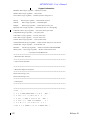
AUTHOR: YAIR LIEBMAN - MSIL
ISSUE 0.1 - Release 15,1,98
ISSUE 0.0 - Draft 22,7,97
6σ
SIX SIGMA
MOTOROLA
MPC8XXFADS - User’s Manual
TABLE OF CONTENTS
1 1•1
1•2
1•3
1•4
1•5
1•6
1•7
1•8
1•9
2 2•1
2•2
2•3
2•3•1
2•3•2
2•3•3
2•3•4
2•3•5
2•3•6
2•4
2•4•1
2•4•2
2•4•3
2•4•4
2•4•5
2•4•6
2•4•7
2•4•8
2•4•9
3 3•1
3•2
3•2•1
3•2•2
3•2•3
3•2•4
3•2•5
3•2•6
3•2•7
3•2•8
3•2•9
3•2•10
3•2•11
3•2•12
3•2•13
3•2•14
3•2•15
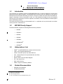
General Information
Introduction
MPC8XX Family Support
Abbreviations’ List
Related Documentation
Revision ENG to Revision PILOT Changes
Changes to This Document from Previous Issue (Draft 0.0)
SPECIFICATIONS
MPC8XXFADS Features
MPC8XXFADS Goals
Hardware Preparation and Installation
INTRODUCTION
UNPACKING INSTRUCTIONS
HARDWARE PREPARATION
ADI Port Address Selection
Clock Source Selection
Power-On Reset Source Selection
VDDL Source Selection
Keep Alive Power Source Selection
Debug Mode Indication Source Selection
INSTALLATION INSTRUCTIONS
Host Controlled Operation
Debug Port Controller For Target System
Stand Alone Operation
+5V Power Supply Connection
P7: +12V Power Supply Connection
ADI Installation
Host computer to MPC8XXFADS Connection
Terminal to MPC8XXFADS RS-232 Connection
Memory Installation
OPERATING INSTRUCTIONS
INTRODUCTION
CONTROLS AND INDICATORS
ABORT Switch SW1
SOFT RESET Switch SW2
HARD RESET - Switches SW1 & SW2
DS1 - Software Options Switch
GND Bridges
ETH ON - LD1
IRD ON - LD2
RS232 Port 1 ON - LD3
RS232 Port 2 ON - LD4
Ethernet RX Indicator - LD5
Ethernet TX Indicator - LD6
Ethernet JABB Indicator - LD7
Ethernet CLSN Indicator LD8
Ethernet PLR Indicator - LD9
Ethernet LIL Indicator - LD10
1
1
1
1
1
2
2
2
4
5
6
6
6
6
8
8
8
9
9
9
9
9
10
11
12
12
13
13
13
14
15
15
15
15
15
15
15
15
16
16
16
16
16
16
16
16
16
16
Release 0.1
MPC8XXFADS - User’s Manual
TABLE OF CONTENTS
3•2•16
3•2•17
3•2•18
3•2•19
3•2•20
3•2•21
3•2•22
3•3
3•4
3•4•1
4 4•1
4•1•1
4•1•2
4•1•3
4•1•4
4•1•5
4•1•6
4•1•6•1
4•1•6•2
4•1•6•3
4•2
4•3
4•4
4•5
4•6
4•6•1
4•6•2
4•6•3
4•6•4
4•7
4•8
4•8•1
4•8•1•1
4•8•2
4•9
4•9•1
4•9•2
4•9•2•1
4•9•3
4•9•3•1
4•10
4•10•1
4•11
4•11•1
4•11•2
4•11•3
4•11•4
5V Indicator - LD11
RUN Indicator - LD12
AUXILARY Indicator LD13
FLASH ON - LD14
DRAM ON - LD15
SDRAM ON - LD16
PCMCIA ON - LD17
MEMORY MAP
MPC Registers’ Programming
Memory Controller Registers Programming
Functional Description
Reset & Reset - Configuration
Keep Alive Power-On Reset
Regular Power - On Reset
Manual Soft Reset
Manual Hard Reset
MPC Internal Sources
Reset Configuration
Power - On Reset Configuration
Hard Reset Configuration
Soft Reset Configuration
Local Interrupter
Clock Generator
Buffering
Chip - Select Generator
DRAM
DRAM 16 Bit Operation
DRAM Performance Figures
Refresh Control
Variable Bus-Width Control
Flash Memory SIMM
Synchronous Dram
SDRAM Programming
SDRAM Initializing Procedure
SDRAM Refresh
Communication Ports
Ethernet Port
Infra-Red Port
Infra-Red Port Rate Range Selection
RS232 Ports
RS-232 Ports’ Signal Description
PCMCIA Port
PCMCIA Power Control
Board Control & Status Register - BCSR
BCSR Disable Protection Logic
BCSR0 - Hard Reset Configuration Register
BCSR1 - Board Control Register 1
BCSR2 - Board Control / Status Register - 2
16
17
17
17
17
17
17
17
18
19
29
29
29
29
29
29
29
30
30
30
30
31
31
31
32
32
33
33
34
35
37
39
40
41
41
42
42
42
43
43
43
44
46
46
47
47
48
52
Release 0.1
MPC8XXFADS - User’s Manual
TABLE OF CONTENTS
4•11•5
4•11•6
4•12
4•12•1
4•12•1•1
4•12•2
4•12•3
4•12•3•1
4•12•3•2
4•12•3•3
4•12•3•4
4•12•3•5
4•12•3•6
4•13
4•13•1
4•13•2
4•13•3
5 5•1
5•1•1
5•1•2
5•1•3
5•1•4
5•1•5
5•1•6
5•1•7
5•1•8
5•1•9
5•2
5•3
5•3•1
5•3•2
5•3•3
APPENDIX A A•1
APPENDIX B B•1
B•2
B•2•1
B•3
B•3•1
BCSR3 - Board Control / Status Register 3
BCSR4 - Board Control / Status Register 4
Debug Port Controller
MPC8XXFADS As Debug Port Controller For Target System
Debug Port Connection - Target System Requirements
Debug Port Control / Status Register
Standard MPCXXX Debug Port Connector Pin Description
VFLS(0:1)
HRESET*
SRESET*
DSDI - Debug-port Serial Data In
DSCK - Debug-port Serial Clock
DSDO - Debug-port Serial Data Out
Power
5V Bus
3.3V Bus
12V Bus
Support Information
Interconnect Signals
P1 ADI - Port Connector
PA2, PB2 - RS232 Ports’ Connectors
P3 - Ethernet Port Connector
PCMCIA Port Connector
P5 - External Debug Port Controller Input Interconnect.
P6 - 5V Power Connector
P7 - 12V Power Connector
P8 - Serial Ports’ Expansion Connector
PD1 - PD4 - Daughter Boards’ Connectors Interconnect Signals
MPC8XXFADS Part List
Programmable Logic Equations
U2 - Debug Port Controller
U11 - Board Control & Status Register
U22 - Auxiliary Board Control
ADI I/F
ADI Port Signal Description
ADI Installation
INTRODUCTION
IBM-PC/XT/AT to MPC8XXFADS Interface
ADI Installation in IBM-PC/XT/AT
SUN-4 to MPC8XXFADS Interface
ADI Installation in the SUN-4
55
58
60
61
62
62
64
64
64
64
64
65
65
65
67
67
67
68
68
68
69
69
70
73
74
74
74
74
100
104
105
133
174
191
191
193
193
193
193
194
195
Release 0.1
MPC8XXFADS - User’s Manual
LIST OF FIGURES
FIGURE 1-1
FIGURE 2-1
FIGURE 2-2
FIGURE 2-3
FIGURE 2-4
FIGURE 2-5
FIGURE 2-6
FIGURE 2-7
FIGURE 2-8
FIGURE 2-9
FIGURE 2-10
FIGURE 2-11
FIGURE 3-1
FIGURE 4-1
FIGURE 4-2
FIGURE 4-3
FIGURE 4-4
FIGURE 4-5
FIGURE 4-6
FIGURE 4-7
FIGURE 4-8
FIGURE 4-1
FIGURE A-1
FIGURE B-1
FIGURE B-2
FIGURE B-3
MPC8XXFADS Motherboard Block Diagram
MPC8XXFADS Top Side Part Location diagram
Configuration Dip-Switch - DS2
J1 - VFLS / FRZ Selection
Host Controlled Operation Scheme
Debug Port Controller For Target System Operation Scheme
Stand Alone Configuration
P6: +5V Power Connector
P7: +12V Power Connector
P1 - ADI Port Connector
PA2, PB2 - RS-232 Serial Port Connectors
Memory SIMM Installation
DS1 - Description
Refresh Scheme
DRAM Address Lines’ Switching Scheme
Flash Memory SIMM Architecture
SDRAM Connection Scheme
RS232 Serial Ports’ Connector
PCMCIA Port Configuration
Debug Port Controller Block Diagram
Standard Debug Port Connector
MPC8XXFADS Power Scheme
ADI Port Connector
Physical Location of jumper JG1 and JG2
JG1 Configuration Options
ADI board for SBus
5
7
8
9
10
11
12
12
13
13
14
14
15
35
37
38
40
43
45
61
64
66
191
194
194
195
Release
MPC8XXFADS - User’s Manual
LIST OF TABLES
TABLE 1-1.
TABLE 3-1.
TABLE 3-2.
TABLE 3-3.
TABLE 3-4.
TABLE 3-5.
TABLE 3-6.
TABLE 3-7.
TABLE 3-8.
TABLE 3-9.
TABLE 4-1.
TABLE 4-2.
TABLE 4-3.
TABLE 4-4.
TABLE 4-5.
TABLE 4-6.
TABLE 4-7.
TABLE 4-8.
TABLE 4-9.
TABLE 4-10.
TABLE 4-11.
TABLE 4-12.
TABLE 4-13.
TABLE 4-14.
TABLE 4-15.
TABLE 4-16.
TABLE 4-17.
TABLE 4-18.
TABLE 4-19.
TABLE 4-20.
TABLE 4-21.
TABLE 4-22.
TABLE 4-23.
TABLE 4-24.
TABLE 4-25.
TABLE 4-26.
TABLE 5-1
TABLE 5-2.
TABLE 5-3.
TABLE 5-4.
TABLE 5-5.
TABLE 5-6.
TABLE 5-7.
TABLE 5-8.
TABLE 5-9.
MPC8XXFADS Specifications
MPC8XXADS Main Memory Map
SIU REGISTERS’ PROGRAMMING
Memory Controller Initializations For 50Mhz
UPMA Initializations for 60nsec DRAMs @ 50MHz
UPMA Initializations for 60nsec EDO DRAMs @ 50MHz
Memory Controller Initializations For 20Mhz
UPMA Initializations for 60nsec EDO DRAMs @ 20MHz
UPMB Initializations for MB811171622A-100 upto 32MHz
UPMB Initializations for MB811171622A-100, 32+MHz - 50MHz
MPC8XXFADS Chip Selects’ Assignment
Regular DRAM Performance Figures
EDO DRAM Performance Figures
DRAM ADDRESS CONNECTIONS
Flash Memory Performance Figures
Estimated SDRAM Performance Figures
SDRAM’s Mode Register Programming
MPC8XX Family Comm. Ports
BCSR0 Description
BCSR1 Description
PCCVCC(0:1) Encoding
PCCVPP(0:1) Encoding
BCSR2 Description
Flash Presence Detect (4:1) Encoding
DRAM Presence Detect (2:1) Encoding
DRAM Presence Detect (4:3) Encoding
EXTOOLI(0:3) Assignment
MPC8XXFADS Daughter Boards’ Revision Encoding
BCSR3 Description
Daughter Boards’ ID Codes
MPC8XXFADS Revision Number Conversion Table
FLASH Presence Detect (7:5) Encoding
BCSR4 Description
Debug Port Control / Status Register
DSCK Frequency Select
Off-board Application Maximum Current Consumption
P1 - ADI Port Interconnect Signals
PA2, PB2 Interconnect Signals
P3 - Ethernet Port Interconnect Signals
P4 - PCMCIA Connector Interconnect Signals
P5 - Interconnect Signals
P6 - Interconnect Signals
P7 - Interconnect Signals
PD1 Interconnect Signals
PD2 Interconnect Signals
2
18
19
20
22
23
23
26
27
28
32
34
34
36
39
39
41
42
48
50
51
52
53
53
54
54
54
55
56
56
57
57
58
63
63
66
68
69
70
70
73
74
74
75
80
Release 0.1
MPC8XXFADS - User’s Manual
LIST OF TABLES
TABLE 5-10.
TABLE 5-11.
TABLE 5-12.
PD3 Interconnect Signals
PD4 Interconnect Signals
MPC8XXFADS Part List
87
94
100
Release 0.1
MPC8XXFADS - User’s Manual
General Information
1 - General Information
1•1
Introduction
This document is an operation guide for the MPC8XXFADS board. It contains operational, functional and
general information about the FADS. The MPC8XXFADS is meant to serve as a platform for s/w and h/w
development around the MPC8XX family processors. Using its on-board resources and its associated debugger, a developer is able to download his code, run it, set breakpoints, display memory and registers
and connect his own proprietary h/w via the expansion connectors, to be incorporated to a desired system
with the MPC8XX processor.
This board could also be used as a demonstration tool, i.e., application s/w may be burnedA into its flash
memory and ran in exhibitions etc‘.
1•2
MPC8XX Family Support
The MPC8XXFADS supports the following MPC8XX family members:
1•3
o
MPC801
o
MPC821B
o
MPC823
o
MPC850
o
MPC860B
o
MPC860SAR B
o
MPC860TB
Abbreviations’ List
•
FADSC - the MPC8XXFADS, the subject of this document.
•
UPM - User Programmable Machine
•
GPCM - General Purpose Chip-select Machine
•
GPL - General Purpose Line (associated with the UPM)
•
I/R - Infra-Red
•
BCSR - Board Control & Status Register.
•
ZIF - Zero Input Force
•
BGA - Ball Grid Array
•
SIMM - Single In-line Memory Module
1•4
Related Documentation
•
MPC8XX User’s Manuals.
•
ADI Board Specification.
A. Either on or off-board.
B. Same Daughter Board.
C. Not to be mistaken for the M683XX Family Ads
8
Release 0.1
MPC8XXFADS - User’s Manual
General Information
1•5
Revision ENG to Revision PILOT Changes
The only electrical change between the two revisions is a bug correction in BCSR. This bug was irrelevant
to ENG 0091A and up, boards. The rest, are production associated changes, which were meant to improve
boards’ reliability and manufacturability, such as changes in SMD pad sizes, drill sizes and so on and are
of no interest to any user.
1•6
Changes to This Document from Previous Issue (Draft 0.0)
1)
Daughter Board’s for MPC821, MPC860, MPC860SAR, MPC860T, are identical. (1•2 on page
8)
2)
Typo error in TABLE 3-1. "MPC8XXADS Main Memory Map" on page 25 was fixed: BCSR occupies 32KByte space rather than 16KByte as implied from this table.
3)
Typo Error in TABLE 3-3. "Memory Controller Initializations For 50Mhz" on page 27 and in TABLE 3-6. "Memory Controller Initializations For 20Mhz" on page 30 was fixed: BR0 is set
02800001. Flash base address is 0x2800000, rather than 0x2200000.
4)
Changed Daughter-Board Codes - MPC821, MPC860/860SAR/860T share the same code now
(0x22). See TABLE 4-20. "Daughter Boards’ ID Codes" on page 63.
5)
Mother Board revsion codes are changed: 0 is now reserved, ENG & PILOT share the same
code - 1. See TABLE 4-18. "MPC8XXFADS Daughter Boards’ Revision Encoding" on page 62.
6)
Added BCSR4 functions’ description for MPC821/860/860SAR/860T Daughter board, with
MPC860T. (TABLE 4-23. on page 65).
7)
Changed Mach equations for U11. Bug correction (Irrelevant for ENG091+ boards). See 5•3•2
"U11 - Board Control & Status Register" on page 140.
1•7
SPECIFICATIONS
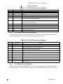
The MPC8XXFADS specifications are given in TABLE 1-1.
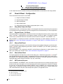
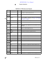
TABLE 1-1. MPC8XXFADS Specifications
CHARACTERISTICS
SPECIFICATIONS
Power requirements (no other boards attached)
+5Vdc @ 1.7 A (typical), 3 A (maximum)
+12Vdc - @1A.
Microprocessor
MPC8XX running upto @ 50 MHz
Addressing
Total address range:
4 GigaBytes
Flash Memory
Dynamic RAM
Synchronous DRAM
2 MByte, 32 bits wide expandable to 8 MBytes
4 MByte, 32 bits wide EDO SIMM
Support for up to 32 MByte, EDO or FPM SIMM
4 MBytes, organized as 1 Meg X 32 bit.
Operating temperature
0OC - 30OC
Storage temperature
-25OC to 85OC
Relative humidity
5% to 90% (non-condensing)
A. The only implication of that bug is that ENG0001 - ENG0090 may not connect to MPC823FADSDB of revision
PILOT. ENG0091 and up may.
9
Release 0.1
MPC8XXFADS - User’s Manual
General Information
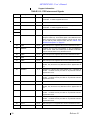
TABLE 1-1. MPC8XXFADS Specifications
CHARACTERISTICS
Dimensions:
Length
Width
Thickness
10
SPECIFICATIONS
9.173" (233 mm)
6.3" (160 mm)
0.063" (1.6 mm)
Release 0.1
MPC8XXFADS - User’s Manual
General Information
1•8
MPC8XXFADS Features
o
4 MByte, Unbuffered, Synchronous Dram On-Board.
o
4 MByte EDO 60nsec delay DRAM SIMM. Support for 4 - 32 MByte FPM or EDO Dram
SIMM, with Automatic Dram SIMM identification. 16 Bit Data-Bus Width Support.
o
2 MByte Flash SIMM. Support for upto 8 MByte, 5V or 12V Programmable, with Automatic
Flash SIMM identification.
o
Memory Disable Option for each local memory map slaves.
o
Board Control & Status Register - BCSR, Controlling Board’s Operation.
o
Programmable Hard-Reset Configuration via BCSR.
o
5V only PCMCIA Socket With Full Buffering, Power Control and Port Disable Option. Complies with PCMCIA 2.1+ Standard.
o
Module Enable Indications.
o
10-Base-T Port On-Board, with Stand-By Mode.
o
Fast-IrDA (4MBps) Port with Stand-By Mode.
o
Dual RS232 port with Low-Power Option per each port.
o
On - Board Debug Port Controller with ADI I/F.
o
MPC8XXFADS Serving as Debug Station for Target System option.
o
Optional Hard-Reset Configuration Burned in FlashA.
o
External Tools’ Identification Capability, via BCSR.
o
Soft / HardB Reset Push - Button
o
ABORT Push - Button
o
SingleC 5V Supply.
o
Reverse / Over Voltage Protection for Power Inputs.
o
3.3V / 2V MPC Internal Logic Operation D, 3.3V MPC I/O Operation.
o
Power Indications for Each Power Bus.
o
Software Option Switch provides 16 S/W options via BCSR.
A. Available only if supported also on the MPC8XX.
B. Hard reset is applied by depressing BOTH Soft Reset & ABORT buttons.
C. Unless a 12V supply is required for a PCMCIA card or for a 12V programmable Flash SIMM.
D. Implemented on Daughter Board.
11
Release 0.1
MPC8XXFADS - User’s Manual
General Information
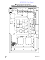
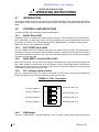
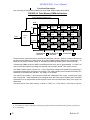
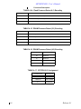
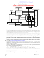
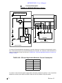
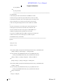
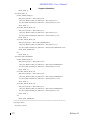
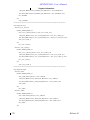
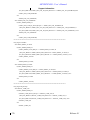
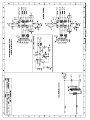
FIGURE 1-1 MPC8XXFADS Motherboard Block Diagram
SDRAM
4 MBytes
DATA & ADDRESS
BUFFERS
FLASH SIMM.
Reset,
Interrupts
& Clock
2 - 8MByte
DRAM SIMM
Dram Width
& Size Logic
4 - 32 Mbyte
Control &
Status
Register
Fast IrDA Port
DAUGHTER
BOARD
CONN.
RS232
PORTS
Debug
Port
Connector
PORT
CONTROLLER
ADI PORT
(*)
(*) May be on a separate board.
1•9
PCMCIA
Buffering
&
Control
PCMCIA
PORT
EEST
(ADI I/F)
ETHERNET
PORT
DEBUG
MPC8XXFADS Goals
The MPC8XXFADS is meant to become a general platform for s/w and h/w development around the
MPC8XX family. Using its on-board resources and its associated debugger, the developer is able to load
his code, run it, set breakpoints, display memory and registers and connect his own proprietary h/w via the
expansion connectors, to be incorporated to a system with the MPC.
This board could also be used as a demonstration tool, i.e., application s/w may be programmed A into its
flash memory and ran in exhibitions etc.
A. Either on or off-board.
12
Release 0.1
MPC8XXFADS - User’s Manual
Hardware Preparation and Installation
2 - Hardware Preparation and Installation
2•1
INTRODUCTION
This chapter provides unpacking instructions, hardware preparation, and installation instructions for the
MPC8XXFADS.
2•2
UNPACKING INSTRUCTIONS
NOTE
If the shipping carton is damaged upon receipt,
request carrier’s agent to be present during
unpacking and inspection of equipment.
Unpack equipment from shipping carton. Refer to packing list and verify that all items are present. Save
packing material for storing and reshipping of equipment.
CAUTION
AVOID TOUCHING AREAS OF INTEGRATED
CIRCUITRY;
STATIC
DISCHARGE
CAN
DAMAGE CIRCUITS.
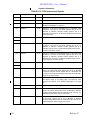
2•3
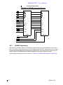
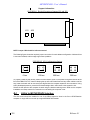
HARDWARE PREPARATION
To select the desired configuration and ensure proper operation of the MPC8XXFADS board, changes of
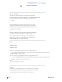
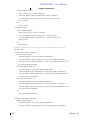
the Dip-Switch settings may be required before installation. The location of the switches, LEDs, DipSwitches, and connectors is illustrated in FIGURE 2-1. The board has been factory tested and is shipped
with Dip-Switch settings as described in the following paragraphs. Parameters can be changed for the
following conditions:
13
•
ADI port address
•
MPC Clock Source
•
Power-On Reset Source.
•
MPC Keep Alive Power Source
•
MPC Internal Logic Supply Source
•
Debug Mode Indication Source
Release 0.1
MPC8XXFADS - User’s Manual
Hardware Preparation and Installation
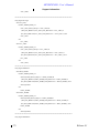
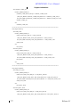
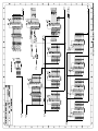
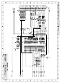
FIGURE 2-1 MPC8XXFADS Top Side Part Location diagram
14
Release 0.1
MPC8XXFADS - User’s Manual
Hardware Preparation and Installation
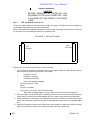
2•3•1
ADI Port Address Selection
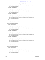
The MPC8XXFADS can have eight possible slave addresses set for its ADI port, enabling up to eight
MPC8XXFADS boards to be connected to the same ADI board in the host computer. The selection of the
slave address is done by setting switches 1, 2 & 3 in the Dip-Switch - DS2. Switch 1 stands for the mostsignificant bit of the address and switch 3 stands for the least-significant bit. If the switch is in the ’ON’ state,
it stands for logical ’1’. In FIGURE 2-2 DS1 is shown to be configured to address ’0’.
FIGURE 2-2 Configuration Dip-Switch - DS2
ON
ADR2
ADR2
1
ADR1
2
ADR1
ADR0
3
ADR0
3 - 5 MHz Generator via EXTCLK
4
32.678 KHz Crystal Resonator
DS2
Table 2-1 describes the switch settings for each slave address:
Table 2-1 ADI Address Selection
2•3•2
ADDRESS
Switch 1
Switch 2
Switch 3
0
OFF
OFF
OFF
1
OFF
OFF
ON
2
OFF
ON
OFF
3
OFF
ON
ON
4
ON
OFF
OFF
5
ON
OFF
ON
6
ON
ON
OFF
7
ON
ON
ON
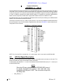
Clock Source Selection
Switch #4 on DS2 selects the clock source for the MPC. When it is in the ’ON’ position while the FADS is
powered-up, the on-board 32.768 KHz crystal resonatorA becomes the clock source and the PLL
multiplication factor becomes 1:513. When switch #4 is in the ’OFF’ position while the FADS is poweredup, the on-board 4BMHz clock generatorA becomes the clock source while the PLL multiplication factor
becomes 1:5.
2•3•3
Power-On Reset Source Selection
As there are differences between MPC revisions regarding the functionality of the Power-On Reset logic,
A. Located on the Daughter-Board
B. A 5MHz clock generator is packed as well.
15
Release 0.1
MPC8XXFADS - User’s Manual
Hardware Preparation and Installation
it is therefore necessary to select different sources for Power-ON reset generation.
The above selection is done on the Daughter Board and therefore, documented in the specific Daughter
Board user’s manual.
2•3•4
VDDL Source Selection
This selection is done on the Daughter Board and therefore, documented in the specific Daughter
Board user’s manual.
2•3•5
Keep Alive Power Source Selection
This selection is done on the Daughter Board and therefore, documented in the specific Daughter
Board user’s manual.
2•3•6
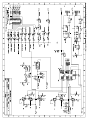
Debug Mode Indication Source Selection
Jumper J1 selects between VFLS(0:1) signals and FRZ signal of the MPC as an indication for debug mode
state. Since with the MPC8XXs, each of these signals has alternate function, it may be necessary to switch
between the two sources, in favor of alternate function being used.
When a jumper is positioned between pins 1 and 2 of J1 - VFLS(0:1) are selected towards the debug-port
controller. When a jumper is placed between positions 2 - 3 of J1(2) - FRZ signal is selected.
FIGURE 2-3 J1 - VFLS / FRZ Selection
J1
1
VFLS(0:1) Selected
2•4
J1
1
FRZ Selected
INSTALLATION INSTRUCTIONS
When the MPC8XXFADS has been configured as desired by the user, it can be installed according to the
required working environment as follows:
•
Host Controlled Operation
•
Debug Port Controller for Target System
•
Stand-Alone
2•4•1
Host Controlled Operation
In this configuration the MPC8XXFADS is controlled by a host computer via the ADI through the debug
port. This configuration allows for extensive debugging using on-host debugger.
16
Release 0.1
MPC8XXFADS - User’s Manual
Hardware Preparation and Installation
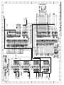
FIGURE 2-4 Host Controlled Operation Scheme
ADI
Host
Computer
37 Wire
Flat Cable
P1
P1
5V Power Supply
P6
P6
2•4•2
Debug Port Controller For Target System
This configuration resembles the previous, but here the local MPC is removed from its socket while the
FADS is connected via a 10 lead Flat-Cable between P5 and a matching connector on a target system.
WARNNING
When connecting the FADS to a target system via P5
and a 10 lead flat-cable, the MPC MUST be REMOVED
from its SOCKET. Otherwise, PERMANENT DAMAGE
might be inflicted to either the Local MPC or to the Target MPC.
With this mode of operation, all on-board modules are disabled and can not be accessed in anyway, except
for the debug port controller. Also, all indications except for 5V power, 3.3V-Power A and RUN are darkened.
All debugger commands and debugging features are available in this mode, including s/w download,
breakpoints, etc‘... The target system may be reset or interrupted by the debug port or reset by the FADS’s
RESET switches. It is the responsibility of the target system designer, to provide Power-On-Reset and
HARD-Reset configurations, while SOFT-Reset configuration is provided by the debug-port controller. See
also 4•12•1 "MPC8XXFADS As Debug Port Controller For Target System" on page 68.
A. On Daughter Board.
17
Release 0.1
MPC8XXFADS - User’s Manual
Hardware Preparation and Installation
FIGURE 2-5 Debug Port Controller For Target System Operation Scheme
Target System
10 Wire
37 Wire
ADI
Host
Computer
Flat Cable
Flat Cable
P1
P1
P5
5V Power Supply
P6
P6
MPC Removed From Socket
2•4•3
Stand Alone Operation
In this mode, the FADS is not controlled by the host via the ADI/Debug port. It may connect to host via one
of its other ports, e.g., RS232 port, I/R port, Ethernet port, etc‘. Operating in this mode requires an application program to be programmed into the board‘s Flash memory (while with the host controlled operation,
no memory is required at all).
18
Release 0.1
MPC8XXFADS - User’s Manual
Hardware Preparation and Installation
FIGURE 2-6 Stand Alone Configuration
RS
23
2
Et
he
rn
e
t
Host
Computer
I/R
P1
5V Power Supply
P6
2•4•4
P6
+5V Power Supply Connection
The MPC8XXFADS requires +5 Vdc @ 5 A max, power supply for operation. Connect the +5V power
supply to connector P6 as shown below:
FIGURE 2-7 P6: +5V Power Connector
+5V
1
GND
2
GND
3
P6 is a 3 terminal block power connector with power plug. The plug is designed to accept 14 to 22 AWG
wires. It is recommended to use 14 to 18 AWG wires. To provide solid ground, two Gnd terminals are
supplied. It is recommended to connect both Gnd wires to the common of the power supply, while VCC is
connected with a single wire.
NOTE
2•4•5
Since hardware applications may be connected to the
MPC8XXFADS via the Daughter-Boards’ expansion
connectors PX1, PX2 PX3, PX4 or FADS’s P8, the additional
power consumption should be taken into consideration when
a power supply is connected to the MPC8XXFADS.
P7: +12V Power Supply Connection
The MPC8XXFADS requires +12 Vdc @ 1 A max, power supply for the PCMCIA channel Flash
programming capability or for 12V programmable Flash SIMM. The MPC8XXFADS can work properly
without the +12V power supply, if there is no need to program either a 12V programmable PCMCIA flash
card or a 12V programmable Flash SIMM.
Connect the +12V power supply to connector P7 as shown below:
19
Release 0.1
MPC8XXFADS - User’s Manual
Hardware Preparation and Installation
FIGURE 2-8 P7: +12V Power Connector
+12V
1
GND
2
P7 is a 2 terminal block power connector with power plug. The plug is designed to accept 14 to 22 AWG
wires. It is recommended to use 14 to 18 AWG wires.
2•4•6
ADI Installation
For ADI installation on various host computers, refer to APPENDIX B - "ADI Installation" on page 200.
2•4•7
Host computer to MPC8XXFADS Connection
The MPC8XXFADS ADI interface connector, P1, is a 37 pin, male, D type connector. The connection
between the MPC8XXFADS and the host computer is by a 37 line flat cable, supplied with the ADI board.
FIGURE 2-9 below shows the pin configuration of the connector.
FIGURE 2-9 P1 - ADI Port Connector
Gnd
Gnd
Gnd
Gnd
Gnd
Gnd
(+ 12 v) N.C.
HOST_VCC
HOST_VCC
HOST_VCC
HOST_ENABLE~
Gnd
Gnd
Gnd
PD0
PD2
PD4
PD6
20
21
22
23
24
25
26
27
28
29
30
31
32
33
34
35
36
37
1
2
3
4
5
6
7
8
9
10
11
12
13
14
15
16
17
18
19
N.C
D_C~
HST_ACK
ADS_SRESET
ADS_HRESET
ADS_SEL2
ADS_SEL1
ADS_SEL0
HOST_REQ
ADS_REQ
ADS_ACK
N.C.
N.C.
N.C.
N.C.
PD1
PD3
PD5
PD7
NOTE: Pin 26 on the ADI is connected to +12 v power supply, but it is not used in the MPC8XXFADS.
2•4•8
Terminal to MPC8XXFADS RS-232 Connection
A serial (RS232) terminal or any other RS232 equipment, may be connected to the RS-232 connectors
PA2 and PB2. The RS-232 connectors is a 9 pin, female, Stacked D-type connector as shown in FIGURE
2-10.
The connectors are arranged in a manner that allows for 1:1 connection with the serial port of an IBM-ATA
or compatibles, i.e. via a flat cable.
A. IBM-AT is a trademark of International Business Machines Inc.
20
Release 0.1
MPC8XXFADS - User’s Manual
Hardware Preparation and Installation
FIGURE 2-10 PA2, PB2 - RS-232 Serial Port Connectors
CD
TX
1
2
RX
3
DTR
4
5
GND
6
7
8
9
DSR
RTS
CTS
N.C.
NOTE: The RTS line (pin 7) is not connected on the MPC8XXFADS.
2•4•9
Memory Installation
The MPC8XXFADS is supplied with two types of memory SIMM:
•
Dynamic Memory SIMM
•
Flash Memory SIMM.
To avoid shipment damage, these memories are packed aside rather than being installed in their sockets.
Therefore, they should be installed on site. To install a memory SIMM, it should be taken out of its package,
put diagonally in its socket (no error can be made here, since the Flash socket has 80 contacts, while the
DRAM socket has 72) and then twisted to a vertical position until the metal lock clips are locked. See
FIGURE 2-11 "Memory SIMM Installation" below.
CAUTION
The memory SIMMs have alignment nibble near their # 1
pin. It is important to align the memory correctly before
it is twisted, otherwise damage might be inflicted to both
the memory SIMM and its socket.
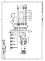
FIGURE 2-11 Memory SIMM Installation
(1)
(2)
Memory
SIMM
Metal Lock Clip
SIMM Socket
21
Release 0.1
MPC8XXFADS - User’s Manual
OPERATING INSTRUCTIONS
3 - OPERATING INSTRUCTIONS
3•1
INTRODUCTION
This chapter provides necessary information to use the MPC8XXFADS in host-controlled and stand-alone
configurations. This includes controls and indicators, memory map details, and software initialization of the
board.
3•2
CONTROLS AND INDICATORS
The MPC8XXFADS has the following switches and indicators.
3•2•1
ABORT Switch SW1
The ABORT switch is normally used to abort program execution, this by issuing a level 0 interrupt to the
MPC. If the FADS is in stand alone mode, it is the responsibility of the user to provide means of handling
the interrupt, since there is no resident debugger with the MPC8XXFADS. The ABORT switch signal is
debounced, and can not be disabled by software.
3•2•2
SOFT RESET Switch SW2
The SOFT RESET switch SW2 performs Soft reset to the MPC internal modules, maintaining MPC’s
configuration (clocks & chip-selects) Dram and SDram contents. The switch signal is debounced, and it is
not possible to disable it by software. At the end of the Soft Reset Sequence, the Soft Reset Configuration
is sampled and becomes valid.
3•2•3
HARD RESET - Switches SW1 & SW2
When BOTH switches - SW1 and SW2 are depressed simultaneously, HARD reset is generated to the
MPC. When the MPC is HARD reset, all its configuration is lost, including data stored in the DRAM or
SDRAM and the MPC has to be re-initialized. At the end of the Hard Reset sequence, the Hard Reset
Configuration stored in BCSR0 becomes valid.
3•2•4
DS1 - Software Options Switch
DS1 is a 4-switches Dip-Switch. This switch is connected over EXTOLI(0:3) lines which are available at
BCSR, S/W options may be manually selected, according to DS1 state.
FIGURE 3-1 DS1 - Description
ON
EXTOLI0 Pulled to ’1’
1
EXTOLI1 Pulled to ’1’
2
EXTOLI1 Driven to ’0’
EXTOLI2 Pulled to ’1’
3
EXTOLI2 Driven to ’0’
EXTOLI3 Pulled to ’1’
4
EXTOLI3 Driven to ’0’
EXTOLI0 Driven to ’0’
DS1
3•2•5
GND Bridges
There are 3 GND bridges on the MPC8XXFADS. They are meant to assist general measurements and
22
Release 0.1
MPC8XXFADS - User’s Manual
OPERATING INSTRUCTIONS
logic-analyzer connection.
Warning
When connecting to a GND bridge, use only INSULATED
GND clips. Failure in doing so, might result in permanent damage to the MPC8XXFADS.
3•2•6
ETH ON - LD1
When the yellow ETH ON led is lit, it indicates that the ethernet port transceiver - the MC68160 EEST,
is active. When it is dark, it indicates that the EEST is in power down mode, enabling the use of its associated SCC pins off-board via the expansion connectors.
3•2•7
IRD ON - LD2
When the yellow IRD ON led is lit, it indicates that the Infra-Red transceiver - the TFDS6000, is active and
enables communication via that medium. When it is dark, the I/R transceiver is in shutdown mode, enabling
the use of its associated SCC pins off-board via the expansion connectors.
3•2•8
RS232 Port 1 ON - LD3
When the yellow RS232 Port 1 ON led is lit, it designates, that the RS232 transceiver connected to PA2,
is active and communication via that medium is allowed. When darkened, it designates that the transceiver
is in shutdown mode, so its associated MPC pins may be used off-board via the expansion connectors.
3•2•9
RS232 Port 2 ON - LD4
When the yellow RS232 Port 2 ON led is lit, it designates that the RS232 transceiver connected to PB2,
is active and communication via that medium is allowed. When darkened, it designates, that the transceiver
is in shutdown mode, so its associated MPC pins may be used off-board via the expansion connectors.
3•2•10
Ethernet RX Indicator - LD5
The green Ethernet Receive LED indicator blinks whenever the EEST is receiving data from one of the
Ethernet port.
3•2•11
Ethernet TX Indicator - LD6
The green Ethernet Receive LED indicator blinks whenever the EEST is transmitting data via the Ethernet
port.
3•2•12
Ethernet JABB Indicator - LD7
The red Ethernet TP Jabber LED indicator - JABB, lights whenever a jabber condition is detected on the
TP ethernet port.
3•2•13
Ethernet CLSN Indicator LD8
The red Ethernet Collision LED indicator CLSN, blinks whenever a collision condition is detected on the
ethernet port, i.e., simultaneous receive and transmit.
3•2•14
Ethernet PLR Indicator - LD9
The red Ethernet TP Polarity LED indicator - PLR, lights whenever the wires connected to the receiver input
of the ethernet port are reversed. The LED is lit by the EEST, and remains on while the EEST has
automatically corrected for the reversed wires.
3•2•15
Ethernet LIL Indicator - LD10
The yellow Ethernet Twisted Pair Link Integrity LED indicator - LIL, lights to indicate good link integrity on
the TP port. The LED is off when the link integrity fails.
3•2•16
5V Indicator - LD11
The yellow 5V led, indicates the presence of the +5V supply at P6.
23
Release 0.1
MPC8XXFADS - User’s Manual
OPERATING INSTRUCTIONS
3•2•17
RUN Indicator - LD12
When the green RUN led - LD12 is lit, it indicates that the MPC is not in debug mode, i.e., VFLS0 & VFLS1
== 0 (or FRZ == 0, which ever selected by J1).
3•2•18
AUXILARY Indicator LD13
This indication has no dedicated function over the FADS. It is meant to provide some visibility for program
behavior. It is controlled by the Signal Lamp bit in BCSR4.
3•2•19
FLASH ON - LD14
When the yellow FLASH ON led is lit, it indicates that the FLASH SIMM is enabled in the BCSR1 register.
I.e., any access done to the CS0~ address space will hit the flash memory. When it is dark, the flash is
disabled and CS0~ may be used off-board via the expansion connectors.
3•2•20
DRAM ON - LD15
When the yellow DRAM ON led is lit, it indicates the DRAM SIMM is enabled in BCSR1. Therefore, any
access made to CS2~ (or CS3~) will hit on the DRAM. When it is dark, it indicates that either the DRAM is
disabled in BCSR1, enabling the use of CS2~ and CS3~ off-board via the expansion connectors.
3•2•21
SDRAM ON - LD16
When the yellow SDRAM ON led is lit, it indicates the SDRAM is enabled in BCSR1. Therefore, any
access made to CS4~ (will hit on the SDRAM. When it is dark, it indicates that either the SDRAM is
disabled in BCSR1, enabling the use of CS4~ off-board via the expansion connectors.
3•2•22
PCMCIA ON - LD17
When the yellow PCMCIA ON led is lit, it indicates the following:
1)
Address & strobe buffers are driven towards the PCMCIA card
2)
Data buffers are driven to / from the PCMCIA card whenever CE1A~A or CE2A~B signals are
asserted.
3)
Card status lines are driven towards the MPC from the PCMCIA card.
When it is dark, it indicates that all the above buffers are tri-stated and the pins associated with PCMCIA
channel AC, may be used off-board via the expansion connectors.
3•3
MEMORY MAP
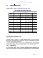
All accesses to MPC8XXFADS’s memories are controlled by the MPC’s memory controller. Therefore, the
memory map is reprogrammable to the desire of the user. After Hard Reset is performed by the debug
station, the debugger checks to see the size, delay and type of the DRAM and FLASH SIMMs mounted on
A. Connected to CE1B~ for MPC823FADSDB.
B. Connected to CE2B~ for MPC823FADSDB.
C. Or B for MPC823FADSDB.
24
Release 0.1
MPC8XXFADS - User’s Manual
OPERATING INSTRUCTIONS
board and initializes the chip-selects accordingly. The DRAM, SDRAM and the FLASH memory respond
to all types of memory access i.e., user / supervisory, program / data and DMA.
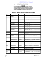
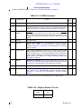
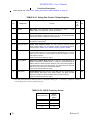
TABLE 3-1. MPC8XXADS Main Memory Map
ADDESS RANGE
Memory Type
00000000 - 003FFFFF
DRAM SIMM
Port
Size
Device Type
MB321Bxa08
MB322Bxa08
MC324Cxa00
MB328Cxa00
32
00400000 - 007FFFFF
32
00800000 - 00FFFFFF
32
01000000 - 01FFFFFF
32
02000000 - 020FFFFF
Empty Space
02100000 - 02107FFF
BCSR(0:4)b
02100000 - 02107FE3
BCSR0
2100004 - 02107FE7
BCSR1
2100008 - 02107FEB
BCSR2
210000C - 02107FEF
BCSR3
2100010 - 02107FF3
BCSR4
02108000 - 021FFFFF
Empty Space
02200000 - 02207FFF
MPC Internal
MAPd
02208000 - 027FFFFF
Empty Space
02800000 - 029FFFFF
Flash SIMM
02A00000 - 02BFFFFF
32c
32
MCM29F020
MCM29F040
SM732A1000A
MCM29F080
SM732A2000
32
32
02C00000 - 02FFFFFF
32
03000000 - 033FFFFF
SDRAM
03400000 - FFFFFFFF
Empty Space
32
a. x ∈ [B,T]
b. The device appears repeatedly in multiples of its size. E.g., BCSR0 appears at memory locations
2100000, 2100020, 2100040..., while BCSR1 appears at 2100004, 2100024, 2100044... and so on.
c. Only upper 16 bit (D0-D15) are in fact used.
d. Refer to the relevant MPC User’s Manual for complete description of the MPC internal memory map.
3•4
MPC Registers’ Programming
The MPC provides the following functions on the MPC8XXFADS:
25
1)
DRAM Controller
2)
SDRAM Controller
3)
Chip Select generator.
Release 0.1
MPC8XXFADS - User’s Manual
OPERATING INSTRUCTIONS
4)
UART for terminal or host computer connection.
5)
Ethernet controller.
6)
Infra-Red Port Controller
7)
General Purpose I/O signals.
The internal registers of the MPC must be programmed after Hard reset as described in the following
paragraphs. The addresses and programming values are in hexadecimal base.
For better understanding the of the following initializations refer to the MPC821 or to the MPC860 User’s
Manual for more information.
TABLE 3-2. SIU REGISTERS’ PROGRAMMING
Register
Init Value[hex]
Description
SIUMCR
01012440
Internal arbitration, External master arbitration priority - 0, External arbitration
priority - 0, PCMCIA channel II pins - PCMCIA, Debug Port on JTAG port pins,
FRZ/IRQ6~ - FRZ, debug register - locked, No parity for non-CS regions, DP(0:3)/
IRQ(3:6)~ pins - DP(0:3), reservation disabled, SPKROUT - Tri-stated, BS_A(0:3)~
and WE(0:3)~ are driven just on their dedicated pins, GPL_B5~ enabled, GPL_A/
B(2:3)~ function as GPLs.
SYPCR
FFFFFF88
Software watchdog timer count - FFFF, Bus-monitor timing FF, Bus-monitor Enabled, S/W watch-dog - Freeze, S/W watch-dog - disabled, S/W watch-dog (if
enabled) causes NMI, S/W (if enabled) not prescaled.
TBSCR
00C2
No interrupt level, reference match indications cleared, interrupts disabled, no
freeze, time-base disabled.
RTCSC
00C2
Interrupt request level - 0, 32768 Hz source, second interrupt disabled, Alarm
interrupt disabled, Real-time clock - FREEZE, Real-time clock enabled.
PISCR
0082
No level for interrupt request, Periodic interrupt disabled, clear status, interrupt
disabled, FREEZE, periodic timer disabled.
3•4•1
Memory Controller Registers Programming
The memory controller on the MPC8XXFADS is initialized to 50 MHz operation. I.e., registers’ programming is based on 50 MHZ timing calculation except for refresh timer which is initialized to 16.67Mhz, the
lowest frequency at which the FADS may wake up. Since the FADS may be made to wake-up at 25MHz A
as well, the initializations are not efficient, since there are too many wait-states inserted. Therefore, additional set of initialization is provided to support efficient 25MHz operation.
The reason for initializing the FADS for 50Mhz is to allow proper (although not efficient) FADS operation
through all available FADS clock frequencies.
A. The only parameter which is initialized to the start-up frequency, is the refresh rate, which would have been inadequate if initialized to 50Mhz while board is running at a lower frequency. Therefore, for best bus bandwidth availability, refresh rate should be adapted to the current system clock frequency.
26
Release 0.1
MPC8XXFADS - User’s Manual
OPERATING INSTRUCTIONS
Warning
Due to availability problems with few of the supported
memory components, the below initializations were not
tested with all parts. Therefore, the below initializations
are liable to CHANGE, throughout the testing period.
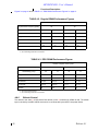
TABLE 3-3. Memory Controller Initializations For 50Mhz
Register
Device Type
BR0
All
Flash
supported.
OR0
BR1
SIMMs
Init Value [hex]
Description
02800001
Base at 2800000, 32 bit port size, no parity, GPCM
MCM29F020-90
FFE00D34
2MByte block size, all types access, CS early negate,
6 w.s., Timing relax
MCM29F040-90
SM732A1000A-9
FFC00D34
4MByte block size, all types access, CS early negate,
6 w.s., Timing relax
MCM29F080-90
SM732A2000-9
FF800D34
8MByte block size, all types access, CS early negate,
6 w.s., Timing relax
MCM29F020-12
FFE00D44
2MByte block size, all types access, CS early negate,
8 w.s., Timing relax
MCM29F040-12
SM732A1000A-12
FFC00D44
4MByte block size, all types access, CS early negate,
8 w.s., Timing relax
MCM29F080-12
SM732A2000-12
FF800D44
8MByte block size, all types access, CS early negate,
8 w.s., Timing relax
BCSR
02100001
Base at 2100000, 32 bit port size, no parity, GPCM
FFFF8110
32 KByte block size, all types access, CS early
negate, 1 w.s.
00000081
Base at 0, 32 bit port size, no parity, UPMA
OR1
BR2
All
Dram
Supported
OR2
MCM36100/200-60/70
FFC00800
4MByte block size, all types access, initial address
multiplexing according to AMA.
MCM36400/800-60/70
MT8/16D432/832X-6/7
FF000800
16MByte block size, all types access, initial address
multiplexing according to AMA.
MCM36200-60/70
00400081
Base at 400000, 32 bit port size, no parity, UPMA
MCM36800-60/70
MT16D832X-6/7
01000081
Base at 1000000, 32 bit port size, no parity, UPMA
MCM36200-60/70
FFC00800
4MByte block size, all types access, initial address
multiplexing according to AMA
MCM36800-60/70
MT16D832X-6/7
FF000800
16MByte block size, all types access, initial address
multiplexing according to AMA.
MB811171622A-100
030000C1
Base at 3000000, on UPM B
FFC00A00
4 MByte block size, all types access, initial address
multiplexing according to AMB.
BR3
OR3
BR4
OR4
27
SIMMs
Release 0.1
MPC8XXFADS - User’s Manual
OPERATING INSTRUCTIONS
TABLE 3-3. Memory Controller Initializations For 50Mhz
Register
Device Type
MPTPR
All
Dram
Supported
MAMR
MBMR
SIMMs
Init Value [hex]
Description
0400
Divide by 16 (decimal)
MB321BT08TASN60
40A21114a
60A21114b
C0A21114c
refresh clock divided by 40a or 60b or C0c, periodic
timer enabled, type 2 address multiplexing scheme, 1
cycle disable timer, GPL4 disabled for data sampling
edge flexibility, 1 loop read, 1 loop write, 4 beats
refresh burst.
MB322BT08TASN60
20A21114a
30A21114b
60A21114c
refresh clock divided by 20a or 30b or 60c, periodic
timer
enabled, type 2 address multiplexing scheme, 1 cycle
disable timer, GPL4 disabled for data sampling edge
flexibility, 1 loop read, 1 loop write, 4 beats refresh
burst.
MB324CT00TBSN60
40B21114a
60B21114b
C0B21114c
refresh clock divided by 40a or 60b or C0c, periodic
timer
enabled, type 3 address multiplexing scheme, 1 cycle
disable timer, GPL4 disabled for data sampling edge
flexibility, 1 loop read, 1 loop write, 4 beats refresh
burst.
MB328CT00TBSN60
20B21114a
30B21114b
60B21114c
refresh clock divided by 20a or 30b or 60c, periodic
timer
enabled, type 3 address multiplexing scheme, 1 cycle
disable timer, GPL4 disabled for data sampling edge
flexibility, 1 loop read, 1 loop write, 4 beats refresh
burst.
MB811171622A-100
D0802114c
80802114 d
refresh clock divided by D0 or 80, periodic timer
enabled, type 0 address multiplexing scheme, 1 cycle
disable timer, GPL4enabled, 1 loop read, 1 loop write,
4 beats refresh burst.
a. Assuming 16.67 MHz BRGCLK.
b. Assuming 25MHz BRGCLK
c. For 50MHz BRGCLK
d. Assuming 32MHz BRGCLK.
28
Release 0.1
MPC8XXFADS - User’s Manual
OPERATING INSTRUCTIONS
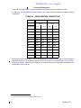
TABLE 3-4. UPMA Initializations for 60nsec DRAMs @ 50MHz
Cycle Type
Single Read
Burst Read
Single Write
Burst Write
Refresh
Exception
Offset in UPM
0
8
18
20
30
3C
0
8FFFEC24
8FFFEC24
8FAFCC24
8FAFCC24
C0FFCC84
33FFCC07
1
0FFFEC04
0FFFEC04
0FAFCC04
0FAFCC04
00FFCC04
X
2
0CFFEC04
08FFEC04
0CAFCC00
0CAFCC00
07FFCC04
X
3
00FFEC04
00FFEC0C
11BFCC47
03AFCC4C
3FFFCC06
X
4
00FFEC00
03FFEC00
X
0CAFCC00
FFFFCC85
5
37FFEC47
00FFEC44
X
03AFCC4C
FFFFCC05
6
X
00FFCC08
X
0CAFCC00
X
7
X
0CFFCC44
X
03AFCC4C
X
Contents
@ Offset +
29
8
00FFEC0C
0CAFCC00
X
9
03FFEC00
33BFCC4F
X
A
00FFEC44
X
X
B
00FFCC00
X
X
C
3FFFC847
X
D
X
X
E
X
X
F
X
X
Release 0.1
MPC8XXFADS - User’s Manual
OPERATING INSTRUCTIONS
TABLE 3-5. UPMA Initializations for 60nsec EDO DRAMs @ 50MHz
Cycle Type
Single Read
Burst Read
Single Write
Burst Write
Refresh
Exception
Offset in UPM
0
8
18
20
30
3C
0
8FFBEC24
8FFFEC24
8FFFCC24
8FFFCC24
C0FFCC84
33FFCC07
1
0FF3EC04
0FFBEC04
0FEFCC04
0FEFCC04
00FFCC04
X
2
0CF3EC04
0CF3EC04
0CAFCC00
0CAFCC00
07FFCC04
X
3
00F3EC04
00F3EC0C
11BFCC47
03AFCC4C
3FFFCC06
X
4
00F3EC00
0CF3EC00
X
0CAFCC00
FFFFCC85
5
37F7EC47
00F3EC4C
X
03AFCC4C
FFFFCC05
6
X
0CF3EC00
X
0CAFCC00
X
7
X
00F3EC4C
X
03AFCC4C
X
Contents
@ Offset +
8
0CF3EC00
0CAFCC00
X
9
00F3EC44
33BFCC4F
X
A
03F3EC00
X
X
B
3FF7EC47
X
X
C
X
X
D
X
X
E
X
X
F
X
X
TABLE 3-6. Memory Controller Initializations For 20Mhz
Register
BR0
30
Device Type
All
Flash
supported.
SIMMs
Init Value [hex]
02800001
Description
Base at 2800000, 32 bit port size, no parity, GPCM
Release 0.1
MPC8XXFADS - User’s Manual
OPERATING INSTRUCTIONS
TABLE 3-6. Memory Controller Initializations For 20Mhz
Register
OR0
BR1
Device Type
Init Value [hex]
Description
MCM29F020-90
FFE00D20
2MByte block size, all types access, CS early negate,
2 w.s.
MCM29F040-90
SM732A1000A-9
FFC00D20
4MByte block size, all types access, CS early negate,
2 w.s.
MCM29F080-90
SM732A2000-9
FF800920
8MByte block size, all types access, CS early negate,
2 w.s., Timing relax
MCM29F020-12
FFE00D30
2MByte block size, all types access, CS early negate,
3 w.s.
MCM29F040-12
SM732A1000A-12
FFC00D30
4MByte block size, all types access, CS early negate,
3 w.s.
MCM29F080-12
SM732A2000-12
FF800930
8MByte block size, all types access, CS early negate,
3 w.s.
BCSR
02100001
Base at 2100000, 32 bit port size, no parity, GPCM
FFFF8110
32 KByte block size, all types access, CS early
negate, 1 w.s.
00000081
Base at 0, 32 bit port size, no parity, UPMA
OR1
BR2
All
Dram
Supported
OR2
MB321/2BT08TASN60
FFC00800
4MByte block size, all types access, initial address
multiplexing according to AMA.
MB324/8CT00TBSN60
FF000800
16MByte block size, all types access, initial address
multiplexing according to AMA.
MB322BT08TASN60
00400081
Base at 400000, 32 bit port size, no parity, UPMA
MB328CT00TBSN60
01000081
Base at 1000000, 32 bit port size, no parity, UPMA
MB322BT08TASN60
FFC00800
4MByte block size, all types access, initial address
multiplexing according to AMA
MB328CT00TBSN60
FF000800
16MByte block size, all types access, initial address
multiplexing according to AMA.
MB811171622A-100
030000C1
Base at 3000000, on UPM B.
FFC00A00
4MByte block size, all types access, initial address
multiplexing according to AMB
0400
Divide by 16 (decimal)
BR3a
OR3
BR4
SIMMs
OR4
MPTPR
31
All
Dram
Supported
SIMMs
Release 0.1
MPC8XXFADS - User’s Manual
OPERATING INSTRUCTIONS
TABLE 3-6. Memory Controller Initializations For 20Mhz
Register
MAMR
MBMR
Device Type
Init Value [hex]
Description
MB321BT08TASN60
60A21114
refresh clock divided by 60, periodic timer enabled,
type 2 address multiplexing scheme, 1 cycle disable
timer, GPL4 disabled for data sampling edge flexibility,
1 loop read, 1 loop write, 4 beats refresh burst.
MB322BT08TASN60
30A21114
refresh clock divided by 30, periodic timer
enabled, type 2 address multiplexing scheme, 1 cycle
disable timer, GPL4 disabled for data sampling edge
flexibility, 1 loop read, 1 loop write, 4 beats refresh
burst.
MB324CT00TBSN60
60B21114
refresh clock divided by 60, periodic timer
enabled, type 3 address multiplexing scheme, 1 cycle
disable timer, GPL4 disabled for data sampling edge
flexibility, 1 loop read, 1 loop write, 4 beats refresh
burst.
MB328CT00TBSN60
30B21114
refresh clock divided by 30, periodic timer
enabled, type 3 address multiplexing scheme, 1 cycle
disable timer, GPL4 disabled for data sampling edge
flexibility, 1 loop read, 1 loop write, 4 beats refresh
burst.
MB811171622A-100
42802114b
refresh clock divided by 42, periodic timer enabled,
type 0 address multiplexing scheme, 1 cycle
disable timer, GPL4 enabled, 1 loop read, 1 loop write,
4 beats refresh burst.
a. BR3 is not initialized for MB321xx or MB324xx EDO DRAM SIMMs.
b. Assuming 16.67MHz BRGCLK
32
Release 0.1
MPC8XXFADS - User’s Manual
OPERATING INSTRUCTIONS
TABLE 3-7. UPMA Initializations for 60nsec EDO DRAMs @ 20MHz
Cycle Type
Single Read
Burst Read
Single Write
Burst Write
Refresh
Exception
Offset in UPM
0
8
18
20
30
3C
0
8FFFCC04
8FFFCC04
8FEFCC00
8FEFCC00
80FFCC84
33FFCC07
1
08FFCC00
08FFCC08
39BFCC47
09AFCC48
17FFCC04
X
2
33FFCC47
08FFCC08
X
09AFCC48
FFFFCC86
X
3
X
08FFCC08
X
09AFCC48
FFFFCC05
X
4
X
08FFCC00
X
39BFCC47
X
5
X
3FFFCC47
X
X
X
6
X
X
X
X
X
7
X
X
X
X
X
Contents
@ Offset +
33
8
X
X
X
9
X
X
X
A
X
X
X
B
X
X
X
C
X
X
D
X
X
E
X
X
F
X
X
Release 0.1
MPC8XXFADS - User’s Manual
OPERATING INSTRUCTIONS
TABLE 3-8. UPMB Initializations for MB811171622A-100 upto 32MHz
Cycle Type
Single Read
Burst Read
Single Write
Burst Write
Refresh
Exception
Offset In UPM
0
8
18
20
30
3C
0
0126CC04
0026FC04
0E26BC04
0E26BC00
1FF5FC84
7FFFFC07
1
0FB98C00
10ADFC00
01B93C00
10AD7C00
FFFFFC04
X
2
1FF74C45
F0AFFC00
1FF77C45
F0AFFC00
FFFFFC84
X
3
X
F1AFFC00
X
F0AFFC00
FFFFFC05
X
4
X
EFBBBC00
X
E1BBBC04
X
5
1FE77C34a
1FF77C45
X
1FF77C45
X
6
EFAABC34
X
X
X
X
7
1FA57C35
X
X
X
X
Contents
@ Offset +
8
X
X
X
9
X
X
X
A
X
X
X
B
X
X
X
C
X
X
D
X
X
E
X
X
F
X
X
a. MRS initialization. Uses Free space.
34
Release 0.1
MPC8XXFADS - User’s Manual
OPERATING INSTRUCTIONS
TABLE 3-9. UPMB Initializations for MB811171622A-100, 32+MHz - 50MHz
Cycle Type
Single Read
Burst Read
Single Write
Burst Write
Refresh
Exception
Offset In UPM
0
8
18
20
30
3C
0
1F07FC04
1F07FC04
1F27FC04
1F07FC04
1FF5FC84
7FFFFC07
1
EEAEFC04
EEAEFC04
EEAEBC00
EEAEBC00
FFFFFC04
X
2
11ADFC04
10ADFC04
01B93C04
10AD7C00
FFFFFC04
X
3
EFBBBC00
F0AFFC00
1FF77C47
F0AFFC00
FFFFFC04
X
4
1FF77C47
F0AFFC00
X
F0AFFC00
FFFFFC84
5
1FF77C34a
F1AFFC00
X
E1BBBC04
FFFFFC07
6
EFEABC34
EFBBBC00
X
1FF77C47
X
7
1FB57C35
1FF77C47
X
X
X
Contents
@ Offset +
8
X
X
X
9
X
X
X
A
X
X
X
B
X
X
X
C
X
X
D
X
X
E
X
X
F
X
X
a. MRS initialization, Uses free space.
35
Release 0.1
MPC8XXFADS - User’s Manual
Functional Description
4 - Functional Description
In this chapter the various modules combining the MPC8XXFADS are described to their design details.
4•1
Reset & Reset - Configuration
There are several reset sources on the FADS:
1) Keep Alive Power-On ResetA
2) Regular Power On Reset
3) Manual Soft-Reset
4) Manual Hard-Reset
5) MPC Internal Sources. (See the appropriate Spec or U/M)
4•1•1
Keep Alive Power-On Reset
The Keep Alive Power - On Reset logic resides on the daughter board this since the Keep Alive power bus
is on that board and it also allows the use of the daughter board connected directly to a user’s application.
4•1•2
Regular Power - On Reset
The regular power on reset operates in the same manner as the keep alive power-on reset, using a similar
device - the Seiko - S-8052ANY-NH-X with detection voltage of 2.595V to 2.805V. The reference voltage
of this device is the MAIN VDDH bus of the MPC while the reset line assertedB, is the HRESET* line.
When HRESET~ is asserted to the MPC, Hard-Reset configuration is made available to the MPC, via
BCSR0. See 4•1•6•2 "Hard Reset Configuration" on page 37 and TABLE 4-9. "BCSR0 Description" on
page 55.
4•1•3
Manual Soft Reset
To support application development not around the debug port and resident debuggers, a soft reset pushbutton is provided. (SW2) Depressing that button, asserts the SRESET* pin of the MPC, generating a
SOFT RESET sequence.
When the SRESET~ line is asserted to the MPC, the Soft-Reset configuration is made available to the
MPC, by the debug-port controller. See 4•1•6•3 "Soft Reset Configuration" on page 37.
4•1•4
Manual Hard Reset
To support application development not around the debug port, a Hard-Reset push-button is providedC.
When the Soft Reset push-button (SW2) is depressed in conjunction with the ABORT push-button (SW1),
the HRESET* line is asserted, generating a HARD RESET sequence. The button sharing is for economy
and board space saving and does not effect in any way, functionality.
4•1•5
MPC Internal Sources
Since the HRESET* and SRESET* lines of the MPC are open-drain and the on-board reset logic drives
these lines with open-drain gates, the correct operation of the internal reset sources of the MPC is facilitated. As a rule, an internal reset source asserts HRESET* and / or SRESET* for a minimum time of 512
system clocks. It is beyond the scope of this document to describe these sources, however Debug-Port
Soft / Hard Resets which are part of the development systemD, are regarded as such.
A. In fact generated on the daughter board.
B. Again not directly.
C. It is not a dedicated button.
D. And therefore mentioned.
36
Release 0.1
MPC8XXFADS - User’s Manual
Functional Description
4•1•6
Reset Configuration
During reset the MPC device samples the state of some external pins to determine its operation modes
and pin configuration. There are 3 kinds of reset levels to the MPC each level having its own configuration
sampled:
1) Power - On Reset configuration
2) Hard Reset configuration
3) Soft Reset Configuration.
4•1•6•1
Power - On Reset Configuration
Just before PORESET* is negated by the external logic, the power-on reset configuration which include
the MODCK(1:2) pins is sampled. These pins determine the clock operation mode of the MPC. Two clock
modes are supported on the MPC8XXFADS:
1)
1:5 PLL operation via on-board clock generator.
In this mode MODCK(1:2) are driven with ’11’ duringA power on reset.
2)
1:513 PLL operation via on-board clock generator.
In this mode MODCK(1:2) are driven with ’00’. during power-on reset.
4•1•6•2
Hard Reset Configuration
During HARD reset sequence, when RSTCONF* pin is asserted, the MPC data bus state is sampled to
acquire the MPC’s hard reset configuration. The reset configuration word is driven by BCSR0 register,
defaults of which are set during power-on reset. The BCSR0 drives half of the configuration word, i.e., data
bits D(0:15) in which the reserved bits are designated RSRVxx. If the hard-reset configuration is to be
changedB, BCSR0 may be written with new values, which become valid after HARD reset is applied to the
MPC.
On the FADS, the RSTCONF* line is always driven during HARD reset, i.e., no use is possible with the
MPC’s internal HARD reset configuration defaults.
The system parameters to which BCSR0 defaults during power-on reset and are driven at hard-reset, are
listed below:
1)
Arbitration: internal arbitration is selected.
2)
Interrupt Prefix: The internal default is interrupt prefix at 0xFFF00000. It is overridden to provide
interrupt prefix at address 0, which is located within the DRAM.
3)
Boot Disable: Boot is enabled.
4)
Boot Port Size: 32 bit boot port size is selected.
5)
Initial Internal Space Base: Immediately after HARD reset, the internal space is located at
$FF000000.
6)
Debug pins configuration: PCMCIA port BC pins become PCMCIA port B pins.
7)
Debug port pins configuration. Debug port pins are on the JTAG port.
8)
External Bus Division Factor: 1:1 internal to external clocks’ frequencies ratio is selected.
4•1•6•3
Soft Reset Configuration
The rising edge of SRESET* is used to configure the development port. Before the negation of SRESET*,
DSCKD is sampled to determine for debug-mode enable / disable. After SRESET* is negated, if debug
A. The MODCK lines are in fact driven longer - by HRESET~ line.
B. With respect the FADS’s power-on defaults.
C. Where they exist.
37
Release 0.1
MPC8XXFADS - User’s Manual
Functional Description
mode was enabled, DSCK is sampled again for debug-mode entry / non-entry.
DSDI is used to determine the debug port clock mode and is sampled after the negation of SRESET*.
The Soft Reset configuration is provided by the debug-port controller via the ADI I/F. Option is given to
enter debug mode directly or only after exception.
4•2
Local Interrupter
The only external interrupt which is applied to the MPC via its interrupt controller is the ABORT (NMI),
which is generated by a push-button. When this button is depressed, the NMI input to the MPC is asserted.
The purpose of this type of interrupt, is to support the use of resident debuggers if any is made available
to the FADS. All other interrupts to the MPC, are generated internally by the MPC’s peripherals and by the
debug port.
To support external (off-board) generation of an NMI, the IRQ0* line which is routed as an NMI input, is
driven by an open-drain gate. This allows for external h/w to also drive this line. If an external h/w indeed
does so, it is compulsory that IRQ0* is driven by an open-drain (or open-collector) gate.
Clock GeneratorA
4•3
There are 2 ways to clock the MPC on the MPC8XXFADS:
1)
3 - 5MHz Clock generatorB connected to CLK4IN input. 1:5 PLL mode.
2)
32.768 KHz crystal resonatorB via EXTAL-XTAL pair of the MPC, 1:513 initial PLL multiplication
factor.
The selection between the above modes is done using Dip-switch (DS2 / 4) with dual functionality: it is responsible to the combination driven to the MODCK lines during power-on reset and to the connection of
the appropriate capacitor between MPC’s XFC and VDDSYN lines to match the PLL’s multiplication factor.
When 1:5 mode is selected, a capacitor of 5nF is connected, while when 1:513 mode is selected a 0.68µF
capacitor is connected parallel to it via a TMOS gate. The capacitors’ values are calculated to support a
wider range of multiplication factors as possible.
When mode (2) above is selected, the output of the clock generator is gated from EXTCLK input and driven
to ’0’ constantly so that a jitter-free system clock is generated.
On-board logic is clocked by the MPC’s CLKOUT coming from the Daughter board. This clock is multiplexed with the debug port’s clock generator, so that on-board logic is always clocked, even when the MPC
is removed from its socketC.
4•4
Buffering
As the FADS meant to serve also as a hardware development platform, it is necessary to buffer the MPC
from the local bus, so the MPC’s capacitive drive capability is not wasted internally and remains available
for user’s off-board applications via the expansion connectors.
Buffers are provided for address and strobeD lines while transceivers are provided for data. Since the capacitive load over dram’s address lines mightE exceed 200 pF, the dram address lines are separately buff-
D. DSCK is configured at hard-reset to reside on the JTAG port.
A. Although this module resides on the DAUGHTER boards, it is described here, as it is common to all MPC8XX
supported.
B. Located On the Daughter Board.
C. When the FADS serves a debug station for target system.
D. If necessary.
E. Depended on dram SIMM’s internal structure.
38
Release 0.1
MPC8XXFADS - User’s Manual
Functional Description
ered. Use is done with 74LCX buffers which are 3.3V operated and are 5V tolerant. This type of buffers
reduces noise on board due to reduced transitions’ amplitude.
To further reduce noise and reflections, series resistors are placed over dram’s address and strobe lines.
The data transceivers open only if there is an access to a validA B board address or during Hard - Reset
configuration C. That way data conflicts are avoided in case an off-board memory is read, provided that it
is not mapped to an address valid on board. It is the users’ responsibility to avoid such errors.
4•5
Chip - Select Generator
The memory controller of the MPC is used as a chip-select generator to access on-boardD memories,
saving board’s area reducing cost, power consumption and increasing flexibility. To enhance off-board application development, memory modules (including the BCSRx) may be disabled via BCSR1 E in favor of
an external memory connected via the expansion connectors. That way, a CS line may be used off-board
via the expansion connectors, while its associated local memory is disabled.
When a CS region is disabled via BCSR1, the local data transceivers do not open during access to that
region, avoiding possible F contention over data lines.
The MPC’s chip-selects assignment to the various memories / registers on the FADS are as shown in
TABLE 4-1. "MPC8XXFADS Chip Selects’ Assignment" below:
TABLE 4-1. MPC8XXFADS Chip Selects’ Assignment
Chip Select:
Assignment
CS0*
Flash Memory
CS1*
BCSR
CS2*
DRAM Bank 1
CS3*
DRAM Bank 2a
CS4*
SDRAM
CS(5-7)*
Unused, user available
a. If exists.
4•6
DRAM
The MPC8XXFADS is provided with 4 MBytes of 60nsec delay EDO Dram SIMM. Support is given to any
5V powered FPM / EDO Dram SIMM configured as 1M X32 upto 2 X 4M X 32, with 60 nsec or 70nsec
delay.
All dram configurations are supported via the Board Control & Status Register (BCSR), i.e., DRAM size
(4M to 32M) and delay (60 / 70 nsec) are read from BCSR2 and the associated registers (including the
A. An address which covered in a Chip-Select region.
B. Except for SDRAM, which is Unbuffered.
C. To allow a configuration word stored in Flash memory become active.
D. And off-board. See further.
E. After the BCSR is removed from the local memory map, there is no way to access it but to re-apply power to the
FADS.
F. During read cycles.
39
Release 0.1
MPC8XXFADS - User’s Manual
Functional Description
UPM) are programmed accordingly.
Dram timing control is performed by UPMA of the MPC via CS2 (and CS3 for a dual-bank SIMM) region(s),
i.e., RAS and CAS signals’ generation, during normalA access as well as during refresh cycles and the necessary address multiplexingB are performed using UPMA. CS2* and CS3* signals are buffered from the
DRAM and each is split to 2 to overcome the capacitive load over the Dram SIMM RAS lines.
The DRAM module may enabled / disabled at any time by writing the DRAMEN~ bit in BCSR1. See TABLE
4-10. "BCSR1 Description" on page 57.
4•6•1
DRAM 16 Bit Operation
To enhance evaluation capabilities, support is given to Dram with 16-bit and 32-bit data bus width. That
way users can tailor dram configuration, to get best fit to their application requirements. When the DRAM
is in 16 bit mode, half of it can not be used, i.e., the memory portion that is connected to data lines D(16:31).
To configure the DRAM for 16 bit data bus width operation, the following steps should be taken:
1)
Set the Dram_Half_Word bit in BCSR1 to Half-Word. See TABLE 4-10. "BCSR1 Description" on
page 57
2)
The Port Size bits of BR2~ (and of BR3~ for a 2-bank DRAM simm) should be set to 16 bits.
3)
The AM bits in OR2 register should be set to 1/2 of the nominal single-bank DRAM simm volume or to 1/4 of the nominal dual-bank DRAM simm volume.
If a Dual-Bank DRAM simm is being used:
4)
The Base-Address bits in BR3 register should be set to DRAM_BASE + 1/4 Nominal_Volume,
that is, if a contiguous block of DRAM is desired.
5)
The AM bits of OR3 register, should be set to 1/4 Nominal_Volume.
If the above is executed out of running code, than this code should not reside on the DRAM while executing, otherwise, erratic behavior is likely to be demonstrated, resulting in a system crash.
4•6•2
DRAM Performance Figures
The projected performance figures for the dram are shown in TABLE 4-2. "Regular DRAM Performance
A. Normal i.e.: Single Read, Single Write, Burst Read & Burst Write.
B. Taking into account support for narrower bus widths.
40
Release 0.1
MPC8XXFADS - User’s Manual
Functional Description
Figures" on page 41 and in TABLE 4-3. "EDO DRAM Performance Figures" on page 41.
TABLE 4-2. Regular DRAM Performance Figures
Number of System Clock Cycles
System Clock Frequency [MHz]
50
DRAM Delay [nsec]
25
60
70
60
70
Single Read
6
6
3
4
Single Write
4
4
3
3
Burst Read
6,2,3,2
6,3,2,3
3,2,2,2
4,2,2,2
Burst Write
4,2,2,2
4,2,2,2
3,1,2,2
3,2,2,2
ab
ab
ab
Refresh
21
25
13
13a b
a. Four-beat refresh burst.
b. Not including arbitration overhead.
TABLE 4-3. EDO DRAM Performance Figures
Number of System Clock Cycles
System Clock Frequency [MHz]
50
DRAM Delay [nsec]
25
60
70
60
70
Single Read
6
6
3
4
Single Write
4
4
2
3
Burst Read
6,2,2,2
6,3,2,2
3,1,1,1
4,1,2,2
Burst Write
4,2,2,2
4,2,2,2
2,1,1,1
3,2,2,2
ab
ab
ab
Refresh
21
25
13
13a b
a. Four-beat refresh burst.
b. Not including arbitration overhead.
4•6•3
Refresh Control
The refresh to the dram is a CAS before RAS refresh, which is controlled by UPMA as well. The refresh
logic is clocked by the MPC’s BRG clock which is not influenced by the MPC’s low-power divider.
41
Release 0.1
MPC8XXFADS - User’s Manual
Functional Description
FIGURE 4-1 Refresh Scheme
BRG Clock
PTP
PTB
UPMB
DRAM BANKS
As seen in FIGURE 4-1 "Refresh Scheme" above, the BRG clock is twice divided: once by the PTP (Periodic Timer Prescaler) and again by another prescaler - the PTA, dedicated for each UPM. If there are
more than one dram banks, than refresh cycles are performed for consecutive banks, therefore, refresh
should be made faster. The formula for calculation of the PTA is given below:
PTA =
Refresh_Period X Number_Of_Beats_Per_Refresh_Cycle
Number_Of_Rows_To_Refresh X T_BRG X MPTPR X Number_Of_Banks
Where:
•
PTA - Periodic Timer A filed in MAMR. The value of the 2’nd divider.
•
Refresh_Period is the time (usually in msec) required to refresh a dram bank
•
Number_Of_Beats_Per_Refresh_Cycle: using the UPM looping capability, it is possible to
perform more than one refresh cycle per refresh burst (in fact upto 16).
•
Number_Of_Rows_To_Refresh: the number of rows in a dram bank
•
T_BRG: the cycle time of the BRG clock
•
MPTPR: the value of the periodic timer prescaler (2 to 64)
•
Number_Of_Banks: number of dram banks to refresh.
If we take for example a MCM36200 SIMM which has the following data:
•
Refresh_Period == 16 msec
•
Number_Of_Beats_Per_Refresh_Cycle: on the FADS it is 4.
•
Number_Of_Rows_To_Refresh == 1024
•
T_BRG == 20 nsec (system clock @ 50 Mhz)
•
MPTPR arbitrarily chosen to be 16
•
Number_Of_Banks == 2 for that SIMM
If we assign the figures to the PTA formula we get the value of PTA should be 97 decimal or 61 hex.
4•6•4
Variable Bus-Width Control
Since a port’s width determines its address lines’ connection scheme, i.e., the number of address lines
required for byte-selection varies (1 for 16-bit port and 2 for 32-bit port) according to the port’s width, it is
necessary to change address connections to a memory port if its width is to be changed. E.g.: if a certain
memory is initially configured as a 32-bit port, the list significant address line which is connected to that
memory’s A0 line should be the MPC’s A29. Now, if that port is to be reconfigured as a 16-bit port, the LS
address line becomes A30.
If a linearA address scheme is to be maintained, all address lines connected to that memory are to be
shifted one bit, this obviously involves extensive multiplexing (passive or active). If linear addressing
42
Release 0.1
MPC8XXFADS - User’s Manual
Functional Description
scheme is not a must, than only minimal multiplexing is required to support variable port width.
In TABLE 4-4. "DRAM ADDRESS CONNECTIONS" below, the FADS’s dram address connection scheme
is presented:
TABLE 4-4. DRAM ADDRESS CONNECTIONS
Width
Dram ADD
32 - Bit
16 - Bit
Depth
Depth
4M
1M
4M
1M
A0
BA29
BA29
BA29
BA29
A1
BA28
BA28
BA28
BA28
A2
BA27
BA27
BA27
BA27
A3
BA26
BA26
BA26
BA26
A4
BA25
BA25
BA25
BA25
A5
BA24
BA24
BA24
BA24
A6
BA23
BA23
BA23
BA23
A7
BA22
BA22
BA22
BA22
A8
BA21
BA21
BA21
BA21
A9
BA20
BA20
BA20
BA30
A10
BA19
BA30
As can seen from the table above, most of the address lines remain fixed while only 2 lines (the shaded
cells) need switching. The switching scheme is shown in FIGURE 4-2 "DRAM Address Lines’ Switching
Scheme" on page 44. The switches on that figure are implemented by active multiplexers controlled by the
BCSR1/Dram_Half_Word* bit.
A. Consequent addresses lead to adjacent memory cells
43
Release 0.1
MPC8XXFADS - User’s Manual
Functional Description
FIGURE 4-2 DRAM Address Lines’ Switching Scheme
DRAM
BA(21:29)
A(0:8)
BA20
A9
BA30
BA19
A10
BA30
4•7
Flash Memory SIMM
The MPC8XXFADS is provided with 2Mbyte of 90 nsec flash memory SIMM - the MCM29020 by Motorola.
Support is given also to 4MBytes MCM29F040, 8 MBytes MCM29F080, 4 MBytes SM73218 and to 8
MBytes SM73228 by Smart Technology. The Motorola SIMMs are internally composed of 1, 2 or 4 banks
of 4 Am29F040 compatible devices, while the Smart SIMMs are arranged as 1 or 2 banks of four 28F008
devices by Intel. The flash SIMM resides on an 80 pin SIMM socket.
To minimize use of MPC’s chip-select lines, only one chip-select line (CS0~) is used to select the flash as
a whole, while distributing chip-select lines among the internal banks is done via on-board programmable
44
Release 0.1
MPC8XXFADS - User’s Manual
Functional Description
logic, according to the Presence-Detect lines of the Flash SIMM inserted to the FADS.
FIGURE 4-3 Flash Memory SIMM Architecture
Flash Presence-Detect Lines
ADD
CS0~
F_CS1~
M29F040 or
1M X 8
M29F040 or
1M X8
M29F040 or
1M X 8
M29F040 or
1M X 8
F_CS2~
M29F040 or
1M X 8
M29F040 or
1M X 8
M29F040 or
1M X 8
M29F040 or
1M X 8
M29F040
M29F040
M29F040
M29F040
M29F040
M29F040
M29F040
M29F040
FADS’s
Logic
F_CS3~
F_CS4~
DATA
MCM29F020
SM73218
MCM29F040
SM73228
MCM29F080
The access time of the Flash memory provided with the FADS is 90 nsec, however, 120 nsec devices may
be used as well. Reading the delay section of the Flash SIMM Presence-Detect lines, the debugger establishes (via OR0) the correct number of wait-states (considering 50MHz system clock frequency).
The Motorola SIMMs are built of AMD’s Am29F0X0 devices which are 5V programmable, i.e., there is no
need for external programming voltage and the flash may be written almostA as a regular memory.
The SMART parts however, require 12V ± 0.5% programming voltage to be applied for programming. If
on-boards programming of such device is required, a 12V supply needs to be connected to the FADS (P7).
Otherwise, for normalB Flash operation, 12V supply is not required.
The control over the flash is done using the GPCM and a dedicated CS0~ region, controlling the whole
bank. During hard - reset initializations, the debugger reads the Flash Presence-Detect lines via BCSR2
and decides how to program BR0 & OR0 registers, within which the size and the delay of the region are
determined.
The performance of the flash memory is shown in TABLE 4-5. "Flash Memory Performance Figures"
A. A manufacturer specific dedicated programming algorithm should be implemented during flash programming.
B. I.e., Read-Only.
45
Release 0.1
MPC8XXFADS - User’s Manual
Functional Description
below:
TABLE 4-5. Flash Memory Performance Figures
Number of System Clock Cycles
System Clock Frequency [MHz]
50
25
Flash Delay [nsec]
90
120
90
120
Read / Writea Access [Clocks]
8
10
4
5
a. The figures in the table refer to the actual write access. The write operation continues internally
and the device has to be polled for operation completion.
The Flash module may disabled / enabled at any time by writing ’1’ / ’0’ the FlashEn~ bit in BCSR1.
4•8
Synchronous Dram
To enhance performance, especially in higher operation frequencies - 4 MBytes of SDRAM is provided on
board. The SDRAM is unbuffered from the MPC bus and is configured as 2 X 512K X 32. Use is done with
two MB811171622A-100 chips by Fujitsu or compatibles.
To enhance performance, the SDRAM is unbuffered from the MPC, saving the delay associated with
address and data buffers. Since only 2 memory chips are involved, it does not adversely effect overall
system performance. The SDRAM does not reside on a SIMM but is soldered directly to the FADS pcb.
The SDRAM may be enabled / disabled at any time by writing 1 / 0 to the SDRAMEN bit in BCSR1. See
TABLE 4-10. "BCSR1 Description" on page 57.
The SDRAM’s timing is controlled by UPMB via its assigned CS (See TABLE 4-1. "MPC8XXFADS Chip
Selects’ Assignment" on page 39) line. Unlike a regular dram the synchronous dram has a CS input in
addition to the RAS and CAS signals.
The sdram connection scheme is shown in FIGURE 4-4 "SDRAM Connection Scheme" on page 47.
The SDRAM’s performance figures, are shown in TABLE 4-6. "Estimated SDRAM Performance Figures":
TABLE 4-6. Estimated SDRAM Performance Figures
Number of System Clock Cycles
System Clock Frequency [MHz]
25a
50
Single Read
5
3
Single Write
3+1b
2 + 1b
Burst Read
5,1,1,1
3,1,1,1
Burst Write
3,1,1,1 + 1b
2,1,1,1 + 1b
Refresh
21 c
13 b
a. In fact upto 32MHz.
b. One additional cycle for RAS precharge
c. 4-beat Refresh Burst, not including arbitration overhead.
46
Release 0.1
MPC8XXFADS - User’s Manual
Functional Description
FIGURE 4-4 SDRAM Connection Scheme
CS4
GPL1
GPL2
GPL3
A10
GPL0 (A11)
A(20:21)
A(22:29)
SDRAMEN
SYSCLK
CS
CS
RAS
RAS
CAS
CAS
W
W
A11
A11
A10
A10
A(9:8)
A(9:8)
A(7:0)
A(7:0)
CKE
CKE
CLK
CLK
BS0_B
DQMU
DQMU
BS1_B
DQML
DQML
DQ(15:0)
DQ(15:0)
D(0:15)
BS2_B
BS3_B
D(16:31)
4•8•1
SDRAM Programming
After power-up, the sdram needs to be initialized by means of programming, to establish its mode of operation. The Sdram is programmed by issuing a Mode Register Set command. During that command, data
is passed to the Mode Register through the Sdram’s address lines. This command is fully supported by the
UPM by means of a dedicated Memory Address Register and the UPM command run option.
Mode Register programming values are shown in TABLE 4-7. "SDRAM’s Mode Register Programming"
47
Release 0.1
MPC8XXFADS - User’s Manual
Functional Description
below:
TABLE 4-7. SDRAM’s Mode Register Programming
Value @ Frequency
SDRAM Option
Burst Length
Burst Type
CAS Latency
Write Burst Length
4•8•1•1
50MHz
25MHz
4
4
Sequential
Sequential
2
1
Burst
Burst
SDRAM Initializing Procedure
After Power-up the SDRAM needs to be initialized in a certain manner, described below:
1)
UPMB should be programmed with values described in TABLE 3-8. "UPMB Initializations for
MB811171622A-100 upto 32MHz" on page 34 or in TABLE 3-9. "UPMB Initializations for
MB811171622A-100, 32+MHz - 50MHz" on page 35.
2)
Memory controller’s MPTPR, MBMR, OR4 and BR4 registers should be programmed according
to TABLE 3-6. "Memory Controller Initializations For 20Mhz" on page 30 or TABLE 3-3. "Memory
Controller Initializations For 50Mhz" on page 27.
3)
MAR should be set with proper value (0x48 for upto 32MHz or 0x88 for 32 - 50 MHz)
4)
MCR should be written with 0x80808105 to run the MRS command programmed in locations 5
- 8 of UPMB.
5)
MBMR’s TLFB field should be changed to 8, to constitute 8-beat refresh Bursts.
6)
MCR should be written with 0x80808130 to run the refresh sequence (8 refresh cycles are performed now)
7)
MBMR’s TLFB field should be restored to 4, to provide 4-beat refresh Bursts for normal operation. The SDRAM is initialized and ready for operation.
4•8•2
SDRAM Refresh
The SDRAM is refreshed using its auto-refresh mode. I.e., using UMPB’s periodic timer, a burst of four
auto-refresh commands is issued to the SDRAM every 62.4 µsec, so that all 2048 SDRAM rows are refreshed within specified 32.8 msec.
48
Release 0.1
MPC8XXFADS - User’s Manual
Functional Description
4•9
Communication Ports
Since the FADS platform is meant to serve all the MPC8XX family, it only contains modules that are
common to all family members. The various communication ports for the present and future family
members are shown in TABLE 4-8. "MPC8XX Family Comm. Ports" below:
TABLE 4-8. MPC8XX Family Comm. Ports
Family Member - MPC
Comm.
Port
801
823
821
860
860SAR
860T
SCC1
Uart, IrDA
USB
3 +Enet
3 +Enet
3 +Enet
3 +Enet
SCC2
Uart, IrDA
3 +Enet,
Fast IrDA
3 +IrDA
3 +Enet,
IrDA
3 +Enet,
IrDA
3 +Enet,
IrDA
SCC3
3 +Enet
3 +Enet
3 +Enet
SCC4
3 +Enet
3 +Enet
3 +Enet
SMC1
3 Uart
3 Uart
3 Uart
3 Uart
3 Uart
SMC2
3 TDM
Only
3 Uart
3 Uart
3 Uart
3 Uart
SPIa
3
3
3
3
3
3
I2 C a
3
3
3
3
3
3
Fast Enet
Utopia
3
3
a. This is an interchip protocol and therefore will not be supported for evaluation.
As can be seen from the above table the Ethernet, I/R and Uart (RS232) support are common to allA family
members. Therefore, the FADS is equipped with 2 port of RS232, each with independent enable via BCSR
and an IRDA transceiver, supporting Fast IRDA.
4•9•1
Ethernet Port
An Ethernet port with T.P. (10-Base-T) I/F is provided on the MPC8XXFADS. The comm. port over which
this port resides, is determined according to the MPC typeB. Use is done with the MC68160 EEST 10-baseT transceiver, used also with the MPC8XXFADS.
To allow alternative use of the Ethernet’s SCC pins, they appear at the expansion connectors over the
daughter-board and over the Comm. Ports expansion connector (P8) of the this board, while the Ethernet
transceiver may be Disabled / Enabled at any time by writing ’1’ / ’0’ to the EthEn~ bit in BCSR1.
4•9•2
Infra-Red Port
An infra-Red communication port is provided with the FADS - the Temic’s TFDS 6000 integrated transceiver, which incorporates both the receiver and transmitter optical devices with the translating logic and
supports Fast IrDA (upto 4 Mbps). The comm. port over which this port resides, is determined according
A. Except for the MPC801 which does not have Ethernet support.
B. I.e., routing is done on the daughter board.
49
Release 0.1
MPC8XXFADS - User’s Manual
Functional Description
B
to the MPC type .
To allow alternative use of the I/R’s SCC or its pins, the infra-red transceiver may be disabled / enabled at
any time, by writing ’1’ / ’0’ to the IrdEn~ bit in BCSR1, while all pins appear on the daughter-board expansion connector, as well as on P8 of this board.
4•9•2•1
Infra-Red Port Rate Range Selection
The TFDS6000 has 2 bit-rate ranges:
1)
9600 Bps to 1.2 MBps
2)
1.2 MBps to 4 MBps.
Selection between the 2 ranges is determined by the state of the transceiver’s TX input on the falling edge
of IrdEn~.
When TX input is LOW at least 200 nsec before the falling edge of IrdEn~, then, the LOWER range is selected. If TX is HIGH for that period of time, then, the HIGHER range is selected.
4•9•3
RS232 Ports
To assist user’s applications and to provided convenient communication channels with both a terminal and
a host computer, two identical RS232 ports are provided on the FADS. The MPC’s communication ports
to which these RS232 ports is routed, is established according to the type of MPC residing on the daughter
board. Use is done with MC145707 transceivers which generates RS232 levels internally using a single
5V supply and are equipped with OE and shutdown mode. When the RS232EN1 or RS232EN2 bits in
BCSR1 are asserted (low), the associated transceiver is enabled. When negated, the associated transceiver enters standby mode, in which the receiver outputs are tri-stated, enabling use of the associated port’s
pins, off-board via the expansion connectors.
Use is done with 9 pins, female D-Type stacked connector, configured to be directly (via a flat cable) connected to a standard IBM-PC like RS232 connector.
FIGURE 4-5 RS232 Serial Ports’ Connector
DCD
TX
1
2
TX
3
DTR
4
5
GND
4•9•3•1
6
7
8
9
DSR
RTS
CTS
N.C.
RS-232 Ports’ Signal Description
In the list below, the directions ’I’, ’O’, and ’I/O’ are relative to the FADS board. (I.e. ’I’ means input to the
FADS)
•
CD ( O ) - Data Carrier Detect. This line is always asserted by the FADS.
•
TX ( O ) - Transmit Data.
•
RX ( I ) - Receive Data.
•
DTR ( I ) - Data Terminal Ready. This signal may be used by the software on the FADS to detect
if a terminal is connected to the FADS board.
•
DSRA ( O ) - Data Set Ready. This line is always asserted by the FADS.
•
RTS ( I ) - Request To Send. This line is not connected in the FADS.
•
CTS ( O ) - Clear To Send. This line is always asserted by the FADS.
A. Since there are only 3 RS232 transmitters in the device, DSR is connected to CD.
50
Release 0.1
MPC8XXFADS - User’s Manual
Functional Description
4•10
PCMCIA
PortA
To enhance PCMCIA i/f development, a dedicated PCMCIA port is provided on the FADS. Support is given
to 5V only PC-Cards, PCMCIA standard 2.1+ compliant. All the necessary control signals are generated
by the MPC itself. To protect MPC signals from external hazards, and to provide sufficient drive capability,
a set of buffers and latches is provided over PC-Card’s address, data & strobe lines.
To conform with the design spirit of the FADS, i.e., making as much as possible MPC resources available
for external application development, input buffers are provided for input control signals, controlled by the
PCC_EN~ bit in BCSR1, so the PCMCIA port may be Disabled / Enabled at any time, by writing ’1’ / ’0’ to
that bit. When the PCMCIA channel is disabled, its associated pins are available for off-board use via the
expansion connectors.
A loudspeaker is provided on board and connected to SPKROUT line of the MPC. The speaker is buffered
from the MPC and low-pass filtered. When the PCC_EN~ bit in BCSR1 is negated (high) the speaker buffer
is tri-stated so the SPKROUT signal of the MPC may be used for alternate function.
Since it is not desirableB to apply control signals to unpowered PC-Card, the strobe / data signal buffers /
transceivers are tri-stated and may be driven only when the PC-Card is powered.
The block diagram of the PCMCIA port is shown in FIGURE 4-6 "PCMCIA Port Configuration" on page 52.
A. As the MPC801 does not have a PCMCIA port, this port is not operational with an MPC801 daughter board.
B. This since the PC-Card might have protection diodes on its inputs, which will force down input signals regardless
of their driven level.
51
Release 0.1
MPC8XXFADS - User’s Manual
Functional Description
FIGURE 4-6 PCMCIA Port Configuration
PCMCIA SOCKET
PCCVCC
Power Logic
LTC1315
or equiv.
PCMCIA POWER CONTROL
From BCSR
PCCVPP
1
1
1
5V 12V
D[8:15]
Data_A[15:8]
D[0:7]
Data_A[7:0]
8
8
8
8
OE
From BCSR
1
1
CE1_A(B)
CE1
1
CE2_A(B)
CE2
1
1
WE/PGM
2
1
RESET_A(B)
1
WE/PGM
OE
IORD,IOWR
MPC8XX
PCMCIA_EN
R/W
OE
IORD,IOWR
RESET
POE_A(B)
1
1
2
1
Transparent latch
with OE
A[6:31]
Address_A[25:0]
26
1
1
buffer
with OE
On Daughter - Board
1
1
REG
REG
ALE_A(B)
VDD
OE
26
1
VDD
WAIT_A(B), IOIS16_A(B)
2
2
RDY/BSY_A(B), BVD(1:2)_A(B)
3
VDD
VDD
3
5
CD(1:2)_A(B),VS(1:2)_A(B)
4
4
1
52
SPKROUT
LPF
Release 0.1
MPC8XXFADS - User’s Manual
Functional Description
4•10•1
PCMCIA Power Control
To support hot-insertion A the socket’s power is controlled via a dedicated PCMCIA power controller the
LTC1315 made by LINEAR TECHNOLOGY. This device, controlled by BCSR1, switches 12V VPP for card
programming and controls gates of external MOSFET transistors, through which the PC Card VCC is
switched.
When a card is inserted while the channel is enabled via BCSR1, i.e., both of the CD(1:2)* (Card Detect)
lines are asserted (low), the status of the voltage select lines VS(1:2)* should be read to determine the PC
Card’s operation voltage level according to which, PCCVCC(0:1) bits in BCSR1 should be set, to drive the
correct VCC (5V) to the PC-Card.
When a card is being removed from the socket while the channel is enabled via BCSR1, the negation of
CD1~ and CD2~ may be sensed by the MPC and power supply to the card may be cut.
WARNNING
Any application S/W handling the PCMCIA channel must
check the Voltage-Sense lines before Power is applied
to the PC-Card. Otherwise, if 5V power is applied to a
3.3V-Only card, permanent damage will be inflicted to
the PC-Card.
4•11
Board Control & Status Register - BCSR
Most of the hardware options on the MPC8XXFADS are controlled or monitored by the BCSR, which is a
32B bit wide read / write register file. The BCSR is accessed via the MPC’s CS1 region and in fact includes
5 registers: BCSR0 to BCSR4. Since the minimum block size for a CS region is 32KBytes, BCSR0 BCSR4 are multiply duplicated within that region. See also TABLE 3-1. "MPC8XXADS Main Memory Map"
on page 25.
The following functions are controlled / monitored by the BCSR:
1)
MPC’s Hard Reset Configuration.
2)
Flash Module Enable / Disable
3)
Dram Module Enable / Disable
4)
Dram port width - 32 bit / 16 bit.
5)
SDRAM Module Enable / Disable.
6)
Ethernet port Enable / Disable.
7)
Infra-Red port Enable / Disable.
8)
RS232 port 1 Enable / Disable.
9)
RS232 port 2 Enable / Disable.
10) BCSR Enable / Disable.
11) Hard Reset Configuration Source - BCSR0 / FlashC Memory
12) PCMCIA control which include:
•
Channel Enable / Disable.
A. I.e., card insertion when the FADS is powered
B. In fact only the upper 16 bits - D(0:15) are used, but the BCSR is mapped as a 32 bit wide register and should be
accessed as such.
C. Provided that support is provided also within the MPC.
53
Release 0.1
MPC8XXFADS - User’s Manual
Functional Description
•
PC Card VCC appliance.
•
PC Card VPP appliance.
13) USBA Port Enable or UtopiaB Port Enable or 100-Base-TC Port Enable
14) USB Power Control.
15) Video Port Enable
16) Video Port Clock Select
17) Ethernet Port Control.
18) Dram Type / Size and Delay Identification.
19) Flash Size / Delay Identification.
20) External (off-board) tools identification or S/W option selection switch - DS1 status.
21) Daughter Board ID.
22) Mother Board Revision code
23) Daughter Board Revision code
Since all of the FADS’s modules are controlled by the BCSR and since they may be disabled in favor of
external hardware, the enable signals for these modules are presented at both the daughter board connector and at the expansion connector over the daughter board, so that off- board hardware may be mutually
exclusive enabled with on-board modules.
4•11•1
BCSR Disable Protection Logic
The BCSR itself may be disabled in favor of off-board logic. To avoid accidental disable of the BCSR, an
event from which only power re-appliance recovers, protection logic is provided:
The BCSR_EN~ bit resides on BCSR1. This bit wakes-up active (low) during power-up and may not be
changedD unless BCSR_EN_PROTECT~ bit in BCSR3 is written with ’1’ previously.
After the BCSR_EN_PROTECT~ is written with ’1’ to unprotect the BCSR_EN~ bit there is only one shot
at disabling the BCSR, since, immediately after any write to BCSR1, BCSR_EN_PROTECT~ is re-activated and BCSR_EN~ is re-protected and the disabling procedure has to be repeated if desired.
4•11•2
BCSR0 - Hard Reset Configuration Register
BCSR0 is located at offset 0 on BCSR space. It may be read or written at any timeE. BCSR0 gets its
defaults upon MAINF Power-On reset. During Hard-Reset data contained in BCSR0 is driven on the data
bus to provide the Hard-Reset configuration for the MPC, this, if the Flash_Configuration_Enable~ bit in
BCSR1 is not active. BCSR0 may be written at any time to change the Hard-Reset configuration of the
MPC. The new values become valid when the next Hard-Reset is issued to the MPC regardless of the
Hard-Reset source. The description of BCSR0 bits is shown in TABLE 4-9. "BCSR0 Description" on page
A. For the MPC823 daughter board
B. For the MPC860SAR daughter board
C. For the MPC860T daughter board
D. It may be written but will not be influenced.
E. Provided that BCSR is not disabled.
F. I.e., when VDDH to the MPC is powered.
54
Release 0.1
MPC8XXFADS - User’s Manual
Functional Description
55.
TABLE 4-9. BCSR0 Description
BIT
MNEMONIC
FUNCTION
PON
DEF.
ATT
0
ERB
External Arbitration. When ’0’ during Hard-Reset, Arbitration is performed
internally. When ’1’ during Hard-Reset, Arbitration is performed externally.
0
R,W
1
IP
Interrupt Prefix. When ’0’ during Hard-Reset, Interrupt prefix set to
0xFFF00000, if ’1’ Interrupt Prefix set to 0.
0
R,W
2
Reserved
Implementeda
0
R,W
3
BDIS
Boot Disable. When ’0’ during Hard-Reset, CS0~ region is enabled for boot.
When ’1’, CS0~ region is disabled for boot.
0
R,W
4-5
BPS(0:1)
Boot Port Size. Determines the port size for CS0~ at boot. ’00’ - 32 bit, ’01’ 8 bit, ’10’ - 16 bit, ’11’ - reserved.
’00’
R,W
6
Reserved
Implementeda
0
R,W
7-8
ISB(0:1)
Initial Space Base. Value during Hard-Reset determines the initial base
address of the internal MPC memory map. When ’00’ - initial space at 0,
when ’01’ - initial space at 0x00F00000, when ’10’ - initial space at
0xFF000000, when ’11’ - initial space at 0xFFF00000.
’10’
R,W
9 - 10
DBGC(0:1)
Debug Pins Configuration. Value during Hard-Reset determines the function
of the PCMCIA channel II pins. When ’00’ - these pins function as PCMCIA
channel II pins, when ’01’ - they serve as Watch-Points,’10’ - Reserved,
when ’11’ - they become show-cycle attribute pins, e.g., VFLS, VF...
’11’
R,W
11-12
DBPC(0:1)
Debug Port Pins Configuration. Value during Hard-Reset determines the
location of the debug port pins. When ’00’ - debug port pins are on the JTAG
port, when ’01’ - debug port non-existent, ’10’ - Reserved, when ’11’ debug
port is on PCMCIA channel II pins.
’00’
R,W
13 - 14
EBDF(0:1)b
External Bus Division Factor. Value during Hard Reset determines the factor
upon which the CLKOUT of the MPC external bus, is divided with respect to
its internal MPC clock. When ’00’ - CLKOUT is GCLK2 divided by 1, when
’01’, CLKOUT is GCLK2 divided by 2.
’00’
R,W
15
Reserved
Implementeda.
’0’
R,W
16 - 31
Reserved
Un-Implemented
-
-
a. May be read and written as any other fields and are presented at their associated data pins during Hard-Reset.
b. Applicable for MPC’s revision A or above. Otherwise have no influence.
4•11•3
BCSR1 - Board Control Register 1
The BCSR1 serves as a control register on the FADS. It is accessed at offset 4 from BCSR base address.
It may be read or written at any time A. BCSR1 gets its defaults upon Power-On reset. Most of BCSR1 pins
are available at the daughter board connectors and on the expansion connectors residing over the
A. Provided that BCSR is not disabled.
55
Release 0.1
MPC8XXFADS - User’s Manual
Functional Description
daughter boards, providing visibility towards daughter boards’ and external logic. BCSR1 fields are de-
56
Release 0.1
MPC8XXFADS - User’s Manual
Functional Description
scribed in TABLE 4-10. "BCSR1 Description" on page 57.
TABLE 4-10. BCSR1 Descriptiona
BIT
MNEMONIC
Function
PON
DEF
ATT.
0
FLASH_EN
Flash Enable. When this bit is active (low), the Flash memory module is
enabled on the local memory map. When in-active, the Flash memory is
removed from the local memory map and CS0~, to which the Flash memory
is connected may be used off-board via the expansion connectors.
0
R,W
1
DRAM_EN
Dram Enable. When this bit is active (low), the DRAM module is enabled
on the local memory map. When in-active, the DRAM is removed from the
local memory map and CS2~ and CS3~b, to which the DRAM is connected
may be used off-board via the expansion connectors.
0
R,W
2
ETHEN
Ethernet Port Enable. When asserted (low) the EEST connected to SCC1
is enabled. When negated (high) that EEST is in standby mode, while all its
system i/f signals are tri-stated.
1
R,W
3
IRDEN
Infra-Red Port Enable. When asserted (low), the Infra-Red transceiver,
connected to SCC2 is enabled. When negated, the Infra-Red transceiver is
put in shutdown mode. And SCC2 pins are available for off-board use via
the expansion connectors.
1
R,W
4
FLASH_CFG_EN
Flash Configuration Enable. When this bit is asserted (low): (A) - the
Hard-Reset configuration held in BCSR0 is NOT driven on the data bus
during Hard-Reset and (B) - configuration data held at the 1’st word of the
flash memory is driven to the data bus during Hard-Reset. c
1
R,W
5
CNT_REG_EN_P
ROTECT
Control Register Enable Protect. When this bit is active (low) the
BCSR_EN bit in that register can not be written. When in-active, BCSR_EN
may be written to remove the BCSR from the memory map. After any write
to BCSR1 this bit becomes active again. This bit is a read-onlyd bit on that
register.
0
R
6
BCSR_EN
BCSR Enable. When this bit is active (low) the Board Control & Status
Register is enabled on the local memory map. When inactive, the BCSR
may not be read or written and its associated CS1~ is available for off-board
use via the expansion connectors.
This bit may be written with ’1’ only if CNT_REG_EN_PROTECT bit is
negated (1).
When the BCSR is disabled it still continues to configure the board
according the last data held in it even during Hard-Reset.
0
R,W
7
RS232EN_1
RS232 port 1 Enable. When asserted (low) the RS232 transceiver for port
1, is enabled. When negated, the RS232 transceiver for port 1, is in standby
mode and the relevant MPC communication port pins are available for offboard use via the expansion connectors.
1
R,W
8
PCCEN
PC Card Enable. When asserted (low), the on-board PCMCIA channel is
enabled, i.e., address and strobe buffers are enabled to / from the card.
When negated, all buffers to / from the PCMCIA channel are disabled
allowing off-board use of its associated lines.
1
R,W
57
Release 0.1
MPC8XXFADS - User’s Manual
Functional Description
TABLE 4-10. BCSR1 Descriptiona
BIT
MNEMONIC
Function
PON
DEF
ATT.
9
PCCVCC0
Pc Card VCC Select 0. These signal in conjunction with PCCVCC1
determine the voltage applied to the PCMCIA card’s VCC. Possible values
are 0 / 3.3 / 5 V. For the encoding of these lines and their associated
voltages see TABLE 4-11. "PCCVCC(0:1) Encoding" on page 59 .
0
R,W
10 - 11
PCCVPP(0:1)
PC Card VPP. These signals determine the voltage applied to the PCMCIA
card’s VPP. Possible values are 0 / 5 / 12 V. For the encoding of these lines
and their associated voltages see TABLE 4-12. "PCCVPP(0:1)
Encoding" on page 59.
’11’
R,W
12
Dram_Half_Word
Dram Half Word. When this bit is active (low) and the steps listed in 4•6•1
"DRAM 16 Bit Operation" on page 40, are taken, the DRAM becomes
16 bit wide. When inactive the DRAM is 32 bit wide.
1
R,W
13
RS232EN_2
RS232 port 2 Enable. When asserted (low) the RS232 transceiver for port
2, is enabled. When negated, the RS232 transceiver for port 2, is in standby
mode and the relevant MPC communication port pins are available for offboard use via the expansion connectors.
1
R,W
14
SDRAMEN
SDRAM Enable. When this bit is active (high), the SDRAM module is
enabled on the local memory map. When in-active, the DRAM is place in
low-power mode, in fact removed from the local memory map, allowing its
associated CS line, to be used off-board via the expansion connectors.
1
R,W
15
PCCVCC1
Pc Card VCC Select 1. These signal in conjunction with PCCVCC0
determine the voltage applied to the PCMCIA card’s VCC. Possible values
are 0 / 3.3 / 5 V. For the encoding of these lines and their associated
voltages see TABLE 4-11. "PCCVCC(0:1) Encoding" on page 59 .
0
R,W
16 - 31
Reserved
Un-implemented
-
-
a. Shaded areas are additions with respect to the MPC8XXFADS.
b. In case a Single Bank DRAM SIMM is used CS3~ is free as well.
c. Provided that this option is supported by the MPC by driving address lines low and asserting
CS0~ during Hard-Reset.
d. It is written in BCSR3.
58
Release 0.1
MPC8XXFADS - User’s Manual
Functional Description
TABLE 4-11. PCCVCC(0:1) Encoding
PCCVCC(0:1)
PC-Card VCC
[V]
00
0
01
5
10
3.3
11
0
TABLE 4-12. PCCVPP(0:1) Encoding
PCCVPP(0:1)
PC Card VPP
[V]
00
0
01
5
10
12 a
11
Hi-Z
a. Provided that a 12V
power supply is applied.
4•11•4
BCSR2 - Board Control / Status Register - 2
BCSR2 is a status register which is accessed at offset 8 from the BCSR base address. Its a read only
register which may be read at any time A. BCSR2’s various fields are described in TABLE 4-13. "BCSR2
A. Provided that BCSR is not disabled.
59
Release 0.1
MPC8XXFADS - User’s Manual
Functional Description
Description" on page 60.
TABLE 4-13. BCSR2 Descriptiona
BIT
MNEMONIC
Function
PON
DEF
ATT.
0-3
FLASH_PD(4:1)
Flash Presence Detect(4:1). These lines are connected to the Flash SIMM
presence detect lines which encode the type of Flash SIMM mounted on the
Flash SIMM socket. There are additional 3 presence detect lines which
encode the SIMM’s delay but appear in BCSR3. For the encoding of
FLASH_PD(4:1) see TABLE 4-14. "Flash Presence Detect (4:1)
Encoding" on page 60.
-
R
4
Reserved
Un-implemented
-
-
5-8
DRAM_PD(4:1)
Dram Presence Detect. These lines are connected to the DRAM SIMM
presence detect lines which encode the size and the delay of the DRAM
SIMM mounted on the DRAM SIMM socket. For the encoding of
DRAM_PD(4:1) see TABLE 4-15. "DRAM Presence Detect (2:1)
Encoding" on page 61 and TABLE 4-16. "DRAM Presence Detect
(4:3) Encoding" on page 61.
-
R
9 - 12
EXTTOLI(0:3)
External Tools Identification. These lines, which are available at the
expansion connectors over the daughter board, are intended to serve as
tools’ identifier or as S/W option selection. On board s/w may check these
lines to detect The presence of various tools (h/w expansions) at the
expansion connectors or the state of a dedicated 4 switches dip-switch
which resides over the same lines or a combination of both. Half of the
available combinations is reserved while the other half is available to users’
applications. For the external tools’ codes and their associated
combinations see TABLE 4-17. "EXTOOLI(0:3) Assignment" on page
61.
-
R
13 - 15
DBREVN(0:2)
Daughter Board Revision Number (0:2). This field represents the revision
code, hard-assigned to each daughter board. This is a production revision
which may be identical for different types of daughter boards. See TABLE
-
R
-
-
4-18. "MPC8XXFADS Daughter Boards’ Revision Encoding" on
page 62, for revisions’ encoding.
13 - 31
Reserved
Un-implemented.
a. Shaded areas are additions with respect to the MPC812/860ADS.
TABLE 4-14. Flash Presence Detect (4:1) Encoding
FLASH_PD(4:1)
0-3
60
FLASH TYPE / SIZE
Reserved
4
SM732A2000 / SM73228 - 8 Mbyte SIMM, by SMART Modular Technologies.
5
SM732A1000A / SM73218 - 4 Mbyte SIMM, by SMART Modular
Technologies.
6
MCM29080 - 8 MByte SIMM, by Motorola
Release 0.1
MPC8XXFADS - User’s Manual
Functional Description
TABLE 4-14. Flash Presence Detect (4:1) Encoding
FLASH_PD(4:1)
FLASH TYPE / SIZE
7
MCM29040 - 4 MByte SIMM, by Motorola
8
MCM29020 - 2 MByte SIMM, by Motorola
9-F
Reserved
TABLE 4-15. DRAM Presence Detect (2:1) Encoding
DRAM_PD(2:1)
DRAM TYPE / SIZE
00
MCM36100 by Motorola or MT8D132X by Micron- 4 MByte SIMM
01
MCM36800 by Motorola or MT16D832X by Micron - 32 MByte SIMM
10
MCM36400 by Motorola or MT8D432X by Micron - 16 MByte SIMM
11
MCM36200 by Motorola or MT16D832X by Micron - 8 MByte SIMM
TABLE 4-16. DRAM Presence Detect (4:3) Encoding
DRAM_PD(4:3)
DRAM DELAY
00
Reserved
01
Reserved
10
70 nsec
11
60 nsec
TABLE 4-17. EXTOOLI(0:3) Assignment
EXTTOOLI(0:3)
0000-0111
Reserved
1000-1110
User Available
1111
61
External Tool
Non Existent
Release 0.1
MPC8XXFADS - User’s Manual
Functional Description
WARNING
Since EXTOLI(0:3) lines may be DRIVEN LOW (’0’) by the
dip-switch, OFF-BOARD tools should NEVER DRIVE
them HIGH. Failure in doing so, might result in PERMANENT DAMAGE to the FADS and / or to OFF-BOARD logic.
TABLE 4-18. MPC8XXFADS Daughter Boards’ Revision Encoding
Revision Number (0:3)
[Hex]
0
ENG (Engineering)
1
PILOT
2-7
4•11•5
MPC8XXFADS Daughter
Board Revision
Reserved
BCSR3 - Board Control / Status Register 3
BCSR3 is an additional control / status register which may be accessed at offset 0xC from BCSR base
address. BCSR3 gets its defaults during Power-On reset and may be read or written at any time. The de-
62
Release 0.1
MPC8XXFADS - User’s Manual
Functional Description
scription of BCSR3 is shown in TABLE 4-19. "BCSR3 Description" on page 63.
TABLE 4-19. BCSR3 Description
BIT
MNEMONIC
Function
PON
DEF
ATT.
’00’
R
0-1
Reserved
Implemented
2-7
DBID(0:5)
Daughter Board ID. This field holds a code for the daughter board ID. Each
Daughter board carries a unique ID code. For the specific daughter boards’
codes see TABLE 4-20. "Daughter Boards’ ID Codes" on page 63 .
-
R
CNT_REG_EN_P
ROTECT
Control Register Enable Protect. When this bit is active (low) the
BCSR_EN bit in that register can not be written. When in-active, BCSR_EN
may be written to remove the BCSR from the memory map. After any write
to BCSR1 this bit becomes active again. This bit is a write-only bit on that
register.
0
W
6-7
Reserved
Un-Implemented
-
-
8
BREVN0
Board Revision Number 0. This is the MS bit of the Board Revision
Number. See TABLE 4-18. "MPC8XXFADS Daughter Boards’
Revision Encoding" on page 62, for the interpretation of the Board
Revision Number.
-
R
FLASH_PD(7:5)
Flash Presence Detect(7:5). These lines are connected to the Flash SIMM
presence detect lines which encode the Delay of Flash SIMM mounted on
the Flash SIMM socket - U15. There are additional 4 presence detect lines
which encode the SIMM’s Type but appear in BCSR2. For the encoding of
FLASH_PD(7:5) see TABLE 4-22. "FLASH Presence Detect (7:5)
Encoding" on page 64.
-
BREVN1
Board Revision Number 1. Second bit of the Board Revision Number. See
-
R
’0’
R
-
R
5a
9 - 11
12
TABLE 4-18. "MPC8XXFADS Daughter Boards’ Revision Encoding"
on page 62, for the interpretation of the Board Revision Number.
13
14 - 15
Reserved
Implemented
BREVN(2:3)
Board Revision Number (2:3). The LS bits of the Board Revision Number.
See TABLE 4-18. "MPC8XXFADS Daughter Boards’ Revision
Encoding" on page 62, for the interpretation of the Board Revision
Number.
a. This is a WRITE ONLY bit so it does not conflict with the DBID filed which is READ ONLY.
TABLE 4-20. Daughter Boards’ ID Codes
DBID(0:5)
[HEX}
0
63
MPC8XX On
D/B
Reserveda.
Release 0.1
MPC8XXFADS - User’s Manual
Functional Description
TABLE 4-20. Daughter Boards’ ID Codes
DBID(0:5)
[HEX}
MPC8XX On
D/B
1-2
Reserved
3
MPC823
4 - 1F
Reserved
20
MPC801
21
MPC850
22
MPC821,
MPC860/
860SAR/860T
23
MPC860SAR
24
MPC860T
23 - 3F
Reserved
a. For MPC821/860ADS
TABLE 4-21. MPC8XXFADS Revision Number Conversion Table
Revision Number (0:3)
[Hex]
MPC8XXFADS Revision
0
Reserved
1
ENG (Engineering)
1
PILOTa
2-F
Reserved
a. There is no electrical difference between revision PILOT to Revision ENG of the
MPC8XXFADS mother board.
TABLE 4-22. FLASH Presence Detect (7:5) Encoding
FLASH_PD(7:5)
000
Not Supported
001
150
010
120
011
90
100 - 111
64
Flash Delay [nsec]
Not Supported
Release 0.1
MPC8XXFADS - User’s Manual
Functional Description
4•11•6
BCSR4 - Board Control / Status Register 4
The BCSR4 serves as a control register on the FADS. It is accessed at offset 10H from BCSR base
address. It may be read or written at any time A. BCSR4 gets its defaults upon Power-On reset. Most of
BCSR4 pins are available at the daughter board connectors and on the expansion connectors residing over
the daughter boards, providing visibility towards daughter boards’ and external logic. BCSR4 fields are described in TABLE 4-23. "BCSR4 Description" on page 65.
TABLE 4-23. BCSR4 Descriptiona
BIT
MNEMONIC
Function
PON
DEF
ATT.
0
ETHLOOP
Ethernet port Diagnostic Loop-Back. When active (high), the MC68160
EEST is configured into diagnostic Loop-Back mode, where the transmit
output is internally fed back into the receive section.
0
R,W
1
TFPLDL~
Twisted Pair Full-Duplex. When active (low), the MC68160 EEST is put
into full-duplex mode, where, simultaneous receive and transmit are
enabled.
1
R,W
2
TPSQEL~
Twisted Pair Signal Quality Error Test Enable. When active (low), a
simulated collision state is generated within the EEST, so the collision
detection circuitry within the EEST may be tested.
1
R,W
3
SIGNAL_LAMP
Signal Lamp. When this signal is active (low), a dedicated LED illuminates.
When in-active, this led is darkened. This led is used for S/W signalling to
user.
1
R,W
4
USB_ENb
FETH_ENc
USB port Enable or Fast Ethernet Port Enable. When this signal is active
(low) it enables the USB port transceiver in case an MPC823 daughter
board is attached to the FADS or it enables the Fast Ethernet Transceiver
(LXT970) if a MPC860T chip resides on the MPC821/860/860SAR/860T
daughter board attached to the FADS.
This signal has no function with the MPC801 daughter board neither with
MPC821/860/860SAR chips residing on a MPC821/860/860SAR/860T
daughter boards.
1
R,W
5
USB_SPEED /
FETHCFG0
USB Port Speed or Fast Ethernet Txcvr Config. 0. When a MPC823
daughter board is attached to the MPC8XXFADS, this signal controls the
speed of the USB transceiver. When this signal is active (high) the USB
transceiver is in full-speed mode. When inactive, the USB transceiver is in
low-speed mode.
When a MPC821/860/860SAR/860T daughter board is attached to the
FADS and a MPC860T resides on it, this signal controls the autonegotiation mode of the LXT970 Fast Ethernet transceiver. When the
LXT970 is in auto negotiation mode, a low to high transition of this signal
causes an auto negotiate to re-start. When auto negotiation is disabled, this
input selects operating speed bit 0.13: When this signal is high, 100Mbps is
selected (0.13 = 1), when low -10Mbps is selected (0.13 = 0).
This signal has no function with any daughter boards.
1
R,W
/
A. Provided that BCSR is not disabled.
65
Release 0.1
MPC8XXFADS - User’s Manual
Functional Description
TABLE 4-23. BCSR4 Descriptiona
BIT
MNEMONIC
Function
PON
DEF
ATT.
6
USB_VCC0 /
FETHFDE
USB Port VCC EN / Fast Ethernet Full-Duplex EN. When a MPC823 or a
MPC850 daughter board is attached to the FADS, this signal controls the
power applied to the USB bus (Master Mode support). When this signal is
active (low), 5V power is applied to the USB Bus. When inactive, power to
the USB port is disconnected.
When a MPC821/860/860SAR/860T daughter board is attached to the
FADS and a MPC860T resides on it, this signal controls the Full-Duplex
mode of the Fast Ethernet Transceiver LXT970. When auto negotiation is
enabled, this signal determines the full duplex advertisement capability of
the LXT970, in conjunction with MF4 and CFG1. See the LXT970
documentation.
When auto negotiation is disabled, this signal effects full duplex mode
directly by setting the value of bit 0.8 (Duplex Mode):
When this signal is high Full Duplex in Enabled. (0.8 = 1). When this pin is
low, Full Duplex is Disabled (0.8 = 0).
This signal has no function with any daughter board.
1
R,W
7
Reserved.
Implemented.
0
R,W
8
VIDEO_ON
Video Port Enable. When this signal is active (low), the Video-On Led on
the MPC823FADSDB is lit. When inactive, the led is darkened. This is
merely an indication that should be set by application S/W to indicate
activity of the Video Port, after it has been enabled via the I2C port.
This signal has no function with any daughter board other the MPC823
daughter board.
1
R,W
9
VDO_EXT_CLK_
EN /
FETHCFG1
Video Port Clock Enable / Fast Ethernet Txcvr Config. 0. When a
MPC823 daughter board is attached to the FADS and, this signal enables
the on-board Video Clock Generator. When this signal is active (high), it
enables an on-board 27MHz clock generator as a source for both the video
encoder and the video port controller of the MPC823.
The system programmer should avoid asserting this signal, until it is
assured that the MPC823 is set to accept external video clock. Failure
in doing so might result in permanent damage to the MPC823 and / or
the on-board 27 MHz clock generator.
When a MPC821/860/860SAR/860T daughter board is attached to the
FADS and a MPC860T resides on it, this signal controls the CFG1 input of
the LXT970. When the LXT970 is in auto negotiation mode, this pin
determines operating speed advertisement capability in conjunction with
MF4. See the LXT970 documentation. When auto negotiation is disabled,
this signal enables 10Mbps link test function and directly effects bit 19.8.
When this pin is high, 10Mbps link test is disabled (19.8 = 1).
When this pin is low, 10Mbps link test is enabled (19.8 = 0).
This signal has no function with any daughter board.
1
R,W
10
VIDEO_RST /
FETHRST
Video Port Reset / Fast Ethernet Txcvr Reset. When a MPC823 daughter
board is attached to the FADS, this signal resets the Video Encoder. When
this active (low) signal is beingd asserted, the Video Encoder, located on
the MPC823FADSDB, is being reset. For further informations see 4•4
"VIDEO Support" on page 13 of the MPC823FADSDB User’s Manual.
When a MPC821/860/860SAR/860T daughter board is attached to the
FADS and a MPC860T resides on it, this signal resets the LXT970 Fast
Ethernet transceiver. When active (low), the LXT970 transceiver is reset.
This signal has no function with any other daughter board.
1
R,W
66
Release 0.1
MPC8XXFADS - User’s Manual
Functional Description
TABLE 4-23. BCSR4 Descriptiona
BIT
MNEMONIC
Function
PON
DEF
ATT.
11
MODEM_EN
Modem Enable for MPC823. When this signal is active (low) while an
MPC823FADSDB is connected to the FADS, it is possible to operate the
MPC821 Modem Tool. This signal has no function with any other daughter
board.
1
R,W
12
DATA_VOICE
Modem Tool Function Select. Effective only with MPC823AFDSDB. When
This signal is high, the DATA function of the modem tool is selected. When
low, the VOICE function of the modem tool is selected.
1
R,W
13 - 31
Reserved
Un-implemented
-
-
a. Shaded areas are additions with respect to the MPC8XXFADS.
b. MPC823 Daughter Board function.
c. MPC860T Daughter Board function.
d. I.e., on the negative edge.
4•12
Debug Port Controller
The debug port of the MPC8XXFADS is implemented on-board, connected to the MPC via the JTAG A port.
Since the locationB of the debug port is determined via the Hard-Reset configuration, It is important that
the relevant configuration bits (see 4•1•6 "Reset Configuration" on page 37) are not changed, if working
with the local debug port is desired.
The debug port controller is interfaced to host computer via Motorola’s ADI port, which is an 8-bit wide
parallel port. Since the debug port is serial, conversion is done by hardware between the parallel and serial
protocols.
The MPC’s debug port is configured at SOFT-Reset to "Asynchronous Clock Mode" i.e., the debug port
generates the debug clock - DSCK, which is asynchronous with the MPC system clock.
The debug port controller block diagram is shown in FIGURE 4-7 "Debug Port Controller Block Diagram"
on page 68.
A. The debug port location is determined by the HARD - Reset configuration.
B. In terms of MPC pins.
67
Release 0.1
MPC8XXFADS - User’s Manual
Functional Description
FIGURE 4-7 Debug Port Controller Block Diagram
ADI Port Connector
Debug Port Conn.
Daughter Board Connector
ADI Address
Selection
HRESET*
ADI - Handshake Logic
SRESET*
& Port Control
VFLS0
1
1
0
1
0
S 0
1
0
S
VFLS1
FRZ
CHINS*
Control / Status Register
Data Register
DSDI
DSCK
Parallel <--> Serial
Converter
DSDO
’1’
’0’
J1
To allow for an external debug port controller to be incorporated with the FADS and to allow target system
debug by the FADS, a standard 10 pin, debug port connector is provided and the local debug port controller
may be disabledA by removing the ADI bundle from the its connector.
When the ADI’s 37 lead cable is disconnected from either the ADI connector or from the FADS’s 37 pin
connector, the debug port controller is disabled allowing either the connection of an external debug port
controller, or independent s/w run, i.e., the MPC boots from the flash memory to run user’s application
without debug port controller intervention. This feature becomes especially handy regarding demo’s.
In this state, VFLS(0:1) or FRZB signals are routed to the debug port connector, so that, the external debug
port controller has run mode status information.
The ADI I/F supports upto 8 boards connected on the same bundle. Address selection is done by DS2 /
1,2,3. See 2•3•1 "ADI Port Address Selection" on page 15.
The debug port I/F has two registers: a control / status register and a data register. The control / status
register hold I/F related control / status functions, while the data register serves as the parallel side of the
Transmit / Receive shift register.
The control / status register is accessed when D_C~ bit is low while the data register is accessed when
D_C~ is driven high by the host via the ADI port.
4•12•1
MPC8XXFADS As Debug Port Controller For Target System
The FADS may be used as a debug port controller for a target system, provided that the target system has
A. I.e., debug port controller outputs are tri-stated, allowing debug port to be driven by an external debug-tool.
B. Depended on H/W settings.
68
Release 0.1
MPC8XXFADS - User’s Manual
Functional Description
a 10 pin header connector matching the one on the FADS.
In this mode of operation, the on-board debug port controller, is connected to the target system’s debugport connector (see 4•12•1•1 "Debug Port Connection - Target System Requirements" below). Since
DSDO signal is driven by the MPC, it is a must, to remove the local MPC from its socket, to avoid contention
over this line.
When either the local MPC is removed from its socket or the daughter board is removed from the FADS,
all FADS’s modules are inaccessible, except for the debug-port controller. All module-enable indications
are darkened, regardless of their associated enable bits in the BCSR. Pull-up resistors are connected to
Chip-Select lines, so they do not float when the MPC is removed from its socket, avoiding possible contention over data-bus lines.
4•12•1•1 Debug Port Connection - Target System Requirements
In order for a target system may be connected to the FADS, as a debug port controller, few measures need
to be taken on the target system:
1)
A 10-pin header connector should be made available, with electrical connections matching FIGURE 4-8 "Standard Debug Port Connector" on page 71.
2)
Pull-down resistors, of app. 1KΩ should be connected over DSDIA and DSCKA signals. These
resistors are to provide normalB operation, when a debug-port controller, is not connected to the
target system
3)
The debug-port should be enabled and routed to the desired pins. See the DBGC and DBPC
fields within the HARD-RESET configuration word.
4•12•2
Debug Port Control / Status Register
The control / status register is an 8 bit register (bit 7 stands for MSB). For the description of the ADI control
A. Remember that the location of DSDI and DSCK is determined by the HARD-Reset configuration.
B. Normal - i.e., boot via CS0~.
69
Release 0.1
MPC8XXFADS - User’s Manual
Functional Description
status register see TABLE 4-24. "Debug Port Control / Status Register" on page 70.
TABLE 4-24. Debug Port Control / Status Register
BIT
MNEMONIC
Function
I/F
Res
et
DEF
ATT.
7
MpcRst
Mpc Reset. When this status only bit indicates when active (high) that
either a SOFT or a HARD reset is driven by the MPC.
-
R
6
TxError
Transmit Error. When this status only bit is active (high) it indicates that
the last transmission towards the MPC, was cut by an internal MPC8XX
reset source. This bit is updated for each byte sent.
-
R
5
InDebug
In Debug Mode. When this status only bit is active (high) it indicates that
the MPC is in debug modea.
-
R
DebugClockFreq
Debug Clock Frequency Select. This field controls a frequency divider
which divides DSCK. For the division factors and associated DSCK
frequencies see TABLE 4-25. "DSCK Frequency Select" below .
’00’
R/W
2
StatusRequest
Status Request. When the host writes this bit active (low), the I/F will issue
a status read request to the host by asserting ADS_REQ line to the host.
When the host writes the control register with this bit negated, no status
read request is issued.
Upon I/F reset this bit wakes-up active.
0
R/W
1
DiagLoopBack
Diagnostic Loopback Mode. When this control bit is active (low) the I/F is
placed in Diagnostic Loopback Mode. I.e., DSDI is connected internally to
DSDO, DSDI is tri-stated, and each data byte sent to the I/F data register, is
sampled back into the receive shift register. This mode allows for complete
ADI I/F test, upto transmit and receive shift registers.
Upon I/F reset this bit wakes-up active.
0
R/W
0
DebugEntry
Debug Mode Entry. When this bit is active (low), the MPC will enter debug
mode instantly after SOFT reset. When inactive, the MPC will start
executing normally and will enter debug mode only after exception.
Upon I/F reset this bit wakes-up active.
0
R/W
4-3
a. Provided that the PCMCIA channel II pins are configured as debug pins - i.e, VFLS(0:1) signals are available. If
not, the debug port can not be operated correctly.
TABLE 4-25. DSCK Frequency Select
70
DebugClockFreq
DSCK
Frequency
[MHz]
00
10
01
5
10
2.5
Release 0.1
MPC8XXFADS - User’s Manual
Functional Description
TABLE 4-25. DSCK Frequency Select
DebugClockFreq
DSCK
Frequency
[MHz]
11
1.25
FIGURE 4-8 Standard Debug Port Connector
1
2
3
4
5
6
HRESET 7
8
VFLS0
GND
GND
VDD
4•12•3
SRESET
DSCK
VFLS1
9
10
DSDI
DSDO
Standard MPCXXX Debug Port Connector Pin Description
The pins on the standard debug port connector are the maximal group needed to support debug port controllers for both the MPC5XX and MPC8XX families. Some of the pins are redundant for the MPC8XX
family but are necessary for the MPC5XX family.
4•12•3•1 VFLS(0:1)
These pins indicate to the debug port controller whether or not the MPC is in debug mode. When both
VFLS(0:1) are at ’1’, the MPC is in debug mode. These lines may serve alternate functions with the MPC,
in which case FRZ needs to selected, on either the FADS or target systemA.
4•12•3•2 HRESET*
This is the Hard-Reset bidirectional signal of the MPC. When this signal is asserted (low) the MPC enters
hard reset sequence which include hard reset configuration. This signal is made redundant with the
MPC8XX debug port controller since there is a hard-reset command integrated within the debug port protocol. However, the local debug port controller uses this signal for compatibility with MPC5XX existing
boards and s/w.
4•12•3•3 SRESET*
This is the Soft-Reset bidirectional signal of the MPC8XX. On the MPC5XX it is an output. The debug port
configuration is sampled and determined on the rising-edgeB of SRESET* (for both processor families). On
the MPC8XX it is a bidirectional signal which may be driven externally to generate soft reset sequence.
This signal is in fact redundant regarding the MPC8XX debug port controller since there is a soft-reset
command integrated within the debug port protocol. However, the local debug port controller uses this
signal for compatibility with MPC5XX existing boards and s/w.
4•12•3•4 DSDI - Debug-port Serial Data In
Via the DSDI signal, the debug port controller sends its data to the MPC. The DSDI serves also a role
A. If a target system needs to use VFLS(0:1) alternate function, then, FRZ line should be connected to both VFLS(0:1)
pins on the debug port connector.
B. In fact that configuration is divided into 2 parts, the first is sampled 3 system clock cycles prior to the rising edge
of SRESET* and the second is sampled 8 clocks after that edge.
71
Release 0.1
MPC8XXFADS - User’s Manual
Functional Description
during soft-reset configuration. (See 4•1•6•3 "Soft Reset Configuration" on page 37).
4•12•3•5 DSCK - Debug-port Serial Clock
During asynchronous clock mode, the serial data is clocked into the MPC accordingA to the DSCK clock.
The DSCK serves also a role during soft-reset configuration. (See 4•1•6•3 "Soft Reset Configuration" on
page 37).
4•12•3•6 DSDO - Debug-port Serial Data Out
DSDO is clocked out by the MPC according to the debug port clock, in parallelB with the DSDI being
clocked in. The DSDO serves also as "READY" signal for the debug port controller to indicate that the
debug port is ready to receive controller’s command (or data).
4•13
Power
There are 4 power buses with the MPC8XXs:
1) I/O
2) Internal Logic
3) Keep Alive
4) PLL
and there are 3 power buses on the MPC8XXFADS:
1) 5V bus
2) 3.3V bus
3) 12V bus
A. I.e., DSDI must meat setup / hold time to / from rising edge of the DSCK.
B. I.e., full-duplex communication.
72
Release 0.1
MPC8XXFADS - User’s Manual
Functional Description
FIGURE 4-1 MPC8XXFADS Power Scheme
3.3V
Expansion Con.
Daughter Board Con.
FADS Logic & Peripherals
2V
PCMCIA
Buffers
5V
PCMCIA
Power
Control
12V
VCC
VPP
PC-Card Socket
VDDSYN
VKA
K.A.
VDDL VDDH
MPC8XX
DAUGHTER BOARD
MOTHER BOARD
To support off-board application development, the power buses are connected to the expansion connectors, so that external logic may be powered directly from the board. The maximum current allowed to be
drawn from the board on each bus is shown in TABLE 4-26. "Off-board Application Maximum Current Consumption" below.
TABLE 4-26. Off-board Application Maximum Current Consumption
Power BUS
Current
5V
2A
3.3V
2A
2V
0.5A
12V
100 mA.
To protect on board devices against supply spikes, decoupling capacitors (typically 0.1µF) are provided
between the devices’ power leads and GND, located as close as possible to the power leads.
73
Release 0.1
MPC8XXFADS - User’s Manual
Functional Description
4•13•1
5V Bus
Some of the FADS peripherals reside on the 5V bus. Since the MPC is 5V friendly, it may operate with 5V
levels on its lines with no damage. The 5V bus is connected to an external power connector via a fuse (5A).
To protect against reverse-voltage or over-voltage being applied to the 5V inputs a set of high-current
diodes and zener diode is connected between the 5V bus GND. When either over or reverse voltage is
applied to the FADS, the protection logic will blow the fuse, while limiting the momentary effects on board.
4•13•2
3.3V Bus
The MPC itself as well as the SDRAM, the address and data buffers are powered by the 3.3A bus, which
is produced from the 5V bus using a special low-voltage drop, linear voltage regulator made by Micrel, the
MIC29500-3.3BT which is capable of driving upto 5A, facilitating operation of external logic as well.
4•13•3
12V Bus
The sole purpose of the 12V bus is to supply VPP (programming voltage) for the PCMCIA card and for the
Flash SIMMB. It is connected to a dedicated input connector via a fuse (1A) and protected from over /
reverse voltage application.
If the 12V supply is not required for either the PC-Card and for the flash SIMM, the 12V input to the FADS
may be omitted.
A. At full speed. When lower performance is needed the internal logic may be powered from the 2V bus.
B. If necessary.
74
Release 0.1
MPC8XXFADS - User’s Manual
Support Information
5 - Support Information
In this chapter all information needed for support, maintenance and connectivity to the MPC8XXFADS is
provided.
5•1
Interconnect Signals
The MPC8XXFADS interconnects with external devices via the following set of connectors:
1)
P1 - ADI Port connector
2)
PA2 - RS232 port 1
3)
PB2 - RS232 port 2
4)
P3 - Ethernet port
5)
P4 - PCMCIA port
6)
P5 - External Debug port controller input / output
7)
P6 - 5V Power In
8)
P7 - 12V Power In
9)
P8 - Serial Ports’ Expansion connector
10) PD1, PD2, PD3 & PD4 - Daughter-Board Connectors
5•1•1
P1 ADI - Port Connector
The ADI port connector - P1, is a 37-pin, Male, 90o, D-Type connector, signals of which are described in
TABLE 5-1 "P1 - ADI Port Interconnect Signals" below:
TABLE 5-1 P1 - ADI Port Interconnect Signals
Pin No.
Signal Name
1
Description
Not connected with this application
2
D_C~
Data / Control selection. When ’1’, the debug port controller’s data register is accessed,
when ’0’ the debug port controller’s control register is accessed.
3
HST_ACK
Host Acknowledge input signal from the host.
4
ADS_SRESET
When asserted (’1’) and the FADS is selected by the host, generates Soft Reset to the
MPC.
5
ADS_HRESET
When asserted (’1’) and the FADS is selected by the host, generates Hard Reset
to the MPC.
6
ADS_SEL2
ADI I/F address line 2 (MSB).
7
ADS_SEL1
ADI I/F address line 1.
8
ADS_SEL0
ADI I/F address line 0 (LSB).
9
HOST_REQ
HOST Request input signal from the host
10
ADS_REQ
ADS Request output signal from the MPC8XXFADS to the host
11
ADS_ACK
ADS Acknowledge output signal from the MPC8XXFADS to the host
12
Not connected with this application
13
Not connected with this application
14
Not connected with this application
15
Not connected with this application
16
PD1
Bit 1 of the ADI port data bus
17
PD3
Bit 3 of the ADI port data bus
75
Release 0.1
MPC8XXFADS - User’s Manual
Support Information
TABLE 5-1 P1 - ADI Port Interconnect Signals
Pin No.
Signal Name
Description
18
PD5
Bit 5 of the ADI port data bus
19
PD7
Bit 7 of the ADI port data bus
20 - 25
GND
Ground.
26
27 - 29
Not connected with this application
HOST_VCC
HOST VCC input from the host. Used to qualify FADS selection by the host. When host
is off, the debug port controller is disabled.
HOST_ENABLE~
HOST Enable input signal from the host. (Active low). Indicates that the host computer
is connected to FADS. Used, in conjunction with HOST_VCC and ADS_SEL(2:0) to
qualify FADS selection by the host.
31 - 33
GND
Ground.
34
PD0
Bit 0 of the ADI port data bus
35
PD2
Bit 2 of the ADI port data bus
36
PD4
Bit 4 of the ADI port data bus
37
PD6
Bit 6 of the ADI port data bus
30
5•1•2
PA2, PB2 - RS232 Ports’ Connectors
The RS232 ports’ connectors - PA2 and PB2 are 9 pin, 90 o, female D-Type Stacked connectors, signals of
which are presented in TABLE 5-2. "PA2, PB2 Interconnect Signals" below
TABLE 5-2. PA2, PB2 Interconnect Signals
Pin No.
Signal Name
Description
1
CD
Carrier Detect output from the MPC8XXFADS.
2
TX
Transmit Data output from the MPC8XXFADS.
3
RX
Receive Data input to the MPC8XXFADS.
4
DTR
Data Terminal Ready input to the MPC8XXFADS.
5
GND
Ground signal of the MPC8XXFADS.
6
DSR
Data Set Ready output from the MPC8XXFADS.
7
RTS (N.C.)
Request To Send. This line is not connected in the MPC8XXFADS.
8
CTS
Clear To Send output from the MPC8XXFADS.
9
-
Not connected
5•1•3
P3 - Ethernet Port Connector
The Ethernet connector on the MPC8XXFADS - P3, is a Twisted-Pair (10-Base-T) compatible connector.
Use is done with 90o, 8-pin, RJ45 connector, signals of which are described in TABLE 5-3. "P3 - Ethernet
76
Release 0.1
MPC8XXFADS - User’s Manual
Support Information
Port Interconnect Signals" below.
TABLE 5-3. P3 - Ethernet Port Interconnect Signals
Pin No.
Signal Name
Description
1
TPTX
Twisted-Pair Transmit Data positive output from the MPC8XXFADS.
2
TPTX~
Twisted-Pair Transmit Data negative output from the MPC8XXFADS.
3
TPRX
Twisted-Pair Receive Data positive input to the MPC8XXFADS.
4
-
Not connected
5
-
Not connected
6
TPRX~
Twisted-Pair Receive Data negative input to the MPC8XXFADS.
7
-
Not connected
8
-
Not connected
5•1•4
PCMCIA Port Connector
The PCMCIA port connector - P4, is a 68 - pin, Male, 90 0, PC Card type, signals of which are presented in
TABLE 5-4. "P4 - PCMCIA Connector Interconnect Signals" below
TABLE 5-4. P4 - PCMCIA Connector Interconnect Signals
Pin No.
77
Signal Name
Attribute
Description
1
GND
Ground.
2
PCCD3
I/O
PCMCIA Data line 3.
3
PCCD4
I/O
PCMCIA Data line 4.
4
PCCD5
I/O
PCMCIA Data line 5.
5
PCCD6
I/O
PCMCIA Data line 6.
6
PCCD7
I/O
PCMCIA Data line 7.
7
BCE1A~
O
PCMCIA Chip Enable 1. Active-low. Enables EVEN numbered
address bytes.
8
PCCA10
O
PCMCIA Address line 10.
9
OE~
O
PCMCIA Output Enable signal. Active-low. Enables data outputs
from PC-Card during memory read cycles.
10
PCCA11
O
PCMCIA Address line 11.
11
PCCA9
O
PCMCIA Address line 9.
12
PCCA8
O
PCMCIA Address line 8.
13
PCCA13
O
PCMCIA Address line 13.
14
PCCA14
O
PCMCIA Address line 14.
Release 0.1
MPC8XXFADS - User’s Manual
Support Information
TABLE 5-4. P4 - PCMCIA Connector Interconnect Signals
Pin No.
78
Signal Name
Attribute
Description
15
WE~/PGM~
O
PCMCIA Memory Write Strobe. Active-low. Strobes data to PCCard during memory write cycles.
16
RDY
I
+Ready/-Busy signal from PC-Card. Allows PC-Card to stall
access from the host, in case a previous access’s processing is
not completed.
17
PCCVCC
O
5V VCC for the PC-Card. Switched by the MPC8XXFADS, via
BCSR1.
18
PCCVPP
O
12V/5V VPP for the PC-Card programming. 12V available only
if12V is applied to P8. Controlled by the MPC8XXFADS, via
BCSR1.
19
PCCA16
O
PCMCIA Address line 16.
20
PCCA15
O
PCMCIA Address line 15.
21
PCCA12
O
PCMCIA Address line 12.
22
PCCA7
O
PCMCIA Address line 7.
23
PCCA6
O
PCMCIA Address line 6.
24
PCCA5
O
PCMCIA Address line 5.
25
PCCA4
O
PCMCIA Address line 4.
26
PCCA3
O
PCMCIA Address line 3.
27
PCCA2
O
PCMCIA Address line 2.
28
PCCA1
O
PCMCIA Address line 1.
29
PCCA0
O
PCMCIA Address line 0.
30
PCCD0
I/O
PCMCIA Data line 0.
31
PCCD1
I/O
PCMCIA Data line 1.
32
PCCD2
I/O
PCMCIA Data line 2.
33
WP
34
GND
Ground
35
GND
Ground
36
CD1~
37
PCCD11
I/O
PCMCIA Data line 11.
38
PCCD12
I/O
PCMCIA Data line 12.
39
PCCD13
I/O
PCMCIA Data line 13.
40
PCCD14
I/O
PCMCIA Data line 14.
41
PCCD15
I/O
PCMCIA Data line 15.
I
I
Write Protect indication from the PC-Card.
Card Detect 1~. Active-low. Indicates in conjunction with CD2~
that a PC-Card is placed correctly in socket.
Release 0.1
MPC8XXFADS - User’s Manual
Support Information
TABLE 5-4. P4 - PCMCIA Connector Interconnect Signals
Pin No.
79
Signal Name
Attribute
Description
42
BCE2A~
O
PCMCIA Chip Enable 2. Active-low. Enables ODD numbered
address bytes.
43
VS1
I
Voltage Sense 1 from PC-Card. Indicates in conjunction with VS2
the operation voltage for the PC-Card.
44
IORD~
O
I/O Read. Active-low. Drives data bus during I/O-Cards’ read
cycles.
45
IOWR~
O
I/O Write. Active-low. Strobes data to the PC-Card during I/OCard write cycles.
46
PCCA17
O
PCMCIA Address line 17.
47
PCCA18
O
PCMCIA Address line 18.
48
PCCA19
O
PCMCIA Address line 19.
49
PCCA20
O
PCMCIA Address line 20.
50
PCCA21
O
PCMCIA Address line 21.
51
PCCVCC
O
5V VCC for the PC-Card. Switched by the MPC8XXFADS, via
BCSR1.
52
PCCVPP
O
12V/5V VPP for the PC-Card programming. 12V available only
if12V is applied to P8. Controlled by the MPC8XXFADS, via
BCSR1.
53
PCCA22
O
PCMCIA Address line 22.
54
PCCA23
O
PCMCIA Address line 23.
55
PCCA24
O
PCMCIA Address line 24.
56
PCCA25
O
PCMCIA Address line 25.
57
VS2
I
Voltage Sense 2 from PC-Card. Indicates in conjunction with VS1
the operation voltage for the PC-Card.
58
RESET
O
Reset signal for PC-Card.
59
WAITA~
I
Cycle Wait from PC-Card. Active-low.
60
INPACK~
I
Input Port Acknowledge. Active-low. Indicates that the Pc-Card
can respond to I/O access for a certain address.
61
PCREG~
O
Attribute Memory or I/O Space - Select. Active-low. Used to select
either attribute (card-configuration) memory or I/O space.
62
BVD2
I
Battery Voltage Detect 2. Used in conjunction with BVD1 to
indicate the condition of the PC-Card’s battery.
63
BVD1
I
Battery Voltage Detect 1. Used in conjunction with BVD2 to
indicate the condition of the PC-Card’s battery.
64
PCCD8
I/O
PCMCIA Data line 8.
65
PCCD9
I/O
PCMCIA Data line 9.
66
PCCD10
I/O
PCMCIA Data line 10.
Release 0.1
MPC8XXFADS - User’s Manual
Support Information
TABLE 5-4. P4 - PCMCIA Connector Interconnect Signals
Pin No.
Signal Name
67
CD2~
68
GND
5•1•5
Attribute
I
Description
Card Detect 2~. Active-low. Indicates in conjunction with CD1~
that a PC-Card is placed correctly in socket.
Ground.
P5 - External Debug Port Controller Input Interconnect.
The debug port connector - P5, is a 10 pin, Male, header connector, signals of which are described in
TABLE 5-5. "P5 - Interconnect Signals" below
TABLE 5-5. P5 - Interconnect Signals
Pin No.
80
Signal Name
Attribute
Description
1
VFLS0
O
Visible history FLushes Status 0. Indicates in conjunction with
VFLS1, the number of instructions flushed from the core’s history
buffer. Indicates also whether the MPC is in debug mode. If not
using the debug port, may be configured for alternate function.
When the FADS is disconnected from the ADI bundle, it may be
FRZ signal, depended on J1’s position.
2
SRESET~
I/O
Soft Reset line of the MPC. Active-low, Open-Drain.
3
GND
4
DSCK
5
GND
6
VFLS1
O
See VFLS0. When the FADS is disconnected from the ADI
bundle, it may be FRZ signal, depended on J1’s position.
7
HRESET~
I/O
Hard Reset line of the MPC. Active-low, Open-Drain
8
DSDI
I/O
Debug Serial Data In of the debug port. Configured on the MPC’s
JTAG port.
When the debug-port controller is on the local MPC or when the
FADS is a debug-port controller for a target system - OUTPUT,
when the ADI bundle is disconnected from the FADS - INPUT.
9
V3.3
O
3.3V Power indication. This line is merely for indication. No
significant power may be drawn from this line.
10
DSDO
I/O
Debug Serial Data Output from the MPC. Configured on the
MPC’s JTAG port.
When the debug-port controller is on the local MPC or when the
ADI bundle is disconnected from the FADS - OUTPUT, when the
FADS is a debug-port controller for a target system - INPUT.
Ground.
I/O
Debug Serial Clock. Over the rising edge of which serial date is
sampled by the MPC from DSDI signal. Over the falling edge of
which DSDI is driven towards the MPC and DSDO is driven by
the MPC. Configured on the MPC’s JTAG port.
When the debug-port controller is on the local MPC or when the
FADS is a debug-port controller for a target system - OUTPUT,
when the FADI bundle is disconnected from the FADS - INPUT.
Ground
Release 0.1
MPC8XXFADS - User’s Manual
Support Information
5•1•6
P6 - 5V Power Connector
The 5V power connector - P6, is a 3-lead, two-part terminal block. The male part is soldered to the pcb,
while the receptacle is connected to the power supply. That way fast connection / disconnection of power
is facilitated and physical efforts are avoided on the solders, which therefore maintain solid connection over
time.
TABLE 5-6. P6 - Interconnect Signals
Pin
Number
Signal Name
Description
1
5V
5V input from external power supply.
2
GND
GND line from external power supply.
3
GND
GND line from external power supply.
5•1•7
P7 - 12V Power Connector
The 12V power connector - P7, is a two-lead, 2 part, terminal block connector, identical in type to the 5V
connector. P7 supplies, when necessary, programming voltage to the Flash SIMM and / or to the PCMCIA
TABLE 5-7. P7 - Interconnect Signals
Pin
Number
Signal Name
Description
1
12V
12V input from external power supply.
2
GND
GND line from external power supply.
slot.
5•1•8
P8 - Serial Ports’ Expansion Connector
P8 is the serial ports expansion connector. Its is compatible A with the QUADS board and with the MPC821/
860ADS.
P8 is a 96 pin, Female, DIN 41612 connector.
Since the pinout of P8 is specific to the Daughter-Board connected to the FADS, it is described in each
Daughter-Board User’s manual.
5•1•9
PD1 - PD4 - Daughter Boards’ Connectors Interconnect Signals
PD1 to PD4 are 140 pin receptacle inter-board connectors, which interconnect between this board and the
daughter board. All MPC pins appear in these connectors plus few auxiliary control pins. These connectors
are arranged in a quadratic assembly around the MPC to provide short PCB routs. The interconnect signals
of the connectors are described in TABLE 5-8. "PD1 Interconnect Signals" on page 82, in TABLE 5-9. "PD2
Interconnect Signals" on page 88, in TABLE 5-10. "PD3 Interconnect Signals" on page 95 and in TABLE
A. True for the MPC860, but true upto an extent for other derivatives.
81
Release 0.1
MPC8XXFADS - User’s Manual
Support Information
5-11. "PD4 Interconnect Signals" on page 102
TABLE 5-8. PD1 Interconnect Signals
Pin No.
82
Signal Name
Attribute
1
BB~
I/O, L
2
VCC
-
3
DRM_W~
4
VCC
-
5
TEA~
I/O, L,
O.D.
6
VCC
7
BR~
8
VCC
9
BURST~
10
VCC
11
GPL4A~
12
VCC
13
TA~
14
VCC
15
TS~
16
VCC
17
GPL5B~
18
VCC
19
BG~
20
VCC
21
GPL4B~
22
VCC
23
R_W~
24
VCC
I,L
Description
MPC’s Bus Busy signal. Pulled - up on the FADS.
MPC’s GPL0~ lines used as R/W~ signal for the DRAM simm or
as A10 line for the SDRAM.
5V Bus.
Transfer Error Acknowledge. Pulled-up, not driven on board.
I/O,L
MPC’s Bus Request signal. Pulled - up on the FADS, but
otherwise unused.
I/O, L
MPC’s Burst indication. Pulled - up on the FADS, but otherwise
unused.
X,L
UPMA general purpose line 4. Not used on the FADS.
I/O, L
MPC’s transfer Acknowledge signal. Indicates end of bus cycle,
used with FADS logic.
I/O, L
MPC’s Transfer Start indication. Pulled - up, but otherwise unused
on the FADS.
O, L
General Purpose Line 5 of UPMB. Not used on the FADS.
I/O, L
MPC’s Bus grant signal. Pulled - up on the FADS, but otherwise
unused.
O, L
General Purpose Line 4 of UPMB. Not used on the FADS.
I/O, L
MPC’s Read/Write~ indication. Pulled - up on the FADS and used
by FADS logic.
Release 0.1
MPC8XXFADS - User’s Manual
Support Information
TABLE 5-8. PD1 Interconnect Signals
Pin No.
83
Signal Name
Attribute
Description
I/O, L
In fact CS1~ of the MPC. Used as chip-select for the BCSRs.
Pulled - up. When BCSR is removed from the local map, may be
used off-board via the daughter-board’s expansion connectors.
25
BCSRCS~
26
VCC
27
GPL5A~
28
VCC
O
29
BI~
I/O,L
30
N.C.
-
Not Connected. Reserved.
31
CS7~
32
GND
-
FADS Ground plane.
33
CS5~
-
MPC’s Chip Select line 5. Unused on the FADS.
34
GND
35
CE1A~
36
GND
37
F_CS~
38
GND
39
CS6~
40
GND
41
CE2A~
42
GND
43
DRMCS2~
44
GND
45
DRMCS1~
46
GND
O
X,L
5V Bus.
UPMA general purpose line 5. Not used on the FADS.
5V Bus.
MPC’s Burst Inhibit input. Pulled - up, but otherwise unused on
the FADS.
I, L
PC-Card Enable 1 for PCMCIA slot A. Enables the EVEN address
bytes. Used by on-board PCMCIA port.
I/O, L
In fact MPC’s chip-select line 0. Used as chip-select for the Flash
Simm. Pulled - up. When the Flash is disabled via BCSR, may be
used off-board via the daughter-board’s expansion connectors.
-
MPC’s Chip Select line 6. Unused on the FADS.
I, L
PC-Card Enable 2 for PCMCIA slot A. Enables the ODD address
bytes. Used by on-board PCMCIA port.
I/O, L
In fact MPC’s chip-select line 3. Used as chip-select line for the
2’nd bank of the Dram Simm. Pulled - up. When the Dram is
disabled via BCSR or when a single-bank Dram Simm is being
used - may be used off-board via the daughter board’s expansion
connectors.
I/O, L
In fact MPC’s chip-select line 2. Used as chip-select line for the
1’st bank of the Dram Simm. Pulled - up. When the Dram is
disabled via BCSR - may be used off-board via the daughter
board’s expansion connectors.
Release 0.1
MPC8XXFADS - User’s Manual
Support Information
TABLE 5-8. PD1 Interconnect Signals
Pin No.
84
Signal Name
47
SDRMCS~
48
GND
49
GPL3~
50
GND
51
GPL2~
52
GND
53
WE3~
54
GND
55
WE2~
56
GND
57
WE1~
58
GND
59
BS2A~
60
GND
61
WE0~
62
GND
63
SPARE1
64
GND
65
EDOOE~
66
GND
67
BS0A~
68
GND
69
BS3A~
Attribute
Description
I/O, L
In fact MPC’s chip-select line 4. Used as chip-select for the
Synchronous Dram. Pulled - up. When the SDRAM is disabled via
BCSR, may be used off-board via the daughter board
I/O, L
UPMA or UPMB general purpose line 3. Used as WR~ signal for
the SDRAM.
I, L
General Purpose Line 2 for UPMA or UPMB. Used with the
SDRAM, as a CAS~ signal.
I, L
GPCM Write Enable 3 or PCMCIA WE~. Selects the LSB within a
word for the Flash Simm or qualifies Writes for the PC-Card.
I, L
GPCM Write Enable 2 or PCMCIA OE~. Selects the offset 2 Byte
within a word for the Flash Simm or open data buffers for read
from PC-Card.
I, L
GPCM Write Enable1 or PCMCIA I/O Write. Used to qualify write
cycles to the Flash memory and as I/O Write for the PCMCIA
channel.
I, L
Byte Select 2 for UPMA. Selects offset 2 bytes within Word. Used
for Dram access.
I, L
GPCM Write Enable 0 or PCMCIA I/O Read. Used to qualify write
cycles to the Flash memory and as I/O Reads from PC-Card.
I,O, L
MPC spare line 1. Pulled - up but otherwise unused on the FADS.
I,L
In fact UPMA or UPMB General Purpose Line 1. Used for Output
Enable with EDO Dram simms, which have this input (most of
them don’t). Used also as RAS signal for the SDRAM.
I, L
Byte Select 0 from UPMA. Selects offset 0 Bytes within a word.
Used as one of the CAS~ lines for Dram access.
I, L
Byte Select 3 from UPMA. Selects offset 3 Bytes within a word.
Used as one of the CAS~ lines for Dram access.
Release 0.1
MPC8XXFADS - User’s Manual
Support Information
TABLE 5-8. PD1 Interconnect Signals
Pin No.
85
Signal Name
70
GND
71
A31
72
GND
73
BS1A~
74
GND
75
TSIZ1
76
GND
77
REG_A~
78
GND
79
A30
80
GND
81
A21
82
GND
83
A20
84
GND
85
A7
86
GND
87
A15
88
GND
89
A14
90
GND
91
A13
92
GND
93
A6
94
GND
95
A12
96
GND
97
A11
98
GND
Attribute
I, T.S.
Description
MPC’s Address line 31.
I, L
Byte Select 1 from UPMA. Selects offset 1 Bytes within a word.
Used as one of the CAS~ lines for Dram access.
x, T.S.
Transfer Size 1. Used in conjunction with TSIZ0 to indicate the
number of bytes remaining in an operand transfer. Not used on
the FADS.
I, T.S., L
In fact TSIZ0/REG~. Transfer Size 0 or PCMCIA slot A REG~.
Used with the PCMCIA port as Attribute memory select or I/O
space select.
I, T.S.
MPC’s Address line 30.
I, T.S.
MPC’s Address line 21.
I, T.S.
MPC’s Address line 20.
I, T.S.
MPC’s Address line 7.
I, T.S.
MPC’s Address line 15.
I, T.S.
MPC’s Address line 14.
I, T.S.
MPC’s Address line 13.
I, T.S.
MPC’s Address line 6.
I, T.S.
MPC’s Address line 12.
I, T.S.
MPC’s Address line 11.
Release 0.1
MPC8XXFADS - User’s Manual
Support Information
TABLE 5-8. PD1 Interconnect Signals
Pin No.
86
Signal Name
99
A19
100
GND
101
A9
102
GND
103
A18
104
GND
105
A10
106
GND
107
A17
108
GND
109
A16
110
GND
111
A8
112
GND
113
A29
114
GND
115
A27
116
GND
117
A28
118
GND
119
A26
120
GND
121
A25
122
GND
123
A24
124
GND
125
A22
126
GND
127
A3
128
GND
129
A23
Attribute
Description
I, T.S.
MPC’s Address line 19.
I, T.S.
MPC’s Address line 9.
I, T.S.
MPC’s Address line 18.
I, T.S.
MPC’s Address line 10.
I, T.S.
MPC’s Address line 17.
I, T.S.
MPC’s Address line 16.
I, T.S.
MPC’s Address line 8.
I, T.S.
MPC’s Address line 29.
I, T.S.
MPC’s Address line 27.
I, T.S.
MPC’s Address line 28.
I, T.S.
MPC’s Address line 26.
I, T.S.
MPC’s Address line 25.
I, T.S.
MPC’s Address line 24.
I, T.S.
MPC’s Address line 22.
I, T.S.
MPC’s Address line 3. Not used on the FADS.
I, T.S.
MPC’s Address line 23.
Release 0.1
MPC8XXFADS - User’s Manual
Support Information
TABLE 5-8. PD1 Interconnect Signals
Pin No.
87
Signal Name
130
GND
131
A4
132
GND
133
A2
134
GND
135
A5
136
GND
137
A1
138
GND
139
A0
140
GND
Attribute
Description
I, T.S.
MPC’s Address line 4. Not used on the FADS.
I, T.S.
MPC’s Address line 2. Not used on the FADS.
I, T.S.
MPC’s Address line 5. Not used on the FADS.
I, T.S.
MPC’s Address line 1. Not used on the FADS.
I, T.S.
MPC’s Address line 0. Not used on the FADS.
Release 0.1
MPC8XXFADS - User’s Manual
Support Information
TABLE 5-9. PD2 Interconnect Signals
Pin No.
1
Signal Name
V12
Attribute
Description
O
10V output from voltage doubler. Used to switch TMOS gates on
both mother and daughter boards. Should not be used for any
other purpose.
I/O
DSDI/TDI. Debug Port Serial Data Input or JTAG port serial
Data Input. Used on the FADS as debug port serial data, driven
by the debug-port controller. If the ADI bundle is not connected to
the FADS, may be driven by external debug / JTAG a port
controller.
2
3
4
5
N.C.
6
7
DSDI
8
GND
9
10
DSCK
I/O
DSCK/TCK. Debug Port Serial Clock input or JTAG port serial
clock input. Used on the FADS as debug port serial clock, driven
by the debug-port controller. If the ADI bundle is not connected to
the FADS, may be driven by an external debug / JTAG a port
controller.
11
DSDO
I
DSDO/TDO. Debug Port Serial Data Output or JTAG port Data
Output. Used on the FADS as debug port serial data. If the ADI
bundle is not connected to the FADS, may be used by an external
debug / JTAGa port controllers.
12
GND
I/O
IP_B2/IOIS16~/AT2. PCMCIA slot B Input Port 2 or PCMCIA 16
bit I/O capability indication or Address Type 2. For MPC823 or
MPC850 daughter boards - configured as IP_B2/IOIS16~. For all
other daughter boards, configured as AT2, but may be configured
to alternate function as no use is done with AT2 on the FADS.
I/O
IP_B3/IWP2/VF2. PCMCIA slot B Input Port 3 or Instruction
Watch-Point 2 or Visible Instruction Queue Flushes Status 2. For
MPC823 or MPC850 daughter boards - configured as IP_B3. For
all other daughter boards, configured as VF2, but may be
configured to alternate function as no use is done with VF2 on the
FADS.
13
88
14
AT2
15
GND
16
VF2
17
GND
Release 0.1
MPC8XXFADS - User’s Manual
Support Information
TABLE 5-9. PD2 Interconnect Signals
Pin No.
Signal Name
18
VF0
19
GND
Attribute
Description
I/O
IP_B4/LWP0/VF0. PCMCIA slot B Input Port 4 or Data WatchPoint 0 or Visible Instruction Queue Flushes Status 0. For
MPC823 or MPC850 daughter boards - configured as IP_B4. For
all other daughter boards, configured as VF0, but may be
configured to alternate function as no use is done with VF0 on the
FADS.
I/O, L
IRQ3~/CR~. MPC’s interrupt request 3 or Cancel Reservation.
Pulled - up but otherwise not used on the FADS.
I, X
Freeze / IRQ6~. MPC debug state indication or Interrupt request
line 6. Used by the debug port controller as debug state
indication. May be configured to alternate function provided that
VFLS(0:1) function as VFLS and J1 is moved to position 1-2.
I/O, L
RSV~/IRQ2~. Reservation or Interrupt Request 2. Pulled - up but
otherwise unused on the FADS.
I/O
IP_B7/PTR/AT3. PCMCIA slot B Input Port 7 or Program Trace
(instruction fetch indication or Address Type 3. For MPC823 or
MPC850 daughter boards - configured as IP_B7. For all other
daughter boards, configured as AT3, but may be configured to
alternate function as no use is done with AT3 on the FADS.
I/O
MPC’s spare line 4. Pulled - up but otherwise unused on the
FADS.
I/O
IP_B0/IWP0/VFLS0. PCMCIA slot B Input Port 0 or Instruction
Watchpoint 0 or Visible history Flushes Status 0. For the MPC823
or MPC850 daughter boards, configured as IP_B0. For all other
daughter boards - configured as VFLS0. May be configured to
any alternate function. Indicates in conjunction with VFLS1, the
number of instructions flushed from the core’s history buffer.
Indicates also whether the MPC is in debug mode. If not using the
debug port, may be configured for alternate function.
20
21
22
IRQ3~
23
GND
24
FRZ
25
GND
26
IRQ2~
27
GND
28
29
89
30
AT3
31
GND
32
SPARE4
33
GND
34
VFLS0
35
GND
Release 0.1
MPC8XXFADS - User’s Manual
Support Information
TABLE 5-9. PD2 Interconnect Signals
Pin No.
Signal Name
36
SPKROUT
37
GND
38
VFLS1
39
GND
Attribute
Description
I, X
KR~/IRQ4~/SPKROUT. Kill Reservation input or Interrupt
Request 4 input or PCMCIA Speaker Output. Configured on the
FADS as SPKROUT. May be configured to alternate function.
I/O
IP_B1/IWP1/VFLS1. PCMCIA slot B Input Port 1 or Instruction
Watchpoint 1 or Visible history Flushes Status 1. For the MPC823
or MPC850 daughter boards, configured as IP_B1. For all other
daughter boards - configured as VFLS0. May be configured.
Indicates in conjunction with VFLS1, the number of instructions
flushed from the core’s history buffer. Indicates also whether the
MPC is in debug mode. If not using the debug port, may be
configured for alternate function.
-
IP_B5/LWP1/VF1. PCMCIA slot B Input Port 5 or Load/Store
Watch-Point 1 or Visible Instruction Queue Flushes Status 1.
For MPC823 or MPC850 configured as IP_B5, for all other
daughter boards configured as VF1. May be configured to any
alternate function as no use is done with it on the FADS.
-
ALE_B/DSCK/AT1. Address Latch Enable for PCMCIA slot B or
Debug Serial Clock or Address Type 1. For MPC823 or MPC850
daughter boards configured as ALE_B for all other daughter
boards configured as AT1. Not used on the FADS. May be
configured to any alternate function.
I
IP_B6/DSDI/AT0. Input Port B 6 or Debug Serial Data Input or
Address Type 0. Configured on the as AT0. May be used for
alternate function.
I, L
In fact OP1 of the PCMCIA I/F. Enables address buffers towards
the PC-Card.
I/O,X
Burst Address Line 30. Dedicated for external master support.
Used to generate Burst address during external master burst
cycles. Pulled - up but otherwise unused on the FADS.
40
41
42
VF1
43
GND
44
AT1
45
GND
46
AT0
47
GND
48
POE_A~
49
GND
50
51
90
52
BADDR30
53
GND
Release 0.1
MPC8XXFADS - User’s Manual
Support Information
TABLE 5-9. PD2 Interconnect Signals
Pin No.
Signal Name
54
ALE_A
55
GND
56
BADDR29
57
GND
58
AS~
59
GND
60
MODCK1
61
GND
62
RESETA
63
GND
Attribute
Description
I, H
Address Latch Enable for PCMCIA slot A. Latches address in
external latches at the beginning of access to a PC-Card.
I/O,X
Burst Address Line 29. Dedicated for external master support.
Used to generate Burst address during external master burst
cycles. Pulled - up but otherwise unused on the FADS.
I/O, L
Asynchronous external master Address Strobe signal. When
asserted (L) by the external master, the MPC recognizes an
asynchronous cycle in progress. Pulled - up but otherwise unused
on the FADS.
I/O
OP2/MODCK1/STS~. PCMCIA Output Port 2 or Mode Clock 1
input or Special Transfer Start output. Used at Power-On reset as
MODCK1. For MPC823 or MPC850 daughter boards configured
afterwards as a OP2 for all other daughter boards configured
afterwards as STS~.
I,H
PC-Card reset signal.
64
65
66
BADDR28
67
GND
68
TEXP
69
GND
70
WAIT_B~
71
GND
72
MODCK2
73
GND
I/O,X
X,X
Burst Address Line 28. Dedicated for external master support.
Used to generate Burst address during external master burst
cycles. Pulled - up but otherwise unused on the FADS.
MPC Timer Expired. Not used on the FADS.
I/O, L
This signal is PCMCIA slot B wait signal. Pulled-up but otherwise
not used on the FADS.
I/O
OP3/MODCK2/DSDO. PCMCIA Output Port 3 or Mode Clock 2
input or Special Transfer Start output. Used at Power-On reset as
MODCK2 and configured afterwards as a OP3. May be used
with alternate function.
74
75
91
Release 0.1
MPC8XXFADS - User’s Manual
Support Information
TABLE 5-9. PD2 Interconnect Signals
Pin No.
Signal Name
76
N.C.
77
GND
Attribute
Description
I/O, L,
O.D.
MPC Soft Reset. Driven by on-board logic and may be driven by
off-board logic with Open-Drain gate only.
78
79
80
SRESET~
81
GND
82
PORST~
83
GND
84
HRESET~
85
GND
86
RSTCNF~
87
GND
88
R_PORI~
89
GND
X, L
Power On reset for the MPC. Not used on the FADS, generated
on the daughter boards
I/O, L,
O.D.
MPC Hard Reset. Driven by on-board logic and may be driven by
off-board logic with Open-Drain gate only.
O, L
Hard Reset Configuration output. Driven during Hard Reset to the
daughter board to signal the MPC that it should sample Hard
Reset configuration from the data bus.
O, L
Main battery power-on reset. Generated as a result of main 3.3V
bus going through power up or power-down. Drives on-board
logic as well either HARD-RESET or Power-On reset to the MPC.
O, L
Buffered PCMCIA slot A WAIT signal. Used to prolong cycles to
slow PC-Cards. In case of MPC823 or MPC850 daughter boards,
connected to WAIT_B~ signal of the MPC.
O, H
Buffered PCMCIA slot A Write Protect. In fact IP_A2/IOIS16A~.
Used as PC-card write protect indication or as 16 bit I/O capability
indication for PCMCIA slot A. In case of MPC823 or MPC850
daughter boards, connected to IP_B2 signal of the MPC.
O,X
Buffered PCMCIA slot A Voltage Sense 1. In fact IP_A0. Used in
conjunction with BVS2 to determine the operation voltage of a
PCMCIA card. In case of MPC823 or MPC850 daughter boards,
connected to IP_B0 signal of the MPC.
90
91
92
92
BWAITA~
93
GND
94
BWP
95
GND
96
BVS1
97
GND
Release 0.1
MPC8XXFADS - User’s Manual
Support Information
TABLE 5-9. PD2 Interconnect Signals
Pin No.
Signal Name
98
BRDY
99
GND
Attribute
Description
O, H
Buffered PCMCIA slot A Ready signal. In fact IP_A7. Used as
PCMCIA port A Card Ready indication. In case of MPC823 or
MPC850 daughter boards, connected to IP_B7 signal of the MPC.
I/O, X
DP3/IRQ6~. Data Parity line 3 or Interrupt Request 6. May
generate and receive parity data for D(24:31) bits connected to
the DRAM SIMM. May also be configured as IRQ6~ input for the
MPC.
O, X
Buffered PCMCIA slot A Voltage Sense 2. In fact IP_A1. Used in
conjunction with BVS1 to determine the operation voltage of a
PCMCIA card. In case of MPC823 or MPC850 daughter boards,
connected to IP_B1 signal of the MPC.
O, L
Buffered PCMCIA slot A Card Detect 1. In fact IP_A4. Input Port 4
of PCMCIA slot A. Used as Card Detect indication in conjunction
with BCD2~. In case of MPC823 or MPC850 daughter boards,
connected to IP_B4 signal of the MPC.
O, X
This signal selects between clock generator and the 32768 Hz
crystal as clock sources for the MPC. Its is driven by DS2/4. See
2•3•2 "Clock Source Selection" on page 15.
O, X
Buffered PCMCIA slot A Battery Voltage Detect 1. In fact IP_A6.
Used in conjunction with BBVD2 to determine the battery status
of a PC-Card. In case of MPC823 or MPC850 daughter boards,
connected to IP_B6 signal of the MPC.
O, L
Buffered PCMCIA slot A Card Detect 2. In fact IP_A3. Input Port 3
of PCMCIA slot A. Used as Card Detect indication in conjunction
with BCD1~. In case of MPC823 or MPC850 daughter boards,
connected to IP_B3 signal of the MPC.
O, X
Buffered PCMCIA slot A Battery Voltage Detect 2. In fact IP_A5.
Used in conjunction with BBVD1 to determine the battery status
of a PC-Card. In case of MPC823 or MPC850 daughter boards,
connected to IP_B5 signal of the MPC.
100
101
102
DP3
103
GND
104
BVS2
105
GND
106
BCD1~
107
GND
108
MODIN
109
GND
110
BBVD1
111
GND
112
BCD2~
113
GND
114
BBVD2
115
GND
116
93
Release 0.1
MPC8XXFADS - User’s Manual
Support Information
TABLE 5-9. PD2 Interconnect Signals
Pin No.
Signal Name
117
N.C.
118
DP0
119
V3.3
120
DP2
121
V3.3
122
DP1
123
V3.3
124
N.C.
125
V3.3
126
IRQ1~
127
V3.3
128
SPARE3
129
V3.3
130
IRQ7~
131
V3.3
132
N.C.
133
V3.3
134
NMI~
135
V3.3
136
N.C.
137
V3.3
138
N.C.
139
V3.3
140
N.C.
Attribute
Description
I/O
DP0/IRQ3~. Data Parity line 0 or Interrupt Request 3. May
generate and receive parity data for D(0:7) bits connected to the
DRAM SIMM. May not be configured as IRQ3~.
I/O
DP2/IRQ5~. Data Parity line 2 or Interrupt Request 5. May
generate and receive parity data for D(16:23) bits connected to
the DRAM SIMM. May not be configured as IRQ5~.
I/O
DP1/IRQ4~. Data Parity line1 or Interrupt Request 4. May
generate and receive parity data for D(8:15) bits connected to the
DRAM SIMM. May not be configured as IRQ4~.
I/O, L
Interrupt Request 1.Pulled-up but otherwise not used on the
FADS.
I/O, X
MPC’s spare line 3. Pulled - up but otherwise unused on the
FADS.
I/O, L
Interrupt Request 7. The lowest priority interrupt request line.
Pulled - up but otherwise not used on the FADS.
I/O, L
Non-Makable Interrupt. In fact IRQ0~ of the MPC. Driven by onboard logic by O.D. gate. Pulled - up. May be driven off-board by
O.D. gate only.
a. Be aware that TRST~ is connected to GND with a zero ohm resistor.
94
Release 0.1
MPC8XXFADS - User’s Manual
Support Information
TABLE 5-10. PD3 Interconnect Signals
Pin No.
Signal Name
1
ETHRX
2
GND
Attribute
Description
O, X
Ethernet port Receive Data. When the ethernet port is disabled
via BCSR1 - tri-stated. Appears also at P8.
3
4
UUFEN~
O, L
Usb Port Enable or Utopia Port enable or Fast Ethernet port
Enable. Generated by BCSR4. See TABLE 4-23. "BCSR4
Description" on page 65.
5
ETHTX
I, X
Ethernet Port Transmit Data. Appears also at P8.
6
GND
7
8
PC9
X, X
MPC’s PI/O C 9 pin. Appears also at P8 but otherwise unused on
the FADS.
9
IRDRXD
O, X
InfraRed Port Receive Data. When the I/R port is disabled via
BCSR1 - tri-stated. Appears also at P8.
10
GND
11
IRDTXD
I, X
InfraRed Port Transmit Data. Appears also at P8.
12
GND
13
14
PC8
I/O, X
MPC PI/O port C 8. Appears also at P8 but otherwise unused.
15
PA11
I/O, X
MPC PI/O port A 11. Appears also at P8 but otherwise unused.
16
GND
17
PA10
I/O, X
MPC PI/O port A 10. Appears also at P8 but otherwise unused.
18
GND
19
20
PC7
I/O, X
MPC PI/O port C 7. Appears also at P8 but otherwise unused.
21
PA9
I/O, X
MPC PI/O port A 9. Appears also at P8 but otherwise unused.
22
GND
23
PA8
I/O, X
MPC PI/O port A 9. Appears also at P8 but otherwise unused.
24
GND
I/O, X
MPC PI/O port C 13. Appears also at P8 but otherwise unused.
25
26
95
PC13
Release 0.1
MPC8XXFADS - User’s Manual
Support Information
TABLE 5-10. PD3 Interconnect Signals
Pin No.
Signal Name
27
ETHTCK
28
GND
29
ETHRCK
30
GND
Attribute
Description
O, X
Ethernet port Transmit Clock. When the ethernet port is disabled
via BCSR1 - tri-stated. Appears also at P8.
O, X
Ethernet port Receive Clock. When the ethernet port is disabled
via BCSR1 - tri-stated. Appears also at P8.
O, X
Usb port Speed control. Applicable for MPC823 or MPC850
daughter boards only. Controls the speed of the USB transceiver,
while changing pull-up resistors between USB D+ and D- lines.
No use with any other daughter board. See also TABLE 4-23.
"BCSR4 Description" on page 65 .
31
96
32
USPSPD
33
PB31
34
BINPAK~
35
PB30
36
GND
37
PB29
38
RSTXD1
I, X
RS232 Port 1 Transmit Data. When RS232 port 1 is disabled via
BCSR1, may be used for any alternate function. Appears also at
P8.
39
RSRXD1
O, X
RS232 Port 1 Receive Data. When RS232 port 1 is disabled via
BCSR1 - tri-stated and may be used for any alternate function.
Appears also at P8.
40
RSDTR1~
O, L
RS232 port 1 DTR~ signal. When RS232 port 1 is disabled via
BCSR1 - tri-stated and may be used for any alternate function.
Appears also at P8.
41
GND
42
RSTXD2
I, X
RS232 Port 2 Transmit Data. When RS232 port 2 is disabled via
BCSR1, may be used for any alternate function. Appears also at
P8.
43
RSRXD2
O, X
RS232 Port 2 Receive Data. When RS232 port 2 is disabled via
BCSR1 - tri-stated and may be used for any alternate function.
Appears also at P8.
44
RSDTR2~
O, L
RS232 port 2 DTR~ signal. When RS232 port 2 is disabled via
BCSR1 - tri-stated and may be used for any alternate function.
Appears also at P8.
45
PC14
46
GND
I/O, X
I/O
MPC PI/O port B 31. Appears also at P8 but otherwise unused.
PCMCIA port Input Port Acknowledge. In fact PC15/DREQ1~/
RTS1~/L1ST1. When the PCMCIA port is disabled via BCSR1,
may be used off-board for any alternate function.
I/O, X
MPC PI/O port B 30. Appears also at P8 but otherwise unused.
I/O, X
MPC PI/O port B 29. Appears also at P8 but otherwise unused.
I/O, X
MPC PI/O port C 14. Appears also at P8 but otherwise unused.
Release 0.1
MPC8XXFADS - User’s Manual
Support Information
TABLE 5-10. PD3 Interconnect Signals
Pin No.
Signal Name
47
N.C.
48
GND
Attribute
Description
49
50
PB27
I/O, X
MPC PI/O port B 27. Appears also at P8 but otherwise unused.
51
PB28
I/O, X
MPC PI/O port B 28. Appears also at P8 but otherwise unused.
52
GND
53
PC12
I/O, X
MPC PI/O port C 12. Appears also at P8 but otherwise unused.
54
PB26
I/O, X
MPC PI/O port C 26. Appears also at P8 but otherwise unused.
55
GND
I/O, X
MPC PI/O port A 5. Appears also at P8 but otherwise unused.
56
57
PA5
58
GND
59
60
PA4
I/O, X
MPC PI/O port A 4. Appears also at P8 but otherwise unused.
61
E_CLSN
I/O, H
Ethernet Port Collision indication signal. Connected to the SCC’s
CTS~ signal. When the ethernet port is disabled via BCSR1, may
be used off-board for any alternate function.
62
E_RENA
I/O, H
Ethernet Receive Enable. Connected to the SCC’s CD~ signal.
Active when there is network activity. When the ethernet port is
disabled via BCSR1, may be used off-board for any alternate
function.
63
SPARE2
I/O, X
MPC spare line 2. Pulled - up but otherwise unused on the FADS.
64
VDOEN~
O, L
Applies only for MPC823 daughter board. Video Encoder Enable
Indication. Generated by BCSR4. See TABLE 4-23. "BCSR4
Description" on page 65.
65
GND
I, X
System Clock. In fact the CLKOUT of the MPC.
66
67
SYSCLK
68
GND
69
70
71
PA3
72
GND
I/O, X
MPC PI/O port A 3. Appears also at P8 but otherwise unused.
73
97
Release 0.1
MPC8XXFADS - User’s Manual
Support Information
TABLE 5-10. PD3 Interconnect Signals
Pin No.
Signal Name
Attribute
Description
74
PA2
I/O, X
MPC PI/O port A 2. Appears also at P8 but otherwise unused.
75
PB17
I/O, X
MPC PI/O port B 17. Appears also at P8 but otherwise unused.
76
PB18
I/O, X
MPC PI/O port B 18. Appears also at P8 but otherwise unused.
77
E_TENA
I/O, H
Ethernet port Transmit Enable. Connected to the SCC’s RTS~
signal. When active, transmit is enabled via the MC68160 EEST.
When the ethernet port is disabled via BCSR1, may be used offboard for any alternate function.
78
GND
79
N.C.
80
81
82
ETHEN~
O, L
Ethernet Port Enable. Connected to BCSR1. See TABLE 4-10.
"BCSR1 Description" on page 57 .
83
N.C.
84
IRD_EN~
O, L
Infra-Red Enable. Connected to BCSR1. See TABLE 4-10.
"BCSR1 Description" on page 57 .
85
PA1
86
GND
I/O, X
MPC PI/O port A 1. Appears also at P8 but otherwise unused.
I/O, X
MPC PI/O port A 0. Appears also at P8 but otherwise unused.
87
88
N.C.
89
PA0
90
GND
91
92
TMS
I/O, X
JTAG port Test Mode Select input. Used to select test through the
JTAG port. Pulled-up but otherwise not used on the FADS.
93
PB16
I/O, X
MPC PI/O port B 16. Appears also at P8 but otherwise unused.
94
TRST~
95
PB15
96
RS_EN1~
O, L
I/O, X
O, L
JTAG port Reset. Pulled down with a zero ohm resistor, so that
the JTAG logic is constantly reset. Otherwise unused on the
FADS.
MPC PI/O port B 15. Appears also at P8 but otherwise unused.
RS232 port 1 Enable. Connected to BCSR1. See TABLE 4-10.
"BCSR1 Description" on page 57 .
98
97
PB14
I/O, X
MPC PI/O port B 14. Appears also at P8 but otherwise unused.
98
PC4
I/O, X
MPC PI/O port C 4. Appears also at P8 but otherwise unused.
99
PC5
I/O, X
MPC PI/O port C 5. Appears also at P8 but otherwise unused.
Release 0.1
MPC8XXFADS - User’s Manual
Support Information
TABLE 5-10. PD3 Interconnect Signals
Pin No.
Signal Name
100
PC6
101
GND
102
RS_EN2~
Attribute
I/O, X
O, L
Description
MPC PI/O port C 6. Appears also at P8 but otherwise unused.
RS232 port 1 Enable. Connected to BCSR1. See TABLE 4-10.
"BCSR1 Description" on page 57 .
103
SHIFT_C
104
GND
I/O, X
MPC821’s or MPC823’s PD3/SHIFT/CLK or MPC860s’ PD3/
RRJECT4~. Not used on the FADS. Appears also at P8. On
MPC823 or MPC821 daughter boards appears also at a
dedicated LCD connector. On MPC823 daughter board used as
Video Clock input.
105
106
HSYNC
I/O, X
MPC821’s or MPC823’s PD4/LOAD/HSYNC or MPC860s’ PD4/
RRJECT3~. Not used on the FADS. Appears also at P8. On
MPC823 or MPC821 daughter boards appears also at a
dedicated LCD connector. On MPC823 daughter board used as
HSYNC for the video encoder.
107
VSYNC
I/O, X
MPC821’s or MPC823’s PD5/FRAME/VSYNC or MPC860s’ PD5/
RRJECT2~. Not used on the FADS. Appears also at P8. On
MPC823 or MPC821 daughter boards appears also at a
dedicated LCD connector. On MPC823 daughter board used as
FIELD signal for the video encoder.
108
GND
I/O, X
MPC821’s or MPC823’s PD6/LCD_AC/LOE or MPC860s’ PD6/
RTS4~. Not used on the FADS. Appears also at P8. On MPC823
or MPC821 daughter boards appears also at a dedicated LCD
connector. On the MPC823 daughter board used also as BLANK~
signal for the video encoder.
109
99
110
LOE
111
VDORST~
O, L
Applies only for MPC823 daughter board. Video Encoder Reset.
This signal resets on its trailing edge, the ADV7176 video
encoder. See TABLE 4-23. "BCSR4 Description" on page
65.
112
VDOEXTCK
O, H
Applies only for MPC823 daughter board.
113
LD0
I/O, X
MPC821’s or MPC823’s PD7/LD0 or MPC860s’ PD7/RTS3~. Not
used on the FADS. Appears also at P8. On MPC823 or MPC821
daughter boards appears also at a dedicated LCD connector. On
MPC823 daughter board used as video data 7.
114
LD1
MPC821’s or MPC PD8/LD1 or MPC860s’ PD8/TXD4. Not used
on the FADS. Appears also at P8. On MPC823 or MPC821
daughter boards appears also at a dedicated LCD connector. On
MPC823 daughter board used as video data 6.
Release 0.1
MPC8XXFADS - User’s Manual
Support Information
TABLE 5-10. PD3 Interconnect Signals
Pin No.
Signal Name
Attribute
Description
115
LD2
I/O, X
MPC821’s or MPC823’s PD9/LD2 or MPC860s’ PD9/RXD4. Not
used on the FADS. Appears also at P8. On MPC823 or MPC821
daughter boards appears also at a dedicated LCD connector. On
MPC823 daughter board used as video data 5.
116
LD3
I/O, X
MPC821’s or MPC823’s PD10/LD3 or MPC860s’ PD10/TXD3.
Not used on the FADS. Appears also at P8. On MPC823 or
MPC821 daughter boards appears also at a dedicated LCD
connector. On MPC823 daughter board used as video data 4.
117
LD4
I/O, X
MPC821’s or MPC823’s PD11/LD4 or MPC860s’ PD11/RXD3.
Not used on the FADS. Appears also at P8. On MPC823 or
MPC821 daughter boards appears also at a dedicated LCD
connector. On MPC823 daughter board used as video data 3.
118
LD5
I/O
MPC821’s or MPC823’s PD12/LD5 or MPC860s’ PD12/
L1RSYNCB. Not used on the FADS. Appears also at P8. On
MPC823 or MPC821 daughter boards appears also at a
dedicated LCD connector. On MPC823 daughter board used as
video data 2.
119
LD6
I/O, X
MPC821’s or MPC823’s PD13/LD6 or MPC860s’ PD13/
L1TSYNCB. Not used on the FADS. Appears also at P8. On
MPC823 or MPC821 daughter boards appears also at a
dedicated LCD connector. On MPC823 daughter board used as
video data 1.
120
LD7
I/O, X
MPC821’s or MPC823’s PD14/LD7 or MPC860s’ PD14/
L1RSYNCA. Not used on the FADS. Appears also at P8. On
MPC823 or MPC821 daughter boards appears also at a
dedicated LCD connector. On MPC823 daughter board used as
video data 0.
121
LD8
I/O, X
MPC821’s or MPC823’s PD15/LD8 or MPC860s’ PD15/
L1TSYNCA. Not used on the FADS. Appears also at P8. On
MPC823 or MPC821 daughter boards appears also at a
dedicated LCD connector.
122
GND
123
124
ETHLOOP
O, H
Ethernet Transceiver Diagnostic Loop-Back Control. Generated
by BCSR4. See TABLE 4-23. "BCSR4 Description" on page
65.
125
TPFLDL~
O, L
Twisted Pair Full Duplex. Allows for full-duplex operation over the
Ethernet Twisted-Pair channel. See TABLE 4-23. "BCSR4
Description" on page 65.
126
TPSQEL~
O, L
Twisted Pair Signal Quality Error Test Enable. See TABLE 4-23.
"BCSR4 Description" on page 65 .
127
100
MDM_AUD~
O, L
Applies only for MPC823 daughter board. Selects between the
Data / Voice paths of the MPC821 Modem Tool. See TABLE 423. "BCSR4 Description" on page 65.
Release 0.1
MPC8XXFADS - User’s Manual
Support Information
TABLE 5-10. PD3 Interconnect Signals
Pin No.
Signal Name
128
MODEMEN~
129
N.C.
130
GND
131
N.C.
Attribute
Description
O, L
Applies only for MPC823 daughter board. Enables the MPC821
Modem Tool as well as a multiplexer for data / voice signals on
the MPC823 daughter board. See TABLE 4-23. "BCSR4
Description" on page 65.
132
133
VCC
134
135
136
137
138
139
140
101
Release 0.1
MPC8XXFADS - User’s Manual
Support Information
TABLE 5-11. PD4 Interconnect Signals
Pin No.
Signal Name
1
GND
2
D31
3
GND
4
D30
5
GND
6
D29
7
GND
8
D28
9
GND
Attribute
Description
I/O, X
MPC’s Data line 31.
I/O, X
MPC’s Data line 30.
I/O, X
MPC’s Data line 29.
I/O, X
MPC’s Data line28.
I/O, X
MPC’s Data line 27.
I/O, X
MPC’s Data line 26.
I/O, X
MPC’s Data line 25.
I/O, X
MPC’s Data line 24.
I/O, X
MPC’s Data line 23.
I/O, X
MPC’s Data line 22.
I/O, X
MPC’s Data line 21.
I/O, X
MPC’s Data line 20.
10
11
12
D27
13
GND
14
D26
15
GND
16
D25
17
GND
18
D24
19
GND
20
21
102
22
D23
23
GND
24
D22
25
GND
26
D21
27
GND
28
D20
Release 0.1
MPC8XXFADS - User’s Manual
Support Information
TABLE 5-11. PD4 Interconnect Signals
Pin No.
29
Signal Name
Attribute
Description
GND
30
31
32
D19
33
GND
34
D18
35
GND
36
D17
37
GND
38
D16
39
GND
I/O, X
MPC’s Data line 191.
I/O, X
MPC’s Data line 18.
I/O, X
MPC’s Data line 17.
I/O, X
MPC’s Data line 16.
I/O, X
MPC’s Data line 15.
I/O, X
MPC’s Data line 14.
I/O, X
MPC’s Data line 13.
I/O, X
MPC’s Data line 12.
I/O, X
MPC’s Data line 11.
I/O, X
MPC’s Data line 10.
I/O, X
MPC’s Data line 9.
I/O, X
MPC’s Data line 8.
40
41
42
D15
43
GND
44
D14
45
GND
46
D13
47
GND
48
D12
49
GND
50
51
103
52
D11
53
GND
54
D10
55
GND
56
D9
57
GND
58
D8
Release 0.1
MPC8XXFADS - User’s Manual
Support Information
TABLE 5-11. PD4 Interconnect Signals
Pin No.
59
Signal Name
Attribute
Description
GND
60
61
62
D7
63
GND
64
D6
65
GND
66
D5
67
GND
68
D4
69
GND
I/O, X
MPC’s Data line 7.
I/O, X
MPC’s Data line 6.
I/O, X
MPC’s Data line 5.
I/O, X
MPC’s Data line 4.
I/O, X
MPC’s Data line 3.
I/O, X
MPC’s Data line 2.
I/O, X
MPC’s Data line 1.
I/O, X
MPC’s Data line 0.
70
71
72
D3
73
GND
74
D2
75
GND
76
D1
77
GND
78
D0
79
GND
80
81
DRMH_W~
O, L
Dram Half Word. Sets the Dram to 16 bit data bus width. See
TABLE 4-10. "BCSR1 Description" on page 57 .
82
DRAMEN~
O, L
Dram Enable. Enables Dram to the FADS memory map. See
TABLE 4-10. "BCSR1 Description" on page 57 .
104
83
FCFGEN~
O, L
Flash Configuration Enable. Allows for Hard Reset Configuration
to be obtained from the Flash memory provided that this option is
supported by the MPC. See TABLE 4-10. "BCSR1
Description" on page 57.
84
F_EN~
O, L
Flash Enable. Enables the Flash memory to the FADS memory
map. See TABLE 4-10. "BCSR1 Description" on page 57
85
SDRAMEN
O, H
Sdram Enable. Enables the Synchronous Dram to the FADS
memory map. See TABLE 4-10. "BCSR1 Description" on
page 57.
Release 0.1
MPC8XXFADS - User’s Manual
Support Information
TABLE 5-11. PD4 Interconnect Signals
Pin No.
86
Signal Name
BCSREN~
Attribute
O, L
Description
BCSR Enable. Enables the BCSR to the FADS memory map. See
TABLE 4-10. "BCSR1 Description" on page 57 .
87
USBVCC0
O, X
Applies only for MPC823DB. USB Power. Drives VCC on the
USB bus when the MPC823 functions as USB host. See TABLE
4-23. "BCSR4 Description" on page 65.
88
PCCEN~
O, L
PC- Card Enable. Enables the PC-Card to be accessed by the
FADS.
89
EXTOLI0
90
SGLAMP~
I/O, X
O, L
External Tool Identification 0. Connected to BCSR2. See 4•11•4
"BCSR2 - Board Control / Status Register - 2" on page 59.
Signaling Lamp. Used for misc. s/w signaling purpose. See
TABLE 4-23. "BCSR4 Description" on page 65 .
I/O, X
External Tool Identification 2. Connected to BCSR2. See 4•11•4
"BCSR2 - Board Control / Status Register - 2" on page 59.
91
EXTOLI2
92
USBVCC1
O, X
Applies only for MPC823DB. Reserved Signal for USB Power.
See TABLE 4-23. "BCSR4 Description" on page 65 .
93
DBREV0
I, X
Daughter Board Revision Code Signal 0. The MSB of the D/B
revision Code. See TABLE 4-13. "BCSR2 Description" on
page 60.
94
EXTOLI1
95
DBREV2
96
EXTOLI3
97
BCSR3R1
I/O, X
I, X
I/O, X
I/O, X
External Tool Identification 1. Connected to BCSR2. See 4•11•4
"BCSR2 - Board Control / Status Register - 2" on page 59.
Daughter Board Revision Code Signal 2. The LMSB of the D/B
revision Code. See TABLE 4-13. "BCSR2 Description" on
page 60.
External Tool Identification 3. Connected to BCSR2. See 4•11•4
"BCSR2 - Board Control / Status Register - 2" on page 59.
Reserved signal 1 in BCSR3. See TABLE 4-19. "BCSR3
Description" on page 63
98
DBREV1
I/O, X
Daughter Board Revision Code Signal 1. See TABLE 4-13.
"BCSR2 Description" on page 60 .
99
DBID1
I/O, X
Daughter Board ID Code 1. Part of the field which designates the
type of daughter board connected. See TABLE 4-19. "BCSR3
Description" on page 63
100
BCSR3R0
I/O, X
Reserved signal 0 in BCSR3. See TABLE 4-19. "BCSR3
Description" on page 63
101
DBID3
I/O, X
Daughter Board ID Code 3. Part of the field which designates the
type of daughter board connected. See TABLE 4-19. "BCSR3
Description" on page 63
102
DBID0
I/O, X
Daughter Board ID Code 0. Part of the field which designates the
type of daughter board connected. See TABLE 4-19. "BCSR3
Description" on page 63
105
Release 0.1
MPC8XXFADS - User’s Manual
Support Information
TABLE 5-11. PD4 Interconnect Signals
Pin No.
103
Signal Name
DBID5
Attribute
I/O, X
Description
Daughter Board ID Code 5. Part of the field which designates the
type of daughter board connected. See TABLE 4-19. "BCSR3
Description" on page 63
104
DBID2
I/O, X
Daughter Board ID Code 2. Part of the field which designates the
type of daughter board connected. See TABLE 4-19. "BCSR3
Description" on page 63
105
BCSR3R13
I/O, X
Reserved signal 13 in BCSR3. See TABLE 4-19. "BCSR3
Description" on page 63
106
DBID4
I/O, X
Daughter Board ID Code 4. Part of the field which designates the
type of daughter board connected. See TABLE 4-19. "BCSR3
Description" on page 63
107
CHINS~
108
GND
I/O, L
Chip In Socket. When this signal is active (low), FADS logic is
noticed that the evaluated MPC8XX resides in its socket. If
inactive, either the MPC is out of socket or a daughter board is not
connected, in which case the FADS becomes a debug station.
109
110
N.C.
111
112
GND
113
114
N.C.
115
116
GND
117
118
N.C.
119
120
GND
121
122
N.C.
123
124
GND
125
126
N.C.
127
106
Release 0.1
MPC8XXFADS - User’s Manual
Support Information
TABLE 5-11. PD4 Interconnect Signals
Pin No.
128
Signal Name
Attribute
Description
GND
129
130
N.C.
131
132
GND
133
134
N.C.
135
136
GND
137
138
N.C.
139
140
107
GND
Release 0.1
MPC8XXFADS - User’s Manual
Support Information
5•2
MPC8XXFADS Part List
In this section the MPC8XXFADS’s bill of material is listed according to their reference designation.
TABLE 5-12. MPC8XXFADS Part List
Reference Designation
Part Description
C1 C2 C3 C5 C9 C10 C12 C14
C17 C20 C21 C22 C24 C26 C27
C28 C32 C33 C34 C36 C38 C39
C40 C41 C42 C43 C44 C45 C46
C47 C48 C51 C52 C53 C54 C55
C56 C57 C58 C59 C60 C61 C62
C63 C64 C65 C66 C67 C68 C69
C70 C71 C72 C73 C74 C76 C77
C78 C79 C82 C83 C84 C86 C88
C90 C91
Capacitor 0.1µF,16V, 10%, SMD
0603, Ceramic
AVX
0603YC104KAT20
C4 C11 C13 C18 C19 C23 C25
C29 C30 C75 C87
Capacitor 10µF, 20V, 10%, SMD
Size C, Tantalum
SIEMENS
B45196-H4475-K20
C7
Capacitor 4.7µF, 20V, 10%, SMD
SIze B, Tantalum
SIEMENS
B45196-H4106-K30
C8 C50
Capacitor 1µF, 25V, 10%, SMD
Size A, Tantalum
SIEMENS
B45196-H5105-K10
C15 C16
Capacitor 68pF, 50V, 5%, SMD
1206, Ceramic
SIEMENS
B37871-K5680J
C31
Capacitor 3900pF, 50V,
COG, SMD 1210 Ceramic
5%,
SIEMENS
B37949-K5392J
C35
Capacitor 0.039µF, 50V, 5%, SMD
1206, Ceramic
SIEMENS
B37872-K5393J
C49
Capacitor 68µF, 16V, 10%, SMD,
Size D, Tantalum
AVX
TAJD686K016R
C80
Capacitor 100pF, 50V, 10%, SMD
1206, Ceramic
SIEMENS
B37871-K5101K
C81
Capacitor 10nF, 50V, 10%, NPO,
SMD 1210, Ceramic
VITRAMNON
VJ1210A103KXAT
C85 C89
Capacitor 100µF, 10V, 10%, SMD
Size D, Tantalum
SIEMENS
B45196-H2107-K10
D1
Zener Diode, 12V SMD
Motorola
1SMC12AT3
D2 D4
Diode Pair, common cathode
Motorola
MBRD620CT
D3
Zener Diode, 5V SMD
Motorola
1SMC5.0AT3
D5 D6 D7
Diode SMD
Motorola
LL4004G
DS1 DS2
Dip-Switch, 4 X SPST, SMD
GRAYHILL
90HBW04S
F1
Fuse, 1A/250V Miniature 5 X
20mm, Fast-blow
108
Manufacturer
Part #
Release 0.1
MPC8XXFADS - User’s Manual
Support Information
TABLE 5-12. MPC8XXFADS Part List
Reference Designation
Part Description
Manufacturer
F2
Fuse, 5A/250V Miniature 5 X
20mm, Fast-blow
H1 H2 H3
Gnd Bridge, Gold Plated
J1
Jumper Header, 3
Fabricated Jumper
LD1 LD2 LD3 LD4 LD10 LD14
LD15 LD16 LD17
Part #
PRECIDIP
999-11-112-10
Led Yellow SMD
SIEMENS
LY T670-HK
LD5 LD6 LD11 LD12 LD13
Led Green SMD
SIEMENS
LG T670-HK
LD7 LD8 LD9
Led Red SMD
SIEMENS
LS T670-HK
P1
Connector 37 pin, Male DType,
90o
KCC
DN-37-P-RCZ
PA2, PB2
Connector 2 X 9 pin Stacked,
Female, DType, 90o
EDA Inc.
8LE 009 009 D 3 06H
P3
Connector
8
Receptacle, 90o
KCC
90015-8P8C
P4
Connector 68 pin, Male, SMD,
PCMCIA.
MOLEX
53380-6810
P5
Connector header, 10 pin, dual inline, SMD
SAMTEC
TSM-105-03-S-DV
P6 (Male Part)
Connector 3 pin, Power, Straight,
with false insertion protection.
WB
8113S-253303353
P6 (Female Part)
Connector 3 pin, Power Plug
WB
8113B-253200353
P7 (Male Part)
Connector 2 pin, Power, Straight,
with false insertion protection.
WB
8113S-253303253
P7 (Female Part)
Connector 2 pin, Power Plug
WB
8113B-253200253
P8
Connector 96 pin, Female, DIN
41612, 90o
ELCO
268477096002025
P8 Counterpart
Connector 96 pin, Male, DIN
41612, 90o, WW
ELCO
168457096004025
PD1 PD2 PD3 PD4
Connector Board to Board 140
pin, receptacle, SMD
MOLEX
52760-1409
R1
Resistor 10 Ω, 1%, SMD 1206, 1/
8W
RODERSTEIN
D25 10R FCS
R2 R15 R44 R48 R50 R51 R57
Resistor 1 KΩ, 5%, SMD 1206, 1/
8W
AVX
CR32 102F T
R4 R80
Resistor 2 kΩ, 1%, SMD 1206, 1/
8W
BOURNS
CR1206 FX 2001E
R5 R21 R31
Resistor 100 Ω, 1%, SMD 1206, 1/
8W
RODERSTEIN
D25 100R FCS
109
Pole with
pin,
RJ45
Release 0.1
MPC8XXFADS - User’s Manual
Support Information
TABLE 5-12. MPC8XXFADS Part List
Reference Designation
Part Description
Manufacturer
Part #
R6 R53 R54 R63 R64 R70 R71
R72 R73
Resistor 75 Ω, 5%, SMD 1206, 1/
8W
DRALORIC
CR1206 100 75RJ
R7 R8 R9 R18 R24 R25 R26
R27 R28 R29 R35 R36 R37 R38
R41 R42 R47 R58 R59 R60 R61
R66 R67 R74 R81 R84 R85 R87
R88 R89 R90 R91 R98 R99
Resistor 10 KΩ, 1%, SMD 1206,
1/8W
RODERSTEIN
D25 010K FC5
R10 R11 R12 R14 R19
Resistor 330 Ω, 5%, SMD 1206,
1/8W
RODERSTEIN
D25 332R FC5
R13
Resistor 243 Ω, 1%, SMD 1206, 1/
8W
RODERSTEIN
D25 243R FCS
R16 R17 R20
Resistor 22 Ω, 5%, SMD 1206, 1/
8W
RODERSTEIN
D25 24R FCS
R22a R23a R39a R40a
Resistor 124 KΩ, 5%, SMD 1206,
1/8W
RODERSTEIN
D25 124K FCS
R30
Resistor 294 Ω, 1%, SMD 1206,
1/8W
TYOHM
RMC 1206 294E 1%
R32 R33
Resistor 39.1 Ω, 1%, SMD 1206,
1/8W
TYOHM
RMC 12061/8W 39E
R34a, R65 R75 R76 R77 R83a
R92 R93 R94 R95, C6b
Resistor 0 Ω, SMD 1206, 1/8W
TYOHM
RMC 1206 0E 1%
R43
Resistor 510 Ω, 1%, SMD 1206,
1/8W
BOURNS
CR1206 JW 472E
R49 R52 R55 R56 R62 R82 R96
R97 R100 R101
Resistor 150 Ω, 5% SMD 1206, 1/
8W
BOURNS
CR1206 JW 151 E
R79
Resistor 5.1 KΩ, 1%, SMD 1206,
1/8W
RODERSTEIN
D25 5K1 FCS
R86
Resistor 47 KΩ, 1%, SMD 1206,
1/8W
KYOCERA
CR32 473JT
RN1 RN2 RN4 RN5 RN8 RN9
RN10
Resistor Network 10 KΩ, 5%, 13
resistors, 14 pin
DALE
SOMC 14 01 103J
RN3
Resistor Network 22 Ω, 5%, 8
resistors, 16 pin.
DALE
SOMC 16 03 220J
RN6 RN7
Resistor Network 75 Ω, 5%, 8
resistors, 16 pin.
BOURNS
4816P 001 750J
SK1
Speaker piazo, Sealed
SOUNDTECH
SEP-1162
SW1
SPDT, push
Sealed
C&K
KS12R23-CQE
SW2
SPDT, push button, RED, Sealed
C&K
KS12R22-CQE
T1 T2 T3
Transistor TMOS, Dual, 3A
Motorola
MMDF3N03HD
110
button,
BLACK,
Release 0.1
MPC8XXFADS - User’s Manual
Support Information
TABLE 5-12. MPC8XXFADS Part List
Reference Designation
Part Description
Manufacturer
Part #
U1
Infra-Red Transceiver
Telefunken
TFDS3000
U2 U11 U22
MACH220-10
logic device
AMD
MACH220-10JC
U3
10 Base-T Filter network
Pulse
Engineering
PE-68026
U4
Enhanced
Transceiver.
Motorola
MC68160FB
U5 U6
RS232 Transceiver (3 X 3)
Motorola
MC145707DW
U7
4 MByte EDO DRAM SIMM
organized as 1 M X 4. 60 nsec
delay
Motorola
MB321BT08TASN60
U8
2 MByte Flash SIMM, 90 nsec
delay
Motorola
MCM29020S90
U9 U16 U17 U36
Octal CMOS Latch.
Motorola
74ACT373D
U10 U12 U13 U14 U15 U21 U31
U35 U37 U38 U41 U42
Octal CMOS Buffer.
Motorola
74LCX541D
U18
3.3V Linear Voltage regulator. 5A
output.
Micrel
MIC29500-3.3BT
U19 U20 U24 U44
Octal CMOS Bus Transceiver
Motorola
74LCX245D
U23 U43
SDRAM, 2 X 2 X 512K X 16
Fujitsu
MB811171622A-100
U25
Schmitt-Trigger Hex Inverter.
Motorola
74ACT14D
U26
Voltage level detector. Range
2.595V to 2.805V. O.D. output.
Seiko
S-8052ANY-NH-X
U27
Octal Tri-State Buffer.
Motorola
74ACT541D
U28
Quad CMOS buffer with individual
Output Enable.
Motorola
74LCX125D
U29
Buffer Schmitt-Trigger
Motorola
MC74LS244D
U30
Dual Channel PCMCIA Power
Controller
Linear
Technology
LTC1315cG
U32 U34
Octal CMOS Bus Transceiver
Motorola
74ACT245D
U33
Clock
generator
20MHz,
±100ppM, 5V, HCMOS output,
SMD
Jauch
VX-3A
U39
Dual CMOS 4 -> 1 MUX
Motorola
74ACT157D
111
-
programmable
Ethernet
Serial
Release 0.1
MPC8XXFADS - User’s Manual
Support Information
TABLE 5-12. MPC8XXFADS Part List
Reference Designation
Y1
Part Description
Manufacturer
Part #
Crystal resonator, 20 MHz,
Fundamental Oscillation mode,
Frequency tolerance ±50 ppm,
Drive-level - 1mW ±0.2 mW,
Shunt capacitance - 7pF Max.,
Load
capacitance
32pF,
Equivalent Series Resistance 50Ω Max. Insulation Resistance 500 MΩ at 100 VDC.
MEC - Modern
Enterprise
Corporation
HC-49/U-SM-3
3 X Socket 68 Pin PLCC.
AMP
822279-1
72 pin SIMM Socket
AMP
822032-4
80 pin SIMM Socket
AMP
822032-5
a. Not Assembled.
b. C6 is bypassed by 0 Ω resistor.
5•3
Programmable Logic Equations
The MPC8XXFADS has 3 programmable logic devices on it. Use is done with MACH220-10 by AMD.
These device support the following function on the FADS:
112
1)
U7 - Debug Port Controller
2)
U10 - auxiliary board control functions, e.g,. buffers control, local interrupter, reset logic, etc’.
3)
U11 - the BCSR.
Release 0.1
MPC8XXFADS - User’s Manual
Support Information
5•3•1
U2 - Debug Port Controller
"******************************************************************************
"******************************************************************************
"* MPC8XX FADS Debug Port Controller.
*
"* Mach controller for an interface between Sun ADI port at one side, to
"* debug port at the other.
*
*
"******************************************************************************
"* In this file (8):
"* - Added support for VFLS / FRZ switching, for both normal operation and
"* external debug station connected to the FADS.
"* Support includes:
"* - separating vfls between MPC and debug port.
"* - Selection between frz / vfls (default) is done by VflsFrz~ input pin.
"* - Selection between on-board / off-board vfls/frz is done by ChinS~ coming
"*
from the expansion connectors.
"* - VFLS(0:1) are driven towards the debug-port connector when board is not
"*
selected, i.e., either ADI is disconnected or addresses don't match.
"******************************************************************************
"* In this file (7):
"* - BundleDelay field in the control register is changed to debug port
"* clock frquency select according to the following values:
"* 0 - divide by 8 (1.25 Mhz)
"* 1 - divide by 4 (2.5 Mhz)
"* 2 - divide by 2 (5 Mhz)
"* 3 - divide by 1 (10 Mhz) default.
"* - Added clock divider for 2 , 4, 8 output of which is routed externaly
"* to the i/f clock input.
"******************************************************************************
"* In this file (6):
"* - RUN siganl polarity was changed to active-high, this, to support
"* other changes for revision PILOT of the fads.
"******************************************************************************
"* In this file (5) added:
"* - protection against spikes on the reset lines, so that the interface
"* will not be reset by an accidental spike.
"* - D_C~ signal was synchronized to avoid accidental write to control
"* during data write.
"* - DSDI is given value (H) prior to negation of SRESET* to comply with 5XX
"* family
"******************************************************************************
113
Release 0.1
MPC8XXFADS - User’s Manual
Support Information
"* In this file (4) the polarity of address selection lines is reversed so
"* that ON the switch represent address line at high and vice-versa
"******************************************************************************
"* In this file (3) the IClk is not reseted at all so it can be used to
"* sync MPC8XX reset signals inside.
"* Added consideration for reset generated by the MPC8XX:
"* - when MPC8XX is reset (i.e., its hard | soft reset signals are asserted,
"* it is not allowed for the host to initiate data trnasfer towards the MPC8XX.
"* It can however, access the control / status register to either change
"* parameters and / or check for status.
"* - The status of reset signals is added to the status register, so it can
"* be polled by the host.
"******************************************************************************
module dbg_prt8
title 'MPC8XXFADS Debug Port Controller’
"******************************************************************************
"* Device declaration.
*
"******************************************************************************
U02 device 'mach220a';
"******************************************************************************
"* #######
*
"* #
#
"* #
# #
"* #####
# ##### ###### ##### #
#
##
#
#
#
#
##
# ## # # # #
##### #
# ## # #
#
#
##### # # # ###### #
"* #
# #
#
#
# # # ## #
"* ####### #
#
#
# #
# #
####
#
#
*
*
# #
##
###### #
####
#
"* #
# #
#
#
*
*
*
# ###### ####
*
"******************************************************************************
"******************************************************************************
"* Pins declaration.
*
"******************************************************************************
"ADI Port pins.
HstReq
114
PIN 20 ;
"Host to ADS, write pulse. (IN)
Release 0.1
MPC8XXFADS - User’s Manual
Support Information
AdsAck
PIN 31 ISTYPE 'reg, buffer'; "ADS to host, write ack.
"(OUT,3s)
AdsReq
PIN 2 ISTYPE 'reg, buffer'; "ADS to host, write
"signal. (OUT,3s)
HstAck
PIN 54;
AdsHardReset
PIN 50;
AdsSoftReset
PIN 17;
HstEn~
PIN 3;
HostVcc
PIN 49;
D_C~
"Host to ADS, write ack. (IN)
"Host to ADS, Hard reset. (IN)
"Host to ADS, Soft reset. (IN)
"Host connected to ADS.
PIN 51;
(IN)
"Host to ADS, host is on. (IN)
"Host to ADS, select data
"or control access.
(IN)
AdsSel0
PIN 22;
AdsSel1
PIN 21;
AdsSel2
PIN 9; "Host to ADS, card addr. (IN)
AdsAddr0
PIN 7;
AdsAddr1
PIN 6;
AdsAddr2
PIN 5; "ADS board address switch. (IN)
AdsSelect~
NODE ISTYPE 'com, buffer'; "ADS selection indicator. (OUT)
"******************************************************************************
"* MPC pins. Including debug port.
*
"******************************************************************************
PdaHardReset~
PdaSoftReset~
PIN 40;
PIN 65;
VFLS0
PIN 10 ;
VFLS1
PIN 11 ;
Freeze
DSCK
115
PIN 24;
"Pda's hard reset input. (I/O. o.d.)
"Pda's soft reset output. (I/O. o.d.)
"Debug/Trap mode, report. (IN)
"Alternative debug mode report (IN)
PIN 48 istype 'com'; "Pda's debug port clock. (Out)
Release 0.1
MPC8XXFADS - User’s Manual
Support Information
DSDI
PIN 47 istype 'com'; "Pda's debug serial data in (Out)
DSDO
PIN 4; " MPC8XX's debug serial data output (In)
"******************************************************************************
"* Dedicated Debug Port pins.
"******************************************************************************
VflsP0
PIN 38 istype 'com';
VflsP1
PIN 37 istype 'com';
VflsFrz~
PIN 13;
" selectes between VFLS/FRZ from MPC
"******************************************************************************
"* Mach to ADI data bus.
*
"******************************************************************************
PD7,
PD6,
PD5,
PD4,
PD3,
PD2,
PD1,
PD0 PIN 66,60,67,59,58,57,56,55; "ADI data bus.(I/O)
"******************************************************************************
"* Clock gen pins.
*
"******************************************************************************
DbgClk
PIN 16;
"Debug Clock input source. (IN)
DbgClkOut PIN 33 istype 'com' ; " to be connected to IClk. (out)
Clk2
PIN 14 istype 'reg, buffer'; "IClk divided by 2 (Out)
" (Out for testing, may be node)
IClk
PIN 15;
" Connected to Clkout externally (In)
"******************************************************************************
"* Misc.
"******************************************************************************
Run
ChinS~
116
PIN 23 istype 'com'; "external indication
PIN 12;
" active (L) when chips is In socket
Release 0.1
MPC8XXFADS - User’s Manual
Support Information
"******************************************************************************
"* ###
*
"*
#
#
"*
#
## #
#
#
"*
#
## #
#
##### #
"*
#
# ##
#
#
##### # # # ###### #
"*
#
# ##
#
#
# # # ## #
#
###### #
"* ###
# ##### ###### ##### #
#
#
#
#
##
# ## # # # #
# ## # #
# #
####
#
*
# #
# #
# #
#
####
*
#
*
#
#
*
*
# ###### ####
*
"******************************************************************************
"******************************************************************************
"* Clock genrator Internals:
"******************************************************************************
DbgClkDivBy2
NODE istype 'reg, buffer';
DbgClkDivBy4
NODE istype 'reg, buffer';
DbgClkDivBy8
NODE istype 'reg, buffer'; " counter (divider) signals.
Cstr0
NODE istype 'reg, buffer';
Cstr1
NODE istype 'reg, buffer'; " Clock Safe Transition Register
"******************************************************************************
"* Reset active. (Active when at least one of the reset sources is active)
*
"******************************************************************************
PrimReset
NODE istype 'com';
D_PrimReset
NODE istype 'com';
DD_PrimReset NODE istype 'com';
Reset
PdaRst
NODE istype 'com';
" Primary Reset. Host initiated
" delayed Reset
" double delayed primary reset.
" Interface reset.
NODE istype 'reg, buffer'; " MPC8XX continued / initiated.
" part of the status register.
"******************************************************************************
"* ADS_ACK, ADS_REQ auxiliary internal control signals
*
"******************************************************************************
S_HstReqNODE istype 'reg'; "sync. host req.
DS_HstReqNODE istype 'reg'; " double sync. host req.
S_D_C~NODE istype 'reg, buffer'; " synchronized data/ control selection
S_HstAckNODE istype 'reg, buffer'; " sync host ack
117
Release 0.1
MPC8XXFADS - User’s Manual
Support Information
DS_HstAckNODE istype 'reg, buffer'; " double sync host ack
BundleDelay1,
BundleDelay0NODE istype 'reg, buffer'; "delay counter for bundle
" delay compensation
BndTmrExpNODE istype 'com';" terminal count for bundle
" delay timer.
PDOeNODE istype 'com';
"Mach to ADI data OE.
PdaHardResetEnNODE istype 'com';
PdaSoftResetEnNODE istype 'com';
" enables hard reset buffer.
" enables soft reset buffer.
"******************************************************************************
"* Tx Shift Register
*
"******************************************************************************
TxReg7,
TxReg6,
TxReg5,
TxReg4,
TxReg3,
TxReg2,
TxReg1,
TxReg0NODE istype 'reg, buffer'; " Transmit latch and
" shift register
"******************************************************************************
"* Tx Control Logic
*
"******************************************************************************
TxWordLen3,
TxWordLen2,
TxWordLen1,
TxWordLen0NODE istype 'reg, buffer'; " Counter, counts (on fast clock,
" to gain 1/2 clock resolution)
" transmission length
TxWordEndNODE istype 'com'; " Terminal count, sets transmission
" length.
TxEn NODE istype 'reg, buffer'; " Transmit Enable.
TxClkSnsNODE istype 'reg, buffer'; " transmit clock polarity
118
Release 0.1
MPC8XXFADS - User’s Manual
Support Information
"******************************************************************************
"* Rx Shift Register
*
"******************************************************************************
RxReg0NODE istype 'reg, buffer'; " receive shift register
" and latch
"******************************************************************************
"* Rx Control Logic
*
"******************************************************************************
DsdiEnNODE istype 'reg'; " enables dsdi towards
"******************************************************************************
"* ADI control & status register bits.
*
"******************************************************************************
StatusRequest~
NODE istype 'reg, buffer';
"Status request
DebugEntry~
NODE istype 'reg, buffer';
"Debug enable after reset (L)
DiagLoopBack~
NODE istype 'reg, buffer'; "diagnostic loopback mode (L)
DbgClkDivSel0
NODE istype 'reg, buffer';
DbgClkDivSel1
NODE istype 'reg, buffer';
" DbgClk division select
InDebugMode
NODE istype 'reg, buffer';
" sync. VFLSs, became pin
TxError
NODE istype 'reg, buffer';
" tx interrupted by MPC8XX
" internal reset.
119
Release 0.1
MPC8XXFADS - User’s Manual
Support Information
"******************************************************************************
"* #####
"* #
*
# #### #
# ####
"* #
#
# ## # #
"* #
#
# # # # ####
"* #
#
# # ##
"* #
# #
"* #####
#####
#
# # ## #
#### #
#
#
#
#
# #####
# # ## #
#
#
##
#
*
# ## #
#
*
###### # # #
#
*
#
# ####
#
# # ##
#
#
#
# #
#
"*
*
#
*
*
"* ######
*
"* #
# ###### #### #
"* #
# #
"* #
# ##### #
"* #
# #
#
#
"* #
# #
#
# #
#
# #
##
# # #
#
#
#####
*
#
# #
*
# #####
*
###### #####
#
*
# # #
"* ###### ###### #### ###### #
"*
"*
*
*
# #
#
*
*
##
#####
#
#### #
#
*
"* # #
#
#
#
# ## #
*
"* #
#
#
#
# ## #
*
#
"* ######
#
#
#
# # ##
"* #
#
#
#
#
# # ##
"* #
#
#
#
#### #
#
*
*
*
"******************************************************************************
H, L, X, Z = 1, 0, .X., .Z.;
C, D, U
= .C., .D., .U.;
"******************************************************************************
"* Since all state machines operate at interface clock (IClk) there is no
"* need to have DbgClk driven during simulation (it will double the number
"* of vectors required). Therefore, an alternative clock generator was built
"* with which the 1/2 clock is the 1'st in the chain.
"* This alternative clock is compiled in if the SIMULATION variable is defined.
"* If not the original clock generator design is compiled, however simulation
"* will not pass then.
"******************************************************************************
"* SIMULATION = 1;
"******************************************************************************
"******************************************************************************
120
Release 0.1
MPC8XXFADS - User’s Manual
Support Information
"* Signal groups
"******************************************************************************
AdsSel
= [AdsSel2,AdsSel1,AdsSel0];
AdsAddr
= [!AdsAddr2,!AdsAddr1,!AdsAddr0];
AdsRst
Rst
= [AdsHardReset, AdsSoftReset];
= [PdaHardReset~, PdaSoftReset~];
ClkOut
= [Clk2];
DbgClkDiv
= [DbgClkDivBy8, DbgClkDivBy4, DbgClkDivBy2];
DbgClkDivSel
= [DbgClkDivSel1, DbgClkDivSel0];
Cstr
= [Cstr1, Cstr0];
PD
= [PD7,PD6,PD5,PD4,PD3,PD2,PD1,PD0];
VFLS
= [VFLS0, VFLS1];
VflsP
= [VflsP0,VflsP1];
BndDly
= [BundleDelay1, BundleDelay0]; "bundle delay
"compensation timer
TxReg
= [TxReg7..TxReg0];
RxReg
= [TxReg6,TxReg5,TxReg4,TxReg3,TxReg2,TxReg1,TxReg0,RxReg0];
AdiCtrlReg
= [DbgClkDivSel1, DbgClkDivSel0, StatusRequest~,
DiagLoopBack~,DebugEntry~];
AdiStatReg
= [PdaRst, TxError, InDebugMode, DbgClkDivSel1, DbgClkDivSel0,
StatusRequest~, DiagLoopBack~, DebugEntry~];
TxWordLen
PortEn
= [TxWordLen3, TxWordLen2, TxWordLen1, TxWordLen0];
= [AdsSel2,AdsSel1,AdsSel0,!AdsAddr2,!AdsAddr1,!AdsAddr0,
HostVcc,HstEn~];
"******************************************************************************
"* Select Logic definitions
"******************************************************************************
HOST_VCC_ACTIVE = 1;
HOST_EN~_ACTIVE = 0;
HOST_IS_ON = ((HstEn~==HOST_EN~_ACTIVE) & (HostVcc==HOST_VCC_ACTIVE));
HOST_IS_OFF = !HOST_IS_ON;
BOARD_IS_SELECTED = 0;
ADS_IS_SELECTED = (AdsSelect~.fb==BOARD_IS_SELECTED) ;
"Data_Cntrl~ line levels.
121
Release 0.1
MPC8XXFADS - User’s Manual
Support Information
DATA
= 1;
CONTROL = !DATA;
"******************************************************************************
"* Reset Logic definitions
"******************************************************************************
ADS_HARD_RESET_ACTIVE
= 1;
ADS_SOFT_RESET_ACTIVE
= 1;
"******************************************************************************
"* Clock Logic definitions
"******************************************************************************
SELECT_CHANGE_ALLOWED = (DbgClkDiv.fb == 0);
DEBUG_CLOCK_DIV_BY_1 = (Cstr.fb == 0);
DEBUG_CLOCK_DIV_BY_2 = (Cstr.fb == 1);
DEBUG_CLOCK_DIV_BY_4 = (Cstr.fb == 2);
DEBUG_CLOCK_DIV_BY_8 = (Cstr.fb == 3);
"******************************************************************************
"* AdsAck Logic definitions
"******************************************************************************
BUNDLE_DELAY = 2;
HOST_REQ_ACTIVE
= 1;
ADS_ACK_ACTIVE
= 1;
"The other state is - !ADS_ACK_ACTIVE
HOST_ACK_ACTIVE = 1;
HOST_WRITE_ADI
= ( (AdsSelect~.fb==BOARD_IS_SELECTED) &
(DS_HstReq.fb ==HOST_REQ_ACTIVE) &
(AdsAck==!ADS_ACK_ACTIVE) &
(HstAck==!HOST_ACK_ACTIVE) );
HOST_WRITE_ADI_CONTROL
= ( (AdsSelect~.fb==BOARD_IS_SELECTED) &
(DS_HstReq.fb ==HOST_REQ_ACTIVE) &
(AdsAck==!ADS_ACK_ACTIVE) &
(D_C~==CONTROL) &
(S_D_C~.fb == CONTROL) &
(HstAck==!HOST_ACK_ACTIVE) );
122
Release 0.1
MPC8XXFADS - User’s Manual
Support Information
HOST_WRITE_ADI_DATA
= ( (AdsSelect~.fb==BOARD_IS_SELECTED) &
(DS_HstReq.fb==HOST_REQ_ACTIVE) &
(AdsAck==!ADS_ACK_ACTIVE) &
(D_C~==DATA) &
(S_D_C~.fb ==DATA) &
(HstAck==!HOST_ACK_ACTIVE) );
HOST_WRITE_COMPLETE
= ( (AdsSelect~.fb==BOARD_IS_SELECTED) &
(DS_HstReq.fb==!HOST_REQ_ACTIVE) &
(AdsAck==!ADS_ACK_ACTIVE) );
"******************************************************************************
"* Control & Status register definitions
"******************************************************************************
STATUS_REQUEST= 0;
DEBUG_ENTRY= 0;
DIAG_LOOP_BACK= 0;
IN_DEBUG_MODE = 1;
TX_DONE_OK= 0;
TX_INTERRUPTED = !TX_DONE_OK;
FRZ_SELECTED
= 0;
IS_STATUS_REQUEST = (StatusRequest~.fb == STATUS_REQUEST);
DEBUG_MODE_ENTRY = (DebugEntry~.fb == DEBUG_ENTRY);
IN_DIAG_LOOP_BACK = (DiagLoopBack~.fb == DIAG_LOOP_BACK);
IS_IN_DEBUG_MODE = (InDebugMode.fb == IN_DEBUG_MODE);
FRZ_IS_SELECTED = (VflsFrz~ == FRZ_SELECTED);
"******************************************************************************
"* DSDI_ENABLE Logic definitions
"******************************************************************************
DSDI_ENABLED = 1;
DSDI_DISABLED = 0;
STATE_DSDI_ENABLED = (DsdiEn.fb == DSDI_ENABLED);
123
Release 0.1
MPC8XXFADS - User’s Manual
Support Information
"******************************************************************************
"* Tx enable state machine
"******************************************************************************
TX_ENABLED = 1;
TX_DISABLED = 0;
STATE_TX_ENABLED = (TxEn.fb == TX_ENABLED);
STATE_TX_DISABLED = (TxEn.fb == TX_DISABLED);
TX_WORD_LENGTH = 14; " In 1/2 IClk clocks
"******************************************************************************
"* TxClkSns state machine
"******************************************************************************
TX_ON_RISING = 0;
TX_ON_FALLING = 1;
STATE_TX_ON_RISING = (TxClkSns.fb == TX_ON_RISING);
STATE_TX_ON_FALLING = (TxClkSns.fb == TX_ON_FALLING);
"******************************************************************************
"* AdsReq machine definitions.
"******************************************************************************
ADS_REQ_ACTIVE = 1;
"The other state is - !ADS_REQ_ACTIVE
HOST_READ_ADI
= ( (AdsSelect~.fb==BOARD_IS_SELECTED) &
(DS_HstAck.fb==HOST_ACK_ACTIVE) &
(AdsReq==ADS_REQ_ACTIVE) &
(HstReq==!HOST_REQ_ACTIVE) );
HOST_READ_ADI_DATA
= ( (AdsSelect~.fb==BOARD_IS_SELECTED) &
(DS_HstAck.fb==HOST_ACK_ACTIVE) &
(HstReq==!HOST_REQ_ACTIVE) &
(AdsReq==ADS_REQ_ACTIVE) &
(D_C~==DATA) );
HOST_READ_ADI_CONTROL
= ( (AdsSelect~.fb==BOARD_IS_SELECTED) &
(DS_HstAck.fb==HOST_ACK_ACTIVE) &
(HstReq==!HOST_REQ_ACTIVE) &
(AdsReq==ADS_REQ_ACTIVE) &
(D_C~==CONTROL) );
124
Release 0.1
MPC8XXFADS - User’s Manual
Support Information
ADS_SEND_STATUS
= ( (AdsSelect~.fb==BOARD_IS_SELECTED) &
(DS_HstReq.fb == !HOST_REQ_ACTIVE) &
(D_C~==CONTROL) &
(AdsAck==ADS_ACK_ACTIVE) &
IS_STATUS_REQUEST );
"******************************************************************************
"* ADI Data Bus definitions
"******************************************************************************
DATA_BUFFERS_ENABLE
= ( (AdsSelect~.fb==BOARD_IS_SELECTED) &
(HstAck==HOST_ACK_ACTIVE) &
(HstReq==!HOST_REQ_ACTIVE) );
STATUS_WORD_ON_ADI_BUS
= ( (AdsSelect~.fb==BOARD_IS_SELECTED) &
(HstAck==HOST_ACK_ACTIVE) &
(HstReq==!HOST_REQ_ACTIVE) &
(D_C~==CONTROL) );
READ_DATA_WORD_ON_ADI_BUS = ( (AdsSelect~.fb==BOARD_IS_SELECTED) &
(HstAck==HOST_ACK_ACTIVE) &
(HstReq==!HOST_REQ_ACTIVE) &
(D_C~== DATA) );
"******************************************************************************
"* Vfls / Frz select definitions
"******************************************************************************
CHIP_IN_SOCKET = 0;
CHIP_IS_IN_SOCKET = (ChinS~ == CHIP_IN_SOCKET);
"******************************************************************************
"* Equations, state diagrams.
*
"******************************************************************************
"*
*
"* #######
*
"* #
#### #
"* #
#
"* #####
# #
#
# #
#
##
# # #
# #
#
#### #
#
#
# ## # #
#
# ####
#
#
#
# # # # ####
#
#
#
# # ##
#
# # ## #
# ## #
# ######
"* #
# # #
# #
#
"* ####### ### # #### #
#
#
#
#
#
#### #
*
*
#
"* #
"*
#####
#
#
*
*
*
# ####
*
*
"******************************************************************************
125
Release 0.1
MPC8XXFADS - User’s Manual
Support Information
"******************************************************************************
"* AdsSelect.
*
"* ADS selection indicator. At low state, when host accesses the ADS.
*
"******************************************************************************
equations
!AdsSelect~ = HOST_IS_ON & (AdsSel==AdsAddr); "AdsAddr is already inverted
"******************************************************************************
"* Internal Logic Reset.
"******************************************************************************
equations
PrimReset = HOST_IS_OFF #
"internal logic reset
( (AdsHardReset == ADS_HARD_RESET_ACTIVE) &
(AdsSoftReset ==ADS_SOFT_RESET_ACTIVE) &
ADS_IS_SELECTED );
D_PrimReset = PrimReset.fb;
DD_PrimReset = D_PrimReset.fb;
Reset = PrimReset.fb & D_PrimReset.fb & DD_PrimReset.fb;" spike filter
"******************************************************************************
"* Reset MPC8XX. (Connected to MPC8XX hard and reset inputs) Asynchronous. *
"******************************************************************************
equations
!PdaHardReset~ = H;
PdaHardReset~.oe = PdaHardResetEn; "open-drain
PdaHardResetEn = ADS_IS_SELECTED &
(AdsHardReset==ADS_HARD_RESET_ACTIVE);
!PdaSoftReset~ = H;
PdaSoftReset~.oe = PdaSoftResetEn; "needs to be open-drain
PdaSoftResetEn = ADS_IS_SELECTED &
(AdsSoftReset==ADS_SOFT_RESET_ACTIVE );
"******************************************************************************
126
Release 0.1
MPC8XXFADS - User’s Manual
Support Information
"******************************************************************************
"* Clock generator.
"* All i/f logic works on IClk, which is driven externally by the output
"* of DbgClk divider.
"* The debug clock divider is a 3 bit free-running counter, outputs of which
"* control a 4:1 mux, output of which drives IClk (externally).
"* Since mux control may change on the fly, a protection logic by means of
"* 2 bit register is provided, so that mux control is allowed to change
"* only when all divider outputs are high which assures a falling edge prior
"* to a rising edge.
"* Clk2 is infact the source for DSCK and is available outside for debug
"* purpose.
"******************************************************************************
equations
DbgClkDiv.clk = DbgClk;
DbgClkDiv := DbgClkDiv.fb + 1; " free running counter.
"******************************************************************************
"* Clock Safe Transition Register. (CSTR)
"* The goal of this register is to provide safe clock transitions, i.e., that
"* a trasition will not cause races over the clockout. E.g., in a transition
"* between divide by 1 and divide by any bigger order, a possible race may
"* occur since the divided outputs are delayed with respect to DbgClk.
"* Therefore, a safe transition may be performed only when all clocks are LOW.
"******************************************************************************
equations
Cstr.clk = DbgClk;
"* Cstr.ar = Reset;
when (SELECT_CHANGE_ALLOWED) then
Cstr := DbgClkDivSel.fb;
else
Cstr := Cstr.fb;
127
Release 0.1
MPC8XXFADS - User’s Manual
Support Information
"******************************************************************************
"* Clock selector.
"* Controlled by the CSTR.
"******************************************************************************
equations
DbgClkOut.oe = 1;
when (DEBUG_CLOCK_DIV_BY_1) then
DbgClkOut = DbgClk;
else when (DEBUG_CLOCK_DIV_BY_2) then
DbgClkOut = DbgClkDivBy2.fb;
else when (DEBUG_CLOCK_DIV_BY_4) then
DbgClkOut = DbgClkDivBy4.fb;
else when (DEBUG_CLOCK_DIV_BY_8) then
DbgClkOut = DbgClkDivBy8.fb;
"******************************************************************************
"* Clk2.
"* IClk divided by 2 .
"******************************************************************************
equations
Clk2.clk = IClk;
ClkOut.oe = 3;
ClkOut.ar = Reset;
Clk2 := !Clk2 & HOST_IS_ON;
"divide by 2
"******************************************************************************
"* Bundle delay timer. This timer ensures data validity in the following casses:
"* 1) Host write to adi. In that case AdsAck is ASSERTED only after that timer
"*
expired.
"* 2) Host read from adi. In that case AdsReq is NEGATED after that timer
"*
expired, ensuring enough time for data propgation over the bundle.
"* The timer is async reset when both soft and hard reset is applied to the i/f.
"* The timer is sync. reset a clock after it expires.
"* Count starts when either HstReq or HstAck are detected asserted
"* (after proper synchronization)
"* The value upon which the terminal count is assereted, is in the control
"* register. When the interface is reset by the host, this value defaults
"* to its upper bound. Using the diagnostic loop-back mode this value
"* may be re-established for optimal performance. (by means of test & error)
"******************************************************************************
128
Release 0.1
MPC8XXFADS - User’s Manual
Support Information
equations
BndDly.ar = Reset;
BndDly.clk = IClk;
when ( ( (HOST_WRITE_ADI_CONTROL # HOST_READ_ADI_CONTROL ) #
(HOST_WRITE_ADI_DATA # HOST_READ_ADI_DATA) & !PdaRst.fb)
& !BndTmrExp.fb) then
BndDly := BndDly.fb +1;
else
BndDly := 0;
BndTmrExp = (BndDly.fb == BUNDLE_DELAY) & !AdsAck ; "delay field
"active low.
"******************************************************************************
"* AdsAck.
"* Host write to ads ack. This state machine generates an automatic ADS_ACK,
"* during a host to ADS write.
"* When the host access the ADS data / control register, an automatic
"* acknowledge is generated, after data has been latched into either the
"* tx shift register or the control register.
"* Acknowledge is released when the host removes its write control line.
"* (HstReq)
"*
"* The machine steps through these states :
"* 0 - !ADS_ACK_ACTIVE
"* 1 - ADS_ACK_ACTIVE
"******************************************************************************
equations
AdsAck.clk = IClk;
AdsAck.ar = Reset;
AdsAck.oe = ADS_IS_SELECTED;
S_HstReq.clk = IClk;
DS_HstReq.clk = IClk;
S_HstReq := HstReq;
DS_HstReq := S_HstReq.fb & HstReq;"double synced
S_D_C~.clk = IClk;" synchronizing D_C~ selector
129
Release 0.1
MPC8XXFADS - User’s Manual
Support Information
S_D_C~ := D_C~;
state_diagram AdsAck
state !ADS_ACK_ACTIVE:
if ( (HOST_WRITE_ADI_CONTROL #
(HOST_WRITE_ADI_DATA & !PdaRst.fb) ) & BndTmrExp.fb) then
ADS_ACK_ACTIVE
else
!ADS_ACK_ACTIVE;
state ADS_ACK_ACTIVE:
if ( DS_HstReq.fb==!HOST_REQ_ACTIVE ) then
!ADS_ACK_ACTIVE
else
ADS_ACK_ACTIVE;
"******************************************************************************
"* Transmit Enable logic.
"* Enables transmit of serial data over DSDI and generation of serial
"* clock over DSCK.
"* Transmission begins immediately after data written by the host is latched
"* into the transmit shift register and ends after 7 shifts were made to the
"* tx shift register.
"* Termination is done using a 4 bit counter TxWordLength which has a terminal
"* count (and reset) TxWordEnd.
"******************************************************************************
equations
TxEn.ar = Reset;
TxEn.clk = IClk;" to provide 1/2 clock resolution
state_diagram TxEn
state TX_DISABLED:
if(HOST_WRITE_ADI_DATA & BndTmrExp.fb & !PdaRst.fb) then
TX_ENABLED
else
TX_DISABLED;
state TX_ENABLED:
if(TxWordEnd # PdaRst.fb) then
TX_DISABLED
else
TX_ENABLED;
130
Release 0.1
MPC8XXFADS - User’s Manual
Support Information
"******************************************************************************
"* Transmit Length Counter. This counter determines the length of transmission
"* towards the MPC. The fast clock is used here to allow 1/2 clock resolution
"* with the negation of TxEn, which enables DSCK outside.
"******************************************************************************
equations
TxWordLen.ar = Reset;
TxWordLen.clk = IClk;
TxWordEnd = (TxWordLen.fb == TX_WORD_LENGTH);
when ( STATE_TX_ENABLED & !TxWordEnd & !PdaRst.fb) then
TxWordLen.d = TxWordLen.fb + 1;
else
TxWordLen.d = 0;
"******************************************************************************
"* TxClkSns - Transmit Clock Sense.
"* Since Host req is synced acc to IClk and may be detected active when Clk2 is
"* either '1' or '0', DSCK and the clock according to which DSDI is sent and
"* DSDO is sampled should be changed.
"* When TxClkSns is '0' - DSCK will be !Clk2 while transmit will be done
"*
according to Clk2 and recieve by !Clk2.
"* When TxClkSns is '1' - DSCK will be Clk2 while transmit will be done
"*
according to !Clk2~ and recieve by Clk2.
"******************************************************************************
equations
TxClkSns.clk = IClk;
TxClkSns.ar = Reset;
state_diagram TxClkSns
state TX_ON_RISING:
if (HOST_WRITE_ADI_DATA & BndTmrExp.fb & Clk2) then
TX_ON_FALLING
else
TX_ON_RISING;
state TX_ON_FALLING:
if (HOST_WRITE_ADI_DATA & BndTmrExp.fb & !Clk2) then
131
Release 0.1
MPC8XXFADS - User’s Manual
Support Information
TX_ON_RISING
else
TX_ON_FALLING;
"******************************************************************************
"* Tx shift Register.
"* 8 bits shift register which either shifts data out (MSB first) or holds
"* its data. The edge (in Clk2 terms) upon which the above actions are taken,
"* is determined by TxClkSns. The Tx shift register operates according to IClk.
"* The Tx shift register is 1'st written by the host (data cycle) and along
"* with write being acknowledged to the host data is shifted out via DSDI.
"*
"* In order of saving logic, the Tx shift register is shared with the Receive
"* shift register, this, due to the fact that when a bit is shifted out a FF
"* becomes available. Since the Tx shift register is shifted MSB first, its
"* LSB FFs are grdualy becoming available for received data.
"* To provide a 1/2 DSCK hold time for DSDI, a single FF receive SR is used
"* which is the source for the Tx shift register. (if 0 hold is required
"* for DSDI this FF may be ommited)
"******************************************************************************
equations
TxReg.clk = IClk;
TxReg.ar = Reset;
when ( HOST_WRITE_ADI_DATA & BndTmrExp.fb & !STATE_TX_ENABLED) then
[TxReg7..TxReg1] := [PD7..PD1].pin; " latching ADI data
else when (STATE_TX_ENABLED & STATE_TX_ON_RISING & !Clk2 #
STATE_TX_ENABLED & STATE_TX_ON_FALLING & Clk2) then
[TxReg7..TxReg1] := [TxReg6..TxReg0].fb; " shifting out MSB 1'st.
else
[TxReg7..TxReg1] := [TxReg7..TxReg1].fb; " Holding value.
when ( HOST_WRITE_ADI_DATA & BndTmrExp.fb & !STATE_TX_ENABLED) then
TxReg0 := PD0.pin;
else when (STATE_TX_ENABLED & STATE_TX_ON_RISING & !Clk2 #
STATE_TX_ENABLED & STATE_TX_ON_FALLING & Clk2) then
TxReg0 := RxReg0.fb;
else
TxReg0 := TxReg0.fb;
132
Release 0.1
MPC8XXFADS - User’s Manual
Support Information
"******************************************************************************
"* Receive Shift Register.
"* A single stage shift register used as a source for the Tx shift register.
"* In normal mode the input for the Rx shift register is the MPC8XX's DSDO, while
"* in diagnostic loopback mode, data is taken directly from the Tx shift
"* serial output.
"*
"* The output of the Rx shift register is fed to the input of the Tx shift
"* register. When transmission (and reception) is done the received data
"* word is compossed of the Rx shift register (LSB) concatenated with the
"* 7 LSBs of the Tx shift register.
"*
"* The edge (in Clk2 terms) upon which data is shifted in is determined by
"* TxClkSns as with the Tx shift register but on opposite edges, i.e.,
"* data is shifted Out from the Tx shift register on the Falling edge of
"* DSCK while is shifted In to the Rx shift register on the Rising edge
"* DSCK. (DSCK terms are constant in that regard).
"******************************************************************************
equations
RxReg0.clk = IClk;
RxReg0.ar = Reset;
when ( STATE_TX_ENABLED & STATE_TX_ON_RISING & Clk2 #
STATE_TX_ENABLED & STATE_TX_ON_FALLING & !Clk2) & (!IN_DIAG_LOOP_BACK) then
RxReg0.d = DSDO; "shift in ext data
else when ( STATE_TX_ENABLED & STATE_TX_ON_RISING & Clk2 #
STATE_TX_ENABLED & STATE_TX_ON_FALLING & !Clk2) & IN_DIAG_LOOP_BACK then
RxReg0.d = TxReg7.fb;" shift in from transmit reg
else
RxReg0.d = RxReg0.fb;" hold value
"******************************************************************************
"* AdsReq.
"* Host from ads, read acknowledge. This state machine generates an automatic
"* ADS read request from the host when either a byte of data is received in the
"* Rx shift register or the status request bit in the control register is
133
Release 0.1
MPC8XXFADS - User’s Manual
Support Information
"* active during a previous host write to the control register.
"* When the host detectes AdsReq asserted, it assertes HstAck in return. HstAck
"* double synchronized from the ADI port and delayed using the bundle delay
"* compensation timer to negate AdsReq. When the host detects AdsReq negated
"* it knows that data is valid to be read. After the host reads the data it
"* negates HstAck.
"* The machine steps through these states :
"* 0 - !ADS_REQ_ACTIVE
"* 1 - ADS_REQ_ACTIVE
"******************************************************************************
equations
AdsReq.clk = IClk;
AdsReq.ar = Reset;
AdsReq.oe = ADS_IS_SELECTED;
S_HstAck.clk = IClk;
DS_HstAck.clk = IClk;
S_HstAck := HstAck;
DS_HstAck := HstAck & S_HstAck;"double synced
state_diagram AdsReq
state !ADS_REQ_ACTIVE:
if ( TxEn.fb & TxWordEnd #" end of data shift to MPC8XX
ADS_SEND_STATUS) then" end of control write and status required
ADS_REQ_ACTIVE
else
!ADS_REQ_ACTIVE;
state ADS_REQ_ACTIVE:
if ( HOST_READ_ADI & BndTmrExp.fb ) then
!ADS_REQ_ACTIVE
else
ADS_REQ_ACTIVE;
"******************************************************************************
"* ADI control register.
"* The ADI control register is written upon host to ADI write with a
"* D_C~ line is in control mode. It also may be read when StatusRequest~ bit
"* is active.
134
Release 0.1
MPC8XXFADS - User’s Manual
Support Information
"*
"* Control register bits description:
"*
"* DebugEntry~: (Bit 0). When this bit is active (L), the MPC8XX will enter debug
"*
mode immediately after reset, i.e., DSCK will be held high
"*
after the rising edge of SRESET*. When negated, DSCK will be
"*
held low after the rising edge of SRESET so the MPC8XX will start
"*
running instantly.
"* DiagLoopBack~: (Bit 1). When active (L), the interface is in Diagnostic
"*
Loopback mode. I.e., the source for the Rx shift register is
"*
the output of the Tx shift register. During that mode, DSCK
"*
and DSDI are tri-stated, so no arbitrary data is sent to the
"*
debug port. When inactive, the interface is in normal mode,
"*
i.e., DSCK and DSDI are driven and the source of the Rx shift
"*
register is DSDO.
"* StatusRequest~: (Bit 2). When active (L) any write to the control register
"*
will be followed by a status read cycle initiated by the
"*
debug port controller, i.e., AdsReq will be asserted after
"*
the write cycle ends. When inactive, a write to the control
"*
register will not be followed by a read from status register.
"* DbgClkDivSel(1:0) : (Bits 4,3). This field selects the division of the
"*
DbgClk input. Division factors are set as follows:
"*
0 - by 1
"*
1 - by 2
"*
2 - by 4
"*
3 - by 8
"*
"* Important!!! All bits wake up active (L) after reset.
"*
"******************************************************************************
equations
AdiCtrlReg.clk = IClk;
AdiCtrlReg.ar = Reset;"All active low.
when ( HOST_WRITE_ADI_CONTROL & BndTmrExp.fb) then
AdiCtrlReg.d = [PD4.pin, PD3.pin, PD2.pin, PD1.pin, PD0.pin];
else
AdiCtrlReg.d = AdiCtrlReg.fb;
135
Release 0.1
MPC8XXFADS - User’s Manual
Support Information
"******************************************************************************
"* ADI Data Bus.
"* The Adi data bus is driven towards the host when the host reads the i/f.
"* When D_C~ line is high (data) the Rx shift register contents is driven. If
"* D_C~ is low (control) the status register contents is driven.
"* The status register contains all control register's bits (4:0) with the
"* addition of the following:
"*
"* InDebugMode: (Bit 5). When this bit is active (H), the mpc is in debug mode,
"* i.e., either Freeze or VFLS(0:1) lines are driven high.
"*
When mpc is not in socket, VflsP(0:1) coming from the debug port
"*
are selected.
"* TxError: (Bit 6). When this bit is active (H), it signals that the MPC8XX was
"* reset (internally) during data transmission. (i.e., data received
"* during that trnasmission is corrupted). This bit is reset (L) when
"* either happens: (1) - The interface is reset by the host (both
"*AdsHardReset and AdsSoftReset are asserted (H) by the host
"* while the board is selected). (2) - The host writes the interface with
"* D_C~ signal low (control) and with data bit 6 high. (3) - a new data
"* word is written to the Tx shift register. (I.e., error is not kept
"*indefinitely).
"* PdaRst: (Bit 7). When this bit is active (H), it means that either SRESET*
"*or HRESET* or both are driven by the MPC8XX. The host have to wait until
"* this bit negates so that data may be wrriten to the debug port.
"******************************************************************************
equations
PDOe = DATA_BUFFERS_ENABLE ;
PD.oe = PDOe;
when ( READ_DATA_WORD_ON_ADI_BUS) then
PD = RxReg.fb;
elsewhen ( STATUS_WORD_ON_ADI_BUS ) then
PD = [PdaRst.fb, TxError.fb, InDebugMode.fb, DbgClkDivSel1.fb, DbgClkDivSel0.fb,
StatusRequest~.fb, DiagLoopBack~.fb, DebugEntry~.fb ];
"******************************************************************************
"* Reset Status
"******************************************************************************
PdaRst.clk = IClk;
136
Release 0.1
MPC8XXFADS - User’s Manual
Support Information
PdaRst := (!PdaHardReset~ # !PdaSoftReset~) &
(AdsSelect~.fb==BOARD_IS_SELECTED); " synchronized inside.
"******************************************************************************
"* In debug Mode
"******************************************************************************
InDebugMode.clk = IClk;
when (FRZ_IS_SELECTED & CHIP_IS_IN_SOCKET) then
InDebugMode := Freeze;
else when (!FRZ_IS_SELECTED & CHIP_IS_IN_SOCKET) then
InDebugMode := (VFLS0 & VFLS1);
else when (!CHIP_IN_SOCKET) then
InDebugMode := (VflsP0.pin & VflsP1.pin);
"******************************************************************************
"* TxError.
"* This bit of the status register is set ('1') when the MPC8XX internally resets
"* during data transmission over the debug port.
"* When this bit is writen '1' by the adi port (control) the status bit is
"* cleared. Writing '0' has no influence on that bit.
"******************************************************************************
equations
TxError.clk = IClk;
TxError.ar = Reset;
state_diagram TxError
state TX_DONE_OK:
if(STATE_TX_ENABLED & PdaRst.fb) then
TX_INTERRUPTED
else
TX_DONE_OK;
state TX_INTERRUPTED:
if (HOST_WRITE_ADI_CONTROL & BndTmrExp.fb & PD6.pin
# HOST_WRITE_ADI_DATA & BndTmrExp.fb & !PdaRst.fb) then
137
Release 0.1
MPC8XXFADS - User’s Manual
Support Information
TX_DONE_OK
else
TX_INTERRUPTED;
"******************************************************************************
"* DSCK.
"* MPC8XX debug port, gated serial clock.
"******************************************************************************
equations
DSCK.oe = ADS_IS_SELECTED;
when ( ADS_IS_SELECTED & !PdaSoftReset~ ) then
DSCK = H;"debug mode enable
else when ( ADS_IS_SELECTED & !TxEn.fb & PdaSoftReset~ ) then
DSCK = !DebugEntry~.fb;"debug mode direct entry
else when (ADS_IS_SELECTED & TxEn.fb & STATE_TX_ON_RISING) then
DSCK = !Clk2;"debug port clock
else when (ADS_IS_SELECTED & TxEn.fb & STATE_TX_ON_FALLING) then
DSCK = Clk2;"debug port inverted clock
else when (!ADS_IS_SELECTED) then
DSCK = H;"default value, infact X
"******************************************************************************
"* DSDI.
"* Debug Port Serial Data in. (from MPC8XX).
"* To provide better hold time for DSDI from the last rising edge of DSCK,
"* a dedicated enable for DSDI is provided - DSDI_ENABLE.
"******************************************************************************
equations
DsdiEn.ar = Reset;
DsdiEn.clk = IClk;
state_diagram DsdiEn
state DSDI_DISABLED:
if(HOST_WRITE_ADI_DATA & BndTmrExp.fb & !PdaRst.fb) then
DSDI_ENABLED
else
DSDI_DISABLED;
state DSDI_ENABLED:
if(STATE_TX_DISABLED # PdaRst.fb) then
138
Release 0.1
MPC8XXFADS - User’s Manual
Support Information
DSDI_DISABLED
else
DSDI_ENABLED;
equations
DSDI.oe = ADS_IS_SELECTED & !IN_DIAG_LOOP_BACK; "avoid junk driven on DSDI input
"during diagnostic loop back mode.
when (ADS_IS_SELECTED & !PdaSoftReset~) then
DSDI = H;
else when (ADS_IS_SELECTED & !STATE_DSDI_ENABLED & PdaSoftReset~ ) then
DSDI = L;
else when (ADS_IS_SELECTED & STATE_DSDI_ENABLED) then
DSDI = TxReg7.fb;
else
DSDI = L;
"******************************************************************************
"* Debug Port VFLS pins.
"******************************************************************************
equations
VflsP.oe = !ADS_IS_SELECTED;
when (!FRZ_IS_SELECTED) then
VflsP = [VFLS0,VFLS1];
else when (FRZ_IS_SELECTED) then
VflsP = [Freeze,Freeze];
"******************************************************************************
"* Run Led
"******************************************************************************
Run.oe = H;
!Run = IS_IN_DEBUG_MODE;"when 1 lits a led.
end dbg_prt7
139
Release 0.1
MPC8XXFADS - User’s Manual
Support Information
5•3•2
U11 - Board Control & Status Register
"******************************************************************************
"* In this file (6):
"* - Added board revision # at BCSR3: 0 ENG
"*
1 - PILOT.
"* - Flash Presence detect lines - added FlashPD(7:5).
"* - Changed polarity of Power-On Reset (now active high)
"* - DramEn becomes active-low to enhance debug-station support changes.
"******************************************************************************
"* In this file (7):
"* - Board revisiob code @ BCSR3 is changed to 2 - Rev A.
"******************************************************************************
"* In this file (8):
"* - Board revisiob code @ BCSR3 is changed to 3 - Rev B.
"* - Added RS232En2~ for 2'nd RS232 port.
"******************************************************************************
"* In this file (9):
"* - All status bits (except CntRegEnProtect~) are removed for external buffers.
"* - Added address line A27
"* - Added BCSR2CS~ and BCSR3CS~ for external status registers.
"* - Added controls on bcsr1:
"* - SdramEn~
"* - PccVcc1~
"* - Added BCSR4 with following controls:
"* - UsbFethEn~ (bit 0) enables Usb or Fast Ethernet ports
"* - UsbSpeed
(bit 1) Usb speed control ('1'- full speed)
"* - UsbVcc0(bit 2) enables VCC for Usb channel
"* - UsbVcc1 (bit 3) reserved for possible 3.3V usb power
"* - VideoOn~(bit 4) enables video transceiver
"* - VideoExtClkEn (bit 5) enables ext 27Mhz clock for video encoder
"* - VideoRst~(bit 6) resets the video encoder.
"* - SignaLamp(bit 7) used for s/w signaling to user.
"******************************************************************************
"* In this file (10):
"* - Added ethernet transceiver control signals to BCSR4:
"* - EthLoop
(bit 8) sets the transceiver to internal loopback (H)
"* - TPFFLDL~
(bit 9) sets the trans. to full-duplex mode. (L)
"* - TPSQEL~
(bit 10) allows for testing the colission ciruitry
"*
"* - ModemEne~
140
of the 68160.
(bit 11) enables the modem tool with the MPC823FADSDB
Release 0.1
MPC8XXFADS - User’s Manual
Support Information
"* - Modem_Audio~
"*
(bit 12) selects between modem / audio function for
modem tool with MPC823 daughter board.
"******************************************************************************
"* In this file (11):
"* - Corrected bug with UsbVcc0 and UsbVcc1 - they were writen according to
"* PccVcc0 and PccVcc1 data bits, instead of UsbVcc0 and UsbVcc1 data bits.
"* For Eng 823DB it has no influence since the USB power is not operational
"* there, but for rev Pilot and up 823DB it is important.
"******************************************************************************
module bcsr11
title 'MPC8XXFADS Board Control and Status Register'
"******************************************************************************
"* Device declaration.
*
"******************************************************************************
U11 device 'mach220a';
"******************************************************************************
"* #######
*
"* #
#
"* #
# #
"* #####
# ##### ###### ##### #
#
##
#
#
#
#
##
# ## # # # #
##### #
# ## # #
#
#
##### # # # ###### #
"* #
# #
#
#
# # # ## #
"* ####### #
#
#
# #
# #
####
#
#
*
*
# #
##
###### #
####
#
"* #
# #
#
#
*
*
*
# ###### ####
*
"******************************************************************************
"******************************************************************************
"* Pins declaration.
*
"******************************************************************************
"* System i/f pins
"******************************************************************************
SYSCLKPIN 15;
RGPORInPIN 54;
ResetConf~PIN 45;
141
Release 0.1
MPC8XXFADS - User’s Manual
Support Information
BrdContRegCs~PIN 49;
TA~ PIN 16;
R_W~PIN 50;
A27 PIN 17;
A28 PIN 20;
A29 PIN 51;
D0
PIN 10;
D1
PIN 11;
D2
PIN 12;
D3
PIN 13;
D4
PIN 33;
D5
PIN 14;
D6
PIN 25;
D7
PIN 24;
D8
PIN 23;
D9
PIN 22;
D10 PIN 21;
D11 PIN 29;
D12 PIN 30;
D13 PIN 31;
D14 PIN 32;
D15 PIN 9;
"******************************************************************************
"* Board Control Pins. Read/Write.
"******************************************************************************
FlashEn~PIN 62 istype 'reg,buffer'; " flash enable.
DramEn~PIN 7 istype 'reg,buffer'; " dram enable
EthEn~PIN 6 istype 'reg,buffer'; " ethernet port enable
InfRedEn~PIN 41 istype 'reg,buffer'; " infra-red port enable
FlashCfgEn~PIN 37 istype 'reg,buffer'; " flash configuration enable
CntRegEn~PIN 36 istype 'reg,buffer'; " control register access enable
RS232En1~PIN 63 istype 'reg,buffer'; " RS232 port 1 enable
PccEn~PIN 40 istype 'reg,buffer'; " PCMCIA port enable
PccVcc0PIN 65 istype 'reg,buffer'; " PCMCIA operation voltage select 0
PccVpp0PIN 59 istype 'reg,buffer'; " PCMCIA programming voltage select
PccVpp1PIN 66 istype 'reg,buffer'; " PCMCIA programming voltage select
HalfWord~PIN 58 istype 'reg,buffer'; " 32/16 bit dram operation select
142
Release 0.1
MPC8XXFADS - User’s Manual
Support Information
RS232En2~PIN 64 istype 'reg,buffer'; " RS232 port 2 enable
SdramEn~PIN 56 istype 'reg,buffer'; " sdram enable
PccVcc1PIN 57 istype 'reg,buffer'; " PCMCIA operation voltage select 1
EthLoop
PIN 60 istype 'reg,buffer'; " 68160 internal loop back
TPFLDL~
PIN 43 istype 'reg,buffer'; " 68160 full-duplex
TPSQEL~
PIN 44 istype 'reg,buffer'; " 68160 colission circuitry test.
SignaLamp~PIN 4 istype 'reg,buffer'; " status lamp for misc s/w visual signaling
UsbFethEn~ PIN 67 istype 'reg,buffer'; " Usb or Fast ethernet port enable
UsbSpeedPIN 46 istype 'reg,buffer'; " Usb speed control
UsbVcc0PIN 3 istype 'reg,buffer'; " Usb VCC select 0 line
UsbVcc1PIN 2 istype 'reg,buffer'; " Usb VCC select 1 line
VideoOn~PIN 39 istype 'reg,buffer'; " Video encoder enable
VideoExtClkEn PIN 38 istype 'reg,buffer'; " Enable external clock gen for video encoder
VideoRst~PIN 5 istype 'reg,buffer'; " Video Encoder reset
ModemEn~
PIN 28 istype 'reg,buffer'; " modem tool enable for MPC823FADSDB
Modem_Audio~
PIN 55 istype 'reg,buffer'; " Modem / Audio functions select
" for modem tool with MPC823 d/b.
"******************************************************************************
"* Board Status Pins. Read only.
"******************************************************************************
"* removed to external buffers
"******************************************************************************
"* Board Status Registers Chip-Selects
"******************************************************************************
Bcsr2Cs~PIN 47 istype 'com';
Bcsr3Cs~PIN 48 istype 'com';
"******************************************************************************
"* Auxiliary Pins.
"******************************************************************************
"******************************************************************************
"* ###
*
"*
#
#
"*
#
## #
#
#
"*
#
## #
#
##### #
"*
#
# ##
#
#
##### # # # ###### #
"*
#
# ##
#
#
# # # ## #
#
###### #
"* ###
143
# ##### ###### ##### #
#
#
#
#
##
# ## # # # #
# ## # #
# #
####
#
*
# #
# #
# #
#
#
####
*
#
*
#
*
*
# ###### ####
*
Release 0.1
MPC8XXFADS - User’s Manual
Support Information
"******************************************************************************
"* System Hard Reset Configuration.
"******************************************************************************
ERBNODE istype 'reg,buffer'; " External Arbitration
IP~NODE istype 'reg,buffer'; " Interrupt Prefix in MSR
BDISNODE istype 'reg,buffer'; " Boot Disable
RSV2NODE istype 'reg,buffer'; " reserved config bit 2
BPS0,
BPS1NODE istype 'reg,buffer'; " Boot Port Size
RSV6NODE istype 'reg,buffer'; " reserved config bit 6
ISB0,
ISB1NODE istype 'reg,buffer'; " Internal Space Base
DBGC0,
DBGC1NODE istype 'reg,buffer'; " Debug pins Config.
DBPC0,
DBPC1NODE istype 'reg,buffer'; " Debug Port pins Config
RSV13 NODE istype 'reg,buffer'; " reserved config bit 13
RSV14 NODE istype 'reg,buffer'; " reserved config bit 14
RSV15 NODE istype 'reg,buffer'; " reserved config bit 15
DataOeNODE istype 'com';" data bus output enable on read.
"******************************************************************************
"* Control Register Enable Protection.
"******************************************************************************
CntRegEnProtect~NODE istype 'reg,buffer';
"******************************************************************************
"* Control Register Write (space saving) Mach 10 required for 52Mhz
"******************************************************************************
Bcsr0Write~ NODE istype 'com';
Bcsr1Write~ NODE istype 'com';
Bcsr4Write~ NODE istype 'com';
144
Release 0.1
MPC8XXFADS - User’s Manual
Support Information
"******************************************************************************
"* #####
"* #
*
# #### #
# ####
"* #
#
# ## # #
"* #
#
# # # # ####
"* #
#
# # ##
"* #
# #
"* #####
#####
#
# # ## #
#### #
#
#
#
#
# #####
# # ## #
#
#
##
#
*
# ## #
#
*
###### # # #
#
*
#
# ####
#
# # ##
#
#
#
# #
#
"*
*
#
*
*
"* ######
*
"* #
# ###### #### #
"* #
# #
"* #
# ##### #
"* #
# #
#
#
"* #
# #
#
# #
#
# #
##
# # #
#
#
#####
*
#
# #
*
# #####
*
###### #####
#
*
# # #
"* ###### ###### #### ###### #
"*
"*
*
*
# #
#
*
*
##
#####
#
#### #
#
*
"* # #
#
#
#
# ## #
*
"* #
#
#
#
# ## #
*
#
"* ######
#
#
#
# # ##
"* #
#
#
#
#
# # ##
"* #
#
#
#
#### #
#
*
*
*
"******************************************************************************
H, L, X, Z = 1, 0, .X., .Z.;
C, D, U
= .C., .D., .U.;
"******************************************************************************
"* SIMULATION = 1;
"* SLOW_PLL_LOCK = 1;
"* DRAM_8_BIT_OPERATION = 1;
"******************************************************************************
"* Signal groups
"******************************************************************************
Add = [A27,A29];
Data = [D0..D15];
145
Release 0.1
MPC8XXFADS - User’s Manual
Support Information
ConfigReg = [ERB,IP~,RSV2,BDIS,
BPS0,BPS1,RSV6,ISB0,
ISB1,DBGC0,DBGC1,DBPC0,
DBPC1,RSV13,RSV14,RSV15];
BPS = [BPS0,BPS1];" boot port size
ISB = [ISB0,ISB1];" Initial Internal Space Base
DBGC = [DBGC0,DBGC1];" Debug Pins Configuration
DBPC = [DBPC0,DBPC1];" Debug port location
ContReg = [FlashEn~,
DramEn~,EthEn~,InfRedEn~,FlashCfgEn~,
CntRegEnProtect~,CntRegEn~,RS232En1~,PccEn~,
PccVcc0,PccVpp0,PccVpp1,HalfWord~,
RS232En2~,SdramEn~,PccVcc1,EthLoop,
TPFLDL~,TPSQEL~,SignaLamp~,UsbFethEn~,
UsbSpeed,UsbVcc0,UsbVcc1,VideoOn~,
VideoExtClkEn,VideoRst~,ModemEn~,Modem_Audio~];
ReadBcsr1 = [FlashEn~,DramEn~,EthEn~,InfRedEn~,
FlashCfgEn~,CntRegEnProtect~.fb,CntRegEn~,RS232En1~,
PccEn~,PccVcc0,PccVpp0,PccVpp1,
HalfWord~,RS232En2~,SdramEn~,PccVcc1];
ReadBcsr4 = [EthLoop,
TPFLDL~,TPSQEL~,SignaLamp~,UsbFethEn~,
UsbSpeed,UsbVcc0, UsbVcc1 ,VideoOn~,
VideoExtClkEn,VideoRst~,ModemEn~,Modem_Audio~];
DrivenContReg = [FlashEn~,DramEn~,EthEn~,InfRedEn~,
FlashCfgEn~,CntRegEn~,RS232En1~,PccEn~,
PccVcc0,PccVpp0,PccVpp1,HalfWord~,
RS232En2~,SdramEn~,PccVcc1,EthLoop,
TPFLDL~,TPSQEL~,SignaLamp~,UsbFethEn~,
UsbSpeed,UsbVcc0,UsbVcc1,VideoOn~,
VideoExtClkEn,VideoRst~,ModemEn~,Modem_Audio~];
PccVcc = [PccVcc0,PccVcc1];
PccVpp = [PccVpp0,PccVpp1];
146
Release 0.1
MPC8XXFADS - User’s Manual
Support Information
WideContReg = [FlashEn~,
DramEn~,EthEn~,InfRedEn~,FlashCfgEn~,
CntRegEnProtect~,CntRegEn~,RS232En1~,PccEn~,
PccVcc0,PccVpp0,PccVpp1,HalfWord~,
RS232En2~,SdramEn~,PccVcc1,EthLoop,
TPFLDL~,TPSQEL~,SignaLamp~,UsbFethEn~,
UsbSpeed,UsbVcc0,UsbVcc1,VideoOn~,
VideoExtClkEn,VideoRst~,ModemEn~,Modem_Audio~];
Bcsr2_3Cs~ = [Bcsr2Cs~,Bcsr3Cs~];
"******************************************************************************
"* Power On Reset definitions
"******************************************************************************
FLASH_CFG_ENABLE = 0;
K_A_PON_RESET_ACTIVE = 1;
RESET_CONFIG_ACTIVE = 0;
"**** changed due to long lock delay of the pda *** 17,7,95 ******************
@ifndef SLOW_PLL_LOCK {
KA_PON_RESET = (RGPORIn == K_A_PON_RESET_ACTIVE);
}
@ifdef SLOW_PLL_LOCK {
PON_DEFAULT_ACTIVE = 0;
KA_PON_RESET = (PonDefault~ == PON_DEFAULT_ACTIVE);
}
"*********** end of change ***************
RESET_CONFIG_DRIVEN = ((ResetConf~ == RESET_CONFIG_ACTIVE) &
(FlashCfgEn~ != FLASH_CFG_ENABLE));
"******************************************************************************
147
Release 0.1
MPC8XXFADS - User’s Manual
Support Information
"* Register Access definitions
"******************************************************************************
CONFIG_REG_ADD = 0;
CONTROL_REG_1_ADD = 1;
STATUS_REG2_ADD = 2;
STATUS_REG3_ADD = 3;
CONTROL_REG_4_ADD = 4;
" MPC_WRITE_BCSR_0 = (!BrdContRegCs~ & !TA~ & !R_W~ & !A27 & !A28 & !A29 & !CntRegEn~);
" MPC_WRITE_BCSR_1 = (!BrdContRegCs~ & !TA~ & !R_W~ & !A27 & !A28 & A29 & !CntRegEn~);
MPC_WRITE_BCSR_3 = (!BrdContRegCs~ & !TA~ & !R_W~ & !A27 & A28 & A29 & !CntRegEn~);
"MPC_WRITE_BCSR_4 = (!BrdContRegCs~ & !TA~ & !R_W~ & A27 & !A28 & !A29 & !CntRegEn~);
BCSR_WRITE_ACTIVE = 0;
MPC_WRITE_BCSR_0 = (Bcsr0Write~.fb == BCSR_WRITE_ACTIVE);
MPC_WRITE_BCSR_1 = (Bcsr1Write~.fb == BCSR_WRITE_ACTIVE);
MPC_WRITE_BCSR_4 = (Bcsr4Write~.fb == BCSR_WRITE_ACTIVE);
MPC_READ = (!BrdContRegCs~ & R_W~ & !CntRegEn~);
MPC_READ_BCSR_0 = (!BrdContRegCs~ & R_W~ & !A27 & !A28 & !A29 & !CntRegEn~);
MPC_READ_BCSR_1 = (!BrdContRegCs~ & R_W~ & !A27 & !A28 & A29 & !CntRegEn~);
MPC_READ_BCSR_2 = (!BrdContRegCs~ & R_W~ & !A27 & A28 & !A29 & !CntRegEn~);
MPC_READ_BCSR_3 = (!BrdContRegCs~ & R_W~ & !A27 & A28 & A29 & !CntRegEn~);
MPC_READ_BCSR_4 = (!BrdContRegCs~ & R_W~ & A27 & !A28 & !A29 & !CntRegEn~);
"******************************************************************************
"******************************************************************************
"* BCSR 0 definitions
"******************************************************************************
"******************************************************************************
INTERNAL_ARBITRATION = 0;
EXTERNAL_ARBITRATION = !INTERNAL_ARBITRATION;
IP_AT_0xFFF00000 = 0;"active low
IP_AT_0x00000000 = !IP_AT_0xFFF00000;
148
Release 0.1
MPC8XXFADS - User’s Manual
Support Information
RSV2_ACTIVE = 1;
BOOT_DISABLE = 1;
BOOT_ENABLE = !BOOT_DISABLE;
BOOT_PORT_32 = 0;
BOOT_PORT_8 = 1;
BOOT_PORT_16 = 2;
BOOT_PORT_RESERVED = 3;
RSV6_ACTIVE = 1;
INT_SPACE_BASE_0x00000000 = 0;
INT_SPACE_BASE_0x00F00000 = 1;
INT_SPACE_BASE_0xFF000000 = 2;
INT_SPACE_BASE_0xFFF00000 = 3;
DEBUG_PINS_PCMCIA_2 = 0;
DEBUG_PINS_WATCH_POINTS = 1;
DEBUG_PINS_RESREVED = 2;
DEBUG_PINS_FOR_SHOW = 3;
DEBUG_PORT_ON_JTAG = 0;
DEBUG_PORT_NON_EXISTANT = 1;
DEBUG_PORT_RESERVED = 2;
DEBUG_PORT_ON_DEBUG_PINS = 3;
RSV13_ACTIVE = 1;
RSV14_ACTIVE = 1;
RSV15_ACTIVE = 1;
"***********************************************
"******* Power On Defaults Assignments *********
"***********************************************
ERB_PON_DEFAULT = INTERNAL_ARBITRATION;
IP~_PON_DEFAULT = IP_AT_0x00000000;
RSV2_PON_DEFAULT = !RSV2_ACTIVE;
BDIS_PON_DEFAULT = BOOT_ENABLE;
BPS_PON_DEFAULT = BOOT_PORT_32;
RSV6_PON_DEFAULT = !RSV6_ACTIVE;
ISB_PON_DEFAULT = INT_SPACE_BASE_0xFF000000;
149
Release 0.1
MPC8XXFADS - User’s Manual
Support Information
DBGC_PON_DEFAULT = DEBUG_PINS_PCMCIA_2;
DBPC_PON_DEFAULT = DEBUG_PORT_ON_JTAG;
RSV13_PON_DEFAULT = !RSV13_ACTIVE;
RSV14_PON_DEFAULT = !RSV14_ACTIVE;
RSV15_PON_DEFAULT = !RSV15_ACTIVE;
"*******************************************
"******* Data Bits Assignments *************
"*******************************************
ERB_DATA_BIT = [D0];
IP~_DATA_BIT = [D1];
RSV2_DATA_BIT = [D2];
BDIS_DATA_BIT = [D3];
BPS_DATA_BIT = [D4,D5];
RSV6_DATA_BIT = [D6];
ISB_DATA_BIT = [D7,D8];
DBGC_DATA_BIT = [D9,D10];
DBPC_DATA_BIT = [D11,D12];
RSV13_DATA_BIT = [D13];
RSV14_DATA_BIT = [D14];
RSV15_DATA_BIT = [D15];
"******************************************************************************
"******************************************************************************
"* BCSR 1 definitions.
"******************************************************************************
"******************************************************************************
HALF_WORD = 0;
ETH_ENABLED = 0;
DRAM_ENABLED = 0;
CONT_REG_ENABLE = 0;
RS232_1_ENABLE = 0;
RS232_2_ENABLE = 0;
PCC_ENABLE = 0;
PCC_VCC_CONT_0 = 0;
PCC_VCC_CONT_1 = 1;
PCC_VPP0 = 1;
PCC_VPP1 = 1;
FLASH_ENABLED = 0;
150
Release 0.1
MPC8XXFADS - User’s Manual
Support Information
INF_RED_ENABLE = 0;
"* FLASH_CFG_ENABLE = 0; needed to be defined ealier
DRAM_5V = 0;
DRAM_3V = !DRAM_5V;
CNT_REG_EN_PROTECT = 0; " inadvertant write protect
SDRAM_ENABLED = 1;
"***********************************************
"******* Power On Defaults Assignments *********
"***********************************************
FLASH_ENABLE_PON_DEFAULT = FLASH_ENABLED;
FLASH_CFG_ENABLE_PON_DEFAULT = !FLASH_CFG_ENABLE;
DRAM_ENABLE_PON_DEFAULT = DRAM_ENABLED;
ETH_ENABLE_PON_DEFAULT = !ETH_ENABLED;
CONT_REG_ENABLE_PON_DEFAULT = CONT_REG_ENABLE;
RS232_1_ENABLE_PON_DEFAULT = !RS232_1_ENABLE;
RS232_2_ENABLE_PON_DEFAULT = !RS232_2_ENABLE;
PCC_ENABLE_PON_DEFAULT = !PCC_ENABLE;
PCC_VCC_0_PON_DEFAULT = PCC_VCC_CONT_0;
PCC_VCC_1_PON_DEFAULT = PCC_VCC_CONT_0;
PCC_VPP0_PON_DEFAULT = PCC_VPP0;
PCC_VPP1_PON_DEFAULT = PCC_VPP1;
" T.S. as default
INF_RED_ENABLE_PON_DEFAULT = !INF_RED_ENABLE;
HALF_WORD_PON_DEFAULT = !HALF_WORD;
SDRAM_ENABLE_PON_DEFAULT = SDRAM_ENABLED;
CNT_REG_EN_PROTECT_PON_DEFAULT = CNT_REG_EN_PROTECT;
"*******************************************
"******* Data Bits Assignments *************
"*******************************************
FLASH_ENABLE_DATA_BIT = [D0];
DRAM_ENABLE_DATA_BIT = [D1];
ETH_ENABLE_DATA_BIT = [D2];
INF_RED_ENABLE_DATA_BIT = [D3];
FLASH_CFG_ENABLE_DATA_BIT = [D4];
CNT_REG_EN_PROTECT_DATA_BIT = [D5];
CONT_REG_ENABLE_DATA_BIT = [D6];
RS232_1_ENABLE_DATA_BIT = [D7];
PCC_ENABLE_DATA_BIT = [D8];
PCC_VCC_0_DATA_BIT = [D9];
PCC_VPP0_DATA_BIT = [D10];
PCC_VPP1_DATA_BIT = [D11];
151
Release 0.1
MPC8XXFADS - User’s Manual
Support Information
HALF_WORD_DATA_BIT = [D12];
RS232_2_ENABLE_DATA_BIT = [D13];
SDRAM_ENABLE_DATA_BIT = [D14];
PCC_VCC_1_DATA_BIT = [D15];
"******************************************************************************
"******************************************************************************
"* BCSR 4 definitions.
"******************************************************************************
"******************************************************************************
ETH_LOOP = 1;
ETH_FULL_DUP = 0;
ETH_CLSN_TEST = 0;
SIGNAL_LAMP_ON = 0;
USB_FETH_ENABLED = 0;
USB_FULL_SPEED = 1;
USB_VCC_CONT_0 = 0;
VIDEO_ENABLED = 0;
VIDEO_EXT_CLK_ENABLED = 1;
VIDEO_RESET_ACTIVE = 0;
MODEM_ENABLED_FOR_823 = 0;
MODEM = 1;
"***********************************************
"******* Power On Defaults Assignments *********
"***********************************************
ETH_LOOP_PON_DEFAULT = !ETH_LOOP;
ETH_FULL_DUP_PON_DEFAULT = !ETH_FULL_DUP;
ETH_CLSN_TEST_PON_DEFAULT = !ETH_CLSN_TEST;
SIGNAL_LAMP_PON_DEFAULT = !SIGNAL_LAMP_ON;
USB_FETH_EN_PON_DEFAULT = !USB_FETH_ENABLED;
USB_SPEED_PON_DEFAULT = USB_FULL_SPEED;
USB_VCC_0_CONT_PON_DEFAULT = !USB_VCC_CONT_0;
USB_VCC_1_CONT_PON_DEFAULT = !USB_VCC_CONT_0;
VIDEO_ENABLE_PON_DEFAULT = !VIDEO_ENABLED;
VIDEO_EXT_CLK_EN_PON_DEFAULT = !VIDEO_EXT_CLK_ENABLED;
VIDEO_RESET_PON_DEFAULT = !VIDEO_RESET_ACTIVE;
MODEM_ENABLE_PON_DEFAULT = !MODEM_ENABLED_FOR_823;
MODEM_FUNC_SEL_PON_DEFAULT = MODEM;
"*******************************************
"******* Data Bits Assignments *************
152
Release 0.1
MPC8XXFADS - User’s Manual
Support Information
"*******************************************
ETH_LOOP_DATA_BIT = [D0];
ETH_FULL_DUP_DATA_BIT = [D1];
ETH_CLSN_TEST_DATA_BIT = [D2];
SIGNAL_LAMP_DATA_BIT = [D3];
USB_FETH_EN_DATA_BIT = [D4];
USB_SPEED_DATA_BIT = [D5];
USB_VCC_0_DATA_BIT = [D6];
USB_VCC_1_DATA_BIT = [D7];
VIDEO_ENABLE_DATA_BIT = [D8];
VIDEO_EXT_CLK_EN_DATA_BIT = [D9];
VIDEO_RESET_DATA_BIT = [D10];
MODEM_ENABLE_DATA_BIT = [D11];
MODEM_FUNC_SEL_DATA_BIT = [D12];
"******************************************************************************
"* Equations, state diagrams.
*
"******************************************************************************
"*
*
"* #######
*
"* #
#### #
"* #
#
"* #####
# #
#
# #
#
##
# # #
# #
#####
#
#### #
#
#
# ## # #
#
# ####
*
#
#
#
#
# # # # ####
#
#
#
# # ##
#
# # ## #
"* #
# ## #
# ######
"* #
# # #
# #
#
#
"* ####### ### # #### #
#
#
#
#
"*
#### #
*
#
#
*
*
*
# ####
*
*
"******************************************************************************
"* Configuration Register.
"* Gets its default pon reset values which are driven to the data bus when
"* during hard reset configuration.
"* If other values are required, this register may be written with new values
"* to become active for the next hard reset.
"* The state machines are built in a way that its power on value is changed in
"* one place - the declarations area.
"******************************************************************************
equations
@ifdef SLOW_PLL_LOCK {
153
Release 0.1
MPC8XXFADS - User’s Manual
Support Information
!PonDefault~ = !ResetConf~ #
RGPORIn;
}
!Bcsr0Write~ = (!BrdContRegCs~ & !TA~ & !R_W~ & !A27 & !A28 & !A29 & !CntRegEn~);
!Bcsr1Write~ = (!BrdContRegCs~ & !TA~ & !R_W~ & !A27 & !A28 & A29 & !CntRegEn~);
!Bcsr4Write~ = (!BrdContRegCs~ & !TA~ & !R_W~ & A27 & !A28 & !A29 & !CntRegEn~);
ConfigReg.clk = SYSCLK;
state_diagram ERB
state INTERNAL_ARBITRATION:
if (MPC_WRITE_BCSR_0 &
(ERB_DATA_BIT.pin == EXTERNAL_ARBITRATION) &
(!KA_PON_RESET # (ERB_PON_DEFAULT != INTERNAL_ARBITRATION)) #
(KA_PON_RESET & (ERB_PON_DEFAULT == EXTERNAL_ARBITRATION)) ) then
EXTERNAL_ARBITRATION
else
INTERNAL_ARBITRATION;
state EXTERNAL_ARBITRATION:
if (MPC_WRITE_BCSR_0 &
(ERB_DATA_BIT.pin == INTERNAL_ARBITRATION) &
(!KA_PON_RESET # (ERB_PON_DEFAULT != EXTERNAL_ARBITRATION)) #
(KA_PON_RESET & (ERB_PON_DEFAULT == INTERNAL_ARBITRATION)) ) then
INTERNAL_ARBITRATION
else
EXTERNAL_ARBITRATION;
"******************************************************************************
state_diagram IP~
state IP_AT_0xFFF00000:
if (MPC_WRITE_BCSR_0 &
(IP~_DATA_BIT.pin == IP_AT_0x00000000) &
(!KA_PON_RESET # (IP~_PON_DEFAULT != IP_AT_0xFFF00000)) #
(KA_PON_RESET & (IP~_PON_DEFAULT == IP_AT_0x00000000)) ) then
IP_AT_0x00000000
else
IP_AT_0xFFF00000;
state IP_AT_0x00000000:
154
Release 0.1
MPC8XXFADS - User’s Manual
Support Information
if (MPC_WRITE_BCSR_0 &
(IP~_DATA_BIT.pin == IP_AT_0xFFF00000) &
(!KA_PON_RESET # (IP~_PON_DEFAULT != IP_AT_0x00000000)) #
(KA_PON_RESET & (IP~_PON_DEFAULT == IP_AT_0xFFF00000)) ) then
IP_AT_0xFFF00000
else
IP_AT_0x00000000;
"******************************************************************************
state_diagram RSV2
state !RSV2_ACTIVE:
if (MPC_WRITE_BCSR_0 &
(RSV2_DATA_BIT.pin == RSV2_ACTIVE) &
(!KA_PON_RESET # (RSV2_PON_DEFAULT != !RSV2_ACTIVE)) #
(KA_PON_RESET & (RSV2_PON_DEFAULT == RSV2_ACTIVE)) ) then
RSV2_ACTIVE
else
!RSV2_ACTIVE;
state RSV2_ACTIVE:
if (MPC_WRITE_BCSR_0 &
(RSV2_DATA_BIT.pin == !RSV2_ACTIVE) &
(!KA_PON_RESET # (RSV2_PON_DEFAULT != RSV2_ACTIVE)) #
(KA_PON_RESET & (RSV2_PON_DEFAULT == !RSV2_ACTIVE)) ) then
!RSV2_ACTIVE
else
RSV2_ACTIVE;
"******************************************************************************
state_diagram BDIS
state BOOT_ENABLE:
if (MPC_WRITE_BCSR_0 &
(BDIS_DATA_BIT.pin == BOOT_DISABLE) &
(!KA_PON_RESET # (BDIS_PON_DEFAULT != BOOT_ENABLE)) #
(KA_PON_RESET & (BDIS_PON_DEFAULT == BOOT_DISABLE)) ) then
BOOT_DISABLE
else
BOOT_ENABLE;
state BOOT_DISABLE:
if (MPC_WRITE_BCSR_0 &
(BDIS_DATA_BIT.pin == BOOT_ENABLE) &
(!KA_PON_RESET # (BDIS_PON_DEFAULT != BOOT_DISABLE)) #
(KA_PON_RESET & (BDIS_PON_DEFAULT == BOOT_ENABLE)) ) then
155
Release 0.1
MPC8XXFADS - User’s Manual
Support Information
BOOT_ENABLE
else
BOOT_DISABLE;
"******************************************************************************
state_diagram BPS
state BOOT_PORT_32:
if (MPC_WRITE_BCSR_0 &
(BPS_DATA_BIT.pin == BOOT_PORT_8) &
(!KA_PON_RESET # (BPS_PON_DEFAULT != BOOT_PORT_32)) #
(KA_PON_RESET & (BPS_PON_DEFAULT == BOOT_PORT_8)) ) then
BOOT_PORT_8
else if (MPC_WRITE_BCSR_0 &
(BPS_DATA_BIT.pin == BOOT_PORT_16) &
(!KA_PON_RESET # (BPS_PON_DEFAULT != BOOT_PORT_32)) #
(KA_PON_RESET & (BPS_PON_DEFAULT == BOOT_PORT_16)) ) then
BOOT_PORT_16
else if (MPC_WRITE_BCSR_0 &
(BPS_DATA_BIT.pin == BOOT_PORT_RESERVED) &
(!KA_PON_RESET # (BPS_PON_DEFAULT != BOOT_PORT_32)) #
(KA_PON_RESET & (BPS_PON_DEFAULT == BOOT_PORT_RESERVED)) ) then
BOOT_PORT_RESERVED
else
BOOT_PORT_32;
state BOOT_PORT_8:
if (MPC_WRITE_BCSR_0 &
(BPS_DATA_BIT.pin == BOOT_PORT_32) &
(!KA_PON_RESET # (BPS_PON_DEFAULT != BOOT_PORT_8)) #
(KA_PON_RESET & (BPS_PON_DEFAULT == BOOT_PORT_32)) ) then
BOOT_PORT_32
else if (MPC_WRITE_BCSR_0 &
(BPS_DATA_BIT.pin == BOOT_PORT_16) &
(!KA_PON_RESET # (BPS_PON_DEFAULT != BOOT_PORT_8)) #
(KA_PON_RESET & (BPS_PON_DEFAULT == BOOT_PORT_16)) ) then
BOOT_PORT_16
else if (MPC_WRITE_BCSR_0 &
(BPS_DATA_BIT.pin == BOOT_PORT_RESERVED) &
(!KA_PON_RESET # (BPS_PON_DEFAULT != BOOT_PORT_8)) #
(KA_PON_RESET & (BPS_PON_DEFAULT == BOOT_PORT_RESERVED)) ) then
BOOT_PORT_RESERVED
else
156
Release 0.1
MPC8XXFADS - User’s Manual
Support Information
BOOT_PORT_8;
state BOOT_PORT_16:
if (MPC_WRITE_BCSR_0 &
(BPS_DATA_BIT.pin == BOOT_PORT_32) &
(!KA_PON_RESET # (BPS_PON_DEFAULT != BOOT_PORT_16)) #
(KA_PON_RESET & (BPS_PON_DEFAULT == BOOT_PORT_32)) ) then
BOOT_PORT_32
else if (MPC_WRITE_BCSR_0 &
(BPS_DATA_BIT.pin == BOOT_PORT_8) &
(!KA_PON_RESET # (BPS_PON_DEFAULT != BOOT_PORT_16)) #
(KA_PON_RESET & (BPS_PON_DEFAULT == BOOT_PORT_8)) ) then
BOOT_PORT_8
else if (MPC_WRITE_BCSR_0 &
(BPS_DATA_BIT.pin == BOOT_PORT_RESERVED) &
(!KA_PON_RESET # (BPS_PON_DEFAULT != BOOT_PORT_16)) #
(KA_PON_RESET & (BPS_PON_DEFAULT == BOOT_PORT_RESERVED)) ) then
BOOT_PORT_RESERVED
else
BOOT_PORT_16;
state BOOT_PORT_RESERVED:
if (MPC_WRITE_BCSR_0 &
(BPS_DATA_BIT.pin == BOOT_PORT_32) &
(!KA_PON_RESET # (BPS_PON_DEFAULT != BOOT_PORT_RESERVED)) #
(KA_PON_RESET & (BPS_PON_DEFAULT == BOOT_PORT_32)) ) then
BOOT_PORT_32
else if (MPC_WRITE_BCSR_0 &
(BPS_DATA_BIT.pin == BOOT_PORT_16) &
(!KA_PON_RESET # (BPS_PON_DEFAULT != BOOT_PORT_RESERVED)) #
(KA_PON_RESET & (BPS_PON_DEFAULT == BOOT_PORT_16)) ) then
BOOT_PORT_16
else if (MPC_WRITE_BCSR_0 &
(BPS_DATA_BIT.pin == BOOT_PORT_8) &
(!KA_PON_RESET # (BPS_PON_DEFAULT != BOOT_PORT_RESERVED)) #
(KA_PON_RESET & (BPS_PON_DEFAULT == BOOT_PORT_8)) ) then
BOOT_PORT_8
else
BOOT_PORT_RESERVED;
"******************************************************************************
state_diagram RSV6
state !RSV6_ACTIVE:
157
Release 0.1
MPC8XXFADS - User’s Manual
Support Information
if (MPC_WRITE_BCSR_0 &
(RSV6_DATA_BIT.pin == RSV6_ACTIVE) &
(!KA_PON_RESET # (RSV6_PON_DEFAULT != !RSV6_ACTIVE)) #
(KA_PON_RESET & (RSV6_PON_DEFAULT == RSV6_ACTIVE)) ) then
RSV6_ACTIVE
else
!RSV6_ACTIVE;
state RSV2_ACTIVE:
if (MPC_WRITE_BCSR_0 &
(RSV6_DATA_BIT.pin == !RSV6_ACTIVE) &
(!KA_PON_RESET # (RSV6_PON_DEFAULT != RSV6_ACTIVE)) #
(KA_PON_RESET & (RSV6_PON_DEFAULT == !RSV6_ACTIVE)) ) then
!RSV6_ACTIVE
else
RSV6_ACTIVE;
"******************************************************************************
state_diagram ISB
state INT_SPACE_BASE_0x00000000:
if (MPC_WRITE_BCSR_0 &
(ISB_DATA_BIT.pin == INT_SPACE_BASE_0x00F00000) &
(!KA_PON_RESET # (ISB_PON_DEFAULT != INT_SPACE_BASE_0x00000000)) #
(KA_PON_RESET & (ISB_PON_DEFAULT == INT_SPACE_BASE_0x00F00000)) ) then
INT_SPACE_BASE_0x00F00000
else if (MPC_WRITE_BCSR_0 &
(ISB_DATA_BIT.pin == INT_SPACE_BASE_0xFF000000) &
(!KA_PON_RESET # (ISB_PON_DEFAULT != INT_SPACE_BASE_0x00000000)) #
(KA_PON_RESET & (ISB_PON_DEFAULT == INT_SPACE_BASE_0xFF000000)) ) then
INT_SPACE_BASE_0xFF000000
else if (MPC_WRITE_BCSR_0 &
(ISB_DATA_BIT.pin == INT_SPACE_BASE_0xFFF00000) &
(!KA_PON_RESET # (ISB_PON_DEFAULT != INT_SPACE_BASE_0x00000000)) #
(KA_PON_RESET & (ISB_PON_DEFAULT == INT_SPACE_BASE_0xFFF00000)) ) then
INT_SPACE_BASE_0xFFF00000
else
INT_SPACE_BASE_0x00000000;
state INT_SPACE_BASE_0x00F00000:
if (MPC_WRITE_BCSR_0 &
(ISB_DATA_BIT.pin == INT_SPACE_BASE_0x00000000) &
(!KA_PON_RESET # (ISB_PON_DEFAULT != INT_SPACE_BASE_0x00F00000)) #
158
Release 0.1
MPC8XXFADS - User’s Manual
Support Information
(KA_PON_RESET & (ISB_PON_DEFAULT == INT_SPACE_BASE_0x00000000)) ) then
INT_SPACE_BASE_0x00000000
else if (MPC_WRITE_BCSR_0 &
(ISB_DATA_BIT.pin == INT_SPACE_BASE_0xFF000000) &
(!KA_PON_RESET # (ISB_PON_DEFAULT != INT_SPACE_BASE_0x00F00000)) #
(KA_PON_RESET & (ISB_PON_DEFAULT == INT_SPACE_BASE_0xFF000000)) ) then
INT_SPACE_BASE_0xFF000000
else if (MPC_WRITE_BCSR_0 &
(ISB_DATA_BIT.pin == INT_SPACE_BASE_0xFFF00000) &
(!KA_PON_RESET # (ISB_PON_DEFAULT != INT_SPACE_BASE_0x00F00000)) #
(KA_PON_RESET & (ISB_PON_DEFAULT == INT_SPACE_BASE_0xFFF00000)) ) then
INT_SPACE_BASE_0xFFF00000
else
INT_SPACE_BASE_0x00F00000;
state INT_SPACE_BASE_0xFF000000:
if (MPC_WRITE_BCSR_0 &
(ISB_DATA_BIT.pin == INT_SPACE_BASE_0x00000000) &
(!KA_PON_RESET # (ISB_PON_DEFAULT != INT_SPACE_BASE_0xFF000000)) #
(KA_PON_RESET & (ISB_PON_DEFAULT == INT_SPACE_BASE_0x00000000)) ) then
INT_SPACE_BASE_0x00000000
else if (MPC_WRITE_BCSR_0 &
(ISB_DATA_BIT.pin == INT_SPACE_BASE_0x00F00000) &
(!KA_PON_RESET # (ISB_PON_DEFAULT != INT_SPACE_BASE_0xFF000000)) #
(KA_PON_RESET & (ISB_PON_DEFAULT == INT_SPACE_BASE_0x00F00000)) ) then
INT_SPACE_BASE_0x00F00000
else if (MPC_WRITE_BCSR_0 &
(ISB_DATA_BIT.pin == INT_SPACE_BASE_0xFFF00000) &
(!KA_PON_RESET # (ISB_PON_DEFAULT != INT_SPACE_BASE_0xFF000000)) #
(KA_PON_RESET & (ISB_PON_DEFAULT == INT_SPACE_BASE_0xFFF00000)) ) then
INT_SPACE_BASE_0xFFF00000
else
INT_SPACE_BASE_0xFF000000;
state INT_SPACE_BASE_0xFFF00000:
if (MPC_WRITE_BCSR_0 &
(ISB_DATA_BIT.pin == INT_SPACE_BASE_0x00000000) &
(!KA_PON_RESET # (ISB_PON_DEFAULT != INT_SPACE_BASE_0xFFF00000)) #
(KA_PON_RESET & (ISB_PON_DEFAULT == INT_SPACE_BASE_0x00000000)) ) then
INT_SPACE_BASE_0x00000000
159
Release 0.1
MPC8XXFADS - User’s Manual
Support Information
else if (MPC_WRITE_BCSR_0 &
(ISB_DATA_BIT.pin == INT_SPACE_BASE_0x00F00000) &
(!KA_PON_RESET # (ISB_PON_DEFAULT != INT_SPACE_BASE_0xFFF00000)) #
(KA_PON_RESET & (ISB_PON_DEFAULT == INT_SPACE_BASE_0x00F00000)) ) then
INT_SPACE_BASE_0x00F00000
else if (MPC_WRITE_BCSR_0 &
(ISB_DATA_BIT.pin == INT_SPACE_BASE_0xFF000000) &
(!KA_PON_RESET # (ISB_PON_DEFAULT != INT_SPACE_BASE_0xFFF00000)) #
(KA_PON_RESET & (ISB_PON_DEFAULT == INT_SPACE_BASE_0xFF000000)) ) then
INT_SPACE_BASE_0xFF000000
else
INT_SPACE_BASE_0xFFF00000;
"******************************************************************************
state_diagram DBGC
state DEBUG_PINS_PCMCIA_2:
if (MPC_WRITE_BCSR_0 &
(DBGC_DATA_BIT.pin == DEBUG_PINS_WATCH_POINTS) &
(!KA_PON_RESET # (DBGC_PON_DEFAULT != DEBUG_PINS_PCMCIA_2)) #
(KA_PON_RESET & (DBGC_PON_DEFAULT == DEBUG_PINS_WATCH_POINTS)) ) then
DEBUG_PINS_WATCH_POINTS
else if (MPC_WRITE_BCSR_0 &
(DBGC_DATA_BIT.pin == DEBUG_PINS_RESREVED) &
(!KA_PON_RESET # (DBGC_PON_DEFAULT != DEBUG_PINS_PCMCIA_2)) #
(KA_PON_RESET & (DBGC_PON_DEFAULT == DEBUG_PINS_RESREVED)) ) then
DEBUG_PINS_RESREVED
else if (MPC_WRITE_BCSR_0 &
(DBGC_DATA_BIT.pin == DEBUG_PINS_FOR_SHOW) &
(!KA_PON_RESET # (DBGC_PON_DEFAULT != DEBUG_PINS_PCMCIA_2)) #
(KA_PON_RESET & (DBGC_PON_DEFAULT == DEBUG_PINS_FOR_SHOW)) ) then
DEBUG_PINS_FOR_SHOW
else
DEBUG_PINS_PCMCIA_2;
state DEBUG_PINS_WATCH_POINTS:
if (MPC_WRITE_BCSR_0 &
(DBGC_DATA_BIT.pin == DEBUG_PINS_PCMCIA_2) &
(!KA_PON_RESET # (DBGC_PON_DEFAULT != DEBUG_PINS_WATCH_POINTS)) #
(KA_PON_RESET & (DBGC_PON_DEFAULT == DEBUG_PINS_PCMCIA_2)) ) then
DEBUG_PINS_PCMCIA_2
else if (MPC_WRITE_BCSR_0 &
160
Release 0.1
MPC8XXFADS - User’s Manual
Support Information
(DBGC_DATA_BIT.pin == DEBUG_PINS_RESREVED) &
(!KA_PON_RESET # (DBGC_PON_DEFAULT != DEBUG_PINS_WATCH_POINTS)) #
(KA_PON_RESET & (DBGC_PON_DEFAULT == DEBUG_PINS_RESREVED)) ) then
DEBUG_PINS_RESREVED
else if (MPC_WRITE_BCSR_0 &
(DBGC_DATA_BIT.pin == DEBUG_PINS_FOR_SHOW) &
(!KA_PON_RESET # (DBGC_PON_DEFAULT != DEBUG_PINS_WATCH_POINTS)) #
(KA_PON_RESET & (DBGC_PON_DEFAULT == DEBUG_PINS_FOR_SHOW)) ) then
DEBUG_PINS_FOR_SHOW
else
DEBUG_PINS_WATCH_POINTS;
state DEBUG_PINS_RESREVED:
if (MPC_WRITE_BCSR_0 &
(DBGC_DATA_BIT.pin == DEBUG_PINS_PCMCIA_2) &
(!KA_PON_RESET # (DBGC_PON_DEFAULT != DEBUG_PINS_RESREVED)) #
(KA_PON_RESET & (DBGC_PON_DEFAULT == DEBUG_PINS_PCMCIA_2)) ) then
DEBUG_PINS_PCMCIA_2
else if (MPC_WRITE_BCSR_0 &
(DBGC_DATA_BIT.pin == DEBUG_PINS_WATCH_POINTS) &
(!KA_PON_RESET # (DBGC_PON_DEFAULT != DEBUG_PINS_RESREVED)) #
(KA_PON_RESET & (DBGC_PON_DEFAULT == DEBUG_PINS_WATCH_POINTS)) ) then
DEBUG_PINS_WATCH_POINTS
else if (MPC_WRITE_BCSR_0 &
(DBGC_DATA_BIT.pin == DEBUG_PINS_FOR_SHOW) &
(!KA_PON_RESET # (DBGC_PON_DEFAULT != DEBUG_PINS_RESREVED)) #
(KA_PON_RESET & (DBGC_PON_DEFAULT == DEBUG_PINS_FOR_SHOW)) ) then
DEBUG_PINS_FOR_SHOW
else
DEBUG_PINS_RESREVED;
state DEBUG_PINS_FOR_SHOW:
if (MPC_WRITE_BCSR_0 &
(DBGC_DATA_BIT.pin == DEBUG_PINS_PCMCIA_2) &
(!KA_PON_RESET # (DBGC_PON_DEFAULT != DEBUG_PINS_FOR_SHOW)) #
(KA_PON_RESET & (DBGC_PON_DEFAULT == DEBUG_PINS_PCMCIA_2)) ) then
DEBUG_PINS_PCMCIA_2
else if (MPC_WRITE_BCSR_0 &
(DBGC_DATA_BIT.pin == DEBUG_PINS_WATCH_POINTS) &
(!KA_PON_RESET # (DBGC_PON_DEFAULT != DEBUG_PINS_FOR_SHOW)) #
(KA_PON_RESET & (DBGC_PON_DEFAULT == DEBUG_PINS_WATCH_POINTS)) ) then
161
Release 0.1
MPC8XXFADS - User’s Manual
Support Information
DEBUG_PINS_WATCH_POINTS
else if (MPC_WRITE_BCSR_0 &
(DBGC_DATA_BIT.pin == DEBUG_PINS_RESREVED) &
(!KA_PON_RESET # (DBGC_PON_DEFAULT != DEBUG_PINS_FOR_SHOW)) #
(KA_PON_RESET & (DBGC_PON_DEFAULT == DEBUG_PINS_RESREVED)) ) then
DEBUG_PINS_RESREVED
else
DEBUG_PINS_FOR_SHOW;
"******************************************************************************
state_diagram DBPC
state DEBUG_PORT_ON_JTAG:
if (MPC_WRITE_BCSR_0 &
(DBPC_DATA_BIT.pin == DEBUG_PORT_NON_EXISTANT) &
(!KA_PON_RESET # (DBPC_PON_DEFAULT != DEBUG_PORT_ON_JTAG)) #
(KA_PON_RESET & (DBPC_PON_DEFAULT == DEBUG_PORT_NON_EXISTANT)) ) then
DEBUG_PORT_NON_EXISTANT
else if (MPC_WRITE_BCSR_0 &
(DBPC_DATA_BIT.pin == DEBUG_PORT_RESERVED) &
(!KA_PON_RESET # (DBPC_PON_DEFAULT != DEBUG_PORT_ON_JTAG)) #
(KA_PON_RESET & (DBPC_PON_DEFAULT == DEBUG_PORT_RESERVED)) ) then
DEBUG_PORT_RESERVED
else if (MPC_WRITE_BCSR_0 &
(DBPC_DATA_BIT.pin == DEBUG_PORT_ON_DEBUG_PINS) &
(!KA_PON_RESET # (DBPC_PON_DEFAULT != DEBUG_PORT_ON_JTAG)) #
(KA_PON_RESET & (DBPC_PON_DEFAULT == DEBUG_PORT_ON_DEBUG_PINS)) ) then
DEBUG_PORT_ON_DEBUG_PINS
else
DEBUG_PORT_ON_JTAG;
state DEBUG_PORT_NON_EXISTANT:
if (MPC_WRITE_BCSR_0 &
(DBPC_DATA_BIT.pin == DEBUG_PORT_ON_JTAG) &
(!KA_PON_RESET # (DBPC_PON_DEFAULT != DEBUG_PORT_NON_EXISTANT)) #
(KA_PON_RESET & (DBPC_PON_DEFAULT == DEBUG_PORT_ON_JTAG)) ) then
DEBUG_PORT_ON_JTAG
else if (MPC_WRITE_BCSR_0 &
(DBPC_DATA_BIT.pin == DEBUG_PORT_RESERVED) &
(!KA_PON_RESET # (DBPC_PON_DEFAULT != DEBUG_PORT_NON_EXISTANT)) #
(KA_PON_RESET & (DBPC_PON_DEFAULT == DEBUG_PORT_RESERVED)) ) then
DEBUG_PORT_RESERVED
162
Release 0.1
MPC8XXFADS - User’s Manual
Support Information
else if (MPC_WRITE_BCSR_0 &
(DBPC_DATA_BIT.pin == DEBUG_PORT_ON_DEBUG_PINS) &
(!KA_PON_RESET # (DBPC_PON_DEFAULT != DEBUG_PORT_NON_EXISTANT)) #
(KA_PON_RESET & (DBPC_PON_DEFAULT == DEBUG_PORT_ON_DEBUG_PINS)) ) then
DEBUG_PORT_ON_DEBUG_PINS
else
DEBUG_PORT_NON_EXISTANT;
state DEBUG_PORT_RESERVED:
if (MPC_WRITE_BCSR_0 &
(DBPC_DATA_BIT.pin == DEBUG_PORT_ON_JTAG) &
(!KA_PON_RESET # (DBPC_PON_DEFAULT != DEBUG_PORT_RESERVED)) #
(KA_PON_RESET & (DBPC_PON_DEFAULT == DEBUG_PORT_ON_JTAG)) ) then
DEBUG_PORT_ON_JTAG
else if (MPC_WRITE_BCSR_0 &
(DBPC_DATA_BIT.pin == DEBUG_PORT_NON_EXISTANT) &
(!KA_PON_RESET # (DBPC_PON_DEFAULT != DEBUG_PORT_RESERVED)) #
(KA_PON_RESET & (DBPC_PON_DEFAULT == DEBUG_PORT_NON_EXISTANT)) ) then
DEBUG_PORT_NON_EXISTANT
else if (MPC_WRITE_BCSR_0 &
(DBPC_DATA_BIT.pin == DEBUG_PORT_ON_DEBUG_PINS) &
(!KA_PON_RESET # (DBPC_PON_DEFAULT != DEBUG_PORT_RESERVED)) #
(KA_PON_RESET & (DBPC_PON_DEFAULT == DEBUG_PORT_ON_DEBUG_PINS)) ) then
DEBUG_PORT_ON_DEBUG_PINS
else
DEBUG_PORT_RESERVED;
state DEBUG_PORT_ON_DEBUG_PINS:
if (MPC_WRITE_BCSR_0 &
(DBPC_DATA_BIT.pin == DEBUG_PORT_ON_JTAG) &
(!KA_PON_RESET # (DBPC_PON_DEFAULT != DEBUG_PORT_ON_DEBUG_PINS)) #
(KA_PON_RESET & (DBPC_PON_DEFAULT == DEBUG_PORT_ON_JTAG)) ) then
DEBUG_PORT_ON_JTAG
else if (MPC_WRITE_BCSR_0 &
(DBPC_DATA_BIT.pin == DEBUG_PORT_NON_EXISTANT) &
(!KA_PON_RESET # (DBPC_PON_DEFAULT != DEBUG_PORT_ON_DEBUG_PINS)) #
(KA_PON_RESET & (DBPC_PON_DEFAULT == DEBUG_PORT_NON_EXISTANT)) ) then
DEBUG_PORT_NON_EXISTANT
else if (MPC_WRITE_BCSR_0 &
(DBPC_DATA_BIT.pin == DEBUG_PORT_RESERVED) &
163
Release 0.1
MPC8XXFADS - User’s Manual
Support Information
(!KA_PON_RESET # (DBPC_PON_DEFAULT != DEBUG_PORT_ON_DEBUG_PINS)) #
(KA_PON_RESET & (DBPC_PON_DEFAULT == DEBUG_PORT_RESERVED)) ) then
DEBUG_PORT_RESERVED
else
DEBUG_PORT_ON_DEBUG_PINS;
"******************************************************************************
state_diagram RSV13
state !RSV13_ACTIVE:
if (MPC_WRITE_BCSR_0 &
(RSV13_DATA_BIT.pin == RSV13_ACTIVE) &
(!KA_PON_RESET # (RSV13_PON_DEFAULT != !RSV13_ACTIVE)) #
(KA_PON_RESET & (RSV13_PON_DEFAULT == RSV13_ACTIVE)) ) then
RSV13_ACTIVE
else
!RSV13_ACTIVE;
state RSV13_ACTIVE:
if (MPC_WRITE_BCSR_0 &
(RSV13_DATA_BIT.pin == !RSV13_ACTIVE) &
(!KA_PON_RESET # (RSV13_PON_DEFAULT != RSV13_ACTIVE)) #
(KA_PON_RESET & (RSV13_PON_DEFAULT == !RSV13_ACTIVE)) ) then
!RSV13_ACTIVE
else
RSV13_ACTIVE;
"******************************************************************************
state_diagram RSV14
state !RSV14_ACTIVE:
if (MPC_WRITE_BCSR_0 &
(RSV14_DATA_BIT.pin == RSV14_ACTIVE) &
(!KA_PON_RESET # (RSV14_PON_DEFAULT != !RSV14_ACTIVE)) #
(KA_PON_RESET & (RSV14_PON_DEFAULT == RSV14_ACTIVE)) ) then
RSV14_ACTIVE
else
!RSV14_ACTIVE;
state RSV14_ACTIVE:
if (MPC_WRITE_BCSR_0 &
(RSV14_DATA_BIT.pin == !RSV14_ACTIVE) &
(!KA_PON_RESET # (RSV14_PON_DEFAULT != RSV14_ACTIVE)) #
(KA_PON_RESET & (RSV14_PON_DEFAULT == !RSV14_ACTIVE)) ) then
!RSV14_ACTIVE
164
Release 0.1
MPC8XXFADS - User’s Manual
Support Information
else
RSV14_ACTIVE;
"******************************************************************************
state_diagram RSV15
state !RSV15_ACTIVE:
if (MPC_WRITE_BCSR_0 &
(RSV15_DATA_BIT.pin == RSV15_ACTIVE) &
(!KA_PON_RESET # (RSV15_PON_DEFAULT != !RSV15_ACTIVE)) #
(KA_PON_RESET & (RSV15_PON_DEFAULT == RSV15_ACTIVE)) ) then
RSV15_ACTIVE
else
!RSV15_ACTIVE;
state RSV15_ACTIVE:
if (MPC_WRITE_BCSR_0 &
(RSV15_DATA_BIT.pin == !RSV15_ACTIVE) &
(!KA_PON_RESET # (RSV15_PON_DEFAULT != RSV15_ACTIVE)) #
(KA_PON_RESET & (RSV15_PON_DEFAULT == !RSV15_ACTIVE)) ) then
!RSV15_ACTIVE
else
RSV15_ACTIVE;
"******************************************************************************
"******************************************************************************
"* BCSR 1
"******************************************************************************
"******************************************************************************
equations
WideContReg.clk = SYSCLK;
DrivenContReg.oe = ^hfffffff;
state_diagram FlashEn~
state FLASH_ENABLED:
if (MPC_WRITE_BCSR_1 &
(FLASH_ENABLE_DATA_BIT.pin == !FLASH_ENABLED) &
(!KA_PON_RESET # (FLASH_ENABLE_PON_DEFAULT != FLASH_ENABLED)) #
(KA_PON_RESET & (FLASH_ENABLE_PON_DEFAULT == !FLASH_ENABLED)) ) then
!FLASH_ENABLED
else
FLASH_ENABLED;
state !FLASH_ENABLED:
165
Release 0.1
MPC8XXFADS - User’s Manual
Support Information
if (MPC_WRITE_BCSR_1 &
(FLASH_ENABLE_DATA_BIT.pin == FLASH_ENABLED) &
(!KA_PON_RESET # (FLASH_ENABLE_PON_DEFAULT != !FLASH_ENABLED)) #
(KA_PON_RESET & (FLASH_ENABLE_PON_DEFAULT == FLASH_ENABLED)) ) then
FLASH_ENABLED
else
!FLASH_ENABLED;
"******************************************************************************
state_diagram DramEn~
state DRAM_ENABLED:
if (MPC_WRITE_BCSR_1 &
(DRAM_ENABLE_DATA_BIT.pin == !DRAM_ENABLED) &
(!KA_PON_RESET # (DRAM_ENABLE_PON_DEFAULT != DRAM_ENABLED)) #
(KA_PON_RESET & (DRAM_ENABLE_PON_DEFAULT == !DRAM_ENABLED)) ) then
!DRAM_ENABLED
else
DRAM_ENABLED;
state !DRAM_ENABLED:
if (MPC_WRITE_BCSR_1 &
(DRAM_ENABLE_DATA_BIT.pin == DRAM_ENABLED) &
(!KA_PON_RESET # (DRAM_ENABLE_PON_DEFAULT != !DRAM_ENABLED)) #
(KA_PON_RESET & (DRAM_ENABLE_PON_DEFAULT == DRAM_ENABLED)) ) then
DRAM_ENABLED
else
!DRAM_ENABLED;
"******************************************************************************
state_diagram EthEn~
state ETH_ENABLED:
if (MPC_WRITE_BCSR_1 &
(ETH_ENABLE_DATA_BIT.pin == !ETH_ENABLED) &
(!KA_PON_RESET # (ETH_ENABLE_PON_DEFAULT != ETH_ENABLED)) #
(KA_PON_RESET & (ETH_ENABLE_PON_DEFAULT == !ETH_ENABLED)) ) then
!ETH_ENABLED
else
ETH_ENABLED;
state !ETH_ENABLED:
if (MPC_WRITE_BCSR_1 &
(ETH_ENABLE_DATA_BIT.pin == ETH_ENABLED) &
(!KA_PON_RESET # (ETH_ENABLE_PON_DEFAULT != !ETH_ENABLED)) #
166
Release 0.1
MPC8XXFADS - User’s Manual
Support Information
(KA_PON_RESET & (ETH_ENABLE_PON_DEFAULT == ETH_ENABLED)) ) then
ETH_ENABLED
else
!ETH_ENABLED;
"******************************************************************************
state_diagram InfRedEn~
state INF_RED_ENABLE:
if (MPC_WRITE_BCSR_1 &
(INF_RED_ENABLE_DATA_BIT.pin == !INF_RED_ENABLE) &
(!KA_PON_RESET # (INF_RED_ENABLE_PON_DEFAULT != INF_RED_ENABLE)) #
(KA_PON_RESET & (INF_RED_ENABLE_PON_DEFAULT == !INF_RED_ENABLE)) ) then
!INF_RED_ENABLE
else
INF_RED_ENABLE;
state !INF_RED_ENABLE:
if (MPC_WRITE_BCSR_1 &
(INF_RED_ENABLE_DATA_BIT.pin == INF_RED_ENABLE) &
(!KA_PON_RESET # (INF_RED_ENABLE_PON_DEFAULT != !INF_RED_ENABLE)) #
(KA_PON_RESET & (INF_RED_ENABLE_PON_DEFAULT == INF_RED_ENABLE)) ) then
INF_RED_ENABLE
else
!INF_RED_ENABLE;
"******************************************************************************
state_diagram FlashCfgEn~
state FLASH_CFG_ENABLE:
if (MPC_WRITE_BCSR_1 &
(FLASH_CFG_ENABLE_DATA_BIT.pin == !FLASH_CFG_ENABLE) &
(!KA_PON_RESET # (FLASH_CFG_ENABLE_PON_DEFAULT != FLASH_CFG_ENABLE)) #
(KA_PON_RESET & (FLASH_CFG_ENABLE_PON_DEFAULT == !FLASH_CFG_ENABLE)) )then
!FLASH_CFG_ENABLE
else
FLASH_CFG_ENABLE;
state !FLASH_CFG_ENABLE:
if (MPC_WRITE_BCSR_1 &
(FLASH_CFG_ENABLE_DATA_BIT.pin == FLASH_CFG_ENABLE) &
(!KA_PON_RESET # (FLASH_CFG_ENABLE_PON_DEFAULT != !FLASH_CFG_ENABLE)) #
(KA_PON_RESET & (FLASH_CFG_ENABLE_PON_DEFAULT == FLASH_CFG_ENABLE)) ) then
FLASH_CFG_ENABLE
else
!FLASH_CFG_ENABLE;
167
Release 0.1
MPC8XXFADS - User’s Manual
Support Information
"******************************************************************************
"* To avoid in advertant write to the Control Register Enable bit, which might
"* result in a need to re-power the board - protection logic is provided.
"* In order of writing the Control Register Enable this bit in the status register
"* must be negated. After any write to the control register, this bit asserts
"* again (to protected mode)
"******************************************************************************
equations
CntRegEnProtect~.clk = SYSCLK;
state_diagram CntRegEnProtect~
state CNT_REG_EN_PROTECT:
if (MPC_WRITE_BCSR_3 &
(CNT_REG_EN_PROTECT_DATA_BIT.pin == !CNT_REG_EN_PROTECT) &
(!KA_PON_RESET # (CNT_REG_EN_PROTECT_PON_DEFAULT != CNT_REG_EN_PROTECT)) #
(KA_PON_RESET & (CNT_REG_EN_PROTECT_PON_DEFAULT == !CNT_REG_EN_PROTECT)) then
!CNT_REG_EN_PROTECT
else
CNT_REG_EN_PROTECT;
state !CNT_REG_EN_PROTECT:
if (MPC_WRITE_BCSR_3 &
(CNT_REG_EN_PROTECT_DATA_BIT.pin == CNT_REG_EN_PROTECT) &
(!KA_PON_RESET # (CNT_REG_EN_PROTECT_PON_DEFAULT != !CNT_REG_EN_PROTECT)) #
(KA_PON_RESET & (CNT_REG_EN_PROTECT_PON_DEFAULT == CNT_REG_EN_PROTECT)) #
MPC_WRITE_BCSR_1) then " any write to control reg 1
CNT_REG_EN_PROTECT
else
!CNT_REG_EN_PROTECT;
"******************************************************************************
"* protected by CntRegEnProtect~ to prevent from inadvertant write
"******************************************************************************
state_diagram CntRegEn~
state CONT_REG_ENABLE:
if (MPC_WRITE_BCSR_1 & (CntRegEnProtect~.fb != CNT_REG_EN_PROTECT) &
(CONT_REG_ENABLE_DATA_BIT.pin == !CONT_REG_ENABLE) &
(!KA_PON_RESET # (CONT_REG_ENABLE_PON_DEFAULT != CONT_REG_ENABLE)) #
(KA_PON_RESET & (CONT_REG_ENABLE_PON_DEFAULT == !CONT_REG_ENABLE)) ) then
!CONT_REG_ENABLE
else
168
Release 0.1
MPC8XXFADS - User’s Manual
Support Information
CONT_REG_ENABLE;
state !CONT_REG_ENABLE:" in fact not applicable
if (MPC_WRITE_BCSR_1 &
(CONT_REG_ENABLE_DATA_BIT.pin == CONT_REG_ENABLE) &
(!KA_PON_RESET # (CONT_REG_ENABLE_PON_DEFAULT != !CONT_REG_ENABLE)) #
(KA_PON_RESET & (CONT_REG_ENABLE_PON_DEFAULT == CONT_REG_ENABLE)) ) then
CONT_REG_ENABLE
else
!CONT_REG_ENABLE;
"******************************************************************************
state_diagram RS232En1~
state RS232_1_ENABLE:
if (MPC_WRITE_BCSR_1 &
(RS232_1_ENABLE_DATA_BIT.pin == !RS232_1_ENABLE) &
(!KA_PON_RESET # (RS232_1_ENABLE_PON_DEFAULT != RS232_1_ENABLE)) #
(KA_PON_RESET & (RS232_1_ENABLE_PON_DEFAULT == !RS232_1_ENABLE)) ) then
!RS232_1_ENABLE
else
RS232_1_ENABLE;
state !RS232_1_ENABLE:
if (MPC_WRITE_BCSR_1 &
(RS232_1_ENABLE_DATA_BIT.pin == RS232_1_ENABLE) &
(!KA_PON_RESET # (RS232_1_ENABLE_PON_DEFAULT != !RS232_1_ENABLE)) #
(KA_PON_RESET & (RS232_1_ENABLE_PON_DEFAULT == RS232_1_ENABLE)) ) then
RS232_1_ENABLE
else
!RS232_1_ENABLE;
"******************************************************************************
state_diagram PccEn~
state PCC_ENABLE:
if (MPC_WRITE_BCSR_1 &
(PCC_ENABLE_DATA_BIT.pin == !PCC_ENABLE) &
(!KA_PON_RESET # (PCC_ENABLE_PON_DEFAULT != PCC_ENABLE)) #
(KA_PON_RESET & (PCC_ENABLE_PON_DEFAULT == !PCC_ENABLE)) ) then
!PCC_ENABLE
else
PCC_ENABLE;
state !PCC_ENABLE:
if (MPC_WRITE_BCSR_1 &
(PCC_ENABLE_DATA_BIT.pin == PCC_ENABLE) &
169
Release 0.1
MPC8XXFADS - User’s Manual
Support Information
(!KA_PON_RESET # (PCC_ENABLE_PON_DEFAULT != !PCC_ENABLE)) #
(KA_PON_RESET & (PCC_ENABLE_PON_DEFAULT == PCC_ENABLE)) ) then
PCC_ENABLE
else
!PCC_ENABLE;
"******************************************************************************
state_diagram PccVcc0
state PCC_VCC_CONT_0:
if (MPC_WRITE_BCSR_1 &
(PCC_VCC_0_DATA_BIT.pin == !PCC_VCC_CONT_0) &
(!KA_PON_RESET # (PCC_VCC_0_PON_DEFAULT != PCC_VCC_CONT_0)) #
(KA_PON_RESET & (PCC_VCC_0_PON_DEFAULT == !PCC_VCC_CONT_0)) ) then
!PCC_VCC_CONT_0
else
PCC_VCC_CONT_0;
state !PCC_VCC_CONT_0:
if (MPC_WRITE_BCSR_1 &
(PCC_VCC_0_DATA_BIT.pin == PCC_VCC_CONT_0) &
(!KA_PON_RESET # (PCC_VCC_0_PON_DEFAULT != !PCC_VCC_CONT_0)) #
(KA_PON_RESET & (PCC_VCC_0_PON_DEFAULT == PCC_VCC_CONT_0)) ) then
PCC_VCC_CONT_0
else
!PCC_VCC_CONT_0;
"******************************************************************************
state_diagram PccVpp0
state PCC_VPP0:
if (MPC_WRITE_BCSR_1 &
(PCC_VPP0_DATA_BIT.pin == !PCC_VPP0) &
(!KA_PON_RESET # (PCC_VPP0_PON_DEFAULT != PCC_VPP0)) #
(KA_PON_RESET & (PCC_VPP0_PON_DEFAULT == !PCC_VPP0)) ) then
!PCC_VPP0
else
PCC_VPP0;
state !PCC_VPP0:
if (MPC_WRITE_BCSR_1 &
(PCC_VPP0_DATA_BIT.pin == PCC_VPP0) &
(!KA_PON_RESET # (PCC_VPP0_PON_DEFAULT != !PCC_VPP0)) #
(KA_PON_RESET & (PCC_VPP0_PON_DEFAULT == PCC_VPP0)) ) then
PCC_VPP0
else
170
Release 0.1
MPC8XXFADS - User’s Manual
Support Information
!PCC_VPP0;
"******************************************************************************
state_diagram PccVpp1
state PCC_VPP1:
if (MPC_WRITE_BCSR_1 &
(PCC_VPP1_DATA_BIT.pin == !PCC_VPP1) &
(!KA_PON_RESET # (PCC_VPP1_PON_DEFAULT != PCC_VPP1)) #
(KA_PON_RESET & (PCC_VPP1_PON_DEFAULT == !PCC_VPP1)) ) then
!PCC_VPP1
else
PCC_VPP1;
state !PCC_VPP1:
if (MPC_WRITE_BCSR_1 &
(PCC_VPP1_DATA_BIT.pin == PCC_VPP1) &
(!KA_PON_RESET # (PCC_VPP1_PON_DEFAULT != !PCC_VPP1)) #
(KA_PON_RESET & (PCC_VPP1_PON_DEFAULT == PCC_VPP1)) ) then
PCC_VPP1
else
!PCC_VPP1;
"******************************************************************************
state_diagram HalfWord~
state HALF_WORD:
if (MPC_WRITE_BCSR_1 &
(HALF_WORD_DATA_BIT.pin == !HALF_WORD) &
(!KA_PON_RESET # (HALF_WORD_PON_DEFAULT != HALF_WORD)) #
(KA_PON_RESET & (HALF_WORD_PON_DEFAULT == !HALF_WORD)) ) then
!HALF_WORD
else
HALF_WORD;
state !HALF_WORD:
if (MPC_WRITE_BCSR_1 &
(HALF_WORD_DATA_BIT.pin == HALF_WORD) &
(!KA_PON_RESET # (HALF_WORD_PON_DEFAULT != !HALF_WORD)) #
(KA_PON_RESET & (HALF_WORD_PON_DEFAULT == HALF_WORD)) ) then
HALF_WORD
else
!HALF_WORD;
"******************************************************************************
state_diagram RS232En2~
171
Release 0.1
MPC8XXFADS - User’s Manual
Support Information
state RS232_2_ENABLE:
if (MPC_WRITE_BCSR_1 &
(RS232_2_ENABLE_DATA_BIT.pin == !RS232_2_ENABLE) &
(!KA_PON_RESET # (RS232_2_ENABLE_PON_DEFAULT != RS232_2_ENABLE)) #
(KA_PON_RESET & (RS232_2_ENABLE_PON_DEFAULT == !RS232_2_ENABLE)) ) then
!RS232_2_ENABLE
else
RS232_2_ENABLE;
state !RS232_2_ENABLE:
if (MPC_WRITE_BCSR_1 &
(RS232_2_ENABLE_DATA_BIT.pin == RS232_2_ENABLE) &
(!KA_PON_RESET # (RS232_2_ENABLE_PON_DEFAULT != !RS232_2_ENABLE)) #
(KA_PON_RESET & (RS232_2_ENABLE_PON_DEFAULT == RS232_2_ENABLE)) ) then
RS232_2_ENABLE
else
!RS232_2_ENABLE;
"******************************************************************************
state_diagram PccVcc1
state PCC_VCC_CONT_0:
if (MPC_WRITE_BCSR_1 &
(PCC_VCC_1_DATA_BIT.pin == !PCC_VCC_CONT_0) &
(!KA_PON_RESET # (PCC_VCC_1_PON_DEFAULT != PCC_VCC_CONT_0)) #
(KA_PON_RESET & (PCC_VCC_1_PON_DEFAULT == !PCC_VCC_CONT_0)) ) then
!PCC_VCC_CONT_0
else
PCC_VCC_CONT_0;
state !PCC_VCC_CONT_0:
if (MPC_WRITE_BCSR_1 &
(PCC_VCC_1_DATA_BIT.pin == PCC_VCC_CONT_0) &
(!KA_PON_RESET # (PCC_VCC_1_PON_DEFAULT != !PCC_VCC_CONT_0)) #
(KA_PON_RESET & (PCC_VCC_1_PON_DEFAULT == PCC_VCC_CONT_0)) ) then
PCC_VCC_CONT_0
else
!PCC_VCC_CONT_0;
"******************************************************************************
state_diagram SdramEn~
state SDRAM_ENABLED:
if (MPC_WRITE_BCSR_1 &
(SDRAM_ENABLE_DATA_BIT.pin == !SDRAM_ENABLED) &
(!KA_PON_RESET # (SDRAM_ENABLE_PON_DEFAULT != SDRAM_ENABLED)) #
172
Release 0.1
MPC8XXFADS - User’s Manual
Support Information
(KA_PON_RESET & (SDRAM_ENABLE_PON_DEFAULT == !SDRAM_ENABLED)) ) then
!SDRAM_ENABLED
else
SDRAM_ENABLED;
state !SDRAM_ENABLED:
if (MPC_WRITE_BCSR_1 &
(SDRAM_ENABLE_DATA_BIT.pin == SDRAM_ENABLED) &
(!KA_PON_RESET # (SDRAM_ENABLE_PON_DEFAULT != !SDRAM_ENABLED)) #
(KA_PON_RESET & (SDRAM_ENABLE_PON_DEFAULT == SDRAM_ENABLED)) ) then
SDRAM_ENABLED
else
!SDRAM_ENABLED;
"******************************************************************************
"******************************************************************************
"* BCSR4 State Machines
"******************************************************************************
"******************************************************************************
state_diagram UsbFethEn~
state USB_FETH_ENABLED:
if (MPC_WRITE_BCSR_4 &
(USB_FETH_EN_DATA_BIT.pin == !USB_FETH_ENABLED) &
(!KA_PON_RESET # (USB_FETH_EN_PON_DEFAULT != USB_FETH_ENABLED)) #
(KA_PON_RESET & (USB_FETH_EN_PON_DEFAULT == !USB_FETH_ENABLED)) ) then
!USB_FETH_ENABLED
else
USB_FETH_ENABLED;
state !USB_FETH_ENABLED:
if (MPC_WRITE_BCSR_4 &
(USB_FETH_EN_DATA_BIT.pin == USB_FETH_ENABLED) &
(!KA_PON_RESET # (USB_FETH_EN_PON_DEFAULT != !USB_FETH_ENABLED)) #
(KA_PON_RESET & (USB_FETH_EN_PON_DEFAULT == USB_FETH_ENABLED)) )then
USB_FETH_ENABLED
else
!USB_FETH_ENABLED;
"******************************************************************************
state_diagram UsbSpeed
173
Release 0.1
MPC8XXFADS - User’s Manual
Support Information
state USB_FULL_SPEED:
if (MPC_WRITE_BCSR_4 &
(USB_SPEED_DATA_BIT.pin == !USB_FULL_SPEED) &
(!KA_PON_RESET # (USB_SPEED_PON_DEFAULT != USB_FULL_SPEED)) #
(KA_PON_RESET & (USB_SPEED_PON_DEFAULT == !USB_FULL_SPEED)) ) then
!USB_FULL_SPEED
else
USB_FULL_SPEED;
state !USB_FULL_SPEED:
if (MPC_WRITE_BCSR_4 &
(USB_SPEED_DATA_BIT.pin == USB_FULL_SPEED) &
(!KA_PON_RESET # (USB_SPEED_PON_DEFAULT != !USB_FULL_SPEED)) #
(KA_PON_RESET & (USB_SPEED_PON_DEFAULT == USB_FULL_SPEED)) ) then
USB_FULL_SPEED
else
!USB_FULL_SPEED;
"******************************************************************************
state_diagram UsbVcc0
state USB_VCC_CONT_0:
if (MPC_WRITE_BCSR_4 &
(USB_VCC_0_DATA_BIT.pin == !USB_VCC_CONT_0) &
(!KA_PON_RESET # (USB_VCC_0_CONT_PON_DEFAULT != USB_VCC_CONT_0)) #
(KA_PON_RESET & (USB_VCC_0_CONT_PON_DEFAULT == !USB_VCC_CONT_0)) ) then
!USB_VCC_CONT_0
else
USB_VCC_CONT_0;
state !USB_VCC_CONT_0:
if (MPC_WRITE_BCSR_4 &
(USB_VCC_0_DATA_BIT.pin == PCC_VCC_CONT_0) &
(!KA_PON_RESET # (USB_VCC_0_CONT_PON_DEFAULT != !USB_VCC_CONT_0)) #
(KA_PON_RESET & (USB_VCC_0_CONT_PON_DEFAULT == USB_VCC_CONT_0)) ) then
USB_VCC_CONT_0
else
!USB_VCC_CONT_0;
"******************************************************************************
state_diagram UsbVcc1
state USB_VCC_CONT_0:
if (MPC_WRITE_BCSR_4 &
174
Release 0.1
MPC8XXFADS - User’s Manual
Support Information
(USB_VCC_1_DATA_BIT.pin == !USB_VCC_CONT_0) &
(!KA_PON_RESET # (USB_VCC_1_CONT_PON_DEFAULT != USB_VCC_CONT_0)) #
(KA_PON_RESET & (USB_VCC_1_CONT_PON_DEFAULT == !USB_VCC_CONT_0)) ) then
!USB_VCC_CONT_0
else
USB_VCC_CONT_0;
state !USB_VCC_CONT_0:
if (MPC_WRITE_BCSR_4 &
(USB_VCC_1_DATA_BIT.pin == PCC_VCC_CONT_0) &
(!KA_PON_RESET # (USB_VCC_1_CONT_PON_DEFAULT != !USB_VCC_CONT_0)) #
(KA_PON_RESET & (USB_VCC_1_CONT_PON_DEFAULT == USB_VCC_CONT_0)) ) then
USB_VCC_CONT_0
else
!USB_VCC_CONT_0;
"******************************************************************************
state_diagram VideoOn~
state VIDEO_ENABLED:
if (MPC_WRITE_BCSR_4 &
(VIDEO_ENABLE_DATA_BIT.pin == !VIDEO_ENABLED) &
(!KA_PON_RESET # (VIDEO_ENABLE_PON_DEFAULT != VIDEO_ENABLED)) #
(KA_PON_RESET & (VIDEO_ENABLE_PON_DEFAULT == !VIDEO_ENABLED)) ) then
!VIDEO_ENABLED
else
VIDEO_ENABLED;
state !VIDEO_ENABLED:
if (MPC_WRITE_BCSR_4 &
(VIDEO_ENABLE_DATA_BIT.pin == VIDEO_ENABLED) &
(!KA_PON_RESET # (VIDEO_ENABLE_PON_DEFAULT != !VIDEO_ENABLED)) #
(KA_PON_RESET & (VIDEO_ENABLE_PON_DEFAULT == VIDEO_ENABLED)) ) then
VIDEO_ENABLED
else
!VIDEO_ENABLED;
"******************************************************************************
state_diagram VideoExtClkEn
state VIDEO_EXT_CLK_ENABLED:
if (MPC_WRITE_BCSR_4 &
(VIDEO_EXT_CLK_EN_DATA_BIT.pin == !VIDEO_EXT_CLK_ENABLED) &
(!KA_PON_RESET # (VIDEO_EXT_CLK_EN_PON_DEFAULT != VIDEO_EXT_CLK_ENABLED)#
175
Release 0.1
MPC8XXFADS - User’s Manual
Support Information
(KA_PON_RESET & (VIDEO_EXT_CLK_EN_PON_DEFAULT ==!VIDEO_EXT_CLK_ENABLED)))then
!VIDEO_EXT_CLK_ENABLED
else
VIDEO_EXT_CLK_ENABLED;
state !VIDEO_EXT_CLK_ENABLED:
if (MPC_WRITE_BCSR_4 &
(VIDEO_EXT_CLK_EN_DATA_BIT.pin == VIDEO_EXT_CLK_ENABLED) &
(!KA_PON_RESET # (VIDEO_EXT_CLK_EN_PON_DEFAULT != !VIDEO_EXT_CLK_ENABLED)) #
(KA_PON_RESET & (VIDEO_EXT_CLK_EN_PON_DEFAULT == VIDEO_EXT_CLK_ENABLED)) ) then
VIDEO_EXT_CLK_ENABLED
else
!VIDEO_EXT_CLK_ENABLED;
"******************************************************************************
state_diagram VideoRst~
state VIDEO_RESET_ACTIVE:
if (MPC_WRITE_BCSR_4 &
(VIDEO_RESET_DATA_BIT.pin == !VIDEO_RESET_ACTIVE) &
(!KA_PON_RESET # (VIDEO_RESET_PON_DEFAULT != VIDEO_RESET_ACTIVE)) #
(KA_PON_RESET & (VIDEO_RESET_PON_DEFAULT == !VIDEO_RESET_ACTIVE)) ) then
!VIDEO_RESET_ACTIVE
else
VIDEO_RESET_ACTIVE;
state !VIDEO_RESET_ACTIVE:
if (MPC_WRITE_BCSR_4 &
(VIDEO_RESET_DATA_BIT.pin == VIDEO_RESET_ACTIVE) &
(!KA_PON_RESET # (VIDEO_RESET_PON_DEFAULT != !VIDEO_RESET_ACTIVE)) #
(KA_PON_RESET & (VIDEO_RESET_PON_DEFAULT == VIDEO_RESET_ACTIVE)) ) then
VIDEO_RESET_ACTIVE
else
!VIDEO_RESET_ACTIVE;
"******************************************************************************
state_diagram SignaLamp~
state SIGNAL_LAMP_ON:
if (MPC_WRITE_BCSR_4 &
(SIGNAL_LAMP_DATA_BIT.pin == !SIGNAL_LAMP_ON) &
(!KA_PON_RESET # (SIGNAL_LAMP_PON_DEFAULT != SIGNAL_LAMP_ON)) #
(KA_PON_RESET & (SIGNAL_LAMP_PON_DEFAULT == !SIGNAL_LAMP_ON)) ) then
!SIGNAL_LAMP_ON
else
SIGNAL_LAMP_ON;
176
Release 0.1
MPC8XXFADS - User’s Manual
Support Information
state !SIGNAL_LAMP_ON:
if (MPC_WRITE_BCSR_4 &
(SIGNAL_LAMP_DATA_BIT.pin == SIGNAL_LAMP_ON) &
(!KA_PON_RESET # (SIGNAL_LAMP_PON_DEFAULT != !SIGNAL_LAMP_ON)) #
(KA_PON_RESET & (SIGNAL_LAMP_PON_DEFAULT == SIGNAL_LAMP_ON)) ) then
SIGNAL_LAMP_ON
else
!SIGNAL_LAMP_ON;
"******************************************************************************
state_diagram EthLoop
state ETH_LOOP:
if (MPC_WRITE_BCSR_4 &
(ETH_LOOP_DATA_BIT.pin == !ETH_LOOP) &
(!KA_PON_RESET # (ETH_LOOP_PON_DEFAULT != ETH_LOOP)) #
(KA_PON_RESET & (ETH_LOOP_PON_DEFAULT == !ETH_LOOP)) ) then
!ETH_LOOP
else
ETH_LOOP;
state !ETH_LOOP:
if (MPC_WRITE_BCSR_4 &
(ETH_LOOP_DATA_BIT.pin == ETH_LOOP) &
(!KA_PON_RESET # (ETH_LOOP_PON_DEFAULT != !ETH_LOOP)) #
(KA_PON_RESET & (ETH_LOOP_PON_DEFAULT == ETH_LOOP)) ) then
ETH_LOOP
else
!ETH_LOOP;
"******************************************************************************
state_diagram TPFLDL~
state ETH_FULL_DUP:
if (MPC_WRITE_BCSR_4 &
(ETH_FULL_DUP_DATA_BIT.pin == !ETH_FULL_DUP) &
(!KA_PON_RESET # (ETH_FULL_DUP_PON_DEFAULT != ETH_FULL_DUP)) #
(KA_PON_RESET & (ETH_FULL_DUP_PON_DEFAULT == !ETH_FULL_DUP)) ) then
!ETH_FULL_DUP
else
ETH_FULL_DUP;
state !ETH_FULL_DUP:
if (MPC_WRITE_BCSR_4 &
(ETH_FULL_DUP_DATA_BIT.pin == ETH_FULL_DUP) &
(!KA_PON_RESET # (ETH_FULL_DUP_PON_DEFAULT != !ETH_FULL_DUP)) #
177
Release 0.1
MPC8XXFADS - User’s Manual
Support Information
(KA_PON_RESET & (ETH_FULL_DUP_PON_DEFAULT == ETH_FULL_DUP)) ) then
ETH_FULL_DUP
else
!ETH_FULL_DUP;
"******************************************************************************
state_diagram TPSQEL~
state ETH_CLSN_TEST:
if (MPC_WRITE_BCSR_4 &
(ETH_CLSN_TEST_DATA_BIT.pin == !ETH_CLSN_TEST) &
(!KA_PON_RESET # (ETH_CLSN_TEST_PON_DEFAULT != ETH_CLSN_TEST)) #
(KA_PON_RESET & (ETH_CLSN_TEST_PON_DEFAULT == !ETH_CLSN_TEST)) ) then
!ETH_CLSN_TEST
else
ETH_CLSN_TEST;
state !ETH_CLSN_TEST:
if (MPC_WRITE_BCSR_4 &
(ETH_CLSN_TEST_DATA_BIT.pin == ETH_CLSN_TEST) &
(!KA_PON_RESET # (ETH_CLSN_TEST_PON_DEFAULT != !ETH_CLSN_TEST)) #
(KA_PON_RESET & (ETH_CLSN_TEST_PON_DEFAULT == ETH_CLSN_TEST)) ) then
ETH_CLSN_TEST
else
!ETH_CLSN_TEST;
"******************************************************************************
state_diagram ModemEn~
state MODEM_ENABLED_FOR_823:
if (MPC_WRITE_BCSR_4 &
(MODEM_ENABLE_DATA_BIT.pin == !MODEM_ENABLED_FOR_823) &
(!KA_PON_RESET # (MODEM_ENABLE_PON_DEFAULT != MODEM_ENABLED_FOR_823)) #
(KA_PON_RESET & (MODEM_ENABLE_PON_DEFAULT == !MODEM_ENABLED_FOR_823)) ) then
!MODEM_ENABLED_FOR_823
else
MODEM_ENABLED_FOR_823;
state !MODEM_ENABLED_FOR_823:
if (MPC_WRITE_BCSR_4 &
(MODEM_ENABLE_DATA_BIT.pin == MODEM_ENABLED_FOR_823) &
(!KA_PON_RESET # (MODEM_ENABLE_PON_DEFAULT != !MODEM_ENABLED_FOR_823)) #
(KA_PON_RESET & (MODEM_ENABLE_PON_DEFAULT == MODEM_ENABLED_FOR_823)) ) then
MODEM_ENABLED_FOR_823
else
!MODEM_ENABLED_FOR_823;
178
Release 0.1
MPC8XXFADS - User’s Manual
Support Information
"******************************************************************************
state_diagram Modem_Audio~
state MODEM:
if (MPC_WRITE_BCSR_4 &
(MODEM_FUNC_SEL_DATA_BIT.pin == !MODEM) &
(!KA_PON_RESET # (MODEM_FUNC_SEL_PON_DEFAULT != MODEM)) #
(KA_PON_RESET & (MODEM_FUNC_SEL_PON_DEFAULT == !MODEM)) ) then
!MODEM
else
MODEM;
state !MODEM:
if (MPC_WRITE_BCSR_4 &
(MODEM_FUNC_SEL_DATA_BIT.pin == MODEM) &
(!KA_PON_RESET # (MODEM_FUNC_SEL_PON_DEFAULT != !MODEM)) #
(KA_PON_RESET & (MODEM_FUNC_SEL_PON_DEFAULT == MODEM)) ) then
MODEM
else
!MODEM;
"******************************************************************************
"******************************************************************************
" External Read Registers' Chip-Selects
"******************************************************************************
"******************************************************************************
equations
Bcsr2_3Cs~.oe = 3;
!Bcsr2Cs~ = MPC_READ_BCSR_2;
!Bcsr3Cs~ = MPC_READ_BCSR_3;
"******************************************************************************
"******************************************************************************
"* Read Registers.
"* All registers have read capabilty.
"******************************************************************************
"******************************************************************************
equations
DataOe = MPC_READ_BCSR_0 #
MPC_READ_BCSR_1 #
MPC_READ_BCSR_4 #
179
Release 0.1
MPC8XXFADS - User’s Manual
Support Information
RESET_CONFIG_DRIVEN;
Data.oe = DataOe;
" Data.oe = ^hffff;
when (MPC_READ_BCSR_0 #
RESET_CONFIG_DRIVEN) then
Data = [ERB.fb,IP~.fb,RSV2.fb,BDIS.fb,BPS0.fb,BPS1.fb,RSV6.fb,
ISB0.fb,ISB1.fb,DBGC0.fb,DBGC1.fb,DBPC0.fb,DBPC1.fb,
RSV13.fb,RSV14.fb,RSV15.fb];
else when (MPC_READ_BCSR_1) then
Data = ReadBcsr1;
else when (MPC_READ_BCSR_4) then
"
Data = [UsbFethEn~,UsbSpeed,UsbVcc0, UsbVcc1, VideoOn~,VideoExtClkEn,
"
VideoRst~,SignaLamp~,EthLoop,TPFLDL~,TPSQEL~,Modem_Audio~,0,0,0,0];
Data = [EthLoop,TPFLDL~,TPSQEL~,SignaLamp~,UsbFethEn~,Usb
Speed,UsbVcc0,
UsbVcc1, VideoOn~,VideoExtClkEn,VideoRst~,ModemEn~,Modem_Audio~,0,0,0];
end bcsr11
"******************************************************************************
180
Release 0.1
MPC8XXFADS - User’s Manual
Support Information
5•3•3
U22 - Auxiliary Board Control
"******************************************************************************
"******************************************************************************
"* In this file (5):
"* 1) The use of BCLOSE~ is removed. This due to the assignment
"*
BCLOSE~ to GPL4A. In order of using of GPL4A bit in the upm to determine
"*
data sampling edge, GPL4A may not be used as a GPL. Therefore DramBankXCs~
"*
must envelope the cycle so that data buffers remain open throughout the
"*
cycle.
"* 2) Removed CS support for flash configuration. I.e., FlashCs1~ will not be
"*
asserted during hard reset. Flash configuration will be supported on
"*
silicon next revisions.
"*
data buffers will still open for flash configuration when hard reset
"*
asserted and flash configuration option bit, asserted.
"* 3) Since Bclose~ is no longer available, the data buffers will open
"*
asynchronously. I.e., driven directly by the various chip-selects.
"*
to provide data hold (0) on write cycles to flash, CSNT bit in the OR
"*
should be programmed active, while ACS == 00.
"******************************************************************************
"* In This file (6), A12 and A11 are removed from the flash selection equation
"* since they can select only a 1/2 Mbyte of flash rather then 2Mbyte selection
"* needed. Therefore, only one bank of 2 Mbyte flash may be used (MCM29F020).
"* The rest of the CS are driven high constantly.
"******************************************************************************
"* In this file (7):
"* - Pon Reset Out is removed. Pon Reset is driven directly to MPC.
"* - Modck0 becomes Modck2
"* - A9 and A10 replace A11 and A12 in flash bank selection
"* - Optional BufClose~ is removed.
"* - DramEn becomes active-low to support debug-station support changes.
"* - Added F_PD(1:3) to support SMART Flash SIMMs.
"* - Support for 32KHz crystal - renewed.
"******************************************************************************
"* In this file (8):
"* - Added protection against data contention for write cycles after
"* Flash read cycle. This is achieved using a state-machine which identifies
"* end of flash read and a chain of internal gates serving as a delay line.
"* This kind of solution guaranties a fixed delay over the data buffer enable
"* signal, that is, only after a flash read cycle.
"******************************************************************************
181
Release 0.1
MPC8XXFADS - User’s Manual
Support Information
"* In this file (9):
"* - The addressing scheme of the flash is changed so that the bank does
"* not occupy a space bigger than its real size. I.e. A9 and A10 use
"* is conditioned with the module type.
"******************************************************************************
" In this file (10):
"* - A bug is fixed in Smart flash memories presence detect encoding:
"* for SM732A1000A - F_PD == 5 (was 2)
"* for SM732A2000 - F_PD == 4 (was 3)
"******************************************************************************
"* In this file (11):
"* - KAPORIn (power-on reset input) line is removed. It was unused previously.
"* - Instead of the the above, F_PD4 input is added, so excact identification
"* may be given to any flash memory.
"* - Number of delay stages for flash turn-off time protection is decreased
"* This to avoid possible problem in write to 0-w.s. memories.
"******************************************************************************
"* In This file (12):
"* - Added ATA support for PCMCIA. I.e., PccEvenEn~ and PccOddEn~ become
"* identical, enabled by logic OR of CE1~ and CE2~
"******************************************************************************
module brdctl12
title 'MPC821ADS Board Misc. Control Functions.
Originated for MPC821ADS, Yair Liebman - (MSIL) - April 10, 1995'
"******************************************************************************
"* Device declaration.
*
"******************************************************************************
U22 device 'mach220a';
"******************************************************************************
"* #######
*
"* #
#
"* #
# #
"* #####
# ##### ###### ##### #
#
##
#
#
#
#
##
# ## # # # #
##### #
# ## # #
#
#
##### # # # ###### #
"* #
# #
#
#
# # # ## #
"* ####### #
#
#
182
# #
# #
####
#
#
*
*
# #
##
###### #
####
#
"* #
# #
#
#
*
*
*
# ###### ####
*
Release 0.1
MPC8XXFADS - User’s Manual
Support Information
"******************************************************************************
"******************************************************************************
"* Pins declaration.
*
"******************************************************************************
"******************************************************************************
"* clock generator
"******************************************************************************
SYSCLKPIN 50;" pda clkout
"******************************************************************************
"* Dram Associated Pins.
"******************************************************************************
A9
PIN 55;
A10 PIN 39;
A19 PIN 38;
A20 PIN 2;
A30 PIN 36;" pda address lines inputs (IN)
R_W~PIN 23;
SizeDetect1PIN 26;
SizeDetect0PIN 20; " dram simm size detect lines (IN)
HalfWord~PIN 51; " dram port width selection from control register:
" '1' - 32 bit
" '0' - 16 bit
DramBank1Cs~PIN 45;" 1'st bank chip-select(IN, L)
DramBank2Cs~PIN 46;" 2'nd bank chip-select (IN, L)
DramEn~PIN 54;" Dram enable from control reg. (IN, H). Active
" high to support power control.
DramAdd10PIN 32 istype 'com';
DramAdd9PIN 33 istype 'com';" dram address lines
Ras1~PIN 28 istype 'com';
183
Release 0.1
MPC8XXFADS - User’s Manual
Support Information
Ras1DD~PIN 30 istype 'com';
Ras2~PIN 29 istype 'com';
Ras2DD~PIN 31 istype 'com';" dram RAS lines.
"******************************************************************************
"* Flash Associated Pins.
"******************************************************************************
F_PD1PIN 7;
F_PD2PIN 65;
F_PD3PIN 41;
F_PD4PIN 25;
FlashCs~ PIN 49;" flash bank chip-select
FlashEn~PIN 15;" flash enable from control reg.
FlashCs1~PIN 12 istype 'com';" Flash bank1 chip-select
FlashCs2~PIN 22 istype 'com';" Flash bank2 chip-select
FlashCs3~PIN 57 istype 'com';" Flash bank3 chip-select
FlashCs4~PIN 24 istype 'com';" Flash bank4 chip-select
FlashOe~PIN 58 istype 'com';" Flash output enable.
"******************************************************************************
"* Control Register pins
"******************************************************************************
ContRegCs~PIN 59;" control register cs from MPC8XX
ContRegEn~PIN 56;" control register enable from control register.
"******************************************************************************
"* Reset & Interrupt Logic Pins.
"******************************************************************************
Rst0
PIN 13;
" connected to N.C. of Reset P.B.
Rst1
PIN 21;
" connected to N.O. of Reset P.B.
!RegPORIn~PIN 9;
" Regular Power On Reset In. (H)
HardReset~PIN 48 istype 'com';
SoftReset~PIN 40 istype 'com';
184
" Actual hard reset output (O.D.)
" Actual soft reset output (O.D.)
Release 0.1
MPC8XXFADS - User’s Manual
Support Information
ResetConfig~PIN 67 istype 'com';
" Drives the RSTCONF* signal of the MPC8XX.
DriveConfig~PIN 63 istype 'com';" Drives configuration data to the MPC8XX
Abr0 PIN 10;
" connected to N.C. of Abort P.B.
Abr1 PIN 11;
" connected to N.O. of Abort P.B.
NMIEnNODE istype 'com'; " enables T.S. NMI pin
NMI~PIN 44 istype 'com';
" Actual NMI pin (O.D.)
"******************************************************************************
"* Power On Reset Configuration Support
"******************************************************************************
ModInPIN 64;" MODCK dip-switch
Modck2PIN 60 istype 'com';" MODCK2 output
Modck1PIN 66 istype 'com';" MODCK1 output
ModckOeNODE istype 'com';" enables MODCKs towards MPC8XX during
" Hard Reset.
"******************************************************************************
"* Data Buffers Enables and Reset configuration support
"******************************************************************************
TA~ PIN 6;
" transfer Acknowledge
TEA~PIN 47;
" Transfer Error Acknowledge.
FlashCfgEn~PIN 17;
" flash configuration enable from control
" register.
PccEn~PIN 4;
" PCMCIA channel enable from control reg.
PccCE1~PIN 16;
PccCE2~PIN 43;
UpperHalfEn~PIN 3 istype 'com,invert';
" bits 0:15 data buffer enable
LowerHalfEn~PIN 5 istype 'com,invert'; " bits 16:31 data buffer enable
PccEvenEn~PIN 14 istype 'com,invert';
" pcc upper byte data buffer enable
PccOddEn~PIN 37 istype 'com,invert'; " pcc lower byte data buffer enable
185
Release 0.1
MPC8XXFADS - User’s Manual
Support Information
PccR_W~PIN 62 istype 'com';" pcmcia data buffers direction
"******************************************************************************
"* ###
*
"*
#
#
"*
#
## #
#
#
"*
#
## #
#
##### #
"*
#
# ##
#
#
##### # # # ###### #
"*
#
# ##
#
#
# # # ## #
#
###### #
"* ###
# ##### ###### ##### #
#
#
#
#
##
# ## # # # #
# ## # #
# #
####
#
*
# #
# #
# #
#
#
####
*
#
*
#
*
*
# ###### ####
*
"******************************************************************************
"******************************************************************************
"* Reset & Interrupt Logic Pins.
"******************************************************************************
RstDeb1NODE istype 'com';
" reset push button debouncer
AbrDeb1NODE istype 'com'; " abort push button debouncer
HardResetEnNODE istype 'com';
" enables T.S. hard reset pin
SoftResetEnNODE istype 'com'; " enables T.S. soft reset pin
ConfigHold2,
ConfigHold1,
ConfigHold0node istype 'reg,buffer';" supplies data hold time for
" hard reset configuration
ConfigHoldEndnode istype 'com';
"******************************************************************************
"* data buffers enable.
"******************************************************************************
SyncHardReset~NODE istype 'reg,buffer'; " synchronized hard reset
DSyncHardReset~ NODE istype 'reg,buffer';" double synchronized hard reset
SyncTEA~NODE istype 'reg,buffer';
" needed since TEA~ is O.D.
HoldOffConsidered NODE istype 'reg,buffer';" data drive hold-off state
" machine.
D_FlashOe~NODE istype 'com'; " delayed flash output enable
DD_FlashOe~NODE istype 'com';" double delayed flash output
" enable
186
Release 0.1
MPC8XXFADS - User’s Manual
Support Information
TD_FlashOe~NODE istype 'com';" triple delayed flash output
" enable
" QD_FlashOe~NODE istype 'com'; quad delayed
" PD_FlashOe~NODE istype 'com'; penta delayed
KeepPinsConnected node istype 'com';
"******************************************************************************
"* #####
"* #
*
# #### #
# ####
"* #
#
# ## # #
"* #
#
# # # # ####
"* #
#
# # ##
"* #
# #
"* #####
#####
#
# # ## #
#### #
#
#
#
#
# #####
# # ## #
#
#
##
#
*
# ## #
#
*
###### # # #
#
*
#
# ####
#
# # ##
#
#
#
# #
#
"*
*
#
*
*
"* ######
*
"* #
# ###### #### #
"* #
# #
"* #
# ##### #
"* #
# #
#
#
"* #
# #
#
# #
#
# #
##
# # #
#
#
#####
*
#
# #
*
# #####
*
###### #####
#
*
# # #
"* ###### ###### #### ###### #
"*
"*
*
*
# #
#
*
*
##
#####
#
#### #
#
*
"* # #
#
#
#
# ## #
*
"* #
#
#
#
# ## #
*
#
"* ######
#
#
#
# # ##
"* #
#
#
#
#
# # ##
"* #
#
#
#
#### #
#
*
*
*
"******************************************************************************
H, L, X, Z = 1, 0, .X., .Z.;
C, D, U
= .C., .D., .U.;
"******************************************************************************
"* SLOW_32K_LOCK = 1;
"******************************************************************************
"* Signal groups
"******************************************************************************
PdaAdd = [A9,A10,A19,A20,A30];
187
Release 0.1
MPC8XXFADS - User’s Manual
Support Information
DramAdd = [DramAdd10,DramAdd9];
DramCS~ =[DramBank2Cs~,DramBank1Cs~];
RAS = [Ras1~,Ras1DD~,Ras2~,Ras2DD~];
SD = [SizeDetect1,SizeDetect0];
FlashCsOut = [FlashCs4~,FlashCs3~,FlashCs2~,FlashCs1~];
Reset = [HardReset~,SoftReset~];
ResetEn = [HardResetEn,SoftResetEn];
Rst = [Rst1,Rst0];
Abr = [Abr1,Abr0];
Debounce = [RstDeb1,AbrDeb1];
DramCs = [DramBank2Cs~,DramBank1Cs~];
Cs = [ContRegCs~,FlashCs~ ,DramBank1Cs~,DramBank2Cs~];
PccCs = [PccCE1~,PccCE2~];
LocDataBufEn = [UpperHalfEn~,LowerHalfEn~];
PccDataBufEn = [PccEvenEn~,PccOddEn~];
ModuleEn = [DramEn~,FlashEn~,PccEn~,ContRegEn~];
SyncReset = [SyncHardReset~,DSyncHardReset~];
RstCause = [Rst1,Rst0,Abr1,Abr0,RegPORIn~];
Stp = [TA~];
Modck = [Modck2, Modck1];
ConfigHold =[ConfigHold2, ConfigHold1, ConfigHold0];
F_PD = [F_PD4, F_PD3, F_PD2, F_PD1];
"******************************************************************************
"* Dram Declarations.
"******************************************************************************
DRAM_ENABLE_ACTIVE = 0;
DRAM_ENABLED = (DramEn~ == DRAM_ENABLE_ACTIVE);
SIMM36100 = (SD == 0);
SIMM36200 = (SD == 3);
SIMM36400 = (SD == 2);
SIMM36800 = (SD == 1);
IS_HALF_WORD = (HalfWord~ == 0);
"******************************************************************************
"* Flash Declarations.
"******************************************************************************
FLASH_ENABLE_ACTIVE = 0;
188
Release 0.1
MPC8XXFADS - User’s Manual
Support Information
FLASH_ENABLED = (FlashEn~ == FLASH_ENABLE_ACTIVE);
MCM29020 = (F_PD == 8);
MCM29040 = (F_PD == 7);
MCM29080 = (F_PD == 6);
SM732A1000A = (F_PD == 5);
SM732A2000 = (F_PD == 4);
FLASH_BANK1 = ( (MCM29020 # SM732A1000A) #
(MCM29040 & !A10) #
(MCM29080 & !A9 & !A10) #
(SM732A2000 & !A9) );
FLASH_BANK2 = ( (MCM29040 & A10) #
(MCM29080 & !A9 & A10) #
(SM732A2000 & A9) );
FLASH_BANK3 = (A9 & !A10 & MCM29080);
FLASH_BANK4 = (A9 & A10 & MCM29080);
"******************************************************************************
"* Reset Declarations.
"******************************************************************************
KEEP_ALIVE_PON_RESET_ACTIVE = 0;
REGULAR_PON_RESET_ACTIVE = 0;
HARD_RESET_ACTIVE = 0;
SOFT_RESET_ACTIVE = 0;
HARD_CONFIG_HOLD_VALUE = 4;
DRIVE_MODCK_TO_PDA = (HardReset~ == HARD_RESET_ACTIVE);" have modck stable
" during hard reset.
REGULAR_POWER_ON_RESET = (RegPORIn~ == REGULAR_PON_RESET_ACTIVE);
HARD_RESET_ASSERTED = (SyncHardReset~.fb == HARD_RESET_ACTIVE);
189
Release 0.1
MPC8XXFADS - User’s Manual
Support Information
HARD_RESET_NEGATES = ( (SyncHardReset~.fb != HARD_RESET_ACTIVE )
& (DSyncHardReset~.fb == HARD_RESET_ACTIVE));
" detecting hard reset negation
"******************************************************************************
"* data buffers enable.
"******************************************************************************
BUFFER_DISABLED = 1;
BUFFER_ENABLED = !BUFFER_DISABLED;
CONTROL_REG_ENABLE_ACTIVE = 0;
FLASH_CONFIG_ENABLED_ACTIVE = 0;
PCMCIA_ENABLE_ACTIVE = 0;
GPL_ACTIVE = 0;
TEA_ASSERTS = (!TEA~ & SyncTEA~.fb);" first clock of TEA~ asserted
CONTROL_REG_ENABLED = (ContRegEn~ == CONTROL_REG_ENABLE_ACTIVE);
FLASH_CONFIGURATION_ENABLED = (FlashCfgEn~ == FLASH_CONFIG_ENABLED_ACTIVE);
PCC_ENABLED = (PccEn~ == PCMCIA_ENABLE_ACTIVE);
NO_HOLD_OFF = 0;
HOLD_OFF_CONSIDERED = 1;
STATE_HOLD_OFF_CONSIDERED = (HoldOffConsidered.fb == HOLD_OFF_CONSIDERED);
STATE_NO_HOLD_OFF = (HoldOffConsidered.fb == NO_HOLD_OFF);
END_OF_FLASH_READ = !TA~ & !FlashCs~ & R_W~;" end of flash read cycle.
END_OF_OTHER_CYCLE = (!TA~ & FlashCs~ # " another access or
!TA~ & !FlashCs~ & !R_W~); " flash write
"* HOLD_OFF_PERIOD = (!R_W~ & !PD_FlashOe~.fb);
HOLD_OFF_PERIOD = (!R_W~ & !TD_FlashOe~.fb);
190
Release 0.1
MPC8XXFADS - User’s Manual
Support Information
"******************************************************************************
"* Equations, state diagrams.
*
"******************************************************************************
"*
*
"* #######
*
"* #
#### #
"* #
#
"* #####
# #
#
#
##
# # #
# #
# #
#####
#
#### #
#
#
# ## # #
#
# ####
*
#
#
#
#
# # # # ####
#
#
#
# # ##
#
# # ## #
"* #
# ## #
# ######
"* #
# # #
# #
#
"* ####### ### # #### #
#
#
#
#
#
#### #
"*
*
#
#
*
*
*
# ####
*
*
"******************************************************************************
"* Reset Logic
"******************************************************************************
equations
Reset.oe = ResetEn;
Reset = 0;" open drain
RstDeb1 = !( Rst1 & (!( RstDeb1.fb & Rst0) ) );
AbrDeb1 = !( Abr1 & (!( AbrDeb1.fb & Abr0) ) );
" Reset push-button debouncer
" Abort push-button debouncer
HardResetEn = RstDeb1.fb & AbrDeb1.fb " both buttons are depressed;
# REGULAR_POWER_ON_RESET;
SoftResetEn = RstDeb1.fb & !AbrDeb1.fb;" only reset button depressed
"******************************************************************************
"* Power On reset configuration
"******************************************************************************
equations
Modck.oe = ModckOe;
ModckOe = DRIVE_MODCK_TO_PDA;
191
Release 0.1
MPC8XXFADS - User’s Manual
Support Information
Modck2 = L;
@ifndef SLOW_32K_LOCK {
Modck2 = ModIn;" support for 1:513 (32KHz crystal) or
Modck1 = ModIn;" 1:5 (5MHz clock gen.) via CLK4IN
}
@ifdef SLOW_32K_LOCK {
Modck2 = !ModIn;" support for 1:1 or 1:5 from CLK4IN only
Modck1 = H;" no support for 32K oscillator.
}
"******************************************************************************
"* Hard reset configuration
"******************************************************************************
equations
ResetConfig~.oe = H;
DriveConfig~.oe = H;
"* Configuration hold counter. Since the rise time of the HARD RESET signal
"* is relatively slow, there is a need to provide a hold time for reset
"* configuration.
ConfigHold.clk = SYSCLK;
when (SyncHardReset~.fb & !ConfigHoldEnd.fb) then ConfigHold := ConfigHold.fb +1;
else when (SyncHardReset~.fb & ConfigHoldEnd.fb) then ConfigHold := ConfigHold.fb;
else when (!SyncHardReset~.fb) then ConfigHold := 0;
ConfigHoldEnd = (ConfigHold.fb == HARD_CONFIG_HOLD_VALUE); " terminal count
!ResetConfig~ = !HardReset~;" drives RSTCONF~ to MPC8XX
!DriveConfig~ = !ConfigHoldEnd.fb; " drives configuration data on the bus.
"******************************************************************************
"* NMI generation
"******************************************************************************
192
Release 0.1
MPC8XXFADS - User’s Manual
Support Information
equations
NMI~.oe = NMIEn;
NMI~ = 0;" O.D.
NMIEn = !RstDeb1.fb & AbrDeb1.fb;" only abort button depressed
"******************************************************************************
"* local data buffers enable
"******************************************************************************
equations
SyncHardReset~.clk = SYSCLK;
DSyncHardReset~.clk = SYSCLK;
SyncHardReset~ := HardReset~;
DSyncHardReset~ := SyncHardReset~.fb;
SyncTEA~.clk = SYSCLK;
SyncTEA~ := TEA~;
LocDataBufEn.oe = 3;
!UpperHalfEn~ = (!DramBank1Cs~ & DRAM_ENABLED #
!DramBank2Cs~ & (SIMM36200 # SIMM36800) & DRAM_ENABLED #
!FlashCs~ & FLASH_ENABLED #
!ContRegCs~ & CONTROL_REG_ENABLED #
!PccCE1~ & PCC_ENABLED #
!PccCE2~ & PCC_ENABLED #
!ConfigHoldEnd.fb) &
(STATE_HOLD_OFF_CONSIDERED & (!HOLD_OFF_PERIOD) #
STATE_NO_HOLD_OFF);
!LowerHalfEn~ = (!DramBank1Cs~ & DRAM_ENABLED & !IS_HALF_WORD #
!DramBank2Cs~ & (SIMM36200 # SIMM36800) &
!IS_HALF_WORD & DRAM_ENABLED #
!FlashCs~ & FLASH_ENABLED #
!ConfigHoldEnd.fb & FLASH_CONFIGURATION_ENABLED) &
(STATE_HOLD_OFF_CONSIDERED & !HOLD_OFF_PERIOD #
STATE_NO_HOLD_OFF);
193
Release 0.1
MPC8XXFADS - User’s Manual
Support Information
"******************************************************************************
"* local data buffers disable (data contention protection)
"******************************************************************************
equations
HoldOffConsidered.clk = SYSCLK;
D_FlashOe~ = FlashOe~;
DD_FlashOe~ = D_FlashOe~.fb;
TD_FlashOe~ = DD_FlashOe~.fb;
"* QD_FlashOe~ = TD_FlashOe~.fb;
"* PD_FlashOe~ = QD_FlashOe~.fb;
@ifdef DEBUG {
equations
HoldOffConsidered := HOLD_OFF_CONSIDERED;
}
@ifndef DEBUG {
state_diagram HoldOffConsidered
state NO_HOLD_OFF:
if (END_OF_FLASH_READ & DSyncHardReset~.fb) then
HOLD_OFF_CONSIDERED
else
NO_HOLD_OFF;
state HOLD_OFF_CONSIDERED:
if (END_OF_OTHER_CYCLE # !DSyncHardReset~.fb) then
NO_HOLD_OFF
else
HOLD_OFF_CONSIDERED;
}
"******************************************************************************
"* pcc data buffers enable
"******************************************************************************
194
Release 0.1
MPC8XXFADS - User’s Manual
Support Information
equations
PccDataBufEn.oe = 3;
!PccEvenEn~ = (!PccCE1~ # !PccCE2~) & PCC_ENABLED & !HARD_RESET_ASSERTED &
(STATE_HOLD_OFF_CONSIDERED & HOLD_OFF_PERIOD #
STATE_NO_HOLD_OFF);
!PccOddEn~ = (!PccCE1~ # !PccCE2~) & PCC_ENABLED & !HARD_RESET_ASSERTED &
(STATE_HOLD_OFF_CONSIDERED & HOLD_OFF_PERIOD #
STATE_NO_HOLD_OFF);
"******************************************************************************
"* pcc data buffers direction
"******************************************************************************
equations
PccR_W~.oe = H;
PccR_W~ = R_W~;
"******************************************************************************
"* Dram Address lines.
"* These lines are conencted to the dram high order address lines A9 and A10
"* (if available). These lines change value according to the dram size and
"* port size.
"* The dram size is encoded from the presence detect lines (see definitions
"* above) and the port size is determined by the control register.
"******************************************************************************
equations
DramAdd.oe = 3;
when (!IS_HALF_WORD # IS_HALF_WORD & (SIMM36400 # SIMM36800)) then
DramAdd9 = A20;
else
DramAdd9 = A30;
when ( (SIMM36400 # SIMM36800) & !IS_HALF_WORD) then
DramAdd10 = A19;
else when ( (SIMM36400 # SIMM36800) & IS_HALF_WORD) then
195
Release 0.1
MPC8XXFADS - User’s Manual
Support Information
DramAdd10 = A30;
else
DramAdd10 = 0;
"******************************************************************************
"* RAS generation.
"* Since the dram simm requires RAS signals to be split due to high capacitive
"* load and to allow 16 bit operation. When working with 16 bit port size,
"* the double drive RAS signals are disabled.
"******************************************************************************
equations
RAS.oe = ^hf;
!Ras1~ = !DramBank1Cs~ & DramBank2Cs~ & DRAM_ENABLED;
!Ras2~ = !DramBank2Cs~ & DramBank1Cs~ & DRAM_ENABLED & (SIMM36200 # SIMM36800);
!Ras1DD~ = !DramBank1Cs~ & DramBank2Cs~ & DRAM_ENABLED;
!Ras2DD~ = !DramBank2Cs~ & DramBank1Cs~ & DRAM_ENABLED & (SIMM36200 # SIMM36800);
"******************************************************************************
"* Flash Chip Select
"******************************************************************************
equations
FlashCsOut.oe = ^hf;
!FlashCs1~ = FLASH_ENABLED & !FlashCs~ & FLASH_BANK1;
!FlashCs2~ = FLASH_ENABLED & !FlashCs~ & FLASH_BANK2 ;
!FlashCs3~ = FLASH_ENABLED & !FlashCs~ & FLASH_BANK3 ;
!FlashCs4~ = FLASH_ENABLED & !FlashCs~ & FLASH_BANK4 ;
FlashOe~.oe = H;
!FlashOe~ = FLASH_ENABLED & R_W~;
"******************************************************************************
"* Auxiliary functions
"******************************************************************************
equations
196
Release 0.1
MPC8XXFADS - User’s Manual
Support Information
KeepPinsConnected = TA~ ;
end brdctl12
"******************************************************************************
197
Release 0.1
MPC8XXFADS - User’s Manual
Support Information
APPENDIX A - ADI I/F
The ADI parallel port supplies parallel link from the MPC8XXFADS to various host computers. This port is
connected via a 37 line cable to a special board called ADI (Application Development Interface) installed
in the host computer. Four versions of the ADI board are available to support connection to IBM-PC/XT/
AT, MAC II, VMEbus computers and SUN-4 SPARC stations. It is possible to connect the MPC281ADS
board to these computers provided that the appropriate software drivers are installed on them.
Each MPC281ADS can have 8 possible slave addresses set for its ADI port, enabling up to 8 MPC281ADS
boards to be connected to the same ADI board.
The ADI port connector is a 37 pin, male, D type connector. The connection between the MPC281ADS and
the host computer is by a 37 line flat cable, supplied with the ADI board. FIGURE A-1 below shows the pin
configuration of the connector.
FIGURE A-1 ADI Port Connector
Gnd
Gnd
Gnd
Gnd
Gnd
Gnd
(+ 12 v) N.C.
HOST_VCC
HOST_VCC
HOST_VCC
HOST_ENABLE~
Gnd
Gnd
Gnd
PD0
PD2
PD4
PD6
20
21
22
23
24
25
26
27
28
29
30
31
32
33
34
35
36
37
1
2
3
4
5
6
7
8
9
10
11
12
13
14
15
16
17
18
19
N.C.
D_C~
HST_ACK
ADS_SRESET
ADS_HRESET
ADS_SEL2
ADS_SEL1
ADS_SEL0
HOST_REQ
ADS_REQ
ADS_ACK
N.C.
N.C.
N.C.
N.C.
PD1
PD3
PD5
PD7
NOTE: Pin 26 on the ADI is connected to +12 v power supply, but it is not used in the MPC281ADS.
A•1
ADI Port Signal Description
The ADI port on the MPC281ADS was slightly modified to generate either hard reset or soft reset. This
feature was added to comply with the MPC’s reset mechanism.
In the list below, the directions ’I’, ’O’, and ’I/O’ are relative to the MPC8XXFADS board. (I.E. ’I’ means input
to the MPC8XXFADS)
NOTE:
Since the ADI was originated for the DSP56001ADS some of
its signals throughout the boards it was used with, were
designated with the prefix "ADS". This convention is kept with
this design also.
•
198
ADS_SEL(0:2) - ’I’
Release 0.1
MPC8XXFADS - User’s Manual
Support Information
These three input lines determine the slave address of the MPC8XXFADS being accessed by
the host computer. Up to 8 boards can be addressed by one ADI board.
•
ADS_SRESET - ’I’
This input line is used to generate Soft Reset for the MPC. When an ads is selected and this line
is asserted by the host computer, Soft Reset will be generated to the MPC along with the Soft
Reset configuration applied during that sequence.
•
HOST_ENABLE~ - ’I’
This line is always driven low by the ADI board. When an ADI is connected to the
MPC8XXFADS, this signals enabled the operation of the debug port controller. Otherwise the
debug port controller is disabled and its outputs are tri-stated.
•
ADS_HRESET - ’I’
When a host is connected, this line is used in conjunction with the addressing lines to generate
a Hard Reset to the MPC8XXFADS board. When this signal is driven in conjunction with the
ADS_SRESET signal, the ADI I/F state machines and registers are reset.
•
HOST_REQ -’I’
This signal initiates a host to MPC8XXFADS write cycle.
•
ADS_ACK - ’O’
This signal is the MPC8XXFADS response to the HOST_REQ signal, indicating that the board
has detected the assertion of HOST_REQ.
•
ADS_REQ - ’O’
This signal initiates an MPC8XXFADS to host write cycle.
•
HST_ACK - ’I’
This signal serves as the host’s response to the ADS_REQ signal.
•
HOST_VCC - ’I’ (three lines)
These lines are power lines from the host computer. In the MPC8XXFADS, these lines are used
by the hardware to determine if the host computer is powered on.
•
PD(0:7) - ’I/O’
These eight I/O lines are the parallel data bus. This bus is used to transmit and receive data from the host
computer.
199
Release 0.1
MPC8XXFADS - User’s Manual
Support Information
APPENDIX B - ADI Installation
B•1
INTRODUCTION
This appendix describes the hardware installation of the ADI board into various host computers.
The installation instructions cover the following host computers:
1)
IBM-PC/XT/AT
2)
SUN - 4 (SBus interface)
B•2
IBM-PC/XT/AT to MPC8XXFADS Interface
The ADI board should be installed in one of the IBM-PC/XT/AT motherboard system expansion slots. A
single ADI can control up to eight MPC8XXFADS boards. The ADI address in the computer is configured
to be at I/O memory addresses 100-102 (hex), but it may be reconfigured for an alternate address space.
CAUTION
B•2•1
BEFORE REMOVING OR INSTALLING ANY
EQUIPMENT
IN
THE
IBM-PC/XT/AT
COMPUTER, TURN THE POWER OFF AND
REMOVE THE POWER CORD.
ADI Installation in IBM-PC/XT/AT
Refer to the appropriate Installation and Setup manual of the IBM-PC/XT/AT computer for instructions on
removing the computer cover.
The ADI board address block should be configured at a free I/O address space in the computer. The
address must be unique and it must not fall within the address range of another card installed in the
computer.
The ADI board address block can be configured to start at one of the three following addresses:
•
$100 - This address is unassigned in the IBM-PC
•
$200 - This address is usually used for the game port
•
$300 - This address is defined as a prototype port
The ADI board is factory configured for address decoding at 100-102 hex in the IBM-PC/XT/AT I/O address
map. These are undefined peripheral addresses.
200
Release 0.1
MPC8XXFADS - User’s Manual
Support Information
FIGURE B-1 Physical Location of jumper JG1 and JG2
JG1
JG2
NOTE: Jumper JG2 should be left unconnected.
The following figure shows the required jumper connection for each address configuration. Address 0 hex
is not recommended, and its usage might cause problems.
FIGURE B-2 JG1 Configuration Options
0 hex
100 hex
200 hex
300 hex
To properly install the ADI board, position its front bottom corner in the plastic card guide channel at the
front of the IBM-PC/XT/AT chassis. Keeping the top of the ADI board level and any ribbon cables out of the
way, lower the board until its connectors are aligned with the computer expansion slot connectors. Using
evenly distributed pressure, press the ADI board straight down until it seats in the expansion slot.
Secure the ADI board to the computer chassis using the bracket retaining screw. Refer to the computer
Installation and Setup manual for instructions on reinstalling the computer cover.
B•3
SUN-4 to MPC8XXFADS Interface
The ADI board should be installed in one of the SBus expansion slots in the Sun-4 SPARCstation
computer. A single ADI can control up to eight MPC8XXFADS boards.
201
Release 0.1
MPC8XXFADS - User’s Manual
Support Information
CAUTION
B•3•1
BEFORE REMOVING OR INSTALLING ANY
EQUIPMENT IN THE SUN-4 COMPUTER, TURN
THE POWER OFF AND REMOVE THE POWER
CORD.
ADI Installation in the SUN-4
There are no jumper options on the ADI board for the Sun-4 computer. The ADI board can be inserted into
any available SBus expansion slot on the motherboard.
Refer to the appropriate Installation and Setup manual for the Sun-4 computer for instructions on removing
the computer cover and installing the board in an expansion slot.
FIGURE B-3 ADI board for SBus
ADI
Connector
SBus
Connector
Following is a summary of the Instructions in the Sun manual:
1. Turn off power to the system, but keep the power cord plugged in. Be sure to save all open files and
then the following steps should shut down your system:
•
hostname% /bin/su
•
Password: mypasswd
•
hostname# /usr/etc/halt
•
wait for the following messages.
Syncing file systems... done
Halted
Program Terminated
Type b(boot), c(continue), n(new command mode)
•
When these messages appear, you can safely turn off the power to the system unit.
2. Open the system unit. Be sure to attach a grounding strap to your wrist and to the metal casing of the
power supply. Follow the instructions supplied with your system to gain access to the SBus slots.
3. Remove the SBus slot filler panel for the desired slot from the inner surface of the back panel of the
system unit. Note that the ADI board is a slave only board and thus will function in any available SBus
slot.
4. Slide the ADI board at an angle into the back panel of the system unit. Make sure that the mounting
plate on the ADI board hooks into the holes on the back panel of the system unit.
202
Release 0.1
MPC8XXFADS - User’s Manual
Support Information
5. Push the ADI board against the back panel and align the connector with its mate and gently press
the corners of the board to seat the connector firmly.
6. Close the system unit.
7. Connect the 37 pin interface flat cable to the ADI board and secure.
8. Turn power on to the system unit and check for proper operation.
203
Release 0.1
HOW TO REACH US:
USA/EUROPE/LOCATIONS NOT LISTED:
Motorola Literature Distribution
P.O. Box 5405
Denver, Colorado 80217
1-800-521-6274 or 480-768-2130
JAPAN:
Motorola Japan Ltd.
SPS, Technical Information Center
3-20-1, Minami-Azabu, Minato-ku
Tokyo 106-8573, Japan
81-3-3440-3569
ASIA/PACIFIC:
Motorola Semiconductors H.K. Ltd.
Silicon Harbour Centre
2 Dai King Street
Tai Po Industrial Estate
Tai Po, N.T., Hong Kong
852-26668334
HOME PAGE:
http://motorola.com/semiconductors
Information in this document is provided solely to enable system and software implementers to use Motorola products.
There are no express or implied copyright licenses granted hereunder to design or fabricate any integrated circuits or
integrated circuits based on the information in this document.
Motorola reserves the right to make changes without further notice to any products herein. Motorola makes no warranty,
representation or guarantee regarding the suitability of its products for any particular purpose, nor does Motorola assume
any liability arising out of the application or use of any product or circuit, and specifically disclaims any and all liability,
including without limitation consequential or incidental damages. “Typical” parameters that may be provided in Motorola
data sheets and/or specifications can and do vary in different applications and actual performance may vary over time. All
operating parameters, including “Typicals”, must be validated for each customer application by customer’s technical
experts. Motorola does not convey any license under its patent rights nor the rights of others. Motorola products are not
designed, intended, or authorized for use as components in systems intended for surgical implant into the body, or other
applications intended to support or sustain life, or for any other application in which the failure of the Motorola product could
create a situation where personal injury or death may occur. Should Buyer purchase or use Motorola products for any such
unintended or unauthorized application, Buyer shall indemnify and hold Motorola and its officers, employees, subsidiaries,
affiliates, and distributors harmless against all claims, costs, damages, and expenses, and reasonable attorney fees arising
out of, directly or indirectly, any claim of personal injury or death associated with such unintended or unauthorized use, even
if such claim alleges that Motorola was negligent regarding the design or manufacture of the part.
MOTOROLA and the Stylized M Logo are registered in the US Patent and Trademark Office. All other product or service
names are the property of their respective owners. Motorola, Inc. is an Equal Opportunity/Affirmative Action Employer.
© Motorola Inc. 1998
MPC860FADSUM/D
Rev. 0.1
1/1998