1
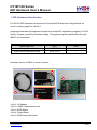
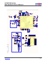
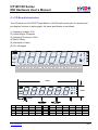
HY16F18X Series
IDE Hardware User’s Manual
.
© 2013 HYCON Technology Corp.
www.hycontek.com
APD-HY16IDE002-V03_EN
Page 1
HY16F18X Series
IDE Hardware User’s Manual!
Table of Contents
1. IDE Hardware Introduction............................................................................................4 2. AICE Board Introduction ...............................................................................................5 3. Target Board Introduction.............................................................................................7 4. LCD Board Introduction ................................................................................................9 5. Hardware Connection Introduction............................................................................10 6. Revision History ..........................................................................................................10 .
© 2013 HYCON Technology Corp
www.hycontek.com
APD-HY16IDE002-V03_EN
Page 2
HY16F18X Series
IDE Hardware User’s Manual!
Attention:
1.
HYCON Technology Corp. reserves the right to change the content of this datasheet without further
notice. For most up-to-date information, please constantly visit our website: http://www.hycontek.com .
2.
HYCON Technology Corp. is not responsible for problems caused by figures or application circuits
narrated herein whose related industrial properties belong to third parties.
3.
Specifications of any HYCON Technology Corp. products detailed or contained herein stipulate the
performance, characteristics, and functions of the specified products in the independent state. We does
not guarantee of the performance, characteristics, and functions of the specified products as placed in
the customer’s products or equipment. Constant and sufficient verification and evaluation is highly
advised.
4.
Please note the operating conditions of input voltage, output voltage and load current and ensure the IC
internal power consumption does not exceed that of package tolerance. HYCON Technology Corp.
assumes no responsibility for equipment failures that resulted from using products at values that exceed,
even momentarily, rated values listed in products specifications of HYCON products specified herein.
5.
Notwithstanding this product has built-in ESD protection circuit, please do not exert excessive static
electricity to protection circuit.
6.
Products specified or contained herein cannot be employed in applications which require extremely high
.
levels of reliability, such as device or equipment affecting the human body, health/medical equipments,
security systems, or any apparatus installed in aircrafts and other vehicles.
7.
Despite the fact that HYCON Technology Corp. endeavors to enhance product quality as well as reliability
in every possible way, failure or malfunction of semiconductor products may happen. Hence, users are
strongly recommended to comply with safety design including redundancy and fire-precaution
equipments to prevent any accidents and fires that may follow.
8.
Use of the information described herein for other purposes and/or reproduction or copying without the
permission of HYCON Technology Corp. is strictly prohibited.
© 2013 HYCON Technology Corp
www.hycontek.com
APD-HY16IDE002-V03_EN
Page 3
HY16F18X Series
IDE Hardware User’s Manual!
1. IDE Hardware Introduction
HY16F18X IDE Hardware development kit includes AICE Board and Target Board, as
shown in below graph No.3 & No.4.
Integrated Hardware development kit helps to develop MCU application program of HY16F
Series. Program compiling, hardware debug, IC programming was implemented through
NB/PC end connection.
Name/Model No.
DK01
DK02
Target Board
A12005 V03
-
USB Control Board and Writer
AICE V2.0.1
-
Hardware device of DK01 is shown in below:
.
※No.1: 9V Adapter
※No.2: USB2.0 transmission wire
※No.3: AICE Board
※No.4: Target Board
※No.5: EDM transmission wire
© 2013 HYCON Technology Corp
www.hycontek.com
APD-HY16IDE002-V03_EN
Page 4
HY16F18X Series
IDE Hardware User’s Manual!
2. AICE Board Introduction
AICE is the device that connects to HY16F Target Board and PC/NB/Tablet end, main
function is to burn program and to debug.
PC/NB/Tablet
HY16F18X
32-bit MCU
AndeSight
GCC
AICE
Board
2-Wire
JTAG
EDM
USB2.0
.
Connection Port DescriptionĈ
(1) USB PortĈUSB connection to PC end
(1.1) to burn program
(1.2) to detect error under Debug mode
© 2013 HYCON Technology Corp
www.hycontek.com
APD-HY16IDE002-V03_EN
Page 5
HY16F18X Series
IDE Hardware User’s Manual!
(2)USB Power LED: USB power light
(3) ACT LED: Blinking under Debug mode and burn program
(4) LINK LED: Error light
(5) Done LED: Connection light after HY16F products power on and connects to AICE
Board
(6) EDM Port: Connecting to EDM Port of HY16F Target Board
(6.1) VDD3V connects to positive power source, VDD3 of HY16F
(6.2) VSS connects to VSS of HY16F
(6.3) EDIO connects to EDIO signal pin of HY16F
(6.4) ECK connects to ECK signal pin of HY16F
For driver install, please refer to HY16F Series, IDE Software User’s Manual.
AICE USB driver program will install automatically when the software is installed.
.
For correct AICE connection status, libusb-win32
devices of AndeShape AICE will show up
under PC device administrator.
© 2013 HYCON Technology Corp
www.hycontek.com
APD-HY16IDE002-V03_EN
Page 6
HY16F18X Series
IDE Hardware User’s Manual!
3. Target Board Introduction
Target Board is the main circuit board of HY16F Series, which executes function such as
sensing ADC value and LCD display of the whole HY16F series IC by connecting to AIC.
Collocating with conventional or Touch KEY buttons helps to speed up the time of product
development.
S2
JP7
S1
J27
U1
.
PIN43
S4
PIN48
J25
N1
N2
N3
D5
Step 01: If to select 3.3V safe voltage for Pin header J25, N2 and N3 must be short circuit
Step 02: Connecting 9V power to J27
Step 03: Press S4, observing whether LED of D5 was lighted on
Step 04: If LED is not light up, check the voltage between PIN43 & PIN48 of U1. Normally, it
should be 3.3V.
Step 05: After IC powered on, connecting AICE to JP7 of EDM.
※S1 & S2 is GPIO button
※There is another HYCON Device on the board, LCD driver IC, HY2613B.
© 2013 HYCON Technology Corp
www.hycontek.com
APD-HY16IDE002-V03_EN
Page 7
HY16F18X Series
IDE Hardware User’s Manual!
RST
C30
10 0pF
J1
S1
VDD3V
R ST
R21
C 31
1
2
4
3
5
RST
VPP
C H2
C H1
2
1
C K CL3 9
C S CL2 8
CL1 7
6
3
CP_O
J2
N/C
VPP
C13
C P_O
C26
VDD3V
CP_O VDD3V
10 uF
C9
C25
0.1u F
10 uF
CP_I
10 uF
C P_I
HY16F188
LQFP48
C27
VDD
1u F
VDD
C28
Y3
20 M
R20 1M
C29
SDA_7/TCI2_7 /RX_7/CK_ 4/PWM1 _7/INT2.5/LS_ XOUT/PT2.5
0.1u F
C37
R EFO
C 38
0.1u F
DAO/OPO2 /PT3.1
AIO4/PT3.2
AIO5/PT3.3
AIO6/PT3.4
N/C
AIO7/PT3.5
U?
38
LXOUT
R22
10 M
37
LXIN
36
35 PT2.3
33 PT2.1
34 PT2.2
32 PT2.0
C33
Y4
32 768
C34
COM0
COM1
COM2
COM3
SEG4
SEG5
SEG6
SEG7
SEG8
SEG9
SEG1 0
SEG1 1
SEG1 2
SEG1 3
SEG1 4
SEG1 5
SEG1 6
SEG1 7
SEG1 8
SEG1 9
SEG2 0
J13
1
2
3
4
5
6
7
8
9
10
11
12
13
14
15
16
17
18
19
20
21
2
4
6
8
LCD Panel
1
3
5
7
PW R JP5
PT2.0
PT2.1
VDD26 13
SCL
SDA
HY2 613 PINVSS2 613
A IO 0
R 37
10 0K
R 33
68 K
R 32
10 0K
HY2 613
TS SOP48
D6
IN4 001
EN
IN
OUT
ADJ
U4
*. POWER NET
8
7
6
5
1
2
3
6
ON2
C OM2
2
OFF2
S4
5
ON1
3
C OM1
1
OFF1
4
GND
GND
GND
GND
GS26 12
1
2
3
Title
Size
A2
D t
U3
HY2 613 B
J17
B LOUT
VUSB
D4
LED
R31
13
VSS2 613
J26
USB P
D7
C47 C48
IN4 007
0.1u F/50V
10 0uF/2 5V
9V 2
3
1
J27
(小頭)
DCJACK
Sh t
f W t L
V 03
Revisio n
HY16F188 + HY2613B ICE Circuit
Number
A12005
31 J l 20 13
JP9
VSSBAT
2
JP8
VBAT
VSS2 613 VLC DPWR
VLCD
VDD26 13J16
VSS2 613 BOR
VSS
VSS2 613
C43
R29 R30
1u F
10 k 10 k
VDD26 13
VDD26 13J15
1
2
3
4
VSS2 613
J14
OSCIN
VDD26 13
VLCD
B LOUT
R 34
3.3VOUT
C46
10 uF
10 uF
1u F
10 uF
電容靠近晶片
10 uF
C45
VSS2 613
C42
C40
J25
EXT
3
2
3V
1
30 OPO2
31 OPO1
J23
Curren t
PW R
VDD Sel
C41
28 AIO5
27 AIO6
25
26 AIO7
HY1 6F1 88_ 1
J24
VDD3V
R25
27 0
D5
29 AIO4
J22
C P_I
SE G30
SE G29
SE G28
SE G27
SE G26
SE G25
SE G24
SE G23
SE G22
SE G21
SE G20
SE G19
SE G18
SE G17
SE G16
SE G15
SE G14
SE G13
SE G12
SE G11
SE G10
SE G9
SE G8
SE G7
48
47
46
45
44
43
42
41
40
39
38
37
36
35
34
33
32
31
30
29
28
27
26
25
SE G30
SE G29
SE G28
SE G27
SE G26
SE G25
SE G24
SE G23
SE G22
SE G21
SE G20
SE G19
SE G18
SE G17
SE G16
SE G15
SE G14
SE G13
SE G12
SE G11
SE G10
SE G9
SE G8
SE G7
VDD3V
R 19 0
PT4.0/RST/NMI
SDA_5/TCI2_5 /RX_5/CK_ 3/PWM1 _5/INT2.1/PT2 .1
SCL_ 6/TC I1 _6/TX_6 /MISO_3 /PWM0_ 6/INT2 .2 /PT2 .2
SC L_ 7/TCI1 _7/TX_7 /CS_ 4/PWM0 _7/INT2.4/LS_ XIN/PT2 .4
N/C
SDA_6/TCI2_6 /R X_6/MOSI_3/PW M1_6 /INT2.3/PT2.3
PT1.0/CH1/INT1.0/PWM0 _1/CS_1 /TX_ 1/TCI1 _1/SCL_1
0.1u F
C 36
R 24
AIO2
AIO3
OPO1/PT3 .0
SCL_ 5/TC I1 _5/TX_5 /CS_ 3/PWM0 _5/INT2.0/PT2 .0
PT1.1/CH2/INT1.1/PWM1 _1/CK_ 1/RX_1 /TCI2_ 1/SDA_1
PT1.2/CH3/INT1.2/PWM0 _2/MISO_1/TX_2 /TCI1_ 2/SCL_ 2
PT1.3/CL1/INT1 .3 /PWM1_ 2/MOSI_ 1/RX_2 /TCI2_ 2/SDA_2
PT1.4/CL2/INT1 .4 /PWM0_ 3/CS_2/TX_3 /TCI1_ 3/SCL_ 3
PT1.5/CL3/INT1 .5 /PWM1_ 3/CK_2 /RX_3/TC I2_3 /SDA_ 3
PT1.6/CL4/INT1 .6 /PWM0_ 4/MISO_ 2/TX_4/TCI1_4 /SCL_4
C35
1u F
VDDA
J20
VDDA
J21
2
LOADCELL
-S +S
R 27
R 28
N /C
PT1.7/CMPO1 /INT1.7/PW M1_4 /MOSI_2 /RX_4/TCI2_ 4/SDA_ 4
RST
3
R26
Lo adcell measuremen t
24
11
N/C
JP7
R23
0
R36
10 0k
PT 3.6/R EFO
1
2
C P_I
J28
PW R
23
DI CL410
DO
39
A IO 0
4
SC L_8/ TC I1_8/T X_8/M ISO _4
PWM 0_8/ INT 2.6/H S_X IN /PT2. 6
A IO 0 19
PW R
40
A IO 2
12
SD A _8/T CI2_8/RX _8/M OS I_4
PWM 1_8/INT 2.7/ H S_X OU T/PT 2.7
A IO 3
A IO 3 22
S2
S3
41
A IO 1
A IO 2 21
To uchPad
JP6
DI PT1.6
CK
DO PT1.7
CS
V DD
A IO 1 20
J18
SPIPWR
2
4
6
8
10
12
42
V DD A
2
1
X IN
43
NC
18
1
SE G31
SE G32
SE G33
SE G34
SE G35
C OM 0
C OM 1
SE G0/ C OM 2
SE G1/ C OM 3
V LC D
V DD
V SS
X out
O SC IN / Xin
SC L
SD A
PO R /IR Q
SE G0/ B LO UT
SE G1/ C H
SE G2/ C L
SE G3/ FB
SE G4
SE G5
SE G6
48
47
X OU T
V DD 3V
N /C
N /C
SE G31
1
2
SE G32
3
SE G33
4
SE G34
5
SE G35
C OM 0
6
O SC IN
7
C OM 1
8
C OM 2
9
C OM 3
V LC D 10
V DD 2613 11
12
13
O SC IN 14
SC L
15
16
SD A
PO R
17
B LO UT SE G0 18
SE G1 19
SE G2 20
SE G3 21
22
SE G4
23
SE G5
24
SE G6
V SS
ED IO
ED IO 14
APD-HY16IDE002-V03_EN
Page 8
© 2013 HYCON Technology Corp
www.hycontek.com
1
2
V DD 3V
44
C P_O
16
17
+E
C P_I
46 C L
45 C H
PT 3.7/O PO 1
-E
EC K
13
EC K
.
CL
CH
15
4
1
3
5
7
9
11
SPI
R 35
J3
ED IO
PW R
J19
AICEPWR
10 0k
V US B
O PO
A IO 1
ED IO
EC K
2
4
6
8
10
1
3
5
7
9
ED M
EC K
HY16F18X Series
IDE Hardware User’s Manual!
4. LCD Board Introduction
The LCD panel on HY16FICE-Target Board is HYCON self-owned mold, it’s symbol and
pin diagram is shown in below graph. It’s panel specification is as follows:
(1) Operating Voltage: 3.0V
(2) Visible Angle: 60 degree
(3) Operating Frequency: 60Hz
(4) Bias:1/3 bias
(5) Waveform:1/4 duty
(6) Pin: 90 degree
E
S1 S2 S3 S4
S8
S14
S9
S15
m
A
O
K
F
B
S5
A
M
V
S11
C
TARE
G
D
S7
S20
S17
S12
S13
H
S1
9
S16
S10
S6
S1
8
g
S21
ZERO
1
COM1
COM2
COM3
COM4
2
3
4
.
5
6
SEG1 SEG2 SEG3 SEG4 SEG5 SEG6 SEG7 SEG8 SEG9 SEG10 SEG11 SEG12 SEG13 SEG14 SEG15 SEG16 SEG17
1A
1E
2A
2E
3A
3E
4A
4E
5A
5E
6A
6E
S1
S5
S10
S9
S18
1B
1F
2B
2F
3B
3F
4B
4F
5B
5F
6B
6F
S2
S6
S11
S14
S19
1C
1G
2C
2G
3C
3G
4C
4G
5C
5G
6C
6G
S3
S7
S12
S15
S20
1D
1H
2D
2H
3D
3H
4D
4H
5D
5H
6D
S17
S4
S8
S13
S16
S21
70mm
m A
K O
M V
g
TARE
ZERO
27mm
17.78mm
8.89mm
1
21
0.812mm
2.54mm
PIN
1
2
3
4
5
6
7
8
9
10
11
I/O
COM1
COM2
COM3
COM4
SEG1
SEG2
SEG3
SEG4
SEG5
SEG6
SEG7
PIN
12
13
14
15
16
17
18
19
20
21
I/O
SEG8
SEG9
SEG10
SEG11
SEG12
SEG13
SEG14
SEG15
SEG16
SEG17
© 2013 HYCON Technology Corp
www.hycontek.com
APD-HY16IDE002-V03_EN
Page 9
HY16F18X Series
IDE Hardware User’s Manual!
5. Hardware Connection Introduction
LED of D5 address will be lighted up when power on.
EDM connection test:
(1) Connecting AICE to AndeSight of PC to observe AICE version information
AICE version: hw_ver = 0X10001, fw_ver = 0X3, fpga_ver = 0X2
(2) Target board connection test, selecting HY16F188 as main chip
.
6. Revision History
Major differences are stated hereinafter:
Version
Page
V03
ALL
Revision Summary
First Edition
© 2013 HYCON Technology Corp
www.hycontek.com
Date
2013/09/09
APD-HY16IDE002-V03_EN
Page 10