1
MVME162LX 200/300 Series
Embedded Controller
Installation and Use
V162LX2-3A/IH3
Notice
While reasonable efforts have been made to assure the accuracy of this document,
Motorola, Inc. assumes no liability resulting from any omissions in this document, or from
the use of the information obtained therein. Motorola reserves the right to revise this
document and to make changes from time to time in the content hereof without obligation
of Motorola to notify any person of such revision or changes.
No part of this material may be reproduced or copied in any tangible medium, or stored in
a retrieval system, or transmitted in any form, or by any means, radio, electronic,
mechanical, photocopying, recording or facsimile, or otherwise, without the prior written
permission of Motorola, Inc.
It is possible that this publication may contain reference to, or information about Motorola
products (machines and programs), programming, or services that are not announced in
your country. Such references or information must not be construed to mean that Motorola
intends to announce such Motorola products, programming, or services in your country.
Restricted Rights Legend
If the documentation contained herein is supplied, directly or indirectly, to the U.S.
Government, the following notice shall apply unless otherwise agreed to in writing by
Motorola, Inc.
Use, duplication, or disclosure by the Government is subject to restrictions as set forth in
subparagraph (c)(1)(ii) of the Rights in Technical Data and Computer Software clause at
DFARS 252.227-7013.
Motorola, Inc.
Computer Group
2900 South Diablo Way
Tempe, Arizona 85282
Preface
The MVME162LX 200/300 Series Embedded Controller Installation and Use Manual
provides a board-level description of the MVME162LX Embedded Controller. It contains
a general overview of the product along with a list of hardware features and a detailed
functional description.
The information contained in this manual applies to the MVME162LX-2xx and
MVME162LX-3xx (200 and 300 series) models that are currently shipping as of the
publication date of this manual.
Motorola® and the Motorola symbol are registered trademarks of Motorola, Inc.
All other products mentioned in this document are trademarks or registered trademarks of
their respective holders.
© Copyright Motorola, Inc. 1998
All Rights Reserved
Printed in the United States of America
November 1998
Safety Summary
Safety Depends On You
The following general safety precautions must be observed during all phases of operation, service, and repair of this
equipment. Failure to comply with these precautions or with specific warnings elsewhere in this manual violates safety
standards of design, manufacture, and intended use of the equipment. Motorola, Inc. assumes no liability for the
customer’s failure to comply with these requirements.
The safety precautions listed below represent warnings of certain dangers of which Motorola is aware. You, as the
user of the product, should follow these warnings and all other safety precautions necessary for the safe operation of
the equipment in your operating environment.
Ground the Instrument.
To minimize shock hazard, the equipment chassis and enclosure must be connected to an electrical ground. The
equipment is supplied with a three-conductor AC power cable. The power cable must be plugged into an approved
three-contact electrical outlet. The power jack and mating plug of the power cable meet International Electrotechnical
Commission (IEC) safety standards.
Do Not Operate in an Explosive Atmosphere.
Do not operate the equipment in the presence of flammable gases or fumes. Operation of any electrical equipment in
such an environment constitutes a definite safety hazard.
Keep Away From Live Circuits.
Operating personnel must not remove equipment covers. Only Factory Authorized Service Personnel or other
qualified maintenance personnel may remove equipment covers for internal subassembly or component replacement
or any internal adjustment. Do not replace components with power cable connected. Under certain conditions,
dangerous voltages may exist even with the power cable removed. To avoid injuries, always disconnect power and
discharge circuits before touching them.
Do Not Service or Adjust Alone.
Do not attempt internal service or adjustment unless another person capable of rendering first aid and resuscitation is
present.
Use Caution When Exposing or Handling the CRT.
Breakage of the Cathode-Ray Tube (CRT) causes a high-velocity scattering of glass fragments (implosion). To
prevent CRT implosion, avoid rough handling or jarring of the equipment. Handling of the CRT should be done only
by qualified maintenance personnel using approved safety mask and gloves.
Do Not Substitute Parts or Modify Equipment.
Because of the danger of introducing additional hazards, do not install substitute parts or perform any unauthorized
modification of the equipment. Contact your local Motorola representative for service and repair to ensure that safety
features are maintained.
Dangerous Procedure Warnings.
Warnings, such as the example below, precede potentially dangerous procedures throughout this manual. Instructions
contained in the warnings must be followed. You should also employ all other safety precautions which you deem
necessary for the operation of the equipment in your operating environment.
!
WARNING
Dangerous voltages, capable of causing death, are present in
this equipment. Use extreme caution when handling, testing,
and adjusting.
All Motorola printed wiring boards (PWBs) are manufactured by UL-recognized
manufacturers, with a flammability rating of 94V-0.
!
WARNING
This equipment generates, uses, and can radiate electromagnetic energy. It may cause or be susceptible to electromagnetic interference (EMI) if not installed and used in a
cabinet with adequate EMI protection.
European Notice: Board products with the CE marking comply with the EMC
Directive (89/336/EEC). Marking a system with the CE symbol indicates
compliance of that Motorola system to the applicable directives of the European
Community. A system with the CE marking meets or exceeds the following
technical standards:
EN55022 (CISPR 22): Limits and Methods of Measurement of Radio
Interference Characteristics of Information Technology Equipment. Tested to
Equipment Class B.
EN50082-1, 1992: Electromagnetic Compatibility -- Generic Immunity
Standard, Part 1: Residential, Commercial and Light Industry.
IEC801-2: Electromagnetic Compatibility for Industrial Process
Measurement and Control Equipment, Part 2: Electrostatic Discharge
Requirements.
IEC801-3: Electromagnetic Compatibility for Industrial Process
Measurement and Control Equipment, Part 3: Radiated Electromagnetic Field
Requirements.
IEC801-4: Electromagnetic Compatibility for Industrial Process
Measurement and Control Equipment, Part 4: Electrical Fast Transient/Burst
Requirements.
The product also fulfills EN60950 (product safety) which is essentially the
requirement for the Low Voltage Directive (73/23/EEC).
In accordance with European Community directives, a “Declaration of
Conformity” has been made and is on file at Motorola, Inc. - Computer Group,
27 Market Street, Maidenhead, United Kingdom, SL6 8AE.
This board product was tested in a representative system to show compliance with
the above mentioned requirements. A proper installation in a CE-marked system
will maintain the required EMC/safety performance.
Contents
CHAPTER 1
Board Level Hardware Description
Introduction................................................................................................................1-1
Overview.............................................................................................................1-1
Related Documentation.......................................................................................1-2
Models Available ................................................................................................1-3
Document Requirements.....................................................................................1-4
Available Software..............................................................................................1-5
Required Equipment ...........................................................................................1-5
Features...............................................................................................................1-5
Specifications......................................................................................................1-7
Cooling Requirements ........................................................................................1-8
Special Considerations for Elevated-Temperature Operation ............................1-9
Manual Terminology.........................................................................................1-10
Block Diagram .........................................................................................................1-11
Functional Description.............................................................................................1-12
Switches and LEDs...........................................................................................1-12
ABORT Switch..........................................................................................1-12
RESET Switch ...........................................................................................1-12
Front Panel Indicators................................................................................1-13
Data Bus Structure ............................................................................................1-13
MC68040 or MC68LC040 CPU.......................................................................1-14
MC68XX040 Cache ..................................................................................1-14
No VMEbus Interface Option...........................................................................1-14
Memory Options ...............................................................................................1-15
DRAM Options..........................................................................................1-15
SRAM Options ..........................................................................................1-15
SRAM Batteries.........................................................................................1-17
EPROM and Flash Memory ......................................................................1-18
Battery Backed Up RAM and Clock ................................................................1-18
VMEbus Interface and VMEchip2 ...................................................................1-19
I/O Interfaces ....................................................................................................1-19
Serial Communications Interface ..............................................................1-19
IndustryPack (IP) Interfaces ......................................................................1-20
Ethernet Interface ......................................................................................1-20
SCSI Interface............................................................................................1-21
SCSI Termination ......................................................................................1-21
vii
Local Resources ............................................................................................... 1-22
Programmable Tick Timers....................................................................... 1-22
Watchdog Timer........................................................................................ 1-22
Software-Programmable Hardware Interrupts .......................................... 1-23
Local Bus Timeout .................................................................................... 1-23
Local Bus Arbiter ............................................................................................. 1-24
Connectors........................................................................................................ 1-24
Memory Maps.......................................................................................................... 1-25
Local Bus Memory Map................................................................................... 1-25
Normal Address Range ............................................................................. 1-25
Detailed I/O Memory Maps ............................................................................. 1-31
IPIC Overall Memory Map ....................................................................... 1-41
BBRAM, TOD Clock Memory Map ........................................................ 1-46
Interrupt Acknowledge Map ..................................................................... 1-49
VMEbus Memory Map .................................................................................... 1-49
VMEbus Accesses to the Local Bus ......................................................... 1-49
VMEbus Short I/O Memory Map ............................................................. 1-49
Software Initialization ............................................................................................. 1-50
Multi-MPU Programming Considerations ....................................................... 1-50
Local Reset Operation ...................................................................................... 1-50
EMC Compliance ............................................................................................. 1-51
CHAPTER 2
Hardware Preparation and Installation
Introduction ............................................................................................................... 2-1
Unpacking Instructions.............................................................................................. 2-1
Hardware Preparation ................................................................................................ 2-1
System Controller Select Header (J1) ................................................................ 2-2
General-Purpose Readable Jumpers Header (J11) ............................................. 2-4
EPROM/Flash Configuration Header (J12) ....................................................... 2-5
SRAM Backup Power Source Select Headers (J13, J1) .................................... 2-9
SCSI Terminator Enable Header (J14) ............................................................. 2-10
Memory Mezzanine Options ............................................................................ 2-11
Installation Instructions ........................................................................................... 2-12
IP Installation on the MVME162LX................................................................ 2-12
MVME162LX Module Installation.................................................................. 2-13
System Considerations ..................................................................................... 2-14
................................................................................................................................. 2-18
viii
CHAPTER 3
Debugger General Information
Overview ....................................................................................................................3-1
Description of 162Bug ...............................................................................................3-1
162Bug Implementation.............................................................................................3-2
Installation and Start-up .............................................................................................3-3
Autoboot ....................................................................................................................3-6
ROMboot ...................................................................................................................3-7
Network Boot .............................................................................................................3-8
Restarting the System ................................................................................................3-9
Reset....................................................................................................................3-9
Abort .................................................................................................................3-10
Break .................................................................................................................3-10
SYSFAIL* Assertion/Negation ........................................................................3-10
MPU Clock Speed Calculation .........................................................................3-11
Memory Requirements.............................................................................................3-11
Terminal Input/Output Control ................................................................................3-12
Disk I/O Support ......................................................................................................3-13
Blocks Versus Sectors.......................................................................................3-13
Device Probe Function......................................................................................3-14
Disk I/O via 162Bug Commands......................................................................3-14
IOI (Input/Output Inquiry).........................................................................3-14
IOP (Physical I/O to Disk).........................................................................3-15
IOT (I/O Teach).........................................................................................3-15
IOC (I/O Control) ......................................................................................3-15
BO (Bootstrap Operating System).............................................................3-15
BH (Bootstrap and Halt)............................................................................3-15
Disk I/O via 162Bug System Calls ...................................................................3-15
Default 162Bug Controller and Device Parameters .........................................3-17
Disk I/O Error Codes ........................................................................................3-17
Network I/O Support................................................................................................3-18
Intel 82596 LAN Coprocessor Ethernet Driver ................................................3-18
UDP/IP Protocol Modules ................................................................................3-18
RARP/ARP Protocol Modules .........................................................................3-19
BOOTP Protocol Module .................................................................................3-19
TFTP Protocol Module .....................................................................................3-19
Network Boot Control Module .........................................................................3-19
Network I/O Error Codes..................................................................................3-19
Multiprocessor Support............................................................................................3-20
Multiprocessor Control Register (MPCR) Method ..........................................3-20
GCSR Method...................................................................................................3-22
Diagnostic Facilities.................................................................................................3-23
Manufacturing Test Process .....................................................................................3-23
ix
CHAPTER 4
Using The 162Bug Debugger
Entering Debugger Command Lines ......................................................................... 4-1
Syntactic Variables ............................................................................................. 4-2
Expression as a Parameter........................................................................... 4-3
Address as a Parameter ............................................................................... 4-4
Address Formats.......................................................................................... 4-4
Offset Registers........................................................................................... 4-6
Port Numbers...................................................................................................... 4-8
Entering and Debugging Programs............................................................................ 4-9
Calling System Utilities from User Programs ........................................................... 4-9
Preserving the Debugger Operating Environment................................................... 4-10
162Bug Vector Table and Workspace............................................................... 4-10
Hardware Functions ......................................................................................... 4-11
Exception Vectors Used by 162Bug................................................................. 4-11
Using 162Bug Target Vector Table .......................................................... 4-12
Creating a New Vector Table.................................................................... 4-13
162Bug Generalized Exception Handler................................................... 4-15
Floating Point Support............................................................................................. 4-17
Single Precision Real........................................................................................ 4-18
Double Precision Real ...................................................................................... 4-18
Extended Precision Real................................................................................... 4-18
Packed Decimal Real........................................................................................ 4-19
Scientific Notation............................................................................................ 4-19
The 162Bug Debugger Command Set..................................................................... 4-20
................................................................................................................................. 4-24
APPENDIX A
Configure and Environment Commands
Configure Board Information Block......................................................................... A-1
Set Environment to Bug/Operating System.............................................................. A-3
Configuring the IndustryPacks........................................................................ A-16
APPENDIX B
Disk/Tape Controller Data
Disk/Tape Controller Modules Supported ................................................................ B-1
Disk/Tape Controller Default Configurations .......................................................... B-2
IOT Command Parameters for Supported Floppy Types ......................................... B-5
x
APPENDIX C
Network Controller Data
Network Controller Modules Supported................................................................... C-1
APPENDIX D
Serial Interface Connections
EIA-232-D Interconnections.....................................................................................D-1
APPENDIX E
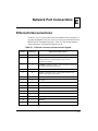
Network Port Connections
Ethernet Interconnections ......................................................................................... E-1
APPENDIX F
SCSI Bus Connections
SCSI Interconnections .............................................................................................. F-1
APPENDIX G
Mezzanine Board Connectors
Mezzanine Connector J15 Signals ............................................................................G-1
Mezzanine Connector J16 Signals ............................................................................G-6
Mezzanine Board Dimensions ................................................................................ G-11
APPENDIX H
Troubleshooting CPU Boards
Solving Startup Problems .........................................................................................H-1
APPENDIX I
Input/Output Connections
IndustryPack Logic Interface Interconnections ......................................................... I-1
IndustryPack I/O Interconnections ............................................................................ I-4
Remote Reset/LED Interconnection .......................................................................... I-5
VME Bus Interconnection ......................................................................................... I-6
Connector P1 Interconnect Signals..................................................................... I-6
Connector P2 Interconnect Signals................................................................... I-10
APPENDIX J
Related Documentation
Motorola Documentation ........................................................................................... J-1
Non-Motorola Documentation................................................................................... J-2
Support Information ................................................................................................... J-3
xi
FIGURES
Figure 1-1. MVME162LX Block Diagram ............................................................. 1-11
Figure 2-1. MVME162LX Switch, Header, Connector, Fuse, and LED Locations.. 2-3
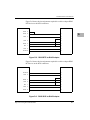
Figure 2-2. DB25-DTE-to-RJ45 Adapter................................................................ 2-16
Figure 2-3. DB25-DCE-to-RJ45 Adapter................................................................ 2-17
Figure 2-4. Typical RJ45 Serial Cable..................................................................... 2-17
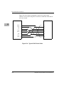
Figure D-1. Serial Interface Connections ................................................................. D-2
Figure D-2. DB25-DTE-to-RJ45 Adapter ................................................................ D-3
Figure D-3. DB25-DCE-to-RJ45 Adapter................................................................ D-3
Figure D-4. Typical RJ45 Serial Cable .................................................................... D-4
Figure G-1. Mezzanine Board Dimensions (Parity DRAM) .................................. G-11
Figure G-2. Mezzanine Board Dimensions (SRAM and ECC DRAM)................. G-12
TABLES
Table 1-1. MVME162LX Embedded Controller Models ......................................... 1-3
Table 1-2. MVME162LX Specifications................................................................... 1-7
Table 1-3. Local Bus Arbitration Priority................................................................ 1-24
Table 1-4. Local Bus Memory Map......................................................................... 1-26
Table 1-5. Local I/O Devices Memory Map ........................................................... 1-28
Table 1-6. VMEchip2 Memory Map - LCSR Summary (Sheet 1 of 2) .................. 1-32
Table 1-7. MCchip Register Map ............................................................................ 1-36
Table 1-8. MCECC Internal Register Memory Map .............................................. 1-37
Table 1-9. Z85230 SCC Register Addresses ........................................................... 1-39
Table 1-10. 82596CA Ethernet LAN Memory Map................................................ 1-39
Table 1-11. 53C710 SCSI Memory Map ................................................................. 1-40
Table 1-12. IPIC Overall Memory Map................................................................... 1-41
Table 1-13. IPIC Memory Map—Control and Status Registers ............................. 1-42
Table 1-14. MK48T08 BBRAM/TOD Clock Memory Map ................................... 1-43
Table 1-15. BBRAM Configuration Area Memory Map ....................................... 1-44
Table 1-16. TOD Clock Memory Map .................................................................... 1-45
Table 2-1. EPROM/Flash Mapping - 128K x 8 EPROMs ........................................ 2-6
Table 2-2. EPROM/Flash Mapping - 256K x 8 EPROMs ........................................ 2-6
Table 2-3. EPROM/Flash Mapping - 512K x 8 EPROMs ........................................ 2-7
Table 2-4. EPROM/Flash Mapping - 1M x 8 EPROMs............................................ 2-7
Table 2-5. EPROM/Flash Mapping - 1M x 8 EPROMs, On-Board Flash Disabled. 2-8
Table 4-1. Debugger Address Parameter Formats..................................................... 4-5
Table 4-2. Exception Vectors Used by 162Bug....................................................... 4-11
xii
Table 4-3. Debugger Commands ............................................................................4-20
Table A-1. ENV Command Parameters ..................................................................A-4
Table D-1. Connector J17 Interconnect Signals ......................................................D-1
Table E-1. Ethernet Connector J9 Interconnect Signals ......................................... E-1
Table F-1. SCSI Connector J10 Interconnect Signals ............................................ F-1
Table G-1. Mezzanine Connector J15 Interconnect Signals ...................................G-1
Table G-2. Mezzanine Connector J16 Interconnect Signals ...................................G-6
Table H-1. Troubleshooting MVME162LX Boards ...............................................H-1
Table I-1. IndustryPack Interconnect Signals .......................................................... I-1
Table I-2. Remote Reset/LED interconnect Signals .................................................. I-5
Table I-3. Connector P1 Interconnect Signals ......................................................... I-6
Table I-4. Connector P2 Interconnect Signals ......................................................... I-10
xiii
xiv
1Board Level Hardware
Description
1
Introduction
This chapter provides a board-level hardware description of the
MVME162LX Embedded Controller. It contains a general overview of the
product along with a list of hardware features and a detailed functional
description. The controller’s front panel switches and indicators are
included in the functional description. Additionally, a section on memory
maps is provided at the end of this chapter to familiarize you with the
controller’s memory addresses and the corresponding devices accessed.
All of the controller’s programmable registers that reside in ASICs are
covered in the MVME162LX Embedded Controller Programmer’s
Reference Guide.
Overview
The MVME162LX Embedded Controller is based on the MC68040 or the
MC68LC040 microprocessor. The MC68040 microprocessor has a
floating-point (math) coprocessor and the MC68LC040 does not.
Various versions of the controller contain the following:
❏
❏
❏
❏
❏
❏
❏
❏
❏
❏
❏
❏
1 or 4 MB of parity-protected DRAM
4, 8, 16, or 32 MB of ECC-protected DRAM
128 KB of SRAM (with battery backup)
Time of day clock (with battery backup)
An optional LAN Ethernet transceiver interface
Four serial ports with an EIA-232-D interface
Six tick timers with watchdog timer(s)
Four EPROM sockets
1 MB flash memory (one flash device)
Two IndustryPack (IP) interfaces
An optional SCSI bus interface with DMA
An optional VMEbus interface (local bus to VMEbus/VMEbus to
local bus, with A16/A24/A32, D8/D16/D32 bus widths and a
VMEbus system controller)
1-1
1
Board Level Hardware Description
Input/Output (I/O) signals are routed through industry standard connectors
on the controller’s front panel. This includes the I/O for the serial ports,
which is provided by four RJ45 connectors.
The VMEbus interface is provided by an ASIC called the VMEchip2. It
contains two tick timers, a watchdog timer, programmable map decoders
for the master and slave interfaces, a VMEbus to/from local bus DMA
controller, a VMEbus to/from local bus non-DMA programmed access
interface, a VMEbus interrupter, a VMEbus system controller, a VMEbus
interrupt handler, and a VMEbus requester.
Processor-to-VMEbus transfers can be D8, D16, or D32. VMEchip2
DMA transfers to the VMEbus, however, can be D16, D32, D16/BLT,
D32/BLT, or D64/MBLT.
The MCchip ASIC provides four tick timers, the interface to the LAN chip,
SCSI chip, serial port chip, BBRAM, EPROM/Flash, DRAM and SRAM.
The MCECC memory controller ASIC provides the programmable
interface for the ECC-protected 16 MB DRAM mezzanine board.
The IndustryPack Interface Controller (IPIC) ASIC provides control and
status information for up to two single size IndustryPacks (IPs) or one
double size IP that can be plugged into the controller’s PCB.
Related Documentation
The MVME162LX Embedded Controller does not ship with all of the
documentation that is available for the product. Additional (optional)
publications are available for the controller and are listed in Appendix I.
These publications can provide you with additional information about the
product. Instructions on how to obtain them are also provided in
Appendix I.
1-2
Computer Group Literature Center Web Site
Introduction
Models Available
As of the publication date of this manual, the MVME162LX Embedded
Controller is available in a number of models shown in Table 1-1.
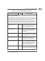
Table 1-1. MVME162LX Embedded Controller Models
Model
Description
-200
MC68LC040 25 MHz microprocessor, 1 MB DRAM,
128 KB SRAM,1 MB Flash memory, 2 IndustryPack sites
-201
MC68LC040 25 MHz microprocessor, 1 MB DRAM,
128 KB SRAM,1 MB Flash memory, 2 IndustryPack sites, 4 serial ports
-202
MC68LC040 25 MHz microprocessor, 1 MB DRAM,
128 KB SRAM,1 MB Flash memory, 2 IndustryPack sites, 4 serial ports
-210
MC68LC040 25 MHz microprocessor, 4 MB DRAM, 128 KB SRAM,
1 MB Flash memory, 2 IndustryPack sites, 4 serial ports
-211
MC68LC040 25 MHz microprocessor, 4 MB DRAM, 128 KB SRAM,
1 MB Flash memory, 2 IndustryPack sites, 4 serial ports, SCSI
-212
MC68LC040 25 MHz microprocessor, 4 MB DRAM, 128 KB SRAM,
1 MB Flash memory, 2 IndustryPack sites, 4 serial ports, Ethernet
-213
MC68LC040 25 MHz microprocessor, 4 MB DRAM, 128 KB SRAM,
1 MB Flash memory, 2 IndustryPack sites, 4 serial ports, SCSI &
Ethernet
-216
MC68LC040 25 MHz microprocessor, 4 MB DRAM, 128 KB SRAM,
1 MB Flash memory, 2 IndustryPack sites, Ethernet, No VME
-220
MC68040 25 MHz microprocessor, 4 MB DRAM, 128 KB SRAM,
1 MB Flash memory, 2 IndustryPack sites, 4 serial ports
-222
MC68040 25 MHz microprocessor, 4 MB DRAM, 128 KB SRAM,
1 MB Flash memory, 2 IndustryPack sites, 4 serial ports, Ethernet
-223
MC68040 25 MHz microprocessor, 4 MB DRAM, 128 KB SRAM,
1 MB Flash memory, 2 IndustryPack sites, 4 serial ports, SCSI &
Ethernet
-233
MC68LC040 25 MHz microprocessor, 4 MB ECC DRAM,
128 KB SRAM, 1 MB Flash memory, 2 IndustryPack sites, 4 serial ports,
SCSI & Ethernet
http://www.mcg.mot.com/literature
1-3
1
1
Board Level Hardware Description
Table 1-1. MVME162LX Embedded Controller Models (Continued)
Model
Description
-243
MC68040 25 MHz microprocessor, 4 MB ECC DRAM, 128 KB SRAM,
1 MB Flash memory, 2 IndustryPack sites, 4 serial ports, SCSI &
Ethernet
-253
MC68LC040 25 MHz microprocessor, 16 MB ECC DRAM,
128 KB SRAM, 1 MB Flash memory, 2 IndustryPack sites, 4 serial ports,
SCSI & Ethernet
-262
MC68040 25 MHz microprocessor, 16 MB ECC DRAM,
128 KB SRAM, 1 MB Flash memory, 2 IndustryPack sites, 4 serial ports,
Ethernet
-263
MC68040 25 MHz microprocessor, 16 MB ECC DRAM,
128 KB SRAM, 1 MB Flash memory, 2 IndustryPack sites, 4 serial ports,
SCSI & Ethernet
-322
MC68LC040 25 MHz microprocessor, 8 MB ECC DRAM,
128 KB SRAM, 1 MB Flash memory, 2 IndustryPack sites, 4 serial ports,
Ethernet
-323
MC68LC040 25 MHz microprocessor, 8 MB ECC DRAM,
128 KB SRAM, 1 MB Flash memory, 2 IndustryPack sites, 4 serial ports,
SCSI & Ethernet
-333
MC68040 25 MHz microprocessor, 8 MB ECC DRAM, 128 KB SRAM,
1 MB Flash memory, 4 serial ports, SCSI & Ethernet
-353
MC68040 25 MHz microprocessor, 32 MB ECC DRAM,
128 KB SRAM, 1 MB Flash memory, 4IndustryPack sites, 4 serial ports,
SCSI & Ethernet
Document Requirements
The controller is designed to conform to the requirements of the following
documents:
❏
❏
❏
❏
1-4
VMEbus Specification (IEEE 1014-87)
EIA-232-D Serial Interface Specification, EIA
SCSI Specification, ANSI
IndustryPack Specification, GreenSpring
Computer Group Literature Center Web Site
Introduction
Available Software
Available software for the controller includes the on-board debugger/monitor
firmware, VMEexec driver packages for various IndustryPack modules, and
numerous third-party applications for MC680x0-based systems. Contact your
local Motorola sales office or distribution for more information.
Required Equipment
The following equipment is required to complete an MVME162LX system:
❏ System console terminal
❏ Disk drives and controllers
❏ Operating system
As mentioned earlier, transition modules are unnecessary, as the controller
incorporates industry-standard SCSI, Ethernet, and RJ45 serial connectors on
its front panel.
Features
General features of the MVME162LX Embedded Controller are shown in
the following table:
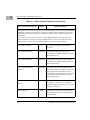
Feature
Microprocessor
Memory
Description
Models
MC68LC040
See Table 1-1
MC68040
See Table 1-1
1 or 4 MB of parity-protected DRAM
See Table 1-1
4, 8, 16, or 32 MB of ECC-protected DRAM See Table 1-1
128 KB of SRAM (with battery backup)
All models
1 MB of Flash memory
All models
Real-time clock
8KB NVRAM with RTC and battery backup All models
(SGS-Thomson M48T18)
Switches
RESET and ABORT
All models
Status LEDs
Four: FAIL, RUN, SCON, and FUSES
All models
Tick timers
Four programmable 32-bit timers
All models
http://www.mcg.mot.com/literature
1-5
1
1
Board Level Hardware Description
Feature
Description
Models
Watchdog timer
Provided in MCchip ASIC (VMEchip2)
All models
Serial I/O
EIA-232-D DTE serial interface with four
serial ports (Zilog Z85230 controller chips)
See Table 1-1
SCSI I/O
Optional Small Computer Systems Interface See Table 1-1
(SCSI) bus interface with 32-bit local bus
burst Direct Memory Access (DMA) (NCR
53C710 controller)
Ethernet I/O
Optional LAN Ethernet transceiver interface See Table 1-1
with 32-bit local bus DMA (Intel 82596CA
controller)
IndustryPack
Interfaces
2 or 4 IndustryPack Interface sites
See Table 1-1
VMEbus interface
(Optional)
VMEbus system controller
All models
VMEbus requester
VMEbus interrupter
NOTE:
VMEbus interrupt handler
This option is a
factory installed and Eight software interrupts
cannot be added in
Programmable map decoders for the master
the field.
and slave interfaces
VMEbus to local bus interface (A24/A32,
D8/D16/D32 (D8/D16/D32/D64 BLT)
(BLT = Block Transfer)
Local-bus-to-VMEbus interface
(A16/A24/A32, D8/D16/D32)
Two 32-bit programmable Tick Timers and a
programmable Watchdog Timer (in the
VMEchip2 ASIC) for periodic interrupts
Global CSR for interprocessor
communications
DMA for fast local memory - VMEbus
transfers (A16/A24/A32,
D16/D32 [D16/D32/D64 BLT])
1-6
Computer Group Literature Center Web Site
Introduction
Specifications
Table 1-2 lists the specifications for an MVME162LX Embedded
Controller without IndustryPacks.
Table 1-2. MVME162LX Specifications
Characteristics
Specifications
Power requirements
+5Vdc (± 5%), 3.5 A typical, 4.5 A maximum
(with EPROMs; without IPs) +12 Vdc (± 5%), 100 mA maximum
-12 Vdc (± 5%), 100 mA maximum
Operating temperature
0° to 70° C exit air with forced air cooling
(see NOTE)
Storage temperature
-40° to +85° C
Relative humidity
5% to 90% (noncondensing)
Physical dimensions
PC board with mezzanine
module only
Height
Depth
Thickness
PC board with connectors
and front panel
Height
Depth
Thickness
Double-high VMEboard
Note:
9.20 inches (233 mm)
6.30 inches (160 mm)
0.66 inch (17 mm)
10.3 inches (262 mm)
7.4 inches (188 mm)
0.80 inch (20 mm)
Refer to the sections on the following pages for information
on Cooling Requirements and Special Requirements for
Elevated-Temperature Operation.
http://www.mcg.mot.com/literature
1-7
1
1
Board Level Hardware Description
Cooling Requirements
The Motorola MVME162LX Embedded Controller is designed and tested
to operate reliably with an incoming air temperature range of 0° to 55° C
(32° to 131° F). This is accomplished with forced air cooling at a velocity
typically achievable by a 100 CFM axial fan. Temperature qualification is
performed in a standard Motorola VME system chassis. 25 watt load
boards are inserted in two card slots (one on each side), adjacent to the
board under test, to simulate a high power density system configuration.
An assembly of three axial fans, rated at 100 CFM per fan, is placed
directly under the VME card cage. The incoming air temperature is
measured between the fan assembly and the card cage, where the incoming
airstream first encounters the controller under test. Test software is
executed as the controller is subjected to ambient temperature variations.
Case temperatures of critical, high power density integrated circuits are
monitored to ensure the component vendor’s specifications are not
exceeded.
While the exact amount of air flow required for cooling depends on the
ambient air temperature and the type, number, and location of boards and
other heat sources; adequate cooling can usually be achieved with 10 CFM
and 490 LFM flowing over the controller. Less air flow is required to cool
the controller in environments having lower maximum ambient
temperatures. Under more favorable thermal conditions, it may be possible
to operate the controller reliably at higher than 55° C with increased air
flow. It is important to note that there are several factors (in addition to the
rated CFM of the fan), which determine the actual volume and speed of air
flowing over the controller.
1-8
Computer Group Literature Center Web Site
Introduction
Special Considerations for Elevated-Temperature Operation
This section provides information pertinent to users whose applications for
the MVME162LX Embedded Controller may subject it to high
temperatures.
The controller’s design uses commercial grade devices. Therefore, it can
operate within an air temperature range of 0° C to 70° C. There are many
factors that affect the ambient temperature felt by components on the
controller: inlet air temperature; air flow characteristics; number, types,
and locations of IndustryPack modules; power dissipation of adjacent
boards in the system, etc.
A temperature profile of an MVME162LX Embedded Controller
(MVME162-223) was developed in an MVME945 12-slot VME chassis.
This board was loaded with one GreenSpring IP-Dual P/T module
(position a) and one GreenSpring IP-488 module (position b). One twentyfive-watt load board was installed adjacent to each side of the board under
test. The exit air velocity was approximately 200 LFM between the
controller and the IP-Dual P/T module. Under these conditions, a 10° C
rise between the inlet and exit air was observed. At 70° C exit air
temperature (60° C inlet air), the junction temperatures of devices on the
controller were calculated (from the measured case temperatures) and did
not exceed 100° C.
The following are some steps that the user can take to help make elevated
temperature operation possible:
1. Position the MVME162LX Embedded Controller in the chassis for
maximum air flow over the component side of the board.
2. Avoid placing boards with high power dissipation adjacent to the
controller.
3. Use low power IndustryPack modules only.
http://www.mcg.mot.com/literature
1-9
1
1
Board Level Hardware Description
Manual Terminology
Throughout this manual, a convention is used which precedes data and address
parameters by a character identifying the numeric format as follows:
$
dollar
specifies a hexadecimal character
%
percent
specifies a binary number
&
ampersand
specifies a decimal number
For example, "12" is the decimal number twelve, and "$12" is the decimal
number eighteen. Unless otherwise specified, all address references are in
hexadecimal.
An asterisk (*) following the signal name for signals which are level
significant denotes that the signal is true or valid when the signal is low.
An asterisk (*) following the signal name for signals which are edge significant
denotes that the actions initiated by that signal occur on high to low transition.
In this manual, assertion and negation are used to specify forcing a signal to a
particular state. In particular, assertion and assert refer to a signal that is active
or true; negation and negate indicate a signal that is inactive or false. These
terms are used independently of the voltage level (high or low) that they
represent.
Data and address sizes are defined as follows:
❏
❏
❏
A byte is eight bits, numbered 0 through 7, with bit 0 being the least
significant.
A word is 16 bits, numbered 0 through 15, with bit 0 being the least
significant.
A longword is 32 bits, numbered 0 through 31, with bit 0 being the least
significant.
The terms "control bit" and "status bit" are used extensively in this document.
The term control bit is used to describe a bit in a register that can be set and
cleared under software control. The term "true" is used to indicate that a bit is
in the state that enables the function it controls. The term "false" is used to
indicate that the bit is in the state that disables the function it controls. In all
tables, the terms 0 and 1 are used to describe the actual value that should be
written to the bit, or the value that it yields when read. The term status bit is
used to describe a bit in a register that reflects a specific condition. The status
bit can be read by software to determine operational or exception conditions.
1-10
Computer Group Literature Center Web Site
http://www.mcg.mot.com/literature
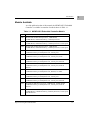
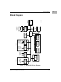
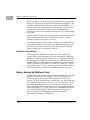
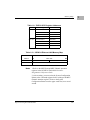
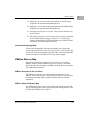
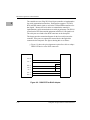
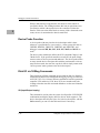
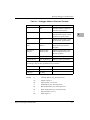
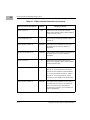
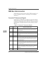
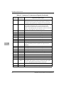
MC68LC040
MPU
25 MHz
16MB ECC
DRAM Memory
Array
53C710
SCSI
Coprocessor
SCSI
Peripherals
68-pin Front
Panel SCSI
Connector
Optional
Configuration Dependent
i82596CA
Ethernet
Controller
Ethernet
Transceiver
DB-15 Front
Panel
Connector
1 or 4MB Parity
DRAM Memory
Array
A32/D32
IPchip
IndustryPack
Interface
IndustryPack
I/O
2 Channels
Optional MC68040
VMEchip2
VMEbus
Interface
VMEbus
A32/24:D64/32/16/08
Master/Slave
Optional
2MB SRAM
Memory Array
w/Battery
MCchip
Four 32-pin
EPROM
Sockets
128KB SRAM
Memory Array
w/Battery
MK48T08
Battery Backed
8KB
Dual 85230
Serial
I/O Controllers
EIA-232
Transceivers
4 Serial Ports
RJ-45 Front
Panel
1211 9310
FLASH
1MB
Optional
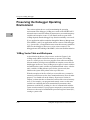
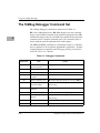
Block Diagram
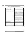
Block Diagram
Figure 1-1. MVME162LX Block Diagram
1-11
1
1
Board Level Hardware Description
Functional Description
This section contains a functional description of the MVME162LX
Embedded Controller.
Switches and LEDs
The controller’s front panel has an ABORT and RESET switch and four
light-emitting diode (LED) indicators (FAIL, RUN, SCON, FUSES).
ABORT Switch
When enabled by software, the ABORT switch generates an interrupt at a
user-programmable level. It is normally used to abort program execution
and return to the 162Bug debugger firmware located in the controller’s
EPROMs and flash memory.
The ABORT switch interrupter in the MCchip ASIC is an edge-sensitive
interrupter connected to the ABORT switch. This interrupter is filtered to
remove switch bounce.
RESET Switch
Note:
For an MVME162LX without the VMEbus option (no
VMEchip2), the LCSR control bit is not available to reset the
module. In this case, the watchdog timer is allowed to time out
to reset the controller.
The RESET switch resets all onboard devices; it also drives SYSRESET*
if the MVME162LX is operating as system controller. The RESET switch
may be disabled by software.
The VMEchip2 includes both a global and a local reset driver. When the
VMEchip2 operates as the VMEbus system controller, the reset driver
provides a global system reset by asserting the VMEbus signal
SYSRESET*. A SYSRESET* may be generated by the RESET switch, a
power-up reset, a watchdog timeout, or by a control bit in the LCSR (local
control/status register) in the VMEchip2. SYSRESET* remains asserted
for at least 200 msec, as required by the VMEbus specification.
1-12
Computer Group Literature Center Web Site
Functional Description
Similarly, the VMEchip2 provides an input signal and a control bit to initiate
a local reset operation. By setting a control bit, software can maintain a board
in a reset state, disabling a faulty board from participating in normal system
operation. The local reset driver is enabled even when the VMEchip2 is not
the system controller. A local reset may be generated by the RESET switch,
a power-up reset, a watchdog timeout, a VMEbus SYSRESET*, or by a
control bit in the global control/status register (GCSR).
Front Panel Indicators
There are four LEDs on the MVME162LX front panel: FAIL, RUN, SCON,
and FUSES.
❏ FAIL LED (red).
Lights when the BRDFAIL* signal line is active or
when the processor is halted. Part of DS1.
LED (green or amber). Lights when the local bus TIP* signal
line is low. This indicates one of the local bus masters is executing
a local bus cycle. Part of DS1.
❏ RUN
LED (green). Lights when the VMEchip2 in the
MVME162LX is the VMEbus system controller. Part of DS2.
❏ SCON
LED (green). Lights when +5 Vdc, +12 Vdc, and -12 Vdc
power is available to the LAN, IP, and SCSI interfaces. Part of DS2.
❏ FUSES
Data Bus Structure
The local bus on the MVME162LX Embedded Controller is a 32-bit
synchronous bus that is based on the MC68040 bus, and supports burst
transfers and snooping. The various local bus master and slave devices use
the local bus to communicate. The local bus is arbitrated by priority type
arbiter and the priority of the local bus masters from highest to lowest is:
82596CA LAN, 53C710 SCSI, VMEbus, and MPU. In the general case,
any master can access any slave; however, not all combinations pass the
common sense test. Refer to the MVME162LX Embedded Controller
Programmer’s Reference Guide to determine its port size, data bus
connection, and any restrictions that apply when accessing the device.
http://www.mcg.mot.com/literature
1-13
1
1
Board Level Hardware Description
MC68040 or MC68LC040 CPU
The MC68040 or MC68LC040 processor is used on the MVME162LX.
The MC68040 has on-chip instruction and data caches and a floating point
processor. The major difference between the two processors is that the
MC68040 has a floating point coprocessor. Refer to the M68040 user’s
manual for additional information.
MC68XX040 Cache
The MVME162LX local bus masters (VMEchip2, MC68XX040, 53C710
SCSI controller, and 82596CA Ethernet controller) have programmable
control of the snoop/caching mode. The MVME162LX local bus slaves
which support MC68XX040 bus snooping are defined in the Local Bus
Memory Map table later in this chapter.
No VMEbus Interface Option
The MVME162LX can be operated as an embedded controller without the
VMEbus interface. To support this feature, certain logic in the VMEchip2
has been duplicated in the MCchip. This logic is inhibited in the MCchip
if the VMEchip2 is present. The enables for these functions are controlled
by software and MCchip hardware initialization.
1-14
Computer Group Literature Center Web Site
Functional Description
Memory Options
The following memory options are used on the different versions of
MVME162LX Embedded Controller boards.
DRAM Options
The controller offers various DRAM options (see Table 1-1): either 1 MB
or 4 MB of parity-protected DRAM, or 4, 8, 16, or 32 MB ECC DRAM on
a mezzanine board. Parity protection can be enabled with interrupts or bus
exception when a parity error is detected. DRAM performance is specified
in the MVME162LX Embedded Controller Programmer’s Reference
Guide in the section on the DRAM Memory Controller in the MCchip
Programming Model.
The DRAM map decoder can be programmed to accommodate different
base address(es) and sizes of mezzanine boards. The onboard DRAM is
disabled by a local bus reset and must be programmed before the DRAM
can be accessed. Refer to the MCchip and MCECC descriptions in the
MVME162LX Embedded Controller Programmer’s Reference Guide for
detailed programming information.
Most DRAM devices require some number of access cycles before the
DRAMs are fully operational. Normally this requirement is met by the
onboard refresh circuitry and normal DRAM initialization. However,
software should insure a minimum of 10 initialization cycles are
performed to each bank of RAM.
SRAM Options
The controller provides 128 KB of 32-bit-wide onboard static RAM in a
single non-interleaved architecture with onboard battery backup.
http://www.mcg.mot.com/literature
1-15
1
1
Board Level Hardware Description
The battery backup function for the onboard SRAM is provided by a
Dallas DS1210S device that supports primary and secondary power
sources. In the event of a main board power failure, the DS1210S checks
power sources and switches to the source with the higher voltage.
If the voltage of the backup source is less than two volts, the DS1210S
blocks the second memory cycle; this allows software to provide an early
warning to avoid data loss. Because the second access may be blocked
during a power failure, software should do at least two accesses before
relying on the data.
The controller provides jumpers (on J13) that allow either power source of
the DS1210S to be connected to the VMEbus +5V STDBY pin or to one
cell of the onboard battery. For example, the primary system backup
source may be a battery connected to the VMEbus +5V STDBY pin and
the secondary source may be the onboard battery. If the system source
should fail or the board is removed from the chassis, the onboard battery
takes over.
Further details on SRAM configuration and specifics on SRAM
performance can be found in the section on the SRAM Memory Controller
in the MCchip Programming Model in the MVME162LX Embedded
Controller Programmer’s Reference Guide. The SRAM arrays are not
parity protected.
:
!
Caution
For proper operation of the SRAM, some jumper
combination must be installed on the respective Backup
Power Source Select Header. Refer to the jumper
information in Chapter 2. If one of the jumpers is used to
select the battery, the battery must be installed on the
MVME162LX. The SRAM may malfunction if inputs to
the DS1210S are left unconnected.
The SRAM is controlled by the MCchip, and the access time is
programmable. Refer to the MCchip description in the MVME162LX
Embedded Controller Programmer’s Reference Guide for additional
information.
1-16
Computer Group Literature Center Web Site
Functional Description
SRAM Batteries
!
Caution
Lithium batteries incorporate inflammable materials such
as lithium and organic solvents. If lithium batteries are
mistreated or handled incorrectly, they may burst open
and ignite, possible resulting in injury and/or fire.
When dealing with lithium batteries, carefully follow the
precautions listed below in order to prevent accidents.
❏
Do not short circuit.
❏
Do not disassemble, deform, or apply excessive pressure.
❏
Do not heat or incinerate.
❏
Do not apply solder directly.
❏
Do not use different models, or new and old batteries together.
❏
Do not charge.
❏
Always check proper polarity.
The power source for the onboard SRAM is a RAYOVAC FB1225 battery
with two BR1225 type lithium cells. The battery is socketed for easy
removal and replacement. The power source for the mezzanine SRAM is
a Sanyo CR2430 battery. Small capacitors are provided so that the
batteries can be quickly replaced without data loss.
The lifetime of the batteries is very dependent on the ambient temperature
of the board and the power-on duty cycle. The lithium batteries supplied
on the controller and on the SRAM mezzanine module should provide at
least two years of backup time with the board powered off and with an
ambient temperature of 40 ° C. If the power-on duty cycle is 50% (the board
is powered on half of the time), the battery lifetime is four years. At lower
ambient temperatures, the backup time is significantly longer and may
approach the shelf life of the battery.
http://www.mcg.mot.com/literature
1-17
1
1
Board Level Hardware Description
When a controller is stored, the battery should be disconnected to prolong
battery life. This is especially important at high ambient temperatures. The
controller is shipped with the batteries disconnected (with VMEbus +5V
standby voltage selected as both primary and secondary power source). If
you intend to use the battery as a power source, whether primary or
secondary, it is necessary to reconfigure the jumpers on J13 before installing
the module.
The power leads from the battery are exposed on the solder side of the board.
The board should not be placed on a conductive surface or stored in a
conductive bag unless the battery is removed.
To remove the battery from the module, carefully pull the battery from the
socket. Before installing a new battery, ensure that the battery pins are clean.
Note the battery polarity and press the battery into the socket. When the
battery is in the socket, no soldering is required.
EPROM and Flash Memory
The MVME162LX Embedded Controller comes with 1 MB of flash
memory and four EPROM sockets ready for the installation of EPROMs,
which may be ordered separately. Flash memory is a single Intel 28F008SA
device organized in a 1Mbit x 8 configuration. The EPROM locations are
standard JEDEC 32-pin DIP sockets accommodating four jumper-selectable
densities (128 Kbit x 8; 256 Kbit X 8; 512 Kbit x 8; 1 Mbit x8). A jumper
setting (GPIO3, pins 7-8 on J11), allows reset code to be fetched either from
flash memory (GPIO3 installed) or from EPROMs (GPIO3 removed).
Battery Backed Up RAM and Clock
An MK48T08 RAM and clock chip is used on the MVME162LX. This chip
provides a time-of-day clock, oscillator, crystal, power fail detection,
memory write protection, 8KB of RAM, and a battery in one 28-pin
package. The clock provides seconds, minutes, hours, day, date, month, and
year in BCD 24-hour format. Corrections for 28-, 29- (leap year), and 30day months are automatically made. No interrupts are generated by the
clock. Although the MK48T08 is an 8 bit device, the interface provided by
the MCchip supports 8-, 16-, and 32-bit accesses to the MK48T08. Refer to
the MCchip in the MVME162LX Embedded Controller Programmer’s
Reference Guide and to the MK48T08 data sheet for additional
programming and battery life information.
1-18
Computer Group Literature Center Web Site
Functional Description
VMEbus Interface and VMEchip2
The local bus to VMEbus interface, VMEbus to local bus interface, and the
DMA controller functions of the local VMEbus are provided by the
VMEchip2. The VMEchip2 can also provide the VMEbus system
controller functions. Refer to the VMEchip2 in the MVME162LX
Embedded Controller Programmer’s Reference Guide for additional
programming information.
Note that the ABORT switch logic in the VMEchip2 is not used. The GPI
inputs to the VMEchip2 which are located at $FFF40088 bits 7-0 are not
used. The ABORT switch interrupt is integrated into the MCchip ASIC at
location $FFF42043. The GPI inputs are integrated into the MCchip ASIC
at location $FFF4202C bits 23-16.
I/O Interfaces
The MVME162LX provides onboard Input/Output (I/O) for many system
applications. The I/O functions include serial ports and optional interfaces
for IndustryPack (IP) modules, LAN Ethernet transceivers, and SCSI mass
storage devices.
I/O signals are routed through industry-standard connectors on the
controller’s front panel; no adapter boards or transition modules are
necessary. I/O connections on the controller’s front panel include an
optional 68-pin SCSI connector, an optional DB15 Ethernet connector,
and four 8-pin RJ45 serial connectors. In addition, the panel has cutouts for
routing of flat cables to the optional IndustryPack modules.
Serial Communications Interface
The MVME162LX uses two Zilog Z85230 serial port controllers to
implement the four serial communications interfaces. Each interface
supports CTS, DCD, RTS, and DTR control signals, as well as the TXD
and RXD transmit/receive data signals. Because the serial clocks are
omitted in the controller’s design, serial communications are strictly
asynchronous. The controller’s hardware supports serial baud rates of
110b/s to 38.4Kb/s.
http://www.mcg.mot.com/literature
1-19
1
1
Board Level Hardware Description
The Z85230 supplies an interrupt vector during interrupt acknowledge
cycles. The vector is modified based upon the interrupt source within the
Z85230. Interrupt request levels are programmed via the MCchip.
The Z85230s are interfaced as DTE (data terminal equipment) with EIA232-D signal levels. The four serial ports are routed to four RJ45 telephone
connectors on the MVME162LX front panel.
Refer to the Z85230 data sheet and to the MCchip Programming Model in
the MVME162LX Embedded Controller Programmer’s Reference Guide
for additional information.
IndustryPack (IP) Interfaces
Up to two IndustryPack (IP) modules may be installed on the
MVME162LX Embedded Controller as an option. The interface between
the IPs and the MVME162LX is the IndustryPack Interface Controller
(IPIC) ASIC. Access to the IPs is provided by two 3M connectors located
behind the controller’s front panel.
Refer to the chapter on the IPIC in the MVME162LX Embedded Controller
Programmer’s Reference Guide for additional information on the IP
interface.
Ethernet Interface
The MVME162LX Embedded Controller uses the 82596CA controller to
implement the Ethernet transceiver interface. The 82596CA accesses local
RAM using DMA operations to perform its normal functions. Because the
82596CA has small internal buffers and the VMEbus has an undefined
latency period, buffer overrun may occur if the DMA is programmed to
access the VMEbus. Therefore, the 82596CA should not be programmed
to access the VMEbus.
Every MVME162LX that has the Ethernet interface is assigned an
Ethernet Station Address. The address is $08003E2XXXXX where XXXXX
is the unique 5-nibble number assigned to the board (every MVME162LX
has a different value for XXXXX).
1-20
Computer Group Literature Center Web Site
Functional Description
Each board has an Ethernet Station Address displayed on a label attached
to the VMEbus P2 connector. In addition, the six bytes including the
Ethernet address are stored in the configuration area of the BBRAM. That
is, 08003E2XXXXX is stored in the BBRAM. At an address of
$FFFC1F2C, the upper four bytes (08003E2X) can be read. At an address
of $FFFC1F30, the lower two bytes (XXXX) can be read. The MVME162
debugger has the capability to retrieve or set the Ethernet address.
If the data in the BBRAM is lost, the user should use the number on the
label on backplane connector P2 to restore it. The Ethernet transceiver
interface is located on the controller’s main circuit board, and the industry
standard connector is located on its front panel.
Support functions for the 82596CA are provided by the MCchip ASIC.
Refer to the 82596CA user's guide and to the MCchip in the MVME162LX
Embedded Controller Programmer’s Reference Guide for additional
programming information.
SCSI Interface
The controller supports mass storage subsystems through the industrystandard SCSI bus. These subsystems may include hard and floppy disk
drives, streaming tape drives, and other mass storage devices. The SCSI
interface is implemented using the NCR 53C710 SCSI I/O controller.
Support functions for the 53C710 are provided by the MCchip ASIC. The
SCSI connector is located on the controller’s front panel.
Refer to the NCR 53C710 user's guide and to the MCchip in the
MVME162LX Embedded Controller Programmer’s Reference Guide for
additional programming information.
SCSI Termination
The individual configuring the system must ensure that the SCSI bus is
properly terminated at both ends. SCSI bus terminators are located on the
controller. The SCSI terminators are enabled/disabled by a jumper on
header J14. If the SCSI bus ends at the controller, then a jumper must be
installed between J14 pins 1 and 2.
http://www.mcg.mot.com/literature
1-21
1
1
Board Level Hardware Description
The controller provides +5 Vdc to the SCSI bus TERMPWR signal
through fuse F4, located near J7. The FUSES LED (part of DS2) on the
MVME162LX front panel monitors the SCSI bus TERMPWR signal in
addition to LAN power; with the controller connected to an SCSI bus, the
FUSES LED lights when SCSI terminator power is present.
Because any device on the SCSI bus can provide TERMPWR, the FUSES
LED does not directly indicate the condition of the fuse. If the LED is not
lit during SCSI bus operation, the fuse should still be checked.
Local Resources
The MVME162LX Embedded Controller includes many resources for the
local processor. These include tick timers, software-programmable
hardware interrupts, a watchdog timer, and a local bus timeout.
Programmable Tick Timers
Four 32-bit programmable tick timers with a 1 µs resolution are provided
in the MCchip and two 32-bit programmable tick timers are provided in the
optional VMEchip2. The tick timers can be programmed to generate
periodic interrupts to the processor.
Refer to the VMEchip2 and MCchip in the MVME162LX Embedded
Controller Programmer’s Reference Guide for additional programming
information.
Watchdog Timer
A watchdog timer is provided in both the MCchip and the optional
VMEchip2. The timers operate independently but in parallel. When the
watchdog timers are enabled, they must be reset by software within the
programmed time or they will time out. The watchdog timers can be
programmed to generate a SYSRESET signal, local reset signal, or board
fail signal if they time out.
1-22
Computer Group Literature Center Web Site
Functional Description
The watchdog timer logic is duplicated in the VMEchip2 and MCchip
ASICs. Because the watchdog timer function in the VMEchip2 is a
superset of that function in the MCchip (system reset function), the timer
in the VMEchip2 is used in all cases except for the version of the
MVME162LX which does not include the VMEbus interface ("No
VMEbus Interface" option).
Refer to the VMEchip2 and the MCchip in the MVME162LX Embedded
Controller Programmer’s Reference Guide for additional programming
information.
Software-Programmable Hardware Interrupts
Eight software-programmable hardware interrupts are provided by the
VMEchip2. These interrupts allow software to create a hardware interrupt.
Refer to the VMEchip2 in the MVME162LX Embedded Controller
Programmer’s Reference Guide for additional programming information.
Local Bus Timeout
The MVME162LX Embedded Controller provides timeout functions in
the VMEchip2 and the MCchip for the local bus. When the timer is
enabled and a local bus access times out, a Transfer Error Acknowledge
(TEA) signal is sent to the local bus master. The timeout value is
selectable by software for 8 µsec, 64 µsec, 256 µsec, or infinite. The local
bus timer does not operate during VMEbus bound cycles. VMEbus bound
cycles are timed by the VMEbus access timer and the VMEbus global
timer. The MCchip also provides local bus timeout logic for controllers
without the optional VMEbus interface (without the VMEchip2).
The access timer logic is duplicated in the VMEchip2 and MCchip ASICs.
Because the local bus timer in the VMEchip2 can detect an offboard access
and the MCchip local bus timer cannot, the timer in the VMEchip2 is used
in all cases except for the version of the controller which does not include
the VMEbus interface ("No VMEbus Interface option").
Refer to the VMEchip2 and the MCchip in the MVME162LX Embedded
Controller Programmer’s Reference Guide for additional programming
information.
http://www.mcg.mot.com/literature
1-23
1
1
Board Level Hardware Description
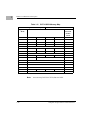
Local Bus Arbiter
The local bus arbiter implements a fixed priority which is described in the
following table.
Table 1-3. Local Bus Arbitration Priority
Device
Priority
Note
LAN
0
Highest
SCSI
1
...
VMEbus
2
Next Lowest
MC68XX040
3
Lowest
Connectors
The MVME162LX Embedded Controller has two 96-position DIN
connectors: P1 and P2. P1 rows A, B, C, and P2 row B provide the
VMEbus interconnection. P2 rows A and C are not used. The
MVME162LX has a 20-pin connector J2 mounted behind the front panel.
When the MVME162LX board is enclosed in a chassis and the front panel
is not visible, this connector allows the reset, abort and LED functions to
be extended to the control panel of the system, where they are visible.
The serial ports on the controller are connected to four 8-pin RJ45 female
connectors (J17) on the front panel. The two IPs connect to the controller
by two pairs of 50-pin connectors. The two 50-pin connectors behind the
front panel are for external connections to IP signals. The memory
mezzanine board is plugged into two 100-pin connectors. The Ethernet
LAN connector is J9, a 15-pin socket connector mounted on the front
panel. The SCSI connector is J10, a 68-pin socket connector is also
mounted on the front panel.
1-24
Computer Group Literature Center Web Site
Memory Maps
Memory Maps
There are two points of view for memory maps:
1. The mapping of all resources as viewed by local bus masters (local
bus memory map).
2. The mapping of onboard resources as viewed by external masters
(VMEbus memory map).
The memory and I/O maps which are described in the next three tables are
correct for all local bus masters. There is some address translation
capability in the VMEchip2. This allows multiple MVME162LXs on the
same VMEbus with different virtual local bus maps as viewed by different
VMEbus masters.
Local Bus Memory Map
The local bus memory map is split into different address spaces by the
transfer type (TT) signals. The local resources respond to the normal
access and interrupt acknowledge codes.
Normal Address Range
The memory map of devices that respond to the normal address range is
shown in the following tables. The normal address range is defined by the
Transfer Type (TT) signals on the local bus. On the MVME162LX
Embedded Controller, Transfer Types 0, 1, and 2 define the normal
address range. Table 1-4 is the entire map from $00000000 to
$FFFFFFFF. Many areas of the map are user-programmable, and
suggested uses are shown in the table. The cache inhibit function is
programmable in the MC68XX040 MMU. The onboard I/O space must be
marked cache inhibit and serialized in its page table. Table 1-5 further
defines the map for the local I/O devices.
http://www.mcg.mot.com/literature
1-25
1
1
Board Level Hardware Description
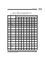
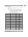
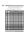
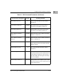
Table 1-4. Local Bus Memory Map
Address Range
Devices Accessed
Port
Width
Size
Software
Cache
Inhibit
Notes
Programmable
DRAM on Parity
Mezzanine
D32
1MB-4MB
N
2
Programmable
DRAM on ECC
Mezzanine
D32
16MB
N
2
Programmable
On-Board SRAM
D32
128KB
N
2, 7
Programmable
SRAM on Mezzanine
D32
2MB
N
2, 7
Programmable
VMEbus A32/A24
D32/D16
--
Y/N
4
Programmable
IP_a Memory
D32-D8
64KB-8MB
Y/N
2, 4
Programmable
IP_b Memory
D32-D8
64KB-8MB
Y/N
2, 4
$FF800000-$FF9FFFFF
Flash/EPROM
D32
2MB
N
1, 5
$FFA00000-$FFBFFFFF
EPROM/Flash
D32
2MB
N
5
$FFC00000-$FFDFFFFF
Not Decoded
D32
2MB
N
7
$FFE00000-$FFE1FFFF
On-Board SRAM
Default
D32
128KB
N
7
$FFE80000-$FFEFFFFF
Not Decoded
--
512KB
N
6
$FFF00000-$FFFEFFFF
Local I/O Devices
(Refer to next table)
D32-D8
878KB
Y
3
$FFFF0000-$FFFFFFFF
VMEbus A16
D32/D16
64KB
Y/N
2, 4
1-26
Computer Group Literature Center Web Site
Memory Maps
Notes 1. Devices mapped at $FFF80000-$FFF9FFFF also appear at
$00000000- $001FFFFF when the ROM0 bit in the MCchip
EPROM control register is high (ROM0=1). ROM0 is set to
1 after each reset. The ROM0 bit must be cleared before other
resources (DRAM or SRAM) can be mapped in this range
($00000000 - $001FFFFF).
2. The EPROM/Flash memory map is also controlled by the
EPROM size and by control bit V19 in the MCchip ASIC.
Refer to the EPROM/Flash configuration tables in the
MVME162LX Embedded Controller Programmer’s
Reference Guide for additional information.
3. This area is user-programmable. The DRAM and SRAM
decoder is programmed in the MCchip, the local-to-VMEbus
decoders are programmed in the VMEchip2, and the IP
memory space is programmed in the IPIC.
4. Size is approximate.
5. Cache inhibit depends on the devices in the area mapped.
6. The EPROM and Flash are dynamically sized by the
MCchip ASIC from an 8-bit private bus to the 32-bit MPU
local bus.
7. These areas are not decoded unless one of the
programmable decoders is initialized to decode this space. If
they are not decoded and the local timer is enabled, an access
to this address range will generate a local bus timeout.
8. SRAM is 128 KB.
http://www.mcg.mot.com/literature
1-27
1
1
Board Level Hardware Description
The following table focuses on the ‘‘Local I/O Devices’’ portion of the
local bus main memory map.
Note
The IPIC chip on the MVME162LX supports up to four
IndustryPack (IP) interfaces, designated IP_a through IP_d.
The MVME162LX itself accommodates two IPs: IP_a and
IP_b. In the following map, the segments applicable to IP_c
and IP_d are not used in the controller.
Table 1-5. Local I/O Devices Memory Map
Address Range
Devices Accessed
Port
Width
Size
Notes
--
256 KB
4
$FFF00000 - $FFF3FFFF
Reserved
$FFF40000 - $FFF400FF
VMEchip2 (LCSR)
D32
256 B
1, 3
$FFF40100 - $FFF401FF
VMEchip2 (GCSR)
D32-D8
256 B
1, 3
$FFF40200 - $FFF40FFF
Reserved
--
3.5 KB
4, 5
$FFF41000 - $FFF41FFF
Reserved
--
4 KB
4
$FFF42000 - $FFF42FFF
MCchip
D32-D8
4 KB
1
$FFF43000 - $FFF430FF
MCECC #1
D8
256 B
1, 9
$FFF43100 - $FFF431FF
MCECC #2
D8
256 B
1, 9
$FFF43200 - $FFF43FFF
MCECCs (repeated)
--
3.5 KB
1, 5, 9
$FFF44000 - $FFF44FFF
Reserved
--
8 KB
4
$FFF45000 - $FFF45800
SCC #1 (Z85230)
D8
2 KB
1, 2
$FFF45801 - $FFF45FFF
SCC #2 (Z85230)
D8
2 KB
1, 2
$FFF46000 - $FFF46FFF
LAN (82596CA)
D32
4 KB
1, 6
$FFF47000 - $FFF47FFF
SCSI (53C710)
D32-D8
4 KB
1
$FFF48000 - $FFF57FFF
Reserved
--
64 KB
4
$FFF58000 - $FFF5807F
IPIC IP_a I/O
D16
128 B
1
$FFF58080 - $FFF580FF
IPIC IP_a ID
D16
128 B
1
$FFF58100 - $FFF5817F
IPIC IP_b I/O
D16
128 B
1
$FFF58180 - $FFF581FF
IPIC IP_b ID Read
D16
128 B
1
1-28
Computer Group Literature Center Web Site
Memory Maps
Table 1-5. Local I/O Devices Memory Map (Continued)
Address Range
Devices Accessed
Port
Width
Size
Notes
$FFF58200 - $FFF5827F
IPIC IP_c I/O
D16
128 B
8
$FFF58280 - $FFF582FF
IPIC IP_c ID
D16
128 B
8
$FFF58300 - $FFF5837F
IPIC IP_d I/O
D16
128 B
8
$FFF58380 - $FFF583FF
IPIC IP_d ID Read
D16
128 B
8
$FFF58400 - $FFF584FF
IPIC IP_ab I/O
D32-D16
256 B
1
$FFF58500 - $FFF585FF
IPIC IP_cd I/O
D32-D16
256 B
8
$FFF58600 - $FFF586FF
IPIC IP_ab I/O Repeated
D32-D16
256 B
1
$FFF58700 - $FFF587FF
IPIC IP_cd I/O Repeated
D32-D16
256 B
8
$FFF58800 - $FFF5887F
Reserved
--
128 B
1
$FFF58880 - $FFF588FF
Reserved
--
128 B
1
$FFF58900 - $FFF5897F
Reserved
--
128 B
1
$FFF58980 - $FFF589FF
Reserved
--
128 B
1
$FFF58A00 - $FFF58A7F
Reserved
--
128 B
1
$FFF58A80 - $FFF58AFF
Reserved
--
128 B
1
$FFF58B00 - $FFF58B7F
Reserved
--
128 B
1
$FFF58B80 - $FFF58BFF
Reserved
--
128 B
1
$FFF58C00 - $FFF58CFF
Reserved
--
256 B
1
$FFF58D00 - $FFF58DFF
Reserved
--
256 B
1
$FFF58E00 - $FFF58EFF
Reserved
--
256 B
1
$FFF58F00 - $FFF58FFF
Reserved
--
256 B
1
$FFFBC000 - $FFFBC01F
IPIC Registers
D32-D8
2 KB
1
$FFFBC800 - $FFFBC81F
Reserved
--
2 KB
1
$FFFBD000 - $FFFBFFFF
Reserved
--
12 KB
4
$FFFC0000 - $FFFC7FFF
MK48T08 (BBRAM,
TOD Clock)
D32-D8
32 KB
1
$FFFC8000 - $FFFCBFFF
MK48T08 & Disable
Flash writes
D32-D8
16 KB
1, 7
http://www.mcg.mot.com/literature
1-29
1
1
Board Level Hardware Description
Table 1-5. Local I/O Devices Memory Map (Continued)
Address Range
Devices Accessed
$FFFCC000 - $FFFCFFFF
MK48T08 & Enable
Flash writes
$FFFD0000 - $FFFEFFFF
Reserved
Port
Width
Size
Notes
D32-D8
16 KB
1, 7
--
128 KB
4
Notes 1. For a complete description of the register bits, refer to the
data sheet for the specific chip. For a more detailed memory
map, refer to the following detailed peripheral device
memory maps
2. The SCC is an 8-bit device located on an MCchip private
data bus. Byte access is required.
3. Writes to the LCSR in the VMEchip2 must be 32 bits.
LCSR writes of 8 or 16 bits terminate with a TEA signal.
Writes to the GCSR may be 8, 16 or 32 bits. Reads to the
LCSR and GCSR may be 8, 16 or 32 bits. Byte reads should
be used to read the interrupt vector.
4. This area does not return an acknowledge signal. If the
local bus timer is enabled, the access times out and is
terminated by a TEA signal.
5. Size is approximate.
6. Port commands to the 82596CA must be written as two 16bit writes: upper word first and lower word second.
7. Refer to the Flash and EPROM Interface section in the
MCchip description in Chapter 3.
8. Not used.
9. To use this area, the ECC mezzanine board must be
installed. If it is not installed, no acknowledge signal is
returned; if the local bus timer is enabled, the access times
out and is terminated by a TEA signal.
1-30
Computer Group Literature Center Web Site
Memory Maps
Detailed I/O Memory Maps
The following tables provide detailed memory maps for the VMEchip2,
MCchip, the MCECC memory controller chip, the Zilog Z85230, the Intel
82596CA controller, the NCR 53C710 controller, the IPIC chip, and the
MK48T08 BBRAM/TOD Clock.
Tables X-X - XX define the programming model for the Local Control and
Status Registers (LCSR) in the VMEchip2. The local bus map decoder for
the LCSR is included in the VMEchip2. The base address of the LCSR is
$FFF40000 and the registers are 32-bits wide. Byte, two-byte, and
four-byte read operations are permitted: however, byte and two-byte write
operations are not permitted. Byte and two-byte write operations return a
TEA signal to the local bus. Read-modify-write operations should be used
to modify a byte or a two-byte of a register.
Each register definition includes a table with 5 lines:
❏
Line 1 is the base address of the register and the number of bits
defined in the table.
❏
Line 2 shows the bits defined by this table.
❏
Line 3 defines the name of the register or the name of the bits in the
register.
❏
Line 4 defines the operations possible on the register bits as follows:
R
This bit is a read-only status bit.
R/W
This bit is readable and writable.
W/AC This bit can be set and it is automatically cleared. This bit can
also be read.
C
Writing a one to this bit clears this bit or another bit. This bit
reads zero.
S
Writing a one to this bit sets this bit or another bit. This bit
reads zero.
❏
Line 5 defines the state of the bit following a reset as follows:
P
S
L
X
The bit is affected by powerup reset.
The bit is affected by SYSRESET.
The bit is affected by local reset.
The bit is not affected by reset.
http://www.mcg.mot.com/literature
1-31
1
1
Board Level Hardware Description
Table 1-6. VMEchip2 Memory Map - LCSR Summary (Sheet 1 of 2)
VMEchip2 LCSR Base Address = $FFF40000
OFFSET:
31
30
29
28
27
26
25
24
23
22
21
0
SLAVE ENDING ADDRESS 1
4
SLAVE ENDING ADDRESS 2
8
SLAVE ADDRESS TRANSLATION ADDRESS 1
C
19
18
17
16
BLK
PRGM
DATA
2
2
2
18
17
16
SLAVE ADDRESS TRANSLATION ADDRESS 2
10
31
30
29
28
ADDER
SNP
WP
SUP
USR
A32
A24
2
2
2
2
2
2
2
BLK
D64
2
24
23
22
21
20
19
27
26
25
14
MASTER ENDING ADDRESS 1
18
MASTER ENDING ADDRESS 2
1C
MASTER ENDING ADDRESS 3
20
MASTER ENDING ADDRESS 4
MASTER ADDRESS TRANSLATION ADDRESS 4
24
28
20
MAST
D16
EN
MAST
WP
EN
MAST
D16
EN
MASTER AM 4
31
30
29
28
27
26
MASTER AM 3
GCSR
BOARD SELECT
GCSR GROUP SELECT
2C
MAST
WP
EN
25
30
24
23
22
21
20
WAIT
RMW
ROM
ZERO
MAST
4
EN
MAST
3
EN
MAST
2
EN
MAST
1
EN
19
18
17
16
DMA TB
SNP MODE
SRAM
SPEED
34
38
DMA CONTROLLER
3C
DMA CONTROLLER
40
DMA CONTROLLER
44
48
DMA CONTROLLER
TICK
2/1
TICK
IRQ 1
EN
CLR
IRQ
IRQ
STAT
VMEBUS
INTERRUPT
LEVEL
VMEBUS INTERRUPT VECTOR
This sheet continues on facing page.
1-32
Computer Group Literature Center Web Site
Memory Maps
15
14
13
12
11
10
9
8
7
6
5
4
3
2
1
0
A24
1
BLK
D64
1
BLK
1
PRGM
1
DATA
1
4
3
2
1
0
SLAVE STARTING ADDRESS 1
SLAVE STARTING ADDRESS 2
SLAVE ADDRESS TRANSLATION SELECT 1
SLAVE ADDRESS TRANSLATION SELECT 2
ADDER
1
15
14
13
12
SNP
1
11
10
9
WP
1
SUP
1
USR
1
8
7
6
A32
1
5
MASTER STARTING ADDRESS 1
MASTER STARTING ADDRESS 2
MASTER STARTING ADDRESS 3
MASTER STARTING ADDRESS 4
MASTER ADDRESS TRANSLATION SELECT 4
MAST
D16
EN
MAST
WP
EN
IO2
EN
IO2
WP
EN
15
14
ARB
ROBN
MAST
DHB
DMA
TBL
INT
MAST
D16
EN
MASTER AM 2
IO2
S/U
13
MAST
DWB
DMA LB
SNP MODE
IO2
P/D
12
IO1
EN
IO1
D16
EN
IO1
WP
EN
9
11
10
MST
FAIR
MST
RWD
DMA
INC
VME
DMA
INC
LB
DMA
WRT
MPU
LBE
ERR
MPU
LPE
ERR
IO1
S/U
8
MAST
WP
EN
MASTER AM 1
ROM
ROM BANK B
ROM BANK A
SIZE
SPEED
SPEED
7
6
5
4
DMA
HALT
DMA
EN
DMA
TBL
DMA
FAIR
DMA
D16
DMA
D64
BLK
DMA
BLK
DMA
AM
5
DMA
AM
4
DMA
AM
3
DMA
AM
2
DMA
AM
1
DMA
AM
0
MPU
LOB
ERR
MPU
LTO
ERR
DMA
LBE
ERR
DMA
LPE
ERR
DMA
LOB
ERR
DMA
LTO
ERR
DMA
TBL
ERR
DMA
VME
ERR
DMA
DONE
MASTER
VMEBUS
3
2
DM
RELM
1
0
DMA
VMEBUS
LOCAL BUS ADDRESS COUNTER
VMEBUS ADDRESS COUNTER
BYTE COUNTER
TABLE ADDRESS COUNTER
DMA TABLE
INTERRUPT COUNT
MPU
CLR
STAT
1360 9403
This sheet begins on facing page.
http://www.mcg.mot.com/literature
1-33
1
1
Board Level Hardware Description
Table 1-6. VMEchip2 Memory Map - LCSR Summary (Sheet 2 of 2)
VMEchip2 LCSR Base Address = $FFF40000
OFFSET:
31
30
29
28
27
26
25
24
23
22
ARB
BGTO
EN
4C
21
20
DMA
TIME OFF
19
18
17
16
VME
GLOBAL
TIMER
DMA
TIME ON
50
TICK TIMER 1
54
TICK TIMER 1
58
TICK TIMER 2
TICK TIMER 2
5C
SCON
60
SYS
FAIL
BRD
FAIL
STAT
PURS
STAT
CLR
PURS
STAT
BRD
FAIL
OUT
RST
SW
EN
SYS
RST
WD
CLR
TO
WD
CLR
CNT
WD
TO
STAT
TO
BF
EN
WD
SRST
LRST
WD
RST
EN
64
WD
EN
PRE
31
30
29
28
27
26
25
24
23
22
21
20
19
18
17
16
68
AC
FAIL
IRQ
AB
IRQ
SYS
FAIL
IRQ
MWP
BERR
IRQ
PE
IRQ
IRQ1E
IRQ
TIC2
IRQ
TIC1
IRQ
VME
IACK
IRQ
DMA
IRQ
SIG3
IRQ
SIG2
IRQ
SIG1
IRQ
SIG0
IRQ
LM1
IRQ
LM0
IRQ
6C
EN
IRQ
31
EN
IRQ
30
EN
IRQ
29
EN
IRQ
28
EN
IRQ
27
EN
IRQ
26
EN
IRQ
25
EN
IRQ
24
EN
IRQ
23
EN
IRQ
22
EN
IRQ
21
EN
IRQ
20
EN
IRQ
19
EN
IRQ
18
EN
IRQ
17
EN
IRQ
16
CLR
IRQ
31
CLR
IRQ
30
CLR
IRQ
29
CLR
IRQ
28
CLR
IRQ
27
CLR
IRQ
26
CLR
IRQ
25
CLR
IRQ
24
CLR
IRQ
23
CLR
IRQ
22
CLR
IRQ
21
CLR
IRQ
20
CLR
IRQ
19
CLR
IRQ
18
CLR
IRQ
17
CLR
IRQ
16
70
74
78
AC FAIL
IRQ LEVEL
ABORT
IRQ LEVEL
SYS FAIL
IRQ LEVEL
MST WP ERROR
IRQ LEVEL
7C
VME IACK
IRQ LEVEL
DMA
IRQ LEVEL
SIG 3
IRQ LEVEL
SIG 2
IRQ LEVEL
80
84
88
SW7
SW6
SW5
SW4
IRQ LEVEL
IRQ LEVEL
IRQ LEVEL
IRQ LEVEL
SPARE
IRQ LEVEL
VME IRQ 7
IRQ LEVEL
VME IRQ 6
IRQ LEVEL
VME IRQ 5
IRQ LEVEL
VECTOR BASE
REGISTER 0
VECTOR BASE
REGISTER 1
MST
IRQ
EN
SYS
FAIL
LEVEL
AC
FAIL
LEVEL
ABORT
GPIOEN
LEVEL
8C
This sheet continues on facing page.
1-34
Computer Group Literature Center Web Site
Memory Maps
15
14
13
VME
ACCESS
TIMER
12
11
LOCAL
BUS
TIMER
10
9
8
7
6
5
WD
TIME OUT
SELECT
4
3
2
1
0
CLR
OVF
1
COC
EN
1
TIC
EN
1
PRESCALER
CLOCK ADJUST
COMPARE REGISTER
COUNTER
COMPARE REGISTER
COUNTER
CLR
OVF
2
OVERFLOW
COUNTER 2
COC
EN
2
TIC
EN
2
OVERFLOW
COUNTER 1
SCALER
15
14
13
12
11
10
9
8
7
6
5
4
3
2
1
0
SW7
IRQ
SW6
IRQ
SW5
IRQ
SW4
IRQ
SW3
IRQ
SW2
IRQ
SW1
IRQ
SW0
IRQ
SPARE
VME
IRQ7
VME
IRQ6
VME
IRQ5
VME
IRQ4
VME
IRQ3
VME
IRQ2
VME
IRQ1
EN
IRQ
15
EN
IRQ
14
EN
IRQ
13
EN
IRQ
12
EN
IRQ
11
EN
IRQ
10
EN
IRQ
9
EN
IRQ
8
EN
IRQ
7
EN
IRQ
6
EN
IRQ
5
EN
IRQ
4
EN
IRQ
3
EN
IRQ
2
EN
IRQ
1
EN
IRQ
0
SET
IRQ
15
SET
IRQ
14
SET
IRQ
13
SET
IRQ
12
SET
IRQ
11
SET
IRQ
10
SET
IRQ
9
SET
IRQ
8
CLR
IRQ
15
CLR
IRQ
14
CLR
IRQ
13
CLR
IRQ
12
CLR
IRQ
11
CLR
IRQ
10
CLR
IRQ
9
CLR
IRQ
8
P ERROR
IRQ LEVEL
IRQ1E
IRQ LEVEL
TIC TIMER 2
IRQ LEVEL
TIC TIMER 1
IRQ LEVEL
SIG 1
IRQ LEVEL
SIG 0
IRQ LEVEL
LM 1
IRQ LEVEL
LM 0
IRQ LEVEL
SW3
IRQ LEVEL
SW2
IRQ LEVEL
SW1
IRQ LEVEL
SW0
IRQ LEVEL
VME IRQ 4
IRQ LEVEL
VMEB IRQ 3
IRQ LEVEL
VME IRQ 2
IRQ LEVEL
VME IRQ 1
IRQ LEVEL
GPIOO
GPIOI
GPI
MP
IRQ
EN
REV
EROM
DIS
SRAM
DIS
MST
NO
EL
BBSY
DIS
BSYT
EN
INT
DIS
BGN
1361 9403
This sheet begins on facing page.
http://www.mcg.mot.com/literature
1-35
1
1
Board Level Hardware Description
Table 1-7. MCchip Register Map
MCchip Base Address = $FFF42000
Offset
1-36
D31-D24
D23-D16
$00
MCchip ID
$04
Tick Timer 1 Compare Register
$08
Tick Timer 1 Counter Register
D15-D8
MCchip Revision General Control
D7-D0
Interrupt Vector
Base Register
$0C
Tick Timer 2 Compare Register
$10
Tick Timer 2 Counter Register
$14
LSB Prescaler
Count Register
$18
Tick Timer 4
Tick Timer 3
Tick Timer 2
Tick Timer 1
Interrupt Control Interrupt Control Interrupt Control Interrupt Control
$1C
DRAM Parity
Error Interrupt
Control
$20
DRAM Space Base Address
Register
SRAM Space Base Address Register
$24
DRAM Space
Size
DRAM/SRAM
Options
SRAM Space
Size
(Reserved)
$28
LANC Error
Status
(Reserved)
LANC Interrupt
Control
LANC Bus Error
Interrupt Control
$2C
SCSI Error
Status
General Purpose
Inputs
MVME162LX
Version
SCSI Interrupt
Control
$30
Tick Timer 3 Compare Register
$34
Tick Timer 3 Counter Register
$38
Tick Timer 4 Compare Register
$3C
Tick Timer 4 Counter Register
$40
Bus Clock
PROM Access
Time Control
Flash Access
Time Control
ABORT Switch
Interrupt Control
$44
RESET Switch
Control
Watchdog Timer
Control
Access &
Watchdog Time
Base Select
(Reserved)
$48
DRAM Control
(Reserved)
MPU Status
(Reserved)
$4C
32-bit Prescaler Count Register
Prescaler Clock
Adjust
SCC Interrupt
Control
Tick Timer 2
Control
Tick Timer 4
Control
Tick Timer 1
Control
Tick Timer 3
Control
Computer Group Literature Center Web Site
Memory Maps
Table 1-8. MCECC Internal Register Memory Map
MCECC Base Address = $FFF43000 (1st); $FFF43100 (2nd)
Register
Offset
Register
Name
Register Bit Names
D31
D30
D29
D28
D27
D26
D25
D24
$00
CHIP ID
CID7
CID6
CID5
CID4
CID3
CID2
CID1
CID0
$04
CHIP REVISION
REV7
REV6
REV5
REV4
REV3
REV2
REV1
REV0
$08
MEM CONFIG
FSTRD
1
0
MSIZ2
MSIZ1
MSIZ0
$0C
DUMMY 0
0
0
0
0
0
0
0
0
$10
DUMMY 1
0
0
0
0
0
0
0
0
$14
BASE ADDRESS
BAD31
BAD30
BAD29
BAD28
BAD27
BAD26
BAD25
BAD24
$18
DRAM CONTRL
BAD23
BAD22
RWB5
SWAIT
RWB3
NCEIEN NCEBE
N
RAMEN
$1C
BCLK FREQ
BCK7
BCK6
BCK5
BCK4
BCK3
BCK2
BCK1
BCK0
$20
DATA CONTRL
0
0
DERC
ZFILL
RWCKB 0
0
0
$24
SCRUB CNTRL
RACOD RADAT HITDIS
E
A
SCRB
SCRBE
N
SBEIEN IDIS
$28
SCRUB PERIOD
SBPD15 SBPD14 SBPD13 SBPD12 SBPD11 SBPD10 SBPD9
SBPD8
$2C
SCRUB PERIOD
SBPD7
$30
0
SBPD6
SBPD5
SBPD4
SBPD3
SBPD2
SBPD1
SBPD0
CHIP PRESCALE CPS7
CPS6
CPS5
CPS4
CPS3
CPS2
CPS1
CPS0
$34
SCRUB TIME
ON/OFF
SRDIS
0
STON2
STON1
STON0
STOFF2 STOFF1 STOFF0
$38
SCRUB
PRESCALE
0
0
SPS21
SPS20
SPS19
SPS18
SPS17
SPS16
$3C
SCRUB
PRESCALE
SPS15
SPS14
SPS13
SPS12
SPS11
SPS10
SPS9
SPS8
$40
SCRUB
PRESCALE
SPS7
SPS6
SPS5
SPS4
SPS3
SPS2
SPS1
SPS0
$44
SCRUB TIMER
ST15
ST14
ST13
ST12
ST11
ST10
ST9
ST8
http://www.mcg.mot.com/literature
1-37
1
1
Board Level Hardware Description
Table 1-8. MCECC Internal Register Memory Map (Continued)
MCECC Base Address = $FFF43000 (1st); $FFF43100 (2nd)
Register
Offset
Register
Name
Register Bit Names
D31
D30
D29
D28
D27
D26
D25
D24
$48
SCRUB TIMER
ST7
ST6
ST5
ST4
ST3
ST2
ST1
ST0
$4C
SCRUB ADDR
CNTRL
0
0
0
0
0
SAC26
SAC25
SAC24
$50
SCRUB ADDR
CNTRL
SAC23
SAC22
SAC21
SAC20
SAC19
SAC18
SAC17
SAC16
$54
SCRUB ADDR
CNTRL
SAC15
SAC14
SAC13
SAC12
SAC11
SAC10
SAC9
SAC8
$58
SCRUB ADDR
CNTRL
SAC7
SAC6
SAC5
SAC4
0
0
0
0
$5C
ERROR LOGGER ERRLO
G
ERD
ESCRB
ERA
EALT
0
MBE
SBE
$60
ERROR
ADDRESS
EA31
EA30
EA29
EA28
EA27
EA26
EA25
EA24
$64
ERROR
ADDRESS
EA23
EA22
EA21
EA20
EA19
EA18
EA17
EA16
$68
ERROR
ADDRESS
EA15
EA14
EA13
EA12
EA11
EA10
EA9
EA8
$6C
ERROR
ADDRESS
EA7
EA6
EA5
EA4
0
0
0
0
$70
ERROR
SYNDROME
S7
S6
S5
S4
S3
S2
S1
S0
$74
DEFAULTS1
WRHDI STATC
S
OL
FSTRD
SELI1
SELI0
RSIZ2
RSIZ1
RSIZ0
$78
DEFAULTS2
FRC_OP XY_FLI REFDIS TVECT
N
P
1-38
NOCAC RESST2 RESST1 RESST0
HE
Computer Group Literature Center Web Site
Memory Maps
Table 1-9. Z85230 SCC Register Addresses
SCC
SCC #1
SCC #2
SCC Register
Address
Port B Control
$FFF45001
Port B Data
$FFF45003
Port A Control
$FFF45005
Port A Data
$FFF45007
Port B Control
$FFF45801
Port B Data
$FFF45803
Port A Control
$FFF45805
Port A Data
$FFF45807
Table 1-10. 82596CA Ethernet LAN Memory Map
Data Bits
Address
D31
D16 D15
$FFF46000
Upper Command Word
$FFF46004
MPU Channel Attention (CA)
D0
Lower Command Word
Notes 1. Refer to the MPU Port and MPU Channel Attention
registers in the MVME162 Embedded Controller
Programmer’s Reference Guide.
2. After resetting, you must write the System Configuration
Pointer to the command registers before writing to the MPU
Channel Attention register. Writes to the System
Configuration Pointer must be upper word first, lower word
second.
http://www.mcg.mot.com/literature
1-39
1
1
Board Level Hardware Description
Table 1-11. 53C710 SCSI Memory Map
53C710 Register Address Map
Base Address is $FFF47000
Big Endian
Mode
SCRIPTs
and Little
Endian
Mode
00
SIEN
SDID
SCNTL1
04
SOCL
SODL
SXFER
SCID
04
08
SBCL
SBDL
SIDL
SFBR
08
0C
SSTAT2
SSTAT1
SSTAT0
DSTAT
0C
10
DSA
14
CTEST3
CTEST2
CTEST1
CTEST0
14
18
CTEST7
CTEST6
CTEST5
CTEST4
18
1C
TEMP
20
LCRC
CTEST8
24
DCMD
DBC
28
DNAD
28
2C
DSP
2C
30
DSPS
30
1C
SCRATCH
38
DCNTL
3C
ADDER
1-40
00
10
34
Note
SCNTL0
ISTAT
DFIFO
20
24
34
DWT
DIEN
DMODE
38
3C
Accesses may be 8-bit or 32-bit, but not 16-bit.
Computer Group Literature Center Web Site
Memory Maps
IPIC Overall Memory Map
The following memory map table includes all devices selected by the IPIC
map decoder.
Note
The IPIC chip on the MVME162LX supports up to four
IndustryPack (IP) interfaces, designated IP_a through IP_d.
The controller itself accommodates two IPs: IP_a and IP_b.
In the maps that follow, the segments applicable to IP_c and
IP_d are not used in the controller.
Table 1-12. IPIC Overall Memory Map
Address Range
Selected Device
Port Width
Size
Programmable
IP_a/IP_ab Memory Space
D32-D8
64 KB-16 MB
Programmable
IP_b Memory Space
D16-D8
64 KB-8 MB
Programmable
IP_c/IP_cd Memory Space
D32-D8
64 KB-16 MB
Programmable
IP_d Memory Space
D16-D8
64 KB-8 MB
$FFF58000-$FFF5807F
IP_a I/O Space
D16
128 B
$FFF58080-$FFF580BF
IP_a ID Space
D16
64 B
$FFF580C0-$FFF580FF
IP_a ID Space Repeated
D16
64 B
$FFF58100-$FFF5817F
IP_b I/O Space
D16
128 B
$FFF58180-$FFF581BF
IP_b ID Space
D16
64 B
$FFF581C0-$FFF581FF
IP_b ID Space Repeated
D16
64 B
$FFF58200-$FFF5827F
IP_c I/O Space
D16
128 B
$FFF58280-$FFF582BF
IP_c ID Space
D16
64 B
$FFF582C0-$FFF582FF
IP_c ID Space Repeated
D16
64 B
$FFF58300-$FFF5837F
IP_d I/O Space
D16
128 B
$FFF58380-$FFF583BF
IP_d ID Space
D16
64 B
$FFF583C0-$FFF583FF
IP_d ID Space Repeated
D16
64 B
$FFF58400-$FFF584FF
IP_ab I/O Space
D32-D16
256 B
$FFF58500-$FFF585FF
IP_cd I/O Space
D32-D16
256 B
$FFF58600-$FFF586FF
IP_ab I/O Space Repeated
D32-D16
256 B
$FFF58700-$FFF587FF
IP_cd I/O Space Repeated
D32-D16
256 B
$FFFBC000$FFFBC01F
Control/Status Registers
D32-D8
32 B
http://www.mcg.mot.com/literature
1-41
1
1
Board Level Hardware Description
Table 1-13 contains a summary of the IPIC CSR registers. The CSR
registers can be accessed as bytes, words, or longwords; they should not be
accessed as lines. They are shown in the table as bytes.
Table 1-13. IPIC Memory Map—Control and Status Registers
IPIC Base Address = $FFFBC000
Register
Offset
Register
Name
Register Bit Names
D7
D6
D5
D4
D3
D2
D1
D0
$00
CHIP ID
0
0
1
0
0
0
1
1
$01
CHIP REVISION
0
0
0
0
0
0
0
0
$02
RESERVED
0
0
0
0
0
0
0
0
$03
RESERVED
0
0
0
0
0
0
0
0
$04
IP_a MEM BASE
UPPER
a_BASE31 a_BASE30 a_BASE29 a_BASE28 a_BASE27 a_BASE26 a_BASE25 a_BASE24
$05
IP_a MEM BASE
LOWER
a_BASE23 a_BASE22 a_BASE21 a_BASE20 a_BASE19 a_BASE18 a_BASE17 a_BASE16
$06
IP_b MEM BASE
UPPER
b_BASE31 b_BASE30 b_BASE29 b_BASE28 b_BASE27 b_BASE26 b_BASE25 b_BASE24
$07
IP_b MEM BASE
LOWER
b_BASE23 b_BASE22 b_BASE21 b_BASE20 b_BASE19 b_BASE18 b_BASE17 b_BASE16
$08
IP_c MEM BASE
UPPER
c_BASE31 c_BASE30 c_BASE29 c_BASE28 c_BASE27 c_BASE26 c_BASE25 c_BASE24
$09
IP_c MEM BASE
LOWER
c_BASE23 c_BASE22 c_BASE21 c_BASE20 c_BASE19 c_BASE18 c_BASE17 c_BASE16
$0A
IP_d MEM BASE
UPPER
d_BASE31 d_BASE30 d_BASE29 d_BASE28 d_BASE27 d_BASE26 d_BASE25 d_BASE24
$0B
IP_d MEM BASE
LOWER
d_BASE23 d_BASE22 d_BASE21 d_BASE20 d_BASE19 d_BASE18 d_BASE17 d_BASE16
$0C
IP_a MEM SIZE
a_SIZE23
a_SIZE22
a_SIZE21
a_SIZE20
a_SIZE19
a_SIZE18
a_SIZE17
a_SIZE16
$0D
IP_b MEM SIZE
b_SIZE23
b_SIZE22
b_SIZE21
b_SIZE20
b_SIZE19
b_SIZE18
b_SIZE17
b_SIZE16
$0E
IP_c MEM SIZE
c_SIZE23
c_SIZE22
c_SIZE21
c_SIZE20
c_SIZE19
c_SIZE18
c_SIZE17
c_SIZE16
$0F
IP_d MEM SIZE
d_SIZE23
d_SIZE22
d_SIZE21
d_SIZE20
d_SIZE19
d_SIZE18
d_SIZE17
d_SIZE16
$10
IP_a INT0 CONTROL
a0_PLTY
a0_E/L*
a0_INT
a0_IEN
a0_ICLR
a0_IL2
a0_IL1
a0_IL0
$11
IP_a INT1 CONTROL
a1_PLTY
a1_E/L*
a1_INT
a1_IEN
a1_ICLR
a1_IL2
a1_IL1
a1_IL0
$12
IP_b INT0 CONTROL
b0_PLTY
b0_E/L*
b0_INT
b0_IEN
b0_ICLR
b0_IL2
b0_IL1
b0_IL0
$13
IP_b INT1 CONTROL
b1_PLTY
b1_E/L*
b1_INT
b1_IEN
b1_ICLR
b1_IL2
b1_IL1
b1_IL0
1-42
Computer Group Literature Center Web Site
Memory Maps
Table 1-13. IPIC Memory Map—Control and Status Registers (Continued)
IPIC Base Address = $FFFBC000
Register
Offset
Register
Name
$14
Register Bit Names
D7
D6
D5
D4
D3
D2
D1
D0
IP_c INT0 CONTROL
c0_PLTY
c0_E/L*
c0_INT
c0_IEN
c0_ICLR
c0_IL2
c0_IL1
c0_IL0
$15
IP_c INT1 CONTROL
c1_PLTY
c1_E/L*
c1_INT
c1_IEN
c1_ICLR
c1_IL2
c1_IL1
c1_IL0
$16
IP_d INT0 CONTROL
d0_PLTY
d0_E/L*
d0_INT
d0_IEN
d0_ICLR
d0_IL2
d0_IL1
d0_IL0
$17
IP_d INT1 CONTROL
d1_PLTY
d1_E/L*
d1_INT
d1_IEN
d1_ICLR
d1_IL2
d1_IL1
d1_IL0
$18
IP_a GENERAL
CONTROL
a_ERR
0
a_RT1
a_RT0
a_WIDTH1 a_WIDTH0
0
a_MEN
$19
IP_a GENERAL
CONTROL
b_ERR
0
b_RT1
b_RT0
b_WIDTH1 b_WIDTH0
0
b_MEN
$1A
IP_b GENERAL
CONTROL
c_ERR
0
c_RT1
c_RT0
c_WIDTH1 c_WIDTH0
0
c_MEN
$1B
IP_b GENERAL
CONTROL
d_ERR
0
d_RT1
d_RT0
d_WIDTH1 d_WIDTH0
0
d_MEN
$1C
RESERVED
0
0
0
0
0
0
0
0
$1D
RESERVED
0
0
0
0
0
0
0
0
$1E
RESERVED
0
0
0
0
0
0
0
0
$1F
IP RESET
0
0
0
0
0
0
0
RES
Table 1-14. MK48T08 BBRAM/TOD Clock Memory Map
Address Range
Description
Size (Bytes)
$FFFC0000 - $FFFC0FFF User Area
4096
$FFFC1000 - $FFFC10FF Networking Area
256
$FFFC1100 - $FFFC16F7
1528
Operating System Area
$FFFC16F8 - $FFFC1EF7 Debugger Area
2048
$FFFC1EF8 - $FFFC1FF7 Configuration Area
256
$FFFC1FF8 - $FFFC1FFF TOD Clock
http://www.mcg.mot.com/literature
8
1-43
1
1
Board Level Hardware Description
Table 1-15. BBRAM Configuration Area Memory Map
Address Range
1-44
Description
Size (Bytes)
$FFFC1EF8 - $FFFC1EFB
Version
4
$FFFC1EFC - $FFFC1F07
Serial Number
12
$FFFC1F08 - $FFFC1F17
Board ID
16
$FFFC1F18 - $FFFC1F27
PWA
16
$FFFC1F28 - $FFFC1F2B
Speed
4
$FFFC1F2C - $FFFC1F31
Ethernet Address
6
$FFFC1F32 - $FFFC1F33
Reserved
2
$FFFC1F34 - $FFFC1F35
Local SCSI ID
2
$FFFC1F36 - $FFFC1F3D
Memory Mezzanine PWB
8
$FFFC1F3E - $FFFC1F45
Memory Mezzanine Serial Number
8
$FFFC1F46 - $FFFC1F4D
Serial Port 2 Personality PWB
8
$FFFC1F4E - $FFFC1F55
Serial Port 2 Personality Serial No.
8
$FFFC1F56 - $FFFC1F5D
IP_a Board ID
8
$FFFC1F5E - $FFFC1F65
IP_a Board Serial Number
8
$FFFC1F66 - $FFFC1F6D
IP_a Board PWB
8
$FFFC1F6E - $FFFC1F75
IP_b Board ID
8
$FFFC1F76 - $FFFC1F7D
IP_b Board Serial Number
8
$FFFC1F7E - $FFFC1F85
IP_b Board PWB
8
$FFFC1F86 - $FFFC1F8D
IP_c Board ID
8
$FFFC1F8E - $FFFC1F95
IP_c Board Serial Number
8
$FFFC1F96 - $FFFC1F9D
IP_c Board PWB
8
$FFFC1F9E - $FFFC1FA5
IP_d Board ID
8
$FFFC1FA6 - $FFFC1FAD
IP_d Board Serial Number
8
$FFFC1FAE - $FFFC1FB5
IP_d Board PWB
8
$FFFC1FB6 - $FFFC1FF6
Reserved
65
$FFFC1FF7
Checksum
1
Computer Group Literature Center Web Site
Memory Maps
Table 1-16. TOD Clock Memory Map
Data Bits
Address
D7
D6
D5
D4
D3
D2
D1
D0
Function
$FFFC1FF8
W
R
S
--
--
--
--
--
CONTROL
$FFFC1FF9
ST
--
--
--
--
--
--
--
SECONDS
00
$FFFC1FFA
x
--
--
--
--
--
--
--
MINUTES
00
$FFFC1FFB
x
x
--
--
--
--
--
--
HOUR
00
$FFFC1FFC
x
FT
x
x
x
--
--
--
DAY
01
$FFFC1FFD
x
x
--
--
--
--
--
--
DATE
01
$FFFC1FFE
x
x
x
--
--
--
--
--
MONTH
01
$FFFC1FFF
--
--
--
--
--
--
--
--
YEAR
00
Note
W = Write
BitR = Read
ST = Stop
BitFT = Frequency
http://www.mcg.mot.com/literature
BitS = Signbit
Testx = Unuse
1-45
1
1
Board Level Hardware Description
BBRAM, TOD Clock Memory Map
The MK48T08 BBRAM (also called Non-Volatile RAM or NVRAM) is
divided into six areas as shown in Table 1-14. The first five areas are
defined by software, while the sixth area, the time-of-day (TOD) clock, is
defined by the chip hardware. The first area is reserved for user data. The
second area is used by Motorola networking software. The third area is
used by the operating system. The fourth area is used by the MVME162LX
board debugger (162Bug). The fifth area, detailed in Table 1-15, is the
configuration area. The sixth area, the TOD clock, detailed in Table 1-16,
is defined by the chip hardware.
The data structure of the configuration bytes starts at $FFFC1EF8 and is
as follows.
struct brdi_cnfg {
char
version[4];
char
serial[12];
char
id[16];
char
pwa[16];
char
speed[4];
char
ethernet[6];
char
fill[2];
char
lscsiid[2];
char
mem_pwb[8];
char
mem_serial[8];
char
port2_pwb[8];
char
port2_serial[8];
char
ipa_brdid[8];
char
ipa_serial[8];
char
ipa_pwb[8];
char
ipb_brdid[8];
char
ipb_serial[8];
char
ipb_pwb[8];
char
ipc_brdid[8];
char
ipc_serial[8];
char
ipc_pwb[8];
char
ipd_brdid[8];
char
ipd_serial[8];
char
ipd_pwb[8];
char
reserved[65];
char
cksum[1]; }
1-46
Computer Group Literature Center Web Site
Memory Maps
The fields are defined as follows:
1. Four bytes are reserved for the revision or version of this structure.
This revision is stored in ASCII format, with the first two bytes
being the major version numbers and the last two bytes being the
minor version numbers. For example, if the version of this structure
is 1.0, this field contains:
0100
2. Twelve bytes are reserved for the serial number of the board in
ASCII format. For example, this field could contain:
000000470476
3. Sixteen bytes are reserved for the board ID in ASCII format. For
example, for an MVME162LX board with MC68040, SCSI,
Ethernet, 4MB DRAM, and 128 KB SRAM, this field contains:
MVME162-223 (The 11 characters are followed byfive
blanks).
4. Sixteen bytes are reserved for the printed wiring assembly (PWA)
number assigned to this board in ASCII format. This includes the
01-W prefix. This is for the main logic board if more than one board
is required for a set. Additional boards in a set are defined by a
structure for that set. For example, for an MVME162LX board with
MC68040, SCSI, Ethernet, 4MB DRAM, and 128 KB SRAM at
revision A, the PWA field contains:
01-W3866B01A (The 12 characters are followed by
four blanks.)
5. Four bytes contain the speed of the board in MHz. The first two
bytes are the whole number of MHz and the second two bytes are
fractions of MHz. For example, for a 25.00 MHz board, this field
contains:
2500
6. Six bytes are reserved for the Ethernet address. The address is
stored in hexadecimal format. (Refer to the detailed description in
Chapter 4.) If the board does not support Ethernet, this field is filled
with zeros.
7. These two bytes are reserved.
http://www.mcg.mot.com/literature
1-47
1
1
Board Level Hardware Description
8. Two bytes are reserved for the local SCSI ID. The SCSI ID is stored
in ASCII format.
9. Eight bytes are reserved for the printed wiring board (PWB) number
assigned to the memory mezzanine board in ASCII format. This
does not include the 01-W prefix.
10. Eight bytes are reserved for the serial number assigned to the
memory mezzanine board in ASCII format.
11. Eight bytes are reserved for the printed wiring board (PWB) number
assigned to the serial port 2 personality board in ASCII format.
12. Eight bytes are reserved for the serial number assigned to the serial
port 2 personality board in ASCII format.
13. Eight bytes are reserved for the board identifier, in ASCII format,
assigned to the optional first IndustryPack a.
14. Eight bytes are reserved for the serial number, in ASCII format,
assigned to the optional first IndustryPack a.
15. Eight bytes are reserved for the printed wiring board (PWB) number
assigned to the optional first IndustryPack a.
16. Eight bytes are reserved for the board identifier, in ASCII format,
assigned to the optional second IndustryPack b.
17. Eight bytes are reserved for the serial number, in ASCII format,
assigned to the optional second IndustryPack b.
18. Eight bytes are reserved for the printed wiring board (PWB) number
assigned to the optional second IndustryPack b.
19. Eight bytes are reserved for the board identifier, in ASCII format,
assigned to the optional third IndustryPack c.
20. Eight bytes are reserved for the serial number, in ASCII format,
assigned to the optional third IndustryPack c.
21. Eight bytes are reserved for the printed wiring board (PWB) number
assigned to the optional third IndustryPack c.
22. Eight bytes are reserved for the board identifier, in ASCII format,
assigned to the optional fourth IndustryPack d.
1-48
Computer Group Literature Center Web Site
Memory Maps
23. Eight bytes are reserved for the serial number, in ASCII format,
assigned to the optional fourth IndustryPack d.
24. Eight bytes are reserved for the printed wiring board (PWB) number
assigned to the optional fourth IndustryPack d.
25. Growth space (65 bytes) is reserved. This pads the structure to an
even 256 bytes.
26. The final one byte of the area is reserved for a checksum (as defined
in the MVME162Bug Debugging Package User’s Manual) for
security and data integrity of the configuration area of the NVRAM.
This data is stored in hexadecimal format.
Interrupt Acknowledge Map
The local bus distinguishes interrupt acknowledge cycles from other
cycles by placing the binary value %11 on TT1-TT0. It also specifies the
level that is being acknowledged using TM2-TM0. The interrupt handler
selects which device within that level is being acknowledged.
VMEbus Memory Map
This section describes the mapping of local resources as viewed by
VMEbus masters. Default addresses for the slave, master, and GCSR
address decoders are provided by the ENV command. Refer to Appendix
A for additional information.
VMEbus Accesses to the Local Bus
The VMEchip2 includes a user-programmable map decoder for the
VMEbus to local bus interface. The map decoder allows you to program
the starting and ending address and the modifiers that the controller
responds to.
VMEbus Short I/O Memory Map
The VMEchip2 includes a user-programmable map decoder for the GCSR.
The GCSR map decoder allows you to program the starting address of the
GCSR in the VMEbus short I/O space.
http://www.mcg.mot.com/literature
1-49
1
1
Board Level Hardware Description
Software Initialization
Most functions that have been done with switches or jumpers on other
modules are done by setting control registers on the MVME162LX
Embedded Controller. At power-up or reset, the PROMs that contain the
162Bug debugging package set up the default values of many of these
registers.
Specific programming details may be determined by study of the M68040
Microprocessor User’s Manual. Then check the details of all the
controller’s onboard registers as given in the MVME162LX Embedded
Controller Programmer’s Reference Guide.
Multi-MPU Programming Considerations
Good programming practice dictates that only one MPU at a time have
control of the MVME162LX control registers. Of particular note are:
❏
Registers that modify the address map
❏
Registers that require two cycles to access
❏
VMEbus interrupt request registers
Local Reset Operation
Local reset (LRST) is a subset of system reset (SRST). Local reset can be
generated five ways:
1-50
❏
Expiration of the watchdog timer
❏
Pressing the front panel RESET switch (if the system controller
function is disabled)
❏
By asserting a bit in the board control register in the GCSR
❏
By SYSRESET*
❏
By powerup reset.
Computer Group Literature Center Web Site
Software Initialization
Note
The GCSR allows a VMEbus master to reset the local bus.
This feature is very dangerous and should be used with
caution. The local reset feature is a partial system reset, not
a complete system reset such as powerup reset or
SYSRESET*. When the local bus reset signal is asserted, a
local bus cycle may be aborted. The VMEchip2 is connected
to both the local bus and the VMEbus and if the aborted cycle
is bound for the VMEbus, erratic operation may result.
Communications between the local processor and a VMEbus
master should use interrupts or mailbox locations; reset
should not be used in normal communications. Reset should
be used only when the local processor is halted or the local
bus is hung and reset is the last resort.
Any VMEbus access to the MVME162LX Embedded Controller while it
is in the reset state is ignored. If a global bus timer is enabled, a bus error
is generated.
EMC Compliance
The MVME162LX Embedded Controller was tested in an EMCcompliant chassis and meets the requirements for Class B equipment. CE
compliance mark was achieved under the following conditions:
1. Shielded cables on all external I/O ports.
2. Cable shields connected to earth ground via metal shell connectors
bonded to a conductive module front panel.
3. Conductive chassis rails connected to earth ground. This provides
the path for connecting shields to earth ground.
4. Front panel screws properly tightened.
For minimum RF emissions, it is essential that the conditions above be
implemented. Failure to do so could compromise the EMC compliance of
the equipment containing the module.
http://www.mcg.mot.com/literature
1-51
1
1
Board Level Hardware Description
1-52
Computer Group Literature Center Web Site
2Hardware Preparation and
Installation
2
Introduction
This chapter provides unpacking instructions, hardware preparation
guidelines, and installation instructions for the MVME162LX Embedded
Controller.
Unpacking Instructions
!
Caution
If the shipping carton is damaged upon receipt, insist that
the carrier’s agent be present during the unpacking and
inspection of the equipment.
Avoid touching areas of integrated circuitry; static
discharge can damage circuits.
Unpack the equipment from the shipping carton. Place the equipment on a
clean and adequately protected working surface. Refer to the packing list
and verify that all items are present. Save the packing material for storing
and reshipping of equipment.
Hardware Preparation
To select the desired configuration and ensure proper operation of the
controller, certain option modifications may be necessary before
installation. The controller provides software control for many of these
options. Some options cannot be modified in software, and consequently
are set by installing or removing jumpers on PCB headers. Most other
modifications are performed by setting bits in control registers after the
controller has been installed in a system.
The controller’s registers are described in the MVME162LX Embedded
Controller Programmer’s Reference Guide.
2-1
Hardware Preparation and Installation
Figure 2-1 shows the placement of the switches, PCB jumper headers,
connectors, and LED indicators on the controller. The controller has been
factory tested and is shipped with the factory jumper settings listed in the
following sections. It operates with its required and factory-installed debug
monitor, MVME162Bug (162Bug), with these factory jumper settings.
Settings can be made for:
2
❏
System controller selection (J1)
❏
General-purpose readable register configuration (J11)
❏
EPROM/Flash configuration (J12)
❏
SRAM backup power source selection (for onboard SRAM: J13 on
the MVME162LX PCB; for the SRAM mezzanine: J1 on the
SRAM mezzanine)
❏
SCSI bus termination (J14)
System Controller Select Header (J1)
The MVME162LX Embedded Controller is factory-configured as a
VMEbus system controller (a jumper is installed across pins 1 and 2 of
PCB header J1). Remove the J1 jumper if the controller is not to act as the
system controller. Note that when the MVME162LX is functioning as a
system controller, the SCON LED is turned on.
Note
For controllers without the optional VMEbus interface (with
no VMEchip2), the jumper may be installed or removed
without affecting normal operation.
J1
1
J1
2
System Controller (factory configuration)
2-2
1
2
Not System Controller
Computer Group Literature Center Web Site
Hardware Preparation
2
MVME
162-2XX
J6
J5
27
2 26
1
27
2 26
1
J1 1 2
S1
RESET
1
2
S2
P1
49
50
24
25
F3
49
50
24
25
F2
8
15
J8
J7
J9
1
2
1
2
9
1
ETHERNET PORT
A32
B32
C32
27
2 26
1
27
2 26
1
XU24 SKT
XU24 SKT
XU23 SKT
XU23 SKT
XU22 SKT
XU22 SKT
XU21 SKT
XU21 SKT
34
33
68
67
F5
F3
F6
J10
SCSI INTERFACE
PRIMARY SIDE
1
2
J12
15
16
1
2
J11
15
16
A1
B1
C1
49
50
24
25
49
50
24
25
DS2
A1
B1
C1
P2
4
2 D
1
99
100
8
7
J16
2 C
1
J17
1
2
2
2 B
1
99
100
8
7
3
J15
2 A 8
7
1
1
1
2
2
J13
J14
1
2
6
1
5
2
1
36
35
CSL
A32
B32
C32
8
7
2-3
http://www.mcg.mot.com/literature
J4
J2
ABORT
49
50
DS1
J3
19
20
FUSES SCON
49
50
FAIL RUN
F1
F4
Figure 2-1. MVME162LX Switch, Header, Connector, Fuse, and LED Locations
Hardware Preparation and Installation
2
General-Purpose Readable Jumpers Header (J11)
PCB header J11 provides eight readable jumpers. These jumpers can be
read as a register (at $FFF4202D) in the MCchip LCSR. The bit values are
read as a zero when the jumper is installed, and as a one when the jumper
is removed.
If the MVME162BUG firmware is installed, four jumpers are userdefinable (pins 9-10, 11-12, 13-14, 15-16). If the MVME162BUG
firmware is not installed, seven jumpers are user-definable (pins 1-2, 3-4,
5-6, 9-10, 11-12, 13-14, 15-16).
Note
Pins 7-8 (GPI 3) are reserved to select either the Flash
memory map (jumper installed) or the EPROM memory map
(jumper removed). They are not user-definable. The address
ranges for the various EPROM/Flash configurations appear
in the next section of this chapter.
The controller is shipped from the factory with J11 set to all zeros (jumpers
on all pins) except for GPI 3.
J11
162BUG INSTALLED
USER CODE INSTALLED
REFER TO 162BUG MANUAL
USER-DEFINABLE
GPI 1
REFER TO 162BUG MANUAL
USER-DEFINABLE
GPI 2
REFER TO 162BUG MANUAL
USER-DEFINABLE
IN=FLASH; OUT=EPROM
IN=FLASH; OUT=EPROM
GPI 4
USER-DEFINABLE
USER-DEFINABLE
GPI 5
USER-DEFINABLE
USER-DEFINABLE
GPI 6
USER-DEFINABLE
USER-DEFINABLE
USER-DEFINABLE
USER-DEFINABLE
GPI 0
GPI 3
1
7
GPI 7 15
2
8
16
EPROMs Selected (factory configuration)
2-4
Computer Group Literature Center Web Site
Hardware Preparation
EPROM/Flash Configuration Header (J12)
2
The MVME162LX Embedded Controller comes with 1 MB of flash
memory and four EPROM sockets ready for the installation of EPROMs,
which may be ordered separately. The EPROM locations are standard
JEDEC 32-pin DIP sockets that accommodate four jumper-selectable
densities (128 Kbit x 8; 256 Kbit x 8; 512 Kbit x 8; 1 Mbit x 8) and permit
disabling of the flash memory.
Header J12 provides eight jumpers to configure the EPROM sockets.
J12
J12
1
2
1
2
15
16
J12
1
15
2
16
CONFIGURATION 1: 128K x 8 EPROMs
CONFIGURATION 2: 256K x 8 EPROMs
J12
1
J12
2
15
1
2
15
16
16
CONFIGURATION 5: 1M x 8 EPROMs
WITH ONBOARD FLASH DISABLED
15
16
CONFIGURATION 3: 512K x 8 EPROMs
http://www.mcg.mot.com/literature
CONFIGURATION 4: 1M x 8 EPROMs
2-5
Hardware Preparation and Installation
The next five tables show the address range for each EPROM socket in all
five configurations. GPI 3 (J11 pins 7-8) is a control bit in the MCchip
ASIC that allows reset code to be fetched either from flash memory or
from EPROMs.
2
Table 2-1. EPROM/Flash Mapping - 128K x 8 EPROMs
GPI 3
Removed
Address Range
1
Device Accessed
$FF800000 - $FF81FFFF
EPROM A (XU24)
$FF820000 - $FF83FFFF
EPROM B (XU23)
$FF840000 - $FF85FFFF
EPROM C (XU22)
$FF860000 - $FF87FFFF
EPROM D (XU21)
$FFA00000 - $FFBFFFFF On-Board Flash
Installed
0
$FF800000 - $FF9FFFFF
On-Board Flash
$FFA00000 - $FFA1FFFF
EPROM A (XU24)
$FFA20000 - $FFA3FFFF
EPROM B (XU23)
$FFA40000 - $FFA5FFFF
EPROM C (XU22)
$FFA60000 - $FBA7FFFF EPROM D (XU21)
Table 2-2. EPROM/Flash Mapping - 256K x 8 EPROMs
GPI 3
Removed
Address Range
1
$FF800000 - $FF83FFFF
Device Accessed
EPROM A (XU24)
$FF840000 - $FF87FFFF
EPROM B (XU23)
$FF880000 - $FF8BFFFF
EPROM C (XU22)
$FF8C0000 - $FF8FFFFF
EPROM D (XU21)
$FFA00000 - $FFBFFFFF On-Board Flash
Installed
0
$FF800000 - $FF9FFFFF
On-Board Flash
$FFA00000 - $FFA3FFFF
EPROM A (XU24)
$FFA40000 - $FFA7FFFF
EPROM B (XU23)
$FFA80000 - $FFABFFFF EPROM C (XU22)
$FFAC0000 - $FBAFFFFF
2-6
EPROM D (XU21)
Computer Group Literature Center Web Site
Hardware Preparation
2
Table 2-3. EPROM/Flash Mapping - 512K x 8 EPROMs
GPI 3
Removed
Address Range
1
Device Accessed
$FF800000 - $FF87FFFF
EPROM A (XU24)
$FF880000 - $FF8FFFFF
EPROM B (XU23)
$FF900000 - $FF97FFFF
EPROM C (XU22)
$FF980000 - $FF9FFFFF
EPROM D (XU21)
$FFA00000 - $FFBFFFFF On-Board Flash
Installed
0
$FF800000 - $FF9FFFFF
On-Board Flash
$FFA00000 - $FFA7FFFF
EPROM A (XU24)
$FFA80000 - $FFAFFFFF EPROM B (XU23)
$FFB00000 - $FFB7FFFF
EPROM C (XU22)
$FFB80000 - $FBF7FFFF
EPROM D (XU21)
Table 2-4. EPROM/Flash Mapping - 1M x 8 EPROMs
GPI 3
Removed
Address Range
1
Device Accessed
$FF800000 - $FF8FFFFF
EPROM A (XU24)
$FF900000 - $FF9FFFFF
EPROM B (XU23)
Not used
EPROM C (XU22)
Not used
EPROM D (XU21)
$FFA00000 - $FFBFFFFF On-Board Flash
Installed
0
$FF800000 - $FF9FFFFF
On-Board Flash
$FFA00000 - $FFAFFFFF EPROM A (XU24)
$FFB00000 - $FFBFFFFF EPROM B (XU23)
Not used
EPROM C (XU22)
Not used
EPROM D (XU21)
http://www.mcg.mot.com/literature
2-7
Hardware Preparation and Installation
2
Table 2-5. EPROM/Flash Mapping - 1M x 8 EPROMs, On-Board Flash Disabled
GPI 3
Removed
Address Range
1
Device Accessed
$FF800000 - $FF8FFFFF
EPROM A (XU24)
$FF900000 - $FF9FFFFF
EPROM B (XU23)
$FFA00000 - $FFAFFFFF EPROM C (XU22)
$FFB00000 - $FFBFFFFF EPROM D (XU21)
Installed
0
Not used
On-Board Flash
Not used
On-Board Flash
$FF800000 - $FF8FFFFF
EPROM A (XU24)
$FF900000 - $FF9FFFFF
EPROM B (XU23)
$FFA00000 - $FFAFFFFF EPROM C (XU22)
$FFB00000 - $FFBFFFFF EPROM D (XU21)
2-8
Computer Group Literature Center Web Site
Hardware Preparation
SRAM Backup Power Source Select Headers (J13, J1)
2
Jumper header J13 determines the source for onboard static RAM backup
power on the controller’s PCB. Header J1 determines the source for
backup power on the 2MB SRAM mezzanine board (if installed).
The following backup power configurations are available for onboard
SRAM through header J13. In the factory configuration, the VMEbus +5V
standby voltage serves as primary and secondary power source (the
onboard battery is disconnected).
Notes For controllers without the optional VMEbus interface
(without the VMEchip2 ASIC), you must select the onboard
battery as the backup power source.
!
Removing all jumpers may temporarily disable the
SRAM. Do not remove all jumpers from J13, except for
storage.
Caution
J13
J13
J13
2
6
2
6
2
6
1
5
1
5
1
5
Primary Source Onboard Battery
Secondary Source Onboard Battery
Primary Source VMEbus +5V STBY
Secondary Source VMEbus +5V STBY
(Factory configuration)
Backup Power Disabled
(For storage only)
J13
J13
2
6
2
6
1
5
1
5
Primary Source VMEbus +5V STBY
Secondary Source Onboard Battery
http://www.mcg.mot.com/literature
Primary Source Onboard Battery
Secondary Source VMEbus +5V STBY
2-9
Hardware Preparation and Installation
The following backup power configurations are available for the 2MB
mezzanine SRAM through header J1 (located on the mezzanine). In the factory
configuration, the onboard battery serves as secondary power source.
2
!
Removing the jumper may temporarily disable the SRAM
mezzanine. Do not remove the jumper from J1, except for
storage.
Caution
J1
J1
J1
1
1
1
2
2
2
3
3
3
Onboard Battery
(Factory configuration)
VMEbus +5V STBY
Backup Power Disabled
(For storage only)
SCSI Terminator Enable Header (J14)
The controller provides terminators for the SCSI bus. The SCSI
terminators are enabled/disabled by a jumper on header J14. The SCSI
terminators may be configured as follows.
!
J14
J14
1
1
2
2
On-Board SCSI Bus Terminator Enabled
(factory configuration)
On-Board SCSI Bus Terminator Disabled
If the controller is to be used at one end of the SCSI bus,
the SCSI bus terminators must be enabled.
Caution
2-10
Computer Group Literature Center Web Site
Hardware Preparation
Memory Mezzanine Options
2
Two 100-pin connectors (J15 and J16) are provided on the controller’s
main module to accommodate optional memory mezzanine boards. The
following memory mezzanine options are available:
❏
4 MB or 8 MB ECC DRAM (stackable on top)
❏
16 MB or 32 MB ECC DRAM
The mezzanine boards may either be used individually or be combined in
a stack (not more than two deep). The following connector options govern
stacking arrangements:
❏
The 4 MB and 8 MB boards has connectors on the top and bottom
(primary and secondary) sides of the board. It can be used as
follows:
– Individually as the only mezzanine board (with nothing stacked
on top)
– Stacked with another 4 MB or 8 MB board on top
– Stacked with either an 8 MB or 32 MB board on top
❏
The 8 MB or 32 MB board has connectors on the bottom only. It can
be used as follows:
– Stacked on top of a 4 MB or 8 MB board
– Individually as the only mezzanine board
Note
When the mezzanines are stacked, the starting address of the
larger board must be less than the starting address of the
smaller board.
http://www.mcg.mot.com/literature
2-11
Hardware Preparation and Installation
2
Installation Instructions
The following sections describe the installation of IndustryPacks (IPs) on
the MVME162LX Embedded Controller and the installation of the
controller in a VME chassis, and discuss system considerations relevant to
the installation. Ensure that EPROM devices are installed as needed.
Ensure that all header jumpers are configured as desired.
IP Installation on the MVME162LX
Up to two IP modules may be installed on the controller. Install the IPs on
the controller as follows:
❏
Each IP has two 50-pin connectors that plug into two corresponding
50-pin connectors on the controller: J5/J6, J7/J8. See Figure 2-1 for
the connector locations.
– Orient the IP(s) so that the tapered connector shells mate
properly. Plug IP_a into connectors J5 and J6; plug IP_b into J7
and J8. If a double-sized IP is used, plug IP_ab into J5, J6, J7,
and J8.
❏
Two additional 50-pin connectors (J3 and J4) are provided behind
the controller’s front panel for external cabling connections to the IP
modules. There is a one-to-one correspondence between the signals
on the cabling connectors and the signals on the associated IP
connectors (J4 has the same IP_a signals as J5; J3 has the same IP_b
signals as J7).
– Connect user-supplied 50-pin cables to J3 and J4 as needed.
Because of the varying requirements for each different kind of
IP, Motorola does not supply these cables.
– Bring the IP cables out the narrow slot in the controller’s front
panel and attach them to the appropriate external equipment,
depending on the nature of the particular IP(s).
2-12
Computer Group Literature Center Web Site
Installation Instructions
MVME162LX Module Installation
2
With EPROMs and IndustryPacks installed and the controller’s headers
properly configured, proceed as follows to install the controller in the
VME chassis:
1. Turn all equipment power OFF and disconnect the power cable
from the AC power source.
!
Warning
!
Caution
Dangerous voltages, capable of causing death, are present
in this equipment. Use extreme caution when handling,
testing, and adjusting.
To prevent damage to the controller’s components, do not
install or remove the controller with the power applied.
2. Remove the chassis cover as instructed in the user’s manual for the
equipment.
3. Remove the filler panel from the card slot where you are going to
install the controller.
– If you intend to use the MVME162LX as system controller, it
must occupy the leftmost card slot (slot 1). The system controller
must be in slot 1 to correctly initiate the bus-grant daisy-chain
and to ensure proper operation of the IACK daisy-chain driver.
– If you do not intend to use the MVME162LX as system
controller, it can occupy any unused double-height card slot.
4. Slide the controller into the selected card slot. Ensure it is seated
properly in the P1 and P2 connectors on the backplane. Do not
damage or bend connector pins.
5. Secure the controller in the chassis with the screws provided,
making good contact with the transverse mounting rails to minimize
RF emissions.
http://www.mcg.mot.com/literature
2-13
Hardware Preparation and Installation
6. On the chassis backplane, remove the INTERRUPT ACKNOWLEDGE
(IACK) and BUS GRANT (BG) jumpers from the header for the card
slot occupied by the controller.
2
7. Connect the appropriate cable(s) to the controller’s panel
connectors for the EIA-232-D serial ports, SCSI port, and LAN
Ethernet port.
– Note that some cables are not provided with the MVME162LX
module and must be made or purchased by the user (Motorola
recommends shielded cable for all peripheral connections to
minimize radiation).
8. Connect the peripheral(s) to the cable(s).
9. Install any other required VMEmodules in the system.
10. Replace the chassis cover.
11. Connect the power cable to the AC power source and turn the
equipment power ON.
System Considerations
The MVME162LX Embedded Controller draws power from both the P1 and
the P2 connectors on the VMEbus backplane. P2 is also used for the upper
16 bits of data in 32-bit transfers, and for the upper 8 address lines in
extended addressing mode. The controller may not operate properly without
its main board connected to VMEbus backplane connectors P1 & P2.
Whether the controller operates as a VMEbus master or as a VMEbus
slave, it is configured for 32 bits of address and 32 bits of data (A32/D32).
However, it handles A16 or A24 devices in the address ranges indicated in
Chapter 3. D8 and/or D16 devices in the system must be handled by the
MC68040/ MC68LC040 software. Refer to the memory maps in the
MVME162LX Embedded Controller Programmer’s Reference Guide.
The controller contains shared onboard DRAM whose base address is
software-selectable. Both the onboard processor and offboard VMEbus
devices see this local DRAM at base physical address $00000000, as
programmed by the MVME162Bug firmware. This may be changed via
software to any other base address. Refer to the MVME162LX Embedded
Controller Programmer’s Reference Guide for additional information.
2-14
Computer Group Literature Center Web Site
Installation Instructions
If the MVME162LX tries to access offboard resources in a nonexistent
location and is not system controller, and if the system does not have a
global bus timeout, the MVME162LX waits forever for the VMEbus cycle
to complete. This will cause the system to lock up. There is only one
situation in which the system might lack this global bus timeout: when the
MVME162LX is not the system controller and there is no global bus
timeout elsewhere in the system.
Multiple controllers may be installed in a single VME chassis. In general,
hardware multiprocessor features are supported.
Note
If you are installing multiple controllers in an MVME945
chassis, do not install the controller in slot 12. The height of
the IP modules may cause clearance difficulties in that slot
position.
Other MPUs on the VMEbus can interrupt, disable, communicate with,
and determine the operational status of the processor(s). One register of the
GCSR (global control/status register) set includes four bits that function as
location monitors to allow one controller processor to broadcast a signal to
any other controller processors. All eight registers are accessible from any
local processor as well as from the VMEbus.
The controller provides +5 Vdc power to the remote LED/switch
connector (J2) as well as to IP_b through a 2A fuse (F3) located near J7.
Connector J2 is the interface for a remote control and indicator panel. If
none of the LEDs light and the ABORT and RESET switches do not
operate, check fuse F3.
The controller provides +12 Vdc power to the Ethernet transceiver
interface through a 1A fuse (F1) located near J3. The FUSES LED lights to
indicate that +12 Vdc is available. If the Ethernet transceiver fails to
operate, check fuse F1.
The controller provides +5 Vdc to the SCSI bus TERMPWR signal through
fuse F4, located near J7. One function of the FUSES LED (part of DS2) on
the front panel is to monitor the SCSI bus TERMPWR signal; with the
controller connected to a SCSI bus, the FUSES LED lights when there is
SCSI terminator power. Because any device on the SCSI bus can provide
TERMPWR, the LED does not directly indicate the condition of the fuse. If
the LED flickers during SCSI bus operation, check the fuse. This display
also indicates the status of the +5 Vdc (F2, F3), +12 Vdc (F5), and -12 Vdc
(F6) fuses for the IP modules.
http://www.mcg.mot.com/literature
2-15
2
Hardware Preparation and Installation
The controller uses two Zilog Z85230 serial port controllers to implement the
four serial communications interfaces. Each interface supports CTS, DCD,
RTS, and DTR control signals as well as the TXD and RXD transmit/receive
data signals. Because the serial clocks are omitted in the controller’s
implementation, serial communications are strictly asynchronous. The Z85230
is interfaced as DTE (data terminal equipment) with EIA-232-D signal levels.
The serial ports are routed to four RJ45 connectors on the front panel.
2
This chapter provides connection diagrams for the four serial ports on the
controller. These ports are connected to external devices through cables
connected to the front panel. The figures showing this are as follows:
Figure 2-2 shows the pin assignments required in a cable to adapt a
DB25 DTE device to the RJ45 connectors.
❏
DB25 DTE DEVICE
RJ45 JACK
DTR 20
1
CTS
5
2
RXD
3
4
TXD
2
5
3
SG
7
6
RTS
4
7
DCD
8
8
Figure 2-2. DB25-DTE-to-RJ45 Adapter
2-16
Computer Group Literature Center Web Site
Installation Instructions
❏
Figure 2-3 shows the pin assignments required in a cable to adapt a
DB25 DCE device to the RJ45 connectors.
DB25 DCE DEVICE
RJ45 JACK
DSR
6
DCD
8
1
RTS
4
2
TXD
2
4
RXD
3
5
SG
7
6
CTS
5
7
DTR 20
8
3
Figure 2-3. DB25-DCE-to-RJ45 Adapter
❏
Figure 2-4 diagrams the pin assignments required in a typical eightconductor serial cable having RJ45 connectors at both ends. Note
that all wires are crossed.
RJ45 CONNECTOR
RJ45 CONNECTOR
DCD
1
1
RTS
2
2
SG
3
3
TXD
4
4
RXD
5
5
SG
6
6
CTS
7
7
DTR
8
8
Figure 2-4. Typical RJ45 Serial Cable
http://www.mcg.mot.com/literature
2-17
2
Hardware Preparation and Installation
2
2-18
Computer Group Literature Center Web Site
3Debugger General Information
3
Overview
This chapter describes the basic features of the debugger used on the
MVME162LX Embedded Controller. The firmware is known as the
"MVME162Bug " or simply the "162Bug". It includes diagnostics for testing
and configuring Industry Pack (IP) modules.
Description of 162Bug
The162Bug is a powerful evaluation and debugging tool for systems built
around the MVME162LX CISC-based microcomputers. Facilities are
available for loading and executing user programs under complete
operator control for system evaluation. The 162Bug includes commands
for display and modification of memory, breakpoint and tracing
capabilities, a powerful assembler/disassembler useful for patching
programs, and a power-up self test which verifies the integrity of the
system. Various 162Bug routines that handle I/O, data conversion, and
string functions are available to user programs through the TRAP #15
system calls.
The 162Bug consists of three parts:
1. A command-driven user-interactive software debugger (referred to
as the "debugger"). Its usage is described in Chapter 4.
2. A command-driven diagnostic package for the MVME162LX
controller (referred to as the "diagnostics"). This is described in the
MVME162Bug Diagnostics Manual.
3. A user interface which accepts commands from the system console
terminal.
When using the 162Bug, you can operate out of the debugger directory or
the diagnostic directory. If you are operating in the debugger directory, the
debugger prompt 162-Bug> is displayed and you have all of the debugger
commands at your disposal.
3-1
Debugger General Information
If you are in the diagnostic directory, the diagnostic prompt
162-Diag> is displayed and you have all of the diagnostic commands at
your disposal as well as all of the debugger commands.
3
You may switch between directories by using the Switch Directories (SD)
command, or you may examine the commands in the particular directory
that you are currently in by using the Help (HE) command.
Because 162Bug is command-driven, it performs its various operations in
direct response to user commands entered at the keyboard. When you enter
a command, the162Bug executes it and then returns you to the prompt.
However, if you enter a command that causes execution of the user target
code (e.g., "GO"), then control may or may not return to the162Bug,
depending on the outcome of the user’s program.
If you have used one or more of Motorola's other debugging packages, you
will find the CISC 162Bug very similar. Some effort has also been made
to make the interactive commands more consistent. For example,
delimiters between commands and arguments may now be commas or
spaces interchangeably.
162Bug Implementation
The 162Bug is written mostly in the "C" programming language,
providing the benefits of portability and maintainability. Where necessary,
assembler language is used in the form of separately compiled modules
containing only assembler code (no mixed language modules are used).
Physically, the 162Bug is contained in a single 27C040 DIP EPROM
installed in socket XU24, providing 512KB (128K longwords) of storage.
Optionally, the 162Bug can be loaded and executed in a single flash
memory chip. The executable code is checksummed at every power-on or
reset firmware entry, and the result (which includes a pre-calculated
checksum contained in the memory devices), is tested for an expected
zero. Thus, users are cautioned against modification of the memory
devices unless re-checksum precautions are taken.
3-2
Computer Group Literature Center Web Site
Installation and Start-up
Installation and Start-up
Even though the 162Bug is installed on the MVME162LX Embedded
Controller, you must follow the steps listed below in order for the 162Bug
to operate properly with the controller.
!
To prevent damage to the controller’s components, do not
insert or remove the controller while power is applied.
Caution
1. Turn all equipment power OFF. Refer to the Hardware Preparation
section in Chapter 2 and install/remove jumpers on headers as
required for your particular application.
Jumpers on header J11 affect the 162Bug operation as listed below.
The default condition for the controller (MVME162-2xx) is with
seven jumpers installed. This is between pins 1-2, 3-4, 5-6, 9-10, 1112, 13-14, and 15-16. No jumper is installed on pins 7-8.
These readable jumpers can be read as a register (at $FFF4202D) on
the Memory Controller ASIC (MCchip). The bit values are read as
a one when the jumper is removed (off), and as a zero when the
jumper is installed (on). This jumper block (header J11) contains
eight bits. Refer also to the MVME162LX Embedded Controller
Programmer’s Reference Guide for additional information on the
MCchip.
The MVME162Bug reserves/defines the four lower order bits
(GPI3 to GPI0). The table on the following page provides a
description for the bits reserved/defined by the debugger.
http://www.mcg.mot.com/literature
3-3
3
Debugger General Information
Bit
J11 Pins
Bit #0 (GPI0)
1-2
When this bit is a one (high), it instructs the debugger to use
local Static RAM for its work page (i.e., variables, stack,
vector tables, etc.).
Bit #1 (GPI1)
3-4
When this bit is a one (high), it instructs the debugger to use
the default setup/operation parameters in flash memory or
ROM versus the user setup/operation parameters in NonVolatile RAM (NVRAM). This is the same as depressing the
RESET and ABORT switches at the same time. This feature
can be used in the event the user setup is corrupted or does
not meet a sanity check. Refer to the ENV command
(described in Appendix A) for the flash memory/ROM
defaults.
Bit #2 (GPI2)
5-6
Reserved for future use.
Bit #3 (GPI3)
7-8
When this bit is a zero (low), it informs the debugger that it is
executing out of the flash memories. When this bit is a one
(high), it informs the debugger that it is executing out of the
PROM.
Bit #4 (GPI4)
9-10
Open to your application.
Bit #5 (GPI5)
11-12
Open to your application.
Bit #6 (GPI6)
13-14
Open to your application.
Bit #7 (GPI7)
15-16
Open to your application.
3
Description
Note that when the controller starts in a cold reset, the 162Bug runs
in Board Mode. Using the Environment (ENV) or MENU
commands can make the162Bug run in System mode. Refer to
Appendix A for additional information.
2. Configure header J1 by installing/removing a jumper between pins
1 and 2. A jumper installed/removed enables/disables the system
controller function of the MVME162LX.
3. Refer to the setup procedure for your particular chassis or system for
details concerning the installation of the MVME162LX Embedded
Controller.
3-4
Computer Group Literature Center Web Site
Installation and Start-up
4. Connect the terminal that is to be used as the 162Bug system
console to the default debug EIA-232-D port at serial port 1 on the
front panel of the controller. Refer to Chapter 2 for other connection
options. Set up the terminal as follows:
–
–
–
–
eight bits per character
one stop bit per character
parity disabled (no parity)
baud rate 9600 baud (default baud rate of controller’s ports at
power-up)
After power-up, the baud rate of the debug port can be reconfigured
by using the Port Format (PF) command of the 162Bug debugger.
Note
In order for high speed serial communication between the
162Bug and the terminal to work, the terminal must do some
form of handshaking. If the terminal being used does not do
hardware handshaking via the CTS line, then it must do
XON/XOFF handshaking. If you get garbled messages and
missing characters, check the terminal to ensure XON/XOFF
handshaking is enabled.
5. If you want to connect devices such as a host computer system
and/or serial printer to the other EIA-232-D port connectors, you
must connect the appropriate cables and configure the port(s) as
shown in step 4 (above). After power-up, this(these) port(s) can be
reconfigured by programming the MVME162LX Z85230 Serial
Communications Controllers (SCCs), or by using the 162Bug PF
command.
6. The EPROM/flash header J12 must be set to configuration 3, with
jumpers between J12 pins 5 and 6, 8 and 10, and 9 and 11. This
configures it for 512K x 8 EPROMs.
7. Power up the system. The 162Bug executes various self-checks and
displays the debugger prompt "162-Bug>" (if it is operating in
Board Mode). However, if the ENV command has put the 162Bug
in System Mode, the system performs a self-test and tries to
autoboot. Refer to the ENV and MENU commands (Table 4-3).
If the confidence test fails, the test is aborted when the first fault is
encountered. If possible, an appropriate message is displayed, and
control then returns to the menu.
http://www.mcg.mot.com/literature
3-5
3
Debugger General Information
Note
3
This product contains a Real Time Clock (RTC) device on
board. The device is backed up with a self-contained battery.
Before shipment of the controller, the RTC device was
stopped to preserve battery life.
The board’s “Self-Tests” (ST)and operating systems require that the
RTC be operating. Before using the controller after the initial
installation, start the clock by using the set SET command of the
debugger. Set the date and time using the following syntax:
162-Bug> SET [mmddyyhhmm] I [<+/-CAL>;C]
Example: Nov. 7, 1998, 10:37 a.m. = SET 1107981037
The C option allows you to calibrate the real-time clock. Refer to the
MVME162Bug Debugging Package User’s Manual for details.
When storing the controller, ensure that the RTC is put into the
power save mode. This will extend the life of the battery. To put the
RTC into the power save mode, use the PS command of the
debugger. For example: 162-Bug> PS <Return>
Autoboot
Autoboot is a software routine that is contained in the 162Bug
Flash/PROM to provide an independent mechanism for booting an
operating system. This autoboot routine automatically scans for controllers
and devices in a specified sequence until a valid bootable device
containing the boot media is found or the list is exhausted. If a valid
bootable device is found, a system boot from that device is started. The
controller scanning sequence goes from the lowest controller Logical Unit
Number (LUN) detected to the highest LUN detected. Controllers,
devices, and their LUNs are listed in Appendix B.
At power-up, Autoboot is enabled, and providing the drive and controller
numbers encountered are valid, the following message is displayed upon
the system console:
"Autoboot in progress... To abort hit <BREAK>"
Following this message there is a delay to allow you an opportunity to
abort the Autoboot process if you wish. Then the actual I/O is begun: the
program pointed to within the volume ID of the media specified is loaded
into RAM and control passed to it. If, however, during this time you want
to gain control without Autoboot, you can press the <BREAK> key or the
software ABORT or RESET switches.
3-6
Computer Group Literature Center Web Site
ROMboot
Autoboot is controlled by parameters contained in the ENV command.
These parameters allow the selection of specific boot devices and files, and
allow programming of the Boot delay. Refer to the ENV command in
Appendix A for more details.
!
Caution
Although streaming tape can be used to autoboot, the
same power supply must be connected to the streaming
tape drive, controller, and the MVME162LX. At powerup, the tape controller will position the streaming tape to
the load point where the volume ID can correctly be read
and used.
If, however, the MVME162LX loses power but the
controller does not, and the tape happens to be at the load
point, the sequences of commands required (attach and
rewind) cannot be given to the controller and autoboot will
not be successful.
ROMboot
As shipped from the factory, the 162Bug occupies an EPROM installed in
socket XU24. This leaves three sockets (XU21 - XU23) and the flash
available for your use. Contact your Motorola sales office for assistance.
This function is configured/enabled by the Environment (ENV) command
(refer to Appendix A) and executed at power-up (optionally also at reset)
or by the RB command assuming there is valid code in the memory devices
(or optionally elsewhere on the controller or VMEbus) to support it. If
ROMboot code is installed, a user-written routine is given control (if the
routine meets the format requirements). One use of ROMboot might be
resetting SYSFAIL* on an unintelligent controller module. The NORB
command disables the function.
For a user’s ROMboot module to gain control through the ROMboot
linkage, four requirements must be met:
1. Power must have just been applied (but the ENV command can
change this to also respond to any reset).
2. Your routine must be located within the controller’s Flash/PROM
memory map (but the ENV command can change this to any other
portion of the onboard memory, or even offboard VMEbus
memory).
http://www.mcg.mot.com/literature
3-7
3
Debugger General Information
3. The ASCII string "BOOT" must be located within the specified
memory range.
4. Your routine must pass a checksum test, which ensures that this
routine was really intended to receive control at power-up.
3
For complete details on how to use ROMboot, refer to the Debugging
Package for Motorola 68K CISC CPUs User’s Manual.
Network Boot
Network Auto Boot is a software routine contained in the 162Bug
Flash/PROM that provides a mechanism for booting an operating system
using a network (local Ethernet interface) as the boot device. The Network
Auto Boot routine automatically scans for controllers and devices in a
specified sequence until a valid bootable device containing a boot media is
found or the list is exhausted. If a valid bootable device is found, a boot
from that device is started. The controller scanning sequence goes from the
lowest controller Logical Unit Number (LUN) detected to the highest LUN
detected. Refer to Appendix C for default LUNs).
At power-up, Network Boot is enabled, and providing the drive and
controller numbers encountered are valid, the following message is
displayed upon the system console:
"Network Boot in progress... To abort hit <BREAK>"
Following this message there is a delay to allow you to abort the Auto Boot
process if you wish. Then the actual I/O is begun: the program pointed to
within the volume ID of the media specified is loaded into RAM and
control passed to it. If, however, during this time you want to gain control
without Network Boot, you can press the <BREAK> key or the software
ABORT or RESET switches.
Network Auto Boot is controlled by parameters contained in the NIOT
and ENV commands. These parameters allow the selection of specific
boot devices, systems, and files, and allow programming of the Boot delay.
Refer to the ENV command in Appendix A for additional information.
3-8
Computer Group Literature Center Web Site
Restarting the System
Restarting the System
You can initialize the system to a known state in three different ways:
reset, abort, and break. Each has characteristics which make it more
appropriate than the others in certain situations.
3
The debugger has a special feature upon a reset condition. This feature is
activated by depressing the RESET and ABORT switches at the same
time. This feature instructs the debugger to use the default setup/operation
parameters in ROM versus your setup/operation parameters in NVRAM.
This feature can be used in the event your setup/operation parameters are
corrupted or do not meet a sanity check. Refer to the ENV command
(Appendix A) for the ROM defaults.
Reset
!
Caution
When the RESET button on the controller is depressed for an
extended length of time (varies from board to board), DRAM refresh
may be inhibited and memory contents may be lost. To ensure that the
contents of DRAM will not be altered, press and release the RESET
button as quickly as possible.
Pressing and releasing the controller’s front panel RESET switch initiates
a system reset. COLD and WARM reset modes are available. By default,
the 162Bug is in COLD mode. During COLD reset, a total system
initialization takes place, as if the controller had just been powered up. All
static variables (including disk device and controller parameters) are
restored to their default states. The breakpoint table and offset registers are
cleared. The target registers are invalidated. Input and output character
queues are cleared. Onboard devices (timer, serial ports, etc.) are reset, and
the two serial ports are reconfigured to their default state.
During WARM reset, the 162Bug variables and tables are preserved, as
well as the target state registers and breakpoints.
Reset must be used if the processor ever halts, or if the 162Bug
environment is ever lost (vector table is destroyed, stack corrupted, etc.).
http://www.mcg.mot.com/literature
3-9
Debugger General Information
Abort
Abort is invoked by pressing and releasing the ABORT switch on the
controller’s front panel. Whenever Abort is invoked when executing a user
program (running target code), a "snapshot" of the processor state is
captured and stored in the target registers. For this reason, abort is most
appropriate when terminating a user program that is being debugged.
Abort should be used to regain control if the program gets caught in a loop,
etc. The target PC, register contents, etc., help to pinpoint the malfunction.
3
Pressing and releasing the ABORT switch generates a local board
condition which may interrupt the processor if enabled. The target
registers, reflecting the machine state at the time the ABORT switch was
pressed, are displayed on the screen. Any breakpoints installed in your
code are removed and the breakpoint table remains intact. Control is
returned to the debugger.
Break
A "Break" is generated by pressing and releasing the BREAK key on the
terminal keyboard. Break does not generate an interrupt. The only time
break is recognized is when characters are sent or received by the console
port. Break removes any breakpoints in your code and keeps the
breakpoint table intact. Break also takes a snapshot of the machine state if
the function was entered using SYSCALL. This machine state is then
accessible to you for diagnostic purposes.
Many times it may be desirable to terminate a debugger command prior to
its completion; for example, during the display of a large block of memory.
Break allows you to terminate the command.
SYSFAIL* Assertion/Negation
Upon a reset/powerup condition the debugger asserts the VMEbus
SYSFAIL* line (refer to the VMEbus specification). SYSFAIL* stays
asserted if any of the following has occurred:
❏
❏
❏
❏
❏
❏
3-10
confidence test failure
NVRAM checksum error
NVRAM low battery condition
local memory configuration status
self test (if system mode) has completed with error
MPU clock speed calculation failure
Computer Group Literature Center Web Site
Memory Requirements
After debugger initialization is done and none of the above situations have
occurred, the SYSFAIL* line is negated. This indicates to the user or
VMEbus masters the state of the debugger. In a multi-computer
configuration, other VMEbus masters could view the pertinent control and
status registers to determine which CPU is asserting SYSFAIL*.
SYSFAIL* assertion/negation is also affected by the ENV command.
Refer to Appendix A for additional information.
MPU Clock Speed Calculation
The clock speed of the microprocessor is calculated and checked against a
user definable parameter housed in NVRAM (refer to the CNFG
command in Appendix A). If the check fails, a warning message is
displayed. The calculated clock speed is also checked against known clock
speeds and tolerances.
Memory Requirements
The program portion of the 162Bug is approximately 512KB of code,
consisting of download, debugger, and diagnostic packages. It is contained
entirely in Flash or PROM.
The 162Bug executes from $FF800000 whether in Flash or PROM. If you
remove the jumper at J11 pins 7 and 8, the address spaces of the Flash and
PROM are swapped. For the MVME162-2XX (MVME162LX), factory
ship configuration is with jumper J11 pins 7-8 removed (162Bug operates
out of EPROM).
The 162Bug initial stack completely changes 8KB of SRAM memory at
addresses offset $C000 from the SRAM base address, at power up or reset.
ECC DRAM mezzanines are mapped contiguously starting at zero
($00000000), largest first. With two mezzanines of the same size, the
bottom mezzanine is first.
Type of Memory Present
Default DRAM
Base Address
Default on-board
SRAM Base
Address
Single ECC DRAM mezzanine
$00000000
FFE00000
Two ECC DRAM mezzanines
stacked
$00000000
$FFE00000
http://www.mcg.mot.com/literature
3-11
3
Debugger General Information
The 162Bug requires 2KB of NVRAM for storage of board configuration,
communication, and booting parameters. This storage area begins at
$FFFC16F8 and ends at $FFFC1EF7.
3
The 162Bug also requires a minimum of 64KB of contiguous read/write
memory to operate. The ENV command controls where this block of
memory is located. Regardless of where the onboard RAM is located, the
first 64KB is used for 162Bug stack and static variable space. The rest is
reserved as user space. Whenever the controller is reset, the target PC is
initialized to the address corresponding to the beginning of the user space;
the target stack pointers are initialized to addresses within the user space,
with the target Interrupt Stack Pointer (ISP) set to the top of the user space.
Terminal Input/Output Control
When entering a command at the prompt, the following control codes may
be entered for limited command line editing:
Note
3-12
The presence of the caret ( ^ ) symbol before a character
indicates that the Control (CTRL) key must be held down
while striking the character key.
^X
(cancel
line)
The cursor is backspaced to the beginning of the line. If
the terminal port is configured with the hardcopy or
TTY option (refer to PF command), then a carriage
return and line feed is issued along with another
prompt.
^H
(backspace) The cursor is moved back one position. The character
at the new cursor position is erased. If the hardcopy
option is selected, a "/" character is typed along with
the deleted character.
<DEL>
(delete or
rubout)
Performs the same function as ^H.
^D
(redisplay)
The entire command line as entered so far is
redisplayed on the following line.
^A
(repeat)
Repeats the previous line. This happens only at the
command line. The last line entered is redisplayed but
not executed. The cursor is positioned at the end of the
line. You may enter the line as is or you can add more
characters to it. You can edit the line by backspacing
and typing over old characters.
Computer Group Literature Center Web Site
Disk I/O Support
When observing output from any 162Bug command, the XON and XOFF
characters which are in effect for the terminal port may be entered to
control the output, if the XON/XOFF protocol is enabled (default). These
characters are initialized to ^S and ^Q respectively by 162Bug, but you
may change them with the PF command. In the initialized (default) mode,
operation is as follows:
^S
(wait)
Console output is halted.
^Q
(resume)
Console output is resumed.
Disk I/O Support
The 162Bug can initiate disk input/output by communicating with
intelligent disk controller modules over the VMEbus. Disk support
facilities built into 162Bug consist of command-level disk operations, disk
I/O system calls (only via one of the TRAP #15 instructions) for use by
user programs, and defined data structures for disk parameters.
Parameters such as the address where the module is mapped and the type
and number of devices attached to the controller module are kept in tables
by the 162Bug. Default values for these parameters are assigned at powerup and cold-start reset, but may be altered as described in the section on
default parameters, later in this chapter.
Appendix B contains a list of the controllers presently supported, as well
as a list of the default configurations for each controller.
Blocks Versus Sectors
The logical block defines the unit of information for disk devices. A disk
is viewed by the 162Bug as a storage area divided into logical blocks. By
default, the logical block size is set to 256 bytes for every block device in
the system. The block size can be changed on a per device basis with the
IOT command.
The sector defines the unit of information for the media, as viewed by the
controller. The sector size varies for different controllers, and the value for
a specific device can be displayed and changed with the IOT command.
http://www.mcg.mot.com/literature
3-13
3
Debugger General Information
When a disk transfer is requested, the start and size of the transfer is
specified in blocks. The 162Bug translates this into an equivalent sector
specification, which is then passed on to the controller to initiate the
transfer. If the conversion from blocks to sectors yields a fractional sector
count, an error is returned and no data is transferred.
3
Device Probe Function
A device probe with entry into the device descriptor table is done
whenever a specified device is accessed (i.e., when system calls such as
.DSKRD, .DSKWR, .DSKCFIG, .DSKFMT, and .DSKCTRL, and
debugger commands BH, BO, IOC, IOP, IOT, MAR, and MAW are
used).
The device probe mechanism utilizes the SCSI commands "Inquiry" and
"Mode Sense". If the specified controller is non-SCSI, the probe simply
returns a status of "device present and unknown". The device probe makes
an entry into the device descriptor table with the pertinent data. After an
entry has been made, the next time a probe is done it simply returns with
"device present" status (pointer to the device descriptor).
Disk I/O via 162Bug Commands
These following 162Bug commands are provided for disk I/O. Detailed
instructions for their use are found in the Debugging Package for Motorola
68K CISC CPUs User’s Manual. When a command is issued to a particular
controller LUN and device LUN, these LUNs are remembered by the
162Bug so that the next disk command defaults to use the same controller
and device.
IOI (Input/Output Inquiry)
This command is used to probe the system for all possible CLUN/DLUN
combinations and display inquiry data for devices which support it. The
device descriptor table only has space for 16 device descriptors; with the
IOI command, you can view the table and clear it if necessary.
3-14
Computer Group Literature Center Web Site
Disk I/O Support
IOP (Physical I/O to Disk)
IOP allows you to read or write blocks of data, or to format the specified
device in a certain way. IOP creates a command packet from the
arguments you have specified, and then invokes the proper system call
function to carry out the operation.
IOT (I/O Teach)
IOT allows you to change any configurable parameters and attributes of
the device. In addition, it allows you to see the controllers available in the
system.
IOC (I/O Control)
IOC allows you to send command packets as defined by the particular
controller directly. IOC can also be used to look at the resultant device
packet after using the IOP command.
BO (Bootstrap Operating System)
BO reads an operating system or control program from the specified
device into memory, and then transfers control to it.
BH (Bootstrap and Halt)
BH reads an operating system or control program from a specified device
into memory, and then returns control to the 162Bug. It is used as a
debugging tool.
Disk I/O via 162Bug System Calls
All operations that actually access the disk are done directly or indirectly
by the 162Bug TRAP #15 system calls (the command-level disk
operations provide a convenient way of using these system calls without
writing and executing a program).
http://www.mcg.mot.com/literature
3-15
3
Debugger General Information
The following system calls are provided to allow user programs to do disk
I/O:
3
.DSKRD
Disk read. System call to read blocks from a disk into
memory.
.DSKWR
Disk write. System call to write blocks from memory onto a
disk.
.DSKCFIG
Disk configure. This function allows you to change the
configuration of the specified device.
.DSKFMT
Disk format. This function allows you to send a format
command to the specified device.
.DSKCTRL
Disk control. This function is used to implement any special
device control functions that cannot be accommodated easily
with any of the other disk functions.
Refer to the Debugging Package for Motorola 68K CISC CPUs User’s
Manual for information on using the above and other system calls.
To perform a disk operation, the 162Bug must eventually present a
particular disk controller module with a controller command packet which
has been especially prepared for that type of controller module (this is
accomplished in the respective controller driver module). It is important to
note that a command packet for one type of controller module usually does
not have the same format as a command packet for a different type of
module. The system call facilities which do disk I/O accept a generalized
(controller-independent) packet format as an argument, and translate it into
a controller-specific packet, which is then sent to the specified device.
Refer to the system call descriptions in the Debugging Package for
Motorola 68K CISC CPUs User’s Manual for additional information on
the format and construction of these standardized "user" packets.
The packets which a controller module expects to be given vary from
controller to controller. The disk driver module for the particular hardware
module (board) must take the standardized packet given to a trap function
and create a new packet which is specifically tailored for the disk drive
controller it is sent to. Refer to documentation on the particular controller
module for the format of its packets, and for using the IOC command.
3-16
Computer Group Literature Center Web Site
Disk I/O Support
Default 162Bug Controller and Device Parameters
The 162Bug initializes the parameter tables for a default configuration of
controllers and devices (refer to Appendix B). If the system needs to be
configured differently than this default configuration (for example, to use
a 70MB Winchester drive where the default is a 40MB Winchester drive),
then these tables must be changed.
There are three ways to change the parameter tables:
1. Using the BO or BH commands. When you invoke one of these
commands, the configuration area of the disk is read and the
parameters corresponding to that device are rewritten according to
the parameter information contained in the configuration area. This
is a temporary change. If a cold-start reset occurs, then the default
parameter information is written back into the tables.
2. Using the IOT command. You can use this command to reconfigure
the parameter table manually for any controller and/or device that is
different from the default. This is also a temporary change and is
overwritten if a cold-start reset occurs.
3. Obtain the source. You can then change the configuration files and
rebuild the 162Bug so that it has different defaults. Changes made
to the defaults are permanent until changed again.
Disk I/O Error Codes
The 162Bug returns an error code if an attempted disk operation is
unsuccessful.
http://www.mcg.mot.com/literature
3-17
3
Debugger General Information
Network I/O Support
The Network Boot Firmware provides the capability to boot the CPU
through the Flash/PROM debugger using a network (local Ethernet
interface) as the boot device.
3
The booting process is executed in two distinct phases.
1. The first phase allows the diskless remote node to discover its
network identify and the name of the file to be booted.
2. The second phase has the diskless remote node reading the boot file
across the network into its memory.
The various modules (capabilities) and the dependencies of these modules
that support the overall network boot function are described in the
following paragraphs.
Intel 82596 LAN Coprocessor Ethernet Driver
This driver manages/surrounds the Intel 82596 LAN Coprocessor.
Management is in the scope of the reception of packets, the transmission
of packets, receive buffer flushing, and interface initialization.
This module ensures that the packaging and unpackaging of Ethernet
packets is done correctly in the Boot PROM.
UDP/IP Protocol Modules
The Internet Protocol (IP) is designed for use in interconnected systems of
packet-switched computer communication networks. The Internet
protocol provides for transmitting of blocks of data called datagrams
(hence User Datagram Protocol, or UDP) from sources to destinations,
where sources and destinations are hosts identified by fixed length
addresses.
The UDP/IP protocols are necessary for the TFTP and BOOTP protocols;
TFTP and BOOTP require a UDP/IP connection.
3-18
Computer Group Literature Center Web Site
Network I/O Support
RARP/ARP Protocol Modules
The Reverse Address Resolution Protocol (RARP) consists of an identityless node broadcasting a "whoami" packet onto the Ethernet, and waiting
for an answer. The RARP server fills an Ethernet reply packet up with the
target’s Internet Address and sends it.
The Address Resolution Protocol (ARP) provides a method of converting
protocol addresses (i.e., IP addresses) to local area network addresses (i.e.,
Ethernet addresses). The RARP protocol module supports systems which
do not support the BOOTP protocol (next paragraph).
BOOTP Protocol Module
The Bootstrap Protocol (BOOTP) allows a diskless client machine to
discover its own IP address, the address of a server host, and the name of
a file to be loaded into memory and executed.
TFTP Protocol Module
The Trivial File Transfer Protocol (TFTP) is a simple protocol to transfer
files. It is implemented on top of the Internet User Datagram Protocol
(UDP or Datagram) so it may be used to move files between machines on
different networks implementing UDP. The only thing it can do is read and
write files from/to a remote server.
Network Boot Control Module
The "control" capability of the Network Boot Control Module is needed to
tie together all the necessary modules (capabilities) and to sequence the
booting process. The booting sequence consists of two phases: the first
phase is labeled "address determination and bootfile selection" and the
second phase is labeled "file transfer". The first phase will utilize the
RARP/BOOTP capability and the second phase will utilize the TFTP
capability.
Network I/O Error Codes
The 162Bug returns an error code if an attempted network operation is
unsuccessful.
http://www.mcg.mot.com/literature
3-19
3
Debugger General Information
Multiprocessor Support
The MVME162LX Embedded Controller dual-port RAM feature makes
the shared RAM available to remote processors as well as to the local
processor. This can be done by either of the following two methods. Either
method can be enabled/disabled by the ENV command as its Remote Start
Switch Method (refer to Appendix A).
3
Multiprocessor Control Register (MPCR) Method
A remote processor can initiate program execution in the local
MVME162LX dual-port RAM by issuing a remote GO command using
the Multiprocessor Control Register (MPCR). The MPCR, located at
shared RAM location of $800 offset from the base address the debugger
loads it at, contains one of two longwords used to control communication
between processors. The MPCR contents are organized as follows:
$800
*
N/A
N/A
N/A
(MPCR)
The status codes stored in the MPCR are of two types:
1. Status returned (from the monitor)
2. Status set (by the bus master)
The status codes that may be returned from the monitor are:
HEX
0
(HEX 00)
-
Wait. Initialization not yet complete.
ASCII
E
(HEX 45)
-
Code pointed to by the MPAR address is
executing.
ASCII
P
(HEX 50)
-
Program Flash Memory. The MPAR is set to
the address of the Flash memory program
control packet.
ASCII
R
(HEX 52)
-
Ready. The firmware monitor is watching for a
change.
You can only program flash memory by the MPCR method. Refer to the
.PFLASH system call in the MVME162Bug Debugging Package User’s
Manual for a description of the flash memory program control packet
structure.
3-20
Computer Group Literature Center Web Site
Multiprocessor Support
The status codes that may be set by the bus master are:
ASCII
G
(HEX 47)
-
Use Go Direct (GD) logic specifying the
MPAR address.
ASCII
B
(HEX 42)
-
Install breakpoints using the Go (G) logic.
3
The Multiprocessor Address Register (MPAR), located in shared RAM
location of $804 offset from the base address the debugger loads it at,
contains the second of two longwords used to control communication
between processors. The MPAR contents specify the address at which
execution for the remote processor is to begin if the MPCR contains a G or
B. The MPAR is organized as follows:
$804
*
*
*
*
(MPAR)
At power-up, the debug monitor self-test routines initialize RAM,
including the memory locations used for multiprocessor support ($800
through $807).
The MPCR contains $00 at power-up, indicating that initialization is not
yet complete. As initialization proceeds, the execution path comes to the
"prompt" routine. Before sending the prompt, this routine places an R in
the MPCR to indicate that initialization is complete. Then the prompt is
sent.
If no terminal is connected to the port, the MPCR is still polled to see
whether an external processor requires control to be passed to the dual-port
RAM. If a terminal does respondtinthe MPCR is polled for the same purpose
while the serial port is being polled for user input.
An ASCII G placed in the MPCR by a remote processor indicates that the
Go Direct type of transfer is requested. An ASCII B in the MPCR indicates
that breakpoints are to be armed before control is transferred (as with the
GO command).
In either sequence, an E is placed in the MPCR to indicate that execution
is underway just before control is passed to RAM (any remote processor
could examine the MPCR contents).
http://www.mcg.mot.com/literature
3-21
Debugger General Information
If the code being executed in dual-port RAM is to reenter the debug
monitor, a TRAP #15 call using function $0063 (SYSCALL .RETURN)
returns control to the monitor with a new display prompt. Note that every
time the debug monitor returns to the prompt, an R is moved into the
MPCR to indicate that control can be transferred once again to a specified
RAM location.
3
GCSR Method
A remote processor can initiate program execution in the local
MVME162LX dual-port RAM by issuing a remote GO command using
the VMEchip2 Global Control and Status Registers (GCSR). The remote
processor places the controller’s execution address in general purpose
registers 0 and 1 (GPCSR0 and GPCSR1). The remote processor then sets
bit 8 (SIG0) of the VMEchip2 LM/SIG register. This causes the controller
to install breakpoints and begin execution. The result is identical to the
MPCR method (with status code B) described in the previous section.
The GCSR registers are accessed in the VMEbus short I/O space. Each
general purpose register is two bytes wide, occurring at an even address.
The general purpose register number 0 is at an offset of $8 (local bus) or
$4 (VMEbus) from the start of the GCSR registers. The local bus base
address for the GCSR is $FFF40100. The VMEbus base address for the
GCSR depends on the group select value and the board select value
programmed in the Local Control and Status Registers (LCSR) of the
controller. The execution address is formed by reading the GCSR general
purpose registers in the following manner:
GPCSR0 used as the upper 16 bits of the address
GPCSR1 used as the lower 16 bits of the address
The address appears as:
GPCSR0 GPCSR1
3-22
Computer Group Literature Center Web Site
Diagnostic Facilities
Diagnostic Facilities
The 162Bug package includes a set of hardware diagnostics for testing and
troubleshooting the MVME162LX Embedded Controller. To use the
diagnostics, switch directories to the diagnostic directory. If you are in the
debugger directory, you can switch to the diagnostic directory with the
Switch Directories (SD) command. The diagnostic prompt ("162-Diag>")
appears. Refer to the MVME162Bug Debugging Package User’s Manual
for complete descriptions of the diagnostic routines available and
instructions on how to invoke them.
Note that some diagnostics depend on restart defaults that are set up only
in a particular restart mode. The documentation for such diagnostics
includes restart information.
Manufacturing Test Process
During the manufacturing process for MVME162LX Embedded
Controllers, the manufacturing test parameters and testing state flags are
stored in NVRAM. These strings are installed during the manufacturing
process and result in the product performing manufacturing tests. None of
these tests harm the product or system into which a module is installed.
Entering an ASCII break on the console port from a terminal terminates
these tests.
The two state flags that start the test processes are:
FLASH EMPTY$00122984
and
Burnin test$00000000
If either string is in the first location of NVRAM ($FFFC0000), the test
process starts.
http://www.mcg.mot.com/literature
3-23
3
Debugger General Information
3
3-24
Computer Group Literature Center Web Site
4Using The 162Bug Debugger
4
Entering Debugger Command Lines
162Bug is command-driven and performs its various operations in
response to user commands entered at the keyboard. When the debugger
prompt (162-Bug>) appears on the terminal screen, the debugger is ready
to accept commands.
As the command line is entered, it is stored in an internal buffer. Execution
begins only after the carriage return is entered, so that you can correct entry
errors, if necessary, using the control characters described in Chapter 3.
When a command is entered, the debugger executes the command and the
prompt reappears. However, if the command entered causes execution of
user target code, for example GO, then control may or may not return to
the debugger, depending on what the user program does. For example, if a
breakpoint has been specified, then control returns to the debugger when
the breakpoint is encountered during execution of the user program.
Alternately, the user program could return to the debugger by means of the
TRAP #15 function ".RETURN".
In general, a debugger command is made up of the following parts:
❏
The command identifier (i.e., MD or md for the Memory Display
command). Note that either upper or lowercase is allowed.
❏
A port number if the command is set up to work with more than one
port.
❏
At least one intervening space before the first argument.
❏
Any required arguments, as specified by command.
❏
An option field, set off by a semicolon (;) to specify conditions other
than the default conditions of the command.
4-1
Using The 162Bug Debugger
The commands are shown using a modified Backus-Naur form syntax. The
metasymbols used are:
boldface strings
A boldface string is a literal such as a command or a
program name, and is to be typed just as it appears.
italic strings
An italic string is a "syntactic variable" and is to be
replaced by one of a class of items it represents.
|
A vertical bar separating two or more items indicates that
a choice is to be made; only one of the items separated by
this symbol should be selected.
[]
Square brackets enclose an item that is optional. The
item may appear zero or one time.
{}
Braces enclose an optional symbol that may occur zero
or more times.
4
Syntactic Variables
The following syntactic variables are encountered in the command
descriptions which follow. In addition, other syntactic variables may be
used and are defined in the particular command description in which they
occur.
4-2
DEL
Delimiter; either a comma or a space.
EXP
Expression (described in detail in a following section).
ADDR
Address (described in detail in a following section).
COUNT
Count; the syntax is the same as for EXP.
RANGE
A range of memory addresses which may be specified either
by ADDR DEL ADDR or by ADDR: COUNT.
TEXT
An ASCII string of up to 255 characters, delimited at each
end by the single quote mark (’).
Computer Group Literature Center Web Site
Entering Debugger Command Lines
Expression as a Parameter
An expression can be one or more numeric values separated by the
arithmetic operators: plus (+), minus (-), multiplied by (*), divided by (/),
logical AND (&), shift left (<<), or shift right (>>).
Numeric values may be expressed in either hexadecimal, decimal, octal, or
binary by immediately preceding them with the proper base identifier.
Data Type
Base
Identifier
Examples
Integer
Hexadecimal
$
$FFFFFFFF
Integer
Decimal
&
&1974, &10-&4
Integer
Octal
@
@456
Integer
Binary
%
%1000110
If no base identifier is specified, then the numeric value is assumed to be
hexadecimal.
A numeric value may also be expressed as a string literal of up to four
characters. The string literal must begin and end with the single quote mark
(’). The numeric value is interpreted as the concatenation of the ASCII
values of the characters. This value is right-justified, as any other numeric
value would be.
String
Literal
Numeric Value
(In Hexadecimal)
’A’
41
’ABC’
414243
’TEST’
54455354
Evaluation of an expression is always from left to right unless parentheses
are used to group part of the expression. There is no operator precedence.
Sub-expressions within parentheses are evaluated first. Nested
parenthetical sub-expressions are evaluated from the inside out.
http://www.mcg.mot.com/literature
4-3
4
Using The 162Bug Debugger
Valid expression examples:
4
Expression
Result (In Hex)
Notes
FF0011
FF0011
45+99
DE
&45+&99
90
@35+@67+@10
5C
%10011110+%1001
A7
88<<4
880
shift left
AA&F0
A0
logical AND
The total value of the expression must be between 0 and $FFFFFFFF.
Address as a Parameter
Many commands use ADDR as a parameter. The syntax accepted by the
162Bug is similar to the one accepted by the MC68040 one-line assembler.
All control addressing modes are allowed. An "address + offset register"
mode is also provided.
Address Formats
Table 4-1 summarizes the address formats which are acceptable for
address parameters in debugger command lines.
4-4
Computer Group Literature Center Web Site
Entering Debugger Command Lines
Table 4-1. Debugger Address Parameter Formats
Format
Example
Description
N
140
Absolute address+contents of
automatic offset register.
N+Rn
130+R5
Absolute address+contents of the
specified offset register (not an
assembler-accepted syntax).
(An)
(A1)
Address register indirect. (also
postincrement, predecrement)
(d,An) or
d(An)
(120,A1)
120(A1)
Address register indirect with
displacement (two formats
accepted).
(d,An,Xn) or
d(An,Xn)
(&120,A1,D2)
&120(A1,D2)
Address register indirect with
index and displacement (two
formats accepted).
([bd,An,Xn],od)
([C,A2,A3],&100)
Memory indirect preindexed.
([bd,An],Xn,od)
([12,A3],D2,&10)
Memory indirect postindexed.
For the memory indirect modes, fields can be omitted.
For example, three of many permutations are as follows:
([,An],od)
([,A1],4)
([bd])
([FC1E])
([bd,,Xn])
([8,,D2])
NOTES:
N
—
Absolute address (any valid expression).
An
—
Address register n.
Xn
—
Index register n (An or Dn).
d
—
Displacement (any valid expression).
bd
—
Base displacement (any valid expression).
od
—
Outer displacement (any valid expression).
n
—
Register number (0 to 7).
Rn
—
Offset register n.
http://www.mcg.mot.com/literature
4-5
4
Using The 162Bug Debugger
Note
4
In commands with RANGE specified as ADDR DEL ADDR,
and with size option W or L chosen, data at the second
(ending) address is acted on only if the second address is a
proper boundary for a word or longword, respectively.
Offset Registers
Eight pseudo-registers (R0 through R7) called offset registers are used to
simplify the debugging of relocatable and position-independent modules.
The listing files in these types of programs usually start at an address
(normally 0) that is not the one at which they are loaded, so it is harder to
correlate addresses in the listing with addresses in the loaded program. The
offset registers solve this problem by taking into account this difference
and forcing the display of addresses in a relative address+offset format.
Offset registers have adjustable ranges and may even have overlapping
ranges. The range for each offset register is set by two addresses: base and
top. Specifying the base and top addresses for an offset register sets its
range. In the event that an address falls in two or more offset registers’
ranges, the one that yields the least offset is chosen.
Note
4-6
Relative addresses are limited to 1MB (5 digits), regardless
of the range of the closest offset register.
Computer Group Literature Center Web Site
Entering Debugger Command Lines
Example: A portion of the listing file of an assembled, relocatable
module is shown below:
1
2
3
4
5
6
7
8
9
10
11
12
13
14
******
******
0
0
0
0
0
0
0
0
00000000
00000004
00000006
00000008
0000000A
0000000C
00000010
00000014
48E78080
4280
1018
5340
12D8
51C8FFFC
4CDF0101
4E75
*
* MOVE STRING SUBROUTINE
*
MOVESTR MOVEM.L D0/A0,—(A7)
CLR.L
D0
MOVE.B
(A0)+,D0
SUBQ.W
#1,D0
LOOP
MOVE.B
(A0)+,(A1)+
MOVS
DBRA
D0,LOOP
MOVEM.L (A7)+,D0/A0
RTS
END
TOTAL ERRORS
TOTAL WARNINGS
0——
0——
The above program was loaded at address $0001327C.
The disassembled code is shown next:
162Bug>MD 1327C;DI
0001327C 48E78080
00013280 4280
00013282 1018
00013284 5340
00013286 12D8
00013288 51C8FFFC
0001328C 4CDF0101
00013290 4E75
162Bug>
http://www.mcg.mot.com/literature
MOVEM.L
CLR.L
MOVE.B
SUBQ.W
MOVE.B
DBF
MOVEM.L
RTS
D0/A0,—(A7)
D0
(A0)+,D0
#1,D0
(A0)+,(A1)+
D0,$13286
(A7)+,D0/A0
4-7
4
Using The 162Bug Debugger
By using one of the offset registers, the disassembled code addresses can
be made to match the listing file addresses as follows:
162Bug>OF R0
R0 =00000000 00000000? 1327C.
162Bug>MD 0+R0;DI
00000+R0 48E78080
00004+R0 4280
00006+R0 1018
00008+R0 5340
0000A+R0 12D8
0000C+R0 51C8FFFC
00010+R0 4CDF0101
00014+R0 4E75
162Bug>
4
MOVEM.L
CLR.L
MOVE.B
SUBQ.W
MOVE.B
DBF
MOVEM.L
RTS
D0/A0,—(A7)
D0
(A0)+,D0
#1,D0
(A0)+,(A1)+
D0,$A+R0
(A7)+,D0/A0
For additional information about the offset registers, refer to the
Debugging Package for Motorola 68K CISC CPUs User’s Manual.
Port Numbers
Some 162Bug commands give you the option to choose the port to be used
to input or output. Valid port numbers which may be used for these
commands are as follows:
1. MVME162LX EIA-232-D Debug (Terminal Port 0 or 00) (PORT 1
on the MVME162LX J17 front panel connector). Sometimes known
as the "console port”, it is used for interactive user I/O by default.
2. MVME162LX EIA-232-D (Terminal Port 1 or 01) (PORT 2 on the
MVME162LX J17 front panel connector). Sometimes known as the
"host port", this is the default for downloading, uploading,
concurrent mode, and transparent modes.
3. MVME162LX EIA-232-D (Terminal Port 2 or 02 and 3 or 03)
(PORT 3 and PORT 4 on the MVME162LX J17 front panel
connector). Additional serial ports available.
Note
4-8
These logical port numbers (0 and 1) are shown in the pinouts
of the MVME162LX controller as "SERIAL PORT 1",
"SERIAL PORT 2" and "SERIAL PORT 3", respectively.
Physically, they are all part of connector P2. They are all part
of the front panel eight-pin RJ45 connectors on J17.
Computer Group Literature Center Web Site
Entering and Debugging Programs
Entering and Debugging Programs
There are various ways to enter a user program into system memory for
execution. One way is to create the program using the Memory Modify
(MM) command with the assembler/disassembler option. You enter the
program one source line at a time. After each source line is entered, it is
assembled and the object code is loaded to memory. Refer to the
Debugging Package for Motorola 68K CISC CPUs User’s Manual for
complete details of the 162Bug Assembler/Disassembler.
Another way to enter a program is to download an object file from a host
system. The program must be in S-record format (described in the
Debugging Package for Motorola 68K CISC CPUs User’s Manual) and
may have been assembled or compiled on the host system. Alternately, the
program may have been previously created using the 162Bug MM
command as outlined above and stored to the host using the Dump (DU)
command. A communication link must exist between the host system and
the MVME162LX port 1 (Hardware configuration details are in the section
on Installation and Startup in Chapter 3). The file is downloaded from the
host to MVME162LX memory by the Load (LO) command.
Another way is by reading in the program from disk, using one of the disk
commands (BO, BH, IOP). Once the object code has been loaded into
memory, you can set breakpoints if desired and run the code or trace
through it.
Calling System Utilities from User Programs
A convenient way of doing character input/output and many other useful
operations has been provided so that you do not have to write these
routines into the target code. You can access various 162Bug routines via
one of the MC68040 TRAP instructions, using vector #15. Refer to the
Debugging Package for Motorola 68K CISC CPUs User’s Manual for
additional information on the various TRAP #15 utilities available and
how to invoke them from within a user program.
http://www.mcg.mot.com/literature
4-9
4
Using The 162Bug Debugger
Preserving the Debugger Operating
Environment
This section explains how to avoid contaminating the operating
environment of the debugger. 162Bug uses certain of the MVME162LX
onboard resources and also offboard system memory to contain temporary
variables and exception vectors. If you disturb resources upon which
162Bug depends, then the debugger may function unreliably or not at all.
4
If your application enables translation through the Memory Management
Units (MMUs), and if your application utilizes resources of the debugger
(e.g., system calls), your application must create the necessary translation
tables for the debugger to have access to its various resources. The
debugger honors the enabling of the MMUs; it does not disable translation.
162Bug Vector Table and Workspace
As described in the Memory Requirements section in Chapter 3, the
162Bug needs 64KB of read/write memory to operate. The 162Bug
reserves a 1024-byte area for a user program vector table area and then
allocates another 1024-byte area and builds an exception vector table for
the debugger itself to use. Next, 162Bug reserves space for static variables
and initializes these static variables to predefined default values. After the
static variables, 162Bug allocates space for the system stack, then
initializes the system stack pointer to the top of this area.
With the exception of the first 1024-byte vector table area, you must be
extremely careful not to use the above-mentioned memory areas for other
purposes. You should refer to the Memory Requirements section in
Chapter 3 to determine how to dictate the location of the reserved memory
areas. If, for example, your program inadvertently wrote over the static
variable area containing the serial communication parameters, these
parameters would be lost, resulting in a loss of communication with the
system console terminal. If your program corrupts the system stack, then
an incorrect value may be loaded into the processor Program Counter (PC),
causing a system crash.
4-10
Computer Group Literature Center Web Site
Preserving the Debugger Operating Environment
Hardware Functions
The only hardware resources used by the debugger are the EIA-232-D
ports, which are initialized to interface to the debug terminal. If these ports
are reprogrammed, the terminal characteristics must be modified to suit, or
the ports should be restored to the debugger-set characteristics prior to
reinvoking the debugger.
Exception Vectors Used by 162Bug
The exception vectors used by the debugger are listed below. These
vectors must reside at the specified offsets in the target program’s vector
table for the associated debugger facilities (breakpoints & trace mode) to
operate.
Table 4-2. Exception Vectors Used by 162Bug
Vector
Offset
Exception
162Bug Facility
$10
Illegal instruction
Breakpoints (used by GO, GN, GT)
$24
Trace
Trace operations (such as T, TC, TT)
TRAP #0 - #14
Used internally
TRAP #15
System calls
NOTE 1
Level 7 interrupt
ABORT pushbutton
NOTE 2
Level 7 interrupt
AC Fail
FP Unimplemented Data
Type
Software emulation and data type
conversion of floating point data.
$80-$B8
$BC
$DC
NOTES:
1. This depends on what the Vector Base Register (VBR) is set to
in the MCchip.
2. This depends on what the Vector Base Register (VBR) is set to
in the VMEchip2.
When the debugger handles one of the exceptions shown in Table 4-2, the
target stack pointer is left pointing past the bottom of the exception stack
frame created; that is, it reflects the system stack pointer values just before
the exception occurred. In this way, the operation of the debugger facility
(through an exception) is transparent to users.
http://www.mcg.mot.com/literature
4-11
4
Using The 162Bug Debugger
Example: Trace one instruction using debugger.
162Bug>RD
PC
=00010000 SR
=2700=TR:OFF_S._7_.....
USP =0000DFFC MSP =0000EFFC ISP* =0000FFFC
DFC =0=F0
CACR =0=........
D0
=00000000 D1
=00000000 D2
=00000000
D4
=00000000 D5
=00000000 D6
=00000000
A0
=00000000 A1
=00000000 A2
=00000000
A4
=00000000 A5
=00000000 A6
=00000000
00010000 203C0000 0001
MOVE.L
#$1,D0
162Bug>T
PC
=00010006 SR
=2700=TR:OFF_S._7_.....
USP =0000DFFC MSP =0000EFFC ISP* =0000FFFC
DFC =0=F0
CACR =0=........
D0
=00000001 D1
=00000000 D2
=00000000
D4
=00000000 D5
=00000000 D6
=00000000
A0
=00000000 A1
=00000000 A2
=00000000
A4
=00000000 A5
=00000000 A6
=00000000
00010006 D280
ADD.L
D0,D1
162Bug>
4
VBR
SFC
=00000000
=0=F0
D3
D7
A3
A7
=00000000
=00000000
=00000000
=0000FFFC
VBR
SFC
=00000000
=0=F0
D3
D7
A3
A7
=00000000
=00000000
=00000000
=0000FFFC
Notice that the value of the target stack pointer register (A7) has not
changed even though a trace exception has taken place. Your program may
either use the exception vector table provided by the 162Bug or it may
create a separate exception vector table of its own. The two following
sections detail these two methods.
Using 162Bug Target Vector Table
The 162Bug initializes and maintains a vector table area for target
programs. A target program is any program started by the bug, either
manually with GO or TR type commands or automatically with the BO
command. The start address of this target vector table area is the base
address of the debugger memory. This address is loaded into the targetstate VBR at power up and cold-start reset and can be observed by using
the RD command to display the target-state registers immediately after
power up.
4-12
Computer Group Literature Center Web Site
Preserving the Debugger Operating Environment
The 162Bug initializes the target vector table with the debugger vectors
listed in Table 4-2 and fills the other vector locations with the address of a
generalized exception handler (refer to the 162Bug Generalized Exception
Handler section in this chapter). The target program may take over as
many vectors as desired by simply writing its own exception vectors into
the table. If the vector locations listed in Table 4-2 are overwritten then the
accompanying debugger functions are lost.
The 162Bug maintains a separate vector table for its own use. In general,
you do not have to be aware of the existence of the debugger vector table.
It is completely transparent and you should never make any modifications
to the vectors contained in it.
Creating a New Vector Table
Your program may create a separate vector table in memory to contain its
exception vectors. If this is done, the program must change the value of the
VBR to point at the new vector table. In order to use the debugger facilities
you can copy the proper vectors from the 162Bug vector table into the
corresponding vector locations in your program vector table.
The vector for the 162Bug generalized exception handler (described in
detail in the 162Bug Generalized Exception Handler section found in this
chapter) may be copied from offset $08 (bus error vector) in the target
vector table to all locations in your program vector table where a separate
exception handler is not used. This provides diagnostic support in the event
that your program is stopped by an unexpected exception. The generalized
exception handler gives a formatted display of the target registers and
identifies the type of the exception.
http://www.mcg.mot.com/literature
4-13
4
Using The 162Bug Debugger
The following is an example of a routine which builds a separate vector
table and then moves the VBR to point at it:
*
*** BUILDX - Build exception vector table ****
*
BUILDX MOVEC.L VBR,A0
Get copy of VBR.
LEA
$10000,A1
New vectors at $10000.
MOVE.L
$80(A0),D0
Get generalized exception vector.
MOVE.W
$3FC,D1
Load count (all vectors).
LOOP
MOVE.L
D0,(A1,D1)
Store generalized exception vector.
SUBQ.W
#4,D1
BNE.B
LOOP
Initialize entire vector table.
MOVE.L
$10(A0),$10(A1)
Copy breakpoints vector.
MOVE.L
$24(A0),$24(A1)
Copy trace vector.
MOVE.L
$BC(A0),$BC(A1)
Copy system call vector.
LEA.L
COPROCC(PC),A2
Get your exception vector.
MOVE.L
A2,$2C(A1)
Install as F-Line handler.
MOVEC.L A1,VBR
Change VBR to new table.
RTS
END
4
It may turn out that your program uses one or more of the exception vectors
that are required for debugger operation. Debugger facilities may still be
used, however, if your exception handler can determine when to handle the
exception itself and when to pass the exception to the debugger.
When an exception occurs which you want to pass on to the debugger; i.e.,
ABORT, your exception handler must read the vector offset from the
format word of the exception stack frame. This offset is added to the
address of the 162Bug target program vector table (which your program
saved), yielding the address of the 162Bug exception vector. The program
then jumps to the address stored at this vector location, which is the
address of the 162Bug exception handler.
Your program must make sure that there is an exception stack frame in the
stack. It must be exactly the same as the processor would have created for
the particular exception before jumping to the address of the exception
handler.
4-14
Computer Group Literature Center Web Site
Preserving the Debugger Operating Environment
The following is an example of an exception handler which can pass an
exception along to the debugger:
*
*** EXCEPT - Exception handler ****
*
EXCEPT SUBQ.L
#4,A7
Save space in stack for a PC value.
LINK
A6,#0
Frame pointer for accessing PC space.
MOVEM.L A0-A5/D0-D7,-(SP) Save registers.
:
: decide here if your code handles exception, if so, branch...
:
MOVE.L
BUFVBR,A0
Pass exception to debugger; Get saved VBR.
MOVE.W
14(A6),D0
Get the vector offset from stack frame.
AND.W
#$0FFF,D0
Mask off the format information.
MOVE.L
(A0,D0.W),4(A6)
Store address of debugger exc handler.
MOVEM.L (SP)+,A0-A5/D0-D7 Restore registers.
UNLK
A6
RTS
Put addr of exc handler into PC and go.
162Bug Generalized Exception Handler
The 162Bug has a generalized exception handler which it uses to handle
all of the exceptions not listed in Table 4-2. For all these exceptions, the
target stack pointer is left pointing to the top of the exception stack frame
created. In this way, if an unexpected exception occurs during execution of
your code, you are presented with the exception stack frame to help
determine the cause of the exception. The following example illustrates
this:
Example: Bus error at address $F00000. It is assumed for this example that
an access of memory location $F00000 initiates bus error exception
processing.
http://www.mcg.mot.com/literature
4-15
4
Using The 162Bug Debugger
162Bug>RD
PC
=00010000 SR
=2708=TR:OFF_S._7_.N... VBR =00000000
USP =0000DFFC MSP =0000EFFC ISP* =0000FFFC SFC =0=F0
DFC =0=F0
CACR =0=........
D0
=00000001 D1
=00000001 D2
=00000000 D3
=00000000
D4
=00000000 D5
=00000002 D6
=00000000 D7
=00000000
A0
=00000000 A1
=00000000 A2
=00000000 A3
=00000000
A4
=00000000 A5
=00000000 A6
=00000000 A7
=0000FFFC
00010000 203900F0 0000
MOVE.L
($F00000).L,D0
162Bug>T
4
Exception: Access Fault (Local Off Board)
PC =FF839154 SR =2704
Format/Vector =7008
SSW =0145 Fault Address =00F00000 Effective Address =0000D4E8
PC
=00010000 SR
=2708=TR:OFF_S._7_.N... VBR =00000000
USP =0000DFFC MSP =0000EFFC ISP* =0000FFFC SFC =0=F0
DFC =0=F0
CACR =0=........
D0
=00000001 D1
=00000001 D2
=00000000 D3
=00000000
D4
=00000000 D5
=00000002 D6
=00000000 D7
=00000000
A0
=00000000 A1
=00000000 A2
=00000000 A3
=00000000
A4
=00000000 A5
=00000000 A6
=00000000 A7
=0000FFC0
00010000 203900F0 0000
MOVE.L
($F00000).L,D0
162Bug>
Notice that the target stack pointer is different. The target stack pointer
now points to the last value of the exception stack frame that was stacked.
The exception stack frame may now be examined using the MD command.
162Bug>MD (A7):&30
0000FFC0 2708 0001 0000 7008 0000 FFFC 0105 0005 ’.....p.........
0000FFD0 0005 0005 00F0 0000 0000 0A64 0000 FFF4 ...........d....
0000FFE0 00F0 0000 FFFF FFFF 00F0 0000 FFFF FFFF ................
0000FFF0 2708 0001 A708 0001 0000 0000
’...........
162Bug>
4-16
Computer Group Literature Center Web Site
Floating Point Support
Floating Point Support
The floating point unit (FPU) of the MC68040 microprocessor chip is
supported in the 162Bug. For MVME162Bug, the commands MD, MM,
RM, and RS have been extended to allow display and modification of
floating point data in registers and in memory. Floating point instructions
can be assembled/disassembled with the DI option of the MD and MM
commands.
Valid data types that can be used when modifying a floating point data
register or a floating point memory location:
Integer Data Types
12
Byte
1234
Word
12345678
Longword
Floating Point Data Types
1_FF_7FFFFF
Single Precision Real Format
1_7FF_FFFFFFFFFFFFF
Double Precision Real Format
1_7FFF_FFFFFFFFFFFFFFFF
Extended Precision Real Format
1111_2103_123456789ABCDEF01
Packed Decimal Real Format
-3.12345678901234501_E+123
Scientific Notation Format (decimal)
When entering data in single, double, extended precision, or packed
decimal format, the following rules must be observed:
1. The sign field is the first field and is a binary field.
2. The exponent field is the second field and is a hexadecimal field.
3. The mantissa field is the last field and is a hexadecimal field.
4. The sign field, the exponent field, and at least the first digit of the
mantissa field must be present (any unspecified digits in the
mantissa field are set to zero).
5. Each field must be separated from adjacent fields by an underscore.
6. All the digit positions in the sign and exponent fields must be
present.
http://www.mcg.mot.com/literature
4-17
4
Using The 162Bug Debugger
Single Precision Real
This format would appear in memory as:
4
1-bit sign field
(1 binary digit)
8-bit biased exponent field
(2 hex digits. Bias = $7F)
23-bit fraction field
(6 hex digits)
A single precision number takes 4 bytes in memory.
Double Precision Real
This format would appear in memory as:
1-bit sign field
(1 binary digit)
11-bit biased exponent field
(3 hex digits. Bias = $3FF)
52-bit fraction field
(13 hex digits)
A double precision number takes 8 bytes in memory.
Note
The single and double precision formats have an implied
integer bit (always 1).
Extended Precision Real
This format would appear in memory as:
1-bit sign field
(1 binary digit)
15-bit biased exponent field
(4 hex digits. Bias = $3FFF)
64-bit mantissa field
(16 hex digits)
An extended precision number takes 10 bytes in memory.
4-18
Computer Group Literature Center Web Site
Floating Point Support
Packed Decimal Real
This format would appear in memory as:
4-bit sign field
(4 binary digits)
16-bit exponent field
(4 hex digits)
68-bit mantissa field
(17 hex digits)
4
A packed decimal number takes 12 bytes in memory.
Scientific Notation
This format provides a convenient way to enter and display a floating point
decimal number. Internally, the number is assembled into a packed
decimal number and then converted into a number of the specified data
type.
Entering data in this format requires the following fields:
❏
An optional sign bit (+ or -).
❏
One decimal digit followed by a decimal point.
❏
Up to 17 decimal digits (at least one must be entered).
❏
An optional exponent field that consists of:
– An optional underscore.
– The exponent field identifier, letter "E".
– An optional exponent sign (+, -).
– From 1 to 3 decimal digits.
For more information about the MC68040 floating point unit, refer to the
M68040 Microprocessor User’s Manual.
http://www.mcg.mot.com/literature
4-19
Using The 162Bug Debugger
The 162Bug Debugger Command Set
The 162Bug debugger commands are summarized in Table 4-3.
HE is the 162Bug help facility. HE <CR> displays only the command
names of all available commands along with their appropriate titles. HE
COMMAND displays only the command name and title for that particular
command, plus its complete command syntax. The command syntax is
shown using the symbols explained earlier in this chapter.
4
The CNFG and ENV commands are explained in Chapter 5. Controllers,
devices, and their LUNs are listed in Appendix B or Appendix C. All other
command details are explained in the Debugging Package for Motorola
68K CISC CPUs User’s Manual.
Table 4-3. Debugger Commands
Command
Mnemonic
AB
Automatic Bootstrap
Operating System
AB [;V]
No Autoboot
NOAB
AS
One Line Assembler
AS ADDR
BC
Block of Memory
Compare
BC RANGE DEL ADDR [; B|W|L]
BF
Block of Memory Fill
BF RANGE DEL data [DEL increment] [; B|W|L]
BH
Bootstrap Operating
System and Halt
BH [DEL Controller LUN][DEL Device LUN]
[DEL String]
BI
Block of Memory
Initialize
BI RANGE [;B|W|L]
BM
Block of Memory Move
BM RANGE DEL ADDR [; B|W|L]
BO
Bootstrap Operating
System
BO [DEL Controller LUN][DEL Device LUN]
[DEL String]
BR
Breakpoint Insert
BR [ADDR[:COUNT]]
NOBR
Breakpoint Delete
NOBR [ADDR]
NOAB
4-20
Command Line
Syntax
Title
Computer Group Literature Center Web Site
The 162Bug Debugger Command Set
Table 4-3. Debugger Commands (Continued)
Command
Mnemonic
BS
Command Line
Syntax
Title
Block of Memory
Search
BS RANGE DEL TEXT [;B|W|L]
or BS RANGE DEL data [DEL mask]
[;B|W|L [,N][,V]]
4
BV
Block of Memory
Verify
BV RANGE DEL data [increment] [;B|W|L]
CM
Concurrent Mode
CM [[PORT][DEL ID-STRING]
[DEL BAUD][DEL PHONE-NUMBER]]|[;A]|[;H]
NOCM
No Concurrent Mode
NOCM
CNFG
Configure Board
Information Block
CNFG [;[I][M]]
CS
Checksum
CS RANGE [;B|W|L]
DC
Data Conversion
DC EXP | ADDR [;[B][O][A]]
DMA
DMA Block of Memory
Move
DMA RANGE DEL ADDR DEL VDIR DEL AM
DEL BLK [;B|W|L]
DS
One Line Disassembler
DS ADDR [:COUNT | DEL ADDR]
DU
Dump S-records
DU [PORT]DEL RANGE [DEL TEXT][DEL
ADDR] [DEL OFFSET][;B|W|L]
Echo String
ECHO [PORT]DEL{hexadecimal number}
{’string’}
Set Environment to
Bug/Operating System
ENV [;[D]]
GD
Go Direct
(Ignore Breakpoints)
GD [ADDR]
GN
Go to Next Instruction
GN
GO
Go Execute User
Program
GO [ADDR]
GT
Go to Temporary
Breakpoint
GT ADDR
HE
Help
HE [COMMAND]
IOC
I/O Control for Disk
IOC
ECHO
ENV
http://www.mcg.mot.com/literature
4-21
Using The 162Bug Debugger
Table 4-3. Debugger Commands (Continued)
Command
Mnemonic
Command Line
Syntax
Title
IOI
I/O Inquiry
IOI [;[C|L]]
IOP
I/O Physical
(Direct Disk Access)
IOP
IOT
I/O "TEACH" for
Configuring Disk
Controller
IOT [;[A][F][H][T]]
Interrupt Request Mask
IRQM [MASK]
LO
Load S-records from
Host
LO [n] [ADDR] [;X|C|T] [=text]
MA
Macro Define/Display
MA [NAME ; L]
Macro Delete
NOMA [NAME]
MAE
Macro Edit
MAE name line# [string]
MAL
Enable Macro
Expansion Listing
MAL
NOMAL
Disable Macro
Expansion Listing
NOMAL
MAW
Save Macros
MAW [controller LUN][DEL[device LUN]
[DEL block #]]
MAR
Load Macros
MAR [controller LUN][DEL[device LUN]
[DEL block #]]
Memory Display
MD[S] ADDR[:COUNT | ADDR]
[; [B|W|L|S|D|X|P|DI] ]
Menu
MENU
Memory Modify
MM ADDR[;[[B|W|L|S|D|X|P][A][N] ]|[DI] ]
MMD
Memory Map
Diagnostic
MMD RANGE DEL increment[;B|W|L]
MS
Memory Set
MS ADDR {Hexadecimal number} {’string’}
MW
Memory Write
MW ADDR DATA [;B|W|L]
4
IRQM
NOMA
MD
MENU
MM
4-22
Computer Group Literature Center Web Site
The 162Bug Debugger Command Set
Table 4-3. Debugger Commands (Continued)
Command
Mnemonic
Command Line
Syntax
Title
NAB
Automatic Network
Boot
Operating System
NAB
NBH
Network Boot
Operating System and
Halt
NBH [Controller LUN][Device LUN]
[Client IP Address][Server IP Address][String]
NBO
Network Boot
Operating System
NBO [Controller LUN][Device LUN]
[Client IP Address][Server IP Address][String]
NIOC
Network I/O Control
NIOC
NIOP
Network I/O Physical
NIOP
NIOT
Network I/O Teach
NIOT [;[H]|[A]]
Network Ping
NPING Controller-LUN Device-LUN Source-IP
Destination-IP [N-Packets]
OF
Offset Registers
Display/Modify
OF [ Rn[;A] ]
PA
Printer Attach
PA [n]
NOPA
Printer Detach
NOPA [n]
PF
Port Format
PF [PORT]
NOPF
Port Detach
NOPF [PORT]
Program FLASH
Memory
PFLASH SSADDR SEADDR DSADDR
[IEADDR][;[A|R][X]]
-orPFLASH SSADDR:COUNT DSADDR [IEADDR]
[;[B|W|L] [A|R] [X]]
PS
Put RTC Into Power
Save Mode for Storage
PS
RB
ROMboot Enable
RB[;V]
NORB
ROMboot Disable
NORB
Register Display
RD {[+|-|=][DNAME][/]} {[+|-|=]
[REG1[-REG2]][/]} [;E]
NPING
PFLASH
RD
http://www.mcg.mot.com/literature
4
4-23
Using The 162Bug Debugger
Table 4-3. Debugger Commands (Continued)
Command
Mnemonic
REMOTE
Command Line
Syntax
Title
Connect the Remote
Modem to CSO
REMOTE
Cold/Warm Reset
RESET
RL
Read Loop
RL ADDR;[B|W|L]
RM
Register Modify
RM [REG] [;[S|D]]
RS
Register Set
RS REG [DEL EXP|DEL ADDR][;[S|D]]
SD
Switch Directories
SD
SET
Set Time and Date
SET mmddyyhhmm -or- SET n;C
SYM
Symbol Table Attach
SYM [ADDR]
NOSYM
Symbol Table Detach
NOSYM
Symbol Table
Display/Search
SYMS [symbol-name]|[;S]
Trace
T [COUNT]
TA
Terminal Attach
TA [port]
TC
Trace on Change of
Control Flow
TC [count]
Display Time and Date
TIME [;[C|L|O]]
TM
Transparent Mode
TM [n] [ESCAPE]
TT
Trace to Temporary
Breakpoint
TT ADDR
VE
Verify S-records
Against Memory
VE [n] [ADDR] [;[X][C]] [=text]
VER
Display
Revision/Version
VER [; E]
WL
Write Loop
WL ADDR:DATA;[B|W|L]
4
RESET
SYMS
T
TIME
4-24
Computer Group Literature Center Web Site
AConfigure and Environment
Commands
A
Configure Board Information Block
CNFG [;[I][M]]
This command is used to display and configure the board information
block. This block is resident within the Non-Volatile RAM (NVRAM).
Refer to the MVME162LX Embedded Controller Programmer’s Reference
Guide for the actual location. The information block contains various
elements detailing specific operation parameters of the hardware. The
MVME162LX Embedded Controller Programmer’s Reference Guide
describes the elements within the board information block, and lists the
size and logical offset of each element. The CNFG command does not
describe the elements and their use. The board information block contents
are checksummed for validation purposes. This checksum is the last
element of the block.
Although the factory fills all fields except the Industry Pack fields, only
these fields MUST contain correct information:
❏
MPU clock speed
❏
Ethernet address
❏
Local SCSI identifier
The board structure for the MVME162LX is as follows:
162-Bug>cnfg
Board (PWA) Serial Number
Board Identifier
Artwork (PWA) Identifier
MPU Clock Speed
Ethernet Address
Local SCSI Identifier
Parity Memory Mezzanine Artwork (PWA) Identifier
Parity Memory Mezzanine (PWA) Serial Number
Static Memory Mezzanine Artwork (PWA) Identifier
Static Memory Mezzanine (PWA) Serial Number
ECC Memory Mezzanine #1 Artwork (PWA) Identifier
ECC Memory Mezzanine #1 (PWA) Serial Number
=
=
=
=
=
=
=
=
=
=
=
=
"
"
"
"
"
"
"
"
08003E200000
"
"
"
"
"
"
"
"
"
"
"
"
"
"
A-1
A
Configure Board Information Block
ECC Memory Mezzanine #2 Artwork (PWA) Identifier
ECC Memory Mezzanine #2 (PWA) Serial Number
Serial Port 2 Personality Artwork (PWA) Identifier
Serial Port 2 Personality Module (PWA) Serial Number
IndustryPack A Board Identifier
IndustryPack A (PWA) Serial Number
IndustryPack A Artwork (PWA) Identifier
IndustryPack B Board Identifier
IndustryPack B (PWA) Serial Number
IndustryPack B Artwork (PWA) Identifier
IndustryPack C Board Identifier
IndustryPack C (PWA) Serial Number
IndustryPack C Artwork (PWA) Identifier
IndustryPack D Board Identifier
IndustryPack D (PWA) Serial Number
IndustryPack D Artwork (PWA) Identifier
162-Bug>
=
=
=
=
=
=
=
=
=
=
=
=
=
=
=
=
"
"
"
"
"
"
"
"
"
"
"
"
"
"
"
"
"
"
"
"
"
"
"
"
"
"
"
"
"
"
"
"
Note that the parameters that are quoted are left-justified character (ASCII)
strings padded with space characters, and the quotes (") are displayed to
indicate the size of the string. Parameters that are not quoted are
considered data strings, and data strings are right-justified. The data strings
are padded with zeroes if the length is not met.
In the event of corruption of the board information block, the command
displays a question mark "?" for nondisplayable characters. A warning
message (WARNING: Board Information Block Checksum Error) is
also displayed in the event of a checksum failure.
Using the I option initializes the unused area of the board information
block to zero.
Modification is permitted by using the M option of the command. At the
end of the modification session, you are prompted for the update to NonVolatile RAM (NVRAM). A Y response must be made for the update to
occur; any other response terminates the update (disregards all changes).
The update also recalculates the checksum.
Exercise caution when modifying parameters. Some of these parameters
are set up by the factory, and correct board operation is dependent upon
these parameters.
Once modification/update is complete, you can now display the current
contents as described earlier.
A-2
Computer Group Literature Center Web Site
Configure and Environment Commands
Set Environment to Bug/Operating System
ENV [;[D]]
The ENV command allows you to interactively view/configure all Bug
operational parameters that are kept in Battery Backed Up RAM
(BBRAM), also known as Non-Volatile RAM (NVRAM). The operational
parameters are saved in NVRAM and used whenever power is lost.
Any time the Bug uses a parameter from NVRAM, the NVRAM contents
are first tested by checksum to insure the integrity of the NVRAM
contents. In the instance of BBRAM checksum failure, certain default
values are assumed as stated below.
The bug operational parameters (which are kept in NVRAM) are not
initialized automatically on power up/warm reset. It is up to the Bug user
to invoke the ENV command. Once the ENV command is invoked and
executed without error, Bug default and/or user parameters are loaded into
NVRAM along with checksum data. If any of the operational parameters
have been modified, the new parameters do not go into effect until a
reset/powerup condition occurs.
If the ENV command is invoked with no options on the command line, you
are prompted to configure all operational parameters. If the ENV
command is invoked with the option D, ROM defaults will be loaded into
NVRAM.
The parameters to be configured are listed in Table A-1.
http://www.mcg.mot.com/literature
A-3
A
A
Set Environment to Bug/Operating System
Table A-1. ENV Command Parameters
ENV Parameter and Options
Default
Bug or System environment [B/S]
B
Bug mode
Field Service Menu Enable [Y/N]
N
Do not display field service menu.
Remote Start Method Switch
[G/M/B/N]
B
Use both the Global Control and Status
Register (GCSR) in the VMEchip2, and the
Multiprocessor Control Register (MPCR) in
shared RAM, methods to pass and start
execution of cross-loaded program.
Probe System for Supported I/O
Controllers [Y/N]
Y
Accesses will be made to the appropriate
system busses (e.g., VMEbus, local MPU bus)
to determine presence of supported controllers.
Negate VMEbus SYSFAIL*
Always [Y/N]
N
Negate VMEbus SYSFAIL after successful
completion or entrance into the bug command
monitor.
Local SCSI Bus Reset on
Debugger Startup [Y/N]
N
Local SCSI bus is not reset on debugger
startup.
Local SCSI Bus Negotiations
Type [A/S/N]
A
Asynchronous negotiations.
Industry Pack Reset on Debugger
Startup [Y/N]
N
Industry Pack(s) is/are not reset on debugger
startup.
Ignore CFGA Block on a Hard
Disk Boot [Y/N]
Y
Enable the ignorance of the Configuration Area
(CFGA) Block (hard disk only).
Auto Boot Enable [Y/N]
N
Auto Boot function is disabled.
A-4
Meaning of Default
Computer Group Literature Center Web Site
Configure and Environment Commands
Table A-1. ENV Command Parameters (Continued)
ENV Parameter and Options
Default
Meaning of Default
Auto Boot at power-up only
[Y/N]
Y
Auto Boot is attempted at power up reset only.
Auto Boot Controller LUN
00
LUN of a disk/tape controller module currently
supported by the Bug. Default is $0.
Auto Boot Device LUN
00
LUN of a disk/tape device currently supported
by the Bug. Default is $0.
Auto Boot Abort Delay
15
This is the time in seconds that the Auto Boot
sequence will delay before starting the boot.
The purpose for the delay is to allow you the
option of stopping the boot by use of the Break
key. The time value is from 0 through 255
seconds.
Auto Boot Default String
[Y(NULL String)/(String)]
You may specify a string (filename) which is
passed on to the code being booted. Maximum
length is 16 characters. Default is the null
string.
ROM Boot Enable [Y/N]
N
ROMboot function is disabled.
ROM Boot at power-up only
[Y/N]
Y
ROMboot is attempted at power up only.
ROM Boot Enable search of
VMEbus [Y/N]
N
VMEbus address space will not be accessed by
ROMboot.
http://www.mcg.mot.com/literature
A-5
A
A
Set Environment to Bug/Operating System
Table A-1. ENV Command Parameters (Continued)
ENV Parameter and Options
Default
Meaning of Default
00
This is the time in seconds that the ROMboot
sequence will delay before starting the boot.
The purpose for the delay is to allow you the
option of stopping the boot by use of the Break
key. The time value is from 0 through 255
seconds.
ROM Boot Direct Starting
Address
FF800000
First location tested when the Bug searches for
a ROMboot module.
ROM Boot Direct Ending
Address
FFDFFFFC
Last location tested when the Bug searches for
a ROMboot module.
ROM Boot Abort Delay
Network Auto Boot Enable [Y/N]
N
Network Auto Boot function is disabled.
Network Auto Boot at power-up
only [Y/N]
Y
Network Auto Boot is attempted at power up
reset only.
Network Auto Boot Controller
LUN
00
LUN of a disk/tape controller module currently
supported by the Bug. Default is $0.
Network Auto Boot Device LUN
00
LUN of a disk/tape device currently supported
by the Bug. Default is $0.
Network Auto Boot Abort Delay
5
This is the time in seconds that the Network
Boot sequence will delay before starting the
boot. The purpose for the delay is to allow you
the option of stopping the boot by use of the
Break key. The time value is from 0 through
255 seconds.
A-6
Computer Group Literature Center Web Site
Configure and Environment Commands
Table A-1. ENV Command Parameters (Continued)
ENV Parameter and Options
Default
Meaning of Default
Network Autoboot Configuration
Parameters Pointer (NVRAM)
00000000
This is the address where the network interface
configuration parameters are to be
saved/retained in NVRAM; these parameters
are the necessary parameters to perform an
unattended network boot.
Memory Search Starting Address
00000000
Where the Bug begins to search for a work
page (a 64KB block of memory) to use for
vector table, stack, and variables. This must be
a multiple of the debugger work page, modulo
$10000 (64KB). In a multi-162LX
environment, each controller could be set to
start its work page at a unique address to allow
multiple debuggers to operate simultaneously.
Memory Search Ending Address
00100000
Top limit of the Bug’s search for a work page.
If a contiguous block of memory, 64KB in size,
is not found in the range specified by Memory
Search Starting Address and Memory Search
Ending Address parameters, then the bug will
place its work page in the onboard static RAM
on the MVME162LX. Default Memory Search
Ending Address is the calculated size of local
memory.
Memory Search Increment Size
00010000
This multi-CPU feature is used to offset the
location of the Bug work page. This must be a
multiple of the debugger work page, modulo
$10000 (64KB). Typically, Memory Search
Increment Size is the product of CPU number
and size of the Bug work page. Example: first
CPU $0 (0 x $10000), second CPU $10000 (1 x
$10000), etc.
http://www.mcg.mot.com/literature
A-7
A
A
Set Environment to Bug/Operating System
Table A-1. ENV Command Parameters (Continued)
ENV Parameter and Options
Memory Search Delay Enable
[Y/N]
Memory Search Delay Address
Memory Size Enable [Y/N]
Default
N
Meaning of Default
There will be no delay before the Bug begins
its search for a work page.
FFFFD20F Default address is $FFFFD20F. This is the
MVME162LX GCSR GPCSR0 as accessed
through VMEbus A16 space and assumes the
MVME162LX GRPAD (group address) and
BDAD (board address within group) switches
are set to "on". This byte-wide value is
initialized to $FF by MVME162LX hardware
after a System or Power-on Reset. In a multi162LX environment, where the work pages of
several Bugs will reside in the memory of the
primary (first) MVME162LX, the non-primary
CPUs will wait for the data at the Memory
Search Delay Address to be set to $00, $01, or
$02 (refer to the Memory Requirements section
in Chapter 3 for the definition of these values)
before attempting to locate their work page in
the memory of the primary CPU.
Y
Memory will be sized for Self Test diagnostics.
Memory Size Starting Address
00000000
Default Starting Address is $0.
Memory Size Ending Address
00100000
Default Ending Address is the calculated size
of local memory.
A-8
Computer Group Literature Center Web Site
Configure and Environment Commands
Table A-1. ENV Command Parameters (Continued)
ENV Parameter and Options
Default
Meaning of Default
Memory Configuration Defaults:
The default configuration for Dynamic RAM mezzanine boards will position the mezzanine with
the largest memory size to start at the address selected with the "ENV" parameter "Base Address
of Dynamic Memory". The Base Address parameter defaults to 0. The smaller sized mezzanine
will follow immediately above the larger in the memory map. If mezzanines of the same size and
type are present, the first (closest to the board) is mapped to the selected base address. If
mezzanines of same size but with different type (parity and ECC) are present, the parity type will
be mapped to the selected base address and the ECC type mezzanine will follow. The SRAM
does not default to a location in the memory map that is contiguous with Dynamic RAM.
Base Address of Dynamic
Memory
00000000
Beginning address of Dynamic Memory (Parity
and/or ECC type memory). It must be a
multiple of the Dynamic Memory board size,
starting with 0. Default is $0.
Size of Parity Memory
00100000
This is the size of the Parity type dynamic
RAM mezzanine, if any. The default is the
calculated size of the Dynamic memory
mezzanine board.
Size of ECC Memory Board 0
00000000
This is the size of the first ECC type memory
mezzanine. The default is the calculated size of
the memory mezzanine.
Size of ECC Memory Board 1
00000000
This is the size of the second ECC type
memory mezzanine. The default is the
calculated size of the memory mezzanine.
Base Address of Static Memory
FFE00000
This is the beginning address of SRAM. The
default is FFE00000 for the onboard 128KB
SRAM, or E1000000 for the 2MB SRAM
mezzanine. If only 2MB SRAM is present, it
defaults to address 00000000.
Size of Static Memory
00080000
This is the size of the SRAM type memory
present. The default is the calculated size of the
onboard SRAM or an SRAM type mezzanine.
http://www.mcg.mot.com/literature
A-9
A
A
Set Environment to Bug/Operating System
Table A-1. ENV Command Parameters (Continued)
ENV Parameter and Options
Default
Meaning of Default
ENV asks the following series of questions to set up the VMEbus interface for the MVME162LX
Embedded Controller. You should have a working knowledge of the VMEchip2 as given in the
MVME162LX Embedded Controller Programmer’s Reference Guide in order to perform this
configuration.
Also included in this series are questions for setting ROM and Flash access time. The slave
address decoders are used to allow another VMEbus master to access a local resource of the
MVME162LX. There are two slave address decoders set. They are set up as follows:
Slave Enable #1 [Y/N]
Y
Yes, setup and enable the Slave Address
Decoder #1.
Slave Starting Address #1
00000000
Base address of the local resource that is
accessible by the VMEbus. Default is the base
of local memory, $0.
Slave Ending Address #1
000FFFFF
Ending address of the local resource that is
accessible by the VMEbus. Default is the end
of calculated memory.
Slave Address Translation
Address #1
00000000
This register will allow the VMEbus address
and the local address to be different. The value
in this register is the base address of local
resource that is associated with the starting and
ending address selection from the previous
questions. Default is 0.
Slave Address Translation
Select #1
00000000
This register defines which bits of the address
are significant. A logical one "1" indicates
significant address bits, logical zero "0" is nonsignificant. Default is 0.
03FF
Defines the access restriction for the address
space defined with this slave address decoder.
Default is $03FF.
Slave Control #1
A-10
Computer Group Literature Center Web Site
Configure and Environment Commands
Table A-1. ENV Command Parameters (Continued)
ENV Parameter and Options
Slave Enable #2 [Y/N]
Default
N
Meaning of Default
Do not setup and enable the Slave Address
Decoder #2.
Slave Starting Address #2
00000000
Base address of the local resource that is
accessible by the VMEbus. Default is 0.
Slave Ending Address #2
00000000
Ending address of the local resource that is
accessible by the VMEbus. Default is 0.
Slave Address Translation
Address #2
00000000
Works the same as Slave Address Translation
Address #1. Default is 0.
Slave Address Translation
Select #2
00000000
Works the same as Slave Address Translation
Select #1. Default is 0.
0000
Defines the access restriction for the address
space defined with this slave address decoder.
Default is $0000.
Slave Control #2
Master Enable #1 [Y/N]
Y
Yes, setup and enable the Master Address
Decoder #1.
Master Starting Address #1
02000000
Master Ending Address #1
EFFFFFFF Ending address of the VMEbus resource that is
accessible from the local bus. Default is the end
of calculated memory.
http://www.mcg.mot.com/literature
Base address of the VMEbus resource that is
accessible from the local bus. Default is the end
of calculated local memory, unless memory is
less than 16MB, then this register will always
be set to 01000000.
A-11
A
A
Set Environment to Bug/Operating System
Table A-1. ENV Command Parameters (Continued)
ENV Parameter and Options
Default
Meaning of Default
Master Control #1
0D
Defines the access characteristics for the
address space defined with this master address
decoder. Default is $0D.
Master Enable #2 [Y/N]
N
Do not setup and enable the Master Address
Decoder #2.
Master Starting Address #2
00000000
Base address of the VMEbus resource that is
accessible from the local bus. Default is
$00000000.
Master Ending Address #2
00000000
Ending address of the VMEbus resource that is
accessible from the local bus. Default is
$00000000.
Master Control #2
00
Defines the access characteristics for the
address space defined with this master address
decoder. Default is $00.
Master Enable #3 [Y/N]
N
Yes, setup and enable the Master Address
Decoder #3. This is the default if the board
contains less than 16MB of calculated RAM.
Do not setup and enable the Master Address
Decoder #3. This is the default for boards
containing at least 16MB of calculated RAM.
00000000
Base address of the VMEbus resource that is
accessible from the local bus. If enabled, the
value is calculated as one more than the
calculated size of memory. If not enabled, the
default is $00000000.
Master Starting Address #3
A-12
Computer Group Literature Center Web Site
Configure and Environment Commands
Table A-1. ENV Command Parameters (Continued)
ENV Parameter and Options
Default
Meaning of Default
00000000
Ending address of the VMEbus resource that is
accessible from the local bus. If enabled, the
default is $00FFFFFF, otherwise $00000000.
Master Control #3
00
Defines the access characteristics for the
address space defined with this master address
decoder. If enabled, the default is $3D,
otherwise $00.
Master Enable #4 [Y/N]
N
Do not set up and enable the Master Address
Decoder #4.
Master Starting Address #4
00000000
Base address of the VMEbus resource that is
accessible from the local bus. Default is $0.
Master Ending Address #4
00000000
Ending address of the VMEbus resource that is
accessible from the local bus. Default is $0.
Master Address Translation
Address #4
00000000
This register will allow the VMEbus address
and the local address to be different. The value
in this register is the base address of VMEbus
resource that is associated with the starting and
ending address selection from the previous
questions. Default is 0.
Master Address Translation
Select #4
00000000
This register defines which bits of the address
are significant. A logical one "1" indicates
significant address bits, logical zero "0" is nonsignificant. Default is 0.
00
Defines the access characteristics for the
address space defined with this master address
decoder. Default is $00.
Master Ending Address #3
Master Control #4
http://www.mcg.mot.com/literature
A-13
A
A
Set Environment to Bug/Operating System
Table A-1. ENV Command Parameters (Continued)
ENV Parameter and Options
Default
Short I/O (VMEbus A16) Enable
[Y/N]
Y
Yes, Enable the Short I/O Address Decoder.
Short I/O (VMEbus A16) Control
01
Defines the access characteristics for the
address space defined with the Short I/O
address decoder. Default is $01.
F-Page (VMEbus A24) Enable
[Y/N]
Y
Yes, Enable the F-Page Address Decoder.
F-Page (VMEbus A24) Control
02
Defines the access characteristics for the
address space defined with the F-Page address
decoder. Default is $02.
ROM Access Time Code
03
This defines the ROM access time. The default
is $03, which sets an access time of 180 ns.
Flash Access Time Code
02
This defines the FLASH access time. The
default is $02, which sets an access time of 140
ns.
MCC Vector Base
VMEC2 Vector Base #1
VMEC2 Vector Base #2
05
06
07
Base interrupt vector for the component
specified. Default: MCchip = $05, VMEchip2
Vector 1 = $06, VMEchip2 Vector 2 = $07.
VMEC2 GCSR Group Base
Address
D2
Specifies the group address ($FFFFXX00) in
Short I/O for this board. Default = $D2.
A-14
Meaning of Default
Computer Group Literature Center Web Site
Configure and Environment Commands
Table A-1. ENV Command Parameters (Continued)
ENV Parameter and Options
Default
Meaning of Default
VMEC2 GCSR Board Base
Address
00
Specifies the base address ($FFFFD2XX) in
Short I/O for this board. Default = $00.
VMEbus Global Time Out Code
01
This controls the VMEbus timeout when the
MVME162LX is systems controller. Default
$01 = 64 µs.
Local Bus Time Out Code
02
This controls the local bus timeout. Default $02
= 256 µs.
VMEbus Access Time Out Code
02
This controls the local bus to VMEbus access
timeout. Default $02 = 32 µs.
http://www.mcg.mot.com/literature
A-15
A
A
Set Environment to Bug/Operating System
Configuring the IndustryPacks
ENV asks the following series of questions to set up IndustryPacks (IPs)
on MVME162LX Embedded Controllers.
The MVME162LX Embedded Controller Programmer’s Reference Guide
describes the base addresses and the IP register settings. Refer to that
manual for information on setting base addresses and register bits.
Note
IP
IP
IP
IP
A
B
C
D
The IPIC chip on the MVME162LX Embedded
Controller supports up to four IndustryPack interfaces,
designated IP_a through IP_d. The controller itself
accommodates two IPs: IP_a and IP_b. In the following
discussion, the segments applicable to IP_c and IP_d are
not used in the controller.
Base
Base
Base
Base
Address
Address
Address
Address
= 00000000?
= 00000000?
= 00000000?
= 00000000?
Base address for mapping IP modules. Only the upper 16 bits are
significant.
IP D/C/B/A Memory Size
= 00000000?
Define the memory size requirements for the IP modules:
A-16
Bits
IP
Register Address
31-24
D
FFFBC00F
23-16
C
FFFBC00E
15-08
B
FFFBC00D
07-00
A
FFFBC00C
Computer Group Literature Center Web Site
Configure and Environment Commands
IP D/C/B/A General Control
= 00000000?
Define the general control requirements for the IP modules:
Bits
IP
Register Address
31-24
D
FFFBC01B
23-16
C
FFFBC01A
15-08
B
FFFBC019
07-00
A
FFFBC018
IP D/C/B/A Interrupt 0 Control = 00000000?
Define the interrupt control requirements for the IP modules channel 0:
Bits
IP
31-24
D
FFFBC016
Register Address
23-16
C
FFFBC014
15-08
B
FFFBC012
07-00
A
FFFBC010
IP D/C/B/A Interrupt 1 Control = 00000000?
Define the interrupt control requirements for the IP modules channel 1:
Bits
IP
Register Address
31-24
D
FFFBC017
23-16
C
FFFBC015
15-08
B
FFFBC013
07-00
A
FFFBC011
http://www.mcg.mot.com/literature
A-17
A
A
Set Environment to Bug/Operating System
!
Caution
Before environment parameters are saved in the NVRAM,
a warning message will appear if the user has specified
environment parameters which will cause an overlap
condition. The important information about each
configurable element in the memory map is displayed,
showing where any overlap conditions exist. This will
allow the user to quickly identify and correct an
undesirable configuration before it is saved.
ENV warning example:
WARNING: Memory MAP Overlap Condition Exists
S-Address
$00000000
$FFE00000
$01000000
$00000000
$00000000
$00000000
$F0000000
$FFFF0000
$FF800000
$FFF00000
$00000000
$00000000
$00000000
$00000000
$00000000
$00000000
A-18
E-Address
$FFFFFFFF
$FFE7FFFF
$EFFFFFFF
$00000000
$00FFFFFF
$00000000
$FF7FFFFF
$FFFFFFFF
$FFBFFFFF
$FFFEFFFF
$00000000
$00000000
$00000000
$00000000
$00000000
$00000000
Enable
Yes
Yes
Yes
No
Yes
No
Yes
Yes
Yes
Yes
No
No
No
No
No
No
Overlap
Yes
Yes
Yes
No
Yes
No
Yes
Yes
Yes
Yes
No
No
No
No
No
No
M-Type
Master
Master
Master
Master
Master
Master
Master
Master
Master
Master
Master
Master
Master
Master
Slave
Slave
Memory-MAP-Name
Local Memory (DRAM)
Static RAM
VMEbus Master #1
VMEbus Master #2
VMEbus Master #3
VMEbus Master #4
VMEbus F Pages(A24/A32)
VMEbus Short I/O (A16)
Flash/PROM
Local I/O
Industry Pack A
Industry Pack B
Industry Pack C
Industry Pack D
VMEbus Slave #1
VMEbusSlave#2
Computer Group Literature Center Web Site
BDisk/Tape Controller Data
B
Disk/Tape Controller Modules Supported
Note
The controllers listed below have been discontinued as of the
publication date of this manual. The information contained in
this appendix is provided for customers that may have
ordered these controllers prior to the discontinuance date.
The following VMEbus disk/tape controller modules are supported by the
162Bug. The default address for each controller type is First Address and
the controller can be addressed by First CLUN during commands BH, BO,
or IOP, or during TRAP #15 calls .DSKRD or .DSKWR. Note that if
another controller of the same type is used, the second one must have its
address changed by its onboard jumpers and/or switches, so that it matches
Second Address and can be called up by Second CLUN.
Controller Type
CISC Embedded Controller
First
CLUN
First
Address
$00 (NOTE 1) --
Second
CLUN
--
Second
Address
--
MVME320 - Winchester/Floppy Controller $11 (NOTE 2) $FFFFB000
$12 (NOTE 2) $FFFFAC00
MVME323 - ESDI Winchester Controller
$08
$FFFFA000
$09
$FFFFA200
MVME327A - SCSI Controller
$02
$FFFFA600
$03
$FFFFA700
MVME328 - SCSI Controller
$06
$FFFF9000
$07
$FFFF9800
MVME328 - SCSI Controller
$16
$FFFF4800
$17
$FFFF5800
MVME328 - SCSI Controller
$18
$FFFF7000
$19
$FFFF7800
MVME350 - Streaming Tape Controller
$04
$FFFF5000
$05
$FFFF5100
Notes: If an MVME162LX Embedded Controller with a SCSI port
is used, then the controller has CLUN 0.
For MVME162LX Embedded Controllers, the first
MVME320 has CLUN $11, and the second MVME320 has
CLUN $12.
B-1
Disk/Tape Controller Default Configurations
B
Disk/Tape Controller Default Configurations
Note
SCSI Common Command Set (CCS) devices are only the
ones tested by Motorola Computer Group.
CISC Embedded Controllers -- 7 Devices
Controller LUN
Address
Device LUN
0
$XXXXXXXX
00
10
20
30
40
50
60
Device Type
SCSI Common Command Set
(CCS), which may be any of these:
- Fixed direct access
- Removable flexible direct access
(TEAC style)
- CD-ROM
- Sequential access
MVME320 -- 4 Devices
Controller LUN
Address
Device LUN
11
$FFFFB000
12
$FFFFAC00
0
1
2
3
Device Type
Winchester hard drive
Winchester hard drive
5-1/4" DS/DD 96 TPI floppy drive
5-1/4" DS/DD 96 TPI floppy drive
B-2
Computer Group Literature Center Web Site
Disk/Tape Controller Data
MVME323 -- 4 Devices
B
Controller LUN
Address
Device LUN
8
$FFFFA000
9
$FFFFA200
0
1
2
3
Device Type
ESDI Winchester hard drive
ESDI Winchester hard drive
ESDI Winchester hard drive
ESDI Winchester hard drive
MVME327A -- 9 Devices
Controller LUN
Address
Device LUN
2
$FFFFA600
SCSI Common Command Set
(CCS), which may be any of these:
3
$FFFFA700
00
10
20
30
40
50
60
80
81
Local floppy drive
http://www.mcg.mot.com/literature
Device Type
- Fixed direct access
- Removable flexible direct access
(TEAC style)
- CD-ROM
- Sequential access
Local floppy drive
B-3
Disk/Tape Controller Default Configurations
MVME328 -- 14 Devices
B
Controller LUN
Address
Device LUN
Device Type
6
$FFFF9000
7
$FFFF9800
00
08
10
18
20
28
30
SCSI Common Command Set
(CCS), which may be any of these:
- Removable flexible direct access
(TEAC style)
- CD-ROM
- Sequential access
16
$FFFF4800
17
$FFFF5800
40
48
50
58
60
68
70
Same as above, but these
will only be available if
the daughter card for the
second SCSI channel is present.
18
$FFFF7000
19
$FFFF7800
MVME350 -- 1 Device
B-4
Controller LUN
Address
Device LUN
4
$FFFF5000
0
5
$FFFF5100
Device Type
QIC-02 streaming tape drive
Computer Group Literature Center Web Site
Disk/Tape Controller Data
IOT Command Parameters for Supported Floppy Types
The following table lists the proper IOT command parameters for floppies
used with boards such as the MVME328 and MVME162LX.
IOT Parameter
Sector Size
0- 128 1- 256 2- 512
3-1024 4-2048 5-4096 =
Block Size:
0- 128 1- 256 2- 512
3-1024 4-2048 5-4096 =
Sectors/Track
Number of Heads =
Number of Cylinders =
Precomp. Cylinder =
Reduced Write Current Cylinder =
Step Rate Code =
Single/Double DATA Density =
Single/Double TRACK Density =
Single/Equal_in_all Track Zero
Density =
Slow/Fast Data Rate =
Other Characteristics
Number of Physical Sectors
Number of Logical Blocks (100 in
size)
Number of Bytes in Decimal
Media Size/Density
Floppy Types and Formats
PCXT9 PCXT9_3 PCAT
PS2
SHD
2
2
2
1
9
2
50
50
50
0
D
D
E
1
F
2
50
50
50
0
D
D
E
1
12
2
50
50
50
0
D
D
E
1
24
2
50
50
50
0
D
D
E
S
S
F
F
F
02D0
05A0
05A0
0B40
0960
12C0
0B40
1680
1680
2D00
DSDD5
PCXT8
1
2
2
2
1
10
2
50
50
50
0
D
D
S
1
8
2
28
28
28
0
D
D
E
1
9
2
28
28
28
0
D
D
E
S
S
0A00
09F8
0280
0500
653312 327680 368460 737280 122880 147456 294912
0
0
0
5.25/D 5.25/D 5.25/D 3.5/DD 5.25/H 3.5/HD 3.5/ED
D
D
D
D
Notes: All numerical parameters are in hexadecimal unless
otherwise noted.
The DSDD5 type floppy is the default setting for the
debugger.
http://www.mcg.mot.com/literature
B-5
B
IOT Command Parameters for Supported Floppy Types
B
B-6
Computer Group Literature Center Web Site
CNetwork Controller Data
C
Network Controller Modules Supported
The following VMEbus network controller modules are supported by the
MVME162Bug. The default address for each type and position is showed
to indicate where the controller must reside to be supported by the
MVME162Bug. The controllers are accessed via the specified CLUN and
DLUNs listed here. The CLUN and DLUNs are used in conjunction with
the debugger commands NBH, NBO, NIOP, NIOC, NIOT , NPING, and
NAB, and also with the debugger system calls .NETRD, .NETWR,
.NETFOPN, .NETFRD, .NETCFIG, and .NETCTRL.
Controller
Type
CLUN
DLUN
Address
Interface
Type
MVME162LX
$00
$00
$FFF46000
Ethernet
MVME376
$02
$00
$FFFF1200
Ethernet
MVME376
$03
$00
$FFFF1400
Ethernet
MVME376
$04
$00
$FFFF1600
Ethernet
MVME376
$05
$00
$FFFF5400
Ethernet
MVME376
$06
$00
$FFFF5600
Ethernet
MVME376
$07
$00
$FFFFA400
Ethernet
MVME374
$10
$00
$FF000000
Ethernet
MVME374
$11
$00
$FF100000
Ethernet
MVME374
$12
$00
$FF200000
Ethernet
MVME374
$13
$00
$FF300000
Ethernet
MVME374
$14
$00
$FF400000
Ethernet
MVME374
$15
$00
$FF500000
Ethernet
C-1
C
C-2
Computer Group Literature Center Web Site
DSerial Interface Connections
D
EIA-232-D Interconnections
Connector J17 houses the four RJ45 sockets on the MVME162LX
Embedded Controller’s front panel which provide the serial interface
connections. Table D-1 lists the pin numbers, signal mnemonics, and
signal descriptions for the RJ45 connectors. The signals are identical for
each serial port.
To interpret this information correctly, remember that the EIA-232-D
interface was developed to connect a terminal to a modem. When
computing equipment is interconnected without modems, one of the units
must be configured as a terminal (data terminal equipment: DTE) and the
other as a modem (data circuit-terminating equipment: DCE). Since
computers are normally configured to work with terminals, they are said to
be configured as a modem in most cases.
Table D-1. Connector J17 Interconnect Signals
Pin
Number
Signal
Mnemonic
1
DCD
Data Carrier Detect. Output from modem to terminal to
indicate that a valid carrier is being received.
2
RTS
Request To Send. Input to modem from terminal when required
to transmit a message. With RTS off, the modem carrier remains
off. When RTS is turned on, the modem immediately turns on
the carrier.
3, 6
SG
Signal Ground. Common return line for all signals at the
modem interface.
4
TxD
Transmit Data. Data to be transmitted; input to modem from
terminal.
5
RxD
Receive Data. Data which is demodulated from the receive line;
output from modem to terminal.
7
CTS
Clear To Send. Output from modem to terminal to indicate that
message transmission can begin. When a modem is used, CTS
follows the off-to-on transition of RTS after a time delay.
8
DTR
Data Terminal Ready. Input to modem from terminal;
indicates that the terminal is ready to send or receive data.
Signal Name and Description
D-1
EIA-232-D Interconnections
The MVME162LX Embedded Controller uses two Zilog Z85230 serial
port controllers to implement the four serial communications interfaces.
Each interface supports CTS, DCD, RTS, and DTR control signals as well
as the TXD and RXD transmit/receive data signals. Because the serial
clocks are omitted in the MVME162LX implementation, serial
communications are strictly asynchronous. The Z85230 is interfaced as
DTE (data terminal equipment) with EIA-232-D signal levels.
D
Figure D-1 shows the connections between the Z85230 and the RJ45
connectors.
Z85230
TXD
DTR
DCD
2
D
7
R
CTS
RJ45 JACK
5
R
RXD
RTS
4
D
DTE
INTERFACE
8
D
1
R
TXC
+5V
3
RXC
+5V
6
JACK
PIN 1 IS TO THE LEFT WITH
THE OPENING FACING YOU
10489.00 9308
Figure D-1. Serial Interface Connections
D-2
Computer Group Literature Center Web Site
Serial Interface Connections
Figure D-2 shows the pin assignments required in a cable to adapt a DB25
DTE device to the RJ45 connectors.
DB25 DTE DEVICE
RJ45 JACK
DSR
6
DCD
8
1
RTS
4
2
D
3
TXD
2
4
RXD
3
5
SG
7
6
CTS
5
7
DTR 20
8
Figure D-2. DB25-DTE-to-RJ45 Adapter
Figure D-3 shows the pin assignments required in a cable to adapt a DB25
DCE device to the RJ45 connectors.
DB25 DCE DEVICE
RJ45 JACK
DTR 20
1
CTS
2
5
3
RXD
3
4
TXD
2
5
SG
7
6
RTS
4
7
DCD
8
8
Figure D-3. DB25-DCE-to-RJ45 Adapter
http://www.mcg.mot.com/literature
D-3
EIA-232-D Interconnections
Figure D-4 shows the pin assignments required in a typical eightconductor serial cable having RJ45 connectors at both ends. Note that all
wires are crossed.
RJ45 CONNECTOR
D
RJ45 CONNECTOR
DCD
1
1
RTS
2
2
SG
3
3
TXD
4
4
RXD
5
5
SG
6
6
CTS
7
7
DTR
8
8
Figure D-4. Typical RJ45 Serial Cable
D-4
Computer Group Literature Center Web Site
ENetwork Port Connections
E
Ethernet Interconnections
Connector J9 is a 15-pin socket connector mounted on the front panel. It
provides the Ethernet LAN (Local Area Network) port connections for the
MVME162LX Embedded Controller. Table E-1 lists the pin numbers,
signal mnemonics, and signal descriptions for J9.
Table E-1. Ethernet Connector J9 Interconnect Signals
Pin
Number
Signal
Mnemonic
1
Signal Name and Description
Ground.
2
C+
Collision + (Ethernet input). A signal to indicate that
multiple stations are contending for access to the
transmission medium.
3
T+
Transmit + (Ethernet output). A line intended for operation
into terminated transmission lines.
4
5
Ground.
R+
6
7
Receive + (Ethernet input). A data input sourced by the
Medium Attachment Unit (MAU).
Ground.
NC
8
Not used.
Ground.
9
C−
Collision - (Ethernet input). Part of a differential pair.
10
T−
Transmit - (Ethernet output). Part of a differential pair.
11
Ground.
12
R−
13
+12VLAN
14
15
Receive - (Ethernet input). Part of a differential pair.
+12 Vdc power (fused on MVME162LX main module).
Ground.
NC
Not used.
E-1
Ethernet Interconnections
E
E-2
Computer Group Literature Center Web Site
FSCSI Bus Connections
F
SCSI Interconnections
Connector J10 is a 68-pin socket connector mounted on the front panel.
It provides the Small Computer System Interface (SCSI) I/O bus
connections. Table F-1 lists the pin numbers, signal mnemonics, and signal
descriptions for J10.
Table F-1. SCSI Connector J10 Interconnect Signals
Pin
Number
Signal
Mnemonic
1-16
17, 18
Signal Name and Description
Return.
TERMPWR
Terminator Power. +5 Vdc for SCSI terminators.
NC
Not used.
20-34
DTRB
Return.
35-38
DB12*-DB15* Data Bus (bits 12-15). SCSI interconnect lines.
19
39
40-47
48
DBP1*
DB00*-DB07* Data Bus (bits 00-07). SCSI interconnect lines.
DBP*
49, 50
51, 52
53
56
Data Bus Parity (parity for data bits 00-07). SCSI
interconnect line.
Return.
TERMPWR
Terminator Power. +5 Vdc for SCSI terminators.
NC
Not used.
54
55
Data Bus Parity 1 (parity for data bits 08-15). SCSI
interconnect line.
Return.
ATN*
Attention. Driven by an initiator; indicates that the initiator
has a message to send to the target.
Return.
F-1
SCSI Interconnections
Table F-1. SCSI Connector J10 Interconnect Signals (Continued)
Pin
Number
F
Signal Name and Description
57
BSY*
Busy. SCSI busy signal; indicates that the bus is in use.
58
ACK*
Acknowledge. Driven by an initiator; indicates an
acknowledgment for a REQ/ACK data transfer handshake.
59
RST*
Reset. SCSI reset signal; clears the bus of all activity.
60
MSG*
Message. Driven by the target during the message transfer
phase.
61
SEL*
Select. Used by the initiator to select a target or by a target
to reselect an initiator.
62
D/C*
Data/Command. Driven by the target; indicates whether
control or data information is on the data bus. True (low)
indicates control information.
63
REQ*
Request. Driven by the target; indicates a request for a
REQ/ACK data transfer handshake.
64
O/I*
Output/Input. Driven by a target; controls the direction of
data movement on the SCSI bus. True (low) indicates input
to the initiator. False (high) indicates output from the
initiator. This signal is also used to distinguish between
selection and reselection phases.
65-68
F-2
Signal
Mnemonic
DB08*-DB11* Data Bus (bits 08-11). SCSI interconnect lines.
Computer Group Literature Center Web Site
GMezzanine Board Connectors
G
Mezzanine Connector J15 Signals
Connector J15 is a standard double-row 100-pin socket connector mounted
on the MVME162LX Embedded Controller PWB (see Figure 2-1). It
connects to a corresponding 100-pin plug connector on the ECC DRAM
mezzanine board and (together with J16) carries the DRAM address, data,
and control signals to and from the mezzanine board. Table G-1 lists the
pin numbers, signal mnemonics, and signal descriptions for J15.
Table G-1. Mezzanine Connector J15 Interconnect Signals
Pin
Number
Signal
Mnemonic
1
GND
2
MPUCLK1
3, 4
Signal
Direction
Signal Name and Description
Ground.
Input
GND
MPU Clock 1. Bus clock (25 MHz).
Ground.
5
PURESET*
Input
Power-Up Reset.
6
LTS*
7
LBRESET*
8
GND
9
LRD
Bidirectional Local Read. MC68040 read/write attribute.
10
LTIP*
Bidirectional Local Transfer In Progress. MC68040
transfer-in-progress strobe.
11
GND
12
SELECT
13
LLOCK*
Bidirectional Local Transfer Start. MC68040 transfer
start strobe.
Input
Local Bus Reset.
Ground.
Ground.
Input
Select. Mezzanine selection (ECC
mezzanines only). High = first slot; low =
second slot.
Bidirectional Local Bus Lock. MC68040 lock attribute.
G-1
Mezzanine Connector J15 Signals
Table G-1. Mezzanine Connector J15 Interconnect Signals (Continued)
Pin
Number
G
G-2
Signal
Mnemonic
Signal
Direction
Signal Name and Description
14
LTA*
Bidirectional Local Transfer Acknowledge. MC68040
transfer acknowledge.
15
LSIZ0
Bidirectional Local Transfer Size 0. MC68040 transfer
size attribute.
16
GND
17
LSIZ1
Bidirectional Local Transfer Size 1. MC68040 transfer
size attribute.
18
LTEA*
Bidirectional Local Transfer Error Acknowledge.
MC68040 transfer error acknowledge.
19
GND
20
SRAMDIS*
21
LTM0
22
MIACKIN*
23
LTM1
24
GND
25
LTM2
Bidirectional Local Transfer Modifier 2. MC68040
transfer modifier attribute.
26
LST0
Bidirectional Local Error Status 0. Valid only when
LTEA* is asserted and LTA* is negated.
27
GND
28
LST1
Ground.
Ground.
Output
SRAM Disable. Disable SRAM on main
module.
Bidirectional Local Transfer Modifier 0. MC68040
transfer modifier attribute.
Output
Local IACK. Daisy-chain signal: Assert
MIACKIN* if the IACK cycle is not for the
mezzanine in question.
Bidirectional Local Transfer Modifier 1. MC68040
transfer modifier attribute.
Ground.
Ground.
Bidirectional Local Error Status 1. Valid only when
LTEA* is asserted and LTA* is negated.
Computer Group Literature Center Web Site
Mezzanine Board Connectors
Table G-1. Mezzanine Connector J15 Interconnect Signals (Continued)
Pin
Number
Signal
Mnemonic
Signal
Direction
Signal Name and Description
29
LSC0
Bidirectional Local Snoop Control 0. MC68040 snoop
control attribute.
30
MEZZIPL0*
31
LSC1
32
GND
33
LTT0
34
MEZZIPL1*
35
GND
36
MEZZIPL2*
37
LTT1
38
MEZZBR*
39
LMI*
40
GND
41
LOCKOK
Input
Lock OK. OK to start a locked bus cycle.
42
MEZZBG*
Input
Mezzanine Bus Grant. Local bus grant
from mezzanine.
43
GND
44
LBB*
Output
Mezzanine Interrupt Line 0. Encoded
interrupt line from mezzanine.
Bidirectional Local Snoop Control 1. MC68040 snoop
control attribute.
Ground.
Bidirectional Local Transfer Type 0. MC68040 transfer
type attribute.
Output
G
Mezzanine Interrupt Line 1. Encoded
interrupt line from mezzanine.
Ground.
Output
Mezzanine Interrupt Line 2. Encoded
interrupt line from mezzanine.
Bidirectional Local Transfer Type 1. MC68040 transfer
type attribute.
Output
Mezzanine Bus Request. Local bus request
from mezzanine.
Input
Local Memory Inhibit. MC68040 memory
inhibit signal.
Ground.
Ground.
Bidirectional Local Bus Busy.
http://www.mcg.mot.com/literature
G-3
Mezzanine Connector J15 Signals
Table G-1. Mezzanine Connector J15 Interconnect Signals (Continued)
Pin
Number
Signal
Mnemonic
Signal
Direction
45
PEIRQ*
Output
Parity Error Interrupt Request. Issued to
VMEchip from mezzanine.
46
SRAMSIZ0
Output
SRAM Size 0. Encoded SRAM size.
47
G
Reserved.
48
GND
49
LA<0>
50
SRAMSIZ1
51
GND
52-55
56
57, 58
59
60-63
64
65, 66
67
68-71
72
73, 74
G-4
Signal Name and Description
LA<1>-LA<4>
Ground.
Bidirectional Local Address bus (bit 0). MC68040
address line. Bit 0 is the least significant bit.
Output
SRAM Size 1. Encoded SRAM size.
Ground.
Bidirectional Local Address bus (bits 1-4). MC68040
address lines.
GND
Ground.
LA<6>, LA<5> Bidirectional Local Address bus (bits 6, 5). MC68040
address lines.
GND
LA<7>LA<10>
GND
LA<12>,
LA<11>
GND
LA<13>LA<16>
GND
LA<18>,
LA<17>
GND
Ground.
Bidirectional Local Address bus (bits 7-10). MC68040
address lines.
Ground.
Bidirectional Local Address bus (bits 12, 11). MC68040
address lines.
Ground.
Bidirectional Local Address bus (bits 13-16). MC68040
address lines.
Ground.
Bidirectional Local Address bus (bits 18, 17). MC68040
address lines.
Computer Group Literature Center Web Site
Mezzanine Board Connectors
Table G-1. Mezzanine Connector J15 Interconnect Signals (Continued)
Pin
Number
75
76-79
80
81, 82
83
84-87
88
89, 90
Signal
Mnemonic
Signal
Direction
GND
LA<19>LA<22>
Ground.
Bidirectional Local Address bus (bits 19-22). MC68040
address lines.
GND
LA<24>,
LA<23>
Ground.
Bidirectional Local Address bus (bits 24, 23). MC68040
address lines.
GND
LA<25>LA<28>
Ground.
Bidirectional Local Address bus (bits 25-28). MC68040
address lines.
GND
LA<30>,
LA<29>
Signal Name and Description
G
Ground.
Bidirectional Local Address bus (bits 30, 29). MC68040
address lines.
91
Reserved.
92
LA<31>
Bidirectional Local Address bus (bit 31). MC68040
address line. Bit 31 is the most significant
bit.
93
+12 V
+12 Vdc Power.
94
−12 V
−12 Vdc Power.
95
+12 V
+12 Vdc Power.
96
−12 V
−12 Vdc Power.
97, 98
GND
Ground.
99, 100
+5 V
+5 Vdc Power.
http://www.mcg.mot.com/literature
G-5
Mezzanine Connector J16 Signals
Mezzanine Connector J16 Signals
Connector J16 is a standard double-row 100-pin socket connector mounted
on the MVME162LX Embedded Controller PWB (see Figure 2-1). It
connects to a corresponding 100-pin plug connector on the ECC DRAM
mezzanine board and (together with J15) carries the DRAM address, data,
and control signals to and from the mezzanine board. Table G-2 lists the
pin numbers, signal mnemonics, and signal descriptions for J16.
Table G-2. Mezzanine Connector J16 Interconnect Signals
Pin
Number
1
G
GND
Signal
Direction
Signal Name and Description
Ground.
2, 3
LD<1>, LD<0> Bidirectional Local Data bus (bits 1, 0). MC68040 data
lines. Bit 0 is the least significant bit.
4, 5
LD<3>, LD<2> Bidirectional Local Data bus (bits 3, 2). MC68040 data
lines.
6
7, 8
9
GND
Ground.
LD<4>, LD<5> Bidirectional Local Data bus (bits 4, 5). MC68040 data
lines.
GND
Ground.
10, 11
LD<7>, LD<6> Bidirectional Local Data bus (bits 7, 6). MC68040 data
lines.
12, 13
LD<9>, LD<8> Bidirectional Local Data bus (bits 9, 8). MC68040 data
lines.
14
15, 16
17
G-6
Signal
Mnemonic
GND
LD<10>,
LD<11>
GND
Ground.
Bidirectional Local Data bus (bits 10, 11). MC68040 data
lines.
Ground.
18, 19
LD<13>,
LD<12>
Bidirectional Local Data bus (bits 13, 12). MC68040 data
lines.
20, 21
LD<15>,
LD<14>
Bidirectional Local Data bus (bits 15, 14). MC68040 data
lines.
Computer Group Literature Center Web Site
Mezzanine Board Connectors
Table G-2. Mezzanine Connector J16 Interconnect Signals (Continued)
Pin
Number
22
23, 24
25
Signal
Mnemonic
Signal
Direction
GND
LD<16>,
LD<17>
Signal Name and Description
Ground.
Bidirectional Local Data bus (bits 16, 17). MC68040 data
lines.
GND
Ground.
26, 27
LD<19>,
LD<18>
Bidirectional Local Data bus (bits 19, 18). MC68040 data
lines.
28, 29
LD<21>,
LD<20>
Bidirectional Local Data bus (bits 21, 20). MC68040 data
lines.
30
31, 32
33
GND
LD<22>,
LD<23>
Ground.
GND
Ground.
34, 35
LD<25>,
LD<24>
Bidirectional Local Data bus (bits 25, 24). MC68040 data
lines.
36, 37
LD<27>,
LD<26>
Bidirectional Local Data bus (bits 27, 26). MC68040 data
lines.
38
39, 40
GND
LD<28>,
LD<29>
G
Bidirectional Local Data bus (bits 22, 23). MC68040 data
lines.
Ground.
Bidirectional Local Data bus (bits 28, 29). MC68040 data
lines.
41
GND
Ground.
42
LD<30>
Bidirectional Local Data bus (bit 30). MC68040 data
line.
43
DRAM_PD0
Bidirectional DRAM Parity Data (bit 0). Bit 0 is the least
significant bit.
44
LD<31>
Bidirectional Local Data bus (bit 31). MC68040 data
line. Bit 31 is the most significant bit.
45
DRAM_PD1
Bidirectional DRAM Parity Data (bit 1).
http://www.mcg.mot.com/literature
G-7
Mezzanine Connector J16 Signals
Table G-2. Mezzanine Connector J16 Interconnect Signals (Continued)
Pin
Number
G
G-8
Signal
Mnemonic
Signal
Direction
Signal Name and Description
46
GND
Ground.
47
DRAM_PD2
48
MEZ0
49
DRAM_PD3
50
MEZ1
51
GND
52
MEZ2
53
RDRAM_A0
Input
DRAM Address (bit 0). Parity DRAM
row/column address line.
54
RDRAM_A5
Input
DRAM Address (bit 5). Parity DRAM
row/column address line.
55
RDRAM_A1
Input
DRAM Address (bit 1). Parity DRAM
row/column address line.
56
RDRAM_A6
Input
DRAM Address (bit 6). Parity DRAM
row/column address line.
57
RDRAM_A2
Input
DRAM Address (bit 2). Parity DRAM
row/column address line.
58
GND
59
RDRAM_A3
Input
DRAM Address (bit 3). Parity DRAM
row/column address line.
60
RDRAM_A7
Input
DRAM Address (bit 7). Parity DRAM
row/column address line.
61
RDRAM_A4
Input
DRAM Address (bit 4). Parity DRAM
row/column address line.
Bidirectional DRAM Parity Data (bit 2).
Output
Mezzanine 0. Encoded DRAM size from
mezzanine.
Bidirectional DRAM Parity Data (bit 3). Bit 3 is the most
significant bit.
Output
Mezzanine 1. Encoded DRAM size from
mezzanine.
Ground.
Output
Mezzanine 2. Encoded DRAM size from
mezzanine.
Ground.
Computer Group Literature Center Web Site
Mezzanine Board Connectors
Table G-2. Mezzanine Connector J16 Interconnect Signals (Continued)
Pin
Number
Signal
Mnemonic
Signal
Direction
62
RDRAM_A8
63
GND
64
RDRAM_A9
Input
DRAM Address (bit 9). Parity DRAM
row/column address line.
65
DRAMCAS0*
Input
DRAM Column Address Strobe (line 0).
Parity DRAM column address strobe.
66
DRAMRAS*
Input
DRAM Row Address Strobe. Parity
DRAM row address strobe.
67
DRAMCAS1*
Input
DRAM Column Address Strobe (line 1).
Parity DRAM column address strobe.
68
GND
69
DRAMCAS2*
Input
DRAM Column Address Strobe (line 2).
Parity DRAM column address strobe.
70
DRAMOE0*
Input
DRAM Output Enable (line 0). Parity
DRAM output enable signal.
71
DRAMCAS3*
Input
DRAM Column Address Strobe (line 3).
Parity DRAM column address strobe.
72
DRAMOE1*
Input
DRAM Output Enable (line 1). Parity
DRAM output enable signal.
73
GND
74
DRAMOE2*
Input
DRAM Output Enable (line 2). Parity
DRAM output enable signal.
75
DRAMWELL*
Input
DRAM Write Enable (lines D07-D00).
Parity DRAM write enable signal.
76
DRAMOE3*
Input
DRAM Output Enable (line 3). Parity
DRAM output enable signal.
77
SRAMWELL*
Input
SRAM Write Enable (lines D07-D00).
http://www.mcg.mot.com/literature
Input
Signal Name and Description
DRAM Address (bit 8). Parity DRAM
row/column address line.
Ground.
G
Ground.
Ground.
G-9
Mezzanine Connector J16 Signals
Table G-2. Mezzanine Connector J16 Interconnect Signals (Continued)
Pin
Number
G
Signal
Mnemonic
Signal Name and Description
78
GND
79
DRAMWELM
*
Input
DRAM Write Enable (lines D15-D08).
Parity DRAM write enable signal.
80
DRAMWEUM
*
Input
DRAM Write Enable (lines D23-D16).
Parity DRAM write enable signal.
81
SRAMWELM*
Input
SRAM Write Enable (lines D15-D08).
82
SRAMWEUM*
Input
SRAM Write Enable (lines D23-D16).
83
GND
84
DRAMWEUU*
Input
DRAM Write Enable (lines D31-D24).
Parity DRAM write enable signal.
85
SRAMCS0*
Input
SRAM Chip Select (line 0).
86
SRAMWEUU*
Input
SRAM Write Enable (lines D31-D24).
87
SRAMCS1*
Input
SRAM Chip Select (line 1).
88
GND
89
SRAMCS2*
Input
SRAM Chip Select (line 2).
90
SRAM_PA2
Input
SRAM Address (bit 2).
91
SRAMCS3*
Input
SRAM Chip Select (line 3).
92
SRAM_PA3
Input
SRAM Address (bit 3).
93, 94
Ground.
Ground.
Ground.
Reserved.
95
GND
Ground.
96
+5V STDBY
+5 Vdc Standby. Secondary power for
system logic circuits.
+5 V
+5 Vdc Power.
97-100
G-10
Signal
Direction
Computer Group Literature Center Web Site
Mezzanine Board Connectors
Mezzanine Board Dimensions
The following drawings specify the dimensions critical to connector and
mounting hole placement on the mezzanine boards used with the
MVME162LX Embedded Controller. They may be helpful in the event
you wish to fabricate your own mezzanine boards for use with the
controller.
0.265
0.100 DIA
PIN 1
0.185
PRI
99
100
P16
G
1
2
BOTTOM CONNECTOR
0.084
BOTTOM VIEW
2.965
2.475
0.125 2 PL
3.011
3.025
3.400
Figure G-1. Mezzanine Board Dimensions (Parity DRAM)
http://www.mcg.mot.com/literature
G-11
Mezzanine Board Dimensions
0.265
PIN 1
0.100 2 PL
0.185
PRI
99
100
1
2
P16
BOTTOM CONNECTOR
0.084
2.475
0.125 2 PL
G
4.634
5.255
4.725
BOTTOM VIEW
PIN 1
TOP CONNECTOR
SEC
99
100
P15
1
2
3.011
3.025
3.400
Figure G-2. Mezzanine Board Dimensions (SRAM and ECC DRAM)
G-12
Computer Group Literature Center Web Site
HTroubleshooting CPU Boards
H
Solving Startup Problems
In the event of difficulty with your CPU board, try the simple
troubleshooting steps on the following pages before calling for help or
sending the board back for repair. Some of the procedures will return the
board to the factory debugger environment (the board was tested under
those conditions before it left the factory). The self-tests may not run in all
user-customized environments.
Table H-1. Troubleshooting MVME162LX Boards
Condition
I. Nothing works,
no display on the
terminal.
Possible Problem
Try This:
A. If the FUSES or
is not lit,
the board may not
be getting correct
power.
1. Make sure the system is plugged in.
2. Check that the board is securely installed in its backplane
or chassis.
3. Check that all necessary cables are connected to the board,
per this manual.
4. Check for compliance with System Considerations, per this
manual.
5. Review the Installation and Startup procedures, per this
manual. This includes a step-by-step powerup routine. Try it.
B. If the LEDs are
lit, the board may
be in the wrong
slot.
1. For VME modules, the CPU board should be in the first
(leftmost) slot.
2. Also check that the “system controller” function on the
board is enabled, per this manual.
C. The “system
console” terminal
may be configured
incorrectly.
Configure the system console terminal per this manual.
RUN LED
H-1
Solving Startup Problems
Table H-1. Troubleshooting MVME162LX Boards (Continued)
Condition
II. There is a
display on the
terminal, but input
from the keyboard
and/or mouse has
no effect.
Possible Problem
Try This:
A. The keyboard or Recheck the keyboard and/or mouse connections and power.
mouse may be
connected
incorrectly.
B. Board jumpers
may be configured
incorrectly.
Check the board jumpers per this manual.
C. You may have
Press the HOLD or PAUSE key again.
invoked flow
If this does not free up the keyboard, type in:
control by pressing <CTRL>-Q
a HOLD or PAUSE
key, or by typing:
<CTRL>-S Also,
a HOLD LED may
be lit.
H
III. Debug prompt
162-Bug> does not
appear at power-up,
and the board does
not autoboot.
A. Debugger
1. Disconnect all power from your system.
EPROM/Flash may 2. Check that the proper debugger EPROM or debugger Flash
be missing
memory is installed per this manual.
B. The board may 3. Remove the jumper from J11, pins 7 and 8. This enables
the use of the EPROM instead of the Flash memory.
need to be reset.
3. Reconnect power.
4. Restart the system by “double-button reset”: press the
RESET and ABORT switches at the same time; quickly release
RESET, wait seven seconds, then release ABORT.
5. If the debug prompt appears, go to step IV or step V, as
indicated. If the debug prompt does not appear, go to step VI.
IV. Debug prompt
162-Bug> appears
at powerup, but the
board does not
autoboot.
A. The initial
debugger
environment
parameters may be
set incorrectly.
1. Start the onboard calendar clock and timer. Type:
set mmddyyhhmm <CR>
where the characters indicate the month, day, year, hour, and
minute. The date and time will be displayed.
B. There may be
some fault in the
board hardware.
Performing the next step (env;d) will change some
parameters that may affect your system’s operation.
H-2
(continues>)
Computer Group Literature Center Web Site
Troubleshooting CPU Boards
Table H-1. Troubleshooting MVME162LX Boards (Continued)
Condition
Possible Problem
IV. Continued
Try This:
2. At the command line prompt, type in:
env;d <CR>
This sets up the default parameters for the debugger
environment.
3. When prompted to Update Non-Volatile RAM, type in:
y <CR>
4. When prompted to Reset Local System, type in:
y <CR>
5. After clock speed is displayed, immediately (within five
seconds) press the Return key:
<CR>
or
BREAK
to exit to the System Menu. Then enter a 3 for “Go to System
Debugger” and Return:
3 <CR>
Now the prompt should be:
162-Diag>
6. You may need to use the cnfg command (see your board
Debugger Manual) to change clock speed and/or Ethernet
Address, and then later return to:
env <CR>
and step 3.
7. Run the selftests by typing in:
st <CR>
The tests take as much as 10 minutes, depending on RAM
size. They are complete when the prompt returns. (The
onboard selftest is a valuable tool in isolating defects.)
8. The system may indicate that it has passed all the selftests.
Or, it may indicate a test that failed. If neither happens, enter:
de <CR>
Any errors should now be displayed. If there are any errors,
go to step VI. If there are no errors, go to step V.
http://www.mcg.mot.com/literature
H-3
H
Table H-1. Troubleshooting MVME162LX Boards (Continued)
Condition
Possible Problem
Try This:
V. The debugger is
in system mode and
the board
autoboots, or the
board has passed
selftests.
A. No apparent
problems —
troubleshooting is
done.
No further troubleshooting steps are required.
VI. The board has
failed one or more
of the tests listed
above, and cannot
be corrected using
the steps given.
A. There may be
some fault in the
board hardware or
the on-board
debugging and
diagnostic
firmware.
1. Document the problem and return the board for service.
2. Phone 1-800-222-5640.
TROUBLESHOOTING PROCEDURE COMPLETE.
H
H-4
Computer Group Literature Center Web Site
IInput/Output Connections
I
IndustryPack Logic Interface Interconnections
For each IP module, there are two 50-pin plug connectors on the
MVME162LX Embedded Controller: J5/J6 and J7/J8. Connectors J6 and
J8 provide the IndustryPack logic interface. Connectors J5 and J7 are
application specific and their definition is dependent upon which IP
modules are used.
Table I-1 lists the pin numbers, signal mnemonics, and signal descriptions
for the IndustryPack logic interface connectors J6 and J8.
Table I-1. IndustryPack Interconnect Signals
Pin
Number
Signal
Mnemonic
1
GND
Ground. First of four ground pins. Serves as zero-volt reference
for logic signals, and as return path for the power supplies
furnishing operating voltages to the IndustryPack.
2
CLK
Clock. An 8 MHz clock signal supplied to the IndustryPack by
the controller. Synchronizes all data transfers to or from the
IndustryPack.
3
Reset*
Reset. Driven by the MVME162 to the IndustryPack to halt all
IP activity and reset the IP circuitry to a known state.
4-19
D0-D15
Data Bus (bits 0-15). The 16 lines of the data bus used to read
and write data between the MVME162 and the IndustryPack.
20, 21
Signal Name and Description
BS0*, BS1* Byte Select. Byte select lines; used on 16-bit IPs to support byte
writes. BS0* selects the low or odd byte (D0-D7). BS1* selects
the high or even byte (D8-D15).
22
-12V
-12 Vdc Power. Used primarily to power IndustryPack analog
and communication functions.
23
+12V
+12 Vdc Power. Used primarily to power IndustryPack analog
and communication functions.
24
+5V
+5 Vdc Power. First of two +5V pins. Primary supply for digital
logic functions on the IndustryPack.
I-1
IndustryPack Logic Interface Interconnections
Table I-1. IndustryPack Interconnect Signals (Continued)
I
I-2
Pin
Number
Signal
Mnemonic
25, 26
GND
Ground. Second and third of four ground pins. Serve as zerovolt reference for logic signals, and as return path for the power
supplies furnishing operating voltages to the IndustryPack.
27
+5V
+5 Vdc Power. Second of two +5V pins. Primary supply for
digital logic functions on the IndustryPack.
28
R/W*
Read/Write. Indicates the direction of data movement on the
data bus. High indicates a read cycle (data lines driven by the
IP); low indicates a write cycle (data lines driven by the
MVME162).
29
IDSel*
IndustryPack ID. First of four ‘‘select’’ lines driven by the
MVME162 to enable the IP. This line is used to read a 32-byte
ROM containing the IP identification information. IDSel* is not
bussed; the signal is unique to each IndustryPack.
30
DMAReq0
DMA Request 0. One of two DMA request lines; driven by the
IndustryPack to indicate that the IP wishes to have a DMA cycle
performed on DMA channel 0.
31
MemSel*
Memory Select. Second of four ‘‘select’’ lines driven by the
MVME162 to enable the IP. This line is used in memory read or
write cycles. MemSel* is not bussed; the signal is unique to each
IndustryPack. An IP need not respond to MemSel* if it has no
memory.
32
DMAReq1
DMA Request 1. One of two DMA request lines; driven by the
IndustryPack to indicate that the IP wishes to have a DMA cycle
performed on DMA channel 1.
33
IntSel*
Interrupt Vector Select. Third of four ‘‘select’’ lines driven by
the MVME162 to enable the IP. This line is used in reading the
IP’s interrupt vector during an interrupt acknowledge cycle.
IntSel* is not bussed; the signal is unique to each IndustryPack.
An IP need not respond to IntSel* if it has no interrupt requests
asserted.
34
DMAck*
DMA Acknowledge. This is driven by the controller and is used
to qualify a DMA cycle. It is bussed to the IP connectors.
Signal Name and Description
Computer Group Literature Center Web Site
Input/Output Connections
Table I-1. IndustryPack Interconnect Signals (Continued)
Pin
Number
Signal
Mnemonic
35
IOSel*
36
Reserved
37
A1
Address Line 1. One of six address lines; driven by the
MVME162 to address I/O locations on the IndustryPack module
designated by the four ‘‘select’’ lines.
38
DMAEnd*
DMA Termination. A bidirectional line which can be used to
terminate DMA transfers. It can be asserted either by the DMA
controller or by an IndustryPack module.
39
A2
Address Line 2. One of six address lines; driven by the
MVME162 to address I/O locations on the IndustryPack module
designated by the four ‘‘select’’ lines.
40
Error*
IP Error. Asserted by an IndustryPack module in the event of a
a non-recoverable error (e.g., component failure). Less serious
errors are signaled by interrupts.
Signal Name and Description
I/O Select. Fourth of four ‘‘select’’ lines driven by the
MVME162 to enable the IP. This line is used in executing input
or output cycles. IOSel* is not bussed; the signal is unique to
each IndustryPack. I/O data width is an IP-specific function; an
IP need not respond to IntSel* if it has no I/O functions.
Reserved.
41
A3
Address Line 3. One of six address lines; driven by the
MVME162 to address I/O locations on the IndustryPack module
designated by the four ‘‘select’’ lines.
42
IntReq0*
Interrupt Request 0. One of two interrupt request lines; driven
by an IndustryPack to indicate that the IP is requesting service
from the MVME162.
43
A4
Address Line 4. One of six address lines; driven by the
MVME162 to address I/O locations on the IndustryPack module
designated by the four ‘‘select’’ lines.
44
IntReq1*
Interrupt Request 1. One of two interrupt request lines; driven
by an IndustryPack to indicate that the IP is requesting service
from the MVME162.
45
A5
Address Line 5. One of six address lines; driven by the
MVME162 to address I/O locations on the IndustryPack module
designated by the four ‘‘select’’ lines.
46
Strobe*
Function Strobe. Available for use as an input to the IP module
by a strobe or clock signal related to the bus interface logic.
http://www.mcg.mot.com/literature
I
I-3
IndustryPack I/O Interconnections
Table I-1. IndustryPack Interconnect Signals (Continued)
Pin
Number
Signal
Mnemonic
47
A6
48
Ack*
Data Acknowledge. Asserted by an IndustryPack module to
terminate each data transfer.
49
+5STBY
+5 Vdc Standby. Second of two +5V pins. Available for
standby functions on the IndustryPack, such as non-volatile
memory, real-time clocks, etc.
50
GND
Ground. Fourth of four ground pins. Serves as zero-volt
reference for logic signals, and as return path for the power
supplies furnishing operating voltages to the IndustryPack.
Signal Name and Description
Address Line 6. One of six address lines; driven by the
MVME162 to address I/O locations on the IndustryPack module
designated by the four ‘‘select’’ lines.
IndustryPack I/O Interconnections
I
Connectors J3 and J4 provide the I/O for the IndustryPack modules. On
the controller’s PCB, they are connected in parallel with J7 and J5.
Connector J3 is wired in parallel with J7 and connector J4 is wired in
parallel with J5. For example:
❏
Pin 1 is connected to pin 1
❏
Pin 25 is connected to pin 25
❏
Pin 50 is connected to pin 50
A 50-conductor ribbon cable is then attached to connector J3 and J4 to
provide the I/O.
I-4
Computer Group Literature Center Web Site
Input/Output Connections
Remote Reset/LED Interconnection
Connector J2 provides the interconnection for the Remote Reset switch
and LED. Table I-2 lists the pin numbers and signal mnemonics for
connector J2.
Table I-2. Remote Reset/LED interconnect Signals
Pin Number
Signal
Mnemonic
1
+5VF
2
LAN LED
3
+12V LED
4
SCSI LED
5
VME LED
6
NC
7
RUN LED
8
STS LED
9
FAIL STAT
10
NC
11
SCON LED
12
ABORT SW
13
RESET SW
14
GND
15
GND
16
GPIO 1
17
GPIO 2
18
GPIO 3
19
NC
20
GND
http://www.mcg.mot.com/literature
I
TO
VME CHIP
I-5
VME Bus Interconnection
VME Bus Interconnection
The MVME162LX PCB interconnects with the VMEbus through rows A,
B, and C of backplane connector P1 and through row B of backplane
connector P2.
Connector P1 Interconnect Signals
Connector P1 is a standard DIN 41612 triple-row, 96-pin male connector.
The MVME162 interconnects with the VMEbus through rows A, B, and C
of connector P1 and through row B of connector P2. Each pin connection,
signal mnemonic, and signal characteristic for the connector is listed in
Table I-3.
Table I-3. Connector P1 Interconnect Signals
I
I-6
Pin
Number
Signal
Mnemonic
A1-A8
D00-D07
A9
GND
A10
SYSCLK
A11
GND
Ground
A12
DS1*
Data Strobe 1. A three-state driven signal that indicates during
byte and word transfers that a data transfer will occur on data
bus lines D08 through D15 and data lines D24 through D31 for
32-bit data transfers.
A13
DS0*
Data Strobe 0. A three-state driven signal that indicates during
byte and word transfers that a data transfer will occur on data
bus lines D00 through D07 and data lines D16 through D23 for
32-bit data transfers.
A14
WRITE*
Write. A three-state driven signal that specifies that the data
transfer cycle in progress is either a read or a write. A high level
indicates a read operation; a low level indicates a write
operation.
A15
GND
Signal Name and Description
Data Bus (bits 0-7). Eight of 16 three-state bidirectional data
lines that provide the data path between the data transfer bus
master and slave.
Ground
System Clock. A constant 16 MHz clock signal that is
independent of processor speed or timing and is used as a timing
reference.
Ground
Computer Group Literature Center Web Site
Input/Output Connections
Table I-3. Connector P1 Interconnect Signals (Continued)
Pin
Number
Signal
Mnemonic
A16
DTACK*
A17
GND
Ground
A18
AS*
Address Strobe. The falling edge of this signal is used to
indicate that a valid address is on the address bus. AS* is an
active low, TTL three-state signal.
A19
GND
Ground
A20
IACK*
Interrupt Acknowledge. An open-collector-driven input signal
that indicates a VME interrupt acknowledge cycle. The VME
system controller has been interrupted on one of seven levels
and is now acknowledging the interrupt.
A21
ACKIN*
(Interrupt) Acknowledge In. The ACKIN* and ACKOUT*
lines form a daisy-chained acknowledge signal. The ACKIN*
input signal is connected directly to ACKOUT* on the
controller.
Signal Name and Description
Data Transfer Acknowledge. An open-collector driven signal
generated by a data transfer bus slave. The falling edge of this
signal indicates that valid data is available on the data bus
during a read cycle, or that data has been accepted from the data
bus during a write cycle.
A22
ACKOUT*
A23
AM4
A24-A27
A07-A04
Address Bus (bits 7-4). Four of 31 three-state input lines that
specify an address in the memory map.
A28-A30
A03-A01
Address Bus (bits 3-1). Three of 31 three-state input lines that
specify an address in the memory map. During an interrupt
acknowledge cycle, address bus lines A01 through A03 are used
to indicate the interrupt level that is being acknowledged.
A31
-12V
-12 Vdc Power. Used by the system logic circuits.
A32
+5V
+5 Vdc Power. Used by the system logic circuits.
B1
BBSY*
VMEbus Busy. An open-collector-driven signal driven by the
bus master to indicate ownership of VMEbus.
B2
BCLR
Bus Clear. A totem-pole signal, generated by an arbiter to
indicate when there is a higher priority request for the bus.
I
(Interrupt) Acknowledge Out. See ACKIN* (pin A21).
Address Modifier (bit 4). One of six input lines that provide
additional information about the address bus, such as size, cycle
type, and/or data transfer bus master identification.
http://www.mcg.mot.com/literature
I-7
VME Bus Interconnection
Table I-3. Connector P1 Interconnect Signals (Continued)
I
Pin
Number
Signal
Mnemonic
B3
ACFAIL*
System AC Power Fail. An open-collector-driven signal which
indicates that the AC input to the power supply is not being
provided or the required input voltage level is not being met.
B4
BG0IN*
Bus Grant In (level 0). The “bus grant in” and “bus grant out”
form a daisy-chained bus grant. A grant received at the
jumpered level indicates the module may become the bus
master. The remaining three “bus grant in” lines are connected
directly to their respective “bus grant out” lines.
B5
BG0OUT*
B6
BG1IN*
B7
BG1OUT*
Bus Grant Out (level 0). See BG0IN* (pin B4).
Bus Grant 1 In. Same as BG0IN on pin B4.
Bus Grant 1 Out. Same as BG0OUT on pin B5.
B8
BG2IN*
B9
BG2OUT*
B10
BG3IN*
B11
BG3OUT*
B12
BR0*
Bus Request (level 0). One of four open-collector driven
signals generated by the bus requesters to request access to
VMEbus.
B13
BR1*
Bus Request (level 1). Same as BR0* on pin B12.
B14
BR2*
Bus Request (level 2). Same as BR0* on pin B12.
B15
BR3*
Bus Request (level 3). Same as BR0* on pin B12.
B16-B19
AM0-AM3
B20
GND
B21
SERCLK
Serial Clock. Not connected on the MVME162.
B22
SERDAT
Serial Data. Not connected on the MVME162.
B23
GND
B24-B30
IRQ7*IRQ1*
B31
B32
I-8
Signal Name and Description
Bus Grant 2 In. Same as BG0IN on pin B4.
Bus Grant 2 Out. Same as BG0OUT on pin B5.
Bus Grant 3 In. Same as BG0IN on pin B4.
Bus Grant 3 Out. Same as BG0OUT on pin B5.
Address Modifier (bits 0-3). Same as AM4 on pin A23.
Ground
Ground
Interrupt Request (bits 7-1, reverse ordered). Generated by an
interrupter; these signals carry the prioritized interrupt requests.
Level 7 is the highest priority and level 1 the lowest.
+5VSTDBY +5Vdc Standby. Not connected on the MVME162.
+5V
+5 Vdc Power. Used by system logic circuits.
Computer Group Literature Center Web Site
Input/Output Connections
Table I-3. Connector P1 Interconnect Signals (Continued)
Pin
Number
Signal
Mnemonic
C1-C8
D08-D15
Signal Name and Description
Data Bus (bits 8-15). Eight of 16 three-state bidirectional data
lines that provide the data path between the data transfer bus
master and slave.
C9
GND
C10
SYSFAIL*
System Failure. An open-collector-driven signal that indicates
a failure has occurred in the system. SYSFAIL* may be
generated by any module on the VMEbus.
C11
BERR*
Bus Error. An open-collector-driven signal generated by a
slave or the bus timer. A falling edge indicates that an error has
been encountered during the data transfer cycle. A low level
indicates the slave may be active on the data bus.
C12
Ground
SYSRESET* System Reset. An open-collector-driven signal which, when
low, will reset all modules in the system.
C13
LWORD*
Longword. A three-state-driven signal specifying that the cycle
is a byte/word transfer (when high) or a longword transfer
(when low).
C14
AM5
C15-C30
A23-A08
C31
+12V
+12 Vdc Power. Used by system logic circuits.
C32
+5V
+5 Vdc Power. Used by system logic circuits.
Address Modifier (bit 5). Same as AM4 on pin A23.
I
Address Bus (bits 23-08, reverse ordered). Sixteen of 31 threestate input lines that specify an address in the memory map.
http://www.mcg.mot.com/literature
I-9
VME Bus Interconnection
Connector P2 Interconnect Signals
Connector P2 is a standard DIN 41612 triple-row, 96-pin male connector.
Each pin connection, signal mnemonic, and signal characteristic for the
connector is listed in Table I-4.
Table I-4. Connector P2 Interconnect Signals
I
I-10
Pin
Number
Signal
Mnemonic
A1
DB0*
Data Bus (bit 0), SCSI. Least significant bit and the lowest
priority during the arbitration phase.
A2
DB1*
Data Bus (bit 1), SCSI.
A3
DB2*
Data Bus (bit 2), SCSI.
A4
DB3*
Data Bus (bit 3), SCSI.
A5
DB4*
Data Bus (bit 4), SCSI.
A6
DB5*
Data Bus (bit 5), SCSI.
A7
DB6*
Data Bus (bit 6), SCSI.
A8
DB7*
Data Bus (bit 7), SCSI. Most significant bit and the highest
priority during the arbitration phase.
A9
DBP*
Data Bus Parity (SCSI). Data parity is odd. Use of parity is a
system option. Parity is not valid during the arbitration phase.
A10
ATN*
Attention (SCSI). Signal driven by the initiator. Indicates the
attention condition.
A11
BSY*
Bus Busy (SCSI). OR-tied signal indicating that the bus is in
use.
A12
ACK*
Acknowledge (SCSI). Signal driven by an initiator to indicate
an acknowledgement for a REQ/ACK data transfer handshake.
A13
RST*
Reset (SCSI). OR-tied signal indicating the reset condition.
A14
MSG*
Message (SCSI). Signal driven by the target during the message
phase.
A15
SEL*
Select (SCSI). Signal used by an initiator to select a target or
used by a target to reselect an initiator.
A16
D/C*
Data/Command (SCSI). Signal driven by the target to indicate
whether command or data information is on the data bus. True
(low) indicates command.
Signal Name and Description
Computer Group Literature Center Web Site
Input/Output Connections
Table I-4. Connector P2 Interconnect Signals (Continued)
Pin
Number
Signal
Mnemonic
A17
REQ*
Request (SCSI). Signal driven by a target to indicate a request
for a REQ/ACK data transfer handshake.
A18
O/I*
Output/Input (SCSI). Signal driven by a target which controls
the direction of data movement on the bus. True (low) indicates
input to the initiator. False (high) indicates output from the
initiator. This signal is also used to distinguish between
selection and reselection phases.
A19
TXD3
EIA-232-D Transmit Data (serial port 3). Data to be
transmitted; input to modem from terminal.
A20
RXD3
EIA-232-D Receive Data (serial port 3). Data which is
demodulated from the receive line; output from modem to
terminal.
A21
RTS3
EIA-232-D Request to Send (serial port 3). Input from modem
to terminal when the modem is required to transmit a message.
With RTS3 off, the modem carrier remains off. When RTS3 is
turned on, the modem immediately turns on the carrier.
A22
CTS3
EIA-232-D Clear to Send (serial port 3). Output from modem
to terminal to indicate that message transmission can begin.
When a modem is used, CTS3 follows the off-to-on transition of
RTS3 after a time delay.
A23
DTR3
EIA-232-D Data Terminal Ready (serial port 3). Input to
modem from terminal; indicates that the terminal is ready to
send or receive data.
A24
DCD3
EIA-232-D Data Carrier Detect (serial port 3). Output from
modem to terminal to indicate that a valid carrier is being
received.
A25
TXD4
EIA-232-D Transmit Data (serial port 4). Data to be transmitted;
input to modem from terminal.
A26
RXD4
EIA-232-D Receive Data (serial port 4). Data which is
demodulated from the receive line; output from modem to
terminal.
A27
RTS4
EIA-232-D Request to Send (serial port 4). Input from modem
to terminal when the modem is required to transmit a message.
With RTS4 off, the modem carrier remains off. When RTS4 is
turned on, the modem immediately turns on the carrier.
Signal Name and Description
http://www.mcg.mot.com/literature
I-11
I
VME Bus Interconnection
Table I-4. Connector P2 Interconnect Signals (Continued)
Pin
Number
Signal
Mnemonic
A28
TRXC4
EIA-232-D Transmit Clock (serial port 4). This line can be
configured to clock output data to the modem from the terminal.
A29
CTS4
EIA-232-D Clear to Send (serial port 4). Output from modem to
terminal to indicate that message transmission can begin. When
a modem is used, CTS4 follows the off-to-on transition of RTS4
after a time delay.
A30
DTR4
EIA-232-D Data Terminal Ready (serial port 4). Input to
modem from terminal; indicates that the terminal is ready to
send or receive data.
A31
DCD4
EIA-232-D Data Carrier Detect (serial port 4). Output from
modem to terminal to indicate that a valid carrier is being
received.
A32
RTXC4
EIA-232-D Receive Clock (serial port 4). This line can be
configured to clock input data from the terminal to the modem.
Signal Name and Description
B1
+5V
+5 Vdc Power. Used by system logic circuits.
B2
GND
Ground
B3
Reserved
Not used
B4-B11
A24-A31
Address Bus (bits 24-31). Eight of 31 three-state lines that
specify an address in the memory map. They are driven by the
MVME162 as a master and received by the controller as a slave.
B12
GND
Ground
B13
+5V
+5 Vdc Power. Used by system logic circuits.
B14-B21
D16-D23
B22
GND
B23-B30
D24-D31
B31
GND
Ground
B32
+5V
+5 Vdc Power. Used by system logic circuits.
C1
C–
Collision – (input), Ethernet. A signal to indicate that multiple
stations are contending for access to the transmission medium.
C2
C+
Collision + (input), Ethernet. Part of a differential pair.
I
I-12
Data Bus (bits 16-23). Eight of 32 bidirectional three-state data
lines that provide the data path between the VMEbus master and
slave.
Ground
Data Bus (bits 24-31). Eight of 32 bidirectional three-state data
lines that provide the data path between the VMEbus master and
slave.
Computer Group Literature Center Web Site
Input/Output Connections
Table I-4. Connector P2 Interconnect Signals (Continued)
Pin
Number
Signal
Mnemonic
C3
T–
Transmit – (output), Ethernet. This line is intended to operate
into terminated transmission lines.
C4
T+
Transmit + (input), Ethernet. Part of a differential pair.
C5
R–
Receive – (input), Ethernet. A data input sourced by the MAU.
C6
R+
Receive + (input), Ethernet. Part of a differential pair.
C7
+12VLAN
C8
PRSTB*
C9
PRD0
Data (bit 0), printer.
C10
PRD1
Data (bit 1), printer.
C11
PRD2
Data (bit 2), printer.
C12
PRD3
Data (bit 3), printer.
C13
PRD4
Data (bit 4), printer.
C14
PRD5
Data (bit 5), printer.
C15
PRD6
Data (bit 6), printer.
Signal Name and Description
+12 Vdc Power (fused), Ethernet. Fused +12 Vdc sourced by
the DTE.
Data Strobe (printer). An active low output pulse used to clock
data from the system to the printer.
I
C16
PRD7
C17
PRACK*
Data Acknowledge (printer). A low-level input pulse indicating
that the next character may be sent.
Data (bit 7), printer.
C18
PRBSY
Busy (printer). An input signal indicating that the printer cannot
receive data.
C19
PRPE
C20
PRSEL
Selected (printer). An input signal indicating that the printer is
selected.
C21
INPRIME*
Input Prime (printer). An output signal that clears the printer
buffer and initializes the logic.
C22
PRFAULT*
Fault (printer). An input signal indicating a printer fault
condition.
C23
TXD1
EIA-232-D Transmit Data (serial port 1). Data to be
transmitted; input to modem from terminal.
C24
RXD1
EIA-232-D Receive Data (serial port 1). Data which is
demodulated from the receive line; output from modem to
terminal.
Paper Empty (printer). Out of paper.
http://www.mcg.mot.com/literature
I-13
VME Bus Interconnection
Table I-4. Connector P2 Interconnect Signals (Continued)
I
I-14
Pin
Number
Signal
Mnemonic
C25
RTS1
EIA-232-D Request to Send (serial port 1). Input from modem
to terminal when the modem is required to transmit a message.
With RTS1 off, the modem carrier remains off. When RTS1 is
turned on, the modem immediately turns on the carrier.
C26
CTS1
EIA-232-D Clear to Send (serial port 1). Output from modem
to terminal to indicate that message transmission can begin.
When a modem is used, CTS1 follows the off-to-on transition of
RTS1 after a time delay.
C27
TXD2
EIA-232-D Transmit Data (serial port 2). Data to be
transmitted; input to modem from terminal.
C28
RXD2
EIA-232-D Receive Data (serial port 2). Data which is
demodulated from the receive line; output from modem to
terminal.
C29
RTS2
EIA-232-D Request to Send (serial port 2). Input from modem
to terminal when the modem is required to transmit a message.
With RTS2 off, the modem carrier remains off. When RTS2 is
turned on, the modem immediately turns on the carrier.
C30
CTS2
EIA-232-D Clear to Send (serial port 2). Output from modem
to terminal to indicate that message transmission can begin.
When a modem is used, CTS2 follows the off-to-on transition of
RTS2 after a time delay.
C31
DTR2
EIA-232-D Data Terminal Ready (serial port 2). Input to
modem from terminal; indicates that the terminal is ready to
send or receive data.
C32
DCD2
EIA-232-D Data Carrier Detect (serial port 2). Output from
modem to terminal to indicate that a valid carrier is being
received.
Signal Name and Description
Computer Group Literature Center Web Site
JRelated Documentation
J
Motorola Documentation
The MVME162LX Embedded Controller does not ship with all of the
documentation that is available for the product. It only ships with the
installation and use guide (the document you are presently reading) that
includes all the information necessary for board installation, jumper
configuration, memory maps, debugger/monitor commands, and any other
data pertinent for proper start-up of the board.
The following publications are applicable to the MVME162LX and may
provide additional reference information. You may download copies of
this documentation in PDF and/or HTML format from the Motorola
Computer Group’s World Wide Web site at
http://www.mcg.mot.com/literature.
Note
Although not shown for each document in the following table,
Motorola Computer Group manual publications numbers are
suffixed with characters which represent the revision level of the
document, such as "/xx2" (the second revision of a manual); a
supplement bears the same number as a manual but has a suffix such
as "/xx2A1" (the first supplement to the second edition of the
manual).
Document Title
MVME162Bug Diagnostics Manual
Debugging Package for Motorola 68K CISC CPUs
User’s Manual
Motorola
Publication Number
V162DIAA/UM
68KBUG 1/D and 2/D
MVME 162Bug Debugging Package User’s
Manual
MVME162BUG/D
MVME162LX 200/300 Series Embedded
Controller Programmer's Reference Guide
V162LX2-3A/PG
J-1
Non-Motorola Documentation
Document Title
Motorola
Publication Number
MVME162LX 700/800 Series Embedded
Controller Programmer’s Reference Guide
MVME1x7 Data Sheet Package (for use with the
MVME162[LX] and the MVME166, MVME167,
MVME187, and MVME197)
V162LX7-8A/PG
68-1X7DS
M68040 Microprocessors User’s Manual
M68040UM
M68000 Family Reference Manual
M68000FR
You may also purchase hard copies of these Motorola manuals in the
following ways:
1. Through the Motorola Computer Group’s World Wide Web site.
2. (USA and Canada only) -- By contacting the Literature Center via
phone or fax at the numbers listed under How to Order Literature at
the Motorola Computer Group’s World Wide Web site.
Non-Motorola Documentation
J
Non-Motorola documents may be purchased from the sources listed. The
following publications are also available from the sources indicated.
Versatile Backplane Bus: VMEbus, ANSI/IEEE Std 1014-1987, The
Institute of Electrical and Electronics Engineers, Inc., 345 East 47th Street,
New York, NY 10017 (VMEbus Specification). This is also available as
Microprocessor system bus for 1 to 4 byte data, IEC 821 BUS, Bureau
Central de la Commission Electrotechnique Internationale; 3, rue de
Varembé, Geneva, Switzerland.
ANSI Small Computer System Interface-2 (SCSI-2), Draft Document
X3.131-198X, Revision 10c; Global Engineering Documents, P.O. Box
19539, Irvine, CA 92714.
J-2
Computer Group Literature Center Web Site
Related Documentation
IndustryPack Logic Interface Specification, Revision 1.0; GreenSpring
Computers, Inc., 1204 O’Brien Drive, Menlo Park, CA 94025.
Z85230 Serial Communications Controller data sheet; Zilog, Inc., 210
Hacienda Ave., Campbell, California 95008-6609.
82596CA Local Area Network Coprocessor Data Sheet, order number
290218; and 82596 User’s Manual, order number 296853; Intel Corporation,
Literature Sales, P.O. Box 58130, Santa Clara, CA 95052-8130.
NCR 53C710 SCSI I/O Processor, Data Manual Document #SCSIP-53C710;
NCR Corporation, Microelectronics Products Division, Colorado Springs, CO.
MK48T08(B) Timekeeper TM and 8Kx8 Zeropower TM RAM data sheet in
Static RAMs Databook, order number DBSRAM71; SGS-THOMPSON
Microelectronics Group; North & South American Marketing
Headquarters, 1000 East Bell Road, Phoenix, AZ 85022-2699.
28F008SA Flash Memory Data Sheet, order number 2904351-001; Intel
Literature Sales, P.O. Box 7641, Mt. Prospect, IL 60056-7641.
Support Information
You can obtain connector interconnect signal information, parts lists, and
schematics for the MVME162LX Embedded Controller free of charge by
contacting your local Motorola sales office.
http://www.mcg.mot.com/literature
J-3
J
J
J-4
Computer Group Literature Center Web Site
Index
Numerics
162Bug 2-2
address
as a parameter 4-4
formats 4-4
parameter formats 4-5
addresses in command lines 4-4
arithmetic expessions 4-3
base and top addresses 4-6
command line 4-1
syntax 4-2
command set 4-20
console port 4-8
creating vector tables 4-13
debugger command set 4-20
example,
creating vector table 4-14
exception handler 4-15
relocatable module 4-7
tracing instruction 4-12
exception vectors 4-11
expression as a parameter 4-3
floating point support 4-17
generalized exception handler 4-15
hardware functions 4-11
metasymbols 4-2
offset registers 4-6
operating environment 4-10
port 0 or 00 4-8
port numbers 4-8
ports used 4-11
pseudo-registers 4-6
relative address+offset format 4-6
serial port 1 4-8
stack 3-12
syntactic variables 4-2
system routines 4-9
using the debugger 4-1
vector base register 4-11
vector table and workspace 4-10
vector tables 4-10
27C040 EPROM 3-2
5-1/4 DS/DD 96 TPI floppy drive B-2
53C710 1-21
SCSI memory map 1-40
82596CA 1-20
Ethernet LAN memory map 1-39
A
ABORT switch 1-12
address
LCSR, VMEchip2 1-31
address/data configurations 2-14
addresses in debugger command lines 4-4
arguments, command line 4-1
arithmetic operators 4-3
assembler/disassembler 4-9
assertion 1-10
B
backplane jumpers 2-14
Backus-Naur syntax 4-2
base address
IndustryPacks A-16
LCSR 1-31
base identifier, numeric values 4-3
IN-1
Index
batteries 1-17
Battery Backed Up RAM (BBRAM) and
Clock 1-18, A-3
BBRAM 1-18
Configuration Area memory map 1-44
BG (bus grant) 2-14
BH (bootstrap and halt) 3-15
binary number 1-10
block diagram 1-11
blocks versus sectors 3-13
BO (bootstrap operating system) 3-15
board configuration 2-1
Board Information Block (BIB) A-1
board layout 2-2
board-level hardware features 1-1
BOOTP protocol module 3-19
BREAK key 3-10
bus grant (BG) 2-14
bus map decoder, LCSR 1-31
byte 1-10
C
I
N
D
E
X
cable(s) 2-14
CCS (SCSI Common Command Set) B-2
character input/output 4-9
checksum data A-3
CISC Embedded Controllers B-2
Clear To Send (CTS) 3-5
CLUN (controller LUN) B-2, C-1
CNFG command A-1
command identifier 4-1
command line, debugger 4-1
command set (see also 162Bug command set)
4-20
commands, debug 4-20
configuration area 1-46
configuration, default disk/tape controller
B-2
Configure (CNFG) and Environment (ENV)
commands A-1
IN-2
configure
BIB A-1
debug parameters A-3
configuring
base addresses of IndustryPacks A-16
IndustryPacks A-16
IndustryPacks A-3
VMEbus interface A-10
connectors 1-24
console port 4-8
control bit 1-10
control/status registers 2-15
controller B-1
controller LUN (CLUN) B-2, C-1
cooling requirements 1-8
CTS (Clear To Send) 3-5
D
data bus structure 1-13
data circuit-terminating equipment (DCE)
D-1
data terminal equipment (DTE) 1-20, D-1
DB25-DCE-to-RJ45 adapter 2-17
DB25-DTE-to-RJ45 adapter 2-16
debug monitor 2-2
debug port 4-8
debugger
address parameter formats 4-5
commands 4-20
description 3-1
operating environment, preserving 4-10
prompt 3-1, 4-1
decimal number 1-10
default 162Bug controller and device
parameters 3-17
default baud rate 3-5
device LUN (DLUN) B-2, C-1
device probe function 3-14
diagnostic
facilities 3-23
prompt 3-2
direct access device B-2, B-4
Computer Group Literature Center Web Site
directories
switching 3-23
Disk I/O
error codes 3-17
support 3-13
via 162Bug Commands 3-14
via 162Bug system calls 3-15
disk/tape controller default configurations
B-2
DLUN (device LUN) B-2, C-1
documentation, related J-1
double precision real format 4-18
double-button reset H-2
downloading object files 4-9
DRAM (Dynamic RAM)
base address 2-14
options 1-15
DTE (data terminal equipment) 1-20
E
EIA-232-D ports 3-5, 4-8
entering and debugging programs 4-9
ENV command A-1, A-3
parameters A-4
environment, operating 1-9
EPROM 1-18, 3-2
address ranges 2-6
Flash memory 1-18
sockets 2-5
EPROM/Flash
configuration header (J12) 2-5
mapping
128K x 8 EPROMs 2-6
256K x 8 EPROMs 2-6
1M x 8 EPROMs 2-7
selection 2-4
ESDI Winchester hard drive B-3
Ethernet 1-20, C-1
interface 1-6, 1-20
signals E-1
station address 1-21
transceiver 2-15
http://www.mcg.mot.com/literature
examples
address formats 4-4
exception handler usage 4-15
exception vector 4-12
numeric value expression 4-3
relocatable module 4-7
valid expressions 4-4
exception
handler 4-15
vectors 4-11
exponent field (floating point data) 4-17
expressions, arithmetic 4-3
extended addressing 2-14
extended precision real format 4-18
F
facilities 3-23
false 1-10
FCC compliance 1-51
features 1-1, 1-5
Flash 1-18, 3-2
Flash memory 2-5
flexible diskette B-2
floating point
unit (FPU) 4-17
coprocessor 1-1
instructions 4-17
support 4-17
floppy disk B-2, B-3, B-4
command parameters B-5
front panel
controls 1-12
switches and indicators 1-13
functional description 1-12
fuses 2-15
I
N
D
E
X
IN-3
Index
G
GCSR 2-15
board control register 1-51
GPCSR0 A-8
method 3-22
general-purpose readable jumpers header
(J11) 2-4
global bus timeout 2-15
H
handshaking 3-5
hard disk drive B-3
hardware interrupts 1-23
hardware preparation 2-1
Help (HE) command 3-2
hexadecimal character 1-10
host port 4-8
host system 4-9
I
I
N
D
E
X
Interrupt Stack Pointer (ISP) 3-12
interrupts 1-23
IOC (I/O control) 3-15
IOI (input/output inquiry) 3-14
IOP (physical I/O to disk) 3-15
IOT (I/O teach) 3-15
command parameters for supported
floppy types B-5
IP installation on the MVME162LX 2-12
IPIC
control/status registers 1-42
overall memory map 1-41
ISP (Interrupt Stack Pointer) 3-12
J
jumpers
backplane 2-14
J2 1-24
J17 1-24
I/O
L
connections 1-19
interfaces 1-19
IACK (interrupt acknowledge) 2-14
indicators 1-12, 1-13, A-16
IndustryPack (IP)
base address of A-16
base addresses of A-16
configuration
general control register A-17
interrupt control registers A-17
memory size A-16
configuring A-16
interfaces 1-20
installation 2-12
specification J-2
installation 3-3
considerations 2-15
instructions 2-12
Intel 82596 LAN coprocessor Ethernet driver
3-18
interrupt acknowledge (IACK) 2-14
LAN 1-20
signals E-1
LCSR
base address 1-31
memory map 1-32
VMEchip2 1-31
LEDs 1-12
local bus 1-23
arbiter 1-24
arbitration priority 1-24
memory map 1-25, 1-26
timeout 1-23
local floppy drive B-3
local
I/O devices memory map 1-28
reset (LRST) 1-12
resources 1-22
location 2-15
location monitors 2-15
longword 1-10
IN-4
Computer Group Literature Center Web Site
M
mantissa field (floating point data) 4-17
manual terminology 1-10
manufacturers’ documents D-1
manufacturing test process 3-23
MC68040 or MC68LC040 MPU 1-14
TRAP instructions 4-9
MC68xx040 cache 1-14
MCchip 2-6
ASIC 2-4
Register map 1-36
MCECC Internal Register memory map 1-37
memory boards 2-11
Memory Management Units (MMUs) 4-10
memory maps 1-25
VMEchip2 LCSR 1-32
memory
mezzanine 2-11
options 1-15
requirements 3-11
metasymbols, 162Bug 4-2
mezzanine
board dimensions G-11
boards 2-11
signals G-1
MK48T08 1-18
BBRAM/TOD Clock memory map 1-43
MPAR 3-21
MPCR 3-20
MPU clock speed calculation 3-11
Multiprocessor Address Register 3-21
Multiprocessor Control Register method 3-20
MVME162Bug 2-2, 3-1
debugging package J-1
http://www.mcg.mot.com/literature
MVME162FX C-1
board-level hardware features 1-1
block diagram 1-11
models 1-3
module installation 2-13
specifications 1-7
switch, header, connector, fuse, and
LED locations 2-3
MVME320 - Winchester/Floppy Controller
B-1, B-2
MVME323 - ESDI Winchester Controller
B-1, B-3
MVME327A - SCSI Controller B-1, B-3
MVME328 - SCSI Controller B-1, B-4
MVME350 - Streaming Tape
Controller B-1, B-4
MVME374 C-1
MVME376 C-1
N
negation 1-10
network
boot control module 3-19
I/O error codes 3-19
I/O support 3-18
No VMEbus Interface Option 1-14
Non-Volatile RAM (NVRAM) 1-18, A-3
normal address range 1-25
numeric values, expression of 4-3
O
object code 4-9
offset registers 4-6
operating environment, debugger 4-10
operational parameters A-3
option field, command line 4-1
overview 1-1
I
N
D
E
X
IN-5
Index
P
P1 connector 1-24
P2 connector 1-24, 4-8
packed decimal real format 4-19
parity DRAM 2-11
port 1 or 01 4-8
port number(s) 4-1, 4-8
ports
for debugging 4-8
used by debugger 4-11
program source lines, entering 4-9
programmable tick timers 1-22
programming model
VMEchip2 LCSR 1-31
programs, debugging 4-9
pseudo-registers 4-6
Q
QIC-02 streaming tape drive B-4
R
register definitions, LCSR 1-31
registers used in debugging 4-6
related documentation 1-2, J-1
remote panel interface 2-15
required equipment 1-5
requirements 1-5
reset 3-9
RESET switch 1-12, 1-50
restarting the system 3-9
RF emissions 1-51
RFI 2-13
RJ45 serial cable 2-17
S
I
N
D
E
X
SCCs 3-5
scientific notation (floating point data) 4-19
SCSI
Common Command Set B-2, B-4
Controller (53C710) 1-21
interface 1-6, 1-21
signals F-1
IN-6
specification J-2
termination 1-21
terminator configuration 1-21, 2-10
terminator enable header (J14) 2-10
terminator power 1-22, 2-15
SD command 3-23
sequential access device B-2, B-4
serial
cable 2-17, D-3
communications 2-16
Communications Controllers 3-5
communications interface 1-19
interface signals D-1
port(s) 1-6, 4-8
interface 1-19
Set Environment to Bug/Operating System
(ENV) command A-3
sign field (floating point data) 4-17
single precision real format (floating point
data) 4-18
slave address decoders A-10
software 1-5
programmable hardware interrupts 1-23
source lines, program 4-9
specifications 1-7, J-2
SRAM (static RAM) 1-15
backup power source select headers
(J13, J1) 2-9
batteries 1-17
options 1-15
S-record format 4-9
stack 3-12
pointers 4-11
stacking mezzanine boards 2-11
startup 3-3
static variable space 3-12
status bit 1-10
streaming tape drive B-4
string literals 4-3
support information J-3
Switch Directories (SD) command 3-2
switches 1-12, 1-13
Computer Group Literature Center Web Site
switching 3-23
syntactic variables, 162Bug 4-2
SYSFAIL* assertion/negation 3-10
system
calls 3-15
considerations 2-14
console 3-5
controller function 3-4
controller select header (J1) 2-2
Fail (SYSFAIL*) 3-7
reset (SRST) 1-12
routines 4-9
startup H-1
T
target vector table 4-12
temperature, high 1-9
TFTP protocol module 3-19
tick timers 1-22
timeout 1-23
global bus timeout 2-15
local bus timeout 1-23
TOD Clock memory map 1-45
transfer type (TT) signals 1-25
TRAP #15 4-9
troubleshooting procedures H-1
true 1-10
TT (see transfer type) 1-25
VMEbus 1-19
accesses to the local bus 1-49
interface and VMEchip2 1-19
memory map 1-49
short I/O memory map 1-49
specification J-2
VMEchip2 1-19
GCSR 2-15, 3-22
memory map, LCSR Summary 1-32
programming model 1-31
W
watchdog timer 1-22
Winchester hard drive B-2, B-3
word 1-10
X
XON/XOFF 3-5
Z
Z85230 1-19
SCC register addresses 1-39
Serial Communications Controllers 3-5
U
UDP/IP protocol modules 3-18
unpacking instructions 2-1
user-definable jumpers 2-4
using 162Bug target vector table 4-12
V
I
N
D
E
X
vector
base register (VBR) 4-11
table creation 4-14
tables 4-12, 4-13
http://www.mcg.mot.com/literature
IN-7
Index
I
N
D
E
X
IN-8
Computer Group Literature Center Web Site