1
M68060 User’s Manual
Including the
MC68060,
MC68LC060,
and
MC68EC060
Motorola reserves the right to make changes without further notice to any products herein. Motorola makes no warranty, representation or guarantee regarding
the suitability of its products for any particular purpose, nor does Motorola assume any liability arising out of the application or use of any product or circuit, and
specifically disclaims any and all liability, including without limitation consequential or incidental damages. "Typical" parameters can and do vary in different
applications. All operating parameters, including "Typicals" must be validated for each customer application by customer's technical experts. Motorola does not
convey any license under its patent rights nor the rights of others. Motorola products are not designed, intended, or authorized for use as components in systems
intended for surgical implant into the body, or other applications intended to support or sustain life, or for any other application in which the failure of the Motorola
product could create a situation where personal injury or death may occur. Should Buyer purchase or use Motorola products for any such unintended or
unauthorized application, Buyer shall indemnify and hold Motorola and its officers, employees, subsidiaries, affiliates, and distributors harmless against all claims,
costs, damages, and expenses, and reasonable attorney fees arising out of, directly or indirectly, any claim of personal injury or death associated with such
unintended or unauthorized use, even if such claim alleges that Motorola was negligent regarding the design or manufacture of the part. Motorola and
are
registered trademarks of Motorola, Inc. Motorola, Inc. is an Equal Opportunity/Affirmative Action Employer.
µ
© MOTOROLA, 1994
68K FAX-IT
Documentation Comments
FAX 512-891-8593—Documentation Comments Only
The Motorola High-End Technical Publications Department provides a fax number for you
to submit any questions or comments about this document or how to order other documents.
We welcome your suggestions for improving our documentation. Please do not fax technical
questions.
Please provide the part number and revision number (located in upper right-hand corner of
the cover) and the title of the document. When referring to items in the manual, please reference by the page number, paragraph number, figure number, table number, and line number if needed.
When sending a fax, please provide your name, company, fax number, and phone number
including area code.
Applications and Technical Information
For questions or comments pertaining to technical information, questions, and applications,
please contact one of the following sales offices nearest you.
MOTOROLA
M68060 USER’S MANUAL
iii
— Sales Offices —
Field Applications Engineering Available Through All Sales Offices
UNITED STATES
ALABAMA, Huntsville
ARIZONA, Tempe
CALIFORNIA, Agoura Hills
CALIFORNIA, Los Angeles
CALIFORNIA, Irvine
CALIFORNIA, Rosevllle
CALIFORNIA, San Diego
CALIFORNIA, Sunnyvale
COLORADO, Colorado Springs
COLORADO, Denver
CONNECTICUT, Wallingford
FLORIDA, Maitland
FLORIDA, Pompano Beach/
Fort Lauderdale
FLORIDA, Clearwater
GEORGlA, Atlanta
IDAHO, Boise
ILLINOIS, Chicago/Hoffman Estates
INDlANA, Fort Wayne
INDIANA, Indianapolis
INDIANA, Kokomo
IOWA, Cedar Rapids
KANSAS, Kansas City/Mission
MARYLAND, Columbia
MASSACHUSETTS, Marborough
MASSACHUSETTS, Woburn
MICHIGAN, Detroit
MINNESOTA, Minnetonka
MISSOURI, St. Louis
NEW JERSEY, Fairfield
NEW YORK, Fairport
NEW YORK, Hauppauge
NEW YORK, Poughkeepsie/Fishkill
NORTH CAROLINA, Raleigh
OHIO, Cleveland
OHIO, Columbus/Worthington
OHIO, Dayton
OKLAHOMA, Tulsa
OREGON, Portland
PENNSYLVANIA, Colmar
Philadelphia/Horsham
TENNESSEE, Knoxville
TEXAS, Austin
TEXAS, Houston
TEXAS, Plano
VIRGINIA, Richmond
WASHINGTON, Bellevue
Seattle Access
WISCONSIN, Milwaukee/Brookfield
CANADA
BRITISH COLUMBIA, Vancouver
ONTARIO, Toronto
ONTARIO, Ottawa
QUEBEC, Montreal
INTERNATIONAL
AUSTRALIA, Melbourne
AUSTRALIA, Sydney
BRAZIL, Sao Paulo
CHINA, Beijing
FINLAND, Helsinki
Car Phone
FRANCE, Paris/Vanves
iv
(205) 464-6800
(602) 897-5056
(818) 706-1929
(310) 417-8848
(714) 753-7360
(916) 922-7152
(619) 541-2163
(408) 749-0510
(719) 599-7497
(303) 337-3434
(203) 949-4100
(407) 628-2636
(305) 486-9776
(813) 538-7750
(404) 729-7100
(208) 323-9413
(708) 490-9500
(219) 436-5818
(317) 571-0400
(317) 457-6634
(319) 373-1328
(913) 451-8555
(410) 381-1570
(508) 481-8100
(617) 932-9700
(313) 347-6800
(612) 932-1500
(314) 275-7380
(201) 808-2400
(716) 425-4000
(516) 361-7000
(914) 473-8102
(919) 870-4355
(216) 349-3100
(614) 431-8492
(513) 495-6800
(800) 544-9496
(503) 641-3681
(215) 997-1020
(215) 957-4100
(615) 690-5593
(512) 873-2000
(800) 343-2692
(214) 516-5100
(804) 285-2100
(206) 454-4160
(206) 622-9960
(414) 792-0122
(604) 293-7605
(416) 497-8181
(613) 226-3491
(514) 731-6881
(61-3)887-0711
(61(2)906-3855
55(11)815-4200
86 505-2180
358-0-35161191
358(49)211501
33(1)40 955 900
GERMANY, Langenhagen/ Hanover
49(511)789911
GERMANY, Munich
49 89 92103-0
GERMANY, Nuremberg
49 911 64-3044
GERMANY, Sindelfingen
49 7031 69 910
GERMANY, Wiesbaden
49 611 761921
HONG KONG, Kwai Fong
852-4808333
Tai Po
852-6668333
INDIA, Bangalore
(91-812)627094
ISRAEL, Tel Aviv
972(3)753-8222
ITALY, Milan
39(2)82201
JAPAN, Aizu
81(241)272231
JAPAN, Atsugi
81(0462)23-0761
JAPAN, Kumagaya
81(0485)26-2600
JAPAN, Kyushu
81(092)771-4212
JAPAN, Mito
81(0292)26-2340
JAPAN, Nagoya
81(052)232-1621
JAPAN, Osaka
81(06)305-1801
JAPAN, Sendai
81(22)268-4333
JAPAN, Tachikawa
81(0425)23-6700
JAPAN, Tokyo
81(03)3440-3311
JAPAN, Yokohama
81(045)472-2751
KOREA, Pusan
82(51)4635-035
KOREA, Seoul
82(2)554-5188
MALAYSIA, Penang
60(4)374514
MEXICO, Mexico City
52(5)282-2864
MEXICO, Guadalajara
52(36)21-8977
Marketing
52(36)21-9023
Customer Service
52(36)669-9160
NETHERLANDS, Best
(31)49988 612 11
PUERTO RICO, San Juan
(809)793-2170
SINGAPORE
(65)2945438
SPAIN, Madrid
34(1)457-8204
or
34(1)457-8254
SWEDEN, Solna
46(8)734-8800
SWITZERLAND, Geneva
41(22)7991111
SWITZERLAND, Zurich
41(1)730 4074
TAlWAN, Taipei
886(2)717-7089
THAILAND, Bangkok
(66-2)254-4910
UNITED KINGDOM, Aylesbury
44(296)395-252
FULL LINE REPRESENTATIVES
COLORADO, Grand Junction
Cheryl Lee Whltely
(303) 243-9658
KANSAS, Wichita
Melinda Shores/Kelly Greiving
(316) 838 0190
NEVADA, Reno
Galena Technology Group
(702) 746 0642
NEW MEXICO, Albuquerque
S&S Technologies, lnc.
(505) 298-7177
UTAH, Salt Lake City
Utah Component Sales, Inc.
(801) 561-5099
WASHINGTON, Spokane
Doug Kenley
(509) 924-2322
ARGENTINA, Buenos Aires
Argonics, S.A.
(541) 343-1787
HYBRID COMPONENTS RESELLERS
Elmo Semiconductor
(818) 768-7400
Minco Technology Labs Inc.
(512) 834-2022
Semi Dice Inc.
(310) 594-4631
M68060 USER’S MANUAL
MOTOROLA
PREFACE
The complete documentation package for the MC68060, MC68LC060, and MC68EC060
(collectively called M68060) consists of the M68060UM/AD, M68060 User’s Manual, and
the M68000PM/AD, M68000 Family Programmer’s Reference Manual. The M68060 User’s
Manual describes the capabilities, operation, and programming of the M68060 superscalar
32-bit microprocessors. The M68000 Family Programmer’s Reference Manual contains the
complete instruction set for the M68000 family.
The introduction of this manual includes general information concerning the MC68060 and
summarizes the differences among the M68060 family devices. Additionally, appendices
provide detailed information on how these M68060 derivatives operate differently from the
MC68060.
When reading this manual, disregard information concerning the floating-point unit in reference to the MC68LC060, and disregard information concerning the floating-point unit and
memory management unit in reference to the MC68EC060.
The organization of this manual is as follows:
Section 1
Introduction
Section 2
Signal Description
Section 3
Integer Unit
Section 4
Memory Management Unit
Section 5
Caches
Section 6
Floating-Point Unit
Section 7
Bus Operation
Section 8
Exception Processing
Section 9
IEEE 1149.1 Test (JTAG) and Debug Pipe Control Modes
Section 10
Instruction Timings
Section 11
Applications
Section 12
Electrical and Thermal Characteristics
Section 13
Ordering Information and Mechanical Data
Appendix A
MC68LC060
Appendix B
MC68EC060
Appendix C
MC68060 Software Package
Appendix D
M68060 Instructions
MOTOROLA
M68060 USER’S MANUAL
v
MC68060 ACRONYM LIST
AGU—address generation unit
ALU—arithmetic logic unit
ATC—address translation cache
BUSCR—bus control register
CACR—cache control register
CCR—condition code register
CM—cache mode
CPU—central processing unit
DFC—destination function code
DTTx—data transparent translation register
DRAM—dynamic random access memory
FPIAR—floating-point instruction address register
FPCR—floating-point control register
FPSP—floating-point software package
FPSR—floating-point status register
FPU—floating-point unit
FP7–FP0—floating-point data registers 7–0
FSLW—fault status long word
IEE—integer execute unit
IFP—instruction fetch pipeline
IFU—instruction fetch unit
IPU—instruction pipe unit
ISP—interrupt stack pointer
ITTR—instruction transparent translation register
IU—integer unit
JTAG—Joint Test Action Group
MMU—memory management unit
MOTOROLA
M68060 USER’S MANUAL
vii
MC68060 Acronym List
MMUSR—memory management unit status register
M68060SP—M68060 software package
NANs—not-a-numbers
NOP—no operation
OEP—operand execution pipeline
OPU—operand pipe unit
PC—program counter
PCR—processor configuration register
PGI—page index field
PI—pointer index field
PLL—phase-locked loop
pOEP—primary operand execution pipeline
RI—root index field
SFC—source function code
SNAN—signaling not-a-number
sOEP—secondary operand execution pipeline
SP—stack pointer
SR—status register
SRP—supervisor root pointer register
SSP—supervisor stack pointer
TAP—test access port
TCR—translation control register
TTL—transistor-transistor logic
TTR—transparent translation register
UPA—user page attribute
URP—user root pointer register
USP—user stack pointer
VBR—vector base register
VLSI—very large-scale integration
viii
M68060 USER’S MANUAL
MOTOROLA
TABLE OF CONTENTS
Section 1
Introduction
1.1
1.1.1
1.1.2
1.1.2.1
1.1.2.2
1.2
1.3
1.4
1.4.1
1.4.2
1.4.2.1
1.4.2.2
1.4.2.3
1.4.2.4
1.4.2.5
1.4.2.6
1.4.2.6.1
1.4.2.6.2
1.4.3
1.5
1.6
1.7
1.8
1.9
1.10
Differences Among M68060 Family Members.............................................. 1-3
MC68LC060................................................................................................ 1-3
MC68EC060 ............................................................................................... 1-3
Address Translation Differences .............................................................. 1-3
Instruction Differences .............................................................................. 1-3
Features........................................................................................................ 1-4
Architecture................................................................................................... 1-4
Processor Overview...................................................................................... 1-5
Functional Blocks........................................................................................ 1-5
Integer Unit ................................................................................................. 1-7
Instruction Fetch Unit................................................................................ 1-7
Integer Unit ............................................................................................... 1-8
Floating-Point Unit .................................................................................... 1-8
Memory Units ........................................................................................... 1-9
Address Translation Caches .................................................................... 1-9
Instruction and Data Caches .................................................................... 1-9
Cache Organization.............................................................................. 1-10
Cache Coherency................................................................................. 1-10
Bus Controller ........................................................................................... 1-10
Processing States ....................................................................................... 1-10
Programming Model.................................................................................... 1-11
Data Format Summary................................................................................ 1-14
Addressing Capabilities Summary .............................................................. 1-14
Instruction Set Overview ............................................................................. 1-15
Notational Conventions............................................................................... 1-21
Section 2
Signal Description
2.1
2.1.1
2.1.2
2.2
2.3
2.3.1
2.3.2
2.3.3
2.3.4
2.3.5
MOTOROLA
Address and Control Signals ........................................................................ 2-3
Address Bus (A31–A0) ............................................................................... 2-3
Cycle Long-Word Address (CLA) ............................................................... 2-4
Data Bus (D31–D0)....................................................................................... 2-4
Transfer Attribute Signals ............................................................................. 2-4
Transfer Cycle Type (TT1, TT0) ................................................................. 2-4
Transfer Cycle Modifier (TM2–TM0) ........................................................... 2-4
Transfer Line Number (TLN1, TLN0).......................................................... 2-5
User-Programmable Page Attributes (UPA1, UPA0).................................. 2-5
Read/Write (R/W) ....................................................................................... 2-6
M68060 USER’S MANUAL
ix
Table of Contents
2.3.6
2.3.7
2.3.8
2.3.9
2.3.10
2.4
2.4.1
2.4.2
2.4.3
2.5
2.5.1
2.5.2
2.5.3
2.5.4
2.5.5
2.6
2.7
2.7.1
2.7.2
2.7.3
2.7.4
2.7.5
2.8
2.8.1
2.8.2
2.8.3
2.8.4
2.9
2.9.1
2.9.2
2.9.3
2.10
2.10.1
2.10.2
2.10.3
2.11
2.11.1
2.11.2
2.11.3
2.11.4
2.11.5
2.11.6
2.12
2.13
2.14
x
Transfer Size (SIZ1, SIZ0).......................................................................... 2-6
Bus Lock (LOCK)........................................................................................ 2-6
Bus Lock End (LOCKE).............................................................................. 2-6
Cache Inhibit Out (CIOUT) ......................................................................... 2-7
Byte Select Lines (BS3–BS0)..................................................................... 2-7
Master Transfer Control Signals ................................................................... 2-7
Transfer Start (TS)...................................................................................... 2-8
Transfer in Progress (TIP) .......................................................................... 2-8
Starting Termination Acknowledge Signal Sampling (SAS) ....................... 2-8
Slave Transfer Control Signals ..................................................................... 2-8
Transfer Acknowledge (TA)........................................................................ 2-8
Transfer Retry Acknowledge (TRA)............................................................ 2-8
Transfer Error Acknowledge (TEA) ............................................................ 2-9
Transfer Burst Inhibit (TBI) ......................................................................... 2-9
Transfer Cache Inhibit (TCI) ....................................................................... 2-9
Snoop Control (SNOOP) .............................................................................. 2-9
Arbitration Signals....................................................................................... 2-10
Bus Request (BR)..................................................................................... 2-10
Bus Grant (BG)......................................................................................... 2-10
Bus Grant Relinquish Control (BGR)........................................................ 2-10
Bus Tenure Termination (BTT)................................................................. 2-10
Bus Busy (BB) .......................................................................................... 2-11
Processor Control Signals .......................................................................... 2-11
Cache Disable (CDIS) .............................................................................. 2-11
MMU Disable (MDIS)................................................................................ 2-12
Reset In (RSTI)......................................................................................... 2-12
Reset Out (RSTO) .................................................................................... 2-12
Interrupt Control Signals ............................................................................. 2-12
Interrupt Priority Level (IPL2–IPL0) .......................................................... 2-12
Interrupt Pending Status (IPEND) ............................................................ 2-12
Autovector (AVEC) ................................................................................... 2-13
Status and Clock Signals............................................................................ 2-13
Processor Status (PST4–PST0)............................................................... 2-13
MC68060 Processor Clock (CLK) ............................................................ 2-14
Clock Enable (CLKEN) ............................................................................. 2-14
Test Signals ................................................................................................ 2-15
JTAG Enable (JTAG)................................................................................ 2-15
Test Clock (TCK) ...................................................................................... 2-15
Test Mode Select (TMS)........................................................................... 2-15
Test Data In (TDI)..................................................................................... 2-16
Test Data Out (TDO) ................................................................................ 2-16
Test Reset (TRST) ................................................................................... 2-16
Thermal Sensing Pins (THERM1, THERM0).............................................. 2-16
Power Supply Connections......................................................................... 2-16
Signal Summary ......................................................................................... 2-16
M68060 USER’S MANUAL
MOTOROLA
Table of Contents
Section 3
Integer Unit
3.1
3.2
3.2.1
3.2.1.1
3.2.1.2
3.2.1.3
3.2.1.4
3.2.1.5
3.2.2
3.2.2.1
3.2.2.2
3.2.2.3
3.2.2.4
3.2.2.5
Integer Unit Execution Pipelines ................................................................... 3-1
Integer Unit Register Description .................................................................. 3-2
Integer Unit User Programming Model ....................................................... 3-2
Data Registers (D7–D0) ........................................................................... 3-2
Address Registers (A6–A0) ...................................................................... 3-2
User Stack Pointer (A7) ............................................................................ 3-2
Program Counter ...................................................................................... 3-3
Condition Code Register .......................................................................... 3-3
Integer Unit Supervisor Programming Model.............................................. 3-3
Supervisor Stack Pointer .......................................................................... 3-4
Status Register ......................................................................................... 3-4
Vector Base Register................................................................................ 3-4
Alternate Function Code Registers........................................................... 3-5
Processor Configuration Register............................................................. 3-5
Section 4
Memory Management Unit
4.1
4.1.1
4.1.2
4.1.3
4.2
4.2.1
4.2.2
4.2.2.1
4.2.2.2
4.2.2.3
4.2.3
4.2.4
4.2.4.1
4.2.4.2
4.2.4.3
4.2.4.4
4.2.5
4.2.6
4.2.6.1
4.2.6.2
4.2.6.3
4.3
4.4
4.5
4.6
4.6.1
MOTOROLA
Memory Management Programming Model.................................................. 4-3
User and Supervisor Root Pointer Registers .............................................. 4-3
Translation Control Register ....................................................................... 4-4
Transparent Translation Registers ............................................................. 4-6
Logical Address Translation.......................................................................... 4-7
Translation Tables ...................................................................................... 4-7
Descriptors................................................................................................ 4-12
Table Descriptors.................................................................................... 4-12
Page Descriptors .................................................................................... 4-12
Descriptor Field Definitions..................................................................... 4-13
Translation Table Example ....................................................................... 4-15
Variations in Translation Table Structure.................................................. 4-16
Indirect Action ......................................................................................... 4-16
Table Sharing Between Tasks................................................................ 4-17
Table Paging .......................................................................................... 4-17
Dynamically Allocated Tables................................................................. 4-17
Table Search Accesses ............................................................................ 4-19
Address Translation Protection................................................................. 4-20
Supervisor and User Translation Tables ................................................ 4-21
Supervisor Only ...................................................................................... 4-22
Write Protect ........................................................................................... 4-22
Address Translation Caches....................................................................... 4-24
Transparent Translation.............................................................................. 4-27
Address Translation Summary.................................................................... 4-28
RSTI and MDIS Effect on the MMU ............................................................ 4-28
Effect of RSTI on the MMUs ..................................................................... 4-28
M68060 USER’S MANUAL
xi
Table of Contents
4.6.2
4.7
4.7.1
4.7.2
4.7.3
Effect of MDIS on Address Translation .................................................... 4-30
MMU Instructions........................................................................................ 4-30
MOVEC .................................................................................................... 4-30
PFLUSH ................................................................................................... 4-30
PLPA ........................................................................................................ 4-30
Section 5
Caches
5.1
5.2
5.3
5.4
5.4.1
5.4.1.1
5.4.1.2
5.4.2
5.4.3
5.5
5.5.1
5.5.2
5.5.3
5.5.4
5.6
5.7
5.7.1
5.7.2
5.8
5.9
5.10
5.11
5.12
5.12.1
5.12.2
Cache Operation........................................................................................... 5-1
Cache Control Register ................................................................................ 5-5
Cache Management ..................................................................................... 5-6
Caching Modes............................................................................................. 5-7
Cachable Accesses .................................................................................... 5-7
Writethrough Mode ................................................................................... 5-7
Copyback Mode ....................................................................................... 5-8
Cache-Inhibited Accesses .......................................................................... 5-8
Special Accesses ....................................................................................... 5-9
Cache Protocol ............................................................................................. 5-9
Read Miss................................................................................................... 5-9
Write Miss................................................................................................... 5-9
Read Hit...................................................................................................... 5-9
Write Hit.................................................................................................... 5-10
Cache Coherency ....................................................................................... 5-10
Memory Accesses for Cache Maintenance ................................................ 5-11
Cache Filling............................................................................................. 5-11
Cache Pushes .......................................................................................... 5-13
Push Buffer ................................................................................................. 5-13
Store Buffer................................................................................................. 5-13
Push Buffer and Store Buffer Bus Operation.............................................. 5-14
Branch Cache ............................................................................................. 5-14
Cache Operation Summary ........................................................................ 5-15
Instruction Cache...................................................................................... 5-15
Data Cache............................................................................................... 5-16
Section 6
Floating-Point Unit
6.1
6.1.1
6.1.2
6.1.2.1
6.1.2.2
6.1.3
6.1.3.1
6.1.3.2
6.1.3.3
xii
Floating-Point User Programming Model...................................................... 6-2
Floating-Point Data Registers (FP7–FP0) .................................................. 6-3
Floating-Point Control Register (FPCR) ..................................................... 6-3
Exception Enable Byte ............................................................................. 6-3
Mode Control Byte.................................................................................... 6-3
Floating-Point Status Register (FPSR)....................................................... 6-4
Floating-Point Condition Code Byte ......................................................... 6-5
Quotient Byte............................................................................................ 6-5
Exception Status Byte .............................................................................. 6-5
M68060 USER’S MANUAL
MOTOROLA
Table of Contents
6.1.3.4
6.1.4
6.2
6.3
6.3.1
6.3.2
6.4
6.4.1
6.4.2
6.5
6.5.1
6.5.2
6.5.3
6.6
6.6.1
6.6.1.1
6.6.1.2
6.6.2
6.6.2.1
6.6.2.2
6.6.3
6.6.3.1
6.6.3.2
6.6.4
6.6.4.1
6.6.4.2
6.6.5
6.6.5.1
6.6.5.2
6.6.6
6.6.6.1
6.6.6.2
6.6.7
6.6.7.1
6.6.7.2
6.7
Accrued Exception Byte ........................................................................... 6-6
Floating-Point Instruction Address Register (FPIAR) ................................. 6-7
Floating-Point Data Formats and Data Types............................................... 6-7
Computational Accuracy ............................................................................. 6-11
Intermediate Result................................................................................... 6-12
Rounding the Result ................................................................................. 6-13
Postprocessing Operation........................................................................... 6-15
Underflow, Round, and Overflow.............................................................. 6-15
Conditional Testing ................................................................................... 6-16
Floating-Point Exceptions ........................................................................... 6-19
Unimplemented Floating-Point Instructions .............................................. 6-19
Unsupported Floating-Point Data Types................................................... 6-21
Unimplemented Effective Address Exception........................................... 6-22
Floating-Point Arithmetic Exceptions .......................................................... 6-22
Branch/Set on Unordered (BSUN)............................................................ 6-24
Trap Disabled Results (FPCR BSUN Bit Cleared) ................................. 6-24
Trap Enabled Results (FPCR BSUN Bit Set) ......................................... 6-24
Signaling Not-a-Number (SNAN) .............................................................. 6-25
Trap Disabled Results (FPCR SNAN Bit Cleared) ................................. 6-25
Trap Enabled Results (FPCR SNAN Bit Set) ......................................... 6-26
Operand Error........................................................................................... 6-26
Trap Disabled Results (FPCR OPERR Bit Cleared)............................... 6-27
Trap Enabled Results (FPCR OPERR Bit Set)....................................... 6-27
Overflow.................................................................................................... 6-28
Trap Disabled Results (FPCR OVFL Bit Cleared) .................................. 6-29
Trap Enabled Results (FPCR OVFL Bit Set) .......................................... 6-29
Underflow.................................................................................................. 6-30
Trap Disabled Results (FPCR UNFL Bit Cleared) .................................. 6-31
Trap Enabled Results (FPCR UNFL Bit Set) .......................................... 6-31
Divide-by-Zero .......................................................................................... 6-32
Trap Disabled Results (FPCR DZ Bit Cleared)....................................... 6-33
Trap Enabled Results (FPCR DZ Bit Set)............................................... 6-33
Inexact Result ........................................................................................... 6-33
Trap Disabled Results (FPCR INEX1 Bit and INEX2 Bit Cleared........... 6-34
Trap Enabled Results (Either FPCR INEX1 Bit or INEX2 Bit Set).......... 6-34
Floating-Point State Frames ....................................................................... 6-35
Section 7
Bus Operation
7.1
7.2
7.3
7.4
7.5
7.6
MOTOROLA
Bus Characteristics ....................................................................................... 7-1
Full-, Half-, and Quarter-Speed Bus Operation and BCLK ........................... 7-3
Acknowledge Termination Ignore State Capability ....................................... 7-4
Bus Control Register..................................................................................... 7-4
Data Transfer Mechanism............................................................................. 7-5
Misaligned Operands .................................................................................... 7-9
M68060 USER’S MANUAL
xiii
Table of Contents
7.7
7.7.1
7.7.2
7.7.3
7.7.4
7.7.5
7.7.6
7.7.7
7.8
7.8.1
7.8.1.1
7.8.1.2
7.8.1.3
7.8.2
7.8.2.1
7.9
7.9.1
7.9.2
7.9.3
7.10
7.11
7.11.1
7.11.2
7.11.3
7.12
7.13
7.14
7.14.1
7.14.2
7.14.3
Processor Data Transfers........................................................................... 7-12
Byte, Word, and Long-Word Read Transfer Cycles ................................. 7-12
Line Read Transfer................................................................................... 7-15
Byte, Word, and Long-Word Write Cycles................................................ 7-20
Line Write Cycles..................................................................................... 7-25
Locked Read-Modify-Write Cycles .......................................................... 7-28
Emulating CAS2 and CAS Misaligned...................................................... 7-31
Using CLA to Increment A3 and A2.......................................................... 7-32
Acknowledge Cycles................................................................................... 7-32
Interrupt Acknowledge Cycles ................................................................. 7-32
Interrupt Acknowledge Cycle (Terminated Normally) ............................. 7-35
Autovector Interrupt Acknowledge Cycle ............................................... 7-35
Spurious Interrupt Acknowledge Cycle .................................................. 7-35
Breakpoint Acknowledge Cycle ................................................................ 7-36
LPSTOP Broadcast Cycle ...................................................................... 7-38
Bus Exception Control Cycles .................................................................... 7-46
Bus Errors................................................................................................. 7-46
Retry Operation ........................................................................................ 7-48
Double Bus Fault ...................................................................................... 7-51
Bus Synchronization ................................................................................... 7-52
Bus Arbitration ............................................................................................ 7-52
MC68040-Arbitration Protocol (BB Protocol)............................................ 7-53
MC68060-Arbitration Protocol (BTT Protocol).......................................... 7-58
External Arbiter Considerations................................................................ 7-65
Bus Snooping Operation............................................................................ 7-68
Reset Operation......................................................................................... 7-71
Special Modes of Operation ....................................................................... 7-74
Acknowledge Termination Ignore State Capability................................... 7-74
Acknowledge Termination Protocol .......................................................... 7-76
Extra Data Write Hold Time Mode............................................................ 7-76
Section 8
Exception Processing
8.1
8.2
8.2.1
8.2.2
8.2.3
8.2.4
8.2.5
8.2.6
8.2.7
8.2.8
8.2.9
8.2.10
xiv
Exception Processing Overview ................................................................... 8-1
Integer Unit Exceptions................................................................................. 8-4
Access Error Exception .............................................................................. 8-5
Address Error Exception............................................................................. 8-7
Instruction Trap Exception.......................................................................... 8-7
Illegal Instruction and Unimplemented Instruction Exceptions ................... 8-8
Privilege Violation Exception .................................................................... 8-10
Trace Exception........................................................................................ 8-10
Format Error Exception ............................................................................ 8-11
Breakpoint Instruction Exception .............................................................. 8-11
Interrupt Exception ................................................................................... 8-12
Reset Exception ....................................................................................... 8-14
M68060 USER’S MANUAL
MOTOROLA
Table of Contents
8.3
8.4
8.4.1
8.4.2
8.4.3
8.4.4
8.4.4.1
8.4.4.2
8.4.4.3
8.4.5
8.4.6
8.4.7
Exception Priorities ..................................................................................... 8-17
Return from Exceptions .............................................................................. 8-19
Four-Word Stack Frame (Format $0) ....................................................... 8-19
Six-Word Stack Frame (Format $2) .......................................................... 8-20
Floating-Point Post-Instruction Stack Frame (Format $3) ........................ 8-20
Eight-Word Stack Frame (Format $4)....................................................... 8-21
Program Counter (PC)............................................................................ 8-21
Fault Address ......................................................................................... 8-22
Fault Status Long Word (FSLW)............................................................. 8-22
Recovering from an Access Error ............................................................. 8-25
Bus Errors and Pending Memory Writes ................................................. 8-27
Branch Prediction Error ............................................................................ 8-29
Section 9
IEEE 1149.1 Test (JTAG) and Debug Pipe Control Modes
9.1
9.1.1
9.1.2
9.1.2.1
9.1.2.2
9.1.2.3
9.1.2.4
9.1.2.5
9.1.2.6
9.1.2.7
9.1.2.8
9.1.3
9.1.3.1
9.1.3.2
9.1.3.3
9.1.4
9.1.5
9.1.6
9.2
9.2.1
9.2.2
9.2.3
9.3
IEEE 1149.1 Test Access Port (Normal JTAG) Mode .................................. 9-1
Overview..................................................................................................... 9-2
JTAG Instruction Shift Register .................................................................. 9-3
EXTEST.................................................................................................... 9-4
LPSAMPLE............................................................................................... 9-5
Private Instructions ................................................................................... 9-5
SAMPLE/PRELOAD ................................................................................. 9-5
IDCODE.................................................................................................... 9-5
CLAMP ..................................................................................................... 9-6
HIGHZ....................................................................................................... 9-6
BYPASS ................................................................................................... 9-6
JTAG Test Data Registers.......................................................................... 9-7
Idcode Register ........................................................................................ 9-7
Boundary Scan Register........................................................................... 9-7
Bypass Register ..................................................................................... 9-15
Restrictions ............................................................................................... 9-15
Disabling the IEEE 1149.1 Standard Operation ....................................... 9-15
Motorola MC68060 BSDL Description...................................................... 9-17
Debug Pipe Control Mode........................................................................... 9-24
Debug Command Interface....................................................................... 9-25
Debug Pipe Control Mode Commands ..................................................... 9-27
Emulator Mode ......................................................................................... 9-31
Switching between JTAG and Debug Pipe ControlModes of Operation..... 9-33
Section 10
Instruction Execution Timing
10.1
10.1.1
10.1.2
MOTOROLA
Superscalar Operand Execution Pipelines ................................................. 10-1
Dispatch Test 1: sOEP Opword and Required
Extension Words Are Valid ....................................................................... 10-2
Dispatch Test 2: Instruction Classification ................................................ 10-2
M68060 USER’S MANUAL
xv
Table of Contents
10.1.3
10.1.4
10.1.5
10.1.6
10.2
10.3
10.3.1
10.3.2
10.3.3
10.3.4
10.4
10.5
10.6
10.7
10.8
10.9
10.10
10.11
10.12
10.13
10.14
10.15
10.16
Dispatch Test 3: Allowable Effective Addressing Mode in the sOEP ....... 10-8
Dispatch Test 4: Allowable Operand Data Memory Reference ................ 10-8
Dispatch Test 5: No Register Conflicts on sOEP.AGU Resources .......... 10-8
Dispatch Test 6: No Register Conflicts on sOEP.IEE Resources ............ 10-9
Timing Assumptions ................................................................................. 10-10
Cache and ATC Performance Degradation Times ................................... 10-12
Instruction ATC Miss .............................................................................. 10-12
Data ATC Miss ....................................................................................... 10-13
Instruction Cache Miss ........................................................................... 10-13
Data Cache Miss .................................................................................... 10-13
Effective Address Calculation Times ........................................................ 10-14
Move Instruction Execution Times............................................................ 10-14
Standard Instruction Execution Times ...................................................... 10-16
Immediate Instruction Execution Times.................................................... 10-17
Single-Operand Instruction Execution Times ........................................... 10-18
Shift/Rotate Execution Times ................................................................... 10-19
Bit Manipulation and Bit Field Execution Times........................................ 10-19
Branch Instruction Execution Times ......................................................... 10-21
LEA, PEA, and MOVEM Execution Times................................................ 10-22
Multiprecision Instruction Execution Times............................................... 10-22
Status Register, MOVES, and Miscellaneous
Instruction Execution Times...................................................................... 10-22
FPU Instruction Execution Times ............................................................. 10-24
Exception Processing Times .................................................................... 10-26
Section 11
Applications Information
11.1
11.1.1
11.1.2
11.1.2.1
11.1.2.1.1
11.1.2.1.2
11.1.2.1.3
11.1.2.1.4
11.1.2.1.5
11.1.2.2
11.1.2.2.1
11.1.2.2.2
11.1.2.2.3
11.1.2.2.4
11.1.2.3
11.1.2.4
11.1.2.5
11.1.3
xvi
Guidelines for Porting Software to the MC68060 ....................................... 11-1
User Code ................................................................................................ 11-1
Supervisor Code....................................................................................... 11-1
Initialization Code (Reset Exception Handler) ........................................ 11-2
Processor Configuration Register (PCR) (MOVEC of PCR). ............... 11-2
Default Transparent Translation Register (MOVEC of TCR) ............... 11-2
MC68060 Software Package (M68060SP). ......................................... 11-2
Cache Control Register (CACR) (MOVEC of CACR).......................... 11-3
Resource Checking (Access Error Handler) ........................................ 11-3
Virtual Memory Software ........................................................................ 11-3
Translation Control Register (MOVEC of TCR).................................... 11-3
Descriptors in Cacheable Copyback Pages Prohibited........................ 11-4
Page and Descriptor Faults (Access Error Handler). ........................... 11-4
PTEST, MOVEC of MMUSR, and PLPA.............................................. 11-4
Context Switch Interrupt Handlers.......................................................... 11-5
Trace Handlers ....................................................................................... 11-5
I/O Device Driver Software ..................................................................... 11-5
Precise Vs. Imprecise Exception Mode .................................................... 11-6
M68060 USER’S MANUAL
MOTOROLA
Table of Contents
11.1.4
11.2
11.2.1
11.2.1.1
11.2.1.1.1
11.2.1.1.2
11.2.1.2
11.2.2
11.2.3
11.2.4
11.2.5
11.2.6
11.2.7
11.2.8
11.3
11.4
11.5
Other Considerations................................................................................ 11-6
Using an MC68060 in an Existing MC68040 System ................................. 11-6
Power Considerations............................................................................... 11-6
DC to DC Voltage Conversion ................................................................ 11-6
Linear Voltage Regulator Solution........................................................ 11-7
Switching Regulator Solution................................................................ 11-7
Input Signals During Power-Up Requirement....................................... 11-11
Output Hold Time Differences ................................................................ 11-11
Bus Arbitration ........................................................................................ 11-13
Snooping................................................................................................. 11-13
Special Modes ........................................................................................ 11-13
Clocking .................................................................................................. 11-14
PSTx Encoding ....................................................................................... 11-14
Miscellaneous Pullup Resistors .............................................................. 11-15
Example DRAM Access............................................................................ 11-15
Thermal Management.............................................................................. 11-17
Support Devices....................................................................................... 11-20
Section 12
Electrical and Thermal Characteristics
12.1
12.2
12.3
12.4
12.5
12.6
12.7
Maximum Ratings ....................................................................................... 12-1
Thermal Characteristics .............................................................................. 12-1
Power Dissipation ....................................................................................... 12-1
DC Electrical Specifications (Vcc = 3.3 Vdc ± 5%) ..................................... 12-2
Clock Input Specifications (Vcc = 3.3 Vdc ± 5%)........................................ 12-3
Output AC Timing Specifications (Vcc = 3.3 Vdc ± 5%) ............................. 12-4
Input AC Timing Specifications (Vcc = 3.3 Vdc ± 5%) ................................ 12-6
Section 13
Ordering Information and Mechanical Data
13.1
13.2
13.2.1
13.2.2
13.3
Ordering Information ................................................................................... 13-1
Pin Assignments ......................................................................................... 13-1
MC68060, MC68LC060, and MC68EC060 Pin Grid Array (RC Suffix) .... 13-2
MC68060, MC68LC060, and MC68EC060 Quad Flat Pack (FE Suffix)... 13-3
Mechanical Data ......................................................................................... 13-4
Appendix A
MC68LC060
Appendix B
MC68EC060
B.1
B.2
MOTOROLA
Address Translation Differences...................................................................B-1
Instruction Differences ..................................................................................B-1
M68060 USER’S MANUAL
xvii
Table of Contents
Appendix C
MC68060 Software Package
C.1
C.2
C.2.1
C.2.2
C.2.2.1
C.2.2.2
C.2.2.3
C.2.3
C.3
C.3.1
C.3.2
C.3.2.1
C.3.2.2
C.3.2.2.1
C.3.2.2.2
C.3.2.2.3
C.3.2.2.4
C.3.2.3
C.3.2.3.1
C.3.2.3.2
C.3.2.3.3
C.3.2.3.4
C.3.2.3.5
C.3.2.4
C.3.2.4.1
C.3.2.4.2
C.3.3
C.3.4
C.4
C.4.1
C.4.2
C.5
C.5.1
C.5.2
C.5.3
C.5.4
Module Format..............................................................................................C-2
Unimplemented Integer Instructions .............................................................C-4
Integer Emulation Results ..........................................................................C-5
Module 1: Unimplemented Integer Instruction Exception
(MC68060ISP)............................................................................................C-5
Unimplemented Integer Instruction Exception Module Entry Points ........C-6
Unimplemented Integer Instruction Exception Module Call-Outs .............C-6
CAS Misaligned Address and CAS2
Emulation-Related Call-Outs and Entry Points ........................................C-6
Module 2: Unimplemented Integer Instruction Library (MC68060ILSP) .....C-9
Floating-Point Emulation Package (MC68060FPSP) .................................C-11
Floating-Point Emulation Results .............................................................C-13
Module 3: Full Floating-Point Kernel ........................................................C-14
Full Floating-Point Kernel Module Entry Points ......................................C-14
Full Floating-Point Kernel Module Call-Outs ..........................................C-14
The F-Line Exception Call-Outs ...........................................................C-14
System-Supplied Floating-Point Arithmetic
Exception Handler Call-Outs ................................................................C-15
Exception-Related Call-Outs ...............................................................C-15
Exit Point Call-Outs ..............................................................................C-15
Bypassing Module-Supplied Floating-Point Arithmetic Handlers ...........C-15
Overflow/Underflow ..............................................................................C-16
Signalling Not-A-Number, Operand Error.............................................C-17
Inexact Exception .................................................................................C-18
Divide-by-Zero Exception .....................................................................C-19
Branch/Set on Unordered Exception....................................................C-19
Exceptions During Emulation .................................................................C-20
Trap-Disabled Operation ......................................................................C-20
Trap-Enabled Operation.......................................................................C-21
Module 4: Partial Floating-Point Kernel ....................................................C-21
Module 5: Floating-Point Library (M68060FPLSP)...................................C-22
Operating System Dependencies ...............................................................C-23
Instruction and Data Fetches....................................................................C-23
Instructions Not Recommended ...............................................................C-26
Installation Notes ........................................................................................C-27
Installing the Library Modules...................................................................C-27
Installing the Kernel Modules ...................................................................C-27
Release Notes and Module Offset Assignments ......................................C-28
AESOP Electronic Bulletin Board .............................................................C-29
Appendix D
MC68060 Instructions
xviii
M68060 USER’S MANUAL
MOTOROLA
LIST OF ILLUSTRATIONS
1-1
1-2
2-1
3-1
3-2
3-3
3-4
3-5
4-1
4-2
4-3
4-4
4-5
4-6
4-7
4-8
4-9
4-10
4-11
4-12
4-13
4-14
4-15
4-16
4-17
4-18
4-19
4-20
4-21
5-1
5-2
5-3
5-4
5-5
5-6
5-7
6-1
6-2
6-3
MC68060 Block Diagram ................................................................................... 1-6
Programming Model ......................................................................................... 1-12
Functional Signal Groups ................................................................................... 2-3
MC68060 Integer Unit Pipeline .......................................................................... 3-1
Integer Unit User Programming Model............................................................... 3-2
Integer Unit Supervisor Programming Model ..................................................... 3-3
Status Register................................................................................................... 3-4
Processor Configuration Register ...................................................................... 3-5
Memory Management Unit ................................................................................. 4-2
Memory Management Programming Model ....................................................... 4-3
URP and SRP Register Formats........................................................................ 4-3
Translation Control Register Format .................................................................. 4-4
Transparent Translation Register Format .......................................................... 4-6
Translation Table Structure ................................................................................ 4-8
Logical Address Format ..................................................................................... 4-8
Detailed Flowchart of Table Search Operation ................................................ 4-10
Detailed Flowchart of Descriptor Fetch Operation ........................................... 4-11
Table Descriptor Formats................................................................................. 4-12
Page Descriptor Formats ................................................................................. 4-12
Example Translation Table............................................................................... 4-15
Translation Table Using Indirect Descriptors ................................................... 4-16
Translation Table Using Shared Tables ........................................................... 4-18
Translation Table with Nonresident Tables ...................................................... 4-19
Translation Table Structure for Two Tasks ...................................................... 4-21
Logical Address Map with Shared Supervisor and User Address Spaces....... 4-22
Translation Table Using S-Bit and W-Bit To Set Protection ............................. 4-23
ATC Organization............................................................................................. 4-24
ATC Entry and Tag Fields ................................................................................ 4-25
Address Translation Flowchart......................................................................... 4-29
MC68060 Instruction and Data Caches ............................................................. 5-2
Instruction Cache Line Format ........................................................................... 5-2
Data Cache Line Format .................................................................................... 5-2
Caching Operation ............................................................................................. 5-3
Cache Control Register ...................................................................................... 5-5
Instruction Cache Line State Diagram.............................................................. 5-16
Data Cache Line State Diagrams..................................................................... 5-18
Floating-Point Unit Block Diagram ..................................................................... 6-2
Floating-Point User Programming Model ........................................................... 6-3
Floating-Point Control Register Format.............................................................. 6-4
MOTOROLA
M68060 USER’S MANUAL
xix
List of Illustrations
6-4
6-5
6-6
6-7
6-8
6-9
6-10
6-11
7-1
7-2
7-3
7-4
7-5
7-6
7-7
7-8
7-9
7-10
7-11
7-12
7-13
7-14
7-15
7-16
7-17
7-18
7-19
7-20
7-21
7-22
7-23
7-24
7-25
7-26
7-27
7-28
7-29
7-30
7-31
7-32
7-33
7-34
7-35
7-36
7-37
xx
Floating-Point Condition Code (FPSR) .............................................................. 6-5
Floating-Point Quotient Byte (FPSR) ................................................................. 6-5
Floating-Point Exception Status Byte (FPSR).................................................... 6-6
Floating-Point Accrued Exception Byte (FPSR)................................................. 6-6
Intermediate Result Format.............................................................................. 6-12
Rounding Algorithm Flowchart ......................................................................... 6-14
Floating-Point State Frame .............................................................................. 6-35
Status Word Contents ...................................................................................... 6-36
Signal Relationships to Clocks........................................................................... 7-2
Full-Speed Clock................................................................................................ 7-2
Half-Speed Clock ............................................................................................... 7-2
Quarter-Speed Clock ......................................................................................... 7-3
Bus Control Register Format.............................................................................. 7-4
Internal Operand Representation....................................................................... 7-5
Data Multiplexing................................................................................................ 7-6
Byte Select Signal Generation and PAL Equation ............................................. 7-8
Example of a Misaligned Long-Word Transfer................................................. 7-10
Example of Misaligned Word Transfer ............................................................. 7-10
Misaligned Long-Word Read Bus Cycle Timing............................................... 7-11
Byte, Word, and Long-Word Read Cycle Flowchart ........................................ 7-13
Byte, Word, and Long-Word Read Bus Cycle Timing ...................................... 7-14
Line Read Cycle Flowchart .............................................................................. 7-17
Line Read Transfer Timing............................................................................... 7-18
Burst-Inhibited Line Read Cycle Flowchart ...................................................... 7-20
Burst-Inhibited Line Read Bus Cycle Timing.................................................... 7-21
Byte, Word, and Long-Word Write Transfer Flowchart .................................... 7-22
Long-Word Write Bus Cycle Timing ................................................................. 7-23
Line Write Cycle Flowchart .............................................................................. 7-26
Line Write Burst-Inhibited Cycle Flowchart ...................................................... 7-27
Line Write Bus Cycle Timing ............................................................................ 7-28
Locked Bus Cycle for TAS Instruction Timing.................................................. 7-30
Using CLA in a High-Speed DRAM Design ..................................................... 7-33
Interrupt Pending Procedure ............................................................................ 7-33
Assertion of IPEND .......................................................................................... 7-34
Interrupt Acknowledge Cycle Flowchart........................................................... 7-36
Interrupt Acknowledge Bus Cycle Timing ........................................................ 7-37
Autovector Interrupt Acknowledge Bus Cycle Timing ...................................... 7-38
Breakpoint Interrupt Acknowledge Cycle Flowchart......................................... 7-39
Breakpoint Interrupt Acknowledge Bus Cycle Timing ...................................... 7-40
LPSTOP Broadcast Cycle Flowchart ............................................................... 7-41
LPSTOP Broadcast Bus Cycle Timing, BG Negated ....................................... 7-42
LPSTOP Broadcast Bus Cycle Timing, BG Asserted ...................................... 7-43
Exiting LPSTOP Mode Flowchart..................................................................... 7-44
Exiting LPSTOP Mode Timing Diagram........................................................... 7-45
Word Write Access Bus Cycle Terminated with TEA Timing ........................... 7-48
M68060 USER’S MANUAL
MOTOROLA
List of Illustrations
7-38
7-39
7-40
7-41
7-42
7-43
7-44
7-45
7-46
7-47
7-48
7-49
7-50
7-51
7-52
8-1
8-2
8-3
8-4
8-5
8-6
9-1
9-2
9-3
9-4
9-5
9-6
9-7
9-8
9-9
9-10
9-11
9-12
9-13
11-1
11-2
11-3
11-4
11-5
11-6
11-7
11-8
11-9
11-10
11-11
Line Read Access Bus Cycle Terminated with TEA Timing............................. 7-49
Retry Read Bus Cycle Timing .......................................................................... 7-50
Line Write Retry Bus Cycle Timing................................................................... 7-51
MC68040-Arbitration Protocol State Diagram .................................................. 7-57
MC68060-Arbitration Protocol State Diagram .................................................. 7-64
Processor Bus Request Timing........................................................................ 7-67
Arbitration During Relinquish and Retry Timing ............................................... 7-68
Implicit Bus Ownership Arbitration Timing........................................................ 7-69
Effect of BGR on Locked Sequences............................................................... 7-70
Snooped Bus Cycle.......................................................................................... 7-71
Initial Power-On Reset Timing.......................................................................... 7-72
Normal Reset Timing........................................................................................ 7-73
Data Bus Usage During Reset ......................................................................... 7-74
Acknowledge Termination Ignore State Example ............................................ 7-75
Extra Data Write Hold Example........................................................................ 7-77
General Exception Processing Flowchart .......................................................... 8-2
General Form of Exception Stack Frame ........................................................... 8-3
Interrupt Recognition Examples ....................................................................... 8-13
Interrupt Exception Processing Flowchart........................................................ 8-15
Reset Exception Processing Flowchart............................................................ 8-16
Fault Status Long-Word Format ....................................................................... 8-22
JTAG Test Logic Block Diagram ........................................................................ 9-3
JTAG Idcode Register Format............................................................................ 9-7
Output Pin Cell (O.Pin)....................................................................................... 9-8
Observe-Only Input Pin Cell (I.Obs)................................................................... 9-8
Input Pin Cell (I.Pin) ........................................................................................... 9-9
Output Control Cell (IO.Ctl) ................................................................................ 9-9
General Arrangement of Bidirectional Pin Cells ............................................... 9-10
JTAG Bypass Register ..................................................................................... 9-15
Circuit Disabling IEEE Standard 1149.1........................................................... 9-16
Debug Command Interface Schematic ............................................................ 9-25
Interface Timing................................................................................................ 9-26
Transition from JTAG to Debug Mode Timing Diagram ................................... 9-34
Transition from Debug to JTAG Mode Timing Diagram ................................... 9-35
Linear Voltage Regulator Solution.................................................................... 11-7
LTC1147 Voltage Regulator Solution............................................................... 11-8
LTC1148 Voltage Regulator Solution............................................................... 11-9
MAX767 Voltage Regulator Solution.............................................................. 11-10
MC68040 Address Hold Time ........................................................................ 11-11
MC68060 Address Hold Time ........................................................................ 11-12
MC68060 Address Hold Time Fix .................................................................. 11-12
Simple CLK Generation.................................................................................. 11-14
Generic CLK Generation ................................................................................ 11-14
MC68040 BCLK to CLKEN Relationship........................................................ 11-15
DRAM Timing Analysis................................................................................... 11-15
MOTOROLA
M68060 USER’S MANUAL
xxi
List of Illustrations
12-12
12-13
12-14
12-15
12-16
12-17
12-18
12-19
12-20
13-1
13-2
C-1
C-2
C-3
C-4
C-5
C-6
C-7
C-8
C-9
C-10
C-11
C-12
xxii
Clock Input Timing Diagram............................................................................. 12-3
Drive Levels and Test Points for AC Specifications ......................................... 12-7
Reset Configuration Timing.............................................................................. 12-8
Read/Write Timing ........................................................................................... 12-9
Bus Arbitration Timing.................................................................................... 12-10
Bus Arbitration Timing (Continued) ................................................................ 12-11
CLA Timing .................................................................................................... 12-12
Snoop Timing ................................................................................................. 12-13
Other Signals Timing...................................................................................... 12-14
PGA Package Dimensions (RC Suffix) ............................................................ 13-4
QFP Package Dimensions (FE Suffix) ............................................................. 13-5
Call-Out Dispatch Table Example ......................................................................C-2
Example Pseudo-Assembly File ........................................................................C-3
Module Call-In, Call-Out Example......................................................................C-4
CAS and CAS2 Call-Outs and Entry Points .......................................................C-9
C-Code Representation of Integer Library Routines ........................................C-10
MUL Instruction Call Example..........................................................................C-11
CMP2 Instruction Call Example .......................................................................C-11
SNAN/OPERR Exception Handler Pseudo-Code ............................................C-18
Disabled vs. Enabled Exception Actions..........................................................C-20
_mem_read Pseudo-Code ...............................................................................C-23
Register Usage of {i,d}mem_{read,write}_{b,w,l} .............................................C-25
Vector Table and M68060SP Relationship ......................................................C-28
M68060 USER’S MANUAL
MOTOROLA
LIST OF TABLES
1-1
1-2
1-3
1-4
2-1
2-2
2-3
2-4
2-5
2-6
2-7
2-8
4-1
4-2
5-1
5-2
5-3
6-1
6-2
6-3
6-4
6-5
6-6
6-7
6-8
6-9
6-10
6-11
6-12
6-13
6-14
6-15
6-16
7-1
7-2
7-3
7-4
7-5
7-6
Data Formats.................................................................................................... 1-14
Effective Addressing Modes............................................................................. 1-15
Instruction Set Summary .................................................................................. 1-16
Notational Conventions .................................................................................... 1-21
Signal Index........................................................................................................ 2-1
Transfer-Type Encoding..................................................................................... 2-4
Normal and MOVE16 Access TMx Encoding..................................................... 2-5
Alternate Access TMx Encoding ........................................................................ 2-5
SIZx Encoding .................................................................................................... 2-6
Data Bus Byte Select Signals............................................................................. 2-7
PSTx Encoding................................................................................................. 2-14
Signal Summary ............................................................................................... 2-17
Updating U-Bit and M-Bit for Page Descriptors................................................ 4-20
SFC and DFC Values....................................................................................... 4-20
TLNx Encoding................................................................................................. 5-11
Instruction Cache Line State Transitions.......................................................... 5-15
Data Cache Line State Transitions................................................................... 5-18
RND Encoding.................................................................................................... 6-4
PREC Encoding ................................................................................................. 6-4
MC68060 FPU Data Formats and Data Types .................................................. 6-7
Single-Precision Real Format Summary ............................................................ 6-8
Double-Precision Real Format Summary........................................................... 6-9
Extended-Precision Real Format Summary ..................................................... 6-10
Packed Decimal Real Format Summary .......................................................... 6-11
Floating-Point Condition Code Encoding ......................................................... 6-16
Floating-Point Conditional Tests ...................................................................... 6-18
Floating-Point Exception Vectors ..................................................................... 6-19
Unimplemented Instructions............................................................................. 6-20
Possible Operand Errors Exceptions ............................................................... 6-27
Overflow Rounding Mode Values..................................................................... 6-29
Underflow Rounding Mode Values................................................................... 6-31
Possible Divide-by-Zero Exceptions................................................................. 6-33
Rounding Mode Values .................................................................................... 6-34
Data Bus Requirements for Read and Write Cycles .......................................... 7-7
Summary of Access Types vs. Bus Signal Encoding......................................... 7-9
Memory Alignment Influence on Noncachable and
Writethrough Bus Cycles.................................................................................. 7-12
Interrupt Acknowledge Termination Summary ................................................. 7-34
Termination Result Summary........................................................................... 7-46
MC68040-Arbitration Protocol Transition Conditions ....................................... 7-55
MOTOROLA
M68060 USER’S MANUAL
xxiii
List of Tables
7-7
7-8
7-9
7-10
8-1
8-2
8-3
9-1
9-2
9-3
9-4
9-5
10-1
10-2
10-3
10-4
10-5
10-6
10-7
10-8
10-9
10-10
10-11
10-12
10-13
10-14
10-15
10-16
10-17
10-18
10-19
10-20
10-21
10-22
10-23
10-24
10-25
10-26
11-1
11-2
11-3
11-4
C-1
C-2
C-3
xxiv
MC68040-Arbitration Protocol State Description ............................................. 7-56
MC68060-Arbitration Protocol State Transition Conditions.............................. 7-62
MC68060-Arbitration Protocol State Description ............................................. 7-63
Special Mode vs. IPLx Signals......................................................................... 7-74
Exception Vector Assignments .......................................................................... 8-4
Interrupt Levels and Mask Values.................................................................... 8-12
Exception Priority Groups ................................................................................ 8-17
JTAG States....................................................................................................... 9-2
JTAG Instructions............................................................................................... 9-4
Boundary Scan Bit Definitions.......................................................................... 9-10
Debug Command Interface Pins ...................................................................... 9-25
Command Summary ........................................................................................ 9-28
Superscalar OEP Dispatch Test Algorithm ...................................................... 10-4
MC68060 Superscalar Classification of M680x0 Integer Instructions.............. 10-4
Superscalar Classification of M680x0 Privileged Instructions.......................... 10-7
Superscalar Classification of M680x0 Floating-Point Instructions ................... 10-7
Effective Address Calculation Times.............................................................. 10-14
Move Byte and Word Execution Times .......................................................... 10-15
Move Long Execution Times.......................................................................... 10-15
MOVE16 Execution Times ............................................................................. 10-15
Standard Instruction Execution Time ............................................................. 10-16
Immediate Instruction Execution Times ......................................................... 10-17
Single-Operand Instruction Execution Times................................................. 10-18
Clear (CLR) Execution Times ........................................................................ 10-18
Shift/Rotate Execution Times......................................................................... 10-19
Bit Manipulation (Dynamic Bit Count) Execution Times................................. 10-19
Bit Manipulation (Static Bit Count) Execution Times...................................... 10-20
Bit Field Execution Times............................................................................... 10-20
Branch Execution Times ................................................................................ 10-21
JMP, JSR Execution Times............................................................................ 10-21
Return Instruction Execution Times ............................................................... 10-21
LEA, PEA, and MOVEM Instruction Execution Times ................................... 10-22
Multiprecision Instruction Execution Times .................................................... 10-22
Status Register (SR) Instruction Execution Times ......................................... 10-23
MOVES Execution Times............................................................................... 10-23
Miscellaneous Instruction Execution Times ................................................... 10-23
Floating-Point Instruction Execution Times.................................................... 10-24
Exception Processing Times.......................................................................... 10-26
With Heat Sink, No Air Flow........................................................................... 11-18
With Heat Sink, with Air Flow ......................................................................... 11-18
No Heat Sink .................................................................................................. 11-19
Support Devices and Products....................................................................... 11-20
Call-Out Dispatch Table and Module Size .........................................................C-4
FPU Comparison..............................................................................................C-12
Unimplemented Instructions.............................................................................C-13
M68060 USER’S MANUAL
MOTOROLA
List of Tables
C-4
C-5
C-6
C-7
D-1
D-2
D-3
Unimplemented Data Formats and Data Types .............................................. C-13
UNIX Operating System Calls ......................................................................... C-23
Instructions Not Handled by the M68060SP ................................................... C-26
Files Provided in an M68060SP Release........................................................ C-27
M68000 Family Instruction Set and Processor Cross-Reference ..................... D-1
M68000 Family Instruction Set.......................................................................... D-6
Exception Vector Assignments for the M68000 Family................................... D-10
MOTOROLA
M68060 USER’S MANUAL
xxv
List of Tables
xxvi
M68060 USER’S MANUAL
MOTOROLA
SECTION 1
INTRODUCTION
The superscalar MC68060 represents a new line of Motorola microprocessor products. The
first generation of the M68060 product line consists of the MC68060, MC68LC060, and
MC68EC060. All three microprocessors offer superscalar integer performance of over 100
MIPS at 66 MHz. The MC68060 comes fully equipped with both a floating-point unit (FPU)
and a memory management unit (MMU) for high-performance embedded control and desktop applications. For cost-sensitive embedded control and desktop applications where an
MMU is required, but the additional cost of a FPU is not justified, the MC68LC060 offers
high-performance at a low cost. Specifically designed for low-cost embedded control applications, the MC68EC060 eliminates both the FPU and MMU, permitting designers to leverage MC68060 performance while avoiding the cost of unnecessary features. Throughout
this product brief, all references to the MC68060 also refer to the MC68LC060 and the
MC68EC060, unless otherwise noted.
Leveraging many of the same performance enhancements used by RISC designs as well
as providing innovative architectural techniques, the MC68060 harnesses new levels of performance for the M68000 family. Incorporating 2.5 million transistors on a single piece of silicon, the MC68060 employs a deep pipeline, dual issue superscalar execution, a branch
cache, a high-performance floating-point unit (MC68060 only), eight Kbytes each of on-chip
instruction and data caches, and dual on-chip demand paging MMUs (MC68060 and
MC68LC060 only). The MC68060 allows simultaneous execution of two integer instructions
(or an integer and a float instruction) and one branch instruction during each clock.
The MC68060 features a full internal Harvard architecture. The instruction and data caches
are designed to support concurrent instruction fetch, operand read and operand write references on every clock. Separate 8-Kbyte instruction and 8-Kbyte data caches can be frozen
to prevent allocation over time-critical code or data. The independent nature of the caches
allows instruction stream fetches, data-stream fetches, and external accesses to occur
simultaneously with instruction execution. The operand data cache is four-way banked to
permit simultaneous read and write access each clock.
A very high bandwidth internal memory system coupled with the compact nature of the
M68000 family code allows the MC68060 to achieve extremely high levels of performance,
even when operating from low-cost memory such as a 32-bit wide dynamic random access
memory system.
Instructions are fetched from the internal cache or external memory by a four-stage instruction fetch pipeline. The MC68060 variable-length instruction system is internally decoded
into a fixed-length representation and channeled into an instruction buffer. The instruction
buffer acts as a FIFO which provides a decoupling mechanism between the instruction fetch
MOTOROLA
M68060 USER’S MANUAL
1-1
Introduction
unit and the operand execution units. Fixed format instructions are dispatched to dual fourstage pipelined RISC operand execution engines where they are then executed.
The branch cache also plays a major role in achieving the high performance levels of the
MC68060. It has been implemented such that most branches are executed in zero cycles.
Using a technique known as branch folding, the branch cache allows the instruction fetch
pipeline to detect and change the instruction prefetch stream before the change of flow
affects the instruction execution engines, minimizing the need for pipeline refill.
In addition to substantial cost and performance benefits, the MC68060 also offers advantages in power consumption and power management. The MC68060 automatically minimizes power dissipation by using a fully-static design, dynamic power management, and
low-voltage operation. It automatically powers-down internal functional blocks that are not
needed on a clock-by-clock basis. Explicitly the MC68060 power consumption can be controlled from the operating system. Although the MC68060 operates at a lower operating voltage, it directly interfaces to both 3-V and 5-V peripherals and logic.
Complete code compatibility with the M68000 family allows the designer to draw on existing
code and past experience to bring products to market quickly. There is also a broad base of
established development tools, including real-time kernels, operating systems, languages,
and applications, to assist in product design. The functionality provided by the MC68060
makes it the ideal choice for a range of high-performance embedded applications and computing applications. With M68000 family code compatibility, the MC68060 provides a range
of upgrade opportunities to virtually any existing MC68040 application.
1-2
M68060 USER’S MANUAL
MOTOROLA
Introduction
1.1 DIFFERENCES AMONG M68060 FAMILY MEMBERS
Because the functionality of individual M68060 family members are similar, this manual is
organized so that the reader will take the following differences into account while reading
the rest of this manual. Unless otherwise noted, all references to MC68060, with the exception of the differences outlined below, will apply to the MC68060, MC68LC060, and
MC68EC060. The following paragraphs describe how the MC68LC060 and the
MC68EC060 differ from the MC68060.
1.1.1 MC68LC060
The MC68LC060 is a derivative of the MC68060. The MC68LC060 has the same execution
unit and MMU as the MC68060, but has no FPU. The MC68LC060 is 100% pin compatible
with the MC68060. Disregard all information concerning the FPU when reading this manual.
The following difference exists between the MC68LC060 and the MC68060:
• The MC68LC060 does not contain an FPU. When floating-point instructions are
encountered, a floating-point disabled exception is taken.
1.1.2 MC68EC060
The MC68EC060 is a derivative of the MC68060. The MC68EC060 has the same execution
unit as the MC68060, but has no FPU or paged MMU, which embedded control applications
generally do not require. Disregard information concerning the FPU and MMU when reading
this manual. The MC68EC060 is pin compatible with the MC68060. The following differences exist between the MC68EC060 and the MC68060:
• The MC68EC060 does not contain an FPU. When floating-point instructions are
encountered, a floating-point disabled exception is taken.
• The MDIS pin name has been changed to the JS0 pin and is included for boundary scan
purposes only.
1.1.2.1 ADDRESS TRANSLATION DIFFERENCES. Although the MC68EC060 has no
paged MMU, the four transparent translation registers (ITT0, ITT1, DTT0, and DTT1) and
the default transparent translation (defined by certain bits in the translation control register
(TCR)) operate normally and can still be used to assign cache modes and supervisor and
write protection for given address ranges. All addresses can be mapped by the four transparent translation registers (TTRs) and the default transparent translation.
1.1.2.2 INSTRUCTION DIFFERENCES. The PFLUSH and PLPA instructions, the supervisor root pointer (SRP) and user root pointer (URP) registers, and the E- and P-bits of the
TCR are not supported by the MC68EC060 and must not be used. Use of these instructions
and registers in the MC68EC060 exhibits poor programming practice since no useful results
can be achieved. Any functional anomalies that may result from their use will require system
software modification (to remove offending instructions) to achieve proper operation.
The PLPA instruction operates normally except that when an address misses in the four
TTRs, instead of performing a table search operation, the access cache mode and write protection properties are defined by the default transparent translation bits in the TCR. The
address register contents are never changed since all addresses are always transparently
MOTOROLA
M68060 USER’S MANUAL
1-3
Introduction
translated. The PLPA instruction can only generate an access error exception only on supervisor or write protection violation cases. The PFLUSH instruction operates as a virtual NOP
instruction.
When the MOVEC instruction is used to access the SRP and URP registers and the E- and
P-bits in the TCR, no exceptions are reported. However, those bits are undefined for the
MC68EC060 and must not be used.
1.2 FEATURES
The main features of the MC68060 are as follows:
• 1.6–1.7 Times the MC68040 Performance at the Same Clock Rate with Existing Compliers. 3.2–3.4 Times the Performance of a 25 MHZ MC68040.
• Harvard Architecture with Independent, Decoupled Fetch and Execution Pipelines.
• Branch Prediction Logic with a 256-Entry, 4-Way Set-Associative, Virtual-Mapped
Branch Cache for Improved Branch Instruction Performance.
• A Superscalar Pipeline and Dual Integer Execution Units Achieving Simultaneous, but
not Out-of-Order Instruction Execution.
• An IEEE Standard, MC68040- and MC68881-/MC68882-Compatible FPU.
• An MC68040-Compatible Paged Memory Management Unit with Dual 64-Entry
Address Translation Caches
• Dual 8-Kbyte Caches (Instruction Cache and Data Cache)
• A Flexible, High-Bandwidth Synchronous Bus Interface
• User Object-Code Compatible with All Earlier M68000 Microprocessors
1.3 ARCHITECTURE
The instruction fetch unit (IFU) is a four-stage pipeline for prefetching instructions. The dual
operand execution pipelines (OEPs) (named primary” (pOEP) and secondary (sOEP)) are
four-stage pipelines for decoding the instructions, fetching the required operand(s), and then
performing the actual execution of the instructions. Since the IFU and OEP are decoupled
by a first-in-first-out (FIFO) instruction buffer, the IFU is able to prefetch instructions in
advance of their actual use by the OEPs.
The MC68060 is designed to maximize the OEP’s efficiency through the use of a superscalar pipeline architecture. This architectural advance improves processor performance dramatically by exploiting instruction-level parallelism. The term superscalar denotes the ability
to detect, dispatch, execute, and return results from more than one instruction during each
machine cycle from an otherwise conventional instruction stream.
As a result, multiple instructions may be executed in a single machine cycle. Since the dual
OEPs perform in a lock-step mode of operation, the multiple instruction execution is performed simultaneously, but not out-of-order. The net effect is a software-invisible pipeline
architecture capable of sustained execution rates of < 1 machine cycle per instruction of the
M68000 instruction set.
1-4
M68060 USER’S MANUAL
MOTOROLA
Introduction
Architectural highlights of the MC68060 include:
• Four-Stage Instruction Fetch Unit (IFU)
— 64-Entry Instruction Address Translation Cache (ATC), Organized as 4-Way SetAssociative, for Fast Virtual-to-Physical Address Translations
— 8- Kbyte, 4-Way Set-Associative, Physically-Mapped Instruction Cache
—256-Entry, 4-Way Set-Associative, Virtually-Mapped Branch Cache, Which Predicts
the Direction of Branches Based on Their Past Execution History
—96-Byte FIFO Instruction Buffer to Allow Decoupling of the IFP and OEPs
• Four-Stage Execution Pipelines Featuring Primary Pipeline (pOEP), Secondary Pipeline (sOEP), and Register File (RGF) Containing Program-Visible General Registers
— 64-Entry Operand Data ATC, Organized as 4-Way Set-Associative, for Fast Virtualto-Physical Address Translations
— 8- Kbyte, 4-Way Set-Associative, Physically-Mapped Operand Data Cache
— The Operand Data Cache Is Organized in a Banked Structure to Allow Simultaneous
Read/Write Accesses
— Integer Execute Engines Optimized to Perform Most Instruction Executions in a
Single Machine Cycle
—Floating-Point Execute Engine, with Floating-Point Register File, Optimized for Performance with Extended-Precision-Wide Internal Datapaths.
—Four-Entry Store Buffer and One-Entry Push Buffer That Provide the Performance
Feature of Decoupling the Processor Pipeline from External Memory for Certain
Cache Modes of Operation.
This pipeline architecture supports extremely high data transfer rates within the MC68060
processor. The on-chip instruction and operand data caches provide 600 MBytes/sec @ 50
MHz to the pipelines, while the integer execute engines can support sustained transfer rates
of 1.2 GBytes/sec.
1.4 PROCESSOR OVERVIEW
The following paragraphs provide a general description of the MC68060.
1.4.1 Functional Blocks
Figure 1-1 illustrates a simplified block diagram of the MC68060.
MOTOROLA
M68060 USER’S MANUAL
1-5
Introduction
The architecture of the MC68060 processor is implemented in the following major blocks:
• Execution Unit
—Instruction Fetch Unit
—Integer Unit
—FPU
• Memory Units
—Instruction Memory Unit
• Instruction ATC
• Instruction Cache
• Instruction Cache Controller
—Data Memory Unit
• Data ATC
• Data Cache
• Data Cache Controller
• Bus Controller
These major units execute concurrently to maximize sustained performance. Note that the
caches reside on separate buses allowing concurrent instruction fetch, data read, and data
write operations (internal Harvard architecture).
EXECUTION UNIT
INSTRUCTION FETCH UNIT
IAG
IA
CALCULATE
INSTRUCTION IC
FETCH
IED
EARLY
DECODE
BRANCH
CACHE
IB
INSTRUCTION
BUFFER
pOEP
EA
FETCH
FP
EXECUTE
INSTRUCTION
CACHE
ADDRESS
INSTRUCTION
CACHE
CONTROLLER
INSTRUCTION MEMORY UNIT
DS
DS
DECODE
EA
CALCULATE
AG
EA
CALCULATE
AG
OC
EA
FETCH
OC
EA
FETCH
OC
EX
INT
EXECUTE
EX
INT
EXECUTE
EX
DATA
CACHE
CONTROLLER
DATA
ATC
INTEGER UNIT
DATA AVAILABLE
DA
WRITE-BACK
WB
B
U
S
C
O
N
T
R
O
L
L
E
R
sOEP
DECODE
FLOATINGPOINT
UNIT
INSTRUCTION
ATC
DATA
CACHE
DATA
CONTROL
DATA MEMORY UNIT
OPERAND DATA BUS
Figure 1-1. MC68060 Block Diagram
1-6
M68060 USER’S MANUAL
MOTOROLA
Introduction
The integer unit implements a subset of the MC68040 instruction set. The FPU implements
a subset of the MC68881/2 coprocessor instruction set. The instruction and data memory
units manage the ATCs and the instruction and data caches. The ATCs provide on-chip storage for the paged MMU’s most recently used address translations. The data and instruction
caches include the logic necessary to read, write, update, invalidate, and flush the caches.
The bus controller manages the interface between the MMUs and the external bus. Snoop
invalidation is supported to maintain cache consistency by monitoring the external bus when
the processor is not the current master.
1.4.2 Integer Unit
The MC68060’s integer unit carries out logical and arithmetic operations. The integer unit
contains an instruction fetch controller, an instruction execution controller, and a branch target cache. The superscalar design of the MC68060 provides dual execution pipelines in the
instruction execution controller, providing simultaneous execution.
The superscalar operation of the integer unit can be disabled in software, turning off the second execution pipeline for debugging. Disabling the superscalar operation also lowers performance and power consumption.
1.4.2.1 INSTRUCTION FETCH UNIT. The instruction fetch unit contains an instruction
fetch pipeline and the logic that interfaces to the branch cache. The instruction fetch pipeline
consists of four stages, providing the ability to prefetch instructions in advance of their actual
use in the instruction execution controller. The continuous fetching of instructions keeps the
instruction execution controller busy for the greatest possible performance. Every instruction
passes through each of the four stages before entering the instruction execution controller.
The four stages in the instruction fetch pipeline are:
1. Instruction Address Calculation (IAG)—The virtual address of the instruction is determined.
2. Instruction Fetch (IC)—The instruction is fetched from memory.
3. Early Decode (IED)—The instruction is pre-decoded for pipeline control information.
4. Instruction Buffer (IB)—The instruction and its pipeline control information are buffered
until the integer execution pipeline is ready to process the instruction.
The branch cache plays a major role in achieving the performance levels of the MC68060.
The concept of the branch cache is to provide a mechanism that allows the instruction fetch
pipeline to detect and change the instruction stream before the change of flow affects the
instruction execution controller.
The branch cache is examined for a valid branch entry after each instruction fetch address
is generated in the instruction fetch pipeline. If a hit does not occur in the branch target
cache, the instruction fetch pipeline continues to fetch instructions sequentially. If a hit
occurs in the branch cache, indicating a branch taken instruction, the current instruction
stream is discarded and a new instruction stream is fetched starting at the location indicated
by the branch cache.
MOTOROLA
M68060 USER’S MANUAL
1-7
Introduction
1.4.2.2 INTEGER UNIT. The integer unit contains dual integer execution pipelines, interface logic to the FPU, and control logic for data written to the data cache and MMU. The
superscalar design of the dual integer execution pipelines provide for simultaneous instruction execution, which allows for processing more than one instruction during each machine
clock cycle. The net effect of this is a software invisible pipeline capable of sustained execution rates of less than one machine clock cycle per instruction for the M68000 instruction
set.
The integer unit’s control logic pulls an instruction pair from the instruction buffer every
machine clock cycle, stopping only if the instruction information is not available or if an integer execution pipeline hold condition exists. The six stages in the dual integer execution
pipelines are:
1. Decode (DS)—The instruction is fully decoded.
2. Effective Address Calculation (AG)—If the instruction calls for data from memory, the
location of the data is calculated.
3. Effective Address Fetch (OC)—Data is fetched from the memory location.
4. Integer Execution (EX)—The data is manipulated during execution.
5. Data Available (DA)—The result is available.
6. Write-Back (WB)—The resulting data is written back to on-chip caches or external
memory.
The MC68060 is optimized for most integer instructions to execute in one machine clock
cycle. If during the instruction decode stage, the instruction is determined to be a floatingpoint instruction, it will be passed to the FPU after the effective address calculate stage. If
data is to be written to either the on-chip caches or external memory after instruction execution, the write-back stage holds the data until memory is ready to receive it.
1.4.2.3 FLOATING-POINT UNIT. Floating-point math is distinguished from integer math,
which deals only with whole numbers and fixed decimal point locations. The IEEE-compatible MC68060's FPU computes numeric calculations with a variable decimal point location.
Consolidating the FPU on-chip speeds up overall processing and eliminates the interfacing
overhead associated with external accelerators. The MC68060's FPU operates in parallel
with the integer unit. The FPU performs numeric calculations while the integer unit continues
integer processing.
The FPU has been optimized for the most frequently used instructions and data types to provide the highest possible performance. The FPU can also be disabled in software to reduce
system power consumption.
1-8
M68060 USER’S MANUAL
MOTOROLA
Introduction
The MC68060 is compatible with the ANSI/IEEE Standard 754 for Binary Floating-Point
Arithmetic. The MC68060’s FPU has been optimized to execute the most commonly used
subset of the MC68881/MC68882 instruction sets. Software emulates floating-point instructions not directly supported in hardware. Refer to Appendix C MC68060 Software Package for details on software emulation. The MC68060FPSP provides the following features:
• Arithmetic and Transcendental Instructions
• IEEE-Compliant Exception Handlers
• Unimplemented Data Type and Data Format Handlers
1.4.2.4 MEMORY UNITS. The MC68060 contains independent instruction and data memory units. Each memory unit consists of an 8-Kbyte cache, a cache controller, and an ATC.
The full addressing range of the MC68060 is 4 Gbytes. Even though most MC68060 systems implement a much smaller physical memory, by using virtual memory techniques, the
system can appear to have a full 4 Gbytes of memory available to each user program. Each
MMU fully supports demand-paged virtual-memory operating systems with either 4- or 8Kbyte page sizes. Each MMU protects supervisor areas from accesses by user programs
and provides write protection on a page-by-page basis. For maximum efficiency, each MMU
operates in parallel with other processor activities. The MMUs can be disabled for emulator
and debugging support.
1.4.2.5 ADDRESS TRANSLATION CACHES. The 64-entry, four-way, set-associative
ATCs store recently used logical-to-physical address translation information as page
descriptors for instruction and data accesses. Each MMU initiates address translation by
searching for a descriptor containing the address translation information in the ATC. If the
descriptor does not reside in the ATC, the MMU performs external bus cycles through the
bus controller to search the translation tables in physical memory. After being located, the
page descriptor is loaded into the ATC, and the address is correctly translated for the
access.
1.4.2.6 INSTRUCTION AND DATA CACHES. Studies have shown that typical programs
spend much of their execution time in a few main routines or tight loops. Earlier members of
the M68000 family took advantage of this locality-of-reference phenomenon to varying
degrees. The MC68060 takes further advantage of cache technology with its two, independent, on-chip physical caches, one for instructions and one for data. The caches reduce the
processor's external bus activity and increase CPU throughput by lowering the effective
memory access time. For a typical system design, the large caches of the MC68060 yield a
very high hit rate, providing a substantial increase in system performance.
The autonomous nature of the caches allows instruction-stream fetches, data-stream
fetches, and external accesses to occur simultaneously with instruction execution. For
example, if the MC68060 requires both an instruction access and an external peripheral
access and if the instruction is resident in the on-chip cache, the peripheral access proceeds
unimpeded rather than being queued behind the instruction fetch. If a data operand is also
required and it is resident in the data cache, it can be accessed without hindering either the
instruction access or the external peripheral access. The parallelism inherent in the
MC68060 also allows multiple instructions that do not require any external accesses to exe-
MOTOROLA
M68060 USER’S MANUAL
1-9
Introduction
cute concurrently while the processor is performing an external access for a previous
instruction.
Each MC68060 cache is 8 Kbytes, accessed by physical addresses. The data cache can be
configured as write-through or deferred copyback on a page basis. This choice allows for
optimizing the system design for high performance if deferred copyback is used.
Cachability of data in each memory page is controlled by two bits in the page descriptor.
Cachable pages can be either write-through or copyback, with no write-allocate for misses
to write-through pages.
The MC68060 implements a four-entry store buffer that maximizes system performance by
decoupling the integer pipeline from the external system bus. When needed, the store buffer
allows the pipeline to generate writes every clock cycle until full, even if the system bus runs
at a slower speed than the processor.
1.4.2.6.1 Cache Organization. The instruction and data caches are each organized as
four-way set associative, with 16-byte lines. Each line of data has associated with it an
address tag and state information that shows the line’s validity. In the data cache, the state
information indicates whether the line is invalid, valid, or dirty.
1.4.2.6.2 Cache Coherency. The MC68060 has the ability to watch or snoop the external
bus during accesses by other bus masters, maintaining coherency between the MC68060's
caches and external memory systems. External bus cycles can be flagged on the bus as
snoopable or nonsnoopable. When an external cycle is marked as snoopable, the bus
snooper checks the caches and invalidates the matching data. Although the integer execution units and the bus snooper circuit have access to the on-chip caches, the snooper has
priority over the execution units.
1.4.3 Bus Controller
The bus is implemented as a nonmultiplexed, fully synchronous protocol that is clocked off
the rising edge of the input clock. The bus controller operates concurrently with all other
functional units of the MC68060 to maximize system throughput. The timing of the bus is
fully configurable to match external memory requirements.
1.5 PROCESSING STATES
The processor is always in one of three states: normal processing, exception processing, or
halted. It is in the normal processing state when executing instructions, fetching instructions
and operands, and storing instruction results.
Exception processing is the transition from program processing to system, interrupt, and
exception handling. Exception processing includes fetching the exception vector, stacking
operations, and refilling the instruction pipe caused after an exception. The processor enters
exception processing when an exceptional internal condition arises such as tracing an
instruction, an instruction results in a trap, or executing specific instructions. External conditions, such as interrupts and access errors, also cause exceptions. Exception processing
ends when the first instruction of the exception handler begins to execute.
1-10
M68060 USER’S MANUAL
MOTOROLA
Introduction
The processor halts when it receives an access error or generates an address error while in
the exception processing state. For example, if during exception processing of one access
error another access error occurs, the MC68060 is unable to complete the transition to normal processing and cannot save the internal state of the machine. The processor assumes
that the system is not operational and halts. Only an external reset can restart a halted processor. Note that when the processor executes a STOP or LPSTOP instruction, it is in a special type of normal processing state, one without bus cycles. The processor stops, but it
does not halt and can be restored by an interrupt or reset.
1.6 PROGRAMMING MODEL
The MC68060 programming model is separated into two privilege modes: supervisor and
user. The integer unit identifies a logical address by accessing either the supervisor or user
address space, maintaining the differentiation between supervisor and user modes. The
MMUs use the indicated privilege mode to control and translate memory accesses, protecting supervisor code, data, and resources from user program accesses. Refer to 1.1.2.1
Address Translation Differences for details concerning the MC68EC060 address translation.
Programs access registers based on the indicated mode. User programs can only access
registers specific to the user mode; whereas, system software executing in the supervisor
mode can access all registers, using the control registers to perform supervisory functions.
User programs are thus restricted from accessing privileged information, and the operating
system performs management and service tasks for the user programs by coordinating their
activities. This difference allows the supervisor mode to protect system resources from
uncontrolled accesses.
Most instructions execute in either mode, but some instructions that have important system
effects are privileged and can only execute in the supervisor mode. For instance, user programs cannot execute the STOP or RESET instructions. To prevent a user program from
entering the supervisor mode, except in a controlled manner, instructions that can alter the
S-bit in the status register (SR) are privileged. The TRAP instructions provide controlled
access to operating system services for user programs.
If the S-bit in the SR is set, the processor executes instructions in the supervisor mode.
Because the processor performs all exception processing in the supervisor mode, all bus
cycles generated during exception processing are supervisor references, and all stack
accesses use the active supervisor stack pointer. If the S-bit of the SR is clear, the processor
executes instructions in the user mode. The bus cycles for an instruction executed in the
user mode are user references. The values on the transfer modifier pins indicate either
supervisor or user accesses.
The processor utilizes the user mode and the user programming model when it is in normal
processing. During exception processing, the processor changes from user to supervisor
mode. Exception processing saves the current value of the SR on the active supervisor
stack and then sets the S-bit, forcing the processor into the supervisor mode. To return to
the user mode, a system routine must execute one of the following instructions: MOVE to
SR, ANDI to SR, EORI to SR, ORI to SR, or RTE, which execute in the supervisor mode,
MOTOROLA
M68060 USER’S MANUAL
1-11
Introduction
modifying the S-bit of the SR. After these instructions execute, the instruction pipeline is
flushed and is refilled from the appropriate address space.
The MC68060 integrates the functions of the integer unit, FPU, and MMU. The registers
depicted in the programming model (see Figure 1-2) provide operand storage and control
for these three units. The registers are partitioned into two levels of privilege modes: user
and supervisor. The user programming model is the same as the user programming model
of the MC68040, which consists of 16 general-purpose 32-bit registers, two control registers, eight 80-bit floating-point data registers, a floating-point control register, a floating-point
status register, and a floating-point instruction address register.
31
0
79
0
D0
D1
D2
D3
D4
D5
D6
D7
DATA
REGISTERS
FLOATING-POINT
DATA
REGISTERS
A0
A1
A2
A3
A4
A5
A6
A7/USP
PC
CCR
ADDRESS
REGISTERS
FP0
FP1
FP2
FP3
FP4
FP5
FP6
FP7
31
FP CONTROL REGISTER
FP STATUS REGISTER
FP INSTRUCTION ADDRESS REGISTER
0
15
FPCR
FPSR
FPIAR
0
USER STACK POINTER
PROGRAM COUNTER
CONDITION CODE REGISTER
USER PROGRAMMING MODEL
31
0
PCR
A7/SSP
(CCR) SR
VBR
SFC
DFC
CACR
URP
SRP
TC
DTT0
DTT1
ITT0
ITT1
BUSCR
PROCESSOR CONFIGURATION REGISTER
SUPERVISOR STACK POINTER
STATUS REGISTER (CCR IS ALSO SHOWN IN THE USER PROGRAMMING MODEL)
VECTOR BASE REGISTER
SOURCE FUNCTION CODE
DESTINATION FUNCTION CODE
CACHE CONTROL REGISTER
USER ROOT POINTER REGISTER
SUPERVISOR ROOT POINTER REGISTER
TRANSLATION CONTROL REGISTER
DATA TRANSPARENT TRANSLATION REGISTER 0
DATA TRANSPARENT TRANSLATION REGISTER 1
INSTRUCTION TRANSPARENT TRANSLATION REGISTER 0
INSTRUCTION TRANSPARENT TRANSLATION REGISTER 1
BUS CONTROL REGISTER
SUPERVISOR PROGRAMMING MODEL
Figure 1-2. Programming Model
Only system programmers can use the supervisor programming model to implement operating system functions, I/O control, and memory management subsystems. This supervisor/
1-12
M68060 USER’S MANUAL
MOTOROLA
Introduction
user distinction in the M68000 family architecture allows for the writing of application software that executes in the user mode and migrates to the MC68060 from any M68000 family
platform without modification. The supervisor programming model contains the control features that system designers need to modify system software when porting to a new design.
For example, only the supervisor software can read or write to the TTRs of the MC68060.
The existence of the TTRs does not affect the programming resources of user application
programs.
The user programming model includes eight data registers, seven address registers, and a
stack pointer register. The address registers and stack pointer can be used as base address
registers or software stack pointers, and any of the 16 registers can be used as index registers. Two control registers are available in the user mode—the program counter (PC),
which usually contains the address of the instruction that the MC68060 is executing, and the
lower byte of the SR, which is accessible as the condition code register (CCR). The CCR
contains the condition codes that reflect the results of a previous operation and can be used
for conditional instruction execution in a program.
The supervisor programming model includes the upper byte of the SR, which contains operation control information. The vector base register (VBR) contains the base address of the
exception vector table, which is used in exception processing. The source function code
(SFC) and destination function code (DFC) registers contain 3-bit function codes. These
function codes can be considered extensions to the 32-bit logical address. The processor
automatically generates function codes to select address spaces for data and program
accesses in the user and supervisor modes. Some instructions use the alternate function
code registers to specify the function codes for various operations.
The processor configuration register (PCR) contains bits which control the internal pipelines
of the MC68060 design.
The bus control register (BUSCR) is used to control software emulation of locked bus transactions.
The cache control register (CACR) controls enabling of the on-chip instruction and data
caches of the MC68060. The supervisor root pointer (SRP) and user root pointer (URP) registers point to the root of the address translation table tree to be used for supervisor and user
mode accesses.
The translation control register (TCR) enables logical-to-physical address translation and
selects either 4- or 8-Kbyte page sizes. There are four TTRs, two for instruction accesses
and two for data accesses. These registers allow portions of the logical address space to be
transparently mapped and accessed without the use of resident descriptors in an ATC.
The user programming model can also access the entire floating-point programming model.
The eight 80-bit floating-point data registers are analogous to the integer data registers. A
32-bit floating-point control register (FPCR) contains an exception enable byte that enables
and disables traps for each class of floating-point exceptions and a mode byte that sets the
user-selectable rounding and precision modes. A floating-point status register (FPSR) contains a condition code byte, quotient byte, exception status byte, and accrued exception
MOTOROLA
M68060 USER’S MANUAL
1-13
Introduction
byte. A floating-point exception handler can use the address in the 32-bit floating-point
instruction address register (FPIAR) to locate the floating-point instruction that has caused
an exception. Instructions that do not modify the FPIAR can be used to read the FPIAR in
the exception handler without changing the previous value.
1.7 DATA FORMAT SUMMARY
The MC68060 supports the basic data formats of the M68000 family. Some data formats
apply only to the integer unit, some only to the FPU, and some to both. In addition, the
instruction set supports operations on other data formats such as memory addresses.
The operand data formats supported by the integer unit are the standard twos-complement
data formats defined in the M68000 family architecture plus a new data format (16-byte
block) for the MOVE16 instruction. Registers, memory, or instructions themselves can contain integer unit operands. The operand size for each instruction is either explicitly encoded
in the instruction or implicitly defined by the instruction operation.
Whenever an integer is used in a floating-point operation, the FPU automatically converts it
to an extended-precision floating-point number before using the integer. The FPU implements single-, double-, and extended-precision floating-point data formats as defined by the
IEEE 754 standard. The FPU does not directly support packed decimal real format. However, software emulation supports this format via the unimplemented data format vector.
Additionally, each data format has a special encoding that represents one of five data types:
normalized numbers, denormalized numbers, zeros, infinities, and not-a-numbers (NANs).
Table 1-1 lists the data formats for both the integer unit and the FPU. Refer to M68000PM/
AD, M68000 Family Programmer’s Reference Manual, for details on data format organization in registers and memory.
Table 1-1. Data Formats
Operand Data Format
Bit
Bit Field
Binary-Coded Decimal (BCD)
Byte Integer
Word Integer
Long-Word Integer
16-Byte
Single-Precision Real
Double-Precision Real
Extended-Precision Real
Size
Supported In
Notes
1 Bit
Integer Unit
—
1–32 Bits
Integer Unit
Field of Consecutive Bits
8 Bits
Integer Unit
Packed: 2 Digits/Byte; Unpacked: 1 Digit/Byte
8 Bits
Integer Unit, FPU
—
16 Bits
Integer Unit, FPU
—
32 Bits
Integer Unit, FPU
—
128 Bits
Integer Unit
Memory Only, Aligned to 16-Byte Boundary
32 Bits
FPU
1-Bit Sign, 8-Bit Exponent, 23-Bit Fraction
64 Bits
FPU
1-Bit Sign, 11-Bit Exponent, 52-Bit Fraction
96 Bits
FPU
1-Bit Sign, 15-Bit Exponent, 64-Bit Mantissa
1.8 ADDRESSING CAPABILITIES SUMMARY
The MC68060 supports the basic addressing modes of the M68000 family. The register indirect addressing modes support postincrement, predecrement, offset, and indexing, which
are particularly useful for handling data structures common to sophisticated applications and
high-level languages. The program counter indirect mode also has indexing and offset capabilities. This addressing mode is typically required to support position-independent software.
Besides these addressing modes, the MC68060 provides index sizing and scaling features.
1-14
M68060 USER’S MANUAL
MOTOROLA
Introduction
An instruction’s addressing mode can specify the value of an operand, a register containing
the operand, or how to derive the effective address of an operand in memory. Each addressing mode has an assembler syntax. Some instructions imply the addressing mode for an
operand. These instructions include the appropriate fields for operands that use only one
addressing mode. Table 1-2 lists a summary of the effective addressing modes for the
MC68060. Refer to M68000PM/AD, M68000 Family Programmer’s Reference Manual, for
details on instruction format and addressing modes.
Table 1-2. Effective Addressing Modes
Syntax
Addressing Modes
Register Direct
Data
Address
Register Indirect
Address
Address with Postincrement
Address with Predecrement
Address with Displacement
(An)
(An)+
–(An)
(d16,An)
Address Register Indirect with Index
8-Bit Displacement
Base Displacement
(d8,An,Xn)
(bd,An,Xn)
Memory Indirect
Postindexed
Preindexed
Dn
An
([bd,An],Xn,od)
([bd,An,Xn],od)
Program Counter Indirect
with Displacement
Program Counter Indirect with Index
8-Bit Displacement
Base Displacement
Program Counter Memory Indirect
Postindexed
Preindexed
Absolute Data Addressing
Short
Long
Immediate
(d16,PC)
(d8,PC,Xn)
(bd,PC,Xn)
([bd,PC],Xn,od)
([bd,PC,Xn],od)
(xxx).W
(xxx).L
#<xxx>
1.9 INSTRUCTION SET OVERVIEW
The instruction set is tailored to support high-level languages and is optimized for those
instructions most commonly executed. The floating-point instructions for the MC68060 are
a commonly used subset of the MC68881/MC68882 instruction set with new arithmetic
instructions to explicitly select single- or double-precision rounding. The remaining unimplemented instructions are less frequently used and are efficiently emulated in the
MC68060FPSP, maintaining compatibility with the MC68881/MC68882 floating-point coprocessors. The MC68060 instruction set includes MOVE16 which allows high-speed transfers
of 16-byte blocks between external devices such as memory to memory or coprocessor to
memory. Table 1-3 provides an alphabetized listing of the MC68060 instruction set’s
opcode, operation, and syntax. Refer to Table 1-4 for notations used in Table 1-3. The left
operand in the syntax is always the source operand, and the right operand is the destination
operand. Refer to M68000PM/AD, M68000 Family Programmer’s Reference Manual, for
details on instructions used by the MC68060.
MOTOROLA
M68060 USER’S MANUAL
1-15
Introduction
Table 1-3. Instruction Set Summary
Opcode
ABCD
ADD
Operation
BCD Source + BCD Destination + X ˘ Destination
Source + Destination ˘ Destination
ADDA
ADDI
ADDQ
Source + Destination ˘ Destination
Immediate Data + Destination ˘ Destination
Immediate Data + Destination ˘ Destination
ADDX
Source + Destination + X ˘ Destination
AND
Source Λ Destination ˘ Destination
ANDI
Immediate Data Λ Destination ˘ Destination
ANDI to CCR Source Λ CCR ˘ CCR
ANDI to SR
ASL, ASR
Bcc
Syntax
ABCD Dy,Dx
ABCD –(Ay),–(Ax)
ADD <ea>,Dn
ADD Dn,<ea>
ADDA <ea>,An
ADDI #<data>,<ea>
ADDQ #<data>,<ea>
ADDX Dy,Dx
ADDX –(Ay),–(Ax)
AND <ea>,Dn
AND Dn,<ea>
ANDI #<data>,<ea>
ANDI #<data>,CCR
If supervisor state
then Source Λ SR ˘ SR
else TRAP
ANDI #<data>,SR
Destination Shifted by count ˘ Destination
ASd Dx,Dy1
ASd #<data>,Dy
ASd <ea>
If condition true
then PC + dn ˘ PC
Bcc <label>
~(bit number of Destination) ˘ Z;
~(bit number of Destination) ˘ (bit number) of Destination
~(bit number of Destination) ˘ Z;
0 ˘ bit number of Destination
~(bit field of Destination) ˘ bit field of Destination
0 ˘ bit field of Destination
bit field of Source ˘ Dn
bit offset of Source ˘ Dn
bit offset of Source Bit Scan ˘ Dn
Dn ˘ bit field of Destination
1s ˘ bit field of Destination
bit field of Destination
Run breakpoint acknowledge cycle;
TRAP as illegal instruction
PC + dn ˘ PC
BCHG Dn,<ea>
BCHG #<data>,<ea>
BCLR Dn,<ea>
BCLR #<data>,<ea>
BFCHG <ea>{offset:width}
BFCLR <ea>{offset:width}
BFEXTS <ea>{offset:width},Dn
BFEXTU <ea>{offset:width},Dn
BFFFO <ea>{offset:width},Dn
BFINS Dn,<ea>{offset:width}
BFSET <ea>{offset:width}
BFTST <ea>{offset:width}
BSET Dn,<ea>
BSET #<data>,<ea>
BSR
~(bit number of Destination) ˘ Z;
1 ˘ bit number of Destination
SP – 4 ˘ SP; PC ˘ (SP); PC + dn ˘ PC
BTST
–(bit number of Destination) ˘ Z;
BCHG
BCLR
BFCHG
BFCLR
BFEXTS
BFEXTU
BFFFO
BFINS
BFSET
BFTST
BKPT
BRA
BSET
CAS8
CAS22
CHK
CHK22
CINV
1-16
CAS Destination – Compare Operand ˘ cc;
if Z, Update Operand ˘ Destination
else Destination ˘ Compare Operand
CAS2 Destination 1 – Compare 1 ˘ cc;
if Z, Destination 2 – Compare ˘ cc;
if Z, Update 1 ˘ Destination 1;
Update 2 ˘ Destination 2
else Destination 1 ˘ Compare 1;
Destination 2 ˘ Compare 2
If Dn < 0 or Dn > Source
then TRAP
If Rn < LB or If Rn > UB
then TRAP
If supervisor state
then invalidate selected cache lines
else TRAP
M68060 USER’S MANUAL
BKPT #<data>
BRA <label>
BSR <label>
BTST Dn,<ea>
BTST #<data>,<ea>
CAS Dc,Du,<ea>
CAS2 Dc1–Dc2,Du1–Du2,(Rn1)–
(Rn2)
CHK <ea>,Dn
CHK2 <ea>,Rn
CINVL <caches>, (An)
CINVP <caches>, (An)
CINVA <caches>
MOTOROLA
Introduction
Table 1-3. Instruction Set Summary (Continued)
Opcode
CLR
CMP
CMPA
CMPI
CMPM
CMP22
CPUSH
DBcc
Operation
0 ˘ Destination
Destination – Source ˘ cc
Destination – Source
Destination – Immediate Data
Destination – Source ˘ cc
Compare Rn < LB or Rn > UB
and Set Condition Codes
If supervisor state
then if data cache push selected dirty data
cache lines; invalidate selected cache lines
else TRAP
If condition false
then (Dn–1 ˘ Dn;
If Dn ≠ –1
then PC + dn ˘ PC)
DIVS, DIVSL Destination ÷ Source ˘ Destination
DIVU, DIVUL Destination ÷ Source ˘ Destination
EOR
Source ⊕ Destination ˘ Destination
EORI
Immediate Data ⊕ Destination ˘ Destination
EORI to CCR Source ⊕ CCR ˘ CCR
If supervisor state
EORI to SR
then Source ⊕ SR ˘ SR
else TRAP
Syntax
CLR <ea>
CMP <ea>,Dn
CMPA <ea>,An
CMPI #<data>,<ea>
CMPM (Ay)+,(Ax)+
CMP2 <ea>,Rn
CPUSHL <caches>, (An)
CPUSHP <caches>, (An)
CPUSHA <caches>
DBcc Dn,<label>
DIVS.W <ea>,Dn32 ÷ 16 ˘ 16r:16q
DIVS.L <ea>,Dq32 ÷ 32 ˘ 32q
DIVS.L <ea>,Dr:Dq64 ÷ 32 ˘ 32r:32q2
DIVSL.L <ea>,Dr:Dq 32 ÷ 32 ˘ 32r:32q
DIVU.W <ea>,Dn32 ÷ 16 ˘ 16r:16q
DIVU.L <ea>,Dq32 ÷ 32 ˘ 32q
DIVU.L <ea>,Dr:Dq64 ÷ 32 ˘ 32r:32q2
DIVUL.L <ea>,Dr:Dq32 ÷ 32 ˘ 32r:32q
EOR Dn,<ea>
EORI #<data>,<ea>
EORI #<data>,CCR
EORI #<data>,SR
EXG Dx,Dy
EXG Ax,Ay
EXG Dx,Ay
EXG Ay,Dx
EXT.W Dnextend byte to word
EXT.L L Dnextend word to long word
EXTB.L Dn extend byte to long word
FABS.<fmt> <ea>,FPn
FABS.X FPm,FPn
FABS.X FPn
FrABS.<fmt> <ea>,FPn3
FrABS.X FPm,FPn3
FrABS.X FPn3
FADD.<fmt> <ea>,FPn
FADD.X FPm,FPn
FrADD.<fmt> <ea>,FPn3
FrADD.X FPm,FPn3
EXG
Rx ¯ ˘ Ry
EXT
EXTB
Destination Sign – Extended ˘ Destination
FABS
Absolute Value of Source ˘ FPn
FADD
Source + FPn ˘ FPn
FBcc
If condition true
then PC + dn ˘ PC
FBcc.SIZE <label>
FCMP
FPn – Source
FCMP.<fmt> <ea>,FPn
FCMP.X FPm,FPn
If condition true
then no operation
else Dn – 1 ˘ Dn
if Dn ≠ –1
then PC + dn ˘ PC
else execute next instruction
FDBcc Dn,<label>
FPn ÷ Source ˘ FPn
FDIV.<fmt> <ea>,FPn
FDIV.X FPm,FPn
FrDIV.<fmt> <ea>,FPn3
FrDIV.X FPm,FPn3
FDBcc2
FDIV
MOTOROLA
M68060 USER’S MANUAL
1-17
Introduction
Table 1-3. Instruction Set Summary (Continued)
Opcode
Operation
FINT
Floating-Point Integer Part
FINTRZ
Floating-Point Integer Part, Round-to-Zero
FMOVE
Source ˘ Destination
FMOVE
Source ˘ Destination
9
FMOVEM
Register List ˘ Destination
Source ˘ Register List
FMOVEM9
Register List ˘ Destination
Source ˘ Register List
FMUL
Source × FPn ˘ FPn
FNEG
–(Source) ˘ FPn
FNOP
None
FRESTORE
FSAVE
FScc2
FPn ÷ Source ˘ FPn
FSGLMUL
Source × FPn ˘ FPn
FSQRT
FPn – Source ˘ FPn
FTRAPcc2
If condition true
then TRAP
ILLEGAL
JMP
1-18
FMOVEM.L <list>,<ea>5
FMOVEM.L <ea>,<list>5
FMUL.<fmt> <ea>,FPn
FMUL.X FPm,FPn
FrMUL<fmt> <ea>,FPn3
FrMUL.X FPm,FPn3
FNEG.<fmt> <ea>,FPn
FNEG.X FPm,FPn
FNEG.X FPn
FrNEG.<fmt> <ea>,FPn3
FrNEG.X FPm,FPn3
FrNEG.X FPn3
FNOP
Square Root of Source ˘ FPn
FSUB
FTST
FMOVEM.X <list>,<ea>4
FMOVEM.X Dn,<ea>
FMOVEM.X <ea>,<list>4
FMOVEM.X <ea>,Dn
If in supervisor state
then FPU State Frame ˘ Internal State
else TRAP
If in supervisor state
then FPU Internal State ˘ State Frame
else TRAP
If condition true
then 1s ˘ Destination
else 0s ˘ Destination
FSGLDIV
Syntax
FINT.<fmt><ea>,FPn
FINT.X FPm,FPn
FINT.X FPn
FINTRZ.<fmt><ea>,FPn
FINTRZ.X FPm,FPn
FINTRZ.X FPn
FMOVE.<fmt> <ea>,FPn
FMOVE.<fmt> FPm,<ea>
FMOVE.P FPm,<ea>{Dn}
FMOVE.P FPm,<ea>{#k}
FrMOVE.<fmt> <ea>,FPn3
FMOVE.L <ea>,FPcr
FMOVE.L FPcr,<ea>
Condition Codes for Operand ˘ FPCC
SSP – 2 ˘ SSP; Vector Offset ˘ (SSP);
SSP – 4 ˘ SSP; PC ˘ (SSP);
SSp – 2 ˘ SSP; SR ˘ (SSP);
Illegal Instruction Vector Address ˘ PC
Destination Address ˘ PC
M68060 USER’S MANUAL
FRESTORE <ea>
FSAVE <ea>
FScc.SIZE <ea>
FSGLDIV.<fmt> <ea>,FPn
FSGLDIV.X FPm,FPn
FSGMUL.<fmt> <ea>,FPn
FSGLMUL.X FPm, FPn
FSQRT.<fmt> <ea>,FPn
FSQRT.X FPm,FPn
FSQRT.X FPn
FrSQRT.<fmt> <ea>,FPn3
FrSQRT FPm,FPn3
FrSQRT FPn3
FSUB.<fmt> <ea>,FPn
FSUB.X FPm,FPn
FrSUB.<fmt> <ea>,FPn3
FrSUB.X FPm,FPn3
FTRAPcc
FTRAPcc.W #<data>
FTRAPcc.L #<data>
FTST.<fmt> <ea>
FTST.X FPm
ILLEGAL
JMP <ea>
MOTOROLA
Introduction
Table 1-3. Instruction Set Summary (Continued)
Opcode
JSR
LEA
LINK
LPSTOP
Operation
SP – 4 ˘ SP; PC ˘ (SP)
Destination Address ˘ PC
<ea> ˘ An
SP – 4 ˘ SP; An ˘ (SP)
SP ˘ An, SP+d ˘ SP
If supervisor state
immediate data ˘ SR
SR ˘ broadcast cycle
STOP
else TRAP
Syntax
JSR <ea>
LEA <ea>,An
LINK An,dn
LPSTOP #<data>
LSL, LSR
Destination Shifted by count ˘ Destination
MOVE
MOVEA
MOVE
from CCR
MOVE to
CCR
Source ˘ Destination
Source ˘ Destination
LSd Dx,Dy1
LSd #<data>,Dy1
LSd <ea>1
MOVE <ea>,<ea>
MOVEA <ea>,An
CCR ˘ Destination
MOVE CCR,<ea>
Source ˘ CCR
MOVE <ea>,CCR
If supervisor state
then SR ˘ Destination
else TRAP
If supervisor state
MOVE to SR
then Source ˘ SR
else TRAP
If supervisor state
MOVE USP
then USP ˘ An or An ˘ USP
else TRAP
MOVE from
SR
MOVE SR,<ea>
MOVE <ea>,SR
MOVE USP,An
MOVE An,USP
MOVE16
Source block ˘ Destination block
MOVE16 (Ax)+, (Ay)+6
MOVE16 (xxx).L, (An)
MOVE16 (An), (xxx).L
MOVE16 (An)+, (xxx).L
MOVEC
If supervisor state
then Rc ˘ Rn or Rn ˘ Rc
else TRAP
MOVEC Rc,Rn
MOVEC Rn,Rc
MOVEM
Registers ˘ Destination
Source ˘ Registers
MOVEP2
Source ˘ Destination
MOVEM <list>,<ea>4
MOVEM <ea>,<list>4
MOVEP Dx,(dn,Ay)
MOVEP (dn,Ay),Dx
MOVEQ
Immediate Data ˘ Destination
If supervisor state
then Rn ˘ Destination [DFC] or
Source [SFC] ˘ Rn
else TRAP
MOVES
MOVEQ #<data>,Dn
MOVES Rn,<ea>
MOVES <ea>,Rn
MULS.W <ea>,Dn 16 × 16 ˘ 32
MULS.L <ea>,Dl 32 × 32 ˘ 32
MULS.L <ea>,Dh–Dl 32 × 32 ˘ 642
MULU.W <ea>,Dn 16 × 16 ˘ 32
MULU.L <ea>,Dl 32 × 32 ˘ 32
MULU.L <ea>,Dh–Dl 32 × 32 ˘ 642
MULS
Source × Destination ˘ Destination
MULU
Source × Destination ˘ Destination
NBCD
0 – (Destination10) – X ˘ Destination
NBCD <ea>
NEG
NEGX
NOP
NOT
0 – (Destination) ˘ Destination
0 – (Destination) – X ˘ Destination
None
~ Destination ˘ Destination
OR
Source V Destination ˘ Destination
NEG <ea>
NEGX <ea>
NOP
NOT <ea>
OR <ea>,Dn
OR Dn,<ea>
ORI #<data>,<ea>
ORI #<data>,CCR
ORI
ORI to CCR
MOTOROLA
Immediate Data V Destination ˘ Destination
Source V CCR ˘ CCR
M68060 USER’S MANUAL
1-19
Introduction
Table 1-3. Instruction Set Summary (Continued)
Opcode
ORI to SR
PACK
PEA
PFLUSH7
PLPA
RESET
ROL, ROR
Operation
If supervisor state
then Source V SR ˘ SR
else TRAP
Source (Unpacked BCD) + adjustment ˘
Destination (Packed BCD)
SP – 4 ˘ SP; <ea> ˘ (SP)
If supervisor state
then invalidate instruction and data ATC entries
for destination address
else TRAP
If supervisor state
then logical address translate to physical
address ˘ An
else TRAP
If supervisor state
then Assert RSTO Line
else TRAP
Destination Rotated by count ˘ Destination
ROXL, ROXR Destination Rotated with X by count ˘ Destination
RTD
RTE
RTR
RTS
SBCD
Scc
STOP
SUB
(SP) ˘ PC; SP + 4 + dn ˘ SP
If supervisor state
then (SP) ˘ SR; SP + 2 ˘ SP; (SP) ˘ PC;
SP + 4 ˘ SP; restore state and deallocate
stack according to (SP)
else TRAP
(SP) ˘ CCR; SP + 2 ˘ SP;
(SP) ˘ PC; SP + 4 ˘ SP
(SP) ˘ PC; SP + 4 ˘ SP
Destination10 – Source10 – X ˘ Destination
If condition true
then 1s ˘ Destination
else 0s ˘ Destination
If supervisor state
then Immediate Data ˘ SR; STOP
else TRAP
Destination – Source ˘ Destination
SUBA
SUBI
SUBQ
Destination – Source ˘ Destination
Destination – Immediate Data ˘ Destination
Destination – Immediate Data ˘ Destination
SUBX
Destination – Source – X ˘ Destination
SWAP
Register 31–16 ¯ ˘ Register 15–0
Destination Tested ˘ Condition Codes;
1 ˘ bit 7 of Destination
SSP – 2 ˘ SSP; Format ÷ Offset ˘ (SSP);
SSP – 4 ˘ SSP; PC ˘ (SSP); SSP – 2 ˘ SSP;
SR ˘ (SSP); Vector Address ˘ PC
TAS
TRAP
TRAPcc
If cc
TRAPV
If V
TST
UNLK
UNPK
1-20
Syntax
ORI #<data>,SR
PACK –(Ax),–(Ay),#(adjustment)
PACK Dx,Dy,#(adjustment)
PEA <ea>
PFLUSH (An)
PFLUSHN (An)
PFLUSHA
PFLUSHAN
PLPAR (An)
PLPAW (An)
RESET
ROd Rx,Dy1
ROXd Dx,Dy1
ROXd #<data>,Dy1
ROXd <ea>1
RTD #(dn)
RTE
RTR
RTS
SBCD Dx,Dy
SBCD –(Ax),–(Ay)
Scc <ea>
STOP #<data>
SUB <ea>,Dn
SUB Dn,<ea>
SUBA <ea>,An
SUBI #<data>,<ea>
SUBQ #<data>,<ea>
SUBX Dx,Dy
SUBX –(Ax),–(Ay)
SWAP Dn
TAS <ea>
TRAP #<vector>
TRAPcc
TRAPcc.W #<data>
TRAPcc.L #<data>
then TRAP
then TRAP
Destination Tested ˘ Condition Codes
An ˘ SP; (SP) ˘ An; SP + 4 ˘ SP
Source (Packed BCD) + adjustment ˘ Destination (Unpacked
BCD)
M68060 USER’S MANUAL
TRAPV
TST <ea>
UNLK An
UNPACK –(Ax),–(Ay),#(adjustment)
UNPACK Dx,Dy,#(adjustment)
MOTOROLA
Introduction
Table 1-3. Instruction Set Summary (Continued)
Opcode
Operation
Syntax
NOTES:
1.Where d is direction, left or right.
2.Emulation support only, not supported in hardware.
3.Where r is rounding precision, single or double precision.
4.List refers to register.
5.List refers to control registers only.
6.MOVE16 (ax)+,(ay)+ is functionally the same as MOVE16 (ax),(ay)+ when ax = ay. The address register is
only incremented once, and the line is copied over itself rather than to the next line.
7.Not available for the MC68EC060.
8.Emulation support for misaligned operands.
9.Emulation support for FMCVEM with dynamic register list.
1.10 NOTATIONAL CONVENTIONS
Table 1-4 lists the notation conventions used throughout this manual.
Table 1-4. Notational Conventions
+
–
×
÷
~
•
+
⊕
˘
¯˘
<op>
<operand>tested
sign-extended
TRAP
STOP
<operand>10
If <condition>
then <operations>
else <operations>
An
Ax, Ay
BR
Dc
Dh, Dl
Dn
Dr, Dq
Du
Dx, Dy
MRn
MOTOROLA
Single- And Double-Operand Operations
Arithmetic addition or postincrement indicator.
Arithmetic subtraction or predecrement indicator.
Arithmetic multiplication.
Arithmetic division or conjunction symbol.
Invert; operand is logically complemented.
Logical AND
Logical OR
Logical exclusive OR
Source operand is moved to destination operand.
Two operands are exchanged.
Any double-operand operation.
Operand is compared to zero and the condition codes are set appropriately.
All bits of the upper portion are made equal to the high-order bit of the lower portion.
Other Operations
Equivalent to Format ÷ Offset Word ˘ (SSP); SSP – 2 ˘ SSP; PC ˘ (SSP); SSP – 4 ˘ SSP; SR ˘
(SSP); SSP – 2 ˘ SSP; (Vector) ˘ PC
Enter the stopped state, waiting for interrupts.
The operand is BCD; operations are performed in decimal.
Test the condition. If true, the operations after “then” are performed. If the condition is false and
the optional “else” clause is present, the operations after “else” are performed. If the condition is
false and else is omitted, the instruction performs no operation. Refer to the Bcc instruction description as an example.
Register Specification
Any Address Register n (example: A3 is address register 3)
Source and destination address registers, respectively.
Base Register—An, PC, or suppressed.
Data register D7–D0, used during compare.
Data registers high- or low-order 32 bits of product.
Any Data Register n (example: D5 is data register 5)
Data register’s remainder or quotient of divide.
Data register D7–D0, used during update.
Source and destination data registers, respectively.
Any Memory Register n.
M68060 USER’S MANUAL
1-21
Introduction
Table 1-4. Notational Conventions (Continued)
Rn
Rx, Ry
Xn
+ inf
<fmt>
B, W, L
D
k
P
S
X
– inf
#<xxx> or #<data>
()
[]
bd
dn
LSB
LSW
MSB
MSW
od
SCALE
SIZE
{offset:width}
*
C
cc
FC
N
U
V
X
Z
—
<ea>
<label>
<list>
LB
m
m–n
UB
1-22
Any Address or Data Register
Any source and destination registers, respectively.
Index Register—An, Dn, or suppressed.
Data Format and Type
Positive Infinity
Operand Data Format: Byte (B), Word (W), Long (L), Single (S), Double (D), Extended (X), or
Packed (P).
Specifies a signed integer data type (twos complement) of byte, word, or long word.
Double-precision real data format (64 bits).
A twos complement signed integer (–64 to +17) specifying a number’s format to be stored in the
packed decimal format.
Packed BCD real data format (96 bits, 12 bytes).
Single-precision real data format (32 bits).
Extended-precision real data format (96 bits, 16 bits unused).
Negative Infinity
Subfields and Qualifiers
Immediate data following the instruction word(s).
Identifies an indirect address in a register.
Identifies an indirect address in memory.
Base Displacement
Displacement Value, n Bits Wide (example: d16 is a 16-bit displacement).
Least Significant Bit
Least Significant Word
Most Significant Bit
Most Significant Word
Outer Displacement
A scale factor (1, 2, 4, or 8, for no-word, word, long-word, or quad-word scaling, respectively).
The index register’s size (W for word, L for long word).
Bit field selection.
Register Codes
General Case.
Carry Bit in CCR
Condition Codes from CCR
Function Code
Negative Bit in CCR
Undefined, Reserved for Motorola Use.
Overflow Bit in CCR
Extend Bit in CCR
Zero Bit in CCR
Not Affected or Applicable.
Miscellaneous
Effective Address
Assemble Program Label
List of registers, for example D3–D0.
Lower Bound
Bit m of an Operand
Bits m through n of Operand
Upper Bound
M68060 USER’S MANUAL
MOTOROLA
SECTION 2
SIGNAL DESCRIPTION
This section contains brief descriptions of the MC68060 signals in their functional groups
(see Figure 2-1). Each signal’s function is briefly explained, referencing other sections containing detailed information about the signal and related operations. Table 2-1 lists the
MC68060 signal names, mnemonics, and functional descriptions of the signals. Timing
specifications for these signals can be found in Section 12 Electrical and Thermal Characteristics.
NOTE
Assertion and negation are used to specify forcing a signal to a
particular state. Assertion and assert refer to a signal that is active or true. Negation and negate refer to a signal that is inactive
or false. These terms are used independently of the voltage level
(high or low) that they represent.
Table 2-1. Signal Index
Signal Name
Address Bus
Cycle Long-Word Address
Data Bus
Transfer Type
Transfer Modifier
Transfer Line Number
User-Programmable
Attributes
Read/Write
Transfer Size
Bus Lock
Bus Lock End
Cache Inhibit Out
Byte Select
Transfer Start
Transfer in Progress
Starting Termination Acknowledge Signal Sampling
Transfer Acknowledge
MOTOROLA
Mnemonic
A31–A0
CLA
Function
32-bit address bus used to address any of 4-Gbytes.
Controls the operation of A3 and A2 during bus cycles.
D31–D0
32-bit data bus used to transfer up to 32 bits of data per bus transfer.
Indicates
the general transfer type: normal, MOVE16, alternate logical function
TT1,TT0
code, and acknowledge.
TM2–TM0 Indicates supplemental information about the access.
which cache line in a set is being pushed or loaded by the current line
TLN1,TLN0 Indicates
transfer cycle.
signals, controlled by the corresponding user attribute bits from the
UPA1,UPA0 User-defined
address translation entry.
Identifies the transfer as a read or write.
R/W
Indicates the data transfer size. These signals, together with A0 and A1,
SIZ1,SIZ0 define the active sections of the data bus. Alternately, BS3–BS0 can be used for
this function.
Indicates a bus cycle is part of a read-modify-write operation and that the
LOCK
sequence of bus cycles should not be interrupted.
LOCKE
Indicates the current bus cycle is the last in a locked sequence of bus cycles.
CIOUT
Indicates the processor will not cache the current bus transfer information.
which bytes within a long word are selected and which data bus bytes
BS3–BS0 Indicate
are valid.
TS
Indicates the beginning of a bus cycle.
TIP
Asserted for the duration of a bus cycle.
SAS
TA
Indicates the MC68060 will begin sampling the termination acknowledge signals.
Asserted to acknowledge a bus transfer.
M68060 USER’S MANUAL
2-1
Signal Description
Table 2-1. Signal Index (Continued)
Signal Name
Mnemonic
Transfer Retry Acknowledge
Transfer Error Acknowledge
Transfer Cycle Burst Inhibit
Transfer Cache Inhibit
Snoop Control
Bus Request
Bus Grant
Bus Grant Relinquish
Control
TRA
Indicates the need to rerun the bus cycle.
TEA
Indicates an error condition exists for a bus transfer.
TBI
Indicates the slave cannot handle a line burst access.
Bus Tenure Termination
Bus Busy
Cache Disable
MMU Disable
Reset In
Reset Out
Interrupt Priority Level
Interrupt Pending
Autovector
Processor Status
Processor Clock
Clock Enable
JTAG Enable
Test Clock
Test Mode Select
Test Data Input
Test Data Output
Test Reset
Thermal Resistor Connections
Power Supply
Ground
2-2
Function
Indicates the current bus transfer should not be cached.
Indicates the MC68060 should snoop bus activity while it is not the bus master.
Asserted by the processor to request bus mastership.
Asserted by an arbiter to grant bus mastership privileges to the processor.
Qualifies BG by indicating the degree of necessity for relinquishing bus ownerBGR
ship when BG is negated.
Indicates the MC68060 has relinquished the bus in response to the external arBTT
biter’s negation of BG.
Asserted by the current bus master to indicate it has assumed ownership of the
BB
bus.
CDIS
Dynamically disables the internal caches to assist emulator support.
MDIS
Disables the translation mechanism of the MMUs.
RSTI
Processor reset.
RSTO
Asserted during execution of a RESET instruction to reset external devices.
IPL2–IPL0 Provides an encoded interrupt level to the processor.
IPEND
Indicates an interrupt is pending.
Used during an interrupt acknowledge transfer to request internal generation of
AVEC
the vector number.
PST4–PST0 Indicates internal processor status.
CLK
Clock input used for all internal logic timing.
Defines
the speed of the system bus clock to be full, 1/2, or 1/4 the speed of the
CLKEN
processor clock.
Selects between IEEE 1149.1 compliance operation and emulation mode operJTAG
ation.
TCK
Clock signal for the IEEE P1149.1 test access port (TAP).
TMS
Selects the principal operations of the test-support circuitry.
TDI
Serial data input for the TAP.
TDO
Serial data output for the TAP.
TRST
Provides an asynchronous reset of the TAP controller.
THERM1, Provides thermal sensing information.
THERM0
VCC
Power supply.
TCI
SNOOP
BR
BG
GND
Ground connection.
M68060 USER’S MANUAL
MOTOROLA
Signal Description
ADDRESS BUS
AND CONTROL
DATA BUS
SNOOP
A31–A0
CLA
D31–D0
TT1
TT0
TM2
TM1
TM0
TLN1
TLN0
UPA1
UPA0
TRANSFER
ATTRIBUTES
MASTER
TRANSFER
CONTROL
BUS SNOOP CONTROL
R/W
SIZ1
SIZ0
LOCK
LOCKE
CIOUT
BS0
BS1
BS2
BS3
MC68060
BR
BG
BGR
BB
BTT
BUS ARBITRATION
CONTROL
CDIS
MDIS
RSTI
RSTO
PROCESSOR
CONTROL
IPL2
IPL1
IPL0
IPEND
AVEC
INTERRUPT
CONTROL
PST4
PST3
PST2
PST1
PST0
CLK
CLKEN
STATUS AND
CLOCKS
JTAG
TCK
TMS
TDI
TS
TIP
SAS
TEST
TDO
TRST
SLAVE
TRANSFER
CONTROL
TA
TRA
TEA
TBI
TCI
THERM1
THERM0
THERMAL RESISTOR
CONNECTIONS
VCC
GND
POWER SUPPLY
Figure 2-1. Functional Signal Groups
2.1 ADDRESS AND CONTROL SIGNALS
The following paragraphs describe the MC68060 address and control signals.
2.1.1 Address Bus (A31–A0)
These three-state bidirectional signals provide the address of the first item of a bus transfer
(except for interrupt acknowledge transfers) when the MC68060 is the bus master. When an
alternate bus master is controlling the bus and asserts the SNOOP signal, the address sig-
MOTOROLA
M68060 USER’S MANUAL
2-3
Signal Description
nals are examined to determine whether the processor should invalidate matching cache
entries to maintain cache coherency.
2.1.2 Cycle Long-Word Address (CLA)
This active-low input signal controls the operation of A3 and A2 during bus cycles. Following
each clock-enabled clock edge in which CLA is asserted, the long-word address for each of
the four transfers encoded on A3 and A2 will increment in a circular wraparound fashion. If
CLA is negated during a clock-enabled clock edge, the values on A3 and A2 will not change.
It is not necessary to synchronize CLA with TA.
2.2 DATA BUS (D31–D0)
These three-state bidirectional signals provide the general-purpose data path between the
MC68060 and all other devices. The data bus can transfer 8, 16, or 32 bits of data per bus
transfer. During a burst bus cycle, the 128 bits of line information are transferred using four
32-bit transfers.
2.3 TRANSFER ATTRIBUTE SIGNALS
The following paragraphs describe the transfer attribute signals, which provide additional
information about the bus transfer cycle. Refer to Section 7 Bus Operation for detailed
information about the relationship of the transfer attribute signals to bus operation.
2.3.1 Transfer Cycle Type (TT1, TT0)
The processor drives these three-state signals to indicate the type of access for the current
bus cycle. During bus cycle transfers by an alternate bus master when the processor is
allowed to snoop bus transactions, TT1 is sampled. Only normal and MOVE16 accesses
can be snooped. Table 2-2 lists the definition of the TTx encoding. The acknowledge access
(TT1 = 1 and TT0 = 1) is used for interrupt acknowledge, breakpoint acknowledge, and lowpower stop broadcast bus cycles.
Table 2-2. Transfer-Type Encoding
TT1
0
0
TT0
0
1
1
0
1
1
Transfer Type
Normal Access
MOVE16 Access
Alternate Logical Function Code Access, Debug Access
Acknowledge Access, Low-Power Stop
Broadcast
2.3.2 Transfer Cycle Modifier (TM2–TM0)
These three-state outputs provide supplemental information for each transfer cycle type.
Table 2-3 lists the encoding for normal (TTx = 00) and MOVE16 (TTx = 01) transfers, and
Table 2-4 lists the encoding for alternate access transfers (TTx = 10). For interrupt acknowledge transfers, the TMx signals carry the interrupt level being acknowledged. For breakpoint
2-4
M68060 USER’S MANUAL
MOTOROLA
Signal Description
acknowledge transfers and low-power stop broadcast cycles, the TMx signals are negated.
When the MC68060 is not the bus master, the TMx signals are in a high-impedance state.
MOTOROLA
M68060 USER’S MANUAL
2-5
Signal Description
Table 2-3. Normal and MOVE16 Access TMx Encoding
TM2
TM1
TM0
Transfer Modifier
0
0
0
Data Cache Push Access
0
0
1
User Data Access*
0
1
0
User Code Access
0
1
1
MMU Table Search Data Access
1
0
0
MMU Table Search Code Access
1
0
1
Supervisor Data Access*
1
1
0
Supervisor Code Access
1
1
1
Reserved
*MOVE16 accesses use only these encodings.
Table 2-4. Alternate Access TMx Encoding
TM2
0
0
0
0
1
1
1
1
TM1
0
0
1
1
0
0
1
1
TM0
0
1
0
1
0
1
0
1
Transfer Modifier
Logical Function Code 0
Debug Access
Reserved
Logical Function Code 3
Logical Function Code 4
Debug Pipe Control Mode Access
Debug Pipe Control Mode Access
Logical Function Code 7
2.3.3 Transfer Line Number (TLN1, TLN0)
These three-state outputs indicate which line in the set of four data or instruction cache lines
is being accessed for normal push and line data read accesses. TLNx signals are undefined
for all other accesses and are placed in a high-impedance state when the processor is not
the bus master.
The TLNx signals can be used in high-performance systems to build an external snoop filter
with a duplicate set of cache tags. The TLNx signals and address bus provide a direct indication of the state of the data caches and can be used to help maintain the duplicate tag
store. The TLNx signals do not indicate the correct TLN number when an instruction cache
burst fill occurs.
2.3.4 User-Programmable Page Attributes (UPA1, UPA0)
The UPAx signals are three-state outputs. These signals are only valid for normal code,
data, and MOVE16 accesses. For all other accesses (including table search and cache line
push accesses), the UPAx signals are low. When the MC68060 is not the bus master, these
signals are placed in a high-impedance state.
During normal and MOVE16 accesses, if a transparent translation register (TTR) is enabled
and the address and attributes match the TTR values, the UPAx signals are defined by the
logical values of the U1 and U0 bits the TTR. If the MMU is enabled via the translation control
register (TCR) and the address and attributes result in an address translation cache (ATC)
hit, the UPAx signals are defined by the logical values of the U1 and U0 bits in the ATC entry.
If a given logical address is not mapped by the TTRs and if address translation is disabled,
2-6
M68060 USER’S MANUAL
MOTOROLA
Signal Description
then the MC68060 invokes default transparent translation. The cache mode, user page
attributes, and other TTR fields for the default translation are defined by the contents of the
TCR. For more information about the UPAx signals, refer to Section 4 Memory Management Unit.
2.3.5 Read/Write (R/W)
This three-state output signal defines the data transfer direction for the current bus cycle. A
high (logic one) level indicates a read cycle, and a low (logic zero) level indicates a write
cycle. This signal is placed in a high-impedance state when the MC68060 is not the bus
master.
2.3.6 Transfer Size (SIZ1, SIZ0)
These three-state output signals indicate the data size for the bus cycle. These signals are
placed in a high-impedance state when the MC68060 is not the bus master. Table 2-5
shows the definitions of the SIZx encoding.
Table 2-5. SIZx Encoding
SIZ1
0
0
1
1
SIZ0
0
1
0
1
Transfer Size
Long Word (4 Bytes)
Byte
Word (2 Bytes)
Line (16 Bytes)
2.3.7 Bus Lock (LOCK)
This three-state output indicates that the current bus cycle is part of a sequence of locked
bus cycles. An external arbiter can use LOCK with its control of an alternate bus master’s
BG to prevent an alternate bus master from gaining control of the bus and accessing the
same operand between processor accesses for the locked sequence of transfers. Although
LOCK indicates that the processor requests that the bus be locked, the processor will relinquish the bus if the external arbiter negates BG and asserts BGR.
When the MC68060 is not the bus master, the LOCK signal is set to a high-impedance state.
If the MC68060 relinquishes the bus while LOCK is asserted, LOCK will be negated for one
full clock-enabled clock cycle and then three-stated one clock-enabled clock cycle after the
address bus is idled. If LOCK was already negated in the clock cycle in which the MC68060
relinquishes the bus, it will be three-stated in the same clock cycle the address bus is idled.
Refer to Section 7 Bus Operation for information on locked transfers.
2.3.8 Bus Lock End (LOCKE)
This three-state output indicates that the current bus cycle is the last in a sequence of locked
bus cycles (except in the case in which a retry termination is indicated on the last write of a
read-modify-write sequence).
When the MC68060 is not the bus master, the LOCKE signal is set to a high-impedance
state. If the MC68060 relinquishes the bus while LOCKE is asserted, LOCKE will be negated
MOTOROLA
M68060 USER’S MANUAL
2-7
Signal Description
for one full BCLK cycle and then three-stated one BCLK cycle after the address bus is idled.
If LOCKE was already negated in the BCLK cycle in which the MC68060 relinquishes the
bus, it will be three-stated in the same BCLK cycle the address bus is idled.
LOCKE is provided to help make the MC68060 bus compatible with the MC68040-style bus
protocol; however, for new designs, external bus arbitration logic can be simplified with the
use of BGR instead of LOCKE.
Do not use LOCKE. The LOCKE protocol breaks the integrity of the locked read-modifywrite sequence if it is possible to retry the last write of a read-modify-write operation. The
reason is that when LOCKE is asserted, a bus arbiter can grant the bus to an alternate master when the current bus cycle is finished (before the retry is attempted). The bus is arbitrated away, the last write’s retry is deferred until the bus is returned to the processor. In the
meantime, the alternate master can access the same location where the write should have
taken place. Hence, the integrity of the locked read-modify-write sequence is compromised
in this situation.
2.3.9 Cache Inhibit Out (CIOUT)
When asserted, this three-state output indicates that the MC68060 will not cache the current
bus information in its internal caches. Refer to Section 4 Memory Management Unit for
more information on CIOUT function. When the MC68060 is not the bus master, the CIOUT
signal is placed in a high-impedance state.
2.3.10 Byte Select Lines (BS3–BS0)
These three-state outputs indicate which bytes within a long-word transfer are being
selected and which bytes of the data bus will be used for the transfer. BS0 refers to D31–
D24, BS1 refers to D23–D16, BS2 refers to D15–D8, and BS3 refers to D7–D0. These signals are generated to provide byte data select signals which are decoded from the SIZx, A1,
and A0 signals as shown in Table 2-6. These signals are placed in a high-impedance state
when the MC68060 is not the bus master.
Table 2-6. Data Bus Byte Select Signals
Transfer Size
SIZ1
SIZ0
A1
A0
Byte
Byte
Byte
Byte
Word
Word
Long Word
Line
0
0
0
0
1
1
0
1
1
1
1
1
0
0
0
1
0
0
1
1
0
1
x
x
0
1
0
1
0
0
x
x
BS0
D31–D24
0
1
1
1
0
1
0
0
BS1
D23–D16
1
0
1
1
0
1
0
0
BS2
D15–D8
1
1
0
1
1
0
0
0
BS3
D7–D0
1
1
1
0
1
0
0
0
2.4 MASTER TRANSFER CONTROL SIGNALS
The following signals provide control functions for bus cycles when the MC68060 is the bus
master. Refer to Section 7 Bus Operation for detailed information about the relationship
of the bus cycle control signals to bus operation.
2-8
M68060 USER’S MANUAL
MOTOROLA
Signal Description
2.4.1 Transfer Start (TS)
The processor asserts this three-state bidirectional signal for one clock-enabled clock period
to indicate the start of each bus cycle. During alternate bus master accesses, the processor
monitors TS and SNOOP to detect the start of each bus cycle which is to be snooped. TS
is placed in a high-impedance state when the MC68060 is not the bus master. To properly
maintain internal state information, all masters on the bus must have their TS signals tied
together.
2.4.2 Transfer in Progress (TIP)
This three-state output is asserted to indicate that a bus cycle is in progress and is negated
during idle bus cycles if the bus is still granted to the processor. TIP remains asserted during
the time between back-to-back bus cycles.
If the MC68060 relinquishes the bus while TIP is asserted, TIP will be negated for one clock
period after completion of the final transfer and then goes to a high-impedance state one
clock period after the address is idled. Note that this one clock period in which TIP is driven
negated refers to an MC68060 processor clock period, not a full clock-enabled clock period.
If TIP was already negated in the clock period in which the MC68060 relinquishes the bus,
it will be placed in a high-impedance state in the same clock period that the address bus
becomes idle.
2.4.3 Starting Termination Acknowledge Signal Sampling (SAS)
This three-state output is asserted for one clock-enabled clock period to indicate that the
MC68060 will begin sampling TA, TEA, TRA, TBI, TCI, AVEC, and spurious interrupt indication on the next rising edge of the clock-enabled clock. SAS is negated at all other times
while the MC68060 is the bus master. When the MC68060 relinquishes the bus, SAS is
driven negated for one clock-enabled clock period and then three-stated one clock-enabled
clock period after the address bus is idled. When the MC68060 newly gains bus ownership
and immediately starts a bus cycle with the assertion of TS, SAS remains three-stated until
the clock-enabled clock period after TS is asserted.
2.5 SLAVE TRANSFER CONTROL SIGNALS
The following signals provide control functions for bus transfers when the MC68060 is not
the bus master. Refer to Section 7 Bus Operation for detailed information about the relationship of the bus cycle control signals to bus operation.
2.5.1 Transfer Acknowledge (TA)
This input indicates the completion of a requested data transfer operation. During transfers
by the MC68060, TA is an input signal from the referenced slave device indicating completion of the transfer. For the MC68060 to accept the transfer as successful with a transfer
acknowledge, TRA and TEA must be negated when TA is asserted.
2.5.2 Transfer Retry Acknowledge (TRA)
For native-MC68060-style (non-MC68040-style) acknowledge termination, this input signal
may be asserted by the current slave on the first transfer of a bus cycle to indicate the need
MOTOROLA
M68060 USER’S MANUAL
2-9
Signal Description
to rerun the current bus cycle. The assertion of TRA on any transfer other than the first transfer is ignored. The assertion of TRA has precedence over TA, but does not have precedence
over TEA.
If the MC68060 processor is to be used with MC68040-style acknowledge termination, then
TRA must be held negated. In this case, TEA does not have precedence over TA and the
slave must assert both TEA and TA on the first transfer of a bus cycle to cause a retry of the
current bus cycle. The assertion of TEA and TA on any transfer other than the first will be
interpreted by the MC68060 as if only TEA had been asserted, which immediately terminates the bus cycle with a bus error indication.
2.5.3 Transfer Error Acknowledge (TEA)
The current slave asserts this input signal to indicate an error condition for the current transfer to immediately terminate the bus cycle. The assertion of TEA has precedence over TRA
and TA for native-MC68060-style acknowledgment termination.
For MC68040-style acknowledge termination, TEA must be asserted with TA negated to
cause the current bus cycle to immediately terminate with a bus error indication. For
MC68040-style acknowledge termination, TRA must be held negated.
2.5.4 Transfer Burst Inhibit (TBI)
This input signal indicates to the processor that the device cannot support burst mode
accesses and that the requested line transfer cycle should be divided into individual longword bus cycles. Asserting TBI with TA terminates the first data transfer of a line access,
causing the processor to terminate the burst bus cycle and access the remaining data for
the line as three successive long-word transfer cycles.
2.5.5 Transfer Cache Inhibit (TCI)
This input signal inhibits line read data from being loaded into the MC68060 instruction or
data caches. TCI is ignored during all writes and after the first data transfer for both burst
line reads and burst-inhibited line reads. TCI is also ignored during all alternate bus master
transfers.
2.6 SNOOP CONTROL (SNOOP)
This input signal controls the operation of the MC68060 internal snoop logic. The MC68060
examines SNOOP when TS is asserted by an alternate master controlling the bus. If snooping is disabled (i.e., SNOOP negated) during the clock when TS is asserted, the MC68060
will not snoop the bus transaction. If snooping is enabled (i.e., SNOOP asserted) during the
clock when TS is asserted, the MC68060 will snoop the access and invalidate matching
cache lines for either read or write bus cycles without any external indication that a cache
entry has been invalidated upon cache snoop hits.
Section 5 Caches provides information about the relationship of SNOOP to the caches,
and Section 7 Bus Operation discusses the relationship of SNOOP to bus operation.
2-10
M68060 USER’S MANUAL
MOTOROLA
Signal Description
2.7 ARBITRATION SIGNALS
The following control signals support bus mastership control by an external arbiter over the
MC68060. Refer to Section 7 Bus Operation for detailed information about the relationship
of the arbitration signals to bus operation.
2.7.1 Bus Request (BR)
This output signal indicates to an external arbiter that the processor needs to become bus
master for one or more bus cycles. BR is negated when the MC68060 begins an access to
the external bus with no other internal accesses pending, and BR remains negated until
another internal request occurs. The assertion and negation of BR are independent of bus
activity and there are some situations in which the MC68060 asserts BR and then negates
it without having run a bus cycle; this is a disregard request condition. Refer to Section 7
Bus Operation for details about this state.
2.7.2 Bus Grant (BG)
This input signal from an external arbiter indicates that the bus is available to the MC68060
as soon as the current bus cycle completes. The MC68060 assumes bus ownership when
BG is asserted and BB is negated, when BG is asserted and a TS-BTT pair (TS asserted,
followed by BTT asserted) has occurred in the past without another assertion of TS, or when
BG and BTT are asserted and TS is negated. The MC68060 indicates its ownership of the
bus by asserting BB. When the external arbiter negates BG, the MC68060 relinquishes the
bus as soon as the current bus cycle is complete unless a locked sequence of bus cycles is
in progress with BGR negated. In this case, the MC68060 will complete the entire sequence
of locked bus cycles and then indicate that it is relinquishing the bus by asserting BTT and
negating BB.
2.7.3 Bus Grant Relinquish Control (BGR)
This input signal is a qualifier for BG and indicates to the MC68060 the degree of necessity
for relinquishing bus ownership when BG is negated by an external arbiter. BGR controls
MC68060 behavior when BG is negated during sequences of locked bus cycles (LOCK
asserted). When the external arbiter negates BG during a series of locked bus cycles, the
assertion of BGR will cause the MC68060 to relinquish the bus on the last transfer of the
current bus cycle, even though the MC68060 had intended the series to be locked. If BGR
remains negated when BG is negated during locked transfers, then the MC68060 will not
relinquish the bus until the series of locked bus cycles is complete.
2.7.4 Bus Tenure Termination (BTT)
This three-state bidirectional signal is asserted for one clock-enabled clock period and
negated for one clock-enabled clock period to indicate that the MC68060 has relinquished
its bus tenure following the negation of BG by an external arbiter. At all other times, BTT is
in a high-impedance state. When an alternate master is controlling the bus, the MC68060
samples BTT as an input to maintain internal state information and to monitor when the
MC68060 may become the bus master. To properly maintain this internal state information,
all masters on the bus must have their TS signals tied together and their BTT signals tied
together so the MC68060 can keep track of TS-BTT pairs.
MOTOROLA
M68060 USER’S MANUAL
2-11
Signal Description
The MC68060 provides the BB signal and protocol to provide compatibility with MC68040style buses. Either the BTT signal and protocol or the BB signal and protocol (but not both)
should be used. The unused signal, either BTT or BB, must be pulled up with a pullup resistor and tied to VCC. Use of the BTT signal and protocol yields higher performance at full bus
speed and high operating frequencies. The use of BB and its associated protocol is not recommended at full bus speeds. The BTT protocol is discussed in detail in Section 7 Bus Operation.
2.7.5 Bus Busy (BB)
This three-state bidirectional signal indicates that the bus is currently owned. BB is monitored as a processor input to determine when an alternate bus master has released control
of the bus. The MC68060 samples bus availability on each clock-enabled clock edge. BG
must be asserted and both TS and BB must be negated (indicating the bus is free) before
the MC68060 asserts BB (with the first assertion of TS) as an output to assume ownership
of the bus. The processor keeps BB asserted until the external arbiter negates BG and the
processor completes the bus cycle in progress. When releasing the bus, the processor
negates BB for one clock period, then places it in a high-impedance state and begins to
sample it as an input. Note that the one clock period in which BB is negated is one MC68060
processor clock period, not a full clock-enabled clock period.
The MC68060 provides the BB signal and protocol to support compatibility with MC68040style buses. Either the BTT signal and protocol or the BB signal and protocol (but not both)
should be used. The unused signal, either BTT or BB, must be pulled up through a pullup
resistor and tied to VCC. Use of the BTT signal and protocol yields higher performance at full
bus speed and high operating frequencies. The use of BB and its associated protocol is not
recommended at full bus speeds. The BTT protocol is discussed in detail in Section 7 Bus
Operation.
2.8 PROCESSOR CONTROL SIGNALS
The following signals control the caches and MMUs and support processor and external
device initialization.
2.8.1 Cache Disable (CDIS)
When asserted, this input signal dynamically disables the on-chip caches on the next internal cache access boundary. The caches are enabled on the next boundary after CDIS is
negated.
CDIS does not flush the data and instruction caches. Cache entries remain unaltered and
become available after CDIS is negated, unless one of the cache invalidate instructions
(CINVA, CINVP, CINVL) are executed. The execution of one of the cache invalidate instructions may invalidate entries even if the caches have been disabled with this signal. The
assertion of CDIS does not affect snooping.
Refer to Section 5 Caches for information about the caches.
2-12
M68060 USER’S MANUAL
MOTOROLA
Signal Description
2.8.2 MMU Disable (MDIS)
When asserted, this input signal dynamically disables the MC68060 internal operand data
and instruction MMUs on the next internal access boundary. While MDIS is asserted, all
accesses bypass the MMU ATCs, and thus translate transparently. The execution of one of
the MMU flush instructions (PFLUSHA, PFLUSHAN, PFLUSH, PFLUSHN) may cause the
deletion of the MMU entries, even if the MMU has been disabled by this signal. The MMUs
are enabled on the next boundary after MDIS is negated. Refer to Section 4 Memory Management Unit for a description of address translation.
2.8.3 Reset In (RSTI)
The assertion of this input signal causes the MC68060 to enter reset exception processing.
The RSTI signal is an asynchronous input that is internally synchronized to the next rising
clock-enabled clock (CLK) edge. All three-state signals will eventually be set to the highimpedance state when RSTI is recognized. The assertion of RSTI does not affect the test
pins. Refer to Section 7 Bus Operation for a description of reset operation and to Section
8 Exception Processing for information about the reset exception.
2.8.4 Reset Out (RSTO)
The MC68060 asserts this output during execution of the RESET instruction to initialize
external devices. All bus cycles by the MC68060 are suspended prior to the assertion of
RSTO, but bus arbitration and snooping still function. Refer to Section 7 Bus Operation for
a description of reset out bus operation.
2.9 INTERRUPT CONTROL SIGNALS
The following signals control the interrupt functions.
2.9.1 Interrupt Priority Level (IPL2–IPL0)
These input signals provide an indication of an interrupt condition with the interrupt level
from a peripheral or external prioritizing circuitry encoded. IPL2 is the most significant bit of
the level number. For example, since the IPLx signals are active low, IPL2–IPL0 = 101 corresponds to an interrupt request at interrupt priority level 2. IPL2–IPL0 = 000 (level 7) is the
highest priority interrupt and cannot be internally masked. IPL2–IPL0 = 111 (level 0) indicates no interrupt is requested. The IPLx signals are asynchronous inputs that are internally
synchronized to rising clock (CLK) edges.
During a processor reset, the levels on the IPLx lines are registered and used to configure
the various operating modes for the MC68060 bus. Refer to Section 7 Bus Operation for
more information on bus operating modes and Section 8 Exception Processing for information on interrupts.
2.9.2 Interrupt Pending Status (IPEND)
This output signal indicates that an interrupt request has been recognized internally by the
processor and exceeds the current interrupt priority mask in the status register (SR). External devices (other bus masters) can use IPEND to predict processor operation on the next
instruction boundaries. IPEND is not intended for use as an interrupt acknowledge to exter-
MOTOROLA
M68060 USER’S MANUAL
2-13
Signal Description
nal peripheral devices. Refer to Section 7 Bus Operation for bus information related to
interrupts and to Section 8 Exception Processing for interrupt information.
2.9.3 Autovector (AVEC)
This input signal is asserted with TA during an interrupt acknowledge bus cycle to request
internal generation of the vector number. Refer to Section 7 Bus Operation for more information about automatic vectors.
2.10 STATUS AND CLOCK SIGNALS
The following paragraphs describe the signals that provide timing and the internal processor
status.
2.10.1 Processor Status (PST4–PST0)
These outputs indicate the internal execution unit status. The timing is synchronous with the
MC68060 processor clock (CLK), and the status may have nothing to do with the current
bus transfer. Table 2-7 lists the definition of the PSTx encodings.
The encodings $16, $17, and $1C indicate the present status and do not reflect a specific
stage of the pipe. These encodings persist as long as the processor stays in the indicated
state. The default encoding $00 is indicated if none of the above conditions apply. Most
other encodings indicate that the instruction is in its last instruction execution stage. These
encodings exist for only one CLK period per instruction and are mutually exclusive.
In general, the PSTx bits indicate the following information:
PST4 = Supervisor Mode
PST3 = Branch Instruction
PST2 = Taken Branch Instruction
PST1, PST0 = Number of Instructions Completed that Cycle
2-14
M68060 USER’S MANUAL
MOTOROLA
Signal Description
Table 2-7. PSTx Encoding
Hex
$00
$01
$02
$03
$04
$05
$06
$07
$08
$09
$0A
$0B
$0C
$0D
$0E
$0F
$10
$11
$12
$13
$14
$15
$16
$17
$18
$19
$1A
$1B
$1C
$1D
$1E
$1F
PST4
0
0
0
0
0
0
0
0
0
0
0
0
0
0
0
0
1
1
1
1
1
1
1
1
1
1
1
1
1
1
1
1
PST3
0
0
0
0
0
0
0
0
1
1
1
1
1
1
1
1
0
0
0
0
0
0
0
0
1
1
1
1
1
1
1
1
PST2
0
0
0
0
1
1
1
1
0
0
0
0
1
1
1
1
0
0
0
0
1
1
1
1
0
0
0
0
1
1
1
1
PST1
0
0
1
1
0
0
1
1
0
0
1
1
0
0
1
1
0
0
1
1
0
0
1
1
0
0
1
1
0
0
1
1
PST0
0
1
0
1
0
1
0
1
0
1
0
1
0
1
0
1
0
1
0
1
0
1
0
1
0
1
0
1
0
1
0
1
Internal Processor Status
Continue Execution in User Mode
Complete 1 Instruction in User Mode
Complete 2 Instructions in User Mode
—
—
—
—
—
Emulator Mode Entry Exception Processing
Complete Not Taken Branch in User Mode
Complete Not Taken Branch Plus 1 Instruction in User Mode
IED Cycle of Branch to Vector, Emulator Entry Exception
—
Complete Taken Branch in User Mode
Complete Taken Branch Plus 1 Instruction in User Mode
Complete Taken Branch Plus 2 Instructions in User Mode
Continue Execution in Supervisor Mode
Complete 1 Instruction in Supervisor Mode
Complete 2 Instructions in Supervisor Mode
—
—
Complete RTE Instruction in Supervisor Mode
Low-Power Stopped State; Waiting for an Interrupt or Reset
MC68060 Is Stopped Waiting for an Interrupt
MC68060 Is Processing an Exception
Complete Not Taken Branch in Supervisor Mode
Complete Not Taken Branch Plus 1 Instruction in Supervisor Mode
IED Cycle of Branch to Vector, Exception Processing
MC68060 Is Halted
Complete Taken Branch in Supervisor Mode
Complete Taken Branch Plus 1 Instruction in Supervisor Mode
Complete Taken Branch Plus 2 Instructions in Supervisor Mode
2.10.2 MC68060 Processor Clock (CLK)
CLK is the synchronous clock of the MC68060. This signal is used internally to clock or
sequence the internal logic of the MC68060 processor and is qualified with CLKEN to clock
all external bus signals.
Since the MC68060 is designed for static operation, CLK can be gated off to lower power
dissipation (e.g., during low-power stopped states). Refer to Section 7 Bus Operation for
more information on low-power stopped states.
2.10.3 Clock Enable (CLKEN)
This input signal is a qualifier for the MC68060 processor clock (CLK) and is provided to support lower bus frequency MC68060 designs. The internal MC68060 bus interface controller
will sample, assert, negate, or three-state signals (except for BB and TIP which can three-
MOTOROLA
M68060 USER’S MANUAL
2-15
Signal Description
state on the rising edge of CLK regardless of the state of the CLKEN) only on those rising
edges of CLK which are spanned by the assertion of CLKEN.
CLKEN may be used to allow the external bus to run at 1/2 or 1/4 the speed of the MC68060
processor clock which controls all internal operations. The MC68060 bus interface controller
will not detect those rising edges of CLK which are spanned with the negation of CLKEN.
To operate the external bus at 1/2 or 1/4 the speed of CLK, CLKEN must be asserted and
stable during the rising edges of CLK which coincide with the system clock running at 1/2 or
1/4 the frequency of the MC68060 processor clock. CLKEN must be negated and stable during all other rising CLK edges.
For full speed operation of the MC68060 processor, CLKEN must be continuously asserted.
Refer to Section 7 Bus Operation for more information on the MC68060 bus interface and
controller. Refer to Section 12 Electrical and Thermal Characteristics for the timing specifications of CLK and CLKEN.
2.11 TEST SIGNALS
The MC68060 includes dedicated user-accessible test logic that is fully compatible with the
IEEE 1149.1 Standard Test Access Port and Boundary Scan Architecture. Problems associated with testing high-density circuit boards have led to the development of this standard
under the IEEE Test Technology Committee and Joint Test Action Group (JTAG) sponsorship. The MC68060 implementation supports circuit board test strategies based on this
standard. However, the JTAG interface is not intended to provide an in-circuit test to verify
MC68060 operations; therefore, it is impossible to test MC68060 operations using this interface. Section 9 IEEE 1149.1 Test (JTAG) and Debug Pipe Control Modes describes the
MC68060 implementation of IEEE 1149.1 and is intended to be used with the supporting
IEEE document.
2.11.1 JTAG Enable (JTAG)
This input signal is used to select between 1149.1 operation and debug emulation mode.
The 1149.1 test access port (TAP) pins are remapped to emulation mode functions when
this pin is negated. For normal 1149.1 operation, JTAG should be grounded.
2.11.2 Test Clock (TCK)
This input signal is used as a dedicated clock for the test logic. Since clocking of the test
logic is independent of the normal operation of the MC68060, several other components on
a board can share a common test clock with the processor even though each component
may operate from a different system clock. The design of the test logic allows the test clock
to run at low frequencies, or to be gated off entirely as required for test purposes. TCK
should be grounded if it is not used and emulation mode is not to be used.
2.11.3 Test Mode Select (TMS)
This input signal is decoded by the TAP controller and distinguishes the principal operations
of the test support circuitry. TMS should be tied to VCC if it is not used and emulation mode
is not to be used.
2-16
M68060 USER’S MANUAL
MOTOROLA
Signal Description
2.11.4 Test Data In (TDI)
This input signal provides a serial data input to the TAP. TDI should be tied to VCC if it is not
used and emulation mode is not to be used.
2.11.5 Test Data Out (TDO)
This three-state output signal provides a serial data output from the TAP. The TDO output
can be placed in a high-impedance mode to allow parallel connection to board-level test
data paths.
2.11.6 Test Reset (TRST)
This input signal provides an asynchronous reset of the TAP controller. TRST should be
grounded if 1149.1 operation is not to be used.
2.12 THERMAL SENSING PINS (THERM1, THERM0)
THERM1 and THERM0 are connected to an internal thermal resistor and provide information about the average temperature of the die. The resistance across these two pins is proportional to the average temperature of the die. The temperature coefficient of the resistor
is approximately 1.2 Ω/°C with a nominal resistance of 400Ω at 25°C.
2.13 POWER SUPPLY CONNECTIONS
The MC68060 requires connection to a VCC power supply, positive with respect to ground.
The VCC and ground connections are grouped to supply adequate current to the various
sections of the processor. Section 13 Ordering Information and Mechanical Data
describes the groupings of the VCC and ground connections.
2.14 SIGNAL SUMMARY
Table 2-8 provides a summary of the electrical characteristics of the MC68060 signals.
MOTOROLA
M68060 USER’S MANUAL
2-17
Signal Description
Table 2-8. Signal Summary
Input/
Active
Reset
Three-State
Output
State
State
Address Bus
A31–A0
Input/Output
High
Yes
Three-Stated
Cycle Long-Word Address
CLA
Input
Low
—
—
Data Bus
D31–D0
Input/Output
High
Yes
Three-Stated
Transfer Type 1
TT1
Input/Output
High
Yes
Three-Stated
Transfer Type 0
TT0
Output
High
Yes
Three-Stated
Transfer Modifier
TM2–TM0
Output
High
Yes
Three-Stated
Transfer Line Number
TLN1,TLN0
Output
High
Yes
Three-Stated
User-Programmable Attributes
UPA1,UPA0
Output
High
Yes
Three-Stated
Read/Write
R/W
Output
High/Low
Yes
Three-Stated
Transfer Size
SIZ1,SIZ0
Output
High
Yes
Three-Stated
Bus Lock
LOCK
Output
Low
Yes
Three-Stated
Bus Lock End
LOCKE
Output
Low
Yes
Three-Stated
Cache Inhibit Out
CIOUT
Output
Low
Yes
Three-Stated
Byte Select
BS3–BS0
Output
Low
Yes
Three-Stated
Transfer Start
TS
Input/Output
Low
Yes
Three-Stated
Transfer in Progress
TIP
Output
Low
Yes
Three-Stated
Starting Termination Acknowledge Signal Sampling
SAS
Output
Low
Yes
Three-Stated
Transfer Acknowledge
TA
Input
Low
—
—
Transfer Retry Acknowledge
TRA
Input
Low
—
—
Transfer Error Acknowledge
TEA
Input
Low
—
—
Transfer Burst Inhibit
TBI
Input
Low
—
—
Transfer Cache Inhibit
TCI
Input
Low
—
—
Snoop Control
SNOOP
Input
Low
—
—
Bus Request
BR
Output
Low
No
Negated
Bus Grant
BG
Input
Low
—
—
Bus Grant Relinquish Control
BGR
Input
Low
—
—
Bus Busy
BB
Input/Output
Low
Yes
Three-Stated
Bus Tenure Termination
BTT
Input/Output
Low
Yes
Three-Stated
Cache Disable
CDIS
Input
Low
—
—
MMU Disable
MDIS
Input
Low
—
—
Reset In
RSTI
Input
Low
—
—
Reset Out
RSTO
Output
Low
No
Negated
Interrupt Priority Level
IPL2–IPL0
Input
Low
—
—
Interrupt Pending
IPEND
Output
Low
No
Negated
Autovector
AVEC
Input
Low
—
—
Processor Status
PST4–PST0
Output
High
No
10000
Processor Clock
CLK
Input
—
—
—
Clock Enable
CLKEN
Input
Low
—
—
JTAG Enable
JTAG
Input
Low
—
—
Test Clock
TCK
Input
—
—
—
Test Mode Select
TMS
Input
High
—
—
Test Data Input
TDI
Input
High
—
—
Test Data Output
TDO
Output
High
Yes
Three-Stated
Test Reset
TRST
Input
Low
—
—
THERM1,
Thermal Resistor Connections
—
—
—
—
THERM0
VCC
Input
—
—
—
Power Supply
Signal Name
Ground
2-18
Mnemonic
GND
Input
M68060 USER’S MANUAL
—
—
—
MOTOROLA
SECTION 3
INTEGER UNIT
This section describes the organization of the MC68060 integer unit and presents a brief
description of the associated registers. Refer to Section 4 Memory Management Unit for
details concerning the paged memory management unit (MMU) programming model and to
Section 6 Floating-Point Unit for details concerning the floating-point unit (FPU) programming model.
3.1 INTEGER UNIT EXECUTION PIPELINES
The MC68060 integer unit execution pipelines are four-stage pipelines which perform final
instruction decode, effective address calculation, and execution or integer operations. The
operand execution pipelines (OEPs) are referred to individually as the primary OEP (pOEP)
and the secondary OEP (sOEP). Figure 3-1 shows the integer unit of the MC68060.
EXECUTION UNIT
INSTRUCTION FETCH UNIT
IAG
IA
CALCULATE
INSTRUCTION IC
FETCH
IED
EARLY
DECODE
BRANCH
CACHE
IB
INSTRUCTION
BUFFER
pOEP
EA
FETCH
FP
EXECUTE
INSTRUCTION
CACHE
ADDRESS
INSTRUCTION
CACHE
CONTROLLER
INSTRUCTION MEMORY UNIT
DS
DS
DECODE
EA
CALCULATE
AG
EA
CALCULATE
AG
OC
EA
FETCH
OC
EA
FETCH
OC
EX
INT
EXECUTE
EX
INT
EXECUTE
EX
DATA
CACHE
CONTROLLER
DATA
ATC
INTEGER UNIT
DATA AVAILABLE
DA
WRITE-BACK
WB
B
U
S
C
O
N
T
R
O
L
L
E
R
sOEP
DECODE
FLOATINGPOINT
UNIT
INSTRUCTION
ATC
DATA
CACHE
DATA
CONTROL
DATA MEMORY UNIT
OPERAND DATA BUS
Figure 3-1. MC68060 Integer Unit Pipeline
MOTOROLA
M68060 USER’S MANUAL
3-1
Integer Unit
The operation of the instruction fetch unit (IFU) and the OEPs are decoupled by a 96-byte
FIFO instruction buffer. The IFU prefetches instructions every processor clock cycle, stopping only if the instruction buffer is full or encountering a wait condition due to instruction
fetch address translation or cache miss. The OEPs attempt to read instructions from the
instruction buffer and execute them every clock cycle, stopping only if full instruction information is not present in the buffer or due to operand pipeline wait conditions.
3.2 INTEGER UNIT REGISTER DESCRIPTION
The following paragraphs describe the integer unit registers in the user and supervisor programming models. Refer to Section 4 Memory Management Unit for details on the MMU
programming model and Section 6 Floating-Point Unit for details on the FPU programming model.
3.2.1 Integer Unit User Programming Model
Figure 3-2 illustrates the integer unit portion of the user programming model. The model is
the same as for previous M68000 family microprocessors, consisting of the following registers:
• 16 General-Purpose 32-Bit Registers (D7–D0, A7–A0)
• 32-Bit Program Counter (PC)
• 8-Bit Condition Code Register (CCR)
3.2.1.1 DATA REGISTERS (D7–D0). Registers D7–D0 are used as data registers for bit
and bit field (1- to 32-bit), byte (8-bit), word (16-bit), long-word (32-bit), and quad-word (64bit) operations. These registers may also be used as index registers.
3.2.1.2 ADDRESS REGISTERS (A6–A0). These registers can be used as software stack
pointers, index registers, or base address registers. The address registers may be used for
word and long-word operations.
31
15
0
A0
A1
A2
A3
A4
A5
A6
31
15
0
31
A7
(USP)
0
PC
15
7
0
CCR
ADDRESS
REGISTERS
USER
STACK
POINTER
PROGRAM
COUNTER
CONDITION
CODE
REGISTER
Figure 3-2. Integer Unit User Programming Model
3.2.1.3 USER STACK POINTER (A7). A7 is used as a hardware stack pointer during
implicit or explicit stacking for subroutine calls and exception handling. The register designation A7 refers to the user stack pointer (USP) in the user programming model and to the
3-2
M68060 USER’S MANUAL
MOTOROLA
Integer Unit
supervisor stack pointer (SSP) in the supervisor programming model. When the S-bit in the
status register (SR) is clear, the USP is the active stack pointer.
A subroutine call saves the program counter (PC) on the active system stack, and the return
restores the PC from the active system stack. Both the PC and the SR are saved on the
supervisor stack during the processing of exceptions and interrupts. Thus, the execution of
supervisor level code is independent of user code and the condition of the user stack. Conversely, user programs use the USP independently of supervisor stack requirements.
3.2.1.4 PROGRAM COUNTER. The PC contains the address of the currently executing
instruction. During instruction execution and exception processing, the processor automatically increments the contents of the PC or places a new value in the PC, as appropriate.
For some addressing modes, the PC can be used as a pointer for PC-relative addressing.
3.2.1.5 CONDITION CODE REGISTER. The CCR is the least significant byte of the processor SR. Bits 3–0 represent a condition of a result generated by a processor operation. Bit 4,
the extend bit (X-bit), is an operand for multiprecision computations. The carry bit (C-bit) and
the X-bit are separate in the M68000 family to simplify programming techniques that use
them.
3.2.2 Integer Unit Supervisor Programming Model
Only system programmers use the supervisor programming model (see Figure 3-3) to implement sensitive operating system functions, I/O control, and MMU subsystems. All accesses
that affect the control features of the MC68060 are in the supervisor programming model.
Thus, all application software is written to run in the user mode and migrates to the
MC68060 from any M68000 platform without modification.
31
15
15
0
7
31
31
SUPERVISOR STACK POINTER
SR
STATUS REGISTER
VBR
VECTOR BASE REGISTER
SFC
DFC
ALTERNATE SOURCE AND DESTINATION
FUNCTION CODE REGISTERS
PCR
PROCESSOR CONFIGURATION REGISTER
0
(CCR)
31
A7 (SSP)
0
2 0
0
Figure 3-3. Integer Unit Supervisor Programming Model
MOTOROLA
M68060 USER’S MANUAL
3-3
Integer Unit
The supervisor programming model consists of the registers available to the user as well as
the following control registers:
• 32-Bit Supervisor Stack Pointer (SSP, A7)
• 16-Bit Status Register (SR)
• 32-Bit Vector Base Register (VBR)
• Two 32-Bit Alternate Function Code Registers: Source Function Code (SFC) and Destination Function Code (DFC)
• 32-Bit Processor Configuration Register (PCR)
The following paragraphs describe the supervisor programming model registers. Additional
information on the SSP, SR, and VBR registers can be found in Section 8 Exception Processing.
3.2.2.1 SUPERVISOR STACK POINTER. When the MC68060 is operating at the supervisor level, instructions that use the system stack implicitly, or access address register A7
explicitly, use the SSP. The SSP is a general-purpose register and can be used as a software stack pointer, index register, or base address register. The SSP can be used for word
and long-word operations. The initial value of the SSP is loaded from the reset exception
vector, address offset 0.
3.2.2.2 STATUS REGISTER. The SR (see Figure 3-4) stores the processor status and
includes the CCR, the interrupt priority mask, and other control bits. In the supervisor mode,
software can access the entire SR. The control bits indicate the following states for the processor: trace mode (T-bit), supervisor or user mode (S-bit), and master or interrupt state (M).
USER BYTE
(CONDITION CODE REGISTER)
SYSTEM BYTE
15
14
13
12
11
10
9
8
7
6
5
4
3
2
1
0
T
0
S
M
0
I2
I1
I0
0
0
0
X
N
Z
V
C
TRACE ENABLE
INTERRUPT
PRIORITY MASK
SUPERVISOR/USER STATE
CARRY
OVERFLOW
ZERO
NEGATIVE
MASTER/INTERRUPT STATE
EXTEND
Figure 3-4. Status Register
3.2.2.3 VECTOR BASE REGISTER. The VBR contains the base address of the exception
vector table in memory. The displacement of an exception vector is added to the value in
this register to access the vector table. Refer to Section 8 Exception Processing for information on exception vectors.
3-4
M68060 USER’S MANUAL
MOTOROLA
Integer Unit
3.2.2.4 ALTERNATE FUNCTION CODE REGISTERS. The alternate function code registers contain 3-bit function codes. Function codes can be considered extensions of the 32-bit
logical address that optionally provides as many as eight 4-Gbyte address spaces. The processor automatically generates function codes to select address spaces for data and programs at the user and supervisor modes. Certain instructions use the SFC and DFC
registers to specify the function codes for operations.
3.2.2.5 PROCESSOR CONFIGURATION REGISTER. The PCR is an 32-bit register which
controls the operations of the MC68060 internal pipelines and contains a software readable
revision number. The PCR is shown in Figure 3-5.
31
0
30
0
29
0
28
0
27
0
26
1
25
0
24
0
23
0
22
0
21
1
20
1
19
0
18
0
17
0
16
0
15
8
Revision Number
7
EDEBUG
6
2
Reserved
1
0
DFP ESS
Figure 3-5. Processor Configuration Register
Bits 31–16—Identification
These bits are configured with the value which identifies this device as an MC68060.
These bits are ignored when writing to the PCR.
See Appendix A MC68LC060 and Appendix B MC68EC060 for MC68LC060 and
MC68EC060, respectively, identification field values.
Bits 15–8—Revision Number
Bits 15–8 contain the 8-bit device revision number. The first revision is 00000000. These
bits are ignored when writing to the PCR.
EDEBUG—Enable Debug Features
When this bit is set, the MC68060 outputs internal control information on the address bus
(A31–A0) and data bus (D31–D0) during idle bus cycles. This capability is implemented
to support debug of designs that include the MC68060. When this bit is cleared, operation
proceeds in a normal manner and no internal information is output on idle bus cycles. This
bit is cleared at reset.
Bits 6–2—Reserved by Motorola for future use and must always be zero.
DFP—Disable Floating-Point Unit
When this bit is set, the on-chip FPU is disabled and any attempt to execute a floatingpoint instruction generates a line F emulator exception. When this bit is cleared, the FPU
executes all floating-point instructions. This bit is cleared at reset. Note that before this bit
is set via the MOVEC instruction, an FNOP must be executed to ensure that all floatingpoint exceptions are caught and handled. This would prevent unexpected floating-point
related exceptions to be reported when the FPU is re-enabled at a later time.
ESS—Enable Superscalar Dispatch
When this bit is set, the ability of the MC68060 to execute multiple instructions per
machine cycle is enabled. When this bit is cleared, the ability to execute multiple instructions per cycle is disabled and the MC68060 operates at a slower rate with lower performance. This bit is cleared at reset.
MOTOROLA
M68060 USER’S MANUAL
3-5
SECTION 4
MEMORY MANAGEMENT UNIT
NOTE
This section does not apply to the MC68EC060. Refer to
Appendix B MC68EC060 for details.
The MC68060 supports a demand-paged virtual memory environment. Demand means that
programs request permission to use memory area by accessing logical addresses, and
paged means that memory is divided into blocks of equal size, called page frames. Each
page frame is divided into pages of the same size. The operating system assigns pages to
page frames as they are required to meet the needs of the program.
The MC68060 memory management includes the following features:
• Independent Instruction and Data Memory Management Units (MMUs)
• 32-Bit Logical Address Translation to 32-Bit Physical Address
• User-Defined 2-Bit Physical Address Extension
• Addresses Translated in Parallel with Indexing into Data or Instruction Cache
• 64-Entry Four-Way Set-Associative Address Translation Cache (ATC) for Each MMU
(128 Total Entries)
• Global Bit Allowing Flushes of All Nonglobal Entries from ATCs
• Selectable 4- or 8-Kbyte Page Size
• Separate Supervisor and User Translation Tables
• Two Independent Blocks for Each MMU Can Be Defined as Transparent (Untranslated)
• Three-Level Translation Tables with Optional Indirection
• Supervisor and Write Protections
• History Bits Automatically Maintained in Descriptors
• External Translation Disable Input Signal (MDIS) for Emulator Support
• Caching Mode Selected on Page Basis
• Default Transparent Translation
• Default Cache Mode and User Attributes
The MMUs completely overlap address translation time with other processing activities
when the translation is resident in the corresponding ATC. ATC accesses operate in parallel
with indexing into the on-chip instruction and data caches. The MMU MDIS signal dynamically disables address translation for emulation and diagnostic support.
MOTOROLA
M68060 USER’S MANUAL
4-1
Memory Management Unit
Figure 4-1 illustrates the MMUs contained in the two memory units, one for instructions (supporting instruction prefetches) and one for data (supporting all other accesses). Each MMU
contains a 64-entry ATC, two transparent translation registers (TTRs), and control logic. The
ATCs hold recently used logical to physical address translations, cache mode and protection information, and whether or not the page has been written. The TTRs are used for defining the cache modes, enabling protection modes and defining user page attributes for large
regions of untranslated address space. Each MMU also allows enabling a default cache
mode, protection, and user page attributes for address regions not covered by the ATC or
TTRs.
EXECUTION UNIT
INSTRUCTION FETCH UNIT
IAG
IA
CALCULATE
INSTRUCTION IC
FETCH
IED
EARLY
DECODE
BRANCH
CACHE
IB
INSTRUCTION
BUFFER
pOEP
INSTRUCTION
CACHE
ADDRESS
INSTRUCTION
CACHE
CONTROLLER
INSTRUCTION MEMORY UNIT
DS
DS
DECODE
EA
CALCULATE
AG
EA
CALCULATE
AG
EA
FETCH
OC
EA
FETCH
OC
EA
FETCH
OC
FP
EXECUTE
EX
INT
EXECUTE
EX
INT
EXECUTE
EX
DATA
CACHE
CONTROLLER
DATA
ATC
INTEGER UNIT
DATA AVAILABLE
DA
WRITE-BACK
WB
B
U
S
C
O
N
T
R
O
L
L
E
R
sOEP
DECODE
FLOATINGPOINT
UNIT
INSTRUCTION
ATC
DATA
CACHE
DATA
CONTROL
DATA MEMORY UNIT
OPERAND DATA BUS
Figure 4-1. Memory Management Unit
One of the principal functions of the MMU is to provide logical to physical address translation
using translation tables stored in memory. As an MMU receives a request from the corresponding pipe unit, its ATC is searched for the translation, using the upper logical address
bits as a tag. If the translation is resident (or one of the TTRs hit causing transparent translation), the MMU provides the physical address for the corresponding cache lookup. If the
translation is not in the ATC (and the TTRs miss), then a table search is done using translation tables stored in memory. When the translation is obtained, it is used for the cache
lookup, and is placed in the ATC for future use. The table search is performed automatically
by the MC68060 using on-chip logic.
4-2
M68060 USER’S MANUAL
MOTOROLA
Memory Management Unit
4.1 MEMORY MANAGEMENT PROGRAMMING MODEL
The memory management programming model is part of the supervisor programming model
for the MC68060. The seven registers that control and provide status information for
address translation in the MC68060 are: the user root pointer register (URP), the supervisor
root pointer register (SRP), the translation control register (TCR), and four independent
transparent translation registers (ITTR0, ITTR1, DTTR0, and DTTR1). Only programs that
execute in the supervisor mode can directly access these registers. Figure 4-2 illustrates the
memory management programming model.
31
0
31
URP
USER ROOT POINTER REGISTER
SRP
SUPERVISOR ROOT POINTER REGISTER
TCR
TRANSLATION CONTROL REGISTER
DTTR0
DATA TRANSPARENT TRANSLATION REGISTER 0
DTTR1
DATA TRANSPARENT TRANSLATION REGISTER 1
ITTR0
INSTRUCTION TRANSPARENT TRANSLATION
REGISTER 0
ITTR1
INSTRUCTION TRANSPARENT TRANSLATION
REGISTER 1
0
31
0
31
0
31
0
31
0
31
0
Figure 4-2. Memory Management Programming Model
4.1.1 User and Supervisor Root Pointer Registers
The SRP and URP registers each contain the physical address of the translation table’s root,
which the MMU uses for supervisor and user accesses, respectively. The URP points to the
translation table for the current user task. When a new task begins execution, the operating
system typically writes a new root pointer to the URP. A new translation table address
implies that the contents of the ATCs may no longer be valid. Writing a root pointer register
does not affect the contents of the ATCs. A PFLUSH instruction should be executed to flush
the ATCs before loading a new root pointer value, if necessary. Figure 4-3 illustrates the format of the 32-bit URP and SRP registers. Bits 8–0 of an address loaded into the URP or the
SRP must be zero. Transfers of data to and from these 32-bit registers are long-word transfers.
31
USER ROOT POINTER
9
8
0
0
0
0
0
0
0
0
0
0
SUPERVISOR ROOT POINTER
0
0
0
0
0
0
0
0
0
Figure 4-3. URP and SRP Register Formats
MOTOROLA
M68060 USER’S MANUAL
4-3
Memory Management Unit
4.1.2 Translation Control Register
The 32-bit TCR contains control bits which select translation properties. The operating system must flush the ATCs before enabling address translation since the TCR accesses and
reset do not flush the ATCs. All unimplemented bits of this register are read as zeros and
must always be written as zeros. The MC68060 always uses long-word transfers to access
this 32-bit register. All bits are cleared by reset. Figure 4-4 illustrates the TCR.
31
0
0 0 0 0 0 0 0 0 0 0 0 0 0 0
16
0
15
E
14
P
13
NAD
12
NAI
11
FOTC
10
FITC
9 8
DCO
7 6
DUO
5
DWO
4 3
DCI
2 1 0
DUI 0
Figure 4-4. Translation Control Register Format
Bits 31–16—Reserved by Motorola. Always read as zero.
E—Enable
This bit enables and disables paged address translation.
0 = Disable
1 = Enable
A reset operation clears this bit. When translation is disabled, logical addresses are used
as physical addresses. The MMU instruction, PFLUSH, can be executed successfully
despite the state of the E-bit. If translation is disabled and an access does not match a
transparent translation register (TTR), the default attributes for the access on the TTR is
defined by the DCO, DUO, DCI, DWO, DUI (default TTR) bits in TCR.
P—Page Size
This bit selects the memory page size.
0 = 4 Kbytes
1 = 8 Kbytes
NAD—No Allocate Mode (Data ATC)
This bit freezes the data ATC in the current state, by enforcing a no-allocate policy for all
accesses. Accesses can still hit, misses will cause a table search. A write access which
finds a corresponding valid read will update the M-bit and the entry remains valid.
0 = Disabled
1 = Enable
NAI—No Allocate Mode (Instruction ATC)
This bit freezes the instruction ATC in the current state, by enforcing a no-allocate policy
for all accesses. Accesses can still hit, misses will cause a table search.
0 = Disabled
1 = Enable
FOTC—1/2-Cache Mode (Data ATC)
0 = The data ATC operates with 64 entries.
1 = The data ATC operates with 32 entries.
4-4
M68060 USER’S MANUAL
MOTOROLA
Memory Management Unit
FITC—1/2-Cache Mode (Instruction ATC)
0 = The instruction ATC operates with 64 entries.
1 = The instruction ATC operates with 32 entries.
DCO—Default Cache Mode (Data Cache)
00 = Writethrough, cachable
01 = Copyback, cachable
10 = Cache-inhibited, precise exception model
11 = Cache-inhibited, imprecise exception model
DUO—Default UPA bits (Data Cache)
These bits are two user-defined bits for operand accesses (see 4.2.2.3 Descriptor Field
Definitions).
DWO—Default Write Protect (Data Cache)
0 = Reads and writes are allowed.
1 = Reads are allowed, writes cause a protection exception.
DCI—Default Cache Mode (Instruction Cache)
00 = Writethrough, cachable
01 = Copyback, cachable
10 = Cache-inhibited, precise exception model
11 = Cache-inhibited, imprecise exception model
DUI—Default UPA Bits (Instruction Cache)
These bits are two user-defined bits for instruction prefetch bus cycles (see 4.2.2.3
Descriptor Field Definitions)
Bit 0—Reserved by Motorola. Always read as zero.
MOTOROLA
M68060 USER’S MANUAL
4-5
Memory Management Unit
4.1.3 Transparent Translation Registers
The data transparent translation registers (DTTR0 and DTTR1) and instruction transparent
translation registers (ITTR0 and ITTR1) are 32-bit registers that define blocks of logical
address space that are untranslated by the MMU (the logical address is the physical
address). The TTRs operate independently of the E-bit in the TCR and the state of the MDIS
signal. Data transfers to and from these registers are long-word transfers. The TTR fields
are defined following Figure 4-5, which illustrates TTR format. Bits 12–10, 7, 4, 3, 1, and 0
always read as zero.
31
24 23
LOGICAL ADDRESS BASE
LOGICAL ADDRESS MASK
16 15 14 13 12 11 10 9 8
E S-FIELD 0 0 0 U1 U0
7
0
6
5
CM
4
0
3
0
2
W
1
0
0
0
Figure 4-5. Transparent Translation Register Format
Bits 31–24—Logical Address Base
This 8-bit field is compared with address bits A31–A24. Addresses that match in this comparison (and are otherwise eligible) are transparently translated.
Bits 23–16—Logical Address Mask
Since this 8-bit field contains a mask for the Logical Address Mask field, setting a bit in
this field causes the corresponding bit in the Logical Address Base field to be ignored.
Blocks of memory larger than 16 Mbytes can be transparently translated by setting some
of the logical address mask bits to ones. The low-order bits of this field can be set to define
contiguous blocks larger than 16 Mbytes. The mask can be used to define multiple noncontiguous blocks of addresses.
E—Enable
This bit enables or disables transparent translation of the block defined by this register:
0 = Transparent translation disabled
1 = Transparent translation enabled
S—Supervisor Mode
This field specifies the way FC2 is used in matching an address:
00 = Match only if FC2 = 0 (user mode access)
01 = Match only if FC2 = 1 (supervisor mode access)
1X = Ignore FC2 when matching
U0, U1—User Page Attributes
The user defines these bits, and the MC68060 does not interpret them. U0 and U1 are
echoed to the UPA0 and UPA1 signals, respectively, if an external bus transfer results
4-6
M68060 USER’S MANUAL
MOTOROLA
Memory Management Unit
from an access. These bits can be programmed by the user to support external addressing, bus snooping, or other applications.
CM—Cache Mode
This field selects the cache mode and access precision as follows:
00 = Cachable, Writethrough
01 = Cachable, Copyback
10 = Cache-Inhibited, Precise Exception Model
11 = Cache-Inhibited, Imprecise Exception Model
Section 5 Caches provides detailed information on caching modes.
W—Write Protect
This bit indicates the write privilege of the TTR block.
0 = Read and write accesses permitted
1 = Write accesses not permitted
Bits 4,3,1,0—Reserved by Motorola.
4.2 LOGICAL ADDRESS TRANSLATION
The primary function of the MMUs is to translate logical addresses to physical addresses.
The MMUs perform translations according to control information in translation tables. The
operating system creates these translation tables and stores them in memory. The processor then searches through a translation table as needed and stores the resulting translation
in an ATC.
4.2.1 Translation Tables
Both instruction and data access use the same translation tree. Separate translations trees
are available for user and supervisor accesses.
Figure 4-6 illustrates the three-level tree structure of a general translation table supported
by the MC68060. The root- and pointer-level tables contain the base addresses of the tables
at the next level. The page-level tables contain either the physical address for the translation
or a pointer to the memory location containing the physical address. Only a portion of the
translation table for the entire logical address space is required to be resident in memory at
any time—specifically, only the portion of the table that translates the logical addresses of
the currently executing process. Portions of translation tables can be dynamically allocated
as the process requires additional memory.
The current privilege mode determines the use of the URP or SRP for translation of the
access. The root pointer contains the base address of the translation table’s root-level table.
The translation table consists of several linked tables of descriptors. The table descriptors
of the root- and pointer-levels can have resident or invalid descriptor types. The page
descriptors of the page-level table have resident, indirect, or invalid descriptor types. The
page descriptors of the page-level table can be resident, indirect, or invalid. A page descriptor defines the physical address of a page frame in memory that corresponds to the logical
address of a page. An indirect descriptor, which contains a pointer to the actual page
MOTOROLA
M68060 USER’S MANUAL
4-7
Memory Management Unit
ROOT POINTER
FIRST
LEVEL
SECOND
LEVEL
THIRD
LEVEL
ROOT
TABLES
POINTER
TABLES
PAGE
TABLES
Figure 4-6. Translation Table Structure
descriptor, can be used when two or more logical addresses access a single page descriptor.
The table search uses logical addresses to access the translation tables. Figure 4-7 illustrates a logical address format, which is segmented into four fields: root index (RI), pointer
index (PI), page index (PGI), and page offset. The first three fields extracted from the logical
address index the base address for each table level. The seven bits of the logical address
RI field are multiplied by 4 or shifted to the left by two bits. This sum is concatenated with
the upper 23 bits of the appropriate root pointer (URP or SRP) to yield the physical address
of a root-level table descriptor. Each of the 128 root-level table descriptors corresponds to
a 32-Mbyte block of memory and points to the base of a pointer-level table.
31
25 24
7 BITS
ROOT INDEX FIELD
(RI)
18 17
13 12 11
8K PAGE
4K PAGE
7 BITS
POINTER INDEX FIELD
(PI)
PAGE INDEX FIELD
(PGI)
0
13 BITS - 8K PAGE
12 BITS - 4K PAGE
PAGE OFFSET
Figure 4-7. Logical Address Format
The seven bits of a logical address PI field are multiplied by 4 (shifted to the left by two bits)
and concatenated with the fetched root-level descriptor’s upper 23 bits to produce the physical address of the pointer-level table descriptor. Each of the 128 pointer-level table descriptors corresponds to a 256-Kbyte block of memory.
4-8
M68060 USER’S MANUAL
MOTOROLA
Memory Management Unit
For 8-Kbyte pages, the five bits of the PGI field are multiplied by 4 (shifted to the left by two
bits) and concatenated with the fetched pointer-level descriptor’s upper 25 bits to produce
the physical address of the 8-Kbyte page descriptor. The upper 19 bits of the page descriptor are the page frame’s physical address. There are 32 8-Kbyte page descriptors in a pagelevel table.
Similarly, for 4-Kbyte pages, the six bits of the PGI field are multiplied by 4 (shifted to the left
by two bits) and concatenated with the fetched pointer-level descriptor’s upper 24 bits to produce the physical address of the 4-Kbyte page descriptor. The upper 20 bits of the page
descriptor are the page frame’s physical address. There are 64 4-Kbyte page descriptors in
a page-level table.
Write-protect status is accumulated from each level’s descriptor and combined with the status from the page descriptor to form the ATC entry status. The MC68060 creates the ATC
entry from the page frame address and the associated status bits and uses this address and
attributes to generate a bus access. Refer to 4.3 Address Translation Caches for details
on ATC entries.
If the descriptor from a page table is an indirect descriptor, the page descriptor pointed to by
this descriptor is fetched. Invalid descriptors can be used at any level of the tree except the
root. When a table search for a normal translation encounters an invalid descriptor, the processor takes an access error exception. The invalid descriptor can be used to identify either
a page or branch of the tree that has been stored on an external device and is not resident
in memory or a portion of the translation table that has not yet been defined. In these two
cases, the exception routine can either restore the page from disk or add to the translation
table. Figure 4-8 and Figure 4-9 illustrate detailed flowcharts of table search and descriptor
fetch operations.
A table search terminates successfully when a page descriptor is encountered. The occurrence of an invalid descriptor or a transfer error acknowledge also terminates a table search,
and the MC68060 takes an access error exception immediately on the data access and is
delayed for instruction fetches until the instruction is ready to be executed. The exception
handler should distinguish between anticipated conditions and true error conditions. The
exception handler can correct an invalid descriptor that indicates a nonresident page or one
that identifies a portion of the translation table yet to be allocated. An access error due to a
system malfunction can require the exception handler to write an error message and terminate the task. The fault status long word (FSLW) of the access error stack frame provides
detailed information regarding the cause of the exception. Refer to Section 8 Exception
Processing for more information on exception handling.
The processor does not use the data cache when performing a table search. Therefore,
translation tables must not be placed in copyback space, since the normal accesses which
build the translation tables would be cached and not written to external memory, but the processor only uses tables in external memory. This is a functional difference between the
MC68060 and the MC68040.
Table and page descriptors must not be left in a state that is incoherent to the processor.
Violation of this restriction can result in an undefined operation. Page descriptors must not
MOTOROLA
M68060 USER’S MANUAL
4-9
Memory Management Unit
ENTRY
SELECT ROOT POINTER
FC2 = 0:URP, 1:SRP
(INITIALIZE ACCRUED
STATUS)
WP 0
UPDATE FALSE
TYPE 'POINTER'
➧
➧
➧
FETCH ROOT
DESCRIPTOR
(CHECK DESCRIPTOR TYPE)
'INVALID'
'RESIDENT'
FETCH POINTER
DESCRIPTOR
(CHECK DESCRIPTOR TYPE)
'RESIDENT'
TYPE
➧
'INVALID'
'PAGE'
FETCH PAGE
DESCRIPTOR
(CHECK DESCRIPTOR TYPE)
'INDIRECT'
TYPE
➧
'INVALID'
'RESIDENT'
'INDIRECT'
FETCH INDIRECT
DESCRIPTOR
(CHECK DESCRIPTOR TYPE)
OTHERWISE
'RESIDENT'
PFA = PHYSICAL ADDRESS
FIELD OF DESCRIPTOR
CREATE ATC ENTRY
ATC TAG FC2, LA, DF[G]
ATC ENTRY PFA, DF[U1,U0,S,CM,M],WP
➧
EXIT TABLE SEARCH
➧
ABBREVIATIONS:
PFA - PAGE FRAME ADDRESS
DF[ ] - DESCRIPTOR FIELD
WP - ACCUMULATED WRITEPROTECTION STATUS
ASSIGNMENT OPERATOR
EXIT TABLE SEARCH
➧
Figure 4-8. Detailed Flowchart of Table Search Operation
4-10
M68060 USER’S MANUAL
MOTOROLA
Memory Management Unit
FETCH DESCRIPTOR &
UPDATE HISTORY AND STATUS
TYPE = 'PAGE' OR 'POINTER'
TYPE = 'INDIRECT'
FETCH DESCRIPTOR
AT PA = TA + (INDEX*4)
FETCH DESCRIPTOR AT
PA = DESCRIPTOR ADDRESS
(INDEX = RI, PI, OR PGI)
IF SCHEDULED, EXECUTE
WRITE ACCESS (U 1) FOR
PREVIOUS DESCRIPTOR
➧
(SEE NOTE)
OTHERWISE
NORMAL TERMINATION
OF ALL BUS TRANSFERS
EXIT TABLE SEARCH
TYPE =
'POINTER'
TYPE = 'PAGE'
OR 'INDIRECT'
'INVALID'
OR 'INDIRECT'
'INVALID'
'RESIDENT'
WP = WP V W
WP = WP V W
U=1
READ ACCESS
SCHEDULE
WRITE ACCESS
U
1
(SEE NOTE)
➧
U=0
WRITE ACCESS
U=0&
(WP = 1 OR M = 1)
EXECUTE
LOCKED
RMW ACCESS
U 1
RETURN
EXECUTE
WRITE ACCESS
U 1, M 1
➧
NOTE : DUE TO ACCESS PIPELINING, A POINTER
DESCRIPTOR WRITE ACCESS TO UPDATE
THE U-BIT OCCURS AFTER THE READ OF
THE NEXT LEVEL DESCRIPTOR.
ABBREVIATIONS:
WP – ACCUMULATED WRITEPROTECTION STATUS
V – LOGICAL "OR" OPERATOR
– ASSIGNMENT OPERATOR
U=1&
(WP = 1 OR M = 1)
WP = 0 & M = 0
U=1
➧
U=0
RETURN
➧
RETURN
'RESIDENT'
OTHERWISE
NORMAL TERMINATION
OF ALL BUS TRANSFERS
RETURN
EXIT TABLE SEARCH
➧
Figure 4-9. Detailed Flowchart of Descriptor Fetch Operation
MOTOROLA
M68060 USER’S MANUAL
4-11
Memory Management Unit
have an encoding of U-bit = 0, M-bit = 1, and PDT field = 01 or 11. This encoding indicates
that the page descriptor is resident, not used, and modified. The processor’s table search
algorithm never leaves a descriptor in this state. This state is possible through direct manipulation by the operating system for this specific instance.
4.2.2 Descriptors
There are three types of descriptors used in the translation tables, root, pointer, and page.
Root table descriptors are used in root-level tables and pointer table descriptors are used in
pointer-level tables. Descriptors in the page-level tables contain either a page descriptor for
the translation or an indirect descriptor that points to a memory location containing the page
descriptor. The P-bit in the TCR selects the page size as either 4 or 8 Kbytes.
4.2.2.1 TABLE DESCRIPTORS. Figure 4-10 illustrates the formats of the root and pointer
table descriptors.
31
9
8
X
7
X
6
X
5
X
4
X
3
U
2
W
1 0
UDT
9
8
X
7
X
6
X
5
X
4
X
3
U
2
W
1 0
UDT
POINTER TABLE ADDRESS
ROOT TABLE DESCRIPTOR (ROOT LEVEL)
31
PAGE TABLE ADDRESS
POINTER TABLE DESCRIPTOR (POINTER LEVEL)
Figure 4-10. Table Descriptor Formats
4.2.2.2 PAGE DESCRIPTORS. Figure 4-11 illustrates the page descriptors for both
4-Kbyte and 8-Kbyte page sizes. Refer to Section 5 Caches for details concerning caching
page descriptors.
31
PHYSICAL ADDRESS
4K PAGE DESCRIPTOR (PAGE LEVEL)
31
PHYSICAL ADDRESS
8K PAGE DESCRIPTOR (PAGE LEVEL)
12 11 10 9 8
UR G U1 U0
7
S
6
13 12 11 10 9 8
UR UR G U1 U0
7
S
6
7
6
31
DESCRIPTOR ADDRESS
5
4
M
3
U
2
W
1 0
PDT
5
4
M
3
U
2
W
1 0
PDT
5
4
3
2
1 0
PDT
CM
CM
INDIRECT PAGE DESCRIPTOR (PAGE LEVEL)
Figure 4-11. Page Descriptor Formats
4-12
M68060 USER’S MANUAL
MOTOROLA
Memory Management Unit
4.2.2.3 DESCRIPTOR FIELD DEFINITIONS. The field definitions for the table- and pagelevel descriptors are listed in alphabetical order:
CM—Cache Mode
This field selects the cache mode and accesses serialization as follows:
00 = Cachable, Writethrough
01 = Cachable, Copyback
10 = Cache-Inhibited, Precise exception model
11 = Cache-Inhibited, Imprecise exception model
Section 5 Caches provides detailed information on caching modes.
Descriptor Address
This 30-bit field, which contains the physical address of a page descriptor, is only used in
indirect descriptors.
G—Global
When this bit is set, it indicates the entry is global which gives the user the option of grouping entries as global or nonglobal for use when PFLUSHing the ATC, and has no other
meaning. PFLUSH instruction variants that specify nonglobal entries do not invalidate global entries, even when all other selection criteria are satisfied. If these PFLUSH variants
are not used, then system software can use this bit.
M—Modified
This bit identifies a page which has been written to by the processor. The MC68060 sets
the M-bit in the corresponding page descriptor before a write operation to a page for which
the M-bit is clear, except for write-protect or supervisor violations in which case the M-bit
is not set. The read portion of a locked read-modify-write access is considered a write for
updating purposes. The MC68060 never clears this bit.
PDT—Page Descriptor Type
This field identifies the descriptor as an invalid descriptor, a page descriptor for a resident
page, or an indirect pointer to another page descriptor.
00 = Invalid
This code indicates that the descriptor is invalid. An invalid descriptor can represent a nonresident page or a logical address range that is out of bounds. All other
bits in the descriptor are ignored. When an invalid descriptor is encountered, an
ATC entry is not created.
01 or 11 = Resident
These codes indicate that the page is resident.
10 = Indirect
This code indicates that the descriptor is an indirect descriptor. Bits 31–2 contain
the physical address of the page descriptor. This encoding is invalid for a page
descriptor pointed to by an indirect descriptor (that is, only one level of indirection
is allowed).
MOTOROLA
M68060 USER’S MANUAL
4-13
Memory Management Unit
Physical Address—
This 20-bit field contains the physical base address of a page in memory. The logical
address supplies the low-order bits of the address required to index into the page. When
the page size is 8-Kbyte, the least significant bit of this field is not used.
S—Supervisor Protected
This bit identifies a page as supervisor only. Only programs operating in the supervisor
mode are allowed to access the portion of the logical address space mapped by this
descriptor when the S-bit is set. If the bit is clear, both supervisor and user accesses are
allowed.
Page Table Address
This field contains the physical base address of a table of page descriptors. The low-order
bits of the address required to index into the page table are supplied by the logical
address.
U—Used
The processor automatically sets this bit when a descriptor is accessed in which the U-bit
is clear. In a page descriptor table, this bit is set to indicate that the page corresponding
to the descriptor has been accessed. In a pointer table, this bit is set to indicate that the
pointer has been accessed by the MC68060 as part of a table search. The U-bit is
updated before the MC68060 allows a page to be accessed. The processor never clears
this bit.
U0, U1—User Page Attributes
These bits are user defined and the processor does not interpret them. U0 and U1 are
echoed to the UPA0 and UPA1 signals, respectively, if an external bus transfer results
from the access. Applications for these bits include extended addressing and snoop protocol selection.
UDT—Upper Level Descriptor Type
These bits indicate whether the next level table descriptor is resident.
00 or 01 = Invalid
These codes indicate that the table at the next level is not resident or that the logical address is out of bounds. All other bits in the descriptor are ignored. When an
invalid descriptor is encountered, an ATC entry is not created.
10 or 11 = Resident
These codes indicate that the page is resident.
UR—User Reserved
These single bit fields are reserved for use by the user.
W—Write Protected
Setting the W-bit in a table descriptor write protects all pages accessed with that descriptor. When the W-bit is set, a write access or a locked read-modify-write access to the logical address corresponding to this entry causes an access error exception to be taken.
4-14
M68060 USER’S MANUAL
MOTOROLA
Memory Management Unit
X—Motorola Reserved
These bit fields are reserved for future use by Motorola.
4.2.3 Translation Table Example
Figure 4-12 illustrates an access example to the logical address $76543210 while in the
supervisor mode with an 8-Kbyte memory page size. The RI field of the logical address, $3B,
is mapped into bits 8–2 of the SRP value to select a 32-bit root table descriptor at a rootlevel table. The selected root table descriptor points to the base of a pointer-level table, and
the PI field of the logical address, $15, is mapped into bits 8–2 of this base address to select
a pointer descriptor within the table. This pointer table descriptor points to the base of a
page-level table, and the PGI field of the logical address, $1, is mapped into bits 6–2 of this
base address to select a page descriptor within the table.
LOGICAL ADDRESS
ROOT INDEX
$76543210 =
POINTER INDEX
PAGE INDEX
$15
$54
$3B
$EC
TABLE ENTRY # =
ADDRESS OFFSET =
$01
$04
TABLE $00
SUPERVISOR
MODE
PAGE OFFSET
0 1 1 1 0 1 1 0 0 1 0 1 0 1 0 0 0 0 1 X X X X X X X X X X X X X
TABLE $00
TABLE $00
TABLE $3B
TABLE $15
SRP
$3B
$00001800
ROOT LEVEL
TABLES
$00003000
$15
$01 FRAME ADDRESS
TABLE $7F
TABLE $1F
POINTER LEVEL
TABLES
PAGE LEVEL
TABLES
Figure 4-12. Example Translation Table
MOTOROLA
M68060 USER’S MANUAL
4-15
Memory Management Unit
4.2.4 Variations in Translation Table Structure
Several aspects of the MMU translation table structure are software configurable, allowing
the system designer flexibility to optimize the performance of the MMUs for a particular system. The following paragraphs discuss the variations of the translation table structure.
4.2.4.1 INDIRECT ACTION. The MC68060 provides the ability to replace an entry in a page
table with a pointer to an alternate entry. The indirection capability allows multiple tasks to
share a physical page while maintaining only a single set of history information for the page
(i.e., the modified indication is maintained only in the single descriptor). The indirection
capability also allows the page frame to appear at arbitrarily different addresses in the logical
address spaces of each task.
Using the indirection capability, single entries or entire tables can be shared between multiple tasks. Figure 4-13 illustrates two tasks sharing a page using indirect descriptors.
LOGICAL ADDRESS
ROOT INDEX
$76543210 =
TABLE ENTRY # =
ADDRESS OFFSET =
POINTER INDEX
PAGE INDEX
PAGE OFFSET
0 1 1 1 0 1 1 0 0 1 0 1 0 1 0 0 0 0 1 X X X X X X X X X X X X X
$15
$54
$3B
$EC
$01
$04
TABLE $00
TABLE $00
TABLE $00
TABLE $3B
TABLE $15
ROOT POINTER
TASK A
$3B
$00001800
$15
$00003000
$01
$80000010
TABLE $7F
TABLE $1F
ROOT POINTER
TASK B
FRAME ADDRESS
ROOT-LEVEL
TABLES
POINTER-LEVEL
TABLES
PAGE-LEVEL
TABLES
Figure 4-13. Translation Table Using Indirect Descriptors
4-16
M68060 USER’S MANUAL
MOTOROLA
Memory Management Unit
When the MC68060 has completed a normal table search, it examines the PDT field of the
last entry fetched from the page tables. If the PDT field contains an indirect ($2) encoding,
it indicates that the address contained in the highest order 30 bits of the descriptor is a
pointer to the page descriptor that is to be used to map the logical address. The processor
then fetches the page descriptor from this address and uses the physical address field of
the page descriptor as the physical mapping for the logical address.
The page descriptor located at the address given by the indirect descriptor must not have a
PDT field with an indirect encoding (it must be either a resident descriptor or invalid). Otherwise, the descriptor is treated as invalid, and the MC68060 takes an access error exception.
4.2.4.2 TABLE SHARING BETWEEN TASKS. More than one task can share a pointer- or
page-level table by placing a pointer to a shared table in the address translation tables. The
upper (nonshared) tables can contain different write-protected settings, allowing different
tasks to use the memory areas with different write permissions. In Figure 4-14, two tasks
share the memory translated by the table at the pointer table level. Task A cannot write to
the shared area; task B, however, has the W-bit clear in its pointer to the shared table so
that it can read and write the shared area. Also, the shared area appears at different logical
addresses for each task. Figure 4-14 illustrates shared tables in a translation table structure.
4.2.4.3 TABLE PAGING. The entire translation table for an active task need not be resident
in main memory. In the same way that only the working set of pages must be allocated in
main memory, only the tables that describe the resident set of pages need be available.
Placing the invalid code ($0 or $1) in the UDT field of the table descriptor that points to the
absent table(s) implements this paging of tables. When a task attempts to use an address
that an absent table would translate, the MC68060 is unable to locate a translation and takes
an access error exception when the access is needed (immediately for operand accesses
and when the instruction is needed for instructions).
The operating system determines that the invalid code in the descriptor corresponds to nonresident tables. This determination can be facilitated by using the unused bits in the descriptor to store status information concerning the invalid encoding. The MC68060 does not
interpret or modify an invalid descriptor’s fields except for the UDT field. This interpretation
allows the operating system to store system-defined information in the remaining bits. Information typically stored includes the reason for the invalid encoding (tables paged out, region
unallocated, etc.) and possibly the disk address for nonresident tables. Figure 4-15 illustrates an address translation table in which only a single page table (table $15) is resident;
all other page tables are not resident.
4.2.4.4 DYNAMICALLY ALLOCATED TABLES. Similar to paged tables, a complete translation table need not exist for an active task. The operating system can dynamically allocate
the translation table based on requests for access to particular areas.
Since it is difficult and less efficient to predict and reserve memory in advance for a task, an
operating system may choose to allocate no memory for a task until a demand is made
requesting access. This access may be to a previously unused area or for data that is no
longer resident in memory. If the access error handler adds to and updates the translation
MOTOROLA
M68060 USER’S MANUAL
4-17
Memory Management Unit
LOGICAL ADDRESS
ROOT INDEX
$76543210 =
TABLE ENTRY # =
ADDRESS OFFSET =
POINTER INDEX
PAGE INDEX
PAGE OFFSET
0 1 1 1 0 1 1 0 0 1 0 1 0 1 0 0 0 0 1 X X X X X X X X X X X X X
$15
$54
$3B
$EC
$01
$04
TABLE $00
TABLE $00
TABLE $00
TABLE $3B
TABLE $15
ROOT POINTER
TASK A
$3B
W-BIT SET
ROOT POINTER
TASK B
W-BIT CLEAR
ROOT-LEVEL
TABLES
$15
$00003000
$01 FRAME ADDRESS*
POINTER-LEVEL
TABLES
PAGE-LEVEL
TABLES
* PAGE FRAME ADDRESS SHARED BY TASK A AND B; WRITE PROTECTED FROM TASK A.
Figure 4-14. Translation Table Using Shared Tables
table for each demand, then the process of making such demands builds the translation
table.
For example, consider an operating system that is preparing the system to execute a previously unexecuted task that has no translation table. Rather than guessing what the memoryusage requirements of the task are, the operating system creates a translation table for the
task that maps one page corresponding to the initial value of the program counter (PC) for
that task and one page corresponding to the initial stack pointer of the task, leaving the other
branches with invalid descriptors. All other branches of the translation table for this task
remain unallocated until the task requests access to the areas mapped by these branches.
This technique allows the operating system to construct a minimal translation table for each
task, conserving physical memory utilization and minimizing operating system overhead.
4-18
M68060 USER’S MANUAL
MOTOROLA
Memory Management Unit
LOGICAL ADDRESS
ROOT INDEX
$76543210 =
TABLE ENTRY # =
ADDRESS OFFSET =
SRP
POINTER INDEX
PAGE INDEX
PAGE OFFSET
0 1 1 1 0 1 1 0 0 1 0 1 0 1 0 0 0 0 1 X X X X X X X X X X X X X
$15
$54
$3B
$EC
$01
$04
SUPERVISOR
TABLE $00
TABLE $00
TABLE $00
NONRESIDENT
(PAGED OR
UNALLOCATED)
NONRESIDENT
(PAGED OR
UNALLOCATED)
NONRESIDENT
(PAGED OR
UNALLOCATED)
TABLE $3B
TABLE $15
UDT = INVALID
UDT = INVALID
UDT = INVALID
$3B UDT = RESIDENT
UDT = INVALID
UDT = INVALID
$15
UDT = INVALID
UDT = RESIDENT
UDT = INVALID
$01 FRAME ADDRESS
UDT = INVALID
TABLE $7F
TABLE $1F
NONRESIDENT
(PAGED OR
UNALLOCATED)
NONRESIDENT
(PAGED OR
UNALLOCATED)
NONRESIDENT
(PAGED OR
UNALLOCATED)
ROOT-LEVEL
TABLES
POINTER-LEVEL
TABLES
PAGE-LEVEL
TABLES
Figure 4-15. Translation Table with Nonresident Tables
4.2.5 Table Search Accesses
Table search accesses bypass the data cache. No allocation is done and no cache search
is performed. Translation tables must not be placed in copyback space, since the normal
accesses which build the translation tables would be cached and not written to external
memory, but the processor only uses tables in external memory.
During a table search, the U- and M-bits of the table descriptors are examined. For any
access, if the U-bit is not set, the processor sets it using a complete read-modify-write
sequence with the LOCK pin asserted. LOCK is asserted in this case to avoid loss of the
status in certain multiprocessor applications which share translation tables. For a write
access, if the M-bit in the page descriptor is not set, and if the page is not write-protected
(W = 0) and the access is not a supervisor violation (for user accesses, the S-bit of the page
descriptor must be clear), then the M-bit is set using a simple write. The U- and M-bits are
MOTOROLA
M68060 USER’S MANUAL
4-19
Memory Management Unit
updated before the MC68060 allows a page to be accessed. Table 4-1 lists the page
descriptor update operations for each combination of U-bit, M-bit, write-protected, and read
or write access type.
Table 4-1. Updating U-Bit and M-Bit for Page Descriptors
Previous Status
Access
Page Descriptor
WP Bit
Type
Update Operation
U-Bit
M-Bit
0
0
Locked RMW Access to Set U
0
1
Locked RMW Access to Set U
X
Read
1
0
None
1
1
None
0
0
Write to Set U and M
0
1
Write to Set U
0
1
0
Write to Set M
1
1
None
Write
0
0
None
0
1
None
1
1
0
None
1
1
None
NOTE: WP indicates the accumulated write-protect status.
New Status
U-Bit
M-Bit
1
0
1
1
1
0
1
1
1
1
1
1
1
1
1
1
0
0
0
1
1
0
1
1
An alternate address space access is a special case that is immediately used as a physical
address without translation. Because the MC68060 implements a merged instruction and
data space, instruction address spaces (SFC/DFC = $6 or $2) using the MOVES instruction
are converted into data references (SFC/DFC = $5 or $1). The data memory unit handles
these translated accesses as normal data accesses. If the access fails due to an ATC fault
or a physical bus error, the resulting access error stack frame contains the converted function code in the TM field for the faulted access. If the MOVES instruction is used to write
instruction address space, then to maintain cache coherency, the corresponding addresses
must be invalidated in the instruction cache. The SFC and DFC values and results for normal (TT = 0) and for MOVES (TT = 10) accesses are listed in Table 4-2.
Table 4-2. SFC and DFC Values
SFC/DFC Value
000
001
010
011
100
101
110
111
Results
TT
10
00
00
10
10
00
00
10
TM
000
001
001
011
100
101
101
111
4.2.6 Address Translation Protection
The MC68060 MMUs provide separate translation tables for supervisor and user address
spaces. The translation tables contain both mapping and protection information. Each table
and page descriptor includes a write-protect (W) bit that can be set to provide write protec-
4-20
M68060 USER’S MANUAL
MOTOROLA
Memory Management Unit
tion at any level. Page descriptors also contain a supervisor-only (S) bit that can limit access
to programs operating at the supervisor privilege level.
The protection mechanisms can be used individually or in any combination to protect:
• Supervisor address space from accesses by user programs.
• User address space from accesses by other user programs.
• Supervisor and user program spaces from write accesses (implicitly supported by
designating all memory pages used for program storage as write protected).
• One or more pages of memory from write accesses.
4.2.6.1 SUPERVISOR AND USER TRANSLATION TABLES. One way of protecting
supervisor and user address spaces from unauthorized accesses is to use separate supervisor and user translation tables. Separate trees protect supervisor programs and data from
accesses by user programs and user programs and data from access by supervisor programs. Supervisor programs may access user space through the MOVES instruction. With
a user-space SFC/DFC, the MOVES access will be translated according to the user-mode
translation tables. This translation table can be common to all tasks. Figure 4-16 illustrates
separate translation tables for supervisor accesses and for two user tasks that share the
common supervisor space. Each user task has a translation table with unique mappings for
the logical addresses in its user address space.
FOR TASK 'A'
USER A LEVEL TABLE
URP FOR TASK 'A'
•
•
•
FOR TASK 'B'
TRANSLATION
TABLE FOR
TASK 'A'
USER A LEVEL TABLE
URP FOR TASK 'B'
•
•
•
POINTER
TRANSLATION
TABLE FOR
TASK 'B'
SUPERVISOR A LEVEL TABLE
COMMON SRP
•
•
•
TRANSLATION
TABLE FOR
ALL SUPERVISOR
ACCESSES
Figure 4-16. Translation Table Structure for Two Tasks
MOTOROLA
M68060 USER’S MANUAL
4-21
Memory Management Unit
4.2.6.2 SUPERVISOR ONLY. A second mechanism protects supervisor programs and data
without requiring segmenting of the logical address space into supervisor and user address
spaces. Page descriptors contain S-bits to protect areas of memory from access by user
programs. When a table search for a user access encounters an S-bit set in a page descriptor, the table search ends, and an access error exception is taken immediately for data
accesses, or when the instruction is needed for instruction accesses. The S-bit can be used
to protect one or more pages from user program access. Supervisor and user mode
accesses can share descriptors by using indirect descriptors or by sharing tables. The entire
user and supervisor address spaces can be mapped together by loading the same root
pointer address into both the SRP and URP registers.
4.2.6.3 WRITE PROTECT. The MC68060 provides write protection independent of other
protection mechanisms. All table and page descriptors contain W-bits to protect areas of
memory from write accesses of any kind, including supervisor writes. On a read-only
access, if the ATC misses, and a W-bit (write-protect) is set in one or more of the table
descriptors, the table search completes normally and the ATC is loaded with the internal Wbit set. Subsequent read-only accesses are allowed, but a subsequent write or read-modifywrite access to that address will immediately take the access error exception as a write-protect violation. The ATC entry and the related translation table entries are unchanged. On a
write or read-modify-write access, if the ATC misses and a W-bit is found set in any table
descriptor, the table search will terminate immediately and the access error exception is
taken. In this case the ATC is not loaded, and the translation table history bits (U and M) for
that descriptor are not updated. The W-bit can be used to protect the entire area of memory
defined by a branch of the translation table or protect only one or more pages from write
accesses. Figure 4-17 illustrates a memory map of the logical address space organized to
use supervisor-only and write-protect bits for protection. Figure 4-18 illustrates an example
translation table for this technique.
SUPERVISOR AND USER SPACE
THIS AREA IS SUPERVISOR ONLY, READ-ONLY
THIS AREA IS SUPERVISOR ONLY, READ/WRITE
THIS AREA IS SUPERVISOR OR USER, READ-ONLY
THIS AREA IS SUPERVISOR OR USER, READ/WRITE
Figure 4-17. Logical Address Map with Shared
Supervisor and User Address Spaces
4-22
M68060 USER’S MANUAL
MOTOROLA
Memory Management Unit
PRIVILEGE
MODE
SRP
URP
W=X
THIS PAGE
SUPERVISOR ONLY,
READ ONLY
S = 1,W = X
W=0
THIS PAGE
SUPERVISOR ONLY,
READ/WRITE
S = 1,W = 0
W=X
THIS PAGE
SUPERVISOR/USER,
READ ONLY
S = 0,W = X
W=0
THIS PAGE
SUPERVISOR/USER,
READ/WRITE
S = 0,W = 0
POINTER-LEVEL
TABLE
PAGE-LEVEL
TABLE
W =1
W=0
URP & SRP POINT
TO SAME A LEVEL
TABLE
W=1
W=0
ROOT-LEVEL
TABLE
NOTE: X = DON'T CARE
Figure 4-18. Translation Table Using S-Bit and W-Bit To Set Protection
MOTOROLA
M68060 USER’S MANUAL
4-23
Memory Management Unit
4.3 ADDRESS TRANSLATION CACHES
The ATCs in the MMUs are four-way set-associative caches that each store 64 logical-tophysical address translations and associated page information similar in form to the corresponding page descriptors in memory. The purpose of the ATC is to provide a fast mechanism for address translation by avoiding the overhead associated with a table search of the
logical-to-physical mapping of recently used logical addresses. Figure 4-19 illustrates the
organization of the ATC.
31
F
C
2
16
0
12
PAGE FRAME
PAGE OFFSET
16
1
1
PA(11–0)
12
MUX
PAGE SIZE
PA(12)
MUX
1
1
3
PAGE SIZE
17
SET
SELECT
19
PA(31–13)
SET 0
TAG
ENTRY
9
SET 1
STATUS
4
SET 15
29
•
•
•
•
•
•
TAG
ENTRY
29
MUX
17
LINE SELECT
3
2
1
COMPARATOR
0
HIT 3
HIT 2
HIT 1
HIT 0
HIT
DETECT
HIT
Figure 4-19. ATC Organization
Each ATC entry consists of a physical address, attribute information from a corresponding
page descriptor, and a tag that contains a logical address and status information. Figure 420, which illustrates the entry and tag fields, is followed by field definitions listed in alphabetical order.
4-24
M68060 USER’S MANUAL
MOTOROLA
Memory Management Unit
U1
ENTRY
V
U0
G
CM
FC2
M
W
PHYSICAL ADDRESS*
LOGICAL ADDRESS*
TAG
*FOR 4-KBYTE PAGE SIZES, THIS FIELD USES ADDRESS BITS 31–12; FOR 8-KBYTE PAGE SIZES, BITS 31–13.
Figure 4-20. ATC Entry and Tag Fields
CM—Cache Mode
This field selects the cache mode and accesses serialization as follows:
00 = Cachable, Writethrough
01 = Cachable, Copyback
10 = Noncachable, Precise
11 = Noncachable, Imprecise
Section 5 Caches provides detailed information on caching modes.
FC2—Function Code Bit 2 (Supervisor/User)
This bit contains the function code corresponding to the logical address in this entry. FC2
is set for supervisor mode accesses and cleared for user mode accesses.
G—Global
When set, this bit indicates the entry is global. Global entries are not invalidated by the
PFLUSH instruction variants that specify nonglobal entries, even when all other selection
criteria are satisfied.
Logical Address
This 16-bit field contains the most significant logical address bits for this entry. All 16 bits
of this field are used in the comparison of this entry to an incoming logical address when
the page size is 4 Kbytes. For 8-Kbytes pages, the least significant bit of this field is
ignored.
M—Modified
The modified bit is set when a valid write access to the logical address corresponding to
the entry occurs. If the M-bit is clear and a write access to this logical address is
attempted, the MC68060 suspends the access, initiates a table search to set the M-bit in
the page descriptor, and writes over the old ATC entry with the current page descriptor
information. The MMU then allows the original write access to be performed. This procedure ensures that the first write operation to a page sets the M-bit in both the ATC and the
page descriptor in the translation tables, even when a previous read operation to the page
had created an entry for that page in the ATC with the M-bit clear.
Physical Address
The upper bits of the translated physical address are contained in this field.
MOTOROLA
M68060 USER’S MANUAL
4-25
Memory Management Unit
U0, U1—User Page Attributes
These user-defined bits are not interpreted by the MC68060. U0 and U1 are echoed to
the UPA0 and UPA1 signals, respectively, if an external bus transfer results from the
access.
V—Valid
When set, this bit indicates that the entry is valid. This bit is set when the MC68060 loads
an entry. A flush operation by a PFLUSH or PFLUSHA instruction that selects this entry
clears the bit.
W—Write Protected
This write-protect bit is set when a W-bit is set in any of the descriptors encountered during the table search for this entry. Setting a W-bit in a table descriptor write protects all
pages accessed with that descriptor. When the W-bit is set, a write access or a locked
read-modify-write access to the logical address corresponding to this entry causes an
access error exception to be taken immediately.
For each access to a memory unit, the MMU uses the four bits of the logical address located
just above the page offset (LA16–LA13 for 8K pages, LA15–LA12 for 4K pages) to index
into the ATC. The tags are compared with the remaining upper bits of the logical address
and FC2. If one of the tags matches and is valid, then the multiplexer chooses the corresponding entry to produce the physical address and status information. The ATC outputs
the corresponding physical address to the cache controller, which accesses the data within
the cache and/or requests an external bus cycle. Each ATC entry contains a logical address,
a physical address, and status bits.
When the ATC does not contain the translation for a logical address, a miss occurs. The
MMU aborts the current access and searches the translation tables in memory for the correct translation. If the table search completes without any errors, the MMU stores the translation in the ATC and provides the physical address and attributes for the access. Otherwise,
if any bus errors (TEA asserted) or invalid descriptors are encountered, the ATC is not modified and an access error exception is taken. The MC68040 differs from the MC68060 in that
the MC68040 ATC contains an R-bit. An R-bit is not needed on the MC68060 because the
ATC is not updated when an access error occurs and therefore all ATC entries represent
usable translations.
There are some variations in the logical-to-physical mapping because of the two page sizes.
If the page size is 4 Kbytes, then logical address bit 12 is used to access the ATC's memory,
the tag comparators use bit 16, and physical address bit 12 is an ATC output. If the page
size is 8 Kbytes, then logical address bit 16 is used to access the ATC's memory, and physical address bit 12 is driven by logical address bit 12. It is advisable that a translation always
be disabled before changing size and that the ATCs are flushed before enabling translation
again.
The MMU is organized such that other operations always completely overlap the translation
time of the ATCs; thus, no performance penalty is associated with ATC searches. The
address translation occurs in parallel with indexing into the on-chip instruction and data
caches.
4-26
M68060 USER’S MANUAL
MOTOROLA
Memory Management Unit
The MMU replaces an invalid entry when the ATC stores a new address translation. When
all entries in an ATC set are valid, the ATC selects a valid entry to be replaced, using a
pseudo round robin replacement algorithm. A 2-bit counter, which is incremented for each
ATC access, points to the entry to replace when an access misses in the ATC. ATC hit rates
are application and page-size dependent, but hit rates ranging from 98% to greater than
99% can be expected. These high rates are achieved because the ATCs are relatively large
(64 entries) and utilization efficiency is high with 8-Kbyte and 4-Kbyte page sizes.
4.4 TRANSPARENT TRANSLATION
Four independent TTRs (DTT0 and DTT1 in the data MMU, ITT0 and ITT1 in the instruction
MMU) define four blocks of logical address space to be translated to physical address
space. These logical address spaces must be at least 16 Mbytes and can overlap or be separate. Each TTR can be disabled and completely ignored. The following description
assumes that the TTRs are enabled.
When an MMU receives an address to be translated, the privilege mode and the eight highorder bits of the address are compared to the logical address spaces defined by the two
TTRs for the corresponding MMU. The logical address space for each TTR is defined by an
S-field, logical base address field, and logical address mask field. The S-field allows matching either user or supervisor accesses or both accesses. When a bit in the logical address
mask field is set, the corresponding bit of the logical base address is ignored in the address
comparison. Setting successively higher order bits in the address mask increases the size
of the physical address space.
The address for the current bus cycle and a TTR address match when the privilege mode
and logical base address bits are equal. Each TTR can specify write protection for the block.
When write protection is enabled for a block, write or locked read-modify-write accesses to
the block are aborted.
By appropriately configuring a TTR, flexible transparent mappings can be specified (refer to
4.1.3 Transparent Translation Registers for field identification). For instance, to transparently translate the user address space, the S-field is set to $0, and the logical address mask
is set to $FF in both an instruction and data TTR. To transparently translate supervisor
accesses of addresses $00000000–$0FFFFFFF with write protection, the logical base
address field is set to $0x, the logical address mask is set to $0F, the W-bit is set to one,
and the S-field is set to $1. It is not necessary for the mask field to specify a contiguous block
of memory. The inclusion of independent TTRs in both the instruction and data MMUs provides an exception to the merged instruction and data address space, allowing different
translations for instruction and operand accesses. Also, since the instruction memory unit is
only used for instruction prefetches, different instruction and data TTRs can cause PC relative operand fetches to be translated differently from instruction prefetches.
If either of the TTRs matched during an access to a memory unit (either instruction or data),
the access is transparently translated. If both registers match, the TT0 status bits are used
for the access. Transparent translation can also be implemented by the translation tables of
the translation tables if the physical addresses of pages are set equal to their logical
addresses.
MOTOROLA
M68060 USER’S MANUAL
4-27
Memory Management Unit
If the paged MMU is disabled (the E-bit in the TCR register is clear) and the TTRs are disabled or do not match, then the status and protection attributes are defined by the default
translation bits (DCO, DUO, DWO, DCI, and DUI) in the TCR.
4.5 ADDRESS TRANSLATION SUMMARY
If the paged MMU is enabled (the E-bit in the TCR is set), the instruction and data MMUs
process translations by first comparing the logical address and privilege mode with the
parameters of the TTRs if they are enabled. If there is a match, the MMU uses the logical
address as a physical address for the access. If there is no match, the MMU compares the
logical address and privilege mode with the tag portions of the entries in the ATC and uses
the corresponding physical address for the access when a match occurs. When neither a
TTR nor a valid ATC entry matches, the MMU initiates a table search operation to obtain the
corresponding physical address from the translation table. When a table search is required,
the processor suspends instruction execution activity and, at the end of a successful table
search, stores the address mapping in the appropriate ATC and retries the access. The
MMU creates a valid ATC entry for the logical address. If the table search encounters an
invalid descriptor, or a write-protect for a write, or is a user access and encounters a supervisor-only flag, then the access error exception is taken whenever the access is needed
(immediately for operands and deferred for instruction fetches).
If a write or locked read-modify-write access results in an ATC hit but the page is write protected, the access is aborted, and an access error exception is taken. If the page is not write
protected and the modified bit of the ATC entry is clear, a table search proceeds to set the
modified bit in both the page descriptor in memory and in the ATC; the access is retried. The
ATC provides the address translation for the access if the modified bit of the ATC entry is
set for a write or locked read-modify-write access to an unprotected page and if none of the
TTRs (instruction or data, as appropriate) match.
Figure 4-21 illustrates a general flowchart for address translation. The top branch of the flowchart applies to transparent translation. The bottom three branches apply to ATC translation.
4.6 RSTI AND MDIS EFFECT ON THE MMU
The following paragraph describes how the MMU is affected by the RSTI and MDIS pins.
4.6.1 Effect of RSTI on the MMUs
When the MC68060 is reset by the assertion of the reset input signal, the E-bits of the TCR
and TTRs are cleared, disabling address translation. This reset causes logical addresses to
be passed through as physical addresses, allowing an operating system to set up the translation tables and MMU registers as required. After the translation tables and registers are
initialized, the E-bit of the TCR can be set, enabling paged address translation. While
address translation is disabled, the default TTR is used. The default TTR attribute bits are
cleared upon reset, so that immediately after assertion of RSTI the attributes will specify
write-through cachable mode, no write protection, user page attribute bits cleared, and 1/2cache mode disabled.
A reset of the processor does not invalidate any entries in the ATCs page size. A PFLUSH
instruction must be executed to flush all existing valid entries from the ATCs after a reset
4-28
M68060 USER’S MANUAL
MOTOROLA
Memory Management Unit
ENTRY
LOGICAL ADDRESS
MATCHES WITH
TTRx*
OTHERWISE
ATC HIT
ATC MISS
LOGICAL ADDRESS
MATCHES WITH TTR0*
OTHERWISE
(TTR1*[W] = 1) AND
(WRITE OR LOCKED
RMW ACCESS)
[(W = 1) AND
(WRITE OR LOCKED RMW CYCLE)
(TTR0*[W] = 1) AND
(WRITE OR LOCKED
RMW ACCESS)
OTHERWISE
OTHERWISE
ABORT CYCLE
OTHERWISE
ABORT CYCLE
TAKE ACCESS ERROR
EXCEPTION
TAKE ACCESS ERROR
EXCEPTION
OTHERWISE
➧
➧
➧
PA
UPA
CM
LOGICAL ADDRESS
TTR1* [U1,U0]
TTR1* [CM]
PA
UPA
CM
➧
➧
➧
(M = 0) AND
(WRITE OR LOCKED RMW CYCLE)
LOGICAL ADDRESS
TTR0* [U1,U0]
TTR0* [CM]
ABORT CYCLE
EXIT
EXIT
TABLE SEARCH
OPERATION
➧
➧
➧
PA
UPA
CM
ATC ENTRY [PA]
ATC ENTRY [U1,U0]
ATC ENTRY [CM]
EXIT
* Refers to either instruction or data transparent translation register.
Figure 4-21. Address Translation Flowchart
operation and before translation is enabled. PFLUSH can be executed even if the E-bit is
cleared.
MOTOROLA
M68060 USER’S MANUAL
4-29
Memory Management Unit
4.6.2 Effect of MDIS on Address Translation
The assertion of MDIS prevents the MMUs from performing ATC searches and the execution unit from performing table searches. With address translation disabled, logical
addresses are used as physical addresses. MDIS disables the MMUs on the next internal
access boundary when asserted and enables the MMUs on the next boundary after the signal is negated. The assertion of this signal does not affect the operation of the transparent
translation registers or execution of the PFLUSH instruction.
4.7 MMU INSTRUCTIONS
The MC68060 instruction set includes three privileged instructions that perform MMU operations. The following paragraphs briefly describe each of these instructions. For detailed
descriptions of these instructions, refer to M68000PR/AD, M68000 Family Programmer's
Reference Manual.
4.7.1 MOVEC
The MOVEC instruction transfers data between an integer data register and any of the
MC68060 control and status registers. The operating system uses the MOVEC instruction
to control and monitor MMU operation by manipulating and reading the seven MMU registers.
4.7.2 PFLUSH
The PFLUSH instruction invalidates (flushes) address translation descriptors in the specified ATC(s). PFLUSHA, a version of the PFLUSH instruction, flushes all entries. The
PFLUSH instruction flushes a user or supervisor entry with a specified logical address. The
PFLUSHAN and PFLUSHN instruction variants qualify entry selection further by flushing
only entries that are nonglobal, indicated by a cleared G-bit in the entry.
4.7.3 PLPA
The PLPA instruction ensures that an ATC is loaded with a valid translation, and returns the
related physical address. If there is a hit in the ATC, and the access has write and supervisor
privilege as specified, the PLPA returns the related physical address. If the PLPA misses in
the ATC, a table search is performed. A successful table search results in the ATC being
loaded with a valid translation; a table search which encounters an invalid descriptor, writeprotection violation, bus error or a supervisor violation will cause the access error exception
to be taken. There are two variants of PLPA, which are PLPAR and PLPAW, which check
the privilege and set the table and ATC history bits as if a read or write access, respectively,
were being performed.
4-30
M68060 USER’S MANUAL
MOTOROLA
SECTION 5
CACHES
The MC68060 contains two independent 8-Kbyte, on-chip caches which can be accessed
simultaneously for instruction and operand data. The caches improve system performance
by providing low latency data to the MC68060 instruction and data pipes. This decouples
processor performance from system memory performance and increases bus availability for
alternate bus masters.
As shown in Figure 5-1, the instruction and data caches are contained in the instruction and
data memory units. The appropriate memory unit independently services instruction
prefetch from the instruction fetch unit (IFU) and data requests from the operand pipe unit
(OPU). The memory units translate the logical address in parallel with indexing into the
cache. If the translated (physical) address matches one of the cache entries, the access hits
in the cache. For a read operation, the memory unit supplies the data to the IPU instruction
buffer or the OPU, and for a write operation, the memory unit updates the cache. If the
access does not match one of the cache entries (misses in the cache) or a write access must
be written through to memory, the appropriate memory unit sends an external bus request
to the bus controller. The bus controller then reads or writes the required data. In the event
that the bus controller receives an external bus request from both memory units, the bus
controller invokes its priority scheme to choose between IPU and OPU requests.
To maintain cache coherency, the MC68060 provides automatic snoop-invalidation when it
is not the bus master. Unlike the MC68040, the MC68060 cannot not source or sink cache
data during alternate bus master accesses.
The MC68060 implements a bus snooper that maintains cache coherency by monitoring an
alternate bus master access to memory and invalidating matching cache lines during the
alternate bus master access. The MC68060 requires that memory pages shared with other
bus masters be cache inhibited or marked cachable writethrough (instead of copyback).
When a processor writes to writethrough pages, external memory is always updated through
an external bus access after updating the cache, keeping memory and cached data consistent.
5.1 CACHE OPERATION
Both four-way set-associative caches have 128 sets of four 16-byte lines. Each set in both
caches has a tag (consisting of the upper 21 bits of the physical address), status information,
and four long words (128 bits) of data. The status information for the instruction cache is a
single valid bit for the line. The status information for the data cache is a valid bit and a dirty
MOTOROLA
M68060 USER’S MANUAL
5-1
Caches
EXECUTION UNIT
INSTRUCTION FETCH UNIT
IAG
IA
CALCULATE
INSTRUCTION IC
FETCH
IED
EARLY
DECODE
BRANCH
CACHE
ADDRESS
B
U
S
INSTRUCTION MEMORY UNIT
C
O
N
T
R
O
L
L
E
R
sOEP
DS
DECODE
FLOATINGPOINT
UNIT
INSTRUCTION
CACHE
INSTRUCTION
CACHE
CONTROLLER
IB
INSTRUCTION
BUFFER
pOEP
INSTRUCTION
ATC
DS
DECODE
EA
CALCULATE
AG
EA
CALCULATE
AG
EA
FETCH
OC
EA
FETCH
OC
EA
FETCH
OC
FP
EXECUTE
EX
INT
EXECUTE
EX
INT
EXECUTE
EX
DATA
CACHE
CONTROLLER
DATA
CACHE
DATA
ATC
INTEGER UNIT
DATA AVAILABLE
DA
WRITE-BACK
WB
DATA
CONTROL
DATA MEMORY UNIT
OPERAND DATA BUS
Figure 5-1. MC68060 Instruction and Data Caches
bit for the line. Note that only the data cache supports dirty cache lines. Figure 5-2 illustrates
the instruction cache line format and Figure 5-3 illustrates the data cache line format.
TAG
V
LW3
WHERE:
TAG—21-BIT PHYSICAL ADDRESS TAG
V—VALID BIT FOR LINE
LWn—LONG WORD n (32-BIT) DATA ENTRY
LW2
LW1
LW0
Figure 5-2. Instruction Cache Line Format
TAG
V D
LW3
WHERE:
TAG—21-BIT PHYSICAL ADDRESS TAG
V—VALID BIT FOR LINE
D—DIRTY BIT FOR LINE
LWn—LONG WORD n (32-BIT) DATA ENTRY
LW2
LW1
LW0
Figure 5-3. Data Cache Line Format
The cache stores an entire line, providing validity on a line-by-line basis. Only burst mode
accesses that successfully read four long words can be cached.
A cache line is always in one of three states: invalid, valid, or dirty. For invalid lines, the Vbit is clear, causing the cache line to be ignored during lookups. Valid lines have their V-bit
set and D-bit cleared, the line contains valid data consistent with memory. Dirty cache lines
5-2
M68060 USER’S MANUAL
MOTOROLA
Caches
have the V-bit and D-bit set, indicating that the line has valid entries that have not been written to memory. A cache line changes states from valid or dirty to invalid if the execution of
the CINV or CPUSH instruction explicitly invalidates the cache line or if a snooped access
hits the cache line. Both caches should be explicitly cleared using the CINVA instruction
after a hardware reset of the processor since reset does not invalidate the cache lines.
Figure 5-4 illustrates the general flow of a caching operation. The caches use the physical
addresses, and to simplify the discussion, the discussion of the translation of logical to physical addresses is omitted.
PHYSICAL ADDRESS
31
4 3 0
11 10
TAG DATA/TAG REFERENCE
INDEX
LINE 3
LINE 2
LINE 1
LINE 0
PHYSICAL
SET SELECT
PA10–PA4
PA31-PA11
SET 0
TAG
STATUS LW0 LW1 LW2 LW3
TAG
STATUS LW0 LW1 LW2 LW3
SET 1
SET 128
DATA OR
INSTRUCTION
TRANSLATED
PHYSICAL
ADDRESS
PA31–PA11
MUX
LINE SELECT
3
HIT 3
2
1
HIT 2
HIT 1
COMPARATOR
LOGICAL OR
HIT
0
HIT 0
Figure 5-4. Caching Operation
To determine if the physical address is already allocated in the cache, the lower physical
address bits 10–4 are used to index into the cache and select 1 of 128 sets of cache lines.
Physical address bits 31–11 are used as a tag reference or to update the cache line tag
MOTOROLA
M68060 USER’S MANUAL
5-3
Caches
field. The four tags from the selected cache set are compared with the tag reference. If any
one of the four tags matches the tag reference and the tag status is either valid or dirty, then
a cache hit has occurred. A cache hit indicates that the data entries (LW3–LW0) in that
cache line contain valid data (for a read access) or is written with new data (for a write access).
To allocate an entry into the cache, the physical address bits 10–4 are used to index into the
cache and select one of the 128 sets of cache lines. The status of each of the four cache
lines is examined. The cache control logic first looks for an invalid cache line to use for the
new entry. If no invalid cache lines are available, then one of the four cache lines must be
deallocated to host the new entry. The cache controller uses a pseudo round-robin replacement algorithm to determine which cache line will be deallocated and replaced.
In the process of deallocation, a cache line that is valid and not dirty is invalidated. A dirty
cache line is placed in a push buffer (to do an external cache line write push) before being
invalidated. Once a cache line is invalidated, it is replaced with the new entry.
When a cache line is selected to host a new cache entry, the new physical address bits 31–
11 are written to the tag, the data bits LW3–LW0 are updated with the new memory data,
and the cache line status is changed to a valid state. Allocating a new entry into the cache
is always associated with a visible cache line read bus cycle externally.
Read cycles that miss in the cache allocate normally as described in the previous paragraphs. Write cycles that miss in the cache do not allocate on a cachable writethrough page,
but do allocate on a cachable copyback page. The allocation process initiates a line read to
allocate a valid entry in the cache as previously described, and is immediately followed by
a write to the newly allocated cache line changing the cache line status to dirty. No external
write to memory occurs.
Read hits do not change the cache status of the cache line that hit and no deallocation and
replacement occurs. Write hits on cachable writethrough pages perform an external write
bus cycle; write hits on cachable copyback pages do not perform an external bus cycle.
If the instruction cache hits on an instruction fetch access, one long word is driven onto the
internal instruction data bus. If the operand data cache hits on an operand read access, 32bits or 64-bits (for double-precision floating-point accesses) are driven onto the internal operand data bus. If the data cache hits on a write access, the data is written to the appropriate
portion of the accessed cache line. If the data access is misaligned, then the operand cache
controller breaks up the access into a sequence of smaller aligned fetches to the data cache.
Any misaligned operand reference generates at least two cache accesses. Since the entry
validity is provided only on a line basis, the entire line must be loaded from system memory
on a cache miss in order for a cache to be able to contain any valid information for that line
address.
Non-cachable addresses (i.e., those designated as cache inhibited by the memory management unit (MMU) page descriptor or transparent translation register) bypass the cache to allow support for I/O, etc. Valid data cache entries that match during non-cachable address
accesses are pushed and invalidated if dirty and are invalidated if not dirty.
5-4
M68060 USER’S MANUAL
MOTOROLA
Caches
Operands of locked instructions (CAS and TAS) and operand references while the lock bit
in the bus control register is set which miss in the data cache do not allocate for reads or
writes regardless of the caching mode, and therefore will bypass the cache. Locked instructions that hit in the data cache invalidate a matching valid entry or will push and invalidate a
matching dirty entry. The locked operand access will then bypass the cache.
5.2 CACHE CONTROL REGISTER
The cache control register (CACR) is a 32-bit register which contains control information for
the instruction and data caches. A MOVEC sets all of the bits in the CACR. A hardware reset
clears the CACR, disabling both caches; however, reset does not affect the tags, state information, and data within the caches. The CACR is illustrated in Figure 5-5.
31
EDC
30
NAD
29
ESB
28
DPI
27
FOC
26
24
0 0 0
23
EBC
22
CABC
21
CUBC
20
16 15
0 0 0 0 0 EIC
14
NAI
13 12
0
FIC 0 0 0 0 0 0 0 0 0 0 0 0 0
Figure 5-5. Cache Control Register
EDC—Enable Data Cache
0 = Data cache is disabled.
1 = Data cache is enabled.
NAD—No Allocate Mode (Data Cache)
0 = Read and write misses will allocate in the data cache.
1 = Read and write misses will not allocate in the data cache.
ESB—Enable Store Buffer
0 = All writes to writethrough or cache-inhibited imprecise pages will bypass the store
buffer and generate bus cycles directly.
1 = The four entry first-in-first-out (FIFO) store buffer to the MC68060 is enabled. This
buffer is used to defer pending writes to writethrough or cache-inhibited imprecise
pages to maximize performance.
Locked write accesses and accesses to cache-inhibited precise pages always bypass the
store buffer.
DPI—Disable CPUSH Invalidation
0 = Each cache line is invalidated as it is pushed. Affects only the data cache.
1 = CPUSHed lines remain valid in the cache.
FOC—1/2 Cache Operation Mode Enable (Data Cache)
0 = The data cache operates in normal, full-cache mode.
1 = The data cache operates in 1/2-cache mode.
MOTOROLA
M68060 USER’S MANUAL
5-5
Caches
Bits 26–24—Reserved.
EBC—Enable Branch Cache
0 = The branch cache is disabled and branch cache information is not used in the
branch prediction strategy.
1 = The on-chip branch cache is enabled. Branches are cached. A predicted branch
executes more quickly, and often can be folded onto another instruction.
CABC—Clear All Entries in the Branch Cache
This bit is always read as zero.
0 = No operation is done on the branch cache.
1 = The entire content of the MC68060 branch cache is invalidated.
CUBC—Clear All User Entries in the Branch Cache
This bit is always read as zero.
0 = No operation is performed on the branch cache.
1 = All user-mode entries in the MC68060 branch cache are invailidated; supervisormode branch cache entries remain valid.
Bits 20–16—Reserved.
EIC—Enable Instruction Cache
0 = Instruction cache is disabled.
1 = Instruction cache is enabled.
NAI—No Allocate Mode (Instruction Cache)
0 = Accesses that miss in the instruction cache will allocate.
1 = The instruction cache will continue to supply instructions to the processor, but an
access that misses will not allocate.
FIC—1/2 Cache Operation Mode Enable (Instruction Cache)
0 = The instruction cache operates in normal, full-cache mode.
1 = The instruction cache operates in 1/2-cache mode.
Bits 13–0—Reserved.
5.3 CACHE MANAGEMENT
The caches are individually enabled and configured by using the MOVEC instruction to
access the CACR. A hardware reset clears the CACR, disabling both caches and removing
all configuration information; however, reset does not affect the tags, state information, and
data within the caches. The CINV instruction must clear the caches before enabling them.
The MC68060 cannot cache page descriptors.
System hardware can assert the cache disable (CDIS) signal to dynamically disable the both
the instruction and data caches, regardless of the state of the enable bits in the CACR. The
caches are disabled immediately after the current access completes. If CDIS is asserted
during the access for the first half of a misaligned operand spanning two cache lines, the
5-6
M68060 USER’S MANUAL
MOTOROLA
Caches
data cache is disabled for the second half of the operand. Internal accesses always bypass
the instruction and data caches while CDIS is recognized, and the contents of the caches
are unchanged. Disabling the caches with CDIS does not affect snoop operations. CDIS is
intended primarily for use by in-circuit emulators to allow swapping between the tags and
emulator memories.
The privileged CINV and CPUSH instructions support cache management, by selectively
pushing and/or invalidating an individual cache line, a full page, or an entire cache, for either
or both instruction and data caches. CINV allows selective invalidation of cache entries. The
CPUSH instruction will either push and invalidate all matching lines, or push and leave the
line valid, depending on the state of the DPI bit of the CACR register. (Note that only CPUSH
instructions which specify the data cache are affected by the DPI bit. Since the instruction
cache cannot have dirty data, a CPUSH specifying the instruction cache is interpreted as a
CINV instruction.) Because of the size of the caches, pushing pages or an entire cache may
incur a significant time penalty. Therefore, the CPUSH instruction may be interrupted to
avoid large interrupt latencies. The state of the CDIS signal or the cache enable or no-allocate bits in the CACR does not affect the operation of CINV and CPUSH.
5.4 CACHING MODES
Every cache access has an associated caching mode from the MMU that determines how
the cache handles the access. An access can be cachable in either the writethrough or
copyback modes, or it can be cache inhibited in precise or imprecise modes. The CM field
(from the transparent translation register (TTR) or MMU translation table page descriptor)
corresponding to the logical address of the access normally specifies, on a page-by-page
basis, one of these caching modes. When the cache is enabled and memory management
is disabled, the default caching mode is writethrough.
The MMU provides the cache mode user page attributes (UPAx) and write protection for
each access. This information may come from a TTR which matches or from the MMU translation tables via the ATC. If both the TTR and the ATC match the access, the TTR provides
the information. If the paging MMU is disabled (TCR bit clear) and neither TTR matches,
then the cache mode, UPAx, and write protection will be that which is specified in the default
bits of the TCR. After reset, the defaults are writethrough cache mode, UPAx bits are zero,
and all addresses may be written.
The TTRs and MMUs allow the defaults to be overridden. In addition, some instructions and
integer unit operations perform data accesses that have an implicit caching mode associated with them. The following paragraphs discuss the different caching accesses and their
related cache modes.
5.4.1 Cachable Accesses
If the CM field of a page descriptor, TTR, or default field of the TCR indicates writethrough
or copyback, then the access is cachable. A read access to a writethrough or copyback page
is read from the cache if matching data is found. Otherwise, the data is read from memory
and used to update the cache. Since instruction cache accesses are always reads, the
selection of writethrough or copyback modes do not affect them. The following paragraphs
describe the writethrough and copyback modes in detail.
MOTOROLA
M68060 USER’S MANUAL
5-7
Caches
5.4.1.1 WRITETHROUGH MODE. Accesses to pages specified as writethrough are always
written to the external address, although the cycle can be buffered (depending on the state
of the ESB bit in the CACR). Writes in writethrough mode are handled with a no-write-allocate policy—i.e., writes that miss in the data cache are written to memory or the write buffer,
but do not cause the corresponding line in memory to be loaded into the cache. Write
accesses that hit always write through to memory and update matching cache lines. Specifying writethrough mode for the shared pages maintains cache coherency for shared memory areas in a multiprocessing environment. The cache supplies data to instruction or data
read accesses that hit in the appropriate cache; misses cause a new cache line to be loaded
into the cache, unless no-allocate mode is selected (NAD or NAI is set) via the CACR.
5.4.1.2 COPYBACK MODE. Copyback pages are typically used for local data structures or
stacks to minimize external bus usage and reduce write access latency. Write accesses to
pages specified as copyback that hit in the data cache update the cache line and set the
corresponding D-bit without an external bus access. The dirty cached data is only written to
memory if the line is replaced due to a miss, or a writethrough or cache-inhibited access
which hits the dirty line, or a CPUSH which pushes the line. If a write access misses in the
cache, then the needed cache line is read from memory and the cache is updated if the NAD
bit in the CACR is clear. If a write miss occurs when the NAD bit is set, the cache is not
updated. When a miss causes a dirty cache line to be selected for replacement, the current
cache line data is moved to the push buffer. The replacement line is read into the cache, and
the push buffer contents are written to external memory.
5.4.2 Cache-Inhibited Accesses
Address space regions containing targets such as I/O devices and shared data structures
in multiprocessing systems can be designated cache inhibited. If a page descriptor’s CM
field indicates precise or imprecise, then the access is cache inhibited. The caching operation is identical for both cache-inhibited modes. The difference between these inhibited
cache modes has to do with recovery from an exception (either external bus error, or interrupt).
If the CM field of a matching address indicates either precise or imprecise modes, the cache
controller bypasses the cache and performs an external bus transfer. The data associated
with the access is not cached internally, and the cache inhibited out (CIOUT) signal is
asserted during the bus cycle to indicate to external memory that the access should not be
cached. If the data cache line is already resident in an internal cache and the current cache
mode for that page becomes cache inhibited, either through an operating system change,
or due to a shared physical page, then the caches provide additional support for cache
coherency, by pushing the line if dirty or invalidating the line if it is valid.
If the CM field indicates precise mode, then the sequence of read and write accesses to the
page is guaranteed to match the sequence of the instruction order. In imprecise mode, the
operand pipeline allows read accesses that hit in the cache to occur before completion of a
pending write from a previous instruction. Writes will not be deferred past operand read
accesses that miss in the cache (i.e. that must be read from the bus). Precise operation
forces operand read accesses for an instruction to occur only once by preventing the instruction from being interrupted after the operand fetch stage. Otherwise, if not in precise mode
5-8
M68060 USER’S MANUAL
MOTOROLA
Caches
and an exception occurs, the instruction is aborted, and the operand may be accessed again
when the instruction is restarted. These guarantees apply only when the CM field indicates
the precise mode and the accesses are aligned. Regardless of the selected cache mode,
locked accesses are implicitly precise. Locked accesses are performed by the MC68060 for
the operands of the TAS and CAS instructions, and for updating history information in the
translation tables during table search operations.
5.4.3 Special Accesses
Several other processor operations result in accesses that have special caching characteristics besides those with an implied cache-inhibited access in the precise mode. Exception
stack accesses and exception vector fetches that miss in the cache do not allocate cache
lines in the data cache, preventing replacement of a cache line. Cache hits by these
accesses are handled in the normal manner according to the caching mode specified for the
accessed address.
MC68060-initiated MMU table searches bypass the cache.
Accesses by the MOVE16 instruction also do not allocate cache lines in the data cache for
either read or write misses. Read hits on either valid or dirty cache lines are read from the
cache. Write hits invalidate a matching line and perform an external access. Interacting with
the cache in this manner prevents a large block move or block initialization implemented with
a MOVE16 from being cached, since the data may not be needed immediately.
5.5 CACHE PROTOCOL
The cache protocol for processor and snooped accesses is described in the following paragraphs. In all cases, an external bus transfer will cause a cache line state to change only if
the bus transfer is marked as snoopable on the bus by asserting the SNOOP signal. The
protocols described in the following paragraphs assume that the data is cachable (i.e.,
writethrough and copyback).
5.5.1 Read Miss
A processor read that misses in the cache causes the cache controller to request a bus
transaction that reads the needed line from memory and supplies the required data to the
integer unit. The line is placed in the cache in the valid state, unless the no-allocate bit (NAD
for the data cache or NAI for the instruction cache) for the corresponding cache in the CACR
is set. Snooped external reads that miss in the cache have no affect on the cache.
5.5.2 Write Miss
The cache controller handles processor writes that miss in the cache differently for
writethrough and copyback pages. Write misses to copyback pages cause a line read from
the external bus to load the cache line (unless the corresponding no-allocate bit, NAD or
NAI, in the CACR is set). The new cache line is then updated with the write data, and the Dbit for the line is set, leaving the cache line in the dirty state. Write misses to writethrough
pages write directly to memory without loading the corresponding cache line in the cache.
Snooped external writes that miss in the cache have no affect on the cache.
MOTOROLA
M68060 USER’S MANUAL
5-9
Caches
5.5.3 Read Hit
On a read hit, the appropriate cache provides the data to the requesting pipe unit. In most
cases no bus transaction is performed, and the state of the cache line does not change.
However, when a writethrough read hit to a line containing dirty data occurs, the dirty line is
pushed and the cache line state changes to valid before the data is provided to the requesting pipe unit.
A snooped external read hit invaildates the cache line that is hit.
5.5.4 Write Hit
The cache controller handles processor writes that hit in the cache differently for
writethrough and copyback pages. For write hits to a writethrough page, the portions of the
cache line(s) corresponding to the size of the access are updated with the data, and the data
is also written to external memory. The cache line state does not change. A writethrough
access to a line containing dirty data results in the dirty line being pushed and then witten to
memory. If the access is copyback, the cache controller updates the cache line and sets the
D-bit for the line. An external write is not performed, and the cache line state changes to, or
remains in, the dirty state.
An alternate bus master can assert the SNOOP signal for a write that it initiates, which will
invalidate any corresponding entry in the internal cache.
5.6 CACHE COHERENCY
The MC68060 provides several different mechanisms to assist in maintaining cache coherency in multimaster systems. Both writethrough and copyback memory update techniques
are supported to maintain coherency between the data cache and memory.
Alternate bus master accesses can reference data that the MC68060 may have cached,
causing coherency problems if the accesses are not handled properly. The MC68060
snoops the bus during alternate bus master transfers if SNOOP is asserted. Snoop hits
invalidate the cache line in all cases (read, write, long word, word, byte) for MOVE16 and
normal accesses. Since the processor may be accessing data in its caches even when it
does not have the bus, a snoop has priority over the processor, to maintain cache coherency.
The snooping protocol and caching mechanism supported by the MC68060 requires that
pages shared with any other bus master be marked cachable writethrough or cache inhibited (either precise or imprecise). This procedure allows each processor to cache shared
data for read access while forcing a processor write to shared data to appear as an external
write to memory, which the other processors can snoop. If shared data is stored in copyback
pages, cache coherency is not guaranteed.
Coherency between the instruction cache and the data cache must be maintained in software since the instruction cache does not monitor data accesses. Processor writes that
modify code segments (i.e., resulting from self-modifying code or from code executed to
load a new page from disk) access memory through the data memory unit. Because the
instruction cache does not monitor these data accesses, stale data occurs in the instruction
5-10
M68060 USER’S MANUAL
MOTOROLA
Caches
cache if the corresponding data in memory is modified. Invalidating instruction cache lines
before writing to the corresponding memory lines can prevent this coherency problem, but
only if the data cache line is in writethrough or cache-inhibited mode. A cache coherency
problem could arise if the data cache line is configured as copyback.
To fully support self-modifying code in any situation, it is imperative that a CPUSHA instruction specifying both caches be executed before the execution of the first self-modified
instruction. The CPUSHA instruction has the effect of ensuring that there is no stale data in
memory, the pipeline is flushed, and instruction prefetches are repeated and taken from
external memory.
5.7 MEMORY ACCESSES FOR CACHE MAINTENANCE
The cache controller in each memory unit performs all maintenance activities that supply
data from the cache to the instruction and operand pipeline units. The activities include
requesting accesses to the bus interface unit for reading new cache lines and writing dirty
cache lines to memory. The following paragraphs describe the memory accesses resulting
from cache fill operations (by both caches) and push operations (by the data cache). Refer
to Section 7 Bus Operation for detailed information about the bus cycles required.
5.7.1 Cache Filling
When a new cache line is required, the cache controller requests a line read from the bus
controller. The bus controller requests a burst read transfer by indicating a line access with
the size signals (SIZ1, SIZ0) and indicates which line in the set is being loaded with the
transfer line number signals (TLN1, TLN0). TLN1 and TLN0 are undefined for the instruction
cache. These pins indicate the appropriate line numbers for cache transfers. Table 5-1 lists
the definition of the TLNx encoding.
Table 5-1. TLNx Encoding
TLN1
0
0
1
1
TLN0
0
1
0
1
Line
Zero
One
Two
Three
The responding device sequentially supplies four long words of data and can assert the
transfer cache inhibit signal (TCI) if the line is not cachable. If the responding device does
not support the burst mode, it should assert the TBI signal for the first long word of the line
access. The bus controller responds by terminating the line access and completes the
remainder of the line read as three, sequential, long-word reads.
Bus controller line accesses implicitly request burst mode operations from external memory.
To operate in the burst mode, the device or external hardware must be able to increment
the low-order address bits as described in Section 7 Bus Operation. The device indicates
its ability to support the burst access by acknowledging the initial long-word transfer with
transfer acknowledge (TA) asserted and TBI negated. This procedure causes the processor
to continue to drive the address and bus control signals and to latch a new data value for
the cache line at the completion of each subsequent cycle (as defined by TA) for a total of
MOTOROLA
M68060 USER’S MANUAL
5-11
Caches
four cycles. The bursting mechanism requires addresses to wrap around so that the entire
four long words in the cache line are filled in a single operation.
When a cache line read is initiated, the first cycle attempts to load the line entry corresponding to the address requested by the IFU. Subsequent transfers are for the remaining entries
in the cache line. In the case of a misaligned access in which the operand spans two line
entries, the first cycle corresponds to the line entry containing the portion of the operand at
the lower address.
Line read data is handled differently by the instruction cache and the data cache. In the
instruction cache, the first long word fetched is immediately available to the IFU. It is also
put in a line read buffer. The data for the rest of the line is also put in this buffer as it is
received. If subsequent IFU requests are sequential and within the address range in the line
read buffer, these requests hit in the instruction read buffer as data becomes available. If
subsequent IFU requests are not sequential, or are outside the address range in the read
buffer, the IFU stalls until the line is completely fetched. In the data cache, the first long word
or first two long words are available to the integer or floating-point units. The amount of data
which is available immediately depends on the size and alignment of the operation that initiated the cache miss. These long words along with the remainder of the line fetch are also
put in the data line read buffer. All subsequent data cache requests stall until the line is completely fetched. A misaligned access which spans two cache lines is handled by the data
cache unit as two separate accesses.
The assertion of TCI during the first cycle of a burst read operation inhibits loading of the
buffered line into the cache, but it does not cause the burst transfer (or pseudo-burst transfer
if TBI is asserted with TCI) to be terminated early. If TCI is asserted during the first data
transfer cycle for a read operand, the initial bypass of data for both instruction and data
accesses takes place normally, as described above in the paragraph on line reads. The line
read buffers in both caches are filled normally. The instruction cache unit will allow sequential access in the address range of the line read buffer until the last long word of the burst is
transferred from the bus controller. No additional data from the line is available from the data
cache unit. When the line fetch is completed, the contents of both line buffers are discarded.
No data is transferred to either cache memory. The assertion of TCI is ignored during the
second, third, or fourth cycle of a burst operation and is ignored for write operations.
A bus error occurring during a burst operation causes the burst operation to abort. If the bus
error occurs during the first cycle of a burst, the data from the bus is ignored. If the access
is a data cycle, exception processing proceeds immediately. If the cycle is for an instruction
prefetch, a bus error exception is not taken immediately, but will be taken if the instruction
flow subsequently causes the instruction to be attempted. Refer to Section 7 Bus Operation for more information about pipeline operation.
For either cache, when a bus error occurs on the second cycle or later, the burst operation
is aborted and the line buffer is invalidated. The processor may or may not take an exception, depending on the status of the pending data request. If the bus error cycle contains a
portion of a data operand that the processor is specifically waiting for (e.g., the second half
of a misaligned operand), the processor immediately takes an exception. Otherwise, no
exception occurs, and the cache line fill is repeated the next time data within the line is
5-12
M68060 USER’S MANUAL
MOTOROLA
Caches
required. In the case of an instruction cache line fill, the unneeded data from the aborted
cycle is completely ignored.
The MC68060 supports native retry functionality using the TRA signal, as well as MC68040compatible retry functionality using TA and TEA. The MC68040-compatible retry functions
as the 040. For either type, on the initial access of a line read, a retry termination causes a
retry of the bus cycle. A MC68040-compatible retry signaled during the remaining cycles of
the line access (either burst or pseudo-burst) is recognized as a bus error, and the processor handles it as described in the previous paragraphs. Assertion of the TRA signal (native
retry) during the remaining cycles of the line access is ignored.
5.7.2 Cache Pushes
When the cache controller selects a dirty data cache line for replacement, memory must be
updated with the dirty data before the line is replaced. Cache pushes occur for line replacement, as required for the execution of the CPUSH instruction, and when a writethrough or
cache-inhibited access hits a dirty cache line. To reduce the requested data’s latency in the
new line, the dirty line being replaced is temporarily placed in a push buffer while the new
line is fetched from memory. When a line is allocated to the push buffer, an alternate bus
master can snoop it, but the execution units cannot access it. After the bus transfer for the
new line successfully completes, the dirty cache line is copied back to memory, and the push
buffer is invalidated. If the operation to access the replacement line is abnormally terminated
or the external cache inhibit signal is asserted, the line in the push buffer is restored back
into its original position in the cache and validated.
A cache line is written to memory using a line push transfer if it is dirty. A push transfer is
distinguished from a normal write transfer by an encoding of 000 on the transfer modifier signals (TM2–TM0) for the push. Refer to Section 8 Exception Processing for information on
the case of a bus error terminating a push transfer.
A dirty cache line hit by a cache-inhibited access is pushed before the external bus access
occurs.
5.8 PUSH BUFFER
The MC68060 processor implements a push buffer to reduce latency for requested new data
on a cache miss by temporarily putting displaced dirty data into the push buffer while the
new data is fetched from memory. While the dirty line resides in the push buffer, it can be
snooped by an external bus master. The push buffer contains 16 bytes of storage (one displaced cache line).
If a data cache miss displaces a dirty line, the miss reference is immediately placed on the
system bus. While waiting for the response, the current contents of the data cache location
are loaded into the push buffer. Once the bus transaction (burst read) completes, the
MC68060 is able to generate the appropriate line write bus transaction to store the contents
of the push buffer into memory.
MOTOROLA
M68060 USER’S MANUAL
5-13
Caches
5.9 STORE BUFFER
The MC68060 processor provides a four-entry store buffer (16 bytes maximum). This store
buffer is a FIFO buffer that can be used for deferring pending writes to imprecise pages to
maximize performance.
For operand writes destined for the store buffer, the operand execution pipeline incurs no
stalls. The store buffer effectively provides a measure of decoupling between the pipeline’s
ability to generate writes (one write per cycle maximum) and the ability of the system bus to
retire those writes (one write per two cycles minimum). When writing to imprecise pages,
only in the event the store buffer becomes full and there is a write operation in the EX cycle
of the operand execution pipeline will a stall be incurred.
If the store buffer is not utilized (store buffer disabled or cache inhibited, precise mode), system bus cycles are generated directly for each pipeline write operation. The instruction is
held in the EX cycle of the operand execution pipeline (OEP) until bus transfer termination
is received. This means each write operation is stalled for a minimum of five cycles in the
EX cycle when the store buffer is not utilized.
A store buffer enable bit is contained in the CACR. This bit can be set and cleared via the
MOVEC instruction. Upon reset, this bit is cleared and all writes are precise. When the bit is
set, the cache mode generated by the MMU is used. The store buffer is utilized by the cachable/writethrough and the cache-inhibited/imprecise modes.
The store buffer can queue data up to four bytes in width per entry. Each entry matches a
corresponding bus cycle it will generate; therefore, a misaligned long-word write to a
writethrough page will create two entries if the address is to an odd word boundary, three
entries if to an odd byte boundary—one per bus cycle.
A misaligned write access which straddles a precise/imprecise page boundary will use the
store buffer for the imprecise portion of the write.
5.10 PUSH BUFFER AND STORE BUFFER BUS OPERATION
Once either the store buffer or the push buffer has valid data, the MC68060 bus controller
uses the next available bus cycle to generate the appropriate write cycles. In the event that
during the continued instruction execution by the processor pipeline another system bus
cycle is required (e.g., data cache miss to process, address translation cache (ATC)
tablesearch to perform), the pipeline will stall until both push and store buffers are empty
before generating the required system bus transaction.
Certain instructions and exception processing which synchronize the MC68060 processor
pipeline guarantee both push and store buffers are empty before proceeding.
5.11 BRANCH CACHE
The branch cache plays a major role in achieving the performance levels of the MC68060
processor. The branch cache provides a table associating branch program counter values
with the corresponding branch target virtual addresses. The fundamental concept is to pro-
5-14
M68060 USER’S MANUAL
MOTOROLA
Caches
vide a mechanism that allows the instruction fetch pipeline to detect and change instruction
streams before the change-of-flow instructions enter an operand execution pipeline.
The branch cache implementation is made up of a five-state prediction model based on past
execution history, in addition to the current program counter/branch target virtual address
association logic.
For each instruction fetch address generated, the branch cache is examined to see if a valid
branch entry is present. If there is not a branch cache hit, the instruction fetch unit continues
to fetch instructions sequentially. If a branch cache hit occurs indicating a “taken branch”,
the instruction fetch unit discards the current instruction steam and begins fetching at the
location indicated by the branch target address. As long as the branch cache prediction is
correct, which happens a very significant percentage of the time, the change-of-flow of the
instruction stream is “invisible” to the OEP and performance is maximized. If the branch
cache prediction is wrong, the internal pipelines are “cancelled” and the correct instruction
flow is established.
The branch cache must be cleared by the operating system on all context switches (using
the MOVEC to CACR instruction), because it is virtually-mapped.
The branch cache is automatically cleared by the hardware as part of any cache invalidate
(CINV) or any cache push and invalidate (CPUSH) instruction operating on the instruction
cache.
Programs that use the TRAPF instruction extension word as a possible branch target destination intefere with proper operation of the branch target cache, resulting in an access error
exception. This condition is indicated by the BPE bit in the FSLW of the access error stack.
5.12 CACHE OPERATION SUMMARY
The instruction and data caches function independently when servicing access requests
from the integer unit. The following paragraphs discuss the operational details for the caches
and present state diagrams depicting the cache line state transitions.
5.12.1 Instruction Cache
The integer unit uses the instruction cache to store instruction prefetches as it requests
them. Instruction prefetches are normally requested from sequential memory locations
except when a change of program flow occurs (e.g., a branch taken) or when an instruction
that can modify the status register (SR) is executed, in which case the instruction pipe is
automatically flushed and refilled. The instruction cache supports a line-based protocol that
allows individual cache lines to be in either the invalid or valid states.
For instruction prefetch requests that hit in the cache, the long word containing the instruction is places onto the internal instruction data bus. When an access misses in the cache,
the cache controller requests the line containing the required data from memory and places
it in the cache. If available, an invalid line is selected and updated with the tag and data from
memory. The line state then changes from invalid to valid by setting the V-bit. If all lines in
the set are already valid, a pseudo round-robin replacement algorithm is used to select one
MOTOROLA
M68060 USER’S MANUAL
5-15
Caches
of the four cache lines replacing the tag and data contents of the line with the new line information. Figure 5-6 illustrates the instruction-cache line state transitions resulting from processor and snoop controller accesses. Transitions are labeled with a capital letter, indicating
the previous state, followed by a number indicating the specific case listed in Table 5-2.
5-16
M68060 USER’S MANUAL
MOTOROLA
Caches
Table 5-2. Instruction Cache Line State Transitions
Current State
Cache Operation
Invalid Cases
Valid Cases
Read line from memory; supply data to
line from memory; supply data to
I1 Read
and update cache (replacing old
IPU and update cache; go to valid state. V1 IPU
line); remain in current state.
data to IPU; remain in current
I2 Not Possible.
V2 Suppply
state.
IPU Read Miss
IPU Read Hit
Cache Invalidate or Push
(CINV or CPUSH)
Alternate Master Snoop Hit
(Read or Write)
Alternate Master Snoop Miss
TCI Asserted on Read Miss
(during the First Access)
I3 No action; remain in current state.
V3 No action; go to invalid state.
I4 Not possible.
V4 No action; go to invalid state.
I5 Not possible.
line for memory; Supply data to
I6 Read
the IPU; remain in current state.
V5 No action; remain in current state.
V6 Not Possible.
V1—IPU READ MISS
V2—IPU READ HIT
V5—SNOOP MISS
I3—CINV/CPUSH
I6—TCI ASSERTED
I1—IPU READ MISS
VALID
INVALID
V3—CINV/CPUSH
V4—SNOOP READ/WRITE HIT
Figure 5-6. Instruction Cache Line State Diagram
5.12.2 Data Cache
The integer unit uses the data cache to store operand data as it requires or generates the
data. The data cache supports a line-based protocol allowing individual cache lines to be in
one of three states: invalid, valid, or dirty. To maintain coherency with memory, the data
cache supports both writethrough and copyback modes, specified by the CM field for the
page.
MOTOROLA
M68060 USER’S MANUAL
5-17
Caches
Read misses and write misses to copyback pages cause the cache controller to read a new
cache line from memory into the cache. If available, an invalid line in the selected set is
updated with the tag and data from memory. The line state then changes from invalid to valid
by setting the V-bit for the line. If all lines in the set are already valid or dirty, the pseudo
round-robin replacement algorithm is used to select one of the four lines and replace the tag
and data contents of the line with the new line information. Before replacement, dirty lines
are temporarily buffered and later copied back to memory after the new line has been read
from memory. Snoops always check both the push buffer and the cache. Figure 5-7 illustrates the three possible states for a data cache line, with the possible transitions caused by
either the processor or snooped accesses. Transitions are labeled with a capital letter, indicating the previous state, followed by a number indicating the specific case listed in Table
5-3.
CI5— CINV
CI6— CPUSH
CV1—CPU READ MISS
CV2—CPU READ HIT
CI1—CPU READ MISS
COPYBACK
INVALID
COPYBACK
VALID
CV5—CINV
CV6—CPUSH
CV7—SNOOP HIT
CI3— CPU
WRITE MISS
CD5—CINV
CD6—CPUSH
CD7—SNOOP HIT
CD1—CPU
READ MISS
CV3—CPU WRITE MISS
CV4—CPU WRITE HIT
COPYBACK
DIRTY
CD2— CPU READ HIT
CD3—CPU WRITE MISS
CD4—CPU WRITE HIT
COPYBACK CACHING MODE
WV1—CPU READ MISS
WV2—CPU READ HIT
WV3—CPU WRITE MISS
WV4—CPU WRITE HIT
WI3—CPU WRITE MISS
WI5—CINV
WI6—CPUSH
WI1— CPU READ MISS
WRITETHROUGH
VALID
WRITETHROUGH
INVALID
WV5— CINV
WV6— CPUSH
WV7—SNOOP HIT
WRITETHROUGH CACHING MODE
Figure 5-7. Data Cache Line State Diagrams
5-18
M68060 USER’S MANUAL
MOTOROLA
Caches
Table 5-3. Data Cache Line State Transitions
Cache
Operation
Current State
Valid Cases
Invalid Cases
Read line from memory
OPU Read (C,W)I1 and update cache; SupMiss
ply data to OPU; Go to
valid state.
OPU Read (C,W)I2 Not possible.
Hit
OPU Write
Miss
(Copyback
Mode)
CI3
Read line from memory
and update cache; Write
data to cache; Go to dirty
state.
Dirty Cases
Push dirty cache line to
push buffer; Read new
Read new line from memline from memory and upory
and
update
cache;
(C,W)V1 supply data to OPU; Re- CD1 date cache; Supply data
to OPU; Write push buffer
main in current state.
contents to memory; Go
to valid state.
Supply
data
to
OPU;
ReSupply
to OPU; Re(C,W)V2 main in current state.
CD2 main in data
current state.
Push dirty cache line to
push buffer; Read new
Read new line from memline from memory and upory
and
update
cache;
CV3
cache; Write push
Write data to cache; Go CD3 date
buffer contents to memoto dirty state.
ry; Remain in current
state.
OPU Write
Miss
Write data to memory;
Write data to memory;
WI3
WV3
(Writethrou
Remain in current state.
Remain in current state.
gh Mode)
OPU Write
Write data to cache; Go
Hit (CopyCI4
Not possible.
CV$
to dirty state.
back Mode)
OPU Write
Write data to memory
Hit
WI4
Not possible.
WV4
and to cache; Remain in
(Writethrou
current state.
gh Mode)
Cache In- (C,W)I5 No action; Remain in cur- (C,W)V5 No action; Go to invalid
validate
rent state.
state.
Cache
Push
Alternate
Master
Snoop Hit
5-19
action; Remain in cur- (C,W)V6 No action; Go to invalid
(C,W)I6 No
rent state.
state.
(C,W)I7 Not possible.
action; Go to invalid
(C,W)V7 No
state.
M68060 USER’S MANUAL
WD Write data to memory;
3 Remain in current state.
data to cache; ReCD4 Write
main in current state.
Push dirty cache line to
WD memory; Write data to
4 memory and to cache;
Go to valid state.
No
(dirty data lost);
CD5 Go action
to invalid state.
Push dirty cache line to
memory; Go to invalid
CD6 state or remain in current
state, depending on the
DPI bit the the CACR.
action (dirty data lost);
CD7 No
Go to invalid state.
MOTOROLA
SECTION 6
FLOATING-POINT UNIT
NOTE
This section does not apply to the MC68LC060 or MC68EC060.
Refer to Appendix A MC68LC060 and Appendix B
MC68EC060 for details.
Floating-point math refers to numeric calculations with a variable decimal point location. It
is distinguished from integer math, which deals only with whole numbers and fixed decimal
point locations. Historically, general-purpose microprocessors have had to depend on addon coprocessors and accelerators such as the MC68881/MC68882 for fast floating-point
capabilities. The MC68060 features a built-in floating-point unit (FPU). Consolidating this
important function on chip speeds up the overall processing and eliminates interfacing overhead required for external accelerators. The MC68060 FPU operates in parallel with the
integer unit. The FPU does the numeric calculation while the integer unit performs other
tasks. When used with Motorola-supplied emulation software, the M68060 software package (M68060SP), the MC68060 FPU is fully compliant with the ANSI/IEEE 754–1985 Standard for Binary Floating-Point Arithmetic.
The on-chip FPU (shown in Figure 6-1) consists of four functional units: FPADD, FPMUL,
FPDIV, and FPMISC. These functional units exist in parallel with the integer unit. The
decode of floating-point operations is done in the same pipeline stage as integer instructions, and operands are fetched by the same logic which feeds the integer unit. The floatingpoint functional units are located in the primary pipeline of the integer unit. Only one floatingpoint functional unit at a time can be active. The FPU allows no concurrency between floating-point instructions to achieve a streamlined floating-point exception model.
The FPADD unit performs floating-point addition and subtraction, compare, absolute value,
negate, floating-point to integer and integer to floating-point conversions, and move-in and
move-out of floating-point data when the precision and destination are not single, double, or
extended precision. Results produced in this unit are rounded to the desired precision and
rounding mode. The FPMUL unit performs floating-point multiply and rounding to desired
precision and rounding mode. The FPDIV unit performs floating-point divide, square root,
and move-in and move-out of floating-point data when the precision and destination are single, double, or extended precision. Results produced in the FDIV unit are rounded to the
desired precision and rounding mode. The FPMISC unit handles the remaining functions
within the FPU. This includes logic for FSAVE and FRESTORE, logic for FMOVEM, and
exception logic. The floating-point control register (FPCR) and floating-point status register
(FPSR) reside within this block. All of these functional units access the floating-point register
file, which contains the program-visible register set.
MOTOROLA
M68060 USER’S MANUAL
6-1
Floating-Point Unit
EXECUTION UNIT
INSTRUCTION FETCH UNIT
IAG
IA
CALCULATE
INSTRUCTION IC
FETCH
IED
EARLY
DECODE
BRANCH
CACHE
IB
INSTRUCTION
BUFFER
pOEP
INSTRUCTION
CACHE
ADDRESS
INSTRUCTION
CACHE
CONTROLLER
INSTRUCTION MEMORY UNIT
DS
DECODE
DS
EA
CALCULATE
AG
EA
CALCULATE
AG
EA
FETCH
OC
EA
FETCH
OC
EA
FETCH
OC
FP
EXECUTE
EX
INT
EXECUTE
EX
INT
EXECUTE
EX
DATA
CACHE
CONTROLLER
DATA
ATC
INTEGER UNIT
DATA AVAILABLE
DA
WRITE-BACK
WB
B
U
S
C
O
N
T
R
O
L
L
E
R
sOEP
DECODE
FLOATINGPOINT
UNIT
INSTRUCTION
ATC
DATA
CACHE
DATA
CONTROL
DATA MEMORY UNIT
OPERAND DATA BUS
Figure 6-1. Floating-Point Unit Block Diagram
The MC68060 FPU has been optimized for the most frequently used instructions and data
types. The MC68060 fully conforms to the ANSI/IEEE 754–1985 Standard for Binary Floating-Point Arithmetic. In addition, the MC68060 processor maintains compatibility with the
Motorola extended-precision architecture and is user object code compatible with the
MC68881/MC68882 floating-point coprocessors and the MC68040 microprocessor FPU.
With the inclusion of the M68060SP, the MC68060 provides MC68881/MC68882-compatible software functions. Details on the M68060SP are provided in Appendix C MC68060
Software Package.
6.1 FLOATING-POINT USER PROGRAMMING MODEL
Figure 6-2 illustrates the floating-point portion of the user programming model. The following
paragraphs describe the FPU portion of the user programming model for the MC68060. The
model, which is identical to the programming model for the MC68881/MC68882 floatingpoint coprocessors, consists of the following registers:
• Eight 80-Bit Floating-Point Data Registers (FP7–FP0)
• 16-Bit Floating-Point Control Register (FPCR)
• 32-Bit Floating-Point Status Register (FPSR)
• 32-Bit Floating-Point Instruction Address Register (FPIAR)
6-2
M68060 USER’S MANUAL
MOTOROLA
Floating-Point Unit
79
64 63
0
FP0
FP1
FP2
FP3
FP4
FLOATING-POINT
DATA REGISTERS
FP5
FP6
FP7
16 15
31
0
24 23
31
CONDITION
CODE
8 7
EXCEPTION
ENABLE
16 15
QUOTIENT
0
MODE
CONTROL
8 7
EXCEPTION
STATUS
31
FPCR
FLOATING-POINT
CONTROL
REGISTER
FPSR
FLOATING-POINT
STATUS
REGISTER
FPIAR
FLOATING-POINT
INSTRUCTION
ADDRESS
REGISTER
0
ACCRUED
EXCEPTION
0
Figure 6-2. Floating-Point User Programming Model
6.1.1 Floating-Point Data Registers (FP7–FP0)
The floating-point data registers are analogous to the integer data registers of the M68000
family. The floating-point data registers always contain extended-precision numbers. All
external operands, regardless of the data format, are converted to extended-precision values before being used in any calculation or stored in a floating-point data register. A reset
or a restore operation of the null state sets FP7–FP0 to positive, nonsignaling not-a-numbers (NANs).
6.1.2 Floating-Point Control Register (FPCR)
The FPCR (see Figure 6-3) contains an exception enable (ENABLE) byte that enables or
disables traps for each class of floating-point exceptions and a mode control (MODE) byte
that sets the user-selectable modes. The user can read or write to the FPCR. Motorola
reserves bits 31–16 for future definition; these bits are always read as zero and are ignored
during write operations. The reset function or a restore operation of the null state clears the
FPCR. When cleared, this register provides the IEEE 754 standard defaults.
6.1.2.1 EXCEPTION ENABLE BYTE. Each bit of the ENABLE byte (see Figure 6-3) corresponds to a floating-point exception class. The user can separately enable traps for each
class of floating-point exceptions.
6.1.2.2 MODE CONTROL BYTE. The MODE byte (see Figure 6-3) controls the userselectable rounding modes and precisions. Zeros in this byte select the IEEE 754 standard
defaults. The rounding mode field (RND) specifies how inexact results are rounded, and the
rounding precision field (PREC) selects the boundary for rounding the mantissa.
MOTOROLA
M68060 USER’S MANUAL
6-3
Floating-Point Unit
MODE CONTROL
EXCEPTION ENABLE
15
BSUN
14
13
SNAN OPERR
12
11
10
9
8
OVFL
UNFL
DZ
INEX2
INEX1
7
6
5
PREC
4
3
RND
2
1
0
0
ROUNDING MODE
ROUNDING PRECISION
INEXACT DECIMAL INPUT
INEXACT OPERATION
DIVIDE-BY-ZERO
UNDERFLOW
OVERFLOW
OPERAND ERROR
SIGNALING NOT-A-NUMBER
BRANCH/SET ON UNORDERED
Figure 6-3. Floating-Point Control Register Format
The processor supports four rounding modes specified by the IEEE 754 standard. These
modes are round to nearest (RN), round toward zero (RZ), round toward plus infinity (RP),
and round toward minus infinity (RM). The RP and RM modes are directed rounding modes
that are useful in interval arithmetic. Rounding is accomplished through the intermediate
result. Single-precision results are rounded to a 24-bit boundary; double-precision results
are rounded to a 53-bit boundary; and extended-precision results are rounded to a 64-bit
boundary. Table 6-1 lists the encoding for the rounding mode. Table 6-2 lists the encoding
for rounding precision.
Table 6-1. RND Encoding
Encoding
0
0
1
1
0
1
0
1
Rounding Mode
To Nearest (RN)
Toward Zero (RZ)
Toward Minus Infinity (RM)
Toward Plus Infinity (RP)
Table 6-2. PREC Encoding
Encoding
0
0
1
1
0
1
0
1
Rounding Precision
Extend (X)
Single (S)
Double (D)
Undefined
6.1.3 Floating-Point Status Register (FPSR)
The FPSR (see Figure 6-2) contains a floating-point condition code byte (FPCC), a quotient
byte, a floating-point exception status byte (EXC), and a floating-point accrued exception
byte (AEXC). The user can read or write to all defined bits in the FPSR. Execution of most
floating-point instructions modifies this register. The reset function or a restore operation of
the null state clears the FPSR. Floating-point conditional operations are not guaranteed if
the FPSR is written directly, because the FPSR is only valid as a result of a floating-point
instruction.
6-4
M68060 USER’S MANUAL
MOTOROLA
Floating-Point Unit
6.1.3.1 FLOATING-POINT CONDITION CODE BYTE. The FPCC byte (see Figure 6-4)
contains four condition code bits that are set at the end of all arithmetic instructions involving
the floating-point data registers. These bits are sign of mantissa (N), zero (Z), infinity (I), and
NAN. The FMOVE FPm,<ea>, FMOVEM FPm, and FMOVE FPCR instructions do not affect
the FPCC.
31
30
29
28
0
27
26
25
24
N
Z
I
NAN
NOT-A-NUMBER OR UNORDERED
INFINITY
ZERO
NEGATIVE
Figure 6-4. Floating-Point Condition Code (FPSR)
To aid programmers of floating-point subroutine libraries, the MC68060 implements the four
FPCC bits in hardware instead of only implementing the four IEEE conditions. An instruction
derives the IEEE conditions when needed. For example, the programmers of a complex
arithmetic multiply subroutine usually prefer to handle special data types, such as zeros,
infinities, or NANs, separately from normal data types. The floating-point condition codes
allow users to efficiently detect and handle these special values.
6.1.3.2 QUOTIENT BYTE. The quotient byte (see Figure 6-5) provides compatibility with
the MC68881/MC68882. This byte is set at the completion of the modulo (FMOD) or IEEE
remainder (FREM) instruction, and contains the seven least significant bits of the unsigned
quotient as well as the sign of the entire quotient.
The quotient bits can be used in argument reduction for transcendentals and other functions.
For example, seven bits are more than enough to determine the quadrant of a circle in which
an operand resides. The quotient field (bits 22–16) remains set until the user clears it.
23
S
22
21
20
19
18
17
16
QUOTIENT
SEVEN LEAST SIGNIFICANT
BITS OF QUOTIENT
SIGN OF QUOTIENT
Figure 6-5. Floating-Point Quotient Byte (FPSR)
6.1.3.3 EXCEPTION STATUS BYTE. The EXC byte (see Figure 6-6) contains a bit for each
floating-point exception that can occur during the most recent arithmetic instruction or move
operation. The start of most operations clears this byte; however, operations that cannot
generate floating-point exceptions (the FMOVEM and FMOVE control register instructions)
do not clear this byte. An exception handler can use this byte to determine which floatingpoint exception(s) caused a trap.
MOTOROLA
M68060 USER’S MANUAL
6-5
Floating-Point Unit
15
14
13
12
11
10
9
8
BSUN
SNAN
OPERR
OVFL
UNFL
DZ
INEX2
INEX1
BRANCH/SET ON
UNORDERED
INEXACT DECIMAL
INPUT
SIGNALING NOT-A-NUMBER
INEXACT OPERATION
OPERAND ERROR
DIVIDE-BY-ZERO
OVERFLOW
UNDERFLOW
Figure 6-6. Floating-Point Exception Status Byte (FPSR)
6.1.3.4 ACCRUED EXCEPTION BYTE. The AEXC byte contains five exception bits (see
Figure 6-7) that the IEEE 754 standard requires for exception-disabled operations. These
exceptions are logical combinations of the bits in the EXC byte. The AEXC byte contains the
history of all floating-point exceptions that have occurred since the user last cleared the
AEXC byte. In normal operations, only the user clears this byte by writing to the FPSR; however, a reset or a restore operation of the null state can also clear the AEXC byte.
7
6
5
4
3
IOP
OVFL
UNFL
DZ
INEX
2
0
RESERVED
INEXACT
DIVIDE-BY-ZERO
UNDERFLOW
OVERFLOW
INVALID OPERATION
Figure 6-7. Floating-Point Accrued Exception Byte (FPSR)
Many users elect to disable traps for all or part of the floating-point exception classes. The
AEXC byte makes it unnecessary to poll the EXC byte after each floating-point instruction.
At the end of most operations (FMOVEM and FMOVE excluded), the bits in the EXC byte
are logically combined to form an AEXC value that is logically ORed into the existing AEXC
byte. This operation creates sticky floating-point exception bits in the AEXC byte that the
user needs to poll only once (i.e., at the end of a series of floating-point operations). A sticky
bit is one that remains set until the user clears it.
Setting or clearing the AEXC bits neither causes nor prevents an exception. The following
equations show the comparative relationship between the EXC byte and AEXC byte. Comparing the current value in the AEXC bit with a combination of bits in the EXC byte derives
a new value in the corresponding AEXC bit. These equations apply to setting the AEXC bits
at the end of each operation affecting the AEXC byte:
6-6
M68060 USER’S MANUAL
MOTOROLA
Floating-Point Unit
New AEXC Bit
IOP
OVFL
UNFL
DZ
INEX
= Old AEXC Bit
= IOP
= OVFL
= UNFL
= DZ
= INEX
+
+
+
+
+
+
EXC Bits
(BSUN + SNAN + OPERR)
(OVFL)
(UNFL • INEX2)
(DZ)
(INEX1 + INEX2 + OVFL)
6.1.4 Floating-Point Instruction Address Register (FPIAR)
For the subset of the floating-point instructions that generate exception traps, the FPU loads
the 32-bit FPIAR with the logical address of the instruction before executing the instruction.
Because the integer unit can execute instructions while the FPU executes floating-point
instructions, the program counter (PC) value stacked by the MC68060 in response to a floating-point exception handler may not point to the offending instruction. Therefore, a floatingpoint exception handler uses the address in the FPIAR to locate a floating-point instruction
that has caused an exception. Since the FMOVE to/from the FPCR, FPSR, or FPIAR and
FMOVEM instructions cannot generate floating-point exceptions, these instructions do not
modify the FPIAR. However, they can be used to read the FPIAR in an exception handler
without changing the previous value. A reset or a restore operation of the null state clears
the FPIAR.
6.2 FLOATING-POINT DATA FORMATS AND DATA TYPES
The M68000 floating-point model (MC68881, MC68882, MC68040, and MC68060) supports
the following floating-point data formats: single precision, double precision, extended
precision, and packed decimal. The M68000 floating-point model supports the following
data types: normalized, zeros, infinities, unnormalized numbers, denormalized numbers,
and NANs. The MC68060 supports part of the M68000 floating-point model in hardware.
Table 6-3 lists the floating-point data formats and data types supported by the MC68060.
Table 6-4 through Table 6-7 summarize the floating-point data formats and data types
details.
Table 6-3. MC68060 FPU Data Formats and Data Types
Data Formats
SingleDoubleExtendedPackedNumber Types
Precision
Precision
Precision
Decimal
Real
Real
Real
Real
*
*
*
†
Normalized
Zero
*
*
*
†
Infinity
*
*
*
†
NAN
*
*
*
†
Denormalized
†
†
†
†
Unnormalized
—
—
†
†
* Data Format/Type Supported by On-Chip MC68060 FPU Hardware
†
Data Format/Type Supported by Software (M68060SP)
MOTOROLA
M68060 USER’S MANUAL
Byte
Integer
Word
Integer
Long-Word
Integer
*
*
—
—
—
—
*
*
—
—
—
—
*
*
—
—
—
—
6-7
Floating-Point Unit
Table 6-4. Single-Precision Real Format Summary
Data Format
31 30
s
23 22
e
0
f
Field Size In Bits
Sign (s)
Biased Exponent (e)
Fraction (f)
Total
1
8
23
32
Interpretation of Sign
Positive Fraction
Negative Fraction
s=0
s=1
Normalized Numbers
Bias of Biased Exponent
Range of Biased Exponent
Range of Fraction
Fraction
Relation to Representation of Real Numbers
Denormalized Numbers
Biased Exponent Format Minimum
Bias of Biased Exponent
Range of Fraction
Fraction
Relation to Representation of Real Numbers
+127 ($7F)
0 < e < 255 ($FF)
Zero or Nonzero
1.f
s
(–1) × 2e–127 × 1.f
0 ($00)
+126 ($7E)
Nonzero
0.f
(–1)s × 2–126 × 0.f
Signed Zeros
Biased Exponent Format Minimum
Fraction
Signed Infinities
Biased Exponent Format Maximum
Fraction
NANs
Sign
Biased Exponent Format Maximum
Fraction
Representation of Fraction
Nonsignaling
Signaling
Nonzero Bit Pattern Created by User
Fraction When Created by FPU
Approximate Ranges
255 ($FF)
0.f = 0.0
Don’t Care
255 ($FF)
Nonzero
1xxxx…xxxx
0xxxx…xxxx
xxxxx…xxxx
11111…1111
Minimum Positive Normalized
3.4 × 1038
1.2 × 10–38
Minimum Positive Denormalized
1.4 × 10–45
Maximum Positive Normalized
6-8
0 ($00)
0.f = 0.0
M68060 USER’S MANUAL
MOTOROLA
Floating-Point Unit
Table 6-5. Double-Precision Real Format Summary
Data Format
63 62
52 51
s
e
0
f
Field Size (in Bits)
1
11
52
64
Sign (s)
Biased Exponent (e)
Fraction (f)
Total
Interpretation of Sign
s=0
s=1
Positive Fraction
Negative Fraction
Normalized Numbers
Bias of Biased Exponent
Range of Biased Exponent
Range of Fraction
Fraction
Relation to Representation of Real Numbers
Denormalized Numbers
Biased Exponent Format Minimum
Bias of Biased Exponent
Range of Fraction
Fraction
Relation to Representation of Real Numbers
+1023 ($3FF)
0 < e < 2047 ($7FF)
Zero or Nonzero
1.f
s
e–1023
(–1) × 2
× 1.f
0 ($000)
+1022 ($3FE)
Nonzero
0.f
(–1)s × 2–1022 × 0.f
Signed Zeros
Biased Exponent Format Minimum
Fraction (Mantissa/Significand)
Signed Infinities
Biased Exponent Format Maximum
Fraction
NANs
Sign
Biased Exponent Format Maximum
Fraction
Representation of Fraction
Nonsignaling
Signaling
Nonzero Bit Pattern Created by User
Fraction When Created by FPU
Approximate Ranges
2047 ($7FF)
0.f = 0.0
0 or 1
2047 ($7FF)
Nonzero
.1xxxx…xxxx
.0xxxx…xxxx
.xxxxx…xxxx
.11111…1111
Minimum Positive Normalized
1.8 x 10308
2.2 x 10–308
Minimum Positive Denormalized
4.9 x 10–324
Maximum Positive Normalized
MOTOROLA
0 ($00)
0.f = 0.0
M68060 USER’S MANUAL
6-9
Floating-Point Unit
Table 6-6. Extended-Precision Real Format Summary
Data Format
95 94 80 79
64 63 62
s
e
u
j
0
f
Field Size (in Bits)
Sign (s)
Biased Exponent (e)
Zero, Reserved (u)
Explicit Integer Bit (j)
Mantissa (f)
Total
1
15
16
1
63
96
Interpretation of Unused Bits
Input
Output
Don’t Care
All Zeros
Interpretation of Sign
Positive Mantissa
Negative Mantissa
s=0
s=1
Normalized Numbers
Bias of Biased Exponent
Range of Biased Exponent
Explicit Integer Bit
Range of Mantissa
Mantissa (Explicit Integer Bit and Fraction)
Relation to Representation of Real Numbers
Denormalized Numbers
Biased Exponent Format Minimum
Bias of Biased Exponent
Explicit Integer Bit
Range of Mantissa
Mantissa (Explicit Integer Bit and Fraction)
Relation to Representation of Real Numbers
Signed Zeros
Biased Exponent Format Minimum
Mantissa (Explicit Integer Bit and Fraction)
Signed Infinities
Biased Exponent Format Maximum
Explicit Integer Bit
Mantissa (Explicit Integer Bit and Fraction)
NANs
Sign
Explicit Integer Bit
Biased Exponent Format Maximum
Mantissa
Representation of Mantissa
Nonsignaling
Signaling
Nonzero Bit Pattern Created by User
Mantissa When Created by FPU
6-10
M68060 USER’S MANUAL
+16383 ($3FFF)
0 < = e < 32767 ($7FFF)
1
Zero or Nonzero
1.f
(–1)s × 2e–16383 × j.f
0 ($0000)
+16383 ($3FFF)
0
Nonzero
0.f
s
–16383
(–1) × 2
× 0.f
0 ($0000)
0.0
32767 ($7FFF)
Don’t Care
x.000…0000
Don’t Care
Don’t Care
32767 ($7FFF)
Nonzero
x.1xxxx…xxxx
x.0xxxx…xxxx
x.xxxxx…xxxx
1.11111…1111
MOTOROLA
Floating-Point Unit
Table 6-6. Extended-Precision Real Format Summary (Continued)
Approximate Ranges
Minimum Positive Normalized
1.2 × 104932
1.7 × 10–4932
Minimum Positive Denormalized
1.7 × 10–4951
Maximum Positive Normalized
Table 6-7. Packed Decimal Real Format Summary
95
64
SM SE Y Y
EXP2
EXP1
EXP0
(EXP3)
XXXX
XXXX
63
INTEGER
32
FRAC15
FRAC14
FRAC13
FRAC12
FRAC11
FRAC10
FRAC9
31
FRAC8
0
FRAC7
FRAC6
FRAC5
FRAC4
FRAC3
FRAC2
FRAC1
FRAC0
Data Type
SM
SE
Y
Y
3-Digit
Exponent
1-Digit
Integer
16-Digit Fraction
±Infinity
±NAN
0/1
1
1
1
$FFF
$XXXX
$00…00
0/1
1
1
1
$FFF
$XXXX
Nonzero
±SNAN
+Zero
0/1
1
1
1
$FFF
$XXXX
Nonzero
0
0/1
X
X
$000–$999
$XXX0
$00…00
–Zero
1
0/1
X
X
$000–$999
$XXX0
$00…00
+In-Range
0
0/1
X
X
$000–$999
$XXX0–$XXX9
$00…01–$99…99
–In-Range
1
0/1
X
X
$000–$999
$XXX0–$XXX9
$00…01–$99…99
NOTE: EXP3 is generated only during an FMOVE OUT if the source is too large to be represented
with a three-digit exponent. Otherwise, it is a don’t care.
6.3 COMPUTATIONAL ACCURACY
Whenever an attempt is made to represent a real number in a binary format of finite precision, there is a possibility that the number can not be represented exactly. This is commonly
referred to as a round-off error. Furthermore, when two inexact numbers are used in a calculation, the error present in each number is reflected, and possibly aggravated, in the
result. All FPU calculations use an intermediate result. When the MC68060 performs an
operation, the calculation is carried out using extended-precision inputs, and the intermediate result is calculated as if to produce infinite precision. After the calculation is complete,
the intermediate result is rounded to the selected precision and stored in the destination.
The FPCR RND and PREC encodings (see Table 6-1 and Table 6-2) provide emulation for
devices that only support single and double precision. By setting the rounding precision to
single, the MC68060 will perform all calculations as if only 24 bits of precision were available
for the result. Setting the rounding precision to double does the same to 53 bits of precision.
The execution speed of all instructions is the same whether using single- or double-precision
rounding. When using these two forced rounding precisions, the MC68060 produces the
same results as any other device that conforms to the IEEE 754 standard, but does not support extended precision. The results are the same when performing the same operation in
extended precision and storing the results in single- or double-precision format.
MOTOROLA
M68060 USER’S MANUAL
6-11
Floating-Point Unit
The FPU performs all floating-point internal operations in extended precision. It supports
mixed-mode arithmetic by converting single- and double-precision operands to extendedprecision values before performing the specified operation. The FPU converts all memory
data formats to extended precision before using it in a floating-point operation or loading it
in a floating-point data register. The FPU also converts extended-precision data formats in
a floating-point data register to any data format and either stores it in a memory destination
or in an integer data register.
If the external operand is a denormalized number or unnormalized number, the number is
normalized before an operation is performed. However, an external denormalized number
moved into a floating-point data register is stored as a denormalized number.
If an external operand is an unnormalized number, the number is normalized before it is
used in an arithmetic operation. If the external operand is an unnormalized zero (i.e., with a
mantissa of all zeros), the number is converted to a normalized zero before the specified
operation is performed. The regular use of unnormalized inputs not only defeats the purpose
of the IEEE 754 standard, but also can produce gross inaccuracies in the results.
6.3.1 Intermediate Result
Figure 6-8 illustrates the intermediate result format. The intermediate result’s exponent for
some dyadic operations (e.g., multiply and divide) can easily overflow or underflow the 15bit exponent of the destination floating-point register. To simplify the overflow and underflow
detection, intermediate results in the FPU maintain a 16-bit, twos-complement integer exponent. Detection of an overflow or underflow intermediate result always converts the 16-bit
exponent into a 15-bit biased exponent before being stored in a floating-point data register.
The FPU internally maintains the 67-bit mantissa for rounding purposes. The mantissa is
always rounded to 64 bits (or less, depending on the selected rounding precision) before it
is stored in a floating-point data register.
16-BIT EXPONENT
63-BIT FRACTION
INTEGER BIT
OVERFLOW BIT
LSB OF FRACTION
GUARD BIT
ROUND BIT
STICKY BIT
Figure 6-8. Intermediate Result Format
If the destination is a floating-point data register, the result is in the extended-precision format and is rounded to the precision specified by the FPCR PREC bits before being stored.
All mantissa bits beyond the selected precision are zero. If the single- or double-precision
mode is selected, the exponent value is in the correct range even if it is stored in extendedprecision format. If the destination is a memory location, the FPCR PREC bits are ignored.
In this case, a number in the extended-precision format is taken from the source floatingpoint data register, rounded to the destination format precision, and then written to memory.
6-12
M68060 USER’S MANUAL
MOTOROLA
Floating-Point Unit
Depending on the selected rounding mode or destination data format in effect, the location
of the least significant bit of the mantissa and the locations of the guard, round, and sticky
bits in the 67-bit intermediate result mantissa varies. The guard and round bits are always
calculated exactly. The sticky bit is used to create the illusion of an infinitely wide intermediate result. As the arrow illustrates in Figure 6-8, the sticky bit is the logical OR of all the bits
in the infinitely precise result to the right of the round bit. During the calculation stage of an
arithmetic operation, any nonzero bits generated that are to the right of the round bit set the
sticky bit to one. Because of the sticky bit, the rounded intermediate result for all required
IEEE arithmetic operations in the RN mode is in error by no more than one-half unit in the
last place.
6.3.2 Rounding the Result
Range control is the process of rounding the mantissa of the intermediate result to the specified precision and checking the 16-bit intermediate exponent to ensure that it is within the
representable range of the selected rounding-precision format. Range control ensures correct emulation of a device that only supports single- or double-precision arithmetic. If the
intermediate result’s exponent exceeds the range of the selected precision, the exponent
value appropriate for an underflow or overflow is stored as the result in the 16-bit extendedprecision format exponent. For example, if the data format and rounding mode is single-precision RM and the result of an arithmetic operation overflows the magnitude of the singleprecision format, the largest normalized single-precision value is stored as an extended-precision number in the destination floating-point data register (i.e., an unbiased 15-bit exponent of $00FF and a mantissa of $FFFFFF0000000000). If an infinity is the appropriate
result for an underflow or overflow, the infinity value for the destination data format is stored
as the result (i.e., an exponent with the maximum value and a mantissa of zero).
Figure 6-9 illustrates the algorithm that is used to round an intermediate result to the
selected rounding precision and destination data format. If the destination is a floating-point
data register, either the selected rounding precision specified by the FPCR PREC bits or by
the instruction itself determines the rounding boundary. For example, FSADD and FDADD
specify single- and double-precision rounding regardless of the precision specified in the
FPCR PREC bits. If the destination is external memory or an integer data register, the destination data format determines the rounding boundary. If the rounded result of an operation
is not exact, then the INEX2 bit is set in the FPSR EXC byte.
The three additional bits beyond the extended-precision format allow the FPU to perform all
calculations as though it were performing calculations using a float engine with infinite bit
precision. The result is always correct for the specified destination’s data format before performing rounding (unless an overflow or underflow error occurs). The specified rounding
operation then produces a number that is as close as possible to the infinitely precise intermediate value and still representable in the selected precision. The following tie-case example illustrates how the 67-bit mantissa allows the FPU to meet the error bound of the IEEE
specification:
The least significant bit of the rounded result does not increment even though the guard bit
is set in the intermediate result. The IEEE 754 standard specifies that tie cases should be
MOTOROLA
M68060 USER’S MANUAL
6-13
Floating-Point Unit
ENTRY
GUARD, ROUND,
AND STICKY BITS = 0
INEX2 ➧ 1
SELECT ROUNDING MODE
RN
RM
POS
GUARD AND LSB = 1,
ROUND AND STICKY = 0
OR
GUARD = 1
ROUND OR STICKY = 1
RP
NEG POS
RZ
NEG
INTERMEDIATE INTERMEDIATE
RESULT
RESULT
EXACT RESULT
ADD 1 TO
LSB
ADD 1 TO
LSB
GUARD, ROUND,
AND STICKY ARE
CHOPPED
OVERFLOW = 1
SHIFT MANTISSA
RIGHT 1 BIT,
ADD 1 TO EXPONENT
GUARD ➧ 0
ROUND ➧ 0
STICKY ➧ 0
EXIT
EXIT
Figure 6-9. Rounding Algorithm Flowchart
Result
Intermediate
Rounded-to-Nearest
Integer
x
x
63-Bit Fraction
xxx…x00
xxx…x00
Guard
1
0
Round
0
0
Sticky
0
0
handled in this manner. If the destination data format is extended and there is a difference
between the infinitely precise intermediate result and the round-to-nearest result, the relative difference is 2–64 (the value of the guard bit). This error is equal to one-half of the least
significant bit’s value and is the worst case error that can be introduced when using the RN
6-14
M68060 USER’S MANUAL
MOTOROLA
Floating-Point Unit
mode. Thus, the term one-half unit in the last place correctly identifies the error bound for
this operation. This error specification is the relative error present in the result; the absolute
error bound is equal to 2exponent x 2–64. The following example illustrates the error bound
for the other rounding modes:
Result
Intermediate
Rounded-to-Zero
Integer
x
x
63-Bit Fraction
xxx…x00
xxx…x00
Guard
1
0
Round
1
0
Sticky
1
0
The difference between the infinitely precise result and the rounded result is 2–64 + 2–65 +
2–66, which is slightly less than 2–63 (the value of the least significant bit). Thus, the error
bound for this operation is not more than one unit in the last place. For all arithmetic operations, the FPU meets these error bounds, providing accurate and repeatable results.
6.4 POSTPROCESSING OPERATION
Most operations end with a postprocessing step. The FPU provides two steps in postprocessing. First, the condition code bits in the FPSR are set or cleared at the end of each arithmetic operation or move operation to a single floating-point data register. The condition code
bits are consistently set based on the result of the operation. Second, the FPU supports 32
conditional tests that allow floating-point conditional instructions to test floating-point conditions in exactly the same way as the integer conditional instructions test the integer condition
codes. The combination of consistently set condition code bits and the simple programming
of conditional instructions gives the MC68060 a very flexible, high-performance method of
altering program flow based on floating-point results. While reading the summary for each
instruction, it should be assumed that an instruction performs postprocessing unless the
summary specifically states that the instruction does not do so. The following paragraphs
describe postprocessing in detail.
6.4.1 Underflow, Round, and Overflow
During the calculation of an arithmetic result, the FPU arithmetic logic unit (ALU) has more
precision and range than the 80-bit extended-precision format. However, the final result of
these operations is an extended-precision floating-point value. In some cases, an intermediate result becomes either smaller or larger than can be represented in extended precision.
Also, the operation can generate a larger exponent or more bits of precision than can be represented in the chosen rounding precision. For these reasons, every arithmetic instruction
ends by rounding the result and checking for overflow and underflow.
At the completion of an arithmetic operation, the intermediate result is checked to see if it is
too small to be represented as a normalized number in the selected precision. If so, the
UNFL bit is set in the FPSR EXC byte. The MC68060 then takes a nonmaskable underflow
exception and executes the M68060SP underflow exception handler, denormalizing the
result. Denormalizing a number causes a loss of accuracy, but a zero is not returned unless
a gross underflow occurs. If a number has grossly underflowed, the MC68060 takes a nonmaskable underflow exception, and the M68060SP returns a zero or the smallest denormalized number with the correct sign, depending on the rounding mode in effect.
MOTOROLA
M68060 USER’S MANUAL
6-15
Floating-Point Unit
If no underflow occurs, the intermediate result is rounded according to the user-selected
rounding precision and rounding mode. After rounding, the INEX2 bit of the FPSR EXC byte
is set accordingly. Finally, the magnitude of the result is checked to see if it is too large to
be represented in the current rounding precision. If so, the OVFL bit of the FPSR EXC byte
is set, and the MC68060 takes a nonmaskable overflow exception and executes the
M68060SP overflow exception handler. The M68060SP returns a correctly signed infinity or
a correctly signed largest normalized number, depending on the rounding mode in effect.
6.4.2 Conditional Testing
Unlike the integer arithmetic condition codes, an instruction either always sets the floatingpoint condition codes in the same way or it does not change them at all. Therefore, the
instruction descriptions do not include floating-point condition code settings. The following
paragraphs describe how floating-point condition codes are set for all instructions that modify condition codes. Refer to 6.1.3.1 Floating-Point Condition Code Byte for a description
of the FPCC byte.
The data type of the operation’s result determines how the four condition code bits are set.
Table 6-8 lists the condition code bit setting for each data type. The MC68060 generates
only eight of the 16 possible combinations. Loading the FPCC with one of the other combinations and executing a conditional instruction can produce an unexpected branch condition.
Table 6-8. Floating-Point Condition Code Encoding
Data Type
+ Normalized or Denormalized
– Normalized or Denormalized
+0
–0
+ Infinity
– Infinity
+ NAN
– NAN
N
0
1
0
1
0
1
0
1
Z
0
0
1
1
0
0
0
0
I
0
0
0
0
1
1
0
0
NAN
0
0
0
0
0
0
1
1
The inclusion of the NAN data type in the IEEE floating-point number system requires each
conditional test to include the NAN condition code bit in its Boolean equation. Because a
comparison of a NAN with any other data type is unordered (i.e., it is impossible to determine
if a NAN is bigger or smaller than an in-range number), the compare instruction sets the
NAN condition code bit when an unordered compare is attempted. All arithmetic instructions
also set the FPCC NAN bit if the result of an operation is a NAN. The conditional instructions
interpret the NAN condition code bit equal to one as the unordered condition.
The IEEE 754 standard defines four conditions: equal to (EQ), greater than (GT), less than
(LT), and unordered (UN). In addition, the standard only requires the generation of the condition codes as a result of a floating-point compare operation. The FPU tests for these conditions and 28 others at the end of any operation affecting the condition codes. For purposes
of the floating-point conditional branch, set byte on condition, decrement and branch on condition, and trap on condition instructions, the MC68060 logically combines the four FPCC
bits to form 32 conditional tests. The 32 conditional tests are separated into two groups—16
6-16
M68060 USER’S MANUAL
MOTOROLA
Floating-Point Unit
tests that set the BSUN bit in the FPSR status byte if an unordered condition is present when
the conditional test is attempted (IEEE nonaware tests), and 16 tests that do not cause the
BSUN bit in the FPSR status byte (IEEE aware tests). The set of IEEE nonaware tests is
best used:
• When porting a program from a system that does not support the IEEE 754 standard to
a conforming system, or
• When generating high-level language code that does not support IEEE floating-point
concepts (i.e., the unordered condition).
An unordered condition occurs when one or both of the operands in a floating-point compare
operation is a NAN. The inclusion of the unordered condition in floating-point branches
destroys the familiar trichotomy relationship (greater than, equal, less than) that exists for
integers. For example, the opposite of floating-point branch greater than (FBGT) is not floating-point branch less than or equal (FBLE). Rather, the opposite condition is floating-point
branch not greater than (FBNGT). If the result of the previous instruction was unordered,
FBNGT is true; whereas, both FBGT and FBLE would be false since unordered fails both of
these tests. Compiler programmers should be particularly careful of the lack of trichotomy in
the floating-point branches since it is common for compilers to invert the sense of conditions.
When using the IEEE nonaware tests, the BSUN bit and the NAN bit are set in the FPSR,
unless the branch is an FBEQ or an FBNE. If the BSUN exception is enabled in the FPCR,
an exception is taken. Therefore, the IEEE nonaware program may be interrupted if an
unexpected condition occurs.
Compilers and programmers who are knowledgeable of the IEEE 754 standard should use
the IEEE aware tests in programs that contain ordered and unordered conditions. Since the
ordered or unordered attribute is explicitly included in the conditional test, the BSUN bit is
not set in the FPSR EXC byte when the unordered condition occurs.
Table 6-9 summarizes the conditional mnemonics, definitions, equations, predicates, and
whether the BSUN bit is set in the FPSR EXC byte for the 32 floating-point conditional tests.
The equation column lists the combination of FPCC bits for each test in the form of an equation.
MOTOROLA
M68060 USER’S MANUAL
6-17
Floating-Point Unit
Table 6-9. Floating-Point Conditional Tests
Mnemonic
Definition
EQ
Equal
Equation
Predicate
BSUN Bit Set
Z
000001
No
IEEE Nonaware Tests
NE
Not Equal
Z
001110
No
GT
Greater Than
NAN + Z + N
010010
Yes
NGT
Not Greater Than
NAN + Z + N
011101
Yes
GE
Greater Than or Equal
Z + (NAN + N)
010011
Yes
NGE
Not Greater Than or Equal
NAN + (N • Z)
011100
Yes
LT
Less Than
N • (NAN + Z)
010100
Yes
NLT
Not Less Than
NAN + (Z + N)
011011
Yes
LE
Less Than or Equal
Z + (N • NAN)
010101
Yes
NLE
Not Less Than or Equal
NAN + (N + Z)
011010
Yes
GL
Greater or Less Than
NAN + Z
010110
Yes
NGL
Not Greater or Less Than
NAN + Z
011001
Yes
GLE
Greater, Less, or Equal
NAN
010111
Yes
NGLE
Not Greater, Less, or Equal
NAN
011000
Yes
IEEE Aware Tests
EQ
Equal
Z
000001
No
NE
Not Equal
Z
001110
No
OGT
Ordered Greater Than
NAN + Z + N
000010
No
ULE
Unordered or Less or Equal
NAN + Z + N
001101
No
OGE
Ordered Greater Than or Equal
Z + (NAN + N)
000011
No
ULT
Unordered or Less Than
NAN + (N • Z)
001100
No
OLT
Ordered Less Than
N • (NAN + Z)
000100
No
UGE
Unordered or Greater or Equal
NAN + (Z + N)
001011
No
OLE
Ordered Less Than or Equal
Z + (N • NAN)
000101
No
UGT
Unordered or Greater Than
NAN + (N + Z)
001010
No
OGL
Ordered Greater or Less Than
NAN + Z
000110
No
UEQ
Unordered or Equal
NAN + Z
001001
No
OR
Ordered
NAN
000111
No
UN
Unordered
NAN
001000
No
F
False
False
000000
No
Miscellaneous Tests
T
True
True
001111
No
SF
Signaling False
False
010000
Yes
ST
Signaling True
True
011111
Yes
SEQ
Signaling Equal
Z
010001
Yes
SNE
Signaling Not Equal
Z
011110
NOTE: All condition codes with an overbar indicate cleared bits; all other bits are set.
6-18
M68060 USER’S MANUAL
Yes
MOTOROLA
Floating-Point Unit
6.5 FLOATING-POINT EXCEPTIONS
There are two classes of floating-point-related exceptions: nonarithmetic floating-point
exceptions and arithmetic floating-point exceptions. The latter relates to the handling of
arithmetic exceptions caused by floating-point activity, and the former includes unimplemented floating-point instructions, unsupported data types and unimplemented effective
addresses not related to the handling of arithmetic exceptions. The floating-point format
error exception is considered an integer unit exception (see Section 8 Exception Processing). The following paragraphs detail floating-point exceptions and how the MC68060 and
M68060SP handle them. Table 6-10 lists the vector numbers related to floating-point exceptions.
Table 6-10. Floating-Point Exception Vectors
Vector
Vector Offset
Frame
Program
Assignment
Number
(Hex)
Format
Counter
11
02C
2
next
Floating-Point Unimplemented Instruction Exception
55
0DC
0,2,3
next
Floating-Point Unimplemented Data Type
60
0F4
0
fault
Unimplemented Effective Address Exception
48
0C0
0
fault
Floating-Point Branch or Set on Unordered Condition
49
0C4
0,3
next
Floating-Point Inexact Result
50
0C8
0
next
Floating-Point Divide-by-Zero
51
0CC
0,3
next
Floating-Point Underflow
52
0D0
0,3
next
Floating-Point Operand Error
53
0D4
0,3
next
Floating-Point Overflow
54
0D8
0,3
next
Floating-Point SNAN
For floating-point pre-instruction exceptions, the PC points to the next floating-point instruction and the stack frame of format 0 is generated. For post-instruction exceptions, the PC points to the next instruction and the frame of format 3 is generated.
The following paragraphs detail nonarithmetic floating-point exceptions.
6.5.1 Unimplemented Floating-Point Instructions
Table 6-11 lists the floating-point instructions which are unimplemented on the MC68060.
Refer to 8.2.4 Illegal Instruction and Unimplemented Instruction Exceptions for background material. Motorola provides the M68060SP, a software package that includes floating-point emulation for the MC68060. Refer to Appendix C for software porting information.
MOTOROLA
M68060 USER’S MANUAL
6-19
Floating-Point Unit
Table 6-11. Unimplemented Instructions
Monadic Operations
FACOS
FASIN
FATAN
FATANH
FCOS
FCOSH
FETOX
FETOXM1
FGETEXP
FGETMAN
FLOG10
FLOGN
FLOGNP1
FMOVECR
FSIN
FSINCOS
FSINH
FTAN
FTANH
FTENTOX
FTWOTOX
FLOG2
Dyadic Operations
FMOD
FSCALE
FREM
—
Miscellaneous
FTRAPcc
FDBcc
FScc
—
Unimplemented Effective Address
FMOVEM.L #immediate, list
FMOVEM.X (dynamic register list)
of 2 or 3 control registers
F<op>.X #immediate,FPn
F<op>.P #immediate,FPn
A floating-point unimplemented instruction exception occurs when the processor attempts
to execute an instruction word pattern that begins with $F, the processor recognizes this bit
pattern as an MC68881 instruction, the FPU is enabled via the processor control register
(PCR), but the floating-point instruction is not implemented in the MC68060 FPU. This
exception corresponds to vector number 11 and shares this vector with the floating-point disabled and the unimplemented F-line exceptions. A stack frame of type 2 is generated when
this exception is reported. The stacked PC points to the logical address of the next instruction after the floating-point instruction. In addition, the effective address of the floating-point
operand in memory (if any) is calculated and stored in the effective address field.
When an unimplemented floating-point instruction is encountered, the processor waits for
all previous floating-point instructions to complete execution. Pending exceptions are taken
and handled prior to the execution of the unimplemented instruction.
The processor begins exception processing for the unimplemented floating-point instruction
by making an internal copy of the current status register (SR). The processor then enters
the supervisor mode and clears the trace bit. The processor creates a format $2 stack frame
and saves the vector offset, PC, internal copy of the SR, and calculated effective address in
the stack frame. The saved PC value is the logical address of the instruction that follows the
unimplemented floating-point instruction. The processor generates exception vector number 11 for the unimplemented F-line instruction exception vector, fetches the address of the
F-line exception handler from the processor’s exception vector table, pushes the format $2
stack frame on the system stack, and begins execution of the exception handler after
prefetching instructions to fill the pipeline.
6-20
M68060 USER’S MANUAL
MOTOROLA
Floating-Point Unit
The M68060SP emulates the unimplemented floating-point instruction in software, maintaining user-object-code compatibility. Refer to Section 8 Exception Processingfor details
about exception vectors and format $2 stack frames.
The M68060SP uses the FPIAR to determine the instruction needing emulation and uses
the effective address field to fetch the memory operand, if any. Once the instruction has
been emulated and the result is reached, the M68060SP moves the result into the appropriate destination floating-point data register or memory location and returns to normal instruction flow using the RTE instruction.
The M68060SP not only emulates the instruction, but in addition, it ensures that if any floating-point arithmetic exceptional conditions arise from the emulation of the unimplemented
instruction and if the corresponding floating-point arithmetic exception is enabled, the
M68060SP restores the floating-point state frame back into the FPU in the desired exceptional state. This effectively imitates the action of the MC68060-implemented instructions.
6.5.2 Unsupported Floating-Point Data Types
An unsupported data type exception occurs when either operand to an implemented floating-point instruction is denormalized (for single-, double-, and extended-precision operands), unnormalized (for extended-precision operands), or either the source or destination
data format is packed decimal real. These data types are unimplemented in the MC68060
and must be emulated in software.
NOTE
In this manual, all references to the unsupported floating-point
data types also refer to the unimplemented data types.
When the processor encounters an unsupported data type, the procedure taken is identical
to that used when an unimplemented instruction is taken. Unsupported data types with operands for register-to-register or memory-to-register instructions cause a pre-instruction
exception. When an unsupported data type is detected for an FMOVE OUT instruction, a
post-instruction exception is generated immediately. A format $0 (for the pre-instruction
exception caused by unnormalized or denormalized operands), format $3 (for the postinstruction exception caused by unnormalized or denormalized operands), or format $2
(caused by packed decimal real) stack frame is saved, and vector number 55 is fetched.
Note that a denormalized value generated as the result of a floating-point operation generates a nonmaskable underflow exception instead of an unsupported data type exception.
Figure 6-10 lists the floating-point state frame fields for unsupported data type exceptions.
The M68060SP uses the FPIAR to determine the instruction that caused the exception. The
effective address field of the stack frame format $2 points to the offending source operand
in memory (if any). The effective address field of the stack frame format $3 points to the destination operand in memory (if any). The M68060SP provides the routines needed to complete the instruction and stores the result to the proper destination, whether it be in a floatingpoint data register, integer data register, or external memory. Once the destination is written,
MOTOROLA
M68060 USER’S MANUAL
6-21
Floating-Point Unit
the floating-point state frame is discarded, and normal execution is resumed by using the
RTE instruction.
The M68060SP not only emulates the instruction, but in addition, it ensures that if any floating-point arithmetic exceptional conditions arise from the instruction emulation with the
unsupported data type instruction and if the corresponding floating-point arithmetic exception is enabled, the M68060SP restores the floating-point state frame back into the FPU in
the desired exceptional state. This effectively imitates the action of the MC68060-implemented instructions.
6.5.3 Unimplemented Effective Address Exception
The unimplemented effective address exception corresponds to vector number 60, and
occurs when the processor attempts to execute a floating-point instruction that contains an
extended-precision or packed BCD immediate operand, or when the processor attempts to
execute an FMOVEM.L instruction with an immediate addressing mode to more than one
floating-point control register (FPCR, FPSR, FPIAR), or when the processor attempts an
FMOVEM.X instruction using a dynamic register list. The stack frame of type $0 is generated
when this exception is reported. The stacked PC points to the logical address of the instruction that caused the exception.
The M68060SP uses the stacked PC to point to the instruction that needs to be emulated.
The M68060SP emulates the instruction, increments the stacked PC and returns to the normal program flow.
The M68060SP not only emulates the instruction, but in addition, it ensures that if any floating-point arithmetic exceptional conditions arise from the instruction emulation including the
unimplemented effective address and if the corresponding floating-point arithmetic exception is enabled, the M68060SP restores the floating-point state frame back into the FPU in
the desired exceptional state. This effectively imitates the action of the MC68060 implemented instructions.
6.6 FLOATING-POINT ARITHMETIC EXCEPTIONS
The MC68060, with the aid of the M68060SP, provides the full MC68881 instruction set,
effective address, data type, and exception handling compatibility. From the perspective of
the user-supplied exception handlers, the information provided by the MC68060 or the
MC68060/M68060SP combination are consistent in that no distinction needs to be made by
the user handler between native MC68060 instructions and non-native instructions or data
types. This section discusses the operation of the MC68060, with the aid of the M68060SP,
and how information is perceived and used by the user-supplied exception handler. It is
assumed in this section that the M68060SP is already ported properly to the MC68060 system.
6-22
M68060 USER’S MANUAL
MOTOROLA
Floating-Point Unit
The following eight user floating-point arithmetic exceptions are listed in order of priority.
• Branch/Set on Unordered (BSUN)
• Signaling Not-A-Number (SNAN)
• Operand Error (OPERR)
• Overflow (OVFL)
• Underflow (UNFL)
• Divide-by-Zero (DZ)
• Inexact 2 (INEX2)
• Inexact 1 (INEX1)
INEX1 exception is the condition that exists when a packed decimal operand cannot be converted exactly to the extended-precision format in the current rounding mode. Since the
MC68060 does not directly support packed decimal real operands, the processor never sets
INEX1 bit in the FPSR EXC byte, but provides it as a latch so that the M68060SP (emulation
software) can report the exception.
The processor takes a floating-point arithmetic exception in one of two situations. The first
situation occurs when the user program enables an arithmetic exception by setting a bit in
the FPCR ENABLE byte and the corresponding bit in the FPSR EXC byte matches the bit
in the FPCR ENABLE byte as a result of program execution. This is referred to as a
maskable exception condition since it is possible to prevent an exception from occurring. All
exceptions except the OVFL and UNFL are maskable. For the SNAN, OPERR, DZ, and
INEX enabled exception cases, some assistance from the M68060SP is required to provide
MC68881-compatible operation. Therefore, the M68060SP supervisor exception handler is
executed before handing control over to the user-supplied exception handler.
Note that a user write operation to the FPSR, which sets a bit in the EXC byte, does not
cause an exception to be taken, regardless of the value in the ENABLE byte. When a user
writes to the ENABLE byte that enables a class of floating-point exceptions, a previously
generated floating-point exception does not cause an exception to be taken, regardless of
the value in the FPSR EXC byte. The user can clear a bit in the FPCR ENABLE byte, disabling each corresponding exception.
The second situation that will cause the processor to take a floating-point arithmetic exception occurs when the processor encounters an OVFL or UNFL condition. These exceptional
conditions are non-maskable, requiring the M68060SP to correct a defaulting result generated by the MC68060 that is different from the result generated by an MC68881/MC68882
executing the same code. After correcting the result, the M68060SP exception handler
hands control over to a user-defined exception handler if the exception has been enabled in
the FPCR ENABLE byte or returns to the main program flow if the exception is disabled.
As outlined in 6.5.1 Unimplemented Floating-Point Instructions to 6.5.3 Unimplemented Effective Address Exception, there are certain conditions such that the
M68060SP reports floating-point arithmetic exceptions as part of handling an unimplemented floating-point instruction, unimplemented effective address, or unsupported data
MOTOROLA
M68060 USER’S MANUAL
6-23
Floating-Point Unit
type exception. The M68060SP passes control over to the user-supplied exception handler,
if needed.
A single instruction execution can generate multiple exceptions. When multiple exceptions
occur with exceptions enabled for more than one exception class, the highest priority exception is reported; the lower priority exceptions are never reported or taken. The previous list
of arithmetic floating-point exceptions is in order of priority. The bits of the ENABLE byte are
organized in decreasing priority, with bit 15 being the highest and bit 8 the lowest. The exception handler must check for multiple exceptions. The address of the exception handler is
derived from the vector number corresponding to the exception. The following is a list of multiple instruction exceptions that can occur:
• SNAN and INEX1
• OPERR and INEX2
• OPERR and INEX1
• OVFL and INEX2 and/or INEX1
• UNFL and INEX2 and/or INEX1
• INEX2 and INEX1
6.6.1 Branch/Set on Unordered (BSUN)
The BSUN exception is the result of performing an IEEE nonaware conditional test associated with the FBcc, FDBcc, FTRAPcc, and FScc instructions when an unordered condition
is present. Refer to 6.4.2 Conditional Testing for information on conditional tests.
If a floating-point exception is pending from a previous floating-point instruction, a preinstruction exception is taken to handle that exception. After the appropriate exception handler is executed, the conditional instruction is restarted. When the previous floating-point
instruction has completed including related exception handling, the conditional predicate is
evaluated and checked for a BSUN exception before executing the conditional instruction.
A BSUN exception is generated in hardware through the FBcc instruction only. All other
BSUN-generating instructions (FDBcc, FTRAPcc, and FScc) are emulated via the
M68060SP. No M68060SP BSUN handler is provided since the processor already provides
MC68881-compatible operation when reporting a BSUN exception.
A BSUN exception occurs if the conditional predicate is one of the IEEE nonaware branches
and the FPCC NAN bit is set. When this condition is detected, the BSUN bit in the FPSR
EXC byte is set.
6.6.1.1 TRAP DISABLED RESULTS (FPCR BSUN BIT CLEARED). The
floating-point
condition is evaluated as if it were the equivalent IEEE aware conditional predicate. No
exceptions are taken.
6.6.1.2 TRAP ENABLED RESULTS (FPCR BSUN BIT SET). The processor takes a floating-point pre-instruction exception. A $0 stack frame is saved, and vector number 48 is generated to access the BSUN exception vector. The BSUN entry in the processor’s vector
table points to the user BSUN exception handler.
6-24
M68060 USER’S MANUAL
MOTOROLA
Floating-Point Unit
The user BSUN exception handler must execute an FSAVE as its first floating-point instruction. FSAVE allows other floating-point instructions to execute without reporting the BSUN
exception again, although none of the state frame values are useful in the execution of the
user BSUN exception handler. The BSUN exception is unique in that the exception is taken
before the conditional predicate is evaluated. If the user BSUN exception handler does not
set the PC to the instruction following the one that caused BSUN exception when returning,
the exception is executed again. Therefore, it is the responsibility of the user BSUN exception handler to prevent the conditional instruction from taking the BSUN exception again.
There are four ways to prevent taking the exception again:
1. Incrementing the stored PC in the stack bypasses the conditional instruction. This
technique applies to situations where a fall-through is desired. Note that accurate calculation of the PC increment requires detailed knowledge of the size of the conditional
instruction being bypassed.
2. Clearing the NAN bit prevents the exception from being taken again. However, this
alone cannot deterministically control the result’s indication (true or false) that would
be returned when the conditional instruction re-executes.
3. Disabling the BSUN bit also prevents the exception from being taken again. Like the
second method, this method cannot control the result indication (true or false) that
would be returned when the conditional instruction re-executes.
4. Examining the conditional predicate and setting the FPCC NAN bit accordingly prevents the exception from being taken again. This technique gives the most control
since it is possible to predetermine the direction of program flow. Bit 7 of the F-line operation word indicates where the conditional predicate is located. If bit 7 is set, the conditional predicate is the lower six bits of the F-line operation word. Otherwise, the
conditional predicate is the lower six bits of the instruction word, which immediately follows the F-line operation word. Using the conditional predicate and the table for IEEE
nonaware test in 6.4.2 Conditional Testing, the condition codes can be set to return
a known result indication when the conditional instruction is re-executed.
Prior to exiting the user BSUN exception handler, the user exception handler discards the
floating-point state frame before executing the RTE to return to normal program flow.
6.6.2 Signaling Not-a-Number (SNAN)
An SNAN is used as an escape mechanism for a user-defined, non-IEEE data type. The processor never creates an SNAN as a result of an operation; a NAN created by an operand
error exception is always a nonsignaling NAN. When an operand is an SNAN involved in an
arithmetic instruction, the SNAN bit is set in the FPSR EXC byte. Since the FMOVEM,
FMOVE FPCR, and FSAVE instructions do not modify the status bits, they cannot generate
exceptions. Therefore, these instructions are useful for manipulating SNANs.
6.6.2.1 TRAP DISABLED RESULTS (FPCR SNAN BIT CLEARED). If the destination
data format is S, D, X, or P, then the most significant bit of the fraction is set to one and the
resulting nonsignaling NAN is transferred to the destination. No bits other than the SNAN bit
of the NAN are modified, although the input NAN is truncated if necessary. If the destination
data format is B, W, or L, then the 8, 16, or 32 most significant bits of the SNAN significand,
with the SNAN bit set, are written to the destination.
MOTOROLA
M68060 USER’S MANUAL
6-25
Floating-Point Unit
6.6.2.2 TRAP ENABLED RESULTS (FPCR SNAN BIT SET). If the destination is not a
floating-point data register (FMOVE OUT instruction), the destination (memory or integer
data register) is written with the same data as though the trap were disabled (FPCR SNAN
bit clear), and then control is passed to the user SNAN handler as a post-instruction exception. If desired, the user SNAN handler can overwrite the result.
For floating-point data register destinations, the source (if register-to-register instruction)
and destination floating-point data registers are not modified. Control is passed to the user
SNAN handler as a pre-instruction exception when the next floating-point instruction is
encountered. In this case, the SNAN user handler should supply the result.
The SNAN user handler must execute an FSAVE instruction as the first floating-point
instruction to prevent the FPU from taking more exceptions. The FSAVE frame generates a
floating-point frame that contains the source operand that has been converted to extended
precision. If the destination is a floating-point data register, it contains the original value. The
FPIAR points to the floating-point instruction that caused the exception. In addition, if the
offending instruction is FMOVE OUT, an integer stack frame format $3 is created as a result
of a post-instruction exception, the effective address of the destination memory operand is
provided. The effective address field is undefined if the destination is an integer data register.
The user SNAN exception handler may discard the floating-point state frame once the handler has completed. The RTE instruction must be executed to return to normal instruction
flow.
6.6.3 Operand Error
The operand error exception encompasses problems arising in a variety of operations,
including those errors not frequent or important enough to merit a specific exceptional condition. Basically, an operand error occurs when an operation has no mathematical interpretation for the given operands. Table 6-12 lists the possible operand errors, both native and
non-native to the MC68060, which the M68060SP unimplemented instruction exception
handler can report. When an operand error occurs, the OPERR bit is set in the FPSR EXC
byte.
6-26
M68060 USER’S MANUAL
MOTOROLA
Floating-Point Unit
Table 6-12. Possible Operand Errors Exceptions
Instruction
FADD
FDIV
FMOVE to B,W,or L
FMUL
FSQRT
FSUB
FACOS
FASIN
FATANH
FCOS
FGETEXP
FGETMAN
FLOG10
FLOG2
FLOGN
FLOGNP1
FMOD
FMOVE to P
FREM
FSCALE
FSGLDIV
FSGLMUL
FSIN
FSINCOS
FTAN
Condition Causing Operand Error
Native to MC68060
[(+∞) + (–∞)] or [(–∞) + (+∞)]
(0 ÷ 0) or (∞ ÷ ∞)
Integer overflow, source is nonsignaling NAN or ±∞
One operand is 0 and other is +∞
(Source < 0) or (−∞)
[(+∞) – (+∞)] or [(–∞) – (–∞)]
Non-Native to MC68060
Source is ±∞, > +1, or < –1
Source is ±∞, > +1, or < –1
Source is ±∞, > +1, or < –1
Source is ±∞
Source is ±∞
Source is ±∞
Source is < 0 or −∞
Source is < 0 or −∞
Source is < 0 or −∞
Source is ≤ 1 or −∞
Floating-point data register is ±∞ or source is 0, other operand is not a NAN
Source exponent > 999 (decimal) or k-factor > 17
Floating-point data register is ±∞ or source is 0, other operand is not a NAN
Source is ±∞, other operand not a NAN
(0 ÷ 0) or(∞ ÷ ∞)
One operand is 0, other operand is ∞
Source is ±∞
Source is ±∞
Source is ±∞
6.6.3.1 TRAP DISABLED RESULTS (FPCR OPERR BIT CLEARED). For an FMOVE
OUT instruction with the format S, D, or X, an OPERR is impossible. For an FMOVE OUT
instruction with the format B, W, or L, an OPERR is possible only on an integer overflow, if
the source is an infinity, or if the source is a NAN. On the integer overflow and infinity source
cases, the largest positive or negative integer that can fit in the specified destination size (B,
W, or L) is stored. On the NAN source case, the 8, 16, or 32 most significant bits of the NAN
significand is stored in the B, W, or L destination.
For FMOVE OUT with the format P (packed decimal), if the k-factor is greater than +17, the
result returned is a packed decimal string that assumes a k-factor equal to +17. For packed
decimal results where the absolute value of the exponent is greater than 999, the decimal
string is returned with the three least significant exponent digits in EXP2, EXP1, and EXP0.
The fourth digit, EXP3, is supplied in the most significant four bits of the third byte in the
string.
For all other OPERR cases, the destination is a floating-point data register. An extendedprecision non-signaling NAN is stored in the destination.
6.6.3.2 TRAP ENABLED RESULTS (FPCR OPERR BIT SET). For the FMOVE OUT
cases, the destination is written as if the trap were disabled, and then control is passed to
MOTOROLA
M68060 USER’S MANUAL
6-27
Floating-Point Unit
the user OPERR handler, as a post-instruction exception. If desired, the user OPERR handler can overwrite the default result.
If the destination is a floating-point data register, the register is not modified. Control is
passed to the user OPERR handler as a pre-instruction exception when the next floatingpoint instruction is encountered. In this case, the user OPERR handler should generate the
appropriate result.
The OPERR user handler must execute an FSAVE instruction as the first floating-point
instruction to prevent the FPU from taking more exceptions. The FSAVE frame generates a
floating-point frame that contains the source operand that has been converted to extended
precision. If the destination is a floating-point data register, the register contains the original,
unmodified value. The FPIAR points to the floating-point instruction that caused the exception. In addition, if the offending instruction is an FMOVE OUT, an integer stack frame format
$3 is created as a result of a post-instruction exception, the effective address of the destination memory operand is provided. The effective address field is undefined if the destination is an integer data register.
The user OPERR exception handler may discard the floating-point state frame once the
handler has completed. The RTE instruction must be executed to return to normal instruction flow.
6.6.4 Overflow
An overflow exception is detected for arithmetic operations in which the destination is a floating-point data register or memory when the intermediate result’s exponent is greater than or
equal to the maximum exponent value of the selected rounding precision. Overflow can only
occur when the destination is in the S-, D-, or X-precision format; all other data format overflows are handled as operand errors. At the end of any operation that could potentially overflow, the intermediate result is checked for underflow, rounded, and then checked for
overflow before it is stored to the destination. If overflow occurs, the OVFL bit is set in the
FPSR EXC byte.
Even if the intermediate result is small enough to be represented as an extended-precision
number, an overflow can occur. The intermediate result is rounded to the selected precision,
and the rounded result is stored in the extended-precision format. If the magnitude of the
intermediate result exceeds the range of the selected rounding precision format, an overflow
occurs.
The MC68060 is implemented such that when the OVFL bit is set in the FPSR EXC byte as
a result of a floating-point instruction, the processor always takes a nonmaskable overflow
exception. If the destination is a floating-point data register, then the register is not affected,
and a pre-instruction exception is reported. If the destination is a memory or integer data
register, an undefined result is stored, and a post-instruction exception is taken immediately.
Execution begins at the M68060SP OVFL exception handler to provide MC68881-compatible operation. The M68060SP then determines whether or not control is passed back to normal instruction flow (the OVFL bit in the FPCR exception enable byte is cleared), to the user
OVFL handler (the OVFL bit in the FPCR exception enable byte is set), or to the user INEX
handler (the OVFL bit in the FPCR exception enable byte is cleared, but the INEX bit in the
6-28
M68060 USER’S MANUAL
MOTOROLA
Floating-Point Unit
FPCR exception enable byte is set and the corresponding INEX bit in the FPSR EXC byte
is also set).
6.6.4.1 TRAP DISABLED RESULTS (FPCR OVFL BIT CLEARED). The values defined
in Table 6-13 are stored in the destination based on the rounding mode defined in the FPCR
MODE byte. The result is rounded according to the rounding precision defined in the FPCR
MODE byte if the destination is a floating-point data register. If the destination is in memory
or an integer data register, then the rounding precision in the FPCR MODE byte is ignored,
and the given destination format defines the rounding precision. If the instruction has a
forced rounding precision (e.g., FSADD, FDMUL), the instruction defines the rounding precision.
Table 6-13. Overflow Rounding Mode Values
Rounding Mode
RN
RZ
RM
RP
Result
Infinity, with the sign of the intermediate result.
Largest magnitude number, with the sign of the intermediate result.
For positive overflow, largest positive number; for negative overflow, – infinity.
For positive overflow, + infinity; for negative overflow, largest negative number.
6.6.4.2 TRAP ENABLED RESULTS (FPCR OVFL BIT SET). The result stored in the destination is the same as the result stored when the trap is disabled before control is passed
to the user OVFL handler. For an FMOVE OUT instruction, the operand is stored in memory
or integer data register, and then control is passed to the user OVFL handler as a postinstruction exception. If the destination is a floating-point data register, control is passed to
the user OVFL handler as a pre-instruction exception when the next floating-point operation
is encountered.
The user OVFL handler must execute an FSAVE instruction as the first floating-point instruction to prevent further exceptions from being taken. The address of the instruction that
causes the overflow is available to the user OVFL handler in the FPIAR. By examining the
instruction, the user OVFL handler can determine the arithmetic operation type and destination location. The exception operand is stored in the floating-point state frame (generated by
the FSAVE). When an overflow occurs, the exception operand is defined differently for various destination types:
1. FMOVE OUT instruction (memory or integer data register destination)—the value in
the exception operand is the intermediate result mantissa rounded to the destination
precision, with a 15-bit exponent biased as a normal extended-precision number. In
the case of a memory destination, the evaluated effective address of the operand is
available in the integer stack frame format $3. This allows the user OVFL handler to
overwrite the default result, if necessary, without recalculating the effective address.
2. Floating-point data register destination—the value in the exception operand is the intermediate result rounded to extended precision, with an exponent bias of $3FFF–
$6000 rather than $3FFF. The additional bias of –$6000 is used so that it is possible
to represent the larger exponent in a 15-bit format.
In addition to normal overflow, the exponential instructions (ex, 10x, 2x, SINH, COSH, and
FSCALE) may generate results that grossly overflow the 16-bit exponent of the internal
MOTOROLA
M68060 USER’S MANUAL
6-29
Floating-Point Unit
intermediate result format. When such an overflow occurs (called a catastrophic overflow),
the exception operand exponent value is set to $0000. This value is easily distinguished
from the exception operand exponent values produced by normal overflow processing.
If an INEX2 or INEX1 exceptional condition exists and the INEX exception is enabled, it is
the responsibility of the user OVFL handler to handle the lower priority inexact exception.
The user OVFL exception handler may discard the floating-point state frame once the handler has completed. The RTE instruction must be executed to return to normal instruction
flow.
6.6.5 Underflow
An underflow exception occurs when the intermediate result of an arithmetic operation is too
small to be represented as a normalized number in a floating-point data register or memory
using the selected rounding precision. An arithmetic operation is too small when the intermediate result exponent is less than or equal to the minimum exponent value of the selected
rounding precision. Underflow is not detected for intermediate result exponents that are
equal to the extended-precision minimum exponent since the explicit integer part bit permits
representation of normalized numbers with a minimum extended-precision exponent.
Underflow can only occur when the destination format is single, double, or extended precision. When the destination format is byte, word, or long word, the conversion underflows to
zero without causing either an underflow or an operand error. At the end of any operation
that could potentially underflow, the intermediate result is checked for underflow, rounded,
and checked for overflow before it is stored at the destination. If an underflow occurs, the
UNFL bit is set in the FPSR EXC byte.
Even if the intermediate result is large enough to be represented as an extended-precision
number, an underflow can occur. The intermediate result is rounded to the selected precision, and the rounded result is stored in extended-precision format. If the magnitude of the
intermediate result is too small to be represented in the selected rounding precision, an
underflow occurs.
The IEEE 754 standard defines two causes of an underflow: 1) when the absolute value of
the number is less than the minimum number that can be represented by a normalized number in a specific data format, or 2) when loss of accuracy occurs while attempting to calculate
such a number (a loss of accuracy also causes an inexact exception). The IEEE 754 standard specifies that if the underflow exception is disabled, an underflow should only be signaled when both of these cases are satisfied (i.e., the result is too small to be represented
with a given format and there is a loss of accuracy during calculation of the final result). If
the exception is enabled, the underflow should be signaled any time a very small result is
produced, regardless of whether accuracy is lost in calculating it.
The processor UNFL bit in the FPSR AEXC byte implements the IEEE exception disabled
definition since it is only set when a very small number is generated and accuracy has been
lost when calculating that number. The UNFL bit in the FPSR EXC byte implements the
IEEE exception enabled definition since it is set any time a tiny number is generated.
The MC68060 is implemented such that when the UNFL bit of the FPCR is set, the processor always takes an exception regardless of whether or not the user UNFL exception han-
6-30
M68060 USER’S MANUAL
MOTOROLA
Floating-Point Unit
dler is enabled. If the destination is a floating-point data register, the register is not affected,
and a pre-instruction exception is reported. If the destination is a memory or integer data
register, then an undefined result is stored, and a post-instruction exception is taken immediately. In addition, the processor incorrectly reports an underflow exception if the result of
a floating-point multiply is a normalized number with an exponent of $0000. Exception processing begins with the M68060SP UNFL exception handler to provide MC68881-compatible operation. The M68060SP then determines whether or not control is passed back to
normal instruction flow (the OVFL bit in the FPCR exception enable byte is cleared), to the
user OVFL handler (the OVFL bit in the FPCR exception enable byte is set) or the user INEX
handler (the OVFL bit in the FPCR exception enable byte is cleared, but the INEX bit in the
FPCR exception enable byte is set and the corresponding INEX bit in the FPSR EXC byte
is also set).
6.6.5.1 TRAP DISABLED RESULTS (FPCR UNFL BIT CLEARED). The result that is
stored in the destination is either a denormalized number or zero. Denormalization is accomplished by shifting the mantissa of the intermediate result to the right while incrementing the
exponent until it is equal to the denormalized exponent value for the destination format. The
denormalized intermediate result is rounded to the selected rounding precision or destination format.
If, in the process of denormalizing the intermediate result, all of the significant bits are shifted
off to the right, the selected rounding mode determines the value to be stored at the destination, as shown in Table 6-14.
Table 6-14. Underflow Rounding Mode Values
Rounding Mode
RN
RZ
RM
RP
Result
Zero, with the sign of the intermediate result.
Zero, with the sign of the intermediate result.
For positive overflow, + zero; for negative underflow, smallest denormalized negative number.
For positive overflow, smallest denormalized positive number; for negative underflow, –zero.
6.6.5.2 TRAP ENABLED RESULTS (FPCR UNFL BIT SET). The result stored in the destination is the same as the result stored when traps are disabled. For an FMOVE OUT, the
operand is stored in the destination memory or integer data register before control is passed
to the user UNFL handler as a post-instruction exception. Otherwise, if the destination is a
floating-point data register, control is passed to the user UNFL handler as a pre-instruction
exception when the next floating-point instruction is encountered.
MOTOROLA
M68060 USER’S MANUAL
6-31
Floating-Point Unit
The user UNFL handler must execute an FSAVE instruction as the first floating-point instruction to prevent further exceptions from reporting. The address of the instruction that causes
the overflow is available to the user UNFL handler in the FPIAR. By examining the instruction, the user UNFL handler can determine the arithmetic operation type and destination
location. The exception operand is stored in the floating-point state frame (generated by the
FSAVE). When an underflow occurs, the exception operand is defined differently for various
destination types:
1. FMOVE OUT (memory or integer data register destination)—the value in the exception operand is the intermediate result mantissa rounded to the destination precision,
with a 15-bit exponent biased as a normal extended-precision number. In the case of
a memory destination, the evaluated effective address of the operand is available in
the stack frame format $3. This allows the user UNFL handler to overwrite the default
result, if necessary, without recalculating the effective address.
2. Floating-point data register destination—the value in the exception operand is the intermediate result mantissa rounded to extended precision, with an exponent bias of
$3FFF + $6000 rather than $3FFF. The additional bias of +$6000 is used so that it is
possible to represent the smaller exponent in a 15-bit format.
In addition to normal underflow, the exponential instructions (ex, 10x, 2x, SINH, COSH, and
FSCALE) may generate results that grossly underflow the 16-bit exponent of the internal intermediate format. When such an underflow occurs (called a catastrophic underflow), the
exception operand exponent value is set to $0000. This value is easily distinguished from
the exception operand exponent values produced by normal underflow processing.
If an INEX2 or INEX1 exceptional condition exists and the user INEX exception is enabled,
it is the responsibility of the user UNFL exception handler to handle this lower priority inexact
exception. The user UNFL exception handler may discard the floating-point state frame
once the handler has completed. The RTE instruction must be executed to return to normal
instruction flow.
6.6.6 Divide-by-Zero
This exception happens when a zero divisor occurs for a divide instruction or when a transcendental function is asymptotic with infinity as the asymptote. Table 6-15 lists the instructions that can cause the divide-by-zero exception. Note that only the FDIV and FSGLDIV
instructions are native to the MC68060. The other conditions occur only if the M68060SP is
used. When a divide-by-zero is detected, the DZ bit is set in the FPSR EXC byte. The divideby-zero exception only has maskable exceptional conditions. An exception is taken only if
the DZ bit is set in FPSR EXC byte and the corresponding bit in the FPCR exception enable
byte is set.
6-32
M68060 USER’S MANUAL
MOTOROLA
Floating-Point Unit
Table 6-15. Possible Divide-by-Zero Exceptions
Instruction
FDIV
FLOG10
FLOG2
FLOGN
FTAN
FSGLDIV
FATANH
FLOGNP1
Operand Value
Source operand = 0 and floating-point data register is not a NAN, ∞, or zero
Source operand = 0
Source operand = 0
Source operand = 0
Source operand is an odd multiple of ±π ÷ 2
Source operand = 0 and floating-point data register is not a NAN, ∞, or zero
Source operand = ±1
Source operand = –1
6.6.6.1 TRAP DISABLED RESULTS (FPCR DZ BIT CLEARED). The destination floatingpoint data register is written with a result that is dependent on the instruction that caused the
DZ exception.
1. For the FDIV and FSGLDIV instructions, an infinity with the sign set to the exclusive
OR of the signs of the input operands is stored in the destination.
2. For the FLOGx instructions, a –∞ is stored in the destination.
3. For the FATANH instruction, a +∞ is stored in the destination if the source operand is
a –1, otherwise, a –∞ is stored in the destination if the source operand is +1.
6.6.6.2 TRAP ENABLED RESULTS (FPCR DZ BIT SET). The destination floating-point
data register is not modified. Control is passed to the user DZ handler as a pre-instruction
exception when the next floating-point instruction is encountered. The user DZ handler must
generate a result to store in the destination.
The user DZ handler must execute an FSAVE instruction as the first floating-point instruction
to prevent further exceptions from reporting. The address of the instruction that causes the
overflow is available to the user DZ handler in the FPIAR. By examining the instruction, the
user DZ handler can determine the arithmetic operation type and destination location. The
exception operand is stored in the floating-point state frame (generated by the FSAVE). The
exception operand contains the source operand converted to the extended-precision format.
When the user DZ exception handler has completed, the floating-point frame may be discarded. The RTE instruction must be executed to return to normal instruction flow.
6.6.7 Inexact Result
The processor provides two inexact bits in the FPSR EXC byte to help distinguish between
inexact results generated by emulated decimal input (INEX1 exceptions) and other inexact
results (INEX2 exceptions). These two bits are useful in instructions where both types of
inexact results can occur (e.g., FDIV.P #7E-1,FP3). In this case, the packed decimal to
extended-precision conversion of the immediate source operand causes an inexact error to
occur that is signaled as INEX1 exception. Furthermore, the subsequent divide could also
produce an inexact result and cause INEX2 to be set in the FPCR EXC byte. Note that only
one inexact exception vector number is generated by the processor. If either of the two inexact exceptions is enabled, the processor fetches the inexact exception vector, and the user
INEX exception handler is initiated. INEX refers to both exceptions in the following paragraphs.
MOTOROLA
M68060 USER’S MANUAL
6-33
Floating-Point Unit
The INEX2 exception is the condition that exists when any operation, except the input of a
packed decimal number, creates a floating-point intermediate result whose infinitely precise
mantissa has too many significant bits to be represented exactly in the selected rounding
precision or in the destination data format. If this condition occurs, the INEX2 bit is set in the
FPSR EXC byte, and the infinitely precise result is rounded. Table 6-16 lists these rounding
mode values.
Table 6-16. Rounding Mode Values
Rounding Mode
RN
RZ
RM
RP
Result
The representable value nearest to the infinitely precise intermediate value is the
result. If the two nearest representable values are equally near (a tie), then the one
with the least significant bit equal to zero (even) is the result. This is sometimes
referred to as “round to nearest, even.”
The result is the value closest to and no greater in magnitude than the infinitely
precise intermediate result. This is sometimes referred to as the “chop mode,”
since the effect is to clear the bits to the right of the rounding point.
The result is the value closest to and no greater than the infinitely precise intermediate result (possibly minus infinity).
The result is the value closest to and no less than the infinitely precise intermediate result (possibly plus infinity).
The INEX1 and INEX2 exceptions are always maskable. Therefore, any INEX exception
goes directly to the user INEX exception handler. When an INEX2 or INEX1 bit in the FPSR
EXC byte is set, the rounded result (listed in Table 6-16), is written to the destination. The
FPCR MODE bits determine the rounding mode. The PREC bits in the FPCR determine the
rounding precision if the destination is a floating-point data register; otherwise, if the destination is memory or an integer data register, the destination format determines the rounding
precision. If one of the instructions has a forced precision, the instruction determines the
rounding precision. If the INEX2 or INEX1 condition exists and if the corresponding INEX bit
in the FPCR exception enable byte is set, then the user INEX exception handler is taken.
6.6.7.1 TRAP DISABLED RESULTS (FPCR INEX1 BIT AND INEX2 BIT CLEARED. The
result is rounded and then written to the destination.
6.6.7.2 TRAP ENABLED RESULTS (EITHER FPCR INEX1 BIT OR INEX2 BIT SET).
The result is rounded and then written to the destination as in the trap disabled case. For an
FMOVE OUT instruction, control is passed to the user INEX handler as a post-instruction
exception. Otherwise, for other floating-point instructions that have floating-point data register destinations, control is passed to the user INEX handler as a pre-instruction exception
when the next floating-point instruction is encountered.
The user INEX exception handler must execute an FSAVE as its first floating-point instruction. At this point, the destination contains the rounding mode values as listed in Table 6-16,
and the user INEX exception handler can choose to modify these values. If the inexact conversion is the only exception that occurs during the execution of an instruction, the value of
the exception operand is invalid. If multiple exceptions occur during an instruction, the
exception operand value is related to a higher priority exception. The FPIAR points to the
instruction that caused the exception. If the instruction is an FMOVE OUT, the integer stack
frame format $3 contains the effective address of the destination memory operand. If the
destination is an integer data register, the effective address field is undefined.
6-34
M68060 USER’S MANUAL
MOTOROLA
Floating-Point Unit
When the user INEX exception handler has completed, the floating-point frame may be discarded. The RTE instruction must be executed to return to normal instruction flow.
NOTE
The IEEE 754 standard specifies that inexactness should be signaled on overflow as well as for rounding. The processor implements this via the INEX bit in the FPSR AEXC byte. However,
the standard also indicates that the inexact exception should be
taken if an overflow occurs with the OVFL bit disabled and the
INEX bit enabled in the FPSR AEXC byte. Therefore, the processor takes the inexact exception if this combination of conditions occurs, even though the INEX1 or INEX2 bit may not be set
in the FPSR EXC byte. In this case, the INEX bit is set in the
FPSR AEXC byte, and the OVFL bit is set in both the FPSR EXC
and AEXC bytes.
6.7 FLOATING-POINT STATE FRAMES
All floating-point arithmetic exception handlers must have FSAVE as the first floating-point
instruction; any other floating-point instruction causes another exception to be reported.
Once the FSAVE instruction has executed, the exception handler should use only the
FMOVEM instruction to read or write to the floating-point data registers since FMOVEM cannot generate further exceptions or change the FPCR.
An FSAVE instruction is executed to save the current floating-point internal state for context
switches and floating-point exception handling. When an FSAVE is executed, the processor
waits until the FPU either completes the instruction or is unable to perform further processing due to a pending exception that must be serviced.
FSAVE operations always write a floating-point state frame containing three long words.
The exception operand, is part of the EXCP frame. This exception operand retains its value
when FRESTOREd as an EXCP frame into the processor and then FSAVEd at a later time.
The FSAVE frame contents are shown in Figure 6-10 and the status word contents are
shown in Figure 6-11.
31
16
15
EXCP Operand Exponent
0
Status Word
EXCP Operand Upper 32 bits
EXCP Operand Lower 32 bits
Figure 6-10. Floating-Point State Frame
Bits 15–8 of the first long word of the floating-point frame define the frame format. The legal
formats for the MC68060 are:
$00
Null Frame (NULL)
$60
Idle Frame (IDLE)
$E0
Exception Frame (EXCP)
MOTOROLA
M68060 USER’S MANUAL
6-35
Floating-Point Unit
8
15
FRAME FORMAT
7
0
0
0
0
3
2
1
0
0
V2
V1
V0
Frame Format
$00—Null Frame
$60—Idle Frame
$E0—Exception Frame
V2–V0—Exception Vector
000—BSUN
001—INEX2 | INEX1
010—DZ
011—UNFL
100—OPERR
101—OVFL
110—SNAN
111—UNSUP
Figure 6-11. Status Word Contents
FSAVE on the MC68060 only generates one size frame (three long words), which creates a
significant performance benefit, and one of these three frame types. An attempt to
FRESTORE a frame format other than $00, $60, or $E0 results in a format error exception.
The format of the first long word of the MC68060 floating-point frame has changed from
that of previous M68000 microprocessors. The MC68060 frame format (bits 15–8) is a
consolidation of the version number and size format information (bits 31–16) on previous
parts. In addition, on the MC68060, this information resides in the lower word of the long
word while the upper word is used for the exception operand exponent in EXCP frames.
Therefore, FRESTORE of a frame on an MC68060 created by FSAVE on a non-MC68060
microprocessor and FRESTORE of a frame on a non-MC68060 microprocessor created by
FSAVE on an MC68060 will not guarantee a format error exception will be detected and
thus must never be attempted.
When an FSAVE is executed, the floating-point frame reflects the state of the FPU at the
time of the FSAVE. Internally, the FPU can be in the NULL, IDLE or EXCP states. Upon
reset, the FPU is in the NULL state. In the NULL state, all floating-point registers contain
nonsignaling NANs and the FPCR, FPSR, and FPIAR contain zeroes. The FPU remains in
this state until the execution of an implemented floating-point instruction (except FSAVE).
At this point, the FPU transitions from a NULL state to an IDLE state. An FRESTORE of
NULL returns the FPU to the NULL state. The EXCP state is entered as a result of either a
floating-point exception or an unsupported data type exception. V2–V0 indicates the
exception types that are associated with the EXCP state.
An FSAVE instruction always clears the internal exception status bit at the completion of
the FSAVE. An FRESTORE of EXCP may be used to place the FPU in the exception state.
The FRESTORE of an EXCP state is used in the M68060SP to provide to the user
exception handler the illusion that the M68060SP handler never existed at all. The user
exception handler is entered with the FPU in the proper exception state. The user
6-36
M68060 USER’S MANUAL
MOTOROLA
Floating-Point Unit
exception handler then executes an FSAVE instruction to clear the internal exception
status bit in the FPU. To return to normal operation, the user exception handler may either
clear the most significant bit of the frame format (changing the frame format from $E0 to
$60, creating an IDLE frame) prior to FRESTOREing the IDLE state frame, or discarding
the floating-point frame before executing the RTE. Given that the state frames are of a
fixed size (three long words), it is quicker to simply discard the state frame.
The exception operand provided in the floating-point frame is dependent on the highest priority exception that is reported. The exception operand as generated by the processor when
the exception is first reported may be undefined. The M68060SP calculates the proper
exception operand and executes an FRESTORE of the EXCP frame with the proper exception operand value in the floating-point frame. When the user exception handler is entered,
the required FSAVE inside the user exception handler generates the floating-point frame
and retrieves the exception operand, as calculated by the M68060SP.
The exception operand provided to the user exception handler is defined as follows for the
possible exceptions:
BSUN User Handler—Undefined.
SNAN, OPERR, DZ—Source operand in extended-precision format.
OVFL—Intermediate result in extended-precision format, but with exponent bias of $3FFF–
$6000 instead of $3FFF. If catastrophic overflow, $0.
UNFL—Intermediate result in extended-precision format but with exponent bias of
$3FFF+$6000 instead of $3FFF. If catastrophic underflow, $0.
INEX—Undefined if INEX only. Otherwise if either SNAN, OPERR, UNFL, or OVFL also set
in FPSR, use exception operand defined for either SNAN, OPERR, UNFL, or OVFL.
MOTOROLA
M68060 USER’S MANUAL
6-37
SECTION 7
BUS OPERATION
The MC68060 bus interface supports synchronous data transfers between the processor
and other devices in the system. This section provides a functional description of the bus,
the signals that control the bus, and the bus cycles provided for data transfer operations.
Operation of the bus is defined for transfers initiated by the processor as a bus master and
for transfers initiated by an alternate bus master which the processor snoops as a slave
device. Descriptions of the error and halt conditions, bus arbitration, and the reset operation
are also included. For timing specifications, refer to Section 12 Electrical and Thermal
Characteristics.
7.1 BUS CHARACTERISTICS
The MC68060 uses the address bus (A31A0) to specify the address for a data transfer and
the data bus (D31–D0) to transfer the data. Control and attribute signals indicate the beginning and type of a bus cycle as well as the address space and size of the transfer. The
selected device then controls the length of the cycle by terminating it using the control signals.
The MC68060 CLK is distributed internally to provide logic timing. CLKEN indicates important rising CLK edges for the bus interface controller but does not directly affect internal
operation or timing of the MC68060. Its main purpose is to allow for easier system design.
CLKEN makes possible full-, half-, and quarter-speed bus operation by providing a signal to
qualify valid rising CLK edges. In general, on rising CLK edges in which CLKEN is asserted,
inputs are sampled and outputs begin to change. However, there are some inputs that are
sampled and outputs that transition on rising CLK edges when CLKEN is negated.
Inputs to the MC68060 (other than the IPLx and RSTI signals) are synchronously sampled
and must be stable during the sample window defined by tsu and thi (see Figure 7-1) to guarantee proper operation. The asynchronous IPLx and RSTI signals are sampled on the rising
edge of CLK, but are internally synchronized to resolve the input to a valid level before being
used. Since the timing specifications for the MC68060 are referenced to the rising edge of
CLK, they are valid only for the specified operating frequency and must be scaled for lower
operating frequencies.
Outputs to the MC68060 begin to transition on rising CLK edges in which CLKEN is
asserted. However, when BB and TIP transition from being asserted to being three-stated,
they are driven negated for one CLK before they are three-stated. Refer to Figure 7-2, Figure 7-3, and Figure 7-4 for an illustration. Furthermore, the processor status signals (PSTx),
RSTO, and IPEND output signals are updated on rising edges of CLK regardless of the
CLKEN input.
MOTOROLA
M68060 USER’S MANUAL
7-1
Bus Operation
CLK
CLKEN
td
t ho
OUTPUTS
t su
t hi
INPUTS
NOTES:
1. t d
2. t ho
3. t su
4. t hi
= Propagation delay of signal relative to CLK rising edge.
= Output hold time relative to CLK rising edge.
= Required input setup time relative to CLK rising edge.
= Required input hold time relative to CLK rising edge.
Figure 7-1. Signal Relationships to Clocks
CLK
CLKEN
BCLK
BB or TIP
THREE-STATING FROM
ASSERTED STATE
Figure 7-2. Full-Speed Clock
CLK
CLKEN
BCLK
BB or TIP
THREE-STATING FROM
ASSERTED STATE
Figure 7-3. Half-Speed Clock
7-2
M68060 USER’S MANUAL
MOTOROLA
Bus Operation
CLK
CLKEN
BCLK
BB or TIP
THREE-STATING FROM
ASSERTED STATE
Figure 7-4. Quarter-Speed Clock
7.2 FULL-, HALF-, AND QUARTER-SPEED BUS OPERATION AND BCLK
To simplify the description of full-, half-, and quarter-speed bus operation, the term “bus
clock” or “BCLK” is introduced to describe the effective frequency of bus operation. The bus
clock is analogous to the MC68040 clock input called BCLK. The MC68040 BCLK defines
when input signals are sampled and when output signals begin to transition. Once the relationship of CLK, CLKEN, and the virtual BCLK is established, it is possible to describe the
MC68060 bus more easily, relative to BCLK.
CLKEN allows the bus to synchronize to BCLK which is running at half or quarter speed of
the processor clock (CLK). On rising CLK edges in which CLKEN is asserted, inputs to the
processor are recognized and outputs of the processor may begin to assert, negate, or
three-state. On rising CLK edges in which CLKEN is negated, no inputs are recognized and
no outputs begin to change (except BB and TIP). Figure 7-1 illustrates the general relationship between CLK, CLKEN, and most input and output signals.
For brevity, the term “full-speed bus” is introduced to refer to systems in which BCLK is running at the same frequency as CLK. The term “half-speed bus” refers to systems in which
BCLK is running at half the frequency of CLK. For those familiar with the MC68040, the halfspeed bus is analogous to the MC68040 implementation. The term “quarter-speed bus”
refers to systems in which BCLK is running at one quarter the frequency of CLK. The
MC68060 clocking mechanism is designed so that systems designed today can be
upgraded with higher-frequency MC68060s, without forcing the rest of the system to operate
at the same higher processor frequency. This flexibility also allows the MC68060 to be used
in existing MC68040 system designs.
A full-speed bus design is achieved by continuously asserting CLKEN as shown in Figure
7-2. A half speed bus is achieved by asserting CLKEN about every other rising edge of CLK.
Figure 7-3 shows a timing diagram of the relationship between CLK, CLKEN, and BCLK for
half-speed bus operation. A quarter-speed bus is achieved by asserting CLKEN once about
every four rising edges of CLK. Figure 7-4 shows a timing diagram of the relationship
between CLK, CLKEN, and BCLK for quarter-speed bus operation.
Note that once BCLK has been established, inputs and outputs appear to be synchronized
to this virtual BCLK. To simplify the description of MC68060 bus operation, the rising edges
MOTOROLA
M68060 USER’S MANUAL
7-3
Bus Operation
of BCLK represent the rising edges of CLK in which CLKEN is asserted. However, there are
cases in which the BCLK concept does not apply.
The BCLK concept does not apply to the IPLx and RSTI input signals. These inputs are sampled every CLK edge. The processor status (PSTx), RSTO, and IPEND outputs do not follow
the BCLK concept, either, since these outputs can change on any CLK rising edge, regardless of CLKEN. The BB and TIP signals generally follow the BCLK concept except when
these signals are already driven asserted by the processor and then three-stated. This
occurs when the bus is arbitrated away from the processor immediately after an active bus
cycle. These outputs are actively negated for one CLK period before three-stating. Figure 72, Figure 7-3, and Figure 7-4 illustrate the behavior of BB and TIP in the case mentioned.
The BB signal is not recommended for use in full-speed bus designs since bus contention
is possible when tied to alternate masters’ BB pins.
Other implementations of CLKEN are not supported.
7.3 ACKNOWLEDGE TERMINATION IGNORE STATE CAPABILITY
The MC68060 provides the capability to ignore termination acknowledgments to assist in
system designs. Independent ignore state counters for read and write, primary (initial) transfer, and secondary (burst) transfer are used during bus cycles to determine which BCLK rising edges transfer acknowledge termination signals should be ignored or sampled.
This special mode is selected during a reset operation. Please refer to 7.14 Special Modes
of Operation for details on how to enable this mode.
7.4 BUS CONTROL REGISTER
The bus control register (BUSCR) is accessed via the MOVEC instruction. Its main purpose
is to provide a way to control the external LOCK and LOCKE signals in software. This feature is essential in emulating the CAS2 instruction and in providing a means to control bus
arbitration activity during critical code segments. Figure 7-5 shows the BUSCR format.
31
30
29
28
L
SL
LE
SLE
0
27
Reserved for Future Use
Figure 7-5. Bus Control Register Format
L—Lock Bit
0 = Negate external LOCK signal.
1 = Assert external LOCK signal.
SL—Shadow Copy, Lock Bit
0 = LOCK negated sequence at time of exception.
1 = LOCK asserted at time of exception.
7-4
M68060 USER’S MANUAL
MOTOROLA
Bus Operation
LE—Lock End Bit
0 = Negate external LOCKE signal.
1 = Assert external LOCKE signal.
SLE—Shadow Copy, Lock End Bit
0 = LOCKE asserted at time of exception.
1 = LOCKE negated at time of exception.
The external LOCK signal is asserted starting with the assertion of TS for the bus cycle of
the next operand read or write after setting the L-bit in the BUSCR. The external LOCKE
signal is asserted starting with the assertion of TS for the bus cycle of the next operand write
after setting the LE bit in the BUSCR. Both the LOCK and LOCKE external signals are
negated the cycle after the final TA assertion associated with the TS that asserted LOCKE.
The final operand write cycle must not be misaligned. A final write to the BUSCR must be
made in order to clear the L and LE bits even though the external signals have already
negated. The L and LE bits are cleared when the processor is reset.
The SL and SLE bits in the BUSCR are provided to retain a copy of the L and LE bits at the
time of an exception. When an exception occurs, the MC68060 copies the L and LE bits to
the SL and SLE bits respectively, negates the external LOCK and LOCKE pins, and clears
the L and LE bits. It is recommended that all interrupts be masked prior to the use of BUSCR.
If the cause of the exception is an access error, a bit in the fault status long word (FSLW) in
the access error frame is used to signify that a locked sequence was being executed at the
time of the fault.
7.5 DATA TRANSFER MECHANISM
Figure 7-6 illustrates how the bus designates operands for transfers on a byte boundary system. The integer unit handles floating-point operands as a sequence of related long-word
operands. These designations are used in the figures and descriptions that follow.
OP0
OP1
0
8 7
16 15
24 23
31
OP2
OP3
LONG-WORD OPERAND
OP2
OP3
WORD OPERAND
OP3
BYTE OPERAND
Figure 7-6. Internal Operand Representation
Figure 7-7 illustrates general multiplexing between an internal register and the external bus.
The internal register connects to the external data bus through the internal data bus and
multiplexer. The data multiplexer establishes the necessary connections for different combinations of address and data sizes.
Unlike the MC68020 and MC68030 processors, the MC68060 does not support dynamic
bus sizing and expects the referenced device to accept the requested access width. The
MC68150 dynamic bus sizer is designed to allow the 32-bit MC68060 bus to communicate
MOTOROLA
M68060 USER’S MANUAL
7-5
Bus Operation
31
REGISTER
24 23
OP0
16 15
OP1
8 7
OP2
0
OP3
ROUTING
MULTIPLEXER
INTERNAL TO
THE MC68060
EXTERNAL
DATA BUS
D23–D16
D31–D24
D15–D8
D7–D0
EXTERNAL BUS
31
ADDRESS
$xxxxxxx0
24 23
BS0
16 15
BS1
8 7
BS2
0
BS3
Figure 7-7. Data Multiplexing
bidirectionally with 32-, 16-, or 8-bit peripherals and memories. It dynamically recognizes the
size of the selected peripheral or memory device and then reads or writes the appropriate
data from that location. Refer to MC68150/D, MC68150 Dynamic Bus Sizer, for information
on this device.
Blocks of memory that must be contiguous, such as for code storage or program stacks,
must be 32 bits wide. Byte- and word-sized I/O ports that return an interrupt vector during
interrupt acknowledge cycles must be mapped into the low-order 8 or 16 bits, respectively,
of the data bus.
The multiplexer takes the four bytes of a long-word transfer and routes them to their required
positions. For example, OP0 would normally be routed to D31–D24 on an aligned long-word
transfer, but it can also be routed to any other byte position supporting a misaligned data
transfer. The same is true for any of the other operand bytes. The transfer size (SIZ0 and
SIZ1) and byte offset (A1 and A0) signals determine the positioning of the bytes (see Table
7-1) or alternatively, BS3–BS0 may be used instead of SIZx, A1, and A0. The BSx pins
determine which byte sections are active. The size indicated on the SIZx signals corresponds to the size of the operand transfer for the entire bus cycle (except for burst-inhibited
bus cycles). During an operand transfer, A31–A2 indicate the long-word base address for
the first byte of the operand to be accessed; A1 and A0 indicate the byte offset from the
base. For long-word or line bus cycles, external logic must ignore address bits A1 and A0
for proper operation.
7-6
M68060 USER’S MANUAL
MOTOROLA
Bus Operation
Table 7-1. Data Bus Requirements for Read and Write Cycles
Signal Encoding
Transfer Size
Byte
Word
Long Word
Line
SIZ1
SIZ0
A1
A0
0
0
0
0
1
1
0
1
1
1
1
1
0
0
0
1
0
0
1
1
0
1
X
X
0
1
0
1
0
0
X
X
Active Data Bus Sections and Byte Enables
D31–D24
D23–D16
D15–D8
D7–D0
BS0
BS1
BS2
BS3
OP3
—
—
—
—
OP3
—
—
—
—
OP3
—
—
—
—
OP3
OP2
OP3
—
—
—
—
OP2
OP3
OP0
OP1
OP2
OP3
OP0
OP1
OP2
OP3
Table 7-1 lists the combinations of the SIZx, A1, and A0 signals, collectively called byte
enable signals, that are used for each of the four sections of the data bus. Alternatively, the
BSx signals may be used for byte selection. In Table 7-1, OP0–OP3 indicates the portion of
the requested operand that is read or written during that bus transfer. For line and long-word
transfers, all bytes are valid as listed and can correspond to portions of the requested operand or to data required to fill the remainder of the cache line. The bytes labeled with a dash
are not required; they are ignored on read transfers and driven with undefined data on write
transfers. Not selecting these bytes prevents incorrect accesses in sensitive areas such as
I/O devices. Figure 7-8 illustrates a logic diagram for one method for generating byte select
signals from SIZx, A1, and A0 and the associated PAL equation. The logic shown in Figure
7-8 is equivalent to the internal logic used to generate the external byte select signals (BSx)
provided by the processor. Byte enable signals derived from the SIZx, A1, and A0 signals,
or alternatively, the external BSx signals, can be combined with the address or other
attributes signals to generate the decode logic of a system.
The MC68060 provides BSx so that it is unnecessary to use the SIZx, A1, and A0 signals to
generate byte selects using external logic. This aids in high-speed system design. Figure 77, Figure 7-8, and Table 7-1 show the relationship between SIZx, A1, A0, and BSx.
A brief summary of the bus signal encoding for each access type is listed in Table 7-2. Additional information on the encoding for the MC68060 signals can be found in Section 2 Signal Description.
MOTOROLA
M68060 USER’S MANUAL
7-7
Bus Operation
UPPER UPPER DATA SELECT
D31–D24
BS0
UPPER MIDDLE DATA SELECT
D23–D16
BS1
LOWER MIDDLE DATA SELECT
D15–D8
BS2
LOWER LOWER DATA SELECT
D7–D0
BS3
A0
A1
SIZ0
SIZ1
PAL16L8
U1
MC68060 Byte Data Select Generation.
A0 A1 SIZ0 SIZ1 NC NC NC NC NC GND NC UUD UMD LMD LLD
NC NC NC NC VCC
/UUD =
/UMD =
/LMD =
/LLD =
;
/A0 * /A1
+ /SIZ1 * /SIZ0 ;
+ SIZ1 * SIZ0 ;
A0 * /A1
;
+ /A1 * /SIZ1 ;
+ SIZ1 * SIZ0 ;
+ /SIZ1 * /SIZ0 ;
/A0 * /A1
;
+ /SIZ1 * /SIZ0 ;
+ SIZ1 * SIZ0 ;
A0 * /A1
;
+ /A1 * /SIZ1 ;
+ SIZ1 * SIZ0 ;
+ /SIZ1 * /SIZ0 ;
directly addressed, any size
enable every byte for long-word size
enable every byte for line size
directly addressed, any size
word aligned, size is word or line
enable every byte for long-word size
enable every byte for line size
directly addressed, any size
enable every byte for long-word size
enable every byte for line size
directly addressed, any size
word aligned, word or line size
enable every byte for long-word size
enable every byte for line size
Figure 7-8. Byte Select Signal Generation and PAL Equation
7-8
M68060 USER’S MANUAL
MOTOROLA
Bus Operation
Table 7-2. Summary of Access Types vs. Bus Signal Encoding
A31–A0
Data
Cache
Push
Access
Access
Address
UPA1,
UPA0
$0
SIZ1,
SIZ0
TT1, TT0
L/Line
$0
$0
$0
$1
TM2–
TM0
$0
$1,2,5, or 6
$3 or 4
$1 or 5
Bus
Signal
TLN1,
TLN0
R/W
LOCK
LOCKE
CIOUT
Normal
Data/
Code
Access
Access
Address
MMU
Source1
Table
Search
Access
Entry
Address
$0
B/W/L/Line Long Word
MOVE16
Access
Alternate
Access
Interrupt
Acknowledge
LPSTOP
Broadcast
Cycle
Breakpoint
Acknowledge
Access
Address
MMU
Source1
Access
Address
$FFFFFFFF
$FFFFFFFE
$00000000
$0
$0
$0
$0
Line
B/W/L
Byte
Word
Byte
$3
$3
$0
$0
Undefined
Undefined
Undefined
Read
Write
Read
Negated
Negated
Negated
Negated
Negated
Negated
$2
$3
Function
Code=0,3,
4,7
Int. Level $1–7
Debug
Access=
1,5,6
Cache Set Cache Set Undefined Undefined Undefined
Entry
Entry2
Write
Read/Write Read/Write Read/Write Read/Write
Asserted/ Asserted/
Negated
Negated
Negated
Negated3 Negated3
MMU
MMU
Negated
Negated
Asserted
Source1
Source1
NOTES
1) The UPA1, UPA0, and CIOUT signals are determined by the U1, U0, and CM bit fields, respectively,
corresponding to the access address.
2) The TLNx signals are defined only for normal push accesses and normal data line read accesses.
3) The LOCK signal is asserted during TAS and CAS operand accesses and for some table search update
sequences. LOCKE is asserted for the last bus cycle of a locked sequence of bus cycles. LOCK and LOCKE
may also be asserted after the execution of a MOVEC instruction that sets the L or LE bit, respectively, in the
BUSCR (see 7.4 Bus Control Register).
4) Refer to Section 2 Signal Description for definitions of the TMx signal encoding for normal, MOVE16, and
alternate accesses.
7.6 MISALIGNED OPERANDS
All MC68060 data formats can be located in memory on any byte boundary. A byte operand
is properly aligned at any address, a word operand is misaligned at an odd address, and a
long word is misaligned at an address that is not evenly divisible by four. However, since
operands can reside at any byte boundary, they can be misaligned. Although the MC68060
does not enforce any alignment restrictions for data operands (including program counter
(PC) relative data addressing), some performance degradation occurs when additional bus
cycles are required for long-word or word operands that are misaligned. For maximum performance, data items should be aligned on their natural boundaries. All instruction words
and extension words must reside on word boundaries. Attempting to prefetch an instruction
word at an odd address causes an address error exception. Refer to Section 8 Exception
Processing for details on address error exceptions.
The MC68060 data memory unit converts misaligned operand accesses that are noncachable to a sequence of aligned accesses. These aligned accesses are then sent to the bus
controller for completion, always resulting in aligned bus transfers. Misaligned operand
accesses that miss in the data cache are cachable and are not aligned before line filling.
Refer to Section 5 Caches for details on line fill and the data cache.
MOTOROLA
M68060 USER’S MANUAL
7-9
Bus Operation
Figure 7-9 illustrates the transfer of a long-word operand from an odd address requiring
more than one bus cycle. For the first transfer or bus cycle, the SIZx signals specify a byte
transfer, and the byte offset is $1. The slave device supplies the byte and acknowledges the
data transfer. When the processor starts the second cycle, the SIZx signals specify a word
transfer with a byte offset of $2. The next two bytes are transferred during this cycle. The
processor then initiates the third cycle, with the SIZx signals indicating a byte transfer. The
byte offset is now $0; the port supplies the final byte and the operation is complete. This
example is similar to the one illustrated in Figure 7-10 except that the operand is word sized
and the transfer requires only two bus cycles. Figure 7-11 illustrates a functional timing diagram for a misaligned long-word read transfer.
MOVE.L D0,$XXXXXXX1
REGISTER
16 15
24 23
31
OP0
31
8 7
OP1
OP2
DATA BUS
16 15
24 23
0
OP3
0
8 7
X
OP0
X
X
TRANSFER 1
X
X
OP1
OP2
TRANSFER 2
OP3
X
X
X
TRANSFER 3
MEMORY
16 15
24 23
31
8 7
0
XXX
OP0
OP1
OP2
OP3
XXX
XXX
XXX
Figure 7-9. Example of a Misaligned Long-Word Transfer
MOVE.W D0,$XXXXXXX3
31
Register
16 15
24 23
—
31
—
OP2
DATA BUS
16 15
24 23
0
8 7
OP3
0
8 7
—
—
—
OP2
TRANSFER 1
OP3
—
—
—
TRANSFER 2
MEMORY
16 15
24 23
31
8 7
0
XXX
XXX
XXX
OP2
OP3
XXX
XXX
XXX
Figure 7-10. Example of Misaligned Word Transfer
7-10
M68060 USER’S MANUAL
MOTOROLA
Bus Operation
C1
C2
C1
C2
C1
C2
BCLK
A31–A2
MISCELLANEOUS
ATTRIBUTES
TS
TIP
R/W
1
2
0
BYTE
WORD
BYTE
A1–A0
SIZ1–SIZ0
TA
BS0
BS1
BS2
BS3
D31–D24
BYTE 3
D23–D16
BYTE 0
D15–D8
BYTE 1
D7–D0
BYTE 2
BYTE
READ
WORD
READ
BYTE
READ
Figure 7-11. Misaligned Long-Word Read Bus Cycle Timing
The combination of operand size and alignment determines the number of bus cycles
required to perform a particular memory access. Table 7-3 lists the number of bus cycles
required for different operand sizes with all possible alignment conditions for read and write
cycles. The table confirms that alignment significantly affects bus cycle throughput for noncachable accesses. For example, in Figure 7-9 the misaligned long-word operand took three
bus cycles because the byte offset = $1. If the byte offset = $0, then it would have taken one
MOTOROLA
M68060 USER’S MANUAL
7-11
Bus Operation
bus cycle. The MC68060 system designer and programmer should account for these
effects, particularly in time-critical applications.
Table 7-3. Memory Alignment Influence on
Noncachable and Writethrough Bus Cycles
Number of Bus Cycles
$0*
$1*
$2*
1
N/A
N/A
Instruction
Byte Operand
1
1
1
Word Operand
1
2
1
Long-Word Operand
1
3
2
*Where the byte offset (A1 and A0) equals this encoding.
Transfer Size
$3*
N/A
1
2
3
7.7 PROCESSOR DATA TRANSFERS
The transfer of data between the processor and other devices involves the address bus,
data bus, and control and attribute signals. The address and data buses are normally parallel, nonmultiplexed buses, supporting byte, word, long-word, and line (16-byte) bus cycles.
Line transfers are normally performed using an efficient burst transfer, which provides an
initial address and time-multiplexes the data bus to transfer four long words of information
to or from the slave device. Slave devices that do not support bursting can burst-inhibit the
first long word of a line transfer, forcing the bus master to complete the access using three
additional long-word bus cycles. All bus input and output signals are synchronized with
respect to the rising edge of the BCLK signal. The MC68060 moves data on the bus by issuing control signals and using a handshake protocol to ensure correct data movement. The
following paragraphs describe the bus cycles for byte, word, long-word, and line read, write,
and read-modify-write transfers.
In general, the bus cycle protocol supported by the MC68060 processor is similar to that
supported by the MC68040 processor. In addition to the basic MC68060 protocol, there are
special modes that can be selected during reset by selectively setting the IPLx and data bus
D15–D0. For the purpose of simplifying the description of the MC68060 bus, this sub-section, 7.7 Processor Data Transfers, describes the behavior of the MC68060 processor
assuming that none of the special modes are selected during reset. For the description of
the MC68060 bus cycle protocol when the special modes are enabled, refer to 7.14 Special
Modes of Operation.
7.7.1 Byte, Word, and Long-Word Read Transfer Cycles
During a read transfer, the processor receives data from a memory or peripheral device.
Since the data read for a byte, word, or long-word access is not placed in either of the internal caches by definition, the processor ignores the transfer cache inhibit (TCI) signal when
registering the data. The bus controller performs byte, word, and long-word read transfers
for the following cases:
• Accesses to a disabled cache
• Accesses to a memory page that is specified noncachable
• Accesses that are implicitly noncachable (locked read-modify-write accesses, accesses to an alternate logical address space via the MOVES instruction, and table searches)
7-12
M68060 USER’S MANUAL
MOTOROLA
Bus Operation
• Accesses that do not allocate in the data cache on a read miss (exception vector fetches, and exception stack deallocation for an RTE instruction)
• The first transfer of a line read is terminated with transfer burst inhibit (TBI), forcing completion of the line access using three additional long-word read transfers
Figure 7-12 is a flowchart for byte, word, and long-word read transfers. Bus operations are
similar for each case and vary only with the size indicated and the portion of the data bus
used for the transfer. Figure 7-13 is a functional timing diagram for byte, word, and longword read transfers.
SYSTEM
PROCESSOR
1) SET R/W TO READ
2) DRIVE ADDRESS ON A31–A0
3) DRIVE UPA1–UPA0, TM2–TM0, CIOUT,
TLN1–TLN0, LOCK, LOCKE, BS3–BS0
4) DRIVE SIZ1–SIZ0 TO BYTE, WORD, OR LONG
5) ASSERT TS FOR ONE BCLK
6) ASSERT TIP
7) ASSERT SAS IMMEDIATELY IF
ACKNOWLEDGE TERMINATION IGNORE
STATE CAPABILITY DISABLED. ELSE,
ASSERT SAS AFTER READ PRIMARY
IGNORE STATE COUNTER HAS EXPIRED
1) REGISTER DATA
2) NEGATE LOCK, LOCKE IF NECESSARY
1) DECODE ADDRESS
2) PLACE DATA ON APPROPRIATE BYTE
LANES BASED ON SIZ1–SIZ0, A1–A0, OR
BS3–BS0
3) ASSERT TA AROUND RISING EDGE OF
BCLK.
1) NEGATE TIP OR START NEXT CYCLE
1) THREE-STATE D31–D0
Figure 7-12. Byte, Word, and Long-Word Read Cycle Flowchart
Clock 1 (C1)
The read cycle starts in C1. During C1, the processor places valid values on the address
bus and transfer attributes. For user and supervisor mode accesses, which the corresponding memory unit translates, the user-programmable attribute signals (UPAx) are
driven with the values from the matching user bits (U1 and U0). The transfer type (TTx)
and transfer modifier (TMx) signals identify the specific access type. The read/write (R/W)
signal is driven high for a read cycle. Cache inhibit out (CIOUT) is asserted since the access is identified as noncachable. Refer to Section 4 Memory Management Unit for information on the MC68060 and MC68LC060 memory units and Appendix B MC68EC060
for information on the MC68EC060 memory unit.
MOTOROLA
M68060 USER’S MANUAL
7-13
Bus Operation
C1
C2
C1
CW
C2
C1
C2
BCLK
ADDRESS AND
ATTRIBUTES
R/W
A1–A0
SIZ1–SIZ0
1
2
0
BYTE
WORD
LONG
TS
TIP
TA
SAS
BS0
BS1
BS2
BS3
D31–D24
D23–D16
D15–D8
D7–D0
BYTE READ
WORD READ
WITH WAIT
LONG-WORD
READ
NOTE: It is assumed that the acknowledge termination ignore state capability is disabled.
Figure 7-13. Byte, Word, and Long-Word Read Bus Cycle Timing
The processor asserts transfer start (TS) during C1 to indicate the beginning of a bus cycle. If not already asserted from a previous bus cycle, the transfer in progress (TIP) signal
is also asserted at this time to indicate that a bus cycle is active.
7-14
M68060 USER’S MANUAL
MOTOROLA
Bus Operation
Clock 2 (C2)
During C2, the processor negates TS. The selected peripheral device uses R/W, SIZ1,
SIZ0, A1, and A0 or BSx to place its information on the data bus. With the exception of
the R/W signal, these signals also select any or all of the operand bytes (D31–D24, D23–
D16, D15–D8, and D7–D0). If the first clock after C1 is not a wait state (CW), then the
selected peripheral device asserts the transfer acknowledge (TA) signal.
The MC68060 implements a special mode called the acknowledge termination ignore
state capability to aid in high-frequency designs. In this mode, the processor begins sampling termination signals such as TA after a user-programmed number of BCLK rising
edges has expired. The SAS signal is provided as a status output to indicate which BCLK
rising edge the processor begins to sample the termination signals. If this mode is disabled, SAS is asserted during C2 to indicate that the processor immediately begins sampling the termination signals. Refer to 7.14.1 Acknowledge Termination Ignore State
Capability for details on this special mode.
Assuming that the acknowledge termination ignore state capability is disabled, at the end
of the first clock cycle C2, the processor samples the level of TA and if asserted, registers
the current value on the data bus; the bus cycle terminates, and the data is passed to the
processor’s appropriate memory unit. If TA is not recognized asserted at the end of the
clock cycle, the processor ignores the data and inserts a wait state instead of terminating
the transfer. The processor continues to sample TA on successive rising edges of BCLK
until TA is recognized asserted. Only when TA is recognized asserted is data passed to
the processor’s appropriate memory unit.
When the processor recognizes TA at the end of a clock cycle and terminates the bus cycle, TIP remains asserted if the processor is ready to begin another bus cycle. Otherwise,
the processor negates TIP during the next clock.
7.7.2 Line Read Transfer
The processor uses line read transfers to access a 16-byte operand for a MOVE16 instruction and to support cache line filling. A line read accesses a block of four long words, aligned
to a 16-byte memory boundary, by supplying a starting address that points to one of the long
words and requires the memory device to sequentially drive each long word on the data bus.
The selected device must internally increment A3 and A2 of the supplied address for each
transfer, causing the address to wrap around at the end of the block if CLA is not used. Otherwise, the external device may request the processor to increment A3 and A2 in a circular
wrap-around fashion via the CLA input. Refer to 7.7.7 Using CLA to Increment A3 and A2
for details on CLA operation. The address and transfer attributes supplied by the processor
remain stable during the transfers, and the selected device terminates each transfer by driving the long word on the data bus and asserting TA. A line transfer performed in this manner
with a single address is referred to as a line burst transfer.
The MC68060 supports burst-inhibited line transfers for memory devices that are unable to
support bursting. For this type of bus cycle, the selected device supplies the first long word
pointed to by the processor address and asserts transfer burst inhibit (TBI) with TA for the
first transfer of the line access. The processor responds by terminating the line burst transfer
and accessing the remainder of the line, using three long-word read bus cycles. Although
the selected device can then treat the line bus cycle as four, independent, long-word bus
MOTOROLA
M68060 USER’S MANUAL
7-15
Bus Operation
cycles, the bus controller still treats the four transfers as a single line bus cycle and does not
allow other unrelated processor accesses or bus arbitration to intervene between the transfers. TBI is ignored after the first long-word transfer.
Line reads to support cache line filling can be cache inhibited by asserting transfer cache
inhibit (TCI) with TA for the first long-word transfer of the line. The assertion of TCI does not
affect completion of the line transfer, but the bus controller registers and passes it to the
memory controller for use. TCI is ignored after the first long-word transfer of a line burst bus
cycle and during the three long-word bus cycles of a burst-inhibited line transfer.
The address placed on the address bus by the processor for line bus cycle does not necessarily point to the most significant byte of each long word because A1 and A0 are copied
from the original operand address supplied to the memory unit by the integer unit for line
reads. These two bits are also unchanged for the three long-word bus cycles of a burstinhibited line transfer. The selected device should ignore A1 and A0 for long-word and line
read transfers.
The address of an instruction fetch will always be aligned to a long-word boundary
($xxxxxxx0, $xxxxxxx4, $xxxxxxx8, or $xxxxxxxC). This is unlike the MC68040 in which the
prefetches occur on half-line boundaries. Therefore, compilers should attempt to locate
branch targets on long-word boundaries to minimize branch stalls. For example, if the target
of a branch is an instruction that starts at $1000000E, the following burst sequence will occur
upon a cache miss: $1000000C, $10000000, $10000004, then $10000008. Figure 7-14 and
Figure 7-15 illustrate a flowchart and functional timing diagram for a line read bus transfer.
Clock 1 (C1)
The line read cycle starts in C1. During C1, the processor places valid values on the address bus and transfer attributes. For user and supervisor mode accesses that are translated by the corresponding memory unit, the UPAx signals are driven with the values from
the matching U1 and U0 bits. The TTx and TMx signals identify the specific access type.
The R/W signal is driven high for a read cycle, and the size signals (SIZx) indicate line
size. CIOUT is asserted for a MOVE16 operand read if the access is identified as noncachable. Refer to Section 4 Memory Management Unit for information on the
MC68060 and MC68LC060 memory units and Appendix B MC68EC060 for information
on the MC68EC060 memory unit.
The processor asserts TS during C1 to indicate the beginning of a bus cycle. If not already
asserted from a previous bus cycle, TIP is also asserted at this time to indicate that a bus
cycle is active.
Clock 2 (C2)
During C2, the processor negates TS. The selected device uses R/W and SIZx to place
the data on the data bus. (The first transfer must supply the long word at the corresponding long-word boundary.) Concurrently, the selected device asserts TA and either negates
TBI to indicate it can or asserts TBI to indicate it cannot support a burst transfer.
The MC68060 implements a special mode called the acknowledge termination ignore
state capability to aid in high-frequency designs. In this mode, the processor begins sampling termination signals such as TA after a user-programmed number of BCLK rising
7-16
M68060 USER’S MANUAL
MOTOROLA
Bus Operation
SYSTEM
PROCESSOR
1) SET R/W TO READ
2) DRIVE ADDRESS ON A31–A0
3) DRIVE UP A1–UPA0, TT1–TT0, TM2–TM0,
CIOUT, TLN1–TLN0, LOCK, LOCKE, BS3–BS0
4) DRIVE SIZ1–SIZ0 TO LINE
5) ASSERT TS FOR ONE BCLK
6) ASSERT TIP
7) ASSERT SAS IMMEDIATELY IF
ACKNOWLEDGE TERMINATION IGNORE
STATE CAPABILITY DISABLED. ELSE,
ASSERT SAS AFTER READ PRIMARY
IGNORE STATE COUNTER HAS EXPIRED
1) REGISTER DATA
2) SAMPLE TBI AND TCI
3) INCREMENT A3–A2 IF CLA ASSERTED
TBI ASSERTED
1) DECODE ADDRESS
2) PLACE DATA ON D31–D0
3) ASSERT TA FOR ONE BCLK
4) ASSERT CLA TO INCREMENT A3–A2
5) ASSERT TBI OR TCI AS NEEDED
TBI NEGATED
1) ASSERT SAS IMMEDIATELY IF
ACKNOWLEDGE TERMINATION
IGNORE STATE CAPABILITY
DISABLED. ELSE, ASSERT SAS
AFTER READ SECONDARY
IGNORE STATE COUNTER HAS
EXPIRED.
1) REGISTER DATA
2) INCREMENT A3–A2 IF CLA
ASSERTED
1) DECODE ADDRESS
2) PLACE DATA ON D31–D0
3) ASSERT TA FOR ONE BCLK
4) ASSERT CLA TO INCREMENT A3–A2
4 LW NOT DONE
4 LW DONE
1) NEGATE LOCK, LOCKE IF
NECESSARY
1) NEGATE TIP OR START NEXT
CYCLE
1) THREE-STATE D31–D0
CONTINUE WITH FIG. 7-16
Figure 7-14. Line Read Cycle Flowchart
edges has expired. The signal SAS is provided as a status output to indicate which BCLK
rising edge the processor begins to sample the termination signals. If this mode is dis-
MOTOROLA
M68060 USER’S MANUAL
7-17
Bus Operation
C1
C2
C3
C4
C5
BCLK
A31–A4
A1–A0
MISCELLANEOUS
ATTRIBUTES
R/W
SIZ1–SIZ0
BS3–BS0
CIOUT
CLA
A3–A2
01
10
11
00
TS
TIP
SAS
TA
TBI
D31–D0
NOTE: It is assumed that the acknowledge termination ignore state capability is disabled.
Figure 7-15. Line Read Transfer Timing
abled, SAS is asserted during C2 to indicate that the processor immediately begins sampling the terminations signals. Refer to 7.14.1 Acknowledge Termination Ignore State
Capability for details on this special mode.
Assuming that the acknowledge termination ignore state capability is disabled, the processor samples the level of TA, TBI, and TCI and registers the current value on the data
bus at the end of C2. If TA is asserted, the transfer terminates and the data is passed to
the appropriate memory unit. If TA is not recognized asserted, the processor ignores the
data and inserts wait states instead of terminating the transfer. The processor continues
to sample TA, TBI, and TCI on successive rising edges of BCLK until TA is recognized
7-18
M68060 USER’S MANUAL
MOTOROLA
Bus Operation
asserted. The registered data and the value of TCI are then passed to the appropriate
memory unit.
If TBI was negated with the assertion of TA, the processor continues the cycle with C3.
Otherwise, if TBI was asserted, the line transfer is burst inhibited, and the processor reads
the remaining three long words using long-word read bus cycles. The processor increments A3 and A2 for each read, and the new address is placed on the address bus for
each bus cycle. Refer to 7.7.1 Byte, Word, and Long-Word Read Transfer Cycles for
information on long-word reads. If no wait states are generated, a burst-inhibited line read
completes in eight clocks instead of the five required for a burst read.
Clock 3 (C3)
The processor holds the address and transfer attribute signals constant during C3 if CLA
is negated. The selected device must either increment A3 and A2 to reference the next
long word to transfer, place the data on the data bus, and assert TA, or alteratively assert
the CLA input to request the processor to increment A3 and A2. Refer to 7.7.7 Using CLA
to Increment A3 and A2 for details on CLA operation.
As in the description of C2, using acknowledge termination ignore state capability, the processor ignores any termination signal, such as TA, until a user-programmable number of
BCLK edges has expired. And, as in the description in C2, SAS indicates the first BCLK
rising edge in which acknowledge termination signals become significant. If this mode is
disabled, SAS stays asserted in C3 to indicate that the processor will sample TA immediately. Refer to 7.14.1 Acknowledge Termination Ignore State Capability for details on
this mode.
Assuming that the acknowledge termination ignore state capability is disabled, the processor samples the level of TA and registers the current value on the data bus at the end
of C3. If TA is asserted, the transfer terminates and the second long word of data is
passed to the appropriate memory unit. If TA is not recognized asserted at the end of C3,
the processor ignores the latched data and inserts wait states instead of terminating the
transfer. The processor continues to sample TA on successive rising edges of BCLK until
it is recognized asserted. The registered data is then passed to the appropriate memory
unit.
Clock 4 (C4)
This clock is identical to C3 except that once TA is recognized asserted, the registered
value corresponds to the third long word of data for the burst.
Clock 5 (C5)
This clock is identical to C3 except that once TA is recognized, the registered value corresponds to the fourth long word of data for the burst. After the processor recognizes the
last TA assertion and terminates the line read bus cycle, TIP remains asserted if the processor is ready to begin another bus cycle. Otherwise, the processor negates TIP during
the next clock.
Figure 7-16 and Figure 7-17 illustrate a flowchart and functional timing diagram for a
burst-inhibited line read bus cycle.
MOTOROLA
M68060 USER’S MANUAL
7-19
Bus Operation
PROCESSOR
SYSTEM
CONTINUED FROM FIGURE 7-14
1) INCREMENT A3–A2
2) DRIVE SIZ1–SIZ0 TO LONG
3) ASSERT TS FOR ONE BCLK
4) ASSERT SAS IMMEDIATELY IF
ACKNOWLEDGE TERMINATION IGNORE
STATE CAPABILITY DISABLED. ELSE,
ASSERT SAS AFTER READ PRIMARY
IGNORE STATE COUNTER HAS EXPIRED
1) DECODE ADDRESS
2) PLACE DATA ON D31–D0
3) ASSERT TA FOR ONE BCLK
4) NEGATE CLA
1) REGISTER DATA
4 LW NOT DONE
4 LW DONE
1) NEGATE LOCK, LOCKE IF NECESSARY
1) THREE-STATE D31–D0
1) NEGATE TIP OR START NEXT CYCLE
Figure 7-16. Burst-Inhibited Line Read Cycle Flowchart
7.7.3 Byte, Word, and Long-Word Write Cycles
During a write transfer, the processor transfers data to a memory or peripheral device. The
level on the TCI signal is ignored by the processor during all write cycles. The bus controller
performs byte, word, and long-word write transfers for the following cases:
• Accesses to a disabled cache
• Accesses to a memory page that is specified noncachable
• Accesses that are implicitly noncachable (locked read-modify-write accesses, accesses to an alternate logical address space via the MOVES instruction, and table searches)
• Writes to writethrough pages
• Accesses that do not allocate in the data cache on a write miss (exception stacking)
• The first transfer of a line write is terminated with TBI, forcing completion of the line access using three additional long-word write transfers
• Cache line pushes for lines containing a single dirty long word.
Figure 7-18 and Figure 7-19 illustrate a flowchart and functional timing diagram for byte,
word, and long-word write bus transfers.
7-20
M68060 USER’S MANUAL
MOTOROLA
Bus Operation
C1
C2
C3
C4
C5
C6
C7
C8
BCLK
A31–A4
A1–A0
MISCELLANEOUS
ATTRIBUTES
R/W
SIZ1–SIZ0
LINE
LONG
LONG
LONG
11
00
BS3–BS0
CIOUT
CLA
A3–A2
01
10
TS
TIP
SAS
TA
TBI
D31–D0
INHIBITED
LINE READ
LONG-WORD
READ
LONG-WORD
READ
LONG-WORD
READ
NOTE: It is assumed that the acknowledge termination ignore state capability is disabled.
Figure 7-17. Burst-Inhibited Line Read Bus Cycle Timing
MOTOROLA
M68060 USER’S MANUAL
7-21
Bus Operation
PROCESSOR
SYSTEM
1) SET R/W TO WRITE
2) DRIVE ADDRESS ON A31–A0
3) DRIVE UPA1–UPA0, TT1–TT0, TM2–TM0,
CIOUT, TLN1–TLN0, LOCK, LOCKE, BS3–BS0
4) DRIVE SIZ1–SIZ0 TO BYTE, WORD, OR LONG
5) ASSERT TS FOR ONE BCLK
6) ASSERT TIP
7) ASSERT SAS IMMEDIATELY IF
ACKNOWLEDGE TERMINATION IGNORE
STATE CAPABILITY DISABLED. ELSE,
ASSERT SAS AFTER WRITE PRIMARY
IGNORE STATE COUNTER HAS EXPIRED
8) DRIVE D31–D0 WITH APPROPRIATE DATA
1) THREE-STATE DATA BUS
2) NEGATE LOCK, LOCKE IF NECESSARY
1) DECODE ADDRESS
2) LATCH DATA FROM APPROPRIATE BYTE
LANES BASED ON SIZ1–SIZ0, A1–A0, OR
BS3–BS0
3) ASSERT TA FOR ONE BCLK
1) NEGATE TIP OR START NEXT CYCLE
Figure 7-18. Byte, Word, and Long-Word Write Transfer Flowchart
7-22
M68060 USER’S MANUAL
MOTOROLA
Bus Operation
C1
C2
C1
CW
C2
C1
C2
BCLK
MISCELLANEOUS
ATTRIBUTES
R/W
A1–A0
SIZ1–SIZ0
1
2
0
BYTE
WORD
LONG
TS
TIP
TA
SAS
BS0
BS1
BS2
BS3
D31–D0
PRE
DRIVE
BYTE WRITE
PRE
DRIVE
WORD WRITE
WITH WAIT
PRE
DRIVE
LONG-WORD
WRITE
NOTE: It is assumed that the acknowledge termination ignore state capability is disabled.
Figure 7-19. Long-Word Write Bus Cycle Timing
MOTOROLA
M68060 USER’S MANUAL
7-23
Bus Operation
Clock 1 (C1)
The write cycle starts in C1. During C1, the processor places valid values on the address
bus and transfer attributes. The processor asserts TS during C1 to indicate the beginning
of a bus cycle. If not already asserted from a previous bus cycle, the TIP signal is also
asserted at this time to indicate that a bus cycle is active.
The processor pre-conditions the data bus during C1 to improve AC timing. The process
of pre-conditioning involves reinforcing the logic level that is already at the data pin. If the
voltage level is originally zero volts, nothing is done; if the voltage level is 3.3 V, that voltage level is reinforced; however, if the voltage level is originally 5 V, the processor drives
that data pin from 5 V down to 3.3 V. Note that no active logic change is done at this time.
The actual logic level change is done in C2. This pre-conditioning affects operation primarily when using the processor in a 5-V system.
For user and supervisor mode accesses, which the corresponding memory unit translates, the UPAx signals are driven with the values from the U1 and U0 bits for the area.
The TTx and TMx signals identify the specific access type. The R/W signal is driven low
for a write cycle. CIOUT is asserted if the access is identified as noncachable or if the access references an alternate address space. Refer to Section 4 Memory Management
Unit for information on the MC68060 and MC68LC060 memory units and Appendix B
MC68EC060 for information on the MC68EC060 memory unit.
Clock 2 (C2)
During C2, the processor negates TS and drives the appropriate bytes of the data bus with
the data to be written. All other bytes are driven with undefined values. The selected device uses R/W, SIZ1, SIZ0, A1, A0, or BS3–BS0, and CIOUT to register only the required
information from the data bus. With the exception of R/W and CIOUT, these signals also
select any or all of the bytes (D31–D24, D23–D16, D15–D8, and D7–D0). If C2 is not a
wait state (CW), then the selected peripheral device asserts the TA signal.
The MC68060 implements a special mode called the acknowledge termination ignore
state capability to aid in high-frequency designs. In this mode, the processor begins the
sampling of termination signals such as TA after a user-programmed number of BCLK rising edges has expired. The SAS signal is provided as a status output to indicate which
BCLK rising edge the processor begins to sample the termination signals. If this mode is
disabled, SAS is asserted during C2 to indicate that the processor immediately begins
sampling the terminations signals. Refer to 7.14.1 Acknowledge Termination Ignore
State Capability for details on this special mode.
Assuming that the acknowledge termination ignore state capability is disabled, at the end
of the C2, the processor samples the level of TA, terminating the bus cycle if TA is asserted. If TA is not recognized asserted at the end of the clock cycle, the processor ignores
the data and inserts a wait state instead of terminating the transfer. The processor continues to sample TA on successive rising edges of BCLK until TA is recognized asserted.
The data bus then three-states and the bus cycle ends.
When the processor recognizes TA at the rising BCLK edge and terminates the bus cycle,
TIP remains asserted if the processor is ready to begin another bus cycle. Otherwise, the
7-24
M68060 USER’S MANUAL
MOTOROLA
Bus Operation
processor negates TIP during the next clock. The processor also three-states the data bus
during the next clock following termination of the write transfer.
7.7.4 Line Write Cycles
The processor uses line write bus cycles to access a 16-byte operand for a MOVE16 instruction and to support cache line pushes. Both burst and burst-inhibited transfers are supported. Figure 7-20 and Figure 7-22 illustrate a flowchart and functional timing diagram for
a line write bus cycle.
Clock 1 (C1)
The line write cycle starts in C1. During C1, the processor places valid values on the address bus and transfer attributes. The processor asserts TS during C1 to indicate the beginning of a bus cycle. If not already asserted from a previous bus cycle, the TIP signal is
also asserted at this time to indicate that a bus cycle is active.
The processor pre-conditions the data bus during C1 to improve AC timing. The process
of pre-conditioning involves reinforcing the logic level that is already at the data pin. If the
voltage level is originally zero volts, nothing is done; if the voltage level is 3.3 V, that voltage level is reinforced; however, if the voltage level is originally 5 V, the processor drives
that data pin from 5 V down to 3.3 V. Note that no active logic change is done at this time.
The actual logic level change is done in C2. This pre-conditioning affects operation primarily when using the processor in a 5-V system.
For user and supervisor mode accesses that are translated by the corresponding memory
unit, UPAx signals are driven with the values from the matching U1 and U0 bits. The TTx
and TMx signals identify the specific access type. The R/W signal is driven low for a write
cycle, and the SIZx signals indicate line size. Refer to Section 4 Memory Management
Unit for information on the MC68060 and MC68LC060 memory units and Appendix B
MC68EC060 for information on the MC68EC060 memory unit.
Clock 2 (C2)
During C2, the processor negates TS and drives the data bus with the data to be written.
The selected device uses R/W, SIZ1, SIZ0, or BSx to register the data on the data bus.
Concurrently, the selected device asserts TA and either negates TBI to indicate it can or
asserts TBI to indicate it cannot support a burst transfer.
The MC68060 implements a special mode called the acknowledge termination ignore
state capability to aid in high-frequency designs. In this mode, the processor begins sampling termination signals such as TA after a user-programmed number of BCLK rising
edges has expired. The SAS signal is provided as a status output to indicate which BCLK
rising edge the processor begins to sample the termination signals. If this mode is disabled, SAS is asserted during C2 to indicate that the processor immediately begins sampling the terminations signals. Refer to 7.14.1 Acknowledge Termination Ignore State
Capability for details on this special mode.
Assuming that the acknowledge termination ignore state capability is disabled, the processor samples the level of TA and TBI at end of C2. If TA is asserted, the transfer terminates. If TA is not recognized asserted, the processor inserts wait states instead of
terminating the transfer. The processor continues to sample TA and TBI on successive
rising edges of BCLK until TA is recognized asserted. If TBI was negated with the asser-
MOTOROLA
M68060 USER’S MANUAL
7-25
Bus Operation
SYSTEM
PROCESSOR
1) SET R/W TO WRITE
2) DRIVE ADDRESS ON A31–A0
3) DRIVE UPA1–UPA0, TT1–TT0, TM2–TM0,
CIOUT, TLN1–TLN0, LOCK, LOCKE, BS3–BS0
4) DRIVE SIZ1–SIZ0 TO LINE
5) ASSERT TS FOR ONE BCLK
6) ASSERT TIP
7) ASSERT SAS IMMEDIATELY IF
ACKNOWLEDGE TERMINATION IGNORE
STATE CAPABILITY DISABLED. ELSE,
ASSERT SAS AFTER WRITE PRIMARY
IGNORE STATE COUNTER HAS EXPIRED
8) PLACE DATA ON D31–D0
1) SAMPLE TBI AND TCI
2) INCREMENT A3–A2 IF CLA ASSERTED
TBI ASSERTED
1) DECODE ADDRESS
2) REGISTER DATA FROM D31–D0
3) ASSERT TA FOR ONE BCLK
4) ASSERT CLA TO INCREMENT A3–A2
5) ASSERT TBI OR TCI AS NEEDED
TBI NEGATED
1) ASSERT SAS IMMEDIATELY IF
ACKNOWLEDGE TERMINATION
IGNORE STATE CAPABILITY
DISABLED. ELSE, ASSERT SAS
AFTER WRITE SECONDARY
IGNORE STATE COUNTER HAS
EXPIRED.
1) INCREMENT A3–A2 IF CLA
ASSERTED
2) PLACE DATA ON D31–D0
1) DECODE ADDRESS
2) REGISTER DATA FROM D31–D0
3) ASSERT TA FOR ONE CLOCK
4) ASSERT CLA TO INCREMENT A3–A2
4 LW NOT DONE
4 LW DONE
1) NEGATE LOCK, LOCKE IF
NECESSARY
1) NEGATE TIP OR START NEXT
CYCLE
CONTINUE WITH FIG. 7-21
Figure 7-20. Line Write Cycle Flowchart
tion of TA, the processor continues the cycle with C3. Otherwise, if TBI was asserted, the
line transfer is burst inhibited and the processor writes the remaining three long words using long-word write bus cycles. In this case, the processor increments A3 and A2 for each
write, and the new address is placed on the address bus for each bus cycle. Refer to 7.7.3
Byte, Word, and Long-Word Write Cycles for information on long-word writes. If no wait
7-26
M68060 USER’S MANUAL
MOTOROLA
Bus Operation
PROCESSOR
SYSTEM
CONTINUED FROM FIGURE 7-20
1) INCREMENT A3–A2
2) DRIVE SIZ1–SIZ0 TO LONG
3) ASSERT TS FOR ONE BCLK
4) ASSERT SAS IMMEDIATELY IF
ACKNOWLEDGE TERMINATION IGNORE
STATE CAPABILITY DISABLED. ELSE,
ASSERT SAS AFTER WRITE PRIMARY
IGNORE STATE COUNTER HAS EXPIRED
5) PLACE DATA ON D31–D0
4 LW DONE
1) DECODE ADDRESS
2) REGISTER DATA FROM D31–D0
3) ASSERT TA FOR ONE BCLK
4) NEGATE CLA
1) THREE-STATE D31–D0
2) NEGATE LOCK, LOCKE IF NECESSARY
4 LW NOT DONE
1) NEGATE TIP OR START NEXT CYCLE
Figure 7-21. Line Write Burst-Inhibited Cycle Flowchart
states are generated, a burst-inhibited line write completes in eight clocks instead of the
five required for a burst write.
Clock 3 (C3)
The processor drives the second long word of data on the data bus and holds the address
and transfer attribute signals constant during C3. The selected device either increments
A3 and A2 to reference the next long word, or requests the processor to increment A3 and
A2 via the CLA input.
The selected device then registers this data from the data bus and asserts TA. At the end
of C3, assuming the acknowledge termination ignore state capability is disabled, the processor samples the level of TA; if TA is asserted, the transfer terminates.
If TA is not recognized asserted at the end of C3, the processor inserts wait states instead
of terminating the transfer. The processor continues to sample TA on successive rising
edges of BCLK until TA is recognized asserted.
Clock 4 (C4)
This clock is identical to C3 except that the value driven on the data bus corresponds to
the third long word of data for the burst.
Clock 5 (C5)
This clock is identical to C3 except that the value driven on the data bus corresponds to
the fourth long word of data for the burst. After the processor recognizes the last TA as-
MOTOROLA
M68060 USER’S MANUAL
7-27
Bus Operation
C1
C2
C3
C4
C5
BCLK
A31–A4
A1–A0
MISCELLANEOUS
ATTRIBUTES
R/W
SIZ1–SIZ0
BS3–BS0
CIOUT
CLA
A3–A2
01
10
11
00
TS
TIP
SAS
TA
TBI
D31–D0
PRE
DRIVE
NOTE: It is assumed that the acknowledge termination ignore state capability is disabled.
Figure 7-22. Line Write Bus Cycle Timing
sertion and terminates the line write bus cycle, TIP remains asserted if the processor is
ready to begin another bus cycle. Otherwise, the processor negates TIP during the next
clock. The processor also three-states the data bus during the next clock following termination of the write cycle.
7.7.5 Locked Read-Modify-Write Cycles
The locked read-modify-write sequence performs a read, conditionally modifies the data in
the processor, and writes the data out to memory. In the MC68060, this operation can be
indivisible, providing semaphore capabilities for multiprocessor systems. During the entire
7-28
M68060 USER’S MANUAL
MOTOROLA
Bus Operation
read-modify-write sequence, the MC68060 asserts the LOCK signal to indicate that an indivisible operation is occurring and asserts the LOCKE signal for the last write bus cycle to
indicate completion of the locked sequence. In addition to LOCK and LOCKE, the MC68060
provides the BGR input to allow external arbiters to indicate to the processor whether or not
to break a locked sequence. Refer to 7.11 Bus Arbitration for details on the bus arbitration
protocol.
The external arbiter can use the LOCK, LOCKE, and/or BGR to prevent arbitration of the
bus during locked processor sequences. External bus arbitrations can use LOCKE to support bus arbitration between consecutive read-modify-write cycles. A read-modify-write
operation is treated as noncachable. If the access hits in the data cache, it invalidates a
matching valid entry and pushes a matching dirty entry. The read-modify-write transfer
begins after the line push (if required) is complete; however, LOCK may assert during the
line push bus cycle.
The TAS, CAS, and MOVEC of BUSCR instructions are the only MC68060 instructions that
utilize read-modify-write transfers. Some page descriptor updates during translation table
searches also use read-modify-write transfers. Refer to Section 4 Memory Management
Unit for information about table searches.
The read-modify-write transfer for the CAS instruction in the MC68060 is similar to that of
the MC68040. If an operand does not match one of these instructions, the MC68060 executes a single write transfer to terminate the locked sequence with LOCKE asserted. For the
CAS instruction, the value read from memory is written back. Figure 7-23 illustrates a functional timing diagram for a TAS instruction read-modify-write bus transfer.
Clock 1 (C1)
The read cycle starts in C1. During C1, the processor places valid values on the address
bus and transfer attributes. LOCK is asserted to identify a locked read-modify-write bus
cycle. For user and supervisor mode accesses, which the corresponding memory unit
translates, the UPAx signals are driven with the values from the matching U1 and U0 bits.
The TTx and TMx signals identify the specific access type. R/W is driven high for a read
cycle. CIOUT is asserted if the access is identified as noncachable. The processor asserts
TS during C1 to indicate the beginning of a bus cycle. If not already asserted from a previous bus cycle, the TIP signal is also asserted at this time to indicate that a bus cycle is
active. Refer to Section 4 Memory Management Unit for information on the MC68060
and MC68LC060 memory units and Appendix B MC68EC060 for information on the
MC68EC060 memory unit.
Clock 2 (C2)
During C2, the processor negates TS. The selected device uses R/W, SIZ1, SIZ0, A1, and
A0 or BSx, to place its information on the data bus. With the exception of R/W, these signals also select any or all of the data bus bytes (D24–D31, D16–D23, D15–D8, and D7–
D0).
Concurrently, the selected device asserts TA. At the end of the C2, assuming that the acknowledge termination ignore state capability is disabled, the processor samples the level
of TA and registers the current value on the data bus. If TA is asserted, the read transfer
terminates and the registered data is passed to the appropriate memory unit. If TA is not
MOTOROLA
M68060 USER’S MANUAL
7-29
Bus Operation
C1
C2
CI
C3
C4
BCLK
A31–A2
A1–A0
MISCELLANEOUS
ATTRIBUTES
R/W
SIZ1–SIZ0
LONG
BS3–BS0
CIOUT
LOCK
LOCKE
TS
TIP
SAS
TA
PRE
DRIVE
D31–D0
LOCKED TRANSFER
NOTE: It is assumed that the acknowledge termination ignore state capability is disabled.
Figure 7-23. Locked Bus Cycle for TAS Instruction Timing
recognized asserted, the processor ignores the data and appends a wait state instead of
terminating the transfer. The processor continues to sample TA on successive rising edges of BCLK until TA is recognized as asserted. The registered data is then passed to the
appropriate memory unit. If more than one read cycle is required to read in the operand(s),
C1 and C2 are repeated accordingly.
7-30
M68060 USER’S MANUAL
MOTOROLA
Bus Operation
When the processor recognizes TA at the end of the last read transfer for the locked bus
cycle, it negates TIP during the first half of the next clock.
Clock Idle (CI)
The processor does not assert any new control signals during the idle clock states, but it
may begin the modify portion of the sequence at this time. The R/W signal remains in the
read mode until C3 to prevent bus conflicts with the preceding read portion of the cycle
and the data bus is not driven until C4.
Clock 3 (C3)
During C3, the processor places valid values on the address bus and transfer attributes
and drives R/W low for a write cycle. The processor asserts TS to indicate the beginning
of a bus cycle. The TIP signal is also asserted at this time to indicate that a bus cycle is
active. LOCKE is asserted during C3 for the last write bus cycle of the locked sequence.
If multiple write transfers are required for misaligned operands or multiple operands,
LOCKE is asserted only for the final write transfer.
The processor pre-conditions the data bus during C3 to improve AC timing. The process
of pre-conditioning involves reinforcing the logic level that is already at the data pin. If the
voltage level is originally zero volts, nothing is done; if the voltage level is 3.3 V, that voltage level is reinforced; however, if the voltage level is originally 5 V, the processor drives
that data pin from 5 V down to 3.3 V. Note that no active logic change is done at this time.
The actual logic level change is done in C4. This pre-conditioning affects operation primarily when using the processor in a 5-V system.
Clock 4 (C4)
During C4, the processor negates TS and drives the appropriate bytes of the data bus with
the data to be written. All other bytes are driven with undefined values. The selected device uses R/W, SIZ1, SIZ0, A1, and A0 or BSx, to register the information on the data bus.
Any or all of the data bus bytes (D31–D24, D23–D16, D15–D8, and D7–D0) are selected
by SIZ1, SIZ0, A1, and A0 or BSx. Concurrently, the selected device asserts TA. Assuming that the acknowledge termination ignore state capability is disabled, the processor
samples the level of TA; if TA is asserted, the bus cycle terminates. If TA is not recognized
asserted at the end of C4, the processor appends a wait state instead of terminating the
transfer. The processor continues to sample the TA signal on successive rising edges of
BCLK until it is recognized asserted.
When the processor recognizes TA at the rising edge of BCLK, the bus cycle is terminated, but TIP remains asserted if the processor is ready to begin another bus cycle. Otherwise, the processor negates TIP during the next clock. The processor also three-states
the data bus during the next clock following termination of the write cycle. When the last
write transfer is terminated, LOCKE is negated. The processor also negates LOCK if the
next bus cycle is not a read-modify-write operation.
7.7.6 Emulating CAS2 and CAS Misaligned
The CAS2 and CAS (with misaligned operands) are not supported in hardware by the
MC68060. If these instructions are encountered, an unimplemented integer exception is
taken. Once the opcode for a CAS2 or CAS is decoded, the MOVEC instruction to the
MOTOROLA
M68060 USER’S MANUAL
7-31
Bus Operation
BUSCR is used to control the LOCK and LOCKE outputs. Refer to 7.4 Bus Control Register for the format of the BUSCR. Emulation of these instructions is done as part of the
MC68060 software package (M68060SP). Refer to Appendix C MC68060 Software Package for more information.
7.7.7 Using CLA to Increment A3 and A2
The MC68060 provides the capability to cycle long-word address bits A3, A2 based on the
CLA signal, which should assist in supporting high-speed DRAM systems. CLA may also be
used to support bursting for slaves which do not burst.
The processor begins sampling CLA immediately following the BCLK rising edge that
causes TS to assert. The initial address of the line transfer is that of the first requested or
needed long word and the attributes are those of the line transfer. After each BCLK rising
edge when CLA is asserted, the long-word address (A3, A2) increments in circular wraparound fashion. If CLA is negated, A3, A2 does not change, but remains fixed, as on the
MC68040 processor. Since CLA is not an acknowledge termination signal, it is not affected
by the acknowledge termination ignore state capability, if that mode is enabled. Also note
that the A3, A2 increments in a circular wrap around fashion for as many times as CLA is
asserted about a rising BCLK edge.
Figure 7-24 shows how CLA may be used for a high-speed DRAM design. In this figure, the
DRAM design requires a means of cycling A3, A2 before TA is asserted to the processor.
CLA provides a method of avoiding a delay which would otherwise be incurred with the use
of an external medium-scale integration (MSI) counter. W0 to W3 represent A3, A2 incrementing. C0 to C3 represent the column address sequencing caused by the change of A3,
A2. The timing diagram represents a 5:3:3:3 design, which is feasible with a full-speed 50MHz clock and 65-ns page-mode DRAMs.
7.8 ACKNOWLEDGE CYCLES
Bus transfers with transfer type signals TT1 and TT0 = $3 are classified as acknowledge bus
cycles. The following paragraphs describe interrupt acknowledge, breakpoint acknowledge,
and LPSTOP broadcast bus cycles that use this encoding.
7.8.1 Interrupt Acknowledge Cycles
When a peripheral device requires the services of the MC68060 or is ready to send information that the processor requires, it can signal the processor to take an interrupt exception.
The interrupt exception transfers control to a routine that responds appropriately. The
peripheral device uses the interrupt priority level signals (IPLx) to signal an interrupt condition to the processor and to specify the priority level for the condition. Refer to Section 8
Exception Processing for a discussion on the IPLx levels and IPEND.
The status register (SR) of the MC68060 contains an interrupt priority mask (I2–I0 bits). The
value in the interrupt mask is the highest priority level that the processor ignores. When an
interrupt request has a priority higher than the value in the mask, the processor makes the
request a pending interrupt. IPLx must maintain the interrupt request level until the
MC68060 acknowledges the interrupt to guarantee that the interrupt is recognized. The
MC68060 continuously samples IPLx on consecutive rising edges of CLK to synchronize
7-32
M68060 USER’S MANUAL
MOTOROLA
Bus Operation
CLK
TS
TA
CLA
W0
A3–A2
W1
W2
W3
W0
C1
C2
C3
C0
DATA
(WRITE CYCLE)
DATA
(READ CYCLE)
RAS
CAS
DRAM ADDRESS
ROW
C0
Figure 7-24. Using CLA in a High-Speed DRAM Design
and debounce these signals. An interrupt request that is held constant for two consecutive
CLK periods is considered a valid input. Although the protocol requires that the request
remain until the processor runs an interrupt acknowledge cycle for that interrupt value, an
interrupt request that is held for as short a period as two CLK cycles can be potentially recognized. Figure 7-25 is a flowchart of the procedure for a pending interrupt condition.
RESET
SAMPLE AND SYNCHRONIZE
IPL2–IPL0
INTERRUPT LEVEL > I2–I0,
OR TRANSITION ON LEVEL 7
OTHERWISE
ASSERT IPEND
Figure 7-25. Interrupt Pending Procedure
The MC68060 asserts IPEND when an interrupt request is pending. Figure 7-26 illustrates
the assertion of IPEND relative to the assertion of an interrupt level on the IPLx signals.
IPEND signals external devices that an interrupt exception will be taken at an upcoming
MOTOROLA
M68060 USER’S MANUAL
7-33
Bus Operation
instruction boundary (following any higher priority exception). The IPEND signal negates
after the interrupt acknowledge bus cycle.
CLK
IPL2–IPL0
IPEND
IPLx RECOGNIZED
ASSERT IPEND
IPLx SYNCHRONIZED
COMPARE REQUEST WITH MASK IN SR
Figure 7-26. Assertion of IPEND
IPEND is intended to provide status information, and must not be used to replace the interrupt acknowledge cycle. As such, normal applications do not rely on IPEND to disable interrupts. Applications that use IPEND as a replacement for the interrupt acknowledge cycle are
neither recommended nor supported.
The MC68060 takes an interrupt exception for a pending interrupt within one instruction
boundary after processing any other pending exception with a higher priority. Thus, the
MC68060 executes at least one instruction in an interrupt exception handler before recognizing another interrupt request. The following paragraphs describe the various kinds of
interrupt acknowledge bus cycles that can be executed as part of interrupt exception processing. Table 7-4 provides a summary of the possible interrupt acknowledge terminations
and the exception processing results. Note that TRA must always be negated for proper
operation in the MC68040 acknowledge termination mode.
Table 7-4. Interrupt Acknowledge Termination Summary
Acknowledge
Termination
TA
Mode
Either
High
MC68040
High
Native-MC68060 Don’t Care
TEA
TRA
AVEC
Termination Condition
High
Don’t Care Insert Wait States
High
Don’t Care
Take Spurious Interrupt Exception
Don’t Care Don’t Care
Register Vector Number on D7–D0 and Take InterEither
Low
High
High
High
rupt Exception
Either
Low
High
High
Low
Take Autovectored Interrupt Exception
MC68040
Low
Low
High
Don’t Care
Retry Interrupt Acknowledge Cycle
Native-MC68060 Don’t Care
High
Low
Don’t Care
MC68040
Don’t Care Don’t Care
Low
Don’t Care Illegal Combination, Unsupported
7-34
High
Low
Low
M68060 USER’S MANUAL
MOTOROLA
Bus Operation
7.8.1.1 INTERRUPT ACKNOWLEDGE CYCLE (TERMINATED NORMALLY). When the
MC68060 processes an interrupt exception, it performs an interrupt acknowledge bus cycle
to obtain the vector number that contains the starting location of the interrupt exception handler. Some interrupting devices have programmable vector registers that contain the interrupt vectors for the exception handlers they use. Other interrupting conditions or devices
cannot supply a vector number and use the autovector bus cycle described in 7.8.1.2
Autovector Interrupt Acknowledge Cycle.
The interrupt acknowledge bus cycle is a read transfer. It differs from a normal read cycle in
the following respects:
• TT1 and TT0 = $3 to indicate an acknowledged bus cycle
• Address signals A31–A0 are set to all ones ($FFFFFFFF)
• TM2–TM0 are set to the interrupt request level (the inverted values of IPLx).
The responding device places the vector number on the lower byte of the data bus during
the interrupt acknowledge bus cycle, and the cycle is terminated normally with TA. Figure 727 and Figure 7-28 illustrate a flowchart and functional timing diagram for an interrupt
acknowledge cycle terminated with TA.
Note that the acknowledge termination ignore state capability is applicable to the interrupt
acknowledge cycle. If enabled, TA and other acknowledge termination signals are ignored
for a user-programmed number of BCLK cycles.
7.8.1.2 AUTOVECTOR INTERRUPT ACKNOWLEDGE CYCLE. When the interrupting
device cannot supply a vector number, it requests an automatically generated vector
(autovector). Instead of placing a vector number on the data bus and asserting TA, the
device asserts the autovector (AVEC) signal with TA to terminate the cycle. AVEC is only
sampled with TA asserted. AVEC can be grounded if all interrupt requests are autovectored.
The vector number supplied in an autovector operation is derived from the interrupt priority
level of the current interrupt. When the AVEC signal is asserted with TA during an interrupt
acknowledge bus cycle, the MC68060 ignores the state of the data bus and internally generates the vector number, which is the sum of the interrupt priority level plus 24 ($18). There
are seven distinct autovectors that can be used, corresponding to the seven levels of interrupts available with IPLx signals. Figure 7-29 illustrates a functional timing diagram for an
autovector operation.
Note that the acknowledge termination ignore state capability is applicable to the interrupt
acknowledge cycle. If enabled, AVEC and other acknowledge termination signals are
ignored for a user-programmed number of BCLK cycles.
7.8.1.3 SPURIOUS INTERRUPT ACKNOWLEDGE CYCLE. When a device does not
respond to an interrupt acknowledge bus cycle, spurious with TA, or AVEC and TA, the
external logic typically returns the transfer error acknowledge signal (TEA). In this case, the
MC68060 automatically generates the spurious interrupt vector number 24 ($18) instead of
the interrupt vector number. If operating in the MC68040 acknowledge termination mode,
MOTOROLA
M68060 USER’S MANUAL
7-35
Bus Operation
1) IPEND RECOGNIZED. WAIT FOR INSTRUCTION BOUNDARY OR LOCK NEGATED
2) SET R/W TO READ
3) DRIVE ADDRESS ON A31–A0 TO $FFFFFFFF
4) DRIVE UPA1–UPA0 = 0
5) DRIVE TT1–TT0 = 3
6) DRIVE TM2–TM0 = INTERRUPT LEVEL
7) DRIVE TLN1–TLN0 = 0
8) ASSERT BS3
9) NEGATIVE CIOUT, LOCK, LOCKE, BS2–BS0
10) DRIVE SIZ1–SIZ0 TO BYTE
11) ASSERT TS FOR ONE BCLK
12) ASSERT TIP
13) ASSERT SAS IMMEDIATELY IF
ACKNOWLEDGE TERMINATION IGNORE
STATE CAPABILITY DISABLED. ELSE,
ASSERT SAS AFTER READ PRIMARY
IGNORE STATE COUNTER HAS EXPIRED
1) IF NORMAL TERMINATION (TA ONLY) WITH
AVEC ASSERTED, USE VECTORS 25 TO 31,
DEPANDING ON INTERRUPT LEVEL
2) IF NORMAL TERMINATION (TA ONLY) WITH
AVEC NEGATED, USE VECTOR GIVEN IN
D7–D0
3) IF BUS ERROR TERMINATION, USE VECTOR 24
4) IF RETRY TERMINATION, RETRY IACK
CYCLE
1) NEGATE TIP OR START NEXT CYCLE
1) ASSERT IPL2–IPL0 SUCH THAT INTERRUPT
LEVEL GREATER THAN MASK LEVEL IN SR
1) DECODE ADDRESS AND ATTRIBUTES
2) EITHER PLACE VECTOR ON D7–D0 OR
ASSERT AVEC
3) ASSERT TA, TEA, OR TRA FOR ONE BCLK
1) THREE-STATE D31–D0
2) NEGATE AVEC IF NECESSARY
Figure 7-27. Interrupt Acknowledge Cycle Flowchart
and if TA and TEA are both asserted, the processor retries the cycle. If operating in nativeMC68060 acknowledge termination mode, a retry is indicated by the assertion of TRA.
Note that the acknowledge termination ignore state capability is applicable to the interrupt
acknowledge cycle. If enabled, TA, TEA, TRA, and other acknowledge termination signals
are ignored for a user-programmed number of BCLK cycles.
7.8.2 Breakpoint Acknowledge Cycle
The execution of a BKPT instruction generates the breakpoint acknowledge cycle. An
acknowledged access is a read bus cycle and is indicated with TT1, TT0 = $3, address A31–
A0 = $00000000, and TM2–TM0 = $0. When the external device terminates the cycle with
either TA or TEA, the processor takes an illegal instruction exception. A retry termination
simply retries the breakpoint acknowledge cycle. Figure 7-30 and Figure 7-31 illustrate a
flowchart and functional timing diagram for a breakpoint acknowledge bus cycle.
7-36
M68060 USER’S MANUAL
MOTOROLA
Bus Operation
C1
C2
C1
C2
BCLK
A31–A0
MISCELLANEOUS
ATTRIBUTES
TT1–TT0
UPA1–UPA0
SIZ1–SIZ0
BYTE
R/W
TM2–TM0
INTERRUPT LEVEL
BS2–BS0
BS3
CIOUT
TS
TIP
SAS
TA
AVEC
D31–D8
VECTOR #
D7–D0
INTERRUPT
ACKNOWLEDGE
WRITE STACK
Figure 7-28. Interrupt Acknowledge Bus Cycle Timing
Note that the acknowledge termination ignore state capability is applicable to the breakpoint
acknowledge cycle. If enabled, TA, TEA, and TRA are ignored for a user-programmed number of BCLK cycles.
MOTOROLA
M68060 USER’S MANUAL
7-37
Bus Operation
C1
C2
C1
C2
BCLK
A31–A0
MISCELLANEOUS
ATTRIBUTES
TT1–TT0
UPA1–UPA0
SIZ1–SIZ0
BYTE
R/W
TM2–TM0
INTERRUPT LEVEL
BS2–BS0
BS3
CIOUT
TS
TIP
SAS
TA
AVEC
D31–D0
INTERRUPT
ACKNOWLEDGE
AUTOVECTORED
WRITE STACK
Figure 7-29. Autovector Interrupt Acknowledge Bus Cycle Timing
7.8.2.1 LPSTOP BROADCAST CYCLE. The execution of an LPSTOP instruction generates the LPSTOP broadcast cycle. This access is a write bus cycle and is indicated with
TT1, TT0 = $3, A31–A0 = $FFFFFFFE, and TM2–TM0 = $0. When an external device terminates the cycle with either TA or TEA, the processor enters the low-power stop mode. A
7-38
M68060 USER’S MANUAL
MOTOROLA
Bus Operation
PROCESSOR
SYSTEM
1) SET R/W TO READ
3) DRIVE ADDRESS ON A31–A0 TO $00000000
4) DRIVE UPA1–UPA0 = 0
5) DRIVE TT1–TT0 = 3
6) DRIVE TM2–TM0 = 0
7) DRIVE TLN1–TLN0 = 0
8) ASSERT BS0
9) NEGATIVE CIOUT, LOCK, LOCKE, BS3–BS1
10) DRIVE SIZ1–SIZ0 TO BYTE
11) ASSERT TS FOR ONE BCLK
12) ASSERT TIP
13) ASSERT SAS IMMEDIATELY IF
ACKNOWLEDGE TERMINATION IGNORE
STATE CAPABILITY DISABLED. ELSE,
ASSERT SAS AFTER READ PRIMARY
IGNORE STATE COUNTER HAS EXPIRED
1) DECODE ADDRESS AND ATTRIBUTES
2) ASSERT TA, TEA, OR TRA FOR ONE BCLK
1) IF NORMAL OR BUS ERROR TERMINATION
TAKE EXCEPTION USING VECTOR 4
(ILLEGAL INSTRUCTION EXCEPTION
VECTOR) AFTER COMPLETION OF BUS
CYCLE
2) IF RETRY TERMINATION, RETRY BREAKPOINT ACKNOWLEDGE CYCLE
1) NEGATE TIP OR START NEXT CYCLE
2) INITIATE EXCEPTION PROCESSING
Figure 7-30. Breakpoint Interrupt Acknowledge Cycle Flowchart
retry termination simply retries the LPSTOP broadcast cycle. The lower data bits D15–D0
are driven with the LPSTOP immediate word value and the upper data bits D31–D16 are
driven high. After a number of CLK cycles, PSTx change to $16. The timing of when the
PSTx signals are updated relative to the LPSTOP broadcast cycle is undefined.
Once the LPSTOP broadcast cycle is finished, no bus arbitration activity is performed by the
MC68060. Furthermore, it is imperative that no alternate master bus activity be done from
the time the LPSTOP broadcast cycle is finished to when the LPSTOP encoding is indicated
by PSTx. For systems that require the MC68060 to be three-stated when in the LPSTOP
mode, the bus must be arbitrated away during the LPSTOP broadcast cycle. This is easily
achieved by having the BG input negated at the same time as TA or TEA. For additional
power savings, CLK may be stopped in the low state while in the LPSTOP mode. Systems
must ensure that CLK only be stopped when the PSTx signals indicate $16.
Figure 7-32 illustrates a flowchart of the LPSTOP broadcast cycle. Figure 7-33 and Figure
7-34 illustrate functional timing diagrams for an LPSTOP broadcast cycle as a function of
BG.
MOTOROLA
M68060 USER’S MANUAL
7-39
Bus Operation
C1
C2
C1
C2
BCLK
A31–A0
MISCELLANEOUS
ATTRIBUTES
TT1–TT0
UPA1–UPA0
SIZ1–SIZ0
BYTE
R/W
TM2–TM0
BS3–BS1
BS0
CIOUT
TS
TIP
SAS
TA
D31–D0
BREAKPOINT
ACKNOWLEDGE
WRITE STACK
Figure 7-31. Breakpoint Interrupt Acknowledge Bus Cycle Timing
To exit the LPSTOP mode, the processor CLK must be restarted for at least eight CLK and
two BCLK periods prior to asserting either the RSTI or generating an interrupt. It is imperative before asserting RSTI or generating the interrupt no alternate master activity be done
until the processor begins exception processing for either the reset or interrupt. Additionally,
the following control signals must be pulled-up or negated during this time: BB, TRA, TA,
TEA, CLA, BGR, BG, SNOOP, AVEC, MDIS, CDIS, TCI, and TBI. The processor uses the
PSTx encoding of $18 to indicate exception processing.
7-40
M68060 USER’S MANUAL
MOTOROLA
Bus Operation
PROCESSOR
SYSTEM
1) SET R/W TO WRITE
2) DRIVE ADDRESS ON A31–A0 TO $FFFFFFFF
3) DRIVE UPA1–UPA0 = 0
4) DRIVE TT1–TT0 = 3
5) DRIVE TM2–TM0 = 0
6) DRIVE TLN1–TLN0 = 0
7) ASSERT BS3–BS2
8) NEGATE CIOUT, LOCK, LOCKE, BS1–BS0
9) DRIVE SIZ1–SIZ0 TO BYTE
10) ASSERT TS FOR ONE BCLK
11) ASSERT TIP
12) DRIVE D15–D0 TO IMMEDIATE VALUE
13) ASSERT SAS IMMEDIATELY IF
ACKNOWLEDGE TERMINATION IGNORE
STATE CAPABILITY DISABLED; ELSE,
ASSERT SAS AFTER WRITE PRIMARY
IGNORE STATE COUNTER HAS EXPIRED
1) IF NORMAL OR BUS ERROR TERMINATION
ENTER LPSTOP MODE AFTER COMPLETION
OF BUS CYCLE
2) IF RETRY TERMINATION, RETRY LPSTOP
BROADCAST CYCLE
1) DECODE ADDRESS AND ATTRIBUTES
2) ASSERT TA, TEA, OR TRA FOR ONE BCLK
3) DRIVE BG
4) TEMPORARILY CEASE ALL ALTERNATE
MASTER ACTIVITY
1) NEGATE TIP
2) THREE-STATE ENTIRE BUS IF BG NEGATED
AT BUS CYCLE TERMINATION; ELSE, DRIVE
BUS SIGNALS HIGH
1) PERFORM INTERNAL CLEANUP
2) ENTER LPSTOP MODE
3) DRIVE PST4–PST0 = $16
1) CONTINUE ALTERNATE MASTER ACTIVITY
AS NECESSARY WHEN PST4–PST0 = $16
2) STOP CLK AT LOW STATE IF NEEDED
3) BUS ARBITRATION MUST RECOGNIZE
THAT PROCESSOR DOES NOT PERFORM
TS-BTT TRACKING WHILE IN LPSTOP MODE
Figure 7-32. LPSTOP Broadcast Cycle Flowchart
In normal applications, the requirement to keep the above-mentioned control signals
negated while exiting the LPSTOP condition should be easy to meet, since most of these
signals should already have pullup resistors and keeping alternate master activity from
occurring would allow the pullup resistors to keep these control signals negated. However,
strict compliance for the BGR and AVEC signals is not necessary because these signals are
significant only during locked sequences (BGR) and interrupt acknowledge cycles (AVEC),
neither of which is pending when exiting the LPSTOP condition.
MOTOROLA
M68060 USER’S MANUAL
7-41
Bus Operation
C1
C2
BCLK
A31–A0
$FFFFFFFE
MISCELLANEOUS
ATTRIBUTES
TT1–TT0
SIZ1–SIZ0
WORD
R/W
TM2–TM0
BS1–BS0
BS3–BS2
CIOUT
TS
TIP
SAS
TA
D15–D0
PRE
DRIVE
BR
BG
BB
BTT
PST4–PST0
$16
LPSTOP
BROADCAST
NO ALTERNATE MASTER ACTIVITY ALLOWED
CLK MAY BE
STOPPED LOW
Figure 7-33. LPSTOP Broadcast Bus Cycle Timing, BG Negated
7-42
M68060 USER’S MANUAL
MOTOROLA
Bus Operation
C1
C2
BCLK
A31–A0
$FFFFFFFE
MISCELLANEOUS
ATTRIBUTES
TT1–TT0
SIZ1–SIZ0
WORD
R/W
TM2–TM0
BS1–BS0
BS3–BS2
CIOUT
TS
TIP
SAS
TA
D15–D0
PRE
DRIVE
BR
BG
BB
BTT
$16
PST4–PST0
LPSTOP
BROADCAST
CLK MAY BE
NO ALTERNATE MASTER ACTIVITY ALLOWED STOPPED LOW
Figure 7-34. LPSTOP Broadcast Bus Cycle Timing, BG Asserted
MOTOROLA
M68060 USER’S MANUAL
7-43
Bus Operation
Figure 7-35 illustrates a flowchart for exiting the LPSTOP mode, and Figure 7-36 illustrates
the bus activity when exiting the LPSTOP mode, assuming that an interrupt is used to
awaken the processor and that the bus is initially three-stated.
PROCESSOR
SYSTEM
1) PERFORM INTERNAL WAKE-UP
2) BEGIN EXCEPTION PROCESSING
3) DRIVE PST4–PST0 = $18 (EXCEPTION
PROCESSING)
RESET
INTERRUPT
1) PERFORM INTERRUPT
ACKNOWLEDGE CYCLE TO
GET VECTOR NUMBER
2) PLACE STACK FRAME ON
SYSTEM STACK
1) BEGIN TO OSCILLATE CLK FOR AT LEAST
8 CLKS PLUS 2 BCLKS
2) TEMPORARILY CEASE ALL ALTERNATE
MASTER ACTIVITY
3) NEGATE BB, TRA, TEA, TA, CLA, BGR, BG,
SNOOP, AVEC, MDIS, CDIS, TCI, AND TBI.
4) ASSERT RSTI OR ASSERT IPL2–IPL0 TO
GREATER THAN INTERRUPT MASK LEVEL
1) ASSERT BG AFTER PST4–PST0 = $18
2) CONTINUE ALTERNATE MASTER
ACTIVITY AS NECESSARY
1) RESPOND TO INTERRUPT ACKNOWLEDGE
BUS CYCLE AS APPROPRIATE
2) PERFORM NORMAL READ/WRITE TO
MEMORY AS REQUESTED BY PROCESSOR
1) FETCH INITIAL SYSTEM STACK
POINTER FROM VECTOR
TABLE
1) FETCH PROGRAM COUNTER FROM
VECTOR TABLE
2) PREFETCH INSTRUCTIONS OF APPROPRIATE EXCEPTION HANDLER
3) EXECUTE FIRST INSTRUCTION OF APPROPRIATE EXCEPTION HANDLER
Figure 7-35. Exiting LPSTOP Mode Flowchart
Note that the acknowledge termination ignore state capability is applicable to the LPSTOP
broadcast cycle. If enabled, TA, TEA, and TRA are ignored for a user-programmed number
of BCLK cycles.
7-44
M68060 USER’S MANUAL
MOTOROLA
Bus Operation
BCLK
A31–A0
MISCELLANEOUS
ATTRIBUTES
TS
TIP
SAS
TA, TEA, TRA,
TCI, TBI, AVEC
SNOOP, BGR,
MDIS, CDIS, CLA
D31–D0
BR
BG
BB
BTT
PST4–PST0
$16
$18
IPL2–IPL0
CLK READY
FOR MORE
THAN 8 CLKS
AND 2 BCLKS
EXCEPTION
PROCESSING
NO ALTERNATE MASTER ACTIVITY ALLOWED
Figure 7-36. Exiting LPSTOP Mode Timing Diagram
MOTOROLA
M68060 USER’S MANUAL
7-45
Bus Operation
7.9 BUS EXCEPTION CONTROL CYCLES
The MC68060 bus architecture requires assertion of TA from an external device to signal
that a bus cycle is complete. TA is not asserted in the following cases:
• The external device does not respond.
• No interrupt vector is provided.
• Various other application-dependent errors occur.
External circuitry can provide TEA when no device responds by asserting TA within an
appropriate period of time after the processor begins the bus cycle. This allows the cycle to
terminate and the processor to enter exception processing for the error condition. A retry
may be indicated by asserting TEA in combination with TA in the MC68040 acknowledge
termination mode or by asserting TRA if in the native-MC68060 acknowledge termination
mode.
To properly control termination of a bus cycle for a bus error or retry condition, TA and TEA
must be asserted and negated about the same rising edge of BCLK when using the
MC68040 acknowledge termination mode. Table 7-5 lists the control signal combinations
and the resulting bus cycle terminations. Bus error and retry terminations during burst cycles
operate as described in 7.7.2 Line Read Transfer and 7.7.4 Line Write Cycles
Table 7-5. Termination Result Summary
Acknowledge
Termination
Mode
MC68040
Native-MC68060
TA
TEA
High
Don’t Care
Low
Low
MC68040 1
Low
Low
High
Native-MC680602
Don’t Care
High
Low
TRA
Result
High
Bus Error—Terminate and Take Bus Error Exception,
Don’t Care Possibly Deferred
Retry Operation—Terminate and Retry
Either
Low
High
High
Normal Cycle Terminate and Continue
Either
High
High
High
Insert Wait States
MC68040
Don’t Care Don’t Care
Low
Illegal operation, Not Supported
NOTES:
1. A retry termination in MC68040-mode is valid only for the first long word of a line transfer and is considered a
bus error termination otherwise. Note that for burst-inhibited line transfers, the resulting long-word bus cycles
are considered part of the original line transfer and would therefore cause a bus error termination as well.
2. A retry termination in native-MC68060-mode is valid only for the first long word of a line transfer it is ignored
otherwise. Note that for burst-inhibited line transfers, the resulting long-word bus cycles are considered part of
the original line transfer and would therefore ignore the retry termination as well.
7.9.1 Bus Errors
The system hardware can use the TEA signal to abort the current bus cycle when a fault is
detected. A bus error is recognized during a bus cycle when TA is negated and TEA is
asserted (MC68040 acknowledge termination mode) or during a bus cycle when TEA is
asserted (native-MC68060 acknowledge termination mode). Also, for the MC68040
acknowledge termination mode, a retry termination during the 2nd, 3rd, or 4th long word of
a line transfer is interpreted as a bus error termination. This rule applies also for the second,
third, and fourth long-word transfer on a line transfer that was burst inhibited.
7-46
M68060 USER’S MANUAL
MOTOROLA
Bus Operation
When the processor recognizes a bus error condition for an access, the access is terminated immediately. A line access that has TEA asserted for one of the four long-word transfers aborts without completing the remaining transfers, regardless of whether the line
transfer uses a burst or burst-inhibited access.
When a bus cycle is terminated with a bus error, the MC68060 can enter access error
exception processing immediately following the bus cycle, or it can defer processing the
exception. The instruction prefetch mechanism requests instruction words from the instruction memory unit before it is ready to execute them. If a bus error occurs on an instruction
fetch, the processor does not take the exception until it attempts to use the instruction.
Should an intervening instruction cause a branch or should a task switch occur, the access
error exception for the unused access does not occur. Similarly, if a bus error is detected on
the second, third, or fourth long-word transfer for a line read access, an access error exception is taken only if the execution unit is specifically requesting that long word. The line is not
placed in the cache, and the processor repeats the line access when another access references the line. If a misaligned operand spans two long words in a line, a bus error on either
the first or second transfer for the line causes exception processing to begin immediately. A
bus error termination for any write access or read access that reference data specifically
requested by the execution unit causes the processor to begin exception processing immediately. Refer to Section 8 Exception Processing for details of access error exception processing.
When a bus error terminates an access, the contents of the corresponding cache can be
affected in different ways, depending on the type of access. For a cache line read to replace
a valid instruction or data cache line, the cache line is untouched if the replacement line read
terminates with a bus error. If a dirty data cache line is being replaced, the dirty line is placed
in the push buffer and is eventually written out to memory. This is done whether or not a bus
error occurs during the replacement line read. If any cache push results in a bus error termination, the cache push data is lost.
Write accesses to memory pages specified as cachable writethrough by the data memory
unit update the corresponding cache line before accessing memory. If a bus error occurs
during a memory access, the cache line remains valid with the new data. For noncachable
precise memory pages, the cache line is not updated if the write cycle terminates with a bus
error. Figure 7-37 illustrates a functional timing diagram of a bus error on a word write
access causing an access error exception. Figure 7-38 illustrates a functional timing diagram of a bus error on a line read access that does not cause an access error exception.
In general, write cycles that result in bus error termination must be avoided. The MC68060
has write and push buffers to decouple the processor from the system. Before the processor
writes into the write and push buffers, access errors that result from address translation
cache (ATC) faults should have been reported via an access error exception and eventually
fixed by the access error handler. Since the instruction that reports the bus error on the write
cycle usually is not the instruction that causes the write, it is not possible to recover that write
cycle via an instruction restart. Although the fault address indicates the logical address of
the write cycle that incurred the bus error, the write data information is not available in the
access error stack. As such, this access error case is nonrecoverable unless the system is
MOTOROLA
M68060 USER’S MANUAL
7-47
Bus Operation
C1
C2
C1
C2
BCLK
A31–A0
MISCELLANEOUS
ATTRIBUTES
SIZ1
WORD
SIZ0
R/W
TS
TIP
SAS
TA
TEA
D31–D0
PRE
DRIVE
WRITE CYCLE
PRE
DRIVE
WRITE STACK
Figure 7-37. Word Write Access Bus Cycle Terminated with TEA Timing
implemented with an external device that latches the write data when a bus error terminates
a write cycle.
7.9.2 Retry Operation
When an external device asserts both the TA and TEA signals during a bus cycle in the
MC68040 acknowledge termination mode or if an external device asserts TRA with TEA
negated during a bus cycle in the native-MC68060 acknowledge termination mode, the processor enters the retry bus operation sequence. The processor terminates the bus cycle and
immediately retries the bus cycle using the same access information (address and transfer
attributes). However, if the bus cycle was a cache push operation and the bus is arbitrated
away from the MC68060 before the retry operation with a snoop access during the arbitration which invalidates the cache push, the processor does not initiate a retry operation. Figure 7-39 illustrates a functional timing diagram for a retry of a read bus transfer.
7-48
M68060 USER’S MANUAL
MOTOROLA
Bus Operation
C1
C2
C3
C4
BCLK
A31–A4
A1–A0
A3–A2
01
10
11
CLA
MISCELLANEOUS
ATTRIBUTES
SIZ1–SIZ0
R/W
TS
TIP
SAS
TA
TEA
TBI
D31–D0
TEA ENDS BURST—
NO EXCEPTION
TAKEN
Figure 7-38. Line Read Access Bus Cycle Terminated with TEA Timing
The processor retries any read or write bus cycles of a read-modify-write sequence separately; LOCK remains asserted during the entire retry sequence. If the last bus cycle of a
locked access is retried, LOCKE remains asserted through the retry of the write bus cycle.
When in the MC68040 acknowledge termination mode, a retry termination on the initial longword transfer of a line access causes the processor to retry the bus cycle as illustrated in
Figure 7-40. However, the processor interprets a retry bus operation signaled during the
second, third, or fourth long-word transfer of a line burst bus cycle as a bus error and causes
the processor to abort the line transfer. However, when in the native-MC68060 acknowledge
termination mode, a retry termination signaled during the second, third, or fourth long-word
transfers of a line burst bus cycle are ignored.
MOTOROLA
M68060 USER’S MANUAL
7-49
Bus Operation
C1
CW
C2
C1
C2
BCLK
A31–A0
MISCELLANEOUS
ATTRIBUTES
R/W
SIZ1–SIZ0
LONG
TS
TIP
D31–D0
SAS
TRA
MC68040
ACKNOWLEDGE
TERMINATION
MODE
TA
TEA
TRA
NATIVE-MC68060
ACKNOWLEDGE
TERMINATION
MODE
TA
TEA
READ CYCLE
RETRY SIGNALED
RETRY
CYCLE
Figure 7-39. Retry Read Bus Cycle Timing
The MC68060 considers the resulting second, third, and fourth long-word bus cycles of a
burst-inhibited line transfer as part of the original line transfer cycle. Therefore, the MC68060
interprets a retry termination during these bus cycles as though they were part of the original
line transfer, and depending on the acknowledge termination mode, a retry termination is
either interpreted as a bus error (MC68040 mode) or ignored (native-MC68060 mode).
Negating the bus grant (BG) signal on the MC68060 while indicating a retry termination provides a relinquish and retry operation for any bus cycle that can be retried (see Figure 7-44).
If retrying a bus cycle that is part of a locked sequence of bus cycles, a relinquish and retry
of the bus requires BGR be asserted along with BG negated to cause the processor to abort
any following locked bus cycles that are a part of the locked sequence.
7-50
M68060 USER’S MANUAL
MOTOROLA
Bus Operation
C1
C2
C1
C2
C3
C4
C5
BCLK
A31–A0
MISCELLANEOUS
ATTRIBUTES
SIZ1–SIZ0
LINE
R/W
TS
TIP
D31–D0
SAS
TRA
MC68040
ACKNOWLEDGE
TERMINATION
MODE
TA
TEA
TRA
NATIVE-MC68060
ACKNOWLEDGE
TERMINATION
MODE
TA
TEA
RETRY
SIGNALED
RETRY CYCLE
Figure 7-40. Line Write Retry Bus Cycle Timing
7.9.3 Double Bus Fault
A double bus fault occurs when an access or address error occurs during the exception processing sequence, e.g., the processor attempts to stack several words containing information about the state of the machine while processing an access error exception. If a bus error
occurs during the stacking operation, the second error is considered a double bus fault and
the processor is halted.
The MC68060 indicates a double bus fault condition by continuously driving PSTx with an
encoded value of $1C until the processor is reset. Only an external reset operation can
restart a halted processor. The halted processor releases the external bus by negating BR
and forcing all outputs to a high-impedance state.
MOTOROLA
M68060 USER’S MANUAL
7-51
Bus Operation
A second access or address error that occurs during execution of an exception handler or
later, does not cause a double bus fault. A bus cycle that is retried does not constitute a bus
error or contribute to a double bus fault. The processor continues to retry the same bus cycle
as long as external hardware requests it.
7.10 BUS SYNCHRONIZATION
The MC68060 integer unit generates access requests to the instruction and data memory
units to support integer and floating-point operations. Both the <ea> fetch and write-back
stages of the integer unit pipeline perform accesses to the data memory unit. All read and
write accesses are performed in strict program order. Compared with the MC68040, the
MC68060 is always “serialized’. This feature makes it possible for automatic bus synchronization without requiring NOPs between instructions to guarantee serialization of reads and
writes to I/O devices.
The instruction restart model used for exception processing in the MC68060 may require
special care when used with certain peripherals. After the operand fetch for an instruction,
an exception that causes the instruction to be aborted can occur, resulting in another access
for the operand after the instruction restarts. For example, an exception could occur after a
read access of an I/O device’s status register. The exception causes the instruction to be
aborted and the register to be read again. If the first read accesses clears the status bits,
the status information is lost, and the instruction obtains incorrect data.
7.11 BUS ARBITRATION
The bus design of the MC68060 provides for one bus master at a time, either the MC68060
or an external device. More than one device having the capability to control the bus can be
attached to the bus. An external arbiter prioritizes requests and determines which device is
granted access to the bus. Bus arbitration is the protocol by which the processor or an external device becomes the bus master. When the MC68060 is the bus master, it uses the bus
to read instructions and transfer data not contained in its internal caches to and from memory. When an alternate bus master owns the bus, the MC68060 can be made to monitor the
alternate bus master’s transfer and maintain cache coherency. This capability is discussed
in more detail in 7.12 Bus Snooping Operation.
Like the MC68040, the MC68060 implements an arbitration method in which an external
arbiter controls bus arbitration and the processor acts as a slave device requesting ownership of the bus from the arbiter. Since the user defines the functionality of the external arbiter, it can be configured to support any desired priority scheme. For systems in which the
processor is the only possible bus master, the bus can be continuously granted to the processor, and no arbiter is needed. Systems that include several devices that can become bus
masters require an arbiter to assign priorities to these devices so, when two or more devices
simultaneously attempt to become the bus master, the one having the highest priority
becomes the bus master first. The MC68060 bus interface controller generates bus
requests to the external arbiter in response to internal requests from the instruction and data
memory units.
The MC68060 supports two bus arbitration protocols. These arbitration protocols are mutually exclusive and must not be mixed in a system. An MC68040-style arbitration protocol is
7-52
M68060 USER’S MANUAL
MOTOROLA
Bus Operation
provided for compatibility with existing MC68040-based ASICs and logic. This arbitration
protocol uses the BR, BG, and BB signals. Bus tenure terminated (BTT) must be ignored by
the external arbiter and pulled high using a separate pullup resistor on the MC68060 pin
when using this arbitration protocol.
In addition to the MC68040-arbitration protocol, a high speed MC68060-arbitration protocol
is introduced to provide arbitration activity at higher frequencies. This arbitration protocol
uses the BR, BG, BTT, and BGR signals. BB must be ignored by the external arbiter and
pulled high using a separate pullup resistor on the MC68060 when using this arbitration protocol.
In either arbitration protocol, the bus arbitration unit in the MC68060 operates synchronously
and transitions between states in which CLK is enabled via CLKEN asserted (on the rising
edge of BCLK). Either arbitration protocol allows arbitration to overlap with bus activity, but
the MC68040-arbitration protocol should not be used at full bus speed. With either arbitration protocol, each master which can initiate bus cycles must have their TS signals connected together so that the MC68060 can maintain proper internal state. Note also, when
using the MC68040-arbitration protocol, any alternate master which takes over bus ownership and initiates bus cycles with the assertion of TS must also assert BB for the time of its
bus tenure.
7.11.1 MC68040-Arbitration Protocol (BB Protocol)
When using the MC68040-arbitration protocol, BTT must be pulled high through a resistor.
Since BTT is also an output, a separate pullup resistor must be used exclusively for BTT.
The MC68060 requests the bus from the external bus arbiter by asserting BR whenever an
internal bus request is pending. The processor continues to assert BR for as long as it
requires the bus. The processor negates BR at any time without regard to the status of BG
and BB. If the bus is granted to the processor when an internal bus request is generated,
BR is asserted simultaneously with transfer start (TS), allowing the access to begin immediately. The processor always drives BR, and BR cannot be wire-ORed with other devices.
The external arbiter asserts BG to indicate to the processor that it has been granted the bus.
If BG is negated while a bus cycle is in progress, the processor relinquishes the bus at the
completion of the bus cycle, except on locked sequences in which BGR is negated. To guarantee that the bus is relinquished, BG must be negated prior to the rising edge of the BCLK
in which the last TA, TEA, or TRA is asserted. Note that the bus controller considers the four
long-word bus transfers of a burst-inhibited line transfer to be a single bus cycle and does
not relinquish the bus until completion of the fourth transfer.
Unlike the MC68040 in which the read and write portions of a locked sequence is divisible,
the MC68060 provides a choice via the BGR input. If BGR is asserted when BG is negated
in the middle of a locked sequence, the MC68060 operates like the MC68040 and relinquishes the bus after the current bus cycle is completed. Otherwise, if BGR is negated when
BG is negated, the MC68060 ignores the negated BG, retains bus ownership, and completes all bus cycles of the locked sequence before giving up the bus. Systems may use the
BGR input to assign severity of the BG negation. For instance, if bus arbitration is used to
allow for DRAM refresh, it is okay to ignore locked sequences and force the MC68060 to
MOTOROLA
M68060 USER’S MANUAL
7-53
Bus Operation
relinquish the bus. But, if the alternate master is another MC68060, it may not be advisable
to allow locked sequences to be broken. Figure 7-46 illustrates BGR functionality on locked
sequences.
When the bus has been granted to the processor in response to the assertion of BR, one of
two situations can occur. In the first situation, the processor monitors BB and TS to determine when the bus cycle of the alternate bus master is complete and to guarantee that
another master has not already started another bus tenure. After the alternate bus master
negates and three-states BB, the processor asserts BB to indicate explicit bus ownership
and begins the bus cycle by asserting TS. The processor continues to assert BB until the
external arbiter negates BG, after which BB is driven negated at the completion of the bus
cycle, then forced to a high-impedance state. As long as BG is asserted, BB remains
asserted to indicate the bus is owned, and the processor continuously drives the address
bus, attributes, and control signals. The processor negates BR when there are no pending
internal requests to allow the external arbiter to grant the bus to an alternate bus master if
necessary.
In the second situation, the processor samples BB until the alternate master negates BB.
Then the processor takes implicit ownership of the bus. Implicit ownership of the bus occurs
when the processor is granted the bus, but there are no pending bus cycles. The MC68060
does not drive the bus and BB if the bus is implicitly owned. This is different from the
MC68040 which drives the address, attributes, and control signals during implicit ownership
of the bus. If an internal access request is generated, the processor assumes explicit ownership of the bus and immediately begins an access, simultaneously asserting BB, BR, TIP,
and TS. If the external arbiter keeps BG asserted to the processor, the processor keeps BB
asserted and either executes active bus cycles or drives the address and attributes with
undefined values in-between active bus cycles.
BR can be used by the external arbiter as an indication that the processor needs the bus.
However, there is no guarantee that when the bus is granted to the processor, that a bus
cycle will be performed. At best, BR must be used as status output that the processor needs
the bus, but not as an indication that the processor is in a certain bus arbitration state. Figure
7-41 provides a high-level arbitration diagram that can be used by external arbiters to predict
how the MC68060 operates as a function of external signals, and internal signals. For
instance, note that the relationship between the internal BR and the external BR is best
described as a synchronous delay off BCLK.
Figure 7-41 is a bus arbitration state diagram for the MC68040 bus arbitration protocol.
Table 7-6 lists conditions that cause a change to and from the various states. Table 7-7 lists
a summary of the bus conditions and states.
7-54
M68060 USER’S MANUAL
MOTOROLA
Bus Operation
Table 7-6. MC68040-Arbitration Protocol Transition Conditions
Present
State
Condition RSTI BG
Reset
Explicit
Own
End
Tenure
AM
Implicit
AM
Explicit
Implicit
Own
A1
A2
A3
B1
B2
B3
B4
C1
C2
C3
C4
C5
D1
D2
D3
D4
D5
D6
E1
E2
E3
E4
E5
E6
F1
F2
F3
F4
G1
A
A
N
N
N
N
N
N
N
N
N
N
N
N
N
N
N
N
N
N
N
N
N
N
N
N
N
N
—
A
—
A
N
N
N
N
A
N
A
A
N
N
—
—
N
A
A
A
—
—
—
A
A
N
N
A
A
N
—
—
TS
sampled
as an
input
TSI
—
—
—
—
—
—
—
N
—
—
A
—
A
A
N
N
N
N
A
A
N
N
N
N
N
—
—
A
—
—
SNOOP
—
—
—
—
—
—
—
—
—
—
—
—
A
N
—
—
—
—
A
N
—
—
—
—
—
—
—
—
—
—
BB
Internal
sampled
Bus
Transfer in
as an
Request Progress?
input
(IBR)
(BBI)
—
—
—
—
—
—
—
—
—
—
—
N
—
—
A
—
—
A
—
—
—
N
—
—
—
N
—
—
A
—
—
—
—
A
—
—
—
—
—
—
—
—
—
—
—
N
N
—
N
A
—
A
—
—
—
—
—
—
—
—
A
—
—
N
N
—
N
A
—
N
—
—
—
—
—
—
N
—
—
A
—
—
—
—
—
—
—
—
—
—
End of
Cycle?
Next State
—
—
—
—
N
A
—
—
—
—
—
—
—
—
—
—
—
—
—
—
—
—
—
—
—
—
—
—
—
—
Reset
Implicit Own
AM Implicit
End Tenure
Explicit Own
End Tenure
Explicit Own
AM Implicit
Implicit Own
Explicit Own
Violation
Violation
Snoop
AM Explicit
AM Implicit
Implicit Own
Explicit Own
AM Explicit
Snoop
AM Explicit
AM Explicit
Implicit Own
Explicit Own
AM Implicit
AM Implicit
Implicit Own
Explicit Own
Violation
AM Explicit
Reset
Snoop
Any
NOTES:
1) “N” means negated; “A” means asserted.
2) End of Cycle: Whatever terminates a bus transaction whether it is normal, bus error, or retried. Note that ong-word
bus cycles that result from a burst-inhibited line transfer are considered part of that original line transfer.
3) Conditions C4, C5, and F4 indicate that an alternate master has taken ownership without sampling BB as negated.
4) IBR refers to an internal bus request. The output signal BR is a registered version of IBR.
5) BBI refers to BB when sampled as an input.
6) SNOOP denotes the condition in which SNOOP is sampled asserted and TT1 = 0.
7) In this state diagram, BGR is assumed always asserted, hence, bus cycles within a locked sequence are treated no
differently from nonlocked bus cycles, except that the processor takes an extra BCLK period in the end tenure state
to allow for LOCK and LOCKE to negate. If BGR is negated and a locked sequence is in progress, the processor
does not relinquish the bus if BG is negated until the end of the last bus cycle in the locked sequence.
8) The processor does not require a valid acknowledge termination for snooped accesses. The only restriction is that
a snoop cycle be performed at no more than a maximum rate of once every two BCLK cycles. This state diagram
properly emulates this behavior.
MOTOROLA
M68060 USER’S MANUAL
7-55
Bus Operation
Table 7-7. MC68040-Arbitration Protocol State Description
BBO
Bus Status
Not Driven
Not Driven
Not Driven
Not Driven
Not Driven
Not Driven
Not Driven
Not Driven
Asserted
Driven
Negated
Stops Being
for One CLK, then Driven at End
Three-Stated
of State
Not Driven
Not Driven
Own
No
No
No
Yes
Yes
State
Reset
Alternate Master Implicit Own
Alternate Master Explicit Own
Implicit Ownership
Explicit Ownership
Yes
End Tenure
No
Alternate Master Own
and Snooped
NOTE:
BBO represents the component of BB when driven by the MC68060. BBO is either driven
asserted or three-stated; however, BBO is driven negated for one CLK (as opposed to
BCLK) period before three-stating.
The MC68060 can be in any one of seven bus arbitration states during bus operation: reset,
AM-implicit own, AM-explicit own, snoop, implicit ownership, explicit ownership, and the end
tenure states.
The reset state is entered whenever RSTI is asserted in any bus arbitration state, except the
explicit ownership state. For that state, the end tenure state is entered prior to entering the
reset state.This is done to ensure other bus masters are capable of taking the bus away from
the processor when it is reset. When RSTI is negated, the processor proceeds to the implicit
ownership state or alternate master implicit ownership state, depending on BG. If an alternate master asserts TS or has asserted TS in the past, the processor waits for BTT to assert
(or alternatively, for BB to go from being asserted to being negated) before taking the bus,
even though BG may be asserted to the processor.
The AM-implicit own state denotes the MC68060 does not have ownership (BG negated) of
the bus and is not in the process of snooping an access, and the alternate has not begun its
tenure by asserting TS (alternate master TS or SNOOP negated). In the AM-implicit own
state, the MC68060 does not drive the bus. The processor enters the AM-explicit own state
when TS is asserted by the alternate master. Once in the AM-explicit own state, the processor waits for the alternate master to transition and negate BB (or alternatively assert BTT)
before recognizing that a change of tenure has occurred. If BG is negated when BB is
negated (or alternatively BTT asserted), the processor assumes that another master has
taken implicit ownership of the bus. Otherwise, if BG is asserted when BB is negated (or BTT
asserted), the processor assumes implicit ownership of the bus.
If an alternate master loses bus ownership when it is in its implicit ownership state, the processor checks TS. If TS is sampled asserted, the processor interprets this as the alternate
master transitioning to its explicit ownership state, and it does not take over bus ownership.
This operation is different from that of the MC68040, in that external arbiters are required to
check for this boundary condition. However, in order for the processor to properly detect this
boundary condition, it is imperative that the TS of all alternate bus masters be tied together
with the processor’s TS signal
7-56
M68060 USER’S MANUAL
MOTOROLA
Bus Operation
SNOOP
D3
D1
G1
D2
AM
IMPLICIT
E1
D6
E2
C1
D4
D5
E6
AM
EXPLICIT
END
TENURE
E5
C2
E3
C3
E4
B1
F1
B3
F2
EXPLICIT
OWN
IMPLICIT
OWN
F3
B2
B4
A3
BB
BBI
A2
RESET
BBO THREE-STATE
BBO
A1
IBR
BCLK
D
Q
BR
IBR
BR
BBI
BBO
BB
BCLK
=
=
=
=
=
=
INTERNAL BUS REQUEST SIGNAL
EXTERNAL BUS REQUEST PIN
INTERNAL BB SAMPLED AS INPUT
BB DRIVEN INTERNALLY BY MC68060
EXTERNAL BB PIN
VIRTUAL BUS CLOCK DERIVED FROM CLK AND CLKEN
Figure 7-41. MC68040-Arbitration Protocol State Diagram
MOTOROLA
M68060 USER’S MANUAL
7-57
Bus Operation
The snoop state is similar to the AM-explicit own state in that the MC68060 does not have
ownership of the bus. The snoop state differs from the AM-explicit own state in that the
MC68060 is in the process of performing an internal snoop operation because the processor
has detected that TS and SNOOP are asserted and TT1 = 0. The snoop state always returns
to the AM-explicit own state.
The implicit ownership state indicates that the MC68060 owns the bus because BG is
asserted to it. The processor, however, is not ready to begin a bus cycle, and it keeps BB
negated and the bus three-stated until an internal bus request occurs.
The MC68060 explicitly owns the bus when the bus is granted to it (BG asserted) and at
least one bus cycle has initiated. The processor asserts BB during this state to indicate the
processor has explicit ownership of the bus. Until BG is negated, the processor retains
explicit ownership of the bus whether or not active bus cycles are being executed. When the
processor is ready to relinquish the bus, it goes through the end tenure state to indicate to
all alternate masters that it is relinquishing the bus. During the end tenure state, BB goes
from being actively asserted to being actively negated for one CLK cycle and then threestated. While in this state, RSTI is asserted and the processor proceeds to the end tenure
state to inform other bus masters it is relinquishing the bus.
7.11.2 MC68060-Arbitration Protocol (BTT Protocol)
The MC68060-arbitration protocol is different from the MC68040-arbitration protocol in that
BTT is used instead of BB. BTT indicates that the MC68060 has completed a bus tenure
and the bus can now be used by another master. When using the MC68060-arbitration protocol, BB must be pulled high via a separate pullup resistor since the processor drives BB
during bus tenure times. This pullup resistor must be used solely for BB.
Arbitration within the MC68060 bus interface controller is based on current bus ownership
and the concept that a bus cycle is an atomic entity which cannot be split, though it may be
prematurely terminated. If the bus is currently owned by the processor, it can be owned by
another master only after the completion of the final bus cycle when the processor has
asserted BTT.
If the bus is not currently owned by the processor, it asserts its BR signal as soon as it needs
the bus. Bus mastership is assumed as soon as the assertion of BG is received from the bus
arbiter and the one BCLK period assertion of the bused BTT is detected (or alternately, the
transition and negation of BB is detected at a rising BCLK edge), indicating the previous
master has terminated its tenure and relinquished the bus. If the MC68060 still has a need
to use the bus when BG is received, it assumes bus mastership, asserts TS, and starts a
bus cycle. Note the MC68060 negates its BR signal if, due to internal state, it no longer
needs to use the bus at that moment in time. It negates its BR signal at the same time it
asserts the TS signal if the bus is only needed for one bus cycle.
BTT is connected to all masters in a system to give notice of the termination of bus tenure
by the MC68060 processor. BTT is asserted by the MC68060 after it has lost right of ownership to the bus by the negation of BG and is ready to end usage of the bus. After the final
termination acknowledgment of the final bus cycle when the MC68060 has lost bus ownership, the processor asserts BTT for a one BCLK period, negates BTT for a one BCLK period,
7-58
M68060 USER’S MANUAL
MOTOROLA
Bus Operation
and then three-states BTT. If the external bus arbiter has granted the bus to an alternate
master by the assertion of BG to that master, that master, using this protocol, can start a bus
cycle on the rising BCLK edge in which it detects the assertion of BTT. The previous master
can be driving BTT negated at the same time the current master is starting a bus cycle
because the current master will still have its BTT signal three-stated. Since the alternate
master does not drive BTT in this protocol until it has finished its tenure, there is no conflict
with tying all master’s BTT signals together. This is different than the MC68040-arbitration
protocol which used BB to continuously indicate to other bus masters the bus was being
used by the MC68040.
When a processor using the MC68040-arbitration protocol is finished using the bus, BB has
to be driven negated for a short period of time and then three-stated. The use of the BTT
protocol works much better than the BB protocol in a high-speed bus environment because
the kind of drive (asserted, negated, or three-stated) of BTT can be synchronous with the
clock. Arbiters do not need to be changed going from a MC68040 system to a MC68060 system, since arbiters do not need to sample the BB signal in a MC68040 system or BTT in a
MC6060 system, but need only use BR, BG, and perhaps LOCK to determine bus ownership rights. Masters need only sample BB or BTT and TS and BG to determine the proper
times to take over ownership of the bus. In cases where the MC68060 has implicit bus ownership after it has finished all needed bus cycles, BTT remains three-stated until BG is
negated and the MC68060 is forced off the bus. For this case, in the next BCLK period after
the MC68060 detects the negation of BG, it asserts BTT for one BCLK period, negates BTT
for one BCLK period, and then three-states BTT. In implicit bus ownership cases where the
MC68060 is given the bus but never actually uses it by asserting TS, the MC68060 does not
assert BTT when BG is negated.
In systems that use the BTT protocol, the assertions of TS and BTT must be tracked by masters, to determine the proper times at which the bus may be taken over. Assertions of BTT
prior to, during, and after the negation of BG may also need to be logged by a master in
cases where the BG is not parked with a master and no master has used the bus for some
time. In such cases the master is required to have kept state information that indicated a previous master had earlier finished using the bus, implying it is safe to immediately take control
of the bus. The MC68060 processor internally maintains this information.
After external reset, initiated with the negation of RSTI, and with BG asserted, the MC68060
does not wait for the assertion of BTT by another master to take over mastership of the bus
and start bus activity, provided there has been no assertion of TS by another master in the
interim of time between the negation of RSTI and the clock cycle when the MC68060 is
ready to start a bus cycle. If another master starts bus activity (TS asserted) in this interim
of time, even though the MC68060 may have received a bus grant indication (BG asserted),
the MC68060 waits for BTT to be asserted by the other master before it takes over bus mastership.
When BG is negated by the arbiter, the MC68060 relinquishes the bus as soon as the current bus cycle is complete unless a locked sequence of bus cycles is in progress with BGR
negated. In this case, the MC68060 completes the sequence of atomic locked bus cycles,
drives LOCK and LOCKE negated for one BCLK period during the clock when the address
and other bus cycle attributes are idled, and in the next BCLK period, three-states LOCK
MOTOROLA
M68060 USER’S MANUAL
7-59
Bus Operation
and LOCKE and then relinquishes the bus by asserting BTT. BGR is a qualifier for BG which
indicates to the MC68060 the degree of necessity for relinquishing bus ownership when BG
is negated. BGR primarily affects how the MC68060 behaves during atomic locked
sequences when BG is negated.
The MC68060 arbitration protocol allows bus ownership to be removed from the MC68060
and granted to another bus master with the negation of BG, even if the processor is indicating a locked sequence is in progress. A LOCK signal is provided by the MC68060 to indicate
the processor intends the current set of bus cycles to be locked together, but this can either
be enforced or overridden by the system bus arbiter’s control of the BGR signal. The assertion of BGR with the negation of BG by an external bus arbiter forces the processor to relinquish the bus as soon as the current bus cycle is finished even if the processor is running a
locked sequence of atomic bus cycles. If both BGR and BG are negated when the MC68060
is running a sequence of locked bus cycles, the MC68060 finishes the entire set of atomic
locked bus cycles and then relinquishes the bus at the completion of that unit of atomic
locked bus cycles and no disruption of the atomic sequence occurs. Note the MC68060 may
be running a set of back-to-back atomic locked sequences, the abutment of which an external bus arbiter can not detect to determine a safe time to negate BG. With BGR negated the
MC68060 finishes the last bus cycle of the current set of atomic locked bus cycles and then
relinquishes the bus, thus preventing the interruption of that unit of atomic locked sequence
of bus cycles. Figure 7-46 illustrates BGR functionality during locked sequences.
As an alternative to the BGR protocol, the MC68060 retains the LOCKE signal from the
MC68040 bus. The MC68040 uses a LOCKE signal during the last bus cycle of a locked
sequence of bus cycles to allow an external arbiter to detect the boundary between back-toback locked sequences on the bus. An external arbiter in a MC68040 system can use the
LOCKE status signal to determine safe times to remove BG without breaking a locked
sequence and allow arbitration to be overlapped with the last transfer in a locked sequence.
However, a retry acknowledge termination during the last bus cycle of a locked sequence
with LOCKE asserted and BG negated requires asynchronous logic in the external bus arbiter to re-assert BG before the bus cycle finishes to prevent the splitting or interruption of the
locked sequence. Use of the BGR protocol prevents this problem by allowing the MC68060
determine the proper time to relinquish bus ownership and simplifies the external bus arbiter
design.
For locked sequences of bus cycles, the MC68060 asserts LOCK with the TS of the first bus
cycle and negates LOCK following the final termination acknowledgment of the last transfer
of the last bus cycle during the execution of the TAS and CAS instructions, on updates of
history information in table searches, and after the execution of MOVEC instructions that set
and later reset the LOCK bit in the BUSCR. Depending on how the arbiter is designed with
respect to LOCK and BGR, this can have the effect of preventing overlapped bus arbitration
during locked sequences. By keeping LOCK asserted throughout the duration of a locked
sequence, the last bus cycle of the sequence can be retried and still maintain the lock status.
7-60
M68060 USER’S MANUAL
MOTOROLA
Bus Operation
The MC68060 processor, like the MC68040, will continue to drive external address and
attribute lines, but unlike the MC68040, it may drive undefined values on the address and
attribute lines during times when the bus is still owned but idle after a previous usage. Also,
unlike the MC68040, in cases of implicit bus ownership, when the MC68060 has been
granted the bus but has not yet run a cycle, the processor does not drive the address and
attributes lines and they remain three-stated until a bus cycle is actually initiated.
Figure 7-42 shows the behavior of the MC68060 given inputs defined in Table 7-8. The
states are defined in Table 7-9. The arbitration state diagram for the MC68060-arbitration
protocol is similar to the MC68040-arbitration protocol with the exception that BB is no
longer used as an input. As with the MC68040-arbitration protocol, the end tenure state is
used to inform other bus masters the processor is relinquishing the bus.
MOTOROLA
M68060 USER’S MANUAL
7-61
Bus Operation
Table 7-8. MC68060-Arbitration Protocol State Transition Conditions
TS sampled
BTT sampled
Internal
Transfer
Present
End of
in
Condition RSTI BG as an input SNOOP as an input Bus Request
Next State
State
Cycle?
(TSI))
(BTTI)
(IBR)
Progress?
A1
A
—
—
—
—
—
—
—
Reset
Reset
A2
N
A
—
—
—
—
—
—
Implicit Own
A3
N
N
—
—
—
—
—
—
AM Implicit
B1
N
N
—
—
—
—
N
—
End Tenure
B2
N
N
—
—
—
—
A
N
Explicit Own
Explicit
Own
B3
N
N
—
—
—
—
A
A
End Tenure
B4
N
A
—
—
—
—
—
—
Explicit Own
C1
N
N
N
—
—
—
—
—
AM Implicit
C2
N
A
—
—
—
N
—
—
Implicit Own
End
Tenure
C3
N
A
—
—
—
A
—
—
Explicit Own
C4
N
N
A
—
—
—
—
—
Violation
D1
N
—
A
A
—
—
—
—
Snoop
D2
N
—
A
N
—
—
—
—
AM Explicit
AM
D3
N
N
N
—
—
—
—
—
AM Implicit
Implicit
D4
N
A
N
—
—
N
—
—
Implicit Own
D5
N
A
N
—
—
A
—
—
Explicit Own
E1
N
—
A
A
—
—
—
—
Snoop
E2
N
—
A
N
—
—
—
—
AM Explicit
E3
N
—
N
—
N
—
—
—
AM Explicit
AM
Explicit
E4
N
A
N
—
A
N
—
—
Implicit Own
E5
N
A
N
—
A
A
—
—
Explicit Own
E6
N
N
N
—
A
—
—
—
AM Implicit
F1
N
N
N
—
—
—
—
—
AM Implicit
F2
N
A
—
—
—
N
—
—
Implicit Own
Implicit
Own
F3
N
A
—
—
—
A
—
—
Explicit Own
F4
N
N
A
—
—
—
—
—
Violation
Snoop
G1
N
—
—
—
—
—
—
—
AM Explicit
Any
—
A
—
—
—
—
—
—
—
Reset
NOTES:
1) “N” means negated; “A” means asserted.
2) End of cycle: Whatever terminates a bus transaction whether it is normal, bus error, or retried. Note that long-word
bus cycles that result from a burst inhibited line transfer are considered part of that original line transfer.
3) Conditions C4 and F4 indicate that an alternate master has taken bus ownership without waiting for the current master
to assert BTT.
4) IBR refers to an internal bus request. The output signal BR is a registered version of IBR.
5) BTTI refers to BTT when sampled as an input.
6) SNOOP denotes the condition in which SNOOP is sampled asserted, and TT1 = 0.
7) In this state diagram, BGR is assumed always asserted; hence, bus cycles within a locked sequence are treated no
differently from nonlocked bus cycles, except that the processor takes an extra BCLK period in the end tenure state
to allow for LOCK and LOCKE to negate. If BGR is negated and a locked sequence is in progress, the processor does
not relinquish the bus if BG is negated until the end of the last bus cycle in the locked sequence.
8) The processor does not require a valid acknowledge termination for snooped accesses. The only restriction is that a
snoop cycle be performed at no more than a maximum rate of once every two BCLK cycles. This state diagram properly emulates this behavior.
7-62
M68060 USER’S MANUAL
MOTOROLA
Bus Operation
Table 7-9. MC68060-Arbitration Protocol State Description
BTTO
Bus Status
Own
State
Not Driven
Not Driven
No
Reset
Not Driven
Not Driven
No
Alternated Master Implicit Own
Not Driven
Not Driven
No
Alternate Master Explicit Own
Not Driven
Not Driven
Yes
Implicit Ownership
Not Driven
Driven
Yes
Explicit Ownership
Asserted for One
Being
BCLK, Negated for Stops
Yes
End Tenure
Driven at End
One BCLK then
of State
Three-Stated
Not Driven
Not Driven
No
Alternate Master Own and Snooped
NOTE: BTTO represents the component of BTT as driven by the MC68060. BTT is normally three-stated but driven for one BCLK when asserted and one BCLK when negated.
The MC68060 can be in any one of seven bus arbitration states during bus operation: reset,
AM-implicit own, AM-explicit own, snoop, implicit ownership, explicit ownership, and the end
tenure state.
The reset state is entered whenever RSTI is asserted in any bus arbitration state, except the
explicit ownership state. For that state, the end tenure state is entered prior to entering the
reset state.This is done to ensure other bus masters are capable of taking the bus away from
the processor when it is reset. When RSTI is negated, the processor proceeds to the implicit
ownership state or alternate master implicit ownership state, depending on BG. If an alternate master asserts TS or has asserted TS in the past, the processor waits for BTT to assert
(or alternatively for BB to go from being asserted to being negated) before taking the bus,
even though BG may be asserted to the processor.
The AM-implicit own state denotes the MC68060 does not have ownership (BG negated) of
the bus and is not in the process of snooping an access, and the alternate has not begun its
tenure by asserting TS (alternate master TS or SNOOP negated). In the AM-implicit own
state, the MC68060 does not drive the bus. The processor enters the AM-explicit own state
when TS is asserted by the alternate master. Once in the AM-explicit own state, the processor waits for the alternate master to assert BTT before recognizing that a change of tenure
has occurred. If BG is negated when BTT is asserted, the processor assumes that another
master has taken implicit ownership of the bus. Otherwise, if BG is asserted when BTT is
asserted, the processor assumes implicit ownership of the bus.
If an alternate master loses bus ownership when it is in implicit ownership state, the processor checks TS. If TS is sampled asserted, the processor interprets this as the alternate master transitioning to its explicit ownership state, and it does not take bus ownership. This
operation is different from that of the MC68040 in that external arbiters are required to check
for this boundary condition. However, in order for the processor to properly detect this
boundary condition, it is imperative that the TS of all alternate bus masters be tied together
with the processor’s TS signal.
MOTOROLA
M68060 USER’S MANUAL
7-63
Bus Operation
SNOOP
D3
D1
G1
D2
AM
IMPLICIT
E1
E2
C1
D4
D5
E6
AM
EXPLICIT
END
TENURE
E5
C2
E3
C3
E4
B1
F1
B3
F2
EXPLICIT
OWN
IMPLICIT
OWN
F3
B2
B4
A3
A2
BTT
BTTI
RESET
BTTO THREE-STATE
BTTO
A1
IBR
BCLK
D
Q
BR
IBR
BR
BTTI
BTTO
BTT
BCLK
=
=
=
=
=
=
INTERNAL BUS REQUEST SIGNAL
EXTERNAL BUS REQUEST PIN
INTERNAL BTT SAMPLED AS INPUT
BTT DRIVEN INTERNALLY BY MC68060
EXTERNAL BTT PIN
VIRTUAL BUS CLOCK DERIVED FROM CLK AND CLKEN
Figure 7-42. MC68060-Arbitration Protocol State Diagram
7-64
M68060 USER’S MANUAL
MOTOROLA
Bus Operation
The snoop state is similar to the AM-explicit own state in that the MC68060 does not have
ownership of the bus. The snoop state differs from the AM-explicit own state in that the
MC68060 is in the process of performing an internal snoop operation because the processor
has detected that TS and SNOOP are asserted and TT1 = 0. The snoop state always returns
to the AM-explicit own state. The implicit ownership state indicates that the MC68060 owns
the bus because BG is asserted to it. The processor, however, is not ready to begin a bus
cycle, and keeps BB negated and the bus three-stated until an internal bus request occurs.
The MC68060 explicitly owns the bus when the bus is granted to it (BG asserted) and it has
initiated at least one bus cycle. Until BG is negated, the processor retains explicit ownership
of the bus whether or not active bus cycles are being executed. When the processor is ready
to relinquish the bus, it goes through the end tenure state to indicate to all alternate masters
that it is relinquishing the bus. During the end tenure state, BTT is asserted for one BCLK
and is actively negated for the next BCLK prior to three-stating. While in this state, if RSTI
is asserted, the processor proceeds to the end tenure state to inform other bus masters it is
relinquishing the bus.
All alternate masters that reside in a system and use the MC68060-arbitration protocol must
provide the same functionality as the MC68060 for proper system operation.
7.11.3 External Arbiter Considerations
The bus arbitration state diagrams for the MC68040-arbitration protocol and MC68060-arbitration protocol may be used to approximate the high level behavior of the processor. In
either case, it is assumed that all TS signals in a system are tied together, all BB signals in
a system are tied together and to a pullup resistor (MC68040-arbitration protocol), or all BTT
signals in a system are tied together and to a pullup resistor (MC68060-arbitration protocol).
Furthermore, unused BB or BTT pins must have separate pullup resistors.
If an alternate master loses bus ownership when it is in its implicit ownership state, the processor checks TS. If TS is sampled asserted, the processor interprets this as the alternate
master transitioning to its explicit ownership state, and it does not take over bus ownership.
This operation is different from that of the MC68040, in that external arbiters are required to
check for this boundary condition. However, in order for the processor to properly detect this
boundary condition, it is imperative that the TS of all alternate bus masters be tied together
with the processor’s TS signal.
When using the MC68040-arbitration protocol, as with the TS signal, the BB of all alternate
bus masters must be tied together to the processor’s BB signal. Also, when an alternate
master becomes bus master, it must assert BB if it initiates a bus cycle with the TS asserted.
The external arbiter design needs to include the function of BR. For example, in certain
cases associated with conditional branches, the MC68060 can assert BR to request the bus
from an alternate bus master, then negate BR without using the bus, regardless of whether
or not the external arbiter eventually asserts BG. This situation happens when the MC68060
attempts to prefetch an instruction for a conditional branch. To achieve maximum performance, the processor may prefetch the instructions of the forward path for a conditional
branch. If the branch prediction is incorrect and if the conditional branch results in a branchnot-taken, the previously issued branch-taken prefetch is then terminated since the prefetch
MOTOROLA
M68060 USER’S MANUAL
7-65
Bus Operation
is no longer needed. In an attempt to save time, the MC68060 negates BR. If BG takes too
long to assert, the MC68060 enters a disregard request condition.
The BR signal can be reasserted immediately for a different pending bus request, or it can
stay negated indefinitely. If an external bus arbiter is designed to wait for the MC68060 to
perform an active bus cycle before proceeding, then the system experiences an extended
period of time in which bus arbitration is dead-locked. It must be understood that BR is a
status signal which may or may not have any relationship to BB, BTT, or BG.
When using the MC68060-arbitration protocol it is possible to determine bus tenure boundaries by observing TS and BTT. An active bus tenure begins when a bus master asserts its
TS for the first time. Once the bus tenure has started, the active bus master must end its
tenure by asserting BTT (or a low-to-high transition of BB). If a bus master is granted the
bus, but does not start an active bus tenure by asserting TS, no BTT assertion (or a low-tohigh transition of BB) is needed since no bus tenure was started. When reset is applied to
the entire system, TS to all bus masters must be negated via a pullup resistor. In addition,
the bus arbiter must grant the bus to a single bus master. Once the first bus master recognizes that TS is negated and that it has been granted the bus, it asserts its TS to establish
its bus tenure and to inform other bus masters that its bus tenure has begun (this assumes
that the TS signals of all bus masters in the system are tied together). All other bus masters
will therefore detect an asserted TS (TS is asserted by the first bus master) immediately
after reset. These bus masters must then wait for BTT to assert (or a low-to-high transition
of BB) before beginning their bus tenure when granted the bus.
Figure 7-43 illustrates an example of the processor requesting the bus from the external bus
arbiter. During C1, the MC68060 asserts BR to request the bus from the arbiter, which
negates the alternate bus master’s BG signal and grants the bus to the processor by asserting BG during C2. During C2, the alternate bus master completes its current access and
relinquishes the bus in C3 by three-stating all bus signals and negating BB and/or asserting
BTT. Typically, the BB and BTT signals require a pullup resistor to maintain a logic-one level
between bus master tenures. The alternate bus master should negate these signals before
three-stating to minimize rise time of the signals and ensure that the processor recognizes
the correct level on the next BCLK rising edge. At the end of C3, the processor has already
received bus grant and the alternate master has relinquished the bus. Hence, the processor
assumes ownership of the bus and immediately begins a bus cycle during C4. During C6,
the processor begins the second bus cycle for the misaligned operand and negates BR
since no other accesses are pending. During C7, the external bus arbiter grants the bus
back to the alternate bus master that is waiting for the processor to relinquish the bus. The
processor negates BB, asserts BTT, and three-states bus signals during C8. Finally, the
alternate bus master has the bus grant. The processor has relinquished the bus at the end
of C8 and is able to resume bus activity during C9. Note that BTT is asserted only for one
BCLK period and is negated for one BCLK period during C10. BTT is then three-stated in
C10.
Further note that BB is only negated for one CLK (as opposed to BCLK) period before being
three-stated, and the MC68040-arbitration protocol should not be used for full bus speed
operation.
7-66
M68060 USER’S MANUAL
MOTOROLA
Bus Operation
BUS
ARBITRATION
STATE
AM-EX
AM-EX
AM-EX
EX-OWN
EX-OWN
EX-OWN
C1
C2
C3
C4
C5
C6
EX-OWN END-TEN
C7
C8
AM-IMP
AM-EX
C9
C10
BCLK
A31–A0
TRANSFER
ATTRIBUTES
TS
TA
D31–D0
BR
BG
BB
BTT
AM_BR*
AM_BG*
ALTERNATE
MASTER
PROCESSOR
ALTERNATE
MASTER
*AM indicates the alternate bus master.
Figure 7-43. Processor Bus Request Timing
Figure 7-44 illustrates a functional timing diagram for an arbitration of a relinquish and retry
operation (MC68040 acknowledge termination mode). In Figure 7-44, the processor read
access that begins in C1 is terminated at the end of C2 with a retry request and BG negated,
forcing the processor to relinquish the bus and allow the alternate master to access the bus.
Note that the processor re-asserts BR during C3 since the original access is pending again.
After alternate bus master ownership, the bus is granted to the processor to allow it to retry
the access beginning in C7.
Figure 7-45 is a functional timing diagram for implicit ownership of the bus.
Figure 7-46 illustrates the effect of BGR on bus arbitration activity during locked sequences.
When BGR is asserted while BG is negated, locked sequences can be broken. Otherwise,
the entire locked sequence of bus cycles are completed by the processor before relinquishing the bus.
MOTOROLA
M68060 USER’S MANUAL
7-67
Bus Operation
BUS
ARBITRATION
STATE
EX-OWN
EX-OWN END-TEN
C1
C2
C3
AM-IMP
AM-EX
AM-EX
EX-OWN
EX-OWN
C4
C5
C6
C7
C8
BCLK
A31–A0
TRANSFER
ATTRIBUTES
R/W
TS
TA
TEA
D31–D0
BR
BG
BB
BTT
AM_BR*
AM_BG*
ALTERNATE
MASTER
PROCESSOR
PROCESSOR
* AM indicates the alternate bus master.
NOTE: The MC68040 acknowledge termination mode is assumed.
Figure 7-44. Arbitration During Relinquish and Retry Timing
7.12 BUS SNOOPING OPERATION
The MC68060 has the capability of monitoring bus transfers by other bus masters. The process of bus monitoring is called snooping and is controlled by the SNOOP signal.
Snooping can occur when the bus is granted to another bus master, and the MC68060 sees
a TS assertion by the alternate master. If SNOOP is asserted, the processor registers the
value of the A31–A0 and TT1 signals on the rising edge of BCLK in which TS is asserted.
7-68
M68060 USER’S MANUAL
MOTOROLA
Bus Operation
BUS
ARBITRATION
STATE
AM-EX
AM-EX
AM-EX
IM-OWN
IM-OWN
EX-OWN
EX-OWN
EX-OWN
EX-OWN
C1
C2
C3
C4
C5
C6
C7
C8
C9
BCLK
A31–A0
TRANSFER
ATTRIBUTES
TS
TA
D31–D0
BR
BG
BB
BTT
AM_BR*
AM_BG*
BUS
IMPLICITLY
OWNED
ALTERNATE
MASTER
BUS OWNED
AND ACTIVE
BUS OWNED
AND IDLE
PROCESSOR
*AM indicates the alternate bus master.
Figure 7-45. Implicit Bus Ownership Arbitration Timing
In addition, the snoop address on A31–A0 is again registered on the next CLK (not BCLK)
rising edge. For proper operation, the snoop addresses registered on these two separate
occasions must be consistent. Only normal and MOVE16 bus transfers can be snooped.
The MC68060 then examines the address of the transfer and invalidates the line in its
caches in which the address matches. This process is done quietly without external indication that a cache entry has been invalidated. Note that when snooping is enabled and an
entry matches in the MC68060 caches, the entry is invalidated regardless of the state of the
R/W signal, transfer size, or whether or not the line has clean or dirty data. If SNOOP is
negated, no snooping is done, and no lines in the caches are invalidated.
MOTOROLA
M68060 USER’S MANUAL
7-69
AM_BG
BB
BTT
BGR
BG
BR
TA
SAS
D31–D0
ADDRESS
ATTRIBUTES
LOCKE
LOCK
R/W
TIP
TS
BCLK
PRE
DRIVE
PROCESSOR
PRE
DRIVE
ALTERNATE
MASTER
PROCESSOR
ALTERNATE
MASTER
Bus Operation
Figure 7-46. Effect of BGR on Locked Sequences
The MC68060 does not require snooped bus cycles to be terminated with a legal transfer
termination (TA, TEA, or TRA). The only requirement is that TS be asserted no more frequently than once every other BCLK edge. Figure 7-47 shows a snooped bus cycle.
7-70
M68060 USER’S MANUAL
MOTOROLA
Bus Operation
BUS
ARBITRATION
STATE
END-TEN
AM-IMP
SNOOP
AM-EXP
AM-EXP
AM-EXP
C1
C2
C3
C4
C5
C6
BCLK
SNOOP
A31–A0
TRANSFER
ATTRIBUTES
TT1
TS
TA
D31–D0
BR
BG
BB
BTT
AM_BR*
AM_BG*
ALTERNATE
MASTER
PROCESSOR
*AM indicates the alternate bus master.
Figure 7-47. Snooped Bus Cycle
7.13 RESET OPERATION
An external device asserts the reset input signal (RSTI) to reset the processor. When power
is applied to the system, external circuitry should assert RSTI for a minimum of ten BCLK
cycles after VCC is within tolerance. Figure 7-48 is a functional timing diagram of the poweron reset operation, illustrating the relationships among VCC, RSTI, mode selects, and bus
signals. CLK is required to be stable by the time VCC reaches the minimum operating specification. CLK should start oscillating as VCC is ramped up in order to clear out contention
internal to the part caused by the random manner in which internal flip-flops power-up. RSTI
is internally synchronized for two BCLKs before being used and must meet the specified
MOTOROLA
M68060 USER’S MANUAL
7-71
Bus Operation
setup and hold times to BCLK (specifications #51 and #52 in Section 12 Electrical and
Thermal Characteristics) only if recognition by a specific BCLK rising edge is required and
for configuration settings to be registered on the rising BCLK edge shown in Figure 7-48.
t > 10
BCLK CYCLES
27
CLK CYCLES
BCLK
+3.3 V
VCC
0V
RSTI
D15-D0,
IPL2–IPL0
BUS
SIGNALS
TS
TIP
BR
BG
BB
BTT
NOTE: For the processor to begin bus cycles after reset, BG must be asserted, TS must be negated or pulled up. If bus arbitration activity
is started by an alternate master (TS asserted), BTT must be asserted (or BB transition from asserted to negated) eventually to indicate
an end to the alternate master's tenure.
Figure 7-48. Initial Power-On Reset Timing
TS must be pulled up or negated during reset. Once RSTI negates, the processor is internally held in reset for another 27 CLK cycles. During the reset period, all signals that can be,
are three-stated, and the remaining signals are driven to their inactive state. Once RSTI
negates, all bus signals continue to remain in a high-impedance state until the processor is
granted the bus. If BG is negated to the processor, the bus is three-stated, and no bus cycle
activity is present until BG is asserted. Afterwards, the first bus cycle for reset exception processing begins. In Figure 7-48 the processor assumes implicit bus ownership on reset
before the first bus cycle begins. The levels on IPLx and D15–D0 are used to selectively
enable the special modes of operation when RSTI is negated. These signals are registered
into the processor on the last rising edge of BCLK in which RSTI is sampled low. These signals should be driven to their normal levels before the end of the 27-CLK internal reset
period.
7-72
M68060 USER’S MANUAL
MOTOROLA
Bus Operation
For processor resets after the initial power-on reset, RSTI should be asserted for at least ten
BCLK periods. Figure 7-49 illustrates timings associated with a reset when the processor is
executing bus cycles. BB and TIP are negated before transitioning to a three-state level.
t > 10
BCLK CYCLES
27
CLK CYCLES
BCLK
RSTI
D15-D0,
IPL2–IPL0
BUS
SIGNALS
TS
TIP
BR
BG
BB
BTT
NOTE: For the processor to reset begin bus cycles after reset, BG must be asserted, TS must be negated or pulled up. BTT must be asserted (or BTT transition
from asserted to negated) eventually to indicate an end to the alternate master's tenure.
Figure 7-49. Normal Reset Timing
Resetting the processor causes any bus cycle in progress to terminate as if TEA had been
asserted. In addition, the processor initializes registers appropriately for a reset exception.
Section 8 Exception Processing describes reset exception processing. When a RESET
bus operation instruction is executed, the processor drives the reset out (RSTO) signal for
512 CLK cycles. In this case, the processor can be used to reset external devices in a system, and the internal registers of the processor are unaffected. The external devices connected to the RSTO signal are reset at the completion of the RESET instruction. An RSTI
signal that is asserted to the processor during execution of a RESET instruction immediately
resets the processor and causes the RSTO signal to negate. RSTO can be logically ANDed
with the external signal driving RSTI to derive a system reset signal that is asserted for both
an external processor reset and execution of a RESET instruction.
MOTOROLA
M68060 USER’S MANUAL
7-73
Bus Operation
7.14 SPECIAL MODES OF OPERATION
The MC68060 supports the following three operation modes, which are selectively enabled
during processor reset and remain in effect until the next processor reset. Refer to 7.13
Reset Operation for reset timing information. Table 7-10 summarizes the three special
modes and associates them with the appropriate IPLx signal.
Table 7-10. Special Mode vs. IPLx Signals
Signal
IPL2
IPL1
IPL0
Value During
Reset Time
Asserted
Negated
Asserted
Negated
Asserted
Negated
Action
Extra Data Write Hold Mode Enabled
Extra Data Write Hold Mode Disabled
Native-MC68060 Acknowledge Termination Protocol
MC68040 Acknowledge Termination Protocol
Acknowledge Termination Ignore State Capability Enabled
Acknowledge Termination Ignore State Capability Disabled
7.14.1 Acknowledge Termination Ignore State Capability
The MC68060 provides acknowledge termination ignore state capability to make high-frequency system design easier. This feature defines BCLK edges during which the acknowledge termination signals (TA, TEA, and TRA) are ignored. This feature is enabled if IPL0 is
asserted during reset.
During reset, 16 bits of information (from D15–D0) are registered into the MC68060. These
16 bits define four values of four bits each. Two of the four values are used for read bus
cycles; the other two values are used for write bus cycles. For the read bus cycle, the first
value is the primary ignore state count value. The primary ignore state count value is used
during the first long-word transfer of a line transfer cycle, or the only data transfer for byte,
word, or long-word bus cycles. The second value is the secondary ignore state count value.
The secondary ignore state count value is used during the next three long words for line
transfer cycles, after the first long word has been transferred. Similarly, the two values of the
write bus cycle are defined as a primary ignore state count value and a secondary ignore
state count value, respectively. Figure 7-50 shows the assignment of the four data nibbles
at reset.
15
12 11
READ PRIMARY
IGNORE STATE COUNT
8 7
READ SECONDARY
IGNORE STATE COUNT
4 3
WRITE PRIMARY
IGNORE STATE COUNT
0
WRITE SECONDARY
IGNORE STATE COUNT
Figure 7-50. Data Bus Usage During Reset
At the beginning of a bus cycle, the appropriate primary ignore state count value is loaded
into an internal counter. The counter decrements every BCLK rising edge. As long as the
counter has a non-zero count value, the MC68060 ignores the acknowledge termination signals. Once the counter reaches zero, the MC68060 asserts SAS for one BCLK period and
begins to sample the acknowledge termination signals and acts accordingly. For byte, word,
or long-word transfers, the bus cycle ends when a valid termination is detected. For line
transfer cycles after the first long-word transfer, the secondary ignore state count value is
7-74
M68060 USER’S MANUAL
MOTOROLA
Bus Operation
loaded into the internal counter and the counter decrements every rising BCLK edge. As
long as the counter has a non-zero count value, the MC68060 ignores the acknowledge termination signals. Once the counter reaches zero, the MC68060 asserts SAS for one BCLK
period and begins to sample the acknowledge termination signals and acts accordingly. This
process repeats for the rest of the line transfer cycle.
To aid in system debug for system designs that continuously assert TA, a status signal,
SAS, is provided to indicate which rising BCLK edge the MC68060 begins to sample
acknowledge termination signals. SAS is negated on the next rising BCLK edge if the bus
cycle ends or if the next ignore state count value is non-zero. Aside from being a status signal, SAS may be used in conjunction with some decode address bits to generate the CLA
signal or TA signal shown in Figure 7-24.
Figure 7-51 shows an example of how the MC68060 behaves when the acknowledge termination ignore state mode is enabled. In this example, the read primary ignore state count
value and the read secondary ignore state count value are initialized to a value of one during
reset. On the first long-word access, TA is asserted immediately, but data is not registered
until the rising edge of C4. On the next long-word access, the secondary count value takes
effect. In a similar manner, TA is ignored until the rising edge of C6. On the last long-word
access of the line, the secondary ignore state count expires before TA is asserted. Therefore, more wait states are added until TA is asserted and recognized on the rising edge of
C12.
IGNORED
C1
C2
IGNORED
C3
C4
IGNORED
C5
C6
C7
IGNORED
C8
C9
C10
C11
C12
BCLK
TS
ADDRESS AND
ATTRIBUTES
R/W
TA
SAS
D31–D0
READ PRIMARY IGNORE STATE COUNT = 1
READ SECONDARY IGNORE STATE COUNT = 1
Figure 7-51. Acknowledge Termination Ignore State Example
MOTOROLA
M68060 USER’S MANUAL
7-75
Bus Operation
The ignore state settings can be used to make the system design of the acknowledge termination logic simpler than in existing MC68040 systems that required these signals to be
valid (either asserted or negated) about every rising BCLK edge. Thus, using the acknowledge termination ignore state capability allows the use of slower ASICs and PALs to be used
for generating the acknowledge termination signals without the requirement that these signals be at a valid logic level about every rising BCLK edge.
7.14.2 Acknowledge Termination Protocol
The MC68060 provides system designers a choice of using either the MC68040 acknowledge termination protocol or the native-MC68060 acknowledge termination protocol. The
native-MC68060 acknowledge termination protocol is chosen if IPL1 is asserted during
reset.
The MC68040 acknowledge termination protocol is provided for MC68040 compatibility. In
this protocol, a retry is indicated by having both TA and TEA asserted simultaneously. In this
mode, the TRA signal must be pulled up at all times. Refer to Table 7-4 and Table 7-5 for
details on acknowledge termination signal encoding.
The native-MC68060 acknowledge termination protocol is provided to aid in high-frequency
designs. The signal TRA is used to indicate a retry operation, as opposed to using a combination of TA and TEA to indicate a retry. Refer to Table 7-4 and Table 7-5 for details on the
native-MC68060 acknowledge termination signal encoding.
7.14.3 Extra Data Write Hold Time Mode
In this mode, the MC68060 holds the contents of the data bus valid during a write bus cycle
for an extra BCLK period after a valid TA is sampled. This mode is enabled if IPL2 is
asserted during reset. When this mode is enabled, a zero wait state burst bus cycle is not
possible and systems must be designed to insert wait states on burst accesses. Figure 752 shows an example of a line transfer cycle with this mode enabled. Read cycles are unaffected by this mode.
7-76
M68060 USER’S MANUAL
MOTOROLA
Bus Operation
C1
C2
C3
C4
C5
C6
C7
C8
C9
C10
C11
C12
BCLK
TS
ADDRESS AND
ATTRIBUTES
R/W
TA
D31–D0
PRE
DRIVE
Figure 7-52. Extra Data Write Hold Example
MOTOROLA
M68060 USER’S MANUAL
7-77
SECTION 8
EXCEPTION PROCESSING
Exception processing is the activity performed by the processor in preparing to execute a
special routine for any condition that causes an exception. Exception processing does not
include execution of the routine itself. This section describes the processing for each type
of integer unit exception, exception priorities, the return from an exception, and bus fault
recovery. This section also describes the formats of the exception stack frames. For details
on floating-point exceptions refer to Section 6 Floating-Point Unit.
8.1 EXCEPTION PROCESSING OVERVIEW
Exception processing is the transition from the normal processing of a program to the processing required for any special internal or external condition that preempts normal processing. External conditions that cause exceptions are interrupts from external devices, bus
errors, and resets. Internal conditions that cause exceptions are instructions, address
errors, and tracing. For example, the TRAP, TRAPcc, CHK, RTE, DIV, and FDIV instructions
can generate exceptions as part of their normal execution. In addition, illegal instructions,
unimplemented integer instructions, unimplemented effective addresses, unimplemented
floating-point instructions and data types, and privilege violations cause exceptions. Exception processing uses an exception vector table and an exception stack frame. The following
paragraphs describe the vector table and a generalized exception stack frame.
The MC68060 uses a restart exception processing model. Exceptions are recognized at the
execution stage of the operand execution pipeline (OEP) and force later instructions that
have not yet reached that stage to be aborted.
Instructions that cannot be interrupted, such as those that generate locked bus transfers or
access noncachable precise pages, are allowed to complete before exception processing
begins, unless an access error prevents this instruction from completing.
Exception processing occurs in four functional steps. However, all individual bus cycles
associated with exception processing (vector acquisition, stacking, etc.) are not guaranteed
to occur in the order in which they are described in this section. Figure 8-1 illustrates a general flowchart for the steps taken by the processor during exception processing.
During the first step, the processor makes an internal copy of the status register (SR). Then
the processor changes to the supervisor mode by setting the S-bit and inhibits tracing of the
exception handler by clearing the T-bit in the SR. For the reset and interrupt exceptions, the
processor also updates the interrupt priority mask in the SR.
During the second step, the processor determines the vector number for the exception. For
interrupts, the processor performs an interrupt acknowledge bus cycle to obtain the vector
MOTOROLA
M68060 USER’S MANUAL
8-1
Exception Processing
ENTRY
SAVE INTERNAL
COPY OF SR
S ➧1
T ➧0
(SEE NOTE)
DETERMINE VECTOR
NUMBER
SAVE CONTENTS
TO STACK FRAME
(SEE NOTE)
OTHERWISE
S➧1
T➧0
VECTOR = 2
BUS ERROR
CALCULATE
ADDRESS OF FIRST
INSTRUCTION OF
EXCEPTION HANDLER
(DOUBLE BUS FAULT)
FETCH FIRST
INSTRUCTION OF
EXCEPTION HANDLER
BUS ERROR OR
ADDRESS ERROR
IF NOT PROCESSING AN
ACCESS ERROR EXCEPTION
BUS ERROR OR
ADDRESS ERROR
IF PROCESSING AN
ACCESS ERROR EXCEPTION
OTHERWISE
BEGIN EXECUTION
OF EXCEPTION
HANDLER
(DOUBLE BUS FAULT)
HALTED STATE
PST4–PST0 = $1C
EXIT
EXIT
NOTE: THESE BLOCKS VARY FOR RESET AND INTERRUPT EXCEPTIONS.
Figure 8-1. General Exception Processing Flowchart
number. For all other exceptions, internal logic provides the vector number. This vector number is used in the last step to calculate the address of the exception vector. Throughout this
section, vector numbers are given in decimal notation.
8-2
M68060 USER’S MANUAL
MOTOROLA
Exception Processing
The third step is to save the current processor contents for all exceptions other than reset.
The processor creates one of four exception stack frame formats on the supervisor stack
and fills it with information appropriate for the type of exception. Other information can also
be stacked, depending on which exception is being processed and the state of the processor
prior to the exception. Figure 8-2 illustrates the general form of the exception stack frame.
15
12 11
SP
0
STATUS REGISTER
PROGRAM COUNTER
FORMAT
VECTOR OFFSET
ADDITIONAL PROCESSOR STATE INFORMATION
(2 OR 4 WORDS, IF NEEDED)
Figure 8-2. General Form of Exception Stack Frame
The last step involves the determination of the address of the first instruction of the exception handler and then passing control to the handler. The processor multiplies the vector
number by four to determine the exception vector offset. It adds the offset to the value stored
in the vector base register (VBR) to obtain the memory address of the exception vector.
Next, the processor loads the program counter (PC) (and the supervisor stack pointer (SSP)
for the reset exception) from the exception vector table entry with the address of the first
instruction of the exception handler. The processor then fetches this instruction and initiates
exception handling. At the conclusion of exception handling, the processor resumes normal
processing at the address in the PC.
The MC68060 is unique from earlier members of the family in that if an interrupt is pending
during exception processing, the exception processing for that interrupt is deferred until the
first instruction of the exception handler of the current exception is executed. This allows any
exception handler to mask interrupts by ensuring that the first instruction of the exception
handler is an SR write that raises the interrupt level.
Normally, the end of an exception handler contains an RTE instruction. When the processor
executes the RTE instruction, it examines the stack frame on top of the supervisor stack to
determine if it is a valid frame. If the processor determines that it is a valid frame, the SR and
PC fields are loaded from the exception frame and control is passed to the specified instruction address.
All exception vectors are located in the supervisor address space and are accessed using
data references. Only the initial reset vector is fixed in the processor’s memory map; once
initialization is complete, there are no fixed assignments. Since the VBR provides the base
address of the exception vector table, the exception vector table can be located anywhere
in memory; it can even be dynamically relocated for each task that an operating system executes.
MOTOROLA
M68060 USER’S MANUAL
8-3
Exception Processing
The MC68060 supports a 1024-byte vector table containing 256 exception vectors (see
Table 8-1). Motorola defines the first 64 vectors and reserves the other 192 vectors for userdefined interrupt vectors. External devices can use vectors reserved for internal purposes
at the discretion of the system designer. External devices can also supply vector numbers
for some exceptions. External devices that cannot supply vector numbers use the autovector capability, which allows the MC68060 to automatically generate a vector number.
Table 8-1. Exception Vector Assignments
Vector
Number(s)
0
1
2
3
4
5
6
7
8
9
10
11
11
11
12
13
14
15
16–23
24
25
26
27
28
29
30
31
32–47
Vector
Stack Frame
Offset (Hex)
Format
000
004
008
00C
010
014
018
01C
020
024
028
02C
02C
02C
030
034
038
03C
040–05C
060
064
068
06C
070
074
078
07C
080–0BC
—
—
4
2
0
2
2
2
0
2
0
0
2
4
0
0
0
—
0
0
0
0
0
0
0
0
0
Stacked
Program
Counter*
—
—
—
fault
fault
next
next
next
fault
next
fault
fault
next
next
next
—
fault
next
—
next
next
next
next
next
next
next
next
next
Assignment
Reset Initial SSP
Reset Initial PC
Access Fault
Address Error
Illegal Instruction
Integer Divide-by-Zero
CHK, CHK2 Instructions
TRAPcc, TRAPV Instructions
Privilege Violation
Trace
Line 1010 Emulator (Unimplemented A-Line Opcode)
Line 1111 Emulator (Unimplemented F-Line Opcode)
Floating-Point Unimplemented Instruction
Floating-Point Disabled
Emulator Interrupt
Defined for MC68020 and MC68030, not used by MC68060
Format Error
Uninitialized Interrupt
(Unassigned, Reserved)
Spurious Interrupt
Level 1 Interrupt Autovector
Level 2 Interrupt Autovector
Level 3 Interrupt Autovector
Level 4 Interrupt Autovector
Level 5 Interrupt Autovector
Level 6 Interrupt Autovector
Level 7 Interrupt Autovector
TRAP #0–15 Instruction Vectors
Floating-Point Exceptions†
56
0E0
—
—
Defined for MC68030 and MC68851, not used by MC68060
57
0E4
—
—
Defined for MC68851, not used by MC68060
58
0E8
—
—
Defined for MC68851, not used by MC68060
59
0EC
—
—
(Unassigned, Reserved)
60
0F0
0
fault
Unimplemented Effective Address
61
0F4
0
fault
Unimplemented Integer Instruction
62–63
0F8–0FC
—
—
(Unassigned, Reserved)
64–255
100–3FC
0
next
User Defined Vectors (192)
* For the Access Fault exception, refer to 8.4.4.1 Program Counter (PC).
“fault” refers to the PC of the instruction that caused the exception.
“next” refers to the PC of the next instruction that follows the instruction that caused the fault.
† Refer to Section 6 Floating-Point Unit.
48–55
0C0–0DC
—
—
8.2 INTEGER UNIT EXCEPTIONS
The following paragraphs describe the external interrupt exceptions and the different types
of exceptions generated internally by the MC68060 integer unit. The following exceptions
are discussed:
• Access Error
• Address Error
8-4
M68060 USER’S MANUAL
MOTOROLA
Exception Processing
• Instruction Trap
• Illegal and Unimplemented Instruction Exceptions
• Privilege Violation
• Trace
• Format Error
• Breakpoint Instruction
• Interrupt
• Reset
8.2.1 Access Error Exception
An access error exception occurs when a bus cycle is terminated with TEA (TA must be
negated if in MC68040 acknowledge termination mode) asserted externally or an internal
access error.
An external access error (bus error) occurs when external logic aborts a bus cycle and
asserts the TEA input signal (TA must be negated if in MC68040 acknowledge termination
mode).
A bus error on an operand write access always results in an access error exception, causing
the processor to begin exception processing. However, the time of reporting this bus error
is a function of the instruction type and/or memory mapping of the destination pages. For
writes that are precise (this includes certain atomic instructions like TAS and CAS and references to pages marked noncachable precise), the occurrence of a bus error causes the
pipeline to be aborted immediately and initiates exception processing. For writes that are
imprecise (stored in push or store buffers or reference to pages marked noncachable imprecise), the actual bus cycle is decoupled from the instruction which generated the access. For
these types of bus errors, the exception is taken, but the state of the processor may be
advanced from the actual instruction which generated the write.
For operand read accesses generating non-line-sized references, a bus error causes the
pipeline to be immediately aborted and initiates exception processing. This is also true if a
bus error occurs on the first transfer of a line-sized transfer. For a bus error that occurs on
the second, third, or fourth transfers of a line access, the line is not allocated in the cache
and no exception is reported. If a subsequent instruction references another operand within
the given line, another system bus cycle is generated and the bus error reported at that time
(i.e., as the subsequent reference receives a bus error on its initial transfer) and the exception is then taken.
Bus errors that are signaled during instruction prefetches are deferred until the processor
attempts to execute that instruction. At that time, the bus error is signaled and exception processing is initiated. If a bus error is encountered during an instruction prefetch cycle, but the
corresponding instruction is never executed due to a change-of-flow in the instruction
stream, the bus error is discarded.
MOTOROLA
M68060 USER’S MANUAL
8-5
Exception Processing
When the MC68060 detects any exception, the pipelines are aborted and exception processing is initiated. After performing the SR copy and forcing the processor into the supervisor mode, the processor then performs a pipeline synchronization to all the push and store
buffers to empty before proceeding with the exception. If a buffer bus error is signaled at this
time, the pipeline discards the original fault and instead reports the access error caused by
the first buffer write bus error (subsequent write buffer bus errors are ignored). Once the
push and store buffers are empty, the exception processing continues.
Processor accesses for either data or instructions can result in internal access errors. Internal access errors must be corrected to complete execution of the current instruction. An
internal access error occurs when the data or instruction memory management unit (MMU)
detects that a successful address translation is not possible because the page is write protected, supervisor only, or nonresident. When the instruction or data MMU detects that a
successful address translation is not possible, the instruction that initiated the unsuccessful
address translation is marked with an MMU fault and is continued down the pipeline. This
fault detection is independent of whether or not a table search was required. Some MMU
faults such as the supervisor-protect and write-protect faults can occur on address translation cache (ATC) hits or table searches. All other MMU faults can only occur on ATC misses
on the subsequent table searches. If this instruction that is marked with an MMU fault
reaches the EX stage of the OEP, an access error exception is reported.
As illustrated in Figure 8-1, the processor begins exception processing for an access error
by making an internal copy of the current SR. The processor then enters the supervisor
mode and clears the T-bit. The processor generates exception vector number 2 for the
access error vector. It saves the vector offset, PC, and internal copy of the SR on the stack.
In addition, the faulting logical address and the fault status long word (FSLW) is saved on
the stack.
A stack frame format of type 4 is generated when access error exception is reported. The
stacked PC is the logical address of the instruction executing at the time the fault was
detected. Note that this instruction is the instruction that initiated the bus cycle for all access
error cases, except for bus errors on write buffer (push or store) bus cycles. The logical
address that caused the fault is saved in the address field on the stack frame. Note that if
the fault occurred on the second or later of a misaligned access, the logical address may
need to be adjusted to point to the logical address that caused the access error. A fault status long word is also provided in the stack to further qualify the conditions that caused the
fault.
If a bus error occurs during the exception processing for an access error, address error, or
reset, a double bus fault occurs, and the processor enters the halted state as indicated by
the PST4–PST0 encoding $1C. In this case, the processor does not attempt to alter the current state of memory. Only an external reset can restart a processor halted by a double bus
fault.
The supervisor stack has special requirements to ensure that exceptions can be stacked.
The stack must be resident with correct protection in the direction of growth to ensure that
exception stacking never has a bus error or internal access error. Memory pages allocated
to the stack that are higher in memory than the current stack pointer can be nonresident
8-6
M68060 USER’S MANUAL
MOTOROLA
Exception Processing
since an RTE or FRESTORE instruction can check for residency and trap before restoring
the state.
A special case exists for systems that allow arbitration of the processor bus during locked
transfer sequences. If the arbiter can signal a bus error of a locked translation table update
due to an improperly broken lock, any pages touched by exception stack operations must
have the U-bit set in the corresponding page descriptor to prevent the occurrence of the
locked access during translation table searches.
8.2.2 Address Error Exception
An address error exception occurs when the processor attempts to prefetch an instruction
from an odd address. An odd address is defined as an address in which the least significant
bit is set. Some of the ways an address error exception is taken is as follows: RTS, RTD,
RTR, or RTE in which the PC value in the stack is odd; a branch (conditional or unconditional), jump, or subroutine call in which the branch target address is odd; and an odd vector
table entry (e.g., an odd reset vector).
A stack frame of type 2 is generated when this exception is reported.The stacked PC contains the address of the instruction that caused the address error. The address field in the
stack contains the branch target address with A0 cleared.
If an address error occurs during the exception processing for a bus error, address error, or
reset, a double bus fault occurs. The processor enters the halted state as indicated by the
PST4–PST0 encoding $1C. In this case, the processor does not attempt to alter the current
state of memory. Only an external reset can restart a processor halted by a double bus fault.
8.2.3 Instruction Trap Exception
Certain instructions are used to explicitly cause trap exceptions. The TRAP #n instruction
always forces an exception and is useful for implementing system calls in user programs.
The TRAPcc, TRAPV, and CHK instructions force exceptions if the user program detects an
error, which can be an arithmetic overflow or a subscript value that is out of bounds. The
DIVS and DIVU instructions force exceptions if a division operation is attempted with a divisor of zero.
As illustrated in Figure 8-1, when a trap exception occurs, the processor internally copies
the SR, enters the supervisor mode, and clears the T-bit. The processor generates a vector
number according to the instruction being executed. Vector 5 is for DIVx, vector 6 is for CHK,
and vector 7 is for TRAPcc and TRAPV instructions. For the TRAP #n instruction, the vector
number is 32 plus n. The stack frame saves the trap vector offset, the PC, and the internal
copy of the SR on the supervisor stack.
A stack frame of type 0 is generated when a TRAP #n exception is taken. The saved value
of the PC is the logical address of the instruction following the instruction that caused the
trap. Instruction execution resumes at the address in the exception vector after the required
instruction is prefetched.
MOTOROLA
M68060 USER’S MANUAL
8-7
Exception Processing
For all instruction traps other than TRAP #n, a stack frame of type 2 is generated. The
stacked PC contains the logical address of the next instruction to be executed. In addition
to the stacked PC, a pointer to the instruction that caused the trap is saved in the address
field of the stack frame. Instruction execution resumes at the address in the exception vector
after the required instruction is prefetched.
8.2.4 Illegal Instruction and Unimplemented Instruction Exceptions
There are eight unimplemented instruction exceptions: unimplemented integer, unimplemented effective address, unimplemented A-line, unimplemented F-line, floating-point disabled, floating-point unimplemented instruction, floating-point unsupported data type, and
illegal instruction.
The unimplemented integer exception corresponds to vector number 61 and occurs when
the processor attempts to execute an instruction that contains a quad word operand (MULx
producing a 64-bit product and DIVx using a 64-bit dividend), CAS2, CHK2, CMP2, CAS
with a misaligned operand, and the MOVEP instruction. A stack frame of type 0 is generated
when this exception is reported. The stacked PC points to the logical address of the unimplemented integer instruction that caused the exception.
The unimplemented effective address exception corresponds to vector number 60, and
occurs when the processor attempts to execute any floating-point instruction that contains
an extended precision immediate source operand (F<op>, #imm,FPx), when the processor
attempts to execute an FMOVEM.L #imm,<control register list> instruction of more than one
floating-point control register (FPCR, FPSR, FPIAR), when the processor attempts an
FMOVEM.X instruction using a dynamic register list (FMOVEM.X Dn,<ea> or FMOVEM.X,
<ea>,Dn). The stack frame of type 0 is generated when this exception is reported. The
stacked PC points to the logical address of the instruction that caused the exception. The
FPIAR is unaffected. Refer to Section 6 Floating-Point Unit for details.
An unimplemented A-line exception corresponds to vector number 10 and occurs when an
instruction word pattern begins (bits 15–12) with $A. The A-line opcodes are user-reserved,
and Motorola will not use any A-line instructions to extend the instruction set of any of Motorola’s processors. A stack frame of format 0 is generated when this exception is reported.
The stacked PC points to the logical address of the A-line instruction word.
A floating-point unsupported data type exception occurs when the processor attempts to
execute a bit pattern that it recognizes as an MC68881 instruction, the floating-point unit
(FPU) is enabled via the processor configuration register (PCR), the floating-point instruction is implemented, but the floating-point data type is not implemented in the MC68060
FPU. This exception corresponds to vector number 55. A stack frame of type 0, 2, or 3 is
generated when this exception is reported. The stacked PC points to the logical address of
next instruction after the floating-point instruction. Refer to Section 6 Floating-Point Unit
for details.
A floating-point unimplemented instruction exception occurs when the processor attempts
to execute an instruction word pattern that begins with $F, the processor recognizes this bit
pattern as an MC68881 instruction, the FPU is enabled via the PCR, but the floating-point
instruction is not implemented in the MC68060 FPU. This exception corresponds to vector
8-8
M68060 USER’S MANUAL
MOTOROLA
Exception Processing
number 11 and shares this vector with the floating-point disabled and the unimplemented Fline exceptions. A stack frame of type 2 is generated when this exception is reported. The
stacked PC points to the logical address of the next instruction after the floating-point
instruction. Refer to Section 6 Floating-Point Unit for details.
A floating-point disabled exception occurs when the processor attempts to execute an
instruction word pattern that begins with $F, the processor recognizes this bit pattern as an
MC68881 instruction, but the FPU is disabled via the PCR, or if the processor is an
MC68LC060 or an MC68EC060. This exception corresponds to vector number 11 and
shares this vector with the floating-point unimplemented and the F-line Unimplemented
exceptions. A type 4 stack frame is generated when this exception is reported. The stacked
PC points to the logical address of the next instruction. The PC of the faulted instruction field
(SP+12) points to the floating-point instruction that needs to be emulated.
The effective address field (SP+8) contains the effective address of the source or destination of the memory operand for the floating-point instruction. This field is valid only if the
floating-point instruction references a memory operand. If the operand is in a register (either
floating-point or data register), the effective address field contains $0. For the (An)+ and
–(An) addressing modes, the address register is not modified by the processor, and it is the
responsibility of the third party emulation software to modify the An value before returning
to the user program. For the –(An) addressing mode, the value of the effective address field
contains the address of the first memory operand except if the operand size is extended precision. For the extended precision case, the effective address field contains An–4 instead of
An–12. This is a key difference between the MC68LC/EC060 and the MC68LC/EC040 stack
frame, and third-party software emulators written for the MC68LC/EC040 must account for
this difference.
An unimplemented F-line exception occurs when an instruction word pattern begins (bits
15–12) with $F, the MC68060 does not recognize it as a valid F-line instruction (e.g.,
PTEST), and the processor does not recognize it as a floating-point MC68881 instruction.
This exception corresponds to vector number 11 and shares this vector with the floatingpoint unimplemented instruction and the floating-point disabled exceptions. A stack frame
of type 0 is generated by this exception. The stacked PC points to the logical address of the
F-line word.
If the processor encounters any other instruction word bit patterns that are not implemented
by the MC68060, and is not covered by one of the other six unimplemented instruction
exceptions, the illegal instruction exception is taken. The illegal instruction exception corresponds to vector number 4. An illegal instruction exception is also taken after a breakpoint
acknowledge bus cycle is terminated, either by the assertion of the transfer acknowledge
(TA) or the transfer error acknowledge (TEA) signal. An illegal instruction exception can also
be a MOVEC instruction with an undefined register specification field in the first extension
word. The M68000 instruction set defines the opcode $4AFC as an ILLEGAL instruction.
This exception is also taken when that opcode is executed. A stack frame of type 0 is generated when this exception is taken. The stacked PC points to the logical address of the illegal instruction that caused the exception.
MOTOROLA
M68060 USER’S MANUAL
8-9
Exception Processing
Exception processing for illegal and unimplemented instructions is similar to that for instruction traps. When the processor has identified an illegal or unimplemented instruction, it initiates exception processing instead of attempting to execute the instruction. The processor
copies the SR, enters the supervisor mode, and clears T-bit, disabling further tracing. The
processor generates the vector number according to the exception type. The illegal or unimplemented instruction vector offset, current PC, and copy of the SR are saved on the supervisor stack. Instruction execution resumes at the address contained in the exception vector.
8.2.5 Privilege Violation Exception
To provide system security, certain instructions are privileged. An attempt to execute one of
the following privileged instructions while in the user mode causes a privilege violation
exception:
ANDI to SR
FSAVE
MOVEC
PLPA
CINV
MOVE from SR
MOVES
RESET
CPUSH
MOVE to SR
ORI to SR
RTE
EORI to SR
MOVE USP
PFLUSH
STOP
FRESTORE
LPSTOP
Exception processing for privilege violations is similar to that for illegal instructions. When
the processor identifies a privilege violation, it begins exception processing before executing
the instruction. As illustrated in Figure 8-1, the processor copies the SR, enters the supervisor mode, and clears the T-bit. The processor generates vector number 8, saves the privilege violation vector offset, the current PC value, and the internal copy of the SR on the
supervisor stack. The saved value of the PC is the logical address of the first word of the
instruction that caused the privilege violation. Instruction execution resumes after the initial
instruction is fetched from the address in the privilege violation exception vector.
8.2.6 Trace Exception
To aid in program development, the M68000 family includes an instruction-by-instruction
tracing capability. In the trace mode, an instruction generates a trace exception after the
instruction completes execution, allowing a debugging program to monitor execution of a
program.
In general terms, a trace exception is an extension to the function of any traced instruction.
The execution of a traced instruction is not complete until trace exception processing is complete. If an instruction does not complete due to an access error or address error exception,
trace exception processing is deferred until after execution of the suspended instruction is
resumed. If an interrupt is pending at the completion of an instruction, trace exception processing occurs before interrupt exception processing starts. If an instruction forces an
exception as part of its normal execution, the forced exception processing occurs before the
trace exception is processed.
The T-bit in the supervisor portion of the SR controls tracing. The state of the T-bit when an
instruction begins execution determines whether the instruction generates a trace exception
after the instruction completes.
8-10
M68060 USER’S MANUAL
MOTOROLA
Exception Processing
Note that if the processor is executing in trace mode when a group 2 or 3 exception is signaled, a trace exception will not be generated. This means that for the second example, as
the TRAP exception handler completes its execution and performs its RTE, the next instruction of the program sequence will be executed before the next trace exception is performed
(the MC68060 will not trace immediately after the TRAP). If tracing is required immediately
following a group 2 or 3 exception, the SR contained in the exception stack frame should be
checked before returning to the next instruction. If the stacked SR indicates that the processor was executing in trace mode, the trace handler should be executed to account for the
instruction that initiated the exception. Refer to 8.2 Integer Unit Exceptions for a list of
group 2 or 3 exceptions.
Trace exception processing starts at the end of normal processing for the traced instruction
and before the start of the next instruction. As illustrated in Figure 8-1, the processor makes
an internal copy of the SR and enters the supervisor mode. It also clears the T-bit of the SR,
disabling further tracing. The processor supplies vector number 9 for the trace exception and
saves the trace exception vector offset, PC value, and the internal copy of the SR on the
supervisor stack. A stack frame of type 2 is generated when this exception is taken. The
stacked value of the PC is the logical address of the next instruction to be executed. In addition, the address field of the stack contains the logical address of the instruction that caused
the trace exception. Instruction execution resumes after the initial instruction is fetched from
the address in the privilege violation exception vector.
When the STOP or LPSTOP instruction is traced, the processor never enters the stopped
condition. A STOP or LPSTOP instruction that begins execution with the T-bit set forces a
trace exception after it loads the SR. Upon return from the trace exception handler, execution continues with the instruction following the STOP or LPSTOP instruction, and the processor never enters the stopped condition.
8.2.7 Format Error Exception
Just as the processor verifies that the bit pattern contained in the operation word represents
a valid instruction, it also performs certain checks of data values for control operations. The
RTE and FRESTORE instruction check the validity of the stack format code. The RTE
instruction checks if the format field indicates a type supported by the processor (formats 0,
2, 3 or 4). Likewise, for FPU state frames, the FRESTORE instruction checks if the upper 8
bits of the status field contained in the floating-point state frame is valid ($00, $60, or $E0).
If any of these checks determine that the format of the data is improper, the instruction generates a format error exception. This exception saves a stack frame of type 0, generates
exception vector number 14, and continues execution at the address in the format exception
vector. The stacked PC value is the logical address of the instruction that detected the format error.
8.2.8 Breakpoint Instruction Exception
To provide increased debug capabilities in conjunction with a hardware emulator, the
MC68060 provides a series of breakpoint instructions ($4848–$484F) which generate a
special external bus cycle when executed.
MOTOROLA
M68060 USER’S MANUAL
8-11
Exception Processing
When the MC68060 executes one of the breakpoint instructions, it performs a breakpoint
acknowledge cycle (read cycle) with an acknowledge transfer type (TT=$3) and transfer
modifier value of $0. Refer to Section 7 Bus Operation for a description of the breakpoint
acknowledge cycle. After external hardware terminates the bus cycle with either TA or TEA,
the processor performs illegal instruction exception processing. Refer to 8.2.4 Illegal
Instruction and Unimplemented Instruction Exceptions for details on illegal instruction
exception processing.
8.2.9 Interrupt Exception
When a peripheral device requires the services of the MC68060 or is ready to send information that the processor requires, it can signal the processor to take an interrupt exception
using the IPLx signals. The three signals encode a value of 0–7 (IPL0 is the least significant
bit). High levels on all three signals correspond to no interrupt requested (level 0). Values
1–7 specify one of seven levels of interrupts, with level 7 having the highest priority. Table
8-2 lists the interrupt levels, the states of IPLx that define each level, and the SR interrupt
mask value that allows an interrupt at each level.
Table 8-2. Interrupt Levels and Mask Values
Requested
Interrupt Level
0
1
2
3
4
5
6
7
Control Line Status
Interrupt Mask Level Required
for Recognition
IPL2
IPL1
IPL0
Negated Negated Negated
No Interrupt Requested
Negated Negated Asserted
0
Negated Asserted Negated
0–1
Negated Asserted Asserted
0–2
Asserted Negated Negated
0–3
Asserted Negated Asserted
0–4
Asserted Asserted Negated
0–5
Asserted Asserted Asserted
0–7
When an interrupt request has a priority higher than the value in the interrupt priority mask
of the SR (bits 10–8), the processor makes the request a pending interrupt. Priority level 7,
the nonmaskable interrupt, is a special case. Level 7 interrupts cannot be masked by the
interrupt priority mask, and they are transition sensitive. The processor recognizes an
interrupt request each time the external interrupt request level changes from some lower
level to level 7, regardless of the value in the mask. Figure 8-3 shows two examples of
interrupt recognitions, one for level 6 and one for level 7. When the MC68060 processes a
level 6 interrupt, the SR mask is automatically updated with a value of 6 before entering the
handler routine so that subsequent level 6 interrupts and lower level interrupts are masked.
Provided no instruction that lowers the mask value is executed, the external request can be
lowered to level 3 and then raised back to level 6 and a second level 6 interrupt is not
processed. However, if the MC68060 is handling a level 7 interrupt (SR mask set to level 7)
and the external request is lowered to level 3 and than raised back to level 7, a second level
7 interrupt is processed. The second level 7 interrupt is processed because the level 7
interrupt is transition sensitive. A level comparison also generates a level 7 interrupt if the
request level and mask level are at 7 and the priority mask is then set to a lower level (as
8-12
M68060 USER’S MANUAL
MOTOROLA
Exception Processing
LEVEL 6 EXAMPLE
with the MOVE to SR or RTE instruction). The level 6 interrupt request and mask level
example in Figure 8-3 is the same as for all interrupt levels except 7.
EXTERNAL
IPL2–IPL0
INTERRUPT PRIORITY
MASK (I2–I0)
100 ($3)
101 ($5)
(INITIAL CONDITIONS)
IF
001 ($6)
AND
101 ($5)
THEN
LEVEL 6 INTERRUPT
IF
100 ($3)
AND STILL
110 ($6)
THEN
NO ACTION
IF
001 ($6)
AND STILL
110 ($6)
THEN
NO ACTION
IF STILL
001 ($6)
AND RTE SO THAT
101 ($5)
THEN
LEVEL 6 INTERRUPT
100 ($3)
LEVEL 7 EXAMPLE
ACTION
101 ($5)
(LEVEL COMPARISON)
(LEVEL COMPARISON)
(INITIAL CONDITIONS)
(TRANSITION)
IF
000 ($7)
AND
101 ($5)
THEN
LEVEL 7 INTERRUPT
IF
000 ($7)
AND
111 ($7)
THEN
NO ACTION
IF
100 ($3)
AND STILL
111 ($7)
THEN
NO ACTION
IF
000 ($7)
AND STILL
111 ($7)
THEN
LEVEL 7 INTERRUPT (TRANSITION)
IF STILL
000 ($7)
AND RTE SO THAT
101 ($5)
THEN
LEVEL 7 INTERRUPT
(LEVEL COMPARISON)
Figure 8-3. Interrupt Recognition Examples
Note that a mask value of 6 and a mask value of 7 both inhibit request levels of 1–6 from
being recognized. In addition, neither masks an interrupt request level of 7. The only difference between mask values of 6 and 7 occurs when the interrupt request level is 7 and the
mask value is 7. If the mask value is lowered to 6, a second level 7 interrupt is recognized.
External circuitry can chain or otherwise merge signals from devices at each level, allowing
an unlimited number of devices to interrupt the processor. When several devices are connected to the same interrupt level, each device should hold its interrupt priority level constant
until its corresponding interrupt acknowledge bus cycle ensures that all requests are processed. Refer to Section 7 Bus Operation for details on the interrupt acknowledge cycle.
Figure 8-4 illustrates a flowchart for interrupt exception processing. When processing an
interrupt exception, the processor first makes an internal copy of the SR, sets the mode to
supervisor, suppresses tracing, and sets the processor interrupt mask level to the level of
the interrupt being serviced. The processor attempts to obtain a vector number from the
MOTOROLA
M68060 USER’S MANUAL
8-13
Exception Processing
interrupting device using an interrupt acknowledge bus cycle with the interrupt level number
output on the transfer modifier signals. For a device that cannot supply an interrupt vector,
the autovector signal (AVEC) must be asserted. In this case, the MC68060 uses an internally generated autovector, which is one of vector numbers 25–31, that corresponds to the
interrupt level number (see Table 8-1). If external logic indicates a bus error during the interrupt acknowledge cycle, the interrupt is considered spurious, and the processor generates
the spurious interrupt vector number, 24.
Once the vector number is obtained, the processor creates a stack frame of type 0. In this
stack frame, the processor saves the exception vector offset, PC value, and the internal
copy of the SR on the supervisor stack. The saved value of the PC is the logical address of
the next instruction had the interrupt not occurred.
Unlike previous processors of the M68000 family, the MC68060 defers interrupt sampling
from the beginning of exception processing of any exception, up to and until the first instruction of the exception handler. This allows the first instruction of any exception handler to
raise the interrupt mask level and therefore execute the exception handler without interrupts
(except level 7 interrupts).
Most M68000 family peripherals use programmable interrupt vector numbers as part of the
interrupt acknowledge operation for the system. If this vector number is not initialized after
reset and the peripheral must acknowledge an interrupt request, the peripheral usually
returns the vector number for the uninitialized interrupt vector, 15.
8.2.10 Reset Exception
Asserting the reset in (RSTI) input signal causes a reset exception. The reset exception has
the highest priority of any exception; it provides for system initialization and recovery from
catastrophic failure. Reset also aborts any processing in progress when RSTI is recognized;
processing cannot be recovered. Figure 8-5 is a flowchart of the reset exception processing.
The reset exception places the processor the supervisor mode by setting the S-bit and disables tracing by clearing the T-bit in the SR. This exception also sets the processor’s interrupt priority mask in the SR to the highest level, level 7. Next the VBR is initialized to zero
($00000000), and all bits in the cache control register (CACR) for the on-chip caches are
cleared. The reset exception also clears the translation control register (TCR). It clears the
enable bit in each of the four transparent translation registers (TTRs). It also clears the bus
control register (BUSCR), and the PCR. The reset also affects the FPU. A quiet not-a-number (NAN) is loaded into each of the seven floating-point registers, and the floating-point
control register (FPCR), floating-point status register (FPSR), and floating-point instruction
address register (FPIAR) are cleared. If the processor is granted the bus, and the processor
does not detect TS asserted (possibly by an alternate master), the processor then performs
two long-word read bus cycles. The first long word, at address 0, is loaded into the SP, and
the second long word, at address 4, is loaded into the PC. Reset exception processing concludes with the transfer of control to the memory location defined by the PC.
After the initial instruction is fetched, program execution begins at the address in the PC.
The reset exception does not flush the ATCs or invalidate entries in the instruction or data
caches; it does not save the value of either the PC or the SR. If an access error or address
8-14
M68060 USER’S MANUAL
MOTOROLA
Exception Processing
ENTRY
SAVE INTERNAL
COPY OF SR
S = 1
T = 0
I2–I0 = LEVEL OF
INTERRUPT
FETCH VECTOR
FROM INTERRUPTING
DEVICE
BUS ERROR
IF NO VECTOR #
SPURIOUS INTERRUPT
VECTOR #24
AUTOVECTOR #25–#31
VECTOR OFFSET,
PC, AND SR ➧
STACK FRAME
CALCULATE ADDRESS
OF FIRST INSTRUCTION
OF HANDLER
BUS ERROR
FETCH FIRST
INSTRUCTION
OF HANDLER
BUS ERROR OR
ADDRESS ERROR
OTHERWISE
BEGIN INSTRUCTION
EXECUTION
PROCESS
ACCESS ERROR
EXIT
EXIT
Figure 8-4. Interrupt Exception Processing Flowchart
error occurs during the exception processing sequence for a reset, a double bus fault is generated. The processor halts and signals the double bus fault status on the processor status
outputs ([PST4–PST0] = $1C). Execution of the reset instruction does not cause a reset
exception, nor does it affect any internal registers except the PC. The execution of this
MOTOROLA
M68060 USER’S MANUAL
8-15
Exception Processing
ENTRY
S-BIT OF SR
T-BIT OF SR
I2–I0 BITS OF SR
VBR
CACR
DTTn[E-BIT]
ITTn[E-BIT]
TCR
BUSCR
PCR
FP DATA REGS.
FP CONTROL REGS.
=
=
=
=
=
=
=
=
=
=
=
=
1
0
$7
$0
$0
0
0
$0
$0
$0
NAN
$0
FETCH VECTOR #0
OTHERWISE
BUS ERROR
VECTOR #0 ➧ SP
(DOUBLE BUS FAULT)
FETCH VECTOR #1
OTHERWISE
BUS ERROR
VECTOR #1 ➧ PC
(DOUBLE BUS FAULT)
FETCH FIRST
INSTRUCTION
BUS ERROR OR
ADDRESS ERROR
OTHERWISE
BEGIN INSTRUCTION
EXECUTION
(DOUBLE BUS FAULT)
HALTED STATE
(PST4–PST0 = $1C)
EXIT
EXIT
Figure 8-5. Reset Exception Processing Flowchart
instruction causes the MC68060 to assert the RSTO signal, allowing other devices within
the system to be reset.
8-16
M68060 USER’S MANUAL
MOTOROLA
Exception Processing
8.3 EXCEPTION PRIORITIES
Exceptions can be divided into the five basic groups identified in Table 8-3. These groups
are defined by specific characteristics and the order in which they are handled. Table 8-3
represents the priority used for simultaneous faults, as viewed by the MC68060 hardware.
In Table 8-3, 0.0 represents the highest priority, while 4.1 is the lowest. Note that there are
shared priorities for exceptions within Group 3, since these types are mutually exclusive.
Table 8-3. Exception Priority Groups
Group.Priority
Exception and Relative Priority
0.0
Reset
1.0
1.1
1.2
2.0
2.1
2.2
2.3
2.4
2.5
Address Error
Instruction Access Error
Data Access Error
A-Line Unimplemented
F-Line Unimplemented
Illegal Instruction
Privilege Violation
Unimplemented EA
Unimplemented Integer
2.6
Floating-Point Unimplemented Instruction,
Floating-Point Unsupported Data Type
Characteristics
The processor aborts all processing (instruction
or exception) and does not save old context.
The processor suspends processing and saves
the processor context.
Exception processing begins before the
instruction is executed.
Exception processing begins after the initial
memory operand address is calculated, but
before instruction is executed.
Floating-Point BSUN*, CHK, CHK2, Divide-byZero, TRAPV, TRAPcc, TRAP #n, RTE Format
Error
3.1
Floating-Point SNAN*
Exception processing is part of instruction
3.2
Floating-Point OPERR*
execution and begins after instruction
3.3
Floating-Point OVFL*
execution.
3.4
Floating-Point UNFL*
3.5
Floating-Point DZ*
3.6
Floating-Point INEX*
4.0
Trace
Exception processing begins when the current
4.1
Interrupt
instruction is completed.
* Refer to Section 6 Floating-Point Unit (MC68060 Only) for details concerning floating-point instructions. For
the case of an emulated FTRAPcc instruction and a floating-point BSUN exception, the BSUN is considered
higher priority.
3.0
Within an MC68060 system, more than one exception can occur at the same time. The reset
exception is unique; central processing unit (CPU) reset overrides and clears all other
exceptions which may have occurred at the same time. All other exceptions are handled
according to the priority relationship defined in Table 8-3.
The method used to process exceptions in the MC68060 is similar to that found on the
MC68040 due to the restart exception model. In general, when multiple exceptions are
pending, the exception with the highest priority is processed first, and the remaining exceptions are regenerated when the original faulting instruction is restarted.
To clarify the exception priority within group 1, it is important to note that instruction fetch
pipeline (IFP) access errors are not recognized until the faulted portion of the instruction is
actually used (or attempted to be used). As an example, consider a “move.l (An), xxx.l”
instruction. If the source operand defined at the address contained in An is faulted, the operand access error will occur. If the extension words defining the destination address are also
faulted, the IFP access error would be processed after the source operand fault. Thus, in
MOTOROLA
M68060 USER’S MANUAL
8-17
Exception Processing
this example, the instruction has two faults (instruction access error and operand access
error), but the faults are not simultaneous and appear as an operand access error on the
source address and an instruction access error on the destination address to the processor.
Another item to note is that for instructions with indirect addresses, the processing of the
indirection is always completed prior to the instruction entering normal OEP sequence control.
To illustrate the handling of multiple exceptions, consider first a pending interrupt being
posted while a program is executing in trace mode (i.e., bit 15 of the SR is set).
Since the processor always samples for pending interrupts and traces at the conclusion of
instruction execution, both the trace and the interrupt appear simultaneous to the processor.
Since the trace has higher priority than the interrupt (4.0 versus 4.1), trace exception processing begins. After the first instruction of the trace exception handler has been executed,
the processor again samples for pending interrupts. Providing the previous interrupt is still
pending, the processor now begins interrupt exception processing. As the interrupt handler
completes execution, control returns to the trace handler. As the trace handler completes,
control returns to the original program.
As a second example of the handling of multiple exceptions, consider the prior scenario (a
pending interrupt being posted while a program is executing in trace mode) at the same time
a TRAP instruction enters the OEP.
As described before, since the processor always samples for pending interrupts and traces
at the conclusion of instruction execution, both the trace and the interrupt appear simultaneous to the processor. Since the trace has higher priority than the interrupt, trace exception
processing begins. After the first instruction of the trace exception handler has been executed, the processor again samples for pending interrupts. Providing the previous interrupt
is still pending, the processor begins interrupt exception processing. As the interrupt handler
completes execution, control returns to the trace handler. As the trace handler completes,
control returns to the original program, where the TRAP instruction is executed, causing that
exception to occur.
Note that if the processor is executing in trace mode when a group 2 or 3 exception is signaled, a trace exception will not be generated. This means that for the second example, as
the TRAP exception handler completes its execution and performs its RTE, the next instruction of the program sequence will be executed before the next trace exception is performed
(the MC68060 will not trace immediately after the TRAP). If tracing is required immediately
following a group 2 or 3 exception, the SR contained in the exception stack frame should be
checked before returning to the next instruction. If the stacked SR indicates that the processor was executing in trace mode, the trace handler should be executed to account for the
instruction that initiated the exception.
Considering the previous example, the TRAP handler should check the stacked SR, and
since the processor was executing in trace mode, pass control to the trace handler. If this
check is not made, the next trace exception will not occur until the instruction after the TRAP
has completed execution.
8-18
M68060 USER’S MANUAL
MOTOROLA
Exception Processing
8.4 RETURN FROM EXCEPTIONS
Once the processor has completed processing of all exceptions, it must restore the machine
context at the time of the initial exception before returning control to the original process.
Since the MC68060 is a complete restart machine, when the processor executes an RTE
instruction, only three fields are referenced. The stack format is accessed (SP+6) and the
frame type is first verified. If the format indicates an invalid type, a format error exception is
signaled. Otherwise, the processor accesses the SR (SP) and PC (SP+2) fields from the top
of the supervisor stack. If the PC value defines an odd address (least significant address bit
is set), then an address error exception is signaled. Note that for the format error or the
address error, the new stack frame will contain the SR value at the time the RTE’s execution
began, i.e., the SR has not been corrupted by the execution of the RTE. For either fault, the
PC is the logical address of the RTE instruction.
Given a valid stack format and a nonfaulting PC, the SR and PC are loaded with the stack
operands, the SSP adjusted by the appropriate value determined by the format field, and
control passed to the location defined by the new PC.
When the processor writes or reads a stack frame, it uses long-word operand transfers
wherever possible. Using a long-word-aligned SP enhances exception processing performance. The processor does not necessarily read or write the stack frame data in sequential
order. The following paragraphs discuss in detail each stack frame format.
Note that unlike any of the previous M68000 processors, the MC68060 RTE instruction
treats the access error frame no differently from other frames.
8.4.1 Four-Word Stack Frame (Format $0)
If a four-word stack frame is on the stack and an RTE instruction is encountered, the processor updates the SR and PC with the data read from the stack, increments the stack
pointer by eight, and resumes normal instruction execution
Stack Frames
Exception Types
• Interrupt
• Format Error
15
0
STATUS REGISTER
SP
+$02
+$06
PROGRAM COUNTER
0000
VECTOR OFFSET
FOUR-WORD STACK FRAME–FORMAT $0
•
•
•
•
•
TRAP #N
Illegal Instruction
A-Line Instruction
F-Line Instruction
Privilege Violation
• Floating-Point Pre-Instruction
• Unimplemented Integer
• Unimplemented Effective Address
MOTOROLA
M68060 USER’S MANUAL
Stacked PC Points To
• Next Instruction
• RTE or FRESTORE Instruction
• Next Instruction
• Illegal Instruction
• A-Line Instruction
• F-Line Instruction
• First Word of Instruction
Causing Privilege Violation
• Floating-Point Instruction
• Unimplemented Integer Instruction
• Instruction That Used the Unimplemented Effective Address
8-19
Exception Processing
8.4.2 Six-Word Stack Frame (Format $2)
If a six-word stack frame is on the stack and an RTE instruction is encountered, the processor restores the SR and PC values from the stack, increments the SSP by $C, and resumes
normal instruction execution.
Stack Frames
15
0
STATUS REGISTER
SP
+$02
PROGRAM COUNTER
+$06
+$08
0010
Stacked PC Points To;
Address Field Has
• Next Instruction; Address field
• CHK, CHK2 (Emulated),
has the address of the instrucTRAPcc, FTRAPcc(Emulated), TRAPV, Trace, or Zero Di- tion that caused the exception.
vide
Exception Types
• Unimplemented FloatingPoint Instruction
VECTOR OFFSET
ADDRESS
• Address Error
SIX-WORD STACK FRAME–FORMAT $2
• Next Instruction; Address field
has the calculated <ea> for
the floating-point instruction.
• Instruction that caused the address error; Address field has
the branch target address with
A0=0.
8.4.3 Floating-Point Post-Instruction Stack Frame (Format $3)
In this case, the processor restores the SR and PC values from the stack and increments
the supervisor stack pointer by $C. If another floating-point post-instruction exception is
pending, exception processing begins immediately for the new exception; otherwise, the
processor resumes normal instruction execution.
15
0
SP
+$02
+$06
+$08
STATUS REGISTER
PROGRAM COUNTER
0011
Stacked PC Points To;
Effective Address Field
• Floating-Point Post-Instruction • Next Instruction; Effective
Address field is the calculated
effective address for the floating-point instruction.
Exception Types
Stack Frames
VECTOR OFFSET
EFFECTIVE ADDRESS
FLOATING-POINT POST-INSTRUCTION
STACK FRAME–FORMAT $3
8-20
M68060 USER’S MANUAL
MOTOROLA
Exception Processing
8.4.4 Eight-Word Stack Frame (Format $4)
An eight-word stack frame is created for data and instruction access errors. It is also used
for the floating-point disabled exception. Refer to 8.2.4 Illegal Instruction and Unimplemented Instruction Exceptions for details on the use of this frame for the floating-point disabled exception. The following paragraphs describe in detail the format for this frame as
used by for the access error and how the processor uses it when returning from exception
processing.
Stack Frames
15
0
SP
+$02
+$06
+$08
STATUS REGISTER
PROGRAM COUNTER
0100
VECTOR OFFSET
FAULT ADDRESS or
EFFECTIVE ADDRESS*
FAULT STATUS LONGWORD (FSLW) or
PC OF FAULTED INSTRUCTION*
EIGHT-WORD STACK FRAME–FORMAT $4
+$0C
Exception Types
• Data or Instruction Access
Fault (ATC Fault or Bus Error)
• Floating-Point Disabled Exception
* Defined for the Floating-Point Disabled Exception
Stacked PC Points To
• See 8.4.4.1 Program
Counter (PC), 8.4.4.2 Fault
Address, and 8.4.4.3 Fault
Status Long Word (FSLW)
for additional information.
• Next instruction; Effective
Address Field has calculated
<ea> of memory operand (if
any); PC of Faulted Instruction points to the F-line instruction word of the floatingpoint instruction.
8.4.4.1 Program Counter (PC). On read access faults, the PC points to the instruction that
caused the access error. This instruction is restarted when an RTE is executed, hence, the
read cycle is re-executed. On read access errors on the second or later of misaligned reads,
the read cycles that are successful prior to the access error are re-executed since the processor uses a restart model for recovery from exceptions.
Programs that rely on a read bus error to test for the existence of I/O or peripheral devices
must increment the value of the PC prior to the execution of the RTE instruction. Incrementing the PC involves the calculation of the instruction length, which is dependent on the
addressing mode used. To avoid having to calculate the instruction length, it is possible to
use a NOP-TEST_WRITE-NOP instead of a TEST_READ of the I/O or peripheral device.
The initial NOP causes all prior write cycles to complete. The TEST_WRITE causes the
access error, and if the write cycle is to imprecise operand space, the stacked PC of the
access error stack contains the address of the second NOP. When the RTE is executed,
instruction execution resumes at the second NOP. The limitation of this method is that it
works only if the I/O device is mapped to imprecise operand space. If the write is to a precise
operand space, the processor does not increment the PC, and the stacked PC contains the
instruction address of the TEST_WRITE.
On write access errors, the PC points to the instruction that causes the access error except
for bus error (TEA) on writes that involve the push and store buffers. Refer to 8.4.4.3 Fault
Status Long Word (FSLW) for specific information on these write cases. For these write
cases, the PC does not point to the instruction that caused the access error. Hence the write
cycle that incurred the bus error is lost. In general, bus errors on writes must be avoided.
The processor provides little support for recovery on bus errored write cycles to imprecise
operand spaces. For precise spaces, both the faulting PC and logical operand address are
directly provided in the exception frame.
MOTOROLA
M68060 USER’S MANUAL
8-21
Exception Processing
I/O devices or peripherals that use multiple pages (paged MMU) to define the cache mode
and that cannot tolerate duplicate reads must not allow code that causes misaligned reads
that cross page boundaries. In this case, either use the TTRs or the default TTR to define
the I/O or peripheral cache mode. I/O devices or peripherals must not be accessed using
instructions which perform both read and write cycles (e.g., a memory-to-memory move)
unless the devices accessed are capable of handling rerun cycles caused by a processor
with a restart recovery model.
8.4.4.2 Fault Address. The fault address field contains the logical address of the access
that incurred the access error. The SIZE, TT, TM, R- and W-bits of the FSLW qualify the fault
address. For MMU-related exceptions (e.g., missing page faults, write protect, supervisor
protect), the fault address is the logical address calculated by the integer unit. For misaligned operand access faults, the fault address points to the initial logical address calculated by the integer unit regardless of which bus cycle actually faulted. For instruction
extension word faults, this field points to the logical address of the instruction opword and
not the extension word.
8.4.4.3 Fault Status Long Word (FSLW) . The FSLW information indicates whether an
access to the instruction stream or the data stream (or both) caused the fault and contains
status information for the faulted access. Figure 8-6 illustrates the FSLW format.
31
28
RESERVED
27
26
25
MA
RESERVED
LK
23
24
22
21
20
SIZE
RW
19
18
TT
16
TM
15
14
13
12
11
10
9
8
7
6
5
4
3
IO
PBE
SBE
PTA
PTB
IL
PF
SP
WP
TWE
RE
WE
TTR
2
1
0
BPE RESERVED SEE
Figure 8-6. Fault Status Long-Word Format
Bits 31–28, 26, and 1—Reserved by Motorola.
IO, MA—Instruction or Operand, Misaligned Access
IO,MA
0, 0 = Fault occurred on the first access of a misaligned transfer, or to the
only access of an aligned transfer.
0, 1 = Fault occurred on the second or later access of a misaligned
transfer.
1, 0 = Fault occurred on an instruction opword fetch.
1, 1 = Fault occurred on a fetch of an extension word.
LK—Locked Transfer
0 =Fault did not occur on a locked transfer.
1 =Fault occurred on a locked transfer initiated by the processor (e.g., TAS, CAS, table
searches. Also set on locked transfers within the boundaries defined by the
MOVEC of BUSCR (LOCK bit) instruction.
8-22
M68060 USER’S MANUAL
MOTOROLA
Exception Processing
RW—Read and Write
00 = Undefined, reserved
01 = Write
10 = Read
11 = Read-Modify-Write
A read-modify-write indicates that the referenced address is capable of being read and
written. For example, for an ADD D0,<ea> instruction, the memory operand is read, modified, and then written by this instruction. A read-modify-write does not imply a “locked”
sequence.
SIZE—Transfer Size
00 = Byte
01 = Word
10 = Long
11 = Double Precision or MOVE16
The SIZE field corresponds to the original access size. If a data cache line read results
from a read miss and the line read encounters a bus error, the SIZE field in the resulting
stack frame indicates the size of the original read generated by the execution unit.
TT—Transfer Type
This field defines the TT1–TT0 signal encoding for the faulted access.
TM—Transfer Modifier
This field defines the TM2–TM0 signal encoding for the faulted access.
PBE—Push Buffer Bus Error
0 = Fault not caused by a bus error (TEA asserted) during a push buffer write.
1 = Fault caused by a bus error (TEA asserted) during a push buffer write.
SBE—Store Buffer Bus Error
0 =Fault not caused by a bus error (TEA asserted) during a store buffer write.
1 =Fault caused by a bus error (TEA asserted) during a store buffer write.
PTA—Pointer A Fault
0 =Fault not due to an invalid root level descriptor.
1 =Fault due to an invalid root level descriptor.
PTB—Pointer B Fault
0 =Fault not due to an invalid pointer level descriptor.
1 =Fault due to an invalid pointer level descriptor.
IL—Indirect Level Fault
0 =Fault not due to encountering a second indirect page descriptor.
1 =Fault due to encountering a second indirect page descriptor.
MOTOROLA
M68060 USER’S MANUAL
8-23
Exception Processing
PF—Page Fault
0 =Fault not due to an invalid page descriptor.
1 =Fault due to an invalid page descriptor.
SP—Supervisor Protect
0 =Fault not due to user process accessing a page that is supervisor protected.
1 =Fault due to user process accessing a page that is supervisor protected.
WP—Write Protect
0 =Fault not due to a write access on a write-protected page.
1 =Fault due to a write access on a write-protected page.
TWE—Bus Error (TEA asserted) on Table Search
0 =Fault is not caused by a bus error during any MMU table search read or write.
1 =Fault is caused by a bus error during any MMU table search read or write.
RE—Bus Error (TEA asserted) on Read
0 =Fault is not caused by a bus error on a read cycle.
1 =Fault is caused by a bus error on a read cycle.
WE—Bus Error (TEA asserted) on Write
0 =Fault is not caused by a bus error on a write cycle.
1 =Fault is caused by a bus error on a write cycle.
TTR—TTR Hit
0 =Fault is detected on an access that is mapped by the a paged MMU translation or a
default TTR translation.
1 =Fault is detected on an access that is mapped by one of the four TTRs.
BPE—Branch Prediction Error
0 =Fault is not caused by a branch prediction error.
1 =Fault is caused by a branch prediction error.
Refer to 8.4.7 Branch Prediction Error for details on this error type.
SEE—Software Emulation Error
0 =Fault is not caused by a software emulation error.
1 =Fault is caused by a software emulation error.
The processor does not set the SEE bit. This bit is used by the M68060SP to indicate a
software emulation error case. Refer to Appendix C MC68060 Software Package for
details on how this bit is set.
8-24
M68060 USER’S MANUAL
MOTOROLA
Exception Processing
8.4.5 Recovering from an Access Error
The access error exception handler can identify the cause of the fault by examining the
FSLW. Unlike earlier processors, the MC68060 provides all the information needed to identify the fault by examining the FSLW. Note that this section does not discuss the use of the
SEE (software emulation error) bit nor does it provide the procedure needed to support the
M68060SP misaligned CAS and CAS2 emulation code. Refer to Appendix C MC68060
Software Package for details of how access error recovery is affected by the M68060SP.
The first step to recovering from an access error is for the exception handler to determine
whether or not a branch prediction error has occurred. See 8.4.7 Branch Prediction Error
for details on how a branch prediction error occurs. If the BPE bit in the FSLW is set, flush
the branch cache and continue with normal access error handling. If no other faults are indicated, then execute an RTE and continue normal operations.
The second step for the handler is to determine whether or not the access error is recoverable. In general, bus errors (TEA Asserted) on write cycles must be avoided. Refer to 8.4.6
Bus Errors and Pending Memory Writes for further details of bus errors and pending
memory writes. In summary, check for any of the following nonrecoverable write cases:
• PBE = 1 (push buffer bus error)
• SBE = 1 (store buffer bus error)
• RW = 11, IO = 0, MA=1 (bus error on misaligned read-modify-write)
• RW = 01, for a MOVE <ea>, <ea> in which the destination operand writes over the
source operand.
For these nonrecoverable write cases, the write reference has been lost and it is up to the
system software designer to determine the next course of action. Probably the most prudent
course of action is to discontinue the user program and enter a known supervisor state.
The third step is to handle the transparent translation access error cases. This is indicated
by TTR=1. All of these cases are recoverable as long as step two from above has been taken out. At this point, the access error may be caused by the following errors, which are mutually exclusive.
• SP = 1 (supervisor protection violation detected by one of the four TTRs)
• WP = 1 (write protection violation detected by one of the four TTRs)
• RE = 1 (bus error on read)
• WE = 1 (bus error on write)
For the SP = 1 or WP = 1 cases, it is possible to modify the transparent translation descriptor
to allow the access to occur once the instruction is restarted.
For the RE = 1 or WE = 1 cases, unless the cause of the bus error is removed, when the
instruction is restarted, the access error handler is re-entered, possibly resulting in an infinite
loop.
MOTOROLA
M68060 USER’S MANUAL
8-25
Exception Processing
The fourth step is to handle the paged memory management invalid descriptor cases. This
step is unnecessary if using an MC68EC060 or if the paged MMU is disabled. An invalid descriptor is indicated by TTR = 0, and any one of the following bits are set: PTA, PTB, IL, PF,
and TWE. These bits indicate the cause of the access error and are mutually exclusive:
•
TWE = 1 (bus error detected during MMU table search reads or writes)
•
PTA = 1 (invalid root level descriptor)
•
PTB = 1 (invalid pointer-level descriptor)
•
IL = 1 (a second indirect level descriptor is encountered)
•
PF = 1 (invalid page descriptor)
Of the above cases, the TWE bit case must be handled with special care. Since no information is given as to when the bus error is encountered, it is possible to encounter the bus error
again in the process of locating the fault.
The paged memory management architecture allows for only one level of indirection. A page
descriptor of type indirect must point to a page descriptor of type resident. If that second
page descriptor is of type invalid, an exception is taken such that PF = 1. If that second page
descriptor is of type indirect, a second level of indirection is attempted, and an exception is
taken such that IL = 1. If IL = 1, the handler must supply a page descriptor of type resident.
The PTA, PTB, PF cases require that the exception handler allocate physical memory for
the appropriate page and update the appropriate descriptor. When the instruction is
restarted, the table search either encounters the next table search fault or executes successfully.
It is important to note that the MC68060 performs table searches in hardware and does not
use the fetch table and page descriptors from the cache. The descriptor tables must be
placed in noncachable memory so that when the exception handler touches these descriptors, that the physical image in memory is updated properly.
Also note that since table searches that result in invalid descriptors (TWE, PTA, PTB, IL, PF)
do not update the ATC, the ATC need not be flushed by the exception handler.
The fifth step is to handle the paged memory management protection violation and bus error
cases. This step is unnecessary if using an MC68EC060 or if the paged MMU is disabled.
At this point, the table search has resulted in a valid page descriptor, and that the ATC has
been updated. As long as fourth step above is handled, following causes are possible and
are mutually exclusive:
•
SP = 1 (supervisor protection violation detected by paged MMU)
•
WP = 1 (write protection violation detected by paged MMU)
•
RE = 1 (bus error on read)
•
WE = 1 (bus error on write)
For the protection violation cases (SP and WP), if the access is to be allowed, the page
descriptor must be updated, and the corresponding ATC entry must be flushed. When the
8-26
M68060 USER’S MANUAL
MOTOROLA
Exception Processing
instruction is restarted, another table search is performed, and the instruction is executed
successfully. If the access is not allowed, it is up to the system software designer to determine appropriate action.
For the physical bus error cases, as long as it is not one of the non-recoverable write cases,
the exception handler must fix the page descriptor to point to a different physical memory,
so that when the restart of the instruction occurs, that bus error does not recur.
It is important to note that the MC68060 performs table searches in hardware, and does not
use the fetch table and page descriptors from the cache. The descriptor tables must be
placed in non-cachable memory so that when the exception handler touches these descriptors, that the physical image in memory is updated properly.
The sixth step is to handle the default TTR cases. The default TTR is indicated if none of
these bits are set: TTR, PTA, PTB, IL and PF. At this point, only the following cases are possible:
•
WP = 1 (write protection violation detected by default TTR)
•
RE = 1 (bus error on read)
•
WE = 1 (bus error on write)
These cases may be handled similarly to step three. If the exception handler has gotten to
this point, but none of the WP, RE and WE bits are set, and if the BPE bit is set and has
been handled by the first step, then execute an RTE.
8.4.6 Bus Errors and Pending Memory Writes
The MC68060 processor contains two different write buffers for pending memory write operations: the store buffer and the push buffer. The store buffer is used to optimize performance
by deferring bus write operations in write through and imprecise cache modes, and the push
buffer holds displaced copyback mode cache lines and line write data for the MOVE16
instruction.
The push buffer holds a displaced cache line destined for memory until the cache-miss bus
read access that caused the push completes. Imprecise cache modes (cachable writethrough and copyback, and cache inhibited, imprecise) use the write buffers of the MC68060
to optimize system performance. Cache inhibited precise mode provides a precise exception model for MC68060 operation, not utilizing the write buffers (store or push).
When the MC68060 detects an exception condition, all instruction execution is aborted and
the exception processing state is entered. Upon entering this state, the pipeline stalls until
both the store and push buffers are empty before beginning exception processing. If a TEA
signal termination occurs during a memory write cycle while emptying the store buffer, ‘a bus
error TEA on store buffer’ is recorded and the buffer sequences through all the remaining,
pending writes. However, if a TEA signal termination occurs during a memory write cycle
while emptying the push buffer, ‘a bus error TEA on push buffer’ is recorded and the memory
write operation is aborted immediately.
MOTOROLA
M68060 USER’S MANUAL
8-27
Exception Processing
Once the write buffers (push and store) are all empty, the pipeline re-evaluates the pending
exception types. If no TEA fault occurred during the emptying of the buffers, the processor
continues with the original exception. If a TEA fault did occur as the buffers were emptied,
the original exception is discarded and an operand data access error exception is taken. The
exception stack for the access error includes indicator bits in the FSLW signalling the occurrence of the push buffer TEA or store buffer TEA. Note that both errors may be present
within a single access error exception. The exception stack frame will record the PC value
at the time the exception was detected, but this value has no relationship to the instruction
that caused the push or store buffer entries to originally be made. The stacked virtual
address is meaningless for these two fault types.
There are other non-recoverable write cases which are unrelated to the push and store
buffer cases. The execution of a misaligned read-modify-write instruction which partially
completes the writes before faulting is inherently non-recoverable on a restart machine.
Consider the ADD D0, <mem> instruction. In this instruction, the processor fetches the
memory operand, adds the contents of D0 internally, and writes the result out to memory. If
the memory operand is misaligned and a bus error occurs on the second or later access,
the first part of the memory operand would have been overwritten. If the instruction enters
the access error exception handler, it cannot be restarted because original memory value
has been corrupted. This read-modify-write instruction and others like it can be detected in
the access error handler because the access error frame has separate read and write bits
(RW field). If both bits are set, the instruction is a read-modify-write instruction similar to the
ADD instruction case as discussed.
Another non-recoverable write case is similar to the ADD case above, but is more difficult to
detect. A MOVE <mem>, <mem> instruction in which the source operand and destination
operand overlap may have the same problems as discussed in the ADD instruction if the
destination operand is part of the source operand and a misaligned write occurs, which
result in an access error on the second or later misaligned case. The MOVE <mem>,
<mem> instruction is not normally considered a read-modify-write type of instruction, and is
not detected simply by looking at the RW bits in the FSLW.
An MC68060 system design could implement address/data capture logic to provide additional information for these bus error scenarios.
8-28
M68060 USER’S MANUAL
MOTOROLA
Exception Processing
8.4.7 Branch Prediction Error
A branch prediction error occurs when a taken branch instruction is executed creating a
branch cache entry and then this same code is re-executed with the former branch instruction now appearing as an extension word for another opcode.In this type of sequence where
the interpretation of the code stream is dynamically changed, a branch prediction error may
occur.
In the past, Motorola had suggested using a TRAPF (word or long) instruction to remove a
branch in the following construct:
label1:
label2:
bra
label2
<op1>
<op2>
where a TRAPF (word or long) can be substituted for the branch instruction and the subsequent instruction, <op1> instruction effectively appears as the extension word of the TRAPF.
The BPE bit of the FSLW can be asserted if the <op1> instruction is a taken branch instruction, but the likelihood of this usage is expected to be very low. The replacement of branch
instructions using this TRAPF construct is still recommended for cases where <op1> is not
a branch instruction. It is the responsibility of the access error handler to test the BPE bit,
and if asserted, clear the branch cache. Refer to 8.4.5 Recovering from an Access Error
for details on how to recover from this error.
MOTOROLA
M68060 USER’S MANUAL
8-29
SECTION 9
IEEE 1149.1 TEST (JTAG) AND
DEBUG PIPE CONTROL MODES
This section describes the IEEE 1149.1 test access port (normal Joint Test Action Group
(JTAG)) mode and the debug pipe control mode, which are available on the MC68060.
9.1 IEEE 1149.1 TEST ACCESS PORT (NORMAL JTAG) MODE
The MC68060 includes dedicated user-accessible test logic that is fully compliant with the
IEEE standard 1149.1-1993 Standard Test Access Port and Boundary Scan Architecture
except in the case where the JTAG architecture and the LPSTOP function interact. This
case is not formally addressed by the standard, but the MC68060 solution is transparent to
the functionality defined by the standard, has the effect of meeting full compatibility to IEEE
1149.1, and has been approved by the IEEE 1149.1 Working Group Committee.
The following description is to be used in conjunction with the supporting IEEE document
listed previously. This section includes the description of those chip-specific items that the
IEEE standard defines as required as well as those items that are specific to the MC68060
implementation.
The MC68060 JTAG test architecture implementation supports circuit board test strategies
that are based on the IEEE standard. This architecture provides access to all of the data and
control pins of the chip from the board-edge connector through the standard four pin test
access port (TAP) plus the additional optional active low TRST reset pin (see Section 2 Signal Description for a description of TRST). The test logic itself uses a static design and is
entirely independent of the system logic, except where the JTAG mode is subordinate to
another complimentary test mode (see 9.2 Debug Pipe Control Mode). When placed in the
subordinate mode, the JTAG test logic is placed in reset and the TAP pins are used for alternate purposes in accordance with the rules and restrictions set forth for the use of a JTAG
compliance enable pin.
The MC68060 JTAG implementation provides the capabilities to:
1. Perform boundary scan operations to test circuit board electrical continuity,
2. Bypass the MC68060 by reducing the shift register path to a single cell,
3. Sample the MC68060 system pins during operation and transparently shift out the
result,
4. Set the MC68060 output drive pins to fixed logic values while reducing the shift register
path to a single cell, and
5. Protect the MC68060 system output and input pins from backdriving and random
MOTOROLA
M68060 USER’S MANUAL
9-1
IEEE 1149.1 Test (JTAG) and Debug Pipe Control Modes
toggling (such as during in-circuit testing) by placing all system signal pins to a high
impedance state.
NOTE
The IEEE standard 1149.1 test logic cannot be considered completely benign to those planning not to use this capability. Certain precautions must be observed to ensure that this logic does
not interfere with system operation and allows full use of the
LPSTOP function. Refer to 9.1.5 Disabling the IEEE 1149.1
Standard Operation
9.1.1 Overview
Figure 9-1 illustrates the block diagram of the MC68060 implementation of the 1149.1 standard.The test logic includes several test data registers, an instruction register, instruction
register control decode, and a 16-state dedicated TAP controller. The sixteen controller
states are defined in detail in the in the IEEE 1149.1 standard, but eight are listed in Table
9-1 and included for illustration purposes:
Table 9-1. JTAG States
State Name
Test-Logic-Reset
Run-Test-Idle
Capture-IR
Shift-IR
Update-IR
Capture-DR
Shift-DR
Update-DR
State Summary
Places test logic in default defined reset state
Allows test control logic to remain idle while test operations
occur
Loads default IDCODE instruction into the instruction register
Allows serial data to move from TDI to TDO through the instruction register
Applies and activates instruction contained in the instruction
shift register
Loads parallel sampled data into the selected test data register
Allows serial data to move from TDI to TDO through the selected
test data register
Applies test data contained in the selected test data register
The TAP consists of five dedicated signal pins which are controlled by a sixth dedicated
compliance enable pin.
1. JTAG—An active low JTAG enable pin that maps the TAP signals to either the 1149.1
logic or the emulation mode logic and meets the requirements set forth for a compliance enable pin. The TAP pins are described in the case of JTAG asserted.
2. TCK—A test clock input that synchronizes test logic operations.
3. TMS—A test mode select input with an internal pullup resistor that is sampled on the
rising edge of TCK to sequence the TAP controller.
4. TDI—A serial test data input with an internal pullup resistor that is sampled on the rising edge of TCK.
5. TDO—A three-state test data output that is actively driven only in the shift-IR and shiftDR controller states and only updates on the falling edge of TCK.
6. TRST—An active low asynchronous reset with an internal pullup resistor that forces
the TAP controller into the test-logic-reset state.
9-2
M68060 USER’S MANUAL
MOTOROLA
IEEE 1149.1 Test (JTAG) and Debug Pipe Control Modes
213
TDI
0
214-BIT BOUNDARY SCAN REGISTER
31
M
U
X
0
32-BIT IDCODE REGISTER
TDO
0
1-BIT BYPASS
INSTRUCTION APPLY & DECODE REGISTER
3
0
4-BIT INSTRUCTION SHIFT REGISTER
TRST
TMS
TAP CONTROLLER
TCK
Figure 9-1. JTAG Test Logic Block Diagram
9.1.2 JTAG Instruction Shift Register
The MC68060 IEEE 1149.1 implementation uses a 4-bit instruction shift register without parity. The shift register transfers its value to a parallel hold register and applies one of sixteen
possible instructions, seven of which are defined as public customer-usable instructions, on
the falling edge of TCK when the TAP state machine is in the update-IR state (the other nine
instructions are private instructions to support manufacturing test and can cause destructive
behavior if used without proper understanding). The instructions may be loaded into the shift
portion of the register by placing the serial data on the TDI signal prior to each rising edge
of TCK. The most significant bit of the instruction shift register is the bit closest to the TDI
signal and the least significant bit is the bit closest to the TDO pin.
The public customer-usable instructions that are supported are listed with their encodings in
Table 9-2.
MOTOROLA
M68060 USER’S MANUAL
9-3
IEEE 1149.1 Test (JTAG) and Debug Pipe Control Modes
Table 9-2. JTAG Instructions
Instruction
EXTEST
Acro
EXT
Class
Required
IR3–IR0
0000
Instruction Summary
Select boundary scan register to apply fixed values to outputs
Selects the boundary scan register for data operations while
LPSAMPLE
LPS
Public
0001
input pins are isolated *
MFG-TEST9
—
Private
0010
For Motorola Internal Manufacturing Test use only
MFG-TEST1
—
Private
0011
For Motorola Internal Manufacturing Test use only
SAMPLE
SMP
Required
0100
Selects boundary scan register for shift, sample and preload
IDCODE
IDC
Optional
0101
Defaults to select the ID code register
CLAMP
CMP
Optional
0110
Selects bypass while fixing output values
HIGHZ
HIZ
Optional
0111
Selects bypass while three-stating all chip outputs
MFG-TEST2
—
Private
1000
For Motorola Internal Manufacturing Test use only
MFG-TEST3
—
Private
1001
For Motorola Internal Manufacturing Test use only
MFG-TEST4
—
Private
1010
For Motorola Internal Manufacturing Test use only
MFG-TEST5
—
Private
1011
For Motorola Internal Manufacturing Test use only
MFG-TEST6
—
Private
1100
For Motorola Internal Manufacturing Test use only
MFG-TEST7
—
Private
1101
For Motorola Internal Manufacturing Test use only
MFG-TEST8
—
Private
1110
For Motorola Internal Manufacturing Test use only
BYPASS
BYP
Required
1111
Selects the bypass register for data operations
*LPSAMPLE is not supported on version 0000. See Figure 9-2 in 9.1.3.1 Idcode Register.
The EXTEST, SAMPLE/PRELOAD, and BYPASS instructions are required by IEEE 1149.1.
IDCODE is an optional public instruction supported by the MC68060. CLAMP and HIGHZ
are optional public instructions that are supported by the MC68060 and are described the
1149.1-1993 standard. LPSAMPLE is a Motorola-defined public instruction.
All encodings other than these are private instructions for Motorola internal use only.
Improper or unauthorized use of these instructions could result in potential internal damage
to the device and can cause external signal contention since these tests operate internal
registers, data path, and memory array logic and can drive random signal values on both
the input and output pins.
9.1.2.1 EXTEST. The external test instruction (EXTEST) selects the 214-bit boundary scan
register. The EXTEST instruction forces all output pins and bidirectional pins configured as
outputs to the fixed values that are preloaded (with the PRELOAD instruction) and held in
the boundary scan update registers. The EXTEST instruction can also be used to configure
the direction of bidirectional pins and establish high-impedance states on some pins. The
EXTEST instruction becomes active on the falling edge of TCK in the update-IR state when
the data held in the instruction shift register is equivalent to $0.
It is recommended that the boundary scan register bit equivalent to the RSTI pin be preloaded with the assert value for system reset prior to application of the EXTEST instruction.
This will ensure that EXTEST asserts the internal reset for the MC68060 system logic to
force a predictable benign internal state while forcing all system output pins to fixed values.
However, if it is desired to hold the processor in the LPSTOP state when applying the
EXTEST instruction, do not preload the boundary scan register bit equivalent to the RSTI
pin with an assert value because this action forces the processor out of the LPSTOP state.
9-4
M68060 USER’S MANUAL
MOTOROLA
IEEE 1149.1 Test (JTAG) and Debug Pipe Control Modes
9.1.2.2 LPSAMPLE. The LPSAMPLE instruction provides identical functionality to the
SAMPLE/PRELOAD instruction described in 9.1.2.4 SAMPLE/PRELOAD with one exception: instead of sampling the system data and control signals present at the MC68060 input
pins, the LPSAMPLE instruction forces the LPSTOP isolation transistors into isolation state
so that it can be verified that they are present and interrupting the path from the signal pin
to the internal logic.The LPSAMPLE instruction becomes active on the falling edge of TCK
in the update-IR state when the data held in the instruction shift register is equivalent to a $1.
9.1.2.3 Private Instructions. The set of private instructions labeled MFG-TEST1 through
MFG-TEST9 are reserved by Motorola for internal manufacturing use. These instructions
can change (remap) the pin I/O and pin functions as defined for system operation (some
input pins may become output pins and some output pins may become input pins). Use of
these instructions without proper understanding can result in potentially destructive operation of the MC68060. These instructions become active on the falling edge of TCK in the
update-IR state when the data held in the instructions shift register is equivalent to values
$2, $3, $8, $9, $A, $B, $C, $D, and $E.
9.1.2.4 SAMPLE/PRELOAD. The SAMPLE/PRELOAD instruction provides two separate
functions. First, it provides a means to obtain a sample of the system data and control signals present at the MC68060 input pins and just prior to the boundary scan cell at the output
pins. This sampling occurs on the rising edge of TCK in the capture-DR state when an
instruction encoding of $4 is resident in the instruction register. The user can observe this
sampled data by shifting it through the boundary scan register to the output TDO by using
the shift-DR state. Both the data capture and the shift operation are transparent to system
operation. The user is responsible for providing some form of external synchronization to
achieve meaningful results since there is no internal synchronization between TCK and the
system clock, CLK.
The second function of the SAMPLE/PRELOAD instruction is to initialize the boundary scan
register update cells before selecting EXTEST or CLAMP. This is accomplished by ignoring
the data being shifted out of the TDO pin while shifting in initialization data. The update-DR
state in conjunction with the falling edge of TCK can then be used to transfer this data to the
update cells. This data will be applied to the external output pins when one of the instructions
listed previously is applied.
9.1.2.5 IDCODE. The IDCODE instruction selects the 32-bit idcode register for connection
as a shift path between the TDI pin and the TDO pin. This instruction allows the user to interrogate the MC68060 to determine its JTAG version number and other part identification
data. The idcode register has been implemented in accordance with IEEE 1149.1 so that
the least significant bit of the shift register stage is set to logic one on the rising edge of TCK
following entry into the capture-DR state. Therefore, the first bit to be shifted out after selecting the idcode register is always a logic one (this is to differentiate a part that supports an
idcode register from a part that supports only the bypass register). The remaining 31-bits are
also set to fixed values (see 9.1.3.1 Idcode Register) on the rising edge of TCK following
entry into the capture-DR state.
The IDCODE instruction is the default value placed in the instruction register when a JTAG
reset is accomplished by, either asserting TRST, or holding TMS high while clocking TCK
MOTOROLA
M68060 USER’S MANUAL
9-5
IEEE 1149.1 Test (JTAG) and Debug Pipe Control Modes
through at least five rising edges and the falling edge after the fifth rising edge. A JTAG reset
will cause the TAP state machine to enter the test-logic-reset state (normal operation of the
TAP state machine into the test-logic-reset state will also result in placing the default value
of $5 into the instruction register). The shift register portion of the instruction register is
loaded with the default value of $5 when in the Capture-IR state and a rising edge of TCK
occurs.
9.1.2.6 CLAMP. The CLAMP instruction selects the bypass register while simultaneously
forcing all output pins and bidirectional pins configured as outputs, to the fixed values that
are preloaded and held in the boundary scan update registers. This instruction enhances
test efficiency by reducing the overall shift path to a single bit (the bypass register) while conducting an EXTEST type of instruction through the boundary scan register. The CLAMP
instruction becomes active on the falling edge of TCK in the update-IR state when the data
held in the instruction shift register is equivalent to $6.
It is recommended that the boundary scan register bit equivalent to the RSTI pin be preloaded with the assert value for system reset prior to application of the CLAMP instruction.
This will ensure that CLAMP asserts the internal reset for the MC68060 system logic to force
a predictable benign internal state while isolating all pins from signals generated external to
the part. However, if it is desired to hold the processor in the LPSTOP state when applying
the CLAMP instruction, do not preload the boundary scan register bit equivalent to the RSTI
pin with an assert value because this action forces the processor out of the LPSTOP state.
9.1.2.7 HIGHZ. The HIGHZ instruction is an IEEE 1149.1 option that is provided as a Motorola public instruction designed to anticipate the need to backdrive the output pins and protect the input pins from random toggling during circuit board testing. The HIGHZ instruction
selects the bypass register, forces all output and bidirectional pins to the high-impedance
state, and isolates all input signal pins except for CLK, IPL, and RSTI. The HIGHZ instruction
becomes active on the falling edge of TCK in the update-IR state when the data held in the
instruction shift register is equivalent to $7.
It is recommended that the boundary scan register bit equivalent to the RSTI pin be preloaded with the assert value for system reset prior to application of the HIGHZ instruction.
This will ensure that HIGHZ asserts the internal reset for the MC68060 system logic to force
a predictable benign internal state while isolating all pins from signals generated external to
the part.
9.1.2.8 BYPASS. The BYPASS instruction selects the single-bit bypass register, creating a
single bit shift register path from the TDI pin to the bypass register to the TDO pin. This
instruction enhances test efficiency by reducing the overall shift path when a device other
than the MC68060 becomes the device under test on a board design with multiple chips on
the overall IEEE-1149.1-defined boundary scan chain. The bypass register has been implemented in accordance with IEEE 1149.1 so that the shift register stage is set to logic zero
on the rising edge of TCK following entry into the capture-DR state. Therefore, the first bit
to be shifted out after selecting the bypass register is always a logic zero (this is to differentiate a part that supports an idcode register from a part that supports only the bypass register).
9-6
M68060 USER’S MANUAL
MOTOROLA
IEEE 1149.1 Test (JTAG) and Debug Pipe Control Modes
The BYPASS instruction becomes active on the falling edge of TCK in the update-IR state
when the data held in the instruction shift register is equivalent to $F.
9.1.3 JTAG Test Data Registers
The following paragraphs describe the JTAG test data registers.
9.1.3.1 Idcode Register. An IEEE-1149.1-compliant JTAG identification register has been
included on the MC68060. The MC68060 JTAG instruction encoded as $5 provides for reading the JTAG idcode register. The format of this register is defined in Figure 9-2.
31
28 27
VERSION NO.
0
0
0
0
0
22 21
1 0
0
0
0
1
1
0
0
0
12 11
0 0
0
0
0
0
0
0
1
1
1
1
0
0
1
Figure 9-2. JTAG Idcode Register Format
VERSION NO.—Version Number
Indicates the JTAG revision of the MC68060.
Bits 27–22
Indicate the high performance design center.
Bits 21–12
Indicate the device is a Motorola MC68060.
Bits 11–1
Indicate the reduced JEDEC ID for Motorola. (JEDEC refers to the Joint Electron Device
Engineering Council. Refer to JEDEC publication 106-A and chapter 11 of the IEEE
1149.1-1993 document for further information on this field.)
Bit 0
Differentiates this register as JTAG idcode (as opposed to the bypass register) according
to IEEE 1149.1.
9.1.3.2 Boundary Scan Register. An IEEE-1149.1-compliant boundary scan register has
been included on the MC68060. This 214-bit boundary scan register can be connected
between TDI and TDO when the EXTEST, LPSAMPLE, or SAMPLE/PRELOAD instructions
are selected. This register is used for capturing signal pin data on the input pins, forcing fixed
values on the output signal pins, and selecting the direction and drive characteristics (a logic
value or high impedance) of the bidirectional and three-state signal pins. Figure 9-3 through
Figure 9-7 depict the various cell types.
The key to using the boundary scan register is knowing the boundary scan bit order and the
pins that are associated with them. Below in Table 9-3 is the bit order starting from the TDI
input and going toward the TDO output.
MOTOROLA
M68060 USER’S MANUAL
9-7
IEEE 1149.1 Test (JTAG) and Debug Pipe Control Modes
1 = EXTEST
0 = OTHERWISE
SHIFT DR
TO NEXT CELL
G1
OUTPUT DATA
FROM SYSTEM LOGIC
TO OUTPUT
BUFFER
1
MUX
1
G1
1
MUX
1D
1
1D
C1
C1
FROM
LAST
CELL
CLOCK DR
UPDATE DR
Figure 9-3. Output Pin Cell (O.Pin)
TO NEXT CELL
TO
SYSTEM
LOGIC
INPUT
PIN
G1
1
1D
MUX
1
C1
CLOCK DR
FROM
LAST
CELL
SHIFT DR
Figure 9-4. Observe-Only Input Pin Cell (I.Obs)
9-8
M68060 USER’S MANUAL
MOTOROLA
IEEE 1149.1 Test (JTAG) and Debug Pipe Control Modes
TO
NEXT
CELL
SHIFT DR
MODE
G1
FROM
INPUT PIN
TO
SYSTEM
LOGIC
1
1
G1
1D
1
C1
1
FROM
LAST
CELL
1D
C1
UPDATE DR
CLOCK DR
Figure 9-5. Input Pin Cell (I.Pin)
1 = EXTEST
0 = OTHERWISE
SHIFT DR
TO NEXT CELL
G1
OUTPUT CONTROL
FROM SYSTEM LOGIC
TO OUTPUT
BUFFER
(1 = DRIVE)
1
MUX
1
G1
1
MUX
1D
1
1D
C1
C1
FROM
LAST
CELL
CLOCK DR
UPDATE DR
Figure 9-6. Output Control Cell (IO.Ctl)
MOTOROLA
M68060 USER’S MANUAL
9-9
IEEE 1149.1 Test (JTAG) and Debug Pipe Control Modes
TO NEXT CELL
OUTPUT
ENABLE
I/O.CTL
OUTPUT
DATA
O.PIN
INPUT
DATA
I.PIN
EN
FROM
LAST CELL
I/O
PIN
TO NEXT
PIN PAIR
Figure 9-7. General Arrangement of Bidirectional Pin Cells
Table 9-3. Boundary Scan Bit Definitions
Bit
0
1
2
3
4
5
6
7
8
9
10
11
12
13
14
15
16
17
18
19
20
21
22
23
24
25
26
27
28
29
30
31
9-10
Cell Type
O.Pin
I.Pin
O.Pin
I.Pin
IO.Ctl
O.Pin
I.Pin
O.Pin
I.Pin
O.Pin
I.Pin
O.Pin
I.Pin
IO.Ctl
O.Pin
I.Pin
O.Pin
I.Pin
O.Pin
I.Pin
O.Pin
I.Pin
IO.Ctl
O.Pin
I.Pin
O.Pin
I.Pin
O.Pin
I.Pin
O.Pin
I.Pin
IO.Ctl
Pin/Cell Name
A31
A31
A30
A30
A31–A28 ena
A29
A29
A28
A28
A27
A27
A26
A26
A27–A24 ena
A25
A25
A24
A24
A23
A23
A22
A22
A23–A20 ena
A21
A21
A20
A20
A19
A19
A18
A18
A19–A16 ena
M68060 USER’S MANUAL
Pin Type
I/O
I/O
I/O
I/O
—
I/O
I/O
I/O
I/O
I/O
I/O
I/O
I/O
—
I/O
I/O
I/O
I/O
I/O
I/O
I/O
I/O
—
I/O
I/O
I/O
I/O
I/O
I/O
I/O
I/O
—
MOTOROLA
IEEE 1149.1 Test (JTAG) and Debug Pipe Control Modes
Table 9-3. Boundary Scan Bit Definitions (Continued)
Bit
32
33
34
35
36
37
38
39
40
41
42
43
44
45
46
47
48
49
50
51
52
53
54
55
56
57
58
59
60
61
62
63
64
65
66
67
68
69
70
71
72
73
74
75
76
77
78
79
80
MOTOROLA
Cell Type
O.Pin
I.Pin
O.Pin
I.Pin
O.Pin
I.Pin
O.Pin
I.Pin
IO.Ctl
O.Pin
I.Pin
O.Pin
I.Pin
O.Pin
I.Pin
O.Pin
I.Pin
IO.Ctl
O.Pin
I.Pin
O.Pin
I.Obs
O.Pin
O.Pin
IO.Ctl
O.Pin
O.Pin
O.Pin
IO.Ctl
O.Pin
O.Pin
IO.Ctl
O.Pin
O.Pin
I.Pin
I.Pin
I.Pin
I.Pin
I.Pin
I.Pin
I.Pin
I.Obs
I.Obs
I.Pin
I.Pin
I.Pin
I.Pin
I.Pin
I.Pin
Pin/Cell Name
A17
A17
A16
A16
A15
A15
A14
A14
A15–A12 ena
A13
A13
A12
A12
A11
A11
A10
A10
A11–A10,TT1–TT0 ena
TT1
TT1
TT0
MTM1
UPA1
UPA0
UPA1–UPA0,XCIOUTena
XCIOUT
XIPEND
XRSTO
XIPEND, XRSTO ena
XBS0
XBS1
XBS3–XBS0 ena
XBS2
XBS3
XMDIS
XCDIS
XRSTI
XIPL2
XIPL1
XIPL0
XCLKEN
CLK
MTM2
XTCI
XAVEC
XTBI
XBGR
XBG
XTRA
M68060 USER’S MANUAL
Pin Type
I/O
I/O
I/O
I/O
I/O
I/O
I/O
I/O
—
I/O
I/O
I/O
I/O
I/O
I/O
I/O
I/O
—
I/O
I/O
Output
I
Output
Output
—
Output
Output
Output
—
Output
Output
—
Output
Output
Input
Input
Input
Input
Input
Input
Input
Input
Input
Input
Input
Input
Input
Input
Input
9-11
IEEE 1149.1 Test (JTAG) and Debug Pipe Control Modes
Table 9-3. Boundary Scan Bit Definitions (Continued)
Bit
81
82
83
84
85
86
87
88
89
90
91
92
93
94
95
96
97
98
99
100
101
102
103
104
105
106
107
108
109
110
111
112
113
114
115
116
117
118
119
120
121
122
123
124
125
126
127
128
129
9-12
Cell Type
I.Pin
I.Pin
O.Pin
O.Pin
O.Pin
IO.Ctl
O.Pin
O.Pin
O.Pin
IO.Ctl
O.Pin
IO.Ctl
I.Pin
O.Pin
I.Pin
I.Pin
O.Pin
IO.Ctl
I.Pin
O.Pin
IO.Ctl
I.Pin
O.Pin
IO.Ctl
O.Pin
O.Pin
O.Pin
O.Pin
IO.Ctl
O.Pin
O.Pin
O.Pin
O.Pin
IO.Ctl
O.Pin
O.Pin
O.Pin
I.Pin
O.Pin
I.Pin
IO.Ctl
I.Pin
O.Pin
I.Pin
O.Pin
I.Pin
IO.Ctl
O.Pin
I.Pin
Pin/Cell Name
XTEA
XTA
PST0
PST1
PST2
PST4–PST0, XBR ena
PST3
PST4
XSAS
XSAS ena
XBTT
XBTT ena
XBTT
XTS
XTS ena
XTS
XTIP
XTIP ena
XSNOOP
XBB
XBB ena
XBB
XBR
XLOCK, XLOCKE ena
XLOCK
XLOCKE
TLN0
SIZ0
TLN0,SIZ1–SIZ0,XR_W ena
SIZ1
XR_W
TLN1
TM0
TLN1,TM2–TM0 ena
TM1
TM2
A0
A0
A1
A1
A1–A0 ena
XCLA
A2
A2
A3
A3
A3–A2 ena
A4
A4
M68060 USER’S MANUAL
Pin Type
Input
Input
Output
Output
Output
—
Output
Output
Output
—
I/O
—
I/O
I/O
—
I/O
Output
—
Input
I/O
—
I/O
Output
—
Output
Output
Output
Output
—
Output
Output
Output
Output
—
Output
Output
I/O
I/O
I/O
I/O
—
—
I/O
I/O
I/O
I/O
—
I/O
I/O
MOTOROLA
IEEE 1149.1 Test (JTAG) and Debug Pipe Control Modes
Table 9-3. Boundary Scan Bit Definitions (Continued)
Bit
130
131
132
133
134
135
136
137
138
139
140
141
142
143
144
145
146
147
148
149
150
151
152
153
154
155
156
157
158
159
160
161
162
163
164
165
166
167
168
169
170
171
172
173
174
175
176
177
178
MOTOROLA
Cell Type
O.Pin
I.Pin
IO.Ctl
O.Pin
I.Pin
O.Pin
I.Pin
IO.Ctl
O.Pin
I.Pin
O.Pin
I.Pin
O.Pin
I.Pin
O.Pin
I.Pin
IO.Ctl
O.Pin
I.Pin
O.Pin
I.Pin
O.Pin
I.Pin
O.Pin
I.Pin
IO.Ctl
O.Pin
I.Pin
O.Pin
I.Pin
O.Pin
I.Pin
O.Pin
I.Pin
IO.Ctl
O.Pin
I.Pin
O.Pin
I.Pin
O.Pin
I.Pin
O.Pin
I.Pin
IO.Ctl
O.Pin
I.Pin
O.Pin
I.Pin
O.Pin
Pin/Cell Name
A5
A5
A5–A4 ena
A6
A6
A7
A7
A9–A6 ena
A8
A8
A9
A9
D31
D31
D30
D30
D31–D28 ena
D29
D29
D28
D28
D27
D27
D26
D26
D27–D24 ena
D25
D25
D24
D24
D23
D23
D22
D22
D23–D20 ena
D21
D21
D20
D20
D19
D19
D18
D18
D19–D16 ena
D17
D17
D16
D16
D15
M68060 USER’S MANUAL
Pin Type
I/O
I/O
—
I/O
I/O
I/O
I/O
—
I/O
I/O
I/O
I/O
I/O
I/O
I/O
I/O
—
I/O
I/O
I/O
I/O
I/O
I/O
I/O
I/O
—
I/O
I/O
I/O
I/O
I/O
I/O
I/O
I/O
—
I/O
I/O
I/O
I/O
I/O
I/O
I/O
I/O
—
I/O
I/O
I/O
I/O
I/O
9-13
IEEE 1149.1 Test (JTAG) and Debug Pipe Control Modes
Table 9-3. Boundary Scan Bit Definitions (Continued)
Bit
179
180
181
182
183
184
185
186
187
188
189
190
191
192
193
194
195
196
197
198
199
200
201
202
203
204
205
206
207
208
209
210
211
212
213
9-14
Cell Type
I.Pin
O.Pin
I.Pin
IO.Ctl
O.Pin
I.Pin
O.Pin
I.Pin
O.Pin
I.Pin
O.Pin
I.Pin
IO.Ctl
O.Pin
I.Pin
O.Pin
I.Pin
O.Pin
I.Pin
O.Pin
I.Pin
IO.Ctl
O.Pin
I.Pin
O.Pin
I.Pin
O.Pin
I.Pin
O.Pin
I.Pin
IO.Ctl
O.Pin
I.Pin
O.Pin
I.Pin
Pin/Cell Name
D15
D14
D14
D15–D12 ena
D13
D13
D12
D12
D11
D11
D10
D10
D11–D8 ena
D9
D9
D8
D8
D7
D7
D6
D6
D7–D4 ena
D5
D5
D4
D4
D3
D3
D2
D2
D3–D0 ena
D1
D1
D0
D0
M68060 USER’S MANUAL
Pin Type
I/O
I/O
I/O
—
I/O
I/O
I/O
I/O
I/O
I/O
I/O
I/O
—
I/O
I/O
I/O
I/O
I/O
I/O
I/O
I/O
—
I/O
I/O
I/O
I/O
I/O
I/O
I/O
I/O
—
I/O
I/O
I/O
I/O
MOTOROLA
IEEE 1149.1 Test (JTAG) and Debug Pipe Control Modes
9.1.3.3 BYPASS REGISTER. An IEEE-1149.1-compliant bypass register has been
included on the MC68060. This register is a single bit in depth when connected between TDI
and TDO. The register element is in the shift path which operates during rising edges of TCK
while the TAP state machine is in the shift-DR state or captures a default state of logic 0
during the rising edge of TCK while the TAP state machine is in the capture-DR state.
SHIFT DR
G1
0
1
FROM TDI
1
MUX
1D
C1
TO TDO
CLOCK DR
Figure 9-8. JTAG Bypass Register
9.1.4 Restrictions
The test logic is implemented using static logic design, and TCK can be stopped in either a
high or low state without loss of data. The system logic, however, operates on a different
system clock which is not synchronized to TCK internally. Any mixed operation requiring the
use of 1149.1 test logic in conjunction with system functional logic that uses both clocks,
must have coordination and synchronization of these clocks done externally to the
MC68060.
The MC68060 also includes an internal instruction known as LPSTOP which can place the
output pins in a high-impedance state, isolate the input pins from their internal signals, and
stop the internal clock. Special care must be taken to ensure that the JTAG logic does not
consume excess power during this mode if it is to be left inactive (see 9.1.5 Disabling the
IEEE 1149.1 Standard Operation).
9.1.5 Disabling the IEEE 1149.1 Standard Operation
There are two methods by which the device can be used without the IEEE 1149.1 test logic
being active: 1) non-use of the JTAG test logic by either non-termination (disconnection) or
intentional fixing of TAP logic values, and 2) intentional disabling of the JTAG test logic by
assertion of the JTAG signal.
There are several considerations that must be addressed if the IEEE 1149.1 logic is not
going to be used once the MC68060 is assembled onto a board. The prime consideration is
to ensure that the IEEE 1149.1 test logic remains transparent and benign to the system logic
during functional operation. This requires the minimum of either connecting the TRST pin to
logic 0, or connecting the TCK clock pin to a clock source that will supply five rising edges
and the falling edge after the fifth rising edge, to ensure that the part enters the test-logicreset state. The recommended solution is to connect TRST to logic 0 since logic was
included to ensure that unterminated or fixed-value terminated pins consume the least
power during the LPSTOP functional state. Another consideration is that the TCK pin does
not have a pullup as is required on the TMS, TDI, and TRST pins; therefore, it should not be
left unterminated to preclude mid-level input values.
MOTOROLA
M68060 USER’S MANUAL
9-15
IEEE 1149.1 Test (JTAG) and Debug Pipe Control Modes
A second method of using the MC68060 without the IEEE 1149.1 logic being active is to
select the alternate complementary test debug emulation mode by placing a logic 1 on the
defined compliance enable pin, JTAG. When the JTAG is asserted, then the IEEE 1149.1
test controller is placed in the test-logic-reset state by applying a logic 0 on the internal TRST
signal to the controller, and the TAP pins are remapped to their equivalent debug emulation
mode pins.
NOTE
The MC68060 supports the low-power stop mode which can isolate the input and output signal pins from their internal connections and allows the internal system clock to be stopped. In
accordance with IEEE1149.1, the JTAG logic can become the
chip master during this functional mode and can conduct test
operations. During this type of testing, the MC68060 will consume power at a level higher than that specified for functional
LPSTOP mode. If the JTAG mode is left active, but is not being
actively used to conduct test operations, the MC68060 will consume power at a level below the rated LPSTOP maximum but
not at the lowest possible level. In order to consume the least
possible power, the JTAG logic must be specifically disabled by
placing a logic 0 on the TRST pin and a logic 1 on the TMS pin,
as shown in Figure 9-9.
Vcc
1K
TDI
TMS
TD0
NO CONNECTION
TRST
TCK
JTAG
Figure 9-9. Circuit Disabling IEEE Standard 1149.1
9-16
M68060 USER’S MANUAL
MOTOROLA
IEEE 1149.1 Test (JTAG) and Debug Pipe Control Modes
9.1.6 Motorola MC68060 BSDL Description
-- Version 1.0 02-18-94
-- Revision List: None
-- Package Type: 18 x 18 PGA
entity MC68060 is
generic(PHYSICAL_PIN_MAP:string := "PGA_18x18");
port (
TDI:
TDO:
TMS:
TCK:
TRST:
D:
A:
CLA:
TM:
TLN:
R_W:
SIZ:
LOCKE:
LOCK:
BR:
BB:
SNOOP:
TIP:
TS:
BTT:
SAS:
PST:
TA:
TEA:
TRA:
BG:
BGR:
TBI:
AVEC:
TCI:
CLK:
CLKEN:
IPL:
RSTI:
CDIS:
MDIS:
BS:
RSTO:
IPEND:
CIOUT:
UPA:
TT1:
TT0:
JTAGENB:
THERM1:
THERM0:
EVDD:
MOTOROLA
in
out
in
in
in
inout
inout
in
out
out
out
out
out
out
out
inout
in
out
inout
inout
out
out
in
in
in
in
in
in
in
in
in
in
in
in
in
in
out
out
out
out
out
inout
out
in
linkage
linkage
linkage
bit;
bit;
bit;
bit;
bit;
bit_vector(0
bit_vector(0
bit;
bit_vector(0
bit_vector(0
bit;
bit_vector(0
bit;
bit;
bit;
bit;
bit;
bit;
bit;
bit;
bit;
bit_vector(0
bit;
bit;
bit;
bit;
bit;
bit;
bit;
bit;
bit;
bit;
bit_vector(0
bit;
bit;
bit;
bit_vector(0
bit;
bit;
bit;
bit_vector(0
bit;
bit;
bit_vector(0
bit;
bit;
bit_vector(1
to 31);
to 31);
to 2);
to 1);
to 1);
to 4);
to 2);
to 3);
to 1);
to 2);
to 25);
M68060 USER’S MANUAL
9-17
IEEE 1149.1 Test (JTAG) and Debug Pipe Control Modes
EVSS:
IVDD:
IVSS:
);
linkage
linkage
linkage
bit_vector(1 to 25);
bit_vector(1 to 16);
bit_vector(1 to 16)
use STD_1149_1_1994.all;
attribute COMPONENT_CONFORMANCE of MC68060: entity is "STD_1149_1_1993" ;
attribute PIN_MAP of MC68060 : entity is PHYSICAL_PIN_MAP;
-- PGA_18x18 Pin Map
--- No-connects: D4, D5, D6, D7, D9, D11, D13, D14, K4, M4, N4, Q16, R7,
-R10, S12, T9, T12
-constant PGA_18x18 : PIN_MAP_STRING :=
"TDI:
S3, " &
"TDO:
T2, " &
"TMS:
S5, " &
"TCK:
S4, " &
"TRST:
T3, " &
-0
1
2
3
4
5
6
7
8
9
10
11
"D:
( C3, B3, C4, A2, A3, A4, A5, A6, B7, A7, A8, A9, " &
-12
13
14
15
16
17
18
19
20
21
22
23
"
A10, A11, A12, A13, B11, A14, B12, A15, A16, A17, B16, C15, " &
-24
25
26
27
28
29
30
31
"
A18, C16, B18, D16, C18, E16, E17, D18 ), " &
-0
1
2
3
4
5
6
7
8
9
10 11
"A:
( L18, K18, J17, J18, H18, G18, G16, F18, E18, F16, P1, N3, " &
-12
13
14
15
16
17
18
19
20
21
22
23
"
N1, M1, L1, K1, K2, J1, H1, J2, G1, F1, E1, G3, " &
-24
25
26
27
28
29
30
31
"
D1, F3, E2, C1, E3, B1, D3, A1 ), " &
"CLA:
K15, " &
"TM:
( N18, M18, K17 ), " &
"TLN:
( Q18, P18 ), " &
"R_W:
N16, " &
"SIZ:
( P17, P16 ), " &
"LOCKE:
R18, " &
"LOCK:
S18, " &
"BR:
T18, " &
"BB:
T17, " &
"SNOOP:
P15, " &
"TIP:
R15, " &
"TS:
R16, " &
"BTT:
Q15, " &
"SAS:
Q14, " &
"PST:
( T15, S14, R14, T16, Q13 ), " &
"TA:
T14, " &
"TEA:
S13, " &
"TRA:
Q12, " &
"BG:
T13, " &
"BGR:
Q11, " &
"TBI:
S11, " &
"AVEC:
T11, " &
9-18
M68060 USER’S MANUAL
MOTOROLA
IEEE 1149.1 Test (JTAG) and Debug Pipe Control Modes
"TCI:
"JTAGENB:
"CLK:
"CLKEN:
"IPL:
"RSTI:
"CDIS:
"MDIS:
"BS:
"RSTO:
"IPEND:
"CIOUT:
"UPA:
"TT1:
"TT0:
"THERM1:
"THERM0:
"EVDD:
"
"
"EVSS:
"
"
"IVDD:
"
"IVSS:
"
T10, " &
( T4, F15, S10 ), " &
R9, " &
Q8, " &
( T8, T7, T6 ), " &
S7, " &
T5, " &
S6, " &
( Q4, Q5, Q6, Q7 ), " &
R3, " &
S1, " &
R1, " &
( Q3, Q1 ), " &
P2, " &
P3, " &
M15, " &
L15, " &
(
(
B5,
G4,
R2,
B2,
F4,
S2,
C5,
M3,
C6,
R4,
(
(
B9,
G15,
R17,
B4,
F17,
S15,
C8,
R5,
C7,
R6,
B14, C2, C17, D8, D10,
G17, J4, J15, L4, M2,
S16 ), " &
B6, B8, B10, B13, B15,
H2, H17, L2, L17, N2,
S17 ), " &
C10, C12, C14, E15, H3,
R8, R12, S8 ), " &
C9, C11, C13, H4, H15,
R11, R13, S9 ) ";
D12, D15,
M17, N15,
B17,
N17,
E4, G2, " &
P4, Q10, " &
D2, D17, F2, " &
Q2, Q9, Q17, " &
H16, J3,
J16, L16, " &
K3, K16, L3,
M16, " &
-- Other Pin Maps here
attribute
attribute
attribute
attribute
attribute
TAP_SCAN_IN of TDI:signal is true;
TAP_SCAN_OUT of TDO:signal is true;
TAP_SCAN_MODE of TMS:signal is true;
TAP_SCAN_CLOCK of TCK:signal is (33.0e6, BOTH);
TAP_SCAN_RESET of TRST:signal is true;
attribute COMPLIANCE_ENABLE of JTAGENB(0): signal is true;
attribute COMPLIANCE_ENABLE of JTAGENB(1): signal is true;
attribute COMPLIANCE_ENABLE of JTAGENB(2): signal is true;
attribute COMPLIANCE_PATTERNS of MC68060: entity is
"(JTAGENB(0), JTAGENB(1), JTAGENB(2)) (000)";
attribute INSTRUCTION_LENGTH of MC68060:entity is 4;
attribute
"EXTEST
"LPSAMPLE
"SAMPLE
"IDCODE
"CLAMP
"HIGHZ
"PRIVATE
"BYPASS
MOTOROLA
INSTRUCTION_OPCODE of MC68060:entity is
(0000)," &
(0001)," &
(0100)," &
(0101)," &
(0110)," &
(0111)," &
(0010, 0011, 1000,1001,1010,1011,1100,1101,1110)," &
(1111)";
M68060 USER’S MANUAL
9-19
IEEE 1149.1 Test (JTAG) and Debug Pipe Control Modes
attribute INSTRUCTION_CAPTURE of MC68060: entity is "0101";
attribute INSTRUCTION_PRIVATE of MC68060:entity is "PRIVATE";
attribute REGISTER_ACCESS of MC68060:entity is
"BOUNDARY (LPSAMPLE)";
attribute IDCODE_REGISTER of MC68060: entity is
"0001" &
-- version
"000001" &
-- design center
"0000110000" & -- sequence number
"00000001110" & -- Motorola
"1";
-- required by 1149.1
attribute BOUNDARY_CELLS of MC68060:entity is
"BC_1, BC_2, BC_4";
attribute BOUNDARY_LENGTH of MC68060:entity is 214;
attribute BOUNDARY_REGISTER of MC68060:entity is
--num cell port
function safe ccell dsval rslt
"0
(BC_1, D(0),
input,
X),
" &
"1
(BC_2, D(0),
output3, X,
4,
0,
Z),
"2
(BC_1, D(1),
input,
X),
" &
"3
(BC_2, D(1),
output3, X,
4,
0,
Z),
"4
(BC_2, *,
control, 0),
" & -- d[3:0]
"5
(BC_1, D(2),
input,
X),
" &
"6
(BC_2, D(2),
output3, X,
4,
0,
Z),
"7
(BC_1, D(3),
input,
X),
" &
"8
(BC_2, D(3),
output3, X,
4,
0,
Z),
"9
(BC_1, D(4),
input,
X),
" &
"10 (BC_2, D(4),
output3, X,
13,
0,
Z),
"11 (BC_1, D(5),
input,
X),
" &
"12 (BC_2, D(5),
output3, X,
13,
0,
Z),
"13 (BC_2, *,
control, 0),
" & -- d[7:4]
"14 (BC_1, D(6),
input,
X),
" &
"15 (BC_2, D(6),
output3, X,
13,
0,
Z),
"16 (BC_1, D(7),
input,
X),
" &
"17 (BC_2, D(7),
output3, X,
13,
0,
Z),
"18 (BC_1, D(8),
input,
X),
" &
"19 (BC_2, D(8),
output3, X,
22,
0,
Z),
--num cell port
function safe ccell dsval rslt
"20 (BC_1, D(9),
input,
X),
" &
"21 (BC_2, D(9),
output3, X,
22,
0,
Z),
"22 (BC_2, *,
control, 0),
" & -- d[11:8]
"23 (BC_1, D(10), input,
X),
" &
"24 (BC_2, D(10), output3, X,
22,
0,
Z),
"25 (BC_1, D(11), input,
X),
" &
"26 (BC_2, D(11), output3, X,
22,
0,
Z),
"27 (BC_1, D(12), input,
X),
" &
"28 (BC_2, D(12), output3, X,
31,
0,
Z),
"29 (BC_1, D(13), input,
X),
" &
"30 (BC_2, D(13), output3, X,
31,
0,
Z),
"31 (BC_2, *,
control, 0),
" & -- d[15:12]
"32 (BC_1, D(14), input,
X),
" &
"33 (BC_2, D(14), output3, X,
31,
0,
Z),
9-20
M68060 USER’S MANUAL
" &
" &
" &
" &
" &
" &
" &
" &
" &
" &
" &
" &
" &
" &
" &
MOTOROLA
IEEE 1149.1 Test (JTAG) and Debug Pipe Control Modes
"34 (BC_1,
"35 (BC_2,
"36 (BC_1,
"37 (BC_2,
"38 (BC_1,
"39 (BC_2,
--num cell
"40 (BC_2,
"41 (BC_1,
"42 (BC_2,
"43 (BC_1,
"44 (BC_2,
"45 (BC_1,
"46 (BC_2,
"47 (BC_1,
"48 (BC_2,
"49 (BC_2,
"50 (BC_1,
"51 (BC_2,
"52 (BC_1,
"53 (BC_2,
"54 (BC_1,
"55 (BC_2,
"56 (BC_1,
"57 (BC_2,
"58 (BC_2,
"59 (BC_1,
--num cell
"60 (BC_2,
"61 (BC_1,
"62 (BC_2,
"63 (BC_1,
"64 (BC_2,
"65 (BC_1,
"66 (BC_2,
"67 (BC_2,
"68 (BC_1,
"69 (BC_2,
"70 (BC_1,
"71 (BC_2,
"72 (BC_1,
"73 (BC_2,
"74 (BC_1,
"75 (BC_2,
"76 (BC_2,
"77 (BC_1,
"78 (BC_2,
"79 (BC_1,
--num cell
"80 (BC_2,
"81 (BC_2,
"82 (BC_1,
"83 (BC_2,
"84 (BC_1,
"85 (BC_2,
MOTOROLA
D(15),
D(15),
D(16),
D(16),
D(17),
D(17),
port
*,
D(18),
D(18),
D(19),
D(19),
D(20),
D(20),
D(21),
D(21),
*,
D(22),
D(22),
D(23),
D(23),
D(24),
D(24),
D(25),
D(25),
*,
D(26),
port
D(26),
D(27),
D(27),
D(28),
D(28),
D(29),
D(29),
*,
D(30),
D(30),
D(31),
D(31),
A(9),
A(9),
A(8),
A(8),
*,
A(7),
A(7),
A(6),
port
A(6),
*,
A(5),
A(5),
A(4),
A(4),
input,
X),
output3, X,
input,
X),
output3, X,
input,
X),
output3, X,
function safe
control, 0),
input,
X),
output3, X,
input,
X),
output3, X,
input,
X),
output3, X,
input,
X),
output3, X,
control, 0),
input,
X),
output3, X,
input,
X),
output3, X,
input,
X),
output3, X,
input,
X),
output3, X,
control, 0),
input,
X),
function safe
output3, X,
input,
X),
output3, X,
input,
X),
output3, X,
input,
X),
output3, X,
control, 0),
input,
X),
output3, X,
input,
X),
output3, X,
input,
X),
output3, X,
input,
X),
output3, X,
control, 0),
input,
X),
output3, X,
input,
X),
function safe
output3, X,
control, 0),
input,
X),
output3, X,
input,
X),
output3, X,
" &
31,
0,
Z),
" &
40,
0,
Z),
" &
40,
0,
Z),
ccell dsval rslt
" & -- d[19:16]
" &
40,
0,
Z),
" &
40,
0,
Z),
" &
49,
0,
Z),
" &
49,
0,
Z),
" & -- d[23:20]
" &
49,
0,
Z),
" &
49,
0,
Z),
"
&
58,
0,
Z),
" &
58,
0,
Z),
" & -- d[27:24]
" &
ccell dsval rslt
58,
0,
Z),
" &
58,
0,
Z),
" &
67,
0,
Z),
" &
67,
0,
Z),
" & -- d[31:28]
" &
67,
0,
Z),
" &
67,
0,
Z),
" &
76,
0,
Z),
" &
76,
0,
Z),
" & -- a[9:6]
" &
76,
0,
Z),
" &
ccell dsval rslt
76,
0,
Z),
" & -- a[5:4]
" &
81,
0,
Z),
" &
81,
0,
Z),
M68060 USER’S MANUAL
" &
" &
" &
" &
" &
" &
" &
" &
" &
" &
" &
" &
" &
" &
" &
" &
" &
" &
" &
" &
" &
" &
" &
9-21
IEEE 1149.1 Test (JTAG) and Debug Pipe Control Modes
"86 (BC_2,
"87 (BC_1,
"88 (BC_2,
"89 (BC_1,
"90 (BC_2,
"91 (BC_1,
"92 (BC_2,
"93 (BC_1,
"94 (BC_2,
"95 (BC_1,
"96 (BC_2,
"97 (BC_2,
"98 (BC_2,
"99 (BC_2,
--num cell
"100 (BC_2,
"101 (BC_2,
"102 (BC_2,
"103 (BC_2,
"104 (BC_2,
"105 (BC_2,
"106 (BC_2,
"107 (BC_2,
"108 (BC_2,
"109 (BC_2,
"110 (BC_2,
"111 (BC_1,
"112 (BC_2,
"113 (BC_2,
"114 (BC_1,
"115 (BC_2,
"116 (BC_2,
"117 (BC_1,
"118 (BC_2,
"119 (BC_2,
--num cell
"120 (BC_1,
"121 (BC_2,
"122 (BC_2,
"123 (BC_2,
"124 (BC_2,
"125 (BC_2,
"126 (BC_2,
"127 (BC_2,
"128 (BC_2,
"129 (BC_2,
"130 (BC_2,
"131 (BC_1,
"132 (BC_1,
"133 (BC_1,
"134 (BC_1,
"135 (BC_1,
"136 (BC_1,
"137 (BC_1,
"138 (BC_1,
9-22
*,
A(3),
A(3),
A(2),
A(2),
CLA,
*,
A(1),
A(1),
A(0),
A(0),
TM(2),
TM(1),
*,
port
TM(0),
TLN(1),
R_W,
SIZ(1),
*,
SIZ(0),
TLN(0),
LOCKE,
LOCK,
*,
BR,
BB,
*,
BB,
SNOOP,
*,
TIP,
TS,
*,
TS,
port
BTT,
*,
BTT,
*,
SAS,
PST(4),
PST(3),
*,
PST(2),
PST(1),
PST(0),
TA,
TEA,
TRA,
BG,
BGR,
TBI,
AVEC,
TCI,
control, 0),
input,
X),
output3, X,
input,
X),
output3, X,
input,
X),
control, 0),
input,
X),
output3, X,
input,
X),
output3, X,
output3, X,
output3, X,
control, 0),
function safe
output3, X,
output3, X,
output3, X,
output3, X,
control, 0),
output3, X,
output3, X,
output3, X,
output3, X,
control, 0),
output3, X,
input,
X),
control, 0),
output3, X,
input,
X),
control, 0),
output3, X,
input,
X),
control, 0),
output3, X,
function safe
input,
X),
control, 0),
output3, X,
control, 0),
output3, X,
output3, X,
output3, X,
control, 0),
output3, X,
output3, X,
output3, X,
input,
X),
input,
X),
input,
X),
input,
X),
input,
X),
input,
X),
input,
X),
input,
X),
" & -- a[3:2]
" &
86,
0,
Z), " &
" &
86,
0,
Z), " &
" &
" & -- a[1:0]
" &
92,
0,
Z), " &
" &
92,
0,
Z), " &
99,
0,
Z), " &
99,
0,
Z), " &
"
& -- tln(1),tm[2:0]
ccell dsval rslt
99,
0,
Z), " &
99,
0,
Z), " &
104,
0,
Z), " &
104,
0,
Z), " &
"
&
-- tln(0),siz[1:0]
104,
0,
Z), " &
104,
0,
Z), " &
109,
0,
Z), " &
109,
0,
Z), " &
"
& -- lock,locke
127,
0,
Z), " &
" &
" & -- bb
112,
0,
Z), " &
" &
" & -- tip
115,
0,
Z), " &
" &
" & -- ts
118,
0,
Z), " &
ccell dsval rslt
" &
" & -- btt
121,
0,
Z), " &
" & -- sas
123,
0,
Z), " &
127,
0,
Z), " &
127,
0,
Z), " &
" & -- pst[4:0],br
127,
0,
Z), " &
127,
0,
Z), " &
127,
0,
Z), " &
" &
" &
" &
" &
" &
" &
" &
" &
M68060 USER’S MANUAL
MOTOROLA
IEEE 1149.1 Test (JTAG) and Debug Pipe Control Modes
"139 (BC_2,
--num cell
"140 (BC_4,
"141 (BC_1,
"142 (BC_1,
"143 (BC_1,
"144 (BC_1,
"145 (BC_1,
"146 (BC_1,
"147 (BC_1,
"148 (BC_2,
"149 (BC_2,
"150 (BC_2,
"151 (BC_2,
"152 (BC_2,
"153 (BC_2,
"154 (BC_2,
"155 (BC_2,
"156 (BC_2,
"157 (BC_2,
"158 (BC_2,
"159 (BC_2,
--num cell
"160 (BC_2,
"161 (BC_2,
"162 (BC_1,
"163 (BC_2,
"164 (BC_2,
"165 (BC_1,
"166 (BC_2,
"167 (BC_1,
"168 (BC_2,
"169 (BC_1,
"170 (BC_2,
"171 (BC_1,
"172 (BC_2,
"173 (BC_2,
"174 (BC_1,
"175 (BC_2,
"176 (BC_1,
"177 (BC_2,
"178 (BC_1,
"179 (BC_2,
--num cell
"180 (BC_1,
"181 (BC_2,
"182 (BC_2,
"183 (BC_1,
"184 (BC_2,
"185 (BC_1,
"186 (BC_2,
"187 (BC_1,
"188 (BC_2,
"189 (BC_1,
"190 (BC_2,
MOTOROLA
*,
port
CLK,
CLKEN,
IPL(0),
IPL(1),
IPL(2),
RSTI,
CDIS,
MDIS,
BS(3),
BS(2),
*,
BS(1),
BS(0),
*,
RSTO,
IPEND,
CIOUT,
*,
UPA(0),
UPA(1),
port
*,
TT0,
TT1,
TT1,
*,
A(10),
A(10),
A(11),
A(11),
A(12),
A(12),
A(13),
A(13),
*,
A(14),
A(14),
A(15),
A(15),
A(16),
A(16),
port
A(17),
A(17),
*,
A(18),
A(18),
A(19),
A(19),
A(20),
A(20),
A(21),
A(21),
internal, X),
" &
function safe ccell dsval rslt
input,
X),
" &
input,
X),
" &
input,
X),
" &
input,
X),
" &
input,
X),
" &
input,
X),
" &
input,
X),
" &
input,
X),
" &
output3, X,
150,
0,
Z), " &
output3, X,
150,
0,
Z), " &
control, 0),
" & -- bs[3:0]
output3, X,
150,
0,
Z), " &
output3, X,
150,
0,
Z), " &
control, 0),
" & -- ipend,rsto
output3, X,
153,
0,
Z), " &
output3, X,
153,
0,
Z), " &
output3, X,
157,
0,
Z), " &
control, 0),
" & -- upa[1:0],ciout
output3, X,
157,
0,
Z), " &
output3, X,
157,
0,
Z), " &
function safe ccell dsval rslt
internal, X),
" &
output3, X,
164,
0,
Z), " &
input,
X),
" &
output3, X,
164,
0,
Z), " &
control, 0),
" & -- a[11:10],TT[1:0]
input,
X),
" &
output3, X,
164,
0,
Z), " &
input,
X),
" &
output3, X,
164,
0,
Z), " &
input,
X),
" &
output3, X,
173,
0,
Z), " &
input,
X),
" &
output3, X,
173,
0,
Z), " &
control, 0),
" & -- a[15:12]
input,
X),
" &
output3, X,
173,
0,
Z), " &
input,
X),
" &
output3, X,
173,
0,
Z), " &
input,
X),
" &
output3, X,
182,
0,
Z), " &
function safe ccell dsval rslt
input,
X),
" &
output3, X,
182,
0,
Z), " &
control, 0),
" & -- a[19:16]
input,
X),
" &
output3, X,
182,
0,
Z), " &
input,
X),
" &
output3, X,
182,
0,
Z), " &
input,
X),
" &
output3, X,
191,
0,
Z), " &
input,
X),
" &
output3, X,
191,
0,
Z), " &
M68060 USER’S MANUAL
9-23
IEEE 1149.1 Test (JTAG) and Debug Pipe Control Modes
"191 (BC_2, *,
"192 (BC_1, A(22),
"193 (BC_2, A(22),
"194 (BC_1, A(23),
"195 (BC_2, A(23),
"196 (BC_1, A(24),
"197 (BC_2, A(24),
"198 (BC_1, A(25),
"199 (BC_2, A(25),
--num cell port
"200 (BC_2, *,
"201 (BC_1, A(26),
"202 (BC_2, A(26),
"203 (BC_1, A(27),
"204 (BC_2, A(27),
"205 (BC_1, A(28),
"206 (BC_2, A(28),
"207 (BC_1, A(29),
"208 (BC_2, A(29),
"209 (BC_2, *,
"210 (BC_1, A(30),
"211 (BC_2, A(30),
"212 (BC_1, A(31),
"213 (BC_2, A(31),
end MC68060;
control, 0), " &
input,
X), " & -- a[23:20]
output3, X,
191,
0,
Z), "
input,
X), " &
output3, X,
191,
0,
Z), "
input,
X), " &
output3, X,
200,
0,
Z), "
input,
X), " &
output3, X,
200,
0,
Z), "
function safe ccell dsval rslt
control, 0), "
& -- a[27:24]
input,
X), "
&
output3, X,
200,
0,
Z), "
input,
X), "
&
output3, X,
200,
0,
Z), "
input,
X), "
&
output3, X,
209,
0,
Z), "
input,
X), "
&
output3, X,
209,
0,
Z), "
control, 0), " & -- a[31:28]
input,
X), " &
output3, X,
209,
0,
Z), "
input,
X), " &
output3, X,
209,
0,
Z) ";
&
&
&
&
&
&
&
&
&
9.2 DEBUG PIPE CONTROL MODE
A debug pipe control mode is implemented on the MC68060 to allow special chip functions
to be accomplished. These functions are useful during system level hardware development
and operating system debug. Access to the debug pipe control mode is achieved by negating the JTAG signal. When in the debug pipe control mode, the regular JTAG interface is
used by the debug pipe control mode, and is therefore not available.
The debug pipe control mode uses the resulting serial interface to load commands that allow
various operations on the processor to occur. Some of the operations are: halt the central
processing unit (CPU), restart the CPU, insert select commands into the primary pipeline,
disable select processor configurations, force all outputs to high-impedance state, release
all outputs from high-impedance state, and generate an emulator interrupt.
The advantage of using the debug pipe control mode is that the processor is allowed to operate normally and at its normal frequency. The only difference is that the processor no longer
has the regular JTAG interface. This should not be a problem since the regular JTAG interface is not used during normal processor operations.
9-24
M68060 USER’S MANUAL
MOTOROLA
IEEE 1149.1 Test (JTAG) and Debug Pipe Control Modes
9.2.1 Debug Command Interface
Figure 9-10 illustrates the debug command interface and Table 9-4 outlines the pins needed
by the debug command interface. The debug command interface consists of a five-bit shift
register and a five-bit parallel register, with each register operating independently. To activate the debug command interface, JTAG must be driven negated. This allows the debug
command interface to take over the regular JTAG interface and remap JTAG pin functions.
The resulting interface is fully synchronous to the CLK input.
D31–D0
A31–A0
CLK
JTAG
TO ALL
FLIP-FLOPS
CONTROLLER
COMMAND
VALID
TRST (PDISABLE)
TDI (PTDI)
TCK (PSHIFT)
TDO (PTDO)
S
E
R
I
A
L
OEP
CONTROL LOGIC
P BIT 4
A
R
5-BIT
A COMMAND
L
WORD
L
E
L BIT 0
TMS (PAPPLY)
MC68060 CHIP BOUNDARY
Figure 9-10. Debug Command Interface Schematic
Table 9-4. Debug Command Interface Pins
Pin Name
TCK
TMS
TDI
TRST
TDO
JTAG
CLK
Alias
PSHIFT
PAPPLY
PTDI
PDISABLE
PTDO
JTAG
CLK
Description
Serial Shift Enable
Command Apply Enable
Serial Command Data In
Debug Command Disable
Serial Command Data Out
JTAG or Debug Select
Clock
The commands enter the debug command interface through the PTDI serial input signal into
the five-bit shift register. The shift register is controlled by the PSHIFT input. The PSHIFT
signal determines which rising CLK edge contains valid data on the PTDI input. When
asserted the PSHIFT input causes data from the PTDI input to be latched and causes internal data bits already in the shift register to be passed on to the next shift register bit. Serial
data eventually shifts out through the PTDO output. PTDO can be used as a status output
and can be used to verify that the shift register is operating properly. Do not assert both PAPPLY and PSHIFT on the same CLK edge as this is interpreted as a “no operation”.
MOTOROLA
M68060 USER’S MANUAL
9-25
IEEE 1149.1 Test (JTAG) and Debug Pipe Control Modes
Operating independently of the 5-bit shift register, the 6-bit parallel register is the command
register used by the operand execution pipeline (OEP) control logic to control processor
operations. The sixth bit of the parallel register is connected to the PDISABLE input and
bypasses the 5-bit shift register. PDISABLE should normally be driven negated at all times
to indicate that the command register is active. The other five bits of the parallel register are
each connected to a corresponding bit in the shift register. The PAPPLY input controls the
parallel register. When PAPPLY is asserted, the PDISABLE and shift register data are
latched into the parallel register, and the command is then transmitted to the OEP control
logic. Do not assert both PAPPLY and PSHIFT on the same rising CLK edge as this is interpreted as a “no operation”. Do not assert PAPPLY more frequently than once every other
rising CLK edge. Although most commands are five bits in length, it is not necessary to shift
in all five bits for the “generate an emulator interrupt” command. For that command, only
three bits need to be shifted in. Figure 9-11 shows a sample interface timing diagram.
CLK
JTAG
PDISABLE
PTDI
0
1
2
3
4
0
1
2
3
4
4
0
1
2
3
3
0
1
2
2
0
1
1
0
0
PSHIFT
SERIAL REGISTER 4
SERIAL REGISTER 3
SERIAL REGISTER 2
SERIAL REGISTER 1
SERIAL REGISTER 0
PAPPLY
PARALLEL REGISTER
COMMAND VALID
Figure 9-11. Interface Timing
9-26
M68060 USER’S MANUAL
MOTOROLA
IEEE 1149.1 Test (JTAG) and Debug Pipe Control Modes
9.2.2 Debug Pipe Control Mode Commands
The following capabilities are provided by the debug pipe control mode:
• Halt and restart processor execution
• Forcing the processor into an emulator mode
• From a halted processor state, the following additional capabilities are provided:
—Setting and resetting a non-pipelined execution mode in the processor
—Override disable processor configuration features (instruction cache, data cache,
address translation caches (ATCs), write buffer, branch cache, floating-point unit
(FPU), superscalar dispatch)
—Forcing insertion of cache and ATC control operations into the processor pipeline for
execution (CINV all for instruction cache and data cache, CPUSH all for instruction
cache and data cache, and PFLUSH all for ATCs)
—Forcing all processor outputs into and out of a high-impedance state and disable all
inputs
—Setting and resetting modes that convert trace exceptions and breakpoint instructions into emulator mode entry
Table 9-5 provides a brief summary of the command functions that are made available
through the debug pipe control mode. Most of the commands can only be issued only when
the processor is halted.
MOTOROLA
M68060 USER’S MANUAL
9-27
IEEE 1149.1 Test (JTAG) and Debug Pipe Control Modes
Table 9-5. Command Summary
Command
$00
$01
$02
$03
$04
$05
$06
$07
$08
$09
$0A
$0B
$0C
9-28
Command Operation
No operation
Restart the processor
This command restarts the processor after it had been halted by the execution of a HALT instruction
(opcode = $4AC8), or receipt of the $02 (Halt the processor) command.This command must be issued
only when the processor is halted.
Halt the processor
This command forces the processor to gracefully halt. The processor samples for halts once per instruction and if this command is present, the processor halts execution. The halted state is reflected in the
PST encoding (PST = 11100).
Enable the PULSE instruction to toggle non-pipelined mode
This command enables the PULSE instruction (opcode = $4acc) to toggle the processor between the
non-pipelined mode (allowing single-pipe dispatches) and normal pipeline mode. The PULSE instruction
must be followed by a NOP to ensure proper operation. Refer to command $07 for details of non-pipelined mode, single-pipe dispatch operation. The $04 command negates the effect of this command. This
command must be issued only when the processor is halted.
Reset all non-pipelined modes
This command forces the processor to normal pipeline operation and negates the effect of the $03, $06,
and $07 commands. The $04 command negates the effect of this command. This command must be issued only when the processor is halted.
Reserved
Enable non-pipelined mode (allowing superscalar dispatches)
This command forces the processor into a non-pipelined mode of operation, while allowing superscalar
dispatches (if PCR0 = 1). After an instruction pair is dispatched into the primary and secondary OEPs,
execution of the subsequent instructions is delayed until the original instruction(s) complete execution
and the pipeline is synchronized. The synchronization requires the processor to be in a quiescent state
with all pending memory cycles complete. This implies all write buffers (push and store) are empty. The
$04 command negates the effect of this command. This command must be issued only when the processor is halted.
Enable non-pipelined mode (allowing single-pipe dispatches)
This command forces the processor into a non-pipelined mode of operation, while allowing instruction
dispatches into the primary OEP only. After an instruction has been dispatched into the primary OEP,
execution of the subsequent instructions is delayed until the original instruction complete execution and
the pipeline is synchronized. The synchronization requires the processor to be in a quiescent state with
all pending memory cycles complete. This implies all write buffers (push and store) are empty. The $04
command negates the effect of this command. This command must be issued only when the processor
is halted.
Perform CINVA IC operation
This command causes a CINVAIC instruction to be inserted into the primary OEP. This command must
be received while the processor is halted.
Perform CINVA DC operation
This command causes a CINVA DC instruction to be inserted into the primary OEP. This command must
be received while the processor is halted.
Perform CPUSHA IC,DC operation
This command causes a CPUSHA IC,DC instruction to be inserted into the primary OEP. This command
must be issued only when the processor is halted.
Perform CPUSHA DC operation
This command causes a CPUSHA DC instruction to be inserted into the primary OEP. This command
must be issued only when the processor is halted.
Perform PFLUSHA operation
This command causes a PFLUSHA instruction to be inserted into the primary OEP. This command must
be received while the processor is halted.
M68060 USER’S MANUAL
MOTOROLA
IEEE 1149.1 Test (JTAG) and Debug Pipe Control Modes
Table 9-5. Command Summary (Continued)
Command
$0D
$0E
$0F
$10
$11
$12
$13
$14
$15
$16
$17
$18
$19
$1A
$1B
$1C–$1F
MOTOROLA
Command Operation
Force all the processor outputs to high-impedance state
This command causes the processor to three-state all output pins and ignore all input pins. This command does not apply to the debug command interface pins. This forces the processor into a state where
an emulator can generate system bus cycles by driving the appropriate pins. This command must be issued only when the processor is halted.
Release all the processor outputs from high-impedance state
This command causes the processor to re-enable all output pins and begin sampling all the input pins.
This command must be issued only when the processor is halted.
Negate the effects of the Disable commands
This command causes the processor to disable the effects of the commands from $10 to $17.
Disable instruction cache
This command forces the processor to run with the instruction cache disabled. The $0F command negates the effect of this command. This command must be issued only when the processor is halted.
Disable data cache
This command forces the processor to run with the data cache disabled. The $0F command negates the
effect of this command. This command must be issued only when the processor is halted.
Disable instruction ATC
This command forces the processor to run with the instruction ATC disabled. The $0F command negates
the effect of this command. This command must be issued only when the processor is halted.
Disable data ATC
This command forces the processor to run with the data ATC disabled. The $0F command negates the
effect of this command. This command must be issued only when the processor is halted.
Disable write buffer
This command forces the processor to run with the store buffers disabled. This command operation is
equivalent to that provided by the cache control register (CACR) bit 29. The $0F command negates the
effect of this command. This command must be issued only when the processor is halted.
Disable branch cache
This command forces the processor to run with the branch cache disabled. The $0F command negates
the effect of this command. This command must be issued only when the processor is halted.
Disable FPU
This command forces the FPU-disabled operation. The $0F command negates the effect of this command. This command must be issued only when the processor is halted.
Disable secondary OEP
This command disables superscalar operation. The $0F command negates the effect of this command.
This command must be issued only when the processor is halted.
trace -> normal trace; bkpt -> normal breakpoint
Both the trace and breakpoint exceptions operate normally. This command must be issued only when
the processor is halted.
trace -> normal trace; bkpt -> bkpt with emulator mode entry
The trace exception operates normally. A breakpoint exception operates using vector offset $30, in addition, the processor enters the emulator mode. This command must be issued only when the processor
is halted.
trace -> normal trace with emulator mode entry; bkpt -> normal breakpoint
The breakpoint exception operates normally. A trace exception operates normally; in addition, the processor enters the emulator mode. This command must be issued only when the processor is halted.
trace -> normal trace with emulator mode entry; bkpt -> bkpt with emulator mode entry
The trace exception operates normally. The breakpoint exception operates using vector offset $30. In
addition, when either of these exceptions are taken, the processor enters the emulator mode. This command must be issued only when the processor is halted.
Generate an emulator interrupt
Take an emulator interrupt exception.
M68060 USER’S MANUAL
9-29
IEEE 1149.1 Test (JTAG) and Debug Pipe Control Modes
There are two ways to halt the processor. The first method uses the debug pipe control
mode command “halt the processor”. This command causes the processor to gracefully halt
instruction execution. When this command is received, the processor posts a pending halt
condition an then waits for an interruptible point to be reached. Once the interruptible point
is encountered, the processor halts instruction execution and signals the status with the
PSTx signals.
The second method uses the HALT instruction. The HALT instruction is a 16-bit privileged
instruction ($4AC8 encoding) and is new with the MC68060 instruction set. When the processor executes this instruction, the pipeline is synchronized and then the processor enters
the halted state. Once halted, the processor drives a unique PSTx output encoding.
The halt state is different than the stopped state since no interrupts are processed while in
this mode. To enable the processor to exit the halted state and resume normal instruction
execution, the “restart the processor” command is issued through the debug pipe control
mode. When this command is received, the processor continues normal instruction execution by forcing an instruction fetch to the next sequential instruction address contained in the
program counter (PC). Using this approach, any commands that may have been executed
while halted (like patching memory and clearing the instruction cache) will be correctly handled by the processor when restarting. For instance, if the HALT instruction was used to
place the processor into the halted state, instruction execution resumes at the instruction following the HALT instruction.
The commands $06 and $07 can be used to force nonpipelined operation. When operating
in nonpipelined execution mode, the processor’s OEP performs a single dispatch (of an
instruction or instruction pair) and immediately enters a pipeline hold state that prevents subsequent dispatches. After the instruction/instruction pair has completed execution of all OEP
pipeline stages, the hold state is reset to release another single dispatch. To allow toggling
between normal operation and the nonpipelined, single-pipe operation, a new MC68060
instruction, the PULSE instruction, can be used by issuing command $03.
The PULSE instruction is a 16-bit user mode instruction that uses the $4ACC opcode. The
PULSE instruction has been added to the instruction set primarily to provide a unique encoding of the PSTx outputs for external triggering purposes. Additionally, with command $03, it
is used to allow the capability to toggle in and out of nonpipelined operation mode. When
the PULSE instruction is executed in user mode, the PSTx encoding $04 will exist for one
CLK period. When the PULSE instruction is executed in supervisor mode, the PSTx encoding of $14 will exist for one CLK period.
When using the PULSE instruction to toggle in and out of nonpipelined mode, A NOP
instruction must follow the PULSE instruction to ensure proper operation. All nonpipelined
modes of operation are disabled through the “reset all nonpipelined modes” command $04.
Commands $08 to $0C are used to insert instructions into the primary OEP. These instructions are executed immediately. Accordingly, any number of commands can be shifted into
the processor while halted. The execution time of the instruction is equal to the normal execution time of the instruction plus three CLK periods, where the first cycle corresponds to
the cycle when “command valid” is asserted. It is the responsibility of the external logic
9-30
M68060 USER’S MANUAL
MOTOROLA
IEEE 1149.1 Test (JTAG) and Debug Pipe Control Modes
inserting the commands to guarantee that there is sufficient time between commands to
allow for proper operation.
Commands $0D three-states all outputs and causes all inputs to be ignored. Command $0E
allows outputs to be driven and inputs to be sampled.
Commands $10–$17 force specific processor features to be disabled. Command $0F
negates the effects of all the commands between $10 and $17. These commands override
the configuration as defined by the CACR, PCR, or TCR. Note that these instructions affecting processor configuration do not affect the operation of the MOVEC instructions which
affect the CACR, PCR, or TCR. The MOVEC instruction to these registers operates normally, but the enabling of a specific feature is overridden if the corresponding debug function
has been executed. Any MOVEC reading contents of the CACR, PCR, or TCR will return
the value contained in the register and is independent of any debug commands which may
have been executed.
Commands $18–$1B configure whether or not the trace and breakpoint exceptions force a
processor entry into emulator mode.
Commands $1C–$1F generate an emulator interrupt exception.
9.2.3 Emulator Mode
The MC68060 implements a mode of operation that provides an outside control function
(i.e., emulator) controllability and visibility mechanisms to direct MC68060 processor operations.
When the processor is in the emulator mode, the branch cache is not used. Instructions executed when the MC68060 is in emulator mode generate address space and bus transfer
cycle attributes as an alternate logical function code space access with no address translation:
• No address translation
• No cache access
• TT1, TT0 = 2 {Alternate Logical Function Code Access}
• TM2–TT0 = 5 (operand references) or 6 (instruction references) {Logical Function Code
5 or 6}.
Entry into emulator mode can be accomplished via one of four methods:
1. A “generate emulator interrupt” command can be initiated through the debug pipe control mode. If this command is received by the MC68060, the processor waits for an
interruptible point in the instruction stream, and then generates an emulator interrupt
exception. A four-word exception stack frame (in alternate address space) is created,
with the PC value equal to the next PC and the exception type/vector offset equal to
$30. The vector pointed to by VBR + $30 defines the exception handler entry point,
within the alternate address space (TT = 2, TM = 6).
MOTOROLA
M68060 USER’S MANUAL
9-31
IEEE 1149.1 Test (JTAG) and Debug Pipe Control Modes
2. After RSTI is negated, the processor counts 16 CLKs before actually beginning the
reset exception processing. The “generate emulator interrupt” command must be
received through the debug pipe control mode within that 16-CLK window. The reset
exception is processed normally, but the fetch of the initial stack pointer and initial PC
is mapped to the alternate address space. Instruction execution begins in emulator
mode. The reset exception vector pointed to by VBR + $04 defines the entry point
within the alternate address space.
3. If a breakpoint entry into emulator mode is enabled via the debug pipe control mode,
the execution of a BKPT instruction generates an entry into emulator mode. For this
case, the processor creates a four-word stack frame (in alternate address space) with
the PC equal to the PC of the BKPT instruction and the vector offset equal to $30. VBR
+ $30 defines the entry point within the alternate address space.
4. If a trace entry into emulator mode is enabled via the debug pipe control mode, all
trace exceptions cause an entry into the emulator mode. For this case, the processor
creates the normal six-word trace exception stack frame (in alternate address space),
with PC equal to the next PC, address equal to the last PC, and vector offset equal to
$24. The trace exception vector pointed to by VBR + $24 defines the entry point within
the alternate address space.
Exit from emulator mode is performed via the execution of an RTE instruction. Note that an
RTE executed from emulator mode assumes that the stack is in the alternate address
space. Other properties of the processor while executing in the emulator mode are as follows:
• MOVES instructions operate normally, using standard address translation/cache access for these instructions. The MDIS and CDIS input pins can be used to disable address translation and/or cache access on these instructions.
• TAS, CAS, and MOVE16 instructions must not be executed in emulator mode—results
of these instructions executed in emulator mode are unpredictable (undefined).
• All interrupts are ignored while the MC68060 is in emulator mode.
If memory does not respond to the alternate function code space, it is the responsibility of
the emulator to capture and save the stack frame information for its own use. The emulator
is also responsible for supplying the saved stack frame information in response to the reads
initiated by an RTE instruction (word read for SR, long-word read for PC, word read for format/vector). A unique PSTx encoding of $08 is used to identify emulator mode exception
processing.
The emulator interrupt exception is treated like other interrupts by the MC68060 processor
and is sampled for at the completion of execution of an instruction. Once an interruptible
point is encountered and the exception initiated, the processor pushes a normal exception
stack frame (storing SR, PC, and format/vector and decrementing the supervisor stack
pointer) by performing two long word writes. This is performed with emulator mode addressing—alternate function code space.
The emulator interrupt exception priority falls below trace and above regular interrupts in the
MC68060 exception priority list. Its exception vector number is 12 (vector offset = $30), its
stack frame is four-word (format =0), and it stores the PC of the next instruction (like other
9-32
M68060 USER’S MANUAL
MOTOROLA
IEEE 1149.1 Test (JTAG) and Debug Pipe Control Modes
interrupts). The 32-bit instruction address of the first instruction of the emulator interrupt
exception handler is derived as with other exceptions—the memory contents of address
VBR + exception offset ($30).
The emulator mode entry from the breakpoint exception shares the same vector table entry
(VBR + $30) as the emulator interrupt exception. However, the emulator mode entry from
the breakpoint exception requires that the exception handler increment the stacked PC by
two to point to the instruction following the breakpoint instruction. On the other hand, the
emulator interrupt stack’s PC already points to the next instruction.
9.3 SWITCHING BETWEEN JTAG AND DEBUG PIPE CONTROL
MODES OF OPERATION
Since JTAG and the debug pipe control modes share the same set of pins, only one mode
can be used at a time. Normally, the JTAG mode is used only during product testing, and
the debug pipe control mode is used by the end user in conjunction with an in-circuit emulator. For this use, the board manufacturer normally designs in whatever JTAG functionality
is required without regard to whether the board will eventually be used in the debug pipe
control mode or not. The responsibility of allowing the processor to operate under the debug
pipe control mode lies with the emulator vendor. The emulator vendor needs to ensure that
the socket built to carry the processor has the target system’s JTAG pins isolated from the
processor to allow full control of these pins. Hence, under normal circumstances, dynamic
switching between JTAG and debug pipe control modes is unnecessary.
However, for systems that need to switch between these modes can do so by following
some guidelines. These guidelines are illustrated in Figure 9-12 and Figure 9-13. These figures illustrate how to transition between the JTAG mode and the debug pipe control mode.
MOTOROLA
M68060 USER’S MANUAL
9-33
IEEE 1149.1 Test (JTAG) and Debug Pipe Control Modes
DEBUG MODE
JTAG MODE
3
4
2
5
6
7
8
9
10
11
12
13
14
CLK
CLK
2
1
TCK
PSHIFT
4
3
JTAG
JTAG
TRST
PDISABLE
TMS
PAPPLY
TDI
PTDI
STATE
SeIR
TLR
TLR
TLR
DISABLED
SHIFT
SHIFT
APPLY ACTION
JTAG MUST BE IN TLR
NOTES:
1. Clock is shown at 2x TCK here for illustration. Any relationship may exist but 3 full rising edges of CLK should occur after JTAG
goes high and before PSHIFT or PDISABLE change.
2. When JTAG goes high, the MC68060 goes from "functional with JTAG" to "functional with DEBUG". When going to DEBUG
modes the JTAG package pins remap to:
TRST → PDISABLE
TDI → PTDI
TMS → PAPPLY
TCK → PSHIFT
ALL "P" signals internally negated when JTAG = low.
3. Hold TRST = H across boundary to prevent PAPPLY.
4. Hold TMS = H across boundary to keep JTAG in TLR.
5. After the boundary, PAPPLY must be negated before PDISABLE negates.
Figure 9-12. Transition from JTAG to Debug Mode Timing Diagram
9-34
M68060 USER’S MANUAL
MOTOROLA
IEEE 1149.1 Test (JTAG) and Debug Pipe Control Modes
1
2
DEBUG MODE
3
4
5
6
JTAG MODE
8
9
7
10
11
12
13
14
15
CLK
CLK
PSHIFT
TCK
JTAG
JTAG
PDISABLE
TRST
PAPPLY
TMS
TDI
PTDI
ACTION
SHIFT
APPLY
NO ACTION
TLR
TLR
TLR
RTI
SeDR STATE
TRANSITION FROM DEBUG TO JTAG MODE
NOTES:
1. Clock is shown at 2x TCK here for illustration.
2. Hold PSHIFT = L and PAPPLY = L across boundary to prevent debug command.
3. Hold TRST = L across boundary to asynchronously set to TLR state.
4. Establish TDI = H and TMS = H before starting TCK.
5. Negate TRST after starting TCK.
Figure 9-13. Transition from Debug to JTAG Mode Timing Diagram
MOTOROLA
M68060 USER’S MANUAL
9-35
SECTION 10
INSTRUCTION EXECUTION TIMING
This section details the MC68060 instruction execution times in terms of processor clock
cycles and the superscalar architecture. The number of operand cycles for each instruction
is also included, enclosed in parentheses following the number of clock cycles. Timing
entries are presented as:
C(r/w)
where:
C = The number of processor clock cycles, including all applicable operand fetches and
stores, plus all internal CPU cycles required to complete the instruction execution.
r/w = The number of operand reads (r) and writes (w). A read-modify-write cycle is
denoted as (1/1).
10.1 SUPERSCALAR OPERAND EXECUTION PIPELINES
The superscalar architecture of the MC68060 processor consists of three structures within
the operand execution pipeline (OEP). The components include a primary OEP (pOEP), a
secondary OEP (sOEP) plus a monolithic register file containing the general-purpose registers, Dn and An. As instructions are gated out of the instruction fetch pipeline’s instruction
buffer, consecutive operation words (if available) are loaded into the pOEP and sOEP. A
superscalar instruction dispatch algorithm must then determine if the instruction-pair may
continue its OEP execution simultaneously.
Each OEP consists of two compute engines: an adder structure for calculating operand virtual addresses (the address generation unit (AGU)) and an integer execute engine for performing instruction operations (the integer execute engine (IEE)).
MOTOROLA
M68060 USER’S MANUAL
10-1
Instruction Execution Timing
Each compute engine has resources associated with its respective function. A generalized
model of the resources required for instruction execution can be stated as:
Instruction Resources = f(Base, Index, A, B, Address_result, Execute_result)
where:
Base
Index
A
= Base address register for the AGU
= Index register for the AGU
= Source operand required by the “A” side of the arithmetic/logic unit
within the integer execute engine
B
= Source operand required by the “B” side of the arithmetic/logic unit
within the integer execute engine
Address_result = Result operand produced by the address generation unit
Execute_result = Result operand produced by the integer execute engine
In the MC68060 design, the dispatch algorithm is implemented by assigning a 5-bit “name”
to each resource. The name is then used to identify the exact resource required for each
instruction’s execution. The resource name may identify one of the sixteen general-purpose
machine registers (Rn) or a non-register resource (e.g., memory operand, immediate operand, etc.).
The dispatch algorithm operates within the first stage of the operand execution pipeline. The
results of the resource examination must be completed within this first stage to transition the
appropriate instruction(s) into the subsequent stages of the OEPs. In particular, the dispatch
algorithm determines if resource conflicts exist between the pOEP and sOEP.
By definition of the MC68060 architecture, there are no conflicts possible on non-register
resources. This means the dispatch algorithm must detect any register resource conflicts
between the pOEP and sOEP. The sOEP resource requirements are validated through a
series of six tests. If all the tests are successful, the sOEP instruction is dispatched simultaneously with the pOEP instruction into the second stage of the pipeline. If any test fails, the
dispatching of the sOEP instruction is inhibited.
10.1.1 Dispatch Test 1: sOEP Opword and Required
Extension Words Are Valid
Whenever instructions are loaded into the OEP, the instruction buffer attempts to load a 16bit operation word and 32-bits of extension words into both the pOEP and sOEP. This test
validates that the operation word and any extension words required by the sOEP instruction
are present. If the required opword and extensions are valid, the subsequent tests may be
performed. In the event that any of the required instruction words are not valid, the instruction in the pOEP is dispatched immediately rather than delay execution waiting for instruction words for the sOEP.
10.1.2 Dispatch Test 2: Instruction Classification
The instruction set of the M68000 family can be broadly separated into two groups: standard
and non-standard instructions. Standard instructions represent the majority of the instruction
set and the basic control structure for the OEP supports these operations without any
instruction-specific control states. Conversely, the non-standard instructions represent more
complex operations and require additional hardware to control their execution within the
10-2
M68060 USER’S MANUAL
MOTOROLA
Instruction Execution Timing
OEP. In many cases, a non-standard instruction requires multiple cycles to execute and the
operation is decomposed into a series of “standard” cycles.
The MC68060 definition of a standard instruction is:
• The instruction requires a maximum of one set of extension words.
• The instruction makes a maximum of one memory access.
• The resources required by the instruction are completely specified by the operation
word.
The standard instruction group is subdivided into two classes:
pOEP | sOEP
pOEP-only
This class identifies those standard instructions which may be executed
in either the primary or secondary OEP. This group represents all
standard single-cycle instructions.
This class of standard instructions may be executed in the primary OEP
only. This class includes all multi-cycle standard instructions.
The non-standard instruction group is subdivided into three classes:
pOEP-until-last
pOEP-only
pOEP-butallows-sOEP
Many of the non-standard instructions represent a combination of
multiple “standard” operations. As an example, consider the
memory-to-memory MOVE instruction. This instruction is decomposed
into two standard operations: first, a standard read cycle followed by a
standard write cycle. This class allows a standard single-cycle
instruction to be dispatched from the sOEP during the last cycle of its
pOEP execution.
This class of non-standard instructions may only be executed in the
primary OEP.
This class of non-standard instructions requires that the
operation be performed in the primary OEP, but allows standard
instructions of the pOEP | sOEP class to be dispatched to the
secondary OEP.
Given these instruction classifications, consider Table 10-1 which defines Test 2 of the
superscalar dispatch algorithm of the OEP:
MOTOROLA
M68060 USER’S MANUAL
10-3
Instruction Execution Timing
Table 10-1. Superscalar OEP Dispatch Test Algorithm
Contents of pOEP
pOEP | sOEP
pOEP | sOEP
pOEP | sOEP
pOEP | sOEP
—
Contents of sOEP
pOEP | sOEP
pOEP-only
pOEP-until-last
pOEP-but-allows-sOEP
—
Dispatch Algorithm
Test 2 is successful
Test 2 fails
Test 2 fails
Test 2 fails
—
pOEP-only
pOEP-only
pOEP-only
pOEP-only
Test 2 fails
Test 2 fails
Test 2 fails
Test 2 fails
—
pOEP | sOEP
pOEP-only
pOEP-until-last
pOEP-but-allows-sOEP
—
pOEP-until-last
pOEP-until-last
pOEP-until-last
pOEP-until-last
—
pOEP | sOEP
pOEP-only
pOEP-until-last
pOEP-but-allows-sOEP
—
Test 2 is successful
Test 2 fails
Test 2 fails
Test 2 fails
—
pOEP-but allows-sOEP
pOEP-but allows-sOEP
pOEP-but allows-sOEP
pOEP-but allows-sOEP
pOEP | sOEP
pOEP-only
pOEP-until-last
pOEP-but-allows-sOEP
Test 2 is successful
Test 2 fails
Test 2 fails
Test 2 fails
—
Table 10-2, Table 10-3, and Table 10-4 define the classification for the entire instruction set.
The notation “–(Ax)+” indicates <ea> = {(Ax), (Ax)+, –(Ax)}.
Table 10-2. MC68060 Superscalar Classification
of M680x0 Integer Instructions
Mnemonic
Instruction
Superscalar Classification
ABCD
ADD
ADDA
ADDI,Dx
ADDI,–(Ax)+
Remaining ADDI
ADDQ
ADDX
AND
ANDI,Dx
ANDI,–(Ax)+
Remaining ANDI
ANDI to CCR
ASL
ASR
Add Decimal with Extend
Add
Add Address
Add Immediate
“
“
Add Quick
Add Extended
AND Logical
AND Immediate
“
“
AND Immediate to Condition Codes
Arithmetic Shift Left
Arithmetic Shift Right
pOEP-only
pOEP | sOEP
pOEP | sOEP
pOEP | sOEP
pOEP | sOEP
pOEP-until-last
pOEP | sOEP
pOEP-only
pOEP | sOEP
pOEP | sOEP
pOEP | sOEP
pOEP-until-last
pOEP-only
pOEP | sOEP
pOEP | sOEP
Bcc
Branch Conditionally
BCHG Dy,
BCHG #<imm>,
BCLR Dy,
BCLR #<imm>,
BFCHG
BFCLR
Test a Bit and Change
“
Test a Bit and Clear
“
Test Bit Field and Change
Test Bit Field and Clear
pOEP-only1
pOEP-only
pOEP-until-last
pOEP-only
pOEP-until-last
pOEP-only
pOEP-only
10-4
M68060 USER’S MANUAL
MOTOROLA
Instruction Execution Timing
Table 10-2. MC68060 Superscalar Classification
of M680x0 Integer Instructions (Continued)
Mnemonic
BFEXTS
BFEXTU
BFFFO
BFINS
BFSET
BFTST
BKPT
BRA
BSET Dy,
BSET #<imm>,
BSR
BTST Dy,
BTST #<imm>,
CAS
CHK
CLR
CMP
CMPA
CMPI,Dx
CMPI,–(Ax)+
Remaining CMPI
CMPM
DBcc
DIVS.L
DIVS.W
DIVU.L
DIVU.W
EOR
EORI,Dx
EORI,–(Ax)+
Remaining EORI
EORI to CCR
EXG
EXT
EXTB.L
ILLEGAL
JMP
JSR
LEA
LINK
LSL
LSR
MOVE,Rx
MOVE Ry,
MOVE <mem>y,<mem>x
MOVE #<imm>,<mem>x
MOVEA
MOVE from CCR
MOTOROLA
Instruction
Extract Bit Field Signed
Extract Bit Field Unsigned
Find First One in Bit Field
Insert Bit Field
Set Bit Field
Test Bit Field
Breakpoint
Branch Always
Test a Bit and Set
“
Branch to Subroutine
Test a Bit
“
Compare and Swap with Operand
Check Register Against Bounds
Clear an Operand
Compare
Compare Address
Compare Immediate
“
“
Compare Memory
Test Condition, Decrement and Branch
Signed Divide Long
Signed Divide Word
Unsigned Long Divide
Unsigned Divide Word
Exclusive OR Logical
Exclusive OR Immediate
“
“
Exclusive OR Immediate to Condition Codes
Exchange Registers
Sign Extend
Sign Extend Byte to Long
Take Illegal Instruction Trap
Jump
Jump to Subroutine
Load Effective Address
Link and Allocate
Logical Shift Left
Logical Shift Right
Move Data from Source to Destination
“
“
“
Move Address
Move from Condition Codes
M68060 USER’S MANUAL
Superscalar Classification
pOEP-only
pOEP-only
pOEP-only
pOEP-only
pOEP-only
pOEP-only
pOEP-only
pOEP-only
pOEP-only
pOEP-until-last
pOEP-only
pOEP-only
pOEP-until-last
pOEP-only
pOEP-only
pOEP | sOEP
pOEP | sOEP
pOEP | sOEP
pOEP | sOEP
pOEP | sOEP
pOEP-until-last
pOEP-until-last
pOEP-only
pOEP-only
pOEP-only
pOEP-only
pOEP-only
pOEP | sOEP
pOEP | sOEP
pOEP | sOEP
pOEP-until-last
pOEP-only
pOEP-only
pOEP | sOEP
pOEP | sOEP
pOEP | sOEP
pOEP-only
pOEP-only
pOEP | sOEP
pOEP-until-last
pOEP | sOEP
pOEP | sOEP
pOEP | sOEP
pOEP | sOEP
pOEP-until-last
pOEP-until-last
pOEP | sOEP
pOEP-only
10-5
Instruction Execution Timing
Table 10-2. MC68060 Superscalar Classification
of M680x0 Integer Instructions (Continued)
Mnemonic
MOVE to CCR
MOVE16
MOVEM
MOVEQ
MULS.L
MULS.W
MULU.L
MULU.W
NBCD
NEG
NEGX
NOP
NOT
OR
ORI,Dx
ORI,–(Ax)+
Remaining ORI
ORI to CCR
PACK
PEA
ROL
ROR
ROXL
ROXR
RTD
RTR
RTS
SBCD
Scc
SUB
SUBA
SUBI,Dx
SUBI,–(Ax)+
Remaining SUBI
SUBQ
SUBX
SWAP
TAS
TRAP
TRAPF
remaining TRAPcc
TRAPV
TST
UNLK
UNPK
Instruction
Move to Condition Codes
Move 16 Byte Block
Move Multiple Registers
Move Quick
Signed Multiply Long
Signed Multiply Word
Unsigned Multiply Long
Unsigned Multiply Word
Negate Decimal with Extend
Negate
Negate with Extend
No Operation
Logical Complement
Inclusive OR Logical
Inclusive OR Immediate
“
“
Inclusive OR Immediate to Condition Codes
Pack BCD Digit
Push Effective Address
Rotate without Extend Left
Rotate without Extend Right
Rotate with Extend Left
Rotate with Extend Right
Return and Deallocate Parameters
Return and Restore Condition Codes
Return from Subroutine
Subtract Decimal with Extend
Set According to Condition
Subtract
Subtract Address
Subtract Immediate
“
“
Subtract Quick
Subtract with Extend
Swap Register Halves
Test and Set an Operand
Trap
Trap on False
Trap on Condition
Trap on Overflow
Test an Operand
Unlink
Unpack BCD Digit
Superscalar Classification
pOEP | sOEP
pOEP-only
pOEP-only
pOEP | sOEP
pOEP-only
pOEP-only
pOEP-only
pOEP-only
pOEP-only
pOEP | sOEP
pOEP-only
pOEP-only
pOEP | sOEP
pOEP | sOEP
pOEP | sOEP
pOEP | sOEP
pOEP-until-last
pOEP-only
pOEP-only
pOEP-only
pOEP | sOEP
pOEP | sOEP
pOEP-only
pOEP-only
pOEP-only
pOEP-only
pOEP-only
pOEP-only
pOEP-but-allows-sOEP
pOEP | sOEP
pOEP | sOEP
pOEP | sOEP
pOEP | sOEP
pOEP-until-last
pOEP | sOEP
pOEP-only
pOEP-only
pOEP-only
pOEP | sOEP
pOEP | sOEP
pOEP-only
pOEP-only
pOEP | sOEP
pOEP-only
pOEP-only
1A
Bcc instruction is pOEP-but-allows-sOEP if it is not predicted from the branch cache and the direction of the
branch is forward or if the Bcc is predicted as a “not-taken” branch.
10-6
M68060 USER’S MANUAL
MOTOROLA
Instruction Execution Timing
Table 10-3. Superscalar Classification of M680x0 Privileged Instructions
Mnemonic
ANDI to SR
CINV
CPUSH
EORI to SR
MOVE from SR
MOVE to SR
MOVE USP
MOVEC
MOVES
ORI to SR
PFLUSH
PLPA
RESET
RTE
STOP
Instruction
AND Immediate to Status Register
Invalidate Cache Lines
Push and Invalidate Cache Lines
Exclusive OR Immediate to Status Register
Move from Status Register
Move to Status Register
Move User Stack Pointer
Move Control Register
Move Address Space
Inclusive OR Immediate to Status Register
Flush ATC Entries
Load Physical Address
Reset External Devices
Return from Exception
Load Status Register and Stop
Superscalar Classification
pOEP-only
pOEP-only
pOEP-only
pOEP-only
pOEP-only
pOEP-only
pOEP-only
pOEP-only
pOEP-only
pOEP-only
pOEP-only
pOEP-only
pOEP-only
pOEP-only
pOEP-only
Table 10-4. Superscalar Classification of M680x0 Floating-Point Instructions
Mnemonic
Instruction
Superscalar Classification
FABS, FDABS, FSABS
Absolute Value
pOEP-but-allows-sOEP1
FADD, FDADD, FSADD
Add
FBcc
Branch Conditionally
pOEP-but-allows-sOEP1
pOEP-only
FCMP
Compare
pOEP-but-allows-sOEP1
FDIV, FDDIV, FSDIV,
FSGLDIV
Divide
pOEP-but-allows-sOEP1
FINT, FINTRZ
Integer Part, Round-to-Zero
pOEP-but-allows-sOEP1
FMOVE
FMOVEM
FMUL, FDMUL, FSMUL,
FSGLMUL
Move System Control Register
Move Multiple Data Registers
pOEP-but-allows-sOEP1
pOEP-only
pOEP-only
Multiply
pOEP-but-allows-sOEP1
FNEG, FDNEG, FSNEG
Negate
FNOP
No Operation
pOEP-but-allows-sOEP1
pOEP-only
FSQRT
Square Root
pOEP-but-allows-sOEP1
FSUB, FDSUB, FSSUB
Subtract
pOEP-but-allows-sOEP1
FTST
Test Operand
pOEP-but-allows-sOEP1
FMOVE, FDMOVE, FSMOVE Move Floating-Point Data Register
1
These floating-point instructions are pOEP-but-allows-sOEP except for the following:
F<op>Dm,FPn
F<op>&imm,FPn
F<op>.x<mem>,FPn
which are classified as pOEP-only
The MC68060 superscalar architecture allows pairs of single-cycle standard operations to
be simultaneously dispatched in the operand execution pipelines. Additionally, the design
also permits a single-cycle standard instruction plus a conditional branch (Bcc) predicted
by the branch cache to be dispatched in the OEP. Bcc instructions predicted as not taken
allow another instruction to be executed in the sOEP. This also is true for forward Bcc
instructions that are not predicted.
MOTOROLA
M68060 USER’S MANUAL
10-7
Instruction Execution Timing
Additionally, the use of instruction folding techniques allow one or two instructions to be
simultaneously executed with a predicted taken Bcc (also for BRA and JMP instructions).
The floating-point pre-exception model of the MC68060 supports execution overlap
between multi-cycle floating-point instructions and the integer execute engines. Once a
multi-cycle floating-point instruction has started its execution, the primary and secondary
OEPs may continue to dispatch and complete integer instructions in parallel with the
floating-point instructions. The OEPs will stall only if another floating-point instruction is
encountered before the first floating-point instruction has completed its execution. The
floating-point instructions that permit this execution overlap are classified as pOEP-butallows-sOEP in Table 10-4.
10.1.3 Dispatch Test 3: Allowable Effective Addressing Mode in the sOEP
To minimize the hardware structures required for the address generation unit within the secondary OEP, certain addressing modes are not allowed. The addressing modes not supported by the sOEP include: the address register indirect with index plus base displacement
{(bd, An, Xi∗SF)} and all PC-relative modes {(d16, PC), (d8, PC, Xi∗SF), (bd, PC, Xi∗SF)}.
10.1.4 Dispatch Test 4: Allowable Operand Data Memory Reference
The MC68060 processor design features a shared operand data cache pipeline capable of
supporting a single operand reference per machine cycle. This test validates that only a single operand data memory reference is present between the instruction-pair in the pOEP and
sOEP.
10.1.5 Dispatch Test 5: No Register Conflicts on sOEP.AGU Resources
This test validates that the register resources of the sOEP.AGU (Base, Index) do not conflict
with the results being generated by the instruction in the pOEP. The most significant bit of
the resource name is asserted to indicate a register resource. Thus, this test can be stated
as:
test5 = 1
/* set test5 as okay
if (sOEP.Base > 15)/* indicates a valid register
/* if the sOEP.Base equals the pOEP’s Address_ or Execute_result, a conflict exists
if ((sOEP.Base = pOEP.Address_result) || (sOEP.Base = pOEP.Execute_result))
test5 = 0/* test5 has register conflict; test fails
if (sOEP.Index > 15)/* indicates a valid register
/* if the sOEP.Index equals the pOEP’s Address_ or Execute_result, a conflict exists
if ((sOEP.Index = pOEP.Address_result) || (sOEP.Index = pOEP.Execute_result))
test5 = 0/* test5 has register conflict; test fails
As examples of failing sequences, consider the following instruction pairs:
add.l #<data>,a0Execute_result = a0
mov.l (a0),d0Base = a0
add.l d1,d0 Execute_result = d0
lea
(a1,d0.l),a0Index = d0
10-8
M68060 USER’S MANUAL
MOTOROLA
Instruction Execution Timing
If the first instruction of each pair is contained in the pOEP and the second in the sOEP, test
5 fails for both pairs. For the first example, the base resource required by the sOEP conflicts
with the execute result generated by the pOEP instruction. In the second example, the index
resource required by the sOEP conflicts with the execute result from the pOEP instruction.
10.1.6 Dispatch Test 6: No Register Conflicts on sOEP.IEE Resources
This test validates that the register resources of the sOEP.IEE (A, B) do not conflict with the
execute result being generated by the instruction in the pOEP. Recall the most significant
bit of the resource name is asserted to indicate a register resource. Thus, this test can be
stated as:
test6 = 1
/* set test6 as okay
if (sOEP.A > 15) /* indicates a valid register
/* if the sOEP.A equals the pOEP’s Execute_result, a conflict exists
if ((sOEP.A = pOEP.Execute_result))
test6 = 0/* test6 has register conflict
if (sOEP.B > 15) /* indicates a valid register
/* if the sOEP.B equals the pOEP’s Execute_result, a conflict exists
if ((sOEP.B = pOEP.Execute_result))
test6 = 0/* test6 has register conflict
There are two very important exceptions to this rule involving the MOVE instruction:
1.
2.
If the primary OEP instruction is a simple “move long to register” (MOVE.L,Rx) and
the destination register Rx is required as either the sOEP.A or sOEP.B input, the
MC68060 bypasses the data as required and the test succeeds.
In the following sequence of instructions:
<op>.l,Dx
mov.l Dx,<mem>
the result of the pOEP instruction is needed as an input to the sOEP.IEE and the sOEP
instruction is a move instruction. The destination operand for the memory write is sourced
directly from the pOEP execute result and the test succeeds.
Consider the following examples:
asl.l
add.l
add.l
sub.l
mov.l
add.l
&k,d0
d0,d1
<ea>,d1
d0,d1
<ea>,d0
d0,d1
Execute_result = d0
A = d0
Execute_result = d1
B = d1
Execute_result = d0
A = d0
For all the examples, let the first instruction be loaded into the primary OEP and the second
loaded into the secondary OEP.
In the first and second examples, the result of the pOEP instruction is required as an input
to the sOEP.IEE. Since the pOEP instruction is not a simple MOVE operation, the test fails
in each case.
In the third example, the result of the pOEP operation is needed as an input to the
sOEP.IEE, but since the pOEP is executing the register-load MOVE instruction, the desti-
MOTOROLA
M68060 USER’S MANUAL
10-9
Instruction Execution Timing
nation operand can be routed to the sOEP before the actual “execution” of the pOEP instruction. The test succeeds in this example.
10.2 TIMING ASSUMPTIONS
For the timing data presented, the following assumptions are made:
1. The data presents the execution times for individual instructions and makes no assumptions concerning the ability of the MC68060 to dispatch multiple instructions in a
given machine cycle. For sequences where instruction-pairs are dispatched, the execution time of the two instructions is defined by the execution time of the instruction in
the pOEP.
2. The OEP is loaded with the opword and all required extension words at the beginning
of each instruction execution. This implies that the OEP spends no time waiting for the
instruction fetch pipeline (IFP) to supply opwords and/or extensions.
3. The OEP does not experience any sequence-related pipeline stalls. The most common example of this type of stall is a “change/use” register stall. This type of stall results from a register being modified by an instruction and a subsequent instruction
generating an address using the previously modified register. The second instruction
must stall in the OEP until the register is actually updated by the previous instruction.
For example:
muls.l #<data>,d0
mov.l (a0,d0.l*4),d1
In this sequence, the second instruction is held for 2 clock cycles stalling for the first
instruction to complete the update of the d0 register. If consecutive instructions load
a register and then use that register as the base for an address calculation (An), a 2clock-cycle wait may be incurred. This represents the maximum change/use penalty
for a base register. The maximum change/use penalty for an index register (Xi) is 3
clock cycles (for Xi.l*2, Xi.l*8, and Xi.w). The change/use penalty for an index register
if Xi.l*1 or Xi.l*4 is 2 clock cycles.
Certain instructions have been optimized to ensure no change/use stall occurs on
subsequent instructions. The destination register of the following instructions is available for subsequent instructions:
lea
mov.l&imm,Rn
movq
clr.lDn,
any op(An)+
any op–(An)
as a base register for address calculation with no stall, or as an index register for
address calculation with no stall, if Xi.l*{1,4}. If the index register used is Xi.l*2, Xi.l*8,
or Xi.w, then the previously described 3 cycle stall occurs.
The MC68060 provides another change/use optimization for a commonly encountered
construct—when an address register is loaded from memory and then used in an operand address calculation, the OEP experiences a one cycle stall.
10-10
M68060 USER’S MANUAL
MOTOROLA
Instruction Execution Timing
mov.l<mem>,An
<op> <ea using An>
4. The OEP is able to complete all memory accesses without any stall conditions due to
ATC or cache misses and/or operand data cache bank busy. This means all operand
data memory references produce address translation cache hits, are mapped to cachable pages, and produce hits in the operand data cache. Additionally, branch instructions are assumed to produce an instruction cache hit for the target address instruction
fetch.
The occurrence of any cache miss will add a specific number of cycles to the base execution time of an instruction (see 10.3 Cache and atc Performance Degradation
Times and 10.4 Effective Address Calculation Times).
For instructions which generate external bus cycles as part of their execution (e.g.,
MOVE16, CPUSH), a 2-1-1-1 memory system is assumed.
5. All data accesses are assumed to be aligned on the same byte boundary as the operand size:
•16-bit operands aligned on 0-modulo-2 addresses
•32-bit operands aligned on 0-modulo-4 addresses
•64-bit operands aligned on 0-modulo-8 addresses
•96-bit operands aligned on 0-modulo-4 addresses
If the operand alignment fails these suggested guidelines, the reference is termed a
misaligned access. The processor is required to make multiple accesses to obtain any
misaligned operand. For copyback or writethrough pages, one processor clock cycle
must be added to the instruction execution time for a misaligned read reference. Two
clock cycles must be added for a misaligned write or read-modify-write.
6. Certain instructions perform a pipeline synchronization prior to their actual execution.
For these opcodes, the instruction enters the pOEP and then waits until the following
conditions are met:
•The instruction cache is in a quiescent state with all outstanding cache misses
completed.
•The data cache is in a quiescent state with all outstanding cache misses completed.
•The push and write buffers are empty.
•The execution of all previous instructions has completed.
Once all these conditions are satisfied, the instruction begins its actual execution.
For the instruction timings listed in the timing data, the following assumptions are made
for these pipeline synchronization instructions:
•The instruction cache is not processing any cache misses.
•The data cache is not processing any cache misses.
•The push and write buffers are empty.
•The OEP has dispatched an instruction or instruction-pair on the previous cycle.
MOTOROLA
M68060 USER’S MANUAL
10-11
Instruction Execution Timing
The following instructions perform this pipeline synchronization:
andi_to_sr
bkpt
cas
cinv
cpush
eori_to_sr
halt
lpstop
move_to_sr
movec
nop
ori_to_sr
pflush
plpa
reset
rte
stop
tas
7. Certain instructions have a variable execution time based on input operands, cache
state, etc. For these instructions, the execution time listed represents the maximum
value. These times are listed as: <= k(r/w) where k is the maximum time.
10.3 CACHE AND ATC PERFORMANCE DEGRADATION TIMES
This section defines degradation times to MC68060 processor performance for cache and
ATC miss conditions (as detailed in 10.2 Timing Assumptions, the performance numbers
in 10.1.5 Dispatch Test 5: No Register Conflicts on sOEP.AGU Resources and 10.1.6
Dispatch Test 6: No Register Conflicts on sOEP.IEE Resources assume internal cache
hits for all memory accesses). If a cache miss is encountered, the appropriate delay times
defined in this section are to be used with the instruction times defined in 10.1.5 Dispatch
Test 5: No Register Conflicts on sOEP.AGU Resources and 10.1.6 Dispatch Test 6: No
Register Conflicts on sOEP.IEE Resources to determine MC68060 execution time.
10.3.1 Instruction ATC Miss
Assumptions:
• A single, “C-index” level, normal table search (the only U-bit update possible is for the
page descriptor itself).
• Given a memory response time of “w-x-y-z” to the bus interface of the MC68060.
Instruction ATC Miss = 10+3*w(3/0), if U-bit of descriptor is already set.
Instruction ATC Miss = 18+5*w(4/1), if U-bit of descriptor must be set by the MC68060.
10-12
M68060 USER’S MANUAL
MOTOROLA
Instruction Execution Timing
10.3.2 Data ATC Miss
Assumptions:
• A single, “C-index” level, normal table search (the only U-bit or M-bit update possible is
for the page descriptor itself).
• Given a memory response time of “w-x-y-z” to the bus interface of the MC68060.
Data ATC Miss = 8+3*w(3/0), if U-bit and M-bit of descriptor are in the proper state.
Data ATC Miss = 14+4*w(3/1), if M-bit only, or U-bit and M-bit of descriptor must be set by
the MC68060.
Data ATC Miss = 16+5*w(4/1), if U-bit only of descriptor must be set by the MC68060.
10.3.3 Instruction Cache Miss
Assumptions:
• The following degradation time assumes the MC68060 instruction buffer is empty and
the instruction cache miss memory access time is fully exposed. This is an estimated
degradation using a conservative assumption.
Note that the MC68060 instruction fetch pipeline prefetches continually, loading instructions into the instruction buffer, which decouples the instruction fetch pipeline from the
operand execution pipeline. As a result, instruction cache miss memory access times
for most operations will be partially or completely hidden by the instruction buffer, contributing minimal degradation to actual execution time.
• The following degradation estimate assumes an instruction fetch flow of sequential operations, the cache miss line is entered sequentially and contains no branches/jumps.
• Given a memory response time of “w-x-y-z” to the bus interface of the MC68060.
Instruction Cache Miss (Line Fill) = w+x+y+z
10.3.4 Data Cache Miss
Assumptions:
• Given a memory response time of “w-x-y-z” to the bus interface of the MC68060.
If copyback mode:
Data Cache Miss (Line Fill) = 2+w {+, if during x+y+z a memory data operand reference is
made by a subsequent instruction, an operand execution pipeline stall will take place until
the entire line is written into the data cache during x+y+z}
If noncachable mode (operand read):
Data Cache Miss = 2+w
If noncacheable mode (operand write) and precise mode or write buffer disabled:
Data Cache Miss = 3+w
MOTOROLA
M68060 USER’S MANUAL
10-13
Instruction Execution Timing
10.4 EFFECTIVE ADDRESS CALCULATION TIMES
Table 10-5 shows the number of clock cycles required to compute an instruction’s effective
address. The MC68060 address generation hardware supports the calculation of most
effective addresses within the structure of the operand execution pipeline with no additional
cycles required. The number of operand read and write cycles is shown in parentheses (r/w).
Table 10-5. Effective Address Calculation Times
Addressing Mode
Dn
An
(An)
(An)+
–(An)
(d16,An)
(d8,An,Xi∗SF)
(bd,An,Xi∗SF)
([bd,An,Xn],od
)
([bd,An],Xn,od
)
(xxx).W
(xxx).L
(d16,PC)
(d8,PC,Xi∗SF)
(bd,PC,Xi∗SF)
#<data>
([bd,PC,Xn],o
d)
([bd,PC],Xn,o
d)
Data Register Direct
Address Register Direct
Address Register Indirect
Address Register Indirect with Postincrement
Address Register Indirect with Predecrement
Address Register Indirect with Displacement
Address Register Indirect with Index and Byte Displacement
Address Register Indirect with Index and Base (16-, 32-bit) Displacement
Calculation
Time
0(0/0)
0(0/0)
0(0/0)
0(0/0)
0(0/0)
0(0/0)
0(0/0)
1(0/0)
Memory Indirect Preindexed Mode
3(1/0)
Memory Indirect Postindexed Mode
3(1/0)
Absolute Short
Absolute Long
Program Counter with Displacement
Program Counter with Index and Byte Displacement
Program Counter with Index and Base (16-, 32-bit) Displacement
Immediate
0(0/0)
0(0/0)
0(0/0)
0(0/0)
1(0/0)
0(0/0)
Program Counter Memory Indirect Preindexed Mode
3(1/0)
Program Counter Memory Indirect Postindexed Mode
3(1/0)
The following rules apply to any effective address calculation:
• The size of the index register (Xi) and the scale factor (SF) do not affect the calculation
time for the indexed addressing modes.
• The size of the absolute address (short, long) does not affect its calculation time. In subsequent tables, the nomenclature “(xxx).WL” is used to denote either the absolute short
{(xxx).W} or absolute long {(xxx).L} addressing modes.
In general, the use of a memory indirect effective address adds three cycles to the instruction execution times (one cycle to process full format effective address and two cycles to
fetch the memory indirect pointer). For instructions which calculate both a source and destination address (e.g., memory-to-memory moves), two effective address calculations are
performed, one for the source and another for the destination.
10.5 MOVE INSTRUCTION EXECUTION TIMES
Table 10-6 and Table 10-7 show the number of clock cycles for execution of the MOVE
instruction. The number of operand read and write cycles is shown in parentheses (r/
w).Note, if memory indirect addressing is used for a MOVE instruction, add 2(1/0) cycles for
10-14
M68060 USER’S MANUAL
MOTOROLA
Instruction Execution Timing
each memory indirect address to the numbers in Table 10-6 and Table 10-7.The execution
times for the MOVE16 instruction are shown in Table 10-8.
Table 10-6. Move Byte and Word Execution Times
Source
Dn
An
(An)
(An)+
–(An)
(d16,An)
(d8,An,Xi∗SF)
(bd,An,Xi∗SF)
(xxx).W
(xxx).L
(d16,PC)
(d8,PC,Xi∗SF)
(bd,PC,Xi∗SF)
#<data>
Dn
1(0/0)
1(0/0)
1(1/0)
1(1/0)
1(1/0)
1(1/0)
1(1/0)
2(1/0)
1(1/0)
1(1/0)
1(1/0)
1(1/0)
2(1/0)
1(0/0)
An
1(0/0)
1(0/0)
1(1/0)
1(1/0)
1(1/0)
1(1/0)
1(1/0)
2(1/0)
1(1/0)
1(1/0)
1(1/0)
1(1/0)
2(1/0)
1(0/0)
(An)
1(0/1)
1(0/1)
2(1/1)
2(1/1)
2(1/1)
2(1/1)
2(1/1)
3(1/1)
2(1/1)
2(1/1)
2(1/1)
2(1/1)
3(1/1)
1(0/1)
(An)+
1(0/1)
1(0/1)
2(1/1)
2(1/1)
2(1/1)
2(1/1)
2(1/1)
3(1/1)
2(1/1)
2(1/1)
2(1/1)
2(1/1)
3(1/1)
1(0/1)
–(An)
1(0/1)
1(0/1)
2(1/1)
2(1/1)
2(1/1)
2(1/1)
2(1/1)
3(1/1)
2(1/1)
2(1/1)
2(1/1)
2(1/1)
3(1/1)
1(0/1)
Destination
(d16,An)
(d8,An,Xi∗SF)
1(0/1)
1(0/1)
1(0/1)
1(0/1)
2(1/1)
2(1/1)
2(1/1)
2(1/1)
2(1/1)
2(1/1)
2(1/1)
2(1/1)
2(1/1)
2(1/1)
3(1/1)
3(1/1)
2(1/1)
2(1/1)
2(1/1)
2(1/1)
2(1/1)
2(1/1)
2(1/1)
2(1/1)
3(1/1)
3(1/1)
2(0/1)
2(0/1)
(bd,An,Xi∗SF)
2(0/1)
2(0/1)
3(1/1)
3(1/1)
3(1/1)
3(1/1)
3(1/1)
4(1/1)
3(1/1)
3(1/1)
3(1/1)
3(1/1)
4(1/1)
3(0/1)
(xxx).WL
1(0/1)
1(0/1)
2(1/1)
2(1/1)
2(1/1)
2(1/1)
2(1/1)
3(1/1)
2(1/1)
2(1/1)
2(1/1)
2(1/1)
3(1/1)
2(0/1)
(bd,An,Xi∗SF)
2(0/1)
2(0/1)
3(1/1)
3(1/1)
3(1/1)
3(1/1)
3(1/1)
4(1/1)
3(1/1)
3(1/1)
3(1/1)
3(1/1)
4(1/1)
3(0/1)
(xxx).WL
1(0/1)
1(0/1)
2(1/1)
2(1/1)
2(1/1)
2(1/1)
2(1/1)
3(1/1)
2(1/1)
2(1/1)
2(1/1)
2(1/1)
3(1/1)
2(0/1)
Table 10-7. Move Long Execution Times
Source
Dn
An
(An)
(An)+
–(An)
(d16,An)
(d8,An,Xi∗SF)
(bd,An,Xi∗SF)
(xxx).W
(xxx).L
(d16,PC)
(d8,PC,Xi∗SF)
(bd,PC,Xi∗SF)
#<data>
Dn
1(0/0)
1(0/0)
1(1/0)
1(1/0)
1(1/0)
1(1/0)
1(1/0)
2(1/0)
1(1/0)
1(1/0)
1(1/0)
1(1/0)
2(1/0)
1(0/0)
An
1(0/0)
1(0/0)
1(1/0)
1(1/0)
1(1/0)
1(1/0)
1(1/0)
2(1/0)
1(1/0)
1(1/0)
1(1/0)
1(1/0)
2(1/0)
1(0/0)
(An)
1(0/1)
1(0/1)
2(1/1)
2(1/1)
2(1/1)
2(1/1)
2(1/1)
3(1/1)
2(1/1)
2(1/1)
2(1/1)
2(1/1)
3(1/1)
1(0/1)
(An)+
1(0/1)
1(0/1)
2(1/1)
2(1/1)
2(1/1)
2(1/1)
2(1/1)
3(1/1)
2(1/1)
2(1/1)
2(1/1)
2(1/1)
3(1/1)
1(0/1)
–(An)
1(0/1)
1(0/1)
2(1/1)
2(1/1)
2(1/1)
2(1/1)
2(1/1)
3(1/1)
2(1/1)
2(1/1)
2(1/1)
2(1/1)
3(1/1)
1(0/1)
Destination
(d16,An)
(d8,An,Xi∗SF)
1(0/1)
1(0/1)
1(0/1)
1(0/1)
2(1/1)
2(1/1)
2(1/1)
2(1/1)
2(1/1)
2(1/1)
2(1/1)
2(1/1)
2(1/1)
2(1/1)
3(1/1)
3(1/1)
2(1/1)
2(1/1)
2(1/1)
2(1/1)
2(1/1)
2(1/1)
2(1/1)
2(1/1)
3(1/1)
3(1/1)
2(0/1)
2(0/1)
Table 10-8. MOVE16 Execution Times
(Ax)
Destination
(Ax)+
(xxx).L
(Ay)
—
—
18(1/1)1
(Ay)+
—
18(1/1)1
18(1/1)1
(xxx).L
18(1/1)1
18(1/1)1
—
Source
1 These
execution times assume cache misses for both read and write MOVE16
accesses. Execution times are 11(1/1) if the read access hits in the operand data
cache. Note, for this instruction the operand read/write refers to a line-sized transfer.
MOTOROLA
M68060 USER’S MANUAL
10-15
Instruction Execution Timing
10.6 STANDARD INSTRUCTION EXECUTION TIMES
Table 10-9 shows the number of clock cycles required for execution of the standard instructions, including completion of the operation and storing of the result. The number of operand
read and write cycles is shown in parentheses (r/w). In this table, <ea> denotes any effective
address and <M> denotes a memory operand. For all instructions in Table 10-9, the clock
cycles and r/w cycles for the effective address calculation (Table 10-5) must be added to the
values listed.
Table 10-9. Standard Instruction Execution Time
Instruction
ADD
“
AND
“
CMP
“
DIVS
Size
Byte, Word
Long
Byte, Word
Long
Byte, Word
Long
Word
op <ea>,An1
1(1/0)
1(1/0)
——
—
1(1/0)
1(1/0)
—
op <ea>,Dn
1(1/0)
1(1/0)
1(1/0)
1(1/0)
1(1/0)
1(1/0)
<=22(1/0)2
“
Long3
—
38(1/0)
—
—
DIVU
Word
—
<=22(1/0)2
—
“
Long3
Byte, Word
Long
Word
—
38(1/0)
—
—
—
—
1(1/0)
1(1/0)
2(1/0)
1(1/1)
1(1/1)
—
Long3
Word
—
2(1/0)
—
—
2(1/0)
—
3
—
2(1/0)
—
—
—
1(1/0)
1(1/0)
1(1/0)
1(1/0)
1(1/0)
1(1/0)
1(1/1)
1(1/1)
1(1/1)
1(1/1)
EOR
“
MULS
'”
MULU
“
OR
“
SUB
“
Long
Byte, Word
Long
Byte, Word
Long
op Dn,<M>
1(1/1)
1(1/1)
1(1/1)
1(1/1)
—
—
1 For
entries in this column, add one cycle if the <ea> is (Ay)+, –(Ay) and Ay = An
divides have conditional exit points.
3 Add one cycle to the effective address calculation time for all addressing modes except Rn, (An), (An)+, –(An),
(d16,An), and (d16,PC)
2 Word
10-16
M68060 USER’S MANUAL
MOTOROLA
Instruction Execution Timing
10.7 IMMEDIATE INSTRUCTION EXECUTION TIMES
Table 10-10 shows the number of clock cycles required for execution of the immediate
instructions, including completion of the operation and storing of the result. The number of
operand read and write cycles is shown in parentheses (r/w).
Table 10-10. Immediate Instruction Execution Times
Instruction
Size
Dn
An
(An)
Destination
(An)
–(An) (d16,An) (d8,An,Xi*SF)
+
1(1/
1(1/
2(1/1)
2(1/1)
1)
1)
1(1/
1(1/
2(1/1)
2(1/1)
1)
1)
1(1/
1(1/
1(1/1)
1(1/1)
1)
1)
1(1/
1(1/
1(1/1)
1(1/1)
1)
1)
1(1/
1(1/
2(1/1)
2(1/1)
1)
1)
1(1/
1(1/
2(1/1)
2(1/1)
1)
1)
1(1/
1(1/
2(1/0)
2(1/0)
0)
0)
1(1/
1(1/
2(1/0)
2(1/0)
0)
0)
1(1/
1(1/
2(1/1)
2(1/1)
1)
1)
1(1/
1(1/
2(1/1)
2(1/1)
1)
1)
1(0/
1(1/
—
0)
1)
1(0/
1(1/
“
Long
—
0)
1)
1(0/
1(0/
1(1/
ADDQ
Byte, Word
0)
0)
1)
1(0/
1(0/
1(1/
“
Long
0)
0)
1)
1(0/
1(1/
ANDI
Byte, Word
—
0)
1)
1(0/
1(1/
“
Long
—
0)
1)
1(0/
1(1/
CMPI
Byte, Word
—
0)
0)
1(0/
1(1/
“
Long
—
0)
0)
1(0/
1(1/
EORI
Byte, Word
—
0)
1)
1(0/
1(1/
“
Long
—
0)
1)
1(0/
MOVEQ
Long
—
—
—
—
—
0)
1(1/
1(1/
1(1/
ORI
Byte, Word 1(0/
—
2(1/1)
0)
1)
1)
1)
1(0/
1(1/
1(1/
1(1/
“
Long
—
2(1/1)
0)
1)
1)
1)
1(1/
1(1/
1(1/
SUBI
Byte, Word 1(0/
—
2(1/1)
0)
1)
1)
1)
1(0/
1(1/
1(1/
1(1/
“
Long
—
2(1/1)
0)
1)
1)
1)
1(0/
1(1/
1(1/
1(1/
SUBQ
Byte, Word 1(0/
1(1/1)
0)
0)
1)
1)
1)
1(0/
1(0/
1(1/
1(1/
1(1/
“
Long
1(1/1)
0)
0)
1)
1)
1)
1 Add 2(1/0) cycles to the (bd,An,Xi*SF) time for a memory indirect address.
ADDI
MOTOROLA
Byte, Word
M68060 USER’S MANUAL
(bd,An,Xi*SF)1 (xxx).WL
3(1/1)
2(1/1)
3(1/1)
2(1/1)
2(1/1)
1(1/1)
2(1/1)
1(1/1)
3(1/1)
2(1/1)
3(1/1)
2(1/1)
3(1/0)
2(1/0)
3(1/0)
2(1/0)
3(1/1)
2(1/1)
3(1/1)
2(1/1)
—
—
—
2(1/1)
3(1/1)
2(1/1)
2(1/1)
3(1/1)
2(1/1)
2(1/1)
3(1/1)
2(1/1)
2(1/1)
3(1/1)
2(1/1)
1(1/1)
2(1/1)
1(1/1)
1(1/1)
2(1/1)
1(1/1)
10-17
Instruction Execution Timing
10.8 SINGLE-OPERAND INSTRUCTION EXECUTION TIMES
Table 10-11 shows the number of clock cycles required for execution of the single-operand
instructions. The number of operand reads and write cycles is shown in parentheses (r/w).
Where indicated, the number of clock cycles and r/w cycles must be added to those required
for effective address calculation.
Table 10-11. Single-Operand Instruction Execution Times
Instruction
Size
Word1
Register
Memory
—
19(1/1)
“
Long1
—
19(1/1)
NBCD
Byte
1(0/0)
1(1/1)2
NEG
Byte, Word
1(0/0)
1(1/1)2
“
Long
1(0/0)
1(1/1)2
NEGX
Byte, Word
1(0/0)
1(1/1)2
“
Long
1(0/0)
1(1/1)2
NOT
Byte, Word
1(0/0)
1(1/1)2
“
Long
1(0/0)
1(1/1)2
Scc
Byte -> False
1(0/0)
1(1/1)2
“
Byte -> True
1(0/0)
1(1/1)2
TAS
Byte
1(0/0)
17(1/1)2
TST
Byte, Word
1(0/0)
1(1/0)2
“
Long
1(0/0)
1(1/0)2
CAS
Byte,
1 Add
(1 + effective address calculation time) cycles for all addressing modes
except Rn, (An), (An)+, –(An), and (d16,An).
2 Add the effective address calculation time to these instructions.
Execution times for the CLR instruction are given in Table 10-12. The number of operand
reads and writes is shown in parentheses (r/w).
Table 10-12. Clear (CLR) Execution Times
Size
Byte, Word
Long
1 Add
Dn
1(0/0)
1(0/0)
A
n
—
—
(An)
(An)+
–(An)
(d16,An)
(d8,An,Xi∗SF)
(bd,An,Xi∗SF)1
(xxx).WL
1(0/1)
1(0/1)
1(0/1)
1(0/1)
1(0/1)
1(0/1)
1(0/1)
1(0/1)
1(0/1)
1(0/1)
2(0/1)
2(0/1)
1(0/1)
1(0/1)
2(1/0) cycles to the (bd,An,Xi*SF) time for a memory indirect address.
10-18
M68060 USER’S MANUAL
MOTOROLA
Instruction Execution Timing
10.9 SHIFT/ROTATE EXECUTION TIMES
Table 10-13 indicates the number of clock cycles required for execution of the shift and
rotate instructions. The number of operand read and write cycles is shown in parentheses
(r/w). Where indicated, the number of clock cycles and r/w cycles must be added to those
required for effective address calculation.
Table 10-13. Shift/Rotate Execution Times
Instruction
ASL, ASR
“
LSL, LSR
“
ROL, ROR
“
ROXL, ROXR
“
Size
Byte, Word
Long
Byte, Word
Long
Byte, Word
Long
Byte, Word
Long
Memory1
1(1/1)
—
1(1/1)
—
1(1/1)
—
1(1/1)
—
Register
1(0/0)
1(0/0)
1(0/0)
1(0/0)
1(0/0)
1(0/0)
1(0/0)
1(0/0)
1 For
entries in this column, add the effective address calculation time. These operations
are word-size only.
10.10 BIT MANIPULATION AND BIT FIELD EXECUTION TIMES
Table 10-14 and Table 10-15 indicate the number of clock cycles required for execution of
the bit manipulation instructions. The execution times for the bit field instructions is shown
in Table 10-16. The number of operand read and write cycles is shown in parentheses (r/w).
Where indicated, the number of clock cycles and r/w cycles must be added to those required
for effective address calculation.
Table 10-14. Bit Manipulation (Dynamic Bit Count)
Execution Times
Instruction
BCHG
“
BCLR
“
BSET
“
BTST
“
Size
Byte
Long
Byte
Long
Byte
Long
Byte
Long
Register
—
1(0/0)
—
1(0/0)
—
1(0/0)
—
1(0/0)
Memory1
1(1/1)
—
1(1/1)
—
1(1/1)
—
1(1/0)
—
1 For
entries in this column, add the effective address calculation
time.
MOTOROLA
M68060 USER’S MANUAL
10-19
Instruction Execution Timing
Table 10-15. Bit Manipulation (Static Bit Count) Execution Times
Destination
Instruction
BCHG
“
BCLR
“
BSET
“
BTST
“
1 Add
Size
Dn
Byte
—
Long 1(0/0)
Byte
—
1(0/0)
Byte
—
Long 1(0/0)
Byte
—
Long 1(0/0)
A
n
—
—
—
—
—
—
—
—
(An)
(An)+ –(An)
1(1/1)
—
1(1/1)
—
1(1/1)
—
1(1/0)
—
1(1/1)
—
1(1/1)
—
1(1/1)
—
1(1/0)
—
1(1/1)
—
1(1/1)
—
1(1/1)
—
1(1/0)
—
(d16,An)
(d8,An,Xi∗SF)
(bd,An,Xi∗SF)1
(xxx).WL
2(1/1)
—
2(1/1)
—
2(1/1)
—
2(1/0)
—
2(1/1)
—
2(1/1)
—
2(1/1)
—
2(1/0)
—
3(1/1)
—
3(1/1)
—
3(1/1)
—
3(1/0)
—
2(1/1)
—
2(1/1)
—
2(1/1)
—
2(1/0)
—
2(1/0) cycles to the (bd,An,Xi*SF) time for a memory indirect address.
Table 10-16. Bit Field Execution Times1
Destination
Dn
An (An) (An)+ –(An) (d16,An) (d8,An,Xi∗SF) (bd,An,Xi∗SF)2
BFCHG (< 5 Bytes)
8(0/0) — 8(2/1)
—
—
8(2/1)
9(2/1)
10(2/1)
BFCHG(= 5 Bytes)
12(0/0) — 12(4/2)
—
—
12(4/2)
13(4/2)
14(4/2)
BFCLR (< 5 Bytes)
8(0/0) — 8(2/1)
—
—
8(2/1)
9(2/1)
10(2/1)
BFCLR(= 5 Bytes)
12(0/0) — 12(4/2)
—
—
12(4/2)
13(4/2)
14(4/2)
BFEXTS(< 5 Bytes)
6(0/0) — 6(1/0)
—
—
6(1/0)
7(1/0)
8(1/0)
BFEXTS(= 5 Bytes)
8(0/0) — 8(2/0)
—
—
8(2/0)
9(2/0)
10(2/0)
BFEXTU(< 5 Bytes)
6(0/0) — 6(1/0)
—
—
6(1/0)
7(1/0)
8(1/0)
BFEXTU(= 5 Bytes)
8(0/0) — 8(2/0)
—
—
8(2/0)
9(2/0)
10(2/0)
BFFFO(< 5 Bytes)
9(0/0) — 9(1/0)
—
—
9(1/0)
10(1/0)
11(1/0)
BFFFO(= 5 Bytes)
11(0/0) — 11(2/0)
—
—
11(2/0)
12(2/0)
13(2/0)
BFINS (< 5 Bytes)
6(0/0) — 6(1/1)
—
—
6(1/1)
7(1/1)
8(1/1)
BFINS(= 5 Bytes)
6(0/0) — 6(2/2)
—
—
6(2/2)
7(2/2)
8(2/2)
BFSET(< 5 Bytes)
8(0/0) — 8(2/1)
—
—
8(2/1)
9(2/1)
10(2/1)
BFSET(= 5 Bytes)
12(0/0) — 12(4/2)
—
—
12(4/2)
13(4/2)
14(4/2)
BFTST (< 5 Bytes)
6(0/0) — 6(1/0)
—
—
6(1/0)
7(1/0)
8(1/0)
BFTST(= 5 Bytes)
8(0/0) — 8(2/0)
—
—
8(2/0)
9(2/0)
10(2/0)
1 The type of offset and width (static, dynamic) does not affect the execution time.
2 Add 2(1/0) cycles to the (bd,An,Xi*SF) time for a memory indirect address.
Instruction
10-20
M68060 USER’S MANUAL
(xxx).WL
9(2/1)
13(4/2)
9(2/1)
13(4/2)
7(1/0)
9(2/0)
7(1/0)
9(2/0)
10(1/0)
12(2/0)
7(1/1)
7(2/2)
9(2/1)
13(4/2)
7(1/0)
9(2/0)
MOTOROLA
Instruction Execution Timing
10.11 BRANCH INSTRUCTION EXECUTION TIMES
Table 10-17, Table 10-18, and Table 10-19 indicate the number of clock cycles required for
execution of the branch, jump, and return instructions. The number of operand read and
write cycles is shown in parentheses (r/w). Where indicated, the number of clock cycles and
r/w cycles must be added to those required for effective address calculation.
Table 10-17. Branch Execution Times
Instruction
Bcc
BRA
BSR
DBcc
DBRA
FBcc
Not
Predicted,
Forward,
Taken
7(0/0)
3(0/0)
3(0/1)
3(0/0)
3(0/0)
8(0/0)
Not
Predicted,
Forward,
Not Taken
1(0/0)
—
—
8(0/0)
7(0/0)
2(0/0)
Not
Predicted,
Backward,
Taken
3(0/0)
3(0/0)
3(0/1)
3(0/0)
3(0/0)
8(0/0)
Not
Predicted,
Backward,
Not Taken
7(0/0)
—
—
8(0/0)
7(0/0)
2(0/0)
Predicted
Predicted
Correctly as Correctly as
Taken
Not Taken
0(0/0)
0(0/0)
1(0/1)
2(0/0)
1(0/0)
2(0/0)
1(0/0)
—
—
2(0/0)
1(0/0)
2(0/0)
Predicted
Incorrectly
7(0/0)
—
—
8(0/0)
7(0/0)
8(0/0)
Table 10-18. JMP, JSR Execution Times1
Not
Not
Not
Predicted,
Predicted,
Predicted,
Instruction
Backward,
Forward,
Forward,
Taken
Not Taken
Taken
JMP (d16,PC)
3(0/0)
—
3(0/0)
JMP xxx.WL
3(0/0)
—
3(0/0)
Remaining JMP
5(0/0)
—
5(0/0)
JSR (d16,PC)
3(0/1)
—
3(0/1)
JSR xxx.WL
3(0/1)
—
3(0/1)
Remaining JSR
5(0/1)
—
5(0/1)
1 Add the effective address calculation time for each entry.
Not
Predicted,
Backward,
Not Taken
——
—
—
—
—
—
Predicted
Predicted
Correctly as Correctly as
Taken
Not Taken
0(0/0)
0(0/0)
5(0/0)
1(0/1)
1(0/1)
5(0/1)
—
—
—
—
—
—
Predicted
Incorrectly
—
—
—
—
—
—
Table 10-19. Return Instruction Execution Times
Instruction
RTD
RTE
RTR
RTS
MOTOROLA
Execution Time
7(1/0)
17(3/0)
8(2/0)
7(1/0)
M68060 USER’S MANUAL
10-21
Instruction Execution Timing
10.12 LEA, PEA, AND MOVEM EXECUTION TIMES
Table 10-20 indicates the number of clock cycles required for execution of the LEA, PEA,
and MOVEM instructions. The number of operand read and write cycles is shown in parentheses (r/w).
Table 10-20. LEA, PEA, and MOVEM Instruction Execution Times
Instruction
(An)
LEA
PEA
1(0/0)
1(0/1)
(An)
+
-
–
(d8,An,
(d16,An)
(An)
Xi∗SF)
1(0/0)
1(0/0)
2(0/1)
2(0/1)
(bd,An,
(d8,PC,
(xxx).WL (d16,PC)
Xi∗SF)1
Xi∗SF)
2(0/0)
1(0/0)
1(0/0)
1(0/0)
3(0/1)
1(0/1)
1(0/1)
2(0/1)
MOVEM Mem->Reg
n2(n/
0)
n(n/
0)
-
n(n/0)
1+n(n/0) 2+n(n/0)
1+n(n/0)
n(n/0)
MOVEM Reg->Mem
n(0/n)
—
n(0/
n)
n(0/n)
1+n(0/n) 2+n(0/n)
1+n(0/n)
—
(bd,PC,
Xi∗SF)1
2(0/0)
2(0/1)
1+n(n/0) 2+n(n/0)
—
—
1 Add
2 “n”
2(1/0) cycles to the (bd,{An,PC},Xi*SF) time for a memory indirect address.
is the number of registers being moved.
10.13 MULTIPRECISION INSTRUCTION EXECUTION TIMES
Table 10-21 indicates the number of clock cycles for execution of the multiprecision instructions. The number of clock cycles includes the time to fetch both operands, perform the
operations, and store the results. The number of read and write cycles is shown in parentheses (r/w).
Table 10-21. Multiprecision Instruction Execution Times
Instruction
Size
op Dy,Dx
ADDX
“
CMPM
“
SUBX
“
ABCD
SBCD
Byte, Word
Long
Byte, Word
Long
Byte, Word
Long
Byte
Byte
1(0/0)
1(0/0)
—
—
1(0/0)
1(0/0)
1(0/0)
1(0/0)
op
<ea>y,<ea>x1
2(2/1)
2(2/1)
2(2/0)
2(2/0)
2(2/1)
2(2/1)
2(2/1)
2(2/1)
1 Where
<ea>y,<ea>x is (Ay)+,(Ax)+ for CMPM and –(Ay),–(Ax) for all
other instructions.
10.14 STATUS REGISTER, MOVES, AND MISCELLANEOUS
INSTRUCTION EXECUTION TIMES
Table 10-22, Table 10-23, and Table 10-24 indicate the number of clock cycles required for
execution of the status register, MOVES, and miscellaneous instructions. The number of
operand read and write cycles is shown in parentheses (r/w). Where indicated, the number
of clock cycles and r/w cycles must be added to those required for effective address calculation.
10-22
M68060 USER’S MANUAL
MOTOROLA
Instruction Execution Timing
Table 10-22. Status Register (SR) Instruction Execution Times
Instruction
ANDI to SR
EORI to SR
Execution Time
12(0/0)
12(0/0)
MOVE from SR
1(0/1)1
MOVE to SR
12(1/0)1
5(0/0)
ORI to SR
1 For
these instructions, add the effective address calculation time.
Table 10-23. MOVES Execution Times
MOVES Function
Source<SFC> -> Rn
“
Rn -> Dest <DFC>
“
1 Add
Size
Byte, Word
Long
Byte, Word
Long
(An)
1(1/0)
1(1/0)
1(0/1)
1(0/1)
(An)+
1(1/0)
1(1/0)
1(0/1)
1(0/1)
Destination
–(An) (d16,An) (d8,An,Xi∗SF)
1(1/0)
1(1/0)
2(1/0)
1(1/0)
1(1/0)
2(1/0)
1(0/1)
1(0/1)
2(0/1)
1(0/1)
1(0/1)
2(0/1)
(bd,An,Xi∗SF)1
3(1/0)
3(1/0)
3(0/1)
3(0/1)
(xxx).WL
2(1/0)
2(1/0)
2(0/1)
2(0/1)
2(1/0) cycles to the (bd,An,Xi*SF) time for a memory indirect address.
Table 10-24. Miscellaneous Instruction Execution Times
Instruction
ANDI to CCR
Size
Byte
Register
1(0/0)
Memory
—
Reg -> Dest
—
Source -> Reg
—
CHK
Word
2(0/0)
2(1/0) 1
—
—
1
“
Long
2(0/0)
—
—
—
—
—
—
—
2(1/0)
<=17(0/0)
<=18(0/0)
<=274(0/0)
—
CINVA
CINVL
CINVP
—
—
—
—
—
—
CPUSHA
—
—
<=5394(0/512)2
—
—
—
<=26(0/1)2
—
—
CPUSHL
—
—
—
<=2838(0/256)2
—
—
EORI to CCR
EXG
EXT
“
EXTB
LINK
“
LPSTOP
Byte
Long
Word
Long
Long
Word
Long
Word
1(0/0)
1(0/0)
1(0/0)
1(0/0)
1(0/0)
2(0/1)
2(0/1)
15(0/1)
—
—
—
—
—
—
—
—
—
—
—
—
—
—
—
—
—
—
—
—
—
—
—
—
MOVE from CCR
Word
1(0/0)
1(0/1)1
—
—
CPUSHP
MOVE to CCR
Word
1(0/0)
1(1/0)1
—
—
MOVE from USP
MOVE to USP
MOVEC (SFC,DFC,
USP,VBR,PCR)
MOVEC (CACR,TC,
TTR,BUSCR,URP,SRP)
NOP
ORI to CCR
PACK
Long
Long
1(0/0)
2(0/0)
—
—
—
—
—
—
Long
—
—
12(0/0)
11(0/0)
Long
—
—
15(0/0)
14(0/0)
—
Byte
—
9(0/0)
1(0/0)
2(0/0)
—
—
2(1/1)
—
—
—
—
—
—
MOTOROLA
M68060 USER’S MANUAL
10-23
Instruction Execution Timing
Table 10-24. Miscellaneous Instruction Execution Times (Continued)
Instruction
PLPA (ATC hit)
PLPA (ATC miss)
PFLUSH
PFLUSHN
PFLUSHAN
PFLUSHA
RESET
STOP
SWAP
TRAPF
TRAPcc
TRAPV
UNLK
UNPK
1 For
2 For
Size Register
—
15(0/0)
—
28(0/0)
—
18(0/0)
—
18(0/0)
—
33(0/0)
—
33(0/0)
—
520(0/0)
Word
8(0/0)
Word
1(0/0)
—
1(0/0)
—
1(0/0)
—
1(0/0)
—
1(1/0)
—
2(0/0)
Memory
—
—
—
—
—
—
—
—
—
—
—
—
—
2(1/1)
Reg -> Dest
—
—
—
—
—
—
—
—
—
—
—
—
—
—
Source -> Reg
—
—
—
—
—
—
—
—
—
—
—
—
—
—
these entries, add the effective address calculation time.
the CPUSH instruction, the operand write figure refers to line-sized transfers.
10.15 FPU INSTRUCTION EXECUTION TIMES
Table 10-25 shows the number of clock cycles required for execution of the floating-point
instructions, including completion of the operation and storing of the result. The number of
operand read and write cycles is shown in parentheses (r/w).
Table 10-25. Floating-Point Instruction Execution Times
Instruction
FABS
FDABS
FSABS
FADD
FDADD
FSADD
FCMP
FDIV
FDDIV
FSDIV
FMOVE
,FPx
FDMOVE
,FPx
FSMOVE
,FPx
FMOVE
FPy,
FMOVE
,FPCR
FMOVE
FPCR,
FINT
FINTRZ
10-24
Effective Address, <ea>
(d16,An) (d8,An,Xi∗SF) (bd,An,XI∗SF)
FPn
Dn
(An)
(An)+ –(An)
(xxx).WL #<imm>
(d16,PC) (d8,PC,Xi∗SF) (bd,PC,XI∗SF)
1(0/0) 3(0/0) 1(1/0) 1(1/0) 1(1/0)
1(1/0)
2(1/0)
3(1/0)
2(1/0)
2(0/0)
1(0/0) 3(0/0) 1(1/0) 1(1/0) 1(1/0)
1(1/0)
2(1/0)
3(1/0)
2(1/0)
2(0/0)
1(0/0) 3(0/0) 1(1/0) 1(1/0) 1(1/0)
1(1/0)
2(1/0)
3(1/0)
2(1/0)
2(0/0)
3(0/0) 5(0/0) 3(1/0) 3(1/0) 3(1/0)
3(1/0)
4(1/0)
5(1/0)
4(1/0)
4(0/0)
3(0/0) 5(0/0) 3(1/0) 3(1/0) 3(1/0)
3(1/0)
4(1/0)
5(1/0)
4(1/0)
4(0/0)
3(0/0) 5(0/0) 3(1/0) 3(1/0) 3(1/0)
3(1/0)
4(1/0)
5(1/0)
4(1/0)
4(0/0)
1(0/0) 3(0/0) 1(1/0) 1(1/0) 1(1/0)
1(1/0)
2(1/0)
3(1/0)
2(1/0)
2(0/0)
37(0/0) 39(0/0) 37(1/0) 37(1/0) 37(1/0) 37(1/0)
38(1/0)
39(1/0)
38(1/0)
38(0/0)
37(0/0) 39(0/0) 37(1/0) 37(1/0) 37(1/0) 37(1/0)
38(1/0)
39(1/0)
38(1/0)
38(0/0)
37(0/0) 39(0/0) 37(1/0) 37(1/0) 37(1/0) 37(1/0)
38(1/0)
39(1/0)
38(1/0)
38(0/0)
1(0/0)
3(0/0)
1(1/0)
1(1/0)
1(1/0)
1(1/0)
2(1/0)
3(1/0)
2(1/0)
1(0/0)
1(0/0)
3(0/0)
1(1/0)
1(1/0)
1(1/0)
1(1/0)
2(1/0)
3(1/0)
2(1/0)
1(0/0)
1(0/0)
3(0/0)
1(1/0)
1(1/0)
1(1/0)
1(1/0)
2(1/0)
3(1/0)
2(1/0)
1(0/0)
—
3(0/0)
1(0/1)
1(0/1)
1(0/1)
1(1/0)
2(0/1)
3(0/1)
2(0/1)
—
—
8(0/0)
6(1/0)
6(1/0)
6(1/0)
6(1/0)
7(1/0)
8(1/0)
7(1/0)
7(0/0)
—
4(0/0)
2(0/1)
2(0/1)
2(0/1)
2(1/0)
3(0/1)
4(0/1)
3(0/1)
—
3(0/0)
3(0/0)
4(0/0)
4(0/0)
3(1/0)
3(1/0)
3(1/0)
3(1/0)
3(1/0)
3(1/0)
3(1/0)
3(1/0)
3(1/0)
3(1/0)
5(1/0)
5(1/0)
3(1/0)
3(1/0)
3(0/0)
3(0/0)
M68060 USER’S MANUAL
MOTOROLA
Instruction Execution Timing
Table 10-25. Floating-Point Instruction Execution Times (Continued)
Instruction
FSGLDIV
FSGLMUL
FMOVEM
,FPx *
FMOVEM
FPy, *
FMUL
FDMUL
FSMUL
FNEG
FDNEG
FSNEG
FSUB
FDSUB
FSSUB
FTST
FSQRT
FSSQRT
FDSQRT
FSAVE
FRESTORE
FMOVEM
,FPxR
FMOVEM
FPxR,
Effective Address, <ea>
(d16,An) (d8,An,Xi∗SF) (bd,An,XI∗SF)
FPn
Dn
(An)
(An)+ –(An)
(xxx).WL #<imm>
(d16,PC) (d8,PC,Xi∗SF) (bd,PC,XI∗SF)
37(0/0) 39(0/0) 37(1/0) 37(1/0) 37(1/0) 37(1/0)
38(1/0)
39(1/0)
38(1/0)
38(0/0)
3(0/0) 5(0/0) 3(1/0) 3(1/0) 3(1/0)
3(1/0)
4(1/0)
5(1/0)
4(1/0)
4(0/0)
1+3n
1+3n
2+3n(3n/
—
1+3n(3n/0) 2+3n(3n/0)
3+3n(3n/0)
—
—
—
0)
(3n/0) (3n/0)
1+3n
1+3n
2+3n(0/
1+3n(0/3n) 2+3n(0/3n)
3+3n(0/3n)
—
—
—
—
3n)
(0/3n)
(0/3n)
3(0/0) 5(0/0) 3(1/0) 3(1/0)
3(0/0) 5(0/0) 3(1/0) 3(1/0)
3(0/0) 5(0/0) 3(1/0) 3(1/0)
1(0/0) 3(0/0) 1(1/0) 1(1/0)
1(0/0) 3(0/0) 1(1/0) 1(1/0)
1(0/0) 3(0/0) 1(1/0) 1(1/0)
3(0/0) 5(0/0) 3(1/0) 3(1/0)
3(0/0) 5(0/0) 3(1/0) 3(1/0)
3(0/0) 5(0/0) 3(1/0) 3(1/0)
1(0/0) 3(0/0) 1(1/0) 1(1/0)
68(0/0) 70(0/0) 68(1/0) 68(1/0)
68(0/0) 70(0/0) 68(1/0) 68(1/0)
68(0/0) 70(0/0) 68(1/0) 68(1/0)
—
—
3(0/3)
—
3(1/0)
3(1/0)
3(1/0)
1(1/0)
1(1/0)
1(1/0)
3(1/0)
3(1/0)
3(1/0)
1(1/0)
68(1/0)
68(1/0)
68(1/0)
—
3(1/0)
3(1/0)
3(1/0)
1(1/0)
1(1/0)
1(1/0)
3(1/0)
3(1/0)
3(1/0)
1(1/0)
68(1/0)
68(1/0)
68(1/0)
—
4(1/0)
4(1/0)
4(1/0)
2(1/0)
2(1/0)
2(1/0)
4(1/0)
4(1/0)
4(1/0)
2(1/0)
69(1/0)
69(1/0)
69(1/0)
—
5(1/0)
5(1/0)
5(1/0)
3(1/0)
3(1/0)
3(1/0)
5(1/0)
5(1/0)
5(1/0)
3(1/0)
70(1/0)
70(1/0)
70(1/0)
—
4(1/0)
4(1/0)
4(1/0)
2(1/0)
2(1/0)
2(1/0)
4(1/0)
4(1/0)
4(1/0)
2(1/0)
69(1/0)
69(1/0)
69(1/0)
—
4(0/0)
4(0/0)
4(0/0)
2(0/0)
2(0/0)
2(0/0)
3(0/0)
3(0/0)
3(0/0)
1(0/0)
69(0/0)
69(0/0)
69(0/0)
—
—
—
6(3/0)
—
—
—
—
—
—
—
—
—
7(n/0)
—
—
—
—
—
—
—
—
—
5(0/n)
—
—
—
—
—
—
—
NOTES:
“n” is the number of registers being moved.
For all FPU operations, if the external operand format is byte, word, or long, add three cycles to the execution time.
*For all FPU operations except FMOVEM, if the external operand format is extended precision, add two cycles to the
execution time.
Add 2(1/0) cycles to the (bd,An,Xi*SF) time for a memory indirect address.
Add 1(0/0) cycle if the <ea> specifies a double precision immediate operand.
MOTOROLA
M68060 USER’S MANUAL
10-25
Instruction Execution Timing
10.16 EXCEPTION PROCESSING TIMES
Table 10-26 indicates the number of clock cycles required for exception processing. The
number of clock cycles includes the time spent in the OEP by the instruction causing the
exception, the stacking of the exception frame, the vector fetch, and the fetch of the first
instruction of the exception handler routine. The number of operand read and write cycles
is shown in parentheses (r/w).
Table 10-26. Exception Processing Times
Exception
Execution Time
Bus Error
Address Error
Illegal Instruction
45(2/0)1
19(1/4)
19(1/3)
19(1/2)
Integer Divide By Zero
20(1/3)2
CHK Instruction
20(1/3)2
19(1/3)
19(1/2)
19(1/3)
19(1/2)
19(1/2)
19(1/2)
19(1/2)
23(1/2)
19(1/3)
CPU Reset
TRAPV, TRAPcc Instructions
Privilege Violation
Trace
Line A Emulator
Line F Emulator
Unimplemented EA
Unimplemented Integer
Format Error
Nonsupported FP
Interrupt3
TRAP Instructions
FP Branch on Unordered Condition
23(1/2)
FP Inexact Result
19(1/3)4
FP Divide By Zero
19(1/3)4
FP Underflow
19(1/3)4
FP Operand Error
19(1/3)4
FP Overflow
19(1/3)4
FP Signaling NAN
19(1/3) 4
19(1/3)
FP Unimplemented Data Type
19(1/2)
21(1/3)
1 Indicates
the time from when RSTI is negated until the first
instruction enters the OEP.
2 For these entries, add the effective address calculation time.
3 Assumes either autovector or external vector supplied with zero
wait states.
4 For these entries, add the instruction execution time minus 1 if a
post-exception fault occurs.
10-26
M68060 USER’S MANUAL
MOTOROLA
SECTION 11
APPLICATIONS INFORMATION
This section describes various applications topics relating to the MC68060.
11.1 GUIDELINES FOR PORTING SOFTWARE TO THE MC68060
The following paragraphs describe the issues involved in using the MC68060 in an existing
MC68040 system from a software perspective. Although this section focuses on the
MC68060, many of these items apply also to the MC68EC060 and MC68LC060.
11.1.1 User Code
The MC68060 is 100% user-mode compatible with the MC68040 when utilized with the
MC68060 software package (M68060SP) provided by Motorola. The M68060SP is available
free of charge. Appendix C MC68060 Software Package discusses the procedure for porting the M68060SP.
All user-mode instructions are handled in the M68060SP, except the “TRAPF #immediate”
instruction, in which the immediate value is a valid branch opcode. Use of this construct
results in a branch prediction error and an access error exception is taken. This exception
is indicated by the BPE bit in the fault status long word (FSLW). Although this error is recoverable in the access error handler by flushing the branch cache, performance is compromised.
In addition, the CAS (misaligned operands) and CAS2 emulation may need special handling
in the access error handler. Furthermore, CAS and CAS2 emulation must not be interrupted
by level 7 interrupts to prevent data corruption. Refer to Appendix C MC68060 Software
Package for additional information.
11.1.2 Supervisor Code
Unlike the MC68040, the MC68060 implements a single supervisor stack. System software
that requires the use of two supervisor stacks can still do so, but with some software overhead.
The MC68060 aids in distinguishing between an interrupt exception and a non-interrupt
exception by implementing the M-bit in the status register (SR). The MC68060 does not
internally use the M-bit, but it is provided for system software. The MC68060 clears the Mbit of the SR when an interrupt exception is taken. Otherwise, it is up to the system software
to set the M-bit and to examine it as needed. Also note, when the MC68060 takes an exception, a minimum of one instruction is always processed before a pending interrupt is taken.
MOTOROLA
M68060 USER’S MANUAL
11-1
Applications Information
System software can take advantage of the conditions described above to emulate an
MC68040-like interrupt handler implementation. The SR stored in the interrupt exception
stack frame will contain the previous value of the M-bit. Since the first instruction of the interrupt handler is always executed prior to evaluating interrupts, a MOVE 0x2700,SR instruction can be used to disable interrupts immediately and permit the interrupt handler to move
the interrupt exception stack frame from the supervisor-stack-pointer (SSP)-addressed area
to an interrupt-stack-pointer (ISP)-addressed area.
11.1.2.1 INITIALIZATION CODE (RESET EXCEPTION HANDLER). When the processor
emerges from reset, it enters the reset exception handler. Items that may be encountered in
the reset exception handler are discussed in the following paragraphs.
11.1.2.1.1 Processor Configuration Register (PCR) (MOVEC of PCR). Immediately
after reset, the MC68060 has the superscalar dispatch disabled and the floating-point unit
(FPU) enabled. The PCR may be used to set up the proper environment. The PCR is
accessed via the MOVEC instruction. Since this is a new MOVEC register on the MC68060,
existing MC68040 code does not reference the PCR.
To properly emulate the MC68EC040 or an MC68LC040 using an MC68060, the DFP bit in
the PCR must be set to disable the FPU. Disabling the FPU causes the MC68060 to create
an MC68LC040- or MC68EC040-compatible stack frame when a floating-point instruction is
encountered. With some modification, floating-point emulation software written for the
MC68LC040 and MC68EC040 that use the stack of type 4 may then be used. However,
keep in mind that there are differences in the floating-point instruction set. Also note that the
stacked effective address field is different when dealing with extended precision operands
using the post-increment or pre-decrement addressing modes.
The ESS bit in the PCR must be set to enable superscalar dispatch. Doing so will greatly
increase system performance.
The PCR also provides the EDEBUG bit to enable the new MC68060 debug feature. This
bit is not directly related to porting existing MC68040 software and should be disabled during
normal operation.The EDEBUG bit is for use in debugging hardware and software problems
with the aid of a logic analyzer. For more information, refer to Section 9 IEEE 1149.1 Test
(JTAG) and Debug Pipe Control Modes.
11.1.2.1.2 Default Transparent Translation Register (MOVEC of TCR). The MC68060
provides a method of defining the cache mode, UPAx, and write protection if the logical
address accessed is not mapped by paged memory management and TTRs. For this case,
a transparent translation is done, and the cache mode, UPAx, write protection from the
translation control register (TCR) (accessed via the MOVEC instruction) is used.
The MC68060 default translation after reset is similar to that of the MC68040 (e.g., cache
mode=cacheable write-through, UPA=00, write protection off). Since existing MC68040
code probably writes zeroes to the new TCR bits, no additional work is expected for placing
the MC68060 default translation to be MC68040-like.
11.1.2.1.3 MC68060 Software Package (M68060SP). The M68060SP replaces the installation of the MC68040 floating-point software package (M68040FPSP). Software that was
11-2
M68060 USER’S MANUAL
MOTOROLA
Applications Information
used to install the M68040FPSP must be removed and then replaced with software that
installs the M68060SP. Be aware that the M68060SP and the M68040FPSP share many
vector table entries and that the M68040FPSP does not work properly with the MC68060.
The M68060SP must be installed before any of the new unimplemented instructions and
unimplemented effective addresses are encountered.
11.1.2.1.4 Cache Control Register (CACR) (MOVEC of CACR). As with the MC68040,
the MC68060 requires that the instruction and data caches be invalidated prior to their use.
In addition to this, the MC68060 requires that the branch cache be invalidated prior to its
use. The branch cache is cleared via the MOVEC to CACR instruction.
Care must be taken whenever the CACR is referenced in existing MC68040 code. Since the
MC68040 does not implement the new CACR bits, and existing MC68040 code may reference the CACR, the new CACR bits are likely to be cleared by MC68040-code CACR writes.
If this occurs, the branch cache is retained and the four-deep store buffer is disabled.
Although this would not adversely affect proper operation, it significantly degrades
MC68060 performance.
11.1.2.1.5 Resource Checking (Access Error Handler). Many systems use the access
error handler at some time after reset to check for the existence of I/O devices or memory.
Existing MC68040 systems already have to deal with the restart nature of the MC68040.
However, the stack frame generated by the MC68040 is significantly different from that of
the MC68060. Resource checking software that relies on the stack size information must be
modified appropriately.
When upgrading to the MC68060 from an existing MC68030 or MC68020 system, porting
resource checking software may be problematic because the continuation architecture
(MC68030 and MC68020) allows an operand read bus error to be ignored and not re-run
the offending instruction, but a restart machine such as the MC68060 has no provisions for
doing so. A possible work-around for this is to either increment the stacked program counter
(PC) prior to the RTE, or to use a NOP-RESOURCE_WRITE-NOP in place of the
RESOURCE_READ, in imprecise exception mode, to poke at the possible resource area.
11.1.2.2 VIRTUAL MEMORY SOFTWARE. The MC68060 fully supports virtual memory.
There are some slight changes that need to be made to support the MC68060 virtual memory. The following paragraphs outline issues that need to be addressed in relation to virtual
memory support.
11.1.2.2.1 Translation Control Register (MOVEC of TCR) . The TCR is accessed via the
MOVEC instruction, as with the MC68040. However, the TCR has newly defined bits. Since
these new bits need to be cleared in normal operating mode anyway, no additional work is
needed.
When the MC68040 emerges from reset, the default translation is cacheable write-through,
UPAx=0, and no write protect. The MC68060 provides a means for modifying these default
translation parameters. There are new bits in the MC68060 TCR to define the default translation.
MOTOROLA
M68060 USER’S MANUAL
11-3
Applications Information
Existing MC68040 TCR writes probably write these new bits as zeroes, which would mean
that the MC68060’s default translation is identical to that of the MC68040. If these bits in the
TCR are non-zero, it is possible that somewhere in the existing MC68040 code, a TCR
access would overwrite the desired bits to zero, hence returning the MC68040 default translation to be MC68040-like. If this is not desired, accesses to the TCR must be changed to
set the appropriate bits.
11.1.2.2.2 Descriptors in Cacheable Copyback Pages Prohibited. The
MC68040
allows the use of cacheable copyback pages to store page descriptors. The reason is that
when a table search is initiated, the MC68040 examines the data cache for valid descriptors.
Although the MC68040 does not allocate table descriptors into the cache on a miss, the system software that is used to set up the descriptors may allocate descriptors into the data
cache.
Since the MC68060 totally ignores the data cache when performing a table search, a
descriptor that resides in a cache entry that is marked valid and dirty would cause incorrect
data to be used. The system software must be modified to make the pages that contain page
and table descriptors to be noncachable or cacheable writethrough to ensure coherency to
avoid this situation.
11.1.2.2.3 Page and Descriptor Faults (Access Error Handler). The access error handler is entered when a table search results in an invalid table descriptor, invalid page
descriptor, supervisor protection violation, write protection violation, or a bus error. In an
MC68040 access error handler, table-search-related causes require the use of the PTEST
instruction to determine the cause of the fault.
Given the many differences in the access error handling of the MC68060 and MC68040, it
is recommended that the entire handler be replaced. Refer to Section 8 Exception Processing for information on recovering from an access error.
Note that on unsuccessful table searches, the processor does not allocate an invalid
address translation cache (ATC) entry; therefore, a PFLUSH is not necessary to remove the
invalid ATC entry.
When an MC68040 reports a write page fault, the stack frame contains the stacked PC of
an instruction subsequent to the one that caused the write fault. On the MC68060, the
stacked PC of the stack frame points to the instruction that caused the write page fault. This
is a consequence of not having write-back slots on the stack frame.
11.1.2.2.4 PTEST, MOVEC of MMUSR, and PLPA. The PTEST instruction is unimplemented and an illegal instruction exception is encountered when this instruction is
attempted. Existing MC68040 software must remove all references to the PTEST instruction. It is likely that this instruction resides in the access error handler when recovering from
a page or descriptor fault. The PTEST instruction is not emulated in the M68060SP and
must therefore be avoided.
The memory management unit status register (MMUSR) of the MC68040 is not implemented in the MC68060. If a MOVEC instruction is attempted to access this register, an ille-
11-4
M68060 USER’S MANUAL
MOTOROLA
Applications Information
gal instruction exception is taken. This instruction must be removed from existing MC68040
software since it is not emulated in the M68060SP.
The MC68060 compensates for the lack of these instructions by providing extensive information in the FSLW in the access error stack frame. In addition, a new instruction, PLPA, is
added to translate a logical to physical address by initiating a table search. This instruction
may be used to provide most of the function of the PTEST instruction. As with the PTEST
instruction, PLPA loads the valid page descriptor into the ATC when the table search it initiates executes successfully.
If it is absolutely necessary to emulate the PTEST and the MOVEC of the MMUSR, Motorola
provides assembly source code for these instructions in the bulletin board (see C.5.4
AESOP Electronic Bulletin Board for bulletin board details). The source code is provided
as-is and is only a rough approximation of these instructions and may need customizing. No
documentation is provided other than what is available in the source code.
11.1.2.3 CONTEXT SWITCH INTERRUPT HANDLERS. Context switch interrupt handlers
that use the same virtual address to map into multiple physical address locations must flush
the branch cache via the MOVEC to CACR instruction. The reason for this is that the branch
cache is a logical cache and not a physical cache. For systems that transparently translate
logical addresses to physical addresses, the branch cache need not be flushed.
In multiprocessor systems, care must be taken so that saved contexts generated by an
MC68040-based node not be restored into an MC68060-based node, or vice-versa. The
floating-point frames are different between an MC68040 and MC68060; incorrect swapping
of contexts may cause format errors to be incurred.
If the context switch interrupt handler uses a nonmaskable interrupt (level 7), CAS (misaligned operands) or CAS2 instruction emulation may result in data corruption. There is no
good workaround except by either avoid using the level 7 interrupt for context switching, or
by using external hardware to block the interrupt lines from reporting an interrupt whenever
LOCK is asserted.
11.1.2.4 TRACE HANDLERS. The MC68060 does not implement “trace on change of flow”.
Debug software that rely on this feature must take this into consideration. When a change
of flow trace encoding is encountered, the processor does not trace.
11.1.2.5 I/O DEVICE DRIVER SOFTWARE. The MC68060, like the MC68040, has a
restart model, and device drivers that have been written for the MC68040 probably do not
need any modification in device driver software when porting to the MC68060; however
there are a few issues to consider.
The cache mode (CM) encoding on the TTRs and the page descriptors is different between
the MC68060 and MC68040. The MC68060 executes reads and writes in strict program
order, and therefore, whenever the CM bits indicate either a noncachable precise or noncachable imprecise, the accesses are serialized. Areas that are marked cache-inhibited
serialized for I/O devices should not be affected adversely by the cache mode change. Otherwise, the TTR format and the page descriptor formats have not changed for the MC68060.
MOTOROLA
M68060 USER’S MANUAL
11-5
Applications Information
I/O devices that normally incur bus errors need to be aware that the MC68060 has an imprecise exception mode that may need to be addressed.
11.1.3 Precise Vs. Imprecise Exception Mode
Systems that do not rely on the bus error (TEA asserted) in normal operation are not
affected much by the differences between the precise and imprecise exception mode.
The MC68060 provides the precise and imprecise exception modes to allow system software to assign the severity of bus errors (TEA asserted) on write cycles. In general, bus
errors on writes are recoverable in the precise exception mode, but not in the imprecise
exception mode. The MC68040 provides a precise exception mode, but at the expense of
performance and a large access error stack frame.
For systems that require precise bus error write cycles in a normal operating environment,
it is possible to disable the store buffer via the MOVEC of CACR instruction. This impacts
performance significantly, and must be carefully considered before doing so. Also, note that
even with the store buffers disabled, a bus error caused by a push buffer write is still nonrecoverable.
11.1.4 Other Considerations
The following is a list of other concerns that are unlikely to affect system software, but are
included for completeness.
1. Some of the exception priorities for multiple exceptions on the MC68060 are different
than the MC68040 (see Section 8 Exception Processing for priority groupings). This
shouldn’t affect the way interrupts are handled, an interrupt is the lowest priority exception on both microprocessors.
2. Unlike the MC68040, the MC68060 provides only one snoop control signal, the snoop
invalidate signal (SNOOP). System software may need to CPUSH the cache before
DMA activity is initiated. Alternatively, the cache mode may be changed to writethrough cacheable for all shared memory areas.
11.2 USING AN MC68060 IN AN EXISTING MC68040 SYSTEM
This document outlines the issues involved in using an MC68060 in an existing MC68040
socket. It is assumed that for these applications, the MC68060 is made to operate in the halfspeed bus mode.
11.2.1 Power Considerations
The MC68060 operates at a supply voltage of 3.3 V, not 5 V. The MC68060 interfaces gluelessly to transistor-transistor logic (TTL) levels.The following paragraphs discuss the two
main issues of the lower, 3.3-V supply voltage.
11.2.1.1 DC TO DC VOLTAGE CONVERSION. The first issue involves the DC-to-DC voltage conversion for the MC68060 Vdd pins. The following paragraphs discuss two solutions
to this problem.
11-6
M68060 USER’S MANUAL
MOTOROLA
Applications Information
11.2.1.1.1 Linear Voltage Regulator Solution. This solution uses a linear voltage regulator to supply 2 A at 3.3 V. This solution is inexpensive; however, conversion efficiency of only
up to 65% can be achieved. Figure 11-1 shows a solution using power BJTs. This solution
would be used primarily for applications that are cost sensitive, but not power sensitive. The
suggested linear solution meets the 3.3 V± 5% MC68060 specifications.
D2
D3
D4
CL
5V
3.3 V
2A
C3
C1
T1
R2
T2
R3
R1
R4
C2
R5
D1
T1
T2
D1
D2,D3,D4
R1
R2,R3,R4
R5
C1
C2
C3
CL
=
=
=
=
=
=
=
=
=
=
=
TIP32
2N2222A
TL431CLP
IN4001
220 Ω
1K Ω
2.2K Ω
47 µF
0.01 µF
0.033 µF
47 µF
Figure 11-1. Linear Voltage Regulator Solution
11.2.1.1.2 Switching Regulator Solution. This solution uses switching regulators. Linear
Technologies offers two parts, the LTC1147 and LTC1148 and MAXIM offers the MAX767.
The main difference among these parts is a trade-off between price, part count, and conversion efficiency.
The LTC1147 solution is less expensive and has one fewer MOSFET than the LTC1148
solution. The LTC1148 is less than $5 in 1000 piece quantities, and the LTC1147 is less
than $4 in 1000 piece quantities. In either of these solutions there are around 15 discrete
MOTOROLA
M68060 USER’S MANUAL
11-7
Applications Information
devices that are needed externally in addition to the Linear Technologies devices. The conversion efficiency is 89% and 93% for the LTC1147 and LTC1148, respectively. Figure 112 and Figure 11-3 show the solutions provided by using the switching regulators. The
MAX767 provides over 90% conversion efficiency at less than $4 in 1000 piece quantities.
The MAX767 solution also requires discreet components off-chip. The MAX767 uses a
smaller inductor than the LTC1148 solution. Figure 11-4 shows a MAXIM voltage regulator
solutions. All the suggested solutions meets 3.3 V ± 5% MC68060 specifications.
5V
C3
C2
C4
D2
D3
VIN
T1
D4
P-DRIVE
SHUTDOWN
L1
SENSE +
ITH
LTC1147-3.3
R1
C1
RC
SENSE –
3.3 V
2A
CT
D1
CL
CC
CT
GND
T1
L1
D1
D2,D3,D4
R1
RC
C1
C2
C3
C4
CC
CT
CL
=
=
=
=
=
=
=
=
=
=
=
=
=
Si9430DY
50 µH Coiltronics CTX50-2-MP
MBRD330
IN4001
0.05 Ω IRC LR2512-01-R050-G
1K Ω
1000 pF
100 µF, 20V
1 µF
100 nF
3300 pF
470 pF
220 µF, 10V x2
Figure 11-2. LTC1147 Voltage Regulator Solution
11-8
M68060 USER’S MANUAL
MOTOROLA
Applications Information
5V
C2
C4
C3
D2
VIN
T1
D3
P-DRIVE
D4
SHUTDOWN
L1
SENSE +
ITH
LTC1148-3.3
C1
R1
RC
SENSE –
CT
3.3 V
2A
T2
D1
N-DRIVE
CL
CT
CC
SGND
T1
T2
L1
D1
D2,D3,D4
R1
RC
C1
C2
C3
C4
CC
CT
CL
=
=
=
=
=
=
=
=
=
=
=
=
=
=
PGND
Si9430DY
Si9410DY
50 µH Coiltronics CTX50-2-MP
MBRS140T3
IN4001
0.05 Ω IRC LR2512-01-R050-G
1K Ω
1000 pF
100 µF, 20V
1 µF
100 nF
3300 pF
470 pF
220µF 10V X 2 AVX
Figure 11-3. LTC1148 Voltage Regulator Solution
MOTOROLA
M68060 USER’S MANUAL
11-9
Applications Information
5V
R2
C1
D1
D5
Vcc
ON
C4
C3
BST
N1
D3
DH
D4
L1
CS
MAX767
SS
LX
R1
FB
SYNC
3.3 V
3A
REF
N2
C5
C6
D2
DL
C2
GND
R1
R2
N1,N2
D1
D2
C1
C2
=
=
=
=
=
=
=
C3
C4
D3,D4,D5
L1
=
=
=
=
PGND
.02 ΩIRC LR2010-01-R020
10 Ω
Motorola MMDF3N03HD
Central Semi. CMPSM-3
Motorola MBRS120T3
2 x 47µF, 20V AVX TPSD476K020R
2 x 150µF Sprague
595D157X0010D7T
0.1µF
4.7µF
IN4001
5.0 µH Sumida CDR125
DRG# 4722-JPS-001
Figure 11-4. MAX767 Voltage Regulator Solution
11-10
M68060 USER’S MANUAL
MOTOROLA
Applications Information
11.2.1.2 INPUT SIGNALS DURING POWER-UP REQUIREMENT. The second issue
involves the requirement that during power-up, input signals to the MC68060 not exceed Vdd
by more than 4 V. This is achieved by ensuring that the 5-V supply not exceed the 3.3-V
supply by more than 4 V. In any of the previously discussed DC-to-DC conversion solutions,
it is possible to add three diodes in series from the 5-V supply to the 3.3-V plane. During
power-up, the diodes forward bias and thus provide a current path between the 5-V source
and the 3.3-V plane. This solution provides no more than (0.7 * 3) = 2.1 V drop between the
5-V input and the 3.3-V plane. When the voltage regulator stabilizes, the difference of (5 –
3.3) = 1.7 V is insufficient to forward bias the three diodes, hence not dissipating any energy.
Both Motorola and Linear Technologies have indicated that the three diode shunt does not
adversely affect operation.
Figure 11-1, Figure 11-2, and Figure 11-3 include the shunt diodes as proposed to keep the
5-V supply from drifting more than 2.5 V from the 3.3-V plane.
11.2.2 Output Hold Time Differences
On the MC68040, outputs are driven off the falling edge of PCLK. Since the MC68060 drives
everything off the rising edge of CLK, a hold time differential exists and is discussed in the
following paragraphs.
The data write hold time specification may be met by using the extra data hold time mode
to extend the hold time by a full CLK cycle in which CLKEN is asserted. However, using this
mode requires that the IPLx signals be modified to invoke configuration of this mode at reset.
Decreasing the address hold time affects primarily systems containing slow peripherals. An
example of this problem can be shown on a system that does a read of the MC68681 duart
peripheral. If the system design is implemented such that on a read of the MC68681, the
address hold time relative to chip select specification is violated, it is possible to internally
confuse the MC68681 and cause it to enter its test mode. The MC68681 is one of many
devices that require addresses to be stable as long as its chip select is asserted. Figure 115 and Figure 11-6 show the differences between the hold time for the MC68060 the
MC68040.
PCLK
BCLK
TA
TS
A31–A0
CSx
Figure 11-5. MC68040 Address Hold Time
MOTOROLA
M68060 USER’S MANUAL
11-11
Applications Information
CLK
CLKEN
1/2-SPEED BUS CLOCK
TA
TS
A31–A0
CS
Figure 11-6. MC68060 Address Hold Time
A possible solution addressing both the address and write data hold time issue for slow
peripherals is to force at least one dead state between TA negation and TS assertion of the
next bus cycle. This can be achieved by arbitrating the bus away from the processor on any
long-word, word, or byte access. This forces the processor to release the bus, not begin a
new bus cycle, three-state the address bus, and three-state the data bus on write cycles.
Since the address and data buses (on writes) are three-stated and not directly driven by the
MC68060, output hold time in this solution relies on the capacitive loading of the bus to
achieve the extended hold time.
Once the dead state has been added, the bus is returned to the processor and normal operation continues. This suggested solution does not affect line (burst) accesses, which are typically cacheable and contain no I/O devices. For this reason, performance is not
compromised. In this implementation, the only signal that may be affected is BG. In this solution, BG is intercepted and combined with the dead-state inserting logic. This combined signal is then fed into the MC68060’s BG. Figure 11-7 shows the effect of BG.
CLK
CLKEN
1/2-SPEED BUS CLOCK
TA
TS
A[31:0]
CSX
BG
Figure 11-7. MC68060 Address Hold Time Fix
11-12
M68060 USER’S MANUAL
MOTOROLA
Applications Information
11.2.3 Bus Arbitration
The MC68060 does not drive the bus in implicit bus ownership cases where it has not yet
requested the bus. Although this feature is not known to be necessary for MC68040-based
designs, this is a difference. This MC68060 action does not pose any known problems to
existing MC68040 designs.
The BGR signal may be pulled low or grounded to cause the MC68060 to relinquish the bus
on locked sequences to behave like the MC68040. To use the BB protocol, BTT should be
pulled up through a resistor (approximate value of 5 KΩ) to Vdd. Since the MC68060 drives
BTT low at times, no other signals should be connected to this pullup resistor.
See 11.2.2 Output Hold Time Differences, as bus arbitration may be an issue for output
hold time requirements.
11.2.4 Snooping
The MC68060 does not support snoop intervention during bus cycles as the MC68040 does.
The MC68060 implements only the snoop invalidate protocol. The MC68060 only has one
SNOOP signal instead of the two-bit encoding of the SCx signals on the MC68040. Also, the
MC68060 does not implement the MI pin; the MI signal must be pulled up if it is used by the
system.
If an MC68040 system only utilizes invalidate line snoop functionality, the SCx signal control
could be mapped to assert SNOOP to the MC68060. Other MC68040 snoop implementations must also implement software changes to flush cache or address map to write-through
mode shared system memory areas.
11.2.5 Special Modes
TheMC68040 and MC68060 IPLx signals have different functionality when coming out of
reset. On the MC68040, the IPLx signals select the buffer size. The MC68060 has only one
buffer size, and therefore the MC68060 encodes different functionality when it samples the
IPLx signals when coming out of reset.
The MC68060 has new special modes that are selectable via the IPLx signals during reset.
These MC68060 special modes are: acknowledge termination ignore state capability,
acknowledge termination mode, and extra write hold mode. To prevent these modes from
being enabled, the IPLx signals must be negated (pulled high) during reset.
The MC68060 does not implement the DLE functionality of the MC68040. Applications that
use the DLE mode are not upgradable without using external logic.The MC68060 does not
implement the muxed bus functionality of the MC68040. Applications that use muxed bus
mode are not upgradable without using external logic.
MOTOROLA
M68060 USER’S MANUAL
11-13
Applications Information
11.2.6 Clocking
For systems which have PCLK-to-BCLK skew controlled by a phase-locked-loop (PLL)
clock generator such as the 88915 or 88916, it is possible to connect the PCLK of the
MC68040 to the MC68060 CLK input as shown in Figure 11-8. Otherwise, the MC68060
CLK must be generated by an 88915 PLL as shown in Figure 11-9.
EXISTING
MC68040
SYSTEM
VIRTUAL MC68040
MC68060
5 NS
BCLK
CLKEN
PCLK
CLK
Figure 11-8. Simple CLK Generation
EXISTING
MC68040
SYSTEM
VIRTUAL MC68040
MC68060
5 ns
FEEDBACK
Q0
CLKEN
BCLK
SYNC0
2XQ
CLK
Figure 11-9. Generic CLK Generation
Appropriate generation of the CLKEN signal to enable 1/2-speed operation is easily
achieved by delaying the MC68040 BCLK by 5 ns before feeding it into the CLKEN input of
the MC68060.
Be aware that a clock skew exists between CLK and BCLK. The MC88915 can only control
the skew to within 1 ns. Figure 11-10 shows the relationship between BCLK and CLKEN.
11.2.7 PSTx Encoding
PSTx signal encoding is different between the MC68060 and MC68040. This should not
affect normal applications because PSTx signals are not used for bus control logic.
11-14
M68060 USER’S MANUAL
MOTOROLA
Applications Information
BCLK
CLK
CLKEN
Figure 11-10. MC68040 BCLK to CLKEN Relationship
11.2.8 Miscellaneous Pullup Resistors
Pullup CLA to prevent the A3 and A2 address lines from cycling on burst accesses. Pullup
TRA when MC68040 acknowledge termination mode is being used.
11.3 EXAMPLE DRAM ACCESS
When interfacing the MC68060 with dynamic random access memory (DRAM), it is necessary to determine how many clocks per bus cycle will be needed for a line burst transfer.
The number of clocks per bus cycle is dependent upon the processor clock frequency and
the DRAM access times. In this example, the DRAM RAS access time, CAS access time,
RAS precharge time, and CAS precharge time are used to determine the number of clocks
per bus cycle of a DRAM access. Figure 11-11 shows two successive line burst transfers.
The CLA signal is used to cycle A3 and A2 a clock before the DRAM subsystem asserts TA.
CLK
TS
TA
CLA
W1
W0
A3–A2
W2
W3
W0
W1
W2
W3
DATA
(WRITE CYCLE)
DATA
(READ CYCLE)
RAS
CAS
DRAM ADDRESS
ROW
C0
C1
C2
C3
ROW
C0
C1
C2
C3
Figure 11-11. DRAM Timing Analysis
MOTOROLA
M68060 USER’S MANUAL
11-15
Applications Information
The RAS access time determines the number of wait states needed for the first memory
access. The RAS access time is the time it takes between RAS being asserted and valid
data coming out of the DRAM. The total available time for the first access is the time
between the TS assertion and the first TA assertion. This time is equal to the clock period
multiplied by the number of primary wait states. In addition to the RAS access time, the
MC68060 input setup time and the TS to RAS propagation delay must also occur between
the TS and TA signals. The following equation represents the number of wait states required
for the primary memory access:
Wait States = (RAS propagation delay + RAS access time + Input Setup Time) / clock period
The following example assumes a RAS access time of 65 ns, an input setup time of 7 ns,
and a RAS propagation delay of 5 ns. The processor is running at 50 MHz, so the clock
period is 20 ns. The number of wait states required is (5ns + 65ns + 7ns) / 20 ns = 3.85 wait
states. Therefore 4 wait states are required.
The CAS access time and the CAS precharge time determines the number of secondary
wait states required. The CAS precharge time is the time that the CAS signal must remain
negated between assertions. The total time available for the secondary access is the time
between the first and second TA signals. This time is equal to the clock period multiplied by
the number of secondary wait states. Since CAS must toggle during this time, two CAS propagation delays, the CAS precharge time, the CAS access time, and the MC68060 input
setup time must occur during this time. Typically, the CAS precharge time is less than a
clock period. Therefore an entire clock period is used to toggle CAS. This leaves one CAS
propagation delay time, a CAS access time, and the input setup time. This time must be less
than the number of wait states less one multiplied by the clock period. The following equation represents the number of wait states required for the secondary memory accesses:
Wait States = [(CAS propagation delay + CAS access time + input setup time) / clock period] + 1
The following example assumes a CAS access time of 20 ns, input setup time of 7 ns, and
a CAS propagation delay of 5 ns. The clock period is 20 ns. The number of wait states
required is [(5ns + 20ns + 7ns) / 20ns] + 1 = 2.6. Therefore three wait states are required.
This first line burst transfer is a 5:3:3:3 transfer. For the primary transfer, an extra clock is
added for the TS signal assertion.
In this example, a second line burst transfer occurs immediately following the first transfer.
If the same DRAM chips are being accessed, RAS precharge time must be considered. RAS
precharge time is the time that the RAS signal must remain high between assertions. In the
example, RAS precharge time is 65 ns. Two additional wait states need to be added after
the second TS to assure that the RAS precharge time is satisfied. Therefore, the second line
burst transfer is a 7:3:3:3 transfer.
11-16
M68060 USER’S MANUAL
MOTOROLA
Applications Information
11.4 THERMAL MANAGEMENT
The maximum case temperature (Tc) in °C can be obtained from the following equation:
Tc = Tj – Pd × θjc
where:
Tc = Maximum Case Temperature
Tj = Maximum Junction Temperature
Pd = Maximum Power Dissipation of the Device
θjc = Thermal Resistance between the Junction of the Die and the Case
In general, the ambient temperature (Ta) in °C is a function of the following equation:
Ta = Tj – Pd × θjc – Pd × θca
The thermal resistance from case to outside ambient (θca) is the only user-dependent
parameter once a buffer output configuration has been determined. Reducing the case to
ambient thermal resistance increases the maximum operating ambient temperature. Therefore, by utilizing methods such as heat sinks and ambient air cooling to minimize θca, a
higher ambient operating temperature and/or a lower junction temperature can be achieved.
However, an easier approach to thermal evaluation uses the following equations:
Ta = Tj – Pd × θja or
Tj = Ta + Pd × θja
where:
θja = Thermal Resistance from the Junction to the Ambient (θjc + θca)
The total thermal resistance for a package (θja) is a combination of its two components, θjc
and θca. These components represent the barrier to heat flow from the semiconductor junction to the package case surface (θjc) and θca. Although θjc is package related and the user
cannot influence it, θca is user dependent. Good thermal management by the user, such as
heat sink and airflow, can significantly reduce θca achieving either a lower semiconductor
junction temperature or a higher ambient operating temperature. The following tables can
be used to aid in deciding how much of air flow and heat sink for proper thermal management.
Data for the “no heat sink” cases are derived from MC68040 PGA package characteristics.
The MC68060 PGA package has similar thermal characteristics as the MC68060 PGA
Package. The heat sink used for the “with heat sink” cases are based on the Thermalloy
2333B heat sink. Since exact power dissipation figures for the MC68060 are unavailable at
the time of printing, linear interpolation of these tables can be used to provide rough estimates. Table 11-1, Table 11-2, and Table 11-3 list the thermal data.
MOTOROLA
M68060 USER’S MANUAL
11-17
Applications Information
Table 11-1. With Heat Sink, No Air Flow
Air Flow
Velocity
0 LFM
0 LFM
0 LFM
0 LFM
0 LFM
0 LFM
0 LFM
0 LFM
PD
TJ
θJC MAX
TA – TC
TC
TA
2.8 W
3.1 W
3.5 W
3.8 W
4.2 W
4.5 W
4.9 W
5.2 W
110 °C
110 °C
110 °C
110 °C
110 °C
110 °C
110 °C
110 °C
2.5 °C/W
2.5 °C/W
2.5 °C/W
2.5 °C/W
2.5 °C/W
2.5 °C/W
2.5 °C/W
2.5 °C/W
35 °C
38 °C
40 °C
43 °C
45 °C
48 °C
50 °C
53 °C
103 °C
102 °C
101 °C
100 °C
100 °C
99 °C
98 °C
97 °C
68 °C
64 °C
61 °C
57 °C
54 °C
51 °C
48 °C
44 °C
Table 11-2. With Heat Sink, with Air Flow
Air Flow
Velocity
200 LFM
200 LFM
200 LFM
200 LFM
200 LFM
200 LFM
200 LFM
200 LFM
400 LFM
400 LFM
400 LFM
400 LFM
400 LFM
400 LFM
400 LFM
400 LFM
600 LFM
600 LFM
600 LFM
600 LFM
600 LFM
600 LFM
600 LFM
600 LFM
11-18
PD
TJ
θJC MAX
θCA
θJA
TC
TA
2.8 W
3.1 W
3.5 W
3.8 W
4.2 W
4.5 W
4.9 W
5.2 W
2.8 W
3.1 W
3.5 W
3.8 W
4.2 W
4.5 W
4.9 W
5.2 W
2.8 W
3.1 W
3.5 W
3.8 W
4.2 W
4.5 W
4.9 W
5.2 W
110 °C
110 °C
110 °C
110 °C
110 °C
110 °C
110 °C
110 °C
110 °C
110 °C
110 °C
110 °C
110 °C
110 °C
110 °C
110 °C
110 °C
110 °C
110 °C
110 °C
110 °C
110 °C
110 °C
110 °C
2.5 °C/W
2.5 °C/W
2.5 °C/W
2.5 °C/W
2.5 °C/W
2.5 °C/W
2.5 °C/W
2.5 °C/W
2.5 °C/W
2.5 °C/W
2.5 °C/W
2.5 °C/W
2.5 °C/W
2.5 °C/W
2.5 °C/W
2.5 °C/W
2.5 °C/W
2.5 °C/W
2.5 °C/W
2.5 °C/W
2.5 °C/W
2.5 °C/W
2.5 °C/W
2.5 °C/W
4.25 °C/W
4.25 °C/W
4.25 °C/W
4.25 °C/W
4.25 °C/W
4.25 °C/W
4.25 °C/W
4.25 °C/W
2.25 °C/W
2.25 °C/W
2.25 °C/W
2.25 °C/W
2.25 °C/W
2.25 °C/W
2.25 °C/W
2.25 °C/W
1.50 °C/W
1.50 °C/W
1.50 °C/W
1.50 °C/W
1.50 °C/W
1.50 °C/W
1.50 °C/W
1.50 °C/W
6.75 °C/W
6.75 °C/W
6.75 °C/W
6.75 °C/W
6.75 °C/W
6.75 °C/W
6.75 °C/W
6.75 °C/W
4.75 °C/W
4.75 °C/W
4.75 °C/W
4.75 °C/W
4.75 °C/W
4.75 °C/W
4.75 °C/W
4.75 °C/W
4.00 °C/W
4.00 °C/W
4.00 °C/W
4.00 °C/W
4.00 °C/W
4.00 °C/W
4.00 °C/W
4.00 °C/W
103 °C
102 °C
101 °C
100 °C
100 °C
99 °C
98 °C
97 °C
103 °C
102 °C
101 °C
100 °C
100 °C
99 °C
98 °C
97 °C
103 °C
102 °C
101 °C
100 °C
100 °C
99 °C
98 °C
97 °C
91 °C
89 °C
87 °C
84 °C
82 °C
80 °C
77 °C
75 °C
97 °C
95 °C
94 °C
92 °C
90 °C
89 °C
87 °C
85 °C
99 °C
98 °C
96 °C
95 °C
93 °C
92 °C
91 °C
89 °C
M68060 USER’S MANUAL
MOTOROLA
Applications Information
Table 11-3. No Heat Sink
Air Flow
Velocity
0 LFM
0 LFM
0 LFM
0 LFM
0 LFM
0 LFM
0 LFM
0 LFM
200 LFM
200 LFM
200 LFM
200 LFM
200 LFM
200 LFM
200 LFM
200 LFM
400 LFM
400 LFM
400 LFM
400 LFM
400 LFM
400 LFM
400 LFM
400 LFM
600 LFM
600 LFM
600 LFM
600 LFM
600 LFM
600 LFM
600 LFM
600 LFM
MOTOROLA
PD
TJ
θJC MAX
θCA
θJA
TC
TA
2.8 W
3.1 W
3.5 W
3.8 W
4.2 W
4.5 W
4.9 W
5.2 W
2.8 W
3.1 W
3.5 W
3.8 W
4.2 W
4.5 W
4.9 W
5.2 W
2.8 W
3.1 W
3.5 W
3.8 W
4.2 W
4.5 W
4.9 W
5.2 W
2.8 W
3.1 W
3.5 W
3.8 W
4.2 W
4.5 W
4.9 W
5.2 W
110 °C
110 °C
110 °C
110 °C
110 °C
110 °C
110 °C
110 °C
110 °C
110 °C
110 °C
110 °C
110 °C
110 °C
110 °C
110 °C
110 °C
110 °C
110 °C
110 °C
110 °C
110 °C
110 °C
110 °C
110 °C
110 °C
110 °C
110 °C
110 °C
110 °C
110 °C
110 °C
2.5 °C/W
2.5 °C/W
2.5 °C/W
2.5 °C/W
2.5 °C/W
2.5 °C/W
2.5 °C/W
2.5 °C/W
2.5 °C/W
2.5 °C/W
2.5 °C/W
2.5 °C/W
2.5 °C/W
2.5 °C/W
2.5 °C/W
2.5 °C/W
2.5 °C/W
2.5 °C/W
2.5 °C/W
2.5 °C/W
2.5 °C/W
2.5 °C/W
2.5 °C/W
2.5 °C/W
2.5 °C/W
2.5 °C/W
2.5 °C/W
2.5 °C/W
2.5 °C/W
2.5 °C/W
2.5 °C/W
2.5 °C/W
20 °C/W
20 °C/W
20 °C/W
20 °C/W
20 °C/W
20 °C/W
20 °C/W
20 °C/W
13 °C/W
13 °C/W
13 °C/W
13 °C/W
13 °C/W
13 °C/W
13 °C/W
13 °C/W
10 °C/W
10 °C/W
10 °C/W
10 °C/W
10 °C/W
10 °C/W
10 °C/W
10 °C/W
8 °C/W
8 °C/W
8 °C/W
8 °C/W
8 °C/W
8 °C/W
8 °C/W
8 °C/W
23 °C/W
23 °C/W
23 °C/W
23 °C/W
23 °C/W
23 °C/W
23 °C/W
23 °C/W
16 °C/W
16 °C/W
16 °C/W
16 °C/W
16 °C/W
16 °C/W
16 °C/W
16 °C/W
13 °C/W
13 °C/W
13 °C/W
13 °C/W
13 °C/W
13 °C/W
13 °C/W
13 °C/W
11 °C/W
11 °C/W
11 °C/W
11 °C/W
11 °C/W
11 °C/W
11 °C/W
11 °C/W
103 °C
102 °C
101 °C
100 °C
100 °C
99 °C
98 °C
97 °C
103 °C
102 °C
101 °C
100 °C
100 °C
99 °C
98 °C
97 °C
103 °C
102 °C
101 °C
100 °C
100 °C
99 °C
98 °C
97 °C
103 °C
102 °C
101 °C
100 °C
100 °C
99 °C
98 °C
97 °C
48 °C
40 °C
32 °C
24 °C
16 °C
9 °C
1 °C
-7 °C
68 °C
63 °C
58 °C
53 °C
48 °C
42 °C
37 °C
32 °C
77 °C
73 °C
68 °C
64 °C
60 °C
56 °C
52 °C
48 °C
81 °C
77 °C
74 °C
70 °C
66 °C
63 °C
59 °C
55 °C
M68060 USER’S MANUAL
11-19
Applications Information
11.5 SUPPORT DEVICES
Table 11-4 outlines miscellaneous devices available that can be used with the MC68060.
Table 11-4. Support Devices and Products
Device
MC88926
MC88915/916
MCM62940
MC68150
Description
Literature
3.3 Volt Clock Driver with PLL
BR1333/D
Clock Drivers with PLL
BR1333/D
SRAM with Burst Capability
DL113
Dynamic Bus Sizing for the MC68040
MC68150/D
Peripherals, DRAM controller when used in the comMC68360
MC68360/D
panion mode
Diodes/Transistors Linear Devices
DL128
SRAMS
Static Memory
DL113
DRAMS
Dynamic Memory
DL113
NM27P6841
EPROM with Burst Capability
Contact National Semiconductor
MAX767
Switching Voltage Regulator
Contact Maxim Integrated Products
LTC1147/1148
Switching Voltage Regulator
Contact Linear Technologies
Bus Adapter
MC68060 to MC68040 PGA to PGA Bus Adapter
Contact Interconnect Systems Inc.
11-20
M68060 USER’S MANUAL
MOTOROLA
SECTION 12
ELECTRICAL AND THERMAL CHARACTERISTICS
The following paragraphs provide information on the maximum rating and thermal characteristics for the MC68060. This section is subject to change. For the most recent specifications, refer to the web page, www.motorola.com/SPS/HPESD.
12.1 MAXIMUM RATINGS
Characteristic
Symbol
VCC
Value
Unit
Ð0.3 to 4.0
V
Vin
Ð0.5 to VCC+4
V
Maximum Operating Junction Temperature
TJ
110
°C
Minimum Operating Ambient Temperature
TA
0
°C
Storage Temperature Range
Tstg
Ð55 to 150
°C
Supply Voltage
Input Voltage
12.2 THERMAL CHARACTERISTICS
Description
Thermal Resistance, Junction to CaseÑPGA
Thermal Resistance, Junction to CaseÑTBGA
Symbol
qJC
Value
Unit
2.5
°C/W
qJC
0.3
°C/W
This device contains protective circuitry
against damage due to high static voltages
or electrical fields; however, it is advised
that normal precautions be taken to avoid
application of any voltages higher that
maximum-rated voltages to this highimpedance circuit. Reliability of operation
is enhanced if unused inputs are tied to an
appropriate logic voltage level (e.g., either
GND or VCC).
12.3 POWER DISSIPATION1, 2
Conditions
MC68EC060
MC68LC060
MC68060
50 MHz 66 MHz 75 MHz 50 MHz 66 MHz 75 MHz 50 MHz 66 MHz
Vcc = 3.465 V, TA = 0°C
3.5
4.5
Note 3 Note 3
4.5
Normal Mode
Vcc = 3.465 V, TA = 0°C
300
300
Note 3
300
300
LPSTOP Mode, CLK Running
Vcc = 3.465 V, TA = 0°C
30
30
Note 3
30
30
LPSTOP Mode, CLK Stopped Low
NOTES:
1. Power dissipation assumes no DC load.
2. Power dissipation data is not applicable to the debug pipe control mode.
3. Data not available at this time.
MOTOROLA
M68060 USERÕS MANUAL
Unit
Note 3
3.9
4.9
W
Note 3
300
300
mW
Note 3
30
30
mW
12-1
Electrical and Thermal Characteristics
12.4 DC ELECTRICAL SPECIFICATIONS (VCC = 3.3 V ± 5%)
Characteristic
Min
Max
Unit
Input High Voltage
Symbol
VIH
2
5.5
V
Input Low Voltage
VIL
GND
0.8
V
Undershoot
Overshoot
Input Leakage Current
AVEC, CLK, TT1, BG, CDIS, MDIS, IPLx, RSTI, SNOOP, CLKEN,
TBI, TCI, TCK, TEA, TA, TRA, BGR, CLA, JTAG
Hi-Z (Off-State) Leakage Current
An, BB, CIOUT, Dn, LOCK, LOCKE, TDO,
TIP, SAS, BTT, BSx, TMx, TLNx, TS, TTx, UPAx
Signal Low Input Current, VIL = 0.8 V
TMS, TDI, TRST
Signal High Input Current, VIH = 2.0 V
TMS, TDI, TRST
Output High Voltage, IOH = 16 mA
Ñ
Ñ
Ñ
Ñ
0.8
0.8
V
V
IIL, IIH
Ð50
20
mA
ITSI
Ð50
20
mA
IIL
Ð1.1
Ð0.18
mA
IIH
Ð0.94
Ð0.16
mA
VOH
VOL
2.4
Ñ
V
Ñ
0.5
V
Cin
Cin
Ñ
20
pF
Ñ
20
pF
Output Low Voltage, IOL = 16 mA
Capacitance*, Vin = 0 V, f = 1 MHz, CLK Only
Capacitance*, Vin = 0 V, f = 1 MHz, All Inputs Except CLK
* Capacitance is sampled periodically and not 100% tested.
12-2
M68060 USERÕS MANUAL
MOTOROLA
Electrical and Thermal Characteristics
12.5 CLOCK INPUT SPECIFICATIONS (VCC = 3.3 V ± 5%)
Num
50 MHz
Min
Max
Characteristic
66 MHz
75 MHz
Unit
Min
Max
Min
Max
66.67
75
MHz
Ñ
2
2
55
02
13.3
Ñ
Ñ
45
Ñ
2
2
55
nS
nS
nS
%
50
CLK Cycle Time
CLK Rise Time
CLK Fall Time
CLK Duty Cycle Measured at 1.5 V
02
20
Ñ
Ñ
45
Ñ
2
2
55
02
15
Ñ
Ñ
45
4a1
CLK Pulse Width High Measured at 1.5 V
9
11
6.75
8.25
6.0
7.3
nS
4b1
55
56
CLK Pulse Width Low Measured at 1.5 V
9
11
6.75
8.25
6.0
7.3
nS
CLKEN Input Setup
CLKEN Input Hold
8
2
Ñ
Ñ
7
2
Ñ
Ñ
5.5
2
Ñ
Ñ
nS
nS
Frequency of Operation
1
2
3
4
NOTES:
1.Specification value at maximum frequency of operation.
2.Minimum frequency is periodically sampled and not 100% tested.
3.CLK may be stopped LOW to conserve power.
2
3
VL
VH
1
VM
CLK
4a
4b
BCLK
55
55
CLKEN
56
56
Figure 12-1. Clock Input Timing Diagram
MOTOROLA
M68060 USERÕS MANUAL
12-3
Electrical and Thermal Characteristics
12.6 OUTPUT AC TIMING SPECIFICATIONS (VCC = 3.3 V ± 5%)
66 MHz
50 MHz
Num
Characteristic
Pad
Starts
Pad
Starts
at 5.5 V
2
at VCC
2
Pad
Starts
Pad
Starts
at 5.5 V
75 MHz
2
at VCC
2
Pad
Starts
Pad
Starts
at 5.5 V
2
at VCC
Unit
2
Min Max Min Max Min Max Min Max Min Max Min Max
BCLK to Address CIOUT, LOCK,
LOCKE, R/W, SIZx, TLN, TMx,
114 TTx, UPAx, BSx Valid (signal predriven)
BCLK to Address CIOUT, LOCK,
LOCKE, R/W, SIZx, TLN, TMx,
11a4 TTx, UPAx, BSx Valid (signal from
three-state)
or CLK to Output Invalid
12 BCLK
(Output Hold)
13 BCLK to TS Valid
14 BCLK to TIP Valid
18 BCLK to Data Out Valid
to Data Out Invalid (Output
19 BCLK
Hold)
21 BCLK to Data-Out High Impedance
BCLK to Address, CIOUT, LOCK,
LOCKE, R/W, SIZx, TS, TLNx,
38 TMx,
TTx, UPAx, BSx High Impedance
39 CLK to BB, TIP High Impedance
BCLK to BR, BB Valid (Signal Pre404 driven)
BCLK to BB Valid (signal from
40a4 three-state)
505
57
58
59
60
61
62
63
Ñ
Ñ
2
12.6
Ñ
Ñ
2
9.9
1.5
8.8
nS
2
15.4
2
13.5
2
11.8
2
10.4 1.5 10.5 1.5
9.2
nS
2
Ð
2
Ð
2
Ð
2
Ð
nS
2
2
2
14.4
15.4
13.5
2
2
2
12.3
13.5
13.5
2
2
2
10.9
11.8
10.4
2
2
2
8.4
9.2
9.2
nS
nS
nS
2
Ð
2
Ð
2
Ð
2
Ð
1.5
Ð
1.5
Ð
nS
Ñ
12
Ñ
12
Ñ
10
Ñ
10
Ñ
8.9
Ñ
8.9
nS
Ñ
12
Ñ
12
Ñ
10
Ñ
10
Ñ
8.9
Ñ
8.9
nS
Ñ
12
Ñ
12
Ñ
10
Ñ
10
Ñ
8.9
Ñ
8.9
nS
Ñ
Ñ
2
12.6
Ñ
Ñ
2
9.9
Ñ
Ñ
1.5
8.8
nS
2
15.4
2
13.5
2
11.8
2
10.4 1.5 10.5 1.5
9.2
nS
Ð
Ñ
1.5
Ñ
Ð
1.5
9.5 1.5 9.7 1.5
10.4 1.5 10.5 1.5
10.4 1.5 9.2 1.5
CLK to IPEND, PSTx, RSTO Valid
Ñ
Ñ
2
13.5
Ñ
Ñ
2
10.4
Ñ
1.5
9.2
nS
BCLK to SAS Valid
BCLK to SAS Invalid (Output Hold)
BCLK to SAS High Impedance
BCLK to TS Invalid (Output Hold)
BCLK to BTT Valid
BCLK to BTT Invalid (Output Hold)
BCLK to BTT High Impedance
2
2
Ñ
2
2
2
Ñ
15.4
Ð
12
Ð
15.4
Ð
12
2
2
Ñ
2
2
2
Ñ
13.5
Ð
12
Ð
13.5
Ð
12
2
2
Ñ
2
2
2
Ñ
11.8
Ð
10
Ð
11.8
Ð
10
2
2
Ñ
2
2
2
Ñ
10.4
Ð
10
Ð
10.4
Ð
10
1.5 10.5 1.5
1.5
Ð
1.5
Ñ 8.9 Ñ
1.5
Ð
1.5
1.5 10.5 1.5
1.5
Ð
1.5
Ñ 8.9 Ñ
Ñ
9.2
Ð
8.9
Ð
9.2
Ð
8.9
nS
nS
nS
nS
nS
nS
nS
NOTES:
1. Output timing is measured at the pin, assuming a capacitive load of 50 pF. A maximum load of 130 pF may be used,
however. Characterization indicates that at 130 pF loads, output propagation delays are modified as follows: 50 MHz,
Pad at VCC, multiply prop delay by 1.4; 50 MHz, Pad at 5.5 V, multiply prop delay by 1.6; 66 MHz, Pad at VCC, multiply
prop delay by 1.3; 66 MHz, pad at 5.5 V, multiply prop delay by 1.4. Exceeding the 130-pF limit on any pin may affect
long-term reliability and Motorola does not guarantee proper operation.
2. In a mixed supply system where the processor drives chips operating with 5-volt supply, the ÒPad Starts at 5.5 VÓ
column should be used, as it is possible that a three-state pin is at 5.5 volts when the processor begins to drive it.
For a non three-state pin driven by the processor or a homogeneous 3.3-volt system, the ÒPad Starts at VccÓ column
must be used. This note does not apply to spec numbers 11, 11a, 40, and 40a. Refer to Note 5 for these specs.
3. BCLK is not a pin signal name. It is a virtual bus clock where the BCLK rising edge coincides with that of CLK when
CLKEN is asserted. The BCLK falling edge is insignificant. An output timing reference to BCLK means that the specific output transitions only on rising CLK edges when CLKEN is asserted. A timing reference to CLK means that the
output may transition off the rising CLK edge, regardless of CLKEN state.
4. When the processor drives these signals from a three-stated condition, use spec 11a or 40a. Use the ÒPad Starts at
VCCÓ column or ÒPad Starts at 5.5 VÓ column as appropriate. Once these signals are driven, subsequent transitions
are defined by spec 11 or 40. The ÒPad Starts at 5.5 VÓ column has no entry for specs 11 and 40, since the processor
only drives up to the VCC level. BR is never three-stated by the processor, and therefore, spec 40a does not apply.
5. ÒPad Starts at 5.5 V" does not apply since these signals are always driven.
12-4
M68060 USERÕS MANUAL
MOTOROLA
Electrical and Thermal Characteristics
12.7 INPUT AC TIMING SPECIFICATIONS (VCC = 3.3 V ± 5%)
Num
Characteristic
15
16
Data-In Valid to BCLK (Setup)
BCLK to Data-In Invalid (Hold)
BCLK to Data-In High Impedance
(Read Followed by Write)
TA, Valid to BCLK (Setup)
TEA Valid to BCLK (Setup)
TCI Valid to BCLK (Setup)
TBI Valid to BCLK (Setup)
TRA Valid to BCLK (Setup)
BCLK to TA, TEA, TCI, TBI, TRA Invalid
(Hold)
AVEC Valid to BCLK (Setup)
BCLK to AVEC Invalid (Hold)
BB Valid to BCLK (Setup)
BG Valid to BCLK (Setup)
CDIS, MDIS Valid to BCLK (Setup)
IPL» Valid to CLK (Setup)
BTT Valid to BCLK (Setup)
BGR Valid to BCLK (Setup)
BCLK to BB Invalid (Hold)
BCLK to BG Invalid (Hold)
BCLK to CDIS, MDIS Invalid (Hold)
CLK to IPLx Invalid (Hold)
BCLK to BTT Invalid (Hold)
BCLK to BGR Invalid (Hold)
Address Valid to BCLK (Setup)
TT1 Valid to BCLK (Setup)
SNOOP Valid to BCLK (Setup)
BCLK to Address Invalid (Hold)
BCLK to TT1 Invalid (Hold)
BCLK to SNOOP Invalid (Hold)
TS Valid to BCLK (Setup)
BCLK to TS Invalid (Hold)
BCLK to BB in High Impedance
(MC68060 Assumes Bus Mastership)
RSTI Valid to BCLK
BCLK to RSTI Invalid (hold)
Mode Select Setup to BCLK (RSTI Asserted)
BCLK to Mode Selects Invalid (RSTI Asserted)
CLA Valid to BCLK (Setup)
BCLK to CLA Invalid (Hold)
17
22a
22b
22c
22d
22e
23
24
25
41a
41b
41c
41d
41e
41f
42a
42b
42c
42d
42e
42f
44a
44c
44e
45a
45c
45e
46
47
49
51
52
53
54
64
65
50 MHz
Min
Max
2
Ñ
2
Ñ
66 MHz
Min
Max
2
Ñ
2
Ñ
75 MHz
Min.
Max.
2
Ñ
2
Ñ
Unit
nS
nS
Ñ
11
Ñ
9
Ñ
8
nS
10
10
10
10
10
Ñ
Ñ
Ñ
Ñ
Ñ
7
7
7
7
7
Ñ
Ñ
Ñ
Ñ
Ñ
6.2
6.2
6.2
6.2
6.2
Ñ
Ñ
Ñ
Ñ
Ñ
nS
nS
nS
nS
nS
2
Ñ
2
Ñ
2
Ñ
nS
10
2
10
10
10
2
10
10
2
2
2
2
2
2
2
10
10
2
2
2
10
2
Ñ
Ñ
Ñ
Ñ
Ñ
Ñ
Ñ
Ñ
Ñ
Ñ
Ñ
Ñ
Ñ
Ñ
Ñ
Ñ
Ñ
Ñ
Ñ
Ñ
Ñ
Ñ
7
2
7
7
7
2
7
7
2
2
2
2
2
2
1
7
7
2
2
2
7
2
Ñ
Ñ
Ñ
Ñ
Ñ
Ñ
Ñ
Ñ
Ñ
Ñ
Ñ
Ñ
Ñ
Ñ
Ñ
Ñ
Ñ
Ñ
Ñ
Ñ
Ñ
Ñ
6.2
2
6.2
6.2
6.2
2
6.2
6.2
2
2
2
2
2
2
2
6.2
6.2
2
2
2
6.2
2
Ñ
Ñ
Ñ
Ñ
Ñ
Ñ
Ñ
Ñ
Ñ
Ñ
Ñ
Ñ
Ñ
Ñ
Ñ
Ñ
Ñ
Ñ
Ñ
Ñ
Ñ
Ñ
nS
nS
nS
nS
nS
nS
nS
nS
nS
nS
nS
nS
nS
nS
nS
nS
nS
nS
nS
nS
nS
nS
Ñ
3
Ñ
3
Ñ
3
nS
2
2
10
Ñ
Ñ
Ñ
2
2
7
Ñ
Ñ
Ñ
2
2
6.2
Ñ
Ñ
Ñ
nS
nS
nS
2
Ñ
2
Ñ
2
Ñ
nS
10
2
Ñ
Ñ
7
2
Ñ
Ñ
6.2
2
Ñ
Ñ
nS
nS
NOTE:
BCLK is not a pin signal name. It is a virtual bus clock where the BCLK rising edge coincides with that of CLK when
CLKEN is asserted. The BCLK falling edge is insignificant. An input timing reference to BCLK means that the specific
input transitions only on rising CLK edges when CLKEN is asserted. A timing reference to CLK means that the input
may transition off the rising CLK edge, regardless of CLKEN state.
MOTOROLA
M68060 USERÕS MANUAL
12-5
Electrical and Thermal Characteristics
CLK
BCLK
CLKEN
51
RSTI
53
D15ÐD0 in
IPL2ÐIPL0
54
MODE SELECTS REGISTERED
ON PREVIOUS BCLK EDGE
Figure 12-2. Reset Configuration Timing
12-6
M68060 USERÕS MANUAL
MOTOROLA
Electrical and Thermal Characteristics
CLK
BCLK
CLKEN
11
ADDRESS &
ATTRIBUTES
12
13
TS
60
14
TIP
12
17
15
D31ÐD0 in
(READ)
16
18
21
D31ÐD0 out
(WRITE)
19
57
SAS
58
22
TA, TRA, TEA,
TBI, TCI
23
24
AVEC
25
PRECONDITIONED DATA OR WRITE DATA FROM PREVIOUS
BUS CYCLE USING EXTRA DATA WRITE HOLD MODE
NOTE: Address and attributes refer to the following signals:
A31ÐA0, SIZ1, SIZ0, R/W, TT1, TT0, TM2ÐTM0, TLN1, TLN0, UPA1, UPA0, CIOUT, BS3-BS0
Figure 12-3. Read/Write Timing
MOTOROLA
M68060 USERÕS MANUAL
12-7
Electrical and Thermal Characteristics
CLK
BCLK
CLKEN
38
11a
ADDRESS &
ATTRIBUTES
12
60
13
TS
38
60
12
14
TIP
12
39
11a
12
LOCK , LOCKE
12
38
12
40a
BB (OUT)
12
39
21
D31ÐD0 (OUT)
(WRITE)
19
41b
41b
BG
42b
42b
(SEE NOTE 1)
NOTES:
1. For illustrative purposes, a bus mastership hand-over is shown after a locked bus cycle sequence
which adds one extra clock period between the bus mastership hand-over that would not
occur for a bus mastership hand-over after a non-locked bus cycle.
2. Address and attributes refer to the following signals:
A31ÐA0, SIZ1, SIZ0, R/W, TT1, TT0, TM2ÐTM0, TLN1, TLN0, UPA1, UPA0, CIOUT, BS3-BS0
Figure 12-4. Bus Arbitration Timing
12-8
M68060 USERÕS MANUAL
MOTOROLA
Electrical and Thermal Characteristics
CLK
BCLK
CLKEN
38
ADDRESS &
ATTRIBUTES
11a
12
60
13
TS
38
60
58
57
SAS
58
59
12
11a
LOCK , LOCKE
12
38
21
D31ÐD0 (OUT)
(WRITE)
19
40
BR
12
41b
41b
BG
42b
42b
41f
BGR
42f
62
BTT (OUT)
61
62
63
(SEE NOTE 1)
NOTES:
1. For illustrative purposes, a bus mastership hand-over is shown after a locked bus cycle sequence
which adds one extra clock period between the bus mastership hand-over that would not
occur for a bus mastership hand-over after a non-locked bus cycle.
2. Address and attributes refer to the following signals:
A31ÐA0, SIZ1, SIZ0, R/W, TT1, TT0, TM2ÐTM0, TLN1, TLN0, UPA1, UPA0, CIOUT, BS3-BS0
Figure 12-5. Bus Arbitration Timing (Continued)
MOTOROLA
M68060 USERÕS MANUAL
12-9
Electrical and Thermal Characteristics
CLK
BCLK
CLKEN
11
ADDRESS &
ATTRIBUTES
13
TS
60
14
TIP
11
12
A3ÐA2
11
64
64
CLA
65
65
NOTE: Address and attributes refer to the following signals: A31-A0, SIZ1, SIZ0, R/W, TT1, TT0, TM2-TM0, TLN1, TLN
Figure 12-6. CLA Timing
12-10
M68060 USERÕS MANUAL
MOTOROLA
Electrical and Thermal Characteristics
CLK
BCLK
CLKEN
44a
A31ÐA0
45a
44c
TT1 (IN)
45c
44e
SNOOP
45e
46
TS (IN)
47
Figure 12-7. Snoop Timing
MOTOROLA
M68060 USERÕS MANUAL
12-11
Electrical and Thermal Characteristics
CLK
CLKEN
BCLK
51
RSTI
52
41c
CDIS, MDIS
42c
41a
49
BB (IN)
42a
41e
BTT (IN)
42e
CLK
50
IPEND
12
50
RSTO
12
50
PST4ÐPST0
12
41d
IPL2ÐIPL0
42d
Figure 12-8. Other Signals Timing
12-12
M68060 USERÕS MANUAL
MOTOROLA
Ordering Information and Mechanical Data
SECTION 13
ORDERING INFORMATION AND MECHANICAL DATA
This section contains the ordering information, pin assignments, and package dimensions
of the MC68060, MC68LC060, and MC68EC060.
13.1 ORDERING INFORMATION
The following table provides ordering information pertaining to the MC68060, MC68LC060,
and MC68EC060 package types, frequencies, temperatures, and Motorola order numbers.
Package Type
Frequency
PGA—RC Suffix
PGA—RC Suffix
PGA—RC Suffix
PGA—RC Suffix
PGA—RC Suffix
PGA—RC Suffix
PGA—RC Suffix
PGA—RC Suffix
50 MHz
66 MHz
50 MHz
66 MHz
75 MHz
50 MHz
66 MHz
75 MHz
Maximum Junction
Temperature
110°C
110°C
110°C
110°C
110°C
110°C
110°C
110°C
Minimum Ambient
Temperature
0°C
0°C
0°C
0°C
0°C
0°C
0°C
0°C
Order Number
MC68060RC50
MC68060RC66
MC68LC060RC50
MC68LC060RC66
MC68LC060RC75
MC68EC060RC50
MC68EC060RC66
MC68EC060RC75
13.2 PIN ASSIGNMENTS
The following are the pin assignments for the MC68060, MC68LC060, and MC68EC060
package types.
13-1
M68060 USER’S MANUAL
MOTOROLA
Ordering Information and Mechanical Data
13.2.1 MC68060, MC68LC060, and MC68EC060 Pin Grid Array (RC Suffix)
T
TDO TRST JTAG CDIS
IPL2
IPL1
IPL0
TCI
AVEC
BG
TA
PST0 PST3
IVDD IVSS IVSS
TBI
TEA
CLK
IVSS
IVDD IVSS PST2
TIP
PST4
BTT
BB
BR
S
IPEND EVSS
TDI
TCK
TMS
MDIS RSTI
PST1 EVSS EVDD EVSS LOCK
R
CIOUT EVDD RSTO IVSS IVDD IVSS
IVDD
TS
EVDD LOCKE
Q
UPA1 EVSS UPA0
BS0
BS1
BS2
BS3 CLKEN EVSS EVDD BGR
TRA
SAS
EVSS TLN0
P
A10
TT1
TT0
A12
EVSS
A11
SNOOP SIZ1
EVDD
SIZ0 TLN1
N
EVDD R/W EVSS TM0
M
THERM1 IVSS EVDD TM1
A13 EVDD IVDD
L
A14
EVSS IVSS EVDD
223 PIN LOCATIONS—206 USED
18 x 18 CAVITY DOWN PGA
122 SIGNAL PINS
50 EVDD/EVSS
34 IVDD/IVSS
17 NO CONNECT
K
A15
A16
IVSS
A17
A19
IVDD EVDD
A18
EVSS
IVDD IVSS
J
H
THERM0 IVDD EVSS
A0
CLA IVSS
TM2
A1
EVDD IVDD
A2
A3
IVSS IVDD EVSS
A4
G
A20 EVDD
A23
EVDD
EVDD A6
EVDD
A5
A21
EVSS
A25
EVSS
IVSS
A9
EVSS
A7
A22
A26
A28
EVDD
IVDD D29
D30
A8
A24
EVSS
A30
A27
EVDD
D0
A29
EVSS
D1
A31
D3
D4
D5
D6
D7
D9
D10
D11
D12
D13
D14
D15
D17
D19
D20
D21
D24
1
2
3
4
5
6
7
8
9
10
11
12
13
14
15
16
17
18
F
E
D
C
B
A
Pin Groups
Internal Logic
Output Drivers
13-2
EVDD
EVDD
D2
IVDD IVSS
EVSS EVDD EVSS
IVSS
D8
IVDD IVSS
EVDD D27 EVSS
D31
D25 EVDD
D28
EVSS EVDD EVSS D22 EVSS
D26
EVDD
IVDD IVSS
IVDD IVSS
EVSS EVDD EVSS D16
GND (VSS)
C6, C7, C9, C11, C13, F15, H4, H15,K3,
K16, L3, M16, R4, R6, R11, R13, S9, S10
B2, B4, B6, B8, B10, B13, B15, B17, D2,
D17, F2, F4, F17, H2, H17, L2, L17, N2, N17,
Q2, Q9, Q17, S2, S15, S17
M68060 USER’S MANUAL
D18
IVDD
D23
VCC (VDD)
C5, C8, C10, C12, C14, E15, H3, H16, J3,
J16, L16, M3, R5, R8, R12, S8
B5, B9, B14, C2, C17, D8, D10, D12, D15,
E4, G2, G4, G15, G17, J4, J15, L4, M2, M17,
N15, P4, Q10, R2, R17, S16
MOTOROLA
Ordering Information and Mechanical Data
TCK
TRST
TDI
IPEND
EVSS
CIOUT
EVDD
UPA0
UPA1
IVSS
IVDD
IVSS
TT0
TT1
EVSS
A10
EVDD
A11
A12
EVSS
A13
EVDD
A14
A15
IVDD
IVSS
A16
A17
EVSS
A18
EVDD
A19
A20
EVSS
A21
EVDD
A22
A23
IVDD
IVSS
A24
A25
EVSS
A26
EVDD
A27
A28
EVSS
A29
EVDD
A30
A31
13.2.2 MC68060, MC68LC060, and MC68EC060
208
1
157
156
98
5/
A
V
A
U
PD
A
TE
D
/2
IL
A
3
B
LE
183
O
T
(TOP VIEW)
208 PIN CQFP
122 SIGNAL PINS
50 EVDD/EVSS
36 IVDD/IVSS
131
Q
FP
PA
C
K
A
G
E
N
26
52
53
105
104
78
IVDD
IVSS
D0
D1
EVDD
D2
EVSS
D3
D4
EVDD
D5
EVSS
D6
D7
IVSS
IVDD
D8
D9
EVDD
D10
EVSS
D11
D12
EVDD
D13
EVSS
D14
D15
IVSS
IVDD
D16
D17
EVDD
D18
EVSS
D19
D20
EVDD
D21
EVSS
D22
D23
IVDD
IVSS
D24
EVDD
D25
EVSS
D26
D27
IVSS
IVDD
IVSS
IVDD
SNOOP
BB
THERM1
EVSS
BR
EVDD
LOCK
LOCKE
IVDD
IVSS
TLN0
SIZ0
EVSS
SIZ1
EVDD
THERM0
R/W
TLN1
EVSS
TM0
EVDD
TM1
TM2
IVDD
IVSS
A0
A1
EVDD
CLA
EVSS
A2
A3
EVSS
A4
IVDD
IVSS
A5
EVDD
A6
A7
EVSS
A8
EVDD
A9
D31
EVSS
D30
EVDD
D29
D28
IVDD
IVSS
RST0
EVSS
TD0
EVDD
TMS
JTAG
BS0
EVSS
BS1
EVDD
BS2
BS3
MDIS
CDIS
IVSS
IVDD
RSTI
IPL2
IPL1
IPL0
CLKEN
IVSS
CLK
IVSS
IVSS
TCI
AVEC
TBI
IVSS
IVDD
BGR
BG
TRA
TEA
TA
PST0
PST1
EVDD
PST2
EVSS
PST3
PST4
IVDD
IVSS
SAS
BTT
EVSS
EVDD
TS
TIP
PIN GROUPS
GND (VSS)
VCC (VDD)
Internal Logic
2, 17, 24, 26, 27, 31, 46, 53, 64, 79, 90, 106,
113, 128, 142, 155, 169, 183, 197, 199
1, 18, 32, 53, 63, 78, 89, 105, 114, 127, 141,
156, 170, 184, 198
Output Drivers
4, 10, 42, 49, 58, 67, 73, 84, 87, 95, 100, 109,
117, 122, 131, 136, 145, 150, 161, 166, 175,
180, 189, 194, 204
6, 12, 40, 50, 60, 69, 75, 82, 92, 97, 102, 111,
119, 124, 133, 138, 147, 152, 159, 164, 173,
178, 187, 192, 202
MOTOROLA
M68060 USER’S MANUAL
13-3
Ordering Information and Mechanical Data
13.3 MECHANICAL DATA
Figure 13-1 illustrates the MC68060, MC68LC060 and MC68EC060 PGA package dimensions. Figure 13-2 illustrates the MC68060, MC68LC060, and MC68EC060 CQFP package
dimensions. Due to space limitation, Figure 13-2 is represented by a general (smaller) package outline rather than showing all 208 leads.
MC68060 PGA
CASE NUMBER: 993A-01
–T–
–A–
A
K
G
T
S
R
G
Q
P
N
M
B
–B–
L
K
J
H
G
F
E
D
C
B
A
1
PIN A1 INDICATOR
C
2 3 4
5
6 7
8 9 10 11 12 13 14 15 16 17 18
D 206 PLACES
.020 (.51) M T A M
.008 (.20) M T
DIM
A
B
C
D
G
K
MILLIMETERS
INCHES
MIN
MAX
MIN
46.74
46.74
2.79
0.41
47.75
47.75
3.05
0.51
1.840
1.880
1.840
1.880
0.110
0.140
0.020
0.016
0.100 BSC
0.170
0.150
2.54 BSC
3.81
4.32
MAX
BM
NOTES:
1. DIMENSIONS AND TOLERANCING PER
ANSI Y14.5M 1982.
2. CONTROLLING DIMENSION: INCH
Figure 13-1. PGA Package Dimensions (RC Suffix)
13-4
M68060 USER’S MANUAL
MOTOROLA
Ordering Information and Mechanical Data
4 x 52 TIPS
MC68060 CQFP
CASE NUMBER: 994-01
∩ 0.20 (0.008) H A – B S D S
U
105
104
156
157
B
Y A
D
0.20 (0.008)
DETAIL "B"
O
D
0.13 (0.005)
E
DETAIL "A"
BASE METAL
A
G
C E
C
INCHES
MIN
MAX
.1.093
1.057
.1.093
1.057
—
0.163
0.011
0.007
0.118
0.146
0.009
0.007
0.020 BSC
0.010
—
0.005
0.007
0.018
0.022
0.602 BSC
0.010 BSC
1°
7°
0.006 REF
1.205 BSC
0.602 BSC
1.205 BSC
0.037 REF
0.071 REF
0.602 BSC
0.005
0.005
1°
7°
PA
MILLIMETERS
MIN
MAX
26.86
27.75
26.86
27.75
—
4.15
0.18
0.27
3.00
3.70
0.17
0.23
.0.50 BSC
0.25
—
0.13
0.18
0.45
0.55
15.30 BSC
0.25 BSC
1°
7°
0.15 REF
30.60 BSC
15.30 BSC
30.60 BSC
0.95 REF
1.80 REF
15.30 BSC
0.13
0.12
1°
7°
Q
A
B
C
D
E
F
G
W
J
K
U
P
θ2
R
S
U
V
AB
AA
Y
Z
θ1
W
FP
DIM
G
K
C
SEATING
PLANE
M
DATUM
PLANE
/9
DETAIL "C"
A
Z
N
A, B, D
H A–BS D S
Θ1
T
P
J
M
VA
A
S
3/
53
F
25
LE
52
U
PD
A
TE
D
1
IL
A
208
B
DETAIL "A"
8
B
V
R
H
R
C A–B S D S
K
DETAIL "C"
H
DATUM
PLANE
AB
Θ2
AA
∩ 0.1 (0.004 )
DETAIL "B"
NOTES:
1. DIMENSIONING AND TOLERANCING PER ANSI Y14.5M, 1982.
2. CONTROLLING DIMENSION: MILLIMETER. INCHES ARE IN "( )".
3. DATUM PLANE -H- IS LOCATED AT BOTTOM OF LEAD AND IS
COINCIDENT WITH THE LEAD WHERE THE LEAD EXITS THE
PLASTIC BODY AT THE BOTTOM OF THE PARTING LINE.
4. DATUMS -A-, -B-, AND -D- TO BE DETERMINED AT DATUM PLANE -H-.
5. DIMENSIONS S AND V TO BE DETERMINED AT SEATING PLANE -C-.
6. DIMENSIONS A AND B DEFINE MAXIMUM CERAMIC BODY DIMENSIONS
INCLUDING GLASS PROTRUSION AND MISMATCH OF CERAMIC BODY
TOP AND BOTTOM.
Figure 13-2. QFP Package Dimensions (FE Suffix)
13-5
M68060 USER’S MANUAL
MOTOROLA
APPENDIX A
MC68LC060
The MC68LC060 is a derivative of the MC68060. The MC68LC060 has the same execution
unit and MMU as the MC68060, but has no FPU. The MC68LC060 is 100% pin compatible
with the MC68060. Disregard all information concerning the FPU when reading this manual.
The following difference exists between the MC68LC060 and the MC68060:
• The MC68LC060 does not contain an FPU. When floating-point instructions are encountered, a floating-point disabled exception is taken.
• Bits 31–16 of the processor configuration register contain 0000010000110001, identifying the device as an MC68LC/EC060.
MOTOROLA
M68060 USER’S MANUAL
A-1
APPENDIX B
MC68EC060
The MC68EC060 is a derivative of the MC68060. The MC68EC060 has the same execution
unit as the MC68060, but has no FPU or paged MMU, which embedded control applications
generally do not require. Disregard information concerning the FPU and MMU when reading
this manual. The MC68EC060 is pin compatible with the MC68060. The following differences exist between the MC68EC060 and the MC68060:
• The MC68EC060 does not contain an FPU. When floating-point instructions are encountered, a floating-point disabled exception is taken.
• Bits 31–16 of the processor configuration register contain 0000010000110001, identifying the device as an MC68LC/EC060.
• The MDIS pin name has been changed to the JS0 pin and is included for boundary scan
purposes only.
B.1 ADDRESS TRANSLATION DIFFERENCES
Although the MC68EC060 has no paged MMU, the four TTRs (ITT0, ITT1, DTT0, and DTT1)
and the default transparent translation (defined by certain bits in the TCR) operate normally
and can still be used to assign cache modes and supervisor and write protection for given
address ranges. All addresses can be mapped by the four TTRs and the default transparent
translation.
B.2 INSTRUCTION DIFFERENCES
The PFLUSH and PLPA instructions, the SRP and URP registers, and the E- and P-bits of
the TCR are not supported by the MC68EC060 and must not be used. Use of these instructions and registers in the MC68EC060 exhibits poor programming practice since no useful
results can be achieved. Any functional anomalies that may result from their use will require
system software modification (to remove offending instructions) to achieve proper operation.
The PLPA instruction operates normally except that when an address misses in the four
TTRs, instead of performing a table search operation, the access cache mode and write protection properties are defined by the default transparent translation bits in the TCR. The
address register contents are never changed since all addresses are always transparently
translated. The PLPA instruction can only generate an access error exception only on supervisor or write protection violation cases. The PFLUSH instruction operates as a virtual NOP
instruction.
When the MOVEC instruction is used to access the SRP and URP registers and the E- and
P-bits in the TCR, no exceptions are reported. However, those bits are undefined for the
MC68EC060 and must not be used.
MOTOROLA
M68060 USER’S MANUAL
B-1
APPENDIX C
MC68060 SOFTWARE PACKAGE
The purpose of the M68060 software package (M68060SP) is to supply, for a target operating system, system exception handlers and user library software that provide:
• Software emulation for integer instructions not implemented in MC68060 hardware via
the new unimplemented integer instruction exception.
• System V ABI-compliant library subroutines to help avoid using unimplemented integer
instructions.
• IEEE floating-point support for the on-chip floating-point unit (FPU) as well as software
emulation of floating-point instructions, data types, and addressing modes not implemented in MC68060 hardware.
• System V ABI-compliant library subroutines to help avoid using unimplemented floating-point instructions.
The design goals in implementing the M68060SP are as follows:
• Position-independent code
• Re-entrant code
• Object code size of less than 64 Kbytes for the complete kernel release
• No assembly-code-to-assembly-code conversion software required
• Minimum assembly code compilation required for system integration
• One-time port; future upgrades done by software patch instead of recompilation
• Easily downloadable from a bulletin board
The M68060SP is divided into five separate modules. This partitioning provides system integrators flexibility in choosing portions of the M68060SP that are applicable to their system.
For instance, a system using the MC68EC060 or MC68LC060 has no use for the floatingpoint related modules. The following modules are provided:
1. Unimplemented integer instruction exception handler
2. Unimplemented integer instruction library
3. Full floating-point kernel exception handlers
4. Partial floating-point kernel exception handlers
5. Floating-point library
MOTOROLA
M68060 USER’S MANUAL
C-1
MC68060 Software Package
Each module has pre-defined addresses used by the target operating system as entry points
into the M68060SP routines. These pre-defined addresses will remain unchanged to ensure
that future releases of the M68060SP do not require recompilation.
The three kernel modules require some system-dependent subroutines to be supplied by
the target system. These modules also contain a call-out dispatch table. Each entry in the
call-out dispatch table represents an external function needed by that module. The call-out
dispatch table must be filled by the system integrator with the relative address (relative to
the top of the module) of the desired external function. This module-relative addressing
ensures full position independence.
C.1 MODULE FORMAT
Each module consists of the following parts:
1. Call-out Dispatch Table
2. Entry-point Dispatch Section
3. Code section
The call-out dispatch table is used by the module to reference external functions. The unimplemented integer and floating-point library modules do not require call-out dispatch tables.
For the other three modules, the call-out dispatch table contains a maximum of 32 call-out
entries. Each entry is 4 bytes long; hence, the call-out dispatch table size is 128 bytes. This
table must be supplied by the system integrator. Each entry must contain the relative
addresses of external functions, relative to the top of the call-out table.
For example, if the call-out dispatch table defines the first location to be the _mem_read
entry and the third entry defines the _mem_write entry, the table appears as shown in Figure
C-1.
xref
xdef
_mem_read, _mem_write
_top
_top:
dc.l _mem_read - _top
dc.l _mem_write - _top
•
•
•
dc.l $00000000
* End of Call-out Dispatch Table. The module (pseudo-assembly module) must
* immediately follow:
Figure C-1. Call-Out Dispatch Table Example
The MC68060SP release has an example call-out dispatch table for each module. Since the
call-out dispatch table is system dependent, it is placed in a file separate from the next two
sections of the module. Care must be taken when porting the MC68060SP to ensure that
each module is kept intact.
C-2
M68060 USER’S MANUAL
MOTOROLA
MC68060 Software Package
The next two sections of the module do not require system customizing. To provide these
sections in a “black box”, they are packaged in “pseudo-assembly” files. The main advantage of this method of packaging is that changing the syntax of this pseudo-assembly file
can be done by any word processor with global search and replace capability. Also, when it
is time to update the MC68060SP, only these pseudo-assembly files need to be replaced,
the system customized code does not need modification.
Figure C-2 shows an example pseudo-assembly file.
dc.l
dc.l
dc.l
•
•
•
dc.l
$60ff0000,$20920000,$60ff0000,$1f5c0000
$60ff0000,$0d040000,$60ff0000,$0eb80000
$60ff0000,$24300000,$60ff0000,$22ca0000
$00000000,$00000000,$00000000,$00000000
Figure C-2. Example Pseudo-Assembly File
The Entry-point Dispatch Section must immediately follow the call-out dispatch table (kernel
modules only). The function entry points are implemented as address offsets from the top
of the module. Each function entry point is eight bytes in width. Each entry point contains an
unconditional branch to another location within the code section. This feature ensures that
future releases of the module would not necessitate a recompile of the system-customized
software envelope.
For example, consider the case of the M68060SP floating-point kernel module. This module
has a 128-byte call-out dispatch table. Assuming that a symbol _060FPSP_TOP points to
the top of the module, and a jump to the third function of the module is needed, the system
call is as such:
bra
_060FPSP_TOP+128+(2*8)
To gain additional performance, it is possible to avoid the double-branch penalty through the
Entry-point Dispatch Section by determining the branch target of each entry point into the
associated code section function addresses. However, this may make it more difficult to
upgrade to future releases without recompiling software envelopes that call into the
M68060SP.
The code section contains the actual M68060SP software. If the code section requires a call
to an external function, it calculates the address of the external function given the information contained in the appropriate call-out entry. The code section is normally entered via a
branch instruction from the entry-point dispatch section.
Figure C-3 provides a visual example of the module interface. The symbol names outside
the boxes represent global symbol names defined by the system integrator. Internal symbols used by the M68060SP source code are represented as labels inside the boxes. Note
that the call-out code example contains approximate code and is shown to emphasize that
module-relative address needs to be filled into the call-out dispatch table.
MOTOROLA
M68060 USER’S MANUAL
C-3
MC68060 Software Package
MODULE
_top
CALL-OUT DISPATCH TABLE
CALL-OUT DISPATCH
TABLE MUST IMMEDIATELY
PRECEDE THE THE ENTRYPOINT SECTION
L1:
_call_out - _top
L2:
_done
- _top
ENTRY-POINT DISPATCH SECTION
MODULE FUNCTIONS
ARE FIXED OFFSETS
FROM THE LABEL _top
_top+func_offset
THE ENTRY-POINT AND CODE
SECTIONS ARE INTHE
PSEUDO-ASSEMBLY FILE
bra f1
CODE SECTION
CALLING ROUTINE
_done:
bra _top+func_offset
next instruction
f1: Actual func code
*Do a call-out
lea
_top,A0
add.1 L1,A0
jsr
(a0)
next instruction
OPERATING SYSTEM-SUPPLIED CODE
_call_out: call_out code here
rts
lea
_top,A0
add.1 L2,A0
jmp
(a0)
Figure C-3. Module Call-In, Call-Out Example
Table C-1 shows the code size of each module.
Table C-1. Call-Out Dispatch Table and Module Size
Module Name
Call-Out Dispatch
Table Size
Unimplemented Integer
Unimplemented Integer Instruction Library
Full Floating-Point Kernel
Floating-Point Library
Partial Floating-Point Kernel
128 bytes
0 bytes
128 bytes
0 bytes
128 bytes
Entry-Point + Code
Section Size
8K-128 bytes
4K bytes
56K-128 bytes
34K bytes
35K-128 bytes
Total Module
Size
8K bytes
4K bytes
56K bytes
34K bytes
35K bytes
C.2 UNIMPLEMENTED INTEGER INSTRUCTIONS
The MC68060 left some low-use integer instructions unimplemented to streamline internal
operations. This results in overall system performance improvement at the expense of software emulation of the unimplemented integer instructions. The M68060SP provides user
object-code compatibility by providing the code needed to emulate these instructions via the
unimplemented integer instruction exception. The M68060SP also provides a software
C-4
M68060 USER’S MANUAL
MOTOROLA
MC68060 Software Package
library that can be used to avoid these unimplemented instructions for new programs that
can be recompiled.
The unimplemented integer instructions include 64-bit divide and multiply, move peripheral
data, CMP2, CHK2, and CAS2. In addition, CAS used with a misaligned effective address
is also unimplemented. Refer to the M68000 Family Programmer’s Reference Manual
(M68000PM/AD) for details on the operation of these instructions. The unimplemented
integer instructions are:
DIVU.L
DIVS.L
MULU.L
MULS.L
MOVEP
MOVEP
CHK2
CMP2
CAS2
CAS
<ea>,Dr:Dq
<ea>,Dr:Dq
<ea>,Dr:Dq
<ea>,Dr:Dq
Dx,(d16,Ay)
(d16,Ay),Dx
<ea>,Rn
<ea>,Rn
Dc1:Dc2,Du1:Du2,(Rn1):(Rn2)
Dc,Du,<ea>
64/32 ⇒ 32r,32q
64/32 ⇒ 32r,32q
32*32 ⇒ 64
32*32 ⇒ 64
size = W or L
size = W or L
size = B, W, or L
size = B, W, or L
size = W or L
size = W or L, misaligned <ea>
C.2.1 Integer Emulation Results
Numerical and condition code results produced by the MC68060ISP (see C.2.2 Module 1:
Unimplemented Integer Instruction Exception (MC68060ISP)) are equivalent to those in
previous M68000 family processors. In addition, as with the MC68060 hardware, if any condition code bits are stated as undefined for the exceptional instruction, then they remain
unchanged from the previous instruction.
C.2.2 Module 1: Unimplemented Integer Instruction Exception
(MC68060ISP)
When the MC68060 encounters an unimplemented integer instruction, the MC68060 initiates exception processing at vector number 61. A type $0, four-word stack frame is created. The stack frame’s stacked program counter (PC) points to the unimplemented integer
instruction.
The M68060SP determines the instruction that caused the exception and emulates the
instruction using implemented integer instructions. This emulation includes the proper condition code effects as produced by the instruction if it had been implemented in hardware.
No floating-point instructions are used within this module (to ensure that this module can be
used for the MC68LC060 and MC68EC060).
When emulating the unimplemented integer instructions, there are conditions that require
the M68060SP to emulate an exception. The M68060SP emulates an exception by cleaning
up the stack to the conditions prior to executing the exception handler, converting the original stack frame to the appropriate stack frame, and then branching to those system-supplied
exception handlers.
MOTOROLA
M68060 USER’S MANUAL
C-5
MC68060 Software Package
C.2.2.1 UNIMPLEMENTED INTEGER INSTRUCTION EXCEPTION MODULE ENTRY
POINTS. The _isp_unimp function is implemented such that the unimplemented integer
instruction exception vector table entry typically points directly to _isp_unimp. If the system
software chooses to perform operations prior to entering the _isp_unimp function, it may do
so as long as the system stack points to the exception stack frame at the time of entry.
C.2.2.2 UNIMPLEMENTED INTEGER INSTRUCTION EXCEPTION MODULE CALLOUTS. The call-outs _real_trace, _real_chk, _real_divbyzero, and _real_access are defined
to provide the system integrator a choice of either having the module point directly to the
actual trace, chk, divide-by-zero, and access error handler, or to an alternate routine that
would fetch the address of the exception handler from the vector table prior to jumping to
the actual handlers. The direct implementation is ideal for systems that do not anticipate any
changes to the vector table and performance is more critical. The indirect approach of consulting the vector table is more accurate in that if the instruction were implemented, the
actual handler’s address is fetched from the appropriate vector table entry before branching
there.
Other call-outs which are common to the floating-point kernel module are discussed in C.4
Operating System Dependencies. These call-outs include the discussion of the
_real_access and other operating-system-dependent functions.
The _isp_done call-out is provided as a means for the system to do any clean-up, if any is
necessary, before executing the RTE instruction to return to normal instruction execution.
The unimplemented integer instruction exception handler will either branch to this call-out or
create an appropriate exception frame and branch to the call-outs _real_trace, _real_chk,
_real_divbyzero, or _real_access routines as outlined previously.
C.2.2.3 CAS MISALIGNED ADDRESS AND CAS2 EMULATION-RELATED CALL-OUTS
AND ENTRY POINTS. The CAS instruction with misaligned address and CAS2 emulation
is the most system dependent of all MC68060ISP code. The emulation code may require
interaction with a system’s interrupt, paging and access error recovery mechanisms. The
emulation algorithm uses the MOVEC of the BUSCR register to assert the LOCK and
LOCKE signals during emulation. The following is a description of the main steps in the emulation process:
1. Decode instruction and fetch all data from registers as necessary. In addition, if any of
the operand pages are non-resident, then they must be paged in and not be allowed
to be paged out or marked invalid for any reason until the emulation process ends. For
each operand address, the MC68060ISP calls _real_lock_page() which must be provided by the host operating system to “lock” the pages. This routine should also check
to see if the address passed is valid and writable. If not, then an error result should be
returned to the MC68060ISP.
2. The MC68060ISP then calls the “core” emulation code for either “cas” or “cas2”. The
MC68060ISP references the “core” routines by calling either the _real_cas() or
_real_cas2() call-outs. If the emulation code provided is sufficient for a given system,
then the system integrator can make these call-outs immediately re-enter the package
by calling either _isp_cas() or _isp_cas2() entry points.These entry points will perform
the required emulation. If the “core” routines provided need to be replaced by a more
C-6
M68060 USER’S MANUAL
MOTOROLA
MC68060 Software Package
system-specific solution, then the new user-generated emulation code should supply
the routines via the _real_cas()/_real_cas2() call-outs, and should then re-enter the
MC68060ISP through the entry point _isp_cas_finish() or _isp_cas2_finish() when
complete.
3. After emulation is completed, the pages which may have been “locked” from being
paged out earlier must now be “unlocked”. To accomplish this, the MC68060ISP executes a _real_unlock_page() call-out for each operand.
For most systems, the entry-points _isp_cas() and _isp_cas2() routines should provide sufficient emulation results. However, it is up to the system integrator to judge whether or not
these routines are sufficient, or that a more system-specific solution is needed. The following
is a description of some aspects of the _isp_cas() and _isp_cas2() emulation code.
1. Interrupt levels 0-6 are immediately masked. If the appropriate pages have been
paged in and have been checked for write permission in _real_lock_page(), then only
physical bus errors can occur within this code sequence. The routine restores the previous interrupt mask level upon completion of the algorithm. (Note: if a system, by design, allows level 7 interrupts to occur while emulating the CAS or CAS2 instructions,
then the operand data corruption may occur. External hardware may be added to the
system to physically mask all interrupts whenever LOCK is asserted.)
2. The operand ATC is loaded for each operand using the PLPAW instruction. In addition, any fresh cache entries corresponding to the operands are pushed from the
cache using CPUSHL instruction. Note: the MC68040 processor initiated the pushes,
if necessary, within the locked bus region. MC68060 hardware, however, pushes the
cache lines, if necessary, outside of the locked bus region for TAS and aligned CAS
instructions. The MC68060ISP emulates the MC68060 processor approach.
3. The main algorithm steps are pre-fetched into the instruction cache if the cache is enabled. The algorithm attempts to allow only operand data bus accesses during the
locked bus instruction sequence. This strategy reduces the number of cycles that the
LOCK signal will be asserted.
4. Before performing the read(s)/write(s), the bus LOCK signal is asserted by the emulation code by using the MOVEC of the BUSCR register. All reads and writes when
LOCK is asserted will be precise. LOCK will not actually appear on the bus until the
first bus read cycle.
5. The LOCKE signal will be asserted for the final operand write of the emulation sequence.
6. The actual read(s)/write(s) are performed using the MOVES instruction for both user
and supervisor accesses. The system DFC is set to the appropriate mode before executing MOVES and PLPAW instructions.
MOTOROLA
M68060 USER’S MANUAL
C-7
MC68060 Software Package
Assuming that the system integrator elects to use the _isp_cas() and _isp_cas2() entry
points for instruction emulation, three routines are made available to the access error exception handler to provide more options when a bus error (TEA) is encountered when in these
critical routines:
1. _isp_cas_inrange(): Accepts an instruction address as an input argument and returns
a failing or passing value corresponding to whether the address is within the
_isp_cas() or _isp_cas2() code region. This function can be used within a system’s access error handler to determine if a PLPA or MOVES instruction has incurred a bus
error (TEA asserted) within the _isp_cas() or _isp_cas2() code region.
2. _isp_cas_restart(): If an access error handler encounters a recoverable physical bus
error (TEA asserted) and the _isp_cas_inrange() routine returns an “in-range” value,
then the operand read/write sequence will be restarted through this entry point. Note
that by design of the MC68060, any exception occurring while LOCK is asserted automatically negates it.
3. _isp_cas_terminate(): If an access error handler encounters a non-recoverable physical bus error (TEA asserted) and the _isp_cas_inrange() routine returns an “in-range”
value, it can re-enter the package through this entry point. The package creates a new
access error frame.
As long as the _real_lock_page() routine operates properly, only physical bus errors caused
by the PLPA or MOVES instructions can occur within the critical code sequence. It is the
access error handler’s responsibility to determine whether or not it is appropriate to restart
the locked sequence or to terminate the CAS or CAS2 emulation. More than likely, at the
time of the bus error, all maskable interrupts have been masked. It is the responsibility of
the access error handler to re-enable the interrupts if desired.
For the recoverable bus error cases, the stacked PC of the access error frame can be
replaced with the _isp_cas_restart() address once the cause of the bus error has been
removed. Code execution continues at the _isp_cas_restart() entry point, when the RTE of
the access error handler is executed.
For the non-recoverable bus error case, the stacked PC must be replaced with the
_isp_cas_terminate() address to ensure that the original CAS or CAS2 emulation stack
frame is removed from the system stack, and system is placed in the same state just before
the CAS or CAS2 emulation was attempted. Also, the Fault Address FSLW must be copied
to the appropriate registers prior to executing the RTE of the access error handler. After the
RTE instruction is executed, code execution resumes at the _isp_cas_terminate() entry
point. When the access error handler is re-entered, the stacked PC contains the address of
the CAS or CAS2 instruction, the Fault Address contains the passed Fault Address from the
previous access error handling, and the FSLW contains the passed FSLW from the previous
access error handling. Figure C-4 outlines the call-outs and entry-points associated with the
CAS and CAS2 emulation.
C-8
M68060 USER’S MANUAL
MOTOROLA
MC68060 Software Package
* _real_cas(), _real_cas2(): MC68060ISP Call-out to provide choice
* of using supplied _isp_cas() and _isp_cas2() routines or to
* write an alternate routine more fitted for the system.
*
*
*
*
*
_isp_cas(), _isp_cas2(): CAS and CAS2 core routine entry point that
can be called from _real_cas() and _real_cas2() if the system wishes
to use the CAS and CAS2 emulation code provided with the package.
The flow is:
(exception) -> _isp_unimp -> _real_cas{2) -> _isp_cas{2}
*
*
*
*
*
*
*
_isp_cas_inrange(): Subroutine entry point provided by the 68060ISP
for use by the access error handler that reports if a given
address resides within the _isp_cas() or _isp_cas2() routines.
Inputs:
a0 = instruction address in question
Outputs:
d0 = 0 -> success; non-zero -> failure
*
*
*
*
*
*
_isp_cas_terminate(): Entry point provided by the MC68060ISP for
use by an access error handler to create an access error frame for
a process and to exit the CAS or CAS2 emulation gracefully.
Inputs:
a0 = faulting address
d0 = Fault Status Longword
*
*
*
*
_isp_cas_restart(): Entry point provided by the 68060ISP for use
by an access error handler to re-start _isp_cas() and _isp_cas2()
if a recoverable bus error occurs within the _isp_cas() and _isp_cas2()
routines.
*
*
*
*
*
*
*
*
_isp_cas_finish(), _isp_cas2_finish(): Entry point provided by the
MC68060ISP for use by system-specific implementations of cas. Enter
here to exit gracefully through the package.
The flow is:
(exception) ->_isp_unimp -> _real_cas{2} -> (new code)
-> _isp_cas{2}_finish
This requires close examination of the _isp_cas() and _isp_cas2() source
code.
Figure C-4. CAS and CAS2 Call-Outs and Entry Points
C.2.3 Module 2: Unimplemented Integer Instruction Library
(MC68060ILSP)
The M68060SP provides a library version of the following unimplemented integer instructions: 64-bit divide, 64-bit multiply, and CMP2. This version can be compiled with user applications desiring the functionality of these instructions. Using the library method, an
application does not have to incur the overhead of the unimplemented integer instruction
exception.
The routines are System V ABI compliant. Currently, the arguments are expected on the
stack by the M68060SP library routines. For _divu64, _divs64, _mulu64, and _muls64, the
results are not returned in a pair of data registers as with the actual instructions, but rather
in a two-long-word memory array pointed to by a pointer argument provided by the caller.
MOTOROLA
M68060 USER’S MANUAL
C-9
MC68060 Software Package
The condition code register upon return from all of the library routines is correct. Figure C-5
provides a C-code representation of the integer library routines in the M68060SP.
/* 64-bit (32x32 -> 64) unsigned multiply routine */
void _mulu64(multiplier,multiplicand,result)
unsigned int multiplier;
unsigned int multiplicand;
unsigned int *result; /* array for result */
/* 64-bit (32x32 -> 64) signed multiply routine */
void _muls64(multiplier,multiplicand,result)
int multiplier;
int multiplicand;
int *result; /* array for result */
/* 64-bit (32/32 -> 32r:32q) unsigned divide routine */
void _divu64(divisor,dividend_hi,dividend_lo,result)
unsigned int divisor;
unsigned int dividend_hi, dividend_lo;
unsigned int *result; /* array for result */
/* 64-bit (32/32 -> 32r:32q) signed divide routine */
void _divs64(divisor,dividend_hi,dividend_lo,result)
int divisor;
int dividend_hi,dividend_lo;
int *result; /* array for result */
/* CMP2 using an “A”ddress or “D”ata register. size = byte. */
void _cmp2_{D,A}b(rn,bounds)
int rn;
char *bounds; /* pointer to byte bounds array */
/* CMP2 using an “A”ddress or “D”ata register. size = word. */
void _cmp2_{D,A}w(rn,bounds)
int rn;
short *bounds; /* pointer to word bounds array */
/* CMP2 using an “A”ddress or “D”ata register. size = longword. */
void _cmp2_{D,A}l(rn,bounds)
int rn;
int *bounds; /* pointer to longword bounds array */
Figure C-5. C-Code Representation of Integer Library Routines
For example, to use a 64-bit divide instruction, do a “bsr” or “jsr” to the entry-point defined
by the MC68060ILSP entry table. A compiler-generated code sequence for unsigned multiply could resemble Figure C-6.
The library routines also return the correct condition code register value. If this is important,
then the caller of the library routine must make sure that the value is not lost while popping
other items off of the stack. An example of using the CMP2 instruction is given in Figure C-7.
The unimplemented integer instruction library module contains no operating system dependencies and does not require a call-out dispatch table. If the instruction being emulated is a
C-10
M68060 USER’S MANUAL
MOTOROLA
MC68060 Software Package
* mulu.l <ea>,Dh:Dl
* mulu.l _multiplier,d1:d0
subq.l
pea
move.l
move.l
bsr.l
add.l
move.l
move.l
#$8,sp
(sp)
d0,-(sp)
_multiplier,-(sp)
_060LISP_TOP+$18
#$c,sp
(sp)+,d1
(sp)+,d0
; make room for result on stack
; pass: result addr on stack
; pass: multiplicand on stack
; pass: multiplier on stack
; branch to multiply routine
; clear arguments from stack
; load result[63:32]
; load result[31:0]
Figure C-6. MUL Instruction Call Example
* cmp2.l <ea>,Rn
* cmp2.l _bounds,d0
pea
move.l
bsr.l
add.l
_bounds
d0,-(sp)
_060LSP_TOP_+$48
#$8,sp
; pass ptr to bounds
; pass Rn
; branch to “cmp2” routine
; clear arguments from stack
Figure C-7. CMP2 Instruction Call Example
divide and the source operand is a zero, then the library routine (as it is last instruction) executes an implemented divide using a zero source operand so that an integer divide-by-zero
exception will be taken. Although the exception stack frame will not point to the correct
instruction, the user can at least be able to record that such an event occurred.
C.3 FLOATING-POINT EMULATION PACKAGE (MC68060FPSP)
The MC68060 does not implement some floating-point instructions, addressing modes, and
data types on-chip in order to streamline internal operations. This results in an overall system performance improvement at the expense of software emulation of these unimplemented instructions, addressing modes, and data types. The M68060SP provides three
separate modules that are related to floating-point operations. The first floating-point module
is the full floating-point kernel module. This module is used for applications that require emulation of the full MC68881 floating-point instruction set, data-types, and IEEE-754 exception
handling. The second floating-point module is the floating-point library. This library is provided as a separate module for applications that need to avoid the latency incurred by the
F-line exception processing for unimplemented floating-point instructions. However, this
method requires recompiling of existing software to implement subroutine calls. The third
floating-point module, the partial floating-point kernel module, is optional and is used primarily in systems that also integrate the floating-point library. The partial floating-point kernel
module is similar in function to the full floating-point kernel except that it does not contain
the unimplemented floating-point instruction exception handler. This module is provided for
the purpose of saving memory space. Otherwise, the full floating-point kernel module must
be used instead.
MOTOROLA
M68060 USER’S MANUAL
C-11
MC68060 Software Package
The floating-point emulation package provides the following services:
1. Floating-point unimplemented instruction exception handler
2. Floating-point unimplemented data-type exception handler
3. Floating-point unimplemented effective address handler
4. Floating-point arithmetic exception handlers
5. Floating-point library
Table C-2 lists a brief comparison among the M68000 family floating-point processors.
Table C-2. FPU Comparison
Is the default result stored in the destination register for exception-enabled register-toregister or memory-to-register operations?
FPU
INEX
DIVZ
OPERR
SNAN
MC68881/882
Yes
No
No
No
MC68040
Yes
No
No
No
MC68060
Yes*
No
No
No
Is the default result stored for exception-enabled FMOVE OUT?
FPU
INEX
DIVZ
OPERR
SNAN
MC68881/882
Yes
—
Yes
Yes
MC68040
Yes
—
Yes+*
Yes+*
MC68060
Yes+*
—
Yes+*
Yes+*
+ Undefined result written by processor
* Floating-point software package assistance needed to store the default result
The unimplemented floating-point instructions, effective addresses, and data types that are
handled by the M68060SP are outlined in Table C-3 and Table C-4.
C-12
M68060 USER’S MANUAL
MOTOROLA
MC68060 Software Package
Table C-3. Unimplemented Instructions
General Monadic Operations
FACOS
FLOGN
FASIN
FLOGNP1
FATAN
FMOVECR
FATANH
FSIN
FCOS
FSINCOS
FCOSH
FSINH
FETOX
FTAN
FETOXM1
FTANH
FGETEXP
FTENTOX
FGETMAN
FTWOTOX
FLOG10
FLOG2
General Dyadic Operations
FREM
FMOD
FSCALE
—
Conditionals
FDBcc
FTRAPcc
FScc
–
Unimplemented Effective Address
FMOVEM.L #immediate of
FMOVEM.X (dynamic register list)
2 or 3 control regs
F<op>.X #immediate,FPn
F<op>.P #immediate,FPn
Table C-4. Unimplemented Data Formats and Data Types
Data Formats/Data Types
SGL
DBL
EXT
DEC
Byte
Word
Long
Normalized
S
S
S
U
S
S
S
Zero
S
S
S
U
S
S
S
Infinity
S
S
S
U
—
—
—
NAN
S
S
S
U
—
—
—
Denormalized
U
U
U
U
—
—
—
Unnormalized
—
—
U
U
—
—
—
Where:
S = Implemented Data Format, handled by the MC68060
U = Unimplemented Data Format, handled by the M68060SP
C.3.1 Floating-Point Emulation Results
All numerical results and condition code settings produced by the M68060FPSP and visible
to the user are identical to those produced by the MC68881/882 and MC68040 with the following exception: the M68060FPSP transcendental calculation results are not the same as
for the MC68881/882, because the algorithms used in the MC68881/882 (CORDIC) cannot
be effectively implemented in software. However, the error bound of the M68060FPSP transcendental routines (same as for the MC68040 routines) are equivalent or superior.
For floating-point arithmetic instructions, the error bound is one-half unit in the last place of
the destination format in the round-to-nearest mode, and one unit in the last place in the
MOTOROLA
M68060 USER’S MANUAL
C-13
MC68060 Software Package
other rounding modes. Transcendental instructions have an error bound of less than 0.6 unit
in the last place of double precision. The error bound for decimal conversions is 0.97 unit in
the destination precision for the round-to-nearest mode and 1.47 units in the last digit of the
destination precision for the other rounding modes.
C.3.2 Module 3: Full Floating-Point Kernel
The full floating-point kernel includes the following exception handlers:
1. Floating-point unimplemented instruction handler
2. Floating-point unimplemented data type handler
3. Unimplemented effective address handler
4. Floating-point arithmetic exception handlers
When the full floating-point kernel is integrated into the system, the entire MC68881 floatingpoint coprocessor instruction set object-code compatibility is attained, and IEEE-754 trap
reporting compliance is achieved. This module stands on its own and is ideal for systems
whose applications were written with the full MC68881 instruction set in mind.
C.3.2.1 FULL FLOATING-POINT KERNEL MODULE ENTRY POINTS. The _fpsp_fline,
_fpsp_unsupp and _fpsp_effadd are entry points supplied for the floating-point unimplemented instruction, floating-point unimplemented data type and unimplemented effective
address handlers respectively. The _fpsp_snan, _fpsp_operr, _fpsp_ovfl, _fpsp_unfl,
_fpsp_dz, _fpsp_inex entry points are supplied as the floating-point arithmetic exception
handlers. These entry points are implemented such that the appropriate vector table entries
typically point directly to these functions. If the system chooses to perform certain system
functions prior to entering these entry points, the system can do so with the condition that
the system stack pointer must point to the exception stack frame at the time of the function
entry. Figure C-12 illustrates the relationship of the module to the vector table and system
software envelope.
C.3.2.2 FULL FLOATING-POINT KERNEL MODULE CALL-OUTS. The full floating-point
kernel requires the following call-outs: _real_fline, _real_fpu_disabled, _real_trace,
_real_trap, _real_bsun, _real_snan, _real_operr, _real_ovfl, _real_unfl, _real_dz,
_real_inex, _fpsp_done. In addition, C.4 Operating System Dependencies discusses the
_real_access call-out and other call-outs that are common to the unimplemented integer
instruction exception module.
C.3.2.2.1 The F-Line Exception Call-Outs. When the _fpsp_fline function is entered, it
checks the stack frame format and determines whether this is an unimplemented floatingpoint instruction, FPU disabled or F-line illegal exception. If it is determined that the FPU is
disabled, the call-out _real_fpu_disabled is taken. It is up to the system software to either
emulate the instruction using integer instructions or simply turn on the FPU before returning
to restart the instruction. If the instruction is not recognized as an MC68881 instruction, the
call-out _real_fline is taken. The system software is responsible for taking the appropriate
action. If neither the FPU disabled or F-line illegal exception cases is true, then the
M68060SP emulates the instruction.
C-14
M68060 USER’S MANUAL
MOTOROLA
MC68060 Software Package
C.3.2.2.2 System-Supplied Floating-Point Arithmetic Exception Handler Call-Outs.
The call-outs _real_bsun, _real_snan, _real_operr, _real_ovfl, _real_unfl, _real_dz,
_real_inex are needed only if the system turns on the floating-point exceptions via the floating-point control register (FPCR) exception enable byte. These call-outs point to the arithmetic handlers that must be supplied for IEEE trap enabled operation. Documentation for
these handlers are fully explained in Section 6 Floating-Point Unit. Additional information
on how these call-outs are reached is found in C.3.2.3 Bypassing Module-Supplied Floating-Point Arithmetic Handlers and C.3.2.4 Exceptions During Emulation.
C.3.2.2.3 Exception-Related Call-Outs. When in the process of emulating any of the floating-point exception handlers, there are conditions that require the M68060SP to emulate an
access error, trace, or trap exception. The M68060SP does so by cleaning up the stack to
the conditions prior to executing the exception handler, converting the original stack frame
to the appropriate stack frame and then branching to those system-supplied exception handlers.
The call-outs _real_access, _real_trace, and _real_trap are defined to provide the system
integrator a choice of either having the module point directly to the actual access error, trace
and trap exception handlers or to an alternate routine that would calculate the exception
handler address from the vector table prior to jumping to actual handlers. The direct implementation is ideal for systems that do not anticipate any changes to the vector table, and for
which performance is more critical. The indirect approach of consulting the vector table is
more accurate in that if the instruction were implemented, the actual handler’s address is
fetched from the appropriate vector table entry before branching there.
C.3.2.2.4 Exit Point Call-Outs. The _fpsp_done call-out is provided as a means for the
system to do any clean-up, if necessary, before executing the RTE instruction to return to
normal instruction execution. All the supplied floating-point handlers will either branch to this
call-out or exit through the call-outs _real_fline, _real_fpu_disabled, _real_trace, _real_trap,
_real_access, _real_bsun, _real_snan, _real_operr, _real_ovfl, _real_unfl, _real_dz, and
_real_inex exit points.
C.3.2.3 BYPASSING MODULE-SUPPLIED FLOATING-POINT ARITHMETIC
HANDLERS. A system that does not require full IEEE trap enabled exception compliance
or does not require the services of the exceptional operand, may choose to bypass the
_fpsp_{ovfl,unfl,snan,operr,dz,inex} entry points. To better assess whether or not to write a
customized floating-point arithmetic handler, it is important to know what the processor
hardware does and what the M68060SP handlers do individually.
The term “opclass” is used in the following paragraphs. An opclass zero instruction refers to
a floating-point general instruction whose source operand(s) and destination operand are all
floating-point data registers (no operands in memory). An opclass two instruction refers to a
floating-point general instruction in which one source operand is in memory or an integer
data register, but the destination is a floating-point data register. An opclass three instruction
refers to an FMOVE instruction that has a memory or integer data register destination.
MOTOROLA
M68060 USER’S MANUAL
C-15
MC68060 Software Package
C.3.2.3.1 Overflow/Underflow. Floating-point overflow and underflow are nonmaskable
exceptions on the MC68060 (as they were on the MC68040). When either occur, the corresponding exception is taken regardless, whether the user overflow or underflow enable bit
is set in the FPCR or not. The purpose of these nonmaskable exceptions is to allow software
to generate the default underflow and overflow results as produced by the MC68881/882.
The M68060FPSP acts differently according to the four following cases:
1. Overflow/Underflow disabled, overflow occurred, and inexact is enabled—the
M68060FPSP exception handler, _fpsp_ovfl, calculates the default result and stores
this value at the destination. Second, the exceptional operand value is calculated and
restored, with exceptional status, into the FPU with an FRESTORE instruction. The
overflow stack frame is then converted into an inexact stack frame. Finally, a branch
is taken to the operating system-supplied call-out (_real_inex) for the user enabled inexact exception handler.
2. Overflow/Underflow disabled, underflow occurred, inexact is enabled, and the result is
inexact—the M68060FPSP exception handler, _fpsp_unfl, calculates the default result and stores this value at the destination. Second, the exceptional operand value is
calculated and restored, with exceptional status, into the FPU with an FRESTORE instruction. The overflow stack frame is then converted into an inexact stack frame. Finally, a branch is taken to the operating system-supplied call-out (_real_inex) for the
user-enabled inexact exception handler.
3. Overflow, underflow, and inexact disabled—the M68060FPSP exception handler,
_fpsp_ovfl or _fpsp_unfl, calculates the default result rounded to the proper mode and
precision, and stores this result at the destination. The handler then returns the processor to normal processing.
4. Overflow or underflow enabled—the M68060FPSP exception handler, _fpsp_ovfl or
_fpsp_unfl, calculates the default result and stores this value at the destination. Second, the exceptional operand value is calculated and restored, with exceptional status,
into the FPU with an FRESTORE instruction. Next, a branch is taken to the operating
system-supplied call-out (_real_{ovfl,unfl}) for the user enabled overflow or underflow
exception handler. At this point, the overflow/underflow exception frame is on the
stack. The exceptional operand can be located in the FSAVE frame. The destination
operand is not available. The source operand may not be available. The following
short list details the information available to _real_{ovfl,unfl} when the M68060FPSP
passes control there:
• Memory or data register destination
—exception stack frame: the six-word post-instruction stack frame contains the
PC of the next instruction and the effective address of the destination operand.
—in the FSAVE frame: the exceptional operand which is the intermediate result
rounded to the destination precision, with the 15-bit exponent biased as a normal extended-precision number. The user ovfl/unfl handler must execute an
“FSAVE” to retrieve this value.
—at the destination location: default result (same as with exceptions disabled).
—FPIAR: address of the instruction that underflowed/overflowed.
C-16
M68060 USER’S MANUAL
MOTOROLA
MC68060 Software Package
• Floating-point data register destination:
—exception stack frame: the four-word pre-instruction stack frame contains the
PC of the next instruction.
—in the FSAVE frame: the exceptional operand which is the intermediate result
mantissa rounded to extended precision, with an exponent bias of
$3FFF+$6000 for underflow and $3FFF-$6000 for overflow rather than $3FFF.
In cases of catastrophic overflow/underflow, the exceptional operand exponent
is set to $0000. The user ovfl/unfl handler must execute an FSAVE to retrieve
this value.
—at the destination location: the default underflow/overflow result.
—FPIAR: address of the instruction that underflowed/overflowed.
—FPSR: the bits are set according to the default result.
Note
Unlike the MC68040, the MC68060 FPU hardware does not provide the exceptional operand on overflow or underflow for use by
an exception handler. Therefore, the M68060FPSP overflow
and underflow handlers must emulate the entire faulted instruction in order to calculate the exceptional operand for the user enabled overflow or underflow handler.
Finally, if the result of the floating-point multiplication unit is a normalized extended-precision
number with a zero exponent, then the processor will incorrectly take an underflow exception. The M68060SP detects and corrects this case.
C.3.2.3.2 Signalling Not-A-Number, Operand Error. On the MC68060, the signalling nota-number (SNAN) and operand error (OPERR) exceptions cause pre-instruction exceptions
for opclass zero and two instructions and post-instruction exceptions for opclass three
instructions. The processor takes exception vector number fifty-four for the SNAN exception
and vector number fifty-two for the OPERR exception. The FSAVE frames for the exceptions
are valid and contain the source operands converted to extended precision.
SNAN and OPERR were non-maskable exceptions on the MC68040 for opclass three
instructions with byte, word, or long-word destination formats. The exceptions were nonmaskable so that the MC68040FPSP software could provide the default SNAN or OPERR
results when the exceptions were disabled. With the MC68060, as with the MC68881/882,
SNAN and OPERR are entirely maskable since the default trap disabled results are provided by floating-point hardware.
MOTOROLA
M68060 USER’S MANUAL
C-17
MC68060 Software Package
M68060FPSP SNAN and OPERR exception handlers, _fpsp_snan and _fpsp_operr, will be
provided for SNAN and OPERR enabled exceptions for the following reasons:
• For opclass two pre-instruction exceptions using a single or double source format with
an infinity, denorm, NAN, or zero source operand, the processor does not create the
correct extended-precision value for the FSAVE frame. The MC68060FPSP handlers
convert the value in the FSAVE frame to extended-precision format before passing control to the user enabled SNAN or OPERR exception handlers (_real_{snan,operr}). No
parameters are passed to the user enabled SNAN or OPERR exception handlers from
the M68060FPSP package since the package provides the illusion that it never existed.
• For opclass three post-instruction exceptions, the processor does not store the default
result to the destination memory or integer data register before taking the enabled exception. The MC68881/882 stored the default result in this scenario. Therefore, to maintain compatibility, the M68060FPSP SNAN and OPERR exception handlers calculate
and store the default result before passing control to the user enabled SNAN and OPERR exception handlers (_real_{snan,operr}). No parameters are passed to the user
SNAN or OPERR exception handlers since the M68060FPSP provides the illusion that
it never existed.
A simple pseudo-code diagram for the SNAN and OPERR handlers is provided in the code
sequence shown in Figure C-8.
_fpsp_{snan,operr}() {
if ((opclass == 0) || (opclass == 2)) {
/*
* if src operand is a sgl or dbl
* zero,NAN,denorm, or infinity,
* fix operand in FSAVE frame.
*/
fix_FSAVE_op();
bra.l _real_{snan,operr}();
}
else {/* opclass 3 */
/*
* save default result to memory
* or integer register file.
*/
save_default_result();
bra.l _real_{snan,operr}();
Figure C-8. SNAN/OPERR Exception Handler Pseudo-Code
C.3.2.3.3 Inexact Exception. Opclass zero and two exception instructions taking the inexact exception cause pre-instruction exceptions, and opclass three instructions cause postinstruction inexact exceptions. The processor takes exception vector number forty-nine for
the inexact exception. The FSAVE frame for the exception is valid and contains the source
operand converted to extended precision.
The inexact exception is a maskable exception on the MC68060 for the trap-disabled case.
The floating-point hardware produces the correct result when the inexact exception enable
C-18
M68060 USER’S MANUAL
MOTOROLA
MC68060 Software Package
bit is clear in the FPCR. Therefore, no software assistance is required in this case to maintain MC68881/882 compatibility. An M68060FPSP handler, _fpsp_inex, is provided for enabled inexact exceptions for the following reasons:
• For opclass two pre-instruction exceptions, the processor does not store the default result to the destination floating-point register before taking the enabled inexact exception. The MC68881/882 stored the default result in this scenario. Therefore, to maintain
compatibility, the M68060FPSP inexact exception handler calculates and stores the default result before passing control to the user enabled inexact exception handler
(_real_inex). No parameters are passed to the user enabled inexact exception handler
since the M68060FPSP handler provides the illusion that it never existed.
• In addition, for opclass two pre-instruction exceptions using a single or double source
format with an infinity, denorm, or zero source operand, the processor does not create
the correct extended-precision value for the FSAVE frame. The correct extended-precision value is also not created when the source format is a longword integer. The
M68060FPSP inexact handler converts the value in the FSAVE frame to extended-precision format for these cases before passing control to the user enabled inexact exception handler (_real_inex).
• For opclass three post-instruction exceptions, the processor does not store the default
result to the destination memory or integer data register before taking the enabled inexact exception. The MC68881/882 stored the default result in this scenario. Therefore,
to maintain compatibility, the M68060FPSP inexact exception handler calculates and
stores the default result before passing control to the user enabled inexact exception
handler (_real_inex). No parameters are passed to the user enabled inexact exception
handler since the M68060FPSP handler provides the illusion that it never existed.
C.3.2.3.4 Divide-by-Zero Exception. Only opclass zero and two instructions can take the
divide-by-zero floating-point (DZ) exception. The processor takes exception vector number
fifty with a type zero stack frame for this case. The FSAVE frame for the DZ exception is
valid and contains the source operand converted to extended precision.
The divide-by-zero exception is a maskable exception on the MC68060 for the trap disabled
case. The FPU produces the correct result when the DZ bit in the FPCR is clear. No
M68060FPSP assistance is required to maintain MC68881/882 compatibility for DZ disabled. A handler, _fpsp_dz, is provided for enabled DZ exceptions. This M68060FPSP handler converts the FSAVE source operand to extended precision if the source operand is a
zero in single or double format. The handler then passes control to the user enabled divideby-zero exception handler (_real_dz). No parameters are passed to the user DZ exception
handler from the M68060FPSP package since the package provides the illusion that it never
existed.
C.3.2.3.5 Branch/Set on Unordered Exception. The MC68060 processor provides the
correct results and actions for both the branch/set on unordered (BSUN) exception enabled
and disabled cases. Therefore, no M68060FPSP assistance is required for MC68881/882
compatibility.
MOTOROLA
M68060 USER’S MANUAL
C-19
MC68060 Software Package
C.3.2.4 EXCEPTIONS DURING EMULATION. Unimplemented data type, unimplemented
effective address, and unimplemented floating-point instruction exception software emulation by the M68060FPSP may determine that the instruction being emulated should take a
BSUN, SNAN, OPERR, OVFL, UNFL, DZ, or INEX exception. These exceptions may either
be enabled or disabled (see examples in Figure C-9).
fsin.x
<non-fp>
<non-fp>
fp0
TAKES FLOATING-POINT UNIMPLEMENTED
EXCEPTION IMMEDIATELY
(a)
(b)
<non-fp>
<fp instruction>
(1) "fsin" software emulation determines that the sine operation should cause an underflow.
(2) If UNFL is:
• DISABLED: the default result is calculated and returned at point "a"; the "exception present"
bit in the FPU is clear.
• ENABLED: an fsave frame with the underflow exception set is restored into the FPU at point "a"
with the "exception present" bit set.
The actual underflow will occur as a pre-instruction exception at point "b".
(a)
fdiv.x
<non-fp>
<non-fp>
TAKES FLOATING-POINT UNIMPLEMENTED
DATA TYPE EXCEPTION HERE
fp0, fp1
(a)
<non-fp>
<fp instruction>
(1) fp0 contains a denormalized number and fp1 contains an SNAN; the exceptionis taken as a preinstruction exception at point "a".
(2) "fdiv" software emulation determines that the divide should cause a signalling non exception.
(2) If SNAN is:
• DISABLED: The default result is calculated and returned at point "a"; the exception present"
bit in the FPU is clear.
• ENABLED: an fsave frame with the SNAN exception set is restored into the FPU at point "a" with
the "exception present" bit set. The actual SNAN exception will then occur immediately as a preinstruction exception when the unimplemented floating point data type handler
(b)
Figure C-9. Disabled vs. Enabled Exception Actions
C.3.2.4.1 Trap-Disabled Operation. If a newly found exception is disabled by the user,
then the default result for that exception is returned as the result of emulation by the
M68060FPSP. The handler then returns the processor to normal processing.
C-20
M68060 USER’S MANUAL
MOTOROLA
MC68060 Software Package
For example, the FSIN operation in Figure C-9(a) will take an unimplemented floating-point
instruction exception. If FSIN emulation discovers that the result should cause an underflow,
and underflow is disabled, then the fp0 register is assigned the default underflow result value
before program execution continues to the next integer or floating-point instruction.
Note
A “true” pre-instruction exception solution would have inserted
an FSAVE frame of type underflow into the FPU so that the underflow processing would be delayed until the next floating-point
instruction triggered a pre-instruction underflow exception. The
approach taken by the M68060FPSP in this case avoids the
overhead of the second exception.
C.3.2.4.2 Trap-Enabled Operation. If an exception is enabled and the instruction is of
opclass zero or two, then an FSAVE frame of that exception type is restored into the FPU
by the M68060FPSP. Second, the stack frame is cleaned up to the point just before the original exception handler was entered. Next, the original exception stack frame is converted to
a stack frame for the new exception type. Finally, the handler returns the processor to normal processing. The new exception is then taken as a pre-instruction exception upon
encountering the next floating-point instruction.
From the previous FSIN example of Figure C-9(a), if the emulation encountered an underflow condition and underflow was enabled, an FSAVE frame with the underflow exception
bit set would be inserted into the FPU. An underflow pre-instruction exception would then be
taken upon encountering the next floating-point instruction.
This restoring procedure is used for enabled exceptions so that an exception will not enter
through an unimplemented data type, unimplemented effective address, or unimplemented
floating-point instruction exception and then exit through an SNAN, OPERR, OVFL, UNFL,
DZ, or INEX exception handler for an opclass zero or two instruction. Some operating systems may be confused by this type of flow change.
Opclass three instruction emulation that encounters an enabled exception is physically
unable to insert the appropriate exception frame into the FPU and return to normal processing to await the next floating-point instruction. So, the M68060FPSP converts the existing
exception stack frame to a frame of the enabled exception’s type and inserts the exceptional
state into the FPU with an FRESTORE. Then, the M68060FPSP package branches to the
appropriate host operating system-supplied interface (_real_{SNAN, OPERR, OVFL, UNFL,
INEX}) for the enabled exception. This approach was also used with the MC68040FPSP.
C.3.3 Module 4: Partial Floating-Point Kernel
This module is identical to the full floating-point kernel in every aspect with the exception that
the floating-point unimplemented exception handler code is not included. This module is typically used with the floating-point library in a system that does not encounter MC68881
instructions that are unimplemented in the MC68060.
MOTOROLA
M68060 USER’S MANUAL
C-21
MC68060 Software Package
C.3.4 Module 5: Floating-Point Library (M68060FPLSP)
The M68060SP provides a library version of the unimplemented general monadic and
dyadic floating-point instructions shown in Table C-3. These routines are System V ABI
compliant as well as IEEE exception-reporting compliant. They are not, however, UNIX
exception-reporting compliant. This library implementation can be compiled with user applications desiring the functionality of these instructions without having to incur the overhead
of the floating-point unimplemented instruction” exception. The floating-point library contains
floating-point instructions that are implemented by the MC68060. The floating-point library
requires the partial floating-point kernel or full floating-point kernel to be ported to the system
for proper operation.
In addition, the FABS, FADD, FDIV, FINT, FINTRZ, FMUL, FNEG, FSQRT, and FSUB
functions are provided for the convenience of older compilers that make subroutine calls for
all floating-point instructions. The code does not emulate these instructions in integer, but
rather simply executes them.
All input variables must be pushed onto the stack prior to calling the supplied library routine. For each function, three entry points are provided, each accepting one of the three
possible input operand data types: single, double, and extended precision. For dyadic
operations both input operands are defined to have the same operand data type. For
instance, for a monadic instruction such as the FSIN instruction, the functions are:
_fsins(single-precision input operand), _fsind(double-precision input operand),
_fsinx(extended-precision input operand). For dyadic operations such as the FDIV instruction, the entry points provided are: _fdivs(both single-precision input operands), _fdivd(both
double-precision input operands, _fdivx(both extended-precision input operands).
To properly call a monadic subroutine, the calling routine must push the input operand onto
the stack first. For instance:
* This example replaces the “fsin.x fp1,fp0” instruction
* Note that _fsinx is actually implemented as an offset from the
* top of the Floating-point Library Module.
fmove.x fp1,-(sp)
; push operand to stack
bsr
_fsinx
; result returned in fp0
add.w
#12,sp
; clean up stack
To properly call a dyadic subroutine, the calling routine must push the second operand
onto the stack before pushing the first operand onto the stack. For instance:
* This example replaces the “fdiv.x fp1,fp0” instruction
* Note that _fdivx is actually implemented as an offset from the
* top of the Floating-point Library Module.
fmove.x fp1,-(sp)
; push 2nd operand to stack
fmove.x fp0,-(sp)
; push 1st operand to stack
bsr
_fdivx
; result returned in fp0
add.w
#24,sp
; clean up stack
All routines return the operation result in the register fp0. It is the responsibility of the calling
routine to remove the input operands from the stack after the routine has been executed.
The result’s rounding precision and mode, as well as exception reporting, is dictated by the
value of the FPCR upon subroutine entry. The floating-point status register (FPSR) is set
C-22
M68060 USER’S MANUAL
MOTOROLA
MC68060 Software Package
appropriately upon subroutine return. The floating-point address register (FPIAR) is undefined.
This module contains no operating system dependencies. There is no call-out dispatch
table. To report an exception, the emulation routine uses the FPCR exception enable byte
to determine whether or not to report an exception. If the exception is enabled, the exception
is forced using implemented floating-point instructions.
For instance, if the instruction being emulated should cause a floating-point OPERR exception, then the library routine, as its last instruction, executes an FMUL of a zero and infinity
to force an OPERR exception. Although the exception stack frame will not point to the correct instruction, the user can record that such an event occurred.
C.4 OPERATING SYSTEM DEPENDENCIES
When porting the unimplemented integer, full or partial floating-point kernel modules, some
routines need to be written outside and are not provided by the M68060SP.
C.4.1 Instruction and Data Fetches
In traditional UNIX systems, portability is promoted by the abstracting of reads/writes from
and to user space into calls to the routines _copyin and _copyout see Table C-5. The
MC68040FPSP provided one higher level of abstraction with the routines _mem_read and
_mem_write. These routines were a superset of the UNIX routines in that they handled both
user and supervisor accesses Figure C-10.
Table C-5. UNIX Operating System Calls
Function Call
Parameters
copyin
(user_addr, super_addr, nbytes)
copyout
(super_addr, user_addr, nbytes)
void mem_read(src_addr, dst_addr, nbytes) {
if (SR[supervisor_bit]) {
/* supervisor mode */
while (nbytes--) {
mem[dst_addr+nbytes] = mem[src_addr+nbytes];
}
}
else /* user mode */
_copyin(src_addr, dst_addr, nbytes);
Figure C-10. _mem_read Pseudo-Code
This approach provided a high degree of portability for the MC68040FPSP. The installer
simply had to replace the references to _copy{in,out} in _mem_{read,write} with the host
operating system’s (UNIX or non-UNIX) corresponding calls. In addition, any pre-processing
necessary before a potential read/write fault (user or supervisor) was confined to these routines. As a result, several operating system types could be supported with only minor modifications.
MOTOROLA
M68060 USER’S MANUAL
C-23
MC68060 Software Package
Since the MC68040FPSP obtained most of its necessary information from the complex
stack frames, very few calls to _mem_{read,write} were required. For the M68060SP, less
information is provided by the processor. Therefore, several accesses to/from user code
and data space may be necessary for emulation. Providing the MC68040FPSP level of subroutine abstraction in the M68060SP will slightly degrade performance.
In order to compensate for this loss, the M68060SP adds to the list of operating system-supplied call-outs that read/write user/supervisor data/instruction memory. The current routines
are _imem_read_{word,long} and _dmem_{read,write}_{byte,word,long}. These provide a finer granularity than the traditional _mem_{read,write} which is also provided. Figure
C-11 outlines the register usage of these routines.
Unlike the MC68040, which stored all necessary operands and decoding information on the
stack, the MC68060 processor does not always “touch” the entire instruction and operand
before entering an exception handler. Therefore, unlike with the MC68040FPSP, the
M68060SP memory read and write routines may encounter bad addresses. For example,
the instruction FSIN.x ADDR,fp0 will enter the M68060SP. When the M68060SP package
executes a _dmem_read to fetch the extended-precision operand, the routine may return a
failing value if ADDR points to inappropriate memory.
If _mem_{read,write} returns a non-zero status value to the M68060SP, the M68060SP creates an access error exception stack frame out of the existing exception stack frame and
branches to the user-supplied call-out _real_access. The _real_access call-out must contain the actual access error handler, a short program that examines the vector table to find
the actual access error handler address and branch to it, or an entirely separate access error
handler for this specific case.
The PC on the access error stack frame points to the instruction the caused the original
exception. The stacked address will point to the address passed to _mem_{read,write}
before it returned a failing value. The stacked fault status long word (FSLW) will have the
SEE bit set. The other FSLW bits may or may not be defined, depending on the M68060SP
release. The initial release of the M68060SP does not define the other FSLW bits. However,
future releases may define these bits. The handler supplied by the operating system for
_real_access (most likely the system’s access error handler) should check for this bit and
take appropriate action if set. An example action could be that the process executing the
instruction that originally entered the M68060SP is terminated.
C-24
M68060 USER’S MANUAL
MOTOROLA
MC68060 Software Package
*
*
*
*
*
*
*
*
*
_dmem_write():
Writes to data memory while in supervisor mode.
INPUTS:
a0 - supervisor source address
a1 - user destination address
d0 - number of bytes to write
$4(a6),bit5 - 1 = supervisor mode, 0 = user mode
OUTPUTS:
d1 - 0 = success, !0 = failure
*
*
*
*
*
*
*
*
*
_imem_read(), _dmem_read():
Reads from data/instruction memory while in supervisor mode.
INPUTS:
a0 - user source address
a1 - supervisor destination address
d0 - number of bytes to read
$4(a6),bit5 - 1 = supervisor mode, 0 = user mode
OUTPUTS:
d1 - 0 = success, !0 = failure
*
*
*
*
*
*
*
*
_dmem_read_byte(), _dmem_read_word(), _dmem_read_long():
Read a data byte/word/long from user memory.
INPUTS:
a0 - user source address
$4(a6),bit5 - 1 = supervisor mode, 0 = user mode
OUTPUTS:
d0 - data byte/word/long in d0
d1 - 0 = success, !0 = failure
*
*
*
*
*
*
*
*
_dmem_write_byte(), dmem_write_word(), dmem_write_long():
Write a data byte/word/long to user memory.
INPUTS:
a0 - user destination address
d0 - data byte/word/long in d0
$4(a6),bit5 - 1 = supervisor mode, 0 = user mode
OUTPUTS:
d1 - 0 = success, !0 = failure
*
*
*
*
*
*
*
*
_imem_read_word(), _imem_read_long():
Read an instruction word/long from user memory.
INPUTS:
a0 - user source address
$4(a6),bit5 - 1 = supervisor mode, 0 = user mode
OUTPUTS:
d0 - instruction word/long in d0
d1 - 0 = success, !0 = failure
Figure C-11. Register Usage of {i,d}mem_{read,write}_{b,w,l}
MOTOROLA
M68060 USER’S MANUAL
C-25
MC68060 Software Package
C.4.2 Instructions Not Recommended
Emulated instructions that use the pre-decrement and post-increment addressing mode on
the system stack must not contradict the basic definition of a stack. An operation that uses
input operands below the stack (using the pre-decrement addressing mode) exhibits poor
programming structure since the instruction is using a value before it has been defined. In
addition, instructions that place a result on the stack using the post-increment addressing
mode exhibit poor programming structure since an unexpected exception such as an interrupt or an unimplemented instruction exception would corrupt the result. The M68060SP
does not handle these instruction cases properly, and unpredictable behavior will be exhibited when executing code of this type.
The M68060SP does not recover gracefully from these instruction cases because a performance penalty would be incurred to handle them properly. To avoid imposing this performance penalty on well-behaved systems, the task of avoiding these cases has been left
outside the M68060SP. If the system absolutely requires that these cases be handled gracefully, the system software envelope can pre-filter these cases prior to entering the
M68060SP. Table C-6 outlines these instructions.
Table C-6. Instructions Not Handled by the M68060SP
C-26
Instruction
Exception
Address
Mode
div{u,s}.l (64-bit)
Integer Unimplemented
–(ssp), dr:dq
mul{u,s}.l (64-bit)
Integer Unimplemented
–(ssp), dr:dq
cas.{w,l} (mis)
Integer Unimplemented
dc:du,–(ssp)
cas.{w,l} (mis)
Integer Unimplemented
dc:du,(ssp)+
f<op>.p (all)
Floating-Point Unimplemented Data Type
–(ssp), fpn
f<op>.p
Floating-Point Unimplemented Data Type
fpn, (ssp)+
f<op>.{b,w,l,s,d,x}
Floating-Point Unimplemented Instruction
–(ssp), fpn
fs<cc>.b
Floating-Point Unimplemented Instruction
–(ssp)
fmovem.x
Floating-Point Unimplemented Instruction
–(ssp), dn
fmovem.x
Floating-Point Unimplemented Instruction
dn, (ssp)+
f<op>.x
Underflow,SNAN
fpn, (ssp)+
f<op>.{b,w,l}
Enabled OPERR
fpn, (ssp)+
M68060 USER’S MANUAL
MOTOROLA
MC68060 Software Package
C.5 INSTALLATION NOTES
This section provides a guide on how to install the M68060SP. The files provided in an
M68060SP release are shown on Table C-7.
Table C-7. Files Provided in an M68060SP Release
File
Description
fpsp.sa
Full floating-point kernel module
pfpsp.sa
Partial floating-point kernel module
isp.sa
fplsp.sa
ilsp.sa
Integer unimplemented exception handler module
Floating-point library module
Integer library module
fskeleton.s
Sample call-outs needed by fpsp.sa and pfpsp.sa
iskeleton.s
Sample call-outs needed by isp.sa
os.s
fpsp.doc
isp.doc
fplsp.doc
ilsp.doc
Sample call-outs needed by fpsp.sa, pfpsp.sa and
isp.sa
Release documentation for fpsp.sa and pfpsp.sa
Release documentation for isp.sa
Release documentation for fplsp.sa
Release documentation for ilsp.sa
fpsp.s
Source code of fpsp.sa
pfpsp.s
Source code of pfpsp.sa
isp.s
fplsp.s
ilsp.s
Source code of isp.sa
Source code of fplsp.sa
Source code of ilsp.sa
C.5.1 Installing the Library Modules
The integer and floating-point library modules (files ilsp.sa and fplsp.sa) require a very simple installation procedure. A symbolic label needs to be added to the module top so that calling routines can use this to reference the other entry-points supplied by these modules as
an offset from the top of the module. It is the responsibility of the calling routine to enter the
package through the proper offset relative to the top of the module.
C.5.2 Installing the Kernel Modules
The unimplemented integer instruction exception handler and full and/or partial floatingpoint kernel modules (files fpsp.sa, isp.sa, pfpsp.sa) may require additional steps. To aid in
installation, three assembly language files are made available in the M68060SP release.
These files contain the sample call-out routines and call-out dispatch tables for the unimplemented integer instruction exception handler module (iskeleton.s file), full or partial floatingpoint kernel modules (fskeleton.s file), and call-outs common to both (os.s file). When mod-
MOTOROLA
M68060 USER’S MANUAL
C-27
MC68060 Software Package
ifying the call-out dispatch table, keep in mind that these need to be supplied and filled-in
with module-relative, and not absolute addresses.
The next step is to prepare the exception vector table. The appropriate vector table entries
must be filled with the addresses of the appropriate entry points. Since the modified pseudoassembly module contains symbols that indicate the top of the module, the appropriate vector table entries must contain the symbol of the appropriate module top plus the pre-defined
offset. Another alternative is to use the module code size information given in Table C-1 to
concatenate the modules and use a single symbolic label to describe the combined module.
Figure C-12 illustrates the relationship of the vector table to the M68060SP.
OR
x_060SP:
os_code:
VECTOR TABLE
VECTOR TABLE
<os start>
jmp os_done
jmp
x_060SP
VECTOR ENTRY
VECTOR ENTRY
OS_done:
<os finish>
rte
(A) STRAIGHT ENTRY
(B) INDIRECT ENTRY
NOTE: X_060SP represents a generic M68060SP handler entry point and is not intended to imply a single shared handler entry
point for all MC68060 exception handlers.
Figure C-12. Vector Table and M68060SP Relationship
The last step is to link everything. Be aware that the files must be linked such that the parts
of the module that are in different files are kept together. Be aware that the included files
are for a very simple installation procedure and may not be appropriate for all systems. For
instance, the supplied _real_trace routine would be inappropriate for a system in which the
trace vector table entry is dynamically changed. For that system, the _real_trace routine
must include vector table query before jumping to the actual trace routine.
C.5.3 Release Notes and Module Offset Assignments
To obtain the most up-to-date offset assignments for the call-out dispatch table and the module Entry-point Dispatch Section assignments, four document files are provided with the
M68060SP release. The files isp.doc, ilsp.doc, fpsp.doc, and fplsp.doc define the offsets for
the unimplemented integer instruction exception handler, unimplemented integer subroutine, full (or partial) floating-point kernel and floating-point library modules respectively. The
current module sizes are shown in Table C-1. If a module increases in code size or if additional entry points are made available in future releases, they will be documented in these
four files.
C-28
M68060 USER’S MANUAL
MOTOROLA
MC68060 Software Package
C.5.4 AESOP Electronic Bulletin Board
Motorola’s AESOP electronic bulletin board contains the most current release of the
M68060SP, as well as older releases of the M68060SP. The source code used to create the
five pseudo-assembly files is provided for documentation purposes only and should not be
used for generating a customized software package. Doing so would create versions of the
package that is untested and unsupported by Motorola. Motorola will not create an assembly-to-assembly conversion software to provide a different assembler syntax than is already
available. AESOP requires VT100 terminal emulation, 9600 Baud, 8 bits, no parity, and 1
stop bit. The modem supports V.32bis and V.42bis and MNP5 protocols. The kermit protocol
is needed to download from AESOP. AESOP can be reached at (800)843-3451 or (512)8913650.
MOTOROLA
M68060 USER’S MANUAL
C-29
APPENDIX D
MC68060 INSTRUCTIONS
This appendix provides a quick reference to instructions of the MC68060 that differ in
description to the instruction description found in the M68000 Family Programmer’s Reference Manual (M68000PM/AD).
To provide a quick summary of which instructions require software assistance from the
M68060 software package (M68060SP), and to indicate differences of the MC68060 relative
to earlier members of the M68000 family, Table D-1 is provided. Table A-2 lists the M68000
family instructions by mnemonics followed by the descriptive name. Table D-3 provides all
assigned vector table entries up to, and including the MC68060. This may be useful for writing handlers that apply to multiple members of the M68000 family of processors.
Since some of the MC68060 instructions require software-assist from the MC68060SP, it is
assumed that the MC68060SP has already been installed properly in the system. Given this
assumption, most of the description found in the M68000 FamilyProgrammer’s Reference
Manual applies to the MC68060. In general, instruction descriptions that apply to the
M68000 family, MC68040 or M68040FPSP apply also to the MC68060 or MC68060SP,
unless otherwise provided in this appendix.
Table D-1. M68000 Family Instruction Set and Processor Cross-Reference
Mnemonic
ABCD
ADD
ADDA
ADDI
ADDQ
ADDX
AND
ANDI
ANDI to CCR
ANDI to SR1
ASL, ASR
Bcc
BCHG
BCLR
BFCHG
BFCLR
BFEXTS
BFEXTU
BFFFO
MOTOROLA
MC68000/
MC68881/
MC68010 MC68020 MC68030 MC68040 MC68060
MC68851
MC68008
MC68882
X
X
X
X
X
X
X
X
X
X
X
X
X
X
X
X
X
X
X
X
X
X
X
X
X
X
X
X
X
X
X
X
X
X
X
X
X
X
X
X
X
X
X
X
X
X
X
X
X
X
X
X
X
X
CPU32
X
X
X
X
X
X
X
X
X
X
X
X
X
X
X
X
X
X
X
X
X
X
X
X
X
X
X
X
X
X
X
X
X
X
X
X
X
X
X
X
X
X
X
X
X
X
X
X
X
X
X
X
X
X
X
X
X
X
X
X
X
X
X
X
M68060 USER’S MANUAL
D-1
MC68060 Instructions
Table D-1. M68000 Family Instruction Set and Processor Cross-Reference (Continued)
Mnemonic
BFINS
BFSET
BFTST
BGND
BKPT
BRA
BSET
BSR
BTST
CALLM
CAS, CAS2
CHK
CHK2
MC68000/
MC68881/
MC68010 MC68020 MC68030 MC68040 MC68060
MC68851
MC68008
MC68882
X
X
X
X
X
X
X
X
X
X
X
X
CPU32
X
X
X
X
X
X
X
X
X
X
X
X
X
X
X
X
X
X
X
X
X
X
X
X
X
X
X
X
X
X
X
X
X
X
X
X
X,3
X
3
X
X
X
X
X
X
X
X
X
X
X
X
X
X
X
X
X
X
X
X
X
X
X
X
X
X
X
X
X
X
X
X
X
3
cpRESTORE1
X
X
cpSAVE1
X
X
cpScc
cpTRAPcc
X
X
X
X
X
X
CINV1
CLR
CMP
CMPA
CMPI
CMPM
CMP2
cpBcc
cpDBcc
cpGEN
CPUSH1
DBcc
DIVS
DIVSL
DIVU
DIVUL
EOR
EORI
EORI to CCR
EORI to SR1
EXG
EXT
EXTB
FABS
FSABS,
FDABS
FACOS
FADD
FSADD,
FDADD
FASIN
D-2
X
X
X
X
X
X
X
X
X
X
X
X
X
X
X
X
X
X
X
X
X
X
X
X
X
X
X
X
X
X
X
X
X
X
X
X
X
X
X
X
X
X
X
X
X
X
X
X
X
X
X
X
X
X
X
X
X
X
X
X
X
X
X
X
X,3
X
X,3
X
X
X
X
X
X
X
X
X
X
X
X
X
X
X
X
X
X
X
X
X
X
X
X
X
X
X
X
X
X
X
X
X,2
X
X
X
X,2
X
X
X
X,2
X,2
2,3
X,2
2,3
X,2
X,2
X,2
2,3
2,3
M68060 USER’S MANUAL
X
X
X
X
MOTOROLA
MC68060 Instructions
Table D-1. M68000 Family Instruction Set and Processor Cross-Reference (Continued)
MC68000/
MC68881/
MC68010 MC68020 MC68030 MC68040 MC68060
MC68851
MC68008
MC68882
2,3
2,3
X
FATAN
FATANH
2,3
2,3
X
FBcc
X,2
X,2
X
FCMP
X,2
X,2
X
FCOS
2,3
2,3
X
FCOSH
2,3
2,3
X
FDBcc
X,2
2,3
X
FDIV
X,2
X,2
X
FSDIV, FDDIV
X,2
X,2
FETOX
2,3
2,3
X
FETOXM1
2,3
2,3
X
FGETEXP
2,3
2,3
X
FGETMAN
2,3
2,3
X
FINT
2,3
X,2
X
FINTRZ
2,3
X,2
X
FLOG10
2,3
2,3
X
FLOG2
2,3
2,3
X
FLOGN
2,3
2,3
X
FLOGNP1
2,3
2,3
FMOD
2,3
2,3
X
FMOVE
X,2
X,2
X
FSMOVE,
X,2
X,2
FDMOVE
FMOVECR
2,3
2,3
X
FMOVEM
X,2
X,2,3
X
FMUL
X,2
X,2
X
FSMUL,
X,2
X,2
FDMUL
FNEG
X,2
X,2
X
FSNEG,
X,2
X,2
FDNEG
FNOP
X,2
X,2
X
FREM
2,3
2,3
X
Mnemonic
FRESTORE1
FSAVE*
FSCALE
FScc
FSGLDIV
FSGLMUL
FSIN
FSINCOS
FSINH
FSQRT
FSSQRT,
FDSQRT
FSUB
FSSUB,
FDSUB
FTAN
FTANH
MOTOROLA
X,2
X,2
X
X,2
2,3
X,2
2,3
2,3
2,3
2,3
2,3
X,2
X,2
2,3
2,3
2,3
2,3
2,3
2,3
2,3
X,2
X
X
X
X
X
X
X
X
X
X,2
X,2
X,2
X,2
X,2
X,2
2,3
2,3
2,3
2,3
M68060 USER’S MANUAL
CPU32
X
X
X
D-3
MC68060 Instructions
Table D-1. M68000 Family Instruction Set and Processor Cross-Reference (Continued)
Mnemonic
FTENTOX
FTRAPcc
FTST
FTWOTOX
ILLEGAL
JMP
JSR
LEA
LINK
LPSTOP
LSL,LSR
MOVE
MOVEA
MOVE from
CCR
MOVE to CCR
MOVE
from SR1
MOVE
to SR1
MOVE USP1
MOVE16
MOVEC1
MOVEM
MOVEP
MOVEQ
MC68000/
MC68881/
MC68010 MC68020 MC68030 MC68040 MC68060
MC68851
MC68008
MC68882
2,3
2,3
X
X,2
2,3
X
X,2
X,2
X
2,3
2,3
X
X
X
X
X
X
X
X
X
X
X
X
X
X
X
X
X
X
X
X
X
X
X
X
X
X
X
X
X
X
X
CPU32
X
X
X
X
X
X
X
X
X
X
X
X
X
X
X
X
X
X
X
X
X
X
X
X
X
X
X
X
X
X
X
X
X
X
X
X
X
4
X
X
X
X
X
X
X
X
X
X
X
X
X
X
X
X
X
X
X
X
X
X
X
X
X
X
X
X
X
X
X
X
X
X
X
X
X
X
X
X
X
X
X
X
X
X
X
X
X
X
X
X
X
X
X
X
X
MULS
MULU
NBCD
NEG
NEGX
NOP
NOT
OR
ORI
ORI to CCR
X
X
X
X
X
X
X
X
X
X
X
X
X
X
X
X
X
X
X
X
X
X
X
X
X
X
X
X
X
X
X
X
X
X
X
X
X
X
X
X
X
X
X
X
X
X
X
X
X
X
X,3
X,3
X
X
X
X
X
X
X
X
X
X
X
X
X
X
X
X
X
X
ORI to SR1
PACK
X
X
X
X
X
X
X
X
X
X
X
MOVES1
PBcc1
X
PDBcc1
PEA
X
X
X
X
X
X
X
PFLUSH1
X,5
X
X
PFLUSHA1
X,5
X
X
X
PFLUSHR1
X
PFLUSHS1
X
PLPA
D-4
X
M68060 USER’S MANUAL
MOTOROLA
MC68060 Instructions
Table D-1. M68000 Family Instruction Set and Processor Cross-Reference (Continued)
Mnemonic
MC68000/
MC68881/
MC68010 MC68020 MC68030 MC68040 MC68060
MC68851
MC68008
MC68882
PLOAD1
X,5
X
PMOVE1
X
X
PRESTORE1
X
PSAVE1
X
PScc1
X
PTEST1
X
X
CPU32
X
PTRAPcc1
X
PVALID
X
RESET1
X
X
X
X
X
X
X
ROL,ROR
ROXL,
ROXR
RTD
X
X
X
X
X
X
X
X
X
X
X
X
X
X
X
X
X
X
X
X
RTE1
RTM
RTR
RTS
SBCD
Scc
X
X
X
X
X
X
X
X
X
X
X
X
X
X
X
X
X
X
X
X
X
X
X
X
X
X
X
X
X
X
X
X
X
X
X
X
X
X
X
X
X
X
X
STOP1
SUB
X
X
X
X
X
X
X
SUBA
X
X
X
X
X
X
X
SUBI
X
X
X
X
X
X
X
SUBQ
X
X
X
X
X
X
X
SUBX
X
X
X
X
X
X
X
SWAP
X
X
X
X
X
X
X
TAS
X
X
X
X
X
X
X
TBLS,
X
TBLSN
TBLU,
X
TBLUN
TRAP
X
X
X
X
X
X
X
TRAPcc
X
X
X
X
X
TRAPV
X
X
X
X
X
X
X
TST
X
X
X
X
X
X
X
UNLK
X
X
X
X
X
X
X
UNPK
X
X
X
X
NOTES:
1. Privileged (Supervisor) Instruction
2. Not applicable to the MC68EC040, MC68LC040, MC68EC060, and MC68LC060.
3. These are software-supported instructions on the MC68040 and MC68060.
4. This instruction is not privileged for the MC68000 and MC68008.
5. Not applicable to MC68EC030.
6. All MC68060 and MC68040 Floating-point instructions require software assistance for unimplemented data types
(MC68040 and MC68060) and unimplemented effective addresses (MC68060 only).
MOTOROLA
M68060 USER’S MANUAL
D-5
MC68060 Instructions
Table D-2. M68000 Family Instruction Set
Mnemonic
ABCD
ADD
ADDA
ADDI
ADDQ
ADDX
AND
ANDI
ANDI to CCR
ANDI to SR
ASL, ASR
Bcc
BCHG
BCLR
BFCHG
BFCLR
BFEXTS
BFEXTU
BFFFO
BFINS
BFSET
BFTST
BGND
BKPT
BRA
BSET
BSR
BTST
CALLM
CAS
CAS2
CHK
CHK2
CINV
CLR
CMP
CMPA
CMPI
CMPM
CMP2
cpBcc
cpDBcc
cpGEN
cpRESTORE
cpSAVE
cpScc
cpTRAPcc
Description
Add Decimal with Extend
Add
Address
Add Immediate
Add Quick
Add with Extend
Logical AND
Logical AND Immediate
AND Immediate to Condition Code Register
AND Immediate to Status Register
Arithmetic Shift Left and Right
Branch Conditionally
Test Bit and Change
Test Bit and Clear
Test Bit Field and Change
Test Bit Field and Clear
Signed Bit Field Extract
Unsigned Bit Field Extract
Bit Field Find First One
Bit Field Insert
Test Bit Field and Set
Test Bit Field
Enter Background Mode
Breakpoint
Branch
Test Bit and Set
Branch to Subroutine
Test Bit
CALL Module
Compare and Swap Operands
Compare and Swap Dual Operands
Check Register Against Bound
Check Register Against Upper and Lower Bounds
Invalidate Cache Entries
Clear
Compare
Compare Address
Compare Immediate
Compare Memory to Memory
Compare Register Against Upper and Lower Bounds
Branch on Coprocessor Condition
Test Coprocessor Condition Decrement and Branch
Coprocessor General Function
Coprocessor Restore Function
Coprocessor Save Function
Set on Coprocessor Condition
Trap on Coprocessor Condition
DBcc
DIVS, DIVSL
DIVU, DIVUL
EOR
EORI
EORI to CCR
EORI to SR
EXG
EXT, EXTB
Test Condition, Decrement and Branch
Signed Divide
Unsigned Divide
Logical Exclusive-OR
Logical Exclusive-OR Immediate
Exclusive-OR Immediate to Condition Code Register
Exclusive-OR Immediate to Status Register
Exchange Registers
Sign Extend
D-6
M68060 USER’S MANUAL
MOTOROLA
MC68060 Instructions
Table D-2. M68000 Family Instruction Set (Continued)
Mnemonic
FABS
FSFABS, FDFABS
FACOS
FADD
FSADD, FDADD
FASIN
FATAN
FATANH
FBcc
FCMP
FCOS
FCOSH
FDBcc
FDIV
FSDIV, FDDIV
FETOX
FETOXM1
FGETEXP
FGETMAN
FINT
FINTRZ
FLOG10
FLOG2
FLOGN
FLOGNP1
FMOD
FMOVE
FSMOVE,FDMOVE
FMOVECR
FMOVEM
FMUL
FSMUL,FDMUL
FNEG
FSNEG,FDNEG
FNOP
FREM
FRESTORE
FSAVE
FSCALE
FScc
FSGLDIV
FSGLMUL
FSIN
FSINCOS
FSINH
FSQRT
FSSQRT,FDSQRT
FSUB
FSSUB,FDSUB
FTAN
FTANH
FTENTOX
FTRAPcc
FTST
FTWOTOX
ILLEGAL
MOTOROLA
Description
Floating-Point Absolute Value
Floating-Point Absolute Value (Single/Double Precision)
Floating-Point Arc Cosine
Floating-Point Add
Floating-Point Add (Single/Double Precision)
Floating-Point Arc Sine
Floating-Point Arc Tangent
Floating-Point Hyperbolic Arc Tangent
Floating-Point Branch
Floating-Point Compare
Floating-Point Cosine
Floating-Point Hyperbolic Cosine
Floating-Point Decrement and Branch
Floating-Point Divide
Floating-Point Divide (Single/Double Precision)
Floating-Point ex
Floating-Point ex–1
Floating-Point Get Exponent
Floating-Point Get Mantissa
Floating-Point Integer Part
Floating-Point Integer Part, Round-to-Zero
Floating-Point Log10
Floating-Point Log2
Floating-Point Loge
Floating-Point Loge(x+1)
Floating-Point Modulo Remainder
Move Floating-Point Register
Move Floating-Point Register (Single/Double Precision)
Move Constant ROM
Move Multiple Floating-Point Registers
Floating-Point Multiply
Floating-Point Multiply (Single/Double Precision)
Floating-Point Negate
Floating-Point Negate (Single/Double Precision)
Floating-Point No Operation
IEEE Remainder
Restore Floating-Point Internal State
Save Floating-Point Internal State
Floating-Point Scale Exponent
Floating-Point Set According to Condition
Single-Precision Divide
Single-Precision Multiply
Sine
Simultaneous Sine and Cosine
Hyperbolic Sine
Floating-Point Square Root
Floating-Point Square Root (Single/Double Precision)
Floating-Point Subtract
Floating-Point Subtract (Single/Double Precision)
Tangent
Hyperbolic Tangent
Floating-Point 10x
Floating-Point Trap on Condition
Floating-Point Test
Floating-Point 2x
Take Illegal Instruction Trap
M68060 USER’S MANUAL
D-7
MC68060 Instructions
Table D-2. M68000 Family Instruction Set (Continued)
Mnemonic
JMP
JSR
LEA
LINK
LPSTOP
LSL, LSR
MOVE
MOVEA
MOVE from CCR
MOVE from SR
MOVE to CCR
MOVE to SR
MOVE USP
MOVE16
MOVEC
MOVEM
MOVEP
MOVEQ
MOVES
MULS
MULU
NBCD
NEG
NEGX
NOP
NOT
OR
ORI
ORI to CCR
ORI to SR
PACK
PBcc
PDBcc
PEA
PFLUSH
PFLUSHA
PFLUSHR
PFLUSHS
PLOAD
PLPA
PMOVE
PRESTORE
PSAVE
PScc
PTEST
PTRAPcc
PVALID
RESET
ROL, ROR
ROXL, ROXR
RTD
RTE
RTM
RTR
RTS
D-8
Description
Jump
Jump to Subroutine
Load Effective Address
Link and Allocate
Low-Power Stop
Logical Shift Left and Right
Move
Move Address
Move from Condition Code Register
Move from Status Register
Move to Condition Code Register
Move to Status Register
Move User Stack Pointer
16-Byte Block Move
Move Control Register
Move Multiple Registers
Move Peripheral
Move Quick
Move Alternate Address Space
Signed Multiply
Unsigned Multiply
Negate Decimal with Extend
Negate
Negate with Extend
No Operation
Logical Complement
Logical Inclusive-OR
Logical Inclusive-OR Immediate
Inclusive-OR Immediate to Condition Code Register
Inclusive-OR Immediate to Status Register
Pack BCD
Branch on PMMU Condition
Test, Decrement, and Branch on PMMU Condition
Push Effective Address
Flush Entry(ies) in the ATCs
Flush Entry(ies) in the ATCs
Flush Entry(ies) in the ATCs and RPT Entries
Flush Entry(ies) in the ATCs
Load an Entry into the ATC
Load Physical Address
Move PMMU Register
PMMU Restore Function
PMMU Save Function
Set on PMMU Condition
Test a Logical Address
Trap on PMMU Condition
Validate a Pointer
Reset External Devices
Rotate Left and Right
Rotate with Extend Left and Right
Return and Deallocate
Return from Exception
Return from Module
Return and Restore
Return from Subroutine
M68060 USER’S MANUAL
MOTOROLA
MC68060 Instructions
Table D-2. M68000 Family Instruction Set (Continued)
Mnemonic
SBCD
Scc
STOP
SUB
SUBA
SUBI
SUBQ
SUBX
SWAP
TAS
TBLS, TBLSN
TBLU, TBLUN
TRAP
TRAPcc
TRAPV
TST
UNLK
UNPK
MOTOROLA
Description
Subtract Decimal with Extend
Set Conditionally
Stop
Subtract
Subtract Address
Subtract Immediate
Subtract Quick
Subtract with Extend
Swap Register Words
Test Operand and Set
Signed Table Lookup with Interpolate
Unsigned Table Lookup with Interpolate
Trap
Trap Conditionally
Trap on Overflow
Test Operand
Unlink
Unpack BCD
M68060 USER’S MANUAL
D-9
MC68060 Instructions
Table D-3. Exception Vector Assignments for the M68000 Family
D-10
Vector
Number(s)
0
1
2
3
4
5
6
7
8
9
10
11
12
13
14
15
16–23
24
25
26
27
28
29
30
31
32–47
Vector
Offset (Hex)
000
004
008
00C
010
014
018
01C
020
024
028
02C
030
034
038
03C
040–05C
060
064
068
06C
070
074
078
07C
080–0BC
48
0C0
49
0C4
50
0C8
51
0CC
52
0D0
53
0D4
54
0D8
55
0DC
56
57
58
59
60
61
62–63
64–255
0E0
0E4
0E8
0EC
0F0
0F4
0F8–0FC
100–3FC
Assignment
Reset Initial Interrupt Stack Pointer
Reset Initial Program Counter
Access Fault
Address Error
Illegal Instruction
Integer Divide-by-Zero
CHK, CHK2 Instruction
FTRAPcc, TRAPcc, TRAPV Instructions
Privilege Violation
Trace
Line 1010 Emulator (Unimplemented A-Line Opcode)
Line 1111 Emulator (Unimplemented F-Line Opcode)
(Reserved)
Coprocessor Protocol Violation (Defined for MC68020 and MC68030)
Format Error
Uninitialized Interrupt
(Unassigned, Reserved)
Spurious Interrupt
Level 1 Interrupt Autovector
Level 2 Interrupt Autovector
Level 3 Interrupt Autovector
Level 4 Interrupt Autovector
Level 5 Interrupt Autovector
Level 6 Interrupt Autovector
Level 7 Interrupt Autovector
TRAP #0–15 Instruction Vectors
Floating-Point Branch or Set on Unordered Condition
(Defined for MC68881, MC68882, MC68040, and MC68060)
Floating-Point Inexact Result
(Defined for MC68881, MC68882, MC68040, and MC68060)
Floating-Point Divide-by-Zero
(Defined for MC68881, MC68882, MC68040, and MC68060)
Floating-Point Underflow
(Defined for MC68881, MC68882, MC68040, and MC68060)
Floating-Point Operand Error
(Defined for MC68881, MC68882, MC68040, and MC68060)
Floating-Point Overflow
(Defined for MC68881, MC68882, MC68040, and MC68060)
Floating-Point Signaling NAN
(Defined for MC68881, MC68882, MC68040, and MC68060)
Floating-Point Unimplemented Data Type
(Defined for MC68040 and MC68060)
MMU Configuration Error (Defined for MC68030 and MC68851)
MMU Illegal Operation Error (Defined for MC68851)
MMU Access Level Violation Error (Defined for MC68851)
(Unassigned, Reserved)
Unimplemented Effective Address (Defined for MC68060)
Unimplemented Integer Instruction (Defined for MC68060)
(Unassigned, Reserved)
User Defined Vectors (192)
M68060 USER’S MANUAL
MOTOROLA
MC68060 Instructions
CPUSH
Push and Possibly Invalidate Cache Line
CPUSH
(MC68060, MC68LC060, MC68EC060)
Operation:
Assembler
Syntax:
If Supervisor State, Then
If Data Cache, Then
Push Selected Dirty Data Cache Lines
If DPI bit of CACR = 0, Then
Invalidate Selected Cache Lines
Endif
Endif
If Instruction Cache, Then
Invalidate Selected Cache lines
Endif
Endif
Else TRAP
CPUSHL<caches>,(An)
CPUSHP<caches>,(An)
CPUSHA<caches>
Where <caches> specifies the instruction cache, data
cache, both caches, or neither cache.
Attributes:
Unsized
Description: Pushes and possibly invalidates selected cache lines. The data cache,
instruction cache, both caches, or neither cache can be specified. When the data
cache is specified, the selected data cache lines are first pushed to memory (if they
contain dirty data) and then invalidated if the DPI bit of the CACR is cleared. Otherwise,
the selected data cache lines remain valid. Selected instruction cache lines are invalidated. The CACR is accessed via the MOVEC instruction.
Specific cache lines can be selected in three ways:
1. CPUSHL pushes and possibly invalidates the cache line (if any) matching the
physical address in the specified address register.
2. CPUSHP pushes and possibly invalidates the cache lines (if any) matching the
physical memory page in the specified address register. For example, if 4K-byte
page sizes are selected and An contains $12345000, all cache lines matching
page $12345000 are selected.
3. CPUSHA pushes and possibly invalidates all cache entries.
MOTOROLA
M68060 USER’S MANUAL
D-11
MC68060 Instructions
CPUSH
CPUSH
Push and Possibly Invalidate Cache Line
(MC68060, MC68LC060, MC68EC060)
Condition Codes:
Not affected.
Instruction Format:
15
14
13
12
11
10
9
8
1
1
1
1
0
1
0
0
7
6
CACHE
5
1
4
3
SCOPE
2
1
0
REGISTER
Instruction Fields:
Cache field—Specifies the Cache.
00—No Operation
01—Data Cache
10—Instruction Cache
11—Data and Instruction Caches
Scope field—Specifies the Scope of the Operation.
00—Illegal (causes illegal instruction trap)
01—Line
10—Page
11—All
Register field—Specifies the address register for line and page operations. For line
operations, the low-order bits 3–0 of the address are don’t care. Bits 11–0 or 12–0 of
the address are don’t care for 4K-byte or 8K-byte page operations, respectively.
D-12
M68060 USER’S MANUAL
MOTOROLA
MC68060 Instructions
FRESTORE
Restore Internal
FRESTORE
Floating-Point State
(MC68060 only)
Operation:
If in Supervisor State
Then FPU State Frame ➧ Internal State
Else TRAP
Assembler
Syntax:
FRESTORE<ea>
Attributes:
Unsized
Description: Aborts the execution of any floating-point operation in progress and loads
a new floating-point unit internal state from the state frame located at the effective
address. The state frame always contains three long words. The third byte from of the
state frame specifies the frame format. The fourth byte of the state frame contains the
exception vector. If the frame format is invalid, the FRESTORE aborts, and a format
exception is generated. If the frame format is valid, the state frame is loaded, starting
at the specified location and proceeding through higher addresses.
The FRESTORE instruction does not normally affect the programmer’s model registers
of the floating-point coprocessor, except for the NULL state frame. The FRESTORE
instruction is used with the FMOVEM instruction to perform a full context restoration of
the floating-point unit, including the floating-point data registers and system control registers. To accomplish a complete restoration, the FMOVEM instructions are first executed to load the programmer’s model, followed by the FRESTORE instruction to load
the internal state.
MOTOROLA
M68060 USER’S MANUAL
D-13
MC68060 Instructions
FRESTORE
Restore Internal
FRESTORE
Floating-Point State
(MC68060 only)
The current implementation of the MC68060 supports the following four state frames:
NULL: This state frame has a frame format of $00. An FRESTORE operation with
this state frame is equivalent to a hardware reset of the floating-point unit.
The programmer’s model is set to the reset state, with nonsignaling NANs
in the floating-point data registers and zeros in the floating-point control register, floating-point status register, and floating-point instruction address
register. (Thus, it is unnecessary to load the programmer’s model before
this operation.)
IDLE: This state frame has a frame format of $60. An FRESTORE operation with
this state frame causes the floating-point unit to be restored to the idle state,
waiting for the initiation of the next instruction, with no exceptions pending.
The programmer’s model is not affected by loading this type of state frame.
EXCP: This state frame has a frame format of $E0. An FRESTORE operation with
this state frame causes the floating-point unit to be restored to an exceptional state. The exception vector field defines the type of exception that is
pending. When in this state, initiation of any floating-point instruction with
the exception of FSAVE or another FRESTORE causes the pending exception to be taken.The floating-point unit remains in this state until an FSAVE
instruction is executed, then, it enters the idle state. The programmer’s
model is not affected by loading this type of state frame.
Floating-Point Status Register: Cleared if the state size is NULL; otherwise, not affected.
D-14
M68060 USER’S MANUAL
MOTOROLA
MC68060 Instructions
FRESTORE
FRESTORE
Restore Internal
Floating-Point State
(MC68060 only)
Instruction Format:
15
14
13
12
11
10
9
8
7
6
1
1
1
1
0
0
1
1
0
1
5
4
3
2
1
0
EFFECTIVE ADDRESS
MODE REGISTER
Instruction Field:
Effective Address field—Determines the addressing mode for the state frame. Only
postincrement or control addressing modes can be used as listed in the following table:
Addressing Mode
Mode
Register
Addressing Mode
Mode
Register
Dn
—
—
(xxx).W
111
000
An
—
—
(xxx).L
111
001
(An)
010
reg. number:An
#<data>
—
—
(An) +
011
reg. number:An
–(An)
—
—
(d16,An)
101
reg. number:An
(d16,PC)
111
010
(d8,An,Xn)
110
reg. number:An
(d8,PC,Xn)
111
011
(bd,An,Xn)
110
reg. number:An
(bd,PC,Xn)
111
011
([bd,An,Xn],od)
110
reg. number:An
([bd,PC,Xn],od)
111
011
([bd,An],Xn,od)
110
reg. number:An
([bd,PC],Xn,od)
111
011
MOTOROLA
M68060 USER’S MANUAL
D-15
MC68060 Instructions
FSAVE
Save Internal Floating-Point State
FSAVE
(MC68060 only)
Operation:
If in Supervisor State
Then FPU Internal State ➧ State Frame
Else TRAP
Assembler
Syntax:
FSAVE<ea>
Attributes:
Unsized
Description: FSAVE allows the completion of any floating-point operation in progress. It
saves the internal state of the floating-point unit in a state frame located at the effective
address. After the save operation, the floating-point unit is in the idle state, waiting for
the execution of the next instruction. The first long word written to the state frame contains the frame format on the third byte. The state frame always contains three long
words.
Any floating-point operation in progress when an FSAVE instruction is encountered
can be completed before the FSAVE executes, saving an IDLE state frame. An IDLE
state frame is created by the FSAVE if no exceptions occurred; otherwise, an EXCP
state frame is created.
D-16
M68060 USER’S MANUAL
MOTOROLA
MC68060 Instructions
FSAVE
Save Internal Floating-Point State
FSAVE
(MC68060 only)
The following state frames apply to the MC68060.
NULL: An FSAVE instruction that generates this state frame indicates that the
floating-point unit state has not been modified since the last hardware reset
or FRESTORE instruction with a NULL state frame. This indicates that the
programmer’s model is in the reset state, with nonsignaling NANs in the
floating-point data registers and zeros in the floating-point control register,
floating-point status register, and floating-point instruction address register.
(Thus, it is not necessary to save the programmer’s model.)
IDLE: An FSAVE instruction that generates this state frame indicates that the
floating-point unit finished in an idle condition and is without any pending
exceptions waiting for the initiation of the next instruction.
EXCP: An FSAVE instruction that generates this size state frame indicates that the
floating-point unit encountered an exception while attempting to complete
the execution of the previous floating-point instructions, or that an FRESTORE of an EXCP frame occurred previously.
The FSAVE does not save the programmer’s model registers of the floating-point unit;
it saves only the user invisible portion of the machine. The FSAVE instruction may be
used with the FMOVEM instruction to perform a full context save of the floating-point
unit that includes the floating-point data registers and system control registers. To
accomplish a complete context save, first execute an FSAVE instruction to suspend
the current operation and save the internal state, then execute the appropriate
FMOVEM instructions to store the programmer’s model.
MOTOROLA
M68060 USER’S MANUAL
D-17
MC68060 Instructions
FSAVE
FSAVE
Save Internal Floating-Point State
(MC68060 only)
Floating-Point Status Register: Not affected.
Instruction Format:
15
14
13
12
11
10
9
8
7
6
1
1
1
1
0
0
1
1
0
0
5
4
3
2
1
0
EFFECTIVE ADDRESS
MODEREGISTER
Instruction Field:
Effective Address field—Determines the addressing mode for the state frame. Only predecrement or control alterable addressing modes can be used as listed in the following
table:
D-18
Addressing Mode
Mode
Register
Addressing Mode
Mode
Register
Dn
—
—
(xxx).W
111
000
An
—
—
(xxx).L
111
001
(An)
010
reg. number:An
#<data>
—
—
(An) +
—
—
–(An)
100
reg. number:An
(d16,An)
101
reg. number:An
(d16,PC)
—
—
(d8,An,Xn)
110
reg. number:An
(d8,PC,Xn)
—
—
(bd,An,Xn)
110
reg. number:An
(bd,PC,Xn)
—
—
([bd,An,Xn],od)
110
reg. number:An
([bd,PC,Xn],od)
—
—
([bd,An],Xn,od)
110
reg. number:An
([bd,PC],Xn,od)
—
—
M68060 USER’S MANUAL
MOTOROLA
MC68060 Instructions
LPSTOP
Low-Power Stop
LPSTOP
(MC68060, MC68LC060, MC68EC060)
Operation:
If Supervisor State
Generate an LPSTOP Broadcast Cycle
Immediate Data ➧ SR
“10110” ➧ PST[4:0]
STOP
Else TRAP
Assembler
Syntax:
LPSTOP #<data>
Attributes:
Size = (Word) Privileged
Description: Moves the immediate operand into the status register (SR). The program
counter (PC) is advanced to the next instruction and the processor stops fetching and
executing instructions.
An interrupt or reset exception causes the processor to resume instruction execution
from an LPSTOP state. If an interrupt request is asserted with a higher priority than the
current priority level set by the new SR value, an interrupt exception occurs: otherwise
the interrupt request is ignored. An external reset always initiates reset exception processing.
A trace exception occurs if the trace bit in the SR is enabled when the LPSTOP instruction begins execution.
A privilege violation is caused by attempting to clear the S-bit of the SR on LPSTOP.
The MC68060 executes the LPSTOP instruction as follows:
1. It synchronizes the pipelines.
2. An LPSTOP broadcast cycle is generated (write cycle):
TT1–TT0 = 3
TM2–TM0 = 0
SIZ1–SIZ0 = 2
31–A0 = $FFFFFFFE
D15–D0 = immediate data
MOTOROLA
M68060 USER’S MANUAL
D-19
MC68060 Instructions
LPSTOP
LPSTOP
Low-Power Stop
(MC68060, MC68LC060, MC68EC060)
3. At the time of the bus cycle termination, (TA or TEA) the state of bus grant
determines how the processor will leave the system bus while in the low-power
stopped state. If the processor is granted the bus, it will drive the transfer
attributes, address bus, data bus, and most control signals high while in the
low-power stopped state. If the bus grant is removed from the processor, it will
threestate all threestateable signals of the system bus at the conclusion of the
bus write broadcast cycle.
4. After the broadcast cycle is complete the processor will load the immediate
operand into the SR and drive the PST lines signalling the low-power stopped
state has been entered.
5. Once the low-power stopped state has been entered, the internal processor
clock is disabled (except to a small number of flip flops to support interrupt and
reset recognition) and all input signals except the RSTI and IPLx, may float.
The processor clock (CLK) input may be stopped during the low-power
stopped state for additional power saving. If this is done, CLK must be stopped
in the low state.
6. During entry into the low-power stopped state, the system bus must be quiescent from the cycle after the broadcast cycle termination until the PST signals
indicate the low-power stopped state. During exit from the low-power stopped
state, the system bus must be quiescent and control signal inputs to the processor negated, beginning with the cycle RSTI, or IPLx is asserted until the
PST signals indicate that the processor is in an exception processing state.
Condition Codes:
Set according to the immediate operand.
Instruction Format:
15
14
13
12
11
10
9
8
7
6
5
4
3
2
1
0
1
1
1
1
1
0
0
0
0
0
0
0
0
0
0
0
0
0
0
0
0
0
0
1
1
1
0
0
0
0
0
0
IMMEDIATE DATA
Instruction Fields:
Immediate field—Specifies the data to be loaded into the status register.
D-20
M68060 USER’S MANUAL
MOTOROLA
MC68060 Instructions
MOVEC
MOVEC
Move Control Register
(MC68060, MC68LC060 and MC68EC060)
Operation:
If Supervisor State
Then Rc ➧ Rn or Rn ➧ Rc
Else TRAP
Assembler
Syntax:
MOVEC Rc,Rn
MOVEC Rn,Rc
Attributes:
Size = (Long)
Description: Moves the contents of the specified control register (Rc) to the specified
general register (Rn) or copies the contents of the specified general register to the
specified control register. This is always a 32-bit transfer, even though the control register may be implemented with fewer bits. Unimplemented bits are read as zeros.
Condition Codes: Not affected.
Instruction Format:
15
14
13
12
11
10
9
8
7
6
5
4
3
2
1
0
0
1
0
0
1
1
1
0
0
1
1
1
1
0
1
dr
A/D
REGISTER
CONTROL REGISTER
Instruction Fields:
dr field—Specifies the direction of the transfer.
0—Control register to general register.
1—General register to control register.
A/D field—Specifies the type of general register.
0—Data Register
1—Address Register
MOTOROLA
M68060 USER’S MANUAL
D-21
MC68060 Instructions
MOVEC
Move Control Register
MOVEC
(MC68060, MC68LC060 and MC68EC060)
Register field—Specifies the register number.
Control Register field—Specifies the control register.
Hex1
Control Register
000
Source Function Code (SFC)
001
Destination Function Code (DFC)
002
Cache Control Register (CACR)
0032
MMU Translation Control Register (TC)
004
Instruction Transparent Translation Register 0 (ITT0)
005
Instruction Transparent Translation Register 1 (ITT1)
006
Data Transparent Translation Register 0 (DTT0)
007
Data Transparent Translation Register 1 (DTT1)
008
Bus Control Register (BUSCR)
800
User Stack Pointer (USP)
801
Vector Base Register (VBR)
8063
User Root Pointer (URP)
8073
Supervisor Root Pointer (SRP)
808
Processor Configuration Register (PCR)
NOTES:
1. Any other code causes an illegal instruction exception.
2. The E and P bits are undefined for the MC68EC060.
3. These registers are undefined for the MC68EC060.
D-22
M68060 USER’S MANUAL
MOTOROLA
MC68060 Instructions
PLPA
Load Physical Address
PLPA
(MC68060, MC68LC060)
Operation:
Assembler
Syntax:
Attributes:
If Supervisor State
Then Logical Address {DFC,An} translated to Physical
Address ➧ An
Else TRAP
PLPAR (An)
PLPAW (An)
Unsized
Description: Translates the logical address defined by the contents of the destination
function code register (DFC2–DFC0) and the address register (An31–An0), using full
paged MMU functionality including TTRs, and generates a 32-bit physical address,
which is loaded into An. All access error checks are performed during the translation,
including in the checks the read/write instruction type, and an access error exception
will be taken for faulting conditions.
PLPA is a privileged instruction; attempted execution in user mode will result in a privilege violation exception.
As with normal address translation activity:
If Data TTR hit
Then Use TTR translation and An stays the same
Else if E bit of TC Register = 0 or MDIS pin asserted
Then Use Default TTR translation and An stays the same
Else if E bit of TC Register =1 and MDIS pin negated and Data ATC hit
Then use ATC translation and An = Physical Address
Else if E bit of TC Register =1 and MDIS pin negated and Data ATC miss
Then Tablewalk
If Valid Page Descriptor Encountered
Then update Data ATC and An = Physical Address
Else Take Access Error Exception
EndIF
Condition Codes:
Not affected.
MOTOROLA
M68060 USER’S MANUAL
D-23
MC68060 Instructions
PLPA
PLPA
Test a Logical Address
(MC68060, MC68LC060)
Instruction Format:
15
14
13
12
11
10
9
8
7
6
5
4
3
1
1
1
1
0
1
0
1
1
R/W
0
0
1
2
1
0
ADDRESS REGISTER
Instruction Fields:
R/W field—Specifies simulating a read or write bus transfer.
0—Write
1—Read
Register field—Specifies the address register containing the effective address for the
instruction.
D-24
M68060 USER’S MANUAL
MOTOROLA
MC68060 Instructions
PLPA
PLPA
Load Physical Address
(MC68EC060 Only)
Operation:
Assembler
Syntax:
If Supervisor State
Then No Operation
Else TRAP
PLPAR (An)
PLPAW (An)
Attributes:
Unsized
Description:
This instruction must not be executed on an MC68EC060.
Instruction Format:
15
14
13
12
11
10
9
8
7
6
5
4
3
1
1
1
1
0
1
0
1
1
R/W
0
0
1
2
1
0
ADDRESS REGISTER
Instruction Fields:
R/W field—Specifies simulating a read or write bus transfer.
0—Write
1—Read
Register field—Specifies the address register containing the effective address for the
instruction.
MOTOROLA
M68060 USER’S MANUAL
D-25
MC68060 Instructions
PFLUSH
PFLUSH
Flush ATC Entries
(MC68EC060 Only)
Operation:
Assembler
Syntax:
If Supervisor State
Then No Operation
Else TRAP
PFLUSH (An)
PFLUSHN (An)
Attributes:
Unsized
Description:
This instruction must not be executed on an MC68EC060.
Instruction Format:
15
14
13
12
11
10
9
8
7
6
5
4
3
1
1
1
1
0
1
0
1
0
0
0
OPMODE
2
1
0
ADDRESS REGISTER
Instruction Fields:
Opmode field—Specifies the flush destination. These bits are defined for the MC68060
and MC68LC060, not for the MC68EC060.
Register field—Specifies the address register containing the effective address for the
instruction entry.
D-26
M68060 USER’S MANUAL
MOTOROLA


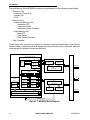


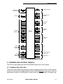

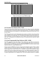

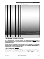
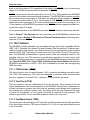
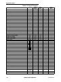
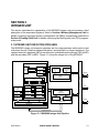
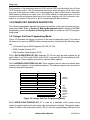
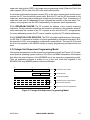
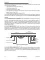
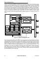
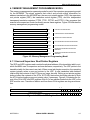

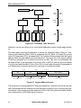

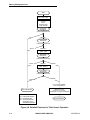
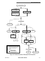
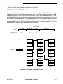
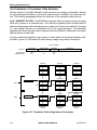

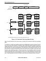
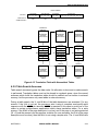
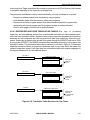
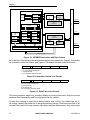
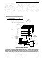


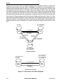
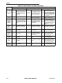
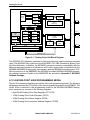
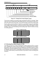
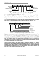
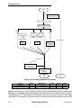


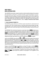
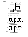
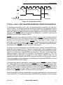
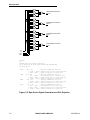
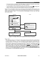
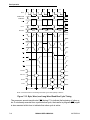
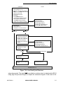
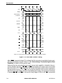
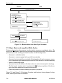
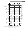
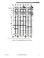
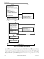
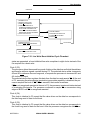
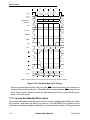
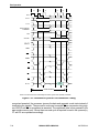
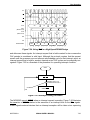
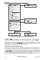
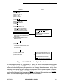
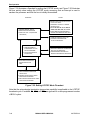

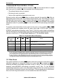
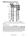
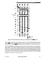
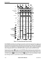
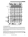
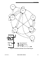


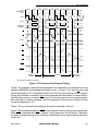
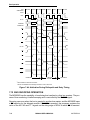

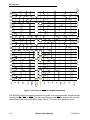
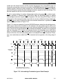

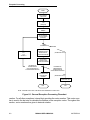

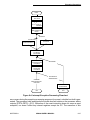
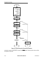


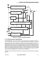

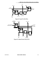

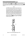

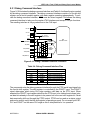
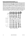
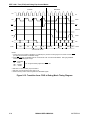
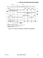


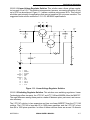
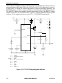
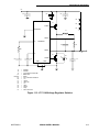
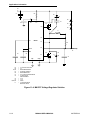
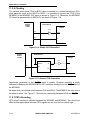

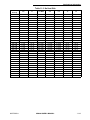
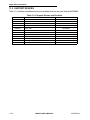
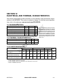
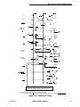
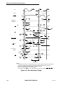
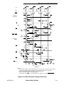
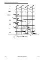
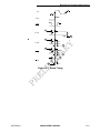

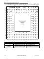
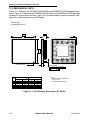
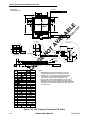
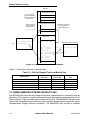

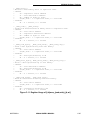
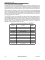


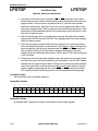


![HiSoft Devpac 3 (text version) [1992] [Manual: PDF]](http://vs1.manualzilla.com/store/data/005668901_1-67cf8256fc448cd2edf58a11a6ec729e-150x150.png)