1
ELECTRONIC LOCKING FOR HIGH VOLTAGE
GROUNDING SYSTEM
Eduard Boja
Josep Font Teixidó
10 June 2014
Contents
1 Introduction
1.1 Investigation . . . . . . . .
1.2 Project Explanation . . . .
1.2.1 Introduction . . . .
1.2.2 Existing system . . .
1.2.3 Our system . . . . .
1.3 Meetings with the tutor and
. . . . . . . .
. . . . . . . .
. . . . . . . .
. . . . . . . .
. . . . . . . .
the Company
.
.
.
.
.
.
.
.
.
.
.
.
.
.
.
.
.
.
.
.
.
.
.
.
.
.
.
.
.
.
.
.
.
.
.
.
.
.
.
.
.
.
.
.
.
.
.
.
.
.
.
.
.
.
.
.
.
.
.
.
.
.
.
.
.
.
.
.
.
.
.
.
.
.
.
.
.
.
.
.
.
.
.
.
.
.
.
.
.
.
.
.
.
.
.
.
.
.
.
.
.
.
.
.
.
.
.
.
.
.
.
.
.
.
.
.
.
.
.
.
.
.
.
.
.
.
.
.
.
.
.
.
.
.
.
.
.
.
.
.
.
.
.
.
.
.
.
.
.
.
.
.
.
.
.
.
5
7
8
8
8
10
11
2 Hardware description
2.1 Introduction . . . . . . . .
2.2 External device . . . . . .
2.2.1 Microcontroller . .
2.2.2 Power . . . . . . .
2.2.3 Display . . . . . .
2.3 Clamp hardware . . . . .
2.3.1 E2prom . . . . . .
2.3.2 Stepper and driver
2.4 Board design . . . . . . .
.
.
.
.
.
.
.
.
.
.
.
.
.
.
.
.
.
.
.
.
.
.
.
.
.
.
.
.
.
.
.
.
.
.
.
.
.
.
.
.
.
.
.
.
.
.
.
.
.
.
.
.
.
.
.
.
.
.
.
.
.
.
.
.
.
.
.
.
.
.
.
.
.
.
.
.
.
.
.
.
.
.
.
.
.
.
.
.
.
.
.
.
.
.
.
.
.
.
.
.
.
.
.
.
.
.
.
.
.
.
.
.
.
.
.
.
.
.
.
.
.
.
.
.
.
.
.
.
.
.
.
.
.
.
.
.
.
.
.
.
.
.
.
.
.
.
.
.
.
.
.
.
.
.
.
.
.
.
.
.
.
.
.
.
.
.
.
.
.
.
.
.
.
.
.
.
.
.
.
.
.
.
.
.
.
.
.
.
.
.
.
.
.
.
.
.
.
.
.
.
.
.
.
.
.
.
.
.
.
.
.
.
.
.
.
.
.
.
.
.
.
.
.
.
.
.
.
.
.
.
.
.
.
.
.
.
.
.
.
.
.
.
.
12
12
13
14
16
17
19
21
22
23
.
.
.
.
.
.
.
.
.
.
.
.
27
27
27
29
31
31
31
31
31
31
32
32
32
4 Conclusions
4.1 Improvements . . . . . . . . . . . . . . . . . . . . . . . . . . . . . . . . . . . . . . . . . .
33
33
5 Bibliography
34
3 Software description
3.1 Introduction . . . .
3.2 I2C Bus . . . . . .
3.3 Modules . . . . . .
3.3.1 twi.c . . . .
3.3.2 display.c . .
3.3.3 E2PROM.c
3.3.4 motor.c . .
3.3.5 polsadors.c
3.3.6 sleep.c . . .
3.3.7 menu.c . . .
3.3.8 main.c . . .
3.3.9 Makefile.c .
6 Annexes
6.1 Code
6.1.1
6.1.2
6.1.3
6.1.4
6.1.5
6.1.6
6.1.7
. . . . . . . .
twi.c . . . .
polsadors.c
motor.c . .
menu.c . . .
E2PROM.c
display.c . .
main.c . . .
.
.
.
.
.
.
.
.
.
.
.
.
.
.
.
.
.
.
.
.
.
.
.
.
.
.
.
.
.
.
.
.
.
.
.
.
.
.
.
.
.
.
.
.
.
.
.
.
.
.
.
.
.
.
.
.
.
.
.
.
.
.
.
.
.
.
.
.
.
.
.
.
.
.
.
.
.
.
.
.
.
.
.
.
.
.
.
.
.
.
.
.
.
.
.
.
.
.
.
.
.
.
.
.
.
.
.
.
.
.
.
.
.
.
.
.
.
.
.
.
.
.
.
.
.
.
.
.
.
.
.
.
.
.
.
.
.
.
.
.
.
.
.
.
.
.
.
.
.
.
.
.
.
.
.
.
.
.
.
.
.
.
.
.
.
.
.
.
.
.
.
.
.
.
.
.
.
.
.
.
.
.
.
.
.
.
.
.
.
.
.
.
.
.
.
.
.
.
.
.
.
.
.
.
.
.
.
.
.
.
.
.
.
.
.
.
.
.
.
.
.
.
.
.
.
.
.
.
.
.
.
.
.
.
.
.
.
.
.
.
.
.
.
.
.
.
.
.
.
.
.
.
.
.
.
.
.
.
.
.
.
.
.
.
.
.
.
.
.
.
.
.
.
.
.
.
.
.
.
.
.
.
.
.
.
.
.
.
.
.
.
.
.
.
.
.
.
.
.
.
.
.
.
.
.
.
.
.
.
.
.
.
.
.
.
.
.
.
.
.
.
.
.
.
.
.
.
.
.
.
.
.
2
.
.
.
.
.
.
.
.
.
.
.
.
.
.
.
.
.
.
.
.
.
.
.
.
.
.
.
.
.
.
.
.
.
.
.
.
.
.
.
.
.
.
.
.
.
.
.
.
.
.
.
.
.
.
.
.
.
.
.
.
.
.
.
.
.
.
.
.
.
.
.
.
.
.
.
.
.
.
.
.
.
.
.
.
.
.
.
.
.
.
.
.
.
.
.
.
.
.
.
.
.
.
.
.
.
.
.
.
.
.
.
.
.
.
.
.
.
.
.
.
.
.
.
.
.
.
.
.
.
.
.
.
.
.
.
.
.
.
.
.
.
.
.
.
.
.
.
.
.
.
.
.
.
.
.
.
.
.
.
.
.
.
.
.
.
.
.
.
.
.
.
.
.
.
.
.
.
.
.
.
.
.
.
.
.
.
.
.
.
.
.
.
.
.
.
.
.
.
.
.
.
.
.
.
.
.
.
.
.
.
.
.
.
.
.
.
.
.
.
.
.
.
.
.
.
.
.
.
.
.
.
.
.
.
.
.
.
.
.
.
.
.
.
.
.
.
.
.
.
.
.
.
.
.
.
.
.
.
.
.
.
.
.
.
.
.
.
.
.
.
.
.
.
.
.
.
.
.
.
.
.
.
.
.
.
.
.
.
.
.
.
.
.
.
.
.
.
.
.
.
.
.
.
.
.
.
.
.
.
.
.
.
.
.
.
.
.
.
.
.
.
.
.
.
.
.
.
.
.
.
.
.
.
.
.
.
.
.
.
.
.
.
.
.
.
.
.
.
.
.
.
.
.
.
.
.
.
.
.
.
.
.
.
.
.
.
.
.
.
.
.
.
.
.
.
.
.
.
.
.
.
.
.
.
.
.
.
.
.
.
.
.
.
.
.
.
.
.
.
.
.
.
.
.
.
.
.
.
.
.
.
.
.
.
.
.
.
.
.
.
.
.
.
.
.
.
.
.
.
.
.
.
.
.
.
.
.
.
.
.
.
.
.
.
.
.
.
.
.
.
.
.
.
.
.
.
.
.
.
.
.
.
.
.
.
.
.
.
.
.
.
.
.
.
.
.
.
.
.
.
.
.
.
.
.
.
.
.
.
.
.
.
.
.
.
.
.
.
.
.
.
.
.
.
.
.
.
.
35
35
35
38
39
41
43
44
48
6.1.8
Makefile . . . . . . . . . . . . . . . . . . . . . . . . . . . . . . . . . . . . . . . . .
3
49
The present document includes all the documentation and information regarding this final degree
project. This project is basically designed with the idea to improve the security and make it easier for
the people who have to deal with high-voltage lines to do their work. Such information includes all
the possible topics going through the very first ideas and reaching the conclusions in the end. Also it
explains all the hardware and software that it includes and how they are related one another. Also it
explains the desiging procedure that has been followed.
It is of crucial importance to mention that this project has been designed and created under the
request of the company Sofamel, SL to fulfill it’s needs and ambitions. They firstly presented a need
of improving a system that had always been mechanical, and our objective was to present a solution.
Our idea was introducing to this basic system a few electronic components that combined achieve the
objective of replacing the mechanical system. Afterwards, we presented our solution to them and they
valorated it and idicated what could be improved in the case of the need to continue with this project
later on.
1 Introduction
The main objective of this project is designing a security system for those people who work at high
voltage lines. Basically, we found out that the system that was used to connect the three-phase line to
the ground was way too rudimentary. Basically, a key was used to enable the worker to connect every
line to the ground. This lead to situations like loosing the key and having to just throw away the whole
equipment.
In the technological world like the one we live in, we decided that probably we could design some kind
of electronical system to perform that activity and improve the actual system. The basic operation
we must perform is authentication, as it is the main issue when we are talking about security. In the
previous system this was done by using a simple key but as we said this was quite of a problem. Our
idea, is to create an universal system to be able to access to any system we have.
The basic idea is that we have system with two way clamp that will be connected respectively to the
ground and to the high voltage line. Previously, any of the two clamp could only be operated when the
key was put inside the rabbet. The fact is that the normal way to operate is the one that follows:
First, we put the key into the rabbet of the clamp that is going to be connected to the ground. Once
we did this, we are able to manually open the clamp and connect it to the ground.
After this, we can remove the key from the first clamp and put it into the rabbet of the clamp that
we will connect to the high voltage. Once this is done we can manually open the second clamp and
connect it to the voltage.
Look out that when we do this, the first clamp can’t be operated at all, so when we have both clamps
connected respectively, the key can’t be removed from the second clamp. The only way to remove the
key is dissconecting the clamp from the high voltage line. This is the security system that we want to
improve electronically.
What we will develop is an external system that will identify every pair of clamps as something unique.
This way, we will be able to use this key in any pair of clamps that we have and will always work, taking
into account that we connect the system properly. Later on we will explain how we will do this. To
communicate our external system with the pair of clamps, we will use a bidirectional communication
bus. The one we have choosen is the I2C system which enables us to do exactly what we want.
This system basically consists in one master controlling a certain number of devices connected to the
bus. In our case the AVR will be the master, controlling all the slaves connected to the bus. The idea is
basically to connect the AVR to the pair of clamps, detect wheter the identification has been a success
of a failure, and afterwards releasing an interlocking that will enable us to manually open the clamp.
The idea is trying to reduce to the minimum the energy that will be needed to this operation, so as to
reduce the number of necessary batteries.
This project has four basic phases:
• Investigation: Information resarch regarding the project realization. This includes material, software, etc.
• Development: Hardware integration and software development to include all the parts in a single
one
• Presentation to the company: As it is a project designed for a company, we will show them our
design to exchange points of view
5
• Improvements: After having exchanged points of view with the people in the company, we will
do the necessary changes in the application to fit their expectations
I must be said that the Development phase has two different parts, the first one is to design a prototype
to fulfill the project expectations. Secondly there is the need of developing a group of boards to achieve
the final objective of implanting the project in the final device.
6
1.1 Investigation
The first step in every well designed project is the investigation. The basic idea is gathering all the
needed specifications and start looking for suitable solutions. Basically, the idea is to strip the project
into small parts and start trying to find solution to each of this parts and as soon as we solve them
start to gather them into bigger ideas and, at the same time, problems.
We knew that we wanted to interact with many possible slaves at the same time, beeing commanded
by a master so we needed a system that could be used this way.
What came into our mind was using Arduino and the i2c bus protocol to communicate with different
slaves. In fact this is what we chosed, and to do this we used the i2c.c library to get some extra time.
So to begin we first thought in what we wanted to do, and in consequence, what we needed to do it.
The first thing that we were asked was to perform an authentication system that replaced the key that
was used since the begining and that also did not need any power supply.
The first idea we had was the EEPROM memory, able to store data for a long time without needing
any power supply. So the first thing that we did was search for a pair of suitable EEPROM memories
for our project. Soon after this be begun developing a library for the interaction with the memories
and for making it easier to deal with them. The way to use the memory is easy, we will only use a
small part of the memory (1 byte) and we will compare if the value stored at both memories is the
same. In the case of getting a good authentication, we can proceed with the operation of the clamp,
else we won’t.
When we finished with the memories and the authentication, we thought it was a good idea to use a
display to show the user in which state was the device. Concerning this matter we used a very simple
display that we already used in some projects during our degree. The usage of this display will be very
simple, it will only show the user what is the system doing at that exact moment. For example, when
the user connects the device to the clamp and presses the button, the device wakes up and starts with
the indentification of the clamp. While doing it, it prints on the screen of the display, whether the
authentication has been a failure or not.
When the authentication is over we bump into the serious part of the project, that is the physical
operation of the clamp. We needed something that, in the case of a failure in the authentication, would
not allow the person working with the clamp to open it. The idea we had is to move an interlocking
90 degrees so as to enable the clamp to be opened manually. In the case of a failure during the
authentication the interlocking would remain closed and the clamp won’t be opened.
After having a clear idea of how our design would work, we started thinking what could we be using to
move the interlocking. The best idea of which we could think was a bipolar stepper motor with which
we would be able to excacly move a certain interlocking 90 degrees. It must be said that this will be
done two times like with the EEPROM’s because we have a pair of clamps so each one needs it’s own
interlocking.
The next thing we thought of is the battery needed to make the arduino work. The arduino needs 5V
to be working and will only need the power to work himself as the only thing that will be doing is
eventually moving the stepper motor 90 degrees. We will later on do some calculations to know how
long would a battery last and what kind of it do we need.
The last thing we thought we needed was a pair of buttons to operate the whole device, and that will
have a function that we will explain later on.
7
1.2 Project Explanation
1.2.1 Introduction
During this chapter we will be explaining the basis of both our project and the original one, that is the
one we will be using as example. From the original one we will be keeping the physical design as we
just want to use it to install an electronic system.
Furthermore we will be using the same concept of key to open the system, but instead of using a
physical one we will be using an electronic one. Also the design of our project is structured in two basic
phases. The first one is designing a prototype for our system, and as soon as it works, we will start
designing all the physical electronics and board layout for our final system.
1.2.2 Existing system
At this point, you may have a more or less clear idea of how our project works but how did the existing
systems work? And also what are their basic parts and what needs to be improved from them?
The previous systems were much more basic and mechanic but the problem is that they did not have
any external security at all. The system was completely mechanic and that’s what we wanted to change.
The basic idea of the existing system is the one that follows. We have a pair of clamps, one of which
can be opened manually to ground it, meaning connecting it into the ground. While you don’t have
the first clamp closed you are unable to open the second one. Once you grounded the first one, you
can open the second one and connect it to the high voltage line.
When you have both of them connected and you want to unplug the system, you have to do it backwards.
By this we mean that you can’t unplug the ground clamp before desconnecting the second one that is
connected to the high voltage. First you have to unplug the second clamp and secondly the ground
clamp.
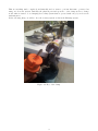
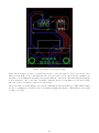
In the following picture we can apreciate one of the pairs of the clamp that will be connected to the
ground.
Figure 1.1: One pair of the clamp
8
This is something made completely mechanically and we want to perform this same operation but
using our electronic system. Basically the physical part and apearence of the clamp needs no change
at all, what we want to do is changing the security system that is operated with a key, by an electronic
authentication.
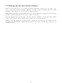
In the following image we will see how the security system works in the Existing system.
Figure 1.2: Key of the clamp
9
1.2.3 Our system
As it has already been explained, the basic idea of our system is to transform a purely mechanical
system into an electronic one. This will be made using an external device that will control the pair of
clamps using an Atmega328p processor. The idea is to use an external device as if it was a key, and it
fact it will be one, but not a physical one but an electronic one.
Our key will be an electronic external device with a display, a microprossesor and a connector that once
it is plugged to the clamp it operates as a key. The idea is that the external device checks the value of a
certain register in each of the pair of clamps and in the case of beeing the same value, proceed with the
authentication. After this the operator will have the oportunity to open the first locking and connect
the clamp to the ground, after this the second clamp will be available to be opened and connected to
the ground also.
As we already explained how our project worked, we will explain it now using a diagram so that you
can get a clearear glance of how the system interacts with the user and with the clamp.
Null
Sleep
Button
Unconnected
Failure
Wake-up
Lock opening
Connected
Success
Authentication
Figure 1.3: State diagram for our system
10
1.3 Meetings with the tutor and the Company
While develoving the project, we performed several meetings with both the tutor responsible of the
project, Josep Font, and the Company. This has been done to know at which point we are when
referring to achieveing the project expectations and specifications.
During this meetings I showed physically how the device was working and evolving since the last meeting
and also I explained what was the next step we will be developing.
After my explanations it was the turn for the tutor and the company to tell me what improvements
could be made and also what modifications they wanted me to do in the system.
It must be said that usually the meetings with the company were not made directly, meaning that the
tutor had a meeting with the company and afterwards it was only me and the tutor doing a project
evolution meeting.
11
2 Hardware description
2.1 Introduction
Certainly, one of the most important parts in any project is the hardware. As we already explained,
our system consists of a very few hardware parts as it is a very basic electronic system. The basic idea
consists of an external device that will be connected to any clamp and that will make it work. We will
later on explain what this external device consists on.
The way we will connect the external device to the clamps will be using a pair of Db9 connectors, one
for each of the pairs of the clamp. The external device will be the one containing the processor and all
the user interface parts. This includes the display and a pair of buttons. This external device contains
the most of the hardware parts our project will have.
The hardware inside the clamp won’t be acessible to any person and it will be only for identificating
any pair of clamps as something unique. Furthermore using the Db9 connector it will be the clamp
board the one moving the stepper motor inside the clamp to enable the worker to externally open the
clamp.
It is very important to understand that first we will design a prototype for testing our hardware and
software and afterwards we will design the final board that will be inside the device using Eagle.
Db9-connector
External device
Driver
Internal Device
Figure 2.1: State diagram for our system
12
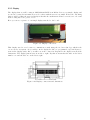
Stepper
2.2 External device
This external device consists on a system that has as objective to control the whole clamp. Meaning
this we understand interacting with the user, and sending the orders to the clamp. Firstly we designed
a prototype to make all the tests and configure all the hardware properly. Afterwards we designed the
board layout with all the components together so as to be integrated in a single device.
The board contains the following hardware, whoose operation will be explained lately:
• One Atmega 328p processor
• Two Capacitors of 22pF and one of 100pF
• One 100KOhms Resistor, one 2kOhms Resistor and two 4.8KOhms resistor
• Two Push-up buttons
• One 16Mhz Crystal oscillator
• One MCCOG21605B6W Display
• Two Db9 Output connectors
• One Double Input pin
• One ISP Input connector
Figure 2.2: External device board
In the figure above, we can see the main board we designed for our project. This board is responsible
for all the system configuration and operation as the rest of the system is pasive and only waits for
orders from the main board.
13
2.2.1 Microcontroller
The microcontroller we will be using is the Atmega 328p as it is the one that best fits ours project
needs. To use our microcontroller we added to it when designing the board schematic the necessary
components to adapt it to something similar to the Arduino board which is the one we used for our
prototype. So as to do this, we added a pair of push-up buttons, some resistances as well as capacitors
and a 16Mhz Oscillator Crystal.
Figure 2.3: Atmega Original Schematic
In the picture above we can see a picture of the the Atmega328p schematic, in the picture below you
can see the physical aperance of the microcontroller welded to the board.
Figure 2.4: Atmega 328p
The utilities that we will be using from our processor are the one’s that follow:
• Eight digital outputs: PD4-PD7 and PB0-PB3
• SDA and SCL bus outputs
• Sleep Mode
• Voltage and Ground outputs
• PC6/Reset as Reset Button
• PD3/INT1 as a Digital input
14
The eight digital outputs will be used to control the two steppers, one in each of the pair of clamps.
What we do is just setting the voltage high (5V) or low (0V). The SDA and SCL i2c bus outputs are
used for the communication with the E2proms and the display, also it is our crucial importance that
we connect the Voltage output and the Ground. The way to operate is the following, we connect the
power supply and the ground to the processor and then it is the processor the one that powers up the
rest of the system.
The reset is a very important matter for a system like this, so we connected a push-up button to the
reset pin in the processor so as to reset the system as soon as the push-up button triggers up. Also we
have connected to the PD3 pin another push-up button. This pin and his twin PD2 are the only ones
that can tell the Atmega to completely wake up when it is asleep so it is a very important part of our
project also.
In the following table we can see a brief explanation of the ports that we are using from the processor
and what are we using them for. For a bigger detail you can check the schematic attached at the annex.
Microcontroller Pin
PC6
Name
Reset
AREF/AVCC
GND
Voltage input
Ground
GND
Ground
PB6/PB7
XTAL1-TOSC1/XTAL2-TOSC2
PC4/PC5
PD4/PD5/PD6/PD7
SDA/SCL
T0/T1/AIN0/AIN1
PB0/PB1/PB2/PB3
ICP/0C1A/0C1B/MOSI
PB0/PB1/PB2/PB3
ICP/0C1A/0C1B/MOSI
PD3
INT1
PB4/PB5
MISO/SCK
Description
Atmega reset pin, used for
general reset.
General processor power.
General connection to the
ground.
General connection to the
ground.
External crystal oscillator
connection
i2c bus connectors
First four outputs used as
stepper motor controllers
Second four outputs used as
stepper motor controllers
Second four outputs used as
stepper motor controllers
Input pin used for waking up
the processor.
Input pins used for programming the processor.
Figure 2.5: Atmega 328p connections
15
2.2.2 Power
To power up our system we will be using four 1,2V AA NiMH Batteries PRT00335 able to supply
2500mAh. They will be connected right into the external device, and consequently to it’s board. Our
system is almost all the time asleep and it only wakes up for eventually authenticating the system and
moving the steppers and right after this it falls asleep again.
The boards on the clamps have no power supply connected to them so once they have been programmed
they remain unpowered until the external device is plugged in. This is the reason why we used e2prom
memories. This way the memories can remain unpowered for a long time and still be able to keep
stored it’s authentication values.
In the following image we can see an example of one of our batteries.
Figure 2.6: System Battery
The Atmega current consumption is of the order of mA when it is awake and 0.1µ A when it is asleep.
Knowing this we can make an apoximation of how long would our battery last. If we get in worst
possible case, the Atmega can reach peaks of 15mA consumption when working at full speed with the
oscillator. In this case we would get a life of 160 hours which is quite a lot, because our Processor works
only for 30 seconds every time it is awakened, then it falls asleep again.
If we get into the real case, the Atmega is awake for no longer than 30 seconds, and then it goes to
sleep again. Knowing this and getting an average that for every time the arduino stays awake it has
been 20 min asleep, we can make the following calculations.
Asuming the proportionality we already stated between the time it is asleep and the time it is awake,
we can calculate the average current consumption of our system.
Current =
(0.1 ∗ 10−3 ) ∗ 20 + (15) ∗ 0.5
= 3.751mA
2
(2.1)
Figure 2.7: Average current calculation in mA
With this calculations we now can calculate how long will our batteries last if we know that their
capacity is 2400mAh.
T ime =
2400mAh
= 660hours
3, 6mA
(2.2)
Figure 2.8: Battery duration calculation
Now we have calculated how long would our batteries last. Of course this is an aproximation and the
duration of the batteries will depend on how the person working uses the system.
16
2.2.3 Display
The display that we will be using is MCCOG21605B6W from Midas. It is a very simple display and
we used it because the information we need to share with the user is very small. In fact, the only thing
that we will be telling the user via display is whether the authentication has been a success or not and
if the locking has been opened or not.
Here you can see a picture of our simple display attached to the board:
Figure 2.9: Display connections
This display was choosen because it communicates easily using the i2c bus technology which is the
one we use in our system. As you will see in the display module, we programmed a specific library to
write in the display easily. Also you will see now the connection diagram for the display as well as the
dimensions. The display pins increase from left to right. By this we mean that the first on the left is
number one and the last one on the left is eight.
Figure 2.10: Display connections and dimensions
17
In the following table you will see a basic description of the connections. Bascially we connect to voltage
inputs and a ground. Also we connect the SCL and the SDA inputs to the bus system. The reset is
connected to the ground also, in the case you want to reset the display you have to trigger up the
system to 5V. The CAP1N and the CAP1P pins remain unused.
Display pin
1
2
3
4
5
6
7
8
Description.
Vout pin, voltage input connection.
Cap1N pin.
Cap1P pin.
Vdd connection, voltage input
connection.
Vss, ground connection.
SDA connection.
SCL connection.
RST, reset connection.
Figure 2.11: Display connection table
18
2.3 Clamp hardware
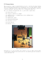
Inside each one of the pair of clamps, we have a small board that contains the hardware necessary to
control the stepper and to identify the clamp pair as a single one. This is basically done using the
following hardware, whoose operation will be explained lately:
• One BR24L08-W E2PROM Memory
• One Db9 connector
• One six output Pin
• One Stepper Driver
• One Stepper Motor
In the following image we can see how the board inside the clamp is:
Figure 2.12: Clamp board
In the board we can clearly see the three important elements. The first one is the E2PROM memory
that is used to authenticate the system, secondly the DB-9 input connector that powers up the board
and also controls the stepper, and third but not least important, the 6 outputs that control the stepper.
19
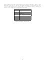
In the following image and it’s self-explaning table, we will see the pinout connection of the DB-9
connector. Regarding the 6 pin-out output for the driver stepper, we will explain them in the driver
and stepper section.
Figure 2.13: Db-9 connection
In this table we can see the connections of the Db-9. In some cases there are two connections, the
boards are symetrical, meaning that both do the same, but the ports that control the stepper are
different in each board thats why there are two connections in ports 5 to 2.
Display pin
1
2
Name
None
PB4 and PD7
3
PB2 and PD6
4
PB1 and PD5
5
PB0 and PB4
6
7
8
9
SCL
SDA
VCC
GND
Description.
Not connected.
Fourth and last port of the
stepper controller.
Third port of the stepper controller.
Second port of the stepper
controller.
First port of the stepper controller.
i2c serial clock connection.
i2c serial data connection.
5 Volt input.
Ground connection.
Figure 2.14: Db-9 connection table
20
2.3.1 E2prom
The memory we will be using in our clamp is BR24L08-W from Rohm. It has 8Kbit of memory that
can be used for storage, but this is very far from what we need for our authentication. In our case we
will only be using 1 register for storing a byte, that will be the same in the two E2proms of the clamp
and that will later on be used for authenticating the system.
Figure 2.15: BR24L08-W e2prom memory
It is important to mention that we are using this E2prom not only because it’s specifications fit perfectly
with our project needs but also because it is specifically designed for working with i2c system, which
is the core of our project design.
In the table below you will find a brief explanation of the connections in the memory. It is important
to mention that this memories have already set all the bits for adressing them but one, which is A2.
So to distinguish both memories we connected this pin to GND and Vcc respectively in each memory,
so that we can address them properly. A0 and A1 remain unconnected in this memories. Also the
write protect terminal is used for enabling or disabling the write in the memory, when is set to 0 and
1 respectively. In our design we set it to 0 as we believe that is inteligent to leave the write available
because if we set it to 1, once the board is welded and in the case of having any problem which required
rewritting the memory, we would have to buy a whole board.
Display pin
1
Name
A0
2
A1
3
A2
4
5
6
7
8
GND
SDA
SCL
WP
VCC
Description.
First bit for i2c memory addressing
Second bit for i2c memory addressing
Third bit for i2c memory addressing
Ground connection.
i2c serial data connection.
i2c serial clock connection.
Write protect terminal.
5 Volt input.
Figure 2.16: E2prom connection table
21
2.3.2 Stepper and driver
Connected right into our special designed clamp board, we have the stepper and it’s driver whoose
main puropuse is to open and close the locking for the clamp. The stepper motor that we will be using
is the 28BYJ-48 and we having it working with the ULN2003 driver. Later on we will further explain
it’s technical characteristics. In the following picture you can see the stepper.
Figure 2.17: 28BYJ-48 stepper motor
The stepper is commanded by our microprocessor in the main board and it is basically done by sending
him small pulses of 5V (steps) to it’s four inputs. The problem we had, is that altough the stepper is
quite small, our microprocessor hadn’t enough power to move it properly. Because of this, and after
beeing unable to move any stepper just with the system we had, we decided to add a driver.
The basic operation of the driver is to increase the current, ideally this driver can transform a current
of 1,5mA to 150mA reaching a maximum output current of 500mA. In our case it increases the current
that the microprocessor sends that has a value of 2mA to reach the necessary input current for our
stepper, aproximately 100mA.
Figure 2.18: ULN2003 stepper driver
Apart from increasing the current the driver does another very important job. In the last part of the
driver there is a diode included so as to not allowing the current to drive the other direction. This is
very important because if it wasn’t for this the current could be driven in inverse which is something
that we don’t want!
If you want to read further technical information about this two components you can find them in the
annex section. Furthermore, the code that is used to program the stepper will be explained in the
software chapter.
22
2.4 Board design
At the very beginning we used a protoboard to design our project and also to check the behavior of
all the components, and as soon as we advanced with the project, we kept integrating the components
into a single system. Once the system worked we decided it was about time to create a board that
could fullfil the necessities of our project.
More certainly, we needed three boards two of which would be practically identical. As we already
explained, we would have a central device that will control the whole system and that will have the big
board containing the Microprocessor and the user interface. Also, we need one small board inside each
pair of the clamp, to which we will connect the big board and that we will be using for authenticating the
system and moving the stepper. By moving the stepper we understand tranismitting the microprocessor
orders to the stepper, as the small board has no active component able to transmitt anything.
In the following picture we can see the interface of the eagle program that we are using for our system
designing.
Figure 2.19: Eagle interface picture
The design of the board has been performed using Eagle, a very specific program for board designing.
The user interface of the program is very easy-going and we got used to it very easily. The designing
of the board has two basic parts:
• Schematic design
• Board layout design
To design the schematic the first step is choosing all the components that we need in our board and
connecting them to one another using the eagle software. It is of vital importance not forgetting any
component nor any interconnection as later on we will link this schematic file to the board layout and
if there isn’t a single component we will have lots of troubles.
23
When finished, our schematics from the main board and clamp board looked like this:
Figure 2.20: Main board schematic design
Figure 2.21: Clamp board schematic design
24
Once we finish our schematic it is time for the layout designing. Unlike the schematic this the closer
you can be to hell if you have never designed a board layout. In our case both boards are quite simple,
yet we had lots of problems until we finished them successfully.
The main problem is that not a single track of the board can ran over any other, as we would get a
short-circuit. This may seem quite of a basic clue but, in fact, it isn’t. The reality is that there are
quite a few dozens of tracks going from one side of the board to the other and is quite a hard job
achieving to optimize the space as well as getting a good looking board.
To make it easier for such a newbie like I am with board design, we will use double side designing so
we can drive tracks through both sides of the board. Also we can connect one another using drills, that
will shortcircuit both sides of the board, we could say it is more or less like making a tunnel.
In the following pictures you can see how our board layout final design looks like.
Figure 2.22: Main board layout design
25
Figure 2.23: Clamp board layout design
In the layout design you can see connections from two colors, blue and red. Red colors are the one’s
that are in the TOP of our board while the blue one’s are in the bottom. As we already explained, we
use this to avoid making shortcircuits between the different connections. The same happens with the
devices attached to the board, blue ones will be attached at the bottom while red ones at the TOP.
The rest of the board will be connected to the ground.
The green button look like things you see are the drills that we already mentioned. This drills are what
we use to communicate both sides of the board without making any disgrace. This drills are very useful
to jump over a line.
26
3 Software description
3.1 Introduction
Having explained the hardware that is used in our project, it is now about time to explain the most
important matter, the software that makes this hardware work properly. The software is certainly the
most important part in our project as it is by far to what we dedicated more time developing.
Our project has been programmed using C and it is jerarquically structured by modules and based on
the i2c system as a communication tool. This is the basis of the system, later on we will explain how
this structure works in the Module section.
In general, we haven’t written a big amount of code but a very specific one. The idea was to be very
concrete and specific rather than writting huge modules full of unusefull lines. During this introduction
we will explain the basis of our project software.
By this we mean explaning both the code and the communication tool we will be using. First of all we
will explain the specifications and usage of the i2c bus protocol and how we will use it in our system.
Later on we will make an introduction of how ous software system works and how the modules interact
with one another. In the end to finish the chapter we will be explaining briefly what each module is
responsible of, as later on we will include the code in the annex and it is not necessary to do a huge
explanation.
3.2 I2C Bus
We will explain now the basis of our project intercomunication, the i2c bus. The i2c is basically a multimaster serial single-ended bus invented by the Philips semiconductor division, today NXP Semiconductors, and used for attaching low-speed peripherals to a motherboard, embedded system, cellphone,
or other digital electronic devices. Several competitors, such as Siemens AG (later Infineon Technologies AG, now Intel mobile communications), NEC, Texas Instruments, STMicroelectronics (formerly
SGS-Thomson), Motorola (later Freescale), and Intersil, have introduced compatible I2C products to
the market since the mid-1990s.
The i2c is a very usefull bus to communicate a master with several slaves as it’s protocol it’s simple
to implement and to understand. In our case we use the i2c to communicate with the Display and the
E2prom memories. We use the 300Khz mode so we could still be using a faster mode in the case of
needing it.
The basis of this system consists in two lines, one is the serial clock (SCL) and the other one is the
serial data (SDA). Every slave or master has to be connected to both lines to have communication with
the system. The beginning of our system will be the Arduino to which we connect the SDA and SCL
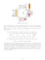
to the analogic pins A4 and A5 respectively.
In the following picture you can see where physically are the SDA and SCL connections for the Atmega328p.
27
Figure 3.1: i2c pins location
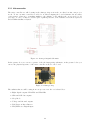
It is of crucial importance to connect both lines using a pull-up to 5V. This is very important when
using i2c as the system wouldn’t work without the pull-up’s, the value of the resistors is 4’8KOhms
each.
In the following picture you will see a diagram of how the pullup should be connected, as well as some
aleatory devices.
Figure 3.2: i2c connection diagram with pull-up
After all this previous matter regarding the setup, we program our Processor to initialize the system
and communicate to the slaves that we want. When this is done it is time to connect the slaves to the
line. It must be said that it is crucial when defining the code that we compile in our Processor, that
the slave adresses are defined properly, both physically and in our software (They must be the same!).
Usually most of the systems have 6-7 bit adress that are fixed and there are 1-2 bits that can be choosen
by hardware externally. This allows us to define the address of our slaves in the case of connecting two
slaves of the same kind.
28
3.3 Modules
As we already explained, our system is structured in modules because it is the best way the define a
clear structure. To make an approach to this structure we will begin listing all the modules that are
included in our system and we will later on explain the communication and dependencies between them
using a jerarchy and dependency diagram.
In later chapters we will include all the code in our project so that we can take even a closer look to
our system. Also we will explain what each module is responsible of. This is the list of the modules
included in our system:
• twi.c
• display.c
• E2PROM.c
• motor.c
• menu.c
• main.c
• sleep.c
• polsadors.c
Also we have a Makefile which is the responsible of structuring the dependencies between modules and
compiling it into a single file. Our system is very simple and easy to understand, as we have very few
lines of code. In the next page we will illustrate you with a module diagram so that you can better
understand which modules is used for who and what are the dependencies between them.
29
In the following diagram, we want to show how our modules interact with one another. The arrow
indicates how the information flows in our system. By this we mean that the main.c is the module
using information from the four below, and the menu is using the other two and so on.
Also it must be said that all the modules include some packages that are not self explained in this
diagram but that are included in the annex so that you can check them.
main2.c
sleep.c
menu.c
polsadors.c
E2PROM.c
display.c
twi.c
Figure 3.3: Software modules digaram
30
motor.c
3.3.1 twi.c
The twi module is the one responsible for the most basic communication with the i2c bus. This module
is responsible for first of all configurating the speed, the address, the master and the salves. Also it
physically sends the instructions for reading writting the registers in a certain slave within the i2c
connection.
The i2c module doesn’t need to use any other module to work but it is used for the display. and the
E2PROM.c modules to help them work.
3.3.2 display.c
The display.c module is the one responsible for interacting with the display. It uses the twi module to
send orders to the display slave so that we can write anything. The module is programmed so that we
can send what we want to write and the module itself uses twi.c to write it.
3.3.3 E2PROM.c
The E2PROM is a ver specific module that is used to adress two different kinds of E2PROM memories.
This module is used to access the different registers in the memory and writting or reading them. With
this module we can write to any memory of the same family of the one designed for our project.
This module uses the twi.c module to physically communicate with the memory and send to it orders
such as what he wants to read etcetera. The way we programmed the module we can access any register
we want and reading it or writting to it.
3.3.4 motor.c
This module is the one that interacts with the stepper motor and does not need any other module to
work, it just interacts with the main.c to receive orders of when to move the stepper. It main task is
to move the lock 45 degrees in one direction or another depending if you want to open or to close the
lock.
This module interacts directily with the output pins of the processor to set them high or low, so interacts
with the most physical layer of the system. It basic operation is fullfilling a complete loop to make the
stepper move one step, and do a certain number of steps to move 45 degrees.
3.3.5 polsadors.c
The polsadors.c module is the module in charge of controlling the push-up buttons in our system.
Basically it controls the button that wakes up the processor when it is asleep. This is done by using
an atention interrupt routine, that wakes up the atmega once the button is pushed.
This module works by its own self and it is only used by the main.
3.3.6 sleep.c
The sleep.c module is a very simple module. This module the only thing that does is awaking and
sending the arduino to sleep. This is done using the ¡avr/sleep.h¿ library that is specifically designed
for this. This module works by its own and does not need any other module to work, furthermore it is
only used by the main.
31
3.3.7 menu.c
The menu.c module is the second most important module in our sytem. This module uses some of the
most basic modules to send information to the main.c. His objective is reducing the amount of code
inside the main and making easier to understand.
This module uses the E2PROM.c, and the display.c module, and inderectly uses also the twi.c module.
The idea of this module is to aglutinate in further implementations also the sleep.c, motor.c and the
polsadors.c modules. This way the main will be only using the menu.c module and will be this one
mentioned the one that is used by the main.c.
3.3.8 main.c
This is our princpial module, as it name indicates. It’s objective is to use, directly or indirectly, all the
modules in our system. Our main is based in a routine that attends the interruption when the button
to wake up the system is pushed.
After this, the system does the authentication of the two E2PROM’s in the clamp and if the authentication is alright the system opens the locking of the sytem, allowing the user to open the clamp manually.
After this it send the processor back to sleep. If the authentication is a failure the system goes back to
sleep again.
It must be said that the system while processing all this actions, it mantains the user informed of the
actuation using the display, sending the system status at all time.
3.3.9 Makefile.c
The makefile is not a module at all, but we thought we had to include it as it is a very important piece
of our design. The makefile is used for compiling the main and sending it to the processor successfully.
If you want to further see what is it based on you can take a look at it on the annex chapter.
32
4 Conclusions
The conclusion of our project is that we successfully designed a device to improve system that had
worked mechanically for so long. This was our objective from the very begining as all the mechanical
systems have huge limitations. Our design, apart from beeing very compact, is suitable to lots of
changes in the case of beeing necessary.
In this first design we used a single byte for the system authentication, this is something we can easily
modify reserving more bits for the authentication. Also the code we programmed to our processor can
easily be used for much more bigger stepers. The only need in the case of needing bigger stepers to
move a bigger lock, would be using a driver or a power bridge able to provide the stepper with the
necessary current.
In general de project has been a success as we achieved the objectives stated in the beginning. During
the project design we achieved the first objective of making the prototype work and once we knew that
our project was factible we begun the design of the board with the final device.
This last steps of designing the final device were much more complicated than the prototype design, as
we weren’t used to the usage of Eagle and to designing board layouts. Anyway, once we knew that our
project was factible and worked properly we can say that our project has been a success.
4.1 Improvements
As we said from the very beginning, this project has been designed for a company, Sofamel, SL an so
on the objectives were stated by them and the tutor of the project. The first objective was to think of
the suitable design that could substitute the existing mechanical system for a more modern one.
All together, we thought that we could use some kind of digital key instead of the physical key that was
used until then. The idea we had was to design an external system that when plugged into the clamp
would work as a key. The difference between the mechanical system and the one that was about to be
designed was that the digital one would work for any clamp, while the key worked only for a certain
one.
This idea needed the design of an external device able to be connected to the clamp, and afterwards
interact with some kind of internal device, that would authenticate the clamp as an unique pair. After
this we would open the clamp locking using the external device.
Having fulfilled the company Sofamel, SL objectives, it is clear that we designed a device that could
be used in real live. The fact is that this device is suitable to huge changes, as we knew it wasn’t the
final device but just the beginning. The idea is that this project can be further developed in the case
of the Company beeing realy interested in developing it for real life usage.
33
5 Bibliography
E2prom = Brl24L, Pdf = ”http://rohmfs.rohm.com/en/products/databook/datasheet/ic/memory/
eeprom/br24l-e.pdf”
Stepper = 28BYJ-48, Pdf = ”http://robocraft.ru/files/datasheet/28BYJ-48.pdf”,
Driver = Uln2003, Pdf = ”http://www.ti.com/lit/ds/symlink/uln2003a.pdf”,
Processor = Atmega328p, Pdf = ”http://www.atmel.com/Images/doc8161.pdf”,
Display = MCCOG21605B6W, Pdf = ”http://www.farnell.com/datasheets/1663636.pdf”,
i2c = i2c user manual, Pdf = ”http://www.nxp.com/documents/user_manual/UM10204.pdf”,
Eagle = Eagle manual, Pdf = ”http://www.cadsoft.de/wp-content/uploads/2011/05/V6_manual_
en.pdf”,
34
6 Annexes
6.1 Code
6.1.1 twi.c
1
2
3
4
5
6
7
8
9
10
11
12
13
14
15
16
17
18
19
20
21
22
23
24
25
26
27
28
29
30
31
32
33
34
35
36
37
38
39
40
41
42
43
44
45
46
47
48
49
50
51
#include
#include
#include
#include
#include
#include
#include
<avr / i o . h>
< u t i l / t w i . h>
<avr / i n t e r r u p t . h>
<s t d b o o l . h>
<i n t t y p e s . h>
” t w i . h”
” d i s p l a y . h”
/∗ Envia ∗/
s t a t i c void s t a r t ( void ) {
TWCR = (1<<TWINT) |(1<<TWSTA) |(1<<TWEN) ;
}
s t a t i c void data ( u i n t 8 t d ) {
TWDR = d ;
TWCR = (1<<TWINT) |(1<<TWEN) ;
}
s t a t i c void s t o p ( void ) {
TWCR = (1<<TWINT) |(1<<TWSTO) |(1<<TWEN) ;
}
/∗ Espera ∗/
s t a t i c void w a i t t w i n t ( void ) {
while ( ! (TWCR&(1<<TWINT) ) ) ;
}
s t a t i c void w a i t s t o p ( void ) {
while ( (TWCR&(1<<TWSTO) ) ) ;
}
/∗ V e r i f i c a ∗/
s t a t i c bool c h e c k s t a r t ( void ) {
return ( (TWSR&0xF8 ) != TW START) ;
}
s t a t i c bool c h e c k r e p s t a r t ( void ) {
return ( (TWSR&0xF8 ) != TW REP START) ;
}
s t a t i c bool c h e c k m t a d d r e s s ( void ) {
return ( (TWSR&0xF8 ) != TW MT SLA ACK) ;
}
s t a t i c bool c h e c k m t d a t a ( void ) {
return ( (TWSR&0xF8 ) != TW MT DATA ACK) ;
}
s t a t i c bool c h e c k m r a d d r e s s ( void ) {
35
52
53
54
55
56
57
58
59
60
61
62
63
64
65
66
67
68
69
70
71
72
73
74
75
76
77
78
79
80
81
82
83
84
85
86
87
88
89
90
91
92
93
94
95
96
97
98
99
100
101
102
103
104
105
106
107
108
109
110
111
112
113
114
115
116
117
return ( (TWSR&0xF8 ) != TW MR SLA ACK) ;
}
/∗−−−−−−−−−−−−−−−−−−−−−−−−−−−−−−−−−−−−−−−−−−−−−∗/
bool c a t c h c h a n n e l ( void ) {
start () ;
wait twint () ;
return c h e c k s t a r t ( ) ;
}
bool r e p c a t c h c h a n n e l ( void ) {
start () ;
wait twint () ;
return c h e c k r e p s t a r t ( ) ;
}
bool s e n d a d d r e s s m t ( u i n t 8 t a ) {
data ( a<<1) ;
wait twint () ;
return c h e c k m t a d d r e s s ( ) ;
}
bool s e n d a d d r e s s m r ( u i n t 8 t a ) {
data ( ( a<<1) | ( 0 b00000001 ) ) ;
wait twint () ;
return c h e c k m r a d d r e s s ( ) ;
}
bool s e n d d a t a ( u i n t 8 t d ) {
data ( d ) ;
wait twint () ;
return c h e c k m t d a t a ( ) ;
}
i n t 8 t r e c e i v e d a t a ( void ) {
// u i n t 8 t d = TWDR;
TWCR = (1<<TWINT) |(1<<TWEN) |(1<<TWEA) ;
wait twint () ;
i n t 8 t d = TWDR;
return d ;
}
i n t 8 t r e c e i v e d a t a l a s t ( void ) {
// u i n t 8 t d = TWDR;
TWCR = (1<<TWINT) |(1<<TWEN) ;
wait twint () ;
i n t 8 t d = TWDR;
return d ;
}
void r e l e a s e c h a n n e l ( void ) {
stop () ;
wait stop () ;
}
/∗−−−−−−−−−−−−−−−−−−−−−−−−−−−−−−−−−−−−−−−−−−−−−∗/
/∗ I n n i t ∗/
void s e t u p t w ( void ) {
36
118
119
120
121
122
123
124
125
126
127
128
129
130
131
132
133
134
135
136
137
138
139
140
141
142
143
144
145
146
147
148
149
150
151
152
153
154
155
156
157
DDRC = 0xFF ;
// P o r t s de s o r t i d a
TWSR &= 0 b11111100 ; // P r e s c a l e r 1
TWBR = 7 2 ;
// Freq . 100 kHz
sei () ;
}
u i n t 8 t regRead ( const u i n t 8 t s l a v e a d d r , const u i n t 8 t r e g ) {
// r e g i s t e r r e a d
u i n t 8 t data ;
catch channel () ;
send address mt ( slave addr ) ;
send data ( reg ) ;
d i s p l a y w r i t e ( ”OK1” ) ;
rep catch channel () ;
d i s p l a y w r i t e ( ”OK2” ) ;
send address mr ( slave addr ) ;
d i s p l a y w r i t e ( ”OK3” ) ;
data = r e c e i v e d a t a l a s t ( ) ;
d i s p l a y w r i t e ( ”OK4” ) ;
release channel () ;
return data ;
}
void r e g W r i t e ( const u i n t 8 t s l a v e a d d r , u i n t 8 t reg , u i n t 8 t data ) {
// r e g i s t e r w r i t e
catch channel () ;
send address mt ( slave addr ) ;
send data ( reg ) ;
s e n d d a t a ( data ) ;
release channel () ;
}
void r e g W r i t e S ( const u i n t 8 t s l a v e a d d r , u i n t 8 t data ) {
catch channel () ;
send address mt ( slave addr ) ;
s e n d d a t a ( data ) ;
release channel () ;
}
37
6.1.2 polsadors.c
1
2
3
4
5
6
7
8
9
10
11
12
13
14
15
16
17
18
19
20
21
22
23
24
25
26
27
28
29
30
31
32
33
34
35
36
37
38
39
40
41
#include
#include
#include
#include
#include
<i n t t y p e s . h>
< u t i l / d e l a y . h>
<avr / i o . h>
<s t d b o o l . h>
” p o l s a d o r s . h”
void i n i t p o l s ( void ) {
/∗ E x t e r n a l i n t e r r u p t s e n a b l e , r e g i s t e r s t o m o d i f i c a t e :
− PORTD − Per a c t i v a r p u l l −ups i n t e r n s
− EICRA [ ISC11 | ISC10 ] − Per s e l e c c i o n a r e l mode
− EIMSK [ INT1 | INT0 ] − Per a c t i v a r / d e s a c t i v a r l e s i n t e r r u p c i o n s
− EIFR [ INTF1 | INTF0 ] − Per comprovar s i h i ha i n t e r r u p c i o n s
∗/
DDRD &= ˜ ( 1 << DDD3) ;
PORTD |= ( 1 << PORTD2) ;
// Activem p u l l −up
EICRA |= ( 1 << ISC10 ) | ( 1 << ISC11 ) ;
// S ’ a c t i v a i n t e r r u p c i o p e r q u a l s e v o l c a n v i
EIMSK |= ( 1 << INT1 ) ;
//EIMSK |= (1 << INT0 ) ;
// I n t e r r u p c i o n s h a b i l i t a d e s
}
void d e s a c t i v a i n t ( void ) {
/∗ I n t e r r u p t d i s a b l e
∗/
EIMSK |= ( 1 << INT1 ) ;
//EIMSK |= (1 << INT0 ) ;
}
bool v a l o r a l t ( void ) {
/∗ R i s e up i n t e r r u p t i o n c h e c k i n g
∗/
return ( ( PIND & ( 1 << PD3) ) != 0 ) ;
}
void d e s a c t i v a f l a g ( void ) {
/∗ f l a g d i s a b l e
∗/
EIFR |= ( 1 << INTF1 ) ;
}
38
6.1.3 motor.c
1
2
3
4
5
6
7
8
9
10
11
12
13
14
15
16
17
18
19
20
21
22
23
24
25
26
27
28
29
30
31
32
33
34
35
36
37
38
39
40
41
42
43
44
45
46
47
48
49
50
51
52
53
54
55
56
57
58
59
60
61
62
63
64
#include ” motor . h”
//#i n c l u d e < s t d l i b . h>
#include <avr / i n t e r r u p t . h>
#include <avr / s f r d e f s . h>
#include ” queue . h”
#include < u t i l / d e l a y . h>
#include <avr / i o . h>
// This i s our u s u a l i n c l u d e
#define F CPU 16000000UL
//F=16Mhz
#include < u t i l / d e l a y . h>
//The d e l a y f u n c t i o n s / r o u t i n e s
void s e t u p 2 ( void ) {
DDRD
DDRD
DDRD
DDRD
DDRB
DDRB
DDRB
DDRB
|=
|=
|=
|=
|=
|=
|=
|=
(1<<PD7) ;
(1<<PD6) ;
(1<<PD5) ;
(1<<PD4) ;
(1<<PB3) ;
(1<<PB2) ;
(1<<PB1) ;
(1<<PB0) ;
}
void d e g r e e ( void ) {
// 45 d e g r e e s r o t a t i o n
i n t t =0;
while ( t <130) {
gir1 () ;
gir2 () ;
t +=1;
}
}
void g i r 1 ( void ) {
// F i r s t s t e p p e r move
i n t x =1;
// 1
PORTD = 1 2 8 ;
delay ms (x) ;
PORTD = 1 9 2 ;
delay ms (x) ;
PORTD= 6 4 ;
delay ms (x) ;
PORTD= 9 6 ;
delay ms (x) ;
PORTD=32;
delay ms (x) ;
PORTD=48;
delay ms (x) ;
PORTD=16;
delay ms (x) ;
PORTD=144;
delay ms (x) ;
}
void g i r 2 ( void ) {
39
65
66
67
68
69
70
71
72
73
74
75
76
77
78
79
80
81
82
83
84
85
// Second s t e p p e r move
i n t x =1;
// 1
PORTB = 8 ;
delay ms (x) ;
PORTB = 1 2 ;
delay ms (x) ;
PORTB= 4 ;
delay ms (x) ;
PORTB= 6 ;
delay ms (x) ;
PORTB=2;
delay ms (x) ;
PORTB=3;
delay ms (x) ;
PORTB=1;
delay ms (x) ;
PORTB=9;
delay ms (x) ;
}
40
6.1.4 menu.c
1
2
3
4
5
6
7
8
9
10
11
12
13
14
15
16
17
18
19
20
21
22
23
24
25
26
27
28
29
30
31
32
33
34
35
36
37
38
39
40
41
42
43
44
45
46
47
48
49
50
51
52
53
54
55
56
57
58
59
60
61
62
63
64
#include <avr / i o . h>
#include < u t i l / d e l a y . h>
#include < u t i l / t w i . h>
#include <avr / i n t e r r u p t . h>
#include <s t d b o o l . h>
#include <i n t t y p e s . h>
#include ” s e r i a l . h”
#include ” d i s p l a y . h”
#include ”E2PROM. h”
//#i n c l u d e <a v r / s l e e p . h>
char x ;
char y ;
/∗
v o i d adorm ard ( v o i d ) {
s e t s l e e p m o d e (SLEEP MODE PWR DOWN) ;
sleep enable () ;
sleep cpu () ;
}
∗/
void i n i t p r i n c ( void ) {
// i n i t
s e r i a l i n i t () ;
setup tw () ;
e2prom init () ;
display init (2 ,0) ;
display on () ;
display cursor on () ;
display clear () ;
}
void w r i t e e p r o m ( void ) {
e 2 p r o m w r i t e ( 0xEA, 0 x02 ) ; //E2prom w r i t e
e 2 p r o m w r i t e 2 ( 0xEA, 0 x02 ) ;
}
void comparacio ( void ) {
// A u t h e n t i c a t i o n comparsion
x = e2prom read ( 0xEA) ;
y = e2prom read2 ( 0xEA) ;
// y= 0 x02 ;
i f ( x == y ) {
display clear () ;
display write (” Authentication ”) ;
display setcursor (0 ,1) ;
d i s p l a y w r i t e ( ”OK” ) ;
delay ms (2000) ;
}
else {
display clear () ;
display write (” Authentication ”) ;
display setcursor (0 ,1) ;
display write (” failure ”) ;
delay ms (2000) ;
}
41
65
66
67
68
69
70
71
72
73
74
75
76
77
78
79
80
81
82
83
84
85
86
87
88
89
90
91
92
93
94
95
96
97
98
99
100
101
102
103
104
105
106
107
108
109
110
111
112
113
114
115
116
}
void benvinguda ( void ) {
//Welcome
init princ () ;
d i s p l a y w r i t e ( ”Welcome” ) ;
delay ms (2000) ;
display clear () ;
d i s p l a y w r i t e ( ” I n i t i a l i z i n g the ” ) ;
display setcursor (0 ,1) ;
d i s p l a y w r i t e ( ” system ” ) ;
delay ms (2000) ;
}
void a u t h e n t i c a t i o n ( void ) {
// System a u t h e n t i c a t i o n
display clear () ;
d i s p l a y w r i t e ( ” System ” ) ;
display setcursor (0 ,1) ;
display write (” authentication ”) ;
delay ms (2000) ;
comparacio ( ) ;
}
void adeu ( void ) {
// Goodbye
display clear () ;
display write (” Autentificacio ”) ;
display setcursor (0 ,1) ;
d i s p l a y w r i t e ( ” acabada ” ) ;
delay ms (2000) ;
display clear () ;
display setcursor (0 ,0) ;
d i s p l a y w r i t e ( ” Desbloquejant ” ) ;
delay ms (2000) ;
display clear () ;
d i s p l a y w r i t e ( ” Enclavament ” ) ;
display setcursor (0 ,1) ;
display write ( ” obert ” ) ;
delay ms (2000) ;
display clear () ;
d i s p l a y w r i t e ( ” Fins a v i a t ” ) ;
delay ms (2000) ;
display clear () ;
}
42
6.1.5 E2PROM.c
1
2
3
4
5
6
7
8
9
10
11
12
13
14
15
16
17
18
19
20
21
22
23
24
25
26
27
28
29
30
31
32
33
34
35
36
37
38
39
40
41
42
43
44
45
46
47
48
49
50
51
52
53
54
55
56
57
58
59
60
61
62
63
64
#include
#include
#include
#include
<s t d i n t . h>
”E2PROM. h”
” t w i . h”
” d i s p l a y . h”
void e 2 p r o m i n i t ( void ) {
// I n i t
setup tw () ;
}
s t a t i c void e 2 p r o m a d d r e s s i n g ( u i n t 1 6 t a d d r e s s ) {
/∗ F i r s t eeprom d i r e c t i o n ∗/
catch channel () ;
s e n d d a t a (E2PROM SLA W) ;
s e n d d a t a ( ( i n t ) ( a d d r e s s >>8) ) ;
s e n d d a t a ( ( i n t ) ( a d d r e s s&0xFF) ) ;
//MSB
//LSB
}
s t a t i c void e 2 p r o m a d d r e s s i n g 2 ( u i n t 1 6 t a d d r e s s ) {
/∗ Second Eeprom d i r e c t i o n ∗/
catch channel () ;
s e n d d a t a (E2PROM SLA W2) ;
s e n d d a t a ( ( i n t ) ( a d d r e s s&0xFF) ) ;
//LSB
}
void e 2 p r o m w r i t e ( u i n t 1 6 t a d d r e s s , char data ) {
/∗ F i r s t eeprom w r i t e ∗/
e2prom addressing ( address ) ;
s e n d d a t a ( data ) ;
release channel () ;
}
void e 2 p r o m w r i t e 2 ( u i n t 1 6 t a d d r e s s , char data ) {
/∗ Second eeprom w r i t e ∗/
e2prom addressing2 ( address ) ;
s e n d d a t a ( data ) ;
release channel () ;
}
char e2prom read ( u i n t 1 6 t a d d r e s s ) {
/∗ F i r s t eeprom r e a d ∗/
e2prom addressing ( address ) ;
release channel () ;
rep catch channel () ;
s e n d d a t a (E2PROM SLA R) ;
char data=r e c e i v e d a t a ( ) ;
release channel () ;
return data ;
}
char e2prom read2 ( u i n t 1 6 t a d d r e s s ) {
/∗ Second eeprom r e a d ∗/
e2prom addressing2 ( address ) ;
release channel () ;
rep catch channel () ;
s e n d d a t a (E2PROM SLA R2) ;
char data=r e c e i v e d a t a ( ) ;
release channel () ;
return data ;
}
43
6.1.6 display.c
1
2
3
4
5
6
7
8
9
10
11
12
13
14
15
16
17
18
19
20
21
22
23
24
25
26
27
28
29
30
31
32
33
34
35
36
37
38
39
40
41
42
43
44
45
46
47
48
49
50
51
52
53
54
55
56
57
58
59
60
61
62
63
#include
#include
#include
#include
#include
uint8
uint8
uint8
uint8
uint8
t
t
t
t
t
<s t d b o o l . h>
<i n t t y p e s . h>
< u t i l / d e l a y . h>
” d i s p l a y . h”
” t w i . h”
addr , c o l s ;
display basic ;
display extended ;
displaycontrol ;
displaymode ;
s t a t i c bool s e n d a d d r e s s d i s p l a y t ( void ) ;
// s t a t i c b o o l s e n d a d d r e s s d i s p l a y r ( v o i d ) ;
s t a t i c void i n s t r u c t i o n ( u i n t 8 t v a l u e ) ;
s t a t i c void w r i t e ( u i n t 8 t v a l u e ) ;
s t a t i c bool s e n d a d d r e s s d i s p l a y t ( void ) {
// Funcio de b a s e
/∗ Catch c h a n n e l and send d i s p l a y a d d r e s s
i n w r i t e mode . ∗/
catch channel () ;
return s e n d a d d r e s s m t ( 6 2 ) ;
}
s t a t i c void i n s t r u c t i o n ( u i n t 8 t v a l u e ) {
send address display t () ;
delay us (5) ;
s e n d d a t a ( 0 x00 ) ; //RS c l e a r
delay us (5) ;
send data ( value ) ;
delay us (5) ;
release channel () ;
delay us (30) ;
}
s t a t i c void w r i t e ( u i n t 8 t v a l u e ) {
/∗ E s c r i v i m e l v a l o r a l a p a n t a l l a ∗/
send address display t () ;
delay us (5) ;
s e n d d a t a ( 0 x40 ) ; //Rs S e t
delay us (5) ;
send data ( value ) ;
delay us (5) ;
release channel () ;
delay us (30) ;
}
// ∗∗∗∗∗
// Usage f u n c t i o n s
// ∗∗∗∗∗
void d i s p l a y i n i t ( u i n t 8 t rows , u i n t 8 t h e i g h t ) {
addr = 6 2 ;
cols = 8;
d i s p l a y b a s i c = LCD INSTRUCTION SET BASIC | LCD 8BITMODE | LCD 1LINE | LCD 5x8DOTS ;
d i s p l a y e x t e n d e d = LCD INSTRUCTION SET EXTENDED | LCD 8BITMODE | LCD 1LINE |
LCD 5x8DOTS ;
d i s p l a y c o n t r o l = LCD DISPLAYON ;
44
64
u i n t 8 t c o n t r a s t = 0x0A ;
65
66
i f ( rows > 1 ) {
67
d i s p l a y b a s i c |= LCD 2LINE ;
68
d i s p l a y e x t e n d e d |= LCD 2LINE ;
69
}
70
i f ( ( h e i g h t == 1 ) & ( rows == 2 ) ) {
71
d i s p l a y b a s i c |= LCD 5x16DOTS ;
72
d i s p l a y e x t e n d e d |= LCD 5x16DOTS ;
73
}
74
75
delay ms (40) ;
76
77
i n s t r u c t i o n (LCD FUNCTIONSET | d i s p l a y b a s i c ) ;
78
delay us (30) ;
79
i n s t r u c t i o n (LCD FUNCTIONSET | d i s p l a y e x t e n d e d ) ;
80
delay us (30) ;
81
82
i n s t r u c t i o n (LCD BIAS OSC CONTROL | LCD BIAS1 5 | LCD OSC 192 ) ;
83
delay us (30) ;
84
85
86 // c o n t r a s t low n i b l e
87
i n s t r u c t i o n (LCD CONTRAST LOW BYTE | ( c o n t r a s t & LCD CONTRAST LOW BYTE MASK) ) ;
88
delay us (30) ;
89
90 // c o n t r a s t h i g h n i b l e / i c o n / power
91
i n s t r u c t i o n (LCD ICON CONTRAST HIGH BYTE | LCD ICON ON | LCD BOOSTER ON | ( c o n t r a s t >>
4 & LCD CONTRAST HIGH BYTE MASK) ) ;
92
delay us (30) ;
93
94 // f o l l o w e r c o n t r o l
95
i n s t r u c t i o n (LCD FOLLOWER CONTROL | LCD FOLLOWER ON | LCD Rab 2 00 ) ;
96
delay ms (200) ;
97
98 // f u n c t i o n s e t b a s i c
99
i n s t r u c t i o n (LCD FUNCTIONSET | d i s p l a y b a s i c ) ;
100
delay us (30) ;
101
102 // d i s p l a y on , unicament posem en marxa e l d i s p l a y , e l c u r s o s i e l b l i n k e s t a n en o f f
103
i n s t r u c t i o n (LCD DISPLAYCONTROL | LCD DISPLAYON | LCD CURSOROFF | LCD BLINKOFF ) ;
104
delay us (30) ;
105
106 // e n t r y mode s e t , i n c r e m e n t d ’ e s q u e r r a a d r e t a i s e n s e a u t o s c r o l l
107
d i s p l a y m o d e=LCD ENTRYLEFT | LCD ENTRYSHIFTDECREMENT;
108
i n s t r u c t i o n (LCD ENTRYMODESET | d i sp l a y m o de ) ;
109
delay us (30) ;
110
111 // c l e a r d i s p l a y n a t e j a e l d i s p l a y i apunta a l a p o s i c i o 0
112
i n s t r u c t i o n (LCD CLEARDISPLAY) ;
113
delay ms (2) ;
114
115 // r e t u r n home apunta a l a p o s i c i o 0
116
i n s t r u c t i o n (LCD RETURNHOME) ;
117
delay ms (2) ;
118
119
120 }
121
122
123 void d i s p l a y w r i t e ( char ∗ data ) {
124
/∗ Printem c a d e n e s l l a r g u e s de c a r a c t e r s ∗/
125
f o r ( i n t i =0; data [ i ] ! = ’ \0 ’ ; i ++){
126
w r i t e ( ( u i n t 8 t ) data [ i ] ) ;
127
}
128 }
45
129
130
131
132
133
134
135
136
137
138
139
140
141
142
143
144
145
146
147
148
149
150
151
152
153
154
155
156
157
158
159
160
161
162
163
164
165
166
167
168
169
170
171
172
173
174
175
176
177
178
179
180
181
182
183
184
185
186
187
188
189
190
191
192
193
194
void d i s p l a y s e t c u r s o r ( u i n t 8 t c o l , u i n t 8 t row ) {
i f ( row > 1 ) {
row = 1 ; }
i f ( row == 1 )
i n s t r u c t i o n (LCD SETDDRAMADDR | ( c o l + 0 x40 ) ) ;
else
i n s t r u c t i o n (LCD SETDDRAMADDR | ( c o l ) ) ;
delay us (30) ;
}
void d i s p l a y c l e a r ( void ) {
/∗ I t c l e a r s t h e s c r e e n ∗/
i n s t r u c t i o n (LCD CLEARDISPLAY) ;
delay ms (2) ;
}
void d i s p l a y h o m e ( void ) {
i n s t r u c t i o n (LCD RETURNHOME) ;
delay ms (2) ;
}
void d i s p l a y o n ( ) {
/∗ encen e l d i s p l a y ∗/
d i s p l a y c o n t r o l |= LCD DISPLAYON ;
i n s t r u c t i o n (LCD DISPLAYCONTROL | d i s p l a y c o n t r o l ) ;
delay us (30) ;
}
void d i s p l a y o f f ( ) {
/∗ a t u r a e l d i s p l a y ∗/
d i s p l a y c o n t r o l &= ˜LCD DISPLAYON ;
i n s t r u c t i o n (LCD DISPLAYCONTROL | d i s p l a y c o n t r o l ) ;
delay us (30) ;
}
void d i s p l a y c u r s o r o n ( void ) {
d i s p l a y c o n t r o l |= LCD CURSORON;
i n s t r u c t i o n (LCD DISPLAYCONTROL | d i s p l a y c o n t r o l ) ;
delay us (30) ;
}
void d i s p l a y c u r s o r o f f ( void ) {
d i s p l a y c o n t r o l &= ˜LCD CURSORON;
i n s t r u c t i o n (LCD DISPLAYCONTROL | d i s p l a y c o n t r o l ) ;
delay us (30) ;
}
void d i s p l a y b l i n k o n ( void ) {
/∗ Activem e l b l i n k d e l c u r s o r ∗/
d i s p l a y c o n t r o l |= LCD BLINKON ;
i n s t r u c t i o n (LCD DISPLAYCONTROL | d i s p l a y c o n t r o l ) ;
delay us (30) ;
}
void d i s p l a y b l i n k o f f ( void ) {
d i s p l a y c o n t r o l &= ˜LCD BLINKON ;
i n s t r u c t i o n (LCD DISPLAYCONTROL | d i s p l a y c o n t r o l ) ;
delay us (30) ;
}
46
195
196
197
198
199
200
201
202
203
204
205
206
207
208
209
210
211
212
213
214
215
216
217
218
219
220
221
222
223
224
225
226
227
228
229
230
231
232
233
234
235
236
237
238
239
240
241
242
243
244
245
246
void d i s p l a y l e f t ( void ) {
/∗ s h i f t a e l d i s p l a y cap a l ’ e s q u e r r a ∗/
i n s t r u c t i o n (LCD FUNCTIONSET | d i s p l a y b a s i c ) ;
delay us (30) ;
i n s t r u c t i o n (LCD CURSORSHIFT | LCD DISPLAYMOVE | LCD MOVELEFT) ;
delay us (30) ;
}
void d i s p l a y r i g h t ( void ) {
/∗ s h i f t a e l d i s p l a y cap a l a d r e t a ∗/
i n s t r u c t i o n (LCD FUNCTIONSET | d i s p l a y b a s i c ) ;
delay us (30) ;
i n s t r u c t i o n (LCD CURSORSHIFT | LCD DISPLAYMOVE | LCD MOVERIGHT) ;
delay us (30) ;
}
void d i s p l a y l e f t t o r i g h t ( void ) {
/∗ c a n v i a l a d i r e c c i o d ’ i n c r e m e n t d e l c u r s o r ( e s c r i v i m d ’ e s q u e r r a a d r e t a ) ∗/
d i s p l a y m o d e |= LCD ENTRYLEFT;
i n s t r u c t i o n (LCD ENTRYMODESET | d i sp l a y m o de ) ;
delay us (30) ;
}
void d i s p l a y r i g h t t o l e f t ( void ) {
/∗ c a n v i a l a d i r e c c i o d ’ i n c r e m e n t d e l c u r s o r ( e s c r i v i m de d r e t a a e s q u e r r a ) ∗/
d i s p l a y m o d e &= ˜LCD ENTRYLEFT;
i n s t r u c t i o n (LCD ENTRYMODESET | d i sp l a y m o de ) ;
delay us (30) ;
}
void d i s p l a y a u t o s c r o l l ( void ) {
/∗ Quan e s c r i u s d e s p l a s a t o t s e l s r e g i s t r e s
en d i r e c c i o c o n t r a r i a a l a d ’ e s c r i p t u r a
∗/
d i s p l a y m o d e |= LCD ENTRYSHIFTINCREMENT;
i n s t r u c t i o n (LCD ENTRYMODESET | d i sp l a y m o de ) ;
delay us (30) ;
}
void d i s p l a y a u t o s c r o l l o f f ( void ) {
d i s p l a y m o d e &= ˜LCD ENTRYSHIFTINCREMENT;
i n s t r u c t i o n (LCD ENTRYMODESET | d i sp l a y m o de ) ;
delay us (30) ;
}
void d i s p l a y s e t c o n t r a s t ( u i n t 8 t c o n t r a s t ) {
i n s t r u c t i o n (LCD FUNCTIONSET | d i s p l a y e x t e n d e d ) ;
delay us (30) ;
i n s t r u c t i o n (LCD ICON CONTRAST HIGH BYTE | LCD ICON ON | LCD BOOSTER ON | ( c o n t r a s t >>
4 & LCD CONTRAST HIGH BYTE MASK) ) ;
delay us (30) ;
247
248
249
i n s t r u c t i o n (LCD CONTRAST LOW BYTE | ( c o n t r a s t & LCD CONTRAST LOW BYTE MASK) ) ;
250
delay us (30) ;
251
252 }
47
6.1.7 main.c
1
2
3
4
5
6
7
8
9
10
11
12
13
14
15
16
17
18
19
20
21
22
23
24
25
26
27
28
29
30
31
32
33
34
35
36
37
38
39
40
41
42
43
44
45
46
47
48
49
50
51
52
53
54
55
56
57
58
59
#include
#include
#include
#include
#include
#include
#include
#include
#include
#include
#include
#include
#include
#include
#include
< u t i l / t w i . h>
<avr / i n t e r r u p t . h>
<s t d b o o l . h>
<i n t t y p e s . h>
” s e r i a l . h”
” d i s p l a y . h”
”E2PROM. h”
”menu . h”
” motor . h”
<avr / s l e e p . h>
< u t i l / d e l a y . h>
<avr / i o . h>
<s t d b o o l . h>
” p o l s a d o r s . h”
” s l e e p . h”
void l o o p ( void ) {
//Main l o o p o f t h e s y s t e m
desperta () ;
benvinguda ( ) ;
// w r i t e e p r o m ( ) ;
// comparacio ( ) ;
authentication () ;
adeu ( ) ;
set up2 () ;
degree () ;
display clear () ;
adorm ( ) ;
}
i n t main ( void ) {
// s y s t e m i n i t
// b e n v i n g u d a ( ) ;
init pols () ;
sei () ;
// d e g r e e ( ) ;
// l o o p ( ) ;
int a ;
while ( true ) {
loop () ;
}
return 0 ;
}
// I n t e r r u p t a t e n t i o n r o u t i n e
ISR ( INT1 vect ) {
delay ms (20) ;
loop () ;
// i f ( v a l o r a l t ( ) ) {
// d i s p l a y c l e a r ( ) ;
// l o o p ( ) ;
// I f i t g e t s h e r e i s b e c a u s e t h e r e i s an i n t e r r u p t
// }
desactiva flag () ;
}
48
6.1.8 Makefile
1
2
3
4
5
6
7
8
9
10
11
12
13
14
15
16
17
18
19
20
21
22
23
24
25
26
27
28
29
30
31
32
33
34
35
36
37
38
39
40
41
42
43
44
45
46
47
48
49
50
51
52
53
54
55
56
57
58
59
60
61
CC=avr−g c c
CPPFLAGS=−DF CPU=16000000UL
CFLAGS=−Wall −s t d=c99 −Os −mmcu=atmega328p −f s h o r t −enums −I l i b p b n
LDFLAGS=−mmcu=atmega328p
#CC=avr−g c c
#CPPFLAGS=−DF CPU=16000000UL
#CFLAGS=−Wall −s t d=c99 −Os −mmcu=atmega328p −f s h o r t −enums
#LDFLAGS=−mmcu=atmega328p
queue . o : queue . h
s e r i a l . o : s e r i a l . h queue . h
t w i . o : t w i . h s e r i a l . h d i s p l a y . h queue . h
d i s p l a y . o : d i s p l a y . h twi . h s e r i a l . h
E2PROM. o : E2PROM. h i 2 c . h d i s p l a y . h t w i . o
menu . o : E2PROM. h menu . h i 2 c . h d i s p l a y . h s e r i a l . h t w i . h
i2c . o : i2c .h
motor . o : s e r i a l . h motor . h queue . h
s l e e p . o : p o l s a d o r s . h s e r i a l . h queue . h
polsadors . o : s e r i a l . h polsadors . h
#p r o v a d i s p l a y . o : t w i . h d i s p l a y . h s e r i a l . h
#p r o v a d i s p l a y : t w i . o d i s p l a y . o s e r i a l . o queue . o
main2 . o : s e r i a l . h d i s p l a y . h i 2 c . h E2PROM. h t w i . h menu . h motor . h p o l s a d o r s . h s l e e p . h
main2 : s e r i a l . o queue . o d i s p l a y . o i 2 c . o E2PROM. o t w i . o menu . o motor . o p o l s a d o r s . o s l e e p .
o
#main3 . o : t w i . h d i s p l a y . h s e r i a l . h queue . h
#main3 : t w i . o d i s p l a y . o s e r i a l . o queue . o
#d r i v e r p r e s s u r e . o : t w i . h
%. hex : %
avr−o b j c o p y −Oihex $< $@
% c : %. hex
avrdude −c a r d u i n o −p atmega328p −P / dev /ttyACM0 −U $<
rm ∗ . o
% c 1 : %. hex
avrdude −c a r d u i n o −p atmega328p −P / dev /ttyACM1 −U $<
rm ∗ . o
% i s p : %. hex
avrdude −c a v r i s p −b19200 −p atmega328p −P / dev /ttyACM0 −U $<
rm ∗ . o
.PHONY: c l e a n v e r y c l e a n
clean :
\rm −f ∗˜ ∗ . o ∗ . s ∗ . hex
$ (MAKE) −C l i b p b n c l e a n
veryclean : clean
\rm −f master
$ (MAKE) −C l i b p b n v e r y c l e a n
49