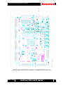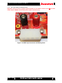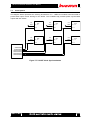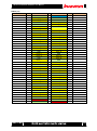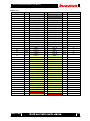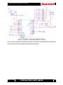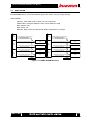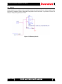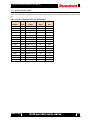
1
TB-KU-xxx-ACDC8K Hardware User Manual TB-KU-xxx-ACDC8K Hardware User Manual Rev. 1.04 Rev. 1.04 1 TB-KU-xxx-ACDC8K Hardware User Manual Revision History Version Date Description Publisher Rev. 1.00 2014/10/15 Initial Release DM Rev. 1.01 2015/01/19 Updated content with board pictures and FMC pinout DM Rev. 1.02 2015/02/18 Updated Figure 4-1, 7-2, 7-6, 7-16 KM Rev. 1.03 2015/07/21 Released for 060 Morita Added Standoffs and Power Strip cord Odajima tables Updated Figure 5-1, 7-6, 7-8, 7-9, 7-12 Updated Table 7-16, 7-22, 7-23 Added 8.1 Default Settings Rev. 1.04 2015/09/28 7.12.1. Updated DIP Switches polarity. Morita (Slide in the ON position for a logic “Low”) Rev. 1.04 2 TB-KU-xxx-ACDC8K Hardware User Manual Table of Contents 1. 2. 3. 4. 5. 6. 7. Related Documents and Accessories ......................................................................................... 9 Overview ...................................................................................................................................... 9 Feature ...................................................................................................................................... 10 Block Diagram ............................................................................................................................11 External View of the Board ........................................................................................................ 12 Board Specifications .................................................................................................................. 13 Description of Components ....................................................................................................... 16 7.1. Power Supply Structure ............................................................................................................ 16 7.1.1. Power Sequencing ............................................................................................................ 17 7.1.2. Power Input connectors .................................................................................................... 17 7.1.3. DC 4-pin Header and Binding Posts ................................................................................. 18 7.1.4. Voltage Rails Test Points .................................................................................................. 19 7.1.5. Power and Miscellaneous LEDs ....................................................................................... 20 7.1.6. Board Power Button .......................................................................................................... 21 7.1.7. FPGA HR Bank Voltage Selection .................................................................................... 21 7.1.8. HR Banks Voltage and SFP+ RX_LOS/TX_FAULT Selection .......................................... 21 7.2. FPGA Banks Assignments ....................................................................................................... 22 7.3. Clock System ........................................................................................................................... 23 7.3.1. VCCINT Clock Architecture .............................................................................................. 23 7.3.2. GTH Clocks ...................................................................................................................... 24 7.3.3. User Assigned Clocks ....................................................................................................... 25 7.4. FMC Connector Interface ......................................................................................................... 26 7.4.1. FMC HPC 0 (J1) ............................................................................................................... 26 7.4.2. FMC HPC 1 (J2) ............................................................................................................... 34 7.4.3. FMC HPC 2 (J5) ............................................................................................................... 41 7.4.4. FMC HPC 3 (J8) ............................................................................................................... 48 7.4.5. FMC HPC 4 (J11) ............................................................................................................. 55 7.4.6. FMC HPC 5 (J14) ............................................................................................................. 62 7.4.7. FMC HPC 6 (J19) ............................................................................................................. 69 7.5. DDR4 SDRAM .......................................................................................................................... 76 7.6. SFP+ Connectors ..................................................................................................................... 77 7.7. USB to UART Controller ........................................................................................................... 79 7.8. Battery ...................................................................................................................................... 80 7.9. Dual Quad (x8) SPI Flash ........................................................................................................ 81 7.10. 8. JTAG and Pmod Interface .................................................................................................... 82 7.10.1. JTAG Connector ............................................................................................................... 82 7.10.2. Pmod Interface ................................................................................................................. 83 7.11. General Purpose LEDs......................................................................................................... 84 7.12. General Purpose Switches ................................................................................................... 85 7.12.1. DIP Switches..................................................................................................................... 85 7.12.2. Push Switches .................................................................................................................. 85 7.12.3. Jumper Switches .............................................................................................................. 86 Appendix .................................................................................................................................... 87 8.1. Default Settings ........................................................................................................................ 87 8.2. Power Sequencer Timings ....................................................................................................... 88 Rev. 1.04 3 TB-KU-xxx-ACDC8K Hardware User Manual List of Figures Figure 4-1 Block Diagram .................................................................................................................11 Figure 5-1 Board Top View ............................................................................................................... 12 Figure 6-1 Board Dimensions (inclusive of wastable substrate, top view) ....................................... 14 Figure 6-2 Board Dimensions (inclusive of wastable substrate, bottom view) ................................. 15 Figure 7-1 Power Supply Structure .................................................................................................. 16 Figure 7-2 Power Sequencer ........................................................................................................... 17 Figure 7-3 Power Input Circuit ......................................................................................................... 17 Figure 7-4 12VDC Input Connector and Binding Posts ................................................................... 18 Figure 7-5 Board Power Button ........................................................................................................ 21 Figure 7-6 FPGA Banks Assignments .............................................................................................. 22 Figure 7-7 VCCINT Clock Synchronization ...................................................................................... 23 Figure 7-8 GTH and MMCX Clocks Architecture ............................................................................. 24 Figure 7-9 User Assigned Clocks Architecture ................................................................................. 25 Figure 7-10 High Pin Count FMC ..................................................................................................... 26 Figure 7-11 FMC 0 to 6 SCL/SDA, GA0/GA1, TDI/TDO .................................................................. 32 Figure 7-12 DDR4 SDRAM Structure ............................................................................................... 76 Figure 7-13 I2C MUX Hardware-selectable Address Pins ............................................................... 77 Figure 7-14 USB UART Interface ..................................................................................................... 79 Figure 7-15 Battery Circuit ............................................................................................................... 80 Figure 7-16 FPGA SPI Flash Configuration Structure...................................................................... 81 Figure 7-17 Pmod Connection ......................................................................................................... 83 Figure 7-18 Jumper Switches Structure ........................................................................................... 86 Figure 8-1 Jumper and Switch location (Component Side) ............................................................. 87 Figure 8-2 Power Sequencer Default Settings ................................................................................. 88 Rev. 1.04 4 TB-KU-xxx-ACDC8K Hardware User Manual List of Tables Table 7-1 Voltage Rails Test Points .................................................................................................. 19 Table 7-2 Board LEDs ...................................................................................................................... 20 Table 7-3 HR Banks Connected Peripherals ................................................................................... 21 Table 7-4 HR Banks Voltage and RX_LOS/TX_FAULT Selection ................................................... 21 Table 7-5 FMC 0 (J1) to FPGA Pinout .............................................................................................. 27 Table 7-6 FMC 1 (J2) to FPGA Pinout .............................................................................................. 35 Table 7-7 FMC 2 (J5) to FPGA Pinout .............................................................................................. 42 Table 7-8 FMC 3 (J8) to FPGA Pinout .............................................................................................. 49 Table 7-9 FMC 4 (J11) to FPGA Pinout ............................................................................................ 56 Table 7-10 FMC 5 (J14) to FPGA Pinout.......................................................................................... 63 Table 7-11 FMC 6 (J19) to FPGA Pinout .......................................................................................... 70 Table 7-12 SFP+ I2C Bus Pin Assignment ....................................................................................... 78 Table 7-13 RX_LOS, TX_FAULT and RS Pin Assignment ............................................................... 78 Table 7-14 Micro-USB Type B and AB Compatibility........................................................................ 79 Table 7-15 UART Interface Pin Assignment ..................................................................................... 79 Table 7-16 SPI Flash Memory Pin Assignment ................................................................................ 82 Table 7-17 Xilinx 14-pin JTAG Pinout ............................................................................................... 82 Table 7-18 FPGA Bank 0 JTAG Pin Assignment .............................................................................. 82 Table 7-19 Pmod Pin Assignment .................................................................................................... 83 Table 7-20 Uncommitted LEDs Pin Assignment .............................................................................. 84 Table 7-21 DIP Switches Pin Assignment ........................................................................................ 85 Table 7-22 Push-button Switches Pin Assignment ........................................................................... 85 Table 7-23 Jumper Switches Pin Assignment .................................................................................. 86 Rev. 1.04 5 TB-KU-xxx-ACDC8K Hardware User Manual Introduction Thank you for purchasing the TB-KU-xxx-ACDC8K board. Before using the product, be sure to carefully read this user manual and fully understand how to correctly use the product. First read through this manual, and always keep it handy. SAFETY PRECAUTIONS Be sure to follow these precautions Observe the precautions listed below to prevent injuries to you or other personnel or damage to property. Before using the product, read these safety precautions carefully to ensure proper use. These precautions contain serious safety instructions that must be followed. After reading through this manual, be sure to always keep it handy. The following conventions are used to indicate the possibility of injury/damage and classify precautions if the product is handled incorrectly. Danger Indicates the high possibility of serious injury or death if the product is handled incorrectly. Indicates the possibility of serious injury or death if the product is handled Warning incorrectly. Indicates the possibility of injury or physical damage in connection with houses or Caution household goods if the product is handled incorrectly. The following graphical symbols are used to indicate and classify precautions in this manual. (Examples) Turn off the power switch. Do not disassemble the product. ! Rev. 1.04 Do not attempt this. 6 TB-KU-xxx-ACDC8K Hardware User Manual Warning In the event of a failure, disconnect the power supply. If the product is used as is, a fire or electric shock may occur. Disconnect the power supply immediately and contact our sales personnel for repair. If an unpleasant smell or smoking occurs, disconnect the power supply. If the product is used as is, a fire or electric shock may occur. Disconnect the power supply immediately. After verifying that no smoking is observed, contact our sales personnel for repair. Do not disassemble, repair or modify the product. Otherwise, a fire or electric shock may occur due to a short circuit or heat generation. For inspection, modification or repair, contact our sales personnel. ! Do not touch a cooling fan. As a cooling fan rotates in high speed, do not put your hand close to it. Otherwise, it may cause injury to persons. Never touch a rotating cooling fan. ! Do not place the product on unstable locations. Otherwise, it may drop or fall, resulting in injury to persons or failure. ! If the product is dropped or damaged, do not use it as is. ! Do not touch the product with a metallic object. ! Do not place the product in dusty or humid locations or where water may Otherwise, a fire or electric shock may occur. Otherwise, a fire or electric shock may occur. splash. Otherwise, a fire or electric shock may occur. ! ! Do not get the product wet or touch it with a wet hand. Otherwise, the product may break down or it may cause a fire, smoking or electric shock. Do not touch a connector on the product (gold-plated portion). Otherwise, the surface of a connector may be contaminated with sweat or skin oil, resulting in contact failure of a connector or it may cause a malfunction, fire or electric shock due to static electricity. Rev. 1.04 7 TB-KU-xxx-ACDC8K Hardware User Manual Caution Do not use or place the product in the following locations. ! Humid and dusty locations Airless locations such as closet or bookshelf Locations which receive oily smoke or steam Locations exposed to direct sunlight Locations close to heating equipment Closed inside of a car where the temperature becomes high Staticky locations Locations close to water or chemicals Otherwise, a fire, electric shock, accident or deformation may occur due to a short circuit or heat generation. ! Do not place heavy things on the product. Otherwise, the product may be damaged. ■ Disclaimer This product is an evaluation board intended for development of video data with Xilinx Kintex UltraScale FPGA. Tokyo Electron Device Limited assumes no responsibility for any damages resulting from the use of this product for purposes other than those stated. Even if the product is used properly, Tokyo Electron Device Limited assumes no responsibility for any damages caused by: (1) Earthquake, thunder, natural disaster or fire resulting from the use beyond our responsibility, acts by a third party or other accidents, the customer’s willful or accidental misuse or use under other abnormal conditions. (2) Secondary impact arising from use of this product or its unusable state (business interruption or others) (3) Use of this product against the instructions given in this manual. (4) Malfunctions due to connection to other devices. Tokyo Electron Device Limited assumes no responsibility or liability for: (1) Erasure or corruption of data arising from use of this product. (2) Any consequences or other abnormalities arising from use of this product, or (3) Damage of this product not due to our responsibility or failure due to modification This product has been developed by assuming its use for research, testing or evaluation. It is not authorized for use in any system or application that requires high reliability. Repair of this product is carried out by replacing it on a chargeable basis, not repairing the faulty devices. However, non-chargeable replacement is offered for initial failure if such notification is received within two weeks after delivery of the product. The specification of this product is subject to change without prior notice. The product is subject to discontinuation without prior notice. Rev. 1.04 8 TB-KU-xxx-ACDC8K Hardware User Manual 1. Related Documents and Accessories Related documents: All documents relating to this board can be downloaded from our website. Please see attached paper on the products. Xilinx FPGA document: http://www.xilinx.com/support/index.html/content/xilinx/en/supportNav/silicon_devices/fpga/kintex-ultras cale.html DS892: UltraScale device data sheets: Kintex UltraScale Architecture Data Sheet: DC and AC Switching Characteristics DS890: UltraScale Architecture and Product Overview UG570: UltraScale Architecture Configuration User Guide UG571: UltraScale Architecture SelectIO Resources User Guide UG572: UltraScale Architecture Clocking Resources User Guide UG573: UltraScale Architecture Memory Resources User Guide UG574: UltraScale Architecture Configurable Logic Block User Guide UG575: UltraScale Architecture Packaging and Pinouts User Guide UG576: UltraScale Architecture GTH Transceivers User Guide UG580: UltraScale Architecture System Monitor User Guide UG583: UltraScale Architecture PCB and Pin Planning User Guide PG150: UltraScale Architecture-Based Memory Interface Solutions Product Guide Board accessories: - Power supply brick (DC 12V) and cable to board: qty. 1 - FMC spacer set Standoff 2.6M x 30mm qty. 14 Screw 2.6M x 6mm qty.14 - Power Strip Cord with Individual Switches qty. 1 2. Overview The TB-KU-xxx-ACDC8K evaluation board for the Xilinx Kintex UltraScale provides a hardware environment with a purpose of evaluating and developing designs targeting the Kintex UltraScale XCKU060 and XCKU085 featuring a FFVA1517 package. Speed grade -2 FPGA is mounted on this board. The TB-KU-xxx-ACDC8K platform provides a common feature set including DDR4 SDRAM memory components, general purpose I/O, a USB to UART interface, four SFP+ modules, seven VITA-57 high-pin count FPGA mezzanine cards (FMC) connectors, a JTAG and a PMOD interface. Rev. 1.04 9 TB-KU-xxx-ACDC8K Hardware User Manual 3. Feature Xilinx Kintex UltraScale: XCKU060/XCKU085 -2 speed grade in FFVA1517 package Memory: 4GByte DDR4 SDRAM: 16Gbits (4 ICs x 32M words x 16 bits x 8 banks) x 2 banks of ICs 256Mbit Dual Quad SPI Flash TI’s UCD9090 power supply sequencer and monitor FMC Connector: 7 x Samtec’s ASP-134486-01 (CC-HPC-10)*1 On Board Clocks: IDT’s ICS849N202I clock generator IDT ICS849N202I PLL 25MHz CMOS oscillator 40MHz crystal IDT 148.50MHz LVDS oscillator IDT 156.25MHz LVDS oscillator IDT 200.00MHz LVDS oscillator Interface: 4x SFP+ modules MMCX for external clocks Standard Xilinx JTAG 14-pin header Digilent Pmod™ compatible header (2x6) Push switches, DIP switches, jumpers and LEDs Single-chip USB to UART bridge Micro-USB 2.0 Type AB connector Note *1: Refer to VITA 57 FMC Standard http://www.samtec.com/standards/vita.aspx Rev. 1.04 10 TB-KU-xxx-ACDC8K Hardware User Manual 4. Block Diagram The following figure shows the block diagram of TB-KU-xxx-ACDC8K FMC0 does not have any high-speed GTH lanes. XCKU060: FMC1, 2 and 3 have 8 high-speed GTH lanes. FMC4 and 6 have 4 high-speed GTH lanes. FMC5 and SFP+ do not have any high-speed GTH lanes. XCKU085: FMC1, 2, 3, 4 and 5 have 8 high-speed GTH lanes. FMC6 and SFP+ have 4 high-speed GTH lanes. There are two groups of FMC HP connections, LA group A and group B. LA group A has 72 I/O connected to the FPGA and group B has 12. FMC6(GTH:4ch) Quad128 LA Group-B 1.8V Fix (12pin – bank 24/46) 4GTH HP I/O HR I/O Power 12V Power IN Power Supplies 0V95 VCCINT 1V8 VCCAUX 1V0 MGTAVCC 1V2 MGTAVTT 1V2 DDR4 0V6 DDR4 VTERM 2V5 DDR4 VPP 1V8 VADJ/VCCO 3V3 FMC3(GTH:8ch) Quad126,127 LA Group-A(36pair) 1.8V Fix (72pin – bank 24/46-25/47) 12 HP I/O DDR4 x 2 Banks 36 HP I/O Front panel LED (2pin) -Config DONE -Green : 1ch -Red : 1ch SFP+(GTH:4ch) Quad232 (060 : NC) (10pin – bank 64/65) 7x2 2.54mm Pin headers (8pin) Total : 8ch connected DDR4 bank X’tal 156.25MHz for SFP+ Push switches (8pin) Total : 8ch connected DDR4 bank X’tal 200MHz for DDR4-2 (2pin) LEDs (16pin) Red : 8ch Green : 8ch connected DDR4 bank X’tal 148.5MHz for User (2pin) DIP switches (16pin) Total : 16ch connected DDR4 bank X’tal 200MHz for DDR4-1 (2pin) Config QUAD Dual-SPI 36 HP I/O JTAG HR power 1.8, 2.5, 3.3V 12 HP I/O FMC0(GTH:0ch) IO voltage : select 3.3V, 2.5V or 1.8V (84 I/O pin – bank 64/65) 36 HP I/O 36 HP I/O 42 HR I/O 42 HR I/O 10 HR I/O USB type AB (UART) PMOD (8pin) 12 HP I/O 12 HP I/O FMC5(GTH:8ch) Quad230,231 (060 : NC) LA Group-B 1.8V Fix (12pin – bank 45) FMC4(GTH:4ch or 8ch) Quad228,229 (060 : Quad228) LA Group-B 1.8V Fix (12pin – bank 44) FMC2(GTH:8ch) Quad226,227 LA Group-B 1.8V Fix (12pin – bank 25/47) FMC1(GTH:8ch) Quad224,225 LA Group-A(36pair) 1.8V Fix (72pin – bank 44-45) Figure 4-1 Block Diagram Rev. 1.04 11 TB-KU-xxx-ACDC8K Hardware User Manual 5. External View of the Board The TB-KU-xxx-ACDC8K board’s components are shown on the top side view in Figure 5-1. GTH CLK HR Voltage FMC Connector 6 (HPC) Sequencer MMCX Inputs PMBUS Header Select Header LA Group B (6pairs) 12V Input Dual Quad GTH 4Lanes Fuse Holder FPGA Program Fan DDR4 SDRAM Uncommitted Flash Memory Button Switches/ LEDs Headers / Pushbuttons (20A) Connector (2 banks) FPGA Coin Cell Battery Holder Power Input Binding Posts FMC6 JTAG Power Input Connector FMC3 Power Switch FPGA Program DONE LED FMC Connector 3 (HPC) LA Group A (36pairs) GTH 8Lanes GTH CLK MMCX Inputs Micro USB Type AB (UART) PMOD FPGA POR_OVERRIDE Switch FPGA SFP+ TX_FAULT/ RX_LOS FMC0 SFP+ Modules 4ch (060: not connected) FMC Connector 0 (HPC) LA Group A (36pairs+HA 5pairs) Supported 1.8/2.5/3.3V No GTH PLL Switch GTH CLK MMCX Inputs FMC5 FMC4 FMC Connector 4 (HPC) FMC Connector 5 (HPC) LA Group B (6pairs) LA Group B (6pairs) GTH 8Lanes (060: not connected) GTH 8Lanes (060: 4Lanes) FMC2 FMC1 FMC Connector 2 (HPC) LA Group B (6pairs) GTH 8Lanes FMC Connector 1 (HPC) LA Group A (36pairs) GTH 8Lanes 7 FMC 12V Fuse Holders (2A) Figure 5-1 Board Top View Rev. 1.04 12 TB-KU-xxx-ACDC8K Hardware User Manual 6. Board Specifications Figure 6-1 shows the board specifications. External Dimensions: 313.08 mm (W) x 208.28 mm (H) Number of Layers: 20 layers Board Thickness: 2.0828 mm +/- 10% Material: Megtron 4 FPGA: Xilinx Kintex UltraScale XCKU060/XCKU085 FFVA1517 (FLVA1517) package FMC HPC CC Connector: Samtec ASP-134486-01 Micro-USB Connector: Hirose Electric’s ZX62D-AB-5P8 Xilinx JTAG Connector: Molex’s 87832-1420 Pmod Connector: Molex’s 15912120 Power Input Connector: TE Connectivity’s 1-350948-0 Emerson Network’s 111-0702-001 and 111-0703-001 Rev. 1.04 13 TB-KU-xxx-ACDC8K Hardware User Manual Figure 6-1 Board Dimensions (inclusive of wastable substrate, top view) Rev. 1.04 14 TB-KU-xxx-ACDC8K Hardware User Manual Figure 6-2 Board Dimensions (inclusive of wastable substrate, bottom view) Rev. 1.04 15 TB-KU-xxx-ACDC8K Hardware User Manual 7. Description of Components 7.1. Power Supply Structure TB-KU-xxx-ACDC8K board’s power supply structure is shown in the figure below. 12V KCU Vccint 0.95V +/- 3% (0.922 to 0.979V)=41.6A KCU Vccint_io 0.95V +/- 3%=2.6A Total 44.2A Fuse from Sequencer LMZ31710 x 6 60A current share KCU Vccbram 0.95V +/- 3% (0.922 to 0.979V) 0.7A KCU Vccaux 1.80V +/- 3% (1.746 to 1.854V)=3.8A KCU Vccaux_io 1.80V +/- 3%=1.4A Total 5.2A TPS53318 from Sequencer In=1.5-22V/Out=0.6-5.5V/8A KCU Vccadc 1.8V +/- 3%(1.746 to 1.854V) Total 0.03A KCU Vcco HR 1.8V/2.5V/3.3V +3/- 5% =0.9A (3.3V +3/- 5% : 0.1A ,1.8V +3/- 5% : 0.1A) FMC Vadj 3.3V=4A Total 4.9A TPS53318 from Sequencer In=1.5-22V/Out=0.6-5.5V/8A from Sequencer In=1.5-15V/Out=0.6-5.5V/30A from Sequencer In=1.5-15V/Out=0.6-5.5V/30A KCU Vcco HP 1.8V +/- 5%=1.9A FMC Vadj 1.8V 4A x 4 = 16A Total 17.9A TPS53355 SFP+ module 3.3V +/-3% 0.3A x 4 = 1.2A FMC 3.3V 3.3V Aux x5 4A x 6 = 24A Total 25.2A TPS53355 KCU Vcco DDR4 1.2V +/- 5%=1.0A DDR4 chip VDDQ : 0.330A x 8chip = 2.64A DDR4 Vterm : 0.39A x 2 = 0.78A Total 4.42A KCU Vterm DDR4 0.6V DDR4 Vterm 0.6V (0.49-0.51VDD) x8 TPS53318 from Sequencer In=1.5-22V/Out=0.6-5.5V/8A TPS51206 Termination 3A DDR4 chip VPP 2.5V +10/-5% x8 Total 0.13A TPS73801 from Sequencer In=2.2-20V/Out=1.21-20V/1A from Sequencer In=1.5-22V/Out=0.6-5.5V/14A from Sequencer In=1.5-22V/Out=0.6-5.5V/14A from Sequencer In=2.2-20V/Out=1.21-20V/1A KCU Vmgtavcc 1.00V +/- 3% (0.970 to 1.030V) Total 7.7A KCU Vmgtavtt 1.20V +/- 2.5%(1.170 to 1.230V)=7.6A KCU Vmgtavttrcal 1.20V +/- 2.5%(1.170 to 1.230V) Total 7.6A KCU Vmgtvccaux 1.80V +/- 2.8%(1.750 to 1.850V) Total 0.1A TPS53319 TPS53319 TPS73801 Fuse UCD9090 Sequencer FMC 12V x7 Total 1A x 7 = 7A 10 to power devices TLV70433 3.3V LDO 5V0_USB_VBUS 5V0_USB_FILT TPS73801 In=2.2-20V/Out=1.21-20V/1A 1V8_USB_PWR USB UART Figure 7-1 Power Supply Structure Rev. 1.04 16 TB-KU-xxx-ACDC8K Hardware User Manual 7.1.1. Power Sequencing The UCD9090 chip features power sequencing and monitoring of the different power supplies available on this board. The sequencer’s outputs are connected to the power supplies’ enable pin which activates each device. UCD9090RGZ 12V0 MON1 GPIO1 0V95_EN 0V95_SENS MON2 GPIO2 1V8_VCCAUX_EN 1V8_VCCAUX_SENS MON3 GPIO3 1V0_MGTAVCC_EN 1V0_MGTAVCC_SENS MON4 GPIO4 1V2_MGTAVTT_EN 1V2_MGTAVTT_SENS MON5 GPIO5 1V8_MGTVCCAUX_EN VCC_HR_SENS MON6 GPIO6 VCC_HR_EN 1V8_FMC_SENS MON7 GPIO7 1V8_FMC_EN 3V3_SENS MON8 GPIO8 3V3_EN 2V5_DDR4 MON9 GPIO9 2V5_DDR4_EN MON10 GPIO10 1V2_DDR4_EN 1V2_DDR4_SENS 3V3_UCD9090 PMBUS GPIO11 CTRL FPGA_PROGRAM_B All power good Reconfiguration AND Push Switch GPIO12 FMC_[6..0]_PGOOD Figure 7-2 Power Sequencer 7.1.2. Power Input connectors TB-KU-xxx-ACDC8K has two power input connectors on the board, a 4-pin header or red and black binding posts. Figure 7-3 Power Input Circuit Rev. 1.04 17 TB-KU-xxx-ACDC8K Hardware User Manual 7.1.3. DC 4-pin Header and Binding Posts Important: There are two (2) power inputs available on this board. Connect one OR the other 12VDC inputs. NEVER connect both power inputs simultaneously. Figure 7-4 12VDC Input Connector and Binding Posts Rev. 1.04 18 TB-KU-xxx-ACDC8K Hardware User Manual 7.1.4. Voltage Rails Test Points Use the development board’s power rail test points for board debugging and troubleshooting or for other types of measurements. Table 7-1 Voltage Rails Test Points Voltage Rail 0V95 0V95_VCCBRAM 1V8_VCCAUX 3V3_VCC_HR 3V3_UCD9090 1V8_FMC 1V2_DDR4 2V5_DDR4 0V6_VTT_DDR4 0V6_VREF_DDR4 0V6_VTT_DDR4_2 0V6_VREF_DDR4_2 1V0_MGTAVCC 1V2_MGTAVTT 1V8_MGTVCCAUX 3V3 12V0 VBATT 5V0_USB_VBUS 5V0_USB_FILT 1V8_USB_PWR Rev. 1.04 Test Point # TP37 TP23 TP40 TP36 TP43 TP19 TP31 TP30 TP32 TP34 TP33 TP35 TP39 TP41 TP38 TP20 TP42 TP68 TP57 TP59 TP58 Power Supply for FPGA VCCINT FPGA VCCBRAM FPGA VCCAUX & VCCAUX_IO FPGA HR I/O Banks Power Sequencer and Monitor FPGA HP I/O Banks & FMC VADJ DDR4 and corresponding FPGA Banks VPP generation DDR4 SDRAM 1 Termination DDR4 SDRAM 1 Reference DDR4 SDRAM 2 Termination DDR4 SDRAM 2 Reference FPGA MGTAVCC FPGA MGTAVTT FPGA MGTVCCAUX FMC and SFP+ modules 12V Master Power Coin Cell Battery Micro USB 5V input Micro USB filtered 5V USB UART controller 1.8V I/O 19 TB-KU-xxx-ACDC8K Hardware User Manual 7.1.5. Power and Miscellaneous LEDs Shown below are the different LEDs present on the board which serve as power indication or general purpose programmable LEDs. Table 7-2 Board LEDs LED Color D1 D3 D4 D5 D6 D10 Bicolor: Green or Red Green Red Red Red Green D12-D27 Green & Red Rev. 1.04 Used for FPGA Programming DONE signal Red: Programming in progress Green: Programming complete Clock generation LOCK_IND indicator for U20 Clock generation CLK0 BAD indicator for U20 Clock generation CLK1 BAD indicator for U20 Clock generation XTAL BAD indicator for U20 12V Input Uncommitted Green: D12, D13, D16, D17, D20, D21, D24, D25 Red: D14, D15, D18, D19, D22, D23, D26, D27 20 TB-KU-xxx-ACDC8K Hardware User Manual 7.1.6. Board Power Button This board features a power button rocker switch on the chassis’ front panel along with 4 SFP+ connectors, a micro USB port and a green and red LED to signal the FPGA programming and idle states. The power sequencer monitors the rocker switch power button which disables power supplies on the board when turned off. The “I” position turns ON the power supplies and the “O” position turns them OFF. The FPGA’s fan however will be active as long as the 12V supply is live. Figure 7-5 Board Power Button 7.1.7. FPGA HR Bank Voltage Selection Various different devices are connected on the FPGA HR banks. The FMC0 connector and SFP+ modules are connected to the FPGA’s HR 64 and 65 banks as shown in blue on this board’s block diagram (Figure 4-1). The SPI flash components are connected to HR bank 0 and bank 65. Banks 0, 64 and 65 have a selectable voltage which is identical on these three banks. Table 7-3 HR Banks Connected Peripherals Bank # Connected Peripherals Dedicated Config 0 7.1.8. HR 64 Dual Quad SPI Flash (Primary) FMC0, SFP 1 and 2 HR 65 FMC0, Dual Quad SPI Flash (Secondary), SFP 3 and 4 Voltage Selectable 1.8V, 2.5V, 3.3V HR Banks Voltage and SFP+ RX_LOS/TX_FAULT Selection The 3V3_VCC_HR power can be selected through the use of a 3-pin jumper (J44). The user can also select between RX_LOS or TX_FAULT on each of the 4 SFP+ modules. Table 7-4 HR Banks Voltage and RX_LOS/TX_FAULT Selection Jumper No. Description J44 HR Banks Voltage Select Rev. 1.04 Status No Jumper 1-2 3-2 Function 1.8V (Default) 2.5V 3.3V 21 TB-KU-xxx-ACDC8K Hardware User Manual 7.2. FPGA Banks Assignments This board supports Xilinx Kintex Ultrascale XCKU060 and XCKU085 FPGA in the FFVA1517 (FLVA1517) packages. The figure below presents bank assignments on this board. FMC6 (4Lane) FMC4 (4Lane) FMC3 (8Lane) FMC2 (8Lane) FMC1 (8Lane) GTH Total 32CH SFP+ (4Lane) FMC5 (8Lane) FMC4 (8Lane) FMC6 (4Lane) FMC3 (8Lane) FMC2 (8Lane) FMC1 (8Lane) GTH Total 48CH Figure 7-6 FPGA Banks Assignments Rev. 1.04 22 TB-KU-xxx-ACDC8K Hardware User Manual 7.3. Clock System 7.3.1. VCCINT Clock Architecture The diagram below represents the clocking architecture of 6 - LMZ31710 modules interconnected to provide 60A output current sharing for the FPGA. The LTC6909 chip provides phase synchronized outputs with 60° offsets. not used LMZ31710 U23 SYNC_OUT not used RT/CLK not used LMZ31710 U26 SYNC_OUT RT/CLK LMZ31710 U24 SYNC_OUT not used RT/CLK not used LMZ31710 U27 SYNC_OUT RT/CLK LMZ31710 U25 SYNC_OUT RT/CLK not used LMZ31710 U28 SYNC_OUT RT/CLK LTC6909 250kHz/0deg 250kHz/60deg 250kHz/120deg 250kHz/180deg 250kHz/240deg 250kHz/300deg Figure 7-7 VCCINT Clock Synchronization Rev. 1.04 23 TB-KU-xxx-ACDC8K Hardware User Manual 7.3.2. GTH Clocks The diagram below represents the GTH clock architecture present in the TB-KU-xxx-ACDC8K board. Some clocks are internally driven by the system while others can be externally provided through MMCX connectors. DIP-SW: SW2 【DIP-SW : OFF】 CLK_GLOBAL_SEL: 0 FeedBack input Clock => 25MHz(OSC) CLK_GLOBAL_CONFIG: 0 Output Clock => 156.25MHz CLK_GLOBAL_OE: 0 No CLK_PLL_P/N to Fanout Buffer CLK_PLL_BYPASS: 0 PLL Mode (default) Quad232(085 Only) GTREFCLK_0_P/N GTREFCLK_1_P/N CLK_SFP_QUAD232 CLK_MMCX_QUAD232 156.25MHz (LVDS) IDT 4MA156250Z4AACUGI MMCX 40MHz (X’tal) TXC 7M-40.000MAHE-T FMC5 Quad231(085 Only) 【DIP-SW : ON】 CLK_GLOBAL_SEL: 1 FeedBack input Clock => From FPGA CLK_GOBAL_CONFIG: 1 Output Clock => 148.50MHz CLK_GLOBAL_OE: 1 CLK_PLL_P/N output to Fanout Buffer CLK_PLL_BYPASS: 1 PLL Bypassed GTREFCLK_0_P/N XTAL GTREFCLK_1_P/N 25MHz (OSC) TXC 7C-25.000MBA-T Bank64 (HR) CLK0 CLK_EXT_REF CLK_QUAD231 CLK_MMCX_QUAD231 MMCX PLL IDT ICS849N202I CLK1 Quad230(085 Only) Q0_P/N 2 CLK_PLL_P/N GTREFCLK_0_P/N CLK_P/N GBTCLK0_M2C_P CLK_FMC_5_GTH_REF1 GBTCLK1_M2C_P Q5 Q4 GTREFCLK_1_P/N CLK_FMC_5_GTH_REF0 GC Bank67 Q3 Q2 Q1 Q0 Fanout Buffer IDT ICS854S006I FMC6 Quad128 GTREFCLK_0_P/N GTREFCLK_1_P/N CLK_FMC_6_GTH_REF0 GBTCLK0_M2C_P CLK_FMC_6_GTH_REF1 GBTCLK1_M2C_P FMC3 CLK_QUAD130 CLK_MMCX_QUAD130 GTREFCLK_1_P/N MMCX Quad126 GTREFCLK_0_P/N GTREFCLK_1_P/N GTREFCLK_0_P/N CLK_QUAD229 GTREFCLK_1_P/N CLK_MMCX_QUAD229 MMCX Quad228 Quad127 GTREFCLK_0_P/N FMC4 Quad229(085 Only) In the case of 060 GTREFCLK_0_P/N GTREFCLK_1_P/N CLK_FMC_4_GTH_REF0 GBTCLK0_M2C_P CLK_FMC_4_GTH_REF1 GBTCLK1_M2C_P FMC2 Quad227 GTREFCLK_0_P/N CLK_QUAD227 GTREFCLK_1_P/N CLK_MMCX_QUAD227 MMCX Quad226 CLK_FMC_3_GTH_REF0 CLK_FMC_3_GTH_REF1 GBTCLK0_M2C_P GBTCLK1_M2C_P GTREFCLK_0_P/N GTREFCLK_1_P/N CLK_FMC_2_GTH_REF0 GBTCLK0_M2C_P CLK_FMC_2_GTH_REF1 GBTCLK1_M2C_P FMC1 Quad225 GTH Assignment FMC1(GTH8CH) FMC2(GTH8CH) FMC3(GTH8CH) FMC4(GTH4/8CH) FMC5(GTH0/8CH) FMC6(GTH4CH) SFP+(GTH4CH) GTREFCLK_0_P/N : Quad224 + 225 : Quad226 + 227 : Quad126 + 127 : Quad228 + 229(085 Only) : Quad230(085 Only) + 231(085 Only) : Quad128 : Quad232(085 Only) GTREFCLK_1_P/N CLK_QUAD225 CLK_MMCX_QUAD225 MMCX Quad224 GTREFCLK_0_P/N GTREFCLK_1_P/N CLK_FMC_1_GTH_REF0 CLK_FMC_1_GTH_REF1 GBTCLK0_M2C_P GBTCLK1_M2C_P Figure 7-8 GTH and MMCX Clocks Architecture Rev. 1.04 24 TB-KU-xxx-ACDC8K Hardware User Manual 7.3.3. User Assigned Clocks This board provides a way to make use of dedicated LA signals on the FMC cards allowing them to be configured as global clocks on the FPGA as shown in the figure below. The figure states the GC and GBC clock assignments on the FPGA for the FMCs and the DDR4 banks. BANK25 FMC_3_LA28 GC FMC_3_LA17 GC/QBC FMC_3_LA18 GC FMC_3_LA14 GC QBC QBC QBC DBC DBC DBC BANK48 BANK68 BANK65 FMC3 FMC_0_LA28_CC GC total LA+CLK 18pair FMC_0_LA18_CC GC/QBC FMC_0_LA17_CC GC LA10 LA13 LA14 LA16 ------LA17 LA18 LA19 LA20 LA21 LA22 LA23 LA24 LA25 LA26 LA28 LA30 LA32 LA33 148.5MHz (LVDS) IDT 4MA148500Z4AACUGI BANK47 200MHz CLK_DDR4_2_200MHZ IDT GC 4MA200000Z4AACUGI (LVDS) CLK_VIDEO GC BANK67 200MHz IDT 4MA200000Z4AACUGI (LVDS) CLK_DDR4_1_200MHZ QBC GC QBC QBC DBC/D04 DBC/D05 BANK46 DBC BANK64 FMC_3_LA01_CC GC CLK_FMC_3_CLK1_M2C GC/QBC CLK_FMC_3_CLK0_M2C GC FMC_3_LA00_CC GC QBC QBC QBC DBC DBC DBC DBC LA10 LA13 LA14 LA16 -----LA17 LA18 LA19 LA20 LA21 LA22 LA23 LA24 LA25 LA26 LA28 LA30 LA32 LA33 DBC BANK66 DBC BANK24 FMC0 total LA+CLK 18pair FMC3 FMC_0_LA01_CC total LA+CLK 18pair LA00 LA01 LA02 LA03 LA04 LA05 LA06 LA07 LA08 LA09 LA11 LA12 LA15 ------LA27 LA29 LA31 ------CLK0_M2C CLK1_M2C DDR4 MIG1 GC CLK_FMC_0_CLK1_M2C GC/QBC CLK_FMC_0_CLK0_M2C GC FMC_0_LA00_CC GC DDR4 MIG2 QBC QBC 25MHz (OSC) 40MHz (OSC) Bank64(HR) Bank70 GC PLL ICS849N202I (IDT) QBC DDR4 Bank CLK_EXT_IN Feed Back Clock(LVDS) MMCX (Non Term) DBC DBC DBC Bank67 GC FMC0 total LA+CLK 18pair LA00 LA01 LA02 LA03 LA04 LA05 LA06 LA07 LA08 LA09 LA11 LA12 LA15 ------LA27 LA29 LA31 ------CLK0_M2C CLK1_M2C DBC CLK_GLBL_FPGA_IN Fanout Buffer For GTH x 5 BANK44 BANK45 FMC_1_LA18_CC GC FMC_1_LA19_CC GC/QBC FMC_1_LA28_CC GC FMC_1_LA17_CC GC QBC QBC QBC DBC DBC DBC DBC FMC1 CLK_FMC_1_CLK1_M2C GC total LA+CLK 18pair CLK_FMC_1_CLK0_M2C GC/QBC LA10 LA13 LA14 LA16 ------LA17 LA18 LA19 LA20 LA21 LA22 LA23 LA24 LA25 LA26 LA28 LA30 LA32 LA33 FMC_1_LA00_CC GC FMC_1_LA01_CC GC QBC QBC QBC DBC DBC DBC DBC Figure 7-9 User Assigned Clocks Architecture Rev. 1.04 25 FMC1 total LA+CLK 18pair LA00 LA01 LA02 LA03 LA04 LA05 LA06 LA07 LA08 LA09 LA11 LA12 LA15 ------LA27 LA29 LA31 ------CLK0_M2C CLK1_M2C TB-KU-xxx-ACDC8K Hardware User Manual 7.4. FMC Connector Interface The TB-KU-xxx-ACDC8K board has 7 high-pin count (HPC) 400 pin FMC connectors (FMC 0 to 6) on board as shown on the block diagram. These FMC connectors follow the VITA 57.1 standard with Samtec ASP-134486-01 connectors. Presented below is the standard pin assignment on FMC HPC connectors. Not all the pins are connected on the FMC connectors. Please follow this section for more details on all the FMC pinouts. Figure 7-10 High Pin Count FMC 7.4.1. FMC HPC 0 (J1) This FMC connects all of the available LA signals and 6 HA differential pairs to banks on the FPGA. High Speed: No GTH channels connected Low Speed: Bank 64: 18 differential LA pairs 3 differential HA pairs Bank 65: 2 differential clock pairs 16 differential LA pairs 3 differential HA pair Rev. 1.04 26 TB-KU-xxx-ACDC8K Hardware User Manual Table 7-5 FMC 0 (J1) to FPGA Pinout Bank# Rev. 1.04 Pin# A B Pin# - GND 1 CLK_DIR - DP1_M2C_P 2 GND - DP1_M2C_N 3 GND GND 4 DP9_M2C_P - GND 5 DP9_M2C_N - DP2_M2C_P 6 GND - DP2_M2C_N 7 GND GND 8 DP8_M2C_P - GND 9 DP8_M2C_N - DP3_M2C_P 10 GND - DP3_M2C_N 11 GND GND 12 DP7_M2C_P - GND 13 DP7_M2C_N - - DP4_M2C_P 14 GND - DP4_M2C_N 15 GND GND 16 DP6_M2C_P - GND 17 DP6_M2C_N - - DP5_M2C_P 18 GND - DP5_M2C_N 19 GND GND 20 *1 GBTCLK1_M2C_P - GND 21 *1 GBTCLK1_M2C_N - - DP1_C2M_P 22 GND - DP1_C2M_N 23 GND GND 24 DP9_C2M_P - GND 25 DP9_C2M_N - DP2_C2M_P 26 GND - DP2_C2M_N 27 GND GND 28 DP8_C2M_P - GND 29 DP8_C2M_N - DP3_C2M_P 30 GND - DP3_C2M_N 31 GND GND 32 DP7_C2M_P - GND 33 DP7_C2M_N - - DP4_C2M_P 34 GND - DP4_C2M_N 35 GND GND 36 DP6_C2M_P - GND 37 DP6_C2M_N - - DP5_C2M_P 38 GND - DP5_C2M_N 39 GND GND 40 RES0 Bank# - 27 TB-KU-xxx-ACDC8K Hardware User Manual FMC 0 (J1) Bank# Pin# C D Pin# *5 PG_C2M - Bank# GND 1 - DP0_C2M_P 2 GND - DP0_C2M_N 3 GND GND 4 *1 GBTCLK0_M2C_P - GND 5 *1 GBTCLK0_M2C_N - - DP0_M2C_P 6 GND - DP0_M2C_N 7 GND GND 8 LA01_P_CC AL14 65 GND 9 LA01_N_CC AL13 65 65 AU12 LA06_P 10 GND 65 AV12 LA06_N 11 LA05_P AV13 65 GND 12 LA05_N AW13 65 GND 13 GND 64 AJ16 LA10_P 14 LA09_P AK13 65 64 AK16 LA10_N 15 LA09_N AK12 65 GND 16 GND GND 17 LA13_P AK18 64 64 AP19 LA14_P 18 LA13_N AK17 64 64 AP18 LA14_N 19 GND GND 20 LA17_P_CC AM19 64 AN19 64 GND 21 LA17_N_CC 64 AL17 LA18_P_CC 22 GND 64 AM17 LA18_N_CC 23 LA23_P AR18 64 GND 24 LA23_N AR17 64 GND 25 GND 65 AT15 LA27_P 26 LA26_P AP16 64 65 AU15 LA27_N 27 LA26_N AR16 64 GND 28 GND GND 29 TCK - - *2 SCL 30 *4 TDI - - *2 SDA 31 *4 TDO - GND 32 *6 3P3VAUX - GND 33 TMS - - *3 GA0 34 TRST_L - - *6 12P0V 35 *3 GA1 - GND 36 *6 3P3V - *6 12P0V 37 GND GND 38 *6 3P3V *6 3P3V 39 GND GND 40 *6 3P3V - Rev. 1.04 - 28 TB-KU-xxx-ACDC8K Hardware User Manual FMC 0 (J1) Bank# Pin# F Pin# GND E 1 *5 PG_M2C - Bank# 65 AD14 HA01_P_CC 2 GND 65 AD13 HA01_N_CC 3 GND GND 4 HA00_P_CC AE12 65 GND 5 HA00_N_CC AF12 65 64 AE18 HA05_P 6 GND 64 AF18 HA05_N 7 HA04_P AP15 65 GND 8 HA04_N AR15 65 - HA09_P 9 GND - HA09_N 10 HA08_P - GND 11 HA08_N - - HA13_P 12 GND - HA13_N 13 HA12_P - GND 14 HA12_N - - HA16_P 15 GND - HA16_N 16 HA15_P - GND 17 HA15_N - - HA20_P 18 GND - HA20_N 19 HA19_P - GND 20 HA19_N - - HB03_P 21 GND - HB03_N 22 HB02_P - GND 23 HB02_N - - HB05_P 24 GND - HB05_N 25 HB04_P - GND 26 HB04_N - - HB09_P 27 GND - HB09_N 28 HB08_P - GND 29 HB08_N - - HB13_P 30 GND - HB13_N 31 HB12_P - GND 32 HB12_N - - HB19_P 33 GND - HB19_N 34 HB16_P - GND 35 HB16_N - - HB21_P 36 GND - HB21_N 37 HB20_P - GND 38 HB20_N - *6 VADJ 39 GND GND 40 *6 VADJ - Rev. 1.04 - 29 TB-KU-xxx-ACDC8K Hardware User Manual FMC 0 (J1) Bank# Pin# G H Pin# Bank# GND 1 *7 VREF_A_M2C - 65 AL12 CLK1_M2C_P 2 *5 PRSNT_M2C_L - 65 AM12 CLK1_M2C_N 3 GND GND 4 CLK0_M2C_P AM14 65 GND 5 CLK0_M2C_N AN14 65 65 AN13 LA00_P_CC 6 GND 65 AN12 LA00_N_CC 7 LA02_P AR12 65 GND 8 LA02_N AT12 65 65 AR13 LA03_P 9 GND 65 AT13 LA03_N 10 LA04_P AT14 65 GND 11 LA04_N AU14 65 65 AV14 LA08_P 12 GND 65 AW14 LA08_N 13 LA07_P AH13 65 GND 14 LA07_N AJ13 65 65 AH14 LA12_P 15 GND 65 AJ14 LA12_N 16 LA11_P AP14 65 GND 17 LA11_N AP13 65 64 AH19 LA16_P 18 GND 64 AH18 LA16_N 19 LA15_P AJ15 65 GND 20 LA15_N AK15 65 64 AU17 LA20_P 21 GND 64 AU16 LA20_N 22 LA19_P AT19 64 GND 23 LA19_N AU19 64 64 AJ19 LA22_P 24 GND 64 AJ18 LA22_N 25 LA21_P AH17 64 GND 26 LA21_N AH16 64 64 AT18 LA25_P 27 GND 64 AT17 LA25_N 28 LA24_P AV18 64 GND 29 LA24_N AV17 64 65 AG12 LA29_P 30 GND 65 AH12 LA29_N 31 LA28_P AL19 64 GND 32 LA28_N AL18 64 65 AF15 LA31_P 33 GND 65 AG15 LA31_N 34 LA30_P AV19 64 GND 35 LA30_N AW18 64 64 AR20 LA33_P 36 GND 64 AT20 LA33_N 37 LA32_P AW20 64 GND 38 LA32_N AW19 64 *6 VADJ 39 GND GND 40 *6 VADJ - Rev. 1.04 - 30 TB-KU-xxx-ACDC8K Hardware User Manual FMC 0 (J1) Bank# Pin# J K Pin# *7 VREF_B_M2C - GND 1 - CLK3_M2C_P 2 GND - CLK3_M2C_N 3 GND GND 4 CLK2_M2C_P - GND 5 CLK2_M2C_N - Bank# 64 AD16 HA03_P 6 GND 64 AE16 HA03_N 7 HA02_P AG17 64 GND 8 HA02_N AG16 64 - HA07_P 9 GND - HA07_N 10 HA06_P - GND 11 HA06_N - - HA11_P 12 GND - HA11_N 13 HA10_P - GND 14 HA10_N - - HA14_P 15 GND - HA14_N 16 HA17_P_CC - GND 17 HA17_N_CC - - HA18_P 18 GND - HA18_N 19 HA21_P - GND 20 HA21_N - - HA22_P 21 GND - HA22_N 22 HA23_P - GND 23 HA23_N - - HB01_P 24 GND - HB01_N 25 HB00_P_CC - GND 26 HB00_N_CC - - HB07_P 27 GND - HB07_N 28 HB06_P_CC - GND 29 HB06_N_CC - - HB11_P 30 GND - HB11_N 31 HB10_P - GND 32 HB10_N - - HB15_P 33 GND - HB15_N 34 HB14_P - GND 35 HB14_N - - HB18_P 36 GND - HB18_N 37 HB17_P_CC - GND 38 HB17_N_CC - *8 VIO_B_M2C 39 GND GND 40 *8 VIO_B_M2C - Rev. 1.04 - 31 TB-KU-xxx-ACDC8K Hardware User Manual Figure 7-11 FMC 0 to 6 SCL/SDA, GA0/GA1, TDI/TDO Note: The above structure is identical for all FMC connectors on this board, with the exception of test points and reference designators being different per FMC. Rev. 1.04 32 TB-KU-xxx-ACDC8K Hardware User Manual For FMC 0 (J1): *1: There are no GTH channels on this connector so the GBTCLK1_M2C_P/N signals are not connected. *2: SCL, SDA The board provides test points with pull-up options to enable I2C communication with the FPGA. By default, the pull-ups are not populated. *3: GA0, GA1 This board provides pull-up or pull-down options for these connections, by default they are floating. *4: TDI, TDO The JTAG TDO pin is connected with a loopback to TDI through a 0 ohm resistor that is not populated by default. *5: PG_C2M, PG_M2C, PRSNT_M2C_N Referring to the figure above, they all have a resistor option for either pull-up or pull-down. However, the resistors are not populated by default, these pins are floating. *6: Power Rails This card provides a 12V output through the 12V0 pins and 3.3V output through the 3V3 and 3V3_AUX pins. It is important to note that all the FMC connectors present on this board are equipped with a fuse on the 12V0 rail. Lastly, the VADJ pins provide a 1.8V/2.5V/3.3V rail to FPGA mezzanine cards. *7: VREF_A_M2C, VREF_B_M2C These terminals can be monitored by test points TP83 and TP84. *8: VIO_B_M2C Both pins J39 and K40 for this terminal can also be monitored by test point TP81. Rev. 1.04 33 TB-KU-xxx-ACDC8K Hardware User Manual 7.4.2. FMC HPC 1 (J2) This FMC connects GTH lanes and all of the available LA signals to banks on the FPGA. High Speed: Quad 224 and 225: 8 GTH lanes 2 differential clock pairs Low Speed: Bank 44: 16 differential LA pairs 2 differential clock pairs Bank 45: 18 differential LA pairs Rev. 1.04 34 TB-KU-xxx-ACDC8K Hardware User Manual Table 7-6 FMC 1 (J2) to FPGA Pinout Bank# Pin# A B Pin# - GND 1 CLK_DIR 225 AN4 DP1_M2C_P 2 GND 225 AN3 DP1_M2C_N 3 GND GND 4 DP9_M2C_P - GND 5 DP9_M2C_N 225 AP2 DP2_M2C_P 6 GND 225 AP1 DP2_M2C_N 7 GND GND 8 DP8_M2C_P - Bank# GND 9 DP8_M2C_N 225 AR4 DP3_M2C_P 10 GND 225 AR3 DP3_M2C_N 11 GND GND 12 DP7_M2C_P AT2 224 GND 13 DP7_M2C_N AT1 224 224 AU4 DP4_M2C_P 14 GND 224 AU3 DP4_M2C_N 15 GND GND 16 DP6_M2C_P AV2 224 GND 17 DP6_M2C_N AV1 224 224 AW4 DP5_M2C_P 18 GND 224 AW3 DP5_M2C_N 19 GND GND 20 *1 GBTCLK1_M2C_P AP10 224 GND 21 *1 GBTCLK1_M2C_N AP9 224 225 AN8 DP1_C2M_P 22 GND 225 AN7 DP1_C2M_N 23 GND GND 24 DP9_C2M_P - GND 25 DP9_C2M_N 225 AP6 DP2_C2M_P 26 GND 225 AP5 DP2_C2M_N 27 GND GND 28 DP8_C2M_P - GND 29 DP8_C2M_N 225 AR8 DP3_C2M_P 30 GND 225 AR7 DP3_C2M_N 31 GND GND 32 DP7_C2M_P AT6 224 GND 33 DP7_C2M_N AT5 224 224 AU8 DP4_C2M_P 34 GND 224 AU7 DP4_C2M_N 35 GND GND 36 DP6_C2M_P AV6 224 GND 37 DP6_C2M_N AV5 224 224 AW8 DP5_C2M_P 38 GND 224 AW7 DP5_C2M_N 39 GND GND 40 RES0 Rev. 1.04 - 35 TB-KU-xxx-ACDC8K Hardware User Manual FMC 1 (J2) Bank# Pin# C D Pin# *5 PG_C2M - Bank# GND 1 225 AM6 DP0_C2M_P 2 GND 225 AM5 DP0_C2M_N 3 GND GND 4 *1 GBTCLK0_M2C_P AT10 224 GND 5 *1 GBTCLK0_M2C_N AT9 224 225 AM2 DP0_M2C_P 6 GND 225 AM1 DP0_M2C_N 7 GND GND 8 LA01_P_CC AM22 44 GND 9 LA01_N_CC AN22 44 44 AR22 LA06_P 10 GND 44 AR23 LA06_N 11 LA05_P AT22 44 GND 12 LA05_N AU22 44 GND 13 GND 45 AW25 LA10_P 14 LA09_P AV23 44 45 AW26 LA10_N 15 LA09_N AW23 44 GND 16 GND GND 17 LA13_P AH24 45 45 AJ25 LA14_P 18 LA13_N AJ24 45 45 AK25 LA14_N 19 GND GND 20 LA17_P_CC AM27 45 AN27 45 GND 21 LA17_N_CC 45 AL27 LA18_P_CC 22 GND 45 AL28 LA18_N_CC 23 LA23_P AT27 45 GND 24 LA23_N AU27 45 GND 25 GND 44 AK20 LA27_P 26 LA26_P AM24 45 44 AK21 LA27_N 27 LA26_N AM25 45 GND 28 GND GND 29 TCK - - *2 SCL 30 *4 TDI - - *2 SDA 31 *4 TDO - GND 32 *6 3P3VAUX - GND 33 TMS - - *3 GA0 34 TRST_L - - *6 12P0V 35 *3 GA1 - GND 36 *6 3P3V - *6 12P0V 37 GND GND 38 *6 3P3V *6 3P3V 39 GND GND 40 *6 3P3V - Rev. 1.04 - 36 TB-KU-xxx-ACDC8K Hardware User Manual FMC 1 (J2) Bank# Pin# F Pin# GND 1 *5 PG_M2C - - HA01_P_CC 2 GND - HA01_N_CC 3 GND GND 4 HA00_P_CC - GND 5 HA00_N_CC - - HA05_P 6 GND - HA05_N 7 HA04_P - GND 8 HA04_N - - HA09_P 9 GND - HA09_N 10 HA08_P - GND 11 HA08_N - - HA13_P 12 GND - HA13_N 13 HA12_P - GND 14 HA12_N - - HA16_P 15 GND - HA16_N 16 HA15_P - GND 17 HA15_N - - HA20_P 18 GND - HA20_N 19 HA19_P - GND 20 HA19_N - - HB03_P 21 GND - HB03_N 22 HB02_P - GND 23 HB02_N - - HB05_P 24 GND - HB05_N 25 HB04_P - GND 26 HB04_N - - HB09_P 27 GND - HB09_N 28 HB08_P - GND 29 HB08_N - - HB13_P 30 GND - HB13_N 31 HB12_P - GND 32 HB12_N - - HB19_P 33 GND - HB19_N 34 HB16_P - GND 35 HB16_N - - HB21_P 36 GND - HB21_N 37 HB20_P - GND 38 HB20_N - *6 VADJ 39 GND GND 40 *6 VADJ - Rev. 1.04 E Bank# - 37 TB-KU-xxx-ACDC8K Hardware User Manual FMC 1 (J2) Bank# Pin# G H Pin# Bank# GND 1 *7 VREF_A_M2C - 44 AK22 CLK1_M2C_P 2 *5 PRSNT_M2C_L - 44 AL22 CLK1_M2C_N 3 GND GND 4 CLK0_M2C_P AK23 44 GND 5 CLK0_M2C_N AL23 44 44 AM21 LA00_P_CC 6 GND 44 AN21 LA00_N_CC 7 LA02_P AJ20 44 GND 8 LA02_N AJ21 44 44 AP21 LA03_P 9 GND 44 AR21 LA03_N 10 LA04_P AH22 44 GND 11 LA04_N AH23 44 44 AV21 LA08_P 12 GND 44 AW21 LA08_N 13 LA07_P AU21 44 GND 14 LA07_N AV22 44 44 AV24 LA12_P 15 GND 44 AW24 LA12_N 16 LA11_P AT23 44 GND 17 LA11_N AT24 44 45 AV26 LA16_P 18 GND 45 AV27 LA16_N 19 LA15_P AL20 44 GND 20 LA15_N AM20 44 45 AH26 LA20_P 21 GND 45 AJ26 LA20_N 22 LA19_P AK27 45 GND 23 LA19_N AK28 45 45 AR28 LA22_P 24 GND 45 AT28 LA22_N 25 LA21_P AL24 45 GND 26 LA21_N AL25 45 45 AN28 LA25_P 27 GND 45 AP28 LA25_N 28 LA24_P AV28 45 GND 29 LA24_N AW28 45 44 AN23 LA29_P 30 GND 44 AP23 LA29_N 31 LA28_P AM26 45 GND 32 LA28_N AN26 45 44 AN24 LA31_P 33 GND 44 AP24 LA31_N 34 LA30_P AP25 45 GND 35 LA30_N AR25 45 45 AU25 LA33_P 36 GND 45 AU26 LA33_N 37 LA32_P AR26 45 GND 38 LA32_N AR27 45 *6 VADJ 39 GND GND 40 *6 VADJ - Rev. 1.04 - 38 TB-KU-xxx-ACDC8K Hardware User Manual FMC 1 (J2) Bank# Pin# K Pin# *7 VREF_B_M2C - GND 1 - CLK3_M2C_P 2 GND - CLK3_M2C_N 3 GND GND 4 CLK2_M2C_P - GND 5 CLK2_M2C_N - - HA03_P 6 GND - HA03_N 7 HA02_P - GND 8 HA02_N - - HA07_P 9 GND - HA07_N 10 HA06_P - GND 11 HA06_N - - HA11_P 12 GND - HA11_N 13 HA10_P - GND 14 HA10_N - - HA14_P 15 GND - HA14_N 16 HA17_P_CC - GND 17 HA17_N_CC - - HA18_P 18 GND - HA18_N 19 HA21_P - GND 20 HA21_N - - HA22_P 21 GND - HA22_N 22 HA23_P - GND 23 HA23_N - - HB01_P 24 GND - HB01_N 25 HB00_P_CC - GND 26 HB00_N_CC - - HB07_P 27 GND - HB07_N 28 HB06_P_CC - GND 29 HB06_N_CC - - HB11_P 30 GND - HB11_N 31 HB10_P - GND 32 HB10_N - - HB15_P 33 GND - HB15_N 34 HB14_P - GND 35 HB14_N - - HB18_P 36 GND - HB18_N 37 HB17_P_CC - GND 38 HB17_N_CC - *8 VIO_B_M2C 39 GND GND 40 *8 VIO_B_M2C - Rev. 1.04 J Bank# - 39 TB-KU-xxx-ACDC8K Hardware User Manual For FMC 1 (J2): *1: GBTCLK[0:1]_M2C_P/N These clocks are connected to Quad 224 of the FPGA while this board provides an MMCX interface for one pair of clocks on Quad 225. The other pair is provided by the system clock buffer. *2: SCL, SDA The board provides test points with pull-up options to enable I2C communication with the FPGA. By default, the pull-ups are not populated. *3: GA0, GA1 This board provides pull-up or pull-down options for these connections, by default they are floating. *4: TDI, TDO The JTAG TDO pin is connected with a loopback to TDI through a 0 ohm resistor that is not populated by default. *5: PG_C2M, PG_M2C, PRSNT_M2C_N These all have a pull-up or pull-down resistor option. However, the resistors are not populated by default, these pins are floating. *6: Power Rails This card provides a 12V output through the 12V0 pins and 3.3V output through the 3V3 and 3V3_AUX pins. It is important to note that all the FMC connectors present on this board are equipped with a fuse on the 12V0 rail. Lastly, the VADJ pins provide a 1.8V rail to FPGA mezzanine cards. *7: VREF_A_M2C, VREF_B_M2C These terminals can be monitored by test points TP75 and TP76. *8: VIO_B_M2C Both pins J39 and K40 for this terminal can also be monitored by test point TP73. Rev. 1.04 40 TB-KU-xxx-ACDC8K Hardware User Manual 7.4.3. FMC HPC 2 (J5) This FMC connects GTH lanes and 6 differential pairs of LA signals to banks on the FPGA. High Speed: Quad 226 and 227: 8 GTH lanes 2 differential clock pairs Low Speed: Bank 25: 6 differential LA pairs Rev. 1.04 41 TB-KU-xxx-ACDC8K Hardware User Manual Table 7-7 FMC 2 (J5) to FPGA Pinout Bank# Pin# A B Pin# - GND 1 CLK_DIR 227 AD2 DP1_M2C_P 2 GND 227 AD1 DP1_M2C_N 3 GND GND 4 DP9_M2C_P - GND 5 DP9_M2C_N 227 AF2 DP2_M2C_P 6 GND 227 AF1 DP2_M2C_N 7 GND GND 8 DP8_M2C_P - Bank# GND 9 DP8_M2C_N 227 AG4 DP3_M2C_P 10 GND 227 AG3 DP3_M2C_N 11 GND GND 12 DP7_M2C_P AH2 226 GND 13 DP7_M2C_N AH1 226 226 AJ4 DP4_M2C_P 14 GND 226 AJ3 DP4_M2C_N 15 GND GND 16 DP6_M2C_P AK2 226 GND 17 DP6_M2C_N AK1 226 226 AL4 DP5_M2C_P 18 GND 226 AL3 DP5_M2C_N 19 GND GND 20 *1 GBTCLK1_M2C_P AF10 226 GND 21 *1 GBTCLK1_M2C_N AF9 226 227 AE4 DP1_C2M_P 22 GND 227 AE3 DP1_C2M_N 23 GND GND 24 DP9_C2M_P - GND 25 DP9_C2M_N 227 AF6 DP2_C2M_P 26 GND 227 AF5 DP2_C2M_N 27 GND GND 28 DP8_C2M_P - GND 29 DP8_C2M_N 227 AG8 DP3_C2M_P 30 GND 227 AG7 DP3_C2M_N 31 GND GND 32 DP7_C2M_P AH6 226 GND 33 DP7_C2M_N AH5 226 226 AJ8 DP4_C2M_P 34 GND 226 AJ7 DP4_C2M_N 35 GND GND 36 DP6_C2M_P AK6 226 GND 37 DP6_C2M_N AK5 226 226 AL8 DP5_C2M_P 38 GND 226 AL7 DP5_C2M_N 39 GND GND 40 RES0 Rev. 1.04 - 42 TB-KU-xxx-ACDC8K Hardware User Manual FMC 2 (J5) Bank# Pin# C D Pin# *5 PG_C2M - Bank# GND 1 227 AD6 DP0_C2M_P 2 GND 227 AD5 DP0_C2M_N 3 GND GND 4 *1 GBTCLK0_M2C_P AH10 226 GND 5 *1 GBTCLK0_M2C_N AH9 226 227 AC4 DP0_M2C_P 6 GND 227 AC3 DP0_M2C_N 7 GND GND 8 LA01_P_CC - GND 9 LA01_N_CC - - LA06_P 10 GND - LA06_N 11 LA05_P - GND 12 LA05_N - GND 13 GND - LA10_P 14 LA09_P - - LA10_N 15 LA09_N - GND 16 GND GND 17 LA13_P - - LA14_P 18 LA13_N - - LA14_N 19 GND GND 20 LA17_P_CC - GND 21 LA17_N_CC - LA18_P_CC 22 GND - LA18_N_CC 23 LA23_P - GND 24 LA23_N - GND 25 GND - LA27_P 26 LA26_P - - LA27_N 27 LA26_N - GND 28 GND GND 29 TCK - - *2 SCL 30 *4 TDI - - *2 SDA 31 *4 TDO - GND 32 *6 3P3VAUX - GND 33 TMS - - *3 GA0 34 TRST_L - - *6 12P0V 35 *3 GA1 - GND 36 *6 3P3V - *6 12P0V 37 GND GND 38 *6 3P3V *6 3P3V 39 GND GND 40 *6 3P3V - Rev. 1.04 - 43 TB-KU-xxx-ACDC8K Hardware User Manual FMC 2 (J5) Bank# Pin# F Pin# GND 1 *5 PG_M2C - - HA01_P_CC 2 GND - HA01_N_CC 3 GND GND 4 HA00_P_CC - GND 5 HA00_N_CC - - HA05_P 6 GND - HA05_N 7 HA04_P - GND 8 HA04_N - - HA09_P 9 GND - HA09_N 10 HA08_P - GND 11 HA08_N - - HA13_P 12 GND - HA13_N 13 HA12_P - GND 14 HA12_N - - HA16_P 15 GND - HA16_N 16 HA15_P - GND 17 HA15_N - - HA20_P 18 GND - HA20_N 19 HA19_P - GND 20 HA19_N - - HB03_P 21 GND - HB03_N 22 HB02_P - GND 23 HB02_N - - HB05_P 24 GND - HB05_N 25 HB04_P - GND 26 HB04_N - - HB09_P 27 GND - HB09_N 28 HB08_P - GND 29 HB08_N - - HB13_P 30 GND - HB13_N 31 HB12_P - GND 32 HB12_N - - HB19_P 33 GND - HB19_N 34 HB16_P - GND 35 HB16_N - - HB21_P 36 GND - HB21_N 37 HB20_P - GND 38 HB20_N - *6 VADJ 39 GND GND 40 *6 VADJ - Rev. 1.04 E Bank# - 44 TB-KU-xxx-ACDC8K Hardware User Manual FMC 2 (J5) Bank# Pin# G H Pin# GND 1 *7 VREF_A_M2C - - CLK1_M2C_P 2 *5 PRSNT_M2C_L - - CLK1_M2C_N 3 GND GND 4 CLK0_M2C_P - GND 5 CLK0_M2C_N - 25 AW33 LA00_P_CC 6 GND 25 AW34 LA00_N_CC 7 LA02_P - GND 8 LA02_N - 25 AR33 LA03_P 9 GND 25 AT33 LA03_N 10 LA04_P - GND 11 LA04_N - 25 AT34 LA08_P 12 GND 25 AU34 LA08_N 13 LA07_P - GND 14 LA07_N - 25 AV33 LA12_P 15 GND 25 AV34 LA12_N 16 LA11_P - GND 17 LA11_N - 25 AT35 LA16_P 18 GND 25 AU35 LA16_N 19 LA15_P - GND 20 LA15_N - - LA20_P 21 GND - LA20_N 22 LA19_P - GND 23 LA19_N - 25 AW35 LA22_P 24 GND 25 AW36 LA22_N 25 LA21_P - GND 26 LA21_N - - LA25_P 27 GND - LA25_N 28 LA24_P - GND 29 LA24_N - - LA29_P 30 GND - LA29_N 31 LA28_P - GND 32 LA28_N - - LA31_P 33 GND - LA31_N 34 LA30_P - GND 35 LA30_N - - LA33_P 36 GND - LA33_N 37 LA32_P - GND 38 LA32_N - *6 VADJ 39 GND GND 40 *6 VADJ - Rev. 1.04 Bank# - 45 TB-KU-xxx-ACDC8K Hardware User Manual FMC 2 (J5) Bank# Pin# K Pin# *7 VREF_B_M2C - GND 1 - CLK3_M2C_P 2 GND - CLK3_M2C_N 3 GND GND 4 CLK2_M2C_P - GND 5 CLK2_M2C_N - - HA03_P 6 GND - HA03_N 7 HA02_P - GND 8 HA02_N - - HA07_P 9 GND - HA07_N 10 HA06_P - GND 11 HA06_N - - HA11_P 12 GND - HA11_N 13 HA10_P - GND 14 HA10_N - - HA14_P 15 GND - HA14_N 16 HA17_P_CC - GND 17 HA17_N_CC - - HA18_P 18 GND - HA18_N 19 HA21_P - GND 20 HA21_N - - HA22_P 21 GND - HA22_N 22 HA23_P - GND 23 HA23_N - - HB01_P 24 GND - HB01_N 25 HB00_P_CC - GND 26 HB00_N_CC - - HB07_P 27 GND - HB07_N 28 HB06_P_CC - GND 29 HB06_N_CC - - HB11_P 30 GND - HB11_N 31 HB10_P - GND 32 HB10_N - - HB15_P 33 GND - HB15_N 34 HB14_P - GND 35 HB14_N - - HB18_P 36 GND - HB18_N 37 HB17_P_CC - GND 38 HB17_N_CC - *8 VIO_B_M2C 39 GND GND 40 *8 VIO_B_M2C - Rev. 1.04 J Bank# - 46 TB-KU-xxx-ACDC8K Hardware User Manual For FMC 2 (J5): *1: GBTCLK[0:1]_M2C_P/N These clocks are connected to Quad 226 of the FPGA while this board provides an MMCX interface for one pair of clocks on Quad 227. The other pair is provided by the system clock buffer. *2: SCL, SDA The board provides test points with pull-up options to enable I2C communication with the FPGA. By default, the pull-ups are not populated. *3: GA0, GA1 This board provides pull-up or pull-down options for these connections, by default they are floating. *4: TDI, TDO The JTAG TDO pin is connected with a loopback to TDI through a 0 ohm resistor that is not populated by default. *5: PG_C2M, PG_M2C, PRSNT_M2C_N These all have a pull-up or pull-down resistor option. However, the resistors are not populated by default, these pins are floating. *6: Power Rails This card provides a 12V output through the 12V0 pins and 3.3V output through the 3V3 and 3V3_AUX pins. It is important to note that all the FMC connectors present on this board are equipped with a fuse on the 12V0 rail. Lastly, the VADJ pins provide a 1.8V rail to FPGA mezzanine cards. *7: VREF_A_M2C, VREF_B_M2C These terminals can be monitored by test points TP79 and TP80. *8: VIO_B_M2C Both pins J39 and K40 for this terminal can also be monitored by test point TP77. Rev. 1.04 47 TB-KU-xxx-ACDC8K Hardware User Manual 7.4.4. FMC HPC 3 (J8) This FMC connects GTH lanes and all of the available LA signals to banks on the FPGA. High Speed: Quad 126 and 127: 8 GTH lanes 2 differential clock pairs Low Speed: Bank 24: 16 differential LA pairs 2 differential clock pairs Bank 25: 18 differential LA pairs Rev. 1.04 48 TB-KU-xxx-ACDC8K Hardware User Manual Table 7-8 FMC 3 (J8) to FPGA Pinout Bank# Pin# A B Pin# - GND 1 CLK_DIR 126 AF36 DP1_M2C_P 2 GND 126 AF37 DP1_M2C_N 3 GND GND 4 DP9_M2C_P - GND 5 DP9_M2C_N 126 AE38 DP2_M2C_P 6 GND 126 AE39 DP2_M2C_N 7 GND GND 8 DP8_M2C_P - Bank# GND 9 DP8_M2C_N 126 AC38 DP3_M2C_P 10 GND 126 AC39 DP3_M2C_N 11 GND GND 12 DP7_M2C_P AB36 127 GND 13 DP7_M2C_N AB37 127 127 AA38 DP4_M2C_P 14 GND 127 AA39 DP4_M2C_N 15 GND GND 16 DP6_M2C_P W38 127 GND 17 DP6_M2C_N W39 127 127 V36 DP5_M2C_P 18 GND 127 V37 DP5_M2C_N 19 GND GND 20 *1 GBTCLK1_M2C_P AB32 126 GND 21 *1 GBTCLK1_M2C_N AB33 126 126 AG34 DP1_C2M_P 22 GND 126 AG35 DP1_C2M_N 23 GND GND 24 DP9_C2M_P - GND 25 DP9_C2M_N 126 AE34 DP2_C2M_P 26 GND 126 AE35 DP2_C2M_N 27 GND GND 28 DP8_C2M_P - GND 29 DP8_C2M_N 126 AD36 DP3_C2M_P 30 GND 126 AD37 DP3_C2M_N 31 GND GND 32 DP7_C2M_P AC34 127 GND 33 DP7_C2M_N AC35 127 127 AA34 DP4_C2M_P 34 GND 127 AA35 DP4_C2M_N 35 GND GND 36 DP6_C2M_P Y36 127 GND 37 DP6_C2M_N Y37 127 127 W34 DP5_C2M_P 38 GND 127 W35 DP5_C2M_N 39 GND GND 40 RES0 Rev. 1.04 - 49 TB-KU-xxx-ACDC8K Hardware User Manual FMC 3 (J8) Bank# Pin# C D Pin# *5 PG_C2M - Bank# GND 1 126 AH36 DP0_C2M_P 2 GND 126 AH37 DP0_C2M_N 3 GND GND 4 *1 GBTCLK0_M2C_P AD32 126 GND 5 *1 GBTCLK0_M2C_N AD33 126 126 AG38 DP0_M2C_P 6 GND 126 AG39 DP0_M2C_N 7 GND GND 8 LA01_P_CC AL29 24 GND 9 LA01_N_CC AM29 24 24 AP29 LA06_P 10 GND 24 AR30 LA06_N 11 LA05_P AK32 24 GND 12 LA05_N AL32 24 GND 13 GND 25 AM36 LA10_P 14 LA09_P AU32 24 25 AM37 LA10_N 15 LA09_N AV32 24 GND 16 GND GND 17 LA13_P AU37 25 25 AR37 LA14_P 18 LA13_N AV37 25 25 AT37 LA14_N 19 GND GND 20 LA17_P_CC AP36 25 AR36 25 GND 21 LA17_N_CC 25 AR38 LA18_P_CC 22 GND 25 AT38 LA18_N_CC 23 LA23_P AN34 25 GND 24 LA23_N AP34 25 GND 25 GND 24 AJ30 LA27_P 26 LA26_P AL37 25 24 AK30 LA27_N 27 LA26_N AL38 25 GND 28 GND GND 29 TCK - - *2 SCL 30 *4 TDI - - *2 SDA 31 *4 TDO - GND 32 *6 3P3VAUX - GND 33 TMS - - *3 GA0 34 TRST_L - - *6 12P0V 35 *3 GA1 - GND 36 *6 3P3V - *6 12P0V 37 GND GND 38 *6 3P3V *6 3P3V 39 GND GND 40 *6 3P3V - Rev. 1.04 - 50 TB-KU-xxx-ACDC8K Hardware User Manual FMC 3 (J8) Bank# Pin# F Pin# GND 1 *5 PG_M2C - - HA01_P_CC 2 GND - HA01_N_CC 3 GND GND 4 HA00_P_CC - GND 5 HA00_N_CC - - HA05_P 6 GND - HA05_N 7 HA04_P - GND 8 HA04_N - - HA09_P 9 GND - HA09_N 10 HA08_P - GND 11 HA08_N - - HA13_P 12 GND - HA13_N 13 HA12_P - GND 14 HA12_N - - HA16_P 15 GND - HA16_N 16 HA15_P - GND 17 HA15_N - - HA20_P 18 GND - HA20_N 19 HA19_P - GND 20 HA19_N - - HB03_P 21 GND - HB03_N 22 HB02_P - GND 23 HB02_N - - HB05_P 24 GND - HB05_N 25 HB04_P - GND 26 HB04_N - - HB09_P 27 GND - HB09_N 28 HB08_P - GND 29 HB08_N - - HB13_P 30 GND - HB13_N 31 HB12_P - GND 32 HB12_N - - HB19_P 33 GND - HB19_N 34 HB16_P - GND 35 HB16_N - - HB21_P 36 GND - HB21_N 37 HB20_P - GND 38 HB20_N - *6 VADJ 39 GND GND 40 *6 VADJ - Rev. 1.04 E Bank# - 51 TB-KU-xxx-ACDC8K Hardware User Manual FMC 3 (J8) Bank# Pin# G H Pin# Bank# GND 1 *7 VREF_A_M2C - 24 AL30 CLK1_M2C_P 2 *5 PRSNT_M2C_L - 24 AM30 CLK1_M2C_N 3 GND GND 4 CLK0_M2C_P AM31 24 GND 5 CLK0_M2C_N AN31 24 24 AM32 LA00_P_CC 6 GND 24 AN32 LA00_N_CC 7 LA02_P AT29 24 GND 8 LA02_N AT30 24 24 AV29 LA03_P 9 GND 24 AW29 LA03_N 10 LA04_P AU29 24 GND 11 LA04_N AU30 24 24 AW30 LA08_P 12 GND 24 AW31 LA08_N 13 LA07_P AU31 24 GND 14 LA07_N AV31 24 24 AP30 LA12_P 15 GND 24 AP31 LA12_N 16 LA11_P AR31 24 GND 17 LA11_N AR32 24 25 AU36 LA16_P 18 GND 25 AV36 LA16_N 19 LA15_P AN33 24 GND 20 LA15_N AP33 24 25 AV38 LA20_P 21 GND 25 AV39 LA20_N 22 LA19_P AT39 25 GND 23 LA19_N AU39 25 25 AN38 LA22_P 24 GND 25 AP38 LA22_N 25 LA21_P AN39 25 GND 26 LA21_N AP39 25 25 AL39 LA25_P 27 GND 25 AM39 LA25_N 28 LA24_P AM34 25 GND 29 LA24_N AM35 25 24 AJ31 LA29_P 30 GND 24 AK31 LA29_N 31 LA28_P AN36 25 GND 32 LA28_N AN37 25 24 AJ33 LA31_P 33 GND 24 AK33 LA31_N 34 LA30_P AK37 25 GND 35 LA30_N AK38 25 25 AK35 LA33_P 36 GND 25 AK36 LA33_N 37 LA32_P AL34 25 GND 38 LA32_N AL35 25 *6 VADJ 39 GND GND 40 *6 VADJ - Rev. 1.04 - 52 TB-KU-xxx-ACDC8K Hardware User Manual FMC 3 (J8) Bank# Pin# K Pin# *7 VREF_B_M2C - GND 1 - CLK3_M2C_P 2 GND - CLK3_M2C_N 3 GND GND 4 CLK2_M2C_P - GND 5 CLK2_M2C_N - - HA03_P 6 GND - HA03_N 7 HA02_P - GND 8 HA02_N - - HA07_P 9 GND - HA07_N 10 HA06_P - GND 11 HA06_N - - HA11_P 12 GND - HA11_N 13 HA10_P - GND 14 HA10_N - - HA14_P 15 GND - HA14_N 16 HA17_P_CC - GND 17 HA17_N_CC - - HA18_P 18 GND - HA18_N 19 HA21_P - GND 20 HA21_N - - HA22_P 21 GND - HA22_N 22 HA23_P - GND 23 HA23_N - - HB01_P 24 GND - HB01_N 25 HB00_P_CC - GND 26 HB00_N_CC - - HB07_P 27 GND - HB07_N 28 HB06_P_CC - GND 29 HB06_N_CC - - HB11_P 30 GND - HB11_N 31 HB10_P - GND 32 HB10_N - - HB15_P 33 GND - HB15_N 34 HB14_P - GND 35 HB14_N - - HB18_P 36 GND - HB18_N 37 HB17_P_CC - GND 38 HB17_N_CC - *8 VIO_B_M2C 39 GND GND 40 *8 VIO_B_M2C - Rev. 1.04 J Bank# - 53 TB-KU-xxx-ACDC8K Hardware User Manual For FMC 3 (J8): *1: GBTCLK[0:1]_M2C_P/N These clocks are connected to Quad 126 of the FPGA while this board provides an MMCX interface for one pair of clocks on Quad 127. The other pair is provided by the system clock buffer. *2: SCL, SDA The board provides test points with pull-up options to enable I2C communication with the FPGA. By default, the pull-ups are not populated. *3: GA0, GA1 This board provides pull-up or pull-down options for these connections, by default they are floating. *4: TDI, TDO The JTAG TDO pin is connected with a loopback to TDI through a 0 ohm resistor that is not populated by default. *5: PG_C2M, PG_M2C, PRSNT_M2C_N These all have a pull-up or pull-down resistor option. However, the resistors are not populated by default, these pins are floating. *6: Power Rails This card provides a 12V output through the 12V0 pins and 3.3V output through the 3V3 and 3V3_AUX pins. It is important to note that all the FMC connectors present on this board are equipped with a fuse on the 12V0 rail. Lastly, the VADJ pins provide a 1.8V rail to FPGA mezzanine cards. *7: VREF_A_M2C, VREF_B_M2C These terminals can be monitored by test points TP83 and TP84. *8: VIO_B_M2C Both pins J39 and K40 for this terminal can also be monitored by test point TP81. Rev. 1.04 54 TB-KU-xxx-ACDC8K Hardware User Manual 7.4.5. FMC HPC 4 (J11) This FMC connects GTH lanes and 6 differential pairs of LA signals to banks on the FPGA. High Speed: Quad 228(XCKU060) / Quad 228 and 229(XCKU085): 4 GTH lanes (XCKU060) / 8 GTH lanes (XCKU085) 2 differential clock pairs Low Speed: Bank 44: 6 differential LA pairs Rev. 1.04 55 TB-KU-xxx-ACDC8K Hardware User Manual Table 7-9 FMC 4 (J11) to FPGA Pinout Bank# Pin# A B Pin# - GND 1 CLK_DIR 229(085) P2 DP1_M2C_P 2 GND 229(085) P1 DP1_M2C_N 3 GND GND 4 DP9_M2C_P - GND 5 DP9_M2C_N 229(085) R4 DP2_M2C_P 6 GND 229(085) R3 DP2_M2C_N 7 GND GND 8 DP8_M2C_P - Bank# GND 9 DP8_M2C_N 229(085) T2 DP3_M2C_P 10 GND 229(085) T1 DP3_M2C_N 11 GND GND 12 DP7_M2C_P V2 228 GND 13 DP7_M2C_N V1 228 228 W4 DP4_M2C_P 14 GND 228 W3 DP4_M2C_N 15 GND GND 16 DP6_M2C_P Y2 228 GND 17 DP6_M2C_N Y1 228 228 AB2 DP5_M2C_P 18 GND 228 AB1 DP5_M2C_N 19 GND GND 20 *1 GBTCLK1_M2C_P W8 228 GND 21 *1 GBTCLK1_M2C_N W7 228 229(085) P6 DP1_C2M_P 22 GND 229(085) P5 DP1_C2M_N 23 GND GND 24 DP9_C2M_P - GND 25 DP9_C2M_N 229(085) T6 DP2_C2M_P 26 GND 229(085) T5 DP2_C2M_N 27 GND GND 28 DP8_C2M_P - GND 29 DP8_C2M_N 229(085) U4 DP3_C2M_P 30 GND 229(085) U3 DP3_C2M_N 31 GND GND 32 DP7_C2M_P V6 228 GND 33 DP7_C2M_N V5 228 228 Y6 DP4_C2M_P 34 GND 228 Y5 DP4_C2M_N 35 GND GND 36 DP6_C2M_P AA4 228 GND 37 DP6_C2M_N AA3 228 228 AB6 DP5_C2M_P 38 GND 228 AB5 DP5_C2M_N 39 GND GND 40 RES0 Rev. 1.04 - 56 TB-KU-xxx-ACDC8K Hardware User Manual FMC 4 (J11) Bank# Pin# C D Pin# *5 PG_C2M - Bank# GND 1 229(085) N8 DP0_C2M_P 2 GND 229(085) N7 DP0_C2M_N 3 GND GND 4 *1 GBTCLK0_M2C_P AA8 228 GND 5 *1 GBTCLK0_M2C_N AA7 228 229(085) N4 DP0_M2C_P 6 GND 229(085) N3 DP0_M2C_N 7 GND GND 8 LA01_P_CC - GND 9 LA01_N_CC - - LA06_P 10 GND - LA06_N 11 LA05_P - GND 12 LA05_N - GND 13 GND - LA10_P 14 LA09_P - - LA10_N 15 LA09_N - GND 16 GND GND 17 LA13_P - - LA14_P 18 LA13_N - - LA14_N 19 GND GND 20 LA17_P_CC - GND 21 LA17_N_CC - LA18_P_CC 22 GND - LA18_N_CC 23 LA23_P - GND 24 LA23_N - GND 25 GND - LA27_P 26 LA26_P - - LA27_N 27 LA26_N - GND 28 GND GND 29 TCK - - *2 SCL 30 *4 TDI - - *2 SDA 31 *4 TDO - GND 32 *6 3P3VAUX - GND 33 TMS - - *3 GA0 34 TRST_L - - *6 12P0V 35 *3 GA1 - GND 36 *6 3P3V - *6 12P0V 37 GND GND 38 *6 3P3V *6 3P3V 39 GND GND 40 *6 3P3V - Rev. 1.04 - 57 TB-KU-xxx-ACDC8K Hardware User Manual FMC 4 (J11) Bank# Pin# F Pin# GND 1 *5 PG_M2C - - HA01_P_CC 2 GND - HA01_N_CC 3 GND GND 4 HA00_P_CC - GND 5 HA00_N_CC - - HA05_P 6 GND - HA05_N 7 HA04_P - GND 8 HA04_N - - HA09_P 9 GND - HA09_N 10 HA08_P - GND 11 HA08_N - - HA13_P 12 GND - HA13_N 13 HA12_P - GND 14 HA12_N - - HA16_P 15 GND - HA16_N 16 HA15_P - GND 17 HA15_N - - HA20_P 18 GND - HA20_N 19 HA19_P - GND 20 HA19_N - - HB03_P 21 GND - HB03_N 22 HB02_P - GND 23 HB02_N - - HB05_P 24 GND - HB05_N 25 HB04_P - GND 26 HB04_N - - HB09_P 27 GND - HB09_N 28 HB08_P - GND 29 HB08_N - - HB13_P 30 GND - HB13_N 31 HB12_P - GND 32 HB12_N - - HB19_P 33 GND - HB19_N 34 HB16_P - GND 35 HB16_N - - HB21_P 36 GND - HB21_N 37 HB20_P - GND 38 HB20_N - *6 VADJ 39 GND GND 40 *6 VADJ - Rev. 1.04 E Bank# - 58 TB-KU-xxx-ACDC8K Hardware User Manual FMC 4 (J11) Bank# Pin# G H Pin# GND 1 *7 VREF_A_M2C - - CLK1_M2C_P 2 *5 PRSNT_M2C_L - - CLK1_M2C_N 3 GND GND 4 CLK0_M2C_P - GND 5 CLK0_M2C_N - 44 AG21 LA00_P_CC 6 GND 44 AG22 LA00_N_CC 7 LA02_P - GND 8 LA02_N - 44 AE23 LA03_P 9 GND 44 AF23 LA03_N 10 LA04_P - GND 11 LA04_N - 44 AD20 LA08_P 12 GND 44 AD21 LA08_N 13 LA07_P - GND 14 LA07_N - 44 AE20 LA12_P 15 GND 44 AE21 LA12_N 16 LA11_P - GND 17 LA11_N - 44 AE22 LA16_P 18 GND 44 AF22 LA16_N 19 LA15_P - GND 20 LA15_N - - LA20_P 21 GND - LA20_N 22 LA19_P - GND 23 LA19_N - 44 AF20 LA22_P 24 GND 44 AG20 LA22_N 25 LA21_P - GND 26 LA21_N - - LA25_P 27 GND - LA25_N 28 LA24_P - GND 29 LA24_N - - LA29_P 30 GND - LA29_N 31 LA28_P - GND 32 LA28_N - - LA31_P 33 GND - LA31_N 34 LA30_P - GND 35 LA30_N - - LA33_P 36 GND - LA33_N 37 LA32_P - GND 38 LA32_N - *6 VADJ 39 GND GND 40 *6 VADJ - Rev. 1.04 Bank# - 59 TB-KU-xxx-ACDC8K Hardware User Manual FMC 4 (J11) Bank# Pin# K Pin# *7 VREF_B_M2C - GND 1 - CLK3_M2C_P 2 GND - CLK3_M2C_N 3 GND GND 4 CLK2_M2C_P - GND 5 CLK2_M2C_N - - HA03_P 6 GND - HA03_N 7 HA02_P - GND 8 HA02_N - - HA07_P 9 GND - HA07_N 10 HA06_P - GND 11 HA06_N - - HA11_P 12 GND - HA11_N 13 HA10_P - GND 14 HA10_N - - HA14_P 15 GND - HA14_N 16 HA17_P_CC - GND 17 HA17_N_CC - - HA18_P 18 GND - HA18_N 19 HA21_P - GND 20 HA21_N - - HA22_P 21 GND - HA22_N 22 HA23_P - GND 23 HA23_N - - HB01_P 24 GND - HB01_N 25 HB00_P_CC - GND 26 HB00_N_CC - - HB07_P 27 GND - HB07_N 28 HB06_P_CC - GND 29 HB06_N_CC - - HB11_P 30 GND - HB11_N 31 HB10_P - GND 32 HB10_N - - HB15_P 33 GND - HB15_N 34 HB14_P - GND 35 HB14_N - - HB18_P 36 GND - HB18_N 37 HB17_P_CC - GND 38 HB17_N_CC - *8 VIO_B_M2C 39 GND GND 40 *8 VIO_B_M2C - Rev. 1.04 J Bank# - 60 TB-KU-xxx-ACDC8K Hardware User Manual For FMC 4 (J11): *1: GBTCLK[0:1]_M2C_P/N These clocks are connected to Quad 228 (XCKU060 and 085) of the FPGA while this board provides an MMCX interface for one pair of clocks on Quad 229 (XCKU085). The other pair is provided by the system clock buffer. *2: SCL, SDA The board provides test points with pull-up options to enable I2C communication with the FPGA. By default, the pull-ups are not populated. *3: GA0, GA1 This board provides pull-up or pull-down options for these connections, by default they are floating. *4: TDI, TDO The JTAG TDO pin is connected with a loopback to TDI through a 0 ohm resistor that is not populated by default. *5: PG_C2M, PG_M2C, PRSNT_M2C_N These all have a pull-up or pull-down resistor option. However, the resistors are not populated by default, these pins are floating. *6: Power Rails This card provides a 12V output through the 12V0 pins and 3.3V output through the 3V3 and 3V3_AUX pins. It is important to note that all the FMC connectors present on this board are equipped with a fuse on the 12V0 rail. Lastly, the VADJ pins provide a 1.8V rail to FPGA mezzanine cards. *7: VREF_A_M2C, VREF_B_M2C These terminals can be monitored by test points TP87 and TP88. *8: VIO_B_M2C Both pins J39 and K40 for this terminal can also be monitored by test point TP85. Rev. 1.04 61 TB-KU-xxx-ACDC8K Hardware User Manual 7.4.6. FMC HPC 5 (J14) This FMC connects GTH lanes (XCKU085 only) and 6 differential pairs of LA signals to banks on the FPGA. High Speed: No GTH (XCKU060) / Quad 230 and 231 (XCKU085): 8 GTH lanes (XCKU085) 2 differential clock pairs Low Speed: Bank 45: 6 differential LA pairs Rev. 1.04 62 TB-KU-xxx-ACDC8K Hardware User Manual Table 7-10 FMC 5 (J14) to FPGA Pinout Bank# Pin# A B Pin# - GND 1 CLK_DIR 231(085) F2 DP1_M2C_P 2 GND 231(085) F1 DP1_M2C_N 3 GND GND 4 DP9_M2C_P - GND 5 DP9_M2C_N 231(085) G4 DP2_M2C_P 6 GND 231(085) G3 DP2_M2C_N 7 GND GND 8 DP8_M2C_P - Bank# GND 9 DP8_M2C_N 231(085) H2 DP3_M2C_P 10 GND 231(085) H1 DP3_M2C_N 11 GND GND 12 DP7_M2C_P J4 230(085) GND 13 DP7_M2C_N J3 230(085) 230(085) K2 DP4_M2C_P 14 GND 230(085) K1 DP4_M2C_N 15 GND GND 16 DP6_M2C_P L4 230(085) GND 17 DP6_M2C_N L3 230(085) 230(085) M2 DP5_M2C_P 18 GND 230(085) M1 DP5_M2C_N 19 GND GND 20 *1 GBTCLK1_M2C_P M10 230(085) GND 21 *1 GBTCLK1_M2C_N M9 230(085) 231(085) F6 DP1_C2M_P 22 GND 231(085) F5 DP1_C2M_N 23 GND GND 24 DP9_C2M_P - GND 25 DP9_C2M_N 231(085) G8 DP2_C2M_P 26 GND 231(085) G7 DP2_C2M_N 27 GND GND 28 DP8_C2M_P - GND 29 DP8_C2M_N 231(085) H6 DP3_C2M_P 30 GND 231(085) H5 DP3_C2M_N 31 GND GND 32 DP7_C2M_P J8 230(085) GND 33 DP7_C2M_N J7 230(085) 230(085) K6 DP4_C2M_P 34 GND 230(085) K5 DP4_C2M_N 35 GND GND 36 DP6_C2M_P L8 230(085) GND 37 DP6_C2M_N L7 230(085) 230(085) M6 DP5_C2M_P 38 GND 230(085) M5 DP5_C2M_N 39 GND GND 40 RES0 Rev. 1.04 - 63 TB-KU-xxx-ACDC8K Hardware User Manual FMC 5 (J14) Bank# Pin# C D Pin# *5 PG_C2M - Bank# GND 1 231(085) E8 DP0_C2M_P 2 GND 231(085) E7 DP0_C2M_N 3 GND GND 4 *1 GBTCLK0_M2C_P P10 230(085) GND 5 *1 GBTCLK0_M2C_N P9 230(085) 231(085) E4 DP0_M2C_P 6 GND 231(085) E3 DP0_M2C_N 7 GND GND 8 LA01_P_CC - GND 9 LA01_N_CC - - LA06_P 10 GND - LA06_N 11 LA05_P - GND 12 LA05_N - GND 13 GND - LA10_P 14 LA09_P - - LA10_N 15 LA09_N - GND 16 GND GND 17 LA13_P - - LA14_P 18 LA13_N - - LA14_N 19 GND GND 20 LA17_P_CC - GND 21 LA17_N_CC - LA18_P_CC 22 GND - LA18_N_CC 23 LA23_P - GND 24 LA23_N - GND 25 GND - LA27_P 26 LA26_P - - LA27_N 27 LA26_N - GND 28 GND GND 29 TCK - - *2 SCL 30 *4 TDI - - *2 SDA 31 *4 TDO - GND 32 *6 3P3VAUX - GND 33 TMS - - *3 GA0 34 TRST_L - - *6 12P0V 35 *3 GA1 - GND 36 *6 3P3V - *6 12P0V 37 GND GND 38 *6 3P3V *6 3P3V 39 GND GND 40 *6 3P3V - Rev. 1.04 - 64 TB-KU-xxx-ACDC8K Hardware User Manual FMC 5 (J14) Bank# Pin# F Pin# GND 1 *5 PG_M2C - - HA01_P_CC 2 GND - HA01_N_CC 3 GND GND 4 HA00_P_CC - GND 5 HA00_N_CC - - HA05_P 6 GND - HA05_N 7 HA04_P - GND 8 HA04_N - - HA09_P 9 GND - HA09_N 10 HA08_P - GND 11 HA08_N - - HA13_P 12 GND - HA13_N 13 HA12_P - GND 14 HA12_N - - HA16_P 15 GND - HA16_N 16 HA15_P - GND 17 HA15_N - - HA20_P 18 GND - HA20_N 19 HA19_P - GND 20 HA19_N - - HB03_P 21 GND - HB03_N 22 HB02_P - GND 23 HB02_N - - HB05_P 24 GND - HB05_N 25 HB04_P - GND 26 HB04_N - - HB09_P 27 GND - HB09_N 28 HB08_P - GND 29 HB08_N - - HB13_P 30 GND - HB13_N 31 HB12_P - GND 32 HB12_N - - HB19_P 33 GND - HB19_N 34 HB16_P - GND 35 HB16_N - - HB21_P 36 GND - HB21_N 37 HB20_P - GND 38 HB20_N - *6 VADJ 39 GND GND 40 *6 VADJ - Rev. 1.04 E Bank# - 65 TB-KU-xxx-ACDC8K Hardware User Manual FMC 5 (J14) Bank# Pin# G H Pin# GND 1 *7 VREF_A_M2C - - CLK1_M2C_P 2 *5 PRSNT_M2C_L - - CLK1_M2C_N 3 GND GND 4 CLK0_M2C_P - GND 5 CLK0_M2C_N - 45 AD25 LA00_P_CC 6 GND 45 AE25 LA00_N_CC 7 LA02_P - GND 8 LA02_N - 45 AG26 LA03_P 9 GND 45 AG27 LA03_N 10 LA04_P - GND 11 LA04_N - 45 AE27 LA08_P 12 GND 45 AF27 LA08_N 13 LA07_P - GND 14 LA07_N - 45 AD26 LA12_P 15 GND 45 AE26 LA12_N 16 LA11_P - GND 17 LA11_N - 45 AF25 LA16_P 18 GND 45 AG25 LA16_N 19 LA15_P - GND 20 LA15_N - - LA20_P 21 GND - LA20_N 22 LA19_P - GND 23 LA19_N - 45 AF24 LA22_P 24 GND 45 AG24 LA22_N 25 LA21_P - GND 26 LA21_N - - LA25_P 27 GND - LA25_N 28 LA24_P - GND 29 LA24_N - - LA29_P 30 GND - LA29_N 31 LA28_P - GND 32 LA28_N - - LA31_P 33 GND - LA31_N 34 LA30_P - GND 35 LA30_N - - LA33_P 36 GND - LA33_N 37 LA32_P - GND 38 LA32_N - *6 VADJ 39 GND GND 40 *6 VADJ - Rev. 1.04 Bank# - 66 TB-KU-xxx-ACDC8K Hardware User Manual FMC 5 (J14) Bank# Pin# K Pin# *7 VREF_B_M2C - GND 1 - CLK3_M2C_P 2 GND - CLK3_M2C_N 3 GND GND 4 CLK2_M2C_P - GND 5 CLK2_M2C_N - - HA03_P 6 GND - HA03_N 7 HA02_P - GND 8 HA02_N - - HA07_P 9 GND - HA07_N 10 HA06_P - GND 11 HA06_N - - HA11_P 12 GND - HA11_N 13 HA10_P - GND 14 HA10_N - - HA14_P 15 GND - HA14_N 16 HA17_P_CC - GND 17 HA17_N_CC - - HA18_P 18 GND - HA18_N 19 HA21_P - GND 20 HA21_N - - HA22_P 21 GND - HA22_N 22 HA23_P - GND 23 HA23_N - - HB01_P 24 GND - HB01_N 25 HB00_P_CC - GND 26 HB00_N_CC - - HB07_P 27 GND - HB07_N 28 HB06_P_CC - GND 29 HB06_N_CC - - HB11_P 30 GND - HB11_N 31 HB10_P - GND 32 HB10_N - - HB15_P 33 GND - HB15_N 34 HB14_P - GND 35 HB14_N - - HB18_P 36 GND - HB18_N 37 HB17_P_CC - GND 38 HB17_N_CC - *8 VIO_B_M2C 39 GND GND 40 *8 VIO_B_M2C - Rev. 1.04 J Bank# - 67 TB-KU-xxx-ACDC8K Hardware User Manual For FMC 5 (J14): *1: GBTCLK[0:1]_M2C_P/N These clocks are connected to Quad 230 (XCKU085 only) of the FPGA while this board provides an MMCX interface for one pair of clocks on Quad 231 (XCKU085 only). The other pair is provided by the system clock buffer. *2: SCL, SDA The board provides test points with pull-up options to enable I2C communication with the FPGA. By default, the pull-ups are not populated. *3: GA0, GA1 This board provides pull-up or pull-down options for these connections, by default they are floating. *4: TDI, TDO The JTAG TDO pin is connected with a loopback to TDI through a 0 ohm resistor that is not populated by default. *5: PG_C2M, PG_M2C, PRSNT_M2C_N These all have a pull-up or pull-down resistor option. However, the resistors are not populated by default, these pins are floating. *6: Power Rails This card provides a 12V output through the 12V0 pins and 3.3V output through the 3V3 and 3V3_AUX pins. It is important to note that all the FMC connectors present on this board are equipped with a fuse on the 12V0 rail. Lastly, the VADJ pins provide a 1.8V rail to FPGA mezzanine cards. *7: VREF_A_M2C, VREF_B_M2C These terminals can be monitored by test points TP91 and TP92. *8: VIO_B_M2C Both pins J39 and K40 for this terminal can also be monitored by test point TP89. Rev. 1.04 68 TB-KU-xxx-ACDC8K Hardware User Manual 7.4.7. FMC HPC 6 (J19) This FMC connects GTH lanes and 6 differential pairs of LA signals to banks on the FPGA. High Speed: Quad 128: 4 GTH lanes 2 differential clock pairs Low Speed: Bank 24: 6 differential LA pairs Rev. 1.04 69 TB-KU-xxx-ACDC8K Hardware User Manual Table 7-11 FMC 6 (J19) to FPGA Pinout Bank# Pin# A B Pin# - GND 1 CLK_DIR 128 U38 DP1_M2C_P 2 GND 128 U39 DP1_M2C_N 3 GND GND 4 DP9_M2C_P - GND 5 DP9_M2C_N 128 R38 DP2_M2C_P 6 GND 128 R39 DP2_M2C_N 7 GND GND 8 DP8_M2C_P - Bank# GND 9 DP8_M2C_N 128 N38 DP3_M2C_P 10 GND 128 N39 DP3_M2C_N 11 GND GND 12 DP7_M2C_P - GND 13 DP7_M2C_N - - DP4_M2C_P 14 GND - DP4_M2C_N 15 GND GND 16 DP6_M2C_P - GND 17 DP6_M2C_N - - DP5_M2C_P 18 GND - DP5_M2C_N 19 GND GND 20 *1 GBTCLK1_M2C_P P32 128 GND 21 *1 GBTCLK1_M2C_N P33 128 128 U34 DP1_C2M_P 22 GND 128 U35 DP1_C2M_N 23 GND GND 24 DP9_C2M_P - GND 25 DP9_C2M_N 128 T36 DP2_C2M_P 26 GND 128 T37 DP2_C2M_N 27 GND GND 28 DP8_C2M_P - GND 29 DP8_C2M_N 128 N34 DP3_C2M_P 30 GND 128 N35 DP3_C2M_N 31 GND GND 32 DP7_C2M_P - GND 33 DP7_C2M_N - - DP4_C2M_P 34 GND - DP4_C2M_N 35 GND GND 36 DP6_C2M_P - GND 37 DP6_C2M_N - - DP5_C2M_P 38 GND - DP5_C2M_N 39 GND GND 40 RES0 Rev. 1.04 - 70 TB-KU-xxx-ACDC8K Hardware User Manual FMC 6 (J19) Bank# Pin# C D Pin# *5 PG_C2M - Bank# GND 1 128 R34 DP0_C2M_P 2 GND 128 R35 DP0_C2M_N 3 GND GND 4 *1 GBTCLK0_M2C_P T32 128 GND 5 *1 GBTCLK0_M2C_N T33 128 128 P36 DP0_M2C_P 6 GND 128 P37 DP0_M2C_N 7 GND GND 8 LA01_P_CC - GND 9 LA01_N_CC - - LA06_P 10 GND - LA06_N 11 LA05_P - GND 12 LA05_N - GND 13 GND - LA10_P 14 LA09_P - - LA10_N 15 LA09_N - GND 16 GND GND 17 LA13_P - - LA14_P 18 LA13_N - - LA14_N 19 GND GND 20 LA17_P_CC - GND 21 LA17_N_CC - LA18_P_CC 22 GND - LA18_N_CC 23 LA23_P - GND 24 LA23_N - GND 25 GND - LA27_P 26 LA26_P - - LA27_N 27 LA26_N - GND 28 GND GND 29 TCK - - *2 SCL 30 *4 TDI - - *2 SDA 31 *4 TDO - GND 32 *6 3P3VAUX - GND 33 TMS - - *3 GA0 34 TRST_L - - *6 12P0V 35 *3 GA1 - GND 36 *6 3P3V - *6 12P0V 37 GND GND 38 *6 3P3V *6 3P3V 39 GND GND 40 *6 3P3V - Rev. 1.04 - 71 TB-KU-xxx-ACDC8K Hardware User Manual FMC 6 (J19) Bank# Pin# F Pin# GND 1 *5 PG_M2C - - HA01_P_CC 2 GND - HA01_N_CC 3 GND GND 4 HA00_P_CC - GND 5 HA00_N_CC - - HA05_P 6 GND - HA05_N 7 HA04_P - GND 8 HA04_N - - HA09_P 9 GND - HA09_N 10 HA08_P - GND 11 HA08_N - - HA13_P 12 GND - HA13_N 13 HA12_P - GND 14 HA12_N - - HA16_P 15 GND - HA16_N 16 HA15_P - GND 17 HA15_N - - HA20_P 18 GND - HA20_N 19 HA19_P - GND 20 HA19_N - - HB03_P 21 GND - HB03_N 22 HB02_P - GND 23 HB02_N - - HB05_P 24 GND - HB05_N 25 HB04_P - GND 26 HB04_N - - HB09_P 27 GND - HB09_N 28 HB08_P - GND 29 HB08_N - - HB13_P 30 GND - HB13_N 31 HB12_P - GND 32 HB12_N - - HB19_P 33 GND - HB19_N 34 HB16_P - GND 35 HB16_N - - HB21_P 36 GND - HB21_N 37 HB20_P - GND 38 HB20_N - *6 VADJ 39 GND GND 40 *6 VADJ - Rev. 1.04 E Bank# - 72 TB-KU-xxx-ACDC8K Hardware User Manual FMC 6 (J19) Bank# Pin# G H Pin# GND 1 *7 VREF_A_M2C - - CLK1_M2C_P 2 *5 PRSNT_M2C_L - - CLK1_M2C_N 3 GND GND 4 CLK0_M2C_P - GND 5 CLK0_M2C_N - 24 AH29 LA00_P_CC 6 GND 24 AJ29 LA00_N_CC 7 LA02_P - GND 8 LA02_N - 24 AH31 LA03_P 9 GND 24 AH32 LA03_N 10 LA04_P - GND 11 LA04_N - 24 AH28 LA08_P 12 GND 24 AJ28 LA08_N 13 LA07_P - GND 14 LA07_N - 24 AE30 LA12_P 15 GND 24 AF30 LA12_N 16 LA11_P - GND 17 LA11_N - 24 AF29 LA16_P 18 GND 24 AG29 LA16_N 19 LA15_P - GND 20 LA15_N - - LA20_P 21 GND - LA20_N 22 LA19_P - GND 23 LA19_N - 24 AE28 LA22_P 24 GND 24 AF28 LA22_N 25 LA21_P - GND 26 LA21_N - - LA25_P 27 GND - LA25_N 28 LA24_P - GND 29 LA24_N - - LA29_P 30 GND - LA29_N 31 LA28_P - GND 32 LA28_N - - LA31_P 33 GND - LA31_N 34 LA30_P - GND 35 LA30_N - - LA33_P 36 GND - LA33_N 37 LA32_P - GND 38 LA32_N - *6 VADJ 39 GND GND 40 *6 VADJ - Rev. 1.04 Bank# - 73 TB-KU-xxx-ACDC8K Hardware User Manual FMC 6 (J19) Bank# Pin# K Pin# *7 VREF_B_M2C - GND 1 - CLK3_M2C_P 2 GND - CLK3_M2C_N 3 GND GND 4 CLK2_M2C_P - GND 5 CLK2_M2C_N - - HA03_P 6 GND - HA03_N 7 HA02_P - GND 8 HA02_N - - HA07_P 9 GND - HA07_N 10 HA06_P - GND 11 HA06_N - - HA11_P 12 GND - HA11_N 13 HA10_P - GND 14 HA10_N - - HA14_P 15 GND - HA14_N 16 HA17_P_CC - GND 17 HA17_N_CC - - HA18_P 18 GND - HA18_N 19 HA21_P - GND 20 HA21_N - - HA22_P 21 GND - HA22_N 22 HA23_P - GND 23 HA23_N - - HB01_P 24 GND - HB01_N 25 HB00_P_CC - GND 26 HB00_N_CC - - HB07_P 27 GND - HB07_N 28 HB06_P_CC - GND 29 HB06_N_CC - - HB11_P 30 GND - HB11_N 31 HB10_P - GND 32 HB10_N - - HB15_P 33 GND - HB15_N 34 HB14_P - GND 35 HB14_N - - HB18_P 36 GND - HB18_N 37 HB17_P_CC - GND 38 HB17_N_CC - *8 VIO_B_M2C 39 GND GND 40 *8 VIO_B_M2C - Rev. 1.04 J Bank# - 74 TB-KU-xxx-ACDC8K Hardware User Manual For FMC 6 (J19): *1: GBTCLK[0:1]_M2C_P/N These clocks are connected to Quad 128 of the FPGA while this board provides an MMCX interface for one pair of clocks on Quad 232 (XCKU085 only). The other pair is provided by the system clock buffer. *2: SCL, SDA The board provides test points with pull-up options to enable I2C communication with the FPGA. By default, the pull-ups are not populated. *3: GA0, GA1 This board provides pull-up or pull-down options for these connections, by default they are floating. *4: TDI, TDO The JTAG TDO pin is connected with a loopback to TDI through a 0 ohm resistor that is not populated by default. *5: PG_C2M, PG_M2C, PRSNT_M2C_N These all have a pull-up or pull-down resistor option. However, the resistors are not populated by default, these pins are floating. *6: Power Rails This card provides a 12V output through the 12V0 pins and 3.3V output through the 3V3 and 3V3_AUX pins. It is important to note that all the FMC connectors present on this board are equipped with a fuse on the 12V0 rail. Lastly, the VADJ pins provide a 1.8V rail to FPGA mezzanine cards. *7: VREF_A_M2C, VREF_B_M2C These terminals can be monitored by test points TP95 and TP96. *8: VIO_B_M2C Both pins J39 and K40 for this terminal can also be monitored by test point TP93. Rev. 1.04 75 TB-KU-xxx-ACDC8K Hardware User Manual 7.5. DDR4 SDRAM This TB-KU-xxx-ACDC8K development board includes 8 DDR4 SDRAM memory components (Micron EDY4016AABG-DR-F). Control and address signals are wired in a fly-by routing topology. DDR4 SDRAM Capacity: 4Gbit (32M words x 16 bits x 8) x 8 components Address Bus: 15bit (Row Address: 15bit, Column Address: 10bit) Bank Address: 2bit Bank Group: 1bit Data Bus: Byte access with data strobe (DQS), Data Mask for each byte. HP Bank67 HP Bank47 A[13:0],BA[1:0],BG[0]CK,/CK,/CS,/RAS,/CAS, CKE,/WE,/ODT,/RESET, /ACT,PAR,TEN,/ALEAT DDR4 SDRAM(4Gbit) (U10) DQU[7:0],DQL[7:0],DQSU,/DQSU, DQSL,/DQSL,DMU,DML A[13:0],BA[1:0],BG[0]CK,/CK,/CS,/RAS,/CAS, CKE,/WE,/ODT,/RESET, /ACT,PAR,TEN,/ALEAT DQU[7:0],DQL[7:0],DQSU,/DQSU, DQSL,/DQSL,DMU,DML DDR4 SDRAM(4Gbit) (U14) HP Bank48 HP Bank68 DDR4 SDRAM(4Gbit) (U9) DQU[7:0],DQL[7:0],DQSU,/DQSU ,DQSL,/DQSL,DMU,DML DQU[7:0],DQL[7:0],DQSU,/DQSU ,DQSL,/DQSL,DMU,DML DDR4 SDRAM(4Gbit) (U7) DQU[7:0],DQL[7:0],DQSU,/DQSU ,DQSL,/DQSL,DMU,DML HP Bank46 HP Bank66 DDR4 SDRAM(4Gbit) (U8) DQU[7:0],DQL[7:0],DQSU,/DQSU ,DQSL,/DQSL,DMU,DML FPGA DQU[7:0],DQL[7:0],DQSU,/DQSU ,DQSL,/DQSL,DMU,DML DQU[7:0],DQL[7:0],DQSU,/DQSU ,DQSL,/DQSL,DMU,DML DDR4 SDRAM(4Gbit) (U13) DDR4 SDRAM(4Gbit) (U11) DDR4 SDRAM(4Gbit) (U12) FPGA Termination Termination Figure 7-12 DDR4 SDRAM Structure Rev. 1.04 76 TB-KU-xxx-ACDC8K Hardware User Manual 7.6. SFP+ Connectors Located on the front panel of the TB-KU-xxx-ACDC8K are 4 SFP+ slots available to the user. These ports are standard single SFP+ modules. For each of these modules, a 3-pin connector is available to jumper between either RX_LOS or TX_FAULT. A jumper between pins 1-2 connects RX_LOS and between 3-2 connects TX_FAULT. Each SFP+ connector has a TX and an RX differential data pair that connect to Quad 232 on the FPGA. They also connect to an I2C bus through TI’s PCA9544A 4-to-1 I2C MUX with four available interrupt inputs for each of the downstream pairs. Available on the same component is a global interrupt input pin which acts as a logic AND for the four interrupts. The PCA9544A chip’s I2C address can be set through the A[0:2] inputs through available 4.7k resistors on the board. Figure 7-13 I2C MUX Hardware-selectable Address Pins By default, the I2C address for this device is: 1110101_. If the last bit of the address is set to a logic 1, a read is selected and 0 for a write. Please refer to TI’s PCA9544A datasheet for additional information concerning this component. Rev. 1.04 77 TB-KU-xxx-ACDC8K Hardware User Manual The SFP+ I2C multiplexed data and multiplexed clocks are connected to the FPGA’s Bank 64. Table 7-12 SFP+ I2C Bus Pin Assignment I2C Signal Name FPGA Bank Pin SCL CLK_SFP_I2C_FPGA_OD 64 AF19 SDA SDA_SFP_I2C_FPGA_OD 64 AG19 Also, pins RS0 and RS1 have been connected together to efficiently make use of available connections. By connecting these together the optical transmit and receive signals operate at the same rate. They both have a 0 ohm resistor option on each of the SFP+ connectors which can be depopulated as required. Table 7-13 RX_LOS, TX_FAULT and RS Pin Assignment SFP FPGA Connector 1 (J21) 2 (J22) 3 (J25) 4 (J26) Signal Name Description Bank Pin SFP_1_RX_L/TX_FA_FPGA_OD Selected RX_LOS or TX_FAULT signal 64 AD18 SFP_1_RS_FPGA RS optical transmit and receive signaling rate 64 AM16 SFP_2_RX_L/TX_FA_FPGA_OD Selected RX_LOS or TX_FAULT signal 64 AN16 SFP_2_RS_FPGA RS optical transmit and receive signaling rate 64 AU20 SFP_3_RX_L/TX_FA_FPGA_OD Selected RX_LOS or TX_FAULT signal 65 AE15 SFP_3_RS_FPGA RS optical transmit and receive signaling rate 65 AL15 SFP_4_RX_L/TX_FA_FPGA_OD Selected RX_LOS or TX_FAULT signal 65 AM15 SFP_4_RS_FPGA RS optical transmit and receive signaling rate 65 AW15 Rev. 1.04 78 TB-KU-xxx-ACDC8K Hardware User Manual 7.7. USB to UART Controller The TB-KU-xxx-ACDC8K features a Silicon Labs CP2103 USB to UART interface to communicate with a PC. This module creates a virtual COM port on the computer to allow the user to connect through standard USB. The USB interface on this card is Micro USB Type AB which mates with either Micro-A or Micro-B cables. Table 7-14 Micro-USB Type B and AB Compatibility Receptacle Plug Micro-B Micro-A Micro-B Micro-AB Micro-A Micro-B The UART signals are connected to the FPGA’s single-ended pins on Bank 24. Provided below is a table indicating where the signals connect. Both the UART transmit and receive data signals are connected as well as flow control signals. Using the PC’s virtual COM port drivers, there are different supported baud rates that are compatible with this controller and can be set during the COM port configuration. TB-KU-060/075-ACDC8K Terminal Debug Register access 1.8V Vcco FPGA Bank46 RX TX RTS CTS D+ DCP2103 Micro USB Connector Type AB MicroUSB Cable ESD Protection Figure 7-14 USB UART Interface Table 7-15 UART Interface Pin Assignment FPGA Bank USB_UART_TX USB_UART_RX USB_UART_RTS_N USB_UART_CTS_N 24 AG30 AL33 AN29 AT32 Rev. 1.04 79 TB-KU-xxx-ACDC8K Hardware User Manual 7.8. Battery This board contains an 11.6 mm coin cell battery connected to the VBATT pin which serves as a battery backup supply for the FPGA’s internal volatile memory that stores the key for AES decryption. More information is available in Xilinx’s UltraScale configuration UG570 document. It is possible to monitor the battery’s voltage through test point TP68. Figure 7-15 Battery Circuit Rev. 1.04 80 TB-KU-xxx-ACDC8K Hardware User Manual 7.9. Dual Quad (x8) SPI Flash This board has a 256Mbit dual quad SPI flash (x8) memory for FPGA configuration purposes. Please refer to Xilinx’s UltraScale configuration UG570 document on Master SPI Dual Quad (x8) for more information. The multi-I/O SPI Flash memory is used to provide non-volatile code and data storage. Access to programming the FPGA Flash has been provided to the Xilinx core and can be programmed through GPIO pins (UserIO shown on figure below). Devices: N25Q256A11EF840E (Micron) 256Mbit, x1/x2/x4/x8 support Devices Data Rate: 108 MHz (maximum) clock frequency in single transfer rate mode VCCO DDR4 VCCO DDR4 VCCO_70 Bank70 UserIO UserIO UserIO UserIO UserIO UserIO D00 D01 D02 D03 CS CCLK FET 1V8_VCCAUX Level shift TXS 0108 VCCO HR 1.8V / 2.5V / 3.3V Selectable OE VCCO HR 1V8_VCCAUX VCCO HR 1V8_VCCAUX VCCO_0 VCCO HR Bank0 Voltage Detect 2.08V CFGBVS Level shift TXS 0108 D00 D01 D02 D03 CS CCLK QSPI N25Q256 OE VCCO HR VCCO HR 1V8_VCCAUX 1V8_VCCAUX VCCO_65 Bank65 D04 D05 D06 D07 CS UserIO Level shift TXS 0108 QSPI N25Q256 ZYNQ_CFG_OD Figure 7-16 FPGA SPI Flash Configuration Structure In order to pre-configure the flash using the Zynq’s interface via JTAG, it is necessary that the user drives signal SPIFLASH_ZYNQ_CFG_OD “low” prior to programming using JTAG. SPIFLASH_ZYNQ_CFG_OD is “high” (default): Bank 0 used for configuration. SPIFLASH_ZYNQ_CFG_OD is “low”: Zynq UserIO programs flash through JTAG. Rev. 1.04 81 TB-KU-xxx-ACDC8K Hardware User Manual Table 7-16 SPI Flash Memory Pin Assignment FPGA Signal Name FPGA Bank Pin Primary Flash SPIFLASH_HR_1_CS_N 0 AB9 SPIFLASH_HR_1_IO_0 0 AE11 SPIFLASH_HR_1_IO_1 0 AD10 SPIFLASH_HR_1_IO_2 0 AC9 SPIFLASH_HR_1_IO_3 0 AD9 CLK_FPGA_CCLK 0 AC11 SPIFLASH_HR_2_CS_N 65 AW16 SPIFLASH_HR_2_IO_0 65 AF14 SPIFLASH_HR_2_IO_1 65 AG14 SPIFLASH_HR_2_IO_2 65 AE13 SPIFLASH_HR_2_IO_3 65 AF13 CLK_FPGA_CCLK 0 AC11 Secondary Flash Xilinx Core User IO SPIFLASH_ZYNQ_CS_N 47 P29 SPIFLASH_ZYNQ_IO_0 47 N29 SPIFLASH_ZYNQ_IO_1 47 L32 SPIFLASH_ZYNQ_IO_2 47 L33 SPIFLASH_ZYNQ_IO_3 47 R30 SPIFLASH_ZYNQ_CFG_OD 65 AV16 CLK_ZYNQ_CONFIG_CCLK 47 P30 7.10. JTAG and Pmod Interface 7.10.1. JTAG Connector The TB-KU-xxx-ACDC8K provides a JTAG interface that follows the Xilinx 14-pin JTAG standard. Table 7-17 Xilinx 14-pin JTAG Pinout Pin Xilinx 14-pin JTAG Pin 1 GND VREF 2 3 GND TMS 4 5 GND TCK 6 7 GND TDO 8 9 GND TDI 10 11 GND NC 12 13 GND NC 14 Table 7-18 FPGA Bank 0 JTAG Pin Assignment Signal Name TMS TCK TDO TDI FPGA Bank 0 Pin W11 AA11 T10 U11 Rev. 1.04 82 TB-KU-xxx-ACDC8K Hardware User Manual 7.10.2. Pmod Interface Digilent’s Pmod standard for system boards that provide I2C connectors is to use a male header. This board features a 0.1” straight 2x6 male header for Pmod connections which includes 3.3V and ground signals and eight I/O. 1.8V XCKU075 Bank 44 and 45 PMOD_[7:0]_FPGA 3.3V TI TXS0108E Voltage Translator PMOD_[7:0] Pmod 2x6 Male 0.1" Straight Header SMT Molex 15912120 (J31) Figure 7-17 Pmod Connection Table 7-19 Pmod Pin Assignment Pmod Pin Signal Name FPGA Pin Pmod Pin Signal Name FPGA Pin 1 PMOD_0 AU24 7 PMOD_4 AT25 2 PMOD_1 AP20 8 PMOD_5 AP26 3 PMOD_2 AJ23 9 PMOD_6 AK26 4 PMOD_3 AH21 10 PMOD_7 AH27 5 GND GND 11 GND GND 6 VCC 3V3 <-> 1V8_FMC 12 VCC 3V3 <-> 1V8_FMC Rev. 1.04 83 TB-KU-xxx-ACDC8K Hardware User Manual 7.11. General Purpose LEDs The TB-KU-xxx-ACDC8K has 16 user programmable LEDs. There are 8 green colored LEDs and 8 red ones. The FPGA can be programmed to output a logic “high” to turn on a LED and a logic “low” to turn it off. Table 7-20 Uncommitted LEDs Pin Assignment LED Signal FPGA FPGA RefDes Color Name Bank Pin D12 Green GRN_LED_1 66 A12 D13 Green GRN_LED_5 66 H13 D14 Red RED_LED_1 67 H16 D15 Red RED_LED_5 67 K17 D16 Green GRN_LED_2 66 G12 D17 Green GRN_LED_6 66 N13 D18 Red RED_LED_2 70 M32 D19 Red RED_LED_6 67 R18 D20 Green GRN_LED_3 66 E15 D21 Green GRN_LED_7 67 D20 D22 Red RED_LED_3 67 M16 D23 Red RED_LED_7 67 R17 D24 Green GRN_LED_4 66 H12 D25 Green GRN_LED_8 66 C16 D26 Red RED_LED_4 67 L17 D27 Red RED_LED_8 67 N19 Rev. 1.04 84 TB-KU-xxx-ACDC8K Hardware User Manual 7.12. General Purpose Switches 7.12.1. DIP Switches This board is equipped of 4 Copal Electronics CHS-04TA SPST 4-positions DIP switches. Slide in the ON position for a logic “Low”. Table 7-21 DIP Switches Pin Assignment Switch RefDes SW17 SW18 SW19 SW20 Signal Name FPGA Bank FPGA Pin SWITCH_1 67 N18 SWITCH_2 67 T18 SWITCH_3 67 T17 SWITCH_4 67 N17 SWITCH_5 67 N16 SWITCH_6 67 R16 SWITCH_7 67 P16 SWITCH_8 67 P19 SWITCH_9 67 P18 SWITCH_10 68 A23 SWITCH_11 68 C24 SWITCH_12 68 F22 SWITCH_13 68 H22 SWITCH_14 68 L22 SWITCH_15 68 J21 SWITCH_16 68 R23 7.12.2. Push Switches The board also features 8 C&K Components KMR211GLFS push buttons. Pressing the button sends logic “low”, in the default position they are set to logic “high”. Table 7-22 Push-button Switches Pin Assignment Push-button RefDes Signal Name FPGA Bank FPGA Pin SW7 PUSHBUTTON_1 46 A33 SW8 PUSHBUTTON_5 46 F34 SW9 PUSHBUTTON_6 46 F35 SW11 PUSHBUTTON_2 46 D36 SW12 PUSHBUTTON_3 46 F39 SW13 PUSHBUTTON_7 46 J36 SW15 PUSHBUTTON_4 46 E38 SW16 PUSHBUTTON_8 47 B29 Rev. 1.04 85 TB-KU-xxx-ACDC8K Hardware User Manual 7.12.3. Jumper Switches Lastly, 8 jumper switches were conveniently placed at the user’s disposal available as a standard 16-pin header. It provides uncommitted GPOs that connect to the board’s FPGA. Figure 7-18 Jumper Switches Structure The signals output logic “high” by default (when there is no jumper connected). Connect an odd-numbered pin to the even-numbered pin across from it to output a logic “low” to the FPGA. The header’s reference designator on the board is J42. Table 7-23 Jumper Switches Pin Assignment Jumper Option Signal Name FPGA Bank FPGA Pin 1-2 HDR1 47 J29 3-4 HDR2 47 H33 5-6 HDR3 47 J30 7-8 HDR4 47 J31 9-10 HDR5 47 M30 11-12 HDR6 47 L30 13-14 HDR7 47 M29 15-16 HDR8 47 L29 Rev. 1.04 86 TB-KU-xxx-ACDC8K Hardware User Manual 8. Appendix 8.1. Default Settings Following Figure shows a setting Jumper and DIP switches. J41 J40 J44 J45 SW1 SW17,18,19.20 J23 J24 J27 SW2 J28 Figure 8-1 Jumper and Switch location (Component Side) Table 8-1 Default Settings No. Silk No. Initial Setting 1 SW1 1-2 2 SW2 ALL OFF Video Clock setting 3 SW17,18,19,20 ALL OFF User DIP Switches setting 4 J44 Open FMC_HR_Bank voltage(1.8V / 2.5V / 3.3V) 5 J40 Open PMBUS_ADDR0(GND_90.9K,1% / GND_41.2K,1% / No Supply) 6 J41 Open PMBUS_ADDR1(GND_90.9K,1% / GND_41.2K,1% / No Supply) 7 J23 Open SFP 1 (RX_LOS / TX_FAULT / No Supply) 8 J24 Open SFP 2 (RX_LOS / TX_FAULT / No Supply) 9 J27 Open SFP 3 (RX_LOS / TX_FAULT / No Supply) 10 J28 Open SFP 4 (RX_LOS / TX_FAULT / No Supply) 11 J45 Open VCCINT Sense (A jumper must be installed when links removed) Rev. 1.04 Function POR Override (ON/OFF) 87 TB-KU-xxx-ACDC8K Hardware User Manual 8.2. Power Sequencer Timings Figure 8-2 Power Sequencer Default Settings Rev. 1.04 88 TB-KU-xxx-ACDC8K Hardware User Manual Inrevium Company URL: http://solutions.inrevium.com/ http://solutions.inrevium.com/jp/ E-mail: [email protected] HEAD Quarter: Yokohama East Square, 1-4 Kinko-cho, Kanagawa-ku, Yokohama City, Kanagawa, Japan 221-0056 TEL: +81-45-443-4031 FAX: +81-45-443-4063 Rev. 1.04 89