1
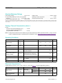
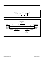
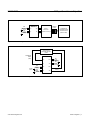
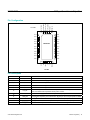
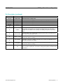
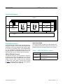
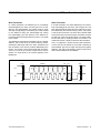
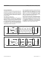
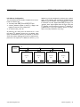
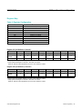
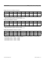
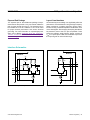
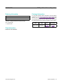
MAX24104
15Gbps Quad Linear Equalizer
General Description
The MAX24104 restores high-frequency signal level at
the decision-feedback equalizer (DFE) receiver for highloss backplane and cable channels. This permits the DFE
receiver to meet BER goals. At 15Gbps, the MAX24104
can operate in channels with FR4 and cable HF loss of
more than 30dB at 7.5GHz. The linear transfer function is
transparent to Adaptive DFE equalizers, permitting DFE
adaptation to track temperature and changing channel
conditions.
Together with the DFE, integrated into Serializer/
Deserializer (SERDES), the device adds increased margin rather than full signal regeneration. Unlike conventional equalizers with limiting output stages, the device
preserves the linear channel characteristics, allowing
the DFE to operate linearly over the entire channel. This
permits extending total channel reach and/or improving
signal-to-noise ratio (SNR). The device typically compensates for up to 19dB of the total loss in a long channel,
effectively reducing the channel length seen by the DFE
receiver.
The device has four channels and is packaged in a spacesaving, 4mm x 6.5mm, FCLGA package.
Applications
●
●
●
●
1Gbps to 15Gbps High-Speed Backplanes and Cables
12.5Gbps Quad XAUI Interconnect
14Gbps 16G Fiber Channel
12Gbps SAS III
Benefits and Features
●● Low Power Consumption Reduces Operating Cost
• Single 2.5V Supply
• 131mW Per Channel (typ) at 700mVP-P Output
• Lower Power, Lower Cost and Smaller Board
Footprint than CDR Solutions
●● Linear Performance for Greater System Flexibility
• 1Gbps to 15Gbps Linear Equalization
• Increases High-Frequency Signal Level to Help Rx
DFE Achieve BER Goals
• Selectable Output Linear Swing from 700mVP-P to
1000mVP-P
• Input Return Loss Better than 16dB Up to 7.5GHz
●● Adjustable Features for Greater Flexibility
• Selectable EQ Peaking Spanning +6dB to +19dB
at 7.5GHz
• Selectable Flat Gain Spanning -2.9dB to +1.7dB
●● Integration Allows Greater Design Flexibility
• I2C Daisy-Chain for Addressing Up to 63 ICs
• Plug and Play – Set Control Pins (All Channels
Set the Same) or Independent Control of Each
Channel through I2C Bus
• Transparent to Link Training, OOB and Idle and
Data-Rate and Coding Agnostic
• 4mm x 6.5mm FCLGA Package
Typical Application Circuit
TX
CMOS
TX
Pre-Em
MAX24104
BOARD
BACKPLANE
BOARD
Ordering Information appears at end of data sheet.
For related parts and recommended products to use with this part, refer to www.maximintegrated.com/MAX24104.related.
19-7346; Rev 1; 4/15
RX
CMOS
DFE AND
SLICER
MAX24104
15Gbps Quad Linear Equalizer
Absolute Maximum Ratings
Power-Supply Voltage...........................................-0.5V to +4.0V
DC Input Voltage Applied (all control pins except SDA
and SCL)............................................... -0.5V to (VCC + 0.3V)
DC Input Voltage Applied (SDA, SCL)..................-0.5V to +4.0V
Output Current................................................... -90mA to +90mA
Operating Junction Temperature...................................... +125ºC
Storage Temperature Range..............................-40ºC to +150°C
Stresses beyond those listed under “Absolute Maximum Ratings” may cause permanent damage to the device. These are stress ratings only, and functional operation of the device at these
or any other conditions beyond those indicated in the operational sections of the specifications is not implied. Exposure to absolute maximum rating conditions for extended periods may affect
device reliability.
Package Thermal Characteristics (Note 1)
FCLGA
Junction-to-Case Thermal Resistance (qJC)................10°C/W
Junction-to-Ambient Thermal Resistance
(qJA) (EIA/JESD51-2 standard)....................................29°C/W
Note 1: Package thermal resistances were obtained using the method described in JEDEC specification JESD51-7, using a four-layer
board. For detailed information on package thermal considerations, refer to www.maximintegrated.com/thermal-tutorial.
Operating Conditions
PARAMETER
Supply Voltage
Operating Ambient
Temperature
SYMBOL
MIN
TYP
MAX
UNITS
VCCR,
VCCT,
VCCP
CONDITIONS
2.312
2.5
2.75
V
TA
-40
+25
+85
°C
15
Gbps
66
CID
1200
mVP-P
Data Rate
1
Source Data Coding and
CID
Differential Source Diff LowFrequency Voltage
DC balanced NRZ, 8B10B or
Scrambled; PRBS31
VLAUNCH
LF Baseline (without PE)
measured at source; source HF
pre-emphasis swing can be higher
Source Rise/Fall Time
Test source 10% to 90%
Source Common-Mode
Noise
DC - 200MHz
Supply Noise
DC - 1MHz
26
ps
150
50
mVP-P
mVP-P
Electrical Characteristics
(Typical values are at VCCR = VCCT = VCCP = 2.5V, TA = +25°C. See Figure 1 for typical supply filtering.) (Note 2)
PARAMETER
Supply Current
Supply Current During
Power-Down
www.maximintegrated.com
SYMBOL
ICCR +
ICCT +
ICCP
CONDITIONS
Total supply
current with all 4
channels enabled
MIN
TYP
MAX
TXAx[1:0] = 00
204
275
TXAx[1:0] = 11
250
305
2.0
UNITS
mA
mA
Maxim Integrated │ 2
MAX24104
15Gbps Quad Linear Equalizer
Electrical Characteristics (continued)
(Typical values are at VCCR = VCCT = VCCP = 2.5V, TA = +25°C. See Figure 1 for typical supply filtering.) (Note 2)
PARAMETER
SYMBOL
Inrush Current
Residual Deterministic Jitter
(Notes 3, 4)
Peaking Gain
(Compensation at 7.5GHz,
relative to 100MHz,
100mVP-P Sine Wave Input)
DJRX
GNP
CONDITIONS
MIN
%
Over-bit rate with EQ peaking
optimized for loss channel, in linear
range
9
psP-P
EQx[3:0] = 1110
18.5
EQx[3:0] = 1001
15.7
EQx[3:0] = 0101
13.2
TA = +85°C
-3.67
+0.82
TA = +25°C
-1.61
+1.96
TA = -40°C
-1.62
+3.60
0.14
FGx[1:0] = 01
-1.36
FGx[1:0] = 00
-2.87
-1dB Compression Point
Output Swing (Note 5) (at
7.5GHz)
Input-Referred Noise
Output-Referred Noise
(Note 3)
www.maximintegrated.com
V1dB_OUT
VNOISE
VNOISE
dB
TA = +85°C
-3.24
+1.72
TA = +25°C
-2.51
+2.85
TA = -40°C
-2.59
TXAx[1:0] = 11
V1dB_OUT
dB
1.68
FGx[1:0] = 10
Variation around
typical
-1dB Compression Point
Output Swing (at 100MHz)
UNITS
< 10
Variation around
typical
GNF
MAX
Beyond steady-state supply current
with supply ramp-up time less than
200µs
FGx[1:0] = 11
Flat Gain (100MHz, EQx[3:0]
= 1000, TXAx[1:0] = 10)
TYP
1000
+3.67
1370
TXAx[1:0] = 10
1280
TXAx[1:0] = 01
1040
TXAx[1:0] = 00
920
TXAx[1:0] = 11
1000
TXAx[1:0] = 10
940
TXAx[1:0] = 01
700
TXAx[1:0] = 00
600
100MHz to 7.5GHz, FGx[1:0] = 11,
EQx[3:0] = 0000, Figure 3
0.6
100MHz to 7.5GHz, FGx[1:0] = 11,
EQx[3:0] = 1010, Figure 3
0.5
100MHz to 7.5GHz, FGx[1:0] = 11,
EQx[3:0] = 0000, Figure 3
0.8
100MHz to 7.5GHz, FGx[1:0] = 11,
EQx[3:0] = 1010, Figure 3
1.0
mVP-P
mVP-P
mVRMS
1.97
mVRMS
Maxim Integrated │ 3
MAX24104
15Gbps Quad Linear Equalizer
Electrical Characteristics (continued)
(Typical values are at VCCR = VCCT = VCCP = 2.5V, TA = +25°C. See Figure 1 for typical supply filtering.) (Note 2)
PARAMETER
SYMBOL
CONDITIONS
MIN
TYP
MAX
UNITS
2.10
V
HIGH SPEED I/O
Input Common-Mode Voltage
VICM
Input Resistance
RIN
Input Return Loss
S11
Output Resistance
ROUT
DC differential resistance
100
AC common-mode (single-ended)
resistance
50
10MHz to 7.5GHz
Differential
> 16
1GHz to 7.5GHz
Common mode
> 10
DC differential resistance
100
AC common mode (single-ended)
resistance
50
Ω
dB
Ω
Pulse Response Ringing
3
%
Intra-Pair Skew
2
ps
4
ps
Inter-Pair Skew
Output Return Loss
Channel Isolation
S22
VCoup
10MHz to 7.5GHz
Differential
> 13
1GHz to 7.5GHz
Common Mode
>8
100MHz to 7.5GHz, Figure 4
(Note 6)
dB
40
dB
LVCMOS I/O
Input Logic-High Voltage
VIH
0.7 x
VCC
VCC +
0.3
V
Input Logic-Low Voltage
VIL
-0.3
0.3 x
VCC
V
Output Logic-High Voltage
VOH
At IOH = -200µA
Output Logic-Low Voltage
VOL
At IOL = -200µA
Open State Current Tolerance
HIZ
Input Logic-High Current
IIH
Input Logic-Low Current
www.maximintegrated.com
IIL
VCC 0.2
V
0.2
±5
mA
VIH(MIN) < VIN < VIH(MAX), all other
CMOS pins
+225
VIH(MIN) < VIN < VIH(MAX), PGM_IN
+120
VIL(MIN) < VIN < VIL(MAX) , all other
CMOS pins
-225
VIL(MIN) < VIN < VIL(MAX), PGM_IN
-18
V
mA
mA
Maxim Integrated │ 4
MAX24104
15Gbps Quad Linear Equalizer
Electrical Characteristics (continued)
(Typical values are at VCCR = VCCT = VCCP = 2.5V, TA = +25°C. See Figure 1 for typical supply filtering.) (Note 2)
PARAMETER
SYMBOL
CONDITIONS
MIN
TYP
MAX
UNITS
0.3 x
VCC
V
I2C CHARACTERISTICS (SDA, SCL) (Note 7)
Low-Level Input Voltage
VIL
High-Level Input Voltage
VIH
Input Hysteresis
0.7 x
VCC
V
VHYS
200
Input Capacitance
CIN
10
Input Leakage Current
IIN
Output Low Voltage SDA
SCLK Clock Frequency
VOL
fSCLK
mV
pF
±1
ISINK = 3mA
0.4
ISINK = 6mA
0.6
400
mA
V
kHz
Note 2: The MAX24104 is 100% production tested at TA = +25°C and TA = +85°C. Specification at TA = -40°C is guaranteed by
design or characterization, unless otherwise noted.
Note 3: Guaranteed by design and characterization.
Note 4: Measured with circuit board loss optimized for best DJ. Residual jitter is the difference in deterministic jitter between the
reference data source and device output. DJRESIDUAL = DJOUTPUT – DJSOURCE. The deterministic jitter at the output
of the transmission line must be from media induced loss. Measured at point D in Figure 2. Test Pattern: 66 Zeroes, 1010,
PRBS7, 66 ones, 0101 Inverted PRBS7.
Note 5: The output voltage range in which a linear relationship between the input and output maintains less than or equal to 1dB
compression.
Note 6: Measured using a vector-network analyzer (VNA N5245A) with -15dBm power level applied to the adjacent input. The VNA
detects the signal at the output of the victim channel. All other inputs and outputs are terminated with 50Ω.
Note 7: Refer to UM10204: I2C-bus specification and user manual, Rev. 03 – 19 June 2007.
www.maximintegrated.com
Maxim Integrated │ 5
MAX24104
15Gbps Quad Linear Equalizer
2.5V
SUPPLY
1µH
100µF
VCC
0.1µF
100µF
0.1µF
Figure 1. Recommended Supply Filtering
RECEIVE TEST SETUP
PCB (FRA)
SIGNAL
SOURCE
A
B
6 MIL
SMA
CONNECTORS
2in < L < 30in
D
MAX24104
RX
TX
OSCILLOSCOPE OR
BIT ERROR DETECTOR
6 MIL
L = 2in
SMA
CONNECTORS
FR4
4.0 < εR < 4.4
tanδ = 0.022
Figure 2. Receiver Test Setup (Points Labeled A, B, and D are Referenced for AC Parameter Test Conditions)
www.maximintegrated.com
Maxim Integrated │ 6
MAX24104
15Gbps Quad Linear Equalizer
MAX24104
50Ω
50Ω
RX_+
TX_+
RX_-
TX_-
BALUN
PSPL 5315A
(200kHz TO 17GHz)
LOWPASS
FILTER
4TH OBT
POWER METER
GIGATRONICS 8652A
WITH 80301A HEAD
(10MHz to 18GHz)
Figure 3. Noise Test Configuration
4-PORT VECTOR
NETWORK ANALYZER
N52454
AGGRESSOR
SIGNAL
(0dBm)
MAX24104
50Ω
VICTIM
INPUT
50Ω
RX1+
TX1+
RX1-
TX1-
RX2+
TX2+
RX2-
TX2-
50Ω
50Ω
VICTIM
OUTPUT
Figure 4. Channel-Isolation Test Configuration
www.maximintegrated.com
Maxim Integrated │ 7
MAX24104
15Gbps Quad Linear Equalizer
Typical Operating Characteristics
(Typical values are at VCCR = VCCT = VCC_DG = 2.5V, TA = +25°C, unless otherwise noted.)
DETERMINISTIC JITTER
vs. EQUALIZATION SETTING
toc01
0.15
0.10
16.7dB Loss, Linear
Range Operation
3dB Loss, Linear
Range Operation
0.05
toc02
0.30
0.25
0.20
3dB Loss, Linear
Range Operation
16.7dB Loss, Linear
Range Operation
0.15
0.10
Data Rate = 15Gbps, TXAx[1:0] = 10, FGx[2:0] = 10
Data Rate = 10.3Gbps, TXAx[1:0] = 10, FGx[1:0] = 10
10.0
TXAx[1:0] = 11
GAIN (dB)
OUTPUT AMPLITUDE (dBV)
-20
-15
-10
-5
toc05
FGx[1:0] = 111
FGx[1:0] = 10
20
TXAx[1:0] = 00
-15.0
FGx[1:0] = 01
15
10
FGx[1:0] = 00
5
-20.0
0
EQx[3:0] = 0111, FGx[1:0] = 10
-25
-20
-15
-10
-5
0
5
-5
10
TXAx[1:0] = 11, EQx[3:0] = 0000
0
2
INPUT AMPLITUDE (dBV)
-5
GAIN (dB)
10
5
EQxx[3:0] = 0010
TXAx[1:0] = 11, FGxx[1:0] = 10
2
4
6
8
FREQUENCY (GHz)
www.maximintegrated.com
FR4 ONLY
-10
-15
-20
EQxx[3:0] = 0000
0
toc07
FR4 with EQx[3:0] = 1110
EQxx[3:0] = 0100
0
10
0
EQxx[3:0] = 0111
15
8
5
EQxx[3:0] = 1111
20
6
FREQUENCY RESPONSE
WITH 18in of FR4
toc06
25
4
FREQUENCY (GHz)
FREQUENCY RESPONSE
GAIN (dB)
-25
INPUT AMPLITUDE (dBV)
25
-10.0
-5
-30
30
0.0
-25.0
EQx[3:0] = 0111, FGx[1:0] = 10
FREQUENCY RESPONSE
toc04
-5.0
-10
EQUALIZATION SETTING (EQxx[3:0])
1dB COMPRESSION
(100MHz Nyquist)
5.0
TXAx[1:0] = 00
-5
-20
0.00
0000
0 1 0010
2 3 0100
4 5 0110
6 7 1000
8 9 1010
10 111100
12 131110
14 15
EQUALIZATION SETTING (EQxx[3:0])
TXAx[1:0] = 11
0
-15
0.05
0.00
0000
0 1 0010
2 3 0100
4 5 0110
6 7 1000
8 9 1010
10 111100
12 131110
14 15
toc03
5
OUTPUT AMPLITUDE (dBV)
0.20
1dB Compression
(7.5GHz Nyquist)
0.35
DETERMINISTIC JITTER (UIP-P)
0.25
DETERMINISTIC JITTER (UIP-P)
DETERMINISTIC JITTER
vs. EQUALIZATION SETTING
10
-25
TXAx[1:0] = 11, FGx[1:0] = 10
0
2
4
6
8
10
FREQUENCY (GHz)
Maxim Integrated │ 8
MAX24104
15Gbps Quad Linear Equalizer
Typical Operating Characteristics (continued)
(Typical values are at VCCR = VCCT = VCC_DG = 2.5V, TA = +25°C, unless otherwise noted.)
MAX24104 SINGLE-ENDED OUTPUT AFTER 18in FR4 AT INPUT
(EQx[3:0] = 1110, FGx[1:0] = 01, TXAx[1:0] = 11, 13.5Gbps)
MAX24104 SINGLE-ENDED OUTPUT AFTER 18in FR4 AT INPUT
(EQx[3:0] = 1110, FGx[1:0] = 01, TXAx[1:0] = 11, 10.3Gbps)
toc9
toc8
50mV/div
VOUTN
VOUTN
VINSIDE
VINSIDE
50mV/div
VBACKUP
VBACKUP
20ps/div
20ps/div
SINGLE-ENDED OUTPUT FROM BERT SOURCE
(12Gbps)
100mV/div
SINGLE-ENDED OUTPUT FROM BERT SOURCE AFTER 18in FR4
(12Gbps)
toc10
toc11
VOUTN
VOUTN
VINSIDE
VINSIDE
100mV/div
VBACKUP
VBACKUP
20ps/div
20ps/div
MAX24104 SINGLE-ENDED OUTPUT AFTER 18in FR4 AT INPUT
(EQx[3:0] = 1110, FGx[1:0] = 01, TXAx[1:0] = 11, 12Gbps)
MAX24104 SINGLE-ENDED TIME DOMAIN OUTPUT VS. EQUALIZATION LEVEL
(FGx[1:0] = 01, TXAx[1:0] = 11, WITH 18in FR4 AT 1Gbps)
toc12
toc13
VOUTN
VOUTN
VINSIDE
50mV/div
VINSIDE
62mV/div
VBACKUP
20ps/div
www.maximintegrated.com
VBACKUP
100ps/div
Maxim Integrated │ 9
MAX24104
15Gbps Quad Linear Equalizer
29 PGM_IN
30 ENABLE
31 APPLICATION
32 OUTPUT_LEVEL
TOP VIEW
33 EQ_PEAKING
34 FLAT_GAIN
Pin Configuration
RX1P
1
28
TX1P
RX1N
2
27
TX1N
VCCR
3
26
VCCT
RX2P
4
25
TX2P
RX2N
5
24
TX2N
VCCR
6
23
VCCT
RX3P
7
22
TX3P
RX3N
8
21
TX3N
VCCR
9
20
VCCT
RX4P 10
19
TX4P
RX4N 11
18
TX4N
PGM_OUT 17
SCL 15
SDA 16
LDO_DIG 14
VCCP 13
I2C_EN 12
MAX24104
FCLGA
Pin Description
PIN
NAME
FUNCTION
1, 2
RX1P, RX1N
3, 6, 9
VCCR
Differential Channel 1 Input, CML
4, 5
RX2P, RX2N
Differential Channel 2 Input, CML
Positive Receive Power Supply, 2.5V. Filter each pin with a 0.1µF capacitor to GND.
7, 8
RX3P, RX3N
Differential Channel 3 Input, CML
10, 11
RX4P, RX4N
Differential Channel 4 Input, CML
12
I2C_EN
13
VCCP
14
LDO_DIG
15
SCL
Analog I2C Serial-Interface Clock Input. Use external 4.7kΩ pullup to VCC.
16
SDA
Analog I2C Serial-Interface Data Input and Output. Use external 4.7kΩ pullup to VCC.
17
PGM_OUT
www.maximintegrated.com
I2C Enable Input, LVCMOS. Hardwire low for pin control. Hardwire high for I2C control.
User must select mode of operation before power-on reset.
Positive Power Supply, 2.5V. Filter each pin with a 0.1µF capacitor to GND.
Compensation capacitor pin for internal LDO. Bypass pin with a 0.22µF capacitor to GND.
Cascadable I2C Output. LVCMOS. See the Slave Address Configuration section.
Maxim Integrated │ 10
MAX24104
15Gbps Quad Linear Equalizer
Pin Description (continued)
PIN
NAME
18, 19
TX4N, TX4P
FUNCTION
Differential Channel 4 Output, CML
20, 23, 26
VCCT
21, 22
TX3N, TX3P
Differential Channel 3 Output, CML
24, 25
TX2N, TX2P
Differential Channel 2 Output, CML
27, 28
TX1N, TX1P
Differential Channel 1 Output, CML
29
PGM_IN
Cascadable I2C Input. Has 30kΩ pulldown, see the I2C Address Configuration section.
30
ENABLE
Power-Down Enable Pin, LVCMOS. Three-state pin to program the power mode of the
part at startup. For high and open, see Table 5 for settings. Set low for reset. Reset,
disables all communication to the chip along with resetting the registers to their default
states.
31
APPLICATION
Application Select Input, LVCMOS. Select between channel cases: short and long. Set
low or open for long. Set high for short.
32
OUTPUT_LEVEL
33
EQ_PEAKING
34
FLAT_GAIN
—
EP
www.maximintegrated.com
Positive Transmit Power Supply, 2.5V. Filter each pin with a 0.1µF capacitor to GND.
Output Level Control, LVCMOS. Three-state pin to program the output level of all
channels. See Table 4 for settings.
Equalization Control Pin, LVCMOS. Three-state pin to program the equalization level of
all channels. See Table 2 for settings.
Gain Adjust Control Pin, LVCMOS. Three-state pin to program the flat gain level of all
channels. See Table 3 for settings.
Exposed Pad. Internally connected to GND. Ground reference for power supplies, threestate, and other low-speed pins. Connect EP to a large ground plane to maximize thermal
performance.
Maxim Integrated │ 11
MAX24104
15Gbps Quad Linear Equalizer
Functional Diagram
4 CHANNELS
RX1P
50Ω
50Ω
EQUALIZER
FLAT GAIN
OUTPUT BUFFER
TX1P
TX1N
RX1N
LANE 1 OF 4
CONTROL
EQ_PEAKING
Detailed Description
The MAX24104 is a 4-channel linear equalizer (EQ) functioning up to 15Gbps. Each channel has a programmable
equalization network and programmable flat gain adjust.
All controls for equalization, gain, output enable/disable,
etc., are individually programmed through the on-chip
programming block. The programming block can be controlled either through pin controls or the I2C serial bus.
APPLICATION Pin Control
The placement range of a linear equalizer is limited by
its dynamic range and noise performance. To allow the
widest placement range, the MAX24104 has two optimizations. The two cases are Short and Long Channels.
By selecting the case based on channel loss as shown
in Table 1, the best dynamic range and noise operating
points can be selected for the application.
www.maximintegrated.com
FLAT GAIN
OUTPUT LEVEL
Input Termination
The input termination consists of two 50Ω resistors forming a differential termination between the input pins. The
excellent return loss minimizes reflections in a channel.
Table 1. APPLICATION Pin Control
INPUT LEVEL
CHANNEL LENGTH
High
Short Channel. 0dB to 18dB channel loss
before MAX24104.
Low, Open
Long Channel. 18dB to 33dB channel loss
before MAX24104.
Maxim Integrated │ 12
MAX24104
15Gbps Quad Linear Equalizer
I2C control, the flat gain can be adjusted independently
for each channel.
Receive Equalizer
For the MAX24104, the input data goes into a selectable
equalization stage. The receive equalizer is designed to
compensate losses up to 19dB (at 7.5GHz) . The selectable equalization can be controlled using commands sent
over the I2C serial bus or pin control. With pin control the
equalization setting has three available compensation
levels and all the channels are controlled globally. See
Table 2 for details. With the I2C serial bus, the equalization has 16 settings and each channel can be adjusted
independently.
Output Stage
The MAX24104 data path transitions from the gain stages
into a linear output buffer with selectable output levels.
With pin control the output levels can be adjusted globally
as shown in Table 4. With I2C control, the output levels
can be adjusted independently for each channel.
Power Saving
The MAX24104 features a power-down enable input
(ENABLE) pin to shut down the device and reduce supply current at startup. Set high to power down the output
stage of all channels. Set open to power up all channels.
Set low for reset. Reset disables all communication to
the chip along with resetting the registers to their default
states.
Gain Stage
The MAX24104 data path goes through a wideband flat
gain stage. With pin control, the flat gain can be adjusted
globally from -2.9dB to +1.7dB as shown in Table 3. With
Table 2. EQ_PEAKING Pin Control (refer to Table 6)
CONTROL PIN
INPUT LEVEL
LONG CHANNEL
(APPLICATION = LOW, OPEN)
SHORT CHANNEL
(APPLICATION = HIGH)
High
(EQx[3:0] = 1110)
(EQx[3:0] = 1001)
Open
(EQx[3:0] = 1001)
(EQx[3:0] = 0101)
Low
(EQx[3:0] = 0101)
(EQx[3:0] = 0011)
UNITS
dB
Table 3. FLAT_GAIN Pin Control (refer to Table 7)
CONTROL PIN
INTPUT LEVEL
LONG CHANNEL
(APPLICATION = LOW, OPEN)
SHORT CHANNEL
(APPLICATION = HIGH)
High
(FGx[1:0] = 11)
(FGx[1:0] = 10)
Open
(FGx[1:0] = 10)
(FGx[1:0] = 01)
Low
(FGx[1:0] = 01)
(FGx[1:0] = 00)
UNITS
dB
Table 4. OUTPUT_LEVEL Pin Control (refer to Table 8)
CONTROL PIN
INPUT LEVEL
OUTPUT AMPLITUDE
High
(TXAx[1:0] = 11)
Open
(TXAx[1:0] = 10)
Low
(TXAx[1:0] = 01)
UNITS
mVP-P
Table 5. ENABLE and Reset Pin Control
CONTROL PIN INPUT LEVEL
(ENABLE)
I2C CONTROL MODE
(I2C_EN = high)
PIN CONTROL MODE
(I2C_EN = low)
High
Upon POR or reset, power down all channels
Power down all channels
Open
Upon POR or reset, power on all channels
Power on all channels
Low
Reset (POR)
Reset (POR)
www.maximintegrated.com
Maxim Integrated │ 13
MAX24104
15Gbps Quad Linear Equalizer
Applications Information
Definitions
dBV is defined as dB relative to 1VP-P (differential).
Hence, the Tx level of 1VP-P is 0dBV, and a Tx level of
0.5VP-P is -6dBV.
Linear Equalizer (EQ) Placement and Use, in 3
Steps
Placement of linear equalizers in lossy channels is
bounded by output linearity and input noise (IRN). See
Figure 5. Although placement is quite flexible, it is
important to maintain linear operation with sufficient SNR,
hence the boundary conditions stated in the following two
sections.
Tx1VP-P
W/6dB PE
Source Tx Level [dBV] is the total measured Tx VP-P,
including pre-emphasis.
Desired Margin is a user decision regarding margin
needed to account for all system min/max variations,
including source Tx, MAX24104, and ASIC receiver.
POSITION 1
POSITION 2
2.0V
dBV
0
1.0V
-5
0.5V
LOS
LF
SS
LOP
(LONG CID)
E(
NYQ
-10
0.2V
-15
-20
LINEAR EQ OUTPUT REFERRED -1dB COMPRESSION LEVEL [VP-P]
HF
UIS
T 7.
5GH
z Sq
DESIGN
MARGIN
WA
VE)
TOTAL GAIN
AT NYQUIST
100mV
ASIC DFE IR-NOISE AT BER 1E-15 [VP-P]
-25
-24dB
50mV
DFE IRN
AT BER
1E-15
-30
-35
-40
20mV
10mV
-45
LINEAR EQ OR-NOISE AT BER 1E-15 [VP-P]
LINEAR EQ IR-NOISE AT BER 1E-15 [VP-P]
5mV
-50
2mV
0
4
8
CHANNEL LOSS [dB]
12
16
20
28
32
36
PLACEMENT RANGE
IN LOSSY CHANNEL
TX
CMOS
1VPPD
6dbPE
24
1
2
RX
CMOS
DFE AND
SLICER
Figure 5. Linear Equalizer Placement
www.maximintegrated.com
Maxim Integrated │ 14
MAX24104
15Gbps Quad Linear Equalizer
Step 1—Maintain EQ Linearity at Low Frequency
(LF)
Minimum Distance (Nyquist Loss) from Source Tx [dB] =
The source Tx low frequency (LF) amplitude needs to be
considered to keep linear EQ within its linear range. The
source Tx low-frequency (LF) amplitude is the differential
peak-peak amplitude after any pre-emphasis has fully settled, e.g., the level of long CID (continuous identical digits)
sequences. The primary controls over LF levels in Linear
EQ are the Used ASIC Source Tx pre-emphasis (or deemphasis) and the Linear EQ Flat Gain (MAX24104).
Source Tx Level [dBV] +
Linear EQ Peaking Gain [dB] +
Linear EQ Flat Gain [dB] –
Linear EQ Output Level setting (-1dB Compression
level) [dBV] +
User System Margin [dB]
For example:
Figure 5 shows a typical example with ASIC Source Tx
having 6dB pre-emphasis, with 1VP-P peak swing and
0.5VP-P swing after pre-emphasis (e.g., long CID LF
content). Note that 0.5VP-P fits easily under the -1dB
Compression line. If the Source Tx were to have higher
LF swing, driving linear EQ into nonlinearity, the linear
EQ flat-gain control can be used to attenuate input signal
level, as needed, to maintain linearity.
Source Tx Level = 0dBV
Linear EQ Peaking Gain = 14dB
Linear EQ Flat Gain = 0dB
Linear EQ Output Level setting (-1dB Compression
Point) = -3dBV
User System Margin = 2dB
For example:
Then:
Maximum Linear EQ Flat Gain setting =
Minimum Distance (Nyquist Loss) from Source Tx = 0
+ 14 + 0 - (-3) + 2 = 19dB
Linear EQ Output Level setting (-1dB compression)
[dBV] -
Step 3—Keep Nyquist Level Sufficiently Above
Noise Floor
Source Tx Level [dBV] +
Source Tx Pre-Emphasis (De-emphasis) [dB] -
User System Margin [dB]
The amplitude of the Nyquist sequence (10101010…)
must be maintained sufficiently above noise floor to
achieve BER goals. Hence, Nyquist level at input to
the Linear EQ needs to be sufficiently above the Linear
EQ self-noise, IRN (input referred noise). This sets the
maximum Nyquist channel loss preceding the Linear EQ,
e.g, farthest placement from Source Tx (see Position 2
in Figure 5).
For example:
Linear EQ Output Level setting (-1dB compression)
[dBV] = -3dBV
Source Tx Level [dBV] = 0dB
Source Tx Pre-Emphasis (De-emphasis) [dB] = 6dB
User System Margin = 2dB
Then:
Maximum Linear EQ Flat Gain setting = (-3) - 0 + 6 - 2
= 1dB
Maximum Distance (Nyquist Loss) from Source Tx [dB] =
Source Tx Level (which is Nyquist level) [dBV] –
Linear EQ IRNpp at BER goal [dBV] –
Margin required to reduce RJ creation –
User System Margin [dB]
(There are three Flat Gain settings available lower than
+1dB: They are -3dB, -1.5dB, 0dB)
For example:
Source Tx Level = 0dBV
Step 2—Maintain EQ Linearity at High Frequency
(Nyquist)
Linear EQ IRNpp at BER goal (0.5mVrms x 15.9 at
BER 1E-15) [dBV] = -43dB
Margin required to reduce RJ creation (to 0.2UIpp at
BER) = 10dB
User System Margin = 3dB
A linear equalizer when placed too close to a Source Tx
is vulnerable to nonlinear compression at high frequency
(Nyquist), especially if the EQ peaking gain is higher
than the preceding channel loss. The -1dB compression
specification gives maximum output level that guarantees
linear operation. As a function of the EQ settings, the minimum placement distance from the Source Tx is calculated
as follows: (see Position 1 in Figure 5).
www.maximintegrated.com
Then:
Maximum Distance (Nyquist Loss) from Source Tx =
0 - (-43) - 10 - 3 = 30dB
Maxim Integrated │ 15
MAX24104
15Gbps Quad Linear Equalizer
Tools—Frequency Response Plotting and EQ
Placement in Channel Calculator
The SDA and SCL pins are referred to as the slave I2C.
The slave I2C provides external access to the register set
within the MAX24104. Typically, an MCU is connected to
the slave I2C.
of SCL. Data is arranged in packets of 9 bits. The first 8
bits represent data to be transferred (most significant bit
(MSB) first). The last bit is an acknowledge bit from the
slave. The recipient of the data holds SDA low during the
ninth clock cycle of a data packet to acknowledge (ACK)
the byte. Leaving SDA left open on the ninth bit signals
a not-acknowledged (NACK) condition. The interpretation
of the acknowledge bit by the sender depends on the type
of transaction and the nature of the byte being received.
SDA is bidirectional so that the master may send data
bytes during write transactions and the slave may send
data bytes during reads.
Framing and Data Transfer
Device Addressing
Several simple Microsoft® Excel spreadsheet tools are
available to assist in the application of the MAX24104
Linear EQs. Please visit www.maximintegrated.com to
access the latest version of these spreadsheets:
I2C Interface
An individual transaction is framed by a START condition
and a STOP condition. A START condition occurs when
a bus master pulls SDA low while SCL is high. A STOP
condition occurs when the bus master allows SDA to transition low-to-high when SCL is high. Within the frame the
master has exclusive control of the bus. The MAX24104
supports Repeated START conditions whereby the master may simultaneously end one frame and start another
without releasing the bus by replacing the STOP condition
with a START condition.
Within a frame, the state of SDA only changes when SCL
is low. A data bit is transferred on a low-to-high transition
VOUT (txa)
Flatgain (vgc)
Peak Gain (eq)
The first byte to be sent after a START condition is a slave
address byte. The first seven bits of the byte contain the
target slave address (MSB first). The eighth bit indicates
the transaction type – ‘0’ = write, ‘1’ = read. Each slave
interface on the bus is assigned a 7-bit slave address. If
no slave matches the address broadcast by the master
then SDA will be left open during the acknowledge bit
and the master receives a NACK. The master must then
assert a STOP condition. If a slave identifies the address
then it acknowledges it by pulling SDA low. The master
then proceeds with the transaction identified by the type
bit. The two-wire interface of the MAX24104 decodes
slave addresses ranging from 00h to 3Fh.
TXA
VGC
EQ
3
2
1
3
2
1
8
4
1
MAX24104
RESPONSE
1
3FREQUENCY
4
16
a
2
3
4
UPDATE
b
c
d
20
MAX24104
TXA2 VGC3 EQ15
15
TXA2 VGC2 EQ7
TXA1 VGC1 EQ3
TXA0 VGC0 EQ0
S21 (dB)
10
5
0
-5
-10
0
2E+09
4E+09
6E+09
8E+09
1E+10
Frequency (Hz)
Figure 6. Frequency Response Plotting
Microsoft Excel is a registered trademark of Microsoft Corp.
www.maximintegrated.com
Maxim Integrated │ 16
MAX24104
15Gbps Quad Linear Equalizer
MAX24104 10.3Gbps Linear EQ: Calculate Placement Range in Channel
ASIC TX
LINEAR EQ
Entry Box in Yellow: Entry Box
Pull Down Box in Pink: Pull Down
ASIC TX SETTINGS
T = Tx HF Level [mVpp]
[dBVpp]
D = Tx De-Emphasis [dB]
ASIC RX
LINEAR EQ SETTINGS
1000
0.00
P = Peaking Gain (HF reLF) [dB]
F = Flat Gain (LF) [dB]
3.0
STEP 1: Make sure that L (Tx LF Level)
is less than EQ LF compression level:
708
L = Tx LF Level [mVpp]
[dBVpp]
-3.00
<
Entry Box in Yellow: Entry Box
ASIC RX SETTINGS
15
0
Input Ref
Mult Output Ref
0.50 n = Refer'd Noise [mVrms]
2
1.00
7.9
[mVpp]
15.8
-42.0
[dBVpp]
-36.0
800 CL = LF -1dB Compress [mVpp]
800
-1.94
[dBVpp]
-1.94
800
142 CH = HF -1dB Compress [mVpp]
-16.9
[dBVpp]
-1.94
N = Input Ref Noise [dBVrms]
[Vpp]
[dBVpp]
0.5
7.9
-42.0
M = Margin [dB]:
12.0
Nyquist (010101) [Vpp] above N [Vpp@BER]
(recommend > 16dB for RJ < 0.10UIpp)
(recommend > 12dB for RJ < 0.16UIpp)
BER Target = 1E-xx, where xx=
Vpp/Vrms Multiplier =
(for BER in 1E-12 to 1E-17 range)
15
15.85
12.0 m = Margin [dB]: Nyquist above n [dBVpp@BER]
(recommend > 16dB for RJ < 0.10UIpp)
(recommend > 12dB for RJ < 0.16UIpp)
RESULTS:
EQ PLACEMENT [Loss@Nyquist]
A = Nearest to Tx [dB] >
Over PVT >
= T - CH (Input Ref)
= Keeps Nyquist(010101)
level below EQ HF
compression level.
16.94
18.94
B = Farthest from Tx [dB] <
30.02 dB
Over PVT <
28.02 dB
= T - n (Input Ref) - m
= Keeps Nyquist (010101) level above
above EQ IRN (input referred noise)
to meet BER and constrain RJ gen.
A = Farthest from Rx [dB] <
Over PVT <
= CH (Output Ref) - N - M
= Keeps Nyquist above
DFE IRN to meet BER
and constrain RJ gen.
28.08
26.08
B = Nearest to Rx [dB] >
6.02 dB
Over PVT >
8.02 dB
= n (output) - N
= Keeps EQ ORN (output ref noise)
below DFE IRN (input ref noise),
including channel loss on noise.
C = Longest Channel [dB] <
45.02 dB
Over PVT <
43.02 dB
= T + F + P - N - M
= Keeps Nyquist (010101) level sufficiently
above DFE IRN (input referred noise)
to meet BER and constrain RJ generation
If using "Typical" specs, add
Margin for PVT Variation +/-
2 dB
Figure 7. EQ Placement Calculator
www.maximintegrated.com
Maxim Integrated │ 17
MAX24104
15Gbps Quad Linear Equalizer
Write Transaction
Read Transaction
In a write transaction, the address byte is successfully
acknowledged by the slave, and the type bit is set low.
After the first acknowledge, the master sends a single
data byte. All signaling is controlled by the master except
for the SDA line during the acknowledge bits. During
the acknowledge cycle the direction of the SDA line is
reversed and the slave pulls SDA low to return a ‘0’ (ACK)
to the master.
In a read transaction, the slave address byte is successfully acknowledged by the slave, and the type bit is set
high. After the ACK the slave returns a byte from the location identified by the internal memory pointer. This pointer
is then auto-incremented. The slave then releases SDA
so that the master can ACK the byte. If the slave receives
an ACK then it will send another byte. The master identifies the last byte by sending a NACK to the slave. The
master then issues a STOP to terminate the transaction.
The MAX24104 interprets the first data byte as a register
address. This is used to set an internal memory pointer.
Subsequent data bytes within the same transaction will
then be written to the memory location addressed by the
pointer. The pointer is auto-incremented after each byte.
There is no limit to the number of bytes which may be
written in a single burst to the internal registers of the
MAX24104.
START
SDA
Thus, to implement a random access read transaction,
a write must first be issued by the master containing a
slave address byte and a single data byte (the register
address). This sets up the memory pointer. A read is then
sent to retrieve data from this address.
ADDRESS
MSB
7
6
5
R/W
4
3
2
1
ACK
STOP
LSB
0
SCL
Figure 8. Device Addressing
www.maximintegrated.com
Maxim Integrated │ 18
MAX24104
15Gbps Quad Linear Equalizer
I2C Access Destination
There is little difference between a normal I2C serial bus
and the MAX24104 solution except that there is a new
signal which controls the programming of the device
addresses. This signal is daisy-chained through all of the
devices on the I2C bus via the PGM_IN and the PGM_
OUT pins. The programming of device addresses is done
as a single parallel write to all devices 1 to N.
The MAX24104 does not provide any security level on the
I2C serial bus. Accesses to unimplemented registers in
the device are discarded in the case of a write, and return
an unpredictable value in the case of a read. During burst
mode accesses, destination addresses are tested on a
byte-by-byte basis.
The I2C bus is the usual “SCL” and bidirectional “SDA”
with the pullup. The “program_reset” signal is a single bit
passed through each device as a flying enable. The input
pin for this signal is PGM_IN and the corresponding output
pin is PGM_OUT. The PGM_IN pin on the first MAX24104
in the chain can be tied low or left unconnected because
the PGM_IN pin has an internal pulldown resistor.
Slave Address Configuration
The slave address of the MAX24104 I2C can be set
using an initialization procedure involving PGM_IN and
PGM_OUT, in conjunction with the standard I2C signals.
This procedure facilitates the assignment of a large number of slave addresses, enabling several MAX24104s to
be controlled by a single I2C serial bus and commands.
All transactions on the I2C bus follow standard protocol,
allowing simple firmware development.
ACK
START
SDA
7
1
ACK
MSB
7
W
6
5
4
3
2
1
STOP
LSB
0
SCL
SDA
DIRECTION
TO SLAVE
FROM SLAVE
Figure 9. Write Transaction
ACK
START
SDA
7
1
R
ACK
7
0
NACK
STOP
0
7
SCL
SDA
DIRECTION
TO SLAVE
FROM SLAVE
TO SLAVE
FROM SLAVE
TO SLAVE
Figure 10. Read Transaction
www.maximintegrated.com
Maxim Integrated │ 19
MAX24104
15Gbps Quad Linear Equalizer
I2C Address Configuration
address” x 2) is then assigned by writing to pgm_register
(3Ch) at I2C address A2h. All devices accept the new
address value (for example: 10h). Each device then starts
to increment it on SCL edges while PGM_IN is high. The
“program_reset” signal ripples down the chain, fixing the
I2C address such that device N has an I2C address of
(“address”*2)+2 x (N-1) (for example: device 1 at (10h),
device 2 at (12h) and device 3 at (14h)).
The new features of this interface compared to a conventional I2C interface are:
● The daisy chain PGM_IN and PGM_OUT pins
● A device_address register (7 bits[7:1] ). Bit[0] in this
register is used as a I2C read/write bit
● An internal “write_once” bit
At power-up, the “write_once” bit will be set to ‘1’ and
the device I2C address will be set to its default value
(A2h). All MAX24104 devices will respond to read and
writes to this slave address until a write to register 3Ch is
performed. The required I2C address of device 1 (“7 bit
SDA
HOST MCU
SCL
MAX24104
#1
PGM_IN
PGM_OUT
MAX24104
#2
PGM_IN
PGM_OUT
MAX24104
#(N-1)
PGM_IN
PGM_OUT
MAX24104
#N
PGM_IN
PGM_OUT
Figure 11. Slave Address Configuration
www.maximintegrated.com
Maxim Integrated │ 20
MAX24104
Startup Sequence
In this example, a chain of MAX24104s are loaded with
the required I2C slave address.
15Gbps Quad Linear Equalizer
Programming Tables
Table 6. EQ_PEAKING Bit Control
1) Power up the devices.
2) Write I2C sequence < “A2h” ack “3Ch” ack “address”
and ‘0’ ack>.
3) The first device is now accessible at its given address.
4)By accessing the first device, the SCL pin is toggled and hence the “program_reset” signal is propagated through the devices using the PGM_IN and
PGM_OUT pins. For long chains, a number of accesses may be needed before all devices have an assigned
address since each access results in 27 SCL transitions and hence 13 devices are allocated an address
To reset the slave address requires a power cycle or
setting the ENABLE pin low.
EQ PEAKING GAIN
EQx[3:0]
AT
4GHz
AT
5.15GHz
AT
6GHz
AT
7.5GHz
1111
11.3
1110
10.8
14.0
15.9
19.0
13.5
15.4
18.5
1101
10.4
13.0
14.9
18.0
1100
9.9
12.5
14.3
17.5
1011
9.5
12.0
13.8
17.0
1010
8.9
11.4
13.2
16.4
1001
8.4
10.8
12.6
15.7
1000
7.9
10.2
11.9
15.1
0111
7.5
9.7
11.4
14.6
0110
7.0
9.1
10.8
13.9
0101
6.5
8.5
10.1
13.2
0100
5.6
7.5
9.1
12.1
0011
4.8
6.5
8.0
10.9
0010
3.8
5.4
6.7
9.5
0001
2.7
4.0
5.2
7.9
0000
1.8
2.6
3.4
6.0
UNITS
dB
Table 7. FLAT_GAIN Bit Control
FGx[1:0]
FLAT GAIN
11
1.68
10
0.14
01
-1.36
00
-2.87
UNITS
dB
Table 8. OUTPUT_LEVEL Bit Control
www.maximintegrated.com
TXAx[1:0]
OUTPUT LEVEL
11
1000
10
940
01
700
00
600
UNITS
mVP-P
Maxim Integrated │ 21
MAX24104
15Gbps Quad Linear Equalizer
Register Map
Table 9. Register Configuration
ADDRESS
I2C ADDRESS
00h
Reserved (read only)
01h
Channel 1
02h
Channel 2
03h
Channel 3
04h
Channel 4
05h
Channel 1–4 Controls
06h
Reserved
07h
Reserved
08h
Reserved
3Ch
I2C address
Register 01h (I2C Address): Channel 1
BIT
7
6
5
4
3
2
1
0
EQ1[3]
EQ1[2]
EQ1[1]
EQ1[0]
FG1[1]
FG1[0]
TXA1[1]
TXA1[0]
DEFAULT
VALUE
0
0
0
0
0
0
0
0
ACCESS
RW
RW
RW
RW
RW
RW
RW
RW
NAME
EQ1[3:0]: Sets the equalizer peaking for channel 1. See Table 6 for values.
FG1[1:0]: Sets the flat gain for channel 1. See Table 7 for values.
TXA1[1:0]: Sets the output amplitude for channel 1. See Table 8 for values.
Register 02h (I2C Address): Channel 2
BIT
7
6
5
4
3
2
1
0
EQ2[3]
EQ2[2]
EQ2[1]
EQ2[0]
FG2[1]
FG2[0]
TXA2[1]
TXA2[0]
DEFAULT
VALUE
0
0
0
0
0
0
0
0
ACCESS
RW
RW
RW
RW
RW
RW
RW
RW
NAME
EQ2[3:0]: Sets the equalizer peaking for channel 2. See Table 6 for values.
FG2[1:0]: Sets the flat gain for channel 2. See Table 7 for values.
TXA2[1:0]: Sets the output amplitude for channel 2. See Table 8 for values.
www.maximintegrated.com
Maxim Integrated │ 22
MAX24104
15Gbps Quad Linear Equalizer
Register 03h (Lower I2C Address): Channel 3
BIT
7
6
5
4
3
2
1
0
EQ3[3]
EQ3[2]
EQ3[1]
EQ3[0]
FG3[1]
FG3[0]
TXA3[1]
TXA3[0]
DEFAULT
VALUE
0
0
0
0
0
0
0
0
ACCESS
RW
RW
RW
RW
RW
RW
RW
RW
NAME
EQ3[3:0]: Sets the equalizer peaking for channel 3. See Table 6 for values.
FG3[1:0]: Sets the flat gain for channel 3. See Table 7 for values.
TXA3[1:0]: Sets the output amplitude for channel 3. See Table 8 for values.
Register 04h (I2C Address): Channel 4
BIT
7
6
5
4
3
2
1
0
EQ4[3]
EQ4[2]
EQ4[1]
EQ4[0]
FG4[1]
FG4[0]
TXA4[1]
TXA4[0]
DEFAULT
VALUE
0
0
0
0
0
0
0
0
ACCESS
RW
RW
RW
RW
RW
RW
RW
RW
NAME
EQ4[3:0]: Sets the equalizer peaking for channel 3. See Table 6 for values.
FG4[1:0]: Sets the flat gain for channel 3. See Table 7 for values.
TXA4[1:0]: Sets the output amplitude for channel 3. See Table 8 for values.
Register 05h (I2C Address): Channel 1–4 Controls
BIT
7
6
5
4
3
2
1
0
Reserved
Reserved
Reserved
REGCONT14
CH1OFF
CH2OFF
CH3OFF
CH4OFF
DEFAULT
VALUE
0
0
0
0
0
0
0
0
ACCESS
RW
RW
RW
RW
RW
RW
RW
RW
NAME
REGCONT14: Selects channel settings, for channels 1–4, from pin control or I2C accessible registers. 0 = pin control (equalizer
peaking, flat gain and output amplitude), 1 = I2C accessible registers.
CH1OFF: Disables channel 1. 0 = enabled, 1 = disabled.
CH2OFF: Disables channel 2. 0 = enabled, 1 = disabled.
CH3OFF: Disables channel 3. 0 = enabled, 1 = disabled.
CH4OFF: Disables channel 4. 0 = enabled, 1 = disabled.
www.maximintegrated.com
Maxim Integrated │ 23
MAX24104
15Gbps Quad Linear Equalizer
Exposed Pad Package
The exposed pad of the MAX24104 package incorporates features that provide a very low thermal resistance
path for heat removal from the IC. The exposed pad on
the MAX24104 must be soldered to the circuit board
for proper thermal performance and correct electrical
grounding. For more information on exposed-pad packages, refer to Maxim Application Note 862: HFAN-08.1:
Thermal Considerations of QFN and Other ExposedPaddle Packages.
Layout Considerations
Circuit board layout and design can significantly affect the
performance of the MAX24104. Use good high-frequency
design techniques, including minimizing ground inductance and using controlled-impedance transmission lines
on the data signals. Power-supply decoupling should also
be placed as close to the VCC pins as possible. There
should be sufficient supply filtering. Always connect all
VCCs to a power plane. Take care to isolate the input from
the output signals to reduce feed through.
Interface Schematics
MAX24104
MAX24104
VCC
VCC - 0.8V
50Ω
VCC
50Ω
50Ω
TXxP
TXxN
50Ω
RXxP
RXxN
Figure 12. CML Equivalent Input Structure
www.maximintegrated.com
Figure 13. CML Equivalent Output Structure
Maxim Integrated │ 24
MAX24104
15Gbps Quad Linear Equalizer
Package Information
Ordering Information
PART
TEMP RANGE
PIN-PACKAGE
MAX24104ELT+
-40°C to +85°C
34 FCLGA-EP*
MAX24104ELT+T
-40°C to +85°C
34 FCLGA-EP*
+Denotes a lead(Pb)-free/RoHS-compliant package.
*EP = Exposed pad.
T = Tape and reel.
For the latest package outline information and land patterns
(footprints), go to www.maximintegrated.com/packages. Note
that a “+”, “#”, or “-” in the package code indicates RoHS status
only. Package drawings may show a different suffix character, but
the drawing pertains to the package regardless of RoHS status.
PACKAGE
TYPE
PACKAGE
CODE
OUTLINE
NO.
LAND
PATTERN NO.
34 FCLGA-EP
L344A6F+1 21-0888
90-0466
Chip Information
PROCESS: SiGe BiCMOS
www.maximintegrated.com
Maxim Integrated │ 25
MAX24104
15Gbps Quad Linear Equalizer
Revision History
REVISION
NUMBER
REVISION
DATE
0
10/14
Initial release
—
1
4/15
Revised Ordering Information
25
DESCRIPTION
PAGES
CHANGED
For pricing, delivery, and ordering information, please contact Maxim Direct at 1-888-629-4642, or visit Maxim Integrated’s website at www.maximintegrated.com.
Maxim Integrated cannot assume responsibility for use of any circuitry other than circuitry entirely embodied in a Maxim Integrated product. No circuit patent licenses
are implied. Maxim Integrated reserves the right to change the circuitry and specifications without notice at any time. The parametric values (min and max limits)
shown in the Electrical Characteristics table are guaranteed. Other parametric values quoted in this data sheet are provided for guidance.
Maxim Integrated and the Maxim Integrated logo are trademarks of Maxim Integrated Products, Inc.
© 2015 Maxim Integrated Products, Inc. │ 26