1
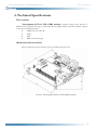
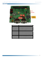
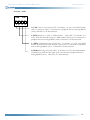
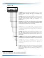
Development KIT for TM2 GPRS modem
User manual 1.2
Development
KIT
Development KIT for TM2
GSM/GPRS modem
User’s manual 1.2
1
Development KIT for TM2 GPRS modem
User manual 1.2
Contents
Attention!......................................................................................................................................................... 3
1.
Basic Safety Requirements.................................................................................................................. 4
2.
General Information............................................................................................................................ 5
2.1 Introduction.................................................................................................................................. 5
2.2 About this document................................................................................................................... 5
2.3 Legal notice................................................................................................................................... 5
2.4 Contacts......................................................................................................................................... 5
2.5 Acronyms ...................................................................................................................................... 5
3.
Package Contents ................................................................................................................................. 6
4.
Technical Specifications ...................................................................................................................... 7
Data transfer ......................................................................................................................................... 7
Mechanical characteristics................................................................................................................... 7
4.1 Switchers ....................................................................................................................................... 9
Switcher – SW1............................................................................................................................... 9
Switcher – SW2............................................................................................................................. 10
Switcher – SW3............................................................................................................................. 11
4.2 Jumpers........................................................................................................................................ 12
Jumper – JP1 ................................................................................................................................. 12
Jumper – JP2 ................................................................................................................................. 12
Jumper – JP3 ................................................................................................................................. 12
Jumper – JP4 ................................................................................................................................. 12
Jumper – JP5 ................................................................................................................................. 12
Jumper – JP7 ................................................................................................................................. 12
Connector - J5 .................................................................................................................................... 13
Connectors J1 (BL09) and J2 (BL09).............................................................................................. 14
4.3 Outlets ......................................................................................................................................... 15
Power supply outlet - J10 ............................................................................................................ 15
Power supply outlet - J11 ............................................................................................................ 15
Power supply outlet - J3 .............................................................................................................. 15
4.4 Buttons ........................................................................................................................................ 16
Button - S1..................................................................................................................................... 16
Button – S2.................................................................................................................................... 16
4.5 Audio ........................................................................................................................................... 16
Audio 1........................................................................................................................................... 16
Audio 2........................................................................................................................................... 16
5.How to Start?............................................................................................................................................. 17
5.1 Setting the device to work ........................................................................................................ 17
Connecting to PC............................................................................................................................... 17
Hyper terminal settings ..................................................................................................................... 17
5.2 AT Commands examples.......................................................................................................... 18
Registering on the network ......................................................................................................... 18
Incoming and outgoing calls....................................................................................................... 19
Incoming and outgoing SMS ......................................................................................................19
6.Technical Support ..................................................................................................................................... 20
Troubleshooting................................................................................................................................. 20
Final notice.......................................................................................................................................... 20
2
Development KIT for TM2 GPRS modem
User manual 1.2
Attention!
Do not rip the device. Do not touch the device if the device block is
broken or his connecting wires are without isolation.
All wireless devices for data transferring may be susceptible to
interference, which could affect performance.
Only qualified personnel may install or repair this product
Use only in normal projected position. Don't touch the antenna
unnecessarily.
Pay attention the device is connected to
network.
220V high voltage supply
Your device is not water-resistant. Keep it dry.
Do not mount or serve device during a thunderbolt.
3
Development KIT for TM2 GPRS modem
User manual 1.2
1. Basic Safety Requirements
In this document you will be introduced how to use the “Development KIT for
TM2 GPRS modem” device safely. You will avoid dangerous situations and harming of
yourself if you stick to these recommendations. You have to be familiar with the safety
requirements before starting using the device!
To avoid burning and voltage caused traumas, of the personnel working with
device, please follow these safety requirements.
Installation and technical support of the device can be performed only
by a qualified personnel or a person who has enough knowledge about
this device and safety requirements.
The device requires 9V
power supply. The PC, to which the device
“Development KIT for TM2 GPRS modem“ is to be connected must have a RS232 or
USB port applied to USB 1.1 or USB 2.0 standards. Nominal power supply voltage is 9V .
Available power supply source range is – 6V...15V , power up to 300 mW.
The PC and power supply source, to which the device „Development
KIT for TM2 GPRS modem“ is connected, should satisfy LST EN
60950 standard. The device can be used on first (Personal Computer) or
second (Notebook) computer safety class.
To avoid mechanical damage of the device, it is recommended to transport the
device packed in damage-proof pack. While using the devise, it should be placed so, that its
indication diodes would be visible as they inform in which working mode the devise is and if
it has any working problems.
In the installation place and supply circuits should be tool up protective devices
(bipolar release device) which will protect the device from short-circuit and wrong ground
installation. The power of connected device should satisfy the power of released device. The
interstice between contacts should not be less than 3mm. Power supply network should be
installed near device on easily accessible place.
If the device starts working insufficiently only qualified personnel may repair this
product. We recommend to dismantle the devise and forward it to repair centre or to
manufacturers. No exchangeable parts inside of the device.
4
Development KIT for TM2 GPRS modem
User manual 1.2
2. General Information
2.1
Introduction
“Development KIT for TM2 GPRS modem” is a device designed for testing
TM2 GPRS module features and functionality. The design of this board enables the
connection to your PC through RS232 or USB interface. Once the board is connected to the
PC, you can get access to the TM2 module. Using AT commands you can test the
functionality, such as writing SMS, making call or even sending DATA through GPRS.
2.2
About this document
This document describes “Development KIT for TM2 GPRS modem” hardware,
quick guide, plug-in and operation. It should help board users to deploy the product.
2.3
Legal notice
Copyright © 2006 UAB „Teltonika“.
All rights reserved. Reproduction, transfer, distribution or storage of part or all of
the contents in this document in any form without the prior written permission of Teltonika is
prohibited.
Other product and company names mentioned herein may be trademarks or trade
names of their respective owners.
2.4
Contacts
If you encounter any problems when using our products, and can not solve them by
yourself, please contact our technical support by writing an e-mail to [email protected] .
We will be pleased to help you.
2.5
Acronyms
GPRS
SIM
USB
SMS
GSM
General Packet Ratio Service
Subscriber Identity Module
Universal Serial Bus
Short Massage Service
Global System for Mobile
5
Development KIT for TM2 GPRS modem
User manual 1.2
3. Package Contents
“Development KIT for TM2 GPRS modem“ is packed in carton box and contains all
the accessories, needed for normal operation:
1. Carton box.
2. CD with User’s guide, schematics and software
3. Development KIT for TM2 GPRS modem device.
4. TM2 GPRS modem device
5. External GSM antenna
6. Serial cable
7. USB A ↔ USB B cable
8. AC/DC adapter
Note: the manufacturer does not provide SIM card, which is necessary for connecting to the
GSM network! SIM card can be obtained from your GSM operator!
If any of the components is missing from your package, please contact manufacturer’s
representative or reseller. (www.teltonika.lt)
6
Development KIT for TM2 GPRS modem
User manual 1.2
4. Technical Specifications
Data transfer
“Development KIT for TM2 GPRS modem“ supports below write bearers of
GSM Network. Which data type is used depends on GSM operator and data transfer capacity
in the chosen GSM Network.
•
GPRS class 10 (class B).
•
CSD.
•
CSF.
•
SMS textual messages.
Mechanical characteristics
Device dimensions and general view is provided in Picture 6.2.1.
Pic 6.2.1 Development KIT for TM2 GPRS modem
7
Development KIT for TM2 GPRS modem
User manual 1.2
D5
D6
Picture 4.1. TM2 development board
AC0
AC1
USB
Power Supply
Audio 1
Audio 2
J4
J5
SW1 and SW2
SW3
JP1
JP4
JP5
VBAT
VCHARGE
Serial interface 0
Serial interface 1
USB interface
Power Supply +9V
Audio interface not amplified
Audio interface amplified
TM2 modem socket
Socket isvadas
Serial interface control switch
USB interface control switch
Serial interface enable/disable jumper
DSR signal jumper
Modem power supply jumper
Connection of external battery
Connection of charger for battery
8
Development KIT for TM2 GPRS modem
4.1
User manual 1.2
Switchers
Switcher – SW1
1 (DCD) Data carrier detect (ON/OFF). If switcher 1 is ON, then TM2
module asynchronous serial interface output port is connected to
peripheral devices through RS232 (AC0) and USB1 ports. Otherwise, it is
disconnected.
2 (RI) Ring indicator (ON/OFF). If switcher 2 is ON, then TM2 module
ring indicator output port is connected with peripheral devices through
RS232 (AC0) and USB2 ports. Otherwise, it is disconnected.
3 (DTR) Data terminal ready (ON/OFF). If switcher 3 is ON, then TM2
module asynchronous serial interface output port is connected to
peripheral devices through RS232 (AC0) and USB3 ports. Otherwise, it is
disconnected.
4 (DSR) Data set ready (ON/OFF). If switcher 4 is ON, then TM2
module asynchronous serial interface output port sending signal about
controller data setup is connected with jumper TC 3 pin. Otherwise, it is
disconnected.
1
If switcher line – JLC, 7 switcher is OFF, then data interface output port is connected or disconnected with peripheral devices only
through RS232 (J2) port.
2
If switcher line – JLC, 8 switcher is OFF, then data interface output port is connected or disconnected with peripheral devices only
through RS232 (J2) port.
9
Development KIT for TM2 GPRS modem
User manual 1.2
Switcher – SW2
1 (CTS) Clear to send (ON/OFF). If switcher 3 is ON, then TM2 module
clear to send port input is connected to peripheral devices through RS232
(AC0). Otherwise, it is disconnected.
2 (RTS) Request to send to TM2 module (ON/OFF). If switcher 4 is
(ON), then data transmit request to TM2 module output port is connected to
peripheral devices through RS232 (AC0). Otherwise, it is disconnected.
3 (TXD) Transmitting data (ON/OFF). If switcher 1 is ON, then TM2
module asynchronous serial interface output port is connected to peripheral
devices through RS232 (AC1). Otherwise, it is disconnected.
4 (RXD) Receiving data (ON/OFF). If switcher 3 is ON, then TM2 module
asynchronous serial interface input port is connected to peripheral devices
through RS232 (AC1). Otherwise, it is disconnected.
10
Development KIT for TM2 GPRS modem
User manual 1.2
Switcher – SW3
1 (RXD) Receiving serial data (ON/OFF). If switcher 1 is ON,
then TM2 module receiving serial data output is connected to
peripheral devices through USB port.
Otherwise, it is
disconnected.
2 (TXD) Transmitting serial data (ON/OFF). If switcher 2 is ON,
then TM2 module transmitting serial data output is connected to
peripheral devices through USB port. Otherwise, it is
disconnected.
3 (CTS) Clear to send (ON/OFF). If switcher 3 is ON, then TM2
module clear to send port input is connected to peripheral devices
through USB port. Otherwise, it is disconnected.
4 (RTS) Request to send to TM2 module (ON/OFF). If switcher
4 is (ON), then data transmit request to TM2 module output port
is connected to peripheral devices through USB port. Otherwise, it
is disconnected.
5 (DTR)3 Data terminal ready (ON/OFF). If switcher 5 is ON,
then TM2 module asynchronous serial interface input port is
connected to peripheral devices through USB port. Otherwise, it is
disconnected.
6 (DSR) Data set ready (ON/OFF). If switcher 6 is (ON), then
peripheral devices are connected to jumper TC 2 pin through USB
port. Otherwise, it is disconnected.
7 (DCD)4 Data carrier detect (ON/OFF). If switcher 7 is ON,
then TM2 module asynchronous serial interface output port is
connected to peripheral devices through USB port. Otherwise, it is
disconnected.
8 (RI) Ring indicator (ON/OFF). If switcher 8 is ON, then TM2
module ring indicator output port is connected to peripheral
devices through RS2325 (AC0) and USB ports. Otherwise, it is
disconnected.
3
Switcher 3 must be ON for USB interface to be connected to switcher line JLA.
Switcher 1 must be ON for USB interface to be connected to switcher line JLA.
5
Switcher 2 must be ON for USB interface to be connected to switcher line JLA.
4
11
Development KIT for TM2 GPRS modem
User manual 1.2
4.2 Jumpers
Jumper ports are numbered from left to right. The first jumper port is marked by a square and
crossed upper left corner.
Jumper – JP1
If jumper is stored, then serial port AC0 will be enabled, USB will be disabled.
Then jumper is not stored USB port is enabled, AC0 is disabled.
Jumper – JP2
If jumper is stored, then indicator D5 shows incoming signal from TM2
module. If D5 indicator light is on, then TM2 module sends high voltage level.
Otherwise, the level is low.
Jumper – JP3
If jumper is stored, then indicator D6 shows incoming signal from TM2
module. If D6 indicator light is on, then TM2 module sends high voltage level.
Otherwise, the level is low.
Jumper – JP4
When jumpers TC ports 1 and 2 are stored, DSR signal will be connected to
RS232 (J2) and USB ports. When jumper TC ports 3 and 4 are stored, DSR
signal will be connected to +3.8V. When jumper TC ports 5 and 6 are stored,
DSR signal will be connected to GND.
Jumper – JP5
Store 1-2 to connect TM2 module power to +3.8V
Store 2-3 to connect TM2 module power to GND
Jumper – JP7
Store JP7 to connect Vbat and Vcharge.
12
Development KIT for TM2 GPRS modem
User manual 1.2
Connector - J5
6.5.1 Pic. General view of J5 connector
6.5.1 Table. Port description of J5 connector
Pin.Nr.
I/O type
Function
1
From 3.3 to 4.3 V (Typ:
GSM Power Supply
3.8 V)
2
Ground
GSM Power Supply
3
4
5
6
7
8
9
From 3.3 to 4.3 V (Typ:
3.8 V)
Ground
From 3.3 to 4.3 V (Typ:
3.8 V)
Ground
From 3.3 to 4.3 V (Typ:
3.8 V)
Ground
12
13
14
15
16
17
18
19
20
21
0 - 12V (Typ: 6V) Current
limited to 600 mA
CMOS 3.3V compatible
0 - 12V (Typ: 6V) Current
limited to 600 mA
CMOS 3.3V compatible
Supply 1.8V-3.3V
CMOS 3.3V compatible
CMOS 3.3V compatible
CMOS 3.3V compatible
CMOS 3.3V compatible
CMOS 3.3V compatible
CMOS 3.3V compatible
CMOS 3.3V compatible
CMOS 3.3V compatible
22
23
CMOS 3.3V compatible
CMOS 3.3V compatible
24
25
CMOS 3.3V compatible
CMOS 3.3V compatible
26
27
28
29
30
31
32
33
34
35
CMOS 3.3V compatible
CMOS 3.3V compatible
CMOS 3.3V compatible
CMOS 3.3V compatible
CMOS 3.3V compatible
CMOS 3.3V compatible
CMOS 3.3V compatible
CMOS 3.3V compatible
CMOS 3.3V compatible
CMOS 3.3V compatible
10
11
GSM Power Supply
GSM Power Supply
GSM Power Supply
GSM Power Supply
GSM Power Supply
GSM Power Supply
GSM Power Supply
Asynchronous Serial Interface 0
GSM Power Supply
Asynchronous Serial Interface
SIM interface
Asynchronous Serial Interface 0
SIM interface
Asynchronous Serial Interface 0
SIM interface
Asynchronous Serial Interface 0
SIM interface
Asynchronous Serial Interface 0
Synchronous Serial Interface
(SPI compatible)
Asynchronous Serial Interface 0
Synchronous Serial Interface
(SPI compatible)
Asynchronous Serial Interface 0
Synchronous Serial Interface
(SPI compatible)
Asynchronous Serial Interface 1
I2C bus interface
Asynchronous Serial Interface 1
I2C bus interface
Keypad interface / GPIO
Digital Audio Interface
Keypad interface / GPIO
Digital Audio Interface
Keypad interface /GPIO
Digital Audio Interface
Description
Should be connected with pins
3, 5, 7
Should be connected with pins
4, 6, 8
Should be connected with pins
1, 5, 7
Should be connected with pins
2, 6, 8
Should be connected with pins
1, 3, 7
Should be connected with pins
2, 4, 8
Should be connected with pins
1, 3, 5
Should be connected with pins
2, 4, 6
Should be connected with pins
11
Data Carrier Detect
Should be connected with pin 9
Data Terminal Ready
SIM power supply
Clear To Send
SIM I/O serial data
Request to Send
SIM clock signal
Receive Serial Data
SIM reset signal
Transmit Serial Data
Master Receive Slave Transmit
Ring Indicator
Master Transmit Slave Receive
Data Set Ready
Shift Clock
Receive Serial Data
Serial Clock Line
Transmit Serial Data
Serial Data Line
Keypad output pin 0 / GPIO00
DAI Clock
Keypad output pin 1 / GPIO50
DAI Receive
Keypad output pin 2 / GPIO01
DAI Transmit
13
Development KIT for TM2 GPRS modem
User manual 1.2
Pin.Nr.
36
37
38
39
40
41
42
43
44
45
46
I/O type
CMOS 3.3Vcompatible
CMOS 3.3V compatible
CMOS 3.3V compatible
CMOS 3.3V compatible
CMOS 3.3V compatible
Analog
CMOS 3.3V compatible
Analog
CMOS 3.3V compatible
Analog
CMOS 3.3V compatible
Function
Keypad interface /GPIO
Digital Audio Interface
Keypad interface /GPIO
External reset
Keypad interface / GPIO
Audio Interface
Keypad interface / GPIO
Audio Interface
Keypad interface / GPIO
Audio Interface
Keypad interface / Power on
47
48
49
50
51
52
53
54
55
56
57
58
Analog
CMOS 3.3V compatible
Analog
CMOS 3.3V compatible
Analog
CMOS 3.3V compatible
Analog
CMOS 3.3V compatible
Analog
CMOS 3.3V compatible
ADC 12bits 0-2.5V
CMOS 3.3V compatible
59
60
ADC 12bits 0-2.5V
CMOS 3.3V compatible
Audio Interface
Keypad interface / GPIO
Audio Interface
Capture Compare / GPIO
Audio Interface
Capture Compare / GPIO
Audio Interface
Capture Compare / GPIO
Audio Interface
Capture Compare / GPIO
Measurement interface
Capture Compare / GPIO /
External Interrupt
Measurement interface
Capture Compare /
GPIO / External Interrupt
Description
Keypad output pin 3 /GPIO02
DAI Reset
Keypad output pin 4 /GPIO03
External HW reset
Keypad output pin 5 /GPIO04
Handset microphone reference
Keypad input pin 0 /GPIO05
Handset microphone bias
Keypad input pin 1 /GPIO06
Balanced audio out
Keypad input pin 2 / Power on
button /GPIO 07
Balanced audio out
Keypad input pin 3 / GPIO08
Handset microphone reference
Capture Compare 19 / PIO47
Handset microphone bias
Capture Compare 02/ GPIO57
Balanced power audio out
Capture Compare 05/ GPIO28
Balanced power audio out
Capture Compare 06/ GPIO30
Analog to Digital Converter
Capture Compare 00 / GPIO
30 / Ext Int 5B
Analog to Digital Converter
Capture Compare 22
/ GPIO 55 / Ext Int 3
Connectors J1 (BL09) and J2 (BL09)
There are two J1 (BL09) (6.6.1 pic.) and J2 (BL09) (6.6.2 pic.) connectors integrated in test board.
Pictures show port numeration and incoming/outgoing signal names.
4.1 Pic. General view of J2 connector
4.2 Pic. General view of J1 connector
14
Development KIT for TM2 GPRS modem
User manual 1.2
4.3 Outlets
Power supply outlet - J10
Outlet ports are numbered from left to right. The first port is marked by a square port.
The power supply providing
0 - 12V (nominal: 9V) 300 mA current and
voltage is connected to J10 power supply outlet.
1 Negative voltage power supply wire (-) (GND) is connected to the first power
supply outlet port.
2 Positive voltage power supply wire (+) is connected to the second power supply
outlet port.
Power supply outlet - J11
The power supply providing
J11 power supply outlet.
3.3 - 4.3 V (Nominal: 3.8 V) voltage is connected to
1 Negative voltage power supply wire (-) (GND) is connected to the first power
supply outlet port.
2 Positive voltage power supply wire (+) is connected to the second power supply
outlet port.
Power supply outlet - J3
The power supply providing 6 – 15 V DC voltage is connected to J3
power supply outlet.
15
Development KIT for TM2 GPRS modem
4.4
User manual 1.2
Buttons
Button - S1
Button - S1 (Reset) – is a TM2 module reset button.
Button – S2
Button – S2 (Power ON) – is a TM2 module power on button. To turn TM2 module on, push S2
button and hold for approximately 2 seconds. To check the modem status – send an AT command. If
TM2 module replies, then it is on.
4.5 Audio
Audio 1
Port description:
1 – Handset microphone reference.
2 – Balanced power audio out.
3 – Balanced power audio out.
4 – Handset microphone bias.
Audio 2
Port description:
1 – Handset microphone reference.
2 – Balanced audio out.
3 – Balanced audio out.
4 – Handset microphone bias
16
Development KIT for TM2 GPRS modem
User manual 1.2
5. How to Start?
5.1
Setting the device to work
Before connecting “Development KIT for TM2 GPRS modem” to PC, make next steps:
1. Set SW1 to 1111
2. Set SW2 to 1100
3. Set SW3 to 00000000
4. Store jumper TC 1-2
5. Store jumper TD (don’t store TE)
Connecting to PC
1)
2)
3)
4)
5)
6)
7)
8)
9)
Turn off your PC;
Insert the SIM card into modem. Follow the instructions on the device sticker. Make sure,
the SIM card is pushed inside till it fixes;
Insert TM2 GPRS module to the board
Plug GSM antenna to module
Plug DB9 connector of the serial (RS232) cable into the board;
Plug another end of the serial cable to one of the COM ports of PC;
Plug in the AC/DC adapter to power supply socket of „Development KIT for TM2 GPRS
modem“,
Plug in the AC/DC adapter to power supply network;
Turn on your PC.
Hyper terminal settings
Start Windows Hyper Terminal.
Enter any connection name
17
Development KIT for TM2 GPRS modem
User manual 1.2
Choose communication port to which
development board is connected.
(COM1, COM2, etc.)
Set the setting
Bits per second= 115200
Data bits= 8
Parity= None
Stop bits= 1
Flow control= Hardware
If flow control is set to None, then
modem will not wake up immediately.
5.2 AT Commands examples
Registering on the network
AT
OK
AT+CPIN?
+CPIN: READY
or
+CPIN: SIM PIN
Check PIN status
When CPIN: READY you don’t need to write PIN
number.
When CPIN: SIM PIN, please use next command to write
PIN number.
AT+CPIN=”xxxx”
Insert the PIN number xxxx ()
To check PIN type “AT+CPIN?”
OK
AT+COPS=0
OK
Register the phone on the network
18
Development KIT for TM2 GPRS modem
AT+CREG?
+CREG: 0, 1
OK
Verify registration
AT+CSQ
+CSQ: 15,95
OK
Check signal intensity
AT+COPS?
+COPS: 0, 0, “
OPERATOR”
OK
Read operator name
User manual 1.2
Incoming and outgoing calls
ATD(telephone number);
After ATD write telephone number without brackets, at the
end of the command there must be semicolon.
OK
ATH
OK
Hang up
AT+CLIP=1
OK
Activation of caller line ID
RING
RING
RING
Incoming Call
ATA
OK
Answer to Voice Call
ATH
OK
Hang up
Incoming and outgoing SMS
AT+CMGS=”Telephone number”
>SMS text massage 12345<CTRL+Z>
+CMGS:0
OK
Enter to the text mode
AT+CMGL
+CMGL:302,”REC UNREAD”, ”Telephone
number”,,”06/10/19, 15:45:25+08”
SMS text massage 12345
List all incoming SMS
19
Development KIT for TM2 GPRS modem
User manual 1.2
6. Technical Support
Troubleshooting
Problem
TM2 module is not answering
after approximately 23s.
TM2 module is not responding to
AT commands
Solution
This means that Flow Control is set to NONE. Set
Flow Control to Hardware (RTS/CTS), in other
case only after pressing RESET button (S1) module
will response.
Check module power jumper, TD jumper must be
stored.
Final notice
The label on the package indicates that before using the product the
User’s Guide contained in the package must be read and understood.
The label on the package indicates that used electronic and electric
equipment should be disposed separately.
If you encounter any problems while using the device and you are not able to solve them yourself,
then you are always welcome to contact our technical support department by e-mail [email protected].
We will be glad to help you.
20