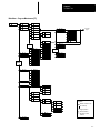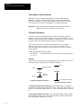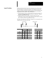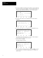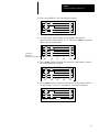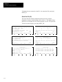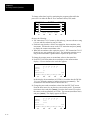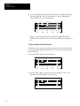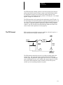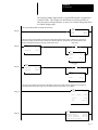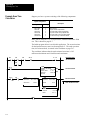
1
ALLEN–BRADLEY
Hand–Held Terminal
(Catalog Number 1747–PT1)
User Manual
Important User Information
Solid state equipment has operational characteristics differing from those of
electromechanical equipment. “Safety Guidelines for the Application,
Installation and Maintenance of Solid State Controls” (Publication SGI-1.1)
describes some important differences between solid state equipment and
hard–wired electromechanical devices. Because of this difference, and also
because of the wide variety of uses for solid state equipment, all persons
responsible for applying this equipment must satisfy themselves that each
intended application of this equipment is acceptable.
In no event will the Allen-Bradley Company be responsible or liable for
indirect or consequential damages resulting from the use or application of
this equipment.
The examples and diagrams in this manual are included solely for illustrative
purposes. Because of the many variables and requirements associated with
any particular installation, the Allen-Bradley Company cannot assume
responsibility or liability for actual use based on the examples and diagrams.
No patent liability is assumed by Allen-Bradley Company with respect to use
of information, circuits, equipment, or software described in this manual.
Reproduction of the contents of this manual, in whole or in part, without
written permission of the Allen-Bradley Company is prohibited.
Throughout this manual we use notes to make you aware of safety
considerations.
!
ATTENTION: Identifies information about practices or
circumstances that can lead to personal injury or death, property
damage, or economic loss.
Attentions help you:
• identify a hazard
• avoid the hazard
• recognize the consequences
Important: Identifies information that is especially important for successful
application and understanding of the product.
PLC, PLC 2, PLC 3, and PLC 5 are registered trademarks of Allen-Bradley Company, Inc.
SLC, SLC 100, SLC 500, SLC 5/01, SLC 5/02, PanelView, RediPANEL, and Dataliner are trademarks of Allen-Bradley Company, Inc.
IBM is a registered trademark of International Business Machines, Incorporated.
Summary of Changes
Summary of Changes
The information below summarizes the changes to this manual since the last
printing as 1747–809 in July 1989, which included the supplement
40063–079–01(A) from October 1990.
New Information
The table below lists sections that document new features and additional
information about existing features, and shows where to find this new
information.
For This New Information
See Chapter
Using the HHT with an SLC
5/02 (in general)
4 – Data File Organization and Addressing
6 – Creating a Program
8 – Saving and Compiling a Program
14 – Using EEPROMs and UVPROMs
15 – Instruction Set Overview
27 – The Status File
32–Bit Addition and
Subtraction
20 – Math Instructions
Index Register
22 – File Copy and File Fill Instructions
23 – Bit Shift, FIFO, and LIFO Instructions
24 – Sequencer Instructions
DH–485 devices
9 – Configuring Online Communication
I/O Interrupts
28 – Troubleshooting Faults
29 – Understanding the User Fault Routine – SLC 5/02
Processor Only
30 – Understanding Selectable Timed Interrupts – SLC 5/02
Processor Only
31 – Understanding I/O Interrupts – SLC 5/02 Processor Only
Instruction Execution Times
C – Memory Usage, Instruction Execution Times
Scan Time Worksheets
D – Estimating Scan Time
User Fault Routine
Selectable Timed Interrupts
Table of Contents
Hand–Held Terminal
User Manual
Preface
Who Should Use this Manual . . . . . . . . . . . . . . . . . . . . . . . . . . . . . . . . . . .
Purpose of this Manual . . . . . . . . . . . . . . . . . . . . . . . . . . . . . . . . . . . . . . . .
Contents of this Manual . . . . . . . . . . . . . . . . . . . . . . . . . . . . . . . . . . . . . . .
Related Documentation . . . . . . . . . . . . . . . . . . . . . . . . . . . . . . . . . . . . .
Common Techniques Used in this Manual . . . . . . . . . . . . . . . . . . . . . . . . . .
Allen–Bradley Support . . . . . . . . . . . . . . . . . . . . . . . . . . . . . . . . . . . . . . . .
Local Product Support . . . . . . . . . . . . . . . . . . . . . . . . . . . . . . . . . . . . . .
Technical Product Assistance . . . . . . . . . . . . . . . . . . . . . . . . . . . . . . . . .
Your Questions or Comments on this Manual . . . . . . . . . . . . . . . . . . . . . .
Features, Installation,
Powerup
Chapter 1
The Menu Tree
Chapter 2
P–1
P–1
P–2
P–4
P–4
P–5
P–5
P–5
P–5
HHT Features . . . . . . . . . . . . . . . . . . . . . . . . . . . . . . . . . . . . . . . . . . . . . . 1–1
Installing the Memory Pak, Battery, and Communication Cable . . . . . . . . . . . 1–3
HHT Powerup . . . . . . . . . . . . . . . . . . . . . . . . . . . . . . . . . . . . . . . . . . . . . . 1–7
HHT Display Format . . . . . . . . . . . . . . . . . . . . . . . . . . . . . . . . . . . . . . . . . 1–8
The Keyboard . . . . . . . . . . . . . . . . . . . . . . . . . . . . . . . . . . . . . . . . . . . . . . 1–9
Menu Function Keys (F1, F2, F3, F4, F5) . . . . . . . . . . . . . . . . . . . . . . . . . 1–9
Data Entry Keys . . . . . . . . . . . . . . . . . . . . . . . . . . . . . . . . . . . . . . . . . . 1–9
Auto Shift . . . . . . . . . . . . . . . . . . . . . . . . . . . . . . . . . . . . . . . . . . . . . . . 1–9
Cursor Keys . . . . . . . . . . . . . . . . . . . . . . . . . . . . . . . . . . . . . . . . . . . . . 1–10
ZOOM and RUNG Keys . . . . . . . . . . . . . . . . . . . . . . . . . . . . . . . . . . . . . 1–12
Using the HHT Menu . . . . . . . . . . . . . . . . . . . . . . . . . . . . . . . . . . . . . . . . . 2–1
Progressing through Menu Displays . . . . . . . . . . . . . . . . . . . . . . . . . . . . 2–1
The ENTER Key . . . . . . . . . . . . . . . . . . . . . . . . . . . . . . . . . . . . . . . . . . 2–2
The ESCAPE Key . . . . . . . . . . . . . . . . . . . . . . . . . . . . . . . . . . . . . . . . . 2–2
The Main Menu . . . . . . . . . . . . . . . . . . . . . . . . . . . . . . . . . . . . . . . . . . . . . 2–3
Main Menu Functions . . . . . . . . . . . . . . . . . . . . . . . . . . . . . . . . . . . . . . . . . 2–3
SELFTEST, [F1] . . . . . . . . . . . . . . . . . . . . . . . . . . . . . . . . . . . . . . . . 2–3
TERMINAL, [F2] . . . . . . . . . . . . . . . . . . . . . . . . . . . . . . . . . . . . . . . . 2–3
PROGRAM MAINTENANCE, [F3] . . . . . . . . . . . . . . . . . . . . . . . . . . . . 2–3
UTILITY, [F5] . . . . . . . . . . . . . . . . . . . . . . . . . . . . . . . . . . . . . . . . . . . 2–4
The Menu Tree . . . . . . . . . . . . . . . . . . . . . . . . . . . . . . . . . . . . . . . . . . . . . 2–4
HHT Function Keys and Instruction Mnemonics . . . . . . . . . . . . . . . . . . . . . . 2–11
Function Keys . . . . . . . . . . . . . . . . . . . . . . . . . . . . . . . . . . . . . . . . . . . . 2–11
Instruction Mnemonics . . . . . . . . . . . . . . . . . . . . . . . . . . . . . . . . . . . . . . 2–14
i
Table of Contents
Hand–Held Terminal
User Manual
Understanding File
Organization
Chapter 3
Data File Organization and
Addressing
Chapter 4
ii
Program, Program Files, and Data Files . . . . . . . . . . . . . . . . . . . . . . . . . . .
Program . . . . . . . . . . . . . . . . . . . . . . . . . . . . . . . . . . . . . . . . . . . . . . . .
Program Files . . . . . . . . . . . . . . . . . . . . . . . . . . . . . . . . . . . . . . . . . . . .
Data Files . . . . . . . . . . . . . . . . . . . . . . . . . . . . . . . . . . . . . . . . . . . . . . .
Downloading Programs . . . . . . . . . . . . . . . . . . . . . . . . . . . . . . . . . . . . .
Uploading Programs . . . . . . . . . . . . . . . . . . . . . . . . . . . . . . . . . . . . . . .
Using EEPROM and UVPROM Memory Modules for Program Backup . . . .
Data File Organization . . . . . . . . . . . . . . . . . . . . . . . . . . . . . . . . . . . . . . . .
Data File Types . . . . . . . . . . . . . . . . . . . . . . . . . . . . . . . . . . . . . . . . . . .
Addressing Data Files . . . . . . . . . . . . . . . . . . . . . . . . . . . . . . . . . . . . . . . .
Data File 2 – Status . . . . . . . . . . . . . . . . . . . . . . . . . . . . . . . . . . . . . . . .
Data Files 0 and 1 – Outputs and Inputs . . . . . . . . . . . . . . . . . . . . . . . . .
Data File 3 – Bit . . . . . . . . . . . . . . . . . . . . . . . . . . . . . . . . . . . . . . . . . . .
Data File 4 – Timers . . . . . . . . . . . . . . . . . . . . . . . . . . . . . . . . . . . . . . . .
Data File 5 – Counters . . . . . . . . . . . . . . . . . . . . . . . . . . . . . . . . . . . . . .
Data File 6 – Control . . . . . . . . . . . . . . . . . . . . . . . . . . . . . . . . . . . . . . .
Data File 7 – Integer . . . . . . . . . . . . . . . . . . . . . . . . . . . . . . . . . . . . . . .
Indexed Addressing
SLC 5/02 Processors Only . . . . . . . . . . . . . . . . . . . . . . . . . . . . . . . . . .
Offset Value (S:24 Index Register ) . . . . . . . . . . . . . . . . . . . . . . . . . . . . .
Example . . . . . . . . . . . . . . . . . . . . . . . . . . . . . . . . . . . . . . . . . . . . . .
Creating Data for Indexed Addresses . . . . . . . . . . . . . . . . . . . . . . . . . . .
Crossing File Boundaries . . . . . . . . . . . . . . . . . . . . . . . . . . . . . . . . . . . .
Example . . . . . . . . . . . . . . . . . . . . . . . . . . . . . . . . . . . . . . . . . . . . . .
Monitoring Indexed Addresses . . . . . . . . . . . . . . . . . . . . . . . . . . . . . . . .
Example . . . . . . . . . . . . . . . . . . . . . . . . . . . . . . . . . . . . . . . . . . . . . .
Effects of File Instructions on Indexed Addressing . . . . . . . . . . . . . . . . . .
Effects of Program Interrupts on Index Register S:24 . . . . . . . . . . . . . . . .
File Instructions – Using the File Indicator # . . . . . . . . . . . . . . . . . . . . . . . . .
Bit Shift Instructions . . . . . . . . . . . . . . . . . . . . . . . . . . . . . . . . . . . . . . . .
Sequencer Instructions . . . . . . . . . . . . . . . . . . . . . . . . . . . . . . . . . . . . . .
File Copy and File Fill Instructions . . . . . . . . . . . . . . . . . . . . . . . . . . . . . .
Creating Data . . . . . . . . . . . . . . . . . . . . . . . . . . . . . . . . . . . . . . . . . . . . . .
Creating Data for Indexed Addresses . . . . . . . . . . . . . . . . . . . . . . . . . . .
Deleting Data . . . . . . . . . . . . . . . . . . . . . . . . . . . . . . . . . . . . . . . . . . . . . .
Program Constants . . . . . . . . . . . . . . . . . . . . . . . . . . . . . . . . . . . . . . . . . .
M0 and M1 Data Files – Specialty I/O Modules . . . . . . . . . . . . . . . . . . . . . .
Addressing M0–M1 Files . . . . . . . . . . . . . . . . . . . . . . . . . . . . . . . . . . . .
Restrictions on Using M0-M1 Data File Addresses . . . . . . . . . . . . . . . . . .
Monitoring Bit Instructions Having M0 or M1 Addresses . . . . . . . . . . . . . .
3–1
3–2
3–2
3–3
3–3
3–4
3–4
4–1
4–2
4–2
4–3
4–4
4–8
4–9
4–10
4–11
4–12
4–13
4–13
4–13
4–14
4–14
4–14
4–15
4–15
4–15
4–15
4–16
4–16
4–17
4–18
4–19
4–19
4–20
4–20
4–21
4–21
4–21
4–22
Table of Contents
Hand–Held Terminal
User Manual
Transferring Data Between Processor Files and M0 or M1 Files . . . . . . . . .
Access Time . . . . . . . . . . . . . . . . . . . . . . . . . . . . . . . . . . . . . . . . . . . . .
Minimizing the Scan Time . . . . . . . . . . . . . . . . . . . . . . . . . . . . . . . . . . . .
Capturing M0–M1 File Data . . . . . . . . . . . . . . . . . . . . . . . . . . . . . . . . . .
Specialty I/O Modules with Retentive Memory . . . . . . . . . . . . . . . . . . . . .
G Data Files – Specialty I/O Modules . . . . . . . . . . . . . . . . . . . . . . . . . . . . .
Editing G File Data . . . . . . . . . . . . . . . . . . . . . . . . . . . . . . . . . . . . . . . . .
Ladder Program Basics
4–23
4–24
4–25
4–26
4–26
4–27
4–28
Chapter 5
Ladder Programming . . . . . . . . . . . . . . . . . . . . . . . . . . . . . . . . . . . . . . . . . 5–1
A 1–Rung Ladder Program . . . . . . . . . . . . . . . . . . . . . . . . . . . . . . . . . . . . . 5–2
Logical Continuity . . . . . . . . . . . . . . . . . . . . . . . . . . . . . . . . . . . . . . . . . . . 5–3
Series Logic . . . . . . . . . . . . . . . . . . . . . . . . . . . . . . . . . . . . . . . . . . . . . . . 5–4
Example – Series Inputs . . . . . . . . . . . . . . . . . . . . . . . . . . . . . . . . . . . 5–4
Parallel Logic . . . . . . . . . . . . . . . . . . . . . . . . . . . . . . . . . . . . . . . . . . . . . . 5–4
Example – Parallel Inputs . . . . . . . . . . . . . . . . . . . . . . . . . . . . . . . . . . 5–4
Input Branching . . . . . . . . . . . . . . . . . . . . . . . . . . . . . . . . . . . . . . . . . . . 5–5
Example – Parallel Input Branching . . . . . . . . . . . . . . . . . . . . . . . . . . . 5–5
Output Branching . . . . . . . . . . . . . . . . . . . . . . . . . . . . . . . . . . . . . . . . . . 5–5
Example – Parallel Output Branching . . . . . . . . . . . . . . . . . . . . . . . . . 5–5
Example – Parallel Output Branching with Conditions (SLC 5/02 Only) . . 5–6
Nested Branching . . . . . . . . . . . . . . . . . . . . . . . . . . . . . . . . . . . . . . . . . 5–6
Example – Nested Input and Output Branches . . . . . . . . . . . . . . . . . . . 5–6
Example . . . . . . . . . . . . . . . . . . . . . . . . . . . . . . . . . . . . . . . . . . . . . . 5–7
A 4–Rung Ladder Program . . . . . . . . . . . . . . . . . . . . . . . . . . . . . . . . . . . . . 5–8
Application Example . . . . . . . . . . . . . . . . . . . . . . . . . . . . . . . . . . . . . 5–9
Operating Cycle (Simplified) . . . . . . . . . . . . . . . . . . . . . . . . . . . . . . . . . . . . 5–11
When the Input Goes True . . . . . . . . . . . . . . . . . . . . . . . . . . . . . . . . . 5–12
When the Input Goes False . . . . . . . . . . . . . . . . . . . . . . . . . . . . . . . . 5–13
Creating a Program
Chapter 6
Creating a Program Offline with the HHT . . . . . . . . . . . . . . . . . . . . . . . . . . . 6–1
Clearing the Memory of the HHT . . . . . . . . . . . . . . . . . . . . . . . . . . . . . . . 6–1
Configuring the Controller . . . . . . . . . . . . . . . . . . . . . . . . . . . . . . . . . . . . 6–2
Configuring the Processor . . . . . . . . . . . . . . . . . . . . . . . . . . . . . . . . . 6–2
Configuring the I/O . . . . . . . . . . . . . . . . . . . . . . . . . . . . . . . . . . . . . . . 6–3
Configuring Specialty I/O Modules – (SLC 5/02 Specific) . . . . . . . . . . . . 6–5
Naming the Ladder Program . . . . . . . . . . . . . . . . . . . . . . . . . . . . . . . . . . 6–8
Naming Your Main Program File . . . . . . . . . . . . . . . . . . . . . . . . . . . . . . . 6–9
Passwords . . . . . . . . . . . . . . . . . . . . . . . . . . . . . . . . . . . . . . . . . . . . . . . . 6–10
Entering Passwords . . . . . . . . . . . . . . . . . . . . . . . . . . . . . . . . . . . . . . . . 6–11
Entering Master Passwords . . . . . . . . . . . . . . . . . . . . . . . . . . . . . . . . . . 6–12
Removing and Changing Passwords . . . . . . . . . . . . . . . . . . . . . . . . . . . . 6–13
iii
Table of Contents
Hand–Held Terminal
User Manual
Creating and Editing
Program Files
iv
Chapter 7
Creating and Deleting Program Files . . . . . . . . . . . . . . . . . . . . . . . . . . . . . .
Creating a Subroutine Program File using the Next Consecutive File Number
Creating a Subroutine Program File using a Non–Consecutive File Number
Deleting a Subroutine Program File . . . . . . . . . . . . . . . . . . . . . . . . . . . . .
Editing a Program File . . . . . . . . . . . . . . . . . . . . . . . . . . . . . . . . . . . . . . . .
Ladder Rung Display . . . . . . . . . . . . . . . . . . . . . . . . . . . . . . . . . . . . . . .
Entering a Rung . . . . . . . . . . . . . . . . . . . . . . . . . . . . . . . . . . . . . . . . .
Entering an Examine if Closed Instruction . . . . . . . . . . . . . . . . . . . . . .
Entering an Output Energize Instruction . . . . . . . . . . . . . . . . . . . . . . . .
Adding a Rung with Branching . . . . . . . . . . . . . . . . . . . . . . . . . . . . . .
Adding a Rung to a Program . . . . . . . . . . . . . . . . . . . . . . . . . . . . . . . .
Entering a Parallel Branch . . . . . . . . . . . . . . . . . . . . . . . . . . . . . . . . .
Inserting an Instruction Within a Branch . . . . . . . . . . . . . . . . . . . . . . . .
Modifying Rungs . . . . . . . . . . . . . . . . . . . . . . . . . . . . . . . . . . . . . . . . . .
Adding an Instruction to a Rung . . . . . . . . . . . . . . . . . . . . . . . . . . . . .
Modifying Instructions . . . . . . . . . . . . . . . . . . . . . . . . . . . . . . . . . . . . . .
Changing the Address of an Instruction . . . . . . . . . . . . . . . . . . . . . . . .
Changing an Instruction Type . . . . . . . . . . . . . . . . . . . . . . . . . . . . . . .
Modifying Branches . . . . . . . . . . . . . . . . . . . . . . . . . . . . . . . . . . . . . . . .
Extending a Branch Up . . . . . . . . . . . . . . . . . . . . . . . . . . . . . . . . . . .
Extending a Branch Down . . . . . . . . . . . . . . . . . . . . . . . . . . . . . . . . .
Appending a Branch . . . . . . . . . . . . . . . . . . . . . . . . . . . . . . . . . . . . . .
Delete and Undelete Commands . . . . . . . . . . . . . . . . . . . . . . . . . . . . . . .
Deleting a Branch . . . . . . . . . . . . . . . . . . . . . . . . . . . . . . . . . . . . . . .
Deleting an Instruction . . . . . . . . . . . . . . . . . . . . . . . . . . . . . . . . . . . .
Copying an Instruction from One Location to Another . . . . . . . . . . . . . .
Deleting and Copying Rungs . . . . . . . . . . . . . . . . . . . . . . . . . . . . . . . .
Abandoning Edits . . . . . . . . . . . . . . . . . . . . . . . . . . . . . . . . . . . . . . . . .
The Search Function . . . . . . . . . . . . . . . . . . . . . . . . . . . . . . . . . . . . . . . . .
Searching for an Instruction . . . . . . . . . . . . . . . . . . . . . . . . . . . . . . . .
Searching for an Address . . . . . . . . . . . . . . . . . . . . . . . . . . . . . . . . . .
Searching for a Particular Instruction with a Specific Address . . . . . . . .
Reversing the Search Direction . . . . . . . . . . . . . . . . . . . . . . . . . . . . . .
Searching for Forced I/O . . . . . . . . . . . . . . . . . . . . . . . . . . . . . . . . . .
Searching for Rungs . . . . . . . . . . . . . . . . . . . . . . . . . . . . . . . . . . . . .
Creating and Deleting Program Files . . . . . . . . . . . . . . . . . . . . . . . . . . . . . .
Creating Data Files . . . . . . . . . . . . . . . . . . . . . . . . . . . . . . . . . . . . . . . .
Deleting Data Files . . . . . . . . . . . . . . . . . . . . . . . . . . . . . . . . . . . . . . . .
7–1
7–1
7–2
7–3
7–4
7–4
7–5
7–6
7–7
7–8
7–9
7–11
7–12
7–14
7–14
7–16
7–16
7–18
7–19
7–19
7–22
7–24
7–26
7–26
7–29
7–30
7–31
7–34
7–35
7–37
7–38
7–40
7–41
7–42
7–44
7–45
7–45
7–46
Table of Contents
Hand–Held Terminal
User Manual
Saving and Compiling a
Program
Chapter 8
Configuring Online
Communication
Chapter 9
Downloading/Uploading a
Program
Chapter 10
Processor Modes
Chapter 11
Saving and Compiling Overview . . . . . . . . . . . . . . . . . . . . . . . . . . . . . . . . .
Saving a Program . . . . . . . . . . . . . . . . . . . . . . . . . . . . . . . . . . . . . . . . . . .
Available Compiler Options . . . . . . . . . . . . . . . . . . . . . . . . . . . . . . . . . . .
[F1] Future Access (All Processors) . . . . . . . . . . . . . . . . . . . . . . . . . . .
[F2] Test Single Rung (SLC 5/02 Specific) . . . . . . . . . . . . . . . . . . . . . .
[F3] Index Checks (Index Across Files) (SLC 5/02) . . . . . . . . . . . . . . . .
[F4] File Protection (SLC 5/02) . . . . . . . . . . . . . . . . . . . . . . . . . . . . . .
Viewing Program Memory Layout . . . . . . . . . . . . . . . . . . . . . . . . . . . . . . . .
Online Configuration . . . . . . . . . . . . . . . . . . . . . . . . . . . . . . . . . . . . . . . . .
Exceptions . . . . . . . . . . . . . . . . . . . . . . . . . . . . . . . . . . . . . . . . . . . .
The Who Function . . . . . . . . . . . . . . . . . . . . . . . . . . . . . . . . . . . . . . . . . . .
Diagnostics . . . . . . . . . . . . . . . . . . . . . . . . . . . . . . . . . . . . . . . . . . . . . .
Attach . . . . . . . . . . . . . . . . . . . . . . . . . . . . . . . . . . . . . . . . . . . . . . . . . .
Exception . . . . . . . . . . . . . . . . . . . . . . . . . . . . . . . . . . . . . . . . . . . . .
Node Configuration . . . . . . . . . . . . . . . . . . . . . . . . . . . . . . . . . . . . . . . .
Consequences of Changing a Processor Node Address . . . . . . . . . . . .
Entering a Maximum Node Address . . . . . . . . . . . . . . . . . . . . . . . . . .
Changing the Baud Rate . . . . . . . . . . . . . . . . . . . . . . . . . . . . . . . . . .
Set and Clear Ownership . . . . . . . . . . . . . . . . . . . . . . . . . . . . . . . . . . . .
Recommendations When Using DH–485 Devices . . . . . . . . . . . . . . . . . . .
8–1
8–1
8–3
8–3
8–4
8–5
8–5
8–5
9–1
9–3
9–4
9–6
9–7
9–8
9–8
9–9
9–10
9–10
9–10
9–12
Downloading a Program . . . . . . . . . . . . . . . . . . . . . . . . . . . . . . . . . . . . . . . 10–1
Uploading a Program . . . . . . . . . . . . . . . . . . . . . . . . . . . . . . . . . . . . . . . . . 10–3
Processor Modes . . . . . . . . . . . . . . . . . . . . . . . . . . . . . . . . . . . . . . . . . . .
Program Mode . . . . . . . . . . . . . . . . . . . . . . . . . . . . . . . . . . . . . . . . . . .
Test Mode . . . . . . . . . . . . . . . . . . . . . . . . . . . . . . . . . . . . . . . . . . . . . . .
Changing Modes . . . . . . . . . . . . . . . . . . . . . . . . . . . . . . . . . . . . . . . . . . . .
Changing the Mode . . . . . . . . . . . . . . . . . . . . . . . . . . . . . . . . . . . . . .
11–1
11–1
11–2
11–2
11–2
v
Table of Contents
Hand–Held Terminal
User Manual
Monitoring Controller
Operation
Chapter 12
The Force Function
Chapter 13
Monitoring a Program File . . . . . . . . . . . . . . . . . . . . . . . . . . . . . . . . . . . . .
True/False Indication . . . . . . . . . . . . . . . . . . . . . . . . . . . . . . . . . . . . .
Monitoring Data Files . . . . . . . . . . . . . . . . . . . . . . . . . . . . . . . . . . . . . . . . .
Data Files . . . . . . . . . . . . . . . . . . . . . . . . . . . . . . . . . . . . . . . . . . . . . . .
Accessing Data Files . . . . . . . . . . . . . . . . . . . . . . . . . . . . . . . . . . . . . . .
Option 1 . . . . . . . . . . . . . . . . . . . . . . . . . . . . . . . . . . . . . . . . . . . . . .
Option 2 . . . . . . . . . . . . . . . . . . . . . . . . . . . . . . . . . . . . . . . . . . . . . .
Option 3 . . . . . . . . . . . . . . . . . . . . . . . . . . . . . . . . . . . . . . . . . . . . . .
Option 4 . . . . . . . . . . . . . . . . . . . . . . . . . . . . . . . . . . . . . . . . . . . . . .
Monitoring a Data File . . . . . . . . . . . . . . . . . . . . . . . . . . . . . . . . . . . . . .
Data File Displays . . . . . . . . . . . . . . . . . . . . . . . . . . . . . . . . . . . . . . . . . . .
Output File (O0) . . . . . . . . . . . . . . . . . . . . . . . . . . . . . . . . . . . . . . . . . . .
Input File (I1) . . . . . . . . . . . . . . . . . . . . . . . . . . . . . . . . . . . . . . . . . . . . .
Status Data File (S2) . . . . . . . . . . . . . . . . . . . . . . . . . . . . . . . . . . . . . . .
Bit Data File (B3) . . . . . . . . . . . . . . . . . . . . . . . . . . . . . . . . . . . . . . . . . .
Timer Data File (T4) . . . . . . . . . . . . . . . . . . . . . . . . . . . . . . . . . . . . . . . .
Counter Data File (C5) . . . . . . . . . . . . . . . . . . . . . . . . . . . . . . . . . . . . . .
Control Data File (R6) . . . . . . . . . . . . . . . . . . . . . . . . . . . . . . . . . . . . . .
Integer Data File (N7) . . . . . . . . . . . . . . . . . . . . . . . . . . . . . . . . . . . . . . .
Online Data Changes . . . . . . . . . . . . . . . . . . . . . . . . . . . . . . . . . . . . . . . . .
Forcing I/O . . . . . . . . . . . . . . . . . . . . . . . . . . . . . . . . . . . . . . . . . . . . . . . .
Forcing an External Input . . . . . . . . . . . . . . . . . . . . . . . . . . . . . . . . . . . . . .
To Close an External Input Circuit . . . . . . . . . . . . . . . . . . . . . . . . . . . . . .
To Close and Open an External Circuit . . . . . . . . . . . . . . . . . . . . . . . . . .
Searching for Forced I/O . . . . . . . . . . . . . . . . . . . . . . . . . . . . . . . . . . . . . .
Forcing an External Output . . . . . . . . . . . . . . . . . . . . . . . . . . . . . . . . . . . . .
Forces Carried Offline . . . . . . . . . . . . . . . . . . . . . . . . . . . . . . . . . . . . . . . .
Using EEPROMs and
UVPROMs
vi
12–1
12–2
12–2
12–2
12–3
12–3
12–3
12–3
12–3
12–3
12–5
12–5
12–5
12–6
12–8
12–8
12–8
12–9
12–9
12–9
13–1
13–2
13–2
13–4
13–6
13–8
13–9
Chapter 14
Using an EEPROM Memory Module . . . . . . . . . . . . . . . . . . . . . . . . . . . . . .
Transferring a Program to an EEPROM Memory Module . . . . . . . . . . . . . .
Transferring a Program from an EEPROM Memory Module . . . . . . . . . . . .
EEPROM Burning Options . . . . . . . . . . . . . . . . . . . . . . . . . . . . . . . . . . . . .
Burning EEPROMs for a SLC 5/01 Processor or Fixed Controller . . . . . . . .
Burning EEPROMs for a SLC 5/02 Processor . . . . . . . . . . . . . . . . . . . . .
Burning EEPROMS for SLC Configurations . . . . . . . . . . . . . . . . . . . . . . .
UVPROM Memory Modules . . . . . . . . . . . . . . . . . . . . . . . . . . . . . . . . . . . .
14–1
14–1
14–3
14–5
14–5
14–5
14–6
14–6
Table of Contents
Hand–Held Terminal
User Manual
Instruction Set Overview
Chapter 15
Instruction Classifications . . . . . . . . . . . . . . . . . . . . . . . . . . . . . . . . . . . . . .
Bit Instructions – Chapter 16 . . . . . . . . . . . . . . . . . . . . . . . . . . . . . . . .
Timer and Counter Instructions – Chapter 17 . . . . . . . . . . . . . . . . . . . .
I/O Message and Communications Instructions – Chapter 18 . . . . . . . .
Comparison Instructions – Chapter 19 . . . . . . . . . . . . . . . . . . . . . . . . .
Math Instructions – Chapter 20 . . . . . . . . . . . . . . . . . . . . . . . . . . . . . .
Move and Logical Instructions – Chapter 21 . . . . . . . . . . . . . . . . . . . . .
File Copy and File Fill Instructions – Chapter 22 . . . . . . . . . . . . . . . . . .
Bit Shift, FIFO, and LIFO Instructions – Chapter 23 . . . . . . . . . . . . . . . .
Sequencer Instructions – Chapter 24 . . . . . . . . . . . . . . . . . . . . . . . . . .
Control Instructions – Chapter 25 . . . . . . . . . . . . . . . . . . . . . . . . . . . .
Proportional Integral Derivative Instruction – Chapter 26 . . . . . . . . . . . .
Instruction Locator . . . . . . . . . . . . . . . . . . . . . . . . . . . . . . . . . . . . . . . . . . .
Bit Instructions
Chapter 16
Bit Instructions Overview . . . . . . . . . . . . . . . . . . . . . . . . . . . . . . . . . . . . . .
Examine if Closed (XIC) . . . . . . . . . . . . . . . . . . . . . . . . . . . . . . . . . . . . . . .
Examine if Open (XIO) . . . . . . . . . . . . . . . . . . . . . . . . . . . . . . . . . . . . . . . .
Output Energize (OTE) . . . . . . . . . . . . . . . . . . . . . . . . . . . . . . . . . . . . . . . .
Output Latch (OTL), Output Unlatch (OTU) . . . . . . . . . . . . . . . . . . . . . . . . .
One-Shot Rising (OSR) . . . . . . . . . . . . . . . . . . . . . . . . . . . . . . . . . . . . . . .
Instruction Parameters . . . . . . . . . . . . . . . . . . . . . . . . . . . . . . . . . . . .
Timer and Counter
Instructions
15–1
15–1
15–2
15–3
15–4
15–5
15–6
15–6
15–7
15–7
15–8
15–9
15–9
16–1
16–2
16–3
16–4
16–5
16–7
16–7
Chapter 17
Timer and Counter Instructions Overview . . . . . . . . . . . . . . . . . . . . . . . . . . .
Indexed Word Addresses . . . . . . . . . . . . . . . . . . . . . . . . . . . . . . . . . .
Timer Data File Elements, Timebase, and Accuracy . . . . . . . . . . . . . . . . . . .
Timebase . . . . . . . . . . . . . . . . . . . . . . . . . . . . . . . . . . . . . . . . . . . . .
Accuracy . . . . . . . . . . . . . . . . . . . . . . . . . . . . . . . . . . . . . . . . . . . . . .
Timer On-Delay (TON) . . . . . . . . . . . . . . . . . . . . . . . . . . . . . . . . . . . . . . . .
Status Bits . . . . . . . . . . . . . . . . . . . . . . . . . . . . . . . . . . . . . . . . . . . .
Timer Off-Delay (TOF) . . . . . . . . . . . . . . . . . . . . . . . . . . . . . . . . . . . . . . . .
Status Bits . . . . . . . . . . . . . . . . . . . . . . . . . . . . . . . . . . . . . . . . . . . .
Retentive Timer (RTO) . . . . . . . . . . . . . . . . . . . . . . . . . . . . . . . . . . . . . . . .
Status Bits . . . . . . . . . . . . . . . . . . . . . . . . . . . . . . . . . . . . . . . . . . . .
Count Up (CTU) and
Count Down (CTD) . . . . . . . . . . . . . . . . . . . . . . . . . . . . . . . . . . . . . . . .
Status Bits . . . . . . . . . . . . . . . . . . . . . . . . . . . . . . . . . . . . . . . . . . . .
High–Speed Counter (HSC) . . . . . . . . . . . . . . . . . . . . . . . . . . . . . . . . . . . .
Instruction Parameters . . . . . . . . . . . . . . . . . . . . . . . . . . . . . . . . . . . .
Application Example . . . . . . . . . . . . . . . . . . . . . . . . . . . . . . . . . . . . .
Reset (RES) . . . . . . . . . . . . . . . . . . . . . . . . . . . . . . . . . . . . . . . . . . . . . . .
17–1
17–2
17–2
17–2
17–2
17–3
17–3
17–4
17–4
17–5
17–6
17–7
17–8
17–9
17–11
17–11
17–13
vii
Table of Contents
Hand–Held Terminal
User Manual
I/O Message and
Communication
Instructions
Chapter 18
Comparison Instructions
Chapter 19
Message Instruction (MSG) . . . . . . . . . . . . . . . . . . . . . . . . . . . . . . . . . . . .
Related Status File Bits . . . . . . . . . . . . . . . . . . . . . . . . . . . . . . . . . . .
Available Configuration Options . . . . . . . . . . . . . . . . . . . . . . . . . . . . . . .
Entering Parameters . . . . . . . . . . . . . . . . . . . . . . . . . . . . . . . . . . . . .
Control Block Layout . . . . . . . . . . . . . . . . . . . . . . . . . . . . . . . . . . . . .
MSG Instruction Status Bits . . . . . . . . . . . . . . . . . . . . . . . . . . . . . . . .
Successful MSG Instruction Timing Diagram . . . . . . . . . . . . . . . . . . . .
MSG Instruction Error Codes . . . . . . . . . . . . . . . . . . . . . . . . . . . . . . .
Application Examples . . . . . . . . . . . . . . . . . . . . . . . . . . . . . . . . . . . . .
Example 1 . . . . . . . . . . . . . . . . . . . . . . . . . . . . . . . . . . . . . . . . . . . . .
Example 2 – Program File 2 of SLC 5/02 Processor . . . . . . . . . . . . . . .
Example 2 – Program File 2 of SLC 5/01 Processor at Node 3 . . . . . . . .
Example 3 . . . . . . . . . . . . . . . . . . . . . . . . . . . . . . . . . . . . . . . . . . . . .
Service Communications (SVC) . . . . . . . . . . . . . . . . . . . . . . . . . . . . . . . . .
Immediate Input with Mask (IIM) . . . . . . . . . . . . . . . . . . . . . . . . . . . . . . . . .
Entering Parameters . . . . . . . . . . . . . . . . . . . . . . . . . . . . . . . . . . . . .
Immediate Output with Mask (IOM) . . . . . . . . . . . . . . . . . . . . . . . . . . . . . . .
Entering Parameters . . . . . . . . . . . . . . . . . . . . . . . . . . . . . . . . . . . . .
I/O Event-Driven Interrupts . . . . . . . . . . . . . . . . . . . . . . . . . . . . . . . . . . . . .
I/O Interrupt Disable and Enable (IID, IIE) . . . . . . . . . . . . . . . . . . . . . .
Reset Pending I/O Interrupt (RPI) . . . . . . . . . . . . . . . . . . . . . . . . . . . .
Entering Parameters . . . . . . . . . . . . . . . . . . . . . . . . . . . . . . . . . . . . .
I/O Refresh (REF) . . . . . . . . . . . . . . . . . . . . . . . . . . . . . . . . . . . . . . . . . . .
Comparison Instructions Overview . . . . . . . . . . . . . . . . . . . . . . . . . . . . . . .
Indexed Word Addresses . . . . . . . . . . . . . . . . . . . . . . . . . . . . . . . . . . . .
Equal (EQU) . . . . . . . . . . . . . . . . . . . . . . . . . . . . . . . . . . . . . . . . . . . . . . .
Entering Parameters . . . . . . . . . . . . . . . . . . . . . . . . . . . . . . . . . . . . . . .
Not Equal (NEQ) . . . . . . . . . . . . . . . . . . . . . . . . . . . . . . . . . . . . . . . . . . . .
Entering Parameters . . . . . . . . . . . . . . . . . . . . . . . . . . . . . . . . . . . . . . .
Less Than (LES) . . . . . . . . . . . . . . . . . . . . . . . . . . . . . . . . . . . . . . . . . . . .
Entering Parameters . . . . . . . . . . . . . . . . . . . . . . . . . . . . . . . . . . . . . . .
Less Than or Equal (LEQ) . . . . . . . . . . . . . . . . . . . . . . . . . . . . . . . . . . . . .
Entering Parameters . . . . . . . . . . . . . . . . . . . . . . . . . . . . . . . . . . . . . . .
Greater Than (GRT) . . . . . . . . . . . . . . . . . . . . . . . . . . . . . . . . . . . . . . . . . .
Entering Parameters . . . . . . . . . . . . . . . . . . . . . . . . . . . . . . . . . . . . . . .
Greater Than or Equal (GEQ) . . . . . . . . . . . . . . . . . . . . . . . . . . . . . . . . . . .
Entering Parameters . . . . . . . . . . . . . . . . . . . . . . . . . . . . . . . . . . . . . . .
Masked Comparison for Equal (MEQ) . . . . . . . . . . . . . . . . . . . . . . . . . . . . .
Entering Parameters . . . . . . . . . . . . . . . . . . . . . . . . . . . . . . . . . . . . . . .
Limit Test (LIM) . . . . . . . . . . . . . . . . . . . . . . . . . . . . . . . . . . . . . . . . . . . . .
viii
18–1
18–2
18–3
18–3
18–7
18–7
18–8
18–9
18–10
18–10
18–11
18–12
18–13
18–14
18–15
18–15
18–16
18–16
18–17
18–18
18–18
18–18
18–19
19–1
19–1
19–2
19–2
19–3
19–3
19–4
19–4
19–5
19–5
19–6
19–6
19–7
19–7
19–8
19–8
19–9
Table of Contents
Hand–Held Terminal
User Manual
Entering Parameters . . . . . . . . . . . . . . . . . . . . . . . . . . . . . . . . . . . . . . . 19–9
True/False Status of the Instruction . . . . . . . . . . . . . . . . . . . . . . . . . . . . . 19–10
Math Instructions
Chapter 20
Math Instructions Overview . . . . . . . . . . . . . . . . . . . . . . . . . . . . . . . . . . . .
Entering Parameters . . . . . . . . . . . . . . . . . . . . . . . . . . . . . . . . . . . . . . .
Using Arithmetic Status Bits . . . . . . . . . . . . . . . . . . . . . . . . . . . . . . . . . .
Overflow Trap Bit, S:5/0 . . . . . . . . . . . . . . . . . . . . . . . . . . . . . . . . . . . . .
Math Register, S:14 and S:13 . . . . . . . . . . . . . . . . . . . . . . . . . . . . . . . . .
Indexed Word Addresses . . . . . . . . . . . . . . . . . . . . . . . . . . . . . . . . . . . .
Add (ADD) . . . . . . . . . . . . . . . . . . . . . . . . . . . . . . . . . . . . . . . . . . . . . . . .
Using Arithmetic Status Bits . . . . . . . . . . . . . . . . . . . . . . . . . . . . . . . . . .
Math Register . . . . . . . . . . . . . . . . . . . . . . . . . . . . . . . . . . . . . . . . . . . .
Subtract (SUB) . . . . . . . . . . . . . . . . . . . . . . . . . . . . . . . . . . . . . . . . . . . . .
Using Arithmetic Status Bits . . . . . . . . . . . . . . . . . . . . . . . . . . . . . . . . . .
Math Register . . . . . . . . . . . . . . . . . . . . . . . . . . . . . . . . . . . . . . . . . . . .
32-Bit Addition and Subtraction–Series C and Later SLC 5/02 Processors . . .
Bit S:2/14 Math Overflow Selection . . . . . . . . . . . . . . . . . . . . . . . . . . . . .
Example of 32-Bit Addition . . . . . . . . . . . . . . . . . . . . . . . . . . . . . . . . . . .
Multiply (MUL) . . . . . . . . . . . . . . . . . . . . . . . . . . . . . . . . . . . . . . . . . . . . . .
Using Arithmetic Status Bits . . . . . . . . . . . . . . . . . . . . . . . . . . . . . . . . . .
Math Register . . . . . . . . . . . . . . . . . . . . . . . . . . . . . . . . . . . . . . . . . . . .
Divide (DIV) . . . . . . . . . . . . . . . . . . . . . . . . . . . . . . . . . . . . . . . . . . . . . . .
Using Arithmetic Status Bits . . . . . . . . . . . . . . . . . . . . . . . . . . . . . . . . . .
Math Register . . . . . . . . . . . . . . . . . . . . . . . . . . . . . . . . . . . . . . . . . . . .
Double Divide (DDV) . . . . . . . . . . . . . . . . . . . . . . . . . . . . . . . . . . . . . . . . .
Using Arithmetic Status Bits . . . . . . . . . . . . . . . . . . . . . . . . . . . . . . . . . .
Math Register . . . . . . . . . . . . . . . . . . . . . . . . . . . . . . . . . . . . . . . . . . . .
Negate (NEG) . . . . . . . . . . . . . . . . . . . . . . . . . . . . . . . . . . . . . . . . . . . . . .
Using Arithmetic Status Bits . . . . . . . . . . . . . . . . . . . . . . . . . . . . . . . . . .
Math Register . . . . . . . . . . . . . . . . . . . . . . . . . . . . . . . . . . . . . . . . . . . .
Clear (CLR) . . . . . . . . . . . . . . . . . . . . . . . . . . . . . . . . . . . . . . . . . . . . . . . .
Using Arithmetic Status Bits . . . . . . . . . . . . . . . . . . . . . . . . . . . . . . . . . .
Math Register . . . . . . . . . . . . . . . . . . . . . . . . . . . . . . . . . . . . . . . . . . . .
Convert to BCD (TOD) . . . . . . . . . . . . . . . . . . . . . . . . . . . . . . . . . . . . . . . .
Entering Parameters . . . . . . . . . . . . . . . . . . . . . . . . . . . . . . . . . . . . . . .
Using Arithmetic Status Bits . . . . . . . . . . . . . . . . . . . . . . . . . . . . . . . . . .
Math Register (When Used) . . . . . . . . . . . . . . . . . . . . . . . . . . . . . . . . . .
Convert from BCD (FRD) . . . . . . . . . . . . . . . . . . . . . . . . . . . . . . . . . . . . . .
Entering Parameters . . . . . . . . . . . . . . . . . . . . . . . . . . . . . . . . . . . . . . .
Using Arithmetic Status Bits . . . . . . . . . . . . . . . . . . . . . . . . . . . . . . . . . .
Math Register (When Used) . . . . . . . . . . . . . . . . . . . . . . . . . . . . . . . . . .
Ladder Logic Filtering of BCD Input Devices . . . . . . . . . . . . . . . . . . . . . .
20–1
20–1
20–2
20–2
20–2
20–2
20–3
20–3
20–3
20–4
20–4
20–4
20–5
20–5
20–5
20–7
20–7
20–7
20–8
20–8
20–8
20–9
20–9
20–9
20–10
20–10
20–10
20–11
20–11
20–11
20–12
20–12
20–13
20–13
20–15
20–15
20–16
20–16
20–16
ix
Table of Contents
Hand–Held Terminal
User Manual
Decode 4 to 1 of 16 (DCD) . . . . . . . . . . . . . . . . . . . . . . . . . . . . . . . . . . . . .
Entering Parameters . . . . . . . . . . . . . . . . . . . . . . . . . . . . . . . . . . . . . . .
Using Arithmetic Status Bits . . . . . . . . . . . . . . . . . . . . . . . . . . . . . . . . . .
Square Root (SQR) . . . . . . . . . . . . . . . . . . . . . . . . . . . . . . . . . . . . . . . . . .
Using Arithmetic Status Bits . . . . . . . . . . . . . . . . . . . . . . . . . . . . . . . . . .
Math Register . . . . . . . . . . . . . . . . . . . . . . . . . . . . . . . . . . . . . . . . . . . .
Scale Data (SCL) . . . . . . . . . . . . . . . . . . . . . . . . . . . . . . . . . . . . . . . . . . . .
Entering Parameters . . . . . . . . . . . . . . . . . . . . . . . . . . . . . . . . . . . . . . .
Using Arithmetic Status Bits . . . . . . . . . . . . . . . . . . . . . . . . . . . . . . . . . .
Math Register . . . . . . . . . . . . . . . . . . . . . . . . . . . . . . . . . . . . . . . . . . . .
Typical Application – Converting Degrees Celsius to Degrees Fahrenheit . .
Move and Logical
Instructions
Chapter 21
File Copy and File Fill
Instructions
Chapter 22
x
Move and Logical Instructions Overview . . . . . . . . . . . . . . . . . . . . . . . . . . .
Entering Parameters . . . . . . . . . . . . . . . . . . . . . . . . . . . . . . . . . . . . . . .
Indexed Word Addresses . . . . . . . . . . . . . . . . . . . . . . . . . . . . . . . . . . . .
Using Arithmetic Status Bits . . . . . . . . . . . . . . . . . . . . . . . . . . . . . . . . . .
Overflow Trap Bit, S:5/0 . . . . . . . . . . . . . . . . . . . . . . . . . . . . . . . . . . . . .
Math Register, S:13 and S:14 . . . . . . . . . . . . . . . . . . . . . . . . . . . . . . . . .
Move (MOV) . . . . . . . . . . . . . . . . . . . . . . . . . . . . . . . . . . . . . . . . . . . . . . .
Entering Parameters . . . . . . . . . . . . . . . . . . . . . . . . . . . . . . . . . . . . . . .
Using Arithmetic Status Bits . . . . . . . . . . . . . . . . . . . . . . . . . . . . . . . . . .
Masked Move (MVM) . . . . . . . . . . . . . . . . . . . . . . . . . . . . . . . . . . . . . . . . .
Entering Parameters . . . . . . . . . . . . . . . . . . . . . . . . . . . . . . . . . . . . . . .
Using Arithmetic Status Bits . . . . . . . . . . . . . . . . . . . . . . . . . . . . . . . . . .
Operation . . . . . . . . . . . . . . . . . . . . . . . . . . . . . . . . . . . . . . . . . . . . . . .
And (AND) . . . . . . . . . . . . . . . . . . . . . . . . . . . . . . . . . . . . . . . . . . . . . . . .
Using Arithmetic Status Bits . . . . . . . . . . . . . . . . . . . . . . . . . . . . . . . . . .
Or (OR) . . . . . . . . . . . . . . . . . . . . . . . . . . . . . . . . . . . . . . . . . . . . . . . . . .
Using Arithmetic Status Bits . . . . . . . . . . . . . . . . . . . . . . . . . . . . . . . . . .
Exclusive Or (XOR) . . . . . . . . . . . . . . . . . . . . . . . . . . . . . . . . . . . . . . . . . .
Using Arithmetic Status Bits . . . . . . . . . . . . . . . . . . . . . . . . . . . . . . . . . .
Not (NOT) . . . . . . . . . . . . . . . . . . . . . . . . . . . . . . . . . . . . . . . . . . . . . . . . .
Using Arithmetic Status Bits . . . . . . . . . . . . . . . . . . . . . . . . . . . . . . . . . .
File Copy and Fill Instructions Overview . . . . . . . . . . . . . . . . . . . . . . . . . . . .
Effect on Index Register in SLC 5/02 Processors . . . . . . . . . . . . . . . . . . .
File Copy (COP) . . . . . . . . . . . . . . . . . . . . . . . . . . . . . . . . . . . . . . . . . . . .
Entering Parameters . . . . . . . . . . . . . . . . . . . . . . . . . . . . . . . . . . . . . . .
File Fill (FLL) . . . . . . . . . . . . . . . . . . . . . . . . . . . . . . . . . . . . . . . . . . . . . . .
Entering Parameters . . . . . . . . . . . . . . . . . . . . . . . . . . . . . . . . . . . . . . .
20–19
20–20
20–20
20–20
20–21
20–21
20–21
20–22
20–22
20–23
20–23
21–1
21–1
21–1
21–1
21–2
21–2
21–2
21–2
21–3
21–3
21–4
21–4
21–4
21–5
21–5
21–6
21–6
21–7
21–7
21–8
21–8
22–1
22–1
22–2
22–2
22–3
22–4
Table of Contents
Hand–Held Terminal
User Manual
Bit Shift, FIFO, and LIFO
Instructions
Chapter 23
Sequencer Instructions
Chapter 24
Bit Shift, FIFO, and LIFO Instructions Overview . . . . . . . . . . . . . . . . . . . . . .
Effect on Index Register in SLC 5/02 Processors . . . . . . . . . . . . . . . . . . .
Bit Shift Left (BSL), Bit Shift Right (BSR) . . . . . . . . . . . . . . . . . . . . . . . . . . .
Entering Parameters . . . . . . . . . . . . . . . . . . . . . . . . . . . . . . . . . . . . . . .
Effect on Index Register in SLC 5/02 Processors . . . . . . . . . . . . . . . . . . .
Operation – Bit Shift Left . . . . . . . . . . . . . . . . . . . . . . . . . . . . . . . . . . . .
Operation – Bit Shift Right . . . . . . . . . . . . . . . . . . . . . . . . . . . . . . . . . . .
FIFO Load (FFL), FIFO Unload (FFU) . . . . . . . . . . . . . . . . . . . . . . . . . . . . .
Entering Parameters . . . . . . . . . . . . . . . . . . . . . . . . . . . . . . . . . . . . . . .
Status Bits . . . . . . . . . . . . . . . . . . . . . . . . . . . . . . . . . . . . . . . . . . . . . .
Operation . . . . . . . . . . . . . . . . . . . . . . . . . . . . . . . . . . . . . . . . . . . . . . .
Effects on Index Register S:24 . . . . . . . . . . . . . . . . . . . . . . . . . . . . . . . .
SLC 5/02 Processors Only . . . . . . . . . . . . . . . . . . . . . . . . . . . . . . . . . . .
LIFO Load (LFL), LIFO Unload (LFU) . . . . . . . . . . . . . . . . . . . . . . . . . . . . .
Entering Parameters . . . . . . . . . . . . . . . . . . . . . . . . . . . . . . . . . . . . . . .
Operation . . . . . . . . . . . . . . . . . . . . . . . . . . . . . . . . . . . . . . . . . . . . . . .
Effects on Index Register S:24 . . . . . . . . . . . . . . . . . . . . . . . . . . . . . . . .
Sequencer Instructions Overview . . . . . . . . . . . . . . . . . . . . . . . . . . . . . . . .
Applications Requiring More than 16 Bits . . . . . . . . . . . . . . . . . . . . . . . . .
Effect on Index Register in SLC 5/02 Processors . . . . . . . . . . . . . . . . . . .
Sequencer Output (SQO), Sequencer Compare (SQC) . . . . . . . . . . . . . . . . .
Entering Parameters . . . . . . . . . . . . . . . . . . . . . . . . . . . . . . . . . . . . . . .
Status Bits of the Control Element . . . . . . . . . . . . . . . . . . . . . . . . . . . . . .
Operation – Sequencer Output . . . . . . . . . . . . . . . . . . . . . . . . . . . . . . . .
Effect on Index Register in SLC 5/02 Processors . . . . . . . . . . . . . . . . . . .
Operation – Sequencer Compare . . . . . . . . . . . . . . . . . . . . . . . . . . . . . .
Effect on Index Register in SLC 5/02 Processors . . . . . . . . . . . . . . . . . . .
Sequencer Load (SQL) . . . . . . . . . . . . . . . . . . . . . . . . . . . . . . . . . . . . . . .
Entering Parameters . . . . . . . . . . . . . . . . . . . . . . . . . . . . . . . . . . . . . . .
Status Bits . . . . . . . . . . . . . . . . . . . . . . . . . . . . . . . . . . . . . . . . . . . . . .
Operation . . . . . . . . . . . . . . . . . . . . . . . . . . . . . . . . . . . . . . . . . . . . . . .
Effect on Index Registers in SLC 5/02 Processors . . . . . . . . . . . . . . . . . .
Control Instructions
23–1
23–1
23–2
23–3
23–3
23–4
23–4
23–5
23–6
23–6
23–7
23–7
23–8
23–8
23–8
23–9
23–9
24–1
24–1
24–1
24–2
24–3
24–4
24–4
24–5
24–6
24–6
24–7
24–7
24–8
24–9
24–9
Chapter 25
Control Instructions Overview . . . . . . . . . . . . . . . . . . . . . . . . . . . . . . . . . . .
Jump to Label (JMP) . . . . . . . . . . . . . . . . . . . . . . . . . . . . . . . . . . . . . . . . .
Entering Parameters . . . . . . . . . . . . . . . . . . . . . . . . . . . . . . . . . . . . . . .
Label (LBL) . . . . . . . . . . . . . . . . . . . . . . . . . . . . . . . . . . . . . . . . . . . . . . . .
Entering Parameters . . . . . . . . . . . . . . . . . . . . . . . . . . . . . . . . . . . . . . .
Jump to Subroutine (JSR) . . . . . . . . . . . . . . . . . . . . . . . . . . . . . . . . . . . . .
25–1
25–2
25–2
25–3
25–3
25–4
xi
Table of Contents
Hand–Held Terminal
User Manual
Nesting Subroutine Files . . . . . . . . . . . . . . . . . . . . . . . . . . . . . . . . . . . .
Entering Parameters . . . . . . . . . . . . . . . . . . . . . . . . . . . . . . . . . . . . . . .
Subroutine (SBR) . . . . . . . . . . . . . . . . . . . . . . . . . . . . . . . . . . . . . . . . . . .
Return from Subroutine (RET) . . . . . . . . . . . . . . . . . . . . . . . . . . . . . . . . . .
Master Control Reset (MCR) . . . . . . . . . . . . . . . . . . . . . . . . . . . . . . . . . . .
Temporary End (TND) . . . . . . . . . . . . . . . . . . . . . . . . . . . . . . . . . . . . . . . .
Suspend (SUS) . . . . . . . . . . . . . . . . . . . . . . . . . . . . . . . . . . . . . . . . . . . . .
Entering Parameters . . . . . . . . . . . . . . . . . . . . . . . . . . . . . . . . . . . . . . .
Selectable Timed
Interrupt (STI) . . . . . . . . . . . . . . . . . . . . . . . . . . . . . . . . . . . . . . . . . . .
Selectable Timed Interrupt Disable and Enable (STD, STE) . . . . . . . . . . . .
Selectable Timed Interrupt Start (STS) . . . . . . . . . . . . . . . . . . . . . . . . . .
Interrupt Subroutine (INT) . . . . . . . . . . . . . . . . . . . . . . . . . . . . . . . . . . . . . .
PID Instruction
25–10
25–11
25–11
25–11
Chapter 26
Proportional, Integral, Derivative (PID) . . . . . . . . . . . . . . . . . . . . . . . . . . . . .
The PID Concept . . . . . . . . . . . . . . . . . . . . . . . . . . . . . . . . . . . . . . . . . . . .
The PID Equation . . . . . . . . . . . . . . . . . . . . . . . . . . . . . . . . . . . . . . . . . . .
Entering Parameters . . . . . . . . . . . . . . . . . . . . . . . . . . . . . . . . . . . . . . . . .
Control Block Layout . . . . . . . . . . . . . . . . . . . . . . . . . . . . . . . . . . . . . . . . .
PID Instruction Flags . . . . . . . . . . . . . . . . . . . . . . . . . . . . . . . . . . . . . . . . .
Runtime Errors . . . . . . . . . . . . . . . . . . . . . . . . . . . . . . . . . . . . . . . . . . . . .
PID and Analog I/O Scaling . . . . . . . . . . . . . . . . . . . . . . . . . . . . . . . . . . . .
Online Data Changes . . . . . . . . . . . . . . . . . . . . . . . . . . . . . . . . . . . . . . . . .
Using Scaled Values . . . . . . . . . . . . . . . . . . . . . . . . . . . . . . . . . . . . . . .
Changing Values in the Manual Mode . . . . . . . . . . . . . . . . . . . . . . . . . . .
Application Notes . . . . . . . . . . . . . . . . . . . . . . . . . . . . . . . . . . . . . . . . . . . .
Input/Output Ranges . . . . . . . . . . . . . . . . . . . . . . . . . . . . . . . . . . . . . . .
Scaling to Engineering Units . . . . . . . . . . . . . . . . . . . . . . . . . . . . . . . . . .
Zero-crossing Deadband DB . . . . . . . . . . . . . . . . . . . . . . . . . . . . . . . . . .
Output Alarms . . . . . . . . . . . . . . . . . . . . . . . . . . . . . . . . . . . . . . . . . . . .
Output Limiting with Anti-reset Windup . . . . . . . . . . . . . . . . . . . . . . . . . .
The Manual Mode . . . . . . . . . . . . . . . . . . . . . . . . . . . . . . . . . . . . . . . . .
Feed Forward . . . . . . . . . . . . . . . . . . . . . . . . . . . . . . . . . . . . . . . . . . . .
Time Proportioning Outputs . . . . . . . . . . . . . . . . . . . . . . . . . . . . . . . . . .
PID Tuning . . . . . . . . . . . . . . . . . . . . . . . . . . . . . . . . . . . . . . . . . . . . . .
Procedure . . . . . . . . . . . . . . . . . . . . . . . . . . . . . . . . . . . . . . . . . . . . . . .
The Status File
25–4
25–5
25–6
25–6
25–7
25–8
25–9
25–9
26–1
26–3
26–4
26–4
26–8
26–9
26–11
26–12
26–14
26–15
26–15
26–16
26–16
26–16
26–17
26–18
26–18
26–19
26–21
26–21
26–23
26–23
Chapter 27
Status File Functions . . . . . . . . . . . . . . . . . . . . . . . . . . . . . . . . . . . . . . . . . 27–1
Status File Display –SLC 5/02 Processors . . . . . . . . . . . . . . . . . . . . . . . . . . 27–32
Status File Display – SLC 5/01 and Fixed Processors . . . . . . . . . . . . . . . . . . 27–33
xii
Table of Contents
Hand–Held Terminal
User Manual
Troubleshooting Faults
Chapter 28
Troubleshooting Overview . . . . . . . . . . . . . . . . . . . . . . . . . . . . . . . . . . . . .
User Fault Routine Not in Effect . . . . . . . . . . . . . . . . . . . . . . . . . . . . . . .
User Fault Routine in Effect – SLC 5/02 Processors Only . . . . . . . . . . . . .
Status File Fault Display . . . . . . . . . . . . . . . . . . . . . . . . . . . . . . . . . . . . . . .
Error Code Description, Cause, and Recommended Action . . . . . . . . . . . . . .
Powerup Errors . . . . . . . . . . . . . . . . . . . . . . . . . . . . . . . . . . . . . . . . . . . . .
Going–to–Run Errors . . . . . . . . . . . . . . . . . . . . . . . . . . . . . . . . . . . . . . . . .
Runtime Errors . . . . . . . . . . . . . . . . . . . . . . . . . . . . . . . . . . . . . . . . . . . . .
User Program Instruction Errors . . . . . . . . . . . . . . . . . . . . . . . . . . . . . . . . .
I/O Errors . . . . . . . . . . . . . . . . . . . . . . . . . . . . . . . . . . . . . . . . . . . . . . . . .
Understanding the User
Fault Routine – SLC 5/02
Processor Only
Chapter 29
Understanding Selectable
Timed Interrupts – SLC 5/02
Processor Only
Chapter 30
Overview of the User Fault Routine . . . . . . . . . . . . . . . . . . . . . . . . . . . . . . .
Status File Data Saved . . . . . . . . . . . . . . . . . . . . . . . . . . . . . . . . . . . . . .
Recoverable and Non–Recoverable User Faults . . . . . . . . . . . . . . . . . . . . .
Recoverable User Faults . . . . . . . . . . . . . . . . . . . . . . . . . . . . . . . . . . . .
Non-Recoverable User Faults . . . . . . . . . . . . . . . . . . . . . . . . . . . . . . . . .
Creating a User Fault Subroutine . . . . . . . . . . . . . . . . . . . . . . . . . . . . . . . .
Application Example . . . . . . . . . . . . . . . . . . . . . . . . . . . . . . . . . . . . . . . . .
STI Overview . . . . . . . . . . . . . . . . . . . . . . . . . . . . . . . . . . . . . . . . . . . . . .
Basic Programming Procedure for the STI Function . . . . . . . . . . . . . . . . .
Operation . . . . . . . . . . . . . . . . . . . . . . . . . . . . . . . . . . . . . . . . . . . . . . . . .
STI Subroutine Content . . . . . . . . . . . . . . . . . . . . . . . . . . . . . . . . . . . . .
Interrupt Occurrences . . . . . . . . . . . . . . . . . . . . . . . . . . . . . . . . . . . . . .
Interrupt Latency . . . . . . . . . . . . . . . . . . . . . . . . . . . . . . . . . . . . . . . . . .
Interrupt Priorities . . . . . . . . . . . . . . . . . . . . . . . . . . . . . . . . . . . . . . . . .
Status File Data Saved . . . . . . . . . . . . . . . . . . . . . . . . . . . . . . . . . . . . . .
STI Parameters . . . . . . . . . . . . . . . . . . . . . . . . . . . . . . . . . . . . . . . . . . . . .
STD and STE Instructions . . . . . . . . . . . . . . . . . . . . . . . . . . . . . . . . . . . . .
STD/STE Zone Example . . . . . . . . . . . . . . . . . . . . . . . . . . . . . . . . . . . .
STS Instruction . . . . . . . . . . . . . . . . . . . . . . . . . . . . . . . . . . . . . . . . . . . . .
INT Instruction . . . . . . . . . . . . . . . . . . . . . . . . . . . . . . . . . . . . . . . . . . . . . .
28–1
28–1
28–1
28–2
28–2
28–3
28–3
28–4
28–6
28–8
29–1
29–1
29–1
29–2
29–4
29–5
29–5
30–1
30–1
30–1
30–2
30–2
30–2
30–3
30–3
30–4
30–6
30–7
30–8
30–9
xiii
Table of Contents
Hand–Held Terminal
User Manual
Understanding I/O
Interrupts – SLC 5/02
Processor Only
Chapter 31
HHT Messages and Error
Definitions
Number Systems, Hex Mask
Appendix A
I/O Overview . . . . . . . . . . . . . . . . . . . . . . . . . . . . . . . . . . . . . . . . . . . . . . .
Basic Programming Procedure for the I/O Interrupt Function . . . . . . . . . . .
Operation . . . . . . . . . . . . . . . . . . . . . . . . . . . . . . . . . . . . . . . . . . . . . . . . .
Interrupt Subroutine (ISR) Content . . . . . . . . . . . . . . . . . . . . . . . . . . . . .
Interrupt Occurrences . . . . . . . . . . . . . . . . . . . . . . . . . . . . . . . . . . . . . .
Interrupt Latency . . . . . . . . . . . . . . . . . . . . . . . . . . . . . . . . . . . . . . . . . .
Interrupt Priorities . . . . . . . . . . . . . . . . . . . . . . . . . . . . . . . . . . . . . . . . .
Status File Data Saved . . . . . . . . . . . . . . . . . . . . . . . . . . . . . . . . . . . . . .
I/O Interrupt Parameters . . . . . . . . . . . . . . . . . . . . . . . . . . . . . . . . . . . . . . .
IID and IIE Instructions . . . . . . . . . . . . . . . . . . . . . . . . . . . . . . . . . . . . . . . .
IID/IIE Zone Example . . . . . . . . . . . . . . . . . . . . . . . . . . . . . . . . . . . . . . .
RPI Instruction . . . . . . . . . . . . . . . . . . . . . . . . . . . . . . . . . . . . . . . . . . . . . .
31–1
31–1
31–2
31–2
31–2
31–3
31–3
31–4
31–4
31–6
31–8
31–9
Appendix B
Binary Numbers . . . . . . . . . . . . . . . . . . . . . . . . . . . . . . . . . . . . . . . . . . . . .
Positive Decimal Values . . . . . . . . . . . . . . . . . . . . . . . . . . . . . . . . . . . . .
Negative Decimal Values . . . . . . . . . . . . . . . . . . . . . . . . . . . . . . . . . . . .
BCD Numbers . . . . . . . . . . . . . . . . . . . . . . . . . . . . . . . . . . . . . . . . . . . . . .
Hexadecimal Numbers . . . . . . . . . . . . . . . . . . . . . . . . . . . . . . . . . . . . . . . .
Hex Mask . . . . . . . . . . . . . . . . . . . . . . . . . . . . . . . . . . . . . . . . . . . . . . . . .
Memory Usage, Instruction
Execution Times
Appendix C
Estimating Scan Time
Appendix D
Memory Usage . . . . . . . . . . . . . . . . . . . . . . . . . . . . . . . . . . . . . . . . . . . . .
Fixed and SLC 5/01 Processors . . . . . . . . . . . . . . . . . . . . . . . . . . . . . . . . .
SLC 5/02 Processor . . . . . . . . . . . . . . . . . . . . . . . . . . . . . . . . . . . . . . . . . .
B–1
B–1
B–2
B–3
B–4
B–5
C–1
C–2
C–6
Events in the Operating Cycle . . . . . . . . . . . . . . . . . . . . . . . . . . . . . . . . . . . D–1
Scan Time Worksheets . . . . . . . . . . . . . . . . . . . . . . . . . . . . . . . . . . . . . . . D–2
Defining Worksheet Terminology . . . . . . . . . . . . . . . . . . . . . . . . . . . . . . . D–2
Worksheet A — Estimating the Scan Time of Your Fixed Controller . . . . D–3
Worksheet B — Estimating the Scan Time of Your 1747–L511 or 1747–L514
Processor . . . . . . . . . . . . . . . . . . . . . . . . . . . . . . . . . . . . . . . . . . D–4
Worksheet C — Estimating the Scan Time of Your 1747–L524 Processor D–5
Example Scan Time Calculation . . . . . . . . . . . . . . . . . . . . . . . . . . . . . . . . . D–6
Example: Worksheet B – Estimating the Scan Time of a 1747–L514 Processor
Application . . . . . . . . . . . . . . . . . . . . . . . . . . . . . . . . . . . . . . . . . . D–7
xiv
Preface
A–B
P
Preface
Read this preface to familiarize yourself with the rest of the manual. This
preface covers the following topics:
• who should use this manual
• the purpose of this manual
• conventions used in this manual
• Allen–Bradley support
Who Should Use this Manual
Use this manual if you are responsible for designing, installing,
programming, or troubleshooting control systems that use Allen–Bradley
small logic controllers.
You should have a basic understanding of SLC 500 products. If you do not,
contact your local Allen–Bradley representative for information on available
training courses before using this product.
We recommend that you review The Getting Started Guide for HHT, catalog
number 1747–NM009 before using the Hand–Held Terminal (HHT).
Purpose of this Manual
This manual is a reference guide for technical personnel who use the
Hand–Held Terminal (HHT) to develop control applications. It describes
those procedures in which you may use an HHT to program an SLC 500
controller.
This manual:
• explains memory organization and instruction addressing
• covers status file functions and individual instructions
• gives you an overview of ladder programming
• explains the procedures you need to effectively use the HHT
P–1
Preface
Contents of this Manual
Title
Chapter
P–2
Contents
Preface
Describes the purpose, background, and scope of
this manual. Also specifies the audience for whom
this manual is intended.
1
Features, Installation,
Powerup
Introduces you to the Hand–Held Terminal (HHT).
2
The Menu Tree
Guides you through the HHT display menu tree.
3
Understanding File
Organization
Defines programs, program files, and data files,
explaining how programs are created, stored, and
modified.
4
Data File Organization and
Addressing
Provides details on data files, covering file formats
and how to create and delete data.
5
Ladder Program Basics
Explains ladder programming. Includes examples
of simple rungs and 4–rung programs.
6
Creating a Program
Steps you through creation of a program.
7
Creating and Editing Program
Files
Shows you how to create and edit a program, and
use the search function.
8
Saving and Compiling a
Program
Covers the procedures used to compile and save a
program.
9
Configuring Online
Communication
Describes online communication between the HHT
and SLC 500.
10
Downloading/Uploading a
Program
Provides the procedures for downloading and
uploading.
11
Processor Modes
Describes the different operating modes a
processor can be placed in while using the HHT.
12
Monitoring Controller
Operation
Briefly covers how to monitor controller operation.
13
The Force Function
Explains and demonstrates the force function.
14
Using EEPROMs and
UVPROMs
Provides procedures for transferring a program
to/from an EEPROM. Briefly covers using
UVPROMs.
15
Instruction Set Overview
Gives you a brief overview of the instruction set with
cross references for detailed information.
16
Bit Instructions
Provides detailed information about these
instructions.
17
Timer and Counter
Instructions
Provides detailed information about these
instructions.
18
I/O Message and
Communication Instructions
Provides detailed information about these
instructions.
Preface
Chapter
Title
Contents
19
Comparison Instructions
Provides detailed information about these
instructions.
20
Math Instructions
Provides detailed information about these
instructions.
21
Move and Logical
Instructions
Provides detailed information about these
instructions.
22
File Copy and File Fill
Instructions
Provides detailed information about these
instructions.
23
Bit Shift, FIFO, and LIFO
Instructions
Provides detailed information about these
instructions.
24
Sequencer Instructions
Provides detailed information about these
instructions.
25
Control Instructions
Provides detailed information about these
instructions.
26
PID Instruction
Provides detailed information about these
instructions.
27
The Status File
Covers the status file functions of the fixed, SLC
5/01, and SLC 5/02 processors.
28
Troubleshooting Faults
Explains the major error fault codes by indicating
the probable causes and recommending corrective
action.
29
Understanding the User Fault
Routine–SLC 5/02 Processor
Only
Covers recoverable and non–recoverable user
faults.
30
Understanding Selectable
Timed Interrupts–SLC 5/02
Processor Only
Explains the operation of selectable timed
interrupts.
31
Understanding I/O
Interrupts–SLC 5/02
Processor Only
Explains the operation of I/O interrupts.
Appendix A
HHT Messages and Error
Definitions
Provides details about the messages that appear
on the prompt line of the HHT display.
Appendix B
Number Systems, Hex Mask
Explains the different number systems needed to
use the HHT.
Appendix C
Memory Usage, Instruction
Execution Times
Covers memory usage and capacity.
Appendix D
Estimating Scan Time
Provides worksheets and examples for estimating
scan time.
P–3
Preface
Related Documentation
The following documents contain additional information concerning
Allen–Bradley SLC and PLC products. To obtain a copy, contact your local
Allen–Bradley office or distributor.
For
Read this Document
Document
Number
An overview of the SLC 500 family of products
SLC 500 System Overview
1747–2.30
A description on how to install and use your Modular SLC 500
programmable controller
Installation & Operation Manual for Modular Hardware
Style Programmable Controllers
1747–NI002
A description on how to install and use your Fixed SLC 500
programmable controller
Installation & Operation Manual for Fixed Hardware Style
Programmable Controllers
1747–NI001
A procedural manual for technical personnel who use APS to develop
control applications
Allen–Bradley Advanced Programming Software (APS)
User Manual
1747–NM002
A reference manual that contains status file data, instruction set, and
troubleshooting information about APS
Allen–Bradley Advanced Programming Software (APS)
Reference Manual
1747–NR001
An introduction to APS for first–time users, containing basic concepts but
focusing on simple tasks and exercises, and allowing the reader to begin
programming in the shortest time possible
Getting Started Guide for APS
1747–NM001
A procedural and reference manual for technical personnel who use the
APS import/export utility to convert APS files to ASCII and conversely
ASCII to APS files
APS Import/Export User Manual
1747–NM006
An introduction to HHT for first–time users, containing basic concepts but
focusing on simple tasks and exercises, and allowing the reader to begin
programming in the shortest time possible
Getting Started Guide for HHT
1747–NM009
A complete listing of current Automation Group documentation, including
ordering instructions. Also indicates whether the documents are
available on CD–ROM or in multi–languages.
Automation Group Publication Index
SD499
A glossary of industrial automation terms and abbreviations
Allen–Bradley Industrial Automation Glossary
ICCG–7.1
Common Techniques Used in
this Manual
P–4
The following conventions are used throughout this manual:
• Bulleted lists such as this one provide information, not procedural steps.
• Numbered lists provide sequential steps or hierarchical information.
• Italic type is used for emphasis.
• Text in this font indicates words or phrases you should type.
• Key names match the names shown and appear in bold, capital letters
within brackets (for example, [ENTER]).
Preface
Allen–Bradley Support
Allen–Bradley offers support services worldwide, with over 75 Sales/Support
Offices, 512 authorized Distributors and 260 authorized Systems Integrators
located throughout the United States alone, plus Allen–Bradley
representatives in every major country in the world.
Local Product Support
Contact your local Allen–Bradley representative for:
• sales and order support
• product technical training
• warranty support
• support service agreements
Technical Product Assistance
If you need to contact Allen–Bradley for technical assistance, please review
the information in the Troubleshooting Faults, chapter 28, first. Then call
your local Allen–Bradley representative.
Your Questions or Comments on this Manual
If you have any suggestions for how this manual could be made more useful
to you, please send us your ideas on the enclosed reply card.
If you find a problem with this manual, please notify us of it on the enclosed
Publication Problem Report.
P–5
Chapter
1
Features, Installation, Powerup
This chapter introduces you to the Hand–Held Terminal (HHT) hardware. It
covers:
• HHT features
• installing the memory pak, battery, and communication cable
• powerup
• display format
• the keyboard
HHT Features
The Hand–Held Terminal is used to:
•
•
•
•
configure the SLC 500 fixed, SLC 5/01, and SLC 5/02 controllers
enter/modify a user program
download/upload programs
monitor, test, and troubleshoot controller operation
You can use the HHT as a standalone device (for remote programming
development with 1747–NP1 or NP2 power supply), point–to–point
communication (one HHT to one controller), or on a DH–485 network
(communicate with up to 31 nodes over a maximum of 4,000 feet or 1219
meters). When equipped with a battery (1747–BA), the HHT retains a user
program in memory for storage and later use.
Specifications:
Environmental conditions
Operating temperature
Storage temperature
Humidity rating
Display
0 to +40° C (+32° to +104° F)
–20° to +65° C (–4° to +149° F)
5 to 95% (non–condensing)
8 line x 40 character super–twist nematic LCD
Keyboard
30 keys
Operating Power
0.105 Amps (max.) at 24 VDC
Communications
DH–485
Certification
UL listed, CSA approved
Memory Retention with Battery
2 years
Compatibility
Dimensions
Fixed, SLC 5/01, SLC 5/02
Not SLC 5/03
201.0 mm H x 193.0 mm W x 50.8 D
(7.9 in H x 7.6 in W x 2.0 in D)
1–1
Chapter 1
Features, Installation, Powerup
The HHT is menu–driven. The display area accommodates 8 lines by 40
characters. You can display up to five rungs of a user program. When
monitoring a program ONLINE, in the Run mode, instructions in a ladder
diagram are intensified to indicate “true” status. A zoom feature is included
to give immediate access to instruction parameters.
Display Area
SLC 500 PROGRAMMING SOFTWARE Rel. 2.03
1747 – PTA1E
Allen–Bradley Company Copyright 1990
All Rights Reserved
PRESS A FUNCTION KEY
OFL
SELFTEST TERM
PROGMAINT
UTILITY
F1
F2
F3
F4
F5
F1
Calculator–style,
Color–coded Keyboard
Keys operate with motion and
tactile response.
1–2
N
F3
F2
S
I
O
U
PRE/LEN ACC/POS
F4
SPACE
ESC
ZOOM
A
7
B
8
C
9
D
4
E
5
F
6
T
1
R
2
M
3
RUNG
#
0
–
.
SHIFT
:
/
F5
ENTER
Chapter 1
Features, Installation, Powerup
Installing the Memory Pak,
Battery, and Communication
Cable
The HHT (with communication cable), memory pak, and battery are supplied
separately. Install each as follows:
1. Install the memory pak first. The English version is catalog number
1747–PTA1E.
!
ATTENTION: The memory pak contains CMOS devices. Wear
a grounding strap and use proper grounding procedures to guard
against damage to the memory pak from electrostatic discharge.
a. To install the memory pak, remove the cover from the back of the
HHT.
Slide cover to the left. Lift off cover.
Backside of HHT
1–3
Chapter 1
Features, Installation, Powerup
b. Insert the memory pak in its compartment as indicated in the following
figure:
After the memory pak
is in the compartment,
press down on handle
to secure connector in
socket.
..
.
.. ..
.. ..
.. ..
.. ..
.. ..
..
Backside of HHT
1–4
Chapter 1
Features, Installation, Powerup
2. Install the battery, catalog number 1747–BA. The battery compartment is
next to the memory pak compartment.
!
ATTENTION: The letter B appears flashing on the prompt line
of the HHT display if the battery is not installed correctly or the
battery power is low; in addition, each time you power up, the
self–diagnostic is interrupted, and the prompt BATTERY TEST
FAILED appears.
To prevent this from happening, leave the “battery low defeat
jumper” inserted in the battery socket. The HHT is functional,
but your user program is cleared from memory when you
de–energize the HHT. If you do not download the user program
to the processor before you de–energize the HHT, your program
will be lost.
a. Remove the jumper from the battery socket, then connect the battery
as shown in the figure below:
Battery Compartment
.
.
Plug battery connector
into socket (red wire up).
Secure battery
between clips.
Backside of HHT
b. Replace the cover.
1–5
Chapter 1
Features, Installation, Powerup
3. Locate the communication port on the SLC 500 controller, or peripheral
port on the 1747–AIC Link Coupler. The figure below shows where it is
located on the different devices:
Processor Module
(Modular Controller)
SLC 500 Fixed Controller
Isolated Link
Coupler
(Peripheral Port)
(Cover Open)
(Communication Port)
The connectors are keyed. Connect one end of the 1747–C10
communication cable to the top of the HHT. The other connector plugs
into the communication port on the SLC 500 controllers or the peripheral
port on the 1747–AIC.
1747–C10 Cable
SLC Controller
(Modular)
HHT
If you are using a 1747–NP1 wall mount power supply or a 1747–NP2
desktop power supply, plug the communication cable connector into the
socket provided.
1–6
Chapter 1
Features, Installation, Powerup
HHT Powerup
After you install the memory pak and battery, and plug in the cable, you can
test the operation of the HHT by applying power to the SLC 500 controller
or plugging in the external power supply such as the 1747–NP1 or –NP2.
When the HHT is energized, it performs a series of diagnostic tests. When
the selftest is successfully completed, the following display appears:
SLC 500 PROGRAMMING SOFTWARE Rel. 2.03
1747 – PTA1E
Allen–Bradley Company Copyright 1990
All Rights Reserved
PRESS A FUNCTION KEY
SELFTEST TERM PROGMAINT
F1
F2
F3
OFL
UTILITY
F4
F5
If any of the tests fail, the failure is indicated by the appropriate message on
the display. For a detailed list of HHT messages and error definitions, refer
to appendix A in this manual.
After powerup, you may perform any of five diagnostic tests using the
selftest function. Press [F1], SELFTEST. The following display appears:
SLC 500 SELFTEST UTILITY
DISPLAY
KEYPAD
RAM
ROM
F1
F2
F3
F4
OFL
WTCHDOG
F5
From this menu, you may choose the test you wish to perform. Press [ESC]
to return to the previous screen.
1–7
Chapter 1
Features, Installation, Powerup
HHT Display Format
The HHT display format consists of the following:
• display area
• prompt/data entry/error message area
• menu tree functions
The figure below indicates what appears in these areas. To access this
particular screen, press [F3], PROGMAINT.
Display Area
Prompt/Data Entry/Error Area
Menu tree functions
are directly accessible.
File Name: 101
File
Name
0
1
2
101
1–8
Indicates that the HHT is offline.
When online, the node address and
processor mode are shown.
OFL
CHG_NAM CRT_FIL EDT_FIL DEL_FIL MEM_MAP >
F1
Select menu function keys
with [F1] to [F5] keys.
Prog Name: 1492
Type Size(Instr)
System
*
Reserved *
Ladder
*
F2
F3
F4
F5
When the > symbol is present, pressing [ENTER]
toggles additional menu functions.
Chapter 1
Features, Installation, Powerup
The Keyboard
F1
N
F3
F2
S
I
O
U
PRE/LEN ACC/POS
F4
SPACE
F5
This section is intended only as a brief preview of keyboard operation.
Starting in chapter 6, you will become familiar with the keyboard as you are
guided through various programming procedures.
ESC
A
7
B
8
C
9
Menu Function Keys (F1, F2, F3, F4, F5)
D
4
E
5
F
6
T
1
R
2
M
3
RUNG
#
0
–
.
SHIFT
The top row of purple keys, F1 through F5, are menu function keys. They
select the menu functions shown on the bottom line of the display. Note that
when the > symbol is present, the [ENTER] key will toggle additional menu
functions (if any) at a particular menu level. The [ESC] key exits the display
to the previous menu level.
:
/
ZOOM
ENTER
Data Entry Keys
These blue keys (A 7, B 8, C 9...) include numbers, letters, and symbols used
for addresses, password, file numbers, and other data. The data you enter
always appears on the prompt/data entry/error message area of the display.
To obtain the upper function of a key, press and release the [SHIFT] key,
then press the desired key.
If you make an error while entering data, press [ESC] and re–enter the data,
or use the cursor (arrow) keys and/or the [SPACE] key to locate and correct
the error. To complete a data entry, press [ENTER]. You can also use the
[ESC] key to exit the data entry and return to the previous menu level.
Auto Shift
When you enter an instruction address, the HHT automatically goes to
SHIFT mode to enable you to enter the upper function of a key without first
pressing the [SHIFT] key. This mode is indicated by a small arrow in the
bottom right hand corner of the display.
] [
ZOOM on XIC
NAME:
BIT ADDR:
2.6.0.0.*
EXAMINE IF CLOSED
Indicates that the HHT is in
SHIFT mode (e.g., to enter
the letter “I” you do not
have to first press SHIFT).
ENTER BIT ADDR:
F1
F2
F3
F4
F5
The data you enter
appears here,
at the cursor location.
1–9
Chapter 1
Features, Installation, Powerup
Cursor Keys
, , ,
Use the four arrow keys to:
• change or modify instruction addresses
• locate and correct data entry errors (either type over or use the [SPACE]
key)
• move the cursor left, right, up, and down in a ladder program (rungs not
shown on the HHT display automatically scroll into view as you move the
cursor up [or down] in the program)
• scroll through controller and I/O configuration selections
• scroll through program file directories
• scroll through active node addresses
• scroll through the elements and bits of individual data files
The
keys move
the cursor left and right
between the items of the
address.
ZOOM on OTE –( )–
NAME:
OUTPUT ENERGIZE
BIT ADDR:O0:2.0/7
2.1.1.0.2
ENTER BIT ADDR: O0:2.0/7
EDT_DAT
F1
F2
XIC:I1:2.0/2
] [
] [
The
keys
move the cursor left, right,
up, and down in a ladder
diagram.
NO FORCE
INS RNG MOD RNG SEARCH
F1
1–10
F3
F2
F3
ACCEPT
F4
F5
2.4.0.0.1
( )
( )
( )
( )
( )
OFL
DEL RNG UND RNG >
F4
F5
Chapter 1
Features, Installation, Powerup
The
keys scroll
through the I/O module
choices in this display.
Similarly, these keys scroll
through rack and CPU
choices in the appropriate
displays.
Rack
Rack
Rack
Slot
1
2
3
0
=
=
=
=
1746–A4
NONE
NONE
1747–L511
Slot 1 = 1746–IA4
Slot 1 = 1746–IA4
F1
The
keys scroll
through user program
files.
File Name:
File Name
0
1
2
4–INPUT 100/120 VAC
4–INPUT 100/120 VAC
F3
F4
F5
Prog Name:2A
Type
Size(Instr)
System
217
Reserved
0
Ladder
30
F2
F3
F4
F5
Node Addr.
Device
Max Addr./Owner
0
APS
(31)
1
TERMINAL
(31)
*** 2
5/02
(31)
***
3
500–20
(31)
Node Addr: 0 Baud Rate: 19200
OFL
DIAGNSTC
ATTACH NODE CFG OWNER
F1
The
keys
move the cursor left, right,
up and down in a data file
display.
CPU–1K USER MEMORY
OFL
CHG NAM CRT FIL EDT FIL DEL FIL MEM MAP >
F1
The
keys scroll
through active node
addresses.
F2
4–SLOT RACK
F2
F3
F4
F5
Address
15
data
0
B3:0
0010 0011 0100 1111
B3:1
1000 0010 0000 0000
B3:2
0000 0000 1110 0000
B3:3
0000 0000 0100 0000
B3:4
0101 1101 0100 1000
B3/31 = 1
RUN
ADDRESS NEXT FL PREV FL NEXT PG PREV PG
F1
F2
F3
F4
F5
1–11
Chapter 1
Features, Installation, Powerup
ZOOM and RUNG Keys
The [ZOOM] key brings up a display that shows the parameters of an
instruction.
The [RUNG] key moves the cursor to a particular rung. Using this key saves
time when you have a long ladder diagram. When you press [RUNG], you are
prompted for the rung number that you want to edit or monitor. Enter the
rung number and press [ENTER], the cursor moves to the selected rung and
the rung appears at the top of the display.
TON:T4:2
] [
] [
] [
] [
] [
INS RNG MOD RNG SEARCH
F1
F2
F3
2.2.0.0.2
(TON)
( )
( )
( )
( )
OFL
DEL RNG UND RNG >
F4
F5
ZOOM on TON –(TON)–
2.2.0.0.2
NAME:
TIMER ON DELAY
TIMER:
T4:2
TIME BASE .01 SEC
PRESET:
20
ACCUM:
0
EDT_DAT
F1
F2
F3
TON:T4:2
] [
] [
] [
] [
] [
Press [RUNG][6][ENTER].
The cursor moves from the Timer
rung to the left power rail of rung 6.
1–12
INS RNG MOD RNG SEARCH
F1
F2
F3
F4
F5
2.6.0.0.*
(TON)
( )
( )
( )
( )
OFL
DEL RNG UND RNG >
F4
F5
Press the [ZOOM] key
with the cursor on an
instruction. The Zoom
display shows the
instruction parameters.
Exit the Zoom display by
pressing [ESC] or
[ZOOM].
Chapter
2
The Menu Tree
This chapter guides you through the HHT display menu tree. It is intended
as an overview. For a more detailed introduction to ladder programming,
refer to The Getting Started Guide for HHT, catalog number 1747–NM009.
The abbreviated function and instruction mnemonic keys you encounter in
this manual and on the HHT displays are explained at the end of this chapter.
Using the HHT Menu
Before you begin using the HHT to develop a user program or communicate
online, you should be familiar with the following:
Progressing through Menu Displays
To progress through the HHT menu displays, press the desired function key.
When that display appears, press the next appropriate function key, and so
on.
1. For example, to clear the HHT memory, start from the Main menu.
SLC 500 PROGRAMMING SOFTWARE Rel. 2.03
1747 – PTA1E
Allen–Bradley Company Copyright 1990
All Rights Reserved
PRESS A FUNCTION KEY
SELFTEST TERM PROGMAINT
F1
F2
F3
OFL
UTILITY
F4
F5
2. Press [F3], PROGMAINT. The following menu is displayed:
File Name: 101
File
Name
0
1
2
101
Prog Name: 1492
Type Size(Instr)
System
217
Reserved 0
Ladder
465
OFL
CHG_NAM CRT_FIL EDT_FIL DEL_FIL MEM_MAP >
F1
F2
F3
F4
F5
2–1
Chapter 2
The Menu Tree
The ENTER Key
1. Because the > symbol appears in the lower right hand corner of the
display, press [ENTER] to display additional menu functions.
File Name: 101
File
Name
0
1
2
101
Prog Name: 1492
Type Size(Instr)
System
217
Reserved 0
Ladder
465
OFL
EDT_DAT SEL_PRO EDT_I/O CLR_MEM
F1
F2
F3
F4
>
F5
2. Press [F4], CLR_MEM to clear the HHT memory. You are asked to
confirm:
File Name: 101
File
Name
0
1
2
101
Prog Name: 1492
Type Size(Instr)
System
217
Reserved 0
Ladder
465
ARE YOU SURE?
YES
F1
F2
OFL
NO
F3
F4
>
F5
3. Press [F2], YES. This deletes the current program in the HHT. After
you confirm, the display returns to the previous menu.
File Name:
File
Name
0
1
2
Prog Name: Default
Type Size(Instr)
System
Reserved
Ladder
OFL
EDT_DAT SEL_PRO EDT_I/O CLR_MEM
F1
F2
F3
F4
>
F5
The ESCAPE Key
Use [ESC] to exit a menu and move to the previous one.
1. Press [ESC] to return to the Main menu.
SLC 500 PROGRAMMING SOFTWARE Rel. 2.03
1747 – PTA1E
Allen–Bradley Company Copyright 1990
All Rights Reserved
PRESS A FUNCTION KEY
SELFTEST TERM PROGMAINT
F1
2–2
F2
F3
OFL
UTILITY
F4
F5
Chapter 2
The Menu Tree
The Main Menu
After going through diagnostic tests at startup/powerup, the HHT displays
the Main menu. It consists of the following function keys:
• Selftest
• Terminal
• Program Maintenance
• Utility
The display appears as follows:
SLC 500 PROGRAMMING SOFTWARE Rel. 2.03
1747 – PTA1E
Allen–Bradley Company Copyright 1990
All Rights Reserved
PRESS A FUNCTION KEY
SELFTEST TERM PROGMAINT
F1
Main Menu Functions
F2
F3
OFL
UTILITY
F4
F5
Some of the procedures you may perform from the Main menu are:
SELFTEST, [F1]
Allows you to test the following components of the HHT:
• display
• keypad
• random access memory
• read only memory
• internal watchdog timer
TERMINAL, [F2]
Allows you to:
• configure the HHT for IMC 110 mode (when attached to a
1746–HS module)
• monitor and debug MML programs
PROGRAM MAINTENANCE, [F3]
Allows you to:
• name programs and program files
• create, delete, and edit program files
• create and delete data files
• edit data files
• select processors and configure the I/O
• clear HHT memory
2–3
Chapter 2
The Menu Tree
UTILITY, [F5]
Allows you to:
• attach online to a processor
– upload and download programs between the processor and HHT
– change processor mode
– transfer processor memory between RAM and EEPROM
– force inputs and outputs
• access network diagnostic functions
• create or delete processor passwords
• clear processor memory
• monitor the ladder diagram while the processor is in Run mode
The Menu Tree
The figures that follow, graphically guide you through the HHT menus and
sub–menus.
Main Menu
F1
SELFTEST
F2
TERM
F3
PROGMAINT
F5
UTILITY
F1
DISPLAY
F2
KEYPAD
F3
RAM
F2
DSTRUCT
F4
ROM
F4
NONDEST
F5
WTCHDOG
Refer to page 2–6.
Refer to page 2–7 to 2–10.
Main Menu Function Key
2–4
Use For
SELFTEST
HHT unit diagnostics
TERM
terminal mode for IMC 110
PROGMAINT
program development and editing
UTILITY
processor/network communications and online monitoring
Chapter 2
The Menu Tree
Main Menu – Program Maintenance [F3]
F3
PROGMAINT
F1
CHG_NAM
F2
PROGRAM
F2
CRT_FIL
F4
FILE
F3
EDT_FIL
F1
INS_RNG_
F2
MOD_RNG
F3
SEARCH
F1
CUR–INS
F4
DEL_RNG
F2
CUR–OPD
F5
UND_RNG
F1
INS_INST
F2
BRANCH
F3
NEW–INS
F4
UP
F3
MOD_INST
F5
FORCE
F5
ACP_RNG
See next
page.
F1
EXT_UP
F2
EXT_DWN
F3
APP_BR
F4
INS_BR
F5
DEL_BR
ENTER
F1
EDT_DAT
F1
ADDRESS
F4
SAVE_CT
F2
NEXT_FL
ENTER
F4
DEL_FIL
F5
SAVE_EX
F3
PREV_FL
F2
DEL_INST
F5
MEM_MAP
F1
CRT_DT
F4
NEXT_PG
F4
UND_INST
F2
DEL_DT
F5
PREV_PG
F3
NEXT_PG
F4
PREV_PG
F5
PRG_SIZE
F1
ADDRESS
F2
NEXT_FL
F3
PREV_FL
F4
NEXT_PG
F5
PREV_PG
F1
TYPE
F3
SERIES
F1
MOD_RCK
F1
RACK 1
F2
RACK 2
F3
RACK 3
F3
OTHER
F1
INT_SBR
F2
MOD_SET
ENTER
F1
F2
F3
F4
EDT_DAT
SEL_PRO
EDT_I/O
F2
MOD_SLT
F3
DEL_SLT
F4
UND_SLT
F5
ADV_SET
F3
CFG_SIZ
F4
ADV_SIZ
F1
BIN
F2
DEC
F3
HEX/BCD
F4
NEXT_PG
F5
PREV_PG
Legend
Modular controllers only
SLC 5/02 only
•
Toggle operation
Enter file number
*
May have to select
node first
CLR_MEM
2–5
Chapter 2
The Menu Tree
Program Maintenance [F3] – Ladder Editing
See previous
page.
F1
BIT
F2
TMR/CNT
F3
I/O_MSG
F4
COMPARE
F1
–] [–
F1
TON
F2
–] / [–
F1
IIM
F2
TOF
F3
–( )–
F1
LIM
F2
IOM
F3
RTO
F4
–( L )–
F3
MEQ
F3
MSG
F4
CTU
F5
–( U )–
F4
EQU
F4
IIE
F5
CTD
F5
NEQ
F5
IID
F1
OSR
F5
OTHERS
ENTER
ENTER
ENTER
F5
ENTER
F1
RES
F1
LES
F1
RPI
F2
HSC
F2
GRT
F3
REF
F5
OTHERS
F3
LEQ
F4
SVC
F4
GEQ
F5
OTHERS
F5
OTHERS
CPT/MTH
ENTER
F1
ADD
F2
SUB
F3
MUL
F4
DIV
F5
DDV
ENTER
F1
MOV/LOG
F2
FILE
F3
SFT/SEQ
F4
CONTROL
F1
BSL
F1
MOV
F1
COP
F2
MVM
F1
NEG
F2
FLL
F3
AND
F2
CLR
F1
JMP
F2
BSR
F4
OR
F3
SQR
F2
LBL
F3
SQC
F5
XOR
F4
TOD
F3
JSR
F4
SQL
F5
FRD
F4
RET
F5
SQO
F5
MCR
F2
DCD
F3
SCL
F4
PID
F5
OTHERS
ENTER
ENTER
F1
SBR
F2
INT
F3
STE
F4
STS
F5
STD
ENTER
2–6
F3
SUS
F4
TND
F5
OTHERS
ENTER
ENTER
F1
FFL
F2
FFU
F3
LFL
F4
LFU
F5
OTHERS
F5
OTHERS
F1
NOT
F5
OTHERS
Chapter 2
The Menu Tree
Main Menu – Utility [F5], Default Program in Processor (First Time)
F5
UTILITY
F1
ONLINE
F1
F3
F4
F5
F2
WHO
F3
PASSWRD
F5
DIAGNSTC
*
ATTACH
NODE_CFG
OWNER
F1
ENT
F2
REM
F3
ENT_MAS
F4
REM_MAS
F1
NODE
F5
NETWORK
F1
OFFLINE
F2
DWNLOAD
F3
CLR_PRC
F4
MEM_PRC
F1
CHG_ADR
F2
MAX_ADR
F3
F1
F5
F5
RESET
BAUD
F1
19200
SET_OWNR
F2
9600
CLR_OWNR
F3
2400
F4
1200
CLR_MEM
Main Menu – Utility [F5], Default Program in Processor (If Previously Attached to that Processor)
F5
UTILITY
F1
F2
ONLINE
WHO
F1
OFFLINE
F2
DWNLOAD
F3
CLR_PRC
F4
MEM_PRC
F1
DIAGNSTC
F3
ATTACH
F4
F3
F5
PASSWRD
*
NODE_CFG
F2
OWNER
F1
ENT
F2
REM
F3
ENT_MAS
F4
REM_MAS
F1
NODE
F5
NETWORK
F1
OFFLINE
F2
DWNLOAD
F3
CLR_PRC
F4
MEM_PRC
F1
CHG_ADR
F2
MAX_ADR
F3
F5
RESET
BAUD
F1
19200
F1
SET_OWNR
F2
9600
F5
CLR_OWNR
F3
2400
F4
1200
Legend
Modular controllers only
SLC 5/02 only
•
Toggle operation
Enter file number
*
May have to select
node first
CLR_MEM
2–7
Chapter 2
The Menu Tree
Main Menu – Utility [F5], Processor Program Does Not Equal HHT Program (First Time)
F5
UTILITY
F1
ONLINE
F1
F3
F4
F5
F2
WHO
F3
PASSWRD
F5
DIAGNSTC
*
ATTACH
NODE_CFG
OWNER
F1
ENT
F2
REM
F3
ENT_MAS
F4
REM_MAS
F1
NODE
F5
NETWORK
F1
OFFLINE
F2
UPLOAD
F3
DWNLOAD
F4
F5
F5
RESET
MODE
F1
RUN
CLR_PRC
F3
TEST
F2
CONT
F1
CHG_ADR
F5
PROGRAM
F4
SINGLE
F2
MAX_ADR
F3
BAUD
F1
SET_OWNR
F5
CLR_OWNR
F1
19200
F2
9600
F3
2400
F4
1200
CLR_MEM
Main Menu – Utility [F5], Processor Program Does Not Equal HHT Program (If Previously Attached to that Processor)
F5
UTILITY
F1
F2
ONLINE
WHO
F1
OFFLINE
F2
UPLOAD
F3
DWNLOAD
F4
MODE
F1
RUN
F5
CLR_PRC
F3
TEST
•
•
F2
CONT
F5
PROGRAM
•
F4
SINGLE
F1
DIAGNSTC
F1
NODE
F5
NETWORK
F5
RESET
F3
ATTACH
F1
OFFLINE
F2
UPLOAD
F3
DWNLOAD
F4
MODE
F1
RUN
F5
CLR_PRC
F3
TEST
F2
CONT
F1
CHG_ADR
F5
PROGRAM
F4
SINGLE
F2
MAX_ADR
F4
F3
F5
2–8
PASSWRD
CLR_MEM
*
NODE_CFG
F3
BAUD
F5
OWNER
F1
SET_OWNR
F1
ENT
F5
CLR_OWNR
F2
REM
F3
ENT_MAS
F4
REM_MAS
F1
19200
F2
9600
F3
2400
F4
1200
Chapter 2
The Menu Tree
Main Menu – Utility [F5], Processor Program Equals HHT Program (First Time)
Legend
F5
UTILITY
F1
ONLINE
F1
F3
DIAGNSTC
ATTACH
Modular controllers only
F1
NODE
F5
NETWORK
F1
OFFLINE
F2
UPLOAD
F3
DWNLOAD
F4
MODE
F1
RUN
F5
CLR_PROC
F3
TEST
F2
CONT
F5
PROGRAM
F4
SINGLE
F1
ENT
F2
REM
F3
ENT_MAS
F4
REM_MAS
F2
MEM_PRC
F4
PRC_MEM
F1
ADDRESS
F2
NEXT_FL
F3
PREV_FL
F4
NEXT_PG
F5
PREV_PG
F1
MODE
F1
RUN
F3
TEST
F2
CONT
F5
PROGRAM
F4
SINGLE
F5
SLC 5/02 only
RESET
•
Toggle operation
Enter file number
*
May have to select
node first
ENTER
F1
F3
F4
F5
F4
F5
F2
WHO
F3
PASSWRD
F5
NODE_CFG
OWNER
PASSWRD
XFERMEM
EDT_DAT
MONITOR
F1
CHG_ADR
F2
MAX_ADR
F1
ON
F3
BAUD
F2
OFF
F1
SET_OWNR
F3
REM
F5
CLR_OWNR
F4
REM_ALL
F5
ENABLE
F1
ADDRESS
F2
F3
FORCE
F1
ENT
EDT_DAT
F2
REM
F2
NEXT_FL
F3
ENT_MAS
F3
PREV_FL
F4
REM_MAS
F4
NEXT_PG
F5
PREV_PG
F1
CUR–INS
F2
CUR–OPD
F3
NEW–INS
F4
UP
F5
FORCE
CLR_MEM
F4
SEARCH
F1
19200
F2
9600
F3
2400
F4
1200
•
•
2–9
Chapter 2
The Menu Tree
Main Menu – Utility [F5], Processor Program Equals the HHT Program (If Previously Attached to that Processor)
F5
UTILITY
F1
ONLINE
F1
OFFLINE
F2
UPLOAD
F3
DWNLOAD
F4
MODE
F1
RUN
F5
CLR_PROC
F3
TEST
F2
CONT
F5
PROGRAM
F4
SINGLE
F1
ENT
F2
REM
F3
ENT_MAS
F4
REM_MAS
Modular controllers only
F2
MEM_PRC
SLC 5/02 only
F4
PRC_MEM
F1
ADDRESS
F2
NEXT_FL
F3
PREV_FL
F4
NEXT_PG
F5
PREV_PG
F1
MODE
ENTER
F1
PASSWRD
F3
XFERMEM
F4
EDT_DAT
F5
MONITOR
F2
F3
F4
F2
2–10
WHO
F1
DIAGNSTC
F3
*
ATTACH
F4
NODE_CFG
F5
OWNER
F3
PASSWRD
F1
ENT
F5
CLR_MEM
F2
REM
F3
ENT_MAS
F4
REM_MAS
F1
NODE
F5
NETWORK
F1
CHG_ADR
F2
MAX_ADR
F3
BAUD
F1
19200
F1
SET_OWNR
F2
9600
F5
CLR_OWNR
F3
2400
F4
1200
F5
FORCE
EDT_DAT
SEARCH
RESET
Legend
•
Toggle operation
Enter file number
*
Select node first
F1
RUN
F3
TEST
F2
CONT
F5
PROGRAM
F4
SINGLE
F1
ON
F2
OFF
F3
REM
F4
REM_ALL
F5
ENABLE
F1
ADDRESS
F2
NEXT_FL
F3
PREV_FL
F4
NEXT_PG
F5
PREV_PG
F1
CUR–INS
F2
CUR–OPD
F3
NEW–INS
F4
UP
F5
FORCE
•
•
Chapter 2
The Menu Tree
HHT Function Keys and
Instruction Mnemonics
The following table provides a listing of the abbreviated function keys and
their meanings. The next table provides a list of instruction mnemonics.
Function Keys
Abbreviation
Meaning
ACCUM
accumulator value
ACP_RNG
accept rung
ADDR
address
ADV_SET
advanced setup
ADV_SIZ
advanced size
APP_BR
append branch
B
battery
BIN
binary number
CAN_ED
cancel edit
CAN_RNG
cancel rung
CFG_SIZ
configure size
CHG_ADR
change node address
CHG_NAM
change name
CLR_MEM
clear memory
CLR_OWNR
clear ownership
CLR_PRC
clear processor
CONT
continuous
CPT/MTH
compute/math
CRT_DT
create data
CRT_FIL
create file
CSN
continuous scan
CUR–INS
current instruction
CUR–OPD
current operand
DEC
decimal number
DEL_BR
delete branch
DEL_DT
delete data
DEL_FIL
delete file
DEL_INST
delete instruction
DEL_RNG
delete rung
DEL_SLT
delete slot
DIAGNSTC
diagnostic
DWNLOAD
download
2–11
Chapter 2
The Menu Tree
Abbreviation
2–12
Meaning
EDT_DAT
edit data
EDT_FIL
edit file
EDT_I/O
edit I/O
ENT
enter
ENT_MAS
enter master
EXEC_FILE
executable files
EXT_DWN
extend down
EXT_UP
extend up
F
force
FILEPRT
file protection
FLT
fault
FUTACC
future access
HEX/BCD
hexadecimal/binary coded decimal number
INDXCHK
index across files
INS_BR
insert branch
INS_INST
insert instruction
INS_RNG
insert rung
INT_SBR
interrupt subroutine
I/O_MSG
I/O message
MAX_ADR
maximum node address
MEM_MAP
memory map
MEM_PRC
memory module to processor
MEM_SIZ
memory size
MOD_INST
modify instruction
MOD_RCK
modify rack
MOD_RNG
modify rung
MOD_SET
modify setup
MOD_SLT
modify slot
MOR_CPT
more compute
MOV/LOG
move/logic
NEW–INS
new instruction
NEW_PRG
new program
NEXT_FL
next file
NEXT_PG
next page
NODE_CFG
node configuration
OFL
offline
OTHERS
other instruction choices
Chapter 2
The Menu Tree
Abbreviation
Meaning
PASSWRD
password
PRC_MEM
processor to memory module
PREV_FL
previous file
PREV_PG
previous page
PRG
program
PRG_SIZE
program size
PROGMAINT
program maintenance
RLY
relay
REM
remove
REM_ALL
remove all
REM_MAS
remove master
SAVE_CT
save and continue
SAVE_EX
save and exit
SEL_PRO
select processor
SET_OWNR
set ownership
SFT/SEQ
shift/sequencer
SNK
sink
SRC
source
SSN
single scan
TERM
terminal
TMR/CNT
timer/counter
TRANS
transistor
TRI
triac
TSTRUNG
test single rung
UND_INST
undelete instruction
UND_RNG
undelete rung
UND_SLT
undelete slot
WTCHDOG
watchdog
XFERMEM
transfer memory
2–13
Chapter 2
The Menu Tree
Instruction Mnemonics
Mnemonic
2–14
Instruction
ADD
add
AND
and
BSL
bit shift left
BSR
bit shift right
CLR
clear
COP
copy file
CTD
count down
CTU
count up
DCD
decode 4 to 1 of 16
DDV
double divide
DIV
divide
EQU
equal
FFL
FIFO load
FFU
FIFO unload
FLL
file fill
FRD
convert from BCD
GEQ
greater than or equal to
GRT
greater than
HSC
high–speed counter
IID
I/O interrupt disable
IIE
I/O interrupt enable
IIM
immediate input with mask
INT
interrupt subroutine
IOM
immediate output with mask
JMP
jump to label
JSR
jump to subroutine
LBL
label
LEQ
less than or equal to
LES
less than
LFL
LIFO load
LFU
LIFO unload
LIM
limit test
MCR
master control reset
MEQ
masked comparison for equal
MOV
move
MSG
message
MUL
multiply
MVM
masked move
Chapter 2
The Menu Tree
Mnemonic
Instruction
NEG
negate
NEQ
not equal
NOT
not
OR
or
OSR
one–shot rising
OTE
output energize
OTL
output latch
OTU
output unlatch
PID
proportional integral derivative
REF
I/O refresh
RES
reset
RET
return from subroutine
RPI
reset pending I/O interrupt
RTO
retentive on–delay timer
SBR
subroutine
SCL
scale data
SQC
sequencer compare
SQL
sequencer load
SQO
sequencer output
SQR
square root
STD
STI disable
STE
STI enable
STS
STI start immediately
SUB
subtract
SUS
suspend
SVC
service communications
TND
temporary end
TOD
convert to BCD
TOF
timer off–delay
TON
timer on–delay
XIC
examine if closed
XIO
examine if open
XOR
exclusive or
2–15
Chapter
3
Understanding File Organization
This chapter:
• defines program, program files, and data files
• indicates how programs are stored and transferred
• covers the use of EEPROMs and UVPROMs for program backup
Program, Program Files, and
Data Files
As explained in the following sections, the program can reside in:
• the Hand–Held Terminal
• an SLC 500 processor
• a memory module
• the APS terminal
Notes on terminology: The term program used in Hand-Held Terminal
(HHT) displays is equivalent to the term processor file used in APS software
displays. These terms mean the collective program files and data files
created under a particular program or processor file.
Most of the operations you perform with the HHT involve the program and
the two components created with it: program files and data files.
Program
Program Files
Data Files
3–1
Chapter 3
Understanding File Organization
Program
A program is the collective program files and data files of a particular user
program. It contains all the instructions, data, and configuration information
pertaining to that user program. The HHT allows only numbers and certain
letters available on the keyboard to be entered for a program name.
The program is a transferable unit. It can be located in the Hand-Held
Terminal (or in the APS programming terminal); it can be transferred to/from
an SLC 500, 5/01, or 5/02 processor, or to/from a memory module located in
the processor.
Program 01
Program 02
Program 03
HHT
SLC 500 Processor
Memory Module
Upload
Download
HHT
SLC 500 Processor
The HHT and each CPU hold one program at a time. A program is created
in the offline mode using your HHT. You first configure your controller,
then create your user program. When you have completed and saved your
program, you download it to the processor RAM memory for online
operation. (See page 3–3 for more information on downloading.) You may
also keep a back–up of your program in the EEPROM memory module
located in the processor.
Program Files
Program files contain controller information, the main control program, and
any subroutine programs. The first three program files are required for each
program. These are:
• System Program (file 0)–This file is always included and contains
various system related information and user-programmed information
such as processor type, I/O configuration, program name and password.
• Reserved (file 1)– This file is always included and is reserved for internal
controller use.
• Main Ladder Program (file 2)–This file is always included and contains
user-programmed instructions defining how the controller is to operate.
• Subroutine Ladder Program (files 3 – 255)–These are user-created and
activated according to subroutine instructions residing in the main ladder
program file.
3–2
Chapter 3
Understanding File Organization
Data Files
Data files contain the data associated with the program files. Each program
can contain up to 256 data files. These files are organized by the type of data
they contain. Each piece of data in each of these files has an address
associated with it that identifies it for use in the program file. For example,
an input point has an address that represents its location in the input data file.
Likewise, a timer in the timer data file has an address associated with it that
allows you to represent it in the program file.
The first 9 data files (0 – 8) have default types. You designate the remainder
of the files (9 – 255) as needed. The default types are:
• Output (file 0) – This file stores the status of the output terminals or
output information written to speciality modules in the system.
• Input (file 1) – This file stores the status of the input terminals or input
information read from the speciality modules in the system.
• Status (file 2) – This file stores controller operation information. This
file is useful for troubleshooting controller and program operation.
• Bit (file 3) – This file is used for internal relay logic storage.
• Timer (file 4) – This file stores the timer accumulated and preset values
and status bits.
• Counter (file 5) – This file stores the counter accumulated and preset
values and the status bits.
• Control (file 6) – This file stores the length, pointer position, and status
bits for specific instructions such as shift registers and sequencers.
• Integer (file 7) – This file is used to store numeric values or bit
information.
• Reserved (file 8) – This file is not accessible to the user.
• User–Defined (file 9 – 255) – These files are user–defined as Bit, Timer,
Counter, Control and/or Integer data storage. In addition, file 9 is
specifically available as a Communication Interface File for
communication with non–SLC 500 devices on a DH–485 network.
Downloading Programs
When you have completed your program, it is necessary to transfer it to the
SLC 500 processor in order to run the program. You do this by attaching
your HHT to the processor and using the download function to transfer the
program into the processor RAM. When downloading, you must take the
processor out of the Run mode.
HHT
PROCESSOR
RAM
RAM
1000
Download
1000
3–3
Chapter 3
Understanding File Organization
Uploading Programs
When you need to modify a program, it may be necessary to upload the
program from an SLC 500 processor to the HHT. If the original HHT
program is not current or the HHT has been attached to a different processor,
uploading is necessary. Use the upload function to do this. When you are
uploading, you can leave the processor in the Run mode.
HHT
PROCESSOR
RAM
RAM
1000
Upload
1000
Using EEPROM and UVPROM Memory Modules for Program Backup
An EEPROM or UVPROM memory module can be inserted in SLC 500
controllers. You can use the HHT to transfer a copy of the program in
processor RAM to an EEPROM memory module. UVPROM memory
modules cannot be programmed by a processor. (You need an external
PROM burner.) You can also transfer a program from an EEPROM or
UVPROM memory module to the processor’s RAM memory. Refer to page
14–1 for more information on using EEPROMs and UVPROMs.
PROCESSOR
RAM
1000
3–4
MEMORY
MODULE
Processor
to Memory
Memory to
Processor
1000
Chapter
4
Data File Organization and Addressing
This chapter discusses the following topics:
• data file organization and addressing
• indexed addressing (SLC 5/02 processors)
• file instructions (using the file indicator #)
• creating and deleting data
• program constants
• M0-M1 files, G files (SLC 5/02 processors with specialty I/O modules)
Data File Organization
Data files contain the status information associated with external I/O and all
other instructions you use in your main and subroutine ladder program files.
In addition, these files store information concerning processor operation.
You can also use the files to store “recipes” and lookup tables if needed.
Data Files residing in the processor memory
0
Output image
1
Input image
2
Status
3
Bit
4
Timer
5
Counter
6
Control
Data Files associated with Specialty I/O modules (SLC 5/02
processors)
M0 and M1 files
These data files reside in the memory of the specialty I/O
module. Their function depends on the particular specialty I/O
module.
In most cases, you can address these files in your ladder
program.
7
Integer
8
Reserved
9
See Note below
These data files are the software equivalent of DIP switches.
Bit, Timer, Counter,
Control, or Integer,
assigned as needed
G files are accessed and edited offline under the I/O
Configuration function. The information is passed on to the
specialty I/O module when you enter the Run or Test mode.
10–255
G files
Note: Data file 9 can be used for network transfer on the
DH-485 network. Non-SLC 500 devices are able to read
and write to this file. Data file 9 can be used as an
ordinary data file if the processor is not on a network.
Designate this file as Integer or Bit when using the
network transfer function.
This file is also called “Common Interface File 485CIF” or
“PLC–2 compatibility file.”
4–1
Chapter 4
Data File Organization and Addressing
Data File Types
For the purposes of addressing, each data file type is identified by a letter
(identifier) and a file number.
File numbers 0 through 7 are the default files, created for you. If you need
additional storage, you can create files by specifying the appropriate
identifier and a file number from 9 to 255. This applies to Bit, Timer,
Counter, Control, and Integer files only. Refer to the tables below:
Data file types, identifiers, and numbers
File
Type
Output
Input
Status
Bit
Timer
Counter
Control
Integer
Addressing Data Files
Identifier
O
I
S
B
T
C
R
N
File
Number
User–Defined Files
0
1
2
3
4
5
6
7
File
Type
Identifier
File
Number
Bit
Timer
Counter
Control
Integer
B
T
C
R
N
9–255
Data files contain elements. As shown below, some data files have 1-word
elements, some have 3-word elements. You will be addressing elements,
words, and bits.
Output and Input files have 1-word elements, with each element specified
by slot and word number:
15 14 13 12 11 10 9
8
7
6
5
4
3
2
1
0
Element
O:1.0
O:1.1
O:1.2
Elements in Timer, Counter, and Control files consist of 3 words:
15 14 13 12 11 10 9
8
7
6
5
4
3
2
1
0
Word
0
1
2
Status, Bit, and Integer files have 1-word elements:
15 14 13 12 11 10 9
8
7
6
5
4
3
2
1
0
Addresses are made up of alpha-numeric characters separated by delimiters.
Delimiters include the colon, slash, and period.
4–2
Chapter 4
Data File Organization and Addressing
Typical element, word, and bit addresses are shown below:
File
Type
File
Number Element
File
Number
File
Type
N7:15
Element
File
Type
Word
T4:7.ACC
Element
Delimiter
An element address
Element
Bit
B3:64/15
Word
Delimiter
Element
Delimiter
File
Number
Element
Delimiter
A word address
Bit
Delimiter
A bit address
The address format varies, depending on the file type. This is explained in
the following sections, beginning with file 2, the status file, and following
with files 0, 1, 3, 4, 5, 6, and 7.
Data File 2 – Status
The status file is explained in chapter 27. You can address various bits and
words as follows:
Format
S:e/b
Explanation
S
Status file
:
Element delimiter
e
Element
number
/
Bit delimiter
b
Bit number
Ranges from 0 to 15 in a SLC 5/01 or fixed controller, 0-32
in a SLC 5/02. These are 1-word elements. 16 bits per
element.
Bit location within the element. Ranges from 0 to 15.
Examples:
S:1/15
Element 1, bit 15. This is the “first pass” bit, which you can use to
initialize instructions in your program.
S:3
Element 3. The lower byte of this element is the current scan time.
The upper byte is the watchdog scan time.
4–3
Chapter 4
Data File Organization and Addressing
Data Files 0 and 1 – Outputs and Inputs
Bits in file 0 are used to represent external outputs. Bits in file 1 are used to
represent external inputs. In most cases, a single 16-bit word in these files
will correspond to a slot location in your controller, with bit numbers
corresponding to input or output terminal numbers. Unused bits of the word
are not available for use.
I/O Addressing for a Controller with Fixed I/O: In the figure below, a
fixed I/O controller has 24 inputs and 16 outputs. An expansion rack has
been added. Slot 1 of the rack contains a module having 6 inputs and 6
outputs. Slot 2 contains a module having 8 outputs.
The figure shows how these outputs and inputs are arranged in data files 0
and 1. For these files, the element size is always 1 word.
The table on the following page explains the addressing format for outputs
and inputs. Note that the format specifies e as the slot number and s as the
word number. When you are dealing with file instructions, refer to the
element as e.s (slot and word), taken together.
Slot
Slot Numbers
0
1
2
I/O
I/O
I/O
Inputs Outputs
16
6
8
24
6
None
0
1
2
Data File 0 – Output Image
15 14 13 12 11 10
9
8
7
6
5
Slot 1 outputs (0–5)
Expansion
rack
3
2
1
0
X
Slot 0 outputs (0–15)
Fixed I/O
Controller
4
O:0
INVALID
Slot 2 outputs (0–7)
O:1
X
INVALID
O:2
Data File 1 – Input Image
15 14 13 12 11 10
Slot 0 inputs (0–15)
Slot 0 inputs (16–23)
8
7
6
5
4
3
2
X
1
0
I:0
INVALID
Slot 1 inputs (0–5)
INVALID
X
4–4
9
X
I:0.1
X
See Addressing “Examples,” next page.
I:1
Chapter 4
Data File Organization and Addressing
Assign I/O addresses to fixed I/O controllers as shown in the table below:
Format
Explanation
O
Output
I
Input
:
Element delimiter
Slot number
(decimal)
e
fixed I/O controller: 0
left slot of expansion rack: 1
right slot of expansion rack: 2
O:e.s/b
.
Word delimiter. Required only if a word number is necessary as noted
below.
s
Word
number
/
Bit delimiter
b
Terminal
number
I:e.s/b
Required if the number of inputs or outputs exceeds 16 for
the slot. Range: 0 – 255 (range accommodates
multi-word “specialty cards”)
Inputs: 0 to 15
Outputs: 0 to 15
Examples (applicable to the controller shown on page 4-4):
O:0/4
O:2/7
I:1/4
I:0/15
I:0.1/7
Controller output 4 (slot 0)
Output 7, slot 2 of the expansion rack
Input 4, slot 1 of the expansion rack
Controller input 15 (slot 0)
Controller input 23 (bit 07, word 1 of slot 0)
Word addresses:
O:1
I:0
I:0.1
Output word 0, slot 1
Input word 0, slot 0
Input word 1, slot 0
Default Values: Your programming device will display an address more formally. For example,
when you assign the address I:1/4, the HHT shows it as I1:1.0/4 (Input file, file #, slot 1, word 0,
terminal 4).
4–5
Chapter 4
Data File Organization and Addressing
I/O Addressing for a Modular Controller: With modular controllers, slot
number 0 is reserved for the processor module (CPU). Slot 0 is invalid as an
I/O slot.
The figure below shows a modular controller configuration consisting of a
7-slot rack interconnected with a 10-slot rack. Slot 0 contains the CPU.
Slots 1 through 10 contain I/O modules. The remaining slots are saved for
future I/O expansion.
The figure indicates the number of inputs and outputs in each slot and also
shows how these inputs and outputs are arranged in the data files. For these
files, the element size is always 1 word.
Slot Numbers
0
1
2
3
4
5
6
Power CPU
Supply
7
8
9
10
I/O
I/O
I/O
I/O
Power
Supply
I/O
I/O
I/O
I/O
I/O
I/O
Future Expansion
Modular controller using a 7–slot rack interconnected with a 10–slot rack.
Data File 0 – Output Image
15 14 13 12 11 10
Slot
1
2
3
4
5
6
7
8
9
10
Inputs Outputs
6
32
None
8
None
16
16
8
None
None
6
None
16
8
32
None
None
None
16
16
Slot 1 outputs (0–5)
Slot 3 outputs (0–15)
Slot 4 outputs (0–7)
9
8
7
6
5
4
3
2
0
INVALID
O:1
X
O:3
INVALID
O:4
X
Slot 5, word 0 outputs (0–15)
Slot 5, word 1 outputs (0–15)
Slot 9 outputs (0–15)
Slot 10 outputs (0–15)
O:5
O:5.1
O:9
X
O:10
Data File 1 – Input Image
15 14 13 12 11 10
Slot 1 inputs (0–5)
9
8
7
6
5
4
3
2
INVALID
INVALID
I:2.1
I:4
Slot 6 inputs (0–15)
I:6
X
Slot 7 inputs (0–15)
Slot 8 inputs (0–7)
0
I:2
X
Slot 2, word 1 inputs (0–15)
Slot 4 inputs (0–7)
1
I:1
Slot 2, word 0 inputs (0–15)
INVALID
See Addressing “Examples,” next page.
4–6
1
I:7
I:8
Chapter 4
Data File Organization and Addressing
The table below explains the addressing format for outputs and inputs. Note
that the format specifies e as the slot number and s as the word number.
When you are dealing with file instructions, refer to the element as e.s (slot
and word), taken together.
Format
Explanation
O
Output
I
Input
:
Element delimiter
O:e.s/b
e
Slot number
(decimal)
I:e.s/b
.
Word delimiter. Required only if a word number is necessary as noted
below.
s
Word
number
/
Bit delimiter
b
Terminal
number
Modular Processor:
Slot 0, adjacent to the power supply in the first rack,
applies to the processor module (CPU). Succeeding slots
are I/O slots, numbered from 1 to a maximum of 30.
Required if the number of inputs or outputs exceeds 16 for
the slot. Range: 0 – 31
Inputs: 0 to 15
Outputs: 0 to 15
Examples (applicable to the controller shown on page 4-6):
O:3/15
O:5/0
O:10/11
I:2.1/3
I:7/8
Output 15, slot 3
Output 0, slot 5
Output 11, slot 10
Input 3, slot 2, word 1
Input 8, slot 7
Word addresses:
O:5
O:5.1
I:8
Output word 0, slot 5
Output word 1, slot 5
Input word 0, slot 8
Default Values: Your programming device will display an address more formally. For example,
when you assign the address O:5/0, the HHT shows it as O0:5.0/0 (Output file, file #, slot 5, word
0, terminal 0).
4–7
Chapter 4
Data File Organization and Addressing
Data File 3 – Bit
File 3 is the bit file, used primarily for bit (relay logic) instructions, shift
registers, and sequencers. The maximum size of the file is 256 1-word
elements, a total of 4096 bits. You can address bits by specifying the element
number (0 to 255) and the bit number (0 to 15) within the element. You can
also address bits by numbering them in sequence, 0 to 4095.
You can also address elements of this file.
15 14 13 12 11 10
9
8
7
6
5
4
3
2
1
0
Element
B3:0
B3:1
Bit 14, Element 3
Address B3:3/14.
B3:2
B3:3
Can also be
expressed as bit 62.
Address B3/62.
Bit 0, Element 252
Address B3:252/0.
Can also be
expressed as bit
4032. Address
B3/4032.
B3:252
B3:253
B3:254
B3:255
Format
Bf:e/b
Bf/b
Explanation
B
Bit type file
f
File number. Number 3 is the default file. A file
number between 10 – 255 can be used if additional
storage is required.
:
Element delimiter
e
Element
number
/
Bit delimiter
b
Bit number
B
f
/
Same as above.
Same as above.
Same as above.
b
Bit number
Ranges from 0 to 255. These are
1-word elements. 16 bits per
element.
Bit location within the element.
Ranges from 0 to 15.
Numerical position of the bit within
the file. Ranges from 0 to 4095.
Examples
B3:3/14
Bit 14, element 3
B3:252/0
Bit 0, element 252
B3:9
Bits 0–15, element 9
B3/62
Bit 62
B3/4032
Bit 4032
Your programming device may display addresses slightly different than what
you entered on the HHT.
The HHT and APS always display the Bf/b format in XIO, XIC, and OTE
instructions.
4–8
Chapter 4
Data File Organization and Addressing
Data File 4 – Timers
Timers are 3-word elements. Word 0 is the control word, word 1 stores the
preset value, and word 2 stores the accumulated value. This is illustrated
below:
Timer Element
15 14 13 12 11 10 9
8
7
6
5
4
3
2
1
0
Word
Internal Use
EN TT DN
0
Preset Value PRE
1
Accumulated Value ACC
2
Addressable Bits
Addressable Words
EN = Bit 15 Enable
TT = Bit 14 Timer Timing
DN = Bit 13 Done
PRE = Preset Value
ACC = Accumulated Value
Bits labeled “Internal Use” are not addressable.
Assign timer addresses as follows:
Format
Explanation
Tf:e
Example:
T4:0
T
Timer
f
File number. Number 4 is the default file. A file number between 10 –
255 can be used if additional storage is required.
:
Element delimiter
e
Element
number
Ranges from 0 to 255. These are 3-word elements.
See figure above.
Element 0, timer file 4.
Address bits and words by using the format Tf:e.s/b
where Tf:e is explained above, and:
. is the word delimiter
s indicates subelement
/ is the bit delimiter
b indicates bit
T4:0/15
T4:0/14
T4:0/13
Enable bit
Timer timing bit
Done bit
T4:0.1 or T4:0.PRE
T4:0.2 or T4:0.ACC
T4:0.1/0
T4:0.2/0
Preset value of the timer
Accumulated value of the timer
Bit 0 of the preset value
Bit 0 of the accumulated value
4–9
Chapter 4
Data File Organization and Addressing
Data File 5 – Counters
Counters are 3-word elements. Word 0 is the control word, word 1 stores the
preset value, and word 2 stores the accumulated value. This is illustrated
below:
Counter Element
15 14 13 12 11 10 9
CU CD DN OV UN UA
8
7 6
5
4
3 2
1
Internal Use
0
Addressable Bits
Word
CU
CD
DN
OV
UN
UA
0
Preset Value PRE
1
Accumulated Value ACC
2
Addressable Words
= Count up enable
PRE = Preset
= Count down enable
ACC = Accum
= Done bit
= Overflow bit
= Underflow bit
= Update accum. value
(HSC in fixed controller only)
Bits labeled “Internal Use” are not addressable.
Assign counter addresses as follows:
Format
Cf:e
Example:
Explanation
C
Counter
f
File number. Number 5 is the default file. A file number between 10 – 255
can be used if additional storage is required.
:
Element delimiter
e
Element
number
C5:0
Ranges from 0 to 255. These are 3-word elements. See
figure above.
Element 0, counter file 5.
Address bits and words by using the format Cf:e.s/b
where Cf:e is explained above, and;
. is the word delimiter
s indicates subelement
/ is the bit delimiter
b indicates bit
C5:0/15
C5:0/14
C5:0/13
C5:0/12
C5:0/11
C5:0/10
C5:0.1
C5:0.2
C5:0.1/0
C5:0.2/0
4–10
Count up enable bit
Count down enable bit
Done bit
Overflow bit
Underflow bit
Update accum. bit (HSC in fixed controller only)
or
or
C5:0.PRE Preset value of the counter
C5:0.ACC Accumulated value of the counter
Bit 0 of the preset value
Bit 0 of the accumulated value
Chapter 4
Data File Organization and Addressing
Data File 6 – Control
These are 3-word elements, used with Bit Shift, FIFO, LIFO, and Sequencer
instructions. Word 0 is the status word, word 1 indicates the length of stored
data, and word 2 indicates position. This is shown below:
Control Element
15 14 13 12 11 10 9
EN EU DN EM ER UL
8 7
FD
6 5
Addressable Bits
4
3 2
1
0 Word
Internal Use
0
Length of Bit array or File
1
Position
2
EN
EU
DN
EM
ER
UL
FD
=
=
=
=
=
=
=
Addressable Words
Enable
LEN = Length
Unload Enable (FFU,LFU) POS = Position
Done
Stack Empty (stacks only)
Error
Unload (Bit shift only)
Found (SQC only)
Bits labeled “Internal Use” are not addressable.
Assign control addresses as follows:
Format
Rf:e
Example:
Explanation
R
Control file
f
File number. Number 6 is the default file. A file number between 10 – 255
can be used if additional storage is required.
:
Element delimiter
e
Element
number
R6:2
Ranges from 0 to 255. These are 3-word elements. See
figure above.
Element 2, control file 6.
Address bits and words by using the format Rf:e.s/b
where Rf:e is explained above, and:
. is the word delimiter
s indicates subelement
/ is the bit delimiter
b indicates bit
R6:2/15
R6:2/14
R6:2/13
R6:2/12
R6:2/11
R6:2/10
R6:2/8
R6:2.1
R6:2.2
R6:2.1/0
R6:2.2/0
Enable bit
Unload Enable bit
Done bit
Stack Empty bit
Error bit
Unload bit
Found bit
or
or
R6:2.LEN Length value
R6:2.POS Position value
Bit 0 of length value.
Bit 0 of position value.
4–11
Chapter 4
Data File Organization and Addressing
Data File 7 – Integer
These are 1-word elements, addressable at the element and bit level.
Address
Data
N7:0
N7:1
N7:2
N7:3
Element 1 has a
decimal value of 495.
0
495
0
66
Element 3 has a
decimal value of 66.
Assign integer addresses as follows:
Format
Nf:e/b
Explanation
N
Integer file
f
File number. Number 7 is the default file. A file number between 10 – 255
can be used if additional storage is required.
:
Element delimiter
e
Element
number
/
Bit delimiter
b
Bit number
Ranges from 0 to 255. These are 1-word elements.
16 bits per element.
Bit location within the element. 0 to 15
Examples:
N7:2
N7:2/8
N10:36
4–12
Element 2, integer file 7
Bit 8 in element 2, integer file 7
Element 36, integer file 10 (you designate file 10 as an integer file)
Chapter 4
Data File Organization and Addressing
Indexed Addressing SLC 5/02
Processors Only
An indexed address is offset from its indicated address in the data table.
Indexing of addresses applies to word addresses in bit and integer data files,
preset and accumulator words of timers and counters, and to the length and
position words of control elements. You can also index I/O addresses.
The indexed address symbol is #. When programming, place it immediately
before the file type identifier in the word address. Examples:
• #N7:2
• #B3:6
• #T4:0.PRE
• #C5:1.ACC
• #R6:0.LEN
Offset Value (S:24 Index Register )
An indexed address in a bit or integer data file is offset from its indicated
address by the number of words you specify in word 24 of the status file.
Operation takes place at the address plus the offset number of words. If the
indexed address is word 1 or 2 of a timer, counter, or control element, the
offset value in S:24 is the offset in elements. For example, an offset value of
2 will offset #T4:0.ACC to T4:2.ACC, which is 2 elements (6 words). The
number in S:24 can be a positive or negative integer, resulting in a positive or
negative offset.
You can use more than one indexed address in your ladder program. All
indexed addresses will have the same offset, stored in word S:24. You can
manipulate the offset value in your program before each indexed address is
operated on.
Note that file instructions (SQO, COP, LFL for example) overwrite S:24
when they execute. For this reason, you must insure that the index register is
loaded with the intended value prior to the execution of an indexed
instruction that follows a file instruction.
Example
Suppose that during the operation of the ADD instruction, an offset value of
10 is stored in word S:24. The processor will take the value at N7:12
(N7:2+10) and add it to the value at N10:0. The result is placed at N11:15
(N11:5+10).
ADD
ADD
Source A
#N7:2
Source B
N10:0
Dest
#N11:5
4–13
Chapter 4
Data File Organization and Addressing
Creating Data for Indexed Addresses
Data tables are not expanded automatically to accommodate indexed
addresses. You must create this data with the memory map function as
described in chapter 6. In the example on the previous page, data words
N7:3 through N7:12 and N11:6 through N11:15 must be allocated.
Important: Failure to allocate these data file elements will result in an
unintended overwrite condition or a major fault.
Crossing File Boundaries
An offset value may extend operation to an address outside the data file
boundary. You can either allow or disallow crossing file boundaries. If you
choose to disallow crossing file boundaries, a runtime error occurs if you use
an offset value which would result in crossing a file boundary.
You are allowed to select crossing file boundaries only if no indexed
addresses exist in the O: (output), I: (input), or S: (status) files. This
selection is made at the time you save your program. The file order from
start to finish is:
• B3:, T4:, C5:, R6:, N7:, x9:, x10: . . .
• x9: and x10: . . . are application-specific files where x can be of types B,
T, C, R, N.
Example
The figure below indicates the maximum offset for word address #T4:3.ACC
when allowing and disallowing crossing file boundaries.
B3:0
Maximum negative
of –3
T4:0.ACC
#T4:3.ACC
#T4:3.ACC
T4:9.ACC
Maximum.
positive of 6
Crossing file boundaries is disallowed.
End of Highest File Created
Crossing file boundaries is allowed.
Crossing file boundaries disallowed: In the example above, the highest
numbered element in the timer data file is T4:9. This means that #T4:3.ACC
can have a maximum negative offset of –3 and a maximum positive offset of
6.
Crossing file boundaries allowed: The maximum negative offset extends
to the beginning of data file 3. The maximum positive offset extends to the
end of the highest numbered file created.
4–14
Chapter 4
Data File Organization and Addressing
Monitoring Indexed Addresses
The offset address value is not displayed when you monitor an indexed
address. For example, the value at N7:2 appears when you monitor indexed
address #N7:2.
Example
If your application requires you to monitor indexed data, we recommend that
you use a MOV instruction to store the value.
MOV
B3
] [
1
MOVE
Source
#N7:2
Dest
N10:2
ADD
ADD
Source A
#N7:2
Source B
T4:0.ACC
Dest
T4:1.PRE
N10:2 will contain the data value that was added to T4:0.ACC.
Effects of File Instructions on Indexed Addressing
The # symbol is also required for addresses in file instructions. The indexed
addresses used in these file instructions also make use of word S:24 to store
an offset value upon file instruction completion. Refer to the next page for a
list of file instructions that use the # symbol for addressing.
!
ATTENTION: File instructions manipulate the offset value
stored in word S:24. Make sure that you load the correct offset
value in S:24 prior to using an indexed address that follows a file
instruction. Otherwise, unpredictable operation could occur,
resulting in possible personal injury and/or damage to equipment.
Effects of Program Interrupts on Index Register S:24
When normal program operation is interrupted by the user error handler, an
STI (selectable timed interrupt), or an I/O interrupt, the content of index
register S:24 is saved; then, when normal program operation is resumed, the
content of index register S:24 is restored. This means that if you alter the
value in S:24 in these interrupt subroutines, the system will overwrite your
alteration with the original value contained on subroutine entry.
4–15
Chapter 4
Data File Organization and Addressing
File Instructions – Using the
File Indicator #
File instructions employ user-created files. These files are addressed with
the # sign. They store an offset value in word S:24, just as with indexed
addressing discussed in the last section.
COP
FLL
BSL
BSR
FFL
FFU
LFL
LFU
SQO
SQC
SQL
Copy File
File Fill
Bit Shift Left
Bit Shift Right
(FIFO Load)*
(FIFO Unload)*
(LIFO Load)*
(LIFO Unload)*
Sequencer Output
Sequencer Compare
Sequencer Load*
* Available in the SLC 5/02 processor only.
!
ATTENTION: SLC 5/02 processor users
If you are using file instructions and also indexed addressing,
make sure that you monitor and/or load the correct offset value
prior to using an indexed address. Otherwise, unpredictable
operation could occur, resulting in possible personal injury and/or
damage to equipment.
The following paragraphs explain user-created files as they apply to Bit Shift
instructions, Sequencer instructions, and File Copy and File Fill instructions.
Bit Shift Instructions
The figure below shows a user-defined file within bit data file 3. For this
particular user-defined file, enter the following parameters when
programming the instruction:
• #B3:2 The address of the bit array. This defines the starting bit as bit 0
in element 2, data file 3.
• 58 This is the length of the bit array, 58 bits. Note that the bits “left
over” in element 5 are unusable.
You can program as many bit arrays as you like in a bit file. Be careful that
they do not overlap.
Bit Data File 3
15
Address of the bit array is #B3:2
Length of the bit array is 58,
entered as a separate parameter
in the Bit Shift instruction.
INVALID
4–16
0
0
1
2
3
#B3:2
4
5
6
Chapter 4
Data File Organization and Addressing
Sequencer Instructions
The figure below shows a user-defined file within bit data file 3. For this
particular user-defined file, enter the following parameters when
programming the instruction:
• #B3:4 The address of the file. This defines the starting element as
element 4, bit file 3.
• 6 This is the specified length of the file, 6 elements beyond the starting
address (totals 7 elements).
You can use user-defined integer files or bit files with sequencer instructions,
depending on the application.
You can program as many files as you like within another file. However, be
careful that the files do not overlap.
15
Bit Data File 3
0
0
1
2
3
4
5
6
7 #B3:4
8
9
10
11
0
1
2
3
4
5
6
Address of the user-defined file is #B3:4.
Length of the file is 6 elements beyond the starting
address (elements labeled 0-6 in the diagram).
4–17
Chapter 4
Data File Organization and Addressing
File Copy and File Fill Instructions
These instructions manipulate user-defined files. The files are used as source
or destination parameters in File Copy or File Fill instructions. Files can be
Output, Input, Status, Bit, Timer, Counter, Control, or Integer files. Two
examples are shown below. Note that the file length is the specified number
of elements of the destination file; this differs from the file length
specification for sequencer instructions. Refer to the previous page.
The first example is a user-defined file within Data File 7 – Integer. The file
is #N7:14, specified as 6 elements long.
The second example is a user-defined file within Data File 0 – Output Image.
We used this particular data file configuration in regard to I/O addressing on
page 4-6. Here, we are defining a file 5 elements long.
Note that for the output file (and the input file as well), an element is always
one word, referenced as the slot and word taken together. For example,
element O:3.0 refers to output file, slot 3, word 0. This defaults to O:3,
where word 0 is implied.
Address
Data
N7:14
N7:15
N7:16
N7:17
N7:18
N7:19
0
0
0
0
0
0
File #N7:14
This file is 6 elements
long: Elements 14, 15,
16, 17, 18, 19.
Data File 0 – Output Image
15
0
INVALID
INVALID
O:1
O:3
O:4
O:5
O:5.1
O:9
O:10
#O:3
File #O:3 shown above is 5 elements long: Elements 3, 4, 5, 5.1, 9.
4–18
Chapter 4
Data File Organization and Addressing
Creating Data
The SLC 500 controller provides the flexibility of a user-configured memory.
Data is created, in the Offline mode, in two ways:
• Assign addresses to instructions in your program – When you assign
an address to an instruction in your ladder program, you are allocating
memory space in a data file. Data files are expanded for instructions that
use File Addresses. As more and more addresses are assigned, the
various data files increase in size, according to the needs of your program.
Memory space is allocated in element blocks, beginning with element 0.
For example, suppose the first address you assign in your program is
B3/16. This allocates two elements to your program: B3:0, which
consists of bits B3/0 through B3/15; and B3:1, which consists of bits
B3/16 through B3/31. Since B3/16 is the first bit of element B3:1, all 16
bits of that element are created, therefore, the highest bit address now
available to you is B3/31. If the first timer element you assign in your
program is T4:99, you allocate timers T4:0 through T4:99. As described
on page 4–9, timers are 3–word elements. By assigning timer T4:100
you allocate 100 elements using 300 words of memory. So whether you
use timers T4:0 through T4:98 later in the program, they are allocated in
memory.
Obviously, you can keep the size of your data files to a minimum by
assigning addresses beginning at element 0 of each data file, and trying to
avoid creating blocks of addresses that are allocated but unused.
• Create files with the memory map function – The memory map
function of the programming device allows you to create data files by
entering addresses directly, rather than assigning addresses to instructions
in your program. You can create data files to store recipes and lookup
tables if needed.
You create a data file by entering the highest numbered element you want
to be included in the file. For example, entering address N7:20 creates 21
integer elements, N7:0 through N7:20.
Creating Data for Indexed Addresses
Data tables are not expanded automatically to accommodate indexed
addresses as described on page 4–14. However, the data tables are expanded
for file addresses. You must create this data with the memory map function
as described in chapter 6.
4–19
Chapter 4
Data File Organization and Addressing
Deleting Data
Deleting data is accomplished only in the Offline mode. There are two ways
to delete the contents of data files:
• Clear memory – This deletes your entire program, including all files
except the system program file (0) and the status data file (2).
• Use the memory map function – The memory map function allows you
to delete data in individual files or portions of files. For example, you can
delete blocks of addresses that have been allocated but are not being used.
Allocated Space
Not Used
You cannot delete
these files.
Not Used
You can delete
these files.
You cannot delete an element if it is used in your program. Neither can you
delete an unused element if a higher numbered element in the file is used in
your program. (For example, if you are using element B3:5, you cannot
delete B3:0 through B3:4, even if you aren’t using them in your program.)
Important: Make certain that you do not inadvertently delete data originally
reserved for indexed addressing. Unexpected operation will
result.
Program Constants
You can enter integer constants directly into many of the instructions you
program. The range of values for most instructions is –32,768 through
+32,767.
Instructions such as SQO, SQC, MEQ, and MVM allow you to enter a hex
mask, which is also a program constant. The hex mask is represented in
hexadecimal, range 0-FFFF.
Program constants are used in place of data file elements. They cannot be
manipulated by the user program. You must enter the offline program editor
to change the value of a constant.
See appendix B in this manual for more information on number systems.
4–20
Chapter 4
Data File Organization and Addressing
M0 and M1 Data Files –
Specialty I/O Modules
M0 and M1 files are data files that reside in specialty I/O modules only.
There is no image for these files in the processor memory. The application
of these files depends on the function of the particular specialty I/O module.
For some modules, the M0 file is regarded as a module output file and the
M1 file is regarded as a module input file. In any case, both M0 and M1 files
are considered read/write files by the SLC 5/02 processor.
M0 and M1 files can be addressed in your ladder program and they can also
be acted upon by the specialty I/O module – independent of the processor
scan. It is important that you keep the following in mind in creating and
applying your ladder logic:
Important: During the processor scan, M0 and M1 data can be changed by
the processor according to ladder diagram instructions
addressing the M0 and M1 files. During the same scan, the
specialty I/O module can change M0 and M1 data, independent
of the rung logic applied during the scan.
Addressing M0–M1 Files
The addressing format for M0 and M1 files is below:
Mf:e.s/b
Where
M
f
e
s
b
=
=
=
=
=
module
file type (0 or 1)
slot (1-30)
word (0 to max. supplied by module)
bit (0-15)
Restrictions on Using M0-M1 Data File Addresses
M0 and M1 data file addresses can be used in all instructions except the OSR
instruction and the instruction parameters noted below:
Instruction
Parameter (uses file indicator #)
BSL, BSR
File (bit array)
SQO, SQC, SQL
File (sequencer file)
LFL, LFU
LIFO (stack)
FFL, FFU
FIFO (stack)
4–21
Chapter 4
Data File Organization and Addressing
Monitoring Bit Instructions Having M0 or M1 Addresses
When you monitor a ladder program in the Run or Test mode, the following
bit instructions, addressed to an M0 or M1 file, are indicated as false
regardless of their actual true/false logical state.
Mf:e.s
] [
b
Mf:e.s
]/[
b
Mf:e.s
( )
b
Mf:e.s
(L)
b
Mf:e.s
(U)
b
f = file (0 or 1)
When you are monitoring the ladder program in the Run or Test mode, the
HHT display does not show these instructions as being true when the
processor evaluates them as true.
If you need to show the state of the M0 or M1 addressed bit, you can transfer
the state to an internal processor bit. This is illustrated below, where an
internal processor bit is used to indicate the true/false state of a rung.
B3
] [
EQU
B3
] [
0
1
EQUAL
Source A
N7:12
Source B
N7:3
M0:3.0
( )
1
This rung will not show its true rungstate because the EQU instruction is always shown as
true and the M0 instruction is always shown as false.
B3
] [
EQU
B3
] [
0
1
EQUAL
Source A
N7:12
Source B
N7:3
B3
( )
2
M0:3.0
( )
1
OTE instruction B3/2 has been added to the rung. This instruction shows the true or
false state of the rung.
4–22
Chapter 4
Data File Organization and Addressing
Transferring Data Between Processor Files and M0 or M1 Files
As pointed out earlier, the processor does not contain an image of the M0 or
M1 file. As a result, you must edit and monitor M0 and M1 file data via
instructions in your ladder program. For example, you can copy a block of
data from a processor data file to an M0 or M1 data file or vice versa using
the COP instruction in your ladder program.
The COP instructions below copy data from a processor bit file and integer
file to an M0 file. Suppose the data is configuration information affecting
the operation of the specialty I/O module.
S:1
] [
15
First scan bit. It makes this
rung true only for the first
scan after entering the Run
mode.
COP
COPY FILE
Source
Dest
Length
#B3:0
#M0:1.0
16
COP
COPY FILE
Source
#N7:0
Dest
#M0:1.16
Length
27
The COP instruction below copies data from an M1 data file to an integer
file. This technique is used to monitor the contents of an M0 or M1 data file
indirectly, in a processor data file.
COP
COPY FILE
Source
Dest
Length
#M1:4.3
#N10:0
6
4–23
Chapter 4
Data File Organization and Addressing
Access Time
During the program scan, the processor must access the specialty I/O card to
read/write M0 or M1 data. This access time must be added to the execution
time of each instruction referencing M0 or M1 data. The following table
shows approximate access times per instruction or word of data for the
SLC 5/02 processors.
Access Time per Bit
Instruction or Word of Data
Access Time per
Multi–Word Instruction
SLC 5/02 Series B
1.93 ms
1.58 ms plus 0.67 ms per word
SLC 5/02 Series C
1.16 ms
0.95 ms plus 0.40 ms per word
Processor
M0:2.1
M0:2.1
M1:3.1
( )
] [
]/[
10
1
1
If you are using a Series B processor, add 1.93 ms to the program scan time for
each bit instruction addressed to an M0 or M1 data file. If you are using a Series C
processor, add 1.16 ms.
COP
COPY FILE
Source
Dest
Length
#B3:0
#M0:1.0
34
If you are using a Series B processor, add 1.58 ms plus 0.67 ms per word of data
addressed to the M0 or M1 file. This adds 24.36 ms to the scan time of the COP
instruction. If you are using a Series C processor, add 0.95 ms plus 0.40 ms per word.
This adds 14.55 ms to the scan time of the COP instruction.
4–24
Chapter 4
Data File Organization and Addressing
Minimizing the Scan Time
You can keep the processor scan time to a minimum by economizing on the
use of instructions addressing the M0 or M1 files. For example, XIC
instruction M0:2.1/1 is used in rungs 1 and 2 of figure 1 below, adding
approximately 2 ms to the scan time if you are using a Series B processor. In
the equivalent rungs of figure 2, XIC instruction M0:2.1/1 is used only in
rung 1, reducing the scan time by approximately 1 ms.
1
M0:2.1
] [
1
2
B3
] [
12
B3
( )
10
B3
( )
14
M0:2.1
] [
1
Figure 1. XIC instructions in rungs 1 and 2 are addressed to the M0 data file.
Each of these instructions adds approximately 1 ms to the scan time (Series
B processor).
1
M0:2.1
] [
1
2
B3
] [
12
B3
( )
10
B3
( )
14
B3
] [
10
Figure 2. These rungs provide equivalent operation to those of figure A by
substituting XIC instruction B3/10 for XIC instruction M0:2.1/1 in rung 2. Scan
time is reduced by approximately 1 ms (Series B processor).
The following figure illustrates another economizing technique. The COP
instruction addresses an M1 file, adding approximately 4.29 ms to the scan
time if you are using a Series B processor. Scan time economy is realized by
making this rung true only periodically, as determined by clock bit S:4/8
(clock bits are discussed in chapter 27). A rung such as this might be used
when you want to monitor the contents of the M1 file, but monitoring need
not be on a continuous basis.
S:4/8 causes the #M1:4.3
file to update the #N10:0 file
every 2.56 seconds.
S:4
] [
8
B11
[OSR]
0
COP
COPY FILE
Source
Dest
Length
#M1:4.3
#N10:0
6
4–25
Chapter 4
Data File Organization and Addressing
Capturing M0–M1 File Data
The first and second figures in the last section illustrate a technique allowing
you to capture and use M0 or M1 data as it exists at a particular time. In the
first figure, bit M0:2.1/1 could change state between rungs 1 and 2. This
could interfere with the logic applied in rung 2. The second figure avoids the
problem. If rung 1 is true, bit B3/10 takes a snapshot of this condition, and
remains true in rung 2, regardless of the state of bit M0:2.1/1 during this
scan.
In the second example of the last section, a COP instruction is used to
monitor the contents of an M1 file. When the instruction goes true, the 6
words of data in file #M1:4.3 is captured as it exists at that time and placed
in file #N10:0.
Specialty I/O Modules with Retentive Memory
Certain specialty I/O modules retain the status of M0-M1 data after power is
removed. See your specialty I/O module user’s manual. This means that an
OTE instruction having an M0 or M1 address remains on if it is on when
power is removed. A “hold-in” rung as shown below will not function as it
would if the OTE instruction were non-retentive on power loss. If the rung is
true at the time power is removed, the OTE instruction latches instead of
dropping out; when power is again applied, the rung will be evaluated as true
instead of false.
B3
] [
0
M0:2.1
( )
1
M0:2.1
] [
1
!
ATTENTION: When used with a speciality I/O module having
retentive outputs, this rung can cause unexpected start–up on
powerup.
You can achieve non-retentive operation by unlatching the retentive output
with the first pass bit at powerup:
S:1
] [
15
M0:2.1
(U)
1
B3
] [
M0:2.1
( )
1
0
M0:2.1
] [
1
4–26
This rung is true for
the first scan after
powerup to unlatch
M0:2.1/1.
Chapter 4
Data File Organization and Addressing
G Data Files – Specialty I/O
Modules
Some specialty I/O modules use G (confiGuration) files (indicated in the
specialty I/O module user’s manual). These files can be thought of as the
software equivalent of DIP switches.
The content of G files is accessed and edited offline under the I/O
Configuration function. You cannot access G files under the Monitor File
function. Data you enter into the G file is passed on to the specialty I/O
module when you download the processor file and enter the Run or Test
mode.
The following figure illustrates the three G file data formats that you can
select on the HHT. Word addresses begin with the file identifier G and the
slot number you have assigned to the specialty I/O module. In this case, the
slot number is 1. Four words have been created (addresses G1:0 through
G1:3).
Important: Word 0 of the G file is configured automatically by the
processor according to the particular specialty I/O module.
Word 0 is read only.
4–word G file, I/O slot 1, decimal format
address
G1:0
G1:1
G1:2
G1:3
DEC
data
xxxx
0
0
0
4–word G file, I/O slot 1, hex/bcd format
address
G1:0
G1:1
G1:2
G1:3
HEX/BCD
data
xxxx
0000
0000
0000
4–word G file, I/O slot 1, binary format
address
G1:0
G1:1
G1:2
G1:3
BIN
15
xxxx
0000
0000
0000
data
xxxx xxxx
0000 0000
0000 0000
0000 0000
0
xxxx
0000
0000
0000
4–27
Chapter 4
Data File Organization and Addressing
Editing G File Data
Data in the G file must be edited according to your application and the
requirements of the specialty I/O module. You edit the data offline under the
I/O configuration function only. With the decimal and hex/bcd formats, you
edit data at the word level:
• G1:1 = 234 (decimal format)
G1:1 = 00EA (hex/bcd format)
• With the binary format, you edit data at the bit level:
G1/19 = 1
Important: Word 0 of the G file is configured automatically by the
processor according to the particular specialty I/O module.
Word 0 cannot be edited.
4–28
Chapter
5
Ladder Program Basics
This chapter discusses the basic operation of ladder programs. For a more
simplified introduction to ladder programming, refer to The Getting Started
Guide for HHT, catalog number 1747–NM009. This guide is intended for
the first time user.
Ladder Programming
The ladder program you enter into the controller’s memory contains bit
(relay logic) instructions representing external input and output devices. It
also contains other instructions, as described in the section “The Instruction
Set,” chapters 15 through 26.
As your program is scanned during controller operation, the changing on/off
state of the external inputs is applied to your program, energizing and
de-energizing external outputs according to the ladder logic you have
programmed.
To illustrate how ladder programming works, we chose to use bit (relay
logic) instructions, since they are the easiest to understand. The three
instructions discussed in this section are:
Examine if Closed (XIC)
] [
Analogous to the normally open relay contact. For this instruction, we ask
the processor to “Examine if (the contact is) Closed.”
]/[
Analogous to the normally closed relay contact. For this instruction, we ask
the processor to “Examine if (the contact is) Open.”
Examine if Open (XIO)
Output Energize (OTE)
( )
Analogous to the relay coil. The processor makes this instruction true
(analogous to energizing a coil) when there is a path of true XIC and XIO
instructions in the rung.
Keep in mind that operation of these instructions is similar but not equivalent
to that of relay contacts and coils. In fact, a knowledge of relay control
techniques is not a prerequisite for programming the SLC 500 Programmable
Controller.
These instructions are explained in greater detail in chapter 16, Bit
Instructions.
5–1
Chapter 5
Ladder Program Basics
A 1–Rung Ladder Program
A ladder program consists of individual rungs, each containing at least one
output instruction and one or more input instructions. Variations of this
simple rung construction are discussed in later chapters.
This ladder rung has two input instructions and an output instruction. An
output instruction always appears at the right, next to the right power rail.
Input instructions always appear to the left of the output instruction.
Input Instructions
XIC
XIO
B3
B3
Output Instructions
OTE
B3
10
11
XIC = Examine if Closed
XIO = Examine if Open
OTE = Output energize
12
Address B3/10
Address B3/11
Address B3/12
A Simple Rung, Using Relay Logic Instructions
Note that each instruction in the diagram above has an address. As described
in the chapter 4, this address identifies a location in the processor’s data files,
where the on/off state of the bit is stored. Addresses of the above
instructions indicate they are located in the Bit data file (B3), bits 10, 11, and
12:
15 14 13 12 11 10
0
0
0
1
0
OTE XIO
Bit Status
1
9
8
7
6
5
4
3
2
1
0
0
0
0
0
0
0
0
0
0
0
Bit Data File 3
– Element 0
XIC
In the preceding diagram, we indicated that bit 10 is logic 1 (on), bit 11 is
logic 0 (off), and bit 12 is logic 1 (on). These logic states indicate whether
an instruction is true or false, as pointed out in the table below.
The status of the instruction is
XIC
Examine if Closed
] [
XIO
Examine if Open
]/[
OTE
Output Energize
( )
Logic 0
False
True
False
Logic 1
True
False
True
If the data table bit
is
From the diagram and table above, we see that the state of bits 10, 11, and 12
indicate that the XIC, XIO, and OTE instructions of our rung are all true.
The true/false state of instructions is the basis of controller operation, as
indicated in the following paragraphs.
5–2
Chapter 5
Ladder Program Basics
Logical Continuity
During controller operation, the processor determines the on/off state of the
bits in the data files, evaluates the rung logic, and changes the state of the
outputs according to the logical continuity of rungs. More specifically, input
instructions set up the conditions under which the processor will make an
output instruction true or false. These conditions are:
• When the processor finds a continuous path of true input instructions in a
rung, the OTE output instruction will become (or remain) true. We then
say that “rung conditions are true.”
• When the processor does not find a continuous path of true input
instructions in a rung, the OTE output instruction will become (or remain)
false. We then say that “rung conditions are false.”
The figure below shows the on/off state of output B3/12 as determined by the
changing states of the inputs in the rung.
Input Instructions
XIC
XIO
B3
B3
10
Output Instructions
OTE
B3
11
Inputs
12
Output
Bit Status
Time
XIC
XIO
OTE
XIC
XIO
OTE
t1(initial)
False
True
False
0
0
0
t2
True
True
Goes True
1
0
1
t3
True
False
Goes False
1
1
0
t4
False
False
Remains False
0
1
0
5–3
Chapter 5
Ladder Program Basics
Series Logic
In the previous section on logical continuity, you have seen examples of
series (And) logic. This means that when all input conditions in the path are
true, energize the output.
Example – Series Inputs
B
A
C
In the above example, if A and B are true, energize C.
Parallel Logic
Another form of logical continuity is Parallel (OR) logic. This means that
when one or another path of logic is true, energize the output.
Example – Parallel Inputs
A
C
B
In the above example, if A or B is true, energize C.
Use branching to form parallel logic in your user program. Branches can be
established at both input and output portions of a rung. The upper limit on
the number of levels which can be programmed in a branch structure is 75.
The maximum number of instructions per rung is 127.
5–4
Chapter 5
Ladder Program Basics
Input Branching
Use an input branch in your application program to allow more than one
combination of input conditions to form parallel branches (OR–logic
conditions.) If at least one of these parallel branches forms a true logic path,
the rung logic is enabled. If none of the parallel branches forms a true logic
path, rung logic is not enabled and the output instruction logic will not be
true. (Output is not energized.)
Example – Parallel Input Branching
A
D
B
C
In the above example, either A and B, or C provides a true logical path.
Output Branching
You can program parallel outputs on a rung to allow a true logic path to
control multiple outputs. When there is a true logic path, all parallel outputs
become true.
Example – Parallel Output Branching
A
C
B
MOV
E
U
In the above example, either A or B provides a true logic path to all three
output instructions.
5–5
Chapter 5
Ladder Program Basics
With the SLC 5/02 processor, additional input logic instructions (conditions)
can be programmed in the output branches to further condition control of the
outputs. When there is a true logic path, including extra input conditions on
an output branch, that branch becomes true.
Example – Parallel Output Branching with Conditions (SLC 5/02 Only)
C
A
B
D
E
In the above example, either A and D or B and D provide a true logic path
to E
Nested Branching
With the SLC 5/02 processor, input and output branches can be “nested” to
avoid redundant instructions, to speed–up processor scan time, and provide
more efficient programming. A “nested” branch is a branch that starts or
ends within another branch. You can nest branches up to four levels deep.
Example – Nested Input and Output Branches
Important: APS allows all branching combinations to be programmed in a
fixed, SLC 5/01, or SLC 5/02 processor. The HHT does not
support nested input or output branches or additional conditions
on output branches to be programmed in a fixed or SLC 5/01
processor.
5–6
Chapter 5
Ladder Program Basics
Nested branches can be converted into non–nested branches by repeating
instructions to make parallel equivalents.
Example
A
B
C
F
D
E
Nested Branch
A
B
C
D
C
F
E
Non–nested Equivalent Parallel Branch
5–7
Chapter 5
Ladder Program Basics
A 4–Rung Ladder Program
The following 4-rung ladder program uses the same 3 bit addresses as our
simple 1-rung diagram. It also uses an external input bit address and an
external output bit address. Note that individual bits are addressed
repeatedly. For example, B3/11 is addressed with an XIC instruction in
rungs 1 and 4, and it is addressed with both an XIC and an OTE instruction
in rung 2.
During normal controller operation, the processor checks the state of the
input data file bits then executes the program instructions individually, rung
by rung, from the beginning to the end of the program; as it does, it updates
the data file bits and the appropriate output data file bits accordingly.
When XIC instruction I:0/1 goes true (because an external momentary push
button closes):
• Rung 1 is evaluated as false, because XIC instruction B3/11 is false at this
time.
• Rung 2 is evaluated as true. XIC B3/11 in the branch of this rung goes
true to maintain continuity in the rung.
• Rung 3 is evaluated as true.
• Rung 4 is evaluated as true because XIC B3/11 has gone true. The
external device represented by OTE O:0/2 is energized.
5–8
Chapter 5
Ladder Program Basics
Application Example
Use the following program to achieve the maintained contact action of an
On–Off toggle switch using a momentary contact push button. (Press for
On; press again for Off.)
The first time you press the push button (represented by address I:0/1),
instruction B3/11 is latched, energizing output O:0/2. The second time you
press the push button, instruction B3/12 unlatches instruction B3/11,
de–energizing output O:0/2. Instruction B3/10 prevents interaction between
instructions B3/12 and B3/11.
1
2
I:0.0
] [
1
B3
]/[
10
B3
] [
I:0.0
] [
1
B3
]/[
10
B3
]/[
11
B3
( )
12
12
B3
( )
11
B3
] [
11
3
I:0.0
] [
1
4
B3
] [
B3
( )
10
O:0.0
( )
2
11
Status Bit
Rung
I:0/1
B3/10
B3/11
B3/12
1
] [
]/[
] [
( )
2
] [
]/[
3
] [
( )
4
( )
] [
] [
O:0/2
]/[
( )
As previously indicated, the processor executes instructions individually,
rung by rung, from the beginning to the end of the program. This is called a
program scan and it is repeated many times a second. The figure on the next
page indicates in greater detail what happens during individual scans when
an external input device (represented by I:0/1) is operated.
5–9
Chapter 5
Ladder Program Basics
When the state of a bit changes during the scan, the effects this may have in
earlier rungs of the program are not accounted for until the next scan. To
point this out, we have shown successive scans (1000 and 1001, 2000 and
2001, etc.).
XIC
I:0/1
1
I:0.0 B3
B3
] [
]/[
] [
1
10
11
B3
( )
12
2
I:0.0 B3
] [
]/[
1
10
B3
( )
11
B3
]/[
12
Goes
True
Instruction Execution
T = true at time of execution
F = false at time of execution
Scan 1000
Scan 1001
T
T
F
F
T
F
T
F
T
T
T
T
T
F
T
T
F
B3
] [
11
3
I:0.0
] [
1
B3
( )
10
4
B3
] [
11
O:0.0
( )
2
Goes
False
T
F
F
F
T
T
F
T
T
T
T
T
T
T
T
Scan 2000
Scan 2001
F
F
T
F
F
T
T
F
F
F
T
T
F
T
T
T
T
The diagram above is the same one that appears on the
preceding page. This diagram is also represented below,
with each instruction replaced with a T or F, indicating
the initial True/False status of the instruction.
F
T
Goes
True
F
T
F
F
F
F
T
T
T
T
Scan 3000
Scan 3001
T
T
T
T
T
F
F
F
T
T
F
F
T
F
T
F
T
F
F
F
T
T
T
T
F
F
F
F
F
F
The table at the right indicates how the instructions are
executed when XIC instruction I:0/1 changes state.
(I:0/1 represents an external momentary contact push
button.)
Goes
False
Scan 4000
Scan 4001
F
F
F
F
F
T
F
F
F
F
T
F
F
T
T
F
F
5–10
F
F
F
F
F
F
F
F
F
Chapter 5
Ladder Program Basics
Operating Cycle (Simplified)
The diagram below shows a simplified operating cycle, consisting of the
program scan, discussed in the last section, and the I/O scan.
I/O SCAN
PROGRAM SCAN
In the I/O scan, data associated with external outputs is transferred from the
output data file to the output terminals. (This data was updated during the
preceding program scan.) In addition, input terminals are examined, and the
associated on/off state of the bits in the input data file are changed
accordingly.
In the program scan, the updated status of the external input devices is
applied to the user program. The processor executes the entire list of
instructions in ascending rung order. Status bits are updated according to
logical continuity rules as the program scan moves from instruction to
instruction through successive ladder rungs.
The I/O scan and program scan are separate, independent functions. Thus,
any status changes occurring in external input devices during the program
scan are not accounted for until the next I/O scan. Similarly, data changes
associated with external outputs are not transferred to the output terminals
until the next I/O scan.
Important: The description here does not account for the processor
overhead and communications portions of the operating cycle.
These are discussed in appendix D, Estimating Scan Time.
5–11
Chapter 5
Ladder Program Basics
The following figures indicate how the operating cycle works for the 4-rung
ladder program discussed on pages 5–7 through 5–10.
When the Input Goes True
Scan before input goes true (scan 999).
Input Scan
15 14 13 12 11 10
0
0
0
0
0
0
9
8
7
6
5
4
3
2
1
0
Input Data File
0
0
0
0
0
0
0
0
0
0
I:0
Input Bit De–energized
I:0.0
Program
Scan
Ladder Program
Instructions are normal
intensity.
O:0.0
1
2
15 14 13 12 11 10
0
0
0
0
0
0
9
8
7
6
5
4
3
2
1
0
Output Data File
0
0
0
0
0
0
0
0
0
0
O:0
Output Bit De–energized
First scan after input goes true (scan 1000).
15 14 13 12 11 10
Input Scan
0
0
0
0
0
0
9
8
7
6
5
4
3
2
1
0
Input Data File
0
0
0
0
0
0
0
0
1
0
I:0
Input bit energized
Ladder Program
Instructions Intensified
I:0.0
O:0.0
1
Program
Scan
2
15 14 13 12 11 10
0
0
0
0
0
0
9
8
7
6
5
4
3
2
1
0
Output Data File
0
0
0
0
0
0
1
0
0
0
O:0
Output Bit De–energized
Second scan after input goes true (scan 1001).
Input Scan
15 14 13 12 11 10
0
0
0
0
0
0
9
8
7
6
5
4
3
2
1
0
Input Data File
0
0
0
0
0
0
0
0
1
0
I:0
Input Bit Energized
I:0.0
Program
Scan
Ladder Program
Instructions Intensified
O:0.0
1
2
15 14 13 12 11 10
0
0
0
0
0
0
9
8
7
6
5
4
3
2
1
0
0
0
0
0
0
0
0
1
0
0
Output Bit Energized
5–12
Output Data File
O:0
Chapter 5
Ladder Program Basics
When the Input Goes False
Scan before input goes false (scan 1999).
Input Scan
15 14 13 12 11 10
0
0
0
0
0
0
9
8
7
6
5
4
3
2
1
0
Input Data File
0
0
0
0
0
0
0
0
1
0
I:0
Input Bit Energized
I:0.0
Ladder Program
Instructions intensified
O:0.0
1
Program
Scan
2
15 14 13 12 11 10
0
0
0
0
0
0
Output Data File
9
8
7
6
5
4
3
2
1
0
0
0
0
0
0
0
0
1
0
0
O:0
Output Bit Energized
First scan after input goes false (scan 2000).
Input Scan
15 14 13 12 11 10
0
0
0
0
0
0
9
8
7
6
5
4
3
2
1
0
Input Data File
0
0
0
0
0
0
0
0
0
0
I:0
Input Bit De–energized
I:0.0
Program
Scan
Ladder Program
Instructions are normal
intensity.
O:0.0
1
2
15 14 13 12 11 10
0
0
0
0
0
0
9
8
7
6
5
4
3
2
1
0
Output Data File
0
0
0
0
0
0
1
0
0
0
O:0
Output Bit Energized
Second scan after input goes false (scan 2001).
Input Scan
15 14 13 12 11 10
0
0
0
0
0
0
9
8
7
6
5
4
3
2
1
0
Input Data File
0
0
0
0
0
0
0
0
0
0
I:0
Input Bit De–energized
I:0.0
Program
Scan
Ladder Program
Instructions are normal
intensity
O:0.0
2
1
15 14 13 12 11 10
0
0
0
0
0
0
9
8
7
6
5
4
3
2
1
0
Output Data File
0
0
0
0
0
0
0
0
0
0
O:0
Output Bit De–energized
5–13
Chapter
6
Creating a Program
In this chapter you create a ladder program. The tasks you will perform are:
• configure your SLC 500 controller
• name your program
Creating a Program Offline
with the HHT
A program is always created offline using the HHT. In creating the program,
you:
1. Clear the memory of the HHT.
2. Configure the processor.
3. Configure the I/O.
4. Name the ladder program and main program file.
Clearing the Memory of the HHT
To create a new program, clear the HHT memory (DEFAULT program).
1. Energize your HHT. After it goes through the self–diagnostic tests, the
main menu display appears:
SLC 500 PROGRAMMING SOFTWARE Rel. 2.03
1747 – PTA1E
Allen–Bradley Company Copyright 1990
All Rights Reserved
PRESS A FUNCTION KEY
SELFTEST TERM PROGMAINT
F1
F2
F3
OFL
UTILITY
F4
F5
6–1
Chapter 6
Creating a Program
2. Press [F3], PROGMAINT. Then press [ENTER] to view the additional
menu functions (as indicated by the > symbol in the lower right corner).
The following display appears:
File Name:
File Name
0
1
2
Prog Name:2345
Type
Size(Instr)
System
*
Reserved
*
Ladder
*
OFL
EDT_DAT SEL_PRO EDT_I/O CLR_MEM
F1
F2
F3
F4
>
F5
3. Press [F4], CLR_MEM. The following display appears:
File Name:
File Name
0
1
2
Prog Name:2345
Type
Size(Instr)
System
76
Reserved
0
Ladder
5
ARE YOU SURE?
YES
F1
F2
OFL
NO
F3
F4
F5
4. Press [F2], YES. This clears the HHT memory and the following display
appears:
File Name:
File Name
0
1
2
Prog Name:DEFAULT
Type
Size(Instr)
System
*
Reserved
*
Ladder
*
OFL
EDT_DAT SEL_PRO EDT_I/O CLR_MEM
F1
F2
F3
F4
>
F5
Configuring the Controller
After clearing the HHT memory, you must configure the processor and I/O
structure for your application.
Configuring the Processor
1. Press [F2], SEL_PRO. Then press [F1], TYPE. The following display
appears:
Type = 1747–L511
CPU–1K USER MEMORY
Series =
Memory Size = 1 K INSTRUCTIONS
Type = 1747–L511
CPU–1K USER MEMORY
OTHER
F1
6–2
F2
F3
F4
F5
Chapter 6
Creating a Program
2. Use the cursor keys [ ↑ ] or [ ↓ ] then press [ENTER] to select the correct
processor type. For this example, select the 1747–L511 processor. Since
this is the default selection on the display, press [ENTER]. Processor
module 1747–L511 is entered into memory. The previous display
appears.
3. Press [ESC] to return to the following display:
File Name:
File Name
0
1
2
Prog Name:DEFAULT
Type
Size(Instr)
System
*
Reserved
*
Ladder
*
OFL
EDT_DAT SEL_PRO EDT_I/O CLR_MEM
F1
F2
F3
F4
>
F5
Configuring the I/O
1. Press [F3], EDT_I/O. The following display appears:
Rack
Rack
Rack
Slot
1
2
3
0
=
=
=
=
1746–A4
NONE
NONE
1747–L511
4–SLOT RACK
CPU–1K USER MEMORY
Slot 1 = NONE
MOD_RCK MOD_SLT DEL_SLT UND_SLT
F1
F2
F3
F4
F5
The display shows that the processor module we just entered is assigned
to slot 0. It also shows the default rack selection 1746–A4. For this
example you do not have to change the rack selection. If you are using a
different rack, press [F1], MOD_RCK, then [F1], RACK 1. Select the
appropriate rack, using the [ ↓ ] and [ ↑ ] keys, then press [ENTER].
If you are using more than one rack, follow the same procedure for racks
2 and 3. The next task is to assign the I/O module slots. For this
example, use slots 1, 2, and 3.
2. Press [F2], MOD_SLT.
The following display appears:
Rack
Rack
Rack
Slot
1
2
3
0
=
=
=
=
1746–A4
NONE
NONE
1747–L511
4–SLOT RACK
CPU–1K USER MEMORY
Slot 1 = NONE
Slot 1 = NONE
OTHER
F1
F2
Slot 1 = NONE
F3
F4
F5
appears on the prompt line.
6–3
Chapter 6
Creating a Program
3. Assign the input module found in slot 1 by scrolling with the [ ↓ ] key.
For this example, press the [ ↓ ] key once to assign the 1746–IA4
module. (The [F3], OTHER key is for configuring I/O modules not
found in the list of catalog numbers. See your specialty I/O user manual
or instruction sheet for the proper code).
4. Press [ENTER]. The 1746–IA4 AC input is entered for slot 1. The
following display appears:
Rack
Rack
Rack
Slot
1
2
3
0
=
=
=
=
1746–A4
NONE
NONE
1747–L511
Slot 1 = 1746–IA4
4–SLOT RACK
CPU–1K USER MEMORY
4–INPUT 100/120 VAC
MOD_RCK MOD_SLT DEL_SLT UND_SLT
F1
F2
F3
F4
F5
5. Call up another slot number using the [ ↓ ] and [ ↑ ] keys. Press the
[ ↓ ] key once for slot 2. Assign the other slots by following the
procedure for slot 1.
Your controller is now fully configured. The configuration can be
changed at any time by using the functions shown here. UND_SLT can
be used to undelete a slot if it is accidently removed or to configure
multiple slots with the same module type.
6. Press [ESC]. This returns you to the display shown below.
File Name:
File Name
0
1
2
3
Prog Name:DEFAULT
Type
Size(Instr)
System
*
Reserved
*
Ladder
*
Ladder
*
OFL
EDT_DAT SEL_PRO EDT_I/O CLR_MEM
>
F1
F2
F3
F4
F5
If needed, use SEL_PRO to change the processor type.
6–4
Chapter 6
Creating a Program
Configuring Specialty I/O Modules – (SLC 5/02 Specific)
When you use a specialty I/O module, you must indicate the type of module
to the HHT. The configuration menu provides a list of available modules to
select from. Each module is pre–configured, so after selecting the module
from the list you have the option of viewing its configuration by pressing
[F5], ADV_SET, advanced setup. Alteration of the fields is not
recommended since these fields are pre–configured. However, if you select a
module not listed, you may be required to alter some of the fields. Refer to
your specialty I/O module user manual for more information regarding the
required parameters.
To configure a specialty I/O module not listed:
1. Configure your SLC 5/02 processor, racks, and standard I/O as described
earlier.
2. Assign the specialty I/O module to an open slot in your rack. We are
using slot 6 in a 1747–A7, 7–slot rack for the following example. We are
also using the Remote I/O Scanner Module, catalog number 1747–SN for
this example. Refer to RIO Scanner User Manual, catalog number
1747–NM005, for a detailed description of the parameters.
From the previous display press [F3], EDT_I/O and [↓] five times. The
following display appears:
Rack
Rack
Rack
Slot
1
2
3
0
=
=
=
=
1746–A7
NONE
NONE
1747–L524
7–SLOT RACK
CPU–4K USER MEMORY
Slot 6 = NONE
MOD_RCK MOD_SLT DEL_SLT UND_SLT ADV_SET
F1
F2
F3
F4
F5
3. Press [F2], MOD_SLT. The following display appears:
Rack
Rack
Rack
Slot
1
2
3
0
=
=
=
=
1746–A7
NONE
NONE
1747–L524
7–SLOT RACK
CPU–4K USER MEMORY
Slot 6 = NONE
Slot 6 = NONE
OTHER
F1
F2
F3
F4
F5
6–5
Chapter 6
Creating a Program
4. Press [F3], OTHER. For the RIO Scanner Module, enter the module ID
code. Type 13608, then press [ENTER]. (For some module ID codes, the
HHT may request additional information). The next display appears:
Rack
Rack
Rack
Slot
1
2
3
0
=
=
=
=
1746–A7
NONE
NONE
1747–L524
7–SLOT RACK
CPU–4K USER MEMORY
Slot 6 = OTHER 13608
MOD_RCK MOD_SLT DEL_SLT UND_SLT ADV_SET
F1
F2
F3
F4
F5
5. Press [F5], ADV_SET to view or modify the RIO scanner module’s
parameters:
–––––– Advanced I/O Configuration ––––––
Current Subroutine File:
0
Current Configuration File:
G6
OFL
INT_SBR MOD_SET CFG_SIZ ADV_SIZ
F1
F2
F3
F4
F5
6. Press [F4], ADV_SIZ to view or modify the I/O and M0/M1 file sizes:
–––––––– Advanced I/O Size Setup ––––––––
Note: All sizes are in words.
Slot = 6
Output Size:
32
M0 File Size: 0
Input Size:
32
M1 File Size: 0
Scanned Output Size: 32
Scanned Input Size:
32
ENTER SCANNED OUTPUT:
32
OFL
F1
F2
F3
F4
F5
The default for the scanned output size is 32 words. In this example, to
reduce the processor scan time, enter 16 words.
7. Type 16, then press [ENTER].
The display changes as follows:
–––––––– Advanced I/O Size Setup ––––––––
Note: All sizes are in words.
Slot = 6
Output Size:
32
M0 File Size: 0
Input Size:
32
M1 File Size: 0
Scanned Output Size: 16
Scanned Input Size:
32
ENTER SCANNED INPUT:
32
OFL
F1
F2
F3
F4
F5
8. View or modify the remaining parameters by pressing [ENTER]. See the
Remote I/O Scanner User Manual, catalog number 1747–NM005, for
specific values.
6–6
Chapter 6
Creating a Program
9. Press [ESC]. The following display appears:
–––––– Advanced I/O Configuration ––––––
Current Subroutine File:
0
Current Configuration File:
G6
OFL
INT_SBR MOD_SET CFG_SIZ ADV_SIZ
F1
F2
F3
F4
F5
10.Set the G file (configuration file) size to 3. Press [F3], CFG_SIZ. The
following display appears:
–––––– Advanced I/O Configuration ––––––
Current Subroutine File:
0
Current Configuration File:
G6
ENTER CONFIG.
F1
FILE SIZE:
F2
F3
0
F4
OFL
F5
11. Type 3, then press [ENTER]. You are returned to the previous display.
Press [F2], MOD_SET to view or modify the G file contents. The
following display appears, with the cursor positioned on G6:0:
Address
G6:0
G6:1
G6:2
Indicates Slot 6
HEX/BCD
Data
2020
0000
0000
ELEMENT CANNOT BE EDITED!
OFL
BIN
DEC
HEX/BCD NEXT_PG PREV_PG
F1
F2
F3
F4
F5
Word 0 of the G file is configured automatically by the processor
according to the particular specialty I/O module. Word 0 is read only.
For a description of G files, refer to page 4–27 in this manual.
12.Press [↓] to edit other words in the G file. The display changes as
follows:
Address
G6:1
G6:2
G6:0
HEX/BCD
G6:1 = 000
BIN
DEC
F1
F2
Data
0000
0000
2020
OFL
HEX/BCD NEXT_PG PREV_PG
F3
F4
F5
6–7
Chapter 6
Creating a Program
13.From this display you may choose the data format you prefer to use to
configure the module for your application: BINary, DECimal,
HEXadecimal/Binary Coded Decimal. Refer to Remote I/O Scanner User
Manual, catalog number 1747–NM005, for a detailed description of the
configuration specifications.
14.When you finish configuring your specialty I/O module, press [ESC] to
return to the previous display:
–––––– Advanced I/O Configuration ––––––
Current Subroutine File:
0
Current Configuration File:
G6
OFL
INT_SBR MOD_SET CFG_SIZ ADV_SIZ
F1
F2
F3
F4
F5
The [F1], INT_SBR, interrupt subroutine number, designates the I/O
event-driven interrupt function that is used with the SLC 5/02 processor
only. This function allows a specialty I/O module to interrupt the normal
processor operating cycle in order to scan a specified subroutine file.
This is described in detail starting on page 31–1. Interrupt operation for a
specific module is described in the user’s manual for the module.
Naming the Ladder Program
In addition to configuring your controller, you must give the program a
name, other than DEFAULT, before continuing. When naming your ladder
program, the HHT allows only numbers and certain letters available on the
keypad, to be entered.
Important: Ladder program names may be created on an APS terminal
using the characters A–Z, 0–9, and underscore ( _ ). These
programs may be uploaded to and displayed on the HHT.
1. From this display:
File Name:
File Name
0
1
2
Prog Name:DEFAULT
Type
Size(Instr)
System
*
Reserved
*
Ladder
*
OFL
CHG_NAM CRT_FIL EDT_FIL DEL_FIL MEM_MAP >
F1
6–8
F2
F3
F4
F5
Chapter 6
Creating a Program
2. Press [F1], CHG_NAM. The following display appears:
––––––– Change Program/File Name –––––––
File Name:
Program Name:
DEFAULT
OFL
PROGRAM
F1
F2
FILE
F3
F4
F5
3. Press [F2], PROGRAM.
The following display appears:
––––––– Change Program/File Name –––––––
File Name:
Program Name:
DEFAULT
ENTER NAME: DEFAULT
F1
F2
OFL
F3
F4
F5
4. Name your program 1000. Type 1000, then press [SPACE], then
[ENTER]. The program name is entered and you are returned to the
previous display.
––––––– Change Program/File Name –––––––
File Name:
Program Name:
1000
OFL
PROGRAM
F1
F2
FILE
F3
F4
F5
Important: If you forget to press the [SPACE] key, the program name is now
1000ULT. Whenever you create a new program name or change
the name; if the previous name consists of more characters than
the new one, the [SPACE] key must be used to clear the
additional characters. To correct the name, repeat the above
procedure.
Naming Your Main Program File
Unlike the ladder program name, it is not required that you name the main
program file. However, a main program file name is helpful, especially if
there are multiple program files, such as a main program file (always file 2)
and one or more subroutine files (files 3 through 255).
6–9
Chapter 6
Creating a Program
1. Continuing from the change name display, press [F4], FILE. This
display appears:
––––––– Change Program/File Name –––––––
File Name:
Program Name:
1000
ENTER NAME:
F1
OFL
F2
F3
F4
F5
2. Name the main program file 222. Type 222, then press [ENTER]. The
main program file name is entered and you are returned to the previous
menu.
The same restrictions apply to the characters for the main program file
name as to ladder program names. Also, using the [SPACE] key may be
necessary if you are re–naming the main program file.
3. Exit this menu level by pressing [ESC]. The program maintenance
display appears:
Main Program
File Name
Program Name
File Name: 222
File Name
0
1
2
222
Prog Name:1000
Type
Size(Instr)
System
*
Reserved
*
Ladder
*
File Size
OFL
CHG_NAM CRT_FIL EDT_FIL DEL_FIL MEM_MAP >
F1
F2
F3
F4
F5
The program directory now shows the name of the program, which is
1000 and the name of the main program file, which is 222. The display
also shows the file sizes. At this point, asterisks (*) are displayed
because no ladder programs are entered.
Passwords
6–10
Password protection prevents access to a program file and prevents changes
from being made to the program. Each program may contain two passwords;
the password and the master password. The master password overrides the
password. This function is available for the offline HHT program, from the
utility menu display and for the online processor program, from the attach
display. You can only use numeric–based passwords.
Chapter 6
Creating a Program
You can use passwords in the following combinations:
You must enter the password to gain access to the program
file.
Only Password Designated
Only Master Password Designated
Password and Master Password
Designated
You do not have to enter the master password to gain
access to the program file. A master password is used by
itself to allow access if a regular password is accidentally
entered.
You must enter either the password or the master password
to gain access to the program file.
Generally, if you are using a number of processors, each processor is given a
different password, and a master password is applied to all of the processors.
You can use the master password to change or remove any password.
Important: There is no password override to defeat the protection. Contact
your Allen-Bradley representative if you are not able to locate
your password.
Entering Passwords
Ordinarily, you do not enter a password until your ladder program is
completed, tested, and ready to be applied. This avoids having to type in the
password each time you edit the program, download, edit again, and so on.
Passwords can consist of up to 10 characters, numbers 0 through 9.
In this example, enter the password, 123, for program file 1000. Use the
Offline mode for this procedure.
1. Begin at the utility display:
File Name: 222
File Name
0
1
2
222
ONLINE
WHO
F1
F2
Prog Name:1000
Type
Size(Instr)
System
*
Reserved
*
Ladder
*
OFL
CLR_MEM
PASSWRD
F3
F4
F5
2. Press [F3], PASSWRD. The following display appears:
File Name: 222
File Name
0
1
2
222
Prog Name:1000
Type
Size(Instr)
System
*
Reserved
*
Ladder
*
OFL
ENT
REM
ENT_MAS
REM_MAS
F1
F2
F3
F4
F5
6–11
Chapter 6
Creating a Program
3. Press [F1], ENT. The display prompts you for the password:
File Name: 222
File Name
0
1
2
222
Prog Name:1000
Type
Size(Instr)
System
*
Reserved
*
Ladder
*
ENTER NEW PASSWORD:
F1
F2
OFL
F3
F4
F5
4. Type 123. Notice that as you enter the characters, X’s are displayed for
security reasons:
File Name: 222
File Name
0
1
2
222
Prog Name:1000
Type
Size(Instr)
System
*
Reserved
*
Ladder
*
ENTER NEW PASSWORD: XXX
F1
F2
F3
OFL
F4
F5
5. Press [ENTER].
You are prompted to verify the password, by re–typing it:
File Name: 222
File Name
0
1
2
222
Prog Name:1000
Type
Size(Instr)
System
*
Reserved
*
Ladder
*
RE–ENTER NEW PASSWORD:
F1
F2
F3
OFL
F4
F5
6. Type 123 again. The password is now accepted.
7. Cycle power to the HHT for the password to take effect.
After the HHT powers up, you are requested to enter the password if you
press [F3], PROGMAINT or [F5], UTILITY.
Entering Master Passwords
If a master password is required, press [F3], ENT_MAS, from the password
menu display. The entry procedure is the same as for a password.
6–12
Chapter 6
Creating a Program
Removing and Changing Passwords
To remove a password or master password, do one of the following:
Removing Passwords
Removing Master Passwords
1. Press [F3], PASSWRD.
1. Press [F3], PASSWRD.
2. Press [F2], REM
2. Press [F4], REM_MAS.
3. Type existing password and press [ENTER].
3. Type the existing master password and press
[ENTER].
To change a password or master password, do one of the following:
Changing Passwords
Changing Master Passwords
1. Press [F3], PASSWRD.
1. Press [F3], PASSWRD.
2. Press [F1], ENT
2. Press [F4], ENT_MAS.
3. Type existing password and press [ENTER].
4. Type the new password and press [ENTER].
5. Re–type the new password and press
[ENTER].
6. Cycle power to the HHT.
3. Type the existing master password and press
[ENTER].
4. Type the new master password and press
[ENTER].
5. Re–type the new master password and press
[ENTER].
6. Cycle power to the HHT.
6–13
Chapter
7
Creating and Editing Program Files
In this chapter you create a ladder program. The topics include:
• creating and deleting program files
• editing program files
• using the search function
• creating and deleting data files
Creating and Deleting
Program Files
As described in chapter 2, a program must contain the main program file (file
2) for user–programmed instructions defining how the controller is to
operate. Additional program files may be created for specialized user
defined program routines. User error handler, STI interrupts and interrupt
programs require subroutine program files. These are described later in this
manual. Valid file numbers range from 3 to 255.
Creating a Subroutine Program File using the Next Consecutive File
Number
Create subroutine program file 3.
1. Begin at the program maintenance display.
File Name: 222
File Name
0
1
2
222
Prog Name:1000
Type
Size(Instr)
System
*
Reserved
*
Ladder
*
OFL
CHG_NAM CRT_FIL EDT_FIL DEL_FIL MEM_MAP >
F1
F2
F3
F4
F5
2. Press [F2], CRT_FIL. The following display appears:
File Name: 222
File Name
0
1
2
222
Prog Name:1000
Type
Size(Instr)
System
*
Reserved
*
Ladder
*
ENTER FILE NUMBER:
F1
F2
OFL
F3
F4
F5
7–1
Chapter 7
Creating and Editing a Program File
3. To create subroutine program file 3, press [3] then [ENTER]. File 3 is
created and the following display appears showing subroutine file 3 as a
ladder file.
File Name: 222
File Name
0
1
2
222
3
Prog Name:1000
Type
Size(Instr)
System
*
Reserved
*
Ladder
*
Ladder
*
OFL
CHG_NAM CRT_FIL EDT_FIL DEL_FIL MEM_MAP >
F1
F2
F3
F4
F5
You may not name any of the subroutine program files using the HHT.
Subroutine program files may be named on an APS terminal. These
programs may be uploaded to, and displayed on the HHT.
Creating a Subroutine Program File using a Non–Consecutive File
Number
In this example create subroutine program file 6.
1. From the above display press [F2], CRT_FIL.
2. Press [6], then [ENTER]. File 6 is created, but the display does not
change.
3. Press the [ ↓ ] key 3 times to view file 6.
These files are listed, but
not created.
File Name: 222
File Name
3
4
5
6
Prog Name:1000
Type
Size(Instr)
Ladder
*
Undefined
*
Undefined
*
Ladder
*
OFL
CHG_NAM CRT_FIL EDT_FIL DEL_FIL MEM_MAP >
F1
F2
F3
F4
F5
Notice that files 4 and 5 are listed as Undefined and file 6, the file you
created, is listed as Ladder. Although files 4 and 5 are not created, they
are still displayed. You may create the files at a later time by repeating
the above procedure.
7–2
Chapter 7
Creating and Editing a Program File
Deleting a Subroutine Program File
All created program files (file numbers 3 – 255) can be deleted. You cannot
delete files 0 and 1. Deleting file 2 deletes all ladder rungs in the main
program file. Attempting to delete file 0, file 1, or an undefined subroutine
file displays the FILE CANNOT BE DELETED! prompt. In the case of a
subroutine file, the error message indicates that a subroutine program file of
a higher number exists.
Delete subroutine program file 6.
1. From the previous display, press [F4], DEL_FIL.
File Name: 222
File Name
3
4
5
6
ENTER FILE NUMBER:
F1
F2
Prog Name:1000
Type
Size(Instr)
Ladder
*
Undefined
*
Undefined
*
Ladder
*
OFL
>
F3
F4
F5
2. You are prompted for the file number to delete. Press [6], then [ENTER].
The following display appears:
File Name: 222
Prog Name:1000
File Name
Type
Size(Instr)
3
Ladder
*
4
Undefined
*
5
Undefined
*
6
Ladder
*
DATA/FORCES IN LAST STATE,DELETE? OFL
>
YES
NO
F1
F2
F3
F4
F5
3. Press [F2], YES to delete the file. Refer to appendix A for a description
of HHT messages and error definitions. The following display appears:
File Name: 222
File Name
0
1
2
222
3
Prog Name:1000
Type
Size(Instr)
System
*
Reserved
*
Ladder
*
Ladder
*
OFL
CHG_NAM CRT_FIL EDT_FIL DEL_FIL MEM_MAP >
F1
F2
F3
F4
F5
Now that you have created all necessary subroutine program files, enter a
simple program.
7–3
Chapter 7
Creating and Editing a Program File
Editing a Program File
This section describes the following editing techniques:
• entering a rung
• adding a rung with branching
• modifying rungs
• modifying instructions
• modifying branches
• deleting branches
• deleting and copying instructions
• deleting and copying rungs
Important: In the following examples, there may be multiple ways to enter
certain instructions. The examples are chosen to show the
simplest methods of programming and editing.
Ladder Rung Display
When you are editing a ladder program offline, a typical rung display
appears as follows:
When you locate the cursor on an instruction
(as shown below), the HHT displays the
instruction mnenomic and address in the upper
left corner of the display.
The HHT displays the full address. For example, when
you assign the address O:3/0, the programming device
displays it as O0:3.0/0 (output file, file 0, slot 3, word 0,
terminal 0).
OTE:O0:3.0/0
These numbers in the upper right corner of the display provide
you with the following ladder program information:
NO FORCE
2.0.0.0.2
( )
] [
<END>
Indicates the force status of the cursored instruction.
OFL
INS_RNG MOD_RNG SEARCH DEL_RNG UND_RNG >
F1
7–4
F2
F3
F4
F5
file number
rung number
nest level
branch level
instruction number in rung (An
asterisk [*] means the cursor is not
on an instruction, but rather on a
power rail or a branch.)
Chapter 7
Creating and Editing a Program File
Entering a Rung
To enter a rung, do the following:
1. Press [F3], EDT_FIL from the program maintenance display. The
following display appears:
File Name: 222
File Name
0
1
2
222
3
ENTER FILE NUMBER:
F1
F2
Prog Name:1000
Type
Size(Instr)
System
*
Reserved
*
Ladder
*
Ladder
*
OFL
F3
F4
F5
2. Edit file number 2, the main program file. Press [2], then [ENTER]. The
display shows the END of program statement. No other rungs exist at this
time. The numbers 2.0.0.0.* appear in the upper right corner of the
display. This indicates that you are editing program file 2, and the cursor
is located on rung 0, nest level 0, branch level 0, and not presently on an
editable instruction (the cursor is located on the END of program
statement).
2.0.0.0.*
<END>
OFL
INS_RNG MOD_RNG SEARCH DEL_RNG UND_RNG >
F1
F2
F3
F4
F5
3. Press [F1], INS_RNG. The following display appears:
The I symbol in the power rails
indicate this rung is being
inserted or edited.
2.0.0.0.*
I
I
<END>
INS_INST
F1
OFL
ACP_RNG >
BRANCH MOD_INST
F2
F3
F4
F5
The Insert Rung command inserts the new rung above the rung where the
cursor is positioned. In this case, since there are no other rungs, the new
rung is placed directly above the END statement. The cursor is now
located on the left power rail of rung 0. The first rung of a program file is
always numbered 0.
7–5
Chapter 7
Creating and Editing a Program File
Entering an Examine if Closed Instruction
1. Press [F1], INS_INST. The following display appears:
2.0.0.0.*
I
I
<END>
BIT
OFL
TMR/CNT I/O_MSG COMPARE CPT/MTH >
F1
F2
F3
F4
F5
2. Press [F1], BIT. The following display appears:
2.0.0.0.*
I
I
<END>
] [
]/[
( )
(L)
OFL
(U)
F2
F3
F4
F5
F1
>
3. Press [F1], —] [— , for the examine if closed instruction.
The following zoom display appears:
] [
ZOOM on XIC
NAME:
BIT ADDR:
2.0.0.0.*
EXAMINE IF CLOSED
This symbol indicates that the
HHT has automatically
shifted for you. You can then
enter the file type ( I, O, S, B,
T, C, R, and N).
ENTER BIT ADDR:
F1
F2
F3
F4
F5
4. At the ENTER BIT ADDR: prompt, type the address I:1/0, which is an
abbreviated form of the address. The display appears as follows:
] [
ZOOM on XIC
NAME:
BIT ADDR:
2.0.0.0.*
EXAMINE IF CLOSED
ENTER BIT ADDR:I:1/0
F1
F2
F3
F4
F5
5. Before continuing, make certain that the information entered is correct. If
you entered the wrong instruction by mistake, press [ESC] twice and
re–enter the correct instruction. If you entered the wrong address, press
[ESC] once and re–enter the correct address. When all the information
displayed is correct, press [ENTER].
7–6
Chapter 7
Creating and Editing a Program File
This zoom display, once again gives you a chance to verify that all the
information entered is accurate. Notice that the address displayed is
shown in its full format:
2.0.0.0.*
] [
ZOOM on XIC
NAME:
EXAMINE IF CLOSED
BIT ADDR: I1:1.0/0
ENTER BIT ADDR:
EDT_DAT
F1
I1:1.0/0
F2
F3
F4
ACCEPT
F5
6. Press [F5], ACCEPT. This inserts the instruction and address into the
rung. The following rung display appears:
2.0.0.0.*
I
] [
I
<END>
] [
]/[
( )
(L)
OFL
(U)
F2
F3
F4
F5
F1
>
Notice that the cursor is now located on the right power rail of rung 0. In
the next section, the Output Energize instruction is inserted to the left of
the cursor.
Further instructions may be entered in the same way.
Entering an Output Energize Instruction
1. Press [F3], —( )— , for the output energize instruction. The following
display appears:
( )
ZOOM on OTE
NAME:
BIT ADDR:
2.0.0.0.*
OUTPUT ENERGIZE
ENTER BIT ADDR:
F1
F2
F3
F4
F5
2. Type bit address O:3/0, then press [ENTER].
( )
ZOOM on OTE
NAME:
OUTPUT ENERGIZE
BIT ADDR: O0:3.0/0
ENTER BIT ADDR:
EDT_DAT
F1
F2
2.0.0.0.*
O0:3.0/0
F3
F4
ACCEPT
F5
7–7
Chapter 7
Creating and Editing a Program File
3. Press [F5], ACCEPT, then press [ESC] twice to move up through the
menu displays. Now press [F5], ACP_RUNG.
The following display appears:
2.1.0.0.*
( )
] [
Notice the I symbol in the power
rails has changed to a solid line,
indicating the rung is accepted
into the program.
<END>
OFL
INS_RNG MOD_RNG SEARCH DEL_RNG UND_RNG >
F1
F2
F3
F4
F5
Important: Saving and compiling your ladder program is explained in
detail, in the next chapter. But before you continue with the
additional editing examples, save the work you have done so
far. Whenever you are adding or editing rungs of a program it
is recommended to periodically save your program. In the
event of a power loss to the HHT, any edits that you have made
up to this point are not recoverable.
4. At this point the rung is entered and accepted. Now save this rung and
continue editing. Press [ENTER] to display additional menu options.
2.1.0.0.*
( )
] [
<END>
OFL
SAVE_CT SAVE_EX >
EDT_DAT
F1
F2
F3
F4
F5
5. To save and continue editing, press [F4], SAVE_CT, then press [F5],
ACCEPT.
Adding a Rung with Branching
Refer to chapter 5 for a description and example of different types of
branching.
7–8
Chapter 7
Creating and Editing a Program File
Adding a Rung to a Program
1. From the previous display, press [ENTER] for the additional menu
functions. The following display appears:
2.0.0.0.*
( )
] [
<END>
OFL
INS_RNG MOD_RNG SEARCH DEL_RNG UND_RNG >
F1
F2
F3
F4
F5
2. Press the [ ↓ ] key once to place the cursor on the END of program
statement.
3. Press [F1], INS_RNG. The insert rung function always places the new
rung above the rung on which the cursor is positioned. This places the
new rung between the first rung and the END of program statement. If you
did not move the cursor, the new rung is inserted above the original rung.
The display appears as follows:
2.1.0.0.*
( )
] [
Position of the new rung
indicated by the I symbol
in the power rails.
I
I
<END>
OFL
INS_RNG MOD_RNG SEARCH DEL_RNG UND_RNG >
F1
F2
F3
F4
F5
4. Press [F1], INS_INST, then [F1], BIT, then [F1], —] [— . The
following display appears:
] [
ZOOM on XIC
NAME:
BIT ADDR:
2.1.0.0.*
EXAMINE IF CLOSED
ENTER BIT ADDR:
F1
F2
F3
F4
F5
7–9
Chapter 7
Creating and Editing a Program File
5. Enter the address for the first examine if closed instruction. Type the
address I:1/0, then press [ENTER], then [F5], ACCEPT. The following
display appears with the cursor positioned on the right power rail:
2.1.0.0.*
I
( )
] [
] [
I
<END>
OFL
] [
]/[
( )
(L)
F1
F2
F3
F4
(U) >
F5
6. Enter the output energize instruction. Press [F3], —( )— . The
following zoom display appears:
( )
ZOOM on OTE
NAME:
BIT ADDR:
2.0.0.0.*
OUTPUT ENERGIZE
ENTER BIT ADDR:
F1
F2
F3
F4
F5
7. Type the address O:3/1, then press [ENTER], then [F5], ACCEPT. The
cursor is now positioned on the output energize instruction and the
following display appears:
OTE:O0:3.0/1
Notice that with the cursor placed
on the output instruction, the
instruction mnemonic and
address are displayed in the
upper left corner.
7–10
I
NO FORCE
2.1.0.0.2
( )
( ) I
] [
] [
<END>
OFL
] [
]/[
( )
(L)
F1
F2
F3
F4
(U) >
F5
The cursor location is also
displayed in the upper right
corner. This indicates that the
cursor is located in program file
2, rung 1, nest level 0, branch
level 0 and on the second
instruction in the rung.
Chapter 7
Creating and Editing a Program File
Entering a Parallel Branch
The five branching instructions available on the HHT are listed below.
Function Key
Description
[F1], Extend Up
Adds a parallel branch above the cursored branch.
[F2], Extend Down
Adds a parallel branch below the cursored branch.
Places the starting point of a branch to the right of the
cursored instruction or at the cursor.
Places the starting point of the branch to the left of the
cursored instruction or at the cursor.
Removes a branch and the instructions within the branch
from a rung.
[F3], Append Branch
[F4], Insert Branch
[F5], Delete Branch
In this example use the insert branch command. The other branching
commands are described starting on page 7–19.
1. Starting from the previous display, press [ESC] twice to bring up the
following menu display:
OTE:O0:3.0/1
I
NO FORCE
2.1.0.0.1
( )
( ) I
] [
] [
<END>
INS_INST
F1
OFL
ACP_RNG >
BRANCH MOD_INST
F2
F3
F4
F5
2. Press [F2], BRANCH. The display shows the various branching
instructions:
OTE:O0:3.0/1
I
NO FORCE
2.1.0.0.1
( )
( ) I
] [
] [
<END>
EXT_UP
F1
EXT_DWN APP_BR
F2
F3
INS_BR
OFL
DEL_BR
F4
F5
7–11
Chapter 7
Creating and Editing a Program File
3. With the cursor still on the output energize instruction, press
[F4], INS_BR.
The display changes as follows:
2.1.0.0.*
I
( )
( ) I
] [
] [
<END>
SELECT BRANCH TARGET, PRESS ENTER OFL
F1
F2
F3
F4
F5
The insert branch instruction places the start of the branch to the left of
the cursor position. (You choose the direction of the branch target by
using the [←] or [→] keys.)
4. The cursor is now positioned on the branch start and you are prompted to
move the cursor to the branch target. Press the[←] key once. The cursor
is now positioned to the left of the examine if closed instruction:
2.1.0.0.*
I
( )
( ) I
] [
] [
<END>
SELECT BRANCH TARGET, PRESS ENTER OFL
F1
F2
F3
F4
F5
5. Press [ENTER]. The branch is inserted around the examine if closed
instruction:
2.1.1.1.*
I
I
( )
( ) I
I
] [
] [
<END>
EXT_UP
F1
EXT_DWN APP_BR
F2
F3
INS_BR
OFL
DEL_BR
F4
F5
Inserting an Instruction Within a Branch
1. Press [ESC] to display the previous editing menu.
2.1.1.1.*
I
I
( )
( ) I
I
] [
] [
<END>
INS_INST
F1
7–12
OFL
ACP_RNG >
BRANCH MOD_INST
F2
F3
F4
F5
Chapter 7
Creating and Editing a Program File
2. Press [F1], INS_INST, then [F1], BIT, then [F1], —] [— .
The zoom display prompts you for the bit address:
] [
ZOOM on XIC
NAME:
BIT ADDR:
2.1.0.0.*
EXAMINE IF CLOSED
ENTER BIT ADDR:
F1
F2
F3
F4
F5
3. Type the address I:1/1, then press [ENTER], then [F5], ACCEPT. The
display appears as follows:
2.1.1.1.*
I
I
( )
( ) I
I
] [
] [
] [
<END>
OFL
] [
]/[
( )
(L)
F1
F2
F3
F4
(U) >
F5
4. To accept the new rung into your program, press [ESC] twice, then
[F5], ACP_RNG. The rung is now a part of your program, as indicated
by the absence of I’s in the power rails:
2.2.0.0.*
( )
( )
] [
] [
] [
<END>
OFL
INS_RNG MOD_RNG SEARCH DEL_RNG UND_RNG >
F1
F2
F3
F4
F5
5. Press [ENTER] for additional menu options, then press [F4], SAVE_CT, to
save and continue editing, then press [F5], ACCEPT.
7–13
Chapter 7
Creating and Editing a Program File
Modifying Rungs
In the previous two examples you created rungs by inserting them into the
program. After rungs are part of a ladder program, you can modify those
rungs offline, at any time.
Adding an Instruction to a Rung
In this example, add an examine if closed instruction to the first rung (rung
0) of your program. The modified rung should appear as follows.
I:1.0
] [
0
O:3.0
( )
0
I:1.0
] [
2
Add this instruction to the rung.
By adding an examine if closed instruction to this rung, you are creating a
rung of series logic, that is: when input I:1.0/0 and input I:1.0/2 are both
energized, output O:3.0/0 is energized.
1. From the previous display, press [ENTER] to display the additional menu
functions.
The cursor is located on the left
power rail of rung 0.
2.0.0.0.*
( )
( )
] [
] [
] [
<END>
OFL
INS_RNG MOD_RNG SEARCH DEL_RNG UND_RNG >
F1
F2
F3
F4
F5
2. To place the new instruction between the existing input and output
instructions, press the [→] key twice to place the cursor on the output
instruction. The display changes as follows:
OTE:O0:3.0/0
2.0.0.0.2
( )
( )
] [
] [
] [
Notice that with the cursor placed
on the output instruction, the
instruction mnemonic and
address are displayed in the
upper left corner.
NO FORCE
<END>
OFL
INS_RNG MOD_RNG SEARCH DEL_RNG UND_RNG >
F1
F2
F3
F4
The cursor location is also
displayed in the upper right
corner. This indicates that the
cursor is located in program file
2, rung 0, nest level 0, branch
level 0 and on the second
instruction in the rung.
F5
3. Press [F2], MOD_RNG then [F1], INS_INST, then [F1], BIT for the
following display to appear:
OTE:O0:3.0/0
I
F1
7–14
2.0.0.0.2
( ) I
( )
] [
] [
] [
] [
NO FORCE
<END>
]/[
( )
(L)
OFL
(U)
F2
F3
F4
F5
>
Chapter 7
Creating and Editing a Program File
4. Press [F1], —] [— for the new examine if closed instruction. The
following zoom display appears:
] [
ZOOM on XIC
NAME:
BIT ADDR:
2.0.0.0.2
EXAMINE IF CLOSED
ENTER BIT ADDR:
F1
F2
F3
F4
F5
5. At the ENTER BIT ADDR: prompt, type the address I:1/2, then press
[ENTER].
6. Press [F5], ACCEPT. This inserts the instruction and address into the
rung. The following display appears:
OTE:O0:3.0/0
I
] [
] [
] [
] [
F1
NO FORCE
2.0.0.0.3
( ) I
( )
] [
<END>
]/[
( )
(L)
OFL
(U)
F2
F3
F4
F5
>
7. Press [ESC] twice. Then press [F5], ACP_RNG.
The new examine if closed instruction is now part of your rung, as
indicated by the absence of I’s in the power rails.
2.1.0.0.*
] [
] [
] [
( )
( )
] [
<END>
OFL
INS_RNG MOD_RNG SEARCH DEL_RNG UND_RNG >
F1
F2
F3
F4
F5
Once again, press [ENTER], then [F4], SAVE_CT, then [F5], ACCEPT to
compile and save these edits, and continue editing.
7–15
Chapter 7
Creating and Editing a Program File
Modifying Instructions
In the previous example you modified a rung by adding an instruction to the
rung. Another function available in the HHT is the ability to modify
instructions. Instructions may be edited by changing the address and/or
changing the type of instruction. The following examples show you how to
do both.
Changing the Address of an Instruction
Change the address of the second examine if closed instruction, in the first
rung (rung 0) of the program, from I:1.0/2 to I:1.0/1. The new rung should
appear as follows:
I:1.0
] [
0
O:3.0
( )
0
I:1.0
] [
1
Change this address.
1. From the previous save and continue display, press [ENTER]. The
following display appears:
2.0.0.0.*
] [
] [
] [
( )
( )
] [
<END>
OFL
INS_RNG MOD_RNG SEARCH DEL_RNG UND_RNG >
F1
F2
F3
F4
F5
2. To change the address of the second examine if closed instruction, press
[→] twice.
3. With the cursor positioned on the examine if closed instruction with
address I1:1.0/2, press [F2], MOD_RNG. The following display
appears:
XIC:I1:1.0/2
I
] [
] [
] [
INS_INST
F1
7–16
NO FORCE
2.0.0.0.2
( )
( )
] [
I
<END>
BRANCH MOD_INST
F2
F3
F4
OFL
ACP_RNG >
F5
Chapter 7
Creating and Editing a Program File
4. Press [F3], MOD_INST, then [ZOOM].
The following display appears with the cursor on the first character of the
instruction address, on the prompt line:
2.0.0.0.2
] [
ZOOM on XIC
NAME:
EXAMINE IF CLOSED
BIT ADDR:I1:1.0/2
ENTER BIT ADDR:
EDT_DAT
F1
F2
I1:1.0/2
F3
F4
ACCEPT
F5
5. To change the address:
• either write over the 2 with a 1 by pressing the [→] key seven times
to position the cursor over the 2, then press [1], then [ENTER]
• or enter the entire new address and then press [ENTER]
Important: When using the second method, you must press the [SHIFT]
key for the file type (I, O, B...). Also, if the previous address
contains more characters than the new one, you must use the
[SPACE] and the [→] keys to clear each remaining character
before pressing [ENTER].
When the new address is displayed on the prompt line:
2.0.0.0.2
] [
ZOOM on XIC
NAME:
EXAMINE IF CLOSED
BIT ADDR: I1:1.0/1
ENTER BIT ADDR:
EDT_DAT
F1
F2
I1:1.0/1
F3
F4
ACCEPT
F5
6. Press [F5], ACCEPT. The display returns to the ladder display, and the
address is changed, as indicated in the upper left corner.
XIC:I1:1.0/1
I
] [
] [
] [
NO FORCE
2.0.0.0.2
( ) I
( )
] [
<END>
BIT
TMR/CNT
F1
F2
OFL
I/O_MSG COMPARE CPT/MTH
F3
F4
F5
7. To accept the new address, press [ESC] once to display the proper menu,
then press [F5], ACP_RNG.
8. Save the changes.
7–17
Chapter 7
Creating and Editing a Program File
Changing an Instruction Type
Change the second examine if closed instruction, in the first rung of the
program, to an examine if open instruction. Keep the same address for the
new instruction. The new rung should appear as follows:
O:3.0
( )
0
I:1.0 I:1.0
] [
]/[
0
1
Change this instruction type.
1. From the previous save and continue display, press [ENTER]. The
following display appears:
2.0.0.0.*
] [
] [
] [
( )
( )
] [
<END>
OFL
INS_RNG MOD_RNG SEARCH DEL_RNG UND_RNG >
F1
F2
F3
F4
F5
2. To change the examine if closed instruction, press the [→] key twice.
With the cursor positioned on the examine if closed instruction with
address I1:1.0/1, press [F2], MOD_RNG. The following display
appears:
XIC:I1:1.0/1
I
] [
] [
] [
INS_INST
F1
NO FORCE
2.0.0.0.2
( ) I
( )
] [
<END>
BRANCH MOD_INST
F2
F3
F4
OFL
ACP_RNG >
F5
3. Press [F3], MOD_INST, then [F1], BIT, then [F2], —] / [— . The
following zoom display appears:
]/[
ZOOM on XIO
NAME:
EXAMINE IF OPEN
BIT ADDR: I1:1.0/1
ENTER BIT ADDR:
EDT_DAT
F1
7–18
F2
2.0.0.0.2
I1:1.0/1
F3
F4
ACCEPT
F5
Chapter 7
Creating and Editing a Program File
4. Since all the information is correct, press [F5], ACCEPT.
The new instruction is inserted into the rung.
NO FORCE
XIC:I1:1.0/1
I
2.0.0.0.2
( ) I
( )
]/[
] [
] [
] [
<END>
OFL
] [
F1
]/[
( )
(L)
(U)
F2
F3
F4
F5
>
5. To accept the new instruction, press [ESC] twice to display the proper
menu, then press [F5], ACP_RNG.
6. Save the changes.
Modifying Branches
Earlier in this chapter you programmed a rung containing a branch, using the
insert branch function. The branch menu contains several different
branching functions. This example deals with those functions.
Extending a Branch Up
Use the extend branch up command to create a new branch level on an
existing branch, above your cursor location. The new branch shares the same
start and target locations as the branch on which the cursor is located. In this
example, modify rung 1 of your program to appear as follows:
O:3.0
( )
1
I:1.0
] [
0
B3
] [
Add this branch to the rung.
B3
] [
1
2
I:1.0
] [
1
1. From the previous save and continue display, press [ENTER]. The
following display appears:
2.0.0.0.*
] [
] [
] [
]/[
( )
( )
<END>
OFL
INS_RNG MOD_RNG SEARCH DEL_RNG UND_RNG >
F1
F2
F3
F4
F5
7–19
Chapter 7
Creating and Editing a Program File
2. Because the cursor is positioned on the left power rail of rung 0, move the
cursor to a position within nest level 1, branch level 1 of rung 1; by
pressing the [↓] key, then the [→] key, then the [↓] key.
The display changes to the following:
2.1.1.1.*
] [
] [
] [
]/[
( )
( )
Cursor Location
<END>
OFL
INS_RNG MOD_RNG SEARCH DEL_RNG UND_RNG >
F1
F2
F3
F4
F5
3. Press [F2], MOD_RNG, then [F2], BRANCH. The following menu
display appears:
2.1.1.1.*
I
I
] [
] [
] [
EXT_UP
F1
]/[
( )
( ) I
I
<END>
EXT_DWN APP_BR
F2
INS_BR
OFL
DEL_BR
F4
F5
F3
4. Press [F1], EXT_UP. The display changes as follows:
2.1.1.1.*
I
I
I
] [
] [
]/[
( )
( ) I
I
I
] [
EXT_UP
F1
<END>
EXT_DWN APP_BR
F2
INS_BR
OFL
DEL_BR
F4
F5
F3
5. Press [ESC]. The proper menu is displayed:
2.1.1.1.*
I
I
I
] [
] [
]/[
( )
( ) I
I
I
] [
<END>
INS_INST
F1
7–20
BRANCH MOD_INST
F2
F3
F4
OFL
ACP_RNG >
F5
Chapter 7
Creating and Editing a Program File
6. First insert the examine if closed instruction with address B3/1, by
pressing [F1], INS_INST, then [F1], BIT, then [F1], —] [— .
7. In the zoom display type the address B3/1, then press [ENTER], then,
[F5], ACCEPT. The display appears as follows:
2.1.1.1.*
I
I
I
]
]
]
]
[
[
[
[
]/[
( )
( ) I
I
I
<END>
OFL
] [
]/[
( )
(L)
(U)
F1
F2
F3
F4
F5
>
8. Now insert the examine if closed instruction with address B3/2. Since the
cursor is located on the right rail of the branch, press [F1], —] [— .
9. In the zoom display type the address B3/2, then press [ENTER], then
[F5], ACCEPT. The display appears as follows:
2.1.1.1.*
I
I
I
]
]
]
]
[
[
[
[
]/[
( )
( ) I
I
I
] [
<END>
] [
]/[
F1
F2
OFL
( )
(L)
(U)
F3
F4
F5
>
Notice that the length of both branches has increased .
10. Press [ESC] twice to return to the proper menu. Then press
[F5], ACP_RNG.
11. Save the changes.
7–21
Chapter 7
Creating and Editing a Program File
Extending a Branch Down
Use the extend branch down command to create a new branch level on an
existing branch, below your cursor location. The new branch shares the same
start and target locations as the branch on which the cursor is located. In this
example, modify rung 1 of your program to appear as follows:
O:3.0
( )
1
I:1.0
] [
0
B3
] [
B3
] [
1
2
I:1.0
] [
1
Add this branch level to the rung.
B3
] [
3
1. From the previous save and continue display, press [ENTER]. The
following display appears:
2.0.0.0.*
]
]
]
]
[
[
[
[
]/[
( )
( )
] [
<END>
OFL
INS_RNG MOD_RNG SEARCH DEL_RNG UND_RNG >
F1
F2
F3
F4
F5
2. Because the cursor is positioned on the left power rail of rung 0, move the
cursor to a position within nest level 1, branch level 2 of rung 1; by
pressing the [↓] key , then the [→] key, then the [↓] key twice. The
display changes to the following:
2.1.1.2.*
]
]
]
]
[
[
[
[
]/[
( )
( )
] [
<END>
OFL
INS_RNG MOD_RNG SEARCH DEL_RNG UND_RNG >
F1
F2
F3
F4
F5
7–22
Cursor Location
Chapter 7
Creating and Editing a Program File
3. Press [F2], MOD_RNG, then [F2], BRANCH.
The following menu display appears:
2.1.1.2.*
I
I
I
]
]
]
]
[
[
[
[
( )
( ) I
I
I
]/[
] [
<END>
EXT_UP
F1
EXT_DWN APP_BR
F2
F3
INS_BR
F4
OFL
DEL_BR
F5
4. Press [F2], EXT_DWN. The display changes as follows:
2.1.1.3.*
I
I
I
I
]
]
]
]
[
[
[
[
EXT_UP
F1
( )
( ) I
I
I
OFL I
]/[
] [
EXT_DWN APP_BR
F2
F3
INS_BR
F4
DEL_BR
F5
5. Press [ESC]. The proper menu is displayed:
2.1.1.3.*
I
I
I
I
]
]
]
]
[
[
[
[
INS_INST
F1
( )
( ) I
I
I
OFL I
]/[
] [
BRANCH MOD_INST
F2
F3
F4
ACP_RNG >
F5
6. Now insert the examine if closed instruction with address B3/3, by
pressing [F1], INS_INST, then [F1], BIT, then [F1], —] [— .
7. In the zoom display type the address B3/3, then press [ENTER], then,
[F5], ACCEPT. The display appears as follows:
2.1.1.3.*
I
I
I
I
] [
] [
] [
] [
] [
] [
]/[
( )
(L)
F1
F2
F3
F4
]/[
] [
( )
( ) I
I
I
OFL I
(U) >
F5
Notice that the length of the newest branch is the same as the rest.
8. Press [ESC] twice to return to the proper menu. Then press
[F5], ACP_RNG.
9. Save the changes.
7–23
Chapter 7
Creating and Editing a Program File
Appending a Branch
Use the append branch command to place the start of a branch to the right of
the cursor location. In this example, you use the append branch command to
create a parallel output branch. Modify rung 1 of your program to appear as
follows:
O:3.0
( )
1
I:1.0
] [
0
B3
] [
O:3.0
( )
2
B3
] [
1
2
Add this branch to the rung.
I:1.0
] [
1
B3
] [
3
1. From the previous save and continue display, press [ENTER] for the main
editing display menu:
2.0.0.0.*
]
]
]
]
]
[
[
[
[
[
( )
( )
]/[
] [
OFL
INS_RNG MOD_RNG SEARCH DEL_RNG UND_RNG >
F1
F2
F3
F4
F5
2. Press the [↓] key once then the [→] key three times to position the cursor
on the right power rail of branch level 0:
2.1.1.0.*
( )
( )
] [
] [
] [
] [
] [
] [
]/[
( )
(L)
(U)
F1
F2
F3
F4
F5
]/[
] [
OFL
>
3. Press [F2], MOD_RNG, then [F2], BRANCH. The branch menu display
appears:
2.1.1.0.*
I
I
I
I
]
]
]
]
]
[
[
[
[
[
EXT_UP
F1
7–24
( )
( ) I
I
I
OFL I
]/[
] [
EXT_DWN APP_BR
F2
F3
INS_BR
F4
DEL_BR
F5
Chapter 7
Creating and Editing a Program File
4. Press [F3], APP_BR. The following display appears:
2.1.1.0.*
I
I
I
I
]
]
]
]
]
[
[
[
[
[
( )
( ) I
I
I
I
]/[
] [
SELECT BRANCH TARGET, PRESS ENTER
F1
F2
F3
F4
OFL
F5
5. Press the [→] key once to place the cursor to the right of the output.
2.1.1.0.6
I
I
I
I
]
]
]
]
]
[
[
[
[
[
( )
( ) I
I
I
I
]/[
] [
SELECT BRANCH TARGET, PRESS ENTER
F1
F2
F3
F4
OFL
F5
6. Press [ENTER]. The branch is placed around the output:
2.1.1.1.*
I
I
I
I
]
]
]
]
]
[
[
[
[
[
EXT_UP
F1
( )
( ) I
I
I
OFL I
]/[
] [
EXT_DWN APP_BR
F2
F3
INS_BR
F4
DEL_BR
F5
7. Press [ESC] to return to the editing menu display:
2.1.1.1.*
I
I
I
I
]
]
]
]
]
[
[
[
[
[
INS_INST
F1
( )
( ) I
I
I
OFL I
]/[
] [
BRANCH MOD_INST
F2
F3
F4
ACP_RNG >
F5
7–25
Chapter 7
Creating and Editing a Program File
8. To enter the output energize instruction, press [F1], INS_INST, then
[F1], BIT, then [F3], —( )— .
9. In the zoom display, type the address O:3/2, then [ENTER], and [ACCEPT].
The display appears as follows:
2.1.1.1.7
I
I
I
I
] [
] [
] [
] [
] [
] [
]/[
]/[
( )
(L)
F1
F2
F3
F4
] [
( )
( ) I
( ) I
I
OFL I
(U) >
F5
10. Press [ESC] twice to return to the proper menu. Then press
[F5], ACP_RNG.
11. Save the changes.
Delete and Undelete Commands
Delete commands are used to delete branches, instructions, and rungs. In
addition, undelete commands are used to copy an instruction or a rung and
create new instructions or rungs.
Deleting a Branch
Use the delete branch command to remove a parallel branch and the
instructions located within the branch. Modify rung 1 of your program to
appear as follows:
I:1.0
] [
0
O:3.0
( )
1
I:1.0
] [
1
O:3.0
( )
2
Important: Unlike the delete rung and delete instruction commands, there is
no associated undelete branch command, in the HHT, to
re–insert a deleted branch.
7–26
Chapter 7
Creating and Editing a Program File
1. From the previous save and continue display, press [ENTER] for the main
editing display menu:
2.0.0.0.*
]
]
]
]
]
[
[
[
[
[
( )
( )
( )
]/[
] [
OFL
INS_RNG MOD_RNG SEARCH DEL_RNG UND_RNG >
F1
F2
F3
F4
F5
2. Press the [↓] key to position the cursor on rung 1, then press
[F2], MOD_RNG. The following display appears with the cursor
positioned on the left power rail of rung 1:
2.1.0.0.*
I
I
I
I
]
]
]
]
]
[
[
[
[
[
INS_INST
F1
( )
( ) I
( ) I
I
OFL I
]/[
] [
ACP_RNG >
BRANCH MOD_INST
F2
F3
F4
F5
3. To remove branch level 1, position the cursor on the branch by pressing
the [→] key, then the [↓] key. The display appears as follows:
2.1.1.1.*
I
I
I
I
]
]
]
]
]
[
[
[
[
[
INS_INST
F1
( )
( ) I
( ) I
I
OFL I
]/[
] [
ACP_RNG >
BRANCH MOD_INST
F2
F3
F4
F5
4. Press [F2], BRANCH, the branch menu display appears:
2.1.1.1.*
I
I
I
I
]
]
]
]
]
[
[
[
[
[
EXT_UP
F1
( )
( ) I
( ) I
I
OFL I
]/[
] [
EXT_DWN APP_BR
F2
F3
INS_BR
DEL_BR
F4
F5
7–27
Chapter 7
Creating and Editing a Program File
5. Press [F5], DEL_BR.
The following display cautions you that address references on this branch
remain in their last state (either energized or de–energized) when you
delete the instructions.
2.1.1.1.*
I
I
I
I
]
]
]
]
]
[
[
[
[
[
( )
( ) I
( ) I
I
I
]/[
] [
DATA/FORCES IN LAST STATE,DELETE?
YES
NO
F1
F2
F3
F4
OFL
F5
Important: When you modify a program after leaving the Run mode, the
status bits associated with the instructions that are energized
(true) or forced on, remain in that state even after they are
deleted. This can cause incorrect program operation if these
addresses are associated with other instructions.
6. Press [F2], YES to delete the branch. The display changes as follows:
2.1.1.1.*
I
I
I
]
]
]
]
[
[
[
[
]/[
( )
( ) I
( ) I
I
<END>
EXT_UP
F1
EXT_DWN APP_BR
F2
F3
INS_BR
F4
OFL
DEL_BR
F5
7. To remove the bottom branch level, press [↓], then [F5], DEL_BR.
8. Press [F2], YES, then press [ESC], to return to the previous display.
Press [F5], ACP_RNG and save the changes.
7–28
Chapter 7
Creating and Editing a Program File
Deleting an Instruction
Modify your program to appear as follows:
I:1.0 I:1.0
] [
] [
1
0
I:1.0
] [
0
I:1.0
] [
1
O:3.0
( )
0
O:3.0
( )
1
O:3.0
( )
2
1. From the previous save and continue display, press [ENTER] for the main
editing display menu:
2.0.0.0.*
] [
] [
] [
]/[
( )
( )
( )
<END>
OFL
INS_RNG MOD_RNG SEARCH DEL_RNG UND_RNG >
F1
F2
F3
F4
F5
2. Press the [→] key twice to place the cursor on the instruction to be
deleted. Then press [F2], MOD_RNG. The following display appears:
XIO:I1:1.0/1
I
] [
] [
] [
NO FORCE
2.0.0.0.2
]/[
( ) I
( )
( )
<END>
INS_RNG BRANCH MOD_INST
F1
F2
F3
OFL
ACP_RNG >
F5
F4
3. Press [ENTER] to display additional menu functions:
XIO:I1:1.0/1
I
] [
] [
] [
NO FORCE
2.0.0.0.2
]/[
( ) I
( )
( )
<END>
OFL
F1
DEL_INST
F2
F3
UND_INST
F4
>
F5
4. Press [F2], DEL_INST, then,[F2], YES to confirm the deletion.
5. Press [ENTER], then [F5], ACP_RNG. The instruction is removed and
placed in a delete buffer. This instruction remains in the delete buffer
until another instruction is deleted to replace it.
7–29
Chapter 7
Creating and Editing a Program File
Copying an Instruction from One Location to Another
Use the delete instruction command in conjunction with the undelete
instruction command to copy an instruction from one location to another,
within the same rung or to a different rung.
1. To copy the examine if closed instruction with address I:1.0/1, in rung 1,
and place it between the input and output instructions in rung 0, start with
the display from the previous procedure, with the cursor positioned on the
left power rail of rung 1.
2.1.0.0.*
( )
( )
( )
] [
] [
] [
<END>
OFL
INS_RNG MOD_RNG SEARCH DEL_RNG UND_RNG >
F1
F2
F3
F4
F5
2. Press the [→] key two times, then the [↓] key once to position the cursor
on the instruction to be copied. The display appears as follows:
XIC:I1:1.0/2
NO FORCE
2.1.1.1.2
( )
( )
( )
] [
] [
] [
<END>
OFL
INS_RNG MOD_RNG SEARCH DEL_RNG UND_RNG >
F1
F2
F3
F4
F5
3. Press [F2], MOD_RNG, then [ENTER], for additional menu functions.
Then press [F2], DEL_INST, then [F2], YES to confirm the deletion and
place the instruction in the delete buffer.
4. Press [F4], UND_INST to re–insert the instruction into rung 1, then
[ENTER], then press [F5], ACP_RNG. The display appears with the
cursor on the END statement:
2.2.0.0.*
( )
( )
( )
] [
] [
] [
<END>
OFL
INS_RNG MOD_RNG SEARCH DEL_RNG UND_RNG >
F1
F2
F3
F4
F5
5. To insert the deleted instruction, between the input and output instructions
in rung 0, press the [↑] key three times, then the [→] key once to
position the cursor on the output energize instruction. Then press [F2],
MOD_RNG, then [ENTER].
The undelete instruction command operates the same as the insert
instruction command. The instruction is placed to the left of the cursor
position.
7–30
Chapter 7
Creating and Editing a Program File
6. Press [F4], UND_INST, then [ENTER], then [F5], ACP_RNG. The
examine if closed instruction is now pasted into rung 0.
2.1.0.0.*
] [
] [
] [
( )
( )
( )
] [
<END>
OFL
INS_RNG MOD_RNG SEARCH DEL_RNG UND_RNG >
F1
F2
F3
F4
F5
7. To confirm this, press the [↑] key, then the [→] key twice. The display
shows you that the examine if closed instruction with address I:1.0/1 is
now the second instruction in rung 0.
XIC:I1:1.0/1
] [
] [
] [
NO FORCE
2.0.0.0.2
( )
( )
( )
] [
<END>
OFL
INS_RNG MOD_RNG SEARCH DEL_RNG UND_RNG >
F1
F2
F3
F4
F5
Deleting and Copying Rungs
Use the delete and undelete rung commands to copy rung 0 and create rungs
2 and 3. After copying the rungs, change the instruction addresses so that
your program appears as follows:
I:1.0 I:1.0
] [
] [
1
0
I:1.0
] [
0
I:1.0
] [
1
I:1.0 I:2.0
] [
] [
0
3
I:2.0 I:2.0
] [
] [
2
1
O:3.0
( )
0
O:3.0
( )
1
O:3.0
( )
2
O:3.0
( )
3
O:3.0
( )
4
1. Starting from the previous display, with the cursor positioned on rung 0,
press [F4], DEL_RNG. The display changes as follows:
XIC:I1:1.0/1
] [
] [
] [
NO FORCE
2.0.0.0.2
( )
( )
( )
] [
<END>
DATA/FORCES IN LAST STATE,DELETE?
YES
NO
F1
F2
F3
F4
OFL
F5
7–31
Chapter 7
Creating and Editing a Program File
2. Confirm the deletion by pressing [F2], YES.
3. Rung 0 is now placed in the delete buffer. Re–insert the rung by pressing
[F5], UND_RNG.
4. Copy the rung before the END statement. Position the cursor on the END
statement by pressing the [↓] key twice.
The undelete rung command functions the same as the insert rung
command, the new rung is inserted above the rung that the cursor is
positioned on.
5. Press [F5], UND_RNG. The new rung is inserted above the END
statement:
2.2.0.0.*
]
]
]
]
[
[
[
[
(
(
(
(
] [
] [
)
)
)
)
<END>
OFL
INS_RNG MOD_RNG SEARCH DEL_RNG UND_RNG >
F1
F2
F3
F4
F5
6. Since the two new rungs are identical at this point, you are not concerned
with the position of the next rung. With the cursor positioned on the left
power rail of the first new rung, press [F5], UND_RNG. The second
new rung is inserted above the previous one:
2.2.0.0.*
]
]
]
]
]
[
[
[
[
[
(
(
(
(
(
] [
] [
] [
)
)
)
)
)
OFL
INS_RNG MOD_RNG SEARCH DEL_RNG UND_RNG >
F1
F2
F3
F4
F5
7. To change the addresses of the instructions in the new rungs, position the
cursor on the first instruction by pressing the [→] key. The address
appears in the upper left corner of the display:
XIC:I1:1.0/0
]
]
]
]
]
[
[
[
[
[
] [
] [
] [
NO FORCE
2.2.0.0.1
(
(
(
(
(
)
)
)
)
)
OFL
INS_RNG MOD_RNG SEARCH DEL_RNG UND_RNG >
F1
F2
F3
F4
F5
7–32
Chapter 7
Creating and Editing a Program File
8. Press [F2], MOD_RNG, then [F3], MOD_INST, then [ZOOM]. The
zoom display for that instruction appears:
2.2.0.0.1
] [
ZOOM on XIC
NAME:
EXAMINE IF CLOSED
BIT ADDR:I1:1.0/0
ENTER BIT ADDR:
EDT_DAT
F1
F2
I1:1.0/0
F3
F4
ACCEPT
F5
9. To change the address to I:1.0/3, press the [→] key seven times to
position the cursor on the bit element.
10. Press [3], then [ENTER], then [F5], ACCEPT. The new address is
assigned to the instruction.
NO FORCE
XIC:I1:1.0/3
I
]
]
]
]
]
[
[
[
[
[
F1
2.2.0.0.1
(
(
(
(
(
] [
] [
] [
F2
F3
F4
)
)
)
) I
)
F5
11. To change the next address, press [→], then [ZOOM]. The zoom display
for this instruction appears:
2.2.0.0.2
] [
ZOOM on XIC
NAME:
EXAMINE IF CLOSED
BIT ADDR:I1:1.0/3
ENTER BIT ADDR:
EDT_DAT
F1
F2
I1:1.0/3
F3
F4
ACCEPT
F5
7–33
Chapter 7
Creating and Editing a Program File
12. Since you are assigning an input address from a different slot, press the
[→] key three times, then press [2]. Press the [→] key three more times,
then press [0], then [ENTER]. Verify that the new address is correct, then
press [F5], ACCEPT.
13. Press the [→] key, then [ZOOM] to change the output address. The zoom
display for the output energize instruction appears:
( )
ZOOM on OTE
NAME:
OUTPUT ENERGIZE
BIT ADDR: O0:3.0/0
ENTER BIT ADDR:
EDT_DAT
F1
F2
2.2.0.0.3
O0:3.0/0
F3
F4
ACCEPT
F5
14. Press the [→] key seven times to position the cursor on the bit element.
15. Press [3], then [ENTER], then [F5], ACCEPT.
16. To complete editing this rung, press [ESC], then [F5], ACP_RNG.
17. Repeat the above procedure for the instructions in rung 3.
18. Save and compile your changes.
Abandoning Edits
If you have made changes that you do not want and they are not saved, press
[ESC] and [F2], YES. This deletes your edits up to the last program save.
7–34
Chapter 7
Creating and Editing a Program File
The Search Function
The search function allows you to quickly locate instructions and addresses
in ladder program files. This section shows you how to search for:
• instruction types, such as XIC
• addresses, such as I:1/2
• combined instruction/address, such as OTE + O:3/4
• forced I/O instructions
• a specific rung
The HHT search function is done only within the existing program file.
Subroutine files require that you go to those files to initiate another search.
The search function is accessible offline, from the edit file menu display
[F3], SEARCH, or...
2.0.0.0.*
]
]
]
]
]
[
[
[
[
[
(
(
(
(
(
] [
] [
] [
)
)
)
)
)
OFL
INS_RNG MOD_RNG SEARCH DEL_RNG UND_RNG >
F1
F2
F3
F4
F5
online, from the monitor file menu display [F4], SEARCH.
2.0.0.0.*
]
]
]
]
]
[
[
[
[
[
MODE
F1
(
(
(
(
(
] [
] [
] [
FORCE
F2
EDT_DAT
F3
SEARCH
F4
)
)
)
)
)
RUN
F5
7–35
Chapter 7
Creating and Editing a Program File
The following is a list of the search commands available on the HHT:
Function Key
[F1], CURSOR–INSTRUCTION
[F2], CURSOR–OPERAND
[F3], NEW–INSTRUCTION
[F4], UP/DOWN
[F5], FORCE
Description
Searches for all instructions that are the same type as the
instruction that the cursor is positioned on.
Searches for every instruction that contains the address
associated with the instruction that the cursor is positioned
on.
Displays the ladder editing menu of the available instruction
symbols and/or mnemonics.
Toggles the search direction within the program.
When UP is displayed, the search starts at the cursor
location and continues down to the end of the program,
then wraps around to the start of the program.
When DOWN is displayed, the search starts at the cursor
location and continues up to the start of the program, then
wraps around to the end of the program.
Searches for all forces installed in a program.
Additionally, a search rung feature is available from either the offline, edit
file display or the online, monitor file display, using the [RUNG] key located
on the keypad.
7–36
Chapter 7
Creating and Editing a Program File
Searching for an Instruction
In this example, search for every examine if closed instruction (XIC) in the
program, regardless of address. A search can be initiated with the cursor
located anywhere in the program. In this example, the cursor is located on
the left power rail of rung 0.
1. Start at the offline edit file display:
2.0.0.0.*
]
]
]
]
]
[
[
[
[
[
(
(
(
(
(
] [
] [
] [
)
)
)
)
)
OFL
INS_RNG MOD_RNG SEARCH DEL_RNG UND_RNG >
F1
F2
F3
F4
F5
2. Press [F3], SEARCH. The search display appears:
2.0.0.0.*
The search address is
displayed here.
The instruction
mnemonic is displayed
here.
]
]
]
]
]
[
[
[
[
[
(
(
(
(
(
] [
] [
] [
+
CUR–INS CUR–OPD NEW–INS
F1
F2
F3
UP
F4
)
)
)
)
)
OFL
FORCE
F5
3. There are two ways to select the examine if closed instruction:
• either use the [→] key to position the cursor on an examine if closed
instruction, then press [F1], CUR–INS
• or press [F3], NEW–INS, then [F1], BIT, then [F1], —] [— , then
[ENTER]
The display changes as follows with the cursor on the first examine if closed
instruction. Notice the instruction mnemonic is displayed in the search
buffer, in the lower left corner of the display:
XIC:I1:1.0/0
The instruction
mnemonic is displayed
in the Search Buffer.
]
]
]
]
]
[
[
[
[
[
NO FORCE
2.0.0.0.1
(
(
(
(
(
] [
] [
] [
XIC +
CUR–INS CUR–OPD NEW–INS
F1
F2
F3
UP
F4
)
)
)
)
)
OFL
FORCE
F5
Each time the search object is found, the new cursor location becomes the
search start point.
7–37
Chapter 7
Creating and Editing a Program File
4. To find the next occurrence of the same instruction, press [ENTER].
The following display appears with the cursor positioned on the second
examine if closed instruction in rung 0. Once again, notice that the
display shows the instruction mnemonic and address in the upper left
corner, and the cursor location in the upper right corner.
Instruction
Mnemonic
and Address
XIC:I1:1.0/1
]
]
]
]
]
[
[
[
[
[
NO FORCE
2.0.0.0.2
(
(
(
(
(
] [
] [
] [
] [
XIC +
CUR–INS CUR–OPD NEW–INS
F1
F2
F3
UP
F4
)
)
)
)
)
Cursor
Location
OFL
FORCE
F5
5. Pressing [ENTER] again, brings up the next occurrence of the instruction,
the first instruction in rung 1, nest level 1, branch level 0.
XIC:I1:1.0/0
]
]
]
]
[
[
[
[
NO FORCE
2.1.1.0.1
(
(
(
(
] [
] [
<END>
XIC +
CUR–INS CUR–OPD NEW–INS
F1
F2
F3
UP
F4
)
)
)
)
OFL
FORCE
F5
You may continue to search for each XIC instruction in the program by
pressing [ENTER]. When you reach the last occurrence of this instruction
in the program, the cursor wraps around to the start of the program.
6. To conclude this search procedure and clear the search buffer, press
[ESC].
Searching for an Address
In this example, search for every occurrence of address I:1/1 in the program,
regardless of instruction type. A search can be initiated with the cursor
located anywhere in the program.
1. Use the cursor keys to position the cursor on the left power rail of rung 0:
2.0.0.0.*
]
]
]
]
]
[
[
[
[
[
] [
] [
] [
(
(
(
(
(
)
)
)
)
)
OFL
INS_RNG MOD_RNG SEARCH DEL_RNG UND_RNG >
F1
F2
F3
F4
F5
7–38
Chapter 7
Creating and Editing a Program File
2. Press [F3], SEARCH. The search display appears:
2.0.0.0.*
]
]
]
]
]
[
[
[
[
[
(
(
(
(
(
] [
] [
] [
+
CUR–INS CUR–OPD NEW–INS
F1
F2
F3
UP
F4
)
)
)
)
)
OFL
FORCE
F5
3. To search for the specific address, press [SHIFT], then type the
abbreviated form of the address, I:1/1. Then press [ENTER] to place the
address into the search buffer:
2.0.0.0.*
The address is
displayed in the
search buffer.
]
]
]
]
]
[
[
[
[
[
(
(
(
(
(
] [
] [
] [
+ I:1/1
CUR–INS CUR–OPD NEW–INS
F1
F2
F3
UP
F4
)
)
)
)
)
OFL
FORCE
F5
4. Press [ENTER] again, to find the first occurrence of the address, which is
the second instruction in rung 0.
XIC:I1:1.0/1
]
]
]
]
]
[
[
[
[
[
NO FORCE
2.0.0.0.2
(
(
(
(
(
] [
] [
] [
+ I:1/2
CUR–INS CUR–OPD NEW–INS
F1
F2
F3
UP
F4
)
)
)
)
)
OFL
FORCE
F5
5. Press [ENTER] again, to find the next occurrence of the address, which is
located in rung 1, nest level 1, branch level 1, instruction number 2:
XIC:I1:1.0/1
]
]
]
]
[
[
[
[
NO FORCE
2.1.1.1.2
(
(
(
(
] [
] [
<END>
+ I:1/1
CUR–INS CUR–OPD NEW–INS
F1
F2
F3
UP
F4
)
)
)
)
OFL
FORCE
F5
7–39
Chapter 7
Creating and Editing a Program File
6. Press [ENTER] again.
The cursor wraps around to the beginning of the program and locates the
cursor on the previous occurrence of the address, in rung 0:
XIC:I1:1.0/1
]
]
]
]
]
[
[
[
[
[
NO FORCE
2.0.0.0.2
(
(
(
(
(
] [
] [
] [
+ I:1/1
CUR–INS CUR–OPD NEW–INS
F1
F2
F3
UP
F4
)
)
)
)
)
OFL
FORCE
F5
7. Exit the search. Press [ESC].
Searching for a Particular Instruction with a Specific Address
In most applications, you search for the location of an instruction and its
associated address. In the procedure below, the search is for the location of
output energize (OTE), O:3/4.
1. Use the cursor keys to position the cursor on the left power rail of rung 0:
2.0.0.0.*
]
]
]
]
]
[
[
[
[
[
(
(
(
(
(
] [
] [
] [
)
)
)
)
)
OFL
INS_RNG MOD_RNG SEARCH DEL_RNG UND_RNG >
F1
F2
F3
F4
F5
2. Press [F3], SEARCH. The search display appears:
2.0.0.0.*
]
]
]
]
]
[
[
[
[
[
] [
] [
+
CUR–INS CUR–OPD NEW–INS
F1
F2
F3
7–40
(
(
(
(
(
] [
UP
F4
)
)
)
)
)
OFL
FORCE
F5
Chapter 7
Creating and Editing a Program File
3. Press [F3], NEW–INS, then [F1], BIT, then [F3], —( )— , then
[ENTER]. The following display appears, with the instruction mnemonic
displayed in the search buffer:
2.0.0.3.*
Instruction Mnemonic
for the Output Energize
Instruction
]
]
]
]
]
[
[
[
[
[
(
(
(
(
(
] [
] [
] [
OTE +
CUR–INS CUR–OPD NEW–INS
F1
F2
F3
UP
F4
)
)
)
)
)
OFL
FORCE
F5
4. To enter the address, press [SHIFT], then type the abbreviated address
O:3/4. Then press [ENTER] to insert the information into the search
buffer. The display appears as follows:
2.0.0.3.*
Instruction Mnemonic and
the Address for the Output
Energize Instruction
]
]
]
]
]
[
[
[
[
[
(
(
(
(
(
] [
] [
] [
OTE + O:3/4
CUR–INS CUR–OPD NEW–INS
F1
F2
F3
UP
F4
)
)
)
)
)
OFL
FORCE
F5
5. Press [ENTER] to locate the instruction. Since this is an output energize
instruction, there should be only one occurrence of this instruction and
address. For other types of instructions, such as the examine if closed
(XIC) instructions that you saw earlier, pressing [ENTER], finds each
additional occurrence of the instruction with that address.
Reversing the Search Direction
The default setting for the search direction is to search from the cursor
position down to the end of the program, then wrap around to the start of the
program. In a large ladder program, you may want to change the search
direction.
Each time you bring up the search display, the direction function displays UP:
2.0.0.0.*
]
]
]
]
]
[
[
[
[
[
(
(
(
(
(
] [
] [
] [
+
CUR–INS CUR–OPD NEW–INS
F1
F2
F3
UP
F4
)
)
)
)
)
OFL
FORCE
F5
With UP displayed, the search starts at the cursor location, in this case at the
start of the program, and continues toward the end of the program.
7–41
Chapter 7
Creating and Editing a Program File
To change the search direction, press [F4], UP. The display changes as
follows:
2.0.0.0.*
]
]
]
]
]
[
[
[
[
[
(
(
(
(
(
] [
] [
] [
+
CUR–INS CUR–OPD NEW–INS
F1
F2
F3
DOWN
F4
)
)
)
)
)
OFL
FORCE
F5
With DOWN displayed, the search starts at the cursor location, in this case at
the start of the program, wraps around to the end of the program and
continues toward the start of the program.
Whenever you exit the search function, the direction display defaults back to
UP.
Searching for Forced I/O
Searching for forced I/O is most useful in the Online Monitor mode, but can
be used in the Offline Editing mode after a ladder program has been running
in a processor and uploaded to the HHT. Refer to chapter 10 for details
regarding uploading a ladder program and chapter 13 for a detailed
description of the force function.
In the Online Monitor mode, use the search forced I/O function to locate all
forced inputs and outputs that are inserted in your program.
In the Offline monitor mode, use the search forced I/O function to locate all
forced inputs and outputs that were inserted into your program the last time it
was operating in the Run mode before being uploaded to the HHT. Then
document the location of each force and investigate the effects on machine
operation before downloading the modified program.
!
7–42
ATTENTION: Use the search force function to locate all forces
that have been uploaded to the HHT. Downloading a program
containing forces can cause personal injury and damage to
equipment.
Chapter 7
Creating and Editing a Program File
In this example, a force has been inserted into the ladder program on input
I1:1.0/0. Start from the offline edit file display with the cursor positioned on
the left power rail of rung 0:
2.0.0.0.*
]
]
]
]
]
[
[
[
[
[
(
(
(
(
(
] [
] [
] [
)
)
)
)
)
OFL
INS_RNG MOD_RNG SEARCH DEL_RNG UND_RNG >
F1
F2
F3
F4
F5
1. To search for any forces, press [F3], SEARCH. The search display
appears:
2.0.0.0.*
]
]
]
]
]
[
[
[
[
[
(
(
(
(
(
] [
] [
] [
+
CUR–INS CUR–OPD NEW–INS
F1
F2
F3
UP
F4
)
)
)
)
)
OFL
FORCE
F5
2. Press [F5], FORCE. The following prompt appears:
2.0.0.0.*
]
]
]
]
]
[
[
[
[
[
(
(
(
(
(
] [
] [
] [
)
)
)
)
)
ENTER TO FIND FORCE
F1
F2
OFL
F3
UP
F4
F5
3. Press [ENTER] to find the first force. The cursor is positioned on the
forced bit. The instruction mnemonic and address, the force status of the
bit, and the location of the instruction are displayed along the top of the
display:
Force Information
FORCE ON
XIC:I1:1.0/0
]
]
]
]
]
[
[
[
[
[
2.0.0.0.1
(
(
(
(
(
] [
] [
] [
ENTER TO FIND FORCE
F1
F2
)
)
)
)
)
OFL
F3
UP
F4
F5
4. To find any additional forces, press [ENTER] again. Since this program
contains no other forces, press [ESC] twice to exit the search function.
7–43
Chapter 7
Creating and Editing a Program File
Searching for Rungs
You can search for a specific rung number by using the rung key located at
the lower right corner of the keypad:
F1
N
F3
F2
S
I
O
U
PRE/LEN ACC/POS
F4
SPACE
ESC
ZOOM
A
7
B
8
C
9
D
4
E
5
F
6
T
1
R
2
M
3
RUNG
#
0
–
.
SHIFT
:
/
F5
Press [RUNG], type the desired rung
number, and then press [ENTER].
ENTER
To use the search rung function you must be in either the offline, edit file
display or the online, monitor file display.
1. To search for rung 3, start at the following display with the cursor located
on the left power rail of rung 0.
2.0.0.0.*
]
]
]
]
]
[
[
[
[
[
] [
] [
] [
(
(
(
(
(
)
)
)
)
)
OFL
INS_RNG MOD_RNG SEARCH DEL_RNG UND_RNG >
F1
F2
F3
F4
F5
2. Press [RUNG]. The following prompt appears:
2.0.0.0.*
]
]
]
]
]
[
[
[
[
[
] [
] [
] [
(
(
(
(
(
)
)
)
)
)
ENTER RUNG NUMBER:
OFL
INS_RNG MOD_RNG SEARCH DEL_RNG UND_RNG >
F1
F2
F3
F4
F5
7–44
Chapter 7
Creating and Editing a Program File
3. Type 3, then press [ENTER]. The cursor is now positioned on the left
power rail of rung 3.
2.3.0.0.*
] [
( )
] [
<END>
OFL
INS_RNG MOD_RNG SEARCH DEL_RNG UND_RNG >
F1
F2
F3
F4
F5
4. To search for additional rungs, repeat steps 1 through 3.
Creating and Deleting
Program Files
The memory map function also allows you to create and delete data elements
and files. To locate the Memory Map function from the HHT’s main menu,
press [F3], PROG_MAINT and [F5], MEM_MAP.
Creating Data Files
If your application requires a lot of data manipulation or use of sequencers,
you may want to create the data files and enter the data prior to developing
the ladder diagram. Also, if you are using indexed addressing in your SLC
5/02 program, you need to create the data file elements that the instructions
may index into.
You cannot create additional elements in the output file (file 0), input file
(file 1), or status file (file 2). These files can only be created through the
processor and I/O configuration.
Data is created by entering the highest numbered element you want to be
included. For example if they have not already been created, entering
element N7:12 (default integer file 7) creates element N7:12 and all lower
numbered elements down to N7:0.
1. From the main menu, press [F3], PROG_MAINT and [F5], MEM_MAP.
The following display appears:
File
0
1
2
3
4
Type
O output
I input
S status
B bit
T timer
CRT DT
F1
LastAddr Elements
O0:3.0
1
I1:2.0
2
S2:15
16
B3/15
1
–
–
DEL DT NEXT PG
F2
F3
Words
1
2
16
1
–
OFL
PREV PG PRG SIZE
F4
F5
7–45
Chapter 7
Creating and Editing a Program File
2. To create elements N7:0 through N7:12, press [F1], CRT_DAT, type
N7:12 and press [ENTER]. The following display appears:
File
7
8
0
1
2
Type
LastAddr Elements
N integer
N7:12
13
Reserved
–
–
O output
O0:3.0
1
I input
I1:2.0
2
S status
S2:15
16
CRT DT
F1
DEL DT NEXT PG
F2
F3
Words
13
–
1
2
16
OFL
PREV PG PRG SIZE
F4
F5
The memory map indicates that the integer (N) file 7 size is 13 elements
(equivalent to 13 words) and the last address is N7:12.
Deleting Data Files
When you modify your ladder program and delete instructions, any
corresponding data file addresses are not de–allocated. For efficient memory
usage, it is best to delete unused data file addresses.
You cannot delete a data file element that is used in your ladder program.
Neither can you delete an unused element within a file if a higher number in
the file is used in your ladder program. Also, you cannot delete elements in
the output file (file 0), input file (file 1), or status file (file 2). These files can
only be deleted through the processor and I/O configuration.
Data is deleted by entering the lowest numbered element you want to be
deleted. For example, entering element N7:12 (default integer file 7) deletes
element N7:12 and all existing higher numbered elements.
To delete elements N7:5 through N7:12, press [F2], DEL_DT from the
memory map display, type N7:5 and press [ENTER]. The following display
appears:
File
7
8
0
1
2
Type
LastAddr Elements
N integer
N7:4
5
Reserved
–
–
O output
O0:3.0
1
I input
I1:2.0
2
S status
S2:15
16
CRT DT
F1
DEL DT NEXT PG
F2
F3
Words
5
–
1
2
16
OFL
PREV PG PRG SIZE
F4
F5
The memory map now indicates that the integer (N) file 7 size is 5 elements
(equivalent to 5 words) and the last address is N7:4.
7–46
Chapter
8
Saving and Compiling a Program
This chapter discusses the procedures used to save and compile ladder
programs. Topics include:
• save and continue editing
• save and exit offline editing
• view memory layout
Saving and Compiling
Overview
When you are entering a new program or editing an existing program, the
ladder program is stored in the work area of the HHT. After completing your
editing session, you must save your program to the HHT RAM memory.
First, your program is compiled, transforming it into a more efficient
package. Then the program and data files are updated. When you save and
exit, a summary of the data words and instruction words used along with the
available memory is updated.
Since programs are created or edited offline, it is important to save your
work before downloading it to the processor.
Saving a Program
As mentioned in the previous chapter, whenever you are creating a new
program or editing an existing one, you should periodically save your work.
In the event of a power loss to the HHT, any edits that you have made up to
that point, are not recoverable. Save and Continue (SAVE_CT) allows you
to save your work and continue editing. Save and Exit (SAVE_EX) allows
you to save your work and exit offline editing.
To save your program, start at the main editing display:
2.0.0.0.*
]
]
]
]
]
[
[
[
[
[
(
(
(
(
(
] [
] [
] [
)
)
)
)
)
OFL
INS_RNG MOD_RNG SEARCH DEL_RNG UND_RNG >
F1
F2
F3
F4
F5
1. Press [ENTER] to display additional menu selections. The following
display appears:
2.0.0.0.*
]
]
]
]
]
[
[
[
[
[
EDT_DAT
F1
(
(
(
(
(
] [
] [
] [
F2
F3
)
)
)
)
)
OFL
SAVE_CT SAVE_EX >
F4
F5
8–1
Chapter 8
Compiling and Saving a Program
2. To save this program and continue editing, press [F4], SAVE_CT. To
save this program and exit offline editing, press [F5], SAVE_EX.
If you are using a SLC 5/02 processor, the following display appears:
Compiler Options
Future Access:
Yes
Test Single Rung:
Disable
Index Across Files:
Disallow
File Protection:
Outputs
MODIFY OPTIONS,
OPTIONS, ACCEPT
ACCEPT TO
TO COMPILE
COMPILE OFL
MODIFY
OFL
FUTACC TSTRUNG INDXCHK FILEPRT ACCEPT
F1
F2
F3
F4
F5
Important: The above display appears if you have a SLC 5/02. If you have
a fixed controller or a SLC 5/01 processor only [F1]and [F5]
appear.
Function Key
Description
[F1], Future Access – Fixed, SLC 5/01, and SLC
5/02 processors
Toggles between Yes and No. This option allows
you to protect proprietary program data and
algorithms. The protection takes affect only after
the processor file is downloaded to a controller.
[F2], Test Single Rung – SLC 5/02 processor
Toggles between Enable and Disable. This
option allows you to execute your program one
rung at a time or a section at a time. Use this
function for debugging purposes.
[F3], Index Checks – SLC 5/02 processor
Toggles between Allow and Disallow. This
option allows you to use indexed addressing to
address data table elements outside of the base
address data file.
[F4], File Protect – SLC 5/02 processor
Toggles between Outputs, None, and All. This
option allows you to protect your data table files
from external modification by devices on the
DH–485 network.
[F5], ACCEPT
Starts the compile.
3. After you have made your selections press [F5], ACCEPT.
8–2
Chapter 8
Compiling and Saving a Program
If you selected SAVE_CT, you are returned to the editing display when
the compile and save is complete. If you selected SAVE_EX, the
following display appears:
File Name: 222
File Name
0
1
2
222
3
Prog Name:1000
Type
Size(Instr)
System
77
Reserved
0
Ladder
13
Ladder
1
OFL
CHG_NAM CRT_FIl EDT_FIL DEL_FIL MEM_MAP >
F1
F2
F3
F4
F5
Available Compiler Options
[F1] Future Access (All Processors)
This option allows you to protect proprietary program data and algorithms.
Important: The protection takes effect only after the program is
downloaded to a controller. The protection does not allow
online access to the processor unless a matching copy of the
online processor program is resident on the terminal hard disk
or in the HHT. Otherwise you are not able to upload the
program.
Yes: Online access to the processor program and data table using a
programming terminal is unrestricted. This is the default.
No: Online access to the processor program and data table is not permitted
unless a matching copy of the online processor program is in the HHT. You
cannot:
• monitor the program
• enter or change the processor password
• upload the online processor program to HHT RAM
• transfer the program from the processor memory to a memory module
However, you can:
• clear the processor memory
• download a different program to the processor
• change the processor mode
Important: If you lose or delete the offline copy of the program, you cannot
access the program in the controller. You must clear the
controller memory and re–enter the program.
8–3
Chapter 8
Compiling and Saving a Program
[F2] Test Single Rung (SLC 5/02 Specific)
This option allows you to execute your program one rung at a time or a
section at a time. Use this function for debugging purposes.
Enable: When selected the size of your program increases by 0.375
instruction words per rung.
Disable: Test Single Rung is not available. This is the default selection.
Important: The HHT can save the program enabling Test Single Rung;
however, the Test Single/Rung mode is available with APS.
[F3] Index Checks (Index Across Files) (SLC 5/02)
This option allows you to use indexed addressing to address data table
elements outside of the base address data file. Refer to chapter 5 for more
information.
Allow: The processor will not verify if the indexed address, the sum of the
base address, and the offset value is in the same data file as the base address.
The processor does check to ensure that the indexed address is contained
within the data table address space.
Disallow: The processor performs runtime checks on indexed addresses to
ensure that the indexed address is contained within the same data file as the
base address. This is the default selection.
[F4] File Protection (SLC 5/02)
This function key toggles between Outputs, None, and All. This option
allows you to protect your data table files from external modification by
devices on the DH–485 network.
Outputs: Only the output file (O0) is protected from external data
modification. This is the default selection.
None: External devices may change any data address within the data table
files, including the output file (O0).
All: The entire data table is protected from external data modification.
8–4
Chapter 8
Compiling and Saving a Program
Viewing Program Memory
Layout
The memory map function allows you to view your program memory layout.
It shows you the type and size of the data files used. It also gives you a
summary of the number of the program files created and the number of
instructions used in them. Lastly, it shows you how much user memory is
left. This section covers:
• viewing data files
• viewing program file sizes
To view your program memory layout, start from the previous display or
select [F3], PROG_MAINT from the main display.
1. Press [F5], MEM_MAP. The following display appears:
File Type
LastAddr Elements
0
O output O0:3.0
1
1
I input
I1:2.1
2
2
S status S2:15
16
3
B bit
B3/15
1
4
T timer
–
–
CRT_DT
F1
Words
1
2
16
1
–
OFL
DEL_DT NEXT_PG PREV_PG PRG_SIZE
F2
F3
F4
F5
This display shows one output file word and two input file words created
by the I/O configuration.
There are 16 words in the status file (file 2). The number of words in the
status file is determined by the particular processor:
• fixed and SLC 5/01 processor–16 words
• SLC 5/02 processor–33 words. There is one word in bit file 3 due to
addresses used in the sample ladder program (B3/1, B3/2, B3/3).
To view additional data files, press [F3], NEXT_PG.
For a detailed description of data files refer to chapter 4, Data File
Organization and Addressing.
2. To view the memory usage, press [F5], PRG_SIZE. The following
display appears:
––––––––––––– MEMORY LAYOUT –––––––––––––
20 data words used in 9 data files
90 instr. used in 4 program files
929 instructions of available memory
OFL
F1
F2
F3
F4
F5
8–5
Chapter 8
Compiling and Saving a Program
––––––––––––– MEMORY LAYOUT –––––––––––––
1 output
20 data words used
2 input
16 status
1 bit
90 instruction words (ladder program and overhead)
20 4 = 5 instruction words (data)
+ 90 instruction words (ladder)
95 instruction words
1024–95 = 929 words left
If you had not saved your program after adding or deleting program files,
or modifying data files, the following display appears with asterisks (*)
indicating that the program has not been compiled.
––––––––––––– MEMORY LAYOUT –––––––––––––
**** data words used in *** data files
**** instr. used in *** program files
**** instructions of available memory
OFL
F1
F2
F3
F4
F5
3. Press [ESC] three times to return to the main menu display.
8–6
Chapter
9
Configuring Online Communication
This chapter describes online communication between the HHT and SLC 500
processors. Topics include:
• online configuration
• the Who function
Online Configuration
As described in chapter 1, the HHT may be connected directly to a port
located on an SLC 500 processor or it may be connected to any fixed, SLC
5/01, or SLC 5/02 processor that is active on a DH–485 network.
Important: The HHT is not compatible with the SLC 5/03 processor.
For the examples in this section, the DH–485 network is configured as
follows:
Node Address
Allen–Bradley 1784–T45, T47
or Compatible Laptop
Network Device
0
APS Terminal
1
Hand–Held Terminal
2
SLC 5/02 Processor
3
SLC 500 Processor
4
SLC 5/01 Processor
SLC 500
Hand–Held Terminal
Node 1
Node 0
1747–PIC
Interface Converter
1747–AIC Isolated
Link Coupler
Node 2
SLC 500 5/02
Modular I/O Controller
1747–AIC Isolated
Link Coupler
Node 3
SLC 500 20
I/O Fixed Controller
1747–AIC Isolated
Link Coupler
Node 4
SLC 500 5/01
Modular I/O Controller
9–1
Chapter 9
Configuring Online Communication
To configure your HHT for online communication, begin at the main menu
display of the HHT.
SLC 500 PROGRAMMING SOFTWARE Rel. 2.03
1747 – PTA1E
Allen–Bradley Company Copyright 1990
All Rights Reserved
PRESS A FUNCTION KEY
SELFTEST TERM PROGMAINT
F1
F2
F3
OFL
UTILITY
F4
F5
Press [F5], UTILITY. The following display appears:
File Name: 222
File Name
0
1
2
222
3
ONLINE
WHO
F1
F2
Prog Name:1000
Type
Size(Instr)
System
76
Reserved
0
Ladder
56
Ladder
0
OFL
PASSWRD
CLR_MEM
F3
F4
F5
The following functions are available from this display:
Function Key
Description
[F1], ONLINE
Allows you to go online and communicate with
the processor you were previously attached to.
If you were not previously attached to a
processor, the Who function is entered.
[F2], WHO
Allows you to view the nodes on the network, run
network diagnostics, attach to and communicate
with a specific node, change a node
configuration, and set and clear ownership.
Allows you to change a password in the HHT
offline program.
Allows you to clear the HHT offline memory.
[F3], PASSWRD
[F4], CLR_MEM
In the following example, go online to the processor at node address 4.
Assume that the HHT has previously been attached to node 4, and that the
program in the HHT and the program in the processor are identical.
From the UTILITY menu, press [F1], ONLINE. The display changes as
follows:
File Name: 222
File Name
0
1
2
222
3
Prog Name:1000
Type
Size(Instr)
System
77
Reserved
0
Ladder
13
Ladder
1
RUN
OFFLINE UPLOAD DWNLOAD
MODE
CLR_PRC >
F1
9–2
F2
F3
F4
F5
Display toggles between the
processor node address and
the processor operating
mode.
Chapter 9
Configuring Online Communication
Because the program files match, there are 2 menu screens and 10 function
keys. The greater than sign (>), in the lower right corner of the display,
indicates that a second function key menu is available.
The following functions are available to you:
Function Key
Description
[F1], OFFLINE
Returns you to the utility menu display.
[F2], UPLOAD
Reads the program from the processor RAM and
copies it to the HHT RAM. This function
overwrites any program currently stored in HHT
RAM.
[F3], DOWNLOAD
Copies the program stored in HHT RAM to the
processor RAM. This function overwrites the
program stored in the processor RAM.
Allows you to change the processor operating
mode to Run, Test, or Program.
Allows you to the clear the processor RAM and
place the memory in the Default state.
[F4], MODE
[F5], CLR_PRC
Pressing [ENTER] displays the second set of function keys.
Function Key
Description
Allows you to change the processor
password/master password.
Transfers processor RAM to EEPROM or
EEPROM/UVPROM to processor RAM.
Allows you to monitor or edit processor data
files.
Allows you to observe the program operation of
the processor program file that you specify.
[F1], PASSWORD
[F3], TRANSFER MEMORY
[F4], EDT_DAT
[F5], MONITOR
Exceptions
The function keys and menus vary depending on how the HHT and processor
programs relate. In the following example, assume that the HHT has
previously been attached to this processor, but the offline program in the
HHT has been altered and no longer matches the program in processor RAM.
If the HHT and processor programs do not match, the following display
appears when you press [F1], ONLINE:
Program Directory
Programmer
Processor
Prog:
1000
Prog:
1000
File:
222
File:
Exec Files:
4
Exec Files:
4
Data Files:
9
Data Files:
9
PROGRAM FILES DIFFER
RUN
OFFLINE UPLOAD DWNLOAD
MODE CLR_PRC
F1
F2
F3
F4
F5
When the program files do not match, there is only one menu display and
five function keys. Notice the absence of the greater than sign (>), in the
lower right corner.
9–3
Chapter 9
Configuring Online Communication
Another exception is when the processor contains the default program. The
following screen appears:
Program Directory
Programmer
Processor
Prog:
1000
Prog:
DEFAULT
File:
222
File:
Exec Files:
4
Exec Files:
3
Data Files:
9
Data Files:
3
DEFAULT FILE IN PROCESSOR
PRG
OFFLINE DWNLOAD CLR_PRC MEM_PRC
F1
The Who Function
F2
F3
F4
F5
The Who function allows you to view the nodes on the network, run network
diagnostics, attach to and communicate with a specific node, change a node
configuration, and set and clear ownership.
From the utility display, press [F2], WHO. The following display appears:
Asterisks indicate the node
previously attached to.
Node Addr.
2
3
*** 4
0
Node Addr:
2
DIAGNSTC
F1
F2
Device
Max Addr./Owner
5/02
(31)
500–20
(31)
5/01
(31)
APS
(31)
Baud Rate: 19200
OFL
ATTACH NODE_CFG OWNER
F3
F4
Current Node
F5
Important: The HHT uses top–line editing. This means that the
information shown nearest the top of the display is the current
node address. For example, the above display indicates that
pressing [F3], ATTACH, causes the HHT to go online with
node 2.
In the following sections, “selected” refers to the node nearest the top of the
display. The current node is also indicated on the status line of the display.
To change the node address, or to view additional nodes on the network, use
the [↑] and [↓] keys.
9–4
Chapter 9
Configuring Online Communication
The following functions are available from the Who display:
Function Key
[F1], DIAGNSTC
[F3], ATTACH
Description
Allows you to monitor the status of the network
or the selected node.
Initiates communication with the selected node
for uploading/downloading a program, changing
the processor operating mode, clearing
processor memory, changing processor
password/master password, monitoring a
program, viewing or modifying data files, or
clearing the processor memory.
[F4], NODE_CFG
Allows you to change the node address, the
maximum node address, and the baud rate of
each node.
[F5], OWNER
Allows you to clear or set ownership of the
selected processor. Setting ownership prevents
other programmers from accessing the owned
processor program.
9–5
Chapter 9
Configuring Online Communication
Diagnostics
1. To monitor the diagnostics of the network or the selected node, press
[F1], DIAGNSTC from the Who display. The following display appears:
Node Addr.
2
3
4
0
Node Addr:
2
NODE
F1
Device
Max Addr./Owner
5/02
(31)
500–20
(31)
5/01
(31)
APS
(31)
Baud Rate: 19200
OFL
NETWORK
F2
F3
F4
F5
2. To monitor the diagnostic display of the selected node press [F1], NODE.
The following display appears:
Node: 2 Device Type: 5/02
Firmware Rel:
5 Series: C
Mode:
PRG
Fault Code: 0000H
Program Name 1000
Forces:
Not Installed
OFL
F1
F2
F3
F4
F5
3. To monitor the diagnostic display of the network press [ESC], then
[F5], NETWORK.
The following display appears:
Total Nodes:
5
Msgs Sent: 29736
Retries:
0
Bad Msgs Rcvd: 0
NAK Sent:
0
Node Addr: 2
Max. Addr.:
31
Msgs Rcvd:
202
Limit Exceeded: 0
NAK Rcvd:
0
OFL
RESET
F1
F2
F3
F4
F5
4. From this display, you can reset the messages sent and messages received
counters by pressing [F5], RESET.
5. Press [ESC] twice to return to the Who menu.
9–6
Chapter 9
Configuring Online Communication
Attach
The Attach function initiates communication between the HHT and a
processor. The Attach function allows you to:
• upload/download a program
• change processor operating modes
• clear the processor memory
• enter or remove a password/master password
• transfer memory between processor RAM and EEPROM
• monitor program execution
• monitor and change data file values
• force I/O
• search the user program for specific instructions and/or addresses
The function keys and menus vary depending on how the HHT and processor
programs relate. In this example, attach the HHT to node 4. Assume that the
HHT and processor programs are identical.
1. Start at the Who display:
Node Addr.
2
3
*** 4
0
Node Addr:
2
DIAGNSTC
F1
F2
Device
Max Addr./Owner
5/02
(31)
500–20
(31)
5/01
(31)
APS
(31)
Baud Rate: 19200
OFL
ATTACH NODE_CFG OWNER
F3
F4
Current Node
F5
2. Press the [↓], twice to select node 4.
The display appears as follows:
Node Addr.
*** 4
0
1
2
Node Addr:
4
DIAGNSTC
F1
F2
Device
Max Addr./Owner
5/01
(31)
APS
(31)
TERMINAL
(31)
5/02
(31)
Baud Rate: 19200
OFL
ATTACH NODE_CFG OWNER
F3
F4
Current Node
F5
3. Press [F3], ATTACH. The following menu is displayed:
File Name: 222
File Name
0
1
2
222
3
Prog Name:1000
Type
Size(Instr)
System
77
Reserved
0
Ladder
13
Ladder
1
RUN
OFFLINE UPLOAD DWNLOAD
MODE
CLR_PRC >
F1
F2
F3
F4
Display toggles between the
processor node address and
the processor operating
mode.
F5
9–7
Chapter 9
Configuring Online Communication
Because the program files match, there are 2 menu displays and 10
function keys. The greater than sign (>), in the lower right corner of the
display, indicates that a second function key menu is available.
At this point, all the functions listed on page 9–3 are available to you.
Return to the utility display by pressing [F1], OFFLINE or press [ESC],
then [F2], YES.
Exception
The function keys and menus vary depending on how the HHT and processor
programs relate. In this example, attach the HHT to node 2. Assume that the
processor contains a program other than the default, and the program is
different from the program in the HHT.
1. From the utility menu display, press [F2], WHO to bring up the Who
display:
Node Addr.
2
3
*** 4
0
Node Addr:
2
DIAGNSTC
F1
F2
Device
Max Addr./Owner
5/02
(31)
500–20
(31)
5/01
(31)
APS
(31)
Baud Rate: 19200
OFL
ATTACH NODE_CFG OWNER
F3
F4
Current Node
F5
2. Use the [↑] and [↓] keys to change the order of the nodes listed, if
necessary. Press [F3], ATTACH, since the current node is already 2.
The following menu is displayed:
Program Directory
Programmer
Processor
Prog:
1000
Prog:
2345
File:
File:
Exec Files:
4
Exec Files:
4
Data Files:
9
Data Files:
9
PROGRAM FILES DIFFER
PRG
OFFLINE UPLOAD DWNLOAD
MODE CLR_PRC
F1
F2
F3
F4
F5
3. You may now perform one of the five functions displayed.
4. Press [F1], OFFLINE or press [ESC], then [F2], YES, to return to the
utility display.
Node Configuration
The Node Configuration function allows you to configure a processor or the
HHT for online communication. The Node Configuration functions are:
• change the node address
• change the maximum address
• change the baud rate
9–8
Chapter 9
Configuring Online Communication
Begin at the WHO display. Press[F4], NODE_CFG.
Node Addr.
2
3
4
0
Node Addr:
Device
Max Addr./Owner
5/02
(31)
500–20
(31)
5/01
(31)
APS
(31)
2 Baud Rate: 19200
OFL
CHG_ADDR MAX_ADDR BAUD
F1
F2
F3
F4
F5
The following functions are available from this menu:
Function Key
Description
[F1], CHG_ADDR
Allows you to change the node address of your
HHT or the node address of any active
processor on the DH–485 network. Cycle power
to the processor for your changes to take effect.
[F2], MAX_ADDR
Allows you to set the maximum node address for
your HHT or any active processor on the
network.
[F3], BAUD
Allows you to set or change the communication
rate of your HHT or any active processor on the
network. Cycle power to the processor for the
changes to take effect.
You do not need to cycle power if you change your HHT node address, the
address changes as soon as you press [ENTER].
Important: Each programming device and processor on a DH–485 network
must have a unique address from 0 through 31. The default
node address of a processor is 1 and a programmer is 0.
Consequences of Changing a Processor Node Address
Remember that the processor node address resides in the status data file
(word S:15) of a program. This means that when you overwrite the contents
of processor memory by using the download function or transfer memory
function, the node address may change as follows:
• Download – When you download a program and cycle processor power,
the node address of the downloaded program takes effect, overwriting the
previous node address.
• Memory Transfer – When you transfer a program from a memory module
to the processor and cycle processor power, the node address of the
transferred file takes effect, overwriting the previous node address.
Important: Immediately after you download a program for transfer a
program from a memory module to the processor, press [F1],
CHG_ADR and re–enter the current node address. Failure to do
this can result in a duplicate or incorrect node address after you
cycle power to the processor.
9–9
Chapter 9
Configuring Online Communication
Entering a Maximum Node Address
You may change the maximum node address for your HHT and any active
processors on the DH–485 network. However, you cannot alter the value on
another programming device. For the most efficient network operation, it is
best to set the maximum node addresses of all devices on the DH–485
network to the lowest available value.
The default maximum node address for all SLC 500 family processors and
programming devices is 31. To minimize the network scan time, it is
recommended to eliminate any unused node addresses of a higher number
than the addresses used on the network. For example, if the highest node
address used on your network is 5, then you should set the maximum node
address of all devices on the network to 5. Consequently, the polling devices
on the network no longer take the time to look for nodes 6 through 31.
Important: If you later add a device to the network with a higher node
address than the present maximum node address, you must
change the maximum node addresses to include that address.
Failure to do so causes the devices on the network to ignore the
new device.
When you cycle power to a Series A SLC 500 or SLC 5/01
processor, the maximum node address returns to the default
selection of 31.
Changing the Baud Rate
The baud rate of a processor or programming device is the speed at which it
communicates with other devices on the DH–485 network. The available
baud rates are:
• 19200 baud (default setting for all SLC 500 family devices)
• 9600 baud
• 2400 baud (not available on SLC 500 and SLC 5/01 processors)
• 1200 baud (not available on SLC 500 and SLC 5/01 processors)
You do not need to cycle power if you change your HHT baud rate. The
baud rate changes as soon as you press [ENTER].
Important: The baud rate change to a processor does not take effect until
power is cycled to the processor.
Set and Clear Ownership
The set and clear ownership function allows a terminal to “own” one or more
processor files on the network. Ownership means that as long as the owner
is active on the network, other terminals cannot access the online functions
of the owned processor files. Only a programming device can own a
processor.
9–10
Chapter 9
Configuring Online Communication
When the owner exits the network or goes offline, another terminal can clear
the ownership of the inactive node and gain access to an owned processor
file.
In this example, the SLC 5/02 processor with node address 5 is owned by the
APS terminal with address 0, which is no longer online. Clear node 0’s
ownership of the processor and set the HHT, node 1, as owner of node 5.
1. Begin at the Who display. To indicate ownership by a programmer, the
node address of the owner is included in parentheses with the maximum
node address.
Node Addr.
3
4
5
1
Node Addr:
3
DIAGNSTC
F1
F2
Device
Max Addr./Owner
500–20
(5)
5/01
(5)
5/02
(5/0)
TERMINAL
(5)
Baud Rate: 19200
OFL
ATTACH NODE_CFG OWNER
F3
F4
Indicates that node 5
is owned by node 0.
F5
2. To claim ownership of node 5, press the [↓] key twice, then press [F5],
OWNER. The display changes as follows:
Node Addr.
5
1
3
4
Node Addr:
SET_OWNR
F1
Device
5/02
TERMINAL
500–20
5/01
5
Baud Rate:
F2
F3
Max Addr./Owner
(5/0)
(5)
(5)
(5)
19200
F4
OFL
CLR_OWNR
F5
3. Press [F1], SET_OWNR. Since the previous owner, node 0, is no longer
active, the display changes as follows:
Node Addr.
5
1
3
4
Node Addr:
SET_OWNR
F1
Device
5/02
TERMINAL
500–20
5/01
5
Baud Rate:
F2
F3
Max Addr./Owner
(5/1)
(5)
(5)
(5)
19200
F4
Indicates that node 5 is
now owned by node 1.
OFL
CLR_OWNR
F5
4. To clear ownership, place the cursor on the desired node and press [F5],
CLR_OWNR. In order to succeed, you must be the current owner or the
current owner cannot be active on the network.
9–11
Chapter 9
Configuring Online Communication
Recommendations When Using DH–485 Devices
The following summarizes the recommendations for a DH–485 network.
• Use node 0 (default) and the lowest node numbers for the programming
device(s).
• Number the processor nodes consecutively, beginning at the lowest
possible number.
• When establishing a multi–node network, keep in mind that the default
node address for a processor is 1. This means that unless the address has
been changed previously, all processor nodes on the network initially
have node address 1, this makes it impossible to communicate with an
individual processor. You must bring up the network one node at a time,
assigning each node address before proceeding to the next.
• Set the maximum node address as low as possible. The highest numbered
node should have its maximum node address set to its own address.
• Set the maximum node address the same for all nodes on the network.
• Make certain that the baud rate settings of all nodes are the same. A
terminal only communicates with processors set at the same baud rate.
The baud rate change for a processor does not take effect until you cycle
power to the processor. The default baud rate for a device on the network
is 19200.
• Make certain that the node address and baud rate are correct before
making a processor memory change using the upload or download
functions. These functions overwrite the existing node address and
existing baud rate when you cycle processor power.
!
9–12
ATTENTION: If two processors on the DH–485 network are
assigned the same node address, it is possible that the processor
file in one of the processors will be lost and replaced with the
default file.
Chapter
10
Downloading/Uploading a Program
This chapter discusses how to:
• download a program from the HHT to a processor
• upload a program from a processor to the HHT➀
Downloading a Program
When you have finished creating your program offline, you must download it
from the HHT to a processor. In this example you will download program
1000, that you created in the previous chapters.
1. Start at the main menu:
SLC 500 PROGRAMMING SOFTWARE Rel. 2.03
1747 – PTA1E
Allen–Bradley Company Copyright 1990
All Rights Reserved
PRESS A FUNCTION KEY
SELFTEST TERM PROGMAINT
F1
F2
F3
OFL
UTILITY
F4
F5
2. Press [F5], UTILITY. The following display appears if a password is
required:
SLC 500 PROGRAMMING SOFTWARE Rel. 2.03
1747 – PTA1E
Allen–Bradley Company Copyright 1990
All Rights Reserved
ENTER PASSWORD:
F1
F2
OFL
F3
F4
F5
or this display appears after the password is entered or if a password is
not required:
File Name: 222
File Name
0
1
2
222
3
ONLINE
WHO
F1
F2
Prog Name:1000
Type
Size(Instr)
System
77
Reserved
0
Ladder
13
Ladder
1
OFL
PASSWRD
CLR_MEM
F3
F4
F5
➀ APS uses the terminology restoring for downloading and saving for uploading.
10–1
Chapter 10
Downloading/Uploading a Program
In this example assume that the HHT has not been previously attached to
a processor.
3. Press [F2], WHO.
4. Use the [↑] and [↓] keys to display node 4 as the current node. The
display should appear as follows:
Node Addr.
4
5
1
3
Node Addr:
DIAGNSTC
F1
Device
5/01
5/02
TERMINAL
500–20
4
Max Addr./Owner
(5)
(5)
(5)
(5)
Indicates that node 4 is the current
node.
Baud Rate: 19200
OFL
ATTACH NODE_CFG OWNER
F2
F3
F4
F5
5. Press [F3], ATTACH.
Either the following display appears if a program is not in processor
memory:
Program Directory
Programmer
Processor
Prog:
1000
Prog:
DEFAULT
File:
222
File:
Exec Files:
4
Exec Files:
3
Data Files:
9
Data Files:
3
DEFAULT FILE IN PROCESSOR
PRG
OFFLINE DWNLOAD CLR_PRC MEM_PRC
F1
F2
F3
F4
DEFAULT indicates that a
program is not in the processor.
F5
or this display appears if a program is in processor memory:
Program Directory
Programmer
Processor
Prog:
1000
Prog:
1952
File:
222
File:
Exec Files:
4
Exec Files:
3
Data Files:
9
Data Files:
9
PROGRAM FILES DIFFER
PRG
OFFLINE UPLOAD DWNLOAD
MODE CLR_PRC
F1
F2
F3
F4
F5
1952 (or anything other than
DEFAULT) indicates that a
program is in the processor.
The processor node address
that you have attached to and
the processor operating mode
are intermittently displayed.
The processor must be in the
Program mode.
Important: The processor must be in the Program mode to download a
program. If the above display appears and the processor is not
in the Program mode, do the following:
a. Press [F4], MODE.
b. Press [F5], PROGRAM.
c. Press [F2], YES.
d. Press [ESC].
Refer to the following chapter for details regarding processor modes.
10–2
Chapter 10
Downloading/Uploading a Program
6. Press [F3], DWNLOAD. The following display appears:
Program Directory
Programmer
Processor
Prog:
1000
Prog:
1952
File:
222
File:
Exec Files:
4
Exec Files:
Data Files:
9
Data Files:
DOWNLOAD TO PROCESSOR?
PRG
YES
NO
F1
F2
F3
F4
3
9
F5
7. Press [F2], YES to confirm. If necessary, the HHT requests you to
compile the program.
When complete, the display then changes as follows:
File Name: 222
File Name
0
1
2
222
3
OFFLINE
F1
Prog Name:1000
Type
Size(Instr)
System
76
Reserved
0
Ladder
56
Ladder
0
PRG
UPLOAD DWNLOAD
MODE
CLR_PRC>
F2
F3
F4
F5
You are now ready to perform the functions described in the following
chapters. These functions are:
• change processor operating mode
• transfer memory
• monitor or edit data files
• monitor online program operation
!
Uploading a Program
ATTENTION: If forces are installed in an offline program, they
are downloaded to the processor in their last state. Be absolutely
certain that the installed forces will not cause unexpected
machine operation before continuing.
Any changes made to a program running in a processor, such as data file
values or bit changes, or I/O forces installed, reside in the processor RAM.
If you wish to save these changes, you must upload the program from the
processor to the HHT. Also, if you wish to monitor a program, other than the
program stored in the HHT, you must upload that program.
!
ATTENTION: Uploading a program to the HHT clears the
current HHT program from memory. There is no way to recover
this program.
10–3
Chapter 10
Downloading/Uploading a Program
In this example you will upload program 03CLOCK stored in processor
node 3. The processor can be in any mode to upload a program.
1. Start at the main menu display:
SLC 500 PROGRAMMING SOFTWARE Rel. 2.03
1747 – PTA1E
Allen–Bradley Company Copyright 1990
All Rights Reserved
PRESS A FUNCTION KEY
SELFTEST TERM PROGMAINT
F1
F2
F3
OFL
UTILITY
F4
F5
2. Press [F5], UTILITY. The following display appears if a password is
required:
SLC 500 PROGRAMMING SOFTWARE Rel. 2.03
1747 – PTA1E
Allen–Bradley Company Copyright 1990
All Rights Reserved
ENTER PASSWORD:
F1
F2
OFL
F3
F4
F5
or this display appears after the password is entered (for the current
offline program, which is 1000) or if a password is not required:
File Name: 222
File Name
0
1
2
222
3
ONLINE
WHO
F1
F2
Prog Name:1000
Type
Size(Instr)
System
77
Reserved
0
Ladder
13
Ladder
1
OFL
PASSWRD
CLR_MEM
F3
F4
F5
3. Press [F2], WHO, then use the [↑] and [↓] keys to display node 3 as the
current node. The display should appear as follows:
Node Addr.
3
4
5
1
Node Addr:
DIAGNSTC
F1
10–4
Device
500–20
5/01
5/02
TERMINAL
3
F2
Max Addr./Owner
(5)
(5)
(5)
(5)
Baud Rate: 19200
OFL
ATTACH NODE_CFG OWNER
F3
F4
F5
Indicates that node 3
is the current node.
Chapter 10
Downloading/Uploading a Program
4. Press [F3], ATTACH. If a password is required for program 03CLOCK,
the following display appears:
Program Directory
Programmer
Processor
Prog:
1000
Prog:
03CLOCK
File:
222
File:
03M
Exec Files:
4
Exec Files:
3
Data Files:
9
Data Files:
9
ENTER PASSWORD:
PRG
F1
F2
F3
F4
F5
or this display appears after the password is entered (for the current online
program, which is 03CLOCK) or if a password is not required:
Program Directory
Programmer
Processor
Prog:
1000
Prog:
03CLOCK
File:
222
File:
03M
Exec Files:
4
Exec Files:
3
Data Files:
9
Data Files:
9
PROGRAM FILES DIFFER
PRG
OFFLINE UPLOAD DWNLOAD
MODE CLR_PRC
F1
F2
F3
F4
F5
5. Press [F2], UPLOAD. The display changes as follows:
Program Directory
Programmer
Processor
Prog:
1000
Prog:
03CLOCK
File:
222
File:
03M
Exec Files:
4
Exec Files:
3
Data Files:
9
Data Files:
9
OVERWRITE EXISTING PROGRAM?
PRG
YES
NO
F1
F2
F3
F4
F5
6. Press [F2], YES to replace program 1000 with 03CLOCK in the HHT
RAM.
Program 03CLOCK is now stored in the HHT RAM and program 1000
has been erased.
You are now ready to perform the following functions:
• go offline and edit the program
• change processor operating mode
• clear processor memory
• change the password/master password
• transfer memory
• monitor or edit data files
• monitor online program operation
10–5
Chapter
11
Processor Modes
This chapter describes the different operating modes a processor can be
placed in while using the HHT. Available processor modes include:
• Run
• Program
• Test
The Test mode has the following options:
– continuous scan
– single scan
Processor Modes
Run Mode
While in the Run mode, the processor scans or executes the ladder program
and monitors input devices. It also energizes output devices and acts on
enabled I/O forces.
The Run mode allows you to:
• Monitor the ladder program, rung state, and data as it is being executed.
• Use the search function.
• Force I/O.
• Upload a processor program to HHT RAM.
• Monitor and edit data.
Program Mode
The Program mode facilitates the transfer of programs through the download
and upload function. In this mode the processor does not scan or execute the
ladder program and all outputs are de–energized regardless of their current
states.
Once a program is downloaded, you can:
• Monitor the ladder program in the processor without rung state indication.
• Set up I/O forces without enables being executed.
• Use the search function.
• Monitor last run mode state of data files.
• Edit data files.
• Transfer programs to and from a memory module.
11–1
Chapter 11
Processor Modes
Test Mode
The Test mode allows you to:
• Monitor the current ladder program as it is being executed.
• Use the search function.
• Force I/O.
• Monitor and edit data.
While you are in the Test mode, the processor scans or executes the ladder
program, monitors input devices, and updates the output data files without
energizing output circuits or devices.
The Test mode provides the following ladder program tests:
Continuous Scan – This mode is the same as the Run mode, except output
circuits are not energized. This allows you to troubleshoot or test your ladder
program without energizing external output devices.
Single Scan – In this mode, the processor executes a single operating cycle
which includes reading the inputs, executing the ladder program, and
updating all data without energizing output circuits.
The remaining portion of this chapter takes you step by step through
changing processor modes.
Changing Modes
The previous chapters described going online to a processor and
downloading/uploading programs.
Changing the Mode
To change any mode (Program, Test, or Run) the same steps are used.
1. To change your processor operating mode, start at the program utility
display for program 1000, resident in processor node 4.
File Name: 222
File Name
0
1
2
222
3
OFFLINE
F1
Prog Name:1000
Type
Size(Instr)
System
77
Reserved
0
Ladder
13
Ladder
1
PRG
UPLOAD DWNLOAD
MODE
CLR_PRC>
F2
F3
F4
F5
In this case, the processor is in the Program mode.
11–2
Program Name
Display toggles between the
processor node address and
the processor operating
mode.
Chapter 11
Processor Modes
2. Press [F4], MODE.
The following display appears:
File Name: 222
File Name
0
1
2
222
3
RUN
F1
F2
Prog Name:1000
Type
Size(Instr)
System
77
Reserved
0
Ladder
13
Ladder
1
PRG
TEST
PROGRAM
F3
F4
F5
3. Change the processor to the Run mode by pressing [F1], RUN. The
display requests you to confirm your selection:
File Name: 222
File Name
0
1
2
222
3
ARE YOU SURE?
YES
F1
F2
Prog Name:1000
Type
Size(Instr)
System
77
Reserved
0
Ladder
13
Ladder
1
PRG
NO
F3
F4
F5
4. Press [F2], YES. The display changes as follows:
File Name: 222
File Name
0
1
2
222
3
RUN
F1
F2
Prog Name:1000
Type
Size(Instr)
System
77
Reserved
0
Ladder
13
Ladder
1
RUN
TEST
PROGRAM
F3
F4
F5
Display toggles between the
processor node address and
the processor operating
mode, which is now Run.
11–3
Chapter
12
Monitoring Controller Operation
This chapter briefly describes monitoring controller operation. Topics
include:
• monitoring a program file
• monitoring data files
• monitoring data file displays
• online data changes
Monitoring a Program File
The following demonstrates how to monitor a program file while online:
1. Start from the main online display:
File Name: 222
File Name
0
1
2
222
3
OFFLINE
F1
Prog Name:1000
Type
Size(Instr)
System
76
Reserved
0
Ladder
56
Ladder
0
RUN
UPLOAD DWNLOAD
MODE
CLR_PRC>
F2
F3
F4
F5
2. Press [ENTER] to view additional menu functions. Then press [F5],
MONITOR. The following display appears requesting the file number
you want to monitor:
File Name: 222
File Name
0
1
2
222
3
ENTER FILE NUMBER:
F1
F2
Prog Name:1000
Type
Size(Instr)
System
76
Reserved
0
Ladder
56
Ladder
0
RUN
F3
F4
F5
3. To view the main program file (2), press 2, then [ENTER]. The ladder
program display appears:
Program Cursor
]
]
]
]
]
[
[
[
[
[
MODE
F1
Another Mode
Menu
2.0.0.0.*
(
(
(
(
(
] [
] [
] [
] [
FORCE
F2
EDT_DAT
F3
SEARCH
F4
)
)
)
)
)
RUN
The cursor location is displayed
in the upper right corner. This
indicates that the cursor is
located in program file 2, rung 0,
nest level 0, branch level 0 and
the asterisk (*) means the cursor
is not on an instruction, in this
case the cursor is located on the
left power rail.
F5
Processor Node Address and
Operating Mode
Further details of the ladder display are provided in chapter 7, Creating
and Editing a Program.
12–1
Chapter 12
Monitoring Controller Operations
True/False Indication
Once the processor is operating in the Run or Test mode, the ladder program
indicates the logical state of the instructions, either true or false.
In the previous display and on the following pages, true instructions and the
program cursor appear as follows:
• true instructions are intensified (heavier line weight)
• the cursor is the blinking reverse video block
• a true instruction at the cursor location flashes between the intensified
instruction and the reverse video block
Monitoring Data Files
This section describes the types of data files, where to access them in the
HHT, and how to monitor them.
Data Files
These files contain information used in your ladder program. Data table files
include:
• Data File 0 – Output
• Data File 1 – Input
• Data File 2 – Status
• Data File 3 – Binary or Bit
• Data File 4 – Timer
• Data File 5 – Counter
• Data File 6 – Control
• Data File 7 – Integer
• Data File 8– Reserved file
• Data Files 9–255 – User created files. They can be bit, timer, counter,
control, and integer files.
When offline, use data files 3–255 to set up sequencers, math routines,
“recipes,” and look-up tables. When online, use data files to reset timers and
counters, and sequencers to test and/or troubleshoot.
12–2
Chapter 12
Monitoring Controller Operations
Accessing Data Files
There are four ways to access the data table:
Option 1
While offline, press [F3], PROGMAINT, from the menu display, then
[ENTER], and [F1], EDT_DAT.
Option 2
While monitoring a program offline, press [ENTER] and [F1], EDT_DAT.
Option 3
While online, press [ENTER] from the main online display, then [F4],
EDT_DAT.
Option 4
While monitoring a program online, press [F3], EDT_DAT.
Important: Data table file protection is available with any of the SLC 500
processors. However, the form of protection can only be
changed during offline programming.
• Fixed and SLC 5/01 processors – output files are always
protected and all other files are unprotected from online
changes while the processor is in the Run mode.
• SLC 5/02 processors – at the time you save your program
you can protect output files, all files, or no files from online
changes while the processor is in the Run mode.
Monitoring a Data File
The following count–up ladder program is an example of how to monitor
data files.
Rung 0
Rung 1
Rung 2
Rung 3
Rung 4
CTU
I:1.0
] [
0
COUNT UP
Counter
Preset
Accum
C5:0
3
0
(CU)
(DN)
C5:0
] [
CU
0:3.0
(
)
0
C5:0
] [
DN
C5:0
] [
OV
I:1.0
] [
1
0:3.0
(
)
1
0:3.0
(
)
2
0:5.0
(RES)
END
12–3
Chapter 12
Monitoring Controller Operations
The following HHT display shows the ladder program being monitored in
the online mode. The cursor is located on the XIC instruction C5:0/DN on
rung 2.
XIC:C5:0/13
]
]
]
]
]
2.2.0.0.1
(CTU)
[
[
[
[
[
MODE
F1
( )
( )
( )
FORCE
F2
EDT_DAT
F3
SEARCH
F4
(RES)
RUN
F5
When you are monitoring a file, the location of the cursor in the ladder
program determines how you access a particular address within a data file:
• If the cursor is on an instruction when you press [F3], EDT_DAT, the
cursor moves to the address (bit or word level) of the instruction in the
appropriate data file.
• If the cursor is on a power rail or branch intersection when you press [F3],
EDT_DAT, the cursor moves to the beginning of the first data file, the
Output data file. You can then use the ADDRESS function key, followed
by [ENTER] to specify any address in the data table.
Monitor the counter data file by pressing [F3], EDT_DAT. The following
display appears:
COUNTER
C5:0
CU CD
0
0
3
0
STATUS
PRESET
ACCUM
DN
0
OV
0
UN
0
UA
0
STATUS=000 000
RUN
ADDRESS NEXT FL PREV FL NEXT PG PREV PG
F1
F2
Function Key
12–4
F3
F4
F5
Description
[F1], ADDRESS
Locates any address in the data table
[F2], NEXT_FL
Displays the next consecutive file in the data table
[F3], PREV_FL
Displays the previous file in the data table
[F4], NEXT_PG
Displays the next page of elements in the existing data file
[F5], PREV_PG
Displays the previous page of elements in the existing data
file
Chapter 12
Monitoring Controller Operations
Data File Displays
The following section provides you with an example of what each data table
display appears as. The radix (or number system) that the file elements are
displayed in is fixed: binary for Input, Output, and Bit files; decimal for
Integer files; and formatted display for Status, Timer, Counter, and Control
files.
To access the data table, place the cursor on the left power rail in the online
monitor display and press [F3], EDT_DAT. The first file in the data table
appears, the output data file.
Output File (O0)
The output data file displays the elements that correspond to the specified
controller I/O configuration. The following output file display indicates that
there is an 8–point output module in slot 3. Each bit in the word represents
the On/Off status of an output circuit or terminal. All bits are presently reset
(0).
Important: If the processor is in the Run mode, you can only save changed
data in the output file if you have a SLC 5/02 processor and
your file was saved allowing this option. Refer to chapter 8.
Address
O0:3.0
15
data
0
0000 0000
O0:3.0/0 = 0
RUN
ADDRESS NEXT FL PREV FL NEXT PG PREV PG
F1
F2
F3
F4
F5
To display the next consecutive data file – the input data file, press [F2],
NEXT_FL.
Input File (I1)
The input data file displays the elements that correspond to the specified
controller I/O configuration. The following input file display indicates that
there is a 4–point input module in slot 1 and an 8–point input module in slot
2. Each input slot is shown as a word/element address. Each bit in the word
represents the On/Off status of an input circuit or terminal. All bits are
presently reset (0).
Address
I1:1.0
I1:2.0
15
data
0
0000
0000 0000
I1:1.0/0 = 0
RUN
ADDRESS NEXT FL PREV FL NEXT PG PREV PG
F1
F2
F3
F4
F5
12–5
Chapter 12
Monitoring Controller Operations
To display the next consecutive data file – the status data file, press [F2],
NEXT_FL.
Status Data File (S2)
The status data file contains information about processor operation,
diagnostics, memory module loading, fault codes, etc. The displays below
show the 16–word status file for a fixed controller or a SLC 5/01 processor.
To move between displays, press [F3], NEXT_PG.
Status File
S2:5 Minor Fault 0000 0000 0000 0000
S2:6 Fault Code 0000H
Desc: No Error
S2:3L Program Scan [x10mS] last:
0
S2:3H Watchdog [x10mS]
10
S2:5/0 = 0
PRG
ADDRESS NEXT FL PREV FL NEXT PG PREV PG
F1
F2
F3
F4
F5
Status File
S2:7 Suspend Code
0
S2:8 Suspend File
0
S2:4 Running Clock
0000 0000 0000 0000
S2:13&14 Math Register 00000000H
S2:7 = 0
PRG
ADDRESS NEXT FL PREV FL NEXT PG PREV PG
F1
F2
F3
F4
F5
Status File
S2:15H Communication KBaud Rate 19.2
S2:15L Processor Address 1
Note:
Enter 3 for 9600
Enter 4 for 19200
S2:15H = 4
PRG
ADDRESS NEXT FL PREV FL NEXT PG PREV PG
F1
12–6
F2
F3
F4
F5
Status File
Active Node List
1
2
3
0
0
0
0
0111 1000 0000 0000 0000 0000 0000 0000
Node = 0
S2:9/0 = 0
PRG
ADDRESS NEXT FL PREV FL NEXT PG PREV PG
S2:9 & S2:10
F1
F2
F3
F4
F5
Status File
S2:11 & S2:12 I/O Slot Enables
1
2
3
0
0
0
0
1111 1111 1111 1111 1111 1111 1111 1111
Slot = 0
S2:11/0 = 1
PRG
ADDRESS NEXT FL PREV FL NEXT PG PREV PG
F1
F2
F3
Status File
Arithmetic Flags S:0 Z:0
S2:0 Proc Status 0000 0000
S2:1 Proc Status 0000 0000
S2:2 Proc Status 1000 0000
F4
V:0
0000
1000
0000
F5
C:0
0000
0001
0010
S2:0/0 = 0
PRG
ADDRESS NEXT FL PREV FL NEXT PG PREV PG
F1
F2
F3
F4
F5
Chapter 12
Monitoring Controller Operations
The displays below show the 33–word status file for a SLC 5/02 processor.
To move between displays, press [F3], NEXT_PG. To display the next
consecutive data file – the bit data file, press [F2], NEXT_FL.
Status File
S2:5 Minor Fault 0000 0000 0000 0000
S2:6 Fault Code 0000H
Desc: No Error
S2:29 Err File: 0
Indx Cross File: No
S2:24 Index Reg: 0
Single Step: No
S2:5/0 = 0
PRG
ADDRESS NEXT FL PREV FL NEXT PG PREV PG
F1
F2
F3
F4
F5
Status File
S2:27 & S2:28 I/O Interrupt Enables
1
2
3
0
0
0
0
0000 0000 0000 0000 0000 0000 0000 0000
S2:27/0 = 0
PRG
ADDRESS NEXT FL PREV FL NEXT PG PREV PG
F1
F2
F3
F4
F5
Status File
S2:7 Suspend Code
0
S2:8 Suspend File
0
S2:4 Running Clock
0000 0000 0000 0000
S2:13&14 Math Register 00000000H
Status File
S2:25 & S2:26 I/O Interrupt Pending
1
2
3
0
0
0
0
0000 0000 0000 0000 0000 0000 0000 0000
S2:7 = 0
PRG
ADDRESS NEXT FL PREV FL NEXT PG PREV PG
S2:25/0 = 0
PRG
ADDRESS NEXT FL PREV FL NEXT PG PREV PG
F1
F2
F3
F4
F5
Status File
S2:3H Watchdog [x10mS]
10
S2:3L Last Scan [x10mS]
S2:23 Avg. Scan [x10mS]
S2:22 Max. Scan [x10mS]
S2:3H = 10
ADDRESS NEXT FL PREV FL NEXT
F1
F2
F3
0
0
2
PRG
PG PREV PG
F4
F5
Status File
Selectable Timed Interrupt
S2:31 Subroutine File:
0
S2:30 Frequency [x10mS]:
0
Enabled: 0
Executing: 0
Pending: 0
S2:31 = 0
PRG
ADDRESS NEXT FL PREV FL NEXT PG PREV PG
F1
F2
F3
F4
F5
Status File
Debug Single Step
File
Single Step
0
Breakpoint
0
Fault/Powerdown
1
Rung
S2:16&17
0
S2:18&19
0
S2:20&21
2
S2:16 = 0
PRG
ADDRESS NEXT FL PREV FL NEXT PG PREV PG
F1
F2
F3
F4
F5
F1
F2
F3
F4
F5
Status File
S2:15H Communication KBaud Rate 19.2
S2:15L Processor Address 1
Note:
Enter 1 for 1200 Enter 3 for 9600
Enter 2 for 2400 Enter 4 for 19200
S2:15H = 4
PRG
ADDRESS NEXT FL PREV FL NEXT PG PREV PG
F1
F2
F3
F4
F5
Status File
Active Node List
1
2
3
0
0
0
0
0111 1000 0000 0000 0000 0000 0000 0000
Node = 0
S2:9/0 = 0
PRG
ADDRESS NEXT FL PREV FL NEXT PG PREV PG
S2:9 & S2:10
F1
F2
F3
Status File
Arithmetic Flags S:0 Z:0
S2:0 Proc Status 0000 0000
S2:1 Proc Status 0000 0000
S2:2 Proc Status 1000 0000
F4
V:0
0000
1000
0000
F5
C:0
0000
0001
0010
S2:0/0 = 0
PRG
ADDRESS NEXT FL PREV FL NEXT PG PREV PG
F1
F2
F3
F4
F5
Status File
S2:11 & S2:12 I/O Slot Enables
1
2
3
0
0
0
0
1111 1111 1111 1111 1111 1111 1111 1111
Slot = 0
S2:11/0 = 1
PRG
ADDRESS NEXT FL PREV FL NEXT PG PREV PG
F1
F2
F3
F4
F5
12–7
Chapter 12
Monitoring Controller Operations
Bit Data File (B3)
The display below shows the bit data file. Two elements are shown; B3:0
and B3:1. The cursor is located on bit B3/0. All bits are reset to zero.
Address
B3:0
B3:1
15
data
0
0000 0000 0000 0000
0000 0000 0000 0000
B3/0 = 0
RUN
ADDRESS NEXT FL PREV FL NEXT PG PREV PG
F1
F2
F3
F4
F5
To display the next consecutive data file – the timer data file, press [F2],
NEXT_FL.
Timer Data File (T4)
The display below shows the timer data file. The cursor is on the enable bit
(EN) of timer T4:0. The control words EN, TT, and DN (bits 15, 14, and 13)
are all reset. The preset is currently 1000 and the accumulator is 0.
Timer
STATUS
PRESET
ACCUM
T4:0
EN TT
0
0
1000
0
DN
0
STATUS=000
RUN
ADDRESS NEXT_FL PREV_FL NEXT_PG PREV_PG
F1
F2
F3
F4
F5
To display the next consecutive data file – the counter data file, press [F2],
NEXT_FL.
Counter Data File (C5)
The display below shows the counter data file. The cursor is on the count–up
enable bit CU (bit 15) of counter C5:0. The control word bits CU, CD, DN,
OV, UN, and UA (bits 15, 14, 13, 12, 11, and 10 respectively) are all reset.
The preset is currently 10 and the accumulator is 0.
Counter
STATUS
PRESET
ACCUM
C5:0
CU CD
0
0
10
0
DN
0
OV
0
UN
0
UA
0
STATUS=000000
RUN
ADDRESS NEXT_FL PREV_FL NEXT_PG PREV_PG
F1
F2
F3
F4
F5
To display the next consecutive data file – the control data file, press [F2],
NEXT_FL.
12–8
Chapter 12
Monitoring Controller Operations
Control Data File (R6)
The display below show the control data file. The cursor is on the enable bit
EN (bit 15) of control element R6:0. The control word bits EN, EU, DN,
EM, ER, UL, IN, and FD (bits 15, 14, 13, 12, 11, 10, 9, and 8 respectively)
are all reset. The length is 25 and the position is 0.
Control
STATUS
PRESET
ACCUM
R6:0
EN EU
0
0
25
0
DN
0
EM
0
ER
0
UL
0
IN
0
FD
0
STATUS=0000000
RUN
ADDRESS NEXT_FL PREV_FL NEXT_PG PREV_PG
F1
F2
F3
F4
F5
To display the next consecutive data file – the integer data file, press [F2],
NEXT_FL.
Integer Data File (N7)
The display below shows the integer data file. Four elements are shown:
N7:0 through N7:3. The cursor is on N7:0, which currently has a decimal
value of 1098.
Address
N7:0
N7:1
N7:2
N7:3
Data
1098
0
2000
5
N7:0=1098
RUN
ADDRESS NEXT_FL PREV_FL NEXT_PG PREV_PG
F1
F2
F3
F4
F5
To display the next consecutive data file, press [F2], NEXT_FL. If a data file
numbered 8 or higher has been used, the displays will change accordingly.
Otherwise, the HHT wraps around to the start of the data table and displays
the output data file.
Online Data Changes
This section illustrates how:
• to monitor counter operation
• to change counter preset and accumulator values
• counter enable, done, and overflow bits operate
• to reset a counter
The examples in this section are based on the count–up ladder diagram
shown on page 12–3. The count–up enable bit CU (bit 15), done bit DN
(bit 13), and overflow bit OV (bit 12) of the counter energize external
outputs 0, 1, and 2 respectively. External input 0 enables the counter;
external input 1 resets the counter.
12–9
Chapter 12
Monitoring Controller Operations
To change online data, begin by monitoring the program online while the
processor is in either the Run or Test Continuous Scan (CSN) mode.
XIC:I1:1.0/0
]
]
]
]
]
NO FORCE
2.0.0.0.1
(CTU)
[
[
[
[
[
MODE
F1
( )
( )
( )
FORCE
F2
EDT_DAT
F3
SEARCH
F4
(RES)
RUN
F5
Observe the following:
• XIC instruction C5:0/15 (count–up bit) and rung 1 are true whenever rung
0 is true, and false whenever rung 0 is false.
• Each time rung 0 makes a false to true transition, the accumulator value
increments. Position the cursor on the CTU instruction and press [ZOOM]
to display the counter accumulator value.
• When the accumulator value equals the preset, 3, XIC instruction C5:0/13
(done bit) goes true, making rung 2 true. The instruction remains true as
long as the accumulator is greater than or equal to the preset value.
To change the counter preset or accumulator values or the status bits:
1. Press EDT_DAT from either the zoom display or the online monitor
display. A screen similar to the one below appears.
Counter
STATUS
PRESET
ACCUM
C5:0
CU CD
0
0
3
16
DN
1
OV
0
UN
0
UA
0
STATUS=001000
RUN
ADDRESS NEXT_FL PREV_FL NEXT_PG PREV_PG
F1
F2
F3
F4
F5
In this display, the accumulator (ACCUM) is 16 and the done bit DN (bit
13) is set. Reset the counter by making rung 4 true momentarily. The
accumulator value and the done bit are reset to zero.
2. Change the preset and accumulator values from the EDT_DAT screen.
Press the down arrow key to place the cursor on the preset. Type 32767
(maximum value) and press [ENTER]. Press the down arrow key to place
the cursor on the accumulator (ACCUM). Type 32767 (maximum value)
and press [ENTER]. The display appears as follows:
Counter
STATUS
PRESET
ACCUM
C5:0
CU CD
0
0
32767
32766
DN
1
OV
0
UN
0
UA
0
STATUS=32766
RUN
ADDRESS NEXT_FL PREV_FL NEXT_PG PREV_PG
F1
12–10
F2
F3
F4
F5
Chapter 12
Monitoring Controller Operations
3. Increment the counter by turning on I:1/0. The accumulator value equals
the preset value, the done bit DN (bit 13) is set, and rung 2 is true.
4. Increment the counter again. The is in an overflow condition, setting the
overflow bit OV (bit 12). Rung 3 in the ladder program is true. The
display changes as follows:
Counter
STATUS
PRESET
ACCUM
C5:0
CU CD DN
0
0
1
32767
–32768
OV
1
UN
0
UA
0
STATUS=–32768
RUN
ADDRESS NEXT_FL PREV_FL NEXT_PG PREV_PG
F1
F2
F3
F4
F5
The accumulator is on the 32768th count, shown as –32678. As the count
continues to increment, the accumulator shows negative numbers of
decreasing absolute value.
12–11
Chapter
13
The Force Function
This chapter briefly describes the force function. Topics include:
• forcing I/O
• forcing an external input
• searching for forced I/O
• forcing an external output
• forces carried offline
Forcing I/O
The force function allows you to override the actual status of external input
circuits by forcing external input data file bits On or Off. You can also
override the processor logic and status of output data file bits by forcing
output circuits On or Off.
You can install and then enable or disable forces with the processor in any
mode while monitoring your file online.
To force an external input, the following program (the same program used in
the last chapter), is used throughout this chapter.
0
1
I:0.0
] [
1
B3
]/[
I:0.0
] [
1
B3
]/[
10
11
B3
( )
12
12
B3
( )
11
B3
] [
10
B3
]/[
B3
] [
11
2
I:0.0
] [
1
B3
( )
10
3
B3
] [
O:0.0
( )
0
11
Operation: This program is used to achieve the maintained contact
action of an On–Off toggle switch using a momentary contact push
button. (Press for on; press again for off.)
The first time you press the push button (represented by address
I:0/1), instruction B3/11 is latched, energizing output O:0/0. The
second time you press the push button, instruction B3/12 unlatches
instruction B3/11, de–energizing output O:0/0. Instruction B3/10
prevents interaction between instructions B3/12 and B3/11.
Note: If you have not yet entered this program and downloaded, refer
to chapter 10. The controller configuration and I/O addresses
programmed in the HHT must match the controller you download to.
This program is written for a fixed controller.
13–1
Chapter 13
The Force Function
Forcing an External Input
Installing forces on input data file bits only affects the input force table.
However, enabling the installed forces affects the input force table, input data
file, and, thus, the program logic. The effects on the program logic of
installed and enabled forces can be seen in both the Run and Test modes.
In the following example, the HHT is online, monitoring the program in the
Run mode. The cursor is located on external input I:0/1. The display
indicates NO FORCE.
XIC: I1:0.0/1
] [
]/[
]/[
] [
] [
] [
] [
NO FORCE
] [
]/[
2.0.0.0.1
( )
( )
( )
( )
RUN
MODE
FORCE
EDT DAT
SEARCH
F1
F2
F3
F4
F5
To Close an External Input Circuit
To simulate the closing of the external input circuit, you must force the input
as follows:
1. Select the force function by pressing [F2], FORCE. The force functions
appear:
XIC: I1:0.0/1
] [
]/[
]/[
] [
] [
] [
] [
ON
F1
NO FORCE
] [
]/[
OFF
REM
F2
F3
2.0.0.0.1
( )
( )
REM_ALL
( )
( )
RUN
ENABLE
F4
F5
Note: The HHT does not have access to the force table.
13–2
Chapter 13
The Force Function
Function Key
Description
[F1], ON
Enters a 1 in the input force table for the cursored external
input bit address. This installs a force. If the Enable
function is in effect and the processor is in the Run or Test
mode, the force is applied. The data file bit remains forced
until: 1) the disable function is in effect, or 2) the force is
removed.
[F2], OFF
Enters a 0 in the input force table for the cursored external
input bit address. This installs a force. If the Enable
function is in effect and the processor is in the Run or Test
mode, the force is applied. The data file bit remains forced
until: 1) the disable function is in effect, or 2) the force is
removed.
[F3], REM
Affects the cursored external input bit address. If
applicable, removes the installed force from the force table
and the data file. Other forces are unaffected.
[F4], REM_ALL
Affects all forced external input bit addresses and external
output circuits. Removes installed forces from all external
input bit addresses and output circuits. You must confirm
your choice.
[F5], ENABLE
Toggles between enable and disable all forces, both inputs
and outputs. You must confirm your choice. The disable
function is in effect when no forces are enabled. Note that
the processor must be in the Run or Test mode to see the
effects of the forced input data bits.
2. Force the input on. Press [F1], ON. FORCE ON is indicated.
XIC: I1:0.0/1
] [
]/[
]/[
] [
] [
] [
] [
ON
F1
FORCE ON
] [
]/[
OFF
REM
F2
F3
2.0.0.0.1
( )
( )
( )
( )
F RUN
REM_ALL ENABLE
F4
F5
The force is installed, but not yet enabled. This is indicated by the
flashing F appearing on the prompt line. This is also indicated by the
FORCED I/O LED on the controller, which is now flashing.
3. Enable the force by pressing [F5], ENABLE. The prompt ARE YOU
SURE? is indicated.
XIC: I1:0.0/1
] [
]/[
]/[
] [
] [
] [
] [
ARE YOU SURE?
YES
F1
F2
FORCE ON
] [
]/[
2.0.0.0.1
( )
( )
( )
( )
F RUN
NO
F3
F4
F5
13–3
Chapter 13
The Force Function
4. To verify enabling of forces, press [F2]. The force is enabled. The letter
F on the prompt line is now on continuously. Also, the FORCED I/O
LED of the processor is on continuously.
XIC: I1:0.0/1
] [
]/[
]/[
] [
] [
] [
] [
ON
F1
FORCE ON
] [
]/[
OFF
REM
F2
F3
2.0.0.0.1
( )
( )
REM_ALL
F4
( )
( )
F RUN
DISABLE
F5
Rungs 1, 2, and 3 have gone true, as indicated by highlighted (bold)
instructions in the display. Note that the output 0 LED of the controller is
on.
To Close and Open an External Circuit
To simulate closing, opening, closing, and opening of an external circuit (as
by pressing and releasing a push button twice), you must force the input off,
then on, then off:
1. Press [F2], OFF. Rungs 1 and 3 remain true.
XIC: I1:0.0/1
] [
]/[
]/[
] [
] [
] [
] [
ON
F1
FORCE OFF
] [
]/[
OFF
REM
F2
F3
2.0.0.0.1
( )
( )
REM_ALL
F4
( )
( )
F RUN
DISABLE
F5
2. Press [F1], ON. Rungs 1 and 3 are now false and rung 2 is true. The
output 0 LED of the controller is no longer on.
XIC: I1:0.0/1
] [
]/[
]/[
] [
] [
] [
] [
ON
F1
13–4
FORCE ON
] [
]/[
OFF
REM
F2
F3
2.0.0.0.1
( )
( )
REM_ALL
F4
( )
( )
F RUN
DISABLE
F5
Chapter 13
The Force Function
3. Press [F2], OFF. All rungs are false. Program operation is back to the
starting point. The display shows FORCE OFF, but the force is still
enabled.
XIC: I1:0.0/1
] [
]/[
]/[
] [
] [
] [
] [
ON
F1
FORCE OFF
] [
]/[
OFF
REM
F2
F3
2.0.0.0.1
( )
( )
REM_ALL
F4
( )
( )
F RUN
DISABLE
F5
To disable and/or remove forces, you can select DISABLE, REM, or
REM ALL.
4. Remove the force by pressing [F3], REM. NO FORCE indicates the force is
removed and disabled. The F no longer appears to the left of RUN. The
FORCED I/O LED of the processor is off.
XIC: I1:0.0/1
] [
]/[
]/[
] [
] [
] [
] [
ON
F1
NO FORCE
] [
]/[
OFF
REM
F2
F3
2.0.0.0.1
( )
( )
REM_ALL
( )
( )
RUN
ENABLE
F4
F5
5. Press [ESC] to exit the force function:
XIC: I1:0.0/1
] [
]/[
]/[
] [
] [
] [
] [
NO FORCE
] [
]/[
2.0.0.0.1
( )
( )
( )
( )
RUN
MODE
FORCE
EDT DAT
SEARCH
F1
F2
F3
F4
F5
13–5
Chapter 13
The Force Function
Searching for Forced I/O
To search for forced I/O, you can have the cursor located anywhere in the
program at the beginning of the search. In the following display, the cursor
is located in rung 0, on a forced instruction. The force is enabled.
1. Set up these initial conditions (a repeat of what was done on page 13–2).
XIC: I1:0.0/1
] [
]/[
]/[
] [
] [
] [
] [
FORCE ON
] [
]/[
2.0.0.0.1
( )
( )
( )
( )
F RUN
MODE
FORCE
EDT DAT
SEARCH
F1
F2
F3
F4
F5
2. Select the search function by pressing [F4], SEARCH. The search
functions appear.
XIC: I1:0.0/1
FORCE ON
] [
]/[
] [
]/[
] [
]/[
] [
] [
] [
+
CUR–INS CUR–OPD NEW–INS
F1
F2
F3
2.0.0.0.1
( )
( )
UP
( )
( )
F RUN
FORCE
F4
F5
3. Press [F5], FORCE.
XIC: I1:0.0/1
] [
]/[
]/[
] [
] [
] [
] [
FORCE ON
] [
]/[
2.0.0.0.1
( )
( )
( )
( )
ENTER TO FIND FORCE
F RUN
UP
F1
13–6
F2
F3
F4
F5
Chapter 13
The Force Function
4. Press [ENTER]. As the display shows, the next occurrence of a forced
instruction is found in rung 1.
XIC: I1:0.0/1
] [
]/[
] [
] [
] [
FORCE ON
] [
2.0.0.0.1
( )
( )
( )
<END>
ENTER TO FIND FORCE
F1
F2
F
F3
UP
F4
RUN
F5
5. Press [ENTER]. The display indicates the next occurrence of a forced
instruction, in rung 2.
XIC: I1:0.0/1
FORCE ON
2.0.0.0.1
] [
] [
( )
( )
<END>
ENTER TO FIND FORCE
F1
F2
F
F3
UP
F4
RUN
F5
6. Press [ENTER]. The cursor has wrapped around to rung 0, the first
occurrence of a forced instruction.
XIC: I1:0.0/1
] [
]/[
]/[
] [
] [
] [
] [
FORCE ON
] [
]/[
2.0.0.0.1
( )
( )
( )
( )
ENTER TO FIND FORCE
F1
F2
F
F3
UP
F4
RUN
F5
Notes:
• The search locates all forced instructions, regardless of instruction type or
address.
• The search for forced instructions can be done online while monitoring,
or offline while editing a file.
13–7
Chapter 13
The Force Function
Forcing an External Output
A forced external output circuit is independent of the internal logic of the
ladder program and the output data file. Installing forces on output circuits
only affects the output force table. Enabling installed forces does not affect
the output data file or the program logic. However, it does affect the output
circuit. The effects of installed and enabled forces can only be seen in the
Run mode. The Test mode does not energize output circuits.
The procedure for forcing an external output is the same as for forcing an
external input. However, the HHT always shows the logical state of the
instruction. For example, the following display shows output O:0/0 forced
off. The controller output LED is off, yet the rung and output data file show
the output to be logically true.
OTE: O0:0.0/1
]/[
] [
] [
] [
] [
FORCE OFF
]/[
2.3.0.0.2
( )
( )
( )
<END>
F
ON
F1
Function Key
13–8
OFF
F2
REM
F3
REM_ALL
F4
RUN
DISABLE
F5
Description
[F1], ON
Enters a 1 in the input force table for the cursored external
input bit address. This installs a force. If the Enable
function is in effect and the processor is in the Run or Test
mode, the force is applied. The data file bit remains forced
until: 1) the disable function is in effect, or 2) the force is
removed.
[F2], OFF
Enters a 0 in the input force table for the cursored external
input bit address. This installs a force. If the Enable
function is in effect and the processor is in the Run or Test
mode, the force is applied. The data file bit remains forced
until: 1) the disable function is in effect, or 2) the force is
removed.
[F3], REM
Affects the cursored external input bit address. If
applicable, removes the installed force from the force table
and the data file. Other forces are unaffected.
[F4], REM_ALL
Affects all forced external input bit addresses and external
output circuits. Removes installed forces from all external
input bit addresses and output circuits. You must confirm
your choice.
[F5], DISABLE
Toggles between enable and disable all forces, both inputs
and outputs. You must confirm your choice. The disable
function is in effect when no forces are enabled. Note that
the processor must be in the Run or Test mode to see the
effects of the forced input data bits.
Chapter 13
The Force Function
The following display shows output O:0/0 forced on. The controller output
LED is on, yet the rung and output data file show the output to be logically
false.
OTE: O0:0.0/1
] [
]/[
] [
] [
] [
FORCE ON
]/[
2.3.0.0.2
( )
( )
( )
<END>
F
ON
F1
Forces Carried Offline
OFF
F2
REM
F3
REM_ALL
F4
RUN
DISABLE
F5
When your program has forced I/O and you go offline, the FORCE ON and
FORCE OFF indications appear in the offline ladder diagram displays,
although the I/O data files do not change. If you subsequently remove the
forces online, then go offline, the FORCE ON and FORCE OFF indications
no longer appear in the offline ladder diagram displays.
13–9
Chapter
14
Using EEPROMs and UVPROMs
This chapter describes:
• using an EEPROM memory module
• EEPROM burning options
• using a UVPROM memory module
Using an EEPROM Memory
Module
You can transfer a program from the processor to an EEPROM and vice
versa. The procedures are similar.
• Make sure the EEPROM is installed in the processor. Disconnect
controller power and insert the EEPROM in the processor. (Access to the
EEPROM socket is gained by removing the front cover of the fixed I/O
controllers or by removing the processor module of modular controllers.)
!
ATTENTION: Ensure that the EEPROM is installed properly.
To avoid damage to the EEPROM and undesired CPU faults,
follow the installation procedure described in the controller
installation manual, 1747–NI001 (fixed controller) or
1747–NI002 (modular controller).
• Establish online communications with the processor.
• Make sure the processor is in the Program mode.
• Transfer the file to/from the EEPROM memory module.
Transferring a Program to an EEPROM Memory Module
1. Establish online communication with the processor. Refer to chapter 9.
2. Change the processor mode to Program. Refer to chapter 11.
3. Download the program from the HHT to processor RAM. Refer to
chapter 10.
4. Begin at the following display:
File Name: 222
File Name
0
1
2
222
3
OFFLINE
F1
Prog Name:1000
Type
Size(Instr)
System
77
Reserved
0
Ladder
13
Ladder
1
PRG
UPLOAD DWNLOAD
MODE
CLR_PRC>
F2
F3
F4
F5
14–1
Chapter 14
Using EEPROMs and UVPROMs
5. Press [ENTER] to view the remaining menu selections:
File Name: 222
File Name
0
1
2
222
3
PASSWRD
F1
F2
Prog Name:1000
Type
Size(Instr)
System
77
Reserved
0
Ladder
13
Ladder
1
PRG
XFERMEM EDT_DAT MONITOR>
F3
F4
F5
6. Press [F3], XFERMEM.
File Name: 222
File Name
0
1
2
222
3
MEM_PRC
F1
F2
Prog Name:1000
Type
Size(Instr)
System
77
Reserved
0
Ladder
13
Ladder
1
PRG
PRC_MEM
F3
F4
F5
Choices are memory to processor (MEM_PRC) and processor to memory
(PRC_MEM).
7. To transfer the processor program to the EEPROM, press [F4],
PRC_MEM.
File Name: 222
Prog Name:1000
File Name
Type
Size(Instr)
0
System
77
1
Reserved
0
2
222
Ladder
13
3
Ladder
1
PRG
XFER PROC TO MEMORY MODULE?
YES
NO
F1
F2
F3
F4
F5
The prompt line asks you to verify your choice.
8. Press [F2]. The prompt line indicates XFERRING PROC TO MEMORY
MODULE momentarily, then returns to this display:
File Name: 222
File Name
0
1
2
222
3
PASSWRD
F1
F2
Prog Name:1000
Type
Size(Instr)
System
77
Reserved
0
Ladder
13
Ladder
1
PRG
XFERMEM EDT_DAT MONITOR>
F3
F4
F5
A copy of the program has been transferred to the EEPROM.
14–2
Chapter 14
Using EEPROMs and UVPROMs
Transferring a Program from an EEPROM Memory Module
1. Establish online communication with the processor. Refer to chapter 9.
2. Change the processor mode to Program. Refer to chapter 11.
3. If the DEFAULT file is in the processor, continue to step 4.
If the processor and HHT programs do not match, upload or download to
make the programs match. (Refer to chapter 10.) Proceed to step 7.
4. With the DEFAULT file in the processor, begin at the following display:
Program Directory
Programmer
Processor
Prog:
1000 Prog:
DEFAULT
File:
222 File:
Exec Files:
4
Exec Files:
3
Data Files:
9
Data Files:
3
DEFAULT FILE IN PROCESSOR
PRG
OFFLINE DWNLOAD CLR_PRC MEM_PRC
F1
F2
F3
F4
F5
5. Press [F4], MEM_PRC.
Program Directory
Programmer
Processor
Prog:
1000 Prog:
DEFAULT
File:
222 File:
Exec Files:
4
Exec Files:
3
Data Files:
9
Data Files:
3
XFER MEMORY MODULE TO PROC?
PRG
YES
NO
F1
F2
F3
F4
F5
The prompt line asks you to verify your choice.
6. Press [F2], YES. The prompt line indicates XFERRING MEMORY MODULE
TO PROC momentarily, then returns to this display:
Program Directory
Programmer
Processor
Prog:
1000 Prog:
1066
File:
222 File:
Exec Files:
4
Exec Files:
3
Data Files:
9
Data Files:
9
PROGRAM FILES DIFFER
PRG
OFFLINE UPLOAD DWNLOAD
MODE CLR_PRC
F1
F2
F3
F4
F5
A copy of the processor program has been transferred to the EEPROM.
14–3
Chapter 14
Using EEPROMs and UVPROMs
7. To transfer a program from an EEPROM with matching programs in the
HHT and the processor, begin at the following display:
File Name: 222
File Name
0
1
2
222
3
OFFLINE
F1
Prog Name:1000
Type
Size(Instr)
System
77
Reserved
0
Ladder
13
Ladder
1
PRG
UPLOAD DWNLOAD
MODE
CLR_PRC>
F2
F3
F4
F5
To view the remaining menu selections, press [ENTER].
File Name: 222
File Name
0
1
2
222
3
PASSWRD
F1
Prog Name:1000
Type
Size(Instr)
System
77
Reserved
0
Ladder
13
Ladder
1
PRG
XFERMEM EDT_DAT MONITOR>
F2
F3
F4
F5
8. Press [F3], XFERMEM:
File Name: 222
File Name
0
1
2
222
3
MEM_PRC
F1
F2
Prog Name:1000
Type
Size(Instr)
System
77
Reserved
0
Ladder
13
Ladder
1
PRG
PRC_MEM
F3
F4
F5
Your choices are memory module to processor RAM (MEM_PRC) and
processor RAM to memory module (PRC_MEM).
9. To transfer the program from the memory module to the processor RAM,
press [F2], MEM_PRC.
File Name: 222
File Name
0
1
2
222
3
XFER MEMORY MODULE
F1
YES
F2
Prog Name:1000
Type
Size(Instr)
System
77
Reserved
0
Ladder
13
Ladder
1
TO PROC?
PRG
F3
NO
F4
F5
The prompt line asks you to verify your choice.
14–4
Chapter 14
Using EEPROMs and UVPROMs
10.Press [F2]. The prompt line indicates XFERRING MEMORY MODULE TO PROC
momentarily, then returns to this display:
Program Directory
Programmer
Processor
Prog:
1000 Prog:
1066
File:
222 File:
Exec Files:
4
Exec Files:
3
Data Files:
9
Data Files:
9
PROGRAM FILES DIFFER
PRG
OFFLINE UPLOAD DWNLOAD
MODE CLR_PRC
F1
F2
F3
F4
F5
A copy of the EEPROM program has been transferred to the processor.
EEPROM Burning Options
You can burn a program into an EEPROM memory module using a processor
that is different from the one used to run the program. The following
conditions describe how to accomplish this.
Burning EEPROMs for a SLC 5/01 Processor or Fixed Controller
As long as the program does not exceed the memory size of the processor
that burns the EEPROM, you can use one SLC 5/01 processor or fixed
controller to burn the EEPROM program and another SLC 5/01 processor or
fixed controller to actually run it. The I/O and rack configurations of the
processors do not have to match, however, the processor and I/O
configuration must match the EEPROM program in order to enter the Run
mode. If you do, a major fault will occur.
You cannot use a SLC 5/02 processor to burn a program configured for a
SLC 5/01 processor or fixed controller. A program configured for a SLC
5/01 processor or fixed controller can only be downloaded to a SLC 5/01
processor or fixed controller.
Burning EEPROMs for a SLC 5/02 Processor
You can use one SLC 5/02 processor to burn the EEPROM program, and
another SLC 5/02 processor to actually run it. The I/O and rack
configurations of the two processors do not have to match, however, the
processor and I/O configuration must match the EEPROM program in order
to enter the Run mode. If you do, a major fault will occur.
You cannot use a SLC 5/01 processor or fixed controller to burn a program
configured for a SLC 5/02 processor. A program configured for a SLC 5/02
processor can only be downloaded to a SLC 5/02 processor.
14–5
Chapter 14
Using EEPROMs and UVPROMs
Burning EEPROMS for SLC Configurations
If you have a SLC 5/02 processor or SLC 5/01 4k processor, you can burn
EEPROMs for any fixed, SLC 5/01, or SLC 5/02 program.
UVPROM Memory Modules
You may choose to use UVPROM modules. These modules are protected
against electrical erasure. You can transfer a program from the UVPROM to
the processor, but you cannot transfer a program to the UVPROM.
To transfer a program from a UVPROM memory module to the processor
RAM, follow the “Transferring A Program from an EEPROM” procedures
earlier in this chapter.
Program loading is done with a commercially available PROM programmer,
and a:
• 1747–M5 adapter
• 1747–M3 or 1747–M4 UVPROM
• either a 1747–M1 or 1747–M2 complementary EEPROM containing the
program to be transferred to the 1747–M3 or 1747–M4 UVPROM
• or a copy of the program in an INT INTELLEC 8/MDS Hex file format
as created by the Advanced Programming Software PROM Translator
Utility. Refer to the APS User Manual.
The 1747–M1 or 1747–M2 EEPROM would contain the program to be
transferred to the 1747–M3 or 1747–M4 UVPROM.
14–6
Chapter
A–B
15
Instruction Set Overview
This chapter:
• takes a brief look at the instruction set
• lists the name, mnemonic, and function of each instruction
• points out the instructions that can be used only with SLC 5/02 processors
Important: To avoid misapplication, do not apply any of the instructions
until you have read the detailed descriptions in chapters 16
through 26.
On page 15–9 you will find an Instruction Locator. This is a list of the
instruction mnemonics, in alphabetical order, with page references.
Instruction Classifications
The instruction set is divided into the classifications named in chapters 16
through 26. A brief description of the individual instructions in each
classification follows.
Bit Instructions – Chapter 16
5/02
Only
Instruction Name
and Mnemonic
•
Function – Conditional (Input) or Output
Instructions as Noted
Examine if Closed
XIC
Conditional instruction. True when bit is on (1).
Examine if Open
XIO
Conditional instruction. True when bit is off (0).
One–Shot Rising
OSR
Conditional instruction. Makes rung true for one scan
upon each false-to-true transition of conditions
preceding it in the rung.
Output Energize
OTE
Output instruction. True (1) when conditions preceding
it are true. Goes false when conditions preceding it go
false.
Output Latch
OTL
Output instruction. Addressed bit goes true (1) when
conditions preceding the OTL instruction are true.
When conditions go false, OTL remains true until rung
containing OTU instruction with same address goes
true.
Output Unlatch
OTU
Output instruction. Addressed bit goes false (0) when
conditions preceding the OTU instruction are true.
Remains false until rung containing OTL instruction with
same address goes true.
15–1
Chapter 15
Instruction Set Overview
Timer and Counter Instructions – Chapter 17
5/02
Only
Instruction Name
and Mnemonic
15–2
•
Function – Output Instructions
Timer On-Delay
TON
Counts time intervals when conditions preceding it in
the rung are true. Produces an output when
accumulated value (count) reaches preset value.
Resets when rung is false (non–retentive).
Timer Off-Delay
TOF
Counts time intervals when conditions preceding it in
the rung are false. Produces an output when
accumulated value (count) reaches preset value.
Resets when rung is true (non–retentive).
Retentive Timer
RTO
This is an On-Delay timer that retains its accumulated
value when:
– rung conditions go false;
– the mode changes to program from run or test;
– the processor loses power;
– a fault occurs.
Count Up
CTU
Counts up for each false–to–true transition of conditions
preceding it in the rung. Produces an output when
accumulated value (count) reaches preset value.
Count Down
CTD
Counts down for each false–to–true transition of
conditions preceding it in the rung. Produces an output
when accumulated value (count) reaches preset value.
High–speed
Counter
HSC
Applies to 24 VDC fixed I/O controllers only. Counts
high–speed pulses from a high–speed input. Maximum
pulse rate of 8kHz.
Reset
RES
Used with timers and counters. When conditions
preceding it in the rung are true, the RES instruction
resets the accumulated value and control bits of the
timer or counter. It is also used to reset position value
and control bits of a sequencer.
Chapter 15
Instruction Set Overview
I/O Message and Communications Instructions – Chapter 18
5/02
Only
Instruction Name
and Mnemonic
•
Function – Output Instructions
Immediate Input
with Mask
IIM
When conditions preceding it in the rung are true, the
IIM instruction is enabled and interrupts the program
scan to read the status of a word of external inputs and
transfer it through a mask to the input data file.
Immediate Output
with Mask
IOM
When conditions preceding it in the rung are true, the
IOM instruction is enabled and interrupts the program
scan to read a word of data from the output data file
and transfer the data through a mask to the
corresponding external outputs.
Message
Read/Write
MSG
•
This instruction transfers data from one node to another
on the DH–485 network. When the instruction is
enabled, message transfer is pending. Actual data
transfer takes place at the end of the scan, during the
communications portion of the operating cycle.
Service
Communications
SVC
•
When conditions preceding it in the rung are true, the
SVC instruction interrupts the program scan to execute
the communications portion of the operating cycle. The
program scan time then resumes from where it left off.
I/O Interrupt Enable
I/O Interrupt Disable
Reset Pending
I/O Interrupt
IIE
IID
RPI
•
•
•
The IIE, IID, and RPI instructions are used with
specialty I/O modules capable of generating an
interrupt. See chapter 31 for functional details.
I/O Refresh
REF
•
When conditions preceding it in the rung are true, the
REF instruction interrupts the program scan to execute
the I/O scan (write outputs-service comms-read inputs).
The program scan then resumes from where it left off.
15–3
Chapter 15
Instruction Set Overview
Comparison Instructions – Chapter 19
5/02
Only
Instruction Name
and Mnemonic
15–4
•
Function – Conditional Input Instructions
Equal
EQU
Instruction is true when source A = source B.
Not Equal
NEQ
Instruction is true when source A 0source B.
Less Than
LES
Instruction is true when source A < source B.
Less Than or Equal
LEQ
Instruction is true when source A < source B.
Greater Than
GRT
Instruction is true when source A > source B.
Greater Than or
Equal
GEQ
Instruction is true when source A > source B.
Masked
Comparison for
Equal
MEQ
Compares 16-bit data of a source address to 16-bit
data at a reference address through a mask. If the
values match the instruction is true.
Limit Test
LIM
•
True/false status of the instruction depends on how a
test value compares to specified low and high limits.
Chapter 15
Instruction Set Overview
Math Instructions – Chapter 20
5/02
Only
Instruction Name
and Mnemonic
•
Function – Output Instructions
Add
ADD
When rung conditions are true, the ADD instruction
adds source A to source B and stores the result in the
destination.
Subtract
SUB
When rung conditions are true, the SUB instruction
subtracts source B from source A and stores the result
in the destination.
Multiply
MUL
When rung conditions are true, the MUL instruction
multiplies source A by source B and stores the result in
the destination.
Divide
DIV
When rung conditions are true, the DIV instruction
divides source A by source B and stores the result in
the destination and the math register.
Double Divide
DDV
When rung conditions are true, the DDV instruction
divides the contents of the math register by the source
and stores the result in the destination and the math
register.
Negate
NEG
When rung conditions are true, the NEG instruction
subtracts the source from zero and stores the result in
the destination.
Clear
CLR
When rung conditions are true, the CLR instruction
clears the destination to zero.
Convert to BCD
TOD
When rung conditions are true, the TOD instruction
converts the source value to BCD and stores it in the
math register or the destination file of the SLC 5/02.
Convert from BCD
FRD
When rung conditions are true, the FRD instruction
converts a BCD value in the math register or the source
file of the SLC 5/02 to an integer, and stores it in the
destination.
Decode
DCD
When rung conditions are true, the DCD instruction
decodes 4-bit value (0 to 16), turning on the
corresponding bit in 16-bit destination.
Square Root
SQR
•
When rung conditions are true, the SQR instruction
calculates the square root of the source and places the
rounded result in the destination.
Scale
SCL
•
When rung conditions are true, the SCL instruction
multiplies the source by a specified rate. The result is
added to an offset value and placed in the destination.
15–5
Chapter 15
Instruction Set Overview
Move and Logical Instructions – Chapter 21
5/02
Only
Instruction Name
and Mnemonic
•
Function – Output Instructions
Move
MOV
When rung conditions are true, the MOV instruction
moves a copy of the source to the destination.
Masked Move
MVM
When rung conditions are true, the MVM instruction
moves a copy of the source through a mask to the
destination.
And
AND
When rung conditions are true, sources A and B of the
AND instruction are ANDed bit by bit and stored in the
destination.
Inclusive Or
OR
When rung conditions are true, sources A and B of the
OR instruction are ORed bit by bit and stored in the
destination.
Exclusive Or
XOR
When rung conditions are true, sources A and B of the
XOR instruction are Exclusive ORed bit by bit and
stored in the destination.
Not
NOT
When rung conditions are true, the source of the NOT
instruction is inverted (0→1, 1→0) bit by bit and stored
in the destination.
File Copy and File Fill Instructions – Chapter 22
5/02
Only
Instruction Name
and Mnemonic
15–6
•
Function – Output Instructions
File Copy
COP
When rung conditions are true, the COP instruction
copies a user-defined source file to the destination file.
File Fill
FLL
When rung conditions are true, the FLL instruction
loads a source value into a specified number of
elements in a user-defined file.
Chapter 15
Instruction Set Overview
Bit Shift, FIFO, and LIFO Instructions – Chapter 23
5/02
Only
Instruction Name
and Mnemonic
Bit Shift Left
Bit Shift Right
Function – Output Instructions
•
BSL
BSR
On each false–to–true transition, these instructions
load a bit of data into a bit array, shift the pattern of
data through the array, and unload the end bit of data.
The BSL shifts data to the left and the BSR shifts
data to the right.
First In First Out (FIFO)
Load (FFL)
Unload (FFU)
FFL
FFU
•
•
Last In First Out (LIFO)
Load (LFL)
Unload (LFU)
LFL
LFU
•
•
The FFL instruction loads a word into an FIFO stack
on successive false–to–true transitions. The FFU
unloads a word from the stack on successive
false–to–true transitions. The first word loaded is the
first to be unloaded.
The LFL instruction loads a word into an LIFO stack
on successive false–to–true transitions. The LFU
unloads a word from the stack on successive
false–to–true transitions. The last word loaded is the
first to be unloaded.
Sequencer Instructions – Chapter 24
5/02
Only
Instruction Name
and Mnemonic
•
Function – Output Instructions
Sequencer Output
SQO
On successive false–to–true transitions, the SQO
transfers a word of data from a programmed
sequencer file through a mask to a destination word.
Sequencer Compare
SQC
On successive false–to–true transitions, the SQC
compares a source word or file through a mask to a
word of data in a programmed sequencer file for
equality.
Sequencer Load
SQL
•
On successive false–to–true transitions, the SQL
loads a word of source data into the current element
of a sequencer file.
15–7
Chapter 15
Instruction Set Overview
Control Instructions – Chapter 25
5/02
Only
Instruction Name
and Mnemonic
Jump to Label
JMP
Output instruction. When rung conditions are true,
the JMP instruction causes the program scan to
jump forward or backward to the corresponding
LBL instruction.
Label
LBL
Conditional instruction. This is the target of the
correspondingly numbered JMP instruction.
Jump to Subroutine
JSR
Output instruction. When rung conditions are true,
the JSR instruction causes the processor to jump
to the targeted subroutine file.
Subroutine
SBR
Conditional instruction. Placed as the first
instruction in a subroutine file. Identifies the
subroutine as a non–interrupt file.
Return from Subroutine
RET
Output instruction, placed in subroutine. When
rung conditions are true, the RET instruction
causes the processor to resume program
execution in the main program file or the previous
subroutine file.
Master Control Reset
MCR
Output instruction. Used in pairs to inhibit/enable a
zone within a ladder program.
Temporary End
TND
Output instruction. When rung conditions are true,
the TND instruction stops the program scan,
updates I/O and communications, then resumes
scanning at rung 0 of the main program file.
Suspend
SUS
Output instruction, used for troubleshooting. When
rung conditions are true, the SUS instruction
places the controller in the Suspend Idle mode.
The suspend ID number is placed in word S:7 and
the program file number is placed in S:8.
Selectable Timed Disable
Selectable Timed Enable
Selectable Timed Start
Interrupt Subroutine
15–8
•
Function – Conditional Input or Output
Instructions
as Noted
STD
STE
STS
•
•
•
Output instructions, associated with the Selectable
Timed Interrupt (STI) function. STD and STE are
used to prevent an STI from occurring during a
portion of the program; STS initiates an STI.
INT
•
Conditional instruction. Placed as the first
instruction in a Selectable Timed Interrupt
subroutine file or an I/O Event–Driven Interrupt
subroutine file. Identifies the subroutine as an
interrupt file.
Chapter 15
Instruction Set Overview
Proportional Integral Derivative Instruction – Chapter 26
5/02
Only
Instruction Name
and Mnemonic
Proportional
Integral Derivative
Instruction Locator
Function – Output Instruction
•
PID
•
This instruction is used to control physical properties
such as temperature, pressure, liquid level, or flow rate
of process loops.
The table below lists instructions by mnemonic, in alphabetical order. Page
references are included.
Instruction Mnemonic and Name
5/02
Page
Only
Instruction Mnemonic and Name
•
ADD
AND
Add
And
20–3
21–5
BSL
BSR
Bit Shift Left
Bit Shift Right
23–2
23–2
CLR
COP
CTD
CTU
Clear
File Copy
Count Down
Count Up
20–11
22–2
17–6
17–6
DCD
DDV
DIV
Decode 4 to 1 of 16
Double Divide
Divide
20–19
20–9
20–8
EQU
Equal
19–2
FFL
FFU
FLL
FRD
FIFO Load
FIFO Unload
File Fill
Convert from BCD
•
•
23–5
23–5
22–4
20–15
GEQ Greater Than or Equal
GRT Greater Than
19–7
19–6
HSC
High–speed Counter
17–9
IID
IIE
IIM
INT
IOM
I/O Interrupt Disable
I/O Interrupt Enable
Immediate Input with Mask
Interrupt Subroutine
Immediate Output with Mask
JMP
JSR
Jump to Label
Jump to Subroutine
25–2
25–4
LBL
LES
LEQ
LFL
LFU
LIM
Label
Less Than
Less Than or Equal
LIFO Load
LIFO Unload
Limit Test
25–3
19–4
19–5
23–8
23–8
19–9
MCR Master Control Reset
MEQ Masked Comparison for Equal
•
•
•
•
•
•
18–17
18–17
18–15
25–11
18–16
25–7
19–8
5/02
Page
Only
•
MOV
MSG
MUL
MVM
Move
Message
Multiply
Masked Move
NEG
NEQ
NOT
Negate
Not Equal
Not
20–10
19–3
21–8
OR
OSR
OTE
OTL
OTU
Or
One Shot Rising
Output Energize
Output Latch
Output Unlatch
21–6
16–6
16–4
16–5
16–5
PID
Proportional Integral Derivative
REF
RES
RET
RPI
RTO
I/O Refresh
Reset
Return from Subroutine
Reset Pending I/O Interrupt
Retentive Timer On–Delay
SBR
SCL
SQC
SQL
SQO
SQR
STD
STE
STS
SUB
SUS
SVC
Subroutine
Scale Data
Sequencer Compare
Sequencer Load
Sequencer Output
Square Root
STI Disable
STI Enable
STI Start Immediately
Subtract
Suspend
Service Communications
TND
TOD
TOF
TON
Temporary End
Convert to BCD
Timer Off–Delay
Timer On–Delay
25–8
20–12
17–4
17–3
XIC
XIO
XOR
Examine if Closed
Examine if Open
Exclusive Or
16–2
16–3
21–7
•
•
•
•
•
•
•
•
•
•
•
21–2
18–1
20–7
21–3
26–1
18–19
17–13
25–6
18–16
17–5
25–6
20–21
24–2
24–8
24–2
20–20
25–10
25–10
25–10
20–4
25–9
18–14
15–9
Chapter
A–B
16
Bit Instructions
This chapter covers the bit instructions with fixed, SLC 5/01, and SLC 5/02
processors:
• Examine if Closed (XIC)
• Examine if Open (XIO)
• Output Energize (OTE)
• Output Latch (OTL)
• Output Unlatch (OTU)
• One–Shot Rising (OSR)
Bit Instructions Overview
Bit instructions operate on a single bit of data. During operation, the
processor may set or reset the bit, based on logical continuity of ladder rungs.
You can address a bit as many times as your program requires.
The following data files use bit instructions:
• output and input data files. The instructions represent external outputs
and inputs.
• the status data file
• the bit data file. Use these instructions for the internal relay logic of your
program.
• timer, counter, and control data files. The instructions use various control
bits.
• the integer data file. The instructions are used (on the bit level) as your
program requires.
16–1
Chapter 16
Bit Instructions
Examine if Closed (XIC)
Examine if Closed
XIC
HHT Ladder Display:
HHT Zoom Display:
(online monitor mode)
Input Instruction
] [
ZOOM on XIC –] [–
2.0.0.0.1
NAME:
EXAMINE IF CLOSED
BIT ADDR: I1:1.0/0
***************0
EDT_DAT
F1
Ladder Diagrams and APS Displays:
Logic States:
F2
F3
F4
F5
I:1.0
] [
0
Bit Address State
XIC Instruction
0
False
1
True
Specific operation of an XIC instruction having an input data file
address: When an external input device completes its circuit, an on state is
indicated at the input terminal wired to the device. This status of the
terminal is reflected in the input data file at a particular addressed bit. With
the terminal on, the processor finds this bit set (1) during an I/O scan,
causing the XIC instruction to be true. When the input device no longer
completes its circuit, the input terminal is Off; the processor then finds the bit
reset (0) during an I/O scan, causing the XIC instruction to be false.
16–2
Chapter 16
Bit Instructions
Examine if Open (XIO)
Examine if Open
XIO
HHT Ladder Display:
HHT Zoom Display:
(online monitor mode)
Input Instruction
]/[
ZOOM on XIO –]/[–
2.3.0.0.1
NAME:
EXAMINE IF OPEN
BIT ADDR: I1:1.0/0
***************0
EDT_DAT
F1
F2
F4
F5
I:1.0
]/[
0
Ladder Diagrams and APS Displays:
Logic States:
F3
Bit Address State
XIO Instruction
0
True
1
False
Specific operation of an XIO instruction having an input data file
address: When an external input device does not complete its circuit, an Off
state is indicated at the input terminal wired to the device. This status of the
terminal is reflected in the input data file at a particular addressed bit. With
the terminal off, the processor finds this bit in the reset condition (0) during
an I/O scan, causing the XIO instruction to be true. When the input device
completes its circuit, the input terminal will be On; the processor then finds
the bit set (1) during an I/O scan, causing the XIO instruction to be false.
16–3
Chapter 16
Bit Instructions
Output Energize (OTE)
Output Energize
HHT Ladder Display:
HHT Zoom Display:
(online monitor mode)
OTE
Output Instruction
( )
ZOOM on OTE –( )–
2.3.0.0.2
NAME:
OUTPUT ENERGIZE
BIT ADDR: O0:2.0/7
********0*******
EDT_DAT
F1
Ladder Diagrams and APS Displays:
F2
F3
F4
F5
O:2.0
( )
7
Specific operation of an OTE instruction having an input data file
address: The status of an output terminal is reflected in the output data file
at a particular bit address. When the processor finds a true logic path in the
rung containing the OTE instruction, it sets this bit (1); this turns the output
terminal On and energizes the output device wired to the terminal during an
I/O scan. When a true logic path no longer exists, the processor resets the bit
(0), turning the terminal Off and de-energizing the output device during an
I/O scan.
The OTE instruction is non-retentive. OTE instructions are reset when:
• You enter or return to the Run or Test mode or power is restored.
• A CPU fault occurs.
• The OTE is programmed within an inactive or false MCR zone.
Important: A bit that is set within a subroutine using an OTE instruction
remains set until the subroutine is scanned again.
Avoid duplicate OTE addresses within the same program file: When you
want two or more different conditions or sets of conditions to control an
output, avoid programming two or more OTE instructions with the same
address. This can cause unwanted results. Use input branching and a single
OTE instruction instead, as shown in the example below.
AVOID Duplicate OTE Addresses
B3
] [
1
B3
( )
3
B3
B3
( )
] [
3
2
If B3/1 is true and B3/2 is false, the OTE instruction will not
be energized. This is because the processor controls the
OTE based on the status of the last rung it solved that
contains the OTE address.
16–4
Use Input Branching and a
Single OTE Instead
B3
B3
( )
] [
3
1
B3
] [
2
Output B3/3 is energized when
B3/1, or B3/2, or both are true.
Chapter 16
Bit Instructions
Output Latch (OTL), Output
Unlatch (OTU)
Output Latch, Output Unlatch
HHT Ladder Display:
HHT Zoom Display:
(online monitor mode)
(L)
OTL, OTU
Output Instruction
(U)
ZOOM on OTL –(L)–
NAME:
OUTPUT LATCH
BIT ADDR: B3/6
2.3.0.0.2
*********0******
EDT_DAT
F1
F2
F3
F4
F5
ZOOM on OTU –(U)–
2.4.0.0.2
NAME:
OUTPUT UNLATCH
BIT ADDR: B3/6
*********0******
EDT_DAT
F1
Ladder Diagrams and APS Displays:
Logic States:
F2
F3
B3
(L)
6
Rung
Instruction Previous
State Condition
True
1
False
OTL
True
0
False
True
1
False
OTU
True
0
False
F4
F5
B3
(U)
6
New
State
1
1
1
0
0
1
0
0
These are retentive output instructions that can be used in a pair for the data
table bit they control. Possible logic states are indicated in the table above.
OTL and OTU instructions can also be used to initialize data values at the bit
level.
When you assign an address to the OTL instruction that corresponds to the
address of an external output terminal, the output device wired to this
terminal is energized when the bit in memory is set (1). An OTU instruction
with the same address as the OTL instruction resets (0) the bit in memory.
16–5
Chapter 16
Bit Instructions
When the processor changes from the Run to the Program mode or when
power is lost (provided there is battery backup or the capacitor retains
memory), the last true output latch or output unlatch instruction in the ladder
program continues to control the bit in memory. The latched output device is
energized even though the rung conditions controlling the output latch
instruction may have gone false.
!
ATTENTION: Physical outputs are turned off under processor
fault conditions. However, when error conditions are fixed, the
controller will resume operation using the data table value stored
at the instruction address.
Your program can examine a bit controlled by OTL and OTU instructions as
often as necessary.
16–6
Chapter 16
Bit Instructions
One-Shot Rising (OSR)
One–Shot Rising
HHT Ladder Display:
HHT Zoom Display:
(online monitor mode)
OSR
Input Instruction
OSR
ZOOM on OSR –|OSR|–
2.3.0.0.2
NAME:
ONE SHOT RISING
BIT ADDR: B3/0
***************0
EDT_DAT
F1
Ladder Diagrams and APS Displays:
F2
F3
F4
F5
B3
[OSR]
0
The OSR instruction is a retentive input instruction that triggers an event to
occur one time. Use the OSR instruction when an event must start based on
the change of state of the rung from false–to–true, not on the resulting status.
Applications include starting events triggered by a pushbutton switch. An
example is freezing rapidly displayed LED values.
This instruction makes a rung true for one program scan upon every
false-to-true transition of the conditions preceding it in the rung. The output
instructions on the rung are executed for only one program scan, even if the
rung goes true and remains true.
Instruction Parameters
Use a bit address from either the bit or integer data file. The addressed bit is
set (1) as long as rung conditions preceding the OSR instruction are true; the
bit is reset (0) when rung conditions preceding the OSR instruction are false.
The address assigned to the OSR instruction is not the one–shot address to be
referenced by your program. The address allows the OSR instruction to
“remember” its previous rung state. The output instruction(s) that follow the
OSR instruction can be referenced by your program.
The bit address you use for this instruction must be unique. Do not use it
elsewhere in the program.
We recommend that you do not use an input or output address to program the
address parameter of the OSR instruction.
The following rungs illustrate the use of the OSR instruction.
16–7
Chapter 16
Bit Instructions
Fixed, SLC 5/01, SLC 5/02 Processors
O:3.0
I:1.0 B3
( )
] [
[OSR]
0
0
0
When the input instruction goes from false–to–true, the OSR instruction conditions the
rung so that the output goes true for one program scan. The output goes false and
remains false for successive scans until the input makes another false–to–true transition.
I:1.0
] [
0
TOD
B3
[OSR]
0
TO BCD
Source
Dest
T4:0.ACC
S:13
MOV
MOVE
Source
Dest
S:13
O:3
In this case, the accumulated value of a timer is converted to BCD and moved to an
output word where an LED display is connected. When the timer is running, the
accumulated value is changing rapidly. This value can be frozen and displayed for each
false–to–true transition of the input condition of the rung.
SLC 5/02 Processors Only
I:1.0
] [
0
TOD
B3
[OSR]
0
TO BCD
Source
Dest
T4:0.ACC
O:3
This example is the same as the one above, except that a MOV instruction is not required.
The accumulated value of a timer is converted to BCD and moved to an output word
where an LED display is connected. When the timer is running, the accumulated value is
changing rapidly. This value can be frozen and displayed for each false–to–true transition
of the input condition of the rung.
I:1.0
] [
0
B3
]/[
1
B3
[OSR]
0
O:3.0
( )
0
O:3.0
B3
B3
( )
] [
[OSR]
3
1
2
Using the OSR instruction in output branching such as in this example is permitted when
using the SLC 5/02 processor. In this case, when I:1/0 is on, output O:3/0 will be on for
one scan only if B3/1 in not on, and output O:3/1 will be on for one scan only if B3/2 is on.
The SLC 5/02 processor allows you to use one OSR instruction per output in
a rung. The SLC 5/01 processor allows you to use one OSR instruction per
rung. Do not place input conditions after the OSR instruction in a rung.
Unexpected operation may occur.
16–8
Chapter
A–B
17
Timer and Counter Instructions
This chapter covers the following timer and counter instructions for use with
all processors except where noted:
• Timer On-Delay (TON)
• Timer Off-Delay (TOF)
• Retentive Timer On-Delay (RTO)
• Count Up (CTU)
• Count Down (CTD)
• High–Speed Counter (HSC) – fixed controller only
• Counter or Timer Reset (RES)
Timer and Counter
Instructions Overview
Timers and counters are output instructions. They include:
• Timer On-Delay (TON). It counts timebase intervals when the rung is
true and resets when the rung is false (non–retentive). The timebase is
selectable as 0.01 sec or 1.0 sec for SLC 5/02 processors, and set at 0.01
sec for fixed controllers and SLC 5/01 processors. See page 17–3.
• Timer Off-Delay (TOF). It counts timebase intervals when the rung is
false and resets when the rung is true (non–retentive). The timebase is
selectable as 0.01 sec or 1.0 sec for SLC 5/02 processors, and set at 0.01
sec for fixed controllers and SLC 5/01 processors. See page 17–4.
• Retentive Timer On-Delay (RTO). An on-delay timer which retains its
accumulated value when the rung goes false. See page 17–5.
• Count Up (CTU). The count increments at each false-true transition of
the rung. See page 17–7.
• Count Down (CTD). The count decrements at each false-true transition
of the rung. See page 17–7.
• High–Speed Counter (HSC). A special CTU counter for use with fixed
controllers having 24 VDC inputs. See page 17–9.
• Counter or Timer Reset (RES). This instruction resets the accumulated
value and status bits of a counter or timer. It cannot be used with TOF
timers. See page 17–13.
Timer and counter instructions have 3-word data file elements, illustrated on
pages 17–2 and 17–7. Word 0 is the control word, containing the status bits
of the instruction. Word 1 is the preset value. Word 2 is the accumulated
value.
The accumulated value is the current number of timebase intervals that have
been measured for a timer instruction; for a counter instruction, it is the
number of false-to–true transitions that have occurred. The preset value is
the set point that you enter in the timer or counter instruction.
When the accumulated value becomes equal to or greater than the preset
value, the done status bit is set. You can use this bit to control an output
device.
17–1
Chapter 17
Timer and Counter Instructions
Preset and accumulated values for timers range from 0 to +32,767. If a timer
preset or accumulated value is a negative number, a runtime error occurs and
places the processor in a fault condition.
Preset and accumulated values for counters range from –32,768 to +32,767.
Indexed Word Addresses
With SLC 5/02 processors, you have the option of referencing timer and
counter preset and accumulated values in other areas of your program with
indexed addressing. The purpose of using indexed addressing is to change
the presets of several timers or counters or to reset several timers or counters.
Before you do so, refer to the discussion of indexed addressing in 3–word
elements, page 4–13.
Timer Data File Elements,
Timebase, and Accuracy
Data File Elements
Control word data for timer instructions includes three timer status bits, as
indicated below. These are the only bits accessible in the control word.
15 14 13
EN TT DN
Internal Use
Preset Value
Accumulated Value
EN = Timer Enable Bit
TT = Timer Timing Bit
DN = Timer Done Bit
Timebase
The timebase is a measure of the interval counted by a timer. Selectable as
0.01 sec or 1.0 sec for SLC 5/02 processors. Fixed at 0.01 sec for fixed
controllers and SLC 5/01 processors.
Accuracy
Timing accuracy is minus 0.01 to plus 0 seconds, with a program scan of up
to 2.5 seconds.
Timing accuracy described here refers only to the length of time between the
moment a timer instruction is enabled and the moment the timed interval is
complete. Inaccuracy caused by the program scan can be greater than the
timer time base. You must also consider the time required to energize the
output device.
Timing could be inaccurate if a Jump (JMP) or Jump to Subroutine (JSR)
instruction is executed and skips over a rung containing the timer instruction
while the timer is timing. If the skip duration is within 2.5 seconds, no time
will be lost; if the skip duration exceeds 2.5 seconds, an undetectable timing
error will occur.
17–2
Chapter 17
Timer and Counter Instructions
Timer On-Delay (TON)
Timer On–Delay
HHT Ladder Display:
HHT Zoom Display:
(online monitor mode)
TON
Output Instruction
(TON)
ZOOM on TON –(TON)–
2.0.0.0.2
NAME:
TIMER ON DELAY
TIMER:
T4:0
TIME BASE .01 SEC
PRESET:
120
ACCUM:
0
EN TT DN
0 0 0
EDT_DAT
F1
Ladder Diagrams and APS Displays:
F2
F3
F4
F5
TON
TIMER ON DELAY
Timer
T4:0
Time Base
0.01
Preset
120
Accum
0
(EN)
(DN)
Operation: The TON instruction begins to count timebase intervals when
rung conditions become true. As long as rung conditions remain true, the
timer adjusts its accumulated value (ACC) each scan until it reaches the
preset value (PRE). The accumulated value is reset when rung conditions go
false, regardless of whether the timer has timed out.
Status Bits
The done bit (DN) is set when the accumulated value is equal to the preset
value. It is reset when rung conditions become false.
The timer timing bit (TT) is set when rung conditions are true and the
accumulated value is less than the preset value. It is reset when the rung
conditions go false or when the done bit is set.
The enable bit (EN) is set when rung conditions are true; it is reset when
rung conditions become false.
Effects of processor mode changes: When the processor changes from the
Run or Test mode to the Program mode or user power is lost while the
instruction is timing but has not reached its preset value, the following
occurs:
• Timer enable and timing bits remain set.
• Accumulated value remains the same.
Upon return to the Run or Test mode, the following can happen:
• If the rung is true, the accumulated value is reset, and the timing and
enable bits remain set.
• If the rung is false, the accumulated value is reset and the control bits are
reset.
17–3
Chapter 17
Timer and Counter Instructions
Timer Off-Delay (TOF)
Timer Off–Delay
HHT Ladder Display:
HHT Zoom Display:
(online monitor mode)
TOF
Output Instruction
(TOF)
ZOOM on TOF –(TOF)–
2.0.0.0.2
NAME:
TIMER OFF DELAY
TIMER:
T4:1
TIME BASE .01 SEC
PRESET:
120
ACCUM:
0
EN TT DN
0 0 0
EDT_DAT
F1
Ladder Diagrams and APS Displays:
F2
F3
F4
F5
TOF
TIMER OFF DELAY
Timer
T4:1
Time Base
0.01
Preset
120
Accum
0
(EN)
(DN)
Operation: The TOF instruction begins to count timebase intervals when
the rung makes a true-false transition. As long as rung conditions remain
false, the timer increments its accumulated value (ACC) each scan until it
reaches the preset value (PRE). The accumulated value is reset when rung
conditions go true regardless of whether the timer has timed out.
Status Bits
The done bit (DN) is reset when the accumulated value is equal to the preset
value. It is set when rung conditions become true.
The timing bit (TT) is set when rung conditions are false and the
accumulated value is less than the preset value. It is reset when the rung
conditions go true or when the done bit is reset.
The enable bit (EN) is set when rung conditions are true; it is reset when
rung conditions become false.
Effects of processor mode changes: When processor operation changes
from the Run or Test mode to the Program mode or user power is lost while a
timer off-delay instruction is timing but has not reached its preset value, the
following occurs:
• Timer enable bit remains reset.
• Timing and done bits remain set.
• The accumulated value remains the same.
17–4
Chapter 17
Timer and Counter Instructions
When you go back to the Run or Test mode, the following can happen:
• If the rung is true, the accumulated value is reset, the timing bit is reset,
the enable bit is set, and the done bit remains set.
• If the rung is false, the accumulated value is set equal to the preset value
and the control bits are reset.
The counter/timer RES instruction cannot be used with the TOF instruction.
Retentive Timer (RTO)
Retentive Timer
HHT Ladder Display:
HHT Zoom Display:
(online monitor mode)
RTO
Output Instruction
(RTO)
ZOOM on RTO –(RTO)–
2.0.0.0.2
NAME:
RETENTIVE TIMER ON
TIMER:
T4:2
TIME BASE .01 SEC
PRESET:
120
ACCUM:
0
EN TT DN
0 0 0
EDT_DAT
F1
Ladder Diagrams and APS Displays:
F2
F3
F4
F5
RTO
RETENTIVE TIMER ON
Timer
T4:2
Time Base
0.01
Preset
120
Accum
0
(EN)
(DN)
Operation: The RTO instruction begins to count timebase intervals when
rung conditions become true. As long as rung conditions remain true, the
timer increments its accumulated value (ACC) each scan until it reaches the
preset value (PRE). The accumulated value is retained when any of the
following occurs:
• Rung conditions become false.
• You change processor operation from the Run or Test mode to the
Program mode.
• The processor loses power (provided that battery backup is maintained).
• A fault occurs.
When you return the processor to the Run or Test mode and/or rung
conditions go true, timing continues from the retained accumulated value.
By retaining its accumulated value, retentive timers measure the cumulative
period during which rung conditions are true. You can use this instruction to
turn an output on or off depending on your ladder logic.
17–5
Chapter 17
Timer and Counter Instructions
Status Bits
• The done bit (DN) is set when the accumulated value is equal to the
preset value. However, it is not reset when rung conditions become false;
it is reset only when the appropriate RES instruction is enabled.
• The timing bit (TT) is set when rung conditions are true and the
accumulated value is less than the preset value. It is reset when the rung
conditions go false or when the done bit is set.
• The enable bit (EN) is set when rung conditions are true; it is reset when
rung conditions become false.
The accumulated value must be reset by the RES instruction. When the RES
instruction having the same address as the RTO is enabled, the accumulated
value and the control bits are reset.
Effects of processor mode changes: When the processor changes from the
Run or Test mode to the Program or Fault mode, or user power is lost while
the timer is timing but not yet at the preset value, the following occurs:
• The timer enable and timing bits remain set.
• The accumulated value remains the same.
When you return to the Run or Test mode or power is restored, the following
can happen:
• If the rung is true, the accumulated value remains the same and continues
incrementing from where it stopped. The enable and timing bits remain
set.
• If the rung is false, the accumulated value remains the same, the timing
and enable bits are reset, and the done bit remains in its last state.
17–6
Chapter 17
Timer and Counter Instructions
Count Up (CTU) and Count
Down (CTD)
Count Up, Count Down
HHT Ladder Displays:
HHT Zoom Displays:
(online monitor mode)
CTU, CTD
(CTU)
Output Instructions
(CTD)
ZOOM on CTU –(CTU)–
NAME:
COUNT UP
COUNTER: C5:0
PRESET:
120
ACCUM:
0
CU CD DN OV UN
0 0 0 0 0
EDT_DAT
F1
F2
F3
2.3.0.0.2
F4
ZOOM on CTD –(CTD)–
NAME:
COUNT DOWN
COUNTER: C5:1
PRESET:
120
ACCUM:
0
CU CD DN OV UN
0 0 0 0 0
EDT_DAT
F1
F2
F3
F5
2.4.0.0.2
F4
F5
Ladder Diagrams and APS Displays:
CTU
COUNT UP
Counter
Preset
Accum
CTD
(CU)
C5:0
120
0
(DN)
COUNT DOWN
Counter
Preset
Accum
(CU)
C5:1
120
0
(DN)
CTU and CTD instructions are retentive. Count up and count down
instructions count false-to-true rung transitions. These rung transitions could
be caused by events occurring in the program such as parts traveling past a
detector or actuating a limit switch.
Each count is retained when the rung conditions again become false. The
count is retained until an RES instruction having the same address as the
counter instruction is enabled.
Each counter instruction has a preset and accumulated value and a control
word associated with it. The accumulated value is retained after the CTU or
CTD instruction goes false, and when power is removed from and then
restored to the processor. Also, the on or off status of counter done,
overflow, and underflow bits is retentive.
17–7
Chapter 17
Timer and Counter Instructions
Status Bits
The control word for counter instructions includes six status bits, indicated in
the figure below.
15 14 13 12 11 10 09 08 07 06 05 04 03 02 01 00
CU CD DN OV UN UA
Not Used
Preset Value
Accumulated Value
CU
CD
DN
OV
UN
UA
=
=
=
=
=
=
Counter up enable bit
Counter down enable bit
Done bit
Overflow bit
Underflow bit
Update accumulator (HSC only)
Counter preset and accumulated values are stored as signed integers.
Negative values are stored in two’s complementary form.
When rung conditions for a CTU instruction have a false-to-true transition,
the accumulated value increments by one count, provided that an evaluation
occurs between these transitions. When this occurs successively so that the
accumulated value becomes equal to the preset value, the counter done (DN)
bit is set and remains set if the accumulator exceeds the preset.
Bit 15 of the counter control word is the count up enable (CU) bit. It is set
when rung conditions of the CTU instruction are true. The bit is reset when
either rung conditions go false or an RES instruction having the same address
as the CTU instruction is enabled.
CTU instructions can count beyond their preset value. When counting
continues past the preset value and reaches (32,767 + 1), an overflow
condition results. This is indicated when bit 12, the overflow (OV) bit, is set.
You can reset the overflow bit by enabling a RES instruction having the same
address as the CTU instruction. You can also reset the overflow bit by
decrementing the count less than or equal to 32,767 with a CTD instruction.
When the OV bit is set, the accumulated value wraps around to – 32,768 and
continues counting up from there.
17–8
Chapter 17
Timer and Counter Instructions
CTD instructions also count false-to-true rung transitions. The counter
accumulated value is decremented one count for each false-to-true transition.
When a sufficient number of counts has occurred and the accumulated value
becomes less than the preset value, the counter done bit (bit 13) is reset.
Bit 14 of the counter control word is the count down enable (CD) bit. It is
set when rung conditions of the CTD instruction are true. It is reset when
either rung conditions go false (count down instruction disabled) or the
appropriate reset instruction is enabled.
When a CTD instruction counts beyond its preset value and reaches a count
of (–32,768 – 1), the underflow bit (UN) is set. You can reset it by
energizing the appropriate RES instruction. You can also reset the underflow
bit by incrementing the count greater than or equal to –32,768 with a CTU
instruction having the same address as the CTD instruction.
When the UN bit is set, the accumulated value wraps around to +32,767 and
continues counting down from there.
High–Speed Counter (HSC)
Fixed Controllers Only
High–Speed Counter
HHT Ladder Displays:
HHT Zoom Displays:
(online monitor mode)
HSC
Output Instruction
(HSC)
ZOOM on HSC –(HSC)–
NAME:
HIGH–SPEED COUNTER
COUNTER: C5:0
PRESET:
800
ACCUM:
0
CU CD DN OV UN UA
0 0 0 0 0 0
EDT_DAT
F1
F2
F3
2.0.0.0.2
F4
F5
Ladder Diagrams and APS Displays:
HSC
HIGH–SPEED COUNTER
Counter
C5:0
Preset
800
Accum
0
(CU)
(DN)
The High–Speed Counter is a variation of the CTU counter. The HSC
instruction is enabled when the rung logic is true and disabled when the rung
logic is false.
17–9
Chapter 17
Timer and Counter Instructions
Important: This instruction provides high–speed counting on fixed
controllers with 24 VDC inputs. One HSC instruction
allowed per controller. To use the instruction, you must clip a
jumper as described in the installation manual, catalog number
1747–NI002. Input I:0/0 then operates in the high–speed mode.
The address of the high–speed counter enable bit is C5:0/CU.
When rung conditions are true, C5:0/CU is set and transitions
occurring at input I:0/0 are counted. The maximum pulse rate is
8 kHz.
Do not program an XIC instruction with the I:0/0 address and
the HSC instruction as the output. This will enable and disable
the high–speed counter –missing counts. Instead, use an
unconditional rung with the HSC instruction, or use a condition
that only prevents the HSC instruction from counting.
To begin high–speed counting, load a preset value into C5:0.PRE and enable
the counter rung. To load a preset value, do one of the following:
• Change to the Run or Test mode from another mode.
• Power up the processor in the Run mode.
• Reset the HSC using the RES instruction.
Automatic reloading occurs when the HSC itself sets the DN bit on interrupt.
Each input transition that occurs at input I:0/0 will cause the accumulator of
the HSC to increment. When the accumulator value equals the preset value,
the done bit (C5:0/DN) will be set, the accumulator will be cleared, and the
preset value (C5:0.PRE) will be loaded into the HSC in preparation for the
next high–speed transition at input I:0/0. The ladder program polls the done
bit (C5:0/DN) to determine the state of the HSC. Once the done bit has been
detected as set, the ladder program should clear bit C5:0/DN (use the unlatch
OTU instruction) before the HSC accumulator again reaches the preset value,
or the overflow bit (C5:0/OV) will be set.
It is important to note that the HSC differs from the CTU and CTD counters
in that the HSC is a hardware counter as opposed to a software counter and
that the HSC operates asynchronously to the ladder program scan. The HSC
accumulator value (C5:0.ACC) is normally updated each time the HSC rung
is evaluated in the ladder program (this means that the HSC hardware
accumulator value is transferred to the HSC software accumulator). Many
HSC counts could occur between HSC evaluations which would make
C5:0.ACC inaccurate when used throughout a ladder program. To allow for
an accurate HSC accumulator value, the update accumulator bit (C5:0/UA)
will cause C5:0.ACC to be immediately updated to the state of the hardware
accumulator when set. (Use the OTE instruction only to reset the UA bit.)
Note: The HSC instruction will immediately clear bit C5:0/UA following the
accumulator update.
The high–speed counter can be reset using the RES instruction at address
C5:0. A reset will clear the HSC status bits, clear the accumulator, and load
the preset value into the counter.
17–10
Chapter 17
Timer and Counter Instructions
The HSC’s status bits and accumulator are non-retentive. At power-up or
Run mode entry, the HSC instruction will clear the status bits, clear the
accumulator, and load the preset value.
Instruction Parameters
Address C5:0 is the HSC counter 3-word element.
15 14 13 12 11 10 09 08 07 06 05 04 03 02 01 00
CU CD DN OV UN UA
Not Used
Preset Value
Accumulated Value
CU
CD
DN
OV
UN
UA
=
=
=
=
=
=
Indicates enable/disable status of the HSC
Does not apply to HSC
Done bit
Overflow bit
Does not apply to HSC
Update accumulator
• Word 0 contains the status bits of the HSC instruction:
– Bit 10 (UA) updates the accumulator word of the HSC to reflect the
immediate state of the HSC when true.
– Bit 12 (OV) indicates if a HSC overflow has occurred.
– Bit 13 (DN) indicates if the HSC preset value has been reached.
– Bit 15 (CU) shows the enable/disable state of the HSC.
• Word 1 contains the preset value that is loaded into the HSC when the
RES instruction is executed, when the done bit is set, or when powerup
takes place. The valid range is 1 – 32767.
• Word 2 contains the HSC accumulated value. This word is updated each
time the HSC instruction is evaluated and when the update accumulator
bit is set using an OTE instruction. This accumulator is read only. Any
value written to the accumulator is overwritten by the actual high–speed
counter on instruction evaluation, reset, or Run mode entry.
Application Example
In the figure that follows, rungs 6, 16, and 31 of the main program file each
consist of an XIC instruction addressed to the HSC done bit and a JSR
instruction. These rungs poll the status of the HSC done bit. When the DN
bit is set at any of these poll points, program execution moves to subroutine
file 3, executing the HSC logic. After the HSC logic is executed, the DN bit
is reset by an unlatch instruction, and program execution returns to the main
program file.
17–11
Chapter 17
Timer and Counter Instructions
Program File 2 – Poll for DN Bit in Main Program File
Rung
] [
6
31
JSR
JUMP TO SUBROUTINE
SBR file number 3
]/[
JSR
JUMP TO SUBROUTINE
SBR file number 3
]/[
( )
] [
JSR
C5:0
] [
DN
] [
( )
] [
C5:0
] [
DN
] [
( )
] [
C5:0
] [
DN
] [
16
]/[
JUMP TO SUBROUTINE
SBR file number 3
]/[
( )
] [
Program File 3 – Execute HSC Logic
Rung
0
1
SBR
SUBROUTINE
] [
]/[
] [
( )
HSC
Application
Logic
( )
] [
Unlatch
DN Bit
C5:0
(U)
DN
20
RET
21
17–12
RETURN
Chapter 17
Timer and Counter Instructions
Reset (RES)
Reset
RES
HHT Ladder Displays:
(RES)
HHT Zoom Displays:
(online monitor mode)
ZOOM on RES –(RES)–
NAME:
RESET
COUNTER: C5:0
Output Instruction
2.3.0.0.2
EDT_DAT
F1
F2
F3
F4
F5
Ladder Diagrams and APS Displays:
C5:0
(RES)
You use a reset instruction to reset timing and counting instructions. The
RES instruction can also be used to reset the position value and status bits
(except FD) of a control file (R6:0) used in sequencers, shift registers, etc.
Using the RES instruction with timers and counters: When the RES
instruction is enabled, it resets the retentive on-delay timer, count up, or
count down instruction having the same address as the RES instruction.
• With timers, the RES instruction resets the accumulated value, done bit,
timing bit, and enable bit.
• With counters, the RES instruction resets the accumulated value, overflow
or underflow bit, done bit, and enable bits.
If the counter rung is enabled, the CU or CD bit will be reset as long as the
RES instruction is enabled.
If the counter preset value is negative, the RES instruction sets the
accumulated value to zero. This in turn causes the done bit to be set by a
count down or count up instruction.
!
ATTENTION: Because the RES instruction resets the
accumulated value, and the done, timing, and enabled bits, do not
use the RES instruction to reset a TOF instruction. Unpredictable
machine operation or injury to personnel may occur.
17–13
Chapter
A–B
18
I/O Message and Communication Instructions
This chapter discusses the following output instructions.
• Instructions for use with fixed, SLC 5/01, and SLC 5/02 processors:
– Immediate Input with Mask (IIM)
– Immediate Output with Mask (IOM)
• Instructions for use with SLC 5/02 processors only:
– Message Read/Write (MSG)
– Service Communications (SVC)
– I/O Interrupt Enable (IIE)
– I/O Interrupt Disable (IID)
– Reset Pending I/O Interrupt (RPI)
– I/O Refresh (REF)
IIE, IID, and RPI instructions apply to I/O event-driven interrupts, discussed
in chapter 31, Understanding I/O Interrupts – SLC 5/02 processor only.
All application examples shown are in the HHT zoom display.
Message Instruction (MSG)
SLC 5/02 Processors Only
Message Read/Write
HHT Ladder Display:
HHT Zoom Display:
(online monitor mode)
MSG
Output Instruction
(MSG)
ZOOM on MSG –(MSG)–
2.0.0.0.1
NAME:
MESSAGE READ/WRITE
MSG TYPE: WRITE
LD/LS ADDR:N7:40
TARGET:
500 CPU TARG NODE: 5
CTRL BLK: N7:0
TARG OS/AD:N7:6
EN ST DN ER NR TO MSG LEN:
2
0 0 0 0 0 0
EDT_DAT
F1
F2
F3
F4
F5
Ladder Diagrams and APS Displays:
MSG
READ/WRITE MESSAGE
Read/write
WRITE
Target Device
500CPU
Control Block
N7:0
Control Block Length
7
(EN)
(DN)
(ER)
18–1
Chapter 18
I/O Message and Communication
Instructions
This is an output instruction that allows you to transfer data from one node to
another on the DH–485 network. The instruction can be programmed as a
write message or read message. The target device can be another SLC 500
processor on the network, or a non-SLC 500 device, using the common
interface file (data file 9 in SLC 500 processors).
When the target device is SLC 500, communication can take place between
two SLC 5/02 processors or between a SLC 5/02 processor and a fixed or
SLC 5/01 processor. The instruction cannot be programmed in the fixed or
SLC 5/01 processor.
The data associated with a message write instruction is not sent when you
enable the instruction. Rather, it is sent at the end of the scan during service
communications of the operating cycle or at the time an SVC or REF
instruction in your ladder program is enabled. In some instances, this means
that you must buffer data in your application.
The processor can service only one message instruction at any given time,
although the processor may hold several messages “enabled and waiting.”
Waiting messages are serviced one at a time in sequential order (first in first
out).
Related Status File Bits
Two status bit files are related to the MSG instruction:
• Bit S:2/6, DH–485 Message Reply Pending – Read only. This bit
becomes set when another node on the DH–485 network has supplied the
information or performed the action that you have requested in the MSG
instruction of your processor. This bit is cleared when the processor
stores the information and updates your MSG instruction status bits.
Use this bit as a condition of an SVC instruction to enhance the
communications capability of your processor.
• Bit S:2/7, DH–485 Outgoing Message Command Pending – Read only.
This bit is set when one or more messages in your program are enabled
and waiting, but no message is being transmitted at the time. As soon as
transmission of a message begins, the bit is cleared. After transmission,
the bit is set again if there are further messages waiting, or it remains
cleared if there are no further messages waiting.
Use this bit as a condition of an SVC instruction to enhance the
communications capability of your processor.
You may also be concerned with the function of status file bit S:2/15,
DH–485 Communications Servicing Selection Bit. Refer to chapter 27.
18–2
Chapter 18
I/O Message and Communication
Instructions
Available Configuration Options
The following configuration options are available with a SLC 5/02 processor:
• Peer–to–Peer Write on a local network to another SLC 500 processor
• Peer–to–Peer Read on a local network to another SLC 500 processor
• Peer–to–Peer Write on a local network to a 485CIF (PLC2 emulation)
• Peer–to–Peer Read on a local network to a 485CIF (PLC2 emulation)
Entering Parameters
After you select the MSG instruction on the HHT, the data entry display
appears. You enter seven parameters in the following order.
1. Select Message Type –
ZOOM on MSG –(MSG)–
2.0.0.0.*
NAME:
MESSAGE READ/WRITE
MSG TYPE: READ
LD/LS ADDR:
TARGET:
500 CPU TARG NODE: 0
CTRL BLK:
TARG OS/AD:
CTRL BLK 7 WORDS
MSG LEN: 0
SELECT MESSAGE TYPE:
READ
WRITE
F1
F2
F3
F4
F5
Choices are READ, WRITE. Read indicates that the local processor
(processor in which the instruction is located) is receiving data; write
indicates that it is sending data.
After you make a selection [F2] or [F4], the display changes to the
following:
2. Select Target Device –
ZOOM on MSG –(MSG)–
2.0.0.0.*
NAME:
MESSAGE READ/WRITE
MSG TYPE: WRITE
LD/LS ADDR:
TARGET:
500 CPU TARG NODE: 0
CTRL BLK:
TARG OS/AD:
CTRL BLK 7 WORDS
MSG LEN: 0
SELECT TARGET DEVICE.
500 CPU
485 CIF
F1
F2
F3
F4
F5
Choices are 500 CPU, 485 CIF. The target device can be a fixed
controller, SLC 5/01, SLC 5/02 processor (500 CPU) or a non–SLC 500
device (485 CIF). For read message instructions, the target device sends
data. For write message instructions, the target device receives data.
18–3
Chapter 18
I/O Message and Communication
Instructions
After you make a selection [F2] or [F4], the display changes to the
following:
3. Enter Control Block –
ZOOM on MSG –(MSG)–
2.0.0.0.*
NAME:
MESSAGE READ/WRITE
MSG TYPE: WRITE
LD/LS ADDR:
TARGET:
500 CPU TARG NODE: 0
CTRL BLK:
TARG OS/AD:
CTRL BLK 7 WORDS
MSG LEN: 0
ENTER CONTROL BLK:
F1
F2
F3
F4
F5
This is an integer file address that you select. It is a 7–element file,
containing the status bits, target file address, and other data associated
with the message instruction.
After you enter an address, the display changes to the following.
4. Local Destination/Source File Address–
ZOOM on MSG –(MSG)–
2.0.0.0.*
NAME:
MESSAGE READ/WRITE
MSG TYPE: WRITE
LD/LS ADDR:
TARGET:
500 CPU TARG NODE: 0
CTRL BLK: N7:0
TARG OS/AD:
CTRL BLK 7 WORDS
MSG LEN: 0
LOCAL SOURCE FILE ADDR:
F1
F2
F3
F4
LD – Local Destination
LS – Local Source
F5
If this is a read message instruction, this parameter is the local destination
file address, the address in the local processor which is to store data that is
read from the target node. If this is a write message instruction, this
parameter is the local source file address, the address in the local
processor which stores data that is written to the target node. Valid file
types are S, B, T, C, R, N.
18–4
Chapter 18
I/O Message and Communication
Instructions
After you enter an address, the display changes to the following.
5. Target Node –
ZOOM on MSG –(MSG)–
2.0.0.0.*
NAME:
MESSAGE READ/WRITE
MSG TYPE: WRITE
LD/LS ADDR:N7:40
TARGET:
500 CPU TARG NODE: 0
CTRL BLK: N7:0
TARG OS/AD:
CTRL BLK 7 WORDS
MSG LEN: 0
TARGET NODE:0
F1
F2
F3
F4
F5
This is the node number of the device that the local processor is reading
or writing to.
After you enter a node number, the display changes to the following.
6. Target File Address/Offset –
ZOOM on MSG –(MSG)–
2.0.0.0.*
NAME:
MESSAGE READ/WRITE
MSG TYPE: WRITE
LD/LS ADDR:N7:40
TARGET:
500 CPU TARG NODE: 5
CTRL BLK: N7:0
TARG OS/AD:
CTRL BLK 7 WORDS
MSG LEN: 0
TARGET FILE ADDR:
F1
F2
F3
F4
OS – Offset
AD – Address
F5
If the target device is a 500 CPU, this is the source or destination file
address in the target processor. Valid file types are S, B, T, C, R, N. If
the target device is 485 CIF, this is the offset value in the common
interface file.
18–5
Chapter 18
I/O Message and Communication
Instructions
After you enter an address, the display changes to the following.
7. Enter Message Length –
ZOOM on MSG –(MSG)–
2.0.0.0.*
NAME:
MESSAGE READ/WRITE
MSG TYPE: WRITE
LD/LS ADDR:N7:40
TARGET:
500 CPU TARG NODE: 5
CTRL BLK: N7:0
TARG OS/AD:N7:6
CTRL BLK 7 WORDS
MSG LEN: 0
ENTER MESSAGE LENGTH:0
F1
F2
F3
F4
F5
This is the length of the message in elements. The 1–word elements are
limited to a maximum length of 41. The 3–word elements (T,C,R) are
limited to a maximum length of 13.
The destination file type determines the number of words that are
transferred. Examples: A MSG read instruction specifying a target file
type C (counter), a destination file type N (integer), and a length value of
1 will transfer 1 word of information. A MSG read instruction specifying
a target file type N, a destination file type C, and a length value of 1 will
transfer 3 words.
The message length is the final parameter. After you enter it, the display
changes to the following.
ZOOM on MSG –(MSG)–
2.0.0.0.*
NAME:
MESSAGE READ/WRITE
MSG TYPE: WRITE
LD/LS ADDR:N7:40
TARGET:
500 CPU TARG NODE: 5
CTRL BLK: N7:0
TARG OS/AD:N7:6
CTRL BLK 7 WORDS
MSG LEN:
2
SELECT MESSAGE TYPE.
READ
WRITE
ACCEPT
F1
F2
F3
F4
F5
Pressing [F5], ACCEPT, completes the entry of parameters. If you must
change any of the parameters, you can run through the entry of
parameters again before you press ACCEPT.
18–6
Chapter 18
I/O Message and Communication
Instructions
Control Block Layout
The control block layout if you select 500 CPU as the target device:
Control Block Layout – 500 CPU
15 14 13 12 11 10 09 08 07 06 05 04 03 02 01 00
EN ST DN ER
EW NR TO
Error Code
Target Device Node Number
Word
0
1
Reserved for message length in words
2
Target Address File Number
3
Target File Type (S, B, T, C, R, N) Code
4
Target Address Element Number
5
Reserved
6
The control block layout if you select 485 CIF as the target device:
Control Block Layout – 485 CIF
15 14 13 12 11 10 09 08 07 06 05 04 03 02 01 00
EN ST DN ER
EW NR TO
Error Code
Word
0
Target Device Node Number
1
Reserved for message length in words
2
Target Device Offset
3
Not used
4
Not used
5
Not used
6
MSG Instruction Status Bits
The upper byte of the first word in the control block contains the MSG
instruction status bits.
• Bit 15, EN – Enable bit. This bit is set when rung conditions go true and
the instruction is being executed. It remains set until message
transmission is completed and the rung goes false.
• Bit 14, ST – Start bit. This bit is set when the processor receives
acknowledgement from the target device. The ST bit is reset when the
DN bit or ER bit is set.
• Bit 13, DN – Done bit. This bit is set when the message is transmitted
successfully and is replied to by the target device. The DN bit is reset the
next time the associated rung goes from false–to–true.
• Bit 12, ER – Error bit. This bit is set when message transmission has
failed. The ER bit is reset the next time the associated rung goes from
false–to–true.
• Bit 10, EW – Enabled and waiting. This bit is set after the enable bit is
set and the message is waiting to be sent.
• Bit 09, NR – No response bit. This bit is set if the target processor does
not acknowledge the message request. The NR bit is reset when the ER
bit or DN bit is set.
• Bit 08, TO – Time out bit. You can set this bit in your application to
remove an active message instruction from processor control. Your
application must supply its own timeout value. An example appears on
page 18–13.
18–7
Chapter 18
I/O Message and Communication
Instructions
When you are online, you can locate the cursor on the MSG instruction,
press the Zoom key, and observe the current status of some of these bits:
ZOOM on MSG –(MSG)–
2.0.0.0.2
NAME:
MESSAGE READ/WRITE
MSG TYPE: WRITE
LD/LS ADDR:N7:40
TARGET:
500 CPU TARG NODE: 5
CTRL BLK: N7:0
TARG OS/AD:N7:6
EN ST DN ER NR TO MSG LEN:
2
0 0 0 0 0 0
EDT_DAT
F1
F2
F3
F4
F5
Successful MSG Instruction Timing Diagram
Target node
Rung goes True. receives packet.
1
EN 0
EW
1
0
1
ST 0
1
DN 0
1
ER 0
18–8
Target node processes packet
successfully and returns data
(read) or writes data (success).
Chapter 18
I/O Message and Communication
Instructions
MSG Instruction Error Codes
When an error condition occurs, the error bit ER is set. The lower byte of
the first word in the control block indicates the type of error:
Error Code
(decimal)
Error Code
(binary)
Error Code
(hex)
2
0000 0010
02H
Target node is busy. The MSG instruction will automatically
reload. If other messages are waiting, the message is placed at
the bottom of the stack.
3
0000 0011
03H
Target node cannot respond because message is too large.
4
0000 0100
04H
Target node cannot respond because it does not understand the
command parameters.
5
0000 0101
05H
Local processor is offline.
6
0000 0110
06H
Target node cannot respond because requested function is not
available.
7
0000 0111
07H
Target node does not respond.
16
0001 0000
10H
Target node cannot respond because of incorrect command
parameters or unsupported command.
55
0011 0111
37H
Message timed out in local processor.
80
0101 0000
50H
Target node is out of memory.
96
0110 0000
60H
Target node cannot respond because file is protected.
241
1111 0001
F1H
Local processor detects illegal target file type.
231
1110 0111
E7H
Target node cannot respond because length requested is too
large.
235
1110 1011
EBH
Target node cannot respond because target node denies access.
236
1110 1100
ECH
Target node cannot respond because requested function is
currently unavailable.
250
1111 1010
FAH
Target node cannot respond because another node is file owner
(has sole file access).
251
1111 1011
FBH
Target node cannot respond because another node is program
owner (has sole access to all files).
Description of Error Condition
18–9
Chapter 18
I/O Message and Communication
Instructions
To view a MSG instruction error code when troubleshooting, add a MVM
instruction to the program as shown in the example below. This example
assumes the control block is an integer file.
MVM
Source
Dest
Mask
N7:0
0OFF
B3:0
Application Examples
1. Application example 1 is shown below. It indicates how you can
implement continuous operation of a message instruction.
2. Application example 2 begins on page 18–11 through 18–12. It involves
a SLC 5/02 processor and a SLC 5/01 processor communicating on a
DH–485 link. Interlocking is provided to verify data transfer and to shut
down both processors if communications fails.
Operation: A temperature-sensing device, connected as an input to the
SLC 5/02 processor, controls the on-off operation of a cooling fan,
connected as an output to the SLC 5/01 processor. The SLC 5/02 and
SLC 5/01 ladder programs are explained in the figure on page 18–11.
3. Application example 3 appears on page 18–13. It shows how you can use
the timeout bit TO to disable an active message instruction. In this
example, an output is energized after five unsuccessful attempts (two
seconds duration) to transmit a message.
Example 1
0
1
B3
] [
1
MSG
READ/WRITE MESSAGE
Read/write
WRITE
Target Device
500CPU
Control Block
N7:0
Control Block Length
7
(EN)
(DN)
(ER)
N7:0
(U)
15*
N7:0
] [
13*
N7:0
] [
12*
2
* MSG instruction
status bits:
12 = ER
13 = DN
15 = EN
END
Operation Notes
Bit B3/1 enables the MSG instruction. When the MSG instruction done bit
is set, it unlatches the MSG enable bit so that the MSG instruction will be
enabled in the next scan. This provides continuous operation.
The MSG error bit will also unlatch the enable bit. This provides
continuous operation regardless of errors.
18–10
Chapter 18
I/O Message and Communication
Instructions
Example 2 – Program File 2 of SLC 5/02 Processor
Temperature–sensing
Input Device
0
I:1.0
] [
5
N7:0
( )
1
1
S:1
] [
15
T4:0
(RES)
N7:0
(L)
0
First Pass Bit
Bit 1 of the message
word. Used for fan
control.
Bit 0 of the message
word. This is the
interlock bit.
B3
(U)
0
TON
TIMER ON DELAY
Timer
T4:0
Time Base
0.01
Preset
400
Accum
0
2
(EN)
4–second Timer
(DN)
First Pass Bit
3
S:1
] [
15
S:4
] [
6
1280 ms Clock Bit
MSG
READ/WRITE MESSAGE
Read/write
WRITE
Target Device
500CPU
Control Block
N10:0
Control Block Length
7
(EN)
(DN)
(ER)
B3
] [
0
4
N10:0
] [
13*
Message Write Done
Bit
5
T4:0
] [
DN
6
N11:0 N7:0
] [
]/[
13*
0
Write message instruction.
The source and target file
addresses are N7:0
Target node: 3
Message length: 1 word.
B3
(L)
0
MSG
READ/WRITE MESSAGE
Read/write
READ
Target Device
500CPU
Control Block
N11:0
Control Block Length
7
(EN)
(DN)
(ER)
B3
(L)
10
T4:0
(RES)
Read message instruction.
The destination and target
file addresses are N7:0
Target node: 3
Message length: 1 word.
Latch – This alarm
instruction notifies the
application if the interlock
bit N7:0/0 remains set for
more than 4 seconds.
N7:0
(L)
0
Message Read Done
Bit
B3
(U)
0
N11:0
(U)
15*
* MSG instruction
status bits:
13 = DN
15 = EN
N10:0
(U)
15*
7
END
Operation notes appear on the following page.
18–11
Chapter 18
I/O Message and Communication
Instructions
Example 2 – Program File 2 of SLC 5/01 Processor at Node 3
0
N7:0
(U)
0
S:1
] [
15
First Pass Bit
Bit 0 of the message
word. This is the interlock
bit.
T4:0
(RES)
TON
TIMER ON DELAY
Timer
T4:0
Time Base
0.01
Preset
400
Accum
0
1
Bit 1 of the message
word. Used for fan
control.
2
T4:0
] [
DN
3
N7:0
] [
0
4
B3
] [
1
(EN)
(DN)
B3
(L)
10
B3
( )
1
B3
[OSR]
0
4–second Timer
Latch Instruction – This alarm
notifies the application if the
interlock bit N7:0/0 is not set
after 4 seconds.
N7:0
(U)
0
T4:0
(RES)
5
O:1.0
( )
0
N7:0
] [
1
6
O:1/0 energizes cooling
fan.
END
Operation Notes, SLC 5/02 and SLC 5/01 Programs
Message instruction parameters: N7:0 is the message word. It is the
target file address (SLC 5/01 processor) and the local source and
destination addresses (SLC 5/02 processor) in the message
instructions.
N7:0/0 of the message word is the interlock bit; it is written to the SLC
5/01 processor as a 1 (set) and read from the SLC 5/01 processor as a
0 (reset).
N7:0/1 of the message word controls cooling fan operation; it is written
to the SLC 5/01 processor as a 1 (set) if cooling is required or as a 0
(reset) if cooling is not required. It is read from the SLC 5/01 processor
as either 1 or 0.
Word N7:0 should have a value of 1 or 3 during the message write
execution. N7:0 should have a value of 0 or 2 during the message
read execution.
Program initialization: The first pass bit S:1/15 initializes the ladder
programs on Run mode entry.
18–12
SLC 5/02 processor: N7:0/0 is latched; timer T4:0 is reset; B3/0 is
unlatched (rung 1), then latched (rung 3). SLC 5/01 processor: N7:0/0
is unlatched; timer T4:0 is reset.
Message instruction operation: The message write instruction in the
SLC 5/02 processor is initiated every 1280 ms by clock bit S:4/6. The
done bit of the message write instruction initiates the message read
instruction.
B3/0 latches the message write instruction. B3/0 is unlatched when the
message read instruction done bit is set, provided that the interlock bit
N7:0/0 is reset.
Communication failure: In the SLC 5/02, bit B3/10 becomes set if
interlock bit N7:0/0 remains set (1) for more than 4 seconds. In the SLC
5/01, bit B3/10 becomes set if interlock bit N7:0/0 remains reset (0) for
more than 4 seconds. Your application can detect this event, take
appropriate action, then unlatch bit B3/10.
Chapter 18
I/O Message and Communication
Instructions
Example 3
0
1
[LBL]
B3
] [
1
1
B3
] [
1
T4:0
]/[
DN
2
T4:0
] [
DN
B3/1 is latched to initiate
the message instruction.
3
MSG
READ/WRITE MESSAGE
Read/write
WRITE
Target Device
500CPU
Control Block
N7:0
Control Block Length
7
(EN)
(DN)
(ER)
TON
TIMER ON DELAY
Timer
T4:0
Time Base
0.01
Preset
200
Accum
0
(EN)
(DN)
2–second timer. Each
attempt at transmission has a
2–second duration.
(CU)
Counter allows 5 attempts.
CTU
COUNT UP
Counter
Preset
Accum
C5:0
5
0
(DN)
CLR
N7:0
] [
8
CLEAR
DEST
Clear the control word and
jump back to rung 0 for
another attempt.
N7:0
0
1
(JMP)
4
T4:0
] [
DN
N7:0
(L)
8
N7:0/8 is the message
instruction timeout bit.
5
C5:0
] [
DN
O:1.0
(L)
0
The fifth attempt latches
O:1/0.
6
N7:0
] [
13*
C5:0
(RES)
O:1.0
(U)
0
B3
(U)
1
7
* MSG instruction
status bits:
8 = TO
13 = DN
15 = EN
END
Operation Notes
The timeout bit is latched (rung 4) after a period of 2 seconds. This
clears the message instruction from processor control on the next
scan. The message instruction is then re-enabled for a second attempt
at transmission. After 5 attempts, O:1/0 is latched.
A successful attempt at transmission resets the counter, unlatches O:1/0,
and unlatches B3/1.
18–13
Chapter 18
I/O Message and Communication
Instructions
Service Communications
(SVC)
SLC 5/02 Processors Only
Service Communications
HHT Ladder Display:
HHT Zoom Display:
(monitor mode)
SVC
Output Instruction
(SVC)
ZOOM on SVC –(SVC)–
2.0.0.0.1
NAME:
SERVICE COMMUNICATIONS
EDT_DAT
F1
F2
Ladder Diagrams and APS Displays:
F3
F4
F5
(SVC)
The SVC instruction has no programming parameters. When it is evaluated
as true, the program scan is interrupted to execute the service
communications part of the operating cycle. The scan then resumes at the
instruction following the SVC instruction.
An explanation of the processor operating cycle appears in appendix D.
One status file bit is related to the SVC instruction:
• Bit S:2/5 DH–485 Incoming Command Pending – Read only. This bit
becomes set when the processor determines that another node on the
DH–485 network has requested information or supplied a command to it.
This bit can become set at any time. This bit is cleared when the
processor services the request (or command).
Use this bit as a condition of an SVC instruction to enhance the
communications capability of your processor.
You are not allowed to place an SVC instruction in an STI interrupt, I/O
interrupt, or user fault subroutine.
Application example: The SVC instruction is used when you want to
execute a communications function, such as transmitting a message, prior to
the normal service communications portion of the operating scan:
Outgoing Message
Command Pending Bit
S:2
] [
7
(SVC)
You can place this rung after a message instruction. S:2/7 will be set when
the message instruction is enabled and waiting (provided no message is
currently being transmitted). When S:2/7 is set, the SVC instruction is
evaluated as true and the program scan is interrupted to execute the service
communications portion of the operating scan. The scan then resumes at the
instruction following the SVC instruction.
18–14
Chapter 18
I/O Message and Communication
Instructions
This example assumes that the Comms Servicing Selection bit S:2/15 is clear
and that this is the only active MSG instruction.
Important: You may program the SVC instruction unconditionally.
Immediate Input with Mask
(IIM)
Immediate Input with Mask
IIM
Output Instruction
HHT Ladder Display:
(IIM)
HHT Zoom Display:
(online monitor mode)
ZOOM on IIM –(IIM)–
2.0.0.0.1
NAME:
IMMEDIATE INPUT w/ MASK
SLOT:
I1:4.0
0000 0000 0000 0000
MASK:
00FF
00FF
EDT_DAT
F1
F2
F3
F4
F5
Ladder Diagrams and APS Displays:
IIM
IMMEDIATE IN w MASK
Slot
I:4.0
Mask
00FF
This instruction updates input data before the normal input scan. When the
IIM instruction is enabled, the program scan is interrupted. Data from a
specified I/O slot is transferred through a mask to the input data file, making
the data available to instructions following the IIM instruction in the ladder
program.
This instruction operates on the inputs assigned to a particular word of a slot
(16 bits maximum). For the mask, a 1 in an input’s bit position passes data
from the physical input slot to the input data file. A 0 inhibits data from
passing from the source to the destination.
Entering Parameters
SLOT: Specify the slot number and the word number pertaining to the slot.
A slot can have up to 8 words for fixed and SLC 5/01 and 32 words for SLC
5/02.
I:0.0
Inputs of slot 0, word 0 (fixed I/O controller)
I:0.1
Inputs of slot 0, word 1 (fixed I/O controller)
I:1.0
Inputs of slot 1, word 0
18–15
Chapter 18
I/O Message and Communication
Instructions
MASK: Specify a Hex constant or register address. Refer to appendix B for
information regarding masks and hexadecimal numbering.
Immediate Output with
Mask (IOM)
Immediate Output with Mask
IOM
Output Instruction
HHT Ladder Display:
(IOM)
HHT Zoom Display:
(online monitor mode)
ZOOM on IOM –(IOM)–
2.0.0.0.1
NAME:
IMMEDIATE OUTPUT w/ MASK
SLOT:
O0:3.0
0000 0000 0000 0000
MASK:
FF00
FF00
EDT_DAT
F1
F2
F3
F4
F5
Ladder Diagrams and APS Displays:
IOM
IMMEDIATE OUT w MASK
Slot
O:3.0
Mask
FF00
This instruction updates outputs before the normal output scan. When the
IOM instruction is enabled, the program scan is interrupted to transfer data to
a specified I/O slot through a mask. The program scan then resumes with the
instruction following the IOM instruction.
This instruction operates on the physical outputs assigned to a particular
word of a slot (16 bits maximum). For the mask, a 1 in the output bit
position passes data from the output data file to the physical output slot. A 0
inhibits the data from passing from the source to the destination.
Entering Parameters
SLOT: Specify the slot number and the word number pertaining to the slot.
A slot can have up to 8 words for fixed and SLC 5/01 and 32 words for SLC
5/02.
O:0.0
Outputs of slot 0, word 0 (fixed I/O controller)
O:1.0
Outputs of slot 1, word 0
O:2.0
Outputs of slot 2, word 1
Specification of slot/word numbers for the modular controller is similar
(except that slot 0 is not applicable).
18–16
Chapter 18
I/O Message and Communication
Instructions
MASK: Specify a Hex constant or register address. Refer to appendix B for
information regarding masks and hexadecimal numbering.
I/O Event-Driven Interrupts
SLC 5/02 Processors Only
I/O Interrupt Disable
I/O Interrupt Enable
Reset Pending I/O Interrupt
HHT Ladder Display:
IID
IIE
RPI
Output Instruction
Output Instruction
Output Instruction
(IID)
HHT Zoom Display:
(monitor mode)
(IIE)
(RPI)
ZOOM on IID –(IID)–
2.4.0.0.1
NAME:
I/O INTERRUPT DISABLE
1
2
3
0
0
0
0
0100 1111 1111 1111 1111 1111 1111 1111
EDT_DAT
F1
F2
F3
F4
F5
ZOOM on IIE –(IIE)–
2.0.0.0.1
NAME:
I/O INTERRUPT ENABLE
1
2
3
0
0
0
0
0011 0000 0000 0000 0000 0000 0000 0001
EDT_DAT
F1
F2
F3
F4
F5
ZOOM on RPI –(RPI)–
2.0.0.0.1
NAME:
RESET PENDING INTERRUPT
1
2
3
0
0
0
0
0000 0000 0000 0000 0000 0000 0000 0001
EDT_DAT
F1
F2
F3
F4
F5
IID
Ladder Diagrams and APS Displays:
I/O INTERRUPT DISABLE
Slots:
2,3
IIE
I/O INTERRUPT ENABLE
Slots:
2,3
RPI
RESET PENDING INTERRUPT
Slots:
1–30
18–17
Chapter 18
I/O Message and Communication
Instructions
The I/O Event-Driven Interrupt function is used with specialty I/O modules
capable of generating an interrupt. You specify a subroutine to be executed
upon receipt of such an interrupt.
Important: Refer to chapter 31, Understanding I/O Interrupts – SLC 5/02
Processor Only, before you use these instructions in your
program.
Programming an I/O event interrupt is done through locations in the status
file.
I/O Interrupt Disable and Enable (IID, IIE)
These instructions are generally used in pairs to prevent I/O interrupts from
occurring during time-critical or sequence-critical portions of your main
program or subroutine. These are also optional and are used to disable an
I/O interrupt.
Reset Pending I/O Interrupt (RPI)
This instruction resets the pending status of the specified slots and informs
the corresponding I/O modules that you have aborted their interrupt requests.
This is also optional and is used to disable an I/O interrupt.
Entering Parameters
IID instruction – Enter a 0 (reset) in a slot position to indicate a disabled I/O
interrupt.
IIE instruction – Enter a 1 (set) in a slot position to indicate an enabled I/O
interrupt.
RPI instruction – Enter a 0 (reset) in a slot position to indicate the pending
status of an I/O interrupt is reset (aborted).
18–18
Chapter 18
I/O Message and Communication
Instructions
I/O Refresh (REF)
SLC 5/02 Processors Only
I/O Refresh
HHT Ladder Display:
HHT Zoom Display:
(monitor mode)
REF
Output Instruction
(REF)
ZOOM on REF –(REF)–
NAME:
REFRESH I/O
2.0.0.0.1
EDT_DAT
F1
Ladder Diagrams and APS Displays:
F2
F3
F4
F5
(REF)
The REF instruction has no programming parameters. When it is evaluated
as true, the program scan is interrupted to execute the I/O scan, which
includes the service communications portion of the operating cycle (write
outputs, service comms, read inputs). The scan then resumes in the program
scan at the instruction following the REF instruction.
You are not allowed to place an REF instruction in an STI interrupt, I/O
interrupt, or user fault subroutine.
!
ATTENTION: The watchdog and scan timers are reset when
executing the REF instruction. You must insure that an REF
instruction is not placed inside of a non-terminating program
loop.
Do not place an REF instruction inside of a program loop
unless the program is thoroughly analyzed.
18–19
Chapter
A–B
19
Comparison Instructions
This chapter covers input instructions that allow you to compare values of
data.
Instructions for use with fixed, SLC 5/01, and SLC 5/02 processors:
• Equal (EQU)
• Not Equal (NEQ)
• Less Than (LES)
• Less Than or Equal (LEQ)
• Greater Than (GRT)
• Greater Than or Equal (GEQ)
• Masked Comparison for Equal (MEQ)
Instruction for use with SLC 5/02 processors only
• Limit (LIM)
Comparison Instructions
Overview
The following general information applies to comparison instructions.
Indexed Word Addresses
With SLC 5/02 processors, you have the option of using indexed word
addresses for instruction parameters specifying word addresses. Indexed
addressing is discussed in chapter 4.
19–1
Chapter 19
Comparison Instructions
Equal (EQU)
Equal
HHT Ladder Display:
HHT Zoom Display:
(online monitor mode)
EQU
Input Instruction
EQU
ZOOM on EQU –|EQU|–
NAME:
EQUAL
SOURCE A: N7:1
SOURCE B: 612
2.3.0.0.1
0
612
EDT_DAT
F1
F2
F3
F4
F5
Ladder Diagrams and APS Displays:
EQU
EQUAL
Source A
Source B
N7:1
0
612
When the values at source A and source B are equal, the instruction is
logically true. If these values are not equal, the instruction is logically false.
Entering Parameters
You must enter a word address for source A. You can enter a program
constant or a word address for source B. Signed integers are stored in two’s
complementary form.
19–2
Chapter 19
Comparison Instructions
Not Equal (NEQ)
Not Equal
HHT Ladder Display:
HHT Zoom Display:
(online monitor mode)
NEQ
Input Instruction
NEQ
ZOOM on NEQ –|NEQ|–
NAME:
NOT EQUAL
SOURCE A: N7:1
SOURCE B: 612
2.3.0.0.1
0
612
EDT_DAT
F1
F2
F3
F4
F5
Ladder Diagrams and APS Displays:
NEQ
NOT EQUAL
Source A
Source B
N7:1
0
612
When the values at source A and source B are not equal, the instruction is
logically true. If the two values are equal, this instruction is logically false.
Entering Parameters
You must enter a word address for source A. You can enter a program
constant or a word address for source B. Signed integers are stored in two’s
complementary form.
19–3
Chapter 19
Comparison Instructions
Less Than (LES)
Less Than
HHT Ladder Display:
HHT Zoom Display:
(online monitor mode)
LES
Input Instruction
LES
ZOOM on LES –|LES|–
NAME:
LESS THAN
SOURCE A: N7:1
SOURCE B: 612
2.3.0.0.1
0
612
EDT_DAT
F1
F2
F3
F4
F5
Ladder Diagrams and APS Displays:
LES
LESS THAN
Source A
Source B
N7:1
0
612
When the value at source A is less than the value at source B, this instruction
is logically true. If the value at source A is greater than or equal to the value
at source B, this instruction is logically false.
Entering Parameters
You must enter a word address for source A. You can enter a program
constant or a word address for source B. Signed integers are stored in two’s
complementary form.
19–4
Chapter 19
Comparison Instructions
Less Than or Equal (LEQ)
Less Than or Equal
HHT Ladder Display:
HHT Zoom Display:
(online monitor mode)
LEQ
Input Instruction
LEQ
ZOOM on LEQ –|LEQ|–
NAME:
LESS THAN OR EQUAL
SOURCE A: N7:1
0
SOURCE B: 612
612
2.3.0.0.1
EDT_DAT
F1
F2
F3
F4
F5
Ladder Diagrams and APS Displays:
LEQ
LESS THAN OR EQUAL
Source A
N7:1
0
Source B
612
When the value at source A is less than or equal to the value at source B, this
instruction is logically true. If the value at source A is greater than the value
at source B, this instruction is logically false.
Entering Parameters
You must enter a word address for source A. You can enter a program
constant or a word address for source B. Signed integers are stored in two’s
complementary form.
19–5
Chapter 19
Comparison Instructions
Greater Than (GRT)
Greater Than
HHT Ladder Display:
HHT Zoom Display:
(online monitor mode)
GRT
Input Instruction
GRT
ZOOM on GRT –|GRT|–
NAME:
GREATER THAN
SOURCE A: N7:1
0
SOURCE B: 612
612
2.3.0.0.1
EDT_DAT
F1
F2
F3
F4
F5
Ladder Diagrams and APS Displays:
GRT
GREATER THAN
Source A
Source B
N7:1
0
612
When the value at source A is greater than the value at source B, this
instruction is logically true. If the value at source A is less than or equal to
the value at source B, this instruction is logically false.
Entering Parameters
You must enter a word address for source A. You can enter a program
constant or a word address for source B. Signed integers are stored in two’s
complementary form.
19–6
Chapter 19
Comparison Instructions
Greater Than or Equal
(GEQ)
Greater Than or Equal
HHT Ladder Display:
HHT Zoom Display:
(online monitor mode)
GEQ
Input Instruction
GEQ
ZOOM on GEQ –|GEQ|–
2.3.0.0.1
NAME:
GREATER THAN OR EQUAL
SOURCE A: N7:1
0
SOURCE B: 612
612
EDT_DAT
F1
F2
F3
F4
F5
Ladder Diagrams and APS Displays:
GEQ
GRTR THAN OR EQUAL
Source A
N7:1
0
Source B
612
When the value at source A is greater than or equal to the value at source B,
this instruction is logically true. If the value at source A is less than the
value at source B, this instruction is logically false.
Entering Parameters
You must enter a word address for source A. You can enter a program
constant or a word address for source B. Signed integers are stored in two’s
complementary form.
19–7
Chapter 19
Comparison Instructions
Masked Comparison for
Equal (MEQ)
Masked Comparison for Equal
HHT Ladder Display:
HHT Zoom Display:
(online monitor mode)
MEQ
Input Instruction
MEQ
ZOOM on MEQ –|MEQ|–
2.3.0.0.1
NAME:
MASKED EQUAL
SOURCE A: B3:10
0100 0110 0000 0000
MASK:
00FF
00FF
COMPARE: B3:11
0000 0000 0111 0101
EDT_DAT
F1
F2
F3
F4
F5
Ladder Diagrams and APS Displays:
MEQ
MASKED EQUAL
Source
B3:10
0100011100000000
Mask
00FF
Compare
B3:11
0000000001110101
This input instruction compares data at a source address with data at a
reference address and allows portions of the data to be masked by a separate
word.
Entering Parameters
• Source – the address of the value you want to compare.
• Mask – a hex value or the address of the mask through which the
instruction moves data. Refer to appendix B for more information
regarding masks and hexadecimal numbering.
• Compare – an integer value or the address of the reference.
If the 16 bits of data at the source address are equal to the 16 bits of data at
the compare address (less masked bits), the instruction is true. The
instruction becomes false as soon as it detects a mismatch. Bits in the mask
word mask data when reset, they pass data when set.
19–8
Chapter 19
Comparison Instructions
Limit Test (LIM)
SLC 5/02 Processors Only
Limit Test
HHT Ladder Display:
HHT Zoom Display:
(online monitor mode)
LIM
Input Instruction
LIM
ZOOM on LIM –|LIM|–
NAME:
LIMIT TEST
LOW LIM: N7:0
14
TEST:
50
50
HIGH LIM: N7:1
70
2.3.0.0.1
EDT_DAT
F1
F2
F3
F4
F5
Ladder Diagrams and APS Displays:
LIM
LIMIT TEST
Low Lim
Test
High Lim
N7:0
14
50
N7:1
70
This input instruction tests for values within or outside a specified range,
depending on how you set the limits.
Entering Parameters
Low Limit, Test, and High Limit values you program can be word addresses
or decimal values, restricted to the following combinations:
• If the Test parameter is a program constant, both the Low Limit and High
Limit parameters must be word addresses.
• If the Test parameter is a word address, the Low Limit and High Limit
parameters can be be either a program constant or a word address.
19–9
Chapter 19
Comparison Instructions
True/False Status of the Instruction
If the Low Limit has a value equal to or less than the High Limit, the
instruction is true when the Test value is between the limits or is equal to
either limit. If the Test value is outside the limits, the instruction is false.
This is illustrated in the figure below.
False
–32,768
True
False
Low Limit
+ 32,767
High Limit
Example, low limit less than high limit:
Low
Limit
High
Limit
Instruction is true
when Test value is
Instruction is false
when Test value is
5
8
5 thru 8
–32,768 thru 4 and 9 thru 32,767
If the Low Limit has a value greater than the High Limit, the instruction is
false when the Test value is between the limits. If the Test value is equal to
either limit or outside the limits, the instruction is true. This is illustrated in
the figure below.
True
–32,768
False
High Limit
True
+ 32,767
Low Limit
Example, low limit greater than high limit:
19–10
Low
Limit
High
Limit
Instruction is true
when Test value is
Instruction is false
when Test value is
8
5
–32,768 thru 5 and 8 thru 32,767
6 thru 7
Chapter
A–B
20
Math Instructions
This chapter covers output instructions that allow you to perform
computation and math operations on individual words.
Instructions for use with fixed, SLC 5/01, and SLC 5/02 processors:
• Add (ADD)
• Subtract (SUB)
• Multiply (MUL)
• Divide (DIV)
• Double Divide (DDV)
• Negate (NEG)
• Clear (CLR)
• Convert to BCD (TOD)
• Convert from BCD (FRD)
• Decode (DCD)
Instructions for use with SLC 5/02 processors only:
• Square Root (SQR)
• Scale (SCL)
Application techniques possible with Series C and later SLC 5/02 processors:
• 32-bit addition and subtraction
All application examples shown are in the HHT zoom display.
Math Instructions Overview
The following general information applies to math instructions.
Entering Parameters
• Source – address(es) of the value(s) on which the mathematical, logical,
or move operation is to be performed; can be word addresses or program
constants. An instruction that has two source operands will not accept
program constants in both operands.
• Destination – the address (destination) of the result of the operation.
Signed integers are stored in two’s complementary form. Refer to appendix
B for more information regarding two’s complement form.
20–1
Chapter 20
Math Instructions
Using Arithmetic Status Bits
After an instruction is executed, the arithmetic status bits in the status file are
updated:
• Carry (C), S:0/0 – Set if a carry is generated; otherwise cleared.
• Overflow (V), S:0/1 – Indicates that the actual result of a math
instruction does not fit in the designated destination.
• Zero (Z), S:0/2 – Indicates a 0 value after a math, move, or logic
instruction.
• Sign (S), S:0/3 – Indicates a negative (less than 0) value after a math,
move, or logic instruction.
Overflow Trap Bit, S:5/0
The minor error bit is set upon detection of a mathematical overflow or
division by 0. If this bit is still set upon execution of the END statement, a
TND instruction, or an REF instruction, a recoverable major error will be
declared.
In applications where a math overflow or a division by 0 will occur, you can
avoid a major error from occurring by resetting S:5/0 with an unlatch (OTU)
instruction in your program. The rung containing the OTU instruction must
be between the overflow point and the END statement, or TND instruction,
or REF instruction.
Math Register, S:14 and S:13
Status word S:13 contains the least significant word of the 32-bit values of
MUL and DDV instructions. It contains the remainder for DIV and DDV
instructions. It also contains the first four BCD digits for the FRD and TOD
instructions.
Status word S:14 contains the most significant word of the 32-bit values of
MUL and DDV instructions. It contains the unrounded quotient for DIV and
DDV instructions. It also contains the most significant digit (digit 5) for
TOD and FRD instructions.
Indexed Word Addresses
With SLC 5/02 processors, you have the option of using indexed word
addresses for instruction parameters specifying word addresses. Indexed
addressing is discussed in chapter 4.
20–2
Chapter 20
Math Instructions
Add (ADD)
Add
ADD
Output Instruction
HHT Ladder Display:
(ADD)
HHT Zoom Display:
(online monitor mode)
ZOOM on ADD –(ADD)–
NAME:
ADD
SOURCE A: N7:0
SOURCE B: N7:1
DEST:
N7:2
2.3.0.0.2
879
2150
3029
EDT_DAT
F1
F2
F3
F4
F5
Ladder Diagrams and APS Displays:
ADD
ADD
Source A
Source B
Dest
N7:0
879
N7:1
2150
N7:2
3029
The value at source A is added to the value at source B and then stored in the
destination.
Using Arithmetic Status Bits
C set if carry is generated; otherwise reset
V set if overflow is detected at destination; otherwise reset. On overflow,
the minor error flag (S:5/0) is also set. The value – 32,768 or 32,767 is
placed in the destination. Exception: If you are using a Series C or later
SLC 5/02 processor and have the Math Overflow Selection Bit S:2/14 set,
then the unsigned, truncated overflow remains in the destination.
Z set if the result is zero; otherwise reset
S set if the result is negative; otherwise reset
Math Register
Contents unchanged.
20–3
Chapter 20
Math Instructions
Subtract (SUB)
Subtract
SUB
Output Instruction
HHT Ladder Display:
(SUB)
HHT Zoom Display:
(online monitor mode)
ZOOM on SUB –(SUB)–
NAME:
SUBTRACT
SOURCE A: N7:0
879
SOURCE B: N7:1
2150
DEST:
N7:2
–1271
2.3.0.0.2
EDT_DAT
F1
F2
F3
F4
F5
Ladder Diagrams and APS Displays:
SUB
SUBTRACT
Source A
Source B
Dest
N7:0
879
N7:1
2150
N7:2
–1271
The value at source B is subtracted from the value at source A and then
stored in the destination.
Using Arithmetic Status Bits
C set if borrow is generated; otherwise reset
V set if underflow; otherwise reset. On underflow, the minor error flag
(S:5/0) is also set, and the value-32,768 or 32,767 will be placed in the
destination. Exception: If you are using a Series C or later SLC 5/02
processor and have the Math Overflow Selection Bit S:2/14 set, then the
unsigned, truncated overflow remains in the destination.
Z set if the result is zero; otherwise reset
S set if the result is negative; otherwise reset
Math Register
Contents unchanged.
20–4
Chapter 20
Math Instructions
32-Bit Addition and
Subtraction–Series C and
Later SLC 5/02 Processors
With the Series C SLC 5/02 processor, you have the option of performing
16-bit signed integer addition and subtraction (same as Series B SLC 5/02
processors) or 32-bit signed integer addition and subtraction. This is
facilitated by status file bit S:2/14, the Math Overflow Selection Bit.
Bit S:2/14 Math Overflow Selection
Set this bit when you intend to use 32-bit addition and subtraction. When
S:2/14 is set, and the result of an ADD, SUB, MUL, or DIV instruction
cannot be represented in the destination address (due to a math underflow or
overflow):
• The overflow bit S:0/1 is set.
• The overflow trap bit S:5/0 is set.
• The destination address contains the unsigned truncated least significant
16 bits of the result. When combined with the operation of the carry bit,
the unsigned truncated value in the destination allows you to retain the
true value of the result.
The default condition of S:2/14 is reset (0). This provides the same operation
as that of the Series B SLC 5/02 processor. When S:2/14 is reset, and the
result of an ADD, SUB, MUL, or DIV instruction cannot be represented in
the destination address (underflow or overflow):
• The overflow bit S:0/1 is set.
• The overflow trap bit S:5/0 is set.
• The destination address contains 32767 if the result is positive or –32768
if the result is negative.
Note that the status of bit S:2/14 has no effect on the DDV instruction. Also,
it has no effect on the math register content when using MUL and DIV
instructions.
Example of 32-Bit Addition
The following example shows how a 16-bit signed integer is added to a
32-bit signed integer. Remember that S:2/14 must be set for 32-bit addition.
Note that in this program, the value of the most significant 16 bits (B3:3) of
the 32-bit number is increased by 1 if the carry bit S:0/0 is set and it is
decreased by 1 if the number being added (B3:1) is negative.
To avoid a major error from occurring at the end of the scan, you must
unlatch overflow trap bit S:5/0 as shown.
20–5
Chapter 20
Math Instructions
Add 16–bit value B3:1 to 32–bit value B3:3 B3:2
Add operation
Binary
Decimal➀
Hex
Addend B3:3 B3:2
Addend
B3:1
0000 0000 0000 0011 0001 1001 0100 0000 0003 1940
55A8
0101 0101 1010 1000
203,072
21,928
Sum B3:3 B3:2
0000 0000 0000 0011 0110 1110 1110 1000 0003 6EE8
225,000
➀ The programming device displays 16–bit decimal values only. The decimal value of a 32–bit integer is derived from
the displayed binary or hex value. For example, 0003 1940 Hex is 16 4x3 + 16 3x1 + 16 2x9 + 16 1x4 + 16 0x0 = 203,072.
B3
] [
ADD
B3
[OSR]
1
0
ADD
Source A
B3:1
0101010110101000
Source B
B3:2
0001100101000000
Dest
B3:2
0001100101000000
ADD
S:0
] [
0
ADD
Source A
1
When rung goes true for a
single scan, B3:1 is added
to B3:2. The result is
placed in B3:2.
If a carry is generated (S:0/0
set), 1 is added to B3:3.
Source B
B3:3
0000000000000011
Dest
B3:3
0000000000000011
B3
] [
31
SUB
SUBTRACT
Source A
B3:3
0000000000000011
Source B
1
If B3:1 is negative (B3/31
set), 1 is subtracted from
B3:3.
Dest
B3:3
0000000000000011
S:5
(U)
0
END
Application Note: You could use the rung above with a DDV instruction and a
counter to find the average value of B3:1
20–6
Overflow trap bit S:5/0 is
unlatched to prevent a major
error from occurring at the
end of the scan.
Chapter 20
Math Instructions
Multiply (MUL)
Multiply
MUL
Output Instruction
HHT Ladder Display:
(MUL)
HHT Zoom Display:
(online monitor mode)
ZOOM on MUL –(MUL)–
NAME:
MULTIPLY
SOURCE A: N7:0
SOURCE B: N7:1
DEST:
N7:2
2.3.0.0.2
8
2150
17200
EDT_DAT
F1
F2
F3
F4
F5
Ladder Diagrams and APS Displays:
MUL
MULTIPLY
Source A
Source B
Dest
N7:0
8
N7:1
2150
N7:2
17200
The value at source A is multiplied by the value at source B and then stored
in the destination.
Using Arithmetic Status Bits
C always reset
V set if overflow is detected at the destination; otherwise reset. On
overflow, the minor error flag is also set. The value 32,767 or –32,768 is
placed in the destination. Exception: If you are using a Series C or later
SLC 5/02 processor and have the Math Overflow Selection Bit S:2/14 set,
then the unsigned, truncated overflow remains in the destination.
Z set if the result is zero; otherwise reset
S set if the result is negative; otherwise reset
Math Register
Contains the 32–bit signed integer result of the multiply operation. This
result is valid at overflow.
20–7
Chapter 20
Math Instructions
Divide (DIV)
Divide
DIV
Output Instruction
HHT Ladder Display:
(DIV)
HHT Zoom Display:
(online monitor mode)
ZOOM on DIV –(DIV)–
NAME:
DIVIDE
SOURCE A: N7:0
SOURCE B: N7:1
DEST:
N7:2
2.3.0.0.2
6214
19
327
EDT_DAT
F1
F2
F3
F4
F5
Ladder Diagrams and APS Displays:
DIV
DIVIDE
Source A
Source B
Dest
N7:0
6214
N7:1
19
N7:2
327
The value at source A is divided by the value at source B with the rounded
quotient being stored in the destination. If the remainder is 0.5 or greater,
round up occurs in the destination. The unrounded quotient is stored in the
most significant word of the math register. The remainder is placed in the
least significant word of the math register.
Using Arithmetic Status Bits
C always reset
V set if division by zero or overflow; otherwise reset. On overflow, the
minor error flag is also set. The value 32,767 is placed in the destination.
Exception: If you are using a Series C or later SLC 5/02 processor and
have the Math Overflow Selection Bit S:2/14 set, then the unsigned,
truncated overflow remains in the destination.
Z set if the result is zero; otherwise reset; undefined if overflow is set
S set if the result is negative; otherwise reset; undefined if overflow is set
Math Register
The unrounded quotient is placed in the most significant word, the remainder
is placed in the least significant word.
20–8
Chapter 20
Math Instructions
Double Divide (DDV)
Double Divide
DDV
Output Instruction
HHT Ladder Display:
(DDV)
HHT Zoom Display:
(online monitor mode)
ZOOM on DDV –(DDV)–
NAME:
DOUBLE DIVIDE
SOURCE:
N7:0
9
DEST:
N7:1
5000
2.3.0.0.2
EDT_DAT
F1
F2
F3
F4
F5
Ladder Diagrams and APS Displays:
DDV
DOUBLE DIVIDE
Source
N7:0
9
Dest
N7:1
5000
The contents of the math register are divided by the source value. The
rounded quotient is placed in the destination. If the remainder is 0.5 or
greater, round up occurs in the destination. The unrounded quotient is placed
in the most significant word of the math register. The remainder is placed in
the least significant word of the math register.
Using Arithmetic Status Bits
C always reset
V set if division by zero or if the result is greater than 32,767 or less than
–32,768; otherwise reset. On overflow, the minor error flag is also set.
The value 32,767 is placed in the destination.
Z set if the result is zero; otherwise reset
S set if the result is negative; otherwise reset; undefined if overflow is set
Math Register
Initially contains the dividend of the DDV operation. Upon instruction
execution the unrounded quotient is placed in the most significant word of
the math register. The remainder is placed in the least significant word of the
math register.
20–9
Chapter 20
Math Instructions
Negate (NEG)
Negate
NEG
Output Instruction
HHT Ladder Display:
(NEG)
HHT Zoom Display:
(online monitor mode)
ZOOM on NEG –(NEG)–
NAME:
NEGATE
SOURCE:
N7:0
DEST:
N7:1
2.3.0.0.2
98
–98
EDT_DAT
F1
F2
F3
F4
F5
Ladder Diagrams and APS Displays:
NEG
NEGATE
Source
Dest
N7:0
98
N7:1
–98
The source value is subtracted from 0 and then stored in the destination.
(The destination contains the 2’s complement of the source.)
Using Arithmetic Status Bits
C cleared if 0 or overflow, otherwise set.
V set if overflow, otherwise reset. On overflow, the minor error flag is also
set. The value 32,767 is placed in the destination. Exception: If you are
using a Series C or later SLC 5/02 processor and have the Math Overflow
Selection Bit S:2/14 set, then the unsigned, truncated overflow remains in
the destination.
Z set if the result is zero; otherwise reset.
S set if the result is negative; otherwise reset.
Math Register
Unchanged.
20–10
Chapter 20
Math Instructions
Clear (CLR)
Clear
CLR
HHT Ladder Display:
(CLR)
HHT Zoom Display:
(online monitor mode)
ZOOM on CLR –(CLR)–
NAME:
CLEAR
DEST:
N7:1
Output Instruction
2.3.0.0.2
0
EDT_DAT
F1
F2
F3
F4
F5
Ladder Diagrams and APS Displays:
CLR
CLEAR
Dest
N7:1
0
The destination value is cleared to zero.
Using Arithmetic Status Bits
C
V
Z
S
always reset
always reset
always set
always reset
Math Register
Unchanged.
20–11
Chapter 20
Math Instructions
Convert to BCD (TOD)
Convert to BCD
TOD
HHT Ladder Display:
(TOD)
HHT Zoom Display:
(online monitor mode)
ZOOM on TOD –(TOD)–
NAME:
TO BCD
SOURCE:
N7:0
DEST:
S:13
Output Instruction
2.3.0.0.2
557
1367 (decimal)
EDT_DAT
F1
F2
F3
F4
F5
Fixed, SLC 5/01 Processors
ZOOM on TOD –(TOD)–
NAME:
TO BCD
SOURCE:
N7:0
DEST:
N7:1
2.3.0.0.2
557
1367 (decimal)
EDT_DAT
F1
F2
F3
F4
F5
SLC 5/02 Processors
Ladder Diagrams and APS Displays:
TOD
TO BCD
Source
Dest
TOD
N7:0
557
S:13
00000557
Fixed, SLC 5/01 Processors
TO BCD
Source
Dest
BCD
N7:0
557
N7:1
0557
BCD
SLC 5/02 Processors
Use this conversion instruction when you want to display or transfer BCD
values external to the processor.
Entering Parameters
• Source – the address of the value to be converted to BCD. If the integer
value you enter is negative, the sign is ignored and the conversion occurs
as if the number were positive. The absolute value of the number is used
for conversion.
• Destination – the address of the location to hold the result of the
conversion. With SLC 5/02 processors, the destination parameter can be
a word address in any data file, or it can be the math register, S:13 and
S:14. With fixed and SLC 5/01 processors, the destination can only be
the math register.
If the math register is the destination, 32,767 is the maximum value. If a
word address is used, 9999 is the maximum value.
20–12
Chapter 20
Math Instructions
Using Arithmetic Status Bits
C always reset
V set if the BCD result is larger than 9999. Overflow results in a minor
error.
Z set if the destination value is zero
S set if the source word is negative; otherwise reset
Math Register (When Used)
Contains the 5–digit BCD result of the conversion. This result is valid at
overflow.
Example 1 (SLC 5/02 Processors Only)
The integer value 9760 stored at N7:3 is converted to BCD and the BCD
equivalent is stored in N10:0. The maximum BCD value possible is 9999.
9
7
6
0
N7:3 Decimal
9
7
6
0
N10:0 4–digit BCD
0010 0110 0010 0000
1001 0111 0110 0000
9
ZOOM on TOD –(TOD)–
NAME:
TO BCD
SOURCE:
N7:3
DEST:
N10:0
7
6
0
2.3.0.0.2
9760
–26784
Destination is displayed as
–26784, decimal
(equivalent to 9760 BCD).
EDT_DAT
F1
F2
F3
F4
F5
20–13
Chapter 20
Math Instructions
Example 2 (Fixed, SLC 5/01, and SLC 5/02 Processors)
In the following example, the integer value 32760 stored at N7:3 is converted
to BCD. The 5-digit BCD value is stored in the math register. The lower 4
digits of the BCD value is moved to output word O:2 and the remaining digit
is moved thru a mask to output word O:3.
When using the math register as the destination parameter in the TOD
instruction, the maximum BCD value possible is 32767. However, for BCD
values above 9999, the overflow bit is set, resulting in minor error bit S:5/0
also being set. Your ladder program can unlatch S:5/0 before the end of the
scan to avoid major error 0020, as done in this example.
This example will output the absolute value (0–32767) contained in N7:3 as 5 BCD digits in output slots 2 and 3.
3 2 7 6 0
0
0
0
3
2
0
15
S:14
7
6
15
ZOOM on TOD –(TOD)–
NAME:
TO BCD
SOURCE:
N7:3
DEST:
S:13
N7:3 Decimal
0
2.3.0.0.2
32760
10080
S:13 & S:14 5–digit BCD
0
EDT_DAT
S:13
F1
F2
F3
F4
F5
Destination is displayed as
10080, decimal
(equivalent to 2760 BCD).
TOD
TO BCD
Source
] [
Dest
N7:3
32760
S:13
00032760
APS displays S:13 and S:14
in BCD.
Overflow bit
S:5
(U)
0
S:0
] [
1
Minor Error Bit
MOV
MOVE
Source
Dest
S:13
10080
O:2.0
10080
0010 0111 0110 0000
2
7
6
0
MVM
MASKED MOVE
Source
Mask
Dest
S:14
3
000F
O:3.0
3
0000 0000 0000 0011
3
20–14
Chapter 20
Math Instructions
Convert from BCD (FRD)
Convert from BCD
FRD
Output Instruction
HHT Ladder Display:
(FRD)
HHT Zoom Display:
(online monitor mode)
ZOOM on FRD –(FRD)–
NAME:
FROM BCD
DEST:
N7:1
SOURCE:
S:13
2.3.0.0.2
557
1367 (decimal)
EDT_DAT
F1
F2
F3
F4
F5
Fixed, SLC 5/01 Processors
ZOOM on FRD –(FRD)–
NAME:
FROM BCD
SOURCE:
N7:0
DEST:
N7:1
2.3.0.0.2
9760 (decimal)
2620
EDT_DAT
F1
F2
F3
F4
F5
SLC 5/02 Processors
Ladder Diagrams and APS Displays:
FRD
FROM BCD
Source
Dest
FRD
S:13
00000557
N7:1
557
Fixed, SLC 5/01 Processors
FROM BCD
Source
BCD
Dest
N7:0
2620
N7:1
2620
BCD
SLC 5/02 Processors
Use this instruction when you want to convert BCD values to integer or
decimal values.
Entering Parameters
• Source – word address of the value in BCD to be converted to
integer/decimal. With SLC 5/02 processors, the source parameter can be
a word address in any data file, or it can be the math register, S:13. With
fixed and SLC 5/01 processors, the source can only be the math register.
If the math register is the source, 32,767 is the maximum value. If a word
address is used, 9999 is the maximum value.
• Destination – word address to contain the converted decimal/integer
value.
20–15
Chapter 20
Math Instructions
Using Arithmetic Status Bits
C always reset
V set if a non-BCD value is contained at the source or the value to be
converted is greater than 32,767; otherwise reset. Overflow results in a
minor error.
Z set when destination value is zero
S always reset
Math Register (When Used)
Used as the source for converting the entire number range of a register.
Ladder Logic Filtering of BCD Input Devices
We recommend that you always provide ladder logic filtering of all BCD
input devices prior to executing the FRD instruction. The slightest difference
in point–to–point input filter delay can cause the FRD instruction to fault due
to conversion of a non–BCD digit. An example of filtering is shown below.
S:1
]/[
15
EQU
FRD
EQUAL
Source A
N7:1
Source B
I:2
FROM BCD
Source
Dest
I:2
N7:2
MOV
MOVE
Source
Dest
I:2
N7:1
The above rungs cause the processor to verify that the value at slot 2 (I:2)
remains the same for two consecutive scans before the FRD instruction is
executed. This prevents the FRD instruction from converting a non–BCD
value during an input value change.
20–16
Chapter 20
Math Instructions
Example 1 (SLC 5/02 Processors Only)
The BCD value 9760 at source N7:3 is converted from BCD and stored in
N10:0. The maximum source value is 9999, BCD.
ZOOM on FRD –(FRD)–
NAME:
FROM BCD
SOURCE:
N7:3
DEST:
N10:0
2.3.0.0.2
–26784
9760
Source is displayed as
–26784, decimal (equivalent
to 9760 BCD).
EDT_DAT
F1
F2
F3
F4
F5
9 7 6 0 N7:3 4–digit BCD 1001 0111 0110 0000
9
7
6
0
9 7 6 0 N10:0 Decimal 0010 0110 0010 0000
Example 2 (Fixed, SLC 5/01, and SLC 5/02 Processors)
The BCD value 32760 in the math register is converted and stored in N10:0.
The maximum source value is 32767, BCD.
ZOOM on FRD –(FRD)–
NAME:
FROM BCD
DEST:
N10:0
SOURCE:
S:13
2.3.0.0.2
Source is displayed as
10080, decimal (equivalent to
32760 BCD).
32760
10080
EDT_DAT
F1
F2
F3
0000 0000 0000 0011
15
0
S:14
0
0
0
3
F4
F5
0010 0111 0110 0000
15
2
S:13
7
6
0
5–digit BCD
0
3 2 7 6 0 N10:0 Decimal 0111 1111 1111 1000
You should convert BCD values to integer before you manipulate them in
your ladder program. If you do not convert the values, the processor
manipulates them as integer and their value is lost.
Important: If the math register (S:13 and S:14) is used as the source for the
FRD instruction and the BCD value does not exceed 4 digits, be
sure to clear word S:14 before executing the FRD instruction.
If S:14 is not cleared and a value is contained in this word from
another math instruction located elsewhere in the program, an
incorrect decimal value will be placed in the destination word.
20–17
Chapter 20
Math Instructions
An example of clearing S:14 before executing the FRD instruction is shown
below.
I:1.0
] [
0
MOV
MOVE
Source
Dest
N7:2
4660
S:13
4660
0001 0010 0011 0100
CLR
CLEAR
Dest
S:14
0
FRD
FROM BCD
Source
Dest
S:13
00001234
N7:0
1234
APS displays S:13 and
S:14 in BCD.
0000 0100 1101 0010
When the input condition is set (1), a BCD value (from a 4-digit thumbwheel switch for example) is
moved from word N7:2 into the math register. Status word S:14 is then cleared to make certain
that unwanted data is not present when the FRD instruction is executed.
20–18
Chapter 20
Math Instructions
Decode 4 to 1 of 16 (DCD)
Decode 4 to 1 of 16
DCD
Output Instruction
HHT Ladder Display:
(DCD)
HHT Zoom Display:
(online monitor mode)
ZOOM on DCD –(DCD)–
2.3.0.0.2
NAME:
DECODE 4 TO 1 OF 16
SOURCE:
N7:0
4519 (decimal)
DEST:
N7:1
128 (decimal)
EDT_DAT
F1
F2
F3
F4
F5
Ladder Diagrams and APS Displays:
DCD
DECODE 4 to 1 of 16
Source
N7:0
11A7
Dest
N7:1
0000000010000000
Hex
Binary
When the rung is true, this output instruction turns on one bit of the
destination word. The particular bit that is turned on depends on the value of
the first four bits of the source word. See the table below. This instruction
can be used to multiplex data. It could be used for applications such as
rotary switches, keypads, bank switching, etc.
Source
Bit
15–04 03 02 01 00
x
x
x
x
x
x
x
x
x
x
x
x
x
x
x
x
0
0
0
0
0
0
0
0
1
1
1
1
1
1
1
1
0
0
0
0
1
1
1
1
0
0
0
0
1
1
1
1
0
0
1
1
0
0
1
1
0
0
1
1
0
0
1
1
0
1
0
1
0
1
0
1
0
1
0
1
0
1
0
1
Destination
15 14 13 12 11 10 09 08 07 06 05 04 03 02 01 00
0
0
0
0
0
0
0
0
0
0
0
0
0
0
0
1
0
0
0
0
0
0
0
0
0
0
0
0
0
0
1
0
0
0
0
0
0
0
0
0
0
0
0
0
0
1
0
0
0
0
0
0
0
0
0
0
0
0
0
0
1
0
0
0
0
0
0
0
0
0
0
0
0
0
0
1
0
0
0
0
0
0
0
0
0
0
0
0
0
0
1
0
0
0
0
0
0
0
0
0
0
0
0
0
0
1
0
0
0
0
0
0
0
0
0
0
0
0
0
0
1
0
0
0
0
0
0
0
0
0
0
0
0
0
0
1
0
0
0
0
0
0
0
0
0
0
0
0
0
0
1
0
0
0
0
0
0
0
0
0
0
0
0
0
0
1
0
0
0
0
0
0
0
0
0
0
0
0
0
0
1
0
0
0
0
0
0
0
0
0
0
0
0
0
0
1
0
0
0
0
0
0
0
0
0
0
0
0
0
0
1
0
0
0
0
0
0
0
0
0
0
0
0
0
0
1
0
0
0
0
0
0
0
0
0
0
0
0
0
0
1
0
0
0
0
0
0
0
0
0
0
0
0
0
0
0
20–19
Chapter 20
Math Instructions
Entering Parameters
• Source – the address that contains the bit decode information. Only the
first four bits (0–3) are used by the DCD instruction. The remaining bits
may be used for other application specific needs. Change the value of the
first four bits of this word to select one bit of the destination word.
• Destination – the address of the word to be decoded. Only one bit of this
word is turned on at any one time, depending on the value of the source
word.
Using Arithmetic Status Bits
Unaffected.
Square Root (SQR)
SLC 5/02 Processors Only
Square Root
SQR
Output Instruction
HHT Ladder Display:
(SQR)
HHT Zoom Display:
(online monitor mode)
ZOOM on SQR –(SQR)–
NAME:
SQUARE ROOT
SOURCE:
N7:0
21583
DEST:
N7:1
147
2.3.0.0.2
EDT_DAT
F1
F2
F3
F4
F5
Ladder Diagrams and APS Displays:
SQR
SQUARE ROOT
Source
Dest
N7:0
21583
N7:1
147
When this instruction is evaluated as true, the square root of the absolute
value of the source is calculated and the rounded result is placed in the
destination.
The instruction will calculate the square root of a negative number without
overflow or faults. In applications where the source value may be negative,
use a comparison instruction to evaluate the source value to determine if the
destination may be invalid.
20–20
Chapter 20
Math Instructions
Using Arithmetic Status Bits
C
V
Z
S
reserved
always reset
set when destination value is zero
always reset
Math Register
Contents unchanged.
Scale Data (SCL)
SLC 5/02 Processors Only
Scale Data
HHT Ladder Display:
HHT Zoom Display:
(online monitor mode)
SCL
Output Instruction
(SCL)
ZOOM on SCL –(SCL)–
NAME:
SCALE
SOURCE:
N7:0
RATE:
25000
OFFSET:
127
DEST:
N7:1
2.3.0.0.2
9760
25000
127
24527
EDT_DAT
F1
F2
F3
F4
F5
Ladder Diagrams and APS Displays:
SCL
SCALE
Source
N7:0
9760
Rate [/10000] 25000
Offset
Dest
127
N7:1
24527
20–21
Chapter 20
Math Instructions
This instruction can be used to solve linear equations of the form
Dest = (Rate/10000) x Source + Offset
“Rate” is sometimes referred to as Slope.
When the SCL instruction is true, the value at the source address is
multiplied by the rate value. The rounded result is added to the offset value
and placed in the destination.
Example
SCL
SCALE
Source
Rate [/10000]
Offset
Dest
N7:0
100
25000
127
N7:1
377
The source 100 is multiplied by
25000/10000 and added to 127.
The result 377 is placed in
the destination.
Important: In some cases, a mathematical overflow can occur before the
offset is added. The overflow sets minor error bit S:5/0. If this
bit is not reset in your ladder program before the end of the
scan, a major error will be declared.
Entering Parameters
The range of values for the following parameters is –32,768 to 32,767.
• Source – This can be a program constant (decimal) or a word address.
• Rate – This is the positive or negative value you enter divided by 10,000.
It can be a program constant (decimal) or a word address. The rate
parameter is limited to a range of –3.2768 to 3.2767.
• Offset – This can be a program constant (decimal) or a word address.
• Destination – This is a word address containing the linear calulation
(Rate/10000) x Source + Offset.
Using Arithmetic Status Bits
C reserved
V presence of an overflow at the destination is checked before and after the
offset value is applied. This bit is set if an overflow is detected; otherwise
reset. On overflow, minor error bit S:5/0 is also set and the value –32,768
or 32,767 is placed in the destination.
Z set when destination value is zero.
S set if the destination value is negative; otherwise reset.
20–22
Chapter 20
Math Instructions
Math Register
Contents unchanged.
Typical Application – Converting Degrees Celsius to Degrees Fahrenheit
Convert degrees Celsius to degrees Fahrenheit. The conversion equation is
F = (9/5)C + 32, or F = (1.8)C + 32.
Example: 25 degrees C = 77 degrees F.
F = (1.8)25 + 32 = 77. Graphically,
F
100
77
32
25
100
C
To implement the conversion equation
F = (1.8)25 + 32 = 77
in the SCL instruction:
1. Place the degrees C value (25 in this case) in the source parameter.
2. The multiplier is 1.8, so place a program constant value of 18000 in the
rate parameter.
3. 32 must be added. Place this program constant in the offset parameter.
When the SCL instruction goes true, the result will appear in the word
address entered in the destination parameter.
SCL
SCALE
Source
Rate [/10000]
Offset
Dest
N7:0
25
18000
32
The source 25 is multiplied by
18000/10000 and added to 32. The
result 77 is placed in the destination.
N7:1
77
20–23
Chapter
A–B
21
Move and Logical Instructions
This chapter covers output instructions that allow you to perform move and
logical operations on individual words. Use these instructions with fixed,
SLC 5/01 and SLC 5/02 processors:
• Move (MOV)
• Masked Move (MVM)
• And (AND)
• Inclusive Or (OR)
• Exclusive Or (XOR)
• Not (NOT)
All application examples shown are in the HHT zoom display.
Move and Logical Instructions
Overview
The following general information applies to move and logical instructions.
Entering Parameters
• Source – This is the address of the value on which the logical or move
operation is to be performed. It can be a word address or a program
constant. If the instruction has two source operands, it will not accept
program constants in both operands.
• Destination – This is the address of the result of the move or logical
operation. It must be a word address.
Indexed Word Addresses
With SLC 5/02 processors, you have the option of using indexed word
addresses for instruction parameters specifying word addresses. Indexed
addressing is discussed in chapter 4.
Using Arithmetic Status Bits
After an instruction is executed, the arithmetic status bits in the status file are
updated:
• Carry (C), S:0/0 – Set if a carry is generated; otherwise cleared.
• Overflow (V), S:0/1 – Indicates that the actual result of a math instruction
does not fit in the designated destination.
• Zero (Z), S:0/2 – Indicates a 0 value after a math, move or logic
instruction.
• Sign (S), S:0/3 – Indicates a negative (less than 0) value after a math,
move or logic instruction.
21–1
Chapter 21
Move and Logical Instructions
Overflow Trap Bit, S:5/0
Minor error bit set upon detection of a mathematical overflow or division by
0. If this bit is set upon execution of the END statement or a TND
instruction, a major error will be declared.
Math Register, S:13 and S:14
Move and logical instructions do not affect the math register.
Move (MOV)
Move
MOV
Output Instruction
HHT Ladder Display:
(MOV)
HHT Zoom Display:
(online monitor mode)
ZOOM on MOV –(MOV)–
NAME:
MOVE
SOURCE:
N7:0
DEST:
N7:1
2.3.0.0.2
9760
9760
EDT_DAT
F1
F2
F3
F4
F5
Ladder Diagrams and APS Displays:
MOV
MOVE
Source
Dest
N7:0
9760
N7:1
9760
The processor moves a copy of the source value to the destination location.
Entering Parameters
• Source – a program constant or the address of the data you want to move.
• Destination – the address where the instruction moves the data.
21–2
Chapter 21
Move and Logical Instructions
Using Arithmetic Status Bits
C
V
Z
S
always reset
always reset
set if the result is zero; otherwise reset
set if the result is negative (most significant bit is set); otherwise reset
Application note: If you wish to move 1 word of data without affecting the
math flags, use a copy (COP) instruction with a length of 1 word instead of
using the MOV instruction. The COP instruction is discussed in chapter 22.
Masked Move (MVM)
Masked Move
HHT Ladder Display:
HHT Zoom Display:
(online monitor mode)
MVM
Output Instruction
(MVM)
ZOOM on MVM –(MVM)–
2.3.0.0.2
NAME:
MASKED MOVE
SOURCE:
B3:6
1111 0100 1111 0101
MASK:
00E0
00E0
DEST:
B3:7
0000 0000 1110 0000
EDT_DAT
F1
F2
F3
F4
F5
Ladder Diagrams and APS Displays:
MVM
MASKED MOVE
Source
B3:6
1111010011110101
Mask
00E0
Dest
B3:7
0000000011100000
The masked move instruction is a word instruction that moves a copy of the
data from a source location to a destination, and allows portions of the
destination data to be masked by a separate word.
21–3
Chapter 21
Move and Logical Instructions
Entering Parameters
• Source – the address of the data you want to move.
• Mask – the address of the mask word through which the instruction
moves data. You can also enter a hex value (constant). Refer to appendix
B for more information regarding masks and hexadecimal numbering.
• Destination – the address where the instruction moves the data.
Using Arithmetic Status Bits
C
V
Z
S
always reset
always reset
set if the result is zero; otherwise reset
set if the result is negative; otherwise reset
Operation
When the rung containing this instruction is true, data at the source address
passes through the mask to the destination address.
MVM
MASKED MOVE
Source
B3:0
0101010101010101
Mask
F0F0
Dest
B3:2
1111111111111111
B3:2 before move
1 1 1 1 1 1 1 1 1 1 1 1 1 1 1 1
source B3:0
0 1 0 1 0 1 0 1 0 1 0 1 0 1 0 1
Mask F0F0
1 1 1 1 0 0 0 0 1 1 1 1 0 0 0 0
B3:2 after move
0 1 0 1 1 1 1 1 0 1 0 1 1 1 1 1
unaltered
unaltered
Mask (do not pass) data by resetting bits in the mask; pass data by setting
bits in the mask. The instruction does not operate unless you set mask bits to
pass data you want to use. The bits of the mask can be fixed by a constant
value, or you can vary them by assigning the mask a direct address. Bits in
the destination that correspond to 0s in the mask are not altered.
21–4
Chapter 21
Move and Logical Instructions
And (AND)
And
AND
Output Instruction
HHT Ladder Display:
(AND)
HHT Zoom Display:
(online monitor mode)
ZOOM on AND –(AND)–
2.3.0.0.2
NAME:
BITWISE AND
SOURCE A: B3:6
0001 0001 1101 0111
SOURCE B: B3:7
0000 1001 0010 0100
DEST:
B3:8
0000 0001 0000 0100
EDT_DAT
F1
F2
F3
F4
F5
Ladder Diagrams and APS Displays:
AND
BITWISE AND
Source A
B3:6
0001000111010111
Source B
B3:7
0000100100100100
Dest
B3:8
0000000100000100
The value at source A is ANDed bit by bit with the value at source B and
then stored in the destination.
Truth Table:
A: Source A bit
B: Source B bit
R: Destination bit
R = A AND B
A
B
R
0
1
0
1
0
0
1
1
0
0
0
1
Using Arithmetic Status Bits
C
V
Z
S
always reset
always reset
set if the result is zero; otherwise reset
set if the most significant bit is set; otherwise reset
21–5
Chapter 21
Move and Logical Instructions
Or (OR)
Or
OR
Output Instruction
HHT Ladder Display:
(OR)
HHT Zoom Display:
(online monitor mode)
ZOOM on OR –(OR)–
NAME:
BITWISE INCLUSIVE OR
SOURCE A: B3:0
0001 0101
SOURCE B: B3:1
0010 0000
DEST:
B3:2
0011 0101
2.3.0.0.2
1010 0001
0010 0101
1010 0101
EDT_DAT
F1
F2
F3
F4
F5
Ladder Diagrams and APS Displays:
OR
BITWISE INCLUS OR
Source A
B3:0
0001010110100001
Source B
B3:1
0010000000100101
Dest
B3:2
0011010110100101
The value at source A is ORed bit by bit with the value at source B and then
stored in the destination.
Truth Table:
A: Source A bit
B: Source B bit
R: Destination bit
R = A OR B
A
B
R
0
1
0
1
0
0
1
1
0
1
1
1
Using Arithmetic Status Bits
C
V
Z
S
21–6
always reset
always reset
set if the result is zero; otherwise reset
set if the result is negative (most significant bit is set); otherwise reset
Chapter 21
Move and Logical Instructions
Exclusive Or (XOR)
Exclusive Or
XOR
Output Instruction
HHT Ladder Display:
(XOR)
HHT Zoom Display:
(online monitor mode)
ZOOM on XOR –(XOR)–
NAME:
BITWISE EXCLUSIVE OR
SOURCE A: B3:0
0001 0101
SOURCE B: B3:1
0010 0000
DEST:
B3:2
0011 0101
2.3.0.0.2
1010 0001
0010 0101
1000 0100
EDT_DAT
F1
F2
F3
F4
F5
Ladder Diagrams and APS Displays:
XOR
BITWISE EXCLUS OR
Source A
B3:0
0001010110100001
Source B
B3:1
0010000000100101
Dest
B3:2
0011010110000100
The value at source A is Exclusive ORed bit by bit with the value at source B
and then stored in the destination.
Truth Table:
A: Source A bit
B: Source B bit
R: Destination bit
R = A XOR B
A
B
R
0
1
0
1
0
0
1
1
0
1
1
0
Using Arithmetic Status Bits
C
V
Z
S
always reset
always reset
set if the result is zero; otherwise reset
set if the result is negative (most significant bit is set); otherwise reset
21–7
Chapter 21
Move and Logical Instructions
Not (NOT)
Not
NOT
HHT Ladder Display:
(NOT)
HHT Zoom Display:
(online monitor mode)
ZOOM on NOT –(NOT)–
NAME:
NOT
SOURCE:
B3:0
DEST:
B3:1
Output Instruction
2.3.0.0.2
1010 0110 1110 1100
0101 1001 0001 0011
EDT_DAT
F1
F2
F3
F4
F5
Ladder Diagrams and APS Displays:
NOT
NOT
Source
B3:0
1010011011101100
Dest
B3:1
0101100100010011
The source value is NOTed (inverted) bit by bit and then stored in the
destination.
Truth Table:
A: Source bit
R: Destination bit
R = NOT A
A
R
0
1
1
0
Using Arithmetic Status Bits
C
V
Z
S
21–8
always reset
always reset
set if the result is zero; otherwise reset
set if the result is negative (most significant bit is set); otherwise reset
Chapter
22
File Copy and File Fill Instructions
This chapter covers the following instructions for use with the fixed, SLC
5/01, and SLC 5/02 processors:
• File Copy (COP)
• File Fill (FLL)
File Copy and Fill Instructions
Overview
These instructions move data from a source file or element to a destination
file. They are similar to a Move (MOV) instruction, but they enable you to
move more than one word at a time. This is facilitated by the use of the file
indicator # in the parameter addresses. The # symbol indicates a file or
group of words, not just one word.
The following general information applies to file copy and file fill
instructions.
Effect on Index Register in SLC 5/02 Processors
After a COP or FLL instruction is executed, index register S:24 is cleared to
zero.
22–1
Chapter 22
File Copy and File Fill Instructions
File Copy (COP)
File Copy
COP
Output Instruction
HHT Ladder Display:
(COP)
HHT Zoom Display:
(online monitor mode)
ZOOM on COP –(COP)–
NAME:
FILE COPY
LENGTH:
10
SOURCE:
#N7:5
DEST:
#N10:0
2.3.0.0.2
10
0
0
EDT_DAT
F1
F2
F3
F4
F5
Ladder Diagrams and APS Displays:
COP
COPY FILE
Source
Dest
Length
#N7:5
#N10:0
10
This instruction copies data from one location into another. It uses no status
bits. If you need an enable bit, you can program a parallel (branched) output
using a storage address.
The COP instruction moves data from one file to another, as illustrated
below.
Source: File
Destination: File
Entering Parameters
• Source – The address of the first word of the file you want to copy. You
must use the file indicator # in the address.
• Destination – The address of the first word of the file where the copy of
the source file will be stored. You must use the file indicator # in the
address.
• Length – The number of elements in the file you want to copy. If the
destination file type is 3 words per element (file types T, C, R), you can
specify a maximum length of 42. If the destination file type is 1 word per
element (file types I, O, S, B, N), you can specify a maximum length of
128.
22–2
Chapter 22
File Copy and File Fill Instructions
All elements are copied from the specified source file into the specified
destination file each scan the rung is true. Elements are copied in ascending
order with no transformation of data. They are copied up to the specified
number (length) or until the last element of the destination file is reached,
whichever occurs first.
The destination file type determines the number of words that the instruction
transfers. For example, if the destination file type is counter and the source
file type is integer, three integer words are transferred for each element in the
counter-type file.
If your destination is a timer, counter, or control file, be sure that the source
words corresponding to the status words of your destination file contains
zeros.
Be sure that you accurately specify the starting address and length of the data
block you are copying. The instruction will not read or write over a file
boundary (such as between files N16 and N17) at the destination.
Note that an error is declared if a write is attempted over a file boundary.
You can perform file shifts by specifying a source element address one or
more elements greater than the destination element address within the same
file. This shifts data to lower element addresses. Shifts to higher element
addresses will not work.
File Fill (FLL)
File Fill
HHT Ladder Display:
HHT Zoom Display:
(online monitor mode)
FLL
Output Instruction
(FLL)
ZOOM on FLL –(FLL)–
NAME:
FILE FILL
LENGTH:
10
SOURCE:
N7:10
DEST:
#N10:20
2.3.0.0.2
10
0
0
EDT_DAT
F1
F2
F3
F4
F5
Ladder Diagrams and APS Displays:
FLL
FILL FILE
Source
Dest
Length
N7:10
#N10:20
10
22–3
Chapter 22
File Copy and File Fill Instructions
The FLL instruction loads either an element of data or a program constant
from the source to a destination file, as illustrated below.
Source: Element
Destination: File
Typically, the FLL instruction might be used to reset or clear several integer
values all at once.
Entering Parameters
• Source – The program constant (decimal) or element address. (The file
indicator # is not required for an element address.)
• Destination – The address of the first word of the file you want to fill.
You must use the file indicator # in the address.
• Length – The number of elements in the file you want filled. If the
destination file type is 3 words per element, you can specify a maximum
length of 42. If the destination file type is 1 word per element, you can
specify a maximum length of 128.
All elements are filled from the source value (typically a program constant)
into the specified destination file each scan the rung is true. Elements are
filled in ascending order until the number of elements (length that you
entered) is reached.
The instruction will not write over a file boundary (such as between files
N16 and N17) at the destination.
Note that an error is declared if a write is attempted over a file boundary.
22–4
Chapter
A–B
23
Bit Shift, FIFO, and LIFO Instructions
This chapter covers instructions for use with fixed, SLC 5/01, and SLC 5/02
processors:
• Bit Shift Left (BSL)
• Bit Shift Right (BSR)
These are output instructions that load data into a bit array one bit at a time.
The data is shifted through the array, then unloaded one bit at a time.
Bit shift instructions are useful in conveyor applications and product
evaluation (pass/fail) applications.
Instructions for use with SLC 5/02 processors only:
• FIFO Load and Unload (FFL, FFU)
• LIFO Load and Unload (LFL, LFU)
FIFO instructions provide a method of loading words into a file and
unloading them in the same order as they were loaded. First word in is the
first word out.
LIFO instructions provide a method of loading words into a file and
unloading them in the opposite order as they were loaded. Last word in is
the first word out.
FIFO and LIFO instruction applications include assembly/transfer lines,
inventory control, and system diagnostics.
All application examples shown are in the HHT zoom display.
Bit Shift, FIFO, and LIFO
Instructions Overview
The following general information applies to bit shift, FIFO, and LIFO
instructions.
Effect on Index Register in SLC 5/02 Processors
All of the instructions in this chapter alter the contents of the index register,
S:24. Details appear with the specific instructions.
23–1
Chapter 23
Bit Shift, FIFO, and LIFO
Instructions
Bit Shift Left (BSL), Bit
Shift Right (BSR)
Bit Shift Left, Bit Shift Right
HHT Ladder Display:
HHT Zoom Display:
(online monitor mode)
BSL, BSR
(BSL)
Output Instructions
(BSR)
ZOOM on BSL –(BSL)–
2.3.0.0.1
NAME:
BIT SHIFT LEFT
FILE:
#B3:1
LENGTH: 50
CONTROL: R6:0
BIT ADDR: I1:1.0/0
EN DN ER UL
0 0 0 0
EDT_DAT
F1
F2
F3
F4
F5
ZOOM on BSR –(BSR)–
2.3.0.0.1
NAME:
BIT SHIFT RIGHT
FILE:
#B3:1
LENGTH: 50
CONTROL: R6:0
BIT ADDR: I1:1.0/0
EN DN ER UL
0 0 0 0
EDT_DAT
F1
F2
F3
F4
Ladder Diagrams and APS Displays:
BSL
BIT SHIFT LEFT
File
#B3:1
Control
R6:0
Bit Address I:1.0/0
Length
50
(EN)
(DN)
BSR
BIT SHIFT RIGHT
File
#B3:1
Control
R6:0
Bit Address I:1.0/0
Length
50
23–2
(EN)
(DN)
F5
Chapter 23
Bit Shift, FIFO, and LIFO
Instructions
Entering Parameters
• File – The address of the bit array you want to manipulate. You must use
the file indicator # in the bit array address. The address must start on an
element boundary (for example, B3:0/0, not B3:0/4).
• Control – The instruction’s address and control (R data file) element that
stores the status byte of the instruction, the length of the array (in number
of bits), and the bit pointer (currently not used). Note: The control
address cannot be used for any other instruction.
The control element is shown below.
15
13
11 10
EN
DN
ER UL
00
Not used
Length of bit array (number of bits)
Bit Pointer (currently not used)
Status bits of the control element:
EN (bit 15) – The enable bit is set on a false-to-true transition of the rung
and indicates the instruction is enabled.
DN (bit 13) – The done bit, when set, indicates the bit array has shifted
one position.
ER (bit 11) – The error bit, when set, indicates the instruction detected an
error such as entering a negative number for the length or position. Avoid
using the unload bit when this bit is set.
UL (bit 10) – The unload bit stores the status of the bit exited from the
array each time the instruction is enabled.
When the register shifts and input conditions go false, the enable, done,
and error bits are reset.
• Bit Address – This is the address of the source bit that the instruction
inserts in the first bit location of the BSL array, or the last bit location of
the BSR array.
• Length (size of bit array) (word 1) – This is the number of bits in the bit
array, up to 2048 bits. A length value of 0 causes the input bit to be
transferred to the UL bit.
A length value that points past the end of the programmed file causes a
runtime major error to occur. If you alter a length value with your ladder
program, make certain that the altered value is valid. Do not use any of
the bits beyond the last bit in the array up to the next word boundary.
They are invalid.
Effect on Index Register in SLC 5/02 Processors
The shift operation clears the index register S:24 to zero.
23–3
Chapter 23
Bit Shift, FIFO, and LIFO
Instructions
Operation – Bit Shift Left
When the rung goes from false–to–true, the enable bit (EN bit 15) is set and
the data block is shifted to the left (to a higher bit number) one bit position.
The specified bit at the Bit Address (source) is shifted into the first bit
position. The last bit is shifted out of the array and stored in the unload bit
(UL bit 10) in the status byte of the control element. The shift is completed
in one scan.
For wraparound operation, set the Bit Address equal to the address of the last
bit of the array or to the UL bit, whichever applies.
The figure below illustrates how the Bit Shift Left instruction functions.
Bit Address
(source) I:22/12
BSL
BIT SHIFT LEFT
File
#B3:1
Control
R6:53
Bit Address I:22/12
Length
58
(EN)
(DN)
Data block is shifted one bit at
a time from bit 16 to bit 73.
31 30 29 28 27 26 25 24 23
47 46 45 44 43 42 41 40 39
63 62 61 60 59 58 57 56 55
DO NOT USE
73 72 71
22
38
54
70
21
37
53
69
20
36
52
68
19
35
51
67
18
34
50
66
17
33
49
65
16
32
48
64
58
bit
array
#B3:1
Unload Bit R6:53/10
Operation – Bit Shift Right
When the rung goes from false–to–true, the enable bit (EN bit 15) is set and
the data block is shifted to the right (to a lower bit number) one bit position.
The specified bit at the Bit Address (source) is shifted into the last bit
position. The first bit is shifted out of the array and stored in the unload bit
(UL bit 10) in the status byte of the control element. The shift is completed
in one scan.
For wraparound operation, set the Bit Address equal to the address of the
first bit of the array or to the UL bit, whichever applies.
The figure below illustrates how the Bit Shift Right instruction functions.
Unload Bit R6:54/10
BSR
BIT SHIFT RIGHT
File
#B3:2
Control
R6:54
Bit Address I:23/06
Length
38
(EN)
(DN)
47 46 45 44 43 42 41 40 39 38 37 36 35 34 33 32
63 62 61 60 59 58 57 56 55 54 53 52 51 50 49 48
DO NOT USE
69 68 67 66 65 64
Data block is shifted one bit at
a time from bit 69 to bit 32.
Bit Address
(source) I:23/06
23–4
38
bit
array
#B3:2
Chapter 23
Bit Shift, FIFO, and LIFO
Instructions
If you wish to shift more than one bit per scan, you must create a loop using
jump (JMP) and label (LBL) instructions.
FIFO Load (FFL), FIFO
Unload (FFU)
SLC 5/02 Processors Only
FIFO Load, FIFO Unload
HHT Ladder Display:
HHT Zoom Display:
(online monitor mode)
FFL, FFU
(FFL)
Output Instructions
(FFU)
ZOOM on FFL –(FFL)–
2.3.0.0.2
NAME:
FIFO LOAD
SOURCE:
N7:10
LENGTH: 34
FIFO:
#N7:12
POSITION:0
CONTROL: R6:0
EN EU DN EM
0 0 0 0
EDT_DAT
F1
F2
F3
F4
F5
ZOOM on FFU –(FFU)–
2.4.0.0.2
NAME:
FIFO UNLOAD
FIFO:
#N7:12
LENGTH: 34
DEST:
N7:11
POSITION:0
CONTROL: R6:0
EN EU DN EM
0 0 0 0
EDT_DAT
F1
F2
F3
F4
F5
Ladder Diagrams and APS Displays:
FFL
FIFO LOAD
Source
FIFO
Control
Length
Position
(EN)
N7:10
#N7:12
R6:0
34
0
(DN)
(EM)
FFU
FIFO UNLOAD
FIFO
Dest
Control
Length
Position
(EU)
#N7:12
N7:11
R6:0
34
0
(DN)
(EM)
FFL and FFU instructions are used in pairs. The FFL instruction loads words
into a user-created file called a FIFO stack. The FFU instruction unloads
words from the FIFO stack, in the same order as they were entered.
FIFO and LIFO instruction applications include assembly/transfer lines,
inventory control, and system diagnostics.
23–5
Chapter 23
Bit Shift, FIFO, and LIFO
Instructions
Entering Parameters
Enter the following parameters when programming these instructions:
• Source – This word address stores the value to be entered next into the
FIFO stack. The FFL instruction places this value into the next available
element in the FIFO stack. SOURCE can be a word address or a program
constant (–32768 to 32767). For I/O addresses, the HHT requires you to
specify the slot and word number, for example I:3.0.
• Destination (Dest) – This word address stores the value that exits from
the FIFO stack. The FFU instruction unloads this value from the stack
and places it in this word address. For I/O addresses, the HHT requires
you to specify the slot and word number, for example O:3.0.
• FIFO – This is the address of the stack. It must be an indexed word
address in the input, output, status, bit, or integer file. The same address
is programmed for the FFL and FFU instructions.
• Control – This is a control file (R data file) address. The status bits, the
stack length, and the position value are stored in this element. The same
address is programmed for the FFL and FFU instructions. Do not use the
control file address for any other instruction.
The 3-word control element:
15 14 13 12 11 10 09 08 07 06 05 04 03 02 01 00
EN EU DN EM
Length
Position
Status Bits
• EN (bit 15) – FFL instruction enable bit. The bit is set on a false-to-true
•
•
•
•
•
23–6
transition of the FFL rung and is reset on a true-to-false transition.
EU (bit 14) – FFU instruction enable bit. The bit is set on a false-to-true
transition of the FFU rung and is reset on a true-to-false transition.
DN (bit 13) – Done bit. It is set by the FFL instruction to indicate the
stack is full. This inhibits loading the stack.
EM (bit 12) – Empty bit. It is set by the FFU instruction to indicate the
stack is empty.
Length (word 1) – This is the length of the stack, the maximum number
of elements in the stack, up to a maximum of 128 words. The same
number is programmed for the FFL and FFU instructions.
Position (word 2) – The next available location where the instruction
loads data into the stack. This value changes after each load or unload
operation. The same number is used for the FFL and FFU instructions.
Chapter 23
Bit Shift, FIFO, and LIFO
Instructions
Operation
Instruction parameters have been programmed in the FFL – FFU instruction
pair shown below.
FFL
FIFO LOAD
Source
FIFO
Control
Length
Position
(EN)
N7:10
#N7:12
R6:0
34
9
(DN)
N7:11
(EM)
FFU
FIFO UNLOAD
FIFO
Dest
Control
Length
Position
(EU)
#N7:12
N7:11
R6:0
34
9
FFU instruction unloads
data from stack #N7:12 at
position 0, N7:12.
(DN)
(EM)
Destination
N7:12
N7:13
N7:14
FFL instruction loads data
into stack #N7:12 at the
next available position, 9 in
this case.
N7:10
Position
0
1
2
3
4
5
6
7
8
9
34 words are
allocated for FIFO
stack starting at
N7:12, ending at
N7:45.
Source
FFL–FFU Instruction Pair
N7:45
33
Loading and Unloading of Stack #N7:12
FFL instruction operation – When rung conditions change from false–to–true,
the FFL enable bit (EN) is set. This loads the contents of the Source, N7:10,
into the stack element indicated by the Position number, 9. The position
value then increments.
The FFL instruction loads an element at each false–to–true transition of the
rung, until the stack is filled (34 elements). The done bit (DN) is then set,
which inhibits further loading.
FFU instruction operation – When rung conditions change from false–to–true,
the FFU enable bit (EU) is set. This unloads the contents of the element at
stack position 0 into the Destination, N7:11. All data in the stack is shifted
one element toward position zero, and the highest numbered element is
zeroed. The position value then decrements.
The FFU instruction unloads an element at each false–to–true transition of
the rung, until the stack is empty. The empty bit (EM) is then set.
Effects on Index Register S:24
The value present in S:24 is overwritten with the position value when a
false–to–true transition of the FFL or FFU rung occurs. For the FFL, the
position value determined at instruction entry is placed in S:24. For the FFU,
the position value determined at instruction exit is placed in S:24.
When the DN bit is set, a false–to–true transition of the FFL rung does not
change the position value or the index register value. When the EM bit is
set, a false–to–true transition of the FFU rung does not change the position
value or the index register value.
23–7
Chapter 23
Bit Shift, FIFO, and LIFO
Instructions
LIFO Load (LFL), LIFO
Unload (LFU)
SLC 5/02 Processors Only
LIFO Load, LIFO Unload
HHT Ladder Display:
HHT Zoom Display:
(online monitor mode)
(monitor mode)
LFL, LFU
(LFL)
Output Instructions
(LFU)
ZOOM on LFL –(LFL)–
2.3.0.0.2
NAME:
LIFO LOAD
SOURCE:
N7:10
LENGTH: 34
LIFO:
#N7:12
POSITION:0
CONTROL: R6:0
EN EU DN EM
0 0 0 0
EDT_DAT
F1
F2
F3
F4
F5
ZOOM on LFU –(LFU)–
2.4.0.0.2
NAME:
LIFO UNLOAD
LIFO:
#N7:12
LENGTH: 34
DEST:
N7:11
POSITION:0
CONTROL: R6:0
EN EU DN EM
0 0 0 0
EDT_DAT
F1
F2
F3
F4
F5
Ladder Diagrams and APS Displays:
LFL
LIFO LOAD
Source
LIFO
Control
Length
Position
(EN)
N7:10
#N7:12
R6:0
34
0
(DN)
(EM)
LFU
LIFO UNLOAD
LIFO
Dest
Control
Length
Position
(EU)
#N7:12
N7:11
R6:0
34
0
(DN)
(EM)
These instructions are the same as the FIFO load and unload instructions
except that the last data loaded is the first data to be unloaded.
FIFO and LIFO instruction applications include assembly/transfer lines,
inventory control, and system diagnostics.
Entering Parameters
The instruction parameter information on page 23–6 applies. Substitute
instruction mnemonics LIFO for FIFO, LFL for FFL, and LFU for FFU.
23–8
Chapter 23
Bit Shift, FIFO, and LIFO
Instructions
Operation
Instruction parameters have been programmed in the LFL – LFU instruction
pair shown below. For purposes of comparison, the same parameters are
used here as in the FFL – FFU example on page 23–7.
LFL
LIFO LOAD
Source
LIFO
Control
Length
Position
(EN)
N7:10
#N7:12
R6:0
34
9
(DN)
(EM)
LFU
LIFO UNLOAD
LIFO
Dest
Control
Length
Position
(EU)
#N7:12
N7:11
R6:0
34
9
(DN)
(EM)
LFU instruction unloads
data from stack #N7:12 at
position 8.
N7:11
Destination
N7:12
N7:13
N7:14
LFL instruction loads data
into stack #N7:12 at the
next available position, 9 in
this case.
N7:10
Position
0
1
2
3
4
5
6
7
8
9
34 words are
allocated for LIFO
stack starting at
N7:12, ending at
N7:45.
Source
LFL–LFU Instruction Pair
N7:45
33
Loading and Unloading of stack #N7:12
LFL instruction operation – When rung conditions change from
false–to–true, the LFL enable bit (EN) is set. This loads the contents of the
Source, N7:10, into the stack element indicated by the Position number, 9.
The position value then increments.
The LFL instruction loads an element at each false–to–true transition of the
rung, until the stack is filled (34 elements). The done bit (DN) is then set,
which inhibits further loading.
LFU instruction operation – When rung conditions change from
false–to–true, the LFU enable bit (EU) is set. This unloads data from the last
element loaded into the stack (at the position value minus 1), placing it in the
Destination, N7:11. The position value then decrements.
The LFU instruction unloads one element at each false–to–true transition of
the rung, until the stack is empty. The empty bit (EM) is then set.
Effects on Index Register S:24
The value present in S:24 is overwritten with the position value when a
false–to-true transition of the LFL or LFU rung occurs. For the LFL, the
position value determined at instruction entry is placed in S:24. For the
LFU, the position value determined at instruction exit is placed in S:24.
When the DN bit is set, a false-to–true transition of the LFL rung does not
change the position value or the index register value. When the EM bit is
set, a false-to–true transition of the LFU rung does not change the position
value or the index register value.
23–9
Chapter
A–B
24
Sequencer Instructions
This chapter covers sequencer instructions including Sequencer Output,
Sequencer Compare, and Sequencer Load. These instructions are generally
used in machine control.
Instructions for use with fixed, SLC 5/01, and SLC 5/02 processors:
• Sequencer Output (SQO). It transfers 16-bit data to word addresses for
the control of sequential machine operations.
• Sequencer Compare (SQC). It compares 16-bit data with stored data to
monitor machine operating conditions or for diagnostic purposes.
Instruction for use with the SLC 5/02 processor only:
• Sequencer Load (SQL). It loads 16-bit data into a file at each step of
sequencer operation.
All application examples shown are in the HHT zoom display.
Sequencer Instructions
Overview
The following general information applies to sequencer instructions.
Applications Requiring More than 16 Bits
When your application requires more than 16 bits, parallel (branch) multiple
sequencer instructions.
Effect on Index Register in SLC 5/02 Processors
Sequencer instructions alter the contents of the index register, S:24. Details
appear with the specific instructions.
24–1
Chapter 24
Sequencer Instructions
Sequencer Output (SQO),
Sequencer Compare (SQC)
Sequencer Output
Sequencer Compare
HHT Ladder Display:
HHT Zoom Display:
(online monitor mode)
SQO
SQC
(SQO)
Output Instructions
(SQC)
ZOOM on SQO –(SQO)–
2.3.0.0.2
NAME:
SEQUENCER OUTPUT
FILE:
#B10:1
CONTROL: R6:20
MASK:
0F0F
LENGTH: 4
DEST:
O0:2.0
POSITION:0
EN DN ER
0 0 0
EDT_DAT
F1
F2
F3
F4
F5
ZOOM on SQC –(SQC)–
2.3.0.0.2
NAME:
SEQUENCER COMPARE
FILE:
#B10:11
CONTROL: R6:21
MASK:
FFF0
LENGTH: 4
SOURCE:
I1:1.0
POSITION:0
EN DN ER FD
0 0 0 0
EDT_DAT
F1
F2
F3
F4
Ladder Diagrams and APS Displays:
SQO
SEQUENCER OUTPUT
File
#B10:1
Mask
0F0F
Dest
O:2.0
Control
R6:20
Length
4
Position
0
(EN)
(DN)
SQC
SEQUENCER COMPARE
File
#B10:11
Mask
FFF0
Source
I:1.0
Control
R6:21
Length
4
Position
0
24–2
(EN)
(DN)
(FD)
F5
Chapter 24
Sequencer Instructions
Entering Parameters
• File (SQO, SQC) – This is the address of the sequencer file. You must
use the file indicator # for this address.
Sequencer file data is used as follows:
Instruction
SQO
SQC
Sequencer File Stores
Data for controlling outputs
Reference data for monitoring inputs
• Mask (SQO, SQC) – This is a hex code or the address of the mask word
or file through which the instruction moves data. Set mask bits to pass
data, reset mask bits to mask data. Use a mask word or file if you want to
change the mask according to application requirements.
If the mask is a file, its length will be equal to the length of the sequencer
file. The two files track automatically.
• Source (SQC) – This is the address of the input word or file from which
the instruction obtains data for comparison to its sequencer file. For input
data file addresses, the HHT requires that you enter the slot and word
number. For example, I:3.0.
• Destination (SQO) – This is the address of the output word or file to
which the instruction moves data from its sequencer file. For output data
file addresses, the HHT requires that you enter the slot and word number.
For example, O:4.0.
Important: You can address the mask, source, or destination of a sequencer
instruction as a word or file. If you address it as a file (using
file indicator #), the instruction automatically tracks through the
source, mask, or destination file as the instruction tracks
step-by-step through its sequencer file.
• Control (SQO, SQC) – This is the instruction’s address and control
element (R6 data file) that stores the status byte of the instruction, the
length of the sequencer file, and the instantaneous position in the file.
15
13
11
08
EN
DN
ER
FD
00
Length of sequencer file
Position
Note: You cannot use the control address for any other instruction.
24–3
Chapter 24
Sequencer Instructions
Status Bits of the Control Element
EN (bit 15) – The enable bit is set by a false-to-true rung transition and
indicates the SQO or SQC instruction is enabled. It follows the rung
condition.
DN (bit 13) – The done bit is set by the SQO or SQC instruction after it has
operated on the last word in the sequencer file. It is reset on the next
false-to-true rung transition after the rung goes false.
ER (bit 11) – The error bit is set when the processor detects a negative
position value, or a negative or zero length value. This results in a major
error if not cleared before the END or TND instruction is executed.
FD (bit 08) – SQC only. The found bit indicates that a match has been found
between a compare of a word or file of input data, through a mask, to a word
or file of reference data for equality. When the status of all non-masked bits
in an input word match those of the corresponding reference word, the found
bit is set. The found bit is set when a match exists, otherwise it is cleared.
This bit is assessed each time the SQC instruction is evaluated while the rung
is true.
• Length (word 1) – This is the number of words of the sequencer file
starting at position 1. Position 0 is the startup position. The instruction
resets (wraps) to position 1 at each cycle completion.
The address assigned for a sequencer file is step zero. Sequencer
instructions use length + 1 words of data table for each file referenced in
the instruction. This applies to the source, mask, and/or destination if
addressed as files.
A length value that points past the end of the programmed file causes a
runtime major error to occur. If you alter a length value with your ladder
program, make certain that the altered value is valid.
• Position (word 2) – This is the word location or step in the sequencer file
from which the instruction moves data in a SQO instruction or to which
the instruction compares data in an SQC instruction.
A position value that points past the end of the programmed file causes a
runtime major error to occur. If you alter a position value with your
ladder program, make certain that the altered value is valid.
Application note: You may use the reset (RES) instruction to reset a
sequencer. All control bits (except FD) will be reset to zero. The Position
will also be set to zero. The RES instruction should be addressed to the
control register (R data file) you are using.
Operation – Sequencer Output
This output instruction steps through the sequencer file whose bits have been
set to control various output devices.
24–4
Chapter 24
Sequencer Instructions
When the rung goes from false–to–true, the instruction increments to the next
step (word) in the sequencer file. Data stored there is transferred through a
mask to the destination address specified in the instruction. Current data is
written to the corresponding destination word every scan that the rung
remains true.
The done bit is set when the last word of the sequencer file is transferred.
Upon the next false-to-true rung transition, the instruction resets the position
to step one, that is, automatically cycles.
At startup, if the position is = 0 when you switch the processor from the
program mode to the Run mode, instruction operation depends on whether
the rung is true or false on the first scan:
• If true, the instruction transfers the value in step 0.
• If false, the instruction waits for the first rung transition from
false–to–true and transfers the value in step 1.
Mask data by resetting bits in the mask word. The bits mask data when reset,
pass data when set. Unless you set mask bits, the instruction will not change
the value in the destination word. The mask can be fixed by entering a hex
code. The mask can be a variable by entering an element address or a file
address for changing the mask with each step. The following figure indicates
how the SQO instruction functions:
SQO
SEQUENCER OUTPUT
File
#B10:1
Mask
0F0F
Dest
O:14.0
Control
R6:20
Length
4
Position
2
Destination O:14.0
(EN)
(DN)
15
0000
8
0101
7
0000
External Outputs
associated with O:14
0
1010
Mask Value 0F0F
15
0000
8
1111
7
0000
0
1111
Sequencer Output File #B10:1
Word
B10:1
2
3
4
5
0000
1010
1111
0101
0000
0000
0010
0101
0101
1111
0000
1111
0100
0101
0000
0000
0101
1010
0101
1111
Step
0
1
2
3
4
Current Step
00
01
02
03
04
05
06
07
08
09
10
11
12
13
14
15
ON
ON
ON
ON
Effect on Index Register in SLC 5/02 Processors
The value present in the index register S:24 is overwritten when the
sequencer output instruction is true. The index register value will equal the
position value of the instruction.
24–5
Chapter 24
Sequencer Instructions
Operation – Sequencer Compare
The SQC instruction compares a word or file of input data, through a mask,
to a word or file of reference data for equality. When the status of all
non-masked bits in an input word match those of the corresponding reference
word, the instruction sets the found bit (FD) in the respective control word.
Otherwise, when the input word does not match, the found bit (FD) is
cleared.
Mask data by resetting bits in the mask word. The bits mask data when reset,
pass data when set. Unless you set mask bits, the instruction will not
compare bits in the reference file against the input value. The mask can be
fixed by entering a hex code. The mask can be a variable by entering an
element address or a file address for changing the mask at each step.
When the rung goes from false–to–true, the instruction increments to the next
step (word) in the sequencer file. Data stored there is transferred through a
mask and compared against the source data for equality. If the source data
equals the reference data, the FD bit is set in the SQC’s control file or word
(R6:x/FD). Current data is compared against the source every scan that the
rung evaluates as true.
Applications of the SQC instruction include machine diagnostics. The
following figure explains how the SQC instruction functions:
SQC
SEQUENCER COMPARE
File
#B10:11
Mask
FFF0
Source
I:3.0
Control
R6:21
Length
4
Position
2
Input Word I:3.0
(EN)
(DN)
0010
0100
1001
1101
(FD)
Mask Value FFF0
1111
1111
1111
0000
Sequencer Compare File #B10:11
Word
Step
B10:11
0
12
1
13 0010 0100 1001 1010 2
14
3
15
4
The FD bit R6:21/FD is set in this example, since the input word matches the sequencer reference
value using the mask value.
Effect on Index Register in SLC 5/02 Processors
The value present in the index register S:24 is overwritten when the
sequencer compare instruction is true. The index register value will equal
the position value of the instruction.
24–6
Chapter 24
Sequencer Instructions
Sequencer Load (SQL)
SLC 5/02 Processors Only
Sequencer Load
SQL
HHT Ladder Display:
HHT Zoom Display:
(online monitor mode)
Output Instruction
(SQL)
ZOOM on SQL –(SQL)–
2.3.0.0.2
NAME:
SEQUENCER LOAD
FILE:
#N7:30
LENGTH: 4
SOURCE:
I1:1.0
POSITION:0
CONTROL: R6:4
EN EU DN EM
0 0 0 0
EDT_DAT
F1
F2
F3
F4
F5
Ladder Diagrams and APS Displays:
SQL
SEQUENCER LOAD
File
#N7:30
Source
I:1.0
Control
R6:4
Length
4
Position
0
(EN)
(DN)
This instruction loads data into a sequencer load file. The source of this data
can be an I/O or storage word address, a file address, or a program constant.
Entering Parameters
• File – This is the address of the sequencer file where the source data is
loaded into. You must use the file indicator # for this address.
• Source – This can be a word address, file address, or a program constant
(–32768 to 32767) indicating the value or location whose contents are
loaded into the sequencer file. For input addresses, the HHT requires that
you enter the slot and word number. For example, I:3.0.
If the source is a file address, its file length will be equal to the length of
the sequencer load file (LENGTH). The two files will track
automatically, per the position value.
• Control – This is a control file address. The status bits, length value, and
position value are stored in this element. Do not use the control file
address for any other instruction.
The 3-word control element:
15 14 13 12 11 10 09 08 07 06 05 04 03 02 01 00
EN
DN
ER
Length
Position
24–7
Chapter 24
Sequencer Instructions
Status Bits
• EN (bit 15) – The enable bit. This bit is set on a false-to-true transition
of the SQL rung and reset on a true-to-false transition.
• DN (bit 13) – The done bit. This bit is set after the instruction has
operated on the last word in the sequencer load file. It is reset on the next
false-to-true rung transition after the rung goes false.
• ER (bit 11) – The error bit. This bit is set when the processor detects a
negative position value, or a negative or zero length value. This results in
a major error if not cleared before the END or TND instruction is
executed. Use an OTU with address S:5/2 to avoid a CPU fault.
• Length (word 1) – This is the number of steps of the sequencer load file
(and also of the source if the source is a file address), starting at position
1. Position 0 is the startup position. The instruction automatically resets
(wraps) to position 1 at each cycle completion.
The position address assigned for a sequencer file is step zero. Sequencer
instructions use length plus 1 word of data for each file referenced in the
instruction. This applies to the source if addressed as a file.
A length value that points past the end of the programmed file causes a
runtime major error to occur. If you alter a length value with your ladder
program, make certain that the altered value is valid.
• Position (word 2) – This is the word location or step in the sequencer file
to which data is moved.
A position value that points past the end of the programmed file causes a
runtime major error to occur. If you alter a position value with your
ladder program, make certain that the altered value is valid.
24–8
Chapter 24
Sequencer Instructions
Operation
Instruction parameters have been programmed in the SQL instruction shown
below. Input word I:1.0 is the source. Data in this word is loaded into
integer file #N7:30 by the sequencer load instruction.
SQL
SEQUENCER LOAD
File
#N7:30
Source
I:1.0
Control
R6:4
Length
4
Position
2
External inputs associated
with I:1.0
(EN)
(DN)
Source I:1.0
15
0000
8
0101
7
0000
0
1010
Sequencer Load File #N7:30
Word
N7:30
31
32
33
34
0000
1010
0000
0000
0000
0000
0010
0101
0000
0000
0000
1111
0000
0000
0000
0000
0101
1010
0000
0000
Step
0
1
2
3
4
Current Step
00
01
02
03
04
05
06
07
08
09
10
11
12
13
14
15
ON
ON
ON
ON
When rung conditions change from false–to–true, the SQL enable bit (EN) is
set. The control element R6:4 increments to the next position in the
sequencer file, and loads the contents of source I:1.0 into this location. The
SQL instruction continues to load the current data into this location each scan
that the rung remains true. When the rung goes false, the enable bit (EN) is
reset.
The instruction loads data into a new file element at each false–to–true
transition of the rung. When step 4 is completed, the done bit (DN) is set.
Operation cycles to position 1 at the next false-to–true transition of the rung
after position 4.
If the source were a file address such as #N7:40, files #N7:40 and #N7:30
would both have a length of 5 (0–4) and would track through the steps
together per the position value. The SQL LENGTH parameter is still 4.
Effect on Index Registers in SLC 5/02 Processors
The value present in the index register S:24 is overwritten when the
sequencer load instruction is true. The index register value will equal the
position value of the instruction.
24–9
Chapter
A–B
25
Control Instructions
This chapter covers the following control instructions.
Instructions for Use with fixed, SLC 5/01, and SLC 5/02 processors:
• Jump to Label (JMP) and Label (LBL)
• Jump to Subroutine (JSR) and Subroutine (SBR)
• Return from Subroutine (RET)
• Master Control Reset (MCR)
• Temporary End (TND)
• Suspend (SUS)
Instructions for use with SLC 5/02 processors only:
The following instructions apply to the Selectable Timed Interrupt (STI)
function, discussed in chapter 30.
• Selectable Timed Disable (STD)
• Selectable Timed Start (STS)
• Selectable Timed Enable (STE)
The following instruction applies to Selectable Timed interrupts and I/O
Event–Driven interrupts, discussed in chapters 30 and 31.
• Interrupt Subroutine (INT)
Control Instructions Overview
The following general information applies to control instructions.
Control instructions allow you to change the order that the processor
scans/solves your ladder diagram rungs. Normally, the processor solves from
left to right on each rung, and from top to bottom of the ladder diagram (rung
0 to the END statement). With control instructions, you can tell the
processor to skip certain rungs (JMP), scan certain groups of rungs (SBR),
end the scan (TND, SUS), or stop/interrupt the scan to do something else
(STI interrupts, Interrupt Subroutine interrupts). Typically, control
instructions are used to minimize scan time, create a more efficient program,
and/or troubleshoot a problem in a program.
25–1
Chapter 25
Control Instructions
Jump to Label (JMP)
Jump to Label
JMP
Output Instruction
HHT Ladder Display:
(JMP)
HHT Zoom Display:
(online monitor mode)
ZOOM on JMP –(JMP)–
NAME:
JUMP TO LABEL
LABEL:
1
2.3.0.0.2
EDT_DAT
F1
Ladder Diagrams and APS Displays:
F2
F3
F4
F5
1
(JMP)
When the rung condition for this output instruction is true, the processor
jumps forward or backward to the corresponding label instruction (LBL) and
resumes program execution at the label. More than one JMP instruction can
jump to the same label. The Jump (JMP) and its corresponding Label (LBL)
must be in the same program file.
When rungs of logic are “jumped over” or skipped, the processor does not
scan/evaluate them, meaning that outputs, timers, etc. are left in their last
state. The outputs are not de–energized (turned off).
Important: Be careful when using the JMP instruction to move backward or
loop through your program. If you loop too many times, you
may cause the watchdog timer to time out and fault the
processor. Use a counter, timer, or the “program scan” register
(system status register, word S:3, bits 0–7) to limit the amount
of time you spend looping inside of JMP/LBL instructions.
Entering Parameters
Enter a decimal label number from 0 to 999. You can place up to 1000 labels
in your program or subroutine file.
25–2
Chapter 25
Control Instructions
Label (LBL)
Label
HHT Ladder Display:
HHT Zoom Display:
(online monitor mode)
LBL
Input Instruction
LBL
ZOOM on LBL –|LBL|–
NAME:
LABEL
LABEL:
1
2.3.0.0.1
EDT_DAT
F1
Ladder Diagrams and APS Displays:
F2
F3
F4
F5
1
[LBL]
This input instruction is the target of the JMP instruction having the same
label number. You must program this instruction as the first instruction of a
rung. The Jump (JMP) and its corresponding Label (LBL) must be in the
same program file. This instruction has no control bits. It is always
evaluated as true or logic 1.
You can program multiple jumps to the same label by assigning the same
label number to multiple JMP instructions, but assigning the same label
number to two or more labels causes a compiler error.
Important: Do not jump (JMP) into an MCR zone. Instructions that are
programmed within the MCR zone starting at the LBL
instruction and ending at the “End MCR” instruction will
always be evaluated as though the MCR zone is true, regardless
of the true state of the “Start MCR” instruction.
Entering Parameters
Enter a decimal label number from 0 to 999. You can place up to 1000 labels
in your program or subroutine file.
25–3
Chapter 25
Control Instructions
Jump to Subroutine (JSR)
Jump to Subroutine
JSR
Output Instruction
HHT Ladder Display:
(JSR)
HHT Zoom Display:
(online monitor mode)
ZOOM on JSR –(JSR)–
NAME:
JUMP TO SUBROUTINE
FILE:
3
2.3.0.0.2
EDT_DAT
F1
F2
F3
F4
F5
Ladder Diagrams and APS Displays:
JSR
JUMP TO SUBROUTINE
SBR file number 3
The Jump to Subroutine (JSR), Subroutine (SUB), and Return (RET) are
used in conjunction, as shown on the following page.
When rung conditions for a JSR instruction are true, the processor jumps to
the subroutine instruction (SBR) at the beginning of the target subroutine file
and resumes execution at that point (you cannot jump into any part of a
subroutine except the first instruction in that file).
When the processor does not jump to the subroutine (JSR rung false), the
SBR rungs are not scanned or evaluated, meaning outputs, timers, etc. are
left in their last state (if an OTE is on, it stays on). They are not
de–energized. Your main program should account for this and turn
off/reset/de–energize output instructions as required.
You must program each subroutine in its own program file by assigning a
unique file number (3–255).
Nesting Subroutine Files
Nesting subroutines allow you to direct program flow from the main program
to one subroutine and then on to another subroutine. The following rules
apply when nesting subroutines:
• With fixed and SLC 5/01 processors, you can nest subroutines up to 4
levels.
• With SLC 5/02 processors, you can nest subroutines up to 8 levels. If you
are using an STI subroutine, I/O event–driven interrupt subroutine, or
user fault routine, you can nest subroutines up to 3 levels from each.
25–4
Chapter 25
Control Instructions
The example below illustrates jumping to successive subroutines, then
returning in reverse order.
Main
Program
90
JSR
Level 1
Subroutine File 90
SBR
Level 2
Subroutine File 91
SBR
Level 3
Subroutine File 92
SBR
91
JSR
92
JSR
RET
RET
RET
Example of Nesting Subroutine to Level 3
Note: Runtime errors (error codes 0025, 0026, 0027, and 0030) occur if
more than the allowable levels of subroutines are called (subroutine stack
overflow) or if more returns are executed than there are call levels
(subroutine stack underflow). Also, do not execute a JSR to a subroutine that
is already active in the subroutine stack.
Update critical I/O in subroutines using immediate input (IIM) and/or
immediate output (IOM) instructions, especially if your application calls for
nested or relatively long subroutines. Otherwise, the processor does not
update I/O until it reaches the end of the main program after executing
subroutines.
Entering Parameters
File – This is the SBR (subroutine) file number. Assign a decimal number
from 3 to 255.
25–5
Chapter 25
Control Instructions
Subroutine (SBR)
Subroutine
HHT Ladder Display:
(online monitor mode)
HHT Zoom Display:
SBR
Input Instruction
SBR
ZOOM on SBR –|SBR|–
NAME:
SUBROUTINE
2.3.0.0.1
EDT_DAT
F1
F2
F3
F4
F5
Ladder Diagrams and APS Displays:
SBR
SUBROUTINE
This instruction serves as a label or identifier of a program file as a regular
subroutine file (SBR label) versus an interrupt subroutine (INT label).
The target subroutine is identified by the file number that you entered in the
JSR instruction.
This instruction has no control bits. It is always evaluated as true. The
instruction must be programmed as the first instruction of the first rung of a
subroutine.
Return from Subroutine
(RET)
Return from Subroutine
HHT Ladder Display:
HHT Zoom Display:
(online monitor mode)
RET
Output Instruction
(RET)
ZOOM on RET –(RET)–
NAME:
RETURN
2.3.0.0.2
EDT_DAT
F1
Ladder Diagrams and APS Displays:
RET
RETURN
25–6
F2
F3
F4
F5
Chapter 25
Control Instructions
This output instruction marks the end of subroutine execution or the end of
the subroutine file. It causes the processor to resume execution in the main
program file at the instruction following the JSR instruction where it exited
the program. If a sequence of nested subroutines is involved, the instruction
causes the processor to return program execution to the previous subroutine.
The rung containing the RET instruction may be conditional if this rung
precedes the end of the subroutine. In this way, the processor omits the
balance of a subroutine only if its rung condition is true.
Without an RET instruction, the END statement (always present in the
subroutine) automatically returns program execution to the JSR instruction in
your calling ladder program.
SLC 5/02 processors: Use the RET instruction to terminate execution of the
STI subroutine (chapter 30), I/O event-driven interrupt subroutine (chapter
31), and the user fault routine (chapter 29).
Master Control Reset
(MCR)
Master Control Reset
HHT Ladder Display:
HHT Zoom Display:
(online monitor mode)
MCR
Output Instruction
(MCR)
ZOOM on MCR –(MCR)–
2.3.0.0.2
NAME:
MASTER CONTROL RESET
EDT_DAT
F1
Ladder Diagrams and APS Displays:
F2
F3
F4
F5
(MCR)
The master control reset instruction is an output instruction, used in pairs. It
lets the processor enable or inhibit a zone of a ladder program according to
your application logic. Instruction parameters do not exist for the MCR.
You start the zone with a conditioned MCR instruction. When the MCR rung
is false, all non–retentive outputs in the zone are disabled. The processor
scans all output instructions within the zone as if they were false. When the
MCR rung is true, outputs act according to their rung logic as if the zone did
not exist. You end the zone with an unconditioned MCR instruction. You
cannot nest MCR zones.
Important: Do not jump (JMP) into an MCR zone. Instructions that are
programmed within the MCR zone starting at the LBL
instruction and ending at the “End MCR” instruction will
always be evaluated as though the MCR zone is true, regardless
of the true state of the “Start MCR” instruction.
25–7
Chapter 25
Control Instructions
!
ATTENTION: If you start instructions such as timers or
counters in an MCR zone, instruction operation ceases when
the zone is disabled. Reprogram critical operations outside
the zone if necessary.
The TOF timer will activate when placed inside of a false
MCR zone.
The MCR instruction is not a substitute for a hard-wired
master control relay. We recommend that your
programmable controller system include a hard-wired master
control relay and emergency stop switches to provide
emergency I/O power shut down. Emergency stop switches
can be monitored but should not be controlled by the ladder
program. Wire these devices as described in the installation
manual.
Temporary End (TND)
Temporary End
HHT Ladder Display:
HHT Zoom Display:
(online monitor mode)
TND
Output Instruction
(TND)
ZOOM on TND –(TND)–
NAME:
TEMPORARY END
2.3.0.0.2
EDT_DAT
F1
Ladder Diagrams and APS Displays:
F2
F3
F4
F5
(TND)
This instruction, when its rung is true, stops the processor from scanning the
rest of the program file, updates the I/O, services communications, and
resumes scanning at rung 0 of the main program (file 2). If this instruction’s
rung is false, the processor continues the scan until the next TND instruction
or the END statement. You can use this instruction to progressively debug a
program, or conditionally omit the balance of your current program file or
subroutines.
When used in a subroutine, this instruction does not function the same as an
END or RET (which causes the processor to resume operation in the
previous file). The processor stops where it is, updates I/O, services
communications, and goes to the beginning of the main program.
25–8
Chapter 25
Control Instructions
Important: Use of this instruction inside a nested subroutine or interrupt
subroutine terminates execution of all nested subroutines.
Suspend (SUS)
Suspend
SUS
Output Instruction
HHT Ladder Display:
(SUS)
HHT Zoom Display:
(online monitor mode)
ZOOM on SUS –(SUS)–
NAME:
SUSPEND
SUS ID:
1
2.3.0.0.2
EDT_DAT
F1
F2
F3
F4
F5
Ladder Diagrams and APS Displays:
SUS
SUSPEND
Suspend ID
1
This instruction, when the rung is true, places the controller in the Suspend
Idle mode. The suspend ID is placed in word 7 (S:7) of the status file. The
suspend file (program or subroutine number identifying where the executed
SUS instruction resides) is placed in word 8 (S:8) of the status file. All
outputs are de-energized.
This instruction can be used to trap and identify specific conditions for
program debugging and system troubleshooting.
Entering Parameters
SUSPEND ID – an integer in the range of –32,768 to 32,767 that is entered
when the instruction is programmed.
When the SUS instruction is executed, the programmed ID as well as the
program file ID from which the SUS instruction executed is placed in the
system status file.
25–9
Chapter 25
Control Instructions
Selectable Timed
Interrupt (STI)
SLC 5/02 Processors Only
Selectable Timed Disable
Selectable Timed Enable
Selectable Timed Start
HHT Ladder Display:
HHT Zoom Display:
(online monitor mode)
STD
STE
STS
(STD)
Output Instruction
Output Instruction
Output Instruction
(STE)
(STS)
ZOOM on STD –(STD)–
2.6.0.0.1
NAME:
SELECTABLE TIMED DISABLE
EDT_DAT
F1
F2
F3
F4
F5
ZOOM on STE –(STE)–
2.3.0.0.2
NAME:
SELECTABLE TIMED ENABLE
EDT_DAT
F1
F2
F3
F4
F5
ZOOM on STS –(STS)–
2.9.0.0.1
NAME:
SELECTABLE TIMED START
FILE:
2
2
TIME:
30
30
EDT_DAT
F1
F2
F3
F4
F5
Ladder Diagrams and APS Displays:
STD
SELECTABLE TIMED DISABLE
STE
SELECTABLE TIMED ENABLE
STS
SELECTABLE TIMED START
File
Time (x10 ms)
2
30
The Selectable Timed Interrupt function allows you to interrupt the scan of
the main program file automatically, on a periodic basis, in order to scan a
specified subroutine file.
25–10
Chapter 25
Control Instructions
Important: The information here is for reference only and is optional.
Program these instructions using the information appearing in
chapter 30.
Selectable Timed Interrupt Disable and Enable (STD, STE)
These instructions are generally used in pairs. The purpose is to prevent the
STI from occurring during a portion of the ladder program.
Selectable Timed Interrupt Start (STS)
The Selectable Timed Start (STS) function is used to initiate or restart the
STI function. Instruction parameters are the STI file number and the STI
setpoint.
Interrupt Subroutine (INT)
SLC 5/02 Processors Only
Interrupt Subroutine
HHT Ladder Display:
HHT Zoom Display:
(online monitor mode)
INT
Input Instruction
INT
ZOOM on INT –|INT|–
NAME:
I/O INTERRUPT
2.3.0.0.1
EDT_DAT
F1
F2
F3
F4
F5
Ladder Diagrams and APS Displays:
INT
INTERRUPT SUBROUTINE
This instruction serves as a label or identifier of a program file as an interrupt
subroutine (INT label) versus a regular subroutine (SBR label). It can be
used to identify Selectable Timed interrupts or I/O event–driven interrupts.
This instruction has no control bits and is always evaluated as true. The
instruction must be programmed as the first instruction of the first rung of the
subroutine.
25–11
Chapter
A–B
26
PID Instruction
This chapter applies to the SLC 5/02 processor only. It explains the PID
instruction.
All application examples shown are in the HHT zoom display.
Proportional, Integral,
Derivative (PID)
SLC 5/02 Processors Only
It is an output instruction that controls physical properties such as
temperature, pressure, liquid level, or flow rate of process loops.
26–1
Chapter 26
PID Instruction
Proportional Integral Derivative
HHT Ladder Display:
HHT Zoom Display:
(monitor mode)
auto
PID
Output Instruction
(PID)
ZOOM on PID –(PID)– 1/2
NAME: PROP INT DERIV MODE:
GAIN: 255 [/10]
OUT LIM:
RESET: 10 [/10 M/R] DEADBND:
RATE: 5
[/100 MIN] OUTPUT:
SETPOINT: 500
PROCESS:
ENTER GAIN: 255
NEXT PG
MANUAL
F1
F2
F3
F4
ZOOM on PID –(PID)– 1/2
NAME: PROP INT DERIV MODE:
PROCESS: 14
SETPOINT: 500
OUTPUT:
0%
MIN OUT: 5%
MAX OUT: 95%
manual
ENTER OUTPUT PCT: 0
NEXT PG
AUTO
F1
F2
F3
2.3.0.0.2
AUTO
5% ,95%
5
0%
14
PRG
F5
2.3.0.0.2
MANUAL
PRG
F4
F5
ZOOM on PID –(PID)– 2/2
2.3.0.0.2
NAME: PROP INT DERIV MODE:
AUTO
LOOP UPDATE: 50
[x10ms]
SET PT RANGE: –100 1000
EN DN PV SP LL UL DB TF SC OL CM AM TM
0 0 0 0 0 0 0 0 0 1 0 0 1
PRG
PREV PG
F1
F2
F3
F4
Ladder Diagrams and APS Displays:
PID
PID
Control
Process
Control
Control
26–2
Block
Variable
Variable
Block Length
N7:2
N7:0
N7:1
23
F5
Chapter 26
PID Instruction
The PID instruction normally controls a closed loop using inputs from an
analog input module and providing an output to an analog output module.
For temperature control, you can convert the analog output to a time
proportioning on/off output for driving a heater or cooling unit. An example
appears on pages 26–20 and 26–22.
The PID instruction can be operated in the timed mode or the STI mode. In
the timed mode, the instruction updates its output periodically at the rate you
set. In the STI mode, the instruction should be placed in an STI interrupt
subroutine. It will then update its output every time the STI subroutine is
scanned. The STI time interval and the PID loop update rate must be the
same in order for the equation to execute properly.
The PID Concept
PID closed loop control holds a process variable at a desired set point. A
flow rate/fluid level example is shown below.
FFWD
or Bias
Set Point
∑
Error
Flow Rate
Process
Variable
PID
Equation
∑
Control
Output
Level
Detector
Control Valve
The PID equation controls the process by sending an output signal to the
control valve. The greater the error between the setpoint and process
variable input, the greater the output signal, and vice versa. An additional
value (feedforward or bias) can be added to the control output as an offset.
The result of PID calculation (control variable) will drive the process
variable you are controlling toward the set point.
26–3
Chapter 26
PID Instruction
The PID Equation
The PID instruction uses the following equation:
Output + K C [(E) ) 1ńT I
ŕ(E)dt ) T
D
· D(PV)ńdt] ) bias
Standard Gains constants:
Term
Range (Low to High)
Reference
Controller Gain KC
0.1 to 25.5 (dimensionless)
Proportional
Reset Term 1/TI
25.5 to 0.1 (minutes per repeat)
Integral
Rate Term TD
0.01 to 2.55 (minutes)
Derivative
The derivative term (rate) provides smoothing by means of a low pass filter.
The cutoff frequency of the filter is 16 times greater than the corner
frequency of the derivative term.
Entering Parameters
Normally, you place the PID instruction on a rung without conditional logic.
The output remains at its last value and the integral sum (words 17 and 18) is
cleared when the rung is false.
The PID instruction is located under CPT/MTH in the HHT instruction set
menu. After you select PID, the following display appears:
ZOOM on PID –(PID)– 1/3
2.0.0.0.*
NAME:
PROP INTEGRAL DERIVATIVE
CONT BLK:
PROCESS:
OUTPUT:
CONTROL BLOCK SIZE 23 WORDS
ENTER CONTROL BLK:
F1
F2
F3
F4
F5
This is the first of three data entry displays. The prompt line asks you to
enter Control Block, then Process, and then Output.
• Control Block – This is a file that stores the data required to operate the
instruction. The file length is fixed at 23 words and should be entered as
an integer file address. For example, an entry of N7:2 will allocate
elements N7:2 through N7:24. The control block layout is shown on page
26–8.
Do not write to control block addresses with other instructions in your
program except as described later in this chapter. If you are re-using a
block of data which was previously allocated for some other use, it is
good practice to first zero the data.
26–4
Chapter 26
PID Instruction
• Process (also called the Process Variable, PV) – This is an element
address that stores the process input value. This address can be the
location of the analog input word where the value of the input A/D is
stored. This value could also be an integer value if you choose to
pre-scale your input value to the range 0–16383.
• Output (also called Control Variable, CV) – This is an element address
that stores the output of the PID instruction. The output value ranges
from 0 to 16383, with 16383 corresponding to a control output percent of
100. This is normally an integer value, so that you can scale the PID
output range to the particular analog range your application requires.
The display below shows typical values entered for these parameters:
ZOOM on PID –(PID)– 1/3
2.0.0.0.*
NAME:
PROP INTEGRAL DERIVATIVE
CONT BLK: N7:2
PROCESS: N7:0
OUTPUT:
N7:1
CONTROL BLOCK SIZE 23 WORDS
ENTER CONTROL BLK: N7:2
NEXT PG
F1
F2
F3
F4
F5
Pressing [F1], NEXT_PG brings up the second display:
ZOOM on PID –(PID)– 2/3
2.0.0.0.*
NAME:
PROP INTEGRAL DERIVATIVE
GAIN:
0
[/10]
MIN OUT: 0%
RESET: 0
[/10 M/R] MAX OUT: 0%
RATE:
0
[/100 MIN] AUTO/MAN: AUTO
SETPOINT: 0
DEADBAND: 0
ENTER GAIN: 0
F1
F2
F3
F4
F5
You enter the following parameters at this display:
• Gain (control block word 3) – This is the Proportional gain (kc), ranging
from 0.1 to 25.5. A rule of thumb is to set this gain to one half the value
needed to cause the output to oscillate when the reset and rate terms
(below) are set to zero. Entered range: 1–255.
• Reset (control block word 4) – This is the Integral gain (1/TI), ranging
from 0.1 to 25.5 minutes per repeat. A rule of thumb is to set the reset
time equal to the natural period measured in the above gain calibration.
Entered range: 1–255. Note: the value 255 will add the minimum integral
term possible into the PID equation.
• Rate (control block word 5) – This is the derivative term (TD). The
adjustment range is 0.01 to 2.55 minutes. A rule of thumb is to set this
value to 1/8 of the integral time above. Entered range: 1–255.
• Setpoint (SP) (control block word 2) – This is the desired control point
of the process variable. Type in the desired value and press ENTER. You
can change this value with instructions in your ladder program. Write the
value to the third word in the control block (for example write the value
to N7:4 if your control block is N7:2). Without scaling, the range of this
value is 0–16383. Otherwise, the range is scaled setpoint min (Smin)
(word 8) to scaled setpoint max (Smax) (word 7).
26–5
Chapter 26
PID Instruction
• Minimum output (control block word 12) – If you want to use output
limiting or alarms, enter a value. If the output limit bit is also set, this
value is the minimum control output percent (word 16) that the control
variable (CV) obtains or outputs.
• Maximum output (control block word 11) – If the output limit bit is
also set, the value you enter is the maximum control output percent (word
16) that the control variable (CV) obtains or outputs.
• Auto/manual (control block word 0, bit 1) – The default condition is
AUTO. This indicates that the PID is controlling the output. MANUAL
indicates that the user is setting the output value. When tuning, we
recommend that changes be made in the MANUAL mode, followed by a
return to AUTO. Output limiting is applied in the MANUAL mode.
• Deadband (control block word 9) – Enter a non-negative value. The
deadband extends above and below the setpoint by the value you enter.
The deadband is entered at the zero crossing of the process variable PV
and the setpoint SP. This means that the deadband is in effect only after
the process variable PV enters the deadband and passes through the
setpoint SP. Range: 0-scaled max, or 0–16383 when no scaling exists.
The display below shows typical values entered for these parameters:
ZOOM on PID –(PID)– 2/3
2.0.0.0.*
NAME:
PROP INTEGRAL DERIVATIVE
GAIN:
25 [/10]
MIN OUT: 5%
RESET: 10 [/10 M/R] MAX OUT: 95%
RATE:
1
[/100 MIN] AUTO/MAN: AUTO
SETPOINT: 500
DEADBAND: 5
ENTER GAIN: 255
NEXT PG
F1
F2
F3
F4
F5
Pressing [F1], NEXT_PG brings up the third display:
ZOOM on PID –(PID)– 3/3
2.0.0.0.*
NAME:
PROP INTEGRAL DERIVATIVE
LOOP UPDATE: 0 [X10ms]
SET PT MIN: 0
SET PT MAX: 0
MODE:
STI
OUT LIMIT: NO
CONTROL:
REVERSE
ENTER LOOP UPDATE: 0
F1
F2
F3
F4
F5
You enter the following parameters at this display:
• Loop update (control block word 13) (Dt) – This is the time interval
between PID calculations. The entry is in 0.01 second intervals. A rule
of thumb is to enter a loop update time five to ten times faster than the
natural period of the load (determined by setting the reset and rate
parameters to zero and then increasing the gain until the output begins to
oscillate). When in the STI mode, this value must equal the STI time
interval value S:30. Entered range: 1–255. In timed mode, the PID loop
is only calculated upon time–out of the loop update and not every scan.
26–6
Chapter 26
PID Instruction
• Scaled setpoint minimum (Smin) (control block word 8) – If the
setpoint is to read in engineering units, then this parameter corresponds to
the value of the setpoint in engineering units when the control input is
zero. Range: –16383 to +16383.
• Scaled setpoint maximum (Smax) (control block word 7) – If the
setpoint is to read in engineering units, then this parameter corresponds to
the value of the setpoint in engineering units when the control input is
16383. Range: –16383 to +16383.
Note: Smin – Smax scaling allows you to enter the setpoint in
engineering units. The deadband plus error will also be displayed in
engineering units. The process variable PV will still be expected to be
within the range 0 –16383. That is, Smin – Smax scaling provides a full
resolution PID calculation.
• Mode (control block word 0, bit 0) – STI is the default condition.
TIMED indicates that the PID updates its output at the rate specified in
the loop update parameter (word 13); STI indicates that the PID updates
its output every time it is scanned. When you select STI, the PID
instruction should be programmed in an STI interrupt subroutine, and the
STI routine should have a time interval (STI period S:30) equal to the
setting of the PID “loop update” parameter (word 13). For example, if
the loop update time contains the value 10 (for 100 ms), then the STI time
interval must also equal 10.
• Output limit (control block word 0, bit 3) – Select YES if you want to
limit the output to minimum and maximum values:
Output
YES
Output Limiting Selected
NO
Output Limiting Deselected
min
The value you enter will be the minimum
output percent that the control variable
CV will obtain.
The value you enter will determine when
the output alarm, lower limit bit is set.
If CV drops below this minimum value,
the output alarm, lower limit LL bit will be
set.
If CV drops below this minimum value,
the following will occur:
• CV will be set to the value you
entered, and
• the output alarm, lower limit LL bit
will be set.
max
The value you enter will be the maximum
output percent that the control variable
CV will obtain.
If CV exceeds this maximum value, the
following will occur:
• CV will be set to the value you
The value you enter will determine when
the output alarm, upper limit bit is set.
If CV exceeds this maximum value, the
output alarm, upper limit UL bit will be
set.
entered, and
• the output alarm, upper limit UL bit
will be set.
26–7
Chapter 26
PID Instruction
• Control (control block word 0, bit 2) – Reverse, the default condition,
corresponds to E=SP–PV. Forward corresponds to E=PV–SP. Direct
acting (E=PV–SP) will cause the output CV to increase when the input
PV is larger than the setpoint SP (for example, a cooling application).
Reverse acting (E=SP–PV) will cause the output CV to increase when the
input PV is smaller than the setpoint SP (for example, a heating
application).
The following display shows typical values entered for these parameters:
ZOOM on PID –(PID)– 3/3
2.0.0.0.*
NAME:
PROP INTEGRAL DERIVATIVE
LOOP UPDATE: 50 [X10ms]
SET PT MIN: –100
SET PT MAX: 1000
MODE:
TIMED OUT LIMIT: YES
CONTROL:
REVERSE
ENTER LOOP UPDATE: 50
NEXT PG PREV PG
ACCEPT
F1
F2
F3
F4
F5
Press [F5], ACCEPT, to complete the entry of parameters. If you must
change any of the parameters, you can run through the entry sequence again
before you press ACCEPT.
Control Block Layout
26–8
The control block length is fixed at 23 words and should be programmed as
an integer file. PID instruction flags (word 0) and other parameters are
located as shown on the following page.
Chapter 26
PID Instruction
Control Block Layout
15 14 13 12 11 10 09 08 07 06 05 04 03 02 01 00
EN
DN PV SP LL UL DB
TF SC
OL CM AM TM
Word
0
PID Sub Error Code (MSbyte)*
1
Setpoint SP *
2
Gain KC *
3
Reset Ti *
4
Rate Td *
5
Feed Forward Bias*
6
Setpoint Max (Smax)
*
7
Setpoint Min (Smin)
*
8
Deadband *
9
INTERNAL USE
DO NOT CHANGE
OL, CM,
AM, TM *
10
Output Max % *
11
Output Min % *
12
Loop Update *
13
Scaled Process Variable
14
Scaled Error SE
15
Control Output Percent CO (0–100%)
16
LSW Integral Sum
17
MSW Integral Sum
18
19
INTERNAL USE
DO NOT CHANGE
20
21
22
* You may alter the state of these values with your ladder program.
!
PID Instruction Flags
ATTENTION: Do not alter the state of any PID control
block value unless you fully understand its function and
related effect on your process.
Instruction flags are in the first word of the control block. They include:
• Time mode bit TM (word 0, bit 0) – This bit specifies the PID mode. It
is set when the TIMED mode is in effect. It is cleared when the STI
mode is in effect. This bit can be set or cleared by instructions in your
ladder program.
• Auto/manual bit AM (word 0, bit 1) – This bit specifies automatic
operation when it is cleared and manual operation when it is set. This bit
can be set or cleared by instructions in your ladder program.
• Control mode bit CM (word 0, bit 2) – This bit is cleared if the control
is E=SP–PV (reverse). It is set if the control is E=PV–SP (forward). This
bit can be set or cleared by instructions in your ladder program.
26–9
Chapter 26
PID Instruction
• Output limiting enabled bit OL (word 0, bit 3) – This bit is set when
you have selected to limit the control variable. This bit can be set or
cleared by instructions in your ladder program.
• Scale setpoint flag SC (word 0, bit 5) – This bit is cleared when setpoint
scaling values have been specified.
• Loop update time too fast TF (word 0, bit 6) – This bit is set by the PID
algorithm if the loop update time you have specified cannot be achieved
by the given program (because of scan time limitations).
If this bit is set, try to correct the problem by updating your PID loop at a
slower rate or move the PID instruction to an STI interrupt routine. Reset
and rate gains will be in error if the instruction operates with this bit set.
• deadband range DB (word 0, bit 8) – This bit is set when the process
•
•
•
•
•
•
26–10
variable or error is within the deadband range.
Output alarm, upper limit UL (word 0, bit 9) – This bit is set when the
calculated control output CV exceeds the upper CV limit.
Output alarm, lower limit LL (word 0, bit 10) – This bit is set when the
calculated control output CV is less than the lower CV limit.
Setpoint out of range SP (word 0, bit 11) – This bit is set when the
setpoint exceeds the maximum scaled value or is less than the minimum
scaled value.
Process var out of range PV (word 0, bit 12) – This bit is set when the
unscaled (or raw) process variable exceeds 16383 or is less than zero.
PID done DN (word 0, bit 13) – This bit is set on scans where the PID
algorithm is computed. (It is computed at the loop update rate.)
PID enabled EN (word 0, bit 15) – This bit is set while the rung of the
PID instruction is enabled.
Chapter 26
PID Instruction
Runtime Errors
Error
Code
(Decimal)
Error
Code
(Hex)
4352
Error code 0036 appears in the status file (S:6) when a PID instruction
runtime error occurs. Code 0036 covers the following PID error conditions,
each of which has been assigned a unique single byte code value that appears
in the MSbyte (most significant byte or upper 8 bits) of the second word
(word 1) of the PID control block.
Description of Error Condition or Conditions
Corrective Action
11H
1) Loop update time Dt > 255, or
2) Loop update time Dt = 0
Change loop update time Dt to
0 < Dt < 255
4608
12H
1) Proportional gain Kc > 255, or
2) Proportional gain Kc = 0
Change proportional gain Kc to
0 < Kc < 255
4864
13H
Integral gain (reset) Ti > 255
Change integral gain (rate) Ti to
0 < Ti < 255
5120
14H
Derivative gain (rate) Td > 255
Change derivative gain (rate) Td to
0 < Td < 255
8448
21H
1) Scaled setpoint max Smax > 16383, or
2) Scaled setpoint max Smax < –16383
Change scaled setpoint max Smax to
–16383 < Smax < 16383
8704
22H
1) Scaled setpoint min Smin > 16383, or
2) Scaled setpoint min Smin < –16383
Change scaled setpoint min Smin to
–16383 < Smin < Smax < 16383
8960
23H
Scaled setpoint min Smin > Scaled setpoint max Smax
Change scaled setpoint min Smin to
–16383 < Smin < Smax < 16383
12544
31H
If you are using setpoint scaling and Smin >
setpoint SP > Smax, or
If you are using setpoint scaling, then change the
setpoint SP to Smin < SP < Smax, or
If you are not using setpoint scaling and 0 >
setpoint SP > 16383,
If you are not using setpoint scaling, then change
the setpoint SP to 0 < SP < 16383.
then during the initial execution of the PID loop, this error occurs
and bit 11 of word 0 of the control block is set. However, during
subsequent execution of the PID loop if an invalid loop setpoint
is entered, the PID loop continues to execute using the old
setpoint, and bit 11 of word 0 of the control block is set.
16640
41H
Scaling Selected
Scaling Deselected
Scaling Selected
Scaling Deselected
1) Deadband < 0, or
2) Deadband >
(Smax - Smin), or
3) Deadband > 16383
1) Deadband < 0, or
2) Deadband > 16383
Change deadband to
0 < deadband <
(Smax – Smin) <
16383
Change deadband to
0 < deadband <
16383
20736
51H
1) Output high limit < 0, or
2) Output high limit > 100
Change output high limit to
0 < output high limit < 100
20992
52H
1) Output low limit < 0, or
2) Output low limit > 100
Change output low limit to
0 < output low limit < output high limit < 100
21248
53H
Output low limit > output high limit
Change output low limit to
0 < output low limit < output high limit < 100
24576
60H
PID is being entered for the second time. (PID loop was inter- You have at least three PID loops in your program: One in the
rupted by an I/O interrupt, which is then interrupted by the PID STI main program or subroutine file, one in an I/O interrupt file, and
interrupt.)
one in the STI subroutine file. You must alter your ladder program
and eliminate the potential nesting of PID loops.
26–11
Chapter 26
PID Instruction
PID and Analog I/O Scaling
For the SLC 500 PID instruction, the numerical scale for both the process
variable (PV) and the control variable (CV) is 0 to 16383. To use
engineering units, such as PSI or degrees, you must first scale your analog
I/O ranges within the above numerical scale. To do this, use the Scale (SCL)
instruction and follow the steps described below. Refer to the Analog I/O
Modules User Manual, catalog number 1746–NM003 for more information.
Scale your analog input by calculating the slope (or rate) of the analog input
range to the PV range (0 to 16383.) For example, an analog input with a
range of 4 to 20mA has a decimal range of 3277 to 16384. The decimal
range must be scaled across the range of 0 to 16383 for use as PV.
Scale the CV to span evenly across your analog output range. For example,
an analog output which is scaled at 4 to 20mA has a decimal range of 6242 to
31208. In this case, 0 to 16383 must be scaled across the range of 6242 to
31208.
Once you have scaled your analog I/O ranges to/from the PID instruction,
you can enter the minimum and maximum engineering units that apply to
your application. For example, if the 4 to 20mA analog input range
represents 0 to 300 PSI, you can enter 0 and 300 as the minimum (Smin) and
maximum (Smax) parameters respectively. The Process Variable, Error,
Setpoint, and Deadband will be displayed in engineering units in the PID
Data Monitor screen. Setpoint and Deadband can be entered into the PID
instruction using engineering units.
The following equations show the linear relationship between the input value
and the resulting scaled value.
Scaled value = (input value x slope) + offset
Slope = (scaled max. – scaled min.) / (input max. – input min)
Offset = scaled min. – (input min. x slope)
Use the following values in an SCL instruction to scale common analog input
ranges to PID process variables.
4 to 20mA
0 to 5V
0 to 10V
Rate/10,000
Parameter
12,499
10,000
5,000
Offset
–4096
0
0
Use the following values in an SCL instruction to scale control variables to
common analog outputs.
Parameter
Rate/10,000
Offset
26–12
4 to 20mA
0 to 5V
0 to 10V
15,239
10,000
19,999
6242
0
0
Chapter 26
PID Instruction
The following ladder diagram shows a typical PID loop that is programmed
in the STI mode. This example (in APS format) is provided primarily to
show the proper scaling techniques. It shows a 4 to 20mA analog input and a
4 to 20mA analog output.
This rung immediately updates the analog input used for PV.
IIM
IMMEDIATE IN w MASK
Slot
I:1.0
Mask
FFFF
Rung 3:0
Rung 3:1
These two rungs ensure the analog input value to be scaled remains within the limits of 3277 to 16384. This is necessary to
prevent “out of range” conversion errors in both the SCL and PID instructions. The latch bits can be used elsewhere in your
program to identify the particular out of range condition that occurred.
Under range
LES
B3
LESS THAN
(L)
Source A
I:1.0
0
Source B
0
3277
MOV
MOVE
Source
Dest
I:1.0
0
Over range
B3
(L)
1
GRT
Rung 3:2
3277
GREATER THAN
Source A
I:1.0
0
Source B
16384
MOV
MOVE
Source
Dest
16384
I:1.0
0
The source to be scaled is the input I:1 and its destination is the process variable of the PID instruction. These values are
calculated knowing that the input range is 3277 to 16384, while the scaled range (PV) is 0 to 16383.
SCL
SCALE
Source
Rung 3:3
Rate [/10000]
I:1.0
0
12499
Offset
–4096
Dest
N10:28
0
PID
Rung 3:4
PID
Control
Process
Control
Control
Block
N10:0
Variable
N10:28
Variable
N10:29
Block Length
23
26–13
Chapter 26
PID Instruction
Rung 3:5
The PID control variable is the input for the scale instruction. The PID instruction guarantees that the CV remains within
the range of 0 to 16383. This value is to be scaled to the range of 6242 to 31208, which represents the numeric range
that is needed to produce 4 to 20mA analog output signal.
SCL
SCALE
Source
N10:29
0
Rate [/10000] 15239
Offset
Dest
6242
O:1.0
0
This rung immediately updates the analog output card that is driven by the PID control variable value.
IOM
IMMEDIATE OUT w MASK
Slot
O:1.0
Mask
FFFF
Rung 3:6
END
Online Data Changes
You can monitor PID parameters and status bits when you are online under
the monitor function. You can also change data in any processor mode.
The following displays appear when you press the Zoom key with the cursor
on the PID instruction while monitoring online. Note that in the first display
you can change the mode from auto to manual and vice versa.
In the auto mode, you can also change the gain parameter:
ZOOM on PID –(PID)– 1/2
NAME: PROP INT DERIV MODE:
GAIN: 25 [/10]
OUT LIM:
RESET: 10 [/10 M/R] DEADBND:
RATE: 1
[/100 MIN] OUTPUT:
SETPOINT: 500
PROCESS:
ENTER GAIN: 25
NEXT PG
MANUAL
F1
F2
F3
F4
2.0.0.0.1
AUTO
5% ,95%
5
0%
0
PRG
F5
In the manual mode, you can change the maximum output percent:
ZOOM on PID –(PID)– 1/2
NAME: PROP INT DERIV MODE:
PROCESS: 0
SETPOINT: 500
OUTPUT:
95%
MIN OUT: 5%
MAX OUT: 95%
ENTER OUTPUT PCT: 95
NEXT PG
AUTO
F1
26–14
F2
F3
2.0.0.0.1
MANUAL
PRG
F4
F5
Chapter 26
PID Instruction
The second display shows the status bits discussed in the last section:
ZOOM on PID –(PID)– 2/2
2.0.0.0.1
NAME: PROP INT DERIV MODE:
MANUAL
LOOP UPDATE: 50
[x10ms]
SET PT RANGE: –100 1000
EN DN PV SP LL UL DB TF SC OL CM AM TM
0 0 0 0 0 0 0 0 0 1 1 1 1
PRG
PREV PG
F1
F2
F3
F4
F5
Using Scaled Values
If you are using scaled values with the PID instruction, note that the HHT
Zoom display in the monitor mode indicates the unscaled value of the
Process Variable PV (PROCESS in the figures above). To display the
process variable in its scaled form, view the control block of the PID
instruction (shown on page 26–8). Word 14 contains the scaled value of the
Process Variable PV. To view the scaled error, view the control block of the
PID instruction. Word 15 contains the scaled error.
Changing Values in the Manual Mode
In the manual mode the Zoom display allows you to change only the
OUTPUT % value:
Only the Output %
can be changed at
this display.
ZOOM on PID –(PID)– 1/2
NAME: PROP INT DERIV MODE:
PROCESS: 0
SETPOINT: 500
OUTPUT:
95%
MIN OUT: 5%
MAX OUT: 95%
ENTER OUTPUT PCT: 95
NEXT PG
AUTO
F1
F2
F3
2.0.0.0.1
MANUAL
PRG
F4
F5
You can change the Setpoint, Deadband, Gain, Reset, Rate, Output min %,
and Output max % parameters by writing to the appropriate word within the
control block of the PID. The control block is shown on page 26–9.
26–15
Chapter 26
PID Instruction
Normally, when the (CV) Output % is changed, the scaled value in the
“Output” location is changed. This value is a number from 0 to 16383
corresponding to the (CV) Output % of 0 to 100. Although the (CV) Output
% is displayed in the control block (word 16), modifying this word in the
manual mode has no effect on the “Output” value. When you are in the
manual mode, the scaled value in the “Output” location can be changed in
either of two ways:
• Use the Zoom display to change the (CV) Output % in the Run mode, or
• Write a ladder program that will convert the (CV) Output % to an analog
value and place it into the “Output” (or “Control Variable”) location. An
example of this is shown on page 26–20.
Application Notes
The following paragraphs discuss:
• Input/Output Ranges
• Scaling to Engineering Units
• Zero-crossing Deadband
• Output Alarms
• Output Limiting with Anti-reset Windup
• The Manual Mode
• Feed Forward
• Time Proportioning Outputs
Input/Output Ranges
The input module measuring the process variable (PV) must have a full scale
binary range of 0 to 16383. If this value is less than 0 (bit 15 set), then a
value of zero will be used for PV and the “Process var out of range” bit will
be set (bit 12 of word 0 in the control block). If the process variable is >
16383 (bit 14 set), then a value of 16383 is used for PV and the “Process var
out of range” bit is set.
The Control Variable, calculated by the PID instruction, has the same range
of 0 to 16383. The Control Output (word 16 of the control block) has the
range of 0 to 100%. You can set lower and upper limits for the instruction’s
calculated output values (where an upper limit of 100% corresponds to a
Control Variable limit of 16383).
Scaling to Engineering Units
Scaling lets you enter the setpoint and zero-crossing deadband values in
engineering units, and to display the process variable and error values in the
same engineering units. Remember, the process variable PV must still be
within the range 0 to 16383.
26–16
Chapter 26
PID Instruction
Select scaling as follows:
1. Enter the maximum and minimum scaling values Smax and Smin in the
PID control block. Refer to the control block of the PID instruction on
page 26–9. The Smin value corresponds to an analog value of zero for
the lowest reading of the process variable, and Smax corresponds to an
analog value of 16383 for the highest reading. These values reflect the
process limits. Setpoint scaling is selected by entering a non-zero value
for one or both parameters. If you enter the same value for both
parameters, setpoint scaling is disabled.
For example, if measuring a full scale temperature range of – 73 (PV=0)
to +1156° C (PV=16383), enter a value of –73 for Smin and 1156 for
Smax. Remember that inputs to the PID instruction must be 0 to 16383.
Signal conversions could be as follows:
Process limit –73 to +1156o C
Transmitter output (if used) +4 to +20 mA
Output of analog input module 0 to 16383mA
PID instruction, Smin to Smax –73 to +1156o C
2. Enter the setpoint (word 2) and deadband (word 9) in the same scaled
engineering units. Read the scaled process variable and scaled error in
the control block as well. The control output (word 16) is displayed as a
percentage of the 0 to 16383 range. The output transferred to the output
modules is always unscaled.
When you select scaling, the instruction scales the setpoint, deadband,
process variable, and error. You must consider the effect on all these
variables when you change scaling.
Zero-crossing Deadband DB
The adjustable deadband lets you select an error range above and below the
setpoint where the output does not change as long as the error remains within
this range. This lets you control how closely the process variable matches
the setpoint without changing the output.
+DB
SP
Error Range
–DB
Time
Zero-crossing is deadband control that lets the instruction use the error for
computational purposes as the process variable crosses into the deadband
until it crosses the setpoint. Once it crosses the setpoint (error crosses zero
and changes sign) and as long as it remains in the deadband, the instruction
considers the error value zero for computational purposes.
Select deadband by entering a value in the deadband storage word (word 9)
in the control block. The deadband extends above and below the setpoint by
the value you enter. A value of zero inhibits this feature. The deadband has
the same scaled units as the setpoint if you choose scaling.
26–17
Chapter 26
PID Instruction
Output Alarms
You may set an output alarm on the control output (CO) at a selected value
above and/or below a selected output percent. When the instruction detects
that the output (CO) has exceeded either value, it sets an alarm bit (bit 10 for
lower limit, bit 9 for upper limit) in word 0 of the PID control block. Alarm
bits are reset by the instruction when the output (CO) comes back inside the
limits. The instruction does not prevent the output (CO) from exceeding the
alarm values unless you select output limiting.
Select upper and lower output alarms by entering a value for the upper alarm
(word 11) and lower alarm (word 12). Alarm values are specified as a
percentage of the output. If you do not want alarms, enter zero and 100%
respectively for lower and upper alarm values and ignore the alarm bits.
Output Limiting with Anti-reset Windup
You may set an output limit (percent of output) on the control output. When
the instruction detects that the output (CO) has exceeded a limit, it sets an
alarm bit (bit 10 for lower limit, bit 9 for upper limit) in word 0 of the PID
control block, and prevents the output (CO) from exceeding either limit
value. The instruction limits the output (CO) to 0 and 100% if you choose
not to limit.
Select upper and lower output limits by setting the limit enable bit (bit 3 of
control word 0), and entering an upper limit (word 11) and lower limit (word
12). Limit values are a percentage (0 to 100%) of the control output (CO).
The difference between selecting output alarms and output limits is that you
must select output limiting to enable limiting. Limit and alarm values are
stored in the same words. Entering these values enables the alarms, but not
limiting. Entering these values and setting the limit enable bit enables
limiting and alarms.
Anti-reset windup is a feature that prevents the integral term from becoming
excessive when the output (CO) reaches a limit. When the sum of the PID
and bias terms in the output (CO) reaches the limit, the instruction stops
calculating the integral output term until the output (CO) comes back in
range.
26–18
Chapter 26
PID Instruction
The Manual Mode
In the manual mode, the PID algorithm does not compute the value of the
control variable. Rather, it uses the value as an input to adjust the integral
sum (words 17 and 18) so that a bumpless transfer takes place upon
re-entering the AUTO mode.
In the manual mode, the HHT allows you to enter a new CO value from 0 to
100%. This value is converted into a number from 0 to 16383 and written to
the Control Variable address. If you are using an analog output module for
this address, you must save (compile) the program with the File Protection
option set to None. This allows writing to the output data table. If you do
not perform this save operation, you will not be able to set the output level in
the manual mode. If your ladder program sets the manual output level,
design your ladder program to write to the CV address when in the manual
mode. Note that this number is in the range of 0 to 16383, not 0 to 100.
Writing to the CO percent (word 16) with your ladder program has no effect
in the manual mode.
The following is an example that can be used to control the output (CV) with
your ladder program.
26–19
Chapter 26
PID Instruction
Example – To Manually Control the CV Output
A/M Bit
Manual
I:2.0
] [
2
N7:10
(L)
1
A/M Bit
Auto
I:2.0
] [
1
A/M Bit
N7:10
] [
1
N7:10
(U)
1
Accept CV
I:2.0
] [
0
FRD
B3
[OSR]
0
FROM BCD
Source
I1:1.0
Dest
LIM
LIMIT TEST
Low Lim
Test
High Lim
N7:0
MUL
0
MULTIPLY
Source A
N7:0
N7:0
Source B
16384
100
Dest
N7:2
DDV
DOUBLE DIVIDE
Source
Dest
Notes on Operation
A 3-digit BCD thumbwheel is wired to an input
module at I1:1.0 (range 0–100).
LIMIT TEST
Low Lim
N7:2 stores an intermediate calculation.
Test
N7:8 is the PID control variable address.
High Lim
N7:26 Percent output is updated automatically
by the PID instruction.
26–20
LIM
N7:0 stores the value entered on the
thumbwheel switch.
N7:10 is the control block address of the PID
instruction.
N7:8
S:5
(U)
0
A pushbutton wired to I1:2.0/0 accepts the
thumbwheel value.
A selector switch for auto/manual mode is wired
to I1:2.0/1 (auto) and I1:2.0/2 (manual).
100
101
N7:0
–1
Error – Out of Range
B3
( )
3
Chapter 26
PID Instruction
Feed Forward
Applications involving transport lags may require that a bias be added to the
CV output in anticipation of a disturbance. This bias can be accomplished in
the SLC 5/02 processor by writing a value to the Feed Forward Bias element,
the seventh element (word 6) in the control block file (see page 26–7). The
value you write will be added to the output, allowing a feed forward action to
take place. You may add a bias by writing a value between 0 and 16383 to
word 6 with your HHT or ladder program.
Time Proportioning Outputs
For heating or cooling applications, the Control Variable analog output is
typically converted to a time-proportioning output. While this cannot be
done directly in the SLC 5/02 processor, you can use the program on the
following page to convert the Control Variable to a time proportioning
output. In this program, cycle time is the preset of timer T4:0. Cycle time
relates to % on-time as follows:
T4:0.PRE is the cycle time
% on–time
100% output on–time
26–21
Chapter 26
PID Instruction
Example – Time Proportioning Outputs
PID
PID
Control
Process
Control
Control
Block
Variable
Variable
Block Length
N7:2
N7:0
N7:1
23
TON
TIMER ON DELAY
Timer
T4:0
Time Base
0.01
Preset
1000
Accum
0
GRT
(EN)
(DN)
Cycle Time of the Output
O:1.0
(U)
0
GREATER THAN
Source A T4:0.ACC
0
Source B
N7:25
0
Time Proportioning
Output Contact
T4:0
(RES)
T4:0
] [
DN
NEQ
NOT EQUAL
Source A
Source B
N7:25
0
0
O:1.0
(L)
0
MUL
N7:2
] [
13
MULTIPLY
Source A
Source B
PID Instruction
Done Bit
Dest
Control Variable
N7:1
0
T4:0.PRE
1000
N7:25
0
DDV
DOUBLE DIVIDE
Source
16383
Dest
N7:25
0
CLR
CLEAR
Dest
END
26–22
Output as a Fraction
of Cycle Time
Clears Minor Error Flag
S:5
0
Chapter 26
PID Instruction
PID Tuning
PID tuning requires a knowledge of process control. If you are
inexperienced, it will be helpful if you obtain training on the process control
theory and methods used by your company.
There are a number of techniques that can be used to tune a PID loop. The
following PID tuning method is general, and is limited in terms of handling
load disturbances.
When tuning, changes should be made in the manual mode, followed by a
return to auto. Output limiting is applied in the manual mode.
Important: This method requires that the PID instruction controls a
non-critical application in terms of personal safety and
equipment damage.
The method requires only a few simple calculations.
Procedure
1. Create your ladder program. Make certain that you have properly scaled
your analog input to the range of the process variable PV and that you
have properly scaled your control variable CV to your analog output.
2. Connect your process control equipment to your analog modules.
Download your program to the processor. Leave the processor in the
program mode.
Important: Ensure that all possibilities of machine motion have been
considered with respect to personal safety and equipment
damage. It is possible that your output CV may swing between
0 and 100% while tuning.
3. Enter the following values: The initial setpoint SP value, a reset Ti of 0, a
rate Td of 0, a gain Kc of 1, and a loop update of 5.
Set the PID mode to STI or Timed, per your ladder diagram. If STI is
selected, ensure that the loop update time equals the STI time interval.
Enter the optional settings that apply (output limiting, output alarm, Smax
– Smin scaling, feedforward).
4. Get prepared to chart the CV, PV, analog input, or analog output as it
varies with time with respect to the setpoint SP value.
5. Place the PID instruction in the MANUAL mode, then place the
processor in the Run mode.
6. While monitoring the PID display, adjust the process manually by writing
to the CO percent value.
7. When you feel that you have the process under control manually, place
the PID instruction in the AUTO mode.
26–23
Chapter 26
PID Instruction
8. Adjust the gain while observing the relationship of the output to the
setpoint over time.
Note that gain adjustments disrupt the process when you change values.
To avoid this disruption, switch to the MANUAL mode prior to making
your gain change, then switch back to the AUTO mode.
9. When you notice that the process is oscillating above and below the
setpoint in an even manner, record the time of 1 cycle. That is, obtain the
natural period of the process. Record the gain value. Return to the
MANUAL mode (stop the process if necessary).
10. Set the loop update time (and STI time interval if applicable) to a value of
5 to 10 times faster than the natural period.
If the cycle time is 20 seconds for example, and you choose to set the
loop update time to 10 times faster than the natural rate, set the loop
update time to 200, which would result in a 2-second rate.
11. Set the gain Kc value to 1/2 the gain needed to obtain the natural period of
the process. For example, if the gain value recorded in step 9 was 80, set
the gain to 40.
12. Set the reset term Ti to approximate the natural period. If the natural
period is 20 seconds, as in our example, you would set the reset term to 3
(0.3 minutes per repeat approximates 20 seconds).
13. Now set the rate Td equal to a value 1/8 that of the reset term. For our
example, the value 4 will be used to provide a rate term of 0.04 minutes
per repeat.
14. Place the process in the AUTO mode. If you have an ideal process, the
PID tuning will be complete.
15. To make adjustments from this point, place the PID instruction in the
MANUAL mode, enter the adjustment, then place the PID instruction
back in the AUTO mode.
This technique of going to MANUAL, then back to AUTO ensures that
all “integral buildup” and “gain error” is removed at the time each
adjustment is made. This allows you to see the effects of each adjustment
immediately.
26–24
Chapter
27
The Status File
This chapter discusses the status file functions of the:
• fixed
• SLC 5/01
• SLC 5/02 processors
All application examples shown are in the HHT zoom display.
Status File Functions
The SLC 5/02 processor has the functions of the fixed and SLC 5/01
processors plus the functions listed in the right-hand column of the figure
below.
The status file gives you information concerning the various instructions you
use in your program, and other information such as EEPROM functionality.
The status file indicates minor faults, diagnostic information on major faults,
processor modes, scan time, baud rate, system node addresses, and various
other data.
Important: Do not write to status file data unless the word or bit is listed as
read/write in the descriptions that follow. If you intend writing
to status file data, it is imperative that you first understand the
function fully.
The status file S: consists of the following words:
Word
S:0
Function
Arithmetic Flags
Words 16 through 32 are functional for the SLC 5/02 only:
S:1L, S:1H
Processor Mode Status/Control
Word
S:2L, S:2H
STI Bits/DH–485 Communications
S:16, S:17
Test Single Step – Start Step On – Rung/File
S:3L
Current Scan Time
S:18, S:19
Test Single Step – End Step Before – Rung/File
S:3H
Watchdog Scan Time
S:20, S:21
Test – Fault/Powerdown – Rung/File
S:4
Free Running Clock
S:22
Maximum Observed Scan Time
S:5
Minor Error Bits
S:23
Average Scan Time
S:6
Major Error Code
S:24
Index Register
S:7, S:8
S:9, S:10
Function
Suspend Code/Suspend File
S:25, S:26
I/O Interrupt Pending
Active Nodes
S:27, S28
I/O Interrupt Enabled
S:11, S;12
I/O Slot Enables
S:29
User Fault Routine File Number
S:13, S:14
Math Register
S:30
Selectable Timed Interrupt Setpoint
S:15L
Node Address
S:31
Selectable Timed Interrupt File Number
S:15H
Baud Rate
S:32
I/O Interrupt Executing
27–1
Chapter 27
The Status File
The following tables describe the status file functions, beginning at address
S:0 and ending at address S:32. If a bullet (•) is present in the columns
headed SLC 5/02 and SLC 5/01, Fixed, the function applies to the indicated
processor(s).
Address
Description
5/02
5/01,
Fixed
S:0
Arithmetic Flags
Read/write. The arithmetic flags are assessed by the processor
following the execution of any math, logical, or move instruction. The
state of these bits remains in effect until the next math, logical, or
move instruction in the program is executed.
•
•
Carry Bit
This bit is set by the processor if a mathematical carry or borrow is
generated. Otherwise the bit remains cleared. This bit is assessed
as if a function of unsigned math.
•
•
S:0/0
When an STI, I/O Slot, or Fault Routine interrupts normal execution of
your program, the original value of S:0/0 is restored when execution
resumes.
S:0/1
Overflow Bit
This bit is set by the processor when the result of a mathematical
operation does not fit in its destination. Otherwise the bit remains
cleared. Whenever this bit is set, the overflow trap bit S:5/0 is also
set (refer to S:5/0).
When an STI, I/O Slot or Fault Routine interrupts normal execution of
your program, the original value of S:0/1 is restored when execution
resumes.
S:0/2
Zero Bit
This bit is set by the processor when the result of a math, logical, or
move instruction is zero. Otherwise the bit remains cleared.
When an STI, I/O Slot, or Fault Routine interrupts normal execution of
your program, the original value of S:0/2 is restored when execution
resumes.
S:0/3
Sign Bit
This bit is set by the processor when the result of a math, logical, or
move instruction is negative. Otherwise the bit remains cleared.
When an STI, I/O Slot, or Fault Routine interrupts normal execution of
your program, the original value of S:0/3 is restored when execution
resumes.
S:0/4 to
S:0/15
27–2
Reserved
•
•
•
•
•
•
•
•
•
•
•
•
Chapter 27
The Status File
Address
Description
5/02
5/01,
Fixed
S:1/0
thru
S:1/4
Processor Mode/Status
Read only. Bits 0 – 4 function as follows:
0 0000 = (0) Download in process
0 0001 = (1) Program mode (the fault mode exists when bit
S:1/13 is set along with mode 0 0001)
0 0011 = (3) Suspend Idle (operation halted by SUS instruction
execution)
0 0110 = (6) Run mode
0 0111 = (7) Test continuous mode
0 1000 = (8) Test single scan mode
•
•
0 1001 = (9)
Test single step (step until)
•
All other values for bits 0–4 are reserved or unallocated.
S:1/5
Forces Enabled Bit
Read only. This bit is set by the processor if you have enabled forces
in a ladder program. Otherwise the bit remains cleared. The
processor “Forced I/O” LED is on continuously when forces are
enabled.
•
•
S:1/6
Forces Installed Bit
Read only. This bit is set by the processor if you have installed forces
in a ladder program. The forces may or may not be enabled.
Otherwise the bit remains cleared. The processor “Forced I/O” LED
flashes when forces are installed but not enabled.
•
•
S:1/7
Communications Active Bit
Read only. This bit is set by the processor when at least one other
node is present on the DH–485 link. Otherwise the bit remains
cleared. When a device is active, it is a recognized participant in a
DH–485 token-passing network.
•
•
S:1/8
Fault Override at Powerup Bit
Read/write. When you set this bit, it causes the processor to clear the
Major Error Halted bit S:1/13 and Minor error bits S:5/0 to S:5/7 on
powerup, if the processor had previously been in the Run mode and
had faulted. The processor then attempts to enter the Run mode.
When this bit remains cleared (default value), the processor remains
in a major fault state at power up. To program this feature, set this bit
using the EDT_DAT function.
•
•
27–3
Chapter 27
The Status File
Address
Description
5/02
S:1/9
Startup Protection Fault Bit
Read/write. When this bit is set and power is cycled while the
processor is in the Run mode, the processor will execute your fault
routine prior to the execution of the first scan of your program. You
then have the option of clearing the Major Error Halted bit S:1/13 to
resume operation in the Run mode. If your fault routine does not
reset bit S:1/13, the fault mode will result.
•
5/01,
Fixed
To program this feature, set this bit using the EDT_DAT function, then
program your fault routine logic accordingly. When executing the
startup protection fault routine, S:6 (major error fault code) will contain
the value 0016H.
S:1/10
Load Memory Module on Memory Error Bit
Read/ write. You can use this bit to transfer a memory module
program to the processor in the event that a processor memory error
is detected at power up. (A memory error means the processor
cannot run the program in the RAM memory because the program
has been corrupted, as detected by a parity or checksum error. This
type of error is caused by battery or capacitor drain, noise, a power
problem, etc.)
•
•
•
•
You must set S:1/10 in the status file of the program in the memory
module. When a memory module is installed that has bit S:1/10 set,
a processor memory error detected at power up will cause the
memory module program to be transferred to the processor, and the
Run mode to be entered.
When S:1/10 is cleared in the memory module, the processor
remains in a major fault condition if a memory error is detected on
power up, regardless of memory module presence.
When S:1/10 is also set in the status file of the user program in RAM
memory, the memory module must be installed at all times to enter
the Run or Test modes. Otherwise, the processor faults and S:6
contains error code 0013H.
To program this feature, set this bit using the EDT_DAT function.
Then store the program in the memory module.
S:1/11
Load Memory Module Always Bit
– Not applicable to series A fixed and SLC 5/01 processors
Read/write. When this bit is set, you can overwrite a processor
program with a memory module program by cycling processor power,
with no need for a programming device. The processor mode after
powerup will be as follows:
Mode before Powerdown
Test/Program
Run
Fault after Test/Program
Fault after Run
Continued on next page
27–4
After Powerup
Program
Run
Program
Run
Chapter 27
The Status File
Address
S:1/11
Description
Continued from previous page:
5/02
5/01,
Fixed
•
•
You must set S:1/11 in the status file of the program in the memory
module. Loading will take place if the master password and/or
password in the processor and memory module match. Loading will
also take place if the processor has neither a password nor master
password.
When S:1/11 is also set in the status file of the user program in RAM
memory, the memory module must be installed at all times to enter
the Run or Test modes. Otherwise, the processor faults and S:6
contains error code 0013H.
!
ATTENTION: The overwriting process, including data
tables, is repeated each time you cycle power.
To program this feature, set this bit using the EDT_DAT function.
Then store the program in the memory module.
S:1/12
Load Memory Module and Run Bit
– Not applicable to series A fixed and SLC 5/01 processors
•
Read/write. With this bit, a user can overwrite a processor program
with a memory module program by cycling processor power, with no
need for a programming device. The processor will attempt to enter
the Run mode, regardless of what mode was in effect before cycling
power:
Mode before Powerdown
After Powerup
Test/Program/Run/Fault
Run
The memory module you install in the processor must have status
file bit S:1/12 set. Loading will take place if the master password
and/or password in the processor and memory module match.
Loading will also take place if the processor has neither a password
nor master password.
When S:1/12 is set in the status file of the user program in RAM
memory, it does not require the presence of the memory module to
enter the Run or Test modes.
Application note: Set both S:1/11 and S:1/12 to 1) autoload and run
every power cycle and 2) require the presence of the memory
module to enter the Run or Test mode.
!
ATTENTION: If you leave the memory module installed,
the overwriting process, including data tables, is repeated
each time you cycle power. The mode is changed to Run
each and every power cycle.
To program this feature, set this bit using the EDT_DAT function.
Then store the program in the memory module. This feature is
particularly useful when you are troubleshooting hardware failures
with “spares” (replacement modules). This feature can also be used
to facilitate application logic upgrades in the field without the need of
a programming device.
27–5
Chapter 27
The Status File
Address
Description
5/02
5/01,
Fixed
S:1/13
Major Error Halted Bit
Read/write. This bit is set by the processor any time a major error is
encountered. The processor then enters a fault condition. Word S:6
Fault Code will contain a code which can be used to diagnose the
fault condition. Any time bit S:1/13 is set, the processor either:
•
•
1) places all outputs in a safe state and indicates the program mode
(00001) in bits S:1/0 – S:1/4, or
2) enters the user fault routine with outputs active, allowing the fault
routine ladder logic to attempt recovery from the fault condition. If
your fault routine determines that recovery is in order, clear S:1/13
using ladder logic prior to exiting the fault routine. If the fault routine
ladder logic does not understand the fault code, or if the routine
determines that it is not desirable to continue operation, exit the fault
routine with bit S:1/13 set. The outputs will then be placed in a safe
state and indicate the program mode (0 0001) in bits S:1/0–S:1/4.
•
When you clear bit S:1/13 using a programming device, the processor
mode changes from fault to program, allowing you to re-enter the run
or test modes. You can set this bit in your ladder program to generate
an application-specific Major Error.
•
Important: Once a major fault state exists, you must correct the
condition causing the fault, and you must also clear this
bit in order for the processor to accept a mode change
attempt (into program, run, or test). Also, clear S:6 (error
code) to avoid the confusion of having an error code but
no fault condition.
Note that if a faulted program is uploaded into the HHT
the fault (S:1/13 set) goes with it. If the program is then
edited offline, you must clear the major fault bit in order
to download and run the program again.
27–6
•
Chapter 27
The Status File
Address
Description
5/02
5/01,
Fixed
S:1/14
Access Denied Bit
Read/write. You can allow or deny future access to a processor file.
If you deny access, the processor sets this bit, indicating that a
programming device must have a matching copy of the processor file
in its memory in order to monitor the ladder program. A programming
device that does not have a matching copy of the processor file is
denied access.
•
•
•
•
To program this feature, select “Future Access Disallow” (SLC 5/02)
or “Future Access No” (SLC 5/01) when saving your program. To
provide protection from inadvertent data monitor alteration of your
selection, program an unconditional OTL instruction at address
S:1/14 to deny future access, or an unconditional OTU instruction at
address S:1/14 to allow future access.
When this bit is cleared, it indicates that any compatible programming
device can access the ladder program (provided that password
conditions are satisfied).
When access is denied, the programming device (APS, HHT) may
not display the ladder diagram or allow access to the EDT_DAT
function unless the device contains a matching copy of the processor
file. Functions such as change mode, clear memory, restore
program, and transfer memory module are allowed regardless of this
selection. A device such as the DTAM is not affected by this function.
S:1/15
First Pass Bit
Read/write. You can use this bit to initialize your program as the
application requires. When this bit is set by the processor, it indicates
that the first scan of the user program is in progress (following power
up in the Run mode or entry into a run or test mode). The processor
clears this bit following the first scan.
When this bit is cleared, it indicates that the program is not in the first
scan of a test or Run mode.
This bit will be set during execution of the startup protection fault
routine. See S:1/9.
•
S:2/0
STI (Selectable Timed Interrupt) Pending Bit
Read only. When set, this bit indicates that the STI timer has timed
out and the STI routine is waiting to be executed. This bit is cleared
upon starting of the STI routine, powerup, Run mode exit, or
execution of a true STS instruction.
•
S:2/1
STI (Selectable Timed Interrupt) Enabled Bit
Read only. This bit is set in its default condition, or when set by the
STE or STS instruction. If set, it allows execution of the STI if the STI
file (word 31) and STI rate (word 30) are non–zero. If clear when the
interrupt occurs, the STI subroutine does not execute and the STI
pending bit is set. The STI Timer continues to run when disabled.
The STI instruction clears this bit.
•
27–7
Chapter 27
The Status File
Address
Description
5/02
S:2/2
STI (Selectable Timed Interrupt) Executing Bit
Read only. This bit, when set, indicates that the STI timer has timed
out and the STI subroutine is currently being executed. Application
example: You could examine this bit in your fault routine to determine
if your STI was executing when the fault occurred. This bit is cleared
upon completion of the STI routine, powerup, or Run mode entry.
•
S:2/3
Index Addressing File Range Bit
Read only. Selected by the user at the time the user program is
saved. When clear, the index register can index only within the same
data file of the specified base address. When set, the index register
can index anywhere from data file B3:0 to the end of the last declared
data file.
•
S:2/4
Saved with Single Step Test Enabled Bit
Read only. This bit is selected by the user prior to saving the user
program. When clear, the Single Step Test mode function is not
available. Clear also indicates that debug registers S:16 through
S:21 are inoperative. When set, the program can operate in the
Single Step Test mode. See descriptions of S:16 through S:21.
When set, your program will also require 0.375 instruction words (3
bytes) per rung of additional memory.
•
Note: The HHT can save a SLC 5/02 program that has this option
enabled, but the Test Single Step mode is not available with the HHT.
S:2/5
DH–485 Incoming Command Pending Bit
Read only. This bit becomes set when the processor determines that
another node on the DH–485 network has requested information or
supplied a command to it. This bit can become set at any time. This
bit is cleared when the processor services the request (or command).
•
You can use this bit as a condition of an SVC instruction to enhance
the communications capability of your processor.
S:2/6
DH–485 Message Reply Pending Bit
Read only. This bit becomes set when another node on the DH–485
network has supplied the information that you have requested in the
MSG instruction of your processor. This bit is cleared when the
processor stores the information and updates your MSG instruction.
You can use this bit as a condition of an SVC instruction to enhance
the communications capability of your processor.
27–8
•
5/01,
Fixed
Chapter 27
The Status File
Address
Description
5/02
S:2/7
DH–485 Outgoing Message Command Pending Bit
Read only. This bit is set when one or more messages in your
program are enabled and waiting, but no message is being
transmitted at the time. As soon as transmission of a message
begins, the bit is cleared. After transmission, the bit is set again if
there are further messages waiting, or it remains cleared if there are
no further messages waiting.
•
5/01,
Fixed
You can use this bit as a condition of an SVC instruction to enhance
the communication capability of your processor.
S:2/8
CIF (Common Interface File) Addressing Mode
Applies to Series C and later SLC 5/02 processors only.
•
Read/write. This bit controls the mode used by the SLC 5/02
processor to address elements in the CIF file (data file 9) when
processing a communications request.
Word address mode – in effect when the bit is clear (0): This is the
default setting, compatible with other SLC 500 devices on the
DH–485 network.
Byte address mode – in effect when the bit is set (1): This mode is
used when a SLC 5/02 processor is receiving a message from a
device on the network, possibly through a bridge or gateway. This
setting is compatible with Allen-Bradley PLC inter-processor
communication.
S:2/9
thru
S:2/13
Reserved
•
•
27–9
Chapter 27
The Status File
Address
S:2/14
Description
Math Overflow Selection Bit
Applies to Series C and later SLC 5/02 processors only.
Set this bit when you intend to use 32-bit addition and subtraction.
When S:2/14 is set, and the result of an ADD, SUB, MUL, or DIV
instruction cannot be represented in the destination address
(underflow or overflow),
• the overflow bit S:0/1 is set,
• the overflow trap bit S:5/0 is set, and
• the destination address contains the unsigned truncated
least significant 16 bits of the result.
The default condition of S:2/14 is reset (0). This provides the same
operation as that of the Series B SLC 5/02 processor. When S:2/14
is reset, and the result of an ADD, SUB, MUL, or DIV instruction
cannot be represented in the destination address (underflow or
overflow),
• the overflow bit S:0/1 is set,
• the overflow trap bit S:5/0 is set, and
• the destination address contains 32767 if the result is
positive or – 32768 if the result is negative.
Note that the status of bit S:2/14 has no effect on the DDV instruction.
Also, it has no effect on the math register content when using MUL
and DIV instructions.
To program this feature, use the EDT_DAT function to set/clear this
bit. To provide protection from inadvertent data monitor alteration of
your selection, program an unconditional OTL instruction at address
S:2/14 to ensure the new math overflow operation, or program an
unconditional OTU instruction at address S:2/14 to ensure the original
math overflow operation.
See chapter 20 for an application example of 32-bit signed math.
27–10
5/02
•
5/01,
Fixed
Chapter 27
The Status File
Address
Description
5/02
S:2/15
DH–485 Communications Servicing Selection Bit
Read/write. When set, only one communication request/command
will be serviced per END, TND, REF, or SVC. When clear, all
serviceable incoming or outgoing communication requests
/commands will be serviced per END, TND, REF, or SVC. When
clear, your communications throughput will increase. However, your
scan time will increase if several communication commands/requests
are received in the same scan.
•
5/01,
Fixed
One communication request/command consists of either a DH–485
incoming command, DH–485 message reply, or DH–485 outgoing
message command. See S:2/5, S:2/6, S:2/7.
To program this feature, use the EDT_DAT function to set/clear this
bit. To provide protection from inadvertent data monitor alteration of
your selection, program an unconditional OTL instruction at address
S:2/15 to ensure one request/command operation, or program an
unconditional OTU instruction at address S:2/15 to ensure multiple
request/command operation. Alternately, your program may change
the state of this bit using ladder logic if your application requires
dynamic selection of this function.
Application example: Suppose you have a system consisting of a
SLC 5/02 processor, an APS programmer, and a DTAM. The
program scan time for your user program is extremely long. Because
of this, the programming device or DTAM takes an unusually long
time to update its screen. You can improve this update time by
clearing S:2/15.
In a case such as this, the additional time spent by the processor to
service all communications at the end of the scan is insignificant
compared to the time it takes to complete one scan. You could
increase communication throughput even further by using an SVC
instruction. See chapter 18.
27–11
Chapter 27
The Status File
Address
Description
5/02
5/01,
Fixed
S:3L
Current/Last 10 ms Scan Time Byte
Read/write. The value of this byte tells you how much time elapses
in a program cycle. A program cycle includes the ladder program
scan, I/O scan, and servicing the communication port. The byte
value is zeroed by the processor each scan, immediately preceding
the execution of rung 0 of program file 2 (main program file) or on
return from the REF instruction. The byte is incremented every 10
milliseconds thereafter, and indicates, in 10 ms increments, the
amount of time elapsed in each program cycle. If this value ever
equals the value in S:3H Watchdog, a user watchdog major error will
be declared (code 0022).
•
•
Resolution of the scan time value: The resolution of this value is +0
to – 10 milliseconds. Example: The value 9 indicates that 80–90 ms
has elapsed since the start of the program cycle.
Application example: Your application requires that each and every
program scan execute in the same length of time. You measure the
maximum and minimum scan times and find them to be 40 ms and
20 ms.
You can make every scan equal to precisely 50 ms by programming
the following rungs as the last rungs of your program.
1
]LBL[
MOV
MOVE
Source
Dest
S:3
N7:0
AND
BITWISE AND
Source A
Source B
N7:0
Dest
N7:0
LES
LESS THAN
Source A
Source B
255
1
(JMP)
N7:0
5
This example assumes that your I/O scan and communications
servicing takes less than 10 ms. If it were to exceed 10 ms, the
resolution of +0 to –1 tick (10 ms) would have to be added to the
scan time.
27–12
Chapter 27
The Status File
Address
Description
5/02
5/01,
Fixed
S:3H
Watchdog Scan Time Byte
Read/write. This byte value contains the number of 10 ms ticks
allowed to occur during a program cycle. The default value is 10 (100
ms) but you can increase this to 250 (2.5 seconds) or decrease it to 2,
as your application requires. If the program scan S:3L value equals
the watchdog value, a watchdog major error will be declared (code
0022).
•
•
S:4
Free Running Clock
Discussion applies to SLC 5/01 and fixed processors only.
•
Read only. Only the first 8 bits (byte value) of this word are assessed
by the processor. This value is zeroed at powerup in the Run mode.
With the Series B SLC 5/01 processor, this value is also zeroed at
each entry into the run or test mode. It is incremented every 10 ms
thereafter.
You can use any individual bit of this byte in your user program as a
50% duty cycle clock bit. Clock rates for S:4/0 to S:4/7 are:
20, 40, 80, 160, 320, 640, 1280, and 2560 milliseconds.
The application using the bit must be evaluated at a rate more than
two times faster than the clock rate of the bit. This is illustrated in the
example below for SLC 5/02 processors.
•
Free Running Clock
Discussion applies to SLC 5/02 processors only.
Read/write. All 16 bits of this word are assessed by the processor.
The value of this word is zeroed upon power up in the Run mode or
entry into the run or test mode. It is incremented every 10 ms
thereafter.
Application note: You can write any value to S:4. It will begin
incrementing from this value.
You can use any individual bit of this word in your user program as a
50% duty cycle clock bit. Clock rates for S:4/0 to S:4/15 are:
20, 40, 80, 160, 320, 640, 1280, 2560, 5120, 10240, 20480,
40960, 81920, 163840, 327680, and 655360 milliseconds.
The application using the bit must be evaluated at a rate more than
two times faster than the clock rate of the bit. In the example below,
bit S:4/3 toggles every 80 ms, producing a 160 ms clock rate. To
maintain accuracy of this bit in your application, the instruction using
bit S:4/3 (O:1/0 in this case) must be evaluated at least once every
79.999 ms.
160 ms
S:4
] [
3
S:4/3 cycles in 160 ms
O:1
( )
0
Both S:4/3 and Output O:1/0 toggle
every 80 ms. O:1/0 must be evaluated
at least once every 79.999 ms.
27–13
Chapter 27
The Status File
Address
Description
5/02
5/01,
Fixed
S:5
Minor Error Bits
The bits of this word are set by the processor to indicate that a minor
error has occurred in your ladder program. Minor errors, bits 0–7,
revert to major error 0020H if any bit is detected as being set at the
end of the scan. If the processor faults for error code 0020H, you
must clear minor error bits S:5/0–7 along with S:1/13 to attempt error
recovery.
•
•
S:5/0
Overflow Trap Bit
Read/write. When this bit is set by the processor, it indicates that a
mathematical overflow has occurred in the ladder program (see
S:0/1).
•
•
If this bit is ever set upon execution of the END, TND, or REF
instruction, a major error (0020) will be declared. To avoid this type of
major error from occurring, examine the state of this bit following a
math instruction (ADD, SUB, MUL, DIV, DDV, NEG, SCL, TOD, or
FRD), take appropriate action, and then clear bit S:5/0 using an OTU
instruction with S:5/0 or a CLR instruction with S:5.0.
S:5/1
Reserved
•
•
S:5/2
Control Register Error Bit
Read/write. The LFU, LFL, FFU, FFL, BSL, BSR, SQO, SQC, and
SQL instructions are capable of generating this error. When bit S:5/2
is set, it indicates that the error bit ER of the control instruction has
been set.
•
•
If this bit is ever set upon execution of the END, TND, or REF
instruction, a major error (0020) will be declared. To avoid this type of
major error from occurring, examine the state of this bit following a
control register instruction, take appropriate action, and then clear bit
S:5/2 using an OTU instruction with S:5/2 or a CLR instruction with
S:5.0.
27–14
Chapter 27
The Status File
Address
Description
5/02
S:5/3
Major Error Detected while Executing User Fault Routine Bit
Read/write. When set, the major error code (S:6) will then represent
the major error that occurred while processing the fault routine due to
another major error.
•
5/01,
Fixed
If this bit is ever set upon execution of the END, TND, or REF
instruction, a major error (0020) will be declared. To avoid this type of
major error from occurring, examine the state of this bit inside your
fault routine, take appropriate action, and then clear bit S:5/3 using an
OTU instruction with S:5/3 or a CLR instruction with S:5.0.
Application example: Suppose you are executing your fault routine
for fault code 0016H Startup Protection. At rung 3 inside this fault
routine, a TON containing a negative preset is executed. When rung
4 is executed, fault code 0016H will be overwritten to indicate code
0034H, and S:5/3 will be set.
If your fault routine did not determine that S:5/3 was set, major error
0020H would be declared at the end of the first scan. To avoid this
problem, examine S:5/3, followed by S:6, prior to returning from your
fault routine. If S:5/3 is set, take appropriate action to remedy the
fault, then clear S:5/3.
S:5/4
M0–M1 Referenced on Disabled Slot Bit
Read/write. This bit is set whenever any instruction references an M0
or M1 module file element for a slot that is disabled (via its I/O slot
enable bit). When set, the bit indicates that an instruction could not
execute properly due to the unavailability of the addressed M0 or M1
data.
•
If this bit is ever set upon execution of the END, TND, or REF
instruction, a major error (0020) will be declared. To avoid this type of
major error from occurring, examine the state of this bit following a
M0–M1 referenced instruction, take appropriate action, and then clear
bit S:5/4 using an OTU instruction with S:5/4 or a CLR instruction with
S:5.0.
S:5/5,
S:5/6,
S:5/7
Reserved
Read/write. Reserved for minor errors that revert to major errors at
the end of the scan.
•
•
27–15
Chapter 27
The Status File
Address
Description
5/02
5/01,
Fixed
S:5/8
Memory Module Boot Bit
Read/write. When this bit is set by the processor, it indicates that a
memory module program has been transferred to the processor. This
bit is not cleared by the processor.
•
•
•
•
Your program can examine the state of this bit every Run mode entry
to determine if the memory module content has been transferred.
S:1/15 will be set to indicate Run mode entry. This information is
useful when you have an application that contains retentive data and
a memory module that has only bit S:1/10 set (load memory module
on NVRAM error). You can use this bit to indicate that retentive data
has been lost. This bit is also helpful when using bits S:1/11 (load
memory module always) or S:1/12 (load memory module always and
run) to distinguish a powerup Run mode entry from a program (or
test) mode to Run mode entry.
S:5/9
Memory Module Password Mismatch Bit
Read/write. This bit is set at Run mode entry, whenever loading from
the memory module is specified (word 1, bits 11 or 12) and the
processor user program is password protected, and the memory
module program does not match that password.
You can use this bit to inform your application program that an
autoloading memory module is installed but did not load due to a
password mismatch.
27–16
S:5/10
STI (Selectable Timed Interrupt) Overflow Bit
Read/ write. This bit is set whenever the STI timer expires while the
STI routine is either executing or disabled and the pending bit is
already set.
•
S:5/11
Battery Low Bit
Read only. This bit is set whenever the Battery Low LED is on; the bit
is cleared when the Battery Low LED is off. It is updated only in the
run or test modes.
•
S:5/12
thru
S:5/15
Reserved
•
•
Chapter 27
The Status File
Address
Description
5/02
5/01,
Fixed
S:6
Major Error Fault Code
Read/write. A hex code will be entered in this word by the processor
when a major error is declared (refer to S:1/13). The code defines
the type of fault, as indicated on the following pages. This word is not
cleared by the processor.
•
•
Error codes are presented, stored, and displayed in hexadecimal.
(appendix B explains hex numbering system.)
If you enter a fault code as a parameter in an instruction in your
ladder program, you must convert the code to decimal. For example,
if you program an EQU instruction to go true when the error 0016
occurs, enter S:6 as source A and 22, the decimal equivalent of
0016H, as source B:
•
EQU
EQUAL
Source A
S:6
Source B
22
Application note: You can declare your own application–specific
major fault by writing your own unique value to S:6 and then setting
bit S:1/13.
SLC 5/02 processor users: Interrogate the value of S:6 in your fault
routine to determine the type of fault that occurred. If your program
was saved with the test single step enabled, you can also interrogate
S:20 and S:21 to pinpoint the exact rung that was being executed
when the fault occurred.
Fault Classifications: Faults are classified as Non-User,
Non-Recoverable, and Recoverable, defined below.
Non-User
Fault
The fault
routine does
not execute.
Non-Recoverable
User Fault
The fault routine executes for 1
pass. (You may initiate a MSG
instruction to another node to
identify the fault condition of
the processor.)
Recoverable
User Fault
The fault routine
may clear the
fault by clearing
bit S:1/13.
Error code descriptions and classifications are listed on pages 27–18
through 27–22. Categories:
•
•
•
•
•
•
•
powerup errors
going to run errors
runtime errors
user program instruction errors
I/O errors
See chapter 28 for cause/recovery information on faults.
27–17
Chapter 27
The Status File
Fault Classification
Description
Address
Error
Code
(Hex)
S:6
0001
NVRAM error.
0002
Processor
User
5/02
5/01,
Fixed
X
•
•
Unexpected hardware watchdog timeout.
X
•
•
0003
Memory module memory error.
X
•
0004
Memory integrity check failed (runtime).
X
•
Powerup Errors
Non-User
Non-Recov
Recov
Fault Classification
Description
Address
Error
Code
(Hex)
S:6
0010
Processor does not meet proper revision level.
0011
27–18
Processor
User
5/02
5/01,
Fixed
X
•
•
The executable file number 2 is absent.
X
•
•
0012
The ladder program has a memory error.
X
•
•
0013
The required memory module is absent or either S:1/10 or
S:1/11 is not set (and the program requires it).
•
•
0014
Internal file error.
X
•
•
0015
Configuration file error.
X
•
•
0016
Startup protection after power loss. Error condition exists at
powerup when bit S:1/9 is set and powerdown occurred while
running.
Going to Run Errors
Non-User
Non-Recov
Recov
X
X
•
Chapter 27
The Status File
Fault Classification
Description
Address
S:6
Error
Code
(Hex)
Runtime Errors
0020
A minor error bit is set at the end of the scan. (See S:5 minor
error bits.)
0021
Remote power failure of an expansion I/O rack occurred.
Processor
User
Non-User
Non-Recov
Recov
5/02
5/01,
Fixed
X
•
•
•
•
•
X
Note: A modular system that encounters an overvoltage or
overcurrent condition in any of its power supplies can
produce any of the I/O error codes listed on pages 27–21 and
27–22 (instead of code 0021). The overvoltage or
overcurrent condition is indicated by the power supply LED
being off.
!
ATTENTION: Fixed and FRN 1 to 4 SLC 5/01
processors – If the remote power failure occurred while
the processor was in the Run mode, error 0021 will
cause the major error halted bit (S:1/13) to be cleared
at the next powerup of the local rack.
SLC 5/02 processors and FRN 5 SLC 5/01 processors
– Power to the local rack does not need to be cycled to
resume the Run mode. Once the remote rack is
re-powered, the CPU will restart the system.
0022
User watchdog scan time exceeded.
X
•
0023
Invalid or non-existent STI interrupt file.
X
•
0024
Invalid STI interrupt interval (greater than 2550 ms or
negative).
X
•
0025
Excessive stack depth/JSR calls for STI routine.
X
•
0026
Excessive stack depth/JSR calls for I/O interrupt routine.
X
•
0027
Excessive stack depth/JSR calls for user fault routine.
X
•
0028
Invalid or non-existent “startup protection” fault routine file
value.
0029
Indexed address reference outside of entire data file space
(range of B3:0 through the last file).
002A
Indexed address reference beyond specific referenced data
file.
•
X
X
X
•
•
27–19
Chapter 27
The Status File
Fault Classification
Description
Address
Error
Code
(Hex)
S:6
0030
Attempt was made to jump to one too many nested
subroutine files. Can also mean that a program has
potentially recursive routines.
0031
Unsupported instruction reference was detected.
0032
Sequencer length/position points past end of data file.
0033
0034
27–20
Processor
User
5/02
5/01,
Fixed
X
•
•
X
•
•
X
•
•
Length of LFU, LFL, FFU, FFL, BSL, or BSR points past end
of data file.
X
•
•
A negative value for a timer accumulator or preset value was
detected.
X
•
•
Fixed processors with 24 VDC inputs only: A negative or
zero HSC preset was detected in an HSC instruction.
X
User Program Instruction Errors
0035
TND, SVC, or REF instruction is called within an interrupting
or user fault routine.
0036
Invalid value for a PID parameter. This code is discussed in
chapter 26.
0038
A RET instruction was detected in a non-subroutine file.
Non-User
Non-Recov
Recov
•
X
X
X
•
•
•
•
Chapter 27
The Status File
SLOT NUMBERS (xx) IN HEXADECIMAL
ERROR CODES: The characters xx in the following codes
represent the slot number, in hex. If the exact slot cannot be
determined, the characters xx become 1F.
Slot
xx
Slot
xx
Slot
xx
Slot
xx
0
1
2
3
4
5
6
7
00
01
02
03
04
05
06
07
8
9
10
11
12
13
14
15
08
09
0A
0B
0C
0D
0E
0F
16
17
18
19
20
21
22
23
10
11
12
13
14
15
16
17
24
25
26
27
28
29
30
18
19
1A
1B
1C
1D
1E
RECOVERABLE I/O FAULTS (SLC 5/02 processors only):
Many I/O faults are recoverable. To recover, you must
disable the specified slot, xx, in the user fault routine. If you
do not disable slot xx, the processor will fault at the end of
the scan.
Fault Classification
Description
Address
Error
Code
(Hex)
S:6
xx50
A rack data error is detected.
xx51
A “stuck” runtime error is detected on an I/O module.
xx52
A module required for the user program is detected as
missing or removed.
xx53
Processor
User
Recov
5/02
5/01,
Fixed
X
•
•
•
•
X
•
•
At going-to-run, a user program declares a slot as unused,
and that slot is detected as having an I/O module inserted.
Can also mean that an I/O module has reset itself.
X
•
•
xx54
A module required for the user program is detected as being
the wrong type.
X
•
•
xx55
A module required for the user program is detected as having
the wrong I/O count or wrong I/O driver.
X
•
•
xx56
The rack configuration specified in the user program is
detected as being incorrect.
•
•
xx57
A specialty I/O module has not responded to a lock shared
memory command within the required time limit.
•
•
xx58
A specialty I/O module has generated a generic fault. The
module fault bit is set to 1 in the status byte of the module.
•
•
xx59
A specialty I/O module has not responded to a command as
being completed within the required time limit.
X
•
•
xx5A
Hardware interrupt problem (“stuck”).
X
•
xx5B
G file configuration error – user program G file size exceeds
capacity of the module.
X
•
I/O Errors
Non-User
Non-Recov
X
X
X
X
27–21
Chapter 27
The Status File
Fault Classification
Description
Address
S:6
27–22
Error
Code
(Hex)
I/O Errors
xx5C
Processor
User
Non-User
Non-Recov
Recov
5/02
M0–M1 file configuration error – user program M0–M1 file
size exceeds capacity of the module.
X
•
xx5D
Interrupt service requested is not supported by the processor.
X
•
xx5E
Processor I/O driver (software) error.
X
•
xx60 thru
xx6F
Identifies an I/O module specific recoverable major error.
Refer to the user manual supplied with the specialty module.
X
•
xx70 thru
xx7F
Identifies an I/O module specific non-recoverable major error.
Refer to the user manual supplied with the specialty module.
X
•
xx90
Interrupt problem on disabled slot.
X
•
xx91
A disabled slot has faulted.
X
•
xx92
Invalid or non-existent module interrupt subroutine file.
X
•
xx93
Unsupported I/O module specific major error.
X
•
In the run or test mode, a module has been detected as
being inserted under power. Can also mean that an I/O
module has reset itself.
X
xx94
•
5/01,
Fixed
Chapter 27
The Status File
Address
Description
5/02
5/01,
Fixed
S:7
and
S:8
Suspend Code/Suspend File
Read/write. When a non-zero value appears in S:7, it indicates that
the SUS instruction identified by this value has been evaluated as
true, and the Suspend Idle mode is in effect. This pinpoints the
conditions in the application that caused the Suspend Idle mode.
This value is not cleared by the processor.
•
•
•
•
Word S:8 contains the program file number in which a true SUS
instruction is located. This value is not cleared by the processor.
Application Note: Use the SUS instruction with startup
troubleshooting, or as runtime diagnostics for detection of system
errors.
Example: You believe that limit switches connected to I:1/0 and I:1/1
cannot be energized at the same time, yet your application program
acts as if they can be. To determine if you have a limit switch
problem or a ladder logic problem, add the following rung to your
program:
I:1.0 I:1.0
] [
] [
0
1
SUS
SUSPEND
Suspend ID
1
If your program enters the SUS idle mode for code 1 when you run
the program, you have a limit switch control problem; if the SUS idle
mode for code 1 does not occur, you have a ladder logic problem.
S:9
and
S:10
Active Nodes
Read only. These two words are bit mapped to represent the 32
possible nodes on a DH–485 link. S:9/0 through S:10/15 represent
node addresses 0–31. These bits are set by the processor when a
node exists on the DH–485 link that your processor is connected to.
The bits are cleared when a node is not present on the link .
27–23
Chapter 27
The Status File
Address
Description
5/02
5/01,
Fixed
S:11
and
S:12
I/O Slot Enables
Read/write. These two words are bit mapped to represent the 30
possible I/O slots in an SLC 500 system. S:11/0 represents I/O slot 0
for fixed I/O systems (slot 0 is used for the CPU in modular systems);
S:11/1 through S:12/14 represent I/O slots 1–30. S:12/15 is unused.
•
•
When a bit is set (default condition), it allows the I/O module
contained in the referenced slot to be updated in the I/O scan of the
processor operating cycle.
When you clear a bit, it causes the I/O module in the referenced slot
to be ignored. That is, an I/O slot enable value of 0 causes the input
image data of an input module to freeze at its last value. Also, the
outputs of an output module will freeze at their last values, regardless
of values contained in the output image. Outputs remain frozen until
•
•
•
either power is removed,
the Run mode is exited,
or a major fault occurs.
At that time the outputs will be zeroed, until the slot is again enabled
(set).
Disabled slots do not have to match the user program configuration.
!
ATTENTION: Make certain that you have thoroughly
examined the effects of disabling (clearing) a slot enable
bit before doing so in your application.
Note: The SLC 5/02 processor informs each specialty I/O module
that has been disabled/enabled. Some I/O modules may perform
other actions or inactions when disabled or re-enabled. Refer to the
user information supplied with the specialty I/O module for possible
differences from the above descriptions.
27–24
•
Chapter 27
The Status File
Address
Description
5/02
5/01,
Fixed
S:13
and
S:14
Math Register
Read/write. Use this double register to produce 32 bit signed divide
and multiply operations, precision divide or double divide operations,
and 5 digit BCD conversions.
•
•
These two words are used in conjunction with the MUL, DIV, DDV,
FRD, and TOD math instructions. The math register value is
assessed upon execution of the instruction and remains valid until the
next MUL, DIV, DDV, FRD, or TOD instruction is executed in the user
program.
An explanation of how the math register functions is included with the
instruction definitions.
If you store 32-bit signed data values (example on page 20–6), you
must manage this data type without the aid of an assigned 32-bit data
type. For example, combine B10:0 and B10:1 to create a 32-bit
signed data value. We recommend that you keep all 32-bit signed
data in a unique data file and that you start all 32-bit values on an
even or odd word boundary for ease of application and viewing. Also,
we recommend that you design, document, and view the contents of
32-bit signed data in either the hexadecimal or binary radix.
S:15L
When an STI, I/O Slot, or Fault Routine interrupts normal execution of
your program, the original value of the math register is restored when
execution resumes.
•
Node Address
Read/write. This byte value contains the node address of your
processor on the DH–485 link. Each device on the DH–485 link must
have a unique address between the decimal values 0 and 31. To
change a processor node address, write a value in the range of 1–31
using either the EDT_DAT or NODE_CFG functions of your HHT, then
cycle power to the processor.
•
•
The default node address of a processor is 1. The default node
address of APS or the HHT programmer is 0. To provide runtime
protection from inadvertent EDT_DAT alteration of your selection,
program this value using a MOV and MVM instruction in an
unconditional rung as shown below. Example, showing runtime
protection of node address 3:
MOV
MOVE
Source
Dest
3
N7:0
MVM
MASKED MOVE
Source
N7:0
Mask
00FF
Dest
S:15
27–25
Chapter 27
The Status File
Address
Description
5/02
5/01,
Fixed
S:15H
Baud Rate
Read/write. This byte value contains a code used to select the baud
rate of the processor on the DH–485 link.
•
•
SLC 5/02 processors provide a baud rate of 19200, 9600, 2400, or
1200. SLC 5/01 and fixed processors provide a baud rate of 19200
or 9600 only.
To change the baud rate from the default value of 19200, use either
the EDT_DAT or NODE_CFG functions of your HHT. The processor
uses code 1 for 1200 baud, code 2 for 2400 baud, code 3 for 9600
baud, and code 4 for 19200 baud.
Example showing runtime protection of baud rate 19200
(code 4):
MOV
MOVE
Source
1024
Dest
N7:100
MVM
MASKED MOVE
Source
N7:100
Mask
FF00
Dest
S:15
S:15H equal to 4
= 1024 decimal = 0400 hex = 0000 0100 0000 0000 binary
Example showing runtime protection for both baud rate 19200 (code
4) and node address 3:
MOV
MOVE
Source
1027
Dest
S:15
S:15H equal to 4 and S:15L equal to 3
= 1027 decimal = 0403 hex = 0000 0100 0000 0011 binary
27–26
Chapter 27
The Status File
Address
Description
5/02
S:16
and
S:17
Test Single Step – Start Step On – Rung/File
Read only. These registers indicate the executable rung (word S:16)
and file (word S:17) number that the processor will execute next when
operating in the Test Single Step mode. To enable this feature, you
must select the Test Single Step option at the time you save your
program.
•
5/01,
Fixed
These values are updated upon completion of every rung (see S:2/4).
Your programming device interrogates this value when providing
“start step on file x, rung y” status line information. There is no known
use for this feature when addressed by your ladder program.
Note: The HHT can save a SLC 5/02 program that has this option
enabled, but the Test Single Step mode is not available with the HHT.
S:18
and
S:19
Test Single Step – End Step Before – Rung/File
Read only. These registers indicate the executable rung (word S:18)
and file (word S:19) number that the processor should stop in front of
when executing in the Test Single Step mode. To enable this feature,
you must select the Test Single Step option at the time you save your
program.
•
If both the rung and file number are 0, the processor will step to the
next rung only; otherwise the processor will continue until it finds a
rung/file equaling the S:18/S:19 value.
The processor stops, then clears S:18 and S:19 when it finds a
match, while remaining in the test single step mode. The processor
will operate indefinitely if it cannot find the end rung/file that you have
entered; it operates until it finds a match, receives a mode change, or
powers down. See S:2/4.
Your programming device interrogates this value when providing “end
step before file x, rung y” status line information. Your programming
device also writes this value when prompting you for “set end rung.”
There is no known use for this feature when addressed by your
ladder program.
Note: The HHT can save a SLC 5/02 program that has this option
enabled, but the Test Single Step mode is not available with the HHT.
27–27
Chapter 27
The Status File
Address
Description
5/02
S:20
and
S:21
Test – Fault/Powerdown – Rung/File
Read/write. These registers indicate the executable rung (word S:20)
and file (word S:21) number that the processor last executed before a
major error or powerdown occurred. To enable this feature, you must
select the Test Single Step option at the time you save your program.
You can use these registers to pinpoint the execution point of the
processor at the last powerdown or fault routine entry. This function
is also active in the Run mode. See S:2/4.
•
Application example: Your program contains several TON
instructions. TON T4:6 in file 2, rung 25 occasionally obtains a
negative preset. Recovery from the negative preset fault is possible
by placing the preset at 100 and resetting the timer.
Place the following rung in your fault routine to accomplish this. Bit
B3/0 is latched as evidence that an application recovery has been
initiated.
Note: The HHT can save a SLC 5/02 program that has this option
enabled, but the Test Single Step mode is not available with the HHT.
EQU
EQUAL
Source A
Source B
EQU
S:6
EQUAL
Source A
52
Source B
The value 52 equals 0034 Hex. This is
the error code for a negative timer
preset.
EQU
MOV
S:20
EQUAL
Source A
S:21
25
Source B
2
Rung Number
File Number
MOVE
Source
Dest
100
T4:6.PRE
T4:6
(RES)
B3
(L)
0
S:1
(U)
13
(RET)
27–28
5/01,
Fixed
Chapter 27
The Status File
Address
S:22
Description
Maximum Observed Scan Time
Read/write. This word indicates the maximum observed interval
between consecutive scans.
5/02
5/01,
Fixed
•
Consecutive scans are defined as: Intervals between file 2/rung 0
and the END instruction, TND instruction, or the REF instruction. This
value indicates, in 10 ms increments, the time elapsed in the longest
program cycle of the processor. The processor compares each last
scan value to the value contained in S:22. If the processor
determines that the last scan value is larger than the value stored at
S:22, the last scan value is written to S:22.
Resolution of the maximum observed scan time value is +0 to –10
milliseconds. For example, the value 9 indicates that 80–90 ms was
observed as the longest program cycle.
Interrogate this value using a programming device data monitor
function if you need to determine or verify the longest scan time of
your program.
The I/O scan, processor overhead, and communication servicing are
not included in this measurement.
S:23
Average Scan Time
Read/write. This word indicates a weighted running average time.
The value indicates, in 10 ms increments, the time elapsed in the
average program cycle of the processor. For every Scan t,
•
Ave = (Ave * 7) + Scant
8
Resolution of the average scan time value is +0 to –10 milliseconds.
For example, the value 2 indicates that 10–20 milliseconds was
calculated as the average program cycle.
The I/O scan, processor overhead, and communication servicing are
not included in this measurement.
S:24
Index Register
Read/write. This word indicates the element offset used in indexed
addressing.
•
When an STI, I/O Slot, or Fault Routine interrupts normal execution of
your program, the original value of this register is restored when
execution resumes.
27–29
Chapter 27
The Status File
Address
Description
5/02
S:25
and
S:26
I/O Interrupt Pending
Read only. These two words are bit-mapped to the 30 I/O slots. Bit
S:25/1 through S:26/14 refer to slots 1–30. Bits S:25/0 and S:26/15
are reserved.
•
The pending bit associated with an interrupting slot is set when the
corresponding I/O slot interrupt enable bit is clear at the time of an
interrupt request. It is cleared when the corresponding I/O event
interrupt enable bit is set, or when an associated RPI instruction is
executed.
The pending bit for an executing I/O interrupt subroutine remains
clear when the ISR is interrupted by an STI or fault routine. Likewise,
the pending bit remains clear if interrupt service is requested at the
time that a higher or equal priority interrupt is executing (fault routine,
STI, or other ISR).
I/O interrupts are discussed in chapter 31.
S:27
and
S:28
I/O Interrupt Enabled
Read/write. These two words are bit-mapped to the 30 I/O slots. Bit
S:27/1 through S:28/14 refer to slots 1–30. Bits S:27/0 and S:28/15
are reserved.
•
The default value of each bit is 1 (set). The enable bit associated
with an interrupting slot must be set when the interrupt occurs to allow
the corresponding ISR to execute. Otherwise, the ISR will not
execute and the associated I/O slot interrupt pending bit will become
set.
Changes made to these bits using the data monitor function or ladder
instructions other than IID or IIE of a programming terminal take affect
at the next end of scan.
I/O interrupts are discussed in chapter 31.
S:29
User Fault Routine File Number
Read/write. You enter a program file number (3–255) to be used in all
recoverable and non-recoverable major errors. Program the ladder
logic of your fault routine in the file you have specified. Write a 0
value to disable the fault subroutine.
To provide protection from inadvertent EDT_DAT alteration of your
selection, program an unconditional MOV instruction containing the
program file number of your fault routine to S:29, or program a CLR
instruction at S:29 to prevent fault routine operation.
The user fault routine is discussed in chapter 29.
27–30
•
5/01,
Fixed
Chapter 27
The Status File
Address
Description
5/02
S:30
Selectable Timed Interrupt – Setpoint
Read/Write. You enter the time base, in tens of milliseconds, to be
used in the selectable timed interrupt. Your STI routine will execute
per the value you enter. Write a 0 value to disable the STI.
•
5/01,
Fixed
To provide protection from inadvertent EDT_DAT alteration of your
selection, program an unconditional MOV instruction containing the
setpoint value of your STI to S:30, or program a CLR instruction at
S:30 to prevent STI operation.
If the STI is initiated while in the Run mode by loading the status
registers, the interrupt starts timing from the end of the program scan
in which the status registers were loaded.
Selectable timed interrupts are discussed in chapter 30.
S:31
Selectable Timed Interrupt – File Number
Read/write. You enter a program file number (3–255) to be used as
the selectable timed interrupt subroutine. Write a 0 value to disable
the STI.
•
To provide protection from inadvertent EDT_DAT alteration of your
selection, program an unconditional MOV instruction containing the
file number value of your STI to S:31, or program a CLR instruction at
S:31 to prevent STI operation.
Selectable timed interrupts are discussed in chapter 30.
S:32
I/O Interrupt Executing
Read only. This word indicates the slot number of the specialty I/O
module that generated the currently executing ISR. This value is
cleared upon completion of the ISR, Run mode entry, or upon
powerup.
•
You can interrogate this word inside of your STI subroutine or fault
routine if you wish to know if these higher priority interrupts have
interrupted an executing ISR. You may also use this value to discern
interrupt slot identity when multiplexing two or more specialty I/O
module interrupts to the same ISR.
I/O interrupts are discussed in chapter 31.
27–31
Chapter 27
The Status File
Status File Display –SLC
5/02 Processors
The status file displays that apply to SLC 5/02 processors are shown below.
The displays are accessible offline and online under the EDT DAT function.
To move between data files: Press NEXT FL or PREV FL. To move
between displays: Press NEXT PG or PREV PG. To move the cursor from
any data file address to any other data file address: Press ADDRESS, enter
the address, then press ENTER.
Status File
S2:5 Minor Fault 0000 0000 0000 0000
S2:6 Fault Code 0000H
Desc: No Error
S2:29 Err File: 0
Indx Cross File: No
S2:24 Index Reg: 0
Single Step: No
S2:5/0 = 0
PRG
ADDRESS NEXT FL PREV FL NEXT PG PREV PG
F1
F2
F3
F4
F5
S2:27/0 = 0
PRG
ADDRESS NEXT FL PREV FL NEXT PG PREV PG
F1
F2
F3
F4
F5
Status File
S2:7 Suspend Code
0
S2:8 Suspend File
0
S2:4 Running Clock
0000 0000 0000 0000
S2:13&14 Math Register 00000000H
Status File
S2:25 & S2:26 I/O Interrupt Pending
1
2
3
0
0
0
0
0000 0000 0000 0000 0000 0000 0000 0000
S2:7 = 0
PRG
ADDRESS NEXT FL PREV FL NEXT PG PREV PG
S2:25/0 = 0
PRG
ADDRESS NEXT FL PREV FL NEXT PG PREV PG
F1
F2
F3
F4
F5
Status File
S2:3H Watchdog [x10mS]
10
S2:3L Last Scan [x10mS]
0
S2:23 Avg. Scan [x10mS]
0
S2:22 Max. Scan [x10mS]
2
S2:3H = 10
PRG
ADDRESS NEXT FL PREV FL NEXT PG PREV PG
F1
F2
F3
F4
F5
Status File
Selectable Timed Interrupt
S2:31 Subroutine File:
0
S2:30 Frequency [x10mS]:
0
Enabled: 0
Executing: 0
Pending: 0
S2:31 = 0
PRG
ADDRESS NEXT FL PREV FL NEXT PG PREV PG
F1
F2
F3
F4
F5
Status File
Debug Single Step
File
Single Step
0
Breakpoint
0
Fault/Powerdown
1
Rung
S2:16&17
0
S2:18&19
0
S2:20&21
2
S2:16 = 0
PRG
ADDRESS NEXT FL PREV FL NEXT PG PREV PG
F1
F2
F3
F4
F5
Status File
S2:11 & S2:12 I/O Slot Enables
1
2
3
0
0
0
0
1111 1111 1111 1111 1111 1111 1111 1111
Slot = 0
S2:11/0 = 1
PRG
ADDRESS NEXT FL PREV FL NEXT PG PREV PG
F1
27–32
Status File
S2:27 & S2:28 I/O Interrupt Enables
1
2
3
0
0
0
0
0000 0000 0000 0000 0000 0000 0000 0000
F2
F3
F4
F5
F1
F2
F3
F4
F5
Status File
S2:15H Communication KBaud Rate 19.2
S2:15L Processor Address 1
Note:
Enter 1 for 1200 Enter 3 for 9600
Enter 2 for 2400 Enter 4 for 19200
S2:15H = 4
PRG
ADDRESS NEXT FL PREV FL NEXT PG PREV PG
F1
F2
F3
F4
F5
Status File
Active Node List
1
2
3
0
0
0
0
0111 1000 0000 0000 0000 0000 0000 0000
Node = 0
S2:9/0 = 0
PRG
ADDRESS NEXT FL PREV FL NEXT PG PREV PG
S2:9 & S2:10
F1
F2
F3
Status File
Arithmetic Flags S:0 Z:0
S2:0 Proc Status 0000 0000
S2:1 Proc Status 0000 0000
S2:2 Proc Status 1000 0000
F4
V:0
0000
1000
0000
F5
C:0
0000
0001
0010
S2:0/0 = 0
PRG
ADDRESS NEXT FL PREV FL NEXT PG PREV PG
F1
F2
F3
F4
F5
Chapter 27
The Status File
Status File Display – SLC
5/01 and Fixed Processors
The figures below are the status file displays that apply to the SLC 5/01 and
fixed processors. The displays are accessible offline and online under the
EDT DAT function. To move between data files: Press NEXT FL or
PREV FL. To move between displays: Press NEXT PG or PREV PG. To
move the cursor from any data file address to any other data file address:
Press ADDRESS, enter the address, then press ENTER.
Status File
S2:5 Minor Fault 0000 0000 0000 0000
S2:6 Fault Code 0000H
Desc: No Error
S2:3L Program Scan [x10mS] last:
0
S2:3H Watchdog [x10mS]
10
S2:5/0 = 0
PRG
ADDRESS NEXT FL PREV FL NEXT PG PREV PG
F1
F2
F3
F4
F5
Status File
S2:7 Suspend Code
0
S2:8 Suspend File
0
S2:4 Running Clock
0000 0000 0000 0000
S2:13&14 Math Register 00000000H
S2:7 = 0
PRG
ADDRESS NEXT FL PREV FL NEXT PG PREV PG
F1
F2
F3
F4
F5
Status File
S2:15H Communication KBaud Rate 19.2
S2:15L Processor Address 1
Note:
Enter 3 for 9600
Enter 4 for 19200
S2:15H = 4
PRG
ADDRESS NEXT FL PREV FL NEXT PG PREV PG
F1
F2
F3
F4
F5
Status File
Active Node List
1
2
3
0
0
0
0
0111 1000 0000 0000 0000 0000 0000 0000
Node = 0
S2:9/0 = 0
PRG
ADDRESS NEXT FL PREV FL NEXT PG PREV PG
S2:9 & S2:10
F1
F2
F3
F4
F5
Status File
S2:11 & S2:12 I/O Slot Enables
1
2
3
0
0
0
0
1111 1111 1111 1111 1111 1111 1111 1111
Slot = 0
S2:11/0 = 1
PRG
ADDRESS NEXT FL PREV FL NEXT PG PREV PG
F1
F2
F3
Status File
Arithmetic Flags S:0 Z:0
S2:0 Proc Status 0000 0000
S2:1 Proc Status 0000 0000
S2:2 Proc Status 1000 0000
F4
V:0
0000
1000
0000
F5
C:0
0000
0001
0010
S2:0/0 = 0
PRG
ADDRESS NEXT FL PREV FL NEXT PG PREV PG
F1
F2
F3
F4
F5
27–33
Chapter
28
Troubleshooting Faults
This chapter:
• lists the major error fault codes
• indicates the probable causes of faults
• recommends corrective action
Chapter 27 also lists the error codes, under word S:6.
Troubleshooting Overview
The following general information applies to troubleshooting.
User Fault Routine Not in Effect
You can clear a fault by one of the following methods:
• Manually clear minor fault bits S:5/0 – S:5/7 and the major fault bit
S:1/13 in the status file, using a programming device or DTAM. The
processor then enters the Program mode. Correct the condition causing
the fault, then return the processor to the Run or Test mode.
• Set the Fault Override at Powerup Bit S:1/8 in the status file to clear the
fault when power is cycled, assuming the user program is not corrupt.
• Set one of the autoload bits S:1/10, S:1/11, or S:1/12 in the status file of
the program in an EEPROM to automatically transfer a new non-faulted
program from the memory module to RAM when power is cycled.
Refer to chapter 27 for more information on status bits S:1/13, S:1/8,
S:1/10, S:1/11, and S:1/12.
Application Note: You can declare your own application-specific major
fault by writing your own unique value to S:6 and then setting S:1/13.
User Fault Routine in Effect – SLC 5/02 Processors Only
When you designate a subroutine file for your user fault routine, the
occurrence of recoverable or non-recoverable user faults will cause the
designated subroutine to be executed for one scan. If the fault is recoverable,
the subroutine can be used to correct the problem and clear the fault bit
S:1/13. The processor will then continue in the Run mode. If the fault is
non-recoverable, the subroutine can be used to send a message via the
Message instruction to another DH–485 node with error code information
and/or do an orderly shutdown of the process.
The subroutine does not execute for non-user faults. The user fault routine is
discussed in chapter 29.
28–1
Chapter 28
Troubleshooting Faults
Status File Fault Display
The status file displays applying to major and minor faults are shown below.
The displays are accessible offline and online under the EDT DAT function.
Press NEXT__FL until you get to the status file. Move between displays by
pressing NEXT__PG or PREV__PG.
SLC 5/02 Processors
B
C
D
Status File
S2:5 Minor Fault 0000 0000 0000 0000
S2:6 Fault Code 0000H
Desc: No Error
S2:29 Err File: 0
Indx Cross File: No
S2:24 Index Reg: 0
Single Step: No
S2:5/0 = 0
PRG
ADDRESS NEXT FL PREV FL NEXT PG PREV PG
F1
A
Fixed and SLC 5/01 Processors
F2
F3
F4
Status File
Arithmetic Flags S:0 Z:0
S2:0 Proc Status 0000 0000
S2:1 Proc Status 0000 0000
S2:2 Proc Status 1000 0000
V:0
0000
1000
0000
F2
F3
F4
C
D
F5
C:0
0000
0001
0010
S2:0/0 = 0
PRG
ADDRESS NEXT FL PREV FL NEXT PG PREV PG
F1
B
F5
Status File
S2:5 Minor Fault 0000 0000 0000 0000
S2:6 Fault Code 0000H
Desc: No Error
S2:3L Program Scan [x10mS] last:
0
S2:3H Watchdog [x10mS]
10
S2:5/0 = 0
PRG
ADDRESS NEXT FL PREV FL NEXT PG PREV PG
F1
A
F2
F3
Status File
Arithmetic Flags S:0 Z:0
S2:0 Proc Status 0000 0000
S2:1 Proc Status 0000 0000
S2:2 Proc Status 1000 0000
F4
V:0
0000
1000
0000
F5
C:0
0000
0001
0010
S2:0/0 = 0
PRG
ADDRESS NEXT FL PREV FL NEXT PG PREV PG
F1
F2
F3
F4
F5
A, B, C, and D in the figure above indicate the location of fault information:
A –Word S2:1. Bit S2:1/13 in this word is the major fault bit. Clear the fault
bit at this display by setting S2:1/13 to 0. Press the [F1], ADDRESS, type
S:1/13, press [ENTER], type 0, press [ENTER].
B –Word S2:5. Minor fault bits. Clear the fault at this display by setting the
bits to 0. Press the [F1], ADDRESS, type in the address of the minor fault
bit, press [ENTER], type 0, press [ENTER].
C –Word S2:6. Fault code. Clear the code at this display by setting S2:6 to
0. Press the [F1], ADDRESS, type in the address of the fault code, press
[ENTER], type 0, press [ENTER].
D – Fault description. A textual description of the fault code. Clear at this
display by setting word S2:6 to 0.
Error Code Description,
Cause, and
Recommended Action
The following tables list error types as:
• Powerup
• Going-to-Run
• Runtime
• User Program Instruction
• I/O
Each table lists the error code description, the probable cause, and the
recommended corrective action.
28–2
Chapter 28
Troubleshooting Faults
Powerup Errors
Error Code
(Hex)
0001
Description
NVRAM error.
Probable Cause
Recommended Action
• Either Noise,
• lightning,
• improper grounding,
• lack of surge suppression on outputs
Correct the problem, reload the program,
and run. You can use the autoload feature
with a memory module to automatically
reload the program and enter the Run
mode.
with inductive loads, or
• poor power source.
• Loss of battery or capacitor backup.
0002
Unexpected hardware watchdog timeout.
• Either Noise,
• lightning,
• improper grounding,
• lack of surge suppression on outputs
Correct the problem, reload the program,
and run. You can use the autoload feature
with a memory module to automatically
reload the program and enter the Run
mode.
with inductive loads, or
• poor power source.
0003
Memory module memory error.
Memory module memory is corrupted.
Re-program the memory module. If the
error persists, replace the memory module.
Going–to–Run Errors
Error Code
(Hex)
Description
Probable Cause
Recommended Action
0010
The processor does not meet the required
revision level.
The revision level of the processor is not
compatible with the revision level for which
the program was developed.
Consult your local A-B representative to
purchase an upgrade kit for your
processor.
0011
The executable program file number 2 is
absent.
Incompatible or corrupt program is present.
Reload the program or reprogram with A-B
approved programming device.
0012
The ladder program has a memory error.
• Either Noise,
• lightning,
• improper grounding,
• lack of surge suppression on outputs
Correct the problem, reload the program,
and run. If the error persists, be sure to
use A-B approved programming device to
develop and load the program.
with inductive loads, or
• poor power source.
0013
• The required memory module is absent,
• Either one of the status bits is set in the
or
• S:1/10 or S:1/11 is not set as required
by the program.
program but the required memory
module is absent, or
• status bit S:1/10 or S:1/11 is not set in
the program stored in the memory
module, but it is set in the program in
the processor memory.
• Either install a memory module in the
processor, or
• upload the program from the processor
to the memory module.
28–3
Chapter 28
Troubleshooting Faults
Error Code
(Hex)
0014
Description
Internal file error.
Probable Cause
Recommended Action
• Either noise,
• lightning,
• improper grounding,
• lack of surge suppression on outputs
Correct the problem, reload the program,
and run. If the error persists, be sure to
use A-B approved programming device to
develop and load the program.
with inductive loads, or
• poor power source.
0015
Configuration file error.
• Either noise,
• lightning,
• improper grounding,
• lack of surge suppression on
Correct the problem, reload the program,
and run. If the error persists, be sure to
use A-B approved programming device to
develop and load the program.
outputs with inductive loads, or
• poor power source.
0016
Startup protection after power loss. Error
condition exists at powerup when bit S:1/9
is set and powerdown occurred while
running.
Status bit S:1/9 has been set by the user
program. Refer to chapter 31 for details on
the operation of status bit S:1/9.
• Either reset bit S:1/9 if this is consistent
with the application requirements, and
change the mode back to run, or
• clear S:1/13, the major fault bit, before
the end of the first program scan is
reached.
Runtime Errors
Error Code
(Hex)
0004
Description
Memory error occurred during the Run
mode.
Probable Cause
Recommended Action
• Either noise,
• lightning,
• improper grounding,
• lack of surge suppression on outputs
Correct the problem, reload the program,
and run. You can use the autoload feature
with a memory module to automatically
reload the program and enter the Run
mode.
with inductive loads, or
• poor power source.
0020
28–4
A minor error bit is set at the end of the
scan.
• Either
math or FRD instruction overflow
has occurred,
• sequencer or shift register instruction
error was detected,
• a major error was detected while
executing a user fault routine, or
• M0–M1 file addresses were referenced
in the user program for a disabled slot.
Correct the programming problem, reload
the program and enter the Run mode. See
also minor error bits S:5 in chapter 27.
Chapter 28
Troubleshooting Faults
Error Code
(Hex)
0021
Description
A remote power failure of an expansion I/O
rack has occurred.
Note: A modular system that encounters
an overvoltage or overcurrent condition in
any of its power supplies can produce any
of the I/O error codes listed on pages 28–8
to 28–10 (instead of code 0021). The
overvoltage or overcurrent condition is
indicated by the power supply LED being
off.
!
Probable Cause
Fixed and FRN 1 to 4 SLC 5/01
processors: Power was removed or the
power dipped below specification for an
expansion rack.
SLC 5/02 processors and FRN 5 and
higher SLC 5/01 processors: This error
code is present only while power is not
applied to an expansion rack. This is the
only self-clearing error code. When power
is re-applied to the expansion rack, the
fault will be cleared.
Recommended Action
Fixed and FRN 1 to 4 SLC 5/01
processors: Cycle power on the local
rack.
SLC 5/02 processors and FRN 5 and
higher SLC 5/01 processors: Re-apply
power to the expansion rack.
ATTENTION: Fixed and FRN 1 to 4
SLC 5/01 processors – If the
remote power failure occurred
while the processor was in the Run
mode, error 0021 will cause the
major error halted bit (S:1/13) to be
cleared at the next powerup of the
local rack.
SLC 5/02 processors and FRN 5
SLC 5/01 processors – Power to
the local rack does not need to be
cycled to resume the Run mode.
Once the remote rack is
re-powered, the CPU will restart
the system.
0022
0023
0024
0025
The user watchdog scan time has been
exceeded.
Invalid or non-existent STI interrupt file.
Invalid STI interrupt interval.
Excessive stack depth/JSR calls for the
STI routine.
• Either Watchdog time is set too low for
• Either increase the watchdog timeout in
the user program, or
• user program caught in a loop.
• correct the user program problem.
• Either an STI interrupt file number was
• Either disable the STI interrupt setpoint
assigned in the status file, but the
subroutine file was not created, or
• the STI interrupt file number assigned
was 0, 1, or 2.
(S:30) and file number (S:31) in the
status file, or
• create an STI interrupt subroutine file
for the file number assigned in the
status file (S:31). The file number must
not be 0, 1, or 2.
The STI setpoint is out of range (greater
than 2550 ms, or negative).
• Either disable the STI interrupt setpoint
A JSR instruction is calling for a file
number assigned to an STI routine.
the status file (S:3H), or
(S:30) and file number (S:31) in the
status file, or
• create an STI interrupt routine for the
file number referenced in the status file
(S:31). The file number must not be 0,
1, or 2.
Correct the user program to meet the
requirements and restrictions for the JSR
instruction, then reload the program and
run.
28–5
Chapter 28
Troubleshooting Faults
Error Code
(Hex)
Description
Probable Cause
Recommended Action
0026
Excessive stack depth/JSR calls for an I/O
interrupt routine.
A JSR instruction is calling for a file
number assigned to an I/O interrupt
routine.
Correct the user program to meet the
requirements and restrictions for the JSR
instruction, then reload the program and
run.
0027
Excessive stack depth/JSR calls for the
user fault routine.
A JSR instruction is calling for a file
number assigned to the user fault routine.
Correct the user program to meet the
requirements and restrictions for the JSR
instruction, then reload the program and
run.
0028
Invalid or non-existent “startup protection”
fault routine file value.
• Either a fault routine file number was
• Either disable the fault routine file
created in the status file, but the fault
routine file was not physically created,
or
• the file number created was 0, 1, or 2.
number (S:29) in the status file, or
• create a fault routine for the file number
referenced in the status file (S:29). The
file number must not be 0, 1, or 2.
0029
Indexed address reference is outside of
the entire data file space.
The program is referencing through
indexed addressing an element beyond
the allowed range. The range is from B3:0
to the last element of the last data file
created by the user.
Correct and reload the user program. This
problem cannot be corrected by writing to
the index register word S:24.
002A
Indexed address reference is beyond the
specific referenced data file.
The program is referencing through
indexed addressing an element beyond a
file boundary.
Correct the user program, allocate more
data space using the memory map, or
re-save the program allowing crossing of
file boundaries. Reload the user program.
This problem cannot be corrected by
writing to the index register word S:24.
Probable Cause
Recommended Action
User Program Instruction
Errors
Error Code
(Hex)
0030
0031
Description
An attempt was made to jump to one too
many nested subroutine files. This code
can also mean that a program has
potential recursive routines.
• Either more than the maximum of 4 (8 if
An unsupported instruction reference was
detected.
The type or series level of the processor
does not support an instruction residing in
the user program.
you are using a SLC 5/02 processor)
levels of nested subroutines are called
for in the user program, or
• nested subroutine(s) are calling for
subroutine(s) of a previous level.
Correct the user program to meet the
requirements and restrictions for the JSR
instruction, then reload the program and
run.
• Either replace the processor with one
that supports the user program, or
• modify the user program so that all
instructions are supported by the
processor, then reload the program and
run.
28–6
Chapter 28
Troubleshooting Faults
Error Code
(Hex)
Description
Probable Cause
Recommended Action
0032
A sequencer instruction length/position
parameter points past the end of a data
file.
The program is referencing an element
beyond a file boundary set up by the
sequencer instruction.
Correct the user program or allocate more
data file space using the memory map,
then reload and run.
0033
The length parameter of an LFU, LFL,
FFU, FFL, BSL, or BSR instruction points
past the end of a data file.
The program is referencing an element
beyond a file boundary set up by the
instruction.
Correct the user program or allocate more
data file space using the memory map,
then reload and run.
0034
A negative value for a timer accumulator or
preset value was entered.
The accumulated or preset value of a timer
in the user program was detected as being
negative.
If the user program is moving values to the
accumulated or preset word of a timer,
make certain these values cannot be
negative. Correct the user program,
reload, and run.
A negative or zero HSC preset was
detected in an HSC instruction.
The preset value for the HSC instruction is
out of the valid range. Valid range is
1–32767.
If the user program is moving values to the
preset word of the HSC instruction, make
certain the values are within the valid
range. Correct the user program, reload,
and run.
0035
A TND, SVC, or REF instruction is called
within an interrupt or user fault routine.
A TND, SVC, or REF instruction is being
used in an interrupt or user fault routine.
This is illegal.
Correct the user program, reload, and run.
0036
An invalid value is being used for a PID
instruction parameter.
An invalid value was loaded into a PID
instruction by the user program or by the
user via the data monitor function for this
instruction.
Code 0036 is discussed in chapter 26.
0038
An RET instruction was detected in a
non-subroutine file.
An RET instruction resides in the main
program.
Correct the user program, reload, and run.
0034
(related to
HSC
instruction)
28–7
Chapter 28
Troubleshooting Faults
I/O Errors
SLOT NUMBERS (xx) IN HEXADECIMAL
ERROR CODES: The characters xx in the following
codes represent the slot number, in hex. The characters
xx become 1F if the exact slot cannot be determined.
RECOVERABLE I/O FAULTS (SLC 5/02 processors
only): Many I/O faults are recoverable. To recover, you
must disable the specified slot, xx, in the user fault
routine. If you do not disable slot xx, the processor will
fault at the end of the scan.
Error Code
(Hex)
xx50
Description
A rack data error is detected.
Slot
xx
Slot
xx
Slot
xx
Slot
xx
0
1
2
3
4
5
6
7
00
01
02
03
04
05
06
07
8
9
10
11
12
13
14
15
08
09
0A
0B
0C
0D
0E
0F
16
17
18
19
20
21
22
23
10
11
12
13
14
15
16
17
24
25
26
27
28
29
30
18
19
1A
1B
1C
1D
1E
Probable Cause
Recommended Action
• Either noise,
• lightning,
• improper grounding,
• lack of surge suppression on outputs
Correct the problem, clear the fault, and
re-enter Run mode.
with inductive loads, or
• poor power source.
xx51
A “stuck” runtime error is detected on an
I/O module.
If this is a discrete I/O module, this is a
noise problem. If this is a specialty I/O
module, refer to the applicable user
manual for the probable cause.
xx52
A module required for the user program is
detected as missing or removed.
An I/O module configured for a particular
slot is missing or has been removed.
Cycle power to the system. If this does not
correct the problem, replace the module.
• Either disable the slot in the status file
(S:11 and S:12), or
• Insert the required module in the slot.
xx53
At going-to-run, a user program declares a
slot as unused, and that slot is detected as
having an I/O module inserted.
• Either the I/O slot is not configured for a
• Either disable the slot in the status file
module, but a module is present, or
• the I/O module has reset itself.
• Remove the module, clear the fault and
(S:11 and S:12), clear the fault and run,
run, or
This code can also mean that an I/O
module has reset itself.
• modify the I/O configuration to include
the module, then reload the program
and run.
• If you suspect that the module has reset
itself, clear the major fault and run.
xx54
28–8
A module required for the user program is
detected as being the wrong type.
An I/O module in a particular slot is a
different type than was configured for that
slot by the user.
• Either replace the module with the
correct module, clear the fault, and run,
or
• change the I/O configuration for the slot,
reload the program and run.
Chapter 28
Troubleshooting Faults
Error Code
(Hex)
xx55
Description
A discrete I/O module required for the user
program is detected as having the wrong
I/O count.
This code can also mean that a specialty
card driver is incorrect.
Probable Cause
Recommended Action
• If this is a discrete I/O module, the I/O
• If this is a discrete I/O module, replace it
count is different from that selected in
the I/O configuration.
• If this is a specialty I/O module, the card
driver is incorrect.
with a module having the I/O count
selected in the I/O configuration. Then,
clear the fault and run, or
• change the I/O configuration to match
the existing module, then reload the
program and run.
• If this is a specialty I/O module, refer to
the user manual for that module.
xx56
The rack configuration is incorrect.
The rack configuration specified by the
user does not match the hardware.
Correct the rack configuration, reload the
program and run.
xx57
A specialty I/O module has not responded
to a Lock Shared Memory command within
the required time limit.
The specialty I/O module is not responding
to the processor in the time allowed.
Cycle rack power. If this does not correct
the problem, refer to the user manual for
the specialty I/O module. You may have to
replace the module.
xx58
A specialty I/O module has generated a
generic fault. The card fault bit is set (1) in
the module’s status byte.
Refer to the user manual for the specialty
I/O module.
Cycle rack power. If this does not correct
the problem, refer to the user manual for
the specialty I/O module. You may have to
replace the module.
xx59
A specialty I/O module has not responded
to a command as being completed within
the required time limit.
A specialty I/O module did not complete a
command from the processor in the time
allowed.
Refer to the user manual for the specialty
I/O module. You may have to replace the
module.
xx5A
Hardware interrupt problem (“stuck”).
If this is a discrete I/O module, this is a
noise problem. If this is a specialty I/O
module, refer to the user manual for the
module.
Cycle rack power. Check for a noise
problem and be sure proper grounding
practices are used. If this is a specialty I/O
module, refer to the user manual for the
module. You may have to replace the
module.
xx5B
G file configuration error – user program G
file size exceeds the capacity of the
module.
G file is incorrect for the module in this slot.
Refer to the user manual for the specialty
I/O module. Reconfigure the G file as
directed in the manual, then reload and
run.
xx5C
M0–M1 file configuration error – user
program M0–M1 file size exceeds capacity
of the module.
M0–M1 files are incorrect for the module in
this slot.
Refer to the user manual for the specialty
I/O module. Reconfigure the M0–M1 files
as directed in the manual, then reload and
run.
xx5D
Interrupt service requested is not
supported by the processor.
The specialty I/O module has requested
service and the processor does not
support it.
Refer to the user manual for the specialty
I/O module to determine which processors
support use of the module. Change
processor to one that supports the module.
xx5E
Processor I/O driver (software) error.
Corrupt processor I/O driver software.
Reload program using A-B approved
programming device.
28–9
Chapter 28
Troubleshooting Faults
Error Code
(Hex)
Description
Probable Cause
Recommended Action
xx60
through
xx6F
Identifies an I/O module specific
recoverable major error. Refer to the
user manual for the specialty module for
further details.
–
–
xx70
through
xx7F
Identifies an I/O module specific
non-recoverable major error. Refer to
the user manual for the specialty module
for further details.
–
–
xx90
Interrupt problem on a disabled slot.
A specialty I/O module requested service
while a slot was disabled.
Refer to the user manual for the
specialty I/O module. You may have to
replace the module.
xx91
A disabled slot has faulted.
A specialty I/O module in a disabled slot
has faulted.
Cycle rack power. If this does not
correct the problem, refer to the user
manual for the specialty I/O module.
You may have to replace the module.
xx92
Invalid or non-existent module interrupt
subroutine (ISR) file.
The I/O configuration/ISR file information
for a specialty I/O module is incorrect.
Correct the I/O configuration/ISR file
information for the specialty I/O module.
Refer to the user manual for the module
for the correct ISR file information. Then
reload the program and run.
xx93
Unsupported I/O module specific major
error.
The processor does not recognize the
error code from a specialty I/O module.
Refer to the user manual for the
specialty I/O module.
xx94
A module has been detected as being
inserted under power in the run or test
mode.
The module has been inserted in the
rack under power, or the module has
reset itself.
No module should ever be inserted in a
rack under power. If this occurs and the
module is not damaged,
• Either remove the module, clear the
fault and run, or
• add the module to the I/O
configuration, reference the module in
the user program where required,
reload the program and run.
This code also can mean that an I/O
module has reset itself.
28–10
Chapter
29
Understanding the User Fault Routine – SLC
5/02 Processor Only
This chapter applies to the SLC 5/02 processor only. It covers the following
topics:
• recoverable and non–recoverable user faults
• application examples of user fault subroutines
Overview of the User Fault
Routine
The SLC 5/02 processor allows you to designate a subroutine file as a User
Fault Routine. This file will be executed when any recoverable or
non-recoverable user fault occurs. The file is not executed for non-user
faults.
The User Fault Routine gives you the option of preventing a processor
shutdown upon the occurrence of a specific user fault. You do this via the
designated subroutine by entering a ladder program which will prevent the
fault from occurring. You can handle a number of user faults in this way, as
the example on page 29–6 shows.
All application examples shown are in the HHT zoom display.
Status File Data Saved
Data in the following words is saved on entry to the designated subroutine
and re-written upon exiting the subroutine.
• S:0 Arithmetic flags
• S:13 and S:14 Math register
• S:24 Index register
Recoverable and
Non–Recoverable User Faults
Faults are classified as recoverable and non-recoverable user faults, and
non-user faults. A complete list appears in chapter 27, “Status File.”
Definitions:
Non-User Fault
The user fault routine
does not execute.
Non-Recoverable User Fault
The user fault routine executes for 1 pass.
(Hint: You may initiate a MSG instruction
to another node to identify the fault
condition of the processor.)
Recoverable User Fault
The user fault routine
may clear the fault by
clearing bit S:1/13.
Recoverable and non-recoverable user faults are listed on the following
pages. Refer to chapters 27 and 28 for additional information.
29–1
Chapter 29
Understanding the User Fault Routine –
5/02 Processor Only
Recoverable User Faults
GOING TO RUN ERRORS
0013
The required memory module is absent or either S:1/10 or S:1/11 is not set
(and the program requires it).
0016
Startup protection after power loss. Error condition exists at powerup when
bit S:1/9 is set and powerdown occurred while running.
RUNTIME ERRORS
0020
A minor error bit is set at the end of the scan.
0029
Indexed address reference outside of entire data file space (range of B3:0
through the last file).
INSTRUCTION ERRORS
29–2
0032
Sequencer length/position points past end of data file.
0033
Length of LFU, LFL, FFU, FFL, BSL, or BSR points past end of data file.
0034
A negative value for a timer accumulator or preset value was detected.
0036
Invalid value for a PID parameter. Code 0036 is discussed further in
chapter 26.
Chapter 29
Understanding the User Fault Routine
5/02 Processor Only
I/O ERRORS
Recoverable only if you disable slot xx in the
user fault routine
xx50
A rack data error is detected.
xx52
A module required for the user program is detected as missing or removed.
xx53
At going-to-run, a user program declares a slot as unused, and that slot is
detected as having an I/O module inserted. Can also mean that the I/O
module has reset itself.
xx54
A module required for the user program is detected as being the wrong
type.
xx55
A module required for the user program is detected as having the wrong
I/O count or wrong I/O driver.
xx57
A specialty I/O module has not responded to a lock shared memory
command within the required time limit.
xx59
A specialty I/O module has not responded to a command as being
completed within the required time limit.
xx5A
Hardware interrupt problem.
xx5B
G file configuration error – User program G file size exceeds capacity of the
module.
xx5C
M0–M1 file configuration error – User program M0–M1 file size exceeds
capacity of the module.
xx5D
Interrupt service requested is not supported by the processor.
xx5E
Processor I/O driver (software) error.
xx60
thru
xx6F
Identifies an I/O module specific recoverable major error. Refer to the user
manual supplied with the module.
29–3
Chapter 29
Understanding the User Fault Routine –
5/02 Processor Only
Non-Recoverable User Faults
An example of using a non-recoverable user fault in a user fault routine
would be to initiate a MSG instruction to inform another node of the fault
condition. Non-recoverable user faults:
RUNTIME ERRORS
0022
User watchdog scan time exceeded.
0023
Invalid or non-existent STI interrupt file.
0024
Invalid STI interrupt interval (greater than 2559ms or negative).
0025
Excessive stack depth/JSR calls for STI routine.
0026
Excessive stack depth/JSR calls for I/O interrupt routine.
0027
Excessive stack depth/JSR calls for user fault routine.
002A
Indexed address reference beyond specific referenced data file.
INSTRUCTION ERRORS
0030
Attempt was made to jump to one too many nested subroutine files. Can
also mean that a program has potentially recursive routines.
0031
Unsupported instruction reference was detected.
0035
TND, SVC, or REF instruction is called within an interrupting or user fault
routine.
I/O ERRORS
29–4
xx51
A “stuck” runtime error is detected on an I/O module.
xx58
A specialty I/O module has generated a generic fault. The module fault bit
is set to 1 in the status byte of the module.
xx70 thru
xx7F
Identifies an I/O module specific non-recoverable major error. Refer to the
user manual supplied with the module.
xx90
Interrupt problem on a disabled slot.
xx91
A disabled slot has faulted.
xx92
Invalid or non-existent module interrupt subroutine file.
xx93
Unsupported I/O module specific major error.
xx94
In the run or test mode, a module has been detected as being inserted
under power. Can also mean that an I/O module has reset itself.
Chapter 29
Understanding the User Fault Routine
5/02 Processor Only
Creating a User Fault
Subroutine
To utilize the user fault routine, create a subroutine file (3–255), then enter
this file number in word S:29 of the status file. In the status file display
below, subroutine file 3 is designated as “Err File,” the user fault routine:
Word S:29
Status File
S2:5 Minor Fault 0000 0000 0000 0000
S2:6 Fault Code 0000H
Desc: No Error
S2:29 Err File: 3
Indx Cross File: No
S2:24 Index Reg: 0
Single Step: No
S2:5/0 = 0
PRG
ADDRESS NEXT FL PREV FL NEXT PG PREV PG
F1
Application Example
F2
F3
F4
F5
Suppose you have a program in which you want to control major errors 0020
(MINOR ERROR AT END OF SCAN) and 0034 (NEGATIVE VALUE IN
TIMER PRE OR ACC) in the following manner:
• Prevent a processor shutdown if the overflow trap bit S:5/0 is set. Permit
a processor shutdown when S:5/0 is set more than five times.
• Prevent a processor shutdown if the accumulator value of timer T4:0
becomes negative. Reset the negative accumulator value to zero.
Energize an output to indicate that the accumulator has gone negative one
or more times.
• Allow a processor shutdown for all other user faults.
A possible method of accomplishing this is indicated in the following
figures. Subroutines 3, 4, and 5 are created. The user fault routine is
designated as subroutine file 3.
When a recoverable or non-recoverable user error occurs, the processor scans
file 3. The processor jumps to file 4 if the error code is 0020 and it jumps to
file 5 if the error code is 0034. For all other recoverable and non-recoverable
errors, the processor exits the user fault routine and halts operation in the
fault mode.
29–5
Chapter 29
Understanding the User Fault Routine –
5/02 Processor Only
Word S:6 is the fault code
(in decimal).
EQU
EQUAL
Source A
Source B
JSR
S:6
0
32
JUMP TO SUBROUTINE
SBR file number 4
Fault code 0020H
= 0000 0000 0010 0000 binary
= 32 decimal
EQU
EQUAL
Source A
Source B
JSR
S:6
0
52
JUMP TO SUBROUTINE
SBR file number 5
Fault code 0034H
= 0000 0000 0011 0100 binary
= 52 decimal
END
User Fault Routine – Subroutine File 3
When the processor detects a recoverable or non-recoverable user fault, this
file is executed. The fault code appears as Source A in the EQU instructions in
this file.
The processor will enter the fault mode and shut down for all user faults except
two:
0020 MINOR ERROR AT END OF SCAN
0034 NEGATIVE VALUE IN TIMER PRE OR ACC
If the fault code (S:6) is 0020H, subroutine file 4 is executed. If the fault code
is 0034H, subroutine file 5 is executed.
29–6
Chapter 29
Understanding the User Fault Routine
5/02 Processor Only
SBR
C5:0
(U)
CU
S:5
] [
SUBROUTINE
0
CTU
COUNT UP
Counter
Preset
Accum
GRT
(CU)
C5:0
120
0
(DN)
RET
GREATER THAN
Source A C5:0.ACC
0
Source B
5
RETURN
S:5
(U)
0
S:5
] [
0
S:1
(U)
13
RET
RETURN
END
Subroutine File 4 – Executed for error 0020
MINOR ERROR AT END OF SCAN
If the overflow trap bit S:5/0 is set, counter C5:0 will increment.
If the count of C5:0 is 5 or less, the overflow trap S:5/0 will be cleared, the
major error halted bit S:1/13 will be cleared, and the processor will remain in
the Run mode. Fault code 0020 will be indicated in the status file display. If
the count is greater than 5, the processor will set S:5/0 and S:1/13 and enter
the fault mode.
This subroutine file is also executed if the control register error bit S:5/2 is set.
In this case, the processor is placed in the fault mode.
Status File Display – At 1st through 5th overflow (S:5/0) occurrences
S:1/13 Cleared
S:5/0 Cleared
Status File
Arithmetic Flags S:0 Z:0
S2:0 Proc Status 0000 0000
S2:1 Proc Status 0000 0000
S2:2 Proc Status 1000 0000
V:0
0000
1000
0000
C:0
0000
0001
0010
S2:0/0 = 0
PRG
ADDRESS NEXT FL PREV FL NEXT PG PREV PG
F1
F2
F3
F4
F5
Status File
S2:5 Minor Fault 0000 0000 0000 0000
S2:6 Fault Code 0020H
Desc: Minor Error At End Of Scan
S2:29 Err File: 0
Indx Cross File: No
S2:24 Index Reg: 0
Single Step: No
S2:5/0 = 0
PRG
ADDRESS NEXT FL PREV FL NEXT PG PREV PG
F1
F2
F3
F4
F5
Fault code and description are indicated.
29–7
Chapter 29
Understanding the User Fault Routine –
5/02 Processor Only
SBR
LES
SUBROUTINE
S:1
(U)
13
LESS THAN
Source A T4:0.ACC
0
Source B
0
CLR
CLEAR
Dest
T4:0.ACC
0
O:3.0
( )
3
RET
RETURN
END
Subroutine File 5 – Executed for error 0034
NEGATIVE VALUE IN TIMER PRE OR ACC
If the accumulator value of timer T4:0 is negative, the major error halted bit,
S:1/13 is unlatched, preventing the processor from entering the fault mode. At
the same time, the accumulator value T4:0.ACC is cleared to zero and output
O:3.0/3 is energized. Fault code 0034 will be indicated in the status file
display.
If the preset of timer T4:0 is negative, S:1/13 will remain set and the processor
will enter the fault mode (O:3.0/3 will be reset if previously set). Also, if either
the preset or accumulator value of any other timer in the program is negative,
S:1/13 will be set and the processor will enter the fault mode (O:3.0/3 will be
reset if previously set).
Status File Display – T4:0.ACC is negative.
S:1/13 Cleared
Fault code and description are indicated.
Status File
Arithmetic Flags S:0 Z:0
S2:0 Proc Status 0000 0000
S2:1 Proc Status 0000 0000
S2:2 Proc Status 1000 0000
V:0
0000
1000
0000
C:0
0000
0001
0010
S2:0/0 = 0
PRG
ADDRESS NEXT FL PREV FL NEXT PG PREV PG
F1
29–8
F2
F3
F4
F5
Status File
S2:5 Minor Fault 0000 0000 0000 0000
S2:6 Fault Code 0034H
Desc: Negative Value in Time PRE or ACC
S2:29 Err File: 0
Indx Cross File: No
S2:24 Index Reg: 0
Single Step: No
S2:5/0 = 0
PRG
ADDRESS NEXT FL PREV FL NEXT PG PREV PG
F1
F2
F3
F4
F5
Chapter
A–B
30
Understanding Selectable Timed Interrupts –
SLC 5/02 Processor Only
This chapter applies to the SLC 5/02 processor only. It covers the following
topics:
• STI operation
• STI parameters
• STD and STE instructions
• STS instruction
• INT instruction
STI Overview
The STI (selectable timed interrupt) function can be used with the SLC 5/02
processor only. This function allows you to interrupt the scan of the main
program file automatically, on a periodic basis, in order to scan a specified
subroutine file.
Basic Programming Procedure for the STI Function
To use the STI function with your main program file:
• Create a subroutine file (range is from 3 to 255) and enter the desired
ladder rungs. This is your STI subroutine file.
Creating a subroutine file is discussed in chapter 7.
• Enter the STI subroutine file number in word S:31 of the status file. (See
page 30–4.) A file number of zero disables the STI function.
• Enter the setpoint (the time between successive interrupts) in word S:30
of the status file (see page 30–4). The range is 10 to 2550 milliseconds
(entered in 10ms increments). A setpoint of zero disables the STI
function.
Important: The setpoint value must be a longer time than the execution
time of the STI subroutine file, or a minor error (overrun bit
S:5/10) will occur.
Operation
After you download your program and enter the Run mode, the STI begins
operation as follows:
• The STI timer begins timing.
• At timeout, the main program scan is interrupted and the specified STI
subroutine file is scanned; simultaneously, the STI timer is reset.
• When the STI subroutine scan is completed, scanning of the main
program file resumes at the point where it left off.
• The cycle repeats.
30–1
Chapter 30
Understanding Selectable Timed
Interrupts – 5/02 Processor Only
STI Subroutine Content
For identification of your STI subroutine, include an INT instruction as the
first instruction. This identifies the subroutine as an interrupt subroutine
versus a normal subroutine.
The STI subroutine will contain the rungs of your application logic. You can
program any instruction inside the STI subroutine except a TND, REF, or
SVC instruction. IIM or IOM instructions are needed in an STI subroutine if
your application requires immediate update of input or output points. End
the STI subroutine with an RET instruction.
JSR stack depth is limited to 3. That is, you may call other subroutines to a
level 3 deep from an STI subroutine.
Interrupt Occurrences
STI interrupts can occur at any point in your program, but not necessarily at
the same point on successive interrupts. Interrupts can only occur between
instructions in your program, inside the I/O scan (between slots), or between
the servicing of communications packets. STI execution time adds directly
to the overall scan time.
STI interrupts can occur:
Input Scan
Between slot updates
Program Scan
Between instruction executions
Output Scan
Between slot updates
Communication
Between communication packets
Processor Overhead
Events in the processor operating cycle
Interrupt Latency
The interrupt latency (interval between the STI timeout and the start of the
interrupt subroutine) is 3.7 milliseconds max. for the SLC 5/02 series B
processor, and 2.4 milliseconds max. for the SLC 5/02 series C and later.
During the latency period, the processor is performing operations that cannot
be disturbed by the STI interrupt function.
30–2
Chapter 30
Understanding Selectable Timed
Interrupts – 5/02 Processor Only
Interrupt Priorities
Interrupt priorities are as follows:
1. Fault routine
2. STI subroutine
3. I/O interrupt subroutine (ISR)
An executing interrupt can only be interrupted by an interrupt having higher
priority.
Status File Data Saved
Data in the following words is saved on entry to the STI subroutine and
re-written upon exiting the STI subroutine.
• S:0 Arithmetic flags
• S:13 and S:14 Math register
• S:24 Index register
30–3
Chapter 30
Understanding Selectable Timed
Interrupts – 5/02 Processor Only
STI Parameters
The following parameters are associated with the STI function. These
parameters have status file addresses. They are described here and also in
chapter 27.
Word S:31 STI file number – This can be any number from 3 to
255. A value of zero disables the STI function. An invalid number
will generate fault 0023.
Word S:30 Setpoint – This is the time between the starting point of
successive scans of the STI file. It can be any value from 10 to 2550
milliseconds. (You enter a value of 1– 255, which results in a
10–2550 ms setpoint.) A value of zero disables the STI function. An
invalid time will generate fault 0024.
Bit S:2/0 Pending bit – Read only. This bit is set when the STI
timer has timed out while the STI file is either being scanned or is
disabled.
This bit will not be set if the STI timer expires while executing the
user fault routine.
This bit is reset upon the start of the STI routine, execution of an STS
instruction, powerup, and exit from the Run mode.
Bit S:2/1 Enable bit – The default value is 1 (set). When a file
number between 3 and 255 is present in word S:31 and a setpoint
value between 1 and 255 is present in word S:30, a set enable bit
allows scanning of the STI file. If the bit is reset by an STD
instruction, scanning of the STI file no longer occurs. If the bit is set
by an STE or STS instruction, scanning is again allowed.
The enable bit only enables/disables the scanning of the STI
subroutine. It does not affect the STI timer. The STS instruction
affects both the enable bit and the STI timer. The default state is
enabled. If this bit is set/reset using the STE, STD, or STS
instruction, enable/disable takes effect immediately.
If this bit is set or reset by the user program or communications, it
will not take effect until the next end of scan.
Bit S:2/2 Executing bit – Read only. This bit is set when the STI
file is being scanned and cleared when the scan is completed. The bit
is also cleared on powerup and entry into the Run mode.
Bit S:5/10 Overrun bit – Read/write. This minor error bit is set
whenever the STI timer expires while the STI routine is executing or
disabled while the pending bit is set. When this occurs, the STI timer
continues to operate at the rate present in word S:30.
If the overrun bit becomes set, take the corrective action your
application dictates, then clear the bit.
30–4
Chapter 30
Understanding Selectable Timed
Interrupts – 5/02 Processor Only
Enter and monitor STI parameters at the status file displays under
EDT_DAT. Parameters are pointed out in the displays that follow.
A
Status File
Arithmetic Flags S:0 Z:0
S2:0 Proc Status 0000 0000
S2:1 Proc Status 0000 0000
S2:2 Proc Status 0000 0000
V:0
0000
0000
0000
C:0
0000
0001
0010
S2:0/0 = 0
PRG
ADDRESS NEXT FL PREV FL NEXT PG PREV PG
F1
B
C
D
F3
F4
F5
Status File
S2:5 Minor Fault 0000 0000 0000 0000
S2:6 Fault Code 0000H
Desc: No Error
S2:29 Err File: 0
Indx Cross File: No
S2:24 Index Reg: 0
Single Step: No
S2:5/0 = 0
PRG
ADDRESS NEXT FL PREV FL NEXT PG PREV PG
F1
E
F
G, H, I
F2
F2
F3
F4
F5
Status File
Selectable Timed Interrupt
S2:31 Subroutine File:
0
S2:30 Frequency [x10mS]:
0
Enabled: 1
Executing: 0
Pending: 0
S2:31 = 0
PRG
ADDRESS NEXT FL PREV FL NEXT PG PREV PG
F1
F2
F3
F4
F5
A – Word S:2. Bits 0, 1, and 2 are the STI pending, enabled, and executing
bits respectively. These bits also appear in the “Selectable Timed Interrupt”
display. See G, H, I.
B – Word S:5. Bit S:5/10 is the STI overrun bit.
C – Fault code. STI and other fault codes appear here.
D – Fault description. A textual description of the fault code.
E – Word S:31, the STI subroutine file number.
F – Word S:30, the STI setpoint or frequency.
G – STI enabled bit S:2/1. Also appears in the first status file display.
See A.
H – STI executing bit S:2/2. Also appears in the first status file display.
See A.
I – STI pending bit S:2/0. Also appears in the first status file display. See A.
30–5
Chapter 30
Understanding Selectable Timed
Interrupts – 5/02 Processor Only
STD and STE Instructions
The STD and STE instructions are used to create zones in which STI
interrupts cannot occur. These instructions are not required to configure a
basic STI interrupt application.
Selectable Timed Disable
Selectable Timed Enable
HHT Ladder Display:
HHT Zoom Display:
(monitor mode)
STD
STE
(STD)
Output Instruction
Output Instruction
(STE)
ZOOM on STD –(STD)–
2.6.0.0.1
NAME:
SELECTABLE TIMED DISABLE
EDT_DAT
F1
F2
F3
F4
F5
ZOOM on STE –(STE)–
2.3.0.0.2
NAME:
SELECTABLE TIMED ENABLE
EDT_DAT
F1
F2
F3
F4
F5
Ladder Diagrams and APS Displays:
STD
SELECTABLE TIMED DISABLE
STE
SELECTABLE TIMED ENABLE
STD Selectable Timed Disable – This instruction, when true, will reset the
STI enable bit and prevent the STI subroutine from executing. When the
rung goes false, the STI enable bit remains reset until a true STS or STE
instruction is executed. The STI timer continues to operate while the enable
bit is reset.
STE Selectable Timed Enable – This instruction, upon a false-true
transition of the rung, will set the STI enable bit and allow execution of the
STI subroutine. When the rung goes false, the STI enable bit remains set
until a true STD instruction is executed. This instruction has no effect on the
operation of the STI timer or setpoint. When the enable bit is set, the first
execution of the STI subroutine can occur at any fraction of the timing cycle
up to a full timing cycle later.
30–6
Chapter 30
Understanding Selectable Timed
Interrupts – 5/02 Processor Only
STD/STE Zone Example
In the program below, the STI function is in effect. The STD and STE
instructions in rungs 6 and 12 are included in the ladder program to avoid
having STI subroutine execution at any point in rungs 7 thru 11.
The STD instruction (rung 6) resets the STI enable bit and the STE
instruction (rung 12) sets the enable bit again. The STI timer increments and
may time out in the STD zone, setting the pending bit S:2/0 and overrun bit
S:5/10.
The first pass bit S:1/15 and the STE instruction in rung 0 are included to
insure that the STI function is initialized following a power cycle. You
should include this rung any time your program contains an STD/STE zone
or an STD instruction.
Program File 2
0
S:1
] [
15
1
] [
STE
SELECTABLE TIMED ENABLE
( )
] [
2
3
4
5
STD
SELECTABLE TIMED DISABLE
6
STI interrupt
execution will
not occur
between STD
and STE.
7
] [
] [
( )
] [
] [
( )
8
9
10
11
STE
SELECTABLE TIMED ENABLE
12
13
] [
( )
] [
14
15
16
17
END
30–7
Chapter 30
Understanding Selectable Timed
Interrupts – 5/02 Processor Only
STS Instruction
The STS instruction can be used to condition the start of the STI timer upon
entering the Run mode – rather than starting automatically. It can also be
used to set up or change the file number or setpoint/frequency of the STI
routine that will be executed when the STI timer expires.
This instruction is not required to configure a basic STI interrupt application.
Selectable Timed Start
STS
Output Instruction
HHT Ladder Display:
(STS)
HHT Zoom Display:
(monitor mode)
ZOOM on STS –(STS)–
2.9.0.0.1
NAME:
SELECTABLE TIMED START
FILE:
3
3
TIME:
30
30
EDT_DAT
F1
F2
F3
F4
F5
Ladder Diagrams and APS Displays:
STS
SELECTABLE TIMED START
File
Time (x10 ms)
3
30
STS Selectable Timed Start Immediately – The STS instruction requires
you to enter two parameters, the STI file number and the STI setpoint. Upon
a true execution of the rung, this instruction will enter the file number and
setpoint/frequency in the status file (S:31, S:30), overwriting the existing
data. At the same time, the STI timer is reset and begins timing; at timeout,
the STI subroutine execution occurs. When the rung goes false, the STI
function remains enabled at the setpoint and file number you’ve entered in
the STS instruction.
30–8
Chapter 30
Understanding Selectable Timed
Interrupts – 5/02 Processor Only
INT Instruction
The Interrupt Subroutine (INT) instruction is used in selectable timed
interrupt subroutines and I/O event–driven interrupt subroutines to
distinguish the subroutine as an interrupt subroutine versus a regular
subroutine. Use of the instruction is optional.
Interrupt Subroutine
HHT Ladder Display:
HHT Zoom Display:
(online monitor mode)
INT
INT
ZOOM on INT –|INT|–
NAME:
I/O INTERRUPT
2.3.0.0.1
EDT_DAT
F1
F2
F3
F4
F5
Ladder Diagrams and APS Displays:
INT
INTERRUPT SUBROUTINE
Interrupt Subroutine – This instruction has no control bits and is always
evaluated as true. When used, the INT should be programmed as the first
instruction of the first rung of the interrupt subroutine.
30–9
Chapter
A–B
31
Understanding I/O Interrupts – SLC 5/02
Processor Only
This chapter applies to the SLC 5/02 processor only. It covers the following
topics:
• I/O interrupt operation
• I/O interrupt parameters
• IID and IIE instructions
• RPI instruction
• INT instruction
I/O Overview
The I/O event-driven interrupt function can be used with the SLC 5/02
processor only. This function allows a specialty I/O module to interrupt the
normal processor operating cycle in order to scan a specified subroutine file.
Interrupt operation for a specific module is described in the user’s manual for
the module.
I/O event-driven interrupts cannot be accomplished using standard discrete
I/O modules.
Basic Programming Procedure for the I/O Interrupt Function
• Specialty I/O modules which create interrupts should be configured in the
lowest numbered I/O slots. When you are configuring the specialty I/O
module slot with the HHT, select the ADV_SET and INT_SBR function
keys and program the “ISR” (interrupt subroutine) program file number
(range 3–255) that you want the I/O module to execute.
Configuring I/O is discussed in chapter 6.
• Create the subroutine file that you have specified in the I/O module slot
configuration.
Creating a subroutine file is discussed in chapter 4.
31–1
Chapter 31
Understanding I/O Interrupts –
5/02 Processor Only
Operation
When you download your program and enter the Run mode, the I/O interrupt
begins operation as follows:
• The specialty I/O module determines that it needs servicing and generates
an interrupt request to the SLC processor.
• The processor is interrupted from what it is doing, and the specified
interrupt subroutine file (ISR) is scanned.
• When the ISR scan is completed, the specialty I/O module is notified.
This informs the specialty I/O module that it is allowed to generate a new
interrupt.
• The processor resumes normal operation from where it left off.
Interrupt Subroutine (ISR) Content
Include an Interrupt Subroutine (INT) instruction as the first instruction in
your ISR. This identifies the subroutine file as an interrupt subroutine versus
a regular subroutine.
The ISR will contain the rungs of your application logic. You can program
any instruction inside an ISR except a TND, REF, or SVC instruction. IIM
or IOM instructions are needed in an ISR if your application requires
immediate update of input or output points. Terminate the ISR with an RET
(return) instruction.
JSR stack depth is limited to 3. That is, you may call other subroutines to a
level 3 deep from an ISR.
Interrupt Occurrences
I/O interrupts can occur at any point in your program, but not necessarily at
the same point on successive interrupts. Interrupts can only occur between
instructions in your program, inside the I/O scan (between slots), or between
the servicing of communications packets. ISR execution time adds directly
to the overall scan time.
I/O interrupts can occur:
Input Scan
Between slot updates
Program Scan
Between instruction executions
Output Scan
Between slot updates
Communication
Between communication packets
Processor Overhead
Events in the processor operating cycle
31–2
Chapter 31
Understanding I/O Interrupts –
5/02 Processor Only
Interrupt Latency
The interrupt latency (interval between the detection of an interrupt request
from the specialty I/O module and the start of the interrupt subroutine) is 3.7
milliseconds max. for the SLC 5/02 series B processor, and 2.4 milliseconds
max. for the SLC 5/02 series C and later. During the latency period, the
processor is performing operations that cannot be disturbed by the I/O
interrupt function.
Interrupt Priorities
Interrupt priorities are as follows:
1. Fault routine
2. STI subroutine
3. I/O interrupt subroutine (ISR)
An executing interrupt can only be interrupted by an interrupt having higher
priority.
The I/O interrupt cannot interrupt an executing fault routine, an executing
STI subroutine, or another executing I/O interrupt subroutine. If an I/O
interrupt occurs while the fault routine or STI subroutine is executing, the
processor will wait until the higher priority interrupts are scanned to
completion. Then the I/O interrupt subroutine will be scanned.
Note: It is important to understand that the I/O Pending bit associated with
the interrupting slot remains clear during the time that the processor is
waiting for the fault routine or STI subroutine to finish.
If a major fault occurs while executing the I/O interrupt subroutine,
execution will immediately switch to the fault routine. If the fault was
recovered by the fault routine, execution will resume at the point that it left
off in the I/O interrupt subroutine. Otherwise, the fault mode will be entered.
If the STI timer expires while executing the I/O interrupt subroutine,
execution will immediately switch to the STI subroutine. When the STI
subroutine is scanned to completion, execution will resume at the point that it
left off in the I/O interrupt subroutine.
If two or more I/O interrupt requests are detected by the processor at the
same instant, or while waiting for a higher or equal priority interrupt
subroutine to finish, the interrupt subroutine associated with the specialty I/O
module in the lowest slot number will be scanned first. For example, if slot 2
(ISR 20) and slot 3 (ISR 11) request interrupt service at the same instant, the
processor will first scan ISR 20 to completion, then ISR 11 to completion.
31–3
Chapter 31
Understanding I/O Interrupts –
5/02 Processor Only
Status File Data Saved
Data in the following words is saved on entry to the I/O interrupt subroutine
and re-written upon exiting the I/O interrupt subroutine.
• S:0 Arithmetic flags
• S:13 and S:14 Math register
• S:24 Index register
I/O Interrupt Parameters
The I/O interrupt parameters below have status file addresses. They are
described here and also in chapter 27.
S:11 and S:12 I/O Slot Enables – Read/Write. These words are bit
mapped to the 30 I/O slots. Bits S:11/1 through S:12/14 refer to slots
1 through 30. Bits S:11/0 and S:12/15 are reserved. The enable bit
associated with an interrupting slot must be set when an interrupt
occurs. Otherwise a major fault will occur. See chapter 27 for more
details. Changes made to these bits using the EDT_DAT function
take effect at the next end of scan.
S:27 and S:28 I/O Interrupt Enables – Read/Write. These words
are bit mapped to the 30 I/O slots. Bits S:27/1 through S:28/14 refer
to slots 1 through 30. Bits S:27/0 and S:28/15 are reserved. The
enable bit associated with an interrupting slot must be set when the
interrupt occurs to allow the corresponding ISR to execute.
Otherwise the ISR will not execute and the associated I/O slot
interrupt pending bit will be set. Changes made to these bits using
the EDT_DAT function take effect at the next end of scan.
S:25 and S:26 I/O Interrupt Pending Bits – Read only. These
words are bit mapped to the 30 I/O slots. Bits S:25/1 through
S:26/14 refer to slots 1 through 30. Bits S:25/0 and S:26/15 are
reserved. The pending bit associated with an interrupting slot is set
when the corresponding I/O slot interrupt enable bit is clear at the
time of an interrupt request. It is cleared when the corresponding I/O
event interrupt enable bit is set, or when an associated RPI
instruction is executed. The pending bit for an executing I/O
interrupt subroutine remains clear when the ISR is interrupted by an
STI or fault routine. Likewise, the pending bit remains clear if
interrupt service is requested at the time that a higher or equal
priority interrupt is executing (fault routine, STI, or other ISR).
31–4
Chapter 31
Understanding I/O Interrupts –
5/02 Processor Only
You can enter and monitor parameters at the status file displays, under
EDT_DAT. Parameters are pointed out in the displays below.
A
Status File
S2:11 & S2:12 I/O Slot Enables
1
2
3
0
0
0
0
1111 1111 1111 1111 1111 1111 1111 1111
Slot = 0
S2:11/0 = 1
PRG
ADDRESS NEXT FL PREV FL NEXT PG PREV PG
F1
B
F2
F3
F4
F5
Status File
S2:27 & S2:28 I/O Interrupt Enables
1
2
3
0
0
0
0
0000 0000 0000 0000 0000 0000 0000 0000
S2:27/0 = 0
PRG
ADDRESS NEXT FL PREV FL NEXT PG PREV PG
F1
C
F2
F3
F4
F5
Status File
S2:25 & S2:26 I/O Interrupt Pending
1
2
3
0
0
0
0
0000 0000 0000 0000 0000 0000 0000 0000
S2:25/0 = 0
PRG
ADDRESS NEXT FL PREV FL NEXT PG PREV PG
F1
F2
F3
F4
F5
A – Words S:11 and S:12. I/O slot enable bits.
B – Words S:27 and S:28. I/O interrupt enable bits.
C – Words S:25 and S:26. I/O interrupt pending bits.
31–5
Chapter 31
Understanding I/O Interrupts –
5/02 Processor Only
IID and IIE Instructions
The IID and IIE instructions are used to create zones in which I/O interrupts
cannot occur. These instructions are not required to configure a basic I/O
interrupt application.
I/O Interrupt Disable
I/O Interrupt Enable
HHT Ladder Display:
HHT Zoom Display:
(online monitor mode)
IID
IIE
(IID)
Output Instruction
Output Instruction
(IIE)
ZOOM on IID –(IID)–
2.4.0.0.1
NAME:
I/O INTERRUPT DISABLE
1
2
3
0
0
0
0
0100 1111 1111 1111 1111 1111 1111 1111
EDT_DAT
F1
F2
F3
F4
F5
ZOOM on IIE –(IIE)–
2.0.0.0.1
NAME:
I/O INTERRUPT ENABLE
1
2
3
0
0
0
0
0011 0000 0000 0000 0000 0000 0000 0001
EDT_DAT
F1
F2
F3
Ladder Diagrams and APS Displays:
IID
I/O INTERRUPT DISABLE
Slots:
2,3
IIE
I/O INTERRUPT ENABLE
Slots:
2,3
31–6
F4
F5
Chapter 31
Understanding I/O Interrupts –
5/02 Processor Only
IID I/O Interrupt Disable – When true, this instruction clears the I/O
interrupt enable bits (S:27/1 through S:28/14) corresponding to the slots
parameter of the instruction (slots 1, 2, 7 in the following example).
Interrupt subroutines of the affected slots will not be able to execute when
an interrupt request is made. Instead, the corresponding I/O pending bits
(S:25/1 through S:26/14) will be set. The ISR will not be executed until an
IIE instruction with the same slot parameter is executed, or until the end of
the scan during which you use a programming device to set the
corresponding status file bit.
Use this instruction together with an IIE instruction to create a zone in your
main ladder program file or subroutine file in which I/O interrupts cannot
occur. The IID instruction takes effect immediately upon execution.
Setting/clearing the I/O interrupt enable bits (S:27 and S:28) with a
programming device or standard instruction such as MVM takes effect at
the END of the scan only.
Parameter – Enter a 0 (reset) in a slot position to indicate a disabled I/O
interrupt.
IIE I/O Interrupt Enable – When true, this instruction sets the I/O
interrupt enable bits (S:27/1 through S:28/14) corresponding to the slots
parameter of the instruction (slots 1, 2, 7 in the following example).
Interrupt subroutines of the affected slots will regain the ability to execute
when an interrupt request is made. If an interrupt was pending (S:25/1
through S:26/14) and the pending slot corresponds to the IIE slots
parameter, the ISR associated with that slot will execute immediately.
Use this instruction together with the IID instruction to create a zone in
your main ladder program file or subroutine file in which I/O interrupts
cannot occur. The IIE instruction takes effect immediately upon execution.
Setting/clearing the I/O interrupt enable bits (S:27 and S:28) with a
programming device or standard instruction such as MVM takes effect at
the END of the scan only.
Parameter – Enter a 1 (set) in a slot position to indicate an enabled I/O
interrupt.
31–7
Chapter 31
Understanding I/O Interrupts –
5/02 Processor Only
IID/IIE Zone Example
In the program below, slots 1, 2, and 7 are capable of generating I/O
interrupts. The IID and IIE instructions in rungs 6 and 12 are included to
avoid having I/O interrupt ISRs execute as a result of interrupt requests from
slots 1, 2, or 7. This allows rungs 7 through 11 to execute without
interruption.
The first pass bit S:1/15 and the IIE instruction in rung 0 are
included to insure that the I/O interrupt function is initialized
following a power cycle. You should include a rung such as this
any time your program contains an IID/IIE zone or an IID
instruction.
The IID instruction in rung 6 clears the I/O interrupt enable bits
associated with slots 1, 2, and 7 (S:27/1, S:27/2, and S:27/7).
The IIE instruction in rung 12 sets these same bits. If an I/O
interrupt is detected by the processor while the processor is
executing rungs 7–11, the interrupt will be marked as pending
(S:25/1, S:25/2, and/or S:25/7 will be set). All interrupts marked
as pending will be serviced upon execution of rung 12 (the
lowest numbered slot is serviced first when multiple pending bits
are set).
0
1
Program File 2
S:1
] [
15
] [
IIE
I/O INTERRUPT ENABLE
Slots:
1,2,7
( )
] [
2
3
4
5
IID
I/O INTERRUPT DISABLE
Slots:
1,2,7
6
HHT Ladder Display:
When the cursor is on the IIE instruction,
the enabled slots are indicated here by 1s.
IIE:0110 0001...
] [
2.0.0.0.2
(IIE)
( )
ISR execution
will not occur 7
between IID 8
and IIE
instructions 9
] [
] [
( )
] [
] [
( )
10
11
IIE
RUN
MODE
FORCE
EDT DAT
SEARCH
F1
F2
F3
F4
I/O INTERRUPT ENABLE
Slots:
1,2,7
12
F5
When the cursor is on the IID instruction, the
disabled slots are indicated here by 0s.
13
] [
( )
] [
14
IID:0001 1110...
2.6.0.0.1
15
16
(IID)
( )
RUN
MODE
FORCE
EDT DAT
SEARCH
F1
F2
F3
F4
31–8
F5
17
END
Chapter 31
Understanding I/O Interrupts –
5/02 Processor Only
RPI Instruction
The RPI instruction is used to purge unwanted I/O interrupt requests. This
instruction is not required to configure a basic I/O interrupt application.
Reset Pending Interrupt
HHT Ladder Display:
HHT Zoom Display:
(online monitor mode)
RPI
Output Instruction
(RPI)
ZOOM on RPI –(RPI)–
2.0.0.0.1
NAME:
RESET PENDING INTERRUPT
1
2
3
0
0
0
0
0000 0000 0000 0000 0000 0000 0000 0001
EDT_DAT
F1
F2
F3
F4
F5
Ladder Diagrams and APS Displays:
RPI
RESET PENDING INTERRUPT
Slots:
1–30
RPI Reset Pending Interrupt – When true, this instruction clears the I/O
pending bits (S:25/1 through S:26/14) corresponding to the slots parameter
of the instruction. In addition, the processor notifies the specialty I/O
modules in those slots that their interrupt request was aborted. Following
this notice, the slot may once again request interrupt service. This
instruction does not affect the I/O slot interrupt enable bits (S:27/1 through
S:28/14).
Parameter: Enter a 0 (reset) in a slot position to indicate that the pending
status of an I/O interrupt is reset (aborted).
HHT Ladder Display:
When the cursor is on the RPI instruction, the
slots having reset Pending I/O Interrupt bits are
indicated here by 0s.
RPI:0000 0000...
] [
2.0.0.0.2
(RPI)
( )
RUN
MODE
FORCE
EDT DAT
SEARCH
F1
F2
F3
F4
F5
31–9
Appendix
A
HHT Messages and Error Definitions
This appendix provides details about the messages that appear on the prompt
line of the HHT display. These messages prompt you regarding
programming procedures, restrictions, and limitations. They also bring your
attention to errors such as incorrect procedures, incorrect data entry, failure
of selftest functions, and hardware/software incompatibility.
The messages in this chapter refer specifically to HHT operations. They are
listed in alphabetical order. For a list of SLC 500 family processor error
codes, refer to chapter 27.
Message:
Appears when:
Respond by:
5/02
INSTRUCTION,
FILE X, RUNG Y
This processor type is incompatible with your present ladder
program. There are references to inputs and outputs in your
program which do not exist in this processor type.
Choosing a different processor type or modifying your ladder
program.
BATTERY TEST
FAILED
The HHT battery is not present or has lost power.
Important: If a ladder program is stored in the HHT, it may be
lost.
Connecting or replacing the battery or connecting the battery
jumper.
BRANCH LEVEL
LIMIT EXCEEDED
You have reached the limit of extend up or extend down
branching instructions.
Using storage bits and programming a separate rung for the
additional branches.
BRANCH WILL
EXCEED NEST
LIMIT
You are attempting to begin a branch within an existing branch
for 500 or 5/01. Or, you are attempting to exceed the nest
level for a 5/02.
Referring to page 5–7 in this manual.
The processor is in a fault condition and try to enter the Run
mode.
Correcting the fault.
You are trying to enable forces where none exist.
Installing the desired force.
You are trying to copy a processor RAM ladder program to a
memory module (EEPROM) that is not installed in the
processor.
Installing the memory module.
CHANGE
PROCESSOR TO
PROGRAM
MODE
The function you are attempting cannot be done while the
processor is in the run or Test mode.
Using the [MODE] function to change the processor to the
Program mode.
CHANGE
PROGRAM NAME
FROM DEFAULT
You are trying to access the edit file function for a program that
does not exist.
Changing the program name from DEFAULT.
CONTINUE AND
GO OFFLINE?
You want to exit online communications.
Answering YES to go offline. Answering NO to continue online
monitoring.
The HHT program compiler cannot successfully compile your
program.
Answering YES to save your program in a state that allows
future edits to be made. Answering NO abandons the save
operation.
Important: You can SAVE the program with errors (to correct
at a later time), but you cannot download the program to the
processor.
CANNOT
GENERATE
CONDITION
CONTINUE AND
SAVE WITH
ERRORS?
A–1
Appendix A
HHT Messages and Error Definitions
Message:
Appears when:
Respond by:
The instruction or rung you are attempting to delete may
contain the only reference to a data location.
Answering YES if you want to continue the deletion.
Answering NO if you wish to abort the deletion.
Forces are present on the instruction or in the rung you are
attempting to delete.
Answering YES if you want to continue the deletion.
Answering NO if you wish to abort the deletion.
DATA INTEGRITY
TEST FAILED
The ladder program file stored in the HHT RAM is lost. The
HHT battery may be missing or the voltage is low.
Connecting or replacing the battery.
DEFAULT FILE IN
PROCESSOR
The processor contains a default ladder program.
Downloading a non–default ladder program.
DELETED RUNG
BUFFER EMPTY
You undelete a rung and the rung buffer is empty.
No response.
DESTRUCTIVE
RAM TEST
FAILED
The battery–backed RAM chip of the HHT is corrupted.
Contacting your A–B service representative.
DIRECTORY FILE
CORRUPTED
The ladder program file directory of the processor is
inaccurate.
No response. The HHT is unable to read or monitor this
program.
DOWNLOAD
DENIED,
COMPILER
ERRORS
The ladder program has been saved with errors (possibly I/O
configuration errors).
Using the ladder program editor to correct your program.
You attempt to program multiple HSC instructions. Your ladder
program is allowed to contain only one HSC instruction
(processor must be DC type).
Removing duplicate HSC instructions.
ERROR
EXPANDING THE
DATA TABLE
The length parameter of an instruction is trying to create a
data file larger than 256 elements.
Entering a smaller length.
ERROR: INVALID
FORCE
The cursored instruction is not an input or output instruction.
Choosing the correct type of instruction or abandoning this
attempt.
ERROR:
UNDEFINED I/O
ADDRESS
A mismatch exists between the I/O addresses used in the
ladder program and the configured I/O modules.
Either editing the program and changing the address to agree
with the configured I/O modules, or re–configuring the I/O to
match the entered address. For the latter, refer to chapter 4
for more help. Important: You can SAVE the program with
errors (to correct at a later time), but you cannot download the
program to the processor.
FILE CANNOT BE
CREATED
You are creating a ladder program file where the number
entered is illegal or the file already exists.
Choosing a different file number.
FILE CANNOT BE
DELETED
The entered program or data file number does not exist or is
incorrect.
Important: Data File numbers 0, 1, and 2 and program files 0
and 1 cannot be deleted.
Choosing a different file or aborting the procedure.
FILE
OVERWRITE
ERROR
A file overwrite has occurred. SQO, SQC, BSL, BSR, FLL, or
COP instruction operation has crossed file boundaries.
Correcting the file length in the appropriate instruction.
HSC ALREADY
EXISTS
You attempt to program multiple HSC instructions. Your ladder
program is allowed to contain only one HSC instruction
(processor must be DC type).
Remove duplicate HSC instructions.
DATA FORCES IN
LAST STATE,
DELETE?
DUPLICATE
‘(HIGH SPEED
COUNTER)’
INSTRUCTION
A–2
Appendix A
HHT Messages and Error Definitions
Message:
Appears when:
Respond by:
HSC
INSTRUCTION,
FILE X, RUNG Y
This processor type does not allow HSC instructions.
Removing any HSC instructions in your ladder program.
ILLEGAL
ADDRESS
The processor is requested to read/write data to a
non–existent ladder program file address or non–existent data
table.
Creating the ladder program file address or aborting the
procedure.
The processor does not understand the command received
from the HHT. Communications may have been interrupted.
Checking power and communications connections to the HHT
and processor and retry the procedure.
The HHT attempts to attach to an SLC 5/03 processor.
Aborting the procedure. The HHT is not compatible with the
5/03 processor.
ILLEGAL ENTRY
TO PROG
ATTEMPTED
You have tried to enter an incorrect password or master
password three times for offline monitoring/editing.
Entering a valid password for the specified program file.
ILLEGAL
NETWORK
There are duplicate nodes or the nodes are operating at
different baud rates.
Use the offline WHO display to set node numbers and baud
rates.
ILLEGAL
OPERAND
The address entered is not in the correct format.
Entering the valid format.
The address entered is not a valid data file operand.
Entering a valid address.
ILLEGAL OSR
LOCATION
An OSR instruction is placed within a branch and is not
immediately adjacent to an output instruction.
Inserting the OSR instruction at a permissible location within
the rung.
ILLEGAL SIZE
The processor does not understand the command received
from the HHT due to invalid size of advanced I/O setup.
Checking power and communication connections to the HHT
and processor and retry the procedure.
The HHT is attempting to communicate with an invalid
processor type.
Aborting the procedure or changing the configuration.
The processor that you have configured in your program does
not match the processor your HHT is communicating with.
Going offline and changing the processor type in the
Processor Configuration.
INCORRECT
PASSWORD
You have tried to enter an incorrect password or master
password three times for online monitoring of a processor.
Entering a valid password for that processor program file.
INITIALIZING HHT
MEMORY TO
DEFAULT
A new memory pak is installed.
Uploading a valid ladder program to the HHT.
The ladder program data stored in the HHT has become
corrupt and it is necessary to replace it with a default program.
Uploading a valid ladder program to the HHT.
INSIDE A
BRANCH
You are attempting to begin a branch within an existing branch
for 500 or 5/01.
Referring to page 5–7 in this manual.
INVALID
ADDRESS
The data file address entered does not correspond to a valid
address in this ladder program.
ILLEGAL
COMMAND
INCOMPATIBLE
PROCESSOR
TYPE
INVALID DATA
FILE
You are attempting to create or monitor a data file and the
address entered is not in the correct format, the file type is
invalid, or it already exists as a different type.
Entering a valid address.
Entering a valid address or file type.
The data file address entered does not correspond to a valid
address in this ladder program.
Entering a valid address.
INVALID ERROR
CODE
The HHT has encountered an unknown error. This should not
occur in a properly functioning HHT.
Cycling power to the HHT. If that does not work contact your
A–B service representative.
INVALID FILE
TYPE
This data file type is not allowed in this instruction.
Entering a valid data file type.
INVALID ID
When you are configuring I/O and the HHT is unable to find a
slot configuration which matches this ID number.
Entering a valid ID number.
A–3
Appendix A
HHT Messages and Error Definitions
Message:
Appears when:
Respond by:
INVALID
OPERAND
The address entered is not a valid data file operand.
Entering a valid address.
INVALID
PROCESSOR
TYPE
This processor type is incompatible with your present ladder
program. There are references to inputs and outputs in your
program which do not exist in this processor type.
Choosing a different processor type or modifying your ladder
program.
INVALID
PROCESSOR
TYPE, HSC
PRESENT
This processor type does not allow HSC instructions.
Removing any HSC instructions in your ladder program.
KEYPAD TEST
FAILED
The internal test of the keypad has determined that there are
one or more inoperable keys.
Contacting your A–B service representative.
LABEL (LBL)
DOES NOT EXIST
FOR JUMP (JMP)
The JMP instruction does not have a valid LBL destination.
Correcting the ladder program.
LABEL (LBL)
VALUE IS NOT
UNIQUE
The LBL number is assigned elsewhere in the ladder program.
Choosing a different LBL number.
LENGTH IS TOO
LARGE
The operand of the instruction is larger than what is defined as
valid.
Entering a smaller length.
MASTER
CONTROL
RESETS (MCR)
NOT MATCHED
A beginning MCR instruction is missing an end MCR
instruction.
Programming the required end MCR instruction.
MCR IS NOT
ONLY
INSTRUCTION
ON RUNG
An end MCR instruction is not the only instruction in the rung.
Removing the other instructions in that rung.
MISSING
DESTINATION
There is an internal compiler error.
Contacting your A–B service representative.
MODULE ID
CODE NOT
SUPPORTED
When you are configuring I/O and the HHT is unable to find a
slot configuration which matches this ID number.
Entering a valid ID number.
MULTIPLE OSR
INSTRUCTIONS
When you attempt to enter multiple OSR instructions in a rung.
Only one OSR instruction per rung is allowed for a 500 or 5/01.
Aborting the entry.
MUST SELECT
AN
INSTRUCTION
You attempt to accept a rung without instructions. A ladder
rung must contain at least one output instruction to be
accepted.
Entering output instructions or aborting the rung edit.
NO MEMORY
MODULE
You are trying to copy a processor RAM ladder program to a
memory module (EEPROM) that is not installed in the
processor.
Installing the memory module.
NO RESPONSE
FROM
PROCESSOR
The processor is not answering requests from the HHT to
communicate.
Checking power and communication connections to the HHT
and processor. Also check online configuration such as baud
rate and the number of devices on the network.
NO SLOTS
AVAILABLE
You are attempting to define more slots than are physically
available in this rack.
Aborting the procedure.
NO SUCH
SUBROUTINE
FILE
The subroutine number in the JSR instruction does not exist.
Creating the subroutine or changing the number in the JSR
instruction.
NOT A BIT
The address entered does not specify a legal bit in a data file.
Entering a valid bit address.
A–4
Appendix A
HHT Messages and Error Definitions
Message:
Appears when:
Respond by:
You are trying to attach the HHT to either itself or a
non–processor device while in the WHO utility.
Using the [ ↓ ] or [ ↑ ] keys to change the order of the
nodes listed on the WHO screen. Put the processor at the top
of the list and try to attach.
You are trying to attach the HHT to a non–existent device, or
no devices are shown on the WHO screen.
Changing the communication parameters of the HHT in the
node configuration menu. From the WHO screen, press
[F4], NODE_CFG. Try changing the baud rate by pressing
[F3], BAUD; the node address by pressing [F1],
CHG_ADR; or the maximum node address by pressing [F2],
MAX_ADR. Try different combinations. (The processor
defaults to node address 1 and baud rate 19200.)
NOT A
SUBELEMENT
The address entered does not specify a valid subelement in a
data file.
Entering a valid address (may require a decimal point and
word value in address).
NOT A
SUBROUTINE
FILE
You attempted to enter an SBR instruction in the main program
file.
Entering a valid address.
NOT AN
ELEMENT
The address entered does not specify a valid element in a
data file.
Entering a valid address.
NOT DIRECT
You have entered the [#] symbol for indirect addressing
where it is not allowed.
Entering a valid address (remove # symbol).
NOT FILE
OWNER
The processor files have been configured to be accessed only
by another programming device.
Pressing [F5], CLR_OWNR from the WHO display to clear
the previous owner.
NOT FOUND
During a search, the entered instruction, address, or force is
not present in the ladder program.
Aborting the search or entering the correct information.
NOT IMMEDIATE
Data file addresses are not allowed.
Entering an immediate value.
NOT IN A
BRANCH
You are attempting to extend or close a branch without first
beginning the branch.
Beginning a branch.
NOT INDEXED
The address entered is not an indexed address.
Beginning the address with the [#] symbol.
NOT ON THE
FIRST RUNG
An SBR instruction is not located on the first rung of the
subroutine program.
Placing the instruction on the first rung of the subroutine file.
NOT PROGRAM
OWNER
The processor program has been configured to be accessed
only by another programming device.
Pressing [F5], CLR_OWNR from the WHO display to clear
the previous owner.
NOT THE FIRST
INSTRUCTION
An SBR instruction is not located as the first instruction in the
subroutine program.
Inserting this instruction as the first instruction of the
subroutine file.
ONLY ONE
IMMEDIATE
ALLOWED
You are attempting to enter more than one immediate value in
an instruction.
Entering a valid data file address for this parameter.
OPCODE NOT
RECOGNIZED
An invalid instruction has been entered.
Correcting the instruction.
OUT OF
MEMORY
The HHT does not have enough memory to store this ladder
file or program.
Decreasing the size of the program.
OUT OF
MEMORY IN
PROCESSOR
IMAGE
The user program and data files are too large for the
processor type.
Aborting the procedure or changing to a processor with
additional memory.
OUTPUT FILE
CANNOT BE
EDITED
You are attempting to change output file data while the
processor is in the Run mode.
Aborting the procedure or changing the Program mode.
NOT A
PROCESSOR
A–5
Appendix A
HHT Messages and Error Definitions
Message:
Appears when:
Respond by:
PASSWORD NOT
CHANGED
The password or master password currently protecting the
ladder program or processor has not been entered correctly.
You must enter the old password before changing it.
Entering the current password correctly.
POSITION IS
TOO LARGE
The position parameter entered is larger than the data file
indicated.
Correcting the position value.
PROCESSOR
FILES
CORRUPTED
The HHT is unable to read or monitor the ladder program
stored in the processor.
Downloading an uncorrupted ladder program to the processor
then uploading that program to the HHT.
PROCESSOR
PROGRAM
INCOMPATIBLE
The processor ladder program was either programmed by a
non–HHT compatible programmer or contains non–HHT
compatible instructions for branching.
Aborting the procedure.
PROC PROGRAM
IS LOCKED
The future access bit in the processor ladder program is set.
This denies monitoring the program.
Aborting the procedure, downloading an unprotected program,
or clearing memory.
PROGRAM FILES
DIFFER
The ladder program in the processor does not match the
program in the HHT.
Uploading or downloading the appropriate ladder program.
Important: The program which is overwritten will be lost.
RACK CANNOT
BE MODIFIED
The slot size of this rack cannot be modified because a higher
numbered rack exists.
Aborting the procedure or deleting higher numbered racks,
modifying this rack, then re–configuring the higher numbered
racks.
RACK MUST
CONTAIN A SLOT
A rack that must have one slot configured for the processor in
slot 0 is not configured correctly.
Configuring the slot.
RESET (RST)
USED ON A
TIMER
OFF–DELAY
(TOF)
A reset (RST) instruction has been used to reset a Timer Off
Delay instruction (TOF). You cannot use a RST to reset a
TOF.
Remove the RST instruction.
ROM TEST
FAILED – FATAL
ERROR
The memory pak of the HHT has failed. The HHT is
inoperable.
Replacing the memory pak.
RUNG HAS NO
OUTPUT
INSTRUCTION
You attempt to accept a rung without instructions. A ladder
rung must contain at least one output instruction to be
accepted.
Entering output instructions or aborting the rung edit.
RUNG HAS NO
OUTPUT
INSTRUCTION
The rung you are editing does not contain an output
instruction. Each rung must contain at least one output
instruction.
Entering an output instruction.
RUNG HAS
SHORTED
OUTPUT
The rung you are editing contains a branch around an output
that does not contain its own output instruction. Any branch
around an output must contain at least one output instruction.
Entering an output instruction within the branch.
RUNG TOO
LARGE
You have reached the limit of instructions and/or branches
allowed on one rung. There are 127 instructions allowed per
rung.
Using storage bits and programming a separate rung for the
additional instructions and/or branches.
SERIAL LINK
DOWN
The communication link between the HHT and the processor
is not functioning.
Checking power and communication connections to the HHT
and processor.
SUBROUTINE
(SBR) OR LABEL
(LBL) ALREADY
EXISTS
A subroutine or label instruction having this number already
exists in this ladder program.
Choosing a different label or subroutine number.
SUBROUTINE
FILE IS INVALID
TYPE
The file accessed in a subroutine (SBR) instruction is not a
ladder file.
Changing the number in the SBR instruction.
A–6
Appendix A
HHT Messages and Error Definitions
Message:
Appears when:
Respond by:
The syntax of the current rung is incorrect.
Correcting the rung.
The syntax of the current rung is incorrect.
Correcting the rung.
TOO MANY
INSTRUCTIONS
ON RUNG
The rung contains more than 127 instructions.
Changing the rung to contain fewer instructions.
TOO MANY
INSTRUCTIONS
ON RUNG
The rung contains more than 127 instructions.
Changing the rung to contain fewer instructions.
UNABLE TO
BEGIN BRANCH
A branch cannot be inserted at the cursor location.
Aborting the procedure or moving the cursor.
UNABLE TO
DELETE
INSTRUCTION
Removing this instruction results in an illegal rung structure.
Aborting the procedure.
The file number entered does not exist in this program.
Entering a valid file number.
The file number entered does not exist in this ladder program.
Choosing the correct file number.
UNABLE TO
INSERT
INSTRUCTION
Inserting this instruction results in an illegal rung structure.
Aborting the procedure.
UNABLE TO
MONITOR FILE
The file number entered either does not exist in the processor
ladder program or it is a file type not capable of being
monitored.
Choosing a different file number or downloading the program
with the program file number.
UNABLE TO
REPLACE
INSTRUCTION
Replacing this instruction results in an illegal rung structure.
Aborting the procedure.
The file type returned by the data base is unknown to the
compiler.
Using only S2, O0, I1, Bx, Rx, Cx, and Nx file types.
The file type returned by the data base is unknown to the
compiler.
Using only S2, O0, I1, Bx, Rx, Cx, and Nx file types.
There is an internal compiler error.
Contacting your A–B service representative.
There is an internal compiler error.
Contacting your A–B service representative.
SYNTAX ERROR
UNABLE TO EDIT
FILE
UNKNOWN FILE
TYPE
UNKNOWN
OPERATOR
A–7
Appendix A
HHT Messages and Error Definitions
Message:
UPDATE
ACCUMULATOR
(UA) IN OUTPUT
ENERGIZE/
OUTPUT LATCH
(OTE/OTL) AND
NO HIGH SPEED
COUNTER (HSC)
Appears when:
Respond by:
You have programmed an update accumulator (UA) bit without
first programming a high–speed counter (HSC).
Programming the high–speed counter (HSC) instruction.
You have programmed an update accumulator (UA) bit without
first programming a high–speed counter (HSC).
Programming the high–speed counter (HSC) instruction.
The ladder program stored in the processor contains errors.
The HHT cannot load this program into its memory. If the HHT
is unable to recover its existing program, it initializes to a
default program.
Downloading an error free ladder program to the processor
then uploading that program to the HHT.
The HHT does not have enough memory to store this ladder
file or program.
Decreasing the size of the program.
The programming device does not have enough memory to
compile the current user program.
Aborting the procedure or shortening the current user
program.
UPLOAD
PROGRAM TO
SAVE DATA
EDITS
The program data changes you have entered are stored only
in the processor program. If you wish to save the data
changes in the HHT, you must upload the program.
Uploading the ladder program to the HHT.
WARNING:
PRG
REFERNCES
UNDEFINED
You are attempting to delete a rack or reduce the slot size of a
rack where the ladder program indicates there are input or
output instructions referencing slots in this rack.
Removing or changing the addresses in your ladder program
or aborting the procedure.
You are attempting to accept an instruction where the I/O
address has not been configured in your program.
Configuring the I/O slot for that address.
A mismatch exists between the I/O addresses used in the
ladder program and the configured I/O modules.
Either editing the program and changing the address to agree
with the configured I/O modules, or re–configuring the I/O to
match the entered address. For the latter, refer to chapter 4
for more help. Important: You can SAVE the program with
errors (to correct at a later time), but you cannot download the
program to the processor.
UPLOAD
DENIED,
DECOMPILER
ERRORS
UPLOAD
DENIED, OUT OF
MEMORY
WARNING:
UNDEFINED I/O
REFERENCED
The address you entered while editing does not match the I/O
configuration.
A–8
Either changing the address to agree with the configured I/O
modules or exiting the edit mode and re–configuring the I/O to
match the entered address.
Appendix
B
Number Systems, Hex Mask
This appendix:
• describes the different number systems you need to understand for use of
the HHT with SLC 500 family controllers
• covers binary, Binary Coded Decimal (BCD), and hexadecimal.
• explains the use of a Hex mask used to filter data in certain programming
instructions
Binary Numbers
The processor memory stores 16-bit binary numbers. As indicated in the
figure below, each position in the number has a decimal value, beginning at
the right with 20 and ending at the left with 215.
Each position can be 0 or 1 in the processor memory. A 0 indicates a value of
0 at that position; a 1 indicates the decimal value of the position. The
equivalent decimal value of the binary number is the sum of the position
values.
Positive Decimal Values
The far left position is always 0 for positive values. As indicated in the figure
below, this limits the maximum positive decimal value to 32767. All
positions are 1 except the far left position.
1x214 = 16384
16384
1x213 = 8192
8192
1x212 = 4096
4096
1x211 = 2048
2048
1x210 = 1024
1024
1x29 = 512
512
1x28 = 256
256
1x27 = 128
128
1x26 = 64
64
1x25 = 32
32
1x24 = 16
16
1x23 = 8
8
1x22 = 4
4
1x21 = 2
2
1x20 = 1 + 1
32767
0 1 1 1
1 1 1 1
1 1 1 1
1 1 1 1
0x215 = 0
This position is always zero for positive numbers.
The binary number may also be converted to decimal as follows:
16 bit pattern = 01111111111111112
= 214 + 213 + 212 + 211 + 210 + 29 + 28 + 27 + 26 + 25 + 24 + 23 + 22 + 21 + 20
= 16384 + 8192 + 4096 + 2048 + 1024 + 512 + 256 + 128 + 64 + 32 + 16 + 8 + 4 + 2 + 0
= 32767
B–1
Appendix B
Number Systems, Hex Mask
Other examples:
16 bit pattern = 0000 1001 0000 11102
= 211 + 28 + 23 + 22 + 21
= 2048 + 256 + 8 + 4 + 2
= 2318
16 bit pattern = 0010 0011 0010 10002
= 213 + 29 + 28 + 25 + 23
= 8192 + 512 + 256 + 32 + 8
= 9000
Negative Decimal Values
The 2s complement notation is used. The far left position is always 1 for
negative values. The equivalent decimal value of the binary number is
obtained by subtracting the value of the far left position, 32768, from the
sum of the values of the other positions. In the figure below all positions are
1, and the value is 32767 – 32768 = –1.
1x214 = 16384
16384
1x213 = 8192
8192
1x212 = 4096
4096
1x211 = 2048
2048
1x210 = 1024
1024
1x29 = 512
512
1x28 = 256
256
1x27 = 128
128
1x26 = 64
64
1x25 = 32
32
1x24 = 16
16
1x23 = 8
8
1x22 = 4
4
1x21 = 2
2
1x20 = 1 + 1
32767
1 1 1 1
1 1 1 1
1 1 1 1
1 1 1 1
1x215 = 32768
This position is always 1 for negative numbers.
The negative binary number may be converted to decimal as follows:
16 bit pattern = 11111111111111112
= ( 214 + 213 + 212 + 211 + 210 + 29 + 28 + 27 + 26 + 25 + 24 + 23 + 22 + 21 + 20) – 215
= ( 16384 + 8192 + 4096 + 2048 + 1024 + 512 + 256 + 128 + 64 + 32 + 16 + 8 + 4 + 2 + 0 ) – 32768
=
32767
– 32768
= –1
B–2
Appendix B
Number Systems, Hex Mask
Another example:
16–bit pattern = 1111 1000 0010 00112
= ( 214 + 213 + 212 + 211 + 25
= ( 16384 + 8192 + 4096 + 2048 + 32
=
30755
= –2013
+ 21
+ 2
+ 20 ) – 215
+ 1 ) – 32768
– 32768
An easier way to calculate a negative value is to locate the last “1” in the
string of 1s beginning at the left, then subtract its value from the total value
of positions to the right of that position.
For example:
16–bit pattern = 1111 1111 0001 10102
= ( 24 + 2 3 + 2 1 ) – 2 8
= ( 16 + 8 + 2 ) – 256
= –230
BCD Numbers
Binary Coded Decimal numbers use a 4–bit binary code to represent decimal
values ranging from 0 to 9 as shown below:
BCD
Value
0
1
2
3
4
5
6
7
8
9
Binary
Value
0000
0001
0010
0011
0100
0101
0110
0111
1000
1001
Thumbwheels and LED displays are two types of I/O devices that use BCD
numbers.
The position values of BCD numbers are powers of 2, as in binary, beginning
with 20 at the right:
23
22
21
20
8
4
2
1
Position Decimal Value
B–3
Appendix B
Number Systems, Hex Mask
Example: BCD bit pattern 01112, for one digit, has a decimal equivalent
value of 7:
0x23 = 0
1x22 = 4
1x21 = 2
1x20 = 1
+
0
4
2
1
7
0 1 1 1
To form multiple digit numbers, BCD uses a 16–bit pattern similar to binary.
This allows up to 4 digits, using the above 4–bit binary code. BCD numbers
have a range of 0 to 32,767 in the SLC 500 family processors.
The following figure shows the BCD representation for the decimal number
9862:
Hexadecimal Numbers
Thousands
Hundreds
Tens
Ones
1 0 0 1
1 0 0 0
0 1 1 0
0 0 1 0
Binary Pattern
8 4 2 1
8 4 2 1
8 4 2 1
8 4 2 1
Position Values
9
8
6
2
Decimal value
Hexadecimal numbers use single characters 0 to 9 and A to F, to represent
decimal values ranging from 0 to 15:
HEX
Decimal
0 1 2 3 4 5 6 7 8 9 A
B
C
D
E
F
0 1 2 3 4 5 6 7 8 9 10 11 12 13 14 15
The position values of hexadecimal numbers are powers of 16, beginning
with 160 at the right:
163 162 161 160
Example: Hexadecimal number 218A has a decimal equivalent value of
8586:
2x163 = 8192
1x162 = 256
8x161 = 128
10x160 = 10
2 1 8 A
B–4
8192
256
128
10
8586
Appendix B
Number Systems, Hex Mask
Hexadecimal and binary numbers have the following equivalence:
Hexadecimal
Binary
2 1 8 A
= 8586
0 0 1 0
0 0 0 1
1 0 0 0
1 0 1 0
8192
1x213
256
1x28
128
1x27
10
1x23+1x21
= 8586
Example: Decimal number –8586 in equivalent binary and hexadecimal
forms:
Binary
1 1 0 1
1 1 1 0
Hexadecimal
0 1 1 1
D E 7 6
0 1 1 0
= –8586
= 56950
(negative number, –8586)
Hex number DE76 = 13x163+14x162+7x161+6x160 = 56950. This is a
negative number because it exceeds the maximum positive value of 32767.
To calculate its value, subtract 164 (the next higher power of 16) from 56950:
56950 – 65536 = –8586.
Hex Mask
This is a 4-character code, entered as a parameter in SQO, SQC, and other
instructions to exclude selected bits of a word from being operated on by the
instruction. The hex values are used in their binary equivalent form, as
indicated in the figure below. The figure also shows an example of a hex
code and the corresponding mask word.
Hex
Value
0
1
2
3
4
5
6
7
8
9
A
B
C
D
E
F
Binary
Value
0000
0001
0010
0011
0100
0101
0110
0111
1000
1001
1010
1011
1100
1101
1110
1111
Hex Code
0 0 F F
0 0 0 0
0 0 0 0
1 1 1 1
1 1 1 1
Mask Word
B–5
Appendix B
Number Systems, Hex Mask
Bits of the mask word that are set (1) pass data from a source to a
destination. Reset bits (0) do not. In the example below, data in bits 0–7 of
the source word is passed to the destination word. Data in bits 8–15 of the
source word is not passed to the destination word. Destination bits 8–15 are
not affected (they are left in their last state).
B–6
Source Word
1 1 1 0
1 0 0 1
1 1 0 0
1 0 1 0
Mask Word
0 0 0 0
0 0 0 0
1 1 1 1
1 1 1 1
Destination Word
(all bits 0 initially)
0 0 0 0
0 0 0 0
1 1 0 0
1 0 1 0
Appendix
A–B
C
Memory Usage, Instruction Execution Times
This appendix covers the following topics:
• memory usage
• instruction execution times for the fixed and SLC 5/01 processors
• instruction execution times for the SLC 5/02 processor series A and B
• instruction execution times for the SLC 5/02 processor series C and later
Memory Usage
SLC 500 controllers have the following user memory capacities:
Type of Processor
Type of Controller
User Memory Capacity
Fixed I/O Controllers
Fixed and SLC 5/01
1024 instruction words
Modular Controllers 1747–L511
SLC 5/02
Modular Controllers 1747–L524
4096 instruction words
Definition: 1 instruction word = 4 data words = 8 bytes.
The number of instruction words used by the individual instructions is
indicated in the following table. Since the program is compiled by the
programmer, it is only possible to establish estimates for the instruction
words used by individual instructions. The calculated memory usage is
normally greater than the actual memory usage, due to compiler
optimization.
C–1
Appendix C
Memory Usage,
Instruction Execution Times
Fixed and SLC 5/01
Processors
Instruction Words for the Fixed and SLC 5/01 Processors
Instruction
C–2
Instruction
Words
(approx)
ADD
AND
1.5
1.5
BSL
BSR
2
2
CLR
COP
CTD
CTU
1
1.5
1
1
DCD
DDV
DIV
1.5
1
1.5
EQU
1.5
FLL
FRD
1.5
1
GEQ
GRT
1.5
1.5
HSC
1
IIM
IOM
1.5
1.5
JMP
JSR
1
1
LBL
LEQ
LES
0.5
1.5
1.5
Instruction
Instruction
Words
(approx)
MCR
MEQ
MOV
MUL
MVM
0.5
1.5
1.5
1.5
1.5
NEG
NEQ
NOT
1.5
1.5
1
OR
OSR
OTE
OTL
OTU
1.5
1
0.75
0.75
0.75
RES
RET
RTO
1
0.5
1
SBR
SQC
SQO
SUB
SUS
0.5
2
2
1.5
1.5
TND
TOD
TOF
TON
0.5
1
1
1
XIC
XIO
XOR
1
1
1.5
Appendix C
Memory Usage,
Instruction Execution Times
Estimating Total Memory Usage of Your System Using a Fixed or
SLC 5/01 Processor
1. Calculate the total instruction words used by the instructions in your
program and enter the result. Refer to the table on page C–2.
2. Multiply the total number of rungs by .375 and enter the result.
3. Multiply the total number of data words (excluding the
status file and I/O data words) by .25 and enter the result.
4. Add 1 word for each data table file and enter the result.
5. Multiply the highest numbered program file used by 2 and enter
the result.
6. Multiply the total number of I/O data words by .75 and enter the
result.
7. Multiply the total number of I/O slots, used or unused, by .75 and
enter the result.
8. To account for processor overhead, enter 65 if you are using a fixed
controller; enter 67 if you are using a 1747–L511 or 1747–L514.
Total:
9. Total steps 1 through 8. This is the estimated total memory usage of
your application system. Remember, this is an estimate, actual
compiled programs may differ by ±12%.
10. If you wish to determine the estimated amount of memory remaining
in the processor you have selected, do the following:
If you are using a fixed controller or 1747–L511, subtract the total
from 1024. If you are using a 1747–L514, subtract the total from
4096.
The result of this calculation will be the estimated total memory
remaining in your selected processor.
Important: The calculated memory usage may vary from the
actual compiled program by ±12%.
C–3
Appendix C
Memory Usage,
Instruction Execution Times
Example: L20B Fixed I/O Controller
42 XIC and XIO
10 OTE instructions
10 TON instructions
1 CTU instruction
1 RES instruction
Instruction Usage
42
10
10
1
1
x
x
x
x
x
1.00
0.75
1.00
1.00
1.00
= 42.00
= 7.50
= 10.00
= 1.00
= 1.00
61.50
21 rungs
37 data words
User Program Total
21 x.375 =
37 x.250 =
7.87
9.25
78.62
2 I/O data words
1 slot
Overhead
I/O Configuration Total
2 x 0.75 =
1 x 0.75 =
1.50
0.75
65.00
67.25
Estimated total memory usage:
145.87
(round to 146)
1024 – 146 = 878 instruction words remaining
in the processor
Example: 1747-L514 processor, 30-slot configuration, (15) 1746-IA16,
(10) 1746-OA8, (1) 1747-DCM full configuration, (1) 1746-NI4, (1) 1746-NIO4I
50 XIC and XIO
15 OTE instructions
5 TON instructions
3 GRT instructions
1 SCL instruction
1 TOD instruction
3 MOV instructions
10 CTU instructions
10 RES instructions
Instruction Usage
50
15
5
3
1
1
3
10
10
x
x
x
x
x
x
x
x
x
1.00
0.75
1.00
1.50
1.75
1.00
1.50
1.00
1.00
30 rungs
30 x 0.375
100 data words
100 x 0.25
10 is highest data table file number
10 x 1
4 is highest program file number
4 x 2
User Program Total
49 I/O data words
30 slot
Overhead
I/O Configuration Total
Estimated total memory usage:
=
=
=
=
=
=
=
=
=
50.00
11.25
5.00
4.50
1.75
1.00
4.50
10.00
10.00
98.00
= 11.25
= 25.00
= 10.00
= 8.00
163.50
49 x 0.75 = 36.75
30 x 0.75 = 22.50
67.00
126.25
289.75
(round to 290)
4096 – 290 = 3806 instruction words remaining
in processor
C–4
Appendix C
Memory Usage,
Instruction Execution Times
Instruction Execution Times for the Fixed and SLC 5/01 Processors
Execution Time
in Microseconds
(approx.)
Instruction
False
Instruction
True
ADD
AND
12
12
122
87
BSL
BSR
12
12
144 + 24 per word
134 + 24 per word
CLR
COP
CTD
CTU
12
12
12
12
40
45 + 21 per word
111
111
DCD
DDV
DIV
12
12
12
80
650
400
EQU➀
12
60
FLL
FRD
12
12
37 +14 per word
223
GEQ➀
GRT➀
12
12
60
60
HSC
12
60
IIM
IOM
12
12
372
475
JMP
JSR
12
12
38
46
LBL
LEQ➀
LES➀
2
12
12
2
60
60
Execution Time
in Microseconds
(approx.)
False
True
MCR
MEQ➀
MOV
MUL
MVM
10
12
12
12
12
10
75
20
230
115
NEG
NEQ➀
NOT
12
12
12
110
60
66
OR
OSR
OTE
OTL
OTU
12
12
18
19
19
87
34
18
19
19
RES
RET
RTO
12
12
12
40
34
140
SBR
SQC
SQO
SUB
SUS
2
12
12
12
12
2
225
225
125
12
TND
TOD
TOF
TON
12
12
12
12
32
200
140
135
XIC➀
XIO➀
XOR
4
4
12
4
4
87
For the rung example at the right:
1) If instruction 1 is false, instructions 2, 3,
4, 5, 6, 7 take zero execution time.
Execution time =
4 + 18 = 22 microseconds.
2) If instruction 1 is true, 2 is true, and 6 is
true, then instructions 3, 4, 5, 7 take
zero execution time. Execution time =
4 + 4 + 4 + 18 = 30 microseconds.
1
2
][
8
6
][
3
][
()
7
][
][
4
][
5
][
➀
These instructions take zero execution time if
they are preceded by conditions that guarantee
the state of the rung. Rung logic is solved left
to right. Branches are solved top to bottom.
C–5
Appendix C
Memory Usage,
Instruction Execution Times
SLC 5/02 Processor
The number of instruction words used by an instruction is indicated in the
following table. Since the program is compiled by the programmer, it is only
possible to establish estimates for the instruction words used by individual
instructions. The calculated memory usage will normally be greater than the
actual memory usage, due to compiler optimization.
Instruction Words for the SLC 5/02 Processor
Instruction
C–6
Instruction
Words
(approx)
Instruction
Instruction
Words
(approx)
ADD
AND
1.5
1.5
JMP
JSR
1
1
BSL
BSR
2
2
CLR
COP
CTD
CTU
1
1.5
1
1
LBL
LEQ
LES
LFL
LFU
LIM
0.5
1.5
1.5
1.5
1.5
1.5
DCD
DDV
DIV
1.5
1
1.5
EQU
1.5
FFL
FFU
FLL
FRD
1.5
1.5
1.5
1
MCR
MEQ
MOV
MSG
MUL
MVM
0.5
1.5
1.5
34.75
1.5
1.5
NEG
NEQ
NOT
1.5
1.5
1
GEQ
GRT
1.5
1.5
OR
OSR
OTE
OTL
OTU
1.5
1
0.75
0.75
0.75
PID
23.25
HSC
1
IID
IIE
IIM
INT
IOM
1.25
1.25
1.5
0.5
1.5
Instruction
Instruction
Words
(approx)
REF
RES
RET
RPI
RTO
0.5
1
0.5
1.25
1
SBR
SCL
SQC
SQL
SQO
SQR
0.5
1.75
2
2
2
1.25
STD
STE
STS
SUB
SUS
SVC
0.5
0.5
1.25
1.5
1.5
0.5
TND
TOD
TOF
TON
0.5
1
1
1
XIC
XIO
XOR
1
1
1.5
Appendix C
Memory Usage,
Instruction Execution Times
Estimating Total Memory Usage of Your System Using a SLC 5/02
Processor
1. Calculate the total instruction words used by the instructions in your
program and enter the result. Refer to the table on page C–6.
2. Multiply the total number of rungs by .375 and enter the result.
3. If you are using a 1747–L524 and have enabled the Single Step
Test mode, multiply the total number of rungs by .375 and enter
the result.
4. Multiply the total number of data words (excluding the
status file and I/O data words) by .25 and enter the result.
5. Add 1 word for each data table file used and enter the result.
C–7
Appendix C
Memory Usage,
Instruction Execution Times
Instruction Execution Times for the SLC 5/02 Processor Series A or B
Instruction
(Series A or B
SLC 5/02)
C–8
Execution Time
in Microseconds
(approx.)
False
True
Instruction
(Series A or B
SLC 5/02)
Execution Time
in microseconds
(approx.)
False
True
MSG
MUL
MVM
80
12
12
300➁
234
119
NEG
NEQ➀
NOT
12
12
12
114
64
70
84
654
404
OR
OSR
OTE
OTL
OTU
12
12
18
19
19
91
34
18
19
19
12
64
PID
150
6000
FFL
FFU
85
85
REF
6
FLL
FRD
12
12
250
250 +
18 x position value
41 + 14 per word
227
GEQ➀
GRT➀
RES
RET
RPI
RTO
12
12
12
12
400 +
300 per word
44
34
400
144
12
12
64
64
IID
IIE
IIM
INT
IOM
12
12
12
0
12
65
70
552
0
767
SBR
SCL
SQC
SQL
SQO
SQR
2
12
12
60
12
12
6
800
229
225
229
270
JMP
JSR
12
12
38
46
LBL
LEQ➀
LES➀
LFL
LFU
LIM
2
12
12
85
85
12
6
64
64
250
300
75
STD
STE
STS
SUB
SUS
SVC
6
6
12
12
12
6
15
15
120
129
12
400
MCR
MEQ➀
MOV
10
12
12
10
79
24
TND
TOD
TOF
TON
12
12
12
12
36
204
144
139
XIC➀
XIO➀
XOR
4
4
12
4
4
91
ADD
AND
12
12
126
91
BSL
BSR
12
12
148 + 24 per word
138 + 24 per word
CLR
COP
CTD
CTU
12
12
12
12
44
49 + 21 per word
115
115
DCD
DDV
DIV
12
12
12
EQU➀
For the rung example below:
1) If instruction 1 is false, instructions 2, 3, 4, 5, 6, 7
take zero execution time.
Execution time = 4 + 18 = 22 microseconds.
2) If instruction 1 is true, 2 is true, and 6 is true, then
instructions 3, 4, 5, 7 take zero execution time.
Execution time = 4 + 4 + 4 + 18 = 30
microseconds.
1
2
][
8
6
][
3
][
()
7
][
][
4
][
5
][
➀
These instructions take zero execution time if
they are preceded by conditions that guarantee
the state of the rung. Rung logic is solved left
to right. Branches are solved top to bottom.
➁
This only includes the amount of time needed
to “set up” the operation requested. It does not
include the time it takes to service the actual
communications.
Appendix C
Memory Usage,
Instruction Execution Times
Instructions Having Indexed Addresses
For each operand having an indexed address, add 50 microseconds to the
execution time for a true instruction. For example, if a MOV instruction has
an indexed address for both the source and destination, the execution time
when the instruction is true is 24 + 50 + 50 = 124 microseconds.
Instructions Having M0 or M1 Data File Addresses
For each bit or word instruction, add 1928 microseconds to the execution
time. For each multiple-word instruction, add 1583 microseconds plus 667
microseconds per word.
M0:2.1
] [
1
M1:3.1
]/[
1
M0:2.1
( )
10
MOV
MOVE
Source
Dest
M1:10.7
N7:10
Example
COP
COPY FILE
Source
#B3:0
Dest
#M0:1.0
Length
34
For the multi–word instruction above, add 1583 microseconds plus 667
microseconds per word. In this example, 34 words are copied from #B3:0 to
M0:1.0. Add 1583 + (667 x 34) = 24261 microseconds to the execution time
listed on page C–8. This comes to 763 (calculated from page C–8 table) plus
24261 = 25024 microseconds total, or 25.0 milliseconds.
C–9
Appendix C
Memory Usage,
Instruction Execution Times
Instruction Execution Times for the SLC 5/02 Processor Series C
and Later
The SLC 5/02 series C processor performance is on the average 40% faster
than that of the SLC 5/02 series B processor. The table below lists the
instruction execution times for the SLC 5/02 series C processor.
Instruction
(Series C
SLC 5/02)
Execution Time
in Microseconds
(approx.)
False
True
Instruction
(Series C
SLC 5/02)
Execution Time
in Microseconds
(approx.)
False
True
MSG
MUL
MVM
48
7
7
180➁
140
71
NEG
NEQ➀
NOT
7
38
7
68
38
42
50
392
242
OR
OSR
OTE
OTL
OTU
7
7
11
11
11
55
20
11
11
11
38
38
PID
90
3600
FFL
FFU
51
51
REF
4
FLL
FRD
7
7
150
150 +
11 x position value
25 + 8 per word
136
GEQ➀
GRT➀
RES
RET
RPI
RTO
7
7
7
30
240 +
180 per word
26
20
240
86
38
38
38
38
IID
IIE
IIM
INT
IOM
7
7
7
0
7
39
42
340
0
465
SBR
SCL
SQC
SQL
SQO
SQR
1
7
36
36
36
7
4
480
137
135
137
162
JMP
JSR
7
7
23
28
LBL
LEQ➀
LES➀
LFL
LFU
LIM
1
38
38
51
51
7
4
38
38
150
180
45
STD
STE
STS
SUB
SUS
SVC
4
4
7
7
7
4
9
9
72
77
7
240
MCR
MEQ➀
MOV
6
7
7
6
47
14
TND
TOD
TOF
TON
7
7
36
36
22
122
86
83
XIC➀
XIO➀
XOR
2.4
2.4
7
2.4
2.4
55
ADD
AND
7
7
76
55
BSL
BSR
36
36
89 + 14 per word
83 + 14 per word
CLR
COP
CTD
CTU
7
7
7
7
26
29 + 13 per word
69
69
DCD
DDV
DIV
7
7
7
EQU➀
C–10
For the rung example below:
1) If instruction 1 is false, instructions 2, 3, 4, 5, 6, 7
take zero execution time.
Execution time = 2.4 + 11 = 13.4 microseconds.
2) If instruction 1 is true, 2 is true, and 6 is true, then
instructions 3, 4, 5, 7 take zero execution time.
Execution time = 2.4 + 2.4 + 2.4 + 11 = 18.2
microseconds.
1
2
][
8
6
][
3
][
()
7
][
][
4
][
5
][
➀
These instructions take zero execution time if
they are preceded by conditions that guarantee
the state of the rung. Rung logic is solved left
to right. Branches are solved top to bottom.
➁
This only includes the amount of time needed to
“set up” the operation requested. It does not
include the time it takes to service the actual
communications.
Appendix C
Memory Usage,
Instruction Execution Times
Example: 1747-L524 series C processor, 30-slot configuration, (15) 1746-IA16,
(10) 1746-OA8, (1) 1747-DCM full configuration, (1) 1746-NI4, (1) 1746-NIO4I
50 XIC and XIO
15 OTE instructions
5 TON instructions
3 GRT instructions
1 SCL instruction
1 TOD instruction
3 MOV instructions
10 CTU instructions
10 RES instructions
Instruction Usage
50
15
5
3
1
1
3
10
10
x
x
x
x
x
x
x
x
x
1.00
0.75
1.00
1.50
1.75
1.00
1.50
1.00
1.00
30 rungs
30 x 0.375
100 data words
100 x 0.25
10 is highest data table file number
10 x 1
4 is highest program file number
4 x 2
User Program Total
49 I/O data words
30 slot
Overhead
I/O Configuration Total
Estimated total memory usage:
=
=
=
=
=
=
=
=
=
50.00
11.25
5.00
4.50
1.75
1.00
4.50
10.00
10.00
98.00
= 11.25
= 25.00
= 10.00
= 8.00
163.50
49 x 0.75 = 36.75
30 x 0.75 = 22.50
204.00
263.25
426.75
(round to 427)
4096 – 427 = 3669 instruction words remaining
in processor
C–11
Appendix C
Memory Usage,
Instruction Execution Times
Instructions Having Indexed Addresses
For each operand having an indexed address, add 30 microseconds to the
execution time for a true instruction. For example, if a MOV instruction has
an indexed address for both the source and destination, the execution time
when the instruction is true is 14 + 30 + 30 = 74 microseconds.
Instructions Having M0 and M1 Data File Addresses
For each bit or word instruction, add 1157 microseconds to the execution
time. For each multiple-word instruction, add 950 microseconds plus 400
microseconds per word.
M0:2.1
] [
1
M1:3.1
]/[
1
M0:2.1
( )
10
MOV
MOVE
Source
Dest
M1:10.7
N7:10
Example
COP
COPY FILE
Source
#B3:0
Dest
#M0:1.0
Length
34
For the multi–word instruction above, add 950 microseconds plus 400
microseconds per word. In this example, 34 words are copied from #B:3.0 to
M0:1.0. Add 950 + (400 x 34) = 14550 microseconds to the execution time
listed on page C–10. This comes to 471 (calculated from page C–10 table)
plus 14550 = 15021 microseconds total, or 15.0 milliseconds.
C–12
Appendix
A–B
D
Estimating Scan Time
This appendix:
• contains worksheets that allow you to estimate the scan time for your
particular controller configuration and program
• includes scan time calculation for an example controller and program
Use the instruction execution times listed in appendix C.
Events in the Operating Cycle
The diagram and table below breaks down the processor operating cycle into
events. Directions for calculating the scan time of these events appear in the
worksheets.
Input Scan
Program Scan
Output Scan
Communication
Processor Overhead
Events in the processor operating cycle
Event
Input Scan
Program Scan
Output Scan
Communications
Processor Overhead
Description
The status of input modules is read and the input image in
the processor is updated with this information.
The ladder program is executed. The input image table is
evaluated, ladder rungs are solved, and the output image is
updated. The information is not yet transferred to the
output modules.
The output image information is transferred to the output
modules.
Communication with programmers and other network
devices takes place.
Processor internal housekeeping takes place. Actions
include performing program pre–scan and updating the
internal timebase and the Status file.
D–1
Appendix D
Estimating Scan Time
Scan Time Worksheets
Worksheets A, B, and C on the following pages are for use with SLC 500
systems as follows:
• Worksheet A – Fixed controllers
• Worksheet B – 1747-L511 or 1747-L514 processor
• Worksheet C – 1747-L524 processor
These worksheets are intended to assist you in estimating scan time for your
application. Refer to appendix C for instruction execution times. Refer to
the SLC 500 System Overview, publication 1747–2.30, for I/O module part
numbers and sizes.
An example scan time calculation appears on page D–6.
Defining Worksheet Terminology
When you work through the worksheets, you will come across the following
terms:
Background Communications – Occurs when your processor is attached to
an active DH–485 network. During this event the processor accepts
characters from the network and places them into a packet buffer.
Foreground Communications – Occurs only when another node is
attached, or when another processor sends an MSG instruction to your
processor. During this event the processor performs the communication
commands contained in completed packets built during background
communications.
Forced Input Overhead – This value is included in your scan time
whenever input forces are Enabled in your program.
Forced Output Overhead – This value is included in your scan time
whenever output forces are Enabled in your program.
Single Step – When using this function with a 5/02 processor, you can
execute your program one rung or section at a time. This function is used for
debugging purposes.
Multi–Word Module – Example of multi–word modules are DCM, analog,
and DSN.
D–2
Appendix D
Estimating Scan Time
Worksheet A — Estimating the Scan Time of Your Fixed Controller
Procedure
1.
B.
C.
D.
E.
F.
2.
C.
D.
E.
F.
Calculate the processor input scan of your discrete input modules.
Number of 8 point modules
________ x 197 =
Number of 16 point modules
________ x 313 =
Number of 32 point modules
________ x 545 =
b.)________
c.)________
d.)________
Calculate the processor input scan of your specialty I/O modules.
Number of 1/4 DCM or analog combo
________ x 652
Number of 1/2 DCM, analog input, or 1746–HS ________ x 1126
Number of 3/4 DCM
________ x 1600
Number of full DCM, BASIC, or 1747–DSN
________ x 2076
Number of 1747–KE
________ x 443
e.)________
f.) ________
g.)________
h.)________
i.) ________
=
=
=
=
=
_________
_________
Add lines a through i. Place this value on line (j).
Add 101 to the value on line (j). This sum is your minimum input scan time.
j.)________ + 101 =
Calculate your maximum input scan time:
Maximum input scan time = Minimum scan time + (Number of specialty I/O modules x 50)
Calculate the Forced Input Overhead: Forced Input Overhead =
(Number of input modules x 180) + 140 per additional word for multi–word modules (e.g. DCM, analog, DSN)
_________
a.)________
Calculate the processor output scan of your discrete output modules.
Number of 8 point modules
________ x 173 =
Number of 16 point modules
________ x 272 =
Number of 32 point modules
________ x 470 =
b.)________
c.)________
d.)________
Calculate the processor output scan of your specialty I/O modules.
Number of 1/4 DCM or analog combo
________ x 620
Number of 1/2 DCM, analog output, or 1746–HS ________ x 1028
Number of 3/4 DCM
________ x 1436
Number of full DCM, BASIC, or 1747–DSN
________ x 1844
e.)________
f.) ________
g.)________
h.)________
=
=
=
=
Add lines a through h. Place this value on line (i).
Add 129 to the value on line (i). This sum is your minimum output scan time.
i.)________ + 129 =
Calculate your maximum output scan time:
Maximum output scan time = Minimum scan time + (Number of specialty I/O modules x 50)
Calculate the Forced Output Overhead: Forced Output Overhead =
(Number of output modules x 172) + 140 per additional word for multi–word modules (e.g. DCM, analog, DSN)
Estimate your program scan time. This estimate assumes operation of all instructions once per operating scan.
A. Count the number of rungs in your APS program. Place value on line (a).
B. Multiply value on line (a) by 1.
a.)________ x 1 =
C. Calculate your program execution time when all instructions are true. (See appendix A to do this.)
_________
_________
_________
4.
Add the values in the minimum and maximum scan time columns.
__________
__________
___________ subtotal
5.
Add processor overhead time (178 for min. scan time; 278 for max. scan time) to the subtotals estimated in step 4.
Use these new subtotals to calculate communication overhead in step 6.
__________ subtotal
6.
Max ScanTime
a.)________
Estimate your output scan time (µs).
A. Determine the type of controller that you have.
If you have a 20 I/O processor, write 173 on line (a).
If you have a 30 or 40 I/O processor, write 272 on line (a).
B.
3.
Min Scan Time
Estimate your input scan time (µs).
A. Determine the type of controller that you have.
If you have a 20 I/O processor, write 313 on line (a).
If you have a 30 or 40 I/O processor, write 429 on line (a).
Estimate your communication overhead:
A. Calculate the background communication overhead: multiply the subtotal for minimum scan time (estimated in
step 5) by 1; multiply the subtotal for maximum scan time by 1.140 (max. value accounts for active DH–485 link).
B. Calculate the foreground communication overhead: for minimum scan time add 0; for maximum scan time
add 2310. (Maximum scan time accounts for programmer being attached to processor.)
C. Convert µsecs. to msecs., divide by 1000.
Estimated minimum and maximum scan times for your fixed controller application:
+ 178
_________
_________
_________ subtotal
+ 278
x 1.000
__________ µsecs.
+ 0
__________ µsecs.
/ 1000
_________ subtotal
x 1.140
_________ µsecs.
+ 2310
_________ µsecs.
/ 1000
msecs.
msecs.
D–3
Appendix D
Estimating Scan Time
Worksheet B — Estimating the Scan Time of Your 1747–L511 or 1747–L514 Processor
Procedure
Min Scan Time
1. Estimate your input scan time (µs).
A. Calculate the processor input scan of your discrete input modules.
Number of 8 point modules
________ x 197 =
Number of 16 point modules
________ x 313 =
Number of 32 point modules
________ x 545 =
B. Calculate the processor input scan of your specialty I/O modules.
Number of 1/4 DCM or analog combo
Number of 1/2 DCM, analog input, 1746–HS
Number of 3/4 DCM
Number of full DCM, BASIC, or 1747–DSN
Number of 1747–KE
________ x 652
________ x 1126
________ x 1600
________ x 2076
________ x 443
=
=
=
=
=
C. Add lines a through h. Place this value on line (i)
Add 101 to the value on line (i). This sum is your minimum input scan time.
a.)________
b.)________
c.)________
d.)________
e.)________
f.)________
g.)________
h.)________
i.)________ + 101 =
_________
D. Calculate your maximum input scan time:
Maximum input scan time = Minimum scan time + (Number of specialty I/O modules x 50)
_________
E. Calculate the Forced Input Overhead: Forced Input Overhead =
(Number of input modules x 180) + 140 per additional word for multi–word modules (e.g. DCM, analog, DSN)
2. Estimate your output scan time (µs).
A. Calculate the processor output scan of your discrete output modules.
Number of 8 point modules
________ x 173 =
Number of 16 point modules
________ x 272 =
Number of 32 point modules
________ x 470 =
a.)________
b.)________
c.)________
B. Calculate the processor output scan of your specialty I/O modules.
Number of 1/4 DCM or analog combo
________ x 620
Number of 1/2 DCM, analog output, or 1746–HS
________ x 1028
Number of 3/4 DCM
________ x 1436
Number of full DCM, BASIC, or 1747–DSN
________ x 1844
d.)________
e.)________
f.) ________
g.)________
=
=
=
=
Max ScanTime
C. Add lines a through g. Place this value on line (h).
Add 129 to the value on line (h). This sum is your minimum output scan time. h.)________ + 129 =
_________
________
D. Calculate your maximum output scan time:
Maximum output scan time = Minimum scan time + (Number of specialty I/O modules x 50)
_________
E. Calculate the Forced Output Overhead: Forced Output Overhead =
(Number of output modules x 172) + 140 per additional word for multi–word modules (e.g. DCM, analog, DSN)
3. Estimate your program scan time. This estimate assumes operation of all instructions once per operating scan.
A. Count the number of rungs in your APS program. Place value on line (a).
B. Multiply value on line (a) by 1.
a.)________ x 1 =
C. Calculate your program execution time when all instructions are true. (See appendix A to do this.)
_________
4. Add the values in the minimum and maximum scan time columns.
__________
_________
_________
__________
___________ subtotal _________ subtotal
5. Add processor overhead time (178 for min scan time; 278 for max. scan time) to the subtotals estimated in
step 4. Use these new subtotals to calculate communications overhead in step 6.
__________subtotal
6. Estimate your communication overhead:
A. Calculate the background communication overhead: multiply the subtotal for minimum scan time (estimated in
step 5) by 1; multiply the subtotal for maximum scan time by 1.140 (max. value accounts for active DH–485 link).
B. Calculate the foreground communication overhead: for minimum scan time add 0; for maximum scan time
add 2310. (Maximum scan time accounts for programmer being attached to processor.)
C. Convert µsecs. to msecs., divide by 1000.
Estimated minimum and maximum scan times for your 1747–L511 or 1747–L514 application:
D–4
+ 178
+ 278
x 1.000
__________ µsecs.
+ 0
__________ µsecs.
/ 1000
_________ subtotal
x 1.140
_________ µsecs.
+ 2310
_________ µsecs.
/ 1000
msecs.
msecs.
Appendix D
Estimating Scan Time
Worksheet C — Estimating the Scan Time of Your 1747–L524 Processor
Procedure
Min Scan Time
Max ScanTime
1. Estimate your input scan time (µs).
A. Calculate the processor input scan of your discrete input modules.
Number of 8 point modules
________ x 126 = a.)________
Number of 16 point modules
________ x 195 = b.)________
Number of 32 point modules
________ x 335 = c.)________
B. Calculate the processor input scan of your specialty I/O modules.
Number of 1/4 DCM or analog combo
________ x
Number of 1/2 DCM, analog input, 1746–HS
________ x
Number of 3/4 DCM
________ x
No. of full DCM, BASIC small config., or 7–block DSN ________ x
Number of 1747–KE
________ x
375 =
659 =
944 =
1228 =
250 =
d.)________
e.)________
f.)________
g.)________
h.)________
C. Calculate the processor input scan of your specialty I/O modules.
Number of BASIC Lg. config., 1746–HSCE
________ x 1557 = i.)________
Number of RI/O Scanner or 30–block DSN
________ x 4970 = j.)________
D. Add lines a through j. Place this value on line (k).
Add 121 to the value on line (k). This sum is your minimum input scan time.
k.)________ + 121 =
_________
E. Calculate the maximum input scan time:
Minimum scan time + (Number of specialty I/O modules in part B x 30) + (Number of specialty I/O modules in part C x 120)
_________
F. Calculate Forced Input Overhead = (No. of input modules x 108) + 140 per additional word for multi–word modules
_________
2. Estimate your output scan time (µs).
A. Calculate the processor output scan of your discrete output modules.
Number of 8 point modules
________ x 104 = a.)________
Number of 16 point modules
________ x 164 = b.)________
Number of 32 point modules
________ x 282 = c.)________
B. Calculate the processor output scan of your specialty I/O modules.
Number of 1/4 DCM or analog combo
________ x
Number of 1/2 DCM, analog output, 1746–HS
________ x
Number of 3/4 DCM
________ x
No. of full DCM, BASIC small config., or 7–block DSN ________ x
372 =
617 =
862 =
1047 =
d.)________
e.) ________
f.)________
g.)________
C. Calculate the processor output scan of your specialty I/O modules.
Number of BASIC Lg. config., 1746–HSCE
________ x 1399 = h.)________
Number of RI/O Scanner or 30–block DSN
________ x 4367 = i.)________
D. Add lines a through i. Place this value on line (j).
Add 138 to the value on line (j). This sum is your minimum output scan time.
j.)________ + 138 =
_________
E. Calculate your maximum output scan time =
Minimum scan time + (Number of specialty I/O modules in part B x 30) + (Number of specialty I/O modules in part C x 120)
_________
F. Calculate the Forced Output Overhead = (No. of output modules x 104) + 140 per additional word for multi–word modules
_________
3. Estimate your program scan time. This estimate assumes operation of all instructions once per operating scan.
A. Count the number of rungs in your APS program. Place value on line (a).
B. Multiply value on line (a) by 6. (If you saved your program with Single–Step Enabled, then multiply the value on line (a)
by 66.)
a.)________ x 6 =
C. Calculate your program execution time when all instructions are true. (See appendix A to do this.)
4. Add the values in the minimum and maximum scan time columns.
5. Add processor overhead time (180 for min. scan time; 280 for max. scan time) to the subtotals estimated in step 4.
Use these new subtotals to calculate communication overhead in step 6.
6. Estimate your communication overhead:
A. Calculate the background communication overhead: multiply the subtotal for minimum scan time (estimated in
step 5) by 1.040; multiply the subtotal for maximum scan time by 1.140 (max. value accounts for active DH–485 link).
B. Calculate the foreground communications overhead: for minimum scan time add 0; for maximum scan time
add 2286. (Maximum scan time accounts for programmer being attached to processor.)
C. Convert µsecs. to msecs., divide by 1000.
__________
_________
_________
__________
__________ subtotal _________ subtotal
+ 180
x 1.040
_________ subtotal
x 1.140
_________ µsecs.
_________ µsecs.
+ 2286
+ 0
__________ µsecs.
_________ µsecs.
/ 1000
/ 1000
msecs.
Estimated minimum and maximum scan times for your 1747–L524 series C application:
7. Estimate the scan time for your 1747–L524 series B application; multiply the values for series C application by 0.60.
Estimated minimum and maximum scan times for your 1747–L524 series B application:
+ 280
________subtotal
x 0.60
msecs.
msecs.
x 0.60
msecs.
D–5
Appendix D
Estimating Scan Time
Example Scan Time
Calculation
Suppose you have a system consisting of the following components:
System Configuration
Description
Catalog Number
Quantity
1747–L514
1746–IA8
1746–IB16
1746–OA16
1746–OB8
1746–NIO4V
1
2
1
3
1
1
4K Processor
8 point 120VAC Input Module
16 point 24VDC Sinking Input Module
16 point 120VAC Relay Output Module
16 point 24VDC Sourcing Output Module
4 Channel Analog Combination Module
Since you are using the 1747-L514 processor, worksheet B must be filled
out. This is shown on page D–7.
The ladder program below is used in this application. The execution times
for the instructions (true state) are from appendix C. The total execution
time, 465 microseconds, is entered in the worksheet on page D–7.
The worksheet indicates that the total estimated scan time is 3.85
milliseconds minimum and 8.9 milliseconds maximum.
B3
] [
0
B3
]/[
1
B3
] [
45
O:1.0
( )
0
T4:0
]/[
DN
Execution Times:
38 microseconds
B3
] [
9
TON
T4:0
]/[
DN
T4:0
] [
DN
TIMER ON DELAY
Timer
T4:0
Time Base
0.01
Preset
6000
Accum
B3
]/[
1
GRT
(EN)
(DN)
TOD
GREATER THAN
Source A T4:0.ACC
TO BCD
Source
Source B
Dest
5999
T4:0.ACC
S:13
MOV
MOVE
Source
Dest
END
D–6
139 microseconds
S:13
O:1.0
288 microseconds
Total: 465 microseconds
Appendix D
Estimating Scan Time
Example: Worksheet B – Estimating the Scan Time of a 1747–L514 Processor Application
Procedure:
Min Scan Time:
1. Estimate your input scan time (µs).
A. Calculate the processor input scan of your discrete input modules.
Number of 8 point modules
2
Number of 16 point modules
1
Number of 32 point modules
0
x 197 =
x 313 =
x 545 =
a.)
b.)
c.)
394
313
0
B. Calculate the processor input scan of your specialty I/O modules.
Number of 1/4 DCM or analog combo
Number of 1/2 DCM, analog input, or 1746–HS
Number of 3/4 DCM
Number of full DCM, BASIC, or 1747–DSN
Number of 1747–KE
x 652 =
x 1126 =
x 1600=
x 2076=
x 443 =
d.)
e.)
f.)
g.)
h.)
652
0
0
0
0
1
0
0
0
0
C. Add lines a through h. Place this value on line (i).
Add 101 to the value on line (i). This sum is your minimum input scan time.
i.) 1359 + 101 =
1460
D. Calculate your maximum input scan time:
Maximum input scan time = Minimum scan time + (Number of specialty I/O modules x 50)
1510
E. Calculate the Forced Input Overhead: Forced Input Overhead =
(Number of input modules x 180) + 140 per additional word for multi–word modules (e.g. DCM, analog, DSN)
2. Estimate your output scan time (µs).
A. Calculate the processor output scan of your discrete output modules.
Number of 8 point modules
1
x 173 =
Number of 16 point modules
0
x 272 =
Number of 32 point modules
0 x 470 =
B. Calculate the processor output scan of your specialty I/O modules.
Number of 1/4 DCM or analog combo
1
Number of 1/2 DCM, analog output, or 1746–HS
0
Number of 3/4 DCM
0
Number of full DCM, BASIC, or 1747–DSN
0
x 620
x 1028
x 1436
x 1844
=
=
=
=
Max ScanTime:
a.)
b.)
c.)
173
816
0
d.)
e.)
f.)
g.)
620
0
0
0
C. Add lines a through g. Place this value on line (h).
Add 138 to the value on line (h). This sum is your minimum output scan time. h.) 1609 + 138 =
860
1747
D. Calculate your maximum output scan time:
Maximum output scan time = Minimum scan time + (Number of specialty I/O modules x 50)
1788
E. Calculate the Forced Output Overhead: Forced Output Overhead =
(Number of output modules x 172) + 140 per additional word for multi–word modules (e.g. DCM, analog, DSN)
1000
3. Estimate your program scan time. This estimate assumes operation of all instructions once per operating scan.
A. Count the number of rungs in your APS program. Place value on line (a).
B. Multiply value on line (a) by 1.
a.) 3 x 1 =
C. Calculate your program execution time when all instructions are true. (See appendix A to do this.)
4. Add the values in the minimum and maximum scan time columns.
3
465
3675
subtotal
5. Add processor overhead time (178 for min scan time; 278 for max. scan time) to the subtotals estimated in
step 4. Use these new subtotals to calculate communication overhead in step 6.
+ 178
6. Estimate your communication overhead:
A. Calculate the background communication overhead: multiply the subtotal for minimum scan time (estimated in
step 5) by 1; multiply the subtotal for maximum scan time by 1.140 (max. value accounts for active DH–485 link).
B. Calculate the foreground communication overhead: for minimum scan time add 0; for maximum scan time
add 2310. (Maximum scan time accounts for programmer being attached to processor.)
C. Convert µsecs. to msecs., divide by 1000.
x 1.000
Estimated minimum and maximum scan times for your 1747–L511 or 1747–L514 application:
5804 subtotal
x 1.140
µsecs.
6617
+ 2310
+ 0
3853
subtotal
+ 278
3853 subtotal
3853
3
465
5626
µsecs.
/ 1000
3.85 msecs.
8927
µsecs.
µsecs.
/ 1000
8.9 msecs.
D–7
Index
Hand–Held Terminal
User Manual
Symbols
#, addressing user–created files with, 4–16
Numbers
1–rung ladder program, 5–2
1747–AIC, link coupler, 1–6
1747–BA
battery installation, 1–5
memory retention, 1–1
1747–C10, communication cable, 1–6
1747–NP1, –NP2, remote programming with,
1–1
1747–PTA1E, memory pak installation, 1–3
4–rung ladder program, 5–8
5/01 processor
instruction words, C–2
status file displays, 27–33
5/02 processor
controller memory usage, C–1
instruction words, C–6
status file, 27–1
status file displays, 27–32
understanding I/O interrupts, 31–1
understanding selectable timed interrupts,
30–1
understanding the user fault routine, 29–1
A
abandoning edits, 7–34
B
battery
installing, 1–3
specifications, 1–1
BCD
convert from (FRD), 15–5, 20–15
convert to (TOD), 15–5, 20–12
ladder logic filtering of, 20–16
mnemonic for converting from, 2–14
number systems, B–3
bit data file display, 12–8
bit instructions, 15–1, 16–1
examine if closed (XIC), 15–1, 16–2
examine if open (XIO), 15–1, 16–3
one–shot rising (OSR), 15–1, 16–7
output energize (OTE), 15–1, 16–4
output latch (OTL), 15–1, 16–5
output unlatch (OTU), 15–1, 16–5
bit shift left (BSL)
bit shift instruction, 15–7, 23–2
mnemonic listing, 2–14
bit shift right (BSR)
bit shift instruction, 15–7, 23–2
mnemonic listing, 2–14
bit shift, FIFO, and LIFO instructions, 15–7,
23–1
bit shift left (BSL), 15–7, 23–2
bit shift right (BSR), 15–7, 23–2
FIFO load (FFL), 15–7, 23–5
FIFO unload (FFU), 15–7, 23–5
LIFO load (LFL), 15–7, 23–8
LIFO unload (LFU), 15–7, 23–8
add (ADD)
math instruction, 15–5, 20–3
mnemonic listing, 2–14
series C or later 5/02 processor, 20–5
cable, communication, installing, 1–3
adding a rung, 7–9
changing an instruction type, 7–18
adding an instruction to a rung, 7–14
changing modes, 11–2
Allen–Bradley, P–5
contacting for assistance, P–5
changing online data, 12–9
counter preset and accumulator values,
12–9
monitor counter operation, 12–9
reset a counter, 12–9
and (AND)
mnemonic listing, 2–14
move and logical instructions, 15–6, 21–5
appending a branch, 7–24
C
changing the address of an instruction, 7–16
auto shift, 1–9
I–1
Index
Hand–Held Terminal
User Manual
clear (CLR)
math instruction, 15–5, 20–11
mnemonic listing, 2–14
clearing the memory of the HHT, 6–1
communication cable, installing, 1–3
comparison instructions, 15–4, 19–1
equal (EQU), 15–4, 19–2
greater than (GRT), 15–4, 19–6
greater than or equal (GEQ), 15–4, 19–7
less than (LES), 15–4, 19–4
less than or equal (LEQ), 15–4, 19–5
limit test (LIM), 15–4, 19–9
masked comparison for equal (MEQ),
15–4, 19–8
not equal (NEQ), 15–4, 19–3
configure your HHT for online
communication, 9–1
exceptions, 9–3
configuring the controller, 6–2
configuring the I/O, 6–3
configuring the processor, 6–2
configuring the specialty I/O modules, 6–5
contacting Allen–Bradley for assistance, P–5
contents of this manual, P–2
control data file display, 12–9
control instructions, 15–8, 25–1
interrupt subroutine (INT), 15–8, 25–11
jump to label (JMP), 15–8, 25–2
jump to subroutine (JSR), 15–8, 25–4
label (LBL), 15–8, 25–3
master control reset (MCR), 15–8, 25–7
return from subroutine (RET), 15–8, 25–6
selectable timed interrupt (STI), 15–8,
25–10
subroutine (SBR), 15–8, 25–6
suspend (SUS), 15–8, 25–9
temporary end (TND), 15–8, 25–8
controller memory usage, C–1
5/02 processor, C–1
fixed and 5/01 processors, C–1
convert from BCD (FRD)
5/02 processor example, 20–17
fixed, 5/01, and 5/02 processor example,
20–17
math instruction, 15–5, 20–15
mnemonic listing, 2–14
convert to BCD (TOD)
5/02 processor example, 20–13
fixed, 5/01, and 5/02 processor example,
20–14
math instruction, 15–5, 20–12
mnemonic listing, 2–15
I–2
COP, file copy and file fill instruction, 22–2
copying an instruction, 7–30
count down (CTD)
mnemonic listing, 2–14
timer and counter instructions, 15–2, 17–7
count up (CTU)
mnemonic listing, 2–14
timer and counter instructions, 15–2, 17–7
counter data file display, 12–8
creating a program file with the HHT, 6–9
creating and deleting program files, 7–1
naming your program file, 6–9
creating a program with the HHT, 6–1
clearing the HHT memory, 6–1
configuring the controller, 6–2
naming the ladder program, 6–8
creating a subroutine program file using a
non–consecutive file number, 7–2
creating a subroutine program file using the
next consecutive file number, 7–1
creating and deleting programs, 7–1
creating a subroutine program file using a
non–consecutive file number, 7–2
creating a subroutine program file using
the next consecutive file number, 7–1
deleting a subroutine program file, 7–3
creating data, 4–19
for indexed addresses, 4–19
offline, 4–19
cursor keys, 1–10
D
data entry keys, 1–9
data file 2 – status, 4–3
data file 3 – bit, 4–8
data file 4 – timers, 4–9
data file 5 – counters, 4–10
data file 6 – control, 4–11
data file 7 – integer, 4–12
data file displays
bit files, 12–8
control files, 12–9
counter files, 12–8
examples of, 12–5
input files, 12–5
integer files, 12–9
output files, 12–5
status files, 12–6
Index
Hand–Held Terminal
User Manual
timer files, 12–8
data file G, 4–27
editing data, 4–28
data file protection, 12–3
data file types
file 2 – status, 4–3
file 3 – bit, 4–8
file 4 – timers, 4–9
file 5 – counters, 4–10
file 6 – control, 4–11
file 7 – integer, 4–12
file G, 4–27
file M0, 4–21
file M1, 4–21
files 0 and 1 – outputs and inputs, 4–4
influence on address formatting, 4–3
data files, 3–3
addressing, 4–2
default types, 3–3, 4–2
monitoring, 12–2
organization of, 4–1
protection of, 12–3
residing in specialty I/O, 4–21, 4–27
data files 0 and 1 – outputs and inputs, 4–4
data files M0 and M1, 4–21
access time, 4–24
capturing data, 4–26
minimizing scan time, 4–25
monitoring bit instructions having M0 or
M1 addresses, 4–22
transferring data between processor files
and M0 and M1 files, 4–23
data table, 12–3
accessing, 12–3
decode (DCD)
math instruction, 15–5, 20–19
mnemonic listing, 2–14
delete and undelete commands, 7–26
copying an instruction, 7–30
deleting a branch, 7–26
deleting an instruction, 7–29
deleting and copying rungs, 7–31
divide (DIV)
math instruction, 15–5, 20–8
mnemonic listing, 2–14
double divide (DDV)
math instruction, 15–5, 20–9
mnemonic listing, 2–14
downloading a program from the HHT to a
processor, 10–1
downloading program from HHT to
processor, 3–3
E
editing a program file, 7–4
abandoning edits, 7–34
adding a rung, 7–9
adding an instruction to a rung, 7–14
appending a branch, 7–24
changing an instruction type, 7–18
changing the address of an instruction,
7–16
copying an instruction, 7–30
delete and undelete commands, 7–26
deleting a branch, 7–26
deleting an instruction, 7–29
deleting and copying rungs, 7–31
entering a parallel branch, 7–11
entering a rung, 7–5
entering an examine if closed instruction,
7–6
entering an output energize instruction,
7–7
extending a branch down, 7–22
extending a branch up, 7–19
inserting an instruction within a branch,
7–12
ladder rung display, 7–4
modifying branches, 7–19
modifying instructions, 7–16
modifying rungs, 7–14
EEPROM burning options, 14–5
EEPROMs, 3–4
transferring to, 14–1
deleting a branch, 7–26
ENTER key, 2–2
deleting a subroutine program file, 7–3
entering a parallel branch, 7–11
deleting an instruction, 7–29
entering a rung, 7–5
deleting and copying rungs, 7–31
deleting data, 4–20
entering an examine if closed instruction,
7–6
dimensions, 1–1
entering an output energize instruction, 7–7
display area, example of, 1–2, 1–8
I–3
Index
Hand–Held Terminal
User Manual
equal (EQU)
comparison instruction, 15–4, 19–2
mnemonic listing, 2–14
error codes, 28–2
going to run, 28–3
I/O, 28–8
powerup, 28–3
recoverable I/O faults, 28–8
runtime, 28–4
user program instruction, 28–6
ESCAPE key, 2–2
estimating scan time for your controller and
program, D–1
example, D–6
worksheets, D–2
examine if closed (XIC)
bit instruction, 5–1, 15–1, 16–2
mnemonic listing, 2–15
file fill (FLL)
file copy and file fill instruction, 15–6, 22–4
mnemonic listing, 2–14
fixed processor
instruction words, C–2
status file displays, 27–33
FLL, file copy and file fill instruction, 22–4
force function
FORCED I/O LED, 13–3, 13–4, 13–5
forces carried offline, 13–9
forcing external input, 13–2
forcing external output, 13–8
forcing I/O, 13–1
searching for forced I/O, 13–6
forced I/O, 13–1
searching for, 13–6
examine if open (XIO)
bit instruction, 5–1, 15–1, 16–3
mnemonic listing, 2–15
forcing
external input, 13–2
external output, 13–8
I/O, 13–1
exclusive or (XOR)
mnemonic listing, 2–15
move and logical instructions, 15–6, 21–7
FRD, convert from BCD, math instruction,
20–15
execution times, C–5
extending a branch down, 7–22
extending a branch up, 7–19
F
fault recovery
error codes, 28–2
status file display, 5/01 and fixed, 27–33
status file display, 5/02, 27–32
faults
non–recoverable, user, 29–4
recoverable, user, 29–2
FIFO load (FFL)
5/02 processor, 23–5
FIFO instruction, 15–7, 23–5
mnemonic listing, 2–14
FIFO unload (FFU)
5/02 processor, 23–5
FIFO instruction, 15–7, 23–5
mnemonic listing, 2–14
file copy (COP)
file copy and file fill instruction, 15–6, 22–2
mnemonic listing, 2–14
file copy and file fill instructions, 15–6, 22–1
file copy (COP), 15–6, 22–2
I–4
file fill (FLL), 15–6, 22–4
G
greater than (GRT)
comparison instruction, 15–4, 19–6
mnemonic listing, 2–14
greater than or equal (GEQ)
comparison instruction, 15–4, 19–7
mnemonic listing, 2–14
H
HHT, 1–1
dimensions, 1–1
display, 1–8
function keys, 2–11
installing the memory pak, battery, and
communication cable, 1–3
instruction mnemonics, 2–14, 15–1
keyboard, 1–9
main menu, 2–3
menu tree, 2–4
powerup, 1–7
specifications, 1–1
HHT display, 1–8
HHT keyboard, 1–9
auto shift, 1–9
Index
Hand–Held Terminal
User Manual
cursor keys, 1–10
data entry keys, 1–9
ENTER key, 2–2
ESCAPE key, 2–2
menu function keys, 1–9
RUNG key, 1–12
ZOOM key, 1–12
HHT main menu functions, 2–3
HHT messages and error definitions
alphabetical listing, A–1
warning messages, A–8
HHT program, in relation to APS, 3–1
high–speed counter (HSC)
mnemonic listing, 2–14
timer and counter instructions, 15–2, 17–9
immediate input with mask (IIM)
I/O message and communications
instructions, 15–3, 18–15
mnemonic listing, 2–14
immediate output with mask (IOM)
I/O message and communications
instructions, 15–3, 18–16
mnemonic listing, 2–14
indexed addressing for 5/02 processors,
4–13
creating data, 4–14
crossing file boundaries, 4–14
effects of file instructions on, 4–15
monitoring, 4–15
input branching, 5–5
input data file display, 12–5
I
I/O event driven interrupts
I/O interrupt disable (IID), 15–3, 18–17
I/O interrupt enable (IIE), 15–3, 18–17
reset pending I/O interrupt (RPI), 15–3,
18–17
I/O interrupt disable (IID)
5/02 processor, 18–17
I/O message and communications
instructions, 15–3, 18–17
mnemonic listing, 2–14
understanding I/O interrupts, 31–6
I/O interrupt enable (IIE)
5/02 processor, 18–17
I/O message and communications
instructions, 15–3, 18–17
mnemonic listing, 2–14
understanding I/O interrupts, 31–6
I/O message and communications
instructions, 15–3, 18–1
I/O event driven interrupts, 15–3, 18–17
I/O refresh (REF), 15–3, 18–19
immediate input with mask (IIM), 15–3,
18–15
immediate output with mask (IOM), 15–3,
18–16
message (MSG), 15–3, 18–2
service communications (SVC), 15–3,
18–14
I/O refresh (REF)
5/02 processor, 18–19
I/O message and communications
instructions, 15–3, 18–19
mnemonic listing, 2–15
inserting an instruction within a branch, 7–12
installing the memory pak, battery, and
communication cable, 1–3
instruction types, 15–1
bit, 5–1, 15–1, 16–1
bit shift, FIFO, and LIFO, 15–7, 23–1
chapters found in, 15–1
comparison, 15–4, 19–1
control, 15–8, 25–1
file copy and file fill, 15–6, 22–1
I/O message and communications, 15–3,
18–1
math, 15–5, 20–1
move and logical, 15–6, 21–1
PID, 15–9
sequencer, 15–7, 24–1
timer and counter, 15–2, 17–1
instruction words
5/01 processor, C–2
5/02 processor, C–6
fixed processor, C–2
instructions for 5/02 processor
add (ADD), 20–5
FIFO load (FFL), 23–5
FIFO unload (FFU), 23–5
I/O interrupt disable (IID), 18–17
I/O interrupt enable (IIE), 18–17
I/O refresh (REF), 18–19
interrupt subroutine (INT), 25–11
limit test (LIM), 19–9
message (MSG), 18–2
proportional integral derivative (PID), 26–1
reset pending I/O interrupt (RPI), 18–17
scale data (SCL), 20–21
selectable timed disable (STD), 25–10
I–5
Index
Hand–Held Terminal
User Manual
selectable timed enable (STE), 25–10
selectable timed interrupt (STI), 25–10
selectable timed start (STS), 25–10
sequencer load (SQL), 24–7
service communications (SVC), 18–14
square root (SQR), 20–20
subtract (SUB), 20–5
LIFO load (LFL)
5/02 processor, 23–8
LIFO instruction, 15–7, 23–8
mnemonic listing, 2–14
integer data file display, 12–9
LIFO unload (LFU)
5/02 processor, 23–8
LIFO instruction, 15–7, 23–8
mnemonic listing, 2–14
interrupt subroutine (INT)
5/02 processor, 2–14, 25–11
control instruction, 15–8, 25–11
understanding, 30–9
limit test (LIM)
5/02 processor, 19–9
comparison instruction, 15–4, 19–9
mnemonic listing, 2–14
logical continuity, 5–3
J
jump to label (JMP)
control instruction, 15–8, 25–2
mnemonic listing, 2–14
jump to subroutine (JSR)
control instruction, 15–8, 25–4
mnemonic listing, 2–14
K
keyboard, description of, 1–2, 1–9
L
label (LBL)
control instruction, 15–8, 25–3
mnemonic listing, 2–14
ladder programming, 5–1
1–rung ladder program, 5–2
4–rung ladder program, 5–8
bit instructions, 5–1
logical continuity, 5–3
ladder rung display, 7–4
adding a rung, 7–9
entering a parallel branch, 7–11
entering a rung, 7–5
entering an examine if closed instruction,
7–6
entering an output energize instruction,
7–7
inserting an instruction within a branch,
7–12
less than (LES)
comparison instruction, 15–4, 19–4
mnemonic listing, 2–14
less than or equal (LEQ)
comparison instruction, 15–4, 19–5
mnemonic listing, 2–14
I–6
M
manuals, related, P–4
masked comparison for equal (MEQ)
comparison instruction, 15–4, 19–8
mnemonic listing, 2–14
masked move (MVM)
mnemonic listing, 2–14
move and logical instructions, 15–6, 21–3
master control reset (MCR)
control instruction, 15–8, 25–7
mnemonic listing, 2–14
master password, 6–10
entering, 6–12
math instructions, 15–5, 20–1
add (ADD), 15–5, 20–3
clear (CLR), 15–5, 20–11
convert from BCD (FRD), 15–5, 20–15
convert to BCD (TOD), 15–5, 20–12
decode (DCD), 15–5, 20–19
divide (DIV), 15–5, 20–8
double divide (DDV), 15–5, 20–9
multiply (MUL), 15–5, 20–7
negate (NEG), 15–5, 20–10
scale (SCL), 15–5, 20–21
square root (SQR), 15–5, 20–20
subtract (SUB), 15–5, 20–4
memory pak, installing, 1–3
menu function keys, 1–9
message (MSG)
5/02 processor, 18–2
application examples, 18–10
available configuration options, 18–3
entering parameters, 18–3
I/O message and communications
instructions, 15–3, 18–2
instruction error codes, 18–9
Index
Hand–Held Terminal
User Manual
instruction status bits, 18–7
mnemonic listing, 2–14
modifying branches, 7–19
appending a branch, 7–24
extending a branch down, 7–22
extending a branch up, 7–19
modifying instructions, 7–16
changing the address of an instruction,
7–16
changing the instruction type, 7–18
modifying rungs, 7–14
adding an instruction to a rung, 7–14
number systems, B–1
BCD, B–3
binary, B–1
hex mask, B–5
hexadecimal, B–4
O
one–shot rising (OSR)
bit instruction, 15–1, 16–7
mnemonic listing, 2–15
operating cycle, 5–11
monitoring
application, 12–1
data files, 12–3
program files, 12–1
or (OR)
mnemonic listing, 2–15
move and logical instructions, 15–6, 21–6
move (MOV)
mnemonic listing, 2–14
move and logical instructions, 15–6, 21–2
OTE, output energize, bit instruction, 16–4
move and logical instructions, 15–6, 21–1
and (AND), 15–6, 21–5
exclusive or (XOR), 15–6, 21–7
masked move (MVM), 15–6, 21–3
move (MOV), 15–6, 21–2
not (NOT), 15–6, 21–8
or (OR), 15–6, 21–6
multiply (MUL)
math instruction, 15–5, 20–7
mnemonic listing, 2–14
N
OSR, one–shot rising, bit instruction, 16–7
OTL, output latch, bit instruction, 16–5
OTU, output unlatch, bit instruction, 16–5
output branching, 5–5
output data file display, 12–5
output energize (OTE)
bit instruction, 5–1, 15–1, 16–4
mnemonic listing, 2–15
output latch (OTL)
bit instruction, 15–1, 16–5
mnemonic listing, 2–15
output unlatch (OTU)
bit instruction, 15–1, 16–5
mnemonic listing, 2–15
naming the ladder program, 6–8
naming your program file, 6–9
negate (NEG)
math instruction, 15–5, 20–10
mnemonic listing, 2–15
nested branching, 5–6
node configuration, 9–8
changing the baud rate, 9–10
consequences of changing a processor
node address, 9–9
entering a maximum node address, 9–10
not (NOT)
mnemonic listing, 2–15
move and logical instructions, 15–6, 21–8
not equal (NEQ)
comparison instruction, 15–4, 19–3
mnemonic listing, 2–15
P
parallel logic, 5–4
input branching, 5–5
nested branching, 5–6
output branching, 5–5
password, 6–10
entering, 6–11
master password, 6–10
removing and changing, 6–13
PID instruction, 15–9, 26–1
5/02 processor, 26–1
analog I/O scaling, 26–12
application notes, 26–16
control block layout, 26–8
entering parameters, 26–4
equation, 26–4
I–7
Index
Hand–Held Terminal
User Manual
explanation of, 26–3
instruction flags, 26–9
mnemonic listing, 2–15
online data changes, 26–14
runtime errors, 26–11
processor modes, 11–1
program mode, 11–1
run mode, 11–1
test mode, 11–2
search function, 7–35
reversing the search direction, 7–41
searching for an address, 7–38
searching for an instruction, 7–37
searching for an instruction within an
address, 7–40
searching for forced I/O, 7–42, 13–6
searching for rungs, 7–44
program, 3–2
searching for an address, 7–38
program constants, 4–20
searching for an address within an
instruction, 7–40
processor execution times, C–5
5/02, C–8
fixed and 5/01, C–5
program files, 3–2
types, 3–2
program mode, 11–1
progressing through the menu displays, 2–1
publications, related, P–4
R
reset (RES)
mnemonic listing, 2–15
timer and counter instructions, 15–2,
17–13
reset pending I/O interrupt (RPI)
5/02 processor, 18–17
I/o message and communications
instructions, 15–3, 18–17, 31–9
mnemonic listing, 2–15
retentive timer (RTO)
mnemonic listing, 2–15
timer and counter instructions, 15–2, 17–5
return from subroutine (RET)
control instruction, 15–8, 25–6
mnemonic listing, 2–15
reversing the search direction, 7–41
run mode, 11–1
RUNG key, 1–12
S
saving a program, 8–1
available protection options, 8–3
scale data (SCL)
5/02 processor, 20–21
application example, 20–23
math instruction, 15–5, 20–21
mnemonic listing, 2–15
I–8
scan time worksheets, D–3
1747–L511 and –L514 processors, D–4
1747–L524 processor, D–5
fixed controller, D–3
searching for an instruction, 7–37
searching for forced I/O, 7–42, 13–6
searching for rungs, 7–44
selectable timed disable (STD)
5/02 processor, 25–10
control instruction, 15–8, 25–10
mnemonic listing, 2–15
understanding, 30–6
selectable timed enable (STE)
5/02 processor, 25–10
control instruction, 15–8, 25–10
mnemonic listing, 2–15
understanding, 30–6
selectable timed interrupt (STI)
5/02 processor, 25–10
control instruction, 15–8, 25–10
selectable timed disable (STD), 15–8,
25–10
selectable timed enable (STE), 15–8,
25–10
selectable timed start (STS), 15–8, 25–10
understanding, 30–1
selectable timed start (STS)
5/02 processor, 25–10
control instruction, 15–8, 25–10
mnemonic listing, 2–15
understanding, 30–8
sequencer compare (SQC)
mnemonic listing, 2–15
sequencer instruction, 15–7, 24–2
sequencer instructions, 15–7, 24–1
sequencer compare (SQC), 15–7, 24–2
sequencer load (SQL), 15–7, 24–7
sequencer output (SQO), 15–7, 24–2
sequencer load (SQL)
5/02 processor, 24–7
Index
Hand–Held Terminal
User Manual
mnemonic listing, 2–15
sequencer instruction, 15–7, 24–7
sequencer output (SQO)
mnemonic listing, 2–15
sequencer instruction, 15–7, 24–2
series logic, 5–4
service communications (SVC)
5/02 processor, 18–14
I/O message and communications
instructions, 15–3, 18–14
mnemonic listing, 2–15
specifications
certification, 1–1
communications, 1–1
compatibility, 1–1
dimensions, 1–1
display, 1–1
environmental, 1–1
humidity rating, 1–1
keyboard, 1–1
memory retention, 1–1
operating power, 1–1
square root (SQR)
5/02 processor, 20–20
math instruction, 15–5, 20–20
mnemonic listing, 2–15
status data file display, 12–6
status file, 27–1
functions, 27–2
status file display, 27–32
5/01 and fixed processors, 27–33
5/02 processors, 27–32
subroutine (SBR)
control instruction, 15–8, 25–6
mnemonic listing, 2–15
subtract (SUB)
math instruction, 15–5, 20–4
mnemonic listing, 2–15
series C or later 5/02 processor, 20–5
suspend (SUS)
control instruction, 15–8, 25–9
mnemonic listing, 2–15
T
table to locate instruction types, 15–9
temperature
operating, 1–1
storage, 1–1
temporary end (TND)
control instruction, 15–8, 25–8
mnemonic listing, 2–15
test mode, 11–2
continuous scan, 11–2
single scan, 11–2
the file indicator #, 4–16
timer and counter instructions, 15–2, 17–1
count down (CTD), 15–2, 17–7
count up (CTU), 15–2, 17–7
high–speed counter (HSC), 15–2, 17–9
reset (RES), 15–2, 17–13
retentive timer (RTO), 15–2, 17–5
timer off–delay (TOF), 15–2, 17–4
timer on–delay (TON), 15–2, 17–3
timer data file display, 12–8
timer off–delay (TOF)
mnemonic listing, 2–15
timer and counter instructions, 15–2, 17–4
timer on–delay (TON)
mnemonic listing, 2–15
timer and counter instructions, 15–2, 17–3
TOD, convert to BCD, math instruction,
20–12
troubleshooting, contacting Allen–Bradley,
P–5
troubleshooting faults
error codes, 28–2
status file fault display, 28–2
U
understanding I/O interrupts for 5/02
processor, 31–1
IID and IIE instructions, 31–6
INT instruction, 30–9
interrupt parameters, 31–4
operation, 31–2
RPI instruction, 31–9
understanding selectable timed interrupts for
5/02 processor, 30–1
operation, 30–1
STD parameters, 30–6
STE parameters, 30–6
STI parameters, 30–4
STS parameters, 30–8
understanding the user fault routine for the
5/02 processor, 29–1
application example, 29–5
I–9
Index
Hand–Held Terminal
User Manual
creating a user fault subroutine, 29–5
non–recoverable faults, 29–1
recoverable faults, 29–1
uploading a program from a processor to the
HHT, 10–3
uploading program from processor to HHT,
3–4
using memory modules (EEPROM and
UVPROM), EEPROM burning options,
14–5
5/01 and fixed controller, 14–5
5/02 processor, 14–5
using the file indicator #, 4–16
UVPROMs, 3–4
program loading with, 14–6
W
WHO function, 9–4
attach, 9–7
diagnostics, 9–6
node configuration, 9–8
set and clear ownership, 9–10
when using DH–485 devices, 9–12
X
XIC, examine if closed, bit instruction, 16–2
XIO, examine if open, bit instruction, 16–3
Z
ZOOM key, 1–12
V
viewing program memory layout, 8–5
I–10
Allen-Bradley has been helping its customers improve productivity and quality for 90 years.
A-B designs, manufactures and supports a broad range of control and automation products
worldwide. They include logic processors, power and motion control devices, man-machine
interfaces and sensors. Allen-Bradley is a subsidiary of Rockwell International, one of the
world’s leading technology companies.
With major offices worldwide.
Algeria • Argentina • Australia • Austria • Bahrain • Belgium • Brazil • Bulgaria • Canada • Chile • China, PRC • Colombia • Costa Rica • Croatia • Cyprus • Czech
Republic • Denmark • Ecuador • Egypt • El Salvador • Finland • France • Germany • Greece • Guatemala • Honduras • Hong Kong • Hungary • Iceland • India •
Indonesia • Israel • Italy • Jamaica • Japan • Jordan • Korea • Kuwait • Lebanon • Malaysia • Mexico • New Zealand • Norway • Oman • Pakistan • Peru • Philippines
• Poland • Portugal • Puerto Rico • Qatar • Romania • Russia–CIS • Saudi Arabia • Singapore • Slovakia • Slovenia • South Africa, Republic • Spain • Switzerland •
Taiwan • Thailand • The Netherlands • Turkey • United Arab Emirates • United Kingdom • United States • Uruguay • Venezuela • Yugoslavia
World Headquarters, Allen-Bradley, 1201 South Second Street, Milwaukee, WI 53204 USA, Tel: (1) 414 382-2000 Fax: (1) 414 382-4444
1747-NP002, Series A — June 1993
Supersedes Publication 1747–809 – July 1989
40063–124–01(A)
Copyright 1993 Allen-Bradley Company, Inc. Printed in USA