1
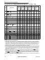
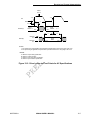
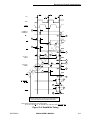
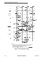
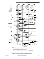
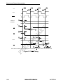
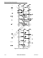
SECTION 12
ELECTRICAL AND THERMAL CHARACTERISTICS
The following paragraphs provide information on the maximum rating and thermal characteristics for the MC68060. This section is subject to change. For the most recent specifications, contact the AESOP electronic bulletin board at (800)843-3451 or (512)891-3650 (refer
to C.5.4 AESOP Electronic Bulletin Board for connection information).
12.1 MAXIMUM RATINGS
Characteristic
Symbol
VCC
Value
Unit
–0.3 to 4.0
V
Input Voltage
Vin
–0.5 to VCC+4
V
Maximum Operating Junction Temperature
TJ
110
°C
Minimum Operating Ambient Temperature
TA
0
°C
Storage Temperature Range
Tstg
–55 to 150
°C
Supply Voltage
This device contains protective circuitry
against damage due to high static voltages
or electrical fields; however, it is advised
that normal precautions be taken to avoid
application of any voltages higher that
maximum-rated voltages to this highimpedance circuit. Reliability of operation
is enhanced if unused inputs are tied to an
appropriate logic voltage level (e.g., either
GND or VCC).
12.2 THERMAL CHARACTERISTICS
Description
Thermal Resistance, Junction to Case—PGA
Thermal Resistance, Junction to Case—CQFP
Symbol
θJC
Value
Unit
2.5
°C/W
θJC
2.0
°C/W
12.3 POWER DISSIPATION
Conditions
MC68EC060
MC68LC060
MC68060
40 MHz 50 MHz 66 MHz 50 MHz 66 MHz 50 MHz 66 MHz
Unit
Vcc = 3.465 V, TA = 0°C
3.1
3.5
4.5
3.5
4.5
3.9
4.9
W
Normal Mode
Vcc = 3.465 V, TA = 0°C
300
300
300
300
300
300
300
mW
LPSTOP Mode, CLK Running
Vcc = 3.465 V, TA = 0°C
30
30
30
30
30
30
30
mW
LPSTOP Mode, CLK Stopped Low
NOTES:
1. Power dissipation values are preliminary and will likely be replaced with lower values upon further testing.
2. Power dissipation assumes no DC load.
3. Power dissipation figures are not applicable to the debug pipe control mode.
MOTOROLA
M68060 USER’S MANUAL
12-1
Electrical and Thermal Characteristics
12.4 DC ELECTRICAL SPECIFICATIONS (VCC = 3.3 VDC ± 5%)
Characteristic
Input High Voltage
Input Low Voltage
Undershoot
Overshoot
Input Leakage Current
AVEC, CLK, TT1, BG, CDIS, MDIS, IPLx, RSTI, SNOOP, CLKEN,
TBI, TCI, TCK, TEA, TA, TRA, BGR, CLA, JTAG
Hi-Z (Off-State) Leakage Current
An, BB, CIOUT, Dn, LOCK, LOCKE, TDO,
TIP, SAS, BTT, BSx, TMx, TLNx, TS, TTx, UPAx
Signal Low Input Current, VIL = 0.8 V
TMS, TDI, TRST
Signal High Input Current, VIH = 2.0 V
TMS, TDI, TRST
Output High Voltage, IOH = 16 mA
Output Low Voltage, IOL = 16 mA
Capacitance*, Vin = 0 V, f = 1 MHz, CLK Only
Capacitance*, Vin = 0 V, f = 1 MHz, All Inputs Except CLK
Symbol
VIH
Min
Max
Unit
2
5.5
V
VIL
—
—
GND
0.8
V
—
—
0.8
0.8
V
V
IIL, IIH
–50
20
µA
ITSI
–50
20
µA
IIL
–1.1
–0.18
mA
IIH
–0.94
–0.16
mA
VOH
VOL
2.4
—
V
—
0.5
V
Cin
Cin
—
20
pF
—
20
pF
*Capacitance is periodically sampled and not 100% tested.
12-2
M68060 USER’S MANUAL
MOTOROLA
Electrical and Thermal Characteristics
12.5 CLOCK INPUT SPECIFICATIONS (VCC = 3.3 VDC ± 5%)
Num
40 MHz1
Min
Max
Characteristic
Frequency of Operation
1
2
3
4
CLK Cycle Time
CLK Rise Time
CLK Fall Time
CLK Duty Cycle Measured at 1.5 V
50 MHz
66 MHz
Unit
Min
Max
Min
Max
50
66.67
MHz
—
2
2
55
04
15
—
—
45
—
2
2
55
ns
ns
ns
%
04
25
—
—
45
40
—
2
2
55
04
20
—
—
45
4a2
CLK Pulse Width High Measured at 1.5 V
11.25
13.75
9
11
6.75
8.25
ns
4b2
55
56
CLK Pulse Width Low Measured at 1.5 V
11.25
13.75
9
11
6.75
8.25
ns
8
2
—
—
7
2
—
—
5
2
—
—
ns
ns
CLKEN Input Setup
CLKEN Input Hold
NOTES:
1.40 MHz available only for the MC68EC060.
2.Specification value at maximum frequency of operation.
3.CLK may be stopped LOW to conserve power.
4.Minimum frequency is periodically sampled and not 100% tested.
2
3
VL
VH
1
VM
CLK
4a
4b
BCLK
55
55
CLKEN
56
56
Figure 12-1. Clock Input Timing Diagram
MOTOROLA
M68060 USER’S MANUAL
12-3
Electrical and Thermal Characteristics
12.6 OUTPUT AC TIMING SPECIFICATIONS (VCC = 3.3 VDC ± 5%)
Num
Characteristic
40 MHz1
Pad
Pad
Starts
Starts
3
at 5.5 V
at VCC
3
50 MHz
Pad
Starts
Pad
Starts
at 5.5 V
66 MHz
3
at
VCC3
Pad
Starts
Pad
Starts
at 5.5 V
3
at VCC
Unit
3
Min Max Min Max Min Max Min Max Min Max Min Max
BCLK to Address CIOUT, LOCK,
LOCKE, R/W, SIZx, TLN, TMx,
TTx, UPAx, BSx Valid (signal predriven)
BCLK to Address CIOUT, LOCK,
LOCKE, R/W, SIZx, TLN, TMx,
11a5 TTx, UPAx, BSx Valid (Signal from
three-state)
or CLK to Output Invalid
12 BCLK
(Output Hold)
13 BCLK to TS Valid
14 BCLK to TIP Valid
18 BCLK to Data Out Valid
to Data Out Invalid (Output
19 BCLK
Hold)
21 BCLK to Data-Out High Impedance
BCLK to Address, CIOUT, LOCK,
R/W, SIZx, TS, TLNx,
38 LOCKE,
TMx, TTx, UPAx, BSx High Impedance
CLK to BB, TIP
39 High
Impedance
5 BCLK to BR, BB Valid (Signal Pre40 driven)
BCLK to BB Valid (signal from
40a5 three-state)
115
506
57
58
59
60
61
62
63
—
—
3
17
—
—
3
12.6
—
—
3
9.9
ns
3
19
3
18
3
15.4
3
13.5
3
11.8
3
10.4
ns
3
–
3
–
3
–
3
–
3
–
3
–
ns
3
3
3
19
19
19
3
3
3
18
18
18
3
3
3
14.4
15.4
13.5
3
3
3
12.3
13.5
13.5
3
3
3
10.9
11.8
10.4
3
3
3
9.5
10.4
10.4
ns
ns
ns
3
–
3
–
3
–
3
–
3
–
3
–
ns
—
15
—
15
—
12
—
12
—
10
—
10
ns
—
15
—
15
—
12
—
12
—
10
—
10
ns
—
15
—
15
—
12
—
12
—
10
—
10
ns
—
—
3
17
—
—
3
12.6
—
—
3
9.9
ns
3
19
3
18
3
15.4
3
13.5
3
11.8
3
10.4
ns
CLK to IPEND, PSTx, RSTO Valid
—
—
3
18
—
—
3
13.5
—
—
3
10.4
ns
BCLK to SAS Valid
BCLK to SAS Invalid (Output Hold)
BCLK to SAS High Impedance
BCLK to TS Invalid (Output Hold)
BCLK to BTT Valid
BCLK to BTT Invalid (Output Hold)
BCLK to BTT High Impedance
3
3
—
3
3
3
—
19
–
15
–
19
–
15
3
3
—
3
3
3
—
18
–
15
–
18
–
15
3
3
—
3
3
3
—
15.4
–
12
–
15.4
–
12
3
3
—
3
3
3
—
13.5
–
12
–
13.5
–
12
3
3
—
3
3
3
—
11.8
–
10
–
11.8
–
10
3
3
—
3
3
3
—
10.4
–
10
–
10.4
–
10
ns
ns
ns
ns
ns
ns
ns
NOTES:
1. 40 MHz available only for the MC68EC060.
2. Output timing is measured at the pin. The specifications assume a capacitive load of 50 pF. However, a maximum
load of 130 pF may be used at each pin. Characterization data shows that at 130 pF loads, output propagation delays
are as follows: 40 MHz, Pad at VCC, multiply by prop delay by 1.4; 40 MHz, Pad at 5.5, multiply prop delay by 1.6; 50
MHz, Pad at VCC, multiply prop delay by 1.4; 50 MHz, Pad at 5.5, multiply prop delay by 1.6; 66 MHz, Pad at VCC,
multiply prop delay by 1.3; 66 MHz, pad at 5.5, multiply prop delay by 1.4. Exceeding the 130-pF limit on any pin
might affect long-term reliability and Motorola does not guarantee proper operation.
3. When interfacing the processor to a system designed for 5-volt operation, the “Pad Starts at 5.5” column must be used
when it is possible that the pin is at 5.5 volts when the processor begins to drive. Once a pin is driven by the processor
and is not three-stated, the “Pad Starts at Vcc” column may be used. If the processor is in a system designed for 3.3volt operation, use the “Pad Starts at Vcc” column always. This note not applicable to specs 11,11a, 40, and 40a.
Refer to note 5 for these specs.
4. BCLK is not a pin signal name. It is a virtual bus clock derived from the combination of CLK and CLKEN. A BCLK
rising edge coincides with a CLK in which CLKEN is asserted. A BCLK falling edge is insignificant. When a reference
to BCLK is used to describe output timing, it means that the specific output transitions only on rising CLK edges in
which CLKEN is asserted. A timing reference to CLK means that the output may transition off the rising CLK edge,
including those rising edges in which CLKEN is negated.
5. When the processor drives these signals from a three-stated condition, use spec 11a or 40a. Use the “Pad Starts at
12-4
M68060 USER’S MANUAL
MOTOROLA
Electrical and Thermal Characteristics
VCC” column or “Pad Starts at 5.5” column as applicable. Once these signals are driven, subsequent transitions are
defined by spec 11 or 40. The “Pad Starts at 5.5” column is deleted from specs 11 and 40 since the processor drives
up to the VCC level only. BR is never three-stated by the processor, and therefore, spec 40a does not apply for BR.
6.)“Pad Starts at 5.5" does not apply since these signals are always driven.
MOTOROLA
M68060 USER’S MANUAL
12-5
Electrical and Thermal Characteristics
12.7 INPUT AC TIMING SPECIFICATIONS (VCC = 3.3 VDC ± 5%)
Num
Characteristic
15
16
Data-In Valid to BCLK (Setup)
BCLK to Data-In Invalid (Hold)
BCLK to Data-In High Impedance
(Read Followed by Write)
TA, Valid to BCLK (Setup)
TEA Valid to BCLK (Setup)
TCI Valid to BCLK (Setup)
TBI Valid to BCLK (Setup)
TRA Valid to BCLK (Setup)
BCLK to TA, TEA, TCI, TBI, TRA Invalid
(Hold)
AVEC Valid to BCLK (Setup)
BCLK to AVEC Invalid (Hold)
BB Valid to BCLK (Setup)
BG Valid to BCLK (Setup)
CDIS, MDIS Valid to BCLK (Setup)
IPL≈ Valid to CLK (Setup)
BTT Valid to BCLK (Setup)
BGR Valid to BCLK (Setup)
BCLK to BB Invalid (Hold)
BCLK to BG Invalid (Hold)
BCLK to CDIS, MDIS Invalid (Hold)
CLK to IPLx Invalid (Hold)
BCLK to BTT Invalid (Hold)
BCLK to BGR Invalid (Hold)
Address Valid to BCLK (Setup)
TT1 Valid to BCLK (Setup)
SNOOP Valid to BCLK (Setup)
BCLK to Address Invalid (Hold)
BCLK to TT1 Invalid (Hold)
BCLK to SNOOP Invalid (Hold)
TS Valid to BCLK (Setup)
BCLK to TS Invalid (Hold)
BCLK to BB in High Impedance
(MC68060 Assumes Bus Mastership)
RSTI Valid to BCLK
BCLK to RSTI Invalid (hold)
Mode Select Setup to BCLK (RSTI Asserted)
BCLK to Mode Selects Invalid (RSTI Asserted)
CLA Valid to BCLK (Setup)
BCLK to CLA Invalid (Hold)
17
22a
22b
22c
22d
22e
23
24
25
41a
41b
41c
41d
41e
41f
42a
42b
42c
42d
42e
42f
44a
44c
44e
45a
45c
45e
46
47
49
51
52
53
54
64
65
40 MHz2
Min
Max
3
—
2
—
50 MHz
Min
Max
2
—
2
—
66 MHz
Min.
Max.
1
—
2
—
Unit
ns
ns
—
7
—
7
—
7
ns
12
12
12
12
12
—
—
—
—
—
10
10
10
10
10
—
—
—
—
—
7
7
7
7
7
—
—
—
—
—
ns
ns
ns
ns
ns
2
—
2
—
2
—
ns
12
2
12
12
12
3
12
12
2
2
2
2
2
2
3
12
12
2
2
2
12
2
—
—
—
—
—
—
—
—
—
—
—
—
—
—
—
—
—
—
—
—
—
—
10
2
10
10
10
2
10
10
2
2
2
2
2
2
2
10
10
2
2
2
10
2
—
—
—
—
—
—
—
—
—
—
—
—
—
—
—
—
—
—
—
—
—
—
7
2
7
7
7
1
7
7
2
2
2
2
2
2
1
7
7
2
2
2
7
2
—
—
—
—
—
—
—
—
—
—
—
—
—
—
—
—
—
—
—
—
—
—
ns
ns
ns
ns
ns
ns
ns
ns
ns
ns
ns
ns
ns
ns
ns
ns
ns
ns
ns
ns
ns
ns
—
3
—
3
—
3
ns
3
2
12
—
—
—
2
2
10
—
—
—
1
2
7
—
—
—
ns
ns
ns
2
—
2
—
2
—
ns
12
2
—
—
10
2
—
—
7
2
—
—
ns
ns
NOTES:
1. BCLK is not a pin signal name. It is a virtual bus clock derived from the combination of CLK and CLKEN. A BCLK
rising edge coincides with a CLK in which CLKEN is asserted. A BCLK falling edge is insignificant. When a reference
to BCLK is used to describe input timing, it means that the specific input is recognized only on rising CLK edges in
which CLKEN is asserted. A timing reference to CLK means that the input is recognized at any rising CLK edge, including those edges in which CLKEN is negated.
2. 40 MHz available only for the MC68EC060.
12-6
M68060 USER’S MANUAL
MOTOROLA
Electrical and Thermal Characteristics
DRIVE
TO 2.4 V
1.5 V
CLK
1.5 V
A
DRIVE TO
0.5 V
OUTPUTS(1)
B
VALID
OUTPUT n
2.0 V
2.0
V
0.8 V
0.8 V
VALID
OUTPUT
C
DRIVE TO
2.4 V
2.0 V
INPUTS(2)
0.8 V
DRIVE TO
0.5 V
n+1
D
VALID
INPUT
2.0 V
0.8 V
NOTES:
1. This output timing is applicable to all parameters specified relative to the rising edge of the clock.
2. This input timing is applicable to all parameters specified relative to the rising edge of the clock.
LEGEND:
A. Maximum output delay specification.
B. Minimum output hold time.
C. Minimum input setup time specification.
D. Minimum input hold time specification.
Figure 12-2. Drive Levels and Test Points for AC Specifications
MOTOROLA
M68060 USER’S MANUAL
12-7
Electrical and Thermal Characteristics
CLK
BCLK
CLKEN
51
RSTI
53
D15–D0 in
IPL2–IPL0
54
MODE SELECTS REGISTERED
ON PREVIOUS BCLK EDGE
Figure 12-3. Reset Configuration Timing
12-8
M68060 USER’S MANUAL
MOTOROLA
Electrical and Thermal Characteristics
CLK
BCLK
CLKEN
11
ADDRESS &
ATTRIBUTES
12
13
TS
60
14
TIP
12
17
15
D31–D0 in
(READ)
16
18
21
D31–D0 out
(WRITE)
19
57
SAS
58
22
TA, TRA, TEA,
TBI, TCI
23
24
AVEC
25
PRECONDITIONED DATA OR WRITE DATA FROM PREVIOUS
BUS CYCLE USING EXTRA DATA WRITE HOLD MODE
NOTE: Address and attributes refer to the following signals:
A31–A0, SIZ1, SIZ0, R/W, TT1, TT0, TM2–TM0, TLN1, TLN0, UPA1, UPA0, CIOUT, BS3–BS0
Figure 12-4. Read/Write Timing
MOTOROLA
M68060 USER’S MANUAL
12-9
Electrical and Thermal Characteristics
CLK
BCLK
CLKEN
38
ADDRESS &
11a
ATTRIBUTES
12
60
13
TS
38
60
12
14
TIP
12
39
11a
12
LOCK, LOCKE
12
38
12
40a
BB (OUT)
12
39
21
D31–D0 (OUT)
(WRITE)
19
41b
41b
BG
42b
42b
(SEE NOTE 1)
NOTES:
1. For illustrative purposes, a bus mastership hand-over is shown after a locked bus cycle sequence
which adds one extra clock period between the bus mastership hand-over that would not
occur for a bus mastership hand-over after a non-locked bus cycle.
2. Address and attributes refer to the following signals:
A31–A0, SIZ1, SIZ0, R/W, TT1, TT0, TM2–TM0, TLN1, TLN0, UPA1, UPA0, CIOUT, BS3–BS0
Figure 12-5. Bus Arbitration Timing
12-10
M68060 USER’S MANUAL
MOTOROLA
Electrical and Thermal Characteristics
CLK
BCLK
CLKEN
38
ADDRESS &
ATTRIBUTES
11a
12
60
13
TS
38
60
58
57
SAS
58
59
12
11a
LOCK, LOCKE
12
38
21
D31–D0 (OUT)
(WRITE)
19
40
BR
12
41b
41b
BG
42b
42b
41f
BGR
42f
62
BTT (OUT)
61
62
63
(SEE NOTE 1)
NOTES:
1. For illustrative purposes, a bus mastership hand-over is shown after a locked bus cycle sequence
which adds one extra clock period between the bus mastership hand-over that would not
occur for a bus mastership hand-over after a non-locked bus cycle.
2. Address and attributes refer to the following signals:
A31–A0, SIZ1, SIZ0, R/W, TT1, TT0, TM2–TM0, TLN1, TLN0, UPA1, UPA0, CIOUT, BS3–BS0
Figure 12-6. Bus Arbitration Timing (Continued)
MOTOROLA
M68060 USER’S MANUAL
12-11
Electrical and Thermal Characteristics
CLK
BCLK
CLKEN
11
ADDRESS &
ATTRIBUTES
13
TS
60
14
TIP
11
12
A3–A2
11
64
64
CLA
65
65
NOTE: Address and attributes refer to the following signals: A31–A0, SIZ1, SIZ0, R/W, TT1, TT0, TM2–TM0, TLN1, TLN0, UPA1, UPA0
Figure 12-7. CLA Timing
12-12
M68060 USER’S MANUAL
MOTOROLA
Electrical and Thermal Characteristics
CLK
BCLK
CLKEN
44a
A31–A0
45a
44c
TT1 (IN)
45c
44e
SNOOP
45e
46
TS (IN)
47
Figure 12-8. Snoop Timing
MOTOROLA
M68060 USER’S MANUAL
12-13
Electrical and Thermal Characteristics
CLK
CLKEN
BCLK
51
RSTI
52
41c
CDIS, MDIS
42c
41a
49
BB (IN)
42a
41e
BTT (IN)
42e
CLK
50
IPEND
12
50
RSTO
12
50
PST4–PST0
12
41d
IPL2–IPL0
42d
Figure 12-9. Other Signals Timing
12-14
M68060 USER’S MANUAL
MOTOROLA