1
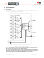
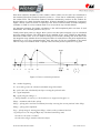
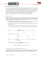
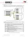
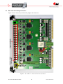
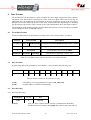
W-Ie–Ne-R
AVM16 / AVX16
16 channel ADC, 160 MHz with
features extraction
User’s Manual V2.0
W-IE-NE-R Plein & Baus GmbH
Board Rev. 1.3, Firmware Rev. 2.1, November 11, 2011
1
www.wiener-d.com
General Remarks
The only purpose of this manual is a description of the product. It must not be interpreted as a
declaration of conformity for this product including the product and software.
W-Ie-Ne-R revises this product and manual without notice. Differences between the description
in manual and the product are possible.
W-Ie-Ne-R excludes completely any liability for loss of profits, loss of business, loss of use or
data, interrupt of business, or for indirect, special incidental, or consequential damages of any
kind, even if
W-Ie-Ne-R has been advises of the possibility of such damages arising from any defect or error
in this manual or product.
Any use of the product which may influence health of human beings requires the express written
permission of W-Ie-Ne-R.
Products mentioned in this manual are mentioned for identification purposes only. Product names
appearing in this manual may or may not be registered trademarks or copyrights of their respective
companies.
No part of this product, including the product and the software may be reproduced, transmitted,
transcribed, stored in a retrieval system, or translated into any language in any form by any means
without the express written permission of W-Ie-Ne-R.
W-IE-NE-R Plein & Baus GmbH
2
www.wiener-d.com
Table of contents:
1 GENERAL DESCRIPTION............................................................................................5
1.1 Overview...................................................................................................................................5
1.2 Functional description.............................................................................................................6
1.2.1 Block diagram.....................................................................................................................6
1.2.2 AVM16 / AVX16 Feature Extraction..................................................................................7
1.2.3 Pedestal and Noise Extraction.............................................................................................9
1.2.4 Trigger Feature Extraction..................................................................................................9
1.2.5 Internal Trigger...................................................................................................................9
1.2.6 External NIM and Software Trigger..................................................................................10
1.2.7 Window Control................................................................................................................10
1.2.8 Trigger and Clock Synchronization...................................................................................11
1.3 Technical Specification..........................................................................................................13
2 TECHNICAL DESCRIPTION.......................................................................................14
2.1 Frontpanel Layout and Connector Description...................................................................14
2.2 DIP Switch and Jumper Position..........................................................................................16
2.3 Analog Input...........................................................................................................................17
3 DESCRIPTION OF VME INTERFACE.........................................................................18
3.1 VME addressing.....................................................................................................................18
3.2 VME registers.........................................................................................................................19
3.3 Technical Description of VME Registers.............................................................................20
3.3.1 Virtex5 Control FPGA Registers.......................................................................................20
3.3.2 Spartan3 ADC FPGA Registers........................................................................................23
3.3.3 Spartan3 Individual Channel Registers.............................................................................26
3.3.4 Virtex5 Data FIFO Readout Register................................................................................26
4 DATA FORMAT........................................................................................................... 27
4.1 Event Data Frames.................................................................................................................27
4.2 Data Preamble........................................................................................................................27
4.3 Data Decoding........................................................................................................................27
4.3.1 Raw Data Decoding..........................................................................................................27
4.3.2 Pulse Integral Decoding....................................................................................................28
4.3.3 Verbose Feature Extraction Data Decoding......................................................................28
W-IE-NE-R Plein & Baus GmbH
3
www.wiener-d.com
4.4 Data Frames...........................................................................................................................29
4.4.1 Compressed Data Frame...................................................................................................29
4.4.2 Verbose Data Frame..........................................................................................................30
4.4.3 Raw Data Frame................................................................................................................31
4.5 Example of Data Readout......................................................................................................32
5 PROM FILE FORMATTING.........................................................................................33
W-IE-NE-R Plein & Baus GmbH
4
www.wiener-d.com
1
1.1
General Description
Overview
The AVM16/AVX16 is a 1-unit wide VME64x/VXS module which allows for compact readout of
physics experiments with very high channel count (16 per unit) while reducing the amount of
transferred data to be stored and interpreted to a minimum. Hence the AVM16/AVX16 series
allows for much higher trigger rates than raw data sampling with traditional FADCs.
This is made possible by extensive use of local data compression power for each channel onboard. The implemented FPGA algorithm called feature extraction is capable to analyze any
unipolar shaped physical signal coming from a scintillating plastic, crystal, a gaseous or silicon
detector with a minimum useful rise time of 20-25ns and fall times lower than 3µs. It extracts all
times, amplitudes and integrals of physical interest for any CR-RC or Gaussian shaped pulses
from a detector. The feature extraction even works up to a pile-up factor of two or more, which
means even searches for the inter-pulse minimum and a following maximum are possible.
Due to a complex on-board triggering architecture up to 16 modules can be synchronized within
one VME crate via daisy chaining on the frontpanel bus on the crate level while other crates can
be point to point connected via the P2 backplane connector to form trees of synchronized crates. 1
The synchronization between the modules is done via modern multipoint transceivers compliant to
the TIA/EIA-899 M-LVDS standard 2 on the front or backplane buses with flat cables to be
terminated on both sides (internal jumpers are foreseen for the frontpanel bus).
Overall trigger synchronization is guaranteed by high resolution system timers and a wide
timestamp register. An overall busy logic is working on single eventbase filling a multi-event
buffer FIFO as long as one or more modules flag for an internal readout FIFO overflow.
The finally achievable trigger rate depends strongly on the analyzed window size, the verbosity
level of the transmitted data (raw, verbose, compressed) and the chosen VME transaction strategy.
For laboratory purposes one AVM16/AVX16 can be simply used as "single master" (SM) with
internal 160MHz clock and external NIM trigger. Additionally every activated channel can be
installed as internal trigger source (or-ed, featured trigger). The current channel baseline and noise
are frequently recalculated. They are only updated within the pulse free time periods.
Extended data transfer cycles via VME allow for up to 64 bit block moves (MBLT). An additional
hardware byte swapper can be activated to ease readout transfer for little endian machines
(INTEL) while default is big endian (Freescale, Motorola).
Further extensions like VME Renaissance (2eVME, 2eSST) are physically possible as well as the
optional VXS readout. Both are physically connected for possible customized implementations in
the future (further firmware upgrades possible).
Further hardware extensions may not be ruled out and may be proven on valued costumer request.
1
In this way a readout system with 480 BGO channel and of two multi wire proportional chambers (MWPC) has been designed
2
As used within current backplane xTCA physics extensions
W-IE-NE-R Plein & Baus GmbH
5
www.wiener-d.com
1.2
Functional description
1.2.1 Block diagram
The AVM16/AVX16 modules contain four quad-channel ADC blocks, a VME/VXS control part
and a clock and synchronization system, see figure 1.
Figure 1: AVM16/AVX16 Block-Diagram
Each of the ADC channel is equipped with a symmetrizing amplifier, anti-aliasing filter and an
individual 12-bit Analog-to-Digital converter running at 160 MS/s.
After conversion, the digital data is passed to 4 FPGA circuits providing buffers for data retention
and a feature extraction logic. One Spartan-3 FPGA from Xilinx is used for a block of four
channels keeping a history of 2048 samples for each channel in its internal registers.
W-IE-NE-R Plein & Baus GmbH
6
www.wiener-d.com
Feature extraction algorithms are used to calculate important parameters of the input pulses such
as amplitude, time, integrals and many others which allows to minimize the readout data volume
and thus increasing the readout speed. The user may still choose to read a full set of samples
recorded in the buffer or to read only a subset of those samples within the specified time
boundaries being in relation to the trigger.
After an internal or external trigger request the stored and/or extracted data is passed to a control
VIRTEX-5 FPGA chip via four local data buses and then transferred over a VME bus or a VXS
backplane P2P connection fabric.
In multichannel systems where a common time base is required global clock and synchronization
signals are provided either via the front panel connector or via user defined pins on the VME P2
connector. The clocking and synchronization circuitry allows for choosing of the correct clock
source especially for bigger data acquisition systems.
1.2.2 AVM16 / AVX16 Feature Extraction
12-BIT
12-BIT
12-BIT
ADC
12-BIT
ADC
ADC
ADC
DPRAM
DPRAM
DPRAM
DPRAM
TRIGGER BUS
M
U
X
(VXS Version)
M
M
M
M
U
U
U
UX
X
XX
WINDOW
WINDOW
WINDOW
WINDOW
CONTROL
CONTROL
CONTROL
CONTROL
WAVEFORM
WAVEFORM
WAVEFORM
WAVEFORM
FEATURE
ANALYSIS
ANALYSIS
ANALYSIS
EXTRACTION
FIFO
FIFO
FIFO
FIFO
CONTROL
LOCAL BUS INTERFACE
TRIGGER
TRIGGER
TRIGGER
TRIGGER
FEATURE
FEATURE
FEATURE
FEATURE
EXTRACTION
EXTRACTION
EXTRACTION
EXTRACTION
LOCAL
BUS
(data+
trigger+
timing)
PEDESTAL
PEDESTAL
PEDESTAL
PEDESTAL
EXTRACTION
EXTRACTION
EXTRACTION
EXTRACTION
NOISEPP
PP
NOISE
NOISE
PP
NOISE
PP
Figure 2: Feature extraction FPGA
The following description of the Feature Extraction applies to every channel in the same manner:
When no trigger occurs while the AVM16/AVX16 is running the current baseline (pedestal) and
the current peak to peak noise value is regularly recalculated and updated. These values can be
read out any time via VME for longtime monitoring purposes. The further Waveform Feature
Extraction then strongly relies on the freshest recalculated baseline value. 3
Data coming from ADC converters are continuously stored in ring buffers (dual-ported RAM)
synchronous to the global clock keeping a record of the last 2048 samples. Only 1024 of these
samples can be selected from the window control for output to the Spartan local interface FIFO.
3
If baseline upsets or trips from the detector side may occur from time to time these can be tackled safely by the VME readout
software only in verbose mode. If they can be completely ruled out compressed mode can be selected for highest trigger rates
W-IE-NE-R Plein & Baus GmbH
7
www.wiener-d.com
Data from within the boundaries of the window control called search window are transferred to
the extended Waveform Feature Extraction section or - if raw data is additionally requested - to
the readout FIFO. The Waveform Feature Extraction continuously searches in this window for
physical pulses (in a kind of pipeline algorithm). If found a detailed list of parameters is extracted.
Figure 3 shows such a list in case of a pile-up event. Those extracted values are made completely
available via VME in verbose readout mode or in raw mode for any selected channel.
An important parameter for further calculations is the self-extrapolated pulse start time Pz (left
dashed line). For a detailed generation see §1.2.8.
Finally when input pulses are bigger than a preset size their pulse integrals (Pq) are calculated
precisely during run-time. The integration can be installed in two ways: Within an individually
fixed time window after Pz or in a window starting at Pz but with a floating end. In the latter case
the integration stops whether the end of integral window is reached first or the pulse amplitude has
fallen back to 1/32 of its maximum before. Only the pairs (Pz,Pq) are transmitted to the central
FIFO in compressed readout mode.³ If pileup events occur the process repeats for every peak.
Figure 3: Feature extraction parameters
P0 – window beginning
Pi – first value greater the channels individual integral threshold
Pz – pulse start time calculated from slope crossing the pedestal value
Pa – signal amplitude
Pq – signal integral (charge) *
j – Pileup Number (in case of j=1 the brackets were suppressed in figure 3)
PPi(j) – minimum value before pileup
PPz(j) – pileup pulse start time calculated from slope crossing the current pedestal value PPi(j)
PPa(j) – pileup pulse amplitude
Pe(j) – pileup integral, starting from PPi(j), relative to the (common) baseline
* If pileup occurs, the integral Pq is only calculated until PPi(j) time,
else when 1/32 of Pa is reached,
else when the integer window end comes before
W-IE-NE-R Plein & Baus GmbH
8
www.wiener-d.com
1.2.3 Pedestal and Noise Extraction
In periods free of trigger and pulses the AVM16/AVX16 Pedestal Extraction Feature steadily
calculates the mean of 32 consecutive samples for every channel. Eight such mean values are
stored in a pipeline register. Only if all of these values are within ±1 this common value becomes
the new current pedestal or baseline value.
In periods free of trigger and pulses the AVM16/AVX16 Noise Extraction Feature maximum
peak to peak delta values are stored in individual noise registers. The maximum noise value is
currently limited to a value of 31. It is reset to zero by its VME noise register read.
1.2.4 Trigger Feature Extraction
For every activated4 channel the AVM16/AVX16 Trigger Feature Extraction steadily integrates
four consecutive samples and stores the results in a pipeline. As soon as the value rises above a
certain value5 (Pi) a pulse tagging mechanism takes place: For samples with distances of one, two
or four samples the delta values will be calculated. Normally when a pulse peaks the pulse drops
again. For a certain time 6 after the tagged maximum Pa only those delta values between ¼ and ¾
of Pa will be used for linear extrapolation of the different pulse start times to the current baseline.
From all of these times the earliest becomes the pulse start or arrival time Pz with an internal
resolution of ¼ clock period (1.5625 ns) and tagged by the ∆-method which has won, see figure 4.
Figure 4: Graphical representation of the generation of the pulse start time Pz by the
AVM16/AVX16 Trigger Feature Extraction
1.2.5 Internal Trigger
Independently of the Trigger Feature Extraction for every channel an internal leading edge
discriminator (sampling) is implemented for fast trigger decision on a one board level (Single or
Local Master, see §1.2.8). The common threshold is programmable via VME trigger level register.
Only the first Spartan3 FPGA trigger from all activated channels 4 becomes the event trigger
referenced to from the local Virtex5 FPGA. If several trigger appear at the same time the trigger
channel with the smallest channel number is chosen. The event trigger location can be readout via
the VME state register. The event trigger is broadcast back to all 16 window controls, see §1.2.7.
Additionally the event timestamp is broadcast in bigger system with more than one card or crate,
see §1.2.8, but only one card in the system is installable with this featured internal trigger (LM) in
the current hardware and firmware version.
4
non-inhibited, controlled via the VME cha_inh register
5
controlled via the channel selective VME q_threshold register
6
controlled via the VME anal_ctrl register
W-IE-NE-R Plein & Baus GmbH
9
www.wiener-d.com
1.2.6 External NIM and Software Trigger
External NIM trigger from the terminated frontpanel TRG LEMO connector can be accepted for
fast trigger timestamp generation on base of the internal 640MHz clock reference. The timestamp
has a resolution of 1,5625ns and is broadcast throughout the system in the same way as described
for the Internal Trigger in §1.2.5. External NIM source is only selectable for mastered boards.
The same rules are valid for the Software-Trigger, generated in-situ to the generated software call,
and can be used for diagnostic purposes (software baseline and noise monitoring).
With any accepted trigger the event number is increased by one, resettable via VME.
1.2.7 Window Control
Either installed and non-inhibited trigger is distributed to all channels of an AVM16/AVX16
module. The trigger time is then used by the channels Window Control to set the time boundaries
for Feature Extraction, means scanning/transmission of the dual-ported RAMs. Those boundaries
are under full user control by four VME registers, see figure 5:
•
SW_START: Search Window Start. Also known as trigger latency, when positive means
presamples, when negative refers to a postsample start, range (±6.4µs)
•
SW_LENGTH: Search Window Length. Transmitted size if raw data output is chosen
(max. 1kS, 6.4µs)
•
IW_Start: Integral Window Start. For exclusion of early integration much before trigger
•
IW_Length: Integral Window Length. To additionally reduce maximum integration length
Figure 5: Data window for feature extraction
The Integral Window is only a sub-part of the Search Window.
Additionally the SW_INTLENGTH variable limits the maximum width for the pulse integral
extraction after Pz (PPz(j) in case of a pile-up event). It can be used with big success for nearly
Gaussian shaped pulses, where tailored integral measurements cause no additional failures.
W-IE-NE-R Plein & Baus GmbH
10
www.wiener-d.com
1.2.8 Trigger and Clock Synchronization
Making extensive use of the frontpanel and backpanel synchronization connectors of the
AVM16/AVX16 eases dramatically the final installation of a multi-module or multi-crate setup.
The following figure 6 shows then how the trigger scheme follows a simple top-down structure:
Figure 6: Trigger and Synchronization Scheme for bigger experiments
To simplify the routing of the different possible clock and trigger sources in such a common
synchronization scheme with flat cables the following nomenclature was introduced to help how
to preset the modules VME mode registers:
SM
Single Master. Standalone module triggered by software, external NIM or internal
Frontpanel Connector (FC) synchronization bus passive (high impedance)
LM
Local Master. Like SM.
Driving FC synchronization bus
LM_GW
Local Master Gateway. Like LM, but additionally
Driving VME-P2 Back Panel (BP) synchronization bus
(used for inter crate synchronization)
RM
Remote Master. Synchronized via BP from a Gate Way (GW) module,
Driving the local crates FC synchronization bus
SLV
Slave. Synchronization done by LM or RM,
FC synchronization bus passive (high impedance)
SLV_GW
Slave Gateway. Synchronization done by LM,
Driving BP synchronization bus
Table 1: AVM16/AVX16 Module Mode Nomenclature
W-IE-NE-R Plein & Baus GmbH
11
www.wiener-d.com
The flat cables transfer differential M-LVDS signals. They have to be terminated on both ends by
jumpers situated at the frontpanel and at the backpanel piggy connectors.
The synchronization takes place automatically after power-up or a system reset SRST: Within
some milliseconds the mastered synchronizing FPGA controllers (LM, RM) perform a full check
of the functionality of the adapted flat cables, e.g. listening to correct transfer of the clock and
trigger signals and re-initialize the system timers and timestamp registers. 7
The implemented Trigger and Clock Synchronization shall guarantee for full clock and event
number synchronization and for broadcast delivery of the correct event timestamps during a
completely asynchronous VME readout.
The current states of the synchronization are to be monitored via the error flags retrievable within
the AVM16/AVX16 masters VME mode registers. As long they are o.k. no sync. failure occurred.
The implemented trigger scheme reduces tremendously the amount of external synchronization
logic required for readout of the AVM16/AVX16 with no extra cost for the user.
7
The small trigger delays between modules of a crate and modules between crates are not recovered by the local or remote masters
within the current firmware version
W-IE-NE-R Plein & Baus GmbH
12
www.wiener-d.com
1.3
Technical Specification
Bus standard
VME64/VXS
No. of channels
16 (LEMO connectors)
Sampling speed
160 MHz
Resolution
12 bit
Input voltage range
+/- 1.0 V
Input offset DAC
individual amplitude offsets (12 bit)
Full bandwidth
141MHz
Anti-aliasing filter
user defined
Default input coupling
AC:*
280 kHz .. user defined, 50Ω terminated
*customizations possible (DC, Gain)
Noise
0.8 LSB (RMS)
Buffer length
2048 samples (12.8 us), selectable 1024 max.
Clock
- Internal clock 160 MHz
- External front panel connector M-LVDS/LVPECL
- User defined VME P2 pins
Trigger options
- External NIM standard (LEMO connector)
- Internal trigger (sampled leading edge)
- Software trigger
Feature extraction
- Amplitude
- Time of arrival
- Charge integrals
- Pile-up count of two or more
Readout mode
- Compressed (only charge and time for the main pulse)
- Verbosity (full set of extracted parameters)
- Raw (all samples plus full set of extracted parameters)
Integration time window
- relative to trigger time or to pulse arrival time
- integral threshold individual for every channel
- programmable relative pulse integral window
System timer resolution
- 1.5625 ns
Self-Test
Internal pulse generator with programmable amplitude
Configuration
- Remote via VME
- Local via JTAG connector
Base address
A[31:16] selectable by 6-dip switch, from 0x0002 up to 0xC01E
Addressing mode
A32/D32, BLT, MBLT
Power requirements
VME-32
VME-64
W-IE-NE-R Plein & Baus GmbH
+5V / 8A,
+5V / 2.5A, +3.3V/5.5A
13
www.wiener-d.com
2
2.1
Technical Description
Frontpanel Layout and Connector Description
Figure 7: P2 VME Backplane Connector and
pinout definition for M-LVDS bus
Figure 8: The AVM-16 / AVX-16
Front Panel Layout
W-IE-NE-R Plein & Baus GmbH
Table 2: Flat Cable Connector pinout
definition for M-LVDS bus
14
www.wiener-d.com
2.2
DIP Switch and Jumper Position
Figure 9 shows the user key locations for jumpers and connectors
Figure 9: The AVM-16 / AVX-16 Printed circuit board
W-IE-NE-R Plein & Baus GmbH
15
www.wiener-d.com
2.3
Analog Input
The default input AC filter provides an effective cut-off for background low frequency noise and
mains pick-up. It is optimized for use in a typical QDC readout chain generating negatively
shaped unipolar pulses of 2 volts dynamics. 12bit DACs allow to shift the baselines individually
into the upper region to use the full dynamical range (12 bit). The symmetrizing amplifier
provides a differential input for the 12 bit ADC reducing PCB noise pickup. The anti-aliasing
filter allows for precise input bandwidth control.
An on-board pulse generator provides a fast test pulse of programmable size to all channels for
diagnostic purposes.
Figure 10: Input symmetrizing amplifier and anti-aliasing filter (R5, R7, C2).
Resistors values, the location of the test pulse and the values and locations
of capacitors may depend on AVM16 version or be customized.
Customization by manufacturer:
Dynamic range of the inputs and the bandwidth of the anti-aliasing filters as well as DC coupling 8
can be easily adapted on customer request.
Due to the unipolar input circuitry positive pulses can be sampled only with halve of range and
resolution (11 bit). In this case the overall sampling polarity for positive feature extraction
analysis can be switched via the VME control register.
8
The 0603 SMD 50Ω input termination is capable to sustain only a maximum power of 63mW and 50V peak voltage
W-IE-NE-R Plein & Baus GmbH
16
www.wiener-d.com
3
3.1
Description of VME Interface
VME addressing
AVM16/AVX16 reacts to read and write accesses with following Address Modifiers (AM):
>0F
A32 supervisory block transfer (BLT)
>0B
A32 non privileged block transfer (BLT)
>0D
A32 supervisory data access
>09
A32 non privileged data access
>0C
A32 supervisory 64-bit block transfer (MBLT)
>08
A32 non privileged 64-bit block transfer (MBLT)
Table 3: AVM16/AVX16 Address Modifiers
The base address is set by means of a 6 fold DIP Switch SW1 according to following table:
SW1
Bit
Base Address
6
31
0x80000000
5
30
0x40000000
4
20
0x00100000
3
19
0x00080000
2
18
0x00040000
1
17
0x00020000
Table 4: Base Address Settings
A switch in the „on“ position means that the corresponding address bit should be 0 (negative
logic). The base address is divided in two parts. The gross range is set with SW1(6:5) and can be
0x0000000, 0x40000000, 0x80000000 or 0xC0000000. The fine range is set with SW(4:1) and
can be from 0x000000 to 0x1E0000 with 0x20000 steps. The real base address is the sum of the
two ranges. For example if only the switch 1 is set to “off” the selected address range will be
0x00020000 to 0x0003FFFC.
The entire address range of the card is 0x20000, or 128kB. Of these ranges, the first kB (0x000 to
0x7FC) is determined for module registers and the rest (0x800 to 0x1FFFC) is determined for the
block data transferred from the FIFO. This means with any addressed read from this range the data
will be removed from the top of the data FIFO and transferred to the VME backplane. A re-read of
the last FIFO word or FIFO block is not possible. BLT/MBLT can be done either with or without
auto-address increment with blocks from 1-256 without a release of the data bus by the master.
W-IE-NE-R Plein & Baus GmbH
17
www.wiener-d.com
3.2
VME registers
Offset
Name
Write
Read
0x000
ident
Version
0x004
serial
serial number, 32 Bit
0x008
com_ids
communication identifier
0x00C
mod_type
Module Type
Module Type and State
0x010
state
Status Register
0x014
dlength
Data length for block
transfer as Byte
0x018
reserved
0x01C
tp_dac
Level of test pulse (DAC)
0x020
offset_dac[4]
baseline offset for all
ADC inputs
0x030
jtag_csr
JTAG Control
JTAG Status
0x034
jtag_data
JTAG Runtest
JTAG Data
reserved
0x100
0x104
cr
act
Control/Mode Register
action like Master Reset
0x108
cha_inh
disable single channels, 16 Bit
0x10C
cha_raw
set channel to raw mode, 16 Bit
0x110
trg_level
local trigger level, 12 Bit
0x114
anal_ctrl
signal analysing control
0x118
iw_start
start of integral window, 10 Bit
0x11C
iw_length
length of integral window, 10 Bit
0x120
sw_start
start of pulse search window, 10 Bit signed
0x124
sw_length
length of search window, 9 Bit
0x128
sw_intlength
0x12C
0x1300x13C
aclk_shift
lb_test[4]
length of integral of the signal analysing
step phase shift factor
status
r/w test register for the local bus (to 4 SPARTAN)
reserved
0x2000x23C
base_line[16]
auto base line 12 bit
0x2400x27C
noise_level[16]
peak to peak noise level,
5 Bit
0x2800x2BC
q_threshold[16]
q-threshold for trigger
decision in the integral
window & data block gen.
reserved
0x0800- data_range
0x1FFFC
W-IE-NE-R Plein & Baus GmbH
data, single or block
transfer
18
www.wiener-d.com
3.3
Technical Description of VME Registers
3.3.1 Virtex5 Control FPGA Registers
ident
0x000 - Board Id. Contains firmware version number.
Bit
Value
Meaning
7:0
0x70
0x71
0x72
Module Id V1.1, common baseline, no NIM Trigger
Module Id V1.2, wrong baseline, byte swap
Module Id V1.3, actual Design
15:8
0x21
Firmware Version
31:16
0
Reserved
(here 2.1), new Sync. System
Serial
0x004 - User serial number. This number can be programmed by the user and is
saved in the FPGA PROM. Read and write access possible.
com_ids
0x008 - In this register there are three identifiers for communication.
Bit
Meaning
2:0
Interrupt Request Level (1 to 6)
an interrupt is issued
if data are available. A 0 disables the interrupt
3
Null
4
Byte Swap. 1 = Little endian, 0 = Big endian (default)
7:5
Null
15:8
Interrupt
Vector,
it
is
transmitted
on
Acknowledge in order to identify the interrupt
Interrupt
19:16 Data recognition. These 4 bits are written in bit 31:28 of
data, so that it is possible to map data to a specific
module (see data format)
31:20 Null
mod_type
0x00C - Module Type and Module Status
Bit
2:0
Name
typeid
Meaning
0:SM Single Master. Independent module
1:LM Local Master. Trigger & controls frontpanel bus
2:LM_GW Gateway Master. Links to Remote Master via P2
3:RM Remote Master. Linked to a *_GW module via P2
4:SLV Slave. Synchronized via frontpanel bus by LM/RM
5:SLV_GW Gateway Slave. SLV links to RM via P2
3
SRSD
Flag: Synchronization reset done
4
FCKF
Flag: Frontpanel clock failure (applies not to SM)
5
RCKF
Flag: Remote clock failure on VME P2
W-IE-NE-R Plein & Baus GmbH
19
www.wiener-d.com
6
FCKR
Flag: Frontpanel clock ready (applies not to SM)
7
RCKR
Flag: Remote clock ready
8
LMSB
Flag: LM Setup Busy, wait until SLV are sync.
9
GCKF
Flag: General Clock Failure (bit4 OR bit5)
10
LTSE
Flag: LM Timeout during sync. setup
11
LTRM
Flag: LM Timeout caused by RM
12
TTPF
Flag: Trigger Time Parity Failure during broadcast
31:13
state
Null
0x010 - General Status Register
Bit
Name
Meaning
0
DVAL
Data valid. Data are ready in readout FIFO. If
this bit is set an interrupt is triggered in case
the programmed interrupt level is not zero. The
number of bytes in dlength register shall be read
out. DVAL will be reset (and another interrupt
will be generated) asynchronously, as soon as a
new event is transferred to the readout FIFO
1
Null (lost meaning Firmware Version 2.1)
2
LBUSY
Local Busy. This bit is set shortly when a trigger
is accepted
blocking further trigger until all
the data is transferred internally to the readout
FIFO. It is set also when no data can be
transferred from the Spartan FIFO
3
BUSY
System Busy. Sum of LBUSY of the whole system
7:4
LTSRC
Level Trigger Source. Indicates which ADC channel
fired the last level trigger.
8
FFULL
FIFO Full. Flags overflow of the 128k readout FIFO
9
FERROR
FIFO Error. If event size too big and FIFO stucks.
This may be generally ruled out by design
31:10
dlength
Null
0x014 - This register indicates how many bytes of data are ready for VME readout
(e.g. BLT/MBLT) in the FIFO (128kB + reserve in total). The dlength count
includes only complete event frames. Hence read out is fully asynchronous from
data transfer as long as no FIFO overflow occurs. Data is packed into a special
event frame format as described for the data_range register
W-IE-NE-R Plein & Baus GmbH
20
www.wiener-d.com
jtag_csr
0x030 - JTAG control/status Register
Bit Name
Write
Read
0
TDI
Data Input to the first JTAG device
1
TMS
Mode Select
2
TCK
JTAG Clock, must be zero when AUTO_CLK is used
3
TDO
Data Output of the last JTAG
device
4
RTEST
JTAG Runtest is running
7:5
8
ENABLE
drives signal to the JTAG Connector, the connector
must be free
9
AUTO_CLK
one clock cycle is generated, rising and falling edge
With bit 8 set TDI, TMS and TCK on JTAG connector are driven from FPGA.
Otherwise these signals are high impedance, in order for an external
programming tool to be able to connect. By means of this register it is possible to
enable a program to gain full control over the JTAG chain.
For programming of the firmware by experts or the manufacturer the JTAG
configuration connector with little imprint of the pins has to be used, see figure 6.
jtag_data
0x034 - This register has two functions:
α) With the read function the user gets the shift register for TDO. In order not to
have to read jtag_csr after each output, the TDO bit is moved to a write
register with each cycle, so that the last 32 TDO bits (e. g. Device ID) can be
read out in chain.
TCK shift
TDO
30
16 15
0
jtag_data
31
16 15
0
β) With the write function a number of TCK Clocks with TMS=0 is returned.
The value is used in svf Files as "RUNTEST n TCK". In this way it is possible
to insert pauses after commands.
tp_dac
0x01C - With bit 3 in “act” register it is possible to generate a test pulse through a
DAC. The height of the test pulse is set by means of this tp_dac register. Since
the DAC has only 8 bits, only bits 11:4 are relevant.
offset_dac[4] 0x020 - When no signal is connected, the ADC mean output value is about 0x800,
i.e. a signal in one polarity can use only half of the measurement range. By means
of an offset value for a DAC, it is possible to reduce this ADC mean value until
zero. For this purpose there are 4 12-bit DACs with 4 channels respectively.
The DAC (AD5324) has the following SPI register assignments:
W-IE-NE-R Plein & Baus GmbH
21
www.wiener-d.com
Bit
Name
DAC Function (WO)
11-0
DATA
12 bit offset, one unit corresponds to about one
ADC unit, i.e. when the value here is increased by
0x100, the ADC mean value when no signal is present
should decrease more or less by the same value.
12
nLDAC
If this bit is 0, all 4 channels are updated. This
bit is always set to 0 internally.
13
nPD
"not power down", this bit is set internally to 1
15-14 A1/A0
DAC channel group number 0 to 3 for offset_dac[0],
4 to 7 for offset_dac[1] and so on...
3.3.2 Spartan3 ADC FPGA Registers
The read back of these registers occurs from a shadow register in VIRTEX-5.
cr
0x100 - Control/Mode Register
Bit Name
Function
0
ENA
General enable. If this bit is not set, AVM16 is in
its ground state. All data is deleted.
1
EXTRIG
Enables the trigger input from the front connector
(LVDS). The trigger time is determined in VIRTEX-5
and sent to all ADC FPGA, in order to start the
analysis. The next trigger is then only possible
when all data have been transmitted to VIRTEX-5.
2
LEVTRIG
With this bit a trigger is fired when the value of
an ADC input (that is not inhibited by cha_inh )
overcomes the value in trig_level register. The
corresponding ADC FPGA sends the trigger time to
VIRTEX-5 which forwards it to all ADC FPGA in order
to start the read out.
3
VERBOSE
If zero means full compression: Only pairs (Pz,Pq)
If one means verbose mode: Additionally the pairs
of values for minima and maxima are transmitted.
Full data is output to channels of cha_raw register
4
ADCPOL
The polarity of the ADC data can be changed here.
By default ADC data are inverted to analyse
negative pulses. When this bit is set ADC data are
not inverted to analyse positive pulses. Also the
RAW data are inverted.
5
SGRD
Single Gradient. In the computation of the rise
time only two points with ∆x=1 are considered.
Normally ∆x
can also
be 2
or 4,
if the
corresponding y values lay between ¼ and ¾ of the
maximal value.
6
TP_ON
With this bit the test signal can be statically
enabled.
7
PW_ON
With this bit, the analogue ADC power supply can be
statically enabled. Otherwise, it is only enabled
when bit 0 (ENA) is set.
W-IE-NE-R Plein & Baus GmbH
22
www.wiener-d.com
act
0x104 - Action register
Bit
Name
Write/single shot
0
MRST
Master Reset
1
SRST
Synchronous Reset for all timers, so that all FPGA
have the same time reference.
2
TRIGGER
Software Trigger
3
TPULSE
Generates a fast test pulse on all 16 channels
Bits 3:1 are only relevant for modules in Single Master (SM) or Local Master (LM)
mode, see mod_type register. Those signals will be sent to all allocated Slave
Modules in the synchronization scheme. A software triggered pulse is generated
when bits 2 and 3 were synchronously set.
cha_inh
0x108 - The corresponding channel to each bit (0 bis 15) which is set is inhibited,
means removed from readout, trigger and feature extraction.
cha_raw
0x10C - If the corresponding channel to each bit is set all ADC raw data samples
that are within the search window are transmitted together with all available data
from the feature extraction (including start, point value pairs, integrals).
trig_level
0x110 - This value is the common trigger level when LEVTRIG in cr register is
activated, relative to internally regularly updated baseline of every channel
anal_ctrl
0x114 - Here it is possible to parametrize the pulse analysis:
Bit
Default
Function
3:0
8
Integral based detection:
this value times 4 indicates how high should the
integral be in order for a pulse to be detected.
In case of a pile up the integral is computed on
the basis of the last minimum value.
7:4
11:8
Null
1
Distance from another maximum:
number of clock units after the last maximum
(start time point) from where a new pulse (even a
pile up) can be detected.
31:12
Null
The default values are restored by reset or by writing 0. A zero as parameter is not
valid and will be ignored.
W-IE-NE-R Plein & Baus GmbH
23
www.wiener-d.com
iw_start
0x118 - Start of the supplementary integral window within the search window.
The time unit is the ADC sample rate (6,25 ns). The value must be bigger or equal
to 4, in order for the 4 values leading the window to be present for calculating the
informational search window start pedestal.
iw_length
0x11C - Length of the integral window in units of the ADC clock. The end of the
integral window plus 4 should not overcome the end of the search window. The
time unit is the ADC sample rate (6,25 ns).
sw_start
0x120 - Start of the search window for the range of internal trigger time search.
The range is -512 to 511 times 12,5 ns (±6,4 µs). Positive values mean halved
number of presamples before trigger time and negative values mean halved
number of postsamples after trigger time.
sw_length
0x124 - Length of the search window. The time corresponds to the value plus 1
times 12,5 ns. The maximum value is 511, i.e. 6,4 µs.
Summary of constraints to be respected:
IW_START >= 4
IW_START + IW_LENGTH + 4 <= SW_LENGTH;
sw_intlength 0x128 - Integral length of pulse integrals in ADC sample rate units (6,25 ns).
After a reset the value is set to maximum (0x03FF) by default, see §1.2.7.
aclk_shift
0x12C - The ADC clock must have a fixed phase to the FPGA clock, in order to
correctly transmit ADC data. For test purposes it is possible to change the phase,
e.g. in order to determine whether the default phase is set correctly.
The default phase is 0.
Bit
0
4
8
12
1
5
9
13
2
6
10
14
ADC
3..0
7..4
11..8
15..12
3..0
7..4
11..8
15..12
3..0
7..4
11..8
15..12
Write
Read
Execute a step
Step executed
0 for positive
step and 1 for
negative step
Upper or lower limit
reached, overflow
Reset number of
steps to 0
0
160 steps in one or the other direction correspond to ±180°.
lb_test[4]
0x130 to 0x13C - Every one of the 4 SPARTAN-3 FPGA has a data test register,
for testing the local data bus. These registers should be writeable with any 16 bit
value and it should be possible to read this value back. After a MRST values
0x1230 to 0x1233 are preset for the 4 FPGA
W-IE-NE-R Plein & Baus GmbH
24
www.wiener-d.com
3.3.3 Spartan3 Individual Channel Registers
base_line[16]
0x200 to 0x23C – Read Only. The ADC mean values for all channels are
continuously updated and can be monitored by these addresses, see
§1.2.3.
noise_level[16]
0x240 to 0x27C – Read Only. The peak noise amplitude is computed for
each channel individually by subtracting the minimum value from the
maximum value outside of pulses since the last read, see §1.2.3. An
individual read call resets the noise level for a new measurement.
q_threshold[16]
0x280 to 0x2BC – Write Only. Individual threshold levels for pulse
integral recognition within the Feature Extraction. If a value is zero the
integral of the corresponding is something like the sum of all signals (also
noise) over the integral window and hence is not of special interest.
Instead a positive value with the meaning of a minimum detection energy
makes sense.
3.3.4 Virtex5 Data FIFO Readout Register
data_range
0x400 to 0x1FFFC – event data frames stored in the VIRTEX-5 FIFO can be read
out through this address, independently from which address in this range is read,
so that also an incremental block transfer is possible. Single transfers as well as
block transfers BLT and MBLT are allowed. In MBLT a trailing empty word is
filled up with a zero word. If the FIFO is empty >FFFFFFFF is output. A second
read of data contents is not possible by FIFO definition.
For the kind of data format see following chapter .
W-IE-NE-R Plein & Baus GmbH
25
www.wiener-d.com
4
Data Format
The AVM16/AVX16 data format is quite complex due to the high compression factor realized.
The whole event data format is structured in 32 bit words of 4 Bytes where the 32 bits may be
subdivided into a preamble part for localization on the most significant section of the word and a
data part on the least significant section of the word, with size and units depending on a decoding
part in between both sections. This is mixed up also with identification due to the output sequence.
The endianness of the readout interface must be checked first before a correct decoding is possible
(can be changed by bit 4 of com_ids register).
4.1
Event Data Frames
Events are additionally kept in blocked event data frames with a frame header, see table 4.
Word #
Word Format
0
10…0
Description
EVBLN[17:0]
Length of event block EVBLN in bytes 12B .. ~17kB
1
TTSP[31:0]
Trigger timestamp in units of 1,5625 ns (640MHz)
2
EVN[31:0]
Event number, reset to zero by SRST
EVBLN/4:3
Preamble
Decoding
Data Words (compressed, verbose, raw)
Table 5: Event Data Frame structure with three word Frame Header
4.2
Data Preamble
In general the data words preamble (or word header) is itself coded in the following way:
Word [31:22]
31
30
29
28
27
26
25
24
23
22
Code
U3
U2
U1
U0
0
0
C3
C2
C1
C0
Table 6: Data Preamble for localization of events
4.3
U[3:0] :
Card address. To be programmed via register com_ids[19:16]
C[3:0] :
Channel address. Generated automatically
Data Decoding
4.3.1 Raw Data Decoding
Word[21:0]
21:12
11:0
Code
0
D[11:0]
D[11:0]:
ADC raw data, if 0xFFF means overflow, if 0x000 means underflow
The Raw Data record repeats sw_length times until it stops with code ≠ 0
W-IE-NE-R Plein & Baus GmbH
26
www.wiener-d.com
4.3.2 Pulse Integral Decoding
Word[21:0]
21
20
19:0
Code
1
0
Pq, Pe(j)
Pulse Integral in ADC units. Negative values are only possible if q_threshold of the
corresponding channel is zero, else it is always positive (see §3.3.3) and may overflow during
baseline upsets or signal excitations (e.g. trips, see also OVF variable in §4.3.3).
4.3.3 Verbose Feature Extraction Data Decoding
The following table 6 gives an overview over the coding structure of the Feature Extraction Data:
Word[21:0]
21 20
19
18 17 16
15:0
Description
Verbose Mode Entry Code Block
1 Code + 0x30
1
1
0
0
0
0
sw_start
Search window start time
2 Code + 0x31
1
1
0
0
0
1
base_line
Channel baseline
Verbose Mode Single Pulse Code Block
1 Code + 0x32
1
1
0
0
1
0
t(Pi)
2 Code + 0x33
1
1
0
0
1
1
Pi
3 Code + 0x34
1
1
0
1
0
0
t(Pa)
4 Code + 0x35
1
1 OVF 1
0
1
Pa
5 Code + 0x36
1
1
1
0
0
1
q_threshold trigger time
First value above q_threshold
Pulse peaking time
Pulse peak amplitude
∆X[1:0]
Pz
Pulse start time, ∆X method
Verbose Mode Pileup Pulse Code Block
1 Code + 0x32
1
1
0
0
1
0
t(PPi(j))
2 Code + 0x33
1
1
0
0
1
1
PPi(j)
3 Code + 0x34
1
1
0
1
0
0
t(PPa(j))
4 Code + 0x35
1
1 OVF 1
0
1
PPa(j)
5 Code + 0x36
1
1
1
0
0
1
∆X[1:0]
Pileup pulse start time
Pileup minimum
Pileup pulse peaking time
Pileup pulse peak amplitude
PPz(j) Pileup pulse start time, ∆X m.
Verbose Mode Pulse Integral Code Block
1 Code + 0x37
1
1
0
1
1
1
base_line
2 Code + 0x37
1
1
0
1
1
1
base_line_start
3 Code + 0x20
4 Code + 0x37
Channel baseline mean
… at search window start
Pulse Integral Decoding, see §4.3.2
1
1
0
1
1
1
base_line_end
… at search window end
Table 7: Addressed and sequenced decoding structure of Feature Extraction Data
W-IE-NE-R Plein & Baus GmbH
27
www.wiener-d.com
OVF:
Overflow bit. To additionally flag for overflow and underflow events
∆X[1:0]:
ΔX-bin decoding. Smallest Pz, PPz(j) was achieved with bin value 1, 2, 4
Units and types:
All times are in units of the system timer, 1,5625 ns (640MHz).
Respectively Pz with signed 14 bit all time types are of signed 16 bit.
Negative values count times before the event trigger.
All other value units are in ADC bits. Types are of signed 16 bit.
The sign refers to the orientation over or under the current baseline.
Code Sequence:
The preferred sequence within the data blocks while output is as given in the order indicated by
the counter number left of the bordered boxes.
4.4
Data Frames
4.4.1 Compressed Data Frame
Compressed mode is the most sparse data mode and should only be used if the overall ground and
channel baseline stability has been proven as well as rare electrical upsets (trips, discharges) can
be ruled out or tackled by another external system.
In this case the Compressed Data Frame has a simple (Pz,Pq) structure, starting with the lowest
channel number containing data above threshold - maybe sparse of some channels - to the highest
channel containing data above threshold:
First Event Block Length
First Trigger Timestamp
First Event Number
Preamble first channel beyond q_threshold + Pulse Start Time Decoding 0x36
Preamble first channel beyond q_threshold + Pulse Integral Decoding 0x20
•
•
•
Preamble last channel beyond q_threshold + Pulse Start Time Decoding 0x36
Preamble last channel beyond q_threshold + Pulse Integral Decoding 0x20
Second Event Block Length
Second Trigger Timestamp
Second Event Number
•
•
•
In case of pile-up further (PPz(j),Pe(j),j=1...N) couples with same channel number directly follow.
Finally the sum of all individual EVBLN shall agree with the d_length FIFO byte count read out.
W-IE-NE-R Plein & Baus GmbH
28
www.wiener-d.com
4.4.2 Verbose Data Frame
Verbose mode allows to tackle for electrical upsets during run-time. To do this the baseline mean
values four samples before the integral window and four samples after the integral window are
output quite early in the Verbose Data Frame by the Verbose Mode Pulse Integral Code Block:
First Event Block Length
First Trigger Timestamp
First Event Number
With Preamble of first channel beyond q_threshold
Verbose Mode Pulse Integral Code Block
Verbose Mode Entry Code Block
Verbose Mode Single Pulse Code Block
Pulse Integral Decoding 0x20
•
•
•
With Preamble of last channel beyond q_threshold
Verbose Mode Pulse Integral Code Block
Verbose Mode Entry Code Block
Verbose Mode Single Pulse Code Block
Pulse Integral Decoding 0x20
Second Event Block Length
Second Trigger Timestamp
Second Event Number
•
•
•
In case of pile-up further code blocks and pulse integrals are transmitted (!):
With Preamble of channel beyond q_threshold with Pileup
Verbose Mode Pulse Integral Code Block
Verbose Mode Entry Code Block
Verbose Mode Single Pulse Code Block
Pulse Integral Decoding 0x20
Verbose Mode Pileup Pulse Code Block
Pulse Integral Decoding 0x20 of Pileup Pulse
Finally the sum of all individual EVBLN shall agree with the d_length FIFO byte count read out.
Rarely Pulse Integral Decoding can be transmitted before the Verbose Pulse Code Block is ready!
W-IE-NE-R Plein & Baus GmbH
29
www.wiener-d.com
4.4.3 Raw Data Frame
While the Verbose Data Frame is changing the data frame format globally as described in the last
paragraph the Raw Data Frame can be masked out by the cha_raw register individually.
Hence in principal all channels can be read out in raw data frame mode or only a subset of them.
In this way a DAQ expert can switch on and off simply a channel of his/her choice for monitoring
purposes during run-time. This eases control of bigger readout systems from time to time without
halting it. This switching is possible within compressed or verbose running DAQ systems.
If selected cha_raw register the whole raw data record expands in its decoding structure (§4.3.1)
maybe localized directly after the last not selected channel block or either behind the data frame
header. For example to check for the Feature Extraction working properly during run-time the full
Verbose Data Frame is automatically added behind:
•
•
With Preamble of a channel beyond q_threshold
Raw Data Record
Verbose Mode Pulse Integral Code Block
Verbose Mode Entry Code Block
Verbose Mode Single Pulse Code Block
Pulse Integral Decoding 0x20
•
•
•
And in case of a pileup event with pileup factor of two:
•
•
With Preamble of a channel beyond q_threshold with Pileup
Raw Data Record
Verbose Mode Pulse Integral Code Block
Verbose Mode Entry Code Block
Verbose Mode Single Pulse Code Block
Pulse Integral Decoding 0x20
Verbose Mode Pileup Pulse Code Block
Pulse Integral Decoding 0x20
•
•
Finally the sum of all individual EVBLN shall agree with the d_length FIFO byte count read out.
W-IE-NE-R Plein & Baus GmbH
30
www.wiener-d.com
4.5
Example of Data Readout
To give a practical example for a typical AVM16/AVX16 data frame the location identifier is set
to zero (com_ids[19:16] = zero) and only the first three channels were non-inhibited
(cha_inh=0xFFF8) and set to raw mode (cha_raw=0x0007), at a trigger point, in which all three
channels see a pileup event at the same time, see figure 11:
Figure 11: Possible example of data output
This is an older example, but shows that the nomenclature has changed a bit from the new manual
version (V2.0) to help for a better understanding. A cross check is given by the following tabular:
New Nomenclature
Old Nomenclature
baseline or baseline at start / end of integral window
mean level / preceding / trailing
q_threshold trigger time (in integral window)
minimum time
first value above q_threshold (in integral window)
minimum level
pulse peaking time
maximum time
pulse peak amplitude
maximum level
single pulse
1 / first
pileup pulse
2 / second
The variable declarations as given by figure 3 (Pz, Pi, Pa, PPz(j), PPi(j), Pq, Pe(j), etc.) are those
since start of the AVM16/AVX16 project, even if ordinates and abscissas had been a bit mixed up.
To disentangle this the times are called t(...) within the code data tables. The pileup count has
changed form two max. to more than two with the newest firmware version/s.
Everyone should feel free to use an own nomenclature in the DAQ software for data processing.
W-IE-NE-R Plein & Baus GmbH
31
www.wiener-d.com
5
PROM File Formatting
In the case a new firmware version exists distributed by W-IE-NE-R directly or is made remotely
available via the W-IE-NE-R Download File Server the expert user may check first whether it fits
to the corresponding board version and if a corresponding new manual version exists (if needed).
Then the following instruction shows up how an hardware expert may reconfigure the board to the
new firmware version with the new .mcs file downloaded, together with an existing XILINX
JTAG download cable and the existing IMPACT boundary scan software.
Else, generally, W-IE-NE-R updates the boards firmware on costumer request.
Figure 12: The AVM-16 / AVX-16 FPGA in the JTAG Boundary Chain
How to program the PROM:
1- Connect the "Plattform Cable USB" to the dedicated JTAG pins.
2- Execute the impact.exe (It can be done from run dialog box or ISE program)
3- In the iMPACT program, run the "Boundary Scan" and then "initialize chain"
from toolbox. A chain with 6 devices has to be appeared (Figure 12)
4- Right click on the xcf32p for
a) "Assign New Configuration File..." (e.g. AVM16_v_2_1.mcs)
b) "Set Programming Properties..." The following property values must be
checked:
b1) Verify
b2) Design-Specific Erase Before Programming
b3) Load FPGA
b4) During Configuration: PROM is Slave(clocked externally)
c) "Program"
After this the AVM16/AVX16 is ready for powering up in a W-IE-NE-R VME64/VXS Crate.
W-IE-NE-R Plein & Baus GmbH
32
www.wiener-d.com