1
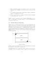
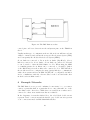
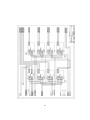
IMS B012 User Guide
and Reference Manual
User Manual
INMOS Limited
January 1988
72-TRN-136-00
You may not:
1. Modify the Materials or use them for any commercial purpose, or any public
display, performance, sale or rental;
2. Remove any copyright or other proprietary notices from the Materials;
This document is distributed in the hope that it will be useful, but WITHOUT
ANY WARRANTY; without even the implied warranty of MERCHANTABILITY
or FITNESS FOR A PARTICULAR PURPOSE.
INMOS, IMS, OCCAM are trademarks of INMOS Limited.
INMOS Limited is a member of the SGS-THOMSON Microelectronics Group.
2
Contents
Preface
5
Disclaimer
5
1 Introduction
6
2 Hardware Description
2.1 Link Connections . . . . . . . . .
2.2 P1 Links . . . . . . . . . . . . . .
2.3 Switch Configuration Transputer
2.4 Reset, Analyse and Error . . . .
2.5 Link Termination . . . . . . . . .
2.6 Error Lights . . . . . . . . . . . .
2.7 User Power Connector . . . . . .
2.8 Uncommitted Pins . . . . . . . .
.
.
.
.
.
.
.
.
.
.
.
.
.
.
.
.
.
.
.
.
.
.
.
.
.
.
.
.
.
.
.
.
.
.
.
.
.
.
.
.
.
.
.
.
.
.
.
.
.
.
.
.
.
.
.
.
.
.
.
.
.
.
.
.
.
.
.
.
.
.
.
.
.
.
.
.
.
.
.
.
.
.
.
.
.
.
.
.
.
.
.
.
.
.
.
.
.
.
.
.
.
.
.
.
.
.
.
.
.
.
.
.
.
.
.
.
.
.
.
.
.
.
.
.
.
.
.
.
6
7
11
13
14
16
17
18
19
3 Configuration
19
3.1 K1 Jumper Block . . . . . . . . . . . . . . . . . . . . . . . . . 19
3.2 SW1 DIL switch . . . . . . . . . . . . . . . . . . . . . . . . . 21
4 Unpacking and Handling
21
4.1 Unpacking the IMS B012 . . . . . . . . . . . . . . . . . . . . 21
4.2 Handling precautions . . . . . . . . . . . . . . . . . . . . . . . 22
4.3 Module Fitting and Handling . . . . . . . . . . . . . . . . . . 23
5 Standard Configurations
5.1 Cables . . . . . . . . . . . . . . . . . . . . .
5.2 DIL Switch . . . . . . . . . . . . . . . . . .
5.3 K1 Standard Configuration . . . . . . . . .
5.4 P1 Connections . . . . . . . . . . . . . . . .
5.5 P2 Connections . . . . . . . . . . . . . . . .
5.6 IMS B012 as a Slave to a Master Controller
5.7 IMS B012 as a System Master . . . . . . . .
.
.
.
.
.
.
.
.
.
.
.
.
.
.
.
.
.
.
.
.
.
.
.
.
.
.
.
.
.
.
.
.
.
.
.
.
.
.
.
.
.
.
.
.
.
.
.
.
.
.
.
.
.
.
.
.
.
.
.
.
.
.
.
.
.
.
.
.
.
.
24
24
26
26
26
28
29
29
6 Example Networks
30
6.1 Four-Connected Matrix . . . . . . . . . . . . . . . . . . . . . 31
6.2 Torus of 16 Processors . . . . . . . . . . . . . . . . . . . . . . 33
7 Testing
34
7.1 T212/C004 Test . . . . . . . . . . . . . . . . . . . . . . . . . 35
7.2 P1 Edge Connector Test . . . . . . . . . . . . . . . . . . . . . 35
A Connector Pinouts
37
3
B Mechanical Details
40
C HL1 Description
42
D Schematic
47
4
Preface
The IMS B012 is a eurocard TRAM motherboard designed to fit into standard card cages such as the INMOS ITEM.
The board is a member of a family of TRAM motherboards which have a
compatible architecture. External signals enable it to control a subsystem
of motherboards, or to be a component of such a subsystem.
For a general description of TRAMs and motherboards, refer to the TRAM
Specification (INMOS Technical Note 29) and Module Motherboard Architecture (INMOS Technical Note 49) manuals. For information on the transputer itself, refer to the Transputer Reference Manual.
The IMS B012 is designed to be compatible with standard INMOS software
such as the Transputer Development System (TDS) and the Module Motherboard Software (MMS). These can run either on a TRAM plugged into
the IMS B012, or on another piece of hardware connected to the IMS B012.
Reference should be made to the TDS user manuals and the MMS User
Manual for details of how to compile and load programs into networks of
TRAMs installed in motherboards.
This manual is divided into three main sections. The first describes the
IMS B012 hardware, detailing the full capabilities of the board. The second
covers installation, handling and configuring the board for the more common
applications and user confidence testing. This section should be read carefully before the IMS B012 is unpacked or power is applied. The last contains
factual details such as the connector pinouts and the full board schematic.
It is assumed that the reader has an understanding of elementary electronics
and a certain understanding of transputers which can be gained from the
documents and manuals mentioned above and referred to in the text.
NOTE: For full information on how to unpack the IMS B012 see section 4.
Disclaimer
Every effort has been made to test the correct operation of this product.
INMOS reserves the right to make changes in specifications at any time and without
notice. The information furnished by INMOS in this publication is believed to be
accurate, but no responsibility is assumed for its use, nor any infringements of
patents or other rights of third parties resulting from its use. No licence is granted
under any patents, trademarks or other rights of the INMOS group of companies.
5
1
Introduction
The IMS B012 is a eurocard TRAM motherboard which is designed to fit
into standard 6U, 220mm deep, DIN41494 (and IEC 297) card cages such as
the INMOS ITEM. It has slots for up to 16 TRAMs. These are transputerbased circuit modules which communicate with the outside world by means
of INMOS serial links (a link is a two-wire serial communications port which
can run at up to 20 MHz).
The smallest TRAM is ”size 1”. Each of the 16 sites for modules on the
IMS B012 will accept a size 1 module. Each module site, or ”slot” has
connections for four INMOS links which are designated link 0, link 1, link 2
and link 3. TRAMs which are larger than size 1 can be mounted on the
B012. A larger module occupies more than one slot and need not use all of
the available link connections provided by the slots which it occupies.
The B012 has two IMS C004 link switch ICs. These devices are able to
connect together links from the slots and 32 links which are available on
an edge connector. The connections can be changed by control data passed
to the board down a configuration link, which may come from some master
system or from one of the TRAMs on the B012 itself.
2
Hardware Description
The 16 module sites or slots provided by the IMS B012 are 16-pin sockets in
accordance with the TRAM Specification (INMOS Technical Note 29). The
slots are numbered as shown on the board silk screen and in figure 1.
Figure 1: IMS B012 slot positions
6
The IMS B012 has two DIN41612 96-way edge connectors, P1 and P2. These
carry almost all signals and power to/from the board and are easily identified
from the board silk screen printing and from figure 1. P2 carries power,
pipeline and configuration links and system control signals (reset and analyse
and error). Full details of the connections to every pin on P1 and P2 are to
be found in appendix A.
NOTE - it is very important that you do not mix up P1 and P2. Unrecoverable damage to the IMS B012 will almost certainly result.
2.1
Link Connections
The link connections to the 16 slots are organised as follows:
Two links from each slot (links 1 and 2) are used to connect the 16 slots as
a 16-stage pipeline (in a pipeline, multiple processors are connected end-toend as in figure 2). The pipeline is actually broken by jumper block K1. K1
will usually be jumpered in the standard way to give a 16-stage pipeline but
can allow other combinations.
Figure 2: A module pipeline
When modules larger than size 1 are used, the pipeline will be broken at the
slots which are underneath large modules. Special plugs, called pipe-jumpers
are provided (figure 3 shows a pipe jumper). These plug into the unused
slot and connect the signals for links 1 and 2 together, thus connecting the
pipeline through to the next TRAM in the chain.
Figure 3: A Pipe-Jumper
Link 1 on slot 0 is wired to an edge connector (P2) and is called PipeHead.
Link 2 on slot 15 is also taken to P2 and is called PipeTail. By connecting
the pipe heads and tails from multiple boards together, a large, multi-board
pipeline is created.
7
The other two links (links 0 and 3) of each slot are, in general, connected
to two IMS C004 programmable link switches (For detailed information on
the IMS C004 see the IMS C004 Link Switch Data Sheet).
The IMS C004 has 32 input pins and 32 output pins, plus an INMOS link
(ConfigLink) used to send configuration information to the IMS C004. Any
of the output pins can be ”connected” to any of the input pins, so a signal
presented on the input pin would be buffered and transmitted on the output
pin (with a slight delay).
The switch connections are made according to information sent to the IMS C004
down its ConfigLink. The two IMS C004s on the IMS B012 allow 64 link
connections to be made under software control.
In most applications using the IMS C004, the device is treated as a 32-way
Link Crossbar. This means that 32 INMOS links, each of which has two
signals, may be connected to each other in an arbitrary fashion. That is
to say that any of the 32 links can be ”connected” via the IMS C004 to
any of the other 31 links. The IMS B012 uses the IMS C004s in a slightly
different way, the difference being that the two signals from any particular
link are routed through different IMS C004 devices. So if the LinkIn signal
comes from one IMS C004, then the LinkOut signal will go to the other
IMS C004. Figure 4 shows the general routing of link signals. A complete
description of how the links on the IMS B012 are connected (in the standard
configuration) is given in appendix C. The full circuit detail is shown on the
schematic (appendix D).
The link output signals from all the link 0s on all the slots (16 signals) are
connected to 16 inputs of one IMS C004 (IC2). The link input signals from
all the link 3s on all the slots (16 signals) are connected to 16 outputs of the
same IMS C004. The remaining 16 inputs and 16 outputs of that IMS C004
are connected to an edge connector (P1).
The other IMS C004 (IC3) is connected similarly, except that 16 of its
inputs are connected to the outputs of all link 3s on all the slots, and 16 of
its outputs are connected to the inputs of all link 0s on all the slots. The
remaining inputs and outputs are connected to P1.
The result of this connection scheme is that any link 0 on any module may
be routed via the IMS C004s to any link 3 on any module, but may not
be routed to any of the link 0s on any other module. The same is true for
link 3s on any modules, they may not be routed to any other link 3. Each
of the links 0 and 3 on any module may be routed to any of half of the link
connections on edge connector P1 (see below).
By hardwiring two of the edge connector links together off the board, any of
the slot link 0s can be routed to another slot link 0, via the two connected
8
Figure 4: Link Organisation - slots to IMS C004s
edge links.
MMS (Module Motherboard System) software which is available for all module motherboards allows the configuration of module interconnection to be
achieved easily from a connection list description of the desired network.
Slot 0 link 0 is not directly connected to its appropriate IMS C004 pins. It
is connected to edge connector P2, along with the respective pins from the
IMS C004s. A link jumper connector which is supplied with the board can
be used to make the connection between slot 0 link 0 and the IMS C004s.
Slot 0 link 0 is taken to P2 in order to provide two links which are directly
connected to module 0 on an edge connector. For some applications it will
be useful to by-pass the IMS C004 switches in this way.
Similarly slot 0 link 3 is connected to pins on jumper-block K1. Usually K1
9
will be configured to connect slot 0 link 3 to the appropriate pins on the two
IMS C004s. Because there are K1 pins which are connected to pins on edge
connector P2, slot 0 link 3 can be wired to the edge connector instead of to
the IMS C004s.
It is possible, using a non-standard configuration of K1, to take links 0, 1
and 3 from slot 0 off the board via P2. This is useful if slot 0 contains a
TRAM which is controlling a system of other TRAMs or transputers.
Figure 5 shows the organisation of the pipeline links and the links which are
available on P2 and K1.
Figure 5: Links Available on P2 and K1
IMS C004 link switches introduce a small delay into the signals which they
switch. If multiple IMS C004s are introduced into a link signal path, as with
multi-board IMS B012 systems, the link data rate may be reduced.
10
2.2
P1 Links
Connector P1 has three rows of 32 pins. All the pins in row ”a” are connected
to ground. All the pins in row ”b” are link inputs and all the pins in
row ”c” are link outputs. At each of the 32 positions along P1, the three
pins from rows a, b and c together carry one link. These signals may be
connected to devices with link ports in any way the user desires, as long as
the correct electrical precautions required when dealing with links are taken
into account. See section 2.5.
A special connector with a small PCB attached and press-fit pins fitted
into this PCB is supplied with the IMS B012. This ”mini-backplane”, when
fitted to P1, allows standard INMOS link cables to be plugged into P1 links.
Note that these link cables are not designed for use in arduous physical
environments (vibration, corrosion and pulling on the cable). This is why
the IMS B012 is provided with standard DIN 41612 connectors. The user
may design a connection method for attaching signals to the board which
best suits the particular application.
The 32 links available on edge connector P1 are numbered, for reference,
starting at ”edge link 0” on pins 1 (a, b and c) through to ”edge link 31” on
pins 32 (a, b and c) (see figure 6). This numbering scheme is for convenience
and there is no obvious mapping between these numbers (the order on the
edge connector) and the links to which they are connected on the IMS C004s.
Figure 6: P1 Connections
As explained in section 2.1, the IMS B012 link switching organisation, using
the two IMS C004s, does not allow complete freedom to connect any link
to any other link. The following table shows which P1 edge connector links
(numbered as above) may be connected to which links on the slots (via the
IMS C004 link switches):
11
P1 Edge Link
To TRAM slot links
0
1
2
3
4
5
6
7
8
9
10
11
12
13
14
15
16
17
18
19
20
21
22
23
24
25
26
27
28
29
30
31
3
3
0
0
0
0
3
3
3
3
0
0
3
0
0
3
3
0
0
3
0
0
3
3
3
3
3
3
0
0
0
0
The link connections on connector P1 are intended mainly for communication between the IMS B012 and other boards. However, it is also possible
to use these P1 links and the IMS C004 link switches to switch link connections for an external system. For instance, two IMS B012 boards in a card
cage, unpopulated with TRAMs, may act as a ”programmable backplane”
to other boards in the card cage. The connections between these boards and
the IMS B012s being hard-wired.
12
2.3
Switch Configuration Transputer
The IMS C004 devices are controlled by an IMS T212 16-bit transputer.
The IMS T212 has four links. Links 0 and 3 are connected to the two
IMS C004s (link 0 to IC2 and link 3 to IC3). Link 1 is available on edge
connector P2 and is called ConfigUp. Link 2 is also available on P2 and is
called ConfigDown. The organisation of these links is shown in figure 7.
Figure 7: Link Configuration Organisation
Configuration data for the IMS C004 is fed into one of the IMS T212’s
links (ConfigUp) from the master configuration system which must be connected to P2. The configuration system could be one of the TRAMs on the
IMS B012, provided that one of its links may be connected to ConfigUp.
The IMS T212 has 2 Kbytes of on-chip RAM. A transputer such as the
IMS T212, after it is reset, is able to treat bytes sent to it down any of its
links as ”boot code”. This is how the IMS T212 on the IMS B012 is used.
13
The configuration host system sends a small program to the IMS T212. The
code is stored in on-chip RAM and takes information from ConfigUp, routes
data out to the two IMS C004s and sends on data out of ConfigDown (if
required). The MMS (Module Motherboard System) handles all these software functions transparently. Full information on the IMS T212 is available
in the IMS T212 Data Sheet.
In a multiple motherboard system it is intended that the ConfigUp and
ConfigDown links from adjacent boards be connected together to form a
configuration daisy-chain (see figure 8). Again the MMS is able to handle
the configuration of multiple-board systems (see the MMS User Manual ).
Figure 8: Multiple-Board Daisy-Chain
This configuration architecture is fully compatible with other INMOS TRAM
motherboards. Multiple board systems may contain different motherboard
types. For instance, an IMS B008 fitted to an IBM PC/XT or PC/AT or
compatible, may be part of a system containing multiple IMS B012 motherboards fitted into a card cage.
2.4
Reset, Analyse and Error
The Reset, Analyse and Error pins of TRAMs (and transputers) will be
referred to collectively as ”system services” in this section. The system service signals are used to reset TRAMs and transputers, to place transputers
in an analyse state (for debugging) and to carry the fact that an error has
occurred in one processor in an array back to some host system which will
14
deal with the error condition.
Some TRAMs and most evaluation boards are capable of generating the system services for other TRAMs and transputers. This is called a ”subsystem”
control capability. The IMS B012 can be connected to another board with
subsystem control and can also accommodate one TRAM with subsystem
control. Furthermore, the IMS B012 can generate subsystem control signals
for other boards.
System services for TRAMs are slightly different to system services for
boards since the Reset and Analyse signals are active low for boards and
active high for TRAMs.
The TRAMs and other circuitry on the IMS B012 splits into two sections
for system services. System services for slot 0 come from the ”Up” pins on
edge connector P2. System services for slots 1 to 15 and IC1 (the IMS T212)
can either come from from ”Up” as slot 0, or from the Subsystem pins of
slot 0, depending upon the state of switch 6.
The IMS T212 Error pin is unconnected so an error condition on IC1 cannot
propagate into the TRAM array.
Note that slot 0 is the only slot which has subsystem pins and that in order
to use these pins it is necessary to have a module with subsystem capability
installed in slot 0. See section 4.3.
The system service signals for slot 0 are buffered and output on edge connector P2 as the ”Down” pins. This allows system services for multiple boards
to be daisy-chained, the ”Down” of one board being connected to the ”Up”
of the next.
Figure 9 shows the complete organisation of the system services (reset, analyse and error) on the board.
Reset and Analyse signals presented to the IMS B012 on connector P2
should have minimum low pulse widths of 1 millisecond. The subsystem
pins of slot 0 are also buffered and are available on edge connector P2 as the
”Subsystem” pins.
The two IMS C004 link switches have a reset pin that is driven by a poweron-reset circuit. The IMS C004s can be also soft-reset by a command from
the IMS T212.
The IMS T212 has 2 Kbytes of on-chip RAM. It also has an external memory
interface. Circuitry on the IMS B012 is connected to the IMS T212’s external
memory interface which allows the reset signal to the IMS C004s to be
controlled from the IMS T212. By writing a one into bit position zero in
any external memory word, the reset signal to the IMS C004s is asserted.
15
Figure 9: IMS B012 System Services Organisation
Similarly, by writing a zero into bit position zero in any external memory
word, the reset signal to the IMS C004s is de-asserted.
Note that if the IMS T212 (IC1) writes to external memory and sets the
IMS C004 reset signal, subsequent resetting of the IMS T212 will not alter
the level of the IMS C004 reset signal. Note also that if the IMS T212 reads
from any location in its external memory space then the IMS C004 reset
signal will be set to an unpredictable level.
2.5
Link Termination
INMOS serial links have two signals, LinkIn and LinkOut. If a link is to be
connected over a distance or between boards then some extra discrete components are needed. The LinkOut signal must be series terminated to match
its load, and the LinkIn should have a diode to VCC for ESD protection and
a pulldown resistor to prevent the receiving transputer booting itself from
a floating LinkIn (see figure 10). The whole question of link connections is
covered in detail in INMOS Technical Note 18.
16
Figure 10: Link Termination and Protection
1. All links on TRAMs have the link termination and protection components on the module. The PipeHead and PipeTail link connections
from P2 are directly connected to the module pins (and are therefore
terminated). Link 0 from slot 0 is also directly connected to P2.
2. The ConfigUp and ConfigDown link connections to the IMS T212 are
connected to P2 via termination and protection components.
3. All the links on P1 (from the IMS C004s) are terminated and protected.
4. The link signals from the IMS C004s which would usually be connected
to link 0 of slot 0 (via the jumper connector on P2) are terminated
and protected.
5. The link signals from the IMS C004s which would usually be connected
to slot 0, link 3 (via K1) are terminated and protected since it is
possible to route these signals directly to an edge connector (P2).
This means that any link available on the edge connector of an IMS B012
is correctly terminated and protected.
2.6
Error Lights
Three yellow LED indicators are mounted on the edge of the board, opposite
P1 (see figure 11). An indicator will be lit when a module asserts its error
pin. One LED, LD1, monitors error from slot 0. The other two LEDs, LD2
and LD3, monitor error from the modules on the front row (not including
slot 0), and back row of slots respectively. The front row is the group of
seven slots situated along the front-panel side of the board (not including
17
slot 0). The back row is the group of eight slots situated along the opposite
edge of the board (see figure 11).
Figure 11: IMS B012 - LEDs
When the IMS B012 is installed in a card cage, LD1 is the lower of the
LEDs; LD2 is the middle one and LD3 is the upper LED.
2.7
User Power Connector
A four pin power connector (designation P3) is mounted near the front edge
of the board as shown in figure 12. P3 is wired to 0V, +5V and via a wide
PCB track to 2 pins on P2. This connector type is the kind used on most
floppy-disk drives and when the appropriate pins on P2 are wired to +12V,
P3 may be used to power disk drives or similar equipment. Users may take
other power signals to P3, such as ECL power supplies.
Figure 12: IMS B012 - P3 Position
Pin 4 is connected to connected to 5V, pins 3 and 2 are connected to 0V,
pin 1 is pins 3a and 3c on P2. Pin 4 is the top pin when the board is viewed
as in figure 12.
These power pins can carry up to 3A of current and pin 1 can have up to
50V with respect to GND.
There is a pin post fitted in one corner of the board (marked GND on the
18
silk screen). This is connected directly to the 0V plane and can be useful
for attaching ’scope probe ground leads.
2.8
Uncommitted Pins
Nine pins on connector P2 are brought to a row of pads near to the connector
at the edge of the board (see figures 13 and 14). These pads, designated P4,
may be hard-wired into any circuitry on the B012 by the user for special
applications. Possible uses would be RS-232 serial lines, analog signals and
extra subsystem control signals. The remaining two pads of P4 are connected
to ground. Pin posts can be inserted into the holes which make up P4.
The posts could take a single-in-line connector similar to those used in the
IMS B012 cable set.
These pins should carry no more than 50mA of current at no more than
25V with respect to GND. Note that these signals, although they are short,
have not been designed to carry analog signals and may be susceptible to
crosstalk.
Figure 13: IMS B012 - P4
3
Configuration
The IMS B012 has a six-way DIL switch (SW1) located between P1 and P2,
and a 10-way header jumper-block located on the front panel. The locations
of K1 and SW1 are shown in figure 15.
3.1
K1 Jumper Block
K1 is a ten by two blocks of pin headers on a 0.1 inch grid. Small twoway connectors (jumpers) plug onto the pins, shorting two adjacent pins
together. A number of these bumpers are supplied with the B012, they are
also widely available from component distributors.
19
Figure 14: IMS B012 - P4 Details
Figure 15: IMS B012 - K1 and SW1
The pins which make up K1 are connected to link connections on some of
the slots and to pins on P2. These connections are shown in appendix A.
K1 allows the module pipeline to be broken between slots 3 and 4, 7 and 8
and 11 and 12.
Two link connections are wired from pins on P2 to pins on K1. These allow
any two of the links available on K1 to be wired to the edge connector.
If a configuration which is not achievable with jumpers is desired then stan-
20
dard mini-wrap wire-wrap connections can be made between the posts of
K1.
3.2
SW1 DIL switch
Each of the six switches which make up SW1 controls one signal on the
board. When a switch is on the signal is low and when the switch is off the
signal is high.
Switch 1 : When on, IC2 and IC3, the IMS C004s, operate at 10 Mbits/sec
link speed. When off, the IMS C004s operate at 20 Mbits/s link speed.
Switch 2 : When on, LinkSpeedB to all slots on the board is low. When
off, LinkSpeedB to all slots on the board is high.
Switch 3 : When on, LinkSpeedA to all slots on the board is low. When
off, LinkSpeedA to all slots on the board is high.
Switch 4 : When on, IC1 (the IMS T212) links 1, 2 and 3 operate at
10 Mbits/s. When off, IC1 links 1, 2 and 3 operate at 20 Mbits/s.
Switch 5 : When on, IC1 (the IMS T212) link 0 operates at 10 Mbits/s.
When off, IC1 links 1, 2 and 3 operate at 20 Mbits/s.
Switch 6 : When on, system services (reset and so on) for slots 1 to 15
comes from P2. When off, system services for slots 1 to 15 come from
the subsystem pins on slot 0.
The TRAMs, IMS C004s and IMS T212 on the IMS B012 can operate with
their links at either 10 Mbits/s or 20 Mbits/s. The configuration switch
controls the link speeds for the TRAMs, the IMS C004s and the IMS T212
separately. In practice it is only of use to operate all the links on the board
at the same speed.
4
Unpacking and Handling
4.1
Unpacking the IMS B012
When you open the packing box in which the IMS B012 is shipped, you will
find:
1. A Packing List which you should check against the box contents immediately.
21
Figure 16: SW1 DIL switch
2. A documentation pack, including this manual.
3. A floppy disk, which contains some test software and example routines.
4. A bag of pipe jumper-plugs.
5. An anti-static box containing the IMS B012 board.
6. A bag containing the standard IMS B012 cable set.
Do not open the box containing the IMS B012 until you have read the section
on handling. Do not connect the IMS B012 to a power supply until you have
read this manual and are fully confident that the connections are correct.
4.2
Handling precautions
To prevent damage from static discharge, certain precautions should be
taken when removing the board from its protective bag:
1. Carefully remove the board from the box, holding the board by the
edges and touching the ground pin (located in one corner of the board).
Avoid touching any components or connections.
22
2. While manipulating switches and jumpers on the board and when
inserting it into an ITEM or card cage, hold the board by its edges
only.
3. Do not change switch settings or link cabling or jumper configuration
when power is applied to the board.
4. If the board is being stored or shipped, standard anti-static handling
precautions should be observed.
NOTE - Under no circumstances plug or unplug a TRAM with power applied to the IMS B012, permanent damage to both the TRAM and the
motherboard could occur.
4.3
Module Fitting and Handling
TRAMs must be carefully installed and removed from the IMS B012, taking special care not to bend any of the module’s pins. The slots on the
IMS B012 have pin 1 marked on the board silk-screen legend as a triangle
(see figure 17). Pin 1 on the module to be installed should be marked, probably also with a triangle. Size 1 TRAMs are orientated alternately, so one
TRAM is reversed to the one next to it. Larger modules are all orientated
the same way round.
Figure 17: Pin 1
NOTE - plugging in a TRAM the wrong way round will/may not result in
the destruction of the module or motherboard.
The IMS B012 has some components mounted on the top (as opposed to
underside) of the board in the positions occupied by some slots (101 -3
23
under slots 6,7 and 14). When plugging a TRAM into these positions it
will probably be necessary to fit ”stand-off” connectors to the TRAM pins.
These are 8-way pin strips which plug into the IMS B012 and into which the
TRAM plugs and raise the module above the motherboard, thus clearing
the tops of the components on the motherboard. These stand-off strips are
supplied fitted to INMOS TRAMs.
It is possible to remove IC1-3 and gain extra space under slots 6, 7 and
14. Some types of TRAM may then be mounted in any (or all) of the slots
on the board without exceeding the inter-motherboard height restriction.
Of course, the ability to use any link connections which are made via the
IMS C004s or IMS T212 is lost. If these ICs are to be removed, please
proceed carefully and use the correct PGA removal tool.
When the IMS B012, with TRAMs fitted, is likely to be subjected to vibration or thermal cycling then the TRAMs should be securely fastened to the
IMS B012. There are holes drilled adjacent to each slot. Nylon bolts may
be fitted through these holes to bolt down the TRAMs securely.
If a TRAM with Subsystem capability is to be installed in slot 0 (the only
slot with sockets for the subsystem pins), then the three-pin strip supplied
with the module must be fitted so that the three sockets on the module
are connected to the three sockets on the motherboard. If a TRAM with
subsystem capability is installed in a slot without subsystem capability then
the three-pin strip must not be fitted.
5
Standard Configurations
The IMS B012 is designed to cover a very wide range of application types
and has a large degree of user configuration. This section gives a standard
configuration which is useful as a starting point and for testing the board’s
operation.
5.1
Cables
INMOS has developed a standard cable set for evaluation boards. Link
cables have 5-pin single-in-line connectors at each end with a key pin. Reset
cables have 5-pin single-in-line connectors at each end with two key pins.
The cables are available in a range of lengths. Using this system it is quick
and easy to connect links and reset signals from board to board and system
to system. These cables must not be used between equipment on different
mains circuits and ideally should only be used within one system operating
from the same 5V power supply.
24
The connectors on all INMOS boards and modules are designed to be compatible with these cables. The IMS B012 is provided with a cable set which
includes many short link cables (which can be used to link edge links to each
other), some standard and long link cables (which can be used to connect
multiple boards together), a power cable, some system services cables (reset,
analyse and error) and two DIN 41612 connectors which when plugged into
P1 and P2 allow cables to be connected to the board. Figure 18 shows the
power cable.
Figure 18: Power Cable
One of these DIN 41612 96-way connectors has a mini-backplane with headerpins. This connector must be plugged into P1 if INMOS link cables are to
be used on P1 links. This mini-backplane is pictured in figure 19.
Figure 19: Mini-Backplane
The other DIN 41612 connector in the standard IMS B012 cable set is a
back-to-back plug with some pins cut short and some pins sleeved (shown
in figure 20). These are to mate with the keying on INMOS cables. This
assembly goes into P2.
Figure 20: Back-to-Back Connector
If extra INMOS cables are required, contact either INMOS or your local
Sales Office for ordering details.
25
5.2
DIL Switch
Five of the DIL switches allow the board link speed to be set to either
10 Mbits/s or 20 Mbits/s. The other switch enables or disables the subsystem pins of slot 0 to control the other slots. Figure 21 shows the switch
settings for links operating at 10 Mbits/s and with system control for slots
1-15 from the ”Up” pins on P2.
Figure 21: DIL Switch
5.3
K1 Standard Configuration
Figure 22 is the jumper configuration for K1 which connects all 16 TRAMs
in a pipeline.
5.4
P1 Connections
P1 takes 32 links off the board. With one of the mini-backplane connectors
mentioned above plugged into P1, link cables may be connected to P1.
It must be remembered that any one of the links on P1 may only be connected to half of the links available on the slots, so a P1 link chosen at
random may not be connectable to the slot link desired.
If a processor network which requires slot link 0s to be connected to each
other or link 3s to be connected to each other then short link cables can be
26
Figure 22: K1 Standard Configuration
used to connect 16 links on P1 to 16 other links on P1. The desired connections can then be made via the edge connector links. The recommended
configuration is shown below:
(a) For link 0 to link 0 connections:
Connect Edge Link
To Edge Link
2
4
10
13
17
20
28
30
3
5
11
14
18
21
29
31
(b) For link 3 to link 3 connections:
27
Connect Edge Link
To Edge Link
0
6
8
12
16
22
24
26
1
7
9
15
19
23
25
27
The MMS is able to take a network description which contains connections not available on the IMS B012 (such as a link 0 to link 0 connection)
and make these connections by routing them via edge links on P1. These
link connections would be routed from the slot to the edge link via the
IMS C004s, then via a cable on P1 to another edge link on P1 and finally
from that edge link to the other slot via the IMS C004s.
The MMS has a list of possible edge to edge connections available to it to
make connections of this type. This list is the same as the list above. If
a mini-backplane fitted with short link cables linking the edge links in the
way described above is fitted to the IMS B012, then the MMS will be able
to route these otherwise unavailable connections.
A ready-assembled mini-backplane with short link cables fitted, as detailed
above, is included in the standard IMS B012 cable set. This connection
arrangement is also used for one of the IMS B012 confidence tests.
5.5
P2 Connections
If the IMS B012 is to be used in an INMOS ITEM card cage then P2
connections are easy. The ITEM supplies power and has a built-in back-toback connector which allows link and reset cables to be connected to P2.
Thus the board can be removed easily from the card cage.
However, if the board is to be used stand-alone or in a card cage other than
an ITEM, the back-to-back D1N41612 connector supplied may be useful
(see figure 20). The purpose of this connector is to allow multiple small
leads (link cables and reset cables) to be plugged and unplugged at the
same time. In addition the back-to-back connector has keying pins either
removed or sleeved to make it difficult to orientate standard INMOS link
and reset cables incorrectly. Figure 24 shows the back-to-back connector
pins as viewed from the ”rear”, i.e. looking towards the pins. The boxes
represent plugged-in cables.
28
A good 5V power supply must be connected to the appropriate pins on P2.
To make this easier a power cable is provided with the IMS B012 (see figure
18). The power cable can be identified by its two 5mm plugs, one red and
one black. The red plug should be connected to the +5V terminal of the
power supply, the black plug should be connected to the 0V terminal of the
power supply. The current required by the IMS B012 depends upon what
TRAMs are installed but your power supply should be rated to at least 3A.
The maximum current requirement of one IMS B012 board is 13A. Do not
use an extension cable for the power leads, long cables will give reduced
voltage on the board and unreliable operation.
NOTE - connecting the power plugs the wrong way round or operating
the board from a sub-standard power supply can result in the permanent
destruction of the IMS B012 and TRAMs installed.
Usually slot 0 link 0 needs to be connected to links 22 on the IMS C004s.
This standard configuration requires a connection to be made via P2. A
single connector assembly is available in the standard IMS B012 cable set
(termed the ”yellow” link jumper plug, shown in figure 23). The position of
the jumper is shown in figure 24.
Users may wish to access slot 0, link 0 from P2, in this case the ”yellow”
link jumper plug is not needed.
Figure 23: ”Yellow Link Jumper Plug”
5.6
IMS B012 as a Slave to a Master Controller
In a standard configuration where the IMS B012 is connected to a mastercontrol system such as an IMS B004 or IMS B008, PipeHead and ConfigUp
links would be connected to two links on the host system, with ”Up” system
control port connected to the ”Subsystem” port of the host (figure 24).
5.7
IMS B012 as a System Master
If a TRAM with ”subsystem” capability is installed in slot 0 then the
IMS B012 can act in a stand-alone or master role. With switch 6 set off, the
system control to the other modules on the board and the ”Down” system
29
Figure 24: The IMS B012 as a slave
control pins on P2 are driven from the subsystem pins on the TRAM in
slot 0.
Usually in this type of configuration the module in slot 0 will have at least
1 Mbyte of memory and can run the transputer Development System (TDS)
and consequently the Module Motherboard System (MMS).
Slot 0, link 0 is connected to P2 as is slot 0, link 1 (PipeHead). Slot 0,
link 2 is connected to slot 1, link 1. Slot 0, link 3 is connected to K1 and
so can be wired to either the IMS C004s or to P2. When using the MMS
or a similar system, slot 0, link 0 can be connected to ”ConfigUp” (link 1
of the IMS T212) via a short link cable connected to P2. This will allow
the module in slot 0 to configure the array (via its link 0), to communicate
with a host system such as an IBM PC/XT/AT or compatible via link 1
and to communicate with the other modules on the board and with other
motherboards via links 2 and 3.
6
Example Networks
The IMS B012 does not provide ”unlimited connectivity”, i.e. you cannot
connect a particular link on a particular slot to any particular one of the
other links on the other slot s. While there are restrictions on what can be
connected to what, most useful networks are realisable.
In the diagrams of networks which follow, the solid black double arrows
represent ”hard” connections and the shaded, grey double arrows represent
”soft” connections made via IMS C004 link switches.
30
Figure 25: P2
”HL1” descriptions for these networks are shown. HL1 is the network description language used by the Module Motherboard System (MMS).
6.1
Four-Connected Matrix
This array retains the 16-slot pipeline and connects links 0 and 3 on each
slot so as to connect the slots in a square matrix. Links from each side of the
array are brought to the edge connector (P1) so the array can be extended
31
Figure 26: Four-Connected Matrix
”lengthways” by using multiple IMS B012 boards. Obviously size 1 modules
are required to realise this array.
Here is the ”HL1” description required for the MMS to configure this array:
SOFTWIRE
SLOT
0,0
SLOT
0,3
SLOT
4,3
SLOT
8,3
SLOT 12,3
SLOT
1,0
SLOT
1,3
SLOT
5,3
SLOT
9,3
SLOT 13,3
SLOT
2,0
SLOT
2,3
SLOT
6,3
SLOT 10,3
TO
TO
TO
TO
TO
TO
TO
TO
TO
TO
TO
TO
TO
TO
EDGE
SLOT
SLOT
SLOT
EDGE
EDGE
SLOT
SLOT
SLOT
EDGE
EDGE
SLOT
SLOT
SLOT
2
4,0
8,0
12,0
6
3
5,0
9,0
13,0
7
4
6,0
10,0
14,0
32
SLOT
SLOT
SLOT
SLOT
SLOT
SLOT
END
6.2
14,3
3,0
3,3
7,3
11,3
15,3
TO
TO
TO
TO
TO
To
EDGE
EDGE
SLOT
SLOT
SLOT
EDGE
8
5
7,0
11,0
15,0
9
Torus of 16 Processors
Figure 27: Torus
This network, while being of little practical use since no connections are
available to the outside, does illustrate the use of K1 and external edge
connections in realising a connection pattern not available with a pipeline.
Slot 3 link 2 is jumpered via K1 to P1 and then wired via a short link cable
on P1 to PipeHead (slot 0 link 1). Slot 4 and 7 and 11 and 8 are connected
via K1 as shown in figure 28. Slot 12 link 1 is jumpered via K1 to P1 and
then wired via a short link cable to slot 15 link 2 (PipeTail).
33
Figure 28: K1 Configuration for Torus
Here is the ”HL1” description required for the MMS to configure this array:
SOFTWIRE
SLOT
0,0
SLOT
0,3
SLOT
4,3
SLOT
8,3
SLOT
1,0
SLOT
1,3
SLOT
5,3
SLOT
9,3
SLOT
2,0
SLOT
2,3
SLOT
6,3
SLOT 10,3
SLOT
3,0
SLOT
3,3
SLOT
7,3
SLOT 11,3
END
7
TO
TO
TO
TO
TO
TO
TO
TO
TO
TO
TO
TO
TO
TO
TO
TO
SLOT
SLOT
SLOT
SLOT
SLOT
SLOT
SLOT
SLOT
SLOT
SLOT
SLOT
SLOT
SLOT
SLOT
SLOT
SLOT
12,3
4,0
8,0
12,0
13,3
5,0
9,0
13,0
14,3
6,0
10,0
14,0
14,3
7,0
11,0
15,0
Testing
The user can perform a confidence test on the IMS B012, provided that the
following equipment is available:
1. A PC or compatible computer, fitted with a board capable of running
34
the TDS - an IMS B004 or IMS B008 fitted with an appropriate TRAM
(IMS B403, IMS B404 or IMS B405).
2. A set of test software routines for the IMS B012 (supplied). You will
need to have the test programs in the current directory, ready to run
the tests. The test programs are run directly from MS-DOS (PC-DOS)
and do not require the TDS.
In the following procedure, links from the board in the PC (IMS B004 or
TRAM on an IMS B008) will be referred to as ”link 0”, ”link 1” and so on.
The link speed of the master board in the PC must be set to 10 Mbits/s.
This is the standard speed for an IMS B004.
The IMS B012 must be configured as in the Standard Configurations section
of this manual (Switches, K1 and P2 connections).
A board which does not pass these tests certainly does not function, or is
incorrectly configured. A board which does pass these tests, on the other
hand, may be faulty in some function not tested.
7.1
T212/C004 Test
This test will confirm that there is power applied to the board, that the clock
is present and that connections are made correctly to the testing board.
To run the test, first connect link 1 to ConfigUp on the B012 and link 2 to
ConfigDown on the B012. Connect ”subsystem” from the testing system to
”Up” on the B012.
Power up the IMS B012.
Run the program T2TEST (type T2TEST <CR>). The results of the test are
displayed on the screen and are self-explanatory.
7.2
P1 Edge Connector Test
This test will confirm that there is power applied to the board, that the
clock is present and that connections to P1 are functioning. It also tests the
IMS C004s fairly thoroughly and exercises the IMS T212, as does the first
test.
You will need a mini-backplane with short link cables plugged into it in the
way detailed in section 5.3. Now remove the short link cable which connects
”edge 0” to ”edge 1” on the mini-backplane. Plug the mini-backplane into
P1 on the IMS B012
35
To run the test, first connect link 2 to ”edge 0” on P1 and link 3 to ”edge 1”
on P1. Connect ”subsystem” from the testing system to ”Up” on the B012.
Power up the IMS B012.
Run the program EDGETEST (type EDGETEST <CR>). The results of the test
are displayed on the screen and are self-explanatory.
36
A
Connector Pinouts
Pins connections for P1, P2 and K1 are shown, note that for P1 and P2
these tables list row c first, then row b and then row a; thus the tables show
the visual location of the pins when the connectors are viewed from the rear.
1
2
3
4
5
6
7
8
9
10
11
12
13
14
15
16
17
18
19
20
21
22
23
24
25
26
27
28
29
30
31
32
c
IC3linkout0
IC3linkout2
IC3linkout4
lC3linkout5
IC3linkout6
IC3linkout3
IC3linkout1
IC3linkout7
IC3linkout29
IC3linkout30
IC3linkout31
IC3linkout28
IC3linkout24
IC3linkout25
IC3linkout26
IC3linkout27
IC3linkout17
IC3linkout19
IC3linkout22
IC3linkout23
IC3linkout16
IC3linkout18
IC3linkout21
IC3linkout20
IC3linkout10
IC3linkout13
IC3linkout14
IC3linkout11
IC3linkout8
IC3linkout9
IC3linkout12
IC3linkout15
b
IC2linkin0
IC2linkin2
IC2linkin4
IC2linkin5
IC2linkin6
IC2linkin3
IC2linkin1
IC2linkin7
lC2linkin29
IC2linkin30
IC2linkin31
IC2linkin28
IC2linkin24
IC2linkin25
IC2linkin26
IC2linkin27
IC2linkin17
IC2linkin19
IC2linkin22
IC2linkin23
IC2linkin16
IC2linkin18
IC2linkin21
IC2linkin20
IC2linkin10
IC2linkin13
IC2linkin14
IC2linkin11
IC2linkin8
IC2linkin9
IC2linkin12
IC2linkin15
Table 1: P1 pinout
37
a
GND
GND
GND
GND
GND
GND
GND
GND
GND
GND
GND
GND
GND
GND
GND
GND
GND
GND
GND
GND
GND
GND
GND
GND
GND
GND
GND
GND
GND
GND
GND
GND
1
2
3
4
5
6
7
8
9
10
11
12
13
14
15
16
17
18
19
20
21
22
23
24
25
26
27
28
29
30
31
32
c
GND
VCC
PAUX
VCC
GND
VCC
GND
nc
slot0linkout1
slot0linkin1
GND
nc
GND
nc
IC1linkout1
IC1linkin1
GND
nc
P4/3
P4/4
P4/5
P4/6
P4/7
P4/8
P4/9
P4/10
nc
notUpReset
notUpAnalyse
notUpError
GND
GND
b
GND
VCC
nc
VCC
GND
VCC
GND
nc
slot0linkout0
slot0linkin0
GND
nc
GND
nc
IC3linkout22
IC2linkin22
GND
nc
nc
nc
GND
nc
K1/11
K1/10
GND
nc
GND
nc
K1/3
K1/18
GND
GND
Table 2: P2 pinout
38
a
GND
VCC
PAUX
VCC
GND
VCC
GND
nc
slot15linkout2
slotl5linkin2
GND
nc
GND
nc
IC1linkout2
IC1linkin2
GND
nc
P4/2
nc
nc
notSubReset
notSubAnalyse
notSubError
GND
nc
nc
notDownReset
notDownAnalyse
notDownError
GND
GND
1
2
3
4
5
6
7
8
9
10
IC3linkin23
slot0linkout3
P2/29b
slot12linkout1
slot11linkin2
slot8linkout1
slot7linkin2
slot4linkout1
slot3linkin2
P2/24b
20
19
18
17
16
15
14
13
12
11
IC2linkout23
slot0linkin3
P2/30b
slot12linkin1
slot11linkout2
slot8linkin1
slot7linkout2
slot4linkin1
slot3linkout2
P2/23b
Table 3: K1 pinout
39
B
Mechanical Details
The IMS B012 is designed to accord with DIN 41494 and IEC 297 standards.
Nominal board thickness is 1.6mm. The supplied front panel width is 4HP
(approx. 20mm). This is compatible with a board-to-board pitch in a card
cage of 0.8in. M2.5 fastening bolts are provided on the front panel, these
mates with tapped holes in the card cage and fix the board securely. Front
panel handles allow the board to be removed from the card cage (by unscrewing the retaining bolts and pulling hard on the handles). Note that
the front panel is required when operating the IMS B012 in a card cage,
both for mechanical rigidity and to give correct cooling air flow.
No components protrude more than 2.47mm below the surface of the board.
To fit in a 0.81n pitch rack, no component should protrude more than
13.7mm above the surface of the board. This is a function of the modules
installed on the board.
Adequate cooling air flow must be provided to maintain the components on
the board within their operating temperature. Air flow should run parallel
to the board surface and parallel to the front panel. The amount of heat
dissipated by the board depends upon the TRAMs fitted. With no modules
the IMS B012 dissipates no more than 3W. With modules fitted, the maximum dissipation (from 5v supply) is 67.5W. The cooling air flow required
for a particular application will probably need to be determined empirically.
40
A single board operating in static air at room temperature (and not in a
rack) will usually not need forced air cooling. This kind of set-up should
only be used for lab work and development work. High reliability is not
to be expected from boards which are not provided with adequate cooling.
Some TRAM types may require forced air cooling if they have high power
dissipation components such as very fast PALS and fast A-D converters.
The two DIN 41612 (603-2-IEC-C096Mx-xxx) connectors (P1 and P2) have
class 2 contact finish (1 micron gold) and are specified to give 400 mating
cycles minimum.
41
C
HL1 Description
Listed below is the ”HL1” description file for the IMS B012. This file is
used by the MMS (Module Motherboard System) and completely describes
the link connectivity of the board in the standard configuration.
SIZES
T2 1
C4 2
SLOT 16
EDGE 32
END
T2CHAIN
T2 0, LINK 0
T2 0, LINK 3
END
HARDWIRE
SLOT 0,
SLOT 1,
SLOT 2,
SLOT 3,
SLOT 4,
SLOT 5,
SLOT 6,
SLOT 7,
SLOT 8,
SLOT 9,
SLOT 10,
SLOT 11,
SLOT 12,
SLOT 13,
SLOT 14,
LINK
LINK
LINK
LINK
LINK
LINK
LINK
LINK
LINK
LINK
LINK
LINK
LINK
LINK
LINK
C4 0
C4 1
2
2
2
2
2
2
2
2
2
2
2
2
2
2
2
TO
TO
TO
TO
TO
TO
TO
TO
TO
TO
TO
TO
TO
TO
TO
SLOT
SLOT
SLOT
SLOT
SLOT
SLOT
SLOT
SLOT
SLOT
SLOT
SLOT
SLOT
SLOT
SLOT
SLOT
1,
2,
3,
4,
5,
6,
7,
8,
9,
10,
11,
12,
13,
14,
15,
LINK
LINK
LINK
LINK
LINK
LINK
LINK
LINK
LINK
LINK
LINK
LINK
LINK
LINK
LINK
1
1
1
1
1
1
1
1
1
1
1
1
1
1
1
C4 0, LINK 22,I TO SLOT
C4 1, LINK 22,O TO SLOT
0, LINK 0,O
0, LINK 0,I
C4 1, LINK 23,I TO SLOT
C4 0, LINK 23,O TO SLOT
0, LINK 3,O
0, LINK 3,I
C4 0, LINK
C4 1, LINK
5,I TO SLOT
5,O TO SLOT
1, LINK 0,O
1, LINK 0,I
C4 1, LINK
2,I TO SLOT
1, LINK 3,O
42
C4 0, LINK
2,O TO SLOT
1, LINK 3,I
C4 0, LINK
C4 1, LINK
4,I TO SLOT
4,O TO SLOT
2, LINK 0,O
2, LINK 0,I
C4 1, LINK
C4 0, LINK
0,I TO SLOT
0,O TO SLOT
2, LINK 3,O
2, LINK 3,I
C4 0, LINK 19,I TO SLOT
C4 1, LINK 19,O TO SLOT
3, LINK 0,O
3, LINK 0,I
C4 1, LINK 17,I TO SLOT
C4 0, LINK 17,O TO SLOT
3, LINK 3,O
3, LINK 3,I
C4 0, LINK 18,I TO SLOT
C4 1, LINK 18,O TO SLOT
4, LINK 0,O
4, LINK 0,I
C4 1, LINK 21,I TO SLOT
C4 0, LINK 21,O TO SLOT
4, LINK 3,O
4, LINK 3,I
C4 0, LINK
C4 1, LINK
3,I TO SLOT
3,O TO SLOT
5, LINK 0,O
5, LINK 0,I
C4 1, LINK
C4 0, LINK
1,I TO SLOT
1,O TO SLOT
5, LINK 3,O
5, LINK 3,I
C4 0, LINK
C4 1, LINK
6,I TO SLOT
6,O TO SLOT
6, LINK 0,O
6, LINK 0,I
C4 1, LINK
C4 0, LINK
7,I TO SLOT
7,O TO SLOT
6, LINK 3,O
6, LINK 3,I
C4 0, LINK 16,I TO SLOT
C4 1, LINK 16,O TO SLOT
7, LINK 0,O
7, LINK 0,I
C4 1, LINK 20,I TO SLOT
C4 0, LINK 20,O TO SLOT
7, LINK 3,O
7, LINK 3,I
C4 0, LINK
C4 1, LINK
9,I TO SLOT
9,O TO SLOT
8, LINK 0,O
8, LINK 0,I
C4 1, LINK 14,I TO SLOT
C4 0, LINK 14,O TO SLOT
8, LINK 3,O
8, LINK 3,I
C4 0, LINK 28,I TO SLOT
C4 1, LINK 28,O TO SLOT
9, LINK 0,O
9, LINK 0,I
C4 1, LINK 29,I TO SLOT
C4 0, LINK 29,O TO SLOT
9, LINK 3,O
9, LINK 3,I
43
C4 0, LINK 31,I TO SLOT 10, LINK 0,O
C4 1, LINK 31,O TO SLOT 10, LINK 0,I
C4 1, LINK 30,I TO SLOT 10, LINK 3,O
C4 0, LINK 30,O TO SLOT 10, LINK 3,I
C4 0, LINK 15,I TO SLOT 11, LINK 0,O
C4 1, LINK 15,O TO SLOT 11, LINK 0,I
C4 1, LINK 11,I TO SLOT 11, LINK 3,O
C4 0, LINK 11,O TO SLOT 11, LINK 3,I
C4 0, LINK 12,I TO SLOT 12, LINK 0,O
C4 1, LINK 12,O TO SLOT 12, LINK 0,I
C4 1, LINK 13,I TO SLOT 12, LINK 3,O
C4 0, LINK 13,O TO SLOT 12, LINK 3,I
C4 0, LINK 25,I TO SLOT 13, LINK 0,O
C4 1, LINK 25,O TO SLOT 13, LINK 0,I
C4 1, LINK 27,I TO SLOT 13, LINK 3,O
C4 0, LINK 27,O TO SLOT 13, LINK 3,I
C4 0, LINK 26,I TO SLOT 14, LINK 0,O
C4 1, LINK 26,O TO SLOT 14, LINK 0,I
C4 1, LINK 24,I TO SLOT 14, LINK 3,O
C4 0, LINK 24,O TO SLOT 14, LINK 3,I
C4 0, LINK
C4 1, LINK
8,I TO SLOT 15, LINK 0,O
8,O TO SLOT 15, LINK 0,I
C4 1, LINK 10,I TO SLOT 15, LINK 3,O
C4 0, LINK 10,O TO SLOT 15, LINK 3,I
C4 1, LINK
C4 0, LINK
0,O TO EDGE
0,I TO EDGE
0,I
0,O
C4 1, LINK
C4 0, LINK
2,O TO EDGE
2,I TO EDGE
1,I
1,O
C4 0, LINK
C4 1, LINK
4,O TO EDGE
4,I TO EDGE
2,I
2,O
C4 0, LINK
C4 1, LINK
5,O TO EDGE
5,I TO EDGE
3,I
3,O
44
C4 0, LINK
C4 1, LINK
6,O TO EDGE
6,I TO EDGE
4,I
4,O
C4 0, LINK
C4 1, LINK
3,O TO EDGE
3,I TO EDGE
5,I
5,O
C4 1, LINK
C4 0, LINK
1,O TO EDGE
1,I TO EDGE
6,I
6,O
C4 1, LINK
C4 0, LINK
7,O TO EDGE
7,I TO EDGE
7,I
7,O
C4 1, LINK 29,O TO EDGE
C4 0, LINK 29,I TO EDGE
8,I
8,O
C4 1, LINK 30,O TO EDGE
C4 0, LINK 30,I TO EDGE
9,I
9,O
C4 0, LINK 31,O TO EDGE 10,I
C4 1, LINK 31,I TO EDGE 10,O
C4 0, LINK 28,O TO EDGE 11,I
C4 1, LINK 28,I TO EDGE 11,O
C4 1, LINK 24,O TO EDGE 12,I
C4 0, LINK 24,I TO EDGE 12,O
C4 0, LINK 25,O TO EDGE 13,I
C4 1, LINK 25,I TO EDGE 13,O
C4 0, LINK 26,O TO EDGE 14,I
C4 1, LINK 26,I TO EDGE 14,O
C4 1, LINK 27,O TO EDGE 15,I
C4 0, LINK 27,I TO EDGE 15,O
C4 1, LINK 17,O TO EDGE 16,I
C4 0, LINK 17,I TO EDGE 16,O
C4 0, LINK 19,O TO EDGE 17,I
C4 1, LINK 19,I TO EDGE 17,O
C4 0, LINK 22,O TO EDGE 18,I
C4 1, LINK 22,I TO EDGE 18,O
C4 1, LINK 23,O TO EDGE 19,I
C4 0, LINK 23,I TO EDGE 19,O
45
C4 0, LINK 16,O TO EDGE 20,I
C4 1, LINK 16,I TO EDGE 20,O
C4 0, LINK 18,O TO EDGE 21,I
C4 1, LINK 18,I TO EDGE 21,O
C4 1, LINK 21,O TO EDGE 22,I
C4 0, LINK 21,I TO EDGE 22,O
C4 1, LINK 20,O TO EDGE 23,I
C4 0, LINK 20,I TO EDGE 23,O
C4 1, LINK 10,O TO EDGE 24,I
C4 0, LINK 10,I TO EDGE 24,O
C4 1, LINK 13,O TO EDGE 25,I
C4 0, LINK 13,I TO EDGE 25,O
C4 1, LINK 14,O TO EDGE 26,I
C4 0, LINK 14,I TO EDGE 26,O
C4 1, LINK 11,O TO EDGE 27,I
C4 0, LINK 11,I TO EDGE 27,O
C4 0, LINK
C4 1, LINK
8,O TO EDGE 28,I
8,I TO EDGE 28,O
C4 0, LINK
C4 1, LINK
9,O TO EDGE 29,I
9,I TO EDGE 29,O
C4 0, LINK 12,O TO EDGE 30,I
C4 1, LINK 12,I TO EDGE 30,O
C4 0, LINK 15,O TO EDGE 31,I
C4 1, LINK 15,I TO EDGE 31,O
END
46
D
Schematic
47
48
49
50
51
52