1
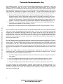
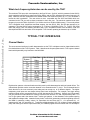
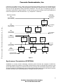
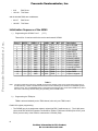
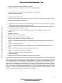
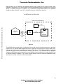
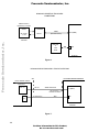
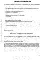
Freescale Semiconductor
Order this document by
AN2031
MC68360
Applications Information
Freescale Semiconductor, Inc...
Interfacing the 68360 (QUICC) to T1/E1 Systems
By: Al Chame’, Technical Sales Engineer
San Jose, CA
Communications controllers are becoming increasingly sophisticated systems which are integrated on a single
silicon chip. It is truly remarkable to witness the numerous functions and features supported by the silicon
solution. The level of integration has provided the flexibility to transport different protocols, and to connect to
and process multiple wide band communications channels emanating from potentially diverse interfaces.
The introduction of the Freescale MC68360 communications controller offers system designers exceptional
flexibility and control of communications systems. The MC68360 provides revolutionary control and flexibility
to a system designer. It has become challenging for the system designer to harness the enormous capacity
and functionality of such a device. This, combined with the freedom to interface to different systems such as
PBXs, LANs, WANs, point-to-point links, Routers, Bridges, and digital public data networks such as the T1/E1
systems, adds to the complexity of the task. The diverse interface flexibility raises the importance of a thorough
understanding of these interfaces and the power and sophistication of the resources available on the MC68360
controller. This document serves to introduce the numerous features offered on the MC68360 controller so the
designer can effectively harness the available resources in serving different system interfaces. One interface
which receives great interest because of its ubiquitous applications is the T1/E1 system and compatible formats.
Compatible formats are: ISDN- both Primary and Basic rate, T1 DSU/CSUs, Digital Cross-Connect systems,
customer premise multiplexers, bridge/routers, SMDS and other public data networks equipment.
This article examines and illustrates various scenarios of interfacing the Freescale MC68360 controller to typical
T1/E1 systems. Representative connections of T1/E1 serial data stream interfaces are illustrated to clarify its
distinctive features. Applications ranging from the simplest interface to more complex and sophisticated
interfaces are discussed. This will help one to better understand the MC68360 controller features and the
interfaces it supports/implements.
T1/E1 SYSTEMS INTERFACE METHODOLOGY
Single or multiplexed high-speed T1/E1 lines are easily connected to the 68360 via the SI (serial interface). The
SI permits connection of the MC68360's six serial channels (four SCCs and the two SMCs) to their own set of
individual pins, or to TDM (time division multiplex) channels. Each SCC or SMC thus may be independently
connected to the TDM or to its own external pins. The NMSI (Non-multiplex serial interface) and TSA (Time
Slot Assigner) connection features of the SI make this setup possible. The NMSI allows the SCC/SMC to be
connected to its own dedicated external individual pins. The decision to connect a given SCC to the NMSI is
made in the SICR register of the 68360. Likewise, the decision to connect a given SMC to the NMSI is made
© Freescale Semiconductor, Inc., 2004. All rights reserved.
Freescale Semiconductor, Inc.
in the SIMODE register. The TSA, on the other hand, allows programming any combination of SCCs and
SMCs to multiplex their data on to one or two full duplex TDM channels which can be supported
simultaneously. The TSA identifies a TDM channel using sync pulses and clock signals provided by the user,
and implements the internal route selection. The TSA implements accordingly both the internal route selection
and time-division multiplexing for multiplexed serial channels. The two TDMs interfaces must first be
connected to the TSA for proper operations. To accomplish this, The TSA may be programmed as follows:
1.) Enable the TDM channels and select either: Static Frames (frames in which the routing is not
changed frequently, and any TDM routing changes require all SCCs/SMCs connected to the TSA be
disabled) or Dynamic Frames (TDM routing changes can be realized while the SCCs/SMCs are connected to the TSA) operation. Dynamic frames provide significant flexibility in dynamic system reconfiguration. Select this configuration by programming the SIGMR (SI Global Mode Register).(7.8.5.1)
Freescale Semiconductor, Inc...
2.) Enable the clock routing to the SMC channels and synchronous/ asynchronous TDM operations by
programming the SIMODE (SI mode register). (7.8.5.2)
3.) Enable the clock routing to the SCCs by programming the SICR ( SI clock route register). (7.8.5.3)
In its most flexible mode, the TSA can provide two separate TDM channels, each with independent transmit
and receive routings, and independent sync and clock inputs. Thus, the TSA can support two independent
full-duplex or four independent half duplex TDMs, two for transmit and two for receive, each with their own
independent sync and clock inputs. Additionally, the TSA will also support multiplexing data from channels /
devices which do not form part of the SCCs or SMCs, by utilizing up to four special programmable Strobe
signals that may be asserted on a bit basis or a byte basis. This provides extra flexibility in supporting devices
which do not reside on-chip.
Once the TSA connections are established, the exact routing decisions are made by initializing the TSA timeslot in the SI RAM. This requires two SI RAM entries: one used for the transmit routing and the other for the
receive routing. The two SI RAMs entries provide the clocking assignment for each SCC/SMC, and connect
the SCC/SMCs to the TSA. These SI RAMs locations are directly accessible by the host processor in the
internal section of the QUICC and are not associated with the on-board dual-port RAM. It is to be noted that
the TSA time-slot programming is completely independent of the protocol used either by the SCCs or the
SMCs.
The size of SI RAM available for time-slot programming is dependent on the nature of the time-slot
programming used. The programming can be implemented for either Static or Dynamic Frames. There are
four possible TSA RAM configurations specified below:
1.) One TDM multiplexed channel with Static Frames: 64 entries for the transmit routing and 64 for the receive routing.
2.) One TDM multiplexed channel with Dynamic Frames: 32 entries fortransmit and 32 for receive.
3.) Two TDM multiplexed channels with Static Frames: 32 entries for transmit and 32 for receive.
4.) Two TDM multiplexed channels with Dynamic Frames: 16 entries for transmit and 16 for receive.
For proper operation, the SI RAM should be initialized before enabling the multiplexed channels. It is
worthwhile to mention that the SI RAM also supports two testing modes, echo and loop-back mode. Echo
retransmits the signal it has received and the loopback mode causes the physical interface to receive the
same signal it is transmitting.
2
For More Information On This Product,
Go to: www.freescale.com
Freescale Semiconductor, Inc.
What clock frequency/data rates can be used by the TSA?
Freescale Semiconductor, Inc...
The maximum TSA input clock rate depends on the SynCLK rate. SynCLK, which is generated in the QUICC
clock synthesizer specifically to support the SCCs, SMCs, and the TSA, defaults to the system frequency (25
Mhz). However, the clock synthesizer in the SIM60 module can divide the SynCLK by 1, 4, 16 or 64 before it
leaves the clock synthesizer. The user selects a clock compatible with the SCCs and SMCs which are
connected to the TSA, as well as those connected to their own pins. The maximum external serial clock
frequency input to the TSA is SynCLK/2.5 (i.e 10 Mhz clock for a 25 MHz 68360 system). This not only allows
T1/E1 compatible clock frequencies and data streams, but also DS1C, DS2, and E2 data streams to be
supported. Thus the QUICC may be connected to T1, T1C lines, CSU/DSUs, DCSs, T2 , T1G, E1, E2, ISDN
basic and primary rate; cell switching interfaces with T1/E1 compatible formats such as MSDS, ATM; and
demultiplexed DS3 lines and other clock compatible T1/E1 formats operating at data rates up to 10 Mhz.
TYPICAL T1/E1 INTERFACES
Channel Banks
The most common interfaces in public data networks are the T1/E1 multiplexers and or channel banks which
form the backbone of the T1/E1 systems. Table 1 describes the frequency/data rate for T1/E1 system channel
banks which potentially may interface to the MC68360.
System
T1
T1C
T1G
T2
T3
T4
E1
E2
E3
Data Rate
Mbps
1.544
3.152
6.443
6.312
44.736
274.176
2.048
8.448
34.368
No. of Voice
Channels
24
48
96
96
672
4032
30
120
480
U.S. Digital
Signal No.
DS1
DS1C
DS2
DS2
DS3
DS4
Table 1.
Digital carrier systems or channel banks are widely used in public data networks and local central offices. The
channel bank provides carrier conversion between voice channels and a T1 circuit. The D4 channel bank in
North America is the most commonly used today and can accept up to 50 different signals. The higher
multiplexing level inputs are not always derived from lower multiplexers. For example, one single analog
television signal can be converted directly to a DS3 data stream (44.73 Mb/sec). Similarly, the DSx streams
can carry a mixture of information from a variety of sources such as video, VF, and computer binary data. T1G
is a T2 type system and is the newest of the T-carrier type systems. It uses standard 1 mile repeater spacing
and standard exchange cable. Instead of binary levels, it uses M=4 (quaternary) multilevel signaling similar to
the ISDN U quaternary coding, where +3V represents the two binary bits 11, +1V represents 01, -1V
represents 00, and -3V represents 10. To achieve reliable signaling, the T1G equipment inserts additional
parity and framing bits into the input stream DS2 (6.312 MBPS) signal so that a total bit rate of 6.443 Mbps is
3
For More Information On This Product,
Go to: www.freescale.com
Freescale Semiconductor, Inc.
needed. Since T2 can not use standard exchange cables, it is not as popular as other T1systems. TIG is
expected to be a popular replacement to T2. In addition, old T1C type systems can be upgraded to DS2
perfromance by replacing the old T1C repeaters with T1G repeaters.
ADPCCM (Adaptive Differential Pulse Code Modulation)
Freescale Semiconductor, Inc...
With the implementation of the 32 Kbps Adaptive Differential Pulse Code Channel Modulation (ADPCCM), the
T1 capacity of 24 channels can be increased to 44 channels on a single DS1 facility. In the United States, this
is known as the M44 multiplexing interface specification and supports either a 12-frame superframe or the 24frame extended superframe format. The data stream is divided into 4 bundles, with each bundle consisting of
11 nibble (4-bits) voice channels and one additional nibble channel for signaling. Thus there will be 4 48-bit
bundles and one additional bit for framing which totals 193 bit.
SLC-96 & T1DM Carrier Systems and their Framing Formats.
The SLC-96 is a digital subscriber carrier operating as a digital local loop with a proprietary framing format.
The digital subscriber loop SLC-96 framing format is used between the Local Digital Switch (LDS) and the
Remote Terminal. It supports a minimum of one T1 line and up to four T1 (96 channels). It essentially uses
the D4 superframe format with specialized Data Link (DL) information bits. The system periodically uses the
framing bits and replaces it with a low speed data link.
The T1DM is used for Digital Data Service (DDS) among hub and local intermediate DDS offices and also uses
the D4 superframe format. It uses a seven-bit channel for data, with bit 8 of each channel byte reserved for
network use. Most T1 I.C. framers support both the SLC-96 and T1DM formats.
Digital Cross-Connect (DCS):
A digital cross-connect, also called Digital Access Cross-Connects (DACS), provides a connection between
various T1 circuits. It allows T1 streams to be split into their individual voice channels and later recombined in
a different grouping onto another T1 stream. Digital cross-connects come in a variety of forms and capacities
that allow multiple channels of incoming T1 circuits to be integrated onto any desired combination of other T1
circuits for routing purposes.
A DCS can be thought of as a nonblocking, time division digital switch that interconnects multiple synchronous
bit streams. A DCS can be cross connected and put into any combination of composite T1 circuits. As digital
cross connect equipment evolves, different terms are being used to describe the various input and output
capabilities. A 1/1 DCS allow T1 channels on the input to be re-routed to other T1 channels on the output. A
3/1 DCS integrates T1 channels with T3, and a 3/3 DACs allows T3 channels to be intermixed with other T-3
channels. A DCS may also be used to route around circuits breaks.
Multiplexers
Point-to-Point Multiplexer:
The standard point-to-point multiplexer supports a single active T1 link supplying access to each of the
individual 24 channels at the user's own facility. Currently, as the carrier signals are routed through the
network the multiplexing technique takes the rate from T1 to T1C, to T2, and then to T-3 at 44.736 Mbps
4
For More Information On This Product,
Go to: www.freescale.com
Freescale Semiconductor, Inc.
(referred to as 45 Mbps service). When going up and down this hierarchy, there must be multiplexing from
level to level and dummy, or stuffed, bits are inserted so that signals of different rates can be sent at higher
rates with all the appropriate framing information maintained. Thus this type of multiplexing requires an
overhead of stuffed bits for proper operation. At the receiving end, the bit stream must be demultiplexed to
restore the original form and lower data rates. Fig. 1 depicts the T1 hierarchy.
DIGITAL LEVELS
DIGITAL
FACILITIES
DS4
(274.176 Mbit/s)
(4032 channels)
T4M,DR18
Freescale Semiconductor, Inc...
M34
DS3
(44.736 Mbit/s)
(672 channels)
1
MX3
DS2
(6.312 Mbit/s)
(96 channels)
1
14
M1C
1
1
7
DS0
(64 Kbits)
(24 Channels)
Analog Channels
Digital Channels
1
2
FT3,3ARDS
DRG-30
M13
MX3
M12
2
3 4
1
26
T1C,T1D
T1,T1/0S
1ARDS
Channel
bank
Channel
bank
Channel
bank
1
1
1
24
FT3,3ARDS
DRG-30
MX3
DS1C
(3.152 Mbit/s)
(48 channels)
DS1
(1.544 Mbit/s)
(24 Channels)
6
24
24
Figure 1.
Synchronous Transmission (SYNTRAN):
SYNTRAN is a recently devised multiplexing mechanism which eliminates the overhead of stuffed bits.
SYNTRAN, designed for operation up to 45 Mbps, allows efficient access to individual DS0 channels, as well
as DS1 data streams, which in turn eliminates the need to go through the intermediate multiplex level of DS2.
All signals entering the SYNTRAN device are multiplexed with a single master clock so their specific locations
are known and they can be individually added to or dropped from the DS3 stream.
5
For More Information On This Product,
Go to: www.freescale.com
Freescale Semiconductor, Inc.
Because SYNTRAN can only support DS3 and lower transmission rates, SONET (Synchronous Optical
Network), with a basic transmission rate of 49.920 Mbps, was proposed as a solution for higher data rate
applications.
Drop and Insert Multiplexing:
A second multiplexing method is known as drop and insert. The drop and insert multiplexer is utilized where
the user needs to remove some DS0 channels, add others, and at the same time maintain T1 capacity between
individual locations along a circuit path. The drop-and insert locations are normally geographically dispersed,
so a substantial amount of network capacity can be incorporated into the system by utilizing the available DS0
channels that exist in each point-to-point connection.
Freescale Semiconductor, Inc...
Networking Multiplexer:
A third type of multiplexer is called a networking multiplexer. This device allows several T1 circuits to be
configured with a DCSs such that entire DS1 channels or DS0 channels may be switched at an individual user
location.
LAN data has become the most prevalent data traffic on T1 networks, reflecting a fundamental change in the
nature of data networking. Years ago, network data consisted mainly of terminal-to-host traffic. Now, LANbased workstation-to-host traffic predominates, and in a few years, data traffic is predicted to be entirely LANto-LAN.
PBX INTERFACES
Computer to PBX Interface (CPI):
CPI is a standardized 24 channel interface developed by Northern Telecom and DEC, and supported by
ROLM, Mitel and Intecom. CPI uses 23 channels for data, and the 24th channel for signaling supervision. This
format is compatible with both ISDN and AT&T's Digital Multiplexed Interface (DMI) which also reserves
channel 24 for signaling. This type of separate channel signaling scheme is also compatible with existing
common control interface signaling (CCIS). Both CPI and DMI describe the necessary protocol definitions to
support data transport at all the standard transmission rates between the PBX and the user's front end
equipment.
CSU (Channel Service Unit)/DSU (Data Service Unit):
The DSU converts DTE signals into bipolar digital signals and performs clocking and signal regeneration on
the channel. The CSU performs functions such as line conditioning (equalization) which keeps the signal's
performance consistent across the channel bandwidth, signal reshaping which reconstitutes the binary pulse
stream, and loop-back testing which entails transmitting test signals between the CSU and and the network
carrier's central office channel unit (OCU). T1 multiplexers must connect through a CSU or an equivalent
device.
6
For More Information On This Product,
Go to: www.freescale.com
Freescale Semiconductor, Inc.
Freescale Semiconductor, Inc...
THE 68360 INTERFACING TO ONE TDM CHANNEL
As a first design illustration, the simple case of the 68360 connected to a single TDM is examined. In this
scenario, the data stream from the 68360's six serial channels are multiplexed onto a single synchronous DS1
data stream using one synchronous TDM enabled for dynamic frames. Synchronous TDM implies
synchronous transmit and receive frames i.e. common sync and clock pulses for the transmit and receive
frames. This is accomplished very simply by programming the CRTa,b bit in the SIMODE register. It is
assumed the serial DS1 data stream emanates from a T1 source such as a T1 transceiver. In addition, four
external devices which do not have a built-in time slot assigners, will multiplex their data onto the same 68360
TDM channel. Strobes generated by the 68360 enable these voice or "non-clear" channels. Data from the
external devices and 68360 serial channels is combined and ultimately connected to the T1 transceiver. In
this example, a T1 transceiver such as the 2180A made by Dallas Semiconductor and Crystal Semiconductor
is used. The 2180A transceiver supports the 68360 serial channels with "clear" or data channels, and as most
integrated T1 transceivers do, allows mixing "clear" and "non-clear" DSO channels, and the insertion of idle
code on the same DS1 stream. The 2180A transceiver is programmed to operate either in the SF
(superframe) or ESF (extended superframe) mode.
This design scenario demonstrates the 68360's versatility in interfacing to several T1 compatible interfaces.
The 2180A channel connections to the 68360 serial channels are as follows:
1.) SCC1 with 4 DS0 channels occupying time slots 1 thru 4.
2.) SCC2 with 1 DS0 channel occupying time slot 6.
3.) SCC3 with 6 DS0 channels occupying time slots 7 thru 12.
4.) SCC4 with 6 DS0 channels occupying time slot 13 thru 18.
5.) SMC1 with 1 DS0 channel occupying time slot 22.
6.) SMC2 with 1 DS0 channel occupying time slot 23.
Note
The configuration of 6 DS0 channels / 386 Khz bandwidth such as in the case
of SCC3 and SCC4 above is typical of video codecs applications requirements and is also used extensively in ISDN as H0 channels.
As mentioned above, the 68360 enables several external voice devices with its strobes (L1ST1, L1ST2 and
L1ST3): one MC145540 ADPCM voice codec, one MC145532 ADPCM encoder/decoder, and two MC145480
PCM voice codecs. The MC145540 is a combined PCM codec-filter and an ADPCM encoder/decoder which
permits digitization and compression of voice signals and operates off a single 5/3.3 V supply. The MC145532
is an ADPCM encoder/decoder and the MC145480 is a single 5V supply PCM codec-filter. The MC145532
and MC145480 both allow voice compression ratios from one up to four.
It is useful to briefly elaborate on the operation of the external ADPCM and codec devices. These devices
operate either with Short Frame or Long Frame Sync clocking. The term "Sync" refers to the function of
synchronizing the PCM data word onto or off the multiplexed TDM channel. When interfacing to the 68360,
the use of Long Frame Sync "clocking" provides greater flexibility to choose the desired ADPCM voice
compression ratio. This setup is used in the discussed design example. Since this is a synchronous DS1
operation, the MC145532 uses one sync clock for both transmit and receive sections of the device i.e. the
EOE, EIE, DOE and DIE control pins are tied together and controlled by a Long Frame Sync pulse strobe from
the 68360. Similarly, both the FST transmit and FSR receive control signals of each MC145480 and the
MC145540 are tied together, and driven by a single Long Frame Sync clock.
If one TDM is programmed with dynamic frames, the initial current RAM addresses in the SI RAM are as
follows:
7
For More Information On This Product,
Go to: www.freescale.com
Freescale Semiconductor, Inc.
• 0-63
RXa Route
• 128-191
TXa Route
and the shadow RAMs are at addresses:
• 64-127
RXa Route
• 192-255
TXa Route
Initialization Sequence of the 68360
1.)
Programming the SI RAM 7.8.4.5.
(7-77)
Freescale Semiconductor, Inc...
There will be 13 entries each for the receive and transmit SI RAM.
Entry #
1
2
3
4
5
6
7
8
9
10
11
12
13
SWTR
SSEL 1-4
14
15
13-10
0
0
0000
0
0
0000
0
0
0000
0
0
0000
0
0
0000
0
0
0001
0
0
0001
0
0
0010
0
0
0000
0
0
0011
0
0
0000
0
0
0000
0
0
0000
9
0
0
0
0
0
0
0
0
0
0
0
0
0
CSEL
8-6
001
000
010
011
100
111
111
111
000
111
101
110
000
CNT
5-2
0001
0000
0000
0101
0101
0011
0011
0011
0011
0000
0000
0000
0000
BYT LST
0
1
0
1
0
1
0
1
0
1
0
1
0
0
0
0
0
0
0
0
0
1
0
1
0
1
1
1
Description
bits in SI RAM
4 bytes SCC1
1 byte skipped
1byte SCC2
6 bytes SCC3
6 bytes SCC4
4 bits MC145532
4 bits MC145480
4 bits MC145540
4 bits no support
1 byte MC145480
1 byte SMC1
1 byte SMC2
1 byte no support
Table 2.
Note: The above entries are made in the SI RAM receive section starting at entry 0 and continuing through entry 12.
An identical entry is made in SI RAM transmit section entries 128 through 140 because one TDM with dynamic
frames is used. Also, if a MC68360 strobe is configured to be asserted in two consecutive SI RAM entries, then it
will remain continuously asserted during the processing of the SI RAM entries.
2.)
Programming the TDM pins:
TDMa is selected arbitrarily as the TDM channel, since only one TDM is used.
Parallel I/O register programming.
• The PAPAR (port A pin assignment register) register bits DD6,7 and8 are set to 1. The 2180A transceiver serial XMT and RCV signals are connected to TDMa L1TXDA and L1RXDA (PA6 & PA7), and
RCLK (receive clock) of the 2180A is connected to L1RCLKA (PA8).
8
For More Information On This Product,
Go to: www.freescale.com
Freescale Semiconductor, Inc.
• PADIR: Set DR7,8 to 0 (inputs) and DR6 to 1 (output).
• PAODR : Set OD6 to 1. (Configures L1TXDA to an open drain output).
• PCPAR: Set DD11 to 1. (connects RFSYNC of 2080A to L1RSYNCA).
• PCDIR: Set DR11 to 0. (input)
3.) Other peripheral programming:
• PBODR: Set OD12, OD13, and OD14 to 0. (Set L1ST1, L1ST2, and L1ST3 strobes for voice devices).
Freescale Semiconductor, Inc...
• PBDIR: Set OD12, OD13, and OD14 to 1.
4.) SICMR= $C0. (SI Command Register) Dynamically programs the SI RAM (only TDMa in the dynamic
frame mode is used and therefore entry is $C0.) (7-89)
5.) SIGMR= $05. Enable the TDMa (32 entries each are available for transmit and receive routing, with
similar entries for shadow RAM). (7-83)
6.) SIMODE= $8000814D. Programs the SIMODE register. This is explained as follows: (7-84)
• SMC1,2 = 1,1
• SM1CS1,2 = 000,000
• SDMa,b = 00,00 ( Normal operation.)
• RFSDa,b = 01,00 (One bit receive frame delay.)
• DSCa,b = 0,0 (Channel clock is equal to the data clock.)
• CRTa,b = 1,0 (Synchronous transmission- both transmit and receive frames use common sync and
clock.)
• STZa,b = 0,0 (Sets up L1TXDx.)
• CE a,b = 0,0 (Data transmitted on the rising edge of the clock and received on the falling edge of the
clock.)
• FEa,b = 1,0 (Frame sync sampled on the rising edge of the clock.)
• GMa,b = 1,0 (Grant mode mechanism supported.)
• TFSDa,b = 01,00 (One bit transmit frame sync delay.)
7.) SICR = $40404040.
8.) Enable the 4 SCCs and the two SMCs for desired protocol operation.
It is worthwhile to note that the data stream connected to the TDM may originate from many sources other than
a DS1 source. Possibilities include a SLC-96 system, a DS2/T1G system with a 96 time slot/ 6 MHz capacity,
an E2 multiplexer with an 8 Mhz bandwidth , a DS3 demultiplexer, or any multi T1/E1 wide band-source such
as an inverse multiplexer. It is also significant to highlight use of the 68360's SPI bus as a control interface to
other devices. The 68360 SPI bus allows the T1 transceiver to be initialized and configured for different
applications. The following modes can be programmed: "clear" and "non-clear" channels, zero suppression
modes, superframe or extended superframe modes, SLC-96 or T1DM applications, and DS3 framers/
formatters. Further, the 68360 SPI bus programs the different desired voice "compression ratios" of the
ADPCM codecs and allows significant flexibility in system operation.
9
For More Information On This Product,
Go to: www.freescale.com
Freescale Semiconductor, Inc.
ASYNCHRONOUS TDM APPLICATIONS
Some applications require asynchronous TDM operation which is the most generic operation mode. This is
accomplished very simply by programming the CRTa,b bit in the SIMODE register. In addition, the user
supplies four inputs to the TDM as opposed to two in the synchronous mode. These inputs consist of two sync
signals, L1TSYNCA and L1RSYNCA, and two clock signals L1TCLKA and L1RCLKA. The connections are
programmed in parallel port A and C. Typical asynchronous applications include D4 channel banks and similar
equipment.
Freescale Semiconductor, Inc...
TDM AND NMSI OPERATIONS
A variation of the above application requires a combination of serial channels connected to the TDM and one
or more serial channels each connected in NMSI mode. It is common to encounter an application where a T1
framer, as described above, connects to the 68360 serial channels in the following manner: One serial channel
(e.g. SCC2) operates in the NMSI mode, and the remaining serial channels connect to the TSA (TDMa). The
68360 SCC2 communicates with the 2180A/B, or any similar framer, on the Facility Data Link (FDL) for both
scheduled Performance Messages (PRMs) and unscheduled messages. The FDL is a 4 KHz data link
extracted from the framing bits of all odd DS1 frames to provide performance monitoring data, control and
maintenance, and perform loopback commands on the T1 transceiver. FDL is a powerful resource and used
in many applications such as CSUs and network management tools. FDL also allows carrying other virtual
circuits to control video codecs, channel banks , bridge /routers and other equipment. Most communications
on the FDL link use the HDLC/LAPD protocol and therefore utilizing an SCC for this function is appropriate.
The entries in the SI RAM receive and transmit section detailed above have to be modified accordingly to
support this configuration by deleting entries for SCC2. SCC2 connections to the 2080A/B are shown in Fig.
2 and are implemented as follows:
• RXD2 (PA2) connected to RLINK.
• TXD2 (PA3) connected to TLINK.
• CLK2 (PA9) connected to TLCLK.
10
For More Information On This Product,
Go to: www.freescale.com
Freescale Semiconductor, Inc.
R0+
R0-
DT
DR
EDI
DDO
BCLKT •
BCLKR •
MCLK
FST •
FSR
•
•
•
DDC
EDC
•
EIE
DIE
•
•
•
•
BCLKR
BCLKT
TSER
RSER
RFSYNC
•
T1+
T1PO+
PO-
DT
DR
FST
FSR
•
CS
SDI
SDO
SCLK
SCPTx
SCRx
SCCLK
SCXX
•
To SPI Bus
SPI Bus to
Master/Slave Devices
FST
FSR
•
•
MC145480
3
RxD2
CLK2
TxD2
BCLKT
BCLKR
MCLK
DT
DR
L1RxDA
L1RCLKA
L1TxDA
L1RSYNCA
•
•
4
RCLK
MC145540
T1+
T1RO+
RO-
To SPI Bus
•
•
L1ST1/2/3
Freescale Semiconductor, Inc...
•
EDO
DDI
2180 A/B
T1 XCVR
RLCLK
RLLINK
TLCLK
TLLINK
T1+
T1-
MC145532
SPISEL
SPICLK
SPIMISO
SPIMOSI
I/0
MC145480
MC68360
Figure 2.
A typical application for the above mentioned configuration is a T1 CSU which extends from the customer
premises to the carrier's local office where it usually terminates on DCS 1/0. Since FDL also terminates on
DCS and thus does not provide end-to-end communications and control, it is important to the central office
carrier to have a communications link to control the customer-premise equipment through the CSU. The
MC68360, as an integral part of a CSU and/or part of a bridge/router, can easily implement this link. It is
important to highlight that in the same system, the MC68360 may also support a LAN and perform bridge/
router functions. Fig. 3 illustrates such a scheme where a Central Office is controlling a CPE T1 CSU.
11
For More Information On This Product,
Go to: www.freescale.com
Freescale Semiconductor, Inc.
CENTRAL OFFICE DCS 1/0 COMMUNICATIN/CONTROLLING CPE CSU VIA FDL
CPE T1 CSU and/or Bridge/Router
Local Central
Office
T1 1.544 Mbps
Data Stream
TDM
Freescale Semiconductor, Inc...
I/O
Digital
Cross
Connect
FDL Virtual Circuits
FDL
TSA
SCC2
(NMSI)
SCC1
To LAN
(NMSI) (Ethernet, Token Ring, etc
or Bridge/Router,
Video Codec)
MC68360
Central Office Management
System
Figure 3.
An equally important application involves the termination of a Fractional T1 (FT1) on a customer premise.
Again, an FT1 normally terminates on a DCS 1/0 at the local center office which grooms and routes the FT1
circuits. Since FDL terminates at the DCS1/0 demarcation interface, it can not be used for end-to-end FT1
control messages. However, recent standards (Annex B of T1E1.2-003R3) now demand that part of the FT1
bandwidth carry monitoring data, commands and responses. FT1 CSU devices now should conform to this
standard by carrying / responding to FDL data. This requirement can be met simply and cost effectively with
a MC68360 as shown in Fig. 4.
FT1 CSU CONTROLLED FROM LOCAL CENTRAL OFFICE
Local Central
Office
I/O
Digital
Cross
Connect
FT1 CSU and/or Bridge/Router
FT1 Data
Stream
TDM
FDL Virtual Circuits
FDL
TSA
SCC2
(NMSI)
SCC1
(NMSI)
MC68360
Figure 4.
12
For More Information On This Product,
Go to: www.freescale.com
To LAN,
Bridge/Router,
or other Devices
Freescale Semiconductor, Inc.
NMSI channels may be connected to wide-band channels which typically do not greatly exceed 2 MHz
bandwidth. Examples are T1/E1 lines and HDSL (High bit-rate Digital Subscriber Line) transceivers connected
directly, or indirectly through a T1 formatter. Fig. 5 represents a typical HDSL interface to the MC68360
through an HDSL transceiver. Here the T1 formatter forms part of the HDSL transceiver.
INTERFACING TO HDSL & PBX
Freescale Semiconductor, Inc...
Customer Premise Equipment
PBX
Local Central
Office
HDSL
XCVR
DSI
Data Rate
TDM
TSA
SCC2
(NMSI)
MC68360
2 x 784 Kbps
HDSL
Figure 5.
The MC68360 also supports public cell switching services that extend LAN-type performance to the public
network such as Switched Multi-megabit Data Service (SMDS) and Asynchronous transfer mode (ATM).
Bellcore specifications require that SMDS physical layer (SIP Level 1) be DS1/DS3 compatible and normally
emanate from ports on DCS, also referred to as DSX-1 and DSX-3. Fig. 6 illustrates how the MC68360
supports an SMDS data stream originating from a local SMDS Control & Reassembly Formatter (SCARF) such
as a Brooktree Bt8210 or Bt8209. Fig. 7 shows a slightly different scenario in which the SMDS data stream
emanates from a DCS 1/1 from the Local Central Office.
13
For More Information On This Product,
Go to: www.freescale.com
Freescale Semiconductor, Inc.
MC68360 SUPPORTING TDM & SMDS
CONNECTIONS
SMDS Control &
Reassembly Formatter
SCARF
T1 FRAMER
SIP LEVEL
1,2 & 3
DS2141
SMDS
(DSI Data Stream)
SCC (NMSI)
Freescale Semiconductor, Inc...
BT8210
or BT8209
PBX, MUX,
or
T1/E1
XCVR
TDM
TSA
MC68360
Figure 6.
MC68360 SUPPORTING SMDS & TDM DATA STREAMS
SET
CUSTOMER PREMISE EQUIPMENT
LOCAL CENTRAL OFFICE
Switching System Exchange
Termination
DCS 1/1
DS1,E1
SMDS Data Stream
SCC (NMSI)
SNI Subscriber
Network Interface
DCS
1/0
T1 Data Stream
TDM
TSA
MC68360
Figure 7.
14
For More Information On This Product,
Go to: www.freescale.com
Freescale Semiconductor, Inc.
The simple scenario described above of interfacing to one TDM and/or NMSI channels is typical of and
compatible with:
1.) Standard T1/E1 line interface and/or T1/E1 framers.
2.) An ISDN primary rate line which requires synchronous operation as described in the above synchronous TDM example. One SCC will be designated to perform the D channel function and is enabled for
the HDLC protocol.
3.) Interfacing to Digital Cross Connect (DCS 1/0 or 3/1).
4.) Fractional T1 (FT1) or fractional E1.
5.) HDSL transceivers connected via a T1 framer.
6.) SLC-96 system which may consist of up to 96 channels.
Freescale Semiconductor, Inc...
7.) T1DM systems.
8.) T1/E1 Channel Banks.
9.) Computer to PBX interface (CPI) and Digital Multiplex Interfaces(DMI).
10.)ADPCM M44 Multiplexing systems interfaces.
11.)A DS2/E2 framer signal or an inverse multiplexer with a wide bandwidth (8 Mhz).
12.)The 68360 as an integral part of a T1 DSU/CSU. DSU/CSUs are widely found as part of Customer
Premise Equipment (CPE) or in local central offices performing many system monitoring and control
functions. Most networks these days include CSUs performing network management functions and
supporting proprietary protocols.
13.)Connection to SMDS data streams at the DS1/E1 demarcation levels or demultiplexed DS3 data
streams.
The above examples clearly illustrate the 68360's flexibility to support a wide number of system and circuit
interfaces at the same time.
THE 68360 INTERFACING TO TWO TDMs
In this more complex scenario, the 68360 interfaces with a T1 framer transporting an ISDN primary rate data
stream, and an ISDN U transceiver carrying an ISDN basic rate data stream. The 68360 serial channels
multiplex their output onto two TDMs enabled for dynamic frames. A T1 transceiver, such as 2180A/B or the
Dallas DS2141, connects to TDMa, and a U transceiver such as the Freescale MC145572 connects to TDMb.
SCC1 supports the primary rate ISDN D channel (channel 24) while the SCC2 supports the basic rate D
channel. The ISDN compatible data streams require that each TDM be synchronous and thus their respective
routings are the same for the transmit and receive frames.
It is relevant to detail the planning of system connections. The MC145572 U transceiver is a versatile device
with an on-board time slot assigner which permits independent slot assignments of the D and two B channels.
In this implementation of a wide-band 128 kbps modem (channel) controlled by SCC3, the B channels are
given consecutive time slots (1&2) to simplify SI RAM programming. However, the MC68360 SCC serial
channels are versatile in supporting non-consecutive time slots and can support the same bandwidth in this
configuration. The D channel (time slot 4) is supported by SCC4. These channels are connected to TDMb.
The versatility of the MC145572 and TDMb dynamic frames provide significant system flexibility for dynamic
allocation of channel locations and resources. The T1 transceiver connections (thru TDMa) are as follows:
SCC2 supports 16 DSOs in time slots 1 thru 16, with D channel in time slot 24.
15
For More Information On This Product,
Go to: www.freescale.com
Freescale Semiconductor, Inc.
Two TDMs are configured with dynamic frames with the initial current-route RAM addresses in the SI RAM as
follows:
• 0-31
RXa Route
• 64-95
RXb Route
• 128-159
TXa Route
• 192-223
TXb Route
Freescale Semiconductor, Inc...
and the shadow RAM addresses:
• 32-63
RXa Route
• 96-127
RXb Route
• 160-191
TXa Route
• 224-255
TXb Route
Initialization Sequence of the 68360
1.)
Program the SI RAM.
Take care to initialize the Shadow RAM correctly as two TDMs are configured with dynamic frames.
Entry #
0
1
2
64
65
128
129
130
192
193
SWTR
0
0
0
0
0
0
0
0
0
0
SSEL
0000
0000
0000
0000
0000
0000
0000
0000
0000
0000
CSEL
010
000
001
011
100
010
000
001
011
100
CNT BYT LST
Description
0 16 bytes SCC2 RCV TDMa
1
1111
0 7 bytes skipped TDMa
1
0110
0 1 byte SCC1 RCV TDMa
1
0000
0 2 bytes SCC3 RCV TDMb
1
0001
0 1 byte SCC4 RCV TDMb
1
0000
0 16 bytes SCC2 XMT TDMa
1
1111
0 7 bytes skipped TDMa
1
0110
0 1 byte SCC1 XMT TDMa
1
0000
0 2 bytes SCC3 XMT TDMb
1
0000
0 1 byte SCC4 XMT TDMb
1
0000
Table 3.
2.)
Program the I/O registers:
• PAODR: Set bits OD4 & OD6 to 1. Configures L1TXDB and L1TXDA to open drain output.
• PAPAR: Set DD4 ,5,6,7,8 & 13 to 1. Configures L1TXDA, L1RXDA, L1TXDB, L1RXDB,
L1RCKLB.
• PADIR: Set DR5, 7, 8 & 13 to 0, and DR4 & 6 to 1.
• PCPAR: Set DD9 & 11 to 1. Configures L1RSYNCA and L1RSYNCB.
• PCDIR: Set DR9 & 11 to 0, (inputs).
16
For More Information On This Product,
Go to: www.freescale.com
L1RCKLA &
Freescale Semiconductor, Inc.
• SIGMR = $0F. Enables TDMa & TDMb with dynamic channel routing.
• SICMR = $F0. Enables Shadow RAM for XMT & RCV.
• SIMODE = $010D010D
• SICR = $C0C0C0C0
Note
The ISDN transmitter grant mechanism is enabled to all SCCs which provides flexibility to dynamically change channel routings.
Freescale Semiconductor, Inc...
• Enable SCC1 and SCC4 for HDLC protocol to support D channels.
In the above design example, the 68360 provides support to both ISDN Primary and Basic rate interfaces with
the added flexibility to dynamically change channel routings and bandwidth. It is important to highlight two
issues:
1.) The two TDMs may operate synchronously with each other i.e. share sync and clock signals. This
frees one sync and one clock signal to be utilized as general I/O pins. Synchronous TDMs are commonly found in channel banks, multiplexers, inverse multiplexers, and Digital Cross Connects.
2.) The Dynamic frame configuration adds great flexibility to operations supported by this mode. Static
frames may also be used for this operation mode.
ASYNCHRONOUS TDM OPERATION
The most nonexclusive applications require asynchronous operation of both TDMs. Program the appropriate
CRTa,b pins in the SIMODE register to establish this operation mode. The user supplies four sync signal and
four clock signal inputs to the TSA (TDMa,b). The required sync signals are L1TSYNCA, L1RSYNCA,
L1TSYNCB, and L1RSYNCB, and the necessary clock signals are L1TCLKA, L1RCLKA, L1TCLKB and
L1RCLKB.
The MC68360 TDMs have the unique ability to transmit serially on one TDM and receive serially on a different
TDM. This in effect implements a Digital Cross Connect system (DCS 1/0 or 1/1 ) since the maximum frame
length supported by the 68360 varies from 2048 bits to 8192 bits i.e 256 to 1,000 time slots (depending on
static or dynamic frame configuration). Thus the 68360 adequately supports channel switching from any wideband signal source such as inverse multiplexers, Syntran devices, T1G / E2, or DS3 demultiplexed signals, on
each TDM. This allows inexpensive Switched T1 deployment which permits many new applications and
services. Today there is significant demand for video intensive applications such as video conferences,
center-to-classroom transmission, and telemedicine. The MC68360 readily supports the growing list of such
applications. Recognize also that the 68360's strobe signals can control many other devices external to the
chip and multiplex their signals onto the TDM channels.
17
For More Information On This Product,
Go to: www.freescale.com
Freescale Semiconductor, Inc.
CONCLUSION
Several MC68360 to T1/E1 digital data public equipment interfaces were discussed above to illustrate and
highlight the MC68360 versatility and interface ease to many complex T1/E1 systems.
REFERENCES
MC68360 (Quad Integrated Communications Controller) User’s Manual, MC68360UM/AD
Freescale Semiconductor, Inc...
How to Reach Us:
Home Page:
www.freescale.com
E-mail:
[email protected]
USA/Europe or Locations Not Listed:
Freescale Semiconductor
Technical Information Center, CH370
1300 N. Alma School Road
Chandler, Arizona 85224
+1-800-521-6274 or +1-480-768-2130
[email protected]
Europe, Middle East, and Africa:
Freescale Halbleiter Deutschland GmbH
Technical Information Center
Schatzbogen 7
81829 Muenchen, Germany
+44 1296 380 456 (English)
+46 8 52200080 (English)
+49 89 92103 559 (German)
+33 1 69 35 48 48 (French)
[email protected]
Japan:
Freescale Semiconductor Japan Ltd.
Headquarters
ARCO Tower 15F
1-8-1, Shimo-Meguro, Meguro-ku,
Tokyo 153-0064
Japan
0120 191014 or +81 3 5437 9125
[email protected]
Asia/Pacific:
Freescale Semiconductor Hong Kong Ltd.
Technical Information Center
2 Dai King Street
Tai Po Industrial Estate
Tai Po, N.T., Hong Kong
+800 2666 8080
[email protected]
For Literature Requests Only:
Freescale Semiconductor Literature Distribution Center
P.O. Box 5405
Denver, Colorado 80217
1-800-441-2447 or 303-675-2140
Fax: 303-675-2150
[email protected]
Information in this document is provided solely to enable system and software
implementers to use Freescale Semiconductor products. There are no express or
implied copyright licenses granted hereunder to design or fabricate any integrated
circuits or integrated circuits based on the information in this document.
Freescale Semiconductor reserves the right to make changes without further notice to
any products herein. Freescale Semiconductor makes no warranty, representation or
guarantee regarding the suitability of its products for any particular purpose, nor does
Freescale Semiconductor assume any liability arising out of the application or use of
any product or circuit, and specifically disclaims any and all liability, including without
limitation consequential or incidental damages. “Typical” parameters which may be
provided in Freescale Semiconductor data sheets and/or specifications can and do
vary in different applications and actual performance may vary over time. All operating
parameters, including “Typicals” must be validated for each customer application by
customer’s technical experts. Freescale Semiconductor does not convey any license
under its patent rights nor the rights of others. Freescale Semiconductor products are
not designed, intended, or authorized for use as components in systems intended for
surgical implant into the body, or other applications intended to support or sustain life,
or for any other application in which the failure of the Freescale Semiconductor product
could create a situation where personal injury or death may occur. Should Buyer
purchase or use Freescale Semiconductor products for any such unintended or
unauthorized application, Buyer shall indemnify and hold Freescale Semiconductor
and its officers, employees, subsidiaries, affiliates, and distributors harmless against all
claims, costs, damages, and expenses, and reasonable attorney fees arising out of,
directly or indirectly, any claim of personal injury or death associated with such
unintended or unauthorized use, even if such claim alleges that Freescale
Semiconductor was negligent regarding the design or manufacture of the part.